US9356159B2 - Three-dimensional semiconductor memory devices - Google Patents
Three-dimensional semiconductor memory devices Download PDFInfo
- Publication number
- US9356159B2 US9356159B2 US14/830,299 US201514830299A US9356159B2 US 9356159 B2 US9356159 B2 US 9356159B2 US 201514830299 A US201514830299 A US 201514830299A US 9356159 B2 US9356159 B2 US 9356159B2
- Authority
- US
- United States
- Prior art keywords
- active pattern
- layer
- pattern
- gate
- substrate
- Prior art date
- Legal status (The legal status is an assumption and is not a legal conclusion. Google has not performed a legal analysis and makes no representation as to the accuracy of the status listed.)
- Active
Links
- 239000004065 semiconductor Substances 0.000 title description 219
- 239000000758 substrate Substances 0.000 claims abstract description 87
- 230000000903 blocking effect Effects 0.000 claims abstract description 29
- 238000000034 method Methods 0.000 claims description 76
- 238000009413 insulation Methods 0.000 claims description 69
- 238000005530 etching Methods 0.000 claims description 16
- XUIMIQQOPSSXEZ-UHFFFAOYSA-N Silicon Chemical compound [Si] XUIMIQQOPSSXEZ-UHFFFAOYSA-N 0.000 claims description 8
- 229910052710 silicon Inorganic materials 0.000 claims description 8
- 239000010703 silicon Substances 0.000 claims description 8
- 230000001590 oxidative effect Effects 0.000 claims description 5
- 230000000149 penetrating effect Effects 0.000 claims 3
- 239000012212 insulator Substances 0.000 claims 1
- 238000003860 storage Methods 0.000 abstract description 25
- 230000015654 memory Effects 0.000 abstract description 16
- 230000004888 barrier function Effects 0.000 abstract description 14
- 239000002131 composite material Substances 0.000 abstract description 2
- 239000010410 layer Substances 0.000 description 431
- 230000004048 modification Effects 0.000 description 62
- 238000012986 modification Methods 0.000 description 62
- 239000002019 doping agent Substances 0.000 description 36
- 230000008569 process Effects 0.000 description 33
- 238000004519 manufacturing process Methods 0.000 description 29
- 239000011229 interlayer Substances 0.000 description 17
- 238000000059 patterning Methods 0.000 description 15
- 238000002955 isolation Methods 0.000 description 12
- 239000003989 dielectric material Substances 0.000 description 9
- 239000000463 material Substances 0.000 description 9
- 230000010354 integration Effects 0.000 description 7
- 230000006870 function Effects 0.000 description 6
- 150000004767 nitrides Chemical class 0.000 description 5
- 238000010586 diagram Methods 0.000 description 4
- 229910052751 metal Inorganic materials 0.000 description 4
- 239000002184 metal Substances 0.000 description 4
- WFKWXMTUELFFGS-UHFFFAOYSA-N tungsten Chemical compound [W] WFKWXMTUELFFGS-UHFFFAOYSA-N 0.000 description 4
- 229910052721 tungsten Inorganic materials 0.000 description 4
- 239000010937 tungsten Substances 0.000 description 4
- 238000000231 atomic layer deposition Methods 0.000 description 3
- 238000005229 chemical vapour deposition Methods 0.000 description 3
- 239000004020 conductor Substances 0.000 description 3
- 229910044991 metal oxide Inorganic materials 0.000 description 3
- 150000004706 metal oxides Chemical class 0.000 description 3
- RYGMFSIKBFXOCR-UHFFFAOYSA-N Copper Chemical compound [Cu] RYGMFSIKBFXOCR-UHFFFAOYSA-N 0.000 description 2
- NRTOMJZYCJJWKI-UHFFFAOYSA-N Titanium nitride Chemical compound [Ti]#N NRTOMJZYCJJWKI-UHFFFAOYSA-N 0.000 description 2
- 229910052782 aluminium Inorganic materials 0.000 description 2
- XAGFODPZIPBFFR-UHFFFAOYSA-N aluminium Chemical compound [Al] XAGFODPZIPBFFR-UHFFFAOYSA-N 0.000 description 2
- 229940024548 aluminum oxide Drugs 0.000 description 2
- 238000004891 communication Methods 0.000 description 2
- 229910052802 copper Inorganic materials 0.000 description 2
- 239000010949 copper Substances 0.000 description 2
- 238000012937 correction Methods 0.000 description 2
- 230000009977 dual effect Effects 0.000 description 2
- 238000005516 engineering process Methods 0.000 description 2
- 229910000449 hafnium oxide Inorganic materials 0.000 description 2
- WIHZLLGSGQNAGK-UHFFFAOYSA-N hafnium(4+);oxygen(2-) Chemical compound [O-2].[O-2].[Hf+4] WIHZLLGSGQNAGK-UHFFFAOYSA-N 0.000 description 2
- TWNQGVIAIRXVLR-UHFFFAOYSA-N oxo(oxoalumanyloxy)alumane Chemical compound O=[Al]O[Al]=O TWNQGVIAIRXVLR-UHFFFAOYSA-N 0.000 description 2
- 238000012545 processing Methods 0.000 description 2
- 230000001681 protective effect Effects 0.000 description 2
- MZLGASXMSKOWSE-UHFFFAOYSA-N tantalum nitride Chemical compound [Ta]#N MZLGASXMSKOWSE-UHFFFAOYSA-N 0.000 description 2
- 230000003936 working memory Effects 0.000 description 2
- VYPSYNLAJGMNEJ-UHFFFAOYSA-N Silicium dioxide Chemical compound O=[Si]=O VYPSYNLAJGMNEJ-UHFFFAOYSA-N 0.000 description 1
- 229910000577 Silicon-germanium Inorganic materials 0.000 description 1
- RTAQQCXQSZGOHL-UHFFFAOYSA-N Titanium Chemical compound [Ti] RTAQQCXQSZGOHL-UHFFFAOYSA-N 0.000 description 1
- LEVVHYCKPQWKOP-UHFFFAOYSA-N [Si].[Ge] Chemical compound [Si].[Ge] LEVVHYCKPQWKOP-UHFFFAOYSA-N 0.000 description 1
- 238000003491 array Methods 0.000 description 1
- 230000008901 benefit Effects 0.000 description 1
- 239000000919 ceramic Substances 0.000 description 1
- 229910052732 germanium Inorganic materials 0.000 description 1
- GNPVGFCGXDBREM-UHFFFAOYSA-N germanium atom Chemical compound [Ge] GNPVGFCGXDBREM-UHFFFAOYSA-N 0.000 description 1
- 238000011065 in-situ storage Methods 0.000 description 1
- 230000009467 reduction Effects 0.000 description 1
- 230000003252 repetitive effect Effects 0.000 description 1
- 229910052814 silicon oxide Inorganic materials 0.000 description 1
- 239000007787 solid Substances 0.000 description 1
- 125000006850 spacer group Chemical group 0.000 description 1
- 230000003068 static effect Effects 0.000 description 1
- 229910052715 tantalum Inorganic materials 0.000 description 1
- GUVRBAGPIYLISA-UHFFFAOYSA-N tantalum atom Chemical compound [Ta] GUVRBAGPIYLISA-UHFFFAOYSA-N 0.000 description 1
- 239000010936 titanium Substances 0.000 description 1
- 229910052719 titanium Inorganic materials 0.000 description 1
- 229910052723 transition metal Inorganic materials 0.000 description 1
- 150000003624 transition metals Chemical class 0.000 description 1
- 235000012773 waffles Nutrition 0.000 description 1
Images


Classifications
-
- H—ELECTRICITY
- H10—SEMICONDUCTOR DEVICES; ELECTRIC SOLID-STATE DEVICES NOT OTHERWISE PROVIDED FOR
- H10B—ELECTRONIC MEMORY DEVICES
- H10B43/00—EEPROM devices comprising charge-trapping gate insulators
- H10B43/20—EEPROM devices comprising charge-trapping gate insulators characterised by three-dimensional arrangements, e.g. with cells on different height levels
- H10B43/23—EEPROM devices comprising charge-trapping gate insulators characterised by three-dimensional arrangements, e.g. with cells on different height levels with source and drain on different levels, e.g. with sloping channels
- H10B43/27—EEPROM devices comprising charge-trapping gate insulators characterised by three-dimensional arrangements, e.g. with cells on different height levels with source and drain on different levels, e.g. with sloping channels the channels comprising vertical portions, e.g. U-shaped channels
-
- H—ELECTRICITY
- H01—ELECTRIC ELEMENTS
- H01L—SEMICONDUCTOR DEVICES NOT COVERED BY CLASS H10
- H01L21/00—Processes or apparatus adapted for the manufacture or treatment of semiconductor or solid state devices or of parts thereof
- H01L21/70—Manufacture or treatment of devices consisting of a plurality of solid state components formed in or on a common substrate or of parts thereof; Manufacture of integrated circuit devices or of parts thereof
- H01L21/71—Manufacture of specific parts of devices defined in group H01L21/70
- H01L21/768—Applying interconnections to be used for carrying current between separate components within a device comprising conductors and dielectrics
- H01L21/76897—Formation of self-aligned vias or contact plugs, i.e. involving a lithographically uncritical step
-
- H—ELECTRICITY
- H01—ELECTRIC ELEMENTS
- H01L—SEMICONDUCTOR DEVICES NOT COVERED BY CLASS H10
- H01L21/00—Processes or apparatus adapted for the manufacture or treatment of semiconductor or solid state devices or of parts thereof
- H01L21/70—Manufacture or treatment of devices consisting of a plurality of solid state components formed in or on a common substrate or of parts thereof; Manufacture of integrated circuit devices or of parts thereof
- H01L21/77—Manufacture or treatment of devices consisting of a plurality of solid state components or integrated circuits formed in, or on, a common substrate
- H01L21/78—Manufacture or treatment of devices consisting of a plurality of solid state components or integrated circuits formed in, or on, a common substrate with subsequent division of the substrate into plural individual devices
- H01L21/82—Manufacture or treatment of devices consisting of a plurality of solid state components or integrated circuits formed in, or on, a common substrate with subsequent division of the substrate into plural individual devices to produce devices, e.g. integrated circuits, each consisting of a plurality of components
- H01L21/822—Manufacture or treatment of devices consisting of a plurality of solid state components or integrated circuits formed in, or on, a common substrate with subsequent division of the substrate into plural individual devices to produce devices, e.g. integrated circuits, each consisting of a plurality of components the substrate being a semiconductor, using silicon technology
- H01L21/8232—Field-effect technology
- H01L21/8234—MIS technology, i.e. integration processes of field effect transistors of the conductor-insulator-semiconductor type
- H01L21/823487—MIS technology, i.e. integration processes of field effect transistors of the conductor-insulator-semiconductor type with a particular manufacturing method of vertical transistor structures, i.e. with channel vertical to the substrate surface
-
- H—ELECTRICITY
- H01—ELECTRIC ELEMENTS
- H01L—SEMICONDUCTOR DEVICES NOT COVERED BY CLASS H10
- H01L27/00—Devices consisting of a plurality of semiconductor or other solid-state components formed in or on a common substrate
- H01L27/02—Devices consisting of a plurality of semiconductor or other solid-state components formed in or on a common substrate including semiconductor components specially adapted for rectifying, oscillating, amplifying or switching and having at least one potential-jump barrier or surface barrier; including integrated passive circuit elements with at least one potential-jump barrier or surface barrier
- H01L27/04—Devices consisting of a plurality of semiconductor or other solid-state components formed in or on a common substrate including semiconductor components specially adapted for rectifying, oscillating, amplifying or switching and having at least one potential-jump barrier or surface barrier; including integrated passive circuit elements with at least one potential-jump barrier or surface barrier the substrate being a semiconductor body
- H01L27/06—Devices consisting of a plurality of semiconductor or other solid-state components formed in or on a common substrate including semiconductor components specially adapted for rectifying, oscillating, amplifying or switching and having at least one potential-jump barrier or surface barrier; including integrated passive circuit elements with at least one potential-jump barrier or surface barrier the substrate being a semiconductor body including a plurality of individual components in a non-repetitive configuration
- H01L27/0688—Integrated circuits having a three-dimensional layout
-
- H01L27/11565—
-
- H01L27/1157—
-
- H01L27/11582—
-
- H—ELECTRICITY
- H01—ELECTRIC ELEMENTS
- H01L—SEMICONDUCTOR DEVICES NOT COVERED BY CLASS H10
- H01L29/00—Semiconductor devices adapted for rectifying, amplifying, oscillating or switching, or capacitors or resistors with at least one potential-jump barrier or surface barrier, e.g. PN junction depletion layer or carrier concentration layer; Details of semiconductor bodies or of electrodes thereof ; Multistep manufacturing processes therefor
- H01L29/66—Types of semiconductor device ; Multistep manufacturing processes therefor
- H01L29/68—Types of semiconductor device ; Multistep manufacturing processes therefor controllable by only the electric current supplied, or only the electric potential applied, to an electrode which does not carry the current to be rectified, amplified or switched
- H01L29/76—Unipolar devices, e.g. field effect transistors
- H01L29/772—Field effect transistors
- H01L29/78—Field effect transistors with field effect produced by an insulated gate
- H01L29/792—Field effect transistors with field effect produced by an insulated gate with charge trapping gate insulator, e.g. MNOS-memory transistors
- H01L29/7926—Vertical transistors, i.e. transistors having source and drain not in the same horizontal plane
-
- H—ELECTRICITY
- H10—SEMICONDUCTOR DEVICES; ELECTRIC SOLID-STATE DEVICES NOT OTHERWISE PROVIDED FOR
- H10B—ELECTRONIC MEMORY DEVICES
- H10B43/00—EEPROM devices comprising charge-trapping gate insulators
- H10B43/10—EEPROM devices comprising charge-trapping gate insulators characterised by the top-view layout
-
- H—ELECTRICITY
- H10—SEMICONDUCTOR DEVICES; ELECTRIC SOLID-STATE DEVICES NOT OTHERWISE PROVIDED FOR
- H10B—ELECTRONIC MEMORY DEVICES
- H10B43/00—EEPROM devices comprising charge-trapping gate insulators
- H10B43/30—EEPROM devices comprising charge-trapping gate insulators characterised by the memory core region
- H10B43/35—EEPROM devices comprising charge-trapping gate insulators characterised by the memory core region with cell select transistors, e.g. NAND
Definitions
- the present disclosure herein relates to a semiconductor device and a method of fabricating the same and, more particularly, to a three-dimensional (3D) semiconductor memory device and a method of fabricating the same.
- semiconductor devices Due to characteristics such as miniaturization, multifunction and/or low-fabricating cost, semiconductor devices are getting the spotlight as an important factor in electronic industries. With the advance of electronic industries, requirements for the superior performances and/or low costs of semiconductor devices are increasing. For satisfying such requirements, high-integrating of semiconductor devices is growing. Particularly, high-integrating of semiconductor memory devices storing logical data is growing more.
- a degree of integration of typical Two-Dimensional (2D) semiconductor memory devices planar areas that unit memory cells occupy may be main factors for deciding the degree of integration. Therefore, a degree of integration of the typical 2D semiconductor memory devices may be largely affected by the level of a technology for forming fine patterns.
- the technology for forming the fine patterns may be gradually reaching limitations, and also, the fabricating costs of semiconductor memory devices may increase because high-cost equipment is required.
- 3D semiconductor memory devices including three dimensionally-arranged memory cells have been proposed.
- Three-dimensional (3D) nonvolatile memory devices include a substrate having a well region of second conductivity type (e.g., P-type) therein and a common source region of first conductivity type (e.g., N-type) on the well region.
- a recess is provided in the substrate. In some embodiments of the invention, the recess extends partially through the common source region.
- a vertical stack of nonvolatile memory cells are provided on the substrate.
- This vertical stack of nonvolatile memory cells includes a vertical stack of spaced-apart gate electrodes and a vertical active region, which extends on sidewalls of the vertical stack of spaced-apart gate electrodes and on a sidewall of the recess.
- Gate dielectric layers are provided, which extend between respective ones of the vertical stack of spaced-apart gate electrodes and the vertical active region.
- each of the gate dielectric layers may include a composite of: (i) a tunnel insulating layer in contact with the vertical active region, (ii) a charge storage layer on the tunnel insulating layer, (iii) a barrier dielectric layer on the charge storage layer; and (iv) a blocking insulating layer extending between the barrier dielectric layer and a respective gate electrode.
- the barrier dielectric layer may be formed of a material having a greater bandgap relative to the blocking insulating layer.
- a protective dielectric layer is provided on a sidewall of the recess. This protective dielectric layer extends between the vertical active region and the common source region. A bottom of the recess may also define an interface between the vertical active region and the well region.
- This vertical active region which may have a cylindrical shape, may include a plurality of concentrically-arranged semiconductor layers of first conductivity type having equivalent or different dopant concentrations therein.
- the vertical stack of spaced-apart gate electrodes has an opening extending therethrough that is aligned to the recess.
- the gate dielectric layers may have a cylindrical shape, and may be concentrically-arranged relative to the plurality of concentrically-arranged semiconductor layers.
- the vertical active region includes an active region plug filling the recess and a cylindrically-shaped active layer on the active region plug.
- the cylindrically-shaped active layer includes a plurality of concentrically-arranged semiconductor layers of first conductivity type having equivalent or different doping concentrations therein.
- a vertical stack of at least two spaced-apart gate electrodes of respective ground selection transistors may also be provided, which extend opposite the active region plug.
- These ground selection transistors include respective gate dielectric layers that extend on sidewalls of the active region plug.
- the gate dielectric layers of the vertical stack of nonvolatile memory cells may be formed of different materials relative to the gate dielectric layers of the stacked ground selection transistors.
- Methods of forming three-dimensional (3D) nonvolatile memory devices may include forming a vertical stack of a plurality of sacrificial layers and a plurality of insulating layers arranged in an alternating sequence, on a substrate. A selective etching step is then performed to etch through the vertical stack to define a first opening therein and a recess in the substrate. The recess is filled with an electrically conductive active region plug, which is electrically connected to a well region in the substrate. A sidewall of the first opening is then lined with a first vertical active layer before the first opening is filled with a dielectric pattern that extends on the first vertical active layer.
- Another selective etching step is performed to selectively etch through the vertical stack to define a second opening therein that exposes the substrate. Portions of the sacrificial layers extending between each of the plurality of insulating layers in the vertical stack are then replaced with gate dielectric layers and gate electrodes of respective memory cells.
- the step of lining a sidewall of the first opening may include lining a sidewall of the first opening with a first vertical active layer that contacts an upper surface of the active region plug.
- the step of filling the recess with an active region plug may also include filling the recess with an active region plug having an upper surface that is elevated relative to surface of the substrate.
- the substrate may include a well region of second conductivity type and a common source region of first conductivity type extending between the well region and a surface of the substrate, and the recess containing the active region plug may extend entirely through the common source region.
- the step of lining a sidewall of the first opening with a first vertical active layer may be preceded by a step of lining the sidewall of the first opening with a first electrically insulating sub-layer that contacts an upper surface of the active region plug.
- a step may also be performed to selectively etching through the first vertical active layer and the first electrically insulating sub-layer in sequence to expose the upper surface of the active region plug.
- the step of filling the first opening with a dielectric pattern may be preceded by lining an inner sidewall of the first vertical active layer with a second vertical active layer that contacts the upper surface of the active region plug.
- These first and second vertical active layers may be formed as doped or undoped cylindrically-shaped silicon layers.
- FIG. 1A is a plan view illustrating a three-dimensional (3D) semiconductor memory device according to an embodiment of the inventive concept
- FIG. 1B is a cross-sectional view taken along line I-I′ of FIG. 1A ;
- FIG. 1C is a magnified view of a portion A of FIG. 1B ;
- FIG. 2A is a cross-sectional view taken along line I-I′ of FIG. 1A for describing a modification example of a 3D semiconductor memory device according to an embodiment of the inventive concept;
- FIG. 2B is a cross-sectional view taken along line I-I′ of FIG. 1A for describing other modification example of a 3D semiconductor memory device according to an embodiment of the inventive concept;
- FIG. 3A is a cross-sectional view taken along line I-I′ of FIG. 1A for describing still other modification example of a 3D semiconductor memory device according to an embodiment of the inventive concept;
- FIG. 3B is a magnified view of a portion B of FIG. 3A ;
- FIG. 3C is a magnified view of a portion B of FIG. 3A for describing even other modification example of a 3D semiconductor memory device according to an embodiment of the inventive concept;
- FIG. 3D is a magnified view of a portion B of FIG. 3A for describing yet other modification example of a 3D semiconductor memory device according to an embodiment of the inventive concept;
- FIG. 4A is a cross-sectional view taken along line I-I′ of FIG. 1A for describing further modification example of a 3D semiconductor memory device according to an embodiment of the inventive concept;
- FIG. 4B is a magnified view of a portion C of FIG. 4A ;
- FIG. 5A is a plan view illustrating still further modification example of a 3D semiconductor memory device according to an embodiment of the inventive concept
- FIG. 5B is a cross-sectional view taken along line II-II′ of FIG. 5A ;
- FIGS. 6A to 6H are cross-sectional views taken along line I-I′ of FIG. 1A for describing a method of fabricating 3D semiconductor memory device according to an embodiment of the inventive concept;
- FIGS. 7A to 7D are cross-sectional views taken along line I-I′ of FIG. 1A for describing a modification example of a method of fabricating 3D semiconductor memory device according to an embodiment of the inventive concept;
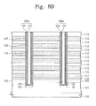
- FIGS. 8A to 8F are cross-sectional views taken along line I-I′ of FIG. 1A for describing other modification example of a method of fabricating 3D semiconductor memory device according to an embodiment of the inventive concept;
- FIGS. 9A to 9D are cross-sectional views taken along line I-I′ of FIG. 1A for describing still other modification example of a method of fabricating 3D semiconductor memory device according to an embodiment of the inventive concept;
- FIGS. 10A to 10C are cross-sectional views taken along line I-I′ of FIG. 1A for describing even other modification example of a method of fabricating 3D semiconductor memory device according to an embodiment of the inventive concept;
- FIG. 11 is a cross-sectional view illustrating a 3D semiconductor memory device according to another embodiment of the inventive concept.
- FIG. 12A is a cross-sectional view illustrating a modification example of a 3D semiconductor memory device according to another embodiment of the inventive concept
- FIG. 12B is a cross-sectional view illustrating other modification example of a 3D semiconductor memory device according to another embodiment of the inventive concept
- FIG. 12C is a cross-sectional view illustrating still other modification example of a 3D semiconductor memory device according to another embodiment of the inventive concept
- FIG. 12D is a cross-sectional view illustrating even other modification example of a 3D semiconductor memory device according to another embodiment of the inventive concept
- FIG. 12E is a cross-sectional view illustrating yet other modification example of a 3D semiconductor memory device according to another embodiment of the inventive concept.
- FIG. 12F is a cross-sectional view illustrating further modification example of a 3D semiconductor memory device according to another embodiment of the inventive concept.
- FIGS. 13A to 13E are cross-sectional views for describing a method of fabricating 3D semiconductor memory device according to another embodiment of the inventive concept
- FIG. 14 is a cross-sectional view illustrating a modification example of a method of fabricating 3D semiconductor memory device according to another embodiment of the inventive concept
- FIGS. 15A to 15F are cross-sectional views illustrating other modification example of a method of fabricating 3D semiconductor memory device according to another embodiment of the inventive concept
- FIGS. 16A and 16B are cross-sectional views illustrating still other modification example of a method of fabricating 3D semiconductor memory device according to another embodiment of the inventive concept
- FIG. 17 is a block diagram schematically illustrating an example of an electronic system including a 3D semiconductor memory device according to an embodiment of the inventive concept.
- FIG. 18 is a block diagram schematically illustrating an example of a memory card including a 3D semiconductor memory device according to an embodiment of the inventive concept.
- first, second, third, etc. may be used herein to describe various elements, components, regions, layers and/or sections, these elements, components, regions, layers and/or sections should not be limited by these terms. These terms are only used to distinguish one element, component, region, layer or section from another region, layer or section. Thus, a first element, component, region, layer or section discussed below could be termed a second element, component, region, layer or section without departing from the teachings of the present invention.
- spatially relative terms such as “beneath,” “below,” “lower,” “above,” “upper” and the like, may be used herein for ease of description to describe one element or feature's relationship to another element(s) or feature(s) as illustrated in the figures. It will be understood that the spatially relative terms are intended to encompass different orientations of the device in use or operation in addition to the orientation depicted in the figures. For example, if the device in the figures is turned over, elements described as “below” or “beneath” other elements or features would then be oriented “above” the other elements or features. Thus, the term “below” can encompass both an orientation of above and below. The device may be otherwise oriented (rotated 90 degrees or at other orientations) and the spatially relative descriptors used herein interpreted accordingly.
- Embodiments of the present invention are described herein with reference to cross-section and perspective illustrations that are schematic illustrations of idealized embodiments (and intermediate structures) of the present invention. As such, variations from the shapes of the illustrations as a result, for example, of manufacturing techniques and/or tolerances, are to be expected. Thus, embodiments of the present invention should not be construed as limited to the particular shapes of regions illustrated herein but are to include deviations in shapes that result, for example, from manufacturing. For example, a sharp angle may be somewhat rounded due to manufacturing techniques/tolerances.
- FIG. 1A is a plan view illustrating a 3D semiconductor memory device according to an embodiment of the inventive concept.
- FIG. 1B is a cross-sectional view taken along line I-I′ of FIG. 1A .
- FIG. 1C is a magnified view of a portion A of FIG. 1B .
- a well region 102 doped with a first conductive dopant may be disposed in a semiconductor substrate 100 (hereinafter referred to as a substrate).
- the substrate 100 may be a silicon substrate, a germanium substrate or a silicon-germanium substrate, for example a common source region 105 doped with a second conductive dopant may be formed in the well region 102 .
- An upper surface of the common source region 105 may be disposed on the substantially same level as that of the upper surface of the substrate 100 .
- a lower surface of the common source region 105 may be disposed on a level higher than that of a lower surface of the well region 102 .
- One of the first and second conductive dopants may be an n-type dopant, and the other may be a p-type dopant.
- the well region 102 may be doped with a p-type dopant
- the common source region 105 may be doped with an n-type dopant.
- a stack-structure including insulation patterns 110 a and gate patterns 155 L, 155 a 1 , 155 a and 155 U that are stacked alternately and repeatedly, may be disposed on the common source region 105 .
- a plurality of the stack-structures may be disposed on the common source region 105 .
- the stack-structures may be extended side by side in a first direction.
- the stack-structures may be spaced apart in a second direction perpendicular to the first direction.
- the first and second directions may be parallel with the upper surface of the substrate 100 .
- a vertical active pattern 130 may pass through the stack-structure.
- the vertical active pattern 130 may be extended into a recess region 120 that is formed in the common source region 105 under the vertical active pattern 130 . Therefore, the vertical active pattern 130 may be connected to the well region 102 under the vertical active pattern 130 .
- the recess region 120 may vertically pass through the common source region 105 .
- a bottom surface of the recess region 120 may be disposed on a level lower than that of the lower surface of the common source region 105 .
- the vertical active pattern 130 may contact the bottom surface of the recess region 120 . Accordingly, the vertical active pattern 130 may contact the well region 102 .
- the vertical active pattern 130 may contact a sidewall of the recess region 120 . As a result, the vertical active pattern 130 may directly contact the common source region 105 .
- a portion 122 of the well region 102 just under the bottom surface of the recess region 120 may have a high dopant concentration.
- the first conductive dopant concentration of the portion 122 of the well region 102 may be higher than the first conductive dopant concentration of another portion of the well region 102 .
- the vertical active pattern 130 may have a hollow pipe shape or a macaroni shape.
- the lower end of the vertical active pattern 130 may be in a closed state.
- the inside of the vertical active pattern 130 may be filled with a filling dielectric pattern 132 .
- a gate dielectric layer 150 may be disposed between a sidewall of the vertical active pattern 130 and each of the gate patterns 155 L, 155 a 1 , 155 a and 155 U.
- the gate dielectric layer 150 may be extended to cover an upper surface and a lower surface of each of the gate patterns 155 L, 155 a 1 , 155 a and 155 U. That is, the extended portion of the gate dielectric layer 150 may be disposed between each of the gate patterns 155 L, 155 a 1 , 155 a and 155 U and the insulation pattern 110 a adjacent to each of the gate patterns 155 L, 155 a 1 , 155 a and 155 U.
- the gate dielectric layer 150 may include a tunnel dielectric layer 141 , a charge storage layer 142 and a blocking dielectric layer 143 .
- the tunnel dielectric layer 141 may be adjacent to the sidewall of the vertical active pattern 130
- the blocking dielectric layer 143 may be adjacent to each of the gate patterns 155 L, 155 a 1 , 155 a and 155 U.
- the charge storage layer 142 may be disposed between the tunnel dielectric layer 141 and the blocking dielectric layer 143 . According to an embodiment of the inventive concept, as illustrated in FIG.
- the entirety of the gate dielectric layer 150 may be extended to cover the upper and lower surfaces of each of the gate patterns 155 L, 155 a 1 , 155 a and 155 U.
- the tunnel dielectric layer 141 may include oxide and/or oxynitride.
- the tunnel dielectric layer 141 may be single-layered or multi-layered.
- the charge storage layer 142 may include a dielectric material having traps for storing electric charges, for example, the charge storage layer 142 may include nitride and/or metal-oxide.
- the blocking dielectric layer 143 may include a high-k dielectric layer having a dielectric constant higher than that of the tunnel dielectric layer 141 .
- the high-k dielectric layer in the blocking dielectric layer 143 may include metal-oxide such as aluminum-oxide or hafnium-oxide.
- the blocking dielectric layer 143 may further include a barrier dielectric layer.
- the barrier dielectric layer in the blocking dielectric layer 143 may include a dielectric material having a greater band gap than the high-k dielectric layer in the blocking dielectric layer 143 .
- the barrier dielectric layer may include oxide.
- the barrier dielectric layer may be disposed between the high-k dielectric layer and the charge storage layer 142 .
- a lowermost gate pattern 155 L in the stack-structure may correspond to a ground selection gate.
- a ground selection transistor including the lowermost gate pattern 155 L may include a vertical channel region that is defined in the sidewall of the vertical active pattern 130 . As illustrated in FIGS. 1A and 1B , the entire lower surface of the lowermost gate pattern 155 L may substantially overlap with the common source region 105 .
- An uppermost gate pattern 155 U in the stack-structure may correspond to a string selection gate.
- Gate patterns 155 a 1 and 155 a between the uppermost gate pattern 155 U and the lowermost gate pattern 155 L may correspond to cell gates.
- a string selection transistor including the uppermost gate pattern 155 U and cell transistors including the cell gates may also include vertical channel regions that are defined in the sidewall of the vertical active pattern 130 a . The vertical channel regions of the ground selection transistor, the cell transistor and the string selection transistor configuring one cell string may be defined in the vertical active pattern 130 .
- a gate pattern most adjacent to the lowermost gate pattern 155 L may correspond to a dummy cell gate.
- the gate pattern 1551 a disposed just on the lowermost gate pattern 155 L may be a dummy gate pattern.
- the gate pattern 155 a 1 that is stacked secondly from the substrate 100 may be a dummy cell gate.
- one of the insulation pattern 110 a is disposed between the lowermost gate pattern 155 L and the secondly-stacked gate pattern 155 a 1 .
- a dummy cell transistor including the secondly-stacked gate pattern 155 a 1 may have the same shape as that of a cell transistor storing data, but may not serve as the cell transistor.
- the dummy cell transistor may perform only a turn-on/off function.
- the secondly-stacked gate pattern 155 a 1 may be a second ground selection gate.
- the cell string may include a plurality of stacked ground selection transistors.
- a plurality of the vertical active patterns 130 may pass through each of the stack-structures. As illustrated in FIG. 1A , the vertical active patterns 130 passing though each of the stack-structures may be arranged in the first direction to form one column. Alternatively, the vertical active patterns 130 passing though each of the stack-structures may be arranged in a zigzag shape in the first direction.
- the vertical active pattern 130 may include a semiconductor material.
- the vertical active pattern 130 may include the same semiconductor material as that of the substrate 100 .
- the vertical active pattern 130 may have an undoped state, or may be doped with the first conductive dopant.
- the vertical active pattern 130 may have a poly-crystalline state or a single crystalline state.
- the gate patterns 155 L, 155 a 1 , 155 a and 155 U include a conductive material.
- the gate patterns 155 L, 155 a 1 , 155 a and 155 U may include at least one of a doped semiconductor (for example, doped silicon and others), a metal (for example, tungsten, aluminum, copper and others), a transition metal (for example, titanium, tantalum and others) or a conductive metal nitride (for example, a titanium nitride, a tantalum nitride and others).
- the insulation patterns 110 a may include oxide.
- a device isolation pattern 160 a may be disposed between the stack-structures. An upper surface of the device isolation pattern 160 a and an upper surface of the stack-structure may substantially be coplanar.
- An interlayer dielectric 165 may be disposed on the substrate 100 .
- a contact plug 167 may be connected to an upper end of the vertical active pattern 130 through the interlayer dielectric 165 .
- a drain being doped with the second conductive dopant may be formed in the upper portion of the vertical active pattern 130 .
- a lower surface of the drain may be disposed on a level adjacent to an upper surface of the uppermost gate pattern 155 U.
- a bit line 170 may be disposed on the interlayer dielectric 165 , and may be connected to the contact plug 167 .
- the bit line 170 may be extended in the second direction and cross over the stack-structure.
- the interlayer dielectric 165 may include oxide.
- the contact plug 167 includes a conductive material.
- the contact plug 167 may include tungsten.
- the bit line 170 also includes a conductive material.
- the bit line 170 may include tungsten, copper, aluminum or the like.
- the vertical active pattern 130 may be disposed in the recess region 120 passing though the common source region 105 and be connected to the well region 102 .
- the common source region 105 may be disposed under the lowermost gate pattern 155 L. Therefore, a distance between the vertical active pattern 130 and the common source region can be minimized, and also the vertical active pattern 130 can be connected to the well region 102 . Consequently, a current flowing through the vertical active pattern 130 can quickly flow to the common source region 105 . Accordingly, the reduction of an amount of current in a cell transistor can be minimized.
- the vertical active pattern 130 is connected to the well region 102 , such that the erasing operation of cell transistors is very easy. As a result, the 3D semiconductor memory device can be implemented which has excellent reliability and is optimized for high integration.
- FIG. 2A is a cross-sectional view taken along line I-I′ of FIG. 1A for describing a modification example of a 3D semiconductor, memory device according to an embodiment of the inventive concept.
- protection dielectric patterns 173 a may be disposed between the insulation patterns 110 a and the vertical active pattern 130 and between the inner sidewall of the recess region 120 and the vertical active pattern 130 .
- the protection dielectric pattern 173 a may include a dielectric material for protecting the vertical active pattern 130 in a fabricating process.
- the protection dielectric pattern 173 a may include oxide.
- a capping semiconductor pattern 175 may be disposed on the vertical active pattern 130 .
- the capping semiconductor pattern 175 may also be disposed on the protection dielectric pattern 173 a that is disposed between an uppermost insulation pattern 110 a and the vertical active pattern 130 .
- the upper end of the vertical active pattern 130 may be disposed on a level lower than an upper surface of the uppermost insulation pattern 110 a .
- the upper surface of the capping semiconductor pattern 175 and the upper surface of the uppermost insulation pattern 110 a may be substantially coplanar.
- the capping semiconductor pattern 175 may include the same semiconductor material as that of the vertical active pattern 130 .
- the capping semiconductor pattern 175 may be doped with the second conductive dopant.
- the contact plug 167 may be connected to the capping semiconductor pattern 175 .
- FIG. 2B is a cross-sectional view taken along line I-I′ of FIG. 1A for describing other modification example of a 3D semiconductor memory device according to an embodiment of the inventive concept.
- a bottom surface of the recess region 120 may be disposed on a level higher than the lower surface of the common source region 105 .
- a region 122 a being counter-doped with the first conductive dopant may be disposed under the bottom surface of the recess region 120 a .
- the counter-doped region 122 a may contact the vertical active pattern 130 and the well region 102 . Therefore, the vertical active pattern 130 may be connected to the well region 102 through the counter-doped region 122 a.
- FIG. 3A is a cross-sectional view taken along line I-I′ of FIG. 1A for describing still other modification example of a 3D semiconductor memory device according to an embodiment of the inventive concept.
- FIG. 3B is a magnified view of a portion B of FIG. 3A .
- a gate dielectric layer 150 a according to the modification example may be disposed between a vertical active pattern 130 a and each of the gate patterns 155 L, 155 a 1 , 155 a and 155 U.
- the gate dielectric layer 150 a may include a first sub-layer 147 and a second sub-layer 149 .
- the first sub-layer 147 may be substantially extended vertically and be disposed between the vertical active pattern 130 a and the insulation pattern 110 a .
- the second sub-layer 149 may be substantially extended horizontally and cover the lower surface and upper surface of each of the gate patterns 155 L, 155 a 1 , 155 a and 155 U.
- the gate dielectric layer 150 a may include the tunnel dielectric layer, the charge storage layer and the blocking dielectric layer.
- the first sub-layer 147 may include at least a portion of the tunnel dielectric layer
- the second sub-layer 149 may include at least a portion of the blocking dielectric layer.
- One of the first and second sub-layers 147 and 149 may include the charge storage layer.
- a portion of the gate dielectric layer 150 a including the tunnel dielectric layer, the charge storage layer and the blocking dielectric layer may be extended vertically, and another portion of the gate dielectric layer 150 a may be extended horizontally.
- the vertical active pattern 130 a may include first and second semiconductor patterns 123 and 124 .
- the first semiconductor pattern 123 may be disposed between the second semiconductor pattern 124 and the first sub-layer 147 .
- the first semiconductor pattern 123 may contact the first sub-layer 147 .
- the first semiconductor pattern 123 may have a macaroni shape or a pipe shape where an upper end and a lower end are opened.
- the first semiconductor pattern 123 may not contact the inner surface of the recess region 120 by the first sub-layer 147 .
- the second semiconductor pattern 124 may contact the first semiconductor pattern 123 and the inner surface of the recess region 120 .
- the second semiconductor pattern 124 may have a macaroni shape or a pipe shape where a lower end is closed.
- a filling dielectric pattern 132 may fill the inside of the second semiconductor pattern 124 .
- the first and second semiconductor patterns 123 and 124 may have an undoped state or be doped with a dopant (i.e., the first conductive dopant) having the same type as that of the well region 102 .
- the first sub-layer 147 of the gate dielectric layer 150 a may include a tunnel dielectric layer 141 , a charge storage layer 142 and a barrier dielectric layer 144 .
- the second sub-layer 149 may include a high-k dielectric material (for example, metal-oxide such as aluminum oxide or hafnium oxide) having a dielectric constant higher than that of the tunnel dielectric layer 141 .
- the barrier dielectric layer 144 may include a dielectric material having a greater band gap than that of the high-k dielectric material.
- the barrier dielectric layer 144 may include oxide.
- the second sub-layer 149 and the barrier dielectric layer 144 disposed between the charge storage layer 142 and each of the gate patterns 155 L, 155 a 1 , 155 a and 155 U, may included in the blocking dielectric layer.
- the first sub-layer 147 may include the tunnel dielectric layer 141 , the charge storage layer 142 and a portion (i.e., the barrier dielectric layer 144 ) of the blocking dielectric layer
- the second sub-layer 149 may include another portion (i.e., the high-k dielectric layer) of the blocking dielectric layer.
- an embodiment of the inventive concept is not limited thereto.
- the first and second sub-layers of the gate dielectric layer may be combined differently.
- FIG. 3C is a magnified view of a portion B of FIG. 3A for describing even other modification example of a 3D semiconductor memory device according to an embodiment of the inventive concept.
- a first sub-layer 147 a of a gate dielectric layer 150 b according to the modification example may include a tunnel dielectric layer 141 and a charge storage layer 142
- a second sub-layer 149 a of the gate dielectric layer 150 b may include a barrier dielectric layer 144 and a high-k dielectric layer 146 .
- the high-k dielectric layer 146 may be formed of the same material as the high-k dielectric material that has been described above with reference to FIG. 3B .
- the second sub-layer 149 b may correspond to a blocking dielectric layer.
- the first sub-layer 147 a may include the tunnel dielectric layer 141 and the charge storage layer 142
- the second sub-layer 149 a may include the blocking dielectric layer.
- FIG. 3D is a magnified view of a portion B of FIG. 3A for describing yet other modification example of a 3D semiconductor memory device according to an embodiment of the inventive concept.
- a first sub-layer 147 b of a gate dielectric layer 150 c according to the modification example may include the tunnel dielectric layer
- a second sub-layer 149 b of the gate dielectric layer 150 c may include the charge storage layer 142 and the blocking dielectric layer 143 .
- the tunnel dielectric layer in the gate dielectric layer 150 c may be extended vertically and be disposed between the vertical active pattern 130 a and the insulation pattern 110 a , and the charge storage layer 142 and the blocking dielectric layer 143 in the gate dielectric layer 150 c may be extended horizontally and cover the upper surface and lower surface of each of the gate patterns 155 L, 155 a 1 , 155 a and 155 U.
- the first and second sub-layers according to an embodiment of the inventive concept are not limited to the modification examples that have been described above with reference to FIGS. 3B, 3C and 3D .
- the first and second sub-layers may be combined differently.
- FIG. 4A is a cross-sectional view taken along line I-I′ of FIG. 1A for describing further modification example of a 3D semiconductor memory device according to an embodiment of the inventive concept.
- FIG. 4B is a magnified view of a portion C of FIG. 4A .
- the entirety of a gate dielectric layer 150 d between the vertical active pattern 130 a and each of the gate patterns 155 L, 155 a 1 , 155 a and 155 U may be substantially extended vertically. That is, the tunnel dielectric layer 141 , charge storage layer 142 and blocking dielectric layer 143 of the gate dielectric layer 150 d may be substantially extended vertically.
- An extended portion of the gate dielectric layer 150 d may be disposed between the vertical active pattern 130 a and the insulation pattern 110 a .
- the stack-structure of FIGS. 1A and 1B may have a line shape that is extended in the first direction. Unlike this, the stack-structure may include gate patterns having a flat plate shape. This will be described below with reference to the accompanying drawings.
- FIG. 5A is a plan view illustrating still further modification example of a 3D semiconductor memory device according to an embodiment of the inventive concept.
- FIG. 5B is a cross-sectional view taken along line II-II′ of FIG. 5A .
- a stack-structure according to the modification example may include gate patterns 220 L, 220 a , 220 and 220 U and insulation patterns 210 and 210 U that are stacked alternately and repeatedly.
- a lowermost gate pattern 220 L in the stack-structure may be a ground selection gate
- an uppermost gate pattern 220 U in the stack-structure may be a string selection gate.
- the gate pattern 220 a just on the lowermost gate pattern 220 L may be used as a cell gate, a dummy cell gate or a second ground selection gate.
- the gate patterns 220 between the gate pattern 220 a just on the lowermost gate pattern 220 L and the upper gate pattern 220 U may be used as cell gates.
- the gate patterns 220 L, 220 a and 220 under a string selection gate may have a flat plate shape.
- the uppermost gate pattern 220 U corresponding to the string selection gate may have a line shape that is extended in the first direction.
- the uppermost gate pattern 220 U may be provided in plurality, and the uppermost gate patterns 220 U may be extended side by side in the first direction.
- the bit line 170 may be extended in the second direction and cross over the uppermost gate pattern 220 U.
- an uppermost insulation pattern 210 U on the uppermost gate pattern 220 U may also be extended in the first direction.
- the vertical active pattern 130 a may pass through the stack-structure and be extended into the recess region 120 under it.
- the lowermost gate pattern 220 L corresponding to the ground selection gate may be disposed on the common source region 105 in the substrate 100 .
- the entire lower surface of the lowermost gate pattern 220 L may substantially overlap with the common source region 105 .
- the gate dielectric layer 150 d may be disposed between the vertical active pattern 130 a and the inner sidewall of an opening 115 passing through the stack-structure.
- the gate dielectric layer 150 d may be substantially extended vertically.
- the opening 115 and the recess region 120 may be self-aligned.
- the gate dielectric layer 150 d may be extended into the recess region 120 .
- the lower end of the gate dielectric layer 150 d in the recess region 120 may be disposed on a level higher than the lower surface of the recess region 120 .
- a lower interlayer dielectric 163 may be disposed between the uppermost gate patterns 220 U.
- An upper surface of the lower interlayer dielectric 163 may be coplanar with an upper surface of the uppermost insulation pattern 210 U.
- An upper interlayer dielectric 165 may be disposed on the lower interlayer dielectric 163 and the uppermost gate patterns 220 U.
- the insulation patterns 210 and 210 U may include oxide, nitride and/or oxynitride.
- the gate patterns 220 L, 220 a , 220 and 220 U may include at least one of a doped semiconductor (for example, doped silicon), a metal (for example, tungsten and others) or a conductive metal nitride (for example, a titanium nitride, a tantalum nitride and others).
- a doped semiconductor for example, doped silicon
- a metal for example, tungsten and others
- a conductive metal nitride for example, a titanium nitride, a tantalum nitride and others.
- the capping semiconductor pattern 175 of FIG. 2A may be disposed on the vertical active pattern 130 or 130 a that has been disclosed in FIG. 1B, 3A, 4A or 5B .
- FIGS. 6A to 6H are cross-sectional views taken along line I-I′ of FIG. 1A for describing a method of fabricating 3D semiconductor memory device according to an embodiment of the inventive concept.
- a well region 102 may be formed by providing a first conductive dopant into the substrate 100 .
- a common source region 105 may be formed by providing a second conductive dopant into the upper portion of the well region 102 .
- Insulation layers 110 and sacrificial layers 112 may be alternately and repeatedly stacked on the common source region 105 .
- the insulation layers 110 may be formed as oxide layers.
- the sacrificial layers 112 may be formed of materials having an etch selectivity with respect to the insulation layers 112 .
- the sacrificial layers 112 may be formed as nitride layers.
- an opening 115 and a recess region 120 may be formed by sequentially patterning the insulation layers 110 , sacrificial layers 112 and the substrate 100 .
- the opening 115 may pass through the insulation layers 110 and sacrificial layers 112 , and the recess region 120 may be formed in the common source region 102 under the opening 115 (i.e., in a portion of the substrate 100 ).
- the recess region 120 is self-aligned in the opening 115 by sequentially patterning the insulation layers 110 and sacrificial layers 112 and the substrate 100 .
- the recess region 120 may pass through the common source region 105 , and the bottom surface of the recess region 120 may be disposed on a level lower than the lower surface of the common source region 105 . Therefore, the well region 102 may be exposed to the bottom surface of the recess region 120 , and the common source region 105 may be exposed to the inner sidewall of the recess region 120 .
- a high concentration region 122 may be formed by providing the first conductive dopant into the well region 102 through the bottom surface of the recess region 120 . The high concentration region 122 of the first conductive dopant may be higher than another portion of the well region 102 . That is, due to the high concentration region 122 , the well region 102 may partially have a high dopant concentration.
- a semiconductor layer may be conformally formed on the substrate 100 having the opening 115 and the recess region 120 . Therefore, the semiconductor layer may be formed to have a substantially uniform thickness on the inner surface of the recess region 120 and an inner sidewall of the opening 115 .
- the semiconductor layer may contact the inner surface (i.e., an inner sidewall and a bottom surface) of the recess region 120 .
- the semiconductor layer may be formed in a chemical vapor deposition process and/or an atomic layer deposition process.
- a filling dielectric layer may be formed on the semiconductor layer to fill the opening 115 .
- the filling dielectric layer may be formed as an oxide layer.
- a trench 135 may be formed by sequentially patterning the insulation layers 110 and sacrificial layers 112 , such that insulation patterns 110 a and the sacrificial patterns 112 a being alternately and repeatedly stacked may be formed at a side of the trench 135 .
- the insulation patterns 110 a and sacrificial patterns 112 a may include the opening 115 . That is, the vertical active patterns 130 may sequentially pass through the insulation patterns 110 a and the sacrificial patterns 112 a being alternately and repeatedly stacked on the substrate 100 . Sidewalls of the sacrificial patterns 112 a and the insulation patterns 110 a are exposed to the trench 135 .
- empty regions 140 may be formed by removing the sacrificial patterns 112 a exposed to the trench 135 .
- Each of the empty regions 140 corresponds to a region from which the each sacrificial pattern 112 a is removed.
- the empty regions 140 may expose some portions of the sidewall of the vertical active pattern 130 , respectively.
- a gate dielectric layer 150 may be conformally formed on the substrate 100 having the empty regions 140 . Therefore, the gate dielectric layer 150 may be conformally formed on the inner surfaces of the empty regions 140 .
- the gate dielectric layer 15 Q as described above with reference to FIGS. 1B and 1C , may include the tunnel dielectric layer, the charge storage layer and the blocking dielectric layer.
- a gate conductive layer 155 filling the empty regions 140 may be formed on the substrate 100 having the gate dielectric layer 150 .
- the gate conductive layer 155 may also be formed in the trench 135 .
- the gate conductive layer 155 may partially fill the trench 135 . Therefore, a space surrounded by the gate conductive layer 155 may be formed in the trench 135 .
- a bottom surface of the space may be lower than an inner-upper surface of the lowermost empty region 140 .
- the gate patterns 155 L, 155 a 1 , 155 a and 155 U respectively filling the empty regions 140 may be formed by etching the gate conductive layer 155 .
- the gate patterns 155 L, 155 a 1 , 155 a and 155 U are separated by the etching process of the gate conductive layer 155 .
- the etching process of the gate conductive layer 155 may be an isotropic etching process.
- the insulation patterns 110 a and the gate patterns 155 L, 155 a 1 , 155 a and 155 U, being alternately and repeatedly stacked on the substrate 100 may be included in a stack-structure. Subsequently, a device isolation insulation layer 160 may be formed to fill the trench 135 .
- the device isolation insulation layer 160 and the gate dielectric layer 150 may be planarized until the uppermost insulation pattern among the insulation patterns 110 a is exposed. Therefore, a device isolation pattern 160 a may be formed in the trench 135 . Subsequently, by forming the interlayer dielectric 165 , contact plug 167 and bit line 170 of the FIG. 1B on the substrate 100 , the 3D semiconductor memory device that has disclosed in FIGS. 1A, 1B and 1C may be implemented. According to the above-described 3D semiconductor memory device, the opening 115 and the recess region 120 can be formed in self-alignment by sequentially patterning the insulation layers 110 , the sacrificial layers 112 and the substrate 100 (i.e.
- the 3D semiconductor memory device can be implemented which has excellent reliability and is optimized for high integration.
- a method of fabricating the 3D semiconductor memory device that has been disclosed in FIG. 2A will be described below with reference to the accompanying drawings. The method may include the methods that have been described above with reference to FIGS. 6A and 6B .
- FIGS. 7A to 7D are cross-sectional views taken along line I-I′ of FIG. 1A for describing a modification example of a method of fabricating 3D semiconductor memory device according to an embodiment of the inventive concept.
- a protection dielectric layer 173 may be conformally formed on the substrate 100 having the opening 115 and the recess region 120 , and the protection dielectric layer 173 may be etched by a blanket anisotropic etching process until the bottom surface of the recess region 120 is exposed. As illustrated in FIG. 7A , therefore, the protection dielectric layer 173 may be formed on the sidewalls of the recess region 120 and the opening 115 .
- the protection dielectric layer 173 may include a dielectric material having an etch selectivity with respect to the sacrificial layer 112 .
- the protection dielectric layer 173 may be formed of oxide.
- a semiconductor layer may be formed, a filling dielectric layer may be formed on the semiconductor layer, and the filling dielectric layer and the semiconductor layer may be planarized. Therefore, the vertical active pattern 130 and the filling dielectric pattern 132 may be formed in the opening 115 and the recess region 120 .
- the vertical active pattern 130 may contact the bottom surface of the recess region 120 .
- the protection dielectric layer 173 may be disposed between the vertical active pattern 130 and the inner sidewalls of the opening 115 and the recess region 120 .
- the upper ends of the vertical active pattern 130 , filling dielectric pattern 132 and protection dielectric layer 175 may be recessed lower than the upper surface of the uppermost insulation layer 110 .
- a capping semiconductor layer filling the opening 110 may be formed on the substrate 100 , and a capping semiconductor pattern 175 may be formed by planarizing the capping semiconductor layer until the uppermost insulation layer 110 is exposed.
- the capping semiconductor pattern 175 may cover the recessed upper ends of the vertical active pattern 130 , filling dielectric pattern 132 and protection dielectric layer 175 .
- the trench 135 may be formed by sequentially patterning the insulation layers 110 and the sacrificial layers 112 .
- the insulation patterns 110 and the sacrificial patterns 112 a that are alternately and repeatedly stacked may be formed at a side of the trench 135 .
- the sacrificial patterns 112 a exposed to the trench 135 may be removed. Therefore, the empty regions 140 may be formed which respectively exposes some portions of the protection dielectric layer 173 disposed on the sacrificial patterns 112 a and the vertical active patterns 130 .
- the protection dielectric layer 173 has an etch selectivity with respect to the sacrificial patterns 112 a , and thus it can protect the vertical active pattern 130 from a process of removing the sacrificial patterns 112 a .
- the protection dielectric layer 173 may be used as an etch stop layer in the process of removing the sacrificial patterns 112 a .
- the exposed portions of the protection dielectric layer 173 may be removed. Therefore, the empty regions 140 may expose some portions of the side wall of the vertical active pattern 130 , respectively.
- the protection dielectric patterns 173 a may be formed between the vertical active pattern 130 and the insulation patterns 110 a and between the vertical active pattern 130 and the inner sidewall of the recess region 120 .
- the protection dielectric patterns 173 a correspond to remaining portions of protection dielectric layer 173 .
- the gate dielectric layer 150 may be conformally formed on the substrate 100 having the empty regions 140 , and the gate patterns 155 L, 155 a 1 , 155 a and 155 U respectively filling the empty regions 140 may be formed. Afterwards, the device isolation pattern 160 a filling the trench 135 may be formed. Subsequently, by forming the interlayer dielectric 165 , contact plug 167 and bit line 170 of FIG. 2A , the 3D semiconductor memory device of FIG. 2A can be implemented.
- the features of a method, that fabricates the 3D semiconductor memory device that has been disclosed in FIG. 2B may have a process of forming the lower surface of the recess region 120 higher than the lower surface of the common source region 105 and a process of forming the counter-doped region 122 a by counter-doping the common source region 105 under the bottom surface of the recess region 120 with the first conductive dopant.
- Other processes may be the same as the processes that have been described above with reference to FIGS. 7A to 7D .
- FIG. 3A a method of fabricating the 3D semiconductor memory device that has been disclosed in FIG. 3A will be described below with reference to the accompanying drawings.
- the method may include the methods that have been described above with reference to FIGS. 6A and 6B .
- FIGS. 8A to 8F are cross-sectional views taken along line I-I′ of FIG. 1A for describing other modification example of a method of fabricating 3D semiconductor memory device according to an embodiment of the inventive concept.
- a first sub-layer 147 may be conformally formed on the substrate 100 having the opening 115 and the recess region 120 .
- the first sub-layer 147 may be conformally formed on the inner sidewall of the opening 115 and the inner surface of the recess region 120 .
- a first semiconductor layer 121 may be conformally formed on the substrate 100 having the first sub-layer 147 .
- portions of the first sub-layer 147 and the first semiconductor layer 121 disposed on the bottom surface of the recess region 120 may be removed.
- portions of the first sub-layer 147 and the first semiconductor layer 121 disposed outside opening 115 may also be removed. Therefore, the first sub-layer 147 and the first semiconductor pattern 123 that are sequentially stacked on the sidewalls of the recess region 120 and opening 115 may be formed.
- the first semiconductor pattern 123 correspond to a portion of the first semiconductor layer 121 .
- the first semiconductor pattern 123 may be formed. The first semiconductor pattern 123 may not contact the inner surface of the recess region 120 by the first sub-layer 147 .
- the first sub-layer 147 by isotropic-etching the first sub-layer 147 , at least one portion of the inner sidewall of the recess region 120 may be exposed. At this point, a portion of the first semiconductor pattern 123 in the recess region 120 may also be etched.
- a second semiconductor layer may be conformally formed on the substrate 100 , a filling dielectric layer filling the opening 115 may be formed on the second semiconductor layer.
- the second semiconductor layer may contact the first semiconductor pattern 123 , and also the second semiconductor layer may contact the bottom surface and exposed inner sidewall of the recess region 120 .
- a second semiconductor pattern 124 and a filling dielectric pattern 132 may be formed in the opening 115 and the recess region 120 .
- the second semiconductor pattern 124 may contact the bottom surface and inner sidewall of the recess region 120 and the first semiconductor pattern 123 .
- the first and second semiconductor patterns 123 and 124 may configure a vertical active pattern 130 a.
- the trench 135 , the insulation patterns 110 a and the sacrificial patterns 112 may be formed by sequentially patterning the insulation layers 110 and the sacrificial layers 112 .
- the empty regions 140 may be formed by removing the sacrificial patterns 112 .
- the empty regions 140 may expose some portions of the first sub-layer 147 , respectively.
- a second sub-layer 149 may be conformally formed on the substrate 100 having the empty regions 140 .
- the second sub-layer 149 may be conformally formed on the inner surfaces of the empty regions 140 .
- the second sub-layer 149 may contact the first sub-layer 147 exposed to the empty regions 140 .
- the first and second sub-layers 147 and 149 may be included in the gate dielectric layer 150 a .
- the first sub-layer 147 may include at least a portion of the tunnel dielectric layer, and the second sub-layer 149 may include at least a portion of the blocking dielectric layer.
- one of the first and second sub-layers 147 and 149 may include the charge storage layer.
- the first and second sub-layers 147 and 149 may be the same as the layers that have been described above with reference to FIG. 3B . Unlike this, the first and second sub-layers 147 and 149 may be replaced with the first and second sub-layers 147 a and 149 a of the FIG. 3C , respectively. Unlike this, the first and second sub-layers 147 and 149 may be replaced with the first and second sub-layers 149 b and 149 c of the FIG. 3C , respectively.
- the gate patterns 155 L, 155 a 1 , 155 a and 155 U respectively filling the empty regions 140 may be formed, and the device isolation pattern 160 a filling the trench 135 may be formed.
- the interlayer dielectric 165 , the contact plug 167 and the bit line 170 that have been disclosed in FIG. 3A may be formed.
- a method of fabricating the 3D semiconductor memory device that has been disclosed in FIGS. 4A and 4B will be described below with reference to the accompanying drawings. The method may include the methods that have been described above with reference to FIGS. 6A and 6B .
- FIGS. 9A to 9D are cross-sectional views taken along line I-I′ of FIG. 1A for describing still other modification example of a method of fabricating 3D semiconductor memory device according to an embodiment of the inventive concept.
- a gate dielectric layer 150 d may be conformally formed on the substrate 100 having the opening 115 and the recess region 120 .
- a first semiconductor layer may be conformally formed on the gate dielectric layer 150 d .
- the first semiconductor layer and the gate dielectric layer 150 d may be etched by a blanket-anisotropic-etching process until the bottom of the recess region 120 is exposed, such that a first semiconductor pattern 123 may be formed in the opening 115 and the recess region 120 .
- the gate dielectric layer 150 d may also be restrictively disposed in the opening 115 and the recess region 120 .
- the first semiconductor pattern 123 may not contact the side wall of the opening 115 and the inner surface of the recess region 120 by the gate dielectric layer 150 d.
- a second semiconductor may be conformally formed over the substrate 100 , and a filling dielectric layer may be formed on the second semiconductor layer.
- a second semiconductor pattern 124 and a filling dielectric pattern 132 may be formed in the opening 115 and the recess region 120 .
- the first and second semiconductor patterns 123 and 124 may configure a vertical active pattern 130 a .
- a trench 135 , insulation patterns 110 a and sacrificial patterns 112 a may be formed by sequentially patterning the insulation layers 110 and the sacrificial layers 112 . According to the modification example, a portion of the lowermost insulation layer among the insulation layers 110 may remain under the trench 135 .
- empty regions 140 may be formed by removing the sacrificial patterns 112 a .
- the empty regions 140 may expose the gate dielectric layer 150 d .
- the blocking dielectric layer 143 (see FIG. 4B ) in the gate dielectric layer 150 d may be exposed.
- a gate conductive layer 155 filling the empty regions 140 may be formed on the substrate 100 .
- gate patterns 155 L, 155 a 1 , 155 a and 155 U filling the empty regions 140 may be formed.
- the device isolation pattern 160 a filling the trench 135 may be formed, and the interlayer dielectric 165 , contact plug 167 and bit line 170 of FIG. 4A may be formed.
- the 3D semiconductor memory device of FIGS. 4A and 4B can be implemented.
- a method of fabricating the 3D semiconductor memory device of FIGS. 5A and 5B will be described below with reference to the accompanying drawings.
- FIGS. 10A to 10C are cross-sectional views taken along line I-I′ of FIG. 1A for describing even other modification example of a method of fabricating 3D semiconductor memory device according to an embodiment of the inventive concept.
- insulation layers 210 and gate layers 220 may be alternately and repeatedly stacked on the common source region 105 in the substrate 100 .
- the insulation layers 210 and gate layers 220 L, 220 a and 220 may have a flat plate shape.
- an uppermost gate pattern 220 U and an uppermost insulation pattern 210 U may be formed by patterning an uppermost insulation layer and an uppermost gate layer.
- the uppermost gate pattern 220 U and the uppermost insulation pattern 210 U may have a line shape that is extended in one direction as illustrated in FIG. 5A .
- a lower interlayer dielectric 163 may be formed on the substrate 100 , and the lower interlayer dielectric 163 may be planarized.
- An opening 115 and a recess region 120 may be formed by sequentially patterning the uppermost insulation pattern 210 U, the uppermost gate pattern 220 U, the insulation layers 210 , the gate layers 220 L, 220 a and 220 and the common source region 105 .
- the recess region 120 may be formed in self-alignment in the opening 115 .
- a high concentration region 122 may be formed.
- a gate dielectric layer 150 d may be conformally formed over the substrate 100 , and a first semiconductor layer may be conformally formed on the gate dielectric layer 150 d .
- a first semiconductor pattern 123 may be formed in the opening 115 and the recess region 120 .
- a second semiconductor layer may be conformally formed over the substrate 100 , and a filling dielectric layer may be formed on the second semiconductor.
- a second semiconductor pattern 124 and a filling dielectric pattern 132 may be formed in the opening 115 and the recess region 120 .
- the first and second semiconductor patterns 123 and 124 may configure a vertical active pattern 130 a .
- the upper dielectric layer 165 , contact plug 167 and bit line 170 of FIG. 5B may be formed.
- the 3D semiconductor memory device of FIGS. 5A and 5B can be implemented.
- the uppermost gate pattern 220 U may be formed, and thereafter the vertical active pattern 130 a may be formed. Unlike this, after the opening 115 , the recess region 120 and the vertical active pattern 130 a may be formed, and then the uppermost gate pattern 220 U may be formed.
- a stack-structure having a line shape may be formed by sequentially patterning the gate layers 220 , 220 a and 220 L and insulation layers 110 under the uppermost gate pattern 220 U.
- the 3D semiconductor memory device of FIGS. 4A and 4B can be implemented.
- the 3D semiconductor memory device of FIGS. 4A and 4B may be implemented in the method that has been described above with reference to FIGS. 9A to 9D or a modified method of a portion of the fabricating method of FIGS. 10A to 10C .
- FIG. 11 is a cross-sectional view illustrating a 3D semiconductor memory device according to another embodiment of the inventive concept.
- a well region 102 doped with a first conductive dopant may be disposed in a substrate 100 .
- a stack-structure may be disposed on the well region 102 .
- the stack-structure may include insulation patterns 110 a and gate patterns 155 L, 155 a 1 , 155 a and 155 U that are alternately and repeatedly stacked on the well region 102 .
- a plurality of the stack-structures may be disposed on the well region 102 .
- the stack-structures may be spaced apart from each other. As illustrated in FIG. 1 a , the stack-structures may be extended in parallel.
- a vertical active pattern 280 may pass through the stack-structure. Also, the vertical active pattern 280 may be extended into a recess region 120 that is formed in the substrate 100 under the vertical active pattern 280 .
- the vertical active pattern 280 may include a lower active pattern 250 and an upper active pattern 270 that are sequentially stacked.
- the lower active pattern 250 may fill the recess region 120 .
- the upper active pattern 270 may contact the inner surface (i.e., inner sidewall and bottom surface) of the recess region 120 .
- the lower active pattern 250 is disposed in the recess region 120 and contacts the well region 102 .
- the upper surface of the lower active pattern 250 may be disposed on a level higher than that of the upper surface of the substrate 100 .
- the upper surface of the lower active pattern 250 may be higher than the lower surface of the lowermost gate pattern 155 L and lower than the upper surface of the lowermost gate pattern 155 L.
- the inventive concept is not limited thereto.
- the upper active pattern 270 contacts the upper surface of the lower active pattern 250 .
- the lower active pattern 250 may have a pillar shape, and the upper active pattern 270 may have a pipe shape or a macaroni shape.
- the inside of the upper active pattern 270 may be filled with a filling dielectric pattern 132 .
- the lower and upper active patterns 250 and 270 may include a semiconductor material.
- the lower and upper active patterns 250 and 270 may include the same semiconductor material as that of the substrate 100 .
- the lower and upper active patterns 250 and 270 may include silicon.
- the lower active pattern 250 may have a single crystalline state.
- the upper active pattern 270 may have a poly-crystalline state.
- the lower active pattern 250 may be doped with a dopant having the same type as that of the well region 102 .
- the upper active pattern 270 may be doped with a dopant having the same type as that of the well region 102 , or may have an undoped state.
- a high concentration region 122 may be disposed under the bottom surface of the recess region 120 .
- the high concentration region 122 may correspond to a portion of the well region 102 , and it may have a higher dopant concentration than another portion of the well region 102 .
- a gate dielectric layer 150 may be disposed between a sidewall of the vertical active pattern 280 and each of the gate patterns 155 L, 155 a 1 , 155 a and 155 U. As described above in first embodiment of the inventive concept, the gate dielectric layer 150 may be extended horizontally and cover the upper surface and lower surface of each of the gate patterns 155 L, 155 a 1 , 155 a and 155 U.
- a common source regions 105 a may be disposed in the substrate 100 of the both sides of the stack-structure, respectively.
- the common source region 105 a may be laterally separated from the lower active pattern 250 .
- the common source region 105 a is doped with a second conductive dopant.
- a device isolation pattern 160 a may be disposed between the stack-structures.
- the common source region 105 a may be disposed under the device isolation pattern 160 a .
- a horizontal channel may be generated in the well region 102 under the lowermost gate pattern 155 L.
- the common source region 105 a may be electrically connected to vertical channels that are formed in the vertical active pattern 280 by the horizontal channel in the well region 102 .
- a contact plug 167 passing through the interlayer dielectric 165 may be connected to the upper end of the upper active pattern 270 .
- a drain doped with the second conductive dopant may be disposed in the upper portion of the upper active pattern 270 .
- the lower surface of the drain may be disposed on a level adjacent to the upper surface of the uppermost gate pattern 155 U in the stack-structure.
- the lower active pattern 250 included in the vertical active pattern 280 fills the recess region 120 to contact the well region 102 . Therefore, reliability for the operations of a vertical cell string can be improved. Particularly, reliability for the erasing operation of cell transistors can be enhanced.
- the vertical active pattern 280 may be divided into the lower active pattern 250 and the upper active pattern 270 . Accordingly, an independent and additional process may be performed in the lower active pattern 250 . For example, a dopant concentration may be adjusted in the lower active pattern 250 .
- the 3D semiconductor memory device can be implemented which has excellent reliability and is optimized for high integration.
- FIG. 12A is a cross-sectional view illustrating a modification example of a 3D semiconductor memory device according to another embodiment of the inventive concept.
- a common source region 105 may be extended to the substrate 100 under the stack-structures.
- the entire lower surface of the lowermost gate pattern 155 L may substantially overlap with the common source region 105 .
- the bottom of the recess region 120 may be disposed on a level lower than the lower surface of the common source region 105 .
- the common source region 105 may contact a sidewall of the lower active pattern 250 .
- FIG. 12B is a cross-sectional view illustrating other modification example of a 3D semiconductor memory device according to another embodiment of the inventive concept.
- a vertical active pattern 280 a may include a lower active pattern 250 and an upper active pattern 270 a that are sequentially stacked.
- a gate dielectric layer 150 a may be disposed between the upper active pattern 270 a and each of the gate patterns 155 a 1 , 155 a and 155 U disposed next to the upper active pattern 270 a .
- the gate dielectric layer 150 a may include a first and a second sub-layers 147 and 149 .
- the first sub-layer 147 may be extended vertically and be disposed between the upper active pattern 270 a and the insulation pattern 110 a .
- the second sub-layer 149 may be extended horizontally and cover the lower surface and upper surface of each of the gate patterns 155 a 1 , 155 a and 155 U.
- the upper active pattern 270 a may include a first semiconductor pattern 265 and a second semiconductor pattern 267 .
- the first semiconductor pattern 265 may be disposed between the first sub-layer 147 and the second semiconductor pattern 267 .
- the first semiconductor pattern 265 may be separated from the upper surface of the lower active pattern 250 by a portion of the first sub-layer 147 .
- the second semiconductor pattern 267 contacts the first semiconductor pattern 265 . Also, the second semiconductor pattern 267 contacts the upper surface of the lower active pattern 250 .
- the upper surface of the lower active pattern 250 may be divided into a center portion 252 c contacting the second semiconductor pattern 267 and an edge portion 252 e contacting the first sub-layer 147 .
- the center portion 252 c of the upper surface of the lower active pattern 250 may be disposed on a level lower than that of the edge portion 252 e .
- the upper active pattern 270 a including the first and second semiconductor patterns 265 and 267 may have a pipe shape or a macaroni shape. In this case, the inside of the upper active pattern 270 a may be filled with a filling dielectric pattern 132 .
- the first and second semiconductor patterns 265 and 267 may have a poly-crystalline state.
- the first and second sub-layers 147 and 149 may be replaced by the first and second sub-layers 147 a and 149 a of FIG. 3C or the first and second sub-layers 147 b and 149 b of FIG. 3C .
- the first and second sub-layers 147 and 149 may be formed by another combination of a tunnel dielectric layer, a charge storage layer and a blocking dielectric layer.
- FIG. 12C is a cross-sectional view illustrating still other modification example of a 3D semiconductor memory device according to another embodiment of the inventive concept.
- at least edge portion of the upper surface of the lower active pattern 250 may be disposed on a level higher than the upper surface of the lowermost gate pattern 155 L.
- an oxide layer 255 may be disposed between the sidewall of the lower active pattern 250 and the lowermost gate pattern 155 L.
- the oxide layer 255 may include oxide formed by oxidizing the sidewall of the lower active pattern 250 . Therefore, the width of a first portion of the lower active pattern 250 next to the oxide layer 255 may be less than that of a second portion of the lower active pattern 250 disposed in the recess region 120 .
- the oxide layer 255 and a portion of the second sub-layer 149 may be disposed between the sidewall of the lower active pattern 250 and the lowermost gate pattern 155 L.
- the first sub-layer 147 may not exist between the sidewall of the lower active pattern 250 and the lowermost gate pattern 155 L.
- the charge storage layer may not exist between the sidewall of the lower active pattern 250 and the lowermost gate pattern 155 L. Therefore, the reliability of a ground selection transistor including the lowermost gate pattern 155 L can be improved.
- the lower active pattern 250 may have a single crystalline state. Accordingly, the reliability of the ground selection transistor can be more enhanced.
- FIG. 12D is a cross-sectional view illustrating even other modification example of a 3D semiconductor memory device according to another embodiment of the inventive concept.
- at least the edge portion of the upper surface of a lower active pattern 250 may be disposed on a level higher than the upper surface of a gate pattern 155 a 1 that is stacked secondarily from the substrate 100 and lower than the lower surface of a gate pattern that is stacked thirdly from the substrate 100 .
- the secondarily-stacked gate pattern 155 a 1 and the thirdly-stacked gate pattern are disposed over the lowermost gate pattern 155 L.
- an oxide layer 255 may also be disposed between the secondarily-stacked gate pattern 155 a 1 and the side wall of the lower active pattern 250 .
- a transistor including the secondarily-stacked gate pattern 155 a 1 may be used as a dummy transistor or a second ground selection transistor.
- a cell gate (for example, the thirdly-stacked gate pattern 155 a ) adjacent to the secondarily-stacked gate pattern 155 a 1 may correspond to a dummy cell gate.
- a dummy cell transistor including the dummy cell gate has the same type as that of a cell transistor storing data, but it may not serve as a cell transistor.
- the dummy cell transistor may perform only a turn-on/off function.
- the thirdly-stacked gate pattern may be used as a cell transistor.
- FIG. 12E is a cross-sectional view illustrating yet other modification example of a 3D semiconductor memory device according to another embodiment of the inventive concept.
- the entirety of a gate dielectric layer 150 d between the sidewall of the upper active pattern 270 a and each of the gate patterns 155 a 1 , 155 a and 155 U may be substantially extended vertically and be disposed between an upper active pattern 270 a and an insulation pattern 110 a .
- only an oxide layer 255 may be disposed between the sidewall of the lower active pattern 250 and the lowermost gate pattern 155 L.
- FIG. 12F is a cross-sectional view illustrating further modification example of a 3D semiconductor memory device according to another embodiment of the inventive concept.
- protection dielectric patterns 173 a may be disposed between the upper active pattern 270 a and the insulation patterns 110 a .
- the protection dielectric pattern 173 a may include a dielectric material for protecting the upper active pattern 270 .
- the protection dielectric pattern 173 a may not exist between the lower active pattern 250 and the inner sidewall of the recess region 120 .
- the elements of the above-described modification examples may be combined without clash or replaced.
- the common source region 105 a of FIG. 11 may be replaced with the common source region 105 of FIGS. 12B to 12F .
- the heights of the upper surfaces of the lower active patterns 250 may be replaced.
- FIGS. 13A to 13E are cross-sectional views for describing a method of fabricating 3D semiconductor memory device according to another embodiment of the inventive concept.
- a well region 102 may be formed by providing a first conductive dopant to the substrate 100 .
- Insulation layers 110 and sacrificial layers 112 that are alternately and repeatedly stacked may be formed on the well region 102 .
- a recess region 120 and an opening 115 that are sequentially stacked may be formed by sequentially patterning the insulation layers 110 , the sacrificial layers 112 and the substrate 100 .
- the opening 115 may pass through the insulation layers 110 and the sacrificial layers 112 , and the recess region 120 may be self-aligned in the opening 115 and be formed in the substrate 100 .
- the recess region 120 may expose the well region 102 .
- a high concentration region 122 may be formed by providing the first conductive dopant through the bottom of the recess region 120 .
- a lower active pattern 250 filling the recess region 120 may be formed.
- the upper surface of the lower active pattern 250 may be higher than the upper surface of the substrate 100 . Therefore, a portion of the lower active pattern 250 may fill the lower portion of the opening 115 .
- the lower active pattern 250 contacts the well region 102 .
- the lower active pattern 250 may be formed in a selective epitaxial growth process that uses the substrate 100 exposed by the recess region 120 as a seed layer. Therefore, the lower active pattern 250 may be formed in a single crystalline state.
- the lower active pattern 250 may be formed in a pillar shape.
- the lower active pattern 250 may be doped with the first conductive dopant.
- the lower active pattern 250 may be doped by an in-situ process when the selective epitaxial growth process is performed. Unlike this, the lower active layer 250 may be doped by an ion-implanting process.
- a semiconductor layer may be conformally formed on the substrate 100 having the lower active pattern 250 , and a filling dielectric layer filling the opening 115 may be formed on the semiconductor layer.
- the semiconductor layer may be conformally formed on the inner sidewall of the opening 115 and the upper surface of the lower active pattern 250 .
- the semiconductor layer may contact the lower active pattern 250 .
- the semiconductor layer may be formed in a chemical vapor deposition process and/or an atomic layer deposition process. Therefore, the semiconductor layer may be formed in a poly-crystalline state.
- an upper active pattern 270 and a filling dielectric pattern 132 may be formed in the opening 115 .
- the lower and upper active patterns 250 and 270 may configure a vertical active pattern 280 .
- a trench 135 , insulation patterns 110 a and sacrificial patterns 110 a may be formed by sequentially patterning the insulation layers 110 and the sacrificial layers 112 .
- the vertical active pattern 280 passes through the insulation patterns 110 a and the sacrificial patterns 112 a .
- a common source region 105 a may be formed.
- empty regions 140 may be formed. According to an embodiment of the inventive concept, at least a portion of an lowermost empty regions 140 may expose a portion of the sidewall of the lower active pattern 250 .
- a gate dielectric layer 150 may be conformally formed on the substrate 100 having the empty regions 140 , and a gate conductive layer 155 filling the empty regions 140 may be formed.
- gate patterns 155 L, 155 a 1 , 155 a and 155 U may be formed by etching the gate conductive layer 155 . Subsequently, a device isolation pattern 160 a filling the trench 135 may be formed.
- the 3D semiconductor memory device of FIG. 11 may be implemented by forming the interlayer dielectric 165 , contact plug 167 and bit line 170 of FIG. 11 .
- the opening 115 and the recess region 120 are formed in self-alignment, and the lower active pattern 250 fills the recess region 120 to contact the well region 102 .
- the lower active pattern 250 is formed, and then the upper active pattern 270 may be formed. Therefore, the doping concentration of the lower active pattern 250 may be independently adjusted. As a result, the 3D semiconductor memory device having superior reliability can be implemented.
- the features of the method of fabricating 3D semiconductor memory device that is illustrated in FIG. 12A will be described below with reference to FIG. 14 .
- FIG. 14 is a cross-sectional view illustrating a modification example of a method of fabricating 3D semiconductor memory device according to another embodiment of the inventive concept.
- a second conductive dopant is injected into a substrate 100 having a well region 102 , such that a common source region 105 may be formed.
- Insulation layers 110 and sacrificial layers 112 that are alternately and repeatedly stacked may be formed on the common source region 105 .
- An opening 115 and a recess region 120 may be formed by sequentially patterning the insulation layers 110 , the sacrificial layers 112 and the substrate 100 .
- the recess region 120 may pass through the common source region 105 , and thus the bottom surface of the recess region 120 may be lower than the lower surface of the common source region 105 .
- the bottom surface of the recess region 120 may expose the well region 102 , and the inner sidewall of the recess region 120 may expose the common source region 105 .
- Successive processes may be performed identically to the process that has been described above with reference to FIG. 13A through FIG. 13E . However, the process of forming the common source region 105 a that has been described above with reference to FIG. 13C may be omitted.
- FIGS. 15A to 15F are cross-sectional views illustrating other modification example of a method of fabricating 3D semiconductor memory device according to another embodiment of the inventive concept.
- a fabricating method according to the modification example may include the method that has been described above with reference to FIG. 14 .
- a lower active pattern 250 filling the recess region 120 may be formed on the substrate 100 having the opening 115 and the recess region 120 .
- the lower active pattern 250 may be formed identically to the process that has been described above with reference to FIG. 13B .
- the level of the upper surface of the lower active pattern 250 may be adjusted.
- the upper surface of the lower active pattern 250 may be higher than the level of the upper surface of a lowermost sacrificial layer and lower than the level of the lower surface of a sacrificial layer just on the lowermost sacrificial layer.
- a first sub-layer 147 may be conformally formed on the substrate 100 having the lower active pattern 250 .
- a first semiconductor layer 264 may be conformally formed on the first sub-layer 147 .
- the first semiconductor layer 264 may be formed in a chemical vapor deposition process and/or an atomic layer deposition process.
- the first semiconductor layer 264 may be formed in a poly-crystalline state.
- the first semiconductor layer 264 and the first sub-layer 147 may be blanket-anisotropic-etched until the upper surface of the lower active pattern 250 is exposed. Therefore, a first semiconductor pattern 265 may be formed in the opening 115 . According to an embodiment of the inventive concept, the center portion of the exposed upper surface of the lower active pattern 250 may be recessed lower than the edge portion of the upper surface of the lower active pattern 250 .
- a second semiconductor layer may be conformally formed on the substrate 100 having the first semiconductor pattern 265 , and a filling dielectric layer may be formed on the second semiconductor layer.
- the second semiconductor layer may contact the first semiconductor pattern 265 and the center portion of the upper surface of the lower active pattern 250 .
- a second semiconductor pattern 267 and a filling dielectric pattern 132 may be formed in the opening 115 .
- the first and second semiconductor patterns 265 and 267 may configure an upper active pattern 270 a
- the lower and upper active patterns 250 and 270 a may configure a vertical active pattern 280 a .
- a trench 135 , insulation patterns 110 a and sacrificial patterns 112 a may be formed by sequentially patterning the insulation layers 110 and the sacrificial layers 112 .
- empty regions 140 may be formed by removing the sacrificial patterns 112 a .
- the lowermost empty region of the empty regions 140 may expose the sidewall of the lower active pattern 250
- empty regions on the lowermost empty region may expose the first sub-layer 147 .
- the inventive concept is not limited thereto.
- the number of empty regions for exposing the sidewall of the lower active pattern 250 may vary with the height of the edge portion of the upper surface of the lower active pattern 250 .
- an oxide layer 255 may be formed by performing an oxidizing process in the exposed sidewall of the lower active pattern 250 .
- the oxide layer 255 may be formed of a silicon oxide.
- the sidewall of the upper active pattern 270 a may not be oxidized by the first sub-layer 147 .
- a second sub-layer 149 may be conformally formed over the substrate 100 , and gate patterns 155 L, 155 a 1 , 155 a and 155 U respectively filling the empty regions 140 may be formed. Subsequently, an isolation pattern 160 a , an interlayer dielectric layer 165 , a contact plug 167 and a bit line 170 may be formed. Therefore, the 3D semiconductor memory device of FIG. 12C can be implemented. In the fabricating method of FIGS.
- the level of the upper surface of the lower active pattern 250 may be higher than the level of the upper surface of a sacrificial layer that is stacked secondarily from the upper surface of the substrate 100 and lower than the level of the lower surface of a thirdly-stacked sacrificial layer.
- the 3D semiconductor memory device of FIG. 12D can be implemented.
- the 3D semiconductor memory device of FIG. 12B can be implemented. In the fabricating method of FIGS.
- the 3D semiconductor memory device of FIG. 12E can be implemented.
- a method of fabricating the 3D semiconductor memory device that is illustrated in FIG. 12F will be described below with reference to the accompanying drawings. The method may include the method that has been described above with reference to FIG. 14 .
- FIGS. 16A and 16B are cross-sectional views illustrating still other modification example of a method of fabricating 3D semiconductor memory device according to another embodiment of the inventive concept.
- a protection dielectric layer may be conformally formed on the substrate 100 .
- the protection dielectric layer may be blanket-anisotropic-etched until the upper surface of the lower active pattern 250 is exposed. Therefore, a protection dielectric layer 173 may be3 formed to have a spacer shape in the sidewall of the opening 115 .
- a semiconductor layer may be conformally formed, and a filling dielectric layer may be formed.
- the filling dielectric layer and the semiconductor layer may be planarized, such that an upper active pattern 270 and a filling dielectric pattern 132 may be formed in the opening 115 .
- the upper ends of the protection dielectric layer 173 , upper active pattern 270 and filling dielectric pattern 132 may be recessed, and then a capping semiconductor pattern 175 may be formed.
- the capping semiconductor pattern 175 may be formed in the same process as the process that has been described above with reference to FIG. 7B .
- a trench 135 , insulation patterns 110 a and sacrificial patterns 112 a may be formed by sequentially patterning insulation layers 110 and sacrificial layers 112 .
- Empty regions 140 may be formed by removing the sacrificial patterns 112 a .
- the protection dielectric layer 173 may be used an etch stop layer.
- the 3D semiconductor memory device of FIG. 12F can be implemented by performing the method that has been described above with reference to FIGS. 13D and 13E .
- an oxidizing process may be performed in the exposed sidewall of the lower active pattern 250 .
- the 3D semiconductor memory devices according to embodiments of the inventive concept may be implemented as various types of packages.
- the 3D semiconductor memory devices according to embodiments of the inventive concept may be packaged in a package type such as Package on Package (PoP), Ball Grid Arrays (BGAs), Chip Scale Packages (CSPs), Plastic Leaded Chip Carrier (PLCC), Plastic Dual In-Line Package (PDIP), Die In Waffle Pack (DIWP), Die In Wafer Form (DIWF), Chip On Board (COB), Ceramic Dual In-Line Package (CERDIP), Plastic Metric Quad Flat Pack (MQFP), Thin Quad Flat Pack (TQFP), Small Outline Package (SOP), Shrink Small Outline Package (SSOP), Thin Small Outline Package (TSOP), Thin Quad Flat Pack (TQFP), System In Package (SIP), Multi Chip Package (MCP), Wafer Level Stack Package (WLSP), Die In Wafer Form (DIWF), Die On Waffle Package (DOWP), Wafer-level Fabricated Package (WFP) and Wa
- a package on which the 3D semiconductor memory device according to embodiments of the inventive concept is mounted may further include at least one semiconductor device (for example, a controller, a memory device and/or a hybrid device) performing another function.
- at least one semiconductor device for example, a controller, a memory device and/or a hybrid device
- FIG. 17 is a block diagram schematically illustrating an example of an electronic system including a 3D semiconductor memory device according to an embodiment of the inventive concept.
- an electronic system 1100 may include a controller 1110 , an input/output (I/O) unit 1120 , a memory device 1130 , an interface 1140 , and a bus 1150 .
- the controller 1110 , the input/output (I/O) unit 1120 , the memory device 1130 and/or the interface 1140 may be connected through the bus 1150 .
- the bus 1150 corresponds to a path for transferring data.
- the controller 1110 may include at least one of a microprocessor, a digital signal processor, a microcontroller, and logical devices for performing a function similar to the functions of the elements.
- the input/output unit 1120 may include a keypad, a keyboard, a display device and others.
- the memory device 1130 may store data and/or commands.
- the memory device 1130 may include at least one of the 3D semiconductor memory devices according to embodiments of the inventive concept. Also, the memory device 1130 may further include another type of semiconductor memory device (for example, Phase-change Random Access Memory (PRAM), Magnetoresistive Random Access Memory (MRAM), Dynamic Random Access Memory (DRAM) and/or Static Random Access Memory (SRAM)).
- PRAM Phase-change Random Access Memory
- MRAM Magnetoresistive Random Access Memory
- DRAM Dynamic Random Access Memory
- SRAM Static Random Access Memory
- the interface 1140 may transmit data to a communication network or receive data from the communication network.
- the interface 1140 may have a wired type or a wireless type.
- the interface 1140 may include an antenna or a wired/wireless transceiver.
- the electronic system 1100 is a working memory device for improving the function of the controller 1110 , and may further include a high-speed DRAM and/or a high-speed SRAM.
- the electronic system 1100 may be applied to Personal Digital Assistants (PDAs), portable computers, web tablets, wireless phones, mobile phones, digital music players, memory cards, and all electronic devices for transmitting/receiving information at a wireless environment.
- PDAs Personal Digital Assistants
- portable computers web tablets
- wireless phones wireless phones
- mobile phones digital music players
- memory cards digital music players
- all electronic devices for transmitting/receiving information at a wireless environment.
- FIG. 18 is a block diagram schematically illustrating an example of a memory card including a 3D semiconductor memory device according to an embodiment of the inventive concept.
- a memory card 1200 may include a memory device 1210 .
- the memory device 1210 may include at least one of the 3D semiconductor memory devices according to embodiments of the inventive concept.
- the memory device 1210 may further include another type of semiconductor memory device (for example, PRAM, MRAM, DRAM and/or SRAM).
- the memory card 1200 may include a memory controller 1220 for controlling data exchange between a host and the memory device 1210 .
- the memory controller 1220 may include a processing unit 1222 for controlling the overall operation of the memory card 1200 . Also, the memory controller 1220 may include an SRAM 1221 that is used as the working memory of the processing unit 1222 . Furthermore, the memory controller 1220 may further include a host interface 1223 and a memory interface 1225 . The host interface 1223 may include a data exchange protocol between the memory card 1200 and the host. The memory interface 1225 may connect the memory controller 1220 and the memory device 1210 . In addition, the memory controller 1220 may further include an error correction block (ECC) 1224 . The error correction block 1224 may detect and correct the error of data that is read from the memory device 1210 .
- ECC error correction block
- the memory card 1200 may further include a ROM that stores code data for interfacing with the host.
- the memory card 1200 may be used as a portable data memory card.
- the memory card 1200 may be implemented as a Solid State Disk (SSD) that may replace the hard disk of a computer system.
- SSD Solid State Disk
- the vertical active pattern can be disposed in the recess region of the common source region and be connected to the well region. Therefore, the distance between the vertical active pattern and the common source region can be minimized, and also, the vertical active pattern can be connected to the well region. As a result, the 3D semiconductor memory device which has excellent reliability and is optimized for high integration can be implemented.
Abstract
Three-dimensional (3D) nonvolatile memory devices include a substrate having a well region of second conductivity type (e.g., P-type) therein and a common source region of first conductivity type (e.g., N-type) on the well region. A recess extends partially (or completely) through the common source region. A vertical stack of nonvolatile memory cells on the substrate includes a vertical stack of spaced-apart gate electrodes and a vertical active region, which extends on sidewalls of the vertical stack of spaced-apart gate electrodes and on a sidewall of the recess. Gate dielectric layers extend between respective ones of the vertical stack of spaced-apart gate electrodes and the vertical active region. The gate dielectric layers may include a composite of a tunnel insulating layer, a charge storage layer, a relatively high bandgap barrier dielectric layer and a blocking insulating layer having a relatively high dielectric strength.
Description
This U.S. non-provisional patent application is a continuation of U.S. patent application Ser. No. 14/057,380, filed Oct. 18, 2013, which is a divisional of and claims priority from U.S. patent application Ser. No. 13/220,376, filed Aug. 29, 2011, now U.S. Pat. No. 8,569,827, which claims the benefit of Korean Patent Application 10-2010-0091140, filed Sep. 16, 2010, the entire contents of which are hereby incorporated herein by reference.
The present disclosure herein relates to a semiconductor device and a method of fabricating the same and, more particularly, to a three-dimensional (3D) semiconductor memory device and a method of fabricating the same.
Due to characteristics such as miniaturization, multifunction and/or low-fabricating cost, semiconductor devices are getting the spotlight as an important factor in electronic industries. With the advance of electronic industries, requirements for the superior performances and/or low costs of semiconductor devices are increasing. For satisfying such requirements, high-integrating of semiconductor devices is growing. Particularly, high-integrating of semiconductor memory devices storing logical data is growing more.
In a degree of integration of typical Two-Dimensional (2D) semiconductor memory devices, planar areas that unit memory cells occupy may be main factors for deciding the degree of integration. Therefore, a degree of integration of the typical 2D semiconductor memory devices may be largely affected by the level of a technology for forming fine patterns. However, the technology for forming the fine patterns may be gradually reaching limitations, and also, the fabricating costs of semiconductor memory devices may increase because high-cost equipment is required. For solving such limitations, 3D semiconductor memory devices including three dimensionally-arranged memory cells have been proposed.
Three-dimensional (3D) nonvolatile memory devices according to embodiments of the invention include a substrate having a well region of second conductivity type (e.g., P-type) therein and a common source region of first conductivity type (e.g., N-type) on the well region. A recess is provided in the substrate. In some embodiments of the invention, the recess extends partially through the common source region. A vertical stack of nonvolatile memory cells are provided on the substrate. This vertical stack of nonvolatile memory cells includes a vertical stack of spaced-apart gate electrodes and a vertical active region, which extends on sidewalls of the vertical stack of spaced-apart gate electrodes and on a sidewall of the recess. Gate dielectric layers are provided, which extend between respective ones of the vertical stack of spaced-apart gate electrodes and the vertical active region.
In other embodiments of the invention, the recess extends entirely through the common source region, which forms a P-N rectifying junction with the well region, and a sidewall of the recess defines an interface between the vertical active region and the well region. In addition, each of the gate dielectric layers may include a composite of: (i) a tunnel insulating layer in contact with the vertical active region, (ii) a charge storage layer on the tunnel insulating layer, (iii) a barrier dielectric layer on the charge storage layer; and (iv) a blocking insulating layer extending between the barrier dielectric layer and a respective gate electrode. In some of these embodiments of the invention, the barrier dielectric layer may be formed of a material having a greater bandgap relative to the blocking insulating layer. According to still further embodiments of the invention, a protective dielectric layer is provided on a sidewall of the recess. This protective dielectric layer extends between the vertical active region and the common source region. A bottom of the recess may also define an interface between the vertical active region and the well region. This vertical active region, which may have a cylindrical shape, may include a plurality of concentrically-arranged semiconductor layers of first conductivity type having equivalent or different dopant concentrations therein.
According to additional embodiments of the invention, the vertical stack of spaced-apart gate electrodes has an opening extending therethrough that is aligned to the recess. In addition, the gate dielectric layers may have a cylindrical shape, and may be concentrically-arranged relative to the plurality of concentrically-arranged semiconductor layers.
According to still further embodiments of the invention, the vertical active region includes an active region plug filling the recess and a cylindrically-shaped active layer on the active region plug. The cylindrically-shaped active layer includes a plurality of concentrically-arranged semiconductor layers of first conductivity type having equivalent or different doping concentrations therein. A vertical stack of at least two spaced-apart gate electrodes of respective ground selection transistors may also be provided, which extend opposite the active region plug. These ground selection transistors include respective gate dielectric layers that extend on sidewalls of the active region plug. The gate dielectric layers of the vertical stack of nonvolatile memory cells may be formed of different materials relative to the gate dielectric layers of the stacked ground selection transistors.
Methods of forming three-dimensional (3D) nonvolatile memory devices according to embodiments of the invention may include forming a vertical stack of a plurality of sacrificial layers and a plurality of insulating layers arranged in an alternating sequence, on a substrate. A selective etching step is then performed to etch through the vertical stack to define a first opening therein and a recess in the substrate. The recess is filled with an electrically conductive active region plug, which is electrically connected to a well region in the substrate. A sidewall of the first opening is then lined with a first vertical active layer before the first opening is filled with a dielectric pattern that extends on the first vertical active layer. Another selective etching step is performed to selectively etch through the vertical stack to define a second opening therein that exposes the substrate. Portions of the sacrificial layers extending between each of the plurality of insulating layers in the vertical stack are then replaced with gate dielectric layers and gate electrodes of respective memory cells. The step of lining a sidewall of the first opening may include lining a sidewall of the first opening with a first vertical active layer that contacts an upper surface of the active region plug. The step of filling the recess with an active region plug may also include filling the recess with an active region plug having an upper surface that is elevated relative to surface of the substrate. In particular, the substrate may include a well region of second conductivity type and a common source region of first conductivity type extending between the well region and a surface of the substrate, and the recess containing the active region plug may extend entirely through the common source region.
According to still further embodiments of the invention, the step of lining a sidewall of the first opening with a first vertical active layer may be preceded by a step of lining the sidewall of the first opening with a first electrically insulating sub-layer that contacts an upper surface of the active region plug. A step may also be performed to selectively etching through the first vertical active layer and the first electrically insulating sub-layer in sequence to expose the upper surface of the active region plug. In addition, the step of filling the first opening with a dielectric pattern may be preceded by lining an inner sidewall of the first vertical active layer with a second vertical active layer that contacts the upper surface of the active region plug. These first and second vertical active layers may be formed as doped or undoped cylindrically-shaped silicon layers.
The accompanying drawings are included to provide a further understanding of the inventive concept, and are incorporated in and constitute a part of this specification. The drawings illustrate exemplary embodiments of the inventive concept and, together with the description, serve to explain principles of the inventive concept. In the drawings:
The present invention now will be described more fully with reference to the accompanying drawings, in which preferred embodiments of the invention are shown. This invention may, however, be embodied in many different forms and should not be construed as being limited to the embodiments set forth herein; rather, these embodiments are provided so that this disclosure will be thorough and complete, and will fully convey the scope of the invention to those skilled in the art. Like reference numerals refer to like elements throughout.
It will be understood that when an element or layer is referred to as being “on,” “connected to” or “coupled to” another element or layer (and variants thereof), it can be directly on, connected or coupled to the other element or layer or intervening elements or layers may be present. In contrast, when an element is referred to as being “directly on,” “directly connected to” or “directly coupled to” another element or layer (and variants thereof), there are no intervening elements or layers present. Like reference numerals refer to like elements throughout.
It will be understood that, although the terms first, second, third, etc. may be used herein to describe various elements, components, regions, layers and/or sections, these elements, components, regions, layers and/or sections should not be limited by these terms. These terms are only used to distinguish one element, component, region, layer or section from another region, layer or section. Thus, a first element, component, region, layer or section discussed below could be termed a second element, component, region, layer or section without departing from the teachings of the present invention.
Spatially relative terms, such as “beneath,” “below,” “lower,” “above,” “upper” and the like, may be used herein for ease of description to describe one element or feature's relationship to another element(s) or feature(s) as illustrated in the figures. It will be understood that the spatially relative terms are intended to encompass different orientations of the device in use or operation in addition to the orientation depicted in the figures. For example, if the device in the figures is turned over, elements described as “below” or “beneath” other elements or features would then be oriented “above” the other elements or features. Thus, the term “below” can encompass both an orientation of above and below. The device may be otherwise oriented (rotated 90 degrees or at other orientations) and the spatially relative descriptors used herein interpreted accordingly.
The terminology used herein is for the purpose of describing particular embodiments only and is not intended to be limiting of the present invention. As used herein, the singular forms “a,” “an” and “the” are intended to include the plural forms as well, unless the context clearly indicates otherwise. It will be further understood that the terms “comprising”, “including”, having” and variants thereof, when used in this specification, specify the presence of stated features, steps, operations, elements, and/or components, but do not preclude the presence or addition of one or more other features, steps, operations, elements, components, and/or groups thereof. In contrast, the term “consisting of” when used in this specification, specifies the stated features, steps, operations, elements, and/or components, and precludes additional features, steps, operations, elements and/or components.
Embodiments of the present invention are described herein with reference to cross-section and perspective illustrations that are schematic illustrations of idealized embodiments (and intermediate structures) of the present invention. As such, variations from the shapes of the illustrations as a result, for example, of manufacturing techniques and/or tolerances, are to be expected. Thus, embodiments of the present invention should not be construed as limited to the particular shapes of regions illustrated herein but are to include deviations in shapes that result, for example, from manufacturing. For example, a sharp angle may be somewhat rounded due to manufacturing techniques/tolerances.
Unless otherwise defined, all terms (including technical and scientific terms) used herein have the same meaning as commonly understood by one of ordinary skill in the art to which the present invention belongs. It will be further understood that terms, such as those defined in commonly used dictionaries, should be interpreted as having a meaning that is consistent with their meaning in the context of the relevant art and will not be interpreted in an idealized or overly formal sense unless expressly so defined herein.
A stack-structure, including insulation patterns 110 a and gate patterns 155L, 155 a 1, 155 a and 155U that are stacked alternately and repeatedly, may be disposed on the common source region 105. A plurality of the stack-structures may be disposed on the common source region 105. As illustrated in FIG. 1A , the stack-structures may be extended side by side in a first direction. The stack-structures may be spaced apart in a second direction perpendicular to the first direction. The first and second directions may be parallel with the upper surface of the substrate 100.
A vertical active pattern 130 may pass through the stack-structure. The vertical active pattern 130 may be extended into a recess region 120 that is formed in the common source region 105 under the vertical active pattern 130. Therefore, the vertical active pattern 130 may be connected to the well region 102 under the vertical active pattern 130. As illustrated in FIG. 1B , the recess region 120 may vertically pass through the common source region 105. A bottom surface of the recess region 120 may be disposed on a level lower than that of the lower surface of the common source region 105. The vertical active pattern 130 may contact the bottom surface of the recess region 120. Accordingly, the vertical active pattern 130 may contact the well region 102. Also, the vertical active pattern 130 may contact a sidewall of the recess region 120. As a result, the vertical active pattern 130 may directly contact the common source region 105.
According to an embodiment of the inventive concept, a portion 122 of the well region 102 just under the bottom surface of the recess region 120 may have a high dopant concentration. In other words, the first conductive dopant concentration of the portion 122 of the well region 102 may be higher than the first conductive dopant concentration of another portion of the well region 102.
According to an embodiment of the inventive concept, the vertical active pattern 130 may have a hollow pipe shape or a macaroni shape. Herein, the lower end of the vertical active pattern 130 may be in a closed state. The inside of the vertical active pattern 130 may be filled with a filling dielectric pattern 132.
A gate dielectric layer 150 may be disposed between a sidewall of the vertical active pattern 130 and each of the gate patterns 155L, 155 a 1, 155 a and 155U. According to an embodiment of the inventive concept, as illustrated in FIG. 1B , the gate dielectric layer 150 may be extended to cover an upper surface and a lower surface of each of the gate patterns 155L, 155 a 1, 155 a and 155U. That is, the extended portion of the gate dielectric layer 150 may be disposed between each of the gate patterns 155L, 155 a 1, 155 a and 155U and the insulation pattern 110 a adjacent to each of the gate patterns 155L, 155 a 1, 155 a and 155U.
The gate dielectric layer 150 will be described below in more detail with reference to FIG. 1C . Referring to FIG. 1C , according to an embodiment of the inventive concept, the gate dielectric layer 150 may include a tunnel dielectric layer 141, a charge storage layer 142 and a blocking dielectric layer 143. The tunnel dielectric layer 141 may be adjacent to the sidewall of the vertical active pattern 130, and the blocking dielectric layer 143 may be adjacent to each of the gate patterns 155L, 155 a 1, 155 a and 155U. The charge storage layer 142 may be disposed between the tunnel dielectric layer 141 and the blocking dielectric layer 143. According to an embodiment of the inventive concept, as illustrated in FIG. 1C , the entirety of the gate dielectric layer 150 (i.e., the tunnel dielectric layer 141, the charge storage layer 142 and the blocking dielectric layer 143) may be extended to cover the upper and lower surfaces of each of the gate patterns 155L, 155 a 1, 155 a and 155U.
The tunnel dielectric layer 141 may include oxide and/or oxynitride. The tunnel dielectric layer 141 may be single-layered or multi-layered. The charge storage layer 142 may include a dielectric material having traps for storing electric charges, for example, the charge storage layer 142 may include nitride and/or metal-oxide. The blocking dielectric layer 143 may include a high-k dielectric layer having a dielectric constant higher than that of the tunnel dielectric layer 141. For example, the high-k dielectric layer in the blocking dielectric layer 143 may include metal-oxide such as aluminum-oxide or hafnium-oxide. Furthermore, the blocking dielectric layer 143 may further include a barrier dielectric layer. The barrier dielectric layer in the blocking dielectric layer 143 may include a dielectric material having a greater band gap than the high-k dielectric layer in the blocking dielectric layer 143. For example, the barrier dielectric layer may include oxide. The barrier dielectric layer may be disposed between the high-k dielectric layer and the charge storage layer 142.
A lowermost gate pattern 155L in the stack-structure may correspond to a ground selection gate. A ground selection transistor including the lowermost gate pattern 155L may include a vertical channel region that is defined in the sidewall of the vertical active pattern 130. As illustrated in FIGS. 1A and 1B , the entire lower surface of the lowermost gate pattern 155L may substantially overlap with the common source region 105.
An uppermost gate pattern 155U in the stack-structure may correspond to a string selection gate. Gate patterns 155 a 1 and 155 a between the uppermost gate pattern 155U and the lowermost gate pattern 155L may correspond to cell gates. A string selection transistor including the uppermost gate pattern 155U and cell transistors including the cell gates may also include vertical channel regions that are defined in the sidewall of the vertical active pattern 130 a. The vertical channel regions of the ground selection transistor, the cell transistor and the string selection transistor configuring one cell string may be defined in the vertical active pattern 130.
According to an embodiment of the inventive concept, among gate patterns used as the cell gates in the stack-structure, a gate pattern most adjacent to the lowermost gate pattern 155L may correspond to a dummy cell gate. For example, the gate pattern 1551 a disposed just on the lowermost gate pattern 155L may be a dummy gate pattern. For example, the gate pattern 155 a 1 that is stacked secondly from the substrate 100 may be a dummy cell gate. Naturally, one of the insulation pattern 110 a is disposed between the lowermost gate pattern 155L and the secondly-stacked gate pattern 155 a 1. For example, a dummy cell transistor including the secondly-stacked gate pattern 155 a 1 may have the same shape as that of a cell transistor storing data, but may not serve as the cell transistor. For example, the dummy cell transistor may perform only a turn-on/off function. Thus, the secondly-stacked gate pattern 155 a 1 may be a second ground selection gate. In this case, the cell string may include a plurality of stacked ground selection transistors.
A plurality of the vertical active patterns 130 may pass through each of the stack-structures. As illustrated in FIG. 1A , the vertical active patterns 130 passing though each of the stack-structures may be arranged in the first direction to form one column. Alternatively, the vertical active patterns 130 passing though each of the stack-structures may be arranged in a zigzag shape in the first direction.
The vertical active pattern 130 may include a semiconductor material. For example, the vertical active pattern 130 may include the same semiconductor material as that of the substrate 100. The vertical active pattern 130 may have an undoped state, or may be doped with the first conductive dopant. The vertical active pattern 130 may have a poly-crystalline state or a single crystalline state. The gate patterns 155L, 155 a 1, 155 a and 155U include a conductive material. For example, the gate patterns 155L, 155 a 1, 155 a and 155U may include at least one of a doped semiconductor (for example, doped silicon and others), a metal (for example, tungsten, aluminum, copper and others), a transition metal (for example, titanium, tantalum and others) or a conductive metal nitride (for example, a titanium nitride, a tantalum nitride and others). The insulation patterns 110 a may include oxide.
A device isolation pattern 160 a may be disposed between the stack-structures. An upper surface of the device isolation pattern 160 a and an upper surface of the stack-structure may substantially be coplanar. An interlayer dielectric 165 may be disposed on the substrate 100. A contact plug 167 may be connected to an upper end of the vertical active pattern 130 through the interlayer dielectric 165. A drain being doped with the second conductive dopant may be formed in the upper portion of the vertical active pattern 130. A lower surface of the drain may be disposed on a level adjacent to an upper surface of the uppermost gate pattern 155U. A bit line 170 may be disposed on the interlayer dielectric 165, and may be connected to the contact plug 167. The bit line 170 may be extended in the second direction and cross over the stack-structure. The interlayer dielectric 165 may include oxide. The contact plug 167 includes a conductive material. For example, the contact plug 167 may include tungsten. The bit line 170 also includes a conductive material. As an example, the bit line 170 may include tungsten, copper, aluminum or the like.
According to the above-described 3D semiconductor memory device, the vertical active pattern 130 may be disposed in the recess region 120 passing though the common source region 105 and be connected to the well region 102. Moreover, the common source region 105 may be disposed under the lowermost gate pattern 155L. Therefore, a distance between the vertical active pattern 130 and the common source region can be minimized, and also the vertical active pattern 130 can be connected to the well region 102. Consequently, a current flowing through the vertical active pattern 130 can quickly flow to the common source region 105. Accordingly, the reduction of an amount of current in a cell transistor can be minimized. Also, the vertical active pattern 130 is connected to the well region 102, such that the erasing operation of cell transistors is very easy. As a result, the 3D semiconductor memory device can be implemented which has excellent reliability and is optimized for high integration.
Next, the modification examples of the 3D semiconductor memory device according to an embodiment of the inventive concept will be described below with reference to the accompanying drawings. In the modification examples, a description on the same elements as the above-described elements will be omitted for avoiding a repetitive description.
The vertical active pattern 130 a may include first and second semiconductor patterns 123 and 124. The first semiconductor pattern 123 may be disposed between the second semiconductor pattern 124 and the first sub-layer 147. The first semiconductor pattern 123 may contact the first sub-layer 147. According to an embodiment of the inventive concept, the first semiconductor pattern 123 may have a macaroni shape or a pipe shape where an upper end and a lower end are opened. The first semiconductor pattern 123 may not contact the inner surface of the recess region 120 by the first sub-layer 147. The second semiconductor pattern 124 may contact the first semiconductor pattern 123 and the inner surface of the recess region 120. The second semiconductor pattern 124 may have a macaroni shape or a pipe shape where a lower end is closed. A filling dielectric pattern 132 may fill the inside of the second semiconductor pattern 124. The first and second semiconductor patterns 123 and 124 may have an undoped state or be doped with a dopant (i.e., the first conductive dopant) having the same type as that of the well region 102.
According to an embodiment of the inventive concept, as illustrated in FIG. 3B , the first sub-layer 147 of the gate dielectric layer 150 a may include a tunnel dielectric layer 141, a charge storage layer 142 and a barrier dielectric layer 144. In this case, the second sub-layer 149 may include a high-k dielectric material (for example, metal-oxide such as aluminum oxide or hafnium oxide) having a dielectric constant higher than that of the tunnel dielectric layer 141. The barrier dielectric layer 144 may include a dielectric material having a greater band gap than that of the high-k dielectric material. For example, the barrier dielectric layer 144 may include oxide. The second sub-layer 149 and the barrier dielectric layer 144, disposed between the charge storage layer 142 and each of the gate patterns 155L, 155 a 1, 155 a and 155U, may included in the blocking dielectric layer. In other words, the first sub-layer 147 may include the tunnel dielectric layer 141, the charge storage layer 142 and a portion (i.e., the barrier dielectric layer 144) of the blocking dielectric layer, and the second sub-layer 149 may include another portion (i.e., the high-k dielectric layer) of the blocking dielectric layer. However, an embodiment of the inventive concept is not limited thereto. The first and second sub-layers of the gate dielectric layer may be combined differently.
The first and second sub-layers according to an embodiment of the inventive concept are not limited to the modification examples that have been described above with reference to FIGS. 3B, 3C and 3D . The first and second sub-layers may be combined differently.
The gate patterns 220L, 220 a and 220 under a string selection gate, as illustrated in FIGS. 5A and 5B , may have a flat plate shape. The uppermost gate pattern 220U corresponding to the string selection gate may have a line shape that is extended in the first direction. The uppermost gate pattern 220U may be provided in plurality, and the uppermost gate patterns 220U may be extended side by side in the first direction. The bit line 170 may be extended in the second direction and cross over the uppermost gate pattern 220U. Like the uppermost gate pattern 220U, an uppermost insulation pattern 210U on the uppermost gate pattern 220U may also be extended in the first direction.
The vertical active pattern 130 a may pass through the stack-structure and be extended into the recess region 120 under it. The lowermost gate pattern 220L corresponding to the ground selection gate may be disposed on the common source region 105 in the substrate 100. The entire lower surface of the lowermost gate pattern 220L may substantially overlap with the common source region 105. According to the modification example, the gate dielectric layer 150 d may be disposed between the vertical active pattern 130 a and the inner sidewall of an opening 115 passing through the stack-structure. The gate dielectric layer 150 d may be substantially extended vertically. The opening 115 and the recess region 120 may be self-aligned. The gate dielectric layer 150 d may be extended into the recess region 120. According to an embodiment of the inventive concept, the lower end of the gate dielectric layer 150 d in the recess region 120 may be disposed on a level higher than the lower surface of the recess region 120.
A lower interlayer dielectric 163 may be disposed between the uppermost gate patterns 220U. An upper surface of the lower interlayer dielectric 163 may be coplanar with an upper surface of the uppermost insulation pattern 210U. An upper interlayer dielectric 165 may be disposed on the lower interlayer dielectric 163 and the uppermost gate patterns 220U. The insulation patterns 210 and 210U may include oxide, nitride and/or oxynitride. The gate patterns 220L, 220 a, 220 and 220U may include at least one of a doped semiconductor (for example, doped silicon), a metal (for example, tungsten and others) or a conductive metal nitride (for example, a titanium nitride, a tantalum nitride and others).
The elements of the above-described modification examples may be combined or replaced. For example, the capping semiconductor pattern 175 of FIG. 2A may be disposed on the vertical active pattern 130 or 130 a that has been disclosed in FIG. 1B, 3A, 4A or 5B .
Referring to FIG. 6B , an opening 115 and a recess region 120 may be formed by sequentially patterning the insulation layers 110, sacrificial layers 112 and the substrate 100. The opening 115 may pass through the insulation layers 110 and sacrificial layers 112, and the recess region 120 may be formed in the common source region 102 under the opening 115 (i.e., in a portion of the substrate 100). The recess region 120 is self-aligned in the opening 115 by sequentially patterning the insulation layers 110 and sacrificial layers 112 and the substrate 100. The recess region 120 may pass through the common source region 105, and the bottom surface of the recess region 120 may be disposed on a level lower than the lower surface of the common source region 105. Therefore, the well region 102 may be exposed to the bottom surface of the recess region 120, and the common source region 105 may be exposed to the inner sidewall of the recess region 120. A high concentration region 122 may be formed by providing the first conductive dopant into the well region 102 through the bottom surface of the recess region 120. The high concentration region 122 of the first conductive dopant may be higher than another portion of the well region 102. That is, due to the high concentration region 122, the well region 102 may partially have a high dopant concentration.
Referring to FIG. 6C , a semiconductor layer may be conformally formed on the substrate 100 having the opening 115 and the recess region 120. Therefore, the semiconductor layer may be formed to have a substantially uniform thickness on the inner surface of the recess region 120 and an inner sidewall of the opening 115. The semiconductor layer may contact the inner surface (i.e., an inner sidewall and a bottom surface) of the recess region 120. The semiconductor layer may be formed in a chemical vapor deposition process and/or an atomic layer deposition process. A filling dielectric layer may be formed on the semiconductor layer to fill the opening 115. For example, the filling dielectric layer may be formed as an oxide layer. By planarizing the filling dielectric layer and the semiconductor layer until the uppermost insulation layer 110 is exposed, a vertical active pattern 130 and a filling dielectric pattern 132 may be formed in the opening 115 and the recess region 120.
Referring to FIG. 6D , a trench 135 may be formed by sequentially patterning the insulation layers 110 and sacrificial layers 112, such that insulation patterns 110 a and the sacrificial patterns 112 a being alternately and repeatedly stacked may be formed at a side of the trench 135. The insulation patterns 110 a and sacrificial patterns 112 a may include the opening 115. That is, the vertical active patterns 130 may sequentially pass through the insulation patterns 110 a and the sacrificial patterns 112 a being alternately and repeatedly stacked on the substrate 100. Sidewalls of the sacrificial patterns 112 a and the insulation patterns 110 a are exposed to the trench 135.
Referring to FIG. 6E , empty regions 140 may be formed by removing the sacrificial patterns 112 a exposed to the trench 135. Each of the empty regions 140 corresponds to a region from which the each sacrificial pattern 112 a is removed. The empty regions 140 may expose some portions of the sidewall of the vertical active pattern 130, respectively.
Referring to FIG. 6F , a gate dielectric layer 150 may be conformally formed on the substrate 100 having the empty regions 140. Therefore, the gate dielectric layer 150 may be conformally formed on the inner surfaces of the empty regions 140. The gate dielectric layer 15Q, as described above with reference to FIGS. 1B and 1C , may include the tunnel dielectric layer, the charge storage layer and the blocking dielectric layer.
A gate conductive layer 155 filling the empty regions 140 may be formed on the substrate 100 having the gate dielectric layer 150. The gate conductive layer 155 may also be formed in the trench 135. Herein, the gate conductive layer 155 may partially fill the trench 135. Therefore, a space surrounded by the gate conductive layer 155 may be formed in the trench 135. A bottom surface of the space may be lower than an inner-upper surface of the lowermost empty region 140.
Referring to FIG. 6G , the gate patterns 155L, 155 a 1, 155 a and 155U respectively filling the empty regions 140 may be formed by etching the gate conductive layer 155. The gate patterns 155L, 155 a 1, 155 a and 155U are separated by the etching process of the gate conductive layer 155. According to an embodiment of the inventive concept, the etching process of the gate conductive layer 155 may be an isotropic etching process. The insulation patterns 110 a and the gate patterns 155L, 155 a 1, 155 a and 155U, being alternately and repeatedly stacked on the substrate 100, may be included in a stack-structure. Subsequently, a device isolation insulation layer 160 may be formed to fill the trench 135.
Referring to FIG. 6H , the device isolation insulation layer 160 and the gate dielectric layer 150 may be planarized until the uppermost insulation pattern among the insulation patterns 110 a is exposed. Therefore, a device isolation pattern 160 a may be formed in the trench 135. Subsequently, by forming the interlayer dielectric 165, contact plug 167 and bit line 170 of the FIG. 1B on the substrate 100, the 3D semiconductor memory device that has disclosed in FIGS. 1A, 1B and 1C may be implemented. According to the above-described 3D semiconductor memory device, the opening 115 and the recess region 120 can be formed in self-alignment by sequentially patterning the insulation layers 110, the sacrificial layers 112 and the substrate 100 (i.e. the common source region 105). Therefore, the 3D semiconductor memory device can be implemented which has excellent reliability and is optimized for high integration. Next, a method of fabricating the 3D semiconductor memory device that has been disclosed in FIG. 2A will be described below with reference to the accompanying drawings. The method may include the methods that have been described above with reference to FIGS. 6A and 6B .
Referring to FIGS. 6B and 7A , a protection dielectric layer 173 may be conformally formed on the substrate 100 having the opening 115 and the recess region 120, and the protection dielectric layer 173 may be etched by a blanket anisotropic etching process until the bottom surface of the recess region 120 is exposed. As illustrated in FIG. 7A , therefore, the protection dielectric layer 173 may be formed on the sidewalls of the recess region 120 and the opening 115. The protection dielectric layer 173 may include a dielectric material having an etch selectivity with respect to the sacrificial layer 112. For example, the protection dielectric layer 173 may be formed of oxide.
Subsequently, a semiconductor layer may be formed, a filling dielectric layer may be formed on the semiconductor layer, and the filling dielectric layer and the semiconductor layer may be planarized. Therefore, the vertical active pattern 130 and the filling dielectric pattern 132 may be formed in the opening 115 and the recess region 120. The vertical active pattern 130 may contact the bottom surface of the recess region 120. The protection dielectric layer 173 may be disposed between the vertical active pattern 130 and the inner sidewalls of the opening 115 and the recess region 120.
Referring to FIG. 7B , the upper ends of the vertical active pattern 130, filling dielectric pattern 132 and protection dielectric layer 175 may be recessed lower than the upper surface of the uppermost insulation layer 110. Subsequently, a capping semiconductor layer filling the opening 110 may be formed on the substrate 100, and a capping semiconductor pattern 175 may be formed by planarizing the capping semiconductor layer until the uppermost insulation layer 110 is exposed. The capping semiconductor pattern 175 may cover the recessed upper ends of the vertical active pattern 130, filling dielectric pattern 132 and protection dielectric layer 175.
Subsequently, the trench 135 may be formed by sequentially patterning the insulation layers 110 and the sacrificial layers 112. In this case, as described above, the insulation patterns 110 and the sacrificial patterns 112 a that are alternately and repeatedly stacked may be formed at a side of the trench 135.
Referring to FIG. 7C , the sacrificial patterns 112 a exposed to the trench 135 may be removed. Therefore, the empty regions 140 may be formed which respectively exposes some portions of the protection dielectric layer 173 disposed on the sacrificial patterns 112 a and the vertical active patterns 130. As described above, the protection dielectric layer 173 has an etch selectivity with respect to the sacrificial patterns 112 a, and thus it can protect the vertical active pattern 130 from a process of removing the sacrificial patterns 112 a. The protection dielectric layer 173 may be used as an etch stop layer in the process of removing the sacrificial patterns 112 a. Subsequently, the exposed portions of the protection dielectric layer 173 may be removed. Therefore, the empty regions 140 may expose some portions of the side wall of the vertical active pattern 130, respectively. When removing the exposed portions of the protection dielectric layer 173, the protection dielectric patterns 173 a may be formed between the vertical active pattern 130 and the insulation patterns 110 a and between the vertical active pattern 130 and the inner sidewall of the recess region 120. The protection dielectric patterns 173 a correspond to remaining portions of protection dielectric layer 173.
Referring to FIG. 7D , the gate dielectric layer 150 may be conformally formed on the substrate 100 having the empty regions 140, and the gate patterns 155L, 155 a 1, 155 a and 155U respectively filling the empty regions 140 may be formed. Afterwards, the device isolation pattern 160 a filling the trench 135 may be formed. Subsequently, by forming the interlayer dielectric 165, contact plug 167 and bit line 170 of FIG. 2A , the 3D semiconductor memory device of FIG. 2A can be implemented.
The features of a method, that fabricates the 3D semiconductor memory device that has been disclosed in FIG. 2B , may have a process of forming the lower surface of the recess region 120 higher than the lower surface of the common source region 105 and a process of forming the counter-doped region 122 a by counter-doping the common source region 105 under the bottom surface of the recess region 120 with the first conductive dopant. Other processes may be the same as the processes that have been described above with reference to FIGS. 7A to 7D .
Next, a method of fabricating the 3D semiconductor memory device that has been disclosed in FIG. 3A will be described below with reference to the accompanying drawings. The method may include the methods that have been described above with reference to FIGS. 6A and 6B .
Referring to FIGS. 6B and 8A , a first sub-layer 147 may be conformally formed on the substrate 100 having the opening 115 and the recess region 120. The first sub-layer 147 may be conformally formed on the inner sidewall of the opening 115 and the inner surface of the recess region 120. A first semiconductor layer 121 may be conformally formed on the substrate 100 having the first sub-layer 147.
Referring to FIG. 8B , portions of the first sub-layer 147 and the first semiconductor layer 121 disposed on the bottom surface of the recess region 120 may be removed. At this point, portions of the first sub-layer 147 and the first semiconductor layer 121 disposed outside opening 115 may also be removed. Therefore, the first sub-layer 147 and the first semiconductor pattern 123 that are sequentially stacked on the sidewalls of the recess region 120 and opening 115 may be formed. the first semiconductor pattern 123 correspond to a portion of the first semiconductor layer 121. According to an embodiment of the inventive concept, by blanket-anisotropic-etching the first semiconductor layer 121 and the first sub-layer 147 until the bottom surface of the recess region 120 is exposed, the first semiconductor pattern 123 may be formed. The first semiconductor pattern 123 may not contact the inner surface of the recess region 120 by the first sub-layer 147.
Referring to FIG. 8C , subsequently, by isotropic-etching the first sub-layer 147, at least one portion of the inner sidewall of the recess region 120 may be exposed. At this point, a portion of the first semiconductor pattern 123 in the recess region 120 may also be etched.
Referring to FIG. 8D , subsequently, a second semiconductor layer may be conformally formed on the substrate 100, a filling dielectric layer filling the opening 115 may be formed on the second semiconductor layer. The second semiconductor layer may contact the first semiconductor pattern 123, and also the second semiconductor layer may contact the bottom surface and exposed inner sidewall of the recess region 120. By planarizing the second semiconductor layer and the filling dielectric layer, a second semiconductor pattern 124 and a filling dielectric pattern 132 may be formed in the opening 115 and the recess region 120. The second semiconductor pattern 124 may contact the bottom surface and inner sidewall of the recess region 120 and the first semiconductor pattern 123. The first and second semiconductor patterns 123 and 124 may configure a vertical active pattern 130 a.
Referring to FIG. 8E , subsequently, the trench 135, the insulation patterns 110 a and the sacrificial patterns 112 may be formed by sequentially patterning the insulation layers 110 and the sacrificial layers 112. The empty regions 140 may be formed by removing the sacrificial patterns 112. At this point, the empty regions 140 may expose some portions of the first sub-layer 147, respectively.
Referring to FIG. 8F , a second sub-layer 149 may be conformally formed on the substrate 100 having the empty regions 140. The second sub-layer 149 may be conformally formed on the inner surfaces of the empty regions 140. The second sub-layer 149 may contact the first sub-layer 147 exposed to the empty regions 140. The first and second sub-layers 147 and 149 may be included in the gate dielectric layer 150 a. The first sub-layer 147 may include at least a portion of the tunnel dielectric layer, and the second sub-layer 149 may include at least a portion of the blocking dielectric layer. Herein, one of the first and second sub-layers 147 and 149 may include the charge storage layer. According to an embodiment of the inventive concept, the first and second sub-layers 147 and 149 may be the same as the layers that have been described above with reference to FIG. 3B . Unlike this, the first and second sub-layers 147 and 149 may be replaced with the first and second sub-layers 147 a and 149 a of the FIG. 3C , respectively. Unlike this, the first and second sub-layers 147 and 149 may be replaced with the first and second sub-layers 149 b and 149 c of the FIG. 3C , respectively. Subsequently, the gate patterns 155L, 155 a 1, 155 a and 155U respectively filling the empty regions 140 may be formed, and the device isolation pattern 160 a filling the trench 135 may be formed. Subsequently, the interlayer dielectric 165, the contact plug 167 and the bit line 170 that have been disclosed in FIG. 3A may be formed. Next, a method of fabricating the 3D semiconductor memory device that has been disclosed in FIGS. 4A and 4B will be described below with reference to the accompanying drawings. The method may include the methods that have been described above with reference to FIGS. 6A and 6B .
Referring to FIG. 9B , subsequently, a second semiconductor may be conformally formed over the substrate 100, and a filling dielectric layer may be formed on the second semiconductor layer. By planarizing the filling dielectric layer and the second semiconductor layer, a second semiconductor pattern 124 and a filling dielectric pattern 132 may be formed in the opening 115 and the recess region 120. The first and second semiconductor patterns 123 and 124 may configure a vertical active pattern 130 a. Subsequently, a trench 135, insulation patterns 110 a and sacrificial patterns 112 a may be formed by sequentially patterning the insulation layers 110 and the sacrificial layers 112. According to the modification example, a portion of the lowermost insulation layer among the insulation layers 110 may remain under the trench 135.
Referring to FIG. 9C , empty regions 140 may be formed by removing the sacrificial patterns 112 a. The empty regions 140 may expose the gate dielectric layer 150 d. Particularly, the blocking dielectric layer 143 (see FIG. 4B ) in the gate dielectric layer 150 d may be exposed. Subsequently, a gate conductive layer 155 filling the empty regions 140 may be formed on the substrate 100.
Referring to FIG. 9D , by removing the gate conductive layer outside the empty regions 140, gate patterns 155L, 155 a 1, 155 a and 155U filling the empty regions 140 may be formed. Subsequently, the device isolation pattern 160 a filling the trench 135 may be formed, and the interlayer dielectric 165, contact plug 167 and bit line 170 of FIG. 4A may be formed. Thus, the 3D semiconductor memory device of FIGS. 4A and 4B can be implemented. Next, a method of fabricating the 3D semiconductor memory device of FIGS. 5A and 5B will be described below with reference to the accompanying drawings.
Referring to FIG. 10C , a second semiconductor layer may be conformally formed over the substrate 100, and a filling dielectric layer may be formed on the second semiconductor. By planarizing the filling dielectric layer and the second semiconductor layer, a second semiconductor pattern 124 and a filling dielectric pattern 132 may be formed in the opening 115 and the recess region 120. The first and second semiconductor patterns 123 and 124 may configure a vertical active pattern 130 a. Subsequently, the upper dielectric layer 165, contact plug 167 and bit line 170 of FIG. 5B may be formed. Thus, the 3D semiconductor memory device of FIGS. 5A and 5B can be implemented. According to the above-described method, the uppermost gate pattern 220U may be formed, and thereafter the vertical active pattern 130 a may be formed. Unlike this, after the opening 115, the recess region 120 and the vertical active pattern 130 a may be formed, and then the uppermost gate pattern 220U may be formed.
When forming the uppermost gate pattern 220U, a stack-structure having a line shape may be formed by sequentially patterning the gate layers 220, 220 a and 220L and insulation layers 110 under the uppermost gate pattern 220U. In this case, the 3D semiconductor memory device of FIGS. 4A and 4B can be implemented. In other words, the 3D semiconductor memory device of FIGS. 4A and 4B may be implemented in the method that has been described above with reference to FIGS. 9A to 9D or a modified method of a portion of the fabricating method of FIGS. 10A to 10C .
A vertical active pattern 280 may pass through the stack-structure. Also, the vertical active pattern 280 may be extended into a recess region 120 that is formed in the substrate 100 under the vertical active pattern 280. The vertical active pattern 280 may include a lower active pattern 250 and an upper active pattern 270 that are sequentially stacked. The lower active pattern 250 may fill the recess region 120. The upper active pattern 270 may contact the inner surface (i.e., inner sidewall and bottom surface) of the recess region 120. The lower active pattern 250 is disposed in the recess region 120 and contacts the well region 102. The upper surface of the lower active pattern 250 may be disposed on a level higher than that of the upper surface of the substrate 100. According to an embodiment of the inventive concept, as illustrated in FIG. 11 , the upper surface of the lower active pattern 250 may be higher than the lower surface of the lowermost gate pattern 155L and lower than the upper surface of the lowermost gate pattern 155L. However, the inventive concept is not limited thereto.
The upper active pattern 270 contacts the upper surface of the lower active pattern 250. According to an embodiment of the inventive concept, the lower active pattern 250 may have a pillar shape, and the upper active pattern 270 may have a pipe shape or a macaroni shape. In this case, the inside of the upper active pattern 270 may be filled with a filling dielectric pattern 132. The lower and upper active patterns 250 and 270 may include a semiconductor material. For example, the lower and upper active patterns 250 and 270 may include the same semiconductor material as that of the substrate 100. As an example, when the substrate 100 is a silicon substrate, the lower and upper active patterns 250 and 270 may include silicon. According to an embodiment of the inventive concept, the lower active pattern 250 may have a single crystalline state. The upper active pattern 270 may have a poly-crystalline state. The lower active pattern 250 may be doped with a dopant having the same type as that of the well region 102. The upper active pattern 270 may be doped with a dopant having the same type as that of the well region 102, or may have an undoped state.
A high concentration region 122 may be disposed under the bottom surface of the recess region 120. The high concentration region 122 may correspond to a portion of the well region 102, and it may have a higher dopant concentration than another portion of the well region 102. A gate dielectric layer 150 may be disposed between a sidewall of the vertical active pattern 280 and each of the gate patterns 155L, 155 a 1, 155 a and 155U. As described above in first embodiment of the inventive concept, the gate dielectric layer 150 may be extended horizontally and cover the upper surface and lower surface of each of the gate patterns 155L, 155 a 1, 155 a and 155U.
According to an embodiment of the inventive concept, a common source regions 105 a may be disposed in the substrate 100 of the both sides of the stack-structure, respectively. The common source region 105 a may be laterally separated from the lower active pattern 250. The common source region 105 a is doped with a second conductive dopant. A device isolation pattern 160 a may be disposed between the stack-structures. The common source region 105 a may be disposed under the device isolation pattern 160 a. In operating of the 3D semiconductor memory device, a horizontal channel may be generated in the well region 102 under the lowermost gate pattern 155L. The common source region 105 a may be electrically connected to vertical channels that are formed in the vertical active pattern 280 by the horizontal channel in the well region 102.
A contact plug 167 passing through the interlayer dielectric 165 may be connected to the upper end of the upper active pattern 270. A drain doped with the second conductive dopant may be disposed in the upper portion of the upper active pattern 270. The lower surface of the drain may be disposed on a level adjacent to the upper surface of the uppermost gate pattern 155U in the stack-structure.
According to the above-described 3D semiconductor memory device, the lower active pattern 250 included in the vertical active pattern 280 fills the recess region 120 to contact the well region 102. Therefore, reliability for the operations of a vertical cell string can be improved. Particularly, reliability for the erasing operation of cell transistors can be enhanced. Also, the vertical active pattern 280 may be divided into the lower active pattern 250 and the upper active pattern 270. Accordingly, an independent and additional process may be performed in the lower active pattern 250. For example, a dopant concentration may be adjusted in the lower active pattern 250. Thus, it is very easy to control the characteristic of the 3D semiconductor memory device. As a result, the 3D semiconductor memory device can be implemented which has excellent reliability and is optimized for high integration.
Next, the modification examples of the 3D semiconductor memory device will be described below with reference to the accompanying drawings.
When the upper surface of the lower active pattern 250 is disposed on a level between the levels of the lower and upper surfaces of the lowermost gate pattern 155L, the first sub-layer 147 may not exist between the lower active pattern 250 and the lowermost gate pattern 155L. The upper active pattern 270 a may include a first semiconductor pattern 265 and a second semiconductor pattern 267. The first semiconductor pattern 265 may be disposed between the first sub-layer 147 and the second semiconductor pattern 267. The first semiconductor pattern 265 may be separated from the upper surface of the lower active pattern 250 by a portion of the first sub-layer 147. The second semiconductor pattern 267 contacts the first semiconductor pattern 265. Also, the second semiconductor pattern 267 contacts the upper surface of the lower active pattern 250.
The upper surface of the lower active pattern 250 may be divided into a center portion 252 c contacting the second semiconductor pattern 267 and an edge portion 252 e contacting the first sub-layer 147. Herein, the center portion 252 c of the upper surface of the lower active pattern 250 may be disposed on a level lower than that of the edge portion 252 e. The upper active pattern 270 a including the first and second semiconductor patterns 265 and 267 may have a pipe shape or a macaroni shape. In this case, the inside of the upper active pattern 270 a may be filled with a filling dielectric pattern 132. The first and second semiconductor patterns 265 and 267 may have a poly-crystalline state. In the modification example, the first and second sub-layers 147 and 149 may be replaced by the first and second sub-layers 147 a and 149 a of FIG. 3C or the first and second sub-layers 147 b and 149 b of FIG. 3C . Unlike this, as described above in first embodiment of the inventive concept, the first and second sub-layers 147 and 149 may be formed by another combination of a tunnel dielectric layer, a charge storage layer and a blocking dielectric layer.
When the gate dielectric layer 150 a includes the first and second sub-layers 147 and 149, the oxide layer 255 and a portion of the second sub-layer 149 may be disposed between the sidewall of the lower active pattern 250 and the lowermost gate pattern 155L. In other words, the first sub-layer 147 may not exist between the sidewall of the lower active pattern 250 and the lowermost gate pattern 155L. According to an embodiment of the inventive concept, when the first sub-layer 147 includes a charge storage layer, the charge storage layer may not exist between the sidewall of the lower active pattern 250 and the lowermost gate pattern 155L. Therefore, the reliability of a ground selection transistor including the lowermost gate pattern 155L can be improved. Moreover, the lower active pattern 250 may have a single crystalline state. Accordingly, the reliability of the ground selection transistor can be more enhanced.
According to the modification example, a transistor including the secondarily-stacked gate pattern 155 a 1 may be used as a dummy transistor or a second ground selection transistor. In this case, a cell gate (for example, the thirdly-stacked gate pattern 155 a) adjacent to the secondarily-stacked gate pattern 155 a 1 may correspond to a dummy cell gate. As described above, a dummy cell transistor including the dummy cell gate has the same type as that of a cell transistor storing data, but it may not serve as a cell transistor. As an example, in operating of the cell string, the dummy cell transistor may perform only a turn-on/off function. However, the inventive concept is not limited thereto. The thirdly-stacked gate pattern may be used as a cell transistor.
The elements of the above-described modification examples may be combined without clash or replaced. For example, the common source region 105 a of FIG. 11 may be replaced with the common source region 105 of FIGS. 12B to 12F . For example, in the 3D semiconductor memory devices of FIGS. 11 and 12A to 12F , the heights of the upper surfaces of the lower active patterns 250 may be replaced.
Referring to FIG. 13B , a high concentration region 122 may be formed by providing the first conductive dopant through the bottom of the recess region 120.
A lower active pattern 250 filling the recess region 120 may be formed. The upper surface of the lower active pattern 250 may be higher than the upper surface of the substrate 100. Therefore, a portion of the lower active pattern 250 may fill the lower portion of the opening 115. The lower active pattern 250 contacts the well region 102. The lower active pattern 250 may be formed in a selective epitaxial growth process that uses the substrate 100 exposed by the recess region 120 as a seed layer. Therefore, the lower active pattern 250 may be formed in a single crystalline state. The lower active pattern 250 may be formed in a pillar shape. The lower active pattern 250 may be doped with the first conductive dopant. The lower active pattern 250 may be doped by an in-situ process when the selective epitaxial growth process is performed. Unlike this, the lower active layer 250 may be doped by an ion-implanting process.
Referring to FIG. 13C , a semiconductor layer may be conformally formed on the substrate 100 having the lower active pattern 250, and a filling dielectric layer filling the opening 115 may be formed on the semiconductor layer. The semiconductor layer may be conformally formed on the inner sidewall of the opening 115 and the upper surface of the lower active pattern 250. The semiconductor layer may contact the lower active pattern 250. The semiconductor layer may be formed in a chemical vapor deposition process and/or an atomic layer deposition process. Therefore, the semiconductor layer may be formed in a poly-crystalline state.
By planarizing the filling dielectric layer and the semiconductor layer, an upper active pattern 270 and a filling dielectric pattern 132 may be formed in the opening 115. The lower and upper active patterns 250 and 270 may configure a vertical active pattern 280. Subsequently, a trench 135, insulation patterns 110 a and sacrificial patterns 110 a may be formed by sequentially patterning the insulation layers 110 and the sacrificial layers 112. The vertical active pattern 280 passes through the insulation patterns 110 a and the sacrificial patterns 112 a. Subsequently, by providing a second conductive dopant into the well region 102 under the trench 135, a common source region 105 a may be formed.
Referring to FIG. 13D , by removing sacrificial patterns 112 a exposed to the trench 135, empty regions 140 may be formed. According to an embodiment of the inventive concept, at least a portion of an lowermost empty regions 140 may expose a portion of the sidewall of the lower active pattern 250. A gate dielectric layer 150 may be conformally formed on the substrate 100 having the empty regions 140, and a gate conductive layer 155 filling the empty regions 140 may be formed.
Referring to FIG. 13E , gate patterns 155L, 155 a 1, 155 a and 155U, that are respectively disposed in the empty regions 140, may be formed by etching the gate conductive layer 155. Subsequently, a device isolation pattern 160 a filling the trench 135 may be formed. The 3D semiconductor memory device of FIG. 11 may be implemented by forming the interlayer dielectric 165, contact plug 167 and bit line 170 of FIG. 11 .
According to the above-described 3D semiconductor memory device, the opening 115 and the recess region 120 are formed in self-alignment, and the lower active pattern 250 fills the recess region 120 to contact the well region 102. After, the lower active pattern 250 is formed, and then the upper active pattern 270 may be formed. Therefore, the doping concentration of the lower active pattern 250 may be independently adjusted. As a result, the 3D semiconductor memory device having superior reliability can be implemented. The features of the method of fabricating 3D semiconductor memory device that is illustrated in FIG. 12A will be described below with reference to FIG. 14 .
Referring to FIG. 15B , the first semiconductor layer 264 and the first sub-layer 147 may be blanket-anisotropic-etched until the upper surface of the lower active pattern 250 is exposed. Therefore, a first semiconductor pattern 265 may be formed in the opening 115. According to an embodiment of the inventive concept, the center portion of the exposed upper surface of the lower active pattern 250 may be recessed lower than the edge portion of the upper surface of the lower active pattern 250.
Referring to FIG. 15C , a second semiconductor layer may be conformally formed on the substrate 100 having the first semiconductor pattern 265, and a filling dielectric layer may be formed on the second semiconductor layer. The second semiconductor layer may contact the first semiconductor pattern 265 and the center portion of the upper surface of the lower active pattern 250. By planarizing the filling dielectric layer and the second semiconductor layer, a second semiconductor pattern 267 and a filling dielectric pattern 132 may be formed in the opening 115. The first and second semiconductor patterns 265 and 267 may configure an upper active pattern 270 a, and the lower and upper active patterns 250 and 270 a may configure a vertical active pattern 280 a. Subsequently, a trench 135, insulation patterns 110 a and sacrificial patterns 112 a may be formed by sequentially patterning the insulation layers 110 and the sacrificial layers 112.
Referring to FIG. 15D , empty regions 140 may be formed by removing the sacrificial patterns 112 a. According to an embodiment of the inventive concept, the lowermost empty region of the empty regions 140 may expose the sidewall of the lower active pattern 250, and empty regions on the lowermost empty region may expose the first sub-layer 147. However, the inventive concept is not limited thereto. The number of empty regions for exposing the sidewall of the lower active pattern 250 may vary with the height of the edge portion of the upper surface of the lower active pattern 250.
Referring to FIG. 15E , an oxide layer 255 may be formed by performing an oxidizing process in the exposed sidewall of the lower active pattern 250. When the lower active pattern 250 is formed of silicon, the oxide layer 255 may be formed of a silicon oxide. The sidewall of the upper active pattern 270 a may not be oxidized by the first sub-layer 147.
Referring to FIG. 15F , subsequently, a second sub-layer 149 may be conformally formed over the substrate 100, and gate patterns 155L, 155 a 1, 155 a and 155U respectively filling the empty regions 140 may be formed. Subsequently, an isolation pattern 160 a, an interlayer dielectric layer 165, a contact plug 167 and a bit line 170 may be formed. Therefore, the 3D semiconductor memory device of FIG. 12C can be implemented. In the fabricating method of FIGS. 15A to 15F , the level of the upper surface of the lower active pattern 250 may be higher than the level of the upper surface of a sacrificial layer that is stacked secondarily from the upper surface of the substrate 100 and lower than the level of the lower surface of a thirdly-stacked sacrificial layer. In this case, the 3D semiconductor memory device of FIG. 12D can be implemented. In the fabricating method of FIGS. 15A to 15F , when the level of the upper surface of the lower active pattern 250 is disposed between the levels of the upper and lower surfaces of the lowermost sacrificial layer and the oxidizing process is omitted, the 3D semiconductor memory device of FIG. 12B can be implemented. In the fabricating method of FIGS. 15A to 15F , when the first sub-layer 147 is replaced by the gate dielectric layer 150 d and forming of the second sub-layer 149 is omitted, the 3D semiconductor memory device of FIG. 12E can be implemented. Next, a method of fabricating the 3D semiconductor memory device that is illustrated in FIG. 12F will be described below with reference to the accompanying drawings. The method may include the method that has been described above with reference to FIG. 14 .
Subsequently, the upper ends of the protection dielectric layer 173, upper active pattern 270 and filling dielectric pattern 132 may be recessed, and then a capping semiconductor pattern 175 may be formed. The capping semiconductor pattern 175 may be formed in the same process as the process that has been described above with reference to FIG. 7B . Referring to FIG. 16B , a trench 135, insulation patterns 110 a and sacrificial patterns 112 a may be formed by sequentially patterning insulation layers 110 and sacrificial layers 112. Empty regions 140 may be formed by removing the sacrificial patterns 112 a. At this point, the protection dielectric layer 173 may be used an etch stop layer. Subsequently, by removing some portions of the protection dielectric layer 173 exposed to the empty regions 140, some portions of the sidewall of the upper active pattern 270 may be exposed. Subsequently, the 3D semiconductor memory device of FIG. 12F can be implemented by performing the method that has been described above with reference to FIGS. 13D and 13E . According to an embodiment of the inventive concept, after forming the empty regions 140 of FIG. 16B and before forming a gate dielectric layer, an oxidizing process may be performed in the exposed sidewall of the lower active pattern 250.
The 3D semiconductor memory devices according to embodiments of the inventive concept may be implemented as various types of packages. For example, the 3D semiconductor memory devices according to embodiments of the inventive concept may be packaged in a package type such as Package on Package (PoP), Ball Grid Arrays (BGAs), Chip Scale Packages (CSPs), Plastic Leaded Chip Carrier (PLCC), Plastic Dual In-Line Package (PDIP), Die In Waffle Pack (DIWP), Die In Wafer Form (DIWF), Chip On Board (COB), Ceramic Dual In-Line Package (CERDIP), Plastic Metric Quad Flat Pack (MQFP), Thin Quad Flat Pack (TQFP), Small Outline Package (SOP), Shrink Small Outline Package (SSOP), Thin Small Outline Package (TSOP), Thin Quad Flat Pack (TQFP), System In Package (SIP), Multi Chip Package (MCP), Wafer Level Stack Package (WLSP), Die In Wafer Form (DIWF), Die On Waffle Package (DOWP), Wafer-level Fabricated Package (WFP) and Wafer-Level Processed Stack Package (WSP).
A package on which the 3D semiconductor memory device according to embodiments of the inventive concept is mounted may further include at least one semiconductor device (for example, a controller, a memory device and/or a hybrid device) performing another function.
The controller 1110 may include at least one of a microprocessor, a digital signal processor, a microcontroller, and logical devices for performing a function similar to the functions of the elements. The input/output unit 1120 may include a keypad, a keyboard, a display device and others. The memory device 1130 may store data and/or commands. The memory device 1130 may include at least one of the 3D semiconductor memory devices according to embodiments of the inventive concept. Also, the memory device 1130 may further include another type of semiconductor memory device (for example, Phase-change Random Access Memory (PRAM), Magnetoresistive Random Access Memory (MRAM), Dynamic Random Access Memory (DRAM) and/or Static Random Access Memory (SRAM)). The interface 1140 may transmit data to a communication network or receive data from the communication network. The interface 1140 may have a wired type or a wireless type. For example, the interface 1140 may include an antenna or a wired/wireless transceiver. Although not shown, the electronic system 1100 is a working memory device for improving the function of the controller 1110, and may further include a high-speed DRAM and/or a high-speed SRAM.
The electronic system 1100 may be applied to Personal Digital Assistants (PDAs), portable computers, web tablets, wireless phones, mobile phones, digital music players, memory cards, and all electronic devices for transmitting/receiving information at a wireless environment.
The memory controller 1220 may include a processing unit 1222 for controlling the overall operation of the memory card 1200. Also, the memory controller 1220 may include an SRAM 1221 that is used as the working memory of the processing unit 1222. Furthermore, the memory controller 1220 may further include a host interface 1223 and a memory interface 1225. The host interface 1223 may include a data exchange protocol between the memory card 1200 and the host. The memory interface 1225 may connect the memory controller 1220 and the memory device 1210. In addition, the memory controller 1220 may further include an error correction block (ECC) 1224. The error correction block 1224 may detect and correct the error of data that is read from the memory device 1210. Although not shown, the memory card 1200 may further include a ROM that stores code data for interfacing with the host. The memory card 1200 may be used as a portable data memory card. On the contrary, the memory card 1200 may be implemented as a Solid State Disk (SSD) that may replace the hard disk of a computer system.
According to the above-described 3D semiconductor memory device, the vertical active pattern can be disposed in the recess region of the common source region and be connected to the well region. Therefore, the distance between the vertical active pattern and the common source region can be minimized, and also, the vertical active pattern can be connected to the well region. As a result, the 3D semiconductor memory device which has excellent reliability and is optimized for high integration can be implemented.
The above-disclosed subject matter is to be considered illustrative and not restrictive, and the appended claims are intended to cover all such modifications, enhancements, and other embodiments, which fall within the true spirit and scope of the inventive concept. Thus, to the maximum extent allowed by law, the scope of the inventive concept is to be determined by the broadest permissible interpretation of the following claims and their equivalents, and shall not be restricted or limited by the foregoing detailed description.
Claims (20)
1. A method of forming a nonvolatile memory device, comprising:
forming a vertical stack of a plurality of sacrificial layers and a plurality of insulating layers arranged in an alternating sequence, on a substrate;
selectively etching through the vertical stack to define a first opening therein and a recess in the substrate;
filling the recess with an active pattern that is electrically connected to the substrate;
lining a sidewall of the first opening with a first vertical active layer;
selectively etching through the vertical stack to define a second opening therein that exposes the substrate; and
replacing the sacrificial layers between each of the plurality of insulating layers in the vertical stack with gate electrodes.
2. The method of claim 1 , wherein the lining a sidewall of the first opening comprises lining the sidewall of the first opening with the first vertical active layer that contacts an upper surface of the active pattern.
3. The method of claim 1 , wherein the filling the recess with an active pattern comprises filling the recess with the active pattern having the upper surface that is above a surface of the substrate.
4. The method of claim 3 , wherein the substrate further comprises a common source region that is spaced apart from the active pattern.
5. The method of claim 1 , wherein the lining a sidewall of the first opening with a first vertical active layer is preceded by a step of lining the sidewall of the first opening with a first electrically insulating sub-layer that contacts an upper surface of the active pattern.
6. The method of claim 5 , further comprising selectively etching through the first vertical active layer and the first electrically insulating sub-layer in sequence to expose the upper surface of the active pattern, wherein a center portion of the exposed upper surface of the active pattern is recessed lower than an edge portion of the upper surface of the active pattern.
7. The method of claim 6 , further comprising lining an inner sidewall of the first vertical active layer with a second vertical active layer that contacts the upper surface of the active pattern.
8. The method of claim 7 , wherein the first and second vertical active layers comprise doped or undoped cylindrically-shaped silicon layers.
9. The method of claim 1 , wherein the gate electrodes includes a ground selection gate, a string section gate, and cell gate electrodes between the ground selection gate and the string selection gate.
10. The method of claim 1 , further comprising forming a common source region in the substrate under the second opening.
11. The method of claim 1 , further comprising forming an oxide layer on a sidewall of the active pattern by oxidizing the sidewall of the active pattern.
12. The method of claim 11 , wherein the replacing the sacrificial layers between each of the plurality of insulating layers in the vertical stack with the gate electrodes comprises replacing portions of the sacrificial layers between each of the plurality of insulating layers in the vertical stack with a blocking layer and the gate electrodes, and the blocking layer is disposed on the oxide layer.
13. A method of forming a nonvolatile memory device, comprising:
forming a stack-structure on the substrate, the stack-structure including insulation patterns and gate patterns that are stacked alternately and repeatedly; and
forming a vertical active pattern penetrating the stack-structure and including a lower active pattern and an upper active pattern that are sequentially stacked,
wherein the lower active pattern fills a recess region formed in the substrate and has a non-planar upper surface.
14. The method of claim 13 , wherein the upper surface of the lower active pattern comprises a recessed portion.
15. The method of claim 14 , further comprising forming a gate dielectric layer between the gate patterns and the upper active pattern, the first gate dielectric layer vertically extending on the lower active pattern.
16. The method of claim 15 , wherein the upper active pattern comprises a first upper active pattern on the gate dielectric layer and the second upper active pattern on the first upper active pattern,
wherein the first upper active pattern contacts the gate dielectric layer and is spaced apart from the lower active pattern, and the second upper active pattern contacts the recessed portion of the lower active pattern.
17. The method of claim 13 , the method further comprises forming a common source region in the substrate at a side of the stack-structure and being spaced apart from the active pattern.
18. A method of forming a nonvolatile memory device, comprising:
forming a lower structure including a lower gate pattern on a substrate and a lower active pattern penetrating the lower gate pattern, the lower active pattern extending into the substrate; and
forming an upper structure including upper gate patterns stacked on the lower structure, an upper active pattern penetrating the upper gate patterns, and a vertical insulator disposed between the upper active pattern and the upper gate patterns, the upper active pattern being electrically connected to the lower active pattern,
wherein an upper surface of the lower active pattern includes a recessed center portion.
19. The method of claim 18 , further comprising forming a recess in the substrate, wherein the lower active pattern fills the recess.
20. The method of claim 18 , wherein the recessed center portion of the upper surface of the lower active pattern contacts the upper active pattern and is positioned at a level lower than that of an edge portion of the upper surface of the lower active pattern.
Priority Applications (5)
| Application Number | Priority Date | Filing Date | Title |
|---|---|---|---|
| US14/830,299 US9356159B2 (en) | 2010-09-16 | 2015-08-19 | Three-dimensional semiconductor memory devices |
| US15/142,533 US9793292B2 (en) | 2010-09-16 | 2016-04-29 | Three-dimensional semiconductor memory devices |
| US15/602,886 US9905574B2 (en) | 2010-09-16 | 2017-05-23 | Three-dimensional semiconductor memory devices |
| US15/871,375 US10600801B2 (en) | 2010-09-16 | 2018-01-15 | Three-dimensional semiconductor memory devices |
| US16/804,982 US10978479B2 (en) | 2010-09-16 | 2020-02-28 | Three-dimensional semiconductor memory devices |
Applications Claiming Priority (5)
| Application Number | Priority Date | Filing Date | Title |
|---|---|---|---|
| KR1020100091140A KR101763420B1 (en) | 2010-09-16 | 2010-09-16 | Therr dimensional semiconductor memory devices and methods of fabricating the same |
| KR10-2010-0091140 | 2010-09-16 | ||
| US13/220,376 US8569827B2 (en) | 2010-09-16 | 2011-08-29 | Three-dimensional semiconductor memory devices |
| US14/057,380 US9136395B2 (en) | 2010-09-16 | 2013-10-18 | Three-dimensional semiconductor memory devices |
| US14/830,299 US9356159B2 (en) | 2010-09-16 | 2015-08-19 | Three-dimensional semiconductor memory devices |
Related Parent Applications (1)
| Application Number | Title | Priority Date | Filing Date |
|---|---|---|---|
| US14/057,380 Continuation US9136395B2 (en) | 2010-09-16 | 2013-10-18 | Three-dimensional semiconductor memory devices |
Related Child Applications (1)
| Application Number | Title | Priority Date | Filing Date |
|---|---|---|---|
| US15/142,533 Continuation US9793292B2 (en) | 2010-09-16 | 2016-04-29 | Three-dimensional semiconductor memory devices |
Publications (2)
| Publication Number | Publication Date |
|---|---|
| US20150357345A1 US20150357345A1 (en) | 2015-12-10 |
| US9356159B2 true US9356159B2 (en) | 2016-05-31 |
Family
ID=45816970
Family Applications (7)
| Application Number | Title | Priority Date | Filing Date |
|---|---|---|---|
| US13/220,376 Active 2032-01-31 US8569827B2 (en) | 2010-09-16 | 2011-08-29 | Three-dimensional semiconductor memory devices |
| US14/057,380 Active US9136395B2 (en) | 2010-09-16 | 2013-10-18 | Three-dimensional semiconductor memory devices |
| US14/830,299 Active US9356159B2 (en) | 2010-09-16 | 2015-08-19 | Three-dimensional semiconductor memory devices |
| US15/142,533 Active US9793292B2 (en) | 2010-09-16 | 2016-04-29 | Three-dimensional semiconductor memory devices |
| US15/602,886 Active US9905574B2 (en) | 2010-09-16 | 2017-05-23 | Three-dimensional semiconductor memory devices |
| US15/871,375 Active 2031-09-05 US10600801B2 (en) | 2010-09-16 | 2018-01-15 | Three-dimensional semiconductor memory devices |
| US16/804,982 Active US10978479B2 (en) | 2010-09-16 | 2020-02-28 | Three-dimensional semiconductor memory devices |
Family Applications Before (2)
| Application Number | Title | Priority Date | Filing Date |
|---|---|---|---|
| US13/220,376 Active 2032-01-31 US8569827B2 (en) | 2010-09-16 | 2011-08-29 | Three-dimensional semiconductor memory devices |
| US14/057,380 Active US9136395B2 (en) | 2010-09-16 | 2013-10-18 | Three-dimensional semiconductor memory devices |
Family Applications After (4)
| Application Number | Title | Priority Date | Filing Date |
|---|---|---|---|
| US15/142,533 Active US9793292B2 (en) | 2010-09-16 | 2016-04-29 | Three-dimensional semiconductor memory devices |
| US15/602,886 Active US9905574B2 (en) | 2010-09-16 | 2017-05-23 | Three-dimensional semiconductor memory devices |
| US15/871,375 Active 2031-09-05 US10600801B2 (en) | 2010-09-16 | 2018-01-15 | Three-dimensional semiconductor memory devices |
| US16/804,982 Active US10978479B2 (en) | 2010-09-16 | 2020-02-28 | Three-dimensional semiconductor memory devices |
Country Status (2)
| Country | Link |
|---|---|
| US (7) | US8569827B2 (en) |
| KR (1) | KR101763420B1 (en) |
Cited By (1)
| Publication number | Priority date | Publication date | Assignee | Title |
|---|---|---|---|---|
| US10734445B2 (en) | 2017-09-20 | 2020-08-04 | Toshiba Memory Corporation | Storage device |
Families Citing this family (116)
| Publication number | Priority date | Publication date | Assignee | Title |
|---|---|---|---|---|
| US9449831B2 (en) | 2007-05-25 | 2016-09-20 | Cypress Semiconductor Corporation | Oxide-nitride-oxide stack having multiple oxynitride layers |
| US8633537B2 (en) | 2007-05-25 | 2014-01-21 | Cypress Semiconductor Corporation | Memory transistor with multiple charge storing layers and a high work function gate electrode |
| US8816424B2 (en) * | 2008-12-26 | 2014-08-26 | SK Hynix Inc. | Nonvolatile memory device |
| US8222688B1 (en) | 2009-04-24 | 2012-07-17 | Cypress Semiconductor Corporation | SONOS stack with split nitride memory layer |
| KR101603731B1 (en) * | 2009-09-29 | 2016-03-16 | 삼성전자주식회사 | Vertical nand charge trap flash memory device and method for manufacturing same |
| KR101624975B1 (en) | 2009-11-17 | 2016-05-30 | 삼성전자주식회사 | Three dimensional semiconductor memory devices |
| KR101585616B1 (en) * | 2009-12-16 | 2016-01-15 | 삼성전자주식회사 | Semiconductor device and method for fabricating the same |
| KR101652829B1 (en) * | 2010-06-03 | 2016-09-01 | 삼성전자주식회사 | Vertical structure non-volatile memory device |
| KR101763420B1 (en) | 2010-09-16 | 2017-08-01 | 삼성전자주식회사 | Therr dimensional semiconductor memory devices and methods of fabricating the same |
| KR101825539B1 (en) * | 2010-10-05 | 2018-03-22 | 삼성전자주식회사 | Three Dimensional Semiconductor Memory Device And Method Of Fabricating The Same |
| KR101907446B1 (en) * | 2011-04-27 | 2018-10-12 | 삼성전자주식회사 | Three dimensional semiconductor memory devices and methods of fabricating the same |
| US20130061100A1 (en) * | 2011-09-01 | 2013-03-07 | Chengdu Haicun Ip Technology Llc | Field-Repair System and Method |
| US20130061108A1 (en) * | 2011-09-01 | 2013-03-07 | Chengdu Haicun Ip Technology Llc | Self-Repair System and Method |
| KR101876996B1 (en) * | 2011-12-07 | 2018-08-10 | 삼성전자 주식회사 | Semiconductor device |
| KR20140008622A (en) | 2012-07-10 | 2014-01-22 | 에스케이하이닉스 주식회사 | Semiconductor device and method of manufacturing the same |
| JP2014027181A (en) * | 2012-07-27 | 2014-02-06 | Toshiba Corp | Semiconductor device and method of manufacturing the same |
| KR102003526B1 (en) * | 2012-07-31 | 2019-07-25 | 삼성전자주식회사 | Semiconductor memory devices and methods for fabricating the same |
| KR20140025864A (en) * | 2012-08-23 | 2014-03-05 | 삼성전자주식회사 | A vertical type semiconductor device and method of manufacturing the same |
| KR102045858B1 (en) * | 2013-02-06 | 2019-11-18 | 삼성전자주식회사 | Three Dimensional Semiconductor Device And Method Of Fabricating The Same |
| KR102054258B1 (en) * | 2013-02-06 | 2019-12-10 | 삼성전자주식회사 | Three Dimensional Semiconductor Device And Method Of Fabricating The Same |
| US9076879B2 (en) | 2012-09-11 | 2015-07-07 | Samsung Electronics Co., Ltd. | Three-dimensional semiconductor memory device and method for fabricating the same |
| KR102031179B1 (en) * | 2012-09-11 | 2019-11-08 | 삼성전자주식회사 | Three dimensional semiconductor memory device Method for manufacturing the same |
| KR102005533B1 (en) * | 2012-10-22 | 2019-07-31 | 에스케이하이닉스 주식회사 | Semiconductor memory device and method for manufacturing the same |
| US8946807B2 (en) * | 2013-01-24 | 2015-02-03 | Micron Technology, Inc. | 3D memory |
| US9230987B2 (en) | 2014-02-20 | 2016-01-05 | Sandisk Technologies Inc. | Multilevel memory stack structure and methods of manufacturing the same |
| US9276011B2 (en) | 2013-03-15 | 2016-03-01 | Micron Technology, Inc. | Cell pillar structures and integrated flows |
| KR102078852B1 (en) * | 2013-08-29 | 2020-02-18 | 삼성전자 주식회사 | Semiconductor devices and method of manufacturing the same |
| KR20150026209A (en) * | 2013-09-02 | 2015-03-11 | 삼성전자주식회사 | Vertical memory devices and methods of manufacturing the same |
| US9230980B2 (en) * | 2013-09-15 | 2016-01-05 | Sandisk Technologies Inc. | Single-semiconductor-layer channel in a memory opening for a three-dimensional non-volatile memory device |
| KR20150062768A (en) * | 2013-11-29 | 2015-06-08 | 삼성전자주식회사 | Methods of Fabricating Semiconductor devices having Double-Layered Blocking Insulating Layers |
| US9076684B1 (en) * | 2013-12-31 | 2015-07-07 | Macronix International Co., Ltd. | 3D memory structure and manufacturing method of the same |
| KR20150080769A (en) * | 2014-01-02 | 2015-07-10 | 에스케이하이닉스 주식회사 | Semiconductor device and method of manufacturing the same |
| CN104766862A (en) * | 2014-01-06 | 2015-07-08 | 旺宏电子股份有限公司 | Three-dimensional memory structure and manufacturing method thereof |
| KR102066743B1 (en) * | 2014-01-09 | 2020-01-15 | 삼성전자주식회사 | Nonvolatile memory device and manufactureing the same |
| JP5657151B1 (en) | 2014-01-23 | 2015-01-21 | ユニサンティス エレクトロニクス シンガポール プライベート リミテッドUnisantis Electronics Singapore Pte Ltd. | Semiconductor device and manufacturing method of semiconductor device |
| KR102190350B1 (en) * | 2014-05-02 | 2020-12-11 | 삼성전자주식회사 | Semiconductor Memory Device And Method of Fabricating The Same |
| KR102269422B1 (en) | 2014-05-30 | 2021-06-28 | 삼성전자주식회사 | Semiconductor device |
| KR102307487B1 (en) * | 2014-06-23 | 2021-10-05 | 삼성전자주식회사 | Three-dimensional semiconductor memory device and method of fabricating the same |
| US9455263B2 (en) * | 2014-06-27 | 2016-09-27 | Sandisk Technologies Llc | Three dimensional NAND device with channel contacting conductive source line and method of making thereof |
| US9425210B2 (en) * | 2014-08-13 | 2016-08-23 | SK Hynix Inc. | Double-source semiconductor device |
| KR20160020210A (en) * | 2014-08-13 | 2016-02-23 | 에스케이하이닉스 주식회사 | Semiconductor device and manufacturing method thereof |
| KR20160025842A (en) * | 2014-08-28 | 2016-03-09 | 에스케이하이닉스 주식회사 | Method of manufacturing semiconductor device |
| US9917096B2 (en) * | 2014-09-10 | 2018-03-13 | Toshiba Memory Corporation | Semiconductor memory device and method for manufacturing same |
| US10685972B2 (en) * | 2014-09-26 | 2020-06-16 | Samsung Electronics Co., Ltd. | Semiconductor memory devices and methods for fabricating the same |
| KR102251366B1 (en) * | 2014-11-03 | 2021-05-14 | 삼성전자주식회사 | Semiconductor Device and Method of fabricating the same |
| US9305849B1 (en) | 2014-11-12 | 2016-04-05 | Sandisk Technologies Inc. | Method of making a three dimensional NAND device |
| US9236396B1 (en) | 2014-11-12 | 2016-01-12 | Sandisk Technologies Inc. | Three dimensional NAND device and method of making thereof |
| KR102298605B1 (en) | 2015-01-14 | 2021-09-06 | 삼성전자주식회사 | Vertical memory devices and methods of manufacturing the same |
| KR101993070B1 (en) * | 2015-02-02 | 2019-06-25 | 가부시키가이샤 코쿠사이 엘렉트릭 | Method for manufacturing semiconductor device and recording medium |
| US9984963B2 (en) | 2015-02-04 | 2018-05-29 | Sandisk Technologies Llc | Cobalt-containing conductive layers for control gate electrodes in a memory structure |
| US10741572B2 (en) | 2015-02-04 | 2020-08-11 | Sandisk Technologies Llc | Three-dimensional memory device having multilayer word lines containing selectively grown cobalt or ruthenium and method of making the same |
| US9893076B2 (en) * | 2015-02-05 | 2018-02-13 | Conversant Intellectual Property Management Inc. | Access transistor of a nonvolatile memory device and method for fabricating same |
| US9418743B1 (en) * | 2015-02-17 | 2016-08-16 | Macronix International Co., Ltd. | 3D NAND memory with decoder and local word line drivers |
| US9553105B2 (en) * | 2015-03-10 | 2017-01-24 | Samsung Electronics Co., Ltd. | Semiconductor devices including gate insulation layers on channel materials |
| KR102332359B1 (en) | 2015-05-19 | 2021-11-29 | 삼성전자주식회사 | Vertical memory devices |
| KR102415401B1 (en) | 2015-05-21 | 2022-07-01 | 삼성전자주식회사 | 3-dimsional semiconductor memory device and operation method thereof |
| US9646981B2 (en) | 2015-06-15 | 2017-05-09 | Sandisk Technologies Llc | Passive devices for integration with three-dimensional memory devices |
| US9589981B2 (en) * | 2015-06-15 | 2017-03-07 | Sandisk Technologies Llc | Passive devices for integration with three-dimensional memory devices |
| KR102423765B1 (en) | 2015-08-26 | 2022-07-21 | 삼성전자주식회사 | Vertical structure non-volatile memory device and method for manufacturing the same |
| US20170069657A1 (en) * | 2015-09-09 | 2017-03-09 | Kabushiki Kaisha Toshiba | Semiconductor memory device and method for manufacturing the same |
| US9754961B2 (en) * | 2015-09-11 | 2017-09-05 | Toshiba Memory Corporation | Semiconductor memory device and method for manufacturing same |
| US9786375B2 (en) * | 2015-09-11 | 2017-10-10 | Intel Corporation | Multiple blocks per string in 3D NAND memory |
| US9842853B2 (en) * | 2015-09-14 | 2017-12-12 | Toshiba Memory Corporation | Memory cell array with improved substrate current pathway |
| KR20170036878A (en) | 2015-09-18 | 2017-04-03 | 삼성전자주식회사 | Three dimensional semiconductor device |
| US9576966B1 (en) * | 2015-09-21 | 2017-02-21 | Sandisk Technologies Llc | Cobalt-containing conductive layers for control gate electrodes in a memory structure |
| US9806089B2 (en) * | 2015-09-21 | 2017-10-31 | Sandisk Technologies Llc | Method of making self-assembling floating gate electrodes for a three-dimensional memory device |
| KR102571561B1 (en) * | 2015-10-19 | 2023-08-29 | 삼성전자주식회사 | Three-dimensional semiconductor devices |
| US9659955B1 (en) | 2015-10-28 | 2017-05-23 | Sandisk Technologies Llc | Crystalinity-dependent aluminum oxide etching for self-aligned blocking dielectric in a memory structure |
| US9397111B1 (en) * | 2015-10-30 | 2016-07-19 | Sandisk Technologies Llc | Select gate transistor with single crystal silicon for three-dimensional memory |
| US9543319B1 (en) * | 2015-11-19 | 2017-01-10 | Macronix International Co., Ltd. | Vertical channel structure |
| US9754888B2 (en) * | 2015-12-14 | 2017-09-05 | Toshiba Memory Corporation | Semiconductor memory device and method for manufacturing the same |
| KR102624498B1 (en) | 2016-01-28 | 2024-01-12 | 삼성전자주식회사 | Vertical memory devices and methods of manufacturing the same |
| US9728552B1 (en) * | 2016-02-09 | 2017-08-08 | Kabushiki Kaisha Toshiba | Semiconductor memory device having voids between word lines and a source line |
| US9953998B2 (en) | 2016-03-03 | 2018-04-24 | Toshiba Memory Corporation | Semiconductor memory device and method for manufacturing same |
| KR102608173B1 (en) | 2016-03-11 | 2023-12-01 | 에스케이하이닉스 주식회사 | Memory device and manufacturing method thereof |
| US9741737B1 (en) | 2016-04-15 | 2017-08-22 | Micron Technology, Inc. | Integrated structures comprising vertical channel material and having conductively-doped semiconductor material directly against lower sidewalls of the channel material |
| TWI624007B (en) | 2016-04-25 | 2018-05-11 | 東芝記憶體股份有限公司 | Semiconductor memory device and method for manufacturing same |
| KR102609516B1 (en) | 2016-05-04 | 2023-12-05 | 삼성전자주식회사 | Semiconductor device |
| US10008570B2 (en) * | 2016-11-03 | 2018-06-26 | Sandisk Technologies Llc | Bulb-shaped memory stack structures for direct source contact in three-dimensional memory device |
| KR20180050840A (en) | 2016-11-07 | 2018-05-16 | 삼성전자주식회사 | Semiconductor device including a channel structure |
| KR20180053918A (en) | 2016-11-14 | 2018-05-24 | 에스케이하이닉스 주식회사 | Semiconductor device and manufacturing method thereof |
| KR20180071100A (en) | 2016-12-19 | 2018-06-27 | 삼성전자주식회사 | Vertical structure non-volatile memory device and method for manufacturing the same |
| US10707121B2 (en) * | 2016-12-31 | 2020-07-07 | Intel Corporatino | Solid state memory device, and manufacturing method thereof |
| KR102273416B1 (en) * | 2017-03-08 | 2021-07-06 | 양쯔 메모리 테크놀로지스 씨오., 엘티디. | Joint opening structure of three-dimensional memory device and manufacturing method thereof |
| US10438964B2 (en) | 2017-06-26 | 2019-10-08 | Sandisk Technologies Llc | Three-dimensional memory device having direct source contact and metal oxide blocking dielectric and method of making thereof |
| KR20190008676A (en) * | 2017-07-17 | 2019-01-25 | 에스케이하이닉스 주식회사 | Semiconductor device and manufacturing method thereof |
| KR102452612B1 (en) * | 2017-09-11 | 2022-10-11 | 삼성전자주식회사 | Semiconductor memory devices and methods of fabricating the same |
| US10290681B2 (en) * | 2017-09-21 | 2019-05-14 | Sandisk Technologies Llc | Array of hole-type surround gate vertical field effect transistors and method of making thereof |
| KR102442214B1 (en) * | 2017-10-12 | 2022-09-13 | 에스케이하이닉스 주식회사 | Semiconductor device and manufacturing method thereof |
| KR102521282B1 (en) | 2017-10-12 | 2023-04-14 | 에스케이하이닉스 주식회사 | Semiconductor device and manufacturing method thereof |
| KR102549967B1 (en) * | 2017-11-21 | 2023-06-30 | 삼성전자주식회사 | Vertical memory devices and methods of manufacturing the same |
| CN110021607A (en) * | 2018-01-10 | 2019-07-16 | 三星电子株式会社 | Three-dimensional semiconductor device and forming method thereof |
| US11342351B2 (en) | 2018-01-10 | 2022-05-24 | Samsung Electronics Co., Ltd. | Three-dimensional semiconductor device |
| CN108172255A (en) * | 2018-01-15 | 2018-06-15 | 上海新储集成电路有限公司 | A kind of data-storage system |
| KR102592882B1 (en) | 2018-04-03 | 2023-10-24 | 에스케이하이닉스 주식회사 | Semiconductor device and manufacturing method thereof |
| KR102588311B1 (en) | 2018-04-03 | 2023-10-13 | 에스케이하이닉스 주식회사 | Semiconductor device and manufacturing method thereof |
| CN109451765B (en) | 2018-04-18 | 2020-05-22 | 长江存储科技有限责任公司 | Method for forming channel plug of three-dimensional memory device |
| KR102449895B1 (en) | 2018-05-18 | 2022-09-30 | 삼성전자주식회사 | Semiconductor devices and method of manufacturing the same |
| US10461148B1 (en) | 2018-05-31 | 2019-10-29 | International Business Machines Corporation | Multilayer buried metal-insultor-metal capacitor structures |
| KR102142268B1 (en) * | 2018-06-25 | 2020-08-12 | 삼성전자 주식회사 | Thin film transistor and vertical non-volatile memory device including transition metal-induced polycrystalline metal oxide channel layer |
| KR102616051B1 (en) * | 2018-08-10 | 2023-12-21 | 에스케이하이닉스 주식회사 | Semiconductor device and manufacturing method thereof |
| WO2020073185A1 (en) * | 2018-10-09 | 2020-04-16 | Yangtze Memory Technologies Co., Ltd. | Methods for reducing defects in semiconductor plug in three-dimensional memory device |
| US10903222B2 (en) * | 2019-02-05 | 2021-01-26 | Sandisk Technologies Llc | Three-dimensional memory device containing a carbon-doped source contact layer and methods for making the same |
| US11217600B2 (en) * | 2019-07-09 | 2022-01-04 | Sunrise Memory Corporation | Process for a 3-dimensional array of horizontal NOR-type memory strings |
| US11917821B2 (en) | 2019-07-09 | 2024-02-27 | Sunrise Memory Corporation | Process for a 3-dimensional array of horizontal nor-type memory strings |
| JP2021048324A (en) * | 2019-09-19 | 2021-03-25 | キオクシア株式会社 | Memory device |
| JP2021129044A (en) * | 2020-02-14 | 2021-09-02 | キオクシア株式会社 | Semiconductor storage device |
| KR20220012343A (en) | 2020-04-27 | 2022-02-03 | 양쯔 메모리 테크놀로지스 씨오., 엘티디. | Three-dimensional memory device and method of forming same |
| CN111788686B (en) * | 2020-04-27 | 2021-08-31 | 长江存储科技有限责任公司 | Three-dimensional memory device and method for forming the same |
| CN111415942B (en) * | 2020-05-14 | 2023-06-09 | 长江存储科技有限责任公司 | Forming method of three-dimensional memory |
| US11158622B1 (en) * | 2020-05-27 | 2021-10-26 | Yangtze Memory Technologies Co., Ltd. | Three-dimensional memory devices |
| CN111937148B (en) | 2020-05-27 | 2021-04-16 | 长江存储科技有限责任公司 | Three-dimensional memory device |
| US11877448B2 (en) | 2020-05-27 | 2024-01-16 | Yangtze Memory Technologies Co., Ltd. | Methods for forming three-dimensional memory devices |
| KR102450596B1 (en) * | 2020-07-17 | 2022-10-05 | 윈본드 일렉트로닉스 코포레이션 | Nand-type flash memory and manufacturing method thereof |
| US11778819B2 (en) | 2020-07-22 | 2023-10-03 | Winbond Electronics Corp. | NAND flash memory with reduced planar size |
| US11935917B2 (en) * | 2020-07-27 | 2024-03-19 | Changxin Memory Technologies, Inc. | Semiconductor structure forming method and semiconductor structure |
Citations (65)
| Publication number | Priority date | Publication date | Assignee | Title |
|---|---|---|---|---|
| US3724065A (en) | 1970-10-01 | 1973-04-03 | Texas Instruments Inc | Fabrication of an insulated gate field effect transistor device |
| US5308782A (en) | 1992-03-02 | 1994-05-03 | Motorola | Semiconductor memory device and method of formation |
| US5403435A (en) | 1992-01-23 | 1995-04-04 | Micron Technology, Inc. | Process for selectively etching integrated circuit devices having deep trenches or troughs or elevated features with re-entrant profiles |
| JPH1093083A (en) | 1996-09-18 | 1998-04-10 | Toshiba Corp | Manufacturing method of semiconductor device |
| US5946230A (en) | 1997-09-19 | 1999-08-31 | Kabushiki Kaisha Toshiba | Nonvolatile semiconductor memory device having the reliability of gate insulating film of memory cells enhanced and method for manufacturing the same |
| US6274413B1 (en) | 1999-02-02 | 2001-08-14 | National Science Council | Method for fabricating a polysilicon thin film transistor |
| JP2001223284A (en) | 2000-02-11 | 2001-08-17 | Samsung Electronics Co Ltd | Flash memory device and its forming method |
| US6483749B1 (en) | 1999-08-30 | 2002-11-19 | Samsung Electronics Co., Ltd. | Nonvolatile memory device having bulk bias contact structure in cell array region |
| US20060125029A1 (en) | 2003-05-13 | 2006-06-15 | Elpida Memory, Inc. | Method of manufacturing semiconductor device having oxide films with different thickness |
| US20070158736A1 (en) | 2005-12-28 | 2007-07-12 | Kabushiki Kaisha Toshiba | Semiconductor memory device and method of fabricating the same |
| US20070173000A1 (en) | 1998-06-22 | 2007-07-26 | Semiconductor Energy Laboratory Co., Ltd. | Method of manufacturing a semiconductor device |
| US20080029811A1 (en) | 2006-08-07 | 2008-02-07 | Samsung Electronics Co., Ltd. | Vertical Twin-Channel Transistors and Methods of Fabricating the Same |
| JP2008042209A (en) | 2006-08-07 | 2008-02-21 | Samsung Electronics Co Ltd | Transistor, and manufacturing method thereof |
| US20080073635A1 (en) | 2006-09-21 | 2008-03-27 | Masahiro Kiyotoshi | Semiconductor Memory and Method of Manufacturing the Same |
| US20080135912A1 (en) | 2006-12-07 | 2008-06-12 | Samsung Electronics Co., Ltd. | Memory device and method of fabricating the same |
| JP2008159699A (en) | 2006-12-21 | 2008-07-10 | Toshiba Corp | Nonvolatile semiconductor memory |
| KR20080070583A (en) | 2007-01-26 | 2008-07-30 | 가부시끼가이샤 도시바 | Nonvolatile semiconductor memory device |
| US20080185668A1 (en) | 2007-01-16 | 2008-08-07 | Samsung Electronics Co., Ltd. | Memory device and method of fabricating the same |
| US20080253183A1 (en) | 2007-04-11 | 2008-10-16 | Makoto Mizukami | Semiconductor memory device |
| US20090072297A1 (en) | 2007-05-23 | 2009-03-19 | Samsung Electronics Co., Ltd. | Multibit electro-mechanical memory device and method of manufacturing the same |
| US20090090960A1 (en) | 2007-10-05 | 2009-04-09 | Kabushiki Kaisha Toshiba | Non-volatile semiconductor storage device and method of manufacturing the same |
| US20090173981A1 (en) | 2008-01-09 | 2009-07-09 | Kabushiki Kaisha Toshiba | Nonvolatile semiconductor storage device and method of manufacturing the same |
| US20090212351A1 (en) | 2006-12-20 | 2009-08-27 | Nanosys, Inc. | Electron blocking layers for electronic devices |
| US20090242968A1 (en) | 2008-03-26 | 2009-10-01 | Kabushiki Kaisha Toshiba | Nonvolatile semiconductor memory device and method for manufacturing same |
| US20090268524A1 (en) | 2008-04-23 | 2009-10-29 | Hiroshi Maejima | Three dimensional stacked nonvolatile semiconductor memory |
| US20090267135A1 (en) | 2008-04-28 | 2009-10-29 | Kabushiki Kaisha Toshiba | Non-volatile semiconductor storage device and method of manufacturing the same |
| US20090278184A1 (en) | 2006-01-31 | 2009-11-12 | Toshitake Yaegashi | Nonvolatile semiconductor memory device in which decrease in coupling ratio of memory cells is suppressed |
| US20090278193A1 (en) | 2008-05-09 | 2009-11-12 | Kabushiki Kaisha Toshiba | Nonvolatile semiconductor memory device and method of manufacturing the same |
| US20090310415A1 (en) | 2008-06-11 | 2009-12-17 | Jin Beom-Jun | Non-volatile memory devices including vertical nand strings and methods of forming the same |
| US20090321813A1 (en) | 2008-06-30 | 2009-12-31 | Kabushiki Kaisha Toshiba | Nonvolatile semiconductor memory device and method for manufacturing same |
| KR20100024096A (en) | 2008-08-25 | 2010-03-05 | 주식회사 하이닉스반도체 | Flash memory device of vertical structure and method for fabricating the same |
| KR20100028827A (en) | 2008-09-05 | 2010-03-15 | 주식회사 하이닉스반도체 | Method for fabricang the semiconductor device and method for fabricating the vertical channel type non-volatile memory device using the same |
| KR20100034612A (en) | 2008-09-24 | 2010-04-01 | 주식회사 하이닉스반도체 | Method for fabricating flash memory device having 3-dimensional structure |
| US20100120214A1 (en) | 2008-11-12 | 2010-05-13 | Samsung Electronics Co., Ltd. | Method of manufacturing nonvolatile memory device and nonvolatile memory device manufactured by the method |
| US20100133599A1 (en) | 2008-12-03 | 2010-06-03 | Samsung Electronics Co., Ltd. | Nonvolatile memory device and method for fabricating the same |
| US20100155818A1 (en) | 2008-12-24 | 2010-06-24 | Heung-Jae Cho | Vertical channel type nonvolatile memory device and method for fabricating the same |
| US20100163968A1 (en) | 2008-12-31 | 2010-07-01 | Samsung Electronics Co., Ltd. | Semiconductor memory device having insulation patterns and cell gate patterns |
| US20100165810A1 (en) | 2006-08-24 | 2010-07-01 | Pioneer Corporation | Noise removing apparatus and method, and optical pickup |
| US20100178755A1 (en) | 2009-01-14 | 2010-07-15 | Samsung Electronics Co., Ltd. | Method of fabricating nonvolatile memory device |
| US20100181610A1 (en) | 2009-01-19 | 2010-07-22 | Samsung Electronics Co., Ltd. | Non-volatile memory device and method for fabricating non-volatile memory device |
| US20100213537A1 (en) | 2009-02-25 | 2010-08-26 | Kabushiki Kaisha Toshiba | Nonvolatile semiconductor memory device and method of manufacturing the same |
| US20100213527A1 (en) | 2009-02-25 | 2010-08-26 | Sunil Shim | Integrated Circuit Memory Devices Having Selection Transistors with Nonuniform Threshold Voltage Characteristics |
| US20100240205A1 (en) | 2009-03-19 | 2010-09-23 | Samsung Electronics Co., Ltd. | Methods of fabricating three-dimensional nonvolatile memory devices using expansions |
| US20100246257A1 (en) | 2009-03-30 | 2010-09-30 | Fumitoshi Ito | Fabricating and operating a memory array having a multi-level cell region and a single-level cell region |
| US20100254191A1 (en) | 2009-04-01 | 2010-10-07 | Byoungkeun Son | Semiconductor memory device comprising three-dimensional memory cell array |
| US20100320528A1 (en) | 2009-06-22 | 2010-12-23 | Samsung Electronics Co., Ltd. | Three-dimensional semiconductor memory device |
| US7884417B2 (en) | 2007-10-03 | 2011-02-08 | Kabushiki Kaisha Toshiba | Nonvolatile semiconductor storage device, and method for controlling nonvolatile semiconductor storage device |
| US20110065270A1 (en) | 2009-09-15 | 2011-03-17 | Sunil Shim | Three-dimensional semiconductor memory device and a method of fabricating the same |
| US20110076819A1 (en) | 2009-09-29 | 2011-03-31 | Jinho Kim | Three-dimensional semiconductor memory device and method of fabricating the same |
| US20110147824A1 (en) | 2009-12-16 | 2011-06-23 | Samsung Electronics Co., Ltd. | Semiconductor devices and methods for fabricating the same |
| US20110156132A1 (en) | 2009-12-28 | 2011-06-30 | Kabushiki Kaisha Toshiba | Nonvolatile semiconductor memory device |
| US8008722B2 (en) | 2008-12-24 | 2011-08-30 | Samsung Electronics Co., Ltd. | Multi-layer nonvolatile memory devices having vertical charge storage regions |
| US20110291178A1 (en) | 2010-05-27 | 2011-12-01 | Kabushiki Kaisha Toshiba | Semiconductor device and method for manufacturing same |
| US20110316069A1 (en) | 2010-06-25 | 2011-12-29 | Kabushiki Kaisha Toshiba | Nonvolatile semiconductor memory device |
| US20120003828A1 (en) | 2010-07-01 | 2012-01-05 | Sung-Il Chang | Semiconductor memory device and method of forming the same |
| US20120001250A1 (en) | 2010-06-30 | 2012-01-05 | Sandisk Corporation | Ultrahigh density vertical nand memory device and method of making thereof |
| US8102711B2 (en) | 2008-04-23 | 2012-01-24 | Kabushiki Kaisha Toshiba | Three dimensional stacked nonvolatile semiconductor memory |
| US20120039130A1 (en) | 2010-08-11 | 2012-02-16 | Samsung Electronics Co., Ltd. | Nonvolatile Memory Devices, Channel Boosting Methods Thereof, Programming Methods Thereof, And Memory Systems Including The Same |
| US20120049148A1 (en) | 2010-08-31 | 2012-03-01 | Fukano Gou | Three-dimensional nonvolatile semiconductor memory |
| US20120058629A1 (en) * | 2010-09-07 | 2012-03-08 | Samsung Electronics Co., Ltd. | Methods of manufacturing vertical semiconductor devices |
| US20120068255A1 (en) | 2010-09-16 | 2012-03-22 | Samsung Electronics Co., Ltd. | Three-dimensional semiconductor memory devices |
| US8247857B2 (en) | 2008-06-02 | 2012-08-21 | Kabushiki Kaisha Toshiba | Nonvolatile semiconductor memory device and method for manufacturing same |
| US8278170B2 (en) | 2010-07-02 | 2012-10-02 | Samsung Electronics Co., Ltd. | Methods of forming nonvolatile memory devices having vertically integrated nonvolatile memory cell sub-strings therein |
| US20120267699A1 (en) | 2011-04-19 | 2012-10-25 | Kabushiki Kaisha Toshiba | Nonvolatile semiconductor memory device and method of manufacturing the same |
| US8541819B1 (en) | 2010-12-09 | 2013-09-24 | Monolithic 3D Inc. | Semiconductor device and structure |
Family Cites Families (50)
| Publication number | Priority date | Publication date | Assignee | Title |
|---|---|---|---|---|
| JP3651689B2 (en) | 1993-05-28 | 2005-05-25 | 株式会社東芝 | NAND type nonvolatile semiconductor memory device and manufacturing method thereof |
| JP3371708B2 (en) * | 1996-08-22 | 2003-01-27 | ソニー株式会社 | Manufacturing method of vertical field effect transistor |
| JPH1093038A (en) | 1996-09-13 | 1998-04-10 | Matsushita Electron Corp | Semiconductor memory device and manufacture thereof |
| US20020196651A1 (en) * | 2001-06-22 | 2002-12-26 | Rolf Weis | Memory cell layout with double gate vertical array transistor |
| EP1271652A3 (en) | 2001-06-22 | 2004-05-06 | Fujio Masuoka | A semiconductor memory and its production process |
| DE10212932B4 (en) * | 2002-03-22 | 2006-02-09 | Infineon Technologies Ag | Trench cell for a DRAM cell array |
| TW578274B (en) | 2003-01-17 | 2004-03-01 | Nanya Technology Corp | Vertical flash memory cell with tip-shape floating gate and method therefor |
| US20050148173A1 (en) * | 2004-01-05 | 2005-07-07 | Fuja Shone | Non-volatile memory array having vertical transistors and manufacturing method thereof |
| JP2005268438A (en) | 2004-03-17 | 2005-09-29 | Sharp Corp | Field effect transistor and method for manufacturing same |
| KR100674952B1 (en) | 2005-02-05 | 2007-01-26 | 삼성전자주식회사 | 3-dimensional flash memory device and fabrication method thereof |
| KR101094840B1 (en) | 2005-07-12 | 2011-12-16 | 삼성전자주식회사 | NAND-type FLASH Memory Device And Method Of Fabricating The Same |
| JP5016832B2 (en) | 2006-03-27 | 2012-09-05 | 株式会社東芝 | Nonvolatile semiconductor memory device and manufacturing method thereof |
| KR100810443B1 (en) | 2006-05-25 | 2008-03-07 | (주)글로벌코센테크 | Method of Imparting Oxidation Resistance to Graphite and its Preparation |
| JP2007317874A (en) | 2006-05-25 | 2007-12-06 | Toshiba Corp | Non-volatile semiconductor storage device |
| KR100707217B1 (en) | 2006-05-26 | 2007-04-13 | 삼성전자주식회사 | Semiconductor memory device having recess-type control gate electrode and method of fabricating the same |
| JP4768557B2 (en) | 2006-09-15 | 2011-09-07 | 株式会社東芝 | Nonvolatile semiconductor memory device and manufacturing method thereof |
| KR100830579B1 (en) | 2006-10-19 | 2008-05-21 | 삼성전자주식회사 | Nonvolatile memory device and method for forming thereof |
| WO2008083042A2 (en) | 2006-12-29 | 2008-07-10 | Bp Corporation North America Inc. | Photovoltaic modules with a transparent material having a camouflaged pattern |
| JP2008192708A (en) | 2007-02-01 | 2008-08-21 | Toshiba Corp | Nonvolatile semiconductor storage device |
| US7773429B2 (en) | 2007-02-22 | 2010-08-10 | Hynix Semiconductor Inc. | Non-volatile memory device and driving method thereof |
| US7575973B2 (en) | 2007-03-27 | 2009-08-18 | Sandisk 3D Llc | Method of making three dimensional NAND memory |
| JP2009016400A (en) | 2007-06-29 | 2009-01-22 | Toshiba Corp | Multilayer wiring structure and manufacturing method thereof, and semiconductor device and manufacturing method thereof |
| JP5193551B2 (en) | 2007-10-05 | 2013-05-08 | 株式会社東芝 | Nonvolatile semiconductor memory device and manufacturing method thereof |
| KR101226685B1 (en) | 2007-11-08 | 2013-01-25 | 삼성전자주식회사 | Vertical type semiconductor device and Method of manufacturing the same |
| JP5352084B2 (en) * | 2007-12-20 | 2013-11-27 | スパンション エルエルシー | Semiconductor device and manufacturing method thereof |
| JP2009206451A (en) | 2008-02-29 | 2009-09-10 | Toshiba Corp | Nonvolatile semiconductor storage device and manufacturing method thereof |
| JP2009212280A (en) | 2008-03-04 | 2009-09-17 | Toshiba Corp | Nonvolatile semiconductor storage device and manufacturing method thereof |
| JP4691124B2 (en) | 2008-03-14 | 2011-06-01 | 株式会社東芝 | Method for manufacturing nonvolatile semiconductor memory device |
| KR20100009321A (en) | 2008-07-18 | 2010-01-27 | 삼성전자주식회사 | Non-volatile memory device and method of fabricating the same |
| KR101498676B1 (en) | 2008-09-30 | 2015-03-09 | 삼성전자주식회사 | 3-Dimensional Semiconductor Device |
| KR101502585B1 (en) | 2008-10-09 | 2015-03-24 | 삼성전자주식회사 | Vertical type semiconductor device and forming method of the same |
| KR20100041231A (en) | 2008-10-13 | 2010-04-22 | 삼성전자주식회사 | Nonvolatile memory device and method of forming the same |
| KR101502584B1 (en) | 2008-10-16 | 2015-03-17 | 삼성전자주식회사 | Nonvolatile memory device |
| KR101588852B1 (en) | 2008-10-31 | 2016-01-26 | 삼성전자주식회사 | Semiconductor device and method of the same |
| US8013389B2 (en) | 2008-11-06 | 2011-09-06 | Samsung Electronics Co., Ltd. | Three-dimensional nonvolatile memory devices having sub-divided active bars and methods of manufacturing such devices |
| KR101487966B1 (en) | 2008-11-25 | 2015-02-03 | 삼성전자주식회사 | Three dimensional semiconductor memory device |
| WO2010066904A1 (en) * | 2008-12-12 | 2010-06-17 | Dsm Ip Assets B.V. | Dispenser |
| KR101489458B1 (en) | 2009-02-02 | 2015-02-06 | 삼성전자주식회사 | Three Dimensional Memory Device |
| KR101527195B1 (en) | 2009-02-02 | 2015-06-10 | 삼성전자주식회사 | Nonvolatile memory device having vertical structure |
| KR20100095900A (en) | 2009-02-23 | 2010-09-01 | 삼성전자주식회사 | Method for manufacturing vertical type non-volatile memory device |
| KR101482639B1 (en) | 2009-03-06 | 2015-01-22 | 삼성전자주식회사 | Nonvolatile memory device |
| US20100314678A1 (en) * | 2009-06-12 | 2010-12-16 | Se-Yun Lim | Non-volatile memory device and method for fabricating the same |
| KR101096199B1 (en) * | 2009-09-07 | 2011-12-22 | 주식회사 하이닉스반도체 | Method for fabricating vertical type non-volatile memory device |
| CN102024699B (en) | 2009-09-17 | 2012-08-22 | 中芯国际集成电路制造(上海)有限公司 | Quick thermal annealing method for semiconductor device |
| JP2011091086A (en) | 2009-10-20 | 2011-05-06 | Mitsubishi Electric Corp | Semiconductor device |
| US9536970B2 (en) * | 2010-03-26 | 2017-01-03 | Samsung Electronics Co., Ltd. | Three-dimensional semiconductor memory devices and methods of fabricating the same |
| KR101652829B1 (en) * | 2010-06-03 | 2016-09-01 | 삼성전자주식회사 | Vertical structure non-volatile memory device |
| TWM397127U (en) | 2010-06-24 | 2011-01-21 | Gemtek Technology Co Ltd | Detachable fastening mechanism |
| US10128261B2 (en) * | 2010-06-30 | 2018-11-13 | Sandisk Technologies Llc | Cobalt-containing conductive layers for control gate electrodes in a memory structure |
| US20120086072A1 (en) * | 2010-10-11 | 2012-04-12 | Samsung Electronics Co., Ltd. | Three-dimensional semiconductor memory device and related method of manufacture |
-
2010
- 2010-09-16 KR KR1020100091140A patent/KR101763420B1/en active IP Right Grant
-
2011
- 2011-08-29 US US13/220,376 patent/US8569827B2/en active Active
-
2013
- 2013-10-18 US US14/057,380 patent/US9136395B2/en active Active
-
2015
- 2015-08-19 US US14/830,299 patent/US9356159B2/en active Active
-
2016
- 2016-04-29 US US15/142,533 patent/US9793292B2/en active Active
-
2017
- 2017-05-23 US US15/602,886 patent/US9905574B2/en active Active
-
2018
- 2018-01-15 US US15/871,375 patent/US10600801B2/en active Active
-
2020
- 2020-02-28 US US16/804,982 patent/US10978479B2/en active Active
Patent Citations (79)
| Publication number | Priority date | Publication date | Assignee | Title |
|---|---|---|---|---|
| US3724065A (en) | 1970-10-01 | 1973-04-03 | Texas Instruments Inc | Fabrication of an insulated gate field effect transistor device |
| US5403435A (en) | 1992-01-23 | 1995-04-04 | Micron Technology, Inc. | Process for selectively etching integrated circuit devices having deep trenches or troughs or elevated features with re-entrant profiles |
| US5308782A (en) | 1992-03-02 | 1994-05-03 | Motorola | Semiconductor memory device and method of formation |
| JPH1093083A (en) | 1996-09-18 | 1998-04-10 | Toshiba Corp | Manufacturing method of semiconductor device |
| US5946230A (en) | 1997-09-19 | 1999-08-31 | Kabushiki Kaisha Toshiba | Nonvolatile semiconductor memory device having the reliability of gate insulating film of memory cells enhanced and method for manufacturing the same |
| US20070173000A1 (en) | 1998-06-22 | 2007-07-26 | Semiconductor Energy Laboratory Co., Ltd. | Method of manufacturing a semiconductor device |
| US6274413B1 (en) | 1999-02-02 | 2001-08-14 | National Science Council | Method for fabricating a polysilicon thin film transistor |
| US6483749B1 (en) | 1999-08-30 | 2002-11-19 | Samsung Electronics Co., Ltd. | Nonvolatile memory device having bulk bias contact structure in cell array region |
| US20020072167A1 (en) | 2000-02-11 | 2002-06-13 | Won-Hong Lee | Flash memory device and method of making same |
| JP2001223284A (en) | 2000-02-11 | 2001-08-17 | Samsung Electronics Co Ltd | Flash memory device and its forming method |
| US6380032B1 (en) | 2000-02-11 | 2002-04-30 | Samsung Electronics Co., Ltd. | Flash memory device and method of making same |
| US20060125029A1 (en) | 2003-05-13 | 2006-06-15 | Elpida Memory, Inc. | Method of manufacturing semiconductor device having oxide films with different thickness |
| US20070158736A1 (en) | 2005-12-28 | 2007-07-12 | Kabushiki Kaisha Toshiba | Semiconductor memory device and method of fabricating the same |
| US20090278184A1 (en) | 2006-01-31 | 2009-11-12 | Toshitake Yaegashi | Nonvolatile semiconductor memory device in which decrease in coupling ratio of memory cells is suppressed |
| US20080029811A1 (en) | 2006-08-07 | 2008-02-07 | Samsung Electronics Co., Ltd. | Vertical Twin-Channel Transistors and Methods of Fabricating the Same |
| JP2008042209A (en) | 2006-08-07 | 2008-02-21 | Samsung Electronics Co Ltd | Transistor, and manufacturing method thereof |
| US20100105181A1 (en) | 2006-08-07 | 2010-04-29 | Samsung Electronics Co., Ltd. | Methods of fabricating vertical twin-channel transistors |
| US20100165810A1 (en) | 2006-08-24 | 2010-07-01 | Pioneer Corporation | Noise removing apparatus and method, and optical pickup |
| US20080073635A1 (en) | 2006-09-21 | 2008-03-27 | Masahiro Kiyotoshi | Semiconductor Memory and Method of Manufacturing the Same |
| US20080135912A1 (en) | 2006-12-07 | 2008-06-12 | Samsung Electronics Co., Ltd. | Memory device and method of fabricating the same |
| JP2008147664A (en) | 2006-12-07 | 2008-06-26 | Samsung Electronics Co Ltd | Nonvolatile memory device and method of fabricating the same |
| US20100327371A1 (en) | 2006-12-07 | 2010-12-30 | Chang-Hyun Lee | Memory device and method of fabricating the same |
| US20090212351A1 (en) | 2006-12-20 | 2009-08-27 | Nanosys, Inc. | Electron blocking layers for electronic devices |
| US20110092033A1 (en) | 2006-12-21 | 2011-04-21 | Fumitaka Arai | Nonvolatile semiconductor memory and process of producing the same |
| JP2008159699A (en) | 2006-12-21 | 2008-07-10 | Toshiba Corp | Nonvolatile semiconductor memory |
| US20080173928A1 (en) | 2006-12-21 | 2008-07-24 | Fumitaka Arai | Nonvolatile semiconductor memory and process of producing the same |
| US20080185668A1 (en) | 2007-01-16 | 2008-08-07 | Samsung Electronics Co., Ltd. | Memory device and method of fabricating the same |
| JP2008186868A (en) | 2007-01-26 | 2008-08-14 | Toshiba Corp | Non-volatile semiconductor memory |
| KR20080070583A (en) | 2007-01-26 | 2008-07-30 | 가부시끼가이샤 도시바 | Nonvolatile semiconductor memory device |
| US20080179659A1 (en) | 2007-01-26 | 2008-07-31 | Kabushiki Kaisha Toshiba | Nonvolatile semiconductor memory device |
| JP2008263029A (en) | 2007-04-11 | 2008-10-30 | Toshiba Corp | Semiconductor memory device |
| US20080253183A1 (en) | 2007-04-11 | 2008-10-16 | Makoto Mizukami | Semiconductor memory device |
| US20090072297A1 (en) | 2007-05-23 | 2009-03-19 | Samsung Electronics Co., Ltd. | Multibit electro-mechanical memory device and method of manufacturing the same |
| US7884417B2 (en) | 2007-10-03 | 2011-02-08 | Kabushiki Kaisha Toshiba | Nonvolatile semiconductor storage device, and method for controlling nonvolatile semiconductor storage device |
| JP2009094236A (en) | 2007-10-05 | 2009-04-30 | Toshiba Corp | Nonvolatile semiconductor storage device |
| US20090090960A1 (en) | 2007-10-05 | 2009-04-09 | Kabushiki Kaisha Toshiba | Non-volatile semiconductor storage device and method of manufacturing the same |
| US20090173981A1 (en) | 2008-01-09 | 2009-07-09 | Kabushiki Kaisha Toshiba | Nonvolatile semiconductor storage device and method of manufacturing the same |
| US20090242968A1 (en) | 2008-03-26 | 2009-10-01 | Kabushiki Kaisha Toshiba | Nonvolatile semiconductor memory device and method for manufacturing same |
| US8102711B2 (en) | 2008-04-23 | 2012-01-24 | Kabushiki Kaisha Toshiba | Three dimensional stacked nonvolatile semiconductor memory |
| US20090268524A1 (en) | 2008-04-23 | 2009-10-29 | Hiroshi Maejima | Three dimensional stacked nonvolatile semiconductor memory |
| US20090267135A1 (en) | 2008-04-28 | 2009-10-29 | Kabushiki Kaisha Toshiba | Non-volatile semiconductor storage device and method of manufacturing the same |
| US20090278193A1 (en) | 2008-05-09 | 2009-11-12 | Kabushiki Kaisha Toshiba | Nonvolatile semiconductor memory device and method of manufacturing the same |
| JP2009272513A (en) | 2008-05-09 | 2009-11-19 | Toshiba Corp | Nonvolatile semiconductor storage device |
| US8247857B2 (en) | 2008-06-02 | 2012-08-21 | Kabushiki Kaisha Toshiba | Nonvolatile semiconductor memory device and method for manufacturing same |
| US20090310415A1 (en) | 2008-06-11 | 2009-12-17 | Jin Beom-Jun | Non-volatile memory devices including vertical nand strings and methods of forming the same |
| US20090321813A1 (en) | 2008-06-30 | 2009-12-31 | Kabushiki Kaisha Toshiba | Nonvolatile semiconductor memory device and method for manufacturing same |
| KR20100024096A (en) | 2008-08-25 | 2010-03-05 | 주식회사 하이닉스반도체 | Flash memory device of vertical structure and method for fabricating the same |
| KR20100028827A (en) | 2008-09-05 | 2010-03-15 | 주식회사 하이닉스반도체 | Method for fabricang the semiconductor device and method for fabricating the vertical channel type non-volatile memory device using the same |
| KR20100034612A (en) | 2008-09-24 | 2010-04-01 | 주식회사 하이닉스반도체 | Method for fabricating flash memory device having 3-dimensional structure |
| US20100120214A1 (en) | 2008-11-12 | 2010-05-13 | Samsung Electronics Co., Ltd. | Method of manufacturing nonvolatile memory device and nonvolatile memory device manufactured by the method |
| US20100133599A1 (en) | 2008-12-03 | 2010-06-03 | Samsung Electronics Co., Ltd. | Nonvolatile memory device and method for fabricating the same |
| US20100155818A1 (en) | 2008-12-24 | 2010-06-24 | Heung-Jae Cho | Vertical channel type nonvolatile memory device and method for fabricating the same |
| US8008722B2 (en) | 2008-12-24 | 2011-08-30 | Samsung Electronics Co., Ltd. | Multi-layer nonvolatile memory devices having vertical charge storage regions |
| US20100163968A1 (en) | 2008-12-31 | 2010-07-01 | Samsung Electronics Co., Ltd. | Semiconductor memory device having insulation patterns and cell gate patterns |
| US20100178755A1 (en) | 2009-01-14 | 2010-07-15 | Samsung Electronics Co., Ltd. | Method of fabricating nonvolatile memory device |
| US20100181610A1 (en) | 2009-01-19 | 2010-07-22 | Samsung Electronics Co., Ltd. | Non-volatile memory device and method for fabricating non-volatile memory device |
| US20100213527A1 (en) | 2009-02-25 | 2010-08-26 | Sunil Shim | Integrated Circuit Memory Devices Having Selection Transistors with Nonuniform Threshold Voltage Characteristics |
| US20100213537A1 (en) | 2009-02-25 | 2010-08-26 | Kabushiki Kaisha Toshiba | Nonvolatile semiconductor memory device and method of manufacturing the same |
| US20100240205A1 (en) | 2009-03-19 | 2010-09-23 | Samsung Electronics Co., Ltd. | Methods of fabricating three-dimensional nonvolatile memory devices using expansions |
| US20100246257A1 (en) | 2009-03-30 | 2010-09-30 | Fumitoshi Ito | Fabricating and operating a memory array having a multi-level cell region and a single-level cell region |
| US20100254191A1 (en) | 2009-04-01 | 2010-10-07 | Byoungkeun Son | Semiconductor memory device comprising three-dimensional memory cell array |
| US20100320528A1 (en) | 2009-06-22 | 2010-12-23 | Samsung Electronics Co., Ltd. | Three-dimensional semiconductor memory device |
| US20110065270A1 (en) | 2009-09-15 | 2011-03-17 | Sunil Shim | Three-dimensional semiconductor memory device and a method of fabricating the same |
| US20110076819A1 (en) | 2009-09-29 | 2011-03-31 | Jinho Kim | Three-dimensional semiconductor memory device and method of fabricating the same |
| US20110147824A1 (en) | 2009-12-16 | 2011-06-23 | Samsung Electronics Co., Ltd. | Semiconductor devices and methods for fabricating the same |
| US20110156132A1 (en) | 2009-12-28 | 2011-06-30 | Kabushiki Kaisha Toshiba | Nonvolatile semiconductor memory device |
| US20110291178A1 (en) | 2010-05-27 | 2011-12-01 | Kabushiki Kaisha Toshiba | Semiconductor device and method for manufacturing same |
| US20110316069A1 (en) | 2010-06-25 | 2011-12-29 | Kabushiki Kaisha Toshiba | Nonvolatile semiconductor memory device |
| US20120001250A1 (en) | 2010-06-30 | 2012-01-05 | Sandisk Corporation | Ultrahigh density vertical nand memory device and method of making thereof |
| US8193054B2 (en) | 2010-06-30 | 2012-06-05 | SanDisk Technologies, Inc. | Ultrahigh density vertical NAND memory device and method of making thereof |
| US20120003828A1 (en) | 2010-07-01 | 2012-01-05 | Sung-Il Chang | Semiconductor memory device and method of forming the same |
| US8278170B2 (en) | 2010-07-02 | 2012-10-02 | Samsung Electronics Co., Ltd. | Methods of forming nonvolatile memory devices having vertically integrated nonvolatile memory cell sub-strings therein |
| US20120327715A1 (en) | 2010-07-02 | 2012-12-27 | Lee Changhyun | Nonvolatile memory devices having vertically integrated nonvolatile memory cell sub-strings therein |
| US20120039130A1 (en) | 2010-08-11 | 2012-02-16 | Samsung Electronics Co., Ltd. | Nonvolatile Memory Devices, Channel Boosting Methods Thereof, Programming Methods Thereof, And Memory Systems Including The Same |
| US20120049148A1 (en) | 2010-08-31 | 2012-03-01 | Fukano Gou | Three-dimensional nonvolatile semiconductor memory |
| US20120058629A1 (en) * | 2010-09-07 | 2012-03-08 | Samsung Electronics Co., Ltd. | Methods of manufacturing vertical semiconductor devices |
| US20120068255A1 (en) | 2010-09-16 | 2012-03-22 | Samsung Electronics Co., Ltd. | Three-dimensional semiconductor memory devices |
| US8541819B1 (en) | 2010-12-09 | 2013-09-24 | Monolithic 3D Inc. | Semiconductor device and structure |
| US20120267699A1 (en) | 2011-04-19 | 2012-10-25 | Kabushiki Kaisha Toshiba | Nonvolatile semiconductor memory device and method of manufacturing the same |
Cited By (1)
| Publication number | Priority date | Publication date | Assignee | Title |
|---|---|---|---|---|
| US10734445B2 (en) | 2017-09-20 | 2020-08-04 | Toshiba Memory Corporation | Storage device |
Also Published As
| Publication number | Publication date |
|---|---|
| US20140042520A1 (en) | 2014-02-13 |
| US9905574B2 (en) | 2018-02-27 |
| KR20120029194A (en) | 2012-03-26 |
| US20150357345A1 (en) | 2015-12-10 |
| KR101763420B1 (en) | 2017-08-01 |
| US20170263641A1 (en) | 2017-09-14 |
| US20120068255A1 (en) | 2012-03-22 |
| US9136395B2 (en) | 2015-09-15 |
| US8569827B2 (en) | 2013-10-29 |
| US20180151590A1 (en) | 2018-05-31 |
| US10600801B2 (en) | 2020-03-24 |
| US20200203376A1 (en) | 2020-06-25 |
| US20160247817A1 (en) | 2016-08-25 |
| US10978479B2 (en) | 2021-04-13 |
| US9793292B2 (en) | 2017-10-17 |
Similar Documents
| Publication | Publication Date | Title |
|---|---|---|
| US10978479B2 (en) | Three-dimensional semiconductor memory devices | |
| US10903227B2 (en) | Semiconductor devices and methods of fabricating the same | |
| KR101616089B1 (en) | Three dimensional semiconductor memory device | |
| US9356033B2 (en) | Three-dimensional semiconductor memory devices and methods of forming the same | |
| US9048138B2 (en) | Methods of fabricating three dimensional semiconductor memory devices | |
| US9515086B2 (en) | Semiconductor device, electronic device, and method of fabricating the same | |
| US9559111B2 (en) | Three-dimensional semiconductor memory device | |
| US9305933B2 (en) | Methods of forming semiconductor memory devices | |
| KR101835114B1 (en) | Three Dimensional Semiconductor Device And Method Of Fabricating The Same | |
| US8921918B2 (en) | Three-dimensional semiconductor devices | |
| KR101487966B1 (en) | Three dimensional semiconductor memory device | |
| KR20120122764A (en) | Methods of forming semiconductor memory devices | |
| KR20130041628A (en) | Three-dimensional semiconductor memory devices | |
| KR101774477B1 (en) | Therr dimensional semiconductor memory devices | |
| US8445343B2 (en) | Methods of fabricating semiconductor devices including semiconductor layers formed in stacked insulating layers |
Legal Events
| Date | Code | Title | Description |
|---|---|---|---|
| STCF | Information on status: patent grant |
Free format text: PATENTED CASE |
|
| MAFP | Maintenance fee payment |
Free format text: PAYMENT OF MAINTENANCE FEE, 4TH YEAR, LARGE ENTITY (ORIGINAL EVENT CODE: M1551); ENTITY STATUS OF PATENT OWNER: LARGE ENTITY Year of fee payment: 4 |
|
| MAFP | Maintenance fee payment |
Free format text: PAYMENT OF MAINTENANCE FEE, 8TH YEAR, LARGE ENTITY (ORIGINAL EVENT CODE: M1552); ENTITY STATUS OF PATENT OWNER: LARGE ENTITY Year of fee payment: 8 |