US9360627B2 - Method and apparatus providing compensation for wavelength drift in photonic structures - Google Patents
Method and apparatus providing compensation for wavelength drift in photonic structures Download PDFInfo
- Publication number
- US9360627B2 US9360627B2 US14/254,173 US201414254173A US9360627B2 US 9360627 B2 US9360627 B2 US 9360627B2 US 201414254173 A US201414254173 A US 201414254173A US 9360627 B2 US9360627 B2 US 9360627B2
- Authority
- US
- United States
- Prior art keywords
- optical structure
- forming
- waveguide
- waveguide core
- electrodes
- Prior art date
- Legal status (The legal status is an assumption and is not a legal conclusion. Google has not performed a legal analysis and makes no representation as to the accuracy of the status listed.)
- Active, expires
Links
- 238000000034 method Methods 0.000 title claims abstract description 39
- 230000005684 electric field Effects 0.000 claims abstract description 6
- 238000005253 cladding Methods 0.000 claims description 76
- 239000011162 core material Substances 0.000 claims description 76
- 239000000463 material Substances 0.000 claims description 74
- 230000003287 optical effect Effects 0.000 claims description 43
- 229910052710 silicon Inorganic materials 0.000 claims description 34
- 239000010703 silicon Substances 0.000 claims description 34
- 239000000758 substrate Substances 0.000 claims description 16
- VYPSYNLAJGMNEJ-UHFFFAOYSA-N Silicium dioxide Chemical compound O=[Si]=O VYPSYNLAJGMNEJ-UHFFFAOYSA-N 0.000 claims description 14
- 229910052581 Si3N4 Inorganic materials 0.000 claims description 8
- GWEVSGVZZGPLCZ-UHFFFAOYSA-N Titan oxide Chemical compound O=[Ti]=O GWEVSGVZZGPLCZ-UHFFFAOYSA-N 0.000 claims description 8
- 230000008859 change Effects 0.000 claims description 8
- HQVNEWCFYHHQES-UHFFFAOYSA-N silicon nitride Chemical compound N12[Si]34N5[Si]62N3[Si]51N64 HQVNEWCFYHHQES-UHFFFAOYSA-N 0.000 claims description 8
- MCMNRKCIXSYSNV-UHFFFAOYSA-N Zirconium dioxide Chemical compound O=[Zr]=O MCMNRKCIXSYSNV-UHFFFAOYSA-N 0.000 claims description 6
- 239000000377 silicon dioxide Substances 0.000 claims description 6
- 229910052681 coesite Inorganic materials 0.000 claims description 4
- 229910052906 cristobalite Inorganic materials 0.000 claims description 4
- 238000010438 heat treatment Methods 0.000 claims description 4
- 239000012212 insulator Substances 0.000 claims description 4
- 230000004044 response Effects 0.000 claims description 4
- 229910052682 stishovite Inorganic materials 0.000 claims description 4
- 229910052905 tridymite Inorganic materials 0.000 claims description 4
- 229910001218 Gallium arsenide Inorganic materials 0.000 claims description 3
- 229910020286 SiOxNy Inorganic materials 0.000 claims description 3
- CJNBYAVZURUTKZ-UHFFFAOYSA-N hafnium(IV) oxide Inorganic materials O=[Hf]=O CJNBYAVZURUTKZ-UHFFFAOYSA-N 0.000 claims description 3
- 229920000642 polymer Polymers 0.000 claims description 3
- OGIDPMRJRNCKJF-UHFFFAOYSA-N titanium oxide Inorganic materials [Ti]=O OGIDPMRJRNCKJF-UHFFFAOYSA-N 0.000 claims description 2
- PNEYBMLMFCGWSK-UHFFFAOYSA-N aluminium oxide Inorganic materials [O-2].[O-2].[O-2].[Al+3].[Al+3] PNEYBMLMFCGWSK-UHFFFAOYSA-N 0.000 claims 2
- 229910052593 corundum Inorganic materials 0.000 claims 2
- 229910052814 silicon oxide Inorganic materials 0.000 claims 2
- 229910001845 yogo sapphire Inorganic materials 0.000 claims 2
- 229910020751 SixGe1-x Inorganic materials 0.000 claims 1
- XUIMIQQOPSSXEZ-UHFFFAOYSA-N Silicon Chemical compound [Si] XUIMIQQOPSSXEZ-UHFFFAOYSA-N 0.000 description 35
- 239000004020 conductor Substances 0.000 description 14
- 238000004519 manufacturing process Methods 0.000 description 12
- 230000008569 process Effects 0.000 description 10
- 238000005530 etching Methods 0.000 description 5
- 230000005697 Pockels effect Effects 0.000 description 3
- 230000015572 biosynthetic process Effects 0.000 description 3
- RYGMFSIKBFXOCR-UHFFFAOYSA-N Copper Chemical compound [Cu] RYGMFSIKBFXOCR-UHFFFAOYSA-N 0.000 description 2
- 229910052782 aluminium Inorganic materials 0.000 description 2
- XAGFODPZIPBFFR-UHFFFAOYSA-N aluminium Chemical compound [Al] XAGFODPZIPBFFR-UHFFFAOYSA-N 0.000 description 2
- 238000000137 annealing Methods 0.000 description 2
- 229910052802 copper Inorganic materials 0.000 description 2
- 239000010949 copper Substances 0.000 description 2
- 229910052751 metal Inorganic materials 0.000 description 2
- 239000002184 metal Substances 0.000 description 2
- 229910044991 metal oxide Inorganic materials 0.000 description 2
- 150000004706 metal oxides Chemical class 0.000 description 2
- 229910021420 polycrystalline silicon Inorganic materials 0.000 description 2
- 229920005591 polysilicon Polymers 0.000 description 2
- 235000012239 silicon dioxide Nutrition 0.000 description 2
- 230000004075 alteration Effects 0.000 description 1
- 230000003466 anti-cipated effect Effects 0.000 description 1
- 239000000919 ceramic Substances 0.000 description 1
- 238000001816 cooling Methods 0.000 description 1
- 230000001419 dependent effect Effects 0.000 description 1
- 238000000151 deposition Methods 0.000 description 1
- 239000003989 dielectric material Substances 0.000 description 1
- 239000002019 doping agent Substances 0.000 description 1
- -1 e.g. Substances 0.000 description 1
- 230000000694 effects Effects 0.000 description 1
- 230000001939 inductive effect Effects 0.000 description 1
- 230000007246 mechanism Effects 0.000 description 1
- 239000007769 metal material Substances 0.000 description 1
- 239000002210 silicon-based material Substances 0.000 description 1
Images


Classifications
-
- G—PHYSICS
- G02—OPTICS
- G02B—OPTICAL ELEMENTS, SYSTEMS OR APPARATUS
- G02B6/00—Light guides; Structural details of arrangements comprising light guides and other optical elements, e.g. couplings
- G02B6/24—Coupling light guides
- G02B6/26—Optical coupling means
- G02B6/28—Optical coupling means having data bus means, i.e. plural waveguides interconnected and providing an inherently bidirectional system by mixing and splitting signals
- G02B6/293—Optical coupling means having data bus means, i.e. plural waveguides interconnected and providing an inherently bidirectional system by mixing and splitting signals with wavelength selective means
- G02B6/29331—Optical coupling means having data bus means, i.e. plural waveguides interconnected and providing an inherently bidirectional system by mixing and splitting signals with wavelength selective means operating by evanescent wave coupling
- G02B6/29335—Evanescent coupling to a resonator cavity, i.e. between a waveguide mode and a resonant mode of the cavity
- G02B6/29338—Loop resonators
- G02B6/29341—Loop resonators operating in a whispering gallery mode evanescently coupled to a light guide, e.g. sphere or disk or cylinder
-
- G—PHYSICS
- G02—OPTICS
- G02B—OPTICAL ELEMENTS, SYSTEMS OR APPARATUS
- G02B6/00—Light guides; Structural details of arrangements comprising light guides and other optical elements, e.g. couplings
- G02B6/24—Coupling light guides
- G02B6/26—Optical coupling means
- G02B6/28—Optical coupling means having data bus means, i.e. plural waveguides interconnected and providing an inherently bidirectional system by mixing and splitting signals
- G02B6/293—Optical coupling means having data bus means, i.e. plural waveguides interconnected and providing an inherently bidirectional system by mixing and splitting signals with wavelength selective means
- G02B6/29379—Optical coupling means having data bus means, i.e. plural waveguides interconnected and providing an inherently bidirectional system by mixing and splitting signals with wavelength selective means characterised by the function or use of the complete device
- G02B6/29398—Temperature insensitivity
-
- G—PHYSICS
- G02—OPTICS
- G02F—OPTICAL DEVICES OR ARRANGEMENTS FOR THE CONTROL OF LIGHT BY MODIFICATION OF THE OPTICAL PROPERTIES OF THE MEDIA OF THE ELEMENTS INVOLVED THEREIN; NON-LINEAR OPTICS; FREQUENCY-CHANGING OF LIGHT; OPTICAL LOGIC ELEMENTS; OPTICAL ANALOGUE/DIGITAL CONVERTERS
- G02F1/00—Devices or arrangements for the control of the intensity, colour, phase, polarisation or direction of light arriving from an independent light source, e.g. switching, gating or modulating; Non-linear optics
- G02F1/01—Devices or arrangements for the control of the intensity, colour, phase, polarisation or direction of light arriving from an independent light source, e.g. switching, gating or modulating; Non-linear optics for the control of the intensity, phase, polarisation or colour
- G02F1/015—Devices or arrangements for the control of the intensity, colour, phase, polarisation or direction of light arriving from an independent light source, e.g. switching, gating or modulating; Non-linear optics for the control of the intensity, phase, polarisation or colour based on semiconductor elements with at least one potential jump barrier, e.g. PN, PIN junction
- G02F1/025—Devices or arrangements for the control of the intensity, colour, phase, polarisation or direction of light arriving from an independent light source, e.g. switching, gating or modulating; Non-linear optics for the control of the intensity, phase, polarisation or colour based on semiconductor elements with at least one potential jump barrier, e.g. PN, PIN junction in an optical waveguide structure
-
- G—PHYSICS
- G02—OPTICS
- G02F—OPTICAL DEVICES OR ARRANGEMENTS FOR THE CONTROL OF LIGHT BY MODIFICATION OF THE OPTICAL PROPERTIES OF THE MEDIA OF THE ELEMENTS INVOLVED THEREIN; NON-LINEAR OPTICS; FREQUENCY-CHANGING OF LIGHT; OPTICAL LOGIC ELEMENTS; OPTICAL ANALOGUE/DIGITAL CONVERTERS
- G02F2203/00—Function characteristic
- G02F2203/21—Thermal instability, i.e. DC drift, of an optical modulator; Arrangements or methods for the reduction thereof
Definitions
- the present invention relates to methods and apparatus for providing wavelength compensation for photonic structures, which may be subject to thermally induced wavelength drift during operation. More specifically, the present invention relates to wavelength compensation for waveguide resonators.
- Ring or racetrack waveguide resonators are commonly used in integrated photonic circuits as modulators or filters for optical signals.
- the resonant frequency, usually denoted in terms of wavelength, of the waveguide resonator needs to align with the wavelength of the expected optical signals passing there through, otherwise the modulator or filter performance will be degraded.
- the operating wavelength of such resonators can be sensitive to operating conditions such as temperature changes, which can cause wavelength drift.
- a local micro-heater can be used to maintain a constant temperature of the waveguide resonator.
- the heating causes a change in the effective refractive index of the waveguide resonator and produces a stable operational wavelength.
- the heater holds the waveguide resonator at a desired temperature and thus at a desired operating wavelength.
- the heat-based drift compensation mechanism has considerable drawbacks such as slow response, extra energy costs, low accuracy, unidirectional heating only (no cooling down) and is difficult to be applied for practical use in integrated photonic systems.
- FIG. 1 is a top down view of a waveguide resonant structure in accordance with embodiments of the invention
- FIG. 2 illustrates changes in resonant wavelength which may be obtained using embodiments of the invention
- FIG. 3 illustrates in cross-section a structural embodiment
- FIGS. 4A-4E illustrate, in cross-section, an embodiment of a method which may be used to form the FIG. 3 embodiment
- FIG. 5 illustrates in cross-section a structural embodiment
- FIGS. 6A-6F illustrate, in cross-section, an embodiment of a method which may be used to form the FIG. 5 embodiment
- FIG. 7 illustrates in cross-section a structural embodiment
- FIGS. 8A-8D illustrate, in cross-section, an embodiment of a method which may be used to form the FIG. 7 embodiment
- FIG. 9 illustrates a control circuit which can be used with the various embodiments of the invention.
- FIG. 10 illustrates an embodiment of a control algorithm, which can be used in the FIG. 9 control circuit.
- FIG. 11 illustrates an embodiment of another control algorithm, which can be used in the FIG. 9 control circuit.
- Structural embodiments described below use a strained waveguide core material for a waveguide resonator and an associated biasing structure which applies a voltage across the waveguide resonator to set an effective refractive index of the waveguide resonator and, thus, the resonance wavelength to a desired value, thereby compensating for thermally induced wavelength drift which might otherwise occur.
- a strained core material is one in which the material atoms are stretched beyond their normal inter-atomic distance.
- the strain can be accomplished in several ways in a waveguide, for example, by placing a cladding material having a different thermal coefficient of expansion than the core material in contact with the core material. To further enhance a strain induced in the core material, the core material and cladding can be heated.
- the strained core material can also be produced by using a cladding material in which the inter-atomic distance is greater than that of the waveguide core material causing the atoms of the core material to stretch and align with those of the cladding material.
- certain materials can be used for the waveguide core material, which are inherently strained. It is also possible to strain the waveguide core material by doping it with certain dopants.
- Silicon is often used as a waveguide core material in photonic systems.
- Various ways of straining a silicon waveguide core material and its use in photonic systems are described in the articles: Second Harmonic Generation in Silicon Waveguide Strained by Silicon Nitride, by Cozzanelli et al., Nature Materials, Dec. 4, 2011, and Pockels Effect Based Fully Integrated Strained Silicon Electro-Optic Modulator, by Chmielak et al., Optics Express, Aug. 17, 2011.
- FIG. 1 illustrates in top view a waveguide resonator 15 which can be used as a modulator or filter in a photonic system.
- An input waveguide 11 and an output waveguide 13 are evanescently coupled to a waveguide 21 of the waveguide resonator 15 .
- the waveguide resonator 15 includes a closed loop waveguide 21 which is shown in a ring shape, but can be constructed in a race track or other closed loop shape.
- a bottom electrode 19 electrically coupled to the bottom surface of the waveguide 21
- a top electrode 17 electrically coupled to the top surface of the waveguide 21 .
- the waveguide 21 includes a strained waveguide core material which permits a change in the effective index of the waveguide 21 upon application of a voltage across the top 17 and bottom 19 electrodes.
- the electric field produced by the applied voltage causes an alteration in the resonance wavelength of the waveguide 21 , which can be used to move and hold a desired wavelength and thus compensate for thermally induced wavelength drift.
- FIG. 2 illustrates how a voltage applied across the top 17 and bottom 19 electrodes in FIG. 1 can be used to shift the effective index of the waveguide 21 and thus the resulting wavelength upon application of a voltage.
- the intensity of an optical signal passing through the waveguide 21 has a nominal resonant wavelength 37 a which can be shifted as shown by intensity values 37 b and 37 c by the voltage applied across the top 17 and bottom 19 electrodes of the FIG. 1 structure.
- FIG. 3 is a cross-section through a portion of the waveguide resonator 15 .
- a waveguide core 29 which may comprise silicon, has an associated lower cladding material 27 and an upper and side cladding material 35 .
- the lower cladding material 27 , waveguide core 29 and upper and side cladding material 35 form a waveguide 21 .
- a strain is introduced in the silicon waveguide core 29 . As noted above, the strain may be induced in several different ways.
- a silicon waveguide core 29 is in contact with an upper cladding material 39 , such as silicon nitride, which has a different thermal coefficient of expansion from that of silicon. This will cause a strain in the silicon waveguide core 29 , which is enhanced by heating the materials during an annealing operation.
- the strain in the silicon waveguide core 29 allows the effective index of the silicon waveguide core 29 to be changed in response to the application of a voltage across the top 39 a and bottom 39 b electrodes, which correspond to the top 17 and bottom 19 electrodes in FIG. 1 , using the well-known Pockels effect.
- the bias applied across the waveguide 21 results in a tuning of the effective index of the waveguide 21 to a set value which can be used to effectively change and/or maintain the wavelength of the waveguide resonator 15 to a desired value to compensate for thermally induced wavelength drift.
- FIG. 3 The manner of fabrication of the structural embodiment of illustrated in FIG. 3 is now described with reference to FIGS. 4A-E .
- FIG. 4A illustrates a starting structure for producing the FIG. 3 embodiment.
- a substrate 25 which may be silicon or other substrate material, has a bottom cladding material 27 formed thereon.
- the bottom cladding material 27 and upper cladding material 35 as is well known in the photonics art, has an index of refraction lower than that of the material of the waveguide core.
- the bottom cladding material 27 can be silicon dioxide or silicon nitride.
- the waveguide core material, illustrated as material 28 in FIG. 4A can be silicon.
- the substrate 25 , bottom cladding material 27 and silicon material 28 can be part of an integral silicon-on-insulator (SOI) substrate.
- SOI silicon-on-insulator
- FIG. 4B illustrates the FIG. 4A structure after the silicon waveguide material 28 has been etched to form a silicon waveguide core 29 .
- an upper cladding material 35 is fabricated over the waveguide core and around its side edges.
- suitable materials for the upper cladding can be, for example, silicon nitride, a spin-on dielectric, silicon dioxide and other materials which have a different thermal coefficient of expansion than silicon and which can be heated to increase the strain in the silicon waveguide core 29 .
- a heat annealing process can be conducted to enhance the strain in the silicon waveguide core 29 .
- a material 28 can be used for the waveguide core 29 , which is inherently strained.
- FIGS. 4A and 4B also illustrate the formation of a conductive material 19 beneath the substrate 25 .
- This layer may be formed by a depositing doped polysilicon or any metal material, e.g., copper, aluminum, commonly used in the manufacture of integrated circuits.
- FIG. 4C illustrates the formation of via 31 in the FIG. 4B structure down to the level of the conductive material 19 .
- This via 31 is formed by conventional anisotropic etching techniques, well known in the art.
- FIG. 4D illustrates the formation of a conductive material 39 over the FIG. 4C structure, which both fills via 31 and provides an overlying conductive material 39 over the upper cladding material 35 .
- FIG. 4E illustrates subsequent etching of the conductive material 39 to form separate electrodes 39 a and 39 b , with electrode 39 corresponding to the top electrode 17 ( FIG. 1 ) and electrode 39 b connecting to the bottom electrode 19 .
- the effective index of the waveguide 21 can be changed with an applied voltage across the conductors 39 a and 39 b . This will correspondingly change the operating wavelength of waveguide resonator 15 .
- control techniques can be developed which apply a voltage across the conductors 39 a and 39 b to set and/or maintain a desired wavelength and which can compensate for thermally induced wavelength drift during operation of the waveguide resonator 15 .
- FIG. 5 illustrates in cross-section a second structural embodiment of a waveguide resonator 15 ′.
- the embodiment illustrated in FIG. 5 differs from the embodiment shown in FIG. 3 in that it further includes a thermo-optic compensation cladding material 43 as part of the waveguide 21 .
- the thermo-optic compensation cladding material 43 can be used to help reduce drift in the resonant wavelength of the waveguide resonator 21 due to temperature changes.
- the thermo-optic compensation cladding layer 43 has a negative thermal optical coefficient compared with the positive thermal optical coefficient of silicon waveguide core 29 .
- FIG. 5 structure can reduce wavelength drift caused by thermal effects, nevertheless, the illustrated structure can still be fine-tuned with an applied voltage to set and/or maintain a desired wavelength and compensate for any actual thermal drift.
- FIG. 5 embodiment is now described with respect to its method of fabrication shown in FIGS. 6A-6F .
- the starting structure illustrated in FIG. 6A includes the bottom conductor 19 , substrate 25 , lower cladding material 27 , core material 28 , and upper cladding material 35 .
- the various materials used are the same as those used in the FIG. 4A-4E fabrication method.
- the substrate 25 , lower cladding material 27 , and core material can be part of a silicon-on-insulator (SOI) substrate.
- SOI silicon-on-insulator
- a strain is induced in the waveguide core 29 by having the waveguide core 29 have a different thermal coefficient of expansion than the upper cladding material 35 a .
- the waveguide core 29 material can be silicon and the upper cladding material 35 a can be silicon nitride, and the strain induced in the silicon core material can be enhanced by a thermal anneal.
- an anisotropic etch is performed on the upper cladding material 35 and waveguide material 28 to form the upper cladding 35 a and waveguide core 29 .
- the thermal anneal can be applied before or after the etching of the upper cladding 35 a and waveguide core 29 .
- other methods described above can be used to induce a strain in the silicon waveguide core 29 .
- thermo-optic compensation cladding material 43 is applied.
- This material has a negative thermal optical coefficient compared to the positive thermal optic coefficient of silicon waveguide core 29 .
- This material can be a well-known negative coefficient of expansion polymer, for example, those polymers described in European published application EP 06885515 A1, which is incorporated by reference herein in its entirety.
- Other materials which can be used for material 43 include negative coefficient of expansion ceramics and metal oxides, with titanium oxide being one example of a suitable metal oxide.
- a via 45 is anisotropically etched through the thermo-optic compensation cladding material 43 , the lower cladding 27 , and the substrate 25 to the conductive material 19 .
- a conductive material 47 is applied within via 45 and over the thermal-optic compensation cladding material 43 .
- This conductive material can be a doped polysilicon or a metal layer, for example, of copper, aluminum, or other metal typically used in integrated circuit fabrication.
- the conductive material 47 over the thermo-optic compensation cladding material 43 can be etched to form two conductors 47 a and 47 b which will allow a voltage to be applied across the waveguide resonator 15 ′ to shift and/or maintain the resonant wavelength.
- FIG. 7 illustrates another structural embodiment of a wavelength resonator 15 ′′.
- electrodes 47 a , 47 b , 47 c are provided for waveguide 21 .
- the electrodes 47 a , 47 b , 47 c are provided solely on the upper surface of the upper cladding material 35 .
- FIGS. 8A-8D The manner of fabricating the FIG. 7 embodiment is now described with reference to FIGS. 8A-8D .
- the starting structure includes substrate 25 , a lower cladding layer 27 and a material 28 , such as silicon which can be used to form the waveguide core.
- a material 28 such as silicon which can be used to form the waveguide core.
- the various materials in the FIG. 8A structure can be parts of a silicon-on-insulator (SOI) substrate.
- waveguide core 29 is formed by etching the waveguide material 28 . Subsequently, an upper cladding layer 35 is fabricated. As with prior embodiments, a strain is produced within the waveguide core 29 during fabrication of the waveguide core 29 and upper cladding material 35 in the manner described above.
- an upper conductive material 47 is formed over the upper cladding material 35 , which, as shown in FIG. 8D , is then selectively etched to produce three conductive areas 47 a , 47 b , and 47 c .
- the central conductive area 47 a is used for application of a positive voltage while the outer conductive areas 47 b and 47 c are grounded.
- application of a voltage to the conductive areas 47 a , 47 b and 47 c can adjust the effective index of waveguide 21 and the resonant wavelength of waveguide resonator 15 ′′.
- no bottom electrode is required making for a simplified processing to produce the overall structure.
- FIG. 7 and 8C show three conductive areas 47 a , 47 b , and 47 c on the upper surface of the upper cladding material 35 , in an alternative embodiment only two spaced conductive areas are formed, one for connection to a positive voltage, and the other for connection to ground.
- FIG. 9 illustrates a DC voltage control circuit which can be used to continuously supply an operating voltage to the various structural embodiments described above.
- the DC voltage control circuit can be fabricated as a CMOS circuit on a common substrate 25 used to fabricate the waveguide resonator 15 ( 15 ′, 15 ′′).
- the control circuit includes a set point adjustor 49 for initially setting a voltage to set the waveguide resonator 15 ( 15 ′, 15 ′′) at a desired operating wavelength.
- a temperature sensor 41 for sensing ambient temperature during operation of the waveguide resonator 15 ( 15 ′, 15 ′′).
- sensor 41 can be a wavelength sensor which senses the actual resonant wavelength of waveguide resonator 15 ( 15 ′, 15 ′′).
- FIG. 10 illustrates a control algorithm for use by the DC voltage control circuit.
- a firmware or software controlled digital processor or an analog signal processor within the circuit can execute the control algorithm illustrated in FIG. 10 .
- an input set point for an anticipated operating temperature T 0 for a desired operating wavelength ⁇ 0 is set by way of set point adjuster 49 .
- the input set point is converted to a set point output voltage.
- this can be done by analog or digital techniques. For example, if a digital processor is used a look-up function can be used which relates an initial temperature T 0 , and wavelength ⁇ 0 to a particular voltage output. This set point can be used to compensate for fabrication variations and tune the wavelength ⁇ 0 to a desired operating value.
- a temperature T 1 is sensed in step 105 using temperature sensor 41 . If the sensed temperature T 1 is within a predetermined threshold T 0 ⁇ Th, which is a prescribed temperature band around the set point temperature T 0 , then no changes are made in the output voltage V and the process returns to step 105 . However, if the sensed temperature T 1 is outside the predetermined threshold band T 0 ⁇ Th, then a ⁇ value is computed as a plus or minus difference between the sensed temperature T 1 and the set temperature T 0 . This plus or minus difference value A is then used in step 111 to change the output voltage V up or down so that the operating wavelength returns to the initial desired operating wavelength ⁇ 0. Once the step 111 is executed, the process returns back to step 103 where the voltage is set and the process continues.
- a predetermined threshold T 0 ⁇ Th which is a prescribed temperature band around the set point temperature T 0 .
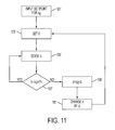
- the control algorithm for control circuit 48 can sense an operating wavelength ⁇ of the waveguide resonator 15 ( 15 ′, 15 ′′), which can be used to adjust the output voltage and thus operating wavelength to a desired value ⁇ 0 as shown in FIG. 11 .
- the FIG. 11 process starts with step 101 ′ where an input set point for a desired operating wavelength ⁇ 0 is set.
- Step 103 ′ converts the wavelength set point ⁇ 0 into an output voltage which is applied to the waveguide resonator 15 ( 15 ′, 15 ′′).
- step 105 ′ the operating wavelength ⁇ is sensed, following which, in step 107 ′, a determination is made whether the operating wavelength ⁇ is within a predetermined threshold band ⁇ 0 ⁇ Th centered around the desired wavelength ⁇ 0. If it is, the process returns to step 105 ′. However, if the sensed operating wavelength ⁇ is not within a predetermined threshold band ⁇ 0 ⁇ Th then a plus or minus difference ⁇ is calculated in step 109 ′ between the sensed ⁇ and set ⁇ 0, which is then used to change the applied voltage in step 111 ′ following which the newly calculated voltage is set in step 103 ′ and the process resumes.
- the initial set point adjustments of the initial desired wavelength in step 101 of the FIGS. 10 and 11 processes can be omitted if the fabrication processes are precise enough to produce a consistent initial desired operating wavelength for the wavelength resonator 15 ( 15 ′, 15 ′′). Otherwise, the initial set point adjustments can be used to compensate the waveguide resonator 15 ( 15 ′, 15 ′′) for any fabrication variations which would produce a resonant wavelength which differs from that desired.
- the various embodiments provide a very fast and efficient manner for adjusting for thermal drift as well as fabrication anomalies in a photonic waveguide resonator, for example, a filter or a modulator, by using an applied voltage in conjunction with a strained waveguide core.
- strained silicon is used as the waveguide core material 29 .
- other strained waveguide core materials may be used in place of silicon, which can be exploited by an applied electric field to tune and maintain the waveguide resonator to a particular effective index corresponding to a desired operating wavelength.
- Such materials include GaAs, I N P, Si x Ge 1 ⁇ x as examples.
- Other materials which can be strained and used to form the waveguide core including any group III to group IV materials.
- some materials used for the waveguide core 29 can inherently have a strain therein.
- a strain is produced in a silicon waveguide core 29 by using an upper cladding material 35 which has a different thermal coefficient of expansion than that of silicon.
- the strain also can be produced using the lower 27 cladding material or by using both the upper 45 and lower 27 cladding materials.
- the effective index of waveguide 21 is dependent on the field strength applied by the external voltage and the direction in this material.
- the various embodiments show ways in which the field can be applied using the top 17 and bottom 19 electrodes; however, other arrangements for controlling the electric field can also be employed.
- the upper 35 and lower 27 cladding materials can include silicon nitride, SiOxNy, SiO 2 , spin on dielectric (SOD), hydronated SiO 2 , TiO 2 , ZrO 2 , HfO 2 , AL 2 O 3 , as well as other dielectrics having thermal expansion coefficients different from that of the silicon waveguide core 29 .
Landscapes
- Physics & Mathematics (AREA)
- General Physics & Mathematics (AREA)
- Optics & Photonics (AREA)
- Nonlinear Science (AREA)
- Optical Integrated Circuits (AREA)
- Optical Modulation, Optical Deflection, Nonlinear Optics, Optical Demodulation, Optical Logic Elements (AREA)
- Engineering & Computer Science (AREA)
- Manufacturing & Machinery (AREA)
Abstract
Description
Claims (33)
Priority Applications (9)
| Application Number | Priority Date | Filing Date | Title |
|---|---|---|---|
| US14/254,173 US9360627B2 (en) | 2014-04-16 | 2014-04-16 | Method and apparatus providing compensation for wavelength drift in photonic structures |
| KR1020167031493A KR102065208B1 (en) | 2014-04-16 | 2015-03-30 | Method and apparatus providing compensation for wavelength drift in photonic structures |
| PCT/US2015/023291 WO2015160495A1 (en) | 2014-04-16 | 2015-03-30 | Method and apparatus providing compensation for wavelength drift in photonic structures |
| CN201580030462.0A CN106461856B (en) | 2014-04-16 | 2015-03-30 | Method and apparatus for providing compensation for wavelength drift in photonic structures |
| SG11201608584WA SG11201608584WA (en) | 2014-04-16 | 2015-03-30 | Method and apparatus providing compensation for wavelength drift in photonic structures |
| EP15780750.4A EP3132294B1 (en) | 2014-04-16 | 2015-03-30 | Method and apparatus providing compensation for wavelength drift in photonic structures |
| JP2016562247A JP6438973B2 (en) | 2014-04-16 | 2015-03-30 | Method and apparatus for providing compensation for wavelength drift in photonic structures |
| KR1020187018032A KR20180074812A (en) | 2014-04-16 | 2015-03-30 | Method and apparatus providing compensation for wavelength drift in photonic structures |
| TW104111979A TWI582476B (en) | 2014-04-16 | 2015-04-14 | Method and apparatus providing compensation for wavelength drift in photonic structures |
Applications Claiming Priority (1)
| Application Number | Priority Date | Filing Date | Title |
|---|---|---|---|
| US14/254,173 US9360627B2 (en) | 2014-04-16 | 2014-04-16 | Method and apparatus providing compensation for wavelength drift in photonic structures |
Publications (2)
| Publication Number | Publication Date |
|---|---|
| US20150301283A1 US20150301283A1 (en) | 2015-10-22 |
| US9360627B2 true US9360627B2 (en) | 2016-06-07 |
Family
ID=54321899
Family Applications (1)
| Application Number | Title | Priority Date | Filing Date |
|---|---|---|---|
| US14/254,173 Active 2034-08-22 US9360627B2 (en) | 2014-04-16 | 2014-04-16 | Method and apparatus providing compensation for wavelength drift in photonic structures |
Country Status (8)
| Country | Link |
|---|---|
| US (1) | US9360627B2 (en) |
| EP (1) | EP3132294B1 (en) |
| JP (1) | JP6438973B2 (en) |
| KR (2) | KR20180074812A (en) |
| CN (1) | CN106461856B (en) |
| SG (1) | SG11201608584WA (en) |
| TW (1) | TWI582476B (en) |
| WO (1) | WO2015160495A1 (en) |
Cited By (3)
| Publication number | Priority date | Publication date | Assignee | Title |
|---|---|---|---|---|
| US9733498B2 (en) * | 2015-10-09 | 2017-08-15 | Oracle International Corporation | Disk resonator based on a composite structure |
| US11372157B2 (en) | 2020-09-30 | 2022-06-28 | Nokia Solutions And Networks Oy | Integrated optical multiplexer / demultiplexer with thermal compensation |
| US11480729B2 (en) | 2020-10-30 | 2022-10-25 | Nokia Solutions And Networks Oy | Thermally compensated slot waveguide |
Families Citing this family (3)
| Publication number | Priority date | Publication date | Assignee | Title |
|---|---|---|---|---|
| US9864132B1 (en) * | 2016-09-30 | 2018-01-09 | Globalfoundries Inc. | Silicon waveguide devices in integrated photonics |
| CN110261958B (en) * | 2019-06-17 | 2021-11-12 | 上海理工大学 | Environment temperature independent silicon nitride micro-ring filter chip based on vertical slit structure |
| US11808978B2 (en) * | 2019-08-12 | 2023-11-07 | Mcmaster University | Post-fabrication trimming of silicon ring resonators via integrated annealing |
Citations (17)
| Publication number | Priority date | Publication date | Assignee | Title |
|---|---|---|---|---|
| US6041071A (en) * | 1995-09-29 | 2000-03-21 | Coretek, Inc. | Electro-optically tunable external cavity mirror for a narrow linewidth semiconductor laser |
| US6407846B1 (en) | 2001-03-16 | 2002-06-18 | All Optical Networks, Inc. | Photonic wavelength shifting method |
| US6636668B1 (en) | 1999-11-23 | 2003-10-21 | Lnl Technologies, Inc. | Localized thermal tuning of ring resonators |
| US20050074194A1 (en) | 2003-10-02 | 2005-04-07 | Tan Michael R. | Optical modulator based on a microdisk resonator |
| US20050110108A1 (en) * | 2003-11-20 | 2005-05-26 | Sioptical, Inc. | Silicon-based Schottky barrier infrared optical detector |
| US20060001089A1 (en) * | 2004-07-02 | 2006-01-05 | International Business Machines Corporation | Ultra-thin, high quality strained silicon-on-insulator formed by elastic strain transfer |
| US7327911B2 (en) * | 2004-10-19 | 2008-02-05 | Sioptical, Inc. | Optical detector configuration and utilization as feedback control in monolithic integrated optic and electronic arrangements |
| US20090169149A1 (en) * | 2007-12-27 | 2009-07-02 | Bruce Andrew Block | Stabilized ring resonator modulator |
| US20090180747A1 (en) * | 2008-01-15 | 2009-07-16 | Interuniversitair Microelektronica Centrum (Imec) | Method for Effective Refractive Index Trimming of Optical Waveguiding Structures and Optical Waveguiding Structures |
| US7603016B1 (en) * | 2007-04-30 | 2009-10-13 | The United States Of America As Represented By The Secretary Of The Air Force | Semiconductor photonic nano communication link apparatus |
| US20090261383A1 (en) * | 2006-10-19 | 2009-10-22 | Electronics And Telecommunications Research Institute | Optical device having strained buried channel |
| US20090314763A1 (en) | 2005-08-19 | 2009-12-24 | Sai Chu | Coupled optical waveguide resonators with heaters for thermo-optic control of wavelength and compound filter shape |
| US20100266232A1 (en) | 2005-03-04 | 2010-10-21 | Cornell Research Foundation, Inc. | Electro-optic modulation |
| US20110058765A1 (en) * | 2009-09-10 | 2011-03-10 | William Marsh Rice University | Dual-ring silicon electro-optic modulator |
| US20130202005A1 (en) * | 2012-02-07 | 2013-08-08 | Apic Corporation | Laser using locally strained germanium on silicon for opto-electronic applications |
| US20140169724A1 (en) * | 2012-12-14 | 2014-06-19 | Imec | Thermally Stabilised Resonant Electro-Optic Modulator and Use Thereof |
| US9127983B1 (en) * | 2013-04-26 | 2015-09-08 | Sandia Corporation | Systems and methods for controlling an operating wavelength |
Family Cites Families (9)
| Publication number | Priority date | Publication date | Assignee | Title |
|---|---|---|---|---|
| US7200308B2 (en) * | 2005-06-28 | 2007-04-03 | California Institute Of Technology | Frequency conversion with nonlinear optical polymers and high index contrast waveguides |
| WO2007065447A1 (en) * | 2005-09-01 | 2007-06-14 | Semus A/S | Phase modulator and interferometer based on electro-optic effects in assymetrically strained group-iv material |
| WO2007029647A1 (en) * | 2005-09-06 | 2007-03-15 | Nec Corporation | Wavelength variable filter and wavelength variable laser |
| JP4427589B2 (en) * | 2008-06-09 | 2010-03-10 | 国立大学法人広島大学 | Optical integrated circuit device |
| JP2010175743A (en) * | 2009-01-28 | 2010-08-12 | Hiroshima Univ | Optical switching device and optical integrated circuit equipped with the same |
| JPWO2011108617A1 (en) * | 2010-03-05 | 2013-06-27 | 日本電気株式会社 | Athermal optical waveguide device |
| US8644649B2 (en) * | 2011-05-27 | 2014-02-04 | Micron Technology, Inc. | Optical waveguide with cascaded modulator circuits |
| JP5752629B2 (en) * | 2012-03-26 | 2015-07-22 | 株式会社東芝 | Athermal ring light modulator |
| JP2013210568A (en) * | 2012-03-30 | 2013-10-10 | Sumitomo Osaka Cement Co Ltd | Optical modulator |
-
2014
- 2014-04-16 US US14/254,173 patent/US9360627B2/en active Active
-
2015
- 2015-03-30 KR KR1020187018032A patent/KR20180074812A/en active Application Filing
- 2015-03-30 SG SG11201608584WA patent/SG11201608584WA/en unknown
- 2015-03-30 EP EP15780750.4A patent/EP3132294B1/en active Active
- 2015-03-30 KR KR1020167031493A patent/KR102065208B1/en active IP Right Grant
- 2015-03-30 CN CN201580030462.0A patent/CN106461856B/en active Active
- 2015-03-30 WO PCT/US2015/023291 patent/WO2015160495A1/en active Application Filing
- 2015-03-30 JP JP2016562247A patent/JP6438973B2/en active Active
- 2015-04-14 TW TW104111979A patent/TWI582476B/en active
Patent Citations (17)
| Publication number | Priority date | Publication date | Assignee | Title |
|---|---|---|---|---|
| US6041071A (en) * | 1995-09-29 | 2000-03-21 | Coretek, Inc. | Electro-optically tunable external cavity mirror for a narrow linewidth semiconductor laser |
| US6636668B1 (en) | 1999-11-23 | 2003-10-21 | Lnl Technologies, Inc. | Localized thermal tuning of ring resonators |
| US6407846B1 (en) | 2001-03-16 | 2002-06-18 | All Optical Networks, Inc. | Photonic wavelength shifting method |
| US20050074194A1 (en) | 2003-10-02 | 2005-04-07 | Tan Michael R. | Optical modulator based on a microdisk resonator |
| US20050110108A1 (en) * | 2003-11-20 | 2005-05-26 | Sioptical, Inc. | Silicon-based Schottky barrier infrared optical detector |
| US20060001089A1 (en) * | 2004-07-02 | 2006-01-05 | International Business Machines Corporation | Ultra-thin, high quality strained silicon-on-insulator formed by elastic strain transfer |
| US7327911B2 (en) * | 2004-10-19 | 2008-02-05 | Sioptical, Inc. | Optical detector configuration and utilization as feedback control in monolithic integrated optic and electronic arrangements |
| US20100266232A1 (en) | 2005-03-04 | 2010-10-21 | Cornell Research Foundation, Inc. | Electro-optic modulation |
| US20090314763A1 (en) | 2005-08-19 | 2009-12-24 | Sai Chu | Coupled optical waveguide resonators with heaters for thermo-optic control of wavelength and compound filter shape |
| US20090261383A1 (en) * | 2006-10-19 | 2009-10-22 | Electronics And Telecommunications Research Institute | Optical device having strained buried channel |
| US7603016B1 (en) * | 2007-04-30 | 2009-10-13 | The United States Of America As Represented By The Secretary Of The Air Force | Semiconductor photonic nano communication link apparatus |
| US20090169149A1 (en) * | 2007-12-27 | 2009-07-02 | Bruce Andrew Block | Stabilized ring resonator modulator |
| US20090180747A1 (en) * | 2008-01-15 | 2009-07-16 | Interuniversitair Microelektronica Centrum (Imec) | Method for Effective Refractive Index Trimming of Optical Waveguiding Structures and Optical Waveguiding Structures |
| US20110058765A1 (en) * | 2009-09-10 | 2011-03-10 | William Marsh Rice University | Dual-ring silicon electro-optic modulator |
| US20130202005A1 (en) * | 2012-02-07 | 2013-08-08 | Apic Corporation | Laser using locally strained germanium on silicon for opto-electronic applications |
| US20140169724A1 (en) * | 2012-12-14 | 2014-06-19 | Imec | Thermally Stabilised Resonant Electro-Optic Modulator and Use Thereof |
| US9127983B1 (en) * | 2013-04-26 | 2015-09-08 | Sandia Corporation | Systems and methods for controlling an operating wavelength |
Non-Patent Citations (5)
| Title |
|---|
| Cazzanelli M., et al., "Second-harmonic generation in silicon waveguides strained by silicon nitride", Nature Materials, vol. 11, Feb. 2012. |
| Chmielak, Bartos et al., "Pockels effect based fully integrated, strained silicon electro-optical modulator", Optical Express, Aug. 29, 2011, vol. 19, No. 18. |
| K. Padmaraju et al. Thermal stabilization of a microring modulator using feedback control. Optics Express, 20:27:27999-28008, Dec. 17, 2012. * |
| Y. Amemiya et al. Optical modulator using metal-oxide-semiconductor type Si ring resonator. Optical Review, 16:3:247-251, May/Jun. 2009. * |
| Y. Sebbag et al. Bistability in silicon microring resonator based on strain induced by a piezoelectric lead zirconate titanate thin film. Applied Physics Letters, vol. 100, 141107-1-141107-4, Apr. 2012. * |
Cited By (3)
| Publication number | Priority date | Publication date | Assignee | Title |
|---|---|---|---|---|
| US9733498B2 (en) * | 2015-10-09 | 2017-08-15 | Oracle International Corporation | Disk resonator based on a composite structure |
| US11372157B2 (en) | 2020-09-30 | 2022-06-28 | Nokia Solutions And Networks Oy | Integrated optical multiplexer / demultiplexer with thermal compensation |
| US11480729B2 (en) | 2020-10-30 | 2022-10-25 | Nokia Solutions And Networks Oy | Thermally compensated slot waveguide |
Also Published As
| Publication number | Publication date |
|---|---|
| EP3132294B1 (en) | 2020-01-15 |
| EP3132294A4 (en) | 2017-09-20 |
| KR20160145104A (en) | 2016-12-19 |
| SG11201608584WA (en) | 2016-11-29 |
| EP3132294A1 (en) | 2017-02-22 |
| JP6438973B2 (en) | 2018-12-19 |
| TW201543093A (en) | 2015-11-16 |
| KR102065208B1 (en) | 2020-02-11 |
| JP2017516132A (en) | 2017-06-15 |
| CN106461856B (en) | 2020-02-07 |
| TWI582476B (en) | 2017-05-11 |
| CN106461856A (en) | 2017-02-22 |
| US20150301283A1 (en) | 2015-10-22 |
| KR20180074812A (en) | 2018-07-03 |
| WO2015160495A1 (en) | 2015-10-22 |
Similar Documents
| Publication | Publication Date | Title |
|---|---|---|
| US9360627B2 (en) | Method and apparatus providing compensation for wavelength drift in photonic structures | |
| US6839488B2 (en) | Tunable resonant cavity based on the field effect in semiconductors | |
| US9513437B2 (en) | Photonic integrated circuit incorporating a bandgap temperature sensor | |
| TWI542912B (en) | Demultiplexer and optical demultiplexing method | |
| USRE48654E1 (en) | Photonic integrated circuit incorporating a bandgap temperature sensor | |
| JP7308311B2 (en) | Optical signal propagation loss and propagation index modulator | |
| EP2829906B1 (en) | Carrier-depletion based silicon waveguide resonant cavity modulator with integrated optical power monitor | |
| US20050105184A1 (en) | Tunable filter membrane structures and methods of making | |
| US10295739B2 (en) | Athermal optical devices based on composite structures | |
| KR20160072108A (en) | Coupling-modulated optical resonator | |
| US9766400B2 (en) | Method for adjusting properties of a photonic circuit by post fabrication ion implantation, and adjusted waveguide and photonic circuit | |
| US8983238B2 (en) | Optical resonator tuning using piezoelectric actuation | |
| CN114509845B (en) | Micro-ring resonator and electronic device | |
| US10031354B2 (en) | Active-control optical resonator | |
| Jayatilleka et al. | Automatic tuning and temperature stabilization of high-order silicon Vernier microring filters | |
| US6366730B1 (en) | Tunable optical waveguides | |
| CN110927871A (en) | Broadband optical waveguide structure insensitive to temperature and low in dispersion and design method thereof | |
| TW200933224A (en) | Metal-diffused single polarization light waveguide chip and manufacturing method thereof | |
| Kumari et al. | Study on temperature sensitivity of Si 3 N 4 cladded silicon 2× 2 MMI coupler | |
| Teng et al. | Athermal SOI ring resonators by overlaying a polymer cladding on narrowed waveguides | |
| Grajower et al. | Post trimming of silicon photonics microresonators by nanoscale flash memory technology | |
| Lu et al. | CMOS-compatible athermal tunable silicon optical lattice filters | |
| JP2001318245A (en) | Substrate-type optical device |
Legal Events
| Date | Code | Title | Description |
|---|---|---|---|
| AS | Assignment |
Owner name: MICRON TECHNOLOGY, INC., IDAHO Free format text: ASSIGNMENT OF ASSIGNORS INTEREST;ASSIGNORS:BI, LEI;MEADE, ROY;SANDHU, GURTEJ;SIGNING DATES FROM 20140207 TO 20140411;REEL/FRAME:032685/0963 |
|
| FEPP | Fee payment procedure |
Free format text: PAYOR NUMBER ASSIGNED (ORIGINAL EVENT CODE: ASPN); ENTITY STATUS OF PATENT OWNER: LARGE ENTITY |
|
| AS | Assignment |
Owner name: U.S. BANK NATIONAL ASSOCIATION, AS COLLATERAL AGENT, CALIFORNIA Free format text: SECURITY INTEREST;ASSIGNOR:MICRON TECHNOLOGY, INC.;REEL/FRAME:038669/0001 Effective date: 20160426 Owner name: U.S. BANK NATIONAL ASSOCIATION, AS COLLATERAL AGEN Free format text: SECURITY INTEREST;ASSIGNOR:MICRON TECHNOLOGY, INC.;REEL/FRAME:038669/0001 Effective date: 20160426 |
|
| STCF | Information on status: patent grant |
Free format text: PATENTED CASE |
|
| AS | Assignment |
Owner name: MORGAN STANLEY SENIOR FUNDING, INC., AS COLLATERAL AGENT, MARYLAND Free format text: PATENT SECURITY AGREEMENT;ASSIGNOR:MICRON TECHNOLOGY, INC.;REEL/FRAME:038954/0001 Effective date: 20160426 Owner name: MORGAN STANLEY SENIOR FUNDING, INC., AS COLLATERAL Free format text: PATENT SECURITY AGREEMENT;ASSIGNOR:MICRON TECHNOLOGY, INC.;REEL/FRAME:038954/0001 Effective date: 20160426 |
|
| AS | Assignment |
Owner name: U.S. BANK NATIONAL ASSOCIATION, AS COLLATERAL AGENT, CALIFORNIA Free format text: CORRECTIVE ASSIGNMENT TO CORRECT THE REPLACE ERRONEOUSLY FILED PATENT #7358718 WITH THE CORRECT PATENT #7358178 PREVIOUSLY RECORDED ON REEL 038669 FRAME 0001. ASSIGNOR(S) HEREBY CONFIRMS THE SECURITY INTEREST;ASSIGNOR:MICRON TECHNOLOGY, INC.;REEL/FRAME:043079/0001 Effective date: 20160426 Owner name: U.S. BANK NATIONAL ASSOCIATION, AS COLLATERAL AGEN Free format text: CORRECTIVE ASSIGNMENT TO CORRECT THE REPLACE ERRONEOUSLY FILED PATENT #7358718 WITH THE CORRECT PATENT #7358178 PREVIOUSLY RECORDED ON REEL 038669 FRAME 0001. ASSIGNOR(S) HEREBY CONFIRMS THE SECURITY INTEREST;ASSIGNOR:MICRON TECHNOLOGY, INC.;REEL/FRAME:043079/0001 Effective date: 20160426 |
|
| CC | Certificate of correction | ||
| AS | Assignment |
Owner name: JPMORGAN CHASE BANK, N.A., AS COLLATERAL AGENT, ILLINOIS Free format text: SECURITY INTEREST;ASSIGNORS:MICRON TECHNOLOGY, INC.;MICRON SEMICONDUCTOR PRODUCTS, INC.;REEL/FRAME:047540/0001 Effective date: 20180703 Owner name: JPMORGAN CHASE BANK, N.A., AS COLLATERAL AGENT, IL Free format text: SECURITY INTEREST;ASSIGNORS:MICRON TECHNOLOGY, INC.;MICRON SEMICONDUCTOR PRODUCTS, INC.;REEL/FRAME:047540/0001 Effective date: 20180703 |
|
| AS | Assignment |
Owner name: MICRON TECHNOLOGY, INC., IDAHO Free format text: RELEASE BY SECURED PARTY;ASSIGNOR:U.S. BANK NATIONAL ASSOCIATION, AS COLLATERAL AGENT;REEL/FRAME:047243/0001 Effective date: 20180629 |
|
| AS | Assignment |
Owner name: MICRON TECHNOLOGY, INC., IDAHO Free format text: RELEASE BY SECURED PARTY;ASSIGNOR:MORGAN STANLEY SENIOR FUNDING, INC., AS COLLATERAL AGENT;REEL/FRAME:050937/0001 Effective date: 20190731 |
|
| AS | Assignment |
Owner name: MICRON SEMICONDUCTOR PRODUCTS, INC., IDAHO Free format text: RELEASE BY SECURED PARTY;ASSIGNOR:JPMORGAN CHASE BANK, N.A., AS COLLATERAL AGENT;REEL/FRAME:051028/0001 Effective date: 20190731 Owner name: MICRON TECHNOLOGY, INC., IDAHO Free format text: RELEASE BY SECURED PARTY;ASSIGNOR:JPMORGAN CHASE BANK, N.A., AS COLLATERAL AGENT;REEL/FRAME:051028/0001 Effective date: 20190731 |
|
| MAFP | Maintenance fee payment |
Free format text: PAYMENT OF MAINTENANCE FEE, 4TH YEAR, LARGE ENTITY (ORIGINAL EVENT CODE: M1551); ENTITY STATUS OF PATENT OWNER: LARGE ENTITY Year of fee payment: 4 |
|
| MAFP | Maintenance fee payment |
Free format text: PAYMENT OF MAINTENANCE FEE, 8TH YEAR, LARGE ENTITY (ORIGINAL EVENT CODE: M1552); ENTITY STATUS OF PATENT OWNER: LARGE ENTITY Year of fee payment: 8 |