US9400278B2 - Biochip - Google Patents
Biochip Download PDFInfo
- Publication number
- US9400278B2 US9400278B2 US14/306,401 US201414306401A US9400278B2 US 9400278 B2 US9400278 B2 US 9400278B2 US 201414306401 A US201414306401 A US 201414306401A US 9400278 B2 US9400278 B2 US 9400278B2
- Authority
- US
- United States
- Prior art keywords
- biochip
- reaction layer
- molecules
- arrangement
- layer
- Prior art date
- Legal status (The legal status is an assumption and is not a legal conclusion. Google has not performed a legal analysis and makes no representation as to the accuracy of the status listed.)
- Expired - Lifetime
Links
- 238000000018 DNA microarray Methods 0.000 title claims abstract description 30
- 238000006243 chemical reaction Methods 0.000 claims abstract description 39
- 239000012491 analyte Substances 0.000 claims abstract description 9
- 239000000017 hydrogel Substances 0.000 claims description 15
- 239000003431 cross linking reagent Substances 0.000 claims description 5
- 239000004065 semiconductor Substances 0.000 claims description 5
- 238000006479 redox reaction Methods 0.000 claims description 3
- 238000001514 detection method Methods 0.000 abstract description 5
- 230000035945 sensitivity Effects 0.000 abstract description 5
- 230000000694 effects Effects 0.000 abstract description 3
- 238000005259 measurement Methods 0.000 description 10
- 230000005684 electric field Effects 0.000 description 9
- XUIMIQQOPSSXEZ-UHFFFAOYSA-N Silicon Chemical compound [Si] XUIMIQQOPSSXEZ-UHFFFAOYSA-N 0.000 description 5
- 230000008878 coupling Effects 0.000 description 5
- 238000010168 coupling process Methods 0.000 description 5
- 238000005859 coupling reaction Methods 0.000 description 5
- 238000000034 method Methods 0.000 description 5
- 229910052710 silicon Inorganic materials 0.000 description 5
- 239000010703 silicon Substances 0.000 description 5
- 239000000126 substance Substances 0.000 description 5
- 230000008859 change Effects 0.000 description 4
- 229920001940 conductive polymer Polymers 0.000 description 4
- 239000000523 sample Substances 0.000 description 4
- ZMXDDKWLCZADIW-UHFFFAOYSA-N N,N-Dimethylformamide Chemical compound CN(C)C=O ZMXDDKWLCZADIW-UHFFFAOYSA-N 0.000 description 3
- 125000005647 linker group Chemical group 0.000 description 3
- 230000008569 process Effects 0.000 description 3
- HRPVXLWXLXDGHG-UHFFFAOYSA-N Acrylamide Chemical compound NC(=O)C=C HRPVXLWXLXDGHG-UHFFFAOYSA-N 0.000 description 2
- NIXOWILDQLNWCW-UHFFFAOYSA-M Acrylate Chemical compound [O-]C(=O)C=C NIXOWILDQLNWCW-UHFFFAOYSA-M 0.000 description 2
- 108091034117 Oligonucleotide Proteins 0.000 description 2
- VYPSYNLAJGMNEJ-UHFFFAOYSA-N Silicium dioxide Chemical compound O=[Si]=O VYPSYNLAJGMNEJ-UHFFFAOYSA-N 0.000 description 2
- JLCPHMBAVCMARE-UHFFFAOYSA-N [3-[[3-[[3-[[3-[[3-[[3-[[3-[[3-[[3-[[3-[[3-[[5-(2-amino-6-oxo-1H-purin-9-yl)-3-[[3-[[3-[[3-[[3-[[3-[[5-(2-amino-6-oxo-1H-purin-9-yl)-3-[[5-(2-amino-6-oxo-1H-purin-9-yl)-3-hydroxyoxolan-2-yl]methoxy-hydroxyphosphoryl]oxyoxolan-2-yl]methoxy-hydroxyphosphoryl]oxy-5-(5-methyl-2,4-dioxopyrimidin-1-yl)oxolan-2-yl]methoxy-hydroxyphosphoryl]oxy-5-(6-aminopurin-9-yl)oxolan-2-yl]methoxy-hydroxyphosphoryl]oxy-5-(6-aminopurin-9-yl)oxolan-2-yl]methoxy-hydroxyphosphoryl]oxy-5-(6-aminopurin-9-yl)oxolan-2-yl]methoxy-hydroxyphosphoryl]oxy-5-(6-aminopurin-9-yl)oxolan-2-yl]methoxy-hydroxyphosphoryl]oxyoxolan-2-yl]methoxy-hydroxyphosphoryl]oxy-5-(5-methyl-2,4-dioxopyrimidin-1-yl)oxolan-2-yl]methoxy-hydroxyphosphoryl]oxy-5-(4-amino-2-oxopyrimidin-1-yl)oxolan-2-yl]methoxy-hydroxyphosphoryl]oxy-5-(5-methyl-2,4-dioxopyrimidin-1-yl)oxolan-2-yl]methoxy-hydroxyphosphoryl]oxy-5-(5-methyl-2,4-dioxopyrimidin-1-yl)oxolan-2-yl]methoxy-hydroxyphosphoryl]oxy-5-(6-aminopurin-9-yl)oxolan-2-yl]methoxy-hydroxyphosphoryl]oxy-5-(6-aminopurin-9-yl)oxolan-2-yl]methoxy-hydroxyphosphoryl]oxy-5-(4-amino-2-oxopyrimidin-1-yl)oxolan-2-yl]methoxy-hydroxyphosphoryl]oxy-5-(4-amino-2-oxopyrimidin-1-yl)oxolan-2-yl]methoxy-hydroxyphosphoryl]oxy-5-(4-amino-2-oxopyrimidin-1-yl)oxolan-2-yl]methoxy-hydroxyphosphoryl]oxy-5-(6-aminopurin-9-yl)oxolan-2-yl]methoxy-hydroxyphosphoryl]oxy-5-(4-amino-2-oxopyrimidin-1-yl)oxolan-2-yl]methyl [5-(6-aminopurin-9-yl)-2-(hydroxymethyl)oxolan-3-yl] hydrogen phosphate Polymers Cc1cn(C2CC(OP(O)(=O)OCC3OC(CC3OP(O)(=O)OCC3OC(CC3O)n3cnc4c3nc(N)[nH]c4=O)n3cnc4c3nc(N)[nH]c4=O)C(COP(O)(=O)OC3CC(OC3COP(O)(=O)OC3CC(OC3COP(O)(=O)OC3CC(OC3COP(O)(=O)OC3CC(OC3COP(O)(=O)OC3CC(OC3COP(O)(=O)OC3CC(OC3COP(O)(=O)OC3CC(OC3COP(O)(=O)OC3CC(OC3COP(O)(=O)OC3CC(OC3COP(O)(=O)OC3CC(OC3COP(O)(=O)OC3CC(OC3COP(O)(=O)OC3CC(OC3COP(O)(=O)OC3CC(OC3COP(O)(=O)OC3CC(OC3COP(O)(=O)OC3CC(OC3COP(O)(=O)OC3CC(OC3COP(O)(=O)OC3CC(OC3CO)n3cnc4c(N)ncnc34)n3ccc(N)nc3=O)n3cnc4c(N)ncnc34)n3ccc(N)nc3=O)n3ccc(N)nc3=O)n3ccc(N)nc3=O)n3cnc4c(N)ncnc34)n3cnc4c(N)ncnc34)n3cc(C)c(=O)[nH]c3=O)n3cc(C)c(=O)[nH]c3=O)n3ccc(N)nc3=O)n3cc(C)c(=O)[nH]c3=O)n3cnc4c3nc(N)[nH]c4=O)n3cnc4c(N)ncnc34)n3cnc4c(N)ncnc34)n3cnc4c(N)ncnc34)n3cnc4c(N)ncnc34)O2)c(=O)[nH]c1=O JLCPHMBAVCMARE-UHFFFAOYSA-N 0.000 description 2
- 239000002318 adhesion promoter Substances 0.000 description 2
- 238000004458 analytical method Methods 0.000 description 2
- 230000008901 benefit Effects 0.000 description 2
- 238000005516 engineering process Methods 0.000 description 2
- 125000003055 glycidyl group Chemical group C(C1CO1)* 0.000 description 2
- FPYJFEHAWHCUMM-UHFFFAOYSA-N maleic anhydride Chemical compound O=C1OC(=O)C=C1 FPYJFEHAWHCUMM-UHFFFAOYSA-N 0.000 description 2
- 238000004519 manufacturing process Methods 0.000 description 2
- 239000004014 plasticizer Substances 0.000 description 2
- 239000002904 solvent Substances 0.000 description 2
- LTHJXDSHSVNJKG-UHFFFAOYSA-N 2-[2-[2-[2-(2-methylprop-2-enoyloxy)ethoxy]ethoxy]ethoxy]ethyl 2-methylprop-2-enoate Chemical compound CC(=C)C(=O)OCCOCCOCCOCCOC(=O)C(C)=C LTHJXDSHSVNJKG-UHFFFAOYSA-N 0.000 description 1
- YYPNJNDODFVZLE-UHFFFAOYSA-N 3-methylbut-2-enoic acid Chemical class CC(C)=CC(O)=O YYPNJNDODFVZLE-UHFFFAOYSA-N 0.000 description 1
- LYCAIKOWRPUZTN-UHFFFAOYSA-N Ethylene glycol Chemical compound OCCO LYCAIKOWRPUZTN-UHFFFAOYSA-N 0.000 description 1
- 229910052581 Si3N4 Inorganic materials 0.000 description 1
- BLRPTPMANUNPDV-UHFFFAOYSA-N Silane Chemical compound [SiH4] BLRPTPMANUNPDV-UHFFFAOYSA-N 0.000 description 1
- 230000004075 alteration Effects 0.000 description 1
- 239000012431 aqueous reaction media Substances 0.000 description 1
- 238000003491 array Methods 0.000 description 1
- 230000003851 biochemical process Effects 0.000 description 1
- 239000003795 chemical substances by application Substances 0.000 description 1
- 239000011248 coating agent Substances 0.000 description 1
- 238000000576 coating method Methods 0.000 description 1
- 239000004020 conductor Substances 0.000 description 1
- 238000004132 cross linking Methods 0.000 description 1
- MTHSVFCYNBDYFN-UHFFFAOYSA-N diethylene glycol Chemical compound OCCOCCO MTHSVFCYNBDYFN-UHFFFAOYSA-N 0.000 description 1
- 238000009792 diffusion process Methods 0.000 description 1
- 238000009826 distribution Methods 0.000 description 1
- 239000012634 fragment Substances 0.000 description 1
- 230000001771 impaired effect Effects 0.000 description 1
- 239000003999 initiator Substances 0.000 description 1
- 239000000203 mixture Substances 0.000 description 1
- 238000012986 modification Methods 0.000 description 1
- 230000004048 modification Effects 0.000 description 1
- 239000000178 monomer Substances 0.000 description 1
- ZIUHHBKFKCYYJD-UHFFFAOYSA-N n,n'-methylenebisacrylamide Chemical compound C=CC(=O)NCNC(=O)C=C ZIUHHBKFKCYYJD-UHFFFAOYSA-N 0.000 description 1
- 230000003287 optical effect Effects 0.000 description 1
- 238000000059 patterning Methods 0.000 description 1
- 230000010287 polarization Effects 0.000 description 1
- 229920002401 polyacrylamide Polymers 0.000 description 1
- 229920000642 polymer Polymers 0.000 description 1
- 239000002243 precursor Substances 0.000 description 1
- 239000000376 reactant Substances 0.000 description 1
- 230000035484 reaction time Effects 0.000 description 1
- 230000000717 retained effect Effects 0.000 description 1
- 229910000077 silane Inorganic materials 0.000 description 1
- 235000012239 silicon dioxide Nutrition 0.000 description 1
- 239000000377 silicon dioxide Substances 0.000 description 1
- HQVNEWCFYHHQES-UHFFFAOYSA-N silicon nitride Chemical compound N12[Si]34N5[Si]62N3[Si]51N64 HQVNEWCFYHHQES-UHFFFAOYSA-N 0.000 description 1
- 238000004611 spectroscopical analysis Methods 0.000 description 1
- 230000008961 swelling Effects 0.000 description 1
- ZIBGPFATKBEMQZ-UHFFFAOYSA-N triethylene glycol Chemical compound OCCOCCOCCO ZIBGPFATKBEMQZ-UHFFFAOYSA-N 0.000 description 1
- XLYOFNOQVPJJNP-UHFFFAOYSA-N water Substances O XLYOFNOQVPJJNP-UHFFFAOYSA-N 0.000 description 1
Images


Classifications
-
- C—CHEMISTRY; METALLURGY
- C12—BIOCHEMISTRY; BEER; SPIRITS; WINE; VINEGAR; MICROBIOLOGY; ENZYMOLOGY; MUTATION OR GENETIC ENGINEERING
- C12M—APPARATUS FOR ENZYMOLOGY OR MICROBIOLOGY; APPARATUS FOR CULTURING MICROORGANISMS FOR PRODUCING BIOMASS, FOR GROWING CELLS OR FOR OBTAINING FERMENTATION OR METABOLIC PRODUCTS, i.e. BIOREACTORS OR FERMENTERS
- C12M1/00—Apparatus for enzymology or microbiology
- C12M1/34—Measuring or testing with condition measuring or sensing means, e.g. colony counters
-
- G—PHYSICS
- G01—MEASURING; TESTING
- G01N—INVESTIGATING OR ANALYSING MATERIALS BY DETERMINING THEIR CHEMICAL OR PHYSICAL PROPERTIES
- G01N33/00—Investigating or analysing materials by specific methods not covered by groups G01N1/00 - G01N31/00
- G01N33/48—Biological material, e.g. blood, urine; Haemocytometers
- G01N33/50—Chemical analysis of biological material, e.g. blood, urine; Testing involving biospecific ligand binding methods; Immunological testing
- G01N33/53—Immunoassay; Biospecific binding assay; Materials therefor
- G01N33/543—Immunoassay; Biospecific binding assay; Materials therefor with an insoluble carrier for immobilising immunochemicals
- G01N33/54366—Apparatus specially adapted for solid-phase testing
- G01N33/54373—Apparatus specially adapted for solid-phase testing involving physiochemical end-point determination, e.g. wave-guides, FETS, gratings
- G01N33/5438—Electrodes
-
- G—PHYSICS
- G01—MEASURING; TESTING
- G01N—INVESTIGATING OR ANALYSING MATERIALS BY DETERMINING THEIR CHEMICAL OR PHYSICAL PROPERTIES
- G01N27/00—Investigating or analysing materials by the use of electric, electrochemical, or magnetic means
- G01N27/02—Investigating or analysing materials by the use of electric, electrochemical, or magnetic means by investigating impedance
- G01N27/026—Dielectric impedance spectroscopy
Definitions
- the invention generally relates to a biochip, in particular a DNA chip.
- Biochips or DNA chips include a flat carrier, on one side of which at least one spot array, that is to say a grid-shaped arrangement of analysis positions, is present.
- the spots contain probe or catcher molecules, for example oligonucleotides, immobilized on the carrier surface.
- Target molecules for example DNA fragments, contained in an analyte solution applied to a spot couple to the catcher molecules.
- the conversion of such coupling or binding events into detectable signals is effected by means of optical, piezoelectric, electrochemical, calorimetric or impedance-spectroscopic methods.
- an inter-digital electrode arrangement is present on a sensor area, catcher molecules being immobilized on the electrodes and the areas arranged between the electrodes.
- the coupling of target molecules to the catcher molecules leads, e.g., on account of charge changes, to a change in the alternating electric field generated by the electrodes or generally to a change in an electrical property in the vicinity of the electrodes, e.g., the impedance.
- a measurement of an impedance change can be carried out by way of a, for example, two-pole inter-digital electrode arrangement in which the electrodes are formed from a plurality of partial electrodes.
- a catcher molecule having 100 base pairs for example, has a length of only approximately 30 nm.
- the influence of binding events in a monomolecular layer of catcher molecules that is immobilized on the sensor surface or the electrodes on the electric field is correspondingly low, particularly when only few binding processes take place.
- An object of an embodiment of the invention is to provide a cost-effectively producible, impedance-spectroscopically readable DNA chip with improved sensitivity.
- the electrode arrangement is at least partially embedded in a hydrophilic reaction layer which is permeable to target molecules and in which immobilized catcher molecules are distributed three-dimensionally.
- the reaction layer is dimensioned such that it is pervaded by the predominant part of the electric field generated by the electrode arrangement or by the impedance-spectroscopic detection range thereof.
- An advantage of a biochip according to an embodiment of the invention resides in the fact that a significantly larger number of catcher molecules can be arranged within the reaction layer than in a monomolecular layer on the carrier surface and on the surfaces of the electrodes. Added to this, however, is the fact that the dimensioning of the reaction layer is adapted to the space pervaded by the electric field or by the field lines thereof, so that a large number or a high concentration of catcher molecules is present with an approximately homogeneous distribution within the detection range mentioned. The consequence is a much greater influencing of the electric field or of the impedance-spectroscopic detection range of the electrode arrangement.
- a DNA chip configured in this way has a correspondingly greater measurement sensitivity, or sensitivity.
- the thickness of the reaction layer should advantageously be at most 100 ⁇ m. In practice, however, the thickness of the reaction layer must not be chosen to be too large because this would result in excessively long diffusion paths and, associated therewith, excessively long reaction times for the transport of the target molecules to the catcher molecules.
- the thickness of the reaction layer is between 2 and 10 ⁇ m, for example approximately 3 ⁇ m in the case of a two-pole microelectrode system and approximately 7 ⁇ m in the case of a four-pole microelectrode system.
- the reaction layer has a thickness laying approximately in the range of 1-5 L, where L is the sum of electrode width and electrode spacing. This ensures that, on the one hand, a region of the electric field with a relatively high field line density is utilized for detecting binding events and, on the other hand, the thickness of the reaction layer is not so large that it impedes the indiffusion of target molecules and reactants.
- thermally stable is intended to mean that the reaction layer, even at the temperature mentioned, is configured in such a way that it does not resolve, that it fixedly retains catcher molecules, that reactions between target and catcher molecules can take place unimpeded in it, and that it also essentially maintains its other properties.
- the reaction layer contains polymers with coupling groups to which catcher molecules are covalently bound.
- binding pairs including target and catcher molecules are retained in the reaction layer in the event of rinsing operations during the analysis procedure.
- a particularly suitable reaction layer comprises a hydrogel. Hydrogels form an aqueous milieu in a mechanically stable form which permits a substance exchange with a predominantly aqueous analyte. Acrylamide-based radical-crosslinkable hydrogels with maleic anhydride and/or glycidyl (meth)acrylate as coupling groups have proved to be particularly suitable.
- the flat carrier of the DNA chip comprises a silicon layer and an insulating layer connected thereto, the latter carrying the electrode arrangement and the reaction layer on its side remote from the silicon layer.
- the flat carrier of the DNA chip comprises a silicon layer and an insulating layer connected thereto, the latter carrying the electrode arrangement and the reaction layer on its side remote from the silicon layer.
- FIG. 1 shows a simplified perspective illustration of a biochip including a flat carrier and a spot array
- FIG. 2 is a cross-sectional view taken along line II-II in FIG. 1 , in an enlarged detail illustration,
- FIG. 3 shows a detail from an electrode arrangement assigned to a spot
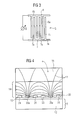
- FIG. 4 shows an embodiment of a biochip with a 4-pole electrode arrangement in an illustration corresponding to FIG. 2 .
- FIG. 5 shows the electrode arrangement of the biochip of FIG. 4 in an illustration corresponding to FIG. 3 .
- a biochip 1 includes a flat carrier 2 , on one side of which a spot array 3 is applied.
- a spot 4 contains immobilized catcher molecules, for example oligonucleotides. If an analyte solution with unknown target molecules is applied to a spot, then the target molecule is coupled to the catcher molecule in the event of corresponding matching in the base sequence.
- the property change brought about by such a binding event e.g., changes in the resistivity or the dielectric constant, is detected preferably impedance-spectroscopically by way of an electrode arrangement 5 .
- a 2-pole electrode arrangement is present in the case of the example embodiment of FIG. 2 .
- This arrangement is applied to the flat carrier 2 for example with the aid of a photolithographic method.
- the electrode arrangement 5 includes two electrodes 6 , 7 designed in the form of an inter-digital structure. That is to say that each electrode includes a plurality of strip-type partial electrodes 6 a , 7 a which run parallel to one another and in each case extend into the interspace between two partial electrodes of the respective other electrodes.
- the partial electrodes 6 a , 7 a are connected to one another by a likewise strip-type connecting conductor 6 b , 7 b extending transversely with respect to the partial electrodes 6 a , 7 a.
- An AC voltage e.g., in the megahertz range is applied to the electrodes 6 , 7 .
- the width 8 of the partial electrodes 6 a , 7 a is approximately 1 ⁇ m, their height 9 is approximately 100 to 500 nm.
- a spacing 10 of likewise approximately 1 ⁇ m is present between the partial electrodes 6 a , 7 a.
- the flat carrier 2 includes a silicon layer 12 and an insulating layer 13 , e.g., made of silicon dioxide or silicon nitride that is arranged between said silicon layer and the electrodes 6 , 7 .
- the electrical interconnections and components required for the impedance-spectroscopic measurement of binding events are realized in a conventional manner by means of a corresponding patterning of the silicon layer (not illustrated).
- a reaction layer 14 made of a hydrogel is applied on the insulating layer 13 , which hydrogel is described in more detail further below.
- Catcher molecules 15 are embedded and homogeneously distributed in the reaction layer 14 or the hydrogel, said catcher molecules being illustrated symbolically and in over-dimensioned fashion in FIG. 2 .
- a catcher molecule with 300 bases has approximately a length of 100 nm. Accordingly, a monomolecular layer of catcher molecules in the case of conventional biochips has at most approximately a thickness corresponding to the line 16 in FIG. 2 .
- the reaction region that contains catcher molecules and is pervaded by field lines is substantially extended and offers space for a number of target molecules 15 that is greater by a plurality of powers of ten. If an analyte solution 18 is applied to a spot array 3 configured in such a way or to a spot 4 , then the target molecules 19 contained in it, which is likewise illustrated only symbolically and with exaggerated size in F. 2 , find a substantially larger number of possible binding partners in the form of the catcher molecules 15 .
- the reaction layer 14 is preferably dimensioned, or has a thickness, such that the impedance-spectroscopic detection range is practically fully utilized, which is achieved in any event given a thickness of the reaction layer of approximately 2 to 100 ⁇ m and is the case in practice already at 2-10 ⁇ m. Consequently, the binding-specific measuring effect of the biochip can be substantially increased given a corresponding concentration of catcher molecules 15 in this region.
- the reaction layer 14 is configured such that it provides an aqueous reaction medium. Furthermore, it is configured such that target molecules 19 or else other substances required for a reaction, for example, polymerase, can infuse or diffuse into it without its activity being impaired in the process.
- a hydrogel is used as the reaction layer 14 .
- a hydrogel represents an aqueous milieu in a mechanically stable form whilst at the same time ensuring the substance exchange in a predominantly aqueous environment.
- chemical composition which relates to the components and the ratio thereof among one another, the properties of the hydrogels such as water content, swelling behavior, mechanical stability etc. can be varied over wide ranges.
- a hydrogel that can be produced easily and has a good adhesion both with respect to the electrode arrangement 5 and with respect to the insulating layer 13 is an acrylamide-based radical-crosslinkable hydrogel containing a comonomer enabling a covalent coupling of correspondingly modified catcher molecules via linker groups.
- the hydrogel includes, in addition to the monomer precursor of polyacrylamide, a crosslinking agent, at least one radical initiator, at least one comonomer with reactive linker groups and, if appropriate, at least one plasticizer.
- a water-swellable hydrogel is obtained containing reactive linker groups for the immobilization of catcher molecules.
- Methylene bisacrylamide and/or dimethylacrylates for example tetraethylene glycol dimethacrylate, are used as crosslinking agents.
- the hydrogel mesh size can be set by varying the concentrations of the crosslinking agent.
- the comonomer used contains maleic anhydride and/or glycidyl (meth)acrylate. Mono-, di- and/or triethylene glycol is suitable as plasticizer.
- the starting substances mentioned are mixed with a polar, water-miscible solvent, preferably with dimethylformamide.
- the processing viscosity can be set by varying the proportion of solvent.
- the adhesion to the flat carrier surface and also to the electrode arrangement 5 can be reinforced by admixture of customary adhesion promoters, for example silane-based adhesion promoters.
- FIGS. 4 and 5 illustrate an exemplary embodiment with a 4-pole electrode arrangement 20 .
- the electrode arrangement 20 is composed of two current electrodes 22 , 23 and two voltage or probe electrodes 24 , 25 .
- the current electrodes 22 , 23 are arranged and configured in accordance with the electrode arrangement 5 of the exemplary embodiment according to FIG. 2 .
- the probe electrodes 24 , 25 are likewise strip-type and extend as a meandering double strand through the interspaces present between the partial electrodes 22 a and 23 a .
- a high-frequency AC current is applied to the current electrodes 22 , 23 .
- a voltmeter 26 is connected to the probe electrodes 24 , 25 and can be used to detect an alteration in the alternating electric field on account of binding events.
- the measurement can thus be effected independently of the current electrodes, so that, e.g., their polarization that increases the electrode impedance cannot affect the measurement.
- the electrode impedance has to be kept low by means of a correspondingly high measurement frequency that is unfavorable in terms of measurement technology, in order to be able to determine the resistance of the analyte solution or of the reaction layer, which resistance is crucial for the measurement.
- a 2-pole electrode arrangement in combination with very high measurement frequencies is advantageous for detecting changes in capacitance within the reaction layer that are caused by binding events.
- DC voltage or current instead of an AC voltage in order to detect binding events by means of the at least one electrode arrangement 5 .
- the DC voltage or current can also vary or be interrupted during and/or between any measurement cycle(s).
Abstract
Description
Claims (7)
Priority Applications (1)
| Application Number | Priority Date | Filing Date | Title |
|---|---|---|---|
| US14/306,401 US9400278B2 (en) | 2002-12-19 | 2014-06-17 | Biochip |
Applications Claiming Priority (6)
| Application Number | Priority Date | Filing Date | Title |
|---|---|---|---|
| DE10259821A DE10259821B4 (en) | 2002-12-19 | 2002-12-19 | Biochip |
| DE10259821.5 | 2002-12-19 | ||
| DE10259821 | 2002-12-19 | ||
| PCT/DE2003/004137 WO2004057335A1 (en) | 2002-12-19 | 2003-12-15 | Biochip |
| US54020805A | 2005-11-16 | 2005-11-16 | |
| US14/306,401 US9400278B2 (en) | 2002-12-19 | 2014-06-17 | Biochip |
Related Parent Applications (2)
| Application Number | Title | Priority Date | Filing Date |
|---|---|---|---|
| PCT/DE2003/004137 Continuation-In-Part WO2004057335A1 (en) | 2002-12-19 | 2003-12-15 | Biochip |
| US10/540,208 Continuation-In-Part US8753874B2 (en) | 2002-12-19 | 2003-12-15 | Biochip |
Publications (2)
| Publication Number | Publication Date |
|---|---|
| US20140294674A1 US20140294674A1 (en) | 2014-10-02 |
| US9400278B2 true US9400278B2 (en) | 2016-07-26 |
Family
ID=32667518
Family Applications (2)
| Application Number | Title | Priority Date | Filing Date |
|---|---|---|---|
| US10/540,208 Active 2026-07-01 US8753874B2 (en) | 2002-12-19 | 2003-12-15 | Biochip |
| US14/306,401 Expired - Lifetime US9400278B2 (en) | 2002-12-19 | 2014-06-17 | Biochip |
Family Applications Before (1)
| Application Number | Title | Priority Date | Filing Date |
|---|---|---|---|
| US10/540,208 Active 2026-07-01 US8753874B2 (en) | 2002-12-19 | 2003-12-15 | Biochip |
Country Status (7)
| Country | Link |
|---|---|
| US (2) | US8753874B2 (en) |
| EP (1) | EP1573328B1 (en) |
| JP (1) | JP2006510882A (en) |
| CA (1) | CA2510719C (en) |
| DE (1) | DE10259821B4 (en) |
| DK (1) | DK1573328T3 (en) |
| WO (1) | WO2004057335A1 (en) |
Families Citing this family (7)
| Publication number | Priority date | Publication date | Assignee | Title |
|---|---|---|---|---|
| JP2008003074A (en) * | 2006-05-26 | 2008-01-10 | Furuido:Kk | Micro fluid device, measuring device, and micro fluid stirring method |
| US9227011B2 (en) | 2006-09-29 | 2016-01-05 | MEDIMETRICS Personalized Drug Delivery B.V. | Miniaturized threshold sensor |
| JP2009092633A (en) * | 2007-10-12 | 2009-04-30 | Denso Corp | Impedance sensor |
| DE102009015114B4 (en) * | 2009-03-31 | 2014-05-22 | Siemens Aktiengesellschaft | Device in the manner of an electrochemical camera and method for producing and using the device |
| DE102009043527B4 (en) | 2009-09-30 | 2021-06-10 | Boehringer Ingelheim Vetmedica Gmbh | Arrangement and method using microsensors for measuring cell vitalities |
| WO2012009322A1 (en) * | 2010-07-12 | 2012-01-19 | Arizona Board Of Regents, A Body Corporate Of The State Of Arizona, Acting For And On Behalf Of Arizona State University | Methods and device for tuning multiplexed markers for disease assay |
| DE102019000763A1 (en) * | 2019-02-02 | 2020-08-06 | Wolfgang Krautschneider | Arrangement for the electrical characterization of biological material |
Citations (19)
| Publication number | Priority date | Publication date | Assignee | Title |
|---|---|---|---|---|
| JPH0593709A (en) | 1991-10-01 | 1993-04-16 | Nippon Oil & Fats Co Ltd | Filler for capillary |
| US5534132A (en) | 1995-05-04 | 1996-07-09 | Vreeke; Mark | Electrode and method for the detection of an affinity reaction |
| WO1997034140A1 (en) | 1996-03-14 | 1997-09-18 | Fraunhofer-Gesellschaft zur Förderung der angewandten Forschung e.V. | Detection of molecules and molecule complexes |
| WO1998019153A1 (en) | 1996-10-26 | 1998-05-07 | The Victoria University Of Manchester | Sensor employing impedance measurements |
| WO2000062048A2 (en) | 1999-04-14 | 2000-10-19 | Fraunhofer-Gesellschaft Zur Foerderung Der Angewandten Forschung E.V. | Sensor arrangement with electrically controllable arrays |
| WO2000065097A1 (en) | 1999-04-26 | 2000-11-02 | Biocept, Inc. | Biochip and method for making it |
| DE4426507C2 (en) | 1994-07-27 | 2001-04-26 | Inst Chemo Biosensorik | Sensors based on microstructures |
| DE20022642U1 (en) | 2000-07-05 | 2002-03-14 | Inventus Biotec Gesellschaft Fuer Innovative Bioanalytik, Biosensoren Und Diagnostika Mbh & Co. Kg | Disposable electrochemical biosensor for the quantitative determination of analyte concentrations in liquids |
| JP2002088652A (en) | 2000-09-08 | 2002-03-27 | Mitsubishi Rayon Co Ltd | Method for introducing hydrophilic functional group into inner wall portion of hollow fiber and method for filling gel into hollow fiber |
| US6372813B1 (en) | 1999-06-25 | 2002-04-16 | Motorola | Methods and compositions for attachment of biomolecules to solid supports, hydrogels, and hydrogel arrays |
| WO2002041992A2 (en) | 2000-11-24 | 2002-05-30 | Siemens Aktiengesellschaft | Method for biochemical analysis and corresponding arrangement |
| US20020102415A1 (en) | 1999-05-20 | 2002-08-01 | Paul L. Valint | Surface treatment of silicone hydrogel contact lenses comprising hydrophilic polymer chains attached to an intermediate carbon coating |
| US6485703B1 (en) | 1998-07-31 | 2002-11-26 | The Texas A&M University System | Compositions and methods for analyte detection |
| US20020179444A1 (en) | 2001-06-04 | 2002-12-05 | Lauks Imants R. | Electrode module |
| US20030000833A1 (en) | 2001-05-31 | 2003-01-02 | Sohrab Mansouri | Analytical instruments, biosensors and methods thereof |
| US6518022B1 (en) * | 1993-11-01 | 2003-02-11 | Nanogen, Inc. | Method for enhancing the hybridization efficiency of target nucleic acids using a self-addressable, self-assembling microelectronic device |
| US20030148530A1 (en) | 2001-06-08 | 2003-08-07 | Lauks Imants R. | Point-of-care in-vitro blood analysis system |
| US20030226768A1 (en) * | 2000-03-30 | 2003-12-11 | Franz Hoffman | Method for detecting macromolecular biopolymers by means of an electrode arrangement |
| US20040121339A1 (en) | 2002-12-19 | 2004-06-24 | Jizhong Zhou | Special film-coated substrate for bio-microarray fabrication and use thereof |
-
2002
- 2002-12-19 DE DE10259821A patent/DE10259821B4/en not_active Expired - Lifetime
-
2003
- 2003-12-15 CA CA2510719A patent/CA2510719C/en not_active Expired - Lifetime
- 2003-12-15 US US10/540,208 patent/US8753874B2/en active Active
- 2003-12-15 JP JP2004561041A patent/JP2006510882A/en active Pending
- 2003-12-15 WO PCT/DE2003/004137 patent/WO2004057335A1/en active Application Filing
- 2003-12-15 DK DK03795751.1T patent/DK1573328T3/en active
- 2003-12-15 EP EP03795751.1A patent/EP1573328B1/en not_active Expired - Lifetime
-
2014
- 2014-06-17 US US14/306,401 patent/US9400278B2/en not_active Expired - Lifetime
Patent Citations (23)
| Publication number | Priority date | Publication date | Assignee | Title |
|---|---|---|---|---|
| JPH0593709A (en) | 1991-10-01 | 1993-04-16 | Nippon Oil & Fats Co Ltd | Filler for capillary |
| US6518022B1 (en) * | 1993-11-01 | 2003-02-11 | Nanogen, Inc. | Method for enhancing the hybridization efficiency of target nucleic acids using a self-addressable, self-assembling microelectronic device |
| DE4426507C2 (en) | 1994-07-27 | 2001-04-26 | Inst Chemo Biosensorik | Sensors based on microstructures |
| US5534132A (en) | 1995-05-04 | 1996-07-09 | Vreeke; Mark | Electrode and method for the detection of an affinity reaction |
| US20020028441A1 (en) | 1996-03-14 | 2002-03-07 | Rainer Hintsche | Detection of molecules and molecule complexes |
| WO1997034140A1 (en) | 1996-03-14 | 1997-09-18 | Fraunhofer-Gesellschaft zur Förderung der angewandten Forschung e.V. | Detection of molecules and molecule complexes |
| WO1998019153A1 (en) | 1996-10-26 | 1998-05-07 | The Victoria University Of Manchester | Sensor employing impedance measurements |
| US6485703B1 (en) | 1998-07-31 | 2002-11-26 | The Texas A&M University System | Compositions and methods for analyte detection |
| WO2000062048A2 (en) | 1999-04-14 | 2000-10-19 | Fraunhofer-Gesellschaft Zur Foerderung Der Angewandten Forschung E.V. | Sensor arrangement with electrically controllable arrays |
| US7208077B1 (en) | 1999-04-14 | 2007-04-24 | Fraunhofer-Gesellschaft Zur Foerderung Der Angewandten Forschung E.V. | Sensor arrangement with electrically controllable arrays |
| WO2000062047A1 (en) | 1999-04-14 | 2000-10-19 | Fraunhofer-Gesellschaft zur Förderung der angewandten Forschung e.V. | Electric sensor array |
| WO2000065097A1 (en) | 1999-04-26 | 2000-11-02 | Biocept, Inc. | Biochip and method for making it |
| US20020102415A1 (en) | 1999-05-20 | 2002-08-01 | Paul L. Valint | Surface treatment of silicone hydrogel contact lenses comprising hydrophilic polymer chains attached to an intermediate carbon coating |
| US6372813B1 (en) | 1999-06-25 | 2002-04-16 | Motorola | Methods and compositions for attachment of biomolecules to solid supports, hydrogels, and hydrogel arrays |
| US20030226768A1 (en) * | 2000-03-30 | 2003-12-11 | Franz Hoffman | Method for detecting macromolecular biopolymers by means of an electrode arrangement |
| DE20022642U1 (en) | 2000-07-05 | 2002-03-14 | Inventus Biotec Gesellschaft Fuer Innovative Bioanalytik, Biosensoren Und Diagnostika Mbh & Co. Kg | Disposable electrochemical biosensor for the quantitative determination of analyte concentrations in liquids |
| JP2002088652A (en) | 2000-09-08 | 2002-03-27 | Mitsubishi Rayon Co Ltd | Method for introducing hydrophilic functional group into inner wall portion of hollow fiber and method for filling gel into hollow fiber |
| WO2002041992A2 (en) | 2000-11-24 | 2002-05-30 | Siemens Aktiengesellschaft | Method for biochemical analysis and corresponding arrangement |
| US20030000833A1 (en) | 2001-05-31 | 2003-01-02 | Sohrab Mansouri | Analytical instruments, biosensors and methods thereof |
| US20020179444A1 (en) | 2001-06-04 | 2002-12-05 | Lauks Imants R. | Electrode module |
| US20030148530A1 (en) | 2001-06-08 | 2003-08-07 | Lauks Imants R. | Point-of-care in-vitro blood analysis system |
| US6845327B2 (en) | 2001-06-08 | 2005-01-18 | Epocal Inc. | Point-of-care in-vitro blood analysis system |
| US20040121339A1 (en) | 2002-12-19 | 2004-06-24 | Jizhong Zhou | Special film-coated substrate for bio-microarray fabrication and use thereof |
Non-Patent Citations (4)
| Title |
|---|
| Datasheet dimethylacrylate, Retrieved from the Internet URL:http//chemicalregister.com/3-3-Dimethylacrylic-acid/suppliers/pid28139.htm, printed Nov. 23, 2010. |
| English translation of Japanese Notice of Reasons for Rejection for counterpart Japanese Patent Application No. 2004-561041. |
| Marquette Christophe A. et al: "Regnerable immunobiosensor for the chemiluminescent flow injection analysis of the herbicide 2, 4-D", Jul. 2, 2000, vol. 5, Nr. 2, S. 395-401. |
| Proudnikov D. et al. "Immobilization of DNA in polyacrylamide gel for the manufacture of DNA and DNA-oligonucleotide microchiips", Analytical Biochemistry, Academic Press, Bd. 259, 1998, S. 34-41. |
Also Published As
| Publication number | Publication date |
|---|---|
| CA2510719A1 (en) | 2004-07-08 |
| DK1573328T3 (en) | 2013-12-09 |
| WO2004057335A1 (en) | 2004-07-08 |
| US8753874B2 (en) | 2014-06-17 |
| EP1573328A1 (en) | 2005-09-14 |
| US20140294674A1 (en) | 2014-10-02 |
| CA2510719C (en) | 2012-01-17 |
| JP2006510882A (en) | 2006-03-30 |
| DE10259821A1 (en) | 2004-08-05 |
| DE10259821B4 (en) | 2006-03-09 |
| US20060137984A1 (en) | 2006-06-29 |
| EP1573328B1 (en) | 2013-10-16 |
Similar Documents
| Publication | Publication Date | Title |
|---|---|---|
| US9400278B2 (en) | Biochip | |
| US8097134B2 (en) | Addressable chem/bio chip array | |
| Xie et al. | Electrochemical sensor for 2, 4-dichlorophenoxy acetic acid using molecularly imprinted polypyrrole membrane as recognition element | |
| US6730212B1 (en) | Sensor for chemical and biological materials | |
| CA2393766A1 (en) | Column and row addressable high density biochip array | |
| US20020028441A1 (en) | Detection of molecules and molecule complexes | |
| US6740214B1 (en) | Microelectrode biosensor and method therefor | |
| US9540683B2 (en) | Biosensor array formed by junctions of functionalized electrodes | |
| WO2010151817A1 (en) | Probe immobilization and signal amplification for polymer-based biosensor | |
| AU776997B2 (en) | Biosensors which utilize charge neutral conjugated polymers | |
| JP2004524534A (en) | Detection method of giant biopolymer using electrode structure | |
| JP4376188B2 (en) | Method and apparatus for PCR amplification and detection of nucleotide sequences | |
| US20060226030A1 (en) | Capacitative biosensor element and method for detecting hybridization events | |
| TW200936767A (en) | Method and device for detection of nucleic acids and/or polypeptides | |
| Liao et al. | Conducting polymer-based impedimetric aptamer biosensor for in situ detection | |
| US20020051975A1 (en) | Reporterless genosensors using electrical detection methods | |
| KR101729489B1 (en) | Biosensor utilizing conductive particles and the combination of polynucleotides corresponding to conductive particles, and method for detecting electric signal using the same | |
| Hwang et al. | Multi-modal biosensing enabled by on-chip nano-corrugated graphene | |
| KR101667648B1 (en) | Method and biochip for detecting target polynucleotide electrically using conductive particles | |
| TR2021015696A2 (en) | A BIOSENSOR FOR PRIMARY FIBROBLAST CELL CHARACTERIZATION | |
| US20060166285A1 (en) | Charged permeation layers for use on active electronic matrix devices | |
| Mustafa | electrical characterization of DNA supported on nitrocellulose membranes |
Legal Events
| Date | Code | Title | Description |
|---|---|---|---|
| AS | Assignment |
Owner name: BOEHRINGER INGELHEIM VETMEDICA GMBH, GERMANY Free format text: ASSIGNMENT OF ASSIGNORS INTEREST;ASSIGNORS:GUMBRECHT, WALTER;STANZEL, MANFRED;SIGNING DATES FROM 20140815 TO 20140820;REEL/FRAME:033590/0169 |
|
| FEPP | Fee payment procedure |
Free format text: PAYOR NUMBER ASSIGNED (ORIGINAL EVENT CODE: ASPN); ENTITY STATUS OF PATENT OWNER: LARGE ENTITY |
|
| STCF | Information on status: patent grant |
Free format text: PATENTED CASE |
|
| MAFP | Maintenance fee payment |
Free format text: PAYMENT OF MAINTENANCE FEE, 4TH YEAR, LARGE ENTITY (ORIGINAL EVENT CODE: M1551); ENTITY STATUS OF PATENT OWNER: LARGE ENTITY Year of fee payment: 4 |
|
| FEPP | Fee payment procedure |
Free format text: MAINTENANCE FEE REMINDER MAILED (ORIGINAL EVENT CODE: REM.); ENTITY STATUS OF PATENT OWNER: LARGE ENTITY |