US9414454B2 - Solid state lighting apparatuses and related methods - Google Patents
Solid state lighting apparatuses and related methods Download PDFInfo
- Publication number
- US9414454B2 US9414454B2 US13/769,277 US201313769277A US9414454B2 US 9414454 B2 US9414454 B2 US 9414454B2 US 201313769277 A US201313769277 A US 201313769277A US 9414454 B2 US9414454 B2 US 9414454B2
- Authority
- US
- United States
- Prior art keywords
- solid state
- state light
- array
- lighting apparatus
- light emitters
- Prior art date
- Legal status (The legal status is an assumption and is not a legal conclusion. Google has not performed a legal analysis and makes no representation as to the accuracy of the status listed.)
- Active
Links
- 239000007787 solid Substances 0.000 title claims abstract description 507
- 238000000034 method Methods 0.000 title abstract description 16
- 239000000758 substrate Substances 0.000 claims abstract description 235
- 238000010521 absorption reaction Methods 0.000 claims abstract description 6
- 239000000463 material Substances 0.000 claims description 59
- 238000000576 coating method Methods 0.000 claims description 55
- 239000011248 coating agent Substances 0.000 claims description 50
- 230000003287 optical effect Effects 0.000 claims description 44
- 238000004891 communication Methods 0.000 claims description 37
- 238000006243 chemical reaction Methods 0.000 claims description 13
- 229920001296 polysiloxane Polymers 0.000 claims description 12
- 230000005540 biological transmission Effects 0.000 claims description 9
- BQCADISMDOOEFD-UHFFFAOYSA-N Silver Chemical compound [Ag] BQCADISMDOOEFD-UHFFFAOYSA-N 0.000 claims description 7
- 229910052709 silver Inorganic materials 0.000 claims description 7
- 239000004332 silver Substances 0.000 claims description 7
- 239000003990 capacitor Substances 0.000 description 19
- 230000004913 activation Effects 0.000 description 16
- 230000009849 deactivation Effects 0.000 description 15
- 238000010586 diagram Methods 0.000 description 14
- 230000001012 protector Effects 0.000 description 14
- 230000002093 peripheral effect Effects 0.000 description 11
- 239000003086 colorant Substances 0.000 description 8
- 238000000605 extraction Methods 0.000 description 8
- 230000004907 flux Effects 0.000 description 8
- 239000004020 conductor Substances 0.000 description 7
- 230000001965 increasing effect Effects 0.000 description 6
- OAICVXFJPJFONN-UHFFFAOYSA-N Phosphorus Chemical compound [P] OAICVXFJPJFONN-UHFFFAOYSA-N 0.000 description 5
- 230000009286 beneficial effect Effects 0.000 description 5
- 239000008393 encapsulating agent Substances 0.000 description 5
- 238000003491 array Methods 0.000 description 4
- 230000006870 function Effects 0.000 description 4
- 238000005286 illumination Methods 0.000 description 4
- 229910052751 metal Inorganic materials 0.000 description 4
- 239000002184 metal Substances 0.000 description 4
- 239000004065 semiconductor Substances 0.000 description 4
- HBMJWWWQQXIZIP-UHFFFAOYSA-N silicon carbide Chemical compound [Si+]#[C-] HBMJWWWQQXIZIP-UHFFFAOYSA-N 0.000 description 4
- 229910010271 silicon carbide Inorganic materials 0.000 description 4
- 229910000679 solder Inorganic materials 0.000 description 4
- 230000007480 spreading Effects 0.000 description 4
- 238000003892 spreading Methods 0.000 description 4
- 238000003860 storage Methods 0.000 description 4
- PNEYBMLMFCGWSK-UHFFFAOYSA-N aluminium oxide Inorganic materials [O-2].[O-2].[O-2].[Al+3].[Al+3] PNEYBMLMFCGWSK-UHFFFAOYSA-N 0.000 description 3
- 239000000919 ceramic Substances 0.000 description 3
- PMHQVHHXPFUNSP-UHFFFAOYSA-M copper(1+);methylsulfanylmethane;bromide Chemical compound Br[Cu].CSC PMHQVHHXPFUNSP-UHFFFAOYSA-M 0.000 description 3
- 230000017525 heat dissipation Effects 0.000 description 3
- 230000010354 integration Effects 0.000 description 3
- 238000004806 packaging method and process Methods 0.000 description 3
- 239000004033 plastic Substances 0.000 description 3
- 238000009877 rendering Methods 0.000 description 3
- 229910052710 silicon Inorganic materials 0.000 description 3
- 239000010703 silicon Substances 0.000 description 3
- 230000007704 transition Effects 0.000 description 3
- 229910002601 GaN Inorganic materials 0.000 description 2
- JMASRVWKEDWRBT-UHFFFAOYSA-N Gallium nitride Chemical compound [Ga]#N JMASRVWKEDWRBT-UHFFFAOYSA-N 0.000 description 2
- 239000000969 carrier Substances 0.000 description 2
- 230000008859 change Effects 0.000 description 2
- 230000007423 decrease Effects 0.000 description 2
- 230000003247 decreasing effect Effects 0.000 description 2
- 238000013461 design Methods 0.000 description 2
- 238000004146 energy storage Methods 0.000 description 2
- 230000002708 enhancing effect Effects 0.000 description 2
- 230000007613 environmental effect Effects 0.000 description 2
- 239000011521 glass Substances 0.000 description 2
- 239000000976 ink Substances 0.000 description 2
- 238000002955 isolation Methods 0.000 description 2
- 230000031700 light absorption Effects 0.000 description 2
- 238000004519 manufacturing process Methods 0.000 description 2
- 230000004048 modification Effects 0.000 description 2
- 238000012986 modification Methods 0.000 description 2
- 238000000465 moulding Methods 0.000 description 2
- 150000004767 nitrides Chemical class 0.000 description 2
- 230000001737 promoting effect Effects 0.000 description 2
- 239000002096 quantum dot Substances 0.000 description 2
- 230000005855 radiation Effects 0.000 description 2
- 230000002441 reversible effect Effects 0.000 description 2
- 229910052594 sapphire Inorganic materials 0.000 description 2
- 239000010980 sapphire Substances 0.000 description 2
- 230000003595 spectral effect Effects 0.000 description 2
- 230000000153 supplemental effect Effects 0.000 description 2
- 230000009182 swimming Effects 0.000 description 2
- 238000012546 transfer Methods 0.000 description 2
- RYGMFSIKBFXOCR-UHFFFAOYSA-N Copper Chemical compound [Cu] RYGMFSIKBFXOCR-UHFFFAOYSA-N 0.000 description 1
- 239000004593 Epoxy Substances 0.000 description 1
- DGAQECJNVWCQMB-PUAWFVPOSA-M Ilexoside XXIX Chemical compound C[C@@H]1CC[C@@]2(CC[C@@]3(C(=CC[C@H]4[C@]3(CC[C@@H]5[C@@]4(CC[C@@H](C5(C)C)OS(=O)(=O)[O-])C)C)[C@@H]2[C@]1(C)O)C)C(=O)O[C@H]6[C@@H]([C@H]([C@@H]([C@H](O6)CO)O)O)O.[Na+] DGAQECJNVWCQMB-PUAWFVPOSA-M 0.000 description 1
- 239000004642 Polyimide Substances 0.000 description 1
- XUIMIQQOPSSXEZ-UHFFFAOYSA-N Silicon Chemical compound [Si] XUIMIQQOPSSXEZ-UHFFFAOYSA-N 0.000 description 1
- 230000001154 acute effect Effects 0.000 description 1
- 239000000853 adhesive Substances 0.000 description 1
- 230000001070 adhesive effect Effects 0.000 description 1
- 229910052782 aluminium Inorganic materials 0.000 description 1
- XAGFODPZIPBFFR-UHFFFAOYSA-N aluminium Chemical compound [Al] XAGFODPZIPBFFR-UHFFFAOYSA-N 0.000 description 1
- 238000000149 argon plasma sintering Methods 0.000 description 1
- 230000000712 assembly Effects 0.000 description 1
- 238000000429 assembly Methods 0.000 description 1
- 230000008901 benefit Effects 0.000 description 1
- 230000000903 blocking effect Effects 0.000 description 1
- 230000004456 color vision Effects 0.000 description 1
- 238000004040 coloring Methods 0.000 description 1
- 239000000470 constituent Substances 0.000 description 1
- 229910052802 copper Inorganic materials 0.000 description 1
- 239000010949 copper Substances 0.000 description 1
- 229910052593 corundum Inorganic materials 0.000 description 1
- 230000008878 coupling Effects 0.000 description 1
- 238000010168 coupling process Methods 0.000 description 1
- 238000005859 coupling reaction Methods 0.000 description 1
- 230000001351 cycling effect Effects 0.000 description 1
- 238000007599 discharging Methods 0.000 description 1
- 238000006073 displacement reaction Methods 0.000 description 1
- 230000000694 effects Effects 0.000 description 1
- 230000008030 elimination Effects 0.000 description 1
- 238000003379 elimination reaction Methods 0.000 description 1
- 239000003292 glue Substances 0.000 description 1
- 230000006872 improvement Effects 0.000 description 1
- 238000011065 in-situ storage Methods 0.000 description 1
- 238000007641 inkjet printing Methods 0.000 description 1
- 238000003780 insertion Methods 0.000 description 1
- 230000037431 insertion Effects 0.000 description 1
- 239000011810 insulating material Substances 0.000 description 1
- QSHDDOUJBYECFT-UHFFFAOYSA-N mercury Chemical compound [Hg] QSHDDOUJBYECFT-UHFFFAOYSA-N 0.000 description 1
- 229910052753 mercury Inorganic materials 0.000 description 1
- 229910044991 metal oxide Inorganic materials 0.000 description 1
- 150000004706 metal oxides Chemical class 0.000 description 1
- 238000004377 microelectronic Methods 0.000 description 1
- 239000000203 mixture Substances 0.000 description 1
- 239000002991 molded plastic Substances 0.000 description 1
- NJPPVKZQTLUDBO-UHFFFAOYSA-N novaluron Chemical compound C1=C(Cl)C(OC(F)(F)C(OC(F)(F)F)F)=CC=C1NC(=O)NC(=O)C1=C(F)C=CC=C1F NJPPVKZQTLUDBO-UHFFFAOYSA-N 0.000 description 1
- 239000003973 paint Substances 0.000 description 1
- 239000002245 particle Substances 0.000 description 1
- 239000006072 paste Substances 0.000 description 1
- 229920000728 polyester Polymers 0.000 description 1
- 229920001721 polyimide Polymers 0.000 description 1
- 239000000843 powder Substances 0.000 description 1
- 230000006798 recombination Effects 0.000 description 1
- 238000005215 recombination Methods 0.000 description 1
- 230000009467 reduction Effects 0.000 description 1
- 230000004044 response Effects 0.000 description 1
- 238000007493 shaping process Methods 0.000 description 1
- 229910052708 sodium Inorganic materials 0.000 description 1
- 239000011734 sodium Substances 0.000 description 1
- 230000000638 stimulation Effects 0.000 description 1
- -1 submounts Substances 0.000 description 1
- 230000001629 suppression Effects 0.000 description 1
- 239000011573 trace mineral Substances 0.000 description 1
- 235000013619 trace mineral Nutrition 0.000 description 1
- 230000001052 transient effect Effects 0.000 description 1
- 238000001429 visible spectrum Methods 0.000 description 1
- 229910052724 xenon Inorganic materials 0.000 description 1
- FHNFHKCVQCLJFQ-UHFFFAOYSA-N xenon atom Chemical compound [Xe] FHNFHKCVQCLJFQ-UHFFFAOYSA-N 0.000 description 1
- 229910001845 yogo sapphire Inorganic materials 0.000 description 1
Images


Classifications
-
- H—ELECTRICITY
- H05—ELECTRIC TECHNIQUES NOT OTHERWISE PROVIDED FOR
- H05B—ELECTRIC HEATING; ELECTRIC LIGHT SOURCES NOT OTHERWISE PROVIDED FOR; CIRCUIT ARRANGEMENTS FOR ELECTRIC LIGHT SOURCES, IN GENERAL
- H05B45/00—Circuit arrangements for operating light-emitting diodes [LED]
- H05B45/20—Controlling the colour of the light
-
- H05B33/083—
-
- H05B33/086—
-
- H—ELECTRICITY
- H05—ELECTRIC TECHNIQUES NOT OTHERWISE PROVIDED FOR
- H05B—ELECTRIC HEATING; ELECTRIC LIGHT SOURCES NOT OTHERWISE PROVIDED FOR; CIRCUIT ARRANGEMENTS FOR ELECTRIC LIGHT SOURCES, IN GENERAL
- H05B45/00—Circuit arrangements for operating light-emitting diodes [LED]
- H05B45/40—Details of LED load circuits
- H05B45/44—Details of LED load circuits with an active control inside an LED matrix
- H05B45/48—Details of LED load circuits with an active control inside an LED matrix having LEDs organised in strings and incorporating parallel shunting devices
Definitions
- the present subject matter generally relates to lighting apparatuses and related methods and, more particularly, to solid state lighting apparatuses and related methods.
- Solid state lighting arrays are used for a number of lighting applications. For example, lighting panels including arrays of solid state light emitting devices have been used as direct illumination sources in applications including architectural and/or accent lighting.
- a solid state light emitting device may include, for example, a packaged light emitting device including one or more light emitting diodes (LEDs) or LED chips, which may include inorganic LED chips and/or organic LED chips (OLEDs).
- LEDs light emitting diodes
- LED chips which may include inorganic LED chips and/or organic LED chips
- OLEDs organic LED chips
- solid state light emitting devices generate light through the recombination of electronic carriers (electrons and holes) in a light emitting layer or region of a LED chip.
- LED chips have significantly longer lifetimes and typically have significantly greater luminous efficiency than conventional incandescent and fluorescent light sources; however, LED chips are narrow-band emitters, and it can be challenging to simultaneously provide good color rendering in combination with high luminous efficacy while maintain a maximizing brightness and efficiency.
- the 1931 CIE Chromaticity Diagram maps out the human color perception in terms of two CIE parameters x and y.
- the spectral colors are distributed around the edge of the outlined space, which includes all of the hues perceived by the human eye.
- the boundary line represents maximum saturation for the spectral colors.
- the 1931 CIE Diagram includes temperature listings along the blackbody locus (embodying a curved line emanating from the right corner). These temperature listings show the color path of a blackbody radiator that is caused to increase to such temperatures. As a heated object becomes incandescent, it first glows reddish, then yellowish, then white, and finally bluish. This occurs because the wavelength associated with the peak radiation of the blackbody radiator becomes progressively shorter with increased temperature, consistent with the Wien Displacement Law. Illuminants which produce light that is on or near the blackbody locus can thus be described in terms of their color temperature.
- LED apparatuses typically receive a direct current (DC) input signal or a modulated square wave input signal so that a constant current flows through the LED chips when in an “on” state.
- a current value is typically set to provide high conversion efficiency.
- LED light sources with variable intensity may be controlled by changing duty factor of a modulated square wave input signal.
- a LED-based light source for use in buildings typically includes an AC-DC power converter.
- An AC-DC power converter often represents a significant fraction of the overall cost of a LED-based light source, and power losses inherent to such a power converter reduces overall efficiency of the light source. Additionally, AC-DC power converters are generally not as reliable as LED chips, and therefore can limit the operating lifetime of a LED light source.
- Elimination of AC-DC power converters from solid state lighting apparatuses may enable enhanced cost and packaging efficiencies. It would be desirable to provide solid state lighting apparatuses with reduced volume (or size) and increased integration of functional components (e.g., including but not limited to driver components), in order to reduce production cost and provide lighting device designers with enhanced packaging flexibility, thereby promoting consumer adoption of solid state lighting devices. Achieving a high degree of functional component integration in lighting apparatuses may require placement of functional components proximate to solid state light emitter (e.g., LED) chips, thereby providing potential for such functional components to block, absorb, trap, or otherwise interfere with light emitted by one or more LED chips.
- solid state light emitter e.g., LED
- Desirable solid state lighting apparatuses and/or improved methods including use of solid state lighting apparatuses that can be directly coupled to an AC voltage signal, without requiring use of an on-board switched mode power supply. Desirable solid state lighting apparatuses and methods would exhibit improved light extraction, brightness, and/or improved thermal management. Desirable apparatuses and methods would also exhibit reduced cost and make it easier for end-users to justify switching to LED products from a return on investment or payback perspective.
- Solid state lighting apparatuses adapted to operate with alternating current (AC) received directly from an AC power source and related methods are disclosed.
- an exemplary solid state lighting apparatus can comprise a substrate and multiple sets of one or more solid state light emitters disposed over arranged on or supported by the substrate.
- at least first and second sets of the multiple sets of solid state light emitters can be configured to be activated and/or deactivated at different times relevant to one another during a portion of an AC cycle.
- the first and second sets of the multiple sets of solid state light emitters can also comprise different duty cycles.
- Various apparatuses disclosed herein may include elements and/or configurations arranged to reduce physical interference between solid state light emitters and functional components (e.g. driver circuit components), thereby enhancing light extraction.
- a solid state lighting apparatus is adapted to operate with alternating current (AC) received from an AC power source, the lighting apparatus comprising: a substrate; an array of solid state light emitters arranged on or supported by the substrate, the array comprising a plurality of mutually exclusive solid state light emitter sets each comprising multiple solid state light emitters, wherein at least two different solid state light emitter sets of the plurality of solid state light emitter sets are arranged to be activated and/or deactivated at different times relative to one another during a portion of an AC cycle; at least one driver circuit component arranged on or over the substrate and arranged to drive the array of solid state light emitters; and at least one reflective structure positioned between one or more solid state light emitters of the array of solid state light emitters and the at least one driver circuit component and arranged to reduce or eliminate absorption by the at least one driver circuit component of light generated by the one or more solid state light emitters.
- AC alternating current
- a solid state lighting apparatus is adapted to operate with alternating current (AC) received from an AC power source, the lighting apparatus comprising: a substrate; an array of solid state light emitters arranged on or supported by the substrate, the array comprising a plurality of mutually exclusive solid state light emitter sets each comprising multiple solid state light emitters, wherein at least two different solid state light emitter sets of the plurality of solid state light emitter sets are arranged to be activated and/or deactivated at different times relative to one another during a portion of an AC cycle; at least one driver circuit component arranged on or over the substrate and arranged to drive the array of solid state light emitters; and a reflective coating arranged over at least a portion of the at least one driver circuit component.
- AC alternating current
- a solid state lighting apparatus is adapted to operate with alternating current (AC) received from an AC power source, the lighting apparatus comprising: a substrate including a first surface, a second surface opposing the first surface, electrical traces arranged on or over the first surface, and electrical traces arranged on or over the second surface; an array of solid state light emitters arranged on or over the first surface, the array comprising a plurality of mutually exclusive solid state light emitter sets each comprising multiple solid state light emitters, wherein at least two different solid state light emitter sets of the plurality of solid state light emitter sets are arranged to be activated and/or deactivated at different times relative to one another during a portion of an AC cycle; and at least one driver circuit component arranged on or over the second surface and arranged to drive the array of solid state light emitters.
- AC alternating current
- a solid state lighting apparatus is adapted to operate with alternating current (AC) received from an AC power source, the lighting apparatus comprising: a substrate; an array of solid state light emitters arranged on or supported by the substrate, the array comprising a plurality of mutually exclusive solid state light emitter sets each comprising multiple solid state light emitters, wherein at least two different solid state light emitter sets of the plurality of solid state light emitter sets are arranged to be activated and/or deactivated at different times relative to one another during a portion of an AC cycle; and at least one surge protection component arranged on or over the substrate and adapted to reduce or eliminate transmission of voltage transients exceeding the line voltage to the array of solid state light emitters.
- AC alternating current
- a solid state lighting apparatus is adapted to operate with alternating current (AC) received from an AC power source, the lighting apparatus comprising: a first array of solid state light emitters including a first plurality of solid state light emitter sets each comprising multiple solid state light emitters arranged in or on a first elongated body structure, wherein at least two different solid state light emitter sets of the first plurality of individually controllable solid state light emitter sets are arranged to be activated and/or deactivated at different times relative to one another during a portion of an AC cycle; at least one driver circuit component arranged to drive the first array of solid state light emitters; and at least one electrical connector arranged to permit electrical communication between the first array of solid state light emitters and a second array of solid state light emitters that includes a second plurality of solid state light emitter sets each comprising multiple solid state light emitters arranged in or on a second elongated body structure, wherein at least two different solid state light emitter sets of the second plurality of solid state light emitter segments are
- a solid state lighting apparatus is adapted to operate with alternating current (AC) received from an AC power source, the lighting apparatus comprising: a substrate; an array of solid state light emitters arranged on or supported by the substrate, the array comprising a plurality of mutually exclusive solid state light emitter sets each comprising multiple solid state light emitters, wherein at least two different solid state light emitter sets of the plurality of solid state light emitter sets are arranged to be activated and/or deactivated at different times relative to one another during a portion of an AC cycle; and at least one optical element comprising a lens and/or a diffuser arranged to receive emissions from each solid state light emitter of the array of solid state light emitters.
- AC alternating current
- a solid state lighting apparatus is adapted to operate with alternating current (AC) received from an AC power source, the lighting apparatus comprising: a base end; a light-transmissive end opposing the base end; an array of solid state light emitters including a plurality of solid state light emitter sets each comprising multiple solid state light emitters, wherein at least two different solid state light emitter sets of the plurality of individually controllable solid state light emitter segments are arranged to be activated and/or deactivated at different times relative to one another during a portion of an AC cycle; and a reflector comprising including a cavity and a reflective surface arranged to permit transmission of light reflected by the reflector toward the light-transmissive end; wherein the array of solid state emitters is arranged in or above the cavity to transmit emissions of the solid state emitters toward the reflective surface; and wherein the array of solid state emitters are arranged to emit light in a direction toward the base end to impinge on the reflective surface for reflection of light toward the light-transmissive end.
- AC
- a solid state lighting apparatus is adapted to operate with alternating current (AC) received from an AC power source, the lighting apparatus comprising: A lighting apparatus adapted to operate with alternating current (AC) received from an AC power source, the lighting device comprising: a light-transmissive end; an array of solid state light emitters including a plurality of solid state light emitter sets each comprising multiple solid state light emitters, wherein at least two different solid state light emitter sets of the plurality of individually controllable solid state light emitter sets are arranged to be activated and/or deactivated at different times relative to one another during a period of the AC waveform; and a reflector defining a cavity and comprising a reflective surface arranged to permit transmission of light reflected by the reflector toward the light-transmissive end; wherein the array of solid state emitters is arranged in or above the cavity to transmit emissions of the solid state emitters toward the reflective surface; and wherein light emissions transmitted through the light-transmissive end comprise emissions reflected by the reflective surface and are devoid of
- a method comprises illuminating an object, a space, or an environment, utilizing a lighting apparatus as described herein.
- any of the foregoing aspects, and/or various separate aspects and features as described herein, may be combined for additional advantage. Any of the various features and elements as disclosed herein may be combined with one or more other disclosed features and elements unless indicated to the contrary herein.
- FIG. 1 is a schematic block diagram illustrating a solid state lighting apparatus including a light emitting diode (LED) driver circuit and an LED string circuit according to certain embodiments;
- LED light emitting diode
- FIG. 2 is a schematic block diagram illustrating the LED driver circuit including a rectifier circuit and a current diversion circuit as shown in FIG. 1 and a LED string circuit coupled thereto according to certain embodiments;
- FIG. 3 is a schematic block diagram illustrating the LED driver circuit shown in FIGS. 1 and 2 further including a current limiter circuit and a capacitor coupled to the LED string circuit according to certain embodiments;
- FIG. 4 is a circuit schematic diagram illustrating an LED driver circuit coupled to an LED string circuit according to certain embodiments
- FIG. 5A is a plot of voltage versus time of a rectified AC waveform with a superimposed plot of activation and deactivation times for three LED sets and a superimposed plot of average current with respect to time of a solid state lighting apparatus according to certain embodiments;
- FIG. 5B is a plot of RMS voltage versus time showing duty cycles for three LED sets of a solid state lighting device according to certain embodiments
- FIGS. 6A to 6D are schematic diagrams illustrating LED chip and/or LED package placement over a substrate according to certain embodiments
- FIG. 6E is a schematic diagram illustrating a first and second arrays of solid state light emitters (e.g. LEDs) associated with first and second body structures, respectively, that are connected by at least one electrical connector.
- solid state light emitters e.g. LEDs
- FIGS. 7A and 7B are perspective views illustrating a solid state lighting apparatus including multiple solid state light emitters, associated circuitry, and reflective structures arranged on or over a substrate according to certain embodiments;
- FIG. 8A is a perspective view illustrating a solid state lighting apparatus including multiple solid state light emitters, associated circuitry, and reflective structures or coatings arranged on or over a substrate according to certain embodiments;
- FIGS. 8B to 8G are sectional views of portions of the solid state lighting apparatus of FIG. 8A according to various embodiments;
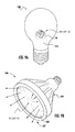
- FIG. 9A is a perspective view of a light bulb including at least one solid state lighting apparatus according to certain embodiments.
- FIG. 9B is a perspective view of a light bulb including a base end, a light transmissive end, a reflective surface, and at least one solid state lightning apparatus according to certain embodiments.
- the present invention relates in certain aspects to solid state lighting apparatuses adapted to operate with alternating current (AC) received directly from an AC power source and related methods.
- Exemplary solid state lighting apparatuses can comprise a substrate and multiple sets of one or more solid state light emitters arranged on or supported by the substrate. At least first and second sets of the multiple sets of solid state light emitters can be configured to be activated and/or deactivated at different times relevant to one another during a portion of an AC cycle. More than two sets of solid state light emitters may be provided, and different sets of solid state light emitters may also comprise different duty cycles.
- Various apparatuses disclosed herein may include elements and/or configurations arranged to reduce physical interference between solid state light emitters and functional components (e.g., driver circuit components), thereby enhancing light extraction.
- solid state lighting apparatuses described herein may include various emitter configurations, color combinations, and/or circuit components adapted to reduce perceivable flicker, perceivable color shifts, and/or perceivable spatial variations in luminous flux that could potentially occur during activation and/or deactivation of multiple sets of different solid state light emitters.
- temis used herein should be construed to have the same meaning as commonly understood by one of ordinary skill in the art to which this invention belongs. It will be further understood that terms used herein should be interpreted as having a meaning that is consistent with their meaning in the context of this specification and the relevant art, and should not be interpreted in an idealized or overly formal sense unless expressly so defined herein.
- Embodiments of the invention are described herein with reference to cross-sectional, perspective, elevation, and/or plan view illustrations that are schematic illustrations of idealized embodiments of the invention. Variations from the shapes of the illustrations as a result, for example, of manufacturing techniques and/or tolerances, are to be expected, such that embodiments of the invention should not be construed as limited to particular shapes illustrated herein.
- This invention may be embodied in different forms and should not be construed as limited to the specific embodiments set forth herein. In the drawings, the size and relative sizes of layers and regions may be exaggerated for clarity.
- electrically activated emitter and “emitter” as used herein refers to any device capable of producing visible or near visible (e.g.; from infrared to ultraviolet) wavelength radiation, including but not limited to, xenon lamps, mercury lamps, sodium lamps, incandescent lamps, and solid state emitters, including light emitting diodes (LEDs or LED chips), organic light emitting diodes (OLEDs), and lasers.
- LEDs or LED chips light emitting diodes
- OLEDs organic light emitting diodes
- solid state light emitter may include a light emitting diode, laser diode, organic light emitting diode, and/or other semiconductor device preferably arranged as a semiconductor chip that includes one or more semiconductor layers, which may include silicon, silicon carbide, gallium nitride and/or other semiconductor materials, a substrate which may include sapphire, silicon, silicon carbide and/or other microelectronic substrates, and one or more contact layers which may include metal and/or other conductive materials.
- semiconductor layers which may include silicon, silicon carbide, gallium nitride and/or other semiconductor materials
- substrate which may include sapphire, silicon, silicon carbide and/or other microelectronic substrates
- contact layers which may include metal and/or other conductive materials.
- substrate refers to a mounting element on which, in which, or over which multiple solid state light emitters (e.g., emitter chips) may be arranged or supported (e.g., mounted).
- exemplary substrates useful with lighting apparatuses as described herein include printed circuit boards (including but not limited to metal core printed circuit boards, flexible circuit boards, dielectric laminates, and the like) having electrical traces arranged on one or multiple surfaces thereof, support panels, and mounting elements of various materials and conformations arranged to receive, support, and/or conduct electrical power to solid state emitters.
- a unitary substrate may be used to support multiple groups of solid state emitter components, and may further be used to support related circuits and/or circuit elements; such as driver circuit elements, rectifier circuit elements (e.g., a rectifier bridge), current limiting circuit elements, current diverting circuit elements, and/or dimmer circuit elements.
- a substrate may include multiple emitter mounting regions each arranged to receive one or more solid state light emitters or sets of solid state light emitters.
- a substrate e.g., such as a circuit board
- a substrate may include a first surface and an opposing second surface, with an array of solid state emitters arranged on or over the first surface, and with at least one driver circuit component (more preferably all driver circuit components) arranged on or over the second surface, with such configuration reducing or eliminating impingement of light on, or absorption of light by, the at least one driver circuit component.
- substrates may include conductive regions arranged to conduct power to solid state light emitters or solid state light emitter groups arranged thereon or there over.
- substrates may be insulating in character, and electrical connections to solid state emitters may be provided by other means (e.g., via conductors not associated with substrates).
- Solid state light emitting devices may include III-V nitride (e.g., gallium nitride) based LED chips or laser chips fabricated on a silicon, silicon carbide, sapphire, or III-V nitride growth substrate, including (for example) devices manufactured and sold by Cree, Inc. of Durham, N.C.
- III-V nitride e.g., gallium nitride
- Such LEDs and/or lasers may be configured to operate such that light emission occurs through the substrate in a so-called “flip chip” orientation.
- Such LED and/or laser chips may also be devoid of growth substrates (e.g., following growth substrate removal).
- LED chips useable with lighting devices as disclosed herein may include horizontal devices (with both electrical contacts on a same side of the LED chip) and/or vertical devices (with electrical contacts on opposite sides of the LED chip).
- a horizontal device (with or without the growth substrate), for example, may be flip chip bonded (e.g., using solder) to a carrier substrate or printed circuit board (PCB), or wire bonded.
- a vertical device (without or without the growth substrate) may have a first terminal solder bonded to a carrier substrate, mounting pad, or printed circuit board (PCB), and have a second terminal wire bonded to the carrier substrate, electrical element, or PCB.
- Electrically activated light emitters may be used individually or in groups to emit one or more beams to stimulate emissions of one or more lumiphoric materials (e.g., phosphors, scintillators, lumiphoric inks, quantum dots) to generate light at one or more peak wavelength, or of at least one desired perceived color (including combinations of colors that may be perceived as white).
- lumiphoric materials e.g., phosphors, scintillators, lumiphoric inks, quantum dots
- lumiphoric materials also called ‘luminescent’
- lumiphoric materials in lighting devices as described herein may be accomplished by direct coating on lumiphor support elements or lumiphor support surfaces (e.g., by powder coating, inkjet printing, or the like), adding such materials to lenses, and/or by embedding or dispersing such materials within lumiphor support elements or surfaces.
- LED devices and methods as disclosed herein may include have multiple LED chips of different colors, one or more of which may be white emitting (e.g., including at least one LED chip with one or more lumiphoric materials).
- one or more short wavelength solid state emitters may be used to stimulate emissions from a mixture of lumiphoric materials, or discrete layers of lumiphoric material, including red, yellow, and green lumiphoric materials.
- multiple groups of solid state emitters may include at least three independently controlled short wavelength (e.g., blue or cyan) LED chips, with a first short wavelength LED chip arranged to stimulate emissions of a first red lumiphor, a second short wavelength LED chip arranged to stimulate emissions of a second yellow lumiphor, and a third short wavelength LED chip arranged to stimulate emissions of a third red lumiphor.
- Such LED chips of different wavelengths may be present in the same group of solid state emitters, or may be provided in different groups of solid state emitters.
- peak wavelength means (1) in the case of a solid state light emitter, to the peak wavelength of light that the solid state light emitter emits if it is illuminated, and (2) in the case of a lumiphoric material, the peak wavelength of light that the lumiphoric material emits if it is excited.
- luminescent materials also known as lumiphors or luminophoric media, e.g., as disclosed in U.S. Pat. No. 6,600,175 and U.S. Patent Application Publication No. 2009/0184616
- luminescent materials include phosphors, scintillators, day glow tapes, nanophosphors, quantum dots (e.g., such as provided by NNCrystal US Corp. (Fayetteville, Ark.)), and inks that glow in the visible spectrum upon illumination with (e.g., ultraviolet) light.
- One or more luminescent materials useable in devices as described herein may be down-converting or up-converting, or can include a combination of both types.
- Some embodiments of the present invention may use solid state emitters, emitter packages, fixtures, luminescent materials/elements, power supply elements, control elements, and/or methods such as described in U.S. Pat. Nos. 7,564,180; 7,456,499; 7,213,940; 7,095,056; 6,958,497; 6,853,010; 6,791,119; 6,600,175, 6,201,262; 6,187,606; 6,120,600; 5,912,477; 5739,554; 5,631,190; 5,604,135; 5,523,589; 5,416,342; 5,393,993; 5,359,345; 5,338,944; 5,210,051; 5,027,168; 5,027,168; 4,966,862, and/or 4,918,497, and U.S.
- a lighting device or lighting apparatus can be a device or apparatus that illuminates an area or volume, e.g., a structure, a swimming pool or spa, a room, a warehouse, an indicator, a road, a parking lot, a vehicle, signage, e.g., road signs, a billboard, a ship, a toy, a mirror, a vessel, an electronic device, a boat, an aircraft, a stadium, a computer, a remote audio device, a remote video device, a cell phone, a tree, a window, an LCD display, a cave, a tunnel, a yard, a lamppost, or a device or array of devices that illuminate an enclosure, or a device that is used for edge or back-lighting (e.g., backlight poster, signage, LCD displays), light bulbs, bulb replacements (e.g., for replacing AC inc
- the inventive subject matter further relates in certain embodiments to an illuminated enclosure (the volume of which can be illuminated uniformly or non-uniformly), comprising an enclosed space and at least one lighting device or lighting apparatus as disclosed herein, wherein the lighting device or apparatus illuminates at least a portion of the enclosure (uniformly or non-uniformly).
- the inventive subject matter further relates to an illuminated area, comprising at least one item, e.g., selected from among the group consisting of a structure, a swimming pool or spa, a room, a warehouse, an indicator, a road, a parking lot, a vehicle, signage, e.g., road signs, a billboard, a ship, a toy, a mirror, a vessel, an electronic device, a boat, an aircraft, a stadium, a computer, a remote audio device, a remote video device, a cell phone, a tree, a window, a LCD display, a cave, a tunnel, a yard, a lamppost, etc., having mounted therein or thereon at least one lighting device as described herein.
- Methods include illuminating an object, a space, or an environment, utilizing one or more lighting devices or apparatuses as disclosed herein.
- lighting devices or apparatuses as described herein including multiple groups of one electrically activated (e.g., solid state) light emitters with peak wavelengths in the visible range.
- multiple electrically activated (e.g., solid state) emitters are provided, with groups of emitters being separately controllable relative to one another.
- one or more groups of solid state emitters as described herein may include at least a first LED chip comprising a first LED peak wavelength, and include at least a second LED chip comprising a second LED peak wavelength that differs from the first LED peak wavelength by at least 20 nm, or by at least 30 nm. In such a case, each of the first wavelength and the second wavelength is preferably within the visible range.
- control of one or more solid state emitter groups or sets may be responsive to a control signal (optionally including at least one sensor arranged to sense electrical, optical, and/or thermal properties and/or environmental conditions), and a control system may be configured to selectively provide one or more control signals to at least one current supply circuit.
- a control signal optionally including at least one sensor arranged to sense electrical, optical, and/or thermal properties and/or environmental conditions
- a control system may be configured to selectively provide one or more control signals to at least one current supply circuit.
- current to different circuits or circuit portions may be pre-set, user-defined, or responsive to one or more inputs or other control parameters.
- each set of solid state light emitters comprises at least one electrostatic discharge protection element in electrical communication therewith.
- multiple solid state emitters e.g., LEDs
- Emitters having similar output wavelengths may be selected from targeted wavelength bins.
- Emitters having different output wavelengths may be selected from different wavelength bins, with peak wavelengths differing from one another by a desired threshold (e.g., at least 20 nm, at least 30 nm, at least 50 nm, or another desired threshold).
- one or more sets of solid state emitter includes at least one BSY or white emitter component (including a blue solid state emitter arranged to stimulate emissions of a yellow lumiphor) and at least one red emitter (e.g., a red LED and/or a LED (e.g., UV, blue, cyan, green, etc.) arranged to stimulate emissions of a red lumiphor).
- a red LED and/or a LED e.g., UV, blue, cyan, green, etc.
- Addition of at least one red emitter may be useful to enhance warmth of the BSY or white emissions and improve color rendering, with the resulting combination being termed BSY+R or warm white.
- red and BSY components may be separately controlled, as may be useful to adjust color temperature and/or to maintain a desired color point as temperature increases.
- BSY components and red components may be controlled together in a single group or set, or may be aggregated into separate groups or sets that are separately controlled.
- One or more supplemental solid state emitters and/or lumiphors of any suitable color (or peak wavelength) may be substituted for one or more red light-emitting components, or may be provided in addition to one or more red light-emitting components.
- a solid state lighting device may include one or more groups or sets of BSY light emitting components supplemented with one or more supplemental emitters, such as long wavelength blue, cyan, green, yellow, amber, orange, red or any other desired colors.
- supplemental emitters such as long wavelength blue, cyan, green, yellow, amber, orange, red or any other desired colors.
- Presence of a cyan solid state emitter (which is preferably independently controllable) is particularly desirable in certain embodiments to permit adjustment or tuning of color temperature of a lighting device, since the tie line for a solid state emitter having a ⁇ 487 nm peak wavelength is substantially parallel to the blackbody locus for a color temperature of less than 3000K to about 4000K.
- Different groups of solid state light emitters are preferably controlled separately, such as may be useful to adjust intensity, permit tuning of output color, permit tuning of color temperature, and/or affect dissipation of heat generated by the light emitting components.
- a solid state lighting apparatus adapted to operate with alternating current (AC) received from an AC power source, can include an array of solid state light emitters arranged on or over a substrate, at least one driver circuit component arranged on or over the substrate to drive the array of solid state light emitters, and at least one reflective structure arranged between one or more solid state light emitters of the array and the at least one driver circuit component for reducing or eliminating absorption by the at least one driver circuit component of light generated by the one or more solid state light emitters.
- AC alternating current
- the array of solid state emitters may include a plurality of mutually exclusive solid state light emitter sets each comprising multiple solid state light emitters, wherein at least two different solid state light emitter sets of the plurality of solid state light emitter sets are arranged to be activated and/or deactivated at different times relative to one another during a portion of an AC cycle.
- the lighting apparatus can include a substrate having a plurality of electrically conductive traces along at least one face of the substrate.
- the reflective structure can include at least one raised element adhered to or deposited on the first face of the substrate.
- the at least one reflective structure can include a plurality of reflective structures.
- the at least one reflective structure can be arranged on or over at least a portion of at least one driver circuit element or component.
- at least one reflective structure may be diffusively reflective.
- at least one reflective structure may be specularly reflective.
- the at least one reflective structure may comprise at least one of a white color and a silver color.
- at least one reflective structure may comprise silicone that can be molded and at least partially cured.
- At least one reflective structure may comprise a diffuser. In certain embodiments, the reflective structure may comprise a lens. In certain embodiments, at least one other (or additional) reflective structure may be disposed along or bound at least a portion of a lens. Such a reflective structure may optionally extend outward or upward from the lens. In certain embodiments, at least one reflective structure may comprise a dispensed silicone wing, dam, or damlet disposed about portions of, or all of, a centrally disposed lens. In certain embodiments, at least one reflective structure may comprise a reflective coating. In certain embodiments, a lighting apparatus as described herein may be devoid of any AC-to-DC converter in electrical communication between a AC power source and an array of solid state light emitters.
- a solid state lighting apparatus adapted to operate with alternating current (AC) received from an AC power source can include an array of solid state light emitters (e.g., LED chips) arranged on or over a substrate, with the array including a plurality of mutually exclusive solid state light emitter sets each comprising multiple solid state light emitters, wherein at least two different solid state light emitter sets of the plurality of solid state light emitter sets are arranged to be activated and/or deactivated at different times relative to one another during a portion of an AC cycle.
- solid state light emitters e.g., LED chips
- the array including a plurality of mutually exclusive solid state light emitter sets each comprising multiple solid state light emitters, wherein at least two different solid state light emitter sets of the plurality of solid state light emitter sets are arranged to be activated and/or deactivated at different times relative to one another during a portion of an AC cycle.
- At least one driver circuit component can be arranged on or over a first face of the substrate and arranged to drive the array of solid state light emitters, optionally adjacent one or more solid state emitters (e.g., LED chips) of the array.
- a reflective coating may be arranged over at least a portion of the at least one driver circuit component.
- the reflective coating may be arranged over an entirety of the at least one driver circuit component.
- a substrate may include a plurality of electrically conductive traces along at least one face of the substrate.
- at least one reflective structure may be diffusively reflective.
- at least one reflective structure may be specularly reflective.
- the at least one reflective structure may comprise at least one of a white color and a silver color.
- at least one reflective structure may comprise silicone that can be molded and at least partially cured.
- a reflective coating can be dispensed, painted, or sprayed over at least portions of (or optionally entirety of) the driver circuit component(s).
- the reflective coating can optionally comprise a wavelength conversion material such as one or more lumiphoric or phosphoric materials.
- a solid state lighting apparatus adapted to operate with alternating current (AC) received from an AC power source can include an array of solid state light emitters (e.g., LED chips) arranged on or over a substrate that includes a first surface, a second surface opposing the first surface, electrical traces arranged on or over the first surface, and electrical traces arranged on or over the second surface.
- solid state light emitters e.g., LED chips
- the array may include an array of solid state light emitters arranged on or over the first surface, the array comprising a plurality of mutually exclusive solid state light emitter sets each comprising multiple solid state light emitters, wherein at least two different solid state light emitter sets of the plurality of solid state light emitter sets are arranged to be activated and/or deactivated at different times relative to one another during a portion of an AC cycle.
- at least one driver circuit component may be arranged on or over the second surface and arranged to drive the array of solid state light emitters.
- the lighting apparatus may be devoid of any driver circuit component arranged on or over the first surface.
- the lighting apparatus may be devoid of any AC-to-DC converter in electrical communication between the AC power source and the array of solid state light emitters.
- a solid state lighting apparatus adapted to operate with alternating current (AC) received from an AC power source can include an array of solid state light emitters (e.g., LED chips) arranged on or supported by a substrate, with the array including a plurality of mutually exclusive solid state light emitter sets each comprising multiple solid state light emitters, wherein at least two different solid state light emitter sets of the plurality of solid state light emitter sets are arranged to be activated and/or deactivated at different times relative to one another during a portion of an AC cycle.
- solid state light emitters e.g., LED chips
- the array including a plurality of mutually exclusive solid state light emitter sets each comprising multiple solid state light emitters, wherein at least two different solid state light emitter sets of the plurality of solid state light emitter sets are arranged to be activated and/or deactivated at different times relative to one another during a portion of an AC cycle.
- a lighting device may include at least one surge protection component (optionally including multiple surge protection components) arranged on or over the substrate and adapted to reduce or eliminate transmission of voltage transients exceeding the line voltage to the array of solid state light emitters.
- at least two different solid state light emitter sets are each associated with a different surge protection component of the multiple surge protection components.
- at least one driver circuit component may be arranged on or over the substrate and arranged to drive the array of solid state light emitters.
- a lighting apparatus may be devoid of any AC-to-DC converter in electrical communication between the AC power source and the array of solid state light emitters.
- a solid state lighting apparatus adapted to operate with alternating current (AC) received from an AC power source can include a first array of solid state light emitters (e.g., LED chips) including a first plurality of solid state light emitter sets each comprising multiple solid state light emitters arranged in or on a first elongated body structure, wherein at least two different solid state light emitter sets of the first plurality of individually controllable solid state light emitter sets are arranged to be activated and/or deactivated at different times relative to one another during a portion of an AC cycle; at least one driver circuit component arranged to drive the first array of solid state light emitters; and at least one electrical connector arranged to permit electrical communication between the first array of solid state light emitters and a second array of solid state light emitters that includes a second plurality of solid state light emitter sets each comprising multiple solid state light emitters arranged in or on a second elongated body structure.
- a first array of solid state light emitters e.g., LED chips
- At least two different solid state light emitter sets of the second plurality of solid state light emitter segments may be arranged to be activated and/or deactivated at different times relative to one another during the portion of the AC cycle, with a first solid state light emitter set of the first array of solid state light emitters in electrical communication with a first solid state light emitter set of the second array of solid state light emitters, and with a second solid state light emitter set of the first array of solid state light emitters in electrical communication with a second solid state light emitter set of the second array of solid state light emitters.
- the first elongated body structure may include a first flexible body structure.
- the second elongated body structure may include a second flexible body structure.
- solid state lighting apparatuses as disclosed herein may include an AC cord and/or plug.
- a lighting apparatus may be devoid of any AC-to-DC converter in electrical communication between the AC power source and the array of solid state light emitters.
- a solid state lighting apparatus adapted to operate with alternating current (AC) received from an AC power source can include an array of solid state light emitters arranged on or supported by a substrate, the array comprising a plurality of mutually exclusive solid state light emitter sets each comprising multiple solid state light emitters, wherein at least two different solid state light emitter sets of the plurality of solid state light emitter sets are arranged to be activated and/or deactivated at different times relative to one another during a portion of an AC cycle; and at least one optical element comprising a lens and/or a diffuser arranged to receive emissions from each solid state light emitter of the array of solid state light emitters.
- AC alternating current
- a lighting apparatus adapted to operate with alternating current (AC) received from an AC power source can include a base end, a light-transmissive end opposing the base end, and an array of solid state light emitters including a plurality of solid state light emitter sets each comprising multiple solid state light emitters, wherein at least two different solid state light emitter sets of the plurality of individually controllable solid state light emitter segments are arranged to be activated and/or deactivated at different times relative to one another during a portion of an AC cycle.
- AC alternating current
- a reflector including a cavity and a reflective surface may be arranged to permit transmission of light reflected by the reflector toward the light-transmissive end and an array of solid state emitters can be arranged in or above the cavity to transmit emissions of the solid state emitters toward the reflective surface.
- the array of solid state emitters can be arranged to emit light in a direction toward the base end to impinge on the reflective surface for reflection of light toward the light-transmissive end.
- light emissions transmitted through the light-transmissive end may comprise emissions reflected by the reflective surface and may be devoid of direct emissions from the array of solid state emitters.
- the reflector may include a cup-shaped body that defines the cavity.
- the reflective surface is diffusively reflector or is specularly reflective.
- a lighting apparatus is devoid of any AC-to-DC converter in electrical communication between the AC power source and the array of solid state light emitters.
- each set of solid state light emitters comprises at least one electrostatic discharge protection element in electrical communication therewith.
- each set of solid state light emitters comprises at least one surge protection element or component in electrical communication therewith.
- each set of solid state light emitters comprises at a plurality of surge protection elements or components in electrical communication therewith. At least two sets can be in electrical communication with at least two different surge protector elements or components.
- solid state light emitters comprising a larger duty cycle may be positioned close to solid state emitters comprising a smaller duty cycle (e.g., with emitters comprising the largest duty cycle positioned closer to emitters comprising the smallest duty cycle than to any other emitters of a lighting device), such as may be beneficial to avoid perceptible spatial variations in light intensity and/or color, and/or may be beneficial for managing heat dissipation from a lighting device.
- a set of solid state light emitters having a smallest duty cycle of multiple sets of solid state light emitters is disposed proximate to a center of a substrate on or over which multiple sets of solid state emitters are arranged.
- a solid state lighting apparatus adapted to operate with AC power received from an AC power source may include: multiple sets of one or more solid state light emitters arranged on or supported by a substrate, wherein at least first and second sets of the multiple sets of solid state light emitters are configured to be activated and/or deactivated at different times relative to one another during a portion of an AC cycle, and wherein the first and second sets of the multiple sets of solid state light emitters comprise different duty cycles; and wherein at least one solid state light emitter of the first set of solid state light emitters comprises a largest duty cycle of the different duty cycles and is arranged closer in proximity to at least one solid state emitter of the second solid state light emitter set comprising a smallest duty cycle of the different duty cycles than in proximity to any other solid state light emitter of the multiple sets of solid state light emitters.
- the multiple sets of solid state light emitters may include at least three different sets of solid state light emitters adapted to be activated and/or deactivated at different times relative to one another.
- multiple sets of solid state light emitters that are configured to be activated and/or deactivated at different times relative to one another during a portion of an AC cycle are configured to operate preferably within 15 percent, more preferably within 10 percent, more preferably within 5 percent, and more preferably within 3 percent, of a root mean square (RMS) voltage of the AC power source.
- RMS root mean square
- the AC power source has frequency of 16.7 Hz, 50 Hz, 60 Hz, or 400 Hz, or any intermediate value between two or more of the foregoing frequency values.
- the AC cycle comprises a substantially sinusoidal waveform cycling between positive and negative voltages.
- the AC power source has a nominal RMS voltage of at least about 100V, such as including approximate values of 40V, 90V, 110V, 120V, 170V, 220V, 230V, 240V, 277V, 300V, 480V, 600V higher voltages, or any approximate or subset of voltage as previously recited.
- Operation of solid state light emitters at elevated voltages contradicts the traditional practice of converting power received from an AC source to substantially lower voltage DC power using an AC/DC converter in order to power solid state emitters (e.g., LED chips).
- an AC voltage signal supplied to a lighting apparatus as described herein may include single phase AC voltage signal.
- the AC voltage signal may be obtained from multiple leads of a three phase AC voltage signal. Accordingly, the AC voltage signal can be provided from higher voltage AC voltage signals, regardless of the phase type.
- the AC voltage signal can be provided from a three phase 600 VAC signal.
- the AC voltage signal can be a relatively low voltage signal, such as approximately 12 VAC.
- a lighting apparatus as described herein receives an AC input signal from an AC power source via an AC power cord and/or AC plug arranged to plug into a conventional wall receptacle, with one end of the power cord comprising a two- or three-conductor male plug, and the other end of the power cord terminating in or on the lighting apparatus.
- a lighting apparatus as described herein is devoid of any AC-to-DC converter in electrical communication between the AC power source and multiple sets (e.g., disposed in an array) of solid state light emitters.
- a lighting apparatus as described herein comprises at least one current diversion circuit (or multiple current diversion circuits in certain embodiments) arranged in electrical communication between an AC source and multiple sets of solid state light emitters.
- a lighting apparatus as described herein comprises at least one current limiting circuit (or multiple current limiting circuits in certain embodiments) arranged in electrical communication between an AC source and multiple sets of solid state light emitters.
- a lighting apparatus as described herein comprises at least one driving circuit (or multiple driving circuits in certain embodiments) arranged in electrical communication between an AC source and multiple sets of solid state light emitters. In certain embodiments, a lighting apparatus as described herein comprises at least one rectifier bridge (or multiple rectifier bridges in certain embodiments) arranged in electrical communication between an AC source and multiple sets of solid state light emitters.
- a lighting apparatus as described herein includes multiple sets of solid state light emitters that are configured to be activated and/or deactivated at different times relative to one another during a portion of an AC cycle, and each set of the multiple sets comprises at least a first solid state light emitter of a first color and at least a second solid state light emitter of a second color that is different than the first color.
- each set of the multiple sets comprises at least two solid state light emitters of a first color.
- each set of the multiple sets of solid state emitters is adapted to emit one or more of the same color(s) of light (e.g., to emit one or more peak wavelengths that coincide among multiple sets of emitters).
- each set of the multiple sets of solid state emitters is adapted to emit one or more color(s) of light that differ relative to one another (e.g., with each set of solid state emitters emitting at least one peak wavelength that is not emitted by another set of solid state emitters).
- a lighting apparatus as described herein includes multiple sets of solid state light emitters that are configured to be activated and/or deactivated at different times relative to one another during a portion of an AC cycle, and the lighting apparatus comprises an output of preferably at least about 70 lumens per watt (LPW), more preferably at least about 80 LPW, more preferably at least about 90 LPW, and still more preferably at least about 100 LPW.
- LPF lumens per watt
- one or more of the foregoing LPW thresholds are attained for emissions having at least one of a cool white color temperature and a warm white color temperature.
- white emissions have x, y color coordinates within four MacAdam step ellipses of a reference point on the blackbody locus of a 1931 CIE Chromaticity Diagram.
- a reference point on the blackbody locus may have a color temperature of preferably less than or equal to 5000 K, more preferably less than or equal to 4000 K, more preferably less than or equal to 3500 K, or more preferably less than or equal to 3000 K.
- combined emissions from a lighting apparatus as described herein embody at least one of (a) a color rendering index (CRI Ra) value of at least 85, and (b) a color quality scale (CQS) value of at least 85.
- CRI Ra color rendering index
- CQS color quality scale
- a lighting apparatus as described herein includes an array of solid state light emitters arranged on or supported by a substrate, with the array including a plurality of solid state light emitter sets each comprising multiple solid state emitters, wherein multiple sets of solid state light emitters are configured to be activated and/or deactivated at different times relative to one another during a portion of an AC cycle, and within the array, at least one solid state light emitter of a first solid state light emitter set is arranged closer to at least one solid state emitter of a second solid state light emitter set than to any other solid state light emitter of the first solid state light emitter set.
- the multiple sets of solid state light emitters include at least two sets having different duty cycles (e.g., including a largest duty cycle and a smallest duty cycle). In certain embodiments, at least a majority of solid state light emitters comprising the smallest duty cycle are arranged in a central region of a substrate, and at least a majority of solid state light emitters comprising the largest duty cycle are arranged in a peripheral region of the substrate.
- a lighting apparatus as described herein includes multiple sets of solid state light emitters that are configured to be activated and/or deactivated at different times relative to one another during a portion of an AC cycle, wherein, for a majority of solid state light emitters of a first solid state emitter set, each solid state light emitter of the majority of solid state light emitters is arranged closer to at least one solid state emitter of a second solid state light emitter set than to any other solid state light emitter of the first solid state light emitter set.
- a first solid state light emitter set of the at least two different solid state emitter sets may comprise a smallest duty cycle of the different duty cycles
- a second solid state light emitter set of the at least two different solid state emitter sets may comprise a largest duty cycle of the different duty cycles
- at least a majority of solid state emitters of the first solid state light emitter set may be disposed in the central portion of the substrate
- at least a majority of solid state emitters of the second solid state light emitter set may be disposed in the peripheral portion of substrate.
- a central portion of a substrate of a solid state lighting apparatus may contain solid state emitters having a greater aggregated light emission area than a peripheral portion of the substrate.
- a plurality of solid state light emitter sets may comprise at least three different solid state light emitter sets arranged to be activated and/or deactivated at different times relative to one another.
- multiple solid state light emitters of an array of solid state light emitters including multiple emitter sets arranged to receive power from an AC source may be symmetrically arranged within or along a region of a substrate supporting the array.
- multiple solid state light emitters may be arranged with azimuthal or rotational symmetry within or along the region.
- the multiple solid state light emitters may be arranged with lateral symmetry within or along the region.
- At least two different solid state emitter sets comprise different duty cycles relative to one another, or at least three different solid state light emitter sets arranged to be activated and/or deactivated at different times relative to one another.
- a first solid state light emitter set includes a plurality of LED chips adapted to generate peak emissions in a blue range and arranged to stimulate at least one phosphor adapted to generate peak emissions in a yellow range or a green range
- a second solid state light emitter set includes a plurality of LED chips adapted to generate peak emissions in an orange range or a red range.
- color temperature of aggregated emissions of a lighting apparatus adapted to operate with AC received from an AC power source may be adjusted by adjusting duty cycle of one or more sets of multiple sets of solid state emitters that are each separately arranged to emit white light but at different color temperatures.
- beam patterns output from a solid state lighting device may be adjusted by adjusting duty cycles of different solid state light emitter sets, preferably without use of any mechanical elements.
- different sets of solid state light emitters are arranged differently with respect to at least one reflector and/or at least one optical element to permit such beam pattern adjustment.
- a lighting apparatus includes an array of solid state light emitters arranged on or supported by a body structure and including a plurality of solid state light emitter sets each comprising multiple solid state light emitters, wherein at least two different solid state light emitter sets of the plurality of solid state light emitter sets are arranged to be activated and/or deactivated at different times relative to one another during a portion of an AC cycle; at least one reflector and/or at least one optical element arranged to receive emissions from the plurality of solid state light emitter sets, and arranged to affect a beam pattern generated by the lighting device; and a control element arranged to permit adjustment of duty cycle of each solid state light emitter set of the at least two solid state light emitter sets, and thereby permit adjustment of said beam pattern.
- both at least one reflector and at least one optical element may be provided.
- a first reflector or first reflector portion may be arranged to receive emissions from a first solid state light emitter set of the plurality of solid state light emitter sets, and a second reflector or second reflector portion may be arranged to receive emissions from a second solid state light emitter set of the plurality of solid state light emitter sets.
- a first optical element portion may be arranged to receive emissions from a first solid state light emitter set, and a second optical element portion may be arranged to receive emissions from a second solid state light emitter set.
- FIG. 1 is a schematic block diagram illustrating a solid state lighting apparatus generally designated 10 according to some embodiments of the present subject matter.
- the solid state lighting apparatus 10 can include a light emitting diode (LED) driver circuit 12 coupled to an LED string circuit 14 , both of which can be mounted, arranged, and/or sported on a surface of a substrate 16 .
- LED light emitting diode
- the term “mounted on” as used herein includes configurations where the component, such as an LED chip or submount of a LED package, can be physically and/or electrically connected to a portion of substrate 16 via solder, epoxy, silicone, adhesive, glue, paste, combinations thereof and/or any other suitable attachment material and/or method.
- ⁇ ⁇ ⁇ ⁇ ⁇ ⁇ ⁇ ⁇ ⁇ ⁇ ⁇ ⁇ ⁇ ⁇ ⁇ ⁇ ⁇ ⁇ ⁇ ⁇ ⁇ ⁇ ⁇ ⁇ ⁇ ⁇ ⁇ ⁇ ⁇ ⁇ ⁇ ⁇ ⁇ ⁇ ⁇ ⁇ ⁇ ⁇ ⁇ ⁇ ⁇ ⁇ ⁇ ⁇ ⁇ ⁇ ⁇ ⁇ ⁇ ⁇ ⁇ ⁇ ⁇ ⁇ ⁇ ⁇ ⁇ ⁇ ⁇ ⁇ ⁇ ⁇ ⁇ ⁇ ⁇ ⁇ ⁇ ⁇ ⁇ ⁇ ⁇ ⁇ ⁇ ⁇ ⁇ ⁇ ⁇ ⁇ ⁇ ⁇ ⁇ ⁇ ⁇ ⁇ ⁇ ⁇ ⁇ ⁇ ⁇ ⁇ ⁇ ⁇ ⁇ ⁇ ⁇ ⁇ ⁇ ⁇ ⁇ ⁇ ⁇ ⁇ ⁇ ⁇ ⁇ ⁇ ⁇ ⁇ ⁇ ⁇ ⁇ ⁇ ⁇ ⁇ ⁇ ⁇ ⁇ ⁇ ⁇ ⁇ ⁇ ⁇ ⁇ ⁇ ⁇ ⁇
- LED driver circuit 12 can be coupled to an alternating electrical AC voltage power source, which can provide an alternating electrical signal (current and voltage) to at least one LED string circuit 14 , and other circuits included in solid state lighting apparatus 10 , to cause light to be emitted from solid state lighting apparatus 10 .
- the at least one LED string circuit 14 can comprise multiple solid state light emitters, such as LED chips, preferably arranged as multiple groups of sets of LED chips, where each group or set is preferably separately controllable relative to each other group or set.
- LED string circuit 14 can comprise a multi-dimensional (e.g., two-dimensional) array of LED chips.
- the LED chips can be optionally arranged in one or more mutually exclusive groups, segments, or sets of LED chips.
- LED string circuit 14 comprises an array of LED chips arranged in mutually exclusive sets of one or more (preferably multiple) LED chips.
- LED driver circuit 12 can output current including a rectified AC waveform to LED string circuit 14 to generate acceptable light output from apparatus 10 .
- solid state lighting apparatus 10 can be utilized in light bulbs, lighting devices, and/or lighting fixtures of any suitable type, such as, for example and without limitation, the various lighting devices illustrated in FIGS. 9A and 9B .
- LED driver circuit 12 can include one or more of the following: components used to rectify the AC voltage signal, components to provide an electrical current source to at least one LED string circuit 14 , components for at least one current diversion circuit, components for at least one current limiting circuit (e.g., to limit the amount of current passing through at least one LED chip and/or set of LED chips in LED string circuit 14 ), and at least one energy storage device, such as a capacitor 32 (such as shown in FIG. 3 ).
- one or more of the foregoing components can be mounted or disposed on a portion of substrate 16 as discrete elements.
- some or all of the foregoing circuit elements described herein can be integrated into one or more integrated circuits or circuit packages mounted or disposed on a portion of substrate 16 .
- LED string circuit 14 can include a plurality of “chip-on-board” (COB) LED chips and/or packaged LED chips that can be electrically coupled or connected in series or parallel with one another and mounted on a portion of substrate 16 .
- COB LED chips can be mounted directly on portions of substrate 16 without the need for additional packaging.
- LED string circuit 14 can make use of packaged LED chips in place of the COB LED chips.
- LED string circuit 14 can comprise serial or parallel arrangements of XLamp XM-L High-Voltage (HV) LED packages available from Cree, Inc. of Durham N.C.
- a solid state lighting apparatus 10 can comprise a relatively small form factor board or substrate 16 , which can be directly coupled to an AC voltage signal and can provide a rectified AC voltage signal to string circuit 14 without the use of an on-board switched mode power supply.
- COB LED chips and/or LED packages within circuit 14 can be electrically connected in serial arrangements, parallel arrangements, or combinations thereof.
- substrate 16 can be provided in any relatively small form factor (e.g., square, round, non-square, non-round, symmetrical and/or asymmetrical) such as those described herein in reference to FIGS. 6A to 6E .
- the resulting small board with COB LED chips or LED packages included thereon operated by the direct application of AC voltage signal i.e., without an on-board switched mode power supply
- LPF lumens per Watt
- a substrate 16 may comprise a larger form factor, such as may be suitable for replacement of elongated fluorescent tube-type bulbs or replacement of fluorescent light fixtures.
- FIG. 2 is a schematic block diagram illustrating solid state lighting apparatus 10 as shown in FIG. 1 as applied to certain embodiments.
- LED driver circuit 12 can include a rectifier circuit 20 coupled to a current diversion circuit 22 , a surge protector 24 or surge protection circuit, and LED string circuit 14 .
- LED string circuit 14 can comprise at least one plurality of LED chips and/or LED packages coupled in series and more preferably multiple sets of multiple LED chips and/or LED packages.
- Each component within LED driver circuit 12 e.g., components of rectifier circuit 20 , current diversion circuit 22 , and surge protector 24
- FIG. 1 is a schematic block diagram illustrating solid state lighting apparatus 10 as shown in FIG. 1 as applied to certain embodiments.
- LED driver circuit 12 can include a rectifier circuit 20 coupled to a current diversion circuit 22 , a surge protector 24 or surge protection circuit, and LED string circuit 14 .
- current diversion circuit 22 can be coupled to selected nodes between one or more sets of LED chips and/or LED packages in string circuit 14 .
- one or more components of LED driver circuit 12 can be at least partially coated with a reflective coating and/or be disposed below or within a portion of a reflective structure for reducing or eliminating impingement of light generated by LED chips or packages within LED string circuit 14 on components within driver circuit 12 .
- Current diversion circuit 22 can be configured to operate responsive to a bias state transition of those sets of respective LED chips or LED packages across which current diversion circuit 22 is coupled.
- LED chips or packages within string circuit 14 can be incrementally activated and deactivated responsive to the forward biasing of LED sets as a rectified AC voltage is applied to LED string circuit 14 .
- current diversion circuit 22 can include transistors configured to provide respective controllable current diversion paths around certain LED sets disposed between the selected nodes to which current diversion circuit 22 is coupled. Such transistors can be turned on or off by the biasing transitions of LED sets which can be used to affect the biasing of the transistors.
- Current diversion circuits 22 operating in conjunction with an LED string circuit 14 are further described, for example, in commonly assigned co-pending U.S.
- Solid state lighting apparatus 10 can comprise multiple LED sets having different duty cycles.
- the multiple LED sets can be provided and strategically positioned over portions of substrate 16 to reduce perceived flicker, perceived color shifts, and/or perceived (e.g., positional or directional) flux variation during activation and/or deactivation of the respective LED chips.
- one or more reflective structures can also be mounted, arranged, or supported by portions of substrate 16 for improving light intensity and/or eliminating obstruction of light via drive circuitry elements or components, such as components of LED driver circuit 12 .
- surge protector 24 can comprise any suitable surge protection device or surge protection circuit adapted to protect LED chips from voltage spikes.
- surge protector 24 can be built in to portions of apparatus 10 such that surge protector 24 can be disposed on and in some aspects directly supported and attached to portions of substrate 16 .
- Surge protector 24 can comprise at least one of a metal oxide varistor (MOV), a transient voltage suppression diode, a Zener diode, an avalanche diode, a silicone avalanche diode (SAD), a thyristor surge protection device, or any other suitable device known for protecting LED chips from voltage spikes.
- MOV metal oxide varistor
- SAD silicone avalanche diode
- thyristor surge protection device or any other suitable device known for protecting LED chips from voltage spikes.
- rectifier circuit 20 can be mounted or disposed on a portion of substrate 16 such that each of these components is provided on a single surface of the substrate 16 .
- some of the circuits described herein are mounted on a first side of the substrate 16 whereas the remaining circuits are mounted on an opposing side of substrate 16 (see e.g., FIG. 8E ).
- the circuits described herein can be mounted directly on the substrate 16 without the use of intervening substrates, submounts, carriers, or other types of surfaces which are sometimes used to provide stacked types of assemblies in conventional arrangements.
- some or all of the components described in reference to FIG. 2 can be mounted on the substrate 16 as discrete electronic component packages. In certain embodiments, some of the remaining circuits described in reference to FIG. 2 can be integrated into a single integrated circuit package mounted on the substrate 16 . Portions of the discrete electronic component packages and/or integrated circuit package can be optionally coated with a reflective coating and/or disposed below, adjacent, and/or proximate one or more reflective structures for decreasing or eliminating an amount of light absorbed thereby or for decreasing or eliminating an amount of light impinged upon the discreet component packages or integrated circuit package.
- solid state lighting apparatus 10 may include one or more current diversion circuits 22 coupled to portions of string circuit 14 alone without use of surge protector 24 and without use of a current limiter circuit 30 ( FIG. 3 ) and capacitor 32 ( FIG. 3 ). That is, in certain embodiments, current diversion circuit 22 can be used alone to selectively activate and/or deactivate sets of LED chips and/or packages within circuit 14 without the need for current limiter circuit 30 and/or capacitor.
- current limiter circuit 30 can be configured to supply current to capacitor 32 instead of LED chips within circuit 14
- current and/or energy can advantageously be stored within capacitor 32 and/or configured to discharge charge from capacitor 32 through LED string circuit 14 during portions of the rectified AC waveform in order to reduce or eliminate perceived flicker and/or observable color change during activation and/or deactivation of one or more LED sets.
- apparatuses 10 as described herein can provide at least about 700 lumens (lm), or provide about 700 lm to about 820 lm, an efficacy ranging from between about 71 LPW and about 80 LPW at cool white or warm white color temperatures. It will be understood that in certain embodiments, however, that greater output may be achieved by, for example, increasing the number of LED chips and/or packages or by increasing the current signal or level used to drive the LED chips or packages. A greater output may also be achieved by, for example, incorporating reflective structures, reflective coatings, optical diffusers, remote phosphors, or wavelength conversion material (e.g., phosphor(s), lumiphors(s), etc.) over portions of each apparatus as described further below.
- FIG. 3 is a schematic block diagram illustrating solid state lighting apparatus 10 including LED driver circuit 12 according to certain embodiments.
- LED driver circuit 12 may include a rectifier circuit 20 , one or more current diversion circuits 22 - 1 , 22 - 2 , . . . , 22 -N (as shown in FIG. 4 ), and/or at least one surge protector 24 connected to respective LED sets or strings within LED string circuit 14 .
- driver circuit 12 can be coupled to current limiter circuit 30 which can be connected in parallel to a capacitor 32 , both of which are optional and can be coupled in series with LED string circuit 14 .
- driver circuit 12 , rectifier circuit 20 , current diversion circuit 22 , string circuit 14 , and current limiter circuit 30 can all be mounted on one or more portions of the same and/or different surfaces of substrate 16 .
- current limiter circuit 30 and capacitor 32 can advantageously reduce flicker which may otherwise result from the AC voltage provided directly to solid state light emitters of solid state lighting apparatus 10 .
- capacitor 32 can be used to store energy (e.g., near peak voltage) and use that stored energy to drive portions of LED string 14 (e.g., one or more LED sets) when the AC voltage magnitude is less than what may be required to forward bias the LED chips or packages in string circuit 14 .
- current limiter circuit 30 can be configured to direct current to capacitor 32 so that energy is stored therein or configured to discharge the charge in capacitor 32 through LED string circuit 14 .
- FIG. 3 shows a capacitor 32 as being used to store and deliver energy, it is also understood that in certain embodiments any type of electronic energy storage device (e.g., including but not limited to inductors) can be used as an alternative to or, in combination with, capacitor 32 .
- the components shown in FIG. 3 can be mounted on the same surface of the substrate 16 and/or one or more different surfaces of substrate 16 .
- some circuits shown in FIG. 3 can be mounted on a first surface of substrate 16 whereas the remaining circuits can be mounted on a second, opposing surface of substrate 16 .
- LED chips included in the LED string circuit 14 may include COB LED chips that may be mounted on any surface of substrate 16 or on a submount or other substrate which is coupled to the substrate 16 , for example, a submount of an LED package.
- Components of solid state lighting apparatus 10 can be mounted on any surface and/or any combination of different surfaces.
- all solid state emitters e.g., LED chips
- a first surface e.g., first face
- at least some (more preferably all) driver components are mounted on or over (or “under” depending on relative orientation of the lighting apparatus) a second surface of the substrate that preferably includes electrical traces.
- Electrical communication between solid state emitters and driver components may be established through the substrate using conductive vias, edge traces, edge connectors, or other conductive elements.
- FIG. 4 is a circuit schematic diagram of solid state lighting apparatus 10 according to certain embodiments.
- string 14 can comprise one or more strings of serially connected sets of solid state emitters, such as one or more sets of LED chips (which can be packaged LED chips or COB) generally designated S 1 , S 2 , . . . , S N .
- each LED set S 1 , S 2 , . . . , S N can be mutually exclusive and can comprise at least one packaged or non-packaged LED chip 40 .
- at least two different LED sets of the plurality of LED sets S 1 , S 2 , . . . , S N are configured to be activated and/or deactivated at different times relevant to one another during a portion of an AC waveform, such as shown in FIG. 5A .
- each set S 1 , S 2 , . . . , S N can also include more than one packaged or non-packaged LED chip 40 . Where multiple LED chips 40 are used, chips 40 within a given set S 1 , S 2 , . . . , S N can be arranged in series, parallel, and/or combinations thereof. In certain embodiments, each LED set S 1 , S 2 , . . . , S N can be configured to be activated and/or deactivated at different times. In certain embodiments, LED sets S 1 , S 2 , . . . , S N can be sequentially activated and deactivated in the reverse order. Notably, LED sets S 1 , S 2 , . . .
- each LED set S 1 , S 2 , . . . , S N can comprise a plurality of LED chips optionally arranged in one or more arrays comprised of serial and/or parallel arrangements.
- each LED set S 1 , S 2 , . . . , S N can be disposed below, adjacent to, and/or proximate to one or more reflective structures, such as one or more of the following: a lens, a dam, a damlet, a reflective wall, a cup-shaped reflector, a diffuser, a lens having remote phosphor, any optical element, combinations thereof, etc., for improving or maximizing light intensity and/or light extraction from solid state lighting apparatus 10 .
- reflective structures may include portions of reflective coatings or structures as described further below with respect to FIGS. 8A to 8G .
- LED chips 40 of each LED set S 1 , S 2 , . . . , S N can comprise one or more chips of the same color (e.g., S 1 , S 2 , . . . , S N can be the same color) or different colors (e.g., S 1 , S 2 , . . . , S N can each be a different color).
- one or more LED sets S 1 , S 2 , . . . , S N can comprise differently colored LED chips 40 within that set (e.g., intra-set).
- S N can comprise the same color combination as other sets (e.g., S 1 , S 2 , . . . , S N can each have a blue, red, and green chip) or at least one set can have a color combination that differs from at least one other set (e.g., S 1 can have a blue, red, and green chip and S 2 can have a blue shifted yellow (BSY), cyan, and amber chip).
- S 1 can have a blue, red, and green chip and S 2 can have a blue shifted yellow (BSY), cyan, and amber chip.
- BSY blue shifted yellow
- multiple LED chips 40 having the same and/or any different combinations of color, wavelength, color temperature, and/or brightness may be provided in one or more sets.
- any combination and/or variation of one or more color of LED chips intra-set and/or inter-set are contemplated herein, whether provided as combinations of LED chips and/or LED chips in combination with differently colored lumiphors (e.g., phosphors).
- Certain embodiments may utilize LED chips that can individually be adapted to generate peak emissions and/or a peak wavelength in a blue range, a cyan range a green range, a red range, red-orange, orange, amber, and/or in a yellow range light upon activation by electrical current. In certain embodiments.
- LED chips can be used alone or in combination with one or more lumiphors (e.g., phosphors) configured to generate peak emissions in a red range, an orange range, a cyan range, a green range, a blue range, a yellow range, or any other desired color range upon activation or stimulation by light from one or more LED chips.
- At least one LED set can be adapted to emit at least one peak wavelength that differs by at least 30 nm from at least one peak wavelength emitted by at least one other LED chip in at least one other LED set.
- at least one LED set can be adapted to emit a first peak wavelength and to emit a second peak wavelength that differs from the first peak wavelength by at least 30 nm.
- driver circuit 12 can be configured to activate and/or deactivate different sets of LED chips without a perceptible shift in color point, color temperature, and/or without perceptible flicker. In part, this can be accomplished by intra-set and inter-set color selection, and/or by relative positioning of LED sets and/or their constituent LED chips.
- each mutually exclusive LED set S 1 , S 2 , . . . S N can comprise more than one LED chip 40 , where each LED chip 40 in the set is connected in parallel.
- Each LED set S 1 , S 2 , . . . , S N can then be serially connected.
- any other serial and/or parallel arrangement of LED chips may be provided.
- parallel connected sets S 1 , S 2 , . . . , S N and/or sets having serially connected and/or serial and parallel connected LED chips 40 may be provided.
- each LED chip 40 can be, but does not have to be packaged.
- the sets of LED chips 40 may be configured in a number of different ways and may have various compensation circuits associated therewith, as discussed, for example, in commonly assigned co-pending U.S. application Ser. Nos. 13/235,103 and 13/235,127, the entire disclosures of which are incorporated herein by reference.
- electrical power or signal can be provided to LED string 14 by driver circuit 20 comprising rectifier circuit 20 that is configured to be coupled to an AC power source 42 and to produce a rectified voltage V R and current I R therefrom.
- rectifier circuit 20 can comprise four diodes which prevent current from flowing in the negative direction, thereby producing a rectified AC waveform (e.g., 50 , FIG. 5 ). Any other suitable circuits for producing rectified AC waveforms are contemplated herein.
- driver circuit 20 may be included in lighting apparatus 10 or may be part of a separate unit that is coupled to apparatus 10 .
- apparatus 10 may include respective current diversion circuits 22 - 1 , 22 - 2 , . . . , 22 -N connected to respective nodes and/or LED sets S 1 , S 2 , . . . S N of string circuit 14 .
- Current diversion circuits 22 - 1 , 22 - 2 , . . . , 22 -N can be configured to provide current paths that bypass respective LED sets S 1 , S 2 , . . . , S N .
- Transistors Q 1 can be biased using one or more second transistors Q 2 , one or more resistors R 1 , R 2 , . . . , RN and/or one or more diodes D.
- Second transistors Q 2 can be configured to operate as diodes, with base and collector terminals connected to one another. Differing numbers of diodes D can be connected in series with second transistors Q 2 in respective ones of current diversion circuits 22 - 1 , 22 - 2 , . . .
- Resistors R 1 , R 2 , . . . , RN can limit base currents for current path transistors Q 1 .
- Current path transistors Q 1 of the respective current diversion circuits 22 - 1 , 22 - 2 , . . . , 22 -N can turn off at different emitter bias voltages, which can be determined by a current flowing through apparatus resistor R 0 . Accordingly, current diversion circuits 22 - 1 , 22 - 2 , . . .
- the , 22 -N can be configured to operate in response to bias state transitions of the LED sets S 1 , S 2 , . . . , S N as the rectified voltage V R increases and decreases such that the LED sets S 1 , S 2 , . . . , S N can be incrementally and selectively activated and deactivated as the rectified voltage VR rises and falls.
- Current path transistors Q 1 can be turned on and off as bias states of LED sets S 1 , S 2 , . . . , S N change.
- string circuit 14 including serially connected LED sets S 1 , S 2 , . . . , S N , can also be connected to surge protection device 24 and coupled in series with current limiter circuit 30 .
- surge protection device 24 is shown as including an MOV, however, any suitable device, devices, component, or components can be used.
- current limiter circuit 30 can comprise a current mirror circuit, although any type of current limiter circuit 30 is contemplated herein.
- current limiter circuit 30 can be connected at nodes 44 and 46 of apparatus 10 as shown in FIG. 4 .
- a plurality of surge protection devices 24 can be provided.
- each solid state light emitter set (e.g., S 1 , S 2 , . . . , S N ) of the at least two different solid state light emitter sets can be associated with a different surge protection device 24 of the multiple surge protection devices.
- one or more storage capacitors 32 can be coupled in parallel with string circuit 14 and serially connected LED sets S 1 , S 2 , . . . , S N within current limiter circuit 30 .
- Current limiter circuit 30 can be configured to limit current through string circuit 14 of serially connected LED sets S 1 , S 2 , . . . , S N to an amount that is less than a nominal current provided to string circuit 14 .
- current limiter circuit 30 can regulate current within apparatus 10 and provide current flow during all portions of a rectified AC waveform (e.g., FIG. 5 ). This can provide uniform light and color emission, thereby reducing or eliminating perceptible flicker and/or color shifting.
- current limiter circuit 30 can include first and second transistors Q 1 , Q 2 and one or more resistors R 1 , R 2 , R 3 connected in a current mirror configuration.
- the current mirror circuit can provide a current limit of approximately (V LED ⁇ 0.7)/(R 1 +R 2 ) ⁇ (R 2 /R 3 ).
- a voltage limiter circuit 48 (e.g., including but not limited to a Zener diode), can also be provided to limit the voltage developed across the one or more storage capacitors 32 . In this manner, one or more storage capacitors 32 can be alternately charged via the driver circuit 12 comprised of the rectifier circuit and discharged via string circuit 14 of serially connected LED sets S 1 , S 2 , . .
- current limiter circuit 30 can also be coupled to an LED set S X , which is included among the plurality of LED sets S 1 , S 2 , . . . , S N in string circuit 14 . It is understood that LED set S X can include single LED chips 40 or multiple LED chips 40 coupled in parallel and/or series with one another. As noted earlier, each LED set S 1 , S 2 , . . . , S N can be mutually exclusive and coupled in series with one another.
- FIGS. 5A and 5B graphically illustrate aspects of operation of solid state lighting apparatuses 10 according to certain embodiments, with respect to voltage and/or current.
- Solid state apparatus 10 can receive AC input directly from an AC power source (not shown). The AC input can have a sinusoidal (or substantially sinusoidal) voltage waveform.
- a rectifier circuit 20 FIGS. 2 and 4 ) can comprise a full-wave rectifier which can convert the sinusoidal voltage waveform into a fully rectified AC waveform generally designated 50 .
- rectified AC waveform 50 goes from 0V to its peak voltage V peak , different LED sets S 1 , S 2 , . . .
- S N can be activated or turn “on” when the voltage is sufficient to run that LED set in addition to any one or more other LED sets that are already on.
- LED sets can become deactivated or turn “off” in the opposite sequence. For example, between 0V and V PEAK ; a first LED set S 1 can first become activated at time t 1 .
- a second LED set S 2 can become activated at time t 2 , where time t 2 is later than and/or occurs after time t 1 .
- FIG. 5 also illustrates an optional third LED set S 3 becoming activated at time t 3 which is later than and/or occurs after times t 1 and t 2 .
- third LED set S 3 can be deactivated first, at time t t .
- Second LED set S 2 can be deactivated at time t 5 , which occurs after time t 4 and finally first LED set S 1 can be deactivated at time t 6 which occurs after times t 4 and t 5 .
- each LED set can be “on” or active for a given time portion or time interval.
- first LED set S 1 is active for a first time interval ⁇ t 1 which is longer than second and third time intervals ⁇ t 2 and ⁇ t 3 that are associated with second and third LED sets S 2 and S 3 , respectively.
- second LED set S 2 is on for the second longest time ⁇ t 2
- third LED set S 3 is on for the shortest amount of time, ⁇ t a during one cycle of rectified AC waveform 50 .
- the activation/deactivation sequence can be repeated over other portions of AC waveform.
- any number of LED sets can be used (e.g., up to an N th set, S N ): and each LED set can include one or multiple LED chips 40 ( FIG. 4 ) of any contemplated color and/or color combinations.
- each LED set can include one or multiple LED chips 40 ( FIG. 4 ) of any contemplated color and/or color combinations.
- such LED chips 40 ( FIG. 4 ) in each LED set can comprise serial, parallel, or any combination of serial/parallel arrangements.
- LED chips 40 can be used in a packaged embodiments or COB embodiments.
- current (generally designated 52 in FIG. 5A ) within solid state lighting apparatus 10 can be controlled via current limiter circuit 30 (see FIGS. 3 and 4 ) by limiting current i 2 through one or more LED sets S 1 , S 2 , . . . , S N (see FIG. 4 ) to a value less than the total current t supplied by driving circuit i 2 ( FIGS. 1 to 4 ).
- current L can be limited to i 2 by diverting a portion of the total current i 1 to charge capacitor 32 (see FIGS. 3, 4 ).
- LED sets S 1 , S 2 , . . . , S N can run at a constant current during each time interval in certain embodiments.
- An increase in current to the total current i 1 can turn on additional LED sets, for example, second and third LED sets S 2 and S 3 .
- additional LED sets for example, second and third LED sets S 2 and S 3 .
- current i 2 through the one or more LED chips 40 in first LED set S 1 can be maintained by discharging the one or more storage capacitors 32 . In this manner, the one or more LED chips 40 within each activated set can continue to be illuminated.
- FIG. 5B graphically illustrates duty cycles associated with the LED sets depicted in FIG. 5A .
- a duty cycle includes the amount time that each LED set spends in an active state as a fraction of the total time under consideration.
- each LED set S 1 , S 2 , . . . , S N within a lighting apparatus 10 can comprise a different duty cycle. That is, in certain embodiments each LED set can be on and/or off for different amounts of time during a rectified AC waveform 50 ( FIG. 5A ).
- a 30% duty cycle means that the set is “on” or activated for approximately 30% of the time and “off” or deactivated approximately 70% of the time; however, each emitter set is preferably activated and deactivated many times per second.
- each LED set e.g., S 1 , S 2 , . . . , and S 3 can turn on and off once time for each voltage zero crossing of a raw (input) AC waveform, or once time for each voltage minimum of a rectified AC waveform 50 (see FIG. 5A ).
- the rectified AC waveform will include 120 voltage minima per second, such that each LED set may be activated and deactivated 120 times per second.
- apparatuses described herein can be configured to activate and/or deactivate different LED sets at different and/or overlapping times to avoid perceptible flicker and to maintain color point (e.g., turn on/off the right color combinations to maintain a constant color point).
- LED sets may be activated and/or deactivated more than twice per cycle, and any suitable AC input frequency may be used to achieve a desired frequency of activation and/or deactivation for one or more LED sets of a solid state lighting apparatus.
- LED sets are activated and deactivated at least 50, 60, 80, 100, 120, 160, 200, 240, or more times per second.
- LED sets S 1 , S 2 , . . . , S N can also comprise overlapping duty cycles, where different LED sets can be activated (e.g. “on”) and/or deactivated (e.g., “off”) during portions of the same cycle and/or fraction of time.
- the multiple sets can be configured to operate within (+/ ⁇ ) approximately 15 percent (%) of a root mean square (RMS) voltage V RMS of the AC power source.
- RMS root mean square
- each LED set S 1 , S 2 , S 3 is shown as operating at a voltage approximately equal to RMS voltage V RMS , however, in certain embodiments, one or more sets can operate approximately 15% more than or approximately 15% less than RMS voltage V.
- FIG. 5B illustrates that first LED set S 1 can comprise a first duty cycle 54 .
- first LED set S 1 can be associated with first duty cycle 54 , which can be the longest duty cycle and can range from approximately 25% to approximately 100%.
- Second LED set S 2 can comprise a second duty cycle 56
- third LED set S 3 can comprise a third duty cycle 58
- Second duty cycle 56 can be the second longest
- third duty cycle 58 can be the shortest duty cycle.
- a solid state lighting apparatus 10 can have at least two LED sets having at least two different duty cycles, wherein the duty cycles are different and one duty cycle can be longer than the other.
- the longest duty cycle can range from approximately 25% to approximately 100% and any subrange therebetween such as approximately 25-50%; approximately 50-75%; and approximately 75-100%.
- the shortest duty cycle can range from approximately 1% to approximately 80%, and any subranges therebetween such as approximately 1-10%; approximately 10-20%; approximately 20-50%; and approximately 50-80%.
- any number of LED sets with appropriate duty cycle values may be provided.
- duty cycles of one or more LED sets may be adjusted.
- a color point of lighting apparatus can be maintained (e.g., without a perceptible color shift) by turning on and off desired color combinations.
- This can also be achieved in part by board or substrate 16 design, placement, and/or spacing of differently colored LED chips.
- LED chips of different sets can become physically intermingled and/or strategically placed in an array adjacent or proximate each other over portions of substrate 16 such that upon activation and deactivation, LED chips of some LED sets can activate and compensate for color combinations that may be lost upon deactivation of some other LED sets.
- Such activation and deactivation of LED sets can be advantageous as it can conserve energy, improve thermal management, and/or improve reliability and lifetime of lighting apparatus 10 .
- FIGS. 6A to 6E schematically illustrate placement of LED sets over portions of substrate 16 .
- Each LED set can comprise one or more LED chips (e.g., LED 1 , LED 2 , . . . LED N ) that may embody the same and/or different output color, color temperature, or color point as previously noted.
- LED chips can be directly mounted over portions of substrate 16 or packaged and portions of the LED package can be directly mounted over portions of substrate 16 .
- LED chips of different LED sets S 1 , S 2 , . . . , S N
- FIG. 6A illustrates a substrate 16 that can be at least partially comprised of concentric or coaxial portions as indicated by the broken or phantom lines.
- Substrate 16 can comprise any overall shape, for example, substrate 16 can be a substantially square, rectangular, circular, non-circular, symmetrically, and/or asymmetrically shaped board.
- Substrate 16 can comprise any size, for example, substrate 16 can comprise a substantially circular shaped board that is approximately 3 mm or more in diameter, approximately 4 mm or more in diameter, approximately 5 mm or more in diameter, approximately 7 mm or more in diameter, approximately 10 mm or more in diameter, or more than approximately 20 mm in diameter.
- substrate 16 can comprise a substantially square or rectangular shaped board having one side that is approximately 3 mm or more in length, approximately 5 mm or more in length, approximately 7 mm or more in length, approximately 10 mm or more in length, approximately 15 mm or more in length, approximately 20 mm or more in length, or more than approximately 30 mm in length.
- Substrate 16 can comprise any thickness, for example, approximately 0.5 mm or more, approximately 1 mm or more, approximately 2 mm or more, approximately 2.5 mm or more, approximately 3 mm or more, approximately 4 mm or more, or more than approximately 5 mm.
- LED chips of one LED set can be physically intermingled, adjacent, and/or closely packed proximate to one or more other LED chips of one or more other LED sets.
- LED chips of different sets form a singular, uniform array of LED chips.
- first LED set S 1 can be disposed over a first portion 60 of substrate 16
- second LED set S 2 can be disposed over a second portion 62 of substrate 16
- third LED set S 3 can be disposed over a third portion 64 of substrate 16 .
- LED chips e.g., LED 1 , LED 2 , . . . , LED N
- first LED set S 1 can be adjacent and/or closest to LED chips of second LED set S 2 .
- LED chips of second LED set S 2 can be disposed between LED chips of first LED set S 1 and third LED set S 3 .
- LED chips heat up during operation.
- LED chips of each LED set can comprise a staggered and/or physically intermingled arrangement for spreading heat across different portions of substrate 16 to improve heat dissipation therefrom 16 and/or to prevent hot spots from occurring in concentrated areas or regions of substrate 16 , such as regions directly under or adjacent to the LED chips.
- LED chips of some LED sets can be intermingled and/or positioned adjacent LED chips of other LED sets in any suitable method, for example, by overlapping strings of LED chips, using flex circuitry components, and/or cross-circuitry components such as embedded electrical traces, conductive vias, and/or jumper elements to transfer current through and/or across portions of substrate 16 and into respective LED chips of different LED sets.
- first portion 60 , second portion 62 , and third portion 64 can comprise substantially circular and/or ring shaped portions that can be coaxial and/or concentric, and the respective LED sets S 1 , S 2 , S 3 may be arranged concentrically, with the sets arranged within or between boundaries of overlapping concentric circles.
- a set of solid state light emitters having a smallest duty cycle e.g., S 3
- S 3 a set of solid state light emitters having a smallest duty cycle
- second portion 62 is arranged along a peripheral portion of third portion 64 and first portion 60 is arranged along a peripheral portion of second portion 62 .
- third LED set S 3 can be active for ⁇ t 3 , which can be the shortest amount of time and third LED set S 3 can comprise the shortest duty cycle of each LED set used in apparatus 10 (see FIGS. 5A and 5B ). This allows LED chips that are active or “on” for a shortest amount of time to be disposed proximate a center of substrate 16 , in third portion 64 . This can advantageously improve thermal management properties associated with substrate 16 , by allowing heat to spread away from the center of substrate 16 .
- Second LED set S 2 having the second longest duty cycle and on for the second longest (or shortest) time ⁇ t 2 ( FIG. 5A ) can be disposed proximate a middle portion of substrate 16 and first LED set S 1 can be disposed proximate the outermost edge regions of substrate 16 .
- the LED set having the longest duty cycle e.g., first LED set S 1
- that is active for a longest time e.g., ⁇ t 1
- third LED set S 3 can comprise more LED chips than either or both of the first S 1 and second S 2 LED sets.
- at least twice as many LED chips are disposed in the central portion (e.g., third portion 68 ) of substrate 16 than in a peripheral area.
- a central portion (e.g., third portion 68 ) of substrate 16 can comprise no more than 50% of a spatial area of substrate 16 , no more than 30% of a spatial area of substrate 16 , or no more than 10% of the spatial area of substrate 16 .
- first, second, and third portions 60 , 62 , and 64 can also comprise concentric shapes and/or rings that are substantially square, rectangular, or non-circular.
- the portions can be non-concentric, for example, parallel strips or other adjacent portions of substrate 16 .
- LED chips of first LED set S 1 can be adjacent LED chips of both second LED set S 2 and third LED set S 3 to form a pattern or array. Any arrangement of LED sets S 1 , S 2 , . . . , S N over portions of substrate 16 is contemplated.
- substrate 16 can comprise only two or more than three portions for receiving only two or more than three sets of LED chips.
- the number of substrate portions corresponds to the number of LED sets.
- FIGS. 6B and 6C illustrate positioning of LED chips LED 1 , LED 2 , . . . , LED N along overlapping portions of electrical traces or circuits of substrate 16 , such that LED chips of different LED sets physically intermingle or form a uniform array of LED chips (i.e., while remaining electrically mutually exclusive within the respective LED set).
- LED chips of different sets may be disposed proximate to one another to thereby reduce or eliminate perceived color shifts, perceived flux (e.g., spatial or directional) flux variations, and/or perceived flicker during operation of lighting apparatus.
- first and second LED sets S 1 and S 2 can be disposed over first and second traces 66 and 68 , respectively.
- First and second traces 66 and 68 are shown schematically and for illustration purposes only. Such traces can, but may not be visible along an exposed surface of substrate, as conductive traces may be arranged on opposing substrate surfaces and/or can be at least partially disposed internal to substrate 16 .
- Traces 66 and 68 can comprise crossing-circuitry components utilizing electrically conductive vias or “through-holes” adapted to convey electrical current internally and/or to different surfaces of substrate 16 .
- portions of first and second traces 66 and 68 can indirectly overlap, and at least one LED chip of first LED set S 1 can be disposed proximate at least one LED chip of third LED set S 3 .
- at least one insulating material e.g., an insulating layer of substrate 16
- traces 66 and 68 can comprise overlapping and/or braided portions of electrically insulated flexible conductors or circuit-containing substrates (e.g., circuit boards).
- third LED set S 3 can be disposed along portions of a third trace 70 , which can be disposed proximate a center line or center portion of substrate 16 .
- LED chips of first LED set S 1 comprising a longest duty cycle can be positioned directly adjacent to and/or closely packed with, LED chips of third LED set S 3 comprising a shortest duty cycle.
- LED chips and/or LED sets can be used to place LED chips that are active the longest amount of time next to LED chips that are active the least amount of time to alleviate noticeable color shifts, flux variations, and/or flicker during operation. Such placement can also advantageously improve thermal management of lighting apparatuses disclosed herein by efficiently spreading heat across different regions and away from the center of substrate 16 , and avoiding or reducing hot spots during operation.
- FIG. 6C illustrates LED chips of first LED set S 1 and second LED set S 2 disposed along portions of overlapping electrical circuitry or first and second electrical conductors or traces 72 and 74 , respectively.
- traces 74 , 76 may be formed on one or more surfaces of substrate 16 .
- traces 74 , 76 may include insulated conductors that may or may not be affixed to a substrate.
- LED chips of first LED set S 1 can be disposed between at least two LED chips of second set S 2 , and vice versa.
- each set may be symmetrically arranged within or along a portion of substrate 16 .
- a solid state lighting apparatus can comprise multiple LED chips arranged with azimuthal and/or lateral symmetry within or along portions of substrate 16 .
- Such arrangement can advantageously spread heat more efficiently by allowing LED chips that are active the longest amount of time and having a largest duty cycle alternate positions along substrate 16 such that they are not concentrated in one portion or area of substrate 16 .
- This arrangement can also allow LED chips that are on the longest to be positioned closest to LED chips that have a shorter and/or a shortest duty cycle thereby reducing color shifts and/or flicker, as large gaps between inactive LED chips can be lessened or bridged by LED chips that are in an active state.
- LED chips of one set can be placed any suitable distance from LED chips of another set.
- LED chips of different sets can be spaced apart a distance of approximately 0.05 mm (e.g., 50 ⁇ m) or more, approximately 0.1 mm (e.g., 100 ⁇ m) or more, approximately 0.2 mm or more, approximately 0.5 mm or more, approximately 1 mm or more, approximately 2 mm or more, approximately 5 mm or more, approximately 1 cm or more, or more than 2 cm.
- approximately 0.05 mm e.g., 50 ⁇ m
- 0.1 mm e.g., 100 ⁇ m
- approximately 0.2 mm or more approximately 0.5 mm or more, approximately 1 mm or more, approximately 2 mm or more, approximately 5 mm or more, approximately 1 cm or more, or more than 2 cm.
- LED chips of first LED set S 1 and second LED set S 2 can be disposed over adjacent portions of substrate 16 .
- LED chips within first and second sets S 1 and S 2 are schematically illustrated as squares, but chips can be rectangular in shape, have straight sides, beveled sides, or any suitable size, design, and/or shape of chip.
- Second set S 2 can be activated or “on” for a shorter amount of time than first set S 1 as described in FIGS. 5A and 5B , thus, LED chips within second set S 2 can be positioned in a central portion of substrate 16 , generally designated 76 .
- Central portion 76 can, but does not have to be circular in shape.
- LED chips within first set S 1 can be positioned within a peripheral portion of substrate 16 , generally designated 78 , that is disposed outside of and/or about a perimeter of central portion 76 .
- central portion 76 can have more LED chips concentrated therein than peripheral portion 78 .
- central portion 76 can comprise multiple chips closely packed in an array that can be surrounded by LED chips arranged in peripheral portion 78 .
- LED chips in peripheral portion 78 can be both less in number and spaced farther apart than LED chips in central portion 76 . As LED chips in central portion 76 can be activated a shorter amount of time than LED chips in peripheral portion 78 , heat can dissipate from and spread more efficiently from portions of substrate 16 .
- one or more sets S 1 , S 2 , . . . , S N of LED chips may be disposed over portions of one or more adjacent substrates 16 .
- Rigid or non-rigid (e.g., flexible) substrates are contemplated.
- each substrate 16 can comprise a rope-light, flexible, braided, and/or expandable string type of substrate adapted to provide, for example, under-cabinet lighting.
- substrate 16 can include an elongated body structure that is flexible.
- each substrate 16 can comprise an array of LED chips, optionally formed in sets S 1 , S 2 , . . . , S N , and more than two adjacent substrates 16 may be provided.
- At least one electrical connector 80 (optionally including one or more electrical connectors associated with each substrate) can be disposed between portions of adjacent substrates 16 and/or between portions of adjacent strings of LED chips.
- electrical connector(s) 80 can be adapted to permit electrical communication between the first array of LED chips (e.g., LED 1 , LED 2 , etc.) disposed over the first substrate 16 (e.g., shown at left in FIG. 6E , and between a second array of LED chips disposed over the second substrate 16 (e.g., shown at the right in FIG. 6E ). At least two different sets of LED chips can be connected via electrical connector(s) 80 .
- electrical connector(s) 80 can be configured to connect at least a first set S 1 associated with a first substrate (e.g., shown at left in FIG. 6E ) to at least a first set S 1 associated with a second substrate (e.g., shown at right in FIG.
- electrical connector(s) 80 can be adapted to connect more than two different sets of LED chips on adjacent substrates 16 .
- a second set S 2 and/or N number of sets S N (where N is a whole integer equal to or greater than 1) can be disposed over portions of adjacent substrates 16 and electrically connected via connector(s) 80 .
- each set S 1 , S 2 , . . . , S N includes multiple LED chips (wherein each set may include LED chips of different peak wavelengths or other characteristics), and each set S 1 , S 2 , . . . , S N can be configured to be activated and/or deactivated at different times relative to one another during portions of an AC waveform or AC cycle as described in FIG. 5A .
- a solid state lighting apparatus may optionally include an external cord or connector 82 and an AC plug 84 .
- external cord or connector 82 and AC plug 84 can advantageously permit apparatuses as disclosed herein to be directly plugged into an AC power source (not shown).
- external cord or connector 82 can include one or more insulated wires adapted to connect the AC power source directly to driver circuit 12 without requiring an on-board switched mode power supply.
- FIGS. 7A, 7B , and BA are perspective views illustrating solid state lighting apparatuses.
- FIG. 7A illustrates a first solid state lighting apparatus, generally designated 90 .
- FIG. 7B illustrates a second solid state lighting apparatus, generally designated 120 , being similar in form and function to apparatus 90 , however, solid state lighting apparatus 120 can utilize COB LED chips 92 as opposed to packaged LED chips 92 .
- each LED chip 92 in FIG. 7B may have associated therewith at least one reflective structure disposed thereabout.
- Such reflective structures can optionally include optical elements, generally designated 122 extending f, which may include one or more wing portions, darns, or “damlets”.
- FIG. 122 optical elements
- FIG. 8A illustrates a third solid state lighting apparatus, generally designated 130 , which can be similar in form to apparatuses 90 and 120 , however, one or more electrical components (such as driving driver circuit components or elements) can be at least partially and/or fully coated by a reflective coating and/or covered by one or more reflective dams.
- one or more electrical components such as driving driver circuit components or elements
- one or more electrical components can be at least partially and/or fully coated by a reflective coating and/or covered by one or more reflective dams.
- Solid state lighting apparatus 90 can be the same as or similar in form and function to apparatus 10 previously described in schematic detail.
- Solid state apparatus 90 can comprise substrate 16 which may include portions or components of an LED driver circuit, an LED string circuit, a rectifier circuit, a surge protector, a current diversion circuit, and/or a current limiter circuit disposed or mounted thereon as previously described.
- substrate 16 can comprise a portion of a printed circuit board (PCB), a metal core printed circuit board (MCPCB), a flexible printed circuit board, a dielectric laminate (e.g., FR-4 boards as known in the art) or any suitable substrate for mounting LED chips and/or LED packages.
- PCB printed circuit board
- MCPCB metal core printed circuit board
- dielectric laminate e.g., FR-4 boards as known in the art
- substrate 16 can be comprised of one or more materials arranged to provide desired electrical isolation and high thermal conductivity. In some embodiments, at least a portion of substrate 16 may include a dielectric to provide the desired electrical isolation between electrical traces or components of multiple LED sets. In certain embodiments, substrate 16 can comprise ceramic such as alumina; aluminum nitride, silicon carbide, or a polymeric material such as polyimide, polyester, etc. In certain embodiments, substrate 16 can comprise a flexible circuit board which can allow the substrate to take a non-planar or curved shape allowing for directional light emission with the LED chips also being arranged in a non-planar manner.
- substrate 16 can comprise a MCPCB, such as a “Thermal-Clad” (T-Clad) insulated substrate material, available from The Bergquist Company of Chanhassen, Minn.
- a MCPCB substrate may reduce thermal impedance and conduct heat more efficiently than standard circuit boards.
- a MCPCB can also include a base plate on the dielectric layer, opposite the LED string circuit, and can comprise a thermally conductive material to assist in heat spreading.
- the base plate can comprise different material such as copper, aluminum or aluminum nitride.
- the base plate can have different thicknesses, such within the range of 100 to 2000 ⁇ m.
- Substrate 16 can comprise any suitable material and any suitable thickness (e.g., approximately 0.5 mm to more than 5 mm as previously described).
- solid state lighting apparatus 90 can comprise a string circuit of multiple solid state light emitters, such as LED chips 92 , arranged in multiple mutually exclusive sets.
- each LED chip 92 can be directly disposed over portions of substrate 16 (e.g., COB LED chips) or each LED chip 92 can be disposed in an LED package generally designated 94 .
- LED package 94 can comprise a package submount 96 and an optional optical element 98 .
- Optical element 98 can comprise a layer of silicone encapsulant or a glass or overmolded silicone lens.
- a submount 96 can comprise any suitable material, for example, a metal, plastic, ceramic, or combinations thereof.
- submount 96 may include a ceramic based submount comprising alumina (Al 2 O 3 ), or aluminum nitride AlN; however, any material is contemplated.
- electrical traces and/or other circuitry components can be used to permit electrical communication with solid state light emitters arranged in multiple sets of LED chips 92 over substrate 16 .
- each LED set can comprise one or more packaged or unpackaged LED chips 92 electrically connected in parallel.
- Each LED set can be connected in series with other LED sets.
- LED chips 92 can comprise the same color intra-set and/or inter-set. In further aspects. LED chips 92 can comprise different colors intra-set and/or inter-set. Any combination of intra- and inter-set colors, color points, and color temperatures are contemplated.
- current diversion circuits comprised of at least one transistor 100 , resistor 102 , and diode 104 can be arranged in parallel with each LED set to divert current about and thereby activate and/or deactivate the LED sets during portions of an AC cycle.
- Current diversion circuits can also comprise multiple transistors 100 , resistors 102 , and/or diodes 104 .
- LED sets can be placed such that LED chips that are “on” the most amount of time or can be directly adjacent LED chips that are “on” the least amount of time. Stated differently, LED chips having the largest duty cycle can be placed closer (e.g., directly adjacent in a closely packed array) to LED chips having a shorter duty cycle and, optionally the shortest duty cycle of multiple duty cycles. Such placement can also improve thermal management and reduce substrate 16 from accumulating hot spots during elevated operating temperatures.
- solid state lighting apparatus 90 can comprise a rectifier circuit in the form of a rectifier bridge 106 .
- Rectifier bridge 106 can comprise a portion of the drive circuit of apparatus 10 for supplying power to LED chips 92 .
- An input connector 108 can receive AC signal directly from an AC power source (not shown). Rectifier bridge 106 can then convert the sinusoidal AC waveform into a rectified AC waveform without requiring an on-board switched mode power supply.
- Input connector 108 can comprise a housing having two inlets for receiving and mechanically and electrically coupling with two electrical wires (not shown) arranged to carry an AC input signal from an AC electrical power source.
- LED chips 92 can be activated and/or deactivated during different portions of the AC cycle.
- Solid state lighting apparatus 90 can also be modular in that it can easily be mounted to and/or affixed within any suitable lighting fixture by insertion of attachment members (e.g., fasteners, screws, pins, nails, etc.) into portions of attachment member receiving areas 110 .
- attachment members e.g., fasteners, screws, pins, nails, etc.
- receiving areas 110 can be configured to receive portions of insulated external wires (not shown) and direct such wires into portions of input connector 108 .
- solid state lighting apparatus 90 can further comprise at least one surge protection element 112 or surge protection device as previously described in FIGS. 2 to 4 .
- a surge protection element 112 may include a MOV.
- any suitable surge protection device or surge protection circuit adapted to protect LED chips 92 from voltage spikes is contemplated.
- surge protector 24 can be built in to apparatus 90 and can be disposed on and directly supported and attached to portions of substrate 16 .
- solid state lighting apparatus 120 is shown and described. As noted earlier, solid state lighting apparatus 120 can be similar in form and function to previously described apparatuses 10 and 90 .
- apparatus 120 can comprise one or more LED chips 92 directly disposed over portions of substrate 16 .
- electrical traces or circuitry can electrically connect LED chips 92 into one or more mutually exclusive groups or sets adapted to be activated and/or deactivated at different times relative to one another during a portion within an AC cycle.
- each LED chip 92 can be at least partially covered by a reflective structure. Such reflective structure may optionally include a lens 98 .
- each lens 98 can include a raised element adhered to or deposited on a first face of the substrate 16 , over one or more LED chips 92 .
- or more other reflective structures such as one or more optical elements 122 can be disposed about portions of LED chips 92 .
- a plurality of reflective structures, such as a plurality of optical elements 122 can be disposed about portions of LED chips 92 .
- Reflective structures such as optical elements 122 may also include raised elements adhered to or deposited on the first face of the substrate 16 .
- lens 98 can comprise a substantially circular or non-circular lens base which can be formed directly and/or indirectly over a top surface of substrate 16 , and can be disposed over at least one LED chip 92 .
- an array of lenses 98 can be molded and/or positioned over a corresponding array of LED chips 92 .
- Lenses 98 can provide environmental and/or mechanical protection of LED chips 92 .
- each lens 98 can be associated with one or more novel optical elements generally designated 122 .
- optical elements 122 may include one or more extensions extending outwardly from lens 98 , or each optical element 122 can be associated with a lens 98 without extending from or being attached to lens 98 .
- optical element 122 can be spaced apart from lens 98 (e.g., not attached thereto) and can comprise a dam or damlet about a portion of lens 98 and/or LED chip 92 .
- optical elements 122 can be substantially clear or transparent, semitransparent, and/or opaque, and can optionally be adapted to shape or affect a beam pattern output by lighting apparatus 120 .
- a centermost LED chip 92 and corresponding lens 98 may be devoid of an optical element 122 , while optical elements 122 can be disposed about outermost LED chips 92 for beam shaping or affecting a pattern of light emitted from the one or more LED chips 92 .
- optical elements 122 can comprise an elongated portion or member that may either be formed integrally with each lens 98 , or formed and disposed separately from each lens 98 .
- multiple optical elements may be provided, including portions formed integrally with each lens and portions formed and disposed separately from each lens.
- optical elements 122 may comprise at least a first portion and optionally a second portion extending outwardly and away from each other and outwardly and away from lens 98 .
- optical elements 122 can be disposed or arranged about portions of a lens base.
- each optical element 122 can be an elongated and optionally concave element configured to affect and reflect light in a desired manner.
- an angle ⁇ can be disposed between opposing first and second portions of each optical element 122 .
- angle ⁇ can comprise an angle of approximately 45° or more, such as an angle of approximately 50° or more, approximately 60° or more, approximately 70° or more, or more than 80°.
- angle ⁇ can comprise an angle of approximately 90° or more, such as an angle of approximately 95° or more, approximately 100° or more, approximately 110° or more, approximately 120° or more, or more than 150°.
- optical elements 122 can be formed integrally with lens 98 , for example, formed via a same mold and/or during the same molding step as lens 98 . That is, the mold that forms domed lens 98 can be integrated with a mold or mold portion for forming optical element 122 . In other aspects, optical element 122 can be formed separately (e.g., via a different mold and/or during a different molding step) than lens 98 .
- Each optical element can 122 can comprise the same material as lens 98 , for example, a molded and optionally curable silicone material. In certain embodiments, each optical element 122 can comprise a different material than lens 98 , for example, a glass or plastic material.
- optical element 122 can fully extend about (e.g., enclose or encircle) each lens 98 .
- each lens 98 and optical element 122 can comprise an optically clear material.
- portions of lenses 98 and optical elements 122 can comprise a semitransparent material, be coated or layered with one or more phosphors or lumiphors, and/or comprise an opaque material.
- Solid state lighting apparatus 130 can be similar in form and/or function to any to previously described apparatuses 10 , 90 , and/or 120 , however, in certain embodiments apparatus 130 can comprise a reflective structure including a reflective coating or reflective darn disposed over one or more electrical components or elements of drive circuit 12 ( FIGS. 1 to 4 ).
- a reflective coating 132 can be disposed over portions of substrate 16 and over portions of electrical driver circuitry disposed over substrate 16 .
- An inner wall 134 of reflective coating 132 can comprise any thickness and can be disposed about LED chips 92 (either COB or packaged).
- inner wall 134 can be substantially vertical or can be inclined at any obtuse or acute angle desired to shape or otherwise affect the beam pattern emitted by apparatus 130 .
- Sectional views of various embodiments of apparatus 130 can be seen in FIGS. 8B to 8G .
- input connector 108 can be rotated outwardly and disposed between portions of reflective coating 132 , such that apparatus 130 can be connected to an AC power supply (not shown).
- covering material or reflective coating 132 can comprise any reflective structure, and can be molded, placed, glued, adhered, or otherwise dispensed over portions of substrate 16 and drive elements, components, or circuitry. This can be advantageous, as reflective coating 132 can reduce or eliminate impingement of light generated by LED chips 92 onto surrounding drive circuitry components or elements (e.g., traces, transistor(s) 100 , resistor(s) 102 , diode(s) 104 , rectifier bridge 106 , surge protector 112 , etc.). As drive circuitry components can absorb or otherwise interfere with light, coating 132 can advantageously improve brightness of apparatus 130 by improving and/or increasing reflection therefrom by coating components with a reflective structure.
- covering or coating 132 can comprise a silicone based dam or silicone based coating of any suitable thickness, and can optionally include a white or silver color.
- coating 132 may be dispensed over portions of substrate 16 and can include a white or silver coloring or component adapted and configured to reflect light.
- coating 132 may include a reflective paint that can be brushed, sprayed, or painted on and can optionally including a wavelength conversion material such as one or more phosphors or lumiphors.
- covering or coating 132 can comprise a reflective structure comprised of molded plastic, such as a plastic cap, which can be placed over, or molded in situ (after mounting of electrical components to the substrate 16 ) over portions of substrate 16 and some or all of the electrical components (e.g., driver circuit components) supported by the substrate 16 .
- a reflective structure comprised of molded plastic, such as a plastic cap, which can be placed over, or molded in situ (after mounting of electrical components to the substrate 16 ) over portions of substrate 16 and some or all of the electrical components (e.g., driver circuit components) supported by the substrate 16 .
- FIGS. 8B to 8G illustrate sectional views of alternative embodiments of apparatus 130 .
- at least one LED chip 92 and at least one electrical component of driver circuit 12 can be covered by and/or disposed below portions of covering material or coating 132 .
- inner wall 134 of coating 132 can be disposed adjacent and/or surround one or more LED chips 92 and advantageously reflect light emitted by the LED chips.
- more than one electrical component such as an adjacent electrical component schematically illustrated as E can also be disposed below portions of coating 132 .
- coating can partially and/or fully cover electrical component E and rectifier bridge 106 .
- coating 132 can comprise a thin coating covering one or more surfaces of electrical component E, or can comprise a thicker coating or other covering material. Coatings 132 of any size, shape, material, and/or thickness can be provided. As FIG. 8C illustrates, in certain embodiments an encapsulant material 136 can optionally be disposed within one or more portions of coating 132 , such as between one or more inner walls 134 of coating or covering material. One or more wavelength conversion materials, such as one or more phosphors or lumiphors, can be disposed within encapsulant material 136 . In this aspect, a covering material or coating 132 can act as a dam for containing a volume of encapsulant material 136 . In certain embodiments, encapsulant material 136 can be filled to any level within a covering material or coating 132 , such as any level convex or concave with respect to coating 132 as illustrated in phantom lines.
- an optical element and/or reflective structure may be placed over portions of at least one LED chip 92 and covering material or coating 132 .
- an optical element 138 comprising a concave shaped portion of concave shaped lens may be placed over portions of apparatus 130 .
- an optical element 138 including a convex lens and/or a lens having convex and concave portions can be placed over portions of apparatus 130 .
- a wavelength conversion material 140 can be disposed over or on portions of optical element 138 , for example, along an inner surface of optical element 138 facing opposing at least one LED chip 92 .
- a wavelength conversion material 140 can comprise a remote phosphor, that is, the phosphor may not directly touch LED chip 92 as shown in FIG. 8C , but may be disposed over other portions of apparatus, such as over portions of optical element 138 .
- some or all electrical elements or components can be disposed on a second surface of substrate 16 which opposes a first surface upon which one or more LED chips 92 are disposed.
- rectifier bridge 106 and electrical component E can be disposed on a lower face of substrate 16 .
- one or more LED chips 92 can be disposed on an upper face of substrate 16 which is opposite from the lower face upon which the electrical components are mounted.
- Covering material or coating 132 can be disposed about portions of one or more LED chips 92 , for example, such that inner wall 134 of coating 132 is disposed proximate and/or adjacent outermost LED chips 92 of an array of LED chips.
- a reflective structure 142 can be disposed over portions of LED chip 92 and covering material or coating 132 .
- Reflective structure 142 can comprise a diffuser arranged to receive emissions from LED chip 92 and diffusively reflect light in a multitude of different directions.
- Reflective structure 142 can be disposed over a same surface of apparatus 130 as LED chip 92 .
- reflective structure 142 can be disposed between portions of LED chip 92 and electrical components, such as between LED chip 92 and electrical component E to further reduce or eliminate impingement of light generated by that at least one LED chip 92 on at least one electrical element E of driving circuit 12 ( FIGS. 1-4 ). That is, reflective structure 142 can be adapted to receive light from LED chip 92 and specularly or diffusively reflect the received light. In certain embodiments, reflective structure 142 can be adapted to receive and reflect light from surfaces of covering material or coating 132 .
- substrate 16 can comprise at least one electrical through hole or via 144 .
- Via 144 can be configured to electrically connect or enable electrical communication between LED chip 92 and an electrical element 146 disposed on another surface of substrate 16 .
- LED chip 92 can be disposed on a surface of substrate 16 opposing a substrate surface on which electrical element 146 is mounted.
- electrical element 146 may include an electrical contact, a solder pad, a heat sink, or an electrical trace element of apparatus 130 .
- solid state lighting apparatuses described herein can deliver approximately 70 LPW or more in select color temperatures, such as cool white or warm white color temperatures (e.g., from approximately 2700 to 7000 K).
- At least one solid state lighting apparatus 90 , 120 , and/or 130 may be housed or provided in one or more lighting products, such as in one or more lighting fixtures. Any number of lighting applications, products, and/or fixtures can be provided.
- a first light bulb, generally designated 150 and second light bulb, generally designated 160 are shown in FIGS. 9A and 9B .
- FIGS. 9A and 9B illustrate in phantom lines, at least one solid state lighting apparatus 90 , 120 , and/or 130 can be incorporated within a portion of light bulb 120 and/or light bulb 160 .
- each lighting fixture can comprise only one, or more than one, solid state lighting apparatus as described herein (e.g., lighting apparatus 90 , 120 , and/or 130 ).
- substrate 16 of a lighting apparatus 90 , 120 , and/or 130 can be disposed over a holding member 152 (e.g., a pedestal) and/or or heat transfer element disposed within a portion of light bulb 150 .
- substrate 16 can be fastened or screwed into holding member 152 by inserting and affixing attachment members into attachment member receiving areas 110 ( FIGS. 7A to 8A ).
- solid state lighting apparatuses 90 , 120 , and/or 130 can comprise multiple mutually exclusive sets of LED chips 92 physically arranged in an array over substrate 16 .
- Solid state lighting apparatuses 90 , 120 , and/or 130 can advantageously operate directly from an AC power source without the use of an on-board switched mode power supply, thereby reducing cost and encouraging adoption of LED products.
- solid state lighting apparatuses 90 , 120 , and/or 130 can be configured to selectively activate and deactivate the multiple LED sets at different times relevant to one another during a portion of an AC cycle.
- the multiple LED sets can comprise multiple different duty cycles.
- LED chips in each LED set can be selected based upon color, color ratio, color point, targeted wavelength, and/or targeted color temperature to reduce or eliminate perceptible flicker, perceptible flux variation, and/or perceptible color variation that may potentially occur during activation and deactivation of one or more of the LED sets. In certain embodiments.
- LED chips within LED sets can be selectively placed over portions of substrate 16 for improved thermal properties (e.g., via better heat spreading) and for physically integrating LED chips of LED sets into a tightly packed array for providing improved illumination characteristics.
- solid state lighting apparatuses 90 , 120 , and/or 130 can comprise flexible substrates 16 , surge protectors 112 ( FIG. 7A ), reflective structures, and/or reflective covering materials or coatings that can be diffusively or specularly reflective.
- light bulb 160 incorporating one or more solid state lighting apparatuses 90 , 120 , and/or 130 is shown.
- light bulb 160 can comprise a light transmissive end 162 from which light can be transmitted or emitted and a base end 164 .
- light bulb 160 can further comprise at least one reflective surface 166 .
- reflective surface 166 can be cup-shaped, have a cup-shaped body, and/or comprise a concave or convex cavity portion. Reflective surface 166 can be diffusively reflective or specularly reflective, and can be white or silver in color.
- reflective surface 166 can be adapted to permit transmission of light reflected by the reflector to be reflected or directed towards light transmissive end 162 . That is, the array of LED chips 92 ( FIGS. 7A to 8A ) can be arranged towards the cavity to transmit emissions towards reflective surface 166 .
- light from apparatus 90 , 120 , and/or 130 can be emitted in a direction toward base end 164 to impinge upon reflective surface 166 for reflection of light toward light transmissive end 162 .
- light emissions transmitted via light transmissive end 162 can consist of emission reflected by reflective surface 166 and can be devoid of direct emissions from the array of LED chips disposed over apparatuses 90 , 120 , and/or 130 .
- solid state lighting apparatus 90 , 120 , and/or 130 can be controlled to selectively switch multiple LED sets between active and inactive states.
- lighting bulb 160 can comprise or be embodied in a can lamp or light, a down light, and/or a parabolic aluminized reflector lamp (PAR) lamp, configured to maintain a uniform color temperature without noticeable flicker, even during switching LED sets between active and inactive states.
- lighting fixture can be adapted to reflect light via one or more reflective surfaces, and can include surge protection built into the LED lighting source (e.g., apparatus 90 , 120 , or 130 ). It is to be appreciated that light fixtures of any desired type or configuration may include lighting apparatuses as described herein.
- Embodiments as disclosed herein may provide one or more of the following beneficial technical effects: reduced cost of solid state lighting devices; reduced size or volume of solid state lighting devices; reduced perceptibility of flicker of solid state lighting devices operated with AC power; reduced perceptibility of variation in intensity (e.g., with respect to area and/or direction) of light output by solid state lighting devices operated with AC power; reduced perceptibility of variation (e.g., with respect to area and/or direction) in output color and/or output color temperature of light output by solid state lighting devices operated with AC power; improved dissipation of heat (and concomitant improvement of operating life) of solid state lighting devices operated with AC power; improved manufacturability of solid state lighting devices operated with AC power; improved ability to vary color temperature of emissions of solid state lighting devices operated with AC power; improved ability to vary beam pattern and/or direction of light output by solid state lighting devices operated with AC power; improved light extraction; reduced absorption of light by driver circuitry components; and reduced impingement of light upon driver circuitry components.
Abstract
Description
Claims (40)
Priority Applications (2)
| Application Number | Priority Date | Filing Date | Title |
|---|---|---|---|
| US13/769,277 US9414454B2 (en) | 2013-02-15 | 2013-02-15 | Solid state lighting apparatuses and related methods |
| PCT/US2014/014217 WO2014126731A1 (en) | 2013-02-15 | 2014-01-31 | Solid state lighting apparatuses and related methods |
Applications Claiming Priority (1)
| Application Number | Priority Date | Filing Date | Title |
|---|---|---|---|
| US13/769,277 US9414454B2 (en) | 2013-02-15 | 2013-02-15 | Solid state lighting apparatuses and related methods |
Publications (2)
| Publication Number | Publication Date |
|---|---|
| US20140232289A1 US20140232289A1 (en) | 2014-08-21 |
| US9414454B2 true US9414454B2 (en) | 2016-08-09 |
Family
ID=51350696
Family Applications (1)
| Application Number | Title | Priority Date | Filing Date |
|---|---|---|---|
| US13/769,277 Active US9414454B2 (en) | 2013-02-15 | 2013-02-15 | Solid state lighting apparatuses and related methods |
Country Status (2)
| Country | Link |
|---|---|
| US (1) | US9414454B2 (en) |
| WO (1) | WO2014126731A1 (en) |
Cited By (31)
| Publication number | Priority date | Publication date | Assignee | Title |
|---|---|---|---|---|
| US20140255038A1 (en) * | 2013-03-06 | 2014-09-11 | Cree, Inc. | Visible light communication via solid state lighting devices |
| US20160293811A1 (en) * | 2015-03-31 | 2016-10-06 | Cree, Inc. | Light emitting diodes and methods with encapsulation |
| US10191362B2 (en) * | 2014-08-08 | 2019-01-29 | Ushio Denki Kabushiki Kaisha | Light source unit and projector |
| US10290777B2 (en) | 2016-07-26 | 2019-05-14 | Cree, Inc. | Light emitting diodes, components and related methods |
| US10317028B2 (en) * | 2016-05-13 | 2019-06-11 | Stephane BOCHENEK | Lighting device made up of lighting elements and striplight made up of a plurality of such lighting devices |
| US10361349B2 (en) | 2017-09-01 | 2019-07-23 | Cree, Inc. | Light emitting diodes, components and related methods |
| US10410997B2 (en) | 2017-05-11 | 2019-09-10 | Cree, Inc. | Tunable integrated optics LED components and methods |
| US10431568B2 (en) | 2014-12-18 | 2019-10-01 | Cree, Inc. | Light emitting diodes, components and related methods |
| US10439114B2 (en) | 2017-03-08 | 2019-10-08 | Cree, Inc. | Substrates for light emitting diodes and related methods |
| US10444421B2 (en) | 2016-12-13 | 2019-10-15 | Lumileds Llc | LED-based light fixture |
| US10453827B1 (en) | 2018-05-30 | 2019-10-22 | Cree, Inc. | LED apparatuses and methods |
| US10573543B2 (en) | 2018-04-30 | 2020-02-25 | Cree, Inc. | Apparatus and methods for mass transfer of electronic die |
| US10672957B2 (en) | 2017-07-19 | 2020-06-02 | Cree, Inc. | LED apparatuses and methods for high lumen output density |
| US10683971B2 (en) | 2015-04-30 | 2020-06-16 | Cree, Inc. | Solid state lighting components |
| US10734560B2 (en) | 2017-11-29 | 2020-08-04 | Cree, Inc. | Configurable circuit layout for LEDs |
| US10804251B2 (en) | 2016-11-22 | 2020-10-13 | Cree, Inc. | Light emitting diode (LED) devices, components and methods |
| US10964866B2 (en) | 2018-08-21 | 2021-03-30 | Cree, Inc. | LED device, system, and method with adaptive patterns |
| US11004890B2 (en) | 2012-03-30 | 2021-05-11 | Creeled, Inc. | Substrate based light emitter devices, components, and related methods |
| US11024785B2 (en) | 2018-05-25 | 2021-06-01 | Creeled, Inc. | Light-emitting diode packages |
| US11101411B2 (en) | 2019-06-26 | 2021-08-24 | Creeled, Inc. | Solid-state light emitting devices including light emitting diodes in package structures |
| US11101248B2 (en) | 2017-08-18 | 2021-08-24 | Creeled, Inc. | Light emitting diodes, components and related methods |
| US11101410B2 (en) | 2018-05-30 | 2021-08-24 | Creeled, Inc. | LED systems, apparatuses, and methods |
| US11107857B2 (en) | 2017-08-18 | 2021-08-31 | Creeled, Inc. | Light emitting diodes, components and related methods |
| US11233183B2 (en) | 2018-08-31 | 2022-01-25 | Creeled, Inc. | Light-emitting diodes, light-emitting diode arrays and related devices |
| US11335833B2 (en) | 2018-08-31 | 2022-05-17 | Creeled, Inc. | Light-emitting diodes, light-emitting diode arrays and related devices |
| US11695102B2 (en) | 2020-06-19 | 2023-07-04 | Creeled, Inc. | Active electrical elements with light-emitting diodes |
| US11694601B2 (en) | 2019-03-29 | 2023-07-04 | Creeled, Inc. | Active control of light emitting diodes and light emitting diode displays |
| US11727857B2 (en) | 2019-03-29 | 2023-08-15 | Creeled, Inc. | Active control of light emitting diodes and light emitting diode displays |
| US11776460B2 (en) | 2019-03-29 | 2023-10-03 | Creeled, Inc. | Active control of light emitting diodes and light emitting diode displays |
| US11790831B2 (en) | 2019-03-29 | 2023-10-17 | Creeled, Inc. | Active control of light emitting diodes and light emitting diode displays |
| US11824148B2 (en) | 2018-02-26 | 2023-11-21 | Elphoton Inc. | Semiconductor light emitting devices and method of manufacturing the same |
Families Citing this family (29)
| Publication number | Priority date | Publication date | Assignee | Title |
|---|---|---|---|---|
| US10267506B2 (en) * | 2010-11-22 | 2019-04-23 | Cree, Inc. | Solid state lighting apparatuses with non-uniformly spaced emitters for improved heat distribution, system having the same, and methods having the same |
| JP5883270B2 (en) * | 2011-11-02 | 2016-03-09 | シチズン電子株式会社 | LED lamp |
| US9806246B2 (en) | 2012-02-07 | 2017-10-31 | Cree, Inc. | Ceramic-based light emitting diode (LED) devices, components, and methods |
| US9786825B2 (en) | 2012-02-07 | 2017-10-10 | Cree, Inc. | Ceramic-based light emitting diode (LED) devices, components, and methods |
| US9084319B2 (en) * | 2012-11-02 | 2015-07-14 | Texas Instruments Incorporated | Circuits and methods for reducing flicker in an LED light source |
| US9173258B2 (en) * | 2013-03-14 | 2015-10-27 | Cree, Inc. | Lighting apparatus including a current bleeder module for sinking current during dimming of the lighting apparatus and methods of operating the same |
| KR20150005113A (en) * | 2013-07-04 | 2015-01-14 | 에스케이하이닉스 주식회사 | Semiconductor package with optical signal path |
| WO2016047132A1 (en) * | 2014-09-26 | 2016-03-31 | 東芝ホクト電子株式会社 | Light-emission module |
| KR20160053527A (en) * | 2014-11-05 | 2016-05-13 | 서울반도체 주식회사 | Led luminescent apparutus with improved flicker index |
| US9826581B2 (en) * | 2014-12-05 | 2017-11-21 | Cree, Inc. | Voltage configurable solid state lighting apparatuses, systems, and related methods |
| US9439257B2 (en) * | 2014-12-11 | 2016-09-06 | LSI Computer Systems Inc. | Minimal component high voltage current limited AC dimmable LED driver |
| US9966000B2 (en) | 2015-01-16 | 2018-05-08 | Apple Inc. | Electro-static discharge and electric overstress protection strategy for micro-chip array on panel |
| US9905985B2 (en) * | 2015-06-16 | 2018-02-27 | Lear Corporation | Optimized high current connector pattern for PDB |
| JP6631904B2 (en) * | 2015-07-13 | 2020-01-15 | パナソニックIpマネジメント株式会社 | Lighting device and lighting device using the same |
| US10009971B2 (en) * | 2015-07-23 | 2018-06-26 | Cree, Inc. | Lighting apparatus using multiple LED strings with current mirror circuitry and methods of operating same |
| JP2017050433A (en) * | 2015-09-02 | 2017-03-09 | パナソニックIpマネジメント株式会社 | Light-emitting device and luminaire |
| US10270359B2 (en) | 2016-03-25 | 2019-04-23 | New Energies & Alternative Technologies, Inc. | Multi-use driver circuits |
| US9681511B1 (en) * | 2016-03-25 | 2017-06-13 | New Energies & Alternative Technologies, Inc. | LED driver circuits |
| US9681504B1 (en) | 2016-06-14 | 2017-06-13 | New Energies & Alternative Technologies, Inc. | Driver circuits with multiple rectifiers |
| US9857664B1 (en) * | 2016-09-15 | 2018-01-02 | Amazon Technologies, Inc. | Collapsible photo enclosure and components |
| CN109151662A (en) * | 2017-06-27 | 2019-01-04 | 鸿富锦精密工业(武汉)有限公司 | Audio power circuit |
| US10154558B1 (en) * | 2017-07-17 | 2018-12-11 | Kanghong Zhang | Parallel connectable light control system |
| WO2019140309A1 (en) | 2018-01-11 | 2019-07-18 | Ecosense Lighting Inc. | Switchable systems for white light with high color rendering and biological effects |
| EP3737469A4 (en) * | 2018-01-11 | 2021-11-10 | Ecosense Lighting Inc. | Display lighting systems with circadian effects |
| US20190261475A1 (en) * | 2018-02-16 | 2019-08-22 | John K. Grady | Method of using a high reactance, inductor transformer to passively reduce flickering, correct power factor, control led current, and eliminate radio frequency interference (rfi) for a current-driven led lighting array intended for use in streetlight mesh networks |
| US20220001200A1 (en) | 2018-11-08 | 2022-01-06 | Ecosense Lighting Inc. | Switchable bioactive lighting |
| US11246199B2 (en) * | 2019-05-09 | 2022-02-08 | Xiamen Eco Lighting Co. Ltd. | Lighting apparatus |
| US10680141B1 (en) * | 2019-06-04 | 2020-06-09 | Dell Products L.P. | Light-emitting diode (LED) switching system |
| DE102019124248A1 (en) * | 2019-09-10 | 2021-03-11 | Tridonic Gmbh & Co Kg | LED module system |
Citations (65)
| Publication number | Priority date | Publication date | Assignee | Title |
|---|---|---|---|---|
| US5941626A (en) | 1996-05-01 | 1999-08-24 | Hiyoshi Electric Co., Ltd. | Long light emitting apparatus |
| US6498440B2 (en) | 2000-03-27 | 2002-12-24 | Gentex Corporation | Lamp assembly incorporating optical feedback |
| US6580228B1 (en) * | 2000-08-22 | 2003-06-17 | Light Sciences Corporation | Flexible substrate mounted solid-state light sources for use in line current lamp sockets |
| US6636003B2 (en) | 2000-09-06 | 2003-10-21 | Spectrum Kinetics | Apparatus and method for adjusting the color temperature of white semiconduct or light emitters |
| US20040046510A1 (en) | 1998-08-28 | 2004-03-11 | Fiber Optic Designs, Inc | Direct AC driven LED light string |
| JP2004119631A (en) | 2002-09-25 | 2004-04-15 | Matsushita Electric Works Ltd | Light emitting diode module |
| US20040105264A1 (en) * | 2002-07-12 | 2004-06-03 | Yechezkal Spero | Multiple Light-Source Illuminating System |
| US20040130518A1 (en) | 2002-10-14 | 2004-07-08 | Lumileds Lighting U.S., Llc | Circuit arrangement |
| US20050162101A1 (en) * | 2002-11-19 | 2005-07-28 | Denovo Lighting, Llc | Power controls for tube mounted LEDs with ballast |
| US20050174473A1 (en) * | 1999-11-18 | 2005-08-11 | Color Kinetics, Inc. | Photography methods and systems |
| US6936855B1 (en) | 2002-01-16 | 2005-08-30 | Shane Harrah | Bendable high flux LED array |
| US20060022214A1 (en) * | 2004-07-08 | 2006-02-02 | Color Kinetics, Incorporated | LED package methods and systems |
| US7072096B2 (en) * | 2001-12-14 | 2006-07-04 | Digital Optics International, Corporation | Uniform illumination system |
| US20070228999A1 (en) * | 2002-11-19 | 2007-10-04 | Denovo Lighting, Llc | Retrofit LED lamp for fluorescent fixtures without ballast |
| US20080211421A1 (en) * | 2005-06-28 | 2008-09-04 | Seoul Opto Device Co., Ltd. | Light Emitting Device For Ac Power Operation |
| US20080211416A1 (en) * | 2007-01-22 | 2008-09-04 | Led Lighting Fixtures, Inc. | Illumination devices using externally interconnected arrays of light emitting devices, and methods of fabricating same |
| US20080290814A1 (en) * | 2006-02-07 | 2008-11-27 | Leong Susan J | Power Controls for Tube Mounted Leds With Ballast |
| US20090161356A1 (en) | 2007-05-30 | 2009-06-25 | Cree Led Lighting Solutions, Inc. | Lighting device and method of lighting |
| US20090167202A1 (en) | 2004-02-25 | 2009-07-02 | Lynk Labs, Inc. | AC Light Emitting Diode And AC Led Drive Methods And Apparatus |
| US20090283779A1 (en) | 2007-06-14 | 2009-11-19 | Cree, Inc. | Light source with near field mixing |
| US20090316393A1 (en) | 2006-07-18 | 2009-12-24 | Koninklijke Philips Electronics N V | Composite light source |
| US20100103660A1 (en) | 2008-10-24 | 2010-04-29 | Cree Led Lighting Solutions, Inc. | Array layout for color mixing |
| US20100102743A1 (en) * | 2008-10-29 | 2010-04-29 | General Led, Inc., A Delaware Corporation | Flexible led lighting film |
| US20100103678A1 (en) | 2008-10-24 | 2010-04-29 | Cree Led Lighting Solutions, Inc. | Lighting device, heat transfer structure and heat transfer element |
| US20100134016A1 (en) * | 2007-05-02 | 2010-06-03 | Koninklijke Philips Electronics N.V. | Solid-state lighting device |
| US20100176743A1 (en) * | 2009-01-09 | 2010-07-15 | Young Hwan Lee | Illumination Apparatus |
| US20100207851A1 (en) | 2009-02-17 | 2010-08-19 | Cok Ronald S | Chiplet driver pairs for two-dimensional display |
| US7791285B2 (en) | 2007-04-13 | 2010-09-07 | Cree, Inc. | High efficiency AC LED driver circuit |
| US7829899B2 (en) | 2006-05-03 | 2010-11-09 | Cree, Inc. | Multi-element LED lamp package |
| US20100283072A1 (en) * | 2007-07-18 | 2010-11-11 | Kazlas Peter T | Quantum dot-based light sheets useful for solid-state lighting |
| US20110037413A1 (en) | 2006-04-18 | 2011-02-17 | Negley Gerald H | Solid State Lighting Devices Including Light Mixtures |
| US20110068701A1 (en) | 2009-09-24 | 2011-03-24 | Cree Led Lighting Solutions, Inc. | Solid state lighting apparatus with compensation bypass circuits and methods of operation thereof |
| US7918581B2 (en) | 2006-12-07 | 2011-04-05 | Cree, Inc. | Lighting device and lighting method |
| US20110176289A1 (en) | 2010-02-15 | 2011-07-21 | Renaissance Lighting, Inc. | Phosphor-centric control of solid state lighting |
| US20110182065A1 (en) | 2010-01-27 | 2011-07-28 | Cree Led Lighting Solutions, Inc | Lighting device with multi-chip light emitters, solid state light emitter support members and lighting elements |
| US20110193487A1 (en) | 2010-02-11 | 2011-08-11 | Goeken Group Corp. | Direct AC Drive for LED Lamps |
| WO2011108876A2 (en) | 2010-03-04 | 2011-09-09 | Korea Advanced Institute Of Science And Technology | Driving apparatus for light emitting diodes |
| US8029155B2 (en) | 2006-11-07 | 2011-10-04 | Cree, Inc. | Lighting device and lighting method |
| US20110273102A1 (en) | 2010-05-07 | 2011-11-10 | Van De Ven Antony P | Ac driven solid state lighting apparatus with led string including switched segments |
| US20110298371A1 (en) | 2010-06-08 | 2011-12-08 | Cree, Inc. | Led light bulbs |
| US20120092865A1 (en) | 2010-11-11 | 2012-04-19 | Bridgelux, Inc. | Driver-free light-emitting device |
| US20120091920A1 (en) | 2011-04-11 | 2012-04-19 | Long Yang | LED Light Source with Direct AC Drive |
| US20120099084A1 (en) * | 2010-10-20 | 2012-04-26 | Seiko Epson Corporation | Light source control device, projector, and light source control method |
| US20120099321A1 (en) | 2010-11-11 | 2012-04-26 | Bridgelux, Inc. | Ac led array module for street light applications |
| US20120120655A1 (en) | 2010-11-11 | 2012-05-17 | Bridgelux, Inc. | Ac led array module for street light applications |
| US20120201024A1 (en) | 2011-02-07 | 2012-08-09 | Cree, Inc. | Lighting device with flexibly coupled heatsinks |
| US20120201022A1 (en) | 2011-02-07 | 2012-08-09 | Cree, Inc. | Solid state lighting device with elongated heatsink |
| US20120206050A1 (en) * | 2002-07-12 | 2012-08-16 | Yechezkal Evan Spero | Detector Controlled Illuminating System |
| US20120206064A1 (en) * | 2011-01-17 | 2012-08-16 | Radiant Research Limited | Hybrid Power Control System |
| KR20120103781A (en) | 2011-03-11 | 2012-09-20 | 정종태 | ACLED lighting with 3-way heat dissipation, heat sink and integrated structure system |
| US8314571B2 (en) | 2010-12-14 | 2012-11-20 | Greenwave Reality, Pte, Ltd. | Light with changeable color temperature |
| US20130009553A1 (en) * | 2005-06-28 | 2013-01-10 | Seoul Opto Device Co., Ltd. | Illumination system |
| US20130026925A1 (en) | 2011-07-28 | 2013-01-31 | Ven Antony P Van De | Solid State Lighting Apparatus and Methods Using Integrated Driver Circuitry |
| US20130026923A1 (en) * | 2011-07-28 | 2013-01-31 | Cree, Inc. | Solid state lighting apparatus and methods of forming |
| US20130043799A1 (en) | 2011-08-16 | 2013-02-21 | Huizhou Light Engine Ltd. | Light engine with led switching array |
| US20130049602A1 (en) * | 2011-08-25 | 2013-02-28 | Abl Ip Holding Llc | Tunable white luminaire |
| US20130069536A1 (en) | 2011-09-16 | 2013-03-21 | Cree, Inc. | Solid-state lighting apparatus and methods using current diversion controlled by lighting device bias states |
| US20130069535A1 (en) | 2011-09-16 | 2013-03-21 | Cree, Inc. | Solid-state lighting apparatus and methods using energy storage |
| WO2013052403A1 (en) | 2011-10-02 | 2013-04-11 | Cree, Inc. | Temperature curve compensation offset |
| US20130088848A1 (en) * | 2011-10-06 | 2013-04-11 | Intematix Corporation | Solid-state lamps with improved radial emission and thermal performance |
| US20130169159A1 (en) | 2011-12-29 | 2013-07-04 | Ihor Lys | Solid-State Lighting Apparatus and Methods Using Parallel-Connected Segment Bypass Circuits |
| US8491140B2 (en) | 2010-11-05 | 2013-07-23 | Cree, Inc. | Lighting device with multiple emitters and remote lumiphor |
| US20130200812A1 (en) * | 2010-10-19 | 2013-08-08 | Koninklijke Philips Electronics N.V. | Led circuit arrangement |
| US20140078715A1 (en) | 2012-09-14 | 2014-03-20 | Cree, Inc. | High efficiency lighting device including one or more solid state light emitters, and method of lighting |
| US20140125229A1 (en) | 2012-11-08 | 2014-05-08 | Cree, Inc. | Multi-segment led lighting apparatus configurations |
-
2013
- 2013-02-15 US US13/769,277 patent/US9414454B2/en active Active
-
2014
- 2014-01-31 WO PCT/US2014/014217 patent/WO2014126731A1/en active Application Filing
Patent Citations (80)
| Publication number | Priority date | Publication date | Assignee | Title |
|---|---|---|---|---|
| US5941626A (en) | 1996-05-01 | 1999-08-24 | Hiyoshi Electric Co., Ltd. | Long light emitting apparatus |
| US20040046510A1 (en) | 1998-08-28 | 2004-03-11 | Fiber Optic Designs, Inc | Direct AC driven LED light string |
| US20050174473A1 (en) * | 1999-11-18 | 2005-08-11 | Color Kinetics, Inc. | Photography methods and systems |
| US6498440B2 (en) | 2000-03-27 | 2002-12-24 | Gentex Corporation | Lamp assembly incorporating optical feedback |
| US6580228B1 (en) * | 2000-08-22 | 2003-06-17 | Light Sciences Corporation | Flexible substrate mounted solid-state light sources for use in line current lamp sockets |
| US6636003B2 (en) | 2000-09-06 | 2003-10-21 | Spectrum Kinetics | Apparatus and method for adjusting the color temperature of white semiconduct or light emitters |
| US7072096B2 (en) * | 2001-12-14 | 2006-07-04 | Digital Optics International, Corporation | Uniform illumination system |
| US7400439B2 (en) * | 2001-12-14 | 2008-07-15 | Digital Optics International Corporation | Uniform illumination system |
| US6936855B1 (en) | 2002-01-16 | 2005-08-30 | Shane Harrah | Bendable high flux LED array |
| US20040105264A1 (en) * | 2002-07-12 | 2004-06-03 | Yechezkal Spero | Multiple Light-Source Illuminating System |
| US20120206050A1 (en) * | 2002-07-12 | 2012-08-16 | Yechezkal Evan Spero | Detector Controlled Illuminating System |
| JP2004119631A (en) | 2002-09-25 | 2004-04-15 | Matsushita Electric Works Ltd | Light emitting diode module |
| US20040130518A1 (en) | 2002-10-14 | 2004-07-08 | Lumileds Lighting U.S., Llc | Circuit arrangement |
| US20050162101A1 (en) * | 2002-11-19 | 2005-07-28 | Denovo Lighting, Llc | Power controls for tube mounted LEDs with ballast |
| US20070228999A1 (en) * | 2002-11-19 | 2007-10-04 | Denovo Lighting, Llc | Retrofit LED lamp for fluorescent fixtures without ballast |
| US20090167202A1 (en) | 2004-02-25 | 2009-07-02 | Lynk Labs, Inc. | AC Light Emitting Diode And AC Led Drive Methods And Apparatus |
| US20060022214A1 (en) * | 2004-07-08 | 2006-02-02 | Color Kinetics, Incorporated | LED package methods and systems |
| US20120217885A1 (en) * | 2005-06-28 | 2012-08-30 | Seoul Opto Device Co., Ltd. | Light emitting device for ac power operation |
| US8860331B2 (en) * | 2005-06-28 | 2014-10-14 | Seoul Viosys Co., Ltd. | Light emitting device for AC power operation |
| US20110031891A1 (en) * | 2005-06-28 | 2011-02-10 | Seoul Opto Device Co., Ltd. | Light emitting device for ac power operation |
| US20130009553A1 (en) * | 2005-06-28 | 2013-01-10 | Seoul Opto Device Co., Ltd. | Illumination system |
| US8896216B2 (en) * | 2005-06-28 | 2014-11-25 | Seoul Viosys Co., Ltd. | Illumination system |
| US8395332B2 (en) * | 2005-06-28 | 2013-03-12 | Seoul Opto Device Co., Ltd. | Light emitting device for AC power operation |
| US20130169174A1 (en) * | 2005-06-28 | 2013-07-04 | Seoul Opto Device Co., Ltd. | Light emitting device for ac power operation |
| US20140028204A1 (en) * | 2005-06-28 | 2014-01-30 | Seoul Opto Device Co., Ltd. | Light emitting device for ac power operation |
| US8716946B2 (en) * | 2005-06-28 | 2014-05-06 | Seoul Opto Device Co., Ltd. | Light emitting device for AC power operation |
| US8188687B2 (en) * | 2005-06-28 | 2012-05-29 | Seoul Opto Device Co., Ltd. | Light emitting device for AC power operation |
| US20100277084A1 (en) * | 2005-06-28 | 2010-11-04 | Seoul Opto Device Co., Ltd. | Light emitting device for ac power operation |
| US8866417B2 (en) * | 2005-06-28 | 2014-10-21 | Seoul Viosys Co., Ltd. | Light emitting device for AC power operation |
| US20080211421A1 (en) * | 2005-06-28 | 2008-09-04 | Seoul Opto Device Co., Ltd. | Light Emitting Device For Ac Power Operation |
| US20080290814A1 (en) * | 2006-02-07 | 2008-11-27 | Leong Susan J | Power Controls for Tube Mounted Leds With Ballast |
| US20110037413A1 (en) | 2006-04-18 | 2011-02-17 | Negley Gerald H | Solid State Lighting Devices Including Light Mixtures |
| US7829899B2 (en) | 2006-05-03 | 2010-11-09 | Cree, Inc. | Multi-element LED lamp package |
| US20090316393A1 (en) | 2006-07-18 | 2009-12-24 | Koninklijke Philips Electronics N V | Composite light source |
| US8029155B2 (en) | 2006-11-07 | 2011-10-04 | Cree, Inc. | Lighting device and lighting method |
| US7918581B2 (en) | 2006-12-07 | 2011-04-05 | Cree, Inc. | Lighting device and lighting method |
| US20080211416A1 (en) * | 2007-01-22 | 2008-09-04 | Led Lighting Fixtures, Inc. | Illumination devices using externally interconnected arrays of light emitting devices, and methods of fabricating same |
| US7791285B2 (en) | 2007-04-13 | 2010-09-07 | Cree, Inc. | High efficiency AC LED driver circuit |
| US20100134016A1 (en) * | 2007-05-02 | 2010-06-03 | Koninklijke Philips Electronics N.V. | Solid-state lighting device |
| US20090161356A1 (en) | 2007-05-30 | 2009-06-25 | Cree Led Lighting Solutions, Inc. | Lighting device and method of lighting |
| US20090283779A1 (en) | 2007-06-14 | 2009-11-19 | Cree, Inc. | Light source with near field mixing |
| US20100283072A1 (en) * | 2007-07-18 | 2010-11-11 | Kazlas Peter T | Quantum dot-based light sheets useful for solid-state lighting |
| US20100127283A1 (en) | 2008-10-24 | 2010-05-27 | Van De Ven Antony P | Array layout for color mixing |
| US20100103678A1 (en) | 2008-10-24 | 2010-04-29 | Cree Led Lighting Solutions, Inc. | Lighting device, heat transfer structure and heat transfer element |
| US20100103660A1 (en) | 2008-10-24 | 2010-04-29 | Cree Led Lighting Solutions, Inc. | Array layout for color mixing |
| US20100102743A1 (en) * | 2008-10-29 | 2010-04-29 | General Led, Inc., A Delaware Corporation | Flexible led lighting film |
| US20100176743A1 (en) * | 2009-01-09 | 2010-07-15 | Young Hwan Lee | Illumination Apparatus |
| US8382315B2 (en) * | 2009-01-09 | 2013-02-26 | Dongbu Hitek Co., Ltd. | Illumination apparatus having two ends connected to different fluorescent sockets |
| US20100207851A1 (en) | 2009-02-17 | 2010-08-19 | Cok Ronald S | Chiplet driver pairs for two-dimensional display |
| US20110068701A1 (en) | 2009-09-24 | 2011-03-24 | Cree Led Lighting Solutions, Inc. | Solid state lighting apparatus with compensation bypass circuits and methods of operation thereof |
| US20110182065A1 (en) | 2010-01-27 | 2011-07-28 | Cree Led Lighting Solutions, Inc | Lighting device with multi-chip light emitters, solid state light emitter support members and lighting elements |
| US20110193487A1 (en) | 2010-02-11 | 2011-08-11 | Goeken Group Corp. | Direct AC Drive for LED Lamps |
| US20110176289A1 (en) | 2010-02-15 | 2011-07-21 | Renaissance Lighting, Inc. | Phosphor-centric control of solid state lighting |
| WO2011108876A2 (en) | 2010-03-04 | 2011-09-09 | Korea Advanced Institute Of Science And Technology | Driving apparatus for light emitting diodes |
| US20110273102A1 (en) | 2010-05-07 | 2011-11-10 | Van De Ven Antony P | Ac driven solid state lighting apparatus with led string including switched segments |
| US20110298371A1 (en) | 2010-06-08 | 2011-12-08 | Cree, Inc. | Led light bulbs |
| US20130200812A1 (en) * | 2010-10-19 | 2013-08-08 | Koninklijke Philips Electronics N.V. | Led circuit arrangement |
| US9000676B2 (en) * | 2010-10-19 | 2015-04-07 | Koninklijke Philips N.V. | LED circuit arrangement |
| US20120099084A1 (en) * | 2010-10-20 | 2012-04-26 | Seiko Epson Corporation | Light source control device, projector, and light source control method |
| US8491140B2 (en) | 2010-11-05 | 2013-07-23 | Cree, Inc. | Lighting device with multiple emitters and remote lumiphor |
| US20120120655A1 (en) | 2010-11-11 | 2012-05-17 | Bridgelux, Inc. | Ac led array module for street light applications |
| US20120092865A1 (en) | 2010-11-11 | 2012-04-19 | Bridgelux, Inc. | Driver-free light-emitting device |
| US20120099321A1 (en) | 2010-11-11 | 2012-04-26 | Bridgelux, Inc. | Ac led array module for street light applications |
| US8314571B2 (en) | 2010-12-14 | 2012-11-20 | Greenwave Reality, Pte, Ltd. | Light with changeable color temperature |
| US20120206064A1 (en) * | 2011-01-17 | 2012-08-16 | Radiant Research Limited | Hybrid Power Control System |
| US20120201024A1 (en) | 2011-02-07 | 2012-08-09 | Cree, Inc. | Lighting device with flexibly coupled heatsinks |
| US20120201022A1 (en) | 2011-02-07 | 2012-08-09 | Cree, Inc. | Solid state lighting device with elongated heatsink |
| KR20120103781A (en) | 2011-03-11 | 2012-09-20 | 정종태 | ACLED lighting with 3-way heat dissipation, heat sink and integrated structure system |
| US20120091920A1 (en) | 2011-04-11 | 2012-04-19 | Long Yang | LED Light Source with Direct AC Drive |
| US20130026923A1 (en) * | 2011-07-28 | 2013-01-31 | Cree, Inc. | Solid state lighting apparatus and methods of forming |
| US20130026925A1 (en) | 2011-07-28 | 2013-01-31 | Ven Antony P Van De | Solid State Lighting Apparatus and Methods Using Integrated Driver Circuitry |
| US20130043799A1 (en) | 2011-08-16 | 2013-02-21 | Huizhou Light Engine Ltd. | Light engine with led switching array |
| US20130049602A1 (en) * | 2011-08-25 | 2013-02-28 | Abl Ip Holding Llc | Tunable white luminaire |
| US20130069535A1 (en) | 2011-09-16 | 2013-03-21 | Cree, Inc. | Solid-state lighting apparatus and methods using energy storage |
| US20130069536A1 (en) | 2011-09-16 | 2013-03-21 | Cree, Inc. | Solid-state lighting apparatus and methods using current diversion controlled by lighting device bias states |
| WO2013052403A1 (en) | 2011-10-02 | 2013-04-11 | Cree, Inc. | Temperature curve compensation offset |
| US20130088848A1 (en) * | 2011-10-06 | 2013-04-11 | Intematix Corporation | Solid-state lamps with improved radial emission and thermal performance |
| US20130169159A1 (en) | 2011-12-29 | 2013-07-04 | Ihor Lys | Solid-State Lighting Apparatus and Methods Using Parallel-Connected Segment Bypass Circuits |
| US20140078715A1 (en) | 2012-09-14 | 2014-03-20 | Cree, Inc. | High efficiency lighting device including one or more solid state light emitters, and method of lighting |
| US20140125229A1 (en) | 2012-11-08 | 2014-05-08 | Cree, Inc. | Multi-segment led lighting apparatus configurations |
Non-Patent Citations (5)
| Title |
|---|
| Co-pending U.S. Appl. No. 13/769,273, filed Feb. 15, 2013. |
| International Preliminary Report on Patentability for International Patent Application No. PCT/US2014/014217, mailed Aug. 27, 2015, 18 pages. |
| International Search Report and Written Opinion for International Patent Application No. PCT/US2014/014217 mailed May 22, 2014, 23 pages. |
| Non-final Office Action for U.S. Appl. No. 13/769,273 mailed May 20, 2014, 16 pages. |
| Notice of Allowance for U.S. Appl. No. 13/769,273, mailed Oct. 22, 2014, 12 pages. |
Cited By (42)
| Publication number | Priority date | Publication date | Assignee | Title |
|---|---|---|---|---|
| US11004890B2 (en) | 2012-03-30 | 2021-05-11 | Creeled, Inc. | Substrate based light emitter devices, components, and related methods |
| US10142018B2 (en) * | 2013-03-06 | 2018-11-27 | Cree, Inc. | Visible light communication via solid state lighting devices |
| US20140255038A1 (en) * | 2013-03-06 | 2014-09-11 | Cree, Inc. | Visible light communication via solid state lighting devices |
| US10191362B2 (en) * | 2014-08-08 | 2019-01-29 | Ushio Denki Kabushiki Kaisha | Light source unit and projector |
| US10431568B2 (en) | 2014-12-18 | 2019-10-01 | Cree, Inc. | Light emitting diodes, components and related methods |
| US20160293811A1 (en) * | 2015-03-31 | 2016-10-06 | Cree, Inc. | Light emitting diodes and methods with encapsulation |
| US10683971B2 (en) | 2015-04-30 | 2020-06-16 | Cree, Inc. | Solid state lighting components |
| US10962199B2 (en) | 2015-04-30 | 2021-03-30 | Cree, Inc. | Solid state lighting components |
| US10317028B2 (en) * | 2016-05-13 | 2019-06-11 | Stephane BOCHENEK | Lighting device made up of lighting elements and striplight made up of a plurality of such lighting devices |
| US10290777B2 (en) | 2016-07-26 | 2019-05-14 | Cree, Inc. | Light emitting diodes, components and related methods |
| US20190237638A1 (en) | 2016-07-26 | 2019-08-01 | Cree, Inc. | Light emitting diodes, components and related methods |
| US10964858B2 (en) | 2016-07-26 | 2021-03-30 | Cree, Inc. | Light emitting diodes, components and related methods |
| US10879435B2 (en) | 2016-07-26 | 2020-12-29 | Cree, Inc. | Light emitting diodes, components and related methods |
| US10804251B2 (en) | 2016-11-22 | 2020-10-13 | Cree, Inc. | Light emitting diode (LED) devices, components and methods |
| US10976481B2 (en) | 2016-12-13 | 2021-04-13 | Lumileds Llc | LED-based light fixture |
| US10444421B2 (en) | 2016-12-13 | 2019-10-15 | Lumileds Llc | LED-based light fixture |
| US10641941B2 (en) | 2016-12-13 | 2020-05-05 | Lumileds Llc | LED-based light fixture |
| US10439114B2 (en) | 2017-03-08 | 2019-10-08 | Cree, Inc. | Substrates for light emitting diodes and related methods |
| US10410997B2 (en) | 2017-05-11 | 2019-09-10 | Cree, Inc. | Tunable integrated optics LED components and methods |
| US10847501B2 (en) | 2017-05-11 | 2020-11-24 | Cree, Inc. | Tunable integrated optics LED components and methods |
| US11430769B2 (en) | 2017-05-11 | 2022-08-30 | Creeled, Inc. | Tunable integrated optics LED components and methods |
| US10672957B2 (en) | 2017-07-19 | 2020-06-02 | Cree, Inc. | LED apparatuses and methods for high lumen output density |
| US11107857B2 (en) | 2017-08-18 | 2021-08-31 | Creeled, Inc. | Light emitting diodes, components and related methods |
| US11101248B2 (en) | 2017-08-18 | 2021-08-24 | Creeled, Inc. | Light emitting diodes, components and related methods |
| US10361349B2 (en) | 2017-09-01 | 2019-07-23 | Cree, Inc. | Light emitting diodes, components and related methods |
| US10734560B2 (en) | 2017-11-29 | 2020-08-04 | Cree, Inc. | Configurable circuit layout for LEDs |
| US11824148B2 (en) | 2018-02-26 | 2023-11-21 | Elphoton Inc. | Semiconductor light emitting devices and method of manufacturing the same |
| US10573543B2 (en) | 2018-04-30 | 2020-02-25 | Cree, Inc. | Apparatus and methods for mass transfer of electronic die |
| US11270897B2 (en) | 2018-04-30 | 2022-03-08 | Creeled, Inc. | Apparatus and methods for mass transfer of electronic die |
| US11121298B2 (en) | 2018-05-25 | 2021-09-14 | Creeled, Inc. | Light-emitting diode packages with individually controllable light-emitting diode chips |
| US11024785B2 (en) | 2018-05-25 | 2021-06-01 | Creeled, Inc. | Light-emitting diode packages |
| US11101410B2 (en) | 2018-05-30 | 2021-08-24 | Creeled, Inc. | LED systems, apparatuses, and methods |
| US10453827B1 (en) | 2018-05-30 | 2019-10-22 | Cree, Inc. | LED apparatuses and methods |
| US10964866B2 (en) | 2018-08-21 | 2021-03-30 | Cree, Inc. | LED device, system, and method with adaptive patterns |
| US11233183B2 (en) | 2018-08-31 | 2022-01-25 | Creeled, Inc. | Light-emitting diodes, light-emitting diode arrays and related devices |
| US11335833B2 (en) | 2018-08-31 | 2022-05-17 | Creeled, Inc. | Light-emitting diodes, light-emitting diode arrays and related devices |
| US11694601B2 (en) | 2019-03-29 | 2023-07-04 | Creeled, Inc. | Active control of light emitting diodes and light emitting diode displays |
| US11727857B2 (en) | 2019-03-29 | 2023-08-15 | Creeled, Inc. | Active control of light emitting diodes and light emitting diode displays |
| US11776460B2 (en) | 2019-03-29 | 2023-10-03 | Creeled, Inc. | Active control of light emitting diodes and light emitting diode displays |
| US11790831B2 (en) | 2019-03-29 | 2023-10-17 | Creeled, Inc. | Active control of light emitting diodes and light emitting diode displays |
| US11101411B2 (en) | 2019-06-26 | 2021-08-24 | Creeled, Inc. | Solid-state light emitting devices including light emitting diodes in package structures |
| US11695102B2 (en) | 2020-06-19 | 2023-07-04 | Creeled, Inc. | Active electrical elements with light-emitting diodes |
Also Published As
| Publication number | Publication date |
|---|---|
| WO2014126731A1 (en) | 2014-08-21 |
| WO2014126731A8 (en) | 2014-12-11 |
| US20140232289A1 (en) | 2014-08-21 |
Similar Documents
| Publication | Publication Date | Title |
|---|---|---|
| US9414454B2 (en) | Solid state lighting apparatuses and related methods | |
| US8970131B2 (en) | Solid state lighting apparatuses and related methods | |
| US9538590B2 (en) | Solid state lighting apparatuses, systems, and related methods | |
| US20150257211A1 (en) | Solid state lighting apparatuses and related methods | |
| US9515055B2 (en) | Light emitting devices including multiple anodes and cathodes | |
| US10267506B2 (en) | Solid state lighting apparatuses with non-uniformly spaced emitters for improved heat distribution, system having the same, and methods having the same | |
| US9826581B2 (en) | Voltage configurable solid state lighting apparatuses, systems, and related methods | |
| US9241384B2 (en) | Solid state lighting devices with adjustable color point | |
| US9240528B2 (en) | Solid state lighting apparatus with high scotopic/photopic (S/P) ratio | |
| US8511851B2 (en) | High CRI adjustable color temperature lighting devices | |
| JP5469176B2 (en) | Lighting device, heat transfer structure, and heat transfer element | |
| US9450505B2 (en) | Optoelectronic component device | |
| US9648675B2 (en) | Lighting source and lighting apparatus | |
| EP3226313B1 (en) | Light emitting device and lighting device including the same | |
| US11107857B2 (en) | Light emitting diodes, components and related methods | |
| US11101248B2 (en) | Light emitting diodes, components and related methods | |
| WO1999057945A1 (en) | A lamp employing a monolithic led device | |
| WO2014123780A1 (en) | Solid state light emitting devices including adjustable scotopic / photopic ratio | |
| KR20090086455A (en) | Lighting device and lighting method | |
| US9788379B2 (en) | Deep dimming of an LED-based illumination device | |
| KR20100102643A (en) | Led lamp replacement of low power incandescent lamp | |
| WO2015142537A1 (en) | Solid state lighting apparatuses,systems, and related methods | |
| JP2014143307A (en) | Light-emitting module and luminaire | |
| EP2737780A1 (en) | Solid state lighting apparatus and methods of forming |
Legal Events
| Date | Code | Title | Description |
|---|---|---|---|
| AS | Assignment |
Owner name: CREE, INC., NORTH CAROLINA Free format text: ASSIGNMENT OF ASSIGNORS INTEREST;ASSIGNORS:BRANDES, GEORGE R.;UNDERWOOD, ROBERT D.;SIGNING DATES FROM 20130221 TO 20130321;REEL/FRAME:030058/0009 |
|
| AS | Assignment |
Owner name: CREE, INC., NORTH CAROLINA Free format text: CORRECTIVE ASSIGNMENT TO CORRECT THE ZIP CODE OF THE ASSIGNEE FROM 27707 TO 27703 PREVIOUSLY RECORDED ON REEL 030058 FRANE 0009. ASSIGNOR(S) HEREBY CONFIRMS THE ASSIGMENT;ASSIGNORS:BRANDES, GEORGE R.;UNDERWOOD, ROBERT D.;REEL/FRAME:030302/0846 Effective date: 20130321 |
|
| STCF | Information on status: patent grant |
Free format text: PATENTED CASE |
|
| CC | Certificate of correction | ||
| MAFP | Maintenance fee payment |
Free format text: PAYMENT OF MAINTENANCE FEE, 4TH YEAR, LARGE ENTITY (ORIGINAL EVENT CODE: M1551); ENTITY STATUS OF PATENT OWNER: LARGE ENTITY Year of fee payment: 4 |
|
| AS | Assignment |
Owner name: CREELED, INC., NORTH CAROLINA Free format text: ASSIGNMENT OF ASSIGNORS INTEREST;ASSIGNOR:CREE, INC.;REEL/FRAME:057017/0311 Effective date: 20210301 |
|
| AS | Assignment |
Owner name: CITIZENS BANK, N.A., MASSACHUSETTS Free format text: SECURITY INTEREST;ASSIGNORS:SMART MODULAR TECHNOLOGIES, INC.;SMART HIGH RELIABILITY SOLUTIONS, LLC;SMART EMBEDDED COMPUTING, INC.;AND OTHERS;REEL/FRAME:058983/0001 Effective date: 20220207 |
|
| MAFP | Maintenance fee payment |
Free format text: PAYMENT OF MAINTENANCE FEE, 8TH YEAR, LARGE ENTITY (ORIGINAL EVENT CODE: M1552); ENTITY STATUS OF PATENT OWNER: LARGE ENTITY Year of fee payment: 8 |