US9425407B2 - Heterocyclic compound and organic light-emitting device including the same - Google Patents
Heterocyclic compound and organic light-emitting device including the same Download PDFInfo
- Publication number
- US9425407B2 US9425407B2 US14/198,372 US201414198372A US9425407B2 US 9425407 B2 US9425407 B2 US 9425407B2 US 201414198372 A US201414198372 A US 201414198372A US 9425407 B2 US9425407 B2 US 9425407B2
- Authority
- US
- United States
- Prior art keywords
- group
- unsubstituted
- substituted
- layer
- formula
- Prior art date
- Legal status (The legal status is an assumption and is not a legal conclusion. Google has not performed a legal analysis and makes no representation as to the accuracy of the status listed.)
- Expired - Fee Related, expires
Links
- 0 C.CC.CC#N.C[Y]C.[1*]C1=C2C=C(C)C=CC2=C([2*])C2=CC([Y]C)=CC=C21.[1*]C1=C2C=C([Y]C)C=CC2=C([2*])C2=CC([3*])=CC=C21.[4*]N1C2=CC=CC3=C2C2=C1C=CC=C2/C=C\3.[4*]N1C2=CC=CC3=C2C2=C1C=CC=C2/C=C\3.[5*]N1C2=CC=CC3=C2C2=C1C=CC=C2/C=C\3.[C-]#[N+]C Chemical compound C.CC.CC#N.C[Y]C.[1*]C1=C2C=C(C)C=CC2=C([2*])C2=CC([Y]C)=CC=C21.[1*]C1=C2C=C([Y]C)C=CC2=C([2*])C2=CC([3*])=CC=C21.[4*]N1C2=CC=CC3=C2C2=C1C=CC=C2/C=C\3.[4*]N1C2=CC=CC3=C2C2=C1C=CC=C2/C=C\3.[5*]N1C2=CC=CC3=C2C2=C1C=CC=C2/C=C\3.[C-]#[N+]C 0.000 description 17
- JSLJQIGKHNTSRC-UHFFFAOYSA-N CBP.CC1=CC(C2=CC=CC=C2)=C2C=CC3=C(N=C(C)C=C3C3=CC=CC=C3)C2=N1 Chemical compound CBP.CC1=CC(C2=CC=CC=C2)=C2C=CC3=C(N=C(C)C=C3C3=CC=CC=C3)C2=N1 JSLJQIGKHNTSRC-UHFFFAOYSA-N 0.000 description 2
- DMENBEYJWRSXJX-RQQYWMJSSA-L B=NS.BrC1=CC2=C(C=C1)C1=C(C=C(Br)C=C1)CC2.BrC1=CC2=C3C(=C1)CC1=CC(Br)=CC(=C13)C=C2.BrC1=CC2=C3C(=C1)CC1=CC(Br)=CC(CC2)C13.BrC1=CC2=C3C(=C1)N(C1=CC=CC=C1)C1=CC(Br)=CC(=C13)C=C2.C.C1=CC2=C(C=C1)C1=C(C=CC=C1)CC2.C1=CC=C(P(C2=CC=CC=C2)C2=CC=CC=C2)C=C1.IC1=CC=CC=C1.N#CC1=CC2=C3C(=C1)N(C1=CC=CC=C1)C1=CC(Br)=CC(=C13)C=C2.N#C[Cu].O=S(=O)(O)O.O=[N+]([O-])C1=CC(Br)=CC2=C1C1=C(C=C(Br)C=C1)CC2.O=[N+]([O-])O.[2H][2H].[Cu]I.[I-3].[I-5].[I-6].[I-].[IH-2].[IH-4] Chemical compound B=NS.BrC1=CC2=C(C=C1)C1=C(C=C(Br)C=C1)CC2.BrC1=CC2=C3C(=C1)CC1=CC(Br)=CC(=C13)C=C2.BrC1=CC2=C3C(=C1)CC1=CC(Br)=CC(CC2)C13.BrC1=CC2=C3C(=C1)N(C1=CC=CC=C1)C1=CC(Br)=CC(=C13)C=C2.C.C1=CC2=C(C=C1)C1=C(C=CC=C1)CC2.C1=CC=C(P(C2=CC=CC=C2)C2=CC=CC=C2)C=C1.IC1=CC=CC=C1.N#CC1=CC2=C3C(=C1)N(C1=CC=CC=C1)C1=CC(Br)=CC(=C13)C=C2.N#C[Cu].O=S(=O)(O)O.O=[N+]([O-])C1=CC(Br)=CC2=C1C1=C(C=C(Br)C=C1)CC2.O=[N+]([O-])O.[2H][2H].[Cu]I.[I-3].[I-5].[I-6].[I-].[IH-2].[IH-4] DMENBEYJWRSXJX-RQQYWMJSSA-L 0.000 description 1
- MNPPWOPIONGJIZ-UHFFFAOYSA-N B=NS.BrC1=CC=C2C3=C1C=CC1=C3C(=CC=C1Br)N2C1=CC=CC=C1.BrC1=CC=C2CC3=CC=C(Br)C4=C3C2=C1C=C4.C1=CC2=C3C(=C1)CC1=CC=CC(=C13)C=C2.C1CCOC1.CC(C)OB1OC(C)(C)C(C)(C)O1.IC1=CC=CC=C1.N#CC1=CC=C2C3=C1C=CC1=C3C(=CC=C1Br)N2C1=CC=CC=C1.N#CC1=CC=C2C3=C1C=CC1=C3C(=CC=C1C1=CC=C(Br)C=C1)N2C1=CC=CC=C1.N#C[Cu].[I-10].[I-11].[I-12].[I-9] Chemical compound B=NS.BrC1=CC=C2C3=C1C=CC1=C3C(=CC=C1Br)N2C1=CC=CC=C1.BrC1=CC=C2CC3=CC=C(Br)C4=C3C2=C1C=C4.C1=CC2=C3C(=C1)CC1=CC=CC(=C13)C=C2.C1CCOC1.CC(C)OB1OC(C)(C)C(C)(C)O1.IC1=CC=CC=C1.N#CC1=CC=C2C3=C1C=CC1=C3C(=CC=C1Br)N2C1=CC=CC=C1.N#CC1=CC=C2C3=C1C=CC1=C3C(=CC=C1C1=CC=C(Br)C=C1)N2C1=CC=CC=C1.N#C[Cu].[I-10].[I-11].[I-12].[I-9] MNPPWOPIONGJIZ-UHFFFAOYSA-N 0.000 description 1
- HMNQBGKSIOMTHF-NEZIZQHGSA-N BCP.C1=CC2=C(C=C1)N(C1=CC=C(C3=CC=C(N4C5=C(C=CC=C5)C5=C4C=CC=C5)C=C3)C=C1)C1=C2C=CC=C1.C1=CC=C(N2C(C3=CC(C4=NC5C=CC=CC5N4C4=CC=CC=C4)=CC(/C4=N/C5C=CC=CC5N4C4=CC=CC=C4)=C3)=NC3C=CC=CC32)C=C1.C1=CC=C2C(=C1)C(C1=CC=C3C=CC=CC3=C1)=C1C=CC=CC1=C2C1=CC=C2C=CC=CC2=C1.CC(C)(C)C1=CC2=C(C3=CC4=C(C=CC=C4)C=C3)C3=CC=CC=C3C(C3=CC4=C(C=CC=C4)C=C3)=C2C=C1.CCC(C)N1C2=C(C=CC=C2)C2=C1/C=C\C=C/2.CCC1(CC)C2=CC(C3=CC4=C(C=C3)C3=CC=C(C5=CC6=C(C=C5)C5=C\C=C/C=C\5C6(CC)CC)C=C3C4(CC)CC)=CC=C2C2=C1C=CC=C2.[3H]P(B)I.[K]P[V] Chemical compound BCP.C1=CC2=C(C=C1)N(C1=CC=C(C3=CC=C(N4C5=C(C=CC=C5)C5=C4C=CC=C5)C=C3)C=C1)C1=C2C=CC=C1.C1=CC=C(N2C(C3=CC(C4=NC5C=CC=CC5N4C4=CC=CC=C4)=CC(/C4=N/C5C=CC=CC5N4C4=CC=CC=C4)=C3)=NC3C=CC=CC32)C=C1.C1=CC=C2C(=C1)C(C1=CC=C3C=CC=CC3=C1)=C1C=CC=CC1=C2C1=CC=C2C=CC=CC2=C1.CC(C)(C)C1=CC2=C(C3=CC4=C(C=CC=C4)C=C3)C3=CC=CC=C3C(C3=CC4=C(C=CC=C4)C=C3)=C2C=C1.CCC(C)N1C2=C(C=CC=C2)C2=C1/C=C\C=C/2.CCC1(CC)C2=CC(C3=CC4=C(C=C3)C3=CC=C(C5=CC6=C(C=C5)C5=C\C=C/C=C\5C6(CC)CC)C=C3C4(CC)CC)=CC=C2C2=C1C=CC=C2.[3H]P(B)I.[K]P[V] HMNQBGKSIOMTHF-NEZIZQHGSA-N 0.000 description 1
- HNYJUXQUFGVWCW-HHLKWOBFSA-N BN=P.C.C.C1=CC=C(N(C2=CC=C(C3=CC=C(N(C4=CC=CC=C4)C4=C5C=CC=CC5=CC=C4)C=C3)C=C2)C2=CC=CC3=C2C=CC=C3)C=C1.CC1=CC=CC(N(C2=CC=CC=C2)C2=CC=C(C3=CC=C(N(C4=CC=CC=C4)C4=CC=CC(C)=C4)C=C3)C=C2)=C1.[2H]P[3H] Chemical compound BN=P.C.C.C1=CC=C(N(C2=CC=C(C3=CC=C(N(C4=CC=CC=C4)C4=C5C=CC=CC5=CC=C4)C=C3)C=C2)C2=CC=CC3=C2C=CC=C3)C=C1.CC1=CC=CC(N(C2=CC=CC=C2)C2=CC=C(C3=CC=C(N(C4=CC=CC=C4)C4=CC=CC(C)=C4)C=C3)C=C2)=C1.[2H]P[3H] HNYJUXQUFGVWCW-HHLKWOBFSA-N 0.000 description 1
- FBOIRVDLCMNPOC-GQDLCOKXSA-N BN=P.C1=CC2=CC=C(C3=C4C=CC=CC4=C(C4=CC=C5C=CC=CC5=C4)C4=C3C=CC=C4)C=C2C=C1.C1=CC=C(N(C2=CC=C(C3=CC=C(N(C4=CC=CC=C4)C4=C5C=CC=CC5=CC=C4)C=C3)C=C2)C2=CC=CC3=C2C=CC=C3)C=C1.C1=CC=C(N(C2=CC=C(N(C3=CC=C(N(C4=CC=CC=C4)C4=CC=C5C=CC=CC5=C4)C=C3)C3=CC=C(N(C4=CC=CC=C4)C4=CC=C5C=CC=CC5=C4)C=C3)C=C2)C2=CC=C3C=CC=CC3=C2)C=C1.C1=CC=C(N(C2=CC=CC=C2)C2=CC=C(/C=C/C3=CC=C(C4=CC=C(/C=C/C5=CC=C(N(C6=CC=CC=C6)C6=CC=CC=C6)C=C5)C=C4)C=C3)C=C2)C=C1 Chemical compound BN=P.C1=CC2=CC=C(C3=C4C=CC=CC4=C(C4=CC=C5C=CC=CC5=C4)C4=C3C=CC=C4)C=C2C=C1.C1=CC=C(N(C2=CC=C(C3=CC=C(N(C4=CC=CC=C4)C4=C5C=CC=CC5=CC=C4)C=C3)C=C2)C2=CC=CC3=C2C=CC=C3)C=C1.C1=CC=C(N(C2=CC=C(N(C3=CC=C(N(C4=CC=CC=C4)C4=CC=C5C=CC=CC5=C4)C=C3)C3=CC=C(N(C4=CC=CC=C4)C4=CC=C5C=CC=CC5=C4)C=C3)C=C2)C2=CC=C3C=CC=CC3=C2)C=C1.C1=CC=C(N(C2=CC=CC=C2)C2=CC=C(/C=C/C3=CC=C(C4=CC=C(/C=C/C5=CC=C(N(C6=CC=CC=C6)C6=CC=CC=C6)C=C5)C=C4)C=C3)C=C2)C=C1 FBOIRVDLCMNPOC-GQDLCOKXSA-N 0.000 description 1
- KQICEUCSSZLBFL-UHFFFAOYSA-N BrC1=CC2=C(C3=CC=C(C4=CC=CC=C4)C=C3)C3=C(C=CC=C3)C(C3=CC=C(C4=CC=CC=C4)C=C3)=C2C=C1.CC1(C)OB(C2=CC=C(C3=CC=C4C5=C3C=CC3=C5C(=CC=C3C#N)N4C3=CC=CC=C3)C=C2)OC1(C)C.N#CC1=CC=C2C3=C1/C=C\C1=C(C4=CC=C(C5=CC6=C(C7=CC=C(C8=CC=CC=C8)C=C7)C7=C(C=CC=C7)C(C7=CC=C(C8=CC=CC=C8)C=C7)=C6C=C5)C=C4)C=CC(=C13)N2C1=CC=CC=C1.[I-13] Chemical compound BrC1=CC2=C(C3=CC=C(C4=CC=CC=C4)C=C3)C3=C(C=CC=C3)C(C3=CC=C(C4=CC=CC=C4)C=C3)=C2C=C1.CC1(C)OB(C2=CC=C(C3=CC=C4C5=C3C=CC3=C5C(=CC=C3C#N)N4C3=CC=CC=C3)C=C2)OC1(C)C.N#CC1=CC=C2C3=C1/C=C\C1=C(C4=CC=C(C5=CC6=C(C7=CC=C(C8=CC=CC=C8)C=C7)C7=C(C=CC=C7)C(C7=CC=C(C8=CC=CC=C8)C=C7)=C6C=C5)C=C4)C=CC(=C13)N2C1=CC=CC=C1.[I-13] KQICEUCSSZLBFL-UHFFFAOYSA-N 0.000 description 1
- YXZIXSDVEJZETI-UHFFFAOYSA-N BrC1=CC2=C(C3=CC=C4C=CC=CC4=C3)C3=C(C=C(C4=CC=CC=C4)C=C3)C(C3=CC=C4C=CC=CC4=C3)=C2C=C1 Chemical compound BrC1=CC2=C(C3=CC=C4C=CC=CC4=C3)C3=C(C=C(C4=CC=CC=C4)C=C3)C(C3=CC=C4C=CC=CC4=C3)=C2C=C1 YXZIXSDVEJZETI-UHFFFAOYSA-N 0.000 description 1
- VYCBHSUBIYFXMQ-UHFFFAOYSA-N BrC1=CC2=C(C3=CC=C4C=CC=CC4=C3)C3=C(C=CC=C3)C(C3=CC=C4C=CC=CC4=C3)=C2C=C1.CC1(C)OB(C2=C3/C=C\C4=C5C(=CC=C4C#N)N(C4=CC=CC=C4)C(=C35)C=C2)OC1(C)C Chemical compound BrC1=CC2=C(C3=CC=C4C=CC=CC4=C3)C3=C(C=CC=C3)C(C3=CC=C4C=CC=CC4=C3)=C2C=C1.CC1(C)OB(C2=C3/C=C\C4=C5C(=CC=C4C#N)N(C4=CC=CC=C4)C(=C35)C=C2)OC1(C)C VYCBHSUBIYFXMQ-UHFFFAOYSA-N 0.000 description 1
- NXGSPWCWNIGPCD-UHFFFAOYSA-N BrC1=CC2=C(C3=CC=CC4=C3C=CC=C4)C3=C(C=C(C4=CC=CC(C5=CC=CC=C5)=N4)C=C3)C(C3=CC=CC4=C3C=CC=C4)=C2C=C1 Chemical compound BrC1=CC2=C(C3=CC=CC4=C3C=CC=C4)C3=C(C=C(C4=CC=CC(C5=CC=CC=C5)=N4)C=C3)C(C3=CC=CC4=C3C=CC=C4)=C2C=C1 NXGSPWCWNIGPCD-UHFFFAOYSA-N 0.000 description 1
- LMXOZFCNVIVYSH-UHFFFAOYSA-N BrC1=CC2=C(C3=CC=CC4=C3C=CC=C4)C3=C(C=CC=C3)C(C3=CC=CC4=C3C=CC=C4)=C2C=C1 Chemical compound BrC1=CC2=C(C3=CC=CC4=C3C=CC=C4)C3=C(C=CC=C3)C(C3=CC=CC4=C3C=CC=C4)=C2C=C1 LMXOZFCNVIVYSH-UHFFFAOYSA-N 0.000 description 1
- NIYQIKNBBMKRKL-UHFFFAOYSA-N BrC1=CC2=C(C3=CC=CC=C3)C3=C(C=C(C4=CC=CN=C4)C=C3)C(C3=CC=CC=C3)=C2C=C1.BrC1=CC2=C(C=C1)C(C1=CC=CC=C1)=C1C=C(Br)C=CC1=C2C1=CC=CC=C1.N#CC1=CC=C2C3=C1/C=C\C1=C(C4=CC5=C(C6=CC=CC=C6)C6=C(C=C(C7=CC=CN=C7)C=C6)C(C6=CC=CC=C6)=C5C=C4)C=CC(=C13)N2C1=CC=CC=C1.O=C1C2=CC(Br)=CC=C2C(=O)C2=C1C=CC(Br)=C2.[I-14] Chemical compound BrC1=CC2=C(C3=CC=CC=C3)C3=C(C=C(C4=CC=CN=C4)C=C3)C(C3=CC=CC=C3)=C2C=C1.BrC1=CC2=C(C=C1)C(C1=CC=CC=C1)=C1C=C(Br)C=CC1=C2C1=CC=CC=C1.N#CC1=CC=C2C3=C1/C=C\C1=C(C4=CC5=C(C6=CC=CC=C6)C6=C(C=C(C7=CC=CN=C7)C=C6)C(C6=CC=CC=C6)=C5C=C4)C=CC(=C13)N2C1=CC=CC=C1.O=C1C2=CC(Br)=CC=C2C(=O)C2=C1C=CC(Br)=C2.[I-14] NIYQIKNBBMKRKL-UHFFFAOYSA-N 0.000 description 1
- NXVWRWDFMTWROJ-UHFFFAOYSA-N BrC1=CC2=C(C3=CC=CC=C3)C3=C(C=C(C4=NC(C5=CC=CC=C5)=NC(C5=CC=CC=C5)=N4)C=C3)C(C3=CC=CC=C3)=C2C=C1.CC1(C)OB(C2=CC3=C4C(=C2)N(C2=CC=CC=C2)C2=CC(C#N)=CC(=C24)C=C3)OC1(C)C Chemical compound BrC1=CC2=C(C3=CC=CC=C3)C3=C(C=C(C4=NC(C5=CC=CC=C5)=NC(C5=CC=CC=C5)=N4)C=C3)C(C3=CC=CC=C3)=C2C=C1.CC1(C)OB(C2=CC3=C4C(=C2)N(C2=CC=CC=C2)C2=CC(C#N)=CC(=C24)C=C3)OC1(C)C NXVWRWDFMTWROJ-UHFFFAOYSA-N 0.000 description 1
- QJOOYXVPZCJVMT-UHFFFAOYSA-N BrC1=CC2=C(C3=CC=CC=C3)C3=C(C=CC=C3)C(C3=CC=CC=C3)=C2C=C1.C1CCOC1.CC(C)OB1OC(C)(C)C(C)(C)O1.CC1(C)OB(C2=CC=C(C3=CC4=C5C(=C3)N(C3=CC=CC=C3)C3=CC(C#N)=CC(=C35)C=C4)C=C2)OC1(C)C.N#CC1=CC2=C3C(=C1)N(C1=CC=CC=C1)C1=CC(C4=CC=C(Br)C=C4)=CC(=C13)C=C2.N#CC1=CC2=C3C(=C1)N(C1=CC=CC=C1)C1=CC(C4=CC=C(C5=CC6=C(C7=CC=CC=C7)C7=C(C=CC=C7)C(C7=CC=CC=C7)=C6C=C5)C=C4)=CC(=C13)/C=C\2.O=C1C2=CC=CC=C2C(=O)C2=C1C=CC(Br)=C2.[I-7].[I-8] Chemical compound BrC1=CC2=C(C3=CC=CC=C3)C3=C(C=CC=C3)C(C3=CC=CC=C3)=C2C=C1.C1CCOC1.CC(C)OB1OC(C)(C)C(C)(C)O1.CC1(C)OB(C2=CC=C(C3=CC4=C5C(=C3)N(C3=CC=CC=C3)C3=CC(C#N)=CC(=C35)C=C4)C=C2)OC1(C)C.N#CC1=CC2=C3C(=C1)N(C1=CC=CC=C1)C1=CC(C4=CC=C(Br)C=C4)=CC(=C13)C=C2.N#CC1=CC2=C3C(=C1)N(C1=CC=CC=C1)C1=CC(C4=CC=C(C5=CC6=C(C7=CC=CC=C7)C7=C(C=CC=C7)C(C7=CC=CC=C7)=C6C=C5)C=C4)=CC(=C13)/C=C\2.O=C1C2=CC=CC=C2C(=O)C2=C1C=CC(Br)=C2.[I-7].[I-8] QJOOYXVPZCJVMT-UHFFFAOYSA-N 0.000 description 1
- OPADFJAGTSHPFD-UHFFFAOYSA-N BrC1=CC2=C3C(=C1)CC1=CC(Br)=CC(=C13)C=C2.CC1(C)OB(C2=CC3=C4C(=C2)N(C2=CC=C(F)C=C2)C2=CC(C#N)=CC(=C24)C=C3)OC1(C)C.FC1=CC=C(N2C3=CC(Br)=CC4=C3C3=C(C=C4)C=C(Br)C=C32)C=C1.N#CC1=CC2=C3C(=C1)N(C1=CC=C(F)C=C1)C1=CC(Br)=CC(=C13)C=C2.N#CC1=CC2=C3C(=C1)N(C1=CC=C(F)C=C1)C1=CC(C4=CC5=C(C6=CC=CC7=C6C=CC=C7)C6=C(C=CC=C6)C(C6=CC=CC7=C6C=CC=C7)=C5C=C4)=CC(=C13)/C=C\2.[I-15].[I-16].[I-17].[IH-4] Chemical compound BrC1=CC2=C3C(=C1)CC1=CC(Br)=CC(=C13)C=C2.CC1(C)OB(C2=CC3=C4C(=C2)N(C2=CC=C(F)C=C2)C2=CC(C#N)=CC(=C24)C=C3)OC1(C)C.FC1=CC=C(N2C3=CC(Br)=CC4=C3C3=C(C=C4)C=C(Br)C=C32)C=C1.N#CC1=CC2=C3C(=C1)N(C1=CC=C(F)C=C1)C1=CC(Br)=CC(=C13)C=C2.N#CC1=CC2=C3C(=C1)N(C1=CC=C(F)C=C1)C1=CC(C4=CC5=C(C6=CC=CC7=C6C=CC=C7)C6=C(C=CC=C6)C(C6=CC=CC7=C6C=CC=C7)=C5C=C4)=CC(=C13)/C=C\2.[I-15].[I-16].[I-17].[IH-4] OPADFJAGTSHPFD-UHFFFAOYSA-N 0.000 description 1
- DMCKFBBYVCBZOD-UHFFFAOYSA-K C.C.C.CC12CCC(C3=C4C5=N(C=CC6=C5C=CC=C6)[Pt]5(OC(=O)C6=N5C=CC=C6)N4N=C31)C2(C)C.CC1=NN2C(=C1)C1=N(C=CC=C1)[Pt]2(Cl)Cl.CC1=NN2C(=C1)C1=N(C=CN=C1)[Pt]21N2N=C(C)C=C2C2=N1C=CN=C2.CC1=NN2C(=N1)C1=N(C=CC=C1)[Pt]21N2N=C(C)N=C2C2=N1C=CC=C2.FC(F)(F)C1=NN2C(=C1)C1=N(C=CC=C1)[Pt]21N2N=C(C(F)(F)F)C=C2C2=N1C=CC=C2 Chemical compound C.C.C.CC12CCC(C3=C4C5=N(C=CC6=C5C=CC=C6)[Pt]5(OC(=O)C6=N5C=CC=C6)N4N=C31)C2(C)C.CC1=NN2C(=C1)C1=N(C=CC=C1)[Pt]2(Cl)Cl.CC1=NN2C(=C1)C1=N(C=CN=C1)[Pt]21N2N=C(C)C=C2C2=N1C=CN=C2.CC1=NN2C(=N1)C1=N(C=CC=C1)[Pt]21N2N=C(C)N=C2C2=N1C=CC=C2.FC(F)(F)C1=NN2C(=C1)C1=N(C=CC=C1)[Pt]21N2N=C(C(F)(F)F)C=C2C2=N1C=CC=C2 DMCKFBBYVCBZOD-UHFFFAOYSA-K 0.000 description 1
- GJBFTKQKYYLAQT-UHFFFAOYSA-N C.C1=CC(N2C3=C(C=CC=C3)C3=C2C=CC=C3)=CC(N2C3=C(C=CC=C3)C3=C2/C=C\C=C/3)=C1.C1=CC2=C(C=C1)N(C1=CC(N3C4=C(C=CC=C4)C4=C3C=CC=C4)=CC(N3C4=C(C=CC=C4)C4=C3/C=C\C=C/4)=C1)C1=C2C=CC=C1.C1=CC=C(C2=NC(C3=CC=CC=C3)=NC(N3C4=C(C=CC=C4)C4=C3C3=C(C5=C4C=CC=C5)C4=C(C=CC=C4)N3C3=CC=CC=C3)=N2)C=C1.CC1=CC(N2C3=C(C=CC=C3)C3=C2C=CC=C3)=CC=C1C1=C(C)C=C(N2C3=C(C=CC=C3)C3=C2C=CC=C3)C=C1 Chemical compound C.C1=CC(N2C3=C(C=CC=C3)C3=C2C=CC=C3)=CC(N2C3=C(C=CC=C3)C3=C2/C=C\C=C/3)=C1.C1=CC2=C(C=C1)N(C1=CC(N3C4=C(C=CC=C4)C4=C3C=CC=C4)=CC(N3C4=C(C=CC=C4)C4=C3/C=C\C=C/4)=C1)C1=C2C=CC=C1.C1=CC=C(C2=NC(C3=CC=CC=C3)=NC(N3C4=C(C=CC=C4)C4=C3C3=C(C5=C4C=CC=C5)C4=C(C=CC=C4)N3C3=CC=CC=C3)=N2)C=C1.CC1=CC(N2C3=C(C=CC=C3)C3=C2C=CC=C3)=CC=C1C1=C(C)C=C(N2C3=C(C=CC=C3)C3=C2C=CC=C3)C=C1 GJBFTKQKYYLAQT-UHFFFAOYSA-N 0.000 description 1
- QYBYTSJGDNKMNK-FDEGJMABSA-M C.C1=CC2=C(C=C1)[Ir]134(C5=C(C=CC=C5)C5=N1C(=CC=C5)C1=CC=CC(=C13)C1=N4C=CC=C1)N1=C2C=CC=C1.CC1(C)CCN2CCC(C)(C)C3=C2C1=CC1=C3OC(=O)C(/C2=N/C3=C(C=CC=C3)S2)=C1.CC1=CC(C)=O[Ir]2(O1)C1=CC=CC=C1C1=N2C=CC=C1.CC1=CC2=N(C=C1)[Ir]C1=CC=CC=C12 Chemical compound C.C1=CC2=C(C=C1)[Ir]134(C5=C(C=CC=C5)C5=N1C(=CC=C5)C1=CC=CC(=C13)C1=N4C=CC=C1)N1=C2C=CC=C1.CC1(C)CCN2CCC(C)(C)C3=C2C1=CC1=C3OC(=O)C(/C2=N/C3=C(C=CC=C3)S2)=C1.CC1=CC(C)=O[Ir]2(O1)C1=CC=CC=C1C1=N2C=CC=C1.CC1=CC2=N(C=C1)[Ir]C1=CC=CC=C12 QYBYTSJGDNKMNK-FDEGJMABSA-M 0.000 description 1
- ROFWZSVXUOLJFI-UHFFFAOYSA-L C.C1=CC=C(N2C(C3=CC=C(C4=CC5=C(C6=CC7=C(C=CC=C7)C=C6)C6=C(C=CC=C6)C(C6=CC7=C(C=CC=C7)C=C6)=C5C=C4)C=C3)=NC3=C2C=CC=C3)C=C1.C1=CC=C2C(=C1)C(C1=CC=C3C=CC=CC3=C1)=C1C=CC(C3=CC=C(C4=CC5=C(C=CC=C5)N=C4)N=C3)=CC1=C2C1=CC=C2C=CC=CC2=C1.CC(C)(C)C1=CC=C(C2=NN=C(C3=CC=C(C4=CC=CC=C4)C=C3)N2C2=CC=CC=C2)C=C1.CC1=N2C3=C(C=CC=C3C=C1)N[AlH]21(OC2=CC=C(C3=CC=CC=C3)C=C2)OC2=C3C(=CC=C2)C=CC(C)=N31 Chemical compound C.C1=CC=C(N2C(C3=CC=C(C4=CC5=C(C6=CC7=C(C=CC=C7)C=C6)C6=C(C=CC=C6)C(C6=CC7=C(C=CC=C7)C=C6)=C5C=C4)C=C3)=NC3=C2C=CC=C3)C=C1.C1=CC=C2C(=C1)C(C1=CC=C3C=CC=CC3=C1)=C1C=CC(C3=CC=C(C4=CC5=C(C=CC=C5)N=C4)N=C3)=CC1=C2C1=CC=C2C=CC=CC2=C1.CC(C)(C)C1=CC=C(C2=NN=C(C3=CC=C(C4=CC=CC=C4)C=C3)N2C2=CC=CC=C2)C=C1.CC1=N2C3=C(C=CC=C3C=C1)N[AlH]21(OC2=CC=C(C3=CC=CC=C3)C=C2)OC2=C3C(=CC=C2)C=CC(C)=N31 ROFWZSVXUOLJFI-UHFFFAOYSA-L 0.000 description 1
- MGWSDIYSEGJZIT-UHFFFAOYSA-N C.CC12CCC(C3=C4C5=N(C=C6C=CC=CC6=C5)[Pt]5(N4N=C31)N1N=C3C(=C1C1=N5C=C4C=CC=CC4=C1)C1CCC3(C)C1(C)C)C2(C)C.CC12CCC(C3=C4C5=N(C=CC6=C5C=CC=C6)[Pt]5(N4N=C31)N1N=C3C(=C1C1=N5C=CC4=C1C=CC=C4)C1CCC3(C)C1(C)C)C2(C)C.CC12CCC(C3=C4C5=N(C=CC=C5)[Pt]5(N4N=C31)N1N=C3C(=C1C1=N5C=CC=C1)C1CCC3(C)C1(C)C)C2(C)C.CC1=NN2C(=C1)C1=N(C=CC=C1)[Pt]21N2N=C(C)C=C2C2=N1C=CC=C2 Chemical compound C.CC12CCC(C3=C4C5=N(C=C6C=CC=CC6=C5)[Pt]5(N4N=C31)N1N=C3C(=C1C1=N5C=C4C=CC=CC4=C1)C1CCC3(C)C1(C)C)C2(C)C.CC12CCC(C3=C4C5=N(C=CC6=C5C=CC=C6)[Pt]5(N4N=C31)N1N=C3C(=C1C1=N5C=CC4=C1C=CC=C4)C1CCC3(C)C1(C)C)C2(C)C.CC12CCC(C3=C4C5=N(C=CC=C5)[Pt]5(N4N=C31)N1N=C3C(=C1C1=N5C=CC=C1)C1CCC3(C)C1(C)C)C2(C)C.CC1=NN2C(=C1)C1=N(C=CC=C1)[Pt]21N2N=C(C)C=C2C2=N1C=CC=C2 MGWSDIYSEGJZIT-UHFFFAOYSA-N 0.000 description 1
- DSAFTAZZNNQZOU-UHFFFAOYSA-N C1=CC2=C(C=C1)C1=C(/C=C\C=C/1)C2.C1=CC=C2C=CC=CC2=C1.C1=CC=CC=C1.CC.CC.CC.CC.CC.CC Chemical compound C1=CC2=C(C=C1)C1=C(/C=C\C=C/1)C2.C1=CC=C2C=CC=CC2=C1.C1=CC=CC=C1.CC.CC.CC.CC.CC.CC DSAFTAZZNNQZOU-UHFFFAOYSA-N 0.000 description 1
- QYYCGQFMFRVYFT-UHFFFAOYSA-N C1=CC2=C(C=C1)C=C(C1=C3C=CC=CC3=C(C3=C4C=CC=CC4=C(C4=CC=CC5=C4C=CC=C5)C4=C3C=CC=C4)C=C1)C=C2.C1=CC2=CC=CC(C3=C4C=CC=CC4=C(C4=C5C=CC=CC5=C(C5=CC=CC6=C5C=CC=C6)C5=C4C=CC=C5)C=C3)=C2C=C1.C1=CC=C(C2=C3C=CC=CC3=C(C3=C4C=CC=CC4=C(C4=CC5=C(C=CC=C5)C=C4)C=C3)C3=C2C=CC=C3)C=C1.C1=CC=C(C2=CC(C3=CC=CC=C3)=CC(C3=C4C=CC=CC4=C(C4=C5C=CC=CC5=C5C=CC=CC5=C4)C4=C3C=CC=C4)=C2)C=C1.C1=CC=C(C2=CC(C3=CC=CC=C3)=CC(C3=C4C=CC=CC4=C(C4=C5C=CC=CC5=CC=C4)C4=C3C=CC=C4)=C2)C=C1.C1=CC=C(C2=CC=C(C3=C4C=CC=CC4=C(C4=C5C=CC=CC5=CC=C4)C4=C3C=CC=C4)C3=C2C=CC=C3)C=C1 Chemical compound C1=CC2=C(C=C1)C=C(C1=C3C=CC=CC3=C(C3=C4C=CC=CC4=C(C4=CC=CC5=C4C=CC=C5)C4=C3C=CC=C4)C=C1)C=C2.C1=CC2=CC=CC(C3=C4C=CC=CC4=C(C4=C5C=CC=CC5=C(C5=CC=CC6=C5C=CC=C6)C5=C4C=CC=C5)C=C3)=C2C=C1.C1=CC=C(C2=C3C=CC=CC3=C(C3=C4C=CC=CC4=C(C4=CC5=C(C=CC=C5)C=C4)C=C3)C3=C2C=CC=C3)C=C1.C1=CC=C(C2=CC(C3=CC=CC=C3)=CC(C3=C4C=CC=CC4=C(C4=C5C=CC=CC5=C5C=CC=CC5=C4)C4=C3C=CC=C4)=C2)C=C1.C1=CC=C(C2=CC(C3=CC=CC=C3)=CC(C3=C4C=CC=CC4=C(C4=C5C=CC=CC5=CC=C4)C4=C3C=CC=C4)=C2)C=C1.C1=CC=C(C2=CC=C(C3=C4C=CC=CC4=C(C4=C5C=CC=CC5=CC=C4)C4=C3C=CC=C4)C3=C2C=CC=C3)C=C1 QYYCGQFMFRVYFT-UHFFFAOYSA-N 0.000 description 1
- UTUMSJAMCQXZAU-UHFFFAOYSA-N C1=CC2=C(C=C1)C=C(C1=C3C=CC=CC3=C(C3=CC4=C(C=CC=C4)C4=C3C=CC=C4)C3=C1C=CC=C3)C=C2.C1=CC2=CC=CC(C3=C4C=CC=CC4=C(C4=C5C=CC=CC5=CC=C4)C4=C3C=CC=C4)=C2C=C1.C1=CC2=CC=CC(C3=C4C=CC=CC4=C(C4=CC5=C(C=CC=C5)C5=C4C=CC=C5)C4=C3C=CC=C4)=C2C=C1.C1=CC2=CC=CC(C3=C4C=CC=CC4=C(C4=CC5=C(C=CC=C5)C=C4)C4=C3C=CC=C4)=C2C=C1 Chemical compound C1=CC2=C(C=C1)C=C(C1=C3C=CC=CC3=C(C3=CC4=C(C=CC=C4)C4=C3C=CC=C4)C3=C1C=CC=C3)C=C2.C1=CC2=CC=CC(C3=C4C=CC=CC4=C(C4=C5C=CC=CC5=CC=C4)C4=C3C=CC=C4)=C2C=C1.C1=CC2=CC=CC(C3=C4C=CC=CC4=C(C4=CC5=C(C=CC=C5)C5=C4C=CC=C5)C4=C3C=CC=C4)=C2C=C1.C1=CC2=CC=CC(C3=C4C=CC=CC4=C(C4=CC5=C(C=CC=C5)C=C4)C4=C3C=CC=C4)=C2C=C1 UTUMSJAMCQXZAU-UHFFFAOYSA-N 0.000 description 1
- GDFAALYOJZHQRI-UHFFFAOYSA-N C1=CC2=C(C=C1)C=C(C1=C3C=CC=CC3=C(C3=CC4=C5C6=C3C=CC=C6/C=C\C5=C\C=C/4)C3=C1C=CC=C3)C=C2.C1=CC2=CC=CC(C3=C4C=CC=CC4=C(C4=CC5=C6C7=C4C=CC=C7/C=C\C6=C\C=C/5)C4=C3C=CC=C4)=C2C=C1.C1=CC=C(C2=C3C=CC=CC3=C(C3=CC4=C5C6=C3C=CC=C6/C=C\C5=C\C=C/4)C3=C2C=CC=C3)C=C1.C1=CC=C(C2=C3C=CC=CC3=C(C3=CC=C(C4=CC=CC5=C4C=CC=C5)C=C3)C3=C2C=CC=C3)C=C1 Chemical compound C1=CC2=C(C=C1)C=C(C1=C3C=CC=CC3=C(C3=CC4=C5C6=C3C=CC=C6/C=C\C5=C\C=C/4)C3=C1C=CC=C3)C=C2.C1=CC2=CC=CC(C3=C4C=CC=CC4=C(C4=CC5=C6C7=C4C=CC=C7/C=C\C6=C\C=C/5)C4=C3C=CC=C4)=C2C=C1.C1=CC=C(C2=C3C=CC=CC3=C(C3=CC4=C5C6=C3C=CC=C6/C=C\C5=C\C=C/4)C3=C2C=CC=C3)C=C1.C1=CC=C(C2=C3C=CC=CC3=C(C3=CC=C(C4=CC=CC5=C4C=CC=C5)C=C3)C3=C2C=CC=C3)C=C1 GDFAALYOJZHQRI-UHFFFAOYSA-N 0.000 description 1
- WBBSOGRGLFZMKI-UHFFFAOYSA-N C1=CC2=C(C=C1)C=C(C1=CC3=CC(C4=C5C=CC=CC5=C(C5=CC=CC6=C5C=CC=C6)C5=C4C=CC=C5)=CC=C3C=C1)C=C2.C1=CC2=C(C=C1)C=C(C1=CC3=CC(C4=C5C=CC=CC5=C(C5=CC=CC6=C5C=CC=C6C5=CC6=C(C=CC=C6)C=C5)C5=C4C=CC=C5)=CC=C3C=C1)C=C2.C1=CC2=CC(C3=C4C=CC=CC4=C(C4=C5C=CC=CC5=C(C5=CC=CC6=C5C=CC=C6)C5=C4C=CC=C5)C=C3)=C3C=CC=CC3=C2C=C1 Chemical compound C1=CC2=C(C=C1)C=C(C1=CC3=CC(C4=C5C=CC=CC5=C(C5=CC=CC6=C5C=CC=C6)C5=C4C=CC=C5)=CC=C3C=C1)C=C2.C1=CC2=C(C=C1)C=C(C1=CC3=CC(C4=C5C=CC=CC5=C(C5=CC=CC6=C5C=CC=C6C5=CC6=C(C=CC=C6)C=C5)C5=C4C=CC=C5)=CC=C3C=C1)C=C2.C1=CC2=CC(C3=C4C=CC=CC4=C(C4=C5C=CC=CC5=C(C5=CC=CC6=C5C=CC=C6)C5=C4C=CC=C5)C=C3)=C3C=CC=CC3=C2C=C1 WBBSOGRGLFZMKI-UHFFFAOYSA-N 0.000 description 1
- AZUJFNYARCKALU-UHFFFAOYSA-N C1=CC2=C(C=C1)C=C(C1=CC=C(C3=C4C=CC=CC4=C(C4=CC=CC5=C4C=CC=C5)C4=C3C=CC=C4)C=C1)C=C2.C1=CC=C(C2=CC=C(C3=C4C=CC=CC4=C(C4=C5C=CC=CC5=CC=C4)C4=C3C=CC=C4)C=C2)C=C1.C1=CC=C(C2=CC=CC(C3=C4C=CC=CC4=C(C4=C5C=CC=CC5=CC=C4)C4=C3C=CC=C4)=C2)C=C1 Chemical compound C1=CC2=C(C=C1)C=C(C1=CC=C(C3=C4C=CC=CC4=C(C4=CC=CC5=C4C=CC=C5)C4=C3C=CC=C4)C=C1)C=C2.C1=CC=C(C2=CC=C(C3=C4C=CC=CC4=C(C4=C5C=CC=CC5=CC=C4)C4=C3C=CC=C4)C=C2)C=C1.C1=CC=C(C2=CC=CC(C3=C4C=CC=CC4=C(C4=C5C=CC=CC5=CC=C4)C4=C3C=CC=C4)=C2)C=C1 AZUJFNYARCKALU-UHFFFAOYSA-N 0.000 description 1
- OIGPDAJAGFLRRJ-UHFFFAOYSA-N C1=CC2=C3C(=C1)/C1=C/C=C\C4=C1[Pt@@]31N3=C(C=CC=C3O4)C3=N1/C(=C/C=C/3)O2.C1=CC=C(C2=CC3=C4C(=C2)N(C2=CC=CC=C2)C2=C5C(=C\C(C6=CC=CC=C6)=C/2)/C2=CC=CC=N2[Pt@@]4/5/N2=C/C=C\C=C\32)C=C1.C1=CC=C(N(C2=CC=CC=C2)C2=CC=C(N3C4=CC=CC5=C4[Pt@]4(C6=C3/C=C\C=C\6C3=CC=CC=N34)/N3=C/C=C\C=C\53)C=C2)C=C1.C1=CC=N2C(=C1)C1=C\C=C/C3=C\1[Pt@]21C2=C(C=CC=C2N3C2=CC=C(N3C4=C(C=CC=C4)C4=C3C=CC=C4)C=C2)C2=C\C=C/C=N\21.CC1=CC(C)=C(N2C3=CC=CC4=C3[Pt@]3(C5=C2/C=C\C=C\5C2=CC=CC=N23)/N2=C/C=C\C=C\42)C(C)=C1 Chemical compound C1=CC2=C3C(=C1)/C1=C/C=C\C4=C1[Pt@@]31N3=C(C=CC=C3O4)C3=N1/C(=C/C=C/3)O2.C1=CC=C(C2=CC3=C4C(=C2)N(C2=CC=CC=C2)C2=C5C(=C\C(C6=CC=CC=C6)=C/2)/C2=CC=CC=N2[Pt@@]4/5/N2=C/C=C\C=C\32)C=C1.C1=CC=C(N(C2=CC=CC=C2)C2=CC=C(N3C4=CC=CC5=C4[Pt@]4(C6=C3/C=C\C=C\6C3=CC=CC=N34)/N3=C/C=C\C=C\53)C=C2)C=C1.C1=CC=N2C(=C1)C1=C\C=C/C3=C\1[Pt@]21C2=C(C=CC=C2N3C2=CC=C(N3C4=C(C=CC=C4)C4=C3C=CC=C4)C=C2)C2=C\C=C/C=N\21.CC1=CC(C)=C(N2C3=CC=CC4=C3[Pt@]3(C5=C2/C=C\C=C\5C2=CC=CC=N23)/N2=C/C=C\C=C\42)C(C)=C1 OIGPDAJAGFLRRJ-UHFFFAOYSA-N 0.000 description 1
- YQQSFRXFPVKCQO-UHFFFAOYSA-N C1=CC2=CC(C3=CC4=CC(C5=C6C=CC=CC6=C(C6=CC=CC7=C6C=CC=C7)C6=C5C=CC=C6)=CC=C4C=C3)=C3C=CC=CC3=C2C=C1.C1=CC2=CC=CC(C3=CC4=CC(C5=C6C=CC=CC6=C(C6=CC=CC7=C6C=CC=C7)C6=C5C=CC=C6)=CC=C4C=C3)=C2C=C1.C1=CC=C(C2=CC3=CC(C4=C5C=CC=CC5=C(C5=CC=CC6=C5C=CC=C6)C5=C4C=CC=C5)=CC=C3C=C2)C=C1 Chemical compound C1=CC2=CC(C3=CC4=CC(C5=C6C=CC=CC6=C(C6=CC=CC7=C6C=CC=C7)C6=C5C=CC=C6)=CC=C4C=C3)=C3C=CC=CC3=C2C=C1.C1=CC2=CC=CC(C3=CC4=CC(C5=C6C=CC=CC6=C(C6=CC=CC7=C6C=CC=C7)C6=C5C=CC=C6)=CC=C4C=C3)=C2C=C1.C1=CC=C(C2=CC3=CC(C4=C5C=CC=CC5=C(C5=CC=CC6=C5C=CC=C6)C5=C4C=CC=C5)=CC=C3C=C2)C=C1 YQQSFRXFPVKCQO-UHFFFAOYSA-N 0.000 description 1
- SAJJAUVXELLEDO-UHFFFAOYSA-N C1=CC2=CC=C(C3=C4C=CC(C5=CC=CC6=C5C=CC=C6)=CC4=C(C4=CC=C(C5=C6C=CC=CC6=CC=C5)C=C4)C4=C3C=CC=C4)C=C2C=C1.C1=CC=C(C2=CC=C(C3=C4C=C(C5=CC=CC=C5)C=CC4=C(C4=CC5=C(C=CC=C5)C=C4)C4=CC=CC=C43)C=C2)C=C1.CC1(C)C2=C(C=CC(C3=CC4=C(C=C3)C(C3=CC=C5C=CC=CC5=C3)=C3C=CC=CC3=C4C3=CC=C4C=CC=CC4=C3)=C2)C2=CC=C3C=CC=CC3=C21 Chemical compound C1=CC2=CC=C(C3=C4C=CC(C5=CC=CC6=C5C=CC=C6)=CC4=C(C4=CC=C(C5=C6C=CC=CC6=CC=C5)C=C4)C4=C3C=CC=C4)C=C2C=C1.C1=CC=C(C2=CC=C(C3=C4C=C(C5=CC=CC=C5)C=CC4=C(C4=CC5=C(C=CC=C5)C=C4)C4=CC=CC=C43)C=C2)C=C1.CC1(C)C2=C(C=CC(C3=CC4=C(C=C3)C(C3=CC=C5C=CC=CC5=C3)=C3C=CC=CC3=C4C3=CC=C4C=CC=CC4=C3)=C2)C2=CC=C3C=CC=CC3=C21 SAJJAUVXELLEDO-UHFFFAOYSA-N 0.000 description 1
- SRPVJEZETCKBSK-XFWJSPRTSA-N C1=CC2=CC=C(C3=C4C=CC=CC4=C(C4=CC=C(C5=C6C=CC=CC6=CC=C5)C=C4)C4=C3C=CC=C4)C=C2C=C1.C1=CC=C(C2=C3C=CC=CC3=C(C3=CC4=C(C=C3)C=C(C3=CC5=C(C=CC=C5)C=C3)C=C4)C3=C2C=CC=C3)C=C1.C1=CC=C(C2=CC3=C(C=C2)C=C(C2=C4C=CC=CC4=C(C4=CC=CC=C4)C4=C2C=CC=C4)C=C3)C=C1.[2H]C1=C([2H])C([2H])=C(C2=C3C=CC=CC3=C(C3=C4C=CC=CC4=C4C=CC=CC4=C3)C3=C2C=CC=C3)C([2H])=C1[2H].[2H]C1=C([2H])C([2H])=C(C2=C3C=CC=CC3=C(C3=CC=C(C4=CC=C5C=CC=CC5=C4)C=C3)C3=C2C=CC=C3)C([2H])=C1[2H].[2H]C1=C([2H])C([2H])=C(C2=C3C=CC=CC3=C(C3=CC=C(C4=CC=CC5=C4C=CC=C5)C=C3)C3=C2C=CC=C3)C([2H])=C1[2H] Chemical compound C1=CC2=CC=C(C3=C4C=CC=CC4=C(C4=CC=C(C5=C6C=CC=CC6=CC=C5)C=C4)C4=C3C=CC=C4)C=C2C=C1.C1=CC=C(C2=C3C=CC=CC3=C(C3=CC4=C(C=C3)C=C(C3=CC5=C(C=CC=C5)C=C3)C=C4)C3=C2C=CC=C3)C=C1.C1=CC=C(C2=CC3=C(C=C2)C=C(C2=C4C=CC=CC4=C(C4=CC=CC=C4)C4=C2C=CC=C4)C=C3)C=C1.[2H]C1=C([2H])C([2H])=C(C2=C3C=CC=CC3=C(C3=C4C=CC=CC4=C4C=CC=CC4=C3)C3=C2C=CC=C3)C([2H])=C1[2H].[2H]C1=C([2H])C([2H])=C(C2=C3C=CC=CC3=C(C3=CC=C(C4=CC=C5C=CC=CC5=C4)C=C3)C3=C2C=CC=C3)C([2H])=C1[2H].[2H]C1=C([2H])C([2H])=C(C2=C3C=CC=CC3=C(C3=CC=C(C4=CC=CC5=C4C=CC=C5)C=C3)C3=C2C=CC=C3)C([2H])=C1[2H] SRPVJEZETCKBSK-XFWJSPRTSA-N 0.000 description 1
- CMMYZBRJZPUTQC-UHFFFAOYSA-N C1=CC2=CC=C(C3=CC=CC(C4=C5C=CC=CC5=C(C5=C6C=CC=CC6=CC=C5)C5=C4C=CC=C5)=C3)C=C2C=C1.C1=CC2=CC=C(C3=CC=CC(C4=C5C=CC=CC5=C(C5=C6C=CC=CC6=CC=C5)C5=C4C=CC=C5)=C3)C=C2C=C1.C1=CC=C(C2=CC3=C(C=C2)C=C(C2=C4C=CC=CC4=C(C4=C5C=CC=CC5=CC=C4)C4=C2C=CC=C4)C=C3)C=C1 Chemical compound C1=CC2=CC=C(C3=CC=CC(C4=C5C=CC=CC5=C(C5=C6C=CC=CC6=CC=C5)C5=C4C=CC=C5)=C3)C=C2C=C1.C1=CC2=CC=C(C3=CC=CC(C4=C5C=CC=CC5=C(C5=C6C=CC=CC6=CC=C5)C5=C4C=CC=C5)=C3)C=C2C=C1.C1=CC=C(C2=CC3=C(C=C2)C=C(C2=C4C=CC=CC4=C(C4=C5C=CC=CC5=CC=C4)C4=C2C=CC=C4)C=C3)C=C1 CMMYZBRJZPUTQC-UHFFFAOYSA-N 0.000 description 1
- QFARFHBFCXICMU-UHFFFAOYSA-J C1=CC2=CC=C3C(=C2C=C1)O[Be]1(OC2=C4C=CC=CC4=CC=C2C2=N1C1=C(C=CC=C1)S2)N1=C3SC2=C1C=CC=C2.C1=CC=C(C2=NC(C3=CC=CC=C3)=NC(C3=CC4=C(C=C3)C3=C(/C=C\C=C/3)C43C4=CC=CC=C4C4=CC=CC=C43)=N2)C=C1.C1=CC=C2C(=C1)SC1=N2[Zn]2(OC3=C1C=CC=C3)OC1=C(C=CC=C1)C1=N2C2=CC=CC=C2S1 Chemical compound C1=CC2=CC=C3C(=C2C=C1)O[Be]1(OC2=C4C=CC=CC4=CC=C2C2=N1C1=C(C=CC=C1)S2)N1=C3SC2=C1C=CC=C2.C1=CC=C(C2=NC(C3=CC=CC=C3)=NC(C3=CC4=C(C=C3)C3=C(/C=C\C=C/3)C43C4=CC=CC=C4C4=CC=CC=C43)=N2)C=C1.C1=CC=C2C(=C1)SC1=N2[Zn]2(OC3=C1C=CC=C3)OC1=C(C=CC=C1)C1=N2C2=CC=CC=C2S1 QFARFHBFCXICMU-UHFFFAOYSA-J 0.000 description 1
- YCGOTTCXJFNTRJ-AZVADZFDSA-K C1=CC2=CC=C3C4=C(C=CC=C4)[Ir]N3=C2C=C1.C1=CC=C2C(=C1)C=CN1=C2C2=CC=CC=C2[Ir]1.CC1=CC(C)=O[Ir@@]2(O1)C1=C(C=CC=C1)C1=CC=C3C=CC=CC3=N12.CC1=CC(C)=O[Ir]2(O1)C1=C(C=CC=C1)C1=C3C=CC=CC3=CC=N12.CC1=CC(C)=O[Ir]2(O1)C1=C(SC3=CC=CC=C31)C1=CC=CC=N12.CCC1=C(CC)/C2=C/C3=C(CC)C(CC)=C4/C=C5/C(CC)=C(CC)/C6=C/C7=C(CC)C(CC)=C8C=C1N2[Pt@](N87)(N65)[N@]34 Chemical compound C1=CC2=CC=C3C4=C(C=CC=C4)[Ir]N3=C2C=C1.C1=CC=C2C(=C1)C=CN1=C2C2=CC=CC=C2[Ir]1.CC1=CC(C)=O[Ir@@]2(O1)C1=C(C=CC=C1)C1=CC=C3C=CC=CC3=N12.CC1=CC(C)=O[Ir]2(O1)C1=C(C=CC=C1)C1=C3C=CC=CC3=CC=N12.CC1=CC(C)=O[Ir]2(O1)C1=C(SC3=CC=CC=C31)C1=CC=CC=N12.CCC1=C(CC)/C2=C/C3=C(CC)C(CC)=C4/C=C5/C(CC)=C(CC)/C6=C/C7=C(CC)C(CC)=C8C=C1N2[Pt@](N87)(N65)[N@]34 YCGOTTCXJFNTRJ-AZVADZFDSA-K 0.000 description 1
- TVIVIEFSHFOWTE-UHFFFAOYSA-K C1=CC2=CC=CN3=C2C(=C1)O[Al]312(OC3=CC=CC4=C3N1=CC=C4)OC1=CC=CC3=C1N2=CC=C3 Chemical compound C1=CC2=CC=CN3=C2C(=C1)O[Al]312(OC3=CC=CC4=C3N1=CC=C4)OC1=CC=CC3=C1N2=CC=C3 TVIVIEFSHFOWTE-UHFFFAOYSA-K 0.000 description 1
- LVULVYHMOGBXEK-UHFFFAOYSA-N C1=CC2=CC=N3C(=C2C=C1)OC1=C2C(=C\C=C/1)/C1=C4C(=CC=C1)OC1=N(C=CC5=C1C=CC=C5)[Pt@]4/23.CC1(C)C2=CC=CC=N2[Pt@]23C4=C(C=CC=C4C(C)(C)C4=N2C=CC=C4)C2=CC=CC1=C23.FC1=CC(F)=C2C3=C1CC1=C(F)C=C(F)C4=C1[Pt@]3(N1=CC=CC=C41)N1=C2C=CC=C1.O=C1C2=CC=CC3=C2[Pt@]2(C4=C1C=CC=C4C1=N2C=CC2=C1C=CC=C2)N1=CC=C2C=CC=CC2=C31.O=C1C2=CC=CC=N2[Pt@]23C4=C1C=CC1=C4C4=C2C(=CC=C4/C=C\1)C(=O)C1=N3C=CC=C1 Chemical compound C1=CC2=CC=N3C(=C2C=C1)OC1=C2C(=C\C=C/1)/C1=C4C(=CC=C1)OC1=N(C=CC5=C1C=CC=C5)[Pt@]4/23.CC1(C)C2=CC=CC=N2[Pt@]23C4=C(C=CC=C4C(C)(C)C4=N2C=CC=C4)C2=CC=CC1=C23.FC1=CC(F)=C2C3=C1CC1=C(F)C=C(F)C4=C1[Pt@]3(N1=CC=CC=C41)N1=C2C=CC=C1.O=C1C2=CC=CC3=C2[Pt@]2(C4=C1C=CC=C4C1=N2C=CC2=C1C=CC=C2)N1=CC=C2C=CC=CC2=C31.O=C1C2=CC=CC=N2[Pt@]23C4=C1C=CC1=C4C4=C2C(=CC=C4/C=C\1)C(=O)C1=N3C=CC=C1 LVULVYHMOGBXEK-UHFFFAOYSA-N 0.000 description 1
- FHSLIQCYFRMBIU-ZXQDYNKTSA-N C1=CC=C(C(=CC2=CC=C(C3=CC=C(C=C(C4=CC=CC=C4)C4=CC=CC=C4)C=C3)C=C2)C2=CC=CC=C2)C=C1.C1=CC=C(N(C2=CC=CC=C2)C2=CC=C(/C=C/C3=CC=C(C4=CC=C(/C=C/C5=CC=C(N(C6=CC=CC=C6)C6=CC=CC=C6)C=C5)C=C4)C=C3)C=C2)C=C1.CC(C)(C)C1=CC2=CC(C(C)(C)C)=CC3=C2C(=C1)/C1=C/C(C(C)(C)C)=C\C2=C1C3=CC(C(C)(C)C)=C2.[2H]P([V])[BiH2] Chemical compound C1=CC=C(C(=CC2=CC=C(C3=CC=C(C=C(C4=CC=CC=C4)C4=CC=CC=C4)C=C3)C=C2)C2=CC=CC=C2)C=C1.C1=CC=C(N(C2=CC=CC=C2)C2=CC=C(/C=C/C3=CC=C(C4=CC=C(/C=C/C5=CC=C(N(C6=CC=CC=C6)C6=CC=CC=C6)C=C5)C=C4)C=C3)C=C2)C=C1.CC(C)(C)C1=CC2=CC(C(C)(C)C)=CC3=C2C(=C1)/C1=C/C(C(C)(C)C)=C\C2=C1C3=CC(C(C)(C)C)=C2.[2H]P([V])[BiH2] FHSLIQCYFRMBIU-ZXQDYNKTSA-N 0.000 description 1
- KPAARVMGTSOEKJ-UHFFFAOYSA-M C1=CC=C(C2=C(N3C4=CC=CC5=C4[Pt@]4(C6=C3C=CC=C6C3=CC=CC=N34)N3=CC=CC=C53)C=CC=C2)C=C1.C1=CC=C(N2C3=CC=CC4=C3[Pt@]3(C5=C2C=CC=C5C2=N3C=CS2)N2=C4SC=C2)C=C1.C1=CC=C2C(=C1)C1=CC=CC3=N1[Pt@]21OC2=C(SC=C2)C2=CC=CC3=N21.CCCCCCCCC1=CC=C(N2C3=C4C(=CC=C3)C3=N(C=CC=C3)[Pt]43C4=C(/C=C/C=C/42)C2=N3C=CC=C2)C=C1.O=C1C2=CC=CC3=C2[Pt@]2(C4=C1/C=C\C=C\4C1=N2C=CC=C1)/N1=C/C=C\C=C\31 Chemical compound C1=CC=C(C2=C(N3C4=CC=CC5=C4[Pt@]4(C6=C3C=CC=C6C3=CC=CC=N34)N3=CC=CC=C53)C=CC=C2)C=C1.C1=CC=C(N2C3=CC=CC4=C3[Pt@]3(C5=C2C=CC=C5C2=N3C=CS2)N2=C4SC=C2)C=C1.C1=CC=C2C(=C1)C1=CC=CC3=N1[Pt@]21OC2=C(SC=C2)C2=CC=CC3=N21.CCCCCCCCC1=CC=C(N2C3=C4C(=CC=C3)C3=N(C=CC=C3)[Pt]43C4=C(/C=C/C=C/42)C2=N3C=CC=C2)C=C1.O=C1C2=CC=CC3=C2[Pt@]2(C4=C1/C=C\C=C\4C1=N2C=CC=C1)/N1=C/C=C\C=C\31 KPAARVMGTSOEKJ-UHFFFAOYSA-M 0.000 description 1
- RMRCHXXXDGTAOG-UHFFFAOYSA-N C1=CC=C(C2=C3C=C(C4=CC=C5C=CC=CC5=C4)C=CC3=C(C3=CC=C4C(=C3)C=CC3=C4C=CC=C3)C3=CC=CC=C32)C=C1 Chemical compound C1=CC=C(C2=C3C=C(C4=CC=C5C=CC=CC5=C4)C=CC3=C(C3=CC=C4C(=C3)C=CC3=C4C=CC=C3)C3=CC=CC=C32)C=C1 RMRCHXXXDGTAOG-UHFFFAOYSA-N 0.000 description 1
- SODGDZCMGVTPAF-UHFFFAOYSA-N C1=CC=C(C2=CC(N3C4=CC=C5C=CC=CC5=C4C4=C3C=C3C(=C4)C4=C(C=CC=C4)N3C3=CC=CC=C3)=CC(C3=CC=CC=C3)=N2)C=C1.C1=CC=C(C2=NC(C3=CC=CC=C3)=NC(N3C4=C(C=CC=C4)C4=C3C3=C(C=C4)C4=C5C=CC=CC5=CC=C4N3C3=CC=CC=C3)=N2)C=C1.C1=CC=C(C2=NC(C3=CC=CC=C3)=NC(N3C4=C(C=CC=C4)C4=CC=C5C(=C43)C=CC3=C5N(C4=CC=CC=C4)C4=C3C=CC=C4)=N2)C=C1 Chemical compound C1=CC=C(C2=CC(N3C4=CC=C5C=CC=CC5=C4C4=C3C=C3C(=C4)C4=C(C=CC=C4)N3C3=CC=CC=C3)=CC(C3=CC=CC=C3)=N2)C=C1.C1=CC=C(C2=NC(C3=CC=CC=C3)=NC(N3C4=C(C=CC=C4)C4=C3C3=C(C=C4)C4=C5C=CC=CC5=CC=C4N3C3=CC=CC=C3)=N2)C=C1.C1=CC=C(C2=NC(C3=CC=CC=C3)=NC(N3C4=C(C=CC=C4)C4=CC=C5C(=C43)C=CC3=C5N(C4=CC=CC=C4)C4=C3C=CC=C4)=N2)C=C1 SODGDZCMGVTPAF-UHFFFAOYSA-N 0.000 description 1
- MXXHWAIEFXLUJG-UHFFFAOYSA-N C1=CC=C(C2=CC=C(N(C3=CC=C(C4=CC5=C(C=C4)N(C4=CC=CC=C4)C4=C5/C=C\C=C/4)C=C3)C3=C/C=C4\C5=C(C=CC=C5)C(C5=CC=CC=C5)(C5=CC=CC=C5)\C4=C\3)C=C2)C=C1.CC1(C)C2=C(C=CC=C2)C2=C\C=C(N(C3=CC=CC=C3)C3=CC=C(C4=CC5=C(C=C4)N(C4=CC=C(C6=CC=CC=C6)C=C4)C4=C5/C=C\C=C/4)C=C3)/C=C\21 Chemical compound C1=CC=C(C2=CC=C(N(C3=CC=C(C4=CC5=C(C=C4)N(C4=CC=CC=C4)C4=C5/C=C\C=C/4)C=C3)C3=C/C=C4\C5=C(C=CC=C5)C(C5=CC=CC=C5)(C5=CC=CC=C5)\C4=C\3)C=C2)C=C1.CC1(C)C2=C(C=CC=C2)C2=C\C=C(N(C3=CC=CC=C3)C3=CC=C(C4=CC5=C(C=C4)N(C4=CC=C(C6=CC=CC=C6)C=C4)C4=C5/C=C\C=C/4)C=C3)/C=C\21 MXXHWAIEFXLUJG-UHFFFAOYSA-N 0.000 description 1
- CPQWBFISWZJMES-UHFFFAOYSA-N C1=CC=C(C2=CC=C(N(C3=CC=C(C4=CC5=C(C=C4)N(C4=CC=CC=C4)C4=C5/C=C\C=C/4)C=C3)C3=C/C=C4\C5=C(C=CC=C5)C5(C6=C(C=CC=C6)C6=C5C=CC=C6)\C4=C\3)C=C2)C=C1.CC1(C)C2=C(C=CC=C2)C2=C\C=C(N(C3=CC=C(C4=CC5=C(C=C4)N(C4=CC=CC=C4)C4=C5/C=C\C=C/4)C=C3)C3=C\C=C4\C5=C(C=CC=C5)C(C)(C)\C4=C\3)/C=C\21 Chemical compound C1=CC=C(C2=CC=C(N(C3=CC=C(C4=CC5=C(C=C4)N(C4=CC=CC=C4)C4=C5/C=C\C=C/4)C=C3)C3=C/C=C4\C5=C(C=CC=C5)C5(C6=C(C=CC=C6)C6=C5C=CC=C6)\C4=C\3)C=C2)C=C1.CC1(C)C2=C(C=CC=C2)C2=C\C=C(N(C3=CC=C(C4=CC5=C(C=C4)N(C4=CC=CC=C4)C4=C5/C=C\C=C/4)C=C3)C3=C\C=C4\C5=C(C=CC=C5)C(C)(C)\C4=C\3)/C=C\21 CPQWBFISWZJMES-UHFFFAOYSA-N 0.000 description 1
- VLOWGVVYTLEJKV-UHFFFAOYSA-N C1=CC=C(C2=CC=C(N(C3=CC=C(C4=CC=C(N(C5=CC=C(C6=CC=CC=C6)C=C5)C5=CC6=C(C=C5)N(C5=CC=CC=C5)C5=C6C=CC=C5)C=C4)C=C3)C3=CC=C4C(=C3)C3=C(C=CC=C3)N4C3=CC=CC=C3)C=C2)C=C1.C1=CC=C(N2C3=CC=C(N(C4=CC=C(C5=CC=C(N(C6=CC7=C(C=C6)N(C6=CC=CC=C6)C6=C7C=CC=C6)C6=CC=CC7=C6C=CC=C7)C=C5)C=C4)C4=C5C=CC=CC5=CC=C4)C=C3C3=C2C=CC=C3)C=C1.[C-]#[N+]C1=CC=C(N(C2=CC=C(C3=CC=C(N(C4=CC=C(C#N)C=C4)C4=CC5=C(C=C4)N(C4=CC=CC=C4)C4=C5C=CC=C4)C=C3)C=C2)C2=CC=C3C(=C2)C2=C(C=CC=C2)N3C2=CC=CC=C2)C=C1 Chemical compound C1=CC=C(C2=CC=C(N(C3=CC=C(C4=CC=C(N(C5=CC=C(C6=CC=CC=C6)C=C5)C5=CC6=C(C=C5)N(C5=CC=CC=C5)C5=C6C=CC=C5)C=C4)C=C3)C3=CC=C4C(=C3)C3=C(C=CC=C3)N4C3=CC=CC=C3)C=C2)C=C1.C1=CC=C(N2C3=CC=C(N(C4=CC=C(C5=CC=C(N(C6=CC7=C(C=C6)N(C6=CC=CC=C6)C6=C7C=CC=C6)C6=CC=CC7=C6C=CC=C7)C=C5)C=C4)C4=C5C=CC=CC5=CC=C4)C=C3C3=C2C=CC=C3)C=C1.[C-]#[N+]C1=CC=C(N(C2=CC=C(C3=CC=C(N(C4=CC=C(C#N)C=C4)C4=CC5=C(C=C4)N(C4=CC=CC=C4)C4=C5C=CC=C4)C=C3)C=C2)C2=CC=C3C(=C2)C2=C(C=CC=C2)N3C2=CC=CC=C2)C=C1 VLOWGVVYTLEJKV-UHFFFAOYSA-N 0.000 description 1
- GHBHIMNLNRZXSN-UHFFFAOYSA-N C1=CC=C(C2=CC=CC(N(C3=CC=C(C4=CC=C(N(C5=CC=CC(C6=CC=CC=C6)=C5)C5=CC6=C(C=C5)N(C5=CC=CC=C5)C5=C6C=CC=C5)C=C4)C=C3)C3=CC=C4C(=C3)C3=C(C=CC=C3)N4C3=CC=CC=C3)=C2)C=C1.CC1(C)C2=C(C=CC=C2)C2=C\C=C(N(C3=CC=CC=C3)C3=CC=C(C4=CC5=C(C=C4)N(C4=CC=CC=C4)C4=C5/C=C\C=C/4)C=C3)/C=C\21.FC1=CC=C(N2C3=CC=C(N(C4=CC=CC=C4)C4=CC=C(C5=CC=C(N(C6=CC=CC=C6)C6=CC7=C(C=C6)N(C6=CC=C(F)C=C6)C6=C7C=CC=C6)C=C5)C=C4)C=C3C3=C2C=CC=C3)C=C1 Chemical compound C1=CC=C(C2=CC=CC(N(C3=CC=C(C4=CC=C(N(C5=CC=CC(C6=CC=CC=C6)=C5)C5=CC6=C(C=C5)N(C5=CC=CC=C5)C5=C6C=CC=C5)C=C4)C=C3)C3=CC=C4C(=C3)C3=C(C=CC=C3)N4C3=CC=CC=C3)=C2)C=C1.CC1(C)C2=C(C=CC=C2)C2=C\C=C(N(C3=CC=CC=C3)C3=CC=C(C4=CC5=C(C=C4)N(C4=CC=CC=C4)C4=C5/C=C\C=C/4)C=C3)/C=C\21.FC1=CC=C(N2C3=CC=C(N(C4=CC=CC=C4)C4=CC=C(C5=CC=C(N(C6=CC=CC=C6)C6=CC7=C(C=C6)N(C6=CC=C(F)C=C6)C6=C7C=CC=C6)C=C5)C=C4)C=C3C3=C2C=CC=C3)C=C1 GHBHIMNLNRZXSN-UHFFFAOYSA-N 0.000 description 1
- KIBVBVIUZRDCOF-UHFFFAOYSA-N C1=CC=C(N(C2=CC=C(C3=CC=C(N(C4=CC=CC=C4)C4=CC5=C(C=C4)N(C4=CC=CC=C4)C4=C5C=CC=C4)C=C3)C=C2)C2=CC=C3C(=C2)C2=C(C=CC=C2)N3C2=CC=CC=C2)C=C1.CC1=CC=C(N(C2=CC=C(C3=CC=C(N(C4=CC=C(C)C=C4)C4=CC5=C(C=C4)N(C4=CC=CC=C4)C4=C5C=CC=C4)C=C3)C=C2)C2=CC=C3C(=C2)C2=C(C=CC=C2)N3C2=CC=CC=C2)C=C1.FC1=CC=C(N(C2=CC=C(C3=CC=C(N(C4=CC=C(F)C=C4)C4=CC5=C(C=C4)N(C4=CC=CC=C4)C4=C5C=CC=C4)C=C3)C=C2)C2=CC=C3C(=C2)C2=C(C=CC=C2)N3C2=CC=CC=C2)C=C1 Chemical compound C1=CC=C(N(C2=CC=C(C3=CC=C(N(C4=CC=CC=C4)C4=CC5=C(C=C4)N(C4=CC=CC=C4)C4=C5C=CC=C4)C=C3)C=C2)C2=CC=C3C(=C2)C2=C(C=CC=C2)N3C2=CC=CC=C2)C=C1.CC1=CC=C(N(C2=CC=C(C3=CC=C(N(C4=CC=C(C)C=C4)C4=CC5=C(C=C4)N(C4=CC=CC=C4)C4=C5C=CC=C4)C=C3)C=C2)C2=CC=C3C(=C2)C2=C(C=CC=C2)N3C2=CC=CC=C2)C=C1.FC1=CC=C(N(C2=CC=C(C3=CC=C(N(C4=CC=C(F)C=C4)C4=CC5=C(C=C4)N(C4=CC=CC=C4)C4=C5C=CC=C4)C=C3)C=C2)C2=CC=C3C(=C2)C2=C(C=CC=C2)N3C2=CC=CC=C2)C=C1 KIBVBVIUZRDCOF-UHFFFAOYSA-N 0.000 description 1
- GOADGCKXLMNJNE-UMDCHQPCSA-H C1=CC=C(N2C3=CC4=N5/C(=C\C=C/4)C4=N6C(=CC=C4)/C=C4/N(C7=CC=CC=C7)C7=C(C=CC=C7)N4[Pt@]65N3C3=C2C=CC=C3)C=C1.C1=CC=C2C(=C1)O[Pd@@]13OC4=C(C=CC=C4)C4=CC=CC(=N41)C1=C\C=C/C2=N\13.C1=CC=C2C(=C1)O[Pt@]13OC4=C(C=CC=C4)C4=CC=CC5=C4N1=C(O5)/C1=N\3C3=C2C=CC=C3O1.C1=CC=N2C(=C1)CC1=C3C(=C\C=C/1)/C1=C4C(=CC=C1)CC1=N(C=CC=C1)[Pt@]4/32.CC(C)(C)C1=CC2=N3C(=C1)C1=C(C=CC=C1)O[Pt@]31OC3=CC=CC=C3C3=C/C(C(C)(C)C)=C/C2=N\31 Chemical compound C1=CC=C(N2C3=CC4=N5/C(=C\C=C/4)C4=N6C(=CC=C4)/C=C4/N(C7=CC=CC=C7)C7=C(C=CC=C7)N4[Pt@]65N3C3=C2C=CC=C3)C=C1.C1=CC=C2C(=C1)O[Pd@@]13OC4=C(C=CC=C4)C4=CC=CC(=N41)C1=C\C=C/C2=N\13.C1=CC=C2C(=C1)O[Pt@]13OC4=C(C=CC=C4)C4=CC=CC5=C4N1=C(O5)/C1=N\3C3=C2C=CC=C3O1.C1=CC=N2C(=C1)CC1=C3C(=C\C=C/1)/C1=C4C(=CC=C1)CC1=N(C=CC=C1)[Pt@]4/32.CC(C)(C)C1=CC2=N3C(=C1)C1=C(C=CC=C1)O[Pt@]31OC3=CC=CC=C3C3=C/C(C(C)(C)C)=C/C2=N\31 GOADGCKXLMNJNE-UMDCHQPCSA-H 0.000 description 1
- AQXIHVVJBLXUSQ-UHFFFAOYSA-N C1=CC=C(N2C3=CC=CC4=C3C3=C2C=CC(C2=CC5=C(C6=CC=C7/C=C\C=C/C7=C6)C6=C(C=CC=C6)C(C6=CC=C7C=CC=CC7=C6)=C5C=C2)=C3/C=C\4)C=C1 Chemical compound C1=CC=C(N2C3=CC=CC4=C3C3=C2C=CC(C2=CC5=C(C6=CC=C7/C=C\C=C/C7=C6)C6=C(C=CC=C6)C(C6=CC=C7C=CC=CC7=C6)=C5C=C2)=C3/C=C\4)C=C1 AQXIHVVJBLXUSQ-UHFFFAOYSA-N 0.000 description 1
- BHVKFRNWMVRITQ-UHFFFAOYSA-L C1=CC=C(N2C3=CC=CC4=C3[Pt@]3(C5=C2/C=C\C=C\5C2=CC=CC=N23)/N2=C/C=C\C=C\42)C=C1.C1=CC=C2C(=C1)C1=C\C=C/C3=N\1[Pt@]21C2=C(/C=C\C=C/2)C2=N1C(=CC=C2)O3.CC(C)(C)C1=CC(N2C3=CC=CC4=C3[Pt@]3(C5=C2/C=C\C=C\5C2=CC=CC=N23)/N2=C/C=C\C=C\42)=CC(C(C)(C)C)=C1.CC(C)(C)C1=CC(N2C3=CC=CC4=N3[Pt@]3(C5=CC=CC=C5C5=C\C=C/C2=N\53)/C2=C/C=C\C=C\42)=CC(C(C)(C)C)=C1.CC1=O[Pt@]23/O=C(/C)C4=CC=CC=C4N2C2=CC=CC=C2N3C2=C1C=CC=C2 Chemical compound C1=CC=C(N2C3=CC=CC4=C3[Pt@]3(C5=C2/C=C\C=C\5C2=CC=CC=N23)/N2=C/C=C\C=C\42)C=C1.C1=CC=C2C(=C1)C1=C\C=C/C3=N\1[Pt@]21C2=C(/C=C\C=C/2)C2=N1C(=CC=C2)O3.CC(C)(C)C1=CC(N2C3=CC=CC4=C3[Pt@]3(C5=C2/C=C\C=C\5C2=CC=CC=N23)/N2=C/C=C\C=C\42)=CC(C(C)(C)C)=C1.CC(C)(C)C1=CC(N2C3=CC=CC4=N3[Pt@]3(C5=CC=CC=C5C5=C\C=C/C2=N\53)/C2=C/C=C\C=C\42)=CC(C(C)(C)C)=C1.CC1=O[Pt@]23/O=C(/C)C4=CC=CC=C4N2C2=CC=CC=C2N3C2=C1C=CC=C2 BHVKFRNWMVRITQ-UHFFFAOYSA-L 0.000 description 1
- IRKQQJGFTJDKGY-UHFFFAOYSA-F C1=CC=C(N2C3=CC=CC4=N3[Pt@]3(OC5=CC=CC=C54)OC4=C(C=CC=C4)C4=CC=CC2=N43)C=C1.C1=CC=C(N2C=C3C4=C(C=CC=C4)O[Pt@@]45OC6=C(C=CC=C6)C6=C/N(C7=CC=CC=C7)\C(=N/64)C2=N35)C=C1.CC1(C)C2=CC=CC3=N2[Pt@]2(OC4=CC=CC=C43)OC3=C(C=CC=C3)C3=CC=CC1=N32.CN1C2=C3C(=CC=C2)C(=O)O[Pt@@]24OC(=O)C5=CC=CC6=C5/N2=C(/C1=N34)N6C.CN1C2=CC=CC=C2C2=N3/C4=C(C=CC5=C4N4=C(C=C5C5=CC=CC=C5)C5=C(C=CC=C5)N(C)[Pt@]143)/C(C1=CC=CC=C1)=C\2 Chemical compound C1=CC=C(N2C3=CC=CC4=N3[Pt@]3(OC5=CC=CC=C54)OC4=C(C=CC=C4)C4=CC=CC2=N43)C=C1.C1=CC=C(N2C=C3C4=C(C=CC=C4)O[Pt@@]45OC6=C(C=CC=C6)C6=C/N(C7=CC=CC=C7)\C(=N/64)C2=N35)C=C1.CC1(C)C2=CC=CC3=N2[Pt@]2(OC4=CC=CC=C43)OC3=C(C=CC=C3)C3=CC=CC1=N32.CN1C2=C3C(=CC=C2)C(=O)O[Pt@@]24OC(=O)C5=CC=CC6=C5/N2=C(/C1=N34)N6C.CN1C2=CC=CC=C2C2=N3/C4=C(C=CC5=C4N4=C(C=C5C5=CC=CC=C5)C5=C(C=CC=C5)N(C)[Pt@]143)/C(C1=CC=CC=C1)=C\2 IRKQQJGFTJDKGY-UHFFFAOYSA-F 0.000 description 1
- XUPFUTOFRFJRMH-UHFFFAOYSA-L C1=CC=C(N2C3=N4C(=CC=C3)C3=CC=CC=C3[Pt@]43C4=C(C=CC=C4)C4=CC=CC2=N43)C=C1.C1=CC=C2C(=C1)S[Pt@@]13SC4=C(C=CC=C4)C4=N1C(=NC=C4)C1=N\C=C/C2=N\13.CC1(C)C2=N3C(=CC=C2)C2=C(F)C=C(F)C=C2[Pt@]32C3=C(C(F)=CC(F)=C3)C3=CC=CC1=N32.CC1(C)C2=N3C(=CC=C2)C2=CC=CN=C2[Pt@]32C3=C(C=CC=N3)C3=CC=CC1=N32.FC1=CC(F)=C2C3=CC=CC4=N3[Pt@]3(C2=C1)C1=C(C(F)=CC(F)=C1)C1=CC=CC(=N13)N4C1=CC=CC=C1 Chemical compound C1=CC=C(N2C3=N4C(=CC=C3)C3=CC=CC=C3[Pt@]43C4=C(C=CC=C4)C4=CC=CC2=N43)C=C1.C1=CC=C2C(=C1)S[Pt@@]13SC4=C(C=CC=C4)C4=N1C(=NC=C4)C1=N\C=C/C2=N\13.CC1(C)C2=N3C(=CC=C2)C2=C(F)C=C(F)C=C2[Pt@]32C3=C(C(F)=CC(F)=C3)C3=CC=CC1=N32.CC1(C)C2=N3C(=CC=C2)C2=CC=CN=C2[Pt@]32C3=C(C=CC=N3)C3=CC=CC1=N32.FC1=CC(F)=C2C3=CC=CC4=N3[Pt@]3(C2=C1)C1=C(C(F)=CC(F)=C1)C1=CC=CC(=N13)N4C1=CC=CC=C1 XUPFUTOFRFJRMH-UHFFFAOYSA-L 0.000 description 1
- VJYIXHQEQZYQOD-UHFFFAOYSA-N C1=CC=C2C=CC=CC2=C1.C1=CC=CC=C1.C1=CC=NC=C1.C1=CN=C2C=CC=CC2=C1.CC.CC.CC.CC.CC.CC.CC.CC.CC.CC1=NC(C)=NC(C)=N1.CC1=NC=CC=N1 Chemical compound C1=CC=C2C=CC=CC2=C1.C1=CC=CC=C1.C1=CC=NC=C1.C1=CN=C2C=CC=CC2=C1.CC.CC.CC.CC.CC.CC.CC.CC.CC.CC1=NC(C)=NC(C)=N1.CC1=NC=CC=N1 VJYIXHQEQZYQOD-UHFFFAOYSA-N 0.000 description 1
- WAHNHYJHZITDOT-UHFFFAOYSA-N C1=CC=C2C=CC=CC2=C1.C1=CC=CC=C1.C1=CC=NC=C1.CC.CC.CC.CC.CC.CC.CC.CC.CC Chemical compound C1=CC=C2C=CC=CC2=C1.C1=CC=CC=C1.C1=CC=NC=C1.CC.CC.CC.CC.CC.CC.CC.CC.CC WAHNHYJHZITDOT-UHFFFAOYSA-N 0.000 description 1
- HRPISIBXWFLHCA-UHFFFAOYSA-N CC(C)(C)C1=C2C=CC(C3=C4/C=C\C5=C6C(=CC=C5C#N)CN(C5=CC=CC=C5)C(=C46)C=C3)=CC2=C(C(C)(C)C)C2=C1C=CC=C2.CC(C)(C)C1=C2C=CC(C3=CC4=C5C(=C3)N(C3=CC=CC=C3)C3=CC(C#N)=CC(=C35)/C=C\4)=CC2=C(C(C)(C)C)C2=C1C=CC=C2.N#CC1=CC2=C3C(=C1)N(C1=C4C=CC=CC4=CC=C1)C1=CC(C4=CC5=C(C6=CC=CC=C6)C6=C(C=CC=C6)C(C6=CC=CC=C6)=C5C=C4)=CC(=C13)/C=C\2.N#CC1=CC2=C3C(=C1)N(C1=CC=CC=C1)C1=CC(C4=CC5=C(C6=CC=CC=C6)C6=C(C=CC=C6)C(C6=CC=CC=C6)=C5C=C4)=CC(=C13)/C=C\2.N#CC1=CC=C2CN(C3=CC=C(F)C=C3)C3=C4C(=C(C5=CC6=C(C7=CC=CC=C7)C7=C(C=CC=C7)C(C7=CC=CC=C7)=C6C=C5)C=C3)/C=C\C1=C24.N#CC1=CC=C2CN(C3=CC=CC=C3)C3=C4C(=C(C5=CC6=C(C7=CC=CC=C7)C7=C(C=CC=C7)C(C7=CC=CC=C7)=C6C=C5)C=C3)/C=C\C1=C24 Chemical compound CC(C)(C)C1=C2C=CC(C3=C4/C=C\C5=C6C(=CC=C5C#N)CN(C5=CC=CC=C5)C(=C46)C=C3)=CC2=C(C(C)(C)C)C2=C1C=CC=C2.CC(C)(C)C1=C2C=CC(C3=CC4=C5C(=C3)N(C3=CC=CC=C3)C3=CC(C#N)=CC(=C35)/C=C\4)=CC2=C(C(C)(C)C)C2=C1C=CC=C2.N#CC1=CC2=C3C(=C1)N(C1=C4C=CC=CC4=CC=C1)C1=CC(C4=CC5=C(C6=CC=CC=C6)C6=C(C=CC=C6)C(C6=CC=CC=C6)=C5C=C4)=CC(=C13)/C=C\2.N#CC1=CC2=C3C(=C1)N(C1=CC=CC=C1)C1=CC(C4=CC5=C(C6=CC=CC=C6)C6=C(C=CC=C6)C(C6=CC=CC=C6)=C5C=C4)=CC(=C13)/C=C\2.N#CC1=CC=C2CN(C3=CC=C(F)C=C3)C3=C4C(=C(C5=CC6=C(C7=CC=CC=C7)C7=C(C=CC=C7)C(C7=CC=CC=C7)=C6C=C5)C=C3)/C=C\C1=C24.N#CC1=CC=C2CN(C3=CC=CC=C3)C3=C4C(=C(C5=CC6=C(C7=CC=CC=C7)C7=C(C=CC=C7)C(C7=CC=CC=C7)=C6C=C5)C=C3)/C=C\C1=C24 HRPISIBXWFLHCA-UHFFFAOYSA-N 0.000 description 1
- UAADSVWPDLYMND-UHFFFAOYSA-N CC(C)(C)C1=C2C=CC(C3=C4/C=C\C5=C6C(=CC=C5C#N)N(C5=CC=CC=C5)C(=C46)C=C3)=CC2=C(C(C)(C)C)C2=C1C=C(C1=CC=C3C4=C1/C=C\C1=C4C(=CC=C1C#N)N3C1=CC=CC=C1)C=C2.N#CC1=CC=C2C3=C1/C=C\C1=C3C(=CC=C1C1=CC3=C(C=C1)C(C1=CC=CC=C1)=C1C=C(C4=C5/C=C\C6=C7C(=CC=C6C#N)N(C6=CC=CC=C6)C(=C57)C=C4)C=CC1=C3C1=CC=CC=C1)N2C1=CC=CC=C1.[C-]#[N+]C1=CC2=C3C(=C1)N(C1=CC=CC=C1)C1=CC(C4=CC5=C(C=C4)C(C4=CC=CC=C4)=C4C=C(C6=CC7=C8C(=C6)N(C6=CC=CC=C6)C6=CC(C#N)=CC(=C68)/C=C\7)C=CC4=C5C4=CC=CC=C4)=CC(=C13)/C=C\2.[C-]#[N+]C1=CC=C2C3=C1/C=C\C1=C(C4=CC=C(C5=CC6=C(C(C)(C)C)C7=C(C=C(C8=CC=C(C9=CC=C%10C%11=C9/C=C\C9=C%11C(=CC=C9C#N)N%10C9=CC=CC=C9)C=C8)C=C7)C(C(C)(C)C)=C6C=C5)C=C4)C=CC(=C13)N2C1=CC=CC=C1 Chemical compound CC(C)(C)C1=C2C=CC(C3=C4/C=C\C5=C6C(=CC=C5C#N)N(C5=CC=CC=C5)C(=C46)C=C3)=CC2=C(C(C)(C)C)C2=C1C=C(C1=CC=C3C4=C1/C=C\C1=C4C(=CC=C1C#N)N3C1=CC=CC=C1)C=C2.N#CC1=CC=C2C3=C1/C=C\C1=C3C(=CC=C1C1=CC3=C(C=C1)C(C1=CC=CC=C1)=C1C=C(C4=C5/C=C\C6=C7C(=CC=C6C#N)N(C6=CC=CC=C6)C(=C57)C=C4)C=CC1=C3C1=CC=CC=C1)N2C1=CC=CC=C1.[C-]#[N+]C1=CC2=C3C(=C1)N(C1=CC=CC=C1)C1=CC(C4=CC5=C(C=C4)C(C4=CC=CC=C4)=C4C=C(C6=CC7=C8C(=C6)N(C6=CC=CC=C6)C6=CC(C#N)=CC(=C68)/C=C\7)C=CC4=C5C4=CC=CC=C4)=CC(=C13)/C=C\2.[C-]#[N+]C1=CC=C2C3=C1/C=C\C1=C(C4=CC=C(C5=CC6=C(C(C)(C)C)C7=C(C=C(C8=CC=C(C9=CC=C%10C%11=C9/C=C\C9=C%11C(=CC=C9C#N)N%10C9=CC=CC=C9)C=C8)C=C7)C(C(C)(C)C)=C6C=C5)C=C4)C=CC(=C13)N2C1=CC=CC=C1 UAADSVWPDLYMND-UHFFFAOYSA-N 0.000 description 1
- UGVTYAVXNZCLCN-UHFFFAOYSA-N CC(C)(C)C1=C2C=CC(C3=C4\C=C/C5=C6C(=CC=C5C#N)N(C5=CC=CC=C5)C(=C64)/C=C\3)=CC2=C(C(C)(C)C)C2=C1C=C(/C1=C/C3=C4C(=CC=C3C#N)N(C3=CC=CC=C3)C3=C4C1=CC=C3)C=C2.N#CC1=CC=C2C3=C1/C=C\C1=C(C4=CC=C(C5=C/C6=C(C7=CC=CC8=C7C=CC=C8)C7=C(C=C(C8=CC=CN=C8)C=C7)C(C7=CC=CC8=C7C=CC=C8)=C6/C=C\5)C=C4)C=CC(=C13)N2C1=CC=CC=C1.[C-]#[N+]C1=CC2=C3C(=C1)N(C1=CC=CC=C1)C1=CC(C4=CC5=C(C=C4)C(C(C)(C)C)=C4C=C(C6=CC7=C8C(=C6)N(C6=CC=CC=C6)C6=CC(C#N)=CC(=C68)C=C7)C=CC4=C5C(C)(C)C)=CC(=C13)C=C2.[C-]#[N+]C1=CC2=C3C(=C1)N(C1=CC=CC=C1)C1=CC(C4=CC=C(C5=CC6=C(C=C5)C(C(C)(C)C)=C5C=C(C7=CC=C(C8=CC9=C%10C(=C8)N(C8=CC=CC=C8)C8=CC(C#N)=CC(=C8%10)C=C9)C=C7)C=CC5=C6C(C)(C)C)C=C4)=CC(=C13)C=C2 Chemical compound CC(C)(C)C1=C2C=CC(C3=C4\C=C/C5=C6C(=CC=C5C#N)N(C5=CC=CC=C5)C(=C64)/C=C\3)=CC2=C(C(C)(C)C)C2=C1C=C(/C1=C/C3=C4C(=CC=C3C#N)N(C3=CC=CC=C3)C3=C4C1=CC=C3)C=C2.N#CC1=CC=C2C3=C1/C=C\C1=C(C4=CC=C(C5=C/C6=C(C7=CC=CC8=C7C=CC=C8)C7=C(C=C(C8=CC=CN=C8)C=C7)C(C7=CC=CC8=C7C=CC=C8)=C6/C=C\5)C=C4)C=CC(=C13)N2C1=CC=CC=C1.[C-]#[N+]C1=CC2=C3C(=C1)N(C1=CC=CC=C1)C1=CC(C4=CC5=C(C=C4)C(C(C)(C)C)=C4C=C(C6=CC7=C8C(=C6)N(C6=CC=CC=C6)C6=CC(C#N)=CC(=C68)C=C7)C=CC4=C5C(C)(C)C)=CC(=C13)C=C2.[C-]#[N+]C1=CC2=C3C(=C1)N(C1=CC=CC=C1)C1=CC(C4=CC=C(C5=CC6=C(C=C5)C(C(C)(C)C)=C5C=C(C7=CC=C(C8=CC9=C%10C(=C8)N(C8=CC=CC=C8)C8=CC(C#N)=CC(=C8%10)C=C9)C=C7)C=CC5=C6C(C)(C)C)C=C4)=CC(=C13)C=C2 UGVTYAVXNZCLCN-UHFFFAOYSA-N 0.000 description 1
- CGAYSJVNDOMIMI-UHFFFAOYSA-N CC(C)(C)C1=C2C=CC(C3=C4\C=C/C5=C6C(=CC=C5C#N)N(C5=CC=CC=C5)C(=C64)/C=C\3)=CC2=C(C(C)(C)C)C2=C1C=CC=C2.CC(C)(C)C1=C2C=CC(C3=CC4=C5C(=C3)N(C3=CC=CC=C3)C3=CC(C#N)=CC(=C35)C=C4)=CC2=C(C(C)(C)C)C2=C1C=CC=C2.N#CC1=CC2=C3C(=C1)N(C1=C4C=CC=CC4=CC=C1)C1=CC(C4=CC5=C(C6=CC=CC=C6)C6=C(C=CC=C6)C(C6=CC=CC=C6)=C5C=C4)=CC(=C13)C=C2.N#CC1=CC2=C3C(=C1)N(C1=CC=CC=C1)C1=CC(C4=CC5=C(C6=CC=CC=C6)C6=C(C=CC=C6)C(C6=CC=CC=C6)=C5C=C4)=CC(=C13)C=C2.N#CC1=CC=C2C3=C1/C=C\C1=C(C4=CC5=C(C6=CC=CC=C6)C6=C(C=CC=C6)C(C6=CC=CC=C6)=C5C=C4)\C=C/C(=C31)N2C1=CC=C(F)C=C1.N#CC1=CC=C2C3=C1/C=C\C1=C(C4=CC5=C(C6=CC=CC=C6)C6=C(C=CC=C6)C(C6=CC=CC=C6)=C5C=C4)\C=C/C(=C31)N2C1=CC=CC=C1 Chemical compound CC(C)(C)C1=C2C=CC(C3=C4\C=C/C5=C6C(=CC=C5C#N)N(C5=CC=CC=C5)C(=C64)/C=C\3)=CC2=C(C(C)(C)C)C2=C1C=CC=C2.CC(C)(C)C1=C2C=CC(C3=CC4=C5C(=C3)N(C3=CC=CC=C3)C3=CC(C#N)=CC(=C35)C=C4)=CC2=C(C(C)(C)C)C2=C1C=CC=C2.N#CC1=CC2=C3C(=C1)N(C1=C4C=CC=CC4=CC=C1)C1=CC(C4=CC5=C(C6=CC=CC=C6)C6=C(C=CC=C6)C(C6=CC=CC=C6)=C5C=C4)=CC(=C13)C=C2.N#CC1=CC2=C3C(=C1)N(C1=CC=CC=C1)C1=CC(C4=CC5=C(C6=CC=CC=C6)C6=C(C=CC=C6)C(C6=CC=CC=C6)=C5C=C4)=CC(=C13)C=C2.N#CC1=CC=C2C3=C1/C=C\C1=C(C4=CC5=C(C6=CC=CC=C6)C6=C(C=CC=C6)C(C6=CC=CC=C6)=C5C=C4)\C=C/C(=C31)N2C1=CC=C(F)C=C1.N#CC1=CC=C2C3=C1/C=C\C1=C(C4=CC5=C(C6=CC=CC=C6)C6=C(C=CC=C6)C(C6=CC=CC=C6)=C5C=C4)\C=C/C(=C31)N2C1=CC=CC=C1 CGAYSJVNDOMIMI-UHFFFAOYSA-N 0.000 description 1
- VTCOPDJZFLQLAV-UHFFFAOYSA-N CC(C)(C)C1=C2C=CC(C3=CC=C(C4=C5\C=C/C6=C7C(=CC=C6C#N)N(C6=CC=CC=C6)C(=C75)/C=C\4)C=C3)=CC2=C(C(C)(C)C)C2=C1C=C(C1=CC=C(C3=C4\C=C/C5=C6C(=CC=C5C#N)N(C5=CC=CC=C5)C(=C64)/C=C\3)C=C1)C=C2.N#CC1=CC=C2C3=C1C=CC1=C3C(=CC=C1C1=CC3=C(C=C1)C(C1=CC=CC=C1)=C1C=C(C4=CC=C5C6=C4C=CC4=C6C(=CC=C4C#N)N5C4=CC=CC=C4)C=CC1=C3C1=CC=CC=C1)N2C1=CC=CC=C1.[C-]#[N+]C1=CC2=C3C(=C1)N(C1=CC=CC=C1)C1=CC(C4=CC5=C(C=C4)C(C4=CC=C6C=CC=CC6=C4)=C4C=C(C6=CC7=C8C(=C6)N(C6=CC=CC=C6)C6=CC(C#N)=CC(=C68)C=C7)C=CC4=C5C4=CC=C5C=CC=CC5=C4)=CC(=C13)C=C2.[C-]#[N+]C1=CC2=C3C(=C1)N(C1=CC=CC=C1)C1=CC(C4=CC5=C(C=C4)C(C4=CC=CC=C4)=C4C=C(C6=CC7=C8C(=C6)N(C6=CC=CC=C6)C6=CC(C#N)=CC(=C68)C=C7)C=CC4=C5C4=CC=CC=C4)=CC(=C13)C=C2 Chemical compound CC(C)(C)C1=C2C=CC(C3=CC=C(C4=C5\C=C/C6=C7C(=CC=C6C#N)N(C6=CC=CC=C6)C(=C75)/C=C\4)C=C3)=CC2=C(C(C)(C)C)C2=C1C=C(C1=CC=C(C3=C4\C=C/C5=C6C(=CC=C5C#N)N(C5=CC=CC=C5)C(=C64)/C=C\3)C=C1)C=C2.N#CC1=CC=C2C3=C1C=CC1=C3C(=CC=C1C1=CC3=C(C=C1)C(C1=CC=CC=C1)=C1C=C(C4=CC=C5C6=C4C=CC4=C6C(=CC=C4C#N)N5C4=CC=CC=C4)C=CC1=C3C1=CC=CC=C1)N2C1=CC=CC=C1.[C-]#[N+]C1=CC2=C3C(=C1)N(C1=CC=CC=C1)C1=CC(C4=CC5=C(C=C4)C(C4=CC=C6C=CC=CC6=C4)=C4C=C(C6=CC7=C8C(=C6)N(C6=CC=CC=C6)C6=CC(C#N)=CC(=C68)C=C7)C=CC4=C5C4=CC=C5C=CC=CC5=C4)=CC(=C13)C=C2.[C-]#[N+]C1=CC2=C3C(=C1)N(C1=CC=CC=C1)C1=CC(C4=CC5=C(C=C4)C(C4=CC=CC=C4)=C4C=C(C6=CC7=C8C(=C6)N(C6=CC=CC=C6)C6=CC(C#N)=CC(=C68)C=C7)C=CC4=C5C4=CC=CC=C4)=CC(=C13)C=C2 VTCOPDJZFLQLAV-UHFFFAOYSA-N 0.000 description 1
- KILHTYJTWHTTMC-NDKLRMDGSA-G CC(C)(C)C1=CC(C(C)(C)C)=O[Ir]23(O1)(C1=C(C(F)=CC(F)=C1)C1=N2C=CC(CO)=C1)C1=C(C(F)=CC(F)=C1)C1=N3C=CC(CO)=C1.CC1=C/C2=N(/C=C/1)[Ir]1(OC(=O)C3=CC=CC=N31)C1=C2C(F)=NC(F)=C1.CC1=C/C2=N(/C=C/1)[Ir]C1=C2C(F)=NC(F)=C1.CC1=CC2=N(N1C)[Ir]1(OC2=O)C2=C(C(F)=CC(F)=C2)C2=N1/C=C/C=C\2.CC1=CC2=N(N1C)[Ir]1(OC2=O)C2=C(C(F)=CC(F)=C2)C2=N1\C=C/C(C)=C\2.CC1=CC2=N(N1C)[Ir]1(OC2=O)C2=C(C(F)=NC(F)=C2)C2=N1/C=C/C(C)=C\2.CN(C)C1=C/C2=N(/C=C/1)[Ir]C1=C2C(F)=NC(F)=C1.CNCC1=C/C2=N(/C=C/1)[Ir]1(OC(=O)C3=N1N(C)C(C)=C3)C1=C2C(F)=CC(F)=C1.FC1=CC2=C(C(F)=C1)N1C=CC=N1[Ir]213(C2=C(C(F)=CC(F)=C2)N2C=CC=N21)N1=C(C(F)=CC(F)=C1)N1/C=C\C=N/13.FC1=CC2=C(C(F)=N1)C1=N(/C=C\C=C/1)[Ir]2.O=C1O[Ir@]2(C3=CC(F)=CC(F)=C3C3=N2/C=C/C=C\3)N2=C1C=CC=C2.[C-]#[N+]C1=C(F)C2=C(C=C1F)[Ir]N1=C2/C=C(C)\C=C\1 Chemical compound CC(C)(C)C1=CC(C(C)(C)C)=O[Ir]23(O1)(C1=C(C(F)=CC(F)=C1)C1=N2C=CC(CO)=C1)C1=C(C(F)=CC(F)=C1)C1=N3C=CC(CO)=C1.CC1=C/C2=N(/C=C/1)[Ir]1(OC(=O)C3=CC=CC=N31)C1=C2C(F)=NC(F)=C1.CC1=C/C2=N(/C=C/1)[Ir]C1=C2C(F)=NC(F)=C1.CC1=CC2=N(N1C)[Ir]1(OC2=O)C2=C(C(F)=CC(F)=C2)C2=N1/C=C/C=C\2.CC1=CC2=N(N1C)[Ir]1(OC2=O)C2=C(C(F)=CC(F)=C2)C2=N1\C=C/C(C)=C\2.CC1=CC2=N(N1C)[Ir]1(OC2=O)C2=C(C(F)=NC(F)=C2)C2=N1/C=C/C(C)=C\2.CN(C)C1=C/C2=N(/C=C/1)[Ir]C1=C2C(F)=NC(F)=C1.CNCC1=C/C2=N(/C=C/1)[Ir]1(OC(=O)C3=N1N(C)C(C)=C3)C1=C2C(F)=CC(F)=C1.FC1=CC2=C(C(F)=C1)N1C=CC=N1[Ir]213(C2=C(C(F)=CC(F)=C2)N2C=CC=N21)N1=C(C(F)=CC(F)=C1)N1/C=C\C=N/13.FC1=CC2=C(C(F)=N1)C1=N(/C=C\C=C/1)[Ir]2.O=C1O[Ir@]2(C3=CC(F)=CC(F)=C3C3=N2/C=C/C=C\3)N2=C1C=CC=C2.[C-]#[N+]C1=C(F)C2=C(C=C1F)[Ir]N1=C2/C=C(C)\C=C\1 KILHTYJTWHTTMC-NDKLRMDGSA-G 0.000 description 1
- ZCNMRTLIXTXAFE-UHFFFAOYSA-N CC(C)C.N#CC1=CC2=C3C(=C1)N(C1=CC=CC=C1)C1=CC(C4=CC=C(C5=CC6=C(C7=CC=CC=C7)C7=C(C=C(C8=CC=C9C=CC=CC9=C8)C=C7)C(C7=CC=CC=C7)=C6C=C5)C=C4)=CC(=C13)/C=C\2.N#CC1=CC=C2CN(C3=CC=CC=C3)C3=C4C(=C(C5=CC=C(C6=CC7=C(C8=CC=C9C=CC=CC9=C8)C8=C(C=C(C9=CC=CC=C9)C=C8)C(C8=CC=C9C=CC=CC9=C8)=C7C=C6)C=C5)C=C3)/C=C\C1=C24.N#CC1=CC=C2CN(C3=CC=CC=C3)C3=C4C(=C(C5=CC=C(C6=CC7=C(C8=CC=CC=C8)C8=C(C=C(C9=C%10C=CC=CC%10=CC=C9)C=C8)C(C8=CC=CC=C8)=C7C=C6)C=C5)C=C3)/C=C\C1=C24.N#CC1=CC=C2CN(C3=CC=CC=C3)C3=C4C(=C(C5=CC=C(C6=CC7=C(C8=CC=CC=C8)C8=C(C=C(C9=CC=CN=C9)C=C8)C(C8=CC=CC=C8)=C7C=C6)C=C5)C=C3)/C=C\C1=C24 Chemical compound CC(C)C.N#CC1=CC2=C3C(=C1)N(C1=CC=CC=C1)C1=CC(C4=CC=C(C5=CC6=C(C7=CC=CC=C7)C7=C(C=C(C8=CC=C9C=CC=CC9=C8)C=C7)C(C7=CC=CC=C7)=C6C=C5)C=C4)=CC(=C13)/C=C\2.N#CC1=CC=C2CN(C3=CC=CC=C3)C3=C4C(=C(C5=CC=C(C6=CC7=C(C8=CC=C9C=CC=CC9=C8)C8=C(C=C(C9=CC=CC=C9)C=C8)C(C8=CC=C9C=CC=CC9=C8)=C7C=C6)C=C5)C=C3)/C=C\C1=C24.N#CC1=CC=C2CN(C3=CC=CC=C3)C3=C4C(=C(C5=CC=C(C6=CC7=C(C8=CC=CC=C8)C8=C(C=C(C9=C%10C=CC=CC%10=CC=C9)C=C8)C(C8=CC=CC=C8)=C7C=C6)C=C5)C=C3)/C=C\C1=C24.N#CC1=CC=C2CN(C3=CC=CC=C3)C3=C4C(=C(C5=CC=C(C6=CC7=C(C8=CC=CC=C8)C8=C(C=C(C9=CC=CN=C9)C=C8)C(C8=CC=CC=C8)=C7C=C6)C=C5)C=C3)/C=C\C1=C24 ZCNMRTLIXTXAFE-UHFFFAOYSA-N 0.000 description 1
- YZASHKLZTQCFLQ-UHFFFAOYSA-N CC.CC.CCC1=C2C=CC=CC2=C(C[Ar])C2=C1C=CC=C2.[Ar].[Ar].[Ar].[Ar].[Ar].[Ar].[Ar].[Ar].[Ar].[Ar].[Ar].[Ar].[Ar].[Ar].[Ar].[Ar].[Ar].[Ar].[Ar].[Ar].[Ar].[Ar].[Ar].[Ar].[Ar].[Ar].[Ar].[Ar].[Ar].[Ar].[Ar].[Ar].[Ar].[Ar].[Ar].[Ar].[Ar].[Ar].[Ar].[Ar].[Ar].[Ar].[Ar].[Ar].[Ar].[Ar].[Ar].[Ar].[Ar].[Ar].[Ar].[Ar].[Ar].[Ar].[Ar].[Ar].[Ar].[Ar].[Ar].[Ar].[Ar].[Ar].[Ar].[Ar].[Ar].[Ar].[Ar].[Ar].[Ar].[Ar].[Ar].[Ar].[Ar].[Ar].[Ar].[Ar].[Ar].[Ar].[Ar].[Ar].[Ar].[Ar].[Ar].[Ar].[Ar].[Ar].[Ar].[Ar].[Ar].[Ar].[Ar].[Ar].[Ar].[Ar].[Ar].[Ar].[Ar].[Ar].[Ar].[Ar].[Ar].[Ar].[Ar].[Ar].[Ar].[Ar].[Ar].[Ar].[Ar].[Ar].[Ar].[Ar] Chemical compound CC.CC.CCC1=C2C=CC=CC2=C(C[Ar])C2=C1C=CC=C2.[Ar].[Ar].[Ar].[Ar].[Ar].[Ar].[Ar].[Ar].[Ar].[Ar].[Ar].[Ar].[Ar].[Ar].[Ar].[Ar].[Ar].[Ar].[Ar].[Ar].[Ar].[Ar].[Ar].[Ar].[Ar].[Ar].[Ar].[Ar].[Ar].[Ar].[Ar].[Ar].[Ar].[Ar].[Ar].[Ar].[Ar].[Ar].[Ar].[Ar].[Ar].[Ar].[Ar].[Ar].[Ar].[Ar].[Ar].[Ar].[Ar].[Ar].[Ar].[Ar].[Ar].[Ar].[Ar].[Ar].[Ar].[Ar].[Ar].[Ar].[Ar].[Ar].[Ar].[Ar].[Ar].[Ar].[Ar].[Ar].[Ar].[Ar].[Ar].[Ar].[Ar].[Ar].[Ar].[Ar].[Ar].[Ar].[Ar].[Ar].[Ar].[Ar].[Ar].[Ar].[Ar].[Ar].[Ar].[Ar].[Ar].[Ar].[Ar].[Ar].[Ar].[Ar].[Ar].[Ar].[Ar].[Ar].[Ar].[Ar].[Ar].[Ar].[Ar].[Ar].[Ar].[Ar].[Ar].[Ar].[Ar].[Ar].[Ar].[Ar] YZASHKLZTQCFLQ-UHFFFAOYSA-N 0.000 description 1
- RRHQXGPASQZEMO-UHFFFAOYSA-N CC.CC.[Ar].[Ar].[Ar].[Ar].[Ar].[Ar].[Ar].[Ar].[Ar].[Ar].[Ar].[Ar].[Ar].[Ar].[Ar].[Ar].[Ar].[Ar].[Ar].[Ar].[Ar].[Ar].[Ar].[Ar].[Ar].[Ar].[Ar].[Ar].[Ar].[Ar].[Ar].[Ar].[Ar].[Ar].[Ar].[Ar].[Ar].[Ar].[Ar].[Ar].[Ar].[Ar].[Ar].[Ar].[Ar].[Ar].[Ar].[Ar].[Ar].[Ar].[Ar].[Ar].[Ar].[Ar].[Ar].[Ar].[Ar].[Ar].[Ar].[Ar].[Ar].[Ar].[Ar].[Ar].[Ar].[Ar].[Ar].[Ar].[Ar].[Ar].[Ar].[Ar].[Ar].[Ar].[Ar].[Ar].[Ar].[Ar].[Ar].[Ar].[Ar].[Ar].[Ar].[Ar].[Ar].[Ar].[Ar].[Ar].[Ar].[Ar].[Ar].[Ar].[Ar].[Ar].[Ar].[Ar].[Ar].[Ar].[Ar].[Ar].[Ar].[Ar].[Ar].[Ar].[Ar].[Ar].[Ar].[Ar].[Ar].[Ar].[Ar].[Ar].[Ar].[Ar].[Ar].[Ar].[Ar].[Ar].[Ar].[Ar].[Ar].[Ar].[Ar].[Ar].[Ar].[Ar].[Ar].[Ar].[Ar].[Ar].[Ar].[Ar].[Ar].[Ar].[Ar].[Ar].[Ar].[Ar].[Ar].[Ar].[Ar].[Ar].[Ar].[Ar].[Ar].[Ar].[Ar].[Ar].[Ar].[Ar].[Ar].[Ar].[Ar].[Ar].[Ar].[Ar].[Ar].[Ar].[Ar].[Ar].[Ar].[Ar].[Ar].[Ar].[Ar].[Ar].[Ar].[Ar].[Ar].[Ar].[Ar].[Ar].[Ar].[Ar].[Ar].[Ar].[Ar].[Ar].[Ar].[Ar].[Ar].[Ar].[Ar].[Ar].[Ar].[Ar].[Ar].[Ar].[Ar].[Ar].[Ar].[Ar].[Ar].[Ar].[Ar].[Ar].[Ar].[Ar].[Ar].[Ar].[Ar].[Ar].[Ar].[Ar].[Ar].[Ar].[Ar].[Ar].[Ar].[Ar].[Ar].[Ar].[Ar].[Ar].[Ar].[Ar].[Ar].[Ar].[Ar].[Ar].[Ar].[Ar].[Ar].[Ar].[Ar].[Ar].[Ar].[Ar].[Ar].[Ar].[Ar].[Ar].[Ar].[Ar].[Ar].[Ar].[Ar].[Ar].[Ar].[Ar].[Ar].[Ar].[Ar].[Ar].[Ar].[Ar].[Ar].[Ar].[Ar].[Ar].[Ar].[Ar].[Ar].[Ar].[Ar].[Ar].[Ar].[Ar].[Ar].[Ar].[Ar].[Ar].[Ar].[Ar].[Ar].[Ar].[Ar].[Ar].[Ar].[Ar].[Ar].[Ar].[Ar].[Ar].[Ar].[Ar].[Ar].[Ar].[Ar].[Ar].[Ar].[Ar].[Ar].[Ar].[Ar].[Ar].[Ar].[Ar].[Ar].[Ar].[Ar].[Ar].[Ar].[Ar].[Ar].[Ar].[Ar].[Ar].[Ar].[Ar].[Ar].[Ar].[Ar].[Ar].[Ar].[Ar].[Ar].[Ar].[Ar].[Ar].[Ar].[Ar].[Ar].[Ar].[Ar].[Ar].[Ar].[Ar].[Ar].[Ar].[Ar].[Ar].[Ar].[Ar].[Ar].[Ar].[Ar].[Ar].[Ar].[Ar].[Ar].[Ar].[Ar].[Ar].[Ar].[Ar].[Ar].[Ar].[Ar].[Ar].[Ar].[Ar].[Ar].[Ar].[Ar].[Ar].[Ar].[Ar].[Ar].[Ar].[Ar].[Ar].[Ar].[Ar].[Ar].[Ar].[Ar].[Ar].[Ar].[Ar].[Ar].[Ar].[Ar].[Ar].[Ar].[Ar].[Ar].[Ar].[Ar].[Ar].[Ar].[Ar].[Ar].[Ar].[Ar].[Ar].[Ar].[Ar].[Ar].[Ar].[Ar].[Ar].[Ar].[Ar].[Ar].[Ar].[Ar].[Ar].[Ar].[Ar].[Ar].[Ar].[Ar].[Ar].[Ar].[Ar].[Ar].[Ar].[Ar].[Ar].[Ar].[Ar].[Ar].[Ar].[Ar].[Ar].[Ar].[Ar].[Ar].[Ar].[Ar].[Ar].[Ar].[Ar].[Ar].[Ar].[Ar].[Ar].[Ar].[Ar].[Ar].[Ar].[Ar].[Ar].[Ar].[Ar].[Ar].[Ar].[Ar].[Ar].[Ar].[Ar].[Ar].[Ar].[Ar].[Ar].[Ar].[Ar].[Ar].[Ar].[Ar].[Ar].[Ar].[Ar].[Ar].[Ar].[Ar].[Ar].[Ar].[Ar].[Ar].[Ar].[Ar].[Ar].[Ar].[Ar].[Ar].[Ar].[Ar].[Ar].[Ar].[Ar].[Ar].[Ar].[Ar].[Ar].[Ar].[Ar].[Ar].[Ar].[Ar].[Ar].[Ar].[Ar].[Ar].[Ar].[Ar].[Ar].[Ar].[Ar].[Ar].[Ar].[Ar].[Ar].[Ar].[Ar].[Ar].[Ar].[Ar].[Ar].[Ar].[Ar].[Ar].[Ar].[Ar]C1=C2C=C3C(=CC2=C([Ar])C2=CC=CC=C21)C([Ar])([Ar])C1=C3C=CC=C1 Chemical compound CC.CC.[Ar].[Ar].[Ar].[Ar].[Ar].[Ar].[Ar].[Ar].[Ar].[Ar].[Ar].[Ar].[Ar].[Ar].[Ar].[Ar].[Ar].[Ar].[Ar].[Ar].[Ar].[Ar].[Ar].[Ar].[Ar].[Ar].[Ar].[Ar].[Ar].[Ar].[Ar].[Ar].[Ar].[Ar].[Ar].[Ar].[Ar].[Ar].[Ar].[Ar].[Ar].[Ar].[Ar].[Ar].[Ar].[Ar].[Ar].[Ar].[Ar].[Ar].[Ar].[Ar].[Ar].[Ar].[Ar].[Ar].[Ar].[Ar].[Ar].[Ar].[Ar].[Ar].[Ar].[Ar].[Ar].[Ar].[Ar].[Ar].[Ar].[Ar].[Ar].[Ar].[Ar].[Ar].[Ar].[Ar].[Ar].[Ar].[Ar].[Ar].[Ar].[Ar].[Ar].[Ar].[Ar].[Ar].[Ar].[Ar].[Ar].[Ar].[Ar].[Ar].[Ar].[Ar].[Ar].[Ar].[Ar].[Ar].[Ar].[Ar].[Ar].[Ar].[Ar].[Ar].[Ar].[Ar].[Ar].[Ar].[Ar].[Ar].[Ar].[Ar].[Ar].[Ar].[Ar].[Ar].[Ar].[Ar].[Ar].[Ar].[Ar].[Ar].[Ar].[Ar].[Ar].[Ar].[Ar].[Ar].[Ar].[Ar].[Ar].[Ar].[Ar].[Ar].[Ar].[Ar].[Ar].[Ar].[Ar].[Ar].[Ar].[Ar].[Ar].[Ar].[Ar].[Ar].[Ar].[Ar].[Ar].[Ar].[Ar].[Ar].[Ar].[Ar].[Ar].[Ar].[Ar].[Ar].[Ar].[Ar].[Ar].[Ar].[Ar].[Ar].[Ar].[Ar].[Ar].[Ar].[Ar].[Ar].[Ar].[Ar].[Ar].[Ar].[Ar].[Ar].[Ar].[Ar].[Ar].[Ar].[Ar].[Ar].[Ar].[Ar].[Ar].[Ar].[Ar].[Ar].[Ar].[Ar].[Ar].[Ar].[Ar].[Ar].[Ar].[Ar].[Ar].[Ar].[Ar].[Ar].[Ar].[Ar].[Ar].[Ar].[Ar].[Ar].[Ar].[Ar].[Ar].[Ar].[Ar].[Ar].[Ar].[Ar].[Ar].[Ar].[Ar].[Ar].[Ar].[Ar].[Ar].[Ar].[Ar].[Ar].[Ar].[Ar].[Ar].[Ar].[Ar].[Ar].[Ar].[Ar].[Ar].[Ar].[Ar].[Ar].[Ar].[Ar].[Ar].[Ar].[Ar].[Ar].[Ar].[Ar].[Ar].[Ar].[Ar].[Ar].[Ar].[Ar].[Ar].[Ar].[Ar].[Ar].[Ar].[Ar].[Ar].[Ar].[Ar].[Ar].[Ar].[Ar].[Ar].[Ar].[Ar].[Ar].[Ar].[Ar].[Ar].[Ar].[Ar].[Ar].[Ar].[Ar].[Ar].[Ar].[Ar].[Ar].[Ar].[Ar].[Ar].[Ar].[Ar].[Ar].[Ar].[Ar].[Ar].[Ar].[Ar].[Ar].[Ar].[Ar].[Ar].[Ar].[Ar].[Ar].[Ar].[Ar].[Ar].[Ar].[Ar].[Ar].[Ar].[Ar].[Ar].[Ar].[Ar].[Ar].[Ar].[Ar].[Ar].[Ar].[Ar].[Ar].[Ar].[Ar].[Ar].[Ar].[Ar].[Ar].[Ar].[Ar].[Ar].[Ar].[Ar].[Ar].[Ar].[Ar].[Ar].[Ar].[Ar].[Ar].[Ar].[Ar].[Ar].[Ar].[Ar].[Ar].[Ar].[Ar].[Ar].[Ar].[Ar].[Ar].[Ar].[Ar].[Ar].[Ar].[Ar].[Ar].[Ar].[Ar].[Ar].[Ar].[Ar].[Ar].[Ar].[Ar].[Ar].[Ar].[Ar].[Ar].[Ar].[Ar].[Ar].[Ar].[Ar].[Ar].[Ar].[Ar].[Ar].[Ar].[Ar].[Ar].[Ar].[Ar].[Ar].[Ar].[Ar].[Ar].[Ar].[Ar].[Ar].[Ar].[Ar].[Ar].[Ar].[Ar].[Ar].[Ar].[Ar].[Ar].[Ar].[Ar].[Ar].[Ar].[Ar].[Ar].[Ar].[Ar].[Ar].[Ar].[Ar].[Ar].[Ar].[Ar].[Ar].[Ar].[Ar].[Ar].[Ar].[Ar].[Ar].[Ar].[Ar].[Ar].[Ar].[Ar].[Ar].[Ar].[Ar].[Ar].[Ar].[Ar].[Ar].[Ar].[Ar].[Ar].[Ar].[Ar].[Ar].[Ar].[Ar].[Ar].[Ar].[Ar].[Ar].[Ar].[Ar].[Ar].[Ar].[Ar].[Ar].[Ar].[Ar].[Ar].[Ar].[Ar].[Ar].[Ar].[Ar].[Ar].[Ar].[Ar].[Ar].[Ar].[Ar].[Ar].[Ar].[Ar].[Ar].[Ar].[Ar].[Ar].[Ar].[Ar].[Ar].[Ar].[Ar].[Ar].[Ar].[Ar].[Ar].[Ar].[Ar].[Ar].[Ar].[Ar].[Ar].[Ar].[Ar].[Ar].[Ar].[Ar].[Ar].[Ar].[Ar].[Ar].[Ar].[Ar].[Ar].[Ar].[Ar].[Ar].[Ar]C1=C2C=C3C(=CC2=C([Ar])C2=CC=CC=C21)C([Ar])([Ar])C1=C3C=CC=C1 RRHQXGPASQZEMO-UHFFFAOYSA-N 0.000 description 1
- IPVKUUHCOFFLLQ-UHFFFAOYSA-N CC1(C)C2=C(C=CC=C2)C2=C\C=C(N(C3=CC4=C(C=C3)N(C3=CC=CC=C3)C3=C4/C=C\C=C/3)C3=C\C=C4\C5=C(C=CC=C5)C(C)(C)\C4=C\3)/C=C\21.CC1(C)C2=C(C=CC=C2)C2=C\C=C(N(C3=CC=C(C4=CN=CC=C4)C=C3)C3=CC=C(C4=CC5=C(C=C4)N(C4=CC=CC=C4)C4=C5/C=C\C=C/4)C=C3)/C=C\21.CC1(C)C2=C(C=CC=C2)C2=C\C=C(N(C3=CC=CC=C3)C3=CC=C(C4=CC5=C(C=C4)N(C4=CC=CC=C4)C4=C5/C=C\C=C/4)C4=C3C=CC=C4)/C=C\21 Chemical compound CC1(C)C2=C(C=CC=C2)C2=C\C=C(N(C3=CC4=C(C=C3)N(C3=CC=CC=C3)C3=C4/C=C\C=C/3)C3=C\C=C4\C5=C(C=CC=C5)C(C)(C)\C4=C\3)/C=C\21.CC1(C)C2=C(C=CC=C2)C2=C\C=C(N(C3=CC=C(C4=CN=CC=C4)C=C3)C3=CC=C(C4=CC5=C(C=C4)N(C4=CC=CC=C4)C4=C5/C=C\C=C/4)C=C3)/C=C\21.CC1(C)C2=C(C=CC=C2)C2=C\C=C(N(C3=CC=CC=C3)C3=CC=C(C4=CC5=C(C=C4)N(C4=CC=CC=C4)C4=C5/C=C\C=C/4)C4=C3C=CC=C4)/C=C\21 IPVKUUHCOFFLLQ-UHFFFAOYSA-N 0.000 description 1
- LYGYWOBFISXEJQ-UHFFFAOYSA-N CC1(C)C2=C(C=CC=C2)C2=C\C=C(N(C3=CC=C(C4=CC5=C(C=C4)N(C4=CC=CC=C4)C4=C5/C=C\C=C/4)C=C3)C3=CC=CC(C4=CC=CC=C4)=C3)/C=C\21.CC1(C)C2=C(C=CC=C2)C2=C\C=C(N(C3=CC=C(C4=CC=CC=C4)C=C3)C3=CC=C(C4=CC5=C(C=C4)N(C4=CC=CC=C4)C4=C5/C=C\C=C/4)C=C3)/C=C\21 Chemical compound CC1(C)C2=C(C=CC=C2)C2=C\C=C(N(C3=CC=C(C4=CC5=C(C=C4)N(C4=CC=CC=C4)C4=C5/C=C\C=C/4)C=C3)C3=CC=CC(C4=CC=CC=C4)=C3)/C=C\21.CC1(C)C2=C(C=CC=C2)C2=C\C=C(N(C3=CC=C(C4=CC=CC=C4)C=C3)C3=CC=C(C4=CC5=C(C=C4)N(C4=CC=CC=C4)C4=C5/C=C\C=C/4)C=C3)/C=C\21 LYGYWOBFISXEJQ-UHFFFAOYSA-N 0.000 description 1
- UAPGSOKFKDBHHB-UHFFFAOYSA-N CC1(C)C2=C(C=CC=C2)C2=C\C=C(N(C3=CC=C(C4=CC5=C(C=C4)N(C4=CC=CC=C4)C4=C5/C=C\C=C/4)C=C3)C3=CC=CC(C4=CC=CN=C4)=C3)/C=C\21.CC1(C)C2=C(C=CC=C2)C2=C\C=C(N(C3=CC=C(C4=CC5=C(C=C4)N(C4=CC=CC=C4)C4=C5/C=C\C=C/4)C=C3)C3=CC=CC=N3)/C=C\21 Chemical compound CC1(C)C2=C(C=CC=C2)C2=C\C=C(N(C3=CC=C(C4=CC5=C(C=C4)N(C4=CC=CC=C4)C4=C5/C=C\C=C/4)C=C3)C3=CC=CC(C4=CC=CN=C4)=C3)/C=C\21.CC1(C)C2=C(C=CC=C2)C2=C\C=C(N(C3=CC=C(C4=CC5=C(C=C4)N(C4=CC=CC=C4)C4=C5/C=C\C=C/4)C=C3)C3=CC=CC=N3)/C=C\21 UAPGSOKFKDBHHB-UHFFFAOYSA-N 0.000 description 1
- OXRTUPYOHMNFFU-UHFFFAOYSA-N CC1(C)C2=CC(/C3=C4\C=C/C(C5=CC6=C7C(=C5)N(C5=CC=CC=C5)C5=CC(C#N)=CC(=C57)C=C6)=C\C4=C(/C4=CC=C5C(=C4)C(C)(C)C4=C5C=CC=C4)C4=C3C=CC=C4)=CC=C2C2=C1C=CC=C2.CC1(C)C2=CC(C3=C4C=CC(C5=C6/C=C\C7=C8C(=CC=C7C#N)CN(C7=CC=C(F)C=C7)C(=C68)C=C5)=CC4=C(C4=CC=C5C(=C4)C(C)(C)C4=C5C=CC=C4)C4=C3C=CC=C4)=CC=C2C2=C1C=CC=C2.CC1(C)C2=CC(C3=C4C=CC(C5=C6/C=C\C7=C8C(=CC=C7C#N)CN(C7=CC=CC=C7)C(=C68)C=C5)=CC4=C(C4=CC=C5C(=C4)C(C)(C)C4=C5C=CC=C4)C4=C3C=CC=C4)=CC=C2C2=C1C=CC=C2.N#CC1=CC=C2CN(C3=CC=CC=C3)C3=C4C(=C(C5=C(F)C(F)=C(C6=CC7=C(C8=CC=CC9=C8C=CC=C9)C8=C(C=CC=C8)C(C8=CC=CC9=C8C=CC=C9)=C7C=C6)C(F)=C5F)C=C3)/C=C\C1=C24 Chemical compound CC1(C)C2=CC(/C3=C4\C=C/C(C5=CC6=C7C(=C5)N(C5=CC=CC=C5)C5=CC(C#N)=CC(=C57)C=C6)=C\C4=C(/C4=CC=C5C(=C4)C(C)(C)C4=C5C=CC=C4)C4=C3C=CC=C4)=CC=C2C2=C1C=CC=C2.CC1(C)C2=CC(C3=C4C=CC(C5=C6/C=C\C7=C8C(=CC=C7C#N)CN(C7=CC=C(F)C=C7)C(=C68)C=C5)=CC4=C(C4=CC=C5C(=C4)C(C)(C)C4=C5C=CC=C4)C4=C3C=CC=C4)=CC=C2C2=C1C=CC=C2.CC1(C)C2=CC(C3=C4C=CC(C5=C6/C=C\C7=C8C(=CC=C7C#N)CN(C7=CC=CC=C7)C(=C68)C=C5)=CC4=C(C4=CC=C5C(=C4)C(C)(C)C4=C5C=CC=C4)C4=C3C=CC=C4)=CC=C2C2=C1C=CC=C2.N#CC1=CC=C2CN(C3=CC=CC=C3)C3=C4C(=C(C5=C(F)C(F)=C(C6=CC7=C(C8=CC=CC9=C8C=CC=C9)C8=C(C=CC=C8)C(C8=CC=CC9=C8C=CC=C9)=C7C=C6)C(F)=C5F)C=C3)/C=C\C1=C24 OXRTUPYOHMNFFU-UHFFFAOYSA-N 0.000 description 1
- BJXUCAKUKYPAHH-UHFFFAOYSA-N CC1(C)C2=CC(/C3=C4\C=C/C(C5=CC=C(C6=C7/C=C\C8=C9C(=CC=C8C#N)CN(C8=CC=C(C#N)C=C8)C(=C79)C=C6)C=C5)=C\C4=C(/C4=CC=C5C(=C4)C(C)(C)C4=C5C=CC=C4)C4=C3C=CC=C4)=CC=C2C2=C1C=CC=C2.CC1(C)C2=CC(/C3=C4\C=C/C(C5=CC=C(C6=C7/C=C\C8=C9C(=CC=C8C#N)CN(C8=CC=CC=C8)C(=C79)C=C6)C=C5)=C\C4=C(/C4=CC=C5C(=C4)C(C)(C)C4=C5C=CC=C4)C4=C3C=CC=C4)=CC=C2C2=C1C=CC=C2.CC1(C)C2=CC(/C3=C4\C=C/C(C5=CC=C(C6=CC7=C8C(=C6)N(C6=CC=CC=C6)C6=CC(C#N)=CC(=C68)C=C7)C=C5)=C\C4=C(/C4=CC=C5C(=C4)C(C)(C)C4=C5C=CC=C4)C4=C3C=CC=C4)=CC=C2C2=C1C=CC=C2.N#CC1=CC2=C3C(=C1)N(C1=CC=CC=C1)C1=CC(C4=CC5=C(C6=CC=CC=C6)C6=C(C=C(C7=CC=C8C=CC=CC8=C7)C=C6)C(C6=CC=CC=C6)=C5C=C4)=CC(=C13)/C=C\2.N#CC1=CC2=C3C(=C1)N(C1=CC=CC=C1)C1=CC(C4=CC5=C(C6=CC=CC=C6)C6=C(C=C(C7=CC=CC=C7)C=C6)C(C6=CC=CC=C6)=C5C=C4)=CC(=C13)/C=C\2.N#CC1=CC2=C3C(=C1)N(C1=CC=CC=C1)C1=CC(C4=CC5=C(C6=CC=CC=C6)C6=C(C=C(C7=CC=CN=C7)C=C6)C(C6=CC=CC=C6)=C5C=C4)=CC(=C13)/C=C\2 Chemical compound CC1(C)C2=CC(/C3=C4\C=C/C(C5=CC=C(C6=C7/C=C\C8=C9C(=CC=C8C#N)CN(C8=CC=C(C#N)C=C8)C(=C79)C=C6)C=C5)=C\C4=C(/C4=CC=C5C(=C4)C(C)(C)C4=C5C=CC=C4)C4=C3C=CC=C4)=CC=C2C2=C1C=CC=C2.CC1(C)C2=CC(/C3=C4\C=C/C(C5=CC=C(C6=C7/C=C\C8=C9C(=CC=C8C#N)CN(C8=CC=CC=C8)C(=C79)C=C6)C=C5)=C\C4=C(/C4=CC=C5C(=C4)C(C)(C)C4=C5C=CC=C4)C4=C3C=CC=C4)=CC=C2C2=C1C=CC=C2.CC1(C)C2=CC(/C3=C4\C=C/C(C5=CC=C(C6=CC7=C8C(=C6)N(C6=CC=CC=C6)C6=CC(C#N)=CC(=C68)C=C7)C=C5)=C\C4=C(/C4=CC=C5C(=C4)C(C)(C)C4=C5C=CC=C4)C4=C3C=CC=C4)=CC=C2C2=C1C=CC=C2.N#CC1=CC2=C3C(=C1)N(C1=CC=CC=C1)C1=CC(C4=CC5=C(C6=CC=CC=C6)C6=C(C=C(C7=CC=C8C=CC=CC8=C7)C=C6)C(C6=CC=CC=C6)=C5C=C4)=CC(=C13)/C=C\2.N#CC1=CC2=C3C(=C1)N(C1=CC=CC=C1)C1=CC(C4=CC5=C(C6=CC=CC=C6)C6=C(C=C(C7=CC=CC=C7)C=C6)C(C6=CC=CC=C6)=C5C=C4)=CC(=C13)/C=C\2.N#CC1=CC2=C3C(=C1)N(C1=CC=CC=C1)C1=CC(C4=CC5=C(C6=CC=CC=C6)C6=C(C=C(C7=CC=CN=C7)C=C6)C(C6=CC=CC=C6)=C5C=C4)=CC(=C13)/C=C\2 BJXUCAKUKYPAHH-UHFFFAOYSA-N 0.000 description 1
- RHXMURUMHSUJAN-UHFFFAOYSA-N CC1(C)C2=CC(C3=C4C=CC(Br)=CC4=C(C4=CC=C5C(=C4)C(C)(C)C4=C5C=CC=C4)C4=C3C=CC=C4)=CC=C2C2=C1C=CC=C2 Chemical compound CC1(C)C2=CC(C3=C4C=CC(Br)=CC4=C(C4=CC=C5C(=C4)C(C)(C)C4=C5C=CC=C4)C4=C3C=CC=C4)=CC=C2C2=C1C=CC=C2 RHXMURUMHSUJAN-UHFFFAOYSA-N 0.000 description 1
- DDTRAXPYWQTUOV-UHFFFAOYSA-N CC1(C)C2=CC(C3=C4C=CC(C5=C6/C=C\C7=C8C(=CC=C7C#N)CN(C7=CC=CC=C7)C(=C68)C=C5)=CC4=C(C4=CC=C5C(=C4)C(C)(C)C4=C5C=CC=C4)C4=C3C=C(C3=CC=C5C=CC=CC5=C3)C=C4)=CC=C2C2=C1C=CC=C2.CC1(C)C2=CC(C3=C4C=CC(C5=C6/C=C\C7=C8C(=CC=C7C#N)CN(C7=CC=CC=C7)C(=C68)C=C5)=CC4=C(C4=CC=C5C(=C4)C(C)(C)C4=C5C=CC=C4)C4=C3C=C(C3=CC=CN=C3)C=C4)=CC=C2C2=C1C=CC=C2.CC1(C)C2=CC(C3=C4C=CC(C5=CC6=C7C(=C5)N(C5=CC=CC=C5)C5=CC(C#N)=CC(=C57)/C=C\6)=CC4=C(C4=CC=C5C(=C4)C(C)(C)C4=C5C=CC=C4)C4=C3C=C(C3=CC=CC=C3)C=C4)=CC=C2C2=C1C=CC=C2.N#CC1=CC2=C3C(=C1)N(C1=CC=CC=C1)C1=CC(C4=CC=C(C5=CC6=C(C7=CC=CC=C7)C7=C(C=C(C8=CC=CC=C8)C=C7)C(C7=CC=CC=C7)=C6C=C5)C=C4)=CC(=C13)/C=C\2.N#CC1=CC=C2CN(C3=CC=CC=C3)C3=C4C(=C(C5=C/C6=C(\C7=CC=CC8=C7C=CC=C8)C7=C(C=C(C8=CC=CC(C9=CC=NC=C9)=N8)C=C7)\C(C7=CC=CC8=C7C=CC=C8)=C6/C=C\5)C=C3)/C=C\C1=C24.N#CC1=CC=C2CN(C3=CC=CC=C3)C3=C4C(=C(C5=C/C6=C(\C7=CC=CC8=C7C=CC=C8)C7=C(C=C(C8=NC(C9=CC=CC=C9)=CC(C9=CC=CC=C9)=N8)C=C7)\C(C7=CC=CC8=C7C=CC=C8)=C6/C=C\5)C=C3)/C=C\C1=C24 Chemical compound CC1(C)C2=CC(C3=C4C=CC(C5=C6/C=C\C7=C8C(=CC=C7C#N)CN(C7=CC=CC=C7)C(=C68)C=C5)=CC4=C(C4=CC=C5C(=C4)C(C)(C)C4=C5C=CC=C4)C4=C3C=C(C3=CC=C5C=CC=CC5=C3)C=C4)=CC=C2C2=C1C=CC=C2.CC1(C)C2=CC(C3=C4C=CC(C5=C6/C=C\C7=C8C(=CC=C7C#N)CN(C7=CC=CC=C7)C(=C68)C=C5)=CC4=C(C4=CC=C5C(=C4)C(C)(C)C4=C5C=CC=C4)C4=C3C=C(C3=CC=CN=C3)C=C4)=CC=C2C2=C1C=CC=C2.CC1(C)C2=CC(C3=C4C=CC(C5=CC6=C7C(=C5)N(C5=CC=CC=C5)C5=CC(C#N)=CC(=C57)/C=C\6)=CC4=C(C4=CC=C5C(=C4)C(C)(C)C4=C5C=CC=C4)C4=C3C=C(C3=CC=CC=C3)C=C4)=CC=C2C2=C1C=CC=C2.N#CC1=CC2=C3C(=C1)N(C1=CC=CC=C1)C1=CC(C4=CC=C(C5=CC6=C(C7=CC=CC=C7)C7=C(C=C(C8=CC=CC=C8)C=C7)C(C7=CC=CC=C7)=C6C=C5)C=C4)=CC(=C13)/C=C\2.N#CC1=CC=C2CN(C3=CC=CC=C3)C3=C4C(=C(C5=C/C6=C(\C7=CC=CC8=C7C=CC=C8)C7=C(C=C(C8=CC=CC(C9=CC=NC=C9)=N8)C=C7)\C(C7=CC=CC8=C7C=CC=C8)=C6/C=C\5)C=C3)/C=C\C1=C24.N#CC1=CC=C2CN(C3=CC=CC=C3)C3=C4C(=C(C5=C/C6=C(\C7=CC=CC8=C7C=CC=C8)C7=C(C=C(C8=NC(C9=CC=CC=C9)=CC(C9=CC=CC=C9)=N8)C=C7)\C(C7=CC=CC8=C7C=CC=C8)=C6/C=C\5)C=C3)/C=C\C1=C24 DDTRAXPYWQTUOV-UHFFFAOYSA-N 0.000 description 1
- RGCGBWJQWFZHJO-UHFFFAOYSA-N CC1(C)C2=CC(C3=C4C=CC(C5=C6\C=C/C7=C8C(=CC=C7C#N)N(C7=CC=C(F)C=C7)C(=C86)/C=C\5)=CC4=C(C4=CC=C5C(=C4)C(C)(C)C4=C5C=CC=C4)C4=C3C=CC=C4)=CC=C2C2=C1C=CC=C2.CC1(C)C2=CC(C3=C4C=CC(C5=C6\C=C/C7=C8C(=CC=C7C#N)N(C7=CC=CC=C7)C(=C86)/C=C\5)=CC4=C(C4=CC=C5C(=C4)C(C)(C)C4=C5C=CC=C4)C4=C3C=CC=C4)=CC=C2C2=C1C=CC=C2.CC1(C)C2=CC(C3=C4C=CC(C5=CC6=C7C(=C5)N(C5=CC=CC=C5)C5=CC(C#N)=CC(=C57)C=C6)=CC4=C(C4=CC=C5C(=C4)C(C)(C)C4=C5C=CC=C4)C4=C3C=CC=C4)=CC=C2C2=C1C=CC=C2.N#CC1=CC=C2C3=C1/C=C\C1=C(C4=C(F)C(F)=C(C5=CC6=C(C7=CC=CC8=C7C=CC=C8)C7=C(C=CC=C7)C(C7=CC=CC8=C7C=CC=C8)=C6C=C5)C(F)=C4F)\C=C/C(=C31)N2C1=CC=CC=C1 Chemical compound CC1(C)C2=CC(C3=C4C=CC(C5=C6\C=C/C7=C8C(=CC=C7C#N)N(C7=CC=C(F)C=C7)C(=C86)/C=C\5)=CC4=C(C4=CC=C5C(=C4)C(C)(C)C4=C5C=CC=C4)C4=C3C=CC=C4)=CC=C2C2=C1C=CC=C2.CC1(C)C2=CC(C3=C4C=CC(C5=C6\C=C/C7=C8C(=CC=C7C#N)N(C7=CC=CC=C7)C(=C86)/C=C\5)=CC4=C(C4=CC=C5C(=C4)C(C)(C)C4=C5C=CC=C4)C4=C3C=CC=C4)=CC=C2C2=C1C=CC=C2.CC1(C)C2=CC(C3=C4C=CC(C5=CC6=C7C(=C5)N(C5=CC=CC=C5)C5=CC(C#N)=CC(=C57)C=C6)=CC4=C(C4=CC=C5C(=C4)C(C)(C)C4=C5C=CC=C4)C4=C3C=CC=C4)=CC=C2C2=C1C=CC=C2.N#CC1=CC=C2C3=C1/C=C\C1=C(C4=C(F)C(F)=C(C5=CC6=C(C7=CC=CC8=C7C=CC=C8)C7=C(C=CC=C7)C(C7=CC=CC8=C7C=CC=C8)=C6C=C5)C(F)=C4F)\C=C/C(=C31)N2C1=CC=CC=C1 RGCGBWJQWFZHJO-UHFFFAOYSA-N 0.000 description 1
- VNBJALNDXWYTHO-UHFFFAOYSA-N CC1(C)C2=CC(C3=C4C=CC(C5=C6\C=C/C7=C8C(=CC=C7C#N)N(C7=CC=CC=C7)C(=C86)/C=C\5)=CC4=C(C4=CC=C5C(=C4)C(C)(C)C4=C5C=CC=C4)C4=C3C=C(C3=CC=C5C=CC=CC5=C3)C=C4)=CC=C2C2=C1C=CC=C2.CC1(C)C2=CC(C3=C4C=CC(C5=C6\C=C/C7=C8C(=CC=C7C#N)N(C7=CC=CC=C7)C(=C86)/C=C\5)=CC4=C(C4=CC=C5C(=C4)C(C)(C)C4=C5C=CC=C4)C4=C3C=C(C3=CC=CN=C3)C=C4)=CC=C2C2=C1C=CC=C2.CC1(C)C2=CC(C3=C4C=CC(C5=CC6=C7C(=C5)N(C5=CC=CC=C5)C5=CC(C#N)=CC(=C57)C=C6)=CC4=C(C4=CC=C5C(=C4)C(C)(C)C4=C5C=CC=C4)C4=C3C=C(C3=CC=CC=C3)C=C4)=CC=C2C2=C1C=CC=C2.N#CC1=CC2=C3C(=C1)N(C1=CC=CC=C1)C1=CC(C4=CC=C(C5=CC6=C(C7=CC=CC=C7)C7=C(C=C(C8=CC=CC=C8)C=C7)C(C7=CC=CC=C7)=C6C=C5)C=C4)=CC(=C13)C=C2.N#CC1=CC=C2C3=C1/C=C\C1=C(C4=CC=C(C5=C/C6=C(C7=CC=CC=C7)C7=C(C=C(C8=CC=CN=C8)C=C7)C(C7=CC=CC=C7)=C6/C=C\5)C=C4)C=CC(=C13)N2C1=CC=CC=C1 Chemical compound CC1(C)C2=CC(C3=C4C=CC(C5=C6\C=C/C7=C8C(=CC=C7C#N)N(C7=CC=CC=C7)C(=C86)/C=C\5)=CC4=C(C4=CC=C5C(=C4)C(C)(C)C4=C5C=CC=C4)C4=C3C=C(C3=CC=C5C=CC=CC5=C3)C=C4)=CC=C2C2=C1C=CC=C2.CC1(C)C2=CC(C3=C4C=CC(C5=C6\C=C/C7=C8C(=CC=C7C#N)N(C7=CC=CC=C7)C(=C86)/C=C\5)=CC4=C(C4=CC=C5C(=C4)C(C)(C)C4=C5C=CC=C4)C4=C3C=C(C3=CC=CN=C3)C=C4)=CC=C2C2=C1C=CC=C2.CC1(C)C2=CC(C3=C4C=CC(C5=CC6=C7C(=C5)N(C5=CC=CC=C5)C5=CC(C#N)=CC(=C57)C=C6)=CC4=C(C4=CC=C5C(=C4)C(C)(C)C4=C5C=CC=C4)C4=C3C=C(C3=CC=CC=C3)C=C4)=CC=C2C2=C1C=CC=C2.N#CC1=CC2=C3C(=C1)N(C1=CC=CC=C1)C1=CC(C4=CC=C(C5=CC6=C(C7=CC=CC=C7)C7=C(C=C(C8=CC=CC=C8)C=C7)C(C7=CC=CC=C7)=C6C=C5)C=C4)=CC(=C13)C=C2.N#CC1=CC=C2C3=C1/C=C\C1=C(C4=CC=C(C5=C/C6=C(C7=CC=CC=C7)C7=C(C=C(C8=CC=CN=C8)C=C7)C(C7=CC=CC=C7)=C6/C=C\5)C=C4)C=CC(=C13)N2C1=CC=CC=C1 VNBJALNDXWYTHO-UHFFFAOYSA-N 0.000 description 1
- URFLOCLLVNPQCM-UHFFFAOYSA-N CC1(C)C2=CC(C3=C4C=CC(C5=CC=C(C6=C7\C=C/C8=C9C(=CC=C8C#N)N(C8=CC=C(C#N)C=C8)C(=C97)/C=C\6)C=C5)=CC4=C(C4=CC=C5C(=C4)C(C)(C)C4=C5C=CC=C4)C4=C3C=CC=C4)=CC=C2C2=C1C=CC=C2.CC1(C)C2=CC(C3=C4C=CC(C5=CC=C(C6=C7\C=C/C8=C9C(=CC=C8C#N)N(C8=CC=CC=C8)C(=C97)/C=C\6)C=C5)=CC4=C(C4=CC=C5C(=C4)C(C)(C)C4=C5C=CC=C4)C4=C3C=CC=C4)=CC=C2C2=C1C=CC=C2.CC1(C)C2=CC(C3=C4C=CC(C5=CC=C(C6=CC7=C8C(=C6)N(C6=CC=CC=C6)C6=CC(C#N)=CC(=C68)C=C7)C=C5)=CC4=C(C4=CC=C5C(=C4)C(C)(C)C4=C5C=CC=C4)C4=C3C=CC=C4)=CC=C2C2=C1C=CC=C2.N#CC1=CC2=C3C(=C1)N(C1=CC=CC=C1)C1=CC(C4=CC5=C(C6=CC=CC=C6)C6=C(C=C(C7=CC=C8C=CC=CC8=C7)C=C6)C(C6=CC=CC=C6)=C5C=C4)=CC(=C13)C=C2.N#CC1=CC2=C3C(=C1)N(C1=CC=CC=C1)C1=CC(C4=CC5=C(C6=CC=CC=C6)C6=C(C=C(C7=CC=CC=C7)C=C6)C(C6=CC=CC=C6)=C5C=C4)=CC(=C13)C=C2.N#CC1=CC2=C3C(=C1)N(C1=CC=CC=C1)C1=CC(C4=CC5=C(C6=CC=CC=C6)C6=C(C=C(C7=CC=CN=C7)C=C6)C(C6=CC=CC=C6)=C5C=C4)=CC(=C13)C=C2 Chemical compound CC1(C)C2=CC(C3=C4C=CC(C5=CC=C(C6=C7\C=C/C8=C9C(=CC=C8C#N)N(C8=CC=C(C#N)C=C8)C(=C97)/C=C\6)C=C5)=CC4=C(C4=CC=C5C(=C4)C(C)(C)C4=C5C=CC=C4)C4=C3C=CC=C4)=CC=C2C2=C1C=CC=C2.CC1(C)C2=CC(C3=C4C=CC(C5=CC=C(C6=C7\C=C/C8=C9C(=CC=C8C#N)N(C8=CC=CC=C8)C(=C97)/C=C\6)C=C5)=CC4=C(C4=CC=C5C(=C4)C(C)(C)C4=C5C=CC=C4)C4=C3C=CC=C4)=CC=C2C2=C1C=CC=C2.CC1(C)C2=CC(C3=C4C=CC(C5=CC=C(C6=CC7=C8C(=C6)N(C6=CC=CC=C6)C6=CC(C#N)=CC(=C68)C=C7)C=C5)=CC4=C(C4=CC=C5C(=C4)C(C)(C)C4=C5C=CC=C4)C4=C3C=CC=C4)=CC=C2C2=C1C=CC=C2.N#CC1=CC2=C3C(=C1)N(C1=CC=CC=C1)C1=CC(C4=CC5=C(C6=CC=CC=C6)C6=C(C=C(C7=CC=C8C=CC=CC8=C7)C=C6)C(C6=CC=CC=C6)=C5C=C4)=CC(=C13)C=C2.N#CC1=CC2=C3C(=C1)N(C1=CC=CC=C1)C1=CC(C4=CC5=C(C6=CC=CC=C6)C6=C(C=C(C7=CC=CC=C7)C=C6)C(C6=CC=CC=C6)=C5C=C4)=CC(=C13)C=C2.N#CC1=CC2=C3C(=C1)N(C1=CC=CC=C1)C1=CC(C4=CC5=C(C6=CC=CC=C6)C6=C(C=C(C7=CC=CN=C7)C=C6)C(C6=CC=CC=C6)=C5C=C4)=CC(=C13)C=C2 URFLOCLLVNPQCM-UHFFFAOYSA-N 0.000 description 1
- AHWNPALYZTURQW-UHFFFAOYSA-N CC1(C)C2=CC3=C(C4=CC=C5C=CC=CC5=C4)C4=C(C=CC=C4)C(C4=CC=C5C=CC=CC5=C4)=C3C=C2C2=C1C=CC=C2.CC1(C)C2=CC3=C(C4=CC=C5C=CC=CC5=C4)C4=CC=CC=C4C(C4=CC=C5C=CC=CC5=C4)=C3C=C2C2=C1C=C(C1=C3C=CC=CC3=CC=C1)C=C2.CC1(C)C2=CC3=CC4=C(C5=CC6=C(C=CC=C6)C=C5)C=CC(C5=CC6=C(C=CC=C6)C=C5)=C4C=C3C=C2C2=C1C=C(C1=CC=C3C=CC=CC3=C1)C=C2 Chemical compound CC1(C)C2=CC3=C(C4=CC=C5C=CC=CC5=C4)C4=C(C=CC=C4)C(C4=CC=C5C=CC=CC5=C4)=C3C=C2C2=C1C=CC=C2.CC1(C)C2=CC3=C(C4=CC=C5C=CC=CC5=C4)C4=CC=CC=C4C(C4=CC=C5C=CC=CC5=C4)=C3C=C2C2=C1C=C(C1=C3C=CC=CC3=CC=C1)C=C2.CC1(C)C2=CC3=CC4=C(C5=CC6=C(C=CC=C6)C=C5)C=CC(C5=CC6=C(C=CC=C6)C=C5)=C4C=C3C=C2C2=C1C=C(C1=CC=C3C=CC=CC3=C1)C=C2 AHWNPALYZTURQW-UHFFFAOYSA-N 0.000 description 1
- VBIDBWGGIUINQY-UHFFFAOYSA-N CC1(C)C2=CC3=C(C4=CC=C5C=CC=CC5=C4)C4=CC=CC=C4C(C4=CC=C5C=CC=CC5=C4)=C3C=C2C2=C1C=C(C1=CC=C(C3=C4C=CC=CC4=CC=C3)C=C1)C=C2 Chemical compound CC1(C)C2=CC3=C(C4=CC=C5C=CC=CC5=C4)C4=CC=CC=C4C(C4=CC=C5C=CC=CC5=C4)=C3C=C2C2=C1C=C(C1=CC=C(C3=C4C=CC=CC4=CC=C3)C=C1)C=C2 VBIDBWGGIUINQY-UHFFFAOYSA-N 0.000 description 1
- SAQSKFIOWCNBDC-UHFFFAOYSA-N CC1(C)C2=CC=CC=C2C2=CC=C(C3=C4C=CC(C5=CC6=CC=CC=C6C=C5)=CC4=C(C4=CC=C(C5=CC6=CC=CC=C6C=C5)C=C4)C4=CC=CC=C43)C=C21.CC1(C)C2=CC=CC=C2C2=CC=C(C3=CC4=C(C5=CC6=C(C=C5)C5=C(C=CC=C5)C6(C)C)C5=CC=CC=C5C(C5=CC=C6C7=CC=CC=C7C(C)(C)C6=C5)=C4C=C3)C=C21 Chemical compound CC1(C)C2=CC=CC=C2C2=CC=C(C3=C4C=CC(C5=CC6=CC=CC=C6C=C5)=CC4=C(C4=CC=C(C5=CC6=CC=CC=C6C=C5)C=C4)C4=CC=CC=C43)C=C21.CC1(C)C2=CC=CC=C2C2=CC=C(C3=CC4=C(C5=CC6=C(C=C5)C5=C(C=CC=C5)C6(C)C)C5=CC=CC=C5C(C5=CC=C6C7=CC=CC=C7C(C)(C)C6=C5)=C4C=C3)C=C21 SAQSKFIOWCNBDC-UHFFFAOYSA-N 0.000 description 1
- AGPAJOLUUCVXIM-UHFFFAOYSA-N CC1(C)OB(c(cc2)c(ccc(c3c4cc5)c5C#N)c3c2[n]4-c2ccccc2)OC1(C)C Chemical compound CC1(C)OB(c(cc2)c(ccc(c3c4cc5)c5C#N)c3c2[n]4-c2ccccc2)OC1(C)C AGPAJOLUUCVXIM-UHFFFAOYSA-N 0.000 description 1
- STSDYRGPDVNGSQ-UHFFFAOYSA-N CC1(C)c2cc(-c3c(cc(cc4)-c5cc(cccc6)c6cc5)c4c(-c(cc4)cc5c4-c4ccccc4C5(C)C)c4c3ccc(-c(c3c5c6c7ccc(C#N)c6cc3)ccc5[n]7-c3ccccc3)c4)ccc2-c2c1cccc2 Chemical compound CC1(C)c2cc(-c3c(cc(cc4)-c5cc(cccc6)c6cc5)c4c(-c(cc4)cc5c4-c4ccccc4C5(C)C)c4c3ccc(-c(c3c5c6c7ccc(C#N)c6cc3)ccc5[n]7-c3ccccc3)c4)ccc2-c2c1cccc2 STSDYRGPDVNGSQ-UHFFFAOYSA-N 0.000 description 1
- DPJUYDIBSDPFGR-UHFFFAOYSA-N CC1(C)c2cc(-c3c(cc(cc4)-c5ccccc5)c4c(-c(cc4)cc5c4-c4ccccc4C5(C)C)c4c3ccc(-c(cc35)cc(ccc6cc(C#N)c7)c3c6c7[n]5-c3ccccc3)c4)ccc2-c2c1cccc2 Chemical compound CC1(C)c2cc(-c3c(cc(cc4)-c5ccccc5)c4c(-c(cc4)cc5c4-c4ccccc4C5(C)C)c4c3ccc(-c(cc35)cc(ccc6cc(C#N)c7)c3c6c7[n]5-c3ccccc3)c4)ccc2-c2c1cccc2 DPJUYDIBSDPFGR-UHFFFAOYSA-N 0.000 description 1
- PECZXCKWAYRFMC-UHFFFAOYSA-N CC1(C)c2cc(-c3c(cc(cc4)-c5cnccc5)c4c(-c(cc4)cc5c4-c4ccccc4C5(C)C)c4c3ccc(-c(cc3)c(ccc(c5c6cc7)c7C#N)c5c3[n]6-c3ccccc3)c4)ccc2-c2c1cccc2 Chemical compound CC1(C)c2cc(-c3c(cc(cc4)-c5cnccc5)c4c(-c(cc4)cc5c4-c4ccccc4C5(C)C)c4c3ccc(-c(cc3)c(ccc(c5c6cc7)c7C#N)c5c3[n]6-c3ccccc3)c4)ccc2-c2c1cccc2 PECZXCKWAYRFMC-UHFFFAOYSA-N 0.000 description 1
- NKKSYVDQJZCCLH-UHFFFAOYSA-N CC1(C)c2cc(-c3c(cccc4)c4c(-c(cc4)cc5c4-c4ccccc4C5(C)C)c4c3ccc(-c(cc3)ccc3-c(cc3)c(ccc5c6c7ccc5C#N)c6c3[n]7-c(cc3)ccc3C#N)c4)ccc2-c2c1cccc2 Chemical compound CC1(C)c2cc(-c3c(cccc4)c4c(-c(cc4)cc5c4-c4ccccc4C5(C)C)c4c3ccc(-c(cc3)ccc3-c(cc3)c(ccc5c6c7ccc5C#N)c6c3[n]7-c(cc3)ccc3C#N)c4)ccc2-c2c1cccc2 NKKSYVDQJZCCLH-UHFFFAOYSA-N 0.000 description 1
- DNXHFBAHCCAWNI-HPABGOPHSA-N CC1=C2C3=CC=CC4=N3[Pt@]3(N2C2=C1C=CC=C2)N1C2=C(C=CC=C2)C(C)=C1C1=N3C(=CC=C1)C4.CCC1=C(CC)/C2=C/C3=C(CC)C(CC)=C4/C=C5/C(C)=C(C)C(C)=N5[Pt@]5(N34)N2C1=CC1=N5C=CC=C1.CN1C2=C(C=CC=C2)C2=C1C1=CC=CC3=N1[Pt@@]21C2=C(C4=N1C(=CC=C4)C3)N(C)C1=C2C=CC=C1.FC1=CC(F)=C2C(=C1)[Pt@@]13C4=C(C(F)=CC(F)=C4)C4=CC=CC(=N41)CC1=CC=CC2=N13 Chemical compound CC1=C2C3=CC=CC4=N3[Pt@]3(N2C2=C1C=CC=C2)N1C2=C(C=CC=C2)C(C)=C1C1=N3C(=CC=C1)C4.CCC1=C(CC)/C2=C/C3=C(CC)C(CC)=C4/C=C5/C(C)=C(C)C(C)=N5[Pt@]5(N34)N2C1=CC1=N5C=CC=C1.CN1C2=C(C=CC=C2)C2=C1C1=CC=CC3=N1[Pt@@]21C2=C(C4=N1C(=CC=C4)C3)N(C)C1=C2C=CC=C1.FC1=CC(F)=C2C(=C1)[Pt@@]13C4=C(C(F)=CC(F)=C4)C4=CC=CC(=N41)CC1=CC=CC2=N13 DNXHFBAHCCAWNI-HPABGOPHSA-N 0.000 description 1
- WPIKTKACDOXJDJ-UHFFFAOYSA-N CC1=CC(C)=N2N1[Pt]1(N3N=C(C)C=C3C3=N1C=CC=C3)N1=C(C)C=C(C)N1[Pt]21N2N=C(C(F)(F)F)C=C2C2=N1C=CC=C2.CC1=NN2C(=C1)C1=N(C=CC=C1)[Pt]21N2C=CC=N2[Pt]2(N3N=C(C(F)(F)F)C=C3C3=N2C=CC=C3)N2C=CC=N21 Chemical compound CC1=CC(C)=N2N1[Pt]1(N3N=C(C)C=C3C3=N1C=CC=C3)N1=C(C)C=C(C)N1[Pt]21N2N=C(C(F)(F)F)C=C2C2=N1C=CC=C2.CC1=NN2C(=C1)C1=N(C=CC=C1)[Pt]21N2C=CC=N2[Pt]2(N3N=C(C(F)(F)F)C=C3C3=N2C=CC=C3)N2C=CC=N21 WPIKTKACDOXJDJ-UHFFFAOYSA-N 0.000 description 1
- QKSPCOCPCDXROB-LHMOPJEXSA-K CC1=CC(C)=O[Ir@@]2(O1)C1=C(C=C3C(=C1)C1=C(C=CC=C1)C3(C)C)C1=C3C=CC=CC3=CC=N12.CC1=CC(C)=O[Ir@@]2(O1)C1=C(C=C3C(=C1)C1=C(C=CC=C1)C3(C)C)C1=CC=C3C=CC=CC3=N12.CC1=CC(C)=O[Ir@]2(O1)C1=CC=CC=C1C1=N2C2=C(C=CC=C2)S1.[C-]#[N+]/C(C#N)=C1\C=C(C)OC(/C=C/C2=CC3=C4C(=C2)C(C)(C)CCN4CCC3(C)C)=C1.[C-]#[N+]/C(C#N)=C1\C=C(C)OC(/C=C/C2=CC=C(N(C)C)C=C2)=C1 Chemical compound CC1=CC(C)=O[Ir@@]2(O1)C1=C(C=C3C(=C1)C1=C(C=CC=C1)C3(C)C)C1=C3C=CC=CC3=CC=N12.CC1=CC(C)=O[Ir@@]2(O1)C1=C(C=C3C(=C1)C1=C(C=CC=C1)C3(C)C)C1=CC=C3C=CC=CC3=N12.CC1=CC(C)=O[Ir@]2(O1)C1=CC=CC=C1C1=N2C2=C(C=CC=C2)S1.[C-]#[N+]/C(C#N)=C1\C=C(C)OC(/C=C/C2=CC3=C4C(=C2)C(C)(C)CCN4CCC3(C)C)=C1.[C-]#[N+]/C(C#N)=C1\C=C(C)OC(/C=C/C2=CC=C(N(C)C)C=C2)=C1 QKSPCOCPCDXROB-LHMOPJEXSA-K 0.000 description 1
- NEQUAUFRXQKILQ-UHFFFAOYSA-Q CC1=NN2C(=C1)C1=N(C=CC=C1)[Os]21(C)([PH](C2=CC=CC=C2)(C2=CC=CC=C2)C2=CC=CC=C2)N2N=C(C)C=C2C2=N1C=CC=C2.CP(C)(C1=CC=CC=C1)(C1=CC=CC=C1)[Os]12(C)(N3N=C(C#CC(F)(F)(F)(F)(F)(F)F)N=C3C3=N1C=CC=C3)N1N=C(C#CC(F)(F)(F)(F)(F)(F)F)N=C1C1=N2C=CC=C1.C[PH](C1=CC=CC=C1)(C1=CC=CC=C1)[Os]12(C)(N3N=C(C(F)(F)F)C=C3C3=N1C=CC=C3)N1N=C(C(F)(F)F)C=C1C1=N2C=CC=C1.C[PH](C1=CC=CC=C1)(C1=CC=CC=C1)[Os]12(C)(N3N=C(C(F)(F)F)N=C3C3=N1C=CC=C3)N1N=C(C(F)(F)F)N=C1C1=N2C=CC=C1.O=C[Os]12(C=O)(N3N=C(C(F)(F)F)C=C3C3=N1C=CC=C3)N1N=C(C(F)(F)F)C=C1C1=N2C=CC=C1 Chemical compound CC1=NN2C(=C1)C1=N(C=CC=C1)[Os]21(C)([PH](C2=CC=CC=C2)(C2=CC=CC=C2)C2=CC=CC=C2)N2N=C(C)C=C2C2=N1C=CC=C2.CP(C)(C1=CC=CC=C1)(C1=CC=CC=C1)[Os]12(C)(N3N=C(C#CC(F)(F)(F)(F)(F)(F)F)N=C3C3=N1C=CC=C3)N1N=C(C#CC(F)(F)(F)(F)(F)(F)F)N=C1C1=N2C=CC=C1.C[PH](C1=CC=CC=C1)(C1=CC=CC=C1)[Os]12(C)(N3N=C(C(F)(F)F)C=C3C3=N1C=CC=C3)N1N=C(C(F)(F)F)C=C1C1=N2C=CC=C1.C[PH](C1=CC=CC=C1)(C1=CC=CC=C1)[Os]12(C)(N3N=C(C(F)(F)F)N=C3C3=N1C=CC=C3)N1N=C(C(F)(F)F)N=C1C1=N2C=CC=C1.O=C[Os]12(C=O)(N3N=C(C(F)(F)F)C=C3C3=N1C=CC=C3)N1N=C(C(F)(F)F)C=C1C1=N2C=CC=C1 NEQUAUFRXQKILQ-UHFFFAOYSA-Q 0.000 description 1
- NLKBBMMLRLFHNZ-UHFFFAOYSA-N N#CC1=CC2=C3C(=C1)N(C1=CC=C(F)C=C1)C1=CC(C4=C/C5=C(C6=CC=CC7=C6C=CC=C7)C6=C(C=CC=C6)C(C6=CC=CC7=C6C=CC=C7)=C5/C=C\4)=CC(=C13)C=C2.N#CC1=CC2=C3C(=C1)N(C1=CC=CC=C1)C1=CC(C4=CC5=C(C6=CC=CC7=C6C=CC=C7)C6=C(C=CC=C6)C(C6=CC=CC7=C6C=CC=C7)=C5C=C4)=CC(=C13)C=C2.N#CC1=CC=C2C3=C1/C=C\C1=C(C4=CC5=C(C6=CC=CC7=C6C=CC=C7)C6=C(C=CC=C6)C(C6=CC=CC7=C6C=CC=C7)=C5C=C4)\C=C/C(=C31)N2C1=CC=C2C=CC=CC2=C1.N#CC1=CC=C2C3=C1/C=C\C1=C(C4=CC5=C(C6=CC=CC7=C6C=CC=C7)C6=C(C=CC=C6)C(C6=CC=CC7=C6C=CC=C7)=C5C=C4)\C=C/C(=C31)N2C1=CC=CC=C1 Chemical compound N#CC1=CC2=C3C(=C1)N(C1=CC=C(F)C=C1)C1=CC(C4=C/C5=C(C6=CC=CC7=C6C=CC=C7)C6=C(C=CC=C6)C(C6=CC=CC7=C6C=CC=C7)=C5/C=C\4)=CC(=C13)C=C2.N#CC1=CC2=C3C(=C1)N(C1=CC=CC=C1)C1=CC(C4=CC5=C(C6=CC=CC7=C6C=CC=C7)C6=C(C=CC=C6)C(C6=CC=CC7=C6C=CC=C7)=C5C=C4)=CC(=C13)C=C2.N#CC1=CC=C2C3=C1/C=C\C1=C(C4=CC5=C(C6=CC=CC7=C6C=CC=C7)C6=C(C=CC=C6)C(C6=CC=CC7=C6C=CC=C7)=C5C=C4)\C=C/C(=C31)N2C1=CC=C2C=CC=CC2=C1.N#CC1=CC=C2C3=C1/C=C\C1=C(C4=CC5=C(C6=CC=CC7=C6C=CC=C7)C6=C(C=CC=C6)C(C6=CC=CC7=C6C=CC=C7)=C5C=C4)\C=C/C(=C31)N2C1=CC=CC=C1 NLKBBMMLRLFHNZ-UHFFFAOYSA-N 0.000 description 1
- HHJDZTXGLYVTNF-UHFFFAOYSA-N N#CC1=CC2=C3C(=C1)N(C1=CC=C(F)C=C1)C1=CC(C4=C/C5=C(\C6=CC=CC7=C6C=CC=C7)C6=C(C=CC=C6)\C(C6=CC=CC7=C6C=CC=C7)=C5/C=C\4)=CC(=C13)C=C2.N#CC1=CC2=C3C(=C1)N(C1=CC=CC=C1)C1=CC(C4=C5C=CC=CC5=C(C5=C/C6=C(\C7=CC=CC8=C7C=CC=C8)C7=C(C=CC=C7)\C(C7=CC=CC8=C7C=CC=C8)=C6/C=C\5)C=C4)=CC(=C13)C=C2.N#CC1=CC2=C3C(=C1)N(C1=CC=CC=C1)C1=CC(C4=CC=C(C5=C/C6=C(\C7=CC=CC8=C7C=CC=C8)C7=C(C=CC=C7)\C(C7=CC=CC8=C7C=CC=C8)=C6/C=C\5)C=C4)=CC(=C13)C=C2.N#CC1=CC=C2CN(C3=CC=C4C=CC=CC4=C3)C3=C4C(=C(C5=CC6=C(C7=CC=CC8=C7C=CC=C8)C7=C(C=CC=C7)C(C7=CC=CC8=C7C=CC=C8)=C6C=C5)C=C3)/C=C\C1=C24.N#CC1=CC=C2CN(C3=CC=CC=C3)C3=C4C(=C(C5=CC=C(C6=CC7=C(C8=CC=CC9=C8C=CC=C9)C8=C(C=CC=C8)C(C8=CC=CC9=C8C=CC=C9)=C7C=C6)C=C5)C=C3)/C=C\C1=C24.[C-]#[N+]C1=CC=C2C3=C1/C=C\C1=C(C4=CC=CC(C5=CC6=C(C7=CC=CC8=C7C=CC=C8)C7=C(C=CC=C7)C(C7=CC=CC8=C7C=CC=C8)=C6C=C5)=C4)C=CC(=C13)N2C1=CC=CC=C1 Chemical compound N#CC1=CC2=C3C(=C1)N(C1=CC=C(F)C=C1)C1=CC(C4=C/C5=C(\C6=CC=CC7=C6C=CC=C7)C6=C(C=CC=C6)\C(C6=CC=CC7=C6C=CC=C7)=C5/C=C\4)=CC(=C13)C=C2.N#CC1=CC2=C3C(=C1)N(C1=CC=CC=C1)C1=CC(C4=C5C=CC=CC5=C(C5=C/C6=C(\C7=CC=CC8=C7C=CC=C8)C7=C(C=CC=C7)\C(C7=CC=CC8=C7C=CC=C8)=C6/C=C\5)C=C4)=CC(=C13)C=C2.N#CC1=CC2=C3C(=C1)N(C1=CC=CC=C1)C1=CC(C4=CC=C(C5=C/C6=C(\C7=CC=CC8=C7C=CC=C8)C7=C(C=CC=C7)\C(C7=CC=CC8=C7C=CC=C8)=C6/C=C\5)C=C4)=CC(=C13)C=C2.N#CC1=CC=C2CN(C3=CC=C4C=CC=CC4=C3)C3=C4C(=C(C5=CC6=C(C7=CC=CC8=C7C=CC=C8)C7=C(C=CC=C7)C(C7=CC=CC8=C7C=CC=C8)=C6C=C5)C=C3)/C=C\C1=C24.N#CC1=CC=C2CN(C3=CC=CC=C3)C3=C4C(=C(C5=CC=C(C6=CC7=C(C8=CC=CC9=C8C=CC=C9)C8=C(C=CC=C8)C(C8=CC=CC9=C8C=CC=C9)=C7C=C6)C=C5)C=C3)/C=C\C1=C24.[C-]#[N+]C1=CC=C2C3=C1/C=C\C1=C(C4=CC=CC(C5=CC6=C(C7=CC=CC8=C7C=CC=C8)C7=C(C=CC=C7)C(C7=CC=CC8=C7C=CC=C8)=C6C=C5)=C4)C=CC(=C13)N2C1=CC=CC=C1 HHJDZTXGLYVTNF-UHFFFAOYSA-N 0.000 description 1
- DLPACPFTROZYMN-UHFFFAOYSA-N N#CC1=CC2=C3C(=C1)N(C1=CC=CC=C1)/C1=C/C(C4=CC5=C(C6=CC=C7OC8=C(C=CC=C8)C7=C6)C6=C(C=CC=C6)C(C6=CC=C7OC8=C(C=CC=C8)C7=C6)=C5C=C4)=C\C(=C/31)/C=C\2.N#CC1=CC2=C3C(=C1)N(C1=CC=CC=C1)/C1=C/C(C4=CC=C(C5=CC6=C(C7=CC=C8OC9=C(C=CC=C9)C8=C7)C7=C(C=CC=C7)C(C7=CC=C8OC9=C(C=CC=C9)C8=C7)=C6C=C5)C=C4)=C\C(=C/31)/C=C\2.N#CC1=CC=C2C3=C1C=CC1=C(C4=CC5=C(C6=CC=C7OC8=C(C=CC=C8)C7=C6)C6=C(C=CC=C6)C(C6=CC=C7OC8=C(C=CC=C8)C7=C6)=C5C=C4)C=CC(=C13)N2C1=CC=CC=C1.N#CC1=CC=C2C3=C1C=CC1=C(C4=CC=C(C5=CC6=C(C7=CC=C8OC9=C(C=CC=C9)C8=C7)C7=C(C=CC=C7)C(C7=CC=C8OC9=C(C=CC=C9)C8=C7)=C6C=C5)C=C4)C=CC(=C13)N2C1=CC=CC=C1.[C-]#[N+]C1=CC=C2C3=C1C=CC1=C(C4=CC5=C(C6=CC=C(C7=CC=CC=C7)C=C6)C6=C(C=C(C7=C8C=CC9=C%10C(=CC=C9C#N)N(C9=CC=CC=C9)C(=C8%10)C=C7)C=C6)C(C6=CC=C(C7=CC=CC=C7)C=C6)=C5C=C4)C=CC(=C13)N2C1=CC=CC=C1 Chemical compound N#CC1=CC2=C3C(=C1)N(C1=CC=CC=C1)/C1=C/C(C4=CC5=C(C6=CC=C7OC8=C(C=CC=C8)C7=C6)C6=C(C=CC=C6)C(C6=CC=C7OC8=C(C=CC=C8)C7=C6)=C5C=C4)=C\C(=C/31)/C=C\2.N#CC1=CC2=C3C(=C1)N(C1=CC=CC=C1)/C1=C/C(C4=CC=C(C5=CC6=C(C7=CC=C8OC9=C(C=CC=C9)C8=C7)C7=C(C=CC=C7)C(C7=CC=C8OC9=C(C=CC=C9)C8=C7)=C6C=C5)C=C4)=C\C(=C/31)/C=C\2.N#CC1=CC=C2C3=C1C=CC1=C(C4=CC5=C(C6=CC=C7OC8=C(C=CC=C8)C7=C6)C6=C(C=CC=C6)C(C6=CC=C7OC8=C(C=CC=C8)C7=C6)=C5C=C4)C=CC(=C13)N2C1=CC=CC=C1.N#CC1=CC=C2C3=C1C=CC1=C(C4=CC=C(C5=CC6=C(C7=CC=C8OC9=C(C=CC=C9)C8=C7)C7=C(C=CC=C7)C(C7=CC=C8OC9=C(C=CC=C9)C8=C7)=C6C=C5)C=C4)C=CC(=C13)N2C1=CC=CC=C1.[C-]#[N+]C1=CC=C2C3=C1C=CC1=C(C4=CC5=C(C6=CC=C(C7=CC=CC=C7)C=C6)C6=C(C=C(C7=C8C=CC9=C%10C(=CC=C9C#N)N(C9=CC=CC=C9)C(=C8%10)C=C7)C=C6)C(C6=CC=C(C7=CC=CC=C7)C=C6)=C5C=C4)C=CC(=C13)N2C1=CC=CC=C1 DLPACPFTROZYMN-UHFFFAOYSA-N 0.000 description 1
- ZNANGUQUXVLXLU-UHFFFAOYSA-N N#CC1=CC2=C3C(=C1)N(C1=CC=CC=C1)/C1=C/C(C4=CC5=C(C6=CC=C7SC8=C(C=CC=C8)C7=C6)C6=C(C=CC=C6)C(C6=CC=C7SC8=C(C=CC=C8)C7=C6)=C5C=C4)=C\C(=C/31)/C=C\2.N#CC1=CC2=C3C(=C1)N(C1=CC=CC=C1)/C1=C/C(C4=CC5=C(C6=CC=CC7=C6OC6=C7C=CC=C6)C6=C(C=CC=C6)C(C6=CC=CC7=C6OC6=C7C=CC=C6)=C5C=C4)=C\C(=C/31)/C=C\2.N#CC1=CC=C2C3=C1C=CC1=C(C4=CC5=C(C6=CC=C7SC8=C(C=CC=C8)C7=C6)C6=C(C=CC=C6)C(C6=CC=C7SC8=C(C=CC=C8)C7=C6)=C5C=C4)C=CC(=C13)N2C1=CC=CC=C1.N#CC1=CC=C2C3=C1C=CC1=C(C4=CC5=C(C6=CC=CC7=C6OC6=C7C=CC=C6)C6=C(C=CC=C6)C(C6=CC=CC7=C6OC6=C7C=CC=C6)=C5C=C4)C=CC(=C13)N2C1=CC=CC=C1.N#CC1=CC=C2C3=C1C=CC1=C(C4=CC=C(C5=CC6=C(C7=CC=C8SC9=C(C=CC=C9)C8=C7)C7=C(C=CC=C7)C(C7=CC=C8SC9=C(C=CC=C9)C8=C7)=C6C=C5)C=C4)C=CC(=C13)N2C1=CC=CC=C1 Chemical compound N#CC1=CC2=C3C(=C1)N(C1=CC=CC=C1)/C1=C/C(C4=CC5=C(C6=CC=C7SC8=C(C=CC=C8)C7=C6)C6=C(C=CC=C6)C(C6=CC=C7SC8=C(C=CC=C8)C7=C6)=C5C=C4)=C\C(=C/31)/C=C\2.N#CC1=CC2=C3C(=C1)N(C1=CC=CC=C1)/C1=C/C(C4=CC5=C(C6=CC=CC7=C6OC6=C7C=CC=C6)C6=C(C=CC=C6)C(C6=CC=CC7=C6OC6=C7C=CC=C6)=C5C=C4)=C\C(=C/31)/C=C\2.N#CC1=CC=C2C3=C1C=CC1=C(C4=CC5=C(C6=CC=C7SC8=C(C=CC=C8)C7=C6)C6=C(C=CC=C6)C(C6=CC=C7SC8=C(C=CC=C8)C7=C6)=C5C=C4)C=CC(=C13)N2C1=CC=CC=C1.N#CC1=CC=C2C3=C1C=CC1=C(C4=CC5=C(C6=CC=CC7=C6OC6=C7C=CC=C6)C6=C(C=CC=C6)C(C6=CC=CC7=C6OC6=C7C=CC=C6)=C5C=C4)C=CC(=C13)N2C1=CC=CC=C1.N#CC1=CC=C2C3=C1C=CC1=C(C4=CC=C(C5=CC6=C(C7=CC=C8SC9=C(C=CC=C9)C8=C7)C7=C(C=CC=C7)C(C7=CC=C8SC9=C(C=CC=C9)C8=C7)=C6C=C5)C=C4)C=CC(=C13)N2C1=CC=CC=C1 ZNANGUQUXVLXLU-UHFFFAOYSA-N 0.000 description 1
- SUSRYPIYLUABPD-UHFFFAOYSA-N N#CC1=CC2=C3C(=C1)N(C1=CC=CC=C1)C1=CC(C4=C(F)C(F)=C(C5=C/C6=C(\C7=CC=C8C=CC=CC8=C7)C7=C(C=CC=C7)\C(C7=CC=C8C=CC=CC8=C7)=C6/C=C\5)C(F)=C4F)=CC(=C13)C=C2.N#CC1=CC2=C3C(=C1)N(C1=CC=CC=C1)C1=CC(C4=C/C5=C(\C6=CC=CC7=C6C=CC=C7)C6=C(C=CC=C6)\C(C6=CC=CC7=C6C=CC=C7)=C5/C=C\4)=CC(=C13)C=C2.N#CC1=CC2=C3C(=C1)N(C1=CC=CC=C1)C1=CC(C4=C5C=CC=CC5=C(C5=C/C6=C(\C7=CC=C8C=CC=CC8=C7)C7=C(C=CC=C7)\C(C7=CC=C8C=CC=CC8=C7)=C6/C=C\5)C=C4)=CC(=C13)C=C2.N#CC1=CC2=C3C(=C1)N(C1=CC=CC=C1)C1=CC(C4=CC=C(C5=C/C6=C(\C7=CC=C8C=CC=CC8=C7)C7=C(C=CC=C7)\C(C7=CC=C8C=CC=CC8=C7)=C6/C=C\5)C=C4)=CC(=C13)C=C2.N#CC1=CC=C2CN(C3=CC=CC=C3)C3=C4C(=C(C5=CC6=C(C7=CC=CC8=C7C=CC=C8)C7=C(C=CC=C7)C(C7=CC=CC8=C7C=CC=C8)=C6C=C5)C=C3)/C=C\C1=C24.N#CC1=CC=C2CN(C3=CC=CC=C3)C3=C4C(=C(C5=CC=C(C6=CC7=C(C8=CC=C9C=CC=CC9=C8)C8=C(C=CC=C8)C(C8=CC=C9C=CC=CC9=C8)=C7C=C6)C=C5)C=C3)/C=C\C1=C24 Chemical compound N#CC1=CC2=C3C(=C1)N(C1=CC=CC=C1)C1=CC(C4=C(F)C(F)=C(C5=C/C6=C(\C7=CC=C8C=CC=CC8=C7)C7=C(C=CC=C7)\C(C7=CC=C8C=CC=CC8=C7)=C6/C=C\5)C(F)=C4F)=CC(=C13)C=C2.N#CC1=CC2=C3C(=C1)N(C1=CC=CC=C1)C1=CC(C4=C/C5=C(\C6=CC=CC7=C6C=CC=C7)C6=C(C=CC=C6)\C(C6=CC=CC7=C6C=CC=C7)=C5/C=C\4)=CC(=C13)C=C2.N#CC1=CC2=C3C(=C1)N(C1=CC=CC=C1)C1=CC(C4=C5C=CC=CC5=C(C5=C/C6=C(\C7=CC=C8C=CC=CC8=C7)C7=C(C=CC=C7)\C(C7=CC=C8C=CC=CC8=C7)=C6/C=C\5)C=C4)=CC(=C13)C=C2.N#CC1=CC2=C3C(=C1)N(C1=CC=CC=C1)C1=CC(C4=CC=C(C5=C/C6=C(\C7=CC=C8C=CC=CC8=C7)C7=C(C=CC=C7)\C(C7=CC=C8C=CC=CC8=C7)=C6/C=C\5)C=C4)=CC(=C13)C=C2.N#CC1=CC=C2CN(C3=CC=CC=C3)C3=C4C(=C(C5=CC6=C(C7=CC=CC8=C7C=CC=C8)C7=C(C=CC=C7)C(C7=CC=CC8=C7C=CC=C8)=C6C=C5)C=C3)/C=C\C1=C24.N#CC1=CC=C2CN(C3=CC=CC=C3)C3=C4C(=C(C5=CC=C(C6=CC7=C(C8=CC=C9C=CC=CC9=C8)C8=C(C=CC=C8)C(C8=CC=C9C=CC=CC9=C8)=C7C=C6)C=C5)C=C3)/C=C\C1=C24 SUSRYPIYLUABPD-UHFFFAOYSA-N 0.000 description 1
- QPFFZEWYBQMNKH-UHFFFAOYSA-N N#CC1=CC2=C3C(=C1)N(C1=CC=CC=C1)C1=CC(C4=C(F)C(F)=C(C5=CC6=C(C7=CC=C8C=CC=CC8=C7)C7=C(C=CC=C7)C(C7=CC=C8C=CC=CC8=C7)=C6C=C5)C(F)=C4F)=CC(=C13)C=C2.N#CC1=CC2=C3C(=C1)N(C1=CC=CC=C1)C1=CC(C4=C5C=CC=CC5=C(C5=CC6=C(C7=CC=C8C=CC=CC8=C7)C7=C(C=CC=C7)C(C7=CC=C8C=CC=CC8=C7)=C6C=C5)C=C4)=CC(=C13)C=C2.N#CC1=CC2=C3C(=C1)N(C1=CC=CC=C1)C1=CC(C4=CC=C(C5=CC6=C(C7=CC=C8C=CC=CC8=C7)C7=C(C=CC=C7)C(C7=CC=C8C=CC=CC8=C7)=C6C=C5)C=C4)=CC(=C13)C=C2.N#CC1=CC=C2C3=C1/C=C\C1=C(C4=CC5=C(C6=CC=C7C=CC=CC7=C6)C6=C(C=CC=C6)C(C6=CC=C7C=CC=CC7=C6)=C5C=C4)\C=C/C(=C31)N2C1=CC=C(F)C=C1.N#CC1=CC=C2C3=C1/C=C\C1=C(C4=CC=C(C5=CC6=C(C7=CC=C8C=CC=CC8=C7)C7=C(C=CC=C7)C(C7=CC=C8C=CC=CC8=C7)=C6C=C5)C=C4)\C=C/C(=C31)N2C1=CC=CC=C1.N#CC1=CC=C2C3=C1/C=C\C1=C(C4=CC=C(C5=CC=C(C6=CC7=C(C8=CC=C9C=CC=CC9=C8)C8=C(C=CC=C8)C(C8=CC=C9C=CC=CC9=C8)=C7C=C6)C=C5)C=C4)\C=C/C(=C31)N2C1=CC=CC=C1 Chemical compound N#CC1=CC2=C3C(=C1)N(C1=CC=CC=C1)C1=CC(C4=C(F)C(F)=C(C5=CC6=C(C7=CC=C8C=CC=CC8=C7)C7=C(C=CC=C7)C(C7=CC=C8C=CC=CC8=C7)=C6C=C5)C(F)=C4F)=CC(=C13)C=C2.N#CC1=CC2=C3C(=C1)N(C1=CC=CC=C1)C1=CC(C4=C5C=CC=CC5=C(C5=CC6=C(C7=CC=C8C=CC=CC8=C7)C7=C(C=CC=C7)C(C7=CC=C8C=CC=CC8=C7)=C6C=C5)C=C4)=CC(=C13)C=C2.N#CC1=CC2=C3C(=C1)N(C1=CC=CC=C1)C1=CC(C4=CC=C(C5=CC6=C(C7=CC=C8C=CC=CC8=C7)C7=C(C=CC=C7)C(C7=CC=C8C=CC=CC8=C7)=C6C=C5)C=C4)=CC(=C13)C=C2.N#CC1=CC=C2C3=C1/C=C\C1=C(C4=CC5=C(C6=CC=C7C=CC=CC7=C6)C6=C(C=CC=C6)C(C6=CC=C7C=CC=CC7=C6)=C5C=C4)\C=C/C(=C31)N2C1=CC=C(F)C=C1.N#CC1=CC=C2C3=C1/C=C\C1=C(C4=CC=C(C5=CC6=C(C7=CC=C8C=CC=CC8=C7)C7=C(C=CC=C7)C(C7=CC=C8C=CC=CC8=C7)=C6C=C5)C=C4)\C=C/C(=C31)N2C1=CC=CC=C1.N#CC1=CC=C2C3=C1/C=C\C1=C(C4=CC=C(C5=CC=C(C6=CC7=C(C8=CC=C9C=CC=CC9=C8)C8=C(C=CC=C8)C(C8=CC=C9C=CC=CC9=C8)=C7C=C6)C=C5)C=C4)\C=C/C(=C31)N2C1=CC=CC=C1 QPFFZEWYBQMNKH-UHFFFAOYSA-N 0.000 description 1
- FSKFBDBFHWBNMD-UHFFFAOYSA-N N#CC1=CC2=C3C(=C1)N(C1=CC=CC=C1)C1=CC(C4=C5C=CC=CC5=C(C5=C/C6=C(C7=CC=CC8=C7C=CC=C8)C7=C(C=CC=C7)C(C7=CC=CC8=C7C=CC=C8)=C6/C=C\5)C=C4)=CC(=C13)C=C2.N#CC1=CC2=C3C(=C1)N(C1=CC=CC=C1)C1=CC(C4=CC=C(C5=C/C6=C(C7=CC=CC8=C7C=CC=C8)C7=C(C=CC=C7)C(C7=CC=CC8=C7C=CC=C8)=C6/C=C\5)C=C4)=CC(=C13)C=C2.N#CC1=CC=C2C3=C1/C=C\C1=C(C4=CC=C(C5=CC6=C(C7=CC=CC8=C7C=CC=C8)C7=C(C=CC=C7)C(C7=CC=CC8=C7C=CC=C8)=C6C=C5)C=C4)\C=C/C(=C31)N2C1=CC=CC=C1.[C-]#[N+]C1=CC=C2C3=C1C=CC1=C3C(=CC=C1C1=CC=CC(C3=C/C4=C(C5=CC=CC6=C5C=CC=C6)C5=C(C=CC=C5)C(C5=CC=CC6=C5C=CC=C6)=C4/C=C\3)=C1)N2C1=CC=CC=C1 Chemical compound N#CC1=CC2=C3C(=C1)N(C1=CC=CC=C1)C1=CC(C4=C5C=CC=CC5=C(C5=C/C6=C(C7=CC=CC8=C7C=CC=C8)C7=C(C=CC=C7)C(C7=CC=CC8=C7C=CC=C8)=C6/C=C\5)C=C4)=CC(=C13)C=C2.N#CC1=CC2=C3C(=C1)N(C1=CC=CC=C1)C1=CC(C4=CC=C(C5=C/C6=C(C7=CC=CC8=C7C=CC=C8)C7=C(C=CC=C7)C(C7=CC=CC8=C7C=CC=C8)=C6/C=C\5)C=C4)=CC(=C13)C=C2.N#CC1=CC=C2C3=C1/C=C\C1=C(C4=CC=C(C5=CC6=C(C7=CC=CC8=C7C=CC=C8)C7=C(C=CC=C7)C(C7=CC=CC8=C7C=CC=C8)=C6C=C5)C=C4)\C=C/C(=C31)N2C1=CC=CC=C1.[C-]#[N+]C1=CC=C2C3=C1C=CC1=C3C(=CC=C1C1=CC=CC(C3=C/C4=C(C5=CC=CC6=C5C=CC=C6)C5=C(C=CC=C5)C(C5=CC=CC6=C5C=CC=C6)=C4/C=C\3)=C1)N2C1=CC=CC=C1 FSKFBDBFHWBNMD-UHFFFAOYSA-N 0.000 description 1
- CUZTZPKXCMOMRX-UHFFFAOYSA-N N#CC1=CC2=C3C(=C1)N(C1=CC=CC=C1)C1=CC(C4=C5C=CC=CC5=C(C5=CC6=C(C7=CC=CC=C7)C7=C(C=CC=C7)C(C7=CC=CC=C7)=C6C=C5)C=C4)=CC(=C13)/C=C\2.N#CC1=CC2=C3C(=C1)N(C1=CC=CC=C1)C1=CC(C4=CC5=C(C6=CC=C(C7=CC=CC=C7)C=C6)C6=C(C=CC=C6)C(C6=CC=C(C7=CC=CC=C7)C=C6)=C5C=C4)=CC(=C13)/C=C\2.N#CC1=CC=C2CN(C3=CC=CC=C3)C3=C4C(=C(C5=CC6=C(C7=CC=C(C8=CC=CC=C8)C=C7)C7=C(C=CC=C7)C(C7=CC=C(C8=CC=CC=C8)C=C7)=C6C=C5)C=C3)/C=C\C1=C24.N#CC1=CC=C2CN(C3=CC=CC=C3)C3=C4C(=C(C5=CC6=C(C=C5)C=C(C5=CC7=C(C8=CC=CC=C8)C8=C(C=CC=C8)C(C8=CC=CC=C8)=C7C=C5)C=C6)C=C3)/C=C\C1=C24 Chemical compound N#CC1=CC2=C3C(=C1)N(C1=CC=CC=C1)C1=CC(C4=C5C=CC=CC5=C(C5=CC6=C(C7=CC=CC=C7)C7=C(C=CC=C7)C(C7=CC=CC=C7)=C6C=C5)C=C4)=CC(=C13)/C=C\2.N#CC1=CC2=C3C(=C1)N(C1=CC=CC=C1)C1=CC(C4=CC5=C(C6=CC=C(C7=CC=CC=C7)C=C6)C6=C(C=CC=C6)C(C6=CC=C(C7=CC=CC=C7)C=C6)=C5C=C4)=CC(=C13)/C=C\2.N#CC1=CC=C2CN(C3=CC=CC=C3)C3=C4C(=C(C5=CC6=C(C7=CC=C(C8=CC=CC=C8)C=C7)C7=C(C=CC=C7)C(C7=CC=C(C8=CC=CC=C8)C=C7)=C6C=C5)C=C3)/C=C\C1=C24.N#CC1=CC=C2CN(C3=CC=CC=C3)C3=C4C(=C(C5=CC6=C(C=C5)C=C(C5=CC7=C(C8=CC=CC=C8)C8=C(C=CC=C8)C(C8=CC=CC=C8)=C7C=C5)C=C6)C=C3)/C=C\C1=C24 CUZTZPKXCMOMRX-UHFFFAOYSA-N 0.000 description 1
- YXRPWCVSJRMTTG-UHFFFAOYSA-N N#CC1=CC2=C3C(=C1)N(C1=CC=CC=C1)C1=CC(C4=C5C=CC=CC5=C(C5=CC6=C(C7=CC=CC=C7)C7=C(C=CC=C7)C(C7=CC=CC=C7)=C6C=C5)C=C4)=CC(=C13)C=C2.N#CC1=CC2=C3C(=C1)N(C1=CC=CC=C1)C1=CC(C4=CC=C(C5=CC6=C(C7=CC=CC=C7)C7=C(C=CC=C7)C(C7=CC=CC=C7)=C6C=C5)C=C4)=CC(=C13)C=C2.N#CC1=CC2=C3C(=C1)N(C1=CC=CC=C1)C1=CC(C4=CN=C(C5=CC6=C(C7=CC=CC=C7)C7=C(C=CC=C7)C(C7=CC=CC=C7)=C6C=C5)C=C4)=CC(=C13)C=C2.N#CC1=CC=C(N2C3=CC=C(C#N)C4=C3C3=C2/C=C\C(C2=CC=C(C5=CC6=C(C7=CC=CC=C7)C7=C(C=CC=C7)C(C7=CC=CC=C7)=C6C=C5)C=C2)=C3\C=C/4)C=C1.N#CC1=CC=C2C3=C1/C=C\C1=C(C4=CC5=C(C=C4)C=C(C4=CC6=C(C7=CC=CC=C7)C7=C(C=CC=C7)C(C7=CC=CC=C7)=C6C=C4)C=C5)\C=C/C(=C31)N2C1=CC=CC=C1.N#CC1=CC=C2C3=C1/C=C\C1=C(C4=CC=C(C5=CC6=C(C7=CC=CC=C7)C7=C(C=CC=C7)C(C7=CC=CC=C7)=C6C=C5)C=C4)\C=C/C(=C31)N2C1=CC=CC=C1 Chemical compound N#CC1=CC2=C3C(=C1)N(C1=CC=CC=C1)C1=CC(C4=C5C=CC=CC5=C(C5=CC6=C(C7=CC=CC=C7)C7=C(C=CC=C7)C(C7=CC=CC=C7)=C6C=C5)C=C4)=CC(=C13)C=C2.N#CC1=CC2=C3C(=C1)N(C1=CC=CC=C1)C1=CC(C4=CC=C(C5=CC6=C(C7=CC=CC=C7)C7=C(C=CC=C7)C(C7=CC=CC=C7)=C6C=C5)C=C4)=CC(=C13)C=C2.N#CC1=CC2=C3C(=C1)N(C1=CC=CC=C1)C1=CC(C4=CN=C(C5=CC6=C(C7=CC=CC=C7)C7=C(C=CC=C7)C(C7=CC=CC=C7)=C6C=C5)C=C4)=CC(=C13)C=C2.N#CC1=CC=C(N2C3=CC=C(C#N)C4=C3C3=C2/C=C\C(C2=CC=C(C5=CC6=C(C7=CC=CC=C7)C7=C(C=CC=C7)C(C7=CC=CC=C7)=C6C=C5)C=C2)=C3\C=C/4)C=C1.N#CC1=CC=C2C3=C1/C=C\C1=C(C4=CC5=C(C=C4)C=C(C4=CC6=C(C7=CC=CC=C7)C7=C(C=CC=C7)C(C7=CC=CC=C7)=C6C=C4)C=C5)\C=C/C(=C31)N2C1=CC=CC=C1.N#CC1=CC=C2C3=C1/C=C\C1=C(C4=CC=C(C5=CC6=C(C7=CC=CC=C7)C7=C(C=CC=C7)C(C7=CC=CC=C7)=C6C=C5)C=C4)\C=C/C(=C31)N2C1=CC=CC=C1 YXRPWCVSJRMTTG-UHFFFAOYSA-N 0.000 description 1
- XZKIOYNOUKCYMZ-UHFFFAOYSA-N N#CC1=CC2=C3C(=C1)N(C1=CC=CC=C1)C1=CC(C4=CC5=C(C6=CC=C(C7=CC=CC=C7)C=C6)C6=C(C=CC=C6)C(C6=CC=C(C7=CC=CC=C7)C=C6)=C5C=C4)=CC(=C13)C=C2.N#CC1=CC2=C3C(=C1)N(C1=CC=CC=C1)C1=CC(C4=CC5=C(C6=CC=C7C=CC=CC7=C6)C6=C(C=CC=C6)C(C6=CC=C7C=CC=CC7=C6)=C5C=C4)=CC(=C13)C=C2.N#CC1=CC2=C3C(=C1)N(C1=CC=CC=C1)C1=CC(C4=CC=C(C5=CC6=C(C7=CC(C8=CC=CC=C8)=CC(C8=CC=CC=C8)=C7)C7=C(C=CC=C7)C(C7=CC(C8=CC=CC=C8)=CC(C8=CC=CC=C8)=C7)=C6C=C5)C=C4)=CC(=C13)C=C2.N#CC1=CC=C2C3=C1/C=C\C1=C(C4=CC5=C(C6=CC=C(C7=CC=CC=C7)C=C6)C6=C(C=CC=C6)C(C6=CC=C(C7=CC=CC=C7)C=C6)=C5C=C4)\C=C/C(=C31)N2C1=CC=CC=C1.N#CC1=CC=C2C3=C1/C=C\C1=C(C4=CC5=C(C6=CC=C7C=CC=CC7=C6)C6=C(C=CC=C6)C(C6=CC=C7C=CC=CC7=C6)=C5C=C4)\C=C/C(=C31)N2C1=CC=CC=C1.N#CC1=CC=C2C3=C1/C=C\C1=C(C4=CC=C(C5=CC6=C(C7=CC=C(C8=CC=CC=C8)C=C7)C7=C(C=CC=C7)C(C7=CC=C(C8=CC=CC=C8)C=C7)=C6C=C5)C=C4)\C=C/C(=C31)N2C1=CC=CC=C1 Chemical compound N#CC1=CC2=C3C(=C1)N(C1=CC=CC=C1)C1=CC(C4=CC5=C(C6=CC=C(C7=CC=CC=C7)C=C6)C6=C(C=CC=C6)C(C6=CC=C(C7=CC=CC=C7)C=C6)=C5C=C4)=CC(=C13)C=C2.N#CC1=CC2=C3C(=C1)N(C1=CC=CC=C1)C1=CC(C4=CC5=C(C6=CC=C7C=CC=CC7=C6)C6=C(C=CC=C6)C(C6=CC=C7C=CC=CC7=C6)=C5C=C4)=CC(=C13)C=C2.N#CC1=CC2=C3C(=C1)N(C1=CC=CC=C1)C1=CC(C4=CC=C(C5=CC6=C(C7=CC(C8=CC=CC=C8)=CC(C8=CC=CC=C8)=C7)C7=C(C=CC=C7)C(C7=CC(C8=CC=CC=C8)=CC(C8=CC=CC=C8)=C7)=C6C=C5)C=C4)=CC(=C13)C=C2.N#CC1=CC=C2C3=C1/C=C\C1=C(C4=CC5=C(C6=CC=C(C7=CC=CC=C7)C=C6)C6=C(C=CC=C6)C(C6=CC=C(C7=CC=CC=C7)C=C6)=C5C=C4)\C=C/C(=C31)N2C1=CC=CC=C1.N#CC1=CC=C2C3=C1/C=C\C1=C(C4=CC5=C(C6=CC=C7C=CC=CC7=C6)C6=C(C=CC=C6)C(C6=CC=C7C=CC=CC7=C6)=C5C=C4)\C=C/C(=C31)N2C1=CC=CC=C1.N#CC1=CC=C2C3=C1/C=C\C1=C(C4=CC=C(C5=CC6=C(C7=CC=C(C8=CC=CC=C8)C=C7)C7=C(C=CC=C7)C(C7=CC=C(C8=CC=CC=C8)C=C7)=C6C=C5)C=C4)\C=C/C(=C31)N2C1=CC=CC=C1 XZKIOYNOUKCYMZ-UHFFFAOYSA-N 0.000 description 1
- UGRQMHLPAVBSCJ-UHFFFAOYSA-N N#CC1=CC2=C3C(=C1)N(C1=CC=CC=C1)C1=CC(C4=CC5=C(C6=CC=C7C=CC=CC7=C6)C6=C(C=C(C7=CC=C8C=CC=CC8=C7)C=C6)C(C6=CC=C7C=CC=CC7=C6)=C5C=C4)=CC(=C13)/C=C\2.N#CC1=CC2=C3C(=C1)N(C1=CC=CC=C1)C1=CC(C4=CC5=C(C6=CC=C7C=CC=CC7=C6)C6=C(C=C(C7=CC=CC=C7)C=C6)C(C6=CC=C7C=CC=CC7=C6)=C5C=C4)=CC(=C13)/C=C\2.N#CC1=CC2=C3C(=C1)N(C1=CC=CC=C1)C1=CC(C4=CC5=C(C6=CC=C7C=CC=CC7=C6)C6=C(C=C(C7=CC=CN=C7)C=C6)C(C6=CC=C7C=CC=CC7=C6)=C5C=C4)=CC(=C13)/C=C\2.N#CC1=CC2=C3C(=C1)N(C1=CC=CC=C1)C1=CC(C4=CC5=C(C6=CC=CC=C6)C6=C(C=C(C7=NC(C8=CC=CC=C8)=NC(C8=CC=CC=C8)=N7)C=C6)C(C6=CC=CC=C6)=C5C=C4)=CC(=C13)/C=C\2.N#CC1=CC=C2CN(C3=CC=CC=C3)C3=C4C(=C(C5=C/C6=C(\C7=CC=C8C=CC=CC8=C7)C7=C(C=C(C8=CC=CC(C9=CC=CC=C9)=N8)C=C7)\C(C7=CC=C8C=CC=CC8=C7)=C6/C=C\5)C=C3)/C=C\C1=C24.N#CC1=CC=C2CN(C3=CC=CC=C3)C3=C4C(=C(C5=C/C6=C(\C7=CC=CC=C7)C7=C(C=C(C8=NC(C9=CC=CC=C9)=CC(C9=CC=CC=C9)=N8)C=C7)\C(C7=CC=CC=C7)=C6/C=C\5)C=C3)/C=C\C1=C24 Chemical compound N#CC1=CC2=C3C(=C1)N(C1=CC=CC=C1)C1=CC(C4=CC5=C(C6=CC=C7C=CC=CC7=C6)C6=C(C=C(C7=CC=C8C=CC=CC8=C7)C=C6)C(C6=CC=C7C=CC=CC7=C6)=C5C=C4)=CC(=C13)/C=C\2.N#CC1=CC2=C3C(=C1)N(C1=CC=CC=C1)C1=CC(C4=CC5=C(C6=CC=C7C=CC=CC7=C6)C6=C(C=C(C7=CC=CC=C7)C=C6)C(C6=CC=C7C=CC=CC7=C6)=C5C=C4)=CC(=C13)/C=C\2.N#CC1=CC2=C3C(=C1)N(C1=CC=CC=C1)C1=CC(C4=CC5=C(C6=CC=C7C=CC=CC7=C6)C6=C(C=C(C7=CC=CN=C7)C=C6)C(C6=CC=C7C=CC=CC7=C6)=C5C=C4)=CC(=C13)/C=C\2.N#CC1=CC2=C3C(=C1)N(C1=CC=CC=C1)C1=CC(C4=CC5=C(C6=CC=CC=C6)C6=C(C=C(C7=NC(C8=CC=CC=C8)=NC(C8=CC=CC=C8)=N7)C=C6)C(C6=CC=CC=C6)=C5C=C4)=CC(=C13)/C=C\2.N#CC1=CC=C2CN(C3=CC=CC=C3)C3=C4C(=C(C5=C/C6=C(\C7=CC=C8C=CC=CC8=C7)C7=C(C=C(C8=CC=CC(C9=CC=CC=C9)=N8)C=C7)\C(C7=CC=C8C=CC=CC8=C7)=C6/C=C\5)C=C3)/C=C\C1=C24.N#CC1=CC=C2CN(C3=CC=CC=C3)C3=C4C(=C(C5=C/C6=C(\C7=CC=CC=C7)C7=C(C=C(C8=NC(C9=CC=CC=C9)=CC(C9=CC=CC=C9)=N8)C=C7)\C(C7=CC=CC=C7)=C6/C=C\5)C=C3)/C=C\C1=C24 UGRQMHLPAVBSCJ-UHFFFAOYSA-N 0.000 description 1
- YTFFKHJEKVGLGL-UHFFFAOYSA-N N#CC1=CC2=C3C(=C1)N(C1=CC=CC=C1)C1=CC(C4=CC5=C(C6=CC=C7C=CC=CC7=C6)C6=C(C=C(C7=CC=C8C=CC=CC8=C7)C=C6)C(C6=CC=C7C=CC=CC7=C6)=C5C=C4)=CC(=C13)C=C2.N#CC1=CC2=C3C(=C1)N(C1=CC=CC=C1)C1=CC(C4=CC5=C(C6=CC=C7C=CC=CC7=C6)C6=C(C=C(C7=CC=CC=C7)C=C6)C(C6=CC=C7C=CC=CC7=C6)=C5C=C4)=CC(=C13)C=C2.N#CC1=CC2=C3C(=C1)N(C1=CC=CC=C1)C1=CC(C4=CC5=C(C6=CC=C7C=CC=CC7=C6)C6=C(C=C(C7=CC=CN=C7)C=C6)C(C6=CC=C7C=CC=CC7=C6)=C5C=C4)=CC(=C13)C=C2.N#CC1=CC2=C3C(=C1)N(C1=CC=CC=C1)C1=CC(C4=CC5=C(C6=CC=CC=C6)C6=C(C=C(C7=NC(C8=CC=CC=C8)=NC(C8=CC=CC=C8)=N7)C=C6)C(C6=CC=CC=C6)=C5C=C4)=CC(=C13)C=C2.N#CC1=CC=C2C3=C1/C=C\C1=C(C4=CC5=C(C6=CC=C7C=CC=CC7=C6)C6=C(C=C(C7=CC=CC(C8=CC=CC=C8)=N7)C=C6)C(C6=CC=C7C=CC=CC7=C6)=C5C=C4)\C=C/C(=C31)N2C1=CC=CC=C1.N#CC1=CC=C2C3=C1/C=C\C1=C(C4=CC5=C(C6=CC=CC=C6)C6=C(C=C(C7=NC(C8=CC=CC=C8)=CC(C8=CC=CC=C8)=N7)C=C6)C(C6=CC=CC=C6)=C5C=C4)\C=C/C(=C31)N2C1=CC=CC=C1 Chemical compound N#CC1=CC2=C3C(=C1)N(C1=CC=CC=C1)C1=CC(C4=CC5=C(C6=CC=C7C=CC=CC7=C6)C6=C(C=C(C7=CC=C8C=CC=CC8=C7)C=C6)C(C6=CC=C7C=CC=CC7=C6)=C5C=C4)=CC(=C13)C=C2.N#CC1=CC2=C3C(=C1)N(C1=CC=CC=C1)C1=CC(C4=CC5=C(C6=CC=C7C=CC=CC7=C6)C6=C(C=C(C7=CC=CC=C7)C=C6)C(C6=CC=C7C=CC=CC7=C6)=C5C=C4)=CC(=C13)C=C2.N#CC1=CC2=C3C(=C1)N(C1=CC=CC=C1)C1=CC(C4=CC5=C(C6=CC=C7C=CC=CC7=C6)C6=C(C=C(C7=CC=CN=C7)C=C6)C(C6=CC=C7C=CC=CC7=C6)=C5C=C4)=CC(=C13)C=C2.N#CC1=CC2=C3C(=C1)N(C1=CC=CC=C1)C1=CC(C4=CC5=C(C6=CC=CC=C6)C6=C(C=C(C7=NC(C8=CC=CC=C8)=NC(C8=CC=CC=C8)=N7)C=C6)C(C6=CC=CC=C6)=C5C=C4)=CC(=C13)C=C2.N#CC1=CC=C2C3=C1/C=C\C1=C(C4=CC5=C(C6=CC=C7C=CC=CC7=C6)C6=C(C=C(C7=CC=CC(C8=CC=CC=C8)=N7)C=C6)C(C6=CC=C7C=CC=CC7=C6)=C5C=C4)\C=C/C(=C31)N2C1=CC=CC=C1.N#CC1=CC=C2C3=C1/C=C\C1=C(C4=CC5=C(C6=CC=CC=C6)C6=C(C=C(C7=NC(C8=CC=CC=C8)=CC(C8=CC=CC=C8)=N7)C=C6)C(C6=CC=CC=C6)=C5C=C4)\C=C/C(=C31)N2C1=CC=CC=C1 YTFFKHJEKVGLGL-UHFFFAOYSA-N 0.000 description 1
- MMYMSCKHPCNGDT-UHFFFAOYSA-N N#CC1=CC2=C3C(=C1)N(C1=CC=CC=C1)C1=CC(C4=CC5=C(C6=CC=C7C=CC=CC7=C6)C6=C(C=CC=C6)C(C6=CC=C7C=CC=CC7=C6)=C5C=C4)=CC(=C13)/C=C\2.N#CC1=CC2=C3C(=C1)N(C1=CC=CC=C1)C1=CC(C4=CC=C(C5=CC6=C(C7=CC(C8=CC=CC=C8)=CC(C8=CC=CC=C8)=C7)C7=C(C=CC=C7)C(C7=CC(C8=CC=CC=C8)=CC(C8=CC=CC=C8)=C7)=C6C=C5)C=C4)=CC(=C13)/C=C\2.N#CC1=CC=C2CN(C3=CC=C(F)C=C3)C3=C4C(=C(C5=CC6=C(C7=CC=C8C=CC=CC8=C7)C7=C(C=CC=C7)C(C7=CC=C8C=CC=CC8=C7)=C6C=C5)C=C3)/C=C\C1=C24.N#CC1=CC=C2CN(C3=CC=CC=C3)C3=C4C(=C(C5=CC6=C(C7=CC=C8C=CC=CC8=C7)C7=C(C=CC=C7)C(C7=CC=C8C=CC=CC8=C7)=C6C=C5)C=C3)/C=C\C1=C24.N#CC1=CC=C2CN(C3=CC=CC=C3)C3=C4C(=C(C5=CC=C(C6=CC7=C(C8=CC=C(C9=CC=CC=C9)C=C8)C8=C(C=CC=C8)C(C8=CC=C(C9=CC=CC=C9)C=C8)=C7C=C6)C=C5)C=C3)/C=C\C1=C24.N#CC1=CC=C2CN(C3=CC=CC=C3)C3=C4C(=C(C5=CC=C(C6=CC=C(C7=CC8=C(C9=CC=C%10C=CC=CC%10=C9)C9=C(C=CC=C9)C(C9=CC=C%10C=CC=CC%10=C9)=C8C=C7)C=C6)C=C5)C=C3)/C=C\C1=C24 Chemical compound N#CC1=CC2=C3C(=C1)N(C1=CC=CC=C1)C1=CC(C4=CC5=C(C6=CC=C7C=CC=CC7=C6)C6=C(C=CC=C6)C(C6=CC=C7C=CC=CC7=C6)=C5C=C4)=CC(=C13)/C=C\2.N#CC1=CC2=C3C(=C1)N(C1=CC=CC=C1)C1=CC(C4=CC=C(C5=CC6=C(C7=CC(C8=CC=CC=C8)=CC(C8=CC=CC=C8)=C7)C7=C(C=CC=C7)C(C7=CC(C8=CC=CC=C8)=CC(C8=CC=CC=C8)=C7)=C6C=C5)C=C4)=CC(=C13)/C=C\2.N#CC1=CC=C2CN(C3=CC=C(F)C=C3)C3=C4C(=C(C5=CC6=C(C7=CC=C8C=CC=CC8=C7)C7=C(C=CC=C7)C(C7=CC=C8C=CC=CC8=C7)=C6C=C5)C=C3)/C=C\C1=C24.N#CC1=CC=C2CN(C3=CC=CC=C3)C3=C4C(=C(C5=CC6=C(C7=CC=C8C=CC=CC8=C7)C7=C(C=CC=C7)C(C7=CC=C8C=CC=CC8=C7)=C6C=C5)C=C3)/C=C\C1=C24.N#CC1=CC=C2CN(C3=CC=CC=C3)C3=C4C(=C(C5=CC=C(C6=CC7=C(C8=CC=C(C9=CC=CC=C9)C=C8)C8=C(C=CC=C8)C(C8=CC=C(C9=CC=CC=C9)C=C8)=C7C=C6)C=C5)C=C3)/C=C\C1=C24.N#CC1=CC=C2CN(C3=CC=CC=C3)C3=C4C(=C(C5=CC=C(C6=CC=C(C7=CC8=C(C9=CC=C%10C=CC=CC%10=C9)C9=C(C=CC=C9)C(C9=CC=C%10C=CC=CC%10=C9)=C8C=C7)C=C6)C=C5)C=C3)/C=C\C1=C24 MMYMSCKHPCNGDT-UHFFFAOYSA-N 0.000 description 1
- XPQIEMITBDNISP-UHFFFAOYSA-N N#CC1=CC2=C3C(=C1)N(C1=CC=CC=C1)C1=CC(C4=CC5=C(C6=CC=C7OC8=C(C=CC=C8)C7=C6)C6=C(C=CC=C6)C(C6=CC=C7OC8=C(C=CC=C8)C7=C6)=C5C=C4)=CC(=C13)/C=C\2.N#CC1=CC2=C3C(=C1)N(C1=CC=CC=C1)C1=CC(C4=CC5=C(C6=CC=C7SC8=C(C=CC=C8)C7=C6)C6=C(C=CC=C6)C(C6=CC=C7SC8=C(C=CC=C8)C7=C6)=C5C=C4)=CC(=C13)/C=C\2.N#CC1=CC2=C3C(=C1)N(C1=CC=CC=C1)C1=CC(C4=CC=C(C5=CC6=C(C7=CC=C8OC9=C(C=CC=C9)C8=C7)C7=C(C=CC=C7)C(C7=CC=C8OC9=C(C=CC=C9)C8=C7)=C6C=C5)C=C4)=CC(=C13)/C=C\2.N#CC1=CC=C2C3=C1/C=C\C1=C(C4=CC5=C(C6=CC=C7OC8=C(C=CC=C8)C7=C6)C6=C(C=CC=C6)C(C6=CC=C7OC8=C(C=CC=C8)C7=C6)=C5C=C4)C=CC(=C13)N2C1=CC=CC=C1.N#CC1=CC=C2C3=C1/C=C\C1=C(C4=CC5=C(C6=CC=C7SC8=C(C=CC=C8)C7=C6)C6=C(C=CC=C6)C(C6=CC=C7SC8=C(C=CC=C8)C7=C6)=C5C=C4)C=CC(=C13)N2C1=CC=CC=C1.N#CC1=CC=C2C3=C1/C=C\C1=C(C4=CC=C(C5=CC6=C(C7=CC=C8OC9=C(C=CC=C9)C8=C7)C7=C(C=CC=C7)C(C7=CC=C8OC9=C(C=CC=C9)C8=C7)=C6C=C5)C=C4)C=CC(=C13)N2C1=CC=CC=C1 Chemical compound N#CC1=CC2=C3C(=C1)N(C1=CC=CC=C1)C1=CC(C4=CC5=C(C6=CC=C7OC8=C(C=CC=C8)C7=C6)C6=C(C=CC=C6)C(C6=CC=C7OC8=C(C=CC=C8)C7=C6)=C5C=C4)=CC(=C13)/C=C\2.N#CC1=CC2=C3C(=C1)N(C1=CC=CC=C1)C1=CC(C4=CC5=C(C6=CC=C7SC8=C(C=CC=C8)C7=C6)C6=C(C=CC=C6)C(C6=CC=C7SC8=C(C=CC=C8)C7=C6)=C5C=C4)=CC(=C13)/C=C\2.N#CC1=CC2=C3C(=C1)N(C1=CC=CC=C1)C1=CC(C4=CC=C(C5=CC6=C(C7=CC=C8OC9=C(C=CC=C9)C8=C7)C7=C(C=CC=C7)C(C7=CC=C8OC9=C(C=CC=C9)C8=C7)=C6C=C5)C=C4)=CC(=C13)/C=C\2.N#CC1=CC=C2C3=C1/C=C\C1=C(C4=CC5=C(C6=CC=C7OC8=C(C=CC=C8)C7=C6)C6=C(C=CC=C6)C(C6=CC=C7OC8=C(C=CC=C8)C7=C6)=C5C=C4)C=CC(=C13)N2C1=CC=CC=C1.N#CC1=CC=C2C3=C1/C=C\C1=C(C4=CC5=C(C6=CC=C7SC8=C(C=CC=C8)C7=C6)C6=C(C=CC=C6)C(C6=CC=C7SC8=C(C=CC=C8)C7=C6)=C5C=C4)C=CC(=C13)N2C1=CC=CC=C1.N#CC1=CC=C2C3=C1/C=C\C1=C(C4=CC=C(C5=CC6=C(C7=CC=C8OC9=C(C=CC=C9)C8=C7)C7=C(C=CC=C7)C(C7=CC=C8OC9=C(C=CC=C9)C8=C7)=C6C=C5)C=C4)C=CC(=C13)N2C1=CC=CC=C1 XPQIEMITBDNISP-UHFFFAOYSA-N 0.000 description 1
- CDKJIFCOOPSWHC-UHFFFAOYSA-N N#CC1=CC2=C3C(=C1)N(C1=CC=CC=C1)C1=CC(C4=CC5=C(C6=CC=CC7=C6C=CC=C7)C6=C(C=C(C7=CC=C8C=CC=CC8=C7)C=C6)C(C6=CC=CC7=C6C=CC=C7)=C5C=C4)=CC(=C13)/C=C\2.N#CC1=CC2=C3C(=C1)N(C1=CC=CC=C1)C1=CC(C4=CC5=C(C6=CC=CC7=C6C=CC=C7)C6=C(C=C(C7=CC=CC=C7)C=C6)C(C6=CC=CC7=C6C=CC=C7)=C5C=C4)=CC(=C13)/C=C\2.N#CC1=CC2=C3C(=C1)N(C1=CC=CC=C1)C1=CC(C4=CC5=C(C6=CC=CC7=C6C=CC=C7)C6=C(C=C(C7=CC=CN=C7)C=C6)C(C6=CC=CC7=C6C=CC=C7)=C5C=C4)=CC(=C13)/C=C\2.N#CC1=CC=C2CN(C3=CC=CC=C3)C3=C4C(=C(C5=C/C6=C(\C7=CC=C8C=CC=CC8=C7)C7=C(C=C(C8=CC(C9=CC=CC=N9)=CC(C9=NC=CC=C9)=C8)C=C7)\C(C7=CC=C8C=CC=CC8=C7)=C6/C=C\5)C=C3)/C=C\C1=C24.N#CC1=CC=C2CN(C3=CC=CC=C3)C3=C4C(=C(C5=C/C6=C(\C7=CC=C8C=CC=CC8=C7)C7=C(C=C(C8=CC=CC=C8)C=C7)\C(C7=CC=C8C=CC=CC8=C7)=C6/C=C\5)C=C3)/C=C\C1=C24.N#CC1=CC=C2CN(C3=CC=CC=C3)C3=C4C(=C(C5=C/C6=C(\C7=CC=CC8=C7C=CC=C8)C7=C(C=C(C8=CC=CC=C8)C=C7)\C(C7=CC=CC8=C7C=CC=C8)=C6/C=C\5)C=C3)/C=C\C1=C24 Chemical compound N#CC1=CC2=C3C(=C1)N(C1=CC=CC=C1)C1=CC(C4=CC5=C(C6=CC=CC7=C6C=CC=C7)C6=C(C=C(C7=CC=C8C=CC=CC8=C7)C=C6)C(C6=CC=CC7=C6C=CC=C7)=C5C=C4)=CC(=C13)/C=C\2.N#CC1=CC2=C3C(=C1)N(C1=CC=CC=C1)C1=CC(C4=CC5=C(C6=CC=CC7=C6C=CC=C7)C6=C(C=C(C7=CC=CC=C7)C=C6)C(C6=CC=CC7=C6C=CC=C7)=C5C=C4)=CC(=C13)/C=C\2.N#CC1=CC2=C3C(=C1)N(C1=CC=CC=C1)C1=CC(C4=CC5=C(C6=CC=CC7=C6C=CC=C7)C6=C(C=C(C7=CC=CN=C7)C=C6)C(C6=CC=CC7=C6C=CC=C7)=C5C=C4)=CC(=C13)/C=C\2.N#CC1=CC=C2CN(C3=CC=CC=C3)C3=C4C(=C(C5=C/C6=C(\C7=CC=C8C=CC=CC8=C7)C7=C(C=C(C8=CC(C9=CC=CC=N9)=CC(C9=NC=CC=C9)=C8)C=C7)\C(C7=CC=C8C=CC=CC8=C7)=C6/C=C\5)C=C3)/C=C\C1=C24.N#CC1=CC=C2CN(C3=CC=CC=C3)C3=C4C(=C(C5=C/C6=C(\C7=CC=C8C=CC=CC8=C7)C7=C(C=C(C8=CC=CC=C8)C=C7)\C(C7=CC=C8C=CC=CC8=C7)=C6/C=C\5)C=C3)/C=C\C1=C24.N#CC1=CC=C2CN(C3=CC=CC=C3)C3=C4C(=C(C5=C/C6=C(\C7=CC=CC8=C7C=CC=C8)C7=C(C=C(C8=CC=CC=C8)C=C7)\C(C7=CC=CC8=C7C=CC=C8)=C6/C=C\5)C=C3)/C=C\C1=C24 CDKJIFCOOPSWHC-UHFFFAOYSA-N 0.000 description 1
- JOZZOGRNRTYQBO-UHFFFAOYSA-N N#CC1=CC2=C3C(=C1)N(C1=CC=CC=C1)C1=CC(C4=CC5=C(C6=CC=CC7=C6C=CC=C7)C6=C(C=C(C7=CC=C8C=CC=CC8=C7)C=C6)C(C6=CC=CC7=C6C=CC=C7)=C5C=C4)=CC(=C13)C=C2.N#CC1=CC2=C3C(=C1)N(C1=CC=CC=C1)C1=CC(C4=CC5=C(C6=CC=CC7=C6C=CC=C7)C6=C(C=C(C7=CC=CC=C7)C=C6)C(C6=CC=CC7=C6C=CC=C7)=C5C=C4)=CC(=C13)C=C2.N#CC1=CC2=C3C(=C1)N(C1=CC=CC=C1)C1=CC(C4=CC5=C(C6=CC=CC7=C6C=CC=C7)C6=C(C=C(C7=CC=CN=C7)C=C6)C(C6=CC=CC7=C6C=CC=C7)=C5C=C4)=CC(=C13)C=C2.N#CC1=CC=C2C3=C1/C=C\C1=C(C4=CC5=C(C6=CC=C7C=CC=CC7=C6)C6=C(C=C(C7=CC(C8=CC=CC=N8)=CC(C8=NC=CC=C8)=C7)C=C6)C(C6=CC=C7C=CC=CC7=C6)=C5C=C4)\C=C/C(=C31)N2C1=CC=CC=C1.N#CC1=CC=C2C3=C1/C=C\C1=C(C4=CC5=C(C6=CC=C7C=CC=CC7=C6)C6=C(C=C(C7=CC=CC=C7)C=C6)C(C6=CC=C7C=CC=CC7=C6)=C5C=C4)\C=C/C(=C31)N2C1=CC=CC=C1.N#CC1=CC=C2C3=C1/C=C\C1=C(C4=CC5=C(C6=CC=CC7=C6C=CC=C7)C6=C(C=C(C7=CC=CC=C7)C=C6)C(C6=CC=CC7=C6C=CC=C7)=C5C=C4)\C=C/C(=C31)N2C1=CC=CC=C1.N#CC1=CC=C2C3=C1/C=C\C1=C(C4=CC5=C(C6=CC=CC7=C6C=CC=C7)C6=C(C=C(C7=CC=CN=C7)C=C6)C(C6=CC=CC7=C6C=CC=C7)=C5C=C4)\C=C/C(=C31)N2C1=CC=CC=C1.N#CC1=CC=C2C3=C1/C=C\C1=C(C4=CC5=C(C6=CC=CC7=C6C=CC=C7)C6=C(C=C(C7=NC(C8=CC=CC=C8)=NC(C8=CC=CC=C8)=N7)C=C6)C(C6=CC=CC7=C6C=CC=C7)=C5C=C4)\C=C/C(=C31)N2C1=CC=CC=C1 Chemical compound N#CC1=CC2=C3C(=C1)N(C1=CC=CC=C1)C1=CC(C4=CC5=C(C6=CC=CC7=C6C=CC=C7)C6=C(C=C(C7=CC=C8C=CC=CC8=C7)C=C6)C(C6=CC=CC7=C6C=CC=C7)=C5C=C4)=CC(=C13)C=C2.N#CC1=CC2=C3C(=C1)N(C1=CC=CC=C1)C1=CC(C4=CC5=C(C6=CC=CC7=C6C=CC=C7)C6=C(C=C(C7=CC=CC=C7)C=C6)C(C6=CC=CC7=C6C=CC=C7)=C5C=C4)=CC(=C13)C=C2.N#CC1=CC2=C3C(=C1)N(C1=CC=CC=C1)C1=CC(C4=CC5=C(C6=CC=CC7=C6C=CC=C7)C6=C(C=C(C7=CC=CN=C7)C=C6)C(C6=CC=CC7=C6C=CC=C7)=C5C=C4)=CC(=C13)C=C2.N#CC1=CC=C2C3=C1/C=C\C1=C(C4=CC5=C(C6=CC=C7C=CC=CC7=C6)C6=C(C=C(C7=CC(C8=CC=CC=N8)=CC(C8=NC=CC=C8)=C7)C=C6)C(C6=CC=C7C=CC=CC7=C6)=C5C=C4)\C=C/C(=C31)N2C1=CC=CC=C1.N#CC1=CC=C2C3=C1/C=C\C1=C(C4=CC5=C(C6=CC=C7C=CC=CC7=C6)C6=C(C=C(C7=CC=CC=C7)C=C6)C(C6=CC=C7C=CC=CC7=C6)=C5C=C4)\C=C/C(=C31)N2C1=CC=CC=C1.N#CC1=CC=C2C3=C1/C=C\C1=C(C4=CC5=C(C6=CC=CC7=C6C=CC=C7)C6=C(C=C(C7=CC=CC=C7)C=C6)C(C6=CC=CC7=C6C=CC=C7)=C5C=C4)\C=C/C(=C31)N2C1=CC=CC=C1.N#CC1=CC=C2C3=C1/C=C\C1=C(C4=CC5=C(C6=CC=CC7=C6C=CC=C7)C6=C(C=C(C7=CC=CN=C7)C=C6)C(C6=CC=CC7=C6C=CC=C7)=C5C=C4)\C=C/C(=C31)N2C1=CC=CC=C1.N#CC1=CC=C2C3=C1/C=C\C1=C(C4=CC5=C(C6=CC=CC7=C6C=CC=C7)C6=C(C=C(C7=NC(C8=CC=CC=C8)=NC(C8=CC=CC=C8)=N7)C=C6)C(C6=CC=CC7=C6C=CC=C7)=C5C=C4)\C=C/C(=C31)N2C1=CC=CC=C1 JOZZOGRNRTYQBO-UHFFFAOYSA-N 0.000 description 1
- JKAKCNBVYXNONN-UHFFFAOYSA-N N#CC1=CC2=C3C(=C1)N(C1=CC=CC=C1)C1=CC(C4=CC5=C(C6=CC=CC7=C6C=CC=C7)C6=C(C=C(C7=CC=CC(C8=CC=CC=C8)=N7)C=C6)C(C6=CC=CC7=C6C=CC=C7)=C5C=C4)=CC(=C13)/C=C\2.N#CC1=CC2=C3C(=C1)N(C1=CC=CC=C1)C1=CC(C4=CC5=C(C6=CC=CC7=C6C=CC=C7)C6=C(C=C(C7=CC=CC8=C7N=CC=C8)C=C6)C(C6=CC=CC7=C6C=CC=C7)=C5C=C4)=CC(=C13)/C=C\2.N#CC1=CC2=C3C(=C1)N(C1=CC=CC=C1)C1=CC(C4=CC5=C(C6=CC=CC7=C6C=CC=C7)C6=C(C=C(C7=NC(C8=CC=CC=C8)=NC(C8=CC=CC=C8)=N7)C=C6)C(C6=CC=CC7=C6C=CC=C7)=C5C=C4)=CC(=C13)/C=C\2.N#CC1=CC=C2CN(C3=CC=CC=C3)C3=C4C(=C(C5=C/C6=C(\C7=CC=CC8=C7C=CC=C8)C7=C(C=C(C8=CC=CC9=C8C=CC=C9)C=C7)\C(C7=CC=CC8=C7C=CC=C8)=C6/C=C\5)C=C3)/C=C\C1=C24.N#CC1=CC=C2CN(C3=CC=CC=C3)C3=C4C(=C(C5=C/C6=C(\C7=CC=CC8=C7C=CC=C8)C7=C(C=C(C8=CC=CN=C8)C=C7)\C(C7=CC=CC8=C7C=CC=C8)=C6/C=C\5)C=C3)/C=C\C1=C24.N#CC1=CC=C2CN(C3=CC=CC=C3)C3=C4C(=C(C5=C/C6=C(\C7=CC=CC8=C7C=CC=C8)C7=C(C=C(C8=NC(C9=CC=CC=C9)=NC(C9=CC=CC=C9)=N8)C=C7)\C(C7=CC=CC8=C7C=CC=C8)=C6/C=C\5)C=C3)/C=C\C1=C24 Chemical compound N#CC1=CC2=C3C(=C1)N(C1=CC=CC=C1)C1=CC(C4=CC5=C(C6=CC=CC7=C6C=CC=C7)C6=C(C=C(C7=CC=CC(C8=CC=CC=C8)=N7)C=C6)C(C6=CC=CC7=C6C=CC=C7)=C5C=C4)=CC(=C13)/C=C\2.N#CC1=CC2=C3C(=C1)N(C1=CC=CC=C1)C1=CC(C4=CC5=C(C6=CC=CC7=C6C=CC=C7)C6=C(C=C(C7=CC=CC8=C7N=CC=C8)C=C6)C(C6=CC=CC7=C6C=CC=C7)=C5C=C4)=CC(=C13)/C=C\2.N#CC1=CC2=C3C(=C1)N(C1=CC=CC=C1)C1=CC(C4=CC5=C(C6=CC=CC7=C6C=CC=C7)C6=C(C=C(C7=NC(C8=CC=CC=C8)=NC(C8=CC=CC=C8)=N7)C=C6)C(C6=CC=CC7=C6C=CC=C7)=C5C=C4)=CC(=C13)/C=C\2.N#CC1=CC=C2CN(C3=CC=CC=C3)C3=C4C(=C(C5=C/C6=C(\C7=CC=CC8=C7C=CC=C8)C7=C(C=C(C8=CC=CC9=C8C=CC=C9)C=C7)\C(C7=CC=CC8=C7C=CC=C8)=C6/C=C\5)C=C3)/C=C\C1=C24.N#CC1=CC=C2CN(C3=CC=CC=C3)C3=C4C(=C(C5=C/C6=C(\C7=CC=CC8=C7C=CC=C8)C7=C(C=C(C8=CC=CN=C8)C=C7)\C(C7=CC=CC8=C7C=CC=C8)=C6/C=C\5)C=C3)/C=C\C1=C24.N#CC1=CC=C2CN(C3=CC=CC=C3)C3=C4C(=C(C5=C/C6=C(\C7=CC=CC8=C7C=CC=C8)C7=C(C=C(C8=NC(C9=CC=CC=C9)=NC(C9=CC=CC=C9)=N8)C=C7)\C(C7=CC=CC8=C7C=CC=C8)=C6/C=C\5)C=C3)/C=C\C1=C24 JKAKCNBVYXNONN-UHFFFAOYSA-N 0.000 description 1
- QLNDOLQDEMPDIJ-UHFFFAOYSA-N N#CC1=CC2=C3C(=C1)N(C1=CC=CC=C1)C1=CC(C4=CC5=C(C6=CC=CC7=C6C=CC=C7)C6=C(C=C(C7=CC=CC(C8=CC=CC=C8)=N7)C=C6)C(C6=CC=CC7=C6C=CC=C7)=C5C=C4)=CC(=C13)C=C2.N#CC1=CC2=C3C(=C1)N(C1=CC=CC=C1)C1=CC(C4=CC5=C(C6=CC=CC7=C6C=CC=C7)C6=C(C=C(C7=CC=CC8=C7N=CC=C8)C=C6)C(C6=CC=CC7=C6C=CC=C7)=C5C=C4)=CC(=C13)C=C2.N#CC1=CC2=C3C(=C1)N(C1=CC=CC=C1)C1=CC(C4=CC5=C(C6=CC=CC7=C6C=CC=C7)C6=C(C=C(C7=NC(C8=CC=CC=C8)=NC(C8=CC=CC=C8)=N7)C=C6)C(C6=CC=CC7=C6C=CC=C7)=C5C=C4)=CC(=C13)C=C2.N#CC1=CC=C2C3=C1/C=C\C1=C(C4=CC5=C(C6=CC=CC7=C6C=CC=C7)C6=C(C=C(C7=CC=CC(C8=CC=NC=C8)=N7)C=C6)C(C6=CC=CC7=C6C=CC=C7)=C5C=C4)\C=C/C(=C31)N2C1=CC=CC=C1.N#CC1=CC=C2C3=C1/C=C\C1=C(C4=CC5=C(C6=CC=CC7=C6C=CC=C7)C6=C(C=C(C7=CC=CC8=C7C=CC=C8)C=C6)C(C6=CC=CC7=C6C=CC=C7)=C5C=C4)\C=C/C(=C31)N2C1=CC=CC=C1.N#CC1=CC=C2C3=C1/C=C\C1=C(C4=CC5=C(C6=CC=CC7=C6C=CC=C7)C6=C(C=C(C7=NC(C8=CC=CC=C8)=CC(C8=CC=CC=C8)=N7)C=C6)C(C6=CC=CC7=C6C=CC=C7)=C5C=C4)\C=C/C(=C31)N2C1=CC=CC=C1 Chemical compound N#CC1=CC2=C3C(=C1)N(C1=CC=CC=C1)C1=CC(C4=CC5=C(C6=CC=CC7=C6C=CC=C7)C6=C(C=C(C7=CC=CC(C8=CC=CC=C8)=N7)C=C6)C(C6=CC=CC7=C6C=CC=C7)=C5C=C4)=CC(=C13)C=C2.N#CC1=CC2=C3C(=C1)N(C1=CC=CC=C1)C1=CC(C4=CC5=C(C6=CC=CC7=C6C=CC=C7)C6=C(C=C(C7=CC=CC8=C7N=CC=C8)C=C6)C(C6=CC=CC7=C6C=CC=C7)=C5C=C4)=CC(=C13)C=C2.N#CC1=CC2=C3C(=C1)N(C1=CC=CC=C1)C1=CC(C4=CC5=C(C6=CC=CC7=C6C=CC=C7)C6=C(C=C(C7=NC(C8=CC=CC=C8)=NC(C8=CC=CC=C8)=N7)C=C6)C(C6=CC=CC7=C6C=CC=C7)=C5C=C4)=CC(=C13)C=C2.N#CC1=CC=C2C3=C1/C=C\C1=C(C4=CC5=C(C6=CC=CC7=C6C=CC=C7)C6=C(C=C(C7=CC=CC(C8=CC=NC=C8)=N7)C=C6)C(C6=CC=CC7=C6C=CC=C7)=C5C=C4)\C=C/C(=C31)N2C1=CC=CC=C1.N#CC1=CC=C2C3=C1/C=C\C1=C(C4=CC5=C(C6=CC=CC7=C6C=CC=C7)C6=C(C=C(C7=CC=CC8=C7C=CC=C8)C=C6)C(C6=CC=CC7=C6C=CC=C7)=C5C=C4)\C=C/C(=C31)N2C1=CC=CC=C1.N#CC1=CC=C2C3=C1/C=C\C1=C(C4=CC5=C(C6=CC=CC7=C6C=CC=C7)C6=C(C=C(C7=NC(C8=CC=CC=C8)=CC(C8=CC=CC=C8)=N7)C=C6)C(C6=CC=CC7=C6C=CC=C7)=C5C=C4)\C=C/C(=C31)N2C1=CC=CC=C1 QLNDOLQDEMPDIJ-UHFFFAOYSA-N 0.000 description 1
- ZBUOKBFLEDYUBD-UHFFFAOYSA-N N#CC1=CC2=C3C(=C1)N(C1=CC=CC=C1)C1=CC(C4=CC5=C(C6=CC=CC7=C6OC6=C7C=CC=C6)C6=C(C=CC=C6)C(C6=CC=CC7=C6OC6=C7C=CC=C6)=C5C=C4)=CC(=C13)/C=C\2.N#CC1=CC=C2C3=C1/C=C\C1=C(C4=CC5=C(C6=CC=CC7=C6OC6=C7C=CC=C6)C6=C(C=CC=C6)C(C6=CC=CC7=C6OC6=C7C=CC=C6)=C5C=C4)C=CC(=C13)N2C1=CC=CC=C1.N#CC1=CC=C2C3=C1/C=C\C1=C(C4=CC=C(C5=CC6=C(C7=CC=C8SC9=C(C=CC=C9)C8=C7)C7=C(C=CC=C7)C(C7=CC=C8SC9=C(C=CC=C9)C8=C7)=C6C=C5)C=C4)C=CC(=C13)N2C1=CC=CC=C1 Chemical compound N#CC1=CC2=C3C(=C1)N(C1=CC=CC=C1)C1=CC(C4=CC5=C(C6=CC=CC7=C6OC6=C7C=CC=C6)C6=C(C=CC=C6)C(C6=CC=CC7=C6OC6=C7C=CC=C6)=C5C=C4)=CC(=C13)/C=C\2.N#CC1=CC=C2C3=C1/C=C\C1=C(C4=CC5=C(C6=CC=CC7=C6OC6=C7C=CC=C6)C6=C(C=CC=C6)C(C6=CC=CC7=C6OC6=C7C=CC=C6)=C5C=C4)C=CC(=C13)N2C1=CC=CC=C1.N#CC1=CC=C2C3=C1/C=C\C1=C(C4=CC=C(C5=CC6=C(C7=CC=C8SC9=C(C=CC=C9)C8=C7)C7=C(C=CC=C7)C(C7=CC=C8SC9=C(C=CC=C9)C8=C7)=C6C=C5)C=C4)C=CC(=C13)N2C1=CC=CC=C1 ZBUOKBFLEDYUBD-UHFFFAOYSA-N 0.000 description 1
- NUZLJEPQKYZOCG-UHFFFAOYSA-N N#CC1=CC2=C3C(=C1)N(C1=CC=CC=C1)C1=CC(C4=CC5=C(C6=CC=CC=C6)C6=C(C=C(C7=CC(C8=CC=CC=N8)=CC(C8=NC=CC=C8)=C7)C=C6)C(C6=CC=CC=C6)=C5C=C4)=CC(=C13)/C=C\2.N#CC1=CC2=C3C(=C1)N(C1=CC=CC=C1)C1=CC(C4=CC5=C(C6=CC=CC=C6)C6=C(C=C(C7=CC=CC(C8=CC=NC=C8)=N7)C=C6)C(C6=CC=CC=C6)=C5C=C4)=CC(=C13)/C=C\2.N#CC1=CC=C2CN(C3=CC=CC=C3)C3=C4C(=C(C5=C/C6=C(\C7=CC=CC=C7)C7=C(C=C(C8=CC=CC(C9=CC=CC=C9)=N8)C=C7)\C(C7=CC=CC=C7)=C6/C=C\5)C=C3)/C=C\C1=C24.N#CC1=CC=C2CN(C3=CC=CC=C3)C3=C4C(=C(C5=C/C6=C(\C7=CC=CC=C7)C7=C(C=C(C8=CC=CC9=C8N=CC=C9)C=C7)\C(C7=CC=CC=C7)=C6/C=C\5)C=C3)/C=C\C1=C24.N#CC1=CC=C2CN(C3=CC=CC=C3)C3=C4C(=C(C5=C/C6=C(\C7=CC=CC=C7)C7=C(C=C(C8=CC=CC=C8)C=C7)\C(C7=CC=CC=C7)=C6/C=C\5)C=C3)/C=C\C1=C24.N#CC1=CC=C2CN(C3=CC=CC=C3)C3=C4C(=C(C5=C/C6=C(\C7=CC=CC=C7)C7=C(C=C(C8=CC=CN=C8)C=C7)\C(C7=CC=CC=C7)=C6/C=C\5)C=C3)/C=C\C1=C24 Chemical compound N#CC1=CC2=C3C(=C1)N(C1=CC=CC=C1)C1=CC(C4=CC5=C(C6=CC=CC=C6)C6=C(C=C(C7=CC(C8=CC=CC=N8)=CC(C8=NC=CC=C8)=C7)C=C6)C(C6=CC=CC=C6)=C5C=C4)=CC(=C13)/C=C\2.N#CC1=CC2=C3C(=C1)N(C1=CC=CC=C1)C1=CC(C4=CC5=C(C6=CC=CC=C6)C6=C(C=C(C7=CC=CC(C8=CC=NC=C8)=N7)C=C6)C(C6=CC=CC=C6)=C5C=C4)=CC(=C13)/C=C\2.N#CC1=CC=C2CN(C3=CC=CC=C3)C3=C4C(=C(C5=C/C6=C(\C7=CC=CC=C7)C7=C(C=C(C8=CC=CC(C9=CC=CC=C9)=N8)C=C7)\C(C7=CC=CC=C7)=C6/C=C\5)C=C3)/C=C\C1=C24.N#CC1=CC=C2CN(C3=CC=CC=C3)C3=C4C(=C(C5=C/C6=C(\C7=CC=CC=C7)C7=C(C=C(C8=CC=CC9=C8N=CC=C9)C=C7)\C(C7=CC=CC=C7)=C6/C=C\5)C=C3)/C=C\C1=C24.N#CC1=CC=C2CN(C3=CC=CC=C3)C3=C4C(=C(C5=C/C6=C(\C7=CC=CC=C7)C7=C(C=C(C8=CC=CC=C8)C=C7)\C(C7=CC=CC=C7)=C6/C=C\5)C=C3)/C=C\C1=C24.N#CC1=CC=C2CN(C3=CC=CC=C3)C3=C4C(=C(C5=C/C6=C(\C7=CC=CC=C7)C7=C(C=C(C8=CC=CN=C8)C=C7)\C(C7=CC=CC=C7)=C6/C=C\5)C=C3)/C=C\C1=C24 NUZLJEPQKYZOCG-UHFFFAOYSA-N 0.000 description 1
- JDVIAKLPGATSJZ-UHFFFAOYSA-N N#CC1=CC2=C3C(=C1)N(C1=CC=CC=C1)C1=CC(C4=CC5=C(C6=CC=CC=C6)C6=C(C=C(C7=CC(C8=CC=CC=N8)=CC(C8=NC=CC=C8)=C7)C=C6)C(C6=CC=CC=C6)=C5C=C4)=CC(=C13)C=C2.N#CC1=CC2=C3C(=C1)N(C1=CC=CC=C1)C1=CC(C4=CC5=C(C6=CC=CC=C6)C6=C(C=C(C7=CC=CC(C8=CC=NC=C8)=N7)C=C6)C(C6=CC=CC=C6)=C5C=C4)=CC(=C13)C=C2.N#CC1=CC=C2C3=C1/C=C\C1=C(C4=CC5=C(C6=CC=CC=C6)C6=C(C=C(C7=CC=CC(C8=CC=CC=C8)=N7)C=C6)C(C6=CC=CC=C6)=C5C=C4)\C=C/C(=C31)N2C1=CC=CC=C1.N#CC1=CC=C2C3=C1/C=C\C1=C(C4=CC5=C(C6=CC=CC=C6)C6=C(C=C(C7=CC=CC8=C7N=CC=C8)C=C6)C(C6=CC=CC=C6)=C5C=C4)\C=C/C(=C31)N2C1=CC=CC=C1.N#CC1=CC=C2C3=C1/C=C\C1=C(C4=CC5=C(C6=CC=CC=C6)C6=C(C=C(C7=CC=CC=C7)C=C6)C(C6=CC=CC=C6)=C5C=C4)\C=C/C(=C31)N2C1=CC=CC=C1.N#CC1=CC=C2C3=C1/C=C\C1=C(C4=CC5=C(C6=CC=CC=C6)C6=C(C=C(C7=CC=CN=C7)C=C6)C(C6=CC=CC=C6)=C5C=C4)\C=C/C(=C31)N2C1=CC=CC=C1 Chemical compound N#CC1=CC2=C3C(=C1)N(C1=CC=CC=C1)C1=CC(C4=CC5=C(C6=CC=CC=C6)C6=C(C=C(C7=CC(C8=CC=CC=N8)=CC(C8=NC=CC=C8)=C7)C=C6)C(C6=CC=CC=C6)=C5C=C4)=CC(=C13)C=C2.N#CC1=CC2=C3C(=C1)N(C1=CC=CC=C1)C1=CC(C4=CC5=C(C6=CC=CC=C6)C6=C(C=C(C7=CC=CC(C8=CC=NC=C8)=N7)C=C6)C(C6=CC=CC=C6)=C5C=C4)=CC(=C13)C=C2.N#CC1=CC=C2C3=C1/C=C\C1=C(C4=CC5=C(C6=CC=CC=C6)C6=C(C=C(C7=CC=CC(C8=CC=CC=C8)=N7)C=C6)C(C6=CC=CC=C6)=C5C=C4)\C=C/C(=C31)N2C1=CC=CC=C1.N#CC1=CC=C2C3=C1/C=C\C1=C(C4=CC5=C(C6=CC=CC=C6)C6=C(C=C(C7=CC=CC8=C7N=CC=C8)C=C6)C(C6=CC=CC=C6)=C5C=C4)\C=C/C(=C31)N2C1=CC=CC=C1.N#CC1=CC=C2C3=C1/C=C\C1=C(C4=CC5=C(C6=CC=CC=C6)C6=C(C=C(C7=CC=CC=C7)C=C6)C(C6=CC=CC=C6)=C5C=C4)\C=C/C(=C31)N2C1=CC=CC=C1.N#CC1=CC=C2C3=C1/C=C\C1=C(C4=CC5=C(C6=CC=CC=C6)C6=C(C=C(C7=CC=CN=C7)C=C6)C(C6=CC=CC=C6)=C5C=C4)\C=C/C(=C31)N2C1=CC=CC=C1 JDVIAKLPGATSJZ-UHFFFAOYSA-N 0.000 description 1
- QBVFWTMURVOJSM-UHFFFAOYSA-N N#CC1=CC2=C3C(=C1)N(C1=CC=CC=C1)C1=CC(C4=CC=C(C5=CC6=C(C7=CC=C8C=CC=CC8=C7)C7=C(C=C(C8=CC=CC=C8)C=C7)C(C7=CC=C8C=CC=CC8=C7)=C6C=C5)C=C4)=CC(=C13)/C=C\2.N#CC1=CC2=C3C(=C1)N(C1=CC=CC=C1)C1=CC(C4=CC=C(C5=CC6=C(C7=CC=CC8=C7C=CC=C8)C7=C(C=C(C8=CC=CC=C8)C=C7)C(C7=CC=CC8=C7C=CC=C8)=C6C=C5)C=C4)=CC(=C13)/C=C\2.N#CC1=CC=C2CN(C3=CC=CC=C3)C3=C4C(=C(C5=CC=C(C6=CC7=C(C8=CC=CC9=C8C=CC=C9)C8=C(C=C(C9=CC=CN=C9)C=C8)C(C8=CC=CC9=C8C=CC=C9)=C7C=C6)C=C5)C=C3)/C=C\C1=C24.[C-]#[N+]C1=CC2=C3C(=C1)N(C1=CC=CC=C1)C1=CC(C4=CC5=C(C=C4)C(C(C)(C)C)=C4C=C(C6=CC7=C8C(=C6)N(C6=CC=CC=C6)C6=CC(C#N)=CC(=C68)/C=C\7)C=CC4=C5C(C)(C)C)=CC(=C13)/C=C\2.[C-]#[N+]C1=CC2=C3C(=C1)N(C1=CC=CC=C1)C1=CC(C4=CC=C(C5=CC6=C(C=C5)C(C(C)(C)C)=C5C=C(C7=CC=C(C8=CC9=C%10C(=C8)N(C8=CC=CC=C8)C8=CC(C#N)=CC(=C8%10)/C=C\9)C=C7)C=CC5=C6C(C)(C)C)C=C4)=CC(=C13)/C=C\2 Chemical compound N#CC1=CC2=C3C(=C1)N(C1=CC=CC=C1)C1=CC(C4=CC=C(C5=CC6=C(C7=CC=C8C=CC=CC8=C7)C7=C(C=C(C8=CC=CC=C8)C=C7)C(C7=CC=C8C=CC=CC8=C7)=C6C=C5)C=C4)=CC(=C13)/C=C\2.N#CC1=CC2=C3C(=C1)N(C1=CC=CC=C1)C1=CC(C4=CC=C(C5=CC6=C(C7=CC=CC8=C7C=CC=C8)C7=C(C=C(C8=CC=CC=C8)C=C7)C(C7=CC=CC8=C7C=CC=C8)=C6C=C5)C=C4)=CC(=C13)/C=C\2.N#CC1=CC=C2CN(C3=CC=CC=C3)C3=C4C(=C(C5=CC=C(C6=CC7=C(C8=CC=CC9=C8C=CC=C9)C8=C(C=C(C9=CC=CN=C9)C=C8)C(C8=CC=CC9=C8C=CC=C9)=C7C=C6)C=C5)C=C3)/C=C\C1=C24.[C-]#[N+]C1=CC2=C3C(=C1)N(C1=CC=CC=C1)C1=CC(C4=CC5=C(C=C4)C(C(C)(C)C)=C4C=C(C6=CC7=C8C(=C6)N(C6=CC=CC=C6)C6=CC(C#N)=CC(=C68)/C=C\7)C=CC4=C5C(C)(C)C)=CC(=C13)/C=C\2.[C-]#[N+]C1=CC2=C3C(=C1)N(C1=CC=CC=C1)C1=CC(C4=CC=C(C5=CC6=C(C=C5)C(C(C)(C)C)=C5C=C(C7=CC=C(C8=CC9=C%10C(=C8)N(C8=CC=CC=C8)C8=CC(C#N)=CC(=C8%10)/C=C\9)C=C7)C=CC5=C6C(C)(C)C)C=C4)=CC(=C13)/C=C\2 QBVFWTMURVOJSM-UHFFFAOYSA-N 0.000 description 1
- RJUSYCMYSCIPOT-UHFFFAOYSA-N N#CC1=CC2=C3C(=C1)N(C1=CC=CC=C1)C1=CC(C4=CC=C(C5=CC6=C(C7=CC=C8C=CC=CC8=C7)C7=C(C=C(C8=CC=CC=C8)C=C7)C(C7=CC=C8C=CC=CC8=C7)=C6C=C5)C=C4)=CC(=C13)C=C2.N#CC1=CC2=C3C(=C1)N(C1=CC=CC=C1)C1=CC(C4=CC=C(C5=CC6=C(C7=CC=CC8=C7C=CC=C8)C7=C(C=C(C8=CC=CC=C8)C=C7)C(C7=CC=CC8=C7C=CC=C8)=C6C=C5)C=C4)=CC(=C13)C=C2.N#CC1=CC2=C3C(=C1)N(C1=CC=CC=C1)C1=CC(C4=CC=C(C5=CC6=C(C7=CC=CC=C7)C7=C(C=C(C8=CC=C9C=CC=CC9=C8)C=C7)C(C7=CC=CC=C7)=C6C=C5)C=C4)=CC(=C13)C=C2.N#CC1=CC=C2C3=C1/C=C\C1=C(C4=CC=C(C5=C/C6=C(C7=CC=C8C=CC=CC8=C7)C7=C(C=C(C8=CC=CC=C8)C=C7)C(C7=CC=C8C=CC=CC8=C7)=C6/C=C\5)C=C4)C=CC(=C13)N2C1=CC=CC=C1.N#CC1=CC=C2C3=C1/C=C\C1=C(C4=CC=C(C5=C/C6=C(C7=CC=CC=C7)C7=C(C=C(C8=C9C=CC=CC9=CC=C8)C=C7)C(C7=CC=CC=C7)=C6/C=C\5)C=C4)C=CC(=C13)N2C1=CC=CC=C1 Chemical compound N#CC1=CC2=C3C(=C1)N(C1=CC=CC=C1)C1=CC(C4=CC=C(C5=CC6=C(C7=CC=C8C=CC=CC8=C7)C7=C(C=C(C8=CC=CC=C8)C=C7)C(C7=CC=C8C=CC=CC8=C7)=C6C=C5)C=C4)=CC(=C13)C=C2.N#CC1=CC2=C3C(=C1)N(C1=CC=CC=C1)C1=CC(C4=CC=C(C5=CC6=C(C7=CC=CC8=C7C=CC=C8)C7=C(C=C(C8=CC=CC=C8)C=C7)C(C7=CC=CC8=C7C=CC=C8)=C6C=C5)C=C4)=CC(=C13)C=C2.N#CC1=CC2=C3C(=C1)N(C1=CC=CC=C1)C1=CC(C4=CC=C(C5=CC6=C(C7=CC=CC=C7)C7=C(C=C(C8=CC=C9C=CC=CC9=C8)C=C7)C(C7=CC=CC=C7)=C6C=C5)C=C4)=CC(=C13)C=C2.N#CC1=CC=C2C3=C1/C=C\C1=C(C4=CC=C(C5=C/C6=C(C7=CC=C8C=CC=CC8=C7)C7=C(C=C(C8=CC=CC=C8)C=C7)C(C7=CC=C8C=CC=CC8=C7)=C6/C=C\5)C=C4)C=CC(=C13)N2C1=CC=CC=C1.N#CC1=CC=C2C3=C1/C=C\C1=C(C4=CC=C(C5=C/C6=C(C7=CC=CC=C7)C7=C(C=C(C8=C9C=CC=CC9=CC=C8)C=C7)C(C7=CC=CC=C7)=C6/C=C\5)C=C4)C=CC(=C13)N2C1=CC=CC=C1 RJUSYCMYSCIPOT-UHFFFAOYSA-N 0.000 description 1
- JFWGAFIGINMDPW-UHFFFAOYSA-N N#CC1=CC2=C3C(=C1)N(C1=CC=CC=C1)C1=CC(C4=CC=C(C5=CC6=C(C7=CC=CC=C7)C7=C(C=CC=C7)C(C7=CC=CC=C7)=C6C=C5)C=C4)=CC(=C13)/C=C\2.N#CC1=CC2=C3C(=C1)N(C1=CC=CC=C1)C1=CC(C4=CN=C(C5=CC6=C(C7=CC=CC=C7)C7=C(C=CC=C7)C(C7=CC=CC=C7)=C6C=C5)C=C4)=CC(=C13)/C=C\2.N#CC1=CC=C(N2CC3=CC=C(C#N)C4=C3C3=C2C=CC(C2=CC=C(C5=CC6=C(C7=CC=CC=C7)C7=C(C=CC=C7)C(C7=CC=CC=C7)=C6C=C5)C=C2)=C3/C=C\4)C=C1.N#CC1=CC=C2CN(C3=CC=CC=C3)C3=C4C(=C(C5=CC=C(C6=CC7=C(C8=CC=CC=C8)C8=C(C=CC=C8)C(C8=CC=CC=C8)=C7C=C6)C=C5)C=C3)/C=C\C1=C24 Chemical compound N#CC1=CC2=C3C(=C1)N(C1=CC=CC=C1)C1=CC(C4=CC=C(C5=CC6=C(C7=CC=CC=C7)C7=C(C=CC=C7)C(C7=CC=CC=C7)=C6C=C5)C=C4)=CC(=C13)/C=C\2.N#CC1=CC2=C3C(=C1)N(C1=CC=CC=C1)C1=CC(C4=CN=C(C5=CC6=C(C7=CC=CC=C7)C7=C(C=CC=C7)C(C7=CC=CC=C7)=C6C=C5)C=C4)=CC(=C13)/C=C\2.N#CC1=CC=C(N2CC3=CC=C(C#N)C4=C3C3=C2C=CC(C2=CC=C(C5=CC6=C(C7=CC=CC=C7)C7=C(C=CC=C7)C(C7=CC=CC=C7)=C6C=C5)C=C2)=C3/C=C\4)C=C1.N#CC1=CC=C2CN(C3=CC=CC=C3)C3=C4C(=C(C5=CC=C(C6=CC7=C(C8=CC=CC=C8)C8=C(C=CC=C8)C(C8=CC=CC=C8)=C7C=C6)C=C5)C=C3)/C=C\C1=C24 JFWGAFIGINMDPW-UHFFFAOYSA-N 0.000 description 1
- JSTZHSUHDQSPAF-UHFFFAOYSA-N N#CC1=CC=C2C3=C1/C=C\C1=C3C(=CC=C1C1=CC3=C(C=C1)C(C1=CC=C4C=CC=CC4=C1)=C1C=C(C4=C5/C=C\C6=C7C(=CC=C6C#N)N(C6=CC=CC=C6)C(=C57)C=C4)C=CC1=C3C1=CC=C3C=CC=CC3=C1)N2C1=CC=CC=C1.[C-]#[N+]C1=CC2=C3C(=C1)N(C1=CC=CC=C1)C1=CC(C4=CC5=C(C=C4)C(C4=CC=C6C=CC=CC6=C4)=C4C=C(C6=CC7=C8C(=C6)N(C6=CC=CC=C6)C6=CC(C#N)=CC(=C68)/C=C\7)C=CC4=C5C4=CC=C5C=CC=CC5=C4)=CC(=C13)/C=C\2.[C-]#[N+]C1=CC2=C3C(=C1)N(C1=CC=CC=C1)C1=CC(C4=CC5=C(C=C4)C(C4=CC=CC6=C4C=CC=C6)=C4C=C(C6=CC7=C8C(=C6)N(C6=CC=CC=C6)C6=CC(C#N)=CC(=C68)/C=C\7)C=CC4=C5C4=CC=CC5=C4C=CC=C5)=CC(=C13)/C=C\2 Chemical compound N#CC1=CC=C2C3=C1/C=C\C1=C3C(=CC=C1C1=CC3=C(C=C1)C(C1=CC=C4C=CC=CC4=C1)=C1C=C(C4=C5/C=C\C6=C7C(=CC=C6C#N)N(C6=CC=CC=C6)C(=C57)C=C4)C=CC1=C3C1=CC=C3C=CC=CC3=C1)N2C1=CC=CC=C1.[C-]#[N+]C1=CC2=C3C(=C1)N(C1=CC=CC=C1)C1=CC(C4=CC5=C(C=C4)C(C4=CC=C6C=CC=CC6=C4)=C4C=C(C6=CC7=C8C(=C6)N(C6=CC=CC=C6)C6=CC(C#N)=CC(=C68)/C=C\7)C=CC4=C5C4=CC=C5C=CC=CC5=C4)=CC(=C13)/C=C\2.[C-]#[N+]C1=CC2=C3C(=C1)N(C1=CC=CC=C1)C1=CC(C4=CC5=C(C=C4)C(C4=CC=CC6=C4C=CC=C6)=C4C=C(C6=CC7=C8C(=C6)N(C6=CC=CC=C6)C6=CC(C#N)=CC(=C68)/C=C\7)C=CC4=C5C4=CC=CC5=C4C=CC=C5)=CC(=C13)/C=C\2 JSTZHSUHDQSPAF-UHFFFAOYSA-N 0.000 description 1
- YUZAJRKSEVGTAZ-UHFFFAOYSA-N N#CC1=CC=C2C3=C1/C=C\C1=C3C(=CC=C1C1=CC3=C(C=C1)C(C1=CC=CC4=C1C=CC=C4)=C1C=C(C4=C5/C=C\C6=C7C(=CC=C6C#N)N(C6=CC=CC=C6)C(=C57)C=C4)C=CC1=C3C1=CC=CC3=C1C=CC=C3)N2C1=CC=CC=C1.[C-]#[N+]C1=CC2=C3C(=C1)N(C1=CC=CC=C1)C1=CC(C4=CC5=C(C=C4)C(C4=CC=C(C6=CC=CC=C6)C=C4)=C4C=C(C6=CC7=C8C(=C6)N(C6=CC=CC=C6)C6=CC(C#N)=CC(=C68)/C=C\7)C=CC4=C5C4=CC=C(C5=CC=CC=C5)C=C4)=CC(=C13)/C=C\2.[C-]#[N+]C1=CC=C2C3=C1/C=C\C1=C(C4=CC5=C(C6=CC=C(C7=CC=CC=C7)C=C6)C6=C(C=C(C7=CC=C8C9=C7/C=C\C7=C9C(=CC=C7C#N)N8C7=CC=CC=C7)C=C6)C(C6=CC=C(C7=CC=CC=C7)C=C6)=C5C=C4)C=CC(=C13)N2C1=CC=CC=C1 Chemical compound N#CC1=CC=C2C3=C1/C=C\C1=C3C(=CC=C1C1=CC3=C(C=C1)C(C1=CC=CC4=C1C=CC=C4)=C1C=C(C4=C5/C=C\C6=C7C(=CC=C6C#N)N(C6=CC=CC=C6)C(=C57)C=C4)C=CC1=C3C1=CC=CC3=C1C=CC=C3)N2C1=CC=CC=C1.[C-]#[N+]C1=CC2=C3C(=C1)N(C1=CC=CC=C1)C1=CC(C4=CC5=C(C=C4)C(C4=CC=C(C6=CC=CC=C6)C=C4)=C4C=C(C6=CC7=C8C(=C6)N(C6=CC=CC=C6)C6=CC(C#N)=CC(=C68)/C=C\7)C=CC4=C5C4=CC=C(C5=CC=CC=C5)C=C4)=CC(=C13)/C=C\2.[C-]#[N+]C1=CC=C2C3=C1/C=C\C1=C(C4=CC5=C(C6=CC=C(C7=CC=CC=C7)C=C6)C6=C(C=C(C7=CC=C8C9=C7/C=C\C7=C9C(=CC=C7C#N)N8C7=CC=CC=C7)C=C6)C(C6=CC=C(C7=CC=CC=C7)C=C6)=C5C=C4)C=CC(=C13)N2C1=CC=CC=C1 YUZAJRKSEVGTAZ-UHFFFAOYSA-N 0.000 description 1
- KDSPCFWUNMACRC-UHFFFAOYSA-N N#CC1=CC=C2C3=C1C=CC1=C3C(=CC=C1C1=CC3=C(C=C1)C(C1=CC=C4C=CC=CC4=C1)=C1C=C(C4=C5C=CC6=C7C(=CC=C6C#N)N(C6=CC=CC=C6)C(=C57)C=C4)C=CC1=C3C1=CC=C3C=CC=CC3=C1)N2C1=CC=CC=C1.N#CC1=CC=C2C3=C1C=CC1=C3C(=CC=C1C1=CC3=C(C=C1)C(C1=CC=CC4=C1C=CC=C4)=C1C=C(C4=C5C=CC6=C7C(=CC=C6C#N)N(C6=CC=CC=C6)C(=C57)C=C4)C=CC1=C3C1=CC=CC3=C1C=CC=C3)N2C1=CC=CC=C1.[C-]#[N+]C1=CC2=C3C(=C1)N(C1=CC=CC=C1)C1=CC(C4=CC5=C(C=C4)C(C4=CC=CC6=C4C=CC=C6)=C4C=C(C6=CC7=C8C(=C6)N(C6=CC=CC=C6)C6=CC(C#N)=CC(=C68)C=C7)C=CC4=C5C4=CC=CC5=C4C=CC=C5)=CC(=C13)C=C2 Chemical compound N#CC1=CC=C2C3=C1C=CC1=C3C(=CC=C1C1=CC3=C(C=C1)C(C1=CC=C4C=CC=CC4=C1)=C1C=C(C4=C5C=CC6=C7C(=CC=C6C#N)N(C6=CC=CC=C6)C(=C57)C=C4)C=CC1=C3C1=CC=C3C=CC=CC3=C1)N2C1=CC=CC=C1.N#CC1=CC=C2C3=C1C=CC1=C3C(=CC=C1C1=CC3=C(C=C1)C(C1=CC=CC4=C1C=CC=C4)=C1C=C(C4=C5C=CC6=C7C(=CC=C6C#N)N(C6=CC=CC=C6)C(=C57)C=C4)C=CC1=C3C1=CC=CC3=C1C=CC=C3)N2C1=CC=CC=C1.[C-]#[N+]C1=CC2=C3C(=C1)N(C1=CC=CC=C1)C1=CC(C4=CC5=C(C=C4)C(C4=CC=CC6=C4C=CC=C6)=C4C=C(C6=CC7=C8C(=C6)N(C6=CC=CC=C6)C6=CC(C#N)=CC(=C68)C=C7)C=CC4=C5C4=CC=CC5=C4C=CC=C5)=CC(=C13)C=C2 KDSPCFWUNMACRC-UHFFFAOYSA-N 0.000 description 1
- SXOYRACURREZFR-UHFFFAOYSA-N N#Cc(c(cc1)c2c3c1c(-c(cc1)cc4c1c(-c1c(cccc5)c5ccc1)c(cc(cc1)-c5nc(-c6ccncc6)ccc5)c1c4-c1c(cccc4)c4ccc1)ccc31)ccc2[n]1-c1ccccc1 Chemical compound N#Cc(c(cc1)c2c3c1c(-c(cc1)cc4c1c(-c1c(cccc5)c5ccc1)c(cc(cc1)-c5nc(-c6ccncc6)ccc5)c1c4-c1c(cccc4)c4ccc1)ccc31)ccc2[n]1-c1ccccc1 SXOYRACURREZFR-UHFFFAOYSA-N 0.000 description 1
- FDHPOUUCVSMJIG-UHFFFAOYSA-N N#Cc(c(cc1)c2c3c1c(-c1cc4c(-c5c(cccc6)c6ccc5)c(ccc(-c5nc(-c6ccccc6)cc(-c6ccccc6)n5)c5)c5c(-c5cccc6c5cccc6)c4cc1)ccc31)ccc2[n]1-c1ccccc1 Chemical compound N#Cc(c(cc1)c2c3c1c(-c1cc4c(-c5c(cccc6)c6ccc5)c(ccc(-c5nc(-c6ccccc6)cc(-c6ccccc6)n5)c5)c5c(-c5cccc6c5cccc6)c4cc1)ccc31)ccc2[n]1-c1ccccc1 FDHPOUUCVSMJIG-UHFFFAOYSA-N 0.000 description 1
- WDYPMVNNPPXQRC-UHFFFAOYSA-N N#Cc(cc1)c(ccc2c3c4ccc2-c(cc2)cc5c2c(-c2ccccc2)c(cc(cc2)-c6ccccc6)c2c5-c2ccccc2)c3c1[n]4-c1ccccc1 Chemical compound N#Cc(cc1)c(ccc2c3c4ccc2-c(cc2)cc5c2c(-c2ccccc2)c(cc(cc2)-c6ccccc6)c2c5-c2ccccc2)c3c1[n]4-c1ccccc1 WDYPMVNNPPXQRC-UHFFFAOYSA-N 0.000 description 1
- NOEDUOJOKUIPIB-UHFFFAOYSA-N N#Cc(cc1)c(ccc2c3c4ccc2-c(cc2)ccc2-c(cc2)cc5c2c(-c(cc2)ccc2-c2ccccc2)c(cccc2)c2c5-c(cc2)ccc2-c2ccccc2)c3c1[n]4-c1ccccc1 Chemical compound N#Cc(cc1)c(ccc2c3c4ccc2-c(cc2)ccc2-c(cc2)cc5c2c(-c(cc2)ccc2-c2ccccc2)c(cccc2)c2c5-c(cc2)ccc2-c2ccccc2)c3c1[n]4-c1ccccc1 NOEDUOJOKUIPIB-UHFFFAOYSA-N 0.000 description 1
- FYKXMTJLUOIWJV-UHFFFAOYSA-N N#Cc1cc([n](c2c3c(cc4)cc(-c(cc5)cc6c5c(-c5ccccc5)c(cc(cc5)-c7ccc(cccc8)c8c7)c5c6-c5ccccc5)c2)-c2ccccc2)c3c4c1 Chemical compound N#Cc1cc([n](c2c3c(cc4)cc(-c(cc5)cc6c5c(-c5ccccc5)c(cc(cc5)-c7ccc(cccc8)c8c7)c5c6-c5ccccc5)c2)-c2ccccc2)c3c4c1 FYKXMTJLUOIWJV-UHFFFAOYSA-N 0.000 description 1
- MZTIKQLEVSBCCI-UHFFFAOYSA-N N#Cc1cc2ccc(cc(cc3[n]4-c5ccccc5)-c(cc5)cc6c5c(-c5ccccc5)c(cc(cc5)-c7cc(-c8ccccn8)cc(-c8ncccc8)c7)c5c6-c5ccccc5)c3c2c4c1 Chemical compound N#Cc1cc2ccc(cc(cc3[n]4-c5ccccc5)-c(cc5)cc6c5c(-c5ccccc5)c(cc(cc5)-c7cc(-c8ccccn8)cc(-c8ncccc8)c7)c5c6-c5ccccc5)c3c2c4c1 MZTIKQLEVSBCCI-UHFFFAOYSA-N 0.000 description 1
- NVWVFUULNCJBRE-UHFFFAOYSA-N N#Cc1cc2ccc(cc(cc3[n]4-c5ccccc5)-c(cc5)cc6c5c(-c5ccccc5)c(cc(cc5)-c7ccccc7)c5c6-c5ccccc5)c3c2c4c1 Chemical compound N#Cc1cc2ccc(cc(cc3[n]4-c5ccccc5)-c(cc5)cc6c5c(-c5ccccc5)c(cc(cc5)-c7ccccc7)c5c6-c5ccccc5)c3c2c4c1 NVWVFUULNCJBRE-UHFFFAOYSA-N 0.000 description 1
- GEFJMXSLVJUCGH-UHFFFAOYSA-N N#Cc1cc2ccc(cc(cc3[n]4-c5ccccc5)-c(cc5)cc6c5c(-c5ccccc5)c(cc(cc5)-c7cnccc7)c5c6-c5ccccc5)c3c2c4c1 Chemical compound N#Cc1cc2ccc(cc(cc3[n]4-c5ccccc5)-c(cc5)cc6c5c(-c5ccccc5)c(cc(cc5)-c7cnccc7)c5c6-c5ccccc5)c3c2c4c1 GEFJMXSLVJUCGH-UHFFFAOYSA-N 0.000 description 1
- JTWMSNVKBTWCCW-UHFFFAOYSA-N N#Cc1cc2ccc(cc(cc3[n]4-c5ccccc5)-c(cc5)ccc5-c(cc5)cc6c5c(-c5ccccc5)c(cc(cc5)-c7ccccc7)c5c6-c5ccccc5)c3c2c4c1 Chemical compound N#Cc1cc2ccc(cc(cc3[n]4-c5ccccc5)-c(cc5)ccc5-c(cc5)cc6c5c(-c5ccccc5)c(cc(cc5)-c7ccccc7)c5c6-c5ccccc5)c3c2c4c1 JTWMSNVKBTWCCW-UHFFFAOYSA-N 0.000 description 1
- TZRFHJHISZAFNZ-UHFFFAOYSA-N [C-]#[N+]C([N+]#[C-])=C1C(F)=C(F)C(=C(C#N)C#N)C(F)=C1F.[C-]#[N+]C1=NC2=C(N=C1C#N)C1=C(N=C(C#N)C(C#N)=N1)C1=C2N=C([N+]#[C-])C(C#N)=N1 Chemical compound [C-]#[N+]C([N+]#[C-])=C1C(F)=C(F)C(=C(C#N)C#N)C(F)=C1F.[C-]#[N+]C1=NC2=C(N=C1C#N)C1=C(N=C(C#N)C(C#N)=N1)C1=C2N=C([N+]#[C-])C(C#N)=N1 TZRFHJHISZAFNZ-UHFFFAOYSA-N 0.000 description 1
- PGZQAXDDOJZMAL-UHFFFAOYSA-N [Li]N1=C(C2=C(OC)C=CC=C2)SC2=CC=CC=C21 Chemical compound [Li]N1=C(C2=C(OC)C=CC=C2)SC2=CC=CC=C21 PGZQAXDDOJZMAL-UHFFFAOYSA-N 0.000 description 1
Images

Classifications
-
- H—ELECTRICITY
- H10—SEMICONDUCTOR DEVICES; ELECTRIC SOLID-STATE DEVICES NOT OTHERWISE PROVIDED FOR
- H10K—ORGANIC ELECTRIC SOLID-STATE DEVICES
- H10K85/00—Organic materials used in the body or electrodes of devices covered by this subclass
- H10K85/60—Organic compounds having low molecular weight
- H10K85/649—Aromatic compounds comprising a hetero atom
- H10K85/657—Polycyclic condensed heteroaromatic hydrocarbons
- H10K85/6572—Polycyclic condensed heteroaromatic hydrocarbons comprising only nitrogen in the heteroaromatic polycondensed ring system, e.g. phenanthroline or carbazole
-
- H—ELECTRICITY
- H10—SEMICONDUCTOR DEVICES; ELECTRIC SOLID-STATE DEVICES NOT OTHERWISE PROVIDED FOR
- H10K—ORGANIC ELECTRIC SOLID-STATE DEVICES
- H10K85/00—Organic materials used in the body or electrodes of devices covered by this subclass
- H10K85/60—Organic compounds having low molecular weight
- H10K85/615—Polycyclic condensed aromatic hydrocarbons, e.g. anthracene
- H10K85/626—Polycyclic condensed aromatic hydrocarbons, e.g. anthracene containing more than one polycyclic condensed aromatic rings, e.g. bis-anthracene
-
- H01L51/0058—
-
- C—CHEMISTRY; METALLURGY
- C07—ORGANIC CHEMISTRY
- C07D—HETEROCYCLIC COMPOUNDS
- C07D209/00—Heterocyclic compounds containing five-membered rings, condensed with other rings, with one nitrogen atom as the only ring hetero atom
- C07D209/56—Ring systems containing three or more rings
- C07D209/80—[b, c]- or [b, d]-condensed
- C07D209/82—Carbazoles; Hydrogenated carbazoles
- C07D209/86—Carbazoles; Hydrogenated carbazoles with only hydrogen atoms, hydrocarbon or substituted hydrocarbon radicals, directly attached to carbon atoms of the ring system
-
- H01L51/0052—
-
- H01L51/0067—
-
- H01L51/0073—
-
- H01L51/0074—
-
- H—ELECTRICITY
- H10—SEMICONDUCTOR DEVICES; ELECTRIC SOLID-STATE DEVICES NOT OTHERWISE PROVIDED FOR
- H10K—ORGANIC ELECTRIC SOLID-STATE DEVICES
- H10K50/00—Organic light-emitting devices
- H10K50/10—OLEDs or polymer light-emitting diodes [PLED]
- H10K50/11—OLEDs or polymer light-emitting diodes [PLED] characterised by the electroluminescent [EL] layers
-
- H—ELECTRICITY
- H10—SEMICONDUCTOR DEVICES; ELECTRIC SOLID-STATE DEVICES NOT OTHERWISE PROVIDED FOR
- H10K—ORGANIC ELECTRIC SOLID-STATE DEVICES
- H10K85/00—Organic materials used in the body or electrodes of devices covered by this subclass
- H10K85/60—Organic compounds having low molecular weight
- H10K85/615—Polycyclic condensed aromatic hydrocarbons, e.g. anthracene
-
- H—ELECTRICITY
- H10—SEMICONDUCTOR DEVICES; ELECTRIC SOLID-STATE DEVICES NOT OTHERWISE PROVIDED FOR
- H10K—ORGANIC ELECTRIC SOLID-STATE DEVICES
- H10K85/00—Organic materials used in the body or electrodes of devices covered by this subclass
- H10K85/60—Organic compounds having low molecular weight
- H10K85/631—Amine compounds having at least two aryl rest on at least one amine-nitrogen atom, e.g. triphenylamine
-
- H—ELECTRICITY
- H10—SEMICONDUCTOR DEVICES; ELECTRIC SOLID-STATE DEVICES NOT OTHERWISE PROVIDED FOR
- H10K—ORGANIC ELECTRIC SOLID-STATE DEVICES
- H10K85/00—Organic materials used in the body or electrodes of devices covered by this subclass
- H10K85/60—Organic compounds having low molecular weight
- H10K85/649—Aromatic compounds comprising a hetero atom
- H10K85/654—Aromatic compounds comprising a hetero atom comprising only nitrogen as heteroatom
-
- H—ELECTRICITY
- H10—SEMICONDUCTOR DEVICES; ELECTRIC SOLID-STATE DEVICES NOT OTHERWISE PROVIDED FOR
- H10K—ORGANIC ELECTRIC SOLID-STATE DEVICES
- H10K85/00—Organic materials used in the body or electrodes of devices covered by this subclass
- H10K85/60—Organic compounds having low molecular weight
- H10K85/649—Aromatic compounds comprising a hetero atom
- H10K85/656—Aromatic compounds comprising a hetero atom comprising two or more different heteroatoms per ring
-
- H—ELECTRICITY
- H10—SEMICONDUCTOR DEVICES; ELECTRIC SOLID-STATE DEVICES NOT OTHERWISE PROVIDED FOR
- H10K—ORGANIC ELECTRIC SOLID-STATE DEVICES
- H10K85/00—Organic materials used in the body or electrodes of devices covered by this subclass
- H10K85/60—Organic compounds having low molecular weight
- H10K85/649—Aromatic compounds comprising a hetero atom
- H10K85/657—Polycyclic condensed heteroaromatic hydrocarbons
- H10K85/6574—Polycyclic condensed heteroaromatic hydrocarbons comprising only oxygen in the heteroaromatic polycondensed ring system, e.g. cumarine dyes
-
- H—ELECTRICITY
- H10—SEMICONDUCTOR DEVICES; ELECTRIC SOLID-STATE DEVICES NOT OTHERWISE PROVIDED FOR
- H10K—ORGANIC ELECTRIC SOLID-STATE DEVICES
- H10K85/00—Organic materials used in the body or electrodes of devices covered by this subclass
- H10K85/60—Organic compounds having low molecular weight
- H10K85/649—Aromatic compounds comprising a hetero atom
- H10K85/657—Polycyclic condensed heteroaromatic hydrocarbons
- H10K85/6576—Polycyclic condensed heteroaromatic hydrocarbons comprising only sulfur in the heteroaromatic polycondensed ring system, e.g. benzothiophene
-
- H01L51/5012—
-
- H01L51/5016—
-
- H01L51/5072—
-
- H01L51/5092—
-
- H—ELECTRICITY
- H10—SEMICONDUCTOR DEVICES; ELECTRIC SOLID-STATE DEVICES NOT OTHERWISE PROVIDED FOR
- H10K—ORGANIC ELECTRIC SOLID-STATE DEVICES
- H10K2101/00—Properties of the organic materials covered by group H10K85/00
- H10K2101/10—Triplet emission
-
- H—ELECTRICITY
- H10—SEMICONDUCTOR DEVICES; ELECTRIC SOLID-STATE DEVICES NOT OTHERWISE PROVIDED FOR
- H10K—ORGANIC ELECTRIC SOLID-STATE DEVICES
- H10K50/00—Organic light-emitting devices
- H10K50/10—OLEDs or polymer light-emitting diodes [PLED]
- H10K50/14—Carrier transporting layers
- H10K50/16—Electron transporting layers
-
- H—ELECTRICITY
- H10—SEMICONDUCTOR DEVICES; ELECTRIC SOLID-STATE DEVICES NOT OTHERWISE PROVIDED FOR
- H10K—ORGANIC ELECTRIC SOLID-STATE DEVICES
- H10K50/00—Organic light-emitting devices
- H10K50/10—OLEDs or polymer light-emitting diodes [PLED]
- H10K50/17—Carrier injection layers
- H10K50/171—Electron injection layers
Definitions
- One or more embodiments of the present invention relate to a heterocyclic compound and an organic light-emitting device including the same.
- Organic light emitting devices are self-emission devices that have wide viewing angles, high contrast ratios, short response time, and excellent brightness, driving voltage, and response speed characteristics, and produce full-color images.
- a typical organic light-emitting device has a structure including a substrate, and an anode, a hole transport layer, an emission layer, an electron transport layer, and a cathode which are sequentially stacked on the substrate.
- the hole transport layer, the emission layer, and the electron transport layer are organic thin films formed of organic compounds.
- One or more aspects of embodiments of the present invention are directed toward novel compounds and organic light-emitting devices that have high efficiency, low voltage, high brightness, and a long lifespan due to the inclusion of the novel compounds.
- a compound is represented by Formula 1 or Formula 2 below:
- R 1 to R 5 are each independently a hydrogen, a deuterium, a substituted or unsubstituted C1 to C60 alkyl group, a substituted or unsubstituted C2 to C60 alkenyl group, a substituted or unsubstituted C2 to C60 alkynyl group, a substituted or unsubstituted C3 to C60 cycloalkyl group, a substituted or unsubstituted C3 to C60 cycloalkenyl group, a substituted or unsubstituted C5 to C60 cycloalkynyl group, a substituted or unsubstituted C6 to C60 aryl group, a substituted or unsubstituted C2 to C60 heteroaryl group (excluding a substituted or unsubstituted benzoimidazol group), or a substituted or unsubstituted C6 to C60 arylamino group;
- Y is a substituted or unsubstituted C6 to C60 arylene group, or a substituted or unsubstituted C2 to C60 heteroarylene group;
- n 0 or 1.
- an organic light-emitting device includes a first electrode, a second electrode facing the first electrode, and an organic layer between the first electrode and the second electrode, wherein the organic layer includes the compound described above.
- a flat display apparatus includes the organic light-emitting device described above, wherein the first electrode of the organic light-emitting device is electrically connected to a source electrode or a drain electrode of a thin film transistor.
- a compound according to an embodiment of the present invention is represented by Formula 1 or Formula 2:
- R 1 to R 5 are each independently a hydrogen, a deuterium, a substituted or unsubstituted C1 to C60 alkyl group, a substituted or unsubstituted C2 to C60 alkenyl group, a substituted or unsubstituted C2 to C60 alkynyl group, a substituted or unsubstituted C3 to C60 cycloalkyl group, a substituted or unsubstituted C3 to C60 cycloalkenyl group, a substituted or unsubstituted C5 to C60 cycloalkynyl group, a substituted or unsubstituted C6 to C60 aryl group, a substituted or unsubstituted C2 to C60 heteroaryl group (excluding a substituted or unsubstituted benzoimidazol group), or a substituted or unsubstituted C6 to C60 arylamino group; and
- Y is a substituted or unsubstituted C6 to C60 arylene group, or a substituted or unsubstituted C2 to C60 heteroarylene group; and n is 0 or 1.
- Organic light emitting devices are self-emission devices that have wide viewing angles, high contrast ratios, and short response time. Due to such characteristics, organic light-emitting devices are getting much attention.
- Light-emitting devices are categorized as an inorganic light-emitting device (in which an emission layer includes an inorganic compound) and an organic light-emitting device (in which an emission layer includes an organic compound). Also, the organic light-emitting device embodies full-color images.
- an organic light-emitting device has a stack structure of anode/organic emission layer/cathode, and additionally, a hole injection layer, a hole transport layer, an electron injection layer, or an electron transport layer may be further stacked between the anode and the emission layer or between the emission layer and the cathode.
- the organic light-emitting device may have a stack structure of anode/hole transport layer/organic emission layer/cathode, or anode/hole transport layer/organic emission layer/electron transport layer/cathode.
- an anthracene derivative is known.
- an electron transport material Alq 3 , TBPi, PBD, PF-6P, or PyPySPyPy are known.
- the electron transport material may be, as an organic mono molecular material, selected from organometallic complexes. From among those materials, Alq3 has the highest stability and the highest electron affinity. However, when Alq3 is used in a blue light-emitting device, due to exciton diffusion-derived emission, color purity deteriorates. Also, a Flavon derivative, which is manufactured by Sanyo company, or a germanium and silicon chloropentadiene derivative, which is manufactured by Chisso company, are known.
- organic mono-molecular material examples include a 2-biphenyl-4-yl-5-(4-t-butylphenyl)-1,3,4-oxadiazole (PBD) derivative linked to a spiro compound, and 2,2′,2′′-(benzene-1,3,5-triyl)-tris(1-phenyl-1H-benzimidazole) (TPBI) having a hole blocking capability and an excellent electron transport capability.
- PBD 2-biphenyl-4-yl-5-(4-t-butylphenyl)-1,3,4-oxadiazole
- TPBI 2,2′,2′′-(benzene-1,3,5-triyl)-tris(1-phenyl-1H-benzimidazole)
- TPBI 2,2′,2′′-(benzene-1,3,5-triyl)-tris(1-phenyl-1H-benzimidazole)
- TPBI 2,2′,2′′-(benz
- an organic light-emitting device including an electron transport layer having the organic mono-molecular material has a short emission lifespan, and low preservative durability and reliability. This is due to physical or chemical change of an organic material, photochemical or electrochemical change of an organic material, oxidation of a cathode, exfoliation, and/or durability.
- novel heterocyclic compound and organic light-emitting device including an organic film having the compound.
- the novel compound having a hetero-ring substituted with a cyano group according to embodiments of the present invention has excellent electric characteristics, a high charge transport capability, a high glass transition temperature, crystallization-prevention characteristics, and may be used as an electron transport material that is suitable for red, green, blue, and white fluorescent and phosphorescent device, and when the novel compound is used in manufacturing an organic light-emitting device, the manufactured organic light-emitting device has high efficiency, low voltage, high brightness, and a long lifespan.
- R 1 and R 2 in Formulae 1 and 2 are each independently a substituted or unsubstituted C1 to C20 alkyl group or one of Formulae 2a to 2c:
- Q 1 indicates —CR 51 R 52 —, —O—, or —S—;
- R 51 , R 52 , and Z 1 are each independently a hydrogen, a deuterium, a substituted or unsubstituted C1 to C20 alkyl group, a substituted or unsubstituted C6 to C20 aryl group, a substituted or unsubstituted C2 to C20 heteroaryl group, a substituted or unsubstituted C6 to C20 condensed polycyclic group, a halogen group, a cyano group, a nitro group, a hydroxyl group, or a carboxyl group, wherein when Z 1 is two or more, they (e.g., a plurality of Z 3 ) may be identical or different;
- p is an integer of 1 to 7; and * indicates a binding site.
- R 3 in Formula 1 may be a hydrogen, a deuterium, or any one of Formulae 3a to 3f:
- Z 1 and Z 2 are each independently a hydrogen, a deuterium, a substituted or unsubstituted C1 to C20 alkyl group, a substituted or unsubstituted C6 to C20 aryl group, a substituted or unsubstituted C2 to C20 heteroaryl group, a substituted or unsubstituted C6 to C20 condensed polycyclic group, a halogen group, a cyano group, a nitro group, a hydroxyl group, or a carboxyl group, wherein when Z 1 is two or more, they may be identical or different;
- p is an integer of 1 to 7; and * indicates a binding site.
- R 4 and R 5 in Formulae 1 and 2 are each independently one of Formulae 4a to 4b:
- Z 1 is a hydrogen, a deuterium, a substituted or unsubstituted C1 to C20 alkyl group, a substituted or unsubstituted C6 to C20 aryl group, a substituted or unsubstituted C2 to C20 heteroaryl group, a substituted or unsubstituted C6 to C20 condensed polycyclic group, a halogen group, a cyano group, a nitro group, a hydroxyl group, or a carboxyl group, wherein when Z 1 is two or more, they may be identical or different;
- p is an integer of 1 to 7; and * indicates a binding site.
- Y in Formulae 1 and may be any one of Formulae 5a to 5c:
- Z 1 is a hydrogen, a deuterium, a substituted or unsubstituted C1 to C20 alkyl group, a substituted or unsubstituted C6 to C20 aryl group, a substituted or unsubstituted C2 to C20 heteroaryl group, a substituted or unsubstituted C6 to C20 condensed polycyclic group, a halogen group, a cyano group, a nitro group, a hydroxyl group, or a carboxyl group, wherein when Z 1 is two or more, they may be identical or different; p is an integer of 1 to 6; and * indicates a binding site.
- the compounds represented by Formula 1 and Formula 2 may be used (utilized) as an electron injection material or electron transport material for an organic light-emitting device.
- R 4 and R 5 in Formula 2 may be identical.
- R 1 and R 2 in Formula 1 and Formula 2 may be each independently a phenyl group, a naphthyl group, a phenanthryl group, a biphenyl group, a fluorophenyl group, a cyano phenyl group, or a fluorenyl group.
- the unsubstituted C 1 to C 60 alkyl group used (utilized) herein may be a linear or branched alkyl group, and non-limiting examples thereof are a methyl group, an ethyl group, a propyl group, an isobutyl group, a sec-butyl group, a pentyl group, an iso-amyl group, a hexyl group, a heptyl group, an octyl group, a nonanyl group, and a dodecyl group, and at least one hydrogen atom of the alkyl group may be substituted with a deuterium atom, a halogen atom, a hydroxyl group, a nitro group, a cyano group, an amino group, an amidino group, a hydrazine group, a hydrazone group, a carboxyl group or a salt thereof, a sulfonic acid group or a salt thereof, a
- the unsubstituted C 2 to C 60 alkenyl group used herein refers to an unsubstituted alkyl group having one or more carbon double bonds at a center or end thereof.
- Examples of the unsubstituted C 2 -C 60 alkenyl group are an ethenyl group, a prophenyl group, and a butenyl group.
- At least one hydrogen atom of the unsubstituted alkenyl group may be substituted with the same substituents as described in connection with the substituted alkyl group.
- the unsubstituted C 2 to C 60 alkynyl group used herein refers to an unsubstituted alkyl group having one or more carbon triple bonds at a center or end thereof. Examples thereof are acetylene, propylene, phenylacetylene, naphthylacetylene, isopropylacetylene, t-butylacetylene, and diphenylacetylene. At least one hydrogen atom of these alkenyl groups may be substituted with the same substituents as described in connection with the substituted alkyl group.
- the unsubstituted C 3 to C 60 cycloalkyl group used herein refers to a C 3 to C 60 cyclic alkyl group, and at least one hydrogen atom of the cycloalkyl group may be substituted with the same substituents as described in connection with the C 1 to C 60 alkyl group.
- the unsubstituted C1 to C60 alkoxy group used herein refers to a group represented by —OA (wherein A is the unsubstituted C 1 to C 60 alkyl group), and non-limiting examples thereof are ethoxy, isopropyloxy, butoxy, and pentoxy. At least one hydrogen atom of the unsubstituted alkoxy group may be substituted with the same substituents as described in connection with the alkyl group.
- the unsubstituted C6 to C60 aryl group used herein refers to a carbocyclic aromatic system having at least one aromatic ring, and when the number of rings is two or more, the rings may be fused to each other or may be linked to each other via, for example, a single bond.
- aryl includes an aromatic system, such as phenyl, naphthyl, or anthracenyl. Also, at least one hydrogen atom of the aryl group may be substituted with the same substituents described in connection with the C 1 to C 60 alkyl group.
- Examples of the substituted or unsubstituted C6 to C60 aryl group are a phenyl group, a C1 to C10 alkylphenyl group (for example, an ethylphenyl group), a biphenyl group, a C1 to C10 alkylbiphenyl group, a C1 to C10 alkoxybiphenyl group, o-, m-, and p-tolyl groups, o-, m- and p-cumenyl groups, a mesityl group, a phenoxyphenyl group, ( ⁇ , ⁇ -dimethylbenzene)a phenyl group, (N,N′-dimethyl)aminophenyl group, (N,N′-diaphenyl group)aminophenyl group, a pentalenyl group, an indenyl group, a naphthyl group, a C1 to C10 alkylnaphthyl
- the unsubstituted C2-C60 heteroaryl group used herein includes at least one hetero atom selected from nitrogen (N), oxygen (O), phosphorous (P), and sulfur (S), and when the group has two or more rings, the rings may be fused to each other or may be linked to each other via, for example, a single bond.
- Examples of the unsubstituted C2-C60 heteroaryl group are a pyrazolyl group; an imidazolyl group, a oxazolyl group, a thiazolyl group, a triazolyl group, a tetrazolyl group, an oxadiazolyl group, a pyridinyl group, a pyridazinyl group, a pyrimidinyl group, a triazinyl group, a carbazolyl group, an indolyl group, a quinolinyl group, an isoquinolinyl group, and a dibenzothiophene group.
- at least one hydrogen atom of the heteroaryl may be substituted with the same substituents described in connection with the C 1 to C 60 alkyl group.
- the unsubstituted C6 to C 60 aryloxy group used herein refers to a group represented by —OA 1 , wherein A 1 is the C 6 to C 60 aryl group.
- a 1 is the C 6 to C 60 aryl group.
- An example of the aryloxy group is a phenoxy group.
- At least one hydrogen atom of the aryloxy group may be substituted with the same substituents described in connection with the C 1 to C 60 alkyl group.
- the unsubstituted C 6 to C 60 arylthio group used herein refers to a group represented by —SA 1 , wherein A 1 is the C 6 to C 60 aryl group.
- the arylthio group are a benzenethio group and a naphthylthio group. At least one hydrogen atom of the arylthio group may be substituted with the same substituents described in connection with the C 1 to C 60 alkyl group.
- the unsubstituted C 6 to C 60 condensed polycyclic group used herein refers to a substituent having two or more rings formed by fusing at least one aromatic ring and/or at least one non-aromatic ring or a substituent in which an unsaturated group is present in a ring but a conjugated system does not exist, and the condensed polycyclic group overall does not have an orientation, which is why the condensed polycyclic group is distinguished from the aryl group or the heteroaryl group.
- An organic light-emitting device includes a first electrode, a second electrode, and an organic layer disposed between the first electrode and the second electrode, wherein the organic layer includes the heterocyclic compound represented by any one of Formula or Formula 2 above.
- the organic layer may include at least one layer selected from a hole injection layer, a hole transport layer, a functional layer having a hole injection function and a hole transport function (hereinafter referred to as an “H-functional layer”), a buffer layer, an electron blocking layer, an emission layer, a hole blocking layer, an electron transport layer, an electron injection layer, and a functional layer having an electron transport function and an electron injection function (hereinafter referred to as an “E-functional layer.”)
- H-functional layer a hole injection layer
- E-functional layer a functional layer having an electron transport function and an electron injection function
- the organic layer may be an electron injection layer or an electron transport layer, and may be an electron transport layer.
- the organic layer may further include an electron injection layer, an electron transport layer, a functional layer having an electron injection capability and an electron transport capability, an emission layer, a hole injection layer, a hole transport layer, or a functional layer having a hole injection capability and a hole transport capability
- the emission layer may include an anthracene-based compound, an arylamine-based compound, or a styryl-based compound.
- the organic layer may include an electron injection layer, an electron transport layer, a functional layer having an electron injection capability and an electron transport capability, an emission layer, a hole injection layer, a hole transport layer, or a functional layer having a hole injection capability and a hole transport capability
- the emission layer may include a red layer, a green layer, a blue layer, and a white layer, and any one of these layers may include a phosphorescent compound
- the hole injection layer, the hole transport layer, or the functional layer having a hole injection capability and a hole transport capability may include a charge-generation material.
- the charge-generation material may be a p-dopant, and the p-dopant may be a quinone derivative, a metal oxide, or a cyano group-containing compound.
- the organic layer may include an electron transport layer that includes an electron-transportable organic compound and a metal complex.
- the electron transport layer may include the compound represented by Formula 1 or Formula 2 and a metal complex.
- the metal complex may be a Li complex.
- organic layer refers to a single layer and/or a plurality of layers disposed between the first electrode and the second electrode of an organic light-emitting device.
- the drawing is a schematic cross-sectional view of an organic light-emitting device according to an embodiment of the present invention.
- the structure of an organic light-emitting device according to an embodiment of the present invention and a method of manufacturing an organic light-emitting device according to an embodiment of the present invention will be described in connection with the drawing.
- a substrate may be any one of various suitable substrates that are used in an organic light-emitting device, and may be a glass substrate or a transparent plastic substrate, with excellent mechanical strength, thermal stability, transparency, surface smoothness, ease of handling, and water repellency.
- the first electrode may be formed by, for example, depositing or sputtering a material for a first electrode on the substrate.
- the material for the first electrode may be selected from materials with a high work function to make holes be easily injected.
- the first electrode may be a reflective electrode or a transmission electrode.
- Suitable materials for the first electrode may be a transparent and highly conductive material, and examples of such suitable materials are indium tin oxide (ITO), indium zinc oxide (IZO), tin oxide (SnO 2 ), and zinc oxide (ZnO).
- magnesium (Mg), aluminum (Al), aluminum-lithium (Al—Li), calcium (Ca), magnesium-indium (Mg—In), or magnesium-silver (Mg—Ag) may be used.
- the first electrode may be a single- or multi-layered structure.
- the first electrode may have a three-layered structure of ITO/Ag/ITO, but the structure of the first electrode is not limited thereto.
- An organic layer is disposed on the first electrode.
- the organic layer may include a hole injection layer, a hole transport layer, a buffer layer, an emission layer, an electron transport layer, or an electron injection layer.
- a hole injection layer (HIL) may be formed on the first electrode by using (utilizing) various suitable methods, such as vacuum deposition, spin coating, casting, langmuir-blodgett (LB) deposition, or the like.
- vacuum deposition conditions may vary according to the compound that is used to form the HIL, and the desired structure and thermal properties of the HIL to be formed.
- vacuum deposition may be performed at a temperature of about 100° C. to about 500° C., a pressure of about 10 ⁇ 8 torr to about 10 ⁇ 3 torr, and a deposition rate of about 0.01 to about 100 ⁇ /sec.
- the deposition conditions are not limited thereto.
- the coating conditions may vary according to the compound that is used to form the HIL, and the desired structure and thermal properties of the HIL to be formed.
- the coating rate may be in the range of about 2000 rpm to about 5000 rpm
- a temperature at which heat treatment is performed to remove the solvent after coating may be in the range of about 80° C. to about 200° C.
- the coating conditions are not limited thereto.
- any suitable hole injection material may be used, and examples of such suitable hole injection materials are N,N′-diphenyl-N,N′-bis-[4-(phenyl-m-tolyl-amino)-phenyl]-biphenyl-4,4′-diamine (DNTPD), a phthalocyanine compound (such as copper phthalocyanine), 4,4′,4′′-tris(3-methylphenylphenylamino)triphenylamine (m-MTDATA), N,N′-di(1-naphthyl)-N,N′-diphenylbenzidine (NPB), TDATA, 2-TNATA, a polyaniline/dodecylbenzenesulfonic acid (pani/DBSA), poly(3,4-ethylenedioxythiophene)/poly(4-styrenesulfonate) (PEDOT/PSS), polyaniline/camphor sulfonicacid
- DNTPD N,N
- a thickness of the HIL may be in a range of about 100 ⁇ to about 10,000 ⁇ , for example, about 100 ⁇ to about 1,000 ⁇ . In one embodiment, when the thickness of the HIL is within the ranges described above, excellent electron injection characteristics are obtained without a substantial increase in driving voltage.
- a hole transport layer may be formed on the HIL by using vacuum deposition, spin coating, casting, or LB.
- the deposition or coating conditions may be similar to those applied to form the HIL although the deposition or coating conditions may vary according to the material that is used to form the HTL.
- any suitable hole transport material may be used.
- suitable hole transport materials are a carbazole derivative (such as N-phenylcarbazole or polyvinylcarbazol), N,N′-bis(3-methylphenyl)-N,N′-diphenyl-[1,1-biphenyl]-4,4′-diamine (TPD), 4,4′,4′′-tris(N-carbazolyl)triphenylamine (TCTA), and N,N′-di(1-naphthyl)-N,N′-diphenylbenzidine (NPB), but are not limited thereto.
- carbazole derivative such as N-phenylcarbazole or polyvinylcarbazol
- TPD N,N′-bis(3-methylphenyl)-N,N′-diphenyl-[1,1-biphenyl]-4,4′-diamine
- TCTA 4,4′,4′′-tris(N-carbazolyl)
- a thickness of the HTL may be in a range of about 50 ⁇ to about 2,000 ⁇ , for example, about 100 ⁇ to about 1,500 ⁇ . In one embodiment, when the thickness of the HTL is within these ranges, the HTL has satisfactory hole transporting ability without a substantial increase in driving voltage.
- the H-functional layer (a functional layer having a hole injection function and a hole transport function) may include at least one material selected from the HIL materials and the HTL materials, and a thickness of the H-functional layer may be in a range of about 50 ⁇ to about 10000 ⁇ , for example, about 100 ⁇ to about 1000 ⁇ . In one embodiment, when the thickness of the H-functional layer is within the range described above, the HIL has satisfactory hole injection and transport characteristics without a substantial increase in a driving voltage.
- At least one layer of the HIL, the HTL, and the H-functional layer may include at least one of a compound represented by Formula 300 below and a compound represented by Formula 350 below:
- Ar 11 , Ar 12 , Ar 21 , and Ar 22 are each independently a substituted or unsubstituted C 5 -C 60 arylene group.
- e and f in Formula 300 may be each independently an integer of 0 to 5, or 0, 1 or 2.
- e may be 1 and f may be 0, but are not limited thereto.
- R 51 to R 58 , R 61 to R 69 and R 71 and R 72 in Formulae 300 and 350 may be each independently a hydrogen, a deuterium, a halogen atom, a hydroxyl group, a cyano group, a nitro group, an amino group, an amidino group, a hydrazine group, a hydrazone group, a carboxylic acid group or a salt thereof, a sulfonic acid group or a salt thereof, a phosphoric acid group or a salt thereof, a substituted or unsubstituted C1-C60 alkyl group, a substituted or unsubstituted C2-C60 alkenyl group, a substituted or unsubstituted C2-C60 alkynyl group, a substituted or unsubstituted C1-C60 alkoxy group, a substituted or unsubstituted C3-C60 cycloalkyl group, a substituted or unsub
- R 51 to R 58 , R 61 to R 69 , and R 71 and R 72 may be each independently selected from a hydrogen; a deuterium; a halogen atom; a hydroxyl group; a cyano group; a nitro group; an amino group; an amidino group; a hydrazine group; a hydrazone group; a carboxylic acid group or a salt thereof; a sulfonic acid group or a salt thereof; a phosphoric acid group or a salt thereof; a C1-C10 alkyl group (for example, a methyl group, an ethyl group, a propyl group, a butyl group, a pentyl group, or a hexyl group); a C1-C10 alkoxy group (for example, a methoxy group, an ethoxy group, a propoxy group, a butoxy group, or a pentoxy group);
- a C1-C10 alkyl group and a C1-C10 alkoxy group each substituted with at least one selected from a deuterium, a halogen atom, a hydroxyl group, a cyano group, a nitro group, an amino group, an amidino group, a hydrazine group, a hydrazone group, a carboxylic acid group or a salt thereof, a sulfonic acid group or a salt thereof and a phosphoric acid group or a salt thereof;
- a phenyl group a naphthyl group; anthryl group; a fluorenyl group; a pyrenyl group; and
- a phenyl group, a naphthyl group, anthryl group, a fluorenyl group and a pyrenyl group each substituted with at least one selected from a deuterium, a halogen atom, a hydroxyl group, a cyano group, a nitro group, an amino group, an amidino group, a hydrazine group, a hydrazone group, a carboxylic acid group or a salt thereof, a sulfonic acid group or a salt thereof, a phosphoric acid group or a salt thereof, a C1-C10 alkyl group, and a C1-C10 alkoxy group.
- R 59 in Formula 300 may be one selected from:
- a phenyl group a naphthyl group; anthryl group; a biphenyl group; a pyridyl group; and
- a phenyl group, a naphthyl group, an anthryl group, a biphenyl group and a pyridyl group each substituted with at least one selected from a deuterium, a halogen atom, a hydroxyl group, a cyano group, a nitro group, an amino group, an amidino group, a hydrazine group, a hydrazone group, a carboxylic acid group or a salt thereof, a sulfonic acid group or a salt thereof, a phosphoric acid group or a salt thereof, a substituted or unsubstituted C1-C20 alkyl group, and a substituted or unsubstituted C1-C20 alkoxy group.
- the compound represented by Formula 300 may be represented by Formula 300A below, but is not limited thereto:
- At least one layer of the HIL, the HTL, and the H-functional layer may include at least one of Compounds 301 to 320 below, but may instead include other materials.
- At least one of the HIL, the HTL, and the H-functional layer may further include a charge-generating material to increase conductivity of a layer, in addition to such suitable hole injecting materials, suitable hole transport materials, and/or materials having both hole injection and hole transport capabilities.
- the charge-generation material may be, for example, a p-dopant.
- the p-dopant may be one of a quinone derivative, a metal oxide, and a cyano group-containing compound, but is not limited thereto.
- Non-limiting examples of the p-dopant are a quinone derivative, such as tetracyanoquinonedimethane (TCNQ) or 2,3,5,6-tetrafluoro-tetracyano-1,4-benzoquinonedimethane (F4-TCNQ); a metal oxide, such as tungsten oxide or molybdenium oxide; and a cyano group-containing compound, such as Compound 200 below, but are not limited thereto.
- the HIL, the HTL or the H-functional layer further includes a charge-generating material
- the charge-generating material may be homogeneously dispersed or non-homogeneously distributed in the HIL, the HTL, and the H-functional layer.
- a buffer layer may be disposed between at least one of the HIL, the HTL, and the H-functional layer, and an emission layer. Also, the buffer layer may compensate for an optical resonance distance according to a wavelength of light emitted from the emission layer, therefore, efficiency of a formed organic light-emitting device may be improved.
- the buffer layer may include a suitable hole injection material and a suitable hole transport material. Also, the buffer layer may include a material that is identical to one of the materials included in the HIL, the HTL, and the H-functional layer formed under the buffer layer.
- an emission layer may be formed on the HTL, the H-functional layer, or the buffer layer by spin coating, casting, or a LB method.
- EML emission layer
- the deposition and coating conditions may be similar to those for the formation of the HIL, though the conditions for deposition and coating may vary according to the material that is used to form the EML.
- the EML may be formed by using various suitable hosts and dopants.
- any suitable fluorescent or phosphorescent dopant may be used herein.
- Suitable hosts are Alq 3 , 4,4′-N,N′-dicarbazole-biphenyl (CBP), poly(n-vinylcarbazole) (PVK), 9,10-di(naphthalene-2-yl)anthracene (ADN), TCTA, 1,3,5-tris(N-phenylbenzimidazole-2-yl)benzene (TPBI), 3-tert-butyl-9,10-di(naphth-2-yl) anthracene (TBADN), E3, distyrylarylene (DSA), dmCBP (see the following chemical structure), and Compounds 501 to 509 illustrated below, but are not limited thereto.
- CBP 4,4′-N,N′-dicarbazole-biphenyl
- PVK poly(n-vinylcarbazole)
- ADN 9,10-di(naphthalene-2-yl)anthracene
- TCTA 1,
- the host may be an anthracene-based compound represented by Formula 400 below:
- Ar 111 and Ar 112 may be each independently a substituted or unsubstituted C 5 -C 60 arylene group;
- Ar 113 to Ar 116 may be each independently a substituted or unsubstituted C1-C 10 alkyl group, or a substituted or unsubstituted C 5 -C 60 aryl group;
- g, h, i, and j are each independently an integer of 0 to 4.
- Ar 111 and Ar 112 in Formula 400 may be each independently a phenylene group, a naphthylene group, a phenanthrenyl group, or a pyrenylene group; or a phenylene group, a naphthylene group, a phenanthrenyl group, a fluorenyl group, or a pyrenylene group, each substituted with at least one of a phenyl group, a naphthyl group, and an anthryl group, but are not limited thereto.
- g, h, i, and j in Formula 400 may each be independently 0, 1, or 2.
- Ar 113 to Ar 116 in Formula 400 may be each independently a C 1 -C 10 alkyl group substituted with at least one of a phenyl group, a naphthyl group, and an anthryl group; a phenyl group; a naphthyl group; an anthryl group; a pyrenyl group; a phenanthrenyl group; a fluorenyl group; or a phenyl group, a naphthyl group, an anthryl group, a pyrenyl group, a phenanthrenyl group, and a fluorenyl group, each substituted with at least one of a deuterium atom, a halogen atom, a hydroxyl group, a cyano group, a nitro group, an amino group, an amidino group, a hydrazine, a hydrazone, a carboxyl group or a salt thereof, a sulfonic group or a salt
- anthracene-based compound represented by Formula 400 may be one of the following compounds, but is not limited thereto:
- the host may be an anthracene-based compound represented by Formula 401 below:
- Ar 122 to Ar 125 in Formula 401 are the same as described in detail in connection with Ar 113 in Formula 400.
- Ar 126 and Ar 127 in Formula 401 may be each independently a C 1 -C 10 alkyl group (for example, a methyl group, an ethyl group, or a propyl group).
- k and l in Formula 401 may be each independently an integer of 0 to 4.
- k and l may be 0, 1, or 2.
- anthracene-based compound represented by Formula 401 may be one of the following compounds, but is not limited thereto:
- the emission layer may be patterned into a red emission layer (red EML), a green emission layer (green EML), and a blue emission layer (blue EML).
- red EML red emission layer
- green EML green emission layer
- blue EML blue emission layer
- blue dopant examples include compounds illustrated below, but the blue dopant is not limited thereto.
- red dopant examples include compounds illustrated below, but the red dopant is not limited thereto.
- compounds illustrated below may be used as a green dopant, but the green dopant is not limited thereto.
- the dopant available for use in the emission layer may be a Pd complex or a Pt complex described below, but is not limited thereto:
- the dopant available for use in the emission layer may be an Os-complex described below, but is not limited thereto:
- an amount of the dopant may be, conventionally, in a range of about 0.01 to about 15 wt % based on 100 wt % of the host, but the amount of the dopant is not limited thereto.
- a thickness of the EML may be in a range of about 100 ⁇ to about 1,000 ⁇ , for example, about 200 ⁇ to about 600 ⁇ . In one embodiment, when the thickness of the emission layer is within this range, excellent light-emission characteristics are obtained without a substantial increase in driving voltage.
- an electron transport layer is formed on the emission layer by using various suitable methods, for example, by vacuum deposition, spin coating, casting, or the like.
- the deposition and coating conditions may be similar to those for the formation of the HIL, though the conditions for deposition and coating may vary according to the material that is used to form the ETL.
- An electron transport material may be any one of various suitable materials that stably transport electrons provided by an electron injection electrode (cathode), and may be the compound represented by Formula 1 or Formula 2 according to an embodiment of the present invention, or any suitable electron transport material.
- Suitable electron transport materials are a quinoline derivative (such as tris(8-quinolinolate)aluminum (Alq3)), TAZ, Balq, beryllium bis(benzoquinolin-10-olate) (Bebq 2 ), ADN, Compound 201, and Compound 202, but are not limited thereto.
- a quinoline derivative such as tris(8-quinolinolate)aluminum (Alq3)
- TAZ tris(8-quinolinolate)aluminum (Alq3)
- TAZ tris(8-quinolinolate)aluminum
- Balq beryllium bis(benzoquinolin-10-olate)
- ADN Compound 201
- Compound 202 but are not limited thereto.
- a thickness of the ETL may be in a range of about 100 ⁇ to about 1,000 ⁇ , for example, about 150 ⁇ to about 500 ⁇ . In one embodiment, when the thickness of the ETL is within the range described above, the ETL has satisfactory electron transport characteristics without a substantial increase in driving voltage.
- the ETL may include, in addition to an electron transport organic compound, a metal-containing material.
- the metal-containing material may include a Li complex.
- Li complex Non-limiting examples of the Li complex are lithium quinolate (LiQ) and Compound 203 illustrated below:
- an electron injection layer which facilitates injection of electrons from the cathode, may be formed on the ETL.
- Any suitable electron-injecting material may be used to form the EIL.
- Non-limiting examples of suitable materials for forming the EIL are LiF, NaCl, CsF, Li 2 O, and BaO, which are known in the art.
- the deposition conditions of the EIL may be similar to those used to form the HIL, although the deposition conditions may vary according to the material that is used to form the EIL.
- a thickness of the EIL may be in a range of about 1 ⁇ to about 100 ⁇ , for example, about 3 ⁇ to about 90 ⁇ . In one embodiment, when the thickness of the EIL is within the range described above, the EIL has satisfactory electron transport characteristics without a substantial increase in driving voltage.
- a second electrode is disposed on the organic layer.
- the second electrode may be a cathode that is an electron injection electrode, and in this regard, a metal for forming the second electrode may be a material having a low work function, and such a material may be a metal, an alloy, an electrically conductive compound, or a mixture thereof.
- a metal for forming the second electrode may be a material having a low work function, and such a material may be a metal, an alloy, an electrically conductive compound, or a mixture thereof.
- lithium (Li), magnesium (Mg), aluminum (Al), aluminum-lithium (Al—Li), calcium (Ca), magnesium-indium (Mg—In), or magnesium-silver (Mg—Ag) may be formed as a thin film to obtain a transmissive electrode.
- a transmissive electrode formed using ITO or IZO may be formed.
- the organic layer may include a capping layer on the second electrode, and the capping layer includes the heterocyclic compound.
- a hole blocking layer may be formed between the HTL and the emission layer or between the E-functional layer and the emission layer by vacuum deposition, spin coating, casting, LB deposition, or the like.
- the deposition or coating conditions may be similar to those applied to form the HIL, although the deposition or coating conditions may vary according to the material that is used to form the HBL.
- a hole blocking material may be any one of suitable hole blocking materials, and examples thereof are an oxadiazole derivative, a triazole derivative, a phenanthroline derivative, etc.
- BCP illustrated below may be used as the hole-blocking material.
- a thickness of the HBL may be in a range of about 20 ⁇ to about 1,000 ⁇ , for example, about 30 ⁇ to about 300 ⁇ . In one embodiment, when the thickness of the hole blocking layer is within these ranges, the hole blocking layer has excellent hole blocking characteristics without a substantial increase in driving voltage.
- An organic light-emitting device may be used in various flat panel display apparatuses, such as a passive matrix organic light-emitting display apparatus or an active matrix organic light-emitting display apparatus.
- a first electrode disposed on a substrate acts as a pixel and may be electrically connected to a source electrode or a drain electrode of a thin film transistor.
- the organic light-emitting device may be included in a flat panel display apparatus that emits light in opposite directions.
- an organic layer according to an embodiment of the present invention may be formed by depositing the compound according to an embodiment of the present invention, or may be formed by using a wet method in which the compound according to an embodiment of the present invention is prepared in the form of solution and then the solution of the compound is used for coating.
- organic light-emitting device according to an embodiment of the present invention is described in more detail with reference to Synthesis Examples and Examples.
- the organic light-emitting device is not limited thereto.
- An anode was prepared by cutting a Corning 15 ⁇ cm 2 (1200 ⁇ ) ITO glass substrate to a size of 50 mm ⁇ 50 mm ⁇ 0.7 mm, ultrasonically cleaning the glass substrate by using isopropyl alcohol and pure water for 5 minutes each, and then irradiating UV light for 30 minutes thereto and exposing to ozone to clean. Then, the anode was loaded into a vacuum deposition apparatus.
- 2-TNATA which is a suitable hole injection material
- 2-TNATA which is a suitable hole injection material
- NPB 4,4′-bis[N-(1-naphthyl)-N-phenylamino]biphenyl
- ADN 9,10-di-naphthalene-2-yl-anthracene
- DPAVBi 4,4′-bis[2-(4-(N,N-diphenylamino)phenyl)vinyl]biphenyl
- EML 9,10-di-naphthalene-2-yl-anthracene
- Compound 7 was deposited on the EML to form an ETL having a thickness of 300 ⁇ , and then, LiF, which is a halogenated alkali metal, was deposited on the ETL to form an EIL having a thickness of 10 ⁇ , and Al was vacuum deposited thereon to a thickness of 3000 ⁇ (cathode), thereby forming an LiF/Al electrode, thereby completing the manufacturing of an organic light-emitting device.
- LiF which is a halogenated alkali metal
- An organic light-emitting device was manufactured in the same manner as in Example 1, except that in forming the ETL, Compound 15 was used instead of Compound 7.
- An organic light-emitting device was manufactured in the same manner as in Example 1, except that in forming the ETL, Compound 18 was used instead of Compound 7.
- An organic light-emitting device was manufactured in the same manner as in Example 1, except that in forming the ETL, Compound 21 was used instead of Compound 7.
- An organic light-emitting device was manufactured in the same manner as in Example 1, except that in forming the ETL, Compound 27 was used instead of Compound 7.
- An organic light-emitting device was manufactured in the same manner as in Example 1, except that in forming the ETL, Compound 35 was used instead of Compound 7.
- An organic light-emitting device was manufactured in the same manner as in Example 1, except that in forming the ETL, Compound 45 was used instead of Compound 7.
- An organic light-emitting device was manufactured in the same manner as in Example 1, except that in forming the ETL, Compound 50 was used instead of Compound 7.
- An organic light-emitting device was manufactured in the same manner as in Example 1, except that in forming the ETL, Compound 64 was used instead of Compound 7.
- An organic light-emitting device was manufactured in the same manner as in Example 1, except that in forming the ETL, Compound 76 was used instead of Compound 7.
- An organic light-emitting device was manufactured in the same manner as in Example 1, except that in forming the ETL, Compound 85 was used instead of Compound 7.
- An organic light-emitting device was manufactured in the same manner as in Example 1, except that in forming the ETL, Alq 3 , which is a suitable electron transport material, was used instead of Compound 7.
- An organic light-emitting device was manufactured in the same manner as in Example 1, except that in forming the ETL, Compound A was used instead of Compound 7.
- Heterocyclic compounds having the structures of Formulae 1 and 2 were used as an electron transport material in manufacturing organic light-emitting devices.
- the driving voltage was lowered by 1 V or more, efficiency was substantially improved, and excellent I-V-L characteristics were obtained. In particular, long lifespan was obtained.
- Such results show that heterocyclic compounds including a heteroaryl group having a cyano group has excellent electron transport characteristics.
- Table 2 shows the results of driving voltage, current density, brightness, efficiency and lifespan of the Examples and Comparative Examples.
- Organic light-emitting devices manufactured according to the Examples had a lower driving voltage, improved efficiency, and better lifespan characteristics than organic light-emitting devices according to the Comparative Examples.
- a compound represented by Formula 1 or Formula 2 according to an embodiment of the present invention is suitable for use as an electron injection material or an electron transport material, and an organic light-emitting device including the compound has high efficiency, low voltage, high brightness, and a long lifespan.
Abstract

Description


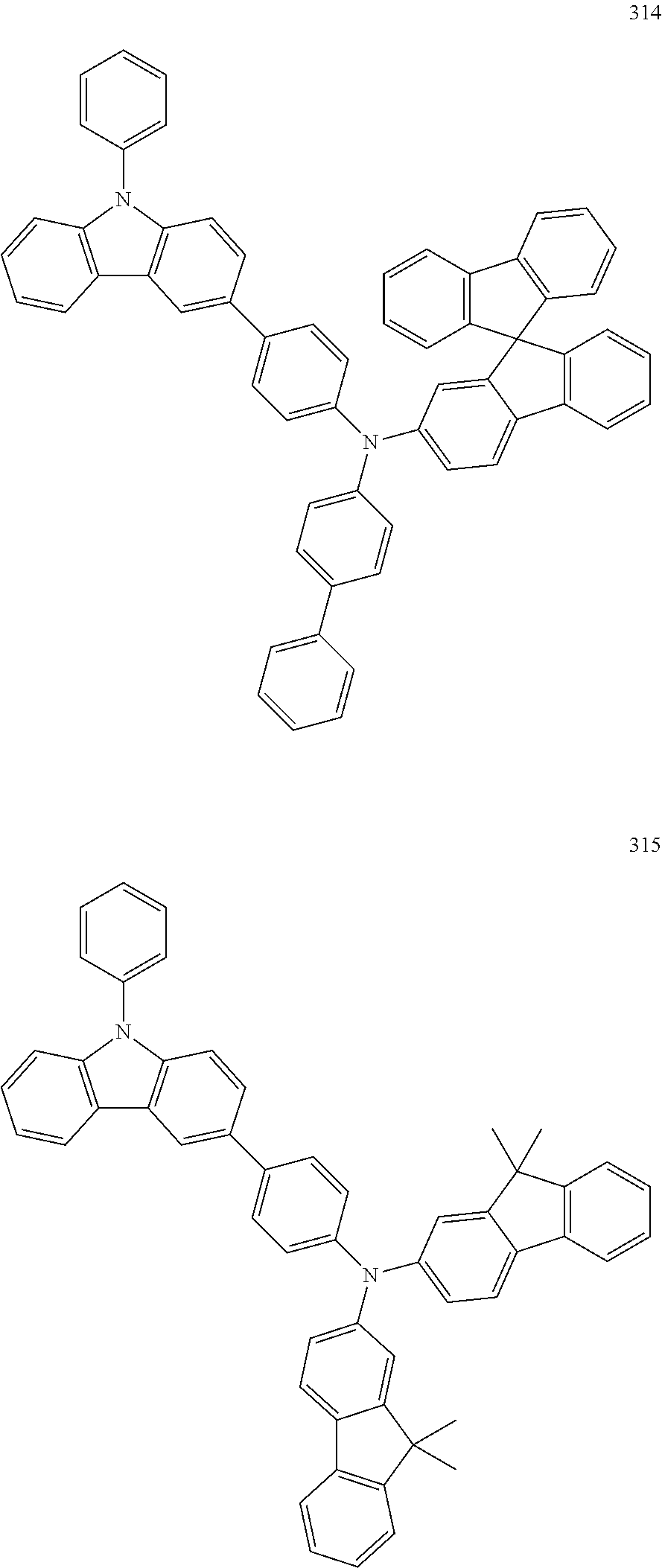


but are not limited thereto.


1) Synthesis of Intermediate I-1


1) Synthesis of Intermediate I-9

1) Synthesis of Intermediate I-14

Synthesis of Intermediate I-15

Synthesis of Intermediate 35-1

1) Synthesis of Intermediate 45-1

Synthesis of Intermediate I-18


| TABLE 1 | ||
| MS/FAB | ||
| Compound | 1H NMR (CDCl3, 400 MHz) | found | calc. |
| 1 | δ = 8.38-8.37 (m, 1H), 8.13-8.09 (m, 2H), 8.08-8.06 (m, | 580.30 | 580.29 |
| 2H), 8.03 (d, 1H), 7.82-7.80 (dd, 1H), 7.64-7.60 (m, 2H), | |||
| 7.59-7.56 (m, 2H), 7.51-7.48 (m, 2H), 7.48-7.42 (m, 2H), | |||
| 7.41-7.35 (m, 2H), 7.30 (d, 1H), 1.64 (s, 9H), 1.61 (s, 9H) | |||
| 4 | δ = 8.17-8.15 (m, 1H), 8.08-8.06 (m, 2H), 8.00-7.98 (m, | 620.22 | 620.23 |
| 1H), 7.96-7.94 (m, 1H), 7.82-7.81 (m, 1H), 7.80-7.79 (m, | |||
| 2H), 7.78-7.77 (m, 1H), 7.76-7.75 (m, 1H), 7.71-7.69 (m, | |||
| 1H), 7.57-7.48 (m, 9H), 7.47-7.46 (m, 1H), 7.44-7.43 (m, | |||
| 1H), 7.41-7.40 (m, 1H), 7.38-7.28 (m, 5H) | |||
| 7 | δ = 8.09-8.08 (m, 1H), 8.07-8.06 (m, 1H), 8.05-8.04 (m, | 696.28 | 696.26 |
| 1H), 8.03-8.01 (m, 2H), 7.95-7.94 (m, 1H), 7.89-7.88 (m, | |||
| 1H), 7.86-7.85 (m, 1H), 7.82-7.81 (m, 1H), 7.80-7.77 (m, | |||
| 4H), 7.71-7.67 (m, 2H), 7.65-7.62 (m, 2H), 7.60-7.54 (m, | |||
| 3H), 7.51-7.46 (m, 6H), 7.41-7.39 (m, 2H), 7.37-7.29 (m, | |||
| 4H) | |||
| 10 | δ = 8.55-8.54 (dd, 1H), 8.53-8.52 (dd, 1H), 8.30-8.29 (dd, | 697.26 | 697.25 |
| 1H), 8.15-8.13 (m, 1H), 8.09-8.08 (m, 1H), 8.06-8.01 (m, | |||
| 3H), 7.96-7.94 (m, 1H), 7.82-7.78 (m, 4H), 7.71-7.69 (dd, | |||
| 1H), 7.62-7.48 (m, 11H), 7.41-7.29 (m, 6H) | |||
| 15 | δ = 8.08-8.06 (m, 1H), 7.98-7.97 (m, 1H), 7.95-7.92 (m, | 848.31 | 848.32 |
| 2H), 7.87-7.85 (m, 1H), 7.84-7.76 (m, 8H), 7.74-7.71 (m, | |||
| 5H), 7.67-7.65 (m, 2H), 7.62-7.61 (m, 1H), 7.60-7.58 (m, | |||
| 3H), 7.54-7.47 (m, 10H), 7.42-7.30 (m, 6H) | |||
| 18 | δ = 8.31-8.30 (m, 1H), 8.17-8.15 (m, 1H), 8.08-8.06 (m, | 720.27 | 720.26 |
| 2H), 8.03-8.01 (m, 1H), 8.00-7.98 (m, 1H), 7.96-7.95 (m, | |||
| 1H), 7.94-7.92 (m, 5H), 7.90-7.88 (m, 3H), 7.77-7.74 (m, | |||
| 2H), 7.71-7.68 (m, 1H), 7.60-7.53 (m, 6H), 7.52-7.49 (m, | |||
| 3H), 7.46-7.43 (m, 2H), 7.41-7.33 (m, 3H) | |||
| 21 | δ = 8.08-8.07 (m, 1H), 8.06-8.05 (m, 2H), 8.00-7.98 (m, | 796.30 | 796.29 |
| 1H), 7.96-7.94 (m, 1H), 7.93-7.92 (m, 5H), 7.91-7.89 (m, | |||
| 4H), 7.87-7.85 (m, 1H), 7.83-7.79 (m, 3H), 7.76-7.74 (m, | |||
| 1H), 7.71-7.67 (m, 2H), 7.65-7.64 (m, 1H), 7.61-7.58 (m, | |||
| 3H), 7.56-7.47 (m, 7H), 7.43-7.41 (m, 1H), 7.40-7.33 (m, | |||
| 3H) | |||
| 27 | δ = 8.51-8.50 (m, 1H), 8.38-8.36 (dd, 1H), 8.18-8.17 (m, | 738.26 | 738.25 |
| 2H), 8.08-8.07 (m, 1H), 7.99-7.98 (m, 1H), 7.90-7.87 (m, | |||
| 1H), 7.84-7.80 (m, 4H), 7.72-7.69 (m, 4H), 7.64-7.62 (m, | |||
| 1H), 7.59-7.58 (m, 1H), 7.52-7.50 (dd, 1H), 7.46-7.44 (m, | |||
| 1H), 7.38-7.30 (m, 8H), 7.21-7.15 (m, 2H), 7.04-7.00 (m, | |||
| 2H) | |||
| 32 | δ = 8.39-8.37 (dd, 1H), 8.19-8.17 (m, 1H), 8.13-8.12 (m, | 796.31 | 796.29 |
| 1H), 8.08-8.01 (m, 2H), 7.86-7.81 (m, 5H), 7.76-7.69 (m, | |||
| 6H), 7.61-7.48 (m, 10H), 7.46-7.43 (m, 2H), 7.41-7.31 (m, | |||
| 6H), 7.05-7.01 (m, 2H) | |||
| 35 | δ = 8.13-8.12 (m, 1H), 8.10-8.06 (m, 2H), 8.03-8.01 (m, | 852.33 | 852.35 |
| 1H), 7.94-7.90 (m, 5H), 7.85-7.79 (m, 4H), 7.77-7.69 (m, | |||
| 3H), 7.56-7.49 (m, 5H), 7.46-7.41 (m, 2H), 7.40-7.31 (m, | |||
| 5H), 7.17-7.11 (m, 4H), 1.61 (s, 12H) | |||
| 39 | δ = 8.08-8.06 (m, 1H), 7.96-7.90 (m, 7H), 7.87-7.85 (m, | 953.39 | 953.38 |
| 2H), 7.83-7.79 (m, 6H), 7.76-7.75 (m, 1H), 7.74-7.73 (m, | |||
| 1H), 7.71-7.65 (m, 2H), 7.49-7.45 (m, 5H), 7.43-7.41 (m, | |||
| 1H), 7.38-7.31 (m, 5H), 7.16-7.09 (m, 4H), 1.61 (s, 12H) | |||
| 45 | δ = 8.62-8.61 (m, 1H), 8.39-8.37 (m, 1H), 8.19-8.12 (m, | 697.24 | 697.25 |
| 3H), 8.09-8.06 (m, 2H), 8.03-7.94 (m, 3H), 7.90-7.88 (m, | |||
| 1H), 7.82-7.80 (m, 4H), 7.77-7.75 (m, 1H), 7.55-7.46 (m, | |||
| 10H), 7.41-7.36 (m, 5H) | |||
| 48 | δ = 8.45-8.44 (m, 1H), 8.37-8.35 (m, 2H), 8.29-8.27 (dd, | 774.30 | 774.28 |
| 1H), 8.19-8.17 (m, 2H), 8.09-8.08 (m, 1H), 8.04-8.02 (m, | |||
| 3H), 8.01-8.00 (m, 1H), 7.89-7.85 (m, 2H), 7.82-7.80 (m, | |||
| 4H), 7.73-7.70 (m, 2H), 7.67-7.65 (m, 1H), 7.62-7.58 (m, | |||
| 3H), 7.53-7.47 (m, 6H), 7.41-7.35 (m, 5H) | |||
| 50 | δ = 8.51-8.50 (m, 1H), 8.45-8.44 (m, 2H), 8.43-8.42 (m, | 851.29 | 851.30 |
| 2H), 8.40 (d, 1H), 8.31-8.29 (dd, 1H), 8.19-8.18 (m, 1H), | |||
| 8.09-8.08 (m, 1H), 8.03-8.01 (m, 2H), 7.88-7.86 (m, 1H), | |||
| 7.83-7.80 (m, 4H), 7.67-7.58 (m, 8H), 7.53-7.47 (m, 6H), | |||
| 7.42-7.35 (m, 7H) | |||
| 53 | δ = 8.25-8.23 (m, 1H), 8.19-8.17 (m, 1H), 8.09-8.08 (m, | 846.31 | 846.30 |
| 2H), 8.07-8.06 (m, 2H), 8.04-8.03 (dd, 1H), 8.01-7.99 (m, | |||
| 1H), 7.97-7.96 (m, 2H), 7.95-7.94 (m, 1H), 7.92-7.89 (m, | |||
| 9H), 7.87-7.83 (m, 2H), 7.73-7.71 (m, 1H), 7.64-7.62 (m, | |||
| 2H), 7.60-7.57 (m, 6H), 7.54-7.53 (m, 1H), 7.52-7.47 (m, | |||
| 3H), 7.40-7.35 (m, 3H) | |||
| 58 | δ = 8.53-8.52 (m, 1H), 8.41-8.39 (m, 1H), 8.33 (d, 1H), | 797.30 | 797.28 |
| 8.31 (d, 1H), 8.26-8.24 (m, 1H), 8.21-8.19 (m, 2H), | |||
| 8.09-8.07 (m, 2H), 8.04-8.03 (m, 1H), 7.95-7.89 (m, 4H), | |||
| 7.84-7.82 (m, 2H), 7.71-7.68 (m, 4H), 7.63-7.57 (m, 5H), | |||
| 7.50-7.47 (m, 3H), 7.40-7.34 (m, 5H), 7.05-7.01 (m, 2H) | |||
| 64 | δ = 8.57-8.56 (m, 1H), 8.42-8.41 (m, 1H), 8.39-8.38 (m, | 873.30 | 873.31 |
| 1H), 8.36 (d, 1H), 8.30-8.28 (m, 1H), 8.21-8.19 (m, 2H), | |||
| 8.14-8.11 (m, 2H), 8.09-8.08 (m, 1H), 8.04-8.03 (m, 1H), | |||
| 7.92-7.89 (m, 2H), 7.84-7.80 (m, 2H), 7.78-7.77 (m, 1H), | |||
| 7.73-7.66 (m, 6H), 7.62-7.57 (m, 5H), 7.51-7.47 (m, 4H), | |||
| 7.42-7.34 (m, 6H), 7.04-7.00 (m, 2H) | |||
| 66 | δ = 8.41 (d, 1H), 8.39 (d, 1H), 8.30 (d, 1H), 8.28 (d, 1H), | 846.29 | 846.30 |
| 8.18-8.17 (m, 1H), 8.08-8.04 (m, 2H), 7.97-7.96 (m, 1H), | |||
| 7.95-7.94 (m, 1H), 7.87-7.84 (m, 2H), 7.82-7.79 (m, 2H), | |||
| 7.77-7.75 (m, 1H), 7.72-7.66 (m, 6H), 7.59-7.48 (m, 9H), | |||
| 7.46-7.41 (m, 2H), 7.40-7.32 (m, 3H), 7.26-7.21 (m, 1H), | |||
| 7.04-6.98 (m, 3H) | |||
| 69 | δ = 8.19-8.18 (m, 1H), 8.09-8.08 (m, 1H), 8.03 (d, 1H), | 928.39 | 928.38 |
| 7.95-7.94 (m, 2H), 7.92-7.91 (m, 1H), 7.89-7.88 (m, 3H), | |||
| 7.85 (d, 1H), 7.83-7.81 (m, 4H), 7.80-7.79 (m, 1H), | |||
| 7.77-7.74 (m, 2H), 7.64-7.58 (m, 3H), 7.51-7.47 (m, 5H), | |||
| 7.43-7.31 (m, 7H), 7.16-7.09 (m, 4H), 1.62 (s, 12H) | |||
| 76 | δ = 8.13-8.12 (m, 1H), 8.08-8.06 (m, 3H), 8.01-8.00 (m, | 872.31 | 872.32 |
| 1H), 7.97-7.96 (m, 1H), 7.95-7.94 (m, 2H), 7.93-7.92 (m, | |||
| 4H), 7.90-7.89 (m, 3H), 7.84-7.80 (m, 5H), 7.77-7.74 (m, | |||
| 2H), 7.67-7.65 (m, 1H), 7.63-7.61 (m, 2H), 7.60-7.58 (m, | |||
| 3H), 7.56-7.53 (m, 2H), 7.52-7.47 (m, 7H), 7.43-7.35 (m, | |||
| 3H) | |||
| 80 | δ = 8.38-8.37 (m, 2H), 8.10-8.08 (m, 4H), 8.04-8.03 (m, | 870.38 | 870.37 |
| 2H), 7.82 (d, 1H), 7.80 (d, 1H), 7.65-7.64 (m, 1H), | |||
| 7.63-7.62 (m, 2H), 7.61-7.60 (m, 3H), 7.59-7.58 (m, 2H), | |||
| 7.51-7.47 (m, 4H), 7.40-7.35 (m, 4H), 7.30 (d, 2H), 1.59 (s, | |||
| 18H) | |||
| 85 | δ = 8.19 (d, 1H), 8.17 (d, 1H), 8.12-8.11 (m, 2H), 8.08-8.06 | 910.30 | 910.31 |
| (m, 2H), 8.03 (d, 1H), 8.01 (d, 1H), 7.94-7.94 (m, 2H), | |||
| 7.84-7.82 (m, 2H), 7.81-7.80 (m, 2H), 7.77-7.75 (m, 2H), | |||
| 7.56-7.55 (m, 3H), 7.54-7.48 (m, 12H), 7.46 (s, 1H), | |||
| 7.44-7.43 (m, 2H), 7.41 (t, 2H), 7.40-7.39 (m, 1H), 7.38-7.35 | |||
| (m, 1H) | |||
| 88 | δ = 8.41 (d, 1H), 8.39 (d, 1H), 8.22-8.21 (m, 1H), 8.20-8.18 | 1010.35 | 1010.34 |
| (m, 3H), 8.09-8.07 (m, 2H), 8.03 (d, 2H), 7.92 (d, 1H), | |||
| 7.90-7.88 (m, 3H), 7.84-7.82 (m, 2H), 7.72-7.68 (m, 4H), | |||
| 7.64-7.57 (m, 8H), 7.51-7.47 (m, 4H), 7.40-7.32 (m, 8H), | |||
| 7.05-7.00 (m, 2H) | |||
| 92 | δ = 8.44-8.42 (m, 1H), 8.33-8.32 (m, 1H), 8.19-8.18 (m, | 800.24 | 800.25 |
| 1H), 8.09-8.08 (m, 2H), 8.03 (d, 1H), 7.99-7.98 (m, 1H), | |||
| 7.97-7.95 (m, 1H), 7.89-7.86 (m, 1H), 7.85-7.79 (m, 4H), | |||
| 7.73-7.68 (m, 5H), 7.64-7.58 (m, 3H), 7.55-7.47 (m, 4H), | |||
| 7.40-7.31 (m, 7H) | |||
| 98 | δ = 8.61-8.59 (m, 1H), 8.54-8.53 (m, 1H), 8.12-8.09 (m, | 908.25 | 908.23 |
| 3H), 8.08-8.05 (m, 3H), 8.01 (d, 1H), 7.99 (d, 1H), | |||
| 7.97-7.93 (m, 2H), 7.85-7.78 (m, 8H), 7.69-7.65 (m, 2H), | |||
| 7.57-7.48 (m, 8H), 7.46-7.33 (m, 6H) | |||
| 100 | δ = 8.38-8.36 (dd, 1H), 8.32-8.31 (m, 1H), 8.08-8.05 (m, | 800.26 | 800.25 |
| 3H), 8.03-8.01 (dd, 1H), 7.99-7.97 (m, 1H), 7.96-7.89 (m, | |||
| 6H), 7.77-7.75 (m, 1H), 7.68-7.67 (m, 1H), 7.66-7.65 (m, | |||
| 1H), 7.56-7.47 (m, 8H), 7.46-7.44 (m, 2H), 7.41 (s, 1H), | |||
| 7.39-7.35 (m, 3H), 7.33-7.29 (m, 2H) | |||


| TABLE 2 | ||||||||
| Electron | Driving | Current | ||||||
| transport | voltage | density | Brightness | Efficiency | Emission | Half lifespan | ||
| material | (V) | (mA/cm2) | (cd/m2) | (cd/A) | color | (hr @100 mA/cm2) | ||
| Example 1 | Compound 7 | 5.80 | 50 | 3,035 | 6.07 | Blue | 325 hr |
| Example 2 | Compound 15 | 5.42 | 50 | 3,055 | 6.11 | Blue | 407 hr |
| Example 3 | Compound 18 | 5.45 | 50 | 3,005 | 6.01 | Blue | 411 hr |
| Example 4 | Compound 21 | 5.38 | 50 | 3,160 | 6.32 | Blue | 425 hr |
| Example 5 | Compound 27 | 5.16 | 50 | 3,150 | 6.30 | Blue | 397 hr |
| Example 6 | Compound 35 | 5.41 | 50 | 3,070 | 6.14 | Blue | 389 hr |
| Example 7 | Compound 45 | 5.16 | 50 | 3,105 | 6.21 | Blue | 376 hr |
| Example 8 | Compound 50 | 5.51 | 50 | 3,130 | 6.26 | Blue | 417 hr |
| Example 9 | Compound 64 | 5.15 | 50 | 3,080 | 6.16 | Blue | 383 hr |
| Example 10 | Compound 76 | 5.95 | 50 | 3,070 | 6.14 | Blue | 414 hr |
| Example 11 | Compound 85 | 5.78 | 50 | 3,115 | 6.23 | Blue | 401 hr |
| Comparative | Alq3 | 7.11 | 50 | 2,275 | 4.55 | Blue | 168 hr |
| Example 1 | |||||||
| Comparative | Compound A | 6.76 | 50 | 2,355 | 4.71 | Blue | 192 hr |
| Example 2 | |||||||
Claims (21)


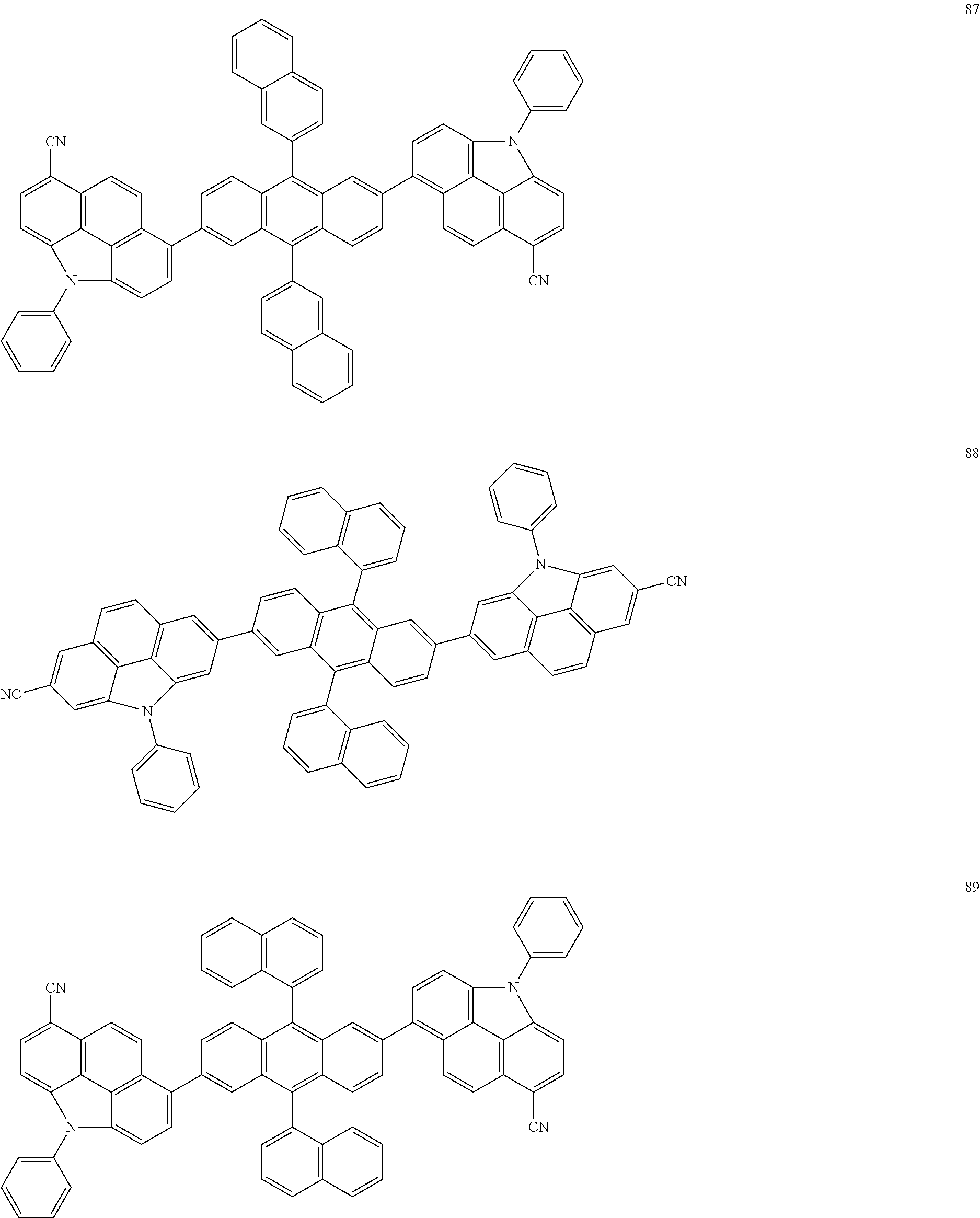


Applications Claiming Priority (2)
| Application Number | Priority Date | Filing Date | Title |
|---|---|---|---|
| KR10-2013-0115720 | 2013-09-27 | ||
| KR1020130115720A KR102191996B1 (en) | 2013-09-27 | 2013-09-27 | Herocyclic compound and organic light emitting device comprising same |
Publications (2)
| Publication Number | Publication Date |
|---|---|
| US20150090964A1 US20150090964A1 (en) | 2015-04-02 |
| US9425407B2 true US9425407B2 (en) | 2016-08-23 |
Family
ID=52739186
Family Applications (1)
| Application Number | Title | Priority Date | Filing Date |
|---|---|---|---|
| US14/198,372 Expired - Fee Related US9425407B2 (en) | 2013-09-27 | 2014-03-05 | Heterocyclic compound and organic light-emitting device including the same |
Country Status (2)
| Country | Link |
|---|---|
| US (1) | US9425407B2 (en) |
| KR (1) | KR102191996B1 (en) |
Cited By (5)
| Publication number | Priority date | Publication date | Assignee | Title |
|---|---|---|---|---|
| US20150048321A1 (en) * | 2013-08-14 | 2015-02-19 | Samsung Display Co., Ltd. | Anthracene-based compound and organic light-emitting device including the same |
| US9583715B2 (en) | 2013-08-09 | 2017-02-28 | Samsung Display Co., Ltd. | Anthracene-based compounds and organic light-emitting device including the same |
| US20200031812A1 (en) * | 2018-07-20 | 2020-01-30 | Samsung Electronics Co., Ltd. | Condensed cyclic compound, composition including the condensed cyclic compound, and organic light-emitting device including the condensed cyclic compound |
| US11563183B2 (en) | 2017-06-21 | 2023-01-24 | Samsung Display Co., Ltd. | Heterocyclic compound and organic light-emitting device including the same |
| US11588111B2 (en) | 2017-08-04 | 2023-02-21 | Samsung Display Co., Ltd. | Condensed-cyclic compound and organic light-emitting device including the same |
Families Citing this family (11)
| Publication number | Priority date | Publication date | Assignee | Title |
|---|---|---|---|---|
| KR102050484B1 (en) | 2013-03-04 | 2019-12-02 | 삼성디스플레이 주식회사 | Anthracene derivatives and organic light emitting diodes comprising the derivatives |
| KR102107106B1 (en) | 2013-05-09 | 2020-05-07 | 삼성디스플레이 주식회사 | Styryl-based compound and organic light emitting diode comprising the same |
| KR102269131B1 (en) | 2013-07-01 | 2021-06-25 | 삼성디스플레이 주식회사 | Compound and organic light emitting device comprising same |
| US10062850B2 (en) | 2013-12-12 | 2018-08-28 | Samsung Display Co., Ltd. | Amine-based compounds and organic light-emitting devices comprising the same |
| KR20150132795A (en) | 2014-05-16 | 2015-11-26 | 삼성디스플레이 주식회사 | Organic light emitting device |
| KR102327086B1 (en) * | 2014-06-11 | 2021-11-17 | 삼성디스플레이 주식회사 | Organic light-emitting devices |
| KR102343145B1 (en) | 2015-01-12 | 2021-12-27 | 삼성디스플레이 주식회사 | Condensed compound and organic light-emitting device comprising the same |
| KR102577274B1 (en) * | 2015-11-16 | 2023-09-12 | 삼성전자주식회사 | Organic light emitting device |
| JP6750783B2 (en) * | 2016-03-30 | 2020-09-02 | エルジー・ケム・リミテッド | Compound and organic light emitting device using the same |
| CN106397326B (en) * | 2016-09-18 | 2019-06-18 | 吉林奥来德光电材料股份有限公司 | Organic luminescent compounds and organic luminescent device containing it |
| KR20190070586A (en) | 2017-12-13 | 2019-06-21 | 엘지디스플레이 주식회사 | Compound for electron transporting material and organic light emitting diode including the same |
Citations (11)
| Publication number | Priority date | Publication date | Assignee | Title |
|---|---|---|---|---|
| US5645948A (en) | 1996-08-20 | 1997-07-08 | Eastman Kodak Company | Blue organic electroluminescent devices |
| JPH1017860A (en) | 1996-06-28 | 1998-01-20 | Chisso Corp | Electroluminescent element characterized in using cyclopentadiene derivative |
| JPH1187067A (en) | 1997-09-05 | 1999-03-30 | Chisso Corp | Hole transfer material having silacyclopentadiene ring |
| US6465115B2 (en) | 1998-12-09 | 2002-10-15 | Eastman Kodak Company | Electroluminescent device with anthracene derivatives hole transport layer |
| US6596415B2 (en) | 1998-12-09 | 2003-07-22 | Eastman Kodak Company | Electroluminescent device with polyphenyl hydrocarbon hole transport layer |
| KR20030067773A (en) | 2002-01-18 | 2003-08-19 | 주식회사 엘지화학 | New material for transporting electron and organic electroluminescent display using the same |
| US20050002857A1 (en) | 2003-05-06 | 2005-01-06 | Pez Guido Peter | Hydrogen storage by reversible hydrogenation of pi-conjugated substrates |
| US20070200490A1 (en) | 2004-04-07 | 2007-08-30 | Idemitsu Kason Co.Ltd | Nitrogenous Heterocycle Derivative, And Organic Electroluminescent Element Employing The Same |
| US20090019768A1 (en) | 2005-01-04 | 2009-01-22 | Air Products And Chemicals, Inc. | Dehydrogenation of Liquid Fuel in Microchannel Catalytic Reactor |
| KR20120051598A (en) | 2010-11-12 | 2012-05-22 | 주식회사 엘지화학 | New compounds and organic electronic device using the same |
| US20150014656A1 (en) * | 2013-07-12 | 2015-01-15 | Samsung Display Co., Ltd. | Compound for organic optoelectronic device organic light emitting diode including the same and display including the organic light emitting diode |
Family Cites Families (4)
| Publication number | Priority date | Publication date | Assignee | Title |
|---|---|---|---|---|
| KR101810045B1 (en) * | 2010-10-25 | 2017-12-19 | 삼성디스플레이 주식회사 | Heterocyclic compound and Organic light emitting device containing same |
| KR101885699B1 (en) * | 2011-06-29 | 2018-08-07 | 삼성디스플레이 주식회사 | Novel heterocyclic compound and Organic light emitting device containing same |
| KR101940103B1 (en) * | 2011-06-29 | 2019-01-21 | 삼성디스플레이 주식회사 | Novel heterocyclic compound and organic light emitting device containing same |
| KR101952707B1 (en) * | 2012-01-03 | 2019-06-03 | 삼성디스플레이 주식회사 | Novel compound and organic light emitting device containing same |
-
2013
- 2013-09-27 KR KR1020130115720A patent/KR102191996B1/en active IP Right Grant
-
2014
- 2014-03-05 US US14/198,372 patent/US9425407B2/en not_active Expired - Fee Related
Patent Citations (13)
| Publication number | Priority date | Publication date | Assignee | Title |
|---|---|---|---|---|
| JPH1017860A (en) | 1996-06-28 | 1998-01-20 | Chisso Corp | Electroluminescent element characterized in using cyclopentadiene derivative |
| US5645948A (en) | 1996-08-20 | 1997-07-08 | Eastman Kodak Company | Blue organic electroluminescent devices |
| JPH1187067A (en) | 1997-09-05 | 1999-03-30 | Chisso Corp | Hole transfer material having silacyclopentadiene ring |
| US6465115B2 (en) | 1998-12-09 | 2002-10-15 | Eastman Kodak Company | Electroluminescent device with anthracene derivatives hole transport layer |
| US6596415B2 (en) | 1998-12-09 | 2003-07-22 | Eastman Kodak Company | Electroluminescent device with polyphenyl hydrocarbon hole transport layer |
| US20030165715A1 (en) | 2002-01-18 | 2003-09-04 | Seok-Hee Yoon | New material for transporting electrons and organic electroluminescent display using the same |
| KR20030067773A (en) | 2002-01-18 | 2003-08-19 | 주식회사 엘지화학 | New material for transporting electron and organic electroluminescent display using the same |
| US20050002857A1 (en) | 2003-05-06 | 2005-01-06 | Pez Guido Peter | Hydrogen storage by reversible hydrogenation of pi-conjugated substrates |
| US20070200490A1 (en) | 2004-04-07 | 2007-08-30 | Idemitsu Kason Co.Ltd | Nitrogenous Heterocycle Derivative, And Organic Electroluminescent Element Employing The Same |
| KR20120101558A (en) | 2004-04-07 | 2012-09-13 | 이데미쓰 고산 가부시키가이샤 | Nitrogenous heterocycle derivative and organic electroluminescent element employing the same |
| US20090019768A1 (en) | 2005-01-04 | 2009-01-22 | Air Products And Chemicals, Inc. | Dehydrogenation of Liquid Fuel in Microchannel Catalytic Reactor |
| KR20120051598A (en) | 2010-11-12 | 2012-05-22 | 주식회사 엘지화학 | New compounds and organic electronic device using the same |
| US20150014656A1 (en) * | 2013-07-12 | 2015-01-15 | Samsung Display Co., Ltd. | Compound for organic optoelectronic device organic light emitting diode including the same and display including the organic light emitting diode |
Non-Patent Citations (7)
| Title |
|---|
| Adachi, C., et al., Confinement of charge carriers and molecular excitons within 5-nm-thick emitter layer in organic electroluminescent devices with a double heterostructure, Applied Physics Letters, Aug. 6, 1990, vol. 57, No. 6, pp. 531-533. |
| Internet Material: 2009 Fall Assembly and Symposium. vol. 34, No. 2, 2009; Publication Date, Oct. 8, 2009-Oct. 9, 2009; Title: A novel conjugated polymer based on 4H-benzo[def]carbazole backbone for OLED, 1 page. |
| Johansson, N., et al., Solid-State Amplified Spontaneous Emission in Some Spiro-Type Molecules: A New Concept for the Design of Solid-State Lasing Molecules, Advanced Materials, Mar. 6, 1998, vol. 10, No. 14, pp. 1136-1141. |
| Sakamoto, Y., et al., Synthesis, Characterization, and Electron-Transport Property of Perfluorinated Phenylene Dendrimers, Journal of American Chemical Society, Feb. 15, 2000, vol. 122, pp. 1832-1833. |
| Tang, C.W., et al., Organic electroluminescent diodes, Applied Physics Letters, Sep. 21, 1987, vol. 51, No. 12, pp. 913-915. |
| Tao, Y.T., et al., Sharp green electroluminescence from 1H-pyrazolo[3,4-b] quinoline-based light emitting diodes, Applied Physics Letters, Sep. 11, 2000, vol. 77, No. 11, pp. 1575-1577. |
| Yamaguchi, S., et al., Diphenylamino-Substituted 2,5-Diarylsiloles for Single-Layer Organic Electroluminescent Devices, Chemistry Letters, (2001), pp. 98-99. |
Cited By (8)
| Publication number | Priority date | Publication date | Assignee | Title |
|---|---|---|---|---|
| US9583715B2 (en) | 2013-08-09 | 2017-02-28 | Samsung Display Co., Ltd. | Anthracene-based compounds and organic light-emitting device including the same |
| US20150048321A1 (en) * | 2013-08-14 | 2015-02-19 | Samsung Display Co., Ltd. | Anthracene-based compound and organic light-emitting device including the same |
| US10256412B2 (en) * | 2013-08-14 | 2019-04-09 | Samsung Display Co., Ltd. | Anthracene-based compound and organic light-emitting device including the same |
| US11563183B2 (en) | 2017-06-21 | 2023-01-24 | Samsung Display Co., Ltd. | Heterocyclic compound and organic light-emitting device including the same |
| US11844273B2 (en) | 2017-06-21 | 2023-12-12 | Samsung Display Co., Ltd. | Heterocyclic compound and organic light-emitting device including the same |
| US11588111B2 (en) | 2017-08-04 | 2023-02-21 | Samsung Display Co., Ltd. | Condensed-cyclic compound and organic light-emitting device including the same |
| US20200031812A1 (en) * | 2018-07-20 | 2020-01-30 | Samsung Electronics Co., Ltd. | Condensed cyclic compound, composition including the condensed cyclic compound, and organic light-emitting device including the condensed cyclic compound |
| US11053228B2 (en) * | 2018-07-20 | 2021-07-06 | Samsung Electronics Co., Ltd. | Condensed cyclic compound, composition including the condensed cyclic compound, and organic light-emitting device including the condensed cyclic compound |
Also Published As
| Publication number | Publication date |
|---|---|
| US20150090964A1 (en) | 2015-04-02 |
| KR20150035331A (en) | 2015-04-06 |
| KR102191996B1 (en) | 2020-12-17 |
Similar Documents
| Publication | Publication Date | Title |
|---|---|---|
| US9425407B2 (en) | Heterocyclic compound and organic light-emitting device including the same | |
| US10256416B2 (en) | Compound and organic light-emitting device including the same | |
| US9825234B2 (en) | Organic light-emitting diode | |
| US9876179B2 (en) | Organic light emitting device | |
| US9559310B2 (en) | Compound with electron injection and/or electron transport capabilities and organic light-emitting device including the same | |
| US9419228B2 (en) | Heterocyclic compound and organic light-emitting diode comprising the same | |
| US8455867B2 (en) | Organic light-emitting device | |
| US20150243895A1 (en) | Compound and organic light-emitting device including the same | |
| US9564596B2 (en) | Heterocyclic compound and organic light-emitting device comprising same | |
| US9716234B2 (en) | Compound and organic light-emitting device including the same | |
| US9252370B2 (en) | Heterocyclic compounds and organic light emitting devices including the same | |
| US9705093B2 (en) | Heterocyclic compound and organic light-emitting device including the same | |
| US9397300B2 (en) | Compound and organic light-emitting diode including the same | |
| US9368730B2 (en) | Heterocyclic compound and organic light-emitting device comprising the same | |
| US9806267B2 (en) | Compound and organic light-emitting device comprising the compound | |
| US9437826B2 (en) | Heterocyclic compound and organic light-emitting device including the same | |
| US9196838B2 (en) | Organic compound and organic light-emitting device comprising the same | |
| US20150053940A1 (en) | Heterocyclic compound and organic light-emitting diode including the same | |
| US9537108B2 (en) | Heterocyclic compound and organic light-emitting device including the same | |
| US9564603B2 (en) | Heterocyclic compound and organic light-emitting device including the same | |
| US9553271B2 (en) | Compound and organic light-emitting device including the same | |
| US9437827B2 (en) | Heterocyclic compound and organic light-emitting device including the same | |
| US9406890B2 (en) | Compound and organic light-emitting diode including the same | |
| US9640768B2 (en) | Heterocyclic compound and orgainic light-emitting device including the same | |
| US9444056B2 (en) | Heterocyclic compound and organic light-emitting device including the same |
Legal Events
| Date | Code | Title | Description |
|---|---|---|---|
| AS | Assignment |
Owner name: SAMSUNG DISPLAY CO., LTD, KOREA, REPUBLIC OF Free format text: ASSIGNMENT OF ASSIGNORS INTEREST;ASSIGNORS:HWANG, SEOK-HWAN;KIM, SOO-YON;KIM, JONG-WOO;REEL/FRAME:032367/0669 Effective date: 20140217 |
|
| FEPP | Fee payment procedure |
Free format text: PAYOR NUMBER ASSIGNED (ORIGINAL EVENT CODE: ASPN); ENTITY STATUS OF PATENT OWNER: LARGE ENTITY |
|
| STCF | Information on status: patent grant |
Free format text: PATENTED CASE |
|
| FEPP | Fee payment procedure |
Free format text: MAINTENANCE FEE REMINDER MAILED (ORIGINAL EVENT CODE: REM.); ENTITY STATUS OF PATENT OWNER: LARGE ENTITY |
|
| LAPS | Lapse for failure to pay maintenance fees |
Free format text: PATENT EXPIRED FOR FAILURE TO PAY MAINTENANCE FEES (ORIGINAL EVENT CODE: EXP.); ENTITY STATUS OF PATENT OWNER: LARGE ENTITY |
|
| STCH | Information on status: patent discontinuation |
Free format text: PATENT EXPIRED DUE TO NONPAYMENT OF MAINTENANCE FEES UNDER 37 CFR 1.362 |
|
| FP | Lapsed due to failure to pay maintenance fee |
Effective date: 20200823 |