US9437776B2 - Method for manufacturing light emitting diodes with smooth surface for reflective electrode - Google Patents
Method for manufacturing light emitting diodes with smooth surface for reflective electrode Download PDFInfo
- Publication number
- US9437776B2 US9437776B2 US14/085,581 US201314085581A US9437776B2 US 9437776 B2 US9437776 B2 US 9437776B2 US 201314085581 A US201314085581 A US 201314085581A US 9437776 B2 US9437776 B2 US 9437776B2
- Authority
- US
- United States
- Prior art keywords
- epitaxial layer
- electrode
- layer
- depositing
- type
- Prior art date
- Legal status (The legal status is an assumption and is not a legal conclusion. Google has not performed a legal analysis and makes no representation as to the accuracy of the status listed.)
- Active
Links
- 238000000034 method Methods 0.000 title claims description 27
- 238000004519 manufacturing process Methods 0.000 title claims description 13
- 239000000758 substrate Substances 0.000 claims description 28
- 238000000151 deposition Methods 0.000 claims description 14
- 229910052751 metal Inorganic materials 0.000 claims description 13
- 239000002184 metal Substances 0.000 claims description 13
- 239000000463 material Substances 0.000 claims description 9
- 229910052782 aluminium Inorganic materials 0.000 claims description 5
- 229910052709 silver Inorganic materials 0.000 claims description 5
- 229910052750 molybdenum Inorganic materials 0.000 claims description 4
- 229910045601 alloy Inorganic materials 0.000 claims description 3
- 239000000956 alloy Substances 0.000 claims description 3
- 238000005229 chemical vapour deposition Methods 0.000 claims description 3
- 150000002739 metals Chemical class 0.000 claims description 3
- 229910052710 silicon Inorganic materials 0.000 claims description 3
- 229910052721 tungsten Inorganic materials 0.000 claims description 3
- 229910001218 Gallium arsenide Inorganic materials 0.000 claims description 2
- PNEYBMLMFCGWSK-UHFFFAOYSA-N aluminium oxide Inorganic materials [O-2].[O-2].[O-2].[Al+3].[Al+3] PNEYBMLMFCGWSK-UHFFFAOYSA-N 0.000 claims description 2
- 239000000919 ceramic Substances 0.000 claims description 2
- 229910052804 chromium Inorganic materials 0.000 claims description 2
- 229910052802 copper Inorganic materials 0.000 claims description 2
- 229910052593 corundum Inorganic materials 0.000 claims description 2
- 229910052759 nickel Inorganic materials 0.000 claims description 2
- 229910052763 palladium Inorganic materials 0.000 claims description 2
- 229910052697 platinum Inorganic materials 0.000 claims description 2
- 229910052703 rhodium Inorganic materials 0.000 claims description 2
- 229910052707 ruthenium Inorganic materials 0.000 claims description 2
- 239000004065 semiconductor Substances 0.000 claims description 2
- 229910052719 titanium Inorganic materials 0.000 claims description 2
- 229910001845 yogo sapphire Inorganic materials 0.000 claims description 2
- 229910005540 GaP Inorganic materials 0.000 claims 1
- 238000010521 absorption reaction Methods 0.000 description 8
- QGZKDVFQNNGYKY-UHFFFAOYSA-N Ammonia Chemical compound N QGZKDVFQNNGYKY-UHFFFAOYSA-N 0.000 description 4
- IJGRMHOSHXDMSA-UHFFFAOYSA-N Atomic nitrogen Chemical compound N#N IJGRMHOSHXDMSA-UHFFFAOYSA-N 0.000 description 4
- 238000000605 extraction Methods 0.000 description 4
- JLTRXTDYQLMHGR-UHFFFAOYSA-N trimethylaluminium Chemical compound C[Al](C)C JLTRXTDYQLMHGR-UHFFFAOYSA-N 0.000 description 4
- XCZXGTMEAKBVPV-UHFFFAOYSA-N trimethylgallium Chemical compound C[Ga](C)C XCZXGTMEAKBVPV-UHFFFAOYSA-N 0.000 description 4
- IBEFSUTVZWZJEL-UHFFFAOYSA-N trimethylindium Chemical compound C[In](C)C IBEFSUTVZWZJEL-UHFFFAOYSA-N 0.000 description 4
- 238000005137 deposition process Methods 0.000 description 3
- 230000000694 effects Effects 0.000 description 3
- 230000004048 modification Effects 0.000 description 3
- 238000012986 modification Methods 0.000 description 3
- 229910052594 sapphire Inorganic materials 0.000 description 3
- 239000010980 sapphire Substances 0.000 description 3
- FYYHWMGAXLPEAU-UHFFFAOYSA-N Magnesium Chemical compound [Mg] FYYHWMGAXLPEAU-UHFFFAOYSA-N 0.000 description 2
- BQCADISMDOOEFD-UHFFFAOYSA-N Silver Chemical compound [Ag] BQCADISMDOOEFD-UHFFFAOYSA-N 0.000 description 2
- XLOMVQKBTHCTTD-UHFFFAOYSA-N Zinc monoxide Chemical compound [Zn]=O XLOMVQKBTHCTTD-UHFFFAOYSA-N 0.000 description 2
- 239000012080 ambient air Substances 0.000 description 2
- 229910021529 ammonia Inorganic materials 0.000 description 2
- 239000011248 coating agent Substances 0.000 description 2
- 238000000576 coating method Methods 0.000 description 2
- 238000010586 diagram Methods 0.000 description 2
- 239000002019 doping agent Substances 0.000 description 2
- 239000001257 hydrogen Substances 0.000 description 2
- 229910052739 hydrogen Inorganic materials 0.000 description 2
- 125000004435 hydrogen atom Chemical class [H]* 0.000 description 2
- 238000002347 injection Methods 0.000 description 2
- 239000007924 injection Substances 0.000 description 2
- 229910052749 magnesium Inorganic materials 0.000 description 2
- 239000011777 magnesium Substances 0.000 description 2
- 238000005259 measurement Methods 0.000 description 2
- 229910052757 nitrogen Inorganic materials 0.000 description 2
- 230000003287 optical effect Effects 0.000 description 2
- 150000002902 organometallic compounds Chemical class 0.000 description 2
- 239000002243 precursor Substances 0.000 description 2
- 230000001902 propagating effect Effects 0.000 description 2
- 238000002310 reflectometry Methods 0.000 description 2
- 239000010703 silicon Substances 0.000 description 2
- 239000004332 silver Substances 0.000 description 2
- 229910000679 solder Inorganic materials 0.000 description 2
- 239000003570 air Substances 0.000 description 1
- XAGFODPZIPBFFR-UHFFFAOYSA-N aluminium Chemical compound [Al] XAGFODPZIPBFFR-UHFFFAOYSA-N 0.000 description 1
- 238000000137 annealing Methods 0.000 description 1
- 230000015572 biosynthetic process Effects 0.000 description 1
- 239000000969 carrier Substances 0.000 description 1
- 238000006243 chemical reaction Methods 0.000 description 1
- 230000008021 deposition Effects 0.000 description 1
- 238000005566 electron beam evaporation Methods 0.000 description 1
- 238000010894 electron beam technology Methods 0.000 description 1
- 230000008020 evaporation Effects 0.000 description 1
- 238000001704 evaporation Methods 0.000 description 1
- 238000005286 illumination Methods 0.000 description 1
- AMGQUBHHOARCQH-UHFFFAOYSA-N indium;oxotin Chemical compound [In].[Sn]=O AMGQUBHHOARCQH-UHFFFAOYSA-N 0.000 description 1
- 229910044991 metal oxide Inorganic materials 0.000 description 1
- 150000004706 metal oxides Chemical class 0.000 description 1
- 238000012821 model calculation Methods 0.000 description 1
- 238000007788 roughening Methods 0.000 description 1
- 238000004544 sputter deposition Methods 0.000 description 1
- 239000010409 thin film Substances 0.000 description 1
- 239000011787 zinc oxide Substances 0.000 description 1
Images


Classifications
-
- H—ELECTRICITY
- H01—ELECTRIC ELEMENTS
- H01L—SEMICONDUCTOR DEVICES NOT COVERED BY CLASS H10
- H01L33/00—Semiconductor devices with at least one potential-jump barrier or surface barrier specially adapted for light emission; Processes or apparatus specially adapted for the manufacture or treatment thereof or of parts thereof; Details thereof
- H01L33/36—Semiconductor devices with at least one potential-jump barrier or surface barrier specially adapted for light emission; Processes or apparatus specially adapted for the manufacture or treatment thereof or of parts thereof; Details thereof characterised by the electrodes
-
- H—ELECTRICITY
- H01—ELECTRIC ELEMENTS
- H01L—SEMICONDUCTOR DEVICES NOT COVERED BY CLASS H10
- H01L33/00—Semiconductor devices with at least one potential-jump barrier or surface barrier specially adapted for light emission; Processes or apparatus specially adapted for the manufacture or treatment thereof or of parts thereof; Details thereof
- H01L33/02—Semiconductor devices with at least one potential-jump barrier or surface barrier specially adapted for light emission; Processes or apparatus specially adapted for the manufacture or treatment thereof or of parts thereof; Details thereof characterised by the semiconductor bodies
- H01L33/20—Semiconductor devices with at least one potential-jump barrier or surface barrier specially adapted for light emission; Processes or apparatus specially adapted for the manufacture or treatment thereof or of parts thereof; Details thereof characterised by the semiconductor bodies with a particular shape, e.g. curved or truncated substrate
- H01L33/22—Roughened surfaces, e.g. at the interface between epitaxial layers
-
- H—ELECTRICITY
- H01—ELECTRIC ELEMENTS
- H01L—SEMICONDUCTOR DEVICES NOT COVERED BY CLASS H10
- H01L2224/00—Indexing scheme for arrangements for connecting or disconnecting semiconductor or solid-state bodies and methods related thereto as covered by H01L24/00
- H01L2224/01—Means for bonding being attached to, or being formed on, the surface to be connected, e.g. chip-to-package, die-attach, "first-level" interconnects; Manufacturing methods related thereto
- H01L2224/02—Bonding areas; Manufacturing methods related thereto
- H01L2224/04—Structure, shape, material or disposition of the bonding areas prior to the connecting process
- H01L2224/05—Structure, shape, material or disposition of the bonding areas prior to the connecting process of an individual bonding area
- H01L2224/0554—External layer
- H01L2224/0556—Disposition
- H01L2224/05568—Disposition the whole external layer protruding from the surface
-
- H—ELECTRICITY
- H01—ELECTRIC ELEMENTS
- H01L—SEMICONDUCTOR DEVICES NOT COVERED BY CLASS H10
- H01L2224/00—Indexing scheme for arrangements for connecting or disconnecting semiconductor or solid-state bodies and methods related thereto as covered by H01L24/00
- H01L2224/01—Means for bonding being attached to, or being formed on, the surface to be connected, e.g. chip-to-package, die-attach, "first-level" interconnects; Manufacturing methods related thereto
- H01L2224/02—Bonding areas; Manufacturing methods related thereto
- H01L2224/04—Structure, shape, material or disposition of the bonding areas prior to the connecting process
- H01L2224/05—Structure, shape, material or disposition of the bonding areas prior to the connecting process of an individual bonding area
- H01L2224/0554—External layer
- H01L2224/05573—Single external layer
-
- H—ELECTRICITY
- H01—ELECTRIC ELEMENTS
- H01L—SEMICONDUCTOR DEVICES NOT COVERED BY CLASS H10
- H01L2224/00—Indexing scheme for arrangements for connecting or disconnecting semiconductor or solid-state bodies and methods related thereto as covered by H01L24/00
- H01L2224/01—Means for bonding being attached to, or being formed on, the surface to be connected, e.g. chip-to-package, die-attach, "first-level" interconnects; Manufacturing methods related thereto
- H01L2224/02—Bonding areas; Manufacturing methods related thereto
- H01L2224/04—Structure, shape, material or disposition of the bonding areas prior to the connecting process
- H01L2224/06—Structure, shape, material or disposition of the bonding areas prior to the connecting process of a plurality of bonding areas
- H01L2224/0601—Structure
- H01L2224/0603—Bonding areas having different sizes, e.g. different heights or widths
-
- H—ELECTRICITY
- H01—ELECTRIC ELEMENTS
- H01L—SEMICONDUCTOR DEVICES NOT COVERED BY CLASS H10
- H01L2224/00—Indexing scheme for arrangements for connecting or disconnecting semiconductor or solid-state bodies and methods related thereto as covered by H01L24/00
- H01L2224/01—Means for bonding being attached to, or being formed on, the surface to be connected, e.g. chip-to-package, die-attach, "first-level" interconnects; Manufacturing methods related thereto
- H01L2224/02—Bonding areas; Manufacturing methods related thereto
- H01L2224/04—Structure, shape, material or disposition of the bonding areas prior to the connecting process
- H01L2224/06—Structure, shape, material or disposition of the bonding areas prior to the connecting process of a plurality of bonding areas
- H01L2224/061—Disposition
- H01L2224/06102—Disposition the bonding areas being at different heights
-
- H—ELECTRICITY
- H01—ELECTRIC ELEMENTS
- H01L—SEMICONDUCTOR DEVICES NOT COVERED BY CLASS H10
- H01L2224/00—Indexing scheme for arrangements for connecting or disconnecting semiconductor or solid-state bodies and methods related thereto as covered by H01L24/00
- H01L2224/01—Means for bonding being attached to, or being formed on, the surface to be connected, e.g. chip-to-package, die-attach, "first-level" interconnects; Manufacturing methods related thereto
- H01L2224/10—Bump connectors; Manufacturing methods related thereto
- H01L2224/12—Structure, shape, material or disposition of the bump connectors prior to the connecting process
- H01L2224/13—Structure, shape, material or disposition of the bump connectors prior to the connecting process of an individual bump connector
-
- H—ELECTRICITY
- H01—ELECTRIC ELEMENTS
- H01L—SEMICONDUCTOR DEVICES NOT COVERED BY CLASS H10
- H01L2224/00—Indexing scheme for arrangements for connecting or disconnecting semiconductor or solid-state bodies and methods related thereto as covered by H01L24/00
- H01L2224/01—Means for bonding being attached to, or being formed on, the surface to be connected, e.g. chip-to-package, die-attach, "first-level" interconnects; Manufacturing methods related thereto
- H01L2224/10—Bump connectors; Manufacturing methods related thereto
- H01L2224/15—Structure, shape, material or disposition of the bump connectors after the connecting process
- H01L2224/16—Structure, shape, material or disposition of the bump connectors after the connecting process of an individual bump connector
- H01L2224/161—Disposition
- H01L2224/16151—Disposition the bump connector connecting between a semiconductor or solid-state body and an item not being a semiconductor or solid-state body, e.g. chip-to-substrate, chip-to-passive
- H01L2224/16221—Disposition the bump connector connecting between a semiconductor or solid-state body and an item not being a semiconductor or solid-state body, e.g. chip-to-substrate, chip-to-passive the body and the item being stacked
- H01L2224/16225—Disposition the bump connector connecting between a semiconductor or solid-state body and an item not being a semiconductor or solid-state body, e.g. chip-to-substrate, chip-to-passive the body and the item being stacked the item being non-metallic, e.g. insulating substrate with or without metallisation
-
- H—ELECTRICITY
- H01—ELECTRIC ELEMENTS
- H01L—SEMICONDUCTOR DEVICES NOT COVERED BY CLASS H10
- H01L2224/00—Indexing scheme for arrangements for connecting or disconnecting semiconductor or solid-state bodies and methods related thereto as covered by H01L24/00
- H01L2224/01—Means for bonding being attached to, or being formed on, the surface to be connected, e.g. chip-to-package, die-attach, "first-level" interconnects; Manufacturing methods related thereto
- H01L2224/10—Bump connectors; Manufacturing methods related thereto
- H01L2224/15—Structure, shape, material or disposition of the bump connectors after the connecting process
- H01L2224/17—Structure, shape, material or disposition of the bump connectors after the connecting process of a plurality of bump connectors
- H01L2224/1701—Structure
- H01L2224/1703—Bump connectors having different sizes, e.g. different diameters, heights or widths
-
- H—ELECTRICITY
- H01—ELECTRIC ELEMENTS
- H01L—SEMICONDUCTOR DEVICES NOT COVERED BY CLASS H10
- H01L2924/00—Indexing scheme for arrangements or methods for connecting or disconnecting semiconductor or solid-state bodies as covered by H01L24/00
-
- H—ELECTRICITY
- H01—ELECTRIC ELEMENTS
- H01L—SEMICONDUCTOR DEVICES NOT COVERED BY CLASS H10
- H01L2924/00—Indexing scheme for arrangements or methods for connecting or disconnecting semiconductor or solid-state bodies as covered by H01L24/00
- H01L2924/0001—Technical content checked by a classifier
- H01L2924/00014—Technical content checked by a classifier the subject-matter covered by the group, the symbol of which is combined with the symbol of this group, being disclosed without further technical details
-
- H—ELECTRICITY
- H01—ELECTRIC ELEMENTS
- H01L—SEMICONDUCTOR DEVICES NOT COVERED BY CLASS H10
- H01L2924/00—Indexing scheme for arrangements or methods for connecting or disconnecting semiconductor or solid-state bodies as covered by H01L24/00
- H01L2924/10—Details of semiconductor or other solid state devices to be connected
- H01L2924/11—Device type
- H01L2924/12—Passive devices, e.g. 2 terminal devices
- H01L2924/1204—Optical Diode
- H01L2924/12044—OLED
-
- H01L33/0079—
-
- H—ELECTRICITY
- H01—ELECTRIC ELEMENTS
- H01L—SEMICONDUCTOR DEVICES NOT COVERED BY CLASS H10
- H01L33/00—Semiconductor devices with at least one potential-jump barrier or surface barrier specially adapted for light emission; Processes or apparatus specially adapted for the manufacture or treatment thereof or of parts thereof; Details thereof
- H01L33/005—Processes
- H01L33/0093—Wafer bonding; Removal of the growth substrate
-
- H—ELECTRICITY
- H01—ELECTRIC ELEMENTS
- H01L—SEMICONDUCTOR DEVICES NOT COVERED BY CLASS H10
- H01L33/00—Semiconductor devices with at least one potential-jump barrier or surface barrier specially adapted for light emission; Processes or apparatus specially adapted for the manufacture or treatment thereof or of parts thereof; Details thereof
- H01L33/02—Semiconductor devices with at least one potential-jump barrier or surface barrier specially adapted for light emission; Processes or apparatus specially adapted for the manufacture or treatment thereof or of parts thereof; Details thereof characterised by the semiconductor bodies
- H01L33/26—Materials of the light emitting region
- H01L33/30—Materials of the light emitting region containing only elements of group III and group V of the periodic system
- H01L33/32—Materials of the light emitting region containing only elements of group III and group V of the periodic system containing nitrogen
-
- H—ELECTRICITY
- H01—ELECTRIC ELEMENTS
- H01L—SEMICONDUCTOR DEVICES NOT COVERED BY CLASS H10
- H01L33/00—Semiconductor devices with at least one potential-jump barrier or surface barrier specially adapted for light emission; Processes or apparatus specially adapted for the manufacture or treatment thereof or of parts thereof; Details thereof
- H01L33/36—Semiconductor devices with at least one potential-jump barrier or surface barrier specially adapted for light emission; Processes or apparatus specially adapted for the manufacture or treatment thereof or of parts thereof; Details thereof characterised by the electrodes
- H01L33/40—Materials therefor
- H01L33/42—Transparent materials
Definitions
- the present disclosure relates to a light emitting diode (LED) structure, and more particularly to a LED structure with a smooth surface for a reflective electrode.
- LED light emitting diode
- LEDs Light emitting diodes
- LEDs have been developed for many years and have been widely used in various light applications.
- LEDs are light-weight, consume less energy, and have a good electrical power to light conversion efficiency, in some application areas, there have been intentions to replace conventional light sources, such as incandescent lamps and fluorescent light sources, with LEDs.
- LEDs produce light in a relatively narrow angular spread direction without side light so that the light cannot be easily collected by optical elements in a package.
- thin-film AlInGaN LEDs produce more light per steradian and photons generated therefrom can be efficiently utilized compared to the conventional lateral LEDs with sapphire substrate attached.
- the efficiency (Lumen/W) of the current LEDs is still not high enough to replace the conventional light source for general illumination or other light applications.
- a light emitting diode includes an epitaxial layer structure, a first electrode, and a second electrode.
- the first and second electrodes are separately disposed on the epitaxial layer structure, and the epitaxial layer structure has a RMS (root-mean-square) roughness less than 3 nm on a surface wherein the second electrode is formed.
- a method for manufacturing a light emitting diode includes fowling an epitaxial layer structure, and separately depositing a first electrode and a second electrode on the epitaxial layer structure.
- the epitaxial layer structure has a RMS roughness less than about 3 nm on a surface whereon the second electrode is formed.
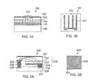
- FIG. 1A is a cross sectional view of a vertical LED structure.
- FIG. 1B is a top view of a vertical LED structure, in which a patterned n contact is shown.
- FIG. 2A is a cross sectional view of a flip-chipped lateral LED structure with metal joints and a sub-mount.
- FIG. 2B is a top view of a flip-chipped lateral LED structure with both p and n electrodes before flip-chipped to a sub-mount.
- FIG. 3 illustrates an exemplary light extraction occurring in a vertical LED structure.
- FIG. 4 is a schematic diagram of a rough interface between a p-GaN layer and a silver (Ag) layer, showing that the rough interface scatters an incident light as well as couples the light into the surface plasmon mode.
- FIGS. 5A-5C illustrate a process for manufacturing a vertical LED that has a smooth surface for forming reflective electrode.
- FIGS. 6A-6C illustrate a process for manufacturing a flip-chipped lateral LED structure that has a smooth surface for forming reflective electrode.
- FIGS. 1A and 1B illustrate a cross-sectional view and a top view of a vertical LED device, respectively.
- the vertical LED device 100 as shown in FIG. 1A , has a vertical current injection configuration, including a patterned n-type contact (or n-type electrode) 101 , an n-type GaN-based layer 102 with a roughened surface, an active region 103 , a p-type GaN-based layer 104 , a broad area reflective p-type contact (or p-type electrode or reflective p electrode) 105 , and a thermally and/or electrically conductive substrate 106 to support the device structure mechanically.
- the n-type GaN-based layer 102 is formed on a substrate (not shown), the active region 103 is formed on the n-type GaN-based layer 102 , and the p-type GaN-based layer 104 is formed on the active region 103 , however, other layers may be included.
- the p-type electrode 105 is directly or indirectly formed on p-type GaN-based layer 104 .
- the substrate on which the n-type GaN-based layer 102 is formed is removed so that the patterned n-type electrode 101 can be formed on the surface of the n-type GaN-based layer 102 that was attached to the removed substrate.
- the reflective p-type electrode 105 is mounted on the thermally conductive substrate 106 for mechanical support.
- n-type GaN-based layer 102 and the p-type GaN-based layer 104 are opposite to each other, together they form a pair of carrier injectors relative to the active region 103 . Therefore, when a power supply is provided to the LED device 100 , electrons and holes will be combined in the active region 103 , thereby releasing energy in the form of light.
- FIG. 1A arrows inside the LED device 100 show that an electrical path is generally vertically formed from the p-type electrode 105 to the patterned n-type electrode 101 .
- FIG. 1B shows a top view of the vertical LED of FIG. 1A , in which an n-type contact with four fingers and a crossbar is shown. It will be recognized by those of ordinary skill in the art that the electrode pattern of the n-type contacts is not limited to the electrode pattern as illustrated.
- FIG. 2A illustrates a cross-sectional view of a flip-chipped lateral LED device 200 .
- the flip-chipped lateral LED device 200 is formed as a lateral LED device 200 ′ having a lateral current injection configuration that is flipped over and mounted on a sub-mount substrate 207 with matching metal contact pads 208 .
- the sub-mount substrate 207 may be electrically insulated or electrically conductive.
- the metal contact pads 208 are electrically isolated from each other either by forming an electrically insulating sub-mount 207 or an insulating dielectric coating formed over an electrically conducting sub-mount (not shown).
- the lateral LED device 200 ′ includes an n-type GaN-based layer 201 with a roughened surface, an active region 202 formed on the n-type GaN-based layer 201 , a p-type GaN-based layer 203 , a p-type electrode 204 , and an n-type electrode 205 .
- the n-type electrode 205 In the manufacturing process, before forming the n-type electrode, parts of the p-type electrode 204 , the active region 202 , and the p-type GaN-based layer 203 are removed to allow the n-type electrode 205 to be formed on top of the n-type GaN-based layer 201 .
- the arrows inside the LED device 200 ′ show that an electrical path is formed from the p-type electrode 204 to the n-type electrode 205 .
- the LED device 200 ′ is flipped over to mount on the sub-mount substrate 207 via solders or metal interconnects 206 to form the flip-chipped lateral LED device 200 .
- FIG. 2B shows a top view of the LED device 200 ′ of FIG. 2A before being flipped over to mount on the sub-mount substrate 207 .
- FIG. 2B shows that the p-type electrode 204 has an area larger than that of the n-type electrode 205 .
- the n-type GaN-based layer, the p-type GaN-based layer, and the active layer in the LED devices of FIGS. 1A-1B and 2A-2B are formed using a GaN-based material.
- injected carriers i.e., holes and electrons
- the reflective index of the GaN-based material is around 2.4 at a wavelength of 460 nm. If an incident angle of light at the interface between the GaN-based layer and the ambient air (or other encapsulating material) is greater than a critical angle, a substantial portion of light generated inside the LED device is likely to get trapped inside the LED device due to total-internal-reflection (TIR). According to Snell's Law, the critical angle at the GaN/air interface is about 24.6 degrees. Conventionally, to increase the chance of light escaping from the LED device, the top surface of the LED device is randomly roughened to break up the limitation of the TIR.
- the LED device 300 in FIG. 3 is a vertical LED device that includes a GaN-based material structure 310 , including an n-type GaN-based layer 302 , an active region 303 , a p-type GaN-based layer 304 , an n-type electrode 301 , and a p-type electrode 305 mounted on a substrate 306 .
- Reference number 320 indicates the direction of travel of light generated inside the LED device 300 .
- the light emitting from the active region 303 has about a 50/50 chance of propagating toward the top surface or the bottom surface of the LED device 300 .
- the p-type electrode (also referred to interchangeably herein as the reflective electrode) 305 is used to re-direct the light propagating back to the top surface of the LED device 300 , as shown in FIG. 3 .
- the reflective electrode 305 usually contains a metal, and the reflectivity of the reflective electrode 305 is made to be as high as possible to reduce reflection loss, since the light emission tends to be reflected multiple times before escaping the LED devices, as shown in FIG. 3 .
- Silver (Ag) is a suitable metal for forming a reflective electrode of an AlInGaN LED device because Ag has a high reflectivity in the wavelength range of interest (i.e., 400-700 nm), and this material can form ohmic contact with a p-type GaN-based layer. Due to an epitaxial growth process and growth conditions used in manufacturing the GaN-based material structure, there is generally some roughness on the p-type GaN-based layer.
- FIG. 4 is an enlarged view of the p-type electrode 305 comprising Ag and the p-type GaN-based layer 304 of FIG. 3 , showing light extraction inside the LED device 300 .
- the normal incidence of reflectance of Ag measured from the p-type GaN-based layer side is lower than an expected value from a simple optical model calculation because of scattering effects 403 and surface plasmon (SP) absorption 420 resulting from the rough GaN/Ag interface 410 , as shown in FIG. 4 .
- the rough interface 410 scatters the normal incident light in random directions and reduces the specular reflection at all wavelengths.
- the photons coupled in the surface plasmon (SP) mode 420 typically will not be able to escape and eventually will be lost.
- the SP absorption can have a significant effect on the reflectance measurement.
- the strength of the SP absorption generally correlates to the degree of interface roughness. Even though the SP absorption peak may be below 400 nm, the width of the absorption may still be wide enough to significantly reduce Ag reflectance for wavelengths of around 460 nm.
- the p-type electrode (e.g., Ag electrode) may be deposited on the p-type GaN-based layer by a physical (e.g., electron-beam or thermal) evaporation process, and Ag will conform to the p-type GaN-based layer surface without voids if the deposition is performed properly.
- the roughness of the p-type GaN-based layer/Ag interface is determined by the quality of the p-type GaN-based layer. The presence of voids created during the deposition process or contact annealing process, however, may increase the interface roughness and further enhance the SP absorption.
- an LED device is provided in which the p-type GaN-based layer has a root-mean-square (RMS) roughness less than about 3 nm to ensure appropriate smoothness of the p-type GaN-based layer/Ag electrode interface and to thereby minimize the SP absorption.
- RMS root-mean-square
- a method for manufacturing the p-type GaN-based layer with a smooth surface is provided, such that the SP absorption can be reduced to a maximum extent.
- FIGS. 5A-5C and 6A-6C illustrate manufacturing processes for a vertical LED device 500 and a flip-chipped lateral LED device 600 , respectively.
- the processes of FIGS. 5A and 6A basically follow similar manufacturing steps, except with regard to the formation of an n-type electrode and final mounting.
- an n-type GaN-based layer 502 is formed on a substrate, such as a sapphire substrate 501 .
- a substrate such as a sapphire substrate 501 .
- an active layer 503 and a p-type GaN-based layer 504 are formed above the n-type GaN-based layer 502 .
- the RMS roughness of the surface of the p-type GaN-based layer 504 that will interface with a p-type electrode 505 shown in FIG. 5B , is preferably controlled to be less than about 3 nm.
- the p-type GaN-based layer 504 is formed by MOCVD (Metal-Organic Chemical Vapor Deposition) using metal-organic compound such as trimethyl gallium (TMGa), trimethyl indium (TMIn), trimethyl aluminum (TMAl), and ammonia, hydrogen, nitrogen as well as dopant precursors for silicon and magnesium in a reactor chamber with controlled pressure and temperature.
- MOCVD Metal-Organic Chemical Vapor Deposition
- metal-organic compound such as trimethyl gallium (TMGa), trimethyl indium (TMIn), trimethyl aluminum (TMAl), and ammonia, hydrogen, nitrogen as well as dopant precursors for silicon and magnesium in a reactor chamber with controlled pressure and temperature.
- the growth temperature in the deposition process is preferably greater than about 950° C. and the growth rate is preferably less than about 150 ⁇ /min.
- the p-type electrode 505 is formed on the p-type GaN-based layer 504 , as shown in FIG. 5B .
- a transparent ohmic contact layer (not shown) may be formed on the p-type GaN-based layer 504 .
- the transparent ohmic contact layer may be formed by, for example, electron-beam evaporation, sputtering, MOCVD, etc., with doped metal oxides, such as indium tin oxide (ITO) or aluminum doped zinc oxide (AZO).
- ITO indium tin oxide
- AZO aluminum doped zinc oxide
- the transparent ohmic contact layer is presented, the RMS roughness of the transparent ohmic contact layer may be controlled to be less than about 3 nm regardless of the RMS roughness of the p-GaN surface.
- the p-type electrode 505 of FIGS. 5B and 5C is a reflective layer for reflecting light emitted downwardly back to the top surface of the LED device, as shown in FIGS. 5B and 5C .
- Exemplary metals used in forming the p-type electrode 505 include Ag, Pt, Ni, Cr, Ti, Al, Pd, Ru, Rh, Mo, and their alloys.
- the substrate 501 is removed from the n-type GaN-based layer 502 to allow an n-type electrode 506 to be formed on the surface of the n-type GaN-based layer 502 that was attached to the substrate 501 , as shown in FIG. 5C .
- the surface of the n-type GaN-based layer 502 on which the n-type electrode 506 is formed is roughened according to a conventional roughening method to minimize the total internal reflection (TIR) effect and enhance light extraction efficiency.
- the p-type electrode 505 may be mounted on a sub-mount substrate 508 for a mechanical support.
- the sub-mount substrate 508 may include similar materials to those used in the substrate 501 . That is, the sub-mount substrate 508 may be selected from one or more of the followings: metals, such as Cu, Mo, W, and Al, or their alloys; semiconductor materials, such as Si, GaAs, GaP, InP, and Ge; and/or ceramics, such as Al 2 O 3 and AlN.
- metals such as Cu, Mo, W, and Al, or their alloys
- semiconductor materials such as Si, GaAs, GaP, InP, and Ge
- ceramics such as Al 2 O 3 and AlN.
- FIGS. 6A-6C will now be described in further detail. Similar to FIG. 5A , in FIG. 6A , an n-type GaN-based layer 602 , an active layer 603 , and a p-type GaN-based layer 604 are formed on a substrate, such as a sapphire substrate 601 . As described above with reference to FIG. 6A , a substrate, such as a sapphire substrate 601 .
- the p-type GaN-based layer 503 may be formed by a MOCVD (Metal-Organic Chemical Vapor Deposition) using metal-organic compound such as trimethyl gallium (TMGa), trimethyl indium (TMIn), trimethyl aluminum (TMAl), and ammonia, hydrogen, nitrogen as well as dopant precursors for silicon and magnesium in a reactor chamber with controlled pressure and temperature.
- MOCVD Metal-Organic Chemical Vapor Deposition
- metal-organic compound such as trimethyl gallium (TMGa), trimethyl indium (TMIn), trimethyl aluminum (TMAl), and ammonia, hydrogen, nitrogen as well as dopant precursors for silicon and magnesium in a reactor chamber with controlled pressure and temperature.
- the growth temperature in the deposition process is preferably greater than about 950° C. and the growth rate is preferably less than about 150 ⁇ /min.
- the RMS roughness of the p-type GaN-based layer may be, for example, less than about 3 nm.
- a transparent ohmic contact layer 609 and a reflective p-type electrode 605 are formed on the p-type GaN-based layer 604 .
- the transparent ohmic contact layer 609 is optional and does not limit the scope of the invention.
- the RMS roughness of the surface in direct contact with reflective electrode 605 for example, the p-GaN surface or the transparent ohmic contact layer surface, may be less than 3 nm.
- FIG. 6C shows that parts of the reflective p-type electrode 605 , the transparent ohmic contact layer 609 , and the p-type GaN-based layer 604 are etched away to allow an n-type electrode 606 to be formed on top of the n-type GaN-based layer 602 , as shown in FIG. 6C .
- the LED structure made by this process is then flipped over and mounted on a sub-mount substrate 608 with matching metal contact pads 611 via solder joints or metal interconnects 610 .
- the metal contact pads 611 are electrically isolated from each other either by an electrically insulating sub-mount 608 or an insulating dielectric coating formed over an electrically conducting sub-mount (not shown).
Abstract
Description
Claims (14)
Priority Applications (1)
| Application Number | Priority Date | Filing Date | Title |
|---|---|---|---|
| US14/085,581 US9437776B2 (en) | 2008-03-31 | 2013-11-20 | Method for manufacturing light emitting diodes with smooth surface for reflective electrode |
Applications Claiming Priority (6)
| Application Number | Priority Date | Filing Date | Title |
|---|---|---|---|
| US4117208P | 2008-03-31 | 2008-03-31 | |
| US12/120,051 US7781780B2 (en) | 2008-03-31 | 2008-05-13 | Light emitting diodes with smooth surface for reflective electrode |
| US12/834,747 US8163578B2 (en) | 2008-03-31 | 2010-07-12 | Light emitting diodes with smooth surface for reflective electrode |
| US13/033,533 US8168984B2 (en) | 2008-03-31 | 2011-02-23 | Light emitting diodes with smooth surface for reflective electrode |
| US13/447,574 US8691606B2 (en) | 2008-03-31 | 2012-04-16 | Method for manufacturing a light emitting diode with smooth surface for reflective electrode |
| US14/085,581 US9437776B2 (en) | 2008-03-31 | 2013-11-20 | Method for manufacturing light emitting diodes with smooth surface for reflective electrode |
Related Parent Applications (1)
| Application Number | Title | Priority Date | Filing Date |
|---|---|---|---|
| US13/447,574 Continuation US8691606B2 (en) | 2008-03-31 | 2012-04-16 | Method for manufacturing a light emitting diode with smooth surface for reflective electrode |
Publications (2)
| Publication Number | Publication Date |
|---|---|
| US20140080234A1 US20140080234A1 (en) | 2014-03-20 |
| US9437776B2 true US9437776B2 (en) | 2016-09-06 |
Family
ID=41115742
Family Applications (5)
| Application Number | Title | Priority Date | Filing Date |
|---|---|---|---|
| US12/120,051 Active US7781780B2 (en) | 2008-03-31 | 2008-05-13 | Light emitting diodes with smooth surface for reflective electrode |
| US12/834,747 Active US8163578B2 (en) | 2008-03-31 | 2010-07-12 | Light emitting diodes with smooth surface for reflective electrode |
| US13/033,533 Active US8168984B2 (en) | 2008-03-31 | 2011-02-23 | Light emitting diodes with smooth surface for reflective electrode |
| US13/447,574 Active US8691606B2 (en) | 2008-03-31 | 2012-04-16 | Method for manufacturing a light emitting diode with smooth surface for reflective electrode |
| US14/085,581 Active US9437776B2 (en) | 2008-03-31 | 2013-11-20 | Method for manufacturing light emitting diodes with smooth surface for reflective electrode |
Family Applications Before (4)
| Application Number | Title | Priority Date | Filing Date |
|---|---|---|---|
| US12/120,051 Active US7781780B2 (en) | 2008-03-31 | 2008-05-13 | Light emitting diodes with smooth surface for reflective electrode |
| US12/834,747 Active US8163578B2 (en) | 2008-03-31 | 2010-07-12 | Light emitting diodes with smooth surface for reflective electrode |
| US13/033,533 Active US8168984B2 (en) | 2008-03-31 | 2011-02-23 | Light emitting diodes with smooth surface for reflective electrode |
| US13/447,574 Active US8691606B2 (en) | 2008-03-31 | 2012-04-16 | Method for manufacturing a light emitting diode with smooth surface for reflective electrode |
Country Status (8)
| Country | Link |
|---|---|
| US (5) | US7781780B2 (en) |
| EP (1) | EP2257985A4 (en) |
| JP (2) | JP5688008B2 (en) |
| KR (1) | KR101287365B1 (en) |
| CN (1) | CN102150272B (en) |
| MY (1) | MY159231A (en) |
| TW (1) | TWI413278B (en) |
| WO (1) | WO2009123936A2 (en) |
Families Citing this family (34)
| Publication number | Priority date | Publication date | Assignee | Title |
|---|---|---|---|---|
| US8545629B2 (en) | 2001-12-24 | 2013-10-01 | Crystal Is, Inc. | Method and apparatus for producing large, single-crystals of aluminum nitride |
| US7641735B2 (en) | 2005-12-02 | 2010-01-05 | Crystal Is, Inc. | Doped aluminum nitride crystals and methods of making them |
| US9034103B2 (en) | 2006-03-30 | 2015-05-19 | Crystal Is, Inc. | Aluminum nitride bulk crystals having high transparency to ultraviolet light and methods of forming them |
| US9771666B2 (en) | 2007-01-17 | 2017-09-26 | Crystal Is, Inc. | Defect reduction in seeded aluminum nitride crystal growth |
| US8323406B2 (en) | 2007-01-17 | 2012-12-04 | Crystal Is, Inc. | Defect reduction in seeded aluminum nitride crystal growth |
| US8080833B2 (en) | 2007-01-26 | 2011-12-20 | Crystal Is, Inc. | Thick pseudomorphic nitride epitaxial layers |
| US7781780B2 (en) | 2008-03-31 | 2010-08-24 | Bridgelux, Inc. | Light emitting diodes with smooth surface for reflective electrode |
| WO2010052810A1 (en) | 2008-11-06 | 2010-05-14 | パナソニック株式会社 | Nitride semiconductor element and method for manufacturing the same |
| JP4676577B2 (en) * | 2009-04-06 | 2011-04-27 | パナソニック株式会社 | Nitride-based semiconductor device and manufacturing method thereof |
| JP2010251390A (en) * | 2009-04-13 | 2010-11-04 | Oki Electric Ind Co Ltd | Light emitting diode and method of fabrication thereof |
| KR101712094B1 (en) * | 2009-11-27 | 2017-03-03 | 포항공과대학교 산학협력단 | Vertical gallium nitride-based light emitting diode and method of manufacturing the same |
| WO2011077704A1 (en) * | 2009-12-25 | 2011-06-30 | パナソニック株式会社 | Nitride semiconductor element and method for manufacturing same |
| US8604500B2 (en) * | 2010-03-17 | 2013-12-10 | Lg Innotek Co., Ltd. | Light emitting device and light emitting device package |
| CN105951177B (en) | 2010-06-30 | 2018-11-02 | 晶体公司 | Use the growth for the bulk aluminum nitride single crystal that thermal gradient controls |
| JP5593163B2 (en) * | 2010-08-18 | 2014-09-17 | 昭和電工株式会社 | Light emitting diode and light emitting diode lamp |
| KR101842586B1 (en) * | 2011-04-05 | 2018-03-28 | 삼성디스플레이 주식회사 | Organic light emitting diode display and manufacturing method thereof |
| KR101873476B1 (en) | 2011-04-11 | 2018-07-03 | 삼성디스플레이 주식회사 | Organic light emitting diode display and manufacturing method thereof |
| CN102269534B (en) * | 2011-07-25 | 2012-11-28 | 天津空中代码工程应用软件开发有限公司 | Spiral-flow-type heat conducting pipe |
| US8962359B2 (en) | 2011-07-19 | 2015-02-24 | Crystal Is, Inc. | Photon extraction from nitride ultraviolet light-emitting devices |
| US9847372B2 (en) * | 2011-12-01 | 2017-12-19 | Micron Technology, Inc. | Solid state transducer devices with separately controlled regions, and associated systems and methods |
| US9450152B2 (en) * | 2012-05-29 | 2016-09-20 | Micron Technology, Inc. | Solid state transducer dies having reflective features over contacts and associated systems and methods |
| KR102005236B1 (en) * | 2012-07-05 | 2019-07-31 | 삼성전자주식회사 | Semiconductor light emitting device comprising contact layer for reflective layer |
| US8748202B2 (en) | 2012-09-14 | 2014-06-10 | Bridgelux, Inc. | Substrate free LED package |
| US9287449B2 (en) | 2013-01-09 | 2016-03-15 | Sensor Electronic Technology, Inc. | Ultraviolet reflective rough adhesive contact |
| US9768357B2 (en) | 2013-01-09 | 2017-09-19 | Sensor Electronic Technology, Inc. | Ultraviolet reflective rough adhesive contact |
| US10276749B2 (en) | 2013-01-09 | 2019-04-30 | Sensor Electronic Technology, Inc. | Ultraviolet reflective rough adhesive contact |
| CN105144345B (en) * | 2013-03-15 | 2018-05-08 | 晶体公司 | With the counterfeit plane contact with electronics and photoelectric device |
| CN105374906A (en) * | 2014-08-26 | 2016-03-02 | 广东量晶光电科技有限公司 | LED chip and preparation method thereof |
| CN104319343B (en) * | 2014-10-29 | 2017-03-08 | 华灿光电股份有限公司 | A kind of manufacture method of white light LEDs and white light LEDs |
| TWI568016B (en) * | 2014-12-23 | 2017-01-21 | 錼創科技股份有限公司 | Semiconductor light-emitting device |
| TWI772266B (en) * | 2015-07-13 | 2022-08-01 | 挪威商卡亞奈米公司 | Light emitting diode device and photodetector device |
| CN108156828A (en) | 2015-07-31 | 2018-06-12 | 科莱约纳诺公司 | For growing the method for nano wire or nanometer pyramid on graphite substrate |
| US9806227B2 (en) * | 2015-09-17 | 2017-10-31 | Crystal Is, Inc. | Ultraviolet light-emitting devices incorporating graded layers and compositional offsets |
| CN111066158B (en) * | 2017-09-07 | 2022-05-03 | 苏州晶湛半导体有限公司 | Method for roughening surface of light-emitting device and light-emitting device |
Citations (58)
| Publication number | Priority date | Publication date | Assignee | Title |
|---|---|---|---|---|
| US4680602A (en) | 1983-09-06 | 1987-07-14 | Nec Corporation | Light emitting diode |
| JPH104208A (en) | 1996-06-14 | 1998-01-06 | Omron Corp | Surface light emission type semiconductor light emitting element |
| US5766345A (en) * | 1994-10-17 | 1998-06-16 | Sony Corporation | Epitaxial growth method of semiconductor |
| JPH1140851A (en) | 1997-07-15 | 1999-02-12 | Matsushita Electric Ind Co Ltd | Gallium nitride compound semiconductor light-emitting element |
| US6252255B1 (en) * | 1998-06-26 | 2001-06-26 | Sharp Kabushiki Kaisha | Crystal growth method for nitride semiconductor, nitride light emitting device, and method for producing the same |
| JP2001196702A (en) | 2000-01-11 | 2001-07-19 | Toyoda Gosei Co Ltd | Iii nitride compound semiconductor light-emitting element |
| JP2002025349A (en) | 2000-07-06 | 2002-01-25 | Japan Science & Technology Corp | Super flat transparent conductive film and manufacturing method of the same |
| US20020105986A1 (en) | 2000-12-20 | 2002-08-08 | Yukio Yamasaki | Semiconductor laser device and method of manufacturing the same |
| US6447604B1 (en) * | 2000-03-13 | 2002-09-10 | Advanced Technology Materials, Inc. | Method for achieving improved epitaxy quality (surface texture and defect density) on free-standing (aluminum, indium, gallium) nitride ((al,in,ga)n) substrates for opto-electronic and electronic devices |
| US6488767B1 (en) * | 2001-06-08 | 2002-12-03 | Advanced Technology Materials, Inc. | High surface quality GaN wafer and method of fabricating same |
| US6515417B1 (en) | 2000-01-27 | 2003-02-04 | General Electric Company | Organic light emitting device and method for mounting |
| US6518602B1 (en) * | 1999-09-03 | 2003-02-11 | Sharp Kabushiki Kaisha | Nitride compound semiconductor light emitting device and method for producing the same |
| US6545296B1 (en) | 1999-02-26 | 2003-04-08 | The Furukawa Electric Co., Ltd. | Semiconductor light emitting device |
| US6639354B1 (en) | 1999-07-23 | 2003-10-28 | Sony Corporation | Light emitting device, production method thereof, and light emitting apparatus and display unit using the same |
| US20040056267A1 (en) | 2002-05-29 | 2004-03-25 | Tsunenori Asatsuma | Gallium nitride semiconductor device and method of producing the same |
| JP2004139747A (en) | 2002-10-15 | 2004-05-13 | Osaka Prefecture | Transparent conductive film and its manufacturing method |
| US20040245543A1 (en) | 2003-06-04 | 2004-12-09 | Yoo Myung Cheol | Method of fabricating vertical structure compound semiconductor devices |
| US6900473B2 (en) * | 2001-06-25 | 2005-05-31 | Kabushiki Kaisha Toshiba | Surface-emitting semiconductor light device |
| US20050156189A1 (en) | 2004-01-20 | 2005-07-21 | Nichia Corporation | Semiconductor light emitting element |
| JP2005209733A (en) | 2004-01-20 | 2005-08-04 | Nichia Chem Ind Ltd | Semiconductor light-emitting device |
| US20050173715A1 (en) | 2003-03-05 | 2005-08-11 | Takashi Kyono | Nitride semiconductor devices and method of their manufacture |
| US20050184305A1 (en) | 2004-02-19 | 2005-08-25 | Matsushita Electric Industrial Co., Ltd. | Semiconductor light emitting device and method for fabricating the same |
| US20050189551A1 (en) | 2004-02-26 | 2005-09-01 | Hui Peng | High power and high brightness white LED assemblies and method for mass production of the same |
| US20050199895A1 (en) | 2004-03-12 | 2005-09-15 | Samsung Electronics Co., Ltd. | Nitride-based light-emitting device and method of manufacturing the same |
| US6949395B2 (en) | 2001-10-22 | 2005-09-27 | Oriol, Inc. | Method of making diode having reflective layer |
| US20050285128A1 (en) | 2004-02-10 | 2005-12-29 | California Institute Of Technology | Surface plasmon light emitter structure and method of manufacture |
| US20060006404A1 (en) | 2004-06-30 | 2006-01-12 | James Ibbetson | Chip-scale methods for packaging light emitting devices and chip-scale packaged light emitting devices |
| JP2006032952A (en) | 2004-07-12 | 2006-02-02 | Shogen Koden Kofun Yugenkoshi | Light emitting diode having omnidirectional reflector including transparent conductive layer |
| US20060043405A1 (en) | 2004-08-31 | 2006-03-02 | Sharp Kabushiki Kaisha | Nitride-based compound semiconductor light emitting device |
| US20060156189A1 (en) | 2004-12-21 | 2006-07-13 | Andrew Tomlin | Method for copying data in reprogrammable non-volatile memory |
| US20060255341A1 (en) | 2005-04-21 | 2006-11-16 | Aonex Technologies, Inc. | Bonded intermediate substrate and method of making same |
| US7148149B2 (en) | 2003-12-24 | 2006-12-12 | Matsushita Electric Industrial Co., Ltd. | Method for fabricating nitride-based compound semiconductor element |
| US7151881B2 (en) | 2003-05-29 | 2006-12-19 | Applied Materials, Inc. | Impurity-based waveguide detectors |
| US7154131B2 (en) * | 2003-10-03 | 2006-12-26 | Sumitomo Electric Industries, Ltd. | Nitride semiconductor substrate and method of producing same |
| EP1746641A1 (en) | 2005-03-15 | 2007-01-24 | Sumitomo Electric Industries, Ltd. | Group iii nitride semiconductor device and epitaxial substrate |
| JP2007073982A (en) | 1998-06-26 | 2007-03-22 | Sharp Corp | Nitride-based compound semiconductor light emitting device |
| US20070069196A1 (en) | 2005-09-26 | 2007-03-29 | Hitachi Cable, Ltd. | Epitaxial wafer for LED and light emitting diode |
| JP2007109713A (en) | 2005-10-11 | 2007-04-26 | Showa Denko Kk | Group iii nitride semiconductor light emitting element |
| US20070096121A1 (en) | 2005-10-28 | 2007-05-03 | Ni Ying C | Light emitting diode and method for manufacturing the same |
| JP2007150314A (en) | 2005-11-24 | 2007-06-14 | Samsung Electro Mech Co Ltd | Gallium-nitride-based light emitting diode with vertical-structure |
| US20070221907A1 (en) | 2006-03-21 | 2007-09-27 | Lg Electronics Inc. | Light emitting device having vertical structure and mehod for manufacturing the same |
| JP2007258514A (en) | 2006-03-24 | 2007-10-04 | Electroplating Eng Of Japan Co | Method for manufacturing led |
| US20070272939A1 (en) | 2006-05-29 | 2007-11-29 | Hui Peng | Tunnel vertical semiconductor devices or chips |
| US20070278506A1 (en) | 2006-05-09 | 2007-12-06 | Tran Anh C | Vertical light emitting diode device structure |
| JP2007335793A (en) | 2006-06-19 | 2007-12-27 | Sanken Electric Co Ltd | Semiconductor light emitting device and its manufacturing method |
| US20080018232A1 (en) | 2006-07-18 | 2008-01-24 | Daihua Zhang | Organic optoelectronic device electrodes with nanotubes |
| US7341878B2 (en) * | 2005-03-14 | 2008-03-11 | Philips Lumileds Lighting Company, Llc | Wavelength-converted semiconductor light emitting device |
| US20080315228A1 (en) | 2006-06-09 | 2008-12-25 | Philips Lumileds Lighting Company, Llc | Low profile side emitting led with window layer and phosphor layer |
| US20090127575A1 (en) | 2007-09-21 | 2009-05-21 | Ray-Hua Horng | Light-Emitting Diode Chip With High Light Extraction And Method For Manufacturing The Same |
| US7537949B2 (en) | 2005-01-13 | 2009-05-26 | S.O.I.Tec Silicon On Insulator Technologies | Optoelectronic substrate and methods of making same |
| US20090152584A1 (en) | 2007-12-14 | 2009-06-18 | Philips Lumileds Lighting Company, Llc | Light emitting device with bonded interface |
| US7598105B2 (en) | 2007-12-21 | 2009-10-06 | Tekcore Co., Ltd. | Light emitting diode structure and method for fabricating the same |
| US20090278148A1 (en) | 2005-12-22 | 2009-11-12 | Showa Denko K.K. | Light-emitting diode and method for fabrication thereof |
| US7626327B2 (en) | 2004-03-05 | 2009-12-01 | Nichia Corporation | Lighting apparatus with filter |
| US7851381B2 (en) * | 2006-05-31 | 2010-12-14 | Sumitomo Electric Industries, Ltd. | Surface treatment method for nitride crystal, nitride crystal substrate, nitride crystal substrate with epitaxial layer and semiconductor device, and method of manufacturing nitride crystal substrate with epitaxial layer and semiconductor device |
| US7863630B2 (en) * | 2005-07-05 | 2011-01-04 | Showa Denko K.K. | Light-emitting diode and method for fabrication thereof |
| US8163578B2 (en) | 2008-03-31 | 2012-04-24 | Bridgelux, Inc. | Light emitting diodes with smooth surface for reflective electrode |
| US8212259B2 (en) * | 2000-03-13 | 2012-07-03 | Cree, Inc. | III-V nitride homoepitaxial material of improved quality formed on free-standing (Al,In,Ga)N substrates |
Family Cites Families (5)
| Publication number | Priority date | Publication date | Assignee | Title |
|---|---|---|---|---|
| KR100483049B1 (en) * | 2003-06-03 | 2005-04-15 | 삼성전기주식회사 | A METHOD OF PRODUCING VERTICAL GaN LIGHT EMITTING DIODES |
| CN100372137C (en) * | 2005-05-27 | 2008-02-27 | 晶能光电(江西)有限公司 | Indium gallium aluminum nitrogen luminous device with up-down cathode strucure and manufacturing method thereof |
| KR100706952B1 (en) * | 2005-07-22 | 2007-04-12 | 삼성전기주식회사 | VERTICALLY STRUCTURED GaN TYPE LED DEVICE AND METHOD OF MANUFACTURING THE SAME |
| KR101115533B1 (en) * | 2005-11-25 | 2012-03-08 | 서울옵토디바이스주식회사 | Flip chip Light-emitting device and Method of manufacturing the same |
| KR100735488B1 (en) * | 2006-02-03 | 2007-07-04 | 삼성전기주식회사 | Method for forming the gan type led device |
-
2008
- 2008-05-13 US US12/120,051 patent/US7781780B2/en active Active
-
2009
- 2009-03-27 WO PCT/US2009/038695 patent/WO2009123936A2/en active Application Filing
- 2009-03-27 KR KR1020107017809A patent/KR101287365B1/en active IP Right Grant
- 2009-03-27 JP JP2011502123A patent/JP5688008B2/en active Active
- 2009-03-27 EP EP09728731.2A patent/EP2257985A4/en not_active Withdrawn
- 2009-03-27 CN CN200980110389.2A patent/CN102150272B/en not_active Expired - Fee Related
- 2009-03-31 TW TW098110700A patent/TWI413278B/en active
-
2010
- 2010-07-12 US US12/834,747 patent/US8163578B2/en active Active
- 2010-07-21 MY MYPI2010003460A patent/MY159231A/en unknown
-
2011
- 2011-02-23 US US13/033,533 patent/US8168984B2/en active Active
-
2012
- 2012-04-16 US US13/447,574 patent/US8691606B2/en active Active
-
2013
- 2013-11-20 US US14/085,581 patent/US9437776B2/en active Active
- 2013-12-13 JP JP2013257878A patent/JP2014064034A/en active Pending
Patent Citations (66)
| Publication number | Priority date | Publication date | Assignee | Title |
|---|---|---|---|---|
| US4680602A (en) | 1983-09-06 | 1987-07-14 | Nec Corporation | Light emitting diode |
| US5766345A (en) * | 1994-10-17 | 1998-06-16 | Sony Corporation | Epitaxial growth method of semiconductor |
| JPH104208A (en) | 1996-06-14 | 1998-01-06 | Omron Corp | Surface light emission type semiconductor light emitting element |
| JPH1140851A (en) | 1997-07-15 | 1999-02-12 | Matsushita Electric Ind Co Ltd | Gallium nitride compound semiconductor light-emitting element |
| JP2007073982A (en) | 1998-06-26 | 2007-03-22 | Sharp Corp | Nitride-based compound semiconductor light emitting device |
| US6252255B1 (en) * | 1998-06-26 | 2001-06-26 | Sharp Kabushiki Kaisha | Crystal growth method for nitride semiconductor, nitride light emitting device, and method for producing the same |
| US6545296B1 (en) | 1999-02-26 | 2003-04-08 | The Furukawa Electric Co., Ltd. | Semiconductor light emitting device |
| US6639354B1 (en) | 1999-07-23 | 2003-10-28 | Sony Corporation | Light emitting device, production method thereof, and light emitting apparatus and display unit using the same |
| US6518602B1 (en) * | 1999-09-03 | 2003-02-11 | Sharp Kabushiki Kaisha | Nitride compound semiconductor light emitting device and method for producing the same |
| JP2001196702A (en) | 2000-01-11 | 2001-07-19 | Toyoda Gosei Co Ltd | Iii nitride compound semiconductor light-emitting element |
| US6515417B1 (en) | 2000-01-27 | 2003-02-04 | General Electric Company | Organic light emitting device and method for mounting |
| US8212259B2 (en) * | 2000-03-13 | 2012-07-03 | Cree, Inc. | III-V nitride homoepitaxial material of improved quality formed on free-standing (Al,In,Ga)N substrates |
| US6447604B1 (en) * | 2000-03-13 | 2002-09-10 | Advanced Technology Materials, Inc. | Method for achieving improved epitaxy quality (surface texture and defect density) on free-standing (aluminum, indium, gallium) nitride ((al,in,ga)n) substrates for opto-electronic and electronic devices |
| JP2002025349A (en) | 2000-07-06 | 2002-01-25 | Japan Science & Technology Corp | Super flat transparent conductive film and manufacturing method of the same |
| US20020105986A1 (en) | 2000-12-20 | 2002-08-08 | Yukio Yamasaki | Semiconductor laser device and method of manufacturing the same |
| US6488767B1 (en) * | 2001-06-08 | 2002-12-03 | Advanced Technology Materials, Inc. | High surface quality GaN wafer and method of fabricating same |
| US6900473B2 (en) * | 2001-06-25 | 2005-05-31 | Kabushiki Kaisha Toshiba | Surface-emitting semiconductor light device |
| US6949395B2 (en) | 2001-10-22 | 2005-09-27 | Oriol, Inc. | Method of making diode having reflective layer |
| US20040056267A1 (en) | 2002-05-29 | 2004-03-25 | Tsunenori Asatsuma | Gallium nitride semiconductor device and method of producing the same |
| JP2004139747A (en) | 2002-10-15 | 2004-05-13 | Osaka Prefecture | Transparent conductive film and its manufacturing method |
| US20050173715A1 (en) | 2003-03-05 | 2005-08-11 | Takashi Kyono | Nitride semiconductor devices and method of their manufacture |
| US7151881B2 (en) | 2003-05-29 | 2006-12-19 | Applied Materials, Inc. | Impurity-based waveguide detectors |
| US20040245543A1 (en) | 2003-06-04 | 2004-12-09 | Yoo Myung Cheol | Method of fabricating vertical structure compound semiconductor devices |
| US7154131B2 (en) * | 2003-10-03 | 2006-12-26 | Sumitomo Electric Industries, Ltd. | Nitride semiconductor substrate and method of producing same |
| US7148149B2 (en) | 2003-12-24 | 2006-12-12 | Matsushita Electric Industrial Co., Ltd. | Method for fabricating nitride-based compound semiconductor element |
| US20050156189A1 (en) | 2004-01-20 | 2005-07-21 | Nichia Corporation | Semiconductor light emitting element |
| US7288797B2 (en) | 2004-01-20 | 2007-10-30 | Nichia Corporation | Semiconductor light emitting element |
| WO2005069388A1 (en) | 2004-01-20 | 2005-07-28 | Nichia Corporation | Semiconductor light-emitting device |
| JP2005209733A (en) | 2004-01-20 | 2005-08-04 | Nichia Chem Ind Ltd | Semiconductor light-emitting device |
| US20050285128A1 (en) | 2004-02-10 | 2005-12-29 | California Institute Of Technology | Surface plasmon light emitter structure and method of manufacture |
| US20050184305A1 (en) | 2004-02-19 | 2005-08-25 | Matsushita Electric Industrial Co., Ltd. | Semiconductor light emitting device and method for fabricating the same |
| US20050189551A1 (en) | 2004-02-26 | 2005-09-01 | Hui Peng | High power and high brightness white LED assemblies and method for mass production of the same |
| US7626327B2 (en) | 2004-03-05 | 2009-12-01 | Nichia Corporation | Lighting apparatus with filter |
| US20050199895A1 (en) | 2004-03-12 | 2005-09-15 | Samsung Electronics Co., Ltd. | Nitride-based light-emitting device and method of manufacturing the same |
| US7485897B2 (en) | 2004-03-12 | 2009-02-03 | Samsung Electronics Co., Ltd. | Nitride-based light-emitting device having grid cell layer |
| US20060006404A1 (en) | 2004-06-30 | 2006-01-12 | James Ibbetson | Chip-scale methods for packaging light emitting devices and chip-scale packaged light emitting devices |
| JP2006032952A (en) | 2004-07-12 | 2006-02-02 | Shogen Koden Kofun Yugenkoshi | Light emitting diode having omnidirectional reflector including transparent conductive layer |
| JP2006073619A (en) | 2004-08-31 | 2006-03-16 | Sharp Corp | Nitride based compound semiconductor light emitting diode |
| US20060043405A1 (en) | 2004-08-31 | 2006-03-02 | Sharp Kabushiki Kaisha | Nitride-based compound semiconductor light emitting device |
| US20060156189A1 (en) | 2004-12-21 | 2006-07-13 | Andrew Tomlin | Method for copying data in reprogrammable non-volatile memory |
| US7537949B2 (en) | 2005-01-13 | 2009-05-26 | S.O.I.Tec Silicon On Insulator Technologies | Optoelectronic substrate and methods of making same |
| US7341878B2 (en) * | 2005-03-14 | 2008-03-11 | Philips Lumileds Lighting Company, Llc | Wavelength-converted semiconductor light emitting device |
| EP1746641A1 (en) | 2005-03-15 | 2007-01-24 | Sumitomo Electric Industries, Ltd. | Group iii nitride semiconductor device and epitaxial substrate |
| US20080265258A1 (en) | 2005-03-15 | 2008-10-30 | Sumitomo Electric Industries, Ltd. | Group III Nitride Semiconductor Device and Epitaxial Substrate |
| US20060255341A1 (en) | 2005-04-21 | 2006-11-16 | Aonex Technologies, Inc. | Bonded intermediate substrate and method of making same |
| US8101498B2 (en) * | 2005-04-21 | 2012-01-24 | Pinnington Thomas Henry | Bonded intermediate substrate and method of making same |
| US7863630B2 (en) * | 2005-07-05 | 2011-01-04 | Showa Denko K.K. | Light-emitting diode and method for fabrication thereof |
| CN1941435A (en) | 2005-09-26 | 2007-04-04 | 日立电线株式会社 | Epitaxial wafer for led and light emitting diode |
| US20070069196A1 (en) | 2005-09-26 | 2007-03-29 | Hitachi Cable, Ltd. | Epitaxial wafer for LED and light emitting diode |
| JP2007109713A (en) | 2005-10-11 | 2007-04-26 | Showa Denko Kk | Group iii nitride semiconductor light emitting element |
| US20070096121A1 (en) | 2005-10-28 | 2007-05-03 | Ni Ying C | Light emitting diode and method for manufacturing the same |
| JP2007150314A (en) | 2005-11-24 | 2007-06-14 | Samsung Electro Mech Co Ltd | Gallium-nitride-based light emitting diode with vertical-structure |
| US20090278148A1 (en) | 2005-12-22 | 2009-11-12 | Showa Denko K.K. | Light-emitting diode and method for fabrication thereof |
| US20070221907A1 (en) | 2006-03-21 | 2007-09-27 | Lg Electronics Inc. | Light emitting device having vertical structure and mehod for manufacturing the same |
| JP2007258514A (en) | 2006-03-24 | 2007-10-04 | Electroplating Eng Of Japan Co | Method for manufacturing led |
| US20070278506A1 (en) | 2006-05-09 | 2007-12-06 | Tran Anh C | Vertical light emitting diode device structure |
| US20070272939A1 (en) | 2006-05-29 | 2007-11-29 | Hui Peng | Tunnel vertical semiconductor devices or chips |
| US7851381B2 (en) * | 2006-05-31 | 2010-12-14 | Sumitomo Electric Industries, Ltd. | Surface treatment method for nitride crystal, nitride crystal substrate, nitride crystal substrate with epitaxial layer and semiconductor device, and method of manufacturing nitride crystal substrate with epitaxial layer and semiconductor device |
| US20080315228A1 (en) | 2006-06-09 | 2008-12-25 | Philips Lumileds Lighting Company, Llc | Low profile side emitting led with window layer and phosphor layer |
| JP2007335793A (en) | 2006-06-19 | 2007-12-27 | Sanken Electric Co Ltd | Semiconductor light emitting device and its manufacturing method |
| US20080018232A1 (en) | 2006-07-18 | 2008-01-24 | Daihua Zhang | Organic optoelectronic device electrodes with nanotubes |
| US20090127575A1 (en) | 2007-09-21 | 2009-05-21 | Ray-Hua Horng | Light-Emitting Diode Chip With High Light Extraction And Method For Manufacturing The Same |
| US20090152584A1 (en) | 2007-12-14 | 2009-06-18 | Philips Lumileds Lighting Company, Llc | Light emitting device with bonded interface |
| US7598105B2 (en) | 2007-12-21 | 2009-10-06 | Tekcore Co., Ltd. | Light emitting diode structure and method for fabricating the same |
| US8163578B2 (en) | 2008-03-31 | 2012-04-24 | Bridgelux, Inc. | Light emitting diodes with smooth surface for reflective electrode |
| US8691606B2 (en) * | 2008-03-31 | 2014-04-08 | Toshiba Techno Center Inc. | Method for manufacturing a light emitting diode with smooth surface for reflective electrode |
Non-Patent Citations (10)
| Title |
|---|
| Chen Cheng-Yen et; "Dependence of resonant coupling between surface plasmons and an inGaN quantum well on metallic structure" Applied Physics Letters, American Institute of Physics, US; vol. 89, No. 20, Nov. 15, 2006; 3 pages. |
| Chinese Office Action dated May 12, 2014, corresponding to Chinese Patent Application No. 200980110389.2. |
| Chinese Office Action dated Oct. 24, 2013, corresponding to Application No. 200980110389.2. |
| Extended Search Report issued for European Patent Application No. 09728731.2, dated Mar. 19, 2015, 7 pages. |
| Koichi Okamoto et al: "Surface plasmon enhanced spontaneous emission rate of InGaN/GaN quantum wells probed by time-resolved photoluminescence spectroscopy" Applied Physics Letters, US; vol. 87; No. 7; Aug. 8, 2005; 3 pages. |
| Office Action by Japan Patent Office in corresponding application, mailed Apr. 23, 2013. |
| Office Action issued for Japanese Patent Application No. 2013-257878, dated Feb. 3. 2015, 4 pages with English Language translation. |
| Office Action issued for Japanese Patent Application No.: 2011-502123, dated Oct. 7, 2014, 4 pages with English language translation. |
| Office Action issued for Japanese Patent Appplication No. 2013-257878, dated Oct. 9, 2015, 6 pages with English language translation. |
| Office Action, Taiwanese Patent Office, Corresponding application in Taiwan. |
Also Published As
| Publication number | Publication date |
|---|---|
| US8168984B2 (en) | 2012-05-01 |
| US20140080234A1 (en) | 2014-03-20 |
| US20110008923A1 (en) | 2011-01-13 |
| TW200941774A (en) | 2009-10-01 |
| US20110140125A1 (en) | 2011-06-16 |
| US20090242924A1 (en) | 2009-10-01 |
| JP2011526733A (en) | 2011-10-13 |
| US8691606B2 (en) | 2014-04-08 |
| CN102150272A (en) | 2011-08-10 |
| KR20100123686A (en) | 2010-11-24 |
| WO2009123936A3 (en) | 2009-12-30 |
| MY159231A (en) | 2016-12-30 |
| US7781780B2 (en) | 2010-08-24 |
| TWI413278B (en) | 2013-10-21 |
| JP2014064034A (en) | 2014-04-10 |
| CN102150272B (en) | 2015-03-11 |
| JP5688008B2 (en) | 2015-03-25 |
| KR101287365B1 (en) | 2013-07-18 |
| WO2009123936A2 (en) | 2009-10-08 |
| US20130102095A1 (en) | 2013-04-25 |
| EP2257985A2 (en) | 2010-12-08 |
| EP2257985A4 (en) | 2015-04-22 |
| US8163578B2 (en) | 2012-04-24 |
Similar Documents
| Publication | Publication Date | Title |
|---|---|---|
| US9437776B2 (en) | Method for manufacturing light emitting diodes with smooth surface for reflective electrode | |
| US8895332B2 (en) | Light-emitting diode chip with high light extraction and method for manufacturing the same | |
| US7173277B2 (en) | Semiconductor light emitting device and method for fabricating the same | |
| US20090127575A1 (en) | Light-Emitting Diode Chip With High Light Extraction And Method For Manufacturing The Same | |
| US9099627B2 (en) | Method for producing group III nitride semiconductor light-emitting device | |
| US20090114940A1 (en) | Light-Emitting Device | |
| KR20080087135A (en) | Nitride semiconductor light emitting element | |
| US20060022209A1 (en) | Light emitting devices having a reflective bond pad and methods of fabricating light emitting devices having reflective bond pads | |
| TWI459588B (en) | Light-emitting diode chip and method for manufacturing the same | |
| US20050224990A1 (en) | High reflectivity p-contacts for group III-nitride light emitting diodes | |
| WO2009102032A1 (en) | Gan led device and method for manufacturing the same | |
| KR100699056B1 (en) | Light emitting diode having a plurality of light emitting cells and mehod for fabricating the same | |
| TWI575783B (en) | Optoelectronic semiconductor chip and method for manufacturing optoelectronic semiconductor chip | |
| TW201511042A (en) | Transparent conductive film composition, transparent electrode, semiconductor light-emitting element, solar cell | |
| JP2016092235A (en) | Semiconductor light emitting element | |
| TWI436497B (en) | Method for forming a light-emitting device | |
| KR101835312B1 (en) | Light emitting device and Method for fabricating the same | |
| KR101072199B1 (en) | Light emitting device and method for fabricating the same | |
| KR20090078479A (en) | Light emitting device having vertical structure and method for manufacturing the same | |
| KR101681573B1 (en) | Method of manufacturing Light emitting device | |
| KR20130053990A (en) | Light emitting diode and method of fabricating the same |
Legal Events
| Date | Code | Title | Description |
|---|---|---|---|
| AS | Assignment |
Owner name: BRIDGELUX, INC., CALIFORNIA Free format text: ASSIGNMENT OF ASSIGNORS INTEREST;ASSIGNORS:LIN, CHAO-KUN;LIU, HENG;SIGNING DATES FROM 20080805 TO 20080806;REEL/FRAME:033376/0831 Owner name: TOSHIBA TECHNO CENTER INC., JAPAN Free format text: ASSIGNMENT OF ASSIGNORS INTEREST;ASSIGNOR:BRIDGELUX, INC.;REEL/FRAME:033376/0857 Effective date: 20130516 |
|
| AS | Assignment |
Owner name: MANUTIUS IP, INC., CALIFORNIA Free format text: ASSIGNMENT OF ASSIGNORS INTEREST;ASSIGNOR:TOSHIBA TECHNO CENTER INC.;REEL/FRAME:033787/0733 Effective date: 20140829 |
|
| AS | Assignment |
Owner name: TOSHIBA CORPORATION, JAPAN Free format text: ASSIGNMENT OF ASSIGNORS INTEREST;ASSIGNOR:MANUTIUS IP, INC.;REEL/FRAME:038334/0444 Effective date: 20151204 |
|
| STCF | Information on status: patent grant |
Free format text: PATENTED CASE |
|
| CC | Certificate of correction | ||
| AS | Assignment |
Owner name: TOSHIBA ELECTRONIC DEVICES & STORAGE CORPORATION, Free format text: ASSIGNMENT OF ASSIGNORS INTEREST;ASSIGNOR:TOSHIBA CORPORATION;REEL/FRAME:046450/0700 Effective date: 20180712 |
|
| AS | Assignment |
Owner name: SAMSUNG ELECTRONICS CO., LTD., KOREA, REPUBLIC OF Free format text: ASSIGNMENT OF ASSIGNORS INTEREST;ASSIGNOR:TOSHIBA ELECTRONIC DEVICES & STORAGE CORPORATION;REEL/FRAME:046986/0159 Effective date: 20180720 |
|
| MAFP | Maintenance fee payment |
Free format text: PAYMENT OF MAINTENANCE FEE, 4TH YEAR, LARGE ENTITY (ORIGINAL EVENT CODE: M1551); ENTITY STATUS OF PATENT OWNER: LARGE ENTITY Year of fee payment: 4 |
|
| MAFP | Maintenance fee payment |
Free format text: PAYMENT OF MAINTENANCE FEE, 8TH YEAR, LARGE ENTITY (ORIGINAL EVENT CODE: M1552); ENTITY STATUS OF PATENT OWNER: LARGE ENTITY Year of fee payment: 8 |