US9443903B2 - Low temperature high strength metal stack for die attachment - Google Patents
Low temperature high strength metal stack for die attachment Download PDFInfo
- Publication number
- US9443903B2 US9443903B2 US13/361,569 US201213361569A US9443903B2 US 9443903 B2 US9443903 B2 US 9443903B2 US 201213361569 A US201213361569 A US 201213361569A US 9443903 B2 US9443903 B2 US 9443903B2
- Authority
- US
- United States
- Prior art keywords
- light emitting
- bonding layer
- emitting diode
- layer
- percent
- Prior art date
- Legal status (The legal status is an assumption and is not a legal conclusion. Google has not performed a legal analysis and makes no representation as to the accuracy of the status listed.)
- Active
Links
- 229910052751 metal Inorganic materials 0.000 title claims abstract description 107
- 239000002184 metal Substances 0.000 title claims abstract description 107
- PXHVJJICTQNCMI-UHFFFAOYSA-N Nickel Chemical compound [Ni] PXHVJJICTQNCMI-UHFFFAOYSA-N 0.000 claims abstract description 133
- 239000011135 tin Substances 0.000 claims abstract description 90
- 229910052718 tin Inorganic materials 0.000 claims abstract description 84
- ATJFFYVFTNAWJD-UHFFFAOYSA-N Tin Chemical compound [Sn] ATJFFYVFTNAWJD-UHFFFAOYSA-N 0.000 claims abstract description 74
- 239000010931 gold Substances 0.000 claims abstract description 56
- 229910052737 gold Inorganic materials 0.000 claims abstract description 51
- PCHJSUWPFVWCPO-UHFFFAOYSA-N gold Chemical compound [Au] PCHJSUWPFVWCPO-UHFFFAOYSA-N 0.000 claims abstract description 48
- 229910052759 nickel Inorganic materials 0.000 claims abstract description 47
- 230000004888 barrier function Effects 0.000 claims abstract description 33
- 239000000758 substrate Substances 0.000 claims description 52
- BASFCYQUMIYNBI-UHFFFAOYSA-N platinum Chemical compound [Pt] BASFCYQUMIYNBI-UHFFFAOYSA-N 0.000 claims description 35
- 239000000463 material Substances 0.000 claims description 29
- 229910045601 alloy Inorganic materials 0.000 claims description 23
- 239000000956 alloy Substances 0.000 claims description 23
- 239000004065 semiconductor Substances 0.000 claims description 21
- 230000008018 melting Effects 0.000 claims description 18
- 238000002844 melting Methods 0.000 claims description 18
- 229910001092 metal group alloy Inorganic materials 0.000 claims description 15
- RTAQQCXQSZGOHL-UHFFFAOYSA-N Titanium Chemical compound [Ti] RTAQQCXQSZGOHL-UHFFFAOYSA-N 0.000 claims description 14
- 150000002739 metals Chemical class 0.000 claims description 14
- 239000010936 titanium Substances 0.000 claims description 14
- 229910052719 titanium Inorganic materials 0.000 claims description 14
- 229910052697 platinum Inorganic materials 0.000 claims description 12
- 230000015572 biosynthetic process Effects 0.000 claims description 5
- 230000005012 migration Effects 0.000 claims description 5
- 238000013508 migration Methods 0.000 claims description 5
- 229910001128 Sn alloy Inorganic materials 0.000 claims description 4
- CLDVQCMGOSGNIW-UHFFFAOYSA-N nickel tin Chemical compound [Ni].[Sn] CLDVQCMGOSGNIW-UHFFFAOYSA-N 0.000 claims description 2
- 239000010410 layer Substances 0.000 description 223
- 238000000034 method Methods 0.000 description 38
- OAICVXFJPJFONN-UHFFFAOYSA-N Phosphorus Chemical compound [P] OAICVXFJPJFONN-UHFFFAOYSA-N 0.000 description 14
- HBMJWWWQQXIZIP-UHFFFAOYSA-N silicon carbide Chemical compound [Si+]#[C-] HBMJWWWQQXIZIP-UHFFFAOYSA-N 0.000 description 13
- 229910010271 silicon carbide Inorganic materials 0.000 description 13
- 239000007787 solid Substances 0.000 description 13
- 238000000113 differential scanning calorimetry Methods 0.000 description 12
- 230000008569 process Effects 0.000 description 11
- RYGMFSIKBFXOCR-UHFFFAOYSA-N Copper Chemical compound [Cu] RYGMFSIKBFXOCR-UHFFFAOYSA-N 0.000 description 8
- 229910052802 copper Inorganic materials 0.000 description 8
- 239000010949 copper Substances 0.000 description 8
- 238000004519 manufacturing process Methods 0.000 description 8
- 150000004767 nitrides Chemical class 0.000 description 8
- 229910002601 GaN Inorganic materials 0.000 description 6
- JMASRVWKEDWRBT-UHFFFAOYSA-N Gallium nitride Chemical compound [Ga]#N JMASRVWKEDWRBT-UHFFFAOYSA-N 0.000 description 6
- 239000008393 encapsulating agent Substances 0.000 description 6
- 239000004033 plastic Substances 0.000 description 6
- 229920001296 polysiloxane Polymers 0.000 description 6
- 238000000605 extraction Methods 0.000 description 5
- 239000004973 liquid crystal related substance Substances 0.000 description 5
- 238000012360 testing method Methods 0.000 description 5
- 229910052782 aluminium Inorganic materials 0.000 description 4
- XAGFODPZIPBFFR-UHFFFAOYSA-N aluminium Chemical compound [Al] XAGFODPZIPBFFR-UHFFFAOYSA-N 0.000 description 4
- 238000003491 array Methods 0.000 description 4
- 238000010586 diagram Methods 0.000 description 4
- 238000001652 electrophoretic deposition Methods 0.000 description 4
- 230000005496 eutectics Effects 0.000 description 4
- 238000012545 processing Methods 0.000 description 4
- 229910052594 sapphire Inorganic materials 0.000 description 4
- 239000010980 sapphire Substances 0.000 description 4
- 235000012431 wafers Nutrition 0.000 description 4
- 229910001020 Au alloy Inorganic materials 0.000 description 3
- 239000004642 Polyimide Substances 0.000 description 3
- 230000002411 adverse Effects 0.000 description 3
- 239000004020 conductor Substances 0.000 description 3
- 230000007423 decrease Effects 0.000 description 3
- JVPLOXQKFGYFMN-UHFFFAOYSA-N gold tin Chemical group [Sn].[Au] JVPLOXQKFGYFMN-UHFFFAOYSA-N 0.000 description 3
- 238000002955 isolation Methods 0.000 description 3
- 239000000203 mixture Substances 0.000 description 3
- 238000010587 phase diagram Methods 0.000 description 3
- FHMDYDAXYDRBGZ-UHFFFAOYSA-N platinum tin Chemical compound [Sn].[Pt] FHMDYDAXYDRBGZ-UHFFFAOYSA-N 0.000 description 3
- 229920001721 polyimide Polymers 0.000 description 3
- 230000007480 spreading Effects 0.000 description 3
- 238000003892 spreading Methods 0.000 description 3
- PIGFYZPCRLYGLF-UHFFFAOYSA-N Aluminum nitride Chemical compound [Al]#N PIGFYZPCRLYGLF-UHFFFAOYSA-N 0.000 description 2
- IJGRMHOSHXDMSA-UHFFFAOYSA-N Atomic nitrogen Chemical compound N#N IJGRMHOSHXDMSA-UHFFFAOYSA-N 0.000 description 2
- 229910015363 Au—Sn Inorganic materials 0.000 description 2
- 239000004954 Polyphthalamide Substances 0.000 description 2
- FTWRSWRBSVXQPI-UHFFFAOYSA-N alumanylidynearsane;gallanylidynearsane Chemical compound [As]#[Al].[As]#[Ga] FTWRSWRBSVXQPI-UHFFFAOYSA-N 0.000 description 2
- RNQKDQAVIXDKAG-UHFFFAOYSA-N aluminum gallium Chemical compound [Al].[Ga] RNQKDQAVIXDKAG-UHFFFAOYSA-N 0.000 description 2
- 150000001875 compounds Chemical class 0.000 description 2
- 238000004590 computer program Methods 0.000 description 2
- 239000000470 constituent Substances 0.000 description 2
- PMHQVHHXPFUNSP-UHFFFAOYSA-M copper(1+);methylsulfanylmethane;bromide Chemical compound Br[Cu].CSC PMHQVHHXPFUNSP-UHFFFAOYSA-M 0.000 description 2
- 238000005530 etching Methods 0.000 description 2
- 239000011810 insulating material Substances 0.000 description 2
- 239000012212 insulator Substances 0.000 description 2
- 238000007747 plating Methods 0.000 description 2
- 229920006375 polyphtalamide Polymers 0.000 description 2
- 230000006798 recombination Effects 0.000 description 2
- 238000005215 recombination Methods 0.000 description 2
- 239000000523 sample Substances 0.000 description 2
- 229910052709 silver Inorganic materials 0.000 description 2
- 239000004332 silver Substances 0.000 description 2
- 229910000679 solder Inorganic materials 0.000 description 2
- 238000000859 sublimation Methods 0.000 description 2
- 230000008022 sublimation Effects 0.000 description 2
- 230000007704 transition Effects 0.000 description 2
- GYHNNYVSQQEPJS-UHFFFAOYSA-N Gallium Chemical compound [Ga] GYHNNYVSQQEPJS-UHFFFAOYSA-N 0.000 description 1
- 229910000530 Gallium indium arsenide Inorganic materials 0.000 description 1
- 229910000990 Ni alloy Inorganic materials 0.000 description 1
- 229910052581 Si3N4 Inorganic materials 0.000 description 1
- VYPSYNLAJGMNEJ-UHFFFAOYSA-N Silicium dioxide Chemical compound O=[Si]=O VYPSYNLAJGMNEJ-UHFFFAOYSA-N 0.000 description 1
- 239000000853 adhesive Substances 0.000 description 1
- 230000001070 adhesive effect Effects 0.000 description 1
- AJGDITRVXRPLBY-UHFFFAOYSA-N aluminum indium Chemical compound [Al].[In] AJGDITRVXRPLBY-UHFFFAOYSA-N 0.000 description 1
- 239000000969 carrier Substances 0.000 description 1
- 229910010293 ceramic material Inorganic materials 0.000 description 1
- 229910019990 cerium-doped yttrium aluminum garnet Inorganic materials 0.000 description 1
- 230000008859 change Effects 0.000 description 1
- 238000005229 chemical vapour deposition Methods 0.000 description 1
- 238000000576 coating method Methods 0.000 description 1
- 239000003086 colorant Substances 0.000 description 1
- 239000013078 crystal Substances 0.000 description 1
- 230000003247 decreasing effect Effects 0.000 description 1
- 238000005137 deposition process Methods 0.000 description 1
- 238000013461 design Methods 0.000 description 1
- 238000009792 diffusion process Methods 0.000 description 1
- 230000000694 effects Effects 0.000 description 1
- 238000005516 engineering process Methods 0.000 description 1
- 239000003822 epoxy resin Substances 0.000 description 1
- 239000006023 eutectic alloy Substances 0.000 description 1
- 230000004907 flux Effects 0.000 description 1
- 229910052733 gallium Inorganic materials 0.000 description 1
- 239000007789 gas Substances 0.000 description 1
- 238000000227 grinding Methods 0.000 description 1
- 238000005286 illumination Methods 0.000 description 1
- 239000007943 implant Substances 0.000 description 1
- 229910052738 indium Inorganic materials 0.000 description 1
- APFVFJFRJDLVQX-UHFFFAOYSA-N indium atom Chemical compound [In] APFVFJFRJDLVQX-UHFFFAOYSA-N 0.000 description 1
- 230000000670 limiting effect Effects 0.000 description 1
- 239000007788 liquid Substances 0.000 description 1
- 238000005297 material degradation process Methods 0.000 description 1
- 239000000155 melt Substances 0.000 description 1
- 238000012986 modification Methods 0.000 description 1
- 230000004048 modification Effects 0.000 description 1
- 239000002991 molded plastic Substances 0.000 description 1
- 229910052757 nitrogen Inorganic materials 0.000 description 1
- 230000006911 nucleation Effects 0.000 description 1
- 238000010899 nucleation Methods 0.000 description 1
- 230000003647 oxidation Effects 0.000 description 1
- 238000007254 oxidation reaction Methods 0.000 description 1
- TWNQGVIAIRXVLR-UHFFFAOYSA-N oxo(oxoalumanyloxy)alumane Chemical compound O=[Al]O[Al]=O TWNQGVIAIRXVLR-UHFFFAOYSA-N 0.000 description 1
- 230000036961 partial effect Effects 0.000 description 1
- 239000002245 particle Substances 0.000 description 1
- 230000000737 periodic effect Effects 0.000 description 1
- 238000005498 polishing Methods 0.000 description 1
- 229920000647 polyepoxide Polymers 0.000 description 1
- 230000002829 reductive effect Effects 0.000 description 1
- 239000013074 reference sample Substances 0.000 description 1
- 238000002310 reflectometry Methods 0.000 description 1
- 238000012552 review Methods 0.000 description 1
- 238000005130 seeded sublimation method Methods 0.000 description 1
- 238000005389 semiconductor device fabrication Methods 0.000 description 1
- 229910052710 silicon Inorganic materials 0.000 description 1
- 239000010703 silicon Substances 0.000 description 1
- HQVNEWCFYHHQES-UHFFFAOYSA-N silicon nitride Chemical compound N12[Si]34N5[Si]62N3[Si]51N64 HQVNEWCFYHHQES-UHFFFAOYSA-N 0.000 description 1
- 229910052814 silicon oxide Inorganic materials 0.000 description 1
- 239000002356 single layer Substances 0.000 description 1
- 238000005476 soldering Methods 0.000 description 1
- 238000005092 sublimation method Methods 0.000 description 1
- 239000000126 substance Substances 0.000 description 1
- 239000002470 thermal conductor Substances 0.000 description 1
- 229910052720 vanadium Inorganic materials 0.000 description 1
- GPPXJZIENCGNKB-UHFFFAOYSA-N vanadium Chemical compound [V]#[V] GPPXJZIENCGNKB-UHFFFAOYSA-N 0.000 description 1
- 238000004383 yellowing Methods 0.000 description 1
Images


Classifications
-
- H—ELECTRICITY
- H01—ELECTRIC ELEMENTS
- H01L—SEMICONDUCTOR DEVICES NOT COVERED BY CLASS H10
- H01L27/00—Devices consisting of a plurality of semiconductor or other solid-state components formed in or on a common substrate
- H01L27/15—Devices consisting of a plurality of semiconductor or other solid-state components formed in or on a common substrate including semiconductor components with at least one potential-jump barrier or surface barrier specially adapted for light emission
- H01L27/153—Devices consisting of a plurality of semiconductor or other solid-state components formed in or on a common substrate including semiconductor components with at least one potential-jump barrier or surface barrier specially adapted for light emission in a repetitive configuration, e.g. LED bars
-
- H—ELECTRICITY
- H01—ELECTRIC ELEMENTS
- H01L—SEMICONDUCTOR DEVICES NOT COVERED BY CLASS H10
- H01L24/00—Arrangements for connecting or disconnecting semiconductor or solid-state bodies; Methods or apparatus related thereto
- H01L24/01—Means for bonding being attached to, or being formed on, the surface to be connected, e.g. chip-to-package, die-attach, "first-level" interconnects; Manufacturing methods related thereto
- H01L24/26—Layer connectors, e.g. plate connectors, solder or adhesive layers; Manufacturing methods related thereto
- H01L24/28—Structure, shape, material or disposition of the layer connectors prior to the connecting process
- H01L24/29—Structure, shape, material or disposition of the layer connectors prior to the connecting process of an individual layer connector
-
- H—ELECTRICITY
- H01—ELECTRIC ELEMENTS
- H01L—SEMICONDUCTOR DEVICES NOT COVERED BY CLASS H10
- H01L24/00—Arrangements for connecting or disconnecting semiconductor or solid-state bodies; Methods or apparatus related thereto
- H01L24/80—Methods for connecting semiconductor or other solid state bodies using means for bonding being attached to, or being formed on, the surface to be connected
- H01L24/83—Methods for connecting semiconductor or other solid state bodies using means for bonding being attached to, or being formed on, the surface to be connected using a layer connector
-
- H—ELECTRICITY
- H01—ELECTRIC ELEMENTS
- H01L—SEMICONDUCTOR DEVICES NOT COVERED BY CLASS H10
- H01L25/00—Assemblies consisting of a plurality of individual semiconductor or other solid state devices ; Multistep manufacturing processes thereof
- H01L25/03—Assemblies consisting of a plurality of individual semiconductor or other solid state devices ; Multistep manufacturing processes thereof all the devices being of a type provided for in the same subgroup of groups H01L27/00 - H01L33/00, or in a single subclass of H10K, H10N, e.g. assemblies of rectifier diodes
- H01L25/04—Assemblies consisting of a plurality of individual semiconductor or other solid state devices ; Multistep manufacturing processes thereof all the devices being of a type provided for in the same subgroup of groups H01L27/00 - H01L33/00, or in a single subclass of H10K, H10N, e.g. assemblies of rectifier diodes the devices not having separate containers
- H01L25/075—Assemblies consisting of a plurality of individual semiconductor or other solid state devices ; Multistep manufacturing processes thereof all the devices being of a type provided for in the same subgroup of groups H01L27/00 - H01L33/00, or in a single subclass of H10K, H10N, e.g. assemblies of rectifier diodes the devices not having separate containers the devices being of a type provided for in group H01L33/00
- H01L25/0753—Assemblies consisting of a plurality of individual semiconductor or other solid state devices ; Multistep manufacturing processes thereof all the devices being of a type provided for in the same subgroup of groups H01L27/00 - H01L33/00, or in a single subclass of H10K, H10N, e.g. assemblies of rectifier diodes the devices not having separate containers the devices being of a type provided for in group H01L33/00 the devices being arranged next to each other
-
- H—ELECTRICITY
- H01—ELECTRIC ELEMENTS
- H01L—SEMICONDUCTOR DEVICES NOT COVERED BY CLASS H10
- H01L33/00—Semiconductor devices with at least one potential-jump barrier or surface barrier specially adapted for light emission; Processes or apparatus specially adapted for the manufacture or treatment thereof or of parts thereof; Details thereof
- H01L33/36—Semiconductor devices with at least one potential-jump barrier or surface barrier specially adapted for light emission; Processes or apparatus specially adapted for the manufacture or treatment thereof or of parts thereof; Details thereof characterised by the electrodes
- H01L33/40—Materials therefor
-
- H—ELECTRICITY
- H01—ELECTRIC ELEMENTS
- H01L—SEMICONDUCTOR DEVICES NOT COVERED BY CLASS H10
- H01L2224/00—Indexing scheme for arrangements for connecting or disconnecting semiconductor or solid-state bodies and methods related thereto as covered by H01L24/00
- H01L2224/01—Means for bonding being attached to, or being formed on, the surface to be connected, e.g. chip-to-package, die-attach, "first-level" interconnects; Manufacturing methods related thereto
- H01L2224/10—Bump connectors; Manufacturing methods related thereto
- H01L2224/15—Structure, shape, material or disposition of the bump connectors after the connecting process
- H01L2224/16—Structure, shape, material or disposition of the bump connectors after the connecting process of an individual bump connector
- H01L2224/161—Disposition
- H01L2224/16151—Disposition the bump connector connecting between a semiconductor or solid-state body and an item not being a semiconductor or solid-state body, e.g. chip-to-substrate, chip-to-passive
- H01L2224/16221—Disposition the bump connector connecting between a semiconductor or solid-state body and an item not being a semiconductor or solid-state body, e.g. chip-to-substrate, chip-to-passive the body and the item being stacked
- H01L2224/16225—Disposition the bump connector connecting between a semiconductor or solid-state body and an item not being a semiconductor or solid-state body, e.g. chip-to-substrate, chip-to-passive the body and the item being stacked the item being non-metallic, e.g. insulating substrate with or without metallisation
-
- H—ELECTRICITY
- H01—ELECTRIC ELEMENTS
- H01L—SEMICONDUCTOR DEVICES NOT COVERED BY CLASS H10
- H01L2224/00—Indexing scheme for arrangements for connecting or disconnecting semiconductor or solid-state bodies and methods related thereto as covered by H01L24/00
- H01L2224/01—Means for bonding being attached to, or being formed on, the surface to be connected, e.g. chip-to-package, die-attach, "first-level" interconnects; Manufacturing methods related thereto
- H01L2224/26—Layer connectors, e.g. plate connectors, solder or adhesive layers; Manufacturing methods related thereto
- H01L2224/28—Structure, shape, material or disposition of the layer connectors prior to the connecting process
- H01L2224/29—Structure, shape, material or disposition of the layer connectors prior to the connecting process of an individual layer connector
- H01L2224/29001—Core members of the layer connector
- H01L2224/29075—Plural core members
- H01L2224/2908—Plural core members being stacked
- H01L2224/29083—Three-layer arrangements
-
- H—ELECTRICITY
- H01—ELECTRIC ELEMENTS
- H01L—SEMICONDUCTOR DEVICES NOT COVERED BY CLASS H10
- H01L2224/00—Indexing scheme for arrangements for connecting or disconnecting semiconductor or solid-state bodies and methods related thereto as covered by H01L24/00
- H01L2224/01—Means for bonding being attached to, or being formed on, the surface to be connected, e.g. chip-to-package, die-attach, "first-level" interconnects; Manufacturing methods related thereto
- H01L2224/26—Layer connectors, e.g. plate connectors, solder or adhesive layers; Manufacturing methods related thereto
- H01L2224/28—Structure, shape, material or disposition of the layer connectors prior to the connecting process
- H01L2224/29—Structure, shape, material or disposition of the layer connectors prior to the connecting process of an individual layer connector
- H01L2224/29001—Core members of the layer connector
- H01L2224/29075—Plural core members
- H01L2224/2908—Plural core members being stacked
- H01L2224/29084—Four-layer arrangements
-
- H—ELECTRICITY
- H01—ELECTRIC ELEMENTS
- H01L—SEMICONDUCTOR DEVICES NOT COVERED BY CLASS H10
- H01L2224/00—Indexing scheme for arrangements for connecting or disconnecting semiconductor or solid-state bodies and methods related thereto as covered by H01L24/00
- H01L2224/01—Means for bonding being attached to, or being formed on, the surface to be connected, e.g. chip-to-package, die-attach, "first-level" interconnects; Manufacturing methods related thereto
- H01L2224/26—Layer connectors, e.g. plate connectors, solder or adhesive layers; Manufacturing methods related thereto
- H01L2224/28—Structure, shape, material or disposition of the layer connectors prior to the connecting process
- H01L2224/29—Structure, shape, material or disposition of the layer connectors prior to the connecting process of an individual layer connector
- H01L2224/29001—Core members of the layer connector
- H01L2224/29099—Material
- H01L2224/291—Material with a principal constituent of the material being a metal or a metalloid, e.g. boron [B], silicon [Si], germanium [Ge], arsenic [As], antimony [Sb], tellurium [Te] and polonium [Po], and alloys thereof
- H01L2224/29101—Material with a principal constituent of the material being a metal or a metalloid, e.g. boron [B], silicon [Si], germanium [Ge], arsenic [As], antimony [Sb], tellurium [Te] and polonium [Po], and alloys thereof the principal constituent melting at a temperature of less than 400°C
- H01L2224/29111—Tin [Sn] as principal constituent
-
- H—ELECTRICITY
- H01—ELECTRIC ELEMENTS
- H01L—SEMICONDUCTOR DEVICES NOT COVERED BY CLASS H10
- H01L2224/00—Indexing scheme for arrangements for connecting or disconnecting semiconductor or solid-state bodies and methods related thereto as covered by H01L24/00
- H01L2224/01—Means for bonding being attached to, or being formed on, the surface to be connected, e.g. chip-to-package, die-attach, "first-level" interconnects; Manufacturing methods related thereto
- H01L2224/26—Layer connectors, e.g. plate connectors, solder or adhesive layers; Manufacturing methods related thereto
- H01L2224/28—Structure, shape, material or disposition of the layer connectors prior to the connecting process
- H01L2224/29—Structure, shape, material or disposition of the layer connectors prior to the connecting process of an individual layer connector
- H01L2224/29001—Core members of the layer connector
- H01L2224/29099—Material
- H01L2224/291—Material with a principal constituent of the material being a metal or a metalloid, e.g. boron [B], silicon [Si], germanium [Ge], arsenic [As], antimony [Sb], tellurium [Te] and polonium [Po], and alloys thereof
- H01L2224/29138—Material with a principal constituent of the material being a metal or a metalloid, e.g. boron [B], silicon [Si], germanium [Ge], arsenic [As], antimony [Sb], tellurium [Te] and polonium [Po], and alloys thereof the principal constituent melting at a temperature of greater than or equal to 950°C and less than 1550°C
- H01L2224/29144—Gold [Au] as principal constituent
-
- H—ELECTRICITY
- H01—ELECTRIC ELEMENTS
- H01L—SEMICONDUCTOR DEVICES NOT COVERED BY CLASS H10
- H01L2224/00—Indexing scheme for arrangements for connecting or disconnecting semiconductor or solid-state bodies and methods related thereto as covered by H01L24/00
- H01L2224/01—Means for bonding being attached to, or being formed on, the surface to be connected, e.g. chip-to-package, die-attach, "first-level" interconnects; Manufacturing methods related thereto
- H01L2224/26—Layer connectors, e.g. plate connectors, solder or adhesive layers; Manufacturing methods related thereto
- H01L2224/28—Structure, shape, material or disposition of the layer connectors prior to the connecting process
- H01L2224/29—Structure, shape, material or disposition of the layer connectors prior to the connecting process of an individual layer connector
- H01L2224/29001—Core members of the layer connector
- H01L2224/29099—Material
- H01L2224/291—Material with a principal constituent of the material being a metal or a metalloid, e.g. boron [B], silicon [Si], germanium [Ge], arsenic [As], antimony [Sb], tellurium [Te] and polonium [Po], and alloys thereof
- H01L2224/29138—Material with a principal constituent of the material being a metal or a metalloid, e.g. boron [B], silicon [Si], germanium [Ge], arsenic [As], antimony [Sb], tellurium [Te] and polonium [Po], and alloys thereof the principal constituent melting at a temperature of greater than or equal to 950°C and less than 1550°C
- H01L2224/29155—Nickel [Ni] as principal constituent
-
- H—ELECTRICITY
- H01—ELECTRIC ELEMENTS
- H01L—SEMICONDUCTOR DEVICES NOT COVERED BY CLASS H10
- H01L2224/00—Indexing scheme for arrangements for connecting or disconnecting semiconductor or solid-state bodies and methods related thereto as covered by H01L24/00
- H01L2224/01—Means for bonding being attached to, or being formed on, the surface to be connected, e.g. chip-to-package, die-attach, "first-level" interconnects; Manufacturing methods related thereto
- H01L2224/26—Layer connectors, e.g. plate connectors, solder or adhesive layers; Manufacturing methods related thereto
- H01L2224/28—Structure, shape, material or disposition of the layer connectors prior to the connecting process
- H01L2224/29—Structure, shape, material or disposition of the layer connectors prior to the connecting process of an individual layer connector
- H01L2224/29001—Core members of the layer connector
- H01L2224/29099—Material
- H01L2224/2919—Material with a principal constituent of the material being a polymer, e.g. polyester, phenolic based polymer, epoxy
-
- H—ELECTRICITY
- H01—ELECTRIC ELEMENTS
- H01L—SEMICONDUCTOR DEVICES NOT COVERED BY CLASS H10
- H01L2224/00—Indexing scheme for arrangements for connecting or disconnecting semiconductor or solid-state bodies and methods related thereto as covered by H01L24/00
- H01L2224/01—Means for bonding being attached to, or being formed on, the surface to be connected, e.g. chip-to-package, die-attach, "first-level" interconnects; Manufacturing methods related thereto
- H01L2224/26—Layer connectors, e.g. plate connectors, solder or adhesive layers; Manufacturing methods related thereto
- H01L2224/28—Structure, shape, material or disposition of the layer connectors prior to the connecting process
- H01L2224/29—Structure, shape, material or disposition of the layer connectors prior to the connecting process of an individual layer connector
- H01L2224/29001—Core members of the layer connector
- H01L2224/29099—Material
- H01L2224/29198—Material with a principal constituent of the material being a combination of two or more materials in the form of a matrix with a filler, i.e. being a hybrid material, e.g. segmented structures, foams
- H01L2224/29199—Material of the matrix
- H01L2224/2929—Material of the matrix with a principal constituent of the material being a polymer, e.g. polyester, phenolic based polymer, epoxy
-
- H—ELECTRICITY
- H01—ELECTRIC ELEMENTS
- H01L—SEMICONDUCTOR DEVICES NOT COVERED BY CLASS H10
- H01L2224/00—Indexing scheme for arrangements for connecting or disconnecting semiconductor or solid-state bodies and methods related thereto as covered by H01L24/00
- H01L2224/01—Means for bonding being attached to, or being formed on, the surface to be connected, e.g. chip-to-package, die-attach, "first-level" interconnects; Manufacturing methods related thereto
- H01L2224/26—Layer connectors, e.g. plate connectors, solder or adhesive layers; Manufacturing methods related thereto
- H01L2224/28—Structure, shape, material or disposition of the layer connectors prior to the connecting process
- H01L2224/29—Structure, shape, material or disposition of the layer connectors prior to the connecting process of an individual layer connector
- H01L2224/29001—Core members of the layer connector
- H01L2224/29099—Material
- H01L2224/29198—Material with a principal constituent of the material being a combination of two or more materials in the form of a matrix with a filler, i.e. being a hybrid material, e.g. segmented structures, foams
- H01L2224/29298—Fillers
- H01L2224/29299—Base material
-
- H—ELECTRICITY
- H01—ELECTRIC ELEMENTS
- H01L—SEMICONDUCTOR DEVICES NOT COVERED BY CLASS H10
- H01L2224/00—Indexing scheme for arrangements for connecting or disconnecting semiconductor or solid-state bodies and methods related thereto as covered by H01L24/00
- H01L2224/01—Means for bonding being attached to, or being formed on, the surface to be connected, e.g. chip-to-package, die-attach, "first-level" interconnects; Manufacturing methods related thereto
- H01L2224/26—Layer connectors, e.g. plate connectors, solder or adhesive layers; Manufacturing methods related thereto
- H01L2224/31—Structure, shape, material or disposition of the layer connectors after the connecting process
- H01L2224/32—Structure, shape, material or disposition of the layer connectors after the connecting process of an individual layer connector
- H01L2224/3201—Structure
- H01L2224/32012—Structure relative to the bonding area, e.g. bond pad
- H01L2224/32014—Structure relative to the bonding area, e.g. bond pad the layer connector being smaller than the bonding area, e.g. bond pad
-
- H—ELECTRICITY
- H01—ELECTRIC ELEMENTS
- H01L—SEMICONDUCTOR DEVICES NOT COVERED BY CLASS H10
- H01L2224/00—Indexing scheme for arrangements for connecting or disconnecting semiconductor or solid-state bodies and methods related thereto as covered by H01L24/00
- H01L2224/01—Means for bonding being attached to, or being formed on, the surface to be connected, e.g. chip-to-package, die-attach, "first-level" interconnects; Manufacturing methods related thereto
- H01L2224/26—Layer connectors, e.g. plate connectors, solder or adhesive layers; Manufacturing methods related thereto
- H01L2224/31—Structure, shape, material or disposition of the layer connectors after the connecting process
- H01L2224/32—Structure, shape, material or disposition of the layer connectors after the connecting process of an individual layer connector
- H01L2224/321—Disposition
- H01L2224/32151—Disposition the layer connector connecting between a semiconductor or solid-state body and an item not being a semiconductor or solid-state body, e.g. chip-to-substrate, chip-to-passive
- H01L2224/32221—Disposition the layer connector connecting between a semiconductor or solid-state body and an item not being a semiconductor or solid-state body, e.g. chip-to-substrate, chip-to-passive the body and the item being stacked
- H01L2224/32225—Disposition the layer connector connecting between a semiconductor or solid-state body and an item not being a semiconductor or solid-state body, e.g. chip-to-substrate, chip-to-passive the body and the item being stacked the item being non-metallic, e.g. insulating substrate with or without metallisation
-
- H—ELECTRICITY
- H01—ELECTRIC ELEMENTS
- H01L—SEMICONDUCTOR DEVICES NOT COVERED BY CLASS H10
- H01L2224/00—Indexing scheme for arrangements for connecting or disconnecting semiconductor or solid-state bodies and methods related thereto as covered by H01L24/00
- H01L2224/01—Means for bonding being attached to, or being formed on, the surface to be connected, e.g. chip-to-package, die-attach, "first-level" interconnects; Manufacturing methods related thereto
- H01L2224/26—Layer connectors, e.g. plate connectors, solder or adhesive layers; Manufacturing methods related thereto
- H01L2224/31—Structure, shape, material or disposition of the layer connectors after the connecting process
- H01L2224/32—Structure, shape, material or disposition of the layer connectors after the connecting process of an individual layer connector
- H01L2224/321—Disposition
- H01L2224/32151—Disposition the layer connector connecting between a semiconductor or solid-state body and an item not being a semiconductor or solid-state body, e.g. chip-to-substrate, chip-to-passive
- H01L2224/32221—Disposition the layer connector connecting between a semiconductor or solid-state body and an item not being a semiconductor or solid-state body, e.g. chip-to-substrate, chip-to-passive the body and the item being stacked
- H01L2224/32245—Disposition the layer connector connecting between a semiconductor or solid-state body and an item not being a semiconductor or solid-state body, e.g. chip-to-substrate, chip-to-passive the body and the item being stacked the item being metallic
- H01L2224/32258—Disposition the layer connector connecting between a semiconductor or solid-state body and an item not being a semiconductor or solid-state body, e.g. chip-to-substrate, chip-to-passive the body and the item being stacked the item being metallic the layer connector connecting to a bonding area protruding from the surface of the item
-
- H—ELECTRICITY
- H01—ELECTRIC ELEMENTS
- H01L—SEMICONDUCTOR DEVICES NOT COVERED BY CLASS H10
- H01L2224/00—Indexing scheme for arrangements for connecting or disconnecting semiconductor or solid-state bodies and methods related thereto as covered by H01L24/00
- H01L2224/01—Means for bonding being attached to, or being formed on, the surface to be connected, e.g. chip-to-package, die-attach, "first-level" interconnects; Manufacturing methods related thereto
- H01L2224/26—Layer connectors, e.g. plate connectors, solder or adhesive layers; Manufacturing methods related thereto
- H01L2224/31—Structure, shape, material or disposition of the layer connectors after the connecting process
- H01L2224/33—Structure, shape, material or disposition of the layer connectors after the connecting process of a plurality of layer connectors
- H01L2224/3301—Structure
- H01L2224/3303—Layer connectors having different sizes, e.g. different heights or widths
-
- H—ELECTRICITY
- H01—ELECTRIC ELEMENTS
- H01L—SEMICONDUCTOR DEVICES NOT COVERED BY CLASS H10
- H01L2224/00—Indexing scheme for arrangements for connecting or disconnecting semiconductor or solid-state bodies and methods related thereto as covered by H01L24/00
- H01L2224/01—Means for bonding being attached to, or being formed on, the surface to be connected, e.g. chip-to-package, die-attach, "first-level" interconnects; Manufacturing methods related thereto
- H01L2224/42—Wire connectors; Manufacturing methods related thereto
- H01L2224/47—Structure, shape, material or disposition of the wire connectors after the connecting process
- H01L2224/48—Structure, shape, material or disposition of the wire connectors after the connecting process of an individual wire connector
- H01L2224/4805—Shape
- H01L2224/4809—Loop shape
- H01L2224/48091—Arched
-
- H—ELECTRICITY
- H01—ELECTRIC ELEMENTS
- H01L—SEMICONDUCTOR DEVICES NOT COVERED BY CLASS H10
- H01L2224/00—Indexing scheme for arrangements for connecting or disconnecting semiconductor or solid-state bodies and methods related thereto as covered by H01L24/00
- H01L2224/01—Means for bonding being attached to, or being formed on, the surface to be connected, e.g. chip-to-package, die-attach, "first-level" interconnects; Manufacturing methods related thereto
- H01L2224/42—Wire connectors; Manufacturing methods related thereto
- H01L2224/47—Structure, shape, material or disposition of the wire connectors after the connecting process
- H01L2224/48—Structure, shape, material or disposition of the wire connectors after the connecting process of an individual wire connector
- H01L2224/481—Disposition
- H01L2224/48135—Connecting between different semiconductor or solid-state bodies, i.e. chip-to-chip
- H01L2224/48137—Connecting between different semiconductor or solid-state bodies, i.e. chip-to-chip the bodies being arranged next to each other, e.g. on a common substrate
- H01L2224/4814—Connecting between different semiconductor or solid-state bodies, i.e. chip-to-chip the bodies being arranged next to each other, e.g. on a common substrate the wire connector connecting to a bonding area protruding from the surface
-
- H—ELECTRICITY
- H01—ELECTRIC ELEMENTS
- H01L—SEMICONDUCTOR DEVICES NOT COVERED BY CLASS H10
- H01L2224/00—Indexing scheme for arrangements for connecting or disconnecting semiconductor or solid-state bodies and methods related thereto as covered by H01L24/00
- H01L2224/01—Means for bonding being attached to, or being formed on, the surface to be connected, e.g. chip-to-package, die-attach, "first-level" interconnects; Manufacturing methods related thereto
- H01L2224/42—Wire connectors; Manufacturing methods related thereto
- H01L2224/47—Structure, shape, material or disposition of the wire connectors after the connecting process
- H01L2224/48—Structure, shape, material or disposition of the wire connectors after the connecting process of an individual wire connector
- H01L2224/481—Disposition
- H01L2224/48151—Connecting between a semiconductor or solid-state body and an item not being a semiconductor or solid-state body, e.g. chip-to-substrate, chip-to-passive
- H01L2224/48221—Connecting between a semiconductor or solid-state body and an item not being a semiconductor or solid-state body, e.g. chip-to-substrate, chip-to-passive the body and the item being stacked
- H01L2224/48225—Connecting between a semiconductor or solid-state body and an item not being a semiconductor or solid-state body, e.g. chip-to-substrate, chip-to-passive the body and the item being stacked the item being non-metallic, e.g. insulating substrate with or without metallisation
- H01L2224/48227—Connecting between a semiconductor or solid-state body and an item not being a semiconductor or solid-state body, e.g. chip-to-substrate, chip-to-passive the body and the item being stacked the item being non-metallic, e.g. insulating substrate with or without metallisation connecting the wire to a bond pad of the item
-
- H—ELECTRICITY
- H01—ELECTRIC ELEMENTS
- H01L—SEMICONDUCTOR DEVICES NOT COVERED BY CLASS H10
- H01L2224/00—Indexing scheme for arrangements for connecting or disconnecting semiconductor or solid-state bodies and methods related thereto as covered by H01L24/00
- H01L2224/01—Means for bonding being attached to, or being formed on, the surface to be connected, e.g. chip-to-package, die-attach, "first-level" interconnects; Manufacturing methods related thereto
- H01L2224/42—Wire connectors; Manufacturing methods related thereto
- H01L2224/47—Structure, shape, material or disposition of the wire connectors after the connecting process
- H01L2224/48—Structure, shape, material or disposition of the wire connectors after the connecting process of an individual wire connector
- H01L2224/481—Disposition
- H01L2224/48151—Connecting between a semiconductor or solid-state body and an item not being a semiconductor or solid-state body, e.g. chip-to-substrate, chip-to-passive
- H01L2224/48221—Connecting between a semiconductor or solid-state body and an item not being a semiconductor or solid-state body, e.g. chip-to-substrate, chip-to-passive the body and the item being stacked
- H01L2224/48245—Connecting between a semiconductor or solid-state body and an item not being a semiconductor or solid-state body, e.g. chip-to-substrate, chip-to-passive the body and the item being stacked the item being metallic
- H01L2224/48247—Connecting between a semiconductor or solid-state body and an item not being a semiconductor or solid-state body, e.g. chip-to-substrate, chip-to-passive the body and the item being stacked the item being metallic connecting the wire to a bond pad of the item
-
- H—ELECTRICITY
- H01—ELECTRIC ELEMENTS
- H01L—SEMICONDUCTOR DEVICES NOT COVERED BY CLASS H10
- H01L2224/00—Indexing scheme for arrangements for connecting or disconnecting semiconductor or solid-state bodies and methods related thereto as covered by H01L24/00
- H01L2224/01—Means for bonding being attached to, or being formed on, the surface to be connected, e.g. chip-to-package, die-attach, "first-level" interconnects; Manufacturing methods related thereto
- H01L2224/42—Wire connectors; Manufacturing methods related thereto
- H01L2224/47—Structure, shape, material or disposition of the wire connectors after the connecting process
- H01L2224/49—Structure, shape, material or disposition of the wire connectors after the connecting process of a plurality of wire connectors
- H01L2224/491—Disposition
- H01L2224/49105—Connecting at different heights
- H01L2224/49107—Connecting at different heights on the semiconductor or solid-state body
-
- H—ELECTRICITY
- H01—ELECTRIC ELEMENTS
- H01L—SEMICONDUCTOR DEVICES NOT COVERED BY CLASS H10
- H01L2224/00—Indexing scheme for arrangements for connecting or disconnecting semiconductor or solid-state bodies and methods related thereto as covered by H01L24/00
- H01L2224/73—Means for bonding being of different types provided for in two or more of groups H01L2224/10, H01L2224/18, H01L2224/26, H01L2224/34, H01L2224/42, H01L2224/50, H01L2224/63, H01L2224/71
- H01L2224/732—Location after the connecting process
- H01L2224/73251—Location after the connecting process on different surfaces
- H01L2224/73265—Layer and wire connectors
-
- H—ELECTRICITY
- H01—ELECTRIC ELEMENTS
- H01L—SEMICONDUCTOR DEVICES NOT COVERED BY CLASS H10
- H01L2224/00—Indexing scheme for arrangements for connecting or disconnecting semiconductor or solid-state bodies and methods related thereto as covered by H01L24/00
- H01L2224/80—Methods for connecting semiconductor or other solid state bodies using means for bonding being attached to, or being formed on, the surface to be connected
- H01L2224/83—Methods for connecting semiconductor or other solid state bodies using means for bonding being attached to, or being formed on, the surface to be connected using a layer connector
-
- H—ELECTRICITY
- H01—ELECTRIC ELEMENTS
- H01L—SEMICONDUCTOR DEVICES NOT COVERED BY CLASS H10
- H01L24/00—Arrangements for connecting or disconnecting semiconductor or solid-state bodies; Methods or apparatus related thereto
- H01L24/01—Means for bonding being attached to, or being formed on, the surface to be connected, e.g. chip-to-package, die-attach, "first-level" interconnects; Manufacturing methods related thereto
- H01L24/26—Layer connectors, e.g. plate connectors, solder or adhesive layers; Manufacturing methods related thereto
- H01L24/31—Structure, shape, material or disposition of the layer connectors after the connecting process
- H01L24/32—Structure, shape, material or disposition of the layer connectors after the connecting process of an individual layer connector
-
- H—ELECTRICITY
- H01—ELECTRIC ELEMENTS
- H01L—SEMICONDUCTOR DEVICES NOT COVERED BY CLASS H10
- H01L2924/00—Indexing scheme for arrangements or methods for connecting or disconnecting semiconductor or solid-state bodies as covered by H01L24/00
-
- H—ELECTRICITY
- H01—ELECTRIC ELEMENTS
- H01L—SEMICONDUCTOR DEVICES NOT COVERED BY CLASS H10
- H01L2924/00—Indexing scheme for arrangements or methods for connecting or disconnecting semiconductor or solid-state bodies as covered by H01L24/00
- H01L2924/0001—Technical content checked by a classifier
- H01L2924/00013—Fully indexed content
-
- H—ELECTRICITY
- H01—ELECTRIC ELEMENTS
- H01L—SEMICONDUCTOR DEVICES NOT COVERED BY CLASS H10
- H01L2924/00—Indexing scheme for arrangements or methods for connecting or disconnecting semiconductor or solid-state bodies as covered by H01L24/00
- H01L2924/0001—Technical content checked by a classifier
- H01L2924/00014—Technical content checked by a classifier the subject-matter covered by the group, the symbol of which is combined with the symbol of this group, being disclosed without further technical details
-
- H—ELECTRICITY
- H01—ELECTRIC ELEMENTS
- H01L—SEMICONDUCTOR DEVICES NOT COVERED BY CLASS H10
- H01L2924/00—Indexing scheme for arrangements or methods for connecting or disconnecting semiconductor or solid-state bodies as covered by H01L24/00
- H01L2924/01—Chemical elements
- H01L2924/01005—Boron [B]
-
- H—ELECTRICITY
- H01—ELECTRIC ELEMENTS
- H01L—SEMICONDUCTOR DEVICES NOT COVERED BY CLASS H10
- H01L2924/00—Indexing scheme for arrangements or methods for connecting or disconnecting semiconductor or solid-state bodies as covered by H01L24/00
- H01L2924/01—Chemical elements
- H01L2924/01006—Carbon [C]
-
- H—ELECTRICITY
- H01—ELECTRIC ELEMENTS
- H01L—SEMICONDUCTOR DEVICES NOT COVERED BY CLASS H10
- H01L2924/00—Indexing scheme for arrangements or methods for connecting or disconnecting semiconductor or solid-state bodies as covered by H01L24/00
- H01L2924/01—Chemical elements
- H01L2924/01013—Aluminum [Al]
-
- H—ELECTRICITY
- H01—ELECTRIC ELEMENTS
- H01L—SEMICONDUCTOR DEVICES NOT COVERED BY CLASS H10
- H01L2924/00—Indexing scheme for arrangements or methods for connecting or disconnecting semiconductor or solid-state bodies as covered by H01L24/00
- H01L2924/01—Chemical elements
- H01L2924/01023—Vanadium [V]
-
- H—ELECTRICITY
- H01—ELECTRIC ELEMENTS
- H01L—SEMICONDUCTOR DEVICES NOT COVERED BY CLASS H10
- H01L2924/00—Indexing scheme for arrangements or methods for connecting or disconnecting semiconductor or solid-state bodies as covered by H01L24/00
- H01L2924/01—Chemical elements
- H01L2924/01028—Nickel [Ni]
-
- H—ELECTRICITY
- H01—ELECTRIC ELEMENTS
- H01L—SEMICONDUCTOR DEVICES NOT COVERED BY CLASS H10
- H01L2924/00—Indexing scheme for arrangements or methods for connecting or disconnecting semiconductor or solid-state bodies as covered by H01L24/00
- H01L2924/01—Chemical elements
- H01L2924/01029—Copper [Cu]
-
- H—ELECTRICITY
- H01—ELECTRIC ELEMENTS
- H01L—SEMICONDUCTOR DEVICES NOT COVERED BY CLASS H10
- H01L2924/00—Indexing scheme for arrangements or methods for connecting or disconnecting semiconductor or solid-state bodies as covered by H01L24/00
- H01L2924/01—Chemical elements
- H01L2924/01033—Arsenic [As]
-
- H—ELECTRICITY
- H01—ELECTRIC ELEMENTS
- H01L—SEMICONDUCTOR DEVICES NOT COVERED BY CLASS H10
- H01L2924/00—Indexing scheme for arrangements or methods for connecting or disconnecting semiconductor or solid-state bodies as covered by H01L24/00
- H01L2924/01—Chemical elements
- H01L2924/01047—Silver [Ag]
-
- H—ELECTRICITY
- H01—ELECTRIC ELEMENTS
- H01L—SEMICONDUCTOR DEVICES NOT COVERED BY CLASS H10
- H01L2924/00—Indexing scheme for arrangements or methods for connecting or disconnecting semiconductor or solid-state bodies as covered by H01L24/00
- H01L2924/01—Chemical elements
- H01L2924/01049—Indium [In]
-
- H—ELECTRICITY
- H01—ELECTRIC ELEMENTS
- H01L—SEMICONDUCTOR DEVICES NOT COVERED BY CLASS H10
- H01L2924/00—Indexing scheme for arrangements or methods for connecting or disconnecting semiconductor or solid-state bodies as covered by H01L24/00
- H01L2924/01—Chemical elements
- H01L2924/0105—Tin [Sn]
-
- H—ELECTRICITY
- H01—ELECTRIC ELEMENTS
- H01L—SEMICONDUCTOR DEVICES NOT COVERED BY CLASS H10
- H01L2924/00—Indexing scheme for arrangements or methods for connecting or disconnecting semiconductor or solid-state bodies as covered by H01L24/00
- H01L2924/01—Chemical elements
- H01L2924/01058—Cerium [Ce]
-
- H—ELECTRICITY
- H01—ELECTRIC ELEMENTS
- H01L—SEMICONDUCTOR DEVICES NOT COVERED BY CLASS H10
- H01L2924/00—Indexing scheme for arrangements or methods for connecting or disconnecting semiconductor or solid-state bodies as covered by H01L24/00
- H01L2924/01—Chemical elements
- H01L2924/01075—Rhenium [Re]
-
- H—ELECTRICITY
- H01—ELECTRIC ELEMENTS
- H01L—SEMICONDUCTOR DEVICES NOT COVERED BY CLASS H10
- H01L2924/00—Indexing scheme for arrangements or methods for connecting or disconnecting semiconductor or solid-state bodies as covered by H01L24/00
- H01L2924/01—Chemical elements
- H01L2924/01078—Platinum [Pt]
-
- H—ELECTRICITY
- H01—ELECTRIC ELEMENTS
- H01L—SEMICONDUCTOR DEVICES NOT COVERED BY CLASS H10
- H01L2924/00—Indexing scheme for arrangements or methods for connecting or disconnecting semiconductor or solid-state bodies as covered by H01L24/00
- H01L2924/01—Chemical elements
- H01L2924/01079—Gold [Au]
-
- H—ELECTRICITY
- H01—ELECTRIC ELEMENTS
- H01L—SEMICONDUCTOR DEVICES NOT COVERED BY CLASS H10
- H01L2924/00—Indexing scheme for arrangements or methods for connecting or disconnecting semiconductor or solid-state bodies as covered by H01L24/00
- H01L2924/01—Chemical elements
- H01L2924/01082—Lead [Pb]
-
- H—ELECTRICITY
- H01—ELECTRIC ELEMENTS
- H01L—SEMICONDUCTOR DEVICES NOT COVERED BY CLASS H10
- H01L2924/00—Indexing scheme for arrangements or methods for connecting or disconnecting semiconductor or solid-state bodies as covered by H01L24/00
- H01L2924/01—Chemical elements
- H01L2924/01087—Francium [Fr]
-
- H—ELECTRICITY
- H01—ELECTRIC ELEMENTS
- H01L—SEMICONDUCTOR DEVICES NOT COVERED BY CLASS H10
- H01L2924/00—Indexing scheme for arrangements or methods for connecting or disconnecting semiconductor or solid-state bodies as covered by H01L24/00
- H01L2924/013—Alloys
- H01L2924/0132—Binary Alloys
-
- H—ELECTRICITY
- H01—ELECTRIC ELEMENTS
- H01L—SEMICONDUCTOR DEVICES NOT COVERED BY CLASS H10
- H01L2924/00—Indexing scheme for arrangements or methods for connecting or disconnecting semiconductor or solid-state bodies as covered by H01L24/00
- H01L2924/013—Alloys
- H01L2924/0132—Binary Alloys
- H01L2924/01322—Eutectic Alloys, i.e. obtained by a liquid transforming into two solid phases
-
- H—ELECTRICITY
- H01—ELECTRIC ELEMENTS
- H01L—SEMICONDUCTOR DEVICES NOT COVERED BY CLASS H10
- H01L2924/00—Indexing scheme for arrangements or methods for connecting or disconnecting semiconductor or solid-state bodies as covered by H01L24/00
- H01L2924/013—Alloys
- H01L2924/0133—Ternary Alloys
-
- H—ELECTRICITY
- H01—ELECTRIC ELEMENTS
- H01L—SEMICONDUCTOR DEVICES NOT COVERED BY CLASS H10
- H01L2924/00—Indexing scheme for arrangements or methods for connecting or disconnecting semiconductor or solid-state bodies as covered by H01L24/00
- H01L2924/013—Alloys
- H01L2924/014—Solder alloys
-
- H—ELECTRICITY
- H01—ELECTRIC ELEMENTS
- H01L—SEMICONDUCTOR DEVICES NOT COVERED BY CLASS H10
- H01L2924/00—Indexing scheme for arrangements or methods for connecting or disconnecting semiconductor or solid-state bodies as covered by H01L24/00
- H01L2924/06—Polymers
- H01L2924/0665—Epoxy resin
-
- H—ELECTRICITY
- H01—ELECTRIC ELEMENTS
- H01L—SEMICONDUCTOR DEVICES NOT COVERED BY CLASS H10
- H01L2924/00—Indexing scheme for arrangements or methods for connecting or disconnecting semiconductor or solid-state bodies as covered by H01L24/00
- H01L2924/10—Details of semiconductor or other solid state devices to be connected
- H01L2924/1015—Shape
- H01L2924/10155—Shape being other than a cuboid
- H01L2924/10158—Shape being other than a cuboid at the passive surface
-
- H—ELECTRICITY
- H01—ELECTRIC ELEMENTS
- H01L—SEMICONDUCTOR DEVICES NOT COVERED BY CLASS H10
- H01L2924/00—Indexing scheme for arrangements or methods for connecting or disconnecting semiconductor or solid-state bodies as covered by H01L24/00
- H01L2924/10—Details of semiconductor or other solid state devices to be connected
- H01L2924/11—Device type
- H01L2924/12—Passive devices, e.g. 2 terminal devices
- H01L2924/1204—Optical Diode
- H01L2924/12041—LED
-
- H—ELECTRICITY
- H01—ELECTRIC ELEMENTS
- H01L—SEMICONDUCTOR DEVICES NOT COVERED BY CLASS H10
- H01L33/00—Semiconductor devices with at least one potential-jump barrier or surface barrier specially adapted for light emission; Processes or apparatus specially adapted for the manufacture or treatment thereof or of parts thereof; Details thereof
- H01L33/48—Semiconductor devices with at least one potential-jump barrier or surface barrier specially adapted for light emission; Processes or apparatus specially adapted for the manufacture or treatment thereof or of parts thereof; Details thereof characterised by the semiconductor body packages
- H01L33/62—Arrangements for conducting electric current to or from the semiconductor body, e.g. lead-frames, wire-bonds or solder balls
Definitions
- the present application relates to semiconductor device fabrication, and in particular to metal stacks for die attachment of semiconductor devices.
- Solid state lighting systems including one- or two-dimensional arrays of solid state lighting devices are used for a number of lighting applications.
- solid state lighting panels including arrays of solid state light emitting devices have been used as direct illumination sources, for example, in architectural and/or accent lighting.
- Solid state lighting arrays are also commonly used as backlights for small liquid crystal display (LCD) screens, such as LCD display screens used in portable electronic devices.
- LCD liquid crystal display
- a solid state light emitting device may include, for example, a packaged light emitting device including one or more light emitting diodes (LEDs).
- LEDs typically include semiconductor layers forming p-n junctions.
- Organic LEDs (OLEDs), which include organic light emission layers, are another type of solid state light emitting device.
- a solid state light emitting device generates light through the recombination of electronic carriers, i.e. electrons and holes, in a light emitting layer or region.
- an LCD backlight it is common to arrange LED devices in a linear array on a metal bar, called a “light bar”, which is arranged within an LCD backlight unit to emit light parallel to the LCD screen. The light is directed toward the LCD screen by a light guide in the LCD backlight unit.
- LED devices that are attached to packages, heatsinks and/or submounts with silicone die attach.
- silicone is not ideal. It is a poor thermal conductor, which may limit the reliability and/or performance of LED die and packages at the higher drive currents needed for higher light output.
- Die attach metals may have better thermal conductivity than silicone. However, conventional die attach metals may be unsuited for attachment to plastic packages, such as those used in backlighting applications.
- a typical die attach metal is a eutectic Au/Sn alloy, with 80% Au and 20% Sn (by weight).
- the Au/Sn 80/20 alloy has good mechanical strength, reliability, and thermal conductivity, and is recognized as a standard die attach alloy.
- a challenge with the AuSn 80/20 alloy die attach is the requirement of a hot reflow to form the bond, typically in the range of about 305° C.
- Many plastic packages or chip-on-board packages are adversely affected by exposure to elevated temperatures.
- the packages may fail catastrophically at temperatures in excess of 300° C., or may suffer material degradation, for example, browning and/or yellowing of the package, which reduces the reflectivity and hence the brightness of the package.
- the overall voltage across the bar may also decrease, resulting in a need to drop the line (supply) voltage further to the operating voltage of the low-voltage bar that includes fewer, larger LED dice. This may require a more complicated power supply that has more dissipation loss, resulting in lower overall system efficiency.
- a packaged light emitting diode includes a package surface, a semiconductor light emitting diode mounted on the package surface, and a metal stack on the light emitting diode.
- the metal stack includes a bonding layer on the light emitting diode that contacts the package surface and provides mechanical attachment of the light emitting diode to the package surface.
- the bonding layer includes gold, tin and nickel.
- a weight percentage of tin in the bonding layer is greater than 20 percent and a weight percentage of gold in the bonding layer is less than about 75 percent.
- the weight percentage of tin in the bonding layer may be greater than about 40 percent in some embodiments, and the weight percentage of gold in the bonding layer may be less than 10 percent.
- a weight percentage of nickel in the bonding layer may be greater than 10 percent in some embodiments.
- the thickness of the bonding layer may be greater than about 2 microns, in some embodiments greater than 2.5 microns, and in some embodiments may be at least about 3 microns.
- the entire metal stack may be less than an 6 microns thick.
- the weight percentage of tin in the bonding layer may be less than 80 percent. In some embodiments, the weight percentage of tin in the bonding layer may be between about 75 percent and 80 percent.
- the weight percentage of gold the bonding layer may be less than about 5 percent, and in some embodiments, the weight percentage of gold the bonding layer may be less than about 2 percent.
- the entire metal stack may contain an amount of less than 5 percent by weight.
- the bonding layer may include a metal alloy that is more than 90 percent nickel and tin by weight. In some embodiments, the metal alloy of the bonding layer may be more than 95 percent nickel and tin by weight, and in some embodiments more than 97 percent nickel and tin by weight.
- the bonding layer may include a metal alloy that is thermally stable at temperatures up to 260 degrees centigrade. In some embodiments, the metal alloy of the bonding layer may be thermally stable at temperatures up to 290 degrees centigrade. In further embodiments, the metal alloy of the bonding layer may be thermally stable at temperatures up to 310 degrees centigrade, and in still further, the metal alloy of the bonding layer may be thermally stable at temperatures up to 320 degrees centigrade.
- the barrier layer may be formed of a material and having a thickness sufficient to reduce the formation or migration of free metals or alloys that have melting points lower than 300 degrees centigrade.
- a light emitting diode structure includes a diode region and a metal stack on the diode region.
- the metal stack includes a barrier layer on the diode region and a bonding layer on the barrier layer.
- the barrier layer is between the bonding layer and the diode region.
- the bonding layer includes gold, tin and nickel.
- a weight percentage of tin in the bonding layer is at least about 70 percent, a weight percentage of gold in the bonding layer is less than about 10 percent, and a weight percentage of nickel in the bonding layer is at least about 19 percent.
- FIG. 1 is a plan view of a light emitting diode structure according to some embodiments.
- FIG. 2 is a cross-sectional view of a light emitting diode structure according to some embodiments taken along line A-A′ of FIG. 1 .
- FIG. 3 is a cross-sectional view of a light emitting diode structure according to further embodiments.
- FIG. 4 is a bottom plan view of a light emitting diode structure according to further embodiments.
- FIG. 5 is a cross-sectional view of a metal bond pad stack according to some embodiments.
- FIG. 6 is a graph of a phase diagram for the Au—Sn material system.
- FIG. 7 is a cross-sectional view of a packaged device including a multiple active region light emitting diode according to some embodiments.
- FIG. 8 is a cross-sectional view of a packaged device including multiple single active region light emitting diodes according to some embodiments.
- FIG. 9 is a schematic diagram of a packaged device according to some embodiments.
- FIGS. 10 and 11 are plan views of a light bars including a plurality of light emitting diodes according to some embodiments.
- FIG. 12 is a schematic diagram illustrating a backlight assembly for a liquid crystal display screen.
- FIG. 13 is a side cross-sectional view of a liquid crystal diode display according to some embodiments.
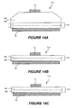
- FIGS. 14A, 14B and 14C are cross-sectional views of light emitting diode structures according to further embodiments.
- FIG. 15 is a cross-sectional view of an LED die according to some embodiments mounted in a package.
- FIG. 16 is a cross-sectional view of a metal die attach pad according to some embodiments on a generic semiconductor LED die.
- FIGS. 17A and 17B illustrate direct die attachment of an LED die including a metal stack according to some embodiments.
- FIGS. 18A and 18B are graphs of differential scanning calorimetry (DSC) results for several different metal stacks including a metal stack according to the present invention.
- FIGS. 19A, 19B, 20 and 21 are cross-sectional views semiconductor LED die mounted in various packages using metal die attach stacks in accordance with some embodiments.
- Embodiments of the present invention are directed towards methods and devices that may improve the thermal characteristics of a solid state lighting apparatus, such as a light bar, and in some cases may reduce the operating temperature of a solid state lighting apparatus.
- Some embodiments provide a light emitting device die design including a plurality of isolated active junctions configured to be connected in series on the die. Providing a die with multiple junctions that are connected in series may allow the chip to produce a high light output while driving the chip at a relatively low current, thereby reducing the operating temperature of the device.
- some embodiments provide a metal die attach for a light emitting device die that decreases the thermal resistance of a package incorporating the die, thereby potentially reducing the operating temperature of the device, while permitting the device to be manufactured using a lower temperature reflow that may not adversely affect plastic material in the device package.
- Relative terms such as “between”, “below,” “above,” “upper,” “lower,” “horizontal,” “lateral,” “vertical,” “beneath,” “over,” “on,” etc., may be used herein to describe a relationship of one element, layer or region to another element, layer or region as illustrated in the figures. It will be understood that these terms are intended to encompass different orientations of the device in addition to the orientation depicted in the figures.
- Embodiments of the invention are described herein with reference to cross-section illustrations that are schematic illustrations of idealized embodiments (and intermediate structures) of the invention.
- the thickness of layers and regions in the drawings may be exaggerated for clarity. Additionally, variations from the shapes of the illustrations as a result, for example, of manufacturing techniques and/or tolerances, are to be expected.
- embodiments of the invention should not be construed as limited to the particular shapes of regions illustrated herein but are to include deviations in shapes that result, for example, from manufacturing.
- a typical die attach metal is a eutectic Au/Sn alloy, with 80% Au and 20% Sn (by weight).
- the Au/Sn 80/20 alloy has good mechanical strength, reliability, and thermal conductivity, and is recognized as a standard die attach alloy.
- an AuSn 80/20 alloy die attach may require a reflow in the range of about 305° C., which can adversely affect plastic packages or chip-on-board packages.
- Some embodiments provide a metal die attach including an Sn rich structure that reflows at temperatures less than 250° C.
- some embodiments provide an AuSn metal die attach that includes about 40% or more (by weight) of Sn.
- the weight percent of Sn in the die attach structure may be greater than 60%, and in some embodiments the weight percent of Sn in the die attach structure may be greater than 70%. In some further embodiments, the weight percent of Sn in the die attach structure may be greater than 75%, and in still further embodiments the weight percent of Sn in the die attach structure may be greater than 90%.
- the tin may melt at a lower temperature than an AuSn alloy having a comparable weight percentage of tin.
- the weight percent of tin in the die attach structure may be greater than 20%.
- a die attach structure may reflow and bond at temperatures less than 250° C.
- the lower reflow temperature of a metal die attach structure as described herein may allow the use of lower reflow temperatures, which may mitigate or reduce the negative effect of high temperature solder reflow on a plastic package body, while providing a metallic submount bond that has enhanced thermal properties, such as reduced thermal resistance, relative to a conventional die attach material, such as silicone.
- a metal die attach structure as disclosed herein can remain stable during a RoHS (Restriction of Harmful Substances)—compliant package reflow, which allows temperatures up to 260° C. That is, a metal stack according to some embodiments may have a reflow temperature less than about 250° C., but once bonded may remain stable at temperatures above 260° C.
- RoHS Restriction of Harmful Substances
- FIG. 1 is a plan view of a light emitting diode die (or chip) 10 according to some embodiments, while FIG. 2 is a cross sectional view of a light emitting diode structure according to some embodiments taken along line A-A′ of FIG. 1 .
- a light emitting diode die 10 is a unitary semiconductor device that includes a support layer 12 having a first face 12 A and a second face 12 B opposite the first face 12 A.
- a diode region including a plurality of isolated active regions 14 A- 14 D is on the first face 12 A of the support layer 12 .
- the active regions 14 A- 14 D may be isolated from one another by means of mesa isolation (as illustrated in FIGS. 1-2 ) or other techniques, such as implant isolation, trench isolation, etc.
- Each of the active regions 14 A- 14 D may include a single p-n junction.
- the light emitting diode die 10 may be referred to as a multi junction die.
- This structure is not to be confused with a multiple quantum well diode structure, which is well known in the art.
- a multiple quantum well structure has an active region that may include multiple stacked quantum wells in which recombination occurs to generate light.
- a conventional multiple quantum well structure may still have only a single p-n junction.
- a light emitting diode die 10 according to some embodiments may have multiple isolated active regions, and hence may have multiple isolated p-n junctions.
- Each of the isolated active regions includes an anode contact 15 and a cathode contact 17 .
- a die attach pad 30 is on the second face of the support layer.
- the bond pad includes a gold-tin structure having a weight percentage of tin of 50% or more.
- the light emitting diode die 10 may further include a first wirebond pad 18 on an anode contact 15 of a first one 14 A of the isolated active regions and a second wirebond pad 20 on a cathode contact 17 of a second one 14 D of the isolated active regions.
- the isolated active regions 14 A- 14 D may be connected in series by means of metal interconnects 28 A, 28 B and 28 C which contact respective current spreading fingers 25 A, 25 B, 25 C on the anode contacts 15 .
- metal interconnect 28 A may electrically connect the cathode contact 17 of the first one 14 A of the isolated active regions and the anode contact 15 of the second one 14 B of the isolated active regions.
- Metal interconnect 28 B may electrically connect the cathode contact 17 of the second one 14 B of the isolated active regions and the anode contact 15 of the third one 14 C of the isolated active regions.
- metal interconnect 28 C may electrically connect the cathode contact 17 of the third one 14 C of the isolated active regions and the anode contact 15 of the fourth one 14 D of the isolated active regions.
- the isolated active regions 14 A- 14 D may thereby be connected in electrical series by the electrical interconnects 28 A- 28 C.
- the isolated active regions 14 A- 14 D may be connected in series to form an electronic device having a single anode contact (wire bond pad 18 ) and a single cathode contact (wire bond pad 20 ).
- the LED die 10 can have many different semiconductor layers arranged in different ways. LED structures and their fabrication and operation are generally known in the art and only briefly discussed herein.
- the layers of the LED die can be fabricated using known processes with a suitable process being fabrication using metal organic chemical vapor deposition (MOCVD).
- MOCVD metal organic chemical vapor deposition
- the layers of the LED die generally include an active layer/region sandwiched between first and second oppositely doped epitaxial layers all of which are formed successively on a growth substrate. LEDs can be formed on a wafer and then singulated for mounting in a package. It is understood that the growth substrate can remain as part of the final singulated LED or the growth substrate can be fully or partially removed, and the epitaxial layers that constitute the diode region can be mounted on a carrier substrate.
- the active region can include single quantum well (SQW), multiple quantum well (MQW), double heterostructure or super lattice structures.
- SQW single quantum well
- MQW multiple quantum well
- the active region and doped layers may be fabricated from different material systems, with preferred material systems being Group-III nitride based material systems.
- Group-III nitrides refer to those semiconductor compounds formed between nitrogen and the elements in the Group III of the periodic table, usually aluminum (Al), gallium (Ga), and indium (In).
- the term also refers to ternary and quaternary compounds such as aluminum gallium nitride (AlGaN) and aluminum indium gallium nitride (AlInGaN).
- AlGaN aluminum gallium nitride
- AlInGaN aluminum indium gallium nitride
- the doped layers are gallium nitride (GaN) and the active region is InGaN.
- the doped layers may be AkGaN, aluminum gallium arsenide (AlGaAs) or aluminum gallium indium arsenide phosphide (AlGaInAsP).
- the growth substrate can be made of many materials such at sapphire, silicon carbide, aluminum nitride (AlN), GaN, with a suitable substrate being a 4H polytype of silicon carbide, although other silicon carbide polytypes can also be used including 3 C, 6 H and 15 R polytypes.
- Silicon carbide has certain advantages, such as a closer crystal lattice match to Group III nitrides than sapphire and results in Group III nitride films of higher quality. Silicon carbide also has a very high thermal conductivity so that the total output power of Group-III nitride devices on silicon carbide are typically not limited by the thermal dissipation of the substrate (as may be the case with some devices formed on sapphire).
- the LED die can be coated with one or more phosphors with the phosphors absorbing at least some of the LED light and emitting a different wavelength of light such that the device emits a combination of light from the LED and the phosphor. In a preferred embodiment the LED emits a white light combination of LED and phosphor light.
- the LED die can be coated and fabricated using many different methods, with one suitable method being described in U.S. patent application Ser. Nos. 11/656,759 and 11/899,790, both entitled “Wafer Level Phosphor Coating Method and Devices Fabricated Utilizing Method”, and both of which are incorporated herein by reference.
- LEDs can be coated using other methods such an electrophoretic deposition (EPD), with a suitable EPD method described in U.S. patent application Ser. No. 11/473,089 entitled “Closed Loop Electrophoretic Deposition of Semiconductor Devices”, which is also incorporated herein by reference. It is understood that LED packages according to the present invention can also have multiple LEDs of different colors, one or more of which may be white emitting.
- EPD electrophoretic deposition
- the support layer 12 may be insulating or semi-insulating, and in some embodiments, the support layer may include semi-insulating silicon carbide, which is available from the assignee Cree, Inc.
- the support layer 12 may be a growth substrate on which the epitaxial semiconductor layers that form the isolated active regions 14 A- 14 D are grown.
- the support layer may include a carrier layer on which the isolated active regions 14 A- 14 D are supported.
- the support layer may include a layer of a semi-insulating gallium nitride based semiconductor material on which the epitaxial semiconductor layers that form the isolated active regions 14 A- 14 D are grown.
- Semi-insulating SiC may include silicon carbide doped with deep level transition elements, such as vanadium, as described in U.S. Pat. No. 5,856,231, the disclosure of which is incorporated herein by reference as if set forth herein, and/or may include high purity semi-insulating silicon carbide.
- a high-purity semi-insulating (HPSI) silicon carbide boule may be formed using a seeded sublimation growth technique. Exemplary sublimation growth techniques are more fully described in U.S. Patent Publication No. 2001/0017374 and in U.S. Pat. Nos. 6,403,982, 6,218,680, 6,396,080, 4,866,005 and Re. 34,861, the disclosures of which are hereby incorporated herein by reference. Sublimation techniques may also include gas fed sublimation, continuous growth and high-temperature CVD.
- the semiconductor light emitting device may be gallium nitride-based LEDs such as those devices manufactured and sold by Cree, Inc. of Durham, N.C.
- the present invention may be suitable for use with LEDs and/or lasers as described in U.S. Pat. Nos. 6,201,262; 6,187,606; 6,120,600; 5,912,477; 5,739,554; 5,631,190; 5,604,135; 5,523,589; 5,416,342; 5,393,993; 5,338,944; 5,210,051; 5,027,168; 5,027,168; 4,966,862 and/or 4,918,497, the disclosures of which are incorporated herein by reference as if set forth fully herein.
- LEDs and/or lasers are described in published U.S. Patent Publication No. US 2003/0006418 A1 entitled Group III Nitride Based Light Emitting Diode Structures With a Quantum Well and Superlattice, Group III Nitride Based Quantum Well Structures and Group III Nitride Based Superlattice Structures, published Jan. 9, 2003, as well as published U.S. Patent Publication No. US 2002/0123164 A1 entitled Light Emitting Diodes Including Modifications for Light Extraction and Manufacturing Methods Therefore.
- the LEDs and/or lasers may be configured to operate such that light emission occurs through the substrate.
- the substrate may be patterned so as to enhance light output of the devices as is described, for example, in the above-cited U.S. Patent Publication No. US 2002/0123164 A1.
- the light emitting devices may include a substrate that has been thinned, for example, by etching, mechanical lapping or grinding and polishing, to reduce the overall thickness of the structure.
- Techniques for thinning a substrate are described in U.S. Patent Publication No. 2005/0151138 entitled “Methods Of Processing Semiconductor Wafer Backsides Having Light Emitting Devices (LEDS) Thereon And LEDs So Formed,” the disclosure of which is hereby incorporated by reference as if set forth fully herein.
- a substrate may be shaped or roughened using sawing, laser scribing or other techniques to introduce geometrical features such as angled sidewalls which may increase light extraction.
- the substrate may be further etched to improve light extraction using for example the etch process described in US. Patent Publication No. 2005/0215000 entitled “Etching Of Substrates Of Light Emitting Diodes,” the disclosure of which is hereby incorporated by reference as if set forth fully herein.
- the substrate may be remove entirely by substrate removal techniques such as the techniques taught in U.S. Pat. Nos. 6,559,075, 6,071,795, 6,800,500 and/or 6,420,199 and/or U.S. Patent Publication No. 2002/0068201, the disclosures of which are hereby incorporated by reference as if set forth fully herein.
- the isolated active regions 14 A- 14 D are arranged in a row extending from a first end 12 C of the support layer 12 to a second end 12 D of the support layer 12 opposite the first end 12 C.
- the anode contact 15 of each of the isolated active regions 14 A- 14 D may be provided on a side of the isolated active region nearest the first end 12 C of the support layer 12
- the cathode contact 17 of each of the isolated active regions 14 A- 14 D may be provided on a side of the isolated active region nearest the second end 12 D of the support layer 12 .
- the light emitting diode die 10 may further include an insulating layer 29 on the support layer 12 and between respective ones of the active regions 14 A- 14 D.
- the electrical interconnects 28 A- 28 C may be at least partially provided on portions of the insulating layer 29 .
- other portions of the insulating layer 29 may be provided on the active regions 14 A- 14 D and on the interconnects 28 A- 28 C.
- the insulating layer 29 may include, for example, an insulating material, such as silicon oxide, silicon nitride, polyimide, or any other suitable insulator.
- the insulating layer 29 may include a single layer of insulating material and/or may be formed in multiple layers of the same or different material.
- the insulating layer 29 may include an encapsulant material, such as silicone, epoxy resin, or the like. Furthermore, the insulating layer 29 may include phosphor materials, such as those described in U.S. Pat. No. 6,853,010, entitled Phosphor-Coated Light Emitting Diodes Including Tapered Sidewalls and Fabrication Methods Therefore, and/or U.S. Pat. No. 7,821,194, entitled “Solid State Lighting Devices Including Light Mixtures” the disclosures of which are incorporated by reference herein as if set forth fully.
- the wirebond pads 18 , 20 may extend outside the insulating layer 29 to facilitate electrical contact to the die 10 .
- the light emitting device chip may include only one active region.
- FIG. 3 is a cross view of a light emitting device die 10 ′ according to further embodiments
- FIG. 4 is a bottom plan view of the light emitting device die 10 ′.
- the isolated active regions 14 A- 14 C, the wirebond pads 18 , 20 , the metal interconnects 28 A- 28 C, the anodes 15 , the cathodes 17 and the insulating layer 29 may all be similar to those described above with respect to FIGS. 1-2 .
- the die 10 ′ includes a support layer 42 that has sidewalls 42 C that are angled at an oblique angle to the upper and lower surfaces 42 A, 42 B of the support layer.
- the sidewalls 42 C may be angled inwardly from the upper surface 42 A on which the isolated active regions are provided to the lower surface 42 B of the support layer 42 .
- the metal die attach pad 30 may be formed on the lower surface 42 B and not on the angled sidewalls 42 C of the support layer 42 to enhance light extraction when the chip 10 ′ is mounted, for example, to a submount.
- FIG. 5 is a cross sectional view of a metal die attach pad 30 according to some embodiments.
- the die attach pad 30 may include a metal stack including a layer of titanium 38 in direct contact with the support layer 12 , 42 , a layer of platinum 36 on the titanium layer 38 , and a layer of nickel 32 on the platinum layer 36 .
- the titanium layer 38 may have a thickness of about 0.5 nm to about 25 nm, and in particular may have a thickness of about 10 nm.
- the purpose of the titanium layer 38 is to promote adhesion.
- the platinum layer 36 may have a thickness of about 100 nm to about 500 nm, and in particular may have a thickness of about 250 nm.
- the purpose of the platinum layer 36 is to reduce tin migration to the titanium layer 38 during the bonding process, and to form a platinum-tin phase with excess molten tin to enhance stability under operation and thermal exposure.
- the nickel layer 32 may have a thickness of about 100 nm to about 500 nm, and in particular may have a thickness of about 200 nm.
- the purpose of the nickel layer 32 is to form a nickel-tin phase with excess molten tin during the bonding process, and to enhance stability under operation and thermal exposure.
- the die attach pad 30 further includes a die attach (bonding) layer 34 that includes a first layer of gold 34 A, a layer of tin 34 B and a second layer of gold 34 D.
- the die attach pad 30 may also include a layer of nickel 34 C between the layer of tin 34 B and the second layer of gold 34 D.
- the purpose of the nickel layer 34 C is to reduce diffusion of gold from the second gold layer 34 D into the tin layer 34 C during the deposition process.
- the nickel layer 34 C may have a thickness between about 50 nm and about 400 nm, and in particular may have a thickness of about 200 nm.
- a thickness of the layer of tin 34 B may be about three times a combined thickness of the first layer of gold 34 A and the second layer of gold 34 D.
- the weight percentage of tin in the die attach layer 34 and/or in the die attach pad 30 may be about 40% or more. In some embodiments, the weight percentage of tin in the bond pad may be at least about 50%, and in still further embodiments, the weight percentage of tin in the bond pad may be at least about 60%. In further embodiments, the weight percentage of tin in the bond pad may be at least about 70%, in still further embodiments, the weight percentage of tin in the bond pad may be at least about 75%, and in yet further embodiments, the weight percentage of tin in the bond pad may be at least about 90%.
- metal layers including for example one or more reflective layers of silver and/or aluminum, may be provided in the metal stack between the die attach layer 34 and the support layer 12 , 42 .
- FIG. 6 is a graph of a phase diagram for the Au—Sn material system.
- temperature is shown on the ordinate (y-axis) while weight percent of tin is shown on the abscissa (x-axis).
- y-axis ordinate
- x-axis weight percent of tin
- an alloy created during the melting and solidifying of the Au and Sn in the metal die attach pad 30 will not pass through the eutectic point E that exists in the AuSn system at about 20% Sn by weight (corresponding to about 29% tin by atomic percentage), as illustrated in FIG. 6 .
- the Au and Sn in the die attach pad 30 will melt at a relatively low temperature as the temperature of the die attach pad 30 is raised, and the high-Sn content melt will then solidify to an alloy that has a melting temperature that is greater than the melting temperature of the 80/20 eutectic alloy, and in particular a melting temperature that is greater than 260° C. Rather, because the metal stack includes a layer of pure tin which has a melting point of about 230° C., a bonding process below 250° C. will be sufficient to melt the tin layer.
- the molten tin in contact with the gold, nickel, and platinum layers in the stack will solidify as various gold-tin and platinum-tin phases. These phases have higher melting points than pure tin according to their respective phase diagrams, and will therefore be thermally stable up to 260C under operation and thermal exposure.
- FIG. 7 is a cross sectional view of a package 50 including a multiple active region light emitting diode 10 ′ according to some embodiments.
- the package 50 includes a submount 55 , which may include a thermally conductive material, such as aluminum nitride, copper, aluminum or the like.
- a reflector 56 is on the submount 55 and surrounds a die mounting region on an upper surface of the submount 55 .
- the reflector 56 may be formed of a material that has specular reflective properties, such as aluminum, or it may be formed of a diffuse reflector, such as white plastic.
- a multiple active region light emitting diode 10 , 10 ′ as described above is mounted on a bond pad or metal bonding region (not shown) in the die mounting region using the metal die attach pad 30 for die attach, and the device 10 ′ is electrically connected to the package through wirebonds to the first and second bond pads 51 A, 51 B, which are electrically connected to anode and cathode pads 52 , 54 , respectively, of the package 50 , for example, through conductive vias in the submount 55 (not shown).
- a separate metal pad 53 may be provided to enhance thermal conduction from the package 50 to an external heat sink (not shown).
- a package 50 includes a unitary light emitting diode chip that includes a plurality (e.g. four) separate active regions on a common substrate. The plurality of active regions are connected in series, so that the package 50 may have a single anode contact 52 and a single cathode contact 54 .
- a package 50 as illustrated in FIG. 7 may have particular advantages when used in a backlight for a liquid crystal display (LCD), because the package may emit an increased amount of light for a given level of current, and the package may have a higher forward voltage drop than a conventional package that includes only one LED chip or two LED chips connected in series.
- LCD liquid crystal display
- a package including two LED chips connected in series that is typically only done to increase light output to compensate for low emission power.
- Such a package may have a forward voltage of about six volts. While a package including two LEDs may be used to increase light output, it is typically undesirable to increase the forward voltage of the package.
- a package 50 may have a forward voltage that is greater than about 6 volts. In some embodiments, the package may have a forward voltage of about 9V or more, and in some embodiments the package may have a forward voltage of about 12 volts or more. Accordingly, a plurality of packages 50 may be provided in series in a structure, such as an LCD backlight unit. The packages 50 may each have a high level of light emission and also a high forward voltage, so that the overall forward voltage of the series may be better matched to the output voltage of a DC power supply that provides current to the LED structure.
- FIG. 8 is a cross sectional view of a packaged device 50 ′ including multiple single active region light emitting diodes according to further embodiments.
- the package 50 ′ is similar to the package 50 illustrated in FIG. 7 . However, instead of one multi junction LED chip, the package 50 includes a plurality of singulated single junction LED chips 60 A- 60 D connected in electrical series by wirebonds 51 .
- a package 50 ′ may have similar advantages for use in LCD backlighting, as the package may generate increased light output for a given level of current while having a higher forward voltage drop over a single packaged component.
- FIG. 9 is a schematic diagram of a packaged device 50 , 50 ′ according to some embodiments.
- a packaged device 50 , 50 ′ may include a single package body having a single anode contact 52 and a single cathode contact 54 made to a group of light emitting diode junctions 14 , 60 coupled in electrical series.
- FIG. 10 is a plan view of a light bar 90 including a plurality of light emitting devices 10 according to some embodiments.
- a light bar 90 includes an elongated support member 70 , and a plurality of light emitting devices 10 A- 10 C mounted on the elongated support member 70 .
- Each of the light emitting diode chips 10 A- 10 C may have a structure as illustrated in FIGS. 1-4 .
- each of the light emitting diode chips 10 A- 10 C may include a support layer 12 , 42 having a first face and a second face opposite the first face, a diode region on the first face of the support layer 12 , 42 , and a die attach pad 30 on the second face of the support layer 12 , 42 .
- Each of the bond pads includes a gold-tin structure having a weight percentage of tin greater than 40%.
- the light emitting diode chips 10 A- 10 C are mounted to the elongated support member by their respective bond pads 30 , so that heat generated during operation of the light emitting devices 10 A- 10 C may be at least partially dissipated through the light bar.
- the light emitting diode chips 10 A- 10 C may be connected in electrical series via anode and cathode contacts 62 A- 62 C, 64 A- 64 C as illustrated in FIG. 10 .
- the active regions 14 A- 14 D of each of the light emitting diode chips 10 A- 10 C may be connected in electrical series.
- Light output from the light bar 90 may thereby enhanced even though the light bar includes fewer light emitting devices 10 A- 10 C, because the light bar 90 still includes a large number of active regions 14 A- 14 D.
- the light bar can be run at lower current than a light bar having a similar number of conventional light emitting devices with similar active junction areas.
- the overall level of voltage that is applied to be light bar 90 may be better matched to an external power supply, so that less voltage must be dropped outside the light bar, thereby decreasing the complexity of a system in which the light bar is used.
- FIG. 11 is a plan view of a light bar 90 ′ including a plurality of multiple emitter light emitting diode packages 50 A to 50 C according to some embodiments.
- the LED packages 50 A to 50 C may have a structure similar to the package 50 illustrated in FIG. 7 and/or the package 50 ′ illustrated in FIG. 8 .
- the LED packages 50 A to 50 C may be connected in electrical series. Accordingly, the light bar 90 ′ may have fewer light emitters (the packaged devices 50 A to 50 C) with higher light emission and higher forward voltage than a light bar that included packages with only one or two LED junctions per package.
- FIG. 12 is a partial exploded diagram illustrating portions of a backlight assembly for a liquid crystal display screen
- FIG. 13 is a side cross sectional view of an LCD display panel 98 according to some embodiments.
- a backlight assembly may include a diffuser sheet 95 and a plurality of light bars 90 , 90 ′, each including a plurality of light emitters 10 , 50 arranged in a linear array to transmit light into an edge of the diffuser sheet 95 .
- Light emitted by the light bars 90 , 90 ′ is diffused by the diffuser sheet and transmitted in a direction normal to the figure shown in FIG. 12 into an LCD screen 96 to provide backlighting for the LCD screen 96 .
- FIGS. 14A, 14B and 14C are cross views of light emitting diode structures according to further embodiments.
- the light emitting diode structures 11 A and 11 B may be mounted in a flip-chip configuration.
- the light emitting diode structure 11 A may include a substrate 12 , which may be a growth substrate or a carrier substrate on which an active region 115 is provided.
- the active region 115 may include a p-type epitaxial region 15 A and an n-type epitaxial region 15 B layered on the substrate 12 .
- a cathode contact 13 is on the substrate 12
- a die attach pad 35 is on the p-type epitaxial region 15 A and provides an anode contact for the diode 11 A.
- the die attach pad 35 may have a structure as described above with respect to FIG. 5 , and, accordingly, may be configured to reflow at low temperatures but solidify to provide a bond that is stable at high temperatures.
- the light emitting diode structure 11 B may be similar to the light emitting diode structure 11 A, except that the substrate 12 has been removed using conventional substrate removal techniques.
- the light emitting diode structure 11 C may be similar to the light emitting diode structure 11 B, except that the die attach pad 35 is on the n-type epitaxial region 15 B and an anode contact 17 is on the p-type epitaxial region 15 A.
- Embodiments of the present invention may be particularly suitable for direct die attach mounting of an LED die to a package including a submount.
- FIG. 15 An LED die 100 mounted by direct die attachment in a package 200 is illustrated in FIG. 15 .
- the LED die 100 includes a diode region 110 having first and second opposing faces 110 a , 110 b , respectively, and including therein an n-type layer 112 and a p-type layer 114 .
- Other layers or regions may be provided, which may include quantum wells, buffer layers, etc., that need not be described herein.
- An anode contact 160 ohmically contacts the p-type layer 114 and extends on a first face 110 a .
- the anode contact 160 may directly ohmically contact the p-type layer 114 , or may ohmically contact the p-type layer 114 by way of one or more conductive vias 162 and/or other intermediate layers.
- a cathode contact 170 ohmically contacts the n-type layer 112 and also extends on the first face 110 a.
- the cathode contact may directly ohmically contact the n-type layer 112 , or may ohmically contact the n-type layer 112 by way of one or more conductive vias 172 and/or other intermediate layers. As illustrated in FIG. 15 , the anode contact 160 and that cathode contact 170 that both extend on the first face 110 a are coplanar.
- the diode region 110 also may be referred to herein as an “LED epi region”, because it is typically formed epitaxially on a substrate 120 .
- a Group III-nitride based LED epitaxial structure 110 may be formed on a silicon carbide growth substrate.
- the growth substrate may be present in the finished product.
- the growth substrate may be removed.
- another substrate may be provided that is different from the growth substrate.
- a transparent substrate 120 such as a transparent silicon carbide growth substrate, is included on the second face 110 b of the diode region 110 .
- the transparent substrate 120 includes a sidewall 120 a and may also include an inner face 120 c adjacent the second face 110 b of the diode region 110 and an outer face 120 b , remote from the inner face 120 c .
- the outer face 120 b is of smaller area than the inner face 120 c .
- the sidewall 120 a may be stepped, beveled and/or faceted, so as to provide the outer face 120 b that is of smaller area than the inner face 120 c .
- the sidewall is an oblique sidewall 120 a that extends at an oblique angle ⁇ , and in some embodiments at an obtuse angle, from the outer face 120 b towards the inner face 120 c.
- An LED die 100 configured as described above in connection with FIG. 15 may be referred to as “horizontal” or “lateral” LEDs, because both the anode and the cathode contacts thereof are provided on a single face of the LED. Horizontal LEDs may be contrasted with vertical LEDs in which the anode and cathode contacts are provided on opposite faces thereof.
- a conformal layer 140 that comprises phosphor particles 142 is provided on the outer face 120 b and on the oblique sidewall 120 a .
- the entire outer face 120 b and the entire oblique sidewall 120 a are covered with the phosphor layer 140 .
- the entire outer face 120 b and/or the entire oblique sidewall 120 a need not be covered with the phosphor layer 140 .
- the conformal phosphor layer 140 may be of uniform thickness on the outer face 120 b and on the oblique sidewall 120 a.
- the diode region 110 is configured to emit blue light, for example light having a dominant wavelength of about 450-460 nm, and the conformal layer comprises yellow phosphor, such as YAG:Ce phosphor.
- the diode region 110 is configured to emit blue light upon energization thereof, as described above, and the conformal layer 140 may comprise a mixture of a yellow phosphor and red phosphor, such as a CASN-based phosphor.
- the LED die 100 may be combined with a mounting substrate or submount 180 and a lens 190 to provide a packaged LED 200 .
- the submount 180 may include a submount body 182 that may comprise aluminum nitride (AlN).
- AlN aluminum nitride
- metal core substrates, printed circuit boards, lead frames and/or other conventional mounting substrates may be used to mount the LED die 100 in a flip-chip configuration.
- the submount 180 includes a submount face 182 a , and an anode pad 184 and a cathode pad 186 thereon.
- the anode and cathode pads may comprise silver-plated copper and/or other conductive materials.
- the LED die 100 is mounted on the submount 180 , such that the first face 110 a is adjacent the submount face 182 a , the outer face 110 b is remote from the submount 180 , the anode contact 184 is adjacent the anode pad 160 , and the cathode contact 186 is adjacent the cathode pad 170 .
- a metal stack 130 including a bonding layer as described herein is used to electrically, thermally and mechanically connect the anode contact 160 to the anode pad 184 , and the cathode contact 170 to the cathode pad 186 .
- direct attachment of the anode contact 160 to the anode pad 184 , and direct attachment of the cathode contact 170 to the cathode pad 186 may be provided, for example using thermocompression bonding and/or other techniques.
- a packaged device anode 192 and a packaged device cathode 194 may be provided on package surface, such as a second face 182 b of the submount body 182 , and may be connected to the anode pad 184 and cathode pad 186 , respectively, using internal vias and/or conductive layers that extend on and/or around the submount body 182 .
- the submount body 182 can be formed of many different materials with a preferred material being electrically insulating. Suitable materials include, but are not limited to ceramic materials such as aluminum oxide, aluminum nitride or organic insulators like polyimide (PI) and polyphthalamide (PPA). In other embodiments the submount body 182 can include a printed circuit board (PCB), sapphire or silicon or any other suitable material. For PCB embodiments different PCB types can be used such as standard FR-4 PCB, metal core PCB, or any other type of printed circuit board. As more fully described below, LED packages according to the present invention can be fabricated using a method that utilizes a submount panel sized to accommodate a plurality of submounts. Multiple LED packages can be formed on the panel, with the individual packages being singulated from the panel.
- PCB printed circuit board
- submounts 180 that may be used with embodiments described herein, are described in the '787 Publication that was cited above.
- Various other embodiments of submounts 180 are described in U.S. Patent Application Publication 2009/0108281 to Keller et al., entitled Light Emitting Diode Package and Method for Fabricating Same, assigned to the assignee of the present application, the disclosure of which is hereby incorporated herein by reference in its entirety as if set forth fully herein (hereinafter referred to as “the '281 Publication”). It will be understood that any and all embodiments of these submounts may be used in embodiments of FIG. 15 . However, the pad structure on the submount may be modified so as to be used with a horizontal LED die 100 of FIG. 15 , rather than the vertical LEDs described in the '281 Publication.
- the packaged LED 200 may also include a lens 190 that extends from submount face 180 a to surround the LED die 100 .
- the lens 190 may be a molded plastic lens, as described in detail in the '281 Publication, and may be fabricated on the submount according to techniques that are described in the '281 Publication, and/or other techniques. In some embodiments, the lens may be about 3.06 mm in diameter.
- FIG. 16 is a cross sectional view of a metal die attach pad 130 on a generic semiconductor LED die 100 according to some embodiments.
- the die attach pad 130 may include a metal stack including an adhesion layer of, e.g., titanium 38 in direct contact with the LED die 100 , and a barrier layer of, e.g., platinum 36 on the adhesion layer 38 .
- the adhesion layer 38 may have a thickness of about 5 nm to about 250 nm, and in particular may have a thickness of about 50 nm.
- the barrier layer 36 may have a thickness of about 100 nm to about 500 nm, and in particular may have a thickness of about 150 nm.
- the purpose of the barrier layer 36 is to reduce tin migration to the titanium layer 38 during the bonding process.
- the barrier layer 36 may be formed of a material and having a thickness sufficient to substantially preclude the formation or migration of free metals or alloys that have melting points lower than 300 degrees centigrade.
- a platinum barrier layer may form a platinum-tin phase with excess molten tin to enhance stability under operation and thermal exposure.
- the metal stack 130 may include a reflector layer that may be surrounded by a barrier layer to protect the reflective layer.
- the metal stack 130 may also include a metal that forms an ohmic contact with an underlying semiconductor layer.
- a bonding layer 134 is provided on the barrier layer 36 .
- the bonding layer 134 includes a layer of nickel 134 A on the barrier layer 36 , a layer of tin 134 B on the nickel layer 134 A, and a layer of gold 134 C on the tin layer 134 B.
- the bonding layer It is desirable for the bonding layer to reflow at relatively low temperatures when the LED die 100 is initially mounted to a carrier substrate, PCB, header, etc.
- the constituent layers 134 A- 134 C of the bonding layer are deposited as discrete layers, once the device has been bonded, the bonding layer forms an alloy of metals that may have a different melting point than the individual metals have. It is desirable for the melting point of the alloyed bonding layer to be high enough for the bonding metal to be able to withstand subsequent high temperature processing steps, such as might be encountered during lead-free soldering. Accordingly, it is desirable for the alloyed bonding layer to have a melting point that is at least about 250 degrees centigrade, and in some cases higher than 260 degrees centigrade.
- the metal of the bonding layer 134 In addition to thermal stability, it is also important for the metal of the bonding layer 134 to have a high shear strength to enable the die attachment to survive mechanical stress, such as may be encountered during subsequent processing steps and/or during use of the device, without delaminating.
- a weight percentage of nickel in the bonding layer may be at least about 10 percent.
- a bonding layer having such a composition may have desirable thermal and/or mechanical characteristics, particularly for bonding an LED chip to a submount in a device package.
- Increasing the thickness of tin in the metal stack to greater than 2 microns, and in some cases up to 3 microns or more, can reduce the formation of voids during the attachment process, which may improve the thermal resistance of the metal stack.
- the nickel layer 134 A may have a thickness greater than about 400 nm, and in particular may have a thickness of about 600 nm. Because tin is relatively soft, it may be desirable to increase the amount of nickel in the bonding layer to increase the mechanical strength of the bonding layer.
- the thickness of the layer of tin 34 B may be greater than about 2 microns (2000 nm), in some cases greater than about 2.5 microns (2500 nm) and in some cases may be at least about 3 microns (3000 nm).
- the entire metal stack including adhesion, barrier, bonding and other layers, may be less than an 6 microns thick to enhance the mechanical stability of the die attach.
- the weight percentage of tin in the bonding layer may be less than 80 percent. In some embodiments, the weight percentage of tin in the bonding layer may be between about 70 percent and 80 percent.
- the weight percentage of gold the bonding layer 134 may be less than about 5 percent, and in some embodiments, the weight percentage of gold the bonding layer may be less than about 2 percent.
- the entire metal stack 130 may contain gold in an amount of less than 5 percent by weight.
- the bonding layer may include a metal alloy that is more than 90 percent nickel and tin by weight. In some embodiments, the metal alloy of the bonding layer may be more than 95 percent nickel and tin by weight, and in some embodiments more than 97 percent nickel and tin by weight.
- the bonding layer Prior to initial bonding, the bonding layer may have a relatively low initial melting temperature.
- the initial melting temperature of the bonding layer may be less than 250 degrees centigrade. In some embodiments, the initial melting temperature of the bonding layer may be less than 240 degrees centigrade and in some embodiments less than 230 degrees centigrade.
- the bonding layer may include a metal alloy that is thermally stable at temperatures up to 260 degrees centigrade. In some embodiments, the metal alloy of the bonding layer may be thermally stable at temperatures up to 290 degrees centigrade. In further embodiments, the metal alloy of the bonding layer may be thermally stable at temperatures up to 310 degrees centigrade, and in still further, the metal alloy of the bonding layer may be thermally stable at temperatures up to 320 degrees centigrade.
- the LED die 100 including the metal stack 130 may be bonded onto a submount body 182 , including a metal die attach pad 186 .
- the submount body 182 has a top surface including patterned conductive features that can include a die attach pad 186 .
- the LED can be mounted to the die attach pad 186 using known methods and material mounting such as using conventional solder materials that may or may not contain a flux material or dispensed polymeric materials that may be thermally and electrically conductive.
- the size of the submount body 182 can vary depending on different factors, with one being the size of the LED.
- the size of the package can be essentially of the same dimension as the effective heat spreading area in the attach pad.
- the submount In a package having a 1 mm LED die, the submount can be approximately 3.5 mm by 3.5 mm; with a package having a 0.7 mm die it can be 3.2 mm by 3.2 mm and generally of square shape in both cases. It is further understood that the submount can have other shapes including circular, rectangular or other multiple sided shapes.
- the die attach pad 186 can include much different material such as metals or other conductive materials.
- the attach pad 186 includes copper deposited using known techniques such as plating. In typical plating process a titanium adhesion layer and copper seed layer are sequentially sputtered onto a substrate. Then, approximately 75 microns of copper is plated onto the copper seed layer. The resulting copper layer being deposited can then be patterned using standard lithographic processes. In other embodiments the layer can be sputtered using a mask to form the desired pattern. In further embodiments a capping layer of silver can be formed over the copper layer.
- the die attach pad 186 can be plated or coated with additional metals or materials to the make the die attach pad 186 more suitable for mounting an LED die 100 .
- the die attach pad 186 can be plated with adhesive or bonding materials, or reflective and barrier layers.
- the bonding layer melts, and the constituent layers of the bonding layer alloy to form an alloyed bonding layer 150 that is in some embodiments an alloy of nickel, tin and gold.
- FIGS. 18A and 18B are graphs of differential scanning calorimetry (DSC) results for several different metal stacks.
- DSC differential scanning calorimetry
- thermoanalytical technique in which the difference in the amount of heat required to increase the temperature of a test sample and a reference sample is measured as a function of temperature. DSC analysis can be used to identify phase changes of a test sample.
- FIG. 18A illustrates DSC results for a first DSC test of three different metal stacks
- FIG. 18B illustrates DSC results for three repeated DSC tests of the three different metal stacks that have already been re-flowed and melted.
- graph 202 is a graph of DSC results for a first metal stack (Stack A) consisting of 50 nm of titanium, 150 nm of platinum, 300 nm of nickel, 100 nm of gold, 2 microns of tin, and 30 nm of gold.
- Graph 204 is a graph of DSC results for a second metal stack (Stack B) consisting of 15 nm of titanium, 200 nm of nickel, and 3 microns of 80/20 gold/tin.
- Graph 206 is a graph of DSC results for a third metal stack (Stack C) consisting of 50 nm of titanium, 150 nm of platinum, 600 nm of nickel, 3 microns of tin, and 30 nm of gold.
- Stack C had the lowest melting point at less than 230 degrees centigrade.
- Stack A had a melting point of about 260 degrees centigrade, while Stack B had a melting point of about 285 degrees centigrade.
- a metal stack including a bonding layer as described above may be well suited for lead-free manufacturing processes, which typically require relatively high temperatures.
- a metal stack including a bonding layer as described above may be well suited for multiple lead-free reflow profiles that may be encountered during subsequent processing steps.
- a metal stack including a bonding layer as described above may be highly durable, and may not significantly corrode even when subjected to extreme environments, such as high temperature, high humidity environments for extended time periods. Thus, such metal stacks may be well suited for long-lifetime applications in various different types of devices and/or packages.
- FIGS. 19A, 19B, 20 and 21 are cross-sectional views semiconductor LED die mounted in various packages using metal die attach stacks in accordance with some embodiments.
- FIG. 19A shows an LED die 100 including a die attach metal stack 130 as disclosed above that is flip-chip mounted onto a submount including a submount body 182 and a die attach pad 186 .
- the LED die 100 includes a p-type region 114 and an n-type region 112 .
- the LED die may include a growth substrate on which the epitaxial layers comprising the LED are grown, a carrier substrate onto which the epitaxial layers are transferred, or no substrate.
- the metal stack 130 includes adhesion and barrier layers 38 , 36 and a eutectic bonding layer 134 on the adhesion and barrier layers.
- the bonding layer 134 includes a layer of nickel 134 A, a layer of tin 134 B on the nickel layer 134 A, and a layer of gold 134 C on the tin layer 134 B.
- the die attach metal stack 130 of the LED die 100 is brought into contact with the die attach pad 186 , and sufficient heat and/or force is applied to the die to cause the bonding layer to reflow, forming an alloyed bond layer 150 that holds the die 100 in place on the submount body 182 .
- An encapsulant, such as silicone, is then dispensed to form a dome lens on the submount body 182 over the attached die 100 .
- LED chips 100 may be mounted using a die attach metal stack 130 with the n-side down and wirebond connections 178 made to anode and cathode contacts 183 , 185 formed on the p-type 114 and n-type 112 layers of the LED die 100 , respectively.
- multiple LED die 100 are mounted on a submount body 182 and wirebonded.
- An encapsulant dam 172 is formed on the submount body, and a liquid encapsulant is dispensed onto the submount body within the encapsulant dam to cover the attached LED die.
- FIG. 21 illustrates embodiments in which multiple LED die 100 are flip-chip mounted onto a submount body 182 using die attach metal stacks 130 formed on the cathode and anode contacts 170 , 160 on the n-type and p-type layers 114 , 112 of the LED die that bond to respective die attach pads 186 on the submount body 182 .
- An encapsulant dome 190 is then formed on the submount body 182 over the attached LED die.
Abstract
Description
Claims (34)
Priority Applications (3)
| Application Number | Priority Date | Filing Date | Title |
|---|---|---|---|
| US13/361,569 US9443903B2 (en) | 2006-06-30 | 2012-01-30 | Low temperature high strength metal stack for die attachment |
| PCT/US2013/023041 WO2013116086A1 (en) | 2012-01-30 | 2013-01-25 | Low temperature high strength metal stack for die attachment |
| EP13743107.8A EP2810307A1 (en) | 2012-01-30 | 2013-01-25 | Low temperature high strength metal stack for die attachment |
Applications Claiming Priority (4)
| Application Number | Priority Date | Filing Date | Title |
|---|---|---|---|
| US11/428,158 US8643195B2 (en) | 2006-06-30 | 2006-06-30 | Nickel tin bonding system for semiconductor wafers and devices |
| US11/844,127 US7910945B2 (en) | 2006-06-30 | 2007-08-23 | Nickel tin bonding system with barrier layer for semiconductor wafers and devices |
| US13/011,417 US8698184B2 (en) | 2011-01-21 | 2011-01-21 | Light emitting diodes with low junction temperature and solid state backlight components including light emitting diodes with low junction temperature |
| US13/361,569 US9443903B2 (en) | 2006-06-30 | 2012-01-30 | Low temperature high strength metal stack for die attachment |
Related Parent Applications (1)
| Application Number | Title | Priority Date | Filing Date |
|---|---|---|---|
| US13/011,417 Continuation-In-Part US8698184B2 (en) | 2006-06-30 | 2011-01-21 | Light emitting diodes with low junction temperature and solid state backlight components including light emitting diodes with low junction temperature |
Publications (2)
| Publication Number | Publication Date |
|---|---|
| US20120211793A1 US20120211793A1 (en) | 2012-08-23 |
| US9443903B2 true US9443903B2 (en) | 2016-09-13 |
Family
ID=46652031
Family Applications (1)
| Application Number | Title | Priority Date | Filing Date |
|---|---|---|---|
| US13/361,569 Active US9443903B2 (en) | 2006-06-30 | 2012-01-30 | Low temperature high strength metal stack for die attachment |
Country Status (1)
| Country | Link |
|---|---|
| US (1) | US9443903B2 (en) |
Cited By (3)
| Publication number | Priority date | Publication date | Assignee | Title |
|---|---|---|---|---|
| US20160172554A1 (en) * | 2013-07-19 | 2016-06-16 | Koninklijke Philips N.V. | Pc led with optical element and without ssubstrate carrier |
| US20160204322A1 (en) * | 2013-11-28 | 2016-07-14 | Epistar Corporation | Light-emitting device and manufacturing method thereof |
| US10790412B2 (en) | 2015-04-20 | 2020-09-29 | Epistar Corporation | Light-emitting device and manufacturing method thereof |
Families Citing this family (9)
| Publication number | Priority date | Publication date | Assignee | Title |
|---|---|---|---|---|
| US9227257B2 (en) | 2012-04-24 | 2016-01-05 | Seagate Technology Llc | Laser subassembly metallization for heat assisted magnetic recording |
| US8933473B1 (en) | 2012-06-01 | 2015-01-13 | Valery Dubin | Method, apparatus and system for providing light source structures on a flexible substrate |
| DE102013201808A1 (en) * | 2013-02-05 | 2014-08-07 | Richard Wolf Gmbh | LED lighting module |
| KR20140104802A (en) * | 2013-02-21 | 2014-08-29 | 한국전자통신연구원 | Method of fabrication semiconductor package |
| KR102311677B1 (en) * | 2014-08-13 | 2021-10-12 | 삼성전자주식회사 | Semiconductor device and method of manufacturing the same |
| US10046408B2 (en) | 2015-05-28 | 2018-08-14 | Osram Opto Semiconductors Gmbh | Device comprising a connecting component and method for producing a connecting component |
| DE102016106734A1 (en) * | 2015-12-14 | 2017-06-14 | Osram Opto Semiconductors Gmbh | Support for an optoelectronic component, method for producing a support for an optoelectronic component, wafers and soldering methods |
| KR20180065700A (en) * | 2016-12-08 | 2018-06-18 | 삼성전자주식회사 | Light emitting device |
| US10380496B2 (en) * | 2018-03-19 | 2019-08-13 | Intel Corporation | Quantum computing assemblies |
Citations (74)
| Publication number | Priority date | Publication date | Assignee | Title |
|---|---|---|---|---|
| USD264792S (en) | 1979-02-12 | 1982-06-08 | Dart Industries Inc. | Combined food storage and service dish |
| USD283399S (en) | 1984-02-22 | 1986-04-15 | Westvaco Corporation | Packaging tray for food or the like |
| USD305410S (en) | 1986-09-02 | 1990-01-09 | Lever Brothers Company | Packaging container |
| USD327234S (en) | 1989-04-20 | 1992-06-23 | Highland Supply Corporation | Flower pot cover |
| US5309001A (en) | 1991-11-25 | 1994-05-03 | Sharp Kabushiki Kaisha | Light-emitting diode having a surface electrode of a tree-like form |
| US5794839A (en) * | 1994-08-01 | 1998-08-18 | Nippondenso Co., Ltd. | Bonding material and bonding method for electric element |
| USD421046S (en) | 1998-01-21 | 2000-02-22 | Avery Dennison Corporation | Minisheet label assembly |
| USD448404S1 (en) | 1998-10-23 | 2001-09-25 | Avery Dennison Corporation | Print indicia and address label sheet |
| US6518598B1 (en) | 2001-12-21 | 2003-02-11 | Epitech Corporation Ltd | III-nitride LED having a spiral electrode |
| US20030059972A1 (en) | 2001-09-27 | 2003-03-27 | Shin-Etsu Handotai Co., Ltd. | Light-emitting device and method for manufacturing the same |
| US6547249B2 (en) | 2001-03-29 | 2003-04-15 | Lumileds Lighting U.S., Llc | Monolithic series/parallel led arrays formed on highly resistive substrates |
| USD476680S1 (en) | 2002-06-06 | 2003-07-01 | S. Temtec, Inc. | Laser printable card badge sheet |
| US20030143103A1 (en) | 1998-03-30 | 2003-07-31 | Takashi Masuda | Die-bonding solder materials |
| US20030164214A1 (en) | 2001-12-13 | 2003-09-04 | Miyazaki Ken-Ichi | Foil-form soldering metal and method for processing the same |
| US20040035909A1 (en) * | 2002-08-22 | 2004-02-26 | Shing Yeh | Lead-based solder alloys containing copper |
| US6767411B2 (en) | 2002-03-15 | 2004-07-27 | Delphi Technologies, Inc. | Lead-free solder alloy and solder reflow process |
| USD495116S1 (en) | 2002-03-28 | 2004-08-31 | Societe De Produits Nestle S.A. | Chocolate piece |
| US6814459B2 (en) | 1999-08-04 | 2004-11-09 | 911Ep, Inc. | LED light bar |
| US20050104220A1 (en) * | 2003-11-14 | 2005-05-19 | Stanley Electric Co., Ltd. | Semiconductor device and its manufacture method capable of preventing short circuit of electrodes when semiconductor device is mounted on sub-mount substrate |
| US6936859B1 (en) | 1998-05-13 | 2005-08-30 | Toyoda Gosei Co., Ltd. | Light-emitting semiconductor device using group III nitride compound |
| US20050194605A1 (en) * | 2004-03-05 | 2005-09-08 | Shelton Bryan S. | Flip-chip light emitting diode device without sub-mount |
| USD521565S1 (en) | 2005-03-08 | 2006-05-23 | Phg Technologies, Llc | Medical label sheet |
| US20060214274A1 (en) * | 2005-03-24 | 2006-09-28 | Kazuo Shimokawa | Semiconductor device and manufacturing method thereof |
| US7141828B2 (en) | 2003-03-19 | 2006-11-28 | Gelcore, Llc | Flip-chip light emitting diode with a thermally stable multiple layer reflective p-type contact |
| US20060284191A1 (en) | 2005-06-16 | 2006-12-21 | Epistar Corporation | Light emitting diode |
| US7173277B2 (en) | 2002-11-27 | 2007-02-06 | Matsushita Electric Industrial Co., Ltd. | Semiconductor light emitting device and method for fabricating the same |
| US20070048885A1 (en) | 2002-12-11 | 2007-03-01 | Jeon Hyeong T | Thin film led |
| US20070102693A1 (en) | 2003-12-24 | 2007-05-10 | Hideo Nagai | Semiconductor light emitting device, lighting module, lighting apparatus, display element, and manufacturing method for semiconductor light emitting device |
| US7247514B2 (en) | 2003-04-11 | 2007-07-24 | Matsushita Electric Industrial Co., Ltd. | Semiconductor device and method for producing the same |
| US20070181900A1 (en) * | 2006-01-19 | 2007-08-09 | Yoshiro Sato | Semiconductor light emitting device and its manufacture method |
| US7285801B2 (en) | 2004-04-02 | 2007-10-23 | Lumination, Llc | LED with series-connected monolithically integrated mesas |
| US20070253209A1 (en) | 2006-04-27 | 2007-11-01 | Cree, Inc. | Submounts for semiconductor light emitting device packages and semiconductor light emitting device packages including the same |
| US20070272940A1 (en) | 2003-06-27 | 2007-11-29 | Lee Kong W | Semiconductor device with a light emitting semiconductor die |
| US20070286762A1 (en) | 2005-11-10 | 2007-12-13 | Herman Oppermann | Gold-containing solder deposit, method for production thereof, soldering method and use |
| US20080003777A1 (en) * | 2006-06-30 | 2008-01-03 | Slater David B | Nickel Tin Bonding System for Semiconductor Wafers and Devices |
| US20080006837A1 (en) * | 2006-07-07 | 2008-01-10 | Lg Electronics Inc. And Lg Innotek Co., Ltd | Sub-mount for mounting light emitting device and light emitting device package |
| US7329905B2 (en) | 2004-06-30 | 2008-02-12 | Cree, Inc. | Chip-scale methods for packaging light emitting devices and chip-scale packaged light emitting devices |
| USD566057S1 (en) | 2006-12-21 | 2008-04-08 | Cree, Inc. | LED chip |
| US7365371B2 (en) | 2005-08-04 | 2008-04-29 | Cree, Inc. | Packages for semiconductor light emitting devices utilizing dispensed encapsulants |
| US20080099777A1 (en) | 2005-10-19 | 2008-05-01 | Luminus Devices, Inc. | Light-emitting devices and related systems |
| US20080099772A1 (en) | 2006-10-30 | 2008-05-01 | Geoffrey Wen-Tai Shuy | Light emitting diode matrix |
| US20080170396A1 (en) | 2006-11-09 | 2008-07-17 | Cree, Inc. | LED array and method for fabricating same |
| US20080179602A1 (en) | 2007-01-22 | 2008-07-31 | Led Lighting Fixtures, Inc. | Fault tolerant light emitters, systems incorporating fault tolerant light emitters and methods of fabricating fault tolerant light emitters |
| US20080210971A1 (en) * | 2006-06-30 | 2008-09-04 | Matthew Donofrio | Nickel tin bonding system with barrier layer for semiconductor wafers and devices |
| US20080211416A1 (en) | 2007-01-22 | 2008-09-04 | Led Lighting Fixtures, Inc. | Illumination devices using externally interconnected arrays of light emitting devices, and methods of fabricating same |
| US20080217640A1 (en) | 2007-03-08 | 2008-09-11 | Stanley Electric Co., Ltd. | Semiconductor Light emitting device, LED package using the same, and method for fabricating the same |
| US20080246051A1 (en) | 2007-04-06 | 2008-10-09 | Kabushiki Kaisha Toshiba | Light emitting apparatus and method for manufacturing same |
| USD582865S1 (en) | 2007-06-11 | 2008-12-16 | Cree, Inc. | LED chip |
| US20090001402A1 (en) | 2006-03-22 | 2009-01-01 | Rohm Co., Ltd. | Semiconductor element and method of making the same |
| US20090085048A1 (en) | 2007-09-27 | 2009-04-02 | Seoul Opto Device Co., Ltd. | Ac light emitting diode |
| US7560738B2 (en) | 2003-07-04 | 2009-07-14 | Epistar Corporation | Light-emitting diode array having an adhesive layer |
| US20090179207A1 (en) | 2008-01-11 | 2009-07-16 | Cree, Inc. | Flip-chip phosphor coating method and devices fabricated utilizing method |
| USD599748S1 (en) | 2008-06-12 | 2009-09-08 | SemiLEDs Optoelectronics Co., Ltd. | Light emitting diode device |
| US20090224653A1 (en) | 2008-03-07 | 2009-09-10 | Bily Wang | LED chip package structure in order to prevent the light-emitting efficiency of fluorescent powder from decreasing due to high temperature and method for making the same |
| US7605403B2 (en) | 2004-05-11 | 2009-10-20 | Stanley Electric Co., Ltd. | Semiconductor light-emitting device and fabrication method of the same |
| US20090283787A1 (en) | 2007-11-14 | 2009-11-19 | Matthew Donofrio | Semiconductor light emitting diodes having reflective structures and methods of fabricating same |
| US20100038660A1 (en) | 2008-08-13 | 2010-02-18 | Progressive Cooling Solutions, Inc. | Two-phase cooling for light-emitting devices |
| US20100051977A1 (en) | 2006-12-18 | 2010-03-04 | Seoul Opto Device Co., Ltd. | Light emitting device having isolating insulative layer for isolating light emitting cells from each other and method of fabricating the same |
| US20100059768A1 (en) | 2008-09-11 | 2010-03-11 | Ghulam Hasnain | Series Connected Segmented LED |
| US20100109031A1 (en) | 2004-06-30 | 2010-05-06 | Seoul Opto Device Co., Ltd. | Light emitting element with a plurality of cells bonded, method of manufacturing the same, and light emitting device using the same |
| US20100141175A1 (en) | 2009-02-26 | 2010-06-10 | Ghulam Hasnain | Light Sources Utilizing Segmented LEDs to Compensate for Manufacturing Variations in the Light Output of Individual Segmented LEDs |
| US20100155746A1 (en) | 2009-04-06 | 2010-06-24 | Cree, Inc. | High voltage low current surface-emitting led |
| US20100163887A1 (en) | 2008-12-31 | 2010-07-01 | Seoul Opto Device Co., Ltd. | Light emitting device having a plurality of non-polar light emitting cells and a method of fabricating the same |
| US20100276706A1 (en) | 2007-06-29 | 2010-11-04 | Osram Opto Semiconductors Gmbh | Method for the Production of a Plurality of Optoelectronic Components, and Optoelectronic Component |
| US7842959B2 (en) | 2004-12-14 | 2010-11-30 | Seoul Opto Device Co., Ltd. | Light emitting device having a plurality of light emitting cells and package mounting the same |
| US7855459B2 (en) * | 2006-09-22 | 2010-12-21 | Cree, Inc. | Modified gold-tin system with increased melting temperature for wafer bonding |
| US20110098420A1 (en) | 2008-03-28 | 2011-04-28 | Mitsubishi Chemical Corporation | Curable polysiloxane composition, and polysiloxane cured product, optical member, member for aerospace industry, semiconductor light-emitting device, illuminating device and image display device using the same |
| US20110127563A1 (en) | 2009-11-27 | 2011-06-02 | Industrial Technology Research Institute | Die-bonding method of led chip and led manufactured by the same |
| US20110147779A1 (en) | 2009-12-21 | 2011-06-23 | Sin-Ho Kang | Light emitting diode package and method of fabricating the same |
| USD645008S1 (en) | 2010-11-08 | 2011-09-13 | SemiLEDs Optoelectronics Co., Ltd. | Light emitting diode device |
| US8049242B2 (en) | 2006-10-17 | 2011-11-01 | Epistar Corporation | Optoelectronic device |
| US8084775B2 (en) | 2010-03-16 | 2011-12-27 | Bridgelux, Inc. | Light sources with serially connected LED segments including current blocking diodes |
| US8178893B2 (en) | 2005-12-28 | 2012-05-15 | A. L. M. T. Corp. | Semiconductor element mounting substrate, semiconductor device using the same, and method for manufacturing semiconductor element mounting substrate |
| US8395166B2 (en) | 2007-12-28 | 2013-03-12 | Seoul Opto Device Co., Ltd. | Light emitting diode and method of fabricating the same |
-
2012
- 2012-01-30 US US13/361,569 patent/US9443903B2/en active Active
Patent Citations (84)
| Publication number | Priority date | Publication date | Assignee | Title |
|---|---|---|---|---|
| USD264792S (en) | 1979-02-12 | 1982-06-08 | Dart Industries Inc. | Combined food storage and service dish |
| USD283399S (en) | 1984-02-22 | 1986-04-15 | Westvaco Corporation | Packaging tray for food or the like |
| USD305410S (en) | 1986-09-02 | 1990-01-09 | Lever Brothers Company | Packaging container |
| USD327234S (en) | 1989-04-20 | 1992-06-23 | Highland Supply Corporation | Flower pot cover |
| US5309001A (en) | 1991-11-25 | 1994-05-03 | Sharp Kabushiki Kaisha | Light-emitting diode having a surface electrode of a tree-like form |
| US5794839A (en) * | 1994-08-01 | 1998-08-18 | Nippondenso Co., Ltd. | Bonding material and bonding method for electric element |
| USD421046S (en) | 1998-01-21 | 2000-02-22 | Avery Dennison Corporation | Minisheet label assembly |
| US20030143103A1 (en) | 1998-03-30 | 2003-07-31 | Takashi Masuda | Die-bonding solder materials |
| US6656422B2 (en) | 1998-03-30 | 2003-12-02 | Yamatake Corporation | Die-bonding solder materials |
| US6936859B1 (en) | 1998-05-13 | 2005-08-30 | Toyoda Gosei Co., Ltd. | Light-emitting semiconductor device using group III nitride compound |
| USD448404S1 (en) | 1998-10-23 | 2001-09-25 | Avery Dennison Corporation | Print indicia and address label sheet |
| US6814459B2 (en) | 1999-08-04 | 2004-11-09 | 911Ep, Inc. | LED light bar |
| US6547249B2 (en) | 2001-03-29 | 2003-04-15 | Lumileds Lighting U.S., Llc | Monolithic series/parallel led arrays formed on highly resistive substrates |
| US20030059972A1 (en) | 2001-09-27 | 2003-03-27 | Shin-Etsu Handotai Co., Ltd. | Light-emitting device and method for manufacturing the same |
| US20030164214A1 (en) | 2001-12-13 | 2003-09-04 | Miyazaki Ken-Ichi | Foil-form soldering metal and method for processing the same |
| US7048813B2 (en) | 2001-12-13 | 2006-05-23 | Tanaka Kikinzoku Kogyo K.K. | Foil-form soldering metal and method for processing the same |
| US6518598B1 (en) | 2001-12-21 | 2003-02-11 | Epitech Corporation Ltd | III-nitride LED having a spiral electrode |
| US6767411B2 (en) | 2002-03-15 | 2004-07-27 | Delphi Technologies, Inc. | Lead-free solder alloy and solder reflow process |
| USD495116S1 (en) | 2002-03-28 | 2004-08-31 | Societe De Produits Nestle S.A. | Chocolate piece |
| USD476680S1 (en) | 2002-06-06 | 2003-07-01 | S. Temtec, Inc. | Laser printable card badge sheet |
| US6811892B2 (en) * | 2002-08-22 | 2004-11-02 | Delphi Technologies, Inc. | Lead-based solder alloys containing copper |
| US20040035909A1 (en) * | 2002-08-22 | 2004-02-26 | Shing Yeh | Lead-based solder alloys containing copper |
| US7173277B2 (en) | 2002-11-27 | 2007-02-06 | Matsushita Electric Industrial Co., Ltd. | Semiconductor light emitting device and method for fabricating the same |
| US20070048885A1 (en) | 2002-12-11 | 2007-03-01 | Jeon Hyeong T | Thin film led |
| US7141828B2 (en) | 2003-03-19 | 2006-11-28 | Gelcore, Llc | Flip-chip light emitting diode with a thermally stable multiple layer reflective p-type contact |
| US7247514B2 (en) | 2003-04-11 | 2007-07-24 | Matsushita Electric Industrial Co., Ltd. | Semiconductor device and method for producing the same |
| US20070272940A1 (en) | 2003-06-27 | 2007-11-29 | Lee Kong W | Semiconductor device with a light emitting semiconductor die |
| US7560738B2 (en) | 2003-07-04 | 2009-07-14 | Epistar Corporation | Light-emitting diode array having an adhesive layer |
| US20050104220A1 (en) * | 2003-11-14 | 2005-05-19 | Stanley Electric Co., Ltd. | Semiconductor device and its manufacture method capable of preventing short circuit of electrodes when semiconductor device is mounted on sub-mount substrate |
| US20070102693A1 (en) | 2003-12-24 | 2007-05-10 | Hideo Nagai | Semiconductor light emitting device, lighting module, lighting apparatus, display element, and manufacturing method for semiconductor light emitting device |
| US20050194605A1 (en) * | 2004-03-05 | 2005-09-08 | Shelton Bryan S. | Flip-chip light emitting diode device without sub-mount |
| US7285801B2 (en) | 2004-04-02 | 2007-10-23 | Lumination, Llc | LED with series-connected monolithically integrated mesas |
| US7605403B2 (en) | 2004-05-11 | 2009-10-20 | Stanley Electric Co., Ltd. | Semiconductor light-emitting device and fabrication method of the same |
| US20110062465A1 (en) | 2004-06-30 | 2011-03-17 | Seoul Opto Device Co., Ltd. | Light emitting element with a plurality of cells bonded, method of manufacturing the same, and light emitting device using the same |
| US20100109031A1 (en) | 2004-06-30 | 2010-05-06 | Seoul Opto Device Co., Ltd. | Light emitting element with a plurality of cells bonded, method of manufacturing the same, and light emitting device using the same |
| US7329905B2 (en) | 2004-06-30 | 2008-02-12 | Cree, Inc. | Chip-scale methods for packaging light emitting devices and chip-scale packaged light emitting devices |
| US7842959B2 (en) | 2004-12-14 | 2010-11-30 | Seoul Opto Device Co., Ltd. | Light emitting device having a plurality of light emitting cells and package mounting the same |
| USD521565S1 (en) | 2005-03-08 | 2006-05-23 | Phg Technologies, Llc | Medical label sheet |
| US7781323B2 (en) * | 2005-03-24 | 2010-08-24 | Kabushiki Kaisha Toshiba | Semiconductor device and manufacturing method thereof |
| US20060214274A1 (en) * | 2005-03-24 | 2006-09-28 | Kazuo Shimokawa | Semiconductor device and manufacturing method thereof |
| US20060284191A1 (en) | 2005-06-16 | 2006-12-21 | Epistar Corporation | Light emitting diode |
| US7365371B2 (en) | 2005-08-04 | 2008-04-29 | Cree, Inc. | Packages for semiconductor light emitting devices utilizing dispensed encapsulants |
| US20080099777A1 (en) | 2005-10-19 | 2008-05-01 | Luminus Devices, Inc. | Light-emitting devices and related systems |
| US20070286762A1 (en) | 2005-11-10 | 2007-12-13 | Herman Oppermann | Gold-containing solder deposit, method for production thereof, soldering method and use |
| US8178893B2 (en) | 2005-12-28 | 2012-05-15 | A. L. M. T. Corp. | Semiconductor element mounting substrate, semiconductor device using the same, and method for manufacturing semiconductor element mounting substrate |
| US20070181900A1 (en) * | 2006-01-19 | 2007-08-09 | Yoshiro Sato | Semiconductor light emitting device and its manufacture method |
| US20090001402A1 (en) | 2006-03-22 | 2009-01-01 | Rohm Co., Ltd. | Semiconductor element and method of making the same |
| US20070253209A1 (en) | 2006-04-27 | 2007-11-01 | Cree, Inc. | Submounts for semiconductor light emitting device packages and semiconductor light emitting device packages including the same |
| US20080210971A1 (en) * | 2006-06-30 | 2008-09-04 | Matthew Donofrio | Nickel tin bonding system with barrier layer for semiconductor wafers and devices |
| US20080003777A1 (en) * | 2006-06-30 | 2008-01-03 | Slater David B | Nickel Tin Bonding System for Semiconductor Wafers and Devices |
| US20110180839A1 (en) | 2006-06-30 | 2011-07-28 | Matthew Donofrio | Nickel Tin Bonding System with Barrier Layer for Semiconductor Wafers and Devices |
| US20080006837A1 (en) * | 2006-07-07 | 2008-01-10 | Lg Electronics Inc. And Lg Innotek Co., Ltd | Sub-mount for mounting light emitting device and light emitting device package |
| US7855459B2 (en) * | 2006-09-22 | 2010-12-21 | Cree, Inc. | Modified gold-tin system with increased melting temperature for wafer bonding |
| US8049242B2 (en) | 2006-10-17 | 2011-11-01 | Epistar Corporation | Optoelectronic device |
| US20080099772A1 (en) | 2006-10-30 | 2008-05-01 | Geoffrey Wen-Tai Shuy | Light emitting diode matrix |
| US20080170396A1 (en) | 2006-11-09 | 2008-07-17 | Cree, Inc. | LED array and method for fabricating same |
| US20100051977A1 (en) | 2006-12-18 | 2010-03-04 | Seoul Opto Device Co., Ltd. | Light emitting device having isolating insulative layer for isolating light emitting cells from each other and method of fabricating the same |
| US7947993B2 (en) | 2006-12-18 | 2011-05-24 | Seoul Opto Device Co., Ltd. | Light emitting device having isolating insulative layer for isolating light emitting cells from each other and method of fabricating the same |
| USD566057S1 (en) | 2006-12-21 | 2008-04-08 | Cree, Inc. | LED chip |
| US20080179602A1 (en) | 2007-01-22 | 2008-07-31 | Led Lighting Fixtures, Inc. | Fault tolerant light emitters, systems incorporating fault tolerant light emitters and methods of fabricating fault tolerant light emitters |
| US20080211416A1 (en) | 2007-01-22 | 2008-09-04 | Led Lighting Fixtures, Inc. | Illumination devices using externally interconnected arrays of light emitting devices, and methods of fabricating same |
| US20080217640A1 (en) | 2007-03-08 | 2008-09-11 | Stanley Electric Co., Ltd. | Semiconductor Light emitting device, LED package using the same, and method for fabricating the same |
| US20080246051A1 (en) | 2007-04-06 | 2008-10-09 | Kabushiki Kaisha Toshiba | Light emitting apparatus and method for manufacturing same |
| USD582865S1 (en) | 2007-06-11 | 2008-12-16 | Cree, Inc. | LED chip |
| US20100276706A1 (en) | 2007-06-29 | 2010-11-04 | Osram Opto Semiconductors Gmbh | Method for the Production of a Plurality of Optoelectronic Components, and Optoelectronic Component |
| US20090085048A1 (en) | 2007-09-27 | 2009-04-02 | Seoul Opto Device Co., Ltd. | Ac light emitting diode |
| US20090283787A1 (en) | 2007-11-14 | 2009-11-19 | Matthew Donofrio | Semiconductor light emitting diodes having reflective structures and methods of fabricating same |
| US8395166B2 (en) | 2007-12-28 | 2013-03-12 | Seoul Opto Device Co., Ltd. | Light emitting diode and method of fabricating the same |
| US20090179207A1 (en) | 2008-01-11 | 2009-07-16 | Cree, Inc. | Flip-chip phosphor coating method and devices fabricated utilizing method |
| US20090224653A1 (en) | 2008-03-07 | 2009-09-10 | Bily Wang | LED chip package structure in order to prevent the light-emitting efficiency of fluorescent powder from decreasing due to high temperature and method for making the same |
| US20110098420A1 (en) | 2008-03-28 | 2011-04-28 | Mitsubishi Chemical Corporation | Curable polysiloxane composition, and polysiloxane cured product, optical member, member for aerospace industry, semiconductor light-emitting device, illuminating device and image display device using the same |
| USD599748S1 (en) | 2008-06-12 | 2009-09-08 | SemiLEDs Optoelectronics Co., Ltd. | Light emitting diode device |
| US20100038660A1 (en) | 2008-08-13 | 2010-02-18 | Progressive Cooling Solutions, Inc. | Two-phase cooling for light-emitting devices |
| US7939839B2 (en) | 2008-09-11 | 2011-05-10 | Bridgelux, Inc. | Series connected segmented LED |
| US20100059768A1 (en) | 2008-09-11 | 2010-03-11 | Ghulam Hasnain | Series Connected Segmented LED |
| US8207543B2 (en) | 2008-09-11 | 2012-06-26 | Bridgelux, Inc. | Series connected segmented LED |
| US20100163887A1 (en) | 2008-12-31 | 2010-07-01 | Seoul Opto Device Co., Ltd. | Light emitting device having a plurality of non-polar light emitting cells and a method of fabricating the same |
| US20100141175A1 (en) | 2009-02-26 | 2010-06-10 | Ghulam Hasnain | Light Sources Utilizing Segmented LEDs to Compensate for Manufacturing Variations in the Light Output of Individual Segmented LEDs |
| US7982409B2 (en) | 2009-02-26 | 2011-07-19 | Bridgelux, Inc. | Light sources utilizing segmented LEDs to compensate for manufacturing variations in the light output of individual segmented LEDs |
| US20100155746A1 (en) | 2009-04-06 | 2010-06-24 | Cree, Inc. | High voltage low current surface-emitting led |
| US20110127563A1 (en) | 2009-11-27 | 2011-06-02 | Industrial Technology Research Institute | Die-bonding method of led chip and led manufactured by the same |
| US20110147779A1 (en) | 2009-12-21 | 2011-06-23 | Sin-Ho Kang | Light emitting diode package and method of fabricating the same |
| US8084775B2 (en) | 2010-03-16 | 2011-12-27 | Bridgelux, Inc. | Light sources with serially connected LED segments including current blocking diodes |
| USD645008S1 (en) | 2010-11-08 | 2011-09-13 | SemiLEDs Optoelectronics Co., Ltd. | Light emitting diode device |
Non-Patent Citations (10)
| Title |
|---|
| Anhock et al. Investigations of Au/Sn alloys on different end-metallizations for high temperature applications. 1998. IEEE/CPMT Berlin Int'l Electronics Manufacturing Technology Symposium. pp. 156-165. * |
| Chuang, R.W. et al., "A Fluxless Au-Sn Bonding Process of Tin-Rich Compositions Achieved in Ambient Air", 2002 Electronic Components and Technology Conference, pp. 134-137. |
| Harris, J. et al., "Selecting Die Attach Technology for High-Power Applications", Power Electronics Technology, Nov. 1, 2009, 6 Pages, Retrieved from the internet http://www.ormetcircuits.com/d/bin-docs/Selecting-Die-Attach-Technology-for-High-Power-Applications.pdf. |
| International Preliminary Report on Patentability corresponding to International Application No. PCT/US2013/023041; Mailing Date: Aug. 14, 2014, 11 pages. |
| International Search Report and Written Opinion Corresponding to International Application No. PCT/US2013/023041; Date of Mailing: Mar. 26, 2013; 12 Pages. |
| International Search Report Corresponding to International Application No. PCT/US12/21253; Date of Mailing: Sep. 6, 2012; 25 Pages. |
| Minor et al. Growth of a Au-Ni-Sn Intermetallic Compound on the Solder-Substrate Interface after Aging. Mar. 2000. Metallurgical and Materials Transactions A. vol. 31A. pp. 798-800. * |
| Mita et al. Effect of Ni on reactive diffusion between Au and Sn at solid-state temperatures. 2006. Materials Science and Engineering B. vol. 126. pp. 37-43. * |
| Wikipedia, the free encyclopedia, "Tin", downloaded Apr. 7, 2015 from http://en.wikipedia.org/w/index.php?title=Tim&printable=yes, 15 pp. |
| Yoon et al. Microstructural evolution of Sn-rich Au-Sn/Ni flip-chip solder joints under high temperature storage testing conditions. 2007. Scripta Materialia. vol. 56. pp. 661-664. * |
Cited By (7)
| Publication number | Priority date | Publication date | Assignee | Title |
|---|---|---|---|---|
| US20160172554A1 (en) * | 2013-07-19 | 2016-06-16 | Koninklijke Philips N.V. | Pc led with optical element and without ssubstrate carrier |
| US20160204322A1 (en) * | 2013-11-28 | 2016-07-14 | Epistar Corporation | Light-emitting device and manufacturing method thereof |
| US9666780B2 (en) * | 2013-11-28 | 2017-05-30 | Epistar Corporation | Light-emitting device and manufacturing method thereof |
| US10050178B2 (en) | 2013-11-28 | 2018-08-14 | Epistar Corporation | Light-emitting device and manufacturing method thereof |
| US10230019B2 (en) | 2013-11-28 | 2019-03-12 | Epistar Corporation | Light-emitting device and manufacturing method thereof |
| US10553761B2 (en) | 2013-11-28 | 2020-02-04 | Epistar Corporation | Light-emitting device and manufacturing method thereof |
| US10790412B2 (en) | 2015-04-20 | 2020-09-29 | Epistar Corporation | Light-emitting device and manufacturing method thereof |
Also Published As
| Publication number | Publication date |
|---|---|
| US20120211793A1 (en) | 2012-08-23 |
Similar Documents
| Publication | Publication Date | Title |
|---|---|---|
| US9443903B2 (en) | Low temperature high strength metal stack for die attachment | |
| US8698184B2 (en) | Light emitting diodes with low junction temperature and solid state backlight components including light emitting diodes with low junction temperature | |
| US9324904B2 (en) | Semiconductor light emitting device and light emitting apparatus | |
| US7897981B2 (en) | Light emitting device and method of manufacturing the same | |
| US9722158B2 (en) | Aligned multiple emitter package | |
| US8860043B2 (en) | Light emitting device packages, systems and methods | |
| JP5237566B2 (en) | Light emitting device package and manufacturing method thereof | |
| US7605403B2 (en) | Semiconductor light-emitting device and fabrication method of the same | |
| US7190005B2 (en) | GaN LED with solderable backside metal | |
| KR100652133B1 (en) | Flip chip light-emitting device | |
| US9583681B2 (en) | Light emitter device packages, modules and methods | |
| JP2007529879A (en) | Semiconductor light emitting device, lighting module, lighting device, surface mount component, and display device | |
| WO2012027871A1 (en) | Led package with contrasting face | |
| US11094865B2 (en) | Semiconductor device and semiconductor device package | |
| JP2001223391A (en) | Forming method of light-emitting diode | |
| TW201131829A (en) | Thermally-enhanced hybrid LED package components | |
| KR20110039639A (en) | Sub-mount for light emitting diode | |
| KR100670929B1 (en) | Flip chip light-emitting device and Method of manufacturing the same | |
| CN1168153C (en) | Luminous device and its mfg. method | |
| WO2013116086A1 (en) | Low temperature high strength metal stack for die attachment | |
| KR20140146354A (en) | Semiconductor light emitting device and package | |
| JP2003092431A (en) | Method for face down fixing to support | |
| KR100762093B1 (en) | Method of manufacturing and packaging LED having vertical structure | |
| US20240047606A1 (en) | Wafer level fabrication for multiple chip light-emitting devices | |
| US20240088337A1 (en) | Liquid metal alloys in a light-emitting diode device |
Legal Events
| Date | Code | Title | Description |
|---|---|---|---|
| AS | Assignment |
Owner name: CREE, INC., NORTH CAROLINA Free format text: ASSIGNMENT OF ASSIGNORS INTEREST;ASSIGNORS:BERGMANN, MICHAEL JOHN;WILLIAMS, CHRISTOPHER D.;SCHNEIDER, KEVIN SHAWNE;AND OTHERS;SIGNING DATES FROM 20120203 TO 20120511;REEL/FRAME:028199/0942 |
|
| STCF | Information on status: patent grant |
Free format text: PATENTED CASE |
|
| CC | Certificate of correction | ||
| MAFP | Maintenance fee payment |
Free format text: PAYMENT OF MAINTENANCE FEE, 4TH YEAR, LARGE ENTITY (ORIGINAL EVENT CODE: M1551); ENTITY STATUS OF PATENT OWNER: LARGE ENTITY Year of fee payment: 4 |
|
| AS | Assignment |
Owner name: CREE LED, INC., CALIFORNIA Free format text: ASSIGNMENT OF ASSIGNORS INTEREST;ASSIGNOR:CREE, INC.;REEL/FRAME:056012/0200 Effective date: 20210301 |
|
| AS | Assignment |
Owner name: CITIZENS BANK, N.A., MASSACHUSETTS Free format text: SECURITY INTEREST;ASSIGNORS:SMART MODULAR TECHNOLOGIES, INC.;SMART HIGH RELIABILITY SOLUTIONS, LLC;SMART EMBEDDED COMPUTING, INC.;AND OTHERS;REEL/FRAME:058983/0001 Effective date: 20220207 |
|
| MAFP | Maintenance fee payment |
Free format text: PAYMENT OF MAINTENANCE FEE, 8TH YEAR, LARGE ENTITY (ORIGINAL EVENT CODE: M1552); ENTITY STATUS OF PATENT OWNER: LARGE ENTITY Year of fee payment: 8 |