US9444064B2 - Organic electroluminescent device - Google Patents
Organic electroluminescent device Download PDFInfo
- Publication number
- US9444064B2 US9444064B2 US13/258,214 US201013258214A US9444064B2 US 9444064 B2 US9444064 B2 US 9444064B2 US 201013258214 A US201013258214 A US 201013258214A US 9444064 B2 US9444064 B2 US 9444064B2
- Authority
- US
- United States
- Prior art keywords
- atoms
- aromatic
- identically
- differently
- occurrence
- Prior art date
- Legal status (The legal status is an assumption and is not a legal conclusion. Google has not performed a legal analysis and makes no representation as to the accuracy of the status listed.)
- Active, expires
Links
- 239000000203 mixture Substances 0.000 claims abstract description 10
- 125000003118 aryl group Chemical group 0.000 claims description 105
- 239000000463 material Substances 0.000 claims description 76
- 150000001875 compounds Chemical class 0.000 claims description 57
- 125000004432 carbon atom Chemical group C* 0.000 claims description 40
- -1 aromatic phosphine oxides Chemical class 0.000 claims description 38
- 238000004770 highest occupied molecular orbital Methods 0.000 claims description 33
- 229910052799 carbon Inorganic materials 0.000 claims description 28
- 238000004768 lowest unoccupied molecular orbital Methods 0.000 claims description 21
- 125000004122 cyclic group Chemical group 0.000 claims description 18
- 229910052731 fluorine Inorganic materials 0.000 claims description 17
- 229910052739 hydrogen Inorganic materials 0.000 claims description 17
- 125000001424 substituent group Chemical group 0.000 claims description 17
- 125000001931 aliphatic group Chemical group 0.000 claims description 16
- 229910052760 oxygen Inorganic materials 0.000 claims description 14
- 229910052751 metal Inorganic materials 0.000 claims description 13
- 239000002184 metal Substances 0.000 claims description 13
- 229910052717 sulfur Inorganic materials 0.000 claims description 13
- 125000004435 hydrogen atom Chemical group [H]* 0.000 claims description 12
- 238000000034 method Methods 0.000 claims description 12
- 125000000217 alkyl group Chemical group 0.000 claims description 11
- 125000006165 cyclic alkyl group Chemical group 0.000 claims description 11
- 125000002950 monocyclic group Chemical group 0.000 claims description 11
- 125000003367 polycyclic group Chemical group 0.000 claims description 11
- 125000003342 alkenyl group Chemical group 0.000 claims description 10
- 125000003545 alkoxy group Chemical group 0.000 claims description 10
- 125000000304 alkynyl group Chemical group 0.000 claims description 10
- 125000005309 thioalkoxy group Chemical group 0.000 claims description 10
- 239000003446 ligand Substances 0.000 claims description 9
- 150000008365 aromatic ketones Chemical class 0.000 claims description 8
- 230000008569 process Effects 0.000 claims description 8
- OKTJSMMVPCPJKN-UHFFFAOYSA-N Carbon Chemical compound [C] OKTJSMMVPCPJKN-UHFFFAOYSA-N 0.000 claims description 7
- 239000004215 Carbon black (E152) Substances 0.000 claims description 7
- 229930195733 hydrocarbon Natural products 0.000 claims description 7
- 125000004429 atom Chemical group 0.000 claims description 6
- 150000003918 triazines Chemical class 0.000 claims description 6
- UFHFLCQGNIYNRP-UHFFFAOYSA-N Hydrogen Chemical compound [H][H] UFHFLCQGNIYNRP-UHFFFAOYSA-N 0.000 claims description 5
- 125000000520 N-substituted aminocarbonyl group Chemical group [*]NC(=O)* 0.000 claims description 5
- 125000004104 aryloxy group Chemical group 0.000 claims description 5
- 125000005553 heteroaryloxy group Chemical group 0.000 claims description 5
- 239000001257 hydrogen Substances 0.000 claims description 5
- 238000004519 manufacturing process Methods 0.000 claims description 5
- 238000002156 mixing Methods 0.000 claims description 5
- XSXHWVKGUXMUQE-UHFFFAOYSA-N osmium dioxide Inorganic materials O=[Os]=O XSXHWVKGUXMUQE-UHFFFAOYSA-N 0.000 claims description 5
- 238000007639 printing Methods 0.000 claims description 5
- IJGRMHOSHXDMSA-UHFFFAOYSA-N Atomic nitrogen Chemical compound N#N IJGRMHOSHXDMSA-UHFFFAOYSA-N 0.000 claims description 4
- ZXZMRYBHVYXOPJ-UHFFFAOYSA-N 1H-diazaborole Chemical group N1C=CB=N1 ZXZMRYBHVYXOPJ-UHFFFAOYSA-N 0.000 claims description 3
- 229910052757 nitrogen Inorganic materials 0.000 claims description 3
- AUONHKJOIZSQGR-UHFFFAOYSA-N oxophosphane Chemical compound P=O AUONHKJOIZSQGR-UHFFFAOYSA-N 0.000 claims description 3
- 150000003384 small molecules Chemical class 0.000 claims description 3
- OAICVXFJPJFONN-UHFFFAOYSA-N Phosphorus Chemical class [P] OAICVXFJPJFONN-UHFFFAOYSA-N 0.000 claims description 2
- 239000012159 carrier gas Substances 0.000 claims description 2
- 150000002430 hydrocarbons Chemical class 0.000 claims description 2
- HZVOZRGWRWCICA-UHFFFAOYSA-N methanediyl Chemical class [CH2] HZVOZRGWRWCICA-UHFFFAOYSA-N 0.000 claims description 2
- 229910052698 phosphorus Chemical class 0.000 claims description 2
- 239000011574 phosphorus Chemical class 0.000 claims description 2
- 238000000859 sublimation Methods 0.000 claims description 2
- 230000008022 sublimation Effects 0.000 claims description 2
- 238000005092 sublimation method Methods 0.000 claims description 2
- 238000001947 vapour-phase growth Methods 0.000 claims description 2
- 150000003751 zinc Chemical class 0.000 claims description 2
- AZDRQVAHHNSJOQ-UHFFFAOYSA-N alumane Chemical class [AlH3] AZDRQVAHHNSJOQ-UHFFFAOYSA-N 0.000 claims 1
- 125000002029 aromatic hydrocarbon group Chemical group 0.000 claims 1
- 239000011159 matrix material Substances 0.000 abstract description 53
- 239000010410 layer Substances 0.000 description 93
- 150000003254 radicals Chemical class 0.000 description 24
- YXFVVABEGXRONW-UHFFFAOYSA-N Toluene Chemical compound CC1=CC=CC=C1 YXFVVABEGXRONW-UHFFFAOYSA-N 0.000 description 15
- 239000000243 solution Substances 0.000 description 15
- 238000002484 cyclic voltammetry Methods 0.000 description 13
- 238000000151 deposition Methods 0.000 description 13
- 230000008021 deposition Effects 0.000 description 13
- YMWUJEATGCHHMB-UHFFFAOYSA-N Dichloromethane Chemical compound ClCCl YMWUJEATGCHHMB-UHFFFAOYSA-N 0.000 description 12
- 125000001072 heteroaryl group Chemical group 0.000 description 10
- 238000002347 injection Methods 0.000 description 9
- 239000007924 injection Substances 0.000 description 9
- BASFCYQUMIYNBI-UHFFFAOYSA-N platinum Chemical compound [Pt] BASFCYQUMIYNBI-UHFFFAOYSA-N 0.000 description 9
- 230000007935 neutral effect Effects 0.000 description 8
- AWXGSYPUMWKTBR-UHFFFAOYSA-N 4-carbazol-9-yl-n,n-bis(4-carbazol-9-ylphenyl)aniline Chemical compound C12=CC=CC=C2C2=CC=CC=C2N1C1=CC=C(N(C=2C=CC(=CC=2)N2C3=CC=CC=C3C3=CC=CC=C32)C=2C=CC(=CC=2)N2C3=CC=CC=C3C3=CC=CC=C32)C=C1 AWXGSYPUMWKTBR-UHFFFAOYSA-N 0.000 description 7
- 101000837344 Homo sapiens T-cell leukemia translocation-altered gene protein Proteins 0.000 description 7
- 102100028692 T-cell leukemia translocation-altered gene protein Human genes 0.000 description 7
- 230000000052 comparative effect Effects 0.000 description 7
- 230000005525 hole transport Effects 0.000 description 7
- 239000011229 interlayer Substances 0.000 description 7
- 238000005259 measurement Methods 0.000 description 7
- 150000002739 metals Chemical class 0.000 description 7
- UHOVQNZJYSORNB-UHFFFAOYSA-N Benzene Chemical compound C1=CC=CC=C1 UHOVQNZJYSORNB-UHFFFAOYSA-N 0.000 description 6
- MWPLVEDNUUSJAV-UHFFFAOYSA-N anthracene Chemical compound C1=CC=CC2=CC3=CC=CC=C3C=C21 MWPLVEDNUUSJAV-UHFFFAOYSA-N 0.000 description 6
- 238000010438 heat treatment Methods 0.000 description 6
- 125000005842 heteroatom Chemical group 0.000 description 6
- PQXKHYXIUOZZFA-UHFFFAOYSA-M lithium fluoride Chemical compound [Li+].[F-] PQXKHYXIUOZZFA-UHFFFAOYSA-M 0.000 description 6
- 125000002915 carbonyl group Chemical group [*:2]C([*:1])=O 0.000 description 5
- 239000004020 conductor Substances 0.000 description 5
- MPQXHAGKBWFSNV-UHFFFAOYSA-N oxidophosphanium Chemical group [PH3]=O MPQXHAGKBWFSNV-UHFFFAOYSA-N 0.000 description 5
- 229910052697 platinum Inorganic materials 0.000 description 5
- 229910052709 silver Inorganic materials 0.000 description 5
- 239000000126 substance Substances 0.000 description 5
- JYEUMXHLPRZUAT-UHFFFAOYSA-N 1,2,3-triazine Chemical compound C1=CN=NN=C1 JYEUMXHLPRZUAT-UHFFFAOYSA-N 0.000 description 4
- OWPJBAYCIXEHFA-UHFFFAOYSA-N 1-phenyl-3-(3-phenylphenyl)benzene Chemical compound C1=CC=CC=C1C1=CC=CC(C=2C=C(C=CC=2)C=2C=CC=CC=2)=C1 OWPJBAYCIXEHFA-UHFFFAOYSA-N 0.000 description 4
- UFWIBTONFRDIAS-UHFFFAOYSA-N Naphthalene Chemical compound C1=CC=CC2=CC=CC=C21 UFWIBTONFRDIAS-UHFFFAOYSA-N 0.000 description 4
- JUJWROOIHBZHMG-UHFFFAOYSA-N Pyridine Chemical compound C1=CC=NC=C1 JUJWROOIHBZHMG-UHFFFAOYSA-N 0.000 description 4
- SMWDFEZZVXVKRB-UHFFFAOYSA-N Quinoline Chemical compound N1=CC=CC2=CC=CC=C21 SMWDFEZZVXVKRB-UHFFFAOYSA-N 0.000 description 4
- YTPLMLYBLZKORZ-UHFFFAOYSA-N Thiophene Chemical compound C=1C=CSC=1 YTPLMLYBLZKORZ-UHFFFAOYSA-N 0.000 description 4
- MVPPADPHJFYWMZ-UHFFFAOYSA-N chlorobenzene Chemical compound ClC1=CC=CC=C1 MVPPADPHJFYWMZ-UHFFFAOYSA-N 0.000 description 4
- 238000004140 cleaning Methods 0.000 description 4
- ZUOUZKKEUPVFJK-UHFFFAOYSA-N diphenyl Chemical compound C1=CC=CC=C1C1=CC=CC=C1 ZUOUZKKEUPVFJK-UHFFFAOYSA-N 0.000 description 4
- 239000002019 doping agent Substances 0.000 description 4
- KTWOOEGAPBSYNW-UHFFFAOYSA-N ferrocene Chemical compound [Fe+2].C=1C=C[CH-]C=1.C=1C=C[CH-]C=1 KTWOOEGAPBSYNW-UHFFFAOYSA-N 0.000 description 4
- GVEPBJHOBDJJJI-UHFFFAOYSA-N fluoranthrene Natural products C1=CC(C2=CC=CC=C22)=C3C2=CC=CC3=C1 GVEPBJHOBDJJJI-UHFFFAOYSA-N 0.000 description 4
- AWJUIBRHMBBTKR-UHFFFAOYSA-N isoquinoline Chemical compound C1=NC=CC2=CC=CC=C21 AWJUIBRHMBBTKR-UHFFFAOYSA-N 0.000 description 4
- 150000002576 ketones Chemical class 0.000 description 4
- 125000001997 phenyl group Chemical group [H]C1=C([H])C([H])=C(*)C([H])=C1[H] 0.000 description 4
- BBEAQIROQSPTKN-UHFFFAOYSA-N pyrene Chemical compound C1=CC=C2C=CC3=CC=CC4=CC=C1C2=C43 BBEAQIROQSPTKN-UHFFFAOYSA-N 0.000 description 4
- ICPSWZFVWAPUKF-UHFFFAOYSA-N 1,1'-spirobi[fluorene] Chemical compound C1=CC=C2C=C3C4(C=5C(C6=CC=CC=C6C=5)=CC=C4)C=CC=C3C2=C1 ICPSWZFVWAPUKF-UHFFFAOYSA-N 0.000 description 3
- YAVCXSHORWKJQQ-UHFFFAOYSA-N 1-phenyl-2-(2-phenylphenyl)benzene Chemical compound C1=CC=CC=C1C1=CC=CC=C1C1=CC=CC=C1C1=CC=CC=C1 YAVCXSHORWKJQQ-UHFFFAOYSA-N 0.000 description 3
- 238000003775 Density Functional Theory Methods 0.000 description 3
- 238000010521 absorption reaction Methods 0.000 description 3
- 238000000862 absorption spectrum Methods 0.000 description 3
- 150000001340 alkali metals Chemical class 0.000 description 3
- 229910052782 aluminium Inorganic materials 0.000 description 3
- 150000001412 amines Chemical class 0.000 description 3
- 229910052788 barium Inorganic materials 0.000 description 3
- 230000008901 benefit Effects 0.000 description 3
- 239000004305 biphenyl Substances 0.000 description 3
- 229910052737 gold Inorganic materials 0.000 description 3
- 239000010931 gold Substances 0.000 description 3
- RAXXELZNTBOGNW-UHFFFAOYSA-N imidazole Natural products C1=CNC=N1 RAXXELZNTBOGNW-UHFFFAOYSA-N 0.000 description 3
- 230000006872 improvement Effects 0.000 description 3
- 229910052741 iridium Inorganic materials 0.000 description 3
- GKOZUEZYRPOHIO-UHFFFAOYSA-N iridium atom Chemical compound [Ir] GKOZUEZYRPOHIO-UHFFFAOYSA-N 0.000 description 3
- 238000000691 measurement method Methods 0.000 description 3
- GPRIERYVMZVKTC-UHFFFAOYSA-N p-quaterphenyl Chemical compound C1=CC=CC=C1C1=CC=C(C=2C=CC(=CC=2)C=2C=CC=CC=2)C=C1 GPRIERYVMZVKTC-UHFFFAOYSA-N 0.000 description 3
- 238000004528 spin coating Methods 0.000 description 3
- YJTKZCDBKVTVBY-UHFFFAOYSA-N 1,3-Diphenylbenzene Chemical group C1=CC=CC=C1C1=CC=CC(C=2C=CC=CC=2)=C1 YJTKZCDBKVTVBY-UHFFFAOYSA-N 0.000 description 2
- AZUYLZMQTIKGSC-UHFFFAOYSA-N 1-[6-[4-(5-chloro-6-methyl-1H-indazol-4-yl)-5-methyl-3-(1-methylindazol-5-yl)pyrazol-1-yl]-2-azaspiro[3.3]heptan-2-yl]prop-2-en-1-one Chemical compound ClC=1C(=C2C=NNC2=CC=1C)C=1C(=NN(C=1C)C1CC2(CN(C2)C(C=C)=O)C1)C=1C=C2C=NN(C2=CC=1)C AZUYLZMQTIKGSC-UHFFFAOYSA-N 0.000 description 2
- FCEHBMOGCRZNNI-UHFFFAOYSA-N 1-benzothiophene Chemical compound C1=CC=C2SC=CC2=C1 FCEHBMOGCRZNNI-UHFFFAOYSA-N 0.000 description 2
- 125000001637 1-naphthyl group Chemical group [H]C1=C([H])C([H])=C2C(*)=C([H])C([H])=C([H])C2=C1[H] 0.000 description 2
- WJFKNYWRSNBZNX-UHFFFAOYSA-N 10H-phenothiazine Chemical compound C1=CC=C2NC3=CC=CC=C3SC2=C1 WJFKNYWRSNBZNX-UHFFFAOYSA-N 0.000 description 2
- TZMSYXZUNZXBOL-UHFFFAOYSA-N 10H-phenoxazine Chemical compound C1=CC=C2NC3=CC=CC=C3OC2=C1 TZMSYXZUNZXBOL-UHFFFAOYSA-N 0.000 description 2
- 125000001622 2-naphthyl group Chemical group [H]C1=C([H])C([H])=C2C([H])=C(*)C([H])=C([H])C2=C1[H] 0.000 description 2
- KDCGOANMDULRCW-UHFFFAOYSA-N 7H-purine Chemical compound N1=CNC2=NC=NC2=C1 KDCGOANMDULRCW-UHFFFAOYSA-N 0.000 description 2
- UJOBWOGCFQCDNV-UHFFFAOYSA-N 9H-carbazole Chemical compound C1=CC=C2C3=CC=CC=C3NC2=C1 UJOBWOGCFQCDNV-UHFFFAOYSA-N 0.000 description 2
- XKRFYHLGVUSROY-UHFFFAOYSA-N Argon Chemical compound [Ar] XKRFYHLGVUSROY-UHFFFAOYSA-N 0.000 description 2
- RYGMFSIKBFXOCR-UHFFFAOYSA-N Copper Chemical compound [Cu] RYGMFSIKBFXOCR-UHFFFAOYSA-N 0.000 description 2
- YLQBMQCUIZJEEH-UHFFFAOYSA-N Furan Chemical compound C=1C=COC=1 YLQBMQCUIZJEEH-UHFFFAOYSA-N 0.000 description 2
- SIKJAQJRHWYJAI-UHFFFAOYSA-N Indole Chemical compound C1=CC=C2NC=CC2=C1 SIKJAQJRHWYJAI-UHFFFAOYSA-N 0.000 description 2
- CPLXHLVBOLITMK-UHFFFAOYSA-N Magnesium oxide Chemical compound [Mg]=O CPLXHLVBOLITMK-UHFFFAOYSA-N 0.000 description 2
- 229920000144 PEDOT:PSS Polymers 0.000 description 2
- KDLHZDBZIXYQEI-UHFFFAOYSA-N Palladium Chemical compound [Pd] KDLHZDBZIXYQEI-UHFFFAOYSA-N 0.000 description 2
- PCNDJXKNXGMECE-UHFFFAOYSA-N Phenazine Natural products C1=CC=CC2=NC3=CC=CC=C3N=C21 PCNDJXKNXGMECE-UHFFFAOYSA-N 0.000 description 2
- KYQCOXFCLRTKLS-UHFFFAOYSA-N Pyrazine Chemical compound C1=CN=CC=N1 KYQCOXFCLRTKLS-UHFFFAOYSA-N 0.000 description 2
- CZPWVGJYEJSRLH-UHFFFAOYSA-N Pyrimidine Chemical compound C1=CN=CN=C1 CZPWVGJYEJSRLH-UHFFFAOYSA-N 0.000 description 2
- KAESVJOAVNADME-UHFFFAOYSA-N Pyrrole Chemical compound C=1C=CNC=1 KAESVJOAVNADME-UHFFFAOYSA-N 0.000 description 2
- BQCADISMDOOEFD-UHFFFAOYSA-N Silver Chemical compound [Ag] BQCADISMDOOEFD-UHFFFAOYSA-N 0.000 description 2
- DZBUGLKDJFMEHC-UHFFFAOYSA-N acridine Chemical compound C1=CC=CC2=CC3=CC=CC=C3N=C21 DZBUGLKDJFMEHC-UHFFFAOYSA-N 0.000 description 2
- 229910052783 alkali metal Inorganic materials 0.000 description 2
- 229910052784 alkaline earth metal Inorganic materials 0.000 description 2
- 150000001342 alkaline earth metals Chemical class 0.000 description 2
- 229910045601 alloy Inorganic materials 0.000 description 2
- 239000000956 alloy Substances 0.000 description 2
- 239000004411 aluminium Substances 0.000 description 2
- XAGFODPZIPBFFR-UHFFFAOYSA-N aluminium Chemical compound [Al] XAGFODPZIPBFFR-UHFFFAOYSA-N 0.000 description 2
- RWCCWEUUXYIKHB-UHFFFAOYSA-N benzophenone Chemical compound C=1C=CC=CC=1C(=O)C1=CC=CC=C1 RWCCWEUUXYIKHB-UHFFFAOYSA-N 0.000 description 2
- 239000012965 benzophenone Substances 0.000 description 2
- IOJUPLGTWVMSFF-UHFFFAOYSA-N benzothiazole Chemical compound C1=CC=C2SC=NC2=C1 IOJUPLGTWVMSFF-UHFFFAOYSA-N 0.000 description 2
- 230000015572 biosynthetic process Effects 0.000 description 2
- 235000010290 biphenyl Nutrition 0.000 description 2
- FJDQFPXHSGXQBY-UHFFFAOYSA-L caesium carbonate Chemical compound [Cs+].[Cs+].[O-]C([O-])=O FJDQFPXHSGXQBY-UHFFFAOYSA-L 0.000 description 2
- 238000004364 calculation method Methods 0.000 description 2
- 238000012512 characterization method Methods 0.000 description 2
- WDECIBYCCFPHNR-UHFFFAOYSA-N chrysene Chemical compound C1=CC=CC2=CC=C3C4=CC=CC=C4C=CC3=C21 WDECIBYCCFPHNR-UHFFFAOYSA-N 0.000 description 2
- 229910052802 copper Inorganic materials 0.000 description 2
- 239000010949 copper Substances 0.000 description 2
- TXCDCPKCNAJMEE-UHFFFAOYSA-N dibenzofuran Chemical compound C1=CC=C2C3=CC=CC=C3OC2=C1 TXCDCPKCNAJMEE-UHFFFAOYSA-N 0.000 description 2
- IYYZUPMFVPLQIF-UHFFFAOYSA-N dibenzothiophene Chemical compound C1=CC=C2C3=CC=CC=C3SC2=C1 IYYZUPMFVPLQIF-UHFFFAOYSA-N 0.000 description 2
- 238000011156 evaluation Methods 0.000 description 2
- NIHNNTQXNPWCJQ-UHFFFAOYSA-N fluorene Chemical compound C1=CC=C2CC3=CC=CC=C3C2=C1 NIHNNTQXNPWCJQ-UHFFFAOYSA-N 0.000 description 2
- 238000007429 general method Methods 0.000 description 2
- PCHJSUWPFVWCPO-UHFFFAOYSA-N gold Chemical compound [Au] PCHJSUWPFVWCPO-UHFFFAOYSA-N 0.000 description 2
- 229910010272 inorganic material Inorganic materials 0.000 description 2
- 239000011147 inorganic material Substances 0.000 description 2
- 229910052749 magnesium Inorganic materials 0.000 description 2
- 229910001092 metal group alloy Inorganic materials 0.000 description 2
- 125000002347 octyl group Chemical group [H]C([*])([H])C([H])([H])C([H])([H])C([H])([H])C([H])([H])C([H])([H])C([H])([H])C([H])([H])[H] 0.000 description 2
- 239000011368 organic material Substances 0.000 description 2
- 230000003647 oxidation Effects 0.000 description 2
- 238000007254 oxidation reaction Methods 0.000 description 2
- YNPNZTXNASCQKK-UHFFFAOYSA-N phenanthrene Chemical compound C1=CC=C2C3=CC=CC=C3C=CC2=C1 YNPNZTXNASCQKK-UHFFFAOYSA-N 0.000 description 2
- RDOWQLZANAYVLL-UHFFFAOYSA-N phenanthridine Chemical compound C1=CC=C2C3=CC=CC=C3C=NC2=C1 RDOWQLZANAYVLL-UHFFFAOYSA-N 0.000 description 2
- 229950000688 phenothiazine Drugs 0.000 description 2
- 238000001420 photoelectron spectroscopy Methods 0.000 description 2
- 238000010926 purge Methods 0.000 description 2
- UMJSCPRVCHMLSP-UHFFFAOYSA-N pyridine Natural products COC1=CC=CN=C1 UMJSCPRVCHMLSP-UHFFFAOYSA-N 0.000 description 2
- XSCHRSMBECNVNS-UHFFFAOYSA-N quinoxaline Chemical compound N1=CC=NC2=CC=CC=C21 XSCHRSMBECNVNS-UHFFFAOYSA-N 0.000 description 2
- 239000012266 salt solution Substances 0.000 description 2
- 239000012488 sample solution Substances 0.000 description 2
- 239000004065 semiconductor Substances 0.000 description 2
- 239000004332 silver Substances 0.000 description 2
- PUZPDOWCWNUUKD-UHFFFAOYSA-M sodium fluoride Chemical compound [F-].[Na+] PUZPDOWCWNUUKD-UHFFFAOYSA-M 0.000 description 2
- 238000010561 standard procedure Methods 0.000 description 2
- 229930192474 thiophene Natural products 0.000 description 2
- 125000005259 triarylamine group Chemical group 0.000 description 2
- HQDYNFWTFJFEPR-UHFFFAOYSA-N 1,2,3,3a-tetrahydropyrene Chemical compound C1=C2CCCC(C=C3)C2=C2C3=CC=CC2=C1 HQDYNFWTFJFEPR-UHFFFAOYSA-N 0.000 description 1
- ZFXBERJDEUDDMX-UHFFFAOYSA-N 1,2,3,5-tetrazine Chemical compound C1=NC=NN=N1 ZFXBERJDEUDDMX-UHFFFAOYSA-N 0.000 description 1
- FNQJDLTXOVEEFB-UHFFFAOYSA-N 1,2,3-benzothiadiazole Chemical compound C1=CC=C2SN=NC2=C1 FNQJDLTXOVEEFB-UHFFFAOYSA-N 0.000 description 1
- UGUHFDPGDQDVGX-UHFFFAOYSA-N 1,2,3-thiadiazole Chemical compound C1=CSN=N1 UGUHFDPGDQDVGX-UHFFFAOYSA-N 0.000 description 1
- HTJMXYRLEDBSLT-UHFFFAOYSA-N 1,2,4,5-tetrazine Chemical compound C1=NN=CN=N1 HTJMXYRLEDBSLT-UHFFFAOYSA-N 0.000 description 1
- BBVIDBNAYOIXOE-UHFFFAOYSA-N 1,2,4-oxadiazole Chemical compound C=1N=CON=1 BBVIDBNAYOIXOE-UHFFFAOYSA-N 0.000 description 1
- YGTAZGSLCXNBQL-UHFFFAOYSA-N 1,2,4-thiadiazole Chemical compound C=1N=CSN=1 YGTAZGSLCXNBQL-UHFFFAOYSA-N 0.000 description 1
- FYADHXFMURLYQI-UHFFFAOYSA-N 1,2,4-triazine Chemical compound C1=CN=NC=N1 FYADHXFMURLYQI-UHFFFAOYSA-N 0.000 description 1
- UDGKZGLPXCRRAM-UHFFFAOYSA-N 1,2,5-thiadiazole Chemical compound C=1C=NSN=1 UDGKZGLPXCRRAM-UHFFFAOYSA-N 0.000 description 1
- DXBHBZVCASKNBY-UHFFFAOYSA-N 1,2-Benz(a)anthracene Chemical compound C1=CC=C2C3=CC4=CC=CC=C4C=C3C=CC2=C1 DXBHBZVCASKNBY-UHFFFAOYSA-N 0.000 description 1
- UUSUFQUCLACDTA-UHFFFAOYSA-N 1,2-dihydropyrene Chemical compound C1=CC=C2C=CC3=CCCC4=CC=C1C2=C43 UUSUFQUCLACDTA-UHFFFAOYSA-N 0.000 description 1
- FKASFBLJDCHBNZ-UHFFFAOYSA-N 1,3,4-oxadiazole Chemical compound C1=NN=CO1 FKASFBLJDCHBNZ-UHFFFAOYSA-N 0.000 description 1
- MBIZXFATKUQOOA-UHFFFAOYSA-N 1,3,4-thiadiazole Chemical compound C1=NN=CS1 MBIZXFATKUQOOA-UHFFFAOYSA-N 0.000 description 1
- JIHQDMXYYFUGFV-UHFFFAOYSA-N 1,3,5-triazine Chemical compound C1=NC=NC=N1 JIHQDMXYYFUGFV-UHFFFAOYSA-N 0.000 description 1
- 150000000182 1,3,5-triazines Chemical class 0.000 description 1
- BCMCBBGGLRIHSE-UHFFFAOYSA-N 1,3-benzoxazole Chemical compound C1=CC=C2OC=NC2=C1 BCMCBBGGLRIHSE-UHFFFAOYSA-N 0.000 description 1
- FLBAYUMRQUHISI-UHFFFAOYSA-N 1,8-naphthyridine Chemical compound N1=CC=CC2=CC=CN=C21 FLBAYUMRQUHISI-UHFFFAOYSA-N 0.000 description 1
- QWENRTYMTSOGBR-UHFFFAOYSA-N 1H-1,2,3-Triazole Chemical compound C=1C=NNN=1 QWENRTYMTSOGBR-UHFFFAOYSA-N 0.000 description 1
- HYZJCKYKOHLVJF-UHFFFAOYSA-N 1H-benzimidazole Chemical compound C1=CC=C2NC=NC2=C1 HYZJCKYKOHLVJF-UHFFFAOYSA-N 0.000 description 1
- BAXOFTOLAUCFNW-UHFFFAOYSA-N 1H-indazole Chemical compound C1=CC=C2C=NNC2=C1 BAXOFTOLAUCFNW-UHFFFAOYSA-N 0.000 description 1
- USYCQABRSUEURP-UHFFFAOYSA-N 1h-benzo[f]benzimidazole Chemical compound C1=CC=C2C=C(NC=N3)C3=CC2=C1 USYCQABRSUEURP-UHFFFAOYSA-N 0.000 description 1
- 125000004206 2,2,2-trifluoroethyl group Chemical group [H]C([H])(*)C(F)(F)F 0.000 description 1
- PFRPMHBYYJIARU-UHFFFAOYSA-N 2,3-diazatetracyclo[6.6.2.04,16.011,15]hexadeca-1(14),2,4,6,8(16),9,11(15),12-octaene Chemical compound C1=CC=C2N=NC3=CC=CC4=CC=C1C2=C43 PFRPMHBYYJIARU-UHFFFAOYSA-N 0.000 description 1
- VEPOHXYIFQMVHW-XOZOLZJESA-N 2,3-dihydroxybutanedioic acid (2S,3S)-3,4-dimethyl-2-phenylmorpholine Chemical compound OC(C(O)C(O)=O)C(O)=O.C[C@H]1[C@@H](OCCN1C)c1ccccc1 VEPOHXYIFQMVHW-XOZOLZJESA-N 0.000 description 1
- GEQBRULPNIVQPP-UHFFFAOYSA-N 2-[3,5-bis(1-phenylbenzimidazol-2-yl)phenyl]-1-phenylbenzimidazole Chemical compound C1=CC=CC=C1N1C2=CC=CC=C2N=C1C1=CC(C=2N(C3=CC=CC=C3N=2)C=2C=CC=CC=2)=CC(C=2N(C3=CC=CC=C3N=2)C=2C=CC=CC=2)=C1 GEQBRULPNIVQPP-UHFFFAOYSA-N 0.000 description 1
- UXGVMFHEKMGWMA-UHFFFAOYSA-N 2-benzofuran Chemical compound C1=CC=CC2=COC=C21 UXGVMFHEKMGWMA-UHFFFAOYSA-N 0.000 description 1
- LYTMVABTDYMBQK-UHFFFAOYSA-N 2-benzothiophene Chemical compound C1=CC=CC2=CSC=C21 LYTMVABTDYMBQK-UHFFFAOYSA-N 0.000 description 1
- 125000004198 2-fluorophenyl group Chemical group [H]C1=C([H])C(F)=C(*)C([H])=C1[H] 0.000 description 1
- 125000004493 2-methylbut-1-yl group Chemical group CC(C*)CC 0.000 description 1
- 125000005916 2-methylpentyl group Chemical group 0.000 description 1
- 125000004105 2-pyridyl group Chemical group N1=C([*])C([H])=C([H])C([H])=C1[H] 0.000 description 1
- VHMICKWLTGFITH-UHFFFAOYSA-N 2H-isoindole Chemical compound C1=CC=CC2=CNC=C21 VHMICKWLTGFITH-UHFFFAOYSA-N 0.000 description 1
- DMEVMYSQZPJFOK-UHFFFAOYSA-N 3,4,5,6,9,10-hexazatetracyclo[12.4.0.02,7.08,13]octadeca-1(18),2(7),3,5,8(13),9,11,14,16-nonaene Chemical group N1=NN=C2C3=CC=CC=C3C3=CC=NN=C3C2=N1 DMEVMYSQZPJFOK-UHFFFAOYSA-N 0.000 description 1
- 125000004180 3-fluorophenyl group Chemical group [H]C1=C([H])C(*)=C([H])C(F)=C1[H] 0.000 description 1
- 125000003349 3-pyridyl group Chemical group N1=C([H])C([*])=C([H])C([H])=C1[H] 0.000 description 1
- CPDDXQJCPYHULE-UHFFFAOYSA-N 4,5,14,16-tetrazapentacyclo[9.7.1.12,6.015,19.010,20]icosa-1(18),2,4,6,8,10(20),11(19),12,14,16-decaene Chemical group C1=CC(C2=CC=CC=3C2=C2C=NN=3)=C3C2=CC=NC3=N1 CPDDXQJCPYHULE-UHFFFAOYSA-N 0.000 description 1
- 125000001255 4-fluorophenyl group Chemical group [H]C1=C([H])C(*)=C([H])C([H])=C1F 0.000 description 1
- 125000000339 4-pyridyl group Chemical group N1=C([H])C([H])=C([*])C([H])=C1[H] 0.000 description 1
- NSPMIYGKQJPBQR-UHFFFAOYSA-N 4H-1,2,4-triazole Chemical compound C=1N=CNN=1 NSPMIYGKQJPBQR-UHFFFAOYSA-N 0.000 description 1
- IUKNPBPXZUWMNO-UHFFFAOYSA-N 5,12-diazatetracyclo[6.6.2.04,16.011,15]hexadeca-1(15),2,4,6,8(16),9,11,13-octaene Chemical compound N1=CC=C2C=CC3=NC=CC4=CC=C1C2=C43 IUKNPBPXZUWMNO-UHFFFAOYSA-N 0.000 description 1
- NHWJSCHQRMCCAD-UHFFFAOYSA-N 5,14-diazatetracyclo[6.6.2.04,16.011,15]hexadeca-1(14),2,4,6,8(16),9,11(15),12-octaene Chemical compound C1=CN=C2C=CC3=NC=CC4=CC=C1C2=C43 NHWJSCHQRMCCAD-UHFFFAOYSA-N 0.000 description 1
- PODJSIAAYWCBDV-UHFFFAOYSA-N 5,6-diazatetracyclo[6.6.2.04,16.011,15]hexadeca-1(14),2,4(16),5,7,9,11(15),12-octaene Chemical compound C1=NN=C2C=CC3=CC=CC4=CC=C1C2=C43 PODJSIAAYWCBDV-UHFFFAOYSA-N 0.000 description 1
- KJCRNHQXMXUTEB-UHFFFAOYSA-N 69637-93-0 Chemical compound C1=CC=C2N=C(N=C3NC=4C(=CC=CC=4)NC3=N3)C3=NC2=C1 KJCRNHQXMXUTEB-UHFFFAOYSA-N 0.000 description 1
- SNFCXVRWFNAHQX-UHFFFAOYSA-N 9,9'-spirobi[fluorene] Chemical compound C12=CC=CC=C2C2=CC=CC=C2C21C1=CC=CC=C1C1=CC=CC=C21 SNFCXVRWFNAHQX-UHFFFAOYSA-N 0.000 description 1
- BPMFPOGUJAAYHL-UHFFFAOYSA-N 9H-Pyrido[2,3-b]indole Chemical compound C1=CC=C2C3=CC=CC=C3NC2=N1 BPMFPOGUJAAYHL-UHFFFAOYSA-N 0.000 description 1
- 239000005964 Acibenzolar-S-methyl Substances 0.000 description 1
- FMMWHPNWAFZXNH-UHFFFAOYSA-N Benz[a]pyrene Chemical compound C1=C2C3=CC=CC=C3C=C(C=C3)C2=C2C3=CC=CC2=C1 FMMWHPNWAFZXNH-UHFFFAOYSA-N 0.000 description 1
- HKMTVMBEALTRRR-UHFFFAOYSA-N Benzo[a]fluorene Chemical compound C1=CC=CC2=C3CC4=CC=CC=C4C3=CC=C21 HKMTVMBEALTRRR-UHFFFAOYSA-N 0.000 description 1
- KHNYNFUTFKJLDD-UHFFFAOYSA-N Benzo[j]fluoranthene Chemical compound C1=CC(C=2C3=CC=CC=C3C=CC=22)=C3C2=CC=CC3=C1 KHNYNFUTFKJLDD-UHFFFAOYSA-N 0.000 description 1
- ROFVEXUMMXZLPA-UHFFFAOYSA-N Bipyridyl Chemical compound N1=CC=CC=C1C1=CC=CC=N1 ROFVEXUMMXZLPA-UHFFFAOYSA-N 0.000 description 1
- ZPIPUFJBRZFYKJ-UHFFFAOYSA-N C1=NC=C2C=CC3=CN=CC4=CC=C1C2=C34 Chemical compound C1=NC=C2C=CC3=CN=CC4=CC=C1C2=C34 ZPIPUFJBRZFYKJ-UHFFFAOYSA-N 0.000 description 1
- 239000005749 Copper compound Substances 0.000 description 1
- 229910052693 Europium Inorganic materials 0.000 description 1
- FUJCRWPEOMXPAD-UHFFFAOYSA-N Li2O Inorganic materials [Li+].[Li+].[O-2] FUJCRWPEOMXPAD-UHFFFAOYSA-N 0.000 description 1
- ZOKXTWBITQBERF-UHFFFAOYSA-N Molybdenum Chemical compound [Mo] ZOKXTWBITQBERF-UHFFFAOYSA-N 0.000 description 1
- 229910017673 NH4PF6 Inorganic materials 0.000 description 1
- 229910005855 NiOx Inorganic materials 0.000 description 1
- ZCQWOFVYLHDMMC-UHFFFAOYSA-N Oxazole Chemical compound C1=COC=N1 ZCQWOFVYLHDMMC-UHFFFAOYSA-N 0.000 description 1
- 229920001609 Poly(3,4-ethylenedioxythiophene) Polymers 0.000 description 1
- 229910002842 PtOx Inorganic materials 0.000 description 1
- WTKZEGDFNFYCGP-UHFFFAOYSA-N Pyrazole Chemical compound C=1C=NNC=1 WTKZEGDFNFYCGP-UHFFFAOYSA-N 0.000 description 1
- KJTLSVCANCCWHF-UHFFFAOYSA-N Ruthenium Chemical compound [Ru] KJTLSVCANCCWHF-UHFFFAOYSA-N 0.000 description 1
- 229910052772 Samarium Inorganic materials 0.000 description 1
- 229910021607 Silver chloride Inorganic materials 0.000 description 1
- PJANXHGTPQOBST-VAWYXSNFSA-N Stilbene Natural products C=1C=CC=CC=1/C=C/C1=CC=CC=C1 PJANXHGTPQOBST-VAWYXSNFSA-N 0.000 description 1
- DPOPAJRDYZGTIR-UHFFFAOYSA-N Tetrazine Chemical compound C1=CN=NN=N1 DPOPAJRDYZGTIR-UHFFFAOYSA-N 0.000 description 1
- FZWLAAWBMGSTSO-UHFFFAOYSA-N Thiazole Chemical compound C1=CSC=N1 FZWLAAWBMGSTSO-UHFFFAOYSA-N 0.000 description 1
- DGEZNRSVGBDHLK-UHFFFAOYSA-N [1,10]phenanthroline Chemical compound C1=CN=C2C3=NC=CC=C3C=CC2=C1 DGEZNRSVGBDHLK-UHFFFAOYSA-N 0.000 description 1
- VGRJHHLDEYYRNF-UHFFFAOYSA-N ac1lasce Chemical compound C1C2=CC=CC=C2C(C=2C3=CC=CC=C3CC=22)=C1C1=C2CC2=CC=CC=C21 VGRJHHLDEYYRNF-UHFFFAOYSA-N 0.000 description 1
- 229910001515 alkali metal fluoride Inorganic materials 0.000 description 1
- 229910001618 alkaline earth metal fluoride Inorganic materials 0.000 description 1
- HSFWRNGVRCDJHI-UHFFFAOYSA-N alpha-acetylene Natural products C#C HSFWRNGVRCDJHI-UHFFFAOYSA-N 0.000 description 1
- 150000001398 aluminium Chemical class 0.000 description 1
- 239000010405 anode material Substances 0.000 description 1
- 229940077746 antacid containing aluminium compound Drugs 0.000 description 1
- 229940058303 antinematodal benzimidazole derivative Drugs 0.000 description 1
- 229910052786 argon Inorganic materials 0.000 description 1
- 150000004945 aromatic hydrocarbons Chemical group 0.000 description 1
- DSAJWYNOEDNPEQ-UHFFFAOYSA-N barium atom Chemical compound [Ba] DSAJWYNOEDNPEQ-UHFFFAOYSA-N 0.000 description 1
- 229910001632 barium fluoride Inorganic materials 0.000 description 1
- RFRXIWQYSOIBDI-UHFFFAOYSA-N benzarone Chemical compound CCC=1OC2=CC=CC=C2C=1C(=O)C1=CC=C(O)C=C1 RFRXIWQYSOIBDI-UHFFFAOYSA-N 0.000 description 1
- 150000001556 benzimidazoles Chemical class 0.000 description 1
- WMUIZUWOEIQJEH-UHFFFAOYSA-N benzo[e][1,3]benzoxazole Chemical compound C1=CC=C2C(N=CO3)=C3C=CC2=C1 WMUIZUWOEIQJEH-UHFFFAOYSA-N 0.000 description 1
- 150000008366 benzophenones Chemical class 0.000 description 1
- QRUDEWIWKLJBPS-UHFFFAOYSA-N benzotriazole Chemical compound C1=CC=C2N[N][N]C2=C1 QRUDEWIWKLJBPS-UHFFFAOYSA-N 0.000 description 1
- 239000012964 benzotriazole Substances 0.000 description 1
- 125000006269 biphenyl-2-yl group Chemical group [H]C1=C([H])C([H])=C(C([H])=C1[H])C1=C(*)C([H])=C([H])C([H])=C1[H] 0.000 description 1
- 125000006268 biphenyl-3-yl group Chemical group [H]C1=C([H])C([H])=C(C([H])=C1[H])C1=C([H])C(*)=C([H])C([H])=C1[H] 0.000 description 1
- 125000000319 biphenyl-4-yl group Chemical group [H]C1=C([H])C([H])=C([H])C([H])=C1C1=C([H])C([H])=C([*])C([H])=C1[H] 0.000 description 1
- 125000002529 biphenylenyl group Chemical group C1(=CC=CC=2C3=CC=CC=C3C12)* 0.000 description 1
- 125000004369 butenyl group Chemical group C(=CCC)* 0.000 description 1
- 125000000480 butynyl group Chemical group [*]C#CC([H])([H])C([H])([H])[H] 0.000 description 1
- 229910000024 caesium carbonate Inorganic materials 0.000 description 1
- XJHCXCQVJFPJIK-UHFFFAOYSA-M caesium fluoride Inorganic materials [F-].[Cs+] XJHCXCQVJFPJIK-UHFFFAOYSA-M 0.000 description 1
- 229910052791 calcium Inorganic materials 0.000 description 1
- 150000001716 carbazoles Chemical class 0.000 description 1
- 150000004649 carbonic acid derivatives Chemical class 0.000 description 1
- WCZVZNOTHYJIEI-UHFFFAOYSA-N cinnoline Chemical compound N1=NC=CC2=CC=CC=C21 WCZVZNOTHYJIEI-UHFFFAOYSA-N 0.000 description 1
- 239000003086 colorant Substances 0.000 description 1
- 150000001880 copper compounds Chemical class 0.000 description 1
- 125000001162 cycloheptenyl group Chemical group C1(=CCCCCC1)* 0.000 description 1
- 125000000582 cycloheptyl group Chemical group [H]C1([H])C([H])([H])C([H])([H])C([H])([H])C([H])(*)C([H])([H])C1([H])[H] 0.000 description 1
- 125000000596 cyclohexenyl group Chemical group C1(=CCCCC1)* 0.000 description 1
- 125000000113 cyclohexyl group Chemical group [H]C1([H])C([H])([H])C([H])([H])C([H])(*)C([H])([H])C1([H])[H] 0.000 description 1
- 125000000522 cyclooctenyl group Chemical group C1(=CCCCCCC1)* 0.000 description 1
- 125000000640 cyclooctyl group Chemical group [H]C1([H])C([H])([H])C([H])([H])C([H])([H])C([H])(*)C([H])([H])C([H])([H])C1([H])[H] 0.000 description 1
- 125000002433 cyclopentenyl group Chemical group C1(=CCCC1)* 0.000 description 1
- 125000001511 cyclopentyl group Chemical group [H]C1([H])C([H])([H])C([H])([H])C([H])(*)C1([H])[H] 0.000 description 1
- 238000000354 decomposition reaction Methods 0.000 description 1
- 230000001419 dependent effect Effects 0.000 description 1
- 238000011161 development Methods 0.000 description 1
- 150000001987 diarylethers Chemical class 0.000 description 1
- XNKVIGSNRYAOQZ-UHFFFAOYSA-N dibenzofluorene Chemical compound C12=CC=CC=C2C2=CC=CC=C2C2=C1CC1=CC=CC=C12 XNKVIGSNRYAOQZ-UHFFFAOYSA-N 0.000 description 1
- XXPBFNVKTVJZKF-UHFFFAOYSA-N dihydrophenanthrene Natural products C1=CC=C2CCC3=CC=CC=C3C2=C1 XXPBFNVKTVJZKF-UHFFFAOYSA-N 0.000 description 1
- XUCJHNOBJLKZNU-UHFFFAOYSA-M dilithium;hydroxide Chemical compound [Li+].[Li+].[OH-] XUCJHNOBJLKZNU-UHFFFAOYSA-M 0.000 description 1
- 239000006185 dispersion Substances 0.000 description 1
- 238000011143 downstream manufacturing Methods 0.000 description 1
- 230000000694 effects Effects 0.000 description 1
- 238000005401 electroluminescence Methods 0.000 description 1
- 238000001194 electroluminescence spectrum Methods 0.000 description 1
- 239000003792 electrolyte Substances 0.000 description 1
- 125000001495 ethyl group Chemical group [H]C([H])([H])C([H])([H])* 0.000 description 1
- 125000002534 ethynyl group Chemical group [H]C#C* 0.000 description 1
- OGPBJKLSAFTDLK-UHFFFAOYSA-N europium atom Chemical compound [Eu] OGPBJKLSAFTDLK-UHFFFAOYSA-N 0.000 description 1
- 230000005284 excitation Effects 0.000 description 1
- 230000005281 excited state Effects 0.000 description 1
- 125000003983 fluorenyl group Chemical class C1(=CC=CC=2C3=CC=CC=C3CC12)* 0.000 description 1
- JKFAIQOWCVVSKC-UHFFFAOYSA-N furazan Chemical compound C=1C=NON=1 JKFAIQOWCVVSKC-UHFFFAOYSA-N 0.000 description 1
- 230000009477 glass transition Effects 0.000 description 1
- 125000006038 hexenyl group Chemical group 0.000 description 1
- 125000005980 hexynyl group Chemical group 0.000 description 1
- 229910052738 indium Inorganic materials 0.000 description 1
- AMGQUBHHOARCQH-UHFFFAOYSA-N indium;oxotin Chemical compound [In].[Sn]=O AMGQUBHHOARCQH-UHFFFAOYSA-N 0.000 description 1
- PZOUSPYUWWUPPK-UHFFFAOYSA-N indole Natural products CC1=CC=CC2=C1C=CN2 PZOUSPYUWWUPPK-UHFFFAOYSA-N 0.000 description 1
- RKJUIXBNRJVNHR-UHFFFAOYSA-N indolenine Natural products C1=CC=C2CC=NC2=C1 RKJUIXBNRJVNHR-UHFFFAOYSA-N 0.000 description 1
- HOBCFUWDNJPFHB-UHFFFAOYSA-N indolizine Chemical compound C1=CC=CN2C=CC=C21 HOBCFUWDNJPFHB-UHFFFAOYSA-N 0.000 description 1
- 239000011261 inert gas Substances 0.000 description 1
- 238000007641 inkjet printing Methods 0.000 description 1
- 125000000959 isobutyl group Chemical group [H]C([H])([H])C([H])(C([H])([H])[H])C([H])([H])* 0.000 description 1
- 125000001449 isopropyl group Chemical group [H]C([H])([H])C([H])(*)C([H])([H])[H] 0.000 description 1
- ZLTPDFXIESTBQG-UHFFFAOYSA-N isothiazole Chemical compound C=1C=NSC=1 ZLTPDFXIESTBQG-UHFFFAOYSA-N 0.000 description 1
- CTAPFRYPJLPFDF-UHFFFAOYSA-N isoxazole Chemical compound C=1C=NOC=1 CTAPFRYPJLPFDF-UHFFFAOYSA-N 0.000 description 1
- 229910052747 lanthanoid Inorganic materials 0.000 description 1
- 150000002602 lanthanoids Chemical class 0.000 description 1
- 238000004020 luminiscence type Methods 0.000 description 1
- 125000000040 m-tolyl group Chemical group [H]C1=C([H])C(*)=C([H])C(=C1[H])C([H])([H])[H] 0.000 description 1
- 239000008204 material by function Substances 0.000 description 1
- 229910044991 metal oxide Inorganic materials 0.000 description 1
- 150000004706 metal oxides Chemical class 0.000 description 1
- 229910003455 mixed metal oxide Inorganic materials 0.000 description 1
- 238000012986 modification Methods 0.000 description 1
- 230000004048 modification Effects 0.000 description 1
- 229910052750 molybdenum Inorganic materials 0.000 description 1
- 239000011733 molybdenum Substances 0.000 description 1
- 125000004108 n-butyl group Chemical group [H]C([H])([H])C([H])([H])C([H])([H])C([H])([H])* 0.000 description 1
- 125000003136 n-heptyl group Chemical group [H]C([H])([H])C([H])([H])C([H])([H])C([H])([H])C([H])([H])C([H])([H])C([H])([H])* 0.000 description 1
- 125000001280 n-hexyl group Chemical group C(CCCCC)* 0.000 description 1
- 125000000740 n-pentyl group Chemical group [H]C([H])([H])C([H])([H])C([H])([H])C([H])([H])C([H])([H])* 0.000 description 1
- 125000004123 n-propyl group Chemical group [H]C([H])([H])C([H])([H])C([H])([H])* 0.000 description 1
- 125000001624 naphthyl group Chemical group 0.000 description 1
- 125000005244 neohexyl group Chemical group [H]C([H])([H])C(C([H])([H])[H])(C([H])([H])[H])C([H])([H])C([H])([H])* 0.000 description 1
- 125000001971 neopentyl group Chemical group [H]C([*])([H])C(C([H])([H])[H])(C([H])([H])[H])C([H])([H])[H] 0.000 description 1
- 125000004433 nitrogen atom Chemical group N* 0.000 description 1
- 125000003261 o-tolyl group Chemical group [H]C1=C([H])C(*)=C(C([H])=C1[H])C([H])([H])[H] 0.000 description 1
- 125000004365 octenyl group Chemical group C(=CCCCCCC)* 0.000 description 1
- 125000005069 octynyl group Chemical group [H]C([H])([H])C([H])([H])C([H])([H])C([H])([H])C([H])([H])C([H])([H])C#C* 0.000 description 1
- 238000007645 offset printing Methods 0.000 description 1
- 125000002524 organometallic group Chemical group 0.000 description 1
- 229910052762 osmium Inorganic materials 0.000 description 1
- SYQBFIAQOQZEGI-UHFFFAOYSA-N osmium atom Chemical compound [Os] SYQBFIAQOQZEGI-UHFFFAOYSA-N 0.000 description 1
- WCPAKWJPBJAGKN-UHFFFAOYSA-N oxadiazole Chemical compound C1=CON=N1 WCPAKWJPBJAGKN-UHFFFAOYSA-N 0.000 description 1
- 150000004866 oxadiazoles Chemical class 0.000 description 1
- 125000004430 oxygen atom Chemical group O* 0.000 description 1
- 125000001037 p-tolyl group Chemical group [H]C1=C([H])C(=C([H])C([H])=C1*)C([H])([H])[H] 0.000 description 1
- 229910052763 palladium Inorganic materials 0.000 description 1
- SLIUAWYAILUBJU-UHFFFAOYSA-N pentacene Chemical compound C1=CC=CC2=CC3=CC4=CC5=CC=CC=C5C=C4C=C3C=C21 SLIUAWYAILUBJU-UHFFFAOYSA-N 0.000 description 1
- 125000006340 pentafluoro ethyl group Chemical group FC(F)(F)C(F)(F)* 0.000 description 1
- 125000002255 pentenyl group Chemical group C(=CCCC)* 0.000 description 1
- 125000005981 pentynyl group Chemical group 0.000 description 1
- 125000002080 perylenyl group Chemical group C1(=CC=C2C=CC=C3C4=CC=CC5=CC=CC(C1=C23)=C45)* 0.000 description 1
- CSHWQDPOILHKBI-UHFFFAOYSA-N peryrene Natural products C1=CC(C2=CC=CC=3C2=C2C=CC=3)=C3C2=CC=CC3=C1 CSHWQDPOILHKBI-UHFFFAOYSA-N 0.000 description 1
- 125000001792 phenanthrenyl group Chemical group C1(=CC=CC=2C3=CC=CC=C3C=CC12)* 0.000 description 1
- 229920000642 polymer Polymers 0.000 description 1
- 125000004368 propenyl group Chemical group C(=CC)* 0.000 description 1
- 125000002568 propynyl group Chemical group [*]C#CC([H])([H])[H] 0.000 description 1
- CPNGPNLZQNNVQM-UHFFFAOYSA-N pteridine Chemical compound N1=CN=CC2=NC=CN=C21 CPNGPNLZQNNVQM-UHFFFAOYSA-N 0.000 description 1
- 125000004307 pyrazin-2-yl group Chemical group [H]C1=C([H])N=C(*)C([H])=N1 0.000 description 1
- 125000004944 pyrazin-3-yl group Chemical group [H]C1=C([H])N=C(*)C([H])=N1 0.000 description 1
- 125000002206 pyridazin-3-yl group Chemical group [H]C1=C([H])C([H])=C(*)N=N1 0.000 description 1
- 125000004940 pyridazin-4-yl group Chemical group N1=NC=C(C=C1)* 0.000 description 1
- PBMFSQRYOILNGV-UHFFFAOYSA-N pyridazine Chemical compound C1=CC=NN=C1 PBMFSQRYOILNGV-UHFFFAOYSA-N 0.000 description 1
- GDISDVBCNPLSDU-UHFFFAOYSA-N pyrido[2,3-g]quinoline Chemical compound C1=CC=NC2=CC3=CC=CN=C3C=C21 GDISDVBCNPLSDU-UHFFFAOYSA-N 0.000 description 1
- 125000000246 pyrimidin-2-yl group Chemical group [H]C1=NC(*)=NC([H])=C1[H] 0.000 description 1
- 125000004527 pyrimidin-4-yl group Chemical group N1=CN=C(C=C1)* 0.000 description 1
- 125000004528 pyrimidin-5-yl group Chemical group N1=CN=CC(=C1)* 0.000 description 1
- 238000003077 quantum chemistry computational method Methods 0.000 description 1
- JWVCLYRUEFBMGU-UHFFFAOYSA-N quinazoline Chemical compound N1=CN=CC2=CC=CC=C21 JWVCLYRUEFBMGU-UHFFFAOYSA-N 0.000 description 1
- 230000009467 reduction Effects 0.000 description 1
- 229910052702 rhenium Inorganic materials 0.000 description 1
- WUAPFZMCVAUBPE-UHFFFAOYSA-N rhenium atom Chemical compound [Re] WUAPFZMCVAUBPE-UHFFFAOYSA-N 0.000 description 1
- 229910052703 rhodium Inorganic materials 0.000 description 1
- 239000010948 rhodium Substances 0.000 description 1
- MHOVAHRLVXNVSD-UHFFFAOYSA-N rhodium atom Chemical compound [Rh] MHOVAHRLVXNVSD-UHFFFAOYSA-N 0.000 description 1
- 229910052707 ruthenium Inorganic materials 0.000 description 1
- 238000007650 screen-printing Methods 0.000 description 1
- 125000002914 sec-butyl group Chemical group [H]C([H])([H])C([H])([H])C([H])(*)C([H])([H])[H] 0.000 description 1
- 239000010944 silver (metal) Substances 0.000 description 1
- HKZLPVFGJNLROG-UHFFFAOYSA-M silver monochloride Chemical compound [Cl-].[Ag+] HKZLPVFGJNLROG-UHFFFAOYSA-M 0.000 description 1
- 239000007787 solid Substances 0.000 description 1
- PJANXHGTPQOBST-UHFFFAOYSA-N stilbene Chemical compound C=1C=CC=CC=1C=CC1=CC=CC=C1 PJANXHGTPQOBST-UHFFFAOYSA-N 0.000 description 1
- 235000021286 stilbenes Nutrition 0.000 description 1
- 238000006467 substitution reaction Methods 0.000 description 1
- 239000000758 substrate Substances 0.000 description 1
- 150000003462 sulfoxides Chemical class 0.000 description 1
- 125000006836 terphenylene group Chemical group 0.000 description 1
- 125000000999 tert-butyl group Chemical group [H]C([H])([H])C(*)(C([H])([H])[H])C([H])([H])[H] 0.000 description 1
- 125000001973 tert-pentyl group Chemical group [H]C([H])([H])C([H])([H])C(*)(C([H])([H])[H])C([H])([H])[H] 0.000 description 1
- IFLREYGFSNHWGE-UHFFFAOYSA-N tetracene Chemical compound C1=CC=CC2=CC3=CC4=CC=CC=C4C=C3C=C21 IFLREYGFSNHWGE-UHFFFAOYSA-N 0.000 description 1
- 150000003536 tetrazoles Chemical class 0.000 description 1
- 238000001931 thermography Methods 0.000 description 1
- 238000010023 transfer printing Methods 0.000 description 1
- 229910052723 transition metal Inorganic materials 0.000 description 1
- 150000003624 transition metals Chemical class 0.000 description 1
- 125000002023 trifluoromethyl group Chemical group FC(F)(F)* 0.000 description 1
- SLGBZMMZGDRARJ-UHFFFAOYSA-N triphenylene Chemical compound C1=CC=C2C3=CC=CC=C3C3=CC=CC=C3C2=C1 SLGBZMMZGDRARJ-UHFFFAOYSA-N 0.000 description 1
- YGPLLMPPZRUGTJ-UHFFFAOYSA-N truxene Chemical compound C1C2=CC=CC=C2C(C2=C3C4=CC=CC=C4C2)=C1C1=C3CC2=CC=CC=C21 YGPLLMPPZRUGTJ-UHFFFAOYSA-N 0.000 description 1
- WFKWXMTUELFFGS-UHFFFAOYSA-N tungsten Chemical compound [W] WFKWXMTUELFFGS-UHFFFAOYSA-N 0.000 description 1
- 229910052721 tungsten Inorganic materials 0.000 description 1
- 239000010937 tungsten Substances 0.000 description 1
- 238000002061 vacuum sublimation Methods 0.000 description 1
- 125000000391 vinyl group Chemical group [H]C([*])=C([H])[H] 0.000 description 1
- XLYOFNOQVPJJNP-UHFFFAOYSA-N water Substances O XLYOFNOQVPJJNP-UHFFFAOYSA-N 0.000 description 1
- 150000003752 zinc compounds Chemical class 0.000 description 1
- YVTHLONGBIQYBO-UHFFFAOYSA-N zinc indium(3+) oxygen(2-) Chemical compound [O--].[Zn++].[In+3] YVTHLONGBIQYBO-UHFFFAOYSA-N 0.000 description 1
Images


Classifications
-
- H01L51/5016—
-
- H—ELECTRICITY
- H10—SEMICONDUCTOR DEVICES; ELECTRIC SOLID-STATE DEVICES NOT OTHERWISE PROVIDED FOR
- H10K—ORGANIC ELECTRIC SOLID-STATE DEVICES
- H10K50/00—Organic light-emitting devices
- H10K50/10—OLEDs or polymer light-emitting diodes [PLED]
- H10K50/11—OLEDs or polymer light-emitting diodes [PLED] characterised by the electroluminescent [EL] layers
-
- H01L51/008—
-
- H—ELECTRICITY
- H10—SEMICONDUCTOR DEVICES; ELECTRIC SOLID-STATE DEVICES NOT OTHERWISE PROVIDED FOR
- H10K—ORGANIC ELECTRIC SOLID-STATE DEVICES
- H10K85/00—Organic materials used in the body or electrodes of devices covered by this subclass
- H10K85/30—Coordination compounds
- H10K85/321—Metal complexes comprising a group IIIA element, e.g. Tris (8-hydroxyquinoline) gallium [Gaq3]
- H10K85/322—Metal complexes comprising a group IIIA element, e.g. Tris (8-hydroxyquinoline) gallium [Gaq3] comprising boron
-
- H—ELECTRICITY
- H10—SEMICONDUCTOR DEVICES; ELECTRIC SOLID-STATE DEVICES NOT OTHERWISE PROVIDED FOR
- H10K—ORGANIC ELECTRIC SOLID-STATE DEVICES
- H10K85/00—Organic materials used in the body or electrodes of devices covered by this subclass
- H10K85/30—Coordination compounds
- H10K85/341—Transition metal complexes, e.g. Ru(II)polypyridine complexes
- H10K85/342—Transition metal complexes, e.g. Ru(II)polypyridine complexes comprising iridium
-
- H—ELECTRICITY
- H10—SEMICONDUCTOR DEVICES; ELECTRIC SOLID-STATE DEVICES NOT OTHERWISE PROVIDED FOR
- H10K—ORGANIC ELECTRIC SOLID-STATE DEVICES
- H10K85/00—Organic materials used in the body or electrodes of devices covered by this subclass
- H10K85/30—Coordination compounds
- H10K85/341—Transition metal complexes, e.g. Ru(II)polypyridine complexes
- H10K85/346—Transition metal complexes, e.g. Ru(II)polypyridine complexes comprising platinum
-
- H—ELECTRICITY
- H10—SEMICONDUCTOR DEVICES; ELECTRIC SOLID-STATE DEVICES NOT OTHERWISE PROVIDED FOR
- H10K—ORGANIC ELECTRIC SOLID-STATE DEVICES
- H10K85/00—Organic materials used in the body or electrodes of devices covered by this subclass
- H10K85/60—Organic compounds having low molecular weight
- H10K85/615—Polycyclic condensed aromatic hydrocarbons, e.g. anthracene
- H10K85/626—Polycyclic condensed aromatic hydrocarbons, e.g. anthracene containing more than one polycyclic condensed aromatic rings, e.g. bis-anthracene
-
- H—ELECTRICITY
- H10—SEMICONDUCTOR DEVICES; ELECTRIC SOLID-STATE DEVICES NOT OTHERWISE PROVIDED FOR
- H10K—ORGANIC ELECTRIC SOLID-STATE DEVICES
- H10K85/00—Organic materials used in the body or electrodes of devices covered by this subclass
- H10K85/60—Organic compounds having low molecular weight
- H10K85/649—Aromatic compounds comprising a hetero atom
- H10K85/654—Aromatic compounds comprising a hetero atom comprising only nitrogen as heteroatom
-
- H—ELECTRICITY
- H10—SEMICONDUCTOR DEVICES; ELECTRIC SOLID-STATE DEVICES NOT OTHERWISE PROVIDED FOR
- H10K—ORGANIC ELECTRIC SOLID-STATE DEVICES
- H10K85/00—Organic materials used in the body or electrodes of devices covered by this subclass
- H10K85/60—Organic compounds having low molecular weight
- H10K85/658—Organoboranes
-
- H01L2251/552—
-
- H01L51/005—
-
- H01L51/0052—
-
- H01L51/0058—
-
- H01L51/0067—
-
- H01L51/0085—
-
- H01L51/0087—
-
- H—ELECTRICITY
- H10—SEMICONDUCTOR DEVICES; ELECTRIC SOLID-STATE DEVICES NOT OTHERWISE PROVIDED FOR
- H10K—ORGANIC ELECTRIC SOLID-STATE DEVICES
- H10K2101/00—Properties of the organic materials covered by group H10K85/00
- H10K2101/10—Triplet emission
-
- H—ELECTRICITY
- H10—SEMICONDUCTOR DEVICES; ELECTRIC SOLID-STATE DEVICES NOT OTHERWISE PROVIDED FOR
- H10K—ORGANIC ELECTRIC SOLID-STATE DEVICES
- H10K2101/00—Properties of the organic materials covered by group H10K85/00
- H10K2101/30—Highest occupied molecular orbital [HOMO], lowest unoccupied molecular orbital [LUMO] or Fermi energy values
Definitions
- the present invention relates to organic electroluminescent devices which comprise at least one layer comprising at least one phosphorescent dopant and at least two matrix materials.
- OLEDs organic electroluminescent devices
- organic semiconductors in which organic semiconductors are employed as functional materials is described, for example, in U.S. Pat. No. 4,539,507, U.S. Pat. No. 5,151,629, EP 0676461 and WO 98/27136.
- a development in the area of organic electroluminescent devices is phosphorescent OLEDs. These have significant advantages owing to the higher achievable efficiency compared with fluorescent OLEDs.
- the technical object on which the present invention is based therefore consists in the provision of a phosphorescent organic electroluminescent device which has an improved lifetime.
- a further object consists in the provision of a phosphorescent organic electroluminescent device which has improved efficiency.
- electron-conducting materials including ketones (for example in accordance with WO 2004/093207 or in accordance with the unpublished application DE 102008033943.1) or triazine derivatives (for example in accordance with the unpublished application DE 102008036982.9), are used as matrix materials for phosphorescent emitters.
- ketones for example in accordance with WO 2004/093207 or in accordance with the unpublished application DE 102008033943.1
- triazine derivatives for example in accordance with the unpublished application DE 102008036982.9
- the prior art furthermore discloses organic electroluminescent devices which comprise a phosphorescent emitter doped into a mixture of two matrix materials.
- US 2007/0252516 discloses phosphorescent organic electroluminescent devices which comprise a mixture of a hole-conducting matrix material and an electron-conducting matrix material. Improved efficiency is disclosed for these OLEDs. No effect on the lifetime is evident.
- US 2007/0099026 discloses white-emitting organic electroluminescent devices, where the green- or red-emitting layer comprises a phosphorescent emitter and a mixture of a hole-conducting matrix material and an electron-conducting matrix material.
- Hole-conducting materials indicated are, inter alia, triarylamine and carbazole derivatives.
- Electron-conducting materials indicated are, inter alia, aluminium and zinc compounds, oxadiazole compounds and triazine or triazole compounds. Further improvements are also still desirable for these OLEDs.
- the matrix used for the phosphorescent emitter in the emitting layer is a mixture of at least two matrix materials, where one of the two matrix materials is a material which is capable of transporting charges, i.e. an electron- or hole-transport material, and the other of the two matrix materials is a material which is selected so that it is not involved in charge transport.
- the invention thus relates to an organic electroluminescent device comprising an anode, a cathode and at least one emitting layer which comprises at least one phosphorescent compound which is doped into a mixture of two materials A and B, where these materials are defined low-molecular-weight compounds having a molecular weight of 2000 g/mol or less, characterised in that material A is a charge-transporting material and in that material B is a material which has an HOMO of ⁇ 5.4 eV or less and an LUMO of ⁇ 2.4 eV or more and which has an energy gap of at least 3.5 eV.
- Materials A and B here are the matrix materials for the phosphorescent compound and are not themselves involved in the emission by the electroluminescent device.
- the charge-transporting matrix material A can be a hole-transporting material or an electron-transporting material.
- a hole-transporting material is characterised by an HOMO of greater than ⁇ 5.4 eV.
- an electron-transporting material is characterised by an LUMO of less than ⁇ 2.4 eV.
- the HOMO and LUMO positions and the energy gap are determined here as generally described in detail in the example part.
- the organic electroluminescent device comprises, as described above, an anode, a cathode and at least one emitting layer which is arranged between the anode and the cathode.
- the emitting layer here comprises at least one phosphorescent compound and furthermore at least one charge-transporting matrix material and a further matrix material having an HOMO of ⁇ 5.4 eV or less, an LUMO of ⁇ 2.4 eV or more and an energy gap of 3.5 eV or more.
- the organic electroluminescent device does not necessarily have to comprise only layers which are built up from organic or organometallic materials.
- the anode, cathode and/or one or more layers to comprise inorganic materials or to be built up entirely from inorganic materials.
- FIG. 1 shows the device according to the invention.
- a phosphorescent compound is a compound which exhibits, at room temperature, luminescence from an excited state of relatively high spin multiplicity, i.e. a spin state >1, in particular from an excited triplet state.
- all luminescent transition-metal complexes in particular all luminescent iridium, platinum and copper compounds, are to be regarded as phosphorescent compounds.
- the phosphorescent compound is a red-phosphorescent compound or a green-phosphorescent compound.
- Matrix materials A and B preferably have a glass-transition temperature T G of greater than 70° C., particularly preferably greater than 90° C., very particularly preferably greater than 110° C.
- the proportion of the phosphorescent compound in the emitting layer is preferably 1 to 50% by vol., particularly preferably 3 to 30% by vol., very particularly preferably 5 to 25% by vol., especially 10 to 20% by vol.
- the ratio between matrix material A and matrix material B can vary.
- the charge balance of the OLED can be adjusted simply and reproducibly by variation of this ratio. Adjustment of the mixing ratio thus enables the efficiency of the OLED to be optimised easily.
- the mixing ratio between the charge-transporting matrix material A and matrix material B here is generally from 10:1 to 1:10, preferably from 7:1 to 1:7, particularly preferably from 4:1 to 1:4, in each case based on the volume.
- the charge-transporting matrix material A is an electron-conducting compound.
- Suitable preferred electron-transporting matrix materials are selected from the group consisting of aromatic ketones, aromatic phosphine oxides, aromatic sulfoxides, aromatic sulfones, triazine derivatives, zinc complexes and aluminium complexes.
- an aromatic ketone is taken to mean a carbonyl group to which two aromatic or heteroaromatic groups or aromatic or heteroaromatic ring systems are bonded directly.
- Aromatic sulfones and sulfoxides are defined correspondingly.
- an aromatic phosphine oxide is taken to mean a phosphine oxide group to which three aromatic or heteroaromatic groups or aromatic or heteroaromatic ring systems are bonded directly.
- the aromatic ketone is a compound of the following formula (1a) and the aromatic phosphine oxide is a compound of the following formula (1b):
- an aryl group contains at least 6 C atoms; for the purposes of this invention, a heteroaryl group contains at least 2 C atoms and at least one heteroatom, with the proviso that the sum of C atoms and heteroatoms is at least 5.
- the heteroatoms are preferably selected from N, O and/or S.
- An aryl group or heteroaryl group here is taken to mean either a simple aromatic ring, i.e.
- benzene or a simple heteroaromatic ring, for example pyridine, pyrimidine, thiophene, etc., or a condensed aryl or heteroaryl group, for example naphthalene, anthracene, pyrene, quinoline, isoquinoline, etc.
- an aromatic ring system contains at least 6 C atoms in the ring system.
- a heteroaromatic ring system contains at least 2 C atoms and at least one heteroatom in the ring system, with the proviso that the sum of C atoms and heteroatoms is at least 5.
- the heteroatoms are preferably selected from N, O and/or S.
- an aromatic or heteroaromatic ring system is intended to be taken to mean a system which does not necessarily contain only aryl or heteroaryl groups, but instead in which, in addition, a plurality of aryl or heteroaryl groups may be interrupted by a short non-aromatic unit (preferably less than 10% of the atoms other than H), such as, for example, an sp 3 -hybridised C, N or O atom or a carbonyl group.
- systems such as 9,9′-spirobifluorene, 9,9-diarylfluorene, triarylamine, diaryl ether, stilbene, benzophenone, etc., are also intended to be taken to be aromatic ring systems for the purposes of this invention.
- An aromatic or heteroaromatic ring system is likewise taken to mean systems in which a plurality of aryl or heteroaryl groups are linked to one another by single bonds, for example biphenyl, terphenyl or bipyridine.
- a C 1 - to C 40 -alkyl group in which, in addition, individual H atoms or CH 2 groups may be substituted by the above-mentioned groups, is particularly preferably taken to mean the radicals methyl, ethyl, n-propyl, i-propyl, n-butyl, i-butyl, s-butyl, t-butyl, 2-methylbutyl, n-pentyl, s-pentyl, t-pentyl, 2-pentyl, neopentyl, cyclopentyl, n-hexyl, s-hexyl, t-hexyl, 2-hexyl, 3-hexyl, neohexyl, cyclohexyl, 2-methyl-pentyl, n-heptyl, 2-heptyl, 3-heptyl, 4-heptyl, cyclohexyl, 2-methyl-
- a C 2 - to C 40 -alkenyl group is preferably taken to mean ethenyl, propenyl, butenyl, pentenyl, cyclopentenyl, hexenyl, cyclohexenyl, heptenyl, cycloheptenyl, octenyl or cyclooctenyl.
- a C 2 - to C 40 -alkynyl group is preferably taken to mean ethynyl, propynyl, butynyl, pentynyl, hexynyl, heptynyl or octynyl.
- a C 1 - to C 40 -alkoxy group is preferably taken to mean methoxy, trifluoromethoxy, ethoxy, n-propoxy, i-propoxy, n-butoxy, i-butoxy, s-butoxy, t-butoxy or 2-methylbutoxy.
- An aromatic or heteroaromatic ring system having 5-60 aromatic ring atoms which may also in each case be substituted by the above-mentioned radicals R and which may be linked to the aromatic or heteroaromatic ring system via any desired positions, is taken to mean, in particular, groups derived from benzene, naphthalene, anthracene, phenanthrene, benzanthracene, benzophenanthrene, pyrene, chrysene, perylene, fluoranthene, benzofluoranthene, naphthacene, pentacene, benzopyrene, biphenyl, biphenylene, terphenyl, terphenylene, fluorene, benzofluorene, dibenzofluorene, spirobifluorene, dihydrophenanthrene, dihydropyrene, tetrahydropyrene, cis- or trans-indenofluorene, cis
- Suitable compounds of the formula (1a) are, in particular, the ketones disclosed in WO 04/093207 and in the unpublished DE 102008033943.1 and suitable compounds of the formula (1b) are the phosphine oxides disclosed in WO 05/003253. These are incorporated into the present invention by way of reference.
- the group Ar in compounds of the formulae (1a) and (1b) is preferably an aromatic ring system having 6 to 40 aromatic ring atoms, i.e. it does not contain any heteroaryl groups.
- the aromatic ring system does not necessarily have to contain only aromatic groups, but instead two aryl groups may also be interrupted by a non-aromatic group, for example by a further carbonyl group or phosphine oxide group.
- the group Ar contains not more than two condensed rings. It is thus preferably built up only from phenyl and/or naphthyl groups, particularly preferably only from phenyl groups, but does not contain any larger condensed aromatic groups, such as, for example, anthracene.
- Preferred groups Ar which are bonded to the carbonyl group are phenyl, 2-, 3- or 4-tolyl, 3- or 4-o-xylyl, 2- or 4-m-xylyl, 2-p-xylyl, o-, m- or p-tert-butylphenyl, o-, m- or p-fluorophenyl, benzophenone, 1-, 2- or 3-phenyl-methanone, 2-, 3- or 4-biphenyl, 2-, 3- or 4-o-terphenyl, 2-, 3- or 4-m-terphenyl, 2-, 3- or 4-p-terphenyl, 2′-p-terphenyl, 2′-, 4′- or 5′-m-terphenyl, 3′- or 4′-o-terphenyl, p-, m,p-, o,p-, m,m-, o,m- or o,o-quaterphenyl, quinquephenyl, sexiphen
- the groups Ar may, as described above, be substituted by one or more radicals R 1 .
- These radicals R 1 are preferably selected, identically or differently on each occurrence, from the group consisting of H, F, C( ⁇ O)Ar 1 , P( ⁇ O)(Ar 1 ) 2 , S( ⁇ O)Ar 1 , S( ⁇ O) 2 Ar 1 , a straight-chain alkyl group having 1 to 4 C atoms or a branched or cyclic alkyl group having 3 to 5 C atoms, each of which may be substituted by one or more radicals R 2 , where one or more H atoms may be replaced by F, or an aromatic ring system having 6 to 24 aromatic ring atoms, which may be substituted by one or more radicals R 2 , or a combination of these systems; two or more adjacent substituents R 1 here may also form a mono- or polycyclic, aliphatic or aromatic ring system with one another.
- radicals R 1 are particularly preferably selected, identically or differently on each occurrence, from the group consisting of H, C( ⁇ O)Ar 1 or an aromatic ring system having 6 to 24 aromatic ring atoms, which may be substituted by one or more radicals R 2 , but is preferably unsubstituted.
- the group Ar 1 is, identically or differently on each occurrence, an aromatic ring system having 6 to 24 aromatic ring atoms, which may be substituted by one or more radicals R 2 .
- Ar 1 is particularly preferably, identically or differently on each occurrence, an aromatic ring system having 6 to 12 aromatic ring atoms.
- aromatic ketones are benzophenone derivatives which are substituted in each of the 3,5,3′,5′-positions by an aromatic or heteroaromatic ring system having 5 to 30 aromatic ring atoms, which may in turn be substituted by one or more radicals R 1 as defined above.
- Preferred aromatic ketones are therefore the compounds of the following formulae (2) to (5):
- Z is, identically or differently on each occurrence, CR 1 or N;
- n is, identically or differently on each occurrence, 0 or 1.
- Ar in the formulae (2), (4) and (5) given above preferably stands for an aromatic or heteroaromatic ring system having 1 to 30 aromatic ring atoms, which may be substituted by one or more radicals R 1 .
- the groups Ar mentioned above are particularly preferred.
- Examples of suitable compounds of the formula (1a) are compounds (1) to (59) depicted below.
- Suitable aromatic phosphine oxide derivatives are compounds (1) to (17) depicted below.
- Suitable triazine derivatives which can be used as matrix material A are, in particular, 1,3,5-triazines which are substituted by at least one, preferably at least two, particularly preferably by three, aromatic or heteroaromatic ring systems. Particular preference is thus given to compounds of the following formula (6) or (7):
- R 1 has the meaning indicated above, and the following applies to the other symbols used:
- At least one group Ar 2 is selected from the groups of the following formulae (8) to (14) and for the other groups Ar 2 to have the meaning indicated above.
- R 1 has the same meaning as described above, the dashed bond represents the link to the triazine unit, and furthermore:
- Particularly preferred groups Ar 2 are selected from the groups of the following formulae (8a) to (14a):
- X is preferably selected, identically or differently, from C(R 1 ) 2 , N(R 1 ), O and S, particularly preferably C(R 1 ) 2 .
- Preferred groups Ar 3 in compounds of the formula (7) are selected from the groups of the following formulae (15) to (21):
- Particularly preferred groups Ar 3 are selected from the groups of the following formulae (15a) to (21a):
- X is preferably selected, identically or differently, from C(R 1 ) 2 , N(R 1 ), O and S, particularly preferably C(R 1 ) 2 .
- matrix material B is a material which has an HOMO of ⁇ 5.4 eV or less and which has an LUMO of ⁇ 2.4 eV or more and which furthermore has an energy gap of 3.5 eV or more.
- matrix material B has an HOMO of ⁇ 5.7 eV or less, particularly preferably ⁇ 6.0 eV or less.
- Matrix material B furthermore preferably has an energy gap of 3.7 eV or more, particularly preferably 3.9 eV or more. Through the choice of materials having the above-mentioned conditions for HOMO, LUMO and energy gap, it is ensured that this material does not participate in the charge transport in the layer, or does not do so to a significant extent.
- Matrix material B furthermore preferably has an LUMO of ⁇ 2.2 eV or more, particularly preferably ⁇ 2.0 eV or more.
- matrix material B is a diazaborole derivative, in particular an aromatic diazaborole derivative.
- matrix material B is a pure hydrocarbon, i.e. a material which is built up only from the atoms carbon and hydrogen and which does not contain any atoms other than carbon and hydrogen.
- matrix material B is an aromatic hydrocarbon. This is characterised in that it contains aromatic groups. However, it may additionally also contain non-aromatic carbon atoms, for example alkyl groups.
- matrix material B is selected from the group consisting of diarylmethane derivatives, fluorene derivatives, spirobifluorene derivatives or diazaborole derivatives.
- Particularly suitable matrix materials B are thus compounds of the following formulae (22), (23), (24) and (25):
- R 1 and n have the meanings indicated above, and the other symbols used have the following meanings:
- Examples of preferred matrix materials B of the formulae (22) to (25) given above are compounds (1) to (19) depicted below.
- Suitable phosphorescent compounds are, in particular, compounds which emit light, preferably in the visible region, on suitable excitation and in addition contain at least one atom having an atomic number greater than 20.
- the phosphorescence emitters used are preferably compounds which contain copper, molybdenum, tungsten, rhenium, ruthenium, osmium, rhodium, iridium, palladium, platinum, silver, gold or europium, in particular compounds which contain iridium, platinum or copper.
- Particularly preferred organic electroluminescent devices comprise, as phosphorescent compound, at least one compound of the formulae (26) to (29):
- R 1 has the same meaning as described above for formula (1), and the following applies to the other symbols used:
- a bridge may also be present between the groups DCy and CCy. Furthermore, due to formation of ring systems between a plurality of radicals R 1 , a bridge may also be present between two or three ligands CCy-DCy or between one or two ligands CCy-DCy and the ligand A, giving a polydentate or polypodal ligand system.
- Examples of the emitters described above are revealed by the applications WO 20/70655, WO 2001/41512, WO 2002/02714, WO 2002/15645, EP 1191613, EP 1191612, EP 1191614, WO 2004/081017, WO 2005/033244, WO 2005/042550, WO 2005/113563, WO 2006/008069, WO 2006/061182, WO 2006/081973, WO 2009/118087, WO 2009/146770 and the unpublished application DE 102009007038.9.
- Suitable phosphorescent compounds are structures (1) to (140) shown in the following table.
- the organic electroluminescent device may also comprise further layers. These are selected, for example, from in each case one or more hole-injection layers, hole-transport layers, hole-blocking layers, electron-transport layers, electron-injection layers, electron-blocking layers, exciton-blocking layers, charge-generation layers and/or organic or inorganic p/n junctions.
- interlayers which control, for example, the charge balance in the device may be present. In particular, such interlayers may be appropriate as interlayer between two emitting layers, in particular as interlayer between a fluorescent layer and a phosphorescent layer.
- the layers in particular the charge-transport layers, may also be doped. Doping of the layers may be advantageous for improved charge transport.
- each of the layers mentioned above does not necessarily have to be present, and the choice of layers is always dependent on the compounds used. The use of layers of this type is known to the person skilled in the art, and he will be able to use all materials in accordance with the prior art that are known for such layers for this purpose without inventive step.
- a particularly preferred embodiment of the invention relates to a white-emitting organic electroluminescent device. This is characterised in that it emits light having CIE colour coordinates in the range from 0.28/0.29 to 0.45/0.41.
- the general structure of a white-emitting electroluminescent device of this type is disclosed, for example, in WO 05/011013.
- the cathode of the electroluminescent device according to the invention preferably comprises metals having a low work function, metal alloys or multilayered structures comprising different metals, such as, for example, alkaline-earth metals, alkali metals, main-group metals or lanthanoids (for example Ca, Ba, Mg, Al, In, Mg, Yb, Sm, etc.).
- metals having a low work function such as, for example, alkaline-earth metals, alkali metals, main-group metals or lanthanoids (for example Ca, Ba, Mg, Al, In, Mg, Yb, Sm, etc.).
- further metals which have a relatively high work function such as, for example, Ag
- combinations of the metals such as, for example, Ca/Ag or Ba/Ag, are generally used.
- metal alloys in particular alloys comprising an alkali metal or alkaline-earth metal and silver, particularly preferably an alloy of Mg and Ag. It may also be preferred to introduce a thin interlayer of a material having a high dielectric constant between a metallic cathode and the organic semiconductor. Suitable for this purpose are, for example, alkali metal or alkaline-earth metal fluorides, but also the corresponding oxides or carbonates (for example LiF, Li 2 O, CsF, Cs 2 CO 3 , BaF 2 , MgO, NaF, etc.). The layer thickness of this layer is preferably between 0.5 and 5 nm.
- the anode of the electroluminescent device according to the invention preferably comprises materials having a high work function.
- the anode preferably has a work function of greater than 4.5 eV vs. vacuum. Suitable for this purpose are on the one hand metals having a high redox potential, such as, for example, Ag, Pt or Au.
- metal/metal oxide electrodes for example Al/Ni/NiO x , Al/PtO x
- At least one of the electrodes here must be transparent in order to facilitate the coupling-out of light.
- a preferred structure uses a transparent anode.
- Preferred anode materials here are conductive mixed metal oxides. Particular preference is given to indium tin oxide (ITO) or indium zinc oxide (IZO). Preference is furthermore given to conductive, doped organic materials, in particular conductive doped polymers.
- the device is correspondingly (depending on the application) structured, provided with contacts and finally hermetically sealed, since the lifetime of devices of this type is drastically shortened in the presence of water and/or air.
- Suitable charge-transport materials are, for example, the compounds disclosed in Y. Shirota et al., Chem. Rev. 2007, 107(4), 953-1010, or other materials as employed in accordance with the prior art in these layers.
- Examples of preferred hole-transport materials which can be used in a hole-transport or hole-injection layer in the electroluminescent device according to the invention are indenofluorenamines and derivatives (for example in accordance with WO 2006/122630 or WO 2006/100896), the amine derivatives disclosed in EP 1661888, hexaazatriphenylene derivatives (for example in accordance with WO 2001/049806), amine derivatives containing condensed aromatic ring systems (for example in accordance with U.S. Pat. No.
- Suitable hole-transport or hole-injection materials are furthermore, for example, the materials listed in the following table.
- Electron-transport and electron-injection materials which are furthermore suitable are derivatives of the compounds depicted above, as disclosed in JP 2000/053957, WO 2003/060956, WO 2004/028217 and WO 2004/080975, and in general benzimidazole derivatives and triazine derivatives.
- an organic electroluminescent device characterised in that one or more layers are applied by means of a sublimation process, in which the materials are vapour-deposited in vacuum sublimation units at an initial pressure of less than 10 ⁇ 5 mbar, preferably less than 10 ⁇ 6 mbar.
- the initial pressure may also be even lower, for example less than 10 ⁇ 7 mbar.
- an organic electroluminescent device characterised in that one or more layers are applied by means of the OVPD (organic vapour phase deposition) process or with the aid of carrier-gas sublimation, in which the materials are applied at a pressure between 10 ⁇ 5 mbar and 1 bar.
- OVPD organic vapour phase deposition
- carrier-gas sublimation in which the materials are applied at a pressure between 10 ⁇ 5 mbar and 1 bar.
- OVJP organic vapour jet printing
- an organic electroluminescent device characterised in that one or more layers are produced from solution, such as, for example, by spin coating, or by means of any desired printing process, such as, for example, screen printing, flexographic printing, offset printing, LITI (light induced thermal imaging, thermal transfer printing), inkjet printing or nozzle printing.
- Soluble compounds are necessary for this purpose. High solubility can be achieved through suitable substitution of the compounds. It is possible here not only for solutions of individual materials to be applied, but also solutions which comprise a plurality of compounds, for example matrix materials and dopants.
- the organic electroluminescent device can also be produced as a hybrid system by applying one or more layers from solution and applying one or more further layers by vapour deposition.
- the organic electroluminescent device can be used for various applications, in particular for display applications or as light source, for example for lighting applications or for medical applications.
- the HOMO and LUMO values and the energy gap are determined by the general methods described below:
- the HOMO value arises from the oxidation potential, which is measured by cyclic voltammetry (CV) at room temperature.
- the measuring instrument used for this purpose is an ECO Autolab system with Metrohm 663 VA stand.
- the working electrode is a gold electrode
- the reference electrode is Ag/AgCl
- the bridge electrolyte is KCl (3 mol/l)
- the auxiliary electrode is platinum.
- a 0.11 M conductive-salt solution of tetrabutyl-ammonium hexafluorophosphate (NH 4 PF 6 ) in dichloromethane is prepared, introduced into the measurement cell and degassed for 5 min. Two measurement cycles are subsequently carried out with the following parameters:
- ferrocene solution 100 mg of ferrocene in 1 ml of dichloromethane
- a measurement cycle is carried out with the following parameters:
- E HOMO the mean of the voltages of the first oxidation maximum is taken from the forward curves and the mean of the voltages of the associated reduction maximum is taken from the return curves (V P and V F ) for the sample solution and the solution to which ferrocene solution has been added, where the voltage used is in each case the voltage against ferrocene.
- the HOMO energy will be determined by photoelectron spectroscopy by means of a model AC-2 photoelectron spectrometer from Riken Keiki Co. Ltd. (http://www.rikenkeiki.com/pages/AC2.htm), in which case it should be noted that the values obtained are typically around 0.3 eV lower than those measured by CV.
- the HOMO value is then taken to mean the value from Riken AC2+0.3 eV.
- the HOMO values are determined from quantum-chemical calculation by means of density functional theory (DFT). This is carried out via the commercially available Gaussian 03W (Gaussian Inc.) software using method B3PW91/6-31 G(d). Standardisation of the calculated values to CV values is achieved by comparison with materials which can be measured by CV. To this end, the HOMO values of a series of materials are measured using the CV method and also calculated. The calculated values are then calibrated by means of the measured values, and this calibration factor is used for all further calculations.
- DFT density functional theory
- the HOMO value is, for the purposes of this patent, therefore taken to mean the value which is obtained in accordance with the description by a DFT calculation calibrated to CV, as described above.
- Examples of values calculated in this way for some common organic materials are: NPB (HOMO ⁇ 5.16 eV, LUMO ⁇ 2.28 eV); TCTA (HOMO ⁇ 5.33 eV, LUMO ⁇ 2.20 eV); TPBI (HOMO ⁇ 6.26 eV, LUMO ⁇ 2.48 eV). These values can be used for calibration of the calculation method.
- the energy gap is determined from the absorption edge of the absorption spectrum measured on a film having a layer thickness of 50 nm.
- the LUMO value is obtained by addition of the energy gap to the HOMO value described above.
- Electroluminescent devices according to the invention can be produced as described in general, for example, in WO 05/003253. The structures of the materials used are depicted below for clarity.
- OLEDs are characterised by standard methods; for this purpose, the electroluminescence spectra and colour coordinates (in accordance with CIE 1931), the efficiency (measured in cd/A) as a function of the luminance, the operating voltage, calculated from current-voltage-luminous density characteristic lines (IUL characteristic lines), and the lifetime are determined.
- the results obtained are summarised in Table 2.
- TMM1 and TMM2 here are electron-conducting matrix materials
- CBP and TCTA are hole-conducting matrix materials
- TMM3 to TMM6 are neither electron-conducting nor hole-conducting matrix materials
- TMM7 is an electron-conducting matrix material.
- TMM1 here in accordance with the definition represents an electron-conducting host and TMM4 represents a neutral host.
- the OLEDs obtained have green emission with high efficiency, low operating voltage and a long operating lifetime.
- Example 2 according to the invention is achieved through the same layer structure as Example 1a, with material TMM3 being used as neutral host instead of TMM4.
- This OLED also has similarly good emission properties as Examples 1a and 1b.
- Example 3 according to the invention is achieved through the same layer structure as Example 2, with material TMM5 being used as neutral host instead of TMM3.
- This OLED also has similarly good emission properties as Example 2.
- Comparative Example 4 is achieved through the same layer structure as Examples 1, 2 and 3, but a mixed layer is omitted here, the emission layer comprises TMM1 alone, doped with 10% of TEG-1.
- Comparative Example 5 is achieved through the same layer structure as Example 4, but the neutral host TMM4 is used here as the sole host for the emission layer, again doped with 10% of TEG-1.
- this material is unsuitable as sole host for obtaining a usable OLED emission characteristic owing to its HOMO and LUMO positions. It is evident merely from the very high operating voltage that this material does not result in good charge transport in the OLED.
- Comparative Examples 6a and 6b again comprise a mixed layer as host, but not one according to the invention since they comprise, in accordance with the prior art, the hole-conducting materials CBP or TCTA besides the electron-conducting material TMM1. They are achieved through the following layer structure analogously to Example 1a:
- TMM7 in accordance with the definition represents an electron-conducting host and TMM4 represents a neutral host.
- the OLEDs obtained have green emission with high efficiency, low operating voltage and a longer operating lifetime than Comparative Example 8.
- Comparative Example 8 is achieved through the same layer structure as Example 7, but a mixed layer is omitted here, the emission layer comprises TMM7 alone, doped with 10% of TEG-1.
- Example 9 according to the invention is achieved through the following layer structure:
- TMM2 in accordance with the definition represents an electron-conducting host and TMM4 represents a neutral host.
- the OLEDs obtained have green emission with high efficiency and in particular a longer operating lifetime than Comparative Example 10.
- Comparative Example 10 is achieved through the same layer structure as Example 9, but a mixed layer is omitted here, the emission layer comprises TMM2 alone, doped with 10% of TEG-1.
- TMM1:TMM4 (2:1) TEG-1 10% 0.36/0.61 46 cd/A 4.0 V 2900 1b TMM1:TMM4 (1:2) TEG-1 10% 0.36/0.61 45 cd/A 4.3 V 3100 2 TMM1:TMM3 (2:1) TEG-1 10% 0.36/0.61 47 cd/A 4.1 V 2700 3 TMM1:TMM5 (2:1) TEG-1 10% 0.36/0.61 45 cd/A 4.1 V 2300 4 TMM1 TEG-1 10% 0.37/0.60 42 cd/A 3.8 V 2000 (comp.) 5 TMM4 TEG-1 10% 0.34/0.59 12 cd/A 8.7 V 140 (comp.) 6a TMM1:CBP (2:1) TEG
- Electroluminescent devices according to the invention can also be produced from solution, which results in significantly simpler devices with nevertheless good properties.
- the production of such components is based on the production of polymeric light-emitting diodes (PLEDs), which has already been described many times in the literature (for example in WO 2004/037887).
- PLEDs polymeric light-emitting diodes
- the corresponding compounds are dissolved in toluene or chlorobenzene.
- the typical solids content of such solutions is between 16 and 25 g/l if, as here, the typical layer thickness of 80 nm for a device is to be achieved by means of spin coating.
- FIG. 1 shows the typical structure of a device of this type.
- the jointly dissolved matrix materials and the emitter are present in the emitting layer in the form of an amorphous layer.
- ITO substrates and the material for the so-called buffer layer are commercially available (ITO from Technoprint and others, PEDOT:PSS as Clevios P aqueous dispersion from H. C. Starck).
- the interlayer used serves for hole injection; in this case, HIL-012 from Merck was used.
- the emission layer is applied by spin coating in an inert-gas atmosphere, in the present case argon, and dried by heating at 160° C. or 180° C. for 10 min. Finally, a barium and aluminium cathode is applied by vacuum vapour deposition.
- the hole-blocking and/or electron-transport layers used in the above-mentioned examples can also be applied between the emitting layer and cathode by vapour deposition, and the interlayer may also be replaced by one or more layers, which merely need to satisfy the condition that they are not detached again by the downstream processing step of deposition of the emitting layer from solution.
- the devices processed from solution are also characterised by standard methods, and the OLED examples mentioned have not yet been optimised.
- Table 3 the device results in accordance with the prior art are compared with those obtained by means of a mixed layer comprising matrix materials A and B. It is also evident in the area of devices processed from solution that the materials according to the invention significantly improve the efficiency and lifetime of the components.
- TEG-2 and 150 mg of TMM1 are dissolved jointly in 10 ml of dry and oxygen-free toluene.
- 80 nm of EML (emitting layer) are deposited on the previously applied HIL-012 layer in an argon-flushed glove box at a spin rate of 1000 rpm. The layer is dried by heating at 120° C. for 10 min before vapour deposition of the cathode.
- TEG-2 40 mg of TEG-2, 100 mg of TMM1 and 100 mg of TMM5 are dissolved jointly in 10 ml of dry and oxygen-free toluene.
- 80 nm of EML are deposited on the previously applied HIL-012 layer in an argon-flushed glove box at a spin rate of 2110 rpm. The layer is dried by heating at 120° C. for 10 min before vapour deposition of the cathode.
- TEG-2 and 200 mg of TMM2 are dissolved jointly in 10 ml of dry and oxygen-free chlorobenzene.
- 80 nm of EML are deposited on the previously applied HIL-012 layer in an argon-flushed glove box at a spin rate of 1000 rpm.
- the layer is dried by heating at 180° C. for 10 min before vapour deposition of the cathode.
- TEG-2 40 mg of TEG-2, 100 mg of TMM2 and 100 mg of TMM4 are dissolved jointly in 10 ml of dry and oxygen-free toluene.
- 80 nm of EML are deposited on the previously applied HIL-012 layer in an argon-flushed glove box at a spin rate of 3260 rpm. The layer is dried by heating at 160° C. for 10 min before vapour deposition of the cathode.
- TEG-2 40 mg of TEG-2, 100 mg of TMM2 and 100 mg of TMM6 are dissolved jointly in 10 ml of dry and oxygen-free toluene.
- 80 nm of EML are deposited on the previously applied HIL-012 layer in an argon-flushed glove box at a spin rate of 2080 rpm.
- the layer is dried by heating at 160° C. for 10 min before vapour deposition of the cathode.
Abstract
Description

where the following applies to the symbols used:
-
- Ar is on each occurrence, identically or differently, an aromatic or heteroaromatic ring system having 5 to 60 aromatic ring atoms, which may in each case be substituted by one or more groups R1;
- R1 is on each occurrence, identically or differently, H, D, F, Cl, Br, I, CHO, C(═O)Ar1, P(═O)(Ar1)2, S(═O)Ar1, S(═O)2Ar1, CR2═CR2Ar1, CN, NO2, Si(R2)3, B(OR2)2, B(R2)2, B(N(R2)2)2, OSO2R2, a straight-chain alkyl, alkoxy or thioalkoxy group having 1 to 40 C atoms or a straight-chain alkenyl or alkynyl group having 2 to 40 C atoms or a branched or cyclic alkyl, alkenyl, alkynyl, alkoxy or thioalkoxy group having 3 to 40 C atoms, each of which may be substituted by one or more radicals R2, where one or more non-adjacent CH2 groups may be replaced by R2C═CR2, C≡C, Si(R2)2, Ge(R2)2, Sn(R2)2, C═O, C═S, C═Se, C═NR2, P(═O)(R2), SO, SO2, NR2, O, S or CONR2 and where one or more H atoms may be replaced by F, Cl, Br, I, CN or NO2, or an aromatic or heteroaromatic ring system having 5 to 60 aromatic ring atoms, which may in each case be substituted by one or more radicals R2, or an aryloxy or heteroaryloxy group having 5 to 60 aromatic ring atoms, which may be substituted by one or more radicals R2, or a combination of these systems; two or more adjacent substituents R1 here may also form a mono- or polycyclic, aliphatic or aromatic ring system with one another;
- Ar1 is on each occurrence, identically or differently, an aromatic or heteroaromatic ring system having 5 to 40 aromatic ring atoms, which may be substituted by one or more radicals R2;
- R2 is on each occurrence, identically or differently, H, D, CN or an aliphatic, aromatic and/or heteroaromatic hydrocarbon radical having 1 to 20 C atoms, in which, in addition, H atoms may be replaced by F; two or more adjacent substituents R2 here may also form a mono- or polycyclic, aliphatic or aromatic ring system with one another.

where Ar and R1 have the same meaning as described above, and furthermore:


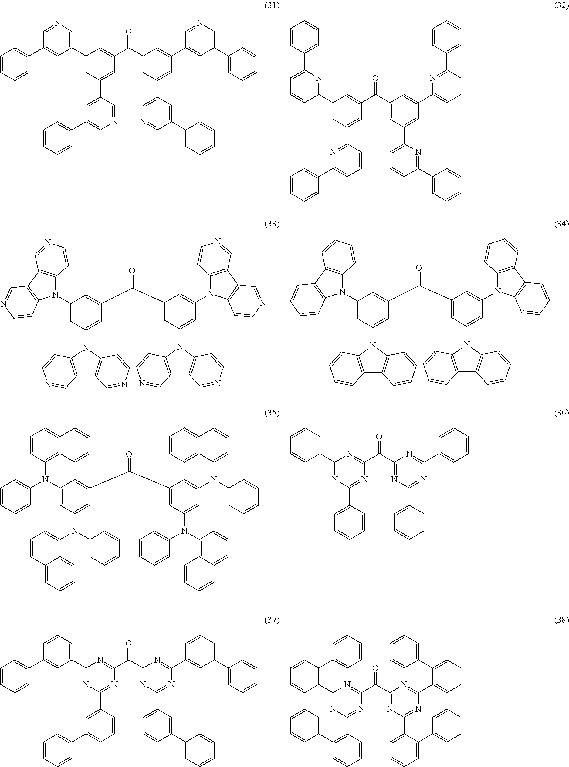


where R1 has the meaning indicated above, and the following applies to the other symbols used:
-
- Ar2 is, identically or differently on each occurrence, a monovalent aromatic or heteroaromatic ring system having 5 to 60 aromatic ring atoms, which may in each case be substituted by one or more radicals R1;
- Ar3 is a divalent aromatic or heteroaromatic ring system having 5 to 60 aromatic ring atoms, which may be substituted by one or more radicals R1.

where R1 has the same meaning as described above, the dashed bond represents the link to the triazine unit, and furthermore:
-
- X is, identically or differently on each occurrence, a divalent bridge selected from B(R1), C(R1)2, Si(R1)2, C═O, C═NR1, C═C(R1)2, O, S, S═O, SO2, N(R1), P(R1) and P(═O)R1;
- m is on each occurrence, identically or differently, 0, 1, 2 or 3;
- o is on each occurrence, identically or differently, 0, 1, 2, 3 or 4.

where the symbols and indices used have the same meaning as described above. X here is preferably selected, identically or differently, from C(R1)2, N(R1), O and S, particularly preferably C(R1)2.

where the symbols and indices used have the same meaning as described above, and the dashed bond represents the link to the two triazine units.

where the symbols and indices used have the same meaning as described above. X here is preferably selected, identically or differently, from C(R1)2, N(R1), O and S, particularly preferably C(R1)2.

where Ar, R1 and n have the meanings indicated above, and the other symbols used have the following meanings:
-
- Ar4 is on each occurrence, identically or differently, an aromatic ring system having 6 to 60 aromatic C atoms, which does not contain any non-aromatic groups other than carbon or hydrogen; Ar4 here may be substituted by one or more radicals R4;
- R3 is on each occurrence, identically or differently, a straight-chain alkyl group having 1 to 20 C atoms or a branched or cyclic alkyl group having 3 to 20 C atoms, or an aromatic ring system having 6 to 60 aromatic C atoms, which does not contain any non-aromatic groups other than carbon and hydrogen and which may be substituted by one or more radicals R4; two or more radicals R3 here may also form a ring system with one another;
- R4 is on each occurrence, identically or differently, a straight-chain alkyl group having 1 to 20 C atoms or a branched or cyclic alkyl group having 3 to 20 C atoms; two or more radicals R4 here may also form a ring system with one another;
- q is 1, 2, 3 or 4.


where R1 has the same meaning as described above for formula (1), and the following applies to the other symbols used:
-
- DCy is, identically or differently on each occurrence, a cyclic group which contains at least one donor atom, preferably nitrogen, carbon in the form of a carbene or phosphorus, via which the cyclic group is bonded to the metal, and which may in turn carry one or more substituents R1; the groups DCy and CCy are bonded to one another via a covalent bond;
- CCy is, identically or differently on each occurrence, a cyclic group which contains a carbon atom via which the cyclic group is bonded to the metal and which may in turn carry one or more substituents R1;
- A is, identically or differently on each occurrence, a monoanionic, bidentate chelating ligand, preferably a diketonate ligand.
 |
(1) |
 |
(2) |
 |
(3) |
 |
(4) |
 |
(5) |
 |
(6) |
 |
(7) |
 |
(8) |
 |
(9) |
 |
(10) |
 |
(11) |
 |
(12) |
 |
(13) |
 |
(14) |
 |
(15) |
 |
(16) |
 |
(17) |
 |
(18) |
 |
(19) |
 |
(20) |
 |
(21) |
 |
(22) |
 |
(23) |
 |
(24) |
 |
(25) |
 |
(26) |
 |
(27) |
 |
(28) |
 |
(29) |
 |
(30) |
 |
(31) |
 |
(32) |
 |
(33) |
 |
(34) |
 |
(35) |
 |
(36) |
 |
(37) |
 |
(38) |
 |
(39) |
 |
(40) |
 |
(41) |
 |
(42) |
 |
(43) |
 |
(44) |
 |
(45) |
 |
(46) |
 |
(47) |
 |
(48) |
 |
(49) |
 |
(50) |
 |
(51) |
 |
(52) |
 |
(53) |
 |
(54) |
 |
(55) |
 |
(56) |
 |
(57) |
 |
(58) |
 |
(59) |
 |
(60) |
 |
(61) |
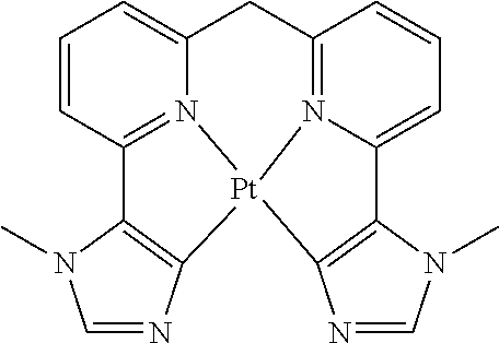 |
(62) |
 |
(63) |
 |
(64) |
 |
(65) |
 |
(66) |
 |
(67) |
 |
(68) |
 |
(69) |
 |
(70) |
 |
(71) |
 |
(72) |
 |
(73) |
 |
(74) |
 |
(75) |
 |
(76) |
 |
(77) |
 |
(78) |
 |
(79) |
 |
(80) |
 |
(81) |
 |
(82) |
 |
(83) |
 |
(84) |
 |
(85) |
 |
(86) |
 |
(87) |
 |
(88) |
 |
(89) |
 |
(90) |
 |
(91) |
 |
(92) |
 |
(93) |
 |
(94) |
 |
(95) |
 |
(96) |
 |
(97) |
 |
(98) |
 |
(99) |
 |
(100) |
 |
(101) |
 |
(102) |
 |
(103) |
 |
(104) |
 |
(105) |
 |
(106) |
 |
(107) |
 |
(108) |
 |
(109) |
 |
(110) |
 |
(111) |
 |
(112) |
 |
(113) |
 |
(114) |
 |
(115) |
 |
(116) |
 |
(117) |
 |
(118) |
 |
(119) |
 |
(120) |
 |
(121) |
 |
(122) |
 |
(123) |
 |
(124) |
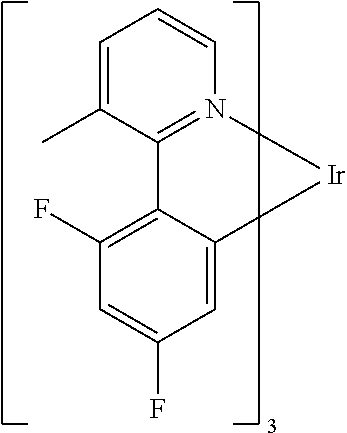 |
(125) |
 |
(126) |
 |
(127) |
 |
(128) |
 |
(129) |
 |
(130) |
 |
(131) |
 |
(132) |
 |
(133) |
 |
(134) |
 |
(135) |
 |
(136) |
 |
(137) |
 |
(138) |
 |
(139) |
 |
(140) |
 |
 |
 |
 |
 |
 |
 |
 |
 |
 |
 |
 |
 |
 |
 |
 |
 |
 |
 |
 |
 |
 |
 |
-
- 1. The organic electroluminescent device according to the invention has very high efficiency. The efficiency here is better than on use of an electron-transporting matrix material in combination with a hole-transporting matrix material.
- 2. The organic electroluminescent device according to the invention at the same time has an improved lifetime. The lifetime here is longer than on use of an electron-transporting matrix material in combination with a hole-transporting matrix material.


| TABLE 1 | |||||||
| Material | HOMO | LUMO | Energy gap | ||||
| TMM1 | −6.3 | eV | −2.75 | eV | 3.55 | eV | ||
| TMM2 | −6.1 | eV | −2.8 | eV | 3.3 | eV | ||
| TMM3 | −5.8 | eV | −1.8 | eV | 4.0 | eV | ||
| TMM4 | −6.15 | eV | −2.0 | eV | 4.15 | eV | ||
| TMM5 | −6.2 | eV | −2.2 | eV | 4.0 | eV | ||
| TMM6 | −6.15 | eV | −2.25 | eV | 3.9 | eV | ||
| TMM7 | −6.0 | eV | −2.5 | eV | 3.5 | eV | ||
| CBP | −5.40 | eV | −2.0 | eV | 3.4 | eV | ||
| TCTA | −5.30 | eV | −2.2 | eV | 3.1 | eV | ||
| TABLE 2 |
| Device results |
| CIE x/y at | Efficiency | Voltage | Lifetime | |||
| 1000 | at 1000 | at 1000 | 50% at | |||
| Ex. | Host material(s) | Dopant | cd/m2 | cd/m2 | cd/m2 | 4000 cd/m2 |
| 1a | TMM1:TMM4 (2:1) | TEG-1 10% | 0.36/0.61 | 46 cd/A | 4.0 V | 2900 |
| 1b | TMM1:TMM4 (1:2) | TEG-1 10% | 0.36/0.61 | 45 cd/A | 4.3 V | 3100 |
| 2 | TMM1:TMM3 (2:1) | TEG-1 10% | 0.36/0.61 | 47 cd/A | 4.1 V | 2700 |
| 3 | TMM1:TMM5 (2:1) | TEG-1 10% | 0.36/0.61 | 45 cd/A | 4.1 V | 2300 |
| 4 | TMM1 | TEG-1 10% | 0.37/0.60 | 42 cd/A | 3.8 V | 2000 |
| (comp.) | ||||||
| 5 | TMM4 | TEG-1 10% | 0.34/0.59 | 12 cd/A | 8.7 V | 140 |
| (comp.) | ||||||
| 6a | TMM1:CBP (2:1) | TEG-1 10% | 0.36/0.61 | 44 cd/A | 4.1 V | 2000 |
| (comp.) | ||||||
| 6b | TMM1:TCTA (2:1) | TEG-1 10% | 0.35/0.60 | 42 cd/A | 3.9 V | 1100 |
| (comp.) | ||||||
| 7a | TMM7:TMM4 (2:1) | TEG-1 10% | 0.37/0.60 | 47 cd/A | 3.9 V | 2200 |
| 7b | TMM7:TMM4 (1:2) | TEG-1 10% | 0.36/0.61 | 45 cd/A | 4.2 V | 2200 |
| 8 | TMM7 | TEG-1 10% | 0.38/0.60 | 41 cd/A | 3.9 V | 1200 |
| (comp.) | ||||||
| 9 | TMM2:TMM4 (1:1) | TEG-1 10% | 0.36/0.60 | 48 cd/A | 4.9 V | 3000 |
| 10 | TMM2 | TEG-1 10% | 0.37/0.60 | 45 cd/A | 4.9 V | 2000 |
| (comp.) | ||||||
| TABLE 3 |
| Device results |
| Lifetime | ||||||
| CIE x/y | Efficiency | Voltage | 50% at | |||
| at 1000 | at 1000 | at 1000 | 1000 | |||
| Ex. | Host material(s) | Dopant | cd/m2 | cd/m2 | cd/m2 | cd/m2 |
| 11 | TMM1 | TEG-2 16.7% | 0.35/0.61 | 24 cd/A | 6.4 V | 2700 |
| (comp.) | ||||||
| 12 | TMM1:TMM5 (1:1) | TEG-2 16.7% | 0.33/0.63 | 32 cd/A | 6.4 V | 6600 |
| 13 | TMM2 | TEG-2 16.7% | 0.36/0.61 | 11 cd/A | 5.7 V | 9400 |
| (comp.) | ||||||
| 14 | TMM2:TMM4 (1:1) | TEG-2 16.7% | 0.32/0.62 | 20 cd/A | 4.6 V | 13000 |
| 15 | TMM2:TMM6 (1:1) | TEG-2 16.7% | 0.33/0.63 | 26 cd/A | 4.7 V | 20500 |
Claims (17)


Applications Claiming Priority (4)
| Application Number | Priority Date | Filing Date | Title |
|---|---|---|---|
| DE102009014513A DE102009014513A1 (en) | 2009-03-23 | 2009-03-23 | Organic electroluminescent device |
| DE102009014513 | 2009-03-23 | ||
| DE102009014513.3 | 2009-03-23 | ||
| PCT/EP2010/001123 WO2010108579A1 (en) | 2009-03-23 | 2010-02-24 | Organic electroluminescent device |
Publications (2)
| Publication Number | Publication Date |
|---|---|
| US20120056169A1 US20120056169A1 (en) | 2012-03-08 |
| US9444064B2 true US9444064B2 (en) | 2016-09-13 |
Family
ID=42170826
Family Applications (1)
| Application Number | Title | Priority Date | Filing Date |
|---|---|---|---|
| US13/258,214 Active 2033-08-13 US9444064B2 (en) | 2009-03-23 | 2010-02-24 | Organic electroluminescent device |
Country Status (7)
| Country | Link |
|---|---|
| US (1) | US9444064B2 (en) |
| JP (1) | JP5670418B2 (en) |
| KR (1) | KR101704837B1 (en) |
| CN (1) | CN102362367B (en) |
| DE (2) | DE102009014513A1 (en) |
| TW (1) | TWI510596B (en) |
| WO (1) | WO2010108579A1 (en) |
Cited By (14)
| Publication number | Priority date | Publication date | Assignee | Title |
|---|---|---|---|---|
| US20120168735A1 (en) * | 2009-09-16 | 2012-07-05 | Merck Patent Gmbh | Organic electroluminescent device |
| US10847727B2 (en) | 2014-06-18 | 2020-11-24 | Merck Patent Gmbh | Compositions for electronic devices |
| US10978661B2 (en) | 2011-03-23 | 2021-04-13 | Semiconductor Energy Laboratory Co., Ltd. | Light-emitting element |
| US11038135B2 (en) | 2011-02-16 | 2021-06-15 | Semiconductor Energy Laboratory Co., Ltd. | Light-emitting element |
| US11107994B2 (en) | 2014-06-18 | 2021-08-31 | Merck Patent Gmbh | Materials for organic electroluminescent devices |
| US11581487B2 (en) | 2017-04-26 | 2023-02-14 | Oti Lumionics Inc. | Patterned conductive coating for surface of an opto-electronic device |
| US11700747B2 (en) | 2019-06-26 | 2023-07-11 | Oti Lumionics Inc. | Optoelectronic device including light transmissive regions, with light diffraction characteristics |
| US11706969B2 (en) | 2015-10-26 | 2023-07-18 | Oti Lumionics Inc. | Method for patterning a coating on a surface and device including a patterned coating |
| US11730048B2 (en) | 2017-05-17 | 2023-08-15 | OTI Lumionic Inc. | Method for selectively depositing a conductive coating over a patterning coating and device including a conductive coating |
| US11730012B2 (en) | 2019-03-07 | 2023-08-15 | Oti Lumionics Inc. | Materials for forming a nucleation-inhibiting coating and devices incorporating same |
| US11744101B2 (en) | 2019-08-09 | 2023-08-29 | Oti Lumionics Inc. | Opto-electronic device including an auxiliary electrode and a partition |
| US11751415B2 (en) | 2018-02-02 | 2023-09-05 | Oti Lumionics Inc. | Materials for forming a nucleation-inhibiting coating and devices incorporating same |
| US11778907B2 (en) | 2017-04-13 | 2023-10-03 | Merck Patent Gmbh | Composition for organic electronic devices |
| US11832473B2 (en) | 2019-06-26 | 2023-11-28 | Oti Lumionics Inc. | Optoelectronic device including light transmissive regions, with light diffraction characteristics |
Families Citing this family (292)
| Publication number | Priority date | Publication date | Assignee | Title |
|---|---|---|---|---|
| DE102009041414A1 (en) | 2009-09-16 | 2011-03-17 | Merck Patent Gmbh | metal complexes |
| DE102009057167A1 (en) | 2009-12-05 | 2011-06-09 | Merck Patent Gmbh | Electronic device containing metal complexes |
| EP2517274B1 (en) * | 2009-12-23 | 2017-05-24 | Merck Patent GmbH | Compositions comprising polymeric binders |
| TW201144406A (en) | 2010-01-15 | 2011-12-16 | Idemitsu Kosan Co | Organic electroluminescent element |
| DE102010004803A1 (en) | 2010-01-16 | 2011-07-21 | Merck Patent GmbH, 64293 | Materials for organic electroluminescent devices |
| DE102010005697A1 (en) | 2010-01-25 | 2011-07-28 | Merck Patent GmbH, 64293 | Connections for electronic devices |
| DE102010009903A1 (en) | 2010-03-02 | 2011-09-08 | Merck Patent Gmbh | Connections for electronic devices |
| DE102010010481A1 (en) | 2010-03-06 | 2011-09-08 | Merck Patent Gmbh | Organic electroluminescent device |
| DE102010014933A1 (en) | 2010-04-14 | 2011-10-20 | Merck Patent Gmbh | Materials for electronic devices |
| DE102010020567A1 (en) | 2010-05-14 | 2011-11-17 | Merck Patent Gmbh | metal complexes |
| CN102939296B (en) | 2010-06-15 | 2016-02-10 | 默克专利有限公司 | Metal complex |
| DE102010024335A1 (en) | 2010-06-18 | 2011-12-22 | Merck Patent Gmbh | Connections for electronic devices |
| DE102010024542A1 (en) | 2010-06-22 | 2011-12-22 | Merck Patent Gmbh | Materials for electronic devices |
| DE102010024897A1 (en) | 2010-06-24 | 2011-12-29 | Merck Patent Gmbh | Materials for organic electroluminescent devices |
| DE102010027218A1 (en) | 2010-07-15 | 2012-01-19 | Merck Patent Gmbh | Organic complexes containing metals |
| DE102010027316A1 (en) | 2010-07-16 | 2012-01-19 | Merck Patent Gmbh | metal complexes |
| DE102010027319A1 (en) | 2010-07-16 | 2012-01-19 | Merck Patent Gmbh | metal complexes |
| DE102010027317A1 (en) | 2010-07-16 | 2012-01-19 | Merck Patent Gmbh | metal complexes |
| DE102010045405A1 (en) | 2010-09-15 | 2012-03-15 | Merck Patent Gmbh | Materials for organic electroluminescent devices |
| DE102010046512A1 (en) | 2010-09-24 | 2012-03-29 | Merck Patent Gmbh | Phosphorus-containing metal complexes |
| KR20140000693A (en) * | 2010-10-11 | 2014-01-03 | 솔베이(소시에떼아노님) | Novel spirobifluorene compounds |
| DE102010048498A1 (en) * | 2010-10-14 | 2012-04-19 | Merck Patent Gmbh | Materials for organic electroluminescent devices |
| DE102010048497A1 (en) * | 2010-10-14 | 2012-04-19 | Merck Patent Gmbh | Formulations for organic electroluminescent devices |
| JP2014504452A (en) * | 2010-12-08 | 2014-02-20 | ジョージア・テック・リサーチ・コーポレーション | Bis (sulfonyl) biaryl derivatives as electron transport and / or host materials |
| DE102011106849A1 (en) | 2010-12-15 | 2012-06-21 | Merck Patent Gmbh | Process for the synthesis of N-N linked and around the N-N bond of rotation-inhibited bis-N-heterocyclic carbenes and their use as ligands for metal complexes |
| DE102011011539A1 (en) | 2011-02-17 | 2012-08-23 | Merck Patent Gmbh | Connections for electronic devices |
| US9469667B2 (en) | 2011-04-04 | 2016-10-18 | Merck Patent Gmbh | Metal complexes |
| US9385335B2 (en) | 2011-04-05 | 2016-07-05 | Merck Patent Gmbh | Organic electroluminescent device |
| WO2012139693A1 (en) | 2011-04-13 | 2012-10-18 | Merck Patent Gmbh | Compounds for electronic devices |
| US9876171B2 (en) | 2011-04-13 | 2018-01-23 | Merck Patent Gmbh | Materials for electronic devices |
| EP2699641B1 (en) | 2011-04-18 | 2017-05-17 | Merck Patent GmbH | Compounds for electronic devices |
| WO2012149992A1 (en) | 2011-05-04 | 2012-11-08 | Merck Patent Gmbh | Device for preserving fresh goods |
| JP6195823B2 (en) | 2011-05-05 | 2017-09-13 | メルク パテント ゲーエムベーハー | Compounds for electronic devices |
| WO2012150001A1 (en) | 2011-05-05 | 2012-11-08 | Merck Patent Gmbh | Compounds for electronic devices |
| WO2012166101A1 (en) | 2011-05-27 | 2012-12-06 | Universal Display Corporation | Oled having multi-component emissivie layer |
| US10103340B2 (en) | 2011-06-03 | 2018-10-16 | Merck Patent Gmbh | Metal complexes |
| US9673402B2 (en) | 2011-06-28 | 2017-06-06 | Merck Patent Gmbh | Platinum metal complexes with divalent groups bridging two ligands |
| CN107814820B (en) | 2011-07-29 | 2020-08-11 | 默克专利有限公司 | Compounds for electronic devices |
| WO2013020631A1 (en) | 2011-08-10 | 2013-02-14 | Merck Patent Gmbh | Metal complexes |
| DE102012016192A1 (en) | 2011-08-19 | 2013-02-21 | Merck Patent Gmbh | New compounds capable of forming hydrogen bonds are useful in electronic device, e.g. organic electroluminescent device, organic light-emitting transistor and organic light-emitting electrochemical cell |
| EP2748878B1 (en) | 2011-08-22 | 2020-04-01 | Merck Patent GmbH | Organic electroluminescence device |
| KR102045197B1 (en) | 2011-10-27 | 2019-11-18 | 메르크 파텐트 게엠베하 | Materials for electronic devices |
| KR102088150B1 (en) * | 2011-12-22 | 2020-03-12 | 메르크 파텐트 게엠베하 | Compounds for organic electroluminescent devices |
| WO2013097920A1 (en) | 2011-12-27 | 2013-07-04 | Merck Patent Gmbh | Metal complexes comprising 1,2,3-triazoles |
| CN106986858B (en) | 2012-01-16 | 2019-08-27 | 默克专利有限公司 | Metal-organic complex |
| KR20220005650A (en) | 2012-02-14 | 2022-01-13 | 메르크 파텐트 게엠베하 | Spirobifluorene compounds for organic electroluminescent devices |
| KR101358784B1 (en) * | 2012-02-14 | 2014-02-10 | 삼성디스플레이 주식회사 | Organic light-emitting device having improved efficiency characterisitics and organic light-emitting display apparatus including the same |
| KR102082111B1 (en) | 2012-05-24 | 2020-02-27 | 메르크 파텐트 게엠베하 | Metal complexes comprising condensed heteroaromatic rings |
| DE102012011335A1 (en) | 2012-06-06 | 2013-12-12 | Merck Patent Gmbh | Connections for Organic Electronic Devices |
| WO2014006913A1 (en) * | 2012-07-06 | 2014-01-09 | 出光興産株式会社 | Benzodiazaborole compound, and material for organic electroluminescent element and organic electroluminescent element each utilizing same |
| CN104428392B (en) | 2012-07-13 | 2017-05-31 | 默克专利有限公司 | Metal complex |
| US9768391B2 (en) | 2012-07-23 | 2017-09-19 | Merck Patent Gmbh | Derivatives of 2-diarylaminofluorene and organic electronic compounds containing them |
| JP6382193B2 (en) | 2012-07-23 | 2018-08-29 | メルク パテント ゲーエムベーハー | Compound and organic electroluminescence element |
| EP2875004B1 (en) | 2012-07-23 | 2018-07-18 | Merck Patent GmbH | Fluorenes and electronic devices containing them |
| EP2882763B1 (en) | 2012-08-07 | 2018-08-22 | Merck Patent GmbH | Metal complexes |
| KR102015270B1 (en) | 2012-08-10 | 2019-08-28 | 메르크 파텐트 게엠베하 | Materials for organic electroluminescence devices |
| DE112013004610A5 (en) | 2012-09-20 | 2015-06-03 | Merck Patent Gmbh | metal complexes |
| DE102012020167A1 (en) | 2012-10-13 | 2014-04-17 | Eberhard Karls Universität Tübingen | metal complexes |
| EP2915199B1 (en) | 2012-10-31 | 2021-03-31 | Merck Patent GmbH | Electronic device |
| DE102012021650A1 (en) | 2012-11-03 | 2014-05-08 | Eberhard Karls Universität Tübingen | metal complexes |
| US9978949B2 (en) | 2012-11-12 | 2018-05-22 | Merck Patent Gmbh | Materials for electronic devices |
| US9695354B2 (en) | 2012-11-20 | 2017-07-04 | Merck Patent Gmbh | Formulation in high-purity solvent for producing electronic devices |
| US10065959B2 (en) | 2012-11-30 | 2018-09-04 | Merck Patent Gmbh | Electronic device |
| US8766531B1 (en) * | 2012-12-14 | 2014-07-01 | Universal Display Corporation | Wearable display |
| US20150340621A1 (en) * | 2012-12-18 | 2015-11-26 | Merck Patent Gmbh | Organic electroluminescent device |
| WO2014106521A1 (en) * | 2013-01-03 | 2014-07-10 | Merck Patent Gmbh | Electronic device |
| US20150340627A1 (en) | 2013-01-03 | 2015-11-26 | Merck Patent Gmbh | Materials for electronic devices |
| JP6367229B2 (en) | 2013-01-03 | 2018-08-01 | メルク パテント ゲーエムベーハー | Compounds for electronic devices |
| DE102013008189A1 (en) | 2013-05-14 | 2014-12-04 | Eberhard Karls Universität Tübingen | metal complexes |
| CN105408449B (en) | 2013-07-30 | 2018-06-29 | 默克专利有限公司 | For the material of electronic device |
| WO2015014434A1 (en) | 2013-07-30 | 2015-02-05 | Merck Patent Gmbh | Materials for electronic devices |
| DE102013013876A1 (en) | 2013-08-20 | 2015-03-12 | Merck Patent Gmbh | metal complexes |
| CN105531347B (en) | 2013-09-11 | 2018-09-11 | 默克专利有限公司 | Metal complex |
| CN111848659A (en) | 2013-10-02 | 2020-10-30 | 默克专利有限公司 | Boron-containing compounds for use in OLEDs |
| US9390649B2 (en) | 2013-11-27 | 2016-07-12 | Universal Display Corporation | Ruggedized wearable display |
| US10374170B2 (en) | 2013-12-06 | 2019-08-06 | Merck Patent Gmbh | Substituted oxepines |
| KR20240005971A (en) | 2013-12-06 | 2024-01-12 | 메르크 파텐트 게엠베하 | Compounds and organic electronic devices |
| KR101993129B1 (en) | 2013-12-12 | 2019-06-26 | 메르크 파텐트 게엠베하 | Materials for electronic devices |
| JP6542228B2 (en) | 2013-12-19 | 2019-07-10 | メルク、パテント、ゲゼルシャフト、ミット、ベシュレンクテル、ハフツングMerck Patent GmbH | Heterocyclic spiro compounds |
| EP3137458B1 (en) | 2014-04-30 | 2019-04-24 | Merck Patent GmbH | Materials for electronic devices |
| DE102015006708A1 (en) | 2014-06-12 | 2015-12-17 | Merck Patent Gmbh | metal complexes |
| WO2015197156A1 (en) | 2014-06-25 | 2015-12-30 | Merck Patent Gmbh | Materials for organic electroluminescent devices |
| US10903430B2 (en) | 2014-07-21 | 2021-01-26 | Merck Patent Gmbh | Materials for electronic devices |
| DE102014012818A1 (en) | 2014-08-28 | 2016-03-03 | Eberhard Karls Universität Tübingen | metal complexes |
| WO2016034262A1 (en) | 2014-09-05 | 2016-03-10 | Merck Patent Gmbh | Formulations and electronic devices |
| EP3221294B1 (en) * | 2014-11-21 | 2018-09-05 | Merck Patent GmbH | Heterocyclic compounds for use in electronic devices |
| EP3241248A1 (en) | 2014-12-30 | 2017-11-08 | Merck Patent GmbH | Formulations and electronic devices |
| WO2016119992A1 (en) | 2015-01-30 | 2016-08-04 | Merck Patent Gmbh | Materials for electronic devices |
| KR102554987B1 (en) | 2015-02-03 | 2023-07-12 | 메르크 파텐트 게엠베하 | Metal complexes |
| JP6800879B2 (en) | 2015-03-30 | 2020-12-16 | メルク パテント ゲーエムベーハー | Formulations of organic functional materials containing siloxane solvents |
| US11208401B2 (en) | 2015-06-10 | 2021-12-28 | Merck Patent Gmbh | Materials for organic electroluminescent devices |
| EP3307846B1 (en) | 2015-06-12 | 2019-08-14 | Merck Patent GmbH | Esters containing non-aromatic cycles as solvents for oled formulations |
| CN107924999B (en) | 2015-07-22 | 2022-04-19 | 默克专利有限公司 | Material for organic electroluminescent device |
| JP6983754B2 (en) | 2015-07-29 | 2021-12-17 | メルク パテント ゲーエムベーハー | Materials for organic electroluminescence devices |
| JP6839697B2 (en) | 2015-07-30 | 2021-03-10 | メルク、パテント、ゲゼルシャフト、ミット、ベシュレンクテル、ハフツングMerck Patent GmbH | Materials for electronic devices |
| KR102599157B1 (en) | 2015-08-14 | 2023-11-06 | 메르크 파텐트 게엠베하 | Phenoxazine derivatives for organic electroluminescent devices |
| JP2018527733A (en) | 2015-08-28 | 2018-09-20 | メルク パテント ゲーエムベーハー | Formulation of organic functional material containing epoxy group-containing solvent |
| DE102015013381A1 (en) | 2015-10-14 | 2017-04-20 | Eberhard Karls Universität Tübingen | metal complexes |
| JP6974315B2 (en) | 2015-10-27 | 2021-12-01 | メルク パテント ゲーエムベーハー | Materials for organic electroluminescence devices |
| WO2017097391A1 (en) | 2015-12-10 | 2017-06-15 | Merck Patent Gmbh | Formulations containing ketones comprising non-aromatic cycles |
| DE102015016016A1 (en) | 2015-12-10 | 2017-06-14 | Eberhard Karls Universität Tübingen | metal complexes |
| CN108369997B (en) | 2015-12-15 | 2020-03-24 | 默克专利有限公司 | Aromatic group-containing esters as solvents for organic electronic formulations |
| JP7438661B2 (en) | 2015-12-16 | 2024-02-27 | メルク パテント ゲーエムベーハー | Formulations containing solid solvents |
| US11407916B2 (en) | 2015-12-16 | 2022-08-09 | Merck Patent Gmbh | Formulations containing a mixture of at least two different solvents |
| US20190040034A1 (en) | 2016-02-05 | 2019-02-07 | Merck Patent Gmbh | Materials for electronic devices |
| EP3417033B1 (en) | 2016-02-17 | 2021-02-24 | Merck Patent GmbH | Formulation of an organic functional material |
| DE102016003104A1 (en) | 2016-03-15 | 2017-09-21 | Merck Patent Gmbh | Container comprising a formulation containing at least one organic semiconductor |
| TWI821807B (en) | 2016-03-17 | 2023-11-11 | 德商麥克專利有限公司 | Compounds having spirobifluorene structures |
| TW202340153A (en) | 2016-04-11 | 2023-10-16 | 德商麥克專利有限公司 | Heterocyclic compounds having dibenzofuran and/or dibenzothiophene structures |
| TWI731981B (en) | 2016-06-03 | 2021-07-01 | 德商麥克專利有限公司 | Materials for organic electroluminescent devices |
| JP2019523997A (en) | 2016-06-16 | 2019-08-29 | メルク パテント ゲーエムベーハー | Formulation of organic functional materials |
| EP3472249B1 (en) | 2016-06-17 | 2022-02-02 | Merck Patent GmbH | Formulation of an organic functional material |
| TW201815998A (en) | 2016-06-28 | 2018-05-01 | 德商麥克專利有限公司 | Formulation of an organic functional material |
| JP7034954B2 (en) | 2016-06-30 | 2022-03-14 | メルク パテント ゲゼルシャフト ミット ベシュレンクテル ハフツング | How to separate the enantiomeric mixture |
| CN109415344B (en) | 2016-07-14 | 2022-06-03 | 默克专利有限公司 | Metal complexes |
| JP7030780B2 (en) | 2016-07-25 | 2022-03-07 | メルク パテント ゲゼルシャフト ミット ベシュレンクテル ハフツング | Binuclear and oligonucleus metal complexes, including tripod-type bidentate subligands, and their use in electronic devices |
| CN116987124A (en) | 2016-07-25 | 2023-11-03 | 默克专利有限公司 | Metal complexes as luminophores in organic electroluminescent devices |
| CN109563402B (en) | 2016-08-04 | 2022-07-15 | 默克专利有限公司 | Preparation of organic functional materials |
| WO2018041769A1 (en) | 2016-08-30 | 2018-03-08 | Merck Patent Gmbh | Binuclear and trinuclear metal complexes composed of two inter-linked tripodal hexadentate ligands for use in electroluminescent devices |
| JP2019530676A (en) | 2016-09-14 | 2019-10-24 | メルク パテント ゲーエムベーハー | Compound having carbazole structure |
| US11447464B2 (en) | 2016-09-14 | 2022-09-20 | Merck Patent Gmbh | Compounds with spirobifluorene-structures |
| CN109715642A (en) | 2016-09-21 | 2019-05-03 | 默克专利有限公司 | PROCESS FOR PRODUCTION OF BINUCLEAR as the illuminator in organic electroluminescence device |
| TWI766884B (en) | 2016-09-30 | 2022-06-11 | 德商麥克專利有限公司 | Compounds having diazadibenzofuran or diazadibenzothiophene structures, process for preparing the same and use thereof |
| CN109790173B (en) | 2016-09-30 | 2022-09-06 | 默克专利有限公司 | Carbazoles having diaza-dibenzofuran or diaza-dibenzothiophene structure |
| WO2018069197A1 (en) | 2016-10-12 | 2018-04-19 | Merck Patent Gmbh | Metal complexes |
| JP7064488B2 (en) | 2016-10-12 | 2022-05-10 | メルク パテント ゲゼルシャフト ミット ベシュレンクテル ハフツング | Dikaryon metal complexes and electronic devices, in particular organic electroluminescence devices comprising said metal complexes. |
| JP7023946B2 (en) | 2016-10-13 | 2022-02-22 | メルク パテント ゲゼルシャフト ミット ベシュレンクテル ハフツング | Metal complex |
| DE102017008794A1 (en) | 2016-10-17 | 2018-04-19 | Merck Patent Gmbh | Materials for use in electronic devices |
| WO2018077769A1 (en) | 2016-10-25 | 2018-05-03 | Merck Patent Gmbh | Metal complexes |
| CN109863223B (en) | 2016-10-31 | 2023-06-20 | 默克专利有限公司 | Preparation of organic functional material |
| KR102436600B1 (en) | 2016-10-31 | 2022-08-25 | 메르크 파텐트 게엠베하 | Formulation of organic functional materials |
| US11302870B2 (en) | 2016-11-02 | 2022-04-12 | Merck Patent Gmbh | Materials for electronic devices |
| TWI756292B (en) | 2016-11-14 | 2022-03-01 | 德商麥克專利有限公司 | Compounds having an acceptor group and a donor group |
| TW201833118A (en) | 2016-11-22 | 2018-09-16 | 德商麥克專利有限公司 | Materials for electronic devices |
| CN109963857A (en) | 2016-11-25 | 2019-07-02 | 默克专利有限公司 | 2,8- diamino indeno [1,2-B] fluorene derivative and related compound condensed as double benzofurans of the material for organic electroluminescence device (OLED) |
| WO2018095940A1 (en) | 2016-11-25 | 2018-05-31 | Merck Patent Gmbh | Bisbenzofuran-fused indeno[1,2-b]fluorene derivatives and related compounds as materials for organic electroluminescent devices (oled) |
| EP3548467B1 (en) | 2016-11-30 | 2023-06-21 | Merck Patent GmbH | Compounds having valerolactam structures |
| US11466021B2 (en) | 2016-12-05 | 2022-10-11 | Merck Patent Gmbh | Materials for organic electroluminescent devices |
| TW201831468A (en) | 2016-12-05 | 2018-09-01 | 德商麥克專利有限公司 | Nitrogen-containing heterocycles |
| EP3548485B1 (en) | 2016-12-05 | 2021-01-20 | Merck Patent GmbH | Materials for organic electroluminescent devices |
| KR102472751B1 (en) | 2016-12-06 | 2022-11-30 | 메르크 파텐트 게엠베하 | Manufacturing method of electronic device |
| KR102486614B1 (en) | 2016-12-13 | 2023-01-09 | 메르크 파텐트 게엠베하 | Formulation of organic functional materials |
| WO2018114883A1 (en) | 2016-12-22 | 2018-06-28 | Merck Patent Gmbh | Mixtures comprising at least two organofunctional compounds |
| WO2018127465A1 (en) | 2017-01-04 | 2018-07-12 | Merck Patent Gmbh | Materials for organic electroluminescent devices |
| KR102594781B1 (en) | 2017-01-23 | 2023-10-26 | 메르크 파텐트 게엠베하 | Materials for organic electroluminescent devices |
| EP3573973B1 (en) | 2017-01-25 | 2023-12-06 | Merck Patent GmbH | Carbazole derivatives |
| TWI763772B (en) | 2017-01-30 | 2022-05-11 | 德商麥克專利有限公司 | Method for forming an organic element of an electronic device |
| TWI791481B (en) | 2017-01-30 | 2023-02-11 | 德商麥克專利有限公司 | Method for forming an organic electroluminescence (el) element |
| US11407766B2 (en) | 2017-01-30 | 2022-08-09 | Merck Patent Gmbh | Materials for organic electroluminescent devices |
| CN110291064B (en) | 2017-02-02 | 2023-04-28 | 默克专利有限公司 | Material for electronic devices |
| TW201835075A (en) | 2017-02-14 | 2018-10-01 | 德商麥克專利有限公司 | Materials for organic electroluminescent devices |
| CN117440703A (en) | 2017-03-01 | 2024-01-23 | 默克专利有限公司 | Organic electroluminescent device |
| US20200055822A1 (en) | 2017-03-02 | 2020-02-20 | Merck Patent Gmbh | Materials for organic electronic devices |
| TW201843143A (en) | 2017-03-13 | 2018-12-16 | 德商麥克專利有限公司 | Compounds containing arylamine structures |
| CN110446703A (en) | 2017-03-29 | 2019-11-12 | 默克专利有限公司 | Aromatic compounds |
| JP7123967B2 (en) | 2017-03-31 | 2022-08-23 | メルク パテント ゲーエムベーハー | Printing method for organic light emitting diodes (OLEDs) |
| JP7200128B2 (en) | 2017-04-10 | 2023-01-06 | メルク パテント ゲーエムベーハー | Formulation of organic functional material |
| EP3615542B1 (en) | 2017-04-25 | 2023-08-23 | Merck Patent GmbH | Compounds for electronic devices |
| KR20200003068A (en) | 2017-05-03 | 2020-01-08 | 메르크 파텐트 게엠베하 | Formulations of Organic Functional Materials |
| US11535619B2 (en) | 2017-05-22 | 2022-12-27 | Merck Patent Gmbh | Hexacyclic heteroaromatic compounds for electronic devices |
| KR20200022010A (en) | 2017-06-26 | 2020-03-02 | 메르크 파텐트 게엠베하 | Homogeneous mixture |
| US20200136045A1 (en) | 2017-06-28 | 2020-04-30 | Merck Patent Gmbh | Materials for electronic devices |
| WO2019007866A1 (en) | 2017-07-05 | 2019-01-10 | Merck Patent Gmbh | Composition for organic electronic devices |
| WO2019007867A1 (en) | 2017-07-05 | 2019-01-10 | Merck Patent Gmbh | Composition for organic electronic devices |
| WO2019016184A1 (en) | 2017-07-18 | 2019-01-24 | Merck Patent Gmbh | Formulation of an organic functional material |
| TWI776926B (en) | 2017-07-25 | 2022-09-11 | 德商麥克專利有限公司 | Metal complexes |
| EP3658541A1 (en) | 2017-07-28 | 2020-06-03 | Merck Patent GmbH | Spirobifluorene derivatives for use in electronic devices |
| WO2019048443A1 (en) | 2017-09-08 | 2019-03-14 | Merck Patent Gmbh | Materials for electronic devices |
| CN108675975A (en) | 2017-10-17 | 2018-10-19 | 默克专利有限公司 | Material for organic electroluminescence device |
| EP3700909B1 (en) | 2017-10-24 | 2024-01-24 | Merck Patent GmbH | Materials for organic electroluminescent devices |
| TWI785142B (en) | 2017-11-14 | 2022-12-01 | 德商麥克專利有限公司 | Composition for organic electronic devices |
| EP3714022B1 (en) | 2017-11-23 | 2023-06-07 | Merck Patent GmbH | Materials for electronic devices |
| JP2021504347A (en) | 2017-11-24 | 2021-02-15 | メルク、パテント、ゲゼルシャフト、ミット、ベシュレンクテル、ハフツングMerck Patent GmbH | Materials for OLED devices |
| TWI820057B (en) | 2017-11-24 | 2023-11-01 | 德商麥克專利有限公司 | Materials for organic electroluminescent devices |
| TWI637960B (en) * | 2017-12-01 | 2018-10-11 | Yuan Ze University | Benzodiazaborole derivatives and organic light-emitting diodes using the same |
| CN111406062B (en) | 2017-12-13 | 2024-01-19 | Udc爱尔兰有限公司 | Metal complex |
| KR20200093653A (en) | 2017-12-15 | 2020-08-05 | 메르크 파텐트 게엠베하 | Formulation of organic functional materials |
| EP3724175A1 (en) | 2017-12-15 | 2020-10-21 | Merck Patent GmbH | Substituted aromatic amines for use in organic electroluminescent devices |
| TW201938562A (en) | 2017-12-19 | 2019-10-01 | 德商麥克專利有限公司 | Heterocyclic compounds |
| TWI811290B (en) | 2018-01-25 | 2023-08-11 | 德商麥克專利有限公司 | Materials for organic electroluminescent devices |
| KR20200120698A (en) | 2018-02-13 | 2020-10-21 | 메르크 파텐트 게엠베하 | Metal complex |
| CN111712551A (en) | 2018-02-26 | 2020-09-25 | 默克专利有限公司 | Preparation of organic functional material |
| TWI802656B (en) | 2018-03-06 | 2023-05-21 | 德商麥克專利有限公司 | Materials for organic electroluminescent devices |
| TW201938761A (en) | 2018-03-06 | 2019-10-01 | 德商麥克專利有限公司 | Materials for organic electroluminescent devices |
| TWI828664B (en) | 2018-03-19 | 2024-01-11 | 愛爾蘭商Udc愛爾蘭責任有限公司 | Metal complexes |
| US20220332724A1 (en) | 2018-05-30 | 2022-10-20 | Merck Patent Gmbh | Composition for organic electronic devices |
| CN112219292A (en) | 2018-06-07 | 2021-01-12 | 默克专利有限公司 | Organic electroluminescent device |
| JP7379389B2 (en) | 2018-06-15 | 2023-11-14 | メルク パテント ゲーエムベーハー | Formulations of organic functional materials |
| KR20210031714A (en) | 2018-07-09 | 2021-03-22 | 메르크 파텐트 게엠베하 | Materials for organic electroluminescent devices |
| KR102316066B1 (en) * | 2018-07-27 | 2021-10-21 | 주식회사 엘지화학 | Ink composition, organic light emitting device using the same and method of manufacturing the same |
| WO2020043646A1 (en) | 2018-08-28 | 2020-03-05 | Merck Patent Gmbh | Materials for organic electroluminescent devices |
| TWI823993B (en) | 2018-08-28 | 2023-12-01 | 德商麥克專利有限公司 | Materials for organic electroluminescent devices |
| WO2020043657A1 (en) | 2018-08-28 | 2020-03-05 | Merck Patent Gmbh | Materials for organic electroluminescent devices |
| JP7459065B2 (en) | 2018-09-12 | 2024-04-01 | メルク パテント ゲーエムベーハー | Materials for organic electroluminescent devices |
| KR20210056432A (en) | 2018-09-24 | 2021-05-18 | 메르크 파텐트 게엠베하 | Method of manufacturing granular material |
| WO2020064666A1 (en) | 2018-09-27 | 2020-04-02 | Merck Patent Gmbh | Compounds that can be used in an organic electronic device as active compounds |
| KR20210065972A (en) | 2018-09-27 | 2021-06-04 | 메르크 파텐트 게엠베하 | Method for producing sterically hindered nitrogen-containing heteroaromatic compound |
| CN112930343A (en) | 2018-10-31 | 2021-06-08 | 默克专利有限公司 | Material for organic electroluminescent device |
| US11917906B2 (en) | 2018-11-05 | 2024-02-27 | Merck Patent Gmbh | Compounds that can be used in an organic electronic device |
| CN112867709A (en) | 2018-11-06 | 2021-05-28 | 默克专利有限公司 | 5, 6-diphenyl-5, 6-dihydro-dibenzo [ C, E ] [1,2] azaphosphabenzene and 6-phenyl-6H-dibenzo [ C, E ] [1,2] thiazine-5, 5-dioxide derivatives and analogous compounds as organic electroluminescent materials for OLEDs |
| KR20210083347A (en) | 2018-11-06 | 2021-07-06 | 메르크 파텐트 게엠베하 | Method of Forming Organic Elements of Electronic Devices |
| US20220006018A1 (en) | 2018-11-14 | 2022-01-06 | Merck Patent Gmbh | Compounds that can be used for producing an organic electronic device |
| EP3880682B1 (en) | 2018-11-15 | 2023-06-14 | Merck Patent GmbH | Materials for organic electroluminescent devices |
| TW202039493A (en) | 2018-12-19 | 2020-11-01 | 德商麥克專利有限公司 | Materials for organic electroluminescent devices |
| TW202035345A (en) | 2019-01-17 | 2020-10-01 | 德商麥克專利有限公司 | Materials for organic electroluminescent devices |
| TW202043247A (en) | 2019-02-11 | 2020-12-01 | 德商麥克專利有限公司 | Metal complexes |
| JP2022520284A (en) | 2019-02-18 | 2022-03-29 | メルク パテント ゲーエムベーハー | Compositions for organic electronic devices |
| US20220127286A1 (en) | 2019-03-04 | 2022-04-28 | Merck Patent Gmbh | Ligands for nano-sized materials |
| CN113544132A (en) | 2019-03-12 | 2021-10-22 | 默克专利有限公司 | Material for organic electroluminescent device |
| KR20210141593A (en) | 2019-03-20 | 2021-11-23 | 메르크 파텐트 게엠베하 | Materials for organic electroluminescent devices |
| EP3947372A1 (en) | 2019-03-25 | 2022-02-09 | Merck Patent GmbH | Materials for organic electroluminescent devices |
| KR20210151905A (en) | 2019-04-15 | 2021-12-14 | 메르크 파텐트 게엠베하 | metal complex |
| JP2022546334A (en) | 2019-08-26 | 2022-11-04 | メルク パテント ゲーエムベーハー | Materials for organic electroluminescent devices |
| KR20220056223A (en) | 2019-09-02 | 2022-05-04 | 메르크 파텐트 게엠베하 | Materials for organic electroluminescent devices |
| TW202122558A (en) | 2019-09-03 | 2021-06-16 | 德商麥克專利有限公司 | Materials for organic electroluminescent devices |
| US20230006143A1 (en) | 2019-09-19 | 2023-01-05 | Merck Patent Gmbh | Mixture of two host materials, and organic electroluminescent device comprising same |
| EP4031549A1 (en) | 2019-09-20 | 2022-07-27 | Merck Patent GmbH | Peri-condensed heterocyclic compounds as materials for electronic devices |
| EP4049325A1 (en) | 2019-10-22 | 2022-08-31 | Merck Patent GmbH | Materials for organic electroluminescent devices |
| EP4048675A1 (en) | 2019-10-25 | 2022-08-31 | Merck Patent GmbH | Compounds that can be used in an organic electronic device |
| WO2021110720A1 (en) | 2019-12-04 | 2021-06-10 | Merck Patent Gmbh | Metal complexes |
| TW202136471A (en) | 2019-12-17 | 2021-10-01 | 德商麥克專利有限公司 | Materials for organic electroluminescent devices |
| KR20220116013A (en) | 2019-12-18 | 2022-08-19 | 메르크 파텐트 게엠베하 | Aromatic compounds for organic electroluminescent devices |
| US20230104248A1 (en) | 2019-12-19 | 2023-04-06 | Merck Patent Gmbh | Polycyclic compounds for organic electroluminescent devices |
| KR20210083464A (en) * | 2019-12-26 | 2021-07-07 | 삼성디스플레이 주식회사 | Organic electroluminescence device and polycyclic compound for organic electroluminescence device |
| WO2021151922A1 (en) | 2020-01-29 | 2021-08-05 | Merck Patent Gmbh | Benzimidazole derivatives |
| EP4110884A1 (en) | 2020-02-25 | 2023-01-04 | Merck Patent GmbH | Use of heterocyclic compounds in an organic electronic device |
| WO2021175706A1 (en) | 2020-03-02 | 2021-09-10 | Merck Patent Gmbh | Use of sulfone compounds in an organic electronic device |
| KR20220154774A (en) | 2020-03-17 | 2022-11-22 | 메르크 파텐트 게엠베하 | Heteroaromatic compounds for organic electroluminescent devices |
| WO2021185829A1 (en) | 2020-03-17 | 2021-09-23 | Merck Patent Gmbh | Heterocyclic compounds for organic electroluminescent devices |
| EP4126868A1 (en) | 2020-03-24 | 2023-02-08 | Merck Patent GmbH | Materials for electronic devices |
| CN115335383A (en) | 2020-03-26 | 2022-11-11 | 默克专利有限公司 | Cyclic compound for organic electroluminescent device |
| KR20220162156A (en) | 2020-04-02 | 2022-12-07 | 메르크 파텐트 게엠베하 | Materials for organic electroluminescent devices |
| EP4132939B1 (en) | 2020-04-06 | 2024-01-31 | Merck Patent GmbH | Polycyclic compounds for organic electroluminescent devices |
| WO2021213918A1 (en) | 2020-04-21 | 2021-10-28 | Merck Patent Gmbh | Formulation of an organic functional material |
| WO2021254984A1 (en) | 2020-06-18 | 2021-12-23 | Merck Patent Gmbh | Indenoazanaphthalenes |
| CN115867426A (en) | 2020-06-23 | 2023-03-28 | 默克专利有限公司 | Method for producing a mixture |
| JP2023530915A (en) | 2020-06-29 | 2023-07-20 | メルク パテント ゲゼルシャフト ミット ベシュレンクテル ハフツング | Heterocyclic compounds for organic electroluminescent devices |
| EP4172164A1 (en) | 2020-06-29 | 2023-05-03 | Merck Patent GmbH | Heteroaromatic compounds for organic electroluminescent devices |
| KR20230043106A (en) | 2020-07-22 | 2023-03-30 | 메르크 파텐트 게엠베하 | Materials for organic electroluminescent devices |
| KR20230049107A (en) | 2020-08-06 | 2023-04-12 | 메르크 파텐트 게엠베하 | Materials for organic electroluminescent devices |
| US20230271989A1 (en) | 2020-08-13 | 2023-08-31 | Merck Patent Gmbh | Metal complexes |
| US20240090327A1 (en) | 2020-08-18 | 2024-03-14 | Merck Patent Gmbh | Materials for organic electroluminescent devices |
| EP4200289A1 (en) | 2020-08-19 | 2023-06-28 | Merck Patent GmbH | Materials for organic electroluminescent devices |
| US20230331754A1 (en) | 2020-09-29 | 2023-10-19 | Merck Patent Gmbh | Mononuclear tripodal hexadentate iridium complexes for use in oleds |
| TW202229215A (en) | 2020-09-30 | 2022-08-01 | 德商麥克專利有限公司 | Compounds for structuring of functional layers of organic electroluminescent devices |
| TW202222748A (en) | 2020-09-30 | 2022-06-16 | 德商麥克專利有限公司 | Compounds usable for structuring of functional layers of organic electroluminescent devices |
| WO2022079068A1 (en) | 2020-10-16 | 2022-04-21 | Merck Patent Gmbh | Heterocyclic compounds for organic electroluminescent devices |
| EP4229145A1 (en) | 2020-10-16 | 2023-08-23 | Merck Patent GmbH | Compounds comprising heteroatoms for organic electroluminescent devices |
| TW202231838A (en) | 2020-10-27 | 2022-08-16 | 德商麥克專利有限公司 | Organic electroluminescent device |
| EP4244228A1 (en) | 2020-11-10 | 2023-09-20 | Merck Patent GmbH | Sulfurous compounds for organic electroluminescent devices |
| KR20230116023A (en) | 2020-12-02 | 2023-08-03 | 메르크 파텐트 게엠베하 | Heterocyclic compounds for organic electroluminescent devices |
| JP2023552761A (en) | 2020-12-08 | 2023-12-19 | メルク パテント ゲーエムベーハー | Methods for ink-based and inkjet printing |
| WO2022122682A2 (en) | 2020-12-10 | 2022-06-16 | Merck Patent Gmbh | Materials for organic electroluminescent devices |
| EP4263746A1 (en) | 2020-12-18 | 2023-10-25 | Merck Patent GmbH | Nitrogenous heteroaromatic compounds for organic electroluminescent devices |
| WO2022129116A1 (en) | 2020-12-18 | 2022-06-23 | Merck Patent Gmbh | Indolo[3.2.1-jk]carbazole-6-carbonitrile derivatives as blue fluorescent emitters for use in oleds |
| EP4263543A1 (en) | 2020-12-18 | 2023-10-25 | Merck Patent GmbH | Nitrogenous compounds for organic electroluminescent devices |
| WO2022148717A1 (en) | 2021-01-05 | 2022-07-14 | Merck Patent Gmbh | Materials for organic electroluminescent devices |
| WO2022157343A1 (en) | 2021-01-25 | 2022-07-28 | Merck Patent Gmbh | Nitrogenous compounds for organic electroluminescent devices |
| WO2022184601A1 (en) | 2021-03-02 | 2022-09-09 | Merck Patent Gmbh | Compounds for organic electroluminescent devices |
| WO2022194799A1 (en) | 2021-03-18 | 2022-09-22 | Merck Patent Gmbh | Heteroaromatic compounds for organic electroluminescent devices |
| KR20230162073A (en) | 2021-03-30 | 2023-11-28 | 메르크 파텐트 게엠베하 | organic electroluminescent device |
| EP4079742A1 (en) | 2021-04-14 | 2022-10-26 | Merck Patent GmbH | Metal complexes |
| KR20240000559A (en) | 2021-04-23 | 2024-01-02 | 메르크 파텐트 게엠베하 | Formulation of organic functional materials |
| WO2022229298A1 (en) | 2021-04-29 | 2022-11-03 | Merck Patent Gmbh | Materials for organic electroluminescent devices |
| KR20240005782A (en) | 2021-04-29 | 2024-01-12 | 메르크 파텐트 게엠베하 | Materials for organic electroluminescent devices |
| KR20240005791A (en) | 2021-04-30 | 2024-01-12 | 메르크 파텐트 게엠베하 | Nitrogen-containing heterocyclic compounds for organic electroluminescent devices |
| WO2022200638A1 (en) | 2021-07-06 | 2022-09-29 | Merck Patent Gmbh | Materials for organic electroluminescent devices |
| WO2023041454A1 (en) | 2021-09-14 | 2023-03-23 | Merck Patent Gmbh | Boronic heterocyclic compounds for organic electroluminescent devices |
| WO2023052313A1 (en) | 2021-09-28 | 2023-04-06 | Merck Patent Gmbh | Materials for electronic devices |
| WO2023052314A1 (en) | 2021-09-28 | 2023-04-06 | Merck Patent Gmbh | Materials for electronic devices |
| WO2023052272A1 (en) | 2021-09-28 | 2023-04-06 | Merck Patent Gmbh | Materials for electronic devices |
| WO2023052275A1 (en) | 2021-09-28 | 2023-04-06 | Merck Patent Gmbh | Materials for electronic devices |
| TW202349760A (en) | 2021-10-05 | 2023-12-16 | 德商麥克專利有限公司 | Method for forming an organic element of an electronic device |
| WO2023072799A1 (en) | 2021-10-27 | 2023-05-04 | Merck Patent Gmbh | Boronic and nitrogenous heterocyclic compounds for organic electroluminescent devices |
| JP2023076937A (en) * | 2021-11-24 | 2023-06-05 | キヤノン株式会社 | Organic compound and organic light-emitting element |
| WO2023094412A1 (en) | 2021-11-25 | 2023-06-01 | Merck Patent Gmbh | Materials for electronic devices |
| WO2023099543A1 (en) | 2021-11-30 | 2023-06-08 | Merck Patent Gmbh | Compounds having fluorene structures |
| WO2023110742A1 (en) | 2021-12-13 | 2023-06-22 | Merck Patent Gmbh | Materials for organic electroluminescent devices |
| WO2023117836A1 (en) | 2021-12-21 | 2023-06-29 | Merck Patent Gmbh | Electronic devices |
| WO2023117837A1 (en) | 2021-12-21 | 2023-06-29 | Merck Patent Gmbh | Process for preparing deuterated organic compounds |
| WO2023152063A1 (en) | 2022-02-09 | 2023-08-17 | Merck Patent Gmbh | Materials for organic electroluminescent devices |
| WO2023152346A1 (en) | 2022-02-14 | 2023-08-17 | Merck Patent Gmbh | Materials for electronic devices |
| WO2023161167A1 (en) | 2022-02-23 | 2023-08-31 | Merck Patent Gmbh | Nitrogenous heterocycles for organic electroluminescent devices |
| WO2023161168A1 (en) | 2022-02-23 | 2023-08-31 | Merck Patent Gmbh | Aromatic hetreocycles for organic electroluminescent devices |
| WO2023213837A1 (en) | 2022-05-06 | 2023-11-09 | Merck Patent Gmbh | Cyclic compounds for organic electroluminescent devices |
| WO2023222559A1 (en) | 2022-05-18 | 2023-11-23 | Merck Patent Gmbh | Process for preparing deuterated organic compounds |
| WO2023247338A1 (en) | 2022-06-20 | 2023-12-28 | Merck Patent Gmbh | Organic heterocycles for photoelectric devices |
| WO2023247345A1 (en) | 2022-06-20 | 2023-12-28 | Merck Patent Gmbh | Heterocycles for photoelectric devices |
| WO2024013004A1 (en) | 2022-07-11 | 2024-01-18 | Merck Patent Gmbh | Materials for electronic devices |
| EP4311849A1 (en) | 2022-07-27 | 2024-01-31 | UDC Ireland Limited | Metal complexes |
| WO2024061948A1 (en) | 2022-09-22 | 2024-03-28 | Merck Patent Gmbh | Nitrogen-containing hetreocycles for organic electroluminescent devices |
| WO2024061942A1 (en) | 2022-09-22 | 2024-03-28 | Merck Patent Gmbh | Nitrogen-containing compounds for organic electroluminescent devices |
Citations (54)
| Publication number | Priority date | Publication date | Assignee | Title |
|---|---|---|---|---|
| US4539507A (en) | 1983-03-25 | 1985-09-03 | Eastman Kodak Company | Organic electroluminescent devices having improved power conversion efficiencies |
| US4780536A (en) | 1986-09-05 | 1988-10-25 | The Ohio State University Research Foundation | Hexaazatriphenylene hexanitrile and its derivatives and their preparations |
| US5061569A (en) | 1990-07-26 | 1991-10-29 | Eastman Kodak Company | Electroluminescent device with organic electroluminescent medium |
| US5151629A (en) | 1991-08-01 | 1992-09-29 | Eastman Kodak Company | Blue emitting internal junction organic electroluminescent device (I) |
| WO1995009147A1 (en) | 1993-09-29 | 1995-04-06 | Idemitsu Kosan Co., Ltd. | Organic electroluminescent element and arylenediamine derivative |
| EP0650955A1 (en) | 1993-11-01 | 1995-05-03 | Hodogaya Chemical Co., Ltd. | Amine compound and electro-luminescence device comprising same |
| EP0676461A2 (en) | 1994-04-07 | 1995-10-11 | Hoechst Aktiengesellschaft | Spiro compounds and their application as electroluminescence materials |
| WO1998027136A1 (en) | 1996-12-16 | 1998-06-25 | Aventis Research & Technologies Gmbh & Co Kg | ARYL-SUBSTITUTED POLY(p-ARYLENE VINYLENES), METHOD FOR THE PRODUCTION AND USE THEREOF IN ELECTROLUMINESCENT COMPONENTS |
| WO1998030071A1 (en) | 1996-12-28 | 1998-07-09 | Tdk Corporation | Organic electroluminescent elements |
| JP2000053957A (en) | 1998-06-23 | 2000-02-22 | Koto Gijutsu Kenkyuin Kenkyu Kumiai | New organic metallic luminescent material and organic electric luminescent element containing the same |
| WO2001041512A1 (en) | 1999-12-01 | 2001-06-07 | The Trustees Of Princeton University | Complexes of form l2mx as phosphorescent dopants for organic leds |
| WO2001049806A1 (en) | 1999-12-31 | 2001-07-12 | Lg Chemical Co., Ltd | Electronic device comprising organic compound having p-type semiconducting characteristics |
| JP2001226331A (en) | 2000-02-14 | 2001-08-21 | Mitsui Chemicals Inc | Amine compound and organic electroluminescent element containing the compound |
| WO2002002714A2 (en) | 2000-06-30 | 2002-01-10 | E.I. Du Pont De Nemours And Company | Electroluminescent iridium compounds with fluorinated phenylpyridines, phenylpyrimidines, and phenylquinolines and devices made with such compounds |
| WO2002015645A1 (en) | 2000-08-11 | 2002-02-21 | The Trustees Of Princeton University | Organometallic compounds and emission-shifting organic electrophosphorescence |
| EP1191612A2 (en) | 2000-09-26 | 2002-03-27 | Canon Kabushiki Kaisha | Luminescence device, display apparatus and metal coordination compound |
| EP1191614A2 (en) | 2000-09-26 | 2002-03-27 | Canon Kabushiki Kaisha | Luminescence device and metal coordination compound therefor |
| EP1191613A2 (en) | 2000-09-26 | 2002-03-27 | Canon Kabushiki Kaisha | Luminescence device, display apparatus and metal coordination compound |
| WO2003060956A2 (en) | 2002-01-18 | 2003-07-24 | Lg Chem, Ltd. | New material for transporting electrons and organic electroluminescent display using the same |
| WO2004028217A1 (en) | 2002-09-20 | 2004-04-01 | Idemitsu Kosan Co., Ltd. | Organic electroluminescent element |
| WO2004037887A2 (en) | 2002-10-25 | 2004-05-06 | Covion Organic Semiconductors Gmbh | Conjugated polymers containing arylamine units, the representation thereof and the use of the same |
| WO2004080975A1 (en) | 2003-03-13 | 2004-09-23 | Idemitsu Kosan Co., Ltd. | Nitrogen-containing heterocycle derivative and organic electroluminescent element using the same |
| WO2004081017A1 (en) | 2003-03-11 | 2004-09-23 | Covion Organic Semiconductors Gmbh | Metal complexes |
| WO2004093207A2 (en) | 2003-04-15 | 2004-10-28 | Covion Organic Semiconductors Gmbh | Mixtures of matrix materials and organic semiconductors capable of emission, use of the same and electronic components containing said mixtures |
| WO2005003253A2 (en) | 2003-07-07 | 2005-01-13 | Covion Organic Semiconductors Gmbh | Mixtures of organic emissive semiconductors and matrix materials, their use and electronic components comprising said materials |
| WO2005011013A1 (en) | 2003-07-21 | 2005-02-03 | Covion Organic Semiconductors Gmbh | Organic electroluminescent element |
| WO2005029923A1 (en) | 2003-09-24 | 2005-03-31 | Fuji Photo Film Co., Ltd. | Electroluminescent device |
| WO2005033244A1 (en) | 2003-09-29 | 2005-04-14 | Covion Organic Semiconductors Gmbh | Metal complexes |
| WO2005042550A1 (en) | 2003-10-30 | 2005-05-12 | Merck Patent Gmbh | Metal complexes with bipodal ligands |
| WO2005113563A1 (en) | 2004-05-19 | 2005-12-01 | Merck Patent Gmbh | Metal complexes |
| WO2006008069A1 (en) | 2004-07-16 | 2006-01-26 | Merck Patent Gmbh | Metal complexes |
| US20060068223A1 (en) | 2004-09-29 | 2006-03-30 | Fuji Photo Film Co., Ltd. | Organic electroluminescent element |
| EP1661888A1 (en) | 2004-11-29 | 2006-05-31 | Samsung SDI Co., Ltd. | Phenylcarbazole-based compound and organic electroluminescent device employing the same |
| WO2006061182A1 (en) | 2004-12-09 | 2006-06-15 | Merck Patent Gmbh | Metal complexes and their use as the emitting constituent in electronic components, in particular in electroluminescent display devices |
| WO2006068223A1 (en) | 2004-12-24 | 2006-06-29 | National University Corporation Yokohama National University | Image processor |
| WO2006073054A1 (en) | 2005-01-05 | 2006-07-13 | Idemitsu Kosan Co., Ltd. | Aromatic amine derivative and organic electroluminescent device using same |
| WO2006081973A1 (en) | 2005-02-03 | 2006-08-10 | Merck Patent Gmbh | Metal complexes |
| JP2006253445A (en) | 2005-03-11 | 2006-09-21 | Toyo Ink Mfg Co Ltd | Organic electroluminescence element |
| WO2006100896A1 (en) | 2005-03-18 | 2006-09-28 | Idemitsu Kosan Co., Ltd. | Aromatic amine derivative and organic electroluminescence device utilizing the same |
| WO2006122630A1 (en) | 2005-05-20 | 2006-11-23 | Merck Patent Gmbh | Compounds for organic electronic devices |
| US20070015005A1 (en) * | 2005-07-07 | 2007-01-18 | Chi Mei Optoelectronics Corp. | Organic electroluminescent device and host material of luminescent and hole-blocking material thereof |
| US20070099026A1 (en) | 2005-07-15 | 2007-05-03 | Samsung Sdi Co., Ltd. | White organic light emitting diode and method for manufacturing the same |
| US20070252516A1 (en) | 2006-04-27 | 2007-11-01 | Eastman Kodak Company | Electroluminescent devices including organic EIL layer |
| WO2007140847A1 (en) | 2006-06-02 | 2007-12-13 | Merck Patent Gmbh | Materials for organic electroluminescent devices |
| WO2008006449A1 (en) | 2006-07-11 | 2008-01-17 | Merck Patent Gmbh | Novel materials for organic electroluminescent devices |
| US20080187748A1 (en) | 2007-02-07 | 2008-08-07 | Masayuki Mishima | Organic electroluminescence device |
| JP2008218972A (en) | 2007-02-07 | 2008-09-18 | Fujifilm Corp | Organic electroluminescence device |
| US20090026937A1 (en) | 2007-07-27 | 2009-01-29 | Masaru Kinoshita | Organic electroluminescent device |
| WO2009118087A1 (en) | 2008-03-25 | 2009-10-01 | Merck Patent Gmbh | Metal complexes |
| WO2009146770A2 (en) | 2008-06-05 | 2009-12-10 | Merck Patent Gmbh | Electronic device comprising metal complexes |
| DE102008033943A1 (en) | 2008-07-18 | 2010-01-21 | Merck Patent Gmbh | New materials for organic electroluminescent devices |
| DE102008036982A1 (en) | 2008-08-08 | 2010-02-11 | Merck Patent Gmbh | Organic electroluminescent device |
| WO2010086089A1 (en) | 2009-02-02 | 2010-08-05 | Merck Patent Gmbh | Metal complexes |
| US7776457B2 (en) * | 2004-11-12 | 2010-08-17 | Samsung Mobile Display Co., Ltd. | Organic electroluminescent device |
Family Cites Families (2)
| Publication number | Priority date | Publication date | Assignee | Title |
|---|---|---|---|---|
| AU5004700A (en) | 1999-05-13 | 2000-12-05 | Trustees Of Princeton University, The | Very high efficiency organic light emitting devices based on electrophosphorescence |
| US8206839B2 (en) * | 2005-10-04 | 2012-06-26 | Fujifilm Corporation | Organic electroluminescent element |
-
2009
- 2009-03-23 DE DE102009014513A patent/DE102009014513A1/en not_active Withdrawn
-
2010
- 2010-02-24 CN CN201080013018.5A patent/CN102362367B/en active Active
- 2010-02-24 US US13/258,214 patent/US9444064B2/en active Active
- 2010-02-24 JP JP2012501154A patent/JP5670418B2/en active Active
- 2010-02-24 WO PCT/EP2010/001123 patent/WO2010108579A1/en active Application Filing
- 2010-02-24 DE DE112010001236.9T patent/DE112010001236B4/en active Active
- 2010-02-24 KR KR1020117024815A patent/KR101704837B1/en active IP Right Grant
- 2010-03-18 TW TW099108016A patent/TWI510596B/en active
Patent Citations (88)
| Publication number | Priority date | Publication date | Assignee | Title |
|---|---|---|---|---|
| US4539507A (en) | 1983-03-25 | 1985-09-03 | Eastman Kodak Company | Organic electroluminescent devices having improved power conversion efficiencies |
| US4780536A (en) | 1986-09-05 | 1988-10-25 | The Ohio State University Research Foundation | Hexaazatriphenylene hexanitrile and its derivatives and their preparations |
| US5061569A (en) | 1990-07-26 | 1991-10-29 | Eastman Kodak Company | Electroluminescent device with organic electroluminescent medium |
| US5151629A (en) | 1991-08-01 | 1992-09-29 | Eastman Kodak Company | Blue emitting internal junction organic electroluminescent device (I) |
| WO1995009147A1 (en) | 1993-09-29 | 1995-04-06 | Idemitsu Kosan Co., Ltd. | Organic electroluminescent element and arylenediamine derivative |
| US5837166A (en) | 1993-09-29 | 1998-11-17 | Idemitsu Kosan Co., Ltd. | Organic electroluminescence device and arylenediamine derivative |
| EP0650955A1 (en) | 1993-11-01 | 1995-05-03 | Hodogaya Chemical Co., Ltd. | Amine compound and electro-luminescence device comprising same |
| EP0676461A2 (en) | 1994-04-07 | 1995-10-11 | Hoechst Aktiengesellschaft | Spiro compounds and their application as electroluminescence materials |
| US5840217A (en) | 1994-04-07 | 1998-11-24 | Hoechst Aktiengesellschaft | Spiro compounds and their use as electroluminescence materials |
| WO1998027136A1 (en) | 1996-12-16 | 1998-06-25 | Aventis Research & Technologies Gmbh & Co Kg | ARYL-SUBSTITUTED POLY(p-ARYLENE VINYLENES), METHOD FOR THE PRODUCTION AND USE THEREOF IN ELECTROLUMINESCENT COMPONENTS |
| US6458909B1 (en) | 1996-12-16 | 2002-10-01 | Hoechst Aktiengesellschaft | Aryl-substituted poly (p-arylene-vinylenes), process for their preparation and their use in electroluminescence components |
| WO1998030071A1 (en) | 1996-12-28 | 1998-07-09 | Tdk Corporation | Organic electroluminescent elements |
| EP0891121A1 (en) | 1996-12-28 | 1999-01-13 | TDK Corporation | Organic electroluminescent elements |
| US6344283B1 (en) | 1996-12-28 | 2002-02-05 | Tdk Corporation | Organic electroluminescent elements |
| JP2000053957A (en) | 1998-06-23 | 2000-02-22 | Koto Gijutsu Kenkyuin Kenkyu Kumiai | New organic metallic luminescent material and organic electric luminescent element containing the same |
| WO2001041512A1 (en) | 1999-12-01 | 2001-06-07 | The Trustees Of Princeton University | Complexes of form l2mx as phosphorescent dopants for organic leds |
| WO2001049806A1 (en) | 1999-12-31 | 2001-07-12 | Lg Chemical Co., Ltd | Electronic device comprising organic compound having p-type semiconducting characteristics |
| JP2001226331A (en) | 2000-02-14 | 2001-08-21 | Mitsui Chemicals Inc | Amine compound and organic electroluminescent element containing the compound |
| WO2002002714A2 (en) | 2000-06-30 | 2002-01-10 | E.I. Du Pont De Nemours And Company | Electroluminescent iridium compounds with fluorinated phenylpyridines, phenylpyrimidines, and phenylquinolines and devices made with such compounds |
| WO2002015645A1 (en) | 2000-08-11 | 2002-02-21 | The Trustees Of Princeton University | Organometallic compounds and emission-shifting organic electrophosphorescence |
| EP1191614A2 (en) | 2000-09-26 | 2002-03-27 | Canon Kabushiki Kaisha | Luminescence device and metal coordination compound therefor |
| EP1191613A2 (en) | 2000-09-26 | 2002-03-27 | Canon Kabushiki Kaisha | Luminescence device, display apparatus and metal coordination compound |
| EP1191612A2 (en) | 2000-09-26 | 2002-03-27 | Canon Kabushiki Kaisha | Luminescence device, display apparatus and metal coordination compound |
| WO2003060956A2 (en) | 2002-01-18 | 2003-07-24 | Lg Chem, Ltd. | New material for transporting electrons and organic electroluminescent display using the same |
| US20060035109A1 (en) | 2002-09-20 | 2006-02-16 | Idemitsu Kosan Co., Ltd. | Organic electroluminescent element |
| WO2004028217A1 (en) | 2002-09-20 | 2004-04-01 | Idemitsu Kosan Co., Ltd. | Organic electroluminescent element |
| WO2004037887A2 (en) | 2002-10-25 | 2004-05-06 | Covion Organic Semiconductors Gmbh | Conjugated polymers containing arylamine units, the representation thereof and the use of the same |
| US20060058494A1 (en) | 2002-10-25 | 2006-03-16 | Convion Organic Semiconductors Gmbh Intellectual Property Group | Conjugated polymers containing arylamine units, the representation thereof and the use of the same |
| WO2004081017A1 (en) | 2003-03-11 | 2004-09-23 | Covion Organic Semiconductors Gmbh | Metal complexes |
| US20100227978A1 (en) | 2003-03-11 | 2010-09-09 | Merck Patent Gmbh | Metal complexes |
| US20100193773A1 (en) | 2003-03-13 | 2010-08-05 | Idemitsu Kosan Co., Ltd, | Nitrogen-containing heterocycle derivative and organic electroluminescent element using the same |
| WO2004080975A1 (en) | 2003-03-13 | 2004-09-23 | Idemitsu Kosan Co., Ltd. | Nitrogen-containing heterocycle derivative and organic electroluminescent element using the same |
| WO2004093207A2 (en) | 2003-04-15 | 2004-10-28 | Covion Organic Semiconductors Gmbh | Mixtures of matrix materials and organic semiconductors capable of emission, use of the same and electronic components containing said mixtures |
| US20060208221A1 (en) | 2003-04-15 | 2006-09-21 | Covion Organic Semiconductors Gmbh | Mixtures of matrix materials and organic semiconductors capable of emission, use of the same and electronic components containing said mixtures |
| JP2006523740A (en) | 2003-04-15 | 2006-10-19 | メルク・オーエルイーディー・マテリアルス・ゲーエムベーハー | Mixture of matrix material and organic semiconductor capable of emitting light, use thereof, and electronic component comprising said mixture |
| US20060255332A1 (en) | 2003-07-07 | 2006-11-16 | Heinrich Becker | Mixtures of organic emissive semiconductors and matrix materials, their use and electronic components comprising said materials |
| WO2005003253A2 (en) | 2003-07-07 | 2005-01-13 | Covion Organic Semiconductors Gmbh | Mixtures of organic emissive semiconductors and matrix materials, their use and electronic components comprising said materials |
| WO2005011013A1 (en) | 2003-07-21 | 2005-02-03 | Covion Organic Semiconductors Gmbh | Organic electroluminescent element |
| US20060175958A1 (en) | 2003-07-21 | 2006-08-10 | Anja Gerhard | Organic electroluminescent element |
| WO2005029923A1 (en) | 2003-09-24 | 2005-03-31 | Fuji Photo Film Co., Ltd. | Electroluminescent device |
| US20070099024A1 (en) | 2003-09-24 | 2007-05-03 | Kazumi Nii | Electrolumiscent device |
| WO2005033244A1 (en) | 2003-09-29 | 2005-04-14 | Covion Organic Semiconductors Gmbh | Metal complexes |
| US20100331506A1 (en) | 2003-09-29 | 2010-12-30 | Merck Patent Gmbh | Metal complexes |
| WO2005042550A1 (en) | 2003-10-30 | 2005-05-12 | Merck Patent Gmbh | Metal complexes with bipodal ligands |
| US20070082284A1 (en) | 2003-10-30 | 2007-04-12 | Merck Patent Gmbh | Metal complexes with bipodal ligands |
| US20070249834A1 (en) | 2004-05-19 | 2007-10-25 | Merck Patent Gmbh Patents & Scientific Information | Metal Complexes |
| WO2005113563A1 (en) | 2004-05-19 | 2005-12-01 | Merck Patent Gmbh | Metal complexes |
| US20080027220A1 (en) | 2004-07-16 | 2008-01-31 | Merck Patent Gmbh | Metal Complexes |
| WO2006008069A1 (en) | 2004-07-16 | 2006-01-26 | Merck Patent Gmbh | Metal complexes |
| US20060068223A1 (en) | 2004-09-29 | 2006-03-30 | Fuji Photo Film Co., Ltd. | Organic electroluminescent element |
| US7776457B2 (en) * | 2004-11-12 | 2010-08-17 | Samsung Mobile Display Co., Ltd. | Organic electroluminescent device |
| EP1661888A1 (en) | 2004-11-29 | 2006-05-31 | Samsung SDI Co., Ltd. | Phenylcarbazole-based compound and organic electroluminescent device employing the same |
| WO2006061182A1 (en) | 2004-12-09 | 2006-06-15 | Merck Patent Gmbh | Metal complexes and their use as the emitting constituent in electronic components, in particular in electroluminescent display devices |
| US20090292080A1 (en) | 2004-12-09 | 2009-11-26 | Merck Patent Gmbh | Metal Complexes and Their Use as the Emitting Constituent in Electronic Components, in Particular in Electroluminescent Display Devices |
| WO2006068223A1 (en) | 2004-12-24 | 2006-06-29 | National University Corporation Yokohama National University | Image processor |
| US20080069399A1 (en) | 2004-12-24 | 2008-03-20 | Tomoharu Nagao | Image Processor |
| WO2006073054A1 (en) | 2005-01-05 | 2006-07-13 | Idemitsu Kosan Co., Ltd. | Aromatic amine derivative and organic electroluminescent device using same |
| US20080303417A1 (en) | 2005-01-05 | 2008-12-11 | Idemitsu Kosan Co., Ltd. | Aromatic Amine Derivative and Organic Electroluminescent Device Using Same |
| WO2006081973A1 (en) | 2005-02-03 | 2006-08-10 | Merck Patent Gmbh | Metal complexes |
| US20080161567A1 (en) | 2005-02-03 | 2008-07-03 | Merck Patent Gmbh | Metal Complexes |
| JP2006253445A (en) | 2005-03-11 | 2006-09-21 | Toyo Ink Mfg Co Ltd | Organic electroluminescence element |
| US20090066225A1 (en) | 2005-03-18 | 2009-03-12 | Idemitsu Kosan Co., Ltd. | Aromatic amine derivative and organic electroluminescence device utilizing the same |
| WO2006100896A1 (en) | 2005-03-18 | 2006-09-28 | Idemitsu Kosan Co., Ltd. | Aromatic amine derivative and organic electroluminescence device utilizing the same |
| WO2006122630A1 (en) | 2005-05-20 | 2006-11-23 | Merck Patent Gmbh | Compounds for organic electronic devices |
| US20080220285A1 (en) | 2005-05-20 | 2008-09-11 | Merck Patent Gmbh | Novel Materials for Organic Electroluminescent Devices |
| US20070015005A1 (en) * | 2005-07-07 | 2007-01-18 | Chi Mei Optoelectronics Corp. | Organic electroluminescent device and host material of luminescent and hole-blocking material thereof |
| US20070099026A1 (en) | 2005-07-15 | 2007-05-03 | Samsung Sdi Co., Ltd. | White organic light emitting diode and method for manufacturing the same |
| US20070252516A1 (en) | 2006-04-27 | 2007-11-01 | Eastman Kodak Company | Electroluminescent devices including organic EIL layer |
| WO2007127063A2 (en) | 2006-04-27 | 2007-11-08 | Eastman Kodak Company | Electroluminescent devices including organic eil layer |
| WO2007140847A1 (en) | 2006-06-02 | 2007-12-13 | Merck Patent Gmbh | Materials for organic electroluminescent devices |
| US20090184313A1 (en) | 2006-06-02 | 2009-07-23 | Merck Patent Gmbh | Materials for organic electroluminescent devices |
| WO2008006449A1 (en) | 2006-07-11 | 2008-01-17 | Merck Patent Gmbh | Novel materials for organic electroluminescent devices |
| US20090261717A1 (en) | 2006-07-11 | 2009-10-22 | Arne Buesing | Novel materials for organic electroluminescent devices |
| US20080187748A1 (en) | 2007-02-07 | 2008-08-07 | Masayuki Mishima | Organic electroluminescence device |
| JP2008218972A (en) | 2007-02-07 | 2008-09-18 | Fujifilm Corp | Organic electroluminescence device |
| JP2009032976A (en) | 2007-07-27 | 2009-02-12 | Fujifilm Corp | Organic electroluminescent element |
| US20090026937A1 (en) | 2007-07-27 | 2009-01-29 | Masaru Kinoshita | Organic electroluminescent device |
| US20110012100A1 (en) | 2008-03-25 | 2011-01-20 | Merck Patent Gmbh | Metal complexes |
| WO2009118087A1 (en) | 2008-03-25 | 2009-10-01 | Merck Patent Gmbh | Metal complexes |
| WO2009146770A2 (en) | 2008-06-05 | 2009-12-10 | Merck Patent Gmbh | Electronic device comprising metal complexes |
| US20110089410A1 (en) | 2008-06-05 | 2011-04-21 | Merck Patent Gmbh | Electronic Device Comprising Metal Complexes |
| WO2010006680A1 (en) | 2008-07-18 | 2010-01-21 | Merck Patent Gmbh | Materials for organic electroluminescence devices |
| DE102008033943A1 (en) | 2008-07-18 | 2010-01-21 | Merck Patent Gmbh | New materials for organic electroluminescent devices |
| US20110140043A1 (en) | 2008-07-18 | 2011-06-16 | Merck Patent Gmbh | Materials for organic electroluminescence device |
| DE102008036982A1 (en) | 2008-08-08 | 2010-02-11 | Merck Patent Gmbh | Organic electroluminescent device |
| US20110121274A1 (en) | 2008-08-08 | 2011-05-26 | Merck Patent Gmbh | Organic electroluminescence device |
| DE102009007038A1 (en) | 2009-02-02 | 2010-08-05 | Merck Patent Gmbh | metal complexes |
| WO2010086089A1 (en) | 2009-02-02 | 2010-08-05 | Merck Patent Gmbh | Metal complexes |
Non-Patent Citations (1)
| Title |
|---|
| English Translation of Japanese Office Action mailed Nov. 5, 2013 for Japanese Patent Application No. 2012-501154. |
Cited By (17)
| Publication number | Priority date | Publication date | Assignee | Title |
|---|---|---|---|---|
| US20120168735A1 (en) * | 2009-09-16 | 2012-07-05 | Merck Patent Gmbh | Organic electroluminescent device |
| US11038135B2 (en) | 2011-02-16 | 2021-06-15 | Semiconductor Energy Laboratory Co., Ltd. | Light-emitting element |
| US11812626B2 (en) | 2011-02-16 | 2023-11-07 | Semiconductor Energy Laboratory Co., Ltd. | Light-emitting element |
| US10978661B2 (en) | 2011-03-23 | 2021-04-13 | Semiconductor Energy Laboratory Co., Ltd. | Light-emitting element |
| US11871592B2 (en) | 2011-03-23 | 2024-01-09 | Semiconductor Energy Laboratory Co., Ltd. | Light-emitting element |
| US10847727B2 (en) | 2014-06-18 | 2020-11-24 | Merck Patent Gmbh | Compositions for electronic devices |
| US11107994B2 (en) | 2014-06-18 | 2021-08-31 | Merck Patent Gmbh | Materials for organic electroluminescent devices |
| US11706969B2 (en) | 2015-10-26 | 2023-07-18 | Oti Lumionics Inc. | Method for patterning a coating on a surface and device including a patterned coating |
| US11785831B2 (en) | 2015-10-26 | 2023-10-10 | Oti Lumionics Inc. | Method for patterning a coating on a surface and device including a patterned coating |
| US11778907B2 (en) | 2017-04-13 | 2023-10-03 | Merck Patent Gmbh | Composition for organic electronic devices |
| US11581487B2 (en) | 2017-04-26 | 2023-02-14 | Oti Lumionics Inc. | Patterned conductive coating for surface of an opto-electronic device |
| US11730048B2 (en) | 2017-05-17 | 2023-08-15 | OTI Lumionic Inc. | Method for selectively depositing a conductive coating over a patterning coating and device including a conductive coating |
| US11751415B2 (en) | 2018-02-02 | 2023-09-05 | Oti Lumionics Inc. | Materials for forming a nucleation-inhibiting coating and devices incorporating same |
| US11730012B2 (en) | 2019-03-07 | 2023-08-15 | Oti Lumionics Inc. | Materials for forming a nucleation-inhibiting coating and devices incorporating same |
| US11700747B2 (en) | 2019-06-26 | 2023-07-11 | Oti Lumionics Inc. | Optoelectronic device including light transmissive regions, with light diffraction characteristics |
| US11832473B2 (en) | 2019-06-26 | 2023-11-28 | Oti Lumionics Inc. | Optoelectronic device including light transmissive regions, with light diffraction characteristics |
| US11744101B2 (en) | 2019-08-09 | 2023-08-29 | Oti Lumionics Inc. | Opto-electronic device including an auxiliary electrode and a partition |
Also Published As
| Publication number | Publication date |
|---|---|
| DE112010001236B4 (en) | 2022-07-07 |
| TW201105769A (en) | 2011-02-16 |
| TWI510596B (en) | 2015-12-01 |
| DE112010001236A5 (en) | 2012-06-14 |
| JP2012521643A (en) | 2012-09-13 |
| CN102362367A (en) | 2012-02-22 |
| US20120056169A1 (en) | 2012-03-08 |
| DE102009014513A1 (en) | 2010-09-30 |
| KR101704837B1 (en) | 2017-02-08 |
| WO2010108579A1 (en) | 2010-09-30 |
| KR20110135974A (en) | 2011-12-20 |
| CN102362367B (en) | 2014-06-18 |
| JP5670418B2 (en) | 2015-02-18 |
Similar Documents
| Publication | Publication Date | Title |
|---|---|---|
| US9444064B2 (en) | Organic electroluminescent device | |
| US9385335B2 (en) | Organic electroluminescent device | |
| US10636990B2 (en) | Organic electroluminescence device | |
| US9236578B2 (en) | Organic electroluminescent device | |
| US9434877B2 (en) | Organic electroluminescent device | |
| US9090532B2 (en) | Organic electroluminescent device | |
| US8941297B2 (en) | Organic electroluminescent device | |
| US9871201B2 (en) | Electronic devices | |
| US10069079B2 (en) | Organic electroluminescent device with thermally activated delayed fluorescence material | |
| US20110108818A1 (en) | Organic electroluminescence device | |
| US10249828B2 (en) | Organic electroluminescent device | |
| US20150155514A1 (en) | Organic electroluminescence device | |
| KR102177883B1 (en) | Organic electroluminescent device | |
| KR102253192B1 (en) | Organic electroluminescent device | |
| US9112172B2 (en) | Organic electroluminescence device | |
| JP5996543B2 (en) | Formulation for organic electroluminescent device | |
| US9356242B2 (en) | Organic electroluminescent device | |
| US20110101328A1 (en) | Organic Electroluminescent Device | |
| CN113227105A (en) | Electronic device | |
| US9246118B2 (en) | Organic electroluminescent device |
Legal Events
| Date | Code | Title | Description |
|---|---|---|---|
| AS | Assignment |
Owner name: MERCK PATENT GMBH, GERMANY Free format text: ASSIGNMENT OF ASSIGNORS INTEREST;ASSIGNORS:KAISER, JOACHIM;HEIL, HOLGER;STOESSEL, PHILIPP;AND OTHERS;REEL/FRAME:026974/0551 Effective date: 20110805 |
|
| STCF | Information on status: patent grant |
Free format text: PATENTED CASE |
|
| MAFP | Maintenance fee payment |
Free format text: PAYMENT OF MAINTENANCE FEE, 4TH YEAR, LARGE ENTITY (ORIGINAL EVENT CODE: M1551); ENTITY STATUS OF PATENT OWNER: LARGE ENTITY Year of fee payment: 4 |
|
| MAFP | Maintenance fee payment |
Free format text: PAYMENT OF MAINTENANCE FEE, 8TH YEAR, LARGE ENTITY (ORIGINAL EVENT CODE: M1552); ENTITY STATUS OF PATENT OWNER: LARGE ENTITY Year of fee payment: 8 |