US9450098B2 - FinFET having superlattice stressor - Google Patents
FinFET having superlattice stressor Download PDFInfo
- Publication number
- US9450098B2 US9450098B2 US14/625,803 US201514625803A US9450098B2 US 9450098 B2 US9450098 B2 US 9450098B2 US 201514625803 A US201514625803 A US 201514625803A US 9450098 B2 US9450098 B2 US 9450098B2
- Authority
- US
- United States
- Prior art keywords
- strained layer
- layers
- atomic composition
- fin
- substrate
- Prior art date
- Legal status (The legal status is an assumption and is not a legal conclusion. Google has not performed a legal analysis and makes no representation as to the accuracy of the status listed.)
- Active, expires
Links
- 239000004065 semiconductor Substances 0.000 claims abstract description 34
- 239000000463 material Substances 0.000 claims abstract description 31
- 239000000758 substrate Substances 0.000 claims abstract description 27
- 229910000577 Silicon-germanium Inorganic materials 0.000 claims abstract description 15
- LEVVHYCKPQWKOP-UHFFFAOYSA-N [Si].[Ge] Chemical compound [Si].[Ge] LEVVHYCKPQWKOP-UHFFFAOYSA-N 0.000 claims abstract description 12
- 229910045601 alloy Inorganic materials 0.000 claims abstract description 8
- 239000000956 alloy Substances 0.000 claims abstract description 8
- 238000002955 isolation Methods 0.000 claims description 17
- 239000000203 mixture Substances 0.000 claims 18
- 230000001939 inductive effect Effects 0.000 claims 3
- 230000005669 field effect Effects 0.000 abstract description 7
- 239000010410 layer Substances 0.000 description 62
- 238000000034 method Methods 0.000 description 7
- 238000000407 epitaxy Methods 0.000 description 5
- 125000006850 spacer group Chemical group 0.000 description 5
- VYPSYNLAJGMNEJ-UHFFFAOYSA-N Silicium dioxide Chemical compound O=[Si]=O VYPSYNLAJGMNEJ-UHFFFAOYSA-N 0.000 description 4
- 229910000676 Si alloy Inorganic materials 0.000 description 3
- 239000003989 dielectric material Substances 0.000 description 3
- XUIMIQQOPSSXEZ-UHFFFAOYSA-N Silicon Chemical compound [Si] XUIMIQQOPSSXEZ-UHFFFAOYSA-N 0.000 description 2
- 238000003917 TEM image Methods 0.000 description 2
- 238000004458 analytical method Methods 0.000 description 2
- 230000005540 biological transmission Effects 0.000 description 2
- 229910052751 metal Inorganic materials 0.000 description 2
- 239000002184 metal Substances 0.000 description 2
- 229910044991 metal oxide Inorganic materials 0.000 description 2
- 150000004706 metal oxides Chemical class 0.000 description 2
- 238000012986 modification Methods 0.000 description 2
- 230000004048 modification Effects 0.000 description 2
- RVTZCBVAJQQJTK-UHFFFAOYSA-N oxygen(2-);zirconium(4+) Chemical compound [O-2].[O-2].[Zr+4] RVTZCBVAJQQJTK-UHFFFAOYSA-N 0.000 description 2
- 229910052710 silicon Inorganic materials 0.000 description 2
- 239000010703 silicon Substances 0.000 description 2
- 239000000377 silicon dioxide Substances 0.000 description 2
- 239000010409 thin film Substances 0.000 description 2
- 235000012431 wafers Nutrition 0.000 description 2
- 229910001928 zirconium oxide Inorganic materials 0.000 description 2
- 229910004129 HfSiO Inorganic materials 0.000 description 1
- PNEYBMLMFCGWSK-UHFFFAOYSA-N aluminium oxide Inorganic materials [O-2].[O-2].[O-2].[Al+3].[Al+3] PNEYBMLMFCGWSK-UHFFFAOYSA-N 0.000 description 1
- 229910052593 corundum Inorganic materials 0.000 description 1
- 238000000151 deposition Methods 0.000 description 1
- CJNBYAVZURUTKZ-UHFFFAOYSA-N hafnium(iv) oxide Chemical compound O=[Hf]=O CJNBYAVZURUTKZ-UHFFFAOYSA-N 0.000 description 1
- 238000005259 measurement Methods 0.000 description 1
- 238000002844 melting Methods 0.000 description 1
- 230000008018 melting Effects 0.000 description 1
- 150000002739 metals Chemical class 0.000 description 1
- 150000004767 nitrides Chemical class 0.000 description 1
- 238000000059 patterning Methods 0.000 description 1
- 229910021420 polycrystalline silicon Inorganic materials 0.000 description 1
- 229920005591 polysilicon Polymers 0.000 description 1
- 235000012239 silicon dioxide Nutrition 0.000 description 1
- 239000002356 single layer Substances 0.000 description 1
- 229910001845 yogo sapphire Inorganic materials 0.000 description 1
Images


Classifications
-
- H—ELECTRICITY
- H01—ELECTRIC ELEMENTS
- H01L—SEMICONDUCTOR DEVICES NOT COVERED BY CLASS H10
- H01L29/00—Semiconductor devices adapted for rectifying, amplifying, oscillating or switching, or capacitors or resistors with at least one potential-jump barrier or surface barrier, e.g. PN junction depletion layer or carrier concentration layer; Details of semiconductor bodies or of electrodes thereof ; Multistep manufacturing processes therefor
- H01L29/66—Types of semiconductor device ; Multistep manufacturing processes therefor
- H01L29/68—Types of semiconductor device ; Multistep manufacturing processes therefor controllable by only the electric current supplied, or only the electric potential applied, to an electrode which does not carry the current to be rectified, amplified or switched
- H01L29/76—Unipolar devices, e.g. field effect transistors
- H01L29/772—Field effect transistors
- H01L29/78—Field effect transistors with field effect produced by an insulated gate
- H01L29/785—Field effect transistors with field effect produced by an insulated gate having a channel with a horizontal current flow in a vertical sidewall of a semiconductor body, e.g. FinFET, MuGFET
- H01L29/7851—Field effect transistors with field effect produced by an insulated gate having a channel with a horizontal current flow in a vertical sidewall of a semiconductor body, e.g. FinFET, MuGFET with the body tied to the substrate
-
- H—ELECTRICITY
- H01—ELECTRIC ELEMENTS
- H01L—SEMICONDUCTOR DEVICES NOT COVERED BY CLASS H10
- H01L21/00—Processes or apparatus adapted for the manufacture or treatment of semiconductor or solid state devices or of parts thereof
- H01L21/02—Manufacture or treatment of semiconductor devices or of parts thereof
- H01L21/02104—Forming layers
- H01L21/02365—Forming inorganic semiconducting materials on a substrate
- H01L21/02518—Deposited layers
- H01L21/02521—Materials
- H01L21/02524—Group 14 semiconducting materials
- H01L21/02532—Silicon, silicon germanium, germanium
-
- H—ELECTRICITY
- H01—ELECTRIC ELEMENTS
- H01L—SEMICONDUCTOR DEVICES NOT COVERED BY CLASS H10
- H01L21/00—Processes or apparatus adapted for the manufacture or treatment of semiconductor or solid state devices or of parts thereof
- H01L21/02—Manufacture or treatment of semiconductor devices or of parts thereof
- H01L21/02104—Forming layers
- H01L21/02365—Forming inorganic semiconducting materials on a substrate
- H01L21/02518—Deposited layers
- H01L21/02521—Materials
- H01L21/02538—Group 13/15 materials
-
- H—ELECTRICITY
- H01—ELECTRIC ELEMENTS
- H01L—SEMICONDUCTOR DEVICES NOT COVERED BY CLASS H10
- H01L29/00—Semiconductor devices adapted for rectifying, amplifying, oscillating or switching, or capacitors or resistors with at least one potential-jump barrier or surface barrier, e.g. PN junction depletion layer or carrier concentration layer; Details of semiconductor bodies or of electrodes thereof ; Multistep manufacturing processes therefor
- H01L29/02—Semiconductor bodies ; Multistep manufacturing processes therefor
- H01L29/04—Semiconductor bodies ; Multistep manufacturing processes therefor characterised by their crystalline structure, e.g. polycrystalline, cubic or particular orientation of crystalline planes
- H01L29/045—Semiconductor bodies ; Multistep manufacturing processes therefor characterised by their crystalline structure, e.g. polycrystalline, cubic or particular orientation of crystalline planes by their particular orientation of crystalline planes
-
- H—ELECTRICITY
- H01—ELECTRIC ELEMENTS
- H01L—SEMICONDUCTOR DEVICES NOT COVERED BY CLASS H10
- H01L29/00—Semiconductor devices adapted for rectifying, amplifying, oscillating or switching, or capacitors or resistors with at least one potential-jump barrier or surface barrier, e.g. PN junction depletion layer or carrier concentration layer; Details of semiconductor bodies or of electrodes thereof ; Multistep manufacturing processes therefor
- H01L29/02—Semiconductor bodies ; Multistep manufacturing processes therefor
- H01L29/06—Semiconductor bodies ; Multistep manufacturing processes therefor characterised by their shape; characterised by the shapes, relative sizes, or dispositions of the semiconductor regions ; characterised by the concentration or distribution of impurities within semiconductor regions
- H01L29/10—Semiconductor bodies ; Multistep manufacturing processes therefor characterised by their shape; characterised by the shapes, relative sizes, or dispositions of the semiconductor regions ; characterised by the concentration or distribution of impurities within semiconductor regions with semiconductor regions connected to an electrode not carrying current to be rectified, amplified or switched and such electrode being part of a semiconductor device which comprises three or more electrodes
- H01L29/1025—Channel region of field-effect devices
- H01L29/1029—Channel region of field-effect devices of field-effect transistors
- H01L29/1033—Channel region of field-effect devices of field-effect transistors with insulated gate, e.g. characterised by the length, the width, the geometric contour or the doping structure
- H01L29/1054—Channel region of field-effect devices of field-effect transistors with insulated gate, e.g. characterised by the length, the width, the geometric contour or the doping structure with a variation of the composition, e.g. channel with strained layer for increasing the mobility
-
- H—ELECTRICITY
- H01—ELECTRIC ELEMENTS
- H01L—SEMICONDUCTOR DEVICES NOT COVERED BY CLASS H10
- H01L29/00—Semiconductor devices adapted for rectifying, amplifying, oscillating or switching, or capacitors or resistors with at least one potential-jump barrier or surface barrier, e.g. PN junction depletion layer or carrier concentration layer; Details of semiconductor bodies or of electrodes thereof ; Multistep manufacturing processes therefor
- H01L29/02—Semiconductor bodies ; Multistep manufacturing processes therefor
- H01L29/12—Semiconductor bodies ; Multistep manufacturing processes therefor characterised by the materials of which they are formed
- H01L29/15—Structures with periodic or quasi periodic potential variation, e.g. multiple quantum wells, superlattices
- H01L29/151—Compositional structures
- H01L29/152—Compositional structures with quantum effects only in vertical direction, i.e. layered structures with quantum effects solely resulting from vertical potential variation
- H01L29/155—Comprising only semiconductor materials
-
- H—ELECTRICITY
- H01—ELECTRIC ELEMENTS
- H01L—SEMICONDUCTOR DEVICES NOT COVERED BY CLASS H10
- H01L29/00—Semiconductor devices adapted for rectifying, amplifying, oscillating or switching, or capacitors or resistors with at least one potential-jump barrier or surface barrier, e.g. PN junction depletion layer or carrier concentration layer; Details of semiconductor bodies or of electrodes thereof ; Multistep manufacturing processes therefor
- H01L29/02—Semiconductor bodies ; Multistep manufacturing processes therefor
- H01L29/12—Semiconductor bodies ; Multistep manufacturing processes therefor characterised by the materials of which they are formed
- H01L29/16—Semiconductor bodies ; Multistep manufacturing processes therefor characterised by the materials of which they are formed including, apart from doping materials or other impurities, only elements of Group IV of the Periodic System
- H01L29/161—Semiconductor bodies ; Multistep manufacturing processes therefor characterised by the materials of which they are formed including, apart from doping materials or other impurities, only elements of Group IV of the Periodic System including two or more of the elements provided for in group H01L29/16, e.g. alloys
- H01L29/165—Semiconductor bodies ; Multistep manufacturing processes therefor characterised by the materials of which they are formed including, apart from doping materials or other impurities, only elements of Group IV of the Periodic System including two or more of the elements provided for in group H01L29/16, e.g. alloys in different semiconductor regions, e.g. heterojunctions
-
- H—ELECTRICITY
- H01—ELECTRIC ELEMENTS
- H01L—SEMICONDUCTOR DEVICES NOT COVERED BY CLASS H10
- H01L29/00—Semiconductor devices adapted for rectifying, amplifying, oscillating or switching, or capacitors or resistors with at least one potential-jump barrier or surface barrier, e.g. PN junction depletion layer or carrier concentration layer; Details of semiconductor bodies or of electrodes thereof ; Multistep manufacturing processes therefor
- H01L29/02—Semiconductor bodies ; Multistep manufacturing processes therefor
- H01L29/12—Semiconductor bodies ; Multistep manufacturing processes therefor characterised by the materials of which they are formed
- H01L29/20—Semiconductor bodies ; Multistep manufacturing processes therefor characterised by the materials of which they are formed including, apart from doping materials or other impurities, only AIIIBV compounds
- H01L29/201—Semiconductor bodies ; Multistep manufacturing processes therefor characterised by the materials of which they are formed including, apart from doping materials or other impurities, only AIIIBV compounds including two or more compounds, e.g. alloys
- H01L29/205—Semiconductor bodies ; Multistep manufacturing processes therefor characterised by the materials of which they are formed including, apart from doping materials or other impurities, only AIIIBV compounds including two or more compounds, e.g. alloys in different semiconductor regions, e.g. heterojunctions
-
- H—ELECTRICITY
- H01—ELECTRIC ELEMENTS
- H01L—SEMICONDUCTOR DEVICES NOT COVERED BY CLASS H10
- H01L29/00—Semiconductor devices adapted for rectifying, amplifying, oscillating or switching, or capacitors or resistors with at least one potential-jump barrier or surface barrier, e.g. PN junction depletion layer or carrier concentration layer; Details of semiconductor bodies or of electrodes thereof ; Multistep manufacturing processes therefor
- H01L29/02—Semiconductor bodies ; Multistep manufacturing processes therefor
- H01L29/12—Semiconductor bodies ; Multistep manufacturing processes therefor characterised by the materials of which they are formed
- H01L29/26—Semiconductor bodies ; Multistep manufacturing processes therefor characterised by the materials of which they are formed including, apart from doping materials or other impurities, elements provided for in two or more of the groups H01L29/16, H01L29/18, H01L29/20, H01L29/22, H01L29/24, e.g. alloys
- H01L29/267—Semiconductor bodies ; Multistep manufacturing processes therefor characterised by the materials of which they are formed including, apart from doping materials or other impurities, elements provided for in two or more of the groups H01L29/16, H01L29/18, H01L29/20, H01L29/22, H01L29/24, e.g. alloys in different semiconductor regions, e.g. heterojunctions
-
- H—ELECTRICITY
- H01—ELECTRIC ELEMENTS
- H01L—SEMICONDUCTOR DEVICES NOT COVERED BY CLASS H10
- H01L29/00—Semiconductor devices adapted for rectifying, amplifying, oscillating or switching, or capacitors or resistors with at least one potential-jump barrier or surface barrier, e.g. PN junction depletion layer or carrier concentration layer; Details of semiconductor bodies or of electrodes thereof ; Multistep manufacturing processes therefor
- H01L29/66—Types of semiconductor device ; Multistep manufacturing processes therefor
- H01L29/66007—Multistep manufacturing processes
- H01L29/66075—Multistep manufacturing processes of devices having semiconductor bodies comprising group 14 or group 13/15 materials
- H01L29/66227—Multistep manufacturing processes of devices having semiconductor bodies comprising group 14 or group 13/15 materials the devices being controllable only by the electric current supplied or the electric potential applied, to an electrode which does not carry the current to be rectified, amplified or switched, e.g. three-terminal devices
- H01L29/66409—Unipolar field-effect transistors
- H01L29/66477—Unipolar field-effect transistors with an insulated gate, i.e. MISFET
- H01L29/66787—Unipolar field-effect transistors with an insulated gate, i.e. MISFET with a gate at the side of the channel
- H01L29/66795—Unipolar field-effect transistors with an insulated gate, i.e. MISFET with a gate at the side of the channel with a horizontal current flow in a vertical sidewall of a semiconductor body, e.g. FinFET, MuGFET
-
- H—ELECTRICITY
- H01—ELECTRIC ELEMENTS
- H01L—SEMICONDUCTOR DEVICES NOT COVERED BY CLASS H10
- H01L29/00—Semiconductor devices adapted for rectifying, amplifying, oscillating or switching, or capacitors or resistors with at least one potential-jump barrier or surface barrier, e.g. PN junction depletion layer or carrier concentration layer; Details of semiconductor bodies or of electrodes thereof ; Multistep manufacturing processes therefor
- H01L29/66—Types of semiconductor device ; Multistep manufacturing processes therefor
- H01L29/68—Types of semiconductor device ; Multistep manufacturing processes therefor controllable by only the electric current supplied, or only the electric potential applied, to an electrode which does not carry the current to be rectified, amplified or switched
- H01L29/76—Unipolar devices, e.g. field effect transistors
- H01L29/772—Field effect transistors
- H01L29/78—Field effect transistors with field effect produced by an insulated gate
- H01L29/7842—Field effect transistors with field effect produced by an insulated gate means for exerting mechanical stress on the crystal lattice of the channel region, e.g. using a flexible substrate
-
- H—ELECTRICITY
- H01—ELECTRIC ELEMENTS
- H01L—SEMICONDUCTOR DEVICES NOT COVERED BY CLASS H10
- H01L29/00—Semiconductor devices adapted for rectifying, amplifying, oscillating or switching, or capacitors or resistors with at least one potential-jump barrier or surface barrier, e.g. PN junction depletion layer or carrier concentration layer; Details of semiconductor bodies or of electrodes thereof ; Multistep manufacturing processes therefor
- H01L29/66—Types of semiconductor device ; Multistep manufacturing processes therefor
- H01L29/68—Types of semiconductor device ; Multistep manufacturing processes therefor controllable by only the electric current supplied, or only the electric potential applied, to an electrode which does not carry the current to be rectified, amplified or switched
- H01L29/76—Unipolar devices, e.g. field effect transistors
- H01L29/772—Field effect transistors
- H01L29/78—Field effect transistors with field effect produced by an insulated gate
- H01L29/785—Field effect transistors with field effect produced by an insulated gate having a channel with a horizontal current flow in a vertical sidewall of a semiconductor body, e.g. FinFET, MuGFET
-
- H—ELECTRICITY
- H01—ELECTRIC ELEMENTS
- H01L—SEMICONDUCTOR DEVICES NOT COVERED BY CLASS H10
- H01L29/00—Semiconductor devices adapted for rectifying, amplifying, oscillating or switching, or capacitors or resistors with at least one potential-jump barrier or surface barrier, e.g. PN junction depletion layer or carrier concentration layer; Details of semiconductor bodies or of electrodes thereof ; Multistep manufacturing processes therefor
- H01L29/40—Electrodes ; Multistep manufacturing processes therefor
- H01L29/43—Electrodes ; Multistep manufacturing processes therefor characterised by the materials of which they are formed
- H01L29/49—Metal-insulator-semiconductor electrodes, e.g. gates of MOSFET
- H01L29/51—Insulating materials associated therewith
- H01L29/517—Insulating materials associated therewith the insulating material comprising a metallic compound, e.g. metal oxide, metal silicate
Definitions
- Semiconductor devices are used in a large number of electronic devices, such as computers, cell phones, and others.
- Semiconductor devices comprise integrated circuits that are formed on semiconductor wafers by depositing many types of thin films of material over the semiconductor wafers, and patterning the thin films of material to form the integrated circuits.
- Integrated circuits include field-effect transistors (FETs) such as metal oxide semiconductor (MOS) transistors.
- FETs field-effect transistors
- MOS metal oxide semiconductor
- fin FETs FinFETs
- multiple gate transistors will be used in sub 32 nm transistor nodes.
- FinFETs not only improve areal density but also improve gate control of the channel.
- the stressor may be formed using silicon germanium (SiGe) grown through a single layer epitaxy process.
- the stressor may be relaxed using SiGe with a high Ge percentage or by implementing a high temperature anneal process.
- a gradient Ge percentage of SiGe epitaxy may be used to provide strain.
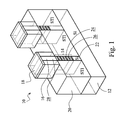
- FIG. 1 is a perspective, three dimensional view in partial cross-section illustrating an embodiment fin field effect transistor (FinFET) device with a superlattice layer as a gate channel stressor;
- FinFET fin field effect transistor
- FIG. 2 is a cross section of an embodiment of the FinFET device of FIG. 1 illustrating further device elements
- FIG. 3 is a transmission electron microscope (TEM) image depicting several adjacent fins from a FinFET device similar to the FinFET device of FIG. 1 ;
- TEM transmission electron microscope
- FIG. 4 is a TEM image illustrating a cross section of one of the fins of FIG. 3 ;
- FIG. 5 is a graphical representation of the strain analysis of the fin of FIG. 3 ;
- FIG. 6 is an embodiment of a method of forming a stressor for the FinFET device of FIG. 1 .
- FinFET fin field effect transistor
- MOS metal oxide semiconductor
- FIG. 1 is a perspective, three-dimensional view in partial cross-section illustrating a FinFET device 10 .
- the FinFET device 10 includes a gate stressor structure that provides tensile strain to a gate channel, reduces or eliminates emitting stacking faults, provides effective epitaxy relaxation, and functions as a virtual substrate.
- the FinFET device 10 includes a substrate 12 , a superlattice layer 14 (a.k.a., superlattice structure), a strained layer 16 , and a gate stack 18 .
- the substrate 12 depicted in FIG. 1 may be formed of silicon or other suitable semiconductor materials. As shown, the substrate 12 is generally disposed beneath a shallow trench isolation (STI) region 20 . As such, the substrate 12 is able to support the STI region 20 . In an embodiment, a lower or fin portion 22 of the substrate 12 projects upwardly into the STI region 20 .
- STI shallow trench isolation
- the superlattice layer 14 is generally supported by the substrate 12 .
- the superlattice layer 14 is disposed on a fin portion 22 of the substrate 12 as shown in FIG. 1 .
- the superlattice layer 14 may be constructed or built on top of the substrate 12 instead of the fin portion 22 .
- the superlattice layer 14 functions as a gate stressor for the FinFET device 10 .
- the superlattice layer 14 is generally formed by stacking different semiconductor materials in an alternating format. As shown in FIG. 1 , the superlattice layer 14 includes a first semiconductor material 24 and a second semiconductor material 26 . In an embodiment, each of the first and second semiconductor materials 24 , 26 are formed from an alloy of silicon germanium (SiGe). In an embodiment, each of the first and second semiconductor materials 24 , 26 are formed from a III-V semiconductor material. In an embodiment, the superlattice layer 14 is entirely or substantially embedded in, or encapsulated by, the STI region 20 .
- the strained layer 16 is generally formed from a semiconductor material. As shown in FIG. 1 , the strained layer 16 is formed from a third semiconductor material 28 . In an embodiment, the third semiconductor material 28 is formed from an alloy of silicon germanium (SiGe). In an embodiment, the third semiconductor material 28 is formed from a III-V semiconductor material. In an embodiment, the strained layer 16 is entirely disposed above the STI region 20 . In other words, the strained layer 16 projects above the STI region 20 . In an embodiment, the first and third semiconductor materials 24 , 28 are each formed from the same semiconductor material (e.g., the same alloy of silicon germanium).
- the gate stack 18 is generally formed over the strained layer 16 . As shown in FIG. 1 , the gate stack 18 is formed over a portion of the STI region 20 , along sidewalls and a top surface of the strained layer 16 , and then on an opposing portion of the STI region 20 . In an embodiment, the gate stack 18 substantially or entirely encapsulates the strained layer 16 . In an embodiment, the gate stack 18 is formed from, for example, an interfacial oxide layer, a high-k value dielectric layer, and a metal layer.
- the dielectric portions of the gate stack 18 may be used to form the dielectric portions of the gate stack 18 such as, for example, hafnium oxide (HfO 2 ), zirconium oxide (ZrO 2 ), or other suitable gate dielectric materials that have a desirably high dielectric constant k, i.e., higher than that of silicon dioxide (SiO 2 ).
- k desirably high dielectric constant
- k desi.e., higher than that of silicon dioxide (SiO 2 ).
- suitable thicknesses may be used and are chosen in conjunction with device speed and application.
- the gate stack 18 is formed using polysilicon.
- the gate stack 18 may be formed from other suitable metals and dielectric materials.
- the FinFET device 10 illustrates further device elements.
- the FinFET device 10 includes source/drain contacts 30 , spacers 32 abutting the gate stack 18 , and a hard mask 34 .
- the source/drain contacts 30 are embedded in the strained layer 16 .
- the source/drain contacts 30 are also disposed on opposing sides of a gate channel 36 (a.k.a., a transistor channel) of the FinFET device 10 .
- the source/drain contacts 30 may be otherwise oriented or configured.
- the gate channel 36 is generally stressed by the superlattice layer 14 of FIG. 1 .
- the superlattice layer 14 produces stress in the gate channel 36 .
- the superlattice layer 14 generates a tensile stress in, for example, an n-channel NMOS SiGe gate channel 36 .
- the superlattice layer 14 may be formed from suitable materials or processes to form stress in other types of gate channels.
- the superlattice layer 14 may provide compressive stress to the gate channel 36 .
- the superlattice layer 14 is also able to inhibit or prevent emitting stacking faults. Indeed, the superlattice layer 14 generally provides stacking fault free epitaxy and effective epitaxy relaxation.
- the superlattice layer 14 may be considered a virtual substrate gate channel stressor.
- the hard mask 34 is formed beneath the gate stack 18 .
- the hard mask 34 is generally a high-k dielectric material.
- the hard mask 34 is formed from, for example, a high-k dielectric.
- the gate spacers 32 are supported from below by the strained layer 16 .
- each of the gate spacers 32 is interposed between one of the source/drain contacts 30 and the hard mask 34 .
- the gate spacers 32 may be otherwise configured or oriented.
- the hard mask 34 , the gate spacers 32 , or both may be formed from or include an oxide, a nitride, an oxynitride, a high-K dielectric like Ta 2 O, Al 2 O 3 , HfO, SiTiO 3 , HfSiO, HfSiON, ZrSiON, and combinations thereof.
- a transmission electron microscope (TEM) image 38 depicts several adjacent fins 40 of the FinFET device 10 .
- each of the fins 40 includes one of the strained layers 16 disposed over, or stacked upon, one of the superlattice layers 14 .
- the superlattice layer 14 is deposited in, or supported by, a v-groove 42 of the substrate 12 .
- the superlattice layer 14 engages the substrate 12 at a (111) surface 44 of the substrate 12 .
- FIG. 4 is a TEM image illustrating a cross section of one of the fins 40 of the FinFET device 10 of FIG. 3 .
- the superlattice layer 14 which is disposed on the substrate 12 , is formed from alternating silicon germanium alloys.
- the superlattice layer 14 is formed from nine (9) bands (a.k.a., loops, layers, etc.) of a 560° C. SiGe 0.25 and 640° C. SiGe 0.75 stacked upon each other.
- more or fewer bands of materials may be stacked or formed upon one another.
- FIG. 9 9 bands
- the strained layer 16 which is disposed on the superlattice layer 14 , is formed from a 560° C. SiGe 0.25 .
- other semiconductor materials e.g., III-V semiconductor materials
- other melting temperatures e.g., between about 400° C. and about 700° C.
- a graph 48 representing a strain analysis of the fin 40 of FIG. 3 .
- the lattice match relative to the percentage of silicon (Si%) 50 is provided on the vertical axis (i.e., the y-axis) of the graph 48 .
- a position 52 along the fin 40 is provided on the horizontal axis (the x-axis) of the graph 48 .
- the position 52 represents a set of points along a horizontal distance, not a specific unit of measurement (e.g., nanometers).
- the lattice match relative to Si% 50 is between about one (1) and about two (2) over the entire fin 40 between position zero (0) and position sixty (60).
- a method 56 of forming a stressor for the FinFET device 10 of FIG. 1 is illustrated.
- the superlattice layer 14 is constructed on the substrate 12 .
- the strained layer 16 is formed on the superlattice layer 14 .
- the strained layer 16 provides the gate channel 36 , which is stressed by the superlattice layer 14 .
- the superlattice layer 14 functions as the stressor.
- a fin field effect transistor (FinFET) device comprising a superlattice layer supported by a substrate, a strained layer disposed on the superlattice layer and providing a gate channel, the gate channel stressed by the superlattice layer.
- FinFET fin field effect transistor
- a field effect transistor (FinFET) device comprising a superlattice layer supported by a substrate, a shallow trench isolation (STI) region encapsulating the superlattice layer, a strained layer disposed on the superlattice layer and providing a gate channel, the gate channel stressed by the superlattice layer, and a gate stack formed over the strained layer.
- STI shallow trench isolation
- a method of forming a stressor for a fin field effect transistor (FinFET) device comprises constructing a superlattice layer on a substrate and forming a strained layer on the superlattice layer, the strained layer providing a gate channel, the gate channel stressed by the superlattice layer.
- FinFET fin field effect transistor
Abstract
A fin field effect transistor (FinFET) device is provided. The FinFET includes a superlattice layer and a strained layer. The superlattice layer is supported by a substrate. The strained layer is disposed on the superlattice layer and provides a gate channel. The gate channel is stressed by the superlattice layer. In an embodiment, the superlattice layer is formed by stacking different silicon germanium alloys or stacking other III-V semiconductor materials.
Description
This application is a continuation of U.S. patent application Ser. No. 13/422,531, filed on Mar. 16, 2012, entitled “FINFET HAVING SUPERLATTICE STRESSOR,” which application is hereby incorporated herein by reference in its entirety.
Semiconductor devices are used in a large number of electronic devices, such as computers, cell phones, and others. Semiconductor devices comprise integrated circuits that are formed on semiconductor wafers by depositing many types of thin films of material over the semiconductor wafers, and patterning the thin films of material to form the integrated circuits. Integrated circuits include field-effect transistors (FETs) such as metal oxide semiconductor (MOS) transistors.
One of the goals of the semiconductor industry is to continue shrinking the size and increasing the speed of individual FETs. To achieve these goals, fin FETs (FinFETs) or multiple gate transistors will be used in sub 32 nm transistor nodes. For example, FinFETs not only improve areal density but also improve gate control of the channel.
In recent years, FinFETs have been constructed with a stressor in order to enhance performance. In some circumstances, the stressor may be formed using silicon germanium (SiGe) grown through a single layer epitaxy process. The stressor may be relaxed using SiGe with a high Ge percentage or by implementing a high temperature anneal process. A gradient Ge percentage of SiGe epitaxy may be used to provide strain.
For a more complete understanding of the present disclosure, and the advantages thereof, reference is now made to the following descriptions taken in conjunction with the accompanying drawing, in which:
Corresponding numerals and symbols in the different figures generally refer to corresponding parts unless otherwise indicated. The figures are drawn to clearly illustrate the relevant aspects of the embodiments and are not necessarily drawn to scale.
The making and using of the presently preferred embodiments are discussed in detail below. It should be appreciated, however, that the present disclosure provides many applicable inventive concepts that can be embodied in a wide variety of specific contexts. The specific embodiments discussed are merely illustrative, and do not limit the scope of the disclosure.
The present disclosure will be described with respect to preferred embodiments in a specific context, namely a fin field effect transistor (FinFET) metal oxide semiconductor (MOS). The invention may also be applied, however, to other integrated circuits, electronic structures, and the like.
The substrate 12 depicted in FIG. 1 may be formed of silicon or other suitable semiconductor materials. As shown, the substrate 12 is generally disposed beneath a shallow trench isolation (STI) region 20. As such, the substrate 12 is able to support the STI region 20. In an embodiment, a lower or fin portion 22 of the substrate 12 projects upwardly into the STI region 20.
Still referring to FIG. 1 , the superlattice layer 14 is generally supported by the substrate 12. In an embodiment, the superlattice layer 14 is disposed on a fin portion 22 of the substrate 12 as shown in FIG. 1 . In an embodiment, the superlattice layer 14 may be constructed or built on top of the substrate 12 instead of the fin portion 22. As will be more fully explained below, the superlattice layer 14 functions as a gate stressor for the FinFET device 10.
The superlattice layer 14 is generally formed by stacking different semiconductor materials in an alternating format. As shown in FIG. 1 , the superlattice layer 14 includes a first semiconductor material 24 and a second semiconductor material 26. In an embodiment, each of the first and second semiconductor materials 24, 26 are formed from an alloy of silicon germanium (SiGe). In an embodiment, each of the first and second semiconductor materials 24, 26 are formed from a III-V semiconductor material. In an embodiment, the superlattice layer 14 is entirely or substantially embedded in, or encapsulated by, the STI region 20.
Still referring to FIG. 1 , the strained layer 16 is generally formed from a semiconductor material. As shown in FIG. 1 , the strained layer 16 is formed from a third semiconductor material 28. In an embodiment, the third semiconductor material 28 is formed from an alloy of silicon germanium (SiGe). In an embodiment, the third semiconductor material 28 is formed from a III-V semiconductor material. In an embodiment, the strained layer 16 is entirely disposed above the STI region 20. In other words, the strained layer 16 projects above the STI region 20. In an embodiment, the first and third semiconductor materials 24, 28 are each formed from the same semiconductor material (e.g., the same alloy of silicon germanium).
The gate stack 18 is generally formed over the strained layer 16. As shown in FIG. 1 , the gate stack 18 is formed over a portion of the STI region 20, along sidewalls and a top surface of the strained layer 16, and then on an opposing portion of the STI region 20. In an embodiment, the gate stack 18 substantially or entirely encapsulates the strained layer 16. In an embodiment, the gate stack 18 is formed from, for example, an interfacial oxide layer, a high-k value dielectric layer, and a metal layer.
Various materials may be used to form the dielectric portions of the gate stack 18 such as, for example, hafnium oxide (HfO2), zirconium oxide (ZrO2), or other suitable gate dielectric materials that have a desirably high dielectric constant k, i.e., higher than that of silicon dioxide (SiO2). Various suitable thicknesses may be used and are chosen in conjunction with device speed and application. In an embodiment, the gate stack 18 is formed using polysilicon. In an embodiment, the gate stack 18 may be formed from other suitable metals and dielectric materials.
Referring now to FIG. 2 , an embodiment of the FinFET device 10 illustrates further device elements. For example, the FinFET device 10 includes source/drain contacts 30, spacers 32 abutting the gate stack 18, and a hard mask 34. As shown, the source/drain contacts 30 are embedded in the strained layer 16. The source/drain contacts 30 are also disposed on opposing sides of a gate channel 36 (a.k.a., a transistor channel) of the FinFET device 10. In other embodiments, the source/drain contacts 30 may be otherwise oriented or configured.
The gate channel 36 is generally stressed by the superlattice layer 14 of FIG. 1 . In other words, the superlattice layer 14 produces stress in the gate channel 36. In an embodiment, the superlattice layer 14 generates a tensile stress in, for example, an n-channel NMOS SiGe gate channel 36. In other embodiments, the superlattice layer 14 may be formed from suitable materials or processes to form stress in other types of gate channels. In an embodiment, the superlattice layer 14 may provide compressive stress to the gate channel 36. In addition to providing stress to the gate channel 36, the superlattice layer 14 is also able to inhibit or prevent emitting stacking faults. Indeed, the superlattice layer 14 generally provides stacking fault free epitaxy and effective epitaxy relaxation. In an embodiment, the superlattice layer 14 may be considered a virtual substrate gate channel stressor.
Still referring to FIG. 2 , the hard mask 34 is formed beneath the gate stack 18. The hard mask 34 is generally a high-k dielectric material. In an embodiment, the hard mask 34 is formed from, for example, a high-k dielectric. As shown in FIG. 2 , the gate spacers 32 are supported from below by the strained layer 16. In addition, each of the gate spacers 32 is interposed between one of the source/drain contacts 30 and the hard mask 34. In an embodiment, the gate spacers 32 may be otherwise configured or oriented. In an embodiment, the hard mask 34, the gate spacers 32, or both may be formed from or include an oxide, a nitride, an oxynitride, a high-K dielectric like Ta2O, Al2O3, HfO, SiTiO3, HfSiO, HfSiON, ZrSiON, and combinations thereof.
Referring now to FIG. 3 , a transmission electron microscope (TEM) image 38 depicts several adjacent fins 40 of the FinFET device 10. As shown, each of the fins 40 includes one of the strained layers 16 disposed over, or stacked upon, one of the superlattice layers 14. In an embodiment, the superlattice layer 14 is deposited in, or supported by, a v-groove 42 of the substrate 12. In an embodiment, the superlattice layer 14 engages the substrate 12 at a (111) surface 44 of the substrate 12.
Referring now to FIG. 5 , a graph 48 representing a strain analysis of the fin 40 of FIG. 3 . As shown in FIG. 5 , the lattice match relative to the percentage of silicon (Si%) 50 is provided on the vertical axis (i.e., the y-axis) of the graph 48. In addition, a position 52 along the fin 40 is provided on the horizontal axis (the x-axis) of the graph 48. The position 52 represents a set of points along a horizontal distance, not a specific unit of measurement (e.g., nanometers). As illustrated by the various data points 54 in the graph 48, the lattice match relative to Si% 50 is between about one (1) and about two (2) over the entire fin 40 between position zero (0) and position sixty (60).
Referring now to FIG. 6 , a method 56 of forming a stressor for the FinFET device 10 of FIG. 1 is illustrated. In block 58, the superlattice layer 14 is constructed on the substrate 12. In block 60, the strained layer 16 is formed on the superlattice layer 14. The strained layer 16 provides the gate channel 36, which is stressed by the superlattice layer 14. In other words, the superlattice layer 14 functions as the stressor.
A fin field effect transistor (FinFET) device. The device comprises a superlattice layer supported by a substrate, a strained layer disposed on the superlattice layer and providing a gate channel, the gate channel stressed by the superlattice layer.
A field effect transistor (FinFET) device. The device comprises a superlattice layer supported by a substrate, a shallow trench isolation (STI) region encapsulating the superlattice layer, a strained layer disposed on the superlattice layer and providing a gate channel, the gate channel stressed by the superlattice layer, and a gate stack formed over the strained layer.
A method of forming a stressor for a fin field effect transistor (FinFET) device. The method comprises constructing a superlattice layer on a substrate and forming a strained layer on the superlattice layer, the strained layer providing a gate channel, the gate channel stressed by the superlattice layer.
While the disclosure provides illustrative embodiments, this description is not intended to be construed in a limiting sense. Various modifications and combinations of the illustrative embodiments, as well as other embodiments, will be apparent to persons skilled in the art upon reference to the description. It is therefore intended that the appended claims encompass any such modifications or embodiments.
Claims (20)
1. A structure comprising:
a substrate having a first isolation region and a second isolation region;
a superlattice structure disposed over the substrate and between the first isolation region and the second isolation region, the superlattice structure comprising alternating first semiconductor layers and second semiconductor layers, the first semiconductor layers comprising a first material, the second semiconductor layers comprising a second material different from the first material;
a strained layer disposed over the superlattice structure, the strained layer forming at least a portion of a fin protruding from between the first isolation region and the second isolation region, the superlattice structure inducing stress in the strained layer by a lattice mismatch between the strained layer and at least one of the alternating first semiconductor layers and second semiconductor layers of the superlattice structure; and
a gate structure over the strained layer, the gate structure defining a channel region in the strained layer.
2. The structure of claim 1 further comprising a first source/drain region in the fin and a second source/drain region in the fin, the first source/drain region and the second source/drain region being on opposing sides of the channel region.
3. The structure of claim 1 , wherein the superlattice structure is disposed in a v-groove of the substrate.
4. The structure of claim 1 , wherein the superlattice structure contacts a (111) surface of the substrate.
5. The structure of claim 1 , wherein the first semiconductor layers comprise a first silicon germanium alloy with a first atomic composition and the second semiconductor layers comprise a second silicon germanium alloy with a second atomic composition, the first atomic composition being different from the second atomic composition.
6. The structure of claim 1 , wherein the first semiconductor layers comprise a first III-V material with a first atomic composition and the second semiconductor layers comprise a second III-V material with a second atomic composition, the first atomic composition being different from the second atomic composition.
7. The structure of claim 1 , wherein the strained layer is tensilely strained.
8. The structure of claim 1 , wherein the strained layer is compressively strained.
9. The structure of claim 1 , wherein an upper surface of the superlattice structure distal the substrate is closer to the substrate than an upper surface of the first isolation region distal the substrate.
10. The structure of claim 1 , wherein the superlattice structure reduces or prevents emitting stacking faults.
11. A structure comprising:
a fin comprising a strained layer, the fin protruding from between a first isolation region on a substrate and a second isolation region on the substrate, the strained layer being disposed on a superlattice structure comprising alternating first layers and second layers, at least one of the first layers and second layers inducing a stress in the strained layer, each of the first layers being a first III-V material with a first atomic composition, and each of the second layers being a second III-V material with a second atomic composition different from the first atomic composition;
a gate structure on the fin, the gate structure defining a channel region in the strained layer;
a first source/drain region in the fin; and
a second source/drain region in the fin, the channel region being disposed between the first source/drain region and the second source/drain region.
12. The structure of claim 11 , wherein the strained layer protrudes above and from between the first isolation region and the second isolation region.
13. The structure of claim 11 , wherein each of the first layers is a first silicon germanium alloy with the first atomic composition, and each of the second layers is a second silicon germanium alloy with the second atomic composition.
14. The structure of claim 11 , wherein the strained layer is tensilely strained.
15. The structure of claim 11 , wherein the strained layer is compressively strained.
16. A structure comprising:
a fin bottom portion on a substrate, the fin bottom portion being between a first isolation region and a second isolation region;
a superlattice structure on the fin bottom portion, the superlattice structure comprising alternating first layers and second layers, each of the first layers being a first III-V material with a first atomic composition, and each of the second layers being a second III-V material with a second atomic composition different from the first atomic composition;
a strained layer on the superlattice structure, at least one of the first layers and second layers inducing a stress in the strained layer, at least a portion of the strained layer forming at least a portion of a fin protruding above the first isolation region and the second isolation region; and
a gate structure on the fin, the gate structure defining a channel region in the strained layer.
17. The structure of claim 16 , wherein each of the first layers is a first silicon germanium alloy with the first atomic composition, and each of the second layers is a second silicon germanium alloy with the second atomic composition.
18. The structure of claim 16 , wherein the fin bottom portion has a v-groove, the superlattice structure contacting the v-groove of the fin bottom portion.
19. The structure of claim 16 further comprising a first source/drain region in the strained layer and a second source/drain region in the strained layer, the channel region being disposed between the first source/drain region and the second source/drain region.
20. The structure of claim 16 , wherein the strained layer is tensilely strained.
Priority Applications (1)
| Application Number | Priority Date | Filing Date | Title |
|---|---|---|---|
| US14/625,803 US9450098B2 (en) | 2012-03-16 | 2015-02-19 | FinFET having superlattice stressor |
Applications Claiming Priority (2)
| Application Number | Priority Date | Filing Date | Title |
|---|---|---|---|
| US13/422,531 US8994002B2 (en) | 2012-03-16 | 2012-03-16 | FinFET having superlattice stressor |
| US14/625,803 US9450098B2 (en) | 2012-03-16 | 2015-02-19 | FinFET having superlattice stressor |
Related Parent Applications (1)
| Application Number | Title | Priority Date | Filing Date |
|---|---|---|---|
| US13/422,531 Continuation US8994002B2 (en) | 2012-03-16 | 2012-03-16 | FinFET having superlattice stressor |
Publications (2)
| Publication Number | Publication Date |
|---|---|
| US20150162447A1 US20150162447A1 (en) | 2015-06-11 |
| US9450098B2 true US9450098B2 (en) | 2016-09-20 |
Family
ID=49136313
Family Applications (2)
| Application Number | Title | Priority Date | Filing Date |
|---|---|---|---|
| US13/422,531 Active US8994002B2 (en) | 2012-03-16 | 2012-03-16 | FinFET having superlattice stressor |
| US14/625,803 Active 2032-04-03 US9450098B2 (en) | 2012-03-16 | 2015-02-19 | FinFET having superlattice stressor |
Family Applications Before (1)
| Application Number | Title | Priority Date | Filing Date |
|---|---|---|---|
| US13/422,531 Active US8994002B2 (en) | 2012-03-16 | 2012-03-16 | FinFET having superlattice stressor |
Country Status (4)
| Country | Link |
|---|---|
| US (2) | US8994002B2 (en) |
| KR (1) | KR20130105224A (en) |
| CN (1) | CN103311297B (en) |
| TW (1) | TWI478335B (en) |
Families Citing this family (41)
| Publication number | Priority date | Publication date | Assignee | Title |
|---|---|---|---|---|
| CN103928333B (en) * | 2013-01-15 | 2019-03-12 | 中国科学院微电子研究所 | Semiconductor devices and its manufacturing method |
| US9057670B2 (en) * | 2013-05-30 | 2015-06-16 | International Business Machines Corporation | Transmission electron microscope sample fabrication |
| WO2015047341A1 (en) * | 2013-09-27 | 2015-04-02 | Intel Corporation | Non-planar semiconductor devices having multi-layered compliant substrates |
| KR101855023B1 (en) * | 2013-11-22 | 2018-05-04 | 아토메라 인코포레이티드 | Vertical semiconductor devices including superlattice punch through stop layer and related methods |
| KR102115552B1 (en) * | 2014-01-28 | 2020-05-27 | 삼성전자주식회사 | Semiconductor device and fabricating method thereof |
| US9515172B2 (en) | 2014-01-28 | 2016-12-06 | Samsung Electronics Co., Ltd. | Semiconductor devices having isolation insulating layers and methods of manufacturing the same |
| WO2015191561A1 (en) | 2014-06-09 | 2015-12-17 | Mears Technologies, Inc. | Semiconductor devices with enhanced deterministic doping and related methods |
| US10559690B2 (en) | 2014-09-18 | 2020-02-11 | International Business Machines Corporation | Embedded source/drain structure for tall FinFET and method of formation |
| US9818877B2 (en) | 2014-09-18 | 2017-11-14 | International Business Machines Corporation | Embedded source/drain structure for tall finFET and method of formation |
| US9722046B2 (en) | 2014-11-25 | 2017-08-01 | Atomera Incorporated | Semiconductor device including a superlattice and replacement metal gate structure and related methods |
| US9397179B1 (en) | 2015-02-17 | 2016-07-19 | Samsung Electronics Co., Ltd. | Semiconductor device |
| US9793403B2 (en) | 2015-04-14 | 2017-10-17 | Samsung Electronics Co., Ltd. | Multi-layer fin field effect transistor devices and methods of forming the same |
| US9460920B1 (en) * | 2015-05-11 | 2016-10-04 | Applied Materials, Inc. | Horizontal gate all around device isolation |
| TWI723993B (en) * | 2015-05-11 | 2021-04-11 | 美商應用材料股份有限公司 | Horizontal gate all around and finfet device isolation |
| US9899479B2 (en) | 2015-05-15 | 2018-02-20 | Atomera Incorporated | Semiconductor devices with superlattice layers providing halo implant peak confinement and related methods |
| WO2016196600A1 (en) | 2015-06-02 | 2016-12-08 | Atomera Incorporated | Method for making enhanced semiconductor structures in single wafer processing chamber with desired uniformity control |
| US9806194B2 (en) | 2015-07-15 | 2017-10-31 | Samsung Electronics Co., Ltd. | FinFET with fin having different Ge doped region |
| US20170033181A1 (en) * | 2015-07-28 | 2017-02-02 | Globalfoundries Inc. | Methods of forming replacement fins comprised of multiple layers of different semiconductor materials |
| US9853101B2 (en) | 2015-10-07 | 2017-12-26 | Taiwan Semiconductor Manufacturing Company, Ltd. | Strained nanowire CMOS device and method of forming |
| KR102323943B1 (en) | 2015-10-21 | 2021-11-08 | 삼성전자주식회사 | Method of manufacturing semiconductor device |
| US20170179127A1 (en) * | 2015-12-18 | 2017-06-22 | Globalfoundries Inc. | Semiconductor structure having silicon germanium fins and method of fabricating same |
| US10483353B2 (en) | 2015-12-24 | 2019-11-19 | Intel Corporation | Transistor including tensile-strained germanium channel |
| US9558939B1 (en) | 2016-01-15 | 2017-01-31 | Atomera Incorporated | Methods for making a semiconductor device including atomic layer structures using N2O as an oxygen source |
| US9837538B2 (en) * | 2016-03-25 | 2017-12-05 | Taiwan Semiconductor Manufacturing Co., Ltd. | Semiconductor device and manufacturing method thereof |
| US9741822B1 (en) | 2016-09-26 | 2017-08-22 | International Business Machines Corporation | Simplified gate stack process to improve dual channel CMOS performance |
| US10847619B2 (en) | 2016-09-30 | 2020-11-24 | Intel Corporation | Supperlatice channel included in a trench |
| CN111370489A (en) | 2016-11-21 | 2020-07-03 | 华为技术有限公司 | Field effect transistor and manufacturing method thereof |
| CN108735804B (en) * | 2017-04-25 | 2021-05-14 | 中芯国际集成电路制造(上海)有限公司 | Transistor and manufacturing method thereof |
| US10516076B2 (en) | 2018-02-01 | 2019-12-24 | Silanna UV Technologies Pte Ltd | Dislocation filter for semiconductor devices |
| US10593761B1 (en) | 2018-11-16 | 2020-03-17 | Atomera Incorporated | Method for making a semiconductor device having reduced contact resistance |
| US10580867B1 (en) * | 2018-11-16 | 2020-03-03 | Atomera Incorporated | FINFET including source and drain regions with dopant diffusion blocking superlattice layers to reduce contact resistance |
| US10840336B2 (en) | 2018-11-16 | 2020-11-17 | Atomera Incorporated | Semiconductor device with metal-semiconductor contacts including oxygen insertion layer to constrain dopants and related methods |
| US10580866B1 (en) * | 2018-11-16 | 2020-03-03 | Atomera Incorporated | Semiconductor device including source/drain dopant diffusion blocking superlattices to reduce contact resistance |
| US10840337B2 (en) | 2018-11-16 | 2020-11-17 | Atomera Incorporated | Method for making a FINFET having reduced contact resistance |
| US10847618B2 (en) | 2018-11-16 | 2020-11-24 | Atomera Incorporated | Semiconductor device including body contact dopant diffusion blocking superlattice having reduced contact resistance |
| US10854717B2 (en) | 2018-11-16 | 2020-12-01 | Atomera Incorporated | Method for making a FINFET including source and drain dopant diffusion blocking superlattices to reduce contact resistance |
| US10840335B2 (en) | 2018-11-16 | 2020-11-17 | Atomera Incorporated | Method for making semiconductor device including body contact dopant diffusion blocking superlattice to reduce contact resistance |
| US10818755B2 (en) | 2018-11-16 | 2020-10-27 | Atomera Incorporated | Method for making semiconductor device including source/drain dopant diffusion blocking superlattices to reduce contact resistance |
| US20210175325A1 (en) * | 2019-12-09 | 2021-06-10 | Entegris, Inc. | Diffusion barriers made from multiple barrier materials, and related articles and methods |
| KR20210134445A (en) * | 2020-04-29 | 2021-11-10 | 삼성전자주식회사 | Semiconductor device |
| CN112382657B (en) * | 2020-11-16 | 2022-03-18 | 中国科学院物理研究所 | Graphic silicon substrate-silicon germanium film composite structure and preparation method and application thereof |
Citations (22)
| Publication number | Priority date | Publication date | Assignee | Title |
|---|---|---|---|---|
| US5019874A (en) | 1989-05-31 | 1991-05-28 | Fujitsu Limited | Semiconductor device having an epitaxial layer grown heteroepitaxially on an underlying substrate |
| US5357119A (en) | 1993-02-19 | 1994-10-18 | Board Of Regents Of The University Of California | Field effect devices having short period superlattice structures using Si and Ge |
| US5629231A (en) | 1994-02-15 | 1997-05-13 | Fujitsu Limited | Method of manufacturing a semiconductor device with metallic precipitate |
| JPH11284220A (en) | 1998-03-02 | 1999-10-15 | Internatl Business Mach Corp <Ibm> | Si/sige photoelectronic integrated circuit and forming method thereof |
| US6369438B1 (en) | 1998-12-24 | 2002-04-09 | Kabushiki Kaisha Toshiba | Semiconductor device and method for manufacturing the same |
| US20020086494A1 (en) | 2000-12-28 | 2002-07-04 | Young-Ju Park | Method of fusion for heteroepitaxial layers and overgrowth thereon |
| US6515335B1 (en) | 2002-01-04 | 2003-02-04 | International Business Machines Corporation | Method for fabrication of relaxed SiGe buffer layers on silicon-on-insulators and structures containing the same |
| US20050035415A1 (en) | 2003-08-13 | 2005-02-17 | Yee-Chia Yeo | Multiple-gate transistors formed on bulk substrates |
| US20050224800A1 (en) | 2004-03-31 | 2005-10-13 | Nick Lindert | Bulk non-planar transistor having strained enhanced mobility and methods of fabrication |
| US20060076625A1 (en) | 2004-09-25 | 2006-04-13 | Lee Sung-Young | Field effect transistors having a strained silicon channel and methods of fabricating same |
| US7091561B2 (en) | 2003-06-13 | 2006-08-15 | Kabushiki Kaisha Toshiba | Field effect transistor and method of manufacturing the same |
| US20060273299A1 (en) * | 2003-06-26 | 2006-12-07 | Rj Mears, Llc | Method for making a semiconductor device including a dopant blocking superlattice |
| US20060292889A1 (en) | 2003-06-26 | 2006-12-28 | Rj Mears, Llc | FINFET Including a Superlattice |
| US20060292765A1 (en) | 2003-06-26 | 2006-12-28 | Rj Mears, Llc | Method for Making a FINFET Including a Superlattice |
| US7569869B2 (en) * | 2007-03-29 | 2009-08-04 | Intel Corporation | Transistor having tensile strained channel and system including same |
| US7629603B2 (en) | 2006-06-09 | 2009-12-08 | Intel Corporation | Strain-inducing semiconductor regions |
| US7888201B2 (en) | 2003-11-04 | 2011-02-15 | Taiwan Semiconductor Manufacturing Company, Ltd. | Semiconductor-on-insulator SRAM configured using partially-depleted and fully-depleted transistors |
| US7928426B2 (en) | 2007-03-27 | 2011-04-19 | Intel Corporation | Forming a non-planar transistor having a quantum well channel |
| US20110147711A1 (en) | 2009-12-23 | 2011-06-23 | Ravi Pillarisetty | Non-planar germanium quantum well devices |
| US8058692B2 (en) | 2008-12-29 | 2011-11-15 | Taiwan Semiconductor Manufacturing Company, Ltd. | Multiple-gate transistors with reverse T-shaped fins |
| US20120032146A1 (en) | 2009-03-16 | 2012-02-09 | Ravi Pillarisetty | Apparatus and methods for improving parallel conduction in a quantum well device |
| US8558279B2 (en) | 2010-09-23 | 2013-10-15 | Intel Corporation | Non-planar device having uniaxially strained semiconductor body and method of making same |
Family Cites Families (1)
| Publication number | Priority date | Publication date | Assignee | Title |
|---|---|---|---|---|
| CN101371363A (en) * | 2005-09-26 | 2009-02-18 | 梅尔斯科技公司 | Semiconductor device including a front side strained superlattice layer and a back side stress layer and associated methods |
-
2012
- 2012-03-16 US US13/422,531 patent/US8994002B2/en active Active
- 2012-06-14 KR KR1020120063651A patent/KR20130105224A/en not_active Application Discontinuation
- 2012-08-15 TW TW101129465A patent/TWI478335B/en active
- 2012-12-31 CN CN201210593522.8A patent/CN103311297B/en active Active
-
2015
- 2015-02-19 US US14/625,803 patent/US9450098B2/en active Active
Patent Citations (30)
| Publication number | Priority date | Publication date | Assignee | Title |
|---|---|---|---|---|
| US5019874A (en) | 1989-05-31 | 1991-05-28 | Fujitsu Limited | Semiconductor device having an epitaxial layer grown heteroepitaxially on an underlying substrate |
| US5357119A (en) | 1993-02-19 | 1994-10-18 | Board Of Regents Of The University Of California | Field effect devices having short period superlattice structures using Si and Ge |
| US5629231A (en) | 1994-02-15 | 1997-05-13 | Fujitsu Limited | Method of manufacturing a semiconductor device with metallic precipitate |
| JPH11284220A (en) | 1998-03-02 | 1999-10-15 | Internatl Business Mach Corp <Ibm> | Si/sige photoelectronic integrated circuit and forming method thereof |
| US20020171077A1 (en) | 1998-03-02 | 2002-11-21 | Chu Jack Oon | Si/SiGe optoelectronic integrated circuits |
| US20050023554A1 (en) | 1998-03-02 | 2005-02-03 | International Business Machines Corporation | Si/SiGe optoelectronic integrated circuits |
| US6369438B1 (en) | 1998-12-24 | 2002-04-09 | Kabushiki Kaisha Toshiba | Semiconductor device and method for manufacturing the same |
| US20020086494A1 (en) | 2000-12-28 | 2002-07-04 | Young-Ju Park | Method of fusion for heteroepitaxial layers and overgrowth thereon |
| US6534385B2 (en) * | 2000-12-28 | 2003-03-18 | Korea Institute Of Science And Technology | Method of fusion for heteroepitaxial layers and overgrowth thereon |
| US6515335B1 (en) | 2002-01-04 | 2003-02-04 | International Business Machines Corporation | Method for fabrication of relaxed SiGe buffer layers on silicon-on-insulators and structures containing the same |
| US7091561B2 (en) | 2003-06-13 | 2006-08-15 | Kabushiki Kaisha Toshiba | Field effect transistor and method of manufacturing the same |
| US20060273299A1 (en) * | 2003-06-26 | 2006-12-07 | Rj Mears, Llc | Method for making a semiconductor device including a dopant blocking superlattice |
| US20060292889A1 (en) | 2003-06-26 | 2006-12-28 | Rj Mears, Llc | FINFET Including a Superlattice |
| US20060292765A1 (en) | 2003-06-26 | 2006-12-28 | Rj Mears, Llc | Method for Making a FINFET Including a Superlattice |
| US20050035415A1 (en) | 2003-08-13 | 2005-02-17 | Yee-Chia Yeo | Multiple-gate transistors formed on bulk substrates |
| US7888201B2 (en) | 2003-11-04 | 2011-02-15 | Taiwan Semiconductor Manufacturing Company, Ltd. | Semiconductor-on-insulator SRAM configured using partially-depleted and fully-depleted transistors |
| US7781771B2 (en) | 2004-03-31 | 2010-08-24 | Intel Corporation | Bulk non-planar transistor having strained enhanced mobility and methods of fabrication |
| US20050224800A1 (en) | 2004-03-31 | 2005-10-13 | Nick Lindert | Bulk non-planar transistor having strained enhanced mobility and methods of fabrication |
| US7154118B2 (en) | 2004-03-31 | 2006-12-26 | Intel Corporation | Bulk non-planar transistor having strained enhanced mobility and methods of fabrication |
| KR100674914B1 (en) | 2004-09-25 | 2007-01-26 | 삼성전자주식회사 | MOS transistor having strained channel layer and methods of manufacturing thereof |
| US20060076625A1 (en) | 2004-09-25 | 2006-04-13 | Lee Sung-Young | Field effect transistors having a strained silicon channel and methods of fabricating same |
| US7629603B2 (en) | 2006-06-09 | 2009-12-08 | Intel Corporation | Strain-inducing semiconductor regions |
| US7928426B2 (en) | 2007-03-27 | 2011-04-19 | Intel Corporation | Forming a non-planar transistor having a quantum well channel |
| US7569869B2 (en) * | 2007-03-29 | 2009-08-04 | Intel Corporation | Transistor having tensile strained channel and system including same |
| US8058692B2 (en) | 2008-12-29 | 2011-11-15 | Taiwan Semiconductor Manufacturing Company, Ltd. | Multiple-gate transistors with reverse T-shaped fins |
| US20120032146A1 (en) | 2009-03-16 | 2012-02-09 | Ravi Pillarisetty | Apparatus and methods for improving parallel conduction in a quantum well device |
| US8242001B2 (en) | 2009-03-16 | 2012-08-14 | Intel Corporation | Apparatus and methods for improving parallel conduction in a quantum well device |
| US20110147711A1 (en) | 2009-12-23 | 2011-06-23 | Ravi Pillarisetty | Non-planar germanium quantum well devices |
| US8283653B2 (en) | 2009-12-23 | 2012-10-09 | Intel Corporation | Non-planar germanium quantum well devices |
| US8558279B2 (en) | 2010-09-23 | 2013-10-15 | Intel Corporation | Non-planar device having uniaxially strained semiconductor body and method of making same |
Also Published As
| Publication number | Publication date |
|---|---|
| US20130240836A1 (en) | 2013-09-19 |
| KR20130105224A (en) | 2013-09-25 |
| US8994002B2 (en) | 2015-03-31 |
| CN103311297B (en) | 2015-12-09 |
| US20150162447A1 (en) | 2015-06-11 |
| TWI478335B (en) | 2015-03-21 |
| CN103311297A (en) | 2013-09-18 |
| TW201340313A (en) | 2013-10-01 |
Similar Documents
| Publication | Publication Date | Title |
|---|---|---|
| US9450098B2 (en) | FinFET having superlattice stressor | |
| US8008751B2 (en) | Semiconductor device and manufacturing method thereof | |
| US10453842B2 (en) | Tuning tensile strain on FinFET | |
| US7078742B2 (en) | Strained-channel semiconductor structure and method of fabricating the same | |
| CN107230729B (en) | Semiconductor device and method for manufacturing the same | |
| US9711413B2 (en) | High performance CMOS device design | |
| US7381604B2 (en) | Strained-channel semiconductor structure and method for fabricating the same | |
| US9318553B1 (en) | Nanowire device with improved epitaxy | |
| US20080157200A1 (en) | Stress liner surrounded facetless embedded stressor mosfet | |
| KR101727368B1 (en) | Non-planar sige channel pfet | |
| US10566435B2 (en) | Gate stack quality for gate-all-around field-effect transistors | |
| KR20090125148A (en) | Forming a non-planar transistor having a quantum well channel | |
| JP2008504677A5 (en) | ||
| CN104241134A (en) | Non-Planar Transistors with Replacement Fins and Methods of Forming the Same | |
| CN106062963A (en) | Strain compensation in transistors | |
| US7268362B2 (en) | High performance transistors with SiGe strain | |
| KR20180067395A (en) | Field effect transistor with decoupled channel and methods of manufacturing the same | |
| JP4875038B2 (en) | Semiconductor device and manufacturing method thereof | |
| Kang et al. | Effects of Film Stress Modulation Using TiN Metal Gate on Stress Engineering and Its Impact on Device Characteristics in Metal Gate/High-$ k $ Dielectric SOI FinFETs | |
| Collaert et al. | Stress hybridization for multigate devices fabricated on supercritical strained-SOI (SC-SSOI) | |
| US9331175B2 (en) | Method of locally stressing a semiconductor layer | |
| US20210126018A1 (en) | Gate stack quality for gate-all-around field-effect transistors | |
| RAN | Strain Engineering for Advanced Silicon, Germanium and Germanium-Tin Transistors | |
| Nagaiah | Development of III-V p-MOSFETs with high-κ gate stack for future CMOS applications |
Legal Events
| Date | Code | Title | Description |
|---|---|---|---|
| STCF | Information on status: patent grant |
Free format text: PATENTED CASE |
|
| MAFP | Maintenance fee payment |
Free format text: PAYMENT OF MAINTENANCE FEE, 4TH YEAR, LARGE ENTITY (ORIGINAL EVENT CODE: M1551); ENTITY STATUS OF PATENT OWNER: LARGE ENTITY Year of fee payment: 4 |
|
| MAFP | Maintenance fee payment |
Free format text: PAYMENT OF MAINTENANCE FEE, 8TH YEAR, LARGE ENTITY (ORIGINAL EVENT CODE: M1552); ENTITY STATUS OF PATENT OWNER: LARGE ENTITY Year of fee payment: 8 |