US9460951B2 - Semiconductor device and method of wafer level package integration - Google Patents
Semiconductor device and method of wafer level package integration Download PDFInfo
- Publication number
- US9460951B2 US9460951B2 US13/172,680 US201113172680A US9460951B2 US 9460951 B2 US9460951 B2 US 9460951B2 US 201113172680 A US201113172680 A US 201113172680A US 9460951 B2 US9460951 B2 US 9460951B2
- Authority
- US
- United States
- Prior art keywords
- over
- layer
- forming
- semiconductor die
- encapsulant
- Prior art date
- Legal status (The legal status is an assumption and is not a legal conclusion. Google has not performed a legal analysis and makes no representation as to the accuracy of the status listed.)
- Active, expires
Links
Images


Classifications
-
- H—ELECTRICITY
- H01—ELECTRIC ELEMENTS
- H01L—SEMICONDUCTOR DEVICES NOT COVERED BY CLASS H10
- H01L21/00—Processes or apparatus adapted for the manufacture or treatment of semiconductor or solid state devices or of parts thereof
- H01L21/67—Apparatus specially adapted for handling semiconductor or electric solid state devices during manufacture or treatment thereof; Apparatus specially adapted for handling wafers during manufacture or treatment of semiconductor or electric solid state devices or components ; Apparatus not specifically provided for elsewhere
- H01L21/683—Apparatus specially adapted for handling semiconductor or electric solid state devices during manufacture or treatment thereof; Apparatus specially adapted for handling wafers during manufacture or treatment of semiconductor or electric solid state devices or components ; Apparatus not specifically provided for elsewhere for supporting or gripping
- H01L21/6835—Apparatus specially adapted for handling semiconductor or electric solid state devices during manufacture or treatment thereof; Apparatus specially adapted for handling wafers during manufacture or treatment of semiconductor or electric solid state devices or components ; Apparatus not specifically provided for elsewhere for supporting or gripping using temporarily an auxiliary support
-
- H—ELECTRICITY
- H01—ELECTRIC ELEMENTS
- H01L—SEMICONDUCTOR DEVICES NOT COVERED BY CLASS H10
- H01L21/00—Processes or apparatus adapted for the manufacture or treatment of semiconductor or solid state devices or of parts thereof
- H01L21/02—Manufacture or treatment of semiconductor devices or of parts thereof
- H01L21/04—Manufacture or treatment of semiconductor devices or of parts thereof the devices having at least one potential-jump barrier or surface barrier, e.g. PN junction, depletion layer or carrier concentration layer
- H01L21/50—Assembly of semiconductor devices using processes or apparatus not provided for in a single one of the subgroups H01L21/06 - H01L21/326, e.g. sealing of a cap to a base of a container
- H01L21/56—Encapsulations, e.g. encapsulation layers, coatings
- H01L21/565—Moulds
- H01L21/566—Release layers for moulds, e.g. release layers, layers against residue during moulding
-
- H—ELECTRICITY
- H01—ELECTRIC ELEMENTS
- H01L—SEMICONDUCTOR DEVICES NOT COVERED BY CLASS H10
- H01L23/00—Details of semiconductor or other solid state devices
- H01L23/28—Encapsulations, e.g. encapsulating layers, coatings, e.g. for protection
- H01L23/31—Encapsulations, e.g. encapsulating layers, coatings, e.g. for protection characterised by the arrangement or shape
- H01L23/3107—Encapsulations, e.g. encapsulating layers, coatings, e.g. for protection characterised by the arrangement or shape the device being completely enclosed
- H01L23/3121—Encapsulations, e.g. encapsulating layers, coatings, e.g. for protection characterised by the arrangement or shape the device being completely enclosed a substrate forming part of the encapsulation
- H01L23/3128—Encapsulations, e.g. encapsulating layers, coatings, e.g. for protection characterised by the arrangement or shape the device being completely enclosed a substrate forming part of the encapsulation the substrate having spherical bumps for external connection
-
- H—ELECTRICITY
- H01—ELECTRIC ELEMENTS
- H01L—SEMICONDUCTOR DEVICES NOT COVERED BY CLASS H10
- H01L23/00—Details of semiconductor or other solid state devices
- H01L23/28—Encapsulations, e.g. encapsulating layers, coatings, e.g. for protection
- H01L23/31—Encapsulations, e.g. encapsulating layers, coatings, e.g. for protection characterised by the arrangement or shape
- H01L23/3107—Encapsulations, e.g. encapsulating layers, coatings, e.g. for protection characterised by the arrangement or shape the device being completely enclosed
- H01L23/3135—Double encapsulation or coating and encapsulation
-
- H—ELECTRICITY
- H01—ELECTRIC ELEMENTS
- H01L—SEMICONDUCTOR DEVICES NOT COVERED BY CLASS H10
- H01L23/00—Details of semiconductor or other solid state devices
- H01L23/52—Arrangements for conducting electric current within the device in operation from one component to another, i.e. interconnections, e.g. wires, lead frames
- H01L23/538—Arrangements for conducting electric current within the device in operation from one component to another, i.e. interconnections, e.g. wires, lead frames the interconnection structure between a plurality of semiconductor chips being formed on, or in, insulating substrates
- H01L23/5389—Arrangements for conducting electric current within the device in operation from one component to another, i.e. interconnections, e.g. wires, lead frames the interconnection structure between a plurality of semiconductor chips being formed on, or in, insulating substrates the chips being integrally enclosed by the interconnect and support structures
-
- H—ELECTRICITY
- H01—ELECTRIC ELEMENTS
- H01L—SEMICONDUCTOR DEVICES NOT COVERED BY CLASS H10
- H01L24/00—Arrangements for connecting or disconnecting semiconductor or solid-state bodies; Methods or apparatus related thereto
- H01L24/80—Methods for connecting semiconductor or other solid state bodies using means for bonding being attached to, or being formed on, the surface to be connected
- H01L24/81—Methods for connecting semiconductor or other solid state bodies using means for bonding being attached to, or being formed on, the surface to be connected using a bump connector
-
- H—ELECTRICITY
- H01—ELECTRIC ELEMENTS
- H01L—SEMICONDUCTOR DEVICES NOT COVERED BY CLASS H10
- H01L2221/00—Processes or apparatus adapted for the manufacture or treatment of semiconductor or solid state devices or of parts thereof covered by H01L21/00
- H01L2221/67—Apparatus for handling semiconductor or electric solid state devices during manufacture or treatment thereof; Apparatus for handling wafers during manufacture or treatment of semiconductor or electric solid state devices or components; Apparatus not specifically provided for elsewhere
- H01L2221/683—Apparatus for handling semiconductor or electric solid state devices during manufacture or treatment thereof; Apparatus for handling wafers during manufacture or treatment of semiconductor or electric solid state devices or components; Apparatus not specifically provided for elsewhere for supporting or gripping
- H01L2221/68304—Apparatus for handling semiconductor or electric solid state devices during manufacture or treatment thereof; Apparatus for handling wafers during manufacture or treatment of semiconductor or electric solid state devices or components; Apparatus not specifically provided for elsewhere for supporting or gripping using temporarily an auxiliary support
- H01L2221/68345—Apparatus for handling semiconductor or electric solid state devices during manufacture or treatment thereof; Apparatus for handling wafers during manufacture or treatment of semiconductor or electric solid state devices or components; Apparatus not specifically provided for elsewhere for supporting or gripping using temporarily an auxiliary support used as a support during the manufacture of self supporting substrates
-
- H—ELECTRICITY
- H01—ELECTRIC ELEMENTS
- H01L—SEMICONDUCTOR DEVICES NOT COVERED BY CLASS H10
- H01L2224/00—Indexing scheme for arrangements for connecting or disconnecting semiconductor or solid-state bodies and methods related thereto as covered by H01L24/00
- H01L2224/01—Means for bonding being attached to, or being formed on, the surface to be connected, e.g. chip-to-package, die-attach, "first-level" interconnects; Manufacturing methods related thereto
- H01L2224/10—Bump connectors; Manufacturing methods related thereto
- H01L2224/15—Structure, shape, material or disposition of the bump connectors after the connecting process
- H01L2224/16—Structure, shape, material or disposition of the bump connectors after the connecting process of an individual bump connector
- H01L2224/161—Disposition
- H01L2224/16135—Disposition the bump connector connecting between different semiconductor or solid-state bodies, i.e. chip-to-chip
- H01L2224/16145—Disposition the bump connector connecting between different semiconductor or solid-state bodies, i.e. chip-to-chip the bodies being stacked
-
- H—ELECTRICITY
- H01—ELECTRIC ELEMENTS
- H01L—SEMICONDUCTOR DEVICES NOT COVERED BY CLASS H10
- H01L2224/00—Indexing scheme for arrangements for connecting or disconnecting semiconductor or solid-state bodies and methods related thereto as covered by H01L24/00
- H01L2224/01—Means for bonding being attached to, or being formed on, the surface to be connected, e.g. chip-to-package, die-attach, "first-level" interconnects; Manufacturing methods related thereto
- H01L2224/10—Bump connectors; Manufacturing methods related thereto
- H01L2224/15—Structure, shape, material or disposition of the bump connectors after the connecting process
- H01L2224/16—Structure, shape, material or disposition of the bump connectors after the connecting process of an individual bump connector
- H01L2224/161—Disposition
- H01L2224/16151—Disposition the bump connector connecting between a semiconductor or solid-state body and an item not being a semiconductor or solid-state body, e.g. chip-to-substrate, chip-to-passive
- H01L2224/16221—Disposition the bump connector connecting between a semiconductor or solid-state body and an item not being a semiconductor or solid-state body, e.g. chip-to-substrate, chip-to-passive the body and the item being stacked
- H01L2224/16225—Disposition the bump connector connecting between a semiconductor or solid-state body and an item not being a semiconductor or solid-state body, e.g. chip-to-substrate, chip-to-passive the body and the item being stacked the item being non-metallic, e.g. insulating substrate with or without metallisation
- H01L2224/16237—Disposition the bump connector connecting between a semiconductor or solid-state body and an item not being a semiconductor or solid-state body, e.g. chip-to-substrate, chip-to-passive the body and the item being stacked the item being non-metallic, e.g. insulating substrate with or without metallisation the bump connector connecting to a bonding area disposed in a recess of the surface of the item
-
- H—ELECTRICITY
- H01—ELECTRIC ELEMENTS
- H01L—SEMICONDUCTOR DEVICES NOT COVERED BY CLASS H10
- H01L2224/00—Indexing scheme for arrangements for connecting or disconnecting semiconductor or solid-state bodies and methods related thereto as covered by H01L24/00
- H01L2224/01—Means for bonding being attached to, or being formed on, the surface to be connected, e.g. chip-to-package, die-attach, "first-level" interconnects; Manufacturing methods related thereto
- H01L2224/26—Layer connectors, e.g. plate connectors, solder or adhesive layers; Manufacturing methods related thereto
- H01L2224/31—Structure, shape, material or disposition of the layer connectors after the connecting process
- H01L2224/32—Structure, shape, material or disposition of the layer connectors after the connecting process of an individual layer connector
- H01L2224/321—Disposition
- H01L2224/32151—Disposition the layer connector connecting between a semiconductor or solid-state body and an item not being a semiconductor or solid-state body, e.g. chip-to-substrate, chip-to-passive
- H01L2224/32221—Disposition the layer connector connecting between a semiconductor or solid-state body and an item not being a semiconductor or solid-state body, e.g. chip-to-substrate, chip-to-passive the body and the item being stacked
- H01L2224/32225—Disposition the layer connector connecting between a semiconductor or solid-state body and an item not being a semiconductor or solid-state body, e.g. chip-to-substrate, chip-to-passive the body and the item being stacked the item being non-metallic, e.g. insulating substrate with or without metallisation
-
- H—ELECTRICITY
- H01—ELECTRIC ELEMENTS
- H01L—SEMICONDUCTOR DEVICES NOT COVERED BY CLASS H10
- H01L2224/00—Indexing scheme for arrangements for connecting or disconnecting semiconductor or solid-state bodies and methods related thereto as covered by H01L24/00
- H01L2224/01—Means for bonding being attached to, or being formed on, the surface to be connected, e.g. chip-to-package, die-attach, "first-level" interconnects; Manufacturing methods related thereto
- H01L2224/42—Wire connectors; Manufacturing methods related thereto
- H01L2224/47—Structure, shape, material or disposition of the wire connectors after the connecting process
- H01L2224/48—Structure, shape, material or disposition of the wire connectors after the connecting process of an individual wire connector
- H01L2224/4805—Shape
- H01L2224/4809—Loop shape
- H01L2224/48091—Arched
-
- H—ELECTRICITY
- H01—ELECTRIC ELEMENTS
- H01L—SEMICONDUCTOR DEVICES NOT COVERED BY CLASS H10
- H01L2224/00—Indexing scheme for arrangements for connecting or disconnecting semiconductor or solid-state bodies and methods related thereto as covered by H01L24/00
- H01L2224/01—Means for bonding being attached to, or being formed on, the surface to be connected, e.g. chip-to-package, die-attach, "first-level" interconnects; Manufacturing methods related thereto
- H01L2224/42—Wire connectors; Manufacturing methods related thereto
- H01L2224/47—Structure, shape, material or disposition of the wire connectors after the connecting process
- H01L2224/48—Structure, shape, material or disposition of the wire connectors after the connecting process of an individual wire connector
- H01L2224/481—Disposition
- H01L2224/48151—Connecting between a semiconductor or solid-state body and an item not being a semiconductor or solid-state body, e.g. chip-to-substrate, chip-to-passive
- H01L2224/48221—Connecting between a semiconductor or solid-state body and an item not being a semiconductor or solid-state body, e.g. chip-to-substrate, chip-to-passive the body and the item being stacked
- H01L2224/48225—Connecting between a semiconductor or solid-state body and an item not being a semiconductor or solid-state body, e.g. chip-to-substrate, chip-to-passive the body and the item being stacked the item being non-metallic, e.g. insulating substrate with or without metallisation
- H01L2224/48227—Connecting between a semiconductor or solid-state body and an item not being a semiconductor or solid-state body, e.g. chip-to-substrate, chip-to-passive the body and the item being stacked the item being non-metallic, e.g. insulating substrate with or without metallisation connecting the wire to a bond pad of the item
- H01L2224/48228—Connecting between a semiconductor or solid-state body and an item not being a semiconductor or solid-state body, e.g. chip-to-substrate, chip-to-passive the body and the item being stacked the item being non-metallic, e.g. insulating substrate with or without metallisation connecting the wire to a bond pad of the item the bond pad being disposed in a recess of the surface of the item
-
- H—ELECTRICITY
- H01—ELECTRIC ELEMENTS
- H01L—SEMICONDUCTOR DEVICES NOT COVERED BY CLASS H10
- H01L2224/00—Indexing scheme for arrangements for connecting or disconnecting semiconductor or solid-state bodies and methods related thereto as covered by H01L24/00
- H01L2224/73—Means for bonding being of different types provided for in two or more of groups H01L2224/10, H01L2224/18, H01L2224/26, H01L2224/34, H01L2224/42, H01L2224/50, H01L2224/63, H01L2224/71
- H01L2224/732—Location after the connecting process
- H01L2224/73201—Location after the connecting process on the same surface
- H01L2224/73203—Bump and layer connectors
- H01L2224/73204—Bump and layer connectors the bump connector being embedded into the layer connector
-
- H—ELECTRICITY
- H01—ELECTRIC ELEMENTS
- H01L—SEMICONDUCTOR DEVICES NOT COVERED BY CLASS H10
- H01L2224/00—Indexing scheme for arrangements for connecting or disconnecting semiconductor or solid-state bodies and methods related thereto as covered by H01L24/00
- H01L2224/73—Means for bonding being of different types provided for in two or more of groups H01L2224/10, H01L2224/18, H01L2224/26, H01L2224/34, H01L2224/42, H01L2224/50, H01L2224/63, H01L2224/71
- H01L2224/732—Location after the connecting process
- H01L2224/73251—Location after the connecting process on different surfaces
- H01L2224/73265—Layer and wire connectors
-
- H—ELECTRICITY
- H01—ELECTRIC ELEMENTS
- H01L—SEMICONDUCTOR DEVICES NOT COVERED BY CLASS H10
- H01L2224/00—Indexing scheme for arrangements for connecting or disconnecting semiconductor or solid-state bodies and methods related thereto as covered by H01L24/00
- H01L2224/80—Methods for connecting semiconductor or other solid state bodies using means for bonding being attached to, or being formed on, the surface to be connected
- H01L2224/81—Methods for connecting semiconductor or other solid state bodies using means for bonding being attached to, or being formed on, the surface to be connected using a bump connector
- H01L2224/81001—Methods for connecting semiconductor or other solid state bodies using means for bonding being attached to, or being formed on, the surface to be connected using a bump connector involving a temporary auxiliary member not forming part of the bonding apparatus
- H01L2224/81005—Methods for connecting semiconductor or other solid state bodies using means for bonding being attached to, or being formed on, the surface to be connected using a bump connector involving a temporary auxiliary member not forming part of the bonding apparatus being a temporary or sacrificial substrate
-
- H—ELECTRICITY
- H01—ELECTRIC ELEMENTS
- H01L—SEMICONDUCTOR DEVICES NOT COVERED BY CLASS H10
- H01L2224/00—Indexing scheme for arrangements for connecting or disconnecting semiconductor or solid-state bodies and methods related thereto as covered by H01L24/00
- H01L2224/80—Methods for connecting semiconductor or other solid state bodies using means for bonding being attached to, or being formed on, the surface to be connected
- H01L2224/81—Methods for connecting semiconductor or other solid state bodies using means for bonding being attached to, or being formed on, the surface to be connected using a bump connector
- H01L2224/8119—Arrangement of the bump connectors prior to mounting
- H01L2224/81191—Arrangement of the bump connectors prior to mounting wherein the bump connectors are disposed only on the semiconductor or solid-state body
-
- H—ELECTRICITY
- H01—ELECTRIC ELEMENTS
- H01L—SEMICONDUCTOR DEVICES NOT COVERED BY CLASS H10
- H01L2224/00—Indexing scheme for arrangements for connecting or disconnecting semiconductor or solid-state bodies and methods related thereto as covered by H01L24/00
- H01L2224/80—Methods for connecting semiconductor or other solid state bodies using means for bonding being attached to, or being formed on, the surface to be connected
- H01L2224/81—Methods for connecting semiconductor or other solid state bodies using means for bonding being attached to, or being formed on, the surface to be connected using a bump connector
- H01L2224/818—Bonding techniques
- H01L2224/81801—Soldering or alloying
- H01L2224/81815—Reflow soldering
-
- H—ELECTRICITY
- H01—ELECTRIC ELEMENTS
- H01L—SEMICONDUCTOR DEVICES NOT COVERED BY CLASS H10
- H01L23/00—Details of semiconductor or other solid state devices
- H01L23/48—Arrangements for conducting electric current to or from the solid state body in operation, e.g. leads, terminal arrangements ; Selection of materials therefor
- H01L23/488—Arrangements for conducting electric current to or from the solid state body in operation, e.g. leads, terminal arrangements ; Selection of materials therefor consisting of soldered or bonded constructions
- H01L23/498—Leads, i.e. metallisations or lead-frames on insulating substrates, e.g. chip carriers
- H01L23/49811—Additional leads joined to the metallisation on the insulating substrate, e.g. pins, bumps, wires, flat leads
- H01L23/49816—Spherical bumps on the substrate for external connection, e.g. ball grid arrays [BGA]
-
- H—ELECTRICITY
- H01—ELECTRIC ELEMENTS
- H01L—SEMICONDUCTOR DEVICES NOT COVERED BY CLASS H10
- H01L23/00—Details of semiconductor or other solid state devices
- H01L23/48—Arrangements for conducting electric current to or from the solid state body in operation, e.g. leads, terminal arrangements ; Selection of materials therefor
- H01L23/488—Arrangements for conducting electric current to or from the solid state body in operation, e.g. leads, terminal arrangements ; Selection of materials therefor consisting of soldered or bonded constructions
- H01L23/498—Leads, i.e. metallisations or lead-frames on insulating substrates, e.g. chip carriers
- H01L23/49822—Multilayer substrates
-
- H—ELECTRICITY
- H01—ELECTRIC ELEMENTS
- H01L—SEMICONDUCTOR DEVICES NOT COVERED BY CLASS H10
- H01L24/00—Arrangements for connecting or disconnecting semiconductor or solid-state bodies; Methods or apparatus related thereto
- H01L24/01—Means for bonding being attached to, or being formed on, the surface to be connected, e.g. chip-to-package, die-attach, "first-level" interconnects; Manufacturing methods related thereto
- H01L24/42—Wire connectors; Manufacturing methods related thereto
- H01L24/47—Structure, shape, material or disposition of the wire connectors after the connecting process
- H01L24/48—Structure, shape, material or disposition of the wire connectors after the connecting process of an individual wire connector
-
- H—ELECTRICITY
- H01—ELECTRIC ELEMENTS
- H01L—SEMICONDUCTOR DEVICES NOT COVERED BY CLASS H10
- H01L24/00—Arrangements for connecting or disconnecting semiconductor or solid-state bodies; Methods or apparatus related thereto
- H01L24/73—Means for bonding being of different types provided for in two or more of groups H01L24/10, H01L24/18, H01L24/26, H01L24/34, H01L24/42, H01L24/50, H01L24/63, H01L24/71
-
- H—ELECTRICITY
- H01—ELECTRIC ELEMENTS
- H01L—SEMICONDUCTOR DEVICES NOT COVERED BY CLASS H10
- H01L2924/00—Indexing scheme for arrangements or methods for connecting or disconnecting semiconductor or solid-state bodies as covered by H01L24/00
-
- H—ELECTRICITY
- H01—ELECTRIC ELEMENTS
- H01L—SEMICONDUCTOR DEVICES NOT COVERED BY CLASS H10
- H01L2924/00—Indexing scheme for arrangements or methods for connecting or disconnecting semiconductor or solid-state bodies as covered by H01L24/00
- H01L2924/0001—Technical content checked by a classifier
- H01L2924/00012—Relevant to the scope of the group, the symbol of which is combined with the symbol of this group
-
- H—ELECTRICITY
- H01—ELECTRIC ELEMENTS
- H01L—SEMICONDUCTOR DEVICES NOT COVERED BY CLASS H10
- H01L2924/00—Indexing scheme for arrangements or methods for connecting or disconnecting semiconductor or solid-state bodies as covered by H01L24/00
- H01L2924/0001—Technical content checked by a classifier
- H01L2924/00014—Technical content checked by a classifier the subject-matter covered by the group, the symbol of which is combined with the symbol of this group, being disclosed without further technical details
-
- H—ELECTRICITY
- H01—ELECTRIC ELEMENTS
- H01L—SEMICONDUCTOR DEVICES NOT COVERED BY CLASS H10
- H01L2924/00—Indexing scheme for arrangements or methods for connecting or disconnecting semiconductor or solid-state bodies as covered by H01L24/00
- H01L2924/01—Chemical elements
- H01L2924/01004—Beryllium [Be]
-
- H—ELECTRICITY
- H01—ELECTRIC ELEMENTS
- H01L—SEMICONDUCTOR DEVICES NOT COVERED BY CLASS H10
- H01L2924/00—Indexing scheme for arrangements or methods for connecting or disconnecting semiconductor or solid-state bodies as covered by H01L24/00
- H01L2924/01—Chemical elements
- H01L2924/01006—Carbon [C]
-
- H—ELECTRICITY
- H01—ELECTRIC ELEMENTS
- H01L—SEMICONDUCTOR DEVICES NOT COVERED BY CLASS H10
- H01L2924/00—Indexing scheme for arrangements or methods for connecting or disconnecting semiconductor or solid-state bodies as covered by H01L24/00
- H01L2924/01—Chemical elements
- H01L2924/01013—Aluminum [Al]
-
- H—ELECTRICITY
- H01—ELECTRIC ELEMENTS
- H01L—SEMICONDUCTOR DEVICES NOT COVERED BY CLASS H10
- H01L2924/00—Indexing scheme for arrangements or methods for connecting or disconnecting semiconductor or solid-state bodies as covered by H01L24/00
- H01L2924/01—Chemical elements
- H01L2924/01023—Vanadium [V]
-
- H—ELECTRICITY
- H01—ELECTRIC ELEMENTS
- H01L—SEMICONDUCTOR DEVICES NOT COVERED BY CLASS H10
- H01L2924/00—Indexing scheme for arrangements or methods for connecting or disconnecting semiconductor or solid-state bodies as covered by H01L24/00
- H01L2924/01—Chemical elements
- H01L2924/01024—Chromium [Cr]
-
- H—ELECTRICITY
- H01—ELECTRIC ELEMENTS
- H01L—SEMICONDUCTOR DEVICES NOT COVERED BY CLASS H10
- H01L2924/00—Indexing scheme for arrangements or methods for connecting or disconnecting semiconductor or solid-state bodies as covered by H01L24/00
- H01L2924/01—Chemical elements
- H01L2924/01029—Copper [Cu]
-
- H—ELECTRICITY
- H01—ELECTRIC ELEMENTS
- H01L—SEMICONDUCTOR DEVICES NOT COVERED BY CLASS H10
- H01L2924/00—Indexing scheme for arrangements or methods for connecting or disconnecting semiconductor or solid-state bodies as covered by H01L24/00
- H01L2924/01—Chemical elements
- H01L2924/01033—Arsenic [As]
-
- H—ELECTRICITY
- H01—ELECTRIC ELEMENTS
- H01L—SEMICONDUCTOR DEVICES NOT COVERED BY CLASS H10
- H01L2924/00—Indexing scheme for arrangements or methods for connecting or disconnecting semiconductor or solid-state bodies as covered by H01L24/00
- H01L2924/01—Chemical elements
- H01L2924/01047—Silver [Ag]
-
- H—ELECTRICITY
- H01—ELECTRIC ELEMENTS
- H01L—SEMICONDUCTOR DEVICES NOT COVERED BY CLASS H10
- H01L2924/00—Indexing scheme for arrangements or methods for connecting or disconnecting semiconductor or solid-state bodies as covered by H01L24/00
- H01L2924/01—Chemical elements
- H01L2924/01049—Indium [In]
-
- H—ELECTRICITY
- H01—ELECTRIC ELEMENTS
- H01L—SEMICONDUCTOR DEVICES NOT COVERED BY CLASS H10
- H01L2924/00—Indexing scheme for arrangements or methods for connecting or disconnecting semiconductor or solid-state bodies as covered by H01L24/00
- H01L2924/01—Chemical elements
- H01L2924/0105—Tin [Sn]
-
- H—ELECTRICITY
- H01—ELECTRIC ELEMENTS
- H01L—SEMICONDUCTOR DEVICES NOT COVERED BY CLASS H10
- H01L2924/00—Indexing scheme for arrangements or methods for connecting or disconnecting semiconductor or solid-state bodies as covered by H01L24/00
- H01L2924/01—Chemical elements
- H01L2924/01073—Tantalum [Ta]
-
- H—ELECTRICITY
- H01—ELECTRIC ELEMENTS
- H01L—SEMICONDUCTOR DEVICES NOT COVERED BY CLASS H10
- H01L2924/00—Indexing scheme for arrangements or methods for connecting or disconnecting semiconductor or solid-state bodies as covered by H01L24/00
- H01L2924/01—Chemical elements
- H01L2924/01074—Tungsten [W]
-
- H—ELECTRICITY
- H01—ELECTRIC ELEMENTS
- H01L—SEMICONDUCTOR DEVICES NOT COVERED BY CLASS H10
- H01L2924/00—Indexing scheme for arrangements or methods for connecting or disconnecting semiconductor or solid-state bodies as covered by H01L24/00
- H01L2924/01—Chemical elements
- H01L2924/01078—Platinum [Pt]
-
- H—ELECTRICITY
- H01—ELECTRIC ELEMENTS
- H01L—SEMICONDUCTOR DEVICES NOT COVERED BY CLASS H10
- H01L2924/00—Indexing scheme for arrangements or methods for connecting or disconnecting semiconductor or solid-state bodies as covered by H01L24/00
- H01L2924/01—Chemical elements
- H01L2924/01079—Gold [Au]
-
- H—ELECTRICITY
- H01—ELECTRIC ELEMENTS
- H01L—SEMICONDUCTOR DEVICES NOT COVERED BY CLASS H10
- H01L2924/00—Indexing scheme for arrangements or methods for connecting or disconnecting semiconductor or solid-state bodies as covered by H01L24/00
- H01L2924/01—Chemical elements
- H01L2924/01082—Lead [Pb]
-
- H—ELECTRICITY
- H01—ELECTRIC ELEMENTS
- H01L—SEMICONDUCTOR DEVICES NOT COVERED BY CLASS H10
- H01L2924/00—Indexing scheme for arrangements or methods for connecting or disconnecting semiconductor or solid-state bodies as covered by H01L24/00
- H01L2924/013—Alloys
- H01L2924/0132—Binary Alloys
- H01L2924/01322—Eutectic Alloys, i.e. obtained by a liquid transforming into two solid phases
-
- H—ELECTRICITY
- H01—ELECTRIC ELEMENTS
- H01L—SEMICONDUCTOR DEVICES NOT COVERED BY CLASS H10
- H01L2924/00—Indexing scheme for arrangements or methods for connecting or disconnecting semiconductor or solid-state bodies as covered by H01L24/00
- H01L2924/013—Alloys
- H01L2924/014—Solder alloys
-
- H—ELECTRICITY
- H01—ELECTRIC ELEMENTS
- H01L—SEMICONDUCTOR DEVICES NOT COVERED BY CLASS H10
- H01L2924/00—Indexing scheme for arrangements or methods for connecting or disconnecting semiconductor or solid-state bodies as covered by H01L24/00
- H01L2924/049—Nitrides composed of metals from groups of the periodic table
- H01L2924/0494—4th Group
- H01L2924/04941—TiN
-
- H—ELECTRICITY
- H01—ELECTRIC ELEMENTS
- H01L—SEMICONDUCTOR DEVICES NOT COVERED BY CLASS H10
- H01L2924/00—Indexing scheme for arrangements or methods for connecting or disconnecting semiconductor or solid-state bodies as covered by H01L24/00
- H01L2924/10—Details of semiconductor or other solid state devices to be connected
- H01L2924/102—Material of the semiconductor or solid state bodies
- H01L2924/1025—Semiconducting materials
- H01L2924/10251—Elemental semiconductors, i.e. Group IV
- H01L2924/10253—Silicon [Si]
-
- H—ELECTRICITY
- H01—ELECTRIC ELEMENTS
- H01L—SEMICONDUCTOR DEVICES NOT COVERED BY CLASS H10
- H01L2924/00—Indexing scheme for arrangements or methods for connecting or disconnecting semiconductor or solid-state bodies as covered by H01L24/00
- H01L2924/10—Details of semiconductor or other solid state devices to be connected
- H01L2924/102—Material of the semiconductor or solid state bodies
- H01L2924/1025—Semiconducting materials
- H01L2924/1026—Compound semiconductors
- H01L2924/1032—III-V
- H01L2924/10329—Gallium arsenide [GaAs]
-
- H—ELECTRICITY
- H01—ELECTRIC ELEMENTS
- H01L—SEMICONDUCTOR DEVICES NOT COVERED BY CLASS H10
- H01L2924/00—Indexing scheme for arrangements or methods for connecting or disconnecting semiconductor or solid-state bodies as covered by H01L24/00
- H01L2924/10—Details of semiconductor or other solid state devices to be connected
- H01L2924/11—Device type
- H01L2924/12—Passive devices, e.g. 2 terminal devices
- H01L2924/1204—Optical Diode
- H01L2924/12041—LED
-
- H—ELECTRICITY
- H01—ELECTRIC ELEMENTS
- H01L—SEMICONDUCTOR DEVICES NOT COVERED BY CLASS H10
- H01L2924/00—Indexing scheme for arrangements or methods for connecting or disconnecting semiconductor or solid-state bodies as covered by H01L24/00
- H01L2924/10—Details of semiconductor or other solid state devices to be connected
- H01L2924/11—Device type
- H01L2924/13—Discrete devices, e.g. 3 terminal devices
- H01L2924/1304—Transistor
- H01L2924/1306—Field-effect transistor [FET]
- H01L2924/13091—Metal-Oxide-Semiconductor Field-Effect Transistor [MOSFET]
-
- H—ELECTRICITY
- H01—ELECTRIC ELEMENTS
- H01L—SEMICONDUCTOR DEVICES NOT COVERED BY CLASS H10
- H01L2924/00—Indexing scheme for arrangements or methods for connecting or disconnecting semiconductor or solid-state bodies as covered by H01L24/00
- H01L2924/10—Details of semiconductor or other solid state devices to be connected
- H01L2924/11—Device type
- H01L2924/14—Integrated circuits
- H01L2924/143—Digital devices
- H01L2924/1433—Application-specific integrated circuit [ASIC]
-
- H—ELECTRICITY
- H01—ELECTRIC ELEMENTS
- H01L—SEMICONDUCTOR DEVICES NOT COVERED BY CLASS H10
- H01L2924/00—Indexing scheme for arrangements or methods for connecting or disconnecting semiconductor or solid-state bodies as covered by H01L24/00
- H01L2924/15—Details of package parts other than the semiconductor or other solid state devices to be connected
- H01L2924/151—Die mounting substrate
- H01L2924/1517—Multilayer substrate
- H01L2924/15192—Resurf arrangement of the internal vias
-
- H—ELECTRICITY
- H01—ELECTRIC ELEMENTS
- H01L—SEMICONDUCTOR DEVICES NOT COVERED BY CLASS H10
- H01L2924/00—Indexing scheme for arrangements or methods for connecting or disconnecting semiconductor or solid-state bodies as covered by H01L24/00
- H01L2924/15—Details of package parts other than the semiconductor or other solid state devices to be connected
- H01L2924/151—Die mounting substrate
- H01L2924/153—Connection portion
- H01L2924/1531—Connection portion the connection portion being formed only on the surface of the substrate opposite to the die mounting surface
- H01L2924/15311—Connection portion the connection portion being formed only on the surface of the substrate opposite to the die mounting surface being a ball array, e.g. BGA
-
- H—ELECTRICITY
- H01—ELECTRIC ELEMENTS
- H01L—SEMICONDUCTOR DEVICES NOT COVERED BY CLASS H10
- H01L2924/00—Indexing scheme for arrangements or methods for connecting or disconnecting semiconductor or solid-state bodies as covered by H01L24/00
- H01L2924/15—Details of package parts other than the semiconductor or other solid state devices to be connected
- H01L2924/151—Die mounting substrate
- H01L2924/153—Connection portion
- H01L2924/1532—Connection portion the connection portion being formed on the die mounting surface of the substrate
-
- H—ELECTRICITY
- H01—ELECTRIC ELEMENTS
- H01L—SEMICONDUCTOR DEVICES NOT COVERED BY CLASS H10
- H01L2924/00—Indexing scheme for arrangements or methods for connecting or disconnecting semiconductor or solid-state bodies as covered by H01L24/00
- H01L2924/15—Details of package parts other than the semiconductor or other solid state devices to be connected
- H01L2924/181—Encapsulation
-
- H—ELECTRICITY
- H01—ELECTRIC ELEMENTS
- H01L—SEMICONDUCTOR DEVICES NOT COVERED BY CLASS H10
- H01L2924/00—Indexing scheme for arrangements or methods for connecting or disconnecting semiconductor or solid-state bodies as covered by H01L24/00
- H01L2924/19—Details of hybrid assemblies other than the semiconductor or other solid state devices to be connected
- H01L2924/1901—Structure
- H01L2924/1904—Component type
- H01L2924/19041—Component type being a capacitor
-
- H—ELECTRICITY
- H01—ELECTRIC ELEMENTS
- H01L—SEMICONDUCTOR DEVICES NOT COVERED BY CLASS H10
- H01L2924/00—Indexing scheme for arrangements or methods for connecting or disconnecting semiconductor or solid-state bodies as covered by H01L24/00
- H01L2924/19—Details of hybrid assemblies other than the semiconductor or other solid state devices to be connected
- H01L2924/1901—Structure
- H01L2924/1904—Component type
- H01L2924/19042—Component type being an inductor
-
- H—ELECTRICITY
- H01—ELECTRIC ELEMENTS
- H01L—SEMICONDUCTOR DEVICES NOT COVERED BY CLASS H10
- H01L2924/00—Indexing scheme for arrangements or methods for connecting or disconnecting semiconductor or solid-state bodies as covered by H01L24/00
- H01L2924/19—Details of hybrid assemblies other than the semiconductor or other solid state devices to be connected
- H01L2924/1901—Structure
- H01L2924/1904—Component type
- H01L2924/19043—Component type being a resistor
-
- H—ELECTRICITY
- H01—ELECTRIC ELEMENTS
- H01L—SEMICONDUCTOR DEVICES NOT COVERED BY CLASS H10
- H01L2924/00—Indexing scheme for arrangements or methods for connecting or disconnecting semiconductor or solid-state bodies as covered by H01L24/00
- H01L2924/30—Technical effects
- H01L2924/301—Electrical effects
- H01L2924/30105—Capacitance
Definitions
- the present invention relates in general to semiconductor devices and, more particularly, to a semiconductor device and method of wafer level (WL) package integration.
- WL wafer level
- Semiconductor devices are commonly found in modern electronic products. Semiconductor devices vary in a number and a density of electrical components. Discrete semiconductor devices generally contain one type of electrical component, e.g., light emitting diode (LED), small signal transistor, resistor, capacitor, inductor, and power metal oxide semiconductor field effect transistor (MOSFET). Integrated semiconductor devices typically contain hundreds to millions of electrical components. Examples of integrated semiconductor devices include microcontrollers, microprocessors, charged-coupled devices (CCDs), solar cells, and digital micro-mirror devices (DMDs).
- LED light emitting diode
- MOSFET power metal oxide semiconductor field effect transistor
- Semiconductor devices perform a wide range of functions such as signal processing, high-speed calculations, transmitting and receiving electromagnetic signals, controlling electronic devices, transforming sunlight to electricity, and creating visual projections for television displays.
- Semiconductor devices are found in the fields of entertainment, communications, power conversion, networks, computers, and consumer products. Semiconductor devices are also found in military applications, aviation, automotive, industrial controllers, and office equipment.
- Semiconductor devices exploit the electrical properties of semiconductor materials.
- the atomic structure of semiconductor material allows its electrical conductivity to be manipulated by the application of an electric field or base current or through the process of doping. Doping introduces impurities into the semiconductor material to manipulate and control the conductivity of the semiconductor device.
- a semiconductor device contains active and passive electrical structures.
- Active structures including bipolar and field effect transistors, control the flow of electrical current. By varying levels of doping and application of an electric field or base current, the transistor either promotes or restricts the flow of electrical current.
- Passive structures including resistors, capacitors, and inductors, create a relationship between voltage and current necessary to perform a variety of electrical functions.
- the passive and active structures are electrically connected to form circuits, which enable the semiconductor device to perform high-speed calculations and other useful functions.
- Front-end manufacturing involves the formation of a plurality of die on the surface of a semiconductor wafer. Each die is typically identical and contains circuits formed by electrically connecting active and passive components.
- semiconductor die as used herein refers to both the singular and plural form of the word, and accordingly, can refer to both a single semiconductor device and multiple semiconductor devices.
- Back-end manufacturing involves singulating individual die from the finished wafer and packaging the die to provide structural support and environmental isolation.
- Flip chip packages or wafer level chip scale packages are ideally suited for ICs demanding high speed, high density, and greater pin count.
- Flip chip style packaging involves mounting the active side of the die facedown toward a chip carrier substrate or printed circuit board (PCB).
- the electrical and mechanical interconnect between the active devices on the die and conduction tracks on the carrier substrate is achieved through an interconnect structure comprising a large number of conductive bumps or balls.
- the bumps may be formed by a reflow process applied to solder material deposited on contact pads which are disposed on the semiconductor substrate. The bumps are then soldered to the carrier substrate.
- the flip chip semiconductor package provides a short electrical conduction path from the active devices on the die to the carrier substrate in order to reduce signal propagation, lower capacitance, and achieve overall better circuit performance.
- the interconnect between the semiconductor die has been achieved with through hole conductive vias and redistribution layers (RDLs).
- RDLs redistribution layers
- the formation of the interconnect structure, including RDLs, is typically performed on an organic substrate having a low glass transition temperature (Tg).
- Tg glass transition temperature
- the substrate's Tg is typically less than 200° C., which limits processing options for the interconnect structure.
- the inter-wafer and intra-wafer registration variation of the semiconductor wafer is relatively large, which reduces manufacturability and wafer integration.
- the present invention is a method of making a wafer level chip scale package comprising providing a temporary substrate, and forming a wafer level interconnect structure over the temporary substrate using wafer level processes.
- the wafer level processes include forming a first insulating layer in contact with an upper surface of the temporary substrate, and forming a first conductive layer in contact with an upper surface of the first passivation layer.
- a first semiconductor die is mounted over the wafer level interconnect structure such that an active surface of the first semiconductor die is in electrical contact with the first conductive layer, and a first encapsulant is deposited over the first semiconductor die.
- a second encapsulant is deposited over the first encapsulant, and the first and second encapsulants are cured simultaneously.
- the temporary substrate is removed to expose the first passivation layer, an under bump metallization (UBM) is formed in electrical contact with the first conductive layer, and conductive bumps are formed on the UBM.
- UBM under bump metallization
- the present invention is a method of making a wafer level chip scale package comprising providing a temporary wafer level substrate, and forming a wafer level interconnect structure over the temporary wafer level substrate using wafer level processes.
- the wafer level processes include forming a first insulating layer on a top surface of the temporary wafer level substrate, and forming a first conductive layer over the first insulating layer.
- the method further comprises mounting a first semiconductor die over the wafer level interconnect structure in electrical contact with the first conductive layer, and depositing a first encapsulant around the first semiconductor die.
- the temporary wafer level substrate is removed to expose a bottom surface of the first insulating layer, and an interconnect structure is formed in electrical contact with the first conductive layer.
- the present invention is a method of making a wafer level chip scale package comprising providing a temporary wafer level substrate, and forming a wafer level interconnect structure over the temporary wafer level substrate using wafer level processes.
- the wafer level processes include forming a first insulating layer on a top surface of the temporary wafer level substrate, and forming a first conductive layer over the first insulating layer.
- the method further comprises mounting a first semiconductor die over the wafer level interconnect structure in electrical contact with the first conductive layer, and depositing a first encapsulant around the first semiconductor die.
- the present invention is a semiconductor device comprising a temporary wafer level substrate, and a wafer level interconnect structure disposed over the temporary wafer level substrate.
- the wafer level interconnect structure includes a first insulating layer disposed over a top surface of the temporary wafer level substrate, and a first conductive layer disposed over the first insulating layer.
- the semiconductor device further comprises a first semiconductor die disposed over the wafer level interconnect structure and in electrical contact with the first conductive layer, and a first encapsulant disposed around the first semiconductor die.
- FIG. 1 illustrates a PCB with different types of packages mounted to its surface
- FIGS. 2 a -2 c illustrate further detail of the semiconductor packages mounted to the PCB
- FIGS. 3 a -3 c illustrate a semiconductor wafer with a plurality of semiconductor die separated by saw streets
- FIG. 4 illustrates a process of manufacturing a WLCSP
- FIGS. 5 a -5 g illustrate formation of an interconnect structure for semiconductor die using a RDL in accordance with one embodiment
- FIGS. 6 a -6 g illustrate formation of an interconnect structure for semiconductor die using a RDL in accordance with another embodiment
- FIG. 7 illustrates an alternate embodiment of the interconnect structure for the semiconductor die using conductive bumps and bond wires
- FIG. 8 illustrates an alternate embodiment of an interconnect structure with underfill under the semiconductor die and a second insulating layer around the backside conductive bumps
- FIG. 9 illustrates an alternate embodiment of an interconnect structure for the semiconductor die with an adhesive and carrier over an encapsulant
- FIG. 10 illustrates an alternative embodiment of an interconnect structure for the semiconductor die with bond wires
- FIG. 11 illustrates an alternative embodiment of an interconnect structure for the semiconductor die with first and second encapsulants
- FIGS. 12 a -12 d are illustrative of mold underfill (MUF) processes that are useful for depositing encapsulant around semiconductor die and in a gap between a semiconductor die and an underlying substrate after semiconductor die are mounted to the underlying substrate; and
- MAF mold underfill
- FIG. 13 is illustrative of another process that is useful for depositing encapsulant around semiconductor die and in a gap between semiconductor die and an underlying substrate after semiconductor die are mounted to the underlying substrate.
- Front-end manufacturing involves the formation of a plurality of die on the surface of a semiconductor wafer.
- Each die on the wafer contains active and passive electrical components, which are electrically connected to form functional electrical circuits.
- Active electrical components such as transistors and diodes, have the ability to control the flow of electrical current.
- Passive electrical components such as capacitors, inductors, resistors, and transformers, create a relationship between voltage and current necessary to perform electrical circuit functions.
- Passive and active components are formed over the surface of the semiconductor wafer by a series of process steps including doping, deposition, photolithography, etching, and planarization.
- Doping introduces impurities into the semiconductor material by techniques such as ion implantation or thermal diffusion.
- the doping process modifies the electrical conductivity of semiconductor material in active devices, transforming the semiconductor material into an insulator, conductor, or dynamically changing the semiconductor material conductivity in response to an electric field or base current.
- Transistors contain regions of varying types and degrees of doping, arranged as necessary, to enable the transistor to promote or restrict the flow of electrical current upon the application of the electric field or base current.
- Active and passive components are formed by layers of materials with different electrical properties.
- the layers can be formed by a variety of deposition techniques determined in part by the type of material being deposited. For example, thin film deposition can involve spin-coating, chemical vapor deposition (CVD), physical vapor deposition (PVD), electrolytic plating, and electroless plating processes.
- CVD chemical vapor deposition
- PVD physical vapor deposition
- electrolytic plating electroless plating processes.
- Each layer is generally patterned to form portions of active components, passive components, or electrical connections between components.
- the layers can be patterned using photolithography, which involves the deposition of light sensitive material, e.g., photoresist, over the layer to be patterned.
- a pattern is transferred from a photomask to the photoresist using light.
- the portion of the photoresist pattern subjected to light is removed using a solvent, exposing portions of the underlying layer to be patterned.
- the portion of the photoresist pattern not subjected to light, the negative photoresist is removed using a solvent, exposing portions of the underlying layer to be patterned.
- the remainder of the photoresist is removed, leaving behind a patterned layer.
- some types of materials are patterned by directly depositing the material into the areas or voids formed by a previous deposition/etch process using techniques such as electroless and electrolytic plating.
- Planarization can be used to remove material from the surface of the wafer and produce a uniformly flat surface. Planarization involves polishing the surface of the wafer with a polishing pad. An abrasive material and corrosive chemical are added to the surface of the wafer during polishing. The combined mechanical action of the abrasive and corrosive action of the chemical removes any irregular topography, resulting in a uniformly flat surface.
- Back-end manufacturing refers to cutting or singulating the finished wafer into the individual die and then packaging the die for structural support and environmental isolation.
- the wafer is scored and broken along non-functional regions of the wafer called saw streets or scribes.
- the wafer is singulated using a laser cutting tool or saw blade.
- the individual die are mounted to a package substrate that includes pins or contact pads for interconnection with other system components.
- Contact pads formed over the semiconductor die are then connected to contact pads within the package.
- the electrical connections can be made with conductive bumps, stud bumps, conductive paste, or wirebonds.
- An encapsulant or other molding material is deposited over the package to provide physical support and electrical isolation.
- the finished package is then inserted into an electrical system and the functionality of the semiconductor device is made available to the other system components.
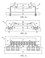
- FIG. 1 illustrates electronic device 50 having a chip carrier substrate or printed circuit board (PCB) 52 with a plurality of semiconductor packages mounted on its surface.
- Electronic device 50 can have one type of semiconductor package, or multiple types of semiconductor packages, depending on the application. The different types of semiconductor packages are shown in FIG. 1 for purposes of illustration.
- Electronic device 50 can be a stand-alone system that uses the semiconductor packages to perform one or more electrical functions.
- electronic device 50 can be a subcomponent of a larger system.
- electronic device 50 can be part of a cellular phone, personal digital assistant (PDA), digital video camera (DVC), or other electronic communication device.
- PDA personal digital assistant
- DVC digital video camera
- electronic device 50 can be a graphics card, network interface card, or other signal processing card that can be inserted into a computer.
- the semiconductor package can include microprocessors, memories, application specific integrated circuits (ASIC), logic circuits, analog circuits, RF circuits, discrete devices, or other semiconductor die or electrical components. Miniaturization and weight reduction are essential for these products to be accepted by the market. The distance between semiconductor devices must be decreased to achieve higher density.
- PCB 52 provides a general substrate for structural support and electrical interconnect of the semiconductor packages mounted on the PCB.
- Conductive signal traces 54 are formed over a surface or within layers of PCB 52 using evaporation, electrolytic plating, electroless plating, screen printing, or other suitable metal deposition process. Signal traces 54 provide for electrical communication between each of the semiconductor packages, mounted components, and other external system components. Traces 54 also provide power and ground connections to each of the semiconductor packages.
- a semiconductor device has two packaging levels.
- First level packaging is a technique for mechanically and electrically attaching the semiconductor die to an intermediate carrier.
- Second level packaging involves mechanically and electrically attaching the intermediate carrier to the PCB.
- a semiconductor device may only have the first level packaging where the die is mechanically and electrically mounted directly to the PCB.
- first level packaging including bond wire package 56 and flip chip 58
- second level packaging including ball grid array (BGA) 60 , bump chip carrier (BCC) 62 , dual in-line package (DIP) 64 , land grid array (LGA) 66 , multi-chip module (MCM) 68 , quad flat non-leaded package (QFN) 70 , and quad flat package 72 .
- BGA ball grid array
- BCC bump chip carrier
- DIP dual in-line package
- LGA land grid array
- MCM multi-chip module
- QFN quad flat non-leaded package
- quad flat package 72 quad flat package
- electronic device 50 includes a single attached semiconductor package, while other embodiments call for multiple interconnected packages.
- manufacturers can incorporate pre-made components into electronic devices and systems. Because semiconductor packages include sophisticated functionality, electronic devices can be manufactured using cheaper components and a streamlined manufacturing process. Resulting devices are less likely to fail and less expensive to manufacture resulting in a lower cost for consumers.
- FIGS. 2 a -2 c show exemplary semiconductor packages.
- FIG. 2 a illustrates further detail of DIP 64 mounted on PCB 52 .
- Semiconductor die 74 includes an active region containing analog or digital circuits implemented as active devices, passive devices, conductive layers, and dielectric layers formed within the die and are electrically interconnected according to an electrical design of the die.
- the circuit can include one or more transistors, diodes, inductors, capacitors, resistors, and other circuit elements formed within active regions of semiconductor die 74 .
- Contact pads 76 are one or more layers of conductive material, such as aluminum (Al), copper (Cu), tin (Sn), nickel (Ni), gold (Au), or silver (Ag), and are electrically connected to circuit elements formed within semiconductor die 74 .
- semiconductor die 74 is mounted to an intermediate carrier 78 using a gold-silicon eutectic layer or adhesive material such as thermal epoxy or epoxy resin.
- a package body includes an insulating packaging material such as polymer or ceramic.
- Conductor leads 80 and bond wires 82 provide electrical interconnect between semiconductor die 74 and PCB 52 .
- Encapsulant 84 is deposited over the package for environmental protection by preventing moisture and particles from entering the package and contaminating die 74 or bond wires 82 .
- FIG. 2 b illustrates further detail of BCC 62 mounted on PCB 52 .
- Semiconductor die 88 is mounted over carrier 90 using an underfill or epoxy-resin adhesive material 92 .
- Bond wires 94 provide first level packaging interconnect between contact pads 96 and 98 .
- Molding compound or encapsulant 100 is deposited over semiconductor die 88 and bond wires 94 to provide physical support and electrical isolation for the device.
- Contact pads 102 are formed over a surface of PCB 52 using a suitable metal deposition process such as electrolytic plating or electroless plating to prevent oxidation.
- Contact pads 102 are electrically connected to one or more conductive signal traces 54 in PCB 52 .
- Bumps 104 are formed between contact pads 98 of BCC 62 and contact pads 102 of PCB 52 .
- FIG. 2 c illustrates further detail of BGA 60 mounted on PCB 52 .
- semiconductor die 58 is mounted face down to intermediate carrier 106 with a flip chip style first level packaging.
- Active region 108 of semiconductor die 58 contains analog or digital circuits implemented as active devices, passive devices, conductive layers, and dielectric layers formed according to an electrical design of the die.
- the circuit can include one or more transistors, diodes, inductors, capacitors, resistors, and other circuit elements within active region 108 .
- Semiconductor die 58 is electrically and mechanically connected to carrier 106 through bumps 110 .
- BGA 60 is electrically and mechanically connected to PCB 52 with a BGA style second level packaging using bumps 112 .
- Semiconductor die 58 is electrically connected to conductive signal traces 54 in PCB 52 through bumps 110 , signal lines 114 , and bumps 112 .
- a molding compound or encapsulant 116 is deposited over semiconductor die 58 and carrier 106 to provide physical support and electrical isolation for the device.
- the flip chip semiconductor device provides a short electrical conduction path from the active devices on semiconductor die 58 to conduction tracks on PCB 52 in order to reduce signal propagation distance, lower capacitance, and improve overall circuit performance.
- the semiconductor die 58 can be mechanically and electrically connected directly to PCB 52 using flip chip style first level packaging without an intermediate carrier 106 .
- FIG. 3 a shows a semiconductor wafer 120 with a base substrate material 122 , such as silicon (Si), germanium (Ge), gallium arsenide (GaAs), indium phosphide (InP), or silicon carbide (SiC), for structural support.
- a base substrate material 122 such as silicon (Si), germanium (Ge), gallium arsenide (GaAs), indium phosphide (InP), or silicon carbide (SiC), for structural support.
- a plurality of semiconductor die or components 124 is formed on wafer 120 separated by saw streets 126 , as described above.
- FIG. 3 b shows a cross-sectional view of a portion of semiconductor wafer 120 .
- Each semiconductor die 124 has a back surface 128 and active surface 130 containing analog or digital circuits implemented as active devices, passive devices, conductive layers, and dielectric layers formed within the die and electrically interconnected according to an electrical design and function of the die.
- a circuit can include one or more transistors, diodes, and other circuit elements formed within active surface 130 to implement analog circuits or digital circuits, such as digital signal processor (DSP), ASIC, memory, or other signal processing circuit.
- DSP digital signal processor
- Semiconductor die 124 can also contain integrated passive devices (IPDs), such as inductors, capacitors, and resistors, for RF signal processing.
- IPDs integrated passive devices
- An electrically conductive layer 132 is formed over active surface 130 using PVD, CVD, electrolytic plating, electroless plating process, or other suitable metal deposition process.
- Conductive layer 132 can be one or more layers of Al, Cu, Sn, Ni, Au, Ag, or other suitable electrically conductive material.
- Conductive layer 132 operates as contact pads electrically connected to circuits on active surface 130 .
- Conductive bumps 134 are formed on contact pads 132 .
- semiconductor die 124 is a flip chip type semiconductor die and conductive bumps 134 are micro bumps.
- semiconductor wafer 120 is singulated through saw street 126 using saw blade or laser cutting tool 136 into individual semiconductor die 124 .
- Each semiconductor die 124 has bumps 134 formed over contact pads 132 .
- FIG. 4 illustrates a process of manufacturing a WLCSP.
- a WL process is used to form circuitry over a dummy silicon wafer.
- WL processing may include any semiconductor device fabrication processes such as WL redistribution, material deposition and removal processes, patterning for removing material from the wafer, and doping for changing electrical characteristics of the wafer.
- semiconductor die are connected to contact pads formed upon the wafer using a bonding or flip chip connection process.
- an encapsulant or molding compound is deposited over the wafer and attached semiconductor die.
- the molding or encapsulation compound may include any suitable material as described below.
- step 156 the dummy silicon wafer is removed using mechanical back grinding and wet etching, plasma etching, or chemical-mechanical polishing.
- step 158 opens vias in one or more insulating layers that were deposited during WL processing. Vias may be opened using a lithography and/or etching process.
- step 160 an under bump metallization (UBM) and conductive bumps are deposited over vias that were formed in step 158 .
- UBM under bump metallization
- FIGS. 5 a -5 g illustrate formation of a WL interconnect structure for use with WLCSP or other semiconductor devices in accordance with one embodiment.
- a low cost dummy substrate or carrier 162 containing temporary or sacrificial base material such as silicon, polymer, beryllium oxide, a composite material with an appropriate coefficient of thermal expansion (CTE), or other suitable low-cost, rigid material is provided for structural support.
- Substrate 162 is a temporary and sacrificial supporting wafer substrate, and is capable of supporting processing temperatures equal to or greater than 200° C.
- Insulating layer 164 can be formed using PVD, CVD, printing, spin coating, spray coating, sintering or thermal oxidation.
- Insulating layer 164 contains one or more layers of silicon nitride (Si3N4), silicon dioxide (SiO2), silicon oxynitride (SiON), SiO2/Si3N4, tantalum pentoxide (Ta2O5), aluminum oxide (Al2O3), or other material having similar insulating and structural properties.
- insulating layer 164 can be replaced by a conductive layer, such as Cu. Insulating layer 164 is chosen to have good selectivity as a silicon etchant so it can act as an etch stop during later removal of the dummy substrate. Insulating layer 164 can be formed and cured at temperatures equal to or greater than 200° C.
- an electrically conductive layer 166 is formed as a contact pad using a patterning and deposition process.
- Conductive layer 166 can be made with a conductive material, such as Al, Cu, Sn, Ni, Au, Ag, or other electrically conductive material.
- Deposition of conductive layer 166 uses PVD, CVD, electrolytic plating, or an electroless plating process. Portions of conductive layer 166 can be electrically common or electrically isolated depending on a design and function of semiconductor die that are subsequently electrically connected to conductive layer 166 .
- a passivation or insulating layer 168 is applied over insulating layer 164 and conductive layer 166 for structural support and electrical isolation.
- Insulating layer 168 can be formed using PVD, CVD, printing, spin coating, spray coating, sintering or thermal oxidation.
- Insulating layer 168 can have one or more layers of Si3N4, SiO2, SiON, polyimide (PI), benzocyclobutene (BCB), polybenzoxazole (PBO), WPR, epoxy, or other material having similar insulating and structural properties.
- Insulating layer 168 can be formed and cured at temperatures equal to or greater than 200° C. Next, a portion of insulating layer 168 is removed using a mask-defined etching process to expose conductive layer 166 .
- Conductive layer 170 is conformally deposited over insulating layer 168 .
- Conductive layer 170 can be formed using a PVD, CVD, electrolytic plating, or electroless plating process.
- Conductive layer 170 can be made with Al, Ni, nickel vanadium (NiV), Cu, Cu alloy, or some other electrically conductive material.
- Conductive layer 170 can be formed with a single layer, or alternatively with multiple layers including an adhesion layer of titanium (Ti), titanium tungsten (TiW), or chromium (Cr).
- Conductive layer 170 follows a contour of insulating layer 168 . That is, conductive layer 170 covers an upper surface and sidewalls of insulating layer 168 .
- Conductive layer 170 physically contacts conductive layer 166 through insulating layer 168 and is electrically connected to conductive layer 166 . Portions of conductive layer 170 can be electrically common or electrically isolated depending on a design and function of semiconductor die that are subsequently electrically connected to conductive layer 170 .
- a passivation or insulating layer 172 is applied over insulating layer 168 and conductive layer 170 for structural support and electrical isolation.
- Insulating layer 172 can be formed using PVD, CVD, printing, spin coating, spray coating, sintering or thermal oxidation.
- Insulating layer 172 can have one or more layers of Si3N4, SiO2, SiON, PI, BCB, PBO, WPR, epoxy, or other material having similar insulating and structural properties.
- Insulating layer 172 can be formed and cured at temperatures equal to or greater than 200° C. A portion of insulating layer 172 is removed using a mask-defined etching process to expose conductive layer 170 .
- An electrically conductive layer 174 is deposited over insulating layer 172 in electrical contact with conductive layer 170 .
- Conductive layer 174 can be deposited using a PVD, CVD, electrolytic plating, or electroless plating process.
- Conductive layer 174 can be made with Al, Cu, Sn, Ni, Au, Ag, or some other electrically conductive material.
- Conductive layer 174 physically contacts conductive layer 170 through insulating layer 172 and is electrically connected to conductive layer 170 .
- Portions of conductive layer 174 can be electrically common or electrically isolated depending on a design and function of semiconductor die that are subsequently electrically connected to conductive layer 174 .
- a passivation or insulating layer 176 is applied over insulating layer 172 and conductive layer 174 for structural support and electrical isolation.
- Insulating layer 176 can be formed using PVD, CVD, printing, spin coating, spray coating, sintering or thermal oxidation.
- Insulating layer 176 can have one or more layers of Si3N4, SiO2, SiON, PI, BCB, PBO, WPR, epoxy, or other material having similar insulating and structural properties.
- Insulating layer 176 can be formed and cured at temperatures equal to or greater than 200° C. A portion of insulating layer 176 is removed using a mask-defined etching process to expose conductive layer 174 . Insulating layer 176 is optional.
- Insulating layer 164 , conductive layer 166 , insulating layer 168 , conductive layer 170 , insulating layer 172 , conductive layer 174 , and insulating layer 176 constitute a wafer level redistribution layer (WL RDL) or interconnect structure 180 .
- WL RDL 180 is implemented through an interconnect circuit build-up process, as described above, to provide electrical connection between semiconductor die 124 , as well as electrical connection to conductive bumps 194 , as described hereinafter.
- semiconductor die 124 have contact pads 132 formed on active surfaces 130 , and conductive bumps 134 formed on contact pads 132 .
- Semiconductor die 124 are mounted to conductive layer 174 using a pick-and-place operation by placing conductive bumps 134 in contact with conductive layer 174 through insulating layer 176 or by flip chip interconnect, which electrically connects contact pads 132 to conductive layer 174 . Then, conductive bumps 134 are reflowed to improve the electrical and mechanical contact between contact pads 132 , bumps 134 , and conductive layer 174 .
- Semiconductor die 124 represent various IC dies and discrete components that can be mounted on a top surface of WL RDL 180 and connected to conductive layers of the WL RDL 180 .
- Semiconductor die 124 each include active and passive devices, conductive layers, and dielectric layers on the active surface according to the electrical design of the die.
- the discrete components can be filters, discrete passive devices, such as inductors, resistors, or capacitors, or other discrete devices.
- an encapsulant or molding compound 190 is deposited on a top surface of WL RDL 180 and over semiconductor die 124 using a paste printing, compressive molding, transfer molding, liquid encapsulant molding, vacuum lamination, or other suitable applicator.
- Encapsulant 190 can be polymer composite material, such as epoxy resin with filler, epoxy acrylate with filler, or polymer with proper filler.
- Encapsulant 190 is non-conductive, provides physical support, and environmentally protects the semiconductor device from external elements and contaminants.
- a backside 128 of semiconductor die 124 can be exposed in the molding process.
- encapsulant 190 is deposited using a film-assisted molding process.
- dummy substrate 162 is removed by mechanical backgrinding, chemical wet etching, plasma dry etching, or chemical mechanical polishing (CMP).
- Insulating layer 164 is patterned and etched to expose conductive layer 166 .
- insulating layer 164 can be patterned and etched before conductive layer 166 is formed on substrate 162 .
- a UBM or conductive layer 192 is deposited over insulating layer 164 by an evaporation, electrolytic plating, electroless plating, or screen printing process.
- Conductive layer 192 can be made with Ti, Ni, NiV, Cu, or Cu alloy.
- Conductive layer 192 is a UBM in electrical contact with conductive layer 166 .
- UBMs 192 can be a multiple metal stack with adhesion layer, barrier layer, and wetting layer.
- An adhesion layer contacts conductive layer 166 and can be made with Ti, Cr, Al, TiW, or titanium nitride (TiN).
- a barrier layer is formed over the adhesion layer and can be made with Ni, NiV, chromium copper (CrCu), or TiW.
- a wetting layer is formed over the barrier layer and can be made with Cu, Au, or Ag.
- UBMs 192 can be electroless Ni or Au on conductive layer 166 for both conductive bumps and wire bonding.
- an electrically conductive material is deposited over UBMs 192 using an electrolytic plating or electroless plating process.
- the electrically conductive material can be any solder, metal, or metal alloy, e.g., Sn, lead (Pb), Ni, Au, Ag, Cu, bismuthinite (Bi) and alloys thereof.
- the electrically conductive material is 63 percent weight of Sn and 37 percent weight of Pb.
- the electrically conductive material is reflowed by heating the conductive material above its melting point to form spherical balls or bumps 194 . In some applications, conductive bumps 194 are reflowed a second time to improve electrical contact to the UBM structure.
- Bumps 194 can also be compression bonded to UBMs 192 .
- Bumps 194 represent one type of interconnect structure that can be formed over UBMs 192 .
- the interconnect structure can also use bond wires, conductive paste, stud bump, micro bump, or other electrical interconnect.
- WL RDL 180 is a single or multiple layer WL interconnect structure.
- the multiple layers may include one or more conductive layers and insulating layers, such as flip-on-chip (FOC), BCB RDLs, PI RDLs, and PI/BCB repassivation.
- FOC flip-on-chip
- the processing temperature used in forming WL RDL 180 is typically greater than 200° C., but can be lower.
- WL RDL 180 provides a complete WL interconnect for semiconductor die 124 according to their functional design.
- the electrical signals from semiconductor die 124 are routed through WL RDL 180 to one or more conductive bumps 194 according to the function of the semiconductor device. Conductive bumps 194 are optional.
- WL RDL 180 is formed on dummy substrate 162 prior to mounting semiconductor die 124 .
- the dummy substrate 162 is removed so external interconnects such as UBMs 192 and conductive bumps 194 can be formed.
- a processing temperature restriction due to the WL RDL process noted in the background section can be reduced. In other words, since the process does not use a substrate with a Tg that is less than 200° C., temperatures equal to or greater than 200° C. can be used to form WL RDL 180 .
- inter-wafer and intra-wafer registration variation of semiconductor die can be reduced by mounting the die to the patterned dummy substrate.
- the process improves manufacturability, flexibility, wafer integration, and self-alignment effect of the WLCSP.
- FIGS. 6 a -6 g illustrate formation of a WL interconnect structure for use with WLCSP or other semiconductor devices in accordance with another embodiment.
- a low cost dummy substrate or carrier 196 containing temporary or sacrificial base material such as silicon, polymer, beryllium oxide, a composite material with an appropriate coefficient of thermal expansion (CTE), or other suitable low-cost, rigid material is provided for structural support.
- Substrate 196 is a temporary and sacrificial supporting wafer substrate, and is capable of supporting processing temperatures equal to or greater than 200° C.
- an electrically conductive multi-layer 198 is formed over dummy substrate 196 as a contact pad using a patterning and deposition process.
- Conductive multi-layer 198 can include a wetting layer, an optional barrier layer, and an adhesive layer.
- a wetting layer of conductive multi-layer 198 is deposited on dummy substrate 196 and can be made with Cu, Au, Ag, or other electrically conductive material.
- An optional barrier layer of conductive multi-layer 198 is deposited on the wetting layer and can be made with Ni, NiV, CrCu, TiW, or other electrically conductive material.
- An adhesive layer of conductive multi-layer 198 is deposited either on the wetting layer or the optional barrier layer and can be made with Ti, Cr, Al, TiW, TiN, or other electrically conductive material.
- the deposition of conductive multi-layer 198 uses PVD, CVD, electrolytic plating, or an electroless plating process.
- the process step of FIG. 6 a does not form an insulating layer (such as insulating layer 164 of FIG. 5 a ) on dummy substrate 196 prior to forming conductive multi-layer 198 directly on dummy substrate 196 .
- Conductive multi-layer 198 constitutes a UBM 198 to which wire bonds or conductive bumps can be subsequently bonded.
- a passivation or insulating layer 200 is formed over conductive multi-layer 198 for structural support and electrical isolation.
- Insulating layer 200 can be formed using PVD, CVD, printing, spin coating, spray coating, sintering or thermal oxidation.
- Insulating layer 200 can have one or more layers of Si3N4, SiO2, SiON, PI, BCB, PBO, WPR, epoxy, or other insulating material.
- Insulating layer 200 can be formed and cured at temperatures equal to or greater than 200° C.
- a portion of insulating layer 200 is removed using a mask-defined etching process to expose conductive multi-layer 198 .
- An electrically conductive layer 202 is conformally deposited over insulating layer 200 .
- Conductive layer 202 can be deposited using a PVD, CVD, electrolytic plating, or electroless plating process.
- Conductive layer 202 can be made with Al, Ni, NiV, Cu, or Cu alloy.
- Conductive layer 202 follows the contour of insulating layer 200 . That is, conductive layer 202 covers an upper surface and sidewalls of insulating layer 200 .
- Conductive layer 202 physically contacts conductive multi-layer 198 through insulating layer 200 and is electrically connected to conductive multi-layer 198 .
- Conductive layer 202 can be made with a single layer, or alternatively with multiple layers including an adhesion layer of Ti, TiW, or Cr.
- a passivation or insulating layer 204 is formed over insulating layer 200 and conductive layer 202 for structural support and electrical isolation.
- Insulating layer 204 can be formed using PVD, CVD, printing, spin coating, spray coating, sintering or thermal oxidation.
- Insulating layer 204 can have one or more layers of Si3N4, SiO2, SiON, PI, BCB, PBO, WPR, epoxy, or other insulating material. Insulating layer 204 can be formed and cured at temperatures equal to or greater than 200° C. A portion of insulating layer 204 is removed using a mask-defined etching process to expose conductive layer 202 .
- An electrically conductive layer 206 is deposited over insulating layer 204 in electrical contact with conductive layer 202 .
- Conductive layer 206 can be deposited using a PVD, CVD, electrolytic plating, or electroless plating process.
- Conductive layer 206 can be made with Al, Cu, Sn, Ni, Au, Ag, or some other electrically conductive material.
- a passivation or insulating layer 208 is formed over insulating layer 204 and conductive layer 206 for structural support and electrical isolation.
- Insulating layer 208 can be formed using PVD, CVD, printing, spin coating, spray coating, sintering or thermal oxidation.
- Insulating layer 208 can have one or more layers of Si3N4, SiO2, SiON, PI, BCB, PBO, WPR, epoxy, or other insulating material.
- Insulating layer 208 can be formed and cured at temperatures equal to or greater than 200° C. A portion of insulating layer 208 is removed using a mask-defined etching process to expose conductive layer 206 . Insulating layer 208 is optional.
- Conductive multi-layer or UBM 198 , insulating layer 200 , conductive layer 202 , insulating layer 204 , conductive layer 206 , and insulating layer 208 constitute a WL RDL or interconnect structure 212 .
- WL RDL 212 is implemented through an interconnect circuit build-up process, as described above, to provide electrical connection between semiconductor die 124 , as well as electrical connection to conductive bumps 224 , as described hereinafter.
- semiconductor die 124 have contact pads 132 formed on active surfaces 130 .
- Semiconductor die 124 are mounted to conductive layer 206 using a pick-and-place operation by placing conductive bumps 134 in contact with conductive layer 206 through insulating layer 208 or by flip chip interconnect, which electrically connects contact pads 132 to conductive layer 206 . Then, conductive bumps 134 are reflowed to improve an electrical and mechanical contact between contact pads 132 , bumps 134 , and conductive layer 206 .
- Semiconductor die 124 represent various IC dies and discrete components that can be mounted on a top surface of WL RDL 212 and connected to conductive layers of interconnect structure 212 .
- Semiconductor die 124 each include active and passive devices, conductive layers, and dielectric layers on an active surface according to an electrical design of semiconductor die 124 .
- Discrete components can be filters, discrete passive devices, such as inductors, resistors, or capacitors, or other discrete devices.
- an encapsulant or molding compound 222 is deposited on a top surface of WL RDL 212 and over semiconductor die 124 using a paste printing, compressive molding, transfer molding, liquid encapsulant molding, vacuum lamination, or other suitable applicator.
- Encapsulant 222 can be polymer composite material, such as epoxy resin with filler, epoxy acrylate with filler, or polymer with proper filler.
- Encapsulant 222 is non-conductive, provides physical support, and environmentally protects the semiconductor device from external elements and contaminants.
- backsides 128 of semiconductor die 124 can be exposed in the molding process.
- encapsulant 222 is deposited using a film-assisted molding process.
- dummy substrate 196 is removed to expose conductive multi-layer or UBMs 198 .
- Dummy substrate 196 can be removed by mechanical backgrinding, chemical wet etching, plasma dry etching, or CMP.
- an electrically conductive material is deposited over UBMs 198 using an electrolytic plating or electroless plating process.
- An electrically conductive material can be any solder, metal, or metal alloy, e.g., Sn, Pb, Ni, Au, Ag, Cu, Bi and alloys thereof. In one embodiment, an electrically conductive material is 63 percent weight of Sn and 37 percent weight of Pb.
- An electrically conductive material is reflowed by heating the conductive material above its melting point to form spherical balls or bumps 224 .
- conductive bumps 224 are reflowed a second time to improve electrical contact with conductive multi-layer or UBMs 198 .
- Bumps 224 can also be compression bonded to UBMs 198 .
- Bumps 224 represent one type of interconnect structure that can be formed over UBMs 198 .
- An interconnect structure can also use bond wires, conductive paste, stud bump, micro bump, or other electrical interconnect.
- WL RDL 212 can be a single or multiple layer wafer level interconnect structure. Multiple layers may include one or more conductive layers and insulating layers, such as flip-on-chip (FOC), BCB RDLs, PI RDLs, and PI/BCB repassivation. A processing temperature used in forming WL RDL 212 is typically greater than 200° C., but can be lower. WL RDL 212 provides a complete wafer level interconnect for semiconductor die 124 according to its functional design. Electrical signals from semiconductor die 124 are routed through WL RDL 212 to one or more conductive bumps 224 according to a function of the semiconductor device. Conductive bumps 224 are optional.
- WL RDL 212 is formed on dummy substrate 196 prior to mounting semiconductor die 124 .
- dummy substrate 196 can be removed so external interconnects such as conductive bumps 224 can be formed.
- a processing temperature restriction due to a conventional WL RDL process that was noted in the background section can be reduced.
- temperatures equal to or greater than 200° C. can be used to form WL RDL 212 .
- inter-wafer and intra-wafer registration variation of semiconductor die can be reduced by mounting a die to a patterned dummy substrate.
- the process improves manufacturability, flexibility, wafer integration, and self-alignment effect of a WLCSP.
- WL RDL 180 is formed as described above with reference to FIGS. 5 a -5 d .
- contact pads of semiconductor die 226 are electrically connected to conductive layer 174 by bond wires 228 .
- Flip chip semiconductor package 230 is electrically connected to semiconductor die 226 with conductive bumps 232 .
- Contact pads 236 of semiconductor die 234 are electrically connected to conductive layer 174 through conductive bumps 238 and UBMs 240 .
- Flip chip semiconductor package 242 is electrically connected to semiconductor die 234 with conductive bumps 244 .
- Contact pads 246 of semiconductor die 248 are electrically connected to conductive layer 174 .
- Semiconductor die 248 can be an IC or a passive device that is surface mounted to WL RDL 180 .
- Encapsulant 250 is formed over semiconductor die 226 , 230 , 234 , 242 , and 248 and underlying WL RDL 180 .
- Encapsulant 250 can be made with epoxy or polymer material.
- insulating layer 164 is patterned and etched to expose conductive layer 166 .
- UBMs 192 are formed in electrical contact with conductive layer 166 and conductive layer 170 .
- An electrically conductive bump material is deposited over UBMs 192 using an evaporation, electrolytic plating, electroless plating, ball drop, or screen printing process.
- a conductive bump material can be Al, Sn, Ni, Au, Ag, Pb, bismuth (Bi), Cu, solder, and combinations thereof, with an optional flux solution.
- a bump material can be eutectic Sn/Pb, high-lead solder, or lead-free solder.
- a bump material is bonded to UBMs 192 using a suitable attachment or bonding process. In one embodiment, a bump material is reflowed by heating bump material above its melting point to form spherical balls or bumps 194 .
- bumps 194 are reflowed a second time to improve electrical contact to UBMs 192 .
- Bumps 194 can also be compression bonded to UBMs 192 .
- Bumps 194 represent one type of interconnect structure that can be formed over UBMs 192 .
- An interconnect structure can also use bond wires, conductive paste, stud bump, micro bump, or other electrical interconnect.
- FIG. 8 illustrates an alternate embodiment of an interconnect structure with an underfill under semiconductor die 124 and a second insulating layer around backside conductive bumps 194 .
- WL RDL 180 is formed and semiconductor die 124 are mounted to WL RDL 180 as was described above with reference to FIGS. 5 a -5 e .
- An underfill material 252 is disposed under semiconductor die 124 .
- Underfill material 252 can be made with epoxy, polymeric material, film, or other non-conductive material.
- An encapsulant or molding compound 254 is formed over semiconductor die 124 and underlying WL RDL 180 .
- underfill material 252 is a no-flow underfill, which can be disposed on insulating layer 176 prior to mounting semiconductor die 124 to conductive layer 174 .
- An advantage of using a no-flow underfill is that underfill material 252 can be applied and cured before and/or during a reflow process, if any, for bumps 134 , which can increase manufacturing throughput.
- dummy substrate 162 can be removed by mechanical back grinding, chemical wet etching, plasma dry etching, or CMP.
- Insulating layer 164 can be patterned and etched to expose conductive layer 166 .
- UBMs 192 are formed in electrical contact with conductive layer 166 and conductive layer 170 .
- An electrically conductive solder material can be deposited over UBMs 192 using an electrolytic plating or electroless plating process.
- an insulating layer 256 can be formed over insulating layer 164 for structural support and electrical isolation.
- Insulating layer 256 can be formed over insulating layer 164 using, e.g., a spin-coating process.
- Insulating layer 256 can have one or more layers of Si3N4, SiO2, SiON, PI, BCB, PBO, WPR, epoxy, or other insulating material.
- a portion of insulating layer 256 can be removed using a mask-defined etching process to expose UBMs 192 .
- An electrically conductive bump material is deposited over UBMs 192 using an evaporation, electrolytic plating, electroless plating, ball drop, or screen printing process.
- Bump material can be Al, Sn, Ni, Au, Ag, Pb, bismuth (Bi), Cu, solder, and combinations thereof, with an optional flux solution.
- a bump material can be eutectic Sn/Pb, high-lead solder, or lead-free solder.
- a bump material is bonded to UBMs 192 using a suitable attachment or bonding process. In one embodiment, a bump material is reflowed by heating bump material above its melting point to form spherical balls or bumps 194 .
- bumps 194 are reflowed a second time to improve electrical contact to UBMs 192 .
- Bumps 194 can also be compression bonded to UBMs 192 .
- Bumps 194 represent one type of interconnect structure that can be formed over UBMs 192 .
- An interconnect structure can also use bond wires, conductive paste, stud bump, micro bump, or other electrical interconnect.
- FIG. 9 illustrates an alternate embodiment of an interconnect structure for semiconductor die 124 with adhesive 260 and carrier 262 over encapsulant 258 .
- WL RDL 180 is formed and semiconductor die 124 are mounted to WL RDL 180 as was described above with reference to FIGS. 5 a -5 e .
- An encapsulant or molding compound 258 can be formed over semiconductor die 124 and underlying WL RDL 180 .
- An adhesive layer 260 can be applied to a top surface of encapsulant 258 .
- a chip carrier 262 can be bonded to encapsulant 258 with adhesive layer 260 .
- Chip carrier 262 can be metal, laminate substrate, glass, or polymer with filler.
- Chip carrier 262 can be pre-formed and then laminated or bonded to encapsulant 258 .
- Chip carrier 262 can also be formed in-situ, for example, as a second molding compound or encapsulant.
- Adhesive layer 260 and chip carrier 262 can be temporary or permanent.
- a backside 128 of semiconductor die 124 can be exposed after molding, or thermally connected to carrier 262 for heat dissipation.
- dummy substrate 162 can be removed by mechanical back grinding, chemical wet etching, plasma dry etching, or CMP.
- Insulating layer 164 can be patterned and etched to expose conductive layer 166 .
- UBMs 192 are formed in electrical contact with conductive layer 166 and conductive layer 170 .
- An electrically conductive solder material can be deposited over UBMs 192 using an electrolytic plating or electroless plating process.
- An electrically conductive bump material is deposited over UBMs 192 using an evaporation, electrolytic plating, electroless plating, ball drop, or screen printing process.
- Bump material can be Al, Sn, Ni, Au, Ag, Pb, bismuth (Bi), Cu, solder, and combinations thereof, with an optional flux solution.
- a bump material can be eutectic Sn/Pb, high-lead solder, or lead-free solder.
- a bump material is bonded to UBMs 192 using a suitable attachment or bonding process. In one embodiment, a bump material is reflowed by heating bump material above its melting point to form spherical balls or bumps 194 .
- bumps 194 are reflowed a second time to improve electrical contact to UBMs 192 .
- Bumps 194 can also be compression bonded to UBMs 192 .
- Bumps 194 represent one type of interconnect structure that can be formed over UBMs 192 .
- An interconnect structure can also use bond wires, conductive paste, stud bump, micro bump, or other electrical interconnect.
- FIG. 10 illustrates an alternative embodiment of an interconnect structure for semiconductor die 124 with bond wires.
- WL RDL 180 is formed and semiconductor die 124 are mounted to WL RDL 180 as was described above with reference to FIGS. 5 a -5 e .
- An encapsulant or molding compound 264 can be formed over semiconductor die 124 and underlying WL RDL 180 .
- dummy substrate 162 can be removed by mechanical back grinding, chemical wet etching, plasma dry etching, or CMP.
- Insulating layer 164 can be patterned and etched to expose conductive layer 166 .
- bond wires 266 are electrically connected to conductive layer 166 using wire bond 268 .
- FIG. 11 illustrates an alternative embodiment of an interconnect structure for semiconductor die 124 having first and second encapsulants.
- WL RDL 180 is formed and semiconductor die 124 are mounted to WL RDL 180 as was described above with reference to FIGS. 5 a -5 e .
- a first encapsulant or molding compound 270 can be formed over semiconductor die 124 and underlying WL RDL 180 .
- Encapsulant 270 underfills semiconductor die 124 .
- encapsulant 270 can be planarized until backsides 128 of semiconductor die 124 are exposed.
- a second encapsulant or molding compound 272 can be formed over encapsulant 270 and semiconductor die 124 .
- Encapsulants 270 , 272 can be made with epoxy or polymer material.
- Encapsulant 272 supports the semiconductor package and provides good thermal conductivity.
- Encapsulants 270 , 272 can post-cure at the same time.
- dummy substrate 162 can be removed by mechanical back grinding, chemical wet etching, plasma dry etching, or CMP.
- Insulating layer 164 is patterned and etched to expose conductive layer 166 .
- UBMs 192 are formed in electrical contact with conductive layer 166 and conductive layer 170 .
- An electrically conductive bump material is deposited over UBMs 192 using an evaporation, electrolytic plating, electroless plating, ball drop, or screen printing process.
- Bump material can be Al, Sn, Ni, Au, Ag, Pb, bismuth (Bi), Cu, solder, and combinations thereof, with an optional flux solution.
- bump material can be eutectic Sn/Pb, high-lead solder, or lead-free solder.
- Bump material is bonded to UBMs 192 using a suitable attachment or bonding process. In one embodiment, bump material is reflowed by heating bump material above its melting point to form spherical balls or bumps 194 .
- bumps 194 are reflowed a second time to improve electrical contact to UBMs 192 .
- Bumps 194 can also be compression bonded to UBMs 192 .
- Bumps 194 represent one type of interconnect structure that can be formed over UBMs 192 .
- An interconnect structure can also use bond wires, conductive paste, stud bump, micro bump, or other electrical interconnect.
- wafer level interconnect structures such as WL RDL 180 ( FIGS. 5 a -5 g , 7 - 11 ) or WL RDL 212 ( FIGS. 6 a -6 g ) can be formed on a dummy substrate prior to mounting semiconductor die to WL interconnect structures.
- dummy substrates can be removed so external interconnects (e.g., UBMs 192 and conductive bumps 194 ) can be formed.
- UBMs 192 and conductive bumps 194 external interconnects
- a processing temperature restriction due to a conventional WL process noted in the background section can be reduced. In other words, since there is no substrate with Tg less than 200° C. used in the process, higher temperatures equal to or greater than 200° C. can be used to form WL interconnect structures.
- FIGS. 12 a -12 d are illustrative of mold underfill (MUF) processes that are useful for depositing encapsulant around semiconductor die 124 and in a gap between semiconductor die and an underlying substrate 276 or other structure after semiconductor die 124 have been mounted to underlying substrate 276 .
- semiconductor die 124 have contact pads 132 formed on an active surfaces 130 , and bumps 134 formed on contact pads 132 .
- Semiconductor die 124 are flip chip mounted to substrate 276 with conductive bumps 134 , which electrically and mechanically connects semiconductor die 124 to substrate 276 .
- Semiconductor die 124 and substrate 276 are placed between upper mold support 278 and lower mold support 280 of chase mold 282 .
- FIGS. 5 a -5 g , 6 a -6 g , 7 , and 9 - 11 can also be placed between upper mold support 278 and lower mold support 280 of chase mold 282 .
- Upper mold support 278 includes compressible releasing film 284 .
- upper mold support 278 and lower mold support 280 are brought together to enclose semiconductor die 124 and substrate 276 with an open space over substrate 276 and between semiconductor die 124 and substrate 276 .
- Compressible releasing film 284 conforms to back surface 128 and side surfaces of semiconductor die 124 to block formation of encapsulant on these surfaces.
- An encapsulant 286 in a liquid state is injected into one side of chase mold 282 with nozzle 288 while an optional vacuum assist 290 draws pressure from an opposite side of chase mold 282 to uniformly fill open space over substrate 276 and between semiconductor die 124 and substrate 276 with encapsulant 286 , as illustrated in FIG. 12 c.
- Encapsulant 286 can be polymer composite material, such as epoxy resin with filler, epoxy acrylate with filler, or polymer with proper filler. Encapsulant 286 is non-conductive and environmentally protects a semiconductor device from external elements and contaminants. Compressible material 284 prevents encapsulant 286 from flowing over back surfaces 128 and around side surfaces of semiconductor die 124 . Encapsulant 286 is cured. Back surfaces 128 and side surfaces of semiconductor die 124 remain exposed from encapsulant 286 .
- FIG. 12 d shows an embodiment of MUF and mold overfill (MOF) without compressible material 284 .
- Semiconductor die 124 and substrate 276 are placed between upper mold support 278 and lower mold support 280 of chase mold 282 .
- Upper mold support 278 and lower mold support 280 are brought together to enclose semiconductor die 124 and substrate 276 with an open space over substrate 276 , around semiconductor die 124 , and between semiconductor die 124 and substrate 276 .
- Encapsulant 292 in a liquid state is injected into one side of chase mold 282 with nozzle 288 while an optional vacuum assist 290 draws pressure from an opposite side of chase mold 282 to uniformly fill open space around semiconductor die 124 , over substrate 276 , and between semiconductor die 124 and substrate 276 with encapsulant 292 . Encapsulant 292 is then cured.
- nozzle 288 can be placed in a central region of a chase mold or strip of die so that encapsulant flows outward towards edges of semiconductor die 124 and substrate 276 .
- FIG. 13 is illustrative of another process that is useful for depositing encapsulant around semiconductor die 124 and in a gap between semiconductor die and an underlying substrate 276 after semiconductor die 124 have been mounted to underlying substrate 276 .
- Semiconductor die 124 and substrate 276 are enclosed by a dam 294 .
- Encapsulant 296 is dispensed from nozzles 298 in a liquid state into dam 294 to fill open space over substrate 276 and between semiconductor die 124 and substrate 276 .
- a volume of encapsulant 296 that is dispensed from nozzles 298 can be controlled to fill dam 294 without covering back surfaces 128 or side surfaces of semiconductor die 124 .
- Encapsulant 296 is then cured.
Abstract
Description
Claims (26)
Priority Applications (1)
| Application Number | Priority Date | Filing Date | Title |
|---|---|---|---|
| US13/172,680 US9460951B2 (en) | 2007-12-03 | 2011-06-29 | Semiconductor device and method of wafer level package integration |
Applications Claiming Priority (2)
| Application Number | Priority Date | Filing Date | Title |
|---|---|---|---|
| US11/949,282 US10074553B2 (en) | 2007-12-03 | 2007-12-03 | Wafer level package integration and method |
| US13/172,680 US9460951B2 (en) | 2007-12-03 | 2011-06-29 | Semiconductor device and method of wafer level package integration |
Related Parent Applications (1)
| Application Number | Title | Priority Date | Filing Date |
|---|---|---|---|
| US11/949,282 Continuation-In-Part US10074553B2 (en) | 2007-12-03 | 2007-12-03 | Wafer level package integration and method |
Publications (2)
| Publication Number | Publication Date |
|---|---|
| US20110254156A1 US20110254156A1 (en) | 2011-10-20 |
| US9460951B2 true US9460951B2 (en) | 2016-10-04 |
Family
ID=44787639
Family Applications (1)
| Application Number | Title | Priority Date | Filing Date |
|---|---|---|---|
| US13/172,680 Active 2029-01-13 US9460951B2 (en) | 2007-12-03 | 2011-06-29 | Semiconductor device and method of wafer level package integration |
Country Status (1)
| Country | Link |
|---|---|
| US (1) | US9460951B2 (en) |
Cited By (3)
| Publication number | Priority date | Publication date | Assignee | Title |
|---|---|---|---|---|
| TWI680593B (en) * | 2018-10-12 | 2019-12-21 | 欣興電子股份有限公司 | Light emitting device package structure and manufacturing method thereof |
| TWI692839B (en) * | 2018-09-25 | 2020-05-01 | 日商東芝股份有限公司 | Semiconductor device and method for manufacturing same |
| US11515260B2 (en) | 2019-08-14 | 2022-11-29 | Samsung Electronics Co., Ltd. | Method for fabricating a semiconductor package |
Families Citing this family (65)
| Publication number | Priority date | Publication date | Assignee | Title |
|---|---|---|---|---|
| US8183095B2 (en) | 2010-03-12 | 2012-05-22 | Stats Chippac, Ltd. | Semiconductor device and method of forming sacrificial protective layer to protect semiconductor die edge during singulation |
| US8343809B2 (en) | 2010-03-15 | 2013-01-01 | Stats Chippac, Ltd. | Semiconductor device and method of forming repassivation layer with reduced opening to contact pad of semiconductor die |
| US8456002B2 (en) | 2007-12-14 | 2013-06-04 | Stats Chippac Ltd. | Semiconductor device and method of forming insulating layer disposed over the semiconductor die for stress relief |
| US7767496B2 (en) | 2007-12-14 | 2010-08-03 | Stats Chippac, Ltd. | Semiconductor device and method of forming interconnect structure for encapsulated die having pre-applied protective layer |
| US9318441B2 (en) | 2007-12-14 | 2016-04-19 | Stats Chippac, Ltd. | Semiconductor device and method of forming sacrificial adhesive over contact pads of semiconductor die |
| US9548240B2 (en) | 2010-03-15 | 2017-01-17 | STATS ChipPAC Pte. Ltd. | Semiconductor device and method of forming repassivation layer for robust low cost fan-out semiconductor package |
| US8513817B2 (en) | 2011-07-12 | 2013-08-20 | Invensas Corporation | Memory module in a package |
| US8823165B2 (en) | 2011-07-12 | 2014-09-02 | Invensas Corporation | Memory module in a package |
| US8502390B2 (en) | 2011-07-12 | 2013-08-06 | Tessera, Inc. | De-skewed multi-die packages |
| US8653646B2 (en) | 2011-10-03 | 2014-02-18 | Invensas Corporation | Stub minimization using duplicate sets of terminals for wirebond assemblies without windows |
| US8436457B2 (en) | 2011-10-03 | 2013-05-07 | Invensas Corporation | Stub minimization for multi-die wirebond assemblies with parallel windows |
| US8441111B2 (en) | 2011-10-03 | 2013-05-14 | Invensas Corporation | Stub minimization for multi-die wirebond assemblies with parallel windows |
| US8436477B2 (en) | 2011-10-03 | 2013-05-07 | Invensas Corporation | Stub minimization using duplicate sets of signal terminals in assemblies without wirebonds to package substrate |
| US8659142B2 (en) | 2011-10-03 | 2014-02-25 | Invensas Corporation | Stub minimization for wirebond assemblies without windows |
| EP2764543A2 (en) | 2011-10-03 | 2014-08-13 | Invensas Corporation | Stub minimization for multi-die wirebond assemblies with parallel windows |
| US8610260B2 (en) | 2011-10-03 | 2013-12-17 | Invensas Corporation | Stub minimization for assemblies without wirebonds to package substrate |
| EP2769409A1 (en) | 2011-10-03 | 2014-08-27 | Invensas Corporation | Stub minimization for multi-die wirebond assemblies with orthogonal windows |
| KR20140069343A (en) | 2011-10-03 | 2014-06-09 | 인벤사스 코포레이션 | Stub minimization with terminal grids offset from center of package |
| US9245083B2 (en) * | 2011-10-13 | 2016-01-26 | Globalfoundries Inc. | Method, structures and method of designing reduced delamination integrated circuits |
| US9190391B2 (en) * | 2011-10-26 | 2015-11-17 | Maxim Integrated Products, Inc. | Three-dimensional chip-to-wafer integration |
| US10050004B2 (en) * | 2015-11-20 | 2018-08-14 | Deca Technologies Inc. | Fully molded peripheral package on package device |
| US9368477B2 (en) | 2012-08-27 | 2016-06-14 | Invensas Corporation | Co-support circuit panel and microelectronic packages |
| US8848391B2 (en) | 2012-08-27 | 2014-09-30 | Invensas Corporation | Co-support component and microelectronic assembly |
| US8787034B2 (en) | 2012-08-27 | 2014-07-22 | Invensas Corporation | Co-support system and microelectronic assembly |
| US8848392B2 (en) | 2012-08-27 | 2014-09-30 | Invensas Corporation | Co-support module and microelectronic assembly |
| US9196537B2 (en) | 2012-10-23 | 2015-11-24 | Nxp B.V. | Protection of a wafer-level chip scale package (WLCSP) |
| US9799592B2 (en) | 2013-11-19 | 2017-10-24 | Amkor Technology, Inc. | Semicondutor device with through-silicon via-less deep wells |
| KR101366461B1 (en) | 2012-11-20 | 2014-02-26 | 앰코 테크놀로지 코리아 주식회사 | Semiconductor device and manufacturing method thereof |
| US8946884B2 (en) * | 2013-03-08 | 2015-02-03 | Xilinx, Inc. | Substrate-less interposer technology for a stacked silicon interconnect technology (SSIT) product |
| KR20140119522A (en) | 2013-04-01 | 2014-10-10 | 삼성전자주식회사 | Semiconductor package having package on package structure |
| US9070423B2 (en) | 2013-06-11 | 2015-06-30 | Invensas Corporation | Single package dual channel memory with co-support |
| TWI541954B (en) * | 2013-08-12 | 2016-07-11 | 矽品精密工業股份有限公司 | Semiconductor package and manufacturing method thereof |
| US9123555B2 (en) | 2013-10-25 | 2015-09-01 | Invensas Corporation | Co-support for XFD packaging |
| KR20150091932A (en) * | 2014-02-04 | 2015-08-12 | 앰코 테크놀로지 코리아 주식회사 | Manufacturing method of semiconductor device and semiconductor device thereof |
| KR20150104467A (en) | 2014-03-05 | 2015-09-15 | 앰코 테크놀로지 코리아 주식회사 | Manufacturing method of semiconductor device and semiconductor device thereof |
| US9318452B2 (en) * | 2014-03-21 | 2016-04-19 | Taiwan Semiconductor Manufacturing Company, Ltd. | Semiconductor packages and methods of forming the same |
| US9691686B2 (en) | 2014-05-28 | 2017-06-27 | Taiwan Semiconductor Manufacturing Company, Ltd. | Contact pad for semiconductor device |
| US9281296B2 (en) | 2014-07-31 | 2016-03-08 | Invensas Corporation | Die stacking techniques in BGA memory package for small footprint CPU and memory motherboard design |
| US9691437B2 (en) | 2014-09-25 | 2017-06-27 | Invensas Corporation | Compact microelectronic assembly having reduced spacing between controller and memory packages |
| US10157823B2 (en) * | 2014-10-31 | 2018-12-18 | Qualcomm Incorporated | High density fan out package structure |
| KR101731700B1 (en) * | 2015-03-18 | 2017-04-28 | 앰코 테크놀로지 코리아 주식회사 | Semiconductor device and manufacturing method thereof |
| US9449935B1 (en) * | 2015-07-27 | 2016-09-20 | Inotera Memories, Inc. | Wafer level package and fabrication method thereof |
| US10141288B2 (en) * | 2015-07-31 | 2018-11-27 | Taiwan Semiconductor Manufacturing Company, Ltd. | Surface mount device/integrated passive device on package or device structure and methods of forming |
| US9484080B1 (en) | 2015-11-09 | 2016-11-01 | Invensas Corporation | High-bandwidth memory application with controlled impedance loading |
| US9984998B2 (en) | 2016-01-06 | 2018-05-29 | Taiwan Semiconductor Manufacturing Company, Ltd. | Devices employing thermal and mechanical enhanced layers and methods of forming same |
| JP2017139316A (en) * | 2016-02-03 | 2017-08-10 | ソニー株式会社 | Semiconductor device, manufacturing method, and electronic apparatus |
| US9704790B1 (en) * | 2016-03-14 | 2017-07-11 | Micron Technology, Inc. | Method of fabricating a wafer level package |
| US9679613B1 (en) | 2016-05-06 | 2017-06-13 | Invensas Corporation | TFD I/O partition for high-speed, high-density applications |
| KR102045236B1 (en) * | 2016-06-08 | 2019-12-02 | 삼성전자주식회사 | Fan-out semiconductor package |
| US9960328B2 (en) | 2016-09-06 | 2018-05-01 | Amkor Technology, Inc. | Semiconductor device and manufacturing method thereof |
| US10014260B2 (en) * | 2016-11-10 | 2018-07-03 | Taiwan Semiconductor Manufacturing Co., Ltd. | Package structure and method for forming the same |
| KR102018616B1 (en) * | 2017-07-04 | 2019-09-06 | 삼성전자주식회사 | Semiconductor device |
| KR102077455B1 (en) * | 2017-07-04 | 2020-02-14 | 삼성전자주식회사 | Semiconductor device |
| US10157864B1 (en) * | 2017-07-27 | 2018-12-18 | Taiwan Semiconductor Manufacturing Co., Ltd. | Package structure and method of forming the same |
| CN107768344B (en) * | 2017-10-26 | 2019-01-11 | 长鑫存储技术有限公司 | Semiconductor packaging system integrating apparatus and its manufacturing method |
| KR102099750B1 (en) | 2017-11-01 | 2020-04-10 | 삼성전자주식회사 | Semiconductor package |
| KR102055595B1 (en) | 2017-12-15 | 2019-12-16 | 삼성전자주식회사 | Semiconductor package |
| US10410999B2 (en) | 2017-12-19 | 2019-09-10 | Amkor Technology, Inc. | Semiconductor device with integrated heat distribution and manufacturing method thereof |
| US10998202B2 (en) * | 2018-09-27 | 2021-05-04 | Taiwan Semiconductor Manufacturing Company, Ltd. | Semiconductor package and manufacturing method thereof |
| US11335634B2 (en) * | 2019-08-30 | 2022-05-17 | Taiwan Semiconductor Manufacturing Co., Ltd. | Chip package structure and method for forming the same |
| WO2021108724A1 (en) * | 2019-11-26 | 2021-06-03 | Hsio Technologies, Llc | Stud bumped printed circuit assembly |
| KR20220007255A (en) | 2020-07-10 | 2022-01-18 | 삼성전자주식회사 | Semiconductor package |
| US11854837B2 (en) * | 2021-04-22 | 2023-12-26 | Taiwan Semiconductor Manufacturing Co., Ltd. | Semiconductor devices and methods of manufacturing |
| US11798858B2 (en) * | 2021-07-15 | 2023-10-24 | Advanced Semiconductor Engineering, Inc. | Semiconductor package structure including reinforcement component and method for manufacturing the same |
| US20230337353A1 (en) * | 2022-04-14 | 2023-10-19 | Hamilton Sundstrand Corporation | Devices and methods to improve thermal conduction from smt and chip on board components to chassis heat sinking |
Citations (51)
| Publication number | Priority date | Publication date | Assignee | Title |
|---|---|---|---|---|
| US5239448A (en) | 1991-10-28 | 1993-08-24 | International Business Machines Corporation | Formulation of multichip modules |
| US5250843A (en) | 1991-03-27 | 1993-10-05 | Integrated System Assemblies Corp. | Multichip integrated circuit modules |
| US5321210A (en) | 1991-01-09 | 1994-06-14 | Nec Corporation | Polyimide multilayer wiring board and method of producing same |
| US5353498A (en) | 1993-02-08 | 1994-10-11 | General Electric Company | Method for fabricating an integrated circuit module |
| US5710071A (en) * | 1995-12-04 | 1998-01-20 | Motorola, Inc. | Process for underfilling a flip-chip semiconductor device |
| US5841193A (en) | 1996-05-20 | 1998-11-24 | Epic Technologies, Inc. | Single chip modules, repairable multichip modules, and methods of fabrication thereof |
| US5998243A (en) * | 1997-10-15 | 1999-12-07 | Kabushiki Kaisha Toshiba | Method for manufacturing semiconductor device and apparatus for resin-encapsulating |
| US6046077A (en) | 1998-01-07 | 2000-04-04 | Nec Corporation | Semiconductor device assembly method and semiconductor device produced by the method |
| US6075290A (en) * | 1998-02-26 | 2000-06-13 | National Semiconductor Corporation | Surface mount die: wafer level chip-scale package and process for making the same |
| US6291331B1 (en) | 1999-10-04 | 2001-09-18 | Taiwan Semiconductor Manufacturing Company | Re-deposition high compressive stress PECVD oxide film after IMD CMP process to solve more than 5 metal stack via process IMD crack issue |
| US6312830B1 (en) | 1999-09-02 | 2001-11-06 | Intel Corporation | Method and an apparatus for forming an under bump metallization structure |
| US6319846B1 (en) * | 2001-01-05 | 2001-11-20 | Taiwan Semiconductor Manufacturing Company, Ltd | Method for removing solder bodies from a semiconductor wafer |
| US6396153B2 (en) | 1999-10-04 | 2002-05-28 | General Electric Company | Circuit chip package and fabrication method |
| US20020068453A1 (en) * | 2000-12-06 | 2002-06-06 | Grigg Ford B. | Thin flip - chip method |
| US6418615B1 (en) * | 1999-03-11 | 2002-07-16 | Shinko Electronics Industries, Co., Ltd. | Method of making multilayered substrate for semiconductor device |
| US6459159B1 (en) * | 1998-01-23 | 2002-10-01 | Apic Yamada Corporation | Apparatus for sealing a semiconductor device utilizing a release film |
| US6518089B2 (en) * | 2001-02-02 | 2003-02-11 | Texas Instruments Incorporated | Flip chip semiconductor device in a molded chip scale package (CSP) and method of assembly |
| US20030054184A1 (en) * | 2001-09-06 | 2003-03-20 | Hitachi Chemical Co., Ltd. | Optical element, method for the production thereof and optical module |
| US20030157799A1 (en) * | 1997-05-13 | 2003-08-21 | Peijun Ding | Sputtering method for filling holes with copper |
| US20030160325A1 (en) | 2002-02-22 | 2003-08-28 | Fujitsu Limited | Semiconductor device substrate and manufacturing method thereof and semiconductor package |
| KR20030075814A (en) | 2002-03-20 | 2003-09-26 | 주식회사 씨큐브디지탈 | Method of fabricating Multichip module package for semiconductor device |
| US20030183917A1 (en) | 2002-02-07 | 2003-10-02 | Macronix International Co., Ltd. | Stacked semiconductor packaging device |
| US20030188975A1 (en) * | 2002-04-05 | 2003-10-09 | Nielsen Thomas D. | Copper anode for semiconductor interconnects |
| US20030193088A1 (en) * | 2002-04-15 | 2003-10-16 | Micron Technology, Inc. | Semiconductor integrated circuit package having electrically disconnected solder balls for mounting |
| US6662442B1 (en) | 1999-07-19 | 2003-12-16 | Nitto Denko Corporation | Process for manufacturing printed wiring board using metal plating techniques |
| US20040040152A1 (en) | 2002-08-30 | 2004-03-04 | Hiroyuki Kigami | Manufacturing method of liquid jet recording head |
| US20040056344A1 (en) * | 2001-11-22 | 2004-03-25 | Tsuyoshi Ogawa | Multi-chip circuit module and method for producing the same |
| US20040124513A1 (en) | 2002-12-19 | 2004-07-01 | Via Technologies, Inc. | High-density multichip module package |
| US6838776B2 (en) | 2003-04-18 | 2005-01-04 | Freescale Semiconductor, Inc. | Circuit device with at least partial packaging and method for forming |
| US20050006752A1 (en) | 2002-07-03 | 2005-01-13 | Tsuyoshi Ogawa | Multi-layer interconnection circuit module and manufacturing method thereof |
| WO2005008724A2 (en) | 2003-07-11 | 2005-01-27 | Fairchild Semiconductor Corporation | Wafer-level chip scale package and method for fabricating and using the same |
| US20050136761A1 (en) * | 2003-12-17 | 2005-06-23 | Daikin Industries, Ltd. | Fire-Retardant Composite Material |
| US6921975B2 (en) | 2003-04-18 | 2005-07-26 | Freescale Semiconductor, Inc. | Circuit device with at least partial packaging, exposed active surface and a voltage reference plane |
| US20050194674A1 (en) | 2004-03-02 | 2005-09-08 | Jochen Thomas | Integrated circuit with re-route layer and stacked die assembly |
| US20050212133A1 (en) * | 2004-03-29 | 2005-09-29 | Barnak John P | Under bump metallization layer to enable use of high tin content solder bumps |
| US20050224966A1 (en) * | 2004-03-31 | 2005-10-13 | Fogel Keith E | Interconnections for flip-chip using lead-free solders and having reaction barrier layers |
| US20050287706A1 (en) | 2002-08-29 | 2005-12-29 | Micron Technology, Inc. | Electronic device package |
| US7019404B2 (en) * | 2002-01-24 | 2006-03-28 | Shinko Electric Industries Co., Ltd. | Multilayered circuit substrate, semiconductor device and method of producing same |
| US7041590B2 (en) * | 2003-07-18 | 2006-05-09 | Advanced Semiconductor Engineering Inc. | Formation method for conductive bump |
| US20060103029A1 (en) * | 2004-11-12 | 2006-05-18 | Delphi Technologies, Inc. | Flip chip system with organic/inorganic hybrid underfill composition |
| US20060121719A1 (en) | 2004-12-01 | 2006-06-08 | Shinko Electric Industries Co., Ltd. | Method of manufacturing a circuit substrate and method of manufacturing an electronic parts packaging structure |
| US20060134831A1 (en) | 2003-12-31 | 2006-06-22 | Microfabrica Inc. | Integrated circuit packaging using electrochemically fabricated structures |
| US7125745B2 (en) | 2003-04-28 | 2006-10-24 | Advanced Semiconductor Engineering, Inc. | Multi-chip package substrate for flip-chip and wire bonding |
| US20060255473A1 (en) * | 2005-05-16 | 2006-11-16 | Stats Chippac Ltd. | Flip chip interconnect solder mask |
| US20060255438A1 (en) * | 2005-05-10 | 2006-11-16 | Kouji Omori | Lead frame and resin-encapsulated semiconductor device |
| US20060272854A1 (en) * | 2005-06-02 | 2006-12-07 | Shinko Electric Industries Co., Ltd. | Wiring board and method for manufacturing the same |
| US20070001293A1 (en) | 2004-08-31 | 2007-01-04 | Tongbi Jiang | Semiconductor assemblies including redistribution layers and packages and assemblies formed therefrom |
| US20070076348A1 (en) * | 2005-09-30 | 2007-04-05 | Fujitsu Limited | Interposer and electronic device fabrication method |
| US7351784B2 (en) * | 2005-09-30 | 2008-04-01 | Intel Corporation | Chip-packaging composition of resin and cycloaliphatic amine hardener |
| US20090046441A1 (en) * | 2006-01-06 | 2009-02-19 | Nec Corporation | Wiring board for mounting semiconductor device, manufacturing method of the same, and wiring board assembly |
| US7619901B2 (en) | 2007-06-25 | 2009-11-17 | Epic Technologies, Inc. | Integrated structures and fabrication methods thereof implementing a cell phone or other electronic system |
-
2011
- 2011-06-29 US US13/172,680 patent/US9460951B2/en active Active
Patent Citations (54)
| Publication number | Priority date | Publication date | Assignee | Title |
|---|---|---|---|---|
| US5321210A (en) | 1991-01-09 | 1994-06-14 | Nec Corporation | Polyimide multilayer wiring board and method of producing same |
| US5250843A (en) | 1991-03-27 | 1993-10-05 | Integrated System Assemblies Corp. | Multichip integrated circuit modules |
| US5239448A (en) | 1991-10-28 | 1993-08-24 | International Business Machines Corporation | Formulation of multichip modules |
| US5353498A (en) | 1993-02-08 | 1994-10-11 | General Electric Company | Method for fabricating an integrated circuit module |
| US5710071A (en) * | 1995-12-04 | 1998-01-20 | Motorola, Inc. | Process for underfilling a flip-chip semiconductor device |
| US5841193A (en) | 1996-05-20 | 1998-11-24 | Epic Technologies, Inc. | Single chip modules, repairable multichip modules, and methods of fabrication thereof |
| US20030157799A1 (en) * | 1997-05-13 | 2003-08-21 | Peijun Ding | Sputtering method for filling holes with copper |
| US5998243A (en) * | 1997-10-15 | 1999-12-07 | Kabushiki Kaisha Toshiba | Method for manufacturing semiconductor device and apparatus for resin-encapsulating |
| US6046077A (en) | 1998-01-07 | 2000-04-04 | Nec Corporation | Semiconductor device assembly method and semiconductor device produced by the method |
| US6459159B1 (en) * | 1998-01-23 | 2002-10-01 | Apic Yamada Corporation | Apparatus for sealing a semiconductor device utilizing a release film |
| US6075290A (en) * | 1998-02-26 | 2000-06-13 | National Semiconductor Corporation | Surface mount die: wafer level chip-scale package and process for making the same |
| US6418615B1 (en) * | 1999-03-11 | 2002-07-16 | Shinko Electronics Industries, Co., Ltd. | Method of making multilayered substrate for semiconductor device |
| US6662442B1 (en) | 1999-07-19 | 2003-12-16 | Nitto Denko Corporation | Process for manufacturing printed wiring board using metal plating techniques |
| US6312830B1 (en) | 1999-09-02 | 2001-11-06 | Intel Corporation | Method and an apparatus for forming an under bump metallization structure |
| US6291331B1 (en) | 1999-10-04 | 2001-09-18 | Taiwan Semiconductor Manufacturing Company | Re-deposition high compressive stress PECVD oxide film after IMD CMP process to solve more than 5 metal stack via process IMD crack issue |
| US6396153B2 (en) | 1999-10-04 | 2002-05-28 | General Electric Company | Circuit chip package and fabrication method |
| US20020068453A1 (en) * | 2000-12-06 | 2002-06-06 | Grigg Ford B. | Thin flip - chip method |
| US6319846B1 (en) * | 2001-01-05 | 2001-11-20 | Taiwan Semiconductor Manufacturing Company, Ltd | Method for removing solder bodies from a semiconductor wafer |
| US6518089B2 (en) * | 2001-02-02 | 2003-02-11 | Texas Instruments Incorporated | Flip chip semiconductor device in a molded chip scale package (CSP) and method of assembly |
| US20030054184A1 (en) * | 2001-09-06 | 2003-03-20 | Hitachi Chemical Co., Ltd. | Optical element, method for the production thereof and optical module |
| US20040056344A1 (en) * | 2001-11-22 | 2004-03-25 | Tsuyoshi Ogawa | Multi-chip circuit module and method for producing the same |
| US6919226B2 (en) | 2001-11-22 | 2005-07-19 | Sony Corporation | Method for producing a multi-chip circuit module including a multi-layered wiring section utilizing a via-on-via structure |
| US7019404B2 (en) * | 2002-01-24 | 2006-03-28 | Shinko Electric Industries Co., Ltd. | Multilayered circuit substrate, semiconductor device and method of producing same |
| US20030183917A1 (en) | 2002-02-07 | 2003-10-02 | Macronix International Co., Ltd. | Stacked semiconductor packaging device |
| US20030160325A1 (en) | 2002-02-22 | 2003-08-28 | Fujitsu Limited | Semiconductor device substrate and manufacturing method thereof and semiconductor package |
| KR20030075814A (en) | 2002-03-20 | 2003-09-26 | 주식회사 씨큐브디지탈 | Method of fabricating Multichip module package for semiconductor device |
| US20030188975A1 (en) * | 2002-04-05 | 2003-10-09 | Nielsen Thomas D. | Copper anode for semiconductor interconnects |
| US20030193088A1 (en) * | 2002-04-15 | 2003-10-16 | Micron Technology, Inc. | Semiconductor integrated circuit package having electrically disconnected solder balls for mounting |
| US20050006752A1 (en) | 2002-07-03 | 2005-01-13 | Tsuyoshi Ogawa | Multi-layer interconnection circuit module and manufacturing method thereof |
| US20050287706A1 (en) | 2002-08-29 | 2005-12-29 | Micron Technology, Inc. | Electronic device package |
| US20040040152A1 (en) | 2002-08-30 | 2004-03-04 | Hiroyuki Kigami | Manufacturing method of liquid jet recording head |
| US20040124513A1 (en) | 2002-12-19 | 2004-07-01 | Via Technologies, Inc. | High-density multichip module package |
| US6921975B2 (en) | 2003-04-18 | 2005-07-26 | Freescale Semiconductor, Inc. | Circuit device with at least partial packaging, exposed active surface and a voltage reference plane |
| US6838776B2 (en) | 2003-04-18 | 2005-01-04 | Freescale Semiconductor, Inc. | Circuit device with at least partial packaging and method for forming |
| US7125745B2 (en) | 2003-04-28 | 2006-10-24 | Advanced Semiconductor Engineering, Inc. | Multi-chip package substrate for flip-chip and wire bonding |
| TW200527625A (en) | 2003-07-11 | 2005-08-16 | Fairchild Kr Semiconductor Ltd | Wafer-level chip scale package and method for fabricating and using the same |
| WO2005008724A2 (en) | 2003-07-11 | 2005-01-27 | Fairchild Semiconductor Corporation | Wafer-level chip scale package and method for fabricating and using the same |
| US7041590B2 (en) * | 2003-07-18 | 2006-05-09 | Advanced Semiconductor Engineering Inc. | Formation method for conductive bump |
| US20050136761A1 (en) * | 2003-12-17 | 2005-06-23 | Daikin Industries, Ltd. | Fire-Retardant Composite Material |
| US20060134831A1 (en) | 2003-12-31 | 2006-06-22 | Microfabrica Inc. | Integrated circuit packaging using electrochemically fabricated structures |
| US20050194674A1 (en) | 2004-03-02 | 2005-09-08 | Jochen Thomas | Integrated circuit with re-route layer and stacked die assembly |
| US20050212133A1 (en) * | 2004-03-29 | 2005-09-29 | Barnak John P | Under bump metallization layer to enable use of high tin content solder bumps |
| US20050224966A1 (en) * | 2004-03-31 | 2005-10-13 | Fogel Keith E | Interconnections for flip-chip using lead-free solders and having reaction barrier layers |
| US20070001293A1 (en) | 2004-08-31 | 2007-01-04 | Tongbi Jiang | Semiconductor assemblies including redistribution layers and packages and assemblies formed therefrom |
| US7268012B2 (en) | 2004-08-31 | 2007-09-11 | Micron Technology, Inc. | Methods for fabrication of thin semiconductor assemblies including redistribution layers and packages and assemblies formed thereby |
| US20060103029A1 (en) * | 2004-11-12 | 2006-05-18 | Delphi Technologies, Inc. | Flip chip system with organic/inorganic hybrid underfill composition |
| US20060121719A1 (en) | 2004-12-01 | 2006-06-08 | Shinko Electric Industries Co., Ltd. | Method of manufacturing a circuit substrate and method of manufacturing an electronic parts packaging structure |
| US20060255438A1 (en) * | 2005-05-10 | 2006-11-16 | Kouji Omori | Lead frame and resin-encapsulated semiconductor device |
| US20060255473A1 (en) * | 2005-05-16 | 2006-11-16 | Stats Chippac Ltd. | Flip chip interconnect solder mask |
| US20060272854A1 (en) * | 2005-06-02 | 2006-12-07 | Shinko Electric Industries Co., Ltd. | Wiring board and method for manufacturing the same |
| US20070076348A1 (en) * | 2005-09-30 | 2007-04-05 | Fujitsu Limited | Interposer and electronic device fabrication method |
| US7351784B2 (en) * | 2005-09-30 | 2008-04-01 | Intel Corporation | Chip-packaging composition of resin and cycloaliphatic amine hardener |
| US20090046441A1 (en) * | 2006-01-06 | 2009-02-19 | Nec Corporation | Wiring board for mounting semiconductor device, manufacturing method of the same, and wiring board assembly |
| US7619901B2 (en) | 2007-06-25 | 2009-11-17 | Epic Technologies, Inc. | Integrated structures and fabrication methods thereof implementing a cell phone or other electronic system |
Non-Patent Citations (1)
| Title |
|---|
| Hazeyama ("Micro-Bump Formation Technology for Flip-Chip LSIs Using Micro-Solder-Ball", NEC Res. & Develop., vol. 44, No. 3, Jul. 2003). * |
Cited By (5)
| Publication number | Priority date | Publication date | Assignee | Title |
|---|---|---|---|---|
| TWI692839B (en) * | 2018-09-25 | 2020-05-01 | 日商東芝股份有限公司 | Semiconductor device and method for manufacturing same |
| US11227826B2 (en) | 2018-09-25 | 2022-01-18 | Kabushiki Kaisha Toshiba | Semiconductor device having chip stacked and molded |
| US11923287B2 (en) | 2018-09-25 | 2024-03-05 | Kabushiki Kaisha Toshiba | Method for manufacturing semiconductor device having chip stacked and molded |
| TWI680593B (en) * | 2018-10-12 | 2019-12-21 | 欣興電子股份有限公司 | Light emitting device package structure and manufacturing method thereof |
| US11515260B2 (en) | 2019-08-14 | 2022-11-29 | Samsung Electronics Co., Ltd. | Method for fabricating a semiconductor package |
Also Published As
| Publication number | Publication date |
|---|---|
| US20110254156A1 (en) | 2011-10-20 |
Similar Documents
| Publication | Publication Date | Title |
|---|---|---|
| US9460951B2 (en) | Semiconductor device and method of wafer level package integration | |
| USRE48408E1 (en) | Semiconductor device and method of forming interposer frame over semiconductor die to provide vertical interconnect | |
| US10998248B2 (en) | Semiconductor device and method of forming sacrificial adhesive over contact pads of semiconductor die | |
| US9824975B2 (en) | Semiconductor device and method of forming stepped interconnect layer for stacked semiconductor die | |
| US9966335B2 (en) | Semiconductor device and method of forming interposer frame electrically connected to embedded semiconductor die | |
| US9224693B2 (en) | Semiconductor device and method of forming TMV and TSV in WLCSP using same carrier | |
| US9252032B2 (en) | Semiconductor device and method of stacking semiconductor die in mold laser package interconnected by bumps and conductive vias | |
| US8896109B2 (en) | Semiconductor device and method of forming different height conductive pillars to electrically interconnect stacked laterally offset semiconductor die | |
| US9153494B2 (en) | Semiconductor die and method of forming Fo-WLCSP vertical interconnect using TSV and TMV | |
| US20130292851A1 (en) | Semiconductor Device and Method of Forming TSV Semiconductor Wafer with Embedded Semiconductor Die | |
| US20130105970A1 (en) | Semiconductor Device and Method of Forming Conductive Posts and Heat Sink Over Semiconductor Die Using Leadframe | |
| USRE48111E1 (en) | Semiconductor device and method of forming interposer frame over semiconductor die to provide vertical interconnect |
Legal Events
| Date | Code | Title | Description |
|---|---|---|---|
| AS | Assignment |
Owner name: STATS CHIPPAC, LTD., SINGAPORE Free format text: ASSIGNMENT OF ASSIGNORS INTEREST;ASSIGNOR:LIN, YAOJIAN;REEL/FRAME:026524/0185 Effective date: 20110628 |
|
| AS | Assignment |
Owner name: CITICORP INTERNATIONAL LIMITED, AS COMMON SECURITY AGENT, HONG KONG Free format text: SECURITY INTEREST;ASSIGNORS:STATS CHIPPAC, INC.;STATS CHIPPAC LTD.;REEL/FRAME:036288/0748 Effective date: 20150806 Owner name: CITICORP INTERNATIONAL LIMITED, AS COMMON SECURITY Free format text: SECURITY INTEREST;ASSIGNORS:STATS CHIPPAC, INC.;STATS CHIPPAC LTD.;REEL/FRAME:036288/0748 Effective date: 20150806 |
|
| AS | Assignment |
Owner name: STATS CHIPPAC PTE. LTE., SINGAPORE Free format text: CHANGE OF NAME;ASSIGNOR:STATS CHIPPAC LTD.;REEL/FRAME:038378/0427 Effective date: 20160329 |
|
| STCF | Information on status: patent grant |
Free format text: PATENTED CASE |
|
| MAFP | Maintenance fee payment |
Free format text: PAYMENT OF MAINTENANCE FEE, 4TH YEAR, LARGE ENTITY (ORIGINAL EVENT CODE: M1551); ENTITY STATUS OF PATENT OWNER: LARGE ENTITY Year of fee payment: 4 |
|
| AS | Assignment |
Owner name: STATS CHIPPAC PTE. LTD. FORMERLY KNOWN AS STATS CHIPPAC LTD., SINGAPORE Free format text: RELEASE BY SECURED PARTY;ASSIGNOR:CITICORP INTERNATIONAL LIMITED, AS COMMON SECURITY AGENT;REEL/FRAME:053476/0094 Effective date: 20190503 Owner name: STATS CHIPPAC, INC., CALIFORNIA Free format text: RELEASE BY SECURED PARTY;ASSIGNOR:CITICORP INTERNATIONAL LIMITED, AS COMMON SECURITY AGENT;REEL/FRAME:053476/0094 Effective date: 20190503 |