US9478646B2 - Methods for fabricating anode shorted field stop insulated gate bipolar transistor - Google Patents

Methods for fabricating anode shorted field stop insulated gate bipolar transistor Download PDF

Info

Publication number
US9478646B2
US9478646B2 US13/192,385 US201113192385A US9478646B2 US 9478646 B2 US9478646 B2 US 9478646B2 US 201113192385 A US201113192385 A US 201113192385A US 9478646 B2 US9478646 B2 US 9478646B2
Authority
US
United States
Prior art keywords
field stop
substrate
implant
layer
igbt
Prior art date
Legal status (The legal status is an assumption and is not a legal conclusion. Google has not performed a legal analysis and makes no representation as to the accuracy of the status listed.)
Active, expires
Application number
US13/192,385
Other versions
US20130029461A1 (en
Inventor
Anup Bhalla
Madhur Bobde
Yongping Ding
Xiaotian Zhang
Yueh-Se Ho
Current Assignee (The listed assignees may be inaccurate. Google has not performed a legal analysis and makes no representation or warranty as to the accuracy of the list.)
Alpha and Omega Semiconductor Inc
Original Assignee
Alpha and Omega Semiconductor Inc
Priority date (The priority date is an assumption and is not a legal conclusion. Google has not performed a legal analysis and makes no representation as to the accuracy of the date listed.)
Filing date
Publication date
Assigned to ALPHA AND OMEGA SEMICONDUCTOR INCORPORATED reassignment ALPHA AND OMEGA SEMICONDUCTOR INCORPORATED ASSIGNMENT OF ASSIGNORS INTEREST (SEE DOCUMENT FOR DETAILS). Assignors: BOBDE, MADHUR, BHALLA, ANUP, DING, YONGPING, HO, YUEH-SE, ZHANG, XIAOTIAN
Priority to US13/192,385 priority Critical patent/US9478646B2/en
Application filed by Alpha and Omega Semiconductor Inc filed Critical Alpha and Omega Semiconductor Inc
Priority to CN201610892855.9A priority patent/CN107068563A/en
Priority to CN201210251772.3A priority patent/CN102903633B/en
Priority to TW101127314A priority patent/TWI520327B/en
Publication of US20130029461A1 publication Critical patent/US20130029461A1/en
Priority to US15/177,191 priority patent/US10050134B2/en
Publication of US9478646B2 publication Critical patent/US9478646B2/en
Application granted granted Critical
Priority to US15/917,415 priority patent/US10522666B2/en
Active legal-status Critical Current
Adjusted expiration legal-status Critical

Links

Images

Classifications

    • HELECTRICITY
    • H01ELECTRIC ELEMENTS
    • H01LSEMICONDUCTOR DEVICES NOT COVERED BY CLASS H10
    • H01L29/00Semiconductor devices adapted for rectifying, amplifying, oscillating or switching, or capacitors or resistors with at least one potential-jump barrier or surface barrier, e.g. PN junction depletion layer or carrier concentration layer; Details of semiconductor bodies or of electrodes thereof  ; Multistep manufacturing processes therefor
    • H01L29/66Types of semiconductor device ; Multistep manufacturing processes therefor
    • H01L29/68Types of semiconductor device ; Multistep manufacturing processes therefor controllable by only the electric current supplied, or only the electric potential applied, to an electrode which does not carry the current to be rectified, amplified or switched
    • H01L29/70Bipolar devices
    • H01L29/72Transistor-type devices, i.e. able to continuously respond to applied control signals
    • H01L29/739Transistor-type devices, i.e. able to continuously respond to applied control signals controlled by field-effect, e.g. bipolar static induction transistors [BSIT]
    • H01L29/7393Insulated gate bipolar mode transistors, i.e. IGBT; IGT; COMFET
    • H01L29/7395Vertical transistors, e.g. vertical IGBT
    • HELECTRICITY
    • H01ELECTRIC ELEMENTS
    • H01LSEMICONDUCTOR DEVICES NOT COVERED BY CLASS H10
    • H01L29/00Semiconductor devices adapted for rectifying, amplifying, oscillating or switching, or capacitors or resistors with at least one potential-jump barrier or surface barrier, e.g. PN junction depletion layer or carrier concentration layer; Details of semiconductor bodies or of electrodes thereof  ; Multistep manufacturing processes therefor
    • H01L29/66Types of semiconductor device ; Multistep manufacturing processes therefor
    • H01L29/66007Multistep manufacturing processes
    • H01L29/66075Multistep manufacturing processes of devices having semiconductor bodies comprising group 14 or group 13/15 materials
    • H01L29/66227Multistep manufacturing processes of devices having semiconductor bodies comprising group 14 or group 13/15 materials the devices being controllable only by the electric current supplied or the electric potential applied, to an electrode which does not carry the current to be rectified, amplified or switched, e.g. three-terminal devices
    • H01L29/66234Bipolar junction transistors [BJT]
    • H01L29/66325Bipolar junction transistors [BJT] controlled by field-effect, e.g. insulated gate bipolar transistors [IGBT]
    • H01L29/66333Vertical insulated gate bipolar transistors
    • HELECTRICITY
    • H01ELECTRIC ELEMENTS
    • H01LSEMICONDUCTOR DEVICES NOT COVERED BY CLASS H10
    • H01L21/00Processes or apparatus adapted for the manufacture or treatment of semiconductor or solid state devices or of parts thereof
    • H01L21/02Manufacture or treatment of semiconductor devices or of parts thereof
    • H01L21/04Manufacture or treatment of semiconductor devices or of parts thereof the devices having at least one potential-jump barrier or surface barrier, e.g. PN junction, depletion layer or carrier concentration layer
    • H01L21/18Manufacture or treatment of semiconductor devices or of parts thereof the devices having at least one potential-jump barrier or surface barrier, e.g. PN junction, depletion layer or carrier concentration layer the devices having semiconductor bodies comprising elements of Group IV of the Periodic System or AIIIBV compounds with or without impurities, e.g. doping materials
    • H01L21/26Bombardment with radiation
    • H01L21/263Bombardment with radiation with high-energy radiation
    • H01L21/2636Bombardment with radiation with high-energy radiation for heating, e.g. electron beam heating
    • HELECTRICITY
    • H01ELECTRIC ELEMENTS
    • H01LSEMICONDUCTOR DEVICES NOT COVERED BY CLASS H10
    • H01L21/00Processes or apparatus adapted for the manufacture or treatment of semiconductor or solid state devices or of parts thereof
    • H01L21/02Manufacture or treatment of semiconductor devices or of parts thereof
    • H01L21/04Manufacture or treatment of semiconductor devices or of parts thereof the devices having at least one potential-jump barrier or surface barrier, e.g. PN junction, depletion layer or carrier concentration layer
    • H01L21/18Manufacture or treatment of semiconductor devices or of parts thereof the devices having at least one potential-jump barrier or surface barrier, e.g. PN junction, depletion layer or carrier concentration layer the devices having semiconductor bodies comprising elements of Group IV of the Periodic System or AIIIBV compounds with or without impurities, e.g. doping materials
    • H01L21/26Bombardment with radiation
    • H01L21/263Bombardment with radiation with high-energy radiation
    • H01L21/265Bombardment with radiation with high-energy radiation producing ion implantation
    • H01L21/26506Bombardment with radiation with high-energy radiation producing ion implantation in group IV semiconductors
    • H01L21/26513Bombardment with radiation with high-energy radiation producing ion implantation in group IV semiconductors of electrically active species
    • HELECTRICITY
    • H01ELECTRIC ELEMENTS
    • H01LSEMICONDUCTOR DEVICES NOT COVERED BY CLASS H10
    • H01L21/00Processes or apparatus adapted for the manufacture or treatment of semiconductor or solid state devices or of parts thereof
    • H01L21/02Manufacture or treatment of semiconductor devices or of parts thereof
    • H01L21/04Manufacture or treatment of semiconductor devices or of parts thereof the devices having at least one potential-jump barrier or surface barrier, e.g. PN junction, depletion layer or carrier concentration layer
    • H01L21/18Manufacture or treatment of semiconductor devices or of parts thereof the devices having at least one potential-jump barrier or surface barrier, e.g. PN junction, depletion layer or carrier concentration layer the devices having semiconductor bodies comprising elements of Group IV of the Periodic System or AIIIBV compounds with or without impurities, e.g. doping materials
    • H01L21/26Bombardment with radiation
    • H01L21/263Bombardment with radiation with high-energy radiation
    • H01L21/265Bombardment with radiation with high-energy radiation producing ion implantation
    • H01L21/266Bombardment with radiation with high-energy radiation producing ion implantation using masks
    • HELECTRICITY
    • H01ELECTRIC ELEMENTS
    • H01LSEMICONDUCTOR DEVICES NOT COVERED BY CLASS H10
    • H01L21/00Processes or apparatus adapted for the manufacture or treatment of semiconductor or solid state devices or of parts thereof
    • H01L21/70Manufacture or treatment of devices consisting of a plurality of solid state components formed in or on a common substrate or of parts thereof; Manufacture of integrated circuit devices or of parts thereof
    • H01L21/71Manufacture of specific parts of devices defined in group H01L21/70
    • H01L21/76Making of isolation regions between components
    • H01L21/761PN junctions
    • HELECTRICITY
    • H01ELECTRIC ELEMENTS
    • H01LSEMICONDUCTOR DEVICES NOT COVERED BY CLASS H10
    • H01L29/00Semiconductor devices adapted for rectifying, amplifying, oscillating or switching, or capacitors or resistors with at least one potential-jump barrier or surface barrier, e.g. PN junction depletion layer or carrier concentration layer; Details of semiconductor bodies or of electrodes thereof  ; Multistep manufacturing processes therefor
    • H01L29/02Semiconductor bodies ; Multistep manufacturing processes therefor
    • H01L29/06Semiconductor bodies ; Multistep manufacturing processes therefor characterised by their shape; characterised by the shapes, relative sizes, or dispositions of the semiconductor regions ; characterised by the concentration or distribution of impurities within semiconductor regions
    • H01L29/0603Semiconductor bodies ; Multistep manufacturing processes therefor characterised by their shape; characterised by the shapes, relative sizes, or dispositions of the semiconductor regions ; characterised by the concentration or distribution of impurities within semiconductor regions characterised by particular constructional design considerations, e.g. for preventing surface leakage, for controlling electric field concentration or for internal isolations regions
    • H01L29/0607Semiconductor bodies ; Multistep manufacturing processes therefor characterised by their shape; characterised by the shapes, relative sizes, or dispositions of the semiconductor regions ; characterised by the concentration or distribution of impurities within semiconductor regions characterised by particular constructional design considerations, e.g. for preventing surface leakage, for controlling electric field concentration or for internal isolations regions for preventing surface leakage or controlling electric field concentration
    • H01L29/0611Semiconductor bodies ; Multistep manufacturing processes therefor characterised by their shape; characterised by the shapes, relative sizes, or dispositions of the semiconductor regions ; characterised by the concentration or distribution of impurities within semiconductor regions characterised by particular constructional design considerations, e.g. for preventing surface leakage, for controlling electric field concentration or for internal isolations regions for preventing surface leakage or controlling electric field concentration for increasing or controlling the breakdown voltage of reverse biased devices
    • H01L29/0615Semiconductor bodies ; Multistep manufacturing processes therefor characterised by their shape; characterised by the shapes, relative sizes, or dispositions of the semiconductor regions ; characterised by the concentration or distribution of impurities within semiconductor regions characterised by particular constructional design considerations, e.g. for preventing surface leakage, for controlling electric field concentration or for internal isolations regions for preventing surface leakage or controlling electric field concentration for increasing or controlling the breakdown voltage of reverse biased devices by the doping profile or the shape or the arrangement of the PN junction, or with supplementary regions, e.g. junction termination extension [JTE]
    • HELECTRICITY
    • H01ELECTRIC ELEMENTS
    • H01LSEMICONDUCTOR DEVICES NOT COVERED BY CLASS H10
    • H01L29/00Semiconductor devices adapted for rectifying, amplifying, oscillating or switching, or capacitors or resistors with at least one potential-jump barrier or surface barrier, e.g. PN junction depletion layer or carrier concentration layer; Details of semiconductor bodies or of electrodes thereof  ; Multistep manufacturing processes therefor
    • H01L29/02Semiconductor bodies ; Multistep manufacturing processes therefor
    • H01L29/06Semiconductor bodies ; Multistep manufacturing processes therefor characterised by their shape; characterised by the shapes, relative sizes, or dispositions of the semiconductor regions ; characterised by the concentration or distribution of impurities within semiconductor regions
    • H01L29/0603Semiconductor bodies ; Multistep manufacturing processes therefor characterised by their shape; characterised by the shapes, relative sizes, or dispositions of the semiconductor regions ; characterised by the concentration or distribution of impurities within semiconductor regions characterised by particular constructional design considerations, e.g. for preventing surface leakage, for controlling electric field concentration or for internal isolations regions
    • H01L29/0607Semiconductor bodies ; Multistep manufacturing processes therefor characterised by their shape; characterised by the shapes, relative sizes, or dispositions of the semiconductor regions ; characterised by the concentration or distribution of impurities within semiconductor regions characterised by particular constructional design considerations, e.g. for preventing surface leakage, for controlling electric field concentration or for internal isolations regions for preventing surface leakage or controlling electric field concentration
    • H01L29/0638Semiconductor bodies ; Multistep manufacturing processes therefor characterised by their shape; characterised by the shapes, relative sizes, or dispositions of the semiconductor regions ; characterised by the concentration or distribution of impurities within semiconductor regions characterised by particular constructional design considerations, e.g. for preventing surface leakage, for controlling electric field concentration or for internal isolations regions for preventing surface leakage or controlling electric field concentration for preventing surface leakage due to surface inversion layer, e.g. with channel stopper
    • HELECTRICITY
    • H01ELECTRIC ELEMENTS
    • H01LSEMICONDUCTOR DEVICES NOT COVERED BY CLASS H10
    • H01L29/00Semiconductor devices adapted for rectifying, amplifying, oscillating or switching, or capacitors or resistors with at least one potential-jump barrier or surface barrier, e.g. PN junction depletion layer or carrier concentration layer; Details of semiconductor bodies or of electrodes thereof  ; Multistep manufacturing processes therefor
    • H01L29/02Semiconductor bodies ; Multistep manufacturing processes therefor
    • H01L29/06Semiconductor bodies ; Multistep manufacturing processes therefor characterised by their shape; characterised by the shapes, relative sizes, or dispositions of the semiconductor regions ; characterised by the concentration or distribution of impurities within semiconductor regions
    • H01L29/0657Semiconductor bodies ; Multistep manufacturing processes therefor characterised by their shape; characterised by the shapes, relative sizes, or dispositions of the semiconductor regions ; characterised by the concentration or distribution of impurities within semiconductor regions characterised by the shape of the body
    • H01L29/0661Semiconductor bodies ; Multistep manufacturing processes therefor characterised by their shape; characterised by the shapes, relative sizes, or dispositions of the semiconductor regions ; characterised by the concentration or distribution of impurities within semiconductor regions characterised by the shape of the body specially adapted for altering the breakdown voltage by removing semiconductor material at, or in the neighbourhood of, a reverse biased junction, e.g. by bevelling, moat etching, depletion etching
    • HELECTRICITY
    • H01ELECTRIC ELEMENTS
    • H01LSEMICONDUCTOR DEVICES NOT COVERED BY CLASS H10
    • H01L29/00Semiconductor devices adapted for rectifying, amplifying, oscillating or switching, or capacitors or resistors with at least one potential-jump barrier or surface barrier, e.g. PN junction depletion layer or carrier concentration layer; Details of semiconductor bodies or of electrodes thereof  ; Multistep manufacturing processes therefor
    • H01L29/02Semiconductor bodies ; Multistep manufacturing processes therefor
    • H01L29/06Semiconductor bodies ; Multistep manufacturing processes therefor characterised by their shape; characterised by the shapes, relative sizes, or dispositions of the semiconductor regions ; characterised by the concentration or distribution of impurities within semiconductor regions
    • H01L29/0684Semiconductor bodies ; Multistep manufacturing processes therefor characterised by their shape; characterised by the shapes, relative sizes, or dispositions of the semiconductor regions ; characterised by the concentration or distribution of impurities within semiconductor regions characterised by the shape, relative sizes or dispositions of the semiconductor regions or junctions between the regions
    • H01L29/0692Surface layout
    • H01L29/0696Surface layout of cellular field-effect devices, e.g. multicellular DMOS transistors or IGBTs
    • HELECTRICITY
    • H01ELECTRIC ELEMENTS
    • H01LSEMICONDUCTOR DEVICES NOT COVERED BY CLASS H10
    • H01L29/00Semiconductor devices adapted for rectifying, amplifying, oscillating or switching, or capacitors or resistors with at least one potential-jump barrier or surface barrier, e.g. PN junction depletion layer or carrier concentration layer; Details of semiconductor bodies or of electrodes thereof  ; Multistep manufacturing processes therefor
    • H01L29/02Semiconductor bodies ; Multistep manufacturing processes therefor
    • H01L29/06Semiconductor bodies ; Multistep manufacturing processes therefor characterised by their shape; characterised by the shapes, relative sizes, or dispositions of the semiconductor regions ; characterised by the concentration or distribution of impurities within semiconductor regions
    • H01L29/08Semiconductor bodies ; Multistep manufacturing processes therefor characterised by their shape; characterised by the shapes, relative sizes, or dispositions of the semiconductor regions ; characterised by the concentration or distribution of impurities within semiconductor regions with semiconductor regions connected to an electrode carrying current to be rectified, amplified or switched and such electrode being part of a semiconductor device which comprises three or more electrodes
    • H01L29/083Anode or cathode regions of thyristors or gated bipolar-mode devices
    • H01L29/0834Anode regions of thyristors or gated bipolar-mode devices, e.g. supplementary regions surrounding anode regions

Landscapes

  • Engineering & Computer Science (AREA)
  • Microelectronics & Electronic Packaging (AREA)
  • Power Engineering (AREA)
  • Physics & Mathematics (AREA)
  • Condensed Matter Physics & Semiconductors (AREA)
  • General Physics & Mathematics (AREA)
  • Computer Hardware Design (AREA)
  • Ceramic Engineering (AREA)
  • Manufacturing & Machinery (AREA)
  • High Energy & Nuclear Physics (AREA)
  • Health & Medical Sciences (AREA)
  • Toxicology (AREA)
  • Metal-Oxide And Bipolar Metal-Oxide Semiconductor Integrated Circuits (AREA)
  • Electrodes Of Semiconductors (AREA)

Abstract

A method for fabricating an anode-shorted field stop insulated gate bipolar transistor (IGBT) comprises selectively forming first and second semiconductor implant regions of opposite conductivity types. A field stop layer of a second conductivity type can be grown onto or implanted into the substrate. An epitaxial layer can be grown on the substrate or on the field stop layer. One or more insulated gate bipolar transistors (IGBT) component cells are formed within the epitaxial layer.

Description

FIELD OF THE INVENTION
This invention relates to methods for fabricating an anode-shorted field stop insulated gate bipolar transistor (IGBT).
BACKGROUND OF THE INVENTION
Insulated gate bipolar transistors (IGBT) are three-terminal power semiconductor devices. The IGBT combines the simple gate-driven characteristics of a metal-oxide-semiconductor field effect transistor (MOSFET) with the high current, low saturation voltage capability of bipolar transistors. This is accomplished by combining an isolated gate FET, which serves as the control input of the IGBT, with a bipolar transistor, which serves as the switch for the IGBT, in a single device.
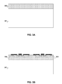
FIG. 1A is a cross-sectional schematic diagram illustrating a conventional IGBT according to the prior art. A conventional IGBT comprises a field stop layer 103 of n-type supported by a p+ substrate 101. An n− epitaxial/voltage blocking layer 105 is grown on top of the field stop layer 103. One or more cells can be formed with the epitaxial/voltage blocking layer 105. Each cell may include a p-type body region 107 formed within the epitaxial/voltage blocking layer 105 and one or more n+ emitter regions 109 formed within the p-type body region 107. Each cell may further include gate electrode insulator 111 (e.g., an oxide) formed on an exposed part of the p-type body region 107 and n+ emitter regions 109. A gate electrode 113 is formed on the gate insulator 111. Emitter electrodes 115 are formed on different portions of the body region 107 and emitter region 109. A collector electrode 117 can be formed on a back surface of the p+ substrate 101. The IGBT 100 is constructed similarly to an n-channel vertical MOSFET, except that the n+ drain is replaced with a p+ collector layer 101, thus forming a vertical PNP bipolar junction transistor. The additional p+ collector layer 101 creates a cascade connection of a PNP bipolar junction transistor with the surface n-channel MOSFET.
The IGBT provides more optimal performance in certain applications over a conventional MOSFET device. This is mainly due to the fact that the IGBT exhibits a significantly lower forward voltage drop in comparison to the MOSFET. However, the increase in forward voltage drop is off-set by the slow switching speeds of the IGBT device. Minority carriers that are injected into the n− epitaxial/voltage blocking layer 105 take time to enter and exit or recombine at turn on and turn off, resulting in longer switching times and higher switching losses in comparison to the MOSFET.
In response to the slow switching speeds of conventional IGBT devices, anode-shorted IGBT devices have been developed. The anode-shorted IGBT is superior to the conventional IGBT in that it exhibits more desirable switching characteristics while retaining the improved forward voltage drop. FIG. 1B is a cross-sectional schematic diagram illustrating a conventional anode-shorted IGBT in accordance with the prior art. The anode-shorted IGBT 100′ shown in FIG. 1B is essentially the same as the IGBT in FIG. 1A, except that the p+ substrate 101 in FIG. 1A is replaced by a layer consisting of alternating p-type regions 101 and n-type regions 119 in FIG. 1B. By alternating p-regions 101 and n-type regions 119 the IGBT is effectively provided an additional body diode as well as improved switching speeds.
Embodiments of the present invention relate to methods for fabricating such an anode-shorted insulated gate bipolar transistor (IGBT).
BRIEF DESCRIPTION OF THE DRAWINGS
FIG. 1A is a cross-sectional schematic diagram illustrating a conventional insulated gate bipolar transistor (IGBT) according to the prior art.
FIG. 1B is a cross-sectional schematic diagram illustrating a conventional anode-shorted insulated gate bipolar transistor (IGBT) according to the prior art.
FIGS. 2A-2H are cross-sectional schematic diagrams illustrating a method for manufacturing an anode-shorted field stop insulated gate bipolar transistor (IGBT) according to an embodiment of the present invention.
FIGS. 3A-3F are cross-sectional schematic diagrams illustrating a method for manufacturing an anode-shorted field stop insulated gate bipolar transistor (IGBT) according to an alternative embodiment of the present invention.
FIGS. 4A-4H are cross-sectional schematic diagrams illustrating a method for manufacturing an anode-shorted field stop insulated gate bipolar transistor (IGBT) according to another alternative embodiment of the present invention.
FIGS. 5A-5J are cross-sectional schematic diagrams illustrating a method for manufacturing an anode-shorted field stop insulated gate bipolar transistor (IGBT) according to another alternative embodiment of the present invention.
DESCRIPTION OF THE SPECIFIC EMBODIMENTS
Although the following detailed description contains many specific details for the purposes of illustration, anyone of ordinary skill in the art will appreciate that many variations and alterations to the following details are within the scope of the invention. Accordingly, the embodiments of the invention described below are set forth without any loss of generality to, and without imposing limitations upon, the claimed invention.
In the following detailed description, reference is made to the accompanying drawings, which form a part hereof, and in which is shown by way of illustration specific embodiments in which the invention may be practiced. In this regard, directional terminology, such as “top,” “bottom,” “front,” “back,” “leading,” “trailing,” etc., is used with reference to the orientation of the figure(s) being described. Because components of embodiments of the present invention can be positioned in a number of different orientations, the directional terminology is used for purposes of illustration and is in no way limiting. It is to be understood that other embodiments may be utilized and structural or logical changes may be made without departing from the scope of the present invention. The following detailed description, therefore, is not to be taken in a limiting sense, and the scope of the present invention is defined by the appended claims.
For convenience, use of + or − after a designation of conductivity or charge carrier type (p or n) refers generally to a relative degree of concentration of designated type of charge carriers within a semiconductor material. In general terms an n+ material has a higher negative charge carrier (e.g., electron) concentration than an n material and an n material has a higher carrier concentration than an n− material. Similarly, a p+ material has a higher positive charge carrier (e.g., hole) concentration than a p material and a p material has a higher concentration than a p− material. It is noted that what is relevant is the concentration of charge carriers, not necessarily dopants. For example, a material may be heavily doped with n-type dopants but still have a relatively low charge carrier concentration if the material is also sufficiently counter-doped with p-type dopants. As used herein, a concentration of dopants less than about 1016/cm3 may be regarded as “lightly doped” and a concentration of dopants greater than about 1017/cm3 may be regarded as “heavily doped”.
FIGS. 2A-2H are cross-sectional schematic diagrams illustrating a method for manufacturing an anode-shorted field stop insulated bipolar transistor (IGBT) according to an embodiment of the present invention. The fabrication method begins with a lightly doped p− substrate 201 as shown in FIG. 2A. A masked implant (mask not shown) is performed on the top surface of the substrate 201 in order to selectively form a plurality of first semiconductor regions 203 of a first conductivity type within a top surface of the substrate 201 as shown in FIG. 2B. By way of example, and not by way of limitation, the first conductivity type may be n+. The first semiconductor regions 203 may then be diffused to a desired depth. In some applications, it is preferable to diffuse the first semiconductor regions to a depth of at least 10 μm. In other applications, a width of the first semiconductor regions may be much smaller than a space between adjacent first semiconductor regions to minimize any snapback issues of the finished device.
After the one or more first semiconductor regions 203 have been formed, a field stop layer 205 of the first conductivity type may be grown onto the top surface of the substrate 201 as shown in FIG. 2C. The field stop layer 205 may have a lower concentration of charge carriers than the first semiconductor regions 203. By way of example, and not by way of limitation, the field stop layer 205 may be n type doped. An epitaxial/voltage blocking layer 207 of the first conductivity type may then be grown on top of the field stop layer 205 as illustrated in FIG. 2D. The voltage blocking layer 207 may have a lower concentration of charge carriers than the field stop layer 205.
One or more IGBT component cells 209 may then be formed on a top portion within the epitaxial/voltage blocking layer 207 as shown in FIG. 2E. The term “IGBT component cell” as defined herein will refer to a cell that includes a body region, one or more emitter regions, a gate electrode, one or more corresponding emitter electrodes, and insulating layers. While an IGBT component cell must include those particular components, one ordinarily skilled in the art will recognize that several different configurations may exist for implementing those IGBT components. For example, the IGBT in FIG. 1A illustrates one possible configuration for implementing an IGBT component cell including emitter regions formed within body regions and an insulated gate. The IGBT component cells 209 formed within the epitaxial/voltage blocking layer 207 may be any configuration so long as they comprise the components discussed above and retain their functionality.
The back surface of the substrate 201 is then thinned, e.g., by Taiko grinding, to a desired thickness such that the first semiconductor regions 203 are exposed as shown in FIG. 2F. The term “Taiko grinding” as used herein refers to a process of grinding an inner surface of a wafer while leaving an outer edge on the outermost circumference untouched. This method reduces the risk of thin wafer handling and lowers warping of the wafer during device processing. For certain applications, it is desirable to grind the back surface of the substrate 201 to a thickness of 5 μm an below the field stop layer 205.
A blanket implant of a second conductivity type is then performed on the back surface of the substrate 201, resulting in implant regions 211 being formed within the back surface of the substrate 201 as shown in FIG. 2G. By way of example, and not by way of limitation, the implant regions may be doped p+ type. Also by way of example, and not by way of limitation, the blanket implant may be a Boron implant with a doping concentration of 1×1016 cm−3 performed at an energy level of 40 KeV. The blanket implant is limited to minimal activation because the high temperatures (typically 900-1000 degree C. for 30 minutes) required to fully activate the implant regions 211 would destroy the IGBT cells 209. Because of the limited activation of the blanket implant, the first semiconductor regions 203 are unaffected by the p+ implant.
Lastly, metal 213 may be evaporated onto the back surface of the substrate 201 to form the collector electrode of the IGBT as shown in FIG. 2H. This process may be performed at 450° C. thereby partially activating the implant regions 211. The resulting structure is an anode-shorted field stop IGBT, with alternating p regions 201, 211 and n regions 203 forming the anode short circuit.
In this embodiment, the p+ regions 211 are implanted from the back at the end of the process, allowing accurate control of the injection efficiency of the IGBT without compromise to the IGBT field stop characteristics of positive temperature coefficient, fast switch without lifetime control and no increase in turn off energy Eoff with temperature. Further the p+ implant is carried out without a mask. This allows the wafer to be ground to a much thinner degree to reduce on resistance compare to the existing technology that uses masking process simply because masking would be difficult on a thin wafer.
FIGS. 3A-3F are cross-sectional schematic diagrams illustrating a method for manufacturing an anode-shorted field stop insulated gate bipolar transistor (IGBT) according to an alternative embodiment of the present invention. The fabrication method begins with an epitaxial/voltage blocking layer 303 that is formed on a very lightly doped substrate 301. The substrate and epitaxial layer may be doped with opposite conductivity types. By way of example, and not by way of limitation, the blocking layer 303 may be doped to be n− type and the substrate 301 may be doped p− type. One or more IGBT component cells 304 may then be formed within the epitaxial/voltage blocking layer 303 as shown in FIG. 3B. As noted above, the term “IGBT component cell” refers to a cell that includes a body region, one or more emitter regions, a gate electrode, one or more corresponding emitter electrodes, and insulating layers in any suitable/functional configuration, such as that shown in FIG. 1A.
The substrate 301 may be thinned, e.g., by grinding, to a desired thickness. A blanket implant of a the first conductivity type may then be performed to the back surface of the epitaxial/voltage blocking layer 301 to form a field stop layer 305 as shown in FIG. 3C. The field stop layer 305 may have a higher concentration of charge carriers than the blocking layer 301. By way of example, and not by way of limitation, the field stop layer 305 may be doped to be n type. Also by way of example and not by way of limitation, the blanket implant may be a Phosphorous implant with a doping concentration of 1-2×1013 cm−3 performed at an energy level ranging between 100-300 KeV.
A first shadow-masked (mask not shown) implant is then performed on a back surface of the field stop layer 305 to selectively form one or more first semiconductor regions 307 of a second conductivity type within the back surface of the field stop layer 305 as shown in FIG. 3D. The term “shadow mask” refers to a metal mask with patterned holes that may directly contact a wafer or may be remotely positioned in proximity to the wafer in order to form a desired pattern within or on top of the wafer. By way of example, and not by way of limitation, the first semiconductor regions 307 may be p+ type doped. Also by way of example, and not by way of limitation, the first shadow-masked implant may be a Boron implant with a doping concentration of 1×1016 cm−3 performed at an energy level of 40 KeV.
A second shadow-masked (mask not shown) implant is then performed on the back surface of the field stop layer 305 to selectively form one or more second semiconductor regions 309 of the first conductivity type within the back surface of the field stop layer 305 as shown in FIG. 3E. The second semiconductor regions 309 may be doped more heavily than the blocking layer 301 and field stop layer 305. By way of example and not by way of limitation, the second semiconductor regions 309 may be n+ type doped. Also by way of example and not by way of limitation, the second shadow-masked implant may be a Phosphorous implant with a doping concentration of 1×1016 cm−3 performed at an energy level of 40 KeV. The first semiconductor regions and the second semiconductor regions may then be laser activated. Laser activation is a process that involves directing a high-energy laser pulse at a desired location. Because of its short duration, the laser pulse activates the dopants without reaching the front surface of the device structure and damaging the IGBT component cells 303.
Lastly, metal 311 may be deposited onto the back surface of the first and second semiconductor regions 307, 309 to form the collector electrode of the IGBT as shown in FIG. 3F. By way of example and not by way of limitation, the metal 311 may be an aluminum-tin-nickel-silver (Al—Ti—Ni—Ag) alloy. The resulting structure is an anode-shorted field stop IGBT, with alternating p regions 307 and n regions 309 forming the anode short circuit. The use of two masks avoids counter-doping the heavy doped regions as described in process shown in FIG. 2G. In one embodiment the first shadow mask and the second shadow mask are complementary. In another embodiment a width of the semiconductor regions of the second conductivity type 307 is much larger than a width of the semiconductor regions of the first conductivity type 309.
FIGS. 4A-4H are cross-sectional schematic diagrams illustrating a method for manufacturing an anode-shorted field stop insulated gate bipolar transistor (IGBT) according to another alternative embodiment of the present invention. The fabrication method begins with an epitaxial/voltage blocking layer 403 formed on a substrate 401 as shown in FIG. 4A. The substrate and epitaxial layer may be of the same conductivity type but with different concentrations of charge carriers. By way of example, and not by way of limitation, the substrate 401 may be n+ type and the epitaxial layer 403 may be n-type. One or more IGBT component cells 404 may then be formed the epitaxial/voltage blocking layer 403 as shown in FIG. 4B. As noted above, the term “IGBT component cell” refers to a cell that includes a body region, one or more emitter regions, a gate electrode, one or more corresponding emitter electrodes, and insulating layers in any suitable/functional configuration.
The back surface of the epitaxial/voltage blocking layer 401 is then thinned, e.g. by Taiko grinding, to a desired thickness. As discussed above, the term “Taiko grinding” refers to a process of grinding an inner surface of a wafer while an outer edge on the outermost circumference remains untouched (not shown). A blanket implant of the first conductivity type is then performed to the back surface of the substrate 401 to form a field stop layer 405 as shown in FIG. 4C. The field stop layer 405 may have a higher concentration of charge carriers than the blocking layer 403 and a lower concentration of charge carriers than the substrate 401. By way of example, and not by way of limitation, the field stop layer 405 may be n type doped if the substrate 401 is n+ doped and the blocking layer 403 is n− doped. Also by way of example and not by way of limitation, the blanket implant may be a phosphorous implant with a doping concentration of 1-2×1013 cm−3 performed at staggered energies ranging up to 1 MeV in order to achieve a field stop layer 405 of several microns.
A blanket implant of the second conductivity type is performed to a back surface of the field stop layer 405 in order to form a first implant layer 407 of the second conductivity type within the back surface of the field stop layer 405 as shown in FIG. 4D. By way of example, and not by way of limitation, the first implant layer 407 may be p+ doped. Also by way of example and not by way of limitation, the blanket implant may be a boron implant with a doping concentration of 1×1016 cm−3 performed at an energy level of 40 KeV.
The dopants in the first implant layer 407 and field stop layer 405 may then be laser activated. As noted above, laser activation is a process that involves directing a high-energy laser pulse at a desired location. Because of their short duration, laser pulses do not penetrate into the front surfaces of the device structure.
After the first implant layer 407 and field stop layer 405 have been laser activated, a first metal layer 409 (e.g., an aluminum layer of 5000 Å) is deposited onto a backside of the first semiconductor layer 407 as shown in FIG. 4E. Isolated implant regions 407′ may then be selectively formed by laser cutting one or more portions of the first metal layer 409 and first semiconductor layer 407 such that one or more portions of the field stop layer 405 are exposed as shown in FIG. 4F.
A blanket implant of dopants of the first conductivity type is then performed to the exposed portions of the field stop layer 405 using the patterned first metal layer 409 as a mask in order to form second implant regions 411 within exposed portions of the field stop layer 405 between isolated implant regions 407′ as shown in FIG. 4G. The isolated implant regions 407′ are shielded from exposure to the blanket implant by the first metal layer 409. The second semiconductor regions 411 may be doped to have a higher concentration of charge carriers than the blocking layer 403 and the field stop layer 405. By way of example, and not by way of limitation, the second implant regions 411 may be doped n+ type if the blocking layer is doped n− and the field stop layer is doped n type. Also by way of example and not by way of limitation the blanket implant may be a phosphorous implant with a doping concentration of 1×1016 cm−3 performed at an energy level of 40 KeV. A second metal layer 413 may then be deposited over the first and second semiconductor regions 407′ and 411 as shown in FIG. 4H. By way of example, and not by way of limitation, the second metal layer 413 may be a titanium-nickel-silver (Ti—Ni—Ag) alloy. Prior to depositing the second metal layer 413 a sputter etch may be performed on the second metal layer 409 to remove any oxide formed on the first metal layer 409 due to exposure to the external environment. The second metal layer 413 and first metal layer 409 collectively form the collector electrode of the IGBT device. The resulting structure is an anode-shorted field stop IGBT, with alternating p implant regions 407′ and n implant regions 405 forming the anode short circuit.
The metal layers 409 and 413 can be different types of metals specifically chosen for their ability to make good contact with the differently doped implant regions 407′, 411. For example first the implant regions 407′ may be doped p+ type and the second implant regions 411 may be doped n type or n+ type. Aluminum makes good contact to p type regions and titanium makes good contact to n type or n+ type regions. In such a case, the first metal layer 409 may be Aluminum and the second metal layer 413 may be Titanium. The resulting structure provides good electrical contact to both implant regions 407′, 411. In addition, cutting an aluminum layer into pieces during the patterning process may reduce stress due to the differences in coefficient of thermal expansion (CTE) between Al and the underlying substrate material (e.g., Silicon).
FIG. 5A-5J are cross-sectional schematic diagrams illustrating a method for manufacturing an anode-shorted field stop insulated gate bipolar transistor (IGBT) according to another alternative embodiment of the present invention. The fabrication method begins with a substrate 501 as shown in FIG. 5A. By way of example, and not by way of limitation, the substrate 501 may be an n+ type substrate. By way of example, and not by way of limitation, the substrate 501 may have a thickness of approximately 700 μm. A first epitaxial layer 503 of the same conductivity type as the substrate is formed on a top surface of the substrate 501 as shown in FIG. 5B. The first epitaxial layer 503 is a semiconducting material of the same conductivity type as the substrate 501 but with a lower concentration of charge carriers than the substrate. By way of example, and not by way of limitation, the first epitaxial layer 503 may be n− type doped if the substrate 501 is doped n+ type. Also by way of example and not by way of limitation, the first epitaxial layer may have a thickness of approximately 10 μm.
After the first epitaxial layer 503 is formed, a field stop layer 505 may be formed on top of the first epitaxial layer 503 as shown in FIG. 5C. The field stop layer 505 is a semiconducting layer of the same conductivity type as the substrate and first epitaxial layer. The field stop layer has a charge carrier concentration that is greater than that of the first epitaxial layer 503 and less than that of the substrate 501. By way of example, and not by way of limitation, the field stop layer 505 may be n type doped if the substrate 501 is n+ type doped and the first epitaxial layer 505 is n− type doped. Also by way of example and not by way of limitation, the field stop layer 505 may have a thickness of approximately 5 μm. A second epitaxial layer 507 of the same conductivity type as the substrate 501, first epitaxial layer 503, and field stop layer 505 is then grown on top of the field stop layer 505 as shown in FIG. 5D. The second epitaxial layer 507 is sometimes referred to herein as the voltage blocking layer 507. The second epitaxial layer 507 may have a lower charge carrier concentration than the substrate 501 and the field stop layer 505. Again, by way of example, and not by way of limitation, the voltage blocking layer 507 may be n− type doped if the substrate 501 is n+ type doped, the first epitaxial layer 503 is n− type doped, and the field stop layer 505 is n type doped. Also, by way of example, and not by way of limitation, the voltage blocking layer may be approximately 100 μm for a 1200V IGBT device or approximately 50 μm for a 600V device.
One or more IGBT component cells 509 may then be formed within a top surface of the voltage blocking layer 507 as shown in FIG. 5E. As noted above, the term “IGBT component cell” refers to a cell that includes a body region, one or more emitter regions, a gate electrode, one or more corresponding emitter electrodes, and insulating layers in any suitable/functional configuration. Following formation of the IGBT component cells 509 the substrate 501 is thinned to a desired thickness by removing material from a back side of the substrate as shown in FIG. 5F. The substrate 501 may be thinned, e.g., by grinding it from the back side. For certain applications, the desired thickness of the substrate 501 after grinding is approximately 5 μm.
A masked metal deposition is then performed on the back surface of the substrate 501 to form a metal pattern 511 on the back surface of the substrate 501 as illustrated in FIG. 5G. The masked deposition may be implemented using a shadow mask, similar to the one discussed above. An anisotropic etch (e.g., a wet etch) may then be performed on the substrate 501 using the metal pattern 511 as a mask, so that one or more portions of the first epitaxial layer 503 are exposed, while leaving portions of the substrate 501 under the metal pattern as shown in FIG. 5H. For certain applications, the desired etch-depth may be approximately 10 μm, depending on the thickness of the substrate remaining after thinning.
A backside blanket implant is then performed on the substrate 501 to implant dopants of an opposite conductivity type to that of the substrate 501, field stop layer 505, and epitaxial layer 503, 507 into exposed portions of the first epitaxial layer 503 and the substrate 501. The dopant implant forms implant regions 513 as shown in FIG. 5I. An annealing process may then be completed to activate the implant regions 513. By way of example and not by way of limitation, if the substrate 501, field stop layer 505, and epitaxial layers 503, 507 are doped n+, n, and n− type, respectively, the implant regions may be doped p+ type.
Lastly a metal layer 511′ is deposited onto a back surface of the implant regions 513 and a back surface of the metal pattern 511 in order to form a collector electrode for the IGBT device. The resulting structure is an anode-shorted field stop IGBT, with alternating semiconductor regions of opposite conductivity type formed by the implant regions 513 and remaining portions of the substrate 501 forming the anode short circuit.
While the above is a complete description of the preferred embodiments of the present invention, it is possible to use various alternatives, modifications, and equivalents. Therefore, the scope of the present invention should be determined not with reference to the above description but should, instead, be determined with reference to the appended claims, along with their full scope of equivalents. Any feature, whether preferred or not, may be combined with any other feature, whether preferred or not. In the claims that follow, the indefinite article “A” or “An” refers to a quantity of one or more of the items following the article, except where expressly stated otherwise. The appended claims are not to be interpreted as including means-plus-function limitations, unless such a limitation is explicitly recited in a given claim using the phrase “means for”. Any element in a claim that does not explicitly state “means for” performing a specified function, is not to be interpreted as a “means” or “step” clause as specified in 35 USC §112, ¶ 6.

Claims (9)

What is claimed is:
1. A method for fabricating an anode-shorted field stop insulated gate bipolar transistor (IGBT), comprising:
a) selectively forming first semiconductor regions of a first conductivity type within a top surface of a semiconductor substrate, wherein the first conductivity type is opposite a conductivity type of the substrate;
b) growing a field stop layer of the first conductivity type onto the top surface of the substrate, wherein the field stop layer has a lower concentration of charge carriers than the first semiconductor regions;
c) growing an epitaxial layer of the first conductivity type on top of the field stop layer, wherein the epitaxial layer has a lower concentration of charge carriers than the field stop layer;
d) forming one or more insulated gate bipolar transistors (IGBT) component cells within the epitaxial layer;
e) thinning a back surface of the substrate to a desired thickness and expose the first semiconductor regions;
f) performing a blanket implant to form implant regions of a second conductivity type opposite that of the epitaxial layer and field stop layer within the back surface of the substrate, wherein is performed after the first semiconductor regions of a first conductivity type are formed on the top surface of the semiconductor substrate, wherein activation of the blanket implant is limited to minimal activation at less than 900° C.; and
g) evaporating metal onto the back surface of the substrate.
2. The method of claim 1, wherein the substrate is a p− type substrate.
3. The method of claim 2, wherein the first semiconductor region is doped n+, the field stop layer is doped n and the epitaxial layer is doped n−.
4. The method of claim 3, wherein the implant regions are doped p+.
5. The method of claim 1, wherein forming the first semiconductor regions comprises performing a masked implant followed by diffusion.
6. The method of claim 5, wherein the first semiconductor regions are diffused at least 10 μm into the top surface of the substrate.
7. The method of claim 1, wherein the desired thickness in e) is 5 μm below the field stop layer.
8. The method of claim 1, wherein the blanket implant in f) is a Boron implant with a concentration of 1e16 performed at 40 keV.
9. The method of claim 1, wherein g) is performed at 450° C.
US13/192,385 2011-07-27 2011-07-27 Methods for fabricating anode shorted field stop insulated gate bipolar transistor Active 2034-03-07 US9478646B2 (en)

Priority Applications (6)

Application Number Priority Date Filing Date Title
US13/192,385 US9478646B2 (en) 2011-07-27 2011-07-27 Methods for fabricating anode shorted field stop insulated gate bipolar transistor
CN201610892855.9A CN107068563A (en) 2011-07-27 2012-07-20 For the method for the field stop igbt for preparing anode in short circuit
CN201210251772.3A CN102903633B (en) 2011-07-27 2012-07-20 For the method for the field stop igbt for preparing anode in short circuit
TW101127314A TWI520327B (en) 2011-07-27 2012-07-27 Methods for fabricating anode shorted field stop insulated gate bipolar transistor
US15/177,191 US10050134B2 (en) 2011-07-27 2016-06-08 Methods for fabricating anode shorted field stop insulated gate bipolar transistor
US15/917,415 US10522666B2 (en) 2011-07-27 2018-03-09 Methods for fabricating anode shorted field stop insulated gate bipolar transistor

Applications Claiming Priority (1)

Application Number Priority Date Filing Date Title
US13/192,385 US9478646B2 (en) 2011-07-27 2011-07-27 Methods for fabricating anode shorted field stop insulated gate bipolar transistor

Related Child Applications (1)

Application Number Title Priority Date Filing Date
US15/177,191 Division US10050134B2 (en) 2011-07-27 2016-06-08 Methods for fabricating anode shorted field stop insulated gate bipolar transistor

Publications (2)

Publication Number Publication Date
US20130029461A1 US20130029461A1 (en) 2013-01-31
US9478646B2 true US9478646B2 (en) 2016-10-25

Family

ID=47575816

Family Applications (3)

Application Number Title Priority Date Filing Date
US13/192,385 Active 2034-03-07 US9478646B2 (en) 2011-07-27 2011-07-27 Methods for fabricating anode shorted field stop insulated gate bipolar transistor
US15/177,191 Active 2031-10-06 US10050134B2 (en) 2011-07-27 2016-06-08 Methods for fabricating anode shorted field stop insulated gate bipolar transistor
US15/917,415 Active US10522666B2 (en) 2011-07-27 2018-03-09 Methods for fabricating anode shorted field stop insulated gate bipolar transistor

Family Applications After (2)

Application Number Title Priority Date Filing Date
US15/177,191 Active 2031-10-06 US10050134B2 (en) 2011-07-27 2016-06-08 Methods for fabricating anode shorted field stop insulated gate bipolar transistor
US15/917,415 Active US10522666B2 (en) 2011-07-27 2018-03-09 Methods for fabricating anode shorted field stop insulated gate bipolar transistor

Country Status (3)

Country Link
US (3) US9478646B2 (en)
CN (2) CN102903633B (en)
TW (1) TWI520327B (en)

Cited By (3)

* Cited by examiner, † Cited by third party
Publication number Priority date Publication date Assignee Title
WO2019157222A1 (en) * 2018-02-07 2019-08-15 Ipower Semiconductor Igbt devices with 3d backside structures for field stop and reverse conduction
US10522666B2 (en) 2011-07-27 2019-12-31 Alpha And Omega Semiconductor Incorporated Methods for fabricating anode shorted field stop insulated gate bipolar transistor
US11233141B2 (en) 2018-01-16 2022-01-25 Ipower Semiconductor Self-aligned and robust IGBT devices

Families Citing this family (16)

* Cited by examiner, † Cited by third party
Publication number Priority date Publication date Assignee Title
JP6265594B2 (en) * 2012-12-21 2018-01-24 ラピスセミコンダクタ株式会社 Semiconductor device manufacturing method and semiconductor device
CN103268861A (en) * 2013-04-03 2013-08-28 吴宗宪 Method for manufacturing FS (field stop) type IGBT (insulated gate bipolar transistor) by multiple epitaxies
CN104241124A (en) * 2013-06-24 2014-12-24 无锡华润上华半导体有限公司 Manufacturing method of non punch through reverse conducting insulated gate bipolar transistor
CN104425258B (en) * 2013-08-30 2017-10-27 无锡华润上华科技有限公司 The manufacture method of reverse-conducting cut-off insulated gate bipolar transistor
CN104979194B (en) * 2014-04-03 2019-03-22 节能元件控股有限公司 End insulated gate bipolar transistor and preparation method thereof in reverse-conducting field
CN105225946A (en) * 2014-06-30 2016-01-06 比亚迪股份有限公司 Inverse conductivity type IGBT structure and forming method thereof
CN106206694A (en) * 2015-05-06 2016-12-07 北大方正集团有限公司 A kind of power device and preparation method thereof
CN106816377B (en) * 2015-11-30 2019-11-22 株洲中车时代电气股份有限公司 The back side IGBT production method and IGBT
US10388781B2 (en) 2016-05-20 2019-08-20 Alpha And Omega Semiconductor Incorporated Device structure having inter-digitated back to back MOSFETs
US9905522B1 (en) * 2016-09-01 2018-02-27 Semiconductor Components Industries, Llc Semiconductor copper metallization structure and related methods
CN109429531A (en) * 2017-07-05 2019-03-05 力特有限公司 IGBT with improved reverse blocking capability
CN107359198A (en) * 2017-08-14 2017-11-17 深圳市芯电元科技有限公司 Novel anode short circuit type IGBT and preparation method thereof
US11342410B2 (en) * 2019-09-27 2022-05-24 Alpha And Omega Semiconductor (Cayman) Ltd. Improving IGBT light load efficiency
US11101137B1 (en) * 2020-03-19 2021-08-24 Alpha And Omega Semiconductor International Lp Method of making reverse conducting insulated gate bipolar transistor
CN112951906B (en) * 2021-01-25 2024-02-06 南瑞联研半导体有限责任公司 SiC insulated gate bipolar transistor device and manufacturing method thereof
CN114141883B (en) * 2021-12-10 2022-09-20 富芯微电子有限公司 Manufacturing method of fast recovery diode chip

Citations (16)

* Cited by examiner, † Cited by third party
Publication number Priority date Publication date Assignee Title
US4450467A (en) 1978-09-14 1984-05-22 Hitachi, Ltd. Gate turn-off thyristor with selective anode penetrating shorts
US5156981A (en) * 1988-04-08 1992-10-20 Kabushiki Kaisha Toshiba Method of making a semiconductor device of a high withstand voltage
US5286655A (en) 1992-06-12 1994-02-15 Kabushiki Kaisha Toshiba Method of manufacturing a semiconductor device of an anode short circuit structure
US5360984A (en) 1991-11-29 1994-11-01 Fuji Electric Co., Ltd. IGBT with freewheeling diode
US20010040255A1 (en) * 2000-05-15 2001-11-15 Masahiro Tanaka Electrode contact section of semiconductor device
JP2002190596A (en) * 2000-12-21 2002-07-05 Toshiba Corp Method of manufacturing semiconductor device
US7112868B2 (en) 2002-10-30 2006-09-26 Infineon Technologies Ag IGBT with monolithic integrated antiparallel diode
US7132321B2 (en) * 2002-10-24 2006-11-07 The United States Of America As Represented By The Secretary Of The Navy Vertical conducting power semiconductor devices implemented by deep etch
US7250639B1 (en) * 2001-07-17 2007-07-31 Mitsubishi Denki Kabushiki Kaisha Insulated gate bipolar transistor
US20080090391A1 (en) * 2006-10-13 2008-04-17 Kabushiki Kaisha Toshiba Method for manufacturing semiconductor device
US7456484B2 (en) 2006-01-10 2008-11-25 Denso Corporation Semiconductor device having IGBT and diode
US7498634B2 (en) 2006-01-10 2009-03-03 Denso Corporation Semiconductor device having IGBT and diode
US20120025261A1 (en) * 2010-07-30 2012-02-02 Madhur Bobde Method of minimizing field stop insulated gate bipolar transistor (IGBT) buffer and emitter charge variation
US8242536B2 (en) 2009-01-27 2012-08-14 Denso Corporation Semiconductor device
US8299539B2 (en) 2008-10-14 2012-10-30 Denso Corporation Semiconductor device having IGBT and FWD on same substrate
US8378427B2 (en) 2009-02-27 2013-02-19 University Of Electronic Science And Technology High speed IGBT

Family Cites Families (11)

* Cited by examiner, † Cited by third party
Publication number Priority date Publication date Assignee Title
US4958211A (en) * 1988-09-01 1990-09-18 General Electric Company MCT providing turn-off control of arbitrarily large currents
US5981981A (en) * 1993-10-13 1999-11-09 Mitsubishi Denki Kabushiki Kaisha Semiconductor device including a bipolar structure
DE4433796A1 (en) * 1994-09-22 1996-03-28 Daimler Benz Ag Controllable semiconductor device
JP2005057235A (en) * 2003-07-24 2005-03-03 Mitsubishi Electric Corp Insulated gate type bipolar transistor, its manufacturing method, and inverter circuit
US20070181927A1 (en) * 2006-02-03 2007-08-09 Yedinak Joseph A Charge balance insulated gate bipolar transistor
EP2073271A1 (en) * 2007-12-19 2009-06-24 ABB Technology AG Reverse-conducting insulated gate bipolar transistor and method for manufacturing such a reverse-conducting insulated gate bipolar transistor
JP5963385B2 (en) * 2008-11-26 2016-08-03 富士電機株式会社 Semiconductor device
US8299494B2 (en) * 2009-06-12 2012-10-30 Alpha & Omega Semiconductor, Inc. Nanotube semiconductor devices
US8466060B2 (en) * 2010-04-30 2013-06-18 Alpha & Omega Semiconductor, Inc. Stackable power MOSFET, power MOSFET stack, and process of manufacture
JP5621334B2 (en) * 2010-06-10 2014-11-12 富士電機株式会社 Semiconductor device and manufacturing method of semiconductor device
US9478646B2 (en) 2011-07-27 2016-10-25 Alpha And Omega Semiconductor Incorporated Methods for fabricating anode shorted field stop insulated gate bipolar transistor

Patent Citations (16)

* Cited by examiner, † Cited by third party
Publication number Priority date Publication date Assignee Title
US4450467A (en) 1978-09-14 1984-05-22 Hitachi, Ltd. Gate turn-off thyristor with selective anode penetrating shorts
US5156981A (en) * 1988-04-08 1992-10-20 Kabushiki Kaisha Toshiba Method of making a semiconductor device of a high withstand voltage
US5360984A (en) 1991-11-29 1994-11-01 Fuji Electric Co., Ltd. IGBT with freewheeling diode
US5286655A (en) 1992-06-12 1994-02-15 Kabushiki Kaisha Toshiba Method of manufacturing a semiconductor device of an anode short circuit structure
US20010040255A1 (en) * 2000-05-15 2001-11-15 Masahiro Tanaka Electrode contact section of semiconductor device
JP2002190596A (en) * 2000-12-21 2002-07-05 Toshiba Corp Method of manufacturing semiconductor device
US7250639B1 (en) * 2001-07-17 2007-07-31 Mitsubishi Denki Kabushiki Kaisha Insulated gate bipolar transistor
US7132321B2 (en) * 2002-10-24 2006-11-07 The United States Of America As Represented By The Secretary Of The Navy Vertical conducting power semiconductor devices implemented by deep etch
US7112868B2 (en) 2002-10-30 2006-09-26 Infineon Technologies Ag IGBT with monolithic integrated antiparallel diode
US7456484B2 (en) 2006-01-10 2008-11-25 Denso Corporation Semiconductor device having IGBT and diode
US7498634B2 (en) 2006-01-10 2009-03-03 Denso Corporation Semiconductor device having IGBT and diode
US20080090391A1 (en) * 2006-10-13 2008-04-17 Kabushiki Kaisha Toshiba Method for manufacturing semiconductor device
US8299539B2 (en) 2008-10-14 2012-10-30 Denso Corporation Semiconductor device having IGBT and FWD on same substrate
US8242536B2 (en) 2009-01-27 2012-08-14 Denso Corporation Semiconductor device
US8378427B2 (en) 2009-02-27 2013-02-19 University Of Electronic Science And Technology High speed IGBT
US20120025261A1 (en) * 2010-07-30 2012-02-02 Madhur Bobde Method of minimizing field stop insulated gate bipolar transistor (IGBT) buffer and emitter charge variation

Cited By (4)

* Cited by examiner, † Cited by third party
Publication number Priority date Publication date Assignee Title
US10522666B2 (en) 2011-07-27 2019-12-31 Alpha And Omega Semiconductor Incorporated Methods for fabricating anode shorted field stop insulated gate bipolar transistor
US11233141B2 (en) 2018-01-16 2022-01-25 Ipower Semiconductor Self-aligned and robust IGBT devices
US11239352B2 (en) 2018-01-16 2022-02-01 Ipower Semiconductor Self-aligned and robust IGBT devices
WO2019157222A1 (en) * 2018-02-07 2019-08-15 Ipower Semiconductor Igbt devices with 3d backside structures for field stop and reverse conduction

Also Published As

Publication number Publication date
CN102903633A (en) 2013-01-30
CN107068563A (en) 2017-08-18
TW201306254A (en) 2013-02-01
US10050134B2 (en) 2018-08-14
US10522666B2 (en) 2019-12-31
CN102903633B (en) 2017-08-15
US20130029461A1 (en) 2013-01-31
TWI520327B (en) 2016-02-01
US20160284797A1 (en) 2016-09-29
US20180204937A1 (en) 2018-07-19

Similar Documents

Publication Publication Date Title
US10522666B2 (en) Methods for fabricating anode shorted field stop insulated gate bipolar transistor
WO2016010097A1 (en) Semiconductor device and semiconductor device manufacturing method
JP6111572B2 (en) Semiconductor device and manufacturing method of semiconductor device
US8653535B2 (en) Silicon carbide semiconductor device having a contact region that includes a first region and a second region, and process for production thereof
US9443926B2 (en) Field-stop reverse conducting insulated gate bipolar transistor and manufacturing method therefor
US11824090B2 (en) Back side dopant activation in field stop IGBT
CN108346688B (en) SiC trench junction barrier Schottky diode with CSL transport layer and manufacturing method thereof
WO2015024502A1 (en) Manufacturing method for reverse conducting insulated gate bipolar transistor
US10096699B2 (en) Field-stop reverse conducting insulated gate bipolar transistor and manufacturing method therefor
JP2018170392A (en) Semiconductor device and method of manufacturing the same
KR101875287B1 (en) A method for forming a semiconductor device
WO2018000223A1 (en) Insulated gate bipolar transistor structure and manufacturing method therefor
CN108010964B (en) IGBT device and manufacturing method thereof
US9029235B2 (en) Trench isolation MOS P-N junction diode device and method for manufacturing the same
JP2007019518A (en) Semiconductor component having field stop
JPH10200132A (en) High speed diode
CN109216436B (en) Semiconductor device and method for manufacturing the same
US9502534B2 (en) Preparation method for power diode
US11508809B2 (en) Semiconductor device and preparation method thereof
CN107452621B (en) Fast recovery diode and manufacturing method thereof
US7291899B2 (en) Power semiconductor component
CN113892189A (en) Silicon carbide semiconductor device and method for manufacturing silicon carbide semiconductor device
JP2008103392A (en) Semiconductor device and manufacturing method of the semiconductor device
CN109166914B (en) Field resistance type IGBT structure and manufacturing method thereof
US11637192B2 (en) Metal oxide semiconductor-controlled thyristor device having uniform turn-off characteristic and method of manufacturing the same

Legal Events

Date Code Title Description
AS Assignment

Owner name: ALPHA AND OMEGA SEMICONDUCTOR INCORPORATED, CALIFO

Free format text: ASSIGNMENT OF ASSIGNORS INTEREST;ASSIGNORS:BHALLA, ANUP;BOBDE, MADHUR;DING, YONGPING;AND OTHERS;SIGNING DATES FROM 20110726 TO 20110727;REEL/FRAME:026660/0919

STCF Information on status: patent grant

Free format text: PATENTED CASE

MAFP Maintenance fee payment

Free format text: PAYMENT OF MAINTENANCE FEE, 4TH YEAR, LARGE ENTITY (ORIGINAL EVENT CODE: M1551); ENTITY STATUS OF PATENT OWNER: LARGE ENTITY

Year of fee payment: 4

MAFP Maintenance fee payment

Free format text: PAYMENT OF MAINTENANCE FEE, 8TH YEAR, LARGE ENTITY (ORIGINAL EVENT CODE: M1552); ENTITY STATUS OF PATENT OWNER: LARGE ENTITY

Year of fee payment: 8