US9502841B2 - Flippable electrical connector - Google Patents
Flippable electrical connector Download PDFInfo
- Publication number
- US9502841B2 US9502841B2 US15/161,307 US201615161307A US9502841B2 US 9502841 B2 US9502841 B2 US 9502841B2 US 201615161307 A US201615161307 A US 201615161307A US 9502841 B2 US9502841 B2 US 9502841B2
- Authority
- US
- United States
- Prior art keywords
- contacts
- pair
- plug connector
- sections
- receiving cavity
- Prior art date
- Legal status (The legal status is an assumption and is not a legal conclusion. Google has not performed a legal analysis and makes no representation as to the accuracy of the status listed.)
- Active
Links
Images


Classifications
-
- H—ELECTRICITY
- H01—ELECTRIC ELEMENTS
- H01R—ELECTRICALLY-CONDUCTIVE CONNECTIONS; STRUCTURAL ASSOCIATIONS OF A PLURALITY OF MUTUALLY-INSULATED ELECTRICAL CONNECTING ELEMENTS; COUPLING DEVICES; CURRENT COLLECTORS
- H01R24/00—Two-part coupling devices, or either of their cooperating parts, characterised by their overall structure
- H01R24/60—Contacts spaced along planar side wall transverse to longitudinal axis of engagement
-
- H—ELECTRICITY
- H01—ELECTRIC ELEMENTS
- H01R—ELECTRICALLY-CONDUCTIVE CONNECTIONS; STRUCTURAL ASSOCIATIONS OF A PLURALITY OF MUTUALLY-INSULATED ELECTRICAL CONNECTING ELEMENTS; COUPLING DEVICES; CURRENT COLLECTORS
- H01R12/00—Structural associations of a plurality of mutually-insulated electrical connecting elements, specially adapted for printed circuits, e.g. printed circuit boards [PCB], flat or ribbon cables, or like generally planar structures, e.g. terminal strips, terminal blocks; Coupling devices specially adapted for printed circuits, flat or ribbon cables, or like generally planar structures; Terminals specially adapted for contact with, or insertion into, printed circuits, flat or ribbon cables, or like generally planar structures
- H01R12/50—Fixed connections
- H01R12/51—Fixed connections for rigid printed circuits or like structures
- H01R12/53—Fixed connections for rigid printed circuits or like structures connecting to cables except for flat or ribbon cables
-
- H—ELECTRICITY
- H01—ELECTRIC ELEMENTS
- H01R—ELECTRICALLY-CONDUCTIVE CONNECTIONS; STRUCTURAL ASSOCIATIONS OF A PLURALITY OF MUTUALLY-INSULATED ELECTRICAL CONNECTING ELEMENTS; COUPLING DEVICES; CURRENT COLLECTORS
- H01R13/00—Details of coupling devices of the kinds covered by groups H01R12/70 or H01R24/00 - H01R33/00
- H01R13/40—Securing contact members in or to a base or case; Insulating of contact members
- H01R13/405—Securing in non-demountable manner, e.g. moulding, riveting
-
- H—ELECTRICITY
- H01—ELECTRIC ELEMENTS
- H01R—ELECTRICALLY-CONDUCTIVE CONNECTIONS; STRUCTURAL ASSOCIATIONS OF A PLURALITY OF MUTUALLY-INSULATED ELECTRICAL CONNECTING ELEMENTS; COUPLING DEVICES; CURRENT COLLECTORS
- H01R13/00—Details of coupling devices of the kinds covered by groups H01R12/70 or H01R24/00 - H01R33/00
- H01R13/62—Means for facilitating engagement or disengagement of coupling parts or for holding them in engagement
- H01R13/627—Snap or like fastening
- H01R13/6271—Latching means integral with the housing
- H01R13/6273—Latching means integral with the housing comprising two latching arms
-
- H—ELECTRICITY
- H01—ELECTRIC ELEMENTS
- H01R—ELECTRICALLY-CONDUCTIVE CONNECTIONS; STRUCTURAL ASSOCIATIONS OF A PLURALITY OF MUTUALLY-INSULATED ELECTRICAL CONNECTING ELEMENTS; COUPLING DEVICES; CURRENT COLLECTORS
- H01R13/00—Details of coupling devices of the kinds covered by groups H01R12/70 or H01R24/00 - H01R33/00
- H01R13/62—Means for facilitating engagement or disengagement of coupling parts or for holding them in engagement
- H01R13/627—Snap or like fastening
- H01R13/6275—Latching arms not integral with the housing
-
- H—ELECTRICITY
- H01—ELECTRIC ELEMENTS
- H01R—ELECTRICALLY-CONDUCTIVE CONNECTIONS; STRUCTURAL ASSOCIATIONS OF A PLURALITY OF MUTUALLY-INSULATED ELECTRICAL CONNECTING ELEMENTS; COUPLING DEVICES; CURRENT COLLECTORS
- H01R13/00—Details of coupling devices of the kinds covered by groups H01R12/70 or H01R24/00 - H01R33/00
- H01R13/648—Protective earth or shield arrangements on coupling devices, e.g. anti-static shielding
- H01R13/658—High frequency shielding arrangements, e.g. against EMI [Electro-Magnetic Interference] or EMP [Electro-Magnetic Pulse]
- H01R13/6581—Shield structure
- H01R13/6582—Shield structure with resilient means for engaging mating connector
- H01R13/6583—Shield structure with resilient means for engaging mating connector with separate conductive resilient members between mating shield members
-
- H—ELECTRICITY
- H01—ELECTRIC ELEMENTS
- H01R—ELECTRICALLY-CONDUCTIVE CONNECTIONS; STRUCTURAL ASSOCIATIONS OF A PLURALITY OF MUTUALLY-INSULATED ELECTRICAL CONNECTING ELEMENTS; COUPLING DEVICES; CURRENT COLLECTORS
- H01R24/00—Two-part coupling devices, or either of their cooperating parts, characterised by their overall structure
- H01R24/28—Coupling parts carrying pins, blades or analogous contacts and secured only to wire or cable
- H01R24/30—Coupling parts carrying pins, blades or analogous contacts and secured only to wire or cable with additional earth or shield contacts
-
- H—ELECTRICITY
- H01—ELECTRIC ELEMENTS
- H01R—ELECTRICALLY-CONDUCTIVE CONNECTIONS; STRUCTURAL ASSOCIATIONS OF A PLURALITY OF MUTUALLY-INSULATED ELECTRICAL CONNECTING ELEMENTS; COUPLING DEVICES; CURRENT COLLECTORS
- H01R4/00—Electrically-conductive connections between two or more conductive members in direct contact, i.e. touching one another; Means for effecting or maintaining such contact; Electrically-conductive connections having two or more spaced connecting locations for conductors and using contact members penetrating insulation
- H01R4/02—Soldered or welded connections
- H01R4/023—Soldered or welded connections between cables or wires and terminals
-
- H—ELECTRICITY
- H01—ELECTRIC ELEMENTS
- H01R—ELECTRICALLY-CONDUCTIVE CONNECTIONS; STRUCTURAL ASSOCIATIONS OF A PLURALITY OF MUTUALLY-INSULATED ELECTRICAL CONNECTING ELEMENTS; COUPLING DEVICES; CURRENT COLLECTORS
- H01R12/00—Structural associations of a plurality of mutually-insulated electrical connecting elements, specially adapted for printed circuits, e.g. printed circuit boards [PCB], flat or ribbon cables, or like generally planar structures, e.g. terminal strips, terminal blocks; Coupling devices specially adapted for printed circuits, flat or ribbon cables, or like generally planar structures; Terminals specially adapted for contact with, or insertion into, printed circuits, flat or ribbon cables, or like generally planar structures
- H01R12/70—Coupling devices
- H01R12/71—Coupling devices for rigid printing circuits or like structures
- H01R12/72—Coupling devices for rigid printing circuits or like structures coupling with the edge of the rigid printed circuits or like structures
- H01R12/722—Coupling devices for rigid printing circuits or like structures coupling with the edge of the rigid printed circuits or like structures coupling devices mounted on the edge of the printed circuits
- H01R12/724—Coupling devices for rigid printing circuits or like structures coupling with the edge of the rigid printed circuits or like structures coupling devices mounted on the edge of the printed circuits containing contact members forming a right angle
-
- H—ELECTRICITY
- H01—ELECTRIC ELEMENTS
- H01R—ELECTRICALLY-CONDUCTIVE CONNECTIONS; STRUCTURAL ASSOCIATIONS OF A PLURALITY OF MUTUALLY-INSULATED ELECTRICAL CONNECTING ELEMENTS; COUPLING DEVICES; CURRENT COLLECTORS
- H01R13/00—Details of coupling devices of the kinds covered by groups H01R12/70 or H01R24/00 - H01R33/00
- H01R13/646—Details of coupling devices of the kinds covered by groups H01R12/70 or H01R24/00 - H01R33/00 specially adapted for high-frequency, e.g. structures providing an impedance match or phase match
- H01R13/6473—Impedance matching
- H01R13/6474—Impedance matching by variation of conductive properties, e.g. by dimension variations
-
- H—ELECTRICITY
- H01—ELECTRIC ELEMENTS
- H01R—ELECTRICALLY-CONDUCTIVE CONNECTIONS; STRUCTURAL ASSOCIATIONS OF A PLURALITY OF MUTUALLY-INSULATED ELECTRICAL CONNECTING ELEMENTS; COUPLING DEVICES; CURRENT COLLECTORS
- H01R2107/00—Four or more poles
-
- H—ELECTRICITY
- H05—ELECTRIC TECHNIQUES NOT OTHERWISE PROVIDED FOR
- H05K—PRINTED CIRCUITS; CASINGS OR CONSTRUCTIONAL DETAILS OF ELECTRIC APPARATUS; MANUFACTURE OF ASSEMBLAGES OF ELECTRICAL COMPONENTS
- H05K1/00—Printed circuits
- H05K1/02—Details
- H05K1/11—Printed elements for providing electric connections to or between printed circuits
- H05K1/117—Pads along the edge of rigid circuit boards, e.g. for pluggable connectors
-
- H—ELECTRICITY
- H05—ELECTRIC TECHNIQUES NOT OTHERWISE PROVIDED FOR
- H05K—PRINTED CIRCUITS; CASINGS OR CONSTRUCTIONAL DETAILS OF ELECTRIC APPARATUS; MANUFACTURE OF ASSEMBLAGES OF ELECTRICAL COMPONENTS
- H05K1/00—Printed circuits
- H05K1/18—Printed circuits structurally associated with non-printed electric components
- H05K1/182—Printed circuits structurally associated with non-printed electric components associated with components mounted in the printed circuit board, e.g. insert mounted components [IMC]
- H05K1/184—Components including terminals inserted in holes through the printed circuit board and connected to printed contacts on the walls of the holes or at the edges thereof or protruding over or into the holes
-
- H—ELECTRICITY
- H05—ELECTRIC TECHNIQUES NOT OTHERWISE PROVIDED FOR
- H05K—PRINTED CIRCUITS; CASINGS OR CONSTRUCTIONAL DETAILS OF ELECTRIC APPARATUS; MANUFACTURE OF ASSEMBLAGES OF ELECTRICAL COMPONENTS
- H05K2201/00—Indexing scheme relating to printed circuits covered by H05K1/00
- H05K2201/09—Shape and layout
- H05K2201/09009—Substrate related
- H05K2201/09063—Holes or slots in insulating substrate not used for electrical connections
-
- H—ELECTRICITY
- H05—ELECTRIC TECHNIQUES NOT OTHERWISE PROVIDED FOR
- H05K—PRINTED CIRCUITS; CASINGS OR CONSTRUCTIONAL DETAILS OF ELECTRIC APPARATUS; MANUFACTURE OF ASSEMBLAGES OF ELECTRICAL COMPONENTS
- H05K2201/00—Indexing scheme relating to printed circuits covered by H05K1/00
- H05K2201/10—Details of components or other objects attached to or integrated in a printed circuit board
- H05K2201/10007—Types of components
- H05K2201/10189—Non-printed connector
Definitions
- the present invention relates to an electrical connector, and more particularly to a flippable plug connector used with a receptacle connector.
- the plug connector is “flippable” whereas we turn the plug over and it functions the same top and bottom.
- a MUX or SS switch
- This can be costly and also cause some additional degredation in the super speed signals.
- USB Universal Serial Bus
- the object of the present invention is to provide a plug connector for provision of power, comprises an insulative housing forming a receiving cavity with two opposite sites in a vertical direction which is compatible with a standard plug connector with twelve contacts on each site and a first and second rows of contacts disposed on the opposite sides while in diagonally symmetrical manner.
- Each of the contacts includes a front contacting section, and a rear connecting section for directly connecting to a corresponding wire or via a circuit pad of a paddle card to the corresponding wire.
- Each row of contacts is categorized with a pair of power contacts and a pair of grounding contacts and a CC (Configuration Channel) contacts without any high speed differential pair.
- FIG. 1 is an assembled perspective view of a plug connector and a mated receptacle connector on the printed circuit board, of a first embodiment of the instant invention.
- FIG. 2 is a front assembled perspective view of the plug connector of FIG. 1 .
- FIG. 3(A) is a front partially exploded perspective view of the plug connector of FIG. 2 wherein the cover is removed away from the remainder.
- FIG. 3(B) is a front partially exploded perspective view of the plug connector of FIG. 3(A) wherein the front and rear over-moldings have been further removed.
- FIG. 4 is a front partially exploded perspective view of the plug connector of FIG. 2 without the cover thereof.
- FIG. 5 is a front partially exploded perspective view of the plug connector of FIG. 4 by removal of additional parts therefrom.
- FIG. 6 is a cross-sectional view of the mated plug connector and receptacle connector taken along lines 6 - 6 in FIG. 1 .
- FIG. 7(A) is a front assembled perspective view of a partially assembled plug connector according to a second embodiment of the invention.
- FIG. 7(B) is a rear assembled perspective view of the plug connector of FIG. 7(A) .
- FIG. 8(A) is a front partially exploded perspective view of the plug connector of FIG. 7(A) .
- FIG. 8(B) is a rear partially exploded perspective view of the plug connector of FIG. 7(B) .
- FIG. 9(A) is a front partially exploded perspective view of the plug connector of FIG. 8(A) .
- FIG. 9(B) is a rear partially exploded perspective view of the plug connector of FIG. 8(B) .
- FIG. 10(A) is a front partially exploded perspective view of the plug connector of FIG. 9(A) .
- FIG. 10(B) is a rear partially exploded perspective view of the plug connector of FIG. 9(B) .
- FIG. 11 is a horizontal view of a lower portion of the plug connector of FIG. 7(A) .
- FIG. 12(A) is an enlarged front perspective view to show how all ten contacts are arranged structurally.
- FIG. 12(B) is an enlarged rear perspective view to show how all ten contacts are arranged structurally.
- FIG. 13 is a front assembled perspective view of the plug connector of a third embodiment according to the invention.
- FIG. 14 is a front partially exploded perspective view of the plug connector of FIG. 13 .
- FIG. 15 is a further front exploded perspective view of the plug connector of FIG. 14 .
- FIG. 16(A) is a further front exploded perspective view of the plug connector of FIG. 15 .
- FIG. 16(B) is a further rear exploded perspective view of the plug connector of FIG. 15 .
- FIG. 17(A) is a further front exploded perspective view of the plug connector of FIG. 16(A) .
- FIG. 17(B) is a further rear exploded perspective view of the plug connector of FIG. 16(B) .
- FIG. 18(A) is a further front exploded perspective view of the plug connector of FIG. 17(A) .
- FIG. 18(B) is a further rear exploded perspective view of the plug connector of FIG. 17(B) .
- FIG. 19(A) is a front assembled perspective view of a terminal module assembly of the receptacle connector of a fourth embodiment.
- FIG. 19(B) is a front assembled perspective view of a terminal module assembly of the receptacle connector of FIG. 19(A) .
- FIG. 20(A) is a front exploded perspective view of the terminal module of the receptacle connector of FIG. 19(A) .
- FIG. 20(B) is a rear exploded perspective view of the terminal module of the receptacle connector of FIG. 19(B) .
- FIG. 21(A) is a further front exploded perspective view of the terminal module of the receptacle connector of FIG. 20(A) .
- FIG. 21(B) is a further front exploded perspective view of the terminal module of the receptacle connector of FIG. 21(B) .
- FIG. 22(A) is a front assembled perspective view of a fifth embodiment of the plug connector mounted to the printed circuit board in a docking manner.
- FIG. 22(B) is a rear assembled perspective view of the plug connector of FIG. 22(A) .
- FIG. 23(A) is a front exploded perspective view of the plug connector of FIG. 22(A) .
- FIG. 23(B) is a rear exploded perspective view of the plug connector of FIG. 22(B) .
- FIG. 24(A) is a further front exploded perspective view of the plug connector of FIG. 23(A) .
- FIG. 24(B) is a further rear exploded perspective view of the plug connector of FIG. 23(B) .
- FIG. 25 is a cross-sectional view of the plug connector taken along lines 25 - 25 of FIG. 22(A) .
- FIG. 26 is a perspective view of the laptop computer with a detachable display using the plug connector of FIG. 23(A) on the base and a corresponding receptacle connector thereon.
- FIG. 27 is a perspective view of the assembly unit used in the laptop computer of FIG. 26 and including the plug connector of FIG. 23(A) and the corresponding receptacle.
- FIG. 28 is the perspective view of the sub-assembly unit used in the base with the plug connector of FIG. 23(A) .
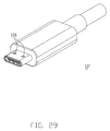
- FIG. 29 is a perspective view of another embodiment of the plug connector according to the invention.
- FIG. 30 is a perspective view of another embodiment of the plug connector according to the invention.
- FIG. 31 is an exploded perspective view of the plug connector of FIG. 30 .
- FIG. 32(A) is a further upward exploded perspective view of the plug connector of FIG. 31 .
- FIG. 32(B) is a further downward exploded perspective view of the plug connector of FIG. 31 .
- FIG. 33(A) is a further upward exploded perspective view of the plug connector of FIG. 32(A) .
- FIG. 33(B) is a further downward exploded perspective view of the plug connector of FIG. 32(B) .
- FIG. 34(A) is a further front downward exploded perspective view of the plug connector without the cable and the shielding covers thereof.
- FIG. 34(B) is a further rearward upward exploded perspective view of the plug connector without the cable and the shielding covers thereof.
- FIG. 35(A) is a front exploded perspective view of the terminal module assembly of the plug connector of FIG. 34(A) .
- FIG. 35(B) is a rear exploded perspective view of the terminal module assembly of the plug connector of FIG. 34(A) .
- FIG. 36(A) is a further front downward exploded perspective view of the terminal module assembly of FIG. 35(A) .
- FIG. 36(B) is a further rear upward exploded perspective view of the terminal module assembly of FIG. 35(A) .
- FIG. 36(C) is a further rear downward exploded perspective view of the terminal module assembly of FIG. 35(B) .
- FIG. 37(A) is a further front downward exploded perspective view of the terminal module assembly of FIG. 36(A) wherein the terminals are fully exposed to an exterior.
- FIG. 37(B) is a further rear upward exploded perspective view of the terminal module assembly of FIG. 36(B) wherein the terminals are fully exposed to an exterior.
- FIG. 38(A) is a front downward exploded perspective view of a combination of only the terminal and the latch.
- FIG. 38(B) is an upward exploded perspective view of the combination of FIG. 38(A) .
- FIG. 38(C) is a cross-sectional view of the combination of FIG. 38(A)
- FIG. 38(D) is a cross-sectional view of the combination with the associated insulator of the terminal module assembly.
- FIG. 1 show a plug connector 10 mated with a receptacle connector 50 mounted in a notch of a printed circuit board 100 .
- the plug connector 10 includes an insulative housing 12 having a capsular front contour with a rectangular receiving cavity 14 therein and enclosed in a metallic shell 16 .
- Opposite upper and lower rows of contacts 18 are disposed in the corresponding passageways 32 of the housing with corresponding contacting sections 20 extending into the receiving cavity 14 wherein the upper and lower rows of contacts 18 are diagonally symmetrically arranged with each other in both electrical and mechanical arrangement so as to meet the so-called flappable mating, i.e., the dual opposite orientations.
- a pair of metallic upper and lower EMI (Electro-Magnetic Interference) spring plates 22 are enclosed in the shell 16 , and each of the EMI spring plates 22 is sandwiched between the shell 16 and the housing 12 and includes a front resilient region 24 extending inwardly toward and into the receiving cavity 14 and in front of the contacting sections 20 , a rear abutting region 26 to abut against the shell 16 , and a pair of side retention regions 28 retainably engaged within corresponding side portions of the housing 12 .
- a pair of tapes 30 are disposed upon two opposite sides of the housing 12 so as to isolate the contacting section 20 from the shell 16 .
- a spacer 34 is located behind the housing and defines a plurality of passages 35 through which the tail sections 21 of the contacts 18 rearwardly extend.
- a recessed region 36 is formed in a rear face of the spacer 34 to receive a front edge region of a paddle card 38 wherein the tail sections 21 of the contacts 18 extending through the corresponding passages 35 , are soldered upon the corresponding pads 37 .
- the spacer 34 forms a forward extending blade 31 with a pair of forward protrusions 33 on two sides to be commonly inserted into a back side of the housing 12 wherein the protrusions 33 of the blade 31 are essentially received in the side slots 13 of the housing 12 .
- a U-shaped metallic latch 39 of a blanking type received in the side slots 13 of the housing 12 with a pair of locking heads 40 extending into the two opposite lateral sides of the receiving cavity 14 to lock with the lateral edge sections 67 of the shielding plate 76 of the receptacle connector 50 during mating. Understandably, the latch 39 is restrained by the blade 31 , the comb structures on the blade 31 , the protrusions 33 of the blade 31 , the slots 13 and an interior rear face of the housing 12 .
- a cable 41 behind the paddle card 38 encloses a plurality of wires 42 regulated by a pair of organizer 43 to be soldered upon a rear region of the paddle card 38 .
- an auxiliary rear shell 17 grasps the shell 16 to shield the paddle card 38
- a clipper 44 grasps the rear shell 17 and further the cable 41 behind the paddle card 38 .
- Opposite front overcoat 45 and rear overcoat or strain relief 46 are overmolded upon the rear shell 17 and the clipper 44 , respectively.
- a cover 47 essentially fully covers the clipper 44 , the front overcoat 45 and the rear overcoat 46 .
- the mating tongue 54 is received in the receiving cavity 14 with the corresponding contacting sections 60 of the contacts 58 of the receptacle connector 50 connected to the contacting sections 20 of the contacts 18 of the plug connector 10 wherein the latch 39 is locked with the shielding plate 76 , and the front resilient region 24 of the spring plate 22 contacts the collar 64 .
- FIGS. 7(A)-12(B) show a second embodiment of the plug connector 510 wherein compared with the plug connector disclosed in the previous first embodiment, the plug connector 510 only provides the power by the less number of the contacts only involved with the power delivery.
- the plug connector 510 includes an insulative housing 512 enclosed within a metallic shell 514 and defining a receiving cavity 516 .
- Opposite first and second rows of contacts 520 only categorized with power contacts, grounding contacts and CC contacts are disposed in the housing 512 with unequal intervals while arranged in a diagonally symmetrical manner with regard to the receiving cavity 516 so as to allow a flippable insertion of the plug connector 510 into the corresponding receptacle connector.
- Each contact 520 includes a front contacting section 522 and a rear connecting section 524 .
- the contacting section 522 of each row of contacts 520 are categorized with the contacting sections 522 G of a pair of grounding contacts 520 commonly sandwiching therebetween the contacting sections 522 P of a pair of power contacts 520 which successively sandwich a contacting section 522 C of a CC (Configuration Channel) contact 520 therebetween.
- the connecting sections 524 of the contacts 520 in the first row are categorized with a pair of intimately side by side connecting sections 524 G of the grounding contact 520 in the first row and that derived from the second row, cooperate with a pair of intimately side by side contacting connecting sections 524 P of the power contact 520 in the first row and that derived from the second row to commonly sandwich a connecting section 524 C of the CC contact 520 derived from the second row in a transverse direction.
- the connecting sections 524 of the contacts 520 in the second row follow the same rule.
- each row the connecting sections 524 of both the power contacts and grounding contacts 520 are spanned in one transverse direction while that of the remaining the CC contact 520 is spanned in an opposite transverse direction.
- the paired grounding contacts 520 have the corresponding contacting sections 522 G spaced from each other in a vertical direction while having the corresponding connecting sections 524 G intimately side by side contacting each other in the transverse direction perpendicular to said vertical direction.
- the power contacts 520 are as well.
- An insulative spacer 530 is located behind the housing 512 with opposite surfaces 532 on which the corresponding connecting sections 524 P, 524 G and 524 C are exposed.
- the insulative spacer 530 comprises a front section 5301 retained with the insulating housing and a rear flat portion 5302 behind the insulative housing 512 , the rear flat portion 5302 defines a top surface and a lower surface, the connecting sections of the two rows of contacts embedded in the rear flat portion 5302 and expose to the upper and lower surface of the rear flat portion 5302 to be directly soldered to wires of a cable 540 .
- the cable 540 is located behind the spacer 530 and includes four power wires 542 , two grounding wires 544 and one CC wire 546 wherein the four power 542 wires are soldered to two pairs of connecting sections 524 P in a one-to-one relation, each of the two grounding wires 544 is soldered to one of the pair of connecting sections 524 G on the corresponding surface 532 .
- the CC wire 546 is soldered to either one of the connecting sections 524 C on the spacer 530 .
- the corresponding wires 542 , 544 , 546 may be simplified and easily organized and soldered to the corresponding connecting sections 524 G, 524 P and 524 C, respectively.
- a pair of spring plates 550 are assembled to the housing 512 with spring tangs 552 extending into the receiving cavity 516 for coupling to the corresponding receptacle connector.
- a H-shaped metallic latch 560 is assembled to the housing 512 with a pair of locking heads 562 located at a front portion and extending into the receiving cavity 516 for latching to the corresponding receptacle connector, and a pair of connecting tails 564 located at a rear portion and extending through the spacer 530 and respectively located on two opposite surfaces 532 for connecting to the braiding of the cable 540 .
- the rear connecting tails 564 are offset from each other in the vertical direction for respectively mounted to the opposite surfaces 532 of the spacer.
- the paddle card is omitted but replaced with the spacer for supporting the connecting sections 524 of the contacts 520 for directly soldering to the corresponding wires in an organized manner.
- a paddle card 590 is horizontally positioned behind the spacer and includes a plurality of front circuit pads 591 on the front edge region to be soldered with the tails 524 of the corresponding contacts 520 , and a plurality of rear circuit pads 592 on the rear edge region to be soldered with the inner conductors 5451 of the corresponding wires, respectively.
- the feature of the embodiment is to arrange the rear circuit pads (as labeled 592 P) for the power contacts on one surface of the paddle card 590 while those (as labeled 592 G) for the grounding contacts on the other surface thereof.
- the three grounding wires are diametrically smaller than the two power contacts.
- the front circuit pads 591 are still aligned with the corresponding power and grounding contacts 520 in the front-to-back direction without shifting. Understandably, in this embodiment the cable only contains the power wires and the grounding wires to mechanically and electrically connect to the corresponding rear power circuit pads 592 P and the corresponding rear grounding circuit pads 592 G.
- a metallic shell 514 encloses the housing 512 , and a pair of metallic covers 581 , 582 are secured to each other and commonly sandwich and retain the assembled housing 512 , the shielding shell 514 and cable to form a subassembly.
- An inner overmolding part 588 encloses the subassembly and an outer overmolding part 589 encloses the inner overmolding part 588 while exposing the front mating port and the rear cable extension.
- the spacer 530 further forms a lateral extension 531 to be received in a corresponding recess 5821 of the cover 581 , 582 for precisely positioning the covers 581 , 582 with regard to the subassembly.
- the metallic shell 514 defies a rear retaining portion 5141
- one of the cover 581 , 582 defines a pair of front retaining portion 5811 on lateral sides thereof which are fitly embrace corresponding portion of the rear retaining portion 5141 of the metallic shell 514 .
- the covers 581 , 582 further defines a pair of retaining plates 5812 , 5822 being soldered to corresponding portion of the rear retaining portion 5141 .
- the pair of front retaining portions are also soldered to the rear retaining portion 5141 .
- the upper terminal module 340 includes an upper insulator 350 with one five contacts 310 , instead of twelve contacts 310 , being integrally formed therewith and the lower terminal module 342 includes a lower insulator 360 with only seven contacts 310 , instead of twelve contacts 310 , being integrally formed therewith.
- the contacts 310 comprises contacting section 311 extending into the receiving cavity and tail sections 3102 embedded in rear flat portions 351 , 361 of corresponding insulators.
- the rear flat portions 351 , 361 of the upper and lower insulator are disposed behind the insulative housing 320 .
- the tail sections 312 of the upper and lower contacts are exposed on a top surface of the rear flat portions 351 , 361 of the upper insulator and a lower surface of rear flat portions of the lower insulator to be directly soldered to the corresponding wires of the cable.
- the upper and lower insulators 340 , 342 comprises a retaining hole 3411 / 3511 and a retaining post 3512 / 34121 fitly engaged with each other to assembled the upper and lower terminal module together, on front flat portions 352 , 362 thereof. The front portions of the upper and lower insulators are retained in insulative housing.
- the paddle card can have the fine pitch of the tail sections of the contacts for connection.
- the tail sections 312 of the contacts 310 are required to be directly soldered to the corresponding wires and thus is desired to be enlarged in width and fanned outwardly for compliance with the wire dimension/position for soldering consideration; in fact, the widened tail sections 312 take/occupy the original space of those of the omitted contacts on the insulator 350 , 360 so as to allow the whole set of the plug connector 300 to keep the similar transverse dimension of the insulators 350 , 360 as original for miniaturization consideration advantageously.
- each contact 310 includes a barb structure 318 in front of the offset section 314 to retain the corresponding contact 310 within the corresponding passageway in the housing 320 .
- the plug connector 200 includes an insulative housing 202 with a metallic shell 204 attached thereon.
- the housing 202 has a base portion 206 with a main portion 208 extending therefrom on the middle region so as to form a pair of side wings 210 with corresponding through holes 212 extending therethrough.
- the main portion 208 is similar to the housing 12 and forming a receiving cavity 214 with two rows of contacts 216 by two opposite elongated sides.
- a pair of EMI spring plates 218 are positioned upon the main portion 208 and extend into the receiving cavity 214 , and a pair of insulative tapes 221 are positioned upon the corresponding EMI spring plates 218 for isolating the EMI spring plates 218 from the metallic shell 204 .
- the plug connector 200 also includes the side latch to engage the shielding plate in the mating tongue of the corresponding receptacle connector.
- the metallic shell 204 includes a main section 220 with a pair of side arms 222 by two sides, and each side arm 222 forms a through holes 224 therein.
- the main section 220 encloses the mating portion 208 , and the pair of side arms 222 cover the pair of side wings 210 with the corresponding through holes 212 and 224 aligned with each other in the mating direction.
- the laptop computer 230 includes a base 232 and a detachable display 234 .
- the base 232 includes a rotatable subassembly 236 pivotally mounted at a longitudinal side while the display 234 includes a securing section 238 on the corresponding longitudinal side thereof.
- the plug connector 200 is mounted to a printed circuit board 235 of the subassembly 236 in a floating manner along the mating direction via a pair of springs 240 .
- the subassembly 236 also includes a pair of latches 242 retractably moveable in the transverse direction along the longitudinal side for locking to the securing section 238 of the display 234 .
- the corresponding receptacle connector 244 is located on the securing section 238 of the display 234 for mating the plug connector 200 .
- FIGS. 30-38 (D) shows another embodiment of the plug/cable connector with the corresponding terminals arranged in a diagonally symmetrical manner so as to be used with a flippable way
- the plug/cable connector 700 includes an insulative housing 702 enclosed within a metallic shell 701 and defining a mating cavity 704 to receive a mating tongue of the complementary receptacle connector, and a plurality of passageways 706 located beside the mating cavity 704 in a vertical direction.
- a pair of spring plates 710 are attached to the housing 702 with spring tangs 712 extending into the mating cavity 704 .
- An insulative tape 714 is attached upon the housing 702 to isolate the corresponding terminals from the metallic shell 701 (illustrated later)
- a terminal module assembly 720 includes opposite upper and lower terminal modules 722 and 724 commonly sandwiching an H-shaped metallic latch 726 therebetween in a vertical direction.
- the upper terminal module 722 includes an upper insulator 728 integrally formed with a plurality of upper terminals 730 via the insert-molding process
- the lower terminal module 724 includes a lower insulator 732 integrally formed with a plurality of lower terminals 734 via the insert-molding process.
- a pair of posts 736 of the lower insulator 732 are received within the corresponding holes 738 in the upper insulator 728 .
- the lower insulator 732 further includes a raised block 740 received within the corresponding notch 742 of the upper insulator 728 wherein contacting sections of a specific pair of lower terminals 734 extend upward and join, at a same level, the contacting section of the upper terminals 730 via supporting of the block 740 .
- the upper terminals 730 are categorized with the grounding terminals G, the power terminals P and the CC terminal while the lower terminal 734 are similarly categorized with the grounding terminals G, the power terminals P, the Vconn terminal and signal terminals D+/D ⁇ .
- the signal terminals D+/D ⁇ are the aforementioned specific pair of lower terminals 734 which are supported by the raised block 740 .
- the tail section of the corresponding power terminals P, the grounding terminals G and the signal terminals D+/D ⁇ are labeled as T(P), T(G) and T(D).
- This embodiment is to have the corresponding grounding terminals G integrated with one another, and have the corresponding power terminals P integrated with one another. It is noted that to ease the soldering between the solderable tail section T(P), T(G) and T(D) of the corresponding lower terminal 734 and the latch 726 or the tail section T of the corresponding upper terminal 730 , the lower insulator 732 forms a soldering platform 733 to retain the tail sections T(P), T(G) and T(D) of the corresponding lower terminals 734 in a coplanar manner, i.e., having the similar thickness thereof. Notably, as shown in FIGS.
- the two power upper terminals 730 /P are joined together by sharing the same tail section T(P), and the two power lower terminals 734 /P are also joined together by sharing the same tail section T(P) abutting against the aforementioned tail section T(P) so as to have those four power terminals electrically joined as one piece.
- the grounding upper terminals 730 /G downwardly abut respectively against the two corresponding side arms of the latch 726
- the grounding lower terminals 734 /G sidewardly abut respectively against the two corresponding side arms of the latch 726 so as to have those four grounding terminals electrically joined together. As shown in FIGS.
- some tiny slits are intentionally formed between the tail sections T(G), T(P) and the platform 733 so as to allow the solder material to be filled therein to join the corresponding tail sections T(P) of the upper terminal 730 and the lower terminal 734 , and to join the corresponding tail sections T(G) of the lower terminal 734 and the latch 726 , and the tail section T(G) of the upper terminal 730 and the latch 726 when a soldering process is applied through a hot bar.
- One feature of the invention is to have the wire W(P) for power, the wire W(G) for grounding, and the wires W(D+)/W(D ⁇ ) for signal are soldered upon the tail sections T(P), T(G) and T(D)s on the same bottom side for simplifying the manufacturing process compared with the previous embodiment shown in FIGS. 7(A)-12(B) in which the corresponding four wires are soldered upon two opposite sides of the terminal module. Anyhow, two pairs of the grounding contacts are unified together and two pairs of the power contacts are unified together are required according to the standard specification. The instant embodiment and the previous embodiment are used to implement such a request.
- a resistor R is adapted to be soldered between the upper terminal CC and the power upper terminal 730 /P on the other side.
- the four wires are joined within a cable 800 .
- a pair of metallic covers 802 are assembled upon the rear side of the shell 701 to shield the exposed wires and protect the soldering thereabouts.
- An insulative cover 804 are overmolded upon the metallic covers 802 and integrally joined with the cable 800 to finalize the whole product.
Abstract
A plug for provision of power includes a housing forming a receiving cavity with two opposite sites in a vertical direction which is compatible with a standard plug connector with twelve contacts on each site and a first and second rows of contacts on the sides while in diagonally symmetrical manner. Each contact includes a contacting section, and a connecting section for directly connecting to a corresponding wire. Each row of contacts is categorized with a pair of power contacts, a pair of grounding contacts and a specific contact without any high speed differential pair. Two pair of power contacts of both two rows are electrically connected together either via direct mechanical connection via vertical extensions or via indirect electrical connection via the latch which has a pair of side arms extending into the receiving cavity at two opposite transverse ends.
Description
This application is a continuation of application Ser. No. 14/698,876 filed on Apr. 29, 2015, which is a continuation-in-part of the co-pending application Ser. No. 14/667,632 filed Mar. 24, 2015 and Ser. No. 14/558,732 filed Dec. 3, 2014 and further claims the benefit of, and priority to, U.S. Provisional Patent Application No. 62/002,934, filed May 26, 2014, No. 62/021,066, filed Jul. 4, 2014, No. 62/026,046 filed Jul. 18, 2014, and No. 62/035,472 filed Aug. 10, 2014, the contents of which are incorporated entirely herein by reference.
1. Field of the Invention
The present invention relates to an electrical connector, and more particularly to a flippable plug connector used with a receptacle connector.
2. Description of Related Art
In the previously filed provisional applications, the plug connector is “flippable” whereas we turn the plug over and it functions the same top and bottom. In order to be able to handle switching of the super speed signaling, a MUX (or SS switch) is built into the silicon. This can be costly and also cause some additional degredation in the super speed signals. Recently, a proposal for use with the future USB (Universal Serial Bus) was presented.
Hence, a new and simple electrical plug connector and the complementary receptacle connector are desired to improve those disclosed in the aforementioned proposal.
Accordingly, the object of the present invention is to provide a plug connector for provision of power, comprises an insulative housing forming a receiving cavity with two opposite sites in a vertical direction which is compatible with a standard plug connector with twelve contacts on each site and a first and second rows of contacts disposed on the opposite sides while in diagonally symmetrical manner. Each of the contacts includes a front contacting section, and a rear connecting section for directly connecting to a corresponding wire or via a circuit pad of a paddle card to the corresponding wire. Each row of contacts is categorized with a pair of power contacts and a pair of grounding contacts and a CC (Configuration Channel) contacts without any high speed differential pair.
Other objects, advantages and novel features of the invention will become more apparent from the following detailed description when taken in conjunction with the accompanying drawings.
Reference will now be made in detail to the preferred embodiment of the present invention.
A cable 41 behind the paddle card 38, encloses a plurality of wires 42 regulated by a pair of organizer 43 to be soldered upon a rear region of the paddle card 38. Via the protrusions and openings (not labeled), an auxiliary rear shell 17 grasps the shell 16 to shield the paddle card 38, and a clipper 44 grasps the rear shell 17 and further the cable 41 behind the paddle card 38. Opposite front overcoat 45 and rear overcoat or strain relief 46 are overmolded upon the rear shell 17 and the clipper 44, respectively. Finally, a cover 47 essentially fully covers the clipper 44, the front overcoat 45 and the rear overcoat 46. During mating, the mating tongue 54 is received in the receiving cavity 14 with the corresponding contacting sections 60 of the contacts 58 of the receptacle connector 50 connected to the contacting sections 20 of the contacts 18 of the plug connector 10 wherein the latch 39 is locked with the shielding plate 76, and the front resilient region 24 of the spring plate 22 contacts the collar 64.
An insulative spacer 530 is located behind the housing 512 with opposite surfaces 532 on which the corresponding connecting sections 524P, 524G and 524C are exposed. The insulative spacer 530 comprises a front section 5301 retained with the insulating housing and a rear flat portion 5302 behind the insulative housing 512, the rear flat portion 5302 defines a top surface and a lower surface, the connecting sections of the two rows of contacts embedded in the rear flat portion 5302 and expose to the upper and lower surface of the rear flat portion 5302 to be directly soldered to wires of a cable 540. The cable 540 is located behind the spacer 530 and includes four power wires 542, two grounding wires 544 and one CC wire 546 wherein the four power 542 wires are soldered to two pairs of connecting sections 524P in a one-to-one relation, each of the two grounding wires 544 is soldered to one of the pair of connecting sections 524G on the corresponding surface 532. The CC wire 546 is soldered to either one of the connecting sections 524C on the spacer 530. In brief, on each surface 532, there are five connection sections 524 including a pair of intimately side by side arranged connecting sections 524G and a pair of intimately side by side arranged connecting sections 524P and a connecting section 524C therebetween in the transverse direction. And on one surface 532, two power wires 542 are soldered upon the corresponding pair of connecting sections 524P, one grounding wire 544 is soldered upon one of the pair of connecting sections 524G, and the CC wire 546 is soldered upon the corresponding connecting section 524C. Similarly, on the other surface 532, there are two power wires 542 and one grounding wire 544 are soldered unto the corresponding connecting sections 524P and 524G while no CC wire 546 is available thereon. Understandably, via the connecting sections 524 offset, in a vertical direction, from the corresponding contacting sections 522 in some contacts 520, the corresponding wires 542, 544, 546 may be simplified and easily organized and soldered to the corresponding connecting sections 524G, 524P and 524C, respectively.
Similar to the first embodiment, a pair of spring plates 550 are assembled to the housing 512 with spring tangs 552 extending into the receiving cavity 516 for coupling to the corresponding receptacle connector. A H-shaped metallic latch 560 is assembled to the housing 512 with a pair of locking heads 562 located at a front portion and extending into the receiving cavity 516 for latching to the corresponding receptacle connector, and a pair of connecting tails 564 located at a rear portion and extending through the spacer 530 and respectively located on two opposite surfaces 532 for connecting to the braiding of the cable 540. Notably, different from the front locking heads 562 are located at the same plane, the rear connecting tails 564 are offset from each other in the vertical direction for respectively mounted to the opposite surfaces 532 of the spacer. Clearly, in this embodiment, because only the power/ground/CC contacts are disposed in the housing 512, the paddle card is omitted but replaced with the spacer for supporting the connecting sections 524 of the contacts 520 for directly soldering to the corresponding wires in an organized manner.
Referring to FIGS. 13-18 (B) showing a third embodiment of the plug connector 510 a, which is similar to the second embodiment with tiny differences. Different from the previous second embodiment, in this embodiment the contacts 520 essentially only has twelve pieces including the power contacts, the configuration channel, the grounding contacts and optionally the low speed differential pairs without the super speed differential pairs. A paddle card 590 is horizontally positioned behind the spacer and includes a plurality of front circuit pads 591 on the front edge region to be soldered with the tails 524 of the corresponding contacts 520, and a plurality of rear circuit pads 592 on the rear edge region to be soldered with the inner conductors 5451 of the corresponding wires, respectively. The feature of the embodiment is to arrange the rear circuit pads (as labeled 592P) for the power contacts on one surface of the paddle card 590 while those (as labeled 592G) for the grounding contacts on the other surface thereof. Notably, in this embodiment, the three grounding wires are diametrically smaller than the two power contacts. On other hand, the front circuit pads 591 are still aligned with the corresponding power and grounding contacts 520 in the front-to-back direction without shifting. Understandably, in this embodiment the cable only contains the power wires and the grounding wires to mechanically and electrically connect to the corresponding rear power circuit pads 592P and the corresponding rear grounding circuit pads 592G. Anyhow, additional lower speed differential pair wires may be contained to be electrically connected to the low speed differential pair contact via the paddle card 590 optionally. A metallic shell 514 encloses the housing 512, and a pair of metallic covers 581, 582 are secured to each other and commonly sandwich and retain the assembled housing 512, the shielding shell 514 and cable to form a subassembly. An inner overmolding part 588 encloses the subassembly and an outer overmolding part 589 encloses the inner overmolding part 588 while exposing the front mating port and the rear cable extension. In this embodiment the spacer 530 further forms a lateral extension 531 to be received in a corresponding recess 5821 of the cover 581, 582 for precisely positioning the covers 581, 582 with regard to the subassembly. The metallic shell 514 defies a rear retaining portion 5141, one of the cover 581, 582 defines a pair of front retaining portion 5811 on lateral sides thereof which are fitly embrace corresponding portion of the rear retaining portion 5141 of the metallic shell 514. The covers 581, 582 further defines a pair of retaining plates 5812, 5822 being soldered to corresponding portion of the rear retaining portion 5141. The pair of front retaining portions are also soldered to the rear retaining portion 5141.
Referring to FIGS. 22-28 , according to a fifth embodiment of the invention, the plug connector 200 includes an insulative housing 202 with a metallic shell 204 attached thereon. The housing 202 has a base portion 206 with a main portion 208 extending therefrom on the middle region so as to form a pair of side wings 210 with corresponding through holes 212 extending therethrough. The main portion 208 is similar to the housing 12 and forming a receiving cavity 214 with two rows of contacts 216 by two opposite elongated sides. A pair of EMI spring plates 218 are positioned upon the main portion 208 and extend into the receiving cavity 214, and a pair of insulative tapes 221 are positioned upon the corresponding EMI spring plates 218 for isolating the EMI spring plates 218 from the metallic shell 204. Understandably, similar to the first embodiment the plug connector 200 also includes the side latch to engage the shielding plate in the mating tongue of the corresponding receptacle connector. The metallic shell 204 includes a main section 220 with a pair of side arms 222 by two sides, and each side arm 222 forms a through holes 224 therein. Notably, the main section 220 encloses the mating portion 208, and the pair of side arms 222 cover the pair of side wings 210 with the corresponding through holes 212 and 224 aligned with each other in the mating direction.
Referring to FIGS. 23-25 , the laptop computer 230 includes a base 232 and a detachable display 234. The base 232 includes a rotatable subassembly 236 pivotally mounted at a longitudinal side while the display 234 includes a securing section 238 on the corresponding longitudinal side thereof. The plug connector 200 is mounted to a printed circuit board 235 of the subassembly 236 in a floating manner along the mating direction via a pair of springs 240. The subassembly 236 also includes a pair of latches 242 retractably moveable in the transverse direction along the longitudinal side for locking to the securing section 238 of the display 234. The corresponding receptacle connector 244 is located on the securing section 238 of the display 234 for mating the plug connector 200.
A terminal module assembly 720 includes opposite upper and lower terminal modules 722 and 724 commonly sandwiching an H-shaped metallic latch 726 therebetween in a vertical direction. The upper terminal module 722 includes an upper insulator 728 integrally formed with a plurality of upper terminals 730 via the insert-molding process, and the lower terminal module 724 includes a lower insulator 732 integrally formed with a plurality of lower terminals 734 via the insert-molding process. A pair of posts 736 of the lower insulator 732 are received within the corresponding holes 738 in the upper insulator 728. The lower insulator 732 further includes a raised block 740 received within the corresponding notch 742 of the upper insulator 728 wherein contacting sections of a specific pair of lower terminals 734 extend upward and join, at a same level, the contacting section of the upper terminals 730 via supporting of the block 740. In a detailed description, in the upper terminals 730 are categorized with the grounding terminals G, the power terminals P and the CC terminal while the lower terminal 734 are similarly categorized with the grounding terminals G, the power terminals P, the Vconn terminal and signal terminals D+/D−. Notably, the signal terminals D+/D− are the aforementioned specific pair of lower terminals 734 which are supported by the raised block 740. The tail section of the corresponding power terminals P, the grounding terminals G and the signal terminals D+/D− are labeled as T(P), T(G) and T(D).
This embodiment is to have the corresponding grounding terminals G integrated with one another, and have the corresponding power terminals P integrated with one another. It is noted that to ease the soldering between the solderable tail section T(P), T(G) and T(D) of the corresponding lower terminal 734 and the latch 726 or the tail section T of the corresponding upper terminal 730, the lower insulator 732 forms a soldering platform 733 to retain the tail sections T(P), T(G) and T(D) of the corresponding lower terminals 734 in a coplanar manner, i.e., having the similar thickness thereof. Notably, as shown in FIGS. 38(A)-38(D) , the two power upper terminals 730/P are joined together by sharing the same tail section T(P), and the two power lower terminals 734/P are also joined together by sharing the same tail section T(P) abutting against the aforementioned tail section T(P) so as to have those four power terminals electrically joined as one piece. On the other hand, the grounding upper terminals 730/G downwardly abut respectively against the two corresponding side arms of the latch 726, and the grounding lower terminals 734/G sidewardly abut respectively against the two corresponding side arms of the latch 726 so as to have those four grounding terminals electrically joined together. As shown in FIGS. 35(B) and 38(D) , some tiny slits are intentionally formed between the tail sections T(G), T(P) and the platform 733 so as to allow the solder material to be filled therein to join the corresponding tail sections T(P) of the upper terminal 730 and the lower terminal 734, and to join the corresponding tail sections T(G) of the lower terminal 734 and the latch 726, and the tail section T(G) of the upper terminal 730 and the latch 726 when a soldering process is applied through a hot bar.
One feature of the invention is to have the wire W(P) for power, the wire W(G) for grounding, and the wires W(D+)/W(D−) for signal are soldered upon the tail sections T(P), T(G) and T(D)s on the same bottom side for simplifying the manufacturing process compared with the previous embodiment shown in FIGS. 7(A)-12(B) in which the corresponding four wires are soldered upon two opposite sides of the terminal module. Anyhow, two pairs of the grounding contacts are unified together and two pairs of the power contacts are unified together are required according to the standard specification. The instant embodiment and the previous embodiment are used to implement such a request. Optionally, a resistor R is adapted to be soldered between the upper terminal CC and the power upper terminal 730/P on the other side. The four wires are joined within a cable 800. A pair of metallic covers 802 are assembled upon the rear side of the shell 701 to shield the exposed wires and protect the soldering thereabouts. An insulative cover 804 are overmolded upon the metallic covers 802 and integrally joined with the cable 800 to finalize the whole product.
However, the disclosure is illustrative only, changes may be made in detail, especially in matter of shape, size, and arrangement of parts within the principles of the invention.
Claims (11)
1. A plug connector comprising:
an insulative housing forming a receiving cavity with two opposite sides in a vertical direction which is compatible with a standard plug connector with twelve contacts on each side;
an upper terminal module and a lower terminal module assembled and retained in the insulative housing, the upper terminal module including an upper insulator with a plurality of upper contacts and the lower terminal module including a lower insulator with a plurality of lower contacts, the upper and lower contacts comprising front contacting sections extending from the corresponding insulators and into the receiving cavity and tail sections embedded in rear flat portions of corresponding insulators;
a metallic latch including two opposite latching arms extending into the receiving cavity at two opposite transverse sides thereof in a transverse direction perpendicular to the vertical direction; and
a cable comprising a plurality of wires;
wherein the rear flat portions of the upper and lower insulator are disposed behind the insulative housing, the tail sections of the upper and lower contacts are exposed on a top surface of the rear flat portions of the upper insulator and a lower surface of rear flat portions of the lower insulator to be directly solder to the corresponding wires of the cable;
wherein each of the upper and lower contacts is categorized with a pair of grounding contacts at two opposite transverse ends, a pair of power contacts between the pair of grounding contacts, and a specific contact without any high speed differential pair.
2. The plug connector as claimed in claim 1 , wherein the tail sections of the upper and lower contacts are spanned transversely and outwardly to increase a corresponding width of each tail section and to enlarge the distance between the tail sections of the neighboring contacts.
3. The plug connector as claimed in claim 2 , wherein one of the upper and lower contacts further comprises one lower speed differential pair contacts.
4. The plug connector as claimed in claim 1 , wherein the upper and lower insulators comprises a retaining hole and a retaining post fitly engaged with each other to assembled the upper and lower terminal module together, on front portions of the insulators.
5. The plug connector as claimed in claim 4 , wherein the front portions of the upper and lower insulators are retained in insulative housing.
6. The plug connector as claimed in claim 5 , further including a metallic shell, wherein the metallic shell includes a front capsular section fitly enclosing the insulative housing and a rear enlarged section thereof.
7. A plug connector comprising:
an insulative housing forming a receiving cavity with two opposite sides in a vertical direction which is compatible with a standard plug connector with twelve contacts on each side;
two rows of contacts disposed on the two opposite sides, each of the contacts including a front contacting section extending into the receiving cavity and a rear connecting section;
a metallic latch including two opposite latching arms extending into the receiving cavity at two opposite transverse sides thereof in a transverse direction perpendicular to the vertical direction; and
an insulative spacer located behind the insulating housing; and
wherein the insulative spacer comprising a front section retained with the insulating housing and a rear flat portion behind the insulative housing, the rear flat portion defines a top surface and a lower surface, the connecting sections of the two rows of contacts embedded in the rear flat portion and expose to the upper and lower surface of the rear flat portion to be directly soldered to wires of a cable;
wherein each row of contacts is categorized with a pair of grounding contacts at two opposite transverse ends, a pair of power contacts between the pair of grounding contacts, and a specific contact without any high speed differential pair.
8. The plug connector as claimed in claim 7 , wherein the pair of grounding contacts in the first row are electrically connected to the pair of grounding contacts in the second row via either vertical extensions in said vertical direction to directly mechanically and electrically connect thereto or indirectly electrically connect thereto via the metallic latch.
9. The plug connector as claimed in claim 8 , wherein the contacts sections of power contacts and grounding contacts from said two rows of contacts are aligned with each other one by one; the connecting sections of the contacts in the first row are categorized with a pair of intimately side by side connecting sections of the grounding contact in the first row and that derived from the second row, and a pair of intimately side by side connecting sections of the power contact in the first row and that derived from the second row to commonly sandwich a connecting section of the CC contact derived from the second row in a transverse direction.
10. The plug connector as claimed in claim 7 , further including a metallic shell enclosing the insulative housing.
11. A plug connector comprising:
an insulative housing forming a receiving cavity with two opposite sites in a vertical direction;
two rows of contacts disposed on said two opposite sides in equal intervals While in diagonally symmetrical manner, each of said contacts including a front contacting section for mating with a terminal of a complementary receptacle connector, and a rear connecting section; wherein
the rear connecting sections are mounted to a printed circuit board instead of a corresponding wire;
wherein the insulative housing includes a pair of wings each with a through hole therein;
further including a metallic shell enclosing the housing, wherein the metallic shell includes a capsular section surrounding the receiving cavity, and a pair of side arms covering the corresponding wings, respectively, each with a corresponding through aperture in alignment with the corresponding through hole.
Priority Applications (1)
| Application Number | Priority Date | Filing Date | Title |
|---|---|---|---|
| US15/161,307 US9502841B2 (en) | 2013-07-19 | 2016-05-23 | Flippable electrical connector |
Applications Claiming Priority (29)
| Application Number | Priority Date | Filing Date | Title |
|---|---|---|---|
| US201361856077P | 2013-07-19 | 2013-07-19 | |
| US201361857687P | 2013-07-23 | 2013-07-23 | |
| US201361863896P | 2013-08-08 | 2013-08-08 | |
| US201361866037P | 2013-08-14 | 2013-08-14 | |
| US201361867584P | 2013-08-19 | 2013-08-19 | |
| US201361875096P | 2013-09-08 | 2013-09-08 | |
| US201361899276P | 2013-11-03 | 2013-11-03 | |
| US201361916147P | 2013-12-14 | 2013-12-14 | |
| US201361917363P | 2013-12-18 | 2013-12-18 | |
| US201361919681P | 2013-12-20 | 2013-12-20 | |
| US201461926270P | 2014-01-11 | 2014-01-11 | |
| US201461940815P | 2014-02-17 | 2014-02-17 | |
| US201461943310P | 2014-02-22 | 2014-02-22 | |
| US201461949232P | 2014-03-06 | 2014-03-06 | |
| US201461977115P | 2014-04-09 | 2014-04-09 | |
| US201462002934P | 2014-05-26 | 2014-05-26 | |
| US201462021066P | 2014-07-04 | 2014-07-04 | |
| US201462026046P | 2014-07-18 | 2014-07-18 | |
| US14/337,180 US9318853B2 (en) | 2013-07-19 | 2014-07-21 | Flippable electrical connector |
| US14/454,737 US9525227B2 (en) | 2012-07-21 | 2014-08-08 | Flippable electrical connector |
| US201462035472P | 2014-08-10 | 2014-08-10 | |
| US14/477,889 US9525223B2 (en) | 2013-07-19 | 2014-09-05 | Flippable electrical connector |
| US14/497,205 US9472910B2 (en) | 2013-07-19 | 2014-09-25 | Flippable electrical connector |
| US14/517,941 US9496662B2 (en) | 2013-07-19 | 2014-10-20 | Flippable electrical connector |
| US14/542,550 US9350126B2 (en) | 2013-07-19 | 2014-11-15 | Electrical connector having a receptacle with a shielding plate and a mating plug with metallic side arms |
| US14/558,732 US9490594B2 (en) | 2013-07-19 | 2014-12-03 | Flippable electrical connector |
| US14/667,632 US9843148B2 (en) | 2013-07-19 | 2015-03-24 | Flippable electrical connector |
| US14/698,876 US9356400B2 (en) | 2013-07-19 | 2015-04-29 | Flippable electrical connector |
| US15/161,307 US9502841B2 (en) | 2013-07-19 | 2016-05-23 | Flippable electrical connector |
Related Parent Applications (7)
| Application Number | Title | Priority Date | Filing Date |
|---|---|---|---|
| US14/337,180 Continuation-In-Part US9318853B2 (en) | 2013-07-19 | 2014-07-21 | Flippable electrical connector |
| US14/454,737 Continuation-In-Part US9525227B2 (en) | 2012-07-21 | 2014-08-08 | Flippable electrical connector |
| US14/477,889 Continuation-In-Part US9525223B2 (en) | 2013-07-19 | 2014-09-05 | Flippable electrical connector |
| US14/517,941 Continuation-In-Part US9496662B2 (en) | 2013-07-19 | 2014-10-20 | Flippable electrical connector |
| US14/542,550 Continuation-In-Part US9350126B2 (en) | 2013-07-19 | 2014-11-15 | Electrical connector having a receptacle with a shielding plate and a mating plug with metallic side arms |
| US14/698,876 Continuation US9356400B2 (en) | 2013-07-19 | 2015-04-29 | Flippable electrical connector |
| US15/161,307 Continuation-In-Part US9502841B2 (en) | 2013-07-19 | 2016-05-23 | Flippable electrical connector |
Related Child Applications (3)
| Application Number | Title | Priority Date | Filing Date |
|---|---|---|---|
| US14/542,550 Continuation-In-Part US9350126B2 (en) | 2013-07-19 | 2014-11-15 | Electrical connector having a receptacle with a shielding plate and a mating plug with metallic side arms |
| US14/698,876 Continuation-In-Part US9356400B2 (en) | 2013-07-19 | 2015-04-29 | Flippable electrical connector |
| US15/161,307 Continuation-In-Part US9502841B2 (en) | 2013-07-19 | 2016-05-23 | Flippable electrical connector |
Publications (2)
| Publication Number | Publication Date |
|---|---|
| US20160268745A1 US20160268745A1 (en) | 2016-09-15 |
| US9502841B2 true US9502841B2 (en) | 2016-11-22 |
Family
ID=54355908
Family Applications (4)
| Application Number | Title | Priority Date | Filing Date |
|---|---|---|---|
| US14/698,876 Active US9356400B2 (en) | 2013-07-19 | 2015-04-29 | Flippable electrical connector |
| US15/161,307 Active US9502841B2 (en) | 2013-07-19 | 2016-05-23 | Flippable electrical connector |
| US15/161,306 Active US9490549B2 (en) | 2013-07-19 | 2016-05-23 | Flippable electrical connector |
| US15/169,004 Active US9583900B2 (en) | 2013-07-19 | 2016-05-31 | Flippable electrical connector |
Family Applications Before (1)
| Application Number | Title | Priority Date | Filing Date |
|---|---|---|---|
| US14/698,876 Active US9356400B2 (en) | 2013-07-19 | 2015-04-29 | Flippable electrical connector |
Family Applications After (2)
| Application Number | Title | Priority Date | Filing Date |
|---|---|---|---|
| US15/161,306 Active US9490549B2 (en) | 2013-07-19 | 2016-05-23 | Flippable electrical connector |
| US15/169,004 Active US9583900B2 (en) | 2013-07-19 | 2016-05-31 | Flippable electrical connector |
Country Status (1)
| Country | Link |
|---|---|
| US (4) | US9356400B2 (en) |
Cited By (9)
| Publication number | Priority date | Publication date | Assignee | Title |
|---|---|---|---|---|
| US20150244111A1 (en) * | 2014-02-21 | 2015-08-27 | Lotes Co., Ltd | Electrical connector and electrical connector assembly |
| US20160197443A1 (en) * | 2015-01-06 | 2016-07-07 | Molex, Llc | Electrical connector |
| US20160294121A1 (en) * | 2015-04-02 | 2016-10-06 | Genesis Technology Usa, Inc. | Three Dimensional Lead-Frames For Reduced Crosstalk |
| US20170033504A1 (en) * | 2014-04-18 | 2017-02-02 | Horizon Co., Ltd. | Connector |
| US20180166825A1 (en) * | 2016-12-08 | 2018-06-14 | Lotes Co., Ltd | Cable connector assembly |
| US10008793B2 (en) | 2014-07-15 | 2018-06-26 | Lotes Co., Ltd | Method for molding electrical connector |
| US10084245B2 (en) * | 2017-01-24 | 2018-09-25 | Lotes Co., Ltd | Electrical connector assembly |
| US10777954B2 (en) * | 2017-06-22 | 2020-09-15 | Foxconn Interconnect Technology Limited | Cable connector assembly |
| US11532913B2 (en) * | 2018-10-19 | 2022-12-20 | Bizlink International Corp. | Cable assembly with improved high frequency signal integrity and increase quality with high frequency signal transmission |
Families Citing this family (39)
| Publication number | Priority date | Publication date | Assignee | Title |
|---|---|---|---|---|
| US9350126B2 (en) * | 2013-07-19 | 2016-05-24 | Foxconn Interconnect Technology Limited | Electrical connector having a receptacle with a shielding plate and a mating plug with metallic side arms |
| US9472910B2 (en) * | 2013-07-19 | 2016-10-18 | Foxconn Interconnect Technology Limited | Flippable electrical connector |
| US9660400B2 (en) * | 2013-07-19 | 2017-05-23 | Foxconn Interconnect Technology Limited | Flippable electrical connector |
| JP6293580B2 (en) * | 2014-06-03 | 2018-03-14 | 日本航空電子工業株式会社 | connector |
| US20220006247A1 (en) * | 2014-06-24 | 2022-01-06 | Chou Hsien Tsai | Reversible dual-position electric connector |
| USD837161S1 (en) * | 2014-08-18 | 2019-01-01 | Japan Aviation Electronics Industry, Limited | Electrical connector |
| CN104377509A (en) * | 2014-11-19 | 2015-02-25 | 连展科技电子(昆山)有限公司 | Plug electric connector |
| TWI569538B (en) * | 2014-11-21 | 2017-02-01 | 連展科技股份有限公司 | Receptacle electrical connector |
| CN105789930B (en) * | 2014-12-16 | 2019-01-11 | 富士康(昆山)电脑接插件有限公司 | Micro coaxial cable connector assembly and its manufacturing method |
| CN104882700A (en) * | 2015-04-24 | 2015-09-02 | 连展科技(深圳)有限公司 | Plug electric connector |
| CN105140687A (en) * | 2015-09-17 | 2015-12-09 | 连展科技(深圳)有限公司 | Socket electric connector |
| CN105140697A (en) * | 2015-09-23 | 2015-12-09 | 连展科技(深圳)有限公司 | Socket electric connector |
| CN105406256B (en) * | 2015-11-05 | 2018-08-10 | 富士康(昆山)电脑接插件有限公司 | Electric connector and its manufacturing method |
| JP6495461B2 (en) * | 2015-11-06 | 2019-04-03 | モレックス エルエルシー | Compact high-speed connector |
| TWM519845U (en) * | 2015-12-16 | 2016-04-01 | Niceconn Technology Co Ltd | Composite type connector |
| CN105428860B (en) * | 2015-12-22 | 2019-02-12 | 欧品电子(昆山)有限公司 | High-speed socket connector |
| CN105680246B (en) * | 2016-01-08 | 2018-12-11 | 富士康(昆山)电脑接插件有限公司 | Electric connector |
| TWI617103B (en) * | 2016-02-29 | 2018-03-01 | Toshiba Memory Corp | Electronic machine |
| CN107275884B (en) * | 2016-04-08 | 2023-05-05 | 昆山德朋电子科技有限公司 | Electric connector |
| TWM529293U (en) * | 2016-06-14 | 2016-09-21 | Simula Technology Inc | Connector with arrangement pin disposed between ground pin and power pin |
| CN107611646B (en) * | 2016-07-12 | 2020-07-28 | 富士康(昆山)电脑接插件有限公司 | Electric connector and manufacturing method thereof |
| CN206195103U (en) | 2016-08-30 | 2017-05-24 | 新海洋精密组件(江西)有限公司 | Cable connector module |
| CN206180288U (en) * | 2016-09-05 | 2017-05-17 | 新海洋精密组件(江西)有限公司 | Cable connector module |
| CN106252344B (en) * | 2016-09-12 | 2019-01-04 | 深圳市时创意电子有限公司 | A kind of the multiple-layer stacked storage dish and its packaging technology of the compatible multiple interfaces of same substrate |
| US9806464B1 (en) * | 2016-09-13 | 2017-10-31 | Allsmartlite Technology Co., Ltd. | Structure of electrical connector |
| US9780492B1 (en) * | 2016-09-13 | 2017-10-03 | Allsmartlite Technology Co., Ltd. | Structure of electrical connector |
| WO2018118738A1 (en) * | 2016-12-21 | 2018-06-28 | 3M Innovative Properties Company | Reversible cable assembly connector |
| US10014638B1 (en) * | 2016-12-21 | 2018-07-03 | Microsoft Technology Licensing, Llc | Ultra-thin USB-C connector |
| CN116231359A (en) * | 2017-01-12 | 2023-06-06 | 昆山全方位电子科技有限公司 | Electric connector |
| CN207124312U (en) * | 2017-01-24 | 2018-03-20 | 番禺得意精密电子工业有限公司 | Micro coaxial cable connector assembly |
| CN109256236B (en) * | 2017-07-13 | 2021-06-18 | 富士康(昆山)电脑接插件有限公司 | Cable and cable connector assembly |
| US10283952B2 (en) | 2017-06-22 | 2019-05-07 | Bretford Manufacturing, Inc. | Rapidly deployable floor power system |
| JP6840636B2 (en) * | 2017-07-19 | 2021-03-10 | 日本航空電子工業株式会社 | Waterproof connector |
| JP6910239B2 (en) * | 2017-08-08 | 2021-07-28 | 株式会社シマノ | Double bearing reel |
| CN110970763B (en) * | 2018-09-28 | 2021-08-20 | 富士康(昆山)电脑接插件有限公司 | Electrical connector |
| CN115606057A (en) * | 2019-03-27 | 2023-01-13 | 上海利韬电子有限公司(Cn) | USB cable with integrated over-current protection and over-temperature protection |
| USD1003294S1 (en) | 2020-03-05 | 2023-10-31 | Accutronics, Ltd. | Docking cradle |
| JP2022175488A (en) * | 2021-05-13 | 2022-11-25 | 日本航空電子工業株式会社 | Connector cable |
| TWI827963B (en) * | 2021-08-13 | 2024-01-01 | 詮欣股份有限公司 | Electrical connector and manufacturing method for the same |
Citations (40)
| Publication number | Priority date | Publication date | Assignee | Title |
|---|---|---|---|---|
| US5073130A (en) | 1989-12-04 | 1991-12-17 | Hosiden Corporation | Electrical Connector |
| US6755689B2 (en) | 2002-07-26 | 2004-06-29 | Hon Hai Precision Ind. Co., Ltd. | Miniature electrical connector having power pair on side surface of a tongue of a housing thereof |
| TWM288035U (en) | 2005-09-12 | 2006-02-21 | Hon Hai Prec Ind Co Ltd | Electrical connector |
| CN201029143Y (en) | 2007-01-31 | 2008-02-27 | 富士康(昆山)电脑接插件有限公司 | Electrical connector |
| CN201230066Y (en) | 2008-07-02 | 2009-04-29 | 富士康(昆山)电脑接插件有限公司 | Electric connector |
| TWM357077U (en) | 2008-12-18 | 2009-05-11 | Advanced Connectek Inc | Socket connector |
| US20090156027A1 (en) | 2007-11-16 | 2009-06-18 | Wan-Tien Chen | Electrical Connector |
| CN101573840A (en) | 2006-11-24 | 2009-11-04 | Fci连接器新加坡有限公司 | Electrical connector having ground contacts formed by ground shields |
| WO2009147791A1 (en) | 2008-06-04 | 2009-12-10 | ホシデン株式会社 | Electric connector |
| US20100267261A1 (en) | 2009-04-20 | 2010-10-21 | Hon Hai Precision Industry Co., Ltd. | Usb/esata combo receptable featured with ground layer retarding interfaces therebetween |
| CN201623280U (en) | 2010-02-09 | 2010-11-03 | 东莞煜森精密端子有限公司 | Electric connector |
| CN201741937U (en) | 2010-06-23 | 2011-02-09 | 泰科电子(上海)有限公司 | Electrical connector |
| CN201741935U (en) | 2009-12-10 | 2011-02-09 | 富士康(昆山)电脑接插件有限公司 | Electric connector and terminal module of same |
| CN201868687U (en) | 2010-10-19 | 2011-06-15 | 富士康(昆山)电脑接插件有限公司 | Electric connector |
| TWM414692U (en) | 2011-01-17 | 2011-10-21 | Hon Hai Prec Ind Co Ltd | Electrical connector |
| US8087944B2 (en) | 2009-10-15 | 2012-01-03 | Fujitsu Component Limited | Connector and connector combination for balanced transmission |
| CN102437482A (en) | 2010-08-23 | 2012-05-02 | 富士康(昆山)电脑接插件有限公司 | Electrical connector |
| CN102544812A (en) | 2010-12-29 | 2012-07-04 | 富士康(昆山)电脑接插件有限公司 | Electric connector |
| CN202423735U (en) | 2011-12-28 | 2012-09-05 | 实盈电子(东莞)有限公司 | Electric connector |
| US8298014B2 (en) * | 2006-12-15 | 2012-10-30 | Beijing Huaqi Information Digital Technology Co., Ltd. | Connector with data and power terminals on opposite sides of a terminal accommodating space |
| TWM443957U (en) | 2012-08-31 | 2012-12-21 | Octekconn Inc | Electrical connector |
| CN202737282U (en) | 2012-04-27 | 2013-02-13 | 艾恩特精密工业股份有限公司 | Communication adaption connector, socket connector and electronic device |
| WO2013020359A1 (en) | 2011-08-05 | 2013-02-14 | 上海莫仕连接器有限公司 | Plug electric connector, socket electric connector and electric connector combination |
| US20130095702A1 (en) | 2010-06-21 | 2013-04-18 | Apple Inc. | External contact plug connector |
| TWM454654U (en) | 2012-12-07 | 2013-06-01 | Suyin Corp | Contracted electrical connector |
| US8517773B2 (en) | 2008-12-18 | 2013-08-27 | Apacer Technology Inc. | SATA connector capable of transmitting electric power |
| CN203242848U (en) | 2013-03-25 | 2013-10-16 | 番禺得意精密电子工业有限公司 | Electrical connector |
| US8568160B2 (en) * | 2010-07-29 | 2013-10-29 | Covidien Lp | ECG adapter system and method |
| US8634901B2 (en) * | 2011-09-30 | 2014-01-21 | Covidien Lp | ECG leadwire system with noise suppression and related methods |
| US20140024257A1 (en) | 2012-07-20 | 2014-01-23 | Speed Tech Corp. | High density connector structure for transmitting high frequency signals |
| TWI427870B (en) | 2009-12-03 | 2014-02-21 | Hon Hai Prec Ind Co Ltd | Photoelectric connector assembly |
| CN203481540U (en) | 2013-08-20 | 2014-03-12 | 嘉基电子科技(苏州)有限公司 | Electric connector |
| US8968031B2 (en) | 2012-06-10 | 2015-03-03 | Apple Inc. | Dual connector having ground planes in tongues |
| US20150162684A1 (en) | 2013-11-17 | 2015-06-11 | Apple Inc. | Connector receptacle having a tongue |
| US20150171562A1 (en) | 2013-11-17 | 2015-06-18 | Apple Inc. | Connector receptacle having a shield |
| US20150214673A1 (en) | 2013-12-19 | 2015-07-30 | Apple Inc. | Connector retention features |
| US20150295362A1 (en) | 2014-04-14 | 2015-10-15 | Apple Inc. | Durable connector receptacles |
| US20150340825A1 (en) | 2014-05-26 | 2015-11-26 | Apple Inc. | Connector insert assembly |
| US20150340815A1 (en) | 2014-05-26 | 2015-11-26 | Apple Inc. | Additional ground paths for connectors having reduced pin counts |
| US20150340813A1 (en) | 2014-05-26 | 2015-11-26 | Apple Inc. | Connector insert assembly |
Family Cites Families (14)
| Publication number | Priority date | Publication date | Assignee | Title |
|---|---|---|---|---|
| US6139363A (en) * | 1999-07-09 | 2000-10-31 | Hon Hai Precision Ind. Co., Ltd. | Micro connector assembly and method of making the same |
| US6123575A (en) * | 1999-07-30 | 2000-09-26 | Huang; Wayne | Electrical card connector with mixed latching means |
| CN2454802Y (en) | 2000-11-08 | 2001-10-17 | 富士康(昆山)电脑接插件有限公司 | Metal housing of electric connector |
| US6489563B1 (en) * | 2001-10-02 | 2002-12-03 | Hon Hai Precision Ind. Co., Ltd. | Electrical cable with grounding sleeve |
| CN2728006Y (en) | 2004-06-29 | 2005-09-21 | 富士康(昆山)电脑接插件有限公司 | Electric connector |
| US7175465B1 (en) | 2005-08-26 | 2007-02-13 | Advanced Connectex Inc. | Electrical connector with a spring push button for disengagement with jack |
| CN200972950Y (en) * | 2006-10-09 | 2007-11-07 | 富士康(昆山)电脑接插件有限公司 | Electric connector |
| CN201478507U (en) * | 2009-05-20 | 2010-05-19 | 富士康(昆山)电脑接插件有限公司 | Electrical connector |
| CN201498751U (en) * | 2009-06-04 | 2010-06-02 | 富士康(昆山)电脑接插件有限公司 | Connector component |
| US8684769B2 (en) | 2012-05-24 | 2014-04-01 | Hon Hai Precision Industry Co., Ltd. | Electrical connector having terminal portions in specific arrangement and a grounding plate for excellent high-frequency characteristics |
| CN203288841U (en) * | 2013-04-23 | 2013-11-13 | 富士康(昆山)电脑接插件有限公司 | Electric connector |
| US9318853B2 (en) * | 2013-07-19 | 2016-04-19 | Foxconn Interconnect Technology Limited | Flippable electrical connector |
| CN104577417B (en) * | 2013-10-21 | 2017-05-24 | 富士康(昆山)电脑接插件有限公司 | Electric connector |
| CN203800282U (en) * | 2013-11-29 | 2014-08-27 | 富士康(昆山)电脑接插件有限公司 | Electric connector |
-
2015
- 2015-04-29 US US14/698,876 patent/US9356400B2/en active Active
-
2016
- 2016-05-23 US US15/161,307 patent/US9502841B2/en active Active
- 2016-05-23 US US15/161,306 patent/US9490549B2/en active Active
- 2016-05-31 US US15/169,004 patent/US9583900B2/en active Active
Patent Citations (46)
| Publication number | Priority date | Publication date | Assignee | Title |
|---|---|---|---|---|
| US5073130A (en) | 1989-12-04 | 1991-12-17 | Hosiden Corporation | Electrical Connector |
| US6755689B2 (en) | 2002-07-26 | 2004-06-29 | Hon Hai Precision Ind. Co., Ltd. | Miniature electrical connector having power pair on side surface of a tongue of a housing thereof |
| TWM288035U (en) | 2005-09-12 | 2006-02-21 | Hon Hai Prec Ind Co Ltd | Electrical connector |
| CN101573840A (en) | 2006-11-24 | 2009-11-04 | Fci连接器新加坡有限公司 | Electrical connector having ground contacts formed by ground shields |
| US8834203B2 (en) * | 2006-12-15 | 2014-09-16 | Beijng Huaqi Information Digital Technology Co., Ltd. | Connector having power terminals and data terminals on separate sides of a terminal part |
| US8298014B2 (en) * | 2006-12-15 | 2012-10-30 | Beijing Huaqi Information Digital Technology Co., Ltd. | Connector with data and power terminals on opposite sides of a terminal accommodating space |
| CN201029143Y (en) | 2007-01-31 | 2008-02-27 | 富士康(昆山)电脑接插件有限公司 | Electrical connector |
| US7758379B2 (en) | 2007-11-16 | 2010-07-20 | Wonten Technology Co., Ltd. | Electrical connector with first and second terminal assemblies |
| US20090156027A1 (en) | 2007-11-16 | 2009-06-18 | Wan-Tien Chen | Electrical Connector |
| WO2009147791A1 (en) | 2008-06-04 | 2009-12-10 | ホシデン株式会社 | Electric connector |
| CN201230066Y (en) | 2008-07-02 | 2009-04-29 | 富士康(昆山)电脑接插件有限公司 | Electric connector |
| TWM357077U (en) | 2008-12-18 | 2009-05-11 | Advanced Connectek Inc | Socket connector |
| US8517773B2 (en) | 2008-12-18 | 2013-08-27 | Apacer Technology Inc. | SATA connector capable of transmitting electric power |
| US20100267261A1 (en) | 2009-04-20 | 2010-10-21 | Hon Hai Precision Industry Co., Ltd. | Usb/esata combo receptable featured with ground layer retarding interfaces therebetween |
| US8087944B2 (en) | 2009-10-15 | 2012-01-03 | Fujitsu Component Limited | Connector and connector combination for balanced transmission |
| TWI427870B (en) | 2009-12-03 | 2014-02-21 | Hon Hai Prec Ind Co Ltd | Photoelectric connector assembly |
| CN201741935U (en) | 2009-12-10 | 2011-02-09 | 富士康(昆山)电脑接插件有限公司 | Electric connector and terminal module of same |
| CN201623280U (en) | 2010-02-09 | 2010-11-03 | 东莞煜森精密端子有限公司 | Electric connector |
| US20130095702A1 (en) | 2010-06-21 | 2013-04-18 | Apple Inc. | External contact plug connector |
| CN103081253A (en) | 2010-06-21 | 2013-05-01 | 苹果公司 | External contact plug connector |
| CN201741937U (en) | 2010-06-23 | 2011-02-09 | 泰科电子(上海)有限公司 | Electrical connector |
| US8568160B2 (en) * | 2010-07-29 | 2013-10-29 | Covidien Lp | ECG adapter system and method |
| CN102437482A (en) | 2010-08-23 | 2012-05-02 | 富士康(昆山)电脑接插件有限公司 | Electrical connector |
| CN201868687U (en) | 2010-10-19 | 2011-06-15 | 富士康(昆山)电脑接插件有限公司 | Electric connector |
| CN102544812A (en) | 2010-12-29 | 2012-07-04 | 富士康(昆山)电脑接插件有限公司 | Electric connector |
| TWM414692U (en) | 2011-01-17 | 2011-10-21 | Hon Hai Prec Ind Co Ltd | Electrical connector |
| TWM453995U (en) | 2011-08-05 | 2013-05-21 | Molex Inc | Electrical connector of plug, electrical connector of socket, and electrical connector assembly |
| WO2013020359A1 (en) | 2011-08-05 | 2013-02-14 | 上海莫仕连接器有限公司 | Plug electric connector, socket electric connector and electric connector combination |
| US20150056839A1 (en) | 2011-08-05 | 2015-02-26 | Molex Incorporated | Electrical connector with power terminals |
| US8634901B2 (en) * | 2011-09-30 | 2014-01-21 | Covidien Lp | ECG leadwire system with noise suppression and related methods |
| CN202423735U (en) | 2011-12-28 | 2012-09-05 | 实盈电子(东莞)有限公司 | Electric connector |
| CN202737282U (en) | 2012-04-27 | 2013-02-13 | 艾恩特精密工业股份有限公司 | Communication adaption connector, socket connector and electronic device |
| US8968031B2 (en) | 2012-06-10 | 2015-03-03 | Apple Inc. | Dual connector having ground planes in tongues |
| US20150214674A1 (en) | 2012-06-10 | 2015-07-30 | Apple Inc. | Dual connector having ground planes in tongues |
| US20140024257A1 (en) | 2012-07-20 | 2014-01-23 | Speed Tech Corp. | High density connector structure for transmitting high frequency signals |
| TWM443957U (en) | 2012-08-31 | 2012-12-21 | Octekconn Inc | Electrical connector |
| TWM454654U (en) | 2012-12-07 | 2013-06-01 | Suyin Corp | Contracted electrical connector |
| CN203242848U (en) | 2013-03-25 | 2013-10-16 | 番禺得意精密电子工业有限公司 | Electrical connector |
| CN203481540U (en) | 2013-08-20 | 2014-03-12 | 嘉基电子科技(苏州)有限公司 | Electric connector |
| US20150162684A1 (en) | 2013-11-17 | 2015-06-11 | Apple Inc. | Connector receptacle having a tongue |
| US20150171562A1 (en) | 2013-11-17 | 2015-06-18 | Apple Inc. | Connector receptacle having a shield |
| US20150214673A1 (en) | 2013-12-19 | 2015-07-30 | Apple Inc. | Connector retention features |
| US20150295362A1 (en) | 2014-04-14 | 2015-10-15 | Apple Inc. | Durable connector receptacles |
| US20150340825A1 (en) | 2014-05-26 | 2015-11-26 | Apple Inc. | Connector insert assembly |
| US20150340815A1 (en) | 2014-05-26 | 2015-11-26 | Apple Inc. | Additional ground paths for connectors having reduced pin counts |
| US20150340813A1 (en) | 2014-05-26 | 2015-11-26 | Apple Inc. | Connector insert assembly |
Non-Patent Citations (3)
| Title |
|---|
| Universal Serial Bus Type-C Cable and Connector Specification Revision 0.7 Working Draft Jan. xx, 2014. |
| Universal Serial Bus Type-C Cable and Connector Specification Revision 1.0 Aug. 11, 2014. |
| USB Type-C Specification 0.9c05-20140518. |
Cited By (14)
| Publication number | Priority date | Publication date | Assignee | Title |
|---|---|---|---|---|
| US20150244111A1 (en) * | 2014-02-21 | 2015-08-27 | Lotes Co., Ltd | Electrical connector and electrical connector assembly |
| US9917405B2 (en) * | 2014-02-21 | 2018-03-13 | Lotes Co., Ltd. | Electrical connector with central shield |
| US20170033504A1 (en) * | 2014-04-18 | 2017-02-02 | Horizon Co., Ltd. | Connector |
| US9812816B2 (en) * | 2014-04-18 | 2017-11-07 | Horizon Co., Ltd. | Connector for use with a socket |
| US10008793B2 (en) | 2014-07-15 | 2018-06-26 | Lotes Co., Ltd | Method for molding electrical connector |
| US9673569B2 (en) * | 2015-01-06 | 2017-06-06 | Molex, Llc | Electrical connector with central grounding plate |
| US20160197443A1 (en) * | 2015-01-06 | 2016-07-07 | Molex, Llc | Electrical connector |
| US20160294121A1 (en) * | 2015-04-02 | 2016-10-06 | Genesis Technology Usa, Inc. | Three Dimensional Lead-Frames For Reduced Crosstalk |
| US10122124B2 (en) * | 2015-04-02 | 2018-11-06 | Genesis Technology Usa, Inc. | Three dimensional lead-frames for reduced crosstalk |
| US20180166825A1 (en) * | 2016-12-08 | 2018-06-14 | Lotes Co., Ltd | Cable connector assembly |
| US10096936B2 (en) * | 2016-12-08 | 2018-10-09 | Lotes Co., Ltd | Cable connector assembly |
| US10084245B2 (en) * | 2017-01-24 | 2018-09-25 | Lotes Co., Ltd | Electrical connector assembly |
| US10777954B2 (en) * | 2017-06-22 | 2020-09-15 | Foxconn Interconnect Technology Limited | Cable connector assembly |
| US11532913B2 (en) * | 2018-10-19 | 2022-12-20 | Bizlink International Corp. | Cable assembly with improved high frequency signal integrity and increase quality with high frequency signal transmission |
Also Published As
| Publication number | Publication date |
|---|---|
| US20160268700A1 (en) | 2016-09-15 |
| US20150318646A1 (en) | 2015-11-05 |
| US9356400B2 (en) | 2016-05-31 |
| US9490549B2 (en) | 2016-11-08 |
| US9583900B2 (en) | 2017-02-28 |
| US20160276789A1 (en) | 2016-09-22 |
| US20160268745A1 (en) | 2016-09-15 |
Similar Documents
| Publication | Publication Date | Title |
|---|---|---|
| US9502841B2 (en) | Flippable electrical connector | |
| US9912111B2 (en) | Flippable electrical connector | |
| USRE49901E1 (en) | Electrical receptacle for transmitting high speed signal | |
| US9905944B2 (en) | Flippable electrical connector | |
| US9490594B2 (en) | Flippable electrical connector | |
| US10158197B2 (en) | Flippable electrical connector | |
| US10574003B2 (en) | Electrical connectors with reinforced structure | |
| JP7163448B2 (en) | connector assembly | |
| US9466930B2 (en) | Flippable electrical connector | |
| US9490584B2 (en) | Flippable electrical connector | |
| US7651379B1 (en) | Cable assembly with improved termination disposition | |
| US9490595B2 (en) | Flippable electrical connector | |
| US9490579B2 (en) | Flippable Electrical Connector | |
| US8579519B2 (en) | Cable assembly transmitting with electrical and optical signals | |
| US9525227B2 (en) | Flippable electrical connector | |
| US7632155B1 (en) | Cable connector assembly with improved termination disposition | |
| US8840321B2 (en) | Cable assembly with electrical and optical transmitting | |
| US20230187862A1 (en) | Electrical connector and assembly thereof with hybrid connection for conductive terminals | |
| US10720734B2 (en) | Flippable electrical connector | |
| US10193262B2 (en) | Electrical device having an insulator wafer | |
| US8858240B2 (en) | Cable assembly | |
| US11831108B2 (en) | Cable connector with improved metallic shield | |
| US7066769B2 (en) | Electrical connector |
Legal Events
| Date | Code | Title | Description |
|---|---|---|---|
| AS | Assignment |
Owner name: FOXCONN INTERCONNECT TECHNOLOGY LIMITED, CAYMAN IS Free format text: ASSIGNMENT OF ASSIGNORS INTEREST;ASSIGNORS:LITTLE, TERRANCE F.;CHENG, CHIH-PI;ZHANG, YUAN;AND OTHERS;REEL/FRAME:038672/0678 Effective date: 20150423 |
|
| STCF | Information on status: patent grant |
Free format text: PATENTED CASE |
|
| MAFP | Maintenance fee payment |
Free format text: PAYMENT OF MAINTENANCE FEE, 4TH YEAR, LARGE ENTITY (ORIGINAL EVENT CODE: M1551); ENTITY STATUS OF PATENT OWNER: LARGE ENTITY Year of fee payment: 4 |