US9541610B2 - Apparatus and method for recovery of three dimensional magnetic field from a magnetic detection system - Google Patents
Apparatus and method for recovery of three dimensional magnetic field from a magnetic detection system Download PDFInfo
- Publication number
- US9541610B2 US9541610B2 US15/003,718 US201615003718A US9541610B2 US 9541610 B2 US9541610 B2 US 9541610B2 US 201615003718 A US201615003718 A US 201615003718A US 9541610 B2 US9541610 B2 US 9541610B2
- Authority
- US
- United States
- Prior art keywords
- magnetic field
- diamond material
- controller
- optical
- excitation
- Prior art date
- Legal status (The legal status is an assumption and is not a legal conclusion. Google has not performed a legal analysis and makes no representation as to the accuracy of the status listed.)
- Expired - Fee Related
Links
Images


Classifications
-
- G—PHYSICS
- G01—MEASURING; TESTING
- G01R—MEASURING ELECTRIC VARIABLES; MEASURING MAGNETIC VARIABLES
- G01R33/00—Arrangements or instruments for measuring magnetic variables
- G01R33/02—Measuring direction or magnitude of magnetic fields or magnetic flux
- G01R33/032—Measuring direction or magnitude of magnetic fields or magnetic flux using magneto-optic devices, e.g. Faraday or Cotton-Mouton effect
Definitions
- the present disclosure generally relates to magnetometers, and more particularly, to apparatuses and methods for the recovery of a three-dimensional (3-D) magnetic field using a single fixed diamond nitrogen vacancy sensor.
- a number of industrial applications including, but not limited to, medical devices, communication devices, and navigation systems, as well as scientific areas such as physics and chemistry can benefit from magnetic detection and imaging.
- Many advanced magnetic imaging systems can operate in limited conditions, for example, high vacuum and/or cryogenic temperatures, which can make them inapplicable for imaging applications that require ambient conditions.
- SWAP small size, weight and power
- Atomic-sized nitrogen vacancy (NV) centers in diamond lattices have been shown to have excellent sensitivity for magnetic field measurement and enable fabrication of small magnetic sensors that can readily replace existing-technology (e.g., Hall-effect, SERF, SQUID) systems and devices.
- the sensing capabilities of diamond NV center sensors are maintained in room temperature and atmospheric pressure and these sensors can be even used in liquid environments (e.g., for biological imaging). Measurement of 3-D vector magnetic fields via diamond NV sensing may be beneficial across a very broad range of applications including communications, geological sensing, navigation, and attitude determination.
- a system for magnetic detection of an external magnetic field may include a nitrogen vacancy (NV) diamond material comprising a plurality of NV centers, a magnetic field generator configured to generate a magnetic field, a radio frequency (RF) excitation source configured to provide RF excitation to the NV diamond material, an optical excitation source configured to provide optical excitation to the NV diamond material, an optical detector configured to receive an optical signal emitted by the NV diamond material, the optical signal being a fluorescence intensity having a plurality of reduced responses across a frequency range of the RF excitation, and a controller.
- NV nitrogen vacancy
- RF radio frequency
- the controller may be configured to calculate a control magnetic field that separates the plurality of reduced responses in the optical signal emitted by the NV diamond material, control the magnetic field generator to generate the control magnetic field, receive a light detection signal from the optical detector based on the optical signal emitted by the NV diamond material due to the sum of the generated control magnetic field and the external magnetic field, store measurement data based on the received light detection signal, and calculate a vector of the external magnetic field based on the stored measurement data.
- a controller may calculate a control magnetic field that equally separates the plurality of reduced responses.
- a controller may calculate a control magnetic field that maximally separates the plurality of reduced responses.
- a controller may be further configured to calculate an orientation of the NV diamond material.
- a controller may be configured to calculate the orientation of the NV diamond material based on a rotation and/or reflection of a standard orientation of the NV diamond material.
- a controller may be configured to assign a plurality of sign values to the measurement data such that a sum of the measurement data approaches zero.
- a controller may be configured to assign a positive sign value to the largest and smallest measurement data, and a negative sign value to the second-largest and third-largest measurement data.
- a controller may be configured to assign a positive sign value to the largest measurement data, and a negative sign value to the second-largest, third-largest, and smallest measurement data.
- a system for magnetic detection may include a nitrogen vacancy (NV) diamond material comprising a plurality of NV centers, a magnetic field generator configured to generate a magnetic field, a radio frequency (RF) excitation source configured to provide RF excitation to the NV diamond material, an optical excitation source configured to provide optical excitation to the NV diamond material, an optical detector configured to receive an optical signal emitted by the NV diamond material, the optical signal being a fluorescence intensity having a plurality of reduced responses across a frequency range of the RF excitation, and a controller.
- the controller may be configured to calculate a control magnetic field that separates the plurality of reduced responses in the optical signal emitted by the NV diamond material, and control the magnetic field generator to generate the control magnetic field.
- a controller may calculate a control magnetic field that equally separates the plurality of reduced responses.
- a controller may calculate a control magnetic field that maximally separates the plurality of reduced responses.
- a controller may be further configured to receive a light detection signal from the optical detector based on the optical signal emitted by the NV diamond material due to the sum of the generated control magnetic field and the external magnetic field, store measurement data based on the received light detection signal, and calculate a vector of the external magnetic field based on the stored measurement data.
- a system may further include a pivot assembly.
- the magnetic field generator may be affixed to the pivot assembly, the pivot assembly may be configured to position the magnetic field generator to a predetermined orientation such that the magnetic field generator generates the control magnetic field, and the controller may be further configured to control the pivot assembly.
- a system for magnetic detection of an external magnetic field may include a nitrogen vacancy (NV) diamond material comprising a plurality of NV centers, a radio frequency (RF) excitation source configured to provide RF excitation to the NV diamond material, an optical excitation source configured to provide optical excitation to the NV diamond material, an optical detector configured to receive an optical signal emitted by the NV diamond material, the optical signal being a fluorescence intensity having a plurality of reduced responses across a frequency range of the RF excitation, a magnetic field generator configured to generate a control magnetic field, the control magnetic field being configured to separate the plurality of reduced responses in the optical signal emitted by the NV diamond material, and a controller.
- NV nitrogen vacancy
- RF radio frequency
- the controller may be configured to receive a light detection signal from the optical detector based on the optical signal emitted by the NV diamond material due to the sum of the control magnetic field and the external magnetic field, store measurement data based on the received light detection signal, and calculate a vector of the external magnetic field based on the stored measurement data.
- a control magnetic field may be configured to equally separate the plurality of reduced responses.
- a control magnetic field may be configured to maximally separate the plurality of reduced responses.
- a controller may be further configured to calculate an orientation of the NV diamond material.
- a controller may be configured to calculate the orientation of the NV diamond material based on a rotation and/or reflection of a standard orientation of the NV diamond material.
- a magnetic field generator may be a permanent magnet.
- a system may further include a pivot assembly.
- the magnetic field generator may be affixed to the pivot assembly, the pivot assembly may be configured to position the magnetic field generator to a predetermined orientation such that the magnetic field generator generates the control magnetic field, and the controller may be further configured to control the pivot assembly.
- a system for magnetic detection of an external magnetic field may include a nitrogen vacancy (NV) diamond material comprising a plurality of NV centers, a radio frequency (RF) excitation source configured to provide RF excitation to the NV diamond material, an optical excitation source configured to provide optical excitation to the NV diamond material, and an optical detector configured to receive an optical signal emitted by the NV diamond material, the optical signal being a fluorescence intensity having a plurality of reduced responses across a frequency range of the RF excitation.
- NV nitrogen vacancy
- RF radio frequency
- the system may further include a magnetic field generator affixed to a pivot assembly, the pivot assembly being configured to position the magnetic field generator to a predetermined orientation such that the magnetic field generator generates a control magnetic field that separates the plurality of reduced responses in the optical signal emitted by the NV diamond material, and a controller.
- the controller may be configured to control the pivot assembly to position the magnetic field generator to the predetermined orientation to generate the control magnetic field, receive a light detection signal from the optical detector based on the optical signal emitted by the NV diamond material due to the sum of the control magnetic field and the external magnetic field, store measurement data based on the received light detection signal, and calculate a vector of the external magnetic field based on the stored measurement data.
- a method for detecting an external magnetic field applied on a nitrogen vacancy (NV) diamond material comprising a plurality of NV centers may include providing radio frequency (RF) excitation to the NV diamond material, providing optical excitation to the NV diamond material, detecting an optical signal emitted by the NV diamond material, the optical signal being a fluorescence intensity having a plurality of reduced responses across a frequency range of the RF excitation, calculating a control magnetic field that separates the plurality of reduced responses in the optical signal emitted by the NV diamond material, applying the control magnetic field to the NV diamond material, receiving a light detection signal based on the optical signal emitted by the NV diamond material due to the sum of the generated control magnetic field and the external magnetic field, storing measurement data based on the received light detection signal, and calculating a vector of the external magnetic field based on the stored measurement data.
- RF radio frequency
- a control magnetic field may separate the plurality of reduced responses.
- a control magnetic field may maximally separate the plurality of reduced responses.
- a method may further include calculating an orientation of the NV diamond material.
- a method may further include calculating the orientation of the NV diamond material is based on a rotation and/or reflection of a standard orientation of the NV diamond material.
- a system for magnetic detection of an external magnetic field may include a magneto-optical defect center material comprising a plurality of magneto-optical defect centers, a magnetic field generator configured to generate a magnetic field, a radio frequency (RF) excitation source configured to provide RF excitation to the magneto-optical defect center material, an optical excitation source configured to provide optical excitation to the magneto-optical defect center material, an optical detector configured to receive an optical signal emitted by the magneto-optical defect center material, the optical signal being a fluorescence intensity having a plurality of reduced responses across a frequency range of the RF excitation, and a controller.
- RF radio frequency
- the controller may be configured to calculate a control magnetic field that separates the plurality of reduced responses in the optical signal emitted by the magneto-optical defect center material, control the magnetic field generator to generate the control magnetic field, receive a light detection signal from the optical detector based on the optical signal emitted by the magneto-optical defect center material due to the sum of the generated control magnetic field and the external magnetic field, store measurement data based on the received light detection signal, and calculate a vector of the external magnetic field based on the stored measurement data.
- a controller may calculate a control magnetic field that equally separates the plurality of reduced responses.
- a controller may calculate a control magnetic field that maximally separates the plurality of reduced responses.
- a controller may be further configured to calculate an orientation of the magneto-optical defect center material.
- a controller may be configured to calculate the orientation of the magneto-optical defect center material based on a rotation and/or reflection of a standard orientation of the magneto-optical defect center material.
- a magneto-optical defect center material may be a nitrogen vacancy (NV) diamond material comprising a plurality of NV centers.
- NV nitrogen vacancy
- a system for detecting an external magnetic field acting on a nitrogen vacancy (NV) diamond material comprising a plurality of NV centers may include means for providing radio frequency (RF) excitation to the NV diamond material, means for providing optical excitation to the NV diamond material, means for detecting an optical signal emitted by the NV diamond material, the optical signal being a fluorescence intensity having a plurality of reduced responses across a frequency range of the RF excitation, means for generating a control magnetic field that separates the plurality of reduced responses in the optical signal emitted by the NV diamond material, means for receiving a light detection signal based on the optical signal emitted by the NV diamond material due to the sum of the generated control magnetic field and the external magnetic field, means for storing measurement data based on the received light detection signal, and means for calculating a vector of the external magnetic field based on the stored measurement data.
- RF radio frequency
- a system may further include means for calculating an orientation of the NV diamond material.
- FIG. 1 illustrates one orientation of an NV center in a diamond lattice.
- FIG. 2 is an energy level diagram showing energy levels of spin states for the NV center.
- FIG. 3 is a schematic diagram illustrating a conventional NV center magnetic sensor system.
- FIG. 4 is a graph illustrating the fluorescence as a function of an applied RF frequency of an NV center along a given direction for a zero magnetic field.
- FIG. 5 is a graph illustrating the fluorescence as a function of an applied RF frequency for four different NV center orientations for a non-zero magnetic field.
- FIG. 6 is a schematic diagram illustrating a magnetic field detection system according to an embodiment.
- FIG. 7A is a unit cell diagram of the crystal structure of a diamond lattice having a standard orientation.
- FIG. 7B is a unit cell diagram of the crystal structure of a diamond lattice having an unknown orientation.
- FIG. 8 is a schematic diagram illustrating a step in a method for determining the unknown orientation of the diamond lattice of FIG. 7B .
- FIG. 9 is a flowchart illustrating a sign recovery method for the method for determining the unknown orientation of the diamond lattice of FIG. 7B .
- FIG. 10 is a schematic diagram illustrating a step in the method for determining the unknown orientation of the diamond lattice of FIG. 7B .
- FIG. 11 is a flowchart illustrating a method for recovering a three-dimensional magnetic field on the NV center magnetic sensor system.
- the present disclosure relates to apparatuses and methods for recovering a full three-dimensional magnetic field from a single diamond NV center sensor system.
- the method utilizes high accuracy estimation methods for determining the axes orientation of the diamond lattice relative to the sensor system, establishing an optimal bias magnetic field to separate the four Lorentzian responses of the NV center to accurately measure RF shifts due to the external magnetic field, and computing an accurate estimate of the external magnetic field on the sensor system.
- the apparatuses and methods may utilize only a single sensor from which the full magnetic field vector may be recovered from simple measurements of the Lorentzian responses of the NV center.
- the NV center in a diamond comprises a substitutional nitrogen atom in a lattice site adjacent a carbon vacancy as shown in FIG. 1 .
- the NV center may have four orientations, each corresponding to a different crystallographic orientation of the diamond lattice.
- the NV center may exist in a neutral charge state or a negative charge state.
- the neutral charge state uses the nomenclature NV 0
- the negative charge state uses the nomenclature NV, which is adopted in this description.
- the NV center has a number of electrons, including three unpaired electrons, each one from the vacancy to a respective of the three carbon atoms adjacent to the vacancy, and a pair of electrons between the nitrogen and the vacancy.
- the NV center which is in the negatively charged state, also includes an extra electron.
- the optical transitions between the ground state 3 A 2 and the excited triplet 3 E are predominantly spin conserving, meaning that the optical transitions are between initial and final states that have the same spin.
- a photon of red light is emitted with a photon energy corresponding to the energy difference between the energy levels of the transitions.
- NV Center or Magneto-Optical Defect Center, Magnetic Sensor System
- the system 300 includes an optical excitation source 310 , which directs optical excitation to an NV diamond material 320 with NV centers.
- the system further includes an RF excitation source 330 , which provides RF radiation to the NV diamond material 320 .
- Light from the NV diamond may be directed through an optical filter 350 to an optical detector 340 .
- the RF excitation source 330 may be a microwave coil, for example.
- the optical excitation source 310 may be a laser or a light emitting diode, for example, which emits light in the green, for example.
- the optical excitation source 310 induces fluorescence in the red, which corresponds to an electronic transition from the excited state to the ground state.
- Light from the NV diamond material 320 is directed through the optical filter 350 to filter out light in the excitation band (in the green, for example), and to pass light in the red fluorescence band, which in turn is detected by the detector 340 .
- the component Bz may be determined.
- Optical excitation schemes other than continuous wave excitation are contemplated, such as excitation schemes involving pulsed optical excitation, and pulsed RF excitation. Examples of pulsed excitation schemes include Ramsey pulse sequence, and spin echo pulse sequence.
- the diamond material 320 will have NV centers aligned along directions of four different orientation classes.
- FIG. 5 illustrates fluorescence as a function of RF frequency for the case where the diamond material 320 has NV centers aligned along directions of four different orientation classes.
- the component Bz along each of the different orientations may be determined.
- FIG. 3 illustrates an NV center magnetic sensor system 300 with NV diamond material 320 with a plurality of NV centers
- the magnetic sensor system may instead employ a different magneto-optical defect center material, with a plurality of magneto-optical defect centers.
- the electronic spin state energies of the magneto-optical defect centers shift with magnetic field, and the optical response, such as fluorescence, for the different spin states is not the same for all of the different spin states.
- the magnetic field may be determined based on optical excitation, and possibly RF excitation, in a corresponding way to that described above with NV diamond material.
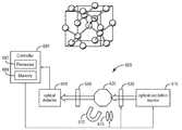
- FIG. 6 is a schematic diagram of a system 600 for a magnetic field detection system according to an embodiment.
- the system 600 includes an optical excitation source 610 , which directs optical excitation to an NV diamond material 620 with NV centers, or another magneto-optical defect center material with magneto-optical defect centers.
- An RF excitation source 630 provides RF radiation to the NV diamond material 620 .
- a first magnetic field generator 670 generates a magnetic field, which is detected at the NV diamond material 620 .
- the first magnetic field generator 670 may be a permanent magnet positioned relative to the NV diamond material 620 , which generates a known, uniform magnetic field (e.g., a bias or control magnetic field) to produce a desired fluorescence intensity response from the NV diamond material 620 .
- a second magnetic field generator 675 may be provided and positioned relative to the NV diamond material 620 to provide an additional bias or control magnetic field.
- the second magnetic field generator 675 may be configured to generate magnetic fields with orthogonal polarizations.
- the second magnetic field generator 675 may include one or more coils, such as a Helmholtz coil.
- the coils may be configured to provide relatively uniform magnetic fields at the NV diamond material 620 and each may generate a magnetic field having a direction that is orthogonal to the direction of the magnetic field generated by the other coils.
- only the first magnetic field generator 670 may be provided to generate the bias magnetic field.
- only the second magnetic field generator 675 may be provided to generate the bias magnetic field.
- the system 600 further includes a controller 680 arranged to receive a light detection signal from the optical detector 640 and to control the optical excitation source 610 , the RF excitation source 630 , and the second magnetic field generator 675 .
- the controller may be a single controller, or multiple controllers. For a controller including multiple controllers, each of the controllers may perform different functions, such as controlling different components of the system 600 .
- the second magnetic field generator 675 may be controlled by the controller 680 via an amplifier 660 , for example.
- the RF excitation source 630 may be a microwave coil, for example.
- the optical excitation source 610 may be a laser or a light emitting diode, for example, which emits light in the green, for example.
- the optical excitation source 610 induces fluorescence in the red from the NV diamond material 620 , where the fluorescence corresponds to an electronic transition from the excited state to the ground state.
- Light from the NV diamond material 620 is directed through the optical filter 650 to filter out light in the excitation band (in the green, for example), and to pass light in the red fluorescence band, which in turn is detected by the optical detector 640 .
- the controller 680 is arranged to receive a light detection signal from the optical detector 640 and to control the optical excitation source 610 , the RF excitation source 630 , and the second magnetic field generator 675 .
- the controller may include a processor 682 and a memory 684 , in order to control the operation of the optical excitation source 610 , the RF excitation source 630 , and the second magnetic field generator 675 .
- the memory 684 which may include a nontransitory computer readable medium, may store instructions to allow the operation of the optical excitation source 610 , the RF excitation source 630 , and the second magnetic field generator 675 to be controlled. That is, the controller 680 may be programmed to provide control.
- the controller 680 may be configured to compute an accurate estimation of the true orientation of the NV diamond lattice, which can be performed on-site as a calibration method prior to use. This information can be subsequently used to accurately recover the full vector information of an unknown external magnetic field acting on the system 600 .
- a desired geospatial coordinate reference frame relative to the system 600 by which measurement of the total magnetic field vector will take place is established.
- a Cartesian reference frame having ⁇ x, y, z ⁇ orthogonal axes may be used, but any arbitrary reference frame and orientation may be used.
- FIG. 7A shows a unit cell 100 of a diamond lattice having a “standard” orientation. The axes of the diamond lattice will fall along four possible directions. Thus, the four axes in a standard orientation relative to the desired coordinate reference frame may be defined as unit vectors corresponding to:
- the four vectors of equation (1) may be represented by a single matrix A S , which represents the standard orientation of the unit cell 100 :
- a S [a S,1 a S,2 a S,3 a S,4 ] (2)
- the angle between axis i and axis j may also be given by the (i, j) th row of the following:
- FIG. 7B is a unit cell 100 ′ that represents an arbitrarily placed NV diamond material having unknown axes orientation with respect to the coordinate reference frame.
- the arbitrary orientation shown in FIG. 7B may be obtained through a rotation and/or reflection of the standard orientation matrix.
- This can be achieved by applying a transformation matrix R, which is defined as a general 3 ⁇ 3 matrix representing the three-dimensional, orthogonal Cartesian space and is, at this stage, unknown.
- b ⁇ 3 ⁇ 1 represents the magnetic field vector acting inside the sensor system, expressed in Cartesian coordinates relative to the coordinate reference frame;
- a T b represents the projection of the magnetic field vector onto each of the four, arbitrarily-placed NV center diamond lattice axes;
- n ⁇ 4 ⁇ 1 represents the sensor noise vector;
- m ⁇ 4 ⁇ 1 represents the measurement vector, where the i th element represents the estimated projection of the magnetic field onto the sensor axis i.
- the measurement vector has been converted from the DNV sensor's native units (in terms of microwave resonance frequency) into the units of magnetic field strength.
- represents the element-wise absolute value of A T b+n, rather than its determinant.
- ⁇ circumflex over (b) ⁇ For a perfect NV diamond material 620 having no defects (e.g., lattice misalignments, impurities, etc.) and no sensor noise, ⁇ circumflex over (b) ⁇ should be equal to b.
- a performance metric to determine the error associated with the measurement.
- the magnitude of the true magnetic field may be used to normalize the metric to give a consistent metric even in the presence of a changing true magnetic field:
- ⁇ ′ ⁇ ( A T ⁇ ( AA T ) - 1 ⁇ A - 1 ) ⁇ m ⁇ 2 ⁇ b ⁇ 2 ( 12 )
- the measurement vector magnitude may be used to normalize the metric:
- ⁇ ′′ ⁇ ( A T ⁇ ( AA T ) - 1 ⁇ A - 1 ) ⁇ m ⁇ 2 ⁇ m ⁇ 2 ( 13 )
- a permanent magnet e.g., the first magnetic field generator 670
- coils e.g., the second magnetic field generator 675
- b bias the required bias or control magnetic field
- any b bias vector that sufficiently separates the four dips may suffice for the determination of the unknown orientation of the diamond lattice, thus increasing the viable b bias vectors appropriate for this step.
- Sufficient spectral dip separation may depend on the width of the dips and the planned magnitude of the calibration magnetic fields (described below).
- the width of the dips varies, depending on diamond composition and sensor laser and/or RF excitation mechanisms. Based on the resulting widths due to inherent sensor characteristics, the magnitude and orientation should be sufficient to ensure that the anticipated maximum spectral shifts that will occur due to the calibration tests will maintain sufficient separation between neighboring Lorentzian dips.
- FIG. 8 shows a step for determining a viable b bias vector field.
- the first magnetic field generator 670 may be arbitrarily placed in one or more positions and/or orientations such that multiple magnetic fields are applied to the diamond having an unknown orientation 100 ′. Measurements of the fluorescence intensity response are taken for each position and/or orientation of the first magnetic field generator 670 . Once a fluorescence intensity response 800 is produced that adequately separates out the four Lorentzian pairs, the position of the first magnetic field generator 670 is maintained and the process may proceed to calibration tests. In other embodiments, the separation process may be performed by the second magnetic field generator 675 .
- the controller 680 may be configured to control the second magnetic field generator 675 to generate multiple magnetic fields until the desired separation is produced.
- the first and/or second magnetic field generators may be affixed to a pivot assembly (e.g., a gimbal assembly) that may be controlled to hold and position the first and/or second magnetic field generators to a predetermined and well-controlled set of orientations, thereby establishing the desired Lorentzian separation and/or calibration magnetic fields (described below).
- the controller 680 may be configured to control the pivot assembly having the first and/or second magnetic field generators to position and hold the first and/or second magnetic field generators at the predetermined orientation.
- m bias
- equation (15) the variables represented in equation (15) are the same, but represented in relation to the applied bias field.
- the axes may be generally assigned such as, for example, the Lorentzian dip that is closest to the zero-field splitting frequency is assigned as a 1 , the second-closest is assigned as a 2 , and so on.
- the obtained m bias vector Due to the symmetry of the sensor measurements, the obtained m bias vector has no inherent sign information for each of its four components. However, sign information may be recovered using the following process.
- the projections of the magnetic field vector onto the four axes is given by the vector A T b.
- a T b 0.75
- a T Ax 0.75( RA S )
- a T ⁇ b [ 0. ⁇ ⁇ 75 - 0. ⁇ ⁇ 25 - 0. ⁇ ⁇ 25 - 0. ⁇ ⁇ 25 - 0. ⁇ ⁇ 25 0. ⁇ ⁇ 75 - 0. ⁇ ⁇ 25 - 0. ⁇ ⁇ 25 - 0. ⁇ ⁇ 25 0. ⁇ ⁇ 75 - 0. ⁇ ⁇ 25 - 0. ⁇ ⁇ 25 0. ⁇ ⁇ 75 - 0. ⁇ ⁇ 25 - 0. ⁇ ⁇ 25 - 0. ⁇ ⁇ 25 0. ⁇ ⁇ 75 - 0. ⁇ ⁇ 25 - 0. ⁇ ⁇ 25 - 0. ⁇ ⁇ 25 - 0. ⁇ ⁇ 25 0. ⁇ ⁇ 25 0.
- equation (19) can be reduced to:
- a method to recover sign information from the bias field measurements will now be described.
- the largest of the four measurements is arbitrarily set to a sign value, either positive or negative. Once this is chosen, the next steps are dictated based on this sign choice such that the principles of equation (16) are maintained. For example, as shown in the embodiment of FIG. 8 , the largest of the four measurements, measurement 810 a , is assigned as positive.
- the second-largest measurement e.g., measurement 810 b shown in FIG. 8
- the positive value assigned to the largest measurement may be offset toward zero.
- the third-largest measurement (e.g., measurement 810 c of FIG. 8 ) is assigned a negative sign value. Because, by definition, the second-largest measurement is smaller than the largest measurement, a negative sign value for the third-largest measurement will offset the largest measurement further towards zero.
- the smallest measurement is assigned either a positive or negative value that allows for the sum total of the four measurements to approximately equal zero. In FIG. 8 , the smallest measurement 810 d is assigned a positive value. After this process, therefore, an appropriately signed m bias vector may be obtained.
- ⁇ tilde over (m) ⁇ k ( m k ⁇
- ⁇ represents the Hadamard (i.e., element-wise) matrix product
- sgn( ) represents the element-wise signum function.
- a T remains unknown.
- a T b bias may be estimated. This is possible by substituting ⁇ hacek over (m) ⁇ bias for A T b bias in equation (23): ⁇ tilde over (m) ⁇ k ⁇ ( m k ⁇
- equation (26) may be expanded as follows:
- an orthogonal matrix ⁇ circumflex over (R) ⁇ is desired that provides the least-squares fit between B T and 3/4 ⁇ tilde over (M) ⁇ T A S T in equation (30).
- Some least-squares formulations may introduce translation and/or angular error into the orthogonal matrix ⁇ circumflex over (R) ⁇ .
- error may be introduced when applying the matrix ⁇ circumflex over (R) ⁇ to the standard orientation matrix A S in the form of a translation of the center of the axes from the standard orientation to the estimated orientation or in a change in the angles shown in equation (3) between given axes.
- 0(3) represents the group of orthogonal 3 ⁇ 3 matrices and ⁇ ⁇ F represents the Frobenius norm.
- the Orthogonal Procrustes Problem provides an advantage in reducing translation and/or angular error that may be introduced by the least-squares fit and, thus, provides an accurate estimation of the needed rotation matrix.
- an accurate estimation of the orientation of an arbitrarily placed lattice structure in a magnetic field detection system having a magneto-optical defect center material is produced. This, in turn, reduces the process to determining the orientation of a diamond in the magnetic detection system 600 to a simple calibration method that may be calculated and controlled by the controller 680 and performed before sensing begins, without the need for pre-manufacturing processes to orient the lattice structure relative to the sensor or additional equipment for visual aid inspection.
- an accurate estimate of the true orientation of the axes of the NV diamond material 620 may be obtained and recovery of the external magnetic field for magnetic sensing, described further below, may be improved.
- the bias magnet's magnetic field can subsequently be optimally re-oriented using the methods described below along with the newfound knowledge of the axes' orientations.
- a bias magnetic field may be applied to cleanly separate out the Lorenztian dips and obtain sign estimates of the magnetic field projections onto the identified diamond lattices.
- the baseline set of microwave resonance frequencies is defined as those frequencies which are created when no external magnetic field is present.
- the baseline resonance frequencies will be identical for all four diamond axes (e.g., all approximately equal to 2.87 GHz). If a bias magnet or coil is introduced (e.g., applied by the first magnetic field generator 670 and/or second magnetic generator 675 ), the four axes' baseline resonance frequencies may be uniquely shifted if the projection of the bias magnet's magnetic field onto each of the four axes is unique.
- the magnitude and orientation of a non-zero external magnetic field may then be determined by evaluating the additional shift in each axis' microwave resonance frequency relative to the baseline frequency offset, which will be described in more detail below.
- the Lorentzian dips in the microwave resonance spectra that correspond to each of the four axes may overlap significantly. Such overlap can occur when either the projection of the external field onto multiple axes is similar, or when the width of the Lorentzian dips is much larger than the difference in the resonance frequency shifts due to the external magnetic field.
- an external bias magnet applied as part of the system 600 may be used to minimize the overlap by significantly separating the Lorentzian spectral dips, thereby enabling unique recovery of the external magnetic field projections on each of the axes.
- the controller 680 calculates how an optimal bias magnetic field via the first magnetic field generator 670 (e.g., a permanent magnet) and/or the second magnetic field generator 675 (e.g., three-axis Helmholtz coil system) is calculated by the controller 680 according to one embodiment.
- the orientation of the bias magnet's magnetic field relative to the diamond may then be determined to produce the desired baseline shifts.
- the magnetic field generated by the bias magnet may be represented by the vector b bias ⁇ 3 ⁇ 1 .
- the projection of the bias magnetic field onto each of the four axes of the diamond is given by A T b bias .
- ⁇ represents the nitrogen vacancy gyromagnetic ratio of about 28 GHz/T.
- optimum performance of the sensor may be achieved under different sets of baseline frequencies. However, not all arbitrary baseline frequency sets may be realizable. Thus, the criteria for producing baseline offsets may be determined from which the corresponding required bias field may be computed.
- the same pair of microwave resonance frequencies ⁇ f i , f i ⁇ will be produced by the system 600 .
- b bias may then be given by:
- the Lorentzian dips may be fine-tuned to a desired separation by applying the appropriate bias field using the first magnetic field generator 670 and/or the second magnetic field generator 675 .
- equation (42) will reduce to:
- the b bias may also be determined after the true axes orientation has been estimated using the methods described above.
- the b bias that will produce an equally separated baseline set for an arbitrarily orientated diamond will be given by substitution of equation (35) into equation (42) to yield:
- equation (46) will reduce to:
- equation (47) corresponds directly to one of the four axis orientations, ⁇ 4 .
- the b bias may also be determined after the true axes orientation has been estimated using the methods described above.
- the b bias that will produce a maximum separated baseline set for an arbitrarily orientated diamond will be given by substitution of equation (35) into equation (46) to yield:
- m ext ( m ⁇
- ⁇ denotes the Hadamard (element-wise) matrix product.
- the resulting m ext will have the appropriate sign for the projection of b ext onto each axis, thereby allowing unambiguous recovery of b ext using the approach shown in equations (5)-(13), where m ext is used in place of m to estimate b ext .
- FIG. 11 shows a flowchart illustrating a method for the recovery of an external magnetic field vector as implemented by the controller 680 of the system 600 using the methods described above.
- the bias magnetic field that will produce the desired separation between the Lorentzian responses for each diamond axis is computed using the methods described above (e.g., equal separation or maximum separation computations).
- the first magnetic field generator 670 e.g., a permanent magnet
- the second magnetic field generator 675 e.g., three-axis Helmholtz coil
- a relative direction i.e., sign value
- step S 300 measurement data of the total magnetic field impinging on the system 600 is collected in a step S 300 .
- this shift information is then used along with the methods described using equations (49)-(50) to compute an estimate of the external magnetic field b ext .
Abstract
Description
A S =[a S,1 a S,2 a S,3 a S,4] (2)
A=RA S (4)
Deriving the Total Magnetic Field Vector
m=|A T b+n| (5)
{circumflex over (b)}=(A T)+ m (6)
{circumflex over (b)}=(AA T)−1 Am
=(RA S A S T R T)−1 Am
=(4/3RIR T)−1 Am
=0.75(RR T)−1 Am (7)
{circumflex over (b)}=0.75(I)−1 Am=0.75Am (8)
{circumflex over (b)}=argminbε
{circumflex over (b)}=(W 1/2 A T)+ W 1/2 m=(AWA T)−1 AWm (10)
γ=∥A T {circumflex over (b)}−m∥ 2
=∥A T(AA T)−1 Am−m∥ 2
=∥(A T(AA T)−1 A−I)m∥ 2 (11)
Estimation of Absolute Axes' Orientation in the NV Diamond Material
m=|A T b+n|=|(RA S)T b+n| (14)
m bias =|A T b bias +n bias| (15)
Σi=1 4(A T b)i=Σi=1 4((RA S)T b)i
=Σi=1 4 a S,i T R T b
=b T RΣ i=1 4 a S,i
=b T RO
=0 (16)
b=0.75Ax (17)
A T b=0.75A T Ax
=0.75(RA S)T RA S x
=0.75A S T R T RA S x
=0.75A S T A S x (18)
B=[b 1 b 2 . . . b p] (21)
m k =|A T(b k +b bias)+n k| (22)
{tilde over (m)} k=(m k −|A T b bias|)∘sgn(A T b bias) (23)
{tilde over (m)} k≈(m k −|{hacek over (m)} bias|)∘sgn({hacek over (m)} bias) (24)
{tilde over (m)} k =A T b k +ñ k (25)
{circumflex over (R)}=argminRε0(3) ∥B T R−3/4{tilde over (M)} T A S T∥F (31)
Z=3/4B{tilde over (M)} T A S T (32)
Z=UΣV T (33)
{circumflex over (R)}=UV T (34)
Â={circumflex over (R)}A S (35)
f={±γ(A T b bias)1, ±γ(A T b bias)2, ±γ(A T b bias)3, ±γ(A T b bias)4,}
={±γa 1 T b bias , ±γa 2 T b bias , ±γa 3 T b bias , ±γa 4 T b bias,} (36)
f={±f 1 , ±f 2 , ±f 3 , ±f 4,} (37)
a i T b bias =−fi/γ or fi/γ for i=1 . . . 4 (38)
Σi=1 4 =a i T b bias=Σi=1 4 s i fi/γ=0, where s 1,2,3,4ε{−1,1} (39)
f={±α, ±3α, ±5α, ±7α,} (41)
f={±α, ±α, ±α, ±3α,} (45)
Measuring an External Magnetic Field
m=|A T b+n|=|A T(b ext +b bias)+n| (49)
m ext=(m−|A T b bias|)∘sgn(A T b bias) (50)
Claims (20)
Priority Applications (12)
| Application Number | Priority Date | Filing Date | Title |
|---|---|---|---|
| GB1713826.4A GB2551090A (en) | 2015-02-04 | 2016-01-21 | Apparatus and method for recovery of three dimensional magnetic field from a magnetic detection system |
| AU2016209217A AU2016209217A1 (en) | 2015-01-23 | 2016-01-21 | DNV magnetic field detector |
| KR1020177023300A KR20170140156A (en) | 2015-01-23 | 2016-01-21 | DNV magnetic field detector |
| EP16740794.9A EP3248021A4 (en) | 2015-01-23 | 2016-01-21 | Dnv magnetic field detector |
| PCT/US2016/014333 WO2016126436A1 (en) | 2015-02-04 | 2016-01-21 | Apparatus and method for recovery of three dimensional magnetic field from a magnetic detection system |
| PCT/US2016/014403 WO2016118791A1 (en) | 2015-01-23 | 2016-01-21 | Dnv magnetic field detector |
| US15/003,718 US9541610B2 (en) | 2015-02-04 | 2016-01-21 | Apparatus and method for recovery of three dimensional magnetic field from a magnetic detection system |
| CA2974688A CA2974688A1 (en) | 2015-01-23 | 2016-01-21 | Dnv magnetic field detector |
| BR112017015746A BR112017015746A2 (en) | 2015-01-23 | 2016-01-21 | dnv magnetic field detector |
| US15/179,957 US9910105B2 (en) | 2014-03-20 | 2016-06-10 | DNV magnetic field detector |
| US15/400,794 US10408889B2 (en) | 2015-02-04 | 2017-01-06 | Apparatus and method for recovery of three dimensional magnetic field from a magnetic detection system |
| US15/912,461 US10725124B2 (en) | 2014-03-20 | 2018-03-05 | DNV magnetic field detector |
Applications Claiming Priority (2)
| Application Number | Priority Date | Filing Date | Title |
|---|---|---|---|
| US201562112071P | 2015-02-04 | 2015-02-04 | |
| US15/003,718 US9541610B2 (en) | 2015-02-04 | 2016-01-21 | Apparatus and method for recovery of three dimensional magnetic field from a magnetic detection system |
Related Parent Applications (2)
| Application Number | Title | Priority Date | Filing Date |
|---|---|---|---|
| US15/003,209 Continuation-In-Part US10088336B2 (en) | 2014-03-20 | 2016-01-21 | Diamond nitrogen vacancy sensed ferro-fluid hydrophone |
| US15/003,177 Continuation-In-Part US20170212258A1 (en) | 2014-03-20 | 2016-01-21 | Hydrophone |
Related Child Applications (4)
| Application Number | Title | Priority Date | Filing Date |
|---|---|---|---|
| US15/003,634 Continuation-In-Part US9823313B2 (en) | 2014-03-20 | 2016-01-21 | Diamond nitrogen vacancy sensor with circuitry on diamond |
| US15/003,519 Continuation-In-Part US10120039B2 (en) | 2014-03-20 | 2016-01-21 | Apparatus and method for closed loop processing for a magnetic detection system |
| US15/179,957 Continuation-In-Part US9910105B2 (en) | 2014-03-20 | 2016-06-10 | DNV magnetic field detector |
| US15/400,794 Continuation US10408889B2 (en) | 2015-02-04 | 2017-01-06 | Apparatus and method for recovery of three dimensional magnetic field from a magnetic detection system |
Publications (2)
| Publication Number | Publication Date |
|---|---|
| US20160223621A1 US20160223621A1 (en) | 2016-08-04 |
| US9541610B2 true US9541610B2 (en) | 2017-01-10 |
Family
ID=56554097
Family Applications (2)
| Application Number | Title | Priority Date | Filing Date |
|---|---|---|---|
| US15/003,718 Expired - Fee Related US9541610B2 (en) | 2014-03-20 | 2016-01-21 | Apparatus and method for recovery of three dimensional magnetic field from a magnetic detection system |
| US15/400,794 Active 2036-10-28 US10408889B2 (en) | 2015-02-04 | 2017-01-06 | Apparatus and method for recovery of three dimensional magnetic field from a magnetic detection system |
Family Applications After (1)
| Application Number | Title | Priority Date | Filing Date |
|---|---|---|---|
| US15/400,794 Active 2036-10-28 US10408889B2 (en) | 2015-02-04 | 2017-01-06 | Apparatus and method for recovery of three dimensional magnetic field from a magnetic detection system |
Country Status (3)
| Country | Link |
|---|---|
| US (2) | US9541610B2 (en) |
| GB (1) | GB2551090A (en) |
| WO (1) | WO2016126436A1 (en) |
Cited By (53)
| Publication number | Priority date | Publication date | Assignee | Title |
|---|---|---|---|---|
| US9720055B1 (en) | 2016-01-21 | 2017-08-01 | Lockheed Martin Corporation | Magnetometer with light pipe |
| US9823381B2 (en) | 2014-03-20 | 2017-11-21 | Lockheed Martin Corporation | Mapping and monitoring of hydraulic fractures using vector magnetometers |
| US9823314B2 (en) | 2016-01-21 | 2017-11-21 | Lockheed Martin Corporation | Magnetometer with a light emitting diode |
| US9824597B2 (en) | 2015-01-28 | 2017-11-21 | Lockheed Martin Corporation | Magnetic navigation methods and systems utilizing power grid and communication network |
| US9835693B2 (en) | 2016-01-21 | 2017-12-05 | Lockheed Martin Corporation | Higher magnetic sensitivity through fluorescence manipulation by phonon spectrum control |
| US9845153B2 (en) | 2015-01-28 | 2017-12-19 | Lockheed Martin Corporation | In-situ power charging |
| US9853837B2 (en) | 2014-04-07 | 2017-12-26 | Lockheed Martin Corporation | High bit-rate magnetic communication |
| US9910105B2 (en) | 2014-03-20 | 2018-03-06 | Lockheed Martin Corporation | DNV magnetic field detector |
| US9910104B2 (en) | 2015-01-23 | 2018-03-06 | Lockheed Martin Corporation | DNV magnetic field detector |
| US10006973B2 (en) | 2016-01-21 | 2018-06-26 | Lockheed Martin Corporation | Magnetometer with a light emitting diode |
| US10012704B2 (en) | 2015-11-04 | 2018-07-03 | Lockheed Martin Corporation | Magnetic low-pass filter |
| US10088452B2 (en) | 2016-01-12 | 2018-10-02 | Lockheed Martin Corporation | Method for detecting defects in conductive materials based on differences in magnetic field characteristics measured along the conductive materials |
| US10088336B2 (en) | 2016-01-21 | 2018-10-02 | Lockheed Martin Corporation | Diamond nitrogen vacancy sensed ferro-fluid hydrophone |
| US10120039B2 (en) | 2015-11-20 | 2018-11-06 | Lockheed Martin Corporation | Apparatus and method for closed loop processing for a magnetic detection system |
| US10126377B2 (en) | 2016-05-31 | 2018-11-13 | Lockheed Martin Corporation | Magneto-optical defect center magnetometer |
| US10145910B2 (en) | 2017-03-24 | 2018-12-04 | Lockheed Martin Corporation | Photodetector circuit saturation mitigation for magneto-optical high intensity pulses |
| US10168393B2 (en) | 2014-09-25 | 2019-01-01 | Lockheed Martin Corporation | Micro-vacancy center device |
| US10228429B2 (en) | 2017-03-24 | 2019-03-12 | Lockheed Martin Corporation | Apparatus and method for resonance magneto-optical defect center material pulsed mode referencing |
| US10241158B2 (en) | 2015-02-04 | 2019-03-26 | Lockheed Martin Corporation | Apparatus and method for estimating absolute axes' orientations for a magnetic detection system |
| US10274550B2 (en) | 2017-03-24 | 2019-04-30 | Lockheed Martin Corporation | High speed sequential cancellation for pulsed mode |
| US10277208B2 (en) | 2014-04-07 | 2019-04-30 | Lockheed Martin Corporation | Energy efficient controlled magnetic field generator circuit |
| US10281550B2 (en) | 2016-11-14 | 2019-05-07 | Lockheed Martin Corporation | Spin relaxometry based molecular sequencing |
| US10317279B2 (en) | 2016-05-31 | 2019-06-11 | Lockheed Martin Corporation | Optical filtration system for diamond material with nitrogen vacancy centers |
| US10330744B2 (en) | 2017-03-24 | 2019-06-25 | Lockheed Martin Corporation | Magnetometer with a waveguide |
| US10333588B2 (en) | 2015-12-01 | 2019-06-25 | Lockheed Martin Corporation | Communication via a magnio |
| US10338163B2 (en) | 2016-07-11 | 2019-07-02 | Lockheed Martin Corporation | Multi-frequency excitation schemes for high sensitivity magnetometry measurement with drift error compensation |
| US10338162B2 (en) | 2016-01-21 | 2019-07-02 | Lockheed Martin Corporation | AC vector magnetic anomaly detection with diamond nitrogen vacancies |
| US10338164B2 (en) | 2017-03-24 | 2019-07-02 | Lockheed Martin Corporation | Vacancy center material with highly efficient RF excitation |
| US10345396B2 (en) | 2016-05-31 | 2019-07-09 | Lockheed Martin Corporation | Selected volume continuous illumination magnetometer |
| US10345395B2 (en) | 2016-12-12 | 2019-07-09 | Lockheed Martin Corporation | Vector magnetometry localization of subsurface liquids |
| US10359479B2 (en) | 2017-02-20 | 2019-07-23 | Lockheed Martin Corporation | Efficient thermal drift compensation in DNV vector magnetometry |
| US10371760B2 (en) | 2017-03-24 | 2019-08-06 | Lockheed Martin Corporation | Standing-wave radio frequency exciter |
| US10371765B2 (en) | 2016-07-11 | 2019-08-06 | Lockheed Martin Corporation | Geolocation of magnetic sources using vector magnetometer sensors |
| US10379174B2 (en) | 2017-03-24 | 2019-08-13 | Lockheed Martin Corporation | Bias magnet array for magnetometer |
| US10408890B2 (en) | 2017-03-24 | 2019-09-10 | Lockheed Martin Corporation | Pulsed RF methods for optimization of CW measurements |
| US10408889B2 (en) | 2015-02-04 | 2019-09-10 | Lockheed Martin Corporation | Apparatus and method for recovery of three dimensional magnetic field from a magnetic detection system |
| US10459041B2 (en) | 2017-03-24 | 2019-10-29 | Lockheed Martin Corporation | Magnetic detection system with highly integrated diamond nitrogen vacancy sensor |
| US10466312B2 (en) | 2015-01-23 | 2019-11-05 | Lockheed Martin Corporation | Methods for detecting a magnetic field acting on a magneto-optical detect center having pulsed excitation |
| US10520558B2 (en) | 2016-01-21 | 2019-12-31 | Lockheed Martin Corporation | Diamond nitrogen vacancy sensor with nitrogen-vacancy center diamond located between dual RF sources |
| US10527746B2 (en) | 2016-05-31 | 2020-01-07 | Lockheed Martin Corporation | Array of UAVS with magnetometers |
| US10571530B2 (en) | 2016-05-31 | 2020-02-25 | Lockheed Martin Corporation | Buoy array of magnetometers |
| US10606271B2 (en) | 2017-07-17 | 2020-03-31 | The Boeing Company | Magnetic navigation and positioning system |
| US10677953B2 (en) | 2016-05-31 | 2020-06-09 | Lockheed Martin Corporation | Magneto-optical detecting apparatus and methods |
| DE102019130480A1 (en) | 2019-01-08 | 2020-07-09 | Lockheed Martin Corporation | RF WINDOWING FOR MAGNETOMETRY |
| US20200225041A1 (en) * | 2019-01-15 | 2020-07-16 | Lockheed Martin Corporation | Terrestrial land air and sea navigation system |
| US10890448B2 (en) * | 2016-11-28 | 2021-01-12 | Q-Sensorix Llc | Gyrocope based on nitrogen vacancy centers in diamond |
| WO2021013308A1 (en) | 2019-07-25 | 2021-01-28 | Jan Meijer | Nv-centre-based microwave-free quantum sensor and uses and characteristics thereof |
| US10921394B2 (en) | 2016-04-08 | 2021-02-16 | Socpra Sciences Et Genie S.E.C. | Vectorial magnetometer and associated methods for sensing an amplitude and orientation of a magnetic field |
| DE102021101583A1 (en) | 2020-01-30 | 2021-08-05 | Elmos Semiconductor Se | Recipients with NV centers |
| US11531073B2 (en) | 2020-12-31 | 2022-12-20 | X Development Llc | Fiber-coupled spin defect magnetometry |
| US11733321B2 (en) | 2019-10-02 | 2023-08-22 | X Development Llc | Magnetometry based on electron spin defects |
| US11774526B2 (en) | 2020-09-10 | 2023-10-03 | X Development Llc | Magnetometry based on electron spin defects |
| US11774384B2 (en) | 2021-01-15 | 2023-10-03 | X Development Llc | Spin defect magnetometry pixel array |
Families Citing this family (11)
| Publication number | Priority date | Publication date | Assignee | Title |
|---|---|---|---|---|
| AU2015230816B2 (en) * | 2015-07-28 | 2021-07-15 | Royal Melbourne Institute Of Technology | A sensor for measuring an external magnetic field |
| US10495698B2 (en) | 2015-07-28 | 2019-12-03 | Royal Melbourne Institute Of Technology | Magneto-encephalography device |
| WO2017087014A1 (en) | 2015-11-20 | 2017-05-26 | Lockheed Martin Corporation | Apparatus and method for hypersensitivity detection of magnetic field |
| WO2017127081A1 (en) | 2016-01-21 | 2017-07-27 | Lockheed Martin Corporation | Diamond nitrogen vacancy sensor with circuitry on diamond |
| US10529416B2 (en) * | 2016-09-23 | 2020-01-07 | The Government Of The United States Of America, As Represented By The Secretary Of The Navy | Quantum metrology and quantum memory using defect states with spin-3/2 or higher half-spin multiplets |
| CN110325869B (en) * | 2017-02-21 | 2022-06-24 | 住友电气工业株式会社 | Diamond magnetic sensor |
| JP7225545B2 (en) * | 2017-02-21 | 2023-02-21 | 日新電機株式会社 | Detection device and detection method |
| WO2018174911A1 (en) * | 2017-03-24 | 2018-09-27 | Lockheed Martin Corporation | Generation of magnetic field proxy through rf frequency dithering |
| EP3646047B1 (en) | 2017-06-29 | 2023-07-12 | Danmarks Tekniske Universitet | A magnetometer using optically active defects in a solid state material |
| EP3480614A1 (en) | 2017-11-02 | 2019-05-08 | Danmarks Tekniske Universitet | Absorption detected magnetic resonance (admr) |
| WO2023049320A1 (en) * | 2021-09-24 | 2023-03-30 | Microtesla Systems, Inc. | Portable magnetic resonance imager |
Citations (223)
| Publication number | Priority date | Publication date | Assignee | Title |
|---|---|---|---|---|
| US2746027A (en) | 1951-11-16 | 1956-05-15 | James J Murray | Flux-gap variation transducer for hydrophones, microphones, and accelerometers |
| US3389333A (en) | 1964-02-10 | 1968-06-18 | Sperry Rand Corp | Control system for maintaining a desired magnetic field in a given space |
| US3514723A (en) | 1966-06-23 | 1970-05-26 | Warwick Electronics Inc | Tone control circuit comprising a single potentiometer |
| US3518531A (en) | 1968-02-23 | 1970-06-30 | Varian Associates | Transient suppressor for use in magnetometer readout circuits |
| US3745452A (en) | 1971-02-23 | 1973-07-10 | J Osburn | Magnetic field gradient apparatus and method for detecting pipe line corrosion |
| US3899758A (en) | 1974-05-01 | 1975-08-12 | Gte International Inc | Variable inductive resonant circuit arrangement having a diamagnetic core for the UHF range |
| US4078247A (en) | 1975-02-05 | 1978-03-07 | Rca Corporation | Inverter circuit control circuit for precluding simultaneous conduction of thyristors |
| US4084215A (en) | 1977-02-25 | 1978-04-11 | The United States Of America As Represented By The Secretary Of The Navy | Strobe light having reduced electromagnetic radiation |
| US4329173A (en) | 1980-03-31 | 1982-05-11 | Carondelet Foundry Company | Alloy resistant to corrosion |
| US4368430A (en) | 1980-08-18 | 1983-01-11 | Sanders Associates, Inc. | Fiber optic magnetic sensors |
| US4514083A (en) | 1981-02-03 | 1985-04-30 | Olympus Optical Company Ltd. | Distance measuring apparatus |
| US4588993A (en) | 1980-11-26 | 1986-05-13 | The United States Of America As Represented By The Secretary Of The Department Of Health And Human Services | Broadband isotropic probe system for simultaneous measurement of complex E- and H-fields |
| US4638324A (en) | 1984-12-10 | 1987-01-20 | Hazeltine Corporation | Resistive loop angular filter |
| US4675522A (en) | 1985-10-09 | 1987-06-23 | Spectron Development Laboratories, Inc. | Fiber optic magnetic field sensor |
| WO1987004028A1 (en) | 1985-12-20 | 1987-07-02 | Pierre Misson | Magnetic transmission |
| WO1988004032A1 (en) | 1986-11-27 | 1988-06-02 | Plessey Overseas Limited | Acoustic sensor |
| US4945305A (en) | 1986-10-09 | 1990-07-31 | Ascension Technology Corporation | Device for quantitatively measuring the relative position and orientation of two bodies in the presence of metals utilizing direct current magnetic fields |
| EP0161940B1 (en) | 1984-05-17 | 1990-12-27 | Electricity Association Services Limited | Radio direction finding for locating lightening ground strikes |
| US5019721A (en) | 1989-08-18 | 1991-05-28 | Wisconsin Alumni Research Foundation | Active superconducting devices formed of thin films |
| US5038103A (en) | 1985-04-22 | 1991-08-06 | The United States Of America As Represented By The Secretary Of The Navy | Optical fiber magnetometer |
| US5113136A (en) | 1989-01-20 | 1992-05-12 | Fujitsu Limited | Gradiometer apparatus with compensation coils for measuring magnetic fields |
| US5134369A (en) | 1991-03-12 | 1992-07-28 | Hughes Aircraft Company | Three axis magnetometer sensor field alignment and registration |
| US5189368A (en) | 1976-09-24 | 1993-02-23 | Lockheed Sanders, Inc. | Magnetometer |
| US5245347A (en) | 1980-12-29 | 1993-09-14 | Raytheon Company | All weather tactical strike system (AWTSS) and method of operation |
| US5252912A (en) | 1989-06-28 | 1993-10-12 | William E. Merritt | System for warning aircraft pilot of potential impact with a power line and generating time-to-time impact signal |
| US5301096A (en) | 1991-09-27 | 1994-04-05 | Electric Power Research Institute | Submersible contactless power delivery system |
| US5384109A (en) | 1990-04-02 | 1995-01-24 | Nycomed Imaging As | Diagnostic magnetometry using superparamagnetic particles |
| US5395802A (en) | 1992-03-31 | 1995-03-07 | Nissan Motor Co., Ltd. | Process for making semiconductor acceleration sensor having anti-etching layer |
| US5396802A (en) | 1993-08-26 | 1995-03-14 | Viatran Corporation | Differential pressure transducer utilizing a variable ferrofluid keeper as an active magnetic circuit element |
| WO1995033972A1 (en) | 1994-06-02 | 1995-12-14 | Spectra-Physics Laserplane, Inc. | Laser alignment device and method using green light |
| EP0718642A1 (en) | 1994-12-20 | 1996-06-26 | De Beers Industrial Diamond Division (Proprietary) Limited | Diffractive optics |
| US5568516A (en) | 1993-07-02 | 1996-10-22 | Phonic Ear Incorporated | Very low power cordless headset system |
| US5694375A (en) | 1996-03-22 | 1997-12-02 | The United States Of America As Represented By The Secretary Of The Navy | Ultra-broadband hydrophone |
| US5818352A (en) | 1994-09-03 | 1998-10-06 | Integrated Drilling Services Limited | Well data telemetry system |
| US5907420A (en) | 1996-09-13 | 1999-05-25 | Lucent Technologies, Inc. | System and method for mitigating cross-saturation in optically amplified networks |
| US6057684A (en) | 1995-10-31 | 2000-05-02 | Yoshihiro Murakami | Magnetic flaw detection apparatus using an E-shaped magnetic sensor and high-pass filter |
| EP0726458B1 (en) | 1995-01-13 | 2000-05-03 | Bruker Analytik Gmbh | Method and apparatus for detecting gemstones within a surrounding substance by means of nuclear magnetic resonance |
| US6124862A (en) | 1997-06-13 | 2000-09-26 | Anivision, Inc. | Method and apparatus for generating virtual views of sporting events |
| US6130753A (en) | 1999-02-01 | 2000-10-10 | The United States Of America As Represented By The Secretary Of The Air Force | Laser optical density measurement system |
| US6195231B1 (en) | 1994-05-06 | 2001-02-27 | Steven R. Sedlmayr | Thin film magnetic data transfer transducer |
| US6360173B1 (en) | 1999-02-22 | 2002-03-19 | Terrescan Technologies, Inc. | Geophysical exploration system and method |
| US6398155B1 (en) | 2001-01-02 | 2002-06-04 | The United States Of America As Represented By The Secretary Of The Army | Method and system for determining the pointing direction of a body in flight |
| US6433944B1 (en) | 1998-09-25 | 2002-08-13 | Fuji Photo Film Co., Ltd. | Master carrier for magnetic transfer and method for transfer |
| US20020167306A1 (en) | 2001-03-23 | 2002-11-14 | Ivano Zalunardo | Device with a magnetic position encoder |
| US6504365B2 (en) | 2000-09-29 | 2003-01-07 | Jeol Ltd. | Magnetic force microscope |
| DE10228536A1 (en) | 2001-06-26 | 2003-01-30 | Fuji Photo Film Co Ltd | Magnetic recording medium used in magnetic disks in mini computers, personal computers, and work stations comprises a support with a non-magnetic lower layer, and a magnetic layer |
| US20030058346A1 (en) | 1997-04-02 | 2003-03-27 | Bechtel Jon H. | Control circuit for image array sensors |
| US6542242B1 (en) | 1999-05-10 | 2003-04-01 | University Of Washington | Mapping air contaminants using path-integrated optical remote sensing with a non-overlapping variable path length beam geometry |
| US20030076229A1 (en) | 2000-03-14 | 2003-04-24 | Roland Blanpain | Microsystem using magnetometer and inclinometer for anti-theft protection of valuables |
| US6636146B1 (en) | 1996-12-10 | 2003-10-21 | Régie Autonome des Transports Parisiens | Contactless communication system for exchanging data |
| US20030235136A1 (en) | 2001-12-04 | 2003-12-25 | Mark Akselrod | Optical single-bit recording and fluorescent readout utilizing aluminum oxide single crystals |
| US20040013180A1 (en) | 2002-04-22 | 2004-01-22 | Giannakis Georgios B. | Space-time multipath coding schemes for wireless communication systems |
| US6686696B2 (en) | 2001-03-08 | 2004-02-03 | Genvac Aerospace Corporation | Magnetron with diamond coated cathode |
| US20040022179A1 (en) | 2002-04-22 | 2004-02-05 | Giannakis Georgios B. | Wireless communication system having error-control coder and linear precoder |
| US6690162B1 (en) | 1999-10-04 | 2004-02-10 | Qest Quantenelektronische Systeme | Device for high-resolution measurement of magnetic fields |
| US20040042150A1 (en) | 2000-01-27 | 2004-03-04 | Swinbanks Malcolm A. | Dynamic degaussing system |
| US20040109328A1 (en) | 2002-12-06 | 2004-06-10 | Chevron U.S.A. Inc. | Optical uses of diamondoid-containing materials |
| US20040247145A1 (en) | 2003-06-03 | 2004-12-09 | Unitron Hearing Ltd. | Automatic magnetic detection in hearing aids |
| US20050099177A1 (en) | 2003-11-06 | 2005-05-12 | Greelish Stephen J. | Dynamic magnetic anomaly compensation |
| US20050130601A1 (en) | 2001-03-16 | 2005-06-16 | Vincent Palermo | Methods and apparatus for tuning in an inductive system |
| US20050126905A1 (en) | 1999-06-22 | 2005-06-16 | President And Fellows Of Harvard College | High-precision feedback control for ion sculpting of solid state features |
| US20050134257A1 (en) | 2003-12-22 | 2005-06-23 | Kurt Etherington | Combination hall effect position sensor and switch |
| US20050146327A1 (en) | 1998-12-23 | 2005-07-07 | Jakab Peter D. | Magnetic resonance scanner with electromagnetic position and orientation tracking device |
| US20060048640A1 (en) | 2002-09-03 | 2006-03-09 | Terry Matthew M | Blast and ballistic protection systems and method of making the same |
| US20060054789A1 (en) | 2004-09-13 | 2006-03-16 | Matsushita Electric Industrial Co., Ltd | Photodetector-amplifier circuit and optical pickup device |
| US20060062084A1 (en) | 2004-09-17 | 2006-03-23 | Julian Drew | Microseismic event detection and location by continuous map migration |
| US20060071709A1 (en) | 2003-12-31 | 2006-04-06 | Franco Maloberti | Switched-capacitor circuits with reduced finite-gain effect |
| US7118657B2 (en) | 1999-06-22 | 2006-10-10 | President And Fellows Of Harvard College | Pulsed ion beam control of solid state features |
| US20070004371A1 (en) | 2001-06-08 | 2007-01-04 | Sony Corporation | IC receiver to minimize tracking error |
| US7221164B1 (en) | 2006-04-25 | 2007-05-22 | Barringer Anthony R | Airborne remote sensing electric field exploration system |
| GB2433737B (en) | 2002-11-21 | 2007-08-15 | Element Six Ltd | Optical quality diamond material |
| US7277161B2 (en) | 2004-11-10 | 2007-10-02 | Wetenschappelijk En Technisch Onderzoekscentrum Voor Diamant | Method for discerning colorless and near colorless diamonds and arrangement for carrying out this method |
| US20070247147A1 (en) | 2001-10-25 | 2007-10-25 | Intermatix Corporation | Detection with evanescent wave probe |
| US7307416B2 (en) | 2004-10-22 | 2007-12-11 | Delphi Technologies, Inc. | Position sensor and assembly |
| US7305869B1 (en) | 2004-04-12 | 2007-12-11 | U. S. Department Of Energy | Spin microscope based on optically detected magnetic resonance |
| US20080016677A1 (en) | 2002-01-23 | 2008-01-24 | Stereotaxis, Inc. | Rotating and pivoting magnet for magnetic navigation |
| US20080048640A1 (en) | 2006-08-18 | 2008-02-28 | Hull David M | Methods for detecting and classifying loads on AC lines |
| US20080078233A1 (en) | 2006-09-25 | 2008-04-03 | Larson John D | Apparatus and method for measuring an environmental condition |
| US20080089367A1 (en) | 2006-10-03 | 2008-04-17 | Kartik Srinivasan | Fiber-Coupled Solid State Microcavity Light Emitters |
| USRE40343E1 (en) | 1997-01-09 | 2008-05-27 | Cymer, Inc. | Control circuit with automatic DC offset |
| US7413011B1 (en) | 2007-12-26 | 2008-08-19 | Schlumberger Technology Corporation | Optical fiber system and method for wellhole sensing of magnetic permeability using diffraction effect of faraday rotator |
| US20080204004A1 (en) | 2007-02-23 | 2008-08-28 | General Electric Company | Coil arrangement for electromagnetic tracking method and system |
| US20080217516A1 (en) | 2004-07-22 | 2008-09-11 | Hamamatsu Photonics K.K. | Photodetector |
| US7427525B2 (en) | 2006-10-13 | 2008-09-23 | Hewlett-Packard Development Company, L.P. | Methods for coupling diamond structures to photonic devices |
| US20080239265A1 (en) | 2007-03-30 | 2008-10-02 | Asml Netherlands B.V. | Angularly resolved scatterometer, inspection method, lithographic apparatus, lithographic processing cell device manufacturing method and alignment sensor |
| US7448548B1 (en) | 2006-01-13 | 2008-11-11 | Point Six Wireless, Llc | Pulsed wireless directional object counter |
| EP1990313A1 (en) | 2007-05-10 | 2008-11-12 | INSERM (Institut National de la Santé et de la Recherche Médicale) | Method to produce light-emitting nano-particles of diamond |
| US20080299904A1 (en) | 2007-06-04 | 2008-12-04 | Seagate Technology Llc | Wireless communication system |
| US7471805B2 (en) | 2004-12-20 | 2008-12-30 | Central Coast Patent Agency, Inc. | Hearing aid mechanism |
| US20090042592A1 (en) | 2007-07-06 | 2009-02-12 | Lg Electronics Inc. | Broadcast receiver and method of processing data |
| US20090060790A1 (en) | 2006-06-16 | 2009-03-05 | Murata Manufacturing Co., Ltd. | Sensor for detecting substance in liquid |
| US20090079426A1 (en) | 2007-09-25 | 2009-03-26 | General Electric Company, A New York Corporation | Electromagnetic tracking employing scalar-magnetometer |
| US20090132100A1 (en) | 2005-03-18 | 2009-05-21 | Hideki Shibata | Flight Control System |
| US7546000B2 (en) | 2006-09-07 | 2009-06-09 | Hewlett-Packard Development Company, L.P. | Scalable and defect-tolerant color-center-based quantum computer architectures and methods for fabricating color-center-based quantum computer architectures |
| US7543780B1 (en) | 2004-10-04 | 2009-06-09 | The United States Of America As Represented By The Secretary Of The Air Force | Unmanned air vehicle transmission line docking surveillance |
| EP1505627B1 (en) | 2003-08-07 | 2009-10-14 | Panasonic Corporation | Magnetron |
| US20090277702A1 (en) | 2005-10-07 | 2009-11-12 | Toyota Jidosha Kabushiki Kaisha | Hybrid vehicle and method of controlling the same |
| US20090310650A1 (en) | 2008-06-12 | 2009-12-17 | Harris Corporation | Featureless coherent chaotic amplitude modulation |
| US20100045269A1 (en) | 2001-03-16 | 2010-02-25 | Lafranchise Jeffrey R | Methods and apparatus to detect location and orientation in an inductive system |
| US20100134922A1 (en) | 2008-11-28 | 2010-06-03 | Kabushiki Kaisha Toshiba | Magnetic recording head, magnetic head assembly, magnetic recording apparatus, and magnetic recording method |
| US20100157305A1 (en) | 2008-12-18 | 2010-06-24 | Henderson Thomas A | In-line self spacing optical sensor assembly for a printer |
| US20100188081A1 (en) | 2007-06-15 | 2010-07-29 | Technische Universitat Graz | Method and Device for Measuring Magnetic Fields |
| US20100192532A1 (en) | 2009-01-30 | 2010-08-05 | Tom Joseph Slater | Variable Speed Transamission |
| US20100237149A1 (en) | 2009-03-17 | 2010-09-23 | Datalogic Scanning, Inc. | Systems and methods for compensating for fixed pattern noise |
| EP2163392B1 (en) | 2008-09-10 | 2010-10-06 | OOO "Novye Energeticheskie Tehnologii" | Document security, securities and article protection method using nanodiamonds with active NV centers |
| US20100271016A1 (en) | 2009-04-24 | 2010-10-28 | Hewlett-Packard Development Company, L.P. | Microfiber Magnetometer |
| US20100308813A1 (en) | 2007-12-03 | 2010-12-09 | President And Fellows Of Harvard College | High sensitivity solid state magnetometer |
| US20100326042A1 (en) | 2008-11-25 | 2010-12-30 | Mclean John P | Efficient RF Electromagnetic Propulsion System With Communications Capability |
| US20110034393A1 (en) | 2007-09-25 | 2011-02-10 | Lesaffre Et Compagnie | Use of a novel natural agent in cosmetic compositions |
| US20110066379A1 (en) | 2008-05-26 | 2011-03-17 | Mes Marius J | survey system for locating geophysical anomalies |
| US20110063957A1 (en) | 2009-09-16 | 2011-03-17 | Hitachi Media Electronics Co., Ltd. | Optical disk apparatus |
| US20110062957A1 (en) | 2009-09-11 | 2011-03-17 | Hewlett-Packard Development Company, L.P. | Optically integrated biosensor based on optically detected magnetic resonance |
| WO2011046403A2 (en) | 2009-10-16 | 2011-04-21 | Korea Advanced Institute Of Science And Technology | Autonomous driving apparatus and method of on-line electric vehicle |
| US20110127999A1 (en) | 2009-08-14 | 2011-06-02 | Paul Lott | Pipeline inspection apparatus and method |
| US20110165862A1 (en) | 2008-11-26 | 2011-07-07 | Nationz Technologies Inc. | Rf sim card, card reader, and communication method |
| US7983812B2 (en) | 2008-08-04 | 2011-07-19 | Scott Potter & Associates, Llc | Method and apparatus for managing battery power in emergency vehicles |
| US20110243267A1 (en) | 2010-03-31 | 2011-10-06 | Korea Electronics Technology Institute | Magnetic field communication method for managing node with low power consumption |
| JP4800896B2 (en) | 2006-10-16 | 2011-10-26 | シャープ株式会社 | Magnetic sensor element and manufacturing method thereof, magnetic head, magnetic reproducing apparatus, and magnetic reproducing method |
| WO2011153339A1 (en) | 2010-06-02 | 2011-12-08 | William Marsh Rice University | Magnetic particles for determining reservoir parameters |
| US20120016538A1 (en) | 2010-06-21 | 2012-01-19 | Waite James W | Uav power line position and load parameter estimation |
| US20120019242A1 (en) | 2008-11-04 | 2012-01-26 | The University Of Melbourne | Method and apparatus for monitoring a property of a sample |
| WO2012016977A2 (en) | 2010-08-04 | 2012-02-09 | Element Six Limited | A diamond optical element |
| US20120037803A1 (en) | 2010-08-12 | 2012-02-16 | Flir Systems, Inc. | Electromagnetic interference shield |
| US8120351B2 (en) | 2004-03-11 | 2012-02-21 | Robert Bosch Gmbh | Magnet sensor arrangement for sensing the movement of element moving in linear or rotary fashion |
| US8120355B1 (en) | 2009-05-27 | 2012-02-21 | Lockheed Martin Corporation | Magnetic anomaly detector |
| US20120044014A1 (en) | 2010-08-18 | 2012-02-23 | Volterra Semiconductor Corporation | Switching Circuits For Extracting Power From An Electric Power Source And Associated Methods |
| US20120051996A1 (en) | 2008-07-23 | 2012-03-01 | Geoffrey Alan Scarsbrook | Diamond material |
| US20120063505A1 (en) | 2010-09-10 | 2012-03-15 | Panasonic Corporation | Power transmitter and wireless power transmission system |
| US20120087449A1 (en) | 2009-12-27 | 2012-04-12 | Curtis Ling | Methods and apparatus for synchronization in multiple-channel communication systems |
| JP2012103171A (en) | 2010-11-11 | 2012-05-31 | Jeol Resonance Inc | Magnetic field measuring device |
| US20120140219A1 (en) | 2010-12-07 | 2012-06-07 | Cleary Joseph A | Monolithic Geared Optical Reflector |
| JP2012110489A (en) | 2010-11-24 | 2012-06-14 | Sumitomo Electric Ind Ltd | Magnetism measuring instrument, and method for manufacturing magnetism sensor element |
| WO2012084750A1 (en) | 2010-12-24 | 2012-06-28 | Element Six Limited | Dislocation engineering in single crystal synthetic diamond material |
| JP2012121748A (en) | 2010-12-07 | 2012-06-28 | Sumitomo Electric Ind Ltd | Diamond and magnetic sensor using the same |
| US20120181020A1 (en) | 2008-05-20 | 2012-07-19 | Oxane Materials, Inc. | Method Of Manufacture And The Use Of A Functional Proppant For Determination Of Subterranean Fracture Geometries |
| US20120194068A1 (en) | 2011-01-31 | 2012-08-02 | Lite-On Technology Corp. | Lamp having light sensor |
| EP2495166A1 (en) | 2011-03-03 | 2012-09-05 | Asociacion de la Industria Navarra (AIN) | Aerial robotic system for the inspection of overhead power lines |
| US20120257683A1 (en) | 2009-12-30 | 2012-10-11 | Sony Corporation | Communications system using beamforming |
| US8294306B2 (en) | 2010-03-16 | 2012-10-23 | Indian Institute Of Technology Madras | DC capacitor balancing |
| US20120281843A1 (en) | 2011-05-06 | 2012-11-08 | Oticon A/S | Receiver and method for retrieving an information signal from a magnetic induction signal |
| US8311767B1 (en) | 2009-07-13 | 2012-11-13 | Lockheed Martin Corporation | Magnetic navigation system |
| US8334690B2 (en) | 2009-08-07 | 2012-12-18 | The United States of America as represented by the Secretary of Commerce, the National Institute of Standards and Technology | Atomic magnetometer and method of sensing magnetic fields |
| US20120326793A1 (en) | 2008-02-07 | 2012-12-27 | Lahav Gan | Device, system, and method of frequency generation using an atomic resonator |
| JP2013028497A (en) | 2011-07-28 | 2013-02-07 | Sumitomo Electric Ind Ltd | Polycrystalline diamond and method for producing the same |
| US8415640B2 (en) | 2010-04-19 | 2013-04-09 | President And Fellows Of Harvard College | Diamond nanowires |
| GB2495632A (en) | 2011-10-14 | 2013-04-17 | Element Six Ltd | A solid state component device for achieving multi-photon interference between quantum registers with nuclear and electron spin state coupling |
| EP2587232A1 (en) | 2011-10-27 | 2013-05-01 | Universität des Saarlandes | System and method for detecting mechanical vibrations |
| WO2013066448A2 (en) | 2011-08-08 | 2013-05-10 | Battelle Memorial Institute | Polymer-sulfur composite materials for electrodes in li-s energy storage devices |
| WO2013066446A1 (en) | 2011-08-01 | 2013-05-10 | The Trustees Of Columbia University In The City Of New York | Conjugates of nano-diamond and magnetic or metallic particles |
| US20130127518A1 (en) | 2011-11-18 | 2013-05-23 | Fujitsu Limited | Control circuit and electronic device |
| GB2483767B (en) | 2010-09-14 | 2013-05-29 | Element Six Ltd | A microfluidic cell and a spin resonance device for use therewith |
| US8471137B2 (en) | 2011-02-22 | 2013-06-25 | Kenneth Michael ADAIR | Pickup system with a cartridge |
| WO2013093136A1 (en) | 2011-12-23 | 2013-06-27 | Universidad De Zaragoza | Device and method for sensing magnetic materials |
| US8480653B2 (en) | 2007-05-23 | 2013-07-09 | Biosense Webster, Inc. | Magnetically guided catheter with concentric needle port |
| US20130215712A1 (en) | 2011-03-23 | 2013-08-22 | Global Geophysical Services, Inc. | Method for Assessing the Effectiveness of Modifying Transmissive Networks of Natural Reservoirs |
| US8525516B2 (en) | 2007-12-11 | 2013-09-03 | Commissariat à l'énergie atomique et aux énergies alternatives | Apparatus with ambient magnetic field correction |
| US20130265782A1 (en) | 2010-12-15 | 2013-10-10 | Illinois Tool Works Inc. | Heat-sink/connector system for light emitting diode |
| US8575929B1 (en) | 2011-06-20 | 2013-11-05 | The United States Of America As Represented By The Secretary Of The Navy | Magnetic anomaly surveillance system using spherical trilateration |
| GB2491936B (en) | 2011-05-24 | 2013-11-13 | Element Six Ltd | Diamond sensors detectors and quantum devices |
| WO2013188732A1 (en) | 2012-06-14 | 2013-12-19 | The Trustees Of Columbia University In The City Of New York | Systems and methods for precision optical imaging of electrical currents and temperature in integrated circuits |
| US20140012505A1 (en) | 2011-03-31 | 2014-01-09 | Laurentian University Of Sudbury | Multi-component electromagnetic prospecting apparatus and method of use thereof |
| US20140037932A1 (en) | 2011-05-06 | 2014-02-06 | Element Six Limited | Diamond sensors, detectors, and quantum devices |
| US20140061510A1 (en) | 2011-05-10 | 2014-03-06 | Element Six Limited | Diamond sensors, detectors, and quantum devices |
| US20140072008A1 (en) | 2012-09-13 | 2014-03-13 | Andrei Faraon | Color centers affected by magnetic fields to produce light based on lasing |
| US20140081592A1 (en) | 2012-09-17 | 2014-03-20 | Xsens Holding B.V. | System and Method for Magnetic Field Data Compression |
| JP5476206B2 (en) | 2010-02-02 | 2014-04-23 | 日本電子株式会社 | Fluorescence microscope device |
| US20140126334A1 (en) | 2009-12-16 | 2014-05-08 | Shb Instruments, Inc. | Underwater acoustic navigation systems and methods |
| US20140139322A1 (en) | 2011-05-03 | 2014-05-22 | Nationz Technologies Inc. | Communication method, device, and system |
| JP5522606B2 (en) | 2007-03-08 | 2014-06-18 | エレメント シックス リミテッド | diamond |
| US20140166904A1 (en) | 2011-06-13 | 2014-06-19 | President And Fellows Of Harvard College | Efficient Fluorescence Detection In Solid State Spin Systems |
| US20140168174A1 (en) | 2012-12-13 | 2014-06-19 | Research In Motion Limited | Stylus location utilizing multiple magnetometers |
| US20140167759A1 (en) | 2012-12-18 | 2014-06-19 | The Regents Of The University Of California | Nmr borehole logging device and method of use |
| WO2014099110A2 (en) | 2012-10-09 | 2014-06-26 | Purdue Research Foundation | Titanium nitride based metamaterial |
| US20140191752A1 (en) | 2011-06-13 | 2014-07-10 | President And Fellows Of Harvard College | Spectral Decomposition Of Composite Solid State Spin Environments Through Quantum Control of Spin Impurities |
| US20140198463A1 (en) | 2011-09-07 | 2014-07-17 | Commissariat A L'energie Atomique Et Aux Energies Alternatives | Printed circuit board and magnetic field or current sensor |
| GB2510053A (en) | 2012-12-13 | 2014-07-23 | Element Six Ltd | Synthetic diamond materials for quantum and optical applications |
| GB2497660B (en) | 2011-12-16 | 2014-08-06 | Element Six Ltd | Single crystal CVD synthetic diamond material |
| US20140215985A1 (en) | 2013-02-07 | 2014-08-07 | Claas Selbstfahrende Erntemaschinen Gmbh | Agricultural harvesting machine |
| US8803513B2 (en) | 2007-06-27 | 2014-08-12 | Brooks Automation, Inc. | Multiple dimension position sensor |
| US20140247094A1 (en) | 2011-09-16 | 2014-09-04 | The Trustees Of Columbia University In The City Of New York | High-precision ghz clock generation using spin states in diamond |
| WO2014135547A1 (en) | 2013-03-06 | 2014-09-12 | Element Six N.V | Synthetic diamond optical elements |
| WO2014135544A1 (en) | 2013-03-06 | 2014-09-12 | Element Six Technologies Limited | Synthetic diamond optical elements |
| US20140273826A1 (en) | 2013-03-15 | 2014-09-18 | Google Inc. | System and Method for Code Communication |
| US20140272119A1 (en) | 2013-03-14 | 2014-09-18 | Sabic Innovative Plastics Ip B.V. | Functionally graded polymer articles and methods of making same |
| JP5601183B2 (en) | 2010-12-07 | 2014-10-08 | 住友電気工業株式会社 | Diamond substrate and manufacturing method thereof |
| EP2790031A1 (en) | 2013-04-08 | 2014-10-15 | Universität Ulm | Method for the hyperpolarisation of nuclear spin in a diamond |
| US20140306707A1 (en) | 2011-11-30 | 2014-10-16 | President And Fellows Of Harvard College | Use of Nuclear Spin Impurities to Suppress Electronic Spin Fluctuations and Decoherence in Composite Solid-State Spin Systems |
| US20140327439A1 (en) | 2013-05-01 | 2014-11-06 | Massachusetts Institute Of Technology | Stable three-axis nuclear spin gyroscope |
| US8885301B1 (en) | 2014-02-19 | 2014-11-11 | Infinitum Solutions, Inc. | Magnetic write head characterization with nano-meter resolution using nitrogen vacancy color centers |
| JP2014216596A (en) | 2013-04-30 | 2014-11-17 | 日本電信電話株式会社 | Construction method of quantum bit |
| JP2014215985A (en) | 2013-04-30 | 2014-11-17 | 日本電信電話株式会社 | Quantum computing device |
| US20140340085A1 (en) | 2013-05-17 | 2014-11-20 | Massachusetts Institute Of Technology | Time-resolved magnetic sensing with electronic spins in diamond |
| US8913900B2 (en) | 2005-10-11 | 2014-12-16 | President And Fellows Of Harvard College | Method and apparatus for fault-tolerant quantum communication based on solid-state photon emitters |
| GB2515226A (en) | 2012-04-13 | 2014-12-17 | Univ California | Gyroscopes based on nitrogen-vacancy centers in diamond |
| US20140368191A1 (en) | 2012-11-12 | 2014-12-18 | Valerian Goroshevskiy | Apparatus and method for metallic constructions assessment |
| WO2014210486A1 (en) | 2013-06-28 | 2014-12-31 | Dirk Robert Englund | Wide-field sensing using nitrogen vacancies |
| US20150009746A1 (en) | 2011-12-23 | 2015-01-08 | President And Fellows Of Harvard College | Solid-State Quantum Memory Based on a Nuclear Spin Coupled to an Electronic Spin |
| US20150009003A1 (en) | 2013-07-03 | 2015-01-08 | Murata Manufacturing Co., Ltd. | Electronic component |
| US20150018018A1 (en) | 2013-07-12 | 2015-01-15 | Microsoft Corporation | Indoor Location-Finding using Magnetic Field Anomalies |
| WO2015015172A1 (en) | 2013-07-30 | 2015-02-05 | The University Of Warwick | Sensitive detector |
| EP2837930A1 (en) | 2013-08-15 | 2015-02-18 | Latvijas Universitate | Method for detecting the magnitude of a magnetic field gradient |
| US20150048822A1 (en) | 2011-06-13 | 2015-02-19 | President And Fellows Of Harvard College | Dynamic Decoupling In Solid State Spin Ensembles |
| US20150054355A1 (en) | 2012-05-03 | 2015-02-26 | Powermat Technologies Ltd. | System and method for triggering power transfer across an inductive power coupling and non resonant transmission |
| US20150128431A1 (en) | 2013-11-14 | 2015-05-14 | Voltafield Technology Corporation | Magnetic-Field Sensing Method |
| JP2015518562A (en) | 2012-03-27 | 2015-07-02 | ビーイー・エアロスペース・インコーポレーテッド | Magnetic encoder system for aircraft seat actuators |
| US20150192596A1 (en) | 2012-06-14 | 2015-07-09 | The Trustees Of Columbia University In The City Of New York | Systems and methods for detection of electric fields, ion exchange, and ph using spectral shift in diamond color centers |
| US20150192532A1 (en) | 2014-01-08 | 2015-07-09 | Massachusetts Institute Of Technology | Methods and apparatus for optically detecting magnetic resonance |
| GB2522309A (en) | 2013-11-18 | 2015-07-22 | Element Six Technologies Ltd | Diamond components for quantum imaging, sensing and information processing devices |
| JP5764059B2 (en) | 2008-07-23 | 2015-08-12 | エレメント シックス リミテッド | Solid state material |
| US20150225052A1 (en) | 2012-07-17 | 2015-08-13 | Steve Cordell | Method and Apparatus for Precision Tracking of Approaching Magnetic-Detonated and Traditional Impact Torpedoes |
| EP2907792A1 (en) | 2012-10-12 | 2015-08-19 | Japan Science and Technology Agency | Nano-diamond particle and method for producing same, and fluorescent molecular probe and method for analyzing structure of protein |
| US20150235661A1 (en) | 2014-02-19 | 2015-08-20 | Infinitum Solutions, Inc. | Magnetic write head characterization with nano-meter resolution using nitrogen vacancy color centers |
| US20150253355A1 (en) | 2012-08-22 | 2015-09-10 | President And Fellows Of Harvard College | Nanoscale scanning sensors |
| US20150269957A1 (en) | 2014-03-18 | 2015-09-24 | Seagate Technology Llc | Nitrogen-vacancy nanocrystal magnetic source sensor |
| JP2015167176A (en) | 2014-03-04 | 2015-09-24 | 日本電信電話株式会社 | control method of quantum memory |
| US20150268373A1 (en) | 2014-03-20 | 2015-09-24 | Lockheed Martin Corporation | Mapping and monitoring of hydraulic fractures using vector magnetometers |
| US20150276897A1 (en) | 2012-10-25 | 2015-10-01 | Koninklijke Philips N.V. | Radio frequency (rf) birdcage coil with separately controlled ring members and rungs for use in a magnetic resonance (mr) imaging system |
| WO2015158383A1 (en) | 2014-04-16 | 2015-10-22 | Universitaet Ulm | Sensor comprising a piezomagnetic or piezoelectric element on a diamond substrate with a colour centre |
| JP5828036B2 (en) | 2011-06-13 | 2015-12-02 | プレジデント アンド フェローズ オブ ハーバード カレッジ | Absorption-based detection of spin impurities in solid-state spin systems |
| GB2526639A (en) | 2013-11-18 | 2015-12-02 | Element Six Technologies Ltd | Methods of fabricating synthetic diamond materials using microwave plasma activated chemical vapour deposition techniques and products obtained using said |
| JP5831947B2 (en) | 2013-01-09 | 2015-12-09 | 日本電信電話株式会社 | Magnetic field detection apparatus and magnetic field detection method |
| WO2015193156A1 (en) | 2014-06-16 | 2015-12-23 | Element Six Technologies Limited | Synthetic diamond optical elements |
| US20150374250A1 (en) | 2014-06-26 | 2015-12-31 | Renesas Electronics Corporation | Magnetic measurement apparatus |
Family Cites Families (230)
| Publication number | Priority date | Publication date | Assignee | Title |
|---|---|---|---|---|
| US3359812A (en) | 1964-03-13 | 1967-12-26 | Spectra Physics | Angle adjusting mechanism for optical elements |
| US3490032A (en) | 1966-12-08 | 1970-01-13 | Gulf Research Development Co | Method and apparatus utilizing a pair of spaced magnetometers for making magnetic surveys |
| US3621380A (en) | 1969-01-02 | 1971-11-16 | Texas Instruments Inc | Method and apparatus for seismic-magnetic prospecting |
| US4047805A (en) | 1973-02-14 | 1977-09-13 | Canon Kabushiki Kaisha | Ripple-free dichroic mirrors |
| US4025873A (en) | 1976-08-17 | 1977-05-24 | The United States Of America As Represented By The Secretary Of The Navy | Broadband, microwave, two-stage, stagger-tuned, field effect transistor amplifier |
| US4359673A (en) | 1980-08-21 | 1982-11-16 | Bross Jr Augustus T | Electromagnetically actuated linear reciprocating self-timed motor |
| DE3037305C2 (en) | 1980-10-02 | 1986-04-03 | Flowtec AG, Reinach, Basel | Arrangement for generating constant magnetic fields of alternating polarity for magnetic-inductive flow measurement |
| US4322769A (en) | 1980-12-22 | 1982-03-30 | International Business Machines Corporation | Electric switch operation monitoring circuitry |
| DE3110499C2 (en) | 1981-03-18 | 1983-12-01 | Jungheinrich Unternehmensverwaltung Kg, 2000 Hamburg | Vehicle with monitoring device and braking device as a freely movable, in particular inductively guided vehicle |
| US4636612A (en) | 1983-04-19 | 1987-01-13 | Cyclomatic Industries, Inc. | Optical tracking device |
| GB8530930D0 (en) | 1985-12-16 | 1986-01-29 | Mansfield P | Inductive circuit arrangements |
| DE8613488U1 (en) | 1986-05-17 | 1987-10-22 | Philips Patentverwaltung Gmbh, 2000 Hamburg, De | |
| US4818990A (en) | 1987-09-11 | 1989-04-04 | Fernandes Roosevelt A | Monitoring system for power lines and right-of-way using remotely piloted drone |
| US4982158A (en) | 1988-06-23 | 1991-01-01 | Electric Power Research Institute, Inc. | Method and apparatus for magnetic detection of flaws |
| US5268305A (en) | 1989-06-15 | 1993-12-07 | Biocircuits Corporation | Multi-optical detection system |
| US4958328A (en) | 1989-07-24 | 1990-09-18 | Texaco Inc. | Marine walkaway vertical seismic profiling |
| US5200855A (en) | 1991-07-12 | 1993-04-06 | Optical Coating Laboratory, Inc. | Absorbing dichroic filters |
| US5846708A (en) | 1991-11-19 | 1998-12-08 | Massachusetts Institiute Of Technology | Optical and electrical methods and apparatus for molecule detection |
| US5210650A (en) | 1992-03-31 | 1993-05-11 | Eastman Kodak Company | Compact, passively athermalized optical assembly |
| US5638472A (en) | 1993-04-01 | 1997-06-10 | Optics For Research | Optical fiber and lens assembly having a movable lens and a fixed optical fiber |
| US5425179A (en) | 1993-10-22 | 1995-06-20 | The Charles Machine Works, Inc. | Optical sensor for measuring inclination angles |
| US5420549A (en) | 1994-05-13 | 1995-05-30 | The United States Of America As Represented By The Administrator Of The National Aeronautics And Space Administration | Extended linear ion trap frequency standard apparatus |
| US5548279A (en) | 1994-07-22 | 1996-08-20 | Mcdonnell Douglas Corporation | Method and apparatus for detecting a power line |
| US5597762A (en) | 1994-09-27 | 1997-01-28 | Nonophase Diamond Technologies, Inc. | Field-enhanced diffusion using optical activation |
| US5586069A (en) | 1994-09-30 | 1996-12-17 | Vlsi Technology, Inc. | Arithmetic logic unit with zero sum prediction |
| US8169311B1 (en) | 1999-12-15 | 2012-05-01 | Automotive Technologies International, Inc. | Wireless transmission system for vehicular component control and monitoring |
| AU7376996A (en) | 1995-09-28 | 1997-04-17 | Allied-Signal Inc. | Hydrogen and moisture getter and absorber for sealed devices |
| JPH09127252A (en) | 1995-10-26 | 1997-05-16 | Kokusai Denshin Denwa Co Ltd <Kdd> | Probing system for submarine cable |
| JPH09210687A (en) | 1996-01-31 | 1997-08-12 | Topcon Corp | Laser level |
| US5894220A (en) | 1996-02-12 | 1999-04-13 | University Of Maryland | Apparatus for microscopic imaging of electrical and magnetic properties of room-temperature objects |
| US5731996A (en) | 1996-03-05 | 1998-03-24 | Hughes Electronics | Dipole moment detector and localizer |
| IT1283721B1 (en) | 1996-04-05 | 1998-04-30 | Pirelli Cavi S P A Ora Pirelli | APPARATUS AND METHOD FOR HOUSING OPTICAL COMPONENTS |
| US5719497A (en) | 1996-05-09 | 1998-02-17 | The Regents Of The University Of California | Lensless Magneto-optic speed sensor |
| US6042249A (en) | 1996-07-30 | 2000-03-28 | Bayer Corporation | Illuminator optical assembly for an analytical instrument and methods of alignment and manufacture |
| JP3299477B2 (en) | 1997-02-07 | 2002-07-08 | 光信 宮城 | Manufacturing method of hollow waveguide |
| US6064210A (en) | 1997-11-14 | 2000-05-16 | Cedar Bluff Group Corporation | Retrievable resistivity logging system for use in measurement while drilling |
| US6437563B1 (en) | 1997-11-21 | 2002-08-20 | Quantum Design, Inc. | Method and apparatus for making measurements of accumulations of magnetically susceptible particles combined with analytes |
| US6144204A (en) | 1997-11-28 | 2000-11-07 | Picker Nordstar Oy | Gradient coils for magnetic resonance meeting |
| US6121053A (en) | 1997-12-10 | 2000-09-19 | Brookhaven Science Associates | Multiple protocol fluorometer and method |
| US6262574B1 (en) | 1999-03-12 | 2001-07-17 | The United States Of America As Represented By The Secretary Of The Navy | Sensor for measuring magnetic field strength and temperature for an electric motor |
| WO2000055368A2 (en) | 1999-03-15 | 2000-09-21 | Pe Corporation (Ny) | Probe/mobility modifier complexes for multiplex nucleic acid detection |
| US6809829B1 (en) | 1999-05-19 | 2004-10-26 | Matsushita Electric Industrial Co., Ltd. | Method and apparatus for evaluating aberrations of optical element and method and apparatus for adjusting optical unit and lens |
| US6215303B1 (en) | 1999-06-14 | 2001-04-10 | The United States Of America As Represented By The Secretary Of The Air Force | Wire detection system |
| JP2001006233A (en) | 1999-06-18 | 2001-01-12 | Fujitsu Ltd | Optical information storage device |
| US6621578B1 (en) | 1999-11-26 | 2003-09-16 | Olympus Optical Co, Ltd. | Elliposometer, sample positioning mechanism, and polarization angular adjusting mechanism, used in the elliposometer |
| US6621377B2 (en) | 2000-05-02 | 2003-09-16 | Paratek Microwave, Inc. | Microstrip phase shifter |
| US6788722B1 (en) | 2000-07-10 | 2004-09-07 | Coherent, Inc. | High power waveguide laser |
| US20040081033A1 (en) | 2001-02-06 | 2004-04-29 | Yoel Arieli | Multiple layer optical storage device |
| US6518747B2 (en) | 2001-02-16 | 2003-02-11 | Quantum Design, Inc. | Method and apparatus for quantitative determination of accumulations of magnetic particles |
| US6889316B2 (en) | 2001-03-28 | 2005-05-03 | Intel Corporation | Method and apparatus for restoring registers after cancelling a multi-cycle instruction |
| US6627916B2 (en) | 2001-03-31 | 2003-09-30 | D-Wave Systems, Inc. | High sensitivity, directional DC-squid magnetometer |
| US6472869B1 (en) | 2001-06-18 | 2002-10-29 | United States Of America As Represented By The Secretary Of The Air Force | Diode laser-pumped magnetometer |
| US6653831B2 (en) | 2001-11-20 | 2003-11-25 | Gentex Corporation | Magnetometer having a dynamically adjustable bias setting and electronic vehicle compass incorporating the same |
| US6765487B1 (en) | 2002-10-17 | 2004-07-20 | The United States Of America As Represented By The Secretary Of The Navy | Underwater detection and deterrent system |
| US7023204B2 (en) | 2002-11-18 | 2006-04-04 | International Business Machine Corporation | Magnetic imaging microscope test system and its application for characterization of read and write heads for magnetic recording |
| US20050031840A1 (en) | 2003-08-05 | 2005-02-10 | Xerox Corporation | RF connector |
| US10443139B2 (en) | 2003-09-05 | 2019-10-15 | Brilliant Light Power, Inc. | Electrical power generation systems and methods regarding same |
| US6992638B2 (en) | 2003-09-27 | 2006-01-31 | Paratek Microwave, Inc. | High gain, steerable multiple beam antenna system |
| EP1687899A4 (en) | 2003-11-18 | 2008-10-08 | Halliburton Energy Serv Inc | High-voltage transistors on insulator substrates |
| US7834801B2 (en) | 2003-11-25 | 2010-11-16 | Metrotech Corporation, Inc. | Sensor fusion for model-based detection in pipe and cable locator systems |
| US20050138330A1 (en) | 2003-12-23 | 2005-06-23 | Maxim Integrated Products, Inc. | MAXQ microcontroller |
| US7589839B2 (en) | 2004-03-31 | 2009-09-15 | Olympus Corporation | Examination apparatus, fluoroscopy apparatus, examination method, and experimental method |
| US7245133B2 (en) | 2004-07-13 | 2007-07-17 | Credence Systems Corporation | Integration of photon emission microscope and focused ion beam |
| US7741936B1 (en) | 2004-09-09 | 2010-06-22 | University Of South Florida | Tunable micro electromechanical inductor |
| NZ535390A (en) | 2004-09-16 | 2007-10-26 | Auckland Uniservices Ltd | Inductively powered mobile sensor system |
| US20100004802A1 (en) | 2005-01-25 | 2010-01-07 | William Kress Bodin | Navigating UAVS with an on-board digital camera |
| US8059019B2 (en) | 2005-01-25 | 2011-11-15 | Atmel Corporation | Method and system for minimizing the accumulated offset error for an analog to digital converter |
| GB2462212B (en) | 2005-02-16 | 2010-05-12 | Illinois Tool Works | Metal detector |
| CA2891641C (en) | 2005-03-18 | 2018-01-02 | Gatekeeper Systems, Inc. | Navigation systems and methods for wheeled objects |
| US7212351B2 (en) | 2005-04-28 | 2007-05-01 | Olympus Imaging Corp. | Zoom optical system and image taking apparatus using the same |
| JP5559448B2 (en) | 2005-05-10 | 2014-07-23 | ジーイー・メディカル・システムズ・グローバル・テクノロジー・カンパニー・エルエルシー | Magnetic resonance imaging apparatus and magnetic resonance imaging method |
| US20060281435A1 (en) | 2005-06-08 | 2006-12-14 | Firefly Power Technologies, Inc. | Powering devices using RF energy harvesting |
| US9270387B2 (en) | 2005-06-15 | 2016-02-23 | Wfs Technologies Ltd. | Mobile device with an underwater communications system and method |
| RU2473720C2 (en) | 2005-06-22 | 2013-01-27 | Элемент Сикс Лимитед | Colourless monocrystalline diamond and method for production thereof |
| US7684660B2 (en) | 2005-06-24 | 2010-03-23 | Intel Corporation | Methods and apparatus to mount a waveguide to a substrate |
| ATE479976T1 (en) | 2005-11-16 | 2010-09-15 | Koninkl Philips Electronics Nv | UNIVERSAL WIRELESS RF SENSOR INTERFACE |
| JP5005256B2 (en) | 2005-11-28 | 2012-08-22 | 株式会社日立ハイテクノロジーズ | Magnetic field measurement system and optical pumping magnetometer |
| EP1795920B1 (en) | 2005-12-09 | 2013-07-17 | Services Pétroliers Schlumberger | An electromagnetic imaging method and device |
| CN101351617A (en) | 2005-12-29 | 2009-01-21 | 尼尔·斯佩克 | Magnetic beacon guidance system |
| JP4896526B2 (en) | 2006-01-11 | 2012-03-14 | 株式会社東芝 | Magnetic resonance imaging system |
| US20070166730A1 (en) | 2006-01-19 | 2007-07-19 | Menon & Associates, Inc. | Magnetic resonance system and method to detect and confirm analytes |
| EP1818651A1 (en) | 2006-02-10 | 2007-08-15 | Rijksuniversiteit Groningen | System and a method for determining one or more parameters of a source of a potential-energy field |
| US7342399B1 (en) | 2006-04-17 | 2008-03-11 | The United States Of America As Represented By The Secretary Of The Navy | Magnetic anomaly sensing-based system for tracking a moving magnetic target |
| JP4228020B2 (en) | 2006-09-27 | 2009-02-25 | シャープ株式会社 | Photoreceiver / amplifier circuit, optical pickup device and optical disk device |
| JP4978774B2 (en) | 2006-11-08 | 2012-07-18 | アイシン精機株式会社 | Mounting structure of rotation angle detector |
| WO2008083409A1 (en) | 2007-01-03 | 2008-07-10 | University Of Florida Research Foundation, Inc. | System for assessing pipeline condition |
| US7805030B2 (en) | 2007-03-08 | 2010-09-28 | Hewlett-Packard Development Company, L.P. | Optical structures including selectively positioned color centers, photonic chips including same, and methods of fabricating optical structures |
| JP4312241B2 (en) | 2007-04-12 | 2009-08-12 | 三洋電機株式会社 | Optical pickup device and optical disk device |
| US7872477B2 (en) | 2007-04-30 | 2011-01-18 | Kjt Enterprises, Inc. | Multi-component marine electromagnetic signal acquisition cable and system |
| US8026723B2 (en) | 2007-04-30 | 2011-09-27 | Kjt Enterprises, Inc. | Multi-component marine electromagnetic signal acquisition method |
| KR100885265B1 (en) | 2007-05-09 | 2009-02-23 | 강릉대학교산학협력단 | System and method for wireless communication in underwater |
| KR101335769B1 (en) | 2007-06-04 | 2013-12-02 | 엘지전자 주식회사 | Display apparatus |
| JP5039452B2 (en) | 2007-06-27 | 2012-10-03 | 株式会社日立ハイテクノロジーズ | Magnetic field measuring device |
| US7705599B2 (en) | 2007-07-09 | 2010-04-27 | Kjt Enterprises, Inc. | Buoy-based marine electromagnetic signal acquisition system |
| US7608820B1 (en) | 2007-08-28 | 2009-10-27 | The United States Of America As Represented By The United States Department Of Energy | Spin microscope based on optically detected magnetic resonance |
| US7667482B2 (en) | 2007-09-21 | 2010-02-23 | Eaton Corporation | Inductively powered power bus apparatus |
| DE202007014319U1 (en) | 2007-10-12 | 2009-02-26 | Woelke Magnetbandtechnik Gmbh & Co. Kg | Magnetic field sensitive sensor |
| US9360844B2 (en) | 2008-02-07 | 2016-06-07 | Dimension 4 Ltd. | Apparatus, system, and method of frequency generation using an atomic resonator |
| WO2009105418A1 (en) | 2008-02-20 | 2009-08-27 | Hobbit Wave | Beamforming devices and methods |
| JP5169379B2 (en) | 2008-03-28 | 2013-03-27 | 富士通オプティカルコンポーネンツ株式会社 | Circuit device and circuit device apparatus |
| US8177305B2 (en) | 2008-04-18 | 2012-05-15 | Shell Oil Company | Heater connections in mines and tunnels for use in treating subsurface hydrocarbon containing formations |
| GB0808856D0 (en) | 2008-05-15 | 2008-06-25 | Univ Warwick | Fabricated nanopores and micropores for chemical and biochemical analysis |
| AT506816B9 (en) | 2008-05-28 | 2010-01-15 | Mohaupt Peter Dipl Ing | VLF test |
| US8884617B2 (en) | 2008-06-23 | 2014-11-11 | The Regents Of The University Of California | Magnetic particle imaging devices and methods |
| US20100015918A1 (en) | 2008-07-18 | 2010-01-21 | Ferro Solutions, Inc. | Wireless transfer of information using magneto-electric devices |
| US20100102809A1 (en) | 2008-08-05 | 2010-04-29 | May Wayne A | Differential gradiometric magnetometer, system and method of use |
| US9082673B2 (en) | 2009-10-05 | 2015-07-14 | Zena Technologies, Inc. | Passivated upstanding nanostructures and methods of making the same |
| US9744858B2 (en) | 2008-09-27 | 2017-08-29 | Witricity Corporation | System for wireless energy distribution in a vehicle |
| US8497601B2 (en) | 2008-09-27 | 2013-07-30 | Witricity Corporation | Wireless energy transfer converters |
| US8963488B2 (en) | 2008-09-27 | 2015-02-24 | Witricity Corporation | Position insensitive wireless charging |
| US8907531B2 (en) | 2008-09-27 | 2014-12-09 | Witricity Corporation | Wireless energy transfer with variable size resonators for medical applications |
| US8901778B2 (en) | 2008-09-27 | 2014-12-02 | Witricity Corporation | Wireless energy transfer with variable size resonators for implanted medical devices |
| US8933594B2 (en) | 2008-09-27 | 2015-01-13 | Witricity Corporation | Wireless energy transfer for vehicles |
| US20100277121A1 (en) | 2008-09-27 | 2010-11-04 | Hall Katherine L | Wireless energy transfer between a source and a vehicle |
| US8482158B2 (en) | 2008-09-27 | 2013-07-09 | Witricity Corporation | Wireless energy transfer using variable size resonators and system monitoring |
| US8164340B2 (en) | 2008-10-23 | 2012-04-24 | Kjt Enterprises, Inc. | Method for determining electromagnetic survey sensor orientation |
| US7932718B1 (en) | 2009-03-12 | 2011-04-26 | The United States Of America As Represented By The Secretary Of The Navy | System and method using magnetic anomaly field magnitudes for detection, localization, classification and tracking of magnetic objects |
| US8134369B2 (en) | 2009-04-28 | 2012-03-13 | Kjt Enterprises, Inc. | Method of testing electric field recording of a marine electromagnetic sensor cable |
| JP5290098B2 (en) | 2009-09-10 | 2013-09-18 | ルネサスエレクトロニクス株式会社 | Transmitter and semiconductor integrated circuit usable therefor |
| US20120232838A1 (en) | 2009-11-24 | 2012-09-13 | Nokia Corporation | Installation of Magnetic Signal Sources for Positioning |
| US20110153339A1 (en) | 2009-12-23 | 2011-06-23 | Jonas Software | Multi-Site Club Membership |
| US8456159B2 (en) | 2010-01-15 | 2013-06-04 | Vale S.A. | Stabilization system for sensors on moving platforms |
| US9017633B2 (en) | 2010-01-18 | 2015-04-28 | Element Six Technologies Limited | CVD single crystal diamond material |
| US20110270078A1 (en) | 2010-04-30 | 2011-11-03 | Wagenaar Douglas J | Methods and systems of combining magnetic resonance and nuclear imaging |
| US8754649B2 (en) | 2010-05-12 | 2014-06-17 | Pgs Geophysical As | Electromagnetic survey systems and methods with rotation-corrected motion compensation |
| US8884581B2 (en) | 2010-05-19 | 2014-11-11 | Qualcomm Incorporated | Adaptive wireless energy transfer system |
| US8158277B1 (en) | 2010-09-30 | 2012-04-17 | Global Energy Science, LLC (California) | Cross-flow electrochemical batteries |
| TWI407677B (en) | 2010-06-29 | 2013-09-01 | Univ Ishou | Power conversion device |
| SE1051137A1 (en) | 2010-10-29 | 2012-04-30 | Fairchild Semiconductor | Process for manufacturing a silicon carbide bipolar transistor and silicon carbide bipolar transistor thereof |
| JP6012614B2 (en) | 2010-11-05 | 2016-10-25 | フリーダム メディテック インコーポレイテッド | Apparatus and method for non-invasively detecting diseases affecting the structural properties of biological tissue |
| WO2012062005A1 (en) | 2010-11-12 | 2012-05-18 | 深圳大学 | Photonic crystal magneto-optical circulator and manufacturing method thereof |
| US20130279319A1 (en) | 2011-01-21 | 2013-10-24 | Mitsubishi Electric Corporation | Optical pickup device and optical disc device |
| US9001003B2 (en) | 2011-03-07 | 2015-04-07 | Htc Corporation | Handheld device |
| JP5741115B2 (en) | 2011-03-25 | 2015-07-01 | ソニー株式会社 | POSITIONING DEVICE, POSITIONING METHOD, PROGRAM, AND RECORDING MEDIUM |
| WO2013014540A2 (en) | 2011-07-22 | 2013-01-31 | Biosensia Patents Limited | Reader device for luminescent immunoassays |
| US8717010B2 (en) | 2011-08-19 | 2014-05-06 | Infineon Technologies Ag | Magnetic position sensors, systems and methods |
| WO2013027074A2 (en) | 2011-08-23 | 2013-02-28 | ARACONSYS Kft. | Magnetometer, method for its operation and non-destructive material testing apparatus |
| US20130070252A1 (en) | 2011-09-21 | 2013-03-21 | Honeywell International Inc. | Systems and methods for a hollow core resonant filter |
| US9194922B2 (en) | 2011-10-18 | 2015-11-24 | Technion Research & Development Foundation Limited | System and method for electron spin resonance |
| US9632045B2 (en) | 2011-10-19 | 2017-04-25 | The Trustees Of Columbia University In The City Of New York | Systems and methods for deterministic emitter switch microscopy |
| WO2013059404A1 (en) | 2011-10-19 | 2013-04-25 | The Trustees Of Columbia University In The City Of New York | Systems and methods for deterministic emitter switch microscopy |
| KR20140088585A (en) | 2011-10-28 | 2014-07-10 | 휴렛-팩커드 디벨롭먼트 컴퍼니, 엘.피. | Devices including a diamond layer |
| US8817254B2 (en) | 2011-10-28 | 2014-08-26 | Hewlett-Packard Development Company, L.P. | Entanglement process |
| FI124153B (en) | 2012-01-11 | 2014-04-15 | Indooratlas Oy | Use of magnetic field-based navigation |
| US9366735B2 (en) | 2012-04-06 | 2016-06-14 | Hitachi, Ltd. | Optical pumping magnetometer |
| US8849124B2 (en) | 2012-05-04 | 2014-09-30 | Raytheon BBN Technologies, Corp. | Boundless reading of information bits with a single photon |
| WO2013171544A1 (en) | 2012-05-15 | 2013-11-21 | Schlumberger Canada Limited | Nmr analysis of a core sample employing an open permanent magnet removable from a core holder |
| GB201211159D0 (en) | 2012-06-22 | 2012-08-08 | Ucl Business Plc | Electron spin resonance (ESR) analytical method and related aspects |
| US9410823B2 (en) | 2012-07-13 | 2016-08-09 | Qualcomm Incorporated | Systems, methods, and apparatus for detection of metal objects in a predetermined space |
| US9518821B2 (en) | 2012-08-02 | 2016-12-13 | Benjamin Malay | Vehicle control system |
| US9472338B2 (en) | 2012-09-11 | 2016-10-18 | Qualcomm Incorporated | Wireless power transfer system coil arrangements and method of operation |
| GB201218963D0 (en) | 2012-10-22 | 2012-12-05 | Bcb Int Ltd | Micro unmanned aerial vehicle and method of control therefor |
| US9625600B2 (en) | 2012-12-04 | 2017-04-18 | Pgs Geophysical As | Systems and methods for removal of swell noise in marine electromagnetic surveys |
| US20140180627A1 (en) | 2012-12-20 | 2014-06-26 | Qualcomm Incorporated | System, method and/or devices for applying magnetic signatures for positioning |
| JP6037386B2 (en) | 2013-02-13 | 2016-12-07 | 株式会社日立製作所 | Inspection apparatus and inspection method |
| US9103873B1 (en) | 2013-03-01 | 2015-08-11 | Anritsu Company | Systems and methods for improved power control in millimeter wave transceivers |
| WO2014138172A1 (en) | 2013-03-06 | 2014-09-12 | The Trustees Of Columbia University In The City Of New York | Techniques for fabricating diamond nanostructures |
| US9291508B1 (en) | 2013-03-13 | 2016-03-22 | Sandia Corporation | Light-pulse atom interferometric device |
| US9692512B2 (en) | 2013-03-15 | 2017-06-27 | Bae Systems Plc | Directional multiband antenna |
| US20140265555A1 (en) | 2013-03-15 | 2014-09-18 | Witricity Corporation | Series relayed wireless power transfer in a vehicle |
| US10436650B2 (en) | 2013-04-02 | 2019-10-08 | President And Fellows Of Harvard College | Nanometer scale quantum thermometer |
| WO2014165845A1 (en) | 2013-04-05 | 2014-10-09 | Research Foundation Of The City University Of New York | Method and apparatus for polarizing nuclear and electronic spins |
| JP6466407B2 (en) | 2013-04-08 | 2019-02-06 | ジョ−ライン コーポレーション リミテッド | Location-based power intermediary module, electric vehicle and intermediary server, and user authentication outlet or connector used therefor |
| US9733106B2 (en) | 2013-05-24 | 2017-08-15 | Allegro Microsystems, Llc | Magnetic field sensor to detect a magnitude of a magnetic field in any direction |
| US9507004B2 (en) | 2013-07-31 | 2016-11-29 | The Government Of The United States Of America, As Represented By The Secretary Of Commerce | Electron spin resonance spectrometer and method for using same |
| US9551561B2 (en) | 2013-12-04 | 2017-01-24 | Google Inc. | Determining location using magnetic fields from AC power lines |
| WO2015084347A1 (en) | 2013-12-04 | 2015-06-11 | Exxonmobil Upstream Research Company | Method and system for detection of a material within a region of the earth |
| WO2015175047A2 (en) | 2014-02-13 | 2015-11-19 | President And Fellows Of Harvard College | Optically detected magnetic resonance imaging with an electromagnetic field resonator |
| US9779769B2 (en) | 2014-02-19 | 2017-10-03 | Infinitum Solutions, Inc. | Integrated optical nanoscale probe |
| US9778329B2 (en) | 2014-02-19 | 2017-10-03 | Infinitum Solutions, Inc. | Integrated optical nanoscale probe measurement of electric fields from electric charges in electronic devices |
| US9482612B2 (en) | 2014-11-14 | 2016-11-01 | Infinitum Solutions, Inc. | Photon emitter characterization using photoluminescence quenching in nitrogen vacancy color centers |
| US10088336B2 (en) | 2016-01-21 | 2018-10-02 | Lockheed Martin Corporation | Diamond nitrogen vacancy sensed ferro-fluid hydrophone |
| US9824597B2 (en) | 2015-01-28 | 2017-11-21 | Lockheed Martin Corporation | Magnetic navigation methods and systems utilizing power grid and communication network |
| US10168393B2 (en) | 2014-09-25 | 2019-01-01 | Lockheed Martin Corporation | Micro-vacancy center device |
| US9910104B2 (en) | 2015-01-23 | 2018-03-06 | Lockheed Martin Corporation | DNV magnetic field detector |
| US20170212046A1 (en) | 2016-01-21 | 2017-07-27 | Lockheed Martin Corporation | Measurement parameters for qc metrology of synthetically generated diamond with nv centers |
| US9910105B2 (en) | 2014-03-20 | 2018-03-06 | Lockheed Martin Corporation | DNV magnetic field detector |
| US9853837B2 (en) | 2014-04-07 | 2017-12-26 | Lockheed Martin Corporation | High bit-rate magnetic communication |
| US9835693B2 (en) | 2016-01-21 | 2017-12-05 | Lockheed Martin Corporation | Higher magnetic sensitivity through fluorescence manipulation by phonon spectrum control |
| US20170068012A1 (en) | 2015-09-04 | 2017-03-09 | Lockheed Martin Corporation | Magnetic wake detector |
| US20170010334A1 (en) | 2015-07-08 | 2017-01-12 | Lockheed Martin Corporation | General purpose removal of geomagnetic noise |
| US20170212183A1 (en) | 2016-01-21 | 2017-07-27 | Lockheed Martin Corporation | Method for resolving natural sensor ambiguity for dnv direction finding applications |
| US10520558B2 (en) | 2016-01-21 | 2019-12-31 | Lockheed Martin Corporation | Diamond nitrogen vacancy sensor with nitrogen-vacancy center diamond located between dual RF sources |
| GB2540308B (en) | 2014-04-07 | 2018-05-16 | Lockheed Corp | Energy efficient controlled magnetic field generator circuit |
| US9570793B2 (en) | 2014-04-15 | 2017-02-14 | Gatesair, Inc. | Directional coupler system |
| JP6442154B2 (en) | 2014-04-23 | 2018-12-19 | 浜松ホトニクス株式会社 | Image acquisition apparatus and image acquisition method |
| US9435791B2 (en) | 2014-06-27 | 2016-09-06 | Verily Life Sciences, LLC | Method for using nanodiamonds to detect nearby magnetic nanoparticles |
| US9746403B2 (en) | 2014-10-06 | 2017-08-29 | CNPC USA Corp. | Method of testing a polycrystalline diamond compact cutter |
| CA2908992A1 (en) | 2014-10-22 | 2016-04-22 | Parsin Haji Reza | Photoacoustic remote sensing (pars) |
| EP3218718A1 (en) | 2014-11-12 | 2017-09-20 | Technische Universiteit Eindhoven | Plasmonic biosensor based on molecular conformation |
| US9964604B2 (en) | 2014-11-12 | 2018-05-08 | Seiko Epson Corporation | Magnetic field measurement method and magnetic field measurement device for measuring and offsetting original magnetic field |
| US10310126B2 (en) | 2014-12-01 | 2019-06-04 | Subvision Ab | System and method for sea bed surveying |
| US10180479B2 (en) | 2014-12-08 | 2019-01-15 | Research Foundation Of The City University Of New York | Method for inducing spin polarization in an analyte using 14N spin defect centers |
| JP6494269B2 (en) | 2014-12-17 | 2019-04-03 | ルネサスエレクトロニクス株式会社 | Magnetic measuring device |
| US9702900B2 (en) | 2015-01-14 | 2017-07-11 | President And Fellows Of Harvard College | Method and system for magnetic resonance imaging using nitrogen-vacancy centers |
| EP3248021A4 (en) | 2015-01-23 | 2018-12-12 | Lockheed Martin Corporation | Dnv magnetic field detector |
| WO2016118756A1 (en) | 2015-01-23 | 2016-07-28 | Lockheed Martin Corporation | Apparatus and method for high sensitivity magnetometry measurement and signal processing in a magnetic detection system |
| WO2016122966A1 (en) | 2015-01-28 | 2016-08-04 | Lockheed Martin Corporation | Rapid high-resolution magnetic field measurements for power line inspection |
| BR112017016261A2 (en) | 2015-01-28 | 2018-03-27 | Lockheed Martin Corporation | in situ power load |
| GB2550809A (en) | 2015-02-04 | 2017-11-29 | Lockheed Corp | Apparatus and method for estimating absolute axes' orientations for a magnetic detection system |
| WO2016126436A1 (en) | 2015-02-04 | 2016-08-11 | Lockheed Martin Corporation | Apparatus and method for recovery of three dimensional magnetic field from a magnetic detection system |
| US9891297B2 (en) | 2015-03-13 | 2018-02-13 | President And Fellows Of Harvard College | Magnetic sensing and imaging using interactions between surface electron spins and solid state spins |
| JP2016205954A (en) | 2015-04-21 | 2016-12-08 | ルネサスエレクトロニクス株式会社 | Magnetic measuring device |
| JP6613063B2 (en) | 2015-07-07 | 2019-11-27 | 大塚電子株式会社 | Optical property measurement system |
| WO2017007514A1 (en) | 2015-07-08 | 2017-01-12 | Lockheed Martin Corporation | Precision position encoder/sensor using nitrogen vacancy diamonds |
| WO2017014807A1 (en) | 2015-07-23 | 2017-01-26 | Lockheed Martin Corporation | Improved light collection from dnv sensors |
| AU2015230816B2 (en) | 2015-07-28 | 2021-07-15 | Royal Melbourne Institute Of Technology | A sensor for measuring an external magnetic field |
| US9966720B2 (en) | 2015-09-10 | 2018-05-08 | The Chinese University Of Hong Kong | Diamond maser and microwave amplifier |
| US20170075205A1 (en) | 2015-09-13 | 2017-03-16 | Apple Inc. | Integrated light pipe for optical projection |
| US10378900B2 (en) | 2015-09-16 | 2019-08-13 | Raytheon Company | Magnetic field gradient navigation aid |
| US10338261B2 (en) | 2015-09-16 | 2019-07-02 | Raytheon Company | Measurement of magnetic field gradients |
| US9851418B2 (en) | 2015-11-20 | 2017-12-26 | Element Six Technologies Limited | Diamond magnetometer |
| WO2017095454A1 (en) | 2015-12-01 | 2017-06-08 | Lockheed Martin Corporation | Communication via a magnio |
| WO2017123261A1 (en) | 2016-01-12 | 2017-07-20 | Lockheed Martin Corporation | Defect detector for conductive materials |
| WO2017127091A1 (en) | 2016-01-21 | 2017-07-27 | Lockheed Martin Corporation | Reduced instruction set controller for diamond nitrogen vacancy sensor |
| GB2562957A (en) | 2016-01-21 | 2018-11-28 | Lockheed Corp | Magnetometer with light pipe |
| AU2016387314A1 (en) | 2016-01-21 | 2018-09-06 | Lockheed Martin Corporation | Magnetometer with a light emitting diode |
| WO2017127093A1 (en) | 2016-01-21 | 2017-07-27 | Lockheed Martin Corporation | Hydrophone |
| WO2017127081A1 (en) | 2016-01-21 | 2017-07-27 | Lockheed Martin Corporation | Diamond nitrogen vacancy sensor with circuitry on diamond |
| GB2562193B (en) | 2016-01-21 | 2021-12-22 | Lockheed Corp | Diamond nitrogen vacancy sensor with common RF and magnetic fields generator |
| WO2017127079A1 (en) | 2016-01-21 | 2017-07-27 | Lockheed Martin Corporation | Ac vector magnetic anomaly detection with diamond nitrogen vacancies |
| CN105738845A (en) | 2016-02-25 | 2016-07-06 | 哈尔滨医科大学 | Nanometer level three-dimension magnetic resonance molecule imaging device based on diamond NV-color center |
| US10677953B2 (en) | 2016-05-31 | 2020-06-09 | Lockheed Martin Corporation | Magneto-optical detecting apparatus and methods |
| US20170343621A1 (en) | 2016-05-31 | 2017-11-30 | Lockheed Martin Corporation | Magneto-optical defect center magnetometer |
| US10345396B2 (en) | 2016-05-31 | 2019-07-09 | Lockheed Martin Corporation | Selected volume continuous illumination magnetometer |
| US20170343619A1 (en) | 2016-05-31 | 2017-11-30 | Lockheed Martin Corporation | Two-stage optical dnv excitation |
| CN106257602A (en) | 2016-07-11 | 2016-12-28 | 东南大学 | A kind of radial direction adjusts the portable nuclear magnetic resonance detection permanent-magnet of uniform field |
| US10712408B2 (en) | 2016-11-08 | 2020-07-14 | Massachusetts Institute Of Technology | Methods and apparatus for optically detecting magnetic resonance |
| US10371760B2 (en) | 2017-03-24 | 2019-08-06 | Lockheed Martin Corporation | Standing-wave radio frequency exciter |
| US10459041B2 (en) | 2017-03-24 | 2019-10-29 | Lockheed Martin Corporation | Magnetic detection system with highly integrated diamond nitrogen vacancy sensor |
-
2016
- 2016-01-21 WO PCT/US2016/014333 patent/WO2016126436A1/en active Application Filing
- 2016-01-21 US US15/003,718 patent/US9541610B2/en not_active Expired - Fee Related
- 2016-01-21 GB GB1713826.4A patent/GB2551090A/en not_active Withdrawn
-
2017
- 2017-01-06 US US15/400,794 patent/US10408889B2/en active Active
Patent Citations (252)
| Publication number | Priority date | Publication date | Assignee | Title |
|---|---|---|---|---|
| US2746027A (en) | 1951-11-16 | 1956-05-15 | James J Murray | Flux-gap variation transducer for hydrophones, microphones, and accelerometers |
| US3389333A (en) | 1964-02-10 | 1968-06-18 | Sperry Rand Corp | Control system for maintaining a desired magnetic field in a given space |
| US3514723A (en) | 1966-06-23 | 1970-05-26 | Warwick Electronics Inc | Tone control circuit comprising a single potentiometer |
| US3518531A (en) | 1968-02-23 | 1970-06-30 | Varian Associates | Transient suppressor for use in magnetometer readout circuits |
| US3745452A (en) | 1971-02-23 | 1973-07-10 | J Osburn | Magnetic field gradient apparatus and method for detecting pipe line corrosion |
| US3899758A (en) | 1974-05-01 | 1975-08-12 | Gte International Inc | Variable inductive resonant circuit arrangement having a diamagnetic core for the UHF range |
| US4078247A (en) | 1975-02-05 | 1978-03-07 | Rca Corporation | Inverter circuit control circuit for precluding simultaneous conduction of thyristors |
| US5189368A (en) | 1976-09-24 | 1993-02-23 | Lockheed Sanders, Inc. | Magnetometer |
| US4084215A (en) | 1977-02-25 | 1978-04-11 | The United States Of America As Represented By The Secretary Of The Navy | Strobe light having reduced electromagnetic radiation |
| US4329173A (en) | 1980-03-31 | 1982-05-11 | Carondelet Foundry Company | Alloy resistant to corrosion |
| US4368430A (en) | 1980-08-18 | 1983-01-11 | Sanders Associates, Inc. | Fiber optic magnetic sensors |
| US4588993A (en) | 1980-11-26 | 1986-05-13 | The United States Of America As Represented By The Secretary Of The Department Of Health And Human Services | Broadband isotropic probe system for simultaneous measurement of complex E- and H-fields |
| US5245347A (en) | 1980-12-29 | 1993-09-14 | Raytheon Company | All weather tactical strike system (AWTSS) and method of operation |
| US4514083A (en) | 1981-02-03 | 1985-04-30 | Olympus Optical Company Ltd. | Distance measuring apparatus |
| EP0161940B1 (en) | 1984-05-17 | 1990-12-27 | Electricity Association Services Limited | Radio direction finding for locating lightening ground strikes |
| US4638324A (en) | 1984-12-10 | 1987-01-20 | Hazeltine Corporation | Resistive loop angular filter |
| US5038103A (en) | 1985-04-22 | 1991-08-06 | The United States Of America As Represented By The Secretary Of The Navy | Optical fiber magnetometer |
| US4675522A (en) | 1985-10-09 | 1987-06-23 | Spectron Development Laboratories, Inc. | Fiber optic magnetic field sensor |
| WO1987004028A1 (en) | 1985-12-20 | 1987-07-02 | Pierre Misson | Magnetic transmission |
| US4945305A (en) | 1986-10-09 | 1990-07-31 | Ascension Technology Corporation | Device for quantitatively measuring the relative position and orientation of two bodies in the presence of metals utilizing direct current magnetic fields |
| WO1988004032A1 (en) | 1986-11-27 | 1988-06-02 | Plessey Overseas Limited | Acoustic sensor |
| US5113136A (en) | 1989-01-20 | 1992-05-12 | Fujitsu Limited | Gradiometer apparatus with compensation coils for measuring magnetic fields |
| US5252912A (en) | 1989-06-28 | 1993-10-12 | William E. Merritt | System for warning aircraft pilot of potential impact with a power line and generating time-to-time impact signal |
| US5019721A (en) | 1989-08-18 | 1991-05-28 | Wisconsin Alumni Research Foundation | Active superconducting devices formed of thin films |
| US5384109A (en) | 1990-04-02 | 1995-01-24 | Nycomed Imaging As | Diagnostic magnetometry using superparamagnetic particles |
| US5134369A (en) | 1991-03-12 | 1992-07-28 | Hughes Aircraft Company | Three axis magnetometer sensor field alignment and registration |
| US5301096A (en) | 1991-09-27 | 1994-04-05 | Electric Power Research Institute | Submersible contactless power delivery system |
| US5395802A (en) | 1992-03-31 | 1995-03-07 | Nissan Motor Co., Ltd. | Process for making semiconductor acceleration sensor having anti-etching layer |
| US5568516A (en) | 1993-07-02 | 1996-10-22 | Phonic Ear Incorporated | Very low power cordless headset system |
| US5396802A (en) | 1993-08-26 | 1995-03-14 | Viatran Corporation | Differential pressure transducer utilizing a variable ferrofluid keeper as an active magnetic circuit element |
| US6195231B1 (en) | 1994-05-06 | 2001-02-27 | Steven R. Sedlmayr | Thin film magnetic data transfer transducer |
| WO1995033972A1 (en) | 1994-06-02 | 1995-12-14 | Spectra-Physics Laserplane, Inc. | Laser alignment device and method using green light |
| US5818352A (en) | 1994-09-03 | 1998-10-06 | Integrated Drilling Services Limited | Well data telemetry system |
| EP0718642A1 (en) | 1994-12-20 | 1996-06-26 | De Beers Industrial Diamond Division (Proprietary) Limited | Diffractive optics |
| DE69608006T2 (en) | 1995-01-13 | 2001-02-15 | Bruker Analytik Gmbh | Method and device for detecting gemstones in a surrounding substance using magnetic resonance |
| DE19600241C2 (en) | 1995-01-13 | 2002-08-01 | Bruker Biospin Gmbh | Method and device for finding gemstones in a surrounding substance by means of magnetic resonance |
| JP3782147B2 (en) | 1995-01-13 | 2006-06-07 | ブルーカー アナリチシェ メステヒニック ゲーエムベーハー | Method and apparatus for measuring gems in surrounding materials by nuclear magnetic resonance |
| EP0726458B1 (en) | 1995-01-13 | 2000-05-03 | Bruker Analytik Gmbh | Method and apparatus for detecting gemstones within a surrounding substance by means of nuclear magnetic resonance |
| US6057684A (en) | 1995-10-31 | 2000-05-02 | Yoshihiro Murakami | Magnetic flaw detection apparatus using an E-shaped magnetic sensor and high-pass filter |
| US5694375A (en) | 1996-03-22 | 1997-12-02 | The United States Of America As Represented By The Secretary Of The Navy | Ultra-broadband hydrophone |
| US5907420A (en) | 1996-09-13 | 1999-05-25 | Lucent Technologies, Inc. | System and method for mitigating cross-saturation in optically amplified networks |
| US6636146B1 (en) | 1996-12-10 | 2003-10-21 | Régie Autonome des Transports Parisiens | Contactless communication system for exchanging data |
| USRE40343E1 (en) | 1997-01-09 | 2008-05-27 | Cymer, Inc. | Control circuit with automatic DC offset |
| US20030058346A1 (en) | 1997-04-02 | 2003-03-27 | Bechtel Jon H. | Control circuit for image array sensors |
| US6124862A (en) | 1997-06-13 | 2000-09-26 | Anivision, Inc. | Method and apparatus for generating virtual views of sporting events |
| US6433944B1 (en) | 1998-09-25 | 2002-08-13 | Fuji Photo Film Co., Ltd. | Master carrier for magnetic transfer and method for transfer |
| US20050146327A1 (en) | 1998-12-23 | 2005-07-07 | Jakab Peter D. | Magnetic resonance scanner with electromagnetic position and orientation tracking device |
| US6130753A (en) | 1999-02-01 | 2000-10-10 | The United States Of America As Represented By The Secretary Of The Air Force | Laser optical density measurement system |
| US6360173B1 (en) | 1999-02-22 | 2002-03-19 | Terrescan Technologies, Inc. | Geophysical exploration system and method |
| US6542242B1 (en) | 1999-05-10 | 2003-04-01 | University Of Washington | Mapping air contaminants using path-integrated optical remote sensing with a non-overlapping variable path length beam geometry |
| US20050126905A1 (en) | 1999-06-22 | 2005-06-16 | President And Fellows Of Harvard College | High-precision feedback control for ion sculpting of solid state features |
| US7118657B2 (en) | 1999-06-22 | 2006-10-10 | President And Fellows Of Harvard College | Pulsed ion beam control of solid state features |
| US6690162B1 (en) | 1999-10-04 | 2004-02-10 | Qest Quantenelektronische Systeme | Device for high-resolution measurement of magnetic fields |
| US20040042150A1 (en) | 2000-01-27 | 2004-03-04 | Swinbanks Malcolm A. | Dynamic degaussing system |
| US20030076229A1 (en) | 2000-03-14 | 2003-04-24 | Roland Blanpain | Microsystem using magnetometer and inclinometer for anti-theft protection of valuables |
| US6504365B2 (en) | 2000-09-29 | 2003-01-07 | Jeol Ltd. | Magnetic force microscope |
| US6398155B1 (en) | 2001-01-02 | 2002-06-04 | The United States Of America As Represented By The Secretary Of The Army | Method and system for determining the pointing direction of a body in flight |
| US6686696B2 (en) | 2001-03-08 | 2004-02-03 | Genvac Aerospace Corporation | Magnetron with diamond coated cathode |
| US20100045269A1 (en) | 2001-03-16 | 2010-02-25 | Lafranchise Jeffrey R | Methods and apparatus to detect location and orientation in an inductive system |
| US20050130601A1 (en) | 2001-03-16 | 2005-06-16 | Vincent Palermo | Methods and apparatus for tuning in an inductive system |
| US20020167306A1 (en) | 2001-03-23 | 2002-11-14 | Ivano Zalunardo | Device with a magnetic position encoder |
| US20070004371A1 (en) | 2001-06-08 | 2007-01-04 | Sony Corporation | IC receiver to minimize tracking error |
| DE10228536A1 (en) | 2001-06-26 | 2003-01-30 | Fuji Photo Film Co Ltd | Magnetic recording medium used in magnetic disks in mini computers, personal computers, and work stations comprises a support with a non-magnetic lower layer, and a magnetic layer |
| US20070247147A1 (en) | 2001-10-25 | 2007-10-25 | Intermatix Corporation | Detection with evanescent wave probe |
| US20030235136A1 (en) | 2001-12-04 | 2003-12-25 | Mark Akselrod | Optical single-bit recording and fluorescent readout utilizing aluminum oxide single crystals |
| US20080016677A1 (en) | 2002-01-23 | 2008-01-24 | Stereotaxis, Inc. | Rotating and pivoting magnet for magnetic navigation |
| US20040022179A1 (en) | 2002-04-22 | 2004-02-05 | Giannakis Georgios B. | Wireless communication system having error-control coder and linear precoder |
| US20040013180A1 (en) | 2002-04-22 | 2004-01-22 | Giannakis Georgios B. | Space-time multipath coding schemes for wireless communication systems |
| US20060048640A1 (en) | 2002-09-03 | 2006-03-09 | Terry Matthew M | Blast and ballistic protection systems and method of making the same |
| GB2433737B (en) | 2002-11-21 | 2007-08-15 | Element Six Ltd | Optical quality diamond material |
| US20040109328A1 (en) | 2002-12-06 | 2004-06-10 | Chevron U.S.A. Inc. | Optical uses of diamondoid-containing materials |
| US20040247145A1 (en) | 2003-06-03 | 2004-12-09 | Unitron Hearing Ltd. | Automatic magnetic detection in hearing aids |
| EP1505627B1 (en) | 2003-08-07 | 2009-10-14 | Panasonic Corporation | Magnetron |
| US20050099177A1 (en) | 2003-11-06 | 2005-05-12 | Greelish Stephen J. | Dynamic magnetic anomaly compensation |
| US20050134257A1 (en) | 2003-12-22 | 2005-06-23 | Kurt Etherington | Combination hall effect position sensor and switch |
| US20060071709A1 (en) | 2003-12-31 | 2006-04-06 | Franco Maloberti | Switched-capacitor circuits with reduced finite-gain effect |
| US8120351B2 (en) | 2004-03-11 | 2012-02-21 | Robert Bosch Gmbh | Magnet sensor arrangement for sensing the movement of element moving in linear or rotary fashion |
| US7305869B1 (en) | 2004-04-12 | 2007-12-11 | U. S. Department Of Energy | Spin microscope based on optically detected magnetic resonance |
| US20080217516A1 (en) | 2004-07-22 | 2008-09-11 | Hamamatsu Photonics K.K. | Photodetector |
| US20060054789A1 (en) | 2004-09-13 | 2006-03-16 | Matsushita Electric Industrial Co., Ltd | Photodetector-amplifier circuit and optical pickup device |
| US20060062084A1 (en) | 2004-09-17 | 2006-03-23 | Julian Drew | Microseismic event detection and location by continuous map migration |
| US7543780B1 (en) | 2004-10-04 | 2009-06-09 | The United States Of America As Represented By The Secretary Of The Air Force | Unmanned air vehicle transmission line docking surveillance |
| US7307416B2 (en) | 2004-10-22 | 2007-12-11 | Delphi Technologies, Inc. | Position sensor and assembly |
| US7474090B2 (en) | 2004-10-22 | 2009-01-06 | Delphi Technologies, Inc. | Position sensor and assembly |
| US7277161B2 (en) | 2004-11-10 | 2007-10-02 | Wetenschappelijk En Technisch Onderzoekscentrum Voor Diamant | Method for discerning colorless and near colorless diamonds and arrangement for carrying out this method |
| US7471805B2 (en) | 2004-12-20 | 2008-12-30 | Central Coast Patent Agency, Inc. | Hearing aid mechanism |
| US20090132100A1 (en) | 2005-03-18 | 2009-05-21 | Hideki Shibata | Flight Control System |
| US20090277702A1 (en) | 2005-10-07 | 2009-11-12 | Toyota Jidosha Kabushiki Kaisha | Hybrid vehicle and method of controlling the same |
| US8913900B2 (en) | 2005-10-11 | 2014-12-16 | President And Fellows Of Harvard College | Method and apparatus for fault-tolerant quantum communication based on solid-state photon emitters |
| US7448548B1 (en) | 2006-01-13 | 2008-11-11 | Point Six Wireless, Llc | Pulsed wireless directional object counter |
| US7221164B1 (en) | 2006-04-25 | 2007-05-22 | Barringer Anthony R | Airborne remote sensing electric field exploration system |
| US20090060790A1 (en) | 2006-06-16 | 2009-03-05 | Murata Manufacturing Co., Ltd. | Sensor for detecting substance in liquid |
| US20080048640A1 (en) | 2006-08-18 | 2008-02-28 | Hull David M | Methods for detecting and classifying loads on AC lines |
| US7546000B2 (en) | 2006-09-07 | 2009-06-09 | Hewlett-Packard Development Company, L.P. | Scalable and defect-tolerant color-center-based quantum computer architectures and methods for fabricating color-center-based quantum computer architectures |
| US20080078233A1 (en) | 2006-09-25 | 2008-04-03 | Larson John D | Apparatus and method for measuring an environmental condition |
| US20080089367A1 (en) | 2006-10-03 | 2008-04-17 | Kartik Srinivasan | Fiber-Coupled Solid State Microcavity Light Emitters |
| US7427525B2 (en) | 2006-10-13 | 2008-09-23 | Hewlett-Packard Development Company, L.P. | Methods for coupling diamond structures to photonic devices |
| JP4800896B2 (en) | 2006-10-16 | 2011-10-26 | シャープ株式会社 | Magnetic sensor element and manufacturing method thereof, magnetic head, magnetic reproducing apparatus, and magnetic reproducing method |
| US20080204004A1 (en) | 2007-02-23 | 2008-08-28 | General Electric Company | Coil arrangement for electromagnetic tracking method and system |
| JP5522606B2 (en) | 2007-03-08 | 2014-06-18 | エレメント シックス リミテッド | diamond |
| US20080239265A1 (en) | 2007-03-30 | 2008-10-02 | Asml Netherlands B.V. | Angularly resolved scatterometer, inspection method, lithographic apparatus, lithographic processing cell device manufacturing method and alignment sensor |
| EP1990313A1 (en) | 2007-05-10 | 2008-11-12 | INSERM (Institut National de la Santé et de la Recherche Médicale) | Method to produce light-emitting nano-particles of diamond |
| US8574536B2 (en) | 2007-05-10 | 2013-11-05 | Inserm (Institut National De La Sante Et De La Recherche Medicale) | Method to produce light-emitting nano-particles of diamond |
| US8480653B2 (en) | 2007-05-23 | 2013-07-09 | Biosense Webster, Inc. | Magnetically guided catheter with concentric needle port |
| US20080299904A1 (en) | 2007-06-04 | 2008-12-04 | Seagate Technology Llc | Wireless communication system |
| US20100188081A1 (en) | 2007-06-15 | 2010-07-29 | Technische Universitat Graz | Method and Device for Measuring Magnetic Fields |
| US8803513B2 (en) | 2007-06-27 | 2014-08-12 | Brooks Automation, Inc. | Multiple dimension position sensor |
| US20090042592A1 (en) | 2007-07-06 | 2009-02-12 | Lg Electronics Inc. | Broadcast receiver and method of processing data |
| US20090079426A1 (en) | 2007-09-25 | 2009-03-26 | General Electric Company, A New York Corporation | Electromagnetic tracking employing scalar-magnetometer |
| US20110034393A1 (en) | 2007-09-25 | 2011-02-10 | Lesaffre Et Compagnie | Use of a novel natural agent in cosmetic compositions |
| US20100315079A1 (en) * | 2007-12-03 | 2010-12-16 | President And Fellows Of Harvard College | Electronic spin based enhancement of magnetometer sensitivity |
| US8947080B2 (en) | 2007-12-03 | 2015-02-03 | President And Fellows Of Harvard College | High sensitivity solid state magnetometer |
| US8547090B2 (en) | 2007-12-03 | 2013-10-01 | President And Fellows Of Harvard College | Electronic spin based enhancement of magnetometer sensitivity |
| US20100308813A1 (en) | 2007-12-03 | 2010-12-09 | President And Fellows Of Harvard College | High sensitivity solid state magnetometer |
| US8525516B2 (en) | 2007-12-11 | 2013-09-03 | Commissariat à l'énergie atomique et aux énergies alternatives | Apparatus with ambient magnetic field correction |
| US7413011B1 (en) | 2007-12-26 | 2008-08-19 | Schlumberger Technology Corporation | Optical fiber system and method for wellhole sensing of magnetic permeability using diffraction effect of faraday rotator |
| US20120326793A1 (en) | 2008-02-07 | 2012-12-27 | Lahav Gan | Device, system, and method of frequency generation using an atomic resonator |
| US20140104008A1 (en) | 2008-02-07 | 2014-04-17 | Lahav Gan | Device, system, and method of frequency generation using an atomic resonator |
| US20120181020A1 (en) | 2008-05-20 | 2012-07-19 | Oxane Materials, Inc. | Method Of Manufacture And The Use Of A Functional Proppant For Determination Of Subterranean Fracture Geometries |
| US20110066379A1 (en) | 2008-05-26 | 2011-03-17 | Mes Marius J | survey system for locating geophysical anomalies |
| US20090310650A1 (en) | 2008-06-12 | 2009-12-17 | Harris Corporation | Featureless coherent chaotic amplitude modulation |
| US20120051996A1 (en) | 2008-07-23 | 2012-03-01 | Geoffrey Alan Scarsbrook | Diamond material |
| JP5764059B2 (en) | 2008-07-23 | 2015-08-12 | エレメント シックス リミテッド | Solid state material |
| JP5536056B2 (en) | 2008-07-23 | 2014-07-02 | エレメント シックス リミテッド | Diamond material |
| US7983812B2 (en) | 2008-08-04 | 2011-07-19 | Scott Potter & Associates, Llc | Method and apparatus for managing battery power in emergency vehicles |
| EP2163392B1 (en) | 2008-09-10 | 2010-10-06 | OOO "Novye Energeticheskie Tehnologii" | Document security, securities and article protection method using nanodiamonds with active NV centers |
| US20120019242A1 (en) | 2008-11-04 | 2012-01-26 | The University Of Melbourne | Method and apparatus for monitoring a property of a sample |
| US20100326042A1 (en) | 2008-11-25 | 2010-12-30 | Mclean John P | Efficient RF Electromagnetic Propulsion System With Communications Capability |
| US20110165862A1 (en) | 2008-11-26 | 2011-07-07 | Nationz Technologies Inc. | Rf sim card, card reader, and communication method |
| US20100134922A1 (en) | 2008-11-28 | 2010-06-03 | Kabushiki Kaisha Toshiba | Magnetic recording head, magnetic head assembly, magnetic recording apparatus, and magnetic recording method |
| US20100157305A1 (en) | 2008-12-18 | 2010-06-24 | Henderson Thomas A | In-line self spacing optical sensor assembly for a printer |
| US20100192532A1 (en) | 2009-01-30 | 2010-08-05 | Tom Joseph Slater | Variable Speed Transamission |
| US20100237149A1 (en) | 2009-03-17 | 2010-09-23 | Datalogic Scanning, Inc. | Systems and methods for compensating for fixed pattern noise |
| US20100271016A1 (en) | 2009-04-24 | 2010-10-28 | Hewlett-Packard Development Company, L.P. | Microfiber Magnetometer |
| US8138756B2 (en) | 2009-04-24 | 2012-03-20 | Hewlett-Packard Development Company, L.P. | Microfiber magnetometer |
| US8120355B1 (en) | 2009-05-27 | 2012-02-21 | Lockheed Martin Corporation | Magnetic anomaly detector |
| US8311767B1 (en) | 2009-07-13 | 2012-11-13 | Lockheed Martin Corporation | Magnetic navigation system |
| US8334690B2 (en) | 2009-08-07 | 2012-12-18 | The United States of America as represented by the Secretary of Commerce, the National Institute of Standards and Technology | Atomic magnetometer and method of sensing magnetic fields |
| US20110127999A1 (en) | 2009-08-14 | 2011-06-02 | Paul Lott | Pipeline inspection apparatus and method |
| US20110062957A1 (en) | 2009-09-11 | 2011-03-17 | Hewlett-Packard Development Company, L.P. | Optically integrated biosensor based on optically detected magnetic resonance |
| US20110063957A1 (en) | 2009-09-16 | 2011-03-17 | Hitachi Media Electronics Co., Ltd. | Optical disk apparatus |
| WO2011046403A2 (en) | 2009-10-16 | 2011-04-21 | Korea Advanced Institute Of Science And Technology | Autonomous driving apparatus and method of on-line electric vehicle |
| US20140126334A1 (en) | 2009-12-16 | 2014-05-08 | Shb Instruments, Inc. | Underwater acoustic navigation systems and methods |
| US20120087449A1 (en) | 2009-12-27 | 2012-04-12 | Curtis Ling | Methods and apparatus for synchronization in multiple-channel communication systems |
| US20120257683A1 (en) | 2009-12-30 | 2012-10-11 | Sony Corporation | Communications system using beamforming |
| JP5476206B2 (en) | 2010-02-02 | 2014-04-23 | 日本電子株式会社 | Fluorescence microscope device |
| US8294306B2 (en) | 2010-03-16 | 2012-10-23 | Indian Institute Of Technology Madras | DC capacitor balancing |
| US20110243267A1 (en) | 2010-03-31 | 2011-10-06 | Korea Electronics Technology Institute | Magnetic field communication method for managing node with low power consumption |
| US8415640B2 (en) | 2010-04-19 | 2013-04-09 | President And Fellows Of Harvard College | Diamond nanowires |
| WO2011153339A1 (en) | 2010-06-02 | 2011-12-08 | William Marsh Rice University | Magnetic particles for determining reservoir parameters |
| US20120016538A1 (en) | 2010-06-21 | 2012-01-19 | Waite James W | Uav power line position and load parameter estimation |
| WO2012016977A2 (en) | 2010-08-04 | 2012-02-09 | Element Six Limited | A diamond optical element |
| GB2482596B (en) | 2010-08-04 | 2014-09-03 | Univ Stuttgart | A diamond optical element |
| US20120037803A1 (en) | 2010-08-12 | 2012-02-16 | Flir Systems, Inc. | Electromagnetic interference shield |
| US20120044014A1 (en) | 2010-08-18 | 2012-02-23 | Volterra Semiconductor Corporation | Switching Circuits For Extracting Power From An Electric Power Source And Associated Methods |
| US20120063505A1 (en) | 2010-09-10 | 2012-03-15 | Panasonic Corporation | Power transmitter and wireless power transmission system |
| GB2483767B (en) | 2010-09-14 | 2013-05-29 | Element Six Ltd | A microfluidic cell and a spin resonance device for use therewith |
| JP2012103171A (en) | 2010-11-11 | 2012-05-31 | Jeol Resonance Inc | Magnetic field measuring device |
| JP2012110489A (en) | 2010-11-24 | 2012-06-14 | Sumitomo Electric Ind Ltd | Magnetism measuring instrument, and method for manufacturing magnetism sensor element |
| JP5601183B2 (en) | 2010-12-07 | 2014-10-08 | 住友電気工業株式会社 | Diamond substrate and manufacturing method thereof |
| US20120140219A1 (en) | 2010-12-07 | 2012-06-07 | Cleary Joseph A | Monolithic Geared Optical Reflector |
| JP2012121748A (en) | 2010-12-07 | 2012-06-28 | Sumitomo Electric Ind Ltd | Diamond and magnetic sensor using the same |
| US20130265782A1 (en) | 2010-12-15 | 2013-10-10 | Illinois Tool Works Inc. | Heat-sink/connector system for light emitting diode |
| GB2486794B (en) | 2010-12-24 | 2014-09-03 | Element Six Ltd | Dislocation engineering in single crystal synthetic diamond material |
| WO2012084750A1 (en) | 2010-12-24 | 2012-06-28 | Element Six Limited | Dislocation engineering in single crystal synthetic diamond material |
| US20120194068A1 (en) | 2011-01-31 | 2012-08-02 | Lite-On Technology Corp. | Lamp having light sensor |
| US8471137B2 (en) | 2011-02-22 | 2013-06-25 | Kenneth Michael ADAIR | Pickup system with a cartridge |
| EP2495166A1 (en) | 2011-03-03 | 2012-09-05 | Asociacion de la Industria Navarra (AIN) | Aerial robotic system for the inspection of overhead power lines |
| US20130215712A1 (en) | 2011-03-23 | 2013-08-22 | Global Geophysical Services, Inc. | Method for Assessing the Effectiveness of Modifying Transmissive Networks of Natural Reservoirs |
| US20140012505A1 (en) | 2011-03-31 | 2014-01-09 | Laurentian University Of Sudbury | Multi-component electromagnetic prospecting apparatus and method of use thereof |
| US20140139322A1 (en) | 2011-05-03 | 2014-05-22 | Nationz Technologies Inc. | Communication method, device, and system |
| US20140037932A1 (en) | 2011-05-06 | 2014-02-06 | Element Six Limited | Diamond sensors, detectors, and quantum devices |
| EP2705179B1 (en) | 2011-05-06 | 2015-01-14 | Element Six Technologies Limited | Single crystal diamond for sensors, detectors, and quantum devices |
| GB2490589B (en) | 2011-05-06 | 2014-08-13 | Element Six Ltd | Diamond sensors, detectors, and quantum devices |
| US20120281843A1 (en) | 2011-05-06 | 2012-11-08 | Oticon A/S | Receiver and method for retrieving an information signal from a magnetic induction signal |
| EP2707523B1 (en) | 2011-05-10 | 2015-01-14 | Element Six Technologies Limited | Single crystal cvd diamond and devices |
| US20140061510A1 (en) | 2011-05-10 | 2014-03-06 | Element Six Limited | Diamond sensors, detectors, and quantum devices |
| GB2493236B (en) | 2011-05-10 | 2015-07-29 | Element Six Ltd | Diamond sensors, detectors, and quantum devices |
| US8686377B2 (en) * | 2011-05-10 | 2014-04-01 | Element Six Limited | Diamond sensors, detectors, and quantum devices |
| GB2491936B (en) | 2011-05-24 | 2013-11-13 | Element Six Ltd | Diamond sensors detectors and quantum devices |
| US20140077231A1 (en) | 2011-05-24 | 2014-03-20 | Element Six Limited | Diamond sensors, detectors, and quantum devices |
| US8758509B2 (en) | 2011-05-24 | 2014-06-24 | Element Six Limited | Diamond sensors, detectors, and quantum devices |
| JP5828036B2 (en) | 2011-06-13 | 2015-12-02 | プレジデント アンド フェローズ オブ ハーバード カレッジ | Absorption-based detection of spin impurities in solid-state spin systems |
| US20150048822A1 (en) | 2011-06-13 | 2015-02-19 | President And Fellows Of Harvard College | Dynamic Decoupling In Solid State Spin Ensembles |
| US20140166904A1 (en) | 2011-06-13 | 2014-06-19 | President And Fellows Of Harvard College | Efficient Fluorescence Detection In Solid State Spin Systems |
| US20140191752A1 (en) | 2011-06-13 | 2014-07-10 | President And Fellows Of Harvard College | Spectral Decomposition Of Composite Solid State Spin Environments Through Quantum Control of Spin Impurities |
| US9157859B2 (en) | 2011-06-13 | 2015-10-13 | President And Fellows Of Harvard College | Efficient fluorescence detection in solid state spin systems |
| US8575929B1 (en) | 2011-06-20 | 2013-11-05 | The United States Of America As Represented By The Secretary Of The Navy | Magnetic anomaly surveillance system using spherical trilateration |
| JP2013028497A (en) | 2011-07-28 | 2013-02-07 | Sumitomo Electric Ind Ltd | Polycrystalline diamond and method for producing the same |
| US20140191139A1 (en) | 2011-08-01 | 2014-07-10 | The Trustees Of Columbia University In The City Of New York | Conjugates of nano-diamond and magnetic or metallic particles |
| WO2013066446A1 (en) | 2011-08-01 | 2013-05-10 | The Trustees Of Columbia University In The City Of New York | Conjugates of nano-diamond and magnetic or metallic particles |
| WO2013066448A2 (en) | 2011-08-08 | 2013-05-10 | Battelle Memorial Institute | Polymer-sulfur composite materials for electrodes in li-s energy storage devices |
| US20140198463A1 (en) | 2011-09-07 | 2014-07-17 | Commissariat A L'energie Atomique Et Aux Energies Alternatives | Printed circuit board and magnetic field or current sensor |
| US20140247094A1 (en) | 2011-09-16 | 2014-09-04 | The Trustees Of Columbia University In The City Of New York | High-precision ghz clock generation using spin states in diamond |
| GB2495632A (en) | 2011-10-14 | 2013-04-17 | Element Six Ltd | A solid state component device for achieving multi-photon interference between quantum registers with nuclear and electron spin state coupling |
| EP2587232A1 (en) | 2011-10-27 | 2013-05-01 | Universität des Saarlandes | System and method for detecting mechanical vibrations |
| US20130127518A1 (en) | 2011-11-18 | 2013-05-23 | Fujitsu Limited | Control circuit and electronic device |
| US20140306707A1 (en) | 2011-11-30 | 2014-10-16 | President And Fellows Of Harvard College | Use of Nuclear Spin Impurities to Suppress Electronic Spin Fluctuations and Decoherence in Composite Solid-State Spin Systems |
| GB2497660B (en) | 2011-12-16 | 2014-08-06 | Element Six Ltd | Single crystal CVD synthetic diamond material |
| US20140335339A1 (en) | 2011-12-16 | 2014-11-13 | Element Six Technologies Limited | Single crystal cvd synthetic diamond material |
| US20150009746A1 (en) | 2011-12-23 | 2015-01-08 | President And Fellows Of Harvard College | Solid-State Quantum Memory Based on a Nuclear Spin Coupled to an Electronic Spin |
| WO2013093136A1 (en) | 2011-12-23 | 2013-06-27 | Universidad De Zaragoza | Device and method for sensing magnetic materials |
| JP2015518562A (en) | 2012-03-27 | 2015-07-02 | ビーイー・エアロスペース・インコーポレーテッド | Magnetic encoder system for aircraft seat actuators |
| GB2515226A (en) | 2012-04-13 | 2014-12-17 | Univ California | Gyroscopes based on nitrogen-vacancy centers in diamond |
| US20150090033A1 (en) | 2012-04-13 | 2015-04-02 | The Regents Of The University Of California | Gyroscopes based on nitrogen-vacancy centers in diamond |
| US20150054355A1 (en) | 2012-05-03 | 2015-02-26 | Powermat Technologies Ltd. | System and method for triggering power transfer across an inductive power coupling and non resonant transmission |
| US20150192596A1 (en) | 2012-06-14 | 2015-07-09 | The Trustees Of Columbia University In The City Of New York | Systems and methods for detection of electric fields, ion exchange, and ph using spectral shift in diamond color centers |
| US20150137793A1 (en) * | 2012-06-14 | 2015-05-21 | The Trustees Of Columbia University In The City Of New York | Systems and methods for precision optical imaging of electrical currents and temperature in integrated circuits |
| WO2013188732A1 (en) | 2012-06-14 | 2013-12-19 | The Trustees Of Columbia University In The City Of New York | Systems and methods for precision optical imaging of electrical currents and temperature in integrated circuits |
| US20150225052A1 (en) | 2012-07-17 | 2015-08-13 | Steve Cordell | Method and Apparatus for Precision Tracking of Approaching Magnetic-Detonated and Traditional Impact Torpedoes |
| US20150253355A1 (en) | 2012-08-22 | 2015-09-10 | President And Fellows Of Harvard College | Nanoscale scanning sensors |
| JP2015529328A (en) | 2012-08-22 | 2015-10-05 | プレジデント アンド フェローズ オブ ハーバード カレッジ | Nanoscale scanning sensor |
| US20140072008A1 (en) | 2012-09-13 | 2014-03-13 | Andrei Faraon | Color centers affected by magnetic fields to produce light based on lasing |
| US20140081592A1 (en) | 2012-09-17 | 2014-03-20 | Xsens Holding B.V. | System and Method for Magnetic Field Data Compression |
| WO2014099110A2 (en) | 2012-10-09 | 2014-06-26 | Purdue Research Foundation | Titanium nitride based metamaterial |
| EP2907792A1 (en) | 2012-10-12 | 2015-08-19 | Japan Science and Technology Agency | Nano-diamond particle and method for producing same, and fluorescent molecular probe and method for analyzing structure of protein |
| US20150276897A1 (en) | 2012-10-25 | 2015-10-01 | Koninklijke Philips N.V. | Radio frequency (rf) birdcage coil with separately controlled ring members and rungs for use in a magnetic resonance (mr) imaging system |
| US20140368191A1 (en) | 2012-11-12 | 2014-12-18 | Valerian Goroshevskiy | Apparatus and method for metallic constructions assessment |
| US20140168174A1 (en) | 2012-12-13 | 2014-06-19 | Research In Motion Limited | Stylus location utilizing multiple magnetometers |
| GB2510053A (en) | 2012-12-13 | 2014-07-23 | Element Six Ltd | Synthetic diamond materials for quantum and optical applications |
| US20150299894A1 (en) | 2012-12-13 | 2015-10-22 | Element Six Limited | Synthetic diamond materials for quantum and optical applications and methods of making the same |
| US20140167759A1 (en) | 2012-12-18 | 2014-06-19 | The Regents Of The University Of California | Nmr borehole logging device and method of use |
| JP5831947B2 (en) | 2013-01-09 | 2015-12-09 | 日本電信電話株式会社 | Magnetic field detection apparatus and magnetic field detection method |
| US20140215985A1 (en) | 2013-02-07 | 2014-08-07 | Claas Selbstfahrende Erntemaschinen Gmbh | Agricultural harvesting machine |
| WO2014135547A1 (en) | 2013-03-06 | 2014-09-12 | Element Six N.V | Synthetic diamond optical elements |
| WO2014135544A1 (en) | 2013-03-06 | 2014-09-12 | Element Six Technologies Limited | Synthetic diamond optical elements |
| US20140272119A1 (en) | 2013-03-14 | 2014-09-18 | Sabic Innovative Plastics Ip B.V. | Functionally graded polymer articles and methods of making same |
| US20140273826A1 (en) | 2013-03-15 | 2014-09-18 | Google Inc. | System and Method for Code Communication |
| WO2014166883A1 (en) | 2013-04-08 | 2014-10-16 | Universitaet Ulm | Method for the hyperpolarisation of nuclear spin in a diamond via a long-range interaction |
| EP2790031A1 (en) | 2013-04-08 | 2014-10-15 | Universität Ulm | Method for the hyperpolarisation of nuclear spin in a diamond |
| JP2014215985A (en) | 2013-04-30 | 2014-11-17 | 日本電信電話株式会社 | Quantum computing device |
| JP2014216596A (en) | 2013-04-30 | 2014-11-17 | 日本電信電話株式会社 | Construction method of quantum bit |
| US20140327439A1 (en) | 2013-05-01 | 2014-11-06 | Massachusetts Institute Of Technology | Stable three-axis nuclear spin gyroscope |
| US20140340085A1 (en) | 2013-05-17 | 2014-11-20 | Massachusetts Institute Of Technology | Time-resolved magnetic sensing with electronic spins in diamond |
| US20150001422A1 (en) | 2013-06-28 | 2015-01-01 | Massachusetts Institute Of Technology | Wide-field imaging using nitrogen vacancies |
| WO2014210486A1 (en) | 2013-06-28 | 2014-12-31 | Dirk Robert Englund | Wide-field sensing using nitrogen vacancies |
| US20150009003A1 (en) | 2013-07-03 | 2015-01-08 | Murata Manufacturing Co., Ltd. | Electronic component |
| US20150018018A1 (en) | 2013-07-12 | 2015-01-15 | Microsoft Corporation | Indoor Location-Finding using Magnetic Field Anomalies |
| WO2015015172A1 (en) | 2013-07-30 | 2015-02-05 | The University Of Warwick | Sensitive detector |
| EP2837930A1 (en) | 2013-08-15 | 2015-02-18 | Latvijas Universitate | Method for detecting the magnitude of a magnetic field gradient |
| US20150128431A1 (en) | 2013-11-14 | 2015-05-14 | Voltafield Technology Corporation | Magnetic-Field Sensing Method |
| GB2522309A (en) | 2013-11-18 | 2015-07-22 | Element Six Technologies Ltd | Diamond components for quantum imaging, sensing and information processing devices |
| GB2526639A (en) | 2013-11-18 | 2015-12-02 | Element Six Technologies Ltd | Methods of fabricating synthetic diamond materials using microwave plasma activated chemical vapour deposition techniques and products obtained using said |
| US20150192532A1 (en) | 2014-01-08 | 2015-07-09 | Massachusetts Institute Of Technology | Methods and apparatus for optically detecting magnetic resonance |
| US20150235661A1 (en) | 2014-02-19 | 2015-08-20 | Infinitum Solutions, Inc. | Magnetic write head characterization with nano-meter resolution using nitrogen vacancy color centers |
| US8885301B1 (en) | 2014-02-19 | 2014-11-11 | Infinitum Solutions, Inc. | Magnetic write head characterization with nano-meter resolution using nitrogen vacancy color centers |
| JP2015167176A (en) | 2014-03-04 | 2015-09-24 | 日本電信電話株式会社 | control method of quantum memory |
| US20150269957A1 (en) | 2014-03-18 | 2015-09-24 | Seagate Technology Llc | Nitrogen-vacancy nanocrystal magnetic source sensor |
| US20150268373A1 (en) | 2014-03-20 | 2015-09-24 | Lockheed Martin Corporation | Mapping and monitoring of hydraulic fractures using vector magnetometers |
| WO2015158383A1 (en) | 2014-04-16 | 2015-10-22 | Universitaet Ulm | Sensor comprising a piezomagnetic or piezoelectric element on a diamond substrate with a colour centre |
| WO2015193156A1 (en) | 2014-06-16 | 2015-12-23 | Element Six Technologies Limited | Synthetic diamond optical elements |
| US20150374250A1 (en) | 2014-06-26 | 2015-12-31 | Renesas Electronics Corporation | Magnetic measurement apparatus |
Non-Patent Citations (227)
| Title |
|---|
| "'Diamond Sensors, Detectors, and Quantum Devices' in Patent Application Approval Process," Chemicals & Chemistry (Feb. 28, 2014). |
| "Findings from University of Stuttgart in physics reported," Physics Week (Jul 7, 2009). |
| "New Findings on Nitrogen from Ecole Normale Superieure Summarized (Magnetic imaging with an ensemble of nitrogen vacancy-centers in diamond)," Physics Week (Jul. 21, 2015). |
| "Patent Issued for Diamond Sensors, Detectors, and Quantum Devices (USPTO 9249526)," Journal of Engineering (Feb. 15, 2016). |
| "Researchers Submit Patent Application, 'Diamond Sensors, Detectors, and Quantum Devices', for Approval," Chemicals & Chemistry (Apr. 11, 2014). |
| Acosta et al., "Broadband magnetometry by infrared-absorption detection of nitrogen-vacancy ensembles in diamond," Appl. Phys. Letters 97: 174104 (2010). |
| Acosta, "Optical Magnetometry with Nitrogen-Vacancy Centers in Diamond," University of California Berkeley, 2011. |
| Acosta, et al., "Diamonds with a high density of nitrogen-vacancy centers for magnetometry applications," Physical Review B, Sep. 2009. |
| Acosta, et al., "Nitrogen-vacancy centers: physics and applications," MRS Bulletin, 2013. |
| Aiello, et al., "Composite-pulse magnetometry with a solid-state quantum sensor," Nature Communications, Jan. 2013. |
| Alam, "Solid-state C-13 magic angle spinning NMR spectroscopy characterization of particle size structural variations in synthetic nanodiamonds," Materials Chemistry and Physics, Jun. 2004. |
| Albrecht, et al., "Coupling of nitrogen vacancy centres in nanodiamonds by means of phonons," New Journal of Physics, Aug. 2013. |
| Anthony, et al., "Jahn-Teller Splitting and Zeeman Effect of Acceptors in Diamond," 20th International Conference on Defects in Semiconductors, Jul. 1999. |
| Appel, et al., "Nanoscale microwave imaging with a single electron spin in diamond," New Journal of Physics, Nov. 2015. |
| Arai, et al., "Fourier magnetic imaging with nanoscale resolution and compressed sensing speed-up using electronic spins in diamond," Nature Nanotechnology, Oct. 2015. |
| Aslam, et al., "Single spin optically detected magnetic resonance with 60-90 GHz (E-band) microwave resonators," Review of Scientific Instruments, Jun. 2015. |
| Awschalom, et al., "Diamond age of spintronics," Scientific American, Oct. 2007. |
| Babamoradi, et al., "Correlation between entanglement and spin density in nitrogen-vacancy center of diamond," European Physical Journal D, Dec. 2011. |
| Babunts, et al., "Diagnostics of NV defect structure orientation in diamond using optically detected magnetic resonance with a modulated magnetic field," Technical Physics Letters, Jun. 2015. |
| Babunts, et al., "Temperature-scanned magnetic resonance and the evidence of two-way transfer of a nitrogen nuclear spin hyperfine interaction in coupled NV-N pairs in diamond," JETP Letters, Jun. 2012. |
| Bagguley, et al., "Zeeman effect of acceptor states in semiconducting diamond," Journal of the Physical Society of Japan, 1966. |
| Balasubramanian, et al., "Nanoscale imaging magnetometry with diamond spins under ambient conditions," Nature, Oct. 2008. |
| Balmer, et al., "Chemical Vapour deposition synthetic diamond: materials technology and applications," J. Of Physics, 2009. |
| Baranov, et al., "Enormously High Concentrations of Fluorescent Nitrogen-Vacancy Centers Fabricated by Sintering of Detonation Nanodiamonds," Small, Jun. 2011. |
| Barfuss, et al., "Strong mechanical driving of a single electron spin," Nature Physics, Oct. 2015. |
| Barry et al., "Optical magnetic detection of single-neuron action potentials using quantum defects in diamond," submitted to Quantum Physics on Feb. 2, 2016. |
| Bennett, et al., "CVD Diamond for High Power Laser Applications," Proceedings of SPIE, Jan. 2013. |
| Berman & Chernobrod, "Single-spin microscope with sub-nanoscale resolution based on optically detected magnetic resonance," Proceedings of SPIE, May 2010. |
| Berman, et al. "Measurement of single electron and nuclear spin states based on optically detected magnetic resonance," J. Physics: Conf. Series 38: 167-170 (2006). |
| Blakley, et al., "Room-temperature magnetic gradiometry with fiber-coupled nitrogen-vacancy centers in diamond," Optics Letters, Aug. 2015. |
| Bourgeois, et al., "Photoelectric detection of electron spin resonance of nitrogen-vacancy centres in diamond," Nature Communications, Oct. 2015. |
| Budker & Kimball, "Optical Magnetometry," Cambridge Press, 2013. |
| Budker & Romalis, "Optical Magnetometry," Nature Physics, 2007. |
| Casanova, et al., "Effect of magnetic field on phosphorus centre in diamond," Physica Status Solidi A, Jul. 2001. |
| Castelletto, et al., "Frontiers in diffraction unlimited optical methods for spin manipulation, magnetic field sensing and imaging using diamond nitrogen vacancy defects," Nanophotonics, 2012. |
| Chapman, et al., "Anomalous saturation effects due to optical spin depolarization in nitrogenvacancy centers in diamond nanocrystals," Physical Review B, Jul. 2012. |
| Chen, et al., "Vector magnetic field sensing by a single nitrogen vacancy center in diamond," EPL, Mar. 2013. |
| Chernobrod, et al., "Improving the sensitivity of frequency modulation spectroscopy using nanomechanical cantilevers," Applied Physics Letters, 2004. |
| Chernobrod, et al., "Spin Microscope Based on Optically Detected Magnetic Resoncance," Journal of Applied Physics, 2005. |
| Childress, at al., "Coherent dynamics of coupled electron and nuclear spin qubits in diamond," Science, 2006. |
| Chipaux, et al., "Magnetic imaging with an ensemble of nitrogen vacancy -centers in diamond," European Physical Journal D, Jul. 2015. |
| Chipaux, et al., "Nitrogen vacancies (NV) centers in diamond for magnetic sensors and quantum sensing," Proceedings of SPIE, Jan. 2015. |
| Chipaux, et al., "Wide bandwidth instantaneous radio frequency spectrum analyzer based on nitrogen vacancy centers in diamond," Applied Physics Letters, Dec. 2015. |
| Clevenson, et al., "Broadband magnetometry and temperature sensing with a light-trapping diamond waveguide," Nature Physics, May 2015. |
| Constable, "Geomagnetic Spectrum, Temporal." in Encyclopedia of Geomagnetism and Paleomagnetism, 353-355. Springer: Dordrecht, Netherlands (2007). |
| Cooper, et al., "Time-resolved magnetic sensing with electronic spins in diamond," Nature Communications, Jan. 2014. |
| Correction: Nizovtsev & Kilin, "Optically Detected Magnetic Resonance Spectra of the 14NV-13C Spin Systems in Diamond: Analytical Theory and Experiment," Doklady of the National Academy of Sciences of Belarus, 2013. |
| Correction: Terblanche, et al., "13C spin-lattice relaxation in natural diamond: Zeeman relaxation at 4.7 T and 300 K due to fixed paramagnetic nitrogen defects," Solid State Nuclear Magnetic Resonance, Aug. 2001. |
| Correction: Tong, et al., "A hybrid-system approach for W state and cluster state generation," Optics Communication 310: 166-172 (2014). |
| Correction: Yang & Gu, "Novel calibration techniques for high pulsed-magnetic fields using luminescence caused by photi," Journal of Huazhong University of Science and Technology, Jun. 2007. |
| Correction: Zhang, et al., "Laser-polarization-dependent spontaneous emission of the zero phonon line from single nitrogen-vacancy center in daimond," Chinese Physics B, Apr. 2014. |
| Creedon, et al., "Strong coupling between P1 diamond impurity centers and a three-dimensional lumped photonic microwave cavity," Physical Review B, Apr. 2015. |
| Davies, "Current problems in diamond: towards a quantitative understanding," Physica B-Condensed Matter, Dec. 1999. |
| De Lange, et al., "Single-Spin Magnetometry with Multipulse Sensing Sequences," Physical Review Letters, Feb. 2011. |
| Degen, "Scanning magnetic field microscope with a diamond single-spin sensor ," Applied Physics Letters, 2008. |
| Delacroix, et al., "Design, manufacturing, and performance analysis of mid-infrared achromatic half-wave plates with diamond subwavelength gratings," Applied Optics, 2012. |
| Denatale, et al., "Fabrication and characterization of diamond moth eye antireflective surfaces on Ge," J. of Applied Physics, 1982. |
| Dobrovitski, et al., "Quantum Control over Single Spins in Diamond," Annual Review of Condensed Matter Physics vol. 4, 2013. |
| Doherty, et al., "The nitrogen-vacancy colour centre in diamond," Physics Reports, Jul. 2013. |
| Doherty, et al., "Theory of the ground-state spin of the NV-center in diamond," Physical Review B, May 2012. |
| Doi, et al., "Pure negatively charged state of the NV center in n-type diamond," Physical Review B, Feb. 2016. |
| Drake, et al., "Influence of magnetic field alignment and defect concentration on nitrogen-vacancy polarization in diamond," New Journal of Physics, Jan. 2016. |
| Dreau, et al., "Avoiding power broadening in optically detected magnetic resonance of single NV defects for enhanced dc magnetic field sensitivity," Physical Review B, Nov. 2011. |
| Dreau, et al., "High-resolution spectroscopy of single NV defects coupled with nearby C-13 nuclear spins in diamond," Physical Review B, Apr. 2012. |
| Dumeige, et al., "Magnetometry with nitrogen-vacancy ensembles in diamond based on infrared absorption in a doubly resonant optical cavity," Physical Review B, Apr. 2013. |
| Epstein, et al., "Anisotropic interactions of a single spin and dark-spin spectroscopy in diamond," Center for Spintronics and Quantum Computation, 2005. |
| Fallah et al., "Multi-sensor approach in vessel magnetic wake imaging," Wave Motion 51(1): 60-76 (Jan. 2014), retrieved from http://www.sciencedirect.com/science/article/pii/S0165200113 (Aug. 21, 2016). |
| Fedotov, et al., "High-resolution magnetic field imaging with a nitrogen-vacancy diamond sensor integrated with a photonic-crystal fiber," Optics Letters, Feb. 2016. |
| Fedotov, et al., "Photonic-crystal-fiber-coupled photoluminescence interrogation of nitrogen vacancies in diamond nanoparticles," Laser Physics Letters, Feb. 2012. |
| Feng & Wei, "A steady-state spectral method to fit microwave absorptions of NV centers in diamonds: application to sensitive magnetic field sensing," Measurement Science & Technology, Oct. 2014. |
| Freitas, et al., "Solid-State Nuclear Magnetic Resonance (NMR) Methods Applied to the Study of Carbon Materials," Chemistry and Physics of Carbon, vol. 31, 2012. |
| Geiselmann, et al., "Fast optical modulation of the fluorescence from a single nitrogen-vacancy centre," Nature Physics, Dec. 2013. |
| Gombert & Blasi, "The Moth-Eye Effect-From Fundamentals to Commercial Exploitation," Functional Properties of Bio-Inspired Surfaces, Nov. 2009. |
| Gong, et al., "Generation of Nitrogen-Vacancy Center Pairs in Bulk Diamond by Molecular Nitrogen Implantation," Chinese Physics Letters, Feb. 2016. |
| Gould, et al., "An imaging magnetometer for bio-sensing based on nitrogen-vacancy centers in diamond," Proceedings of the SPIE-Progress in Biomedical Optics and Imaging, 2014. |
| Gould, et al., "Room-temperature detection of a single 19 nm super-paramagnetic nanoparticle with an imaging magnetometer," Applied Physics Letters, Aug. 2014. |
| Gruber, et al., "Scanning confocal optical microscopy and magnetic resonance on single defect centers," Science, Jun. 1997. |
| Haeberle, et al., "Nanoscale nuclear magnetic imaging with chemical contrast," Nature Nanotechnology, Feb. 2015. |
| Haihua, et al., "Design of wideband anti-reflective sub wavelength nanostructures," Infrared and Laser Engineering, 2011. |
| Hall, et al., "Sensing of Fluctuating Nanoscale Magnetic Fields Using Nitrogen-Vacancy Centers in Diamond," Physical Review Letters, Nov. 2009. |
| Hanson, et al., "Coherent Dynamics of a single spin interacting with an adjustable spin bath," Sci. Am. Ass'n for the Advancement of Science, 2008. |
| Hanson, et al., "Polarization and Readout of Coupled Single Spins in Diamond," Physical Review Letters, 2006. |
| Hanson, et al., "Room-temperature manipulation and decoherence of a single spin in diamond," Physical Review, 2006. |
| Hanzawa, et al., "Zeeman effect on the zero-phonon line of the NV center in synthetic diamond," Physica B, Feb. 1993. |
| Hegyi & Yablonovitch, "Molecular imaging by optically detected electron spin resonance of nitrogen-vacancies in nanodiamonds," Nano Letters, Mar. 2013. |
| Hegyi & Yablonovitch, "Nanodiamond molecular imaging with enhanced contrast and expanded field of view," Journal of Biomedical Optics, Jan. 2014. |
| Hilser, et al., "All-optical control of the spin state in the NV-center in diamond," Physical Review B, Sep. 2012. |
| Hobbs, "Study of the Environmental and Optical Durability of AR Microstructures in Sapphire, ALON, and Diamond," Proceedings of SPIE, 2009. |
| Huebener, et al., "ODMR of NV centers in nano-diamonds covered with N@C60," Physica Status Solidi B, Oct. 2008. |
| Huxter, et al., "Vibrational and electronic dynamics of nitrogen-vacancy centres in diamond revealed by two-dimensional ultrafast spectroscopy," Nature Physics, Nov. 2013. |
| International Preliminary Report on Patentability dated Oct. 20, 2016 from related PCT application PCT/US2015/024723, 7 pages. |
| International Search Report and Written Opinion dated Mar. 25, 2016, from related PCT application PCT/US2016/014389. |
| International Search Report and Written Opinion of the International Searching Authority dated Apr. 1, 2016 from related PCT application PCT/US2016/014384. |
| International Search Report and Written Opinion of the International Searching Authority dated Apr. 11, 2016 from related PCT application PCT/US2016/014376. |
| International Search Report and Written Opinion of the International Searching Authority dated Apr. 11, 2016 from related PCT application PCT/US2016/014388. |
| International Search Report and Written Opinion of the International Searching Authority dated Apr. 11, 2016 from related PCT application PCT/US2016/014395. |
| International Search Report and Written opinion of the International Searching Authority dated Jul. 12, 2016, from related PCT application PCT/US2016/014287. |
| International Search Report and Written Opinion of the International Searching Authority dated Jun. 10, 2016 from related PCT application PCT/US2016/014290. |
| International Search Report and Written Opinion of the International Searching Authority dated Jun. 2, 2016, from related PCT application PCT/US2016/014386. |
| International Search Report and Written Opinion of the International Searching Authority dated Jun. 2, 2016, from related PCT application PCT/US2016/014387. |
| International Search Report and Written Opinion of the International Searching Authority dated Jun. 6, 2016, from related PCT application PCT/US2016/014291. |
| International Search Report and Written Opinion of the International Searching Authority dated Jun. 9, 2016 from related PCT application PCT/US2016/014333. |
| International Search Report and Written Opinion of the International Searching Authority dated Mar. 24, 2016 from related PCT application PCT/US2016/014297. |
| International Search Report and Written Opinion of the International Searching Authority dated Mar. 24, 2016 from related PCT application PCT/US2016/014336. |
| International Search Report and Written Opinion of the International Searching Authority dated Mar. 24, 2016 from related PCT application PCT/US2016/014392. |
| International Search Report and Written Opinion of the International Searching Authority dated Mar. 24, 2016 from related PCT application PCT/US2016/014403. |
| International Search Report and Written Opinion of the International Searching Authority dated Mar. 25, 2016, from related PCT application PCT/US2016/014363. |
| International Search Report and Written Opinion of the International Searching Authority dated Mar. 28, 2016, from related PCT application PCT/US2016/014380. |
| International Search Report and Written Opinion of the International Searching Authority dated Mar. 28, 2016, from related PCT application PCT/US2016/014394. |
| International Search Report and Written Opinion of the International Searching Authority dated Mar. 29, 2016 from related PCT application PCT/US2016/014325. |
| International Search Report and Written Opinion of the International Searching Authority dated Mar. 29, 2016 from related PCT application PCT/US2016/014330. |
| International Search Report and Written Opinion of the International Searching Authority dated Mar. 29, 2016, from related PCT application PCT/US/2016014328. |
| International Search Report and Written Opinion of the International Searching Authority dated Mar. 29, 2016, from related PCT application PCT/US2016/014385. |
| International Search Report and Written Opinion of the International Searching Authority dated Mar. 30, 2016 from related PCT application PCT/US2016/014298. |
| International Search Report and Written Opinion of the International Searching Authority dated Mar. 31, 2016 from related PCT application PCT/US2016/014375. |
| International Search Report and Written Opinion of the International Searching Authority dated Mar. 31, 2016 from related PCT application PCT/US2016/014396. |
| International Search Report and Written Opinion of the International Searching Authority dated May 26 2016, 2016 from related PCT application PCT/US2016/014331. |
| International Search Report and Written Opinion of the International Searching Authority dated Sep. 13, 2016, from related PCT application PCT/US16/14377, 11 pages. |
| Ivady, et al., "Pressure and temperature dependence of the zero-field splitting in the ground state of NV centers in diamond: A first-principles study," Physical Review B, Dec. 2014. |
| Jarmola, et al., "Temperature- and Magnetic-Field-Dependent Longitudinal Spin Relaxation in Nitrogen-Vacancy Ensembles in Diamond," Physical Review Letters, May 2012. |
| Jensen, et al., "Light narrowing of magnetic resonances in ensembles of nitrogen-vacancy centers in diamond," Physical Review, Jan. 2013. |
| Kailath, "Linear Systems," Prentice Hall, 1979. |
| Karlsson, et al., "Diamond micro-optics: microlenses and antireflection structures surfaces for the infrared spectral region," Optics Express, 2003. |
| Khan & Hemmer, "Noise limitation in nano-scale imaging," Proceedings of SPIE, Dec. 2005. |
| Kim, et al., "Electron spin resonance shift and linewidth broadening of nitrogen-vacancy centers in diamond as a function of electron irradiation dose," Applied Physics Letters, Aug. 2012. |
| Kim, et al., "Magnetospectroscopy of acceptors in 'blue' diamonds," Physics B, Aug. 2001. |
| Kim, et al., "Zeeman effect of electronic Raman lines of accepters in elemental semiconductors: Boron in blue diamond," Physical Review B, Sep. 2000. |
| King, et al., "Optical polarization of 13C nuclei in diamond through nitrogen vacancy centers," Physical Review B, Feb. 2010. |
| Kok, et al., "Materials Science: Qubits in the pink," Nature, 2006. |
| Konenko, et al., "Formation of antireflective surface structures on diamond films by laser patterning," Applied Physics a, 1999. |
| Kraus, et al., "Magnetic field and temperature sensing with atomic-scale spin defects in silicon carbide," Scientific Reports, Jul. 2014. |
| Lai, et al., "Influence of a static magnetic field on the photoluminescence of an ensemble of nitrogen-vacancy color centers in a diamond single-crystal," Applied Physics Letters, Sep. 2009. |
| Lai, et al., "Optically detected magnetic resonance of a single Nitrogen-Vacancy electronic spin in diamond nanocrystals," CLEO/EQEC, 2009. |
| Laraoui, et al., "Nitrogen-vacancy-assisted magnetometry of paramagnetic centers in an individual diamond nanocrystal," Nano Letters, Jul. 2012. |
| Lazariev, et al., "A nitrogen-vacancy spin based molecular structure microscope using multiplexed projection reconstruction," Scientific Reports, Sep. 2015. |
| Le Sage et al., "Efficient photon detection from color centers in a diamond optical waveguide," Phys. Rev. B 85: 121202(R) (2012). |
| Lee, et al., "Vector magnetometry based on S=3/2 electronic spins," Physical Review B, Sep. 2015. |
| Lesik, et al., "Preferential orientation of NV defects in CVD diamond films grown on (113)-oriented substrates," Diamond and Related Materials, Jun. 2015. |
| Levchenko, et al., "Inhomogeneous broadening of optically detected magnetic resonance of the ensembles of nitrogen-vacancy centers in diamond by interstitial carbon atoms," Applied Physics Letters, Mar. 2015. |
| Liu, et al., "Electron spin studies of nitrogen vacancy centers in nanodiamonds," Acta Physica Sinica, Aug. 2013. |
| Liu, et al., "Fiber-integrated diamond-based magnetometer," Applied Physics Letters, Sep. 2013. |
| Maclaurin, et al., "Nanoscale magnetometry through quantum control of nitrogen-vacancy centres in rotationally diffusing nanodiamonds," New Journal of Physics, Jan. 2013. |
| MacQuarie et al., "Mechanical spin control of nitrogen-vacancy centers in diamond," Retrieved from http://www.arxiv.org/pdf/1306.6356.pdf (Jun. 2013). |
| Macs, et al., "Diamond as a magnetic field calibration probe," Journal of Physics D: Applied Physics, Apr. 2004. |
| Maletinsky, et al., "A robust scanning diamond sensor for nanoscale imaging with single nitrogenvacancy centres," Nature Nanotechnology, May 2012. |
| Mamin, et al., "Multipulse Double-Quantum Magnetometry with Near-Surface Nitrogen-Vacancy Centers," Physical Review Letters, Jul. 2014. |
| Mamin, et al., "Nanoscale Nuclear Magnetic Resonance with a Nitrogen-Vacancy Spin Sensor," Science, Feb. 2013. |
| Manson, et al., "GR transitions in diamond: magnetic field measurements," Journal of Physics C, Nov. 1980. |
| Massachusetts Institute of Technology; "Wide-Field Imaging Using Nitrogen Vacancies" in Patent Application Approval Process, Physics Week (2015). |
| Matsuda, et al., "Development of a plastic diamond anvil cell for high pressure magnetophotoluminescence in pulsed high magnetic fields," International Journal of Modern Physics B, Nov. 2004. |
| Maze et al., "Nanoscale magnetic sensing with an individual electronic spin in diamond," Nature Physics (2008). |
| Maze, et al., "Nanoscale magnetic sensing using spin qubits in diamond," Nature Physics, 2009. |
| Meijer, et al., "Generation of single color centers by focused nitrogen implantation," Applied Physics Letters, Dec. 2005. |
| Millot, et al., "High-field Zeeman and paschen-back effects at high pressure in oriented ruby," Physical Review B, Oct. 2008. |
| Moriyama, et al., "Importance of electron-electron interactions and Zeeman splitting in single-wall carbon nanotube quantum dots," Physica E, Feb. 2005. |
| Mrozek, et al., "Circularly polarized microwaves for magnetic resonance study in the GHz range: Application to nitrogen-vacancy in diamonds," Applied Physics Letters, Jul. 2015. |
| Nagl, et al., "Improving surface and defect center chemistry of fluorescent nanodiamonds for imaging purposes-a review," Analytical and Bioanalaytical Chemistry, Oct. 2015. |
| Neumann, et al., "Excited-state spectroscopy of single NV defects in diamond using optically detected magnetic resonance," New Journal of Physics, Jan. 2009. |
| Nizovtsev & Kilin, "Optically Detected Magnetic Resonance Spectra of the 14NV-13C Spin Systems in Diamond: Analytical Theory and Experiment," Doklady of the National Academy of Sciences of Belarus, 2013. |
| Nizovtsev, et al., "Modeling fluorescence of single nitrogen-vacancy defect centers in diamond," Physica B-Condensed Matter, Dec. 2001. |
| Nizovtsev, et al., "Theoretical study of hyperfine interactions and optically detected magnetic resonance spectra by simulation of the C-291(NV)H-(172) diamond cluster hosting nitrogen-vacancy center," New Journal of Physics, Aug. 2014. |
| Nobauer et al., "Smooth optimal quantum control for robust solid state spin magnetometry," Retrieved from http://www.arxiv.org/abs/1412.5051 (Dec. 2014). |
| Notice of Allowance dated Sep. 8, 2016, from related U.S. Appl. No. 15/003,298, 10 pages. |
| Nowodzinski, et al., "Nitrogen-Vacancy centers in diamond for current imaging at the redistributive layer level of Integrated Circuits," Microelectronics Reliability, Aug. 2015. |
| Nusran, et al., "Optimizing phase-estimation algorithms for diamond spin magnetometry," Physical Review B, Jul. 2014. |
| Ohashi, at al., "Negatively Charged Nitrogen-Vacancy Centers in a 5 nm Thin C-12 Diamond Film," Nano Letters, Oct. 2013. |
| Plakhotnik, et al., "Super-Paramagnetic Particles Chemically Bound to Luminescent Diamond : Single Probed with Optically Detected Magnetic Resonance," Journal of Physical Chemistry C, Aug. 2015. |
| Polatomic. "AN/ASQ-233A Digital Magnetic Anomaly Detective Set." Retrieved May 9, 2016, from http://polatomic.com/images/DMAD-Data-Sheet-09-2009.pdf (2009). |
| Poole, "What is Gmsk Modulation - Gaussian Minimum Shift Keying." Radio-Electronics. Apr. 3, 2015 (Apr. 2015), pp. 1 [online] https://web.archive.org/web/20150403045840/http://www.radioelectronics.com/info/rf-technology-design/pm-phase-modulation/what-is-gmsk-gaussian-minimum-shiftkeyingtutorial.php. |
| Rabeau, at al., "Implantation of labelled single nitrogen vacancy centers in diamond using N-15," Applied Physics Letters, Jan. 2006. |
| Ranjbar, et al., "Many-electron states of nitrogen-vacancy centers in diamond and spin density calculations," Physical Review B, Oct. 2011. |
| Reynhardt, "Spin-lattice relaxation of spin-1/2 nuclei in solids containing diluted paramagnetic impurity centers. I. Zeeman polarization of nuclear spin system," Concepts in Magnetic Resonance Part A, Sep. 2003. |
| Rogers, et al., "Singlet levels of the NV(-)centre in diamond," New Journal of Physics, Jan. 2015. |
| Rondin et al., "Magnetometry with nitrogen-vacancy defects in diamond." May 22, 2014 (May 22, 2014), pp. 1 [online] http://arxiv.org/pdf/1311.5214.pdf. |
| Rondin, at al., "Magnetometry with nitrogen-vacancy defects in diamond," Reports on Progress in Physics, May 2014. |
| Rondin, et al., "Nanoscale magnetic field mapping with a single spin scanning probe magnetometer," Applied Physics Letters, Apr. 2012. |
| Sarkar, et al., "Magnetic properties of graphite oxide and reduced graphene oxide," Physica E, 2014. |
| Scheuer, et al., "Accelerated 2D magnetic resonance spectroscopy of single spins using matrix completion," Scientific Reports, Dec. 2015. |
| Schirhagl, et al., "Nitrogen-vacancy centers in diamond: Nanoscale sensors for physics and biology," Annual Review of Physical Chemistry, Jan. 2014. |
| Schoenfeld & Harneit, "Real time magnetic field sensing and imaging using a single spin in diamond," Physical Review Letters, Jan. 2011. |
| Sedov, et al., "Si-doped nano- and microcrystalline diamond films with controlled bright photoluminescence of silicon-vacancy color centers," Diamond and Related Materials, Jun. 2015. |
| Shames, et al., "Magnetic resonance tracking of fluorescent nanodiamond fabrication," Journal of Physics D: Applied Physics, Apr. 2015. |
| Shao et al., "Diamond Color Center Based FM Microwave Demodulator," in Conference on Lasers and Electro-Optics, OSA Technical Digest (online) (Optical Society of America, 2016), paper JTh2A.136. |
| Simanovskaia, et al., "Sidebands in optically detected magnetic resonance signals of nitrogen vacancy centers in diamond," Physical Review B, Jun. 2013. |
| Sotoma, et al., "Effective production of fluorescent nanodiamonds containing negatively-charged nitrogen-vacancy centers by ion irradiation," Diamond and Related Materials, Oct. 2014. |
| Soykal et al., "Quantum metrology with a single spin-3/2 defect in silicon carbide," Mesoscale and Nanoscale Physics (May 24, 2016), 9 pages. |
| Steiner, et al., "Universal enhancement of the optical readout fidelity of single electron spins at nitrogen-vacancy centers in diamond," Physical Review B, Jan. 2010. |
| Steinert et al., "High-sensitivity magnetic imaging using an array of spins in diamond," Rev. Sci. Inst. (2010). |
| Steinert, et al., "High sensitivity magnetic imaging using an array of spins in diamond," Review of Scientific Instruments, Apr. 2010. |
| Stepanov, et al., "High-frequency and high-field optically detected magnetic resonance of nitrogen-vacancy centers in diamond," Applied Physics Letters, Feb. 2015. |
| Sternschulte, et al., "Uniaxial stress and Zeeman splitting of the 1.681 eV optical center in a homoepitaxial CVD diamond film," Diamond and Related Materials, Sep. 1995. |
| Storteboom, et al., "Lifetime investigation of single nitrogen vacancy centres in nanodiamonds," Optics Express, May 2015. |
| Tahara, et al., "Quantifying selective alignment of ensemble nitrogen-vacancy centers in (111) diamond," Applied Physics Letters, Nov. 2015. |
| Taylor, et al., "High-sensitivity diamond magnetometer with nanoscale resolution," Nature Physics, Oct. 2008. |
| Teale, "Magnetometry with Ensembles of Nitrogen Vacancy Centers in Bulk Diamond," Master's Thesis, Massachusetts Institute of Technology Department of Electrical Engineering and Computer Science (Sep. 2015), 57 pages. |
| Terblanche, at al., "13C spin-lattice relaxation in natural diamond: Zeeman relaxation in fields of 500 to 5000 G at 300 K due to fixed paramagnetic nitrogen defects," Solid State Nuclear Magnetic Resonance, May 2001. |
| Terblanche, et al., "13C spin-lattice relaxation in natural diamond: Zeeman relaxation at 4.7 T and 300 K due to fixed paramagnetic nitrogen defects," Solid State Nuclear Magnetic Resonance, Aug. 2001. |
| Tetienne, et al., "Magnetic-field-dependent photodynamics of single NV defects in diamond: an application to qualitative all-optical magnetic imaging," New Journal of Physics, Oct. 2012. |
| Tong, et al., "A hybrid-system approach for W state and cluster state generation," Optics Communication 310: 166-172 (2014). |
| Uhlen, et al., "New Diamond Nanofabrication process for hard x-ray zone plates," J. Of Vacuum Science & Tech. B, 2011. |
| US Notice of Allowance dated Apr. 20, 2016, on U.S. Appl. No. 15/003,718. |
| US Notice of Allowance dated Jul. 19, 2016, from related U.S. Appl. No. 15/003,590. |
| US Notice of Allowance dated Mar. 29, 2016 in U.S. Appl. No. 15/003,590. |
| US Office Action dated Aug. 24, 2016 from related U.S. Appl. No. 14/676,740, 19 pages. |
| US Office Action dated Jul. 29, 2016 from related U.S. Appl. No. 14/680,877, 8 pages. |
| US Office Action dated May 13, 2016, from related U.S. Appl. No. 14/676,740. |
| US Office Action dated May 6, 2016, from related U.S. Appl. No. 14/659,498. |
| US Office Action dated Nov. 2, 2016, from related U.S. Appl. No. 15/003,256, 19 pages. |
| US Office Action dated Nov. 3, 2016, from related U.S. Appl. No. 15/204,675, 9 pages. |
| US Office Action dated Oct. 14, 2016 from related U.S. Appl. No. 15/003,677, 13 pages. |
| US Office Action dated Oct. 19, 2016, from related U.S. Appl. No. 15/218,821, 6 pages. |
| Vershovskii & Dmitriev, "Combined excitation of an optically detected magnetic resonance in nitrogen-vacancy centers in diamond for precision measurement of the components of a magnetic field vector," Technical Physics Letters, Nov. 2015. |
| Vershovskii & Dmitriev, "Micro-scale three-component quantum magnetometer based on nitrogen-vacancy color centers in diamond crystal," Technical Physics Letters, Apr. 2015. |
| Wahlstrom et al., "Modeling Magnetic Fields Using Gaussian Processes," 2013 IEEE International Conference on Acoustics, Speech, and Signal Processing, pp. 3522-3526 (May 26-31, 2013). |
| Wang, et al., "Optimizing ultrasensitive single electron magnetometer based on nitrogen-vacancy center in diamond," Chinese Science Bulletin, Aug. 2013. |
| Webber, et al., "Ab initio thermodynamics calculation of the relative concentration of NV-and NVO defects in diamond," Physical Review B, Jan. 2012. |
| Widmann et al., "Coherent control of single spins in silicon carbide at room temperature," Nature Materials, 12: 164-168 (2015) (available online Dec. 1, 2014). |
| Wolf, et al., "Subpicotesla Diamond Magnetometry," Physical Review X, Oct. 2015. |
| Wolfe, et al., "Off-resonant manipulation of spins in diamond via processing magnetization of a proximal ferromagnet," Physical Review B, May 2014. |
| Xue & Liu, "Producing GHZ state of nitrogen-vacancy centers in cavity QED," Journal of Modern Optics, Mar. 2013. |
| Yang & Gu, "Novel calibration techniques for high pulsed-magnetic fields using luminescence caused by photo," Journal of Huazhong University of Science and Technology, Jun. 2007. |
| Yavkin, et al., "Defects in Nanodiamonds: Application of High-Frequency cw and Pulse EPR, ODMR," Applied Magnetic Resonance, Oct. 2014. |
| Yu, et al., "Bright fluorescent nanodiamonds: no photobleaching and low cytotoxicity," J. Am. Chem. Soc., 2005. |
| Zhang, et al., "Laser-polarization-dependent and magnetically controlled optical bistability in diamond nitrogen-vacancy centers," Physics Letters A, Nov. 2013. |
| Zhang, et al., "Laser-polarization-dependent spontaneous emission of the zero phonon line from single nitrogen-vacancy center in diamond," Chinese Physics B, Apr. 2014. |
| Zhang, et al., "Scalable quantum information transfer between nitrogen-vacancy-center ensembles," Annals of Physics, Apr. 2015. |
| Zhao, et al., "Atomic-scale magnetometry of distant nuclear spin clusters via nitrogen-vacancy spin in diamond," Nature Nanotechnology, Apr. 2011. |
Cited By (75)
| Publication number | Priority date | Publication date | Assignee | Title |
|---|---|---|---|---|
| US9823381B2 (en) | 2014-03-20 | 2017-11-21 | Lockheed Martin Corporation | Mapping and monitoring of hydraulic fractures using vector magnetometers |
| US10725124B2 (en) | 2014-03-20 | 2020-07-28 | Lockheed Martin Corporation | DNV magnetic field detector |
| US9910105B2 (en) | 2014-03-20 | 2018-03-06 | Lockheed Martin Corporation | DNV magnetic field detector |
| US9853837B2 (en) | 2014-04-07 | 2017-12-26 | Lockheed Martin Corporation | High bit-rate magnetic communication |
| US10277208B2 (en) | 2014-04-07 | 2019-04-30 | Lockheed Martin Corporation | Energy efficient controlled magnetic field generator circuit |
| US10168393B2 (en) | 2014-09-25 | 2019-01-01 | Lockheed Martin Corporation | Micro-vacancy center device |
| US10466312B2 (en) | 2015-01-23 | 2019-11-05 | Lockheed Martin Corporation | Methods for detecting a magnetic field acting on a magneto-optical detect center having pulsed excitation |
| US9910104B2 (en) | 2015-01-23 | 2018-03-06 | Lockheed Martin Corporation | DNV magnetic field detector |
| US9845153B2 (en) | 2015-01-28 | 2017-12-19 | Lockheed Martin Corporation | In-situ power charging |
| US9824597B2 (en) | 2015-01-28 | 2017-11-21 | Lockheed Martin Corporation | Magnetic navigation methods and systems utilizing power grid and communication network |
| US10408889B2 (en) | 2015-02-04 | 2019-09-10 | Lockheed Martin Corporation | Apparatus and method for recovery of three dimensional magnetic field from a magnetic detection system |
| US10241158B2 (en) | 2015-02-04 | 2019-03-26 | Lockheed Martin Corporation | Apparatus and method for estimating absolute axes' orientations for a magnetic detection system |
| US10012704B2 (en) | 2015-11-04 | 2018-07-03 | Lockheed Martin Corporation | Magnetic low-pass filter |
| US10120039B2 (en) | 2015-11-20 | 2018-11-06 | Lockheed Martin Corporation | Apparatus and method for closed loop processing for a magnetic detection system |
| US10333588B2 (en) | 2015-12-01 | 2019-06-25 | Lockheed Martin Corporation | Communication via a magnio |
| US10088452B2 (en) | 2016-01-12 | 2018-10-02 | Lockheed Martin Corporation | Method for detecting defects in conductive materials based on differences in magnetic field characteristics measured along the conductive materials |
| US9817081B2 (en) | 2016-01-21 | 2017-11-14 | Lockheed Martin Corporation | Magnetometer with light pipe |
| US10520558B2 (en) | 2016-01-21 | 2019-12-31 | Lockheed Martin Corporation | Diamond nitrogen vacancy sensor with nitrogen-vacancy center diamond located between dual RF sources |
| US9720055B1 (en) | 2016-01-21 | 2017-08-01 | Lockheed Martin Corporation | Magnetometer with light pipe |
| US9835693B2 (en) | 2016-01-21 | 2017-12-05 | Lockheed Martin Corporation | Higher magnetic sensitivity through fluorescence manipulation by phonon spectrum control |
| US10088336B2 (en) | 2016-01-21 | 2018-10-02 | Lockheed Martin Corporation | Diamond nitrogen vacancy sensed ferro-fluid hydrophone |
| US9823314B2 (en) | 2016-01-21 | 2017-11-21 | Lockheed Martin Corporation | Magnetometer with a light emitting diode |
| US9835694B2 (en) | 2016-01-21 | 2017-12-05 | Lockheed Martin Corporation | Higher magnetic sensitivity through fluorescence manipulation by phonon spectrum control |
| US10338162B2 (en) | 2016-01-21 | 2019-07-02 | Lockheed Martin Corporation | AC vector magnetic anomaly detection with diamond nitrogen vacancies |
| US10006973B2 (en) | 2016-01-21 | 2018-06-26 | Lockheed Martin Corporation | Magnetometer with a light emitting diode |
| US10921394B2 (en) | 2016-04-08 | 2021-02-16 | Socpra Sciences Et Genie S.E.C. | Vectorial magnetometer and associated methods for sensing an amplitude and orientation of a magnetic field |
| US10677953B2 (en) | 2016-05-31 | 2020-06-09 | Lockheed Martin Corporation | Magneto-optical detecting apparatus and methods |
| US10317279B2 (en) | 2016-05-31 | 2019-06-11 | Lockheed Martin Corporation | Optical filtration system for diamond material with nitrogen vacancy centers |
| US10527746B2 (en) | 2016-05-31 | 2020-01-07 | Lockheed Martin Corporation | Array of UAVS with magnetometers |
| US10571530B2 (en) | 2016-05-31 | 2020-02-25 | Lockheed Martin Corporation | Buoy array of magnetometers |
| US10345396B2 (en) | 2016-05-31 | 2019-07-09 | Lockheed Martin Corporation | Selected volume continuous illumination magnetometer |
| US10126377B2 (en) | 2016-05-31 | 2018-11-13 | Lockheed Martin Corporation | Magneto-optical defect center magnetometer |
| US10338163B2 (en) | 2016-07-11 | 2019-07-02 | Lockheed Martin Corporation | Multi-frequency excitation schemes for high sensitivity magnetometry measurement with drift error compensation |
| US10371765B2 (en) | 2016-07-11 | 2019-08-06 | Lockheed Martin Corporation | Geolocation of magnetic sources using vector magnetometer sensors |
| US10281550B2 (en) | 2016-11-14 | 2019-05-07 | Lockheed Martin Corporation | Spin relaxometry based molecular sequencing |
| US10890448B2 (en) * | 2016-11-28 | 2021-01-12 | Q-Sensorix Llc | Gyrocope based on nitrogen vacancy centers in diamond |
| US10345395B2 (en) | 2016-12-12 | 2019-07-09 | Lockheed Martin Corporation | Vector magnetometry localization of subsurface liquids |
| US10359479B2 (en) | 2017-02-20 | 2019-07-23 | Lockheed Martin Corporation | Efficient thermal drift compensation in DNV vector magnetometry |
| US10379174B2 (en) | 2017-03-24 | 2019-08-13 | Lockheed Martin Corporation | Bias magnet array for magnetometer |
| US10228429B2 (en) | 2017-03-24 | 2019-03-12 | Lockheed Martin Corporation | Apparatus and method for resonance magneto-optical defect center material pulsed mode referencing |
| US10408890B2 (en) | 2017-03-24 | 2019-09-10 | Lockheed Martin Corporation | Pulsed RF methods for optimization of CW measurements |
| US10371760B2 (en) | 2017-03-24 | 2019-08-06 | Lockheed Martin Corporation | Standing-wave radio frequency exciter |
| US10338164B2 (en) | 2017-03-24 | 2019-07-02 | Lockheed Martin Corporation | Vacancy center material with highly efficient RF excitation |
| US10330744B2 (en) | 2017-03-24 | 2019-06-25 | Lockheed Martin Corporation | Magnetometer with a waveguide |
| US10459041B2 (en) | 2017-03-24 | 2019-10-29 | Lockheed Martin Corporation | Magnetic detection system with highly integrated diamond nitrogen vacancy sensor |
| US10145910B2 (en) | 2017-03-24 | 2018-12-04 | Lockheed Martin Corporation | Photodetector circuit saturation mitigation for magneto-optical high intensity pulses |
| US10274550B2 (en) | 2017-03-24 | 2019-04-30 | Lockheed Martin Corporation | High speed sequential cancellation for pulsed mode |
| US10606271B2 (en) | 2017-07-17 | 2020-03-31 | The Boeing Company | Magnetic navigation and positioning system |
| DE102019130480A1 (en) | 2019-01-08 | 2020-07-09 | Lockheed Martin Corporation | RF WINDOWING FOR MAGNETOMETRY |
| US10883830B2 (en) * | 2019-01-15 | 2021-01-05 | Lockheed Martin Corporation | Terrestrial land air and sea navigation system |
| US20200225041A1 (en) * | 2019-01-15 | 2020-07-16 | Lockheed Martin Corporation | Terrestrial land air and sea navigation system |
| WO2021013308A1 (en) | 2019-07-25 | 2021-01-28 | Jan Meijer | Nv-centre-based microwave-free quantum sensor and uses and characteristics thereof |
| US11733321B2 (en) | 2019-10-02 | 2023-08-22 | X Development Llc | Magnetometry based on electron spin defects |
| DE102021101577A1 (en) | 2020-01-30 | 2021-08-05 | Elmos Semiconductor Se | Optical system with NV centers and optically transparent film structures |
| DE102021101567A1 (en) | 2020-01-30 | 2021-08-05 | Elmos Semiconductor Se | NV center based, microwave-free and galvanically isolated magnetometer with HD NV diamonds |
| DE102021101578A1 (en) | 2020-01-30 | 2021-08-05 | Elmos Semiconductor Se | Use of an optical device with NV centers in an area of ionizing radiation |
| DE102021101566A1 (en) | 2020-01-30 | 2021-08-05 | Elmos Semiconductor Se | NV center based, microwave-free and galvanically isolated magnetometer with quantum point measurement over a sensor element surface |
| DE102021101580A1 (en) | 2020-01-30 | 2021-08-05 | Elmos Semiconductor Se | Sensor element with spatial density modulation of the NV center density |
| DE102021101570A1 (en) | 2020-01-30 | 2021-08-05 | Elmos Semiconductor Se | Energy supply device with NV center based current sensor |
| DE102021101572A1 (en) | 2020-01-30 | 2021-08-05 | Elmos Semiconductor Se | Quantum optical system with NV centers and transparent circuit carriers |
| DE102021101573A1 (en) | 2020-01-30 | 2021-08-05 | Elmos Semiconductor Se | Process for the production of an optical system with NV centers by means of glass frit structures |
| DE102021101579A1 (en) | 2020-01-30 | 2021-08-05 | Elmos Semiconductor Se | Direct contact sensor system with NV centers for measurements on abrasive fluids |
| DE102021101565A1 (en) | 2020-01-30 | 2021-08-05 | Elmos Semiconductor Se | NV center based, microwave-free and galvanically isolated magnetometer with a circuit board made of glass |
| DE102021101582A1 (en) | 2020-01-30 | 2021-08-05 | Elmos Semiconductor Se | Quantum system with NV centers with temporally asymmetrical pump intensity |
| DE102021101576A1 (en) | 2020-01-30 | 2021-08-05 | Elmos Semiconductor Se | Process for the production of an optical system with NV centers by means of laminated optically transparent film structures |
| DE102021101568A1 (en) | 2020-01-30 | 2021-08-05 | Elmos Semiconductor Se | NV center based, microwave-free and galvanically isolated sensor module |
| WO2021151429A2 (en) | 2020-01-30 | 2021-08-05 | Elmos Semiconductor Se | Nv center-based microwave-free galvanically isolated magnetometer |
| DE102021101569A1 (en) | 2020-01-30 | 2021-08-05 | Elmos Semiconductor Se | NV center based current sensor |
| DE102021101575A1 (en) | 2020-01-30 | 2021-08-05 | Elmos Semiconductor Se | Process for the production of an optical system with NV centers by means of optically transparent film structures |
| DE102021101571A1 (en) | 2020-01-30 | 2021-08-05 | Elmos Semiconductor Se | Power monitoring device with NV center based current sensors |
| DE102021101581A1 (en) | 2020-01-30 | 2021-08-05 | Elmos Semiconductor Se | Vehicle with a sensor element with NV centers |
| DE102021101583A1 (en) | 2020-01-30 | 2021-08-05 | Elmos Semiconductor Se | Recipients with NV centers |
| US11774526B2 (en) | 2020-09-10 | 2023-10-03 | X Development Llc | Magnetometry based on electron spin defects |
| US11531073B2 (en) | 2020-12-31 | 2022-12-20 | X Development Llc | Fiber-coupled spin defect magnetometry |
| US11774384B2 (en) | 2021-01-15 | 2023-10-03 | X Development Llc | Spin defect magnetometry pixel array |
Also Published As
| Publication number | Publication date |
|---|---|
| WO2016126436A1 (en) | 2016-08-11 |
| GB2551090A (en) | 2017-12-06 |
| US20160223621A1 (en) | 2016-08-04 |
| US20170115361A1 (en) | 2017-04-27 |
| US10408889B2 (en) | 2019-09-10 |
| GB201713826D0 (en) | 2017-10-11 |
Similar Documents
| Publication | Publication Date | Title |
|---|---|---|
| US9541610B2 (en) | Apparatus and method for recovery of three dimensional magnetic field from a magnetic detection system | |
| US10241158B2 (en) | Apparatus and method for estimating absolute axes' orientations for a magnetic detection system | |
| US10359479B2 (en) | Efficient thermal drift compensation in DNV vector magnetometry | |
| US9557391B2 (en) | Apparatus and method for high sensitivity magnetometry measurement and signal processing in a magnetic detection system | |
| Cheng et al. | High precision magnetometer for geomagnetic exploration onboard of the China Seismo-Electromagnetic Satellite | |
| US10338162B2 (en) | AC vector magnetic anomaly detection with diamond nitrogen vacancies | |
| US9116201B2 (en) | Method for detecting zero-field resonance | |
| Woodruff et al. | Paramagnetic resonance absorption of a V center in LiF | |
| CN110988757B (en) | Weak magnetic field vector measurement method based on atomic magnetometer | |
| JP2008544297A (en) | Calibration method for receive-only phased array radar antenna | |
| US20180275221A1 (en) | Apparatus and method for resonance magneto-optical defect center material pulsed mode referencing | |
| US8063637B2 (en) | System and method for phase relaxed RF pulse design | |
| US20170146616A1 (en) | Apparatus and method for closed loop processing for a magnetic detection system | |
| US20230087433A1 (en) | Reducing interference from magnetic resonance tomography units | |
| WO2018174907A1 (en) | Apparatus and method for resonance magneto-optical defect center material pulsed mode referencing | |
| US10883830B2 (en) | Terrestrial land air and sea navigation system | |
| US10338163B2 (en) | Multi-frequency excitation schemes for high sensitivity magnetometry measurement with drift error compensation | |
| US20180011152A1 (en) | Geolocation of Magnetic Sources Using Vector Magnetometer Sensors | |
| Skog et al. | Position and orientation estimation of a permanent magnet using a small-scale sensor array | |
| Wu et al. | A new indoor positioning system using artificial encoded magnetic fields | |
| Grandvallet et al. | A sliding window filter for real-time attitude independent TAM calibration | |
| US20190018091A1 (en) | Magnetometer with thermally compensated bias magnet | |
| US20180275207A1 (en) | Magneto-optical defect center sensor with vivaldi rf antenna array | |
| Ge et al. | Cooperative suppression of negative effects associated with multicollinearity and abnormal data for aeromagnetic compensation | |
| Allahyari et al. | Long gradient mode and large-scale structure observables |
Legal Events
| Date | Code | Title | Description |
|---|---|---|---|
| AS | Assignment |
Owner name: LOCKHEED MARTIN CORPORATION, MARYLAND Free format text: ASSIGNMENT OF ASSIGNORS INTEREST;ASSIGNORS:KAUP, PETER G.;MANICKAM, ARUL;REEL/FRAME:040049/0105 Effective date: 20160705 |
|
| STCF | Information on status: patent grant |
Free format text: PATENTED CASE |
|
| FEPP | Fee payment procedure |
Free format text: MAINTENANCE FEE REMINDER MAILED (ORIGINAL EVENT CODE: REM.); ENTITY STATUS OF PATENT OWNER: LARGE ENTITY |
|
| LAPS | Lapse for failure to pay maintenance fees |
Free format text: PATENT EXPIRED FOR FAILURE TO PAY MAINTENANCE FEES (ORIGINAL EVENT CODE: EXP.); ENTITY STATUS OF PATENT OWNER: LARGE ENTITY |
|
| STCH | Information on status: patent discontinuation |
Free format text: PATENT EXPIRED DUE TO NONPAYMENT OF MAINTENANCE FEES UNDER 37 CFR 1.362 |
|
| FP | Lapsed due to failure to pay maintenance fee |
Effective date: 20210110 |