US9553193B2 - Double gated fin transistors and methods of fabricating and operating the same - Google Patents
Double gated fin transistors and methods of fabricating and operating the same Download PDFInfo
- Publication number
- US9553193B2 US9553193B2 US12/950,787 US95078710A US9553193B2 US 9553193 B2 US9553193 B2 US 9553193B2 US 95078710 A US95078710 A US 95078710A US 9553193 B2 US9553193 B2 US 9553193B2
- Authority
- US
- United States
- Prior art keywords
- gate
- fin
- sidewall
- conductor
- gates
- Prior art date
- Legal status (The legal status is an assumption and is not a legal conclusion. Google has not performed a legal analysis and makes no representation as to the accuracy of the status listed.)
- Active, expires
Links
- 238000000034 method Methods 0.000 title abstract description 35
- 239000004065 semiconductor Substances 0.000 claims abstract description 12
- 239000004020 conductor Substances 0.000 claims description 61
- NRTOMJZYCJJWKI-UHFFFAOYSA-N Titanium nitride Chemical compound [Ti]#N NRTOMJZYCJJWKI-UHFFFAOYSA-N 0.000 claims description 6
- 229910052721 tungsten Inorganic materials 0.000 claims description 5
- 239000010937 tungsten Substances 0.000 claims description 5
- WFKWXMTUELFFGS-UHFFFAOYSA-N tungsten Chemical compound [W] WFKWXMTUELFFGS-UHFFFAOYSA-N 0.000 claims description 4
- 238000004519 manufacturing process Methods 0.000 abstract description 5
- 230000008569 process Effects 0.000 description 27
- 229910052751 metal Inorganic materials 0.000 description 26
- 239000002184 metal Substances 0.000 description 26
- 239000000463 material Substances 0.000 description 17
- 239000000758 substrate Substances 0.000 description 16
- 230000015572 biosynthetic process Effects 0.000 description 10
- 238000005530 etching Methods 0.000 description 7
- 238000002955 isolation Methods 0.000 description 7
- 238000010849 ion bombardment Methods 0.000 description 6
- 230000001681 protective effect Effects 0.000 description 6
- 229910052581 Si3N4 Inorganic materials 0.000 description 4
- VYPSYNLAJGMNEJ-UHFFFAOYSA-N Silicium dioxide Chemical compound O=[Si]=O VYPSYNLAJGMNEJ-UHFFFAOYSA-N 0.000 description 4
- GWEVSGVZZGPLCZ-UHFFFAOYSA-N Titan oxide Chemical compound O=[Ti]=O GWEVSGVZZGPLCZ-UHFFFAOYSA-N 0.000 description 4
- 238000000151 deposition Methods 0.000 description 4
- CJNBYAVZURUTKZ-UHFFFAOYSA-N hafnium(iv) oxide Chemical compound O=[Hf]=O CJNBYAVZURUTKZ-UHFFFAOYSA-N 0.000 description 4
- HQVNEWCFYHHQES-UHFFFAOYSA-N silicon nitride Chemical compound N12[Si]34N5[Si]62N3[Si]51N64 HQVNEWCFYHHQES-UHFFFAOYSA-N 0.000 description 4
- 235000012431 wafers Nutrition 0.000 description 4
- 239000003989 dielectric material Substances 0.000 description 3
- -1 oxide (e.g. Substances 0.000 description 3
- BOTDANWDWHJENH-UHFFFAOYSA-N Tetraethyl orthosilicate Chemical compound CCO[Si](OCC)(OCC)OCC BOTDANWDWHJENH-UHFFFAOYSA-N 0.000 description 2
- MCMNRKCIXSYSNV-UHFFFAOYSA-N ZrO2 Inorganic materials O=[Zr]=O MCMNRKCIXSYSNV-UHFFFAOYSA-N 0.000 description 2
- 230000008021 deposition Effects 0.000 description 2
- 230000005669 field effect Effects 0.000 description 2
- 238000012986 modification Methods 0.000 description 2
- 230000004048 modification Effects 0.000 description 2
- RVTZCBVAJQQJTK-UHFFFAOYSA-N oxygen(2-);zirconium(4+) Chemical compound [O-2].[O-2].[Zr+4] RVTZCBVAJQQJTK-UHFFFAOYSA-N 0.000 description 2
- 230000004044 response Effects 0.000 description 2
- 238000000926 separation method Methods 0.000 description 2
- 235000012239 silicon dioxide Nutrition 0.000 description 2
- 239000000377 silicon dioxide Substances 0.000 description 2
- 125000006850 spacer group Chemical group 0.000 description 2
- 239000004408 titanium dioxide Substances 0.000 description 2
- JBRZTFJDHDCESZ-UHFFFAOYSA-N AsGa Chemical compound [As]#[Ga] JBRZTFJDHDCESZ-UHFFFAOYSA-N 0.000 description 1
- 229910001218 Gallium arsenide Inorganic materials 0.000 description 1
- GPXJNWSHGFTCBW-UHFFFAOYSA-N Indium phosphide Chemical compound [In]#P GPXJNWSHGFTCBW-UHFFFAOYSA-N 0.000 description 1
- KJTLSVCANCCWHF-UHFFFAOYSA-N Ruthenium Chemical compound [Ru] KJTLSVCANCCWHF-UHFFFAOYSA-N 0.000 description 1
- 230000004888 barrier function Effects 0.000 description 1
- 239000000919 ceramic Substances 0.000 description 1
- 238000010276 construction Methods 0.000 description 1
- 230000008878 coupling Effects 0.000 description 1
- 238000010168 coupling process Methods 0.000 description 1
- 238000005859 coupling reaction Methods 0.000 description 1
- 229910021419 crystalline silicon Inorganic materials 0.000 description 1
- 239000002019 doping agent Substances 0.000 description 1
- 230000006870 function Effects 0.000 description 1
- 150000002500 ions Chemical class 0.000 description 1
- 229910021420 polycrystalline silicon Inorganic materials 0.000 description 1
- 229910052707 ruthenium Inorganic materials 0.000 description 1
Images


Classifications
-
- H—ELECTRICITY
- H01—ELECTRIC ELEMENTS
- H01L—SEMICONDUCTOR DEVICES NOT COVERED BY CLASS H10
- H01L29/00—Semiconductor devices adapted for rectifying, amplifying, oscillating or switching, or capacitors or resistors with at least one potential-jump barrier or surface barrier, e.g. PN junction depletion layer or carrier concentration layer; Details of semiconductor bodies or of electrodes thereof ; Multistep manufacturing processes therefor
- H01L29/66—Types of semiconductor device ; Multistep manufacturing processes therefor
- H01L29/68—Types of semiconductor device ; Multistep manufacturing processes therefor controllable by only the electric current supplied, or only the electric potential applied, to an electrode which does not carry the current to be rectified, amplified or switched
- H01L29/76—Unipolar devices, e.g. field effect transistors
- H01L29/772—Field effect transistors
- H01L29/78—Field effect transistors with field effect produced by an insulated gate
- H01L29/785—Field effect transistors with field effect produced by an insulated gate having a channel with a horizontal current flow in a vertical sidewall of a semiconductor body, e.g. FinFET, MuGFET
-
- H01L27/10826—
-
- H01L27/10879—
-
- H—ELECTRICITY
- H01—ELECTRIC ELEMENTS
- H01L—SEMICONDUCTOR DEVICES NOT COVERED BY CLASS H10
- H01L29/00—Semiconductor devices adapted for rectifying, amplifying, oscillating or switching, or capacitors or resistors with at least one potential-jump barrier or surface barrier, e.g. PN junction depletion layer or carrier concentration layer; Details of semiconductor bodies or of electrodes thereof ; Multistep manufacturing processes therefor
- H01L29/66—Types of semiconductor device ; Multistep manufacturing processes therefor
- H01L29/66007—Multistep manufacturing processes
- H01L29/66075—Multistep manufacturing processes of devices having semiconductor bodies comprising group 14 or group 13/15 materials
- H01L29/66227—Multistep manufacturing processes of devices having semiconductor bodies comprising group 14 or group 13/15 materials the devices being controllable only by the electric current supplied or the electric potential applied, to an electrode which does not carry the current to be rectified, amplified or switched, e.g. three-terminal devices
- H01L29/66409—Unipolar field-effect transistors
- H01L29/66477—Unipolar field-effect transistors with an insulated gate, i.e. MISFET
- H01L29/66787—Unipolar field-effect transistors with an insulated gate, i.e. MISFET with a gate at the side of the channel
- H01L29/66795—Unipolar field-effect transistors with an insulated gate, i.e. MISFET with a gate at the side of the channel with a horizontal current flow in a vertical sidewall of a semiconductor body, e.g. FinFET, MuGFET
-
- H—ELECTRICITY
- H10—SEMICONDUCTOR DEVICES; ELECTRIC SOLID-STATE DEVICES NOT OTHERWISE PROVIDED FOR
- H10B—ELECTRONIC MEMORY DEVICES
- H10B12/00—Dynamic random access memory [DRAM] devices
- H10B12/01—Manufacture or treatment
- H10B12/02—Manufacture or treatment for one transistor one-capacitor [1T-1C] memory cells
- H10B12/05—Making the transistor
- H10B12/056—Making the transistor the transistor being a FinFET
-
- H—ELECTRICITY
- H10—SEMICONDUCTOR DEVICES; ELECTRIC SOLID-STATE DEVICES NOT OTHERWISE PROVIDED FOR
- H10B—ELECTRONIC MEMORY DEVICES
- H10B12/00—Dynamic random access memory [DRAM] devices
- H10B12/30—DRAM devices comprising one-transistor - one-capacitor [1T-1C] memory cells
- H10B12/36—DRAM devices comprising one-transistor - one-capacitor [1T-1C] memory cells the transistor being a FinFET
Definitions
- Embodiments of the invention relate generally to electronic devices, and more specifically, to non-planar transistors and techniques for fabricating the same
- Fin field effect transistors are often built around a fin (e.g., a tall, thin semiconductive member) extending generally perpendicularly from a substrate.
- a gate traverses the fin by conformally running up one side of the fin over the top and down the other side of the fin.
- a source and a drain are located on opposite sides of the gate in the fin. In operation, a current through the fin between the source and drain is controlled by selectively biasing the gate.
- High aspect ratio fins typically are desirable but challenging to construct.
- high aspect ratio finFETs can be integrated into a small area of the substrate, thereby potentially reducing manufacturing costs on a per-transistor basis.
- the width of each fin, and the gap between each fin may be reduced.
- construction of gates or other structures, and operation and control of the transistors may be increasingly difficult.
- FIG. 1 depicts an embodiment of a portion of a semiconductor device in accordance with an embodiment of the present invention
- FIGS. 2-5 depict an embodiment of a process for forming lower gates of the device of FIG. 1 ;
- FIGS. 6-9 depict an embodiment of a process for forming upper gates of the device of FIG. 1 ;
- FIGS. 10-14 depict another embodiment of a process for forming upper gates of the device of FIG. 1 ;
- FIG. 15 is flowchart depicting the manufacturing process of FIGS. 1-9 in accordance with an embodiment of the present invention.
- FIGS. 16 and 17 depict operation of an array portion having upper gates and lower gates in accordance with another embodiment of the present invention.
- Some of the subsequently discussed embodiments may facilitate the manufacture of high aspect ratio structures such as finFETs having double gates for improved selection and operation.
- a highly resistive upper gate and a low resistive lower gate may be formed between each fin.
- the fin transistors may be operated by biasing the lower gate and upper gate, such that the lower gates provide preselection of a fin during biasing of the upper gates.
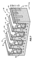
- FIG. 1 depicts a cross-sectional plane view of a portion 10 of a memory array comprising high aspect ratio structures, e.g., fins 12 , in accordance with an embodiment of the present invention.
- fin refers to a tall, thin, semiconductor member extending from a substrate and generally having a length (i.e., y-direction) greater than the width (i.e., x-direction) and the depth (i.e., z-direction) of the fin.
- the high aspect ratio structures 12 may be formed in and on a substrate 14 having an upper doped region 16 and a lower doped region 18 formed in the substrate 14 by any suitable processes.
- the substrate 14 may include semiconductive materials such as single crystalline or poly crystalline silicon, gallium arsenide, indium phosphide, or other materials with semiconductor properties. Alternately, or additionally, the substrate 14 may include a non-semiconductor surface on which an electronic device may be constructed such as a plastic or ceramic work surface, for example.
- the substrate 14 may be in the form of a whole wafer, a portion of a diced wafer, or a portion of a diced wafer in a packaged electronic device, for instance.
- the upper doped region 16 and the lower doped region 18 may be differently doped.
- the upper doped region 16 may be an n+ material and the lower doped region 18 may be a p ⁇ material (referred to as a “p-well”).
- the depth of the upper doped region 16 may be generally uniform over a substantial portion of the substrate 14 , such as throughout a substantial portion of an array area of a memory device, for example.
- the upper doped region 16 and lower doped region 18 may be formed by implanting or diffusing dopant materials.
- one or both of these regions 16 and/or 18 may be doped during growth or deposition of all or part of the substrate 14 , such as during epitaxial deposition of a semiconductive material or during growth of a semiconductive ingot from which wafers may be cut.
- the upper doped region 16 may form a source and a drain of an access device, e.g., a transistor
- the lower doped region 18 may form a channel of an access device, e.g., a transistor.
- the array portion 10 may include deep isolation trenches 20 and shallow trenches 22 that may be formed in the substrate 14 . These trenches 20 and 22 may generally extend in the y-direction, as indicated in FIG. 1 .
- the deep isolation trenches 20 generally separate access devices, e.g., transistors, formed in the high aspect ratio structures, and the shallow trenches 22 generally separate the source and drain of a single access device.
- One or more shallow trenches 22 may be interposed between pairs of the deep isolation trenches 20 .
- the shallow trenches 22 may be deeper than the upper doped region 16 to separate sources and drains.
- the deep isolation trenches 20 may be deeper than the shallow trenches 22 to isolate subsequently formed access devices, e.g., transistors.
- the deep isolation trenches 20 and/or shallow trenches 22 may have a generally rectangular or trapezoidal cross-section, and, in some embodiments, their cross-section may be generally uniform through some distance in the y-direction, for example through a distance larger than one, two, five, or more transistor lengths.
- the deep isolation trenches 20 and shallow trenches 22 may be partially or entirely filled with various dielectric materials, such as high density plasma (HDP) oxide, for instance, to electrically isolate features.
- the deep isolation trenches 20 and/or shallow trenches 22 may include various liner materials, such as silicon nitride for example, to relieve film stresses, improve adhesion, and/or function as a barrier material.
- the fins 12 may include a transistor 21 formed by a source 23 and drain 25 in the upper doped region 16 and a conductive channel 27 formed in the lower doped region 18 .
- This structure may be referred to as a fin field-effect transistor (finFET).
- finFET fin field-effect transistor
- the fins 12 may be formed in the substrate 14 and separated via row trenches 24 , forming sidewalls 26 on one or both sides of each fin 12 and a bottom surface 28 .
- the row trenches 24 may be formed by any suitable process.
- the row trenches 24 may be formed in the substrate 14 through use a mask, sub-photolithographic techniques, any suitable etching, or combination thereof.
- the fins 12 may define regions having a width 29 and the row trenches 24 may define regions having a width 30 .
- the row trenches 24 may be formed using a mask with a sub-photolithographic process, e.g., a sidewall-spacer process, a resist-reflow process, or a line-width thinning process.
- the widths 28 and 30 may be generally equal to or less than F, 3 ⁇ 4 F, or 1 ⁇ 2 F, wherein F refers to the photolithographic-resolution limit or minimum achievable feature size.
- the width 29 of the fins 12 may be about 30 nanometers, 20 nanometers, or less, and the width 30 of the row trench 24 may be about 40 nanometers, 30 nanometers, or less.
- the fins 12 may include one or more materials the above upper doped region 16 .
- the fin 12 may include, for example, a pad oxide cap 32 and a silicon nitride cap 34 .
- the pad oxide cap 32 and silicon nitride cap 34 may be formed from pad oxide and silicon nitride respectively during etch of the row trenches 24 and formation of the fins 12 .
- other materials may be disposed on the fins 12 .
- FIGS. 2-5 depict formation of lower gates in the trenches 24 and adjacent to each of the sidewalls 26 of the fins 12 .
- the term “lower” refers to the location of the gate relative to the trenches 24 , such that lower gates are nearer to the bottom surface 28 of the trenches 24 .
- the lower gates are relatively closer to the substrate 14 and farther from the upper portion of the fins 12 than subsequently formed upper gates.
- a gate oxide 36 may be formed on the sidewalls 26 of the fins 12 and the bottom portion 28 of the trenches 24 .
- the gate oxide 36 may be deposited, grown, or otherwise formed, and it may substantially or entirely cover the exposed portions of the upper doped region 16 and the lower doped region 18 .
- the gate oxide 36 may include a variety of dielectric materials, such as oxide (e.g., silicon dioxide), oxynitride, or high-dielectric constant materials like hafnium dioxide, zirconium dioxide, and titanium dioxide.
- the gate oxide 36 may have a thickness less than about 60 ⁇ , e.g., a thickness equal to or less than about 40 ⁇ .
- a liner 38 may be formed on the gate oxide 36 in accordance with an embodiment of the present invention. As shown in FIG. 3 , the liner 38 may be formed on the bottom portion 28 of the row trenches 24 and on the sidewalls 26 of the fins 12 .
- the liner 38 may include titanium nitride (TiN), tungsten nitride, or other appropriate conductive materials or combination thereof. In some embodiments, the liner 38 may have a thickness less than about 40 ⁇ , e.g., a thickness equal to or less than about 30 ⁇ .
- a metal conductor 40 may be formed on the array portion 10 in accordance with an embodiment of the present invention.
- the metal conductor 40 may be formed in the row trenches 24 and on the sidewalls 26 of the fins 12 . As will be appreciated, only that portion of the metal conductor 40 in the trenches 24 is illustrated.
- the metal conductor 40 may include tungsten, ruthenium (Ru), or other appropriate conductive materials or combination thereof.
- titanium nitride liner 38 may be disposed on the gate oxide 36 , and tungsten may be disposed on the titanium nitride liner 38 to form the metal conductor 40 .
- etching of the metal conductor 40 may form bottom gates (e.g., wordlines) in the row trenches 24 on either of the sidewalls 26 of the fins 12 .
- the formation of the upper gates may be accomplished during or after etch of the metal conductor 40 by separating an upper portion of the liner 38 from the lower portion of the liner 38 during etch of the metal conductor 40 .
- FIG. 5 depicts the array portion 10 after a removal of a portion of the metal conductor 40 to form lower gates 42 in accordance with an embodiment of the present invention.
- the metal conductor 40 may be removed to a depth 44 in the trenches 24 .
- the metal conductor 40 may be removed by one of or a combination of etch processes, such as wet etch, dry etch, or other suitable processes. The duration of the etch may control the depth (e.g., distance) of the etch into the row trench 24 .
- the un-etched upper portions of the liner 38 may form upper gates above the lower gates 42 .
- the upper gates may be formed by ion bombardment to separate portions of the liner 38 .
- FIG. 6 depicts the array portion 10 after ion bombardment to separate the liner 38 in accordance with an embodiment of the present invention.
- the ion bombardment, of the liner 8 may be performed during or after etch of the metal conductor 40 described above in FIG. 5 .
- the etch may naturally separate the liner 38 near the top of the metal conductor 40 .
- the liner 38 may be separated into an upper portion 46 and a lower portion 48 .
- the ion bombardment may result from sputter from the metal conductor 40 during ion etch of the conductor 40 .
- the separation between the upper portion 46 and lower portion 48 thus occurs near the depth 44 of the metal conductor 40 .
- the liner 38 of the lower gates 42 may be formed at a depth 50 .
- the metal conductor 40 may protrude slightly above the liner 38 , such that the depth 50 is less than the depth 44 . In other embodiments, the depth 50 may be equal to or greater than the depth 44 .
- FIG. 7 depicts the array portion 10 after removal of the liner 38 in accordance with an embodiment of the present invention.
- portion of the liner 38 may be removed to form upper gates 52 and 54 from the upper portion 46 of the liner 38 .
- the gates 52 and 54 may connect to one another, e.g., by wrapping around the ends (not shown) of the fins 12 , or they may be electrically independent. Accordingly, in some embodiments the upper gates 52 and 54 may be titanium nitride and the lower gate 42 may be tungsten.
- the liner may be removed by one of or a combination of etch processes, such as wet etch, dry etch, or other suitable processes.
- portions of the liner 38 may be removed during etch of the metal conductor 40 .
- the steps described in FIGS. 5-7 may be accomplished during an etch process.
- any one of or combination of the step described in FIGS. 5-7 may be performed using separate processes.
- a dielectric 56 may be formed on the array portion 10 , as illustrated by FIG. 8 .
- the dielectric 56 may be formed with an overburden 58 to increase the likelihood of covering the gates upper gates 42 over a substantial portion of the portion 10 .
- the dielectric 56 may include an oxide formed with TEOS CVD or other appropriate materials.
- Planarization may include processing the array portion 10 with a CMP process, an etch-back process, or other processes that planarize.
- the planarization process may stop on or in the upper doped region 16 , removing the overburden 58 of the dielectric 56 .
- combinations of upper gates 52 and 54 and lower gates 42 may be used to activate the transistors 21 of the fins 12 .
- each access line e.g., gates 52 , 54 , and 42
- each access line connects (i.e., forms a cross-point or cross-hair) with an access device (e.g., the transistors 21 of fins 12 ).
- the upper gates may be separately formed after formation of the lower gates.
- FIGS. 10-14 depict formation of the upper gates after formation of the lower gates depicted in FIGS. 2-5 and in accordance with another embodiment of the present invention.
- FIG. 10 depicts the array portion 10 after a removal of a portion of the metal conductor 40 , the liner 38 , and the gate oxide 36 to form the lower gates 42 in accordance with an embodiment of the present invention.
- the liner 38 and gate oxide 36 may be removed along the sidewalls 26 of the fins 12 to a depth 60 .
- the metal conductor 40 may be removed to a depth 61 in the trenches 24 .
- the metal conductor 40 , the liner 38 , and the gate oxide 36 may be removed by one of or a combination of etch processes, such as wet etch, dry etch, or other suitable processes.
- the duration of the etch may control the depth (e.g., distance) of the etch into the row trench 24 .
- differing etch rates of the different materials may result in different depths 60 and 61 .
- the metal conductor 40 may protrude slightly above the gate oxide 36 and the liner 38 , such that the depth 60 is less than the depth 61 . In other embodiments, the depth 60 may be equal to or greater than the depth 61 .
- FIG. 11 depicts formation of a second gate oxide 62 on the sidewalls 26 of the fins 12 and on the lower gates 42 , such as on the metal conductor 40 , the liner 38 , and the gate oxide 36 .
- the second gate oxide 62 may be deposited, grown, or otherwise formed, and it may substantially or entirely cover the exposed portions of the upper doped region 16 and some of the lower doped region 18 .
- the second gate oxide 62 may include a variety of dielectric materials, such as oxide (e.g., silicon dioxide), oxynitride, or high-dielectric constant materials like hafnium dioxide, zirconium dioxide, and titanium dioxide.
- the second gate oxide 62 may have a thickness less than about 60 ⁇ , e.g., a thickness equal to or less than about 40 ⁇ .
- a second conductor 63 may be formed on either side of the fins 12 to form upper gates 64 and 66 , as illustrated by FIG. 12 .
- the gates 64 and 66 may connect to one another, e.g., by wrapping around the ends (not shown) of the fins 12 , or they may be electrically independent.
- the gates 64 and 66 may partially, substantially, or entirely overlap the upper doped region 112 .
- the gates 64 and 66 may be sidewall spacers formed by depositing a conductive film on the array portion 10 and, then, anisotropically etching the conductive film until the conductive film is generally removed from horizontal surfaces, leaving the conductor 63 disposed against generally vertical surfaces.
- the gates 64 and 66 may include TiN, Ru, or other appropriate conductive materials.
- a protective body may be formed on the conductive material. Examples of a protective body include a high-aspect-ratio-process (HARP) oxide formed on the conductor 63 .
- the conductor 63 have a thickness less than about 40 ⁇ , e.g., a thickness equal to or less than about 30 ⁇ .
- the protective body may be anisotropically etched, e.g., dry etched, to expose generally horizontal portions of the conductive material, and the exposed portions of the conductive material may then be dry etched or wet etched, e.g., with an SC1 etch for less than 10 minutes, e.g., generally equal to or less than five minutes. After removing the exposed portions of the conductor 63 , the remaining portion of the protective body may be removed with another etch that selectively removes the protective body, while leaving a substantial portion of the conductor 63 disposed against the sidewalls 26 of the fins 12 .
- a dielectric 68 may be formed on the array portion 10 , as illustrated by FIG. 13 .
- the dielectric 68 may be formed with an overburden 70 to increase the likelihood of covering the gates 64 and 66 over a substantial portion of the array portion 10 .
- the dielectric 68 may include an oxide formed with TEOS CVD or other appropriate materials.
- the dielectric 68 is formed with a thickness of less than about 1500 ⁇ , e.g., equal to or less than about 1000 ⁇ .
- the array portion 10 may be planarized, as illustrated by FIG. 14 . Planarization may include processing the substrate 110 with a CMP process, an etch-back process, or other processes that planarize.
- the planarization process may stop on or in the upper doped region 16 , removing the overburden 70 of the dielectric 68 .
- combinations of upper gates 64 and 66 and lower gates 42 may be used to activate the transistors 21 of the fins 12 .
- Such a device may be referred to as a “cross-hair cell” as each access line (e.g., gates 64 , 66 , and 42 ) connects (i.e., forms a cross-point or cross-hair) with an access device (e.g., the transistors 21 of fins 12 ).
- FIG. 15 is a flowchart of a manufacturing process 80 in accordance with the embodiments depicted above in FIGS. 1-14 .
- fins 12 and row trenches 24 may be formed in the substrate 14 by any suitable process (block 82 ).
- An oxide 36 may be formed in the row trenches 24 on the sidewalls 26 and bottom surface 28 of the row trenches 24 (block 84 ), a liner 38 may be formed on the oxide (block 86 ), and a metal conductor may be deposited in the row trenches 24 (block 88 ), as shown above in FIGS. 2-4 .
- the metal conductor 40 may be etched to a desired depth to form the lower gates 42 (block 90 ). As discussed above in FIGS. 5-7 , during or after the etch, ion bombardment may separate an upper portion of the liner 38 to form upper gates 52 and 54 (block 92 ), and remaining portions of the liner 38 may be removed.
- the metal conductor 40 may be etched to a desired depth to form the lower gates (block 94 ), and a second oxide 62 may be formed in the row trenches on the lower gates (block 96 ).
- the upper gates 64 and 66 may be created through formation of a second conductor on the second oxide 62 (block 98 ).
- a dielectric may be formed on the array portion 10 (block 100 ), such as in the row trenches 24 .
- the array portion 10 may be subjected to further processing (block 102 ).
- FIGS. 16 and 17 are schematic cross-sections of an array portion 104 formed in the manner described above in FIGS. 1-14 and depicting operation of upper gates 104 and 106 and lower gates 108 to operate the transistors of fins 12 .
- FIGS. 15 and 16 depict fins 12 A- 12 F separated by row trenches 24 and each having upper gates 104 and 106 and lower gates 108 disposed therebetween and constructed according to the techniques described above.
- the upper gates 104 and 106 may be relatively highly resistive as compared to the lower gates 108 , resulting in a relatively longer response time (e.g., slow switching).
- the lower gates 108 may be of a relatively low resistance, as compared to the upper gates 104 and 106 , and may have a relatively quicker response time.
- the cross-sectional area through the lower gates 108 may be less than the cross-sectional area through the upper gates 104 and 106 .
- the conductor 40 of the lower gates 108 may be a different material than the conductor 62 (or liner 38 ).
- an access line e.g., a wordline
- both the upper and lower gates may be biased to a desired voltage.
- the upper gates 104 and 160 may connect to one another, e.g., by wrapping around the ends (not shown) of the fins 12 , or they may be electrically independent
- the lower gates 108 may provide for relatively fast selection of upper gates 104 and 106 of a specific fin 12 .
- FIG. 16 depicts operation of the transistors of fin 12 B in accordance with an embodiment of the present invention.
- upper gates 104 and 106 may be biased to a first voltage to preselect gates of the fins 12 .
- each upper gate may be biased to a first and second voltage respectively.
- upper gates 110 and 112 may be used to preselect fin 12 B
- upper gates 114 and 116 may be used to preselect fin 12 D
- upper gate 118 and a corresponding upper gate (not shown) may be used to preselect fin 12 F.
- the transistors of a specific fin 12 may be operated by biasing the lower gates 120 and 122 on either side of the fin 12 to a second voltage.
- the lower gates 120 and 122 may be biased to a desired voltage, allowing relatively faster selection of the fin 12 B and operation of the corresponding transistors.
- the lower gates 120 and 122 exhibit minimal capacitive coupling during operation.
- FIG. 17 depicts operation of the transistors of fin 12 D in accordance with an embodiment of the present invention.
- upper gates 110 and 112 may be used to preselect fin 12 B
- upper gates 114 and 116 may be used to preselect fin 12 D
- upper gate 118 and a corresponding upper gate (not shown) may be used to preselect fin 12 F.
- lower gates 124 and 126 may be biased to a second voltage, allowing relatively faster selection of the fin 12 D and operation of the corresponding transistors.
- each fin 12 of the array portion 104 may be preselected by biasing the upper gates 104 and 106 surrounding each fin 12
- the lower gates 108 may be biased to select a desired fin 12 and operate transistors of the selected fin 12 .
Abstract
Description
Claims (16)
Priority Applications (3)
| Application Number | Priority Date | Filing Date | Title |
|---|---|---|---|
| US12/950,787 US9553193B2 (en) | 2010-11-19 | 2010-11-19 | Double gated fin transistors and methods of fabricating and operating the same |
| PCT/US2011/060034 WO2012067919A1 (en) | 2010-11-19 | 2011-11-09 | Double gated fin transistors and methods of fabricating and operating the same |
| TW100141885A TWI503980B (en) | 2010-11-19 | 2011-11-16 | Double gated fin transistors and methods of fabricating and operating the same |
Applications Claiming Priority (1)
| Application Number | Priority Date | Filing Date | Title |
|---|---|---|---|
| US12/950,787 US9553193B2 (en) | 2010-11-19 | 2010-11-19 | Double gated fin transistors and methods of fabricating and operating the same |
Publications (2)
| Publication Number | Publication Date |
|---|---|
| US20120126884A1 US20120126884A1 (en) | 2012-05-24 |
| US9553193B2 true US9553193B2 (en) | 2017-01-24 |
Family
ID=44993198
Family Applications (1)
| Application Number | Title | Priority Date | Filing Date |
|---|---|---|---|
| US12/950,787 Active 2034-08-27 US9553193B2 (en) | 2010-11-19 | 2010-11-19 | Double gated fin transistors and methods of fabricating and operating the same |
Country Status (3)
| Country | Link |
|---|---|
| US (1) | US9553193B2 (en) |
| TW (1) | TWI503980B (en) |
| WO (1) | WO2012067919A1 (en) |
Families Citing this family (12)
| Publication number | Priority date | Publication date | Assignee | Title |
|---|---|---|---|---|
| US8293602B2 (en) | 2010-11-19 | 2012-10-23 | Micron Technology, Inc. | Method of fabricating a finFET having cross-hair cells |
| US8921899B2 (en) | 2010-11-19 | 2014-12-30 | Micron Technology, Inc. | Double gated 4F2 dram CHC cell and methods of fabricating the same |
| KR101927992B1 (en) * | 2012-08-31 | 2018-12-12 | 에스케이하이닉스 주식회사 | Semiconductor device and method for fabricating the same |
| US20140103452A1 (en) | 2012-10-15 | 2014-04-17 | Marvell World Trade Ltd. | Isolation components for transistors formed on fin features of semiconductor substrates |
| US9240352B2 (en) * | 2012-10-24 | 2016-01-19 | Globalfoundries Inc. | Bulk finFET well contacts with fin pattern uniformity |
| KR102054302B1 (en) * | 2013-06-21 | 2019-12-10 | 삼성전자 주식회사 | Semiconductor device and method for fabricating the same |
| US9515172B2 (en) | 2014-01-28 | 2016-12-06 | Samsung Electronics Co., Ltd. | Semiconductor devices having isolation insulating layers and methods of manufacturing the same |
| KR102115552B1 (en) * | 2014-01-28 | 2020-05-27 | 삼성전자주식회사 | Semiconductor device and fabricating method thereof |
| US9773888B2 (en) | 2014-02-26 | 2017-09-26 | Micron Technology, Inc. | Vertical access devices, semiconductor device structures, and related methods |
| WO2017111819A1 (en) * | 2015-12-26 | 2017-06-29 | Intel Corporation | Gate isolation in non-planar transistors |
| US10014302B1 (en) * | 2016-12-27 | 2018-07-03 | Micron Technology, Inc. | Methods of forming memory arrays |
| US10615165B1 (en) | 2018-10-04 | 2020-04-07 | Micron Technology, Inc. | Methods of forming integrated assemblies |
Citations (21)
| Publication number | Priority date | Publication date | Assignee | Title |
|---|---|---|---|---|
| US5315143A (en) | 1992-04-28 | 1994-05-24 | Matsushita Electric Industrial Co., Ltd. | High density integrated semiconductor device |
| US5929477A (en) * | 1997-01-22 | 1999-07-27 | International Business Machines Corporation | Self-aligned diffused source vertical transistors with stack capacitors in a 4F-square memory cell array |
| US20030193065A1 (en) | 2002-04-11 | 2003-10-16 | International Business Machines Corporation | Dual double gate transistor and method for forming |
| US6900102B2 (en) | 2003-02-10 | 2005-05-31 | Samsung Electronics Co., Ltd. | Methods of forming double gate electrodes using tunnel and trench |
| US6977404B2 (en) | 2002-12-27 | 2005-12-20 | Kabushiki Kaisha Toshiba | Trench DRAM with double-gated transistor and method of manufacturing the same |
| WO2007085996A2 (en) | 2006-01-30 | 2007-08-02 | Nxp B.V. | Mos device and method of fabricating a mos device |
| US20090057778A1 (en) * | 2007-08-31 | 2009-03-05 | Lars Dreeskornfeld | Integrated circuit and method of manufacturing an integrated circuit |
| US7566620B2 (en) | 2005-07-25 | 2009-07-28 | Micron Technology, Inc. | DRAM including a vertical surround gate transistor |
| US7573108B2 (en) | 2006-05-12 | 2009-08-11 | Micron Technology, Inc | Non-planar transistor and techniques for fabricating the same |
| US20090206400A1 (en) | 2008-02-19 | 2009-08-20 | Micron Technology, Inc. | Systems and devices including fin transistors and methods of using, making, and operating the same |
| US20090206443A1 (en) | 2008-02-19 | 2009-08-20 | Micron Technology, Inc. | Devices including fin transistors robust to gate shorts and methods of making the same |
| US20090224357A1 (en) | 2008-03-06 | 2009-09-10 | Micron Technology, Inc. | Devices with cavity-defined gates and methods of making the same |
| US20090237996A1 (en) | 2008-03-20 | 2009-09-24 | Micron Technology, Inc. | Memory structure having volatile and non-volatile memory portions |
| US20090238010A1 (en) | 2008-03-20 | 2009-09-24 | Micron Technology, Inc. | Systems and devices including multi-transistor cells and methods of using, making, and operating the same |
| US20090251946A1 (en) | 2008-04-03 | 2009-10-08 | Micron Technology, Inc. | Data cells with drivers and methods of making and operating the same |
| US20090294842A1 (en) | 2008-05-30 | 2009-12-03 | Micron Technology, Inc. | Methods of forming data cells and connections to data cells |
| US7635648B2 (en) | 2008-04-10 | 2009-12-22 | Applied Materials, Inc. | Methods for fabricating dual material gate in a semiconductor device |
| US20100066440A1 (en) | 2008-09-15 | 2010-03-18 | Micron Technology, Inc. | Transistor with a passive gate and methods of fabricating the same |
| US7742324B2 (en) | 2008-02-19 | 2010-06-22 | Micron Technology, Inc. | Systems and devices including local data lines and methods of using, making, and operating the same |
| US7808042B2 (en) | 2008-03-20 | 2010-10-05 | Micron Technology, Inc. | Systems and devices including multi-gate transistors and methods of using, making, and operating the same |
| US8148775B2 (en) | 2008-06-02 | 2012-04-03 | Micron Technology, Inc. | Methods of providing electrical isolation and semiconductor structures including same |
-
2010
- 2010-11-19 US US12/950,787 patent/US9553193B2/en active Active
-
2011
- 2011-11-09 WO PCT/US2011/060034 patent/WO2012067919A1/en active Application Filing
- 2011-11-16 TW TW100141885A patent/TWI503980B/en active
Patent Citations (22)
| Publication number | Priority date | Publication date | Assignee | Title |
|---|---|---|---|---|
| US5315143A (en) | 1992-04-28 | 1994-05-24 | Matsushita Electric Industrial Co., Ltd. | High density integrated semiconductor device |
| US5929477A (en) * | 1997-01-22 | 1999-07-27 | International Business Machines Corporation | Self-aligned diffused source vertical transistors with stack capacitors in a 4F-square memory cell array |
| US6077745A (en) | 1997-01-22 | 2000-06-20 | International Business Machines Corporation | Self-aligned diffused source vertical transistors with stack capacitors in a 4F-square memory cell array |
| US20030193065A1 (en) | 2002-04-11 | 2003-10-16 | International Business Machines Corporation | Dual double gate transistor and method for forming |
| US6977404B2 (en) | 2002-12-27 | 2005-12-20 | Kabushiki Kaisha Toshiba | Trench DRAM with double-gated transistor and method of manufacturing the same |
| US6900102B2 (en) | 2003-02-10 | 2005-05-31 | Samsung Electronics Co., Ltd. | Methods of forming double gate electrodes using tunnel and trench |
| US7566620B2 (en) | 2005-07-25 | 2009-07-28 | Micron Technology, Inc. | DRAM including a vertical surround gate transistor |
| WO2007085996A2 (en) | 2006-01-30 | 2007-08-02 | Nxp B.V. | Mos device and method of fabricating a mos device |
| US7573108B2 (en) | 2006-05-12 | 2009-08-11 | Micron Technology, Inc | Non-planar transistor and techniques for fabricating the same |
| US20090057778A1 (en) * | 2007-08-31 | 2009-03-05 | Lars Dreeskornfeld | Integrated circuit and method of manufacturing an integrated circuit |
| US20090206400A1 (en) | 2008-02-19 | 2009-08-20 | Micron Technology, Inc. | Systems and devices including fin transistors and methods of using, making, and operating the same |
| US20090206443A1 (en) | 2008-02-19 | 2009-08-20 | Micron Technology, Inc. | Devices including fin transistors robust to gate shorts and methods of making the same |
| US7742324B2 (en) | 2008-02-19 | 2010-06-22 | Micron Technology, Inc. | Systems and devices including local data lines and methods of using, making, and operating the same |
| US20090224357A1 (en) | 2008-03-06 | 2009-09-10 | Micron Technology, Inc. | Devices with cavity-defined gates and methods of making the same |
| US20090237996A1 (en) | 2008-03-20 | 2009-09-24 | Micron Technology, Inc. | Memory structure having volatile and non-volatile memory portions |
| US20090238010A1 (en) | 2008-03-20 | 2009-09-24 | Micron Technology, Inc. | Systems and devices including multi-transistor cells and methods of using, making, and operating the same |
| US7808042B2 (en) | 2008-03-20 | 2010-10-05 | Micron Technology, Inc. | Systems and devices including multi-gate transistors and methods of using, making, and operating the same |
| US20090251946A1 (en) | 2008-04-03 | 2009-10-08 | Micron Technology, Inc. | Data cells with drivers and methods of making and operating the same |
| US7635648B2 (en) | 2008-04-10 | 2009-12-22 | Applied Materials, Inc. | Methods for fabricating dual material gate in a semiconductor device |
| US20090294842A1 (en) | 2008-05-30 | 2009-12-03 | Micron Technology, Inc. | Methods of forming data cells and connections to data cells |
| US8148775B2 (en) | 2008-06-02 | 2012-04-03 | Micron Technology, Inc. | Methods of providing electrical isolation and semiconductor structures including same |
| US20100066440A1 (en) | 2008-09-15 | 2010-03-18 | Micron Technology, Inc. | Transistor with a passive gate and methods of fabricating the same |
Non-Patent Citations (6)
| Title |
|---|
| Taiwan Office Action for Application No. 100141885 dated Nov. 26, 2014, 6 pgs. |
| U.S. Appl. No. 12/702,123, filed Feb. 8, 2010, Werner Juengling. |
| U.S. Appl. No. 12/702,947, filed Feb. 9, 2010, Werner Juengling. |
| U.S. Appl. No. 12/950,761, filed Nov. 19, 2010, Werner Juengling. |
| U.S. Appl. No. 12/950,774, filed Nov. 19, 2010, Werner Juengling. |
| U.S. Appl. No. 12/950,797, filed Nov. 19, 2010, Werner Juengling. |
Also Published As
| Publication number | Publication date |
|---|---|
| US20120126884A1 (en) | 2012-05-24 |
| TWI503980B (en) | 2015-10-11 |
| TW201230338A (en) | 2012-07-16 |
| WO2012067919A1 (en) | 2012-05-24 |
Similar Documents
| Publication | Publication Date | Title |
|---|---|---|
| US9553193B2 (en) | Double gated fin transistors and methods of fabricating and operating the same | |
| US9472461B2 (en) | Double gated 4F2 dram CHC cell and methods of fabricating the same | |
| US11114550B2 (en) | Recessing STI to increase FIN height in FIN-first process | |
| US9281309B2 (en) | Cross-hair cell wordline formation | |
| US8293602B2 (en) | Method of fabricating a finFET having cross-hair cells | |
| US9362418B2 (en) | Semiconductor structures including bodies of semiconductor material and methods of forming same | |
| US10943837B2 (en) | Device having overlapping semiconductor fins oriented in different directions | |
| US20140306297A1 (en) | Recessing sti to increase fin height in fin-first process | |
| TWI749363B (en) | Finfet having insulating layers between gate and source/drain contacts | |
| US9711505B2 (en) | Semiconductor devices having dummy gate structure for controlling channel stress | |
| US20190051731A1 (en) | Semiconductor device and method for fabricating the same | |
| US9685540B2 (en) | Semiconductor device having a gate that is buried in an active region and a device isolation film | |
| US20230187542A1 (en) | Multi-layer dielectric refill for profile control in semiconductor devices | |
| US8853018B2 (en) | Method of manufacturing semiconductor device having multi-channels | |
| US11316043B2 (en) | Semiconductor transistor device and method of manufacturing the same |
Legal Events
| Date | Code | Title | Description |
|---|---|---|---|
| AS | Assignment |
Owner name: MICRON TECHNOLOGY, INC., IDAHO Free format text: ASSIGNMENT OF ASSIGNORS INTEREST;ASSIGNOR:JUENGLING, WERNER;REEL/FRAME:025393/0796 Effective date: 20101110 |
|
| AS | Assignment |
Owner name: U.S. BANK NATIONAL ASSOCIATION, AS COLLATERAL AGENT, CALIFORNIA Free format text: SECURITY INTEREST;ASSIGNOR:MICRON TECHNOLOGY, INC.;REEL/FRAME:038669/0001 Effective date: 20160426 Owner name: U.S. BANK NATIONAL ASSOCIATION, AS COLLATERAL AGEN Free format text: SECURITY INTEREST;ASSIGNOR:MICRON TECHNOLOGY, INC.;REEL/FRAME:038669/0001 Effective date: 20160426 |
|
| AS | Assignment |
Owner name: MORGAN STANLEY SENIOR FUNDING, INC., AS COLLATERAL AGENT, MARYLAND Free format text: PATENT SECURITY AGREEMENT;ASSIGNOR:MICRON TECHNOLOGY, INC.;REEL/FRAME:038954/0001 Effective date: 20160426 Owner name: MORGAN STANLEY SENIOR FUNDING, INC., AS COLLATERAL Free format text: PATENT SECURITY AGREEMENT;ASSIGNOR:MICRON TECHNOLOGY, INC.;REEL/FRAME:038954/0001 Effective date: 20160426 |
|
| FEPP | Fee payment procedure |
Free format text: PAYOR NUMBER ASSIGNED (ORIGINAL EVENT CODE: ASPN); ENTITY STATUS OF PATENT OWNER: LARGE ENTITY |
|
| STCF | Information on status: patent grant |
Free format text: PATENTED CASE |
|
| AS | Assignment |
Owner name: U.S. BANK NATIONAL ASSOCIATION, AS COLLATERAL AGENT, CALIFORNIA Free format text: CORRECTIVE ASSIGNMENT TO CORRECT THE REPLACE ERRONEOUSLY FILED PATENT #7358718 WITH THE CORRECT PATENT #7358178 PREVIOUSLY RECORDED ON REEL 038669 FRAME 0001. ASSIGNOR(S) HEREBY CONFIRMS THE SECURITY INTEREST;ASSIGNOR:MICRON TECHNOLOGY, INC.;REEL/FRAME:043079/0001 Effective date: 20160426 Owner name: U.S. BANK NATIONAL ASSOCIATION, AS COLLATERAL AGEN Free format text: CORRECTIVE ASSIGNMENT TO CORRECT THE REPLACE ERRONEOUSLY FILED PATENT #7358718 WITH THE CORRECT PATENT #7358178 PREVIOUSLY RECORDED ON REEL 038669 FRAME 0001. ASSIGNOR(S) HEREBY CONFIRMS THE SECURITY INTEREST;ASSIGNOR:MICRON TECHNOLOGY, INC.;REEL/FRAME:043079/0001 Effective date: 20160426 |
|
| AS | Assignment |
Owner name: JPMORGAN CHASE BANK, N.A., AS COLLATERAL AGENT, ILLINOIS Free format text: SECURITY INTEREST;ASSIGNORS:MICRON TECHNOLOGY, INC.;MICRON SEMICONDUCTOR PRODUCTS, INC.;REEL/FRAME:047540/0001 Effective date: 20180703 Owner name: JPMORGAN CHASE BANK, N.A., AS COLLATERAL AGENT, IL Free format text: SECURITY INTEREST;ASSIGNORS:MICRON TECHNOLOGY, INC.;MICRON SEMICONDUCTOR PRODUCTS, INC.;REEL/FRAME:047540/0001 Effective date: 20180703 |
|
| AS | Assignment |
Owner name: MICRON TECHNOLOGY, INC., IDAHO Free format text: RELEASE BY SECURED PARTY;ASSIGNOR:U.S. BANK NATIONAL ASSOCIATION, AS COLLATERAL AGENT;REEL/FRAME:047243/0001 Effective date: 20180629 |
|
| AS | Assignment |
Owner name: MICRON TECHNOLOGY, INC., IDAHO Free format text: RELEASE BY SECURED PARTY;ASSIGNOR:MORGAN STANLEY SENIOR FUNDING, INC., AS COLLATERAL AGENT;REEL/FRAME:050937/0001 Effective date: 20190731 |
|
| AS | Assignment |
Owner name: MICRON SEMICONDUCTOR PRODUCTS, INC., IDAHO Free format text: RELEASE BY SECURED PARTY;ASSIGNOR:JPMORGAN CHASE BANK, N.A., AS COLLATERAL AGENT;REEL/FRAME:051028/0001 Effective date: 20190731 Owner name: MICRON TECHNOLOGY, INC., IDAHO Free format text: RELEASE BY SECURED PARTY;ASSIGNOR:JPMORGAN CHASE BANK, N.A., AS COLLATERAL AGENT;REEL/FRAME:051028/0001 Effective date: 20190731 |
|
| MAFP | Maintenance fee payment |
Free format text: PAYMENT OF MAINTENANCE FEE, 4TH YEAR, LARGE ENTITY (ORIGINAL EVENT CODE: M1551); ENTITY STATUS OF PATENT OWNER: LARGE ENTITY Year of fee payment: 4 |