US9563433B1 - System and method for class-based execution of an instruction broadcasted to an array of processing elements - Google Patents
System and method for class-based execution of an instruction broadcasted to an array of processing elements Download PDFInfo
- Publication number
- US9563433B1 US9563433B1 US13/719,119 US201213719119A US9563433B1 US 9563433 B1 US9563433 B1 US 9563433B1 US 201213719119 A US201213719119 A US 201213719119A US 9563433 B1 US9563433 B1 US 9563433B1
- Authority
- US
- United States
- Prior art keywords
- class
- processing elements
- processing
- instruction
- classes
- Prior art date
- Legal status (The legal status is an assumption and is not a legal conclusion. Google has not performed a legal analysis and makes no representation as to the accuracy of the status listed.)
- Expired - Fee Related, expires
Links
- 238000012545 processing Methods 0.000 title claims abstract description 114
- 238000000034 method Methods 0.000 title claims description 12
- 230000015654 memory Effects 0.000 claims description 17
- 238000010586 diagram Methods 0.000 description 8
- 230000001419 dependent effect Effects 0.000 description 2
- 238000012546 transfer Methods 0.000 description 2
- 238000013459 approach Methods 0.000 description 1
- 238000010276 construction Methods 0.000 description 1
- 230000002596 correlated effect Effects 0.000 description 1
- 230000000875 corresponding effect Effects 0.000 description 1
- 238000005516 engineering process Methods 0.000 description 1
- 238000012986 modification Methods 0.000 description 1
- 230000004048 modification Effects 0.000 description 1
- 238000012827 research and development Methods 0.000 description 1
- 238000004904 shortening Methods 0.000 description 1
Images


Classifications
-
- G—PHYSICS
- G06—COMPUTING; CALCULATING OR COUNTING
- G06F—ELECTRIC DIGITAL DATA PROCESSING
- G06F9/00—Arrangements for program control, e.g. control units
- G06F9/06—Arrangements for program control, e.g. control units using stored programs, i.e. using an internal store of processing equipment to receive or retain programs
- G06F9/30—Arrangements for executing machine instructions, e.g. instruction decode
- G06F9/38—Concurrent instruction execution, e.g. pipeline, look ahead
- G06F9/3885—Concurrent instruction execution, e.g. pipeline, look ahead using a plurality of independent parallel functional units
-
- G—PHYSICS
- G06—COMPUTING; CALCULATING OR COUNTING
- G06F—ELECTRIC DIGITAL DATA PROCESSING
- G06F15/00—Digital computers in general; Data processing equipment in general
- G06F15/76—Architectures of general purpose stored program computers
- G06F15/80—Architectures of general purpose stored program computers comprising an array of processing units with common control, e.g. single instruction multiple data processors
- G06F15/8007—Architectures of general purpose stored program computers comprising an array of processing units with common control, e.g. single instruction multiple data processors single instruction multiple data [SIMD] multiprocessors
- G06F15/8015—One dimensional arrays, e.g. rings, linear arrays, buses
-
- G—PHYSICS
- G06—COMPUTING; CALCULATING OR COUNTING
- G06F—ELECTRIC DIGITAL DATA PROCESSING
- G06F9/00—Arrangements for program control, e.g. control units
- G06F9/06—Arrangements for program control, e.g. control units using stored programs, i.e. using an internal store of processing equipment to receive or retain programs
- G06F9/30—Arrangements for executing machine instructions, e.g. instruction decode
- G06F9/30003—Arrangements for executing specific machine instructions
- G06F9/30007—Arrangements for executing specific machine instructions to perform operations on data operands
- G06F9/30036—Instructions to perform operations on packed data, e.g. vector, tile or matrix operations
-
- G—PHYSICS
- G06—COMPUTING; CALCULATING OR COUNTING
- G06F—ELECTRIC DIGITAL DATA PROCESSING
- G06F9/00—Arrangements for program control, e.g. control units
- G06F9/06—Arrangements for program control, e.g. control units using stored programs, i.e. using an internal store of processing equipment to receive or retain programs
- G06F9/30—Arrangements for executing machine instructions, e.g. instruction decode
- G06F9/30003—Arrangements for executing specific machine instructions
- G06F9/3004—Arrangements for executing specific machine instructions to perform operations on memory
- G06F9/30043—LOAD or STORE instructions; Clear instruction
-
- G—PHYSICS
- G06—COMPUTING; CALCULATING OR COUNTING
- G06F—ELECTRIC DIGITAL DATA PROCESSING
- G06F9/00—Arrangements for program control, e.g. control units
- G06F9/06—Arrangements for program control, e.g. control units using stored programs, i.e. using an internal store of processing equipment to receive or retain programs
- G06F9/30—Arrangements for executing machine instructions, e.g. instruction decode
- G06F9/30003—Arrangements for executing specific machine instructions
- G06F9/30072—Arrangements for executing specific machine instructions to perform conditional operations, e.g. using predicates or guards
-
- G—PHYSICS
- G06—COMPUTING; CALCULATING OR COUNTING
- G06F—ELECTRIC DIGITAL DATA PROCESSING
- G06F9/00—Arrangements for program control, e.g. control units
- G06F9/06—Arrangements for program control, e.g. control units using stored programs, i.e. using an internal store of processing equipment to receive or retain programs
- G06F9/30—Arrangements for executing machine instructions, e.g. instruction decode
- G06F9/30098—Register arrangements
- G06F9/3012—Organisation of register space, e.g. banked or distributed register file
-
- G—PHYSICS
- G06—COMPUTING; CALCULATING OR COUNTING
- G06F—ELECTRIC DIGITAL DATA PROCESSING
- G06F9/00—Arrangements for program control, e.g. control units
- G06F9/06—Arrangements for program control, e.g. control units using stored programs, i.e. using an internal store of processing equipment to receive or retain programs
- G06F9/30—Arrangements for executing machine instructions, e.g. instruction decode
- G06F9/30181—Instruction operation extension or modification
- G06F9/30189—Instruction operation extension or modification according to execution mode, e.g. mode flag
-
- G—PHYSICS
- G06—COMPUTING; CALCULATING OR COUNTING
- G06F—ELECTRIC DIGITAL DATA PROCESSING
- G06F9/00—Arrangements for program control, e.g. control units
- G06F9/06—Arrangements for program control, e.g. control units using stored programs, i.e. using an internal store of processing equipment to receive or retain programs
- G06F9/30—Arrangements for executing machine instructions, e.g. instruction decode
- G06F9/38—Concurrent instruction execution, e.g. pipeline, look ahead
- G06F9/3836—Instruction issuing, e.g. dynamic instruction scheduling or out of order instruction execution
- G06F9/3851—Instruction issuing, e.g. dynamic instruction scheduling or out of order instruction execution from multiple instruction streams, e.g. multistreaming
-
- G—PHYSICS
- G06—COMPUTING; CALCULATING OR COUNTING
- G06F—ELECTRIC DIGITAL DATA PROCESSING
- G06F9/00—Arrangements for program control, e.g. control units
- G06F9/06—Arrangements for program control, e.g. control units using stored programs, i.e. using an internal store of processing equipment to receive or retain programs
- G06F9/30—Arrangements for executing machine instructions, e.g. instruction decode
- G06F9/38—Concurrent instruction execution, e.g. pipeline, look ahead
- G06F9/3867—Concurrent instruction execution, e.g. pipeline, look ahead using instruction pipelines
-
- G—PHYSICS
- G06—COMPUTING; CALCULATING OR COUNTING
- G06F—ELECTRIC DIGITAL DATA PROCESSING
- G06F9/00—Arrangements for program control, e.g. control units
- G06F9/06—Arrangements for program control, e.g. control units using stored programs, i.e. using an internal store of processing equipment to receive or retain programs
- G06F9/30—Arrangements for executing machine instructions, e.g. instruction decode
- G06F9/38—Concurrent instruction execution, e.g. pipeline, look ahead
- G06F9/3885—Concurrent instruction execution, e.g. pipeline, look ahead using a plurality of independent parallel functional units
- G06F9/3887—Concurrent instruction execution, e.g. pipeline, look ahead using a plurality of independent parallel functional units controlled by a single instruction for multiple data lanes [SIMD]
-
- G—PHYSICS
- G06—COMPUTING; CALCULATING OR COUNTING
- G06F—ELECTRIC DIGITAL DATA PROCESSING
- G06F9/00—Arrangements for program control, e.g. control units
- G06F9/06—Arrangements for program control, e.g. control units using stored programs, i.e. using an internal store of processing equipment to receive or retain programs
- G06F9/46—Multiprogramming arrangements
- G06F9/50—Allocation of resources, e.g. of the central processing unit [CPU]
- G06F9/5061—Partitioning or combining of resources
Definitions
- the present invention relates to the field of data processing. More specifically, the present invention relates to data processing using a data parallel machine with multiple sequencers each sending an instruction.
- ASICs highly specialized integrated circuits
- ASIC designers are able to optimize efficiency and cost through judicious use of parallel processing and parallel data paths.
- An ASIC designer is free to look for explicit and latent parallelism in every nook and cranny of a specific application or algorithm, and then exploit that in circuits.
- an embedded parallel computer is needed that finds the optimum balance between all of the available forms of parallelism, yet remains programmable.
- Embedded computation requires more generality/flexibility than that offered by an ASIC, but less generality than that offered by a general purpose processor. Therefore, the instruction set architecture of an embedded computer can be optimized for an application domain, yet remain “general purpose” within that domain.
- the present invention is a data parallel system which is able to utilize a very high percentage of processing elements.
- the data parallel system includes an array of processing elements and multiple instruction sequencers. Each instruction sequencer (IS) is coupled to the array of processing elements by a bus and is able to send an instruction to the array of processing elements.
- the processing elements are separated into classes and only execute instructions that are directed to their class, although all of the processing elements receive each instruction.
- the data parallel system includes an array of processing elements and an instruction sequencer where the instruction sequencer is able to send multiple instructions. Again, the processing elements are separated into classes and execute instructions based on their class.
- FIG. 1 illustrates a block diagram of a data parallel system with multiple instruction sequencers.
- FIG. 2 illustrates a block diagram of a data parallel system with an instruction sequencer sending out multiple instructions.
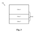
- FIG. 3 illustrates a block diagram of an exemplary array of processing elements separated into multiple classes.
- FIG. 4 illustrates a block diagram of an exemplary array of processing elements separated into multiple classes wherein the classes are not contiguous.
- FIG. 5 illustrates a flowchart of processing multiple instructions in an array of processing elements.
- the present invention maximizes the use of processing elements (PEs) in an array for data parallel processing.
- PEs processing elements
- the present invention employs multiple sequencers to enable more efficient use of the PEs in the array.
- Each instruction sequencer used to drive the array issues an instruction to be executed only by a certain class of PEs.
- multiple programs are able to be processed simultaneously, one for each instruction sequencer.
- two or more streams of instructions can be broadcast into the array.
- the PEs are classified in two or more classes with each stream of instructions being received by the PEs. Although all of the PEs receive each instruction, the PEs only execute the instruction that applies to their class.
- FIG. 1 illustrates a block diagram of a data parallel system 100 with multiple instruction sequencers 104 .
- the data parallel system 100 includes an array of PEs 102 coupled to multiple instruction sequencers 104 .
- the array of PEs 102 is also coupled to a Smart Direct Memory Access (DMA) 106 for data transfer between the array of PEs 102 and a memory.
- DMA Smart Direct Memory Access
- Each of the instruction sequencers 104 is coupled to the array of PEs 102 by a separate bus so that each instruction sequencer 104 is able to send an instruction to all of the PEs within the array of PEs 102 at the same time.
- the array of PEs 102 are separated into a plurality of classes such that PEs in a first class execute a first instruction from a first instruction sequencer, and PEs in an mth class execute an mth instruction from an mth instruction sequencer. By separating the PEs into different classes, there is more data for each class to process since multiple instructions are being processed at once.
- Each PE from the array of PEs 102 receives all of the instructions broadcast by IS l through IS m , but executes only one instruction according with its internal state corresponding to the class.
- FIG. 1 There are two operational modes associated to the system from FIG. 1 .
- Each instruction sequencer has its own program counter issuing m independent streams of instructions, or only one program counter is activated and all the others are disabled and the m streams of instructions are strongly correlated.
- FIG. 2 illustrates the second operational mode.
- FIG. 2 illustrates a block diagram of a data parallel system 100 ′ with an instruction sequencer 104 ′ sending out multiple instructions.
- PC program counter
- the collection of instruction sequencers where only the one program counter 108 is utilized is considered to be the instruction sequencer 104 ′.
- the instruction sequencer 104 ′ broadcasts, in each clock cycle, multiple instructions to an array of PEs 102 . This is a version of the previous embodiment with only one program counter using all the program memories. The switch between the previous embodiment and this embodiment can be done at clock cycle level by disabling some of the program counters of the instruction sequencers.
- Some instruction sequencers are independent, and other instruction sequencers are grouped under the control of only one program counter.
- Each PE in the array of PEs 102 executes only the proper instructions according to its internal state. Therefore, each class of PEs is configured to only execute one instruction of the multiple instructions received.
- the array of PEs 102 is also coupled to a Smart-DMA 106 for data transfer between the array of PEs 102 and a memory.
- FIG. 3 illustrates a block diagram of an exemplary array of processing elements 300 separated into multiple classes 302 .
- the multiple classes 302 in the example include class 1, class 2 and class 3.
- Class 1 includes half of the processing elements, while classes 2 and 3 each include a quarter of the processing elements. Therefore, class 1 would be dedicated the largest amount of data that needs to be processed while classes 2 and 3 would be used for smaller tasks.
- FIG. 3 illustrates three classes of processing elements, there are able to be any number of classes of processing elements where the number is two or greater.
- the graphical representation of the array of processing elements 300 and multiple classes 302 appears to show that the processing elements are designated in classes in straight lines and in groups. This specific linear grouping is not required.
- the classification of processing elements is able to be done in any fashion including a completely random selection of processing elements to be in each group. However, the size of each group is data dependent.
- FIG. 4 illustrates a block diagram of an exemplary array of processing elements 400 separated into multiple classes 402 wherein the classes are not contiguous.
- the multiple classes 402 in the example include class 1, class 2 and class 3. As shown, the classes are able to be noncontiguous such that some of class 1 is separated by class 3 and class 2. Similarly class 3 and class 2 are also separated by other classes.
- the classification of processing elements is able to be done in any fashion including a completely random selection of processing elements to be in each group. However, the size of each group is data dependent.
- FIG. 4 illustrates three classes of processing elements, there are able to be any number of classes of processing elements where the number is two or greater.
- FIG. 5 illustrates a flow chart of a process of processing multiple instructions in an array of processing elements.
- an array of processing elements is separated into a plurality of classes.
- the processing elements are not physically separated, but they are classified so that each is aware of the class to which it belongs. If the classification of PEs is performed by a local condition in each PE, then there is a flexible way to define the classification and consequently to associate a PE to an instruction sequencer.
- an instruction is sent from each of a plurality of instruction sequencers to the array of processing elements. Alternatively, when implementing an instruction sequencer with a program counter and multiple memories, the instruction is sent from the instruction sequencer to the array of processing elements.
- All of the instructions are received by all of the processing elements, but not all of the instructions are processed by all of the processing elements.
- the instructions are processed based on the class of the instruction and the processing elements such that only instructions that correspond to a processing element's class are processed by that processing element.
- An example of separate multiple tasks to be performed is video with sound.
- the array of PEs is divided so that a majority of the PEs are directed to handle video and the rest handle sound, since video processing is typically much more intensive than audio processing.
- Another example is with two streams of data which are encoded in different formats such as h.264 and Moving Picture Experts Group-2 (MPEG-2). One sequencer runs one algorithm, and a second sequencer runs another algorithm.
- MPEG-2 Moving Picture Experts Group-2
- PEs are not entirely used at once.
- the data is preferably processed in a diagonal fashion starting from the top left corner of the screen going to the bottom right corner. Therefore, only a small amount of data is initially processed because the screen size in the top left corner is very small. Then, as the video is processed in the middle of the screen, more data is concurrently processed. There is less data again as the scan gets to the bottom right corner of the screen.
- a system is capable of maintaining a proper balance between the amount of data in each stream to maximize the efficiency of the PEs by utilizing as many PEs as possible.
- PEs within an array of PEs are classified to correspond to instruction sequencers.
- the instruction sequencers send data to be processed by the PEs.
- Each class of PEs executes the set of instructions that correspond to their class. When in use for data processing, by classifying PEs and utilizing multiple instructions, the processing efficiency of the array of PEs is greatly improved.
- a data parallel machine includes an array of PEs. Multiple instruction sequencers are coupled to the array of PEs to broadcast instructions to all of the PEs within the array of PEs. Although not each PE executes each instruction, each PE receives each instruction. Each PE is classified (e.g. class 1, 2, 3), and instructions are executed based on the class. The instructions are executed according to the internal state of each PE. For example if a first set of PEs are designated class 1 and a second set of PEs are designated class 2, the first set of PEs execute instructions from instruction sequencer 1 and the second set of PEs execute instructions from instruction sequencer 2 .
- each PE selects the instruction to be executed according to its class.
- classifying PEs into different classes it is possible to designate more PEs to work on a more intensive task and other PEs to work on less intensive task.
- the size of each class is able to be varied in some embodiments. For example, if initially class 1 requires 60% of the PEs but later needs 80%, the system is able to switch some of the PEs from another class to class 1 to provide the 80%.
- the present invention is very efficient when processing complex data such as in graphics and video processing, for example HDTV and HD-DVD.
Abstract
The present invention is a data parallel system which is able to utilize a very high percentage of processing elements. In an embodiment, the data parallel system includes an array of processing elements and multiple instruction sequencers. Each instruction sequencer is coupled to the array of processing elements by a bus and is able to send an instruction to the array of processing elements. The processing elements are separated into classes and only execute instructions that are directed to their class, although all of the processing elements receive each instruction. In another embodiment, the data parallel system includes an array of processing elements and an instruction sequencer where the instruction sequencer is able to send multiple instructions. Again, the processing elements are separated in classes and execute instructions based on their class.
Description
This Patent Application is a continuation-in-part of co-pending U.S. patent application Ser. No. 11/897,672, filed Aug. 30, 2007, entitled “STREAM PROCESSING ACCELERATOR,” which in turn claims priority under 35 U.S.C. §119(e) to U.S. Provisional Patent Application No. 60/841,888, filed Sep. 1, 2006, entitled “INTEGRAL PARALLEL COMPUTATION”, both of which are hereby incorporated by reference in their entirety as if set forth herein.
The present invention relates to the field of data processing. More specifically, the present invention relates to data processing using a data parallel machine with multiple sequencers each sending an instruction.
Computing workloads in the emerging world of “high definition” digital multimedia (e.g. High-Definition Television (HDTV) and High-Definition-Digital Versatile Disc (HD-DVD)) more closely resemble workloads associated with scientific computing, or so called supercomputing, rather than general purpose personal computing workloads. Unlike traditional supercomputing applications, which are free to trade performance for super-size or super-cost structures, entertainment supercomputing in the rapidly growing digital consumer electronic industry imposes extreme constraints of both size, cost and power.
With rapid growth has come rapid change in market requirements and industry standards. The traditional approach of implementing highly specialized integrated circuits (ASICs) is no longer cost effective as the research and development required for each new application specific integrated circuit is less likely to be amortized over the ever shortening product life cycle. At the same time, ASIC designers are able to optimize efficiency and cost through judicious use of parallel processing and parallel data paths. An ASIC designer is free to look for explicit and latent parallelism in every nook and cranny of a specific application or algorithm, and then exploit that in circuits. With the growing need for flexibility, however, an embedded parallel computer is needed that finds the optimum balance between all of the available forms of parallelism, yet remains programmable.
Embedded computation requires more generality/flexibility than that offered by an ASIC, but less generality than that offered by a general purpose processor. Therefore, the instruction set architecture of an embedded computer can be optimized for an application domain, yet remain “general purpose” within that domain.
The current implementations of data parallel computing systems use only one instruction sequencer to send one instruction at a time to an array of processing elements. This results in significantly less than 100% processor utilization, typically closer to the 20%-60% range because many of the processing elements have no data to process or because they have the inappropriate internal state.
The present invention is a data parallel system which is able to utilize a very high percentage of processing elements. In an embodiment, the data parallel system includes an array of processing elements and multiple instruction sequencers. Each instruction sequencer (IS) is coupled to the array of processing elements by a bus and is able to send an instruction to the array of processing elements. The processing elements are separated into classes and only execute instructions that are directed to their class, although all of the processing elements receive each instruction. In another embodiment, the data parallel system includes an array of processing elements and an instruction sequencer where the instruction sequencer is able to send multiple instructions. Again, the processing elements are separated into classes and execute instructions based on their class.
The present invention maximizes the use of processing elements (PEs) in an array for data parallel processing. In previous implementations of PEs with one sequencer, occasionally the degree of parallelism was small, and many of the PEs were not used. The present invention employs multiple sequencers to enable more efficient use of the PEs in the array. Each instruction sequencer used to drive the array issues an instruction to be executed only by a certain class of PEs. By utilizing multiple sequencers, multiple programs are able to be processed simultaneously, one for each instruction sequencer.
With a system that has more than one instruction sequencer, two or more streams of instructions can be broadcast into the array. The PEs are classified in two or more classes with each stream of instructions being received by the PEs. Although all of the PEs receive each instruction, the PEs only execute the instruction that applies to their class.
There are two operational modes associated to the system from FIG. 1 . Each instruction sequencer has its own program counter issuing m independent streams of instructions, or only one program counter is activated and all the others are disabled and the m streams of instructions are strongly correlated. FIG. 2 illustrates the second operational mode.
The typical use of a parallel array with one sequencer is in the range of 20%-60%. By adding additional instruction sequencers, the use of the array will tend to surpass 90%.
Since the area and power of an instruction sequencer are very small compared with the area and power used by the array, the multi-sequence control is very efficient. By adding a second instruction sequencer, there is only an increase in size by about 10%, but the efficiency of the array is doubled. Furthermore, because the weight of the program memory in each instruction sequencer is dominant versus the control logic, providing the possibility to use one or many program counters becomes a very advantageous feature.
An example of separate multiple tasks to be performed is video with sound. The array of PEs is divided so that a majority of the PEs are directed to handle video and the rest handle sound, since video processing is typically much more intensive than audio processing. Another example is with two streams of data which are encoded in different formats such as h.264 and Moving Picture Experts Group-2 (MPEG-2). One sequencer runs one algorithm, and a second sequencer runs another algorithm.
One reason an array of PEs is not entirely used at once is that there is not enough data to fill up the array. For example, with video processing, the data is preferably processed in a diagonal fashion starting from the top left corner of the screen going to the bottom right corner. Therefore, only a small amount of data is initially processed because the screen size in the top left corner is very small. Then, as the video is processed in the middle of the screen, more data is concurrently processed. There is less data again as the scan gets to the bottom right corner of the screen. Thus, by handling two streams at the same time and offsetting the streams so that a first stream is processing less data in the corner of a screen while a second stream is processing more data in the middle of a screen, a system is capable of maintaining a proper balance between the amount of data in each stream to maximize the efficiency of the PEs by utilizing as many PEs as possible.
With current processor technology, if a processor is not needed, it is possible not to clock the processor and save power. However, in the near future leakage current will be half of the power of the processor and even if it is not clocked, a significant percentage of total power will be consumed. Therefore, to avoid wasting power, as many transistors as possible should be used continuously (e.g. each clock cycle).
To utilize the present invention, PEs within an array of PEs are classified to correspond to instruction sequencers. The instruction sequencers send data to be processed by the PEs. Each class of PEs executes the set of instructions that correspond to their class. When in use for data processing, by classifying PEs and utilizing multiple instructions, the processing efficiency of the array of PEs is greatly improved.
In operation, a data parallel machine includes an array of PEs. Multiple instruction sequencers are coupled to the array of PEs to broadcast instructions to all of the PEs within the array of PEs. Although not each PE executes each instruction, each PE receives each instruction. Each PE is classified ( e.g. class 1, 2, 3), and instructions are executed based on the class. The instructions are executed according to the internal state of each PE. For example if a first set of PEs are designated class 1 and a second set of PEs are designated class 2, the first set of PEs execute instructions from instruction sequencer 1 and the second set of PEs execute instructions from instruction sequencer 2.
As described above, all of the instructions are received by each PE, but each PE selects the instruction to be executed according to its class. There does not need to be a uniform, contiguous or adjacent distribution of PEs which can be random. For example, with two classes, it is possible to have class 1 with 70% of the PEs and class 2 with 30% of the PEs. By classifying PEs into different classes, it is possible to designate more PEs to work on a more intensive task and other PEs to work on less intensive task. Furthermore, the size of each class is able to be varied in some embodiments. For example, if initially class 1 requires 60% of the PEs but later needs 80%, the system is able to switch some of the PEs from another class to class 1 to provide the 80%.
There are many uses for the present invention, in particular where large amounts of data is processed. The present invention is very efficient when processing complex data such as in graphics and video processing, for example HDTV and HD-DVD.
The present invention has been described in terms of specific embodiments incorporating details to facilitate the understanding of principles of construction and operation of the invention. Such reference herein to specific embodiments and details thereof is not intended to limit the scope of the claims appended hereto. It will be readily apparent to one skilled in the art that other various modifications may be made in the embodiment chosen for illustration without departing from the spirit and scope of the invention as defined by the claims.
Claims (22)
1. A system for processing data, the system comprising:
a set of processing elements, separated into a plurality of classes, including a first class, a second class and a third class, wherein the first class comprises a first half of the processing elements, the second class comprises a first half subset of a second half of the processing elements and the third class comprises a second half subset of the second half of the processing elements; and
a plurality of sequencers coupled to the set of processing elements wherein each of the plurality of sequencers sends a respective instruction to each processing element of the set of processing elements, and wherein a particular processing element executes the respective instruction only if the respective instruction corresponds to a class the particular processing element is in, wherein the class the particular processing element is in depends on a local condition within the particular processing element.
2. The system as claimed in claim 1 further comprising a Smart-Direct Memory Access (Smart-DMA) circuit for transferring data between the set of processing elements and a memory.
3. The system as claimed in claim 1 wherein the system is configured to switch a portion of the processing elements from one class to another class.
4. The system as claimed in claim 1 wherein each of the plurality of sequencers is able to run a different algorithm.
5. The system as claimed in claim 1 wherein a size of each of the plurality of classes is variable.
6. The system as claimed in claim 1 wherein the first class of processing elements is for processing a larger amount of data.
7. The system as claimed in claim 1 further comprising a first sequencer of the plurality of sequencers, the first sequencer with a program counter and a plurality of memories coupled to the set of processing elements, wherein the first sequencer sends multiple instructions to the set of processing elements.
8. The system as claimed in claim 1 wherein each of the plurality of classes is not contiguous.
9. A system for processing data, the system comprising:
a set of processing elements separated into a plurality of classes, including a first class, a second class and a third class, wherein the first class comprises a first half of the processing elements, the second class comprises a first half subset of a second half of the processing elements and the third class comprises a second half subset of the second half of the processing elements; and
a sequencer coupled to the set of processing elements wherein the sequencer sends multiple instructions to the set of processing elements, wherein each processing element is configured to receive each instruction of the multiple instructions and executes a particular instruction only if the particular instruction corresponds to a class the processing element is in, wherein the class a particular processing element is in depends on a local condition within the particular processing element.
10. The system as claimed in claim 9 wherein the sequencer further comprises a program counter and a plurality of memories.
11. The system as claimed in claim 9 further comprising a Smart-Direct Memory Access (Smart-DMA) circuit for transferring data between the set of processing elements and a memory.
12. The system as claimed in claim 9 wherein the system is configured to switch a portion of the processing elements from one class to another class.
13. The system as claimed in claim 9 wherein the sequencer comprises a program counter and a plurality of memories coupled to the set of processing elements.
14. The system as claimed in claim 9 wherein a size of each of the plurality of classes is variable.
15. The system as claimed in claim 9 wherein the first class of processing elements is for processing a larger amount of data.
16. The system as claimed in claim 9 further comprising a plurality of sequencers coupled to the set of processing elements wherein each of the plurality of sequencers sends a respective instruction to the set of processing elements.
17. The system as claimed in claim 9 wherein each of the plurality of classes is not contiguous.
18. A method of processing data, the method comprising:
classifying a set of processing elements in a plurality of classes, including a first class, a second class and a third class, wherein the first class comprises a first half of the processing elements, the second class comprises a first half subset of a second half of the processing elements and the third class comprises a second half subset of the second half of the processing elements;
sending a respective instruction from each of a plurality of instruction sequencers to each processing element of the set of processing elements; and
processing the respective instruction by a corresponding class of processing elements in the set of processing elements, wherein the class each particular processing element is in depends on a local condition within that particular processing element.
19. The method as claimed in claim 18 further comprising sending the respective instruction from a first instruction sequencer of the plurality of instruction sequencers to the set of processing elements, wherein the first instruction sequencer includes a program counter and multiple memories.
20. The method as claimed in claim 18 further comprising transferring data between the set of processing elements and a memory utilizing a Smart-Direct Memory Access (Smart-DMA) circuit.
21. The method as claimed in claim 18 wherein a size of each of the plurality of classes is variable.
22. The method as claimed in claim 18 wherein each of the plurality of classes is not contiguous.
Priority Applications (1)
| Application Number | Priority Date | Filing Date | Title |
|---|---|---|---|
| US13/719,119 US9563433B1 (en) | 2006-09-01 | 2012-12-18 | System and method for class-based execution of an instruction broadcasted to an array of processing elements |
Applications Claiming Priority (3)
| Application Number | Priority Date | Filing Date | Title |
|---|---|---|---|
| US84188806P | 2006-09-01 | 2006-09-01 | |
| US11/897,672 US20080244238A1 (en) | 2006-09-01 | 2007-08-30 | Stream processing accelerator |
| US13/719,119 US9563433B1 (en) | 2006-09-01 | 2012-12-18 | System and method for class-based execution of an instruction broadcasted to an array of processing elements |
Related Parent Applications (1)
| Application Number | Title | Priority Date | Filing Date |
|---|---|---|---|
| US11/897,672 Continuation-In-Part US20080244238A1 (en) | 2006-09-01 | 2007-08-30 | Stream processing accelerator |
Publications (1)
| Publication Number | Publication Date |
|---|---|
| US9563433B1 true US9563433B1 (en) | 2017-02-07 |
Family
ID=57908801
Family Applications (1)
| Application Number | Title | Priority Date | Filing Date |
|---|---|---|---|
| US13/719,119 Expired - Fee Related US9563433B1 (en) | 2006-09-01 | 2012-12-18 | System and method for class-based execution of an instruction broadcasted to an array of processing elements |
Country Status (1)
| Country | Link |
|---|---|
| US (1) | US9563433B1 (en) |
Cited By (1)
| Publication number | Priority date | Publication date | Assignee | Title |
|---|---|---|---|---|
| US10901939B2 (en) * | 2015-10-30 | 2021-01-26 | International Business Machines Corporation | Computer architecture with resistive processing units |
Citations (61)
| Publication number | Priority date | Publication date | Assignee | Title |
|---|---|---|---|---|
| US4575818A (en) | 1983-06-07 | 1986-03-11 | Tektronix, Inc. | Apparatus for in effect extending the width of an associative memory by serial matching of portions of the search pattern |
| US4780811A (en) | 1985-07-03 | 1988-10-25 | Hitachi, Ltd. | Vector processing apparatus providing vector and scalar processor synchronization |
| US4876644A (en) | 1987-10-30 | 1989-10-24 | International Business Machines Corp. | Parallel pipelined processor |
| US4907148A (en) | 1985-11-13 | 1990-03-06 | Alcatel U.S.A. Corp. | Cellular array processor with individual cell-level data-dependent cell control and multiport input memory |
| US4983958A (en) | 1988-01-29 | 1991-01-08 | Intel Corporation | Vector selectable coordinate-addressable DRAM array |
| US5038386A (en) * | 1986-08-29 | 1991-08-06 | International Business Machines Corporation | Polymorphic mesh network image processing system |
| US5122984A (en) | 1987-01-07 | 1992-06-16 | Bernard Strehler | Parallel associative memory system |
| US5150430A (en) | 1991-03-15 | 1992-09-22 | The Board Of Trustees Of The Leland Stanford Junior University | Lossless data compression circuit and method |
| JPH04291659A (en) | 1991-03-20 | 1992-10-15 | Hitachi Ltd | Parallel computer system and its operation method |
| US5241635A (en) | 1988-11-18 | 1993-08-31 | Massachusetts Institute Of Technology | Tagged token data processing system with operand matching in activation frames |
| JPH0668053A (en) | 1992-08-20 | 1994-03-11 | Toshiba Corp | Parallel computer |
| US5319762A (en) | 1990-09-07 | 1994-06-07 | The Mitre Corporation | Associative memory capable of matching a variable indicator in one string of characters with a portion of another string |
| US5329405A (en) | 1989-01-23 | 1994-07-12 | Codex Corporation | Associative cam apparatus and method for variable length string matching |
| US5373290A (en) | 1991-09-25 | 1994-12-13 | Hewlett-Packard Corporation | Apparatus and method for managing multiple dictionaries in content addressable memory based data compression |
| US5440753A (en) | 1992-11-13 | 1995-08-08 | Motorola, Inc. | Variable length string matcher |
| US5446915A (en) | 1993-05-25 | 1995-08-29 | Intel Corporation | Parallel processing system virtual connection method and apparatus with protection and flow control |
| US5448733A (en) | 1993-07-16 | 1995-09-05 | International Business Machines Corp. | Data search and compression device and method for searching and compressing repeating data |
| US5475856A (en) * | 1991-11-27 | 1995-12-12 | International Business Machines Corporation | Dynamic multi-mode parallel processing array |
| US5497488A (en) | 1990-06-12 | 1996-03-05 | Hitachi, Ltd. | System for parallel string search with a function-directed parallel collation of a first partition of each string followed by matching of second partitions |
| US5588152A (en) * | 1990-11-13 | 1996-12-24 | International Business Machines Corporation | Advanced parallel processor including advanced support hardware |
| US5602764A (en) | 1993-12-22 | 1997-02-11 | Storage Technology Corporation | Comparing prioritizing memory for string searching in a data compression system |
| US5640582A (en) | 1992-05-21 | 1997-06-17 | Intel Corporation | Register stacking in a computer system |
| US5682491A (en) | 1994-12-29 | 1997-10-28 | International Business Machines Corporation | Selective processing and routing of results among processors controlled by decoding instructions using mask value derived from instruction tag and processor identifier |
| US5758176A (en) | 1994-09-28 | 1998-05-26 | International Business Machines Corporation | Method and system for providing a single-instruction, multiple-data execution unit for performing single-instruction, multiple-data operations within a superscalar data processing system |
| US5818873A (en) | 1992-08-03 | 1998-10-06 | Advanced Hardware Architectures, Inc. | Single clock cycle data compressor/decompressor with a string reversal mechanism |
| US5828894A (en) * | 1990-11-13 | 1998-10-27 | International Business Machines Corporation | Array processor having grouping of SIMD pickets |
| US5828593A (en) | 1996-07-11 | 1998-10-27 | Northern Telecom Limited | Large-capacity content addressable memory |
| US5870619A (en) | 1990-11-13 | 1999-02-09 | International Business Machines Corporation | Array processor with asynchronous availability of a next SIMD instruction |
| US5963746A (en) | 1990-11-13 | 1999-10-05 | International Business Machines Corporation | Fully distributed processing memory element |
| US5963210A (en) | 1996-03-29 | 1999-10-05 | Stellar Semiconductor, Inc. | Graphics processor, system and method for generating screen pixels in raster order utilizing a single interpolator |
| JPH11345218A (en) | 1998-04-03 | 1999-12-14 | Sony Corp | Image processor and its method |
| US6088044A (en) | 1998-05-29 | 2000-07-11 | International Business Machines Corporation | Method for parallelizing software graphics geometry pipeline rendering |
| US6089453A (en) | 1997-10-10 | 2000-07-18 | Display Edge Technology, Ltd. | Article-information display system using electronically controlled tags |
| US6128720A (en) * | 1994-12-29 | 2000-10-03 | International Business Machines Corporation | Distributed processing array with component processors performing customized interpretation of instructions |
| US6145075A (en) | 1998-02-06 | 2000-11-07 | Ip-First, L.L.C. | Apparatus and method for executing a single-cycle exchange instruction to exchange contents of two locations in a register file |
| JP2001045523A (en) | 1999-07-30 | 2001-02-16 | Nippon Telegr & Teleph Corp <Ntt> | Three-dimensional image processing unit |
| US6212237B1 (en) | 1997-06-17 | 2001-04-03 | Nippon Telegraph And Telephone Corporation | Motion vector search methods, motion vector search apparatus, and storage media storing a motion vector search program |
| WO2001053933A2 (en) | 2000-01-19 | 2001-07-26 | Micron Technology, Inc. | Dram embedded coprocessor |
| JP2001229138A (en) | 2000-02-15 | 2001-08-24 | Sony Corp | Device and method for image processing |
| US6295534B1 (en) | 1998-05-28 | 2001-09-25 | 3Com Corporation | Apparatus for maintaining an ordered list |
| US6317819B1 (en) | 1996-01-11 | 2001-11-13 | Steven G. Morton | Digital signal processor containing scalar processor and a plurality of vector processors operating from a single instruction |
| US6405302B1 (en) | 1995-05-02 | 2002-06-11 | Hitachi, Ltd. | Microcomputer |
| US20020107990A1 (en) | 2000-03-03 | 2002-08-08 | Surgient Networks, Inc. | Network connected computing system including network switch |
| US20020114394A1 (en) | 2000-12-06 | 2002-08-22 | Kai-Kuang Ma | System and method for motion vector generation and analysis of digital video clips |
| US20020174318A1 (en) | 1999-04-09 | 2002-11-21 | Dave Stuttard | Parallel data processing apparatus |
| US20030041163A1 (en) | 2001-02-14 | 2003-02-27 | John Rhoades | Data processing architectures |
| US6542989B2 (en) | 1999-06-15 | 2003-04-01 | Koninklijke Philips Electronics N.V. | Single instruction having op code and stack control field |
| US20030085902A1 (en) | 2001-11-02 | 2003-05-08 | Koninklijke Philips Electronics N.V. | Apparatus and method for parallel multimedia processing |
| US20040030872A1 (en) | 2002-08-08 | 2004-02-12 | Schlansker Michael S. | System and method using differential branch latency processing elements |
| US20040071215A1 (en) | 2001-04-20 | 2004-04-15 | Bellers Erwin B. | Method and apparatus for motion vector estimation |
| US6728862B1 (en) * | 2000-05-22 | 2004-04-27 | Gazelle Technology Corporation | Processor array and parallel data processing methods |
| US6745317B1 (en) | 1999-07-30 | 2004-06-01 | Broadcom Corporation | Three level direct communication connections between neighboring multiple context processing elements |
| US6772268B1 (en) | 2000-12-22 | 2004-08-03 | Nortel Networks Ltd | Centralized look up engine architecture and interface |
| US20040215927A1 (en) | 2003-04-23 | 2004-10-28 | Mark Beaumont | Method for manipulating data in a group of processing elements |
| US20040223656A1 (en) | 1999-07-30 | 2004-11-11 | Indinell Sociedad Anonima | Method and apparatus for processing digital images |
| US6848041B2 (en) | 1997-12-18 | 2005-01-25 | Pts Corporation | Methods and apparatus for scalable instruction set architecture with dynamic compact instructions |
| US20050163220A1 (en) | 2004-01-26 | 2005-07-28 | Kentaro Takakura | Motion vector detection device and moving picture camera |
| US20060018562A1 (en) | 2004-01-16 | 2006-01-26 | Ruggiero Carl J | Video image processing with parallel processing |
| US7013302B2 (en) | 2000-12-22 | 2006-03-14 | Nortel Networks Limited | Bit field manipulation |
| US20080059762A1 (en) * | 2006-09-01 | 2008-03-06 | Bogdan Mitu | Multi-sequence control for a data parallel system |
| US20080294875A1 (en) * | 2007-05-23 | 2008-11-27 | Chun Gi Lyuh | Parallel processor for efficient processing of mobile multimedia |
-
2012
- 2012-12-18 US US13/719,119 patent/US9563433B1/en not_active Expired - Fee Related
Patent Citations (61)
| Publication number | Priority date | Publication date | Assignee | Title |
|---|---|---|---|---|
| US4575818A (en) | 1983-06-07 | 1986-03-11 | Tektronix, Inc. | Apparatus for in effect extending the width of an associative memory by serial matching of portions of the search pattern |
| US4780811A (en) | 1985-07-03 | 1988-10-25 | Hitachi, Ltd. | Vector processing apparatus providing vector and scalar processor synchronization |
| US4907148A (en) | 1985-11-13 | 1990-03-06 | Alcatel U.S.A. Corp. | Cellular array processor with individual cell-level data-dependent cell control and multiport input memory |
| US5038386A (en) * | 1986-08-29 | 1991-08-06 | International Business Machines Corporation | Polymorphic mesh network image processing system |
| US5122984A (en) | 1987-01-07 | 1992-06-16 | Bernard Strehler | Parallel associative memory system |
| US4876644A (en) | 1987-10-30 | 1989-10-24 | International Business Machines Corp. | Parallel pipelined processor |
| US4983958A (en) | 1988-01-29 | 1991-01-08 | Intel Corporation | Vector selectable coordinate-addressable DRAM array |
| US5241635A (en) | 1988-11-18 | 1993-08-31 | Massachusetts Institute Of Technology | Tagged token data processing system with operand matching in activation frames |
| US5329405A (en) | 1989-01-23 | 1994-07-12 | Codex Corporation | Associative cam apparatus and method for variable length string matching |
| US5497488A (en) | 1990-06-12 | 1996-03-05 | Hitachi, Ltd. | System for parallel string search with a function-directed parallel collation of a first partition of each string followed by matching of second partitions |
| US5319762A (en) | 1990-09-07 | 1994-06-07 | The Mitre Corporation | Associative memory capable of matching a variable indicator in one string of characters with a portion of another string |
| US5828894A (en) * | 1990-11-13 | 1998-10-27 | International Business Machines Corporation | Array processor having grouping of SIMD pickets |
| US5870619A (en) | 1990-11-13 | 1999-02-09 | International Business Machines Corporation | Array processor with asynchronous availability of a next SIMD instruction |
| US5963746A (en) | 1990-11-13 | 1999-10-05 | International Business Machines Corporation | Fully distributed processing memory element |
| US5588152A (en) * | 1990-11-13 | 1996-12-24 | International Business Machines Corporation | Advanced parallel processor including advanced support hardware |
| US5150430A (en) | 1991-03-15 | 1992-09-22 | The Board Of Trustees Of The Leland Stanford Junior University | Lossless data compression circuit and method |
| JPH04291659A (en) | 1991-03-20 | 1992-10-15 | Hitachi Ltd | Parallel computer system and its operation method |
| US5373290A (en) | 1991-09-25 | 1994-12-13 | Hewlett-Packard Corporation | Apparatus and method for managing multiple dictionaries in content addressable memory based data compression |
| US5475856A (en) * | 1991-11-27 | 1995-12-12 | International Business Machines Corporation | Dynamic multi-mode parallel processing array |
| US5640582A (en) | 1992-05-21 | 1997-06-17 | Intel Corporation | Register stacking in a computer system |
| US5818873A (en) | 1992-08-03 | 1998-10-06 | Advanced Hardware Architectures, Inc. | Single clock cycle data compressor/decompressor with a string reversal mechanism |
| JPH0668053A (en) | 1992-08-20 | 1994-03-11 | Toshiba Corp | Parallel computer |
| US5440753A (en) | 1992-11-13 | 1995-08-08 | Motorola, Inc. | Variable length string matcher |
| US5446915A (en) | 1993-05-25 | 1995-08-29 | Intel Corporation | Parallel processing system virtual connection method and apparatus with protection and flow control |
| US5448733A (en) | 1993-07-16 | 1995-09-05 | International Business Machines Corp. | Data search and compression device and method for searching and compressing repeating data |
| US5602764A (en) | 1993-12-22 | 1997-02-11 | Storage Technology Corporation | Comparing prioritizing memory for string searching in a data compression system |
| US5758176A (en) | 1994-09-28 | 1998-05-26 | International Business Machines Corporation | Method and system for providing a single-instruction, multiple-data execution unit for performing single-instruction, multiple-data operations within a superscalar data processing system |
| US5682491A (en) | 1994-12-29 | 1997-10-28 | International Business Machines Corporation | Selective processing and routing of results among processors controlled by decoding instructions using mask value derived from instruction tag and processor identifier |
| US6128720A (en) * | 1994-12-29 | 2000-10-03 | International Business Machines Corporation | Distributed processing array with component processors performing customized interpretation of instructions |
| US6405302B1 (en) | 1995-05-02 | 2002-06-11 | Hitachi, Ltd. | Microcomputer |
| US6317819B1 (en) | 1996-01-11 | 2001-11-13 | Steven G. Morton | Digital signal processor containing scalar processor and a plurality of vector processors operating from a single instruction |
| US5963210A (en) | 1996-03-29 | 1999-10-05 | Stellar Semiconductor, Inc. | Graphics processor, system and method for generating screen pixels in raster order utilizing a single interpolator |
| US5828593A (en) | 1996-07-11 | 1998-10-27 | Northern Telecom Limited | Large-capacity content addressable memory |
| US6212237B1 (en) | 1997-06-17 | 2001-04-03 | Nippon Telegraph And Telephone Corporation | Motion vector search methods, motion vector search apparatus, and storage media storing a motion vector search program |
| US6089453A (en) | 1997-10-10 | 2000-07-18 | Display Edge Technology, Ltd. | Article-information display system using electronically controlled tags |
| US6848041B2 (en) | 1997-12-18 | 2005-01-25 | Pts Corporation | Methods and apparatus for scalable instruction set architecture with dynamic compact instructions |
| US6145075A (en) | 1998-02-06 | 2000-11-07 | Ip-First, L.L.C. | Apparatus and method for executing a single-cycle exchange instruction to exchange contents of two locations in a register file |
| JPH11345218A (en) | 1998-04-03 | 1999-12-14 | Sony Corp | Image processor and its method |
| US6295534B1 (en) | 1998-05-28 | 2001-09-25 | 3Com Corporation | Apparatus for maintaining an ordered list |
| US6088044A (en) | 1998-05-29 | 2000-07-11 | International Business Machines Corporation | Method for parallelizing software graphics geometry pipeline rendering |
| US20020174318A1 (en) | 1999-04-09 | 2002-11-21 | Dave Stuttard | Parallel data processing apparatus |
| US6542989B2 (en) | 1999-06-15 | 2003-04-01 | Koninklijke Philips Electronics N.V. | Single instruction having op code and stack control field |
| JP2001045523A (en) | 1999-07-30 | 2001-02-16 | Nippon Telegr & Teleph Corp <Ntt> | Three-dimensional image processing unit |
| US20040223656A1 (en) | 1999-07-30 | 2004-11-11 | Indinell Sociedad Anonima | Method and apparatus for processing digital images |
| US6745317B1 (en) | 1999-07-30 | 2004-06-01 | Broadcom Corporation | Three level direct communication connections between neighboring multiple context processing elements |
| WO2001053933A2 (en) | 2000-01-19 | 2001-07-26 | Micron Technology, Inc. | Dram embedded coprocessor |
| JP2001229138A (en) | 2000-02-15 | 2001-08-24 | Sony Corp | Device and method for image processing |
| US20020107990A1 (en) | 2000-03-03 | 2002-08-08 | Surgient Networks, Inc. | Network connected computing system including network switch |
| US6728862B1 (en) * | 2000-05-22 | 2004-04-27 | Gazelle Technology Corporation | Processor array and parallel data processing methods |
| US20020114394A1 (en) | 2000-12-06 | 2002-08-22 | Kai-Kuang Ma | System and method for motion vector generation and analysis of digital video clips |
| US6772268B1 (en) | 2000-12-22 | 2004-08-03 | Nortel Networks Ltd | Centralized look up engine architecture and interface |
| US7013302B2 (en) | 2000-12-22 | 2006-03-14 | Nortel Networks Limited | Bit field manipulation |
| US20030041163A1 (en) | 2001-02-14 | 2003-02-27 | John Rhoades | Data processing architectures |
| US20040071215A1 (en) | 2001-04-20 | 2004-04-15 | Bellers Erwin B. | Method and apparatus for motion vector estimation |
| US20030085902A1 (en) | 2001-11-02 | 2003-05-08 | Koninklijke Philips Electronics N.V. | Apparatus and method for parallel multimedia processing |
| US20040030872A1 (en) | 2002-08-08 | 2004-02-12 | Schlansker Michael S. | System and method using differential branch latency processing elements |
| US20040215927A1 (en) | 2003-04-23 | 2004-10-28 | Mark Beaumont | Method for manipulating data in a group of processing elements |
| US20060018562A1 (en) | 2004-01-16 | 2006-01-26 | Ruggiero Carl J | Video image processing with parallel processing |
| US20050163220A1 (en) | 2004-01-26 | 2005-07-28 | Kentaro Takakura | Motion vector detection device and moving picture camera |
| US20080059762A1 (en) * | 2006-09-01 | 2008-03-06 | Bogdan Mitu | Multi-sequence control for a data parallel system |
| US20080294875A1 (en) * | 2007-05-23 | 2008-11-27 | Chun Gi Lyuh | Parallel processor for efficient processing of mobile multimedia |
Non-Patent Citations (17)
| Title |
|---|
| Berrached, Ali et al., A Decoupled Access/Execute Architecture for Efficient Access of Structured Data, PA State University, 1993 IEEE, pp. 438-447. |
| Bridges, "The GPA Machine: A Generally Partitionable MSIMD Architecture", 1990, pp. 196-203. * |
| Final Office Action mailed on Nov. 25, 2008, U.S. Appl. No. 11/897,798, filed Aug. 30, 2007, Bogdan Mitu et al., 17 pages. |
| Hascsi, Zoltan and Stefan, Gheorghe, The Connex Addressable Memory (C2RAM)* "Politehnica" University of Bucharest, Electronics & Telecommunication Dpdt., pp. 422-425. |
| Hascsi, Zoltan; Mitu, Bogdan; Petre, Mariana; Stefan, Gheorghe, "High-Level Synthesis of an Enhanced Connex Memory", 1996 IEEE, p. 163-166. |
| Intel, Intel Architecture Software Developer's Manual-vol. 1: Basic Architecture, Chpt. 4, "Procedure Calls, Interrupts, and Exceptions," 1999, 31 pages. |
| Mitu et al., "A CMOS Implementation of a Connex Memory," 1997 IEEE, pp. 579-582. |
| Office Action mailed on Jun. 19, 2008, U.S. Appl. No. 11/897,798, filed Aug. 30, 2007, Bogdan Mitu et al., 14 pages. |
| Shaw D E et al: "Active Memory Chip: A Brief Survey and Case Study" Circuits, Systems and Signal Processing, Cambridge, MS, US, vol. 6 No. 2, 1987 pp. 239-258 XP000747239. |
| Shen et al., "Modern Processor Design-Fundamentals of Superscalar Processors", Beta Edition, 2002, p. 175. * |
| Stefan, Denisa and Stefan, Gheorghe, "Bi-thread Microcontroller as Digital Signal Processor," 1997 IEEE, pp. 585-588. |
| Stefan, G. and Dragnici, F., "Memory Management Unit With a Performant LRU Circuit" Polytechnic Institute of Bucharesi, pp. 89-96. |
| Stefan, Gheorge and Benea, Robert, Connex Memories & Rewriting Systems, Politehnica Univ. of Bucharest, Department of Electronics, pp. 1-5. |
| Stefan, Gheorge, Silicon or Molecules? What's the Best for Splicing?, Technical Univ. of Bucharest, Department of Electronics, pp. 1-23. |
| Stefan, Gheorge, The Connex Memory. A Physical Support for Tree/List Processing, Technical Univ. of Bucharest, Department of Electronics, pp. 1-22. |
| Stefan, Gheorghe and Malita, Mihaela, "The Splicing Mechanism and the Connex Memory" Technical Univ. of Bucharest, Dept. of Electronics: Univ. of Bucharest, Fac. of Mathematics, pp. 225-229. |
| Thiebaut, Dominique and Stefan, Gheorge, "Local Alignments of DNA Sequences with the Connex Engine," 2001, pp. 1-12. |
Cited By (1)
| Publication number | Priority date | Publication date | Assignee | Title |
|---|---|---|---|---|
| US10901939B2 (en) * | 2015-10-30 | 2021-01-26 | International Business Machines Corporation | Computer architecture with resistive processing units |
Similar Documents
| Publication | Publication Date | Title |
|---|---|---|
| US20080059762A1 (en) | Multi-sequence control for a data parallel system | |
| US10644877B2 (en) | Configurable number theoretic transform (NTT) butterfly circuit for homomorphic encryption | |
| WO2019218896A1 (en) | Computing method and related product | |
| Veredas et al. | Custom implementation of the coarse-grained reconfigurable ADRES architecture for multimedia purposes | |
| US8725990B1 (en) | Configurable SIMD engine with high, low and mixed precision modes | |
| US20040257370A1 (en) | Apparatus and method for selectable hardware accelerators in a data driven architecture | |
| US20080059467A1 (en) | Near full motion search algorithm | |
| CN113344171A (en) | Vector quantization decoding hardware unit for real-time dynamic decompression of neural network parameters | |
| US20080244238A1 (en) | Stream processing accelerator | |
| WO2008027568A2 (en) | Fine-grain instruction parallelism for increased efficiency of processing compressed multimedia data | |
| US20080059764A1 (en) | Integral parallel machine | |
| US20090193238A1 (en) | Reconfigurable apparatus and method for providing multiple modes | |
| US20100146241A1 (en) | Modified-SIMD Data Processing Architecture | |
| US9563433B1 (en) | System and method for class-based execution of an instruction broadcasted to an array of processing elements | |
| Hinrichs et al. | A 1.3-GOPS parallel DSP for high-performance image-processing applications | |
| US20100281234A1 (en) | Interleaved multi-threaded vector processor | |
| JP2011034190A (en) | Data processing device | |
| Parizi et al. | A reconfigurable architecture for wireless communication systems | |
| Wu et al. | Indexed color history many-core engines for display stream compression decoders | |
| CN1650257A (en) | Method and apparatus for swapping the contents of address registers | |
| Maeda et al. | A real-time software platform for the Cell processor | |
| Abbo et al. | Xetal-II: A low-power massively-parallel processor for video scene analysis | |
| US20090199023A1 (en) | Processor and Semiconductor Device Capable of Reducing Power Consumption | |
| US8359455B2 (en) | System and method for generating real addresses using a connection ID designating a buffer and an access pattern | |
| Chien et al. | An 8.6 mW 25 Mvertices/s 400-MFLOPS 800-MOPS 8.91 mm $^{2} $ Multimedia Stream Processor Core for Mobile Applications |
Legal Events
| Date | Code | Title | Description |
|---|---|---|---|
| STCF | Information on status: patent grant |
Free format text: PATENTED CASE |
|
| FEPP | Fee payment procedure |
Free format text: MAINTENANCE FEE REMINDER MAILED (ORIGINAL EVENT CODE: REM.); ENTITY STATUS OF PATENT OWNER: SMALL ENTITY |
|
| LAPS | Lapse for failure to pay maintenance fees |
Free format text: PATENT EXPIRED FOR FAILURE TO PAY MAINTENANCE FEES (ORIGINAL EVENT CODE: EXP.); ENTITY STATUS OF PATENT OWNER: SMALL ENTITY |
|
| STCH | Information on status: patent discontinuation |
Free format text: PATENT EXPIRED DUE TO NONPAYMENT OF MAINTENANCE FEES UNDER 37 CFR 1.362 |
|
| FP | Lapsed due to failure to pay maintenance fee |
Effective date: 20210207 |