US9590033B1 - Trench separation diffusion for high voltage device - Google Patents
Trench separation diffusion for high voltage device Download PDFInfo
- Publication number
- US9590033B1 US9590033B1 US14/948,156 US201514948156A US9590033B1 US 9590033 B1 US9590033 B1 US 9590033B1 US 201514948156 A US201514948156 A US 201514948156A US 9590033 B1 US9590033 B1 US 9590033B1
- Authority
- US
- United States
- Prior art keywords
- die
- peripheral
- trench
- semiconductor device
- region
- Prior art date
- Legal status (The legal status is an assumption and is not a legal conclusion. Google has not performed a legal analysis and makes no representation as to the accuracy of the status listed.)
- Active
Links
- 238000009792 diffusion process Methods 0.000 title abstract description 52
- 238000000926 separation method Methods 0.000 title abstract description 23
- 239000004065 semiconductor Substances 0.000 claims abstract description 135
- 230000002093 peripheral effect Effects 0.000 claims abstract description 90
- XAGFODPZIPBFFR-UHFFFAOYSA-N aluminium Chemical compound [Al] XAGFODPZIPBFFR-UHFFFAOYSA-N 0.000 claims abstract description 64
- 229910052782 aluminium Inorganic materials 0.000 claims abstract description 60
- 230000000903 blocking effect Effects 0.000 claims abstract description 33
- 229910052710 silicon Inorganic materials 0.000 claims abstract description 13
- 239000010703 silicon Substances 0.000 claims abstract description 13
- 239000000463 material Substances 0.000 claims description 55
- 238000000034 method Methods 0.000 claims description 24
- 238000004519 manufacturing process Methods 0.000 claims description 18
- XUIMIQQOPSSXEZ-UHFFFAOYSA-N Silicon Chemical compound [Si] XUIMIQQOPSSXEZ-UHFFFAOYSA-N 0.000 claims description 12
- 239000011888 foil Substances 0.000 claims description 4
- 239000007787 solid Substances 0.000 claims description 3
- 230000015556 catabolic process Effects 0.000 abstract description 6
- 235000012431 wafers Nutrition 0.000 description 55
- ZOXJGFHDIHLPTG-UHFFFAOYSA-N Boron Chemical compound [B] ZOXJGFHDIHLPTG-UHFFFAOYSA-N 0.000 description 12
- 229910052796 boron Inorganic materials 0.000 description 12
- 238000010586 diagram Methods 0.000 description 11
- TWNQGVIAIRXVLR-UHFFFAOYSA-N oxo(oxoalumanyloxy)alumane Chemical compound O=[Al]O[Al]=O TWNQGVIAIRXVLR-UHFFFAOYSA-N 0.000 description 11
- VYPSYNLAJGMNEJ-UHFFFAOYSA-N Silicium dioxide Chemical compound O=[Si]=O VYPSYNLAJGMNEJ-UHFFFAOYSA-N 0.000 description 10
- 229910052751 metal Inorganic materials 0.000 description 10
- 239000002184 metal Substances 0.000 description 10
- 239000002019 doping agent Substances 0.000 description 8
- 229910052814 silicon oxide Inorganic materials 0.000 description 8
- 238000007667 floating Methods 0.000 description 5
- KRHYYFGTRYWZRS-UHFFFAOYSA-N Fluorane Chemical compound F KRHYYFGTRYWZRS-UHFFFAOYSA-N 0.000 description 3
- 238000005516 engineering process Methods 0.000 description 3
- 238000000227 grinding Methods 0.000 description 3
- 230000008018 melting Effects 0.000 description 3
- 238000002844 melting Methods 0.000 description 3
- 229910021420 polycrystalline silicon Inorganic materials 0.000 description 3
- 229920005591 polysilicon Polymers 0.000 description 3
- 230000002457 bidirectional effect Effects 0.000 description 2
- 238000004140 cleaning Methods 0.000 description 2
- 238000005520 cutting process Methods 0.000 description 2
- 238000000151 deposition Methods 0.000 description 2
- 230000005684 electric field Effects 0.000 description 2
- 238000005530 etching Methods 0.000 description 2
- 238000002161 passivation Methods 0.000 description 2
- 238000005498 polishing Methods 0.000 description 2
- 239000002210 silicon-based material Substances 0.000 description 2
- 239000000126 substance Substances 0.000 description 2
- KWYUFKZDYYNOTN-UHFFFAOYSA-M Potassium hydroxide Chemical compound [OH-].[K+] KWYUFKZDYYNOTN-UHFFFAOYSA-M 0.000 description 1
- 230000006978 adaptation Effects 0.000 description 1
- 239000013078 crystal Substances 0.000 description 1
- 230000008021 deposition Effects 0.000 description 1
- 238000003698 laser cutting Methods 0.000 description 1
- 238000001465 metallisation Methods 0.000 description 1
- 238000012986 modification Methods 0.000 description 1
- 230000004048 modification Effects 0.000 description 1
- DOTMOQHOJINYBL-UHFFFAOYSA-N molecular nitrogen;molecular oxygen Chemical compound N#N.O=O DOTMOQHOJINYBL-UHFFFAOYSA-N 0.000 description 1
- QPJSUIGXIBEQAC-UHFFFAOYSA-N n-(2,4-dichloro-5-propan-2-yloxyphenyl)acetamide Chemical compound CC(C)OC1=CC(NC(C)=O)=C(Cl)C=C1Cl QPJSUIGXIBEQAC-UHFFFAOYSA-N 0.000 description 1
- 238000000059 patterning Methods 0.000 description 1
- 238000001020 plasma etching Methods 0.000 description 1
- 238000007517 polishing process Methods 0.000 description 1
- 230000002459 sustained effect Effects 0.000 description 1
- 239000012808 vapor phase Substances 0.000 description 1
Images


Classifications
-
- H—ELECTRICITY
- H01—ELECTRIC ELEMENTS
- H01L—SEMICONDUCTOR DEVICES NOT COVERED BY CLASS H10
- H01L29/00—Semiconductor devices adapted for rectifying, amplifying, oscillating or switching, or capacitors or resistors with at least one potential-jump barrier or surface barrier, e.g. PN junction depletion layer or carrier concentration layer; Details of semiconductor bodies or of electrodes thereof ; Multistep manufacturing processes therefor
- H01L29/02—Semiconductor bodies ; Multistep manufacturing processes therefor
- H01L29/06—Semiconductor bodies ; Multistep manufacturing processes therefor characterised by their shape; characterised by the shapes, relative sizes, or dispositions of the semiconductor regions ; characterised by the concentration or distribution of impurities within semiconductor regions
- H01L29/0603—Semiconductor bodies ; Multistep manufacturing processes therefor characterised by their shape; characterised by the shapes, relative sizes, or dispositions of the semiconductor regions ; characterised by the concentration or distribution of impurities within semiconductor regions characterised by particular constructional design considerations, e.g. for preventing surface leakage, for controlling electric field concentration or for internal isolations regions
- H01L29/0642—Isolation within the component, i.e. internal isolation
- H01L29/0646—PN junctions
-
- H—ELECTRICITY
- H01—ELECTRIC ELEMENTS
- H01L—SEMICONDUCTOR DEVICES NOT COVERED BY CLASS H10
- H01L21/00—Processes or apparatus adapted for the manufacture or treatment of semiconductor or solid state devices or of parts thereof
- H01L21/02—Manufacture or treatment of semiconductor devices or of parts thereof
- H01L21/04—Manufacture or treatment of semiconductor devices or of parts thereof the devices having at least one potential-jump barrier or surface barrier, e.g. PN junction, depletion layer or carrier concentration layer
- H01L21/18—Manufacture or treatment of semiconductor devices or of parts thereof the devices having at least one potential-jump barrier or surface barrier, e.g. PN junction, depletion layer or carrier concentration layer the devices having semiconductor bodies comprising elements of Group IV of the Periodic System or AIIIBV compounds with or without impurities, e.g. doping materials
- H01L21/22—Diffusion of impurity materials, e.g. doping materials, electrode materials, into or out of a semiconductor body, or between semiconductor regions; Interactions between two or more impurities; Redistribution of impurities
- H01L21/223—Diffusion of impurity materials, e.g. doping materials, electrode materials, into or out of a semiconductor body, or between semiconductor regions; Interactions between two or more impurities; Redistribution of impurities using diffusion into or out of a solid from or into a gaseous phase
-
- H—ELECTRICITY
- H01—ELECTRIC ELEMENTS
- H01L—SEMICONDUCTOR DEVICES NOT COVERED BY CLASS H10
- H01L21/00—Processes or apparatus adapted for the manufacture or treatment of semiconductor or solid state devices or of parts thereof
- H01L21/70—Manufacture or treatment of devices consisting of a plurality of solid state components formed in or on a common substrate or of parts thereof; Manufacture of integrated circuit devices or of parts thereof
- H01L21/71—Manufacture of specific parts of devices defined in group H01L21/70
- H01L21/76—Making of isolation regions between components
- H01L21/761—PN junctions
-
- H—ELECTRICITY
- H01—ELECTRIC ELEMENTS
- H01L—SEMICONDUCTOR DEVICES NOT COVERED BY CLASS H10
- H01L21/00—Processes or apparatus adapted for the manufacture or treatment of semiconductor or solid state devices or of parts thereof
- H01L21/70—Manufacture or treatment of devices consisting of a plurality of solid state components formed in or on a common substrate or of parts thereof; Manufacture of integrated circuit devices or of parts thereof
- H01L21/71—Manufacture of specific parts of devices defined in group H01L21/70
- H01L21/76—Making of isolation regions between components
- H01L21/762—Dielectric regions, e.g. EPIC dielectric isolation, LOCOS; Trench refilling techniques, SOI technology, use of channel stoppers
- H01L21/76224—Dielectric regions, e.g. EPIC dielectric isolation, LOCOS; Trench refilling techniques, SOI technology, use of channel stoppers using trench refilling with dielectric materials
- H01L21/76229—Concurrent filling of a plurality of trenches having a different trench shape or dimension, e.g. rectangular and V-shaped trenches, wide and narrow trenches, shallow and deep trenches
-
- H—ELECTRICITY
- H01—ELECTRIC ELEMENTS
- H01L—SEMICONDUCTOR DEVICES NOT COVERED BY CLASS H10
- H01L21/00—Processes or apparatus adapted for the manufacture or treatment of semiconductor or solid state devices or of parts thereof
- H01L21/70—Manufacture or treatment of devices consisting of a plurality of solid state components formed in or on a common substrate or of parts thereof; Manufacture of integrated circuit devices or of parts thereof
- H01L21/71—Manufacture of specific parts of devices defined in group H01L21/70
- H01L21/76—Making of isolation regions between components
- H01L21/762—Dielectric regions, e.g. EPIC dielectric isolation, LOCOS; Trench refilling techniques, SOI technology, use of channel stoppers
- H01L21/76224—Dielectric regions, e.g. EPIC dielectric isolation, LOCOS; Trench refilling techniques, SOI technology, use of channel stoppers using trench refilling with dielectric materials
- H01L21/76237—Dielectric regions, e.g. EPIC dielectric isolation, LOCOS; Trench refilling techniques, SOI technology, use of channel stoppers using trench refilling with dielectric materials introducing impurities in trench side or bottom walls, e.g. for forming channel stoppers or alter isolation behavior
-
- H—ELECTRICITY
- H01—ELECTRIC ELEMENTS
- H01L—SEMICONDUCTOR DEVICES NOT COVERED BY CLASS H10
- H01L21/00—Processes or apparatus adapted for the manufacture or treatment of semiconductor or solid state devices or of parts thereof
- H01L21/70—Manufacture or treatment of devices consisting of a plurality of solid state components formed in or on a common substrate or of parts thereof; Manufacture of integrated circuit devices or of parts thereof
- H01L21/71—Manufacture of specific parts of devices defined in group H01L21/70
- H01L21/76—Making of isolation regions between components
- H01L21/763—Polycrystalline semiconductor regions
-
- H—ELECTRICITY
- H01—ELECTRIC ELEMENTS
- H01L—SEMICONDUCTOR DEVICES NOT COVERED BY CLASS H10
- H01L21/00—Processes or apparatus adapted for the manufacture or treatment of semiconductor or solid state devices or of parts thereof
- H01L21/70—Manufacture or treatment of devices consisting of a plurality of solid state components formed in or on a common substrate or of parts thereof; Manufacture of integrated circuit devices or of parts thereof
- H01L21/77—Manufacture or treatment of devices consisting of a plurality of solid state components or integrated circuits formed in, or on, a common substrate
- H01L21/78—Manufacture or treatment of devices consisting of a plurality of solid state components or integrated circuits formed in, or on, a common substrate with subsequent division of the substrate into plural individual devices
-
- H—ELECTRICITY
- H01—ELECTRIC ELEMENTS
- H01L—SEMICONDUCTOR DEVICES NOT COVERED BY CLASS H10
- H01L29/00—Semiconductor devices adapted for rectifying, amplifying, oscillating or switching, or capacitors or resistors with at least one potential-jump barrier or surface barrier, e.g. PN junction depletion layer or carrier concentration layer; Details of semiconductor bodies or of electrodes thereof ; Multistep manufacturing processes therefor
- H01L29/02—Semiconductor bodies ; Multistep manufacturing processes therefor
- H01L29/06—Semiconductor bodies ; Multistep manufacturing processes therefor characterised by their shape; characterised by the shapes, relative sizes, or dispositions of the semiconductor regions ; characterised by the concentration or distribution of impurities within semiconductor regions
- H01L29/0603—Semiconductor bodies ; Multistep manufacturing processes therefor characterised by their shape; characterised by the shapes, relative sizes, or dispositions of the semiconductor regions ; characterised by the concentration or distribution of impurities within semiconductor regions characterised by particular constructional design considerations, e.g. for preventing surface leakage, for controlling electric field concentration or for internal isolations regions
- H01L29/0607—Semiconductor bodies ; Multistep manufacturing processes therefor characterised by their shape; characterised by the shapes, relative sizes, or dispositions of the semiconductor regions ; characterised by the concentration or distribution of impurities within semiconductor regions characterised by particular constructional design considerations, e.g. for preventing surface leakage, for controlling electric field concentration or for internal isolations regions for preventing surface leakage or controlling electric field concentration
- H01L29/0611—Semiconductor bodies ; Multistep manufacturing processes therefor characterised by their shape; characterised by the shapes, relative sizes, or dispositions of the semiconductor regions ; characterised by the concentration or distribution of impurities within semiconductor regions characterised by particular constructional design considerations, e.g. for preventing surface leakage, for controlling electric field concentration or for internal isolations regions for preventing surface leakage or controlling electric field concentration for increasing or controlling the breakdown voltage of reverse biased devices
- H01L29/0615—Semiconductor bodies ; Multistep manufacturing processes therefor characterised by their shape; characterised by the shapes, relative sizes, or dispositions of the semiconductor regions ; characterised by the concentration or distribution of impurities within semiconductor regions characterised by particular constructional design considerations, e.g. for preventing surface leakage, for controlling electric field concentration or for internal isolations regions for preventing surface leakage or controlling electric field concentration for increasing or controlling the breakdown voltage of reverse biased devices by the doping profile or the shape or the arrangement of the PN junction, or with supplementary regions, e.g. junction termination extension [JTE]
- H01L29/0619—Semiconductor bodies ; Multistep manufacturing processes therefor characterised by their shape; characterised by the shapes, relative sizes, or dispositions of the semiconductor regions ; characterised by the concentration or distribution of impurities within semiconductor regions characterised by particular constructional design considerations, e.g. for preventing surface leakage, for controlling electric field concentration or for internal isolations regions for preventing surface leakage or controlling electric field concentration for increasing or controlling the breakdown voltage of reverse biased devices by the doping profile or the shape or the arrangement of the PN junction, or with supplementary regions, e.g. junction termination extension [JTE] with a supplementary region doped oppositely to or in rectifying contact with the semiconductor containing or contacting region, e.g. guard rings with PN or Schottky junction
-
- H—ELECTRICITY
- H01—ELECTRIC ELEMENTS
- H01L—SEMICONDUCTOR DEVICES NOT COVERED BY CLASS H10
- H01L29/00—Semiconductor devices adapted for rectifying, amplifying, oscillating or switching, or capacitors or resistors with at least one potential-jump barrier or surface barrier, e.g. PN junction depletion layer or carrier concentration layer; Details of semiconductor bodies or of electrodes thereof ; Multistep manufacturing processes therefor
- H01L29/02—Semiconductor bodies ; Multistep manufacturing processes therefor
- H01L29/06—Semiconductor bodies ; Multistep manufacturing processes therefor characterised by their shape; characterised by the shapes, relative sizes, or dispositions of the semiconductor regions ; characterised by the concentration or distribution of impurities within semiconductor regions
- H01L29/0603—Semiconductor bodies ; Multistep manufacturing processes therefor characterised by their shape; characterised by the shapes, relative sizes, or dispositions of the semiconductor regions ; characterised by the concentration or distribution of impurities within semiconductor regions characterised by particular constructional design considerations, e.g. for preventing surface leakage, for controlling electric field concentration or for internal isolations regions
- H01L29/0607—Semiconductor bodies ; Multistep manufacturing processes therefor characterised by their shape; characterised by the shapes, relative sizes, or dispositions of the semiconductor regions ; characterised by the concentration or distribution of impurities within semiconductor regions characterised by particular constructional design considerations, e.g. for preventing surface leakage, for controlling electric field concentration or for internal isolations regions for preventing surface leakage or controlling electric field concentration
- H01L29/0638—Semiconductor bodies ; Multistep manufacturing processes therefor characterised by their shape; characterised by the shapes, relative sizes, or dispositions of the semiconductor regions ; characterised by the concentration or distribution of impurities within semiconductor regions characterised by particular constructional design considerations, e.g. for preventing surface leakage, for controlling electric field concentration or for internal isolations regions for preventing surface leakage or controlling electric field concentration for preventing surface leakage due to surface inversion layer, e.g. with channel stopper
-
- H—ELECTRICITY
- H01—ELECTRIC ELEMENTS
- H01L—SEMICONDUCTOR DEVICES NOT COVERED BY CLASS H10
- H01L29/00—Semiconductor devices adapted for rectifying, amplifying, oscillating or switching, or capacitors or resistors with at least one potential-jump barrier or surface barrier, e.g. PN junction depletion layer or carrier concentration layer; Details of semiconductor bodies or of electrodes thereof ; Multistep manufacturing processes therefor
- H01L29/66—Types of semiconductor device ; Multistep manufacturing processes therefor
- H01L29/68—Types of semiconductor device ; Multistep manufacturing processes therefor controllable by only the electric current supplied, or only the electric potential applied, to an electrode which does not carry the current to be rectified, amplified or switched
- H01L29/70—Bipolar devices
- H01L29/72—Transistor-type devices, i.e. able to continuously respond to applied control signals
- H01L29/739—Transistor-type devices, i.e. able to continuously respond to applied control signals controlled by field-effect, e.g. bipolar static induction transistors [BSIT]
- H01L29/7393—Insulated gate bipolar mode transistors, i.e. IGBT; IGT; COMFET
- H01L29/7395—Vertical transistors, e.g. vertical IGBT
-
- H—ELECTRICITY
- H01—ELECTRIC ELEMENTS
- H01L—SEMICONDUCTOR DEVICES NOT COVERED BY CLASS H10
- H01L29/00—Semiconductor devices adapted for rectifying, amplifying, oscillating or switching, or capacitors or resistors with at least one potential-jump barrier or surface barrier, e.g. PN junction depletion layer or carrier concentration layer; Details of semiconductor bodies or of electrodes thereof ; Multistep manufacturing processes therefor
- H01L29/66—Types of semiconductor device ; Multistep manufacturing processes therefor
- H01L29/68—Types of semiconductor device ; Multistep manufacturing processes therefor controllable by only the electric current supplied, or only the electric potential applied, to an electrode which does not carry the current to be rectified, amplified or switched
- H01L29/70—Bipolar devices
- H01L29/74—Thyristor-type devices, e.g. having four-zone regenerative action
- H01L29/744—Gate-turn-off devices
- H01L29/745—Gate-turn-off devices with turn-off by field effect
-
- H—ELECTRICITY
- H01—ELECTRIC ELEMENTS
- H01L—SEMICONDUCTOR DEVICES NOT COVERED BY CLASS H10
- H01L21/00—Processes or apparatus adapted for the manufacture or treatment of semiconductor or solid state devices or of parts thereof
- H01L21/70—Manufacture or treatment of devices consisting of a plurality of solid state components formed in or on a common substrate or of parts thereof; Manufacture of integrated circuit devices or of parts thereof
- H01L21/71—Manufacture of specific parts of devices defined in group H01L21/70
- H01L21/768—Applying interconnections to be used for carrying current between separate components within a device comprising conductors and dielectrics
-
- H—ELECTRICITY
- H01—ELECTRIC ELEMENTS
- H01L—SEMICONDUCTOR DEVICES NOT COVERED BY CLASS H10
- H01L2224/00—Indexing scheme for arrangements for connecting or disconnecting semiconductor or solid-state bodies and methods related thereto as covered by H01L24/00
- H01L2224/01—Means for bonding being attached to, or being formed on, the surface to be connected, e.g. chip-to-package, die-attach, "first-level" interconnects; Manufacturing methods related thereto
- H01L2224/02—Bonding areas; Manufacturing methods related thereto
- H01L2224/04—Structure, shape, material or disposition of the bonding areas prior to the connecting process
- H01L2224/05—Structure, shape, material or disposition of the bonding areas prior to the connecting process of an individual bonding area
- H01L2224/0554—External layer
- H01L2224/05599—Material
- H01L2224/056—Material with a principal constituent of the material being a metal or a metalloid, e.g. boron [B], silicon [Si], germanium [Ge], arsenic [As], antimony [Sb], tellurium [Te] and polonium [Po], and alloys thereof
-
- H—ELECTRICITY
- H01—ELECTRIC ELEMENTS
- H01L—SEMICONDUCTOR DEVICES NOT COVERED BY CLASS H10
- H01L24/00—Arrangements for connecting or disconnecting semiconductor or solid-state bodies; Methods or apparatus related thereto
- H01L24/01—Means for bonding being attached to, or being formed on, the surface to be connected, e.g. chip-to-package, die-attach, "first-level" interconnects; Manufacturing methods related thereto
- H01L24/02—Bonding areas ; Manufacturing methods related thereto
- H01L24/04—Structure, shape, material or disposition of the bonding areas prior to the connecting process
- H01L24/05—Structure, shape, material or disposition of the bonding areas prior to the connecting process of an individual bonding area
-
- H—ELECTRICITY
- H01—ELECTRIC ELEMENTS
- H01L—SEMICONDUCTOR DEVICES NOT COVERED BY CLASS H10
- H01L29/00—Semiconductor devices adapted for rectifying, amplifying, oscillating or switching, or capacitors or resistors with at least one potential-jump barrier or surface barrier, e.g. PN junction depletion layer or carrier concentration layer; Details of semiconductor bodies or of electrodes thereof ; Multistep manufacturing processes therefor
- H01L29/02—Semiconductor bodies ; Multistep manufacturing processes therefor
- H01L29/06—Semiconductor bodies ; Multistep manufacturing processes therefor characterised by their shape; characterised by the shapes, relative sizes, or dispositions of the semiconductor regions ; characterised by the concentration or distribution of impurities within semiconductor regions
- H01L29/08—Semiconductor bodies ; Multistep manufacturing processes therefor characterised by their shape; characterised by the shapes, relative sizes, or dispositions of the semiconductor regions ; characterised by the concentration or distribution of impurities within semiconductor regions with semiconductor regions connected to an electrode carrying current to be rectified, amplified or switched and such electrode being part of a semiconductor device which comprises three or more electrodes
- H01L29/083—Anode or cathode regions of thyristors or gated bipolar-mode devices
- H01L29/0834—Anode regions of thyristors or gated bipolar-mode devices, e.g. supplementary regions surrounding anode regions
-
- H—ELECTRICITY
- H01—ELECTRIC ELEMENTS
- H01L—SEMICONDUCTOR DEVICES NOT COVERED BY CLASS H10
- H01L29/00—Semiconductor devices adapted for rectifying, amplifying, oscillating or switching, or capacitors or resistors with at least one potential-jump barrier or surface barrier, e.g. PN junction depletion layer or carrier concentration layer; Details of semiconductor bodies or of electrodes thereof ; Multistep manufacturing processes therefor
- H01L29/40—Electrodes ; Multistep manufacturing processes therefor
- H01L29/402—Field plates
- H01L29/407—Recessed field plates, e.g. trench field plates, buried field plates
-
- H—ELECTRICITY
- H01—ELECTRIC ELEMENTS
- H01L—SEMICONDUCTOR DEVICES NOT COVERED BY CLASS H10
- H01L2924/00—Indexing scheme for arrangements or methods for connecting or disconnecting semiconductor or solid-state bodies as covered by H01L24/00
- H01L2924/10—Details of semiconductor or other solid state devices to be connected
- H01L2924/11—Device type
- H01L2924/13—Discrete devices, e.g. 3 terminal devices
- H01L2924/1301—Thyristor
Definitions
- the described embodiments relate to edge termination and separation structures for power semiconductor devices.
- Some power semiconductor devices such as reverse blocking IGBTs, high voltage inverse diodes, and high reverse blocking voltage thyristors, must be able to withstand high reverse voltages without suffering breakdown. Under high reverse voltages, a depletion region extends outward from a reverse biased junction in the active area of the device. If this depletion region, with its attendant high electric fields, were allowed to reach the side edges of the die, then breakdown and leakage may occur at the side edges of the die. For such high voltage bidirectional devices that are to withstand reverse voltages up to 3000 volts, a separation edge diffusion technology has been used.
- a first strip of aluminum is provided on the top of the N ⁇ type wafer so that the strip extends along what will be the ultimate edges of the device die.
- a second strip of aluminum is provided on the opposite side of the wafer, directly underneath the first strip.
- the two aluminum strips act as a diffusion sources. Under high temperature conditions, aluminum from these strips is made to diffuse into the wafer, thereby forming a downward extending P type region that extends downward from the top of the wafer, and thereby forming an upward extending P type region that extends upward from the bottom of the wafer.
- the wafer For a bidirectional blocking device that is to withstand 3000 volts of reverse voltage, the wafer must be about 300 to 400 microns thick in order to provide enough silicon to contain the wide depletion region.
- the diffusion time required to form a separation edge diffusion through this wafer thickness is about 100 hours. If the separation edge diffusion technology is to be applied for blocking voltages over 3000 volts, then thicker silicon wafers are required. A rule of thumb is that about 100 microns more silicon in wafer thickness is required for each additional 1000 volts of blocking voltage. Diffusion depth, however, increases with the square root of diffusion time.
- the separation diffusion technique can be used to form separation diffusions through a 300 micron thick wafer in about 100 hours of diffusion time
- doubling the wafer thickness to 600 microns would require a diffusion time equal to the square of the 100 hour diffusion time for the 300 micron thick wafer.
- the square of 100 hours of diffusion time is 10,000 hours.
- dopants of a very deep separation diffusion structure would diffuse laterally as well as vertically.
- the resulting large lateral extent of the separation diffusion structure would serve to consume an undesirably large amount of semiconductor die area. Accordingly, the extremely large amount of diffusion time and the undesirable large lateral dimension of the separation diffusion structure makes using the separation diffusion region technique commercially impractical for devices that are to have reverse blocking voltage ratings much in excess of 3000 volts.
- bevel edge termination techniques semiconductor material is removed at the upper peripheral edge of the die, thereby forming a so-called “bevel” at the upper peripheral edge of the die.
- this bevel edge is formed by mechanical grinding.
- the bevel edge is formed using etching techniques.
- bevel edge termination techniques see: B. Jayant Baliga, “Power Semiconductor Devices”, Chapter 3, pages 66-128, published by PWS Publishing Company, 20 Park Plaza, Boston, Mass. (1996).
- a bevel edge is formed by etching a wide trench at what will be the die edge, where the sidewalls of the wide trench are sloped.
- U.S. Pat. No. 7,741,192 entitled “Semiconductor Device And manufacturing Method Thereof”, filed Aug. 19, 2005, by Shimoyama et al.
- U.S. Pat. No. 7,776,672 entitled “Semiconductor Device And manufacturing Method Thereof”, filed Mar. 27, 2006, by Nakazawa et al.
- the wafer is singulated into dice by cutting, either using a saw or by laser cutting, down the center of the bottom of the trench.
- the sloped sidewall on one side of the trench forms the bevel edge of one die.
- the sloped sidewall on the opposite side of the trench forms the bevel edge of another die.
- the semiconductor device is much larger and may, for example, when considered from the top-down perspective, be circular in shape. After the large area device die has been cut from the wafer, grinding and polishing processes are employed on the singulated circular dice in order to bevel the upper peripheral circular edges of the circular device.
- bevel edge termination techniques known in the art. Near ideal breakdown voltages are achievable using bevel edge termination techniques.
- a manufacturable and economically viable edge termination structure allows a semiconductor device to withstand a very high reverse blocking voltage well in excess of 3000 volts (for example, 8500 volts) without suffering breakdown.
- a P type peripheral aluminum diffusion region extends around the bottom peripheral edges of a thick die.
- the thick die has a rectangular top surface and a rectangular bottom surface.
- the die is adequately thick to retain the depletion region present when the device is under the very high reverse blocking voltage.
- the die is 850 microns thick.
- the P type dopant is aluminum.
- the P type peripheral aluminum diffusion region extends upward from the bottom semiconductor surface of the die, extending into N ⁇ type bulk silicon.
- the P type peripheral aluminum diffusion region extends less than half way through the wafer, and in an advantageous aspect is formed in less than 200 hours of diffusion time.
- a deep peripheral trench extends around the upper peripheral edges of the die.
- the deep trench extends, in the vertical dimension, from the topside surface of the die down toward the P type peripheral aluminum diffusion region.
- P type dopants are diffused into the sidewalls of the deep trench, so that a P type sidewall doped region extends laterally inward from the inner sidewall of the trench, and so that the P type sidewall doped region also extends laterally outward from the outer sidewall of the trench.
- the peripheral trench is filled later with a solid trench fill material.
- the solid trench fill material may, for example, P type polysilicon or silicon oxide.
- P type semiconductor material of the P type sidewall doped region joins with P type semiconductor material of the peripheral aluminum diffusion region, thereby forming a single P type separation edge diffusion structure.
- the single P type separation edge diffusion structure in the vertical dimension, extends all the way from the top semiconductor surface of the die to the bottom semiconductor surface of the die. In the lateral dimension, the P type separation edge diffusion structure surrounds the active area of the die, and separates the active area at the center of the die from the four side edges of the die.
- the die has no bevel edge termination feature. The complexities and expense of forming a beveled edge on a rectangular singulated die are avoided.
- a high reverse voltage thyristor is disposed in the active area of the die, so that the novel P type separation edge diffusion structure separates the high reverse voltage thyristor from the four side edges of the die.
- another semiconductor device for example, a reverse blocking IGBT or an inverse diode
- a reverse blocking IGBT or an inverse diode that is to withstand the very high reverse blocking voltage is disposed in the active area, so that the novel P type separation edge diffusion structure separates that device from the edges of the die.
- FIG. 1 is a cross-sectional side view diagram of a power semiconductor device die 1 in accordance with one novel aspect.
- FIG. 2 shows an edge portion of the structure of FIG. 1 in more detail.
- FIG. 3 shows a step, in a method of manufacturing the power semiconductor device die of FIG. 1 , of depositing and patterning aluminum.
- FIG. 3A is a view of the bottom surface of the wafer during the method of manufacturing the power semiconductor device die of FIG. 1 , where the diagram shows the aluminum mesh-like grid that underlies the scribe areas at what will be the edges of the dice.
- FIG. 4 shows a step, in the method of manufacturing the power semiconductor device die of FIG. 1 , of converting aluminum into aluminum oxide.
- FIG. 5 shows a step, in the method of manufacturing the power semiconductor device die of FIG. 1 , of diffusing aluminum into the wafer.
- FIG. 6 shows a step, in the method of manufacturing the power semiconductor device die of FIG. 1 , of removing the aluminum oxide.
- FIG. 7 shows a step, in the method of manufacturing the power semiconductor device die of FIG. 1 , of removing silicon oxide from the wafer.
- FIG. 8 shows a step, in the method of manufacturing the power semiconductor device die of FIG. 1 , of diffusing boron into the bottom surface of the wafer.
- FIG. 9 shows a step, in the method of manufacturing the power semiconductor device die of FIG. 1 , of formed trenches down into the wafer.
- FIG. 9A is a view of the top surface of the wafer during the method of manufacturing the power semiconductor device die of FIG. 1 , where the diagram shows trenches surrounding active areas.
- FIG. 10 shows a step, in the method of manufacturing the power semiconductor device die of FIG. 1 , of diffusing boron into the trench sidewalls.
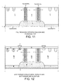
- FIG. 11 shows a step, in the method of manufacturing the power semiconductor device die of FIG. 1 , of filling the trenches and planarizing the top of the wafer.
- FIG. 12 shows the result of several more steps of the method of manufacturing the power semiconductor device die of FIG. 1 , of forming topside structures on the wafer.
- FIG. 13 shows a step, in the method of manufacturing the power semiconductor device die of FIG. 1 , of singulating the power semiconductor device die of FIG. 1 from the wafer by cutting the wafer along scribe lines.
- first object when referred to as being disposed “over” or “on” a second object, it is to be understood that the first object can be directly on the second object, or an intervening object may be present between the first and second objects.
- FIG. 1 is a cross-sectional side view diagram of a power semiconductor device die 1 in accordance with one novel aspect.
- the die 1 has a rectangular top surface, a rectangular bottom surface, and four peripheral side edges. Two of the side edges 2 and 3 are illustrated in the cross-sectional diagram.
- a high reverse blocking voltage thyristor that can withstand a very high 8500 volt blocking voltage in both the forward direction and in the reverse direction is realized in the active area of the die.
- the thyristor is a three terminal device that has a metal cathode terminal 4 , a metal gate terminal (not seen in the particular cross-section of the diagram), and a metal anode terminal 5 .
- the metal cathode terminal 4 contacts an N+ type cathode region 6 .
- the N+ type cathode region 6 extends downward from the top semiconductor surface 7 into a P type gate region 8 .
- the P type gate region 8 in turn extends down into the bulk silicon material 9 of the die, which is of N ⁇ type silicon.
- Extending upward from the bottom semiconductor surface 10 into the N ⁇ type bulk semiconductor material 9 is a P type anode region 11 .
- the bottom semiconductor surface 10 is not entirely planar but rather has a very shallow peripheral groove 27 .
- the shallow peripheral groove of the bottom surface 10 extends along the periphery of the die.
- Backside metal of the metal anode terminal 5 contacts the P type anode region 11 as shown.
- the power semiconductor device die 1 includes edge termination structures.
- the edge termination structures include two P type floating rings 12 and 13 , and an N+ type channel stopper ring 14 .
- An optional metal ring plate 15 makes electrical contact with the channel stopper diffusion 14 below.
- the P type floating rings 12 and 13 extend down into the die from the top semiconductor surface 7 the same distance as does the P type gate region 8 .
- the N+ type channel stopper diffusion 14 extends down into the die from the top semiconductor surface 7 the same distance as does the N+ type cathode region 6 .
- a layer of passivation 16 covers over the peripheral guard rings and edge termination structures as illustrated.
- a field plate portion 17 of the metal cathode terminal 4 extends up and over a part of the passivation layer 16 around the periphery of the thyristor gate region.
- the rings 12 and 13 and the channel stopper 14 are concentric rings that surround the metal cathode terminal 4 .
- FIG. 2 shows an edge portion of the structure of FIG. 1 in more detail.
- a peripheral trench 18 extends downward into the die from the top semiconductor surface 7 .
- the peripheral trench 18 has an inner sidewall 21 , an outer sidewall 22 , and a bottom 23 .
- This peripheral trench 18 is “peripheral” in the sense that it extends along the rectangular periphery of the top surface of the rectangular die.
- the inner and outer sidewalls are vertical and extend downward substantially perpendicularly from the plane of the top semiconductor surface 7 .
- An amount of the N ⁇ type bulk semiconductor material 9 laterally rings the peripheral trench 18 such that N ⁇ type semiconductor material is disposed between the peripheral trench and the peripheral side edges of the die. As shown in FIG. 1 and FIG.
- a P type sidewall doped region 19 extends laterally inwardly from the inner sidewalls of the trench and also extends laterally outwardly from the outer sidewalls of the trench.
- a material fills the peripheral trench. This material may, for example, be silicon oxide or P type polysilicon or another suitable material that can fill a deep trench. Known techniques for filling trenches in trench IGBTs are employed.
- a peripheral aluminum diffused region 20 of P type silicon is disposed under the peripheral trench 18 .
- the peripheral aluminum diffused region 20 extends upward from the bottom semiconductor surface 10 toward the bottom of the peripheral trench, and also extends laterally outwardly to the peripheral side edges of the die.
- the dopant of the peripheral aluminum diffused region 20 is aluminum.
- the peripheral aluminum diffused region 20 extends laterally to the right to die side edge 3 .
- P type material of the peripheral aluminum diffused region 20 contacts and joins with P type material of the anode region 11 as shown.
- P type material of the peripheral aluminum region 20 also contacts and joins with P type material of the sidewall doped region 19 as shown.
- the crystal structure of the silicon at the side edges of the die is generally damaged at the time when the die is singulated from other dice when the source wafer is cut into dice. This is represented in FIG. 2 by the jagged edge labeled “saw cut edge at scribe line”.
- the thyristor device in the active area has extremely high forward and reverse blocking voltage ratings of 8500 volts, and yet its peripheral separation diffusion structure is manufactured in an economically realistic amount of time of less than 200 hours.
- the die thickness E between the bottom semiconductor surface 10 and the top semiconductor surface 7 is greater than 600 microns.
- distance E is 850 microns.
- the peripheral aluminum diffused region 20 extends upward from the bottom semiconductor surface 10 a distance B of at least 100 microns. Distance B is at least 100 microns, but it is less than half of the distance E.
- distance B is about 300 microns.
- the diffusion time required to diffuse the aluminum dopant up from semiconductor surface 10 into the die this distance B is less than 200 hours, and in the example of FIG. 1 and FIG. 2 is about 150 hours.
- the peripheral trench 18 extends downward into the die from the top semiconductor surface 7 a distance A such that the P type material of the sidewall doped region 19 joins the P type material of the peripheral aluminum doped region 11 .
- the distance A is more than half of the overall die thickness E and is about 600 microns.
- a substantial amount of diffusion time is required to form the sidewall doped region 19 to an adequate thickness as required for the 8500 volt reverse breakdown voltage device.
- the thickness C of the sidewall doped region 19 is at least 20 microns, and in the example of FIG. 1 and FIG. 2 the thickness C of the sidewall doped region 19 is 50 microns.
- the diffusion time to form sidewall doped region 19 is about 80 hours.
- the width D of the peripheral trench 18 is about 100 microns.
- the device in the active area is a thyristor
- the device in the active area in other examples is another type of device.
- the device in the active in one example is a reverse blocking IGBT, and in another example is an inverse diode.
- FIG. 3 through FIG. 13 set forth a method of making a semiconductor device die in accordance with one novel aspect.
- the initial starting wafer is of N-type bulk silicon 9 .
- aluminum 24 is deposited on the bottom side of the wafer, and is patterned so that aluminum is disposed under the scribe regions.
- FIG. 3 is a cross-sectional view taken at location of a scribe line.
- the aluminum 24 appears as a cross-section of a strip at this location.
- FIG. 3A is view of the bottom of the wafer. As FIG. 3A shows, the aluminum 24 forms a mesh-like grid structure that underlies all the scribe line areas.
- the cross-sectional diagram of FIG. 3 is taken along sectional line A-A′ of FIG. 3A .
- the mesh-like grid of aluminum 24 is converted into aluminum oxide 25 .
- the wafer is heated in a nitrogen-oxygen atmosphere, at a temperature of about 500 degrees Celsius, which is a temperature below the 660 degrees melting point of aluminum.
- the aluminum is oxidized without the aluminum first melting.
- the resulting aluminum oxide 25 has a higher melting point in excess of two thousand degrees Celsius.
- the temperature is then increased to about 1250 degrees Celsius.
- aluminum from the aluminum oxide 25 diffuses into the wafer.
- Silicon oxide 26 also grows on the exposed silicon surfaces on the top and bottom of the wafer.
- the high temperature condition is sustained long enough that the aluminum diffuses approximately 40 microns into the wafer, thereby forming peripheral aluminum diffused region 20 .
- the diffusion time is about 70 hours. (Later in the process when boron regions are thermally diffused, this aluminum will diffuse an additional amount due to an additional 80 hours of diffusion time, for a total aluminum diffusion time of about 150 hours.)
- the aluminum oxide 25 is chemically removed by underetching in a wet etch step using potassium hydroxide (KOH).
- KOH potassium hydroxide
- the silicon oxide layer 26 is removed in a wet etch cleaning step using hydrofluoric acid (HF).
- HF hydrofluoric acid
- chemical mechanical polishing is employed.
- the cleaning process removes all silicon oxide but may also remove an amount of semiconductor material (for example, it may remove one micron of silicon) from the bottom surface of the wafer.
- P type anode region 11 , front side P type region 8 and floating P rings 12 and 13 are about 20 microns thick.
- FIG. 9 shows the top of the wafer at this stage in processing.
- the cross-sectional diagram of FIG. 9 is taken along sectional line A-A′ of top-down diagram FIG. 9A . From the top-down perspective of FIG. 9A , each trench has a square shape. Trench 18 extends around active area 29 . Trench 28 extends around active area 30 .
- a sidewall doping step is performed to diffuse boron into the trench sidewalls, thereby forming sidewall doped regions 19 and 31 .
- Vapor phase diffusion of diborane or another suitable doping technique is employed.
- most of the top surface of the wafer is masked off with a thick layer of silicon oxide or other material to block dopants (not shown) so that boron is not also diffused down everywhere into the upper surface of the wafer at the time when regions 19 and 31 are formed.
- the boron dopants of all boron doped regions are thermally diffused further for about 80 hours more of diffusion time.
- This thermal step causes boron of sidewall doped regions 19 and 31 to diffuse further so that the sidewall doped regions 19 and 31 have their final desired sidewall depths of 50 microns, and causes boron of the anode region 11 to diffuse further upward to its final desired extent of 40 microns, and causes boron of the gate region 8 to diffuse down further to its final junction depth of 40 microns, and causes boron of the floating rings 12 and 13 to diffuse down to their final depths of 40 microns, and causes aluminum of region 20 to diffuse further upward to its final desired extent of 300 microns.
- the trenches are filled with a fill material 32 , such as silicon oxide or P type polysilicon.
- a fill material 32 such as silicon oxide or P type polysilicon.
- FIG. 12 is a simplified cross-sectional diagram of the resulting wafer structure, shown here with floating ring structures, channel stopper structures, and metallization structures.
- the wafer structure is then cut along the scribe lines into square semiconductor device dice.
- the top semiconductor surface of each die is square even though the devices have 8500 volt forward and reverse blocking voltages.
- the square die does not have termination edge bevels and the expense of providing such bevels is avoided.
- the wafer is cut, such as using a mechanical saw 33 or using a laser, along the scribe line 34 . The sawing may consume between 80 to 100 microns of silicon material.
- a malleable foil Prior to sawing, a malleable foil may be applied to the backside of the wafer in a hot roll process so that material of the foil is pressed into grooves in the bottom of the wafer to support the wafer material at the scribe line areas during sawing.
- Anode metal 5 may not be entirely planar at the bottom of the wafer, and the foil supports the wafer during sawing.
- An additional expensive step of planarizing the bottom semiconductor surface 10 of the wafer is thereby avoided, and the shallow peripheral groove 27 remains in each finished semiconductor device.
- Each of the resulting dice is as shown in the cross-sectional diagram of FIG. 1 .
- the outward boundary of the sidewall doped region 19 is about 100 microns from the side edge of the die.
Abstract
Description
Claims (20)
Priority Applications (2)
| Application Number | Priority Date | Filing Date | Title |
|---|---|---|---|
| US14/948,156 US9590033B1 (en) | 2015-11-20 | 2015-11-20 | Trench separation diffusion for high voltage device |
| US15/452,592 US9922864B2 (en) | 2015-11-20 | 2017-03-07 | Trench separation diffusion for high voltage device |
Applications Claiming Priority (1)
| Application Number | Priority Date | Filing Date | Title |
|---|---|---|---|
| US14/948,156 US9590033B1 (en) | 2015-11-20 | 2015-11-20 | Trench separation diffusion for high voltage device |
Related Child Applications (1)
| Application Number | Title | Priority Date | Filing Date |
|---|---|---|---|
| US15/452,592 Continuation US9922864B2 (en) | 2015-11-20 | 2017-03-07 | Trench separation diffusion for high voltage device |
Publications (1)
| Publication Number | Publication Date |
|---|---|
| US9590033B1 true US9590033B1 (en) | 2017-03-07 |
Family
ID=58163553
Family Applications (2)
| Application Number | Title | Priority Date | Filing Date |
|---|---|---|---|
| US14/948,156 Active US9590033B1 (en) | 2015-11-20 | 2015-11-20 | Trench separation diffusion for high voltage device |
| US15/452,592 Active US9922864B2 (en) | 2015-11-20 | 2017-03-07 | Trench separation diffusion for high voltage device |
Family Applications After (1)
| Application Number | Title | Priority Date | Filing Date |
|---|---|---|---|
| US15/452,592 Active US9922864B2 (en) | 2015-11-20 | 2017-03-07 | Trench separation diffusion for high voltage device |
Country Status (1)
| Country | Link |
|---|---|
| US (2) | US9590033B1 (en) |
Cited By (9)
| Publication number | Priority date | Publication date | Assignee | Title |
|---|---|---|---|---|
| CN108074966A (en) * | 2017-12-27 | 2018-05-25 | 电子科技大学 | Constant current device and its manufacturing method |
| CN108172616A (en) * | 2017-12-27 | 2018-06-15 | 电子科技大学 | Constant current device and its manufacturing method |
| CN108183128A (en) * | 2017-12-27 | 2018-06-19 | 电子科技大学 | Constant current device and its manufacturing method |
| CN108183129A (en) * | 2017-12-27 | 2018-06-19 | 电子科技大学 | Constant current device and its manufacturing method |
| US10193000B1 (en) | 2017-07-31 | 2019-01-29 | Ixys, Llc | Fast recovery inverse diode |
| EP3451386A1 (en) | 2017-08-31 | 2019-03-06 | Ixys, Llc | Inverse diode with charge carrier extraction regions |
| EP3451387A1 (en) | 2017-08-31 | 2019-03-06 | Ixys, Llc | Packaged fast inverse diode component for pfc applications |
| GB2589543A (en) * | 2019-09-09 | 2021-06-09 | Mqsemi Ag | Method for forming a low injection P-type contact region and power semiconductor devices with the same |
| CN116741821A (en) * | 2023-08-09 | 2023-09-12 | 深圳腾睿微电子科技有限公司 | IGBT device structure and corresponding manufacturing method |
Families Citing this family (5)
| Publication number | Priority date | Publication date | Assignee | Title |
|---|---|---|---|---|
| US20170373142A1 (en) * | 2016-06-23 | 2017-12-28 | Littelfuse, Inc. | Semiconductor device having side-diffused trench plug |
| CN109346514A (en) * | 2018-11-05 | 2019-02-15 | 北京工业大学 | A kind of chip and manufacturing method of reverse blocking IGBT |
| EP3920209A4 (en) * | 2019-09-11 | 2022-05-11 | Fuji Electric Co., Ltd. | Semiconductor device and manufacturing method |
| US11901406B2 (en) * | 2021-07-13 | 2024-02-13 | Analog Power Conversion LLC | Semiconductor high-voltage termination with deep trench and floating field rings |
| US20230021169A1 (en) * | 2021-07-13 | 2023-01-19 | Analog Power Conversion LLC | Semiconductor device with deep trench and manufacturing process thereof |
Citations (9)
| Publication number | Priority date | Publication date | Assignee | Title |
|---|---|---|---|---|
| US4040878A (en) | 1975-03-26 | 1977-08-09 | U.S. Philips Corporation | Semiconductor device manufacture |
| US4351677A (en) | 1979-07-16 | 1982-09-28 | Hitachi, Ltd. | Method of manufacturing semiconductor device having aluminum diffused semiconductor substrate |
| US4904609A (en) * | 1988-05-06 | 1990-02-27 | General Electric Company | Method of making symmetrical blocking high voltage breakdown semiconductor device |
| US5698454A (en) | 1995-07-31 | 1997-12-16 | Ixys Corporation | Method of making a reverse blocking IGBT |
| US6507050B1 (en) * | 1999-08-21 | 2003-01-14 | Koninklijke Philips Electronics N.V. | Thyristors having a novel arrangement of concentric perimeter zones |
| US6936908B2 (en) | 2001-05-03 | 2005-08-30 | Ixys Corporation | Forward and reverse blocking devices |
| US7030426B2 (en) | 2004-03-16 | 2006-04-18 | Ixys Semiconductor Gmbh | Power semiconductor component in the planar technique |
| US7776672B2 (en) | 2004-08-19 | 2010-08-17 | Fuji Electric Systems Co., Ltd. | Semiconductor device and manufacturing method thereof |
| US8093652B2 (en) | 2002-08-28 | 2012-01-10 | Ixys Corporation | Breakdown voltage for power devices |
-
2015
- 2015-11-20 US US14/948,156 patent/US9590033B1/en active Active
-
2017
- 2017-03-07 US US15/452,592 patent/US9922864B2/en active Active
Patent Citations (10)
| Publication number | Priority date | Publication date | Assignee | Title |
|---|---|---|---|---|
| US4040878A (en) | 1975-03-26 | 1977-08-09 | U.S. Philips Corporation | Semiconductor device manufacture |
| US4351677A (en) | 1979-07-16 | 1982-09-28 | Hitachi, Ltd. | Method of manufacturing semiconductor device having aluminum diffused semiconductor substrate |
| US4904609A (en) * | 1988-05-06 | 1990-02-27 | General Electric Company | Method of making symmetrical blocking high voltage breakdown semiconductor device |
| US5698454A (en) | 1995-07-31 | 1997-12-16 | Ixys Corporation | Method of making a reverse blocking IGBT |
| US6507050B1 (en) * | 1999-08-21 | 2003-01-14 | Koninklijke Philips Electronics N.V. | Thyristors having a novel arrangement of concentric perimeter zones |
| US6936908B2 (en) | 2001-05-03 | 2005-08-30 | Ixys Corporation | Forward and reverse blocking devices |
| US7442630B2 (en) | 2001-05-03 | 2008-10-28 | Ixys Corporation | Method for fabricating forward and reverse blocking devices |
| US8093652B2 (en) | 2002-08-28 | 2012-01-10 | Ixys Corporation | Breakdown voltage for power devices |
| US7030426B2 (en) | 2004-03-16 | 2006-04-18 | Ixys Semiconductor Gmbh | Power semiconductor component in the planar technique |
| US7776672B2 (en) | 2004-08-19 | 2010-08-17 | Fuji Electric Systems Co., Ltd. | Semiconductor device and manufacturing method thereof |
Cited By (15)
| Publication number | Priority date | Publication date | Assignee | Title |
|---|---|---|---|---|
| JP2019050358A (en) * | 2017-07-31 | 2019-03-28 | イクシス・リミテッド・ライアビリティ・カンパニーIxys, Llc | Fast recovery inverse diode |
| EP3439045A1 (en) | 2017-07-31 | 2019-02-06 | Ixys, Llc | Fast recovery inverse diode |
| US10847658B2 (en) | 2017-07-31 | 2020-11-24 | Littelfuse, Inc. | Fast recovery inverse diode |
| KR20190013662A (en) * | 2017-07-31 | 2019-02-11 | 익시스, 엘엘씨 | Fast recovery inverse diode |
| US10193000B1 (en) | 2017-07-31 | 2019-01-29 | Ixys, Llc | Fast recovery inverse diode |
| EP3451387A1 (en) | 2017-08-31 | 2019-03-06 | Ixys, Llc | Packaged fast inverse diode component for pfc applications |
| EP3451386A1 (en) | 2017-08-31 | 2019-03-06 | Ixys, Llc | Inverse diode with charge carrier extraction regions |
| US10319669B2 (en) | 2017-08-31 | 2019-06-11 | Ixys, Llc | Packaged fast inverse diode component for PFC applications |
| US10424677B2 (en) | 2017-08-31 | 2019-09-24 | Littelfuse, Inc. | Charge carrier extraction inverse diode |
| CN108172616A (en) * | 2017-12-27 | 2018-06-15 | 电子科技大学 | Constant current device and its manufacturing method |
| CN108183129A (en) * | 2017-12-27 | 2018-06-19 | 电子科技大学 | Constant current device and its manufacturing method |
| CN108074966A (en) * | 2017-12-27 | 2018-05-25 | 电子科技大学 | Constant current device and its manufacturing method |
| CN108183128A (en) * | 2017-12-27 | 2018-06-19 | 电子科技大学 | Constant current device and its manufacturing method |
| GB2589543A (en) * | 2019-09-09 | 2021-06-09 | Mqsemi Ag | Method for forming a low injection P-type contact region and power semiconductor devices with the same |
| CN116741821A (en) * | 2023-08-09 | 2023-09-12 | 深圳腾睿微电子科技有限公司 | IGBT device structure and corresponding manufacturing method |
Also Published As
| Publication number | Publication date |
|---|---|
| US20170178947A1 (en) | 2017-06-22 |
| US9922864B2 (en) | 2018-03-20 |
Similar Documents
| Publication | Publication Date | Title |
|---|---|---|
| US9922864B2 (en) | Trench separation diffusion for high voltage device | |
| US9082845B1 (en) | Super junction field effect transistor | |
| US9209242B2 (en) | Semiconductor device with an edge termination structure having a closed vertical trench | |
| US9287383B2 (en) | Method for manufacturing a semiconductor device with step-shaped edge termination | |
| US10276708B2 (en) | Reverse-blocking IGBT having a reverse-blocking edge termination structure | |
| US9099321B2 (en) | Method for fabricating power semiconductor device | |
| US11393736B2 (en) | Method of manufacturing a semiconductor device having an integrated pn diode temperature sensor | |
| US9553165B2 (en) | Method of forming a semiconductor device | |
| CN101499421A (en) | Mesa type semiconductor device and manufacturing method thereof | |
| US10304930B2 (en) | Semiconductor device implanted with arsenic and nitrogen | |
| US9496337B2 (en) | Method for producing a semiconductor device having a beveled edge termination | |
| JPWO2012137412A1 (en) | Semiconductor device | |
| CN107481970B (en) | Ultra-thin semiconductor component fabrication using dielectric backbone structures | |
| US20140302657A1 (en) | Method for fabricating power semiconductor device | |
| US20160203977A1 (en) | Semiconductor Arrangement Including Buried Anodic Oxide and Manufacturing Method | |
| US9178013B2 (en) | Semiconductor device with edge termination and method for manufacturing a semiconductor device | |
| US20140151841A1 (en) | Semiconductor devices having a positive-bevel termination or a negative-bevel termination and their manufacture | |
| US9917180B2 (en) | Trenched and implanted bipolar junction transistor | |
| EP3142143A1 (en) | Method for manufacturing a power semiconductor device | |
| JPH098274A (en) | Semiconductor device and its manufacture | |
| US10608099B2 (en) | Methods of manufacturing semiconductor devices with a deep barrier layer | |
| US20210167195A1 (en) | Vertical Power Semiconductor Device, Semiconductor Wafer or Bare-Die Arrangement, Carrier, and Method of Manufacturing a Vertical Power Semiconductor Device | |
| US6903435B2 (en) | Vertical power component | |
| JP2009038136A (en) | Semiconductor device, and manufacturing method thereof |
Legal Events
| Date | Code | Title | Description |
|---|---|---|---|
| AS | Assignment |
Owner name: IXYS CORPORATION, CALIFORNIA Free format text: ASSIGNMENT OF ASSIGNORS INTEREST;ASSIGNORS:WISOTZKI, ELMAR;KOERBER, CHRISTOPH;REEL/FRAME:037107/0527 Effective date: 20151117 |
|
| STCF | Information on status: patent grant |
Free format text: PATENTED CASE |
|
| AS | Assignment |
Owner name: IXYS, LLC, CALIFORNIA Free format text: MERGER AND CHANGE OF NAME;ASSIGNORS:IXYS CORPORATION;IXYS, LLC;REEL/FRAME:045406/0670 Effective date: 20180116 |
|
| AS | Assignment |
Owner name: LITTELFUSE, INC., ILLINOIS Free format text: ASSIGNMENT OF ASSIGNORS INTEREST;ASSIGNOR:IXYS, LLC;REEL/FRAME:049056/0649 Effective date: 20190430 |
|
| MAFP | Maintenance fee payment |
Free format text: PAYMENT OF MAINTENANCE FEE, 4TH YEAR, LARGE ENTITY (ORIGINAL EVENT CODE: M1551); ENTITY STATUS OF PATENT OWNER: LARGE ENTITY Year of fee payment: 4 |