US9602750B2 - Image sensor pixels having built-in variable gain feedback amplifier circuitry - Google Patents
Image sensor pixels having built-in variable gain feedback amplifier circuitry Download PDFInfo
- Publication number
- US9602750B2 US9602750B2 US14/553,822 US201414553822A US9602750B2 US 9602750 B2 US9602750 B2 US 9602750B2 US 201414553822 A US201414553822 A US 201414553822A US 9602750 B2 US9602750 B2 US 9602750B2
- Authority
- US
- United States
- Prior art keywords
- transistor
- pixel
- image sensor
- coupled
- floating diffusion
- Prior art date
- Legal status (The legal status is an assumption and is not a legal conclusion. Google has not performed a legal analysis and makes no representation as to the accuracy of the status listed.)
- Active, expires
Links
- 238000009792 diffusion process Methods 0.000 claims abstract description 53
- 238000007667 floating Methods 0.000 claims abstract description 53
- 239000003990 capacitor Substances 0.000 claims abstract description 34
- 238000012546 transfer Methods 0.000 claims abstract description 32
- 239000000758 substrate Substances 0.000 claims description 29
- 239000004065 semiconductor Substances 0.000 claims description 25
- 238000003384 imaging method Methods 0.000 claims description 11
- 238000002955 isolation Methods 0.000 claims description 7
- 238000012545 processing Methods 0.000 claims description 6
- 230000000903 blocking effect Effects 0.000 claims description 4
- 230000004044 response Effects 0.000 claims description 4
- 230000005669 field effect Effects 0.000 claims description 3
- 230000001419 dependent effect Effects 0.000 claims description 2
- 238000013461 design Methods 0.000 abstract description 4
- 230000000875 corresponding effect Effects 0.000 description 25
- 238000010586 diagram Methods 0.000 description 19
- 238000001514 detection method Methods 0.000 description 11
- 230000008901 benefit Effects 0.000 description 4
- 230000006870 function Effects 0.000 description 4
- 239000007943 implant Substances 0.000 description 4
- 230000003321 amplification Effects 0.000 description 3
- 238000005513 bias potential Methods 0.000 description 3
- 238000006243 chemical reaction Methods 0.000 description 3
- 230000001276 controlling effect Effects 0.000 description 3
- 238000003199 nucleic acid amplification method Methods 0.000 description 3
- VYPSYNLAJGMNEJ-UHFFFAOYSA-N Silicium dioxide Chemical compound O=[Si]=O VYPSYNLAJGMNEJ-UHFFFAOYSA-N 0.000 description 2
- 230000009471 action Effects 0.000 description 2
- 238000003491 array Methods 0.000 description 2
- 230000002596 correlated effect Effects 0.000 description 2
- 238000005516 engineering process Methods 0.000 description 2
- 230000010354 integration Effects 0.000 description 2
- 238000012986 modification Methods 0.000 description 2
- 230000004048 modification Effects 0.000 description 2
- 238000005036 potential barrier Methods 0.000 description 2
- 238000005070 sampling Methods 0.000 description 2
- 235000008733 Citrus aurantifolia Nutrition 0.000 description 1
- XUIMIQQOPSSXEZ-UHFFFAOYSA-N Silicon Chemical compound [Si] XUIMIQQOPSSXEZ-UHFFFAOYSA-N 0.000 description 1
- 235000011941 Tilia x europaea Nutrition 0.000 description 1
- FRIKWZARTBPWBN-UHFFFAOYSA-N [Si].O=[Si]=O Chemical compound [Si].O=[Si]=O FRIKWZARTBPWBN-UHFFFAOYSA-N 0.000 description 1
- 230000004888 barrier function Effects 0.000 description 1
- 230000009286 beneficial effect Effects 0.000 description 1
- 238000004891 communication Methods 0.000 description 1
- 230000000295 complement effect Effects 0.000 description 1
- 230000000779 depleting effect Effects 0.000 description 1
- 230000000694 effects Effects 0.000 description 1
- 238000010348 incorporation Methods 0.000 description 1
- 238000002347 injection Methods 0.000 description 1
- 239000007924 injection Substances 0.000 description 1
- 239000012212 insulator Substances 0.000 description 1
- 239000004571 lime Substances 0.000 description 1
- 230000005055 memory storage Effects 0.000 description 1
- 239000002184 metal Substances 0.000 description 1
- 238000000034 method Methods 0.000 description 1
- 150000004767 nitrides Chemical class 0.000 description 1
- 229910021420 polycrystalline silicon Inorganic materials 0.000 description 1
- 230000035945 sensitivity Effects 0.000 description 1
- 229910052710 silicon Inorganic materials 0.000 description 1
- 239000010703 silicon Substances 0.000 description 1
- 235000012239 silicon dioxide Nutrition 0.000 description 1
- 239000000377 silicon dioxide Substances 0.000 description 1
- 230000006641 stabilisation Effects 0.000 description 1
- 238000011105 stabilization Methods 0.000 description 1
Images


Classifications
-
- H—ELECTRICITY
- H04—ELECTRIC COMMUNICATION TECHNIQUE
- H04N—PICTORIAL COMMUNICATION, e.g. TELEVISION
- H04N25/00—Circuitry of solid-state image sensors [SSIS]; Control thereof
- H04N25/70—SSIS architectures; Circuits associated therewith
- H04N25/76—Addressed sensors, e.g. MOS or CMOS sensors
- H04N25/77—Pixel circuitry, e.g. memories, A/D converters, pixel amplifiers, shared circuits or shared components
- H04N25/778—Pixel circuitry, e.g. memories, A/D converters, pixel amplifiers, shared circuits or shared components comprising amplifiers shared between a plurality of pixels, i.e. at least one part of the amplifier must be on the sensor array itself
-
- H04N5/37457—
-
- H—ELECTRICITY
- H01—ELECTRIC ELEMENTS
- H01L—SEMICONDUCTOR DEVICES NOT COVERED BY CLASS H10
- H01L27/00—Devices consisting of a plurality of semiconductor or other solid-state components formed in or on a common substrate
- H01L27/14—Devices consisting of a plurality of semiconductor or other solid-state components formed in or on a common substrate including semiconductor components sensitive to infrared radiation, light, electromagnetic radiation of shorter wavelength or corpuscular radiation and specially adapted either for the conversion of the energy of such radiation into electrical energy or for the control of electrical energy by such radiation
- H01L27/144—Devices controlled by radiation
- H01L27/146—Imager structures
- H01L27/14601—Structural or functional details thereof
- H01L27/14641—Electronic components shared by two or more pixel-elements, e.g. one amplifier shared by two pixel elements
-
- H—ELECTRICITY
- H01—ELECTRIC ELEMENTS
- H01L—SEMICONDUCTOR DEVICES NOT COVERED BY CLASS H10
- H01L27/00—Devices consisting of a plurality of semiconductor or other solid-state components formed in or on a common substrate
- H01L27/14—Devices consisting of a plurality of semiconductor or other solid-state components formed in or on a common substrate including semiconductor components sensitive to infrared radiation, light, electromagnetic radiation of shorter wavelength or corpuscular radiation and specially adapted either for the conversion of the energy of such radiation into electrical energy or for the control of electrical energy by such radiation
- H01L27/144—Devices controlled by radiation
- H01L27/146—Imager structures
- H01L27/14601—Structural or functional details thereof
- H01L27/14609—Pixel-elements with integrated switching, control, storage or amplification elements
- H01L27/14612—Pixel-elements with integrated switching, control, storage or amplification elements involving a transistor
-
- H—ELECTRICITY
- H01—ELECTRIC ELEMENTS
- H01L—SEMICONDUCTOR DEVICES NOT COVERED BY CLASS H10
- H01L27/00—Devices consisting of a plurality of semiconductor or other solid-state components formed in or on a common substrate
- H01L27/14—Devices consisting of a plurality of semiconductor or other solid-state components formed in or on a common substrate including semiconductor components sensitive to infrared radiation, light, electromagnetic radiation of shorter wavelength or corpuscular radiation and specially adapted either for the conversion of the energy of such radiation into electrical energy or for the control of electrical energy by such radiation
- H01L27/144—Devices controlled by radiation
- H01L27/146—Imager structures
- H01L27/14601—Structural or functional details thereof
- H01L27/1463—Pixel isolation structures
-
- H—ELECTRICITY
- H01—ELECTRIC ELEMENTS
- H01L—SEMICONDUCTOR DEVICES NOT COVERED BY CLASS H10
- H01L27/00—Devices consisting of a plurality of semiconductor or other solid-state components formed in or on a common substrate
- H01L27/14—Devices consisting of a plurality of semiconductor or other solid-state components formed in or on a common substrate including semiconductor components sensitive to infrared radiation, light, electromagnetic radiation of shorter wavelength or corpuscular radiation and specially adapted either for the conversion of the energy of such radiation into electrical energy or for the control of electrical energy by such radiation
- H01L27/144—Devices controlled by radiation
- H01L27/146—Imager structures
- H01L27/14643—Photodiode arrays; MOS imagers
-
- H—ELECTRICITY
- H04—ELECTRIC COMMUNICATION TECHNIQUE
- H04N—PICTORIAL COMMUNICATION, e.g. TELEVISION
- H04N25/00—Circuitry of solid-state image sensors [SSIS]; Control thereof
- H04N25/50—Control of the SSIS exposure
- H04N25/57—Control of the dynamic range
- H04N25/571—Control of the dynamic range involving a non-linear response
- H04N25/575—Control of the dynamic range involving a non-linear response with a response composed of multiple slopes
-
- H—ELECTRICITY
- H04—ELECTRIC COMMUNICATION TECHNIQUE
- H04N—PICTORIAL COMMUNICATION, e.g. TELEVISION
- H04N25/00—Circuitry of solid-state image sensors [SSIS]; Control thereof
- H04N25/50—Control of the SSIS exposure
- H04N25/57—Control of the dynamic range
- H04N25/58—Control of the dynamic range involving two or more exposures
- H04N25/581—Control of the dynamic range involving two or more exposures acquired simultaneously
- H04N25/583—Control of the dynamic range involving two or more exposures acquired simultaneously with different integration times
-
- H—ELECTRICITY
- H04—ELECTRIC COMMUNICATION TECHNIQUE
- H04N—PICTORIAL COMMUNICATION, e.g. TELEVISION
- H04N25/00—Circuitry of solid-state image sensors [SSIS]; Control thereof
- H04N25/60—Noise processing, e.g. detecting, correcting, reducing or removing noise
- H04N25/65—Noise processing, e.g. detecting, correcting, reducing or removing noise applied to reset noise, e.g. KTC noise related to CMOS structures by techniques other than CDS
-
- H—ELECTRICITY
- H04—ELECTRIC COMMUNICATION TECHNIQUE
- H04N—PICTORIAL COMMUNICATION, e.g. TELEVISION
- H04N25/00—Circuitry of solid-state image sensors [SSIS]; Control thereof
- H04N25/70—SSIS architectures; Circuits associated therewith
- H04N25/76—Addressed sensors, e.g. MOS or CMOS sensors
- H04N25/77—Pixel circuitry, e.g. memories, A/D converters, pixel amplifiers, shared circuits or shared components
- H04N25/771—Pixel circuitry, e.g. memories, A/D converters, pixel amplifiers, shared circuits or shared components comprising storage means other than floating diffusion
-
- H04N5/35527—
-
- H04N5/363—
-
- H04N5/37452—
Definitions
- CMOS complementary metal-oxide-semiconductor
- Typical image sensors sense light by converting impinging photons into electrons (or holes) that are integrated (collected) in sensor pixels. Upon completion of each integration cycle, the collected charge is converted into voltage signals, which are supplied to corresponding output terminals associated with the image sensor. Typically, the charge-to-voltage conversion is performed directly within the pixels, and the resulting analog pixel voltage signals are transferred to the output terminals through various pixel addressing and scanning schemes. The analog voltage signal can sometimes be converted on-chip to a digital equivalent before being conveyed off-chip.
- Each pixel includes a buffer amplifier (i.e., source follower) that drives output sensing, lines that are connected to the pixels via respective address transistors.
- CMOS image sensors that utilize CDS require at least four transistors (4T) per pixel.
- 4T pixel circuit with a pinned photodiode can be found in Lee (U.S. Pat. No. 5,625,210), incorporated herein as a reference.
- FIG. 1 shows a simplified circuit diagram of a pixel 100 in a CMOS sensor.
- Pixel circuit 100 has a two-way shared photodiode scheme in which two photodiodes share a single floating diffusion node.
- photodiodes 101 (PD 1 ) and 102 (PD 2 ) share common floating diffusion (FD) charge detection node 114 to which source follower (SF) transistor 103 is connected.
- the drain terminal of source follower transistor 103 is connected to Vdd column bias line 109 and the source terminal of source follower transistor 103 is connected to column output signal (readout) line 108 through addressing transistor 104 .
- Charge detection node 114 is reset by reset transistor 105 , which is also connected to Vdd column bias line 109 .
- Charge from photodiodes 101 and 102 is transferred onto floating diffusion node 114 by charge transfer transistors 106 and 107 , respectively.
- Reset transistor gate 105 is controlled by reset control signals received over row control line 110
- charge transfer transistor gates 106 and 107 are controlled by transfer control signals received over row lines 112 and 113 , respectively
- addressing transistor gate 104 is controlled by row select control signals received over row addressing line 111 .
- FIG. 1 it is clear that each pair of pixel photodiodes must be coupled to a total of five transistors (i.e., 2.5 transistors per photodiode).
- Conventional arrangements such as the arrangement of FIG. 1 involve below unity gain amplification generated by the buffer amplifier of source follower 103 , causing signal line 108 to be susceptible to noise and interference pickups, which can distort the final image signal produced by the pixel.
- FIG. 1 is a simplified circuit diagram of a conventional image sensor pixel having two photodiodes sharing the same pixel circuitry, which includes two transfer gates, a source follower transistor, an addressing transistor, and a reset transistor.
- FIG. 2 is an illustrative circuit diagram of an image sensor pixel having two photodiodes that share a common floating diffusion region having a p-channel gain transistor, a p-channel addressing transistor, an n-channel reset transistor, a pre-charge capacitor, and a variable feedback capacitor for improving the noise susceptibility of the image sensor pixel in accordance with an embodiment of the present invention.
- FIG. 3 is an illustrative timing diagram of a readout sequence performed by a selected row of image sensor pixels having the circuit of the type shown in FIG. 2 in accordance with an embodiment of the present invention.
- FIG. 4 is an illustrative diagram of a pixel circuit and a corresponding partial pixel cross section showing how gain and addressing transistors of the type shown in FIG. 2 may be placed within a mini n-well region of the pixel substrate in accordance with an embodiment of the present invention.
- FIG. 5 is an illustrative diagram of a pixel circuit and a corresponding partial pixel cross section of an image sensor pixel of the type shown in FIG. 2 further illustrating how p-type doped drain extension portions of a gain transistor may form a variable capacitance for controlling amplifier gain depending on the number of detected electrons in accordance with an embodiment of the present invention.
- FIG. 6 is an illustrative diagram of the potential profile under the gate of a p-channel gain transistor of the type shown in FIGS. 2-5 that illustrates how holes may flow depending on a position of the drain Quasi Fermi level in accordance with an embodiment of the present invention.
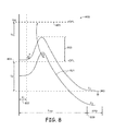
- FIG. 7 is an illustrative graph showing the dependence of pixel output voltage of a pixel of the type shown in FIG. 2 on the number of input electrons received from the corresponding photodiode where a break point in the graph may depend on a doping level of a p-type doped drain extension of the type shown in FIG. 5 in accordance with an embodiment of the present invention.
- FIG. 8 is an illustrative diagram showing the bias potentials and energy band diagrams in a fully depleted mini n-well region under the drain of a p-channel MOSFET transistor of the type shown in FIGS. 2-7 in accordance with an embodiment of the present invention.
- FIG. 9 is an illustrative layout diagram of a four photodiode per shared floating diffusion region pixel topology, in which the p-channel MOSFET gain transistor and the p-channel MOSFET addressing transistor are located in an STI region between photodiode rows in accordance with an embodiment of the present invention.
- FIG. 10 is a block diagram of a processor system employing the image sensor pixels of FIGS. 2-9 in accordance with an embodiment of the present invention.
- FIG. 2 A simplified circuit diagram of an illustrative image sensor pixel having built-in amplifier circuitry with adjustable gain is shown in FIG. 2 .
- pixel circuit 200 may include a first photodiode 219 (PD 1 ) and a second photodiode 218 (PD 2 ) that share the same pixel circuitry 200 .
- PD 1 photodiode 219
- PD 2 photodiode 218
- This example is merely illustrative and, if desired, pixel 200 may include four or more photodiodes that share a common charge detection circuit.
- Charge transfer transistor 220 may connect second photodiode 218 to common (shared) floating diffusion node 201 (sometimes referred to herein as a charge storage node, charge detection node, charge storage region, floating diffusion region, or floating diffusion junction region).
- Charge transfer transistor 221 may connect first photodiode 219 to floating diffusion node 201 .
- the gates of transfer transistors 220 and 221 may receive transfer control signals from row control circuitry (not shown for the sake of simplicity) over row control lines 214 and 215 , respectively.
- Charge detection node 201 may be connected to pre-charge capacitor 216 (having capacitance Cp). Capacitor 216 may be coupled between node 201 and row control line 212 for receiving a controlling signal.
- Feedback capacitor 207 (having variable capacitance Cf), the gate terminal of p-channel metal-oxide-semiconductor field-effect transistor (MOSFET) 202 (sometimes referred to herein as gain transistor 202 , amplifying transistor 202 , or amplifier transistor 202 ), and the source terminal of n-channel MOSFET reset transistor 206 may be coupled to charge storage node 201 .
- Floating diffusion node 201 may have an equivalent capacitance Cn as indicated by capacitor 217 .
- the drain terminal of p-channel MOSFET transistor 202 , the drain terminal of n-channel MOSFET reset transistor 206 , feedback capacitor 207 , and p-channel MOSFET addressing transistor 205 may be coupled to circuit output node 204 (sometimes referred to as pixel output node 204 ). Addressing transistor 205 may connect output node 204 to column sense line 208 , which is common to all the pixels in that column of the corresponding pixel array and delivers the selected pixel output signal to the periphery of the array.
- the source terminal of p-channel MOSFET transistor 202 may be coupled to column line 203 over which bias voltage Vdd is provided to all corresponding the transistors in that column of the array.
- Reset transistor 206 may receive reset control signals from row control circuitry over row control line 209 and addressing transistor 205 may receive row select (addressing) control signals from the row control circuitry over row control line 210 .
- the capacitance of signal output column line 208 is indicated by column capacitor 211 (e.g., having capacitance Cc).
- Column output line 208 may be coupled to constant current source 212 .
- Current source 212 may provide current bias to the selected pixels 200 .
- the connections of the pixel array to the periphery or to the underlying chip that carries the rest of the image processing circuits are indicated by via connections 222 .
- pixel circuit 200 can be understood from the simplified timing diagram 300 shown in FIG. 3 .
- this diagram shows only the signal readout from one of the shared photodiodes (e.g., photodiode 219 of FIG. 2 ) in a given selected row of the array.
- pixel readout operations begin by turning on p-channel MOSFET row select transistor 205 for the pixels of the selected row of the pixel array. This may be accomplished by applying waveform 301 to the gate of addressing transistor 205 at the time t 1 .
- This step lowers the voltage swing on transfer gate 221 that lowers the feed through from this gate to the floating diffusion node 201 .
- This operation is beneficial for the circuit operation, as the transfer gate is typically biased by a considerable negative bias to accumulate holes under the gate and thus to minimize the generation of dark current from the silicon-silicon dioxide interface states in the region under this gate.
- the partial step signal 305 eliminates this bias and prepares the gate for the charge transfer at a later time.
- the pixel reset may be released by applying signal 302 at time t 3 to the gate of reset transistor 206 .
- This step may be followed by applying pre-charge pulse 303 at lime t 4 to charge detection node 201 through pre-charge capacitor 216 .
- This step is important because it lowers the pixel output to its minimum level and thus provides the necessary output voltage swing margin for the signal.
- the pixel output signal Vout may be sampled after the elapse of a certain settling time given by a correlated double sampling (CDS) reference pulse R at time t 5 , as is indicated by waveform 304 .
- This step may be followed by charge transfer from the selected pixel photodiode 219 at the time to by applying the full charge transfer pulse (waveform 305 ).
- CDS correlated double sampling
- the pixel output level may be sampled again after the elapse of a certain settling time by the CDS circuits at the time t 7 by the pulse S as is indicated by waveform 306 .
- the readout sequence may be completed by turning on reset transistor 206 at time t 8 (waveform 302 ), biasing off transfer gate 221 to its pinning level at time t 9 (waveform 305 ), and finally turning off the pre-charge pulse and the pixel addressing transistor at time t 10 (waveforms 301 and 303 ).
- the source follower transistors are n-channel type transistors.
- the transistor that amplifies the signal detected on floating diffusion node 201 is a p-channel MOSFET transistor preferably with a p-type doped poly-silicon gate e.g., as opposed to the n-channel source follower transistor of FIG. 1 ). For this reason, it may be necessary to form a miniature n-type well region 405 as shown in FIG. 4 .
- the mini n-type well 405 may be a lightly n-type doped region in the pixel substrate and may sometimes be referred to herein as a mini n-well, miniature n-well, or simply as the n-well of the pixel.
- the pixel substrate may be a p-type doped epitaxial layer 403 .
- P-channel MOSFET transistor 202 may be formed within this mini n-well region 405 .
- FIG. 4 shows a simplified device cross section 400 and circuit schematic diagram of a pixel having built-in amplifier circuitry such as pixel circuit 200 of FIG. 2 .
- the example of FIG. 4 shows a simplified schematic of the charge transfer transistor 413 (corresponding to transistor 221 of FIG. 2 , for example), photodiode 412 (e.g., corresponding to photodiode 219 ), reset transistor 414 (corresponding to reset transistor 206 ), and pre-charge capacitor 416 (corresponding to capacitor 216 ), and a simplified device cross section of corresponding built-in (intra-pixel) amplifier transistor gate 410 (corresponding to transistor 202 ) and the corresponding addressing transistor gate 411 (corresponding to transistor 205 ).
- transistor gates 410 and 411 are both placed within mini n-well region 405 .
- Transistor gates 410 and 411 are typically isolated from the epitaxial substrate 403 by a silicon dioxide layer or other suitable insulators such as a combination of oxide and nitride layers.
- the floating diffusion charge detection node 201 of FIG. 2 is shown as node 425 , which may also have a feedback capacitor (e.g., capacitor 207 ) connected to it (not shown for the sake of simplicity).
- the amplifying p-channel MOSFET transistor 410 may have a corresponding source terminal 407 connected to Vdd column bias line 426 (corresponding to line 203 of FIG. 2 ).
- Line 426 may be connected to n+ doped region 406 that provides the bias voltage to mini n-well 405 .
- Mini n-well 405 may be partially or fully depleted of electron mobile charge.
- P-channel MOSFET transistor 410 may have a drain terminal shown by region 408 that is common (shared) with the drain of the addressing transistor (gate 411 ).
- Region 409 may be the source terminal of addressing transistor 411 and may be connected to common signal column line 423 (corresponding to line 208 ) that supplies the signal to the array periphery or through via 424 to the carrier chip in the case that a chip stacking technology is used.
- the transistor controlling signals may be supplied to the pixels through row lines 417 , 418 , 419 and 420 , respectively.
- the amplifier circuit may be biased by current source 421 (corresponding to current source 212 ) that is located at the sensor array periphery or on the carrier chip.
- the column sense line may have a capacitance Cb as indicated by capacitor 422 (corresponding to capacitor 211 ) that may also include via capacitance.
- a p+ type retrograde doped p-well (RPW) layer 404 may be placed under the partially or fully depleted mini n-well 405 to prevent light generated electrons in the bulk of the epitaxial layer 403 from entering into mini n-well 405 . These electrons are thus diverted to flow into the photodiode 412 , which is shown in the drawing only schematically for the sake of simplicity.
- the silicon substrate 401 may include a p+ type doped layer 402 deposited at the back side surface to minimize interface states generated dark current.
- addressing transistor 411 may be an n-channel type transistor.
- the doping of all the layers and the junctions may be inverted as well as the corresponding bias voltages. This results in the epitaxial layer being n-type doped, the RPW layer being changed to an RNW layer and retrograde doped by the n+ type doping, the mini n-well changed to a mini p-well, and all the remaining junctions changed to opposite polarities, for example.
- drawing 500 may be similar to drawing 400 in FIG. 4 with all the elements starting with the number 501 and ending with the number 525 corresponding to the elements starting with the number 401 and ending with the number 425 of FIG. 4 (e.g., element 525 corresponds to element 425 , element 414 corresponds to element 514 , etc.).
- the difference between the arrangement of FIG. 5 and the arrangement of FIG. 4 is in the structure of the p-channel MOSFET gain amplifier transistor 510 , where a p-type doped extension region 526 has been added to the structure.
- This extension is formed in the path of the transistor current flow, but may alternatively be placed away from the transistor channel current flow in a direction perpendicular to the drawing page.
- a completely independent capacitance varying structure may be formed and connected to the drain terminal of gain transistor 510 and the corresponding gate terminal by suitable wiring.
- Drain extension region 526 may provide a variable voltage dependent feedback capacitance (Varicap) that changes the amplifier gain depending on the number of electrons transferred from the photodiode 512 onto floating diffusion node 525 . Due to the application of the pre-charge pulse to floating diffusion node 525 through pre-charge capacitor 516 , the p-channel MOSFET gain transistor output voltage may be changed to a lower level. This action increases the voltage difference between the gain transistor gate 510 and its drain terminal 508 , thus hilly depleting the p-type doped extension 526 . When extension 526 is fully depleted of holes, the gate to drain capacitance (the feedback capacitance Cf) is low and the amplifier gain is therefore high.
- Varicap variable voltage dependent feedback capacitance
- the gain transistor drain voltage increases and drain extension 526 begins to be again populated by holes. This increases the magnitude of feedback capacitance Cf and consequently reduces the amplifier gain (e.g., the gain associated with transistor 202 of FIG. 2 ). It is thus possible, by selecting the correct doping level, the suitable doping profile, and the size for the drain extension 526 , to control the pixel charge to voltage transfer characteristic such that a nonlinear transfer function can be designed for the output voltage.
- FIG. 7 An example of such a nonlinear piece-wise transfer function characteristic is shown in graph 700 of FIG. 7 .
- the doping level for the extension 526 is selected such that when 2000 electrons have been transferred onto floating diffusion 525 , the charge to voltage conversion characteristic changes from 400 uV/e to 120 uV/e. This effect increases the pixel dynamic range. It is now possible to detect 12,000 electrons instead of only 5000 electrons for a given pixel output voltage swing if the conversion factor of 400 uV/e is kept unchanged. The high value of the charge to voltage conversion factor is desirable for the detection of low light level signals. This concept thus maintains high sensitivity for tow level signals and, at the same time, accommodates high level signals. This feature thus extends the dynamic range of the image sensor.
- a simplified potential profile diagram 600 of the p-channel MOSFET gain transistor 202 / 410 / 510 along the channel region 602 is shown in FIG. 6 .
- the drain Quasi Fermi level of is at level 603 with the extension 526 fully depleted.
- the Quasi Fermi level moves to the position 604 and the drain extension becomes again un-depleted. This increases the gate to drain capacitance Cf, thereby changing the in-pixel amplifier gain.
- the source of the p-channel MOSFET transistor is kept at a constant Vdd level 601 .
- FIG. 8 An example of various bias potentials and a corresponding energy band diagram within the fully depleted mini n-well under the drain of the p-channel MOSFET gain transistor 202 / 410 / 510 is shown in FIG. 8 .
- diagram 800 represents various bias potentials and the potential barrier for holes in the mini n-well region 405 / 505 .
- the simplified energy band diagram under the transistor drain is represented by the curves 801 .
- the transistor source and the drain junction depths are indicated as Xj 802 .
- the n-type doped implant in the mini n-well region is used to form only a potential barrier for holes 803 , thereby forcing holes to flow from the source along the transistor channel (perpendicular to the drawing plane of the figure) to drain.
- the sufficiently high barrier thus prevents shorting of the transistor drain and source to ground (the RPW region).
- the voltage level appearing on the transistor drain when a current bias is applied to it is shown as a Quasi Fermi level potential for holes Vd 804 .
- the reference bias for the mini n-well is indicated by the Quasi Fermi level potential for electrons Vdd 805 .
- the mini n-well depth is indicated as the region Xmin 806 .
- mini n-well may also be only partially depleted of mobile electron charge (not shown in the example of FIG. 8 ).
- the n-channel MOSFET reset transistor 206 can be replaced by a p-channel MOSFET transistor.
- the polarity of the reset gate pulses must be inverted.
- the advantage here is that the mini n-well can now be common to all the circuit transistors in the pixel except for the transfer gate transistors. This may have an advantage for some transistor design rule relaxation.
- FIG. 9 For the sake of completeness, an example of a 4-way shared pixel photodiode topology is shown in FIG. 9 (e.g., an arrangement in which four photodiodes share the same pixel circuitry).
- drawing 900 represents a simplified pixel top view (not to scale).
- the active photodiode regions are shown by regions 901 and may include anti-dome (AD) implants and RPW compensating opening regions 910 located approximately in the center of the pixel photodiodes.
- Photodiode region 901 may be isolated from similar regions of the neighboring pixels by shallow trench isolation (STI) regions 899 .
- STI shallow trench isolation
- This example is merely illustrative and, if desired, other types of pixel isolation, such as suitable implants or deep trench isolation (DTI) may be formed between the active pixel portions.
- DTI deep trench isolation
- Charge transfer gates are shown by regions 902 that interface with the n+ type doped floating diffusion regions 911 connected together by a metal wiring bus.
- the transfer gates may have regions 912 implanted underneath, which form charge wells that improve the charge transfer efficiency.
- the n-channel MOSFET reset transistor, the p-channel MOSFET gain transistor, and the p-channel MOSFET addressing transistor are placed in the STI isolated trunk region 903 located between the photodiode rows.
- the p+ type doped p-channel MOSFET gain transistor source terminal and drain terminal are shown by regions 907 and 908 respectively.
- the transistor source terminal is connected to the adjacent n+ type doped region 916 that provides the bias contact for the mini n-well region delineated by the implant mask opening 913 .
- the p-channel MOSFET gain transistor gate is shown by region 905 .
- the pixel addressing transistor gate is shown by region 914 and the p+ type doped drain of this transistor is shown by region 915 , where the output signal is sensed.
- the source of this transistor is shared (common) with the drain of the p-channel MOSFET gain transistor 908 .
- the n-channel MOSFET reset transistor has its n+ type doped source region 906 , but its drain region is connected to the floating diffusion regions 911 .
- the n-channel MOSFET reset transistor gate is shown by region 904 .
- the pixel wiring details have been omitted for the sake of simplicity. However, contact via 909 placements are indicated by the dark circles.
- the mask for forming the fully depleted or only the partially depleted mini n-well is indicated by the region bounded by the dashed line 913 .
- a primary advantage of the 4-way shared PD layout shown in FIG. 9 is the less stringent requirement for the transistor design rules and a larger photodiode area, thereby resulting in a larger charge storage capacity in the pixel.
- FIG. 10 shows in simplified form a typical processor system 10 , such as a digital camera, which includes an imaging device such as imaging device 1001 (e.g., imaging device 1001 such as an image sensor that includes the backside illuminated global shutter pixels with an intra-pixel amplifying transistor and feedback capacitor as described above in connection with FIGS. 1-9 ).
- imaging device 1001 e.g., imaging device 1001 such as an image sensor that includes the backside illuminated global shutter pixels with an intra-pixel amplifying transistor and feedback capacitor as described above in connection with FIGS. 1-9 ).
- Processor system 1000 is exemplary of a system having digital circuits that could include imaging device 1001 . Without being limiting, such a system could include a computer system, still or video camera system, scanner, machine vision, vehicle navigation, video phone, surveillance system, auto focus system, star tracker system, motion detection system, image stabilization system, and other systems employing an imaging device.
- Processor system 1000 may include a lens such as lens 1096 for focusing an image onto a pixel array when shutter release button 1097 is pressed.
- Processor system 1000 may include a central processing unit such as central processing unit (CPU) 1095 .
- CPU 1095 may be a microprocessor that controls camera functions and one or more image flow functions and communicates with one or more input/output (I/O) devices 1091 over a bus such as bus 1093 .
- Imaging device 1001 may also communicate with CPU 1095 over bus 1093 .
- System 1000 may include random access memory (RAM) 1092 and removable memory 1094 .
- Removable memory 1094 may include flash memory that communicates with CPU 1095 over bus 1093 .
- Imaging device 1001 may be combined with CPU 1095 , with or without memory storage, on a single integrated circuit or on a different chip.
- bus 1093 is illustrated as a single bus, it may be one or more buses or bridges or other communication paths used to interconnect the system components.
- an imaging system e.g., image sensor pixel array
- the array may include a number of image sensor pixels arranged in rows and columns.
- the image sensor pixels may each include a photodiode that generates charge in response to image light, a floating diffusion node, and a charge transfer transistor configured to transfer the generated charge from the photodiode to the floating diffusion node.
- An amplifying transistor (sometimes referred to herein as a gain transistor) may have a gate terminal coupled to the floating diffusion node, a drain terminal coupled to a pixel output node, and a source terminal coupled to a bias voltage column line.
- a feedback capacitor may be coupled between the pixel output node and the floating diffusion node and may be configured to provide negative voltage feedback for the floating diffusion node.
- the amplifying transistor may be configured to provide the transferred charge with greater than unity again (e.g., a gain greater than one such that signals at the floating diffusion node have a lesser magnitude than signals at the pixel output node).
- the pixels may include a reset transistor coupled between the pixel output node and the floating diffusion node in parallel with the feedback capacitor that is configured to reset the floating diffusion node to a reset voltage and/or to drain overflow charge from the floating diffusion node.
- the pixel output node may be coupled to a column readout line through a pixel addressing (row select) transistor.
- a column biasing current source may be coupled to the pixel through the column readout line.
- a pre-charge capacitor may be coupled between the floating diffusion node and as pre-charge bus line.
- the reset transistor may include an n-channel reset transistor whereas the amplifying transistor and the addressing transistor may each include a corresponding p-channel amplifying transistor.
- the reset transistor may include a p-channel MOSFET whereas the amplifying transistor and the addressing transistor may include corresponding n-channel MOSFETs.
- the reset transistor may include a p-channel MOSFET, whereas the amplifying transistor and the addressing transistor include respective n-channel MOSFETs.
- the pixel substrate may include a p-type doped epitaxial layer and an n-type doped well region within which the p-channel amplifying transistor and addressing transistor are formed (or a p-type doped well region within which the n-channel amplifying transistor and addressing transistor are formed).
- a p+ type retrograde doped electron blocking layer in the semiconductor substrate may separate the n-type doped well region from the p-type doped epitaxial layer (or an n+ type retrograde doped electron blocking layer may separate the p-type doped well region from an n-type doped epitaxial layer).
- the feedback capacitor may have a variable capacitance that depends on a potential difference between the gate terminal of the amplifying transistor and the drain terminal of the amplifying transistor.
- the pixel may be formed in a system that also includes a central processing unit, memory, input-output circuitry, and a lens.
Abstract
Description
Claims (17)
Priority Applications (2)
| Application Number | Priority Date | Filing Date | Title |
|---|---|---|---|
| US14/553,822 US9602750B2 (en) | 2014-11-25 | 2014-11-25 | Image sensor pixels having built-in variable gain feedback amplifier circuitry |
| CN201520752254.9U CN205159324U (en) | 2014-11-25 | 2015-09-25 | Image sensor pixel circuit and treater system |
Applications Claiming Priority (1)
| Application Number | Priority Date | Filing Date | Title |
|---|---|---|---|
| US14/553,822 US9602750B2 (en) | 2014-11-25 | 2014-11-25 | Image sensor pixels having built-in variable gain feedback amplifier circuitry |
Publications (2)
| Publication Number | Publication Date |
|---|---|
| US20160150174A1 US20160150174A1 (en) | 2016-05-26 |
| US9602750B2 true US9602750B2 (en) | 2017-03-21 |
Family
ID=55694986
Family Applications (1)
| Application Number | Title | Priority Date | Filing Date |
|---|---|---|---|
| US14/553,822 Active 2035-04-01 US9602750B2 (en) | 2014-11-25 | 2014-11-25 | Image sensor pixels having built-in variable gain feedback amplifier circuitry |
Country Status (2)
| Country | Link |
|---|---|
| US (1) | US9602750B2 (en) |
| CN (1) | CN205159324U (en) |
Cited By (2)
| Publication number | Priority date | Publication date | Assignee | Title |
|---|---|---|---|---|
| US20170026595A1 (en) * | 2015-07-24 | 2017-01-26 | Pyxalis | Active pixel image sensor operating in global shutter mode, subtraction of the reset noise and non-destructive read |
| US11032504B2 (en) * | 2011-12-19 | 2021-06-08 | Sony Semiconductor Solutions Corporation | Solid-state imaging device, method of manufacturing solid-state imaging device, and electronic apparatus |
Families Citing this family (53)
| Publication number | Priority date | Publication date | Assignee | Title |
|---|---|---|---|---|
| US9832407B2 (en) | 2014-11-26 | 2017-11-28 | Semiconductor Components Industries, Llc | Global shutter image sensor pixels having improved shutter efficiency |
| US9883130B2 (en) * | 2015-03-09 | 2018-01-30 | Rambus Inc. | Image sensor with feedthrough-compensated charge-binned readout |
| JP2016178408A (en) * | 2015-03-19 | 2016-10-06 | キヤノン株式会社 | Solid-state image pickup device, driving method for the same and imaging system |
| TWI676281B (en) | 2015-07-23 | 2019-11-01 | 光澄科技股份有限公司 | Optical sensor and method for fabricating thereof |
| TWI723890B (en) | 2015-08-04 | 2021-04-01 | 光澄科技股份有限公司 | Method for fabricating image sensor array |
| US10761599B2 (en) | 2015-08-04 | 2020-09-01 | Artilux, Inc. | Eye gesture tracking |
| US10861888B2 (en) | 2015-08-04 | 2020-12-08 | Artilux, Inc. | Silicon germanium imager with photodiode in trench |
| US10707260B2 (en) | 2015-08-04 | 2020-07-07 | Artilux, Inc. | Circuit for operating a multi-gate VIS/IR photodiode |
| WO2017035447A1 (en) | 2015-08-27 | 2017-03-02 | Artilux Corporation | Wide spectrum optical sensor |
| US10739443B2 (en) | 2015-11-06 | 2020-08-11 | Artilux, Inc. | High-speed light sensing apparatus II |
| US10741598B2 (en) | 2015-11-06 | 2020-08-11 | Atrilux, Inc. | High-speed light sensing apparatus II |
| US10418407B2 (en) | 2015-11-06 | 2019-09-17 | Artilux, Inc. | High-speed light sensing apparatus III |
| US10254389B2 (en) | 2015-11-06 | 2019-04-09 | Artilux Corporation | High-speed light sensing apparatus |
| US10886309B2 (en) | 2015-11-06 | 2021-01-05 | Artilux, Inc. | High-speed light sensing apparatus II |
| JP2017098809A (en) * | 2015-11-26 | 2017-06-01 | キヤノン株式会社 | Photoelectric conversion device and imaging system |
| EP3414777B1 (en) * | 2016-06-08 | 2021-01-06 | Invisage Technologies, Inc. | Image sensors with electronic shutter |
| KR102538172B1 (en) | 2016-08-30 | 2023-05-31 | 삼성전자주식회사 | Data output device |
| WO2018075705A1 (en) * | 2016-10-20 | 2018-04-26 | Invisage Technologies, Inc. | Image sensor with electron and hole collection electrodes |
| JP6808463B2 (en) * | 2016-11-30 | 2021-01-06 | キヤノン株式会社 | Photoelectric conversion device and photoelectric conversion system |
| JP6929643B2 (en) * | 2016-12-27 | 2021-09-01 | キヤノン株式会社 | Imaging device and imaging system |
| KR20180081869A (en) * | 2017-01-09 | 2018-07-18 | 삼성전자주식회사 | Image sensor |
| CA3050847A1 (en) * | 2017-01-25 | 2018-08-02 | BAE Systems Imaging Solutions Inc. | Imaging array with extended dynamic range |
| KR102651415B1 (en) * | 2017-02-20 | 2024-03-28 | 에스케이하이닉스 주식회사 | Image sensor and method for operation the same |
| TWI774545B (en) * | 2017-02-28 | 2022-08-11 | 美商光程研創股份有限公司 | High-speed light sensing apparatus ii |
| WO2018187370A1 (en) * | 2017-04-04 | 2018-10-11 | Artilux Corporation | High-speed light sensing apparatus iii |
| TWI793002B (en) | 2017-04-13 | 2023-02-11 | 美商光程研創股份有限公司 | Circuit coupled to a multi-gate photodiode |
| EP3487075B1 (en) * | 2017-11-15 | 2024-03-13 | ams AG | Sensor arrangement to sense an external signal |
| CN110099229B (en) | 2018-01-30 | 2023-04-28 | 松下知识产权经营株式会社 | Image pickup apparatus |
| US11482553B2 (en) | 2018-02-23 | 2022-10-25 | Artilux, Inc. | Photo-detecting apparatus with subpixels |
| TWI762768B (en) | 2018-02-23 | 2022-05-01 | 美商光程研創股份有限公司 | Photo-detecting apparatus |
| US11105928B2 (en) | 2018-02-23 | 2021-08-31 | Artilux, Inc. | Light-sensing apparatus and light-sensing method thereof |
| CN108419033B (en) * | 2018-03-01 | 2020-11-27 | 思特威(上海)电子科技有限公司 | HDR image sensor pixel structure based on inflection point and imaging system |
| US10559614B2 (en) * | 2018-03-09 | 2020-02-11 | Semiconductor Components Industries, Llc | Dual conversion gain circuitry with buried channels |
| WO2019188321A1 (en) * | 2018-03-28 | 2019-10-03 | ソニーセミコンダクタソリューションズ株式会社 | Solid-state imaging device, imaging device, and electronic device |
| CN112236686B (en) | 2018-04-08 | 2022-01-07 | 奥特逻科公司 | Optical detection device |
| TWI795562B (en) | 2018-05-07 | 2023-03-11 | 美商光程研創股份有限公司 | Avalanche photo-transistor |
| US10969877B2 (en) | 2018-05-08 | 2021-04-06 | Artilux, Inc. | Display apparatus |
| JP2021192395A (en) * | 2018-08-29 | 2021-12-16 | ソニーセミコンダクタソリューションズ株式会社 | Solid state image sensor |
| CN109390367A (en) * | 2018-12-07 | 2019-02-26 | 德淮半导体有限公司 | Pixel circuit and its manufacturing method |
| US11448830B2 (en) | 2018-12-12 | 2022-09-20 | Artilux, Inc. | Photo-detecting apparatus with multi-reset mechanism |
| US11574942B2 (en) | 2018-12-12 | 2023-02-07 | Artilux, Inc. | Semiconductor device with low dark noise |
| EP3705907A1 (en) * | 2019-03-04 | 2020-09-09 | Infineon Technologies AG | Time of flight sensor device and time of flight sensor arrangement |
| JP2020162117A (en) * | 2019-03-20 | 2020-10-01 | パナソニックIpマネジメント株式会社 | Imaging apparatus |
| FR3096855B1 (en) * | 2019-06-03 | 2022-08-05 | St Microelectronics Grenoble 2 | Image sensor and its driving method |
| TW202104927A (en) | 2019-06-19 | 2021-02-01 | 美商光程研創股份有限公司 | Photo-detecting apparatus and current reuse method |
| US10771725B1 (en) * | 2019-07-03 | 2020-09-08 | Himax Imaging Limited | Pixel circuit |
| US11165977B2 (en) * | 2019-07-22 | 2021-11-02 | Semiconductor Components Industries, Llc | Imaging systems and methods for generating high dynamic range images |
| US11777049B2 (en) | 2019-08-28 | 2023-10-03 | Artilux, Inc. | Photo-detecting apparatus with low dark current |
| FR3100657B1 (en) * | 2019-09-09 | 2023-02-10 | St Microelectronics Crolles 2 Sas | Pixel comprising a photodiode |
| CN111403428A (en) * | 2020-03-23 | 2020-07-10 | 中山大学 | Photoelectric sensor, random-readable active pixel circuit, image sensor, and camera device |
| US11189655B1 (en) * | 2020-07-08 | 2021-11-30 | Omnivision Technologies, Inc. | Isolation structure for suppressing floating diffusion junction leakage in CMOS image sensor |
| CN113394239B (en) * | 2021-05-10 | 2023-08-18 | 汇顶科技私人有限公司 | Image sensor, fingerprint identification module and electronic device |
| CN115347007A (en) * | 2021-05-14 | 2022-11-15 | 思特威(上海)电子科技股份有限公司 | Pixel unit, CMOS image sensor, electronic device and preparation method |
Citations (19)
| Publication number | Priority date | Publication date | Assignee | Title |
|---|---|---|---|---|
| US5625210A (en) | 1995-04-13 | 1997-04-29 | Eastman Kodak Company | Active pixel sensor integrated with a pinned photodiode |
| US6121843A (en) * | 1999-06-04 | 2000-09-19 | Raytheon Company | Charge mode capacitor transimpedance amplifier |
| US6445014B1 (en) * | 1999-06-16 | 2002-09-03 | Micron Technology Inc. | Retrograde well structure for a CMOS imager |
| US20040201071A1 (en) * | 2003-04-14 | 2004-10-14 | Dialog Semiconductor | CMOS pixel using vertical structure and sub-micron CMOS process |
| US6952004B2 (en) | 2002-02-01 | 2005-10-04 | Stmicroelectronics Ltd. | Image sensor with capacitive amplifier and associated methods |
| US20070165117A1 (en) * | 2006-01-17 | 2007-07-19 | Matsushita Electric Industrial Co., Ltd. | Solid-state imaging device |
| US20100072350A1 (en) * | 2008-09-22 | 2010-03-25 | Cypress Semiconductor Corporation | Active pixel with precharging circuit |
| US20100243866A1 (en) * | 2009-03-26 | 2010-09-30 | Yaowu Mo | Imaging devices and methods for charge transfer |
| US20110266645A1 (en) * | 2010-04-28 | 2011-11-03 | Taiwan Semiconductor Manufacturing Company, Ltd. | Back Side Illuminated Image Sensor With Back Side Pixel Substrate Bias |
| US20110267505A1 (en) * | 2010-04-29 | 2011-11-03 | Bart Dierickx | Pixel with reduced 1/f noise |
| US8159011B2 (en) | 2006-05-04 | 2012-04-17 | Intellectual Ventures Ii Llc | Complementary metal oxide semiconductor (CMOS) image sensor with extended pixel dynamic range incorporating transfer gate with potential well |
| US20130146747A1 (en) | 2011-12-12 | 2013-06-13 | Jaroslav Hynecek | Image sensors with vertical junction gate source follower pixels |
| US8471310B2 (en) | 2011-01-11 | 2013-06-25 | Aptina Imaging Corporation | Image sensor pixels with back-gate-modulated vertical transistor |
| US8513753B1 (en) * | 2004-09-14 | 2013-08-20 | Cypress Semiconductor Corporation | Photodiode having a buried well region |
| US8558931B2 (en) | 2006-12-22 | 2013-10-15 | Intellectual Ventures Ii Llc | Method and image sensor pixel without address transistor |
| US8610046B2 (en) | 2011-06-16 | 2013-12-17 | Forza Silicon Corporation | Image readout circuit with capacitor that is shared between sample and hold and buffer |
| US20140085523A1 (en) | 2012-09-25 | 2014-03-27 | Aptina Imaging Corporation | Back side illuminated global shutter image sensors with back side charge storage |
| US8710420B2 (en) | 2011-11-08 | 2014-04-29 | Aptina Imaging Corporation | Image sensor pixels with junction gate photodiodes |
| US20150263058A1 (en) * | 2014-03-12 | 2015-09-17 | E2V Technologies (Uk) Limited | Cmos image sensor with backside biased substrate |
-
2014
- 2014-11-25 US US14/553,822 patent/US9602750B2/en active Active
-
2015
- 2015-09-25 CN CN201520752254.9U patent/CN205159324U/en not_active Expired - Fee Related
Patent Citations (19)
| Publication number | Priority date | Publication date | Assignee | Title |
|---|---|---|---|---|
| US5625210A (en) | 1995-04-13 | 1997-04-29 | Eastman Kodak Company | Active pixel sensor integrated with a pinned photodiode |
| US6121843A (en) * | 1999-06-04 | 2000-09-19 | Raytheon Company | Charge mode capacitor transimpedance amplifier |
| US6445014B1 (en) * | 1999-06-16 | 2002-09-03 | Micron Technology Inc. | Retrograde well structure for a CMOS imager |
| US6952004B2 (en) | 2002-02-01 | 2005-10-04 | Stmicroelectronics Ltd. | Image sensor with capacitive amplifier and associated methods |
| US20040201071A1 (en) * | 2003-04-14 | 2004-10-14 | Dialog Semiconductor | CMOS pixel using vertical structure and sub-micron CMOS process |
| US8513753B1 (en) * | 2004-09-14 | 2013-08-20 | Cypress Semiconductor Corporation | Photodiode having a buried well region |
| US20070165117A1 (en) * | 2006-01-17 | 2007-07-19 | Matsushita Electric Industrial Co., Ltd. | Solid-state imaging device |
| US8159011B2 (en) | 2006-05-04 | 2012-04-17 | Intellectual Ventures Ii Llc | Complementary metal oxide semiconductor (CMOS) image sensor with extended pixel dynamic range incorporating transfer gate with potential well |
| US8558931B2 (en) | 2006-12-22 | 2013-10-15 | Intellectual Ventures Ii Llc | Method and image sensor pixel without address transistor |
| US20100072350A1 (en) * | 2008-09-22 | 2010-03-25 | Cypress Semiconductor Corporation | Active pixel with precharging circuit |
| US20100243866A1 (en) * | 2009-03-26 | 2010-09-30 | Yaowu Mo | Imaging devices and methods for charge transfer |
| US20110266645A1 (en) * | 2010-04-28 | 2011-11-03 | Taiwan Semiconductor Manufacturing Company, Ltd. | Back Side Illuminated Image Sensor With Back Side Pixel Substrate Bias |
| US20110267505A1 (en) * | 2010-04-29 | 2011-11-03 | Bart Dierickx | Pixel with reduced 1/f noise |
| US8471310B2 (en) | 2011-01-11 | 2013-06-25 | Aptina Imaging Corporation | Image sensor pixels with back-gate-modulated vertical transistor |
| US8610046B2 (en) | 2011-06-16 | 2013-12-17 | Forza Silicon Corporation | Image readout circuit with capacitor that is shared between sample and hold and buffer |
| US8710420B2 (en) | 2011-11-08 | 2014-04-29 | Aptina Imaging Corporation | Image sensor pixels with junction gate photodiodes |
| US20130146747A1 (en) | 2011-12-12 | 2013-06-13 | Jaroslav Hynecek | Image sensors with vertical junction gate source follower pixels |
| US20140085523A1 (en) | 2012-09-25 | 2014-03-27 | Aptina Imaging Corporation | Back side illuminated global shutter image sensors with back side charge storage |
| US20150263058A1 (en) * | 2014-03-12 | 2015-09-17 | E2V Technologies (Uk) Limited | Cmos image sensor with backside biased substrate |
Non-Patent Citations (1)
| Title |
|---|
| Hynecek, U.S. Appl. No. 14/183,042, filed Feb. 18, 2014. |
Cited By (5)
| Publication number | Priority date | Publication date | Assignee | Title |
|---|---|---|---|---|
| US11032504B2 (en) * | 2011-12-19 | 2021-06-08 | Sony Semiconductor Solutions Corporation | Solid-state imaging device, method of manufacturing solid-state imaging device, and electronic apparatus |
| US11343455B2 (en) | 2011-12-19 | 2022-05-24 | Sony Semiconductor Solutions Corporation | Solid-state imaging device, method of manufacturing solid-state imaging device, and electronic apparatus |
| US11729530B2 (en) | 2011-12-19 | 2023-08-15 | Sony Semiconductor Solutions Corporation | Solid-state imaging device, method of manufacturing solid-state imaging device, and electronic apparatus |
| US20170026595A1 (en) * | 2015-07-24 | 2017-01-26 | Pyxalis | Active pixel image sensor operating in global shutter mode, subtraction of the reset noise and non-destructive read |
| US9781364B2 (en) * | 2015-07-24 | 2017-10-03 | Pyxalis | Active pixel image sensor operating in global shutter mode, subtraction of the reset noise and non-destructive read |
Also Published As
| Publication number | Publication date |
|---|---|
| US20160150174A1 (en) | 2016-05-26 |
| CN205159324U (en) | 2016-04-13 |
Similar Documents
| Publication | Publication Date | Title |
|---|---|---|
| US9602750B2 (en) | Image sensor pixels having built-in variable gain feedback amplifier circuitry | |
| US9456157B2 (en) | Image sensor pixels having p-channel source follower transistors and increased photodiode charge storage capacity | |
| US10582140B2 (en) | Global shutter image sensor pixels having improved shutter efficiency | |
| US10051214B2 (en) | High dynamic range and global shutter image sensor pixels having charge overflow signal detecting structures | |
| US9094612B2 (en) | Back side illuminated global shutter image sensors with back side charge storage | |
| US9991306B2 (en) | Hybrid bonded image sensor and method of operating such image sensor | |
| US8471310B2 (en) | Image sensor pixels with back-gate-modulated vertical transistor | |
| US9865632B2 (en) | Image sensor pixel with memory node having buried channel and diode portions formed on N-type substrate | |
| US7446807B2 (en) | Imager pixel with capacitance for boosting reset voltage | |
| US9502457B2 (en) | Global shutter image sensor pixels having centralized charge storage regions | |
| US6326230B1 (en) | High speed CMOS imager with motion artifact supression and anti-blooming | |
| KR100718781B1 (en) | Cmos image sensors with compact pixel layout | |
| US8242546B2 (en) | Small pixel for image sensors with JFET and vertically integrated reset diode | |
| US8159011B2 (en) | Complementary metal oxide semiconductor (CMOS) image sensor with extended pixel dynamic range incorporating transfer gate with potential well | |
| US7022965B2 (en) | Low voltage active CMOS pixel on an N-type substrate with complete reset | |
| US10141356B2 (en) | Image sensor pixels having dual gate charge transferring transistors | |
| US9252185B2 (en) | Back side illuminated image sensors with back side charge storage | |
| US8367998B2 (en) | Image sensor having a charge pump circuit and a drive transistor | |
| US7061033B2 (en) | Solid-state imaging device | |
| US7619671B2 (en) | Method, apparatus and system for charge injection suppression in active pixel sensors | |
| US7067860B2 (en) | Solid-state imaging device | |
| JP2001119628A (en) | Solid-state image-pickup element |
Legal Events
| Date | Code | Title | Description |
|---|---|---|---|
| AS | Assignment |
Owner name: ON SEMICONDUCTOR, ARIZONA Free format text: ASSIGNMENT OF ASSIGNORS INTEREST;ASSIGNOR:HYNECEK, JAROSLAV;REEL/FRAME:034645/0050 Effective date: 20141219 |
|
| AS | Assignment |
Owner name: SEMICONDUCTOR COMPONENTS INDUSTRIES, LLC, ARIZONA Free format text: CORRECTIVE ASSIGNMENT TO CORRECT THE ASSIGNEE PREVIOUSLY RECORDED ON REEL 034645 FRAME 0050. ASSIGNOR(S) HEREBY CONFIRMS THE ASSIGNMENT;ASSIGNOR:HYNECEK, JAROSLAV;REEL/FRAME:034743/0522 Effective date: 20141219 |
|
| AS | Assignment |
Owner name: DEUTSCHE BANK AG NEW YORK BRANCH, NEW YORK Free format text: SECURITY INTEREST;ASSIGNOR:SEMICONDUCTOR COMPONENTS INDUSTRIES, LLC;REEL/FRAME:038620/0087 Effective date: 20160415 |
|
| AS | Assignment |
Owner name: DEUTSCHE BANK AG NEW YORK BRANCH, AS COLLATERAL AG Free format text: CORRECTIVE ASSIGNMENT TO CORRECT THE INCORRECT PATENT NUMBER 5859768 AND TO RECITE COLLATERAL AGENT ROLE OF RECEIVING PARTY IN THE SECURITY INTEREST PREVIOUSLY RECORDED ON REEL 038620 FRAME 0087. ASSIGNOR(S) HEREBY CONFIRMS THE SECURITY INTEREST;ASSIGNOR:SEMICONDUCTOR COMPONENTS INDUSTRIES, LLC;REEL/FRAME:039853/0001 Effective date: 20160415 Owner name: DEUTSCHE BANK AG NEW YORK BRANCH, AS COLLATERAL AGENT, NEW YORK Free format text: CORRECTIVE ASSIGNMENT TO CORRECT THE INCORRECT PATENT NUMBER 5859768 AND TO RECITE COLLATERAL AGENT ROLE OF RECEIVING PARTY IN THE SECURITY INTEREST PREVIOUSLY RECORDED ON REEL 038620 FRAME 0087. ASSIGNOR(S) HEREBY CONFIRMS THE SECURITY INTEREST;ASSIGNOR:SEMICONDUCTOR COMPONENTS INDUSTRIES, LLC;REEL/FRAME:039853/0001 Effective date: 20160415 |
|
| STCF | Information on status: patent grant |
Free format text: PATENTED CASE |
|
| MAFP | Maintenance fee payment |
Free format text: PAYMENT OF MAINTENANCE FEE, 4TH YEAR, LARGE ENTITY (ORIGINAL EVENT CODE: M1551); ENTITY STATUS OF PATENT OWNER: LARGE ENTITY Year of fee payment: 4 |
|
| AS | Assignment |
Owner name: FAIRCHILD SEMICONDUCTOR CORPORATION, ARIZONA Free format text: RELEASE OF SECURITY INTEREST IN PATENTS RECORDED AT REEL 038620, FRAME 0087;ASSIGNOR:DEUTSCHE BANK AG NEW YORK BRANCH, AS COLLATERAL AGENT;REEL/FRAME:064070/0001 Effective date: 20230622 Owner name: SEMICONDUCTOR COMPONENTS INDUSTRIES, LLC, ARIZONA Free format text: RELEASE OF SECURITY INTEREST IN PATENTS RECORDED AT REEL 038620, FRAME 0087;ASSIGNOR:DEUTSCHE BANK AG NEW YORK BRANCH, AS COLLATERAL AGENT;REEL/FRAME:064070/0001 Effective date: 20230622 |