US9679806B1 - Nanowires for pillar interconnects - Google Patents
Nanowires for pillar interconnects Download PDFInfo
- Publication number
- US9679806B1 US9679806B1 US15/191,628 US201615191628A US9679806B1 US 9679806 B1 US9679806 B1 US 9679806B1 US 201615191628 A US201615191628 A US 201615191628A US 9679806 B1 US9679806 B1 US 9679806B1
- Authority
- US
- United States
- Prior art keywords
- conductive
- forming
- substrate
- nanowires
- pillar
- Prior art date
- Legal status (The legal status is an assumption and is not a legal conclusion. Google has not performed a legal analysis and makes no representation as to the accuracy of the status listed.)
- Active
Links
Images


Classifications
-
- H—ELECTRICITY
- H01—ELECTRIC ELEMENTS
- H01L—SEMICONDUCTOR DEVICES NOT COVERED BY CLASS H10
- H01L24/00—Arrangements for connecting or disconnecting semiconductor or solid-state bodies; Methods or apparatus related thereto
- H01L24/01—Means for bonding being attached to, or being formed on, the surface to be connected, e.g. chip-to-package, die-attach, "first-level" interconnects; Manufacturing methods related thereto
- H01L24/10—Bump connectors ; Manufacturing methods related thereto
- H01L24/12—Structure, shape, material or disposition of the bump connectors prior to the connecting process
- H01L24/13—Structure, shape, material or disposition of the bump connectors prior to the connecting process of an individual bump connector
-
- H—ELECTRICITY
- H01—ELECTRIC ELEMENTS
- H01L—SEMICONDUCTOR DEVICES NOT COVERED BY CLASS H10
- H01L21/00—Processes or apparatus adapted for the manufacture or treatment of semiconductor or solid state devices or of parts thereof
- H01L21/02—Manufacture or treatment of semiconductor devices or of parts thereof
- H01L21/04—Manufacture or treatment of semiconductor devices or of parts thereof the devices having at least one potential-jump barrier or surface barrier, e.g. PN junction, depletion layer or carrier concentration layer
- H01L21/50—Assembly of semiconductor devices using processes or apparatus not provided for in a single one of the subgroups H01L21/06 - H01L21/326, e.g. sealing of a cap to a base of a container
- H01L21/56—Encapsulations, e.g. encapsulation layers, coatings
- H01L21/563—Encapsulation of active face of flip-chip device, e.g. underfilling or underencapsulation of flip-chip, encapsulation preform on chip or mounting substrate
-
- H—ELECTRICITY
- H01—ELECTRIC ELEMENTS
- H01L—SEMICONDUCTOR DEVICES NOT COVERED BY CLASS H10
- H01L21/00—Processes or apparatus adapted for the manufacture or treatment of semiconductor or solid state devices or of parts thereof
- H01L21/70—Manufacture or treatment of devices consisting of a plurality of solid state components formed in or on a common substrate or of parts thereof; Manufacture of integrated circuit devices or of parts thereof
- H01L21/71—Manufacture of specific parts of devices defined in group H01L21/70
- H01L21/768—Applying interconnections to be used for carrying current between separate components within a device comprising conductors and dielectrics
- H01L21/76838—Applying interconnections to be used for carrying current between separate components within a device comprising conductors and dielectrics characterised by the formation and the after-treatment of the conductors
- H01L21/7684—Smoothing; Planarisation
-
- H—ELECTRICITY
- H01—ELECTRIC ELEMENTS
- H01L—SEMICONDUCTOR DEVICES NOT COVERED BY CLASS H10
- H01L23/00—Details of semiconductor or other solid state devices
- H01L23/28—Encapsulations, e.g. encapsulating layers, coatings, e.g. for protection
- H01L23/31—Encapsulations, e.g. encapsulating layers, coatings, e.g. for protection characterised by the arrangement or shape
- H01L23/3157—Partial encapsulation or coating
- H01L23/3171—Partial encapsulation or coating the coating being directly applied to the semiconductor body, e.g. passivation layer
-
- H—ELECTRICITY
- H01—ELECTRIC ELEMENTS
- H01L—SEMICONDUCTOR DEVICES NOT COVERED BY CLASS H10
- H01L23/00—Details of semiconductor or other solid state devices
- H01L23/52—Arrangements for conducting electric current within the device in operation from one component to another, i.e. interconnections, e.g. wires, lead frames
- H01L23/522—Arrangements for conducting electric current within the device in operation from one component to another, i.e. interconnections, e.g. wires, lead frames including external interconnections consisting of a multilayer structure of conductive and insulating layers inseparably formed on the semiconductor body
- H01L23/528—Geometry or layout of the interconnection structure
- H01L23/5283—Cross-sectional geometry
-
- H—ELECTRICITY
- H01—ELECTRIC ELEMENTS
- H01L—SEMICONDUCTOR DEVICES NOT COVERED BY CLASS H10
- H01L24/00—Arrangements for connecting or disconnecting semiconductor or solid-state bodies; Methods or apparatus related thereto
- H01L24/01—Means for bonding being attached to, or being formed on, the surface to be connected, e.g. chip-to-package, die-attach, "first-level" interconnects; Manufacturing methods related thereto
- H01L24/02—Bonding areas ; Manufacturing methods related thereto
- H01L24/03—Manufacturing methods
-
- H—ELECTRICITY
- H01—ELECTRIC ELEMENTS
- H01L—SEMICONDUCTOR DEVICES NOT COVERED BY CLASS H10
- H01L24/00—Arrangements for connecting or disconnecting semiconductor or solid-state bodies; Methods or apparatus related thereto
- H01L24/01—Means for bonding being attached to, or being formed on, the surface to be connected, e.g. chip-to-package, die-attach, "first-level" interconnects; Manufacturing methods related thereto
- H01L24/02—Bonding areas ; Manufacturing methods related thereto
- H01L24/04—Structure, shape, material or disposition of the bonding areas prior to the connecting process
- H01L24/05—Structure, shape, material or disposition of the bonding areas prior to the connecting process of an individual bonding area
-
- H—ELECTRICITY
- H01—ELECTRIC ELEMENTS
- H01L—SEMICONDUCTOR DEVICES NOT COVERED BY CLASS H10
- H01L24/00—Arrangements for connecting or disconnecting semiconductor or solid-state bodies; Methods or apparatus related thereto
- H01L24/01—Means for bonding being attached to, or being formed on, the surface to be connected, e.g. chip-to-package, die-attach, "first-level" interconnects; Manufacturing methods related thereto
- H01L24/02—Bonding areas ; Manufacturing methods related thereto
- H01L24/04—Structure, shape, material or disposition of the bonding areas prior to the connecting process
- H01L24/06—Structure, shape, material or disposition of the bonding areas prior to the connecting process of a plurality of bonding areas
-
- H—ELECTRICITY
- H01—ELECTRIC ELEMENTS
- H01L—SEMICONDUCTOR DEVICES NOT COVERED BY CLASS H10
- H01L24/00—Arrangements for connecting or disconnecting semiconductor or solid-state bodies; Methods or apparatus related thereto
- H01L24/01—Means for bonding being attached to, or being formed on, the surface to be connected, e.g. chip-to-package, die-attach, "first-level" interconnects; Manufacturing methods related thereto
- H01L24/10—Bump connectors ; Manufacturing methods related thereto
- H01L24/11—Manufacturing methods
-
- H—ELECTRICITY
- H01—ELECTRIC ELEMENTS
- H01L—SEMICONDUCTOR DEVICES NOT COVERED BY CLASS H10
- H01L24/00—Arrangements for connecting or disconnecting semiconductor or solid-state bodies; Methods or apparatus related thereto
- H01L24/80—Methods for connecting semiconductor or other solid state bodies using means for bonding being attached to, or being formed on, the surface to be connected
- H01L24/81—Methods for connecting semiconductor or other solid state bodies using means for bonding being attached to, or being formed on, the surface to be connected using a bump connector
-
- H—ELECTRICITY
- H01—ELECTRIC ELEMENTS
- H01L—SEMICONDUCTOR DEVICES NOT COVERED BY CLASS H10
- H01L25/00—Assemblies consisting of a plurality of individual semiconductor or other solid state devices ; Multistep manufacturing processes thereof
- H01L25/03—Assemblies consisting of a plurality of individual semiconductor or other solid state devices ; Multistep manufacturing processes thereof all the devices being of a type provided for in the same subgroup of groups H01L27/00 - H01L33/00, or in a single subclass of H10K, H10N, e.g. assemblies of rectifier diodes
- H01L25/04—Assemblies consisting of a plurality of individual semiconductor or other solid state devices ; Multistep manufacturing processes thereof all the devices being of a type provided for in the same subgroup of groups H01L27/00 - H01L33/00, or in a single subclass of H10K, H10N, e.g. assemblies of rectifier diodes the devices not having separate containers
- H01L25/065—Assemblies consisting of a plurality of individual semiconductor or other solid state devices ; Multistep manufacturing processes thereof all the devices being of a type provided for in the same subgroup of groups H01L27/00 - H01L33/00, or in a single subclass of H10K, H10N, e.g. assemblies of rectifier diodes the devices not having separate containers the devices being of a type provided for in group H01L27/00
- H01L25/0657—Stacked arrangements of devices
-
- H—ELECTRICITY
- H01—ELECTRIC ELEMENTS
- H01L—SEMICONDUCTOR DEVICES NOT COVERED BY CLASS H10
- H01L25/00—Assemblies consisting of a plurality of individual semiconductor or other solid state devices ; Multistep manufacturing processes thereof
- H01L25/50—Multistep manufacturing processes of assemblies consisting of devices, each device being of a type provided for in group H01L27/00 or H01L29/00
-
- H—ELECTRICITY
- H01—ELECTRIC ELEMENTS
- H01L—SEMICONDUCTOR DEVICES NOT COVERED BY CLASS H10
- H01L2224/00—Indexing scheme for arrangements for connecting or disconnecting semiconductor or solid-state bodies and methods related thereto as covered by H01L24/00
- H01L2224/01—Means for bonding being attached to, or being formed on, the surface to be connected, e.g. chip-to-package, die-attach, "first-level" interconnects; Manufacturing methods related thereto
- H01L2224/02—Bonding areas; Manufacturing methods related thereto
- H01L2224/03—Manufacturing methods
- H01L2224/034—Manufacturing methods by blanket deposition of the material of the bonding area
- H01L2224/0341—Manufacturing methods by blanket deposition of the material of the bonding area in liquid form
- H01L2224/03416—Spin coating
-
- H—ELECTRICITY
- H01—ELECTRIC ELEMENTS
- H01L—SEMICONDUCTOR DEVICES NOT COVERED BY CLASS H10
- H01L2224/00—Indexing scheme for arrangements for connecting or disconnecting semiconductor or solid-state bodies and methods related thereto as covered by H01L24/00
- H01L2224/01—Means for bonding being attached to, or being formed on, the surface to be connected, e.g. chip-to-package, die-attach, "first-level" interconnects; Manufacturing methods related thereto
- H01L2224/02—Bonding areas; Manufacturing methods related thereto
- H01L2224/03—Manufacturing methods
- H01L2224/034—Manufacturing methods by blanket deposition of the material of the bonding area
- H01L2224/03444—Manufacturing methods by blanket deposition of the material of the bonding area in gaseous form
- H01L2224/0345—Physical vapour deposition [PVD], e.g. evaporation, or sputtering
-
- H—ELECTRICITY
- H01—ELECTRIC ELEMENTS
- H01L—SEMICONDUCTOR DEVICES NOT COVERED BY CLASS H10
- H01L2224/00—Indexing scheme for arrangements for connecting or disconnecting semiconductor or solid-state bodies and methods related thereto as covered by H01L24/00
- H01L2224/01—Means for bonding being attached to, or being formed on, the surface to be connected, e.g. chip-to-package, die-attach, "first-level" interconnects; Manufacturing methods related thereto
- H01L2224/02—Bonding areas; Manufacturing methods related thereto
- H01L2224/03—Manufacturing methods
- H01L2224/034—Manufacturing methods by blanket deposition of the material of the bonding area
- H01L2224/03444—Manufacturing methods by blanket deposition of the material of the bonding area in gaseous form
- H01L2224/03452—Chemical vapour deposition [CVD], e.g. laser CVD
-
- H—ELECTRICITY
- H01—ELECTRIC ELEMENTS
- H01L—SEMICONDUCTOR DEVICES NOT COVERED BY CLASS H10
- H01L2224/00—Indexing scheme for arrangements for connecting or disconnecting semiconductor or solid-state bodies and methods related thereto as covered by H01L24/00
- H01L2224/01—Means for bonding being attached to, or being formed on, the surface to be connected, e.g. chip-to-package, die-attach, "first-level" interconnects; Manufacturing methods related thereto
- H01L2224/02—Bonding areas; Manufacturing methods related thereto
- H01L2224/03—Manufacturing methods
- H01L2224/039—Methods of manufacturing bonding areas involving a specific sequence of method steps
- H01L2224/03912—Methods of manufacturing bonding areas involving a specific sequence of method steps the bump being used as a mask for patterning the bonding area
-
- H—ELECTRICITY
- H01—ELECTRIC ELEMENTS
- H01L—SEMICONDUCTOR DEVICES NOT COVERED BY CLASS H10
- H01L2224/00—Indexing scheme for arrangements for connecting or disconnecting semiconductor or solid-state bodies and methods related thereto as covered by H01L24/00
- H01L2224/01—Means for bonding being attached to, or being formed on, the surface to be connected, e.g. chip-to-package, die-attach, "first-level" interconnects; Manufacturing methods related thereto
- H01L2224/02—Bonding areas; Manufacturing methods related thereto
- H01L2224/04—Structure, shape, material or disposition of the bonding areas prior to the connecting process
- H01L2224/0401—Bonding areas specifically adapted for bump connectors, e.g. under bump metallisation [UBM]
-
- H—ELECTRICITY
- H01—ELECTRIC ELEMENTS
- H01L—SEMICONDUCTOR DEVICES NOT COVERED BY CLASS H10
- H01L2224/00—Indexing scheme for arrangements for connecting or disconnecting semiconductor or solid-state bodies and methods related thereto as covered by H01L24/00
- H01L2224/01—Means for bonding being attached to, or being formed on, the surface to be connected, e.g. chip-to-package, die-attach, "first-level" interconnects; Manufacturing methods related thereto
- H01L2224/02—Bonding areas; Manufacturing methods related thereto
- H01L2224/04—Structure, shape, material or disposition of the bonding areas prior to the connecting process
- H01L2224/05—Structure, shape, material or disposition of the bonding areas prior to the connecting process of an individual bonding area
- H01L2224/05001—Internal layers
- H01L2224/05099—Material
- H01L2224/051—Material with a principal constituent of the material being a metal or a metalloid, e.g. boron [B], silicon [Si], germanium [Ge], arsenic [As], antimony [Sb], tellurium [Te] and polonium [Po], and alloys thereof
- H01L2224/05138—Material with a principal constituent of the material being a metal or a metalloid, e.g. boron [B], silicon [Si], germanium [Ge], arsenic [As], antimony [Sb], tellurium [Te] and polonium [Po], and alloys thereof the principal constituent melting at a temperature of greater than or equal to 950°C and less than 1550°C
- H01L2224/05147—Copper [Cu] as principal constituent
-
- H—ELECTRICITY
- H01—ELECTRIC ELEMENTS
- H01L—SEMICONDUCTOR DEVICES NOT COVERED BY CLASS H10
- H01L2224/00—Indexing scheme for arrangements for connecting or disconnecting semiconductor or solid-state bodies and methods related thereto as covered by H01L24/00
- H01L2224/01—Means for bonding being attached to, or being formed on, the surface to be connected, e.g. chip-to-package, die-attach, "first-level" interconnects; Manufacturing methods related thereto
- H01L2224/02—Bonding areas; Manufacturing methods related thereto
- H01L2224/04—Structure, shape, material or disposition of the bonding areas prior to the connecting process
- H01L2224/05—Structure, shape, material or disposition of the bonding areas prior to the connecting process of an individual bonding area
- H01L2224/05001—Internal layers
- H01L2224/05099—Material
- H01L2224/051—Material with a principal constituent of the material being a metal or a metalloid, e.g. boron [B], silicon [Si], germanium [Ge], arsenic [As], antimony [Sb], tellurium [Te] and polonium [Po], and alloys thereof
- H01L2224/05163—Material with a principal constituent of the material being a metal or a metalloid, e.g. boron [B], silicon [Si], germanium [Ge], arsenic [As], antimony [Sb], tellurium [Te] and polonium [Po], and alloys thereof the principal constituent melting at a temperature of greater than 1550°C
- H01L2224/05166—Titanium [Ti] as principal constituent
-
- H—ELECTRICITY
- H01—ELECTRIC ELEMENTS
- H01L—SEMICONDUCTOR DEVICES NOT COVERED BY CLASS H10
- H01L2224/00—Indexing scheme for arrangements for connecting or disconnecting semiconductor or solid-state bodies and methods related thereto as covered by H01L24/00
- H01L2224/01—Means for bonding being attached to, or being formed on, the surface to be connected, e.g. chip-to-package, die-attach, "first-level" interconnects; Manufacturing methods related thereto
- H01L2224/02—Bonding areas; Manufacturing methods related thereto
- H01L2224/04—Structure, shape, material or disposition of the bonding areas prior to the connecting process
- H01L2224/05—Structure, shape, material or disposition of the bonding areas prior to the connecting process of an individual bonding area
- H01L2224/05001—Internal layers
- H01L2224/05099—Material
- H01L2224/051—Material with a principal constituent of the material being a metal or a metalloid, e.g. boron [B], silicon [Si], germanium [Ge], arsenic [As], antimony [Sb], tellurium [Te] and polonium [Po], and alloys thereof
- H01L2224/05163—Material with a principal constituent of the material being a metal or a metalloid, e.g. boron [B], silicon [Si], germanium [Ge], arsenic [As], antimony [Sb], tellurium [Te] and polonium [Po], and alloys thereof the principal constituent melting at a temperature of greater than 1550°C
- H01L2224/05171—Chromium [Cr] as principal constituent
-
- H—ELECTRICITY
- H01—ELECTRIC ELEMENTS
- H01L—SEMICONDUCTOR DEVICES NOT COVERED BY CLASS H10
- H01L2224/00—Indexing scheme for arrangements for connecting or disconnecting semiconductor or solid-state bodies and methods related thereto as covered by H01L24/00
- H01L2224/01—Means for bonding being attached to, or being formed on, the surface to be connected, e.g. chip-to-package, die-attach, "first-level" interconnects; Manufacturing methods related thereto
- H01L2224/02—Bonding areas; Manufacturing methods related thereto
- H01L2224/04—Structure, shape, material or disposition of the bonding areas prior to the connecting process
- H01L2224/05—Structure, shape, material or disposition of the bonding areas prior to the connecting process of an individual bonding area
- H01L2224/05001—Internal layers
- H01L2224/05099—Material
- H01L2224/051—Material with a principal constituent of the material being a metal or a metalloid, e.g. boron [B], silicon [Si], germanium [Ge], arsenic [As], antimony [Sb], tellurium [Te] and polonium [Po], and alloys thereof
- H01L2224/05163—Material with a principal constituent of the material being a metal or a metalloid, e.g. boron [B], silicon [Si], germanium [Ge], arsenic [As], antimony [Sb], tellurium [Te] and polonium [Po], and alloys thereof the principal constituent melting at a temperature of greater than 1550°C
- H01L2224/05184—Tungsten [W] as principal constituent
-
- H—ELECTRICITY
- H01—ELECTRIC ELEMENTS
- H01L—SEMICONDUCTOR DEVICES NOT COVERED BY CLASS H10
- H01L2224/00—Indexing scheme for arrangements for connecting or disconnecting semiconductor or solid-state bodies and methods related thereto as covered by H01L24/00
- H01L2224/01—Means for bonding being attached to, or being formed on, the surface to be connected, e.g. chip-to-package, die-attach, "first-level" interconnects; Manufacturing methods related thereto
- H01L2224/02—Bonding areas; Manufacturing methods related thereto
- H01L2224/04—Structure, shape, material or disposition of the bonding areas prior to the connecting process
- H01L2224/05—Structure, shape, material or disposition of the bonding areas prior to the connecting process of an individual bonding area
- H01L2224/0554—External layer
- H01L2224/0556—Disposition
- H01L2224/05571—Disposition the external layer being disposed in a recess of the surface
-
- H—ELECTRICITY
- H01—ELECTRIC ELEMENTS
- H01L—SEMICONDUCTOR DEVICES NOT COVERED BY CLASS H10
- H01L2224/00—Indexing scheme for arrangements for connecting or disconnecting semiconductor or solid-state bodies and methods related thereto as covered by H01L24/00
- H01L2224/01—Means for bonding being attached to, or being formed on, the surface to be connected, e.g. chip-to-package, die-attach, "first-level" interconnects; Manufacturing methods related thereto
- H01L2224/02—Bonding areas; Manufacturing methods related thereto
- H01L2224/04—Structure, shape, material or disposition of the bonding areas prior to the connecting process
- H01L2224/05—Structure, shape, material or disposition of the bonding areas prior to the connecting process of an individual bonding area
- H01L2224/0554—External layer
- H01L2224/05599—Material
- H01L2224/056—Material with a principal constituent of the material being a metal or a metalloid, e.g. boron [B], silicon [Si], germanium [Ge], arsenic [As], antimony [Sb], tellurium [Te] and polonium [Po], and alloys thereof
- H01L2224/05638—Material with a principal constituent of the material being a metal or a metalloid, e.g. boron [B], silicon [Si], germanium [Ge], arsenic [As], antimony [Sb], tellurium [Te] and polonium [Po], and alloys thereof the principal constituent melting at a temperature of greater than or equal to 950°C and less than 1550°C
- H01L2224/05647—Copper [Cu] as principal constituent
-
- H—ELECTRICITY
- H01—ELECTRIC ELEMENTS
- H01L—SEMICONDUCTOR DEVICES NOT COVERED BY CLASS H10
- H01L2224/00—Indexing scheme for arrangements for connecting or disconnecting semiconductor or solid-state bodies and methods related thereto as covered by H01L24/00
- H01L2224/01—Means for bonding being attached to, or being formed on, the surface to be connected, e.g. chip-to-package, die-attach, "first-level" interconnects; Manufacturing methods related thereto
- H01L2224/02—Bonding areas; Manufacturing methods related thereto
- H01L2224/04—Structure, shape, material or disposition of the bonding areas prior to the connecting process
- H01L2224/05—Structure, shape, material or disposition of the bonding areas prior to the connecting process of an individual bonding area
- H01L2224/0554—External layer
- H01L2224/05599—Material
- H01L2224/056—Material with a principal constituent of the material being a metal or a metalloid, e.g. boron [B], silicon [Si], germanium [Ge], arsenic [As], antimony [Sb], tellurium [Te] and polonium [Po], and alloys thereof
- H01L2224/05663—Material with a principal constituent of the material being a metal or a metalloid, e.g. boron [B], silicon [Si], germanium [Ge], arsenic [As], antimony [Sb], tellurium [Te] and polonium [Po], and alloys thereof the principal constituent melting at a temperature of greater than 1550°C
- H01L2224/05666—Titanium [Ti] as principal constituent
-
- H—ELECTRICITY
- H01—ELECTRIC ELEMENTS
- H01L—SEMICONDUCTOR DEVICES NOT COVERED BY CLASS H10
- H01L2224/00—Indexing scheme for arrangements for connecting or disconnecting semiconductor or solid-state bodies and methods related thereto as covered by H01L24/00
- H01L2224/01—Means for bonding being attached to, or being formed on, the surface to be connected, e.g. chip-to-package, die-attach, "first-level" interconnects; Manufacturing methods related thereto
- H01L2224/02—Bonding areas; Manufacturing methods related thereto
- H01L2224/04—Structure, shape, material or disposition of the bonding areas prior to the connecting process
- H01L2224/05—Structure, shape, material or disposition of the bonding areas prior to the connecting process of an individual bonding area
- H01L2224/0554—External layer
- H01L2224/05599—Material
- H01L2224/056—Material with a principal constituent of the material being a metal or a metalloid, e.g. boron [B], silicon [Si], germanium [Ge], arsenic [As], antimony [Sb], tellurium [Te] and polonium [Po], and alloys thereof
- H01L2224/05663—Material with a principal constituent of the material being a metal or a metalloid, e.g. boron [B], silicon [Si], germanium [Ge], arsenic [As], antimony [Sb], tellurium [Te] and polonium [Po], and alloys thereof the principal constituent melting at a temperature of greater than 1550°C
- H01L2224/05671—Chromium [Cr] as principal constituent
-
- H—ELECTRICITY
- H01—ELECTRIC ELEMENTS
- H01L—SEMICONDUCTOR DEVICES NOT COVERED BY CLASS H10
- H01L2224/00—Indexing scheme for arrangements for connecting or disconnecting semiconductor or solid-state bodies and methods related thereto as covered by H01L24/00
- H01L2224/01—Means for bonding being attached to, or being formed on, the surface to be connected, e.g. chip-to-package, die-attach, "first-level" interconnects; Manufacturing methods related thereto
- H01L2224/10—Bump connectors; Manufacturing methods related thereto
- H01L2224/11—Manufacturing methods
- H01L2224/114—Manufacturing methods by blanket deposition of the material of the bump connector
- H01L2224/11444—Manufacturing methods by blanket deposition of the material of the bump connector in gaseous form
- H01L2224/1145—Physical vapour deposition [PVD], e.g. evaporation, or sputtering
-
- H—ELECTRICITY
- H01—ELECTRIC ELEMENTS
- H01L—SEMICONDUCTOR DEVICES NOT COVERED BY CLASS H10
- H01L2224/00—Indexing scheme for arrangements for connecting or disconnecting semiconductor or solid-state bodies and methods related thereto as covered by H01L24/00
- H01L2224/01—Means for bonding being attached to, or being formed on, the surface to be connected, e.g. chip-to-package, die-attach, "first-level" interconnects; Manufacturing methods related thereto
- H01L2224/10—Bump connectors; Manufacturing methods related thereto
- H01L2224/11—Manufacturing methods
- H01L2224/114—Manufacturing methods by blanket deposition of the material of the bump connector
- H01L2224/11444—Manufacturing methods by blanket deposition of the material of the bump connector in gaseous form
- H01L2224/11452—Chemical vapour deposition [CVD], e.g. laser CVD
-
- H—ELECTRICITY
- H01—ELECTRIC ELEMENTS
- H01L—SEMICONDUCTOR DEVICES NOT COVERED BY CLASS H10
- H01L2224/00—Indexing scheme for arrangements for connecting or disconnecting semiconductor or solid-state bodies and methods related thereto as covered by H01L24/00
- H01L2224/01—Means for bonding being attached to, or being formed on, the surface to be connected, e.g. chip-to-package, die-attach, "first-level" interconnects; Manufacturing methods related thereto
- H01L2224/10—Bump connectors; Manufacturing methods related thereto
- H01L2224/11—Manufacturing methods
- H01L2224/114—Manufacturing methods by blanket deposition of the material of the bump connector
- H01L2224/1146—Plating
- H01L2224/11462—Electroplating
-
- H—ELECTRICITY
- H01—ELECTRIC ELEMENTS
- H01L—SEMICONDUCTOR DEVICES NOT COVERED BY CLASS H10
- H01L2224/00—Indexing scheme for arrangements for connecting or disconnecting semiconductor or solid-state bodies and methods related thereto as covered by H01L24/00
- H01L2224/01—Means for bonding being attached to, or being formed on, the surface to be connected, e.g. chip-to-package, die-attach, "first-level" interconnects; Manufacturing methods related thereto
- H01L2224/10—Bump connectors; Manufacturing methods related thereto
- H01L2224/11—Manufacturing methods
- H01L2224/114—Manufacturing methods by blanket deposition of the material of the bump connector
- H01L2224/1146—Plating
- H01L2224/11464—Electroless plating
-
- H—ELECTRICITY
- H01—ELECTRIC ELEMENTS
- H01L—SEMICONDUCTOR DEVICES NOT COVERED BY CLASS H10
- H01L2224/00—Indexing scheme for arrangements for connecting or disconnecting semiconductor or solid-state bodies and methods related thereto as covered by H01L24/00
- H01L2224/01—Means for bonding being attached to, or being formed on, the surface to be connected, e.g. chip-to-package, die-attach, "first-level" interconnects; Manufacturing methods related thereto
- H01L2224/10—Bump connectors; Manufacturing methods related thereto
- H01L2224/11—Manufacturing methods
- H01L2224/1147—Manufacturing methods using a lift-off mask
- H01L2224/11474—Multilayer masks
-
- H—ELECTRICITY
- H01—ELECTRIC ELEMENTS
- H01L—SEMICONDUCTOR DEVICES NOT COVERED BY CLASS H10
- H01L2224/00—Indexing scheme for arrangements for connecting or disconnecting semiconductor or solid-state bodies and methods related thereto as covered by H01L24/00
- H01L2224/01—Means for bonding being attached to, or being formed on, the surface to be connected, e.g. chip-to-package, die-attach, "first-level" interconnects; Manufacturing methods related thereto
- H01L2224/10—Bump connectors; Manufacturing methods related thereto
- H01L2224/11—Manufacturing methods
- H01L2224/116—Manufacturing methods by patterning a pre-deposited material
- H01L2224/1163—Manufacturing methods by patterning a pre-deposited material using a laser or a focused ion beam [FIB]
- H01L2224/11632—Ablation by means of a laser or focused ion beam [FIB]
-
- H—ELECTRICITY
- H01—ELECTRIC ELEMENTS
- H01L—SEMICONDUCTOR DEVICES NOT COVERED BY CLASS H10
- H01L2224/00—Indexing scheme for arrangements for connecting or disconnecting semiconductor or solid-state bodies and methods related thereto as covered by H01L24/00
- H01L2224/01—Means for bonding being attached to, or being formed on, the surface to be connected, e.g. chip-to-package, die-attach, "first-level" interconnects; Manufacturing methods related thereto
- H01L2224/10—Bump connectors; Manufacturing methods related thereto
- H01L2224/12—Structure, shape, material or disposition of the bump connectors prior to the connecting process
- H01L2224/13—Structure, shape, material or disposition of the bump connectors prior to the connecting process of an individual bump connector
- H01L2224/13001—Core members of the bump connector
- H01L2224/13005—Structure
-
- H—ELECTRICITY
- H01—ELECTRIC ELEMENTS
- H01L—SEMICONDUCTOR DEVICES NOT COVERED BY CLASS H10
- H01L2224/00—Indexing scheme for arrangements for connecting or disconnecting semiconductor or solid-state bodies and methods related thereto as covered by H01L24/00
- H01L2224/01—Means for bonding being attached to, or being formed on, the surface to be connected, e.g. chip-to-package, die-attach, "first-level" interconnects; Manufacturing methods related thereto
- H01L2224/10—Bump connectors; Manufacturing methods related thereto
- H01L2224/12—Structure, shape, material or disposition of the bump connectors prior to the connecting process
- H01L2224/13—Structure, shape, material or disposition of the bump connectors prior to the connecting process of an individual bump connector
- H01L2224/13001—Core members of the bump connector
- H01L2224/1301—Shape
- H01L2224/13016—Shape in side view
- H01L2224/13017—Shape in side view being non uniform along the bump connector
-
- H—ELECTRICITY
- H01—ELECTRIC ELEMENTS
- H01L—SEMICONDUCTOR DEVICES NOT COVERED BY CLASS H10
- H01L2224/00—Indexing scheme for arrangements for connecting or disconnecting semiconductor or solid-state bodies and methods related thereto as covered by H01L24/00
- H01L2224/01—Means for bonding being attached to, or being formed on, the surface to be connected, e.g. chip-to-package, die-attach, "first-level" interconnects; Manufacturing methods related thereto
- H01L2224/10—Bump connectors; Manufacturing methods related thereto
- H01L2224/12—Structure, shape, material or disposition of the bump connectors prior to the connecting process
- H01L2224/13—Structure, shape, material or disposition of the bump connectors prior to the connecting process of an individual bump connector
- H01L2224/13001—Core members of the bump connector
- H01L2224/1301—Shape
- H01L2224/13016—Shape in side view
- H01L2224/13018—Shape in side view comprising protrusions or indentations
- H01L2224/13019—Shape in side view comprising protrusions or indentations at the bonding interface of the bump connector, i.e. on the surface of the bump connector
-
- H—ELECTRICITY
- H01—ELECTRIC ELEMENTS
- H01L—SEMICONDUCTOR DEVICES NOT COVERED BY CLASS H10
- H01L2224/00—Indexing scheme for arrangements for connecting or disconnecting semiconductor or solid-state bodies and methods related thereto as covered by H01L24/00
- H01L2224/01—Means for bonding being attached to, or being formed on, the surface to be connected, e.g. chip-to-package, die-attach, "first-level" interconnects; Manufacturing methods related thereto
- H01L2224/10—Bump connectors; Manufacturing methods related thereto
- H01L2224/12—Structure, shape, material or disposition of the bump connectors prior to the connecting process
- H01L2224/13—Structure, shape, material or disposition of the bump connectors prior to the connecting process of an individual bump connector
- H01L2224/13001—Core members of the bump connector
- H01L2224/1302—Disposition
- H01L2224/13026—Disposition relative to the bonding area, e.g. bond pad, of the semiconductor or solid-state body
-
- H—ELECTRICITY
- H01—ELECTRIC ELEMENTS
- H01L—SEMICONDUCTOR DEVICES NOT COVERED BY CLASS H10
- H01L2224/00—Indexing scheme for arrangements for connecting or disconnecting semiconductor or solid-state bodies and methods related thereto as covered by H01L24/00
- H01L2224/01—Means for bonding being attached to, or being formed on, the surface to be connected, e.g. chip-to-package, die-attach, "first-level" interconnects; Manufacturing methods related thereto
- H01L2224/10—Bump connectors; Manufacturing methods related thereto
- H01L2224/12—Structure, shape, material or disposition of the bump connectors prior to the connecting process
- H01L2224/13—Structure, shape, material or disposition of the bump connectors prior to the connecting process of an individual bump connector
- H01L2224/13001—Core members of the bump connector
- H01L2224/13075—Plural core members
- H01L2224/13078—Plural core members being disposed next to each other, e.g. side-to-side arrangements
-
- H—ELECTRICITY
- H01—ELECTRIC ELEMENTS
- H01L—SEMICONDUCTOR DEVICES NOT COVERED BY CLASS H10
- H01L2224/00—Indexing scheme for arrangements for connecting or disconnecting semiconductor or solid-state bodies and methods related thereto as covered by H01L24/00
- H01L2224/01—Means for bonding being attached to, or being formed on, the surface to be connected, e.g. chip-to-package, die-attach, "first-level" interconnects; Manufacturing methods related thereto
- H01L2224/10—Bump connectors; Manufacturing methods related thereto
- H01L2224/12—Structure, shape, material or disposition of the bump connectors prior to the connecting process
- H01L2224/13—Structure, shape, material or disposition of the bump connectors prior to the connecting process of an individual bump connector
- H01L2224/13001—Core members of the bump connector
- H01L2224/13075—Plural core members
- H01L2224/1308—Plural core members being stacked
- H01L2224/13082—Two-layer arrangements
-
- H—ELECTRICITY
- H01—ELECTRIC ELEMENTS
- H01L—SEMICONDUCTOR DEVICES NOT COVERED BY CLASS H10
- H01L2224/00—Indexing scheme for arrangements for connecting or disconnecting semiconductor or solid-state bodies and methods related thereto as covered by H01L24/00
- H01L2224/01—Means for bonding being attached to, or being formed on, the surface to be connected, e.g. chip-to-package, die-attach, "first-level" interconnects; Manufacturing methods related thereto
- H01L2224/10—Bump connectors; Manufacturing methods related thereto
- H01L2224/12—Structure, shape, material or disposition of the bump connectors prior to the connecting process
- H01L2224/13—Structure, shape, material or disposition of the bump connectors prior to the connecting process of an individual bump connector
- H01L2224/13001—Core members of the bump connector
- H01L2224/13099—Material
- H01L2224/131—Material with a principal constituent of the material being a metal or a metalloid, e.g. boron [B], silicon [Si], germanium [Ge], arsenic [As], antimony [Sb], tellurium [Te] and polonium [Po], and alloys thereof
- H01L2224/13117—Material with a principal constituent of the material being a metal or a metalloid, e.g. boron [B], silicon [Si], germanium [Ge], arsenic [As], antimony [Sb], tellurium [Te] and polonium [Po], and alloys thereof the principal constituent melting at a temperature of greater than or equal to 400°C and less than 950°C
- H01L2224/13124—Aluminium [Al] as principal constituent
-
- H—ELECTRICITY
- H01—ELECTRIC ELEMENTS
- H01L—SEMICONDUCTOR DEVICES NOT COVERED BY CLASS H10
- H01L2224/00—Indexing scheme for arrangements for connecting or disconnecting semiconductor or solid-state bodies and methods related thereto as covered by H01L24/00
- H01L2224/01—Means for bonding being attached to, or being formed on, the surface to be connected, e.g. chip-to-package, die-attach, "first-level" interconnects; Manufacturing methods related thereto
- H01L2224/10—Bump connectors; Manufacturing methods related thereto
- H01L2224/12—Structure, shape, material or disposition of the bump connectors prior to the connecting process
- H01L2224/13—Structure, shape, material or disposition of the bump connectors prior to the connecting process of an individual bump connector
- H01L2224/13001—Core members of the bump connector
- H01L2224/13099—Material
- H01L2224/131—Material with a principal constituent of the material being a metal or a metalloid, e.g. boron [B], silicon [Si], germanium [Ge], arsenic [As], antimony [Sb], tellurium [Te] and polonium [Po], and alloys thereof
- H01L2224/13138—Material with a principal constituent of the material being a metal or a metalloid, e.g. boron [B], silicon [Si], germanium [Ge], arsenic [As], antimony [Sb], tellurium [Te] and polonium [Po], and alloys thereof the principal constituent melting at a temperature of greater than or equal to 950°C and less than 1550°C
- H01L2224/13147—Copper [Cu] as principal constituent
-
- H—ELECTRICITY
- H01—ELECTRIC ELEMENTS
- H01L—SEMICONDUCTOR DEVICES NOT COVERED BY CLASS H10
- H01L2224/00—Indexing scheme for arrangements for connecting or disconnecting semiconductor or solid-state bodies and methods related thereto as covered by H01L24/00
- H01L2224/01—Means for bonding being attached to, or being formed on, the surface to be connected, e.g. chip-to-package, die-attach, "first-level" interconnects; Manufacturing methods related thereto
- H01L2224/10—Bump connectors; Manufacturing methods related thereto
- H01L2224/12—Structure, shape, material or disposition of the bump connectors prior to the connecting process
- H01L2224/13—Structure, shape, material or disposition of the bump connectors prior to the connecting process of an individual bump connector
- H01L2224/13001—Core members of the bump connector
- H01L2224/13099—Material
- H01L2224/131—Material with a principal constituent of the material being a metal or a metalloid, e.g. boron [B], silicon [Si], germanium [Ge], arsenic [As], antimony [Sb], tellurium [Te] and polonium [Po], and alloys thereof
- H01L2224/13138—Material with a principal constituent of the material being a metal or a metalloid, e.g. boron [B], silicon [Si], germanium [Ge], arsenic [As], antimony [Sb], tellurium [Te] and polonium [Po], and alloys thereof the principal constituent melting at a temperature of greater than or equal to 950°C and less than 1550°C
- H01L2224/13155—Nickel [Ni] as principal constituent
-
- H—ELECTRICITY
- H01—ELECTRIC ELEMENTS
- H01L—SEMICONDUCTOR DEVICES NOT COVERED BY CLASS H10
- H01L2224/00—Indexing scheme for arrangements for connecting or disconnecting semiconductor or solid-state bodies and methods related thereto as covered by H01L24/00
- H01L2224/01—Means for bonding being attached to, or being formed on, the surface to be connected, e.g. chip-to-package, die-attach, "first-level" interconnects; Manufacturing methods related thereto
- H01L2224/10—Bump connectors; Manufacturing methods related thereto
- H01L2224/12—Structure, shape, material or disposition of the bump connectors prior to the connecting process
- H01L2224/13—Structure, shape, material or disposition of the bump connectors prior to the connecting process of an individual bump connector
- H01L2224/13001—Core members of the bump connector
- H01L2224/13099—Material
- H01L2224/131—Material with a principal constituent of the material being a metal or a metalloid, e.g. boron [B], silicon [Si], germanium [Ge], arsenic [As], antimony [Sb], tellurium [Te] and polonium [Po], and alloys thereof
- H01L2224/13138—Material with a principal constituent of the material being a metal or a metalloid, e.g. boron [B], silicon [Si], germanium [Ge], arsenic [As], antimony [Sb], tellurium [Te] and polonium [Po], and alloys thereof the principal constituent melting at a temperature of greater than or equal to 950°C and less than 1550°C
- H01L2224/13157—Cobalt [Co] as principal constituent
-
- H—ELECTRICITY
- H01—ELECTRIC ELEMENTS
- H01L—SEMICONDUCTOR DEVICES NOT COVERED BY CLASS H10
- H01L2224/00—Indexing scheme for arrangements for connecting or disconnecting semiconductor or solid-state bodies and methods related thereto as covered by H01L24/00
- H01L2224/01—Means for bonding being attached to, or being formed on, the surface to be connected, e.g. chip-to-package, die-attach, "first-level" interconnects; Manufacturing methods related thereto
- H01L2224/10—Bump connectors; Manufacturing methods related thereto
- H01L2224/12—Structure, shape, material or disposition of the bump connectors prior to the connecting process
- H01L2224/13—Structure, shape, material or disposition of the bump connectors prior to the connecting process of an individual bump connector
- H01L2224/13001—Core members of the bump connector
- H01L2224/13099—Material
- H01L2224/131—Material with a principal constituent of the material being a metal or a metalloid, e.g. boron [B], silicon [Si], germanium [Ge], arsenic [As], antimony [Sb], tellurium [Te] and polonium [Po], and alloys thereof
- H01L2224/13163—Material with a principal constituent of the material being a metal or a metalloid, e.g. boron [B], silicon [Si], germanium [Ge], arsenic [As], antimony [Sb], tellurium [Te] and polonium [Po], and alloys thereof the principal constituent melting at a temperature of greater than 1550°C
- H01L2224/13184—Tungsten [W] as principal constituent
-
- H—ELECTRICITY
- H01—ELECTRIC ELEMENTS
- H01L—SEMICONDUCTOR DEVICES NOT COVERED BY CLASS H10
- H01L2224/00—Indexing scheme for arrangements for connecting or disconnecting semiconductor or solid-state bodies and methods related thereto as covered by H01L24/00
- H01L2224/01—Means for bonding being attached to, or being formed on, the surface to be connected, e.g. chip-to-package, die-attach, "first-level" interconnects; Manufacturing methods related thereto
- H01L2224/10—Bump connectors; Manufacturing methods related thereto
- H01L2224/15—Structure, shape, material or disposition of the bump connectors after the connecting process
- H01L2224/16—Structure, shape, material or disposition of the bump connectors after the connecting process of an individual bump connector
- H01L2224/1601—Structure
-
- H—ELECTRICITY
- H01—ELECTRIC ELEMENTS
- H01L—SEMICONDUCTOR DEVICES NOT COVERED BY CLASS H10
- H01L2224/00—Indexing scheme for arrangements for connecting or disconnecting semiconductor or solid-state bodies and methods related thereto as covered by H01L24/00
- H01L2224/01—Means for bonding being attached to, or being formed on, the surface to be connected, e.g. chip-to-package, die-attach, "first-level" interconnects; Manufacturing methods related thereto
- H01L2224/26—Layer connectors, e.g. plate connectors, solder or adhesive layers; Manufacturing methods related thereto
- H01L2224/28—Structure, shape, material or disposition of the layer connectors prior to the connecting process
- H01L2224/29—Structure, shape, material or disposition of the layer connectors prior to the connecting process of an individual layer connector
- H01L2224/29001—Core members of the layer connector
- H01L2224/29099—Material
- H01L2224/2919—Material with a principal constituent of the material being a polymer, e.g. polyester, phenolic based polymer, epoxy
-
- H—ELECTRICITY
- H01—ELECTRIC ELEMENTS
- H01L—SEMICONDUCTOR DEVICES NOT COVERED BY CLASS H10
- H01L2224/00—Indexing scheme for arrangements for connecting or disconnecting semiconductor or solid-state bodies and methods related thereto as covered by H01L24/00
- H01L2224/73—Means for bonding being of different types provided for in two or more of groups H01L2224/10, H01L2224/18, H01L2224/26, H01L2224/34, H01L2224/42, H01L2224/50, H01L2224/63, H01L2224/71
- H01L2224/732—Location after the connecting process
- H01L2224/73201—Location after the connecting process on the same surface
- H01L2224/73203—Bump and layer connectors
- H01L2224/73204—Bump and layer connectors the bump connector being embedded into the layer connector
-
- H—ELECTRICITY
- H01—ELECTRIC ELEMENTS
- H01L—SEMICONDUCTOR DEVICES NOT COVERED BY CLASS H10
- H01L2224/00—Indexing scheme for arrangements for connecting or disconnecting semiconductor or solid-state bodies and methods related thereto as covered by H01L24/00
- H01L2224/80—Methods for connecting semiconductor or other solid state bodies using means for bonding being attached to, or being formed on, the surface to be connected
- H01L2224/81—Methods for connecting semiconductor or other solid state bodies using means for bonding being attached to, or being formed on, the surface to be connected using a bump connector
- H01L2224/8112—Aligning
-
- H—ELECTRICITY
- H01—ELECTRIC ELEMENTS
- H01L—SEMICONDUCTOR DEVICES NOT COVERED BY CLASS H10
- H01L2224/00—Indexing scheme for arrangements for connecting or disconnecting semiconductor or solid-state bodies and methods related thereto as covered by H01L24/00
- H01L2224/80—Methods for connecting semiconductor or other solid state bodies using means for bonding being attached to, or being formed on, the surface to be connected
- H01L2224/81—Methods for connecting semiconductor or other solid state bodies using means for bonding being attached to, or being formed on, the surface to be connected using a bump connector
- H01L2224/8119—Arrangement of the bump connectors prior to mounting
- H01L2224/81193—Arrangement of the bump connectors prior to mounting wherein the bump connectors are disposed on both the semiconductor or solid-state body and another item or body to be connected to the semiconductor or solid-state body
-
- H—ELECTRICITY
- H01—ELECTRIC ELEMENTS
- H01L—SEMICONDUCTOR DEVICES NOT COVERED BY CLASS H10
- H01L2224/00—Indexing scheme for arrangements for connecting or disconnecting semiconductor or solid-state bodies and methods related thereto as covered by H01L24/00
- H01L2224/80—Methods for connecting semiconductor or other solid state bodies using means for bonding being attached to, or being formed on, the surface to be connected
- H01L2224/81—Methods for connecting semiconductor or other solid state bodies using means for bonding being attached to, or being formed on, the surface to be connected using a bump connector
- H01L2224/812—Applying energy for connecting
- H01L2224/81201—Compression bonding
- H01L2224/81203—Thermocompression bonding, e.g. diffusion bonding, pressure joining, thermocompression welding or solid-state welding
-
- H—ELECTRICITY
- H01—ELECTRIC ELEMENTS
- H01L—SEMICONDUCTOR DEVICES NOT COVERED BY CLASS H10
- H01L2224/00—Indexing scheme for arrangements for connecting or disconnecting semiconductor or solid-state bodies and methods related thereto as covered by H01L24/00
- H01L2224/80—Methods for connecting semiconductor or other solid state bodies using means for bonding being attached to, or being formed on, the surface to be connected
- H01L2224/81—Methods for connecting semiconductor or other solid state bodies using means for bonding being attached to, or being formed on, the surface to be connected using a bump connector
- H01L2224/8134—Bonding interfaces of the bump connector
- H01L2224/81345—Shape, e.g. interlocking features
-
- H—ELECTRICITY
- H01—ELECTRIC ELEMENTS
- H01L—SEMICONDUCTOR DEVICES NOT COVERED BY CLASS H10
- H01L2224/00—Indexing scheme for arrangements for connecting or disconnecting semiconductor or solid-state bodies and methods related thereto as covered by H01L24/00
- H01L2224/80—Methods for connecting semiconductor or other solid state bodies using means for bonding being attached to, or being formed on, the surface to be connected
- H01L2224/81—Methods for connecting semiconductor or other solid state bodies using means for bonding being attached to, or being formed on, the surface to be connected using a bump connector
- H01L2224/8136—Bonding interfaces of the semiconductor or solid state body
- H01L2224/81365—Shape, e.g. interlocking features
-
- H—ELECTRICITY
- H01—ELECTRIC ELEMENTS
- H01L—SEMICONDUCTOR DEVICES NOT COVERED BY CLASS H10
- H01L2224/00—Indexing scheme for arrangements for connecting or disconnecting semiconductor or solid-state bodies and methods related thereto as covered by H01L24/00
- H01L2224/80—Methods for connecting semiconductor or other solid state bodies using means for bonding being attached to, or being formed on, the surface to be connected
- H01L2224/81—Methods for connecting semiconductor or other solid state bodies using means for bonding being attached to, or being formed on, the surface to be connected using a bump connector
- H01L2224/8138—Bonding interfaces outside the semiconductor or solid-state body
- H01L2224/81385—Shape, e.g. interlocking features
-
- H—ELECTRICITY
- H01—ELECTRIC ELEMENTS
- H01L—SEMICONDUCTOR DEVICES NOT COVERED BY CLASS H10
- H01L2224/00—Indexing scheme for arrangements for connecting or disconnecting semiconductor or solid-state bodies and methods related thereto as covered by H01L24/00
- H01L2224/80—Methods for connecting semiconductor or other solid state bodies using means for bonding being attached to, or being formed on, the surface to be connected
- H01L2224/81—Methods for connecting semiconductor or other solid state bodies using means for bonding being attached to, or being formed on, the surface to be connected using a bump connector
- H01L2224/818—Bonding techniques
- H01L2224/81801—Soldering or alloying
- H01L2224/81815—Reflow soldering
-
- H—ELECTRICITY
- H01—ELECTRIC ELEMENTS
- H01L—SEMICONDUCTOR DEVICES NOT COVERED BY CLASS H10
- H01L2224/00—Indexing scheme for arrangements for connecting or disconnecting semiconductor or solid-state bodies and methods related thereto as covered by H01L24/00
- H01L2224/80—Methods for connecting semiconductor or other solid state bodies using means for bonding being attached to, or being formed on, the surface to be connected
- H01L2224/83—Methods for connecting semiconductor or other solid state bodies using means for bonding being attached to, or being formed on, the surface to be connected using a layer connector
- H01L2224/831—Methods for connecting semiconductor or other solid state bodies using means for bonding being attached to, or being formed on, the surface to be connected using a layer connector the layer connector being supplied to the parts to be connected in the bonding apparatus
- H01L2224/83102—Methods for connecting semiconductor or other solid state bodies using means for bonding being attached to, or being formed on, the surface to be connected using a layer connector the layer connector being supplied to the parts to be connected in the bonding apparatus using surface energy, e.g. capillary forces
-
- H—ELECTRICITY
- H01—ELECTRIC ELEMENTS
- H01L—SEMICONDUCTOR DEVICES NOT COVERED BY CLASS H10
- H01L2224/00—Indexing scheme for arrangements for connecting or disconnecting semiconductor or solid-state bodies and methods related thereto as covered by H01L24/00
- H01L2224/91—Methods for connecting semiconductor or solid state bodies including different methods provided for in two or more of groups H01L2224/80 - H01L2224/90
- H01L2224/92—Specific sequence of method steps
- H01L2224/921—Connecting a surface with connectors of different types
- H01L2224/9212—Sequential connecting processes
- H01L2224/92122—Sequential connecting processes the first connecting process involving a bump connector
- H01L2224/92125—Sequential connecting processes the first connecting process involving a bump connector the second connecting process involving a layer connector
-
- H—ELECTRICITY
- H01—ELECTRIC ELEMENTS
- H01L—SEMICONDUCTOR DEVICES NOT COVERED BY CLASS H10
- H01L2225/00—Details relating to assemblies covered by the group H01L25/00 but not provided for in its subgroups
- H01L2225/03—All the devices being of a type provided for in the same subgroup of groups H01L27/00 - H01L33/648 and H10K99/00
- H01L2225/04—All the devices being of a type provided for in the same subgroup of groups H01L27/00 - H01L33/648 and H10K99/00 the devices not having separate containers
- H01L2225/065—All the devices being of a type provided for in the same subgroup of groups H01L27/00 - H01L33/648 and H10K99/00 the devices not having separate containers the devices being of a type provided for in group H01L27/00
- H01L2225/06503—Stacked arrangements of devices
- H01L2225/06513—Bump or bump-like direct electrical connections between devices, e.g. flip-chip connection, solder bumps
-
- H—ELECTRICITY
- H01—ELECTRIC ELEMENTS
- H01L—SEMICONDUCTOR DEVICES NOT COVERED BY CLASS H10
- H01L24/00—Arrangements for connecting or disconnecting semiconductor or solid-state bodies; Methods or apparatus related thereto
- H01L24/01—Means for bonding being attached to, or being formed on, the surface to be connected, e.g. chip-to-package, die-attach, "first-level" interconnects; Manufacturing methods related thereto
- H01L24/10—Bump connectors ; Manufacturing methods related thereto
- H01L24/15—Structure, shape, material or disposition of the bump connectors after the connecting process
- H01L24/16—Structure, shape, material or disposition of the bump connectors after the connecting process of an individual bump connector
-
- H—ELECTRICITY
- H01—ELECTRIC ELEMENTS
- H01L—SEMICONDUCTOR DEVICES NOT COVERED BY CLASS H10
- H01L24/00—Arrangements for connecting or disconnecting semiconductor or solid-state bodies; Methods or apparatus related thereto
- H01L24/01—Means for bonding being attached to, or being formed on, the surface to be connected, e.g. chip-to-package, die-attach, "first-level" interconnects; Manufacturing methods related thereto
- H01L24/26—Layer connectors, e.g. plate connectors, solder or adhesive layers; Manufacturing methods related thereto
- H01L24/28—Structure, shape, material or disposition of the layer connectors prior to the connecting process
- H01L24/29—Structure, shape, material or disposition of the layer connectors prior to the connecting process of an individual layer connector
-
- H—ELECTRICITY
- H01—ELECTRIC ELEMENTS
- H01L—SEMICONDUCTOR DEVICES NOT COVERED BY CLASS H10
- H01L24/00—Arrangements for connecting or disconnecting semiconductor or solid-state bodies; Methods or apparatus related thereto
- H01L24/01—Means for bonding being attached to, or being formed on, the surface to be connected, e.g. chip-to-package, die-attach, "first-level" interconnects; Manufacturing methods related thereto
- H01L24/26—Layer connectors, e.g. plate connectors, solder or adhesive layers; Manufacturing methods related thereto
- H01L24/31—Structure, shape, material or disposition of the layer connectors after the connecting process
- H01L24/32—Structure, shape, material or disposition of the layer connectors after the connecting process of an individual layer connector
-
- H—ELECTRICITY
- H01—ELECTRIC ELEMENTS
- H01L—SEMICONDUCTOR DEVICES NOT COVERED BY CLASS H10
- H01L24/00—Arrangements for connecting or disconnecting semiconductor or solid-state bodies; Methods or apparatus related thereto
- H01L24/80—Methods for connecting semiconductor or other solid state bodies using means for bonding being attached to, or being formed on, the surface to be connected
- H01L24/83—Methods for connecting semiconductor or other solid state bodies using means for bonding being attached to, or being formed on, the surface to be connected using a layer connector
-
- H—ELECTRICITY
- H01—ELECTRIC ELEMENTS
- H01L—SEMICONDUCTOR DEVICES NOT COVERED BY CLASS H10
- H01L2924/00—Indexing scheme for arrangements or methods for connecting or disconnecting semiconductor or solid-state bodies as covered by H01L24/00
- H01L2924/20—Parameters
- H01L2924/201—Temperature ranges
- H01L2924/20106—Temperature range 200 C=<T<250 C, 473.15 K =<T < 523.15K
-
- H—ELECTRICITY
- H01—ELECTRIC ELEMENTS
- H01L—SEMICONDUCTOR DEVICES NOT COVERED BY CLASS H10
- H01L2924/00—Indexing scheme for arrangements or methods for connecting or disconnecting semiconductor or solid-state bodies as covered by H01L24/00
- H01L2924/20—Parameters
- H01L2924/201—Temperature ranges
- H01L2924/20107—Temperature range 250 C=<T<300 C, 523.15K =<T< 573.15K
-
- H—ELECTRICITY
- H01—ELECTRIC ELEMENTS
- H01L—SEMICONDUCTOR DEVICES NOT COVERED BY CLASS H10
- H01L2924/00—Indexing scheme for arrangements or methods for connecting or disconnecting semiconductor or solid-state bodies as covered by H01L24/00
- H01L2924/20—Parameters
- H01L2924/201—Temperature ranges
- H01L2924/20108—Temperature range 300 C=<T<350 C, 573.15K =<T< 623.15K
-
- H—ELECTRICITY
- H01—ELECTRIC ELEMENTS
- H01L—SEMICONDUCTOR DEVICES NOT COVERED BY CLASS H10
- H01L2924/00—Indexing scheme for arrangements or methods for connecting or disconnecting semiconductor or solid-state bodies as covered by H01L24/00
- H01L2924/20—Parameters
- H01L2924/201—Temperature ranges
- H01L2924/20109—Temperature range 350 C=<T<400 C, 623.15K =<T< 673.15K
-
- H—ELECTRICITY
- H01—ELECTRIC ELEMENTS
- H01L—SEMICONDUCTOR DEVICES NOT COVERED BY CLASS H10
- H01L2924/00—Indexing scheme for arrangements or methods for connecting or disconnecting semiconductor or solid-state bodies as covered by H01L24/00
- H01L2924/20—Parameters
- H01L2924/201—Temperature ranges
- H01L2924/2011—Temperature range 400 C=<T<450 C, 673.15K =<T< 723.15K
-
- H—ELECTRICITY
- H01—ELECTRIC ELEMENTS
- H01L—SEMICONDUCTOR DEVICES NOT COVERED BY CLASS H10
- H01L2924/00—Indexing scheme for arrangements or methods for connecting or disconnecting semiconductor or solid-state bodies as covered by H01L24/00
- H01L2924/30—Technical effects
- H01L2924/35—Mechanical effects
- H01L2924/351—Thermal stress
- H01L2924/3511—Warping
Definitions
- the present invention relates generally to semiconductor structures and methods of manufacture and, more particularly, to connect interconnect structures with copper nanowires.
- New integrated circuit technologies include three-dimensional integrated circuits.
- One type of 3D integrated circuit may include two or more layers of active electronic components stacked vertically and electrically joined with through-substrate vias and solder bumps.
- the 3D integrated circuit may provide numerous benefits such as increased package density yielding a smaller footprint, and improved bandwidth due to the short connection lengths made possible by the use of through-silicon-vias.
- the 3D integrated circuit described above may be fabricated in any number of known methods.
- Some 3D integrated circuits may include a silicon interposer which may be used to re-direct circuitry between a ship carrier and one or more top chips.
- Copper pillars are a chip-to-chip interconnect technology used to enhance electromigration performance, to reduce the pitch of interconnects, and to provide for a larger gap, or standoff, between individual chips for underfill flow over conventional solder controlled collapse chip connections (C4 connections).
- C4 connections solder controlled collapse chip connections
- a small amount of solder is still required to connect and join the copper pillars of one chip to a pad of another chip or substrate.
- An embodiment of the invention may include a method of forming a semiconductor structure.
- the method may include forming a plurality of first conductive pillars on a first substrate.
- the method may include forming a first set of conductive nanowires on a first surface of the plurality of first conductive pillar.
- the method may include forming a plurality of second conductive pillars on a second substrate.
- the method may include forming a second set of conductive nanowires on a second surface of the plurality of second conductive pillar.
- the method may include forming an electrical connection between the first pillar and the second pillar by joining the first set of conductive nanowires with the second set of conductive nanowires.
- An embodiment of the invention may include a method of forming a semiconductor structure.
- the method may include forming a plurality of first conductive pillars on a first substrate.
- the method may include forming a plurality of conductive nanowires on a first surface of the plurality of first conductive pillar.
- the method may include forming a plurality of second conductive pillars on a second substrate.
- the method may include forming a solder bump on a second surface of the plurality of second conductive pillar.
- the method may include forming an electrical connection between the first pillar and the second pillar by joining the plurality of conductive nanowires with the solder bump.
- An embodiment of the invention may include a semiconductor structure.
- the semiconductor structure may include a first set of pillars located on a first substrate.
- the semiconductor structure may include a second set of pillars located on a second substrate.
- the semiconductor structure may include a joining layer connecting the first pillar to the second pillar.
- the semiconductor structure may include an underfill layer located between the first and second substrate.
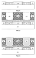
- FIG. 1 represents a cross sectional view depicting a bond pad on a substrate, according to an example embodiment
- FIG. 2 represents a cross sectional view depicting forming a seed layer and patterning a photoresist, according to an example embodiment
- FIG. 3 represents a cross sectional view depicting forming a conductive pillar, according to an example embodiment
- FIG. 4 represents a cross sectional view depicting forming a porous layer above the conductive pillar, according to an example embodiment
- FIG. 5 represents a cross sectional view depicting forming conductive nanowires on the conductive pillar, and removing the porous layer and photoresist, according to an example embodiment
- FIG. 6 represents a cross sectional view depicting joining the structure of FIG. 5 to a second substrate, according to an example embodiment
- FIG. 7 represents a cross sectional view depicting forming an underfill between the two substrates, according to an example embodiment
- FIG. 8 represents a cross sectional view depicting joining the structure of FIG. 5 to a third substrate, according to an example embodiment.
- FIG. 9 represents a cross sectional view depicting forming an underfill between the two substrates, according to an example embodiment.
- the terms “upper”, “lower”, “right”, “left”, “vertical”, “horizontal”, “top”, “bottom”, and derivatives thereof shall relate to the disclosed structures and methods, as oriented in the drawing figures. It will be understood that when an element such as a layer, region, or substrate is referred to as being “on”, “over”, “beneath”, “below”, or “under” another element, it may be present on or below the other element or intervening elements may also be present. In contrast, when an element is referred to as being “directly on”, “directly over”, “directly beneath”, “directly below”, or “directly contacting” another element, there may be no intervening elements present.
- solder interconnects have traditionally been used to form these connections, however the temperatures required to form the connections may create warping due to differing thermal expansion coefficients of the substrates to be joined. Additionally, as the electrical connections become increasingly small and close together, misalignment of the connections may cause the solder interconnections to block the path of underfill used to mechanically join and seal the component from the environment, thus leading to decreased chip performance.
- a process and device are described using conductive nanowires on a conductive pillar, such as copper nanowires on a copper pillar, as a mechanism to reduce the temperature necessary to form an electromechanical connection between conductive portions of two substrates.
- conductive nanowires are used on both substrates, and the fusion of the nanowires forms the electromechanical connection between the substrates, and eliminates the need for traditional soldering techniques.
- conductive nanowires on one substrate reduce the amount of solder on the other substrate necessary to form an electromechanical connection, thus reducing the amount of solder that may impede underfill material from entering the spaces between the two substrates.
- FIG. 1 illustrates a bond pad 110 and passivation layer 120 located on a first substrate 100 .
- the first substrate 100 may be either a dielectric layer formed above a device (not shown) or a semiconductor substrate. Further, the first substrate 100 may contain semiconductor structures electrically connected to bond pad 110 .
- the bond pad 110 may be any electrically conductive material that leads to underlying structures on the device.
- the bond pad 110 may include, for example, copper, aluminum, or tungsten.
- Passivation layer 120 may be any electrical insulating material, isolating each bond pad 110 from the others. Passivation layer 120 may include any suitable dielectric material, for example, silicon nitride (Si 3 N 4 ), silicon carbide (SiC), silicon carbon nitride (SiCN), hydrogenated silicon carbide (SiCH).
- a seed layer 130 and a photoresist material 140 may be formed above the bond pad 110 and passivation layer 120 .
- the seed layer 130 may be deposited on the bond pad 110 and passivation layer 120 using any conventional deposition technique known in the art, such as, for example, atomic layer deposition (ALD), chemical vapor deposition (CVD), low pressure CVD (LPCVD), physical vapor deposition (PVD), molecular beam deposition (MBD), pulsed laser deposition (PLD), liquid source misted chemical deposition (LSMCD), sputtering, or spin-on deposition.
- ALD atomic layer deposition
- CVD chemical vapor deposition
- LPCVD low pressure CVD
- PVD physical vapor deposition
- MBD molecular beam deposition
- PLD pulsed laser deposition
- LSMCD liquid source misted chemical deposition
- sputtering or spin-on deposition.
- the seed layer 130 may encourage the adhesion of a conductive pillar 150 to the
- the seed layer 130 may be composed of a metal or metal alloy, such as, for example, titanium, titanium tungsten, or titanium tungsten chrome copper. While the current embodiment shows the use of a seed layer 130 , additional embodiments may use materials or methods that do not require the seed layer 130 .
- a photoresist material 140 may be deposited on passivation layer 120 using any conventional deposition technique, such as those listed above.
- the photoresist material 140 may be deposited, for example, using a dry film lamination technique or spin on liquid resist technique.
- the photoresist material 140 may then be subjected to a conventional lithographic techniques (i.e., light exposure and development) to solidify the photoresist material and form an opening 145 .
- a conductive pillar 150 may be formed in the opening 145 and in contact with seed layer 130 by depositing a conductive material in the opening.
- the conductive material may be copper or an alloy thereof.
- a different metal/metal alloy may be used for the conductive pillar 150 such as, for example, cobalt or nickel.
- copper or copper alloys will be referred to hereinafter as the material used with the invention, but this should not be considered a limiting feature.
- the conductive pillar 150 may have a height ranging from approximately 20 ⁇ m to approximately 60 ⁇ m.
- a porous layer 160 may be formed above photoresist material 140 and the conductive pillar 150 .
- the porous layer 160 contains one or more pores that extend from the bottom surface of the porous layer SB to the top surface of the porous layer ST.
- the pores may range in diameter from 25 to 500 nm, and may be in a concentration of 4 to 400 pores/( ⁇ m) 2 .
- the porous layer 160 may have a thickness of 50 to 1000 nm.
- the porous layer 160 may be formed using a polymerization process that results in a porous material, such as, for example, forming a polycarbonate membrane.
- an anodized alumina oxide membrane may be formed.
- first conductive nanowires 170 are formed on the top surface of the conductive pillar 150 , and porous layer 160 and photoresist material 140 are removed. During formation of the first conductive nanowires 170 , the material may take the shape of the pores of porous layer 160 , and may only join with the top surface of conductive pillar 150 .
- the first conductive nanowires 170 may contain, for example, copper, nickel, aluminum, or tungsten. In an example embodiment, the conductive nanowires 170 and conductive pillar 150 may be formed using the same material.
- the first conductive nanowires 170 may be formed using a filing technique such as electroplating, electrophoresis, electroless plating, chemical vapor deposition, physical vapor deposition or a combination of methods.
- the porous layer 160 , the photoresist material 140 and seed layer 130 beneath the photoresist material 140 may be removed to leave the final pillar structure, first conductive nanowires 170 and pillar seed layer 135 .
- the photoresist material 140 may be stripped selective to the conductive pillar 150 and passivation layer 120 using laser ablation.
- Laser ablation is a technique in which a laser beam irradiates the surface of a material to evaporate or sublimate the material away, and thus leaving the underlying structures. By selecting the right wavelengths of light, and pulses of the laser light, laser ablation may only heat and remove the desired material without unnecessarily heating surrounding materials. Laser ablation selectively removes the unnecessary materials, without damaging (or with minimal damage) to the first conductive nanowires 170 , as compared to traditional wet or dry etching techniques that would dissolve the conductive nanowires 170 due to the narrow diameters involved.
- FIGS. 6 and 7 shows a first embodiment of joining the structure pictured in FIG. 5 to another substrate.
- the conductive pillars 150 and first conductive nanowires 170 may be joined to a first conductive structure 210 , located on a second substrate 200 , using a second conductive nanowire 220 .
- the processes for making the first conductive structure 210 and the second conductive nanowire 220 may be the same as those for the conductive pillars 150 and first conductive nanowires, respectively.
- the second substrate 200 may contain additional semiconductor structures, similar to those located on the first substrate 100 . Further, the space between the first substrate 100 and second substrate 200 may be filled with an underfill layer 250 .
- the first substrate 100 may be joined to the second substrate 200 using thermal compression to create an electrical connection between conductive pillar 150 and conductive structure 210 .
- a thermal compression tool such as a flip-chip bonder, may be used to apply the temperature and the pressure, and form the electrical connection by fusing the first conductive nanowires 170 with the second conductive nanowires 220 , forming a nanowire fused connection 230 ( FIG. 7 ) between the two structures. This may allow for semiconductor structures on the first substrate 100 to be electrically connected to features or structures located on the second substrate 200 .
- temperatures below the reflow temperature of material of the first conductive nanowires 170 and the second conductive nanowires 220 may fuse the two structures together as the increased surface area of the nanowires enables a phase transition, or reorganization of the structure of the adjoining materials, at a temperature much lower than the bulk melting point of the material, thus creating an electromechanical connection between the two structures.
- the temperatures may range from about 150° C. to about 230° C., and more preferably from about 150° C. to about 200° C., and the temperatures used in the thermal compression tool may range from about 200° C. to about 400° C.
- the applied temperatures of the thermal compression tool may depend on the interconnect material and chip size.
- a pressure ranging from about 6.0 ⁇ 10 4 Pa to about 6.0 ⁇ 10 5 Pa may be applied during the assembly using the thermal compression tool, although this pressure may be adjusted based on the contact area and materials to be interconnected.
- a force ranging from about 5 N to about 50 N may be applied. The force too may be adjusted based on the contact area and materials to be interconnected. In some cases, there may be between 1,000 and 170,000 connections between components.
- the space created between the first substrate 100 and the second substrate 200 is then underfilled, with underfill layer 250 , in order to strengthen the interconnections.
- a curable non-conductive polymeric underfill material is dispensed onto the substrate adjacent to the chip and is drawn into the gap by capillary action, forming underfill layer 250 .
- the underfill material provides environmental protection, and mechanically locks together the first substrate 100 and the second substrate 200 so that differences in thermal expansion of the two materials do not break the nanowire fused connection 230 .
- the underfill material may comprise one or more polymerizable monomers, polyurethane prepolymers, constituents of block copolymers, constituents of radial copolymers, initiators, catalysts, cross-linking agents, stabilizers, and the like.
- polymeric materials contain molecules that are chained or cross-linked to form a strong bonding material as they are cured and hardened.
- a resultant semiconductor structure is created, where an electrical connection is formed between the first substrate 100 and second substrate 200 through the fused connection 230 .
- the fused connection 230 represents an electrically conductive region formed by the first conductive nanowires 170 and the second conductive nanowires 220 , thus allowing structures or devices on the first substrate 100 to be electrically connected, and thus send signals, to structures or devices located on the second substrate 200 .
- FIGS. 8 and 9 shows a second embodiment of joining the structure pictured in FIG. 5 to another substrate.
- the conductive pillars 150 and first conductive nanowires 170 may be joined to a second conductive structure 310 , located on a third substrate 300 , using a solder bump 320 .
- the processes for making the second conductive structure 310 may be the same as those for the conductive pillars 150 .
- the third substrate 300 may contain additional semiconductor structures, similar to those located on the first substrate 100 . Further, the space between the first substrate 100 and third substrate 300 may be filled with an underfill layer 350 .
- the first substrate 100 may be joined to the third substrate 300 using thermal compression to create an electrical connection between conductive pillar 150 and second conductive structure 310 .
- a thermal compression tool such as a flip-chip bonder, may be used to apply the temperature and the pressure, and form the electrical connection using, for example, the first conductive nanowire 170 and the solder bump 320 .
- a temperature just below the reflow temperature of the solder may be used to form the requisite electromechanical connection, as the increased surface area of the first conductive nanowire 170 may reduce the temperature necessary to achieve a structural reorganization of the solder and the copper to create an electromechanical connection, referred to as solder fused connection 330 , between the first conductive nanowire 170 and the solder bump 320 .
- the reflow temperatures of common lead-free solder bumps may range from about 210° C. to about 250° C.
- the temperatures used in the thermal compression tool may range from about 230° C. to about 400° C.
- the applied temperatures of the thermal compression tool may depend on the interconnect material and chip size.
- a pressure ranging from about 6.0 ⁇ 10 4 Pa to about 6.0 ⁇ 10 5 Pa may be applied during the 3D assembly using the thermal compression tool, although this pressure may be adjusted based on the contact area and materials to be interconnected.
- a force ranging from about 5 N to about 50 N may be applied. The force too may be adjusted based on the contact area and materials to be interconnected. In some cases, there may be between 1,000 and 170,000 connections between components.
- the space created between the first substrate 100 and the third substrate 300 is then underfilled, with underfill layer 350 , in order to strengthen the interconnections.
- a curable non-conductive polymeric underfill material is dispensed onto the substrate adjacent to the chip and is drawn into the gap by capillary action, forming underfill layer 350 .
- the underfill material provides environmental protection, and mechanically locks together the first substrate 100 and the second substrate 200 so that differences in thermal expansion of the two materials do not break the solder fused connection 330 .
- the underfill material may comprise one or more polymerizable monomers, polyurethane prepolymers, constituents of block copolymers, constituents of radial copolymers, initiators, catalysts, cross-linking agents, stabilizers, and the like.
- polymeric materials contain molecules that are chained or cross-linked to form a strong bonding material as they are cured and hardened.
- a resultant semiconductor structure is created, where an electrical connection is formed between the first substrate 100 and third substrate 300 through the solder fused connection 330 .
- the solder fused connection 330 represents an electrically conductive region formed by the first conductive nanowires 170 and the solder bump 320 , thus allowing structures or devices on the first substrate 100 to be electrically connected, and thus send signals, to structures or devices located on the second substrate 200 .
Abstract
Description
Claims (7)
Priority Applications (2)
| Application Number | Priority Date | Filing Date | Title |
|---|---|---|---|
| US15/191,628 US9679806B1 (en) | 2015-12-03 | 2016-06-24 | Nanowires for pillar interconnects |
| US15/453,113 US10068864B2 (en) | 2015-12-03 | 2017-03-08 | Nanowires for pillar interconnects |
Applications Claiming Priority (2)
| Application Number | Priority Date | Filing Date | Title |
|---|---|---|---|
| US201514957684A | 2015-12-03 | 2015-12-03 | |
| US15/191,628 US9679806B1 (en) | 2015-12-03 | 2016-06-24 | Nanowires for pillar interconnects |
Related Parent Applications (1)
| Application Number | Title | Priority Date | Filing Date |
|---|---|---|---|
| US201514957684A Continuation-In-Part | 2015-12-03 | 2015-12-03 |
Related Child Applications (1)
| Application Number | Title | Priority Date | Filing Date |
|---|---|---|---|
| US15/453,113 Division US10068864B2 (en) | 2015-12-03 | 2017-03-08 | Nanowires for pillar interconnects |
Publications (2)
| Publication Number | Publication Date |
|---|---|
| US20170162436A1 US20170162436A1 (en) | 2017-06-08 |
| US9679806B1 true US9679806B1 (en) | 2017-06-13 |
Family
ID=58799251
Family Applications (3)
| Application Number | Title | Priority Date | Filing Date |
|---|---|---|---|
| US15/041,381 Abandoned US20170162536A1 (en) | 2015-12-03 | 2016-02-11 | Nanowires for pillar interconnects |
| US15/191,628 Active US9679806B1 (en) | 2015-12-03 | 2016-06-24 | Nanowires for pillar interconnects |
| US15/453,113 Active US10068864B2 (en) | 2015-12-03 | 2017-03-08 | Nanowires for pillar interconnects |
Family Applications Before (1)
| Application Number | Title | Priority Date | Filing Date |
|---|---|---|---|
| US15/041,381 Abandoned US20170162536A1 (en) | 2015-12-03 | 2016-02-11 | Nanowires for pillar interconnects |
Family Applications After (1)
| Application Number | Title | Priority Date | Filing Date |
|---|---|---|---|
| US15/453,113 Active US10068864B2 (en) | 2015-12-03 | 2017-03-08 | Nanowires for pillar interconnects |
Country Status (1)
| Country | Link |
|---|---|
| US (3) | US20170162536A1 (en) |
Cited By (7)
| Publication number | Priority date | Publication date | Assignee | Title |
|---|---|---|---|---|
| US20190096845A1 (en) * | 2017-05-09 | 2019-03-28 | Unimicron Technology Corp. | Chip module and stacked structure |
| US10559948B2 (en) * | 2018-05-08 | 2020-02-11 | Yazaki Corporation | Casing, electrical connection box, and wire harness |
| TWI685284B (en) * | 2018-12-11 | 2020-02-11 | 欣興電子股份有限公司 | Package structure and manufacturing method thereof |
| US10685922B2 (en) | 2017-05-09 | 2020-06-16 | Unimicron Technology Corp. | Package structure with structure reinforcing element and manufacturing method thereof |
| US10950535B2 (en) | 2017-05-09 | 2021-03-16 | Unimicron Technology Corp. | Package structure and method of manufacturing the same |
| US11013103B2 (en) | 2017-05-09 | 2021-05-18 | Unimicron Technology Corp. | Method for forming circuit board stacked structure |
| US20220102307A1 (en) * | 2019-04-08 | 2022-03-31 | Texas Instruments Incorporated | Dielectric and metallic nanowire bond layers |
Families Citing this family (8)
| Publication number | Priority date | Publication date | Assignee | Title |
|---|---|---|---|---|
| CN106463426B (en) * | 2014-06-27 | 2020-03-13 | 索尼公司 | Semiconductor device and method for manufacturing the same |
| DE102017122865B3 (en) * | 2017-10-02 | 2019-03-14 | Infineon Technologies Ag | A method of forming a metallic interconnect, method of making a semiconductor interconnect having a metallic interconnect, and a semiconductor interconnect semiconductor device array |
| JP7022595B2 (en) * | 2018-01-17 | 2022-02-18 | スタンレー電気株式会社 | Electronic devices and their manufacturing methods |
| US10833048B2 (en) * | 2018-04-11 | 2020-11-10 | International Business Machines Corporation | Nanowire enabled substrate bonding and electrical contact formation |
| TWI665774B (en) * | 2018-08-15 | 2019-07-11 | 矽品精密工業股份有限公司 | Electronic package and manufacturing method thereof |
| DE102018122007A1 (en) * | 2018-09-10 | 2020-03-12 | Nanowired Gmbh | Arrangement of interconnected components and method for connecting components |
| US11387202B2 (en) | 2019-03-01 | 2022-07-12 | Invensas Llc | Nanowire bonding interconnect for fine-pitch microelectronics |
| DE102019128900A1 (en) * | 2019-10-25 | 2021-04-29 | Endress+Hauser SE+Co. KG | Method for producing an SMD-solderable component, SMD-solderable component, electronic unit and field device |
Citations (25)
| Publication number | Priority date | Publication date | Assignee | Title |
|---|---|---|---|---|
| US5401687A (en) * | 1993-04-15 | 1995-03-28 | Martin Marietta Corporation | Process for high density interconnection of substrates and integrated circuit chips containing sensitive structures |
| JP2000340569A (en) | 1999-03-19 | 2000-12-08 | Toshiba Corp | Wiring structre of semiconductor device and formation method thereof |
| US6297063B1 (en) | 1999-10-25 | 2001-10-02 | Agere Systems Guardian Corp. | In-situ nano-interconnected circuit devices and method for making the same |
| US6340822B1 (en) | 1999-10-05 | 2002-01-22 | Agere Systems Guardian Corp. | Article comprising vertically nano-interconnected circuit devices and method for making the same |
| US20050003652A1 (en) | 2003-07-02 | 2005-01-06 | Shriram Ramanathan | Method and apparatus for low temperature copper to copper bonding |
| US20050003650A1 (en) | 2003-07-02 | 2005-01-06 | Shriram Ramanathan | Three-dimensional stacked substrate arrangements |
| US20050275497A1 (en) | 2004-06-09 | 2005-12-15 | Agency For Science, Technology And Research&Nanyang Technological University | Microfabricated system for magnetic field generation and focusing |
| US20070148949A1 (en) | 2005-12-22 | 2007-06-28 | Intel Corporation | Nanostructure-based package interconnect |
| US20080227294A1 (en) | 2007-03-12 | 2008-09-18 | Daewoong Suh | Method of making an interconnect structure |
| US7479702B2 (en) | 2004-11-30 | 2009-01-20 | Industrial Technology Research Institute | Composite conductive film and semiconductor package using such film |
| US20090065932A1 (en) | 2007-09-11 | 2009-03-12 | Sandeep Sane | Methods of forming nano-coatings for improved adhesion between first level interconnects and epoxy under-fills in microelectronic packages and structures formed thereby |
| US7569935B1 (en) * | 2008-11-12 | 2009-08-04 | Powertech Technology Inc. | Pillar-to-pillar flip-chip assembly |
| US20100305516A1 (en) * | 2004-03-12 | 2010-12-02 | Yuan Xu | Methods and moulds for use in fabricating side-ported microneedles |
| US7964964B2 (en) * | 2005-08-18 | 2011-06-21 | James Sheats | Method of packaging and interconnection of integrated circuits |
| US8004076B2 (en) | 2008-09-30 | 2011-08-23 | Intel Corporation | Microelectronic package with carbon nanotubes interconnect and method of making same |
| US20120119359A1 (en) | 2010-11-17 | 2012-05-17 | Samsung Electronics Co., Ltd. | Bump structure and semiconductor package having the bump structure |
| US8253253B2 (en) | 2007-09-12 | 2012-08-28 | Smoltek Ab | Connecting and bonding adjacent layers with nanostructures |
| US8420978B2 (en) * | 2007-01-18 | 2013-04-16 | The Board Of Trustees Of The University Of Illinois | High throughput, low cost dual-mode patterning method for large area substrates |
| WO2013134054A1 (en) | 2012-03-04 | 2013-09-12 | Set North America, Llc | 3d packaging with low-force thermocompression bonding of oxidizable materials |
| US20130270329A1 (en) | 2009-07-20 | 2013-10-17 | Set North America, Llc | 3D Packaging With Low-Force Thermocompression Bonding Of Oxidizable Materials |
| US8592995B2 (en) * | 2009-07-02 | 2013-11-26 | Taiwan Semiconductor Manufacturing Company, Ltd. | Method and structure for adhesion of intermetallic compound (IMC) on Cu pillar bump |
| US20140145328A1 (en) | 2009-07-13 | 2014-05-29 | Georgia Tech Research Corporation | Interconnect assemblies and methods of making and using same |
| US20140252614A1 (en) | 2013-03-11 | 2014-09-11 | Taiwan Semiconductor Manufacturing Company, Ltd. | Surface Treatment Method and Apparatus for Semiconductor Packaging |
| US20140353018A1 (en) | 2013-05-28 | 2014-12-04 | Hitachi, Ltd. | Interlayer connection substrate and its manufacturing method |
| WO2015118611A1 (en) | 2014-02-04 | 2015-08-13 | 千住金属工業株式会社 | Cu BALL, Cu CORE BALL, SOLDER JOINT, SOLDER PASTE, AND SOLDER FOAM |
-
2016
- 2016-02-11 US US15/041,381 patent/US20170162536A1/en not_active Abandoned
- 2016-06-24 US US15/191,628 patent/US9679806B1/en active Active
-
2017
- 2017-03-08 US US15/453,113 patent/US10068864B2/en active Active
Patent Citations (40)
| Publication number | Priority date | Publication date | Assignee | Title |
|---|---|---|---|---|
| US5401687A (en) * | 1993-04-15 | 1995-03-28 | Martin Marietta Corporation | Process for high density interconnection of substrates and integrated circuit chips containing sensitive structures |
| JP3727818B2 (en) | 1999-03-19 | 2005-12-21 | 株式会社東芝 | Wiring structure of semiconductor device and method for forming the same |
| JP2000340569A (en) | 1999-03-19 | 2000-12-08 | Toshiba Corp | Wiring structre of semiconductor device and formation method thereof |
| US6340822B1 (en) | 1999-10-05 | 2002-01-22 | Agere Systems Guardian Corp. | Article comprising vertically nano-interconnected circuit devices and method for making the same |
| US6383923B1 (en) | 1999-10-05 | 2002-05-07 | Agere Systems Guardian Corp. | Article comprising vertically nano-interconnected circuit devices and method for making the same |
| US6297063B1 (en) | 1999-10-25 | 2001-10-02 | Agere Systems Guardian Corp. | In-situ nano-interconnected circuit devices and method for making the same |
| US8421225B2 (en) | 2003-07-02 | 2013-04-16 | Intel Corporation | Three-dimensional stacked substrate arrangements |
| US20050003664A1 (en) | 2003-07-02 | 2005-01-06 | Shriram Ramanathan | Method and apparatus for low temperature copper to copper bonding |
| US20090174070A1 (en) | 2003-07-02 | 2009-07-09 | Shriram Ramanathan | Three-dimensional stacked substrate arrangements |
| US20050003650A1 (en) | 2003-07-02 | 2005-01-06 | Shriram Ramanathan | Three-dimensional stacked substrate arrangements |
| US20050003652A1 (en) | 2003-07-02 | 2005-01-06 | Shriram Ramanathan | Method and apparatus for low temperature copper to copper bonding |
| US7183648B2 (en) | 2003-07-02 | 2007-02-27 | Intel Corporation | Method and apparatus for low temperature copper to copper bonding |
| US20120280387A1 (en) | 2003-07-02 | 2012-11-08 | Shriram Ramanathan | Three-dimensional stacked substrate arrangements |
| US8203208B2 (en) | 2003-07-02 | 2012-06-19 | Intel Corporation | Three-dimensional stacked substrate arrangements |
| US20110260319A1 (en) | 2003-07-02 | 2011-10-27 | Shriram Ramanathan | Three-dimensional stacked substrate arrangements |
| US7973407B2 (en) | 2003-07-02 | 2011-07-05 | Intel Corporation | Three-dimensional stacked substrate arrangements |
| US20100305516A1 (en) * | 2004-03-12 | 2010-12-02 | Yuan Xu | Methods and moulds for use in fabricating side-ported microneedles |
| WO2005122194A1 (en) | 2004-06-09 | 2005-12-22 | Agency For Science, Technology And Research | Microfabricated system for magnetic field generation and focusing |
| US7791440B2 (en) | 2004-06-09 | 2010-09-07 | Agency For Science, Technology And Research | Microfabricated system for magnetic field generation and focusing |
| US20050275497A1 (en) | 2004-06-09 | 2005-12-15 | Agency For Science, Technology And Research&Nanyang Technological University | Microfabricated system for magnetic field generation and focusing |
| US7479702B2 (en) | 2004-11-30 | 2009-01-20 | Industrial Technology Research Institute | Composite conductive film and semiconductor package using such film |
| US7964964B2 (en) * | 2005-08-18 | 2011-06-21 | James Sheats | Method of packaging and interconnection of integrated circuits |
| US20070148949A1 (en) | 2005-12-22 | 2007-06-28 | Intel Corporation | Nanostructure-based package interconnect |
| US7371674B2 (en) * | 2005-12-22 | 2008-05-13 | Intel Corporation | Nanostructure-based package interconnect |
| US8420978B2 (en) * | 2007-01-18 | 2013-04-16 | The Board Of Trustees Of The University Of Illinois | High throughput, low cost dual-mode patterning method for large area substrates |
| US20080227294A1 (en) | 2007-03-12 | 2008-09-18 | Daewoong Suh | Method of making an interconnect structure |
| US7781260B2 (en) | 2007-09-11 | 2010-08-24 | Intel Corporation | Methods of forming nano-coatings for improved adhesion between first level interconnects and epoxy under-fills in microelectronic packages and structures formed thereby |
| US20090065932A1 (en) | 2007-09-11 | 2009-03-12 | Sandeep Sane | Methods of forming nano-coatings for improved adhesion between first level interconnects and epoxy under-fills in microelectronic packages and structures formed thereby |
| US8253253B2 (en) | 2007-09-12 | 2012-08-28 | Smoltek Ab | Connecting and bonding adjacent layers with nanostructures |
| US8004076B2 (en) | 2008-09-30 | 2011-08-23 | Intel Corporation | Microelectronic package with carbon nanotubes interconnect and method of making same |
| US7569935B1 (en) * | 2008-11-12 | 2009-08-04 | Powertech Technology Inc. | Pillar-to-pillar flip-chip assembly |
| US8592995B2 (en) * | 2009-07-02 | 2013-11-26 | Taiwan Semiconductor Manufacturing Company, Ltd. | Method and structure for adhesion of intermetallic compound (IMC) on Cu pillar bump |
| US20140145328A1 (en) | 2009-07-13 | 2014-05-29 | Georgia Tech Research Corporation | Interconnect assemblies and methods of making and using same |
| US20130270329A1 (en) | 2009-07-20 | 2013-10-17 | Set North America, Llc | 3D Packaging With Low-Force Thermocompression Bonding Of Oxidizable Materials |
| US20120119359A1 (en) | 2010-11-17 | 2012-05-17 | Samsung Electronics Co., Ltd. | Bump structure and semiconductor package having the bump structure |
| US20140147974A1 (en) | 2010-11-17 | 2014-05-29 | Samsung Electronics Co., Ltd. | Bump structure including nano-wires and a body connecting ends of the nano-wires, semiconductor package having the bump structure and method of manufacturing the semiconductor package |
| WO2013134054A1 (en) | 2012-03-04 | 2013-09-12 | Set North America, Llc | 3d packaging with low-force thermocompression bonding of oxidizable materials |
| US20140252614A1 (en) | 2013-03-11 | 2014-09-11 | Taiwan Semiconductor Manufacturing Company, Ltd. | Surface Treatment Method and Apparatus for Semiconductor Packaging |
| US20140353018A1 (en) | 2013-05-28 | 2014-12-04 | Hitachi, Ltd. | Interlayer connection substrate and its manufacturing method |
| WO2015118611A1 (en) | 2014-02-04 | 2015-08-13 | 千住金属工業株式会社 | Cu BALL, Cu CORE BALL, SOLDER JOINT, SOLDER PASTE, AND SOLDER FOAM |
Non-Patent Citations (13)
| Title |
|---|
| Arvin et al., "Nanowires for Pillar Interconnects," U.S. Appl. No. 14/957,684, filed Dec. 3, 2015. |
| Arvin et al., "Nanowires for Pillar Interconnects," U.S. Appl. No. 15/041,381, filed Feb. 11, 2016. |
| Gerber et al., "Next Generation Fine Pitch Cu Pillar Technology-Enabling Next Generation Silicon Nodes", 2011 Electronic Components and Technology Conference, IEEE, pp. 612-618. |
| Gerber et al., "Next Generation Fine Pitch Cu Pillar Technology—Enabling Next Generation Silicon Nodes", 2011 Electronic Components and Technology Conference, IEEE, pp. 612-618. |
| Krahne et al., "Physical Properties of Nanorods," Melting Studies of Elongated Inorganic Nanoparticles, 3 pgs., published by Springer-Verlag, 2013. |
| Lin et al., "Evaluation of Cu-bumps with lead-free solders for flip-chip package applications", Microelectronic Engineering, vol. 86, 2009, pp. 2392-2395. |
| List of IBM Patents or Patent Applications Treated as Related, signed Jun. 22, 2016, 2 pgs. |
| Wang et al. "Low Temperature Wafer bonding by Copper Nanorod Array" in Electrochemical and Solid-State Letters vol. 12, pp. H138-H141. Published by Electrochemical Society in 2009. * |
| Wang et al. "Low temperature wafer bonding by copper nanorod array" in Electrochemical and Solid-State Letters vol. 12, pp. H138-H141. Published by the Electrochemical Society in 2009. * |
| Wang et al., "Copper/Parylene Core/Shell Nanowire Surface Fastener Used for Room-Temperature Electrical Bonding", Langmuir, Article, 2013 American Chemical Society, pp. 13909-13916. |
| Wang et al., "Low Temperature Wafer bonding by Copper Nanorod Array" in Electrochemical and Solid-State Letters, vol. 12, pp. H138-H141. Published by The Electrochemical Society in 2009. |
| Wang et al., "Room-Temperature Bonding Technique Based on Copper Nanowire Surface Fastener", Applied Physics Express vol. 6, 2013, The Japan Society of Applied Physics, pp. 035001-1-035001-4. |
| Zurcher, "Nanoparticle Assembly and Sintering Towards All-Copper Flip Chip Interconnects", 2015 Electronic Components & Technology Conference, pp. 1115-1121. |
Cited By (11)
| Publication number | Priority date | Publication date | Assignee | Title |
|---|---|---|---|---|
| US20190096845A1 (en) * | 2017-05-09 | 2019-03-28 | Unimicron Technology Corp. | Chip module and stacked structure |
| US10685922B2 (en) | 2017-05-09 | 2020-06-16 | Unimicron Technology Corp. | Package structure with structure reinforcing element and manufacturing method thereof |
| US10714448B2 (en) * | 2017-05-09 | 2020-07-14 | Unimicron Technology Corp. | Chip module with porous bonding layer and stacked structure with porous bonding layer |
| US10950535B2 (en) | 2017-05-09 | 2021-03-16 | Unimicron Technology Corp. | Package structure and method of manufacturing the same |
| US10957658B2 (en) | 2017-05-09 | 2021-03-23 | Unimicron Technology Corp. | Package structure with structure reinforcing element and manufacturing method thereof |
| US11013103B2 (en) | 2017-05-09 | 2021-05-18 | Unimicron Technology Corp. | Method for forming circuit board stacked structure |
| US11410940B2 (en) | 2017-05-09 | 2022-08-09 | Unimicron Technology Corp. | Package structure with structure reinforcing element and manufacturing method thereof |
| US10559948B2 (en) * | 2018-05-08 | 2020-02-11 | Yazaki Corporation | Casing, electrical connection box, and wire harness |
| TWI685284B (en) * | 2018-12-11 | 2020-02-11 | 欣興電子股份有限公司 | Package structure and manufacturing method thereof |
| US20220102307A1 (en) * | 2019-04-08 | 2022-03-31 | Texas Instruments Incorporated | Dielectric and metallic nanowire bond layers |
| US11791296B2 (en) * | 2019-04-08 | 2023-10-17 | Texas Instruments Incorporated | Dielectric and metallic nanowire bond layers |
Also Published As
| Publication number | Publication date |
|---|---|
| US20170162536A1 (en) | 2017-06-08 |
| US10068864B2 (en) | 2018-09-04 |
| US20170179061A1 (en) | 2017-06-22 |
| US20170162436A1 (en) | 2017-06-08 |
Similar Documents
| Publication | Publication Date | Title |
|---|---|---|
| US10068864B2 (en) | Nanowires for pillar interconnects | |
| US9385083B1 (en) | Wafer-level die to package and die to die interconnects suspended over integrated heat sinks | |
| Khan et al. | Development of 3-D silicon module with TSV for system in packaging | |
| CN106206530B (en) | Semiconductor devices and its manufacturing method | |
| US9013037B2 (en) | Semiconductor package with improved pillar bump process and structure | |
| Oi et al. | Development of new 2.5 D package with novel integrated organic interposer substrate with ultra-fine wiring and high density bumps | |
| US8030208B2 (en) | Bonding method for through-silicon-via based 3D wafer stacking | |
| CN106158824B (en) | Ic package and forming method thereof | |
| US9324557B2 (en) | Method for fabricating equal height metal pillars of different diameters | |
| US9515006B2 (en) | 3D device packaging using through-substrate posts | |
| US20180342404A1 (en) | Package Structures and Methods for Forming the Same | |
| JP2013538467A (en) | Gradual via formation from both sides of the chip | |
| CN106057775A (en) | Semiconductor device and manufacturing method therefor | |
| US8076177B2 (en) | Scalable transfer-join bonding lock-and-key structures | |
| JP5663607B2 (en) | Semiconductor device | |
| TW201332072A (en) | Semiconductor devices and methods for forming the same | |
| US9412723B2 (en) | Package on-package structures and methods for forming the same | |
| WO2009146588A1 (en) | Bonding method for through-silicon-via based 3d wafer stacking | |
| WO2013137809A1 (en) | Semiconductor devices with close-packed via structures having in-plane routing and method of making same | |
| US9425174B1 (en) | Integrated circuit package with solderless interconnection structure | |
| US20170309584A1 (en) | Method of bonding a first substrate and a second substrate | |
| JP2016512929A (en) | Flip chip assembly method including pre-coating interconnect member | |
| US9263376B2 (en) | Chip interposer, semiconductor device, and method for manufacturing a semiconductor device | |
| US7514340B2 (en) | Composite integrated device and methods for forming thereof | |
| JP6996823B2 (en) | Methods and Semiconductor Structures for Manufacturing Semiconductor Devices Containing Substrate Penetrating Vias with Self-Aligned Solder Bumps |
Legal Events
| Date | Code | Title | Description |
|---|---|---|---|
| AS | Assignment |
Owner name: INTERNATIONAL BUSINESS MACHINES CORPORATION, NEW Y Free format text: ASSIGNMENT OF ASSIGNORS INTEREST;ASSIGNORS:ARVIN, CHARLES L.;GAMBINO, JEFFREY P.;MUZZY, CHRISTOPHER D.;AND OTHERS;SIGNING DATES FROM 20151120 TO 20151201;REEL/FRAME:039001/0658 |
|
| AS | Assignment |
Owner name: INTERNATIONAL BUSINESS MACHINES CORPORATION, NEW Y Free format text: ASSIGNMENT OF ASSIGNORS INTEREST;ASSIGNORS:ARVIN, CHARLES L.;GAMBINO, JEFFREY P.;MUZZY, CHRISTOPHER D.;AND OTHERS;SIGNING DATES FROM 20160805 TO 20160808;REEL/FRAME:039376/0559 |
|
| STCF | Information on status: patent grant |
Free format text: PATENTED CASE |
|
| MAFP | Maintenance fee payment |
Free format text: PAYMENT OF MAINTENANCE FEE, 4TH YEAR, LARGE ENTITY (ORIGINAL EVENT CODE: M1551); ENTITY STATUS OF PATENT OWNER: LARGE ENTITY Year of fee payment: 4 |