US9689889B1 - Systems and methods to stabilize high-Q MEMS sensors - Google Patents
Systems and methods to stabilize high-Q MEMS sensors Download PDFInfo
- Publication number
- US9689889B1 US9689889B1 US14/067,105 US201314067105A US9689889B1 US 9689889 B1 US9689889 B1 US 9689889B1 US 201314067105 A US201314067105 A US 201314067105A US 9689889 B1 US9689889 B1 US 9689889B1
- Authority
- US
- United States
- Prior art keywords
- sensor
- voltage
- bias
- circuit
- mems
- Prior art date
- Legal status (The legal status is an assumption and is not a legal conclusion. Google has not performed a legal analysis and makes no representation as to the accuracy of the status listed.)
- Active, expires
Links
- 238000000034 method Methods 0.000 title claims description 21
- 230000004044 response Effects 0.000 claims description 8
- 230000010355 oscillation Effects 0.000 abstract description 14
- 230000007704 transition Effects 0.000 abstract description 7
- 230000006641 stabilisation Effects 0.000 abstract description 2
- 238000011105 stabilization Methods 0.000 abstract description 2
- 230000001133 acceleration Effects 0.000 description 10
- 230000008569 process Effects 0.000 description 7
- 238000006073 displacement reaction Methods 0.000 description 6
- 230000008901 benefit Effects 0.000 description 5
- 239000003990 capacitor Substances 0.000 description 5
- 238000013016 damping Methods 0.000 description 5
- 230000000087 stabilizing effect Effects 0.000 description 5
- 238000010586 diagram Methods 0.000 description 4
- 230000005284 excitation Effects 0.000 description 4
- 230000008859 change Effects 0.000 description 3
- 230000000694 effects Effects 0.000 description 2
- 238000012986 modification Methods 0.000 description 2
- 230000004048 modification Effects 0.000 description 2
- 239000000758 substrate Substances 0.000 description 2
- 238000009966 trimming Methods 0.000 description 2
- 238000001514 detection method Methods 0.000 description 1
- 238000005265 energy consumption Methods 0.000 description 1
- 230000005484 gravity Effects 0.000 description 1
- 230000010354 integration Effects 0.000 description 1
- 238000005259 measurement Methods 0.000 description 1
- 230000010358 mechanical oscillation Effects 0.000 description 1
- 238000005070 sampling Methods 0.000 description 1
Images


Classifications
-
- G—PHYSICS
- G01—MEASURING; TESTING
- G01P—MEASURING LINEAR OR ANGULAR SPEED, ACCELERATION, DECELERATION, OR SHOCK; INDICATING PRESENCE, ABSENCE, OR DIRECTION, OF MOVEMENT
- G01P15/00—Measuring acceleration; Measuring deceleration; Measuring shock, i.e. sudden change of acceleration
- G01P15/02—Measuring acceleration; Measuring deceleration; Measuring shock, i.e. sudden change of acceleration by making use of inertia forces using solid seismic masses
- G01P15/08—Measuring acceleration; Measuring deceleration; Measuring shock, i.e. sudden change of acceleration by making use of inertia forces using solid seismic masses with conversion into electric or magnetic values
- G01P15/13—Measuring acceleration; Measuring deceleration; Measuring shock, i.e. sudden change of acceleration by making use of inertia forces using solid seismic masses with conversion into electric or magnetic values by measuring the force required to restore a proofmass subjected to inertial forces to a null position
- G01P15/131—Measuring acceleration; Measuring deceleration; Measuring shock, i.e. sudden change of acceleration by making use of inertia forces using solid seismic masses with conversion into electric or magnetic values by measuring the force required to restore a proofmass subjected to inertial forces to a null position with electrostatic counterbalancing means
-
- B—PERFORMING OPERATIONS; TRANSPORTING
- B81—MICROSTRUCTURAL TECHNOLOGY
- B81B—MICROSTRUCTURAL DEVICES OR SYSTEMS, e.g. MICROMECHANICAL DEVICES
- B81B7/00—Microstructural systems; Auxiliary parts of microstructural devices or systems
- B81B7/02—Microstructural systems; Auxiliary parts of microstructural devices or systems containing distinct electrical or optical devices of particular relevance for their function, e.g. microelectro-mechanical systems [MEMS]
-
- G—PHYSICS
- G01—MEASURING; TESTING
- G01P—MEASURING LINEAR OR ANGULAR SPEED, ACCELERATION, DECELERATION, OR SHOCK; INDICATING PRESENCE, ABSENCE, OR DIRECTION, OF MOVEMENT
- G01P15/00—Measuring acceleration; Measuring deceleration; Measuring shock, i.e. sudden change of acceleration
- G01P15/02—Measuring acceleration; Measuring deceleration; Measuring shock, i.e. sudden change of acceleration by making use of inertia forces using solid seismic masses
- G01P15/08—Measuring acceleration; Measuring deceleration; Measuring shock, i.e. sudden change of acceleration by making use of inertia forces using solid seismic masses with conversion into electric or magnetic values
- G01P15/125—Measuring acceleration; Measuring deceleration; Measuring shock, i.e. sudden change of acceleration by making use of inertia forces using solid seismic masses with conversion into electric or magnetic values by capacitive pick-up
-
- G—PHYSICS
- G01—MEASURING; TESTING
- G01P—MEASURING LINEAR OR ANGULAR SPEED, ACCELERATION, DECELERATION, OR SHOCK; INDICATING PRESENCE, ABSENCE, OR DIRECTION, OF MOVEMENT
- G01P15/00—Measuring acceleration; Measuring deceleration; Measuring shock, i.e. sudden change of acceleration
- G01P15/02—Measuring acceleration; Measuring deceleration; Measuring shock, i.e. sudden change of acceleration by making use of inertia forces using solid seismic masses
- G01P15/08—Measuring acceleration; Measuring deceleration; Measuring shock, i.e. sudden change of acceleration by making use of inertia forces using solid seismic masses with conversion into electric or magnetic values
- G01P2015/0805—Measuring acceleration; Measuring deceleration; Measuring shock, i.e. sudden change of acceleration by making use of inertia forces using solid seismic masses with conversion into electric or magnetic values being provided with a particular type of spring-mass-system for defining the displacement of a seismic mass due to an external acceleration
- G01P2015/0808—Measuring acceleration; Measuring deceleration; Measuring shock, i.e. sudden change of acceleration by making use of inertia forces using solid seismic masses with conversion into electric or magnetic values being provided with a particular type of spring-mass-system for defining the displacement of a seismic mass due to an external acceleration for defining in-plane movement of the mass, i.e. movement of the mass in the plane of the substrate
- G01P2015/0811—Measuring acceleration; Measuring deceleration; Measuring shock, i.e. sudden change of acceleration by making use of inertia forces using solid seismic masses with conversion into electric or magnetic values being provided with a particular type of spring-mass-system for defining the displacement of a seismic mass due to an external acceleration for defining in-plane movement of the mass, i.e. movement of the mass in the plane of the substrate for one single degree of freedom of movement of the mass
- G01P2015/0814—Measuring acceleration; Measuring deceleration; Measuring shock, i.e. sudden change of acceleration by making use of inertia forces using solid seismic masses with conversion into electric or magnetic values being provided with a particular type of spring-mass-system for defining the displacement of a seismic mass due to an external acceleration for defining in-plane movement of the mass, i.e. movement of the mass in the plane of the substrate for one single degree of freedom of movement of the mass for translational movement of the mass, e.g. shuttle type
Definitions
- the present invention relates to high-Q Micro Electro Mechanical System (MEMS) sensors and, more particularly, to systems, devices, and methods of reducing resonance effects in high-Q MEMS sensors operating in spot mode.
- MEMS Micro Electro Mechanical System
- a new generation of high performance, low power MEMS sensors is playing an increasingly important role in the consumer electronics market.
- Miniaturization efforts drive the integration of multiple navigational sensors, such as accelerometers, magnetometers, and gyroscopes, into a single package.
- Some inertial sensor applications that use stand-alone accelerometers in inclinometers, fall detection sensors, etc., employ spot mode operation techniques in order to reduce power consumption. Transitions between ON and OFF states within spot mode operation involve relatively rapid changes in sensor bias conditions that give rise to perturbations, which may cause unwanted oscillations that negatively impact settling times.
- accelerometers sensor with movable proof-mass perturbations are greatly amplified when excitation frequencies coincide with resonance frequencies of high-Q mechanical resonator systems that comprise a proof-mass.
- MEMS gyroscope sensors Unfortunately, for MEMS gyroscope sensors, high Q is a crucial and wanted design parameter. In fact, these sensors are generally assembled and operated under vacuum conditions. Therefore, in an integrated accelerometer-gyroscope sensor system, as a tradeoff, the quality factor of a MEMS accelerometer sensor typically gives way to the requirements of the gyroscope since the quality factor of the MEMS accelerometer cannot be made sufficiently low so as to avoid unwanted high-Q oscillations during accelerometer spot mode operation.
- the disclosed systems and methods allow to stabilize high-Q oscillations in capacitive MEMS sensors caused by perturbations resulting from turning ON-OFF transitions when biasing in the sensor readout chain in spot mode operation.
- Various embodiments of the invention take advantage of a dedicated ultra-low power circuit module that provides an alternative bias to the sensor during an OFF-phase.
- the alternative bias is designed to apply to a sensor movable mass an electrostatic force that is comparable to a force that is present during an ON-phase. This minimizes perturbations of the sensor movable mass and, thus, provides for smooth transition conditions. As a result, relatively short sensor settling times can be achieved.
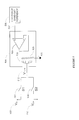
- FIG. 1A shows a typical inertial MEMS accelerometer sensor for differential readout.
- FIG. 1B shows a general electrical equivalent circuit representation of the MEMS sensor shown in FIG. 1A .
- FIG. 2A shows a general mechanical model representing MEMS sensor in FIG. 1A .
- FIG. 2B shows a typical step response for the general mechanical model in FIG. 2A .
- FIG. 3A shows a block diagram of a prior art MEMS sensor front end readout circuit.
- FIG. 3B shows typical voltage waveforms during spot mode operation of a prior art MEMS sensor front end readout circuit.
- FIG. 4A illustrates an exemplary block diagram of a MEMS accelerometer front-end readout circuit utilizing a low power voltage bias control circuit, according to various embodiments of the invention.
- FIG. 4B illustrates exemplary voltage waveforms during spot mode operation of a MEMS accelerometer front-end readout circuit according to various embodiments of the invention.
- FIG. 5 illustrates an exemplary schematic of a low power voltage bias control circuit according to various embodiments of the invention.
- FIG. 6 is a flowchart of an illustrative process for stabilizing high-Q MEMS sensors in accordance with various embodiments of the invention.
- connections between components or between method steps in the figures are not restricted to connections that are affected directly. Instead, connections illustrated in the figures between components or method steps may be modified or otherwise changed through the addition thereto of intermediary components or method steps, without departing from the teachings of the present invention.
- FIG. 1A shows a typical inertial MEMS accelerometer sensor 100 for differential readout.
- Sensor 100 is a relatively small mechanical device for use in various applications, including navigation.
- Sensor 100 comprises inertial proof-mass 106 that is anchored to a fixed structure 102 via spring 104 .
- Sense electrodes 108 , 110 are capacitive structures within sensor 100 that are driven by some electrical circuit (not shown).
- FIG. 1B shows a general electrical equivalent circuit representation 150 of the MEMS sensor shown in FIG. 1A .
- Equivalent circuit 150 is formed by a pair of parallel variable capacitors 152 , 154 that are typically coupled between a movable proof-mass having an inertial resistance to acceleration and a sensing circuit (not shown). The variation of the differential capacitance of capacitors 152 , 154 is related to the movement of the proof-mass.
- FIG. 2A shows a general mechanical model representing MEMS sensor in FIG. 1A .
- Sensor 200 is an inertial MEMS accelerometer sensor.
- the mechanical model represents a harmonic resonator having a natural resonant frequency.
- the resonator comprises proof-mass 202 , spring 204 , and damping element 206 .
- proof-mass 202 is connected to a parallel configuration of spring 204 and damping element 206 .
- the parallel configuration is anchored to substrate 208 .
- Proof-mass 202 is characterized by mass m
- spring 204 is characterized by spring constant k
- damping element 206 is characterized by damping coefficient b.
- the resonant frequency of the mechanical system together with the bandwidth of the resonator define the quality factor, Q, of the resonant system, which is a dimensionless figure of merit.
- the excitation frequency of an accelerometer sensor is significantly different from the mechanical resonant frequency of the accelerometer, such that acceleration of the sensor can be determined from the displacement 212 of proof-mass 202 relative to substrate 208 .
- Displacement 212 (labeled as “x”) is characterized by a movement in position, x, of proof-mass 202 resulting from inertial acceleration force Fin(t) 210 acting on proof-mass 202 . Displacement 212 can be capacitively measured and converted into a measured acceleration value. In addition to gravity, the sum of acceleration force 210 , spring force F k , and damping force F b determine the total time-varying force F(t) that acts on proof-mass 208 .
- FIG. 2B shows a typical step response 250 for the general mechanical model in FIG. 2A .
- FIG. 2B depicts an exponentially decaying mechanical oscillation having envelope 260 .
- the oscillation decays from its initial amplitude A 252 to value Ale 262 within decay time ⁇ 256 .
- the quality factor, Q, of this harmonic resonator is a parameter that can be determined from the decay.
- Q can be determined from the number of oscillations within a decay time ⁇ 256 within which amplitude A 252 decays by approximately 37%.
- FIG. 3A shows a block diagram of a prior art MEMS sensor front end readout circuit 300 .
- Readout circuit 300 comprises voltage source 302 , sensor 306 , bias control circuit 308 , and front end amplifier 310 .
- Voltage source 302 is coupled to MEMS sensor 306 that outputs differential sensor output signal 320 , 322 to low-noise front end amplifier 310 via bias control circuit 308 .
- MEMS sensor 306 is an accelerometer sensor configured to read out the position of a proof-mass within the MEMS sensor 306 and sensor output signal 320 , 322 .
- voltage source 302 provides a source voltage 304 as a stimulus to electrodes of sensor 306 to determine variations in the capacitance of sensor electrodes 316 , 318 .
- MEMS sensor 306 generates differential sensor output signal 320 , 322 in response to receiving acceleration information from sensor electrodes 316 , 318 .
- Bias control circuit 308 controls capacitive sensor outputs common mode voltage by applying to it an average bias voltage that creates an average electrostatic force on capacitive electrodes 316 , 318 in order to properly read out differential sensor output signal 320 , 322 .
- Signal 324 is provided to front end amplifier 310 .
- Front end amplifier 310 amplifies signal 324 to generate output signal V OUT 312 .
- the sum of the electrostatic forces applied to sensor electrodes 316 , 318 are balanced, such that the net electrostatic force of the mechanical system cancels out.
- the application of the bias voltage to sensor electrodes 316 , 318 will not cause any additional forces on the proof mass that possibly create perturbations and negatively impact readout voltage 312 .
- a change in one or of more of voltages V S+ , V S ⁇ , or V D at the MEMS electrodes tends to disturb the force balance and cause the proof-mass to oscillate, until the system reaches a stable position (within boundaries defining a predetermined displacement accuracy after the passage of a corresponding settling time).
- a zero bias voltage may be applied to sensor electrodes 316 , 318 or to output of voltage source 302 in order to conserve energy.
- FIG. 3B shows typical voltage waveforms during spot mode operation of a prior art MEMS sensor front end readout circuit 300 .
- spot mode which involves relatively low output data rates (e.g., 10 Hz-50 Hz)
- the system alternates between an ON phase and an OFF phase. Only during the ON phase (e.g., 1 ms) is acceleration information processed by active front-end circuit 300 .
- bias control circuit 308 applies a bias voltage to differential sensor electrodes 316 , 318 to generate biased sense signal V 1 370 , while during the relatively longer OFF phase (e.g., 100 ms) power hungry circuit components, such as front end amplifier 310 , are powered down and capacitive sensor electrodes 316 , 318 are grounded, so the sense signal V S 354 assumes a zero value.
- relatively longer OFF phase e.g. 100 ms
- biased sense signal V 1 370 in the ON phase causes an electrostatic force on sensor 306 that is much different from the non-biased OFF phase.
- bias control circuit 308 causes an undesired and abrupt stimulus that perturbs the proof-mass within sensor 306 and creates unwanted oscillations that can last for a few milliseconds or more prior to decaying to an acceptable target range.
- the amplitude of the oscillation is especially large if the transition occurs at excitation frequencies that coincide with the mechanical resonance frequency of the mechanical resonator system. Therefore, it would be desirable to minimize the oscillation amplitude and achieve a fast turn-on time of readout circuit 300 for a given accuracy.
- any electrical frequencies contained in source voltage V D 304 should be chosen, such that they do not overlap with potential excitation frequencies of the harmonic system presented in FIG. 2A .
- the source voltage V D 304 could be chosen to operate in the kHz range.
- the duration of the ON phase is extended so as to accommodate the settling time in which the MEMS mechanical position undergoes the stabilization process prior to performing a reading operation. Extending the ON phase, however, increases power consumption and, especially in high-Q mechanical systems, negates to a certain degree the energy savings that are gained by operating sensor 306 in spot mode.
- FIG. 4A illustrates an exemplary block diagram of a MEMS accelerometer front-end readout circuit utilizing a low power voltage bias control circuit, according to various embodiments of the invention. For clarity, components similar to those shown in FIG. 3A are labeled in the same manner.
- Front-end circuit 400 comprises voltage source 302 , sensor 306 , off-bias control circuit 406 , bias control circuit 408 , and front end amplifier circuit 310 .
- Voltage source 302 is coupled to sensor 306 .
- Sensor 306 outputs differential sense signal 420 , 422 to differential, low-noise front end amplifier 310 via bias control circuit 408 .
- MEMS sensor 306 is an inertial capacitive accelerometer sensor that, in response to reading out the position of a proof-mass, generates sense signal 420 , 422 .
- Front end amplifier circuit 310 is an analog front-end circuit coupled to MEMS sensor 306 to read sense signal 420 , 422 .
- Off-bias control circuit 406 is a low power control circuit that is coupled to sense signal 420 , 422 .
- Bias control 408 is a dedicated circuit that is configured to provide a bias voltage to sensor electrodes 316 , 318 . In one embodiment, bias control circuit 408 is an input common mode voltage circuit of front end amplifier 310 .
- voltage source 302 provides source voltage 304 as a stimulus to electrodes 316 , 318 , e.g., in the form of a pulsating input voltage signal, in order to determine variations in the capacitance of sensor electrodes 316 , 318 .
- Sensor 306 generates differential sense signal 420 , 422 in response to reading out acceleration information from capacitive sensor electrodes 316 , 318 .
- bias control circuit 408 controls sense signal 420 , 422 by applying an average bias voltage to sensor electrodes 316 , 318 in order to obtain acceleration information.
- the common mode voltage produces an average electrostatic force on the proof mass within sensor 306 and enables front-end circuit 400 to properly read out differential sense signal 420 , 422 .
- the bias-controlled sense signal 420 , 422 is provided to front end amplifier 310 , which amplifies and outputs it as output signal V OUT 312 .
- V 1 is the common mode voltage set by bias-control to sense signal 420 , 422
- V D is the source voltage 304 in the ON phase
- V 1 _ OFF is the off-bias-controlled sense signal 420 , 422 .
- V S is grounded in the OFF phase and V 1 _ OFF , rather than being applied to V S , is applied to source voltage 304 V D via a second voltage source (not shown). This is possible because the electrostatic force responds to the averaged square value of the voltage difference between sensed voltage V S 454 and source voltage 304 V D , so that becomes irrelevant whether V 1 _ OFF is applied to voltage 454 V S or 304 V D .
- off-bias control circuit 406 is implemented as a low power mode within bias-control circuit 408 .
- bias-control circuit 408 comprises a bit selection circuit that selectably operates in a regular power mode during the first phase when bias-controlled sense signal 420 , 422 is biased with a first voltage V 1 , and operates in the low power mode during the second phase when off-bias-controlled sense signal 420 , 422 is biased with a second voltage V 1 _ OFF .
- This embodiment eliminates the need for off-bias control circuit 406 and, thus, reduces the die area required by front-end circuit 400 .
- off-bias control circuit 406 can be implemented within front-end amplifier 310 , by simply holding the ON state bias voltage V 1 _ ON value on one or more capacitors, e.g., on the sensor capacitors themselves, during the OFF-phase. In this embodiment, the difference between the voltage held on the capacitors and the calculated ideal V 1 _ OFF value may be compensated to account for leakage current of the sensor electrodes.
- the off-bias-controlled sense signal 420 , 422 , V 1 _ OFF is generated by a circuit that comprises trimming capability that is configured to match process variations or operational variables, such as power supply voltage, temperature variations, etc. of both V 1 and V 2 .
- FIG. 4B illustrates exemplary voltage waveforms during spot mode operation of a MEMS accelerometer front-end readout circuit according to various embodiments of the invention. Same numerals as in FIG. 3B denote similar elements. It is noted that FIG. 4B is not drawn to scale.
- ON state voltage waveforms 360 , 370 are similar to voltage waveforms depicted in FIG. 3A .
- off-bias voltage waveform V 1 _ OFF 410 of sensed voltage V S 454 is ideally identical to ON state bias voltage waveform V 1 370 .
- Off-bias voltage V 1 _ OFF 410 generates an electrostatic force comparable to the force that sensor electrodes 316 , 318 experience during the ON state. In other words, equivalent bias conditions are present in both the reading phase and the non-reading phase.
- the resulting force balance allows proof-mass in sensor 306 to experience ideally no changes in electrostatic force and, thus, remain free from resonance effects during transitions between phases.
- FIG. 5 illustrates an exemplary schematic of a low power voltage bias control circuit 500 according to various embodiments of the invention.
- Circuit 500 comprises switch 502 , 504 , trim DAC 506 , and low power band-gap reference module 508 .
- trim DAC 506 comprises operational amplifier 520 to buffer bandgap reference voltage 532 on resistive ladder 528 .
- Resistive ladder 528 is coupled to the output V 1 _ OFF 512 via switches 524 . It will be apparent to one of skill in the art that many different implementation of trim DAC 506 are possible.
- Trim DAC 506 may be factory pre-set, for example based on measurements of V 1 and V 2 , to a predetermined value for V 1 _ OFF 512 that is within the resolution and the accuracy of trim DAC 506 . Since the voltage error resulting from the difference between V 1 _ OFF 512 generated by trim DAC 506 and the calculated V 1 _ OFF may disturb the system, in one embodiment, the resolution of DAC 506 is increased in a range of expected V 1 values in order to keep tsensor resonance oscillation within a desired accuracy range.
- low power band-gap reference module 508 is realized by sampling the ON-state band-gap reference with a low power (e.g., passive) sample-and-hold circuit (not shown in FIG. 5 ).
- the sampled voltage may be refreshed at every ON-cycle. In this example, the trimming could be reduced or entirely avoided.
- FIG. 6 is a flowchart of an illustrative process for stabilizing high-Q MEMS sensors in accordance with various embodiments of the invention.
- the process for stabilizing 600 starts at step 602 when a sensor generates a sensor signal, for example, in response to receiving a pulsating input voltage.
- the sensor signal is received, for example, by a first bias control circuit that is coupled within a front-end readout circuit.
- a bias voltage is applied to the sensor, for example, by the front-end readout circuit to generate a biased sensor signal.
- the biased sensor signal is amplified by a front-end amplifier circuit to generate an amplified sensor signal.
- the amplified sensor signal is output from the front-end readout circuit.
- the front-end amplifier circuit is de-energized.
- an OFF bias control voltage is applied to the sensor signal.
- the process for stabilizing further comprises the steps of energizing a front-end amplifier. In one embodiment, the process for stabilizing further comprises energizing and de-energizing a bias control circuit.
Abstract
Description
F(t)=m{umlaut over (x)}+b{dot over (x)}+kx
which can be solved by numerical analysis.
Q=π(τ/T)
where T is the period of the resonance oscillation measured in seconds.
F EL =a x(V S+ −V D)2 −a −x(V S− −V D)2
where VS+ and VS− are bias voltages; and VD is the source voltage 304, and coefficients ax and a−x are proportionality factors that depend on the particular geometry of sensor 306 (e.g., the gap between proof-mass and sensor electrodes 316, 318).
<(V 1 −V D)2>=<(V 1 _ OFF)2>
where V1 is the common mode voltage set by bias-control to sense signal 420, 422, VD is the source voltage 304 in the ON phase, and V1 _ OFF is the off-bias-controlled sense signal 420, 422. As a result, the average electrostatic forces in both ON phase and OFF phase, balance each other independent of mechanical sensor non-idealities. One of ordinary skill in the art will appreciate that any timing circuit known in the art may be used to implement the timing function of source voltage 304.
Claims (5)
Priority Applications (1)
| Application Number | Priority Date | Filing Date | Title |
|---|---|---|---|
| US14/067,105 US9689889B1 (en) | 2013-07-24 | 2013-10-30 | Systems and methods to stabilize high-Q MEMS sensors |
Applications Claiming Priority (2)
| Application Number | Priority Date | Filing Date | Title |
|---|---|---|---|
| US201361857996P | 2013-07-24 | 2013-07-24 | |
| US14/067,105 US9689889B1 (en) | 2013-07-24 | 2013-10-30 | Systems and methods to stabilize high-Q MEMS sensors |
Publications (1)
| Publication Number | Publication Date |
|---|---|
| US9689889B1 true US9689889B1 (en) | 2017-06-27 |
Family
ID=59070174
Family Applications (1)
| Application Number | Title | Priority Date | Filing Date |
|---|---|---|---|
| US14/067,105 Active 2034-11-22 US9689889B1 (en) | 2013-07-24 | 2013-10-30 | Systems and methods to stabilize high-Q MEMS sensors |
Country Status (1)
| Country | Link |
|---|---|
| US (1) | US9689889B1 (en) |
Cited By (1)
| Publication number | Priority date | Publication date | Assignee | Title |
|---|---|---|---|---|
| US11472696B1 (en) * | 2022-03-23 | 2022-10-18 | Institute Of Geology And Geophysics, Chinese Academy Of Sciences | Seismic acquisition system and sensor based on MEMS sensor with low power consumption |
Citations (18)
| Publication number | Priority date | Publication date | Assignee | Title |
|---|---|---|---|---|
| US5612494A (en) * | 1994-12-22 | 1997-03-18 | Murata Manufacturing Co., Ltd. | Capacitance-type electrostatic servo acceleration sensor |
| US6127767A (en) * | 1996-10-31 | 2000-10-03 | Samsung Electronics Co., Ltd. | Complementary electrostatic driving apparatus for microactuator with parasitic capacitances offset |
| US20050024145A1 (en) * | 2002-12-03 | 2005-02-03 | Bocock Ryan M. | Fast settling power amplifier regulator |
| US20050272397A1 (en) * | 2004-06-04 | 2005-12-08 | Tirdad Sowlati | Mixer having dynamic biasing |
| US20060162454A1 (en) * | 2003-06-25 | 2006-07-27 | Hannu Manninen | Capacitive acceleration sensor arrangement |
| US20070024951A1 (en) * | 2005-07-26 | 2007-02-01 | Fuji Photo Film Co.,Ltd. | Small thin film movable element, small thin film movable element array and method of driving small thin film movable element array |
| US20090161890A1 (en) * | 2007-12-25 | 2009-06-25 | Yuh-Min Lin | Micro-electro-mechanical systems (mems) capacitive sensing circuit |
| US7817075B2 (en) * | 2009-02-03 | 2010-10-19 | Windtop Technology Corp. | Apparatus for converting MEMS inductive capacitance |
| US20110115498A1 (en) * | 2009-10-20 | 2011-05-19 | Analog Devices, Inc. | Detection and Mitigation of Particle Contaminants in MEMS Devices |
| US20120090393A1 (en) * | 2010-06-18 | 2012-04-19 | Baolab Microsystems Sl | Unstable electrostatic spring accelerometer |
| US20120235726A1 (en) * | 2010-09-14 | 2012-09-20 | Ayman Elsayed | Interface for MEMS intertial sensors |
| US20120262192A1 (en) * | 2011-04-15 | 2012-10-18 | Zeleznik Matthew A | High-impedance mems switch |
| US20130265070A1 (en) * | 2012-04-04 | 2013-10-10 | Fairchild Semiconductor Corporation | Self test of mems accelerometer with asics integrated capacitors |
| US8661871B2 (en) * | 2009-07-31 | 2014-03-04 | Stmicroelectronics S.R.L. | Method for testing a microelectromechanical device, microelectromechanical device |
| US20140167789A1 (en) * | 2012-12-19 | 2014-06-19 | Invensense, Inc. | Mode-tuning sense interface |
| US20140266260A1 (en) * | 2013-03-15 | 2014-09-18 | Infineon Technologies Ag | Apparatus and a Method for Generating a Sensor Signal Indicating Information on a Capacitance of a Variable Capacitor Comprising a Variable Capacitance |
| US20140345380A1 (en) * | 2013-05-23 | 2014-11-27 | Kemiao Jia | Active lateral force stiction self-recovery for microelectromechanical systems devices |
| US20140361844A1 (en) * | 2013-06-05 | 2014-12-11 | Silicon Laboratories Inc. | Suspended passive element for mems devices |
-
2013
- 2013-10-30 US US14/067,105 patent/US9689889B1/en active Active
Patent Citations (19)
| Publication number | Priority date | Publication date | Assignee | Title |
|---|---|---|---|---|
| US5612494A (en) * | 1994-12-22 | 1997-03-18 | Murata Manufacturing Co., Ltd. | Capacitance-type electrostatic servo acceleration sensor |
| US6127767A (en) * | 1996-10-31 | 2000-10-03 | Samsung Electronics Co., Ltd. | Complementary electrostatic driving apparatus for microactuator with parasitic capacitances offset |
| US20050024145A1 (en) * | 2002-12-03 | 2005-02-03 | Bocock Ryan M. | Fast settling power amplifier regulator |
| US20060162454A1 (en) * | 2003-06-25 | 2006-07-27 | Hannu Manninen | Capacitive acceleration sensor arrangement |
| US20050272397A1 (en) * | 2004-06-04 | 2005-12-08 | Tirdad Sowlati | Mixer having dynamic biasing |
| US20070024951A1 (en) * | 2005-07-26 | 2007-02-01 | Fuji Photo Film Co.,Ltd. | Small thin film movable element, small thin film movable element array and method of driving small thin film movable element array |
| US20090161890A1 (en) * | 2007-12-25 | 2009-06-25 | Yuh-Min Lin | Micro-electro-mechanical systems (mems) capacitive sensing circuit |
| US7817075B2 (en) * | 2009-02-03 | 2010-10-19 | Windtop Technology Corp. | Apparatus for converting MEMS inductive capacitance |
| US8661871B2 (en) * | 2009-07-31 | 2014-03-04 | Stmicroelectronics S.R.L. | Method for testing a microelectromechanical device, microelectromechanical device |
| US20110115498A1 (en) * | 2009-10-20 | 2011-05-19 | Analog Devices, Inc. | Detection and Mitigation of Particle Contaminants in MEMS Devices |
| US8421481B2 (en) * | 2009-10-20 | 2013-04-16 | Analog Devices, Inc. | Detection and mitigation of particle contaminants in MEMS devices |
| US20120090393A1 (en) * | 2010-06-18 | 2012-04-19 | Baolab Microsystems Sl | Unstable electrostatic spring accelerometer |
| US20120235726A1 (en) * | 2010-09-14 | 2012-09-20 | Ayman Elsayed | Interface for MEMS intertial sensors |
| US20120262192A1 (en) * | 2011-04-15 | 2012-10-18 | Zeleznik Matthew A | High-impedance mems switch |
| US20130265070A1 (en) * | 2012-04-04 | 2013-10-10 | Fairchild Semiconductor Corporation | Self test of mems accelerometer with asics integrated capacitors |
| US20140167789A1 (en) * | 2012-12-19 | 2014-06-19 | Invensense, Inc. | Mode-tuning sense interface |
| US20140266260A1 (en) * | 2013-03-15 | 2014-09-18 | Infineon Technologies Ag | Apparatus and a Method for Generating a Sensor Signal Indicating Information on a Capacitance of a Variable Capacitor Comprising a Variable Capacitance |
| US20140345380A1 (en) * | 2013-05-23 | 2014-11-27 | Kemiao Jia | Active lateral force stiction self-recovery for microelectromechanical systems devices |
| US20140361844A1 (en) * | 2013-06-05 | 2014-12-11 | Silicon Laboratories Inc. | Suspended passive element for mems devices |
Cited By (1)
| Publication number | Priority date | Publication date | Assignee | Title |
|---|---|---|---|---|
| US11472696B1 (en) * | 2022-03-23 | 2022-10-18 | Institute Of Geology And Geophysics, Chinese Academy Of Sciences | Seismic acquisition system and sensor based on MEMS sensor with low power consumption |
Similar Documents
| Publication | Publication Date | Title |
|---|---|---|
| US11614463B2 (en) | High performance micro-electro-mechanical systems accelerometer | |
| US8875578B2 (en) | Electronic damper circuit for MEMS sensors and resonators | |
| JP5960257B2 (en) | Apparatus and method for time domain measurement of vibrational perturbations | |
| Langfelder et al. | Z-axis magnetometers for MEMS inertial measurement units using an industrial process | |
| US7696749B2 (en) | Resonator-based magnetic field sensor | |
| US8549915B2 (en) | Micromachined gyroscopes with 2-DOF sense modes allowing interchangeable robust and precision operation | |
| US8878528B2 (en) | MEMS-based magnetic sensor with a Lorentz force actuator used as force feedback | |
| EP2746780B1 (en) | Bias reduction in force rebalanced accelerometers | |
| Langfelder et al. | Design criteria of low-power oscillators for consumer-grade MEMS resonant sensors | |
| US10161957B2 (en) | Accelerometers | |
| Lee et al. | An axial strain modulated double-ended tuning fork electrometer | |
| Yin et al. | Design and test of a micromachined resonant accelerometer with high scale factor and low noise | |
| US20160298963A1 (en) | Quality Factor Estimation for Resonators | |
| US9689889B1 (en) | Systems and methods to stabilize high-Q MEMS sensors | |
| US9252707B2 (en) | MEMS mass bias to track changes in bias conditions and reduce effects of flicker noise | |
| Pandit et al. | Reduction of amplitude ratio dependence on drive level in mode localized resonant MEMS sensors | |
| US20200028509A1 (en) | Radiation-hard precision voltage reference | |
| Li et al. | Open–loop operating mode of micromachined capacitive accelerometer | |
| Wang et al. | Utilizing mechanical micro-lever coupling structure to enhance sensitivity in mode-localized MEMS accelerometer | |
| Sonmezoglu et al. | Off-resonance operation of a MEMS Lorentz force magnetometer with improved thermal stability of the scale factor | |
| Ciotirca et al. | New Stability Method of a Multirate Controller for a Three-Axis High-$ Q $ MEMS Accelerometer With Simultaneous Electrostatic Damping | |
| CN113049995B (en) | Micromechanical Lorentz force magnetometer with double resonance structure and interface detection circuit | |
| Gando et al. | An intermittent free-vibration MEMS gyroscope enabled by catch-and-release mechanism for low-power and fast-startup applications | |
| Liu et al. | A resonant accelerometer based on electrostatic stiffness and its closed‐loop control method | |
| Xu et al. | Research on nonlinear dynamics of drive mode in z-axis silicon microgyroscope |
Legal Events
| Date | Code | Title | Description |
|---|---|---|---|
| AS | Assignment |
Owner name: MAXIM INTEGRATED PRODUCTS, INC., CALIFORNIA Free format text: ASSIGNMENT OF ASSIGNORS INTEREST;ASSIGNORS:CASIRAGHI, ROBERTO;PADOVANI, IGINO;MEMBRETTI, GEORGIO MASSAMILIANO;AND OTHERS;SIGNING DATES FROM 20131018 TO 20131030;REEL/FRAME:031513/0209 |
|
| AS | Assignment |
Owner name: HANKING ELECTRONICS, LTD., OHIO Free format text: ASSIGNMENT OF ASSIGNORS INTEREST;ASSIGNOR:MAXIM INTEGRATED PRODUCTS, INC.;REEL/FRAME:040459/0091 Effective date: 20161018 |
|
| STCF | Information on status: patent grant |
Free format text: PATENTED CASE |
|
| MAFP | Maintenance fee payment |
Free format text: PAYMENT OF MAINTENANCE FEE, 4TH YEAR, LARGE ENTITY (ORIGINAL EVENT CODE: M1551); ENTITY STATUS OF PATENT OWNER: LARGE ENTITY Year of fee payment: 4 |
|
| AS | Assignment |
Owner name: HANKING ELECTRONICS HONGKONG CO., LIMITED, HONG KONG Free format text: ASSIGNMENT OF ASSIGNORS INTEREST;ASSIGNOR:HANKING ELECTRONICS, LTD.;REEL/FRAME:066990/0671 Effective date: 20230621 |