US9755157B2 - Organic compound and organic optoelectric device and display device - Google Patents
Organic compound and organic optoelectric device and display device Download PDFInfo
- Publication number
- US9755157B2 US9755157B2 US14/197,376 US201414197376A US9755157B2 US 9755157 B2 US9755157 B2 US 9755157B2 US 201414197376 A US201414197376 A US 201414197376A US 9755157 B2 US9755157 B2 US 9755157B2
- Authority
- US
- United States
- Prior art keywords
- group
- substituted
- unsubstituted
- organic
- organic compound
- Prior art date
- Legal status (The legal status is an assumption and is not a legal conclusion. Google has not performed a legal analysis and makes no representation as to the accuracy of the status listed.)
- Active, expires
Links
- 0 *1=*C2=C(*=*1)C1=*\*=*/*=C\1C2.*C.*CC1=CC=CC=C1*.*CC1=CC=CC=C1*.[1*]C.[2*]C.[4*]C Chemical compound *1=*C2=C(*=*1)C1=*\*=*/*=C\1C2.*C.*CC1=CC=CC=C1*.*CC1=CC=CC=C1*.[1*]C.[2*]C.[4*]C 0.000 description 21
- HEQNOFFRILLUKZ-UHFFFAOYSA-N CC1(C)C2=C(C=CC=C2)C2=C1C=CC1=C2OC2=C1N=CC1=C2C2=C(C=CC=C2)N1C1=CC=CC=C1 Chemical compound CC1(C)C2=C(C=CC=C2)C2=C1C=CC1=C2OC2=C1N=CC1=C2C2=C(C=CC=C2)N1C1=CC=CC=C1 HEQNOFFRILLUKZ-UHFFFAOYSA-N 0.000 description 3
- JMKSDDFDYGRFNG-UHFFFAOYSA-N C1=CC(C2=CC=NC=C2)=CC(N2C3=C(C=CC=C3)C3=C2C=CC2=C3OC3=C2C=CC2=C3C3=C(C=CC=C3)C2)=C1.CC1(C)C2=C(C=CC=C2)C2=C1C=CC1=C2OC2=C1C=CC1=C2C2=C(C=CC=C2)N1C1=CC=CC(C2=NC(C3=CC=CC=C3)=NC(C3=CC=CC=C3)=N2)=C1.CC1(C)C2=C(C=CC=C2)C2=C1C=CC1=C2SC2=C1C=CC1=C2C2=C(C=CC=C2)N1C1=CC=CC(C2=NC(C3=CC=CC=C3)=NC(C3=CC=CC=C3)=N2)=C1 Chemical compound C1=CC(C2=CC=NC=C2)=CC(N2C3=C(C=CC=C3)C3=C2C=CC2=C3OC3=C2C=CC2=C3C3=C(C=CC=C3)C2)=C1.CC1(C)C2=C(C=CC=C2)C2=C1C=CC1=C2OC2=C1C=CC1=C2C2=C(C=CC=C2)N1C1=CC=CC(C2=NC(C3=CC=CC=C3)=NC(C3=CC=CC=C3)=N2)=C1.CC1(C)C2=C(C=CC=C2)C2=C1C=CC1=C2SC2=C1C=CC1=C2C2=C(C=CC=C2)N1C1=CC=CC(C2=NC(C3=CC=CC=C3)=NC(C3=CC=CC=C3)=N2)=C1 JMKSDDFDYGRFNG-UHFFFAOYSA-N 0.000 description 2
- XUSRSRHZQXTWDJ-UHFFFAOYSA-N C1=CC(C2=CC=NC=C2)=CC(N2C3=C(C=CC=C3)C3=C2C=CC2=C3OC3=C2C=CC2=C3C3=C(C=CC=C3)O2)=C1.C1=CC(C2=CC=NC=C2)=CC(N2C3=C(C=CC=C3)C3=C2C=CC2=C3OC3=C2C=CC2=C3C3=C(C=CC=C3)S2)=C1.C1=CC(C2=CC=NC=C2)=CC(N2C3=C(C=CC=C3)C3=C2C=CC2=C3SC3=C2C=CC2=C3C3=C(C=CC=C3)C2)=C1 Chemical compound C1=CC(C2=CC=NC=C2)=CC(N2C3=C(C=CC=C3)C3=C2C=CC2=C3OC3=C2C=CC2=C3C3=C(C=CC=C3)O2)=C1.C1=CC(C2=CC=NC=C2)=CC(N2C3=C(C=CC=C3)C3=C2C=CC2=C3OC3=C2C=CC2=C3C3=C(C=CC=C3)S2)=C1.C1=CC(C2=CC=NC=C2)=CC(N2C3=C(C=CC=C3)C3=C2C=CC2=C3SC3=C2C=CC2=C3C3=C(C=CC=C3)C2)=C1 XUSRSRHZQXTWDJ-UHFFFAOYSA-N 0.000 description 2
- JRSSTJKVGJSRJU-UHFFFAOYSA-N C1=CC(C2=CC=NC=C2)=CC(N2C3=C(C=CC=C3)C3=C2C=CC2=C3SC3=C2C=CC2=C3C3=C(C=CC=C3)O2)=C1.C1=CC(C2=CC=NC=C2)=CC(N2C3=C(C=CC=C3)C3=C2C=CC2=C3SC3=C2C=CC2=C3C3=C(C=CC=C3)S2)=C1.CC1(C)C2=C(C=CC=C2)C2=C1C=CC1=C2OC2=C1C=CC1=C2C2=C(C=CC=C2)N1C1=CC=CC(C2=CC=NC=C2)=C1 Chemical compound C1=CC(C2=CC=NC=C2)=CC(N2C3=C(C=CC=C3)C3=C2C=CC2=C3SC3=C2C=CC2=C3C3=C(C=CC=C3)O2)=C1.C1=CC(C2=CC=NC=C2)=CC(N2C3=C(C=CC=C3)C3=C2C=CC2=C3SC3=C2C=CC2=C3C3=C(C=CC=C3)S2)=C1.CC1(C)C2=C(C=CC=C2)C2=C1C=CC1=C2OC2=C1C=CC1=C2C2=C(C=CC=C2)N1C1=CC=CC(C2=CC=NC=C2)=C1 JRSSTJKVGJSRJU-UHFFFAOYSA-N 0.000 description 2
- FFPPBSKHUMBYSK-UHFFFAOYSA-N C1=CC2=C(C=C1)C1=C(C=CC3=C1OC1=C3C=CC3=C1C1=C(C=CC=C1)N3C1=C/C=C3/OC4=C(C=CC=C4)/C3=C\1)C2.C1=CC2=C(C=C1)C1=C(C=CC3=C1SC1=C3C=CC3=C1C1=C(C=CC=C1)N3C1=C/C=C3/OC4=C(C=CC=C4)/C3=C\1)C2.CC1(C)C2=C(C=CC=C2)C2=C1C=CC1=C2SC2=C1C=CC1=C2C2=C(C=CC=C2)N1C1=C/C=C2/SC3=C(C=CC=C3)/C2=C\1 Chemical compound C1=CC2=C(C=C1)C1=C(C=CC3=C1OC1=C3C=CC3=C1C1=C(C=CC=C1)N3C1=C/C=C3/OC4=C(C=CC=C4)/C3=C\1)C2.C1=CC2=C(C=C1)C1=C(C=CC3=C1SC1=C3C=CC3=C1C1=C(C=CC=C1)N3C1=C/C=C3/OC4=C(C=CC=C4)/C3=C\1)C2.CC1(C)C2=C(C=CC=C2)C2=C1C=CC1=C2SC2=C1C=CC1=C2C2=C(C=CC=C2)N1C1=C/C=C2/SC3=C(C=CC=C3)/C2=C\1 FFPPBSKHUMBYSK-UHFFFAOYSA-N 0.000 description 2
- WMZKSMDFAXMXSQ-UHFFFAOYSA-N C1=CC2=C(C=C1)C1=C(C=CC3=C1OC1=C3C=CC3=C1C1=C(C=CC=C1)N3C1=C/C=C3/OC4=C(C=CC=C4)/C3=C\1)O2.C1=CC2=C(C=C1)C1=C(C=CC3=C1SC1=C3C=CC3=C1C1=C(C=CC=C1)N3C1=C/C=C3/OC4=C(C=CC=C4)/C3=C\1)O2.C1=CC2=C(C=C1)C1=C\C(N3C4=C(C=CC=C4)C4=C3C=CC3=C4OC4=C3C=CC3=C4C4=C(C=CC=C4)S3)=C/C=C\1O2 Chemical compound C1=CC2=C(C=C1)C1=C(C=CC3=C1OC1=C3C=CC3=C1C1=C(C=CC=C1)N3C1=C/C=C3/OC4=C(C=CC=C4)/C3=C\1)O2.C1=CC2=C(C=C1)C1=C(C=CC3=C1SC1=C3C=CC3=C1C1=C(C=CC=C1)N3C1=C/C=C3/OC4=C(C=CC=C4)/C3=C\1)O2.C1=CC2=C(C=C1)C1=C\C(N3C4=C(C=CC=C4)C4=C3C=CC3=C4OC4=C3C=CC3=C4C4=C(C=CC=C4)S3)=C/C=C\1O2 WMZKSMDFAXMXSQ-UHFFFAOYSA-N 0.000 description 2
- LJZRJKFSZUHNJA-UHFFFAOYSA-N C1=CC2=C(C=C1)C1=C(C=CC3=C1OC1=C3C=CC3=C1C1=C(C=CC=C1)N3C1=C/C=C3/SC4=C(C=CC=C4)/C3=C\1)C2.CC1(C)C2=C(C=CC=C2)C2=C1C=CC1=C2OC2=C1C=CC1=C2C2=C(C=CC(C3=NC(C4=CC=CC=C4)=NC(C4=CC=CC=C4)=N3)=C2)N1C1=CC=CC=C1.CC1(C)C2=C(C=CC=C2)C2=C1C=CC1=C2SC2=C1C=CC1=C2C2=C(C=CC(C3=NC(C4=CC=CC=C4)=NC(C4=CC=CC=C4)=N3)=C2)N1C1=CC=CC=C1 Chemical compound C1=CC2=C(C=C1)C1=C(C=CC3=C1OC1=C3C=CC3=C1C1=C(C=CC=C1)N3C1=C/C=C3/SC4=C(C=CC=C4)/C3=C\1)C2.CC1(C)C2=C(C=CC=C2)C2=C1C=CC1=C2OC2=C1C=CC1=C2C2=C(C=CC(C3=NC(C4=CC=CC=C4)=NC(C4=CC=CC=C4)=N3)=C2)N1C1=CC=CC=C1.CC1(C)C2=C(C=CC=C2)C2=C1C=CC1=C2SC2=C1C=CC1=C2C2=C(C=CC(C3=NC(C4=CC=CC=C4)=NC(C4=CC=CC=C4)=N3)=C2)N1C1=CC=CC=C1 LJZRJKFSZUHNJA-UHFFFAOYSA-N 0.000 description 2
- QAPXVVHJCCKKGJ-UHFFFAOYSA-N C1=CC2=C(C=C1)C1=C(C=CC3=C1OC1=C3C=CC3=C1C1=C(C=CC=C1)N3C1=C/C=C3/SC4=C(C=CC=C4)/C3=C\1)O2.C1=CC2=C(C=C1)C1=C(C=CC3=C1OC1=C3C=CC3=C1C1=C(C=CC=C1)N3C1=C/C=C3/SC4=C(C=CC=C4)/C3=C\1)S2.C1=CC2=C(C=C1)C1=C(C=CC3=C1SC1=C3C=CC3=C1C1=C(C=CC=C1)N3C1=C/C=C3/SC4=C(C=CC=C4)/C3=C\1)C2 Chemical compound C1=CC2=C(C=C1)C1=C(C=CC3=C1OC1=C3C=CC3=C1C1=C(C=CC=C1)N3C1=C/C=C3/SC4=C(C=CC=C4)/C3=C\1)O2.C1=CC2=C(C=C1)C1=C(C=CC3=C1OC1=C3C=CC3=C1C1=C(C=CC=C1)N3C1=C/C=C3/SC4=C(C=CC=C4)/C3=C\1)S2.C1=CC2=C(C=C1)C1=C(C=CC3=C1SC1=C3C=CC3=C1C1=C(C=CC=C1)N3C1=C/C=C3/SC4=C(C=CC=C4)/C3=C\1)C2 QAPXVVHJCCKKGJ-UHFFFAOYSA-N 0.000 description 2
- PVUIEKNOFYNOMX-UHFFFAOYSA-N C1=CC2=C(C=C1)C1=C(C=CC3=C1OC1=C3C=CC3=C1C1=C(C=CC=C1)N3C1=CC(C3=CC=NC=C3)=CC(C3=CC=NC=C3)=C1)C2.C1=CC2=C(C=C1)C1=C(C=CC3=C1SC1=C3C=CC3=C1C1=C(C=CC=C1)N3C1=CC(C3=CC=NC=C3)=CC(C3=CC=NC=C3)=C1)C2.CC1(C)C2=C(C=CC=C2)C2=C1C=CC1=C2SC2=C1C=CC1=C2C2=C(C=CC=C2)N1C1=CC=CC(C2=CC=NC=C2)=C1 Chemical compound C1=CC2=C(C=C1)C1=C(C=CC3=C1OC1=C3C=CC3=C1C1=C(C=CC=C1)N3C1=CC(C3=CC=NC=C3)=CC(C3=CC=NC=C3)=C1)C2.C1=CC2=C(C=C1)C1=C(C=CC3=C1SC1=C3C=CC3=C1C1=C(C=CC=C1)N3C1=CC(C3=CC=NC=C3)=CC(C3=CC=NC=C3)=C1)C2.CC1(C)C2=C(C=CC=C2)C2=C1C=CC1=C2SC2=C1C=CC1=C2C2=C(C=CC=C2)N1C1=CC=CC(C2=CC=NC=C2)=C1 PVUIEKNOFYNOMX-UHFFFAOYSA-N 0.000 description 2
- YMXBAOVMLOUSPS-UHFFFAOYSA-N C1=CC2=C(C=C1)C1=C(C=CC3=C1OC1=C3C=CC3=C1C1=C(C=CC=C1)N3C1=CC(C3=CC=NC=C3)=CC(C3=CC=NC=C3)=C1)O2 Chemical compound C1=CC2=C(C=C1)C1=C(C=CC3=C1OC1=C3C=CC3=C1C1=C(C=CC=C1)N3C1=CC(C3=CC=NC=C3)=CC(C3=CC=NC=C3)=C1)O2 YMXBAOVMLOUSPS-UHFFFAOYSA-N 0.000 description 2
- FVODKDLTVJRYAR-UHFFFAOYSA-N C1=CC2=C(C=C1)C1=C(C=CC3=C1OC1=C3C=CC3=C1C1=C(C=CC=C1)N3C1=CC(C3=CC=NC=C3)=CC(C3=CC=NC=C3)=C1)S2.C1=CC2=C(C=C1)C1=C(C=CC3=C1SC1=C3C=CC3=C1C1=C(C=CC=C1)N3C1=CC(C3=CC=NC=C3)=CC(C3=CC=NC=C3)=C1)O2.C1=CC2=C(C=C1)C1=C(C=CC3=C1SC1=C3C=CC3=C1C1=C(C=CC=C1)N3C1=CC(C3=CC=NC=C3)=CC(C3=CC=NC=C3)=C1)S2 Chemical compound C1=CC2=C(C=C1)C1=C(C=CC3=C1OC1=C3C=CC3=C1C1=C(C=CC=C1)N3C1=CC(C3=CC=NC=C3)=CC(C3=CC=NC=C3)=C1)S2.C1=CC2=C(C=C1)C1=C(C=CC3=C1SC1=C3C=CC3=C1C1=C(C=CC=C1)N3C1=CC(C3=CC=NC=C3)=CC(C3=CC=NC=C3)=C1)O2.C1=CC2=C(C=C1)C1=C(C=CC3=C1SC1=C3C=CC3=C1C1=C(C=CC=C1)N3C1=CC(C3=CC=NC=C3)=CC(C3=CC=NC=C3)=C1)S2 FVODKDLTVJRYAR-UHFFFAOYSA-N 0.000 description 2
- SAHHATFORHVWAB-UHFFFAOYSA-N C1=CC2=C(C=C1)C1=C(C=CC3=C1SC1=C3C=CC3=C1C1=C(C=CC=C1)N3C1=C/C=C3/SC4=C(C=CC=C4)/C3=C\1)O2.C1=CC2=C(C=C1)C1=C(C=CC3=C1SC1=C3C=CC3=C1C1=C(C=CC=C1)N3C1=C/C=C3/SC4=C(C=CC=C4)/C3=C\1)S2.CC1(C)C2=C(C=CC=C2)C2=C1C=CC1=C2OC2=C1C=CC1=C2C2=C(C=CC=C2)N1C1=C/C=C2/SC3=C(C=CC=C3)/C2=C\1 Chemical compound C1=CC2=C(C=C1)C1=C(C=CC3=C1SC1=C3C=CC3=C1C1=C(C=CC=C1)N3C1=C/C=C3/SC4=C(C=CC=C4)/C3=C\1)O2.C1=CC2=C(C=C1)C1=C(C=CC3=C1SC1=C3C=CC3=C1C1=C(C=CC=C1)N3C1=C/C=C3/SC4=C(C=CC=C4)/C3=C\1)S2.CC1(C)C2=C(C=CC=C2)C2=C1C=CC1=C2OC2=C1C=CC1=C2C2=C(C=CC=C2)N1C1=C/C=C2/SC3=C(C=CC=C3)/C2=C\1 SAHHATFORHVWAB-UHFFFAOYSA-N 0.000 description 2
- KZJNTVNEKJKASY-UHFFFAOYSA-N C1=CC2=C(C=C1)C1=C\C(N3C4=C(C=CC=C4)C4=C3C=CC3=C4SC4=C3C=CC3=C4C4=C(C=CC=C4)S3)=C/C=C\1O2.CC1(C)C2=C(C=CC=C2)C2=C1C=CC1=C2OC2=C1C=CC1=C2C2=C(C=CC=C2)N1C1=C/C=C2/OC3=C(C=CC=C3)/C2=C\1.CC1(C)C2=C(C=CC=C2)C2=C1C=CC1=C2SC2=C1C=CC1=C2C2=C(C=CC=C2)N1C1=C/C=C2/OC3=C(C=CC=C3)/C2=C\1 Chemical compound C1=CC2=C(C=C1)C1=C\C(N3C4=C(C=CC=C4)C4=C3C=CC3=C4SC4=C3C=CC3=C4C4=C(C=CC=C4)S3)=C/C=C\1O2.CC1(C)C2=C(C=CC=C2)C2=C1C=CC1=C2OC2=C1C=CC1=C2C2=C(C=CC=C2)N1C1=C/C=C2/OC3=C(C=CC=C3)/C2=C\1.CC1(C)C2=C(C=CC=C2)C2=C1C=CC1=C2SC2=C1C=CC1=C2C2=C(C=CC=C2)N1C1=C/C=C2/OC3=C(C=CC=C3)/C2=C\1 KZJNTVNEKJKASY-UHFFFAOYSA-N 0.000 description 2
- HKKPONCJIMOUBA-UHFFFAOYSA-N C1=CC=C(C2=CC(C3=CC=CC=C3)=CC(N3C4=C(C=CC=C4)C4=C3C=CC3=C4OC4=C3C=CC3=C4C4=C(C=CC=C4)C3)=C2)C=C1.CC1(C)C2=C(C=CC=C2)C2=C1C=CC1=C2OC2=C1C=CC1=C2C2=C(C=CC=C2)N1C1=NC(C2=CC=CC=C2)=NC(C2=CC=CC=C2)=N1.CC1(C)C2=C(C=CC=C2)C2=C1C=CC1=C2SC2=C1C=CC1=C2C2=C(C=CC=C2)N1C1=NC(C2=CC=CC=C2)=NC(C2=CC=CC=C2)=N1 Chemical compound C1=CC=C(C2=CC(C3=CC=CC=C3)=CC(N3C4=C(C=CC=C4)C4=C3C=CC3=C4OC4=C3C=CC3=C4C4=C(C=CC=C4)C3)=C2)C=C1.CC1(C)C2=C(C=CC=C2)C2=C1C=CC1=C2OC2=C1C=CC1=C2C2=C(C=CC=C2)N1C1=NC(C2=CC=CC=C2)=NC(C2=CC=CC=C2)=N1.CC1(C)C2=C(C=CC=C2)C2=C1C=CC1=C2SC2=C1C=CC1=C2C2=C(C=CC=C2)N1C1=NC(C2=CC=CC=C2)=NC(C2=CC=CC=C2)=N1 HKKPONCJIMOUBA-UHFFFAOYSA-N 0.000 description 2
- NWFAIYOJHVYXGK-UHFFFAOYSA-N C1=CC=C(C2=CC(C3=CC=CC=C3)=CC(N3C4=C(C=CC=C4)C4=C3C=CC3=C4OC4=C3C=CC3=C4C4=C(C=CC=C4)O3)=C2)C=C1.C1=CC=C(C2=CC(C3=CC=CC=C3)=CC(N3C4=C(C=CC=C4)C4=C3C=CC3=C4OC4=C3C=CC3=C4C4=C(C=CC=C4)S3)=C2)C=C1.C1=CC=C(C2=CC(C3=CC=CC=C3)=CC(N3C4=C(C=CC=C4)C4=C3C=CC3=C4SC4=C3C=CC3=C4C4=C(C=CC=C4)C3)=C2)C=C1 Chemical compound C1=CC=C(C2=CC(C3=CC=CC=C3)=CC(N3C4=C(C=CC=C4)C4=C3C=CC3=C4OC4=C3C=CC3=C4C4=C(C=CC=C4)O3)=C2)C=C1.C1=CC=C(C2=CC(C3=CC=CC=C3)=CC(N3C4=C(C=CC=C4)C4=C3C=CC3=C4OC4=C3C=CC3=C4C4=C(C=CC=C4)S3)=C2)C=C1.C1=CC=C(C2=CC(C3=CC=CC=C3)=CC(N3C4=C(C=CC=C4)C4=C3C=CC3=C4SC4=C3C=CC3=C4C4=C(C=CC=C4)C3)=C2)C=C1 NWFAIYOJHVYXGK-UHFFFAOYSA-N 0.000 description 2
- WMANHUUPKUXCJW-UHFFFAOYSA-N C1=CC=C(C2=CC(C3=CC=CC=C3)=CC(N3C4=C(C=CC=C4)C4=C3C=CC3=C4SC4=C3C=CC3=C4C4=C(C=CC=C4)O3)=C2)C=C1.C1=CC=C(C2=CC(C3=CC=CC=C3)=CC(N3C4=C(C=CC=C4)C4=C3C=CC3=C4SC4=C3C=CC3=C4C4=C(C=CC=C4)S3)=C2)C=C1 Chemical compound C1=CC=C(C2=CC(C3=CC=CC=C3)=CC(N3C4=C(C=CC=C4)C4=C3C=CC3=C4SC4=C3C=CC3=C4C4=C(C=CC=C4)O3)=C2)C=C1.C1=CC=C(C2=CC(C3=CC=CC=C3)=CC(N3C4=C(C=CC=C4)C4=C3C=CC3=C4SC4=C3C=CC3=C4C4=C(C=CC=C4)S3)=C2)C=C1 WMANHUUPKUXCJW-UHFFFAOYSA-N 0.000 description 2
- MUPFQFXRGYQWAJ-UHFFFAOYSA-N C1=CC=C(C2=CC(C3=CC=CC=C3)=NC(N3C4=C(C=CC=C4)C4=C3C=CC3=C4OC4=C3C=CC3=C4C4=C(C=CC=C4)C3)=N2)C=C1.CC1(C)C2=C(C=CC=C2)C2=C1C=CC1=C2OC2=C1C=CC1=C2C2=C(C=CC=C2)N1C1=CC(C2=CC=NC=C2)=CC(C2=CC=NC=C2)=C1.CC1(C)C2=C(C=CC=C2)C2=C1C=CC1=C2SC2=C1C=CC1=C2C2=C(C=CC=C2)N1C1=CC(C2=CC=NC=C2)=CC(C2=CC=NC=C2)=C1 Chemical compound C1=CC=C(C2=CC(C3=CC=CC=C3)=NC(N3C4=C(C=CC=C4)C4=C3C=CC3=C4OC4=C3C=CC3=C4C4=C(C=CC=C4)C3)=N2)C=C1.CC1(C)C2=C(C=CC=C2)C2=C1C=CC1=C2OC2=C1C=CC1=C2C2=C(C=CC=C2)N1C1=CC(C2=CC=NC=C2)=CC(C2=CC=NC=C2)=C1.CC1(C)C2=C(C=CC=C2)C2=C1C=CC1=C2SC2=C1C=CC1=C2C2=C(C=CC=C2)N1C1=CC(C2=CC=NC=C2)=CC(C2=CC=NC=C2)=C1 MUPFQFXRGYQWAJ-UHFFFAOYSA-N 0.000 description 2
- PIWMEZHIYXRMQF-UHFFFAOYSA-N C1=CC=C(C2=CC(C3=CC=CC=C3)=NC(N3C4=C(C=CC=C4)C4=C3C=CC3=C4OC4=C3C=CC3=C4C4=C(C=CC=C4)O3)=N2)C=C1.C1=CC=C(C2=CC(C3=CC=CC=C3)=NC(N3C4=C(C=CC=C4)C4=C3C=CC3=C4OC4=C3C=CC3=C4C4=C(C=CC=C4)S3)=N2)C=C1.C1=CC=C(C2=CC(C3=CC=CC=C3)=NC(N3C4=C(C=CC=C4)C4=C3C=CC3=C4SC4=C3C=CC3=C4C4=C(C=CC=C4)C3)=N2)C=C1 Chemical compound C1=CC=C(C2=CC(C3=CC=CC=C3)=NC(N3C4=C(C=CC=C4)C4=C3C=CC3=C4OC4=C3C=CC3=C4C4=C(C=CC=C4)O3)=N2)C=C1.C1=CC=C(C2=CC(C3=CC=CC=C3)=NC(N3C4=C(C=CC=C4)C4=C3C=CC3=C4OC4=C3C=CC3=C4C4=C(C=CC=C4)S3)=N2)C=C1.C1=CC=C(C2=CC(C3=CC=CC=C3)=NC(N3C4=C(C=CC=C4)C4=C3C=CC3=C4SC4=C3C=CC3=C4C4=C(C=CC=C4)C3)=N2)C=C1 PIWMEZHIYXRMQF-UHFFFAOYSA-N 0.000 description 2
- NMHANPNDJDBKKU-UHFFFAOYSA-N C1=CC=C(C2=CC(C3=CC=CC=C3)=NC(N3C4=C(C=CC=C4)C4=C3C=CC3=C4SC4=C3C=CC3=C4C4=C(C=CC=C4)O3)=N2)C=C1.C1=CC=C(C2=CC(C3=CC=CC=C3)=NC(N3C4=C(C=CC=C4)C4=C3C=CC3=C4SC4=C3C=CC3=C4C4=C(C=CC=C4)S3)=N2)C=C1.CC1(C)C2=C(C=CC=C2)C2=C1C=CC1=C2OC2=C1C=CC1=C2C2=C(C=CC=C2)N1C1=NC(C2=CC=CC=C2)=CC(C2=CC=CC=C2)=N1 Chemical compound C1=CC=C(C2=CC(C3=CC=CC=C3)=NC(N3C4=C(C=CC=C4)C4=C3C=CC3=C4SC4=C3C=CC3=C4C4=C(C=CC=C4)O3)=N2)C=C1.C1=CC=C(C2=CC(C3=CC=CC=C3)=NC(N3C4=C(C=CC=C4)C4=C3C=CC3=C4SC4=C3C=CC3=C4C4=C(C=CC=C4)S3)=N2)C=C1.CC1(C)C2=C(C=CC=C2)C2=C1C=CC1=C2OC2=C1C=CC1=C2C2=C(C=CC=C2)N1C1=NC(C2=CC=CC=C2)=CC(C2=CC=CC=C2)=N1 NMHANPNDJDBKKU-UHFFFAOYSA-N 0.000 description 2
- OLNSWIIPRAKNKY-UHFFFAOYSA-N C1=CC=C(C2=CC3=C(C=C2)N(C2=CC=CC=C2)C2=C3C3=C(C=C2)C2=C(O3)C3=C(C=C2)CC2=C3C=CC=C2)C=C1.C1=CC=C(C2=CC3=C(C=C2)N(C2=CC=CC=C2)C2=C3C3=C(C=C2)C2=C(S3)C3=C(C=C2)CC2=C3C=CC=C2)C=C1.C1=CC=C(N2C3=C(C=CC=C3)C3=C2C=CC2=C3OC3=C2C2=C(C=C3)C3=C(C=CC=C3)O2)C=C1 Chemical compound C1=CC=C(C2=CC3=C(C=C2)N(C2=CC=CC=C2)C2=C3C3=C(C=C2)C2=C(O3)C3=C(C=C2)CC2=C3C=CC=C2)C=C1.C1=CC=C(C2=CC3=C(C=C2)N(C2=CC=CC=C2)C2=C3C3=C(C=C2)C2=C(S3)C3=C(C=C2)CC2=C3C=CC=C2)C=C1.C1=CC=C(N2C3=C(C=CC=C3)C3=C2C=CC2=C3OC3=C2C2=C(C=C3)C3=C(C=CC=C3)O2)C=C1 OLNSWIIPRAKNKY-UHFFFAOYSA-N 0.000 description 2
- NLVFSPPCRPEBCX-UHFFFAOYSA-N C1=CC=C(C2=CC3=C(C=C2)N(C2=CC=CC=C2)C2=C3C3=C(C=C2)C2=C(O3)C3=C(C=C2)OC2=C3C=CC=C2)C=C1.C1=CC=C(C2=CC3=C(C=C2)N(C2=CC=CC=C2)C2=C3C3=C(C=C2)C2=C(O3)C3=C(C=C2)SC2=C3C=CC=C2)C=C1.C1=CC=C(C2=CC3=C(C=C2)N(C2=CC=CC=C2)C2=C3C3=C(C=C2)C2=C(S3)C3=C(C=C2)OC2=C3C=CC=C2)C=C1 Chemical compound C1=CC=C(C2=CC3=C(C=C2)N(C2=CC=CC=C2)C2=C3C3=C(C=C2)C2=C(O3)C3=C(C=C2)OC2=C3C=CC=C2)C=C1.C1=CC=C(C2=CC3=C(C=C2)N(C2=CC=CC=C2)C2=C3C3=C(C=C2)C2=C(O3)C3=C(C=C2)SC2=C3C=CC=C2)C=C1.C1=CC=C(C2=CC3=C(C=C2)N(C2=CC=CC=C2)C2=C3C3=C(C=C2)C2=C(S3)C3=C(C=C2)OC2=C3C=CC=C2)C=C1 NLVFSPPCRPEBCX-UHFFFAOYSA-N 0.000 description 2
- WAMKEQVJZBAVNK-UHFFFAOYSA-N C1=CC=C(C2=CC3=C(C=C2)N(C2=CC=CC=C2)C2=C3C3=C(C=C2)C2=C(S3)C3=C(C=C2)SC2=C3C=CC=C2)C=C1.CC1(C)C2=C(C=CC=C2)C2=C1C=CC1=C2OC2=C1C=CC1=C2C2=C(C=CC(C3=CC=CC=C3)=C2)N1C1=CC=CC=C1.CC1(C)C2=C(C=CC=C2)C2=C1C=CC1=C2SC2=C1C=CC1=C2C2=C(C=CC(C3=CC=CC=C3)=C2)N1C1=CC=CC=C1 Chemical compound C1=CC=C(C2=CC3=C(C=C2)N(C2=CC=CC=C2)C2=C3C3=C(C=C2)C2=C(S3)C3=C(C=C2)SC2=C3C=CC=C2)C=C1.CC1(C)C2=C(C=CC=C2)C2=C1C=CC1=C2OC2=C1C=CC1=C2C2=C(C=CC(C3=CC=CC=C3)=C2)N1C1=CC=CC=C1.CC1(C)C2=C(C=CC=C2)C2=C1C=CC1=C2SC2=C1C=CC1=C2C2=C(C=CC(C3=CC=CC=C3)=C2)N1C1=CC=CC=C1 WAMKEQVJZBAVNK-UHFFFAOYSA-N 0.000 description 2
- AOGNWIHFEBCHMH-UHFFFAOYSA-N C1=CC=C(C2=CC=C(N3C4=C(C=CC=C4)C4=C3C=CC3=C4OC4=C3C=CC3=C4C4=C(C=CC=C4)C3)C=C2)C=C1.CC1(C)C2=C(C=CC=C2)C2=C1C=CC1=C2OC2=C1C=CC1=C2C2=C(C=CC=C2)N1C1=CC(C2=CC=CC=C2)=CC(C2=CC=CC=C2)=C1.CC1(C)C2=C(C=CC=C2)C2=C1C=CC1=C2SC2=C1C=CC1=C2C2=C(C=CC=C2)N1C1=CC(C2=CC=CC=C2)=CC(C2=CC=CC=C2)=C1 Chemical compound C1=CC=C(C2=CC=C(N3C4=C(C=CC=C4)C4=C3C=CC3=C4OC4=C3C=CC3=C4C4=C(C=CC=C4)C3)C=C2)C=C1.CC1(C)C2=C(C=CC=C2)C2=C1C=CC1=C2OC2=C1C=CC1=C2C2=C(C=CC=C2)N1C1=CC(C2=CC=CC=C2)=CC(C2=CC=CC=C2)=C1.CC1(C)C2=C(C=CC=C2)C2=C1C=CC1=C2SC2=C1C=CC1=C2C2=C(C=CC=C2)N1C1=CC(C2=CC=CC=C2)=CC(C2=CC=CC=C2)=C1 AOGNWIHFEBCHMH-UHFFFAOYSA-N 0.000 description 2
- RESYAPPRPXAUJU-UHFFFAOYSA-N C1=CC=C(C2=CC=C(N3C4=C(C=CC=C4)C4=C3C=CC3=C4OC4=C3C=CC3=C4C4=C(C=CC=C4)O3)C=C2)C=C1.C1=CC=C(C2=CC=C(N3C4=C(C=CC=C4)C4=C3C=CC3=C4SC4=C3C=CC3=C4C4=C(C=CC=C4)C3)C=C2)C=C1 Chemical compound C1=CC=C(C2=CC=C(N3C4=C(C=CC=C4)C4=C3C=CC3=C4OC4=C3C=CC3=C4C4=C(C=CC=C4)O3)C=C2)C=C1.C1=CC=C(C2=CC=C(N3C4=C(C=CC=C4)C4=C3C=CC3=C4SC4=C3C=CC3=C4C4=C(C=CC=C4)C3)C=C2)C=C1 RESYAPPRPXAUJU-UHFFFAOYSA-N 0.000 description 2
- ZBGDMQBEMTWITQ-UHFFFAOYSA-N C1=CC=C(C2=CC=C(N3C4=C(C=CC=C4)C4=C3C=CC3=C4OC4=C3C=CC3=C4C4=C(C=CC=C4)S3)C=C2)C=C1.C1=CC=C(C2=CC=C(N3C4=C(C=CC=C4)C4=C3C=CC3=C4SC4=C3C=CC3=C4C4=C(C=CC=C4)O3)C=C2)C=C1 Chemical compound C1=CC=C(C2=CC=C(N3C4=C(C=CC=C4)C4=C3C=CC3=C4OC4=C3C=CC3=C4C4=C(C=CC=C4)S3)C=C2)C=C1.C1=CC=C(C2=CC=C(N3C4=C(C=CC=C4)C4=C3C=CC3=C4SC4=C3C=CC3=C4C4=C(C=CC=C4)O3)C=C2)C=C1 ZBGDMQBEMTWITQ-UHFFFAOYSA-N 0.000 description 2
- CGTHCNHMAFQKHP-UHFFFAOYSA-N C1=CC=C(C2=CC=C(N3C4=C(C=CC=C4)C4=C3C=CC3=C4SC4=C3C=CC3=C4C4=C(C=CC=C4)S3)C=C2)C=C1.CC1(C)C2=C(C=CC=C2)C2=C1C=CC1=C2OC2=C1C=CC1=C2C2=C(C=CC=C2)N1C1=CC=C(C2=CC=CC=C2)C=C1 Chemical compound C1=CC=C(C2=CC=C(N3C4=C(C=CC=C4)C4=C3C=CC3=C4SC4=C3C=CC3=C4C4=C(C=CC=C4)S3)C=C2)C=C1.CC1(C)C2=C(C=CC=C2)C2=C1C=CC1=C2OC2=C1C=CC1=C2C2=C(C=CC=C2)N1C1=CC=C(C2=CC=CC=C2)C=C1 CGTHCNHMAFQKHP-UHFFFAOYSA-N 0.000 description 2
- HSWMPQAYLIEXRM-UHFFFAOYSA-N C1=CC=C(C2=NC(C3=CC=CC=C3)=NC(C3=CC(C4=CC5=C(C=C4)N(C4=CC=CC=C4)C4=C5C5=C(C=C4)C4=C(O5)C5=C(C=C4)CC4=C5C=CC=C4)=CC=C3)=N2)C=C1.CC1(C)C2=C(C=CC=C2)C2=C1C=CC1=C2OC2=C1C=CC1=C2C2=C(O1)C(C1=NC(C3=CC=CC=C3)=NC(C3=CC=CC=C3)=N1)=CC=C2.CC1(C)C2=C(C=CC=C2)C2=C1C=CC1=C2SC2=C1C=CC1=C2C2=C(O1)C(C1=NC(C3=CC=CC=C3)=NC(C3=CC=CC=C3)=N1)=CC=C2 Chemical compound C1=CC=C(C2=NC(C3=CC=CC=C3)=NC(C3=CC(C4=CC5=C(C=C4)N(C4=CC=CC=C4)C4=C5C5=C(C=C4)C4=C(O5)C5=C(C=C4)CC4=C5C=CC=C4)=CC=C3)=N2)C=C1.CC1(C)C2=C(C=CC=C2)C2=C1C=CC1=C2OC2=C1C=CC1=C2C2=C(O1)C(C1=NC(C3=CC=CC=C3)=NC(C3=CC=CC=C3)=N1)=CC=C2.CC1(C)C2=C(C=CC=C2)C2=C1C=CC1=C2SC2=C1C=CC1=C2C2=C(O1)C(C1=NC(C3=CC=CC=C3)=NC(C3=CC=CC=C3)=N1)=CC=C2 HSWMPQAYLIEXRM-UHFFFAOYSA-N 0.000 description 2
- QEEIKBUEXQPJRC-UHFFFAOYSA-N C1=CC=C(C2=NC(C3=CC=CC=C3)=NC(C3=CC(C4=CC5=C(C=C4)N(C4=CC=CC=C4)C4=C5C5=C(C=C4)C4=C(O5)C5=C(C=C4)OC4=C5C=CC=C4)=CC=C3)=N2)C=C1.C1=CC=C(C2=NC(C3=CC=CC=C3)=NC(C3=CC(C4=CC5=C(C=C4)N(C4=CC=CC=C4)C4=C5C5=C(C=C4)C4=C(O5)C5=C(C=C4)SC4=C5C=CC=C4)=CC=C3)=N2)C=C1.C1=CC=C(C2=NC(C3=CC=CC=C3)=NC(C3=CC(C4=CC5=C(C=C4)N(C4=CC=CC=C4)C4=C5C5=C(C=C4)C4=C(S5)C5=C(C=C4)CC4=C5C=CC=C4)=CC=C3)=N2)C=C1 Chemical compound C1=CC=C(C2=NC(C3=CC=CC=C3)=NC(C3=CC(C4=CC5=C(C=C4)N(C4=CC=CC=C4)C4=C5C5=C(C=C4)C4=C(O5)C5=C(C=C4)OC4=C5C=CC=C4)=CC=C3)=N2)C=C1.C1=CC=C(C2=NC(C3=CC=CC=C3)=NC(C3=CC(C4=CC5=C(C=C4)N(C4=CC=CC=C4)C4=C5C5=C(C=C4)C4=C(O5)C5=C(C=C4)SC4=C5C=CC=C4)=CC=C3)=N2)C=C1.C1=CC=C(C2=NC(C3=CC=CC=C3)=NC(C3=CC(C4=CC5=C(C=C4)N(C4=CC=CC=C4)C4=C5C5=C(C=C4)C4=C(S5)C5=C(C=C4)CC4=C5C=CC=C4)=CC=C3)=N2)C=C1 QEEIKBUEXQPJRC-UHFFFAOYSA-N 0.000 description 2
- XMNPVYCJPNBSAL-UHFFFAOYSA-N C1=CC=C(C2=NC(C3=CC=CC=C3)=NC(C3=CC(C4=CC5=C(C=C4)N(C4=CC=CC=C4)C4=C5C5=C(C=C4)C4=C(S5)C5=C(C=C4)OC4=C5C=CC=C4)=CC=C3)=N2)C=C1.C1=CC=C(C2=NC(C3=CC=CC=C3)=NC(C3=CC(C4=CC5=C(C=C4)N(C4=CC=CC=C4)C4=C5C5=C(C=C4)C4=C(S5)C5=C(C=C4)SC4=C5C=CC=C4)=CC=C3)=N2)C=C1.CC1(C)C2=C(C=CC=C2)C2=C1C=CC1=C2OC2=C1C=CC1=C2C2=C(C=CC(C3=CC=CC(C4=NC(C5=CC=CC=C5)=NC(C5=CC=CC=C5)=N4)=C3)=C2)N1C1=CC=CC=C1 Chemical compound C1=CC=C(C2=NC(C3=CC=CC=C3)=NC(C3=CC(C4=CC5=C(C=C4)N(C4=CC=CC=C4)C4=C5C5=C(C=C4)C4=C(S5)C5=C(C=C4)OC4=C5C=CC=C4)=CC=C3)=N2)C=C1.C1=CC=C(C2=NC(C3=CC=CC=C3)=NC(C3=CC(C4=CC5=C(C=C4)N(C4=CC=CC=C4)C4=C5C5=C(C=C4)C4=C(S5)C5=C(C=C4)SC4=C5C=CC=C4)=CC=C3)=N2)C=C1.CC1(C)C2=C(C=CC=C2)C2=C1C=CC1=C2OC2=C1C=CC1=C2C2=C(C=CC(C3=CC=CC(C4=NC(C5=CC=CC=C5)=NC(C5=CC=CC=C5)=N4)=C3)=C2)N1C1=CC=CC=C1 XMNPVYCJPNBSAL-UHFFFAOYSA-N 0.000 description 2
- NXYQMTGNBHBBEC-UHFFFAOYSA-N C1=CC=C(C2=NC(C3=CC=CC=C3)=NC(C3=CC(N4C5=C(C=CC=C5)C5=C4C=CC4=C5OC5=C4C=CC4=C5C5=C(C=CC=C5)C4)=CC=C3)=N2)C=C1.CC1(C)C2=C(C=CC=C2)C2=C1C=CC1=C2SC2=C1C=CC1=C2C2=C(C=CC=C2)N1C1=CC=C(N(C2=CC=CC=C2)C2=CC=CC=C2)C=C1 Chemical compound C1=CC=C(C2=NC(C3=CC=CC=C3)=NC(C3=CC(N4C5=C(C=CC=C5)C5=C4C=CC4=C5OC5=C4C=CC4=C5C5=C(C=CC=C5)C4)=CC=C3)=N2)C=C1.CC1(C)C2=C(C=CC=C2)C2=C1C=CC1=C2SC2=C1C=CC1=C2C2=C(C=CC=C2)N1C1=CC=C(N(C2=CC=CC=C2)C2=CC=CC=C2)C=C1 NXYQMTGNBHBBEC-UHFFFAOYSA-N 0.000 description 2
- IJEBAQUULLTYCB-UHFFFAOYSA-N C1=CC=C(C2=NC(C3=CC=CC=C3)=NC(C3=CC(N4C5=C(C=CC=C5)C5=C4C=CC4=C5OC5=C4C=CC4=C5C5=C(C=CC=C5)O4)=CC=C3)=N2)C=C1.C1=CC=C(C2=NC(C3=CC=CC=C3)=NC(C3=CC(N4C5=C(C=CC=C5)C5=C4C=CC4=C5SC5=C4C=CC4=C5C5=C(C=CC=C5)C4)=CC=C3)=N2)C=C1 Chemical compound C1=CC=C(C2=NC(C3=CC=CC=C3)=NC(C3=CC(N4C5=C(C=CC=C5)C5=C4C=CC4=C5OC5=C4C=CC4=C5C5=C(C=CC=C5)O4)=CC=C3)=N2)C=C1.C1=CC=C(C2=NC(C3=CC=CC=C3)=NC(C3=CC(N4C5=C(C=CC=C5)C5=C4C=CC4=C5SC5=C4C=CC4=C5C5=C(C=CC=C5)C4)=CC=C3)=N2)C=C1 IJEBAQUULLTYCB-UHFFFAOYSA-N 0.000 description 2
- LFRMQAXHTLOXKE-UHFFFAOYSA-N C1=CC=C(C2=NC(C3=CC=CC=C3)=NC(C3=CC(N4C5=C(C=CC=C5)C5=C4C=CC4=C5OC5=C4C=CC4=C5C5=C(C=CC=C5)S4)=CC=C3)=N2)C=C1 Chemical compound C1=CC=C(C2=NC(C3=CC=CC=C3)=NC(C3=CC(N4C5=C(C=CC=C5)C5=C4C=CC4=C5OC5=C4C=CC4=C5C5=C(C=CC=C5)S4)=CC=C3)=N2)C=C1 LFRMQAXHTLOXKE-UHFFFAOYSA-N 0.000 description 2
- WHDXERLVKZTOPI-UHFFFAOYSA-N C1=CC=C(C2=NC(C3=CC=CC=C3)=NC(C3=CC(N4C5=C(C=CC=C5)C5=C4C=CC4=C5SC5=C4C=CC4=C5C5=C(C=CC=C5)O4)=CC=C3)=N2)C=C1.C1=CC=C(C2=NC(C3=CC=CC=C3)=NC(C3=CC(N4C5=C(C=CC=C5)C5=C4C=CC4=C5SC5=C4C=CC4=C5C5=C(C=CC=C5)S4)=CC=C3)=N2)C=C1 Chemical compound C1=CC=C(C2=NC(C3=CC=CC=C3)=NC(C3=CC(N4C5=C(C=CC=C5)C5=C4C=CC4=C5SC5=C4C=CC4=C5C5=C(C=CC=C5)O4)=CC=C3)=N2)C=C1.C1=CC=C(C2=NC(C3=CC=CC=C3)=NC(C3=CC(N4C5=C(C=CC=C5)C5=C4C=CC4=C5SC5=C4C=CC4=C5C5=C(C=CC=C5)S4)=CC=C3)=N2)C=C1 WHDXERLVKZTOPI-UHFFFAOYSA-N 0.000 description 2
- AOWNYKYFXXQMQJ-UHFFFAOYSA-N C1=CC=C(C2=NC(C3=CC=CC=C3)=NC(C3=CC4=C(C=C3)N(C3=CC=CC=C3)C3=C4C4=C(C=C3)C3=C(O4)C4=C(C=C3)CC3=C4C=CC=C3)=N2)C=C1.C1=CC=C(C2=NC(C3=CC=CC=C3)=NC(C3=CC4=C(C=C3)N(C3=CC=CC=C3)C3=C4C4=C(C=C3)C3=C(O4)C4=C(C=C3)OC3=C4C=CC=C3)=N2)C=C1.C1=CC=C(C2=NC(C3=CC=CC=C3)=NC(C3=CC4=C(C=C3)N(C3=CC=CC=C3)C3=C4C4=C(C=C3)C3=C(S4)C4=C(C=C3)CC3=C4C=CC=C3)=N2)C=C1 Chemical compound C1=CC=C(C2=NC(C3=CC=CC=C3)=NC(C3=CC4=C(C=C3)N(C3=CC=CC=C3)C3=C4C4=C(C=C3)C3=C(O4)C4=C(C=C3)CC3=C4C=CC=C3)=N2)C=C1.C1=CC=C(C2=NC(C3=CC=CC=C3)=NC(C3=CC4=C(C=C3)N(C3=CC=CC=C3)C3=C4C4=C(C=C3)C3=C(O4)C4=C(C=C3)OC3=C4C=CC=C3)=N2)C=C1.C1=CC=C(C2=NC(C3=CC=CC=C3)=NC(C3=CC4=C(C=C3)N(C3=CC=CC=C3)C3=C4C4=C(C=C3)C3=C(S4)C4=C(C=C3)CC3=C4C=CC=C3)=N2)C=C1 AOWNYKYFXXQMQJ-UHFFFAOYSA-N 0.000 description 2
- DXPDATNYUJCXDY-UHFFFAOYSA-N C1=CC=C(C2=NC(C3=CC=CC=C3)=NC(C3=CC4=C(C=C3)N(C3=CC=CC=C3)C3=C4C4=C(C=C3)C3=C(O4)C4=C(C=C3)SC3=C4C=CC=C3)=N2)C=C1.C1=CC=C(C2=NC(C3=CC=CC=C3)=NC(C3=CC4=C(C=C3)N(C3=CC=CC=C3)C3=C4C4=C(C=C3)C3=C(S4)C4=C(C=C3)OC3=C4C=CC=C3)=N2)C=C1.C1=CC=C(C2=NC(C3=CC=CC=C3)=NC(C3=CC4=C(C=C3)N(C3=CC=CC=C3)C3=C4C4=C(C=C3)C3=C(S4)C4=C(C=C3)SC3=C4C=CC=C3)=N2)C=C1 Chemical compound C1=CC=C(C2=NC(C3=CC=CC=C3)=NC(C3=CC4=C(C=C3)N(C3=CC=CC=C3)C3=C4C4=C(C=C3)C3=C(O4)C4=C(C=C3)SC3=C4C=CC=C3)=N2)C=C1.C1=CC=C(C2=NC(C3=CC=CC=C3)=NC(C3=CC4=C(C=C3)N(C3=CC=CC=C3)C3=C4C4=C(C=C3)C3=C(S4)C4=C(C=C3)OC3=C4C=CC=C3)=N2)C=C1.C1=CC=C(C2=NC(C3=CC=CC=C3)=NC(C3=CC4=C(C=C3)N(C3=CC=CC=C3)C3=C4C4=C(C=C3)C3=C(S4)C4=C(C=C3)SC3=C4C=CC=C3)=N2)C=C1 DXPDATNYUJCXDY-UHFFFAOYSA-N 0.000 description 2
- PUBQGUXRQVPETJ-UHFFFAOYSA-N C1=CC=C(C2=NC(C3=CC=CC=C3)=NC(C3=CC=CC4=C3OC3=C4C4=C(C=C3)C3=C(O4)C4=C(C=C3)OC3=C4C=CC=C3)=N2)C=C1.CC1(C)C2=C(C=CC=C2)C2=C1C=CC1=C2OC2=C1C=CC1=C2C2=C(S1)C(C1=NC(C3=CC=CC=C3)=NC(C3=CC=CC=C3)=N1)=CC=C2.CC1(C)C2=C(C=CC=C2)C2=C1C=CC1=C2SC2=C1C=CC1=C2C2=C(S1)C(C1=NC(C3=CC=CC=C3)=NC(C3=CC=CC=C3)=N1)=CC=C2 Chemical compound C1=CC=C(C2=NC(C3=CC=CC=C3)=NC(C3=CC=CC4=C3OC3=C4C4=C(C=C3)C3=C(O4)C4=C(C=C3)OC3=C4C=CC=C3)=N2)C=C1.CC1(C)C2=C(C=CC=C2)C2=C1C=CC1=C2OC2=C1C=CC1=C2C2=C(S1)C(C1=NC(C3=CC=CC=C3)=NC(C3=CC=CC=C3)=N1)=CC=C2.CC1(C)C2=C(C=CC=C2)C2=C1C=CC1=C2SC2=C1C=CC1=C2C2=C(S1)C(C1=NC(C3=CC=CC=C3)=NC(C3=CC=CC=C3)=N1)=CC=C2 PUBQGUXRQVPETJ-UHFFFAOYSA-N 0.000 description 2
- LTFMMQMOOPRLHX-UHFFFAOYSA-N C1=CC=C(C2=NC(C3=CC=CC=C3)=NC(C3=CC=CC4=C3OC3=C4C4=C(C=C3)C3=C(O4)C4=C(C=C3)SC3=C4C=CC=C3)=N2)C=C1.C1=CC=C(C2=NC(C3=CC=CC=C3)=NC(C3=CC=CC4=C3OC3=C4C4=C(C=C3)C3=C(S4)C4=C(C=C3)OC3=C4C=CC=C3)=N2)C=C1.C1=CC=C(C2=NC(C3=CC=CC=C3)=NC(C3=CC=CC4=C3OC3=C4C4=C(C=C3)C3=C(S4)C4=C(C=C3)SC3=C4C=CC=C3)=N2)C=C1 Chemical compound C1=CC=C(C2=NC(C3=CC=CC=C3)=NC(C3=CC=CC4=C3OC3=C4C4=C(C=C3)C3=C(O4)C4=C(C=C3)SC3=C4C=CC=C3)=N2)C=C1.C1=CC=C(C2=NC(C3=CC=CC=C3)=NC(C3=CC=CC4=C3OC3=C4C4=C(C=C3)C3=C(S4)C4=C(C=C3)OC3=C4C=CC=C3)=N2)C=C1.C1=CC=C(C2=NC(C3=CC=CC=C3)=NC(C3=CC=CC4=C3OC3=C4C4=C(C=C3)C3=C(S4)C4=C(C=C3)SC3=C4C=CC=C3)=N2)C=C1 LTFMMQMOOPRLHX-UHFFFAOYSA-N 0.000 description 2
- AAFCUGPIXRPSTM-UHFFFAOYSA-N C1=CC=C(C2=NC(C3=CC=CC=C3)=NC(N3C4=C(C=CC=C4)C4=C3C=CC3=C4OC4=C3C3=C(C=C4)C4=C(C=CC=C4)O3)=N2)C=C1.C1=CC=C(C2=NC(C3=CC=CC=C3)=NC(N3C4=C(C=CC=C4)C4=C3C=CC3=C4OC4=C3C3=C(C=C4)C4=C(C=CC=C4)S3)=N2)C=C1.C1=CC=C(C2=NC(C3=CC=CC=C3)=NC(N3C4=C(C=CC=C4)C4=C3C=CC3=C4SC4=C3C3=C(C=C4)C4=C(C=CC=C4)S3)=N2)C=C1 Chemical compound C1=CC=C(C2=NC(C3=CC=CC=C3)=NC(N3C4=C(C=CC=C4)C4=C3C=CC3=C4OC4=C3C3=C(C=C4)C4=C(C=CC=C4)O3)=N2)C=C1.C1=CC=C(C2=NC(C3=CC=CC=C3)=NC(N3C4=C(C=CC=C4)C4=C3C=CC3=C4OC4=C3C3=C(C=C4)C4=C(C=CC=C4)S3)=N2)C=C1.C1=CC=C(C2=NC(C3=CC=CC=C3)=NC(N3C4=C(C=CC=C4)C4=C3C=CC3=C4SC4=C3C3=C(C=C4)C4=C(C=CC=C4)S3)=N2)C=C1 AAFCUGPIXRPSTM-UHFFFAOYSA-N 0.000 description 2
- QMQJKGFOEPVGOV-UHFFFAOYSA-N C1=CC=C(C2=NC(C3=CC=CC=C3)=NC(N3C4=C(C=CC=C4)C4=C3C=CC3=C4OC4=C3C=CC3=C4C4=C(C=CC=C4)C3)=N2)C=C1.C1=CC=C(C2=NC(C3=CC=CC=C3)=NC(N3C4=C(C=CC=C4)C4=C3C=CC3=C4SC4=C3C=CC3=C4C4=C(C=CC=C4)C3)=N2)C=C1.CC1(C)C2=C(C=CC=C2)C2=C1C=CC1=C2SC2=C1C=CC1=C2C2=C(C=CC=C2)N1C1=NC(C2=CC=CC=C2)=CC(C2=CC=CC=C2)=N1 Chemical compound C1=CC=C(C2=NC(C3=CC=CC=C3)=NC(N3C4=C(C=CC=C4)C4=C3C=CC3=C4OC4=C3C=CC3=C4C4=C(C=CC=C4)C3)=N2)C=C1.C1=CC=C(C2=NC(C3=CC=CC=C3)=NC(N3C4=C(C=CC=C4)C4=C3C=CC3=C4SC4=C3C=CC3=C4C4=C(C=CC=C4)C3)=N2)C=C1.CC1(C)C2=C(C=CC=C2)C2=C1C=CC1=C2SC2=C1C=CC1=C2C2=C(C=CC=C2)N1C1=NC(C2=CC=CC=C2)=CC(C2=CC=CC=C2)=N1 QMQJKGFOEPVGOV-UHFFFAOYSA-N 0.000 description 2
- SWBYFEGPDRECSC-UHFFFAOYSA-N C1=CC=C(C2=NC(C3=CC=CC=C3)=NC(N3C4=C(C=CC=C4)C4=C3C=CC3=C4OC4=C3C=CC3=C4C4=C(C=CC=C4)O3)=N2)C=C1.C1=CC=C(C2=NC(C3=CC=CC=C3)=NC(N3C4=C(C=CC=C4)C4=C3C=CC3=C4OC4=C3C=CC3=C4C4=C(C=CC=C4)S3)=N2)C=C1.C1=CC=C(C2=NC(C3=CC=CC=C3)=NC(N3C4=C(C=CC=C4)C4=C3C=CC3=C4SC4=C3C=CC3=C4C4=C(C=CC=C4)O3)=N2)C=C1 Chemical compound C1=CC=C(C2=NC(C3=CC=CC=C3)=NC(N3C4=C(C=CC=C4)C4=C3C=CC3=C4OC4=C3C=CC3=C4C4=C(C=CC=C4)O3)=N2)C=C1.C1=CC=C(C2=NC(C3=CC=CC=C3)=NC(N3C4=C(C=CC=C4)C4=C3C=CC3=C4OC4=C3C=CC3=C4C4=C(C=CC=C4)S3)=N2)C=C1.C1=CC=C(C2=NC(C3=CC=CC=C3)=NC(N3C4=C(C=CC=C4)C4=C3C=CC3=C4SC4=C3C=CC3=C4C4=C(C=CC=C4)O3)=N2)C=C1 SWBYFEGPDRECSC-UHFFFAOYSA-N 0.000 description 2
- PGSGDFLTPAGEGH-UHFFFAOYSA-N C1=CC=C(C2=NC(C3=CC=CC=C3)=NC(N3C4=C(C=CC=C4)C4=C3C=CC3=C4SC4=C3C=CC3=C4C4=C(C=CC=C4)S3)=N2)C=C1 Chemical compound C1=CC=C(C2=NC(C3=CC=CC=C3)=NC(N3C4=C(C=CC=C4)C4=C3C=CC3=C4SC4=C3C=CC3=C4C4=C(C=CC=C4)S3)=N2)C=C1 PGSGDFLTPAGEGH-UHFFFAOYSA-N 0.000 description 2
- PCEJGSLETSYLSA-UHFFFAOYSA-N C1=CC=C(N(C2=CC=CC=C2)C2=CC3=C(C=C2)N(C2=CC=CC=C2)C2=C3C3=C(C=C2)C2=C(O3)C3=C(C=C2)CC2=C3C=CC=C2)C=C1.C1=CC=C(N(C2=CC=CC=C2)C2=CC3=C(C=C2)N(C2=CC=CC=C2)C2=C3C3=C(C=C2)C2=C(S3)C3=C(C=C2)CC2=C3C=CC=C2)C=C1.CC1(C)C2=C(C=CC=C2)C2=C1C=CC1=C2SC2=C1C=CC1=C2C2=C(C=CC(C3=CC=CC(C4=NC(C5=CC=CC=C5)=NC(C5=CC=CC=C5)=N4)=C3)=C2)N1C1=CC=CC=C1 Chemical compound C1=CC=C(N(C2=CC=CC=C2)C2=CC3=C(C=C2)N(C2=CC=CC=C2)C2=C3C3=C(C=C2)C2=C(O3)C3=C(C=C2)CC2=C3C=CC=C2)C=C1.C1=CC=C(N(C2=CC=CC=C2)C2=CC3=C(C=C2)N(C2=CC=CC=C2)C2=C3C3=C(C=C2)C2=C(S3)C3=C(C=C2)CC2=C3C=CC=C2)C=C1.CC1(C)C2=C(C=CC=C2)C2=C1C=CC1=C2SC2=C1C=CC1=C2C2=C(C=CC(C3=CC=CC(C4=NC(C5=CC=CC=C5)=NC(C5=CC=CC=C5)=N4)=C3)=C2)N1C1=CC=CC=C1 PCEJGSLETSYLSA-UHFFFAOYSA-N 0.000 description 2
- UDKHRJPSYQITRI-UHFFFAOYSA-N C1=CC=C(N(C2=CC=CC=C2)C2=CC3=C(C=C2)N(C2=CC=CC=C2)C2=C3C3=C(C=C2)C2=C(O3)C3=C(C=C2)OC2=C3C=CC=C2)C=C1.C1=CC=C(N(C2=CC=CC=C2)C2=CC3=C(C=C2)N(C2=CC=CC=C2)C2=C3C3=C(C=C2)C2=C(O3)C3=C(C=C2)SC2=C3C=CC=C2)C=C1.C1=CC=C(N(C2=CC=CC=C2)C2=CC3=C(C=C2)N(C2=CC=CC=C2)C2=C3C3=C(C=C2)C2=C(S3)C3=C(C=C2)OC2=C3C=CC=C2)C=C1 Chemical compound C1=CC=C(N(C2=CC=CC=C2)C2=CC3=C(C=C2)N(C2=CC=CC=C2)C2=C3C3=C(C=C2)C2=C(O3)C3=C(C=C2)OC2=C3C=CC=C2)C=C1.C1=CC=C(N(C2=CC=CC=C2)C2=CC3=C(C=C2)N(C2=CC=CC=C2)C2=C3C3=C(C=C2)C2=C(O3)C3=C(C=C2)SC2=C3C=CC=C2)C=C1.C1=CC=C(N(C2=CC=CC=C2)C2=CC3=C(C=C2)N(C2=CC=CC=C2)C2=C3C3=C(C=C2)C2=C(S3)C3=C(C=C2)OC2=C3C=CC=C2)C=C1 UDKHRJPSYQITRI-UHFFFAOYSA-N 0.000 description 2
- AFGOJHGMNLAPKQ-UHFFFAOYSA-N C1=CC=C(N(C2=CC=CC=C2)C2=CC3=C(C=C2)N(C2=CC=CC=C2)C2=C3C3=C(C=C2)C2=C(S3)C3=C(C=C2)SC2=C3C=CC=C2)C=C1.CC1(C)C2=C(C=CC=C2)C2=C1C=CC1=C2OC2=C1C=CC1=C2C2=C(C=CC(N(C3=CC=CC=C3)C3=CC=CC=C3)=C2)N1C1=CC=CC=C1.CC1(C)C2=C(C=CC=C2)C2=C1C=CC1=C2SC2=C1C=CC1=C2C2=C(C=CC(N(C3=CC=CC=C3)C3=CC=CC=C3)=C2)N1C1=CC=CC=C1 Chemical compound C1=CC=C(N(C2=CC=CC=C2)C2=CC3=C(C=C2)N(C2=CC=CC=C2)C2=C3C3=C(C=C2)C2=C(S3)C3=C(C=C2)SC2=C3C=CC=C2)C=C1.CC1(C)C2=C(C=CC=C2)C2=C1C=CC1=C2OC2=C1C=CC1=C2C2=C(C=CC(N(C3=CC=CC=C3)C3=CC=CC=C3)=C2)N1C1=CC=CC=C1.CC1(C)C2=C(C=CC=C2)C2=C1C=CC1=C2SC2=C1C=CC1=C2C2=C(C=CC(N(C3=CC=CC=C3)C3=CC=CC=C3)=C2)N1C1=CC=CC=C1 AFGOJHGMNLAPKQ-UHFFFAOYSA-N 0.000 description 2
- LXXDZHFRVDPXQZ-UHFFFAOYSA-N C1=CC=C(N(C2=CC=CC=C2)C2=CC=C(N3C4=C(C=CC=C4)C4=C3C=CC3=C4OC4=C3C=CC3=C4C4=C(C=CC=C4)C3)C=C2)C=C1.C1=CC=C(N(C2=CC=CC=C2)C2=CC=C(N3C4=C(C=CC=C4)C4=C3C=CC3=C4SC4=C3C=CC3=C4C4=C(C=CC=C4)C3)C=C2)C=C1 Chemical compound C1=CC=C(N(C2=CC=CC=C2)C2=CC=C(N3C4=C(C=CC=C4)C4=C3C=CC3=C4OC4=C3C=CC3=C4C4=C(C=CC=C4)C3)C=C2)C=C1.C1=CC=C(N(C2=CC=CC=C2)C2=CC=C(N3C4=C(C=CC=C4)C4=C3C=CC3=C4SC4=C3C=CC3=C4C4=C(C=CC=C4)C3)C=C2)C=C1 LXXDZHFRVDPXQZ-UHFFFAOYSA-N 0.000 description 2
- BBZWFDRRYZCIJG-UHFFFAOYSA-N C1=CC=C(N(C2=CC=CC=C2)C2=CC=C(N3C4=C(C=CC=C4)C4=C3C=CC3=C4OC4=C3C=CC3=C4C4=C(C=CC=C4)O3)C=C2)C=C1.C1=CC=C(N(C2=CC=CC=C2)C2=CC=C(N3C4=C(C=CC=C4)C4=C3C=CC3=C4OC4=C3C=CC3=C4C4=C(C=CC=C4)S3)C=C2)C=C1 Chemical compound C1=CC=C(N(C2=CC=CC=C2)C2=CC=C(N3C4=C(C=CC=C4)C4=C3C=CC3=C4OC4=C3C=CC3=C4C4=C(C=CC=C4)O3)C=C2)C=C1.C1=CC=C(N(C2=CC=CC=C2)C2=CC=C(N3C4=C(C=CC=C4)C4=C3C=CC3=C4OC4=C3C=CC3=C4C4=C(C=CC=C4)S3)C=C2)C=C1 BBZWFDRRYZCIJG-UHFFFAOYSA-N 0.000 description 2
- HGAQXWMCKKBEFC-UHFFFAOYSA-N C1=CC=C(N(C2=CC=CC=C2)C2=CC=C(N3C4=C(C=CC=C4)C4=C3C=CC3=C4SC4=C3C=CC3=C4C4=C(C=CC=C4)O3)C=C2)C=C1 Chemical compound C1=CC=C(N(C2=CC=CC=C2)C2=CC=C(N3C4=C(C=CC=C4)C4=C3C=CC3=C4SC4=C3C=CC3=C4C4=C(C=CC=C4)O3)C=C2)C=C1 HGAQXWMCKKBEFC-UHFFFAOYSA-N 0.000 description 2
- LFEOIPXWEAHCFA-UHFFFAOYSA-N C1=CC=C(N(C2=CC=CC=C2)C2=CC=C(N3C4=C(C=CC=C4)C4=C3C=CC3=C4SC4=C3C=CC3=C4C4=C(C=CC=C4)S3)C=C2)C=C1.CC1(C)C2=C(C=CC=C2)C2=C1C=CC1=C2OC2=C1C=CC1=C2C2=C(C=CC=C2)N1C1=CC=C(N(C2=CC=CC=C2)C2=CC=CC=C2)C=C1 Chemical compound C1=CC=C(N(C2=CC=CC=C2)C2=CC=C(N3C4=C(C=CC=C4)C4=C3C=CC3=C4SC4=C3C=CC3=C4C4=C(C=CC=C4)S3)C=C2)C=C1.CC1(C)C2=C(C=CC=C2)C2=C1C=CC1=C2OC2=C1C=CC1=C2C2=C(C=CC=C2)N1C1=CC=C(N(C2=CC=CC=C2)C2=CC=CC=C2)C=C1 LFEOIPXWEAHCFA-UHFFFAOYSA-N 0.000 description 2
- SIGLCYJKTCLHEJ-UHFFFAOYSA-N C1=CC=C(N(C2=CC=CC=C2)C2=CC=CC3=C2OC2=C3C3=C(C=C2)C2=C(O3)C3=C(C=C2)OC2=C3C=CC=C2)C=C1.C1=CC=C(N(C2=CC=CC=C2)C2=CC=CC3=C2OC2=C3C3=C(C=C2)C2=C(O3)C3=C(C=C2)SC2=C3C=CC=C2)C=C1.C1=CC=C(N(C2=CC=CC=C2)C2=CC=CC3=C2OC2=C3C3=C(C=C2)C2=C(S3)C3=C(C=C2)OC2=C3C=CC=C2)C=C1 Chemical compound C1=CC=C(N(C2=CC=CC=C2)C2=CC=CC3=C2OC2=C3C3=C(C=C2)C2=C(O3)C3=C(C=C2)OC2=C3C=CC=C2)C=C1.C1=CC=C(N(C2=CC=CC=C2)C2=CC=CC3=C2OC2=C3C3=C(C=C2)C2=C(O3)C3=C(C=C2)SC2=C3C=CC=C2)C=C1.C1=CC=C(N(C2=CC=CC=C2)C2=CC=CC3=C2OC2=C3C3=C(C=C2)C2=C(S3)C3=C(C=C2)OC2=C3C=CC=C2)C=C1 SIGLCYJKTCLHEJ-UHFFFAOYSA-N 0.000 description 2
- RNEJKSXPTMCLLU-UHFFFAOYSA-N C1=CC=C(N(C2=CC=CC=C2)C2=CC=CC3=C2OC2=C3C3=C(C=C2)C2=C(S3)C3=C(C=C2)SC2=C3C=CC=C2)C=C1.CC1(C)C2=C(C=CC=C2)C2=C1C=CC1=C2OC2=C1C=CC1=C2C2=C(O1)C(N(C1=CC=CC=C1)C1=CC=CC=C1)=CC=C2.CC1(C)C2=C(C=CC=C2)C2=C1C=CC1=C2SC2=C1C=CC1=C2C2=C(O1)C(N(C1=CC=CC=C1)C1=CC=CC=C1)=CC=C2 Chemical compound C1=CC=C(N(C2=CC=CC=C2)C2=CC=CC3=C2OC2=C3C3=C(C=C2)C2=C(S3)C3=C(C=C2)SC2=C3C=CC=C2)C=C1.CC1(C)C2=C(C=CC=C2)C2=C1C=CC1=C2OC2=C1C=CC1=C2C2=C(O1)C(N(C1=CC=CC=C1)C1=CC=CC=C1)=CC=C2.CC1(C)C2=C(C=CC=C2)C2=C1C=CC1=C2SC2=C1C=CC1=C2C2=C(O1)C(N(C1=CC=CC=C1)C1=CC=CC=C1)=CC=C2 RNEJKSXPTMCLLU-UHFFFAOYSA-N 0.000 description 2
- QBFVHIMDVAZJTA-UHFFFAOYSA-N C1=CC=C(N2C3=C(C4=C2N=CC=C4)C2=C(C=C3)C3=C(O2)C2=C(C=C3)CC3=C2C=CC=C3)C=C1.C1=CC=C(N2C3=C(C4=C2N=CC=C4)C2=C(C=C3)C3=C(O2)C2=C(C=C3)OC3=C2C=CC=C3)C=C1.C1=CC=C(N2C3=C(C4=C2N=CC=C4)C2=C(C=C3)C3=C(S2)C2=C(C=C3)CC3=C2C=CC=C3)C=C1 Chemical compound C1=CC=C(N2C3=C(C4=C2N=CC=C4)C2=C(C=C3)C3=C(O2)C2=C(C=C3)CC3=C2C=CC=C3)C=C1.C1=CC=C(N2C3=C(C4=C2N=CC=C4)C2=C(C=C3)C3=C(O2)C2=C(C=C3)OC3=C2C=CC=C3)C=C1.C1=CC=C(N2C3=C(C4=C2N=CC=C4)C2=C(C=C3)C3=C(S2)C2=C(C=C3)CC3=C2C=CC=C3)C=C1 QBFVHIMDVAZJTA-UHFFFAOYSA-N 0.000 description 2
- CHRJLQQZQHOZSJ-UHFFFAOYSA-N C1=CC=C(N2C3=C(C4=C2N=CC=C4)C2=C(C=C3)C3=C(O2)C2=C(C=C3)SC3=C2C=CC=C3)C=C1.C1=CC=C(N2C3=C(C4=C2N=CC=C4)C2=C(C=C3)C3=C(S2)C2=C(C=C3)OC3=C2C=CC=C3)C=C1.C1=CC=C(N2C3=C(C4=C2N=CC=C4)C2=C(C=C3)C3=C(S2)C2=C(C=C3)SC3=C2C=CC=C3)C=C1 Chemical compound C1=CC=C(N2C3=C(C4=C2N=CC=C4)C2=C(C=C3)C3=C(O2)C2=C(C=C3)SC3=C2C=CC=C3)C=C1.C1=CC=C(N2C3=C(C4=C2N=CC=C4)C2=C(C=C3)C3=C(S2)C2=C(C=C3)OC3=C2C=CC=C3)C=C1.C1=CC=C(N2C3=C(C4=C2N=CC=C4)C2=C(C=C3)C3=C(S2)C2=C(C=C3)SC3=C2C=CC=C3)C=C1 CHRJLQQZQHOZSJ-UHFFFAOYSA-N 0.000 description 2
- SYZRHBPFMYVYPV-UHFFFAOYSA-N C1=CC=C(N2C3=C(C=CC=C3)C3=C2C=CC2=C3OC3=C2C2=C(C=C3)C3=C(C=CC=C3)S2)C=C1.C1=CC=C(N2C3=C(C=CC=C3)C3=C2C=CC2=C3SC3=C2C2=C(C=C3)C3=C(C=CC=C3)O2)C=C1.C1=CC=C(N2C3=C(C=CC=C3)C3=C2C=CC2=C3SC3=C2C2=C(C=C3)C3=C(C=CC=C3)S2)C=C1 Chemical compound C1=CC=C(N2C3=C(C=CC=C3)C3=C2C=CC2=C3OC3=C2C2=C(C=C3)C3=C(C=CC=C3)S2)C=C1.C1=CC=C(N2C3=C(C=CC=C3)C3=C2C=CC2=C3SC3=C2C2=C(C=C3)C3=C(C=CC=C3)O2)C=C1.C1=CC=C(N2C3=C(C=CC=C3)C3=C2C=CC2=C3SC3=C2C2=C(C=C3)C3=C(C=CC=C3)S2)C=C1 SYZRHBPFMYVYPV-UHFFFAOYSA-N 0.000 description 2
- ZDVHOGFVENQVSI-UHFFFAOYSA-N C1=CC=C(N2C3=C(C=CC=C3)C3=C2C=CC2=C3OC3=C2C=CC2=C3C3=C(C=CC=C3)C2)C=C1.C1=CC=C(N2C3=C(C=CC=C3)C3=C2C=CC2=C3SC3=C2C=CC2=C3C3=C(C=CC=C3)C2)C=C1.CC1(C)C2=C(C=CC=C2)C2=C1C=CC1=C2SC2=C1C=CC1=C2C2=C(C=CC=C2)N1C1=CC=C(C2=CC=CC=C2)C=C1 Chemical compound C1=CC=C(N2C3=C(C=CC=C3)C3=C2C=CC2=C3OC3=C2C=CC2=C3C3=C(C=CC=C3)C2)C=C1.C1=CC=C(N2C3=C(C=CC=C3)C3=C2C=CC2=C3SC3=C2C=CC2=C3C3=C(C=CC=C3)C2)C=C1.CC1(C)C2=C(C=CC=C2)C2=C1C=CC1=C2SC2=C1C=CC1=C2C2=C(C=CC=C2)N1C1=CC=C(C2=CC=CC=C2)C=C1 ZDVHOGFVENQVSI-UHFFFAOYSA-N 0.000 description 2
- SLCKVKPESADVFS-UHFFFAOYSA-N C1=CC=C(N2C3=C(C=CC=C3)C3=C2C=CC2=C3OC3=C2C=CC2=C3C3=C(C=CC=C3)O2)C=C1.C1=CC=C(N2C3=C(C=CC=C3)C3=C2C=CC2=C3OC3=C2C=CC2=C3C3=C(C=CC=C3)S2)C=C1.C1=CC=C(N2C3=C(C=CC=C3)C3=C2C=CC2=C3SC3=C2C=CC2=C3C3=C(C=CC=C3)O2)C=C1 Chemical compound C1=CC=C(N2C3=C(C=CC=C3)C3=C2C=CC2=C3OC3=C2C=CC2=C3C3=C(C=CC=C3)O2)C=C1.C1=CC=C(N2C3=C(C=CC=C3)C3=C2C=CC2=C3OC3=C2C=CC2=C3C3=C(C=CC=C3)S2)C=C1.C1=CC=C(N2C3=C(C=CC=C3)C3=C2C=CC2=C3SC3=C2C=CC2=C3C3=C(C=CC=C3)O2)C=C1 SLCKVKPESADVFS-UHFFFAOYSA-N 0.000 description 2
- BYUYHYUOOLILTM-UHFFFAOYSA-N C1=CC=C(N2C3=C(C=CC=C3)C3=C2C=CC2=C3SC3=C2C=CC2=C3C3=C(C=CC=C3)S2)C=C1.CC1(C)C2=C(C=CC=C2)C2=C1C=CC1=C2OC2=C1C=CC1=C2C2=C(C=CC=C2)N1C1=CC=CC=C1.CC1(C)C2=C(C=CC=C2)C2=C1C=CC1=C2SC2=C1C=CC1=C2C2=C(C=CC=C2)N1C1=CC=CC=C1 Chemical compound C1=CC=C(N2C3=C(C=CC=C3)C3=C2C=CC2=C3SC3=C2C=CC2=C3C3=C(C=CC=C3)S2)C=C1.CC1(C)C2=C(C=CC=C2)C2=C1C=CC1=C2OC2=C1C=CC1=C2C2=C(C=CC=C2)N1C1=CC=CC=C1.CC1(C)C2=C(C=CC=C2)C2=C1C=CC1=C2SC2=C1C=CC1=C2C2=C(C=CC=C2)N1C1=CC=CC=C1 BYUYHYUOOLILTM-UHFFFAOYSA-N 0.000 description 2
- QQRGIXOCWCHRPN-UHFFFAOYSA-N C1=CC=C(N2C3=C(C=CC=C3)C3=C2C=NC2=C3OC3=C2C=CC2=C3C3=C(C=CC=C3)C2)C=C1.CC1(C)C2=C(C=CC=C2)C2=C1C=CC1=C2OC2=C1C=CC1=C2C2=C(N=CC=C2)N1C1=CC=CC=C1.CC1(C)C2=C(C=CC=C2)C2=C1C=CC1=C2SC2=C1C=CC1=C2C2=C(N=CC=C2)N1C1=CC=CC=C1 Chemical compound C1=CC=C(N2C3=C(C=CC=C3)C3=C2C=NC2=C3OC3=C2C=CC2=C3C3=C(C=CC=C3)C2)C=C1.CC1(C)C2=C(C=CC=C2)C2=C1C=CC1=C2OC2=C1C=CC1=C2C2=C(N=CC=C2)N1C1=CC=CC=C1.CC1(C)C2=C(C=CC=C2)C2=C1C=CC1=C2SC2=C1C=CC1=C2C2=C(N=CC=C2)N1C1=CC=CC=C1 QQRGIXOCWCHRPN-UHFFFAOYSA-N 0.000 description 2
- NUCIZXHUXDFSJY-UHFFFAOYSA-N C1=CC=C(N2C3=C(C=CC=C3)C3=C2C=NC2=C3OC3=C2C=CC2=C3C3=C(C=CC=C3)O2)C=C1.C1=CC=C(N2C3=C(C=CC=C3)C3=C2C=NC2=C3OC3=C2C=CC2=C3C3=C(C=CC=C3)S2)C=C1.C1=CC=C(N2C3=C(C=CC=C3)C3=C2C=NC2=C3SC3=C2C=CC2=C3C3=C(C=CC=C3)C2)C=C1 Chemical compound C1=CC=C(N2C3=C(C=CC=C3)C3=C2C=NC2=C3OC3=C2C=CC2=C3C3=C(C=CC=C3)O2)C=C1.C1=CC=C(N2C3=C(C=CC=C3)C3=C2C=NC2=C3OC3=C2C=CC2=C3C3=C(C=CC=C3)S2)C=C1.C1=CC=C(N2C3=C(C=CC=C3)C3=C2C=NC2=C3SC3=C2C=CC2=C3C3=C(C=CC=C3)C2)C=C1 NUCIZXHUXDFSJY-UHFFFAOYSA-N 0.000 description 2
- NJQADKCSTHGGLO-UHFFFAOYSA-N C1=CC=C(N2C3=C(C=CC=C3)C3=C2C=NC2=C3SC3=C2C=CC2=C3C3=C(C=CC=C3)O2)C=C1.C1=CC=C(N2C3=C(C=CC=C3)C3=C2C=NC2=C3SC3=C2C=CC2=C3C3=C(C=CC=C3)S2)C=C1 Chemical compound C1=CC=C(N2C3=C(C=CC=C3)C3=C2C=NC2=C3SC3=C2C=CC2=C3C3=C(C=CC=C3)O2)C=C1.C1=CC=C(N2C3=C(C=CC=C3)C3=C2C=NC2=C3SC3=C2C=CC2=C3C3=C(C=CC=C3)S2)C=C1 NJQADKCSTHGGLO-UHFFFAOYSA-N 0.000 description 2
- XCPYVBWRGVBTQP-UHFFFAOYSA-N CC1(C)C2=C(C=CC=C2)C2=C1C=CC1=C2OC2=C1C=CC1=C2C2=C(S1)C(N(C1=CC=CC=C1)C1=CC=CC=C1)=CC=C2.CC1(C)C2=C(C=CC=C2)C2=C1C=CC1=C2SC2=C1C=CC1=C2C2=C(S1)C(N(C1=CC=CC=C1)C1=CC=CC=C1)=CC=C2 Chemical compound CC1(C)C2=C(C=CC=C2)C2=C1C=CC1=C2OC2=C1C=CC1=C2C2=C(S1)C(N(C1=CC=CC=C1)C1=CC=CC=C1)=CC=C2.CC1(C)C2=C(C=CC=C2)C2=C1C=CC1=C2SC2=C1C=CC1=C2C2=C(S1)C(N(C1=CC=CC=C1)C1=CC=CC=C1)=CC=C2 XCPYVBWRGVBTQP-UHFFFAOYSA-N 0.000 description 2
- JNHZUBXWEUJLDZ-FFHCYXCSSA-K BCP.BN=P.C1=CC2=C(C=C1)N(C1=CC=C(C3=CC=C(N4C5=C(C=CC=C5)C5=C4C=CC=C5)C=C3)C=C1)C1=C2C=CC=C1.C1=CC=C(C2=CC(C3=CC=CC=C3)=NC(N3C4=C(C=CC=C4)C4=C3C=CC3=C4SC4=C3/C=C\C3=C4C4=C(C=CC=C4)N3C3=NC(C4=CC=CC=C4)=CC(C4=CC=CC=C4)=N3)=N2)C=C1.C1=CC=C(N(C2=CC=C(C3=CC=C(N(C4=CC=CC=C4)C4=CC=CC5=C4C=CC=C5)C=C3)C=C2)C2=CC=CC3=C2C=CC=C3)C=C1.C1=CC=C(N2C3=C(C=CC=C3)C3=C2C=CC2=C3SC3=C2/C=C\C2=C3C3=C(C=CC=C3)N2C2=CC=CC=C2)C=C1.C1=CC=N2C(=C1)C1=C(C=CC=C1)[Ir]213(C2=C(C=CC=C2)C2=CC=CC=N21)C1=C(C=CC=C1)C1=N3C=CC=C1.CC1=N2C3=C(C=CC=C3C=C1)O[AlH]21(OC2=CC=C(C3=CC=CC=C3)C=C2)OC2=C3C(=CC=C2)C=CC(C)=N31.[3H]SO.[3H][SH]([3H])O Chemical compound BCP.BN=P.C1=CC2=C(C=C1)N(C1=CC=C(C3=CC=C(N4C5=C(C=CC=C5)C5=C4C=CC=C5)C=C3)C=C1)C1=C2C=CC=C1.C1=CC=C(C2=CC(C3=CC=CC=C3)=NC(N3C4=C(C=CC=C4)C4=C3C=CC3=C4SC4=C3/C=C\C3=C4C4=C(C=CC=C4)N3C3=NC(C4=CC=CC=C4)=CC(C4=CC=CC=C4)=N3)=N2)C=C1.C1=CC=C(N(C2=CC=C(C3=CC=C(N(C4=CC=CC=C4)C4=CC=CC5=C4C=CC=C5)C=C3)C=C2)C2=CC=CC3=C2C=CC=C3)C=C1.C1=CC=C(N2C3=C(C=CC=C3)C3=C2C=CC2=C3SC3=C2/C=C\C2=C3C3=C(C=CC=C3)N2C2=CC=CC=C2)C=C1.C1=CC=N2C(=C1)C1=C(C=CC=C1)[Ir]213(C2=C(C=CC=C2)C2=CC=CC=N21)C1=C(C=CC=C1)C1=N3C=CC=C1.CC1=N2C3=C(C=CC=C3C=C1)O[AlH]21(OC2=CC=C(C3=CC=CC=C3)C=C2)OC2=C3C(=CC=C2)C=CC(C)=N31.[3H]SO.[3H][SH]([3H])O JNHZUBXWEUJLDZ-FFHCYXCSSA-K 0.000 description 1
- BPVSISYJYCUWSQ-UHFFFAOYSA-N C.C.CC1(C)C2=C(C=CC=C2)C2=C1C=CC1=C2OC2=C1C=CC1=C2C2=C(C=CC=C2)C1.CC1(C)C2=C(C=CC=C2)C2=C1C=CC1=C2OC2=C1C=CC1=C2C2=C(C=CC=C2)N1C1=CC(C2=NC(C3=CC=CC=C3)=NC(C3=CC=CC=C3)=N2)=CC=C1.ClC1=CC=CC(C2=NC(C3=CC=CC=C3)=NC(C3=CC=CC=C3)=N2)=C1.[I-12].[I-13] Chemical compound C.C.CC1(C)C2=C(C=CC=C2)C2=C1C=CC1=C2OC2=C1C=CC1=C2C2=C(C=CC=C2)C1.CC1(C)C2=C(C=CC=C2)C2=C1C=CC1=C2OC2=C1C=CC1=C2C2=C(C=CC=C2)N1C1=CC(C2=NC(C3=CC=CC=C3)=NC(C3=CC=CC=C3)=N2)=CC=C1.ClC1=CC=CC(C2=NC(C3=CC=CC=C3)=NC(C3=CC=CC=C3)=N2)=C1.[I-12].[I-13] BPVSISYJYCUWSQ-UHFFFAOYSA-N 0.000 description 1
- AWZNIAOVYBASJP-UHFFFAOYSA-N C.C.CC1(C)C2=C(C=CC=C2)C2=C1C=CC1=C2OC2=C1C=CC1=C2C2=C(C=CC=C2)C1.CC1(C)C2=C(C=CC=C2)C2=C1C=CC1=C2OC2=C1C=CC1=C2C2=C(C=CC=C2)N1C1=CC=CC=C1.IC1=CC=CC=C1.[I-12] Chemical compound C.C.CC1(C)C2=C(C=CC=C2)C2=C1C=CC1=C2OC2=C1C=CC1=C2C2=C(C=CC=C2)C1.CC1(C)C2=C(C=CC=C2)C2=C1C=CC1=C2OC2=C1C=CC1=C2C2=C(C=CC=C2)N1C1=CC=CC=C1.IC1=CC=CC=C1.[I-12] AWZNIAOVYBASJP-UHFFFAOYSA-N 0.000 description 1
- KSZKYVMVYNDEKA-UHFFFAOYSA-N C.C.CC1(C)C2=C(C=CC=C2)C2=C1C=CC1=C2OC2=C1C=CC1=C2C2=C(C=CC=C2)C1.CC1(C)C2=C(C=CC=C2)C2=C1C=CC1=C2OC2=C1C=CC1=C2C2=C(C=CC=C2)N1C1=NC(C2=CC=CC=C2)=NC(C2=CC=CC=C2)=N1.ClC1=NC(C2=CC=CC=C2)=NC(C2=CC=CC=C2)=N1.[I-12] Chemical compound C.C.CC1(C)C2=C(C=CC=C2)C2=C1C=CC1=C2OC2=C1C=CC1=C2C2=C(C=CC=C2)C1.CC1(C)C2=C(C=CC=C2)C2=C1C=CC1=C2OC2=C1C=CC1=C2C2=C(C=CC=C2)N1C1=NC(C2=CC=CC=C2)=NC(C2=CC=CC=C2)=N1.ClC1=NC(C2=CC=CC=C2)=NC(C2=CC=CC=C2)=N1.[I-12] KSZKYVMVYNDEKA-UHFFFAOYSA-N 0.000 description 1
- NRNZNBLNCNVQJM-UHFFFAOYSA-N C.C.CC1(C)C2=C(C=CC=C2)C2=C1C=CC1=C2SC2=C1C=CC1=C2C2=C(C=CC=C2)C1.CC1(C)C2=C(C=CC=C2)C2=C1C=CC1=C2SC2=C1C=CC1=C2C2=C(C=CC=C2)N1C1=CC(C2=NC(C3=CC=CC=C3)=NC(C3=CC=CC=C3)=N2)=CC=C1.ClC1=CC=CC(C2=NC(C3=CC=CC=C3)=NC(C3=CC=CC=C3)=N2)=C1.[I-13].[I-6] Chemical compound C.C.CC1(C)C2=C(C=CC=C2)C2=C1C=CC1=C2SC2=C1C=CC1=C2C2=C(C=CC=C2)C1.CC1(C)C2=C(C=CC=C2)C2=C1C=CC1=C2SC2=C1C=CC1=C2C2=C(C=CC=C2)N1C1=CC(C2=NC(C3=CC=CC=C3)=NC(C3=CC=CC=C3)=N2)=CC=C1.ClC1=CC=CC(C2=NC(C3=CC=CC=C3)=NC(C3=CC=CC=C3)=N2)=C1.[I-13].[I-6] NRNZNBLNCNVQJM-UHFFFAOYSA-N 0.000 description 1
- WHMACIXVCWEREX-UHFFFAOYSA-N C.C.CC1(C)C2=C(C=CC=C2)C2=C1C=CC1=C2SC2=C1C=CC1=C2C2=C(C=CC=C2)C1.CC1(C)C2=C(C=CC=C2)C2=C1C=CC1=C2SC2=C1C=CC1=C2C2=C(C=CC=C2)N1C1=CC=CC=C1.IC1=CC=CC=C1.[I-6] Chemical compound C.C.CC1(C)C2=C(C=CC=C2)C2=C1C=CC1=C2SC2=C1C=CC1=C2C2=C(C=CC=C2)C1.CC1(C)C2=C(C=CC=C2)C2=C1C=CC1=C2SC2=C1C=CC1=C2C2=C(C=CC=C2)N1C1=CC=CC=C1.IC1=CC=CC=C1.[I-6] WHMACIXVCWEREX-UHFFFAOYSA-N 0.000 description 1
- ULGYHERNTYBRFU-UHFFFAOYSA-N C.C.CC1(C)C2=C(C=CC=C2)C2=C1C=CC1=C2SC2=C1C=CC1=C2C2=C(C=CC=C2)C1.CC1(C)C2=C(C=CC=C2)C2=C1C=CC1=C2SC2=C1C=CC1=C2C2=C(C=CC=C2)N1C1=NC(C2=CC=CC=C2)=NC(C2=CC=CC=C2)=N1.ClC1=NC(C2=CC=CC=C2)=NC(C2=CC=CC=C2)=N1.[I-6] Chemical compound C.C.CC1(C)C2=C(C=CC=C2)C2=C1C=CC1=C2SC2=C1C=CC1=C2C2=C(C=CC=C2)C1.CC1(C)C2=C(C=CC=C2)C2=C1C=CC1=C2SC2=C1C=CC1=C2C2=C(C=CC=C2)N1C1=NC(C2=CC=CC=C2)=NC(C2=CC=CC=C2)=N1.ClC1=NC(C2=CC=CC=C2)=NC(C2=CC=CC=C2)=N1.[I-6] ULGYHERNTYBRFU-UHFFFAOYSA-N 0.000 description 1
- QEENPZHNQSFDLZ-UHFFFAOYSA-N C.ClC1=CC=CC(C2=NC(C3=CC=CC=C3)=NC(C3=CC=CC=C3)=N2)=C1.ClC1=NC(C2=CC=CC=C2)=NC(C2=CC=CC=C2)=N1.OBOC1=CC=CC(Cl)=C1.[I-13] Chemical compound C.ClC1=CC=CC(C2=NC(C3=CC=CC=C3)=NC(C3=CC=CC=C3)=N2)=C1.ClC1=NC(C2=CC=CC=C2)=NC(C2=CC=CC=C2)=N1.OBOC1=CC=CC(Cl)=C1.[I-13] QEENPZHNQSFDLZ-UHFFFAOYSA-N 0.000 description 1
- JSVRTWYRZQOHLY-UHFFFAOYSA-N C1=CC(N2C3=C(C4=C(C=C3)C3=C(C=CC=C3)S4)C3=C2C=CC2=C3SC3=C2C=CC=C3)=CC(C2=CC=NC=C2)=C1.C1=CC=C(C2=NC(C3=CC=CC=C3)=NC(N3C4=C(C5=C(C=C4)C4=C(C=CC=C4)S5)C4=C3C=CC3=C4SC4=C3C=CC=C4)=N2)C=C1.CC1(C)C2=C(C=CC=C2)C2=C1C=CC1=C2SC2=C1N=CC1=C2C2=C(C=CC=C2)N1C1=CC=CC=C1 Chemical compound C1=CC(N2C3=C(C4=C(C=C3)C3=C(C=CC=C3)S4)C3=C2C=CC2=C3SC3=C2C=CC=C3)=CC(C2=CC=NC=C2)=C1.C1=CC=C(C2=NC(C3=CC=CC=C3)=NC(N3C4=C(C5=C(C=C4)C4=C(C=CC=C4)S5)C4=C3C=CC3=C4SC4=C3C=CC=C4)=N2)C=C1.CC1(C)C2=C(C=CC=C2)C2=C1C=CC1=C2SC2=C1N=CC1=C2C2=C(C=CC=C2)N1C1=CC=CC=C1 JSVRTWYRZQOHLY-UHFFFAOYSA-N 0.000 description 1
- USFJLIQOILOEGF-UHFFFAOYSA-N C1=CC2=C(/C=C\C=C/2)[W]1.C1=CC2=C(C=C1)C1=C(/C=C\C=C/1)[W]2.C1=CC2=C(C=C1)C1=C(C=CC=C1)C1=C2C=CC=C1.C1=CC2=CC=C3=C(=C=2C=C1)C=CC=C3.C1=CC=C(C2=CC=CC=C2)C=C1.C1=CC=C(C2C=[W]C3=C2/C=C\C=C/3)C=C1.C1=CC=C(N(C2=CC=CC=C2)C2=CC=CC=C2)C=C1.C1=CC=C2=C(=C1)C=C1=C(=C2)C=CC=C1.C1=CC=C2=C(=C1)C=CC=C2.C1=CC=CC=C1.C1=CC=CC=C1.C1=CC=CC=C1.C1=CC=CC=C1.C1=CC=CC=C1.C1=CC=CC=C1.C1=CC=CC=C1.C1=CC=CC=C1.C1=CC=CC=C1.CC.CC.CC.CC.CC.CC.CC.CC.CC.CC.CC.CC.CC.CC.CC.CC.CC.CC.CC1=CC2=C(/C=C\C=C/2)[W]1.CN(C1=CC=CC=C1)C1=CC=CC=C1 Chemical compound C1=CC2=C(/C=C\C=C/2)[W]1.C1=CC2=C(C=C1)C1=C(/C=C\C=C/1)[W]2.C1=CC2=C(C=C1)C1=C(C=CC=C1)C1=C2C=CC=C1.C1=CC2=CC=C3=C(=C=2C=C1)C=CC=C3.C1=CC=C(C2=CC=CC=C2)C=C1.C1=CC=C(C2C=[W]C3=C2/C=C\C=C/3)C=C1.C1=CC=C(N(C2=CC=CC=C2)C2=CC=CC=C2)C=C1.C1=CC=C2=C(=C1)C=C1=C(=C2)C=CC=C1.C1=CC=C2=C(=C1)C=CC=C2.C1=CC=CC=C1.C1=CC=CC=C1.C1=CC=CC=C1.C1=CC=CC=C1.C1=CC=CC=C1.C1=CC=CC=C1.C1=CC=CC=C1.C1=CC=CC=C1.C1=CC=CC=C1.CC.CC.CC.CC.CC.CC.CC.CC.CC.CC.CC.CC.CC.CC.CC.CC.CC.CC.CC1=CC2=C(/C=C\C=C/2)[W]1.CN(C1=CC=CC=C1)C1=CC=CC=C1 USFJLIQOILOEGF-UHFFFAOYSA-N 0.000 description 1
- MZRMEGDNARTDBR-UHFFFAOYSA-N C1=CC2=C(C=C1)C1=C(S2)C2=C(C=C1)N(C1=CC=NC=C1)C1=C2C2=C(C=C1)C1=C(C=CC=C1)S2.C1=CC=C(N2C3=C(C4=C(C=C3)C3=C(C=CC=C3)O4)C3=C2C=CC2=C3OC3=C2C=CC=C3)C=C1.C1=CC=C(N2C3=C(C4=C(C=C3)C3=C(C=CC=C3)O4)C3=C2C=CC2=C3SC3=C2C=CC=C3)C=C1.C1=CC=C(N2C3=C(C4=C(C=C3)C3=C(C=CC=C3)S4)C3=C2C=CC2=C3SC3=C2C=CC=C3)C=C1 Chemical compound C1=CC2=C(C=C1)C1=C(S2)C2=C(C=C1)N(C1=CC=NC=C1)C1=C2C2=C(C=C1)C1=C(C=CC=C1)S2.C1=CC=C(N2C3=C(C4=C(C=C3)C3=C(C=CC=C3)O4)C3=C2C=CC2=C3OC3=C2C=CC=C3)C=C1.C1=CC=C(N2C3=C(C4=C(C=C3)C3=C(C=CC=C3)O4)C3=C2C=CC2=C3SC3=C2C=CC=C3)C=C1.C1=CC=C(N2C3=C(C4=C(C=C3)C3=C(C=CC=C3)S4)C3=C2C=CC2=C3SC3=C2C=CC=C3)C=C1 MZRMEGDNARTDBR-UHFFFAOYSA-N 0.000 description 1
- CLXOSURMTINLOK-UHFFFAOYSA-N C1=CC=C(C2=CC=CC=C2)C=C1.C1=CC=C(C2=CC=NC=C2)C=C1.C1=CC=C(C2=NC(C3=CC=CC=C3)=NC(C3=CC=CC=C3)=N2)C=C1.C1=CC=CC=C1.CC.CC.CC.CC.CC1=CC(C2=CC=CC=C2)=CC(C2=CC=CC=C2)=C1.CC1=CC(C2=CC=NC=C2)=CC(C2=CC=NC=C2)=C1.CC1=NC(C2=CC=CC=C2)=CC(C2=CC=CC=C2)=N1.CC1=NC(C2=CC=CC=C2)=NC(C2=CC=CC=C2)=N1 Chemical compound C1=CC=C(C2=CC=CC=C2)C=C1.C1=CC=C(C2=CC=NC=C2)C=C1.C1=CC=C(C2=NC(C3=CC=CC=C3)=NC(C3=CC=CC=C3)=N2)C=C1.C1=CC=CC=C1.CC.CC.CC.CC.CC1=CC(C2=CC=CC=C2)=CC(C2=CC=CC=C2)=C1.CC1=CC(C2=CC=NC=C2)=CC(C2=CC=NC=C2)=C1.CC1=NC(C2=CC=CC=C2)=CC(C2=CC=CC=C2)=N1.CC1=NC(C2=CC=CC=C2)=NC(C2=CC=CC=C2)=N1 CLXOSURMTINLOK-UHFFFAOYSA-N 0.000 description 1
- ZRJROFZJZHTMMJ-UHFFFAOYSA-N C1=CC=C(C2=NC(C3=CC=CC=C3)=NC(C3=CC=CC=C3)=N2)C=C1.C1=CC=C(N(C2=CC=CC=C2)C2=CC=CC=C2)C=C1.C1=CC=C2C(=C1)OC1=C2C=CC=C1.C1=CC=C2C(=C1)SC1=C2C=CC=C1.C1=CC=NC=C1.CC.CC.CC.CC.CC.CN(C1=CC=CC=C1)C1=CC=CC=C1 Chemical compound C1=CC=C(C2=NC(C3=CC=CC=C3)=NC(C3=CC=CC=C3)=N2)C=C1.C1=CC=C(N(C2=CC=CC=C2)C2=CC=CC=C2)C=C1.C1=CC=C2C(=C1)OC1=C2C=CC=C1.C1=CC=C2C(=C1)SC1=C2C=CC=C1.C1=CC=NC=C1.CC.CC.CC.CC.CC.CN(C1=CC=CC=C1)C1=CC=CC=C1 ZRJROFZJZHTMMJ-UHFFFAOYSA-N 0.000 description 1
- WPOGAWUCIIPEEX-UHFFFAOYSA-N C1=CC=C(C2=NC(C3=CC=CC=C3)=NC(N3C4=C(C5=C(C=C4)C4=C(C=CC=C4)O5)C4=C3C=CC3=C4OC4=C3C=CC=C4)=N2)C=C1.C1=CC=C(C2=NC(C3=CC=CC=C3)=NC(N3C4=C(C5=C(C=C4)C4=C(C=CC=C4)O5)C4=C3C=CC3=C4SC4=C3C=CC=C4)=N2)C=C1.C1=CC=C(C2=NC(C3=CC=CC=C3)=NC(N3C4=C(C=CC=C4)C4=C3C=CC3=C4SC4=C3C3=C(C=C4)C4=C(C=CC=C4)O3)=N2)C=C1 Chemical compound C1=CC=C(C2=NC(C3=CC=CC=C3)=NC(N3C4=C(C5=C(C=C4)C4=C(C=CC=C4)O5)C4=C3C=CC3=C4OC4=C3C=CC=C4)=N2)C=C1.C1=CC=C(C2=NC(C3=CC=CC=C3)=NC(N3C4=C(C5=C(C=C4)C4=C(C=CC=C4)O5)C4=C3C=CC3=C4SC4=C3C=CC=C4)=N2)C=C1.C1=CC=C(C2=NC(C3=CC=CC=C3)=NC(N3C4=C(C=CC=C4)C4=C3C=CC3=C4SC4=C3C3=C(C=C4)C4=C(C=CC=C4)O3)=N2)C=C1 WPOGAWUCIIPEEX-UHFFFAOYSA-N 0.000 description 1
- HJQNUGBJQLYUEG-UHFFFAOYSA-N C1=CC=C(C2=NC(C3=CC=CC=C3)=NC(N3C4=C(C=CC=C4)C4=C3C=CC3=C4SC4=C3C3=C(C=C4)C4=C(C=CC=C4)O3)=N2)C=C1.CC1(C)C2=C(C=CC=C2)C2=C1C=CC1=C2SC2=C1N=CC1=C2C2=C(C=CC=C2)N1C1=CC=CC=C1 Chemical compound C1=CC=C(C2=NC(C3=CC=CC=C3)=NC(N3C4=C(C=CC=C4)C4=C3C=CC3=C4SC4=C3C3=C(C=C4)C4=C(C=CC=C4)O3)=N2)C=C1.CC1(C)C2=C(C=CC=C2)C2=C1C=CC1=C2SC2=C1N=CC1=C2C2=C(C=CC=C2)N1C1=CC=CC=C1 HJQNUGBJQLYUEG-UHFFFAOYSA-N 0.000 description 1
- GVBCMUUXZGOCEN-UHFFFAOYSA-N C1CCOC1.CC(C)OB(OC(C)C)OC(C)C.CC1(C)C2=C(C=CC=C2)C2=C1C=CC1=C2OC2=C1C=CC=C2.CC1(C)C2=C(C=CC=C2)C2=C1C=CC1=C2OC2=C1C=CC=C2B(O)O.NCl.[I-10].[I-9].[Li]CCCC Chemical compound C1CCOC1.CC(C)OB(OC(C)C)OC(C)C.CC1(C)C2=C(C=CC=C2)C2=C1C=CC1=C2OC2=C1C=CC=C2.CC1(C)C2=C(C=CC=C2)C2=C1C=CC1=C2OC2=C1C=CC=C2B(O)O.NCl.[I-10].[I-9].[Li]CCCC GVBCMUUXZGOCEN-UHFFFAOYSA-N 0.000 description 1
- LCTXBTAUUATFQE-UHFFFAOYSA-N C1CCOC1.CC(C)OB(OC(C)C)OC(C)C.CC1(C)C2=C(C=CC=C2)C2=C1C=CC1=C2SC2=C1C=CC=C2.CC1(C)C2=C(C=CC=C2)C2=C1C=CC1=C2SC2=C1C=CC=C2B(O)O.NCl.[I-3].[IH-4].[Li]CCCC Chemical compound C1CCOC1.CC(C)OB(OC(C)C)OC(C)C.CC1(C)C2=C(C=CC=C2)C2=C1C=CC1=C2SC2=C1C=CC=C2.CC1(C)C2=C(C=CC=C2)C2=C1C=CC1=C2SC2=C1C=CC=C2B(O)O.NCl.[I-3].[IH-4].[Li]CCCC LCTXBTAUUATFQE-UHFFFAOYSA-N 0.000 description 1
- SQTDHSNQFVYNPE-UHFFFAOYSA-N C1c2ccc(c(c([o]3)c4c5c6ccc(N(c7ccccc7)c7ccccc7)c5)ccc4[n]6-c4ccccc4)c3c2-c2c1cccc2 Chemical compound C1c2ccc(c(c([o]3)c4c5c6ccc(N(c7ccccc7)c7ccccc7)c5)ccc4[n]6-c4ccccc4)c3c2-c2c1cccc2 SQTDHSNQFVYNPE-UHFFFAOYSA-N 0.000 description 1
- QHHYVCMLHDYBMJ-UHFFFAOYSA-N C1c2ccc(c(c([s]3)c4c5c6ccc(N(c7ccccc7)c7ccccc7)c5)ccc4[n]6-c4ccccc4)c3c2-c2ccccc12 Chemical compound C1c2ccc(c(c([s]3)c4c5c6ccc(N(c7ccccc7)c7ccccc7)c5)ccc4[n]6-c4ccccc4)c3c2-c2ccccc12 QHHYVCMLHDYBMJ-UHFFFAOYSA-N 0.000 description 1
- XKMXTQBFSDTSJT-UHFFFAOYSA-M CC(C)(O)C1=CC=CC=C1C1=CC=CC2=C1OC1=C2C=CC=C1.CC1(C)C2=CC=CC=C2C2=C1C=CC1=C2OC2=C1C=CC=C2.O=COO[Na].[I-8].[I-9] Chemical compound CC(C)(O)C1=CC=CC=C1C1=CC=CC2=C1OC1=C2C=CC=C1.CC1(C)C2=CC=CC=C2C2=C1C=CC1=C2OC2=C1C=CC=C2.O=COO[Na].[I-8].[I-9] XKMXTQBFSDTSJT-UHFFFAOYSA-M 0.000 description 1
- PEMWVMBQZSPXPW-UHFFFAOYSA-M CC(C)(O)C1=CC=CC=C1C1=CC=CC2=C1OC1=C2C=CC=C1.COC(=O)C1=CC=CC=C1C1=CC=CC2=C1OC1=C2C=CC=C1.C[Mg]Br.Cl.N.[I-7].[I-8] Chemical compound CC(C)(O)C1=CC=CC=C1C1=CC=CC2=C1OC1=C2C=CC=C1.COC(=O)C1=CC=CC=C1C1=CC=CC2=C1OC1=C2C=CC=C1.C[Mg]Br.Cl.N.[I-7].[I-8] PEMWVMBQZSPXPW-UHFFFAOYSA-M 0.000 description 1
- URZZKWMGPYWPGQ-UHFFFAOYSA-M CC(C)(O)C1=CC=CC=C1C1=CC=CC2=C1SC1=C2C=CC=C1.CC1(C)C2=CC=CC=C2C2=C1C=CC1=C2SC2=C1C=CC=C2.O=COO[Na].[I-3].[IH-2] Chemical compound CC(C)(O)C1=CC=CC=C1C1=CC=CC2=C1SC1=C2C=CC=C1.CC1(C)C2=CC=CC=C2C2=C1C=CC1=C2SC2=C1C=CC=C2.O=COO[Na].[I-3].[IH-2] URZZKWMGPYWPGQ-UHFFFAOYSA-M 0.000 description 1
- SADNDDMDCLLOKF-UHFFFAOYSA-M CC(C)(O)C1=CC=CC=C1C1=CC=CC2=C1SC1=C2C=CC=C1.COC(=O)C1=CC=CC=C1C1=CC=CC2=C1SC1=C2C=CC=C1.C[Mg]Br.Cl.N.[I-].[IH-2] Chemical compound CC(C)(O)C1=CC=CC=C1C1=CC=CC2=C1SC1=C2C=CC=C1.COC(=O)C1=CC=CC=C1C1=CC=CC2=C1SC1=C2C=CC=C1.C[Mg]Br.Cl.N.[I-].[IH-2] SADNDDMDCLLOKF-UHFFFAOYSA-M 0.000 description 1
- BIBLIIURNZNLNQ-UHFFFAOYSA-N CC(C)(c1c-2cccc1)c(cc1)c-2c2c1c1ccccc1[s]2 Chemical compound CC(C)(c1c-2cccc1)c(cc1)c-2c2c1c1ccccc1[s]2 BIBLIIURNZNLNQ-UHFFFAOYSA-N 0.000 description 1
- JWJSDTSOBJKLFF-UHFFFAOYSA-N CC1(C)C2=C(C=CC=C2)C2=C1C=CC1=C2OC2=C1C=CC1=C2C2=C(C=CC=C2)C1.CC1(C)C2=C(C=CC=C2)C2=C1C=CC1=C2OC2=C1C=CC=C2C1=C([N+](=O)[O-])C=CC=C1.CCOP(COC)OCC.[I-11].[I-12] Chemical compound CC1(C)C2=C(C=CC=C2)C2=C1C=CC1=C2OC2=C1C=CC1=C2C2=C(C=CC=C2)C1.CC1(C)C2=C(C=CC=C2)C2=C1C=CC1=C2OC2=C1C=CC=C2C1=C([N+](=O)[O-])C=CC=C1.CCOP(COC)OCC.[I-11].[I-12] JWJSDTSOBJKLFF-UHFFFAOYSA-N 0.000 description 1
- YJSBXTGWYMKUGB-UHFFFAOYSA-N CC1(C)C2=C(C=CC=C2)C2=C1C=CC1=C2OC2=C1C=CC=C2C1=C([N+](=O)[O-])C=CC=C1.CC1(C)C2=C(C=CC=C2)C2=C1C=CC1=C2OC2=C1C=CC=C2OBO.O=[N+]([O-])C1=CC=CC=C1Br.[I-10].[I-11] Chemical compound CC1(C)C2=C(C=CC=C2)C2=C1C=CC1=C2OC2=C1C=CC=C2C1=C([N+](=O)[O-])C=CC=C1.CC1(C)C2=C(C=CC=C2)C2=C1C=CC1=C2OC2=C1C=CC=C2OBO.O=[N+]([O-])C1=CC=CC=C1Br.[I-10].[I-11] YJSBXTGWYMKUGB-UHFFFAOYSA-N 0.000 description 1
- QBSFKSXXFQSDBL-UHFFFAOYSA-N CC1(C)C2=C(C=CC=C2)C2=C1C=CC1=C2SC2=C1C=CC1=C2C2=C(C=CC=C2)C1.CC1(C)C2=C(C=CC=C2)C2=C1C=CC1=C2SC2=C1C=CC=C2C1=C([N+](=O)[O-])C=CC=C1.CCOP(COC)OCC.[I-5].[I-6] Chemical compound CC1(C)C2=C(C=CC=C2)C2=C1C=CC1=C2SC2=C1C=CC1=C2C2=C(C=CC=C2)C1.CC1(C)C2=C(C=CC=C2)C2=C1C=CC1=C2SC2=C1C=CC=C2C1=C([N+](=O)[O-])C=CC=C1.CCOP(COC)OCC.[I-5].[I-6] QBSFKSXXFQSDBL-UHFFFAOYSA-N 0.000 description 1
- KCJFWDPJHCPQKI-UHFFFAOYSA-N CC1(C)C2=C(C=CC=C2)C2=C1C=CC1=C2SC2=C1C=CC=C2C1=C([N+](=O)[O-])C=CC=C1.CC1(C)C2=C(C=CC=C2)C2=C1C=CC1=C2SC2=C1C=CC=C2OBO.O=[N+]([O-])C1=CC=CC=C1Br.[I-5].[IH-4] Chemical compound CC1(C)C2=C(C=CC=C2)C2=C1C=CC1=C2SC2=C1C=CC=C2C1=C([N+](=O)[O-])C=CC=C1.CC1(C)C2=C(C=CC=C2)C2=C1C=CC1=C2SC2=C1C=CC=C2OBO.O=[N+]([O-])C1=CC=CC=C1Br.[I-5].[IH-4] KCJFWDPJHCPQKI-UHFFFAOYSA-N 0.000 description 1
- BXRDKQSCXXTTKI-UHFFFAOYSA-N CC1(C)c2ccc(c(c([o]3)c4c5c6ccc(-c7cc(-c8nc(-c9ccccc9)nc(-c9ccccc9)n8)ccc7)c5)ccc4[n]6-c4ccccc4)c3c2-c2ccccc12 Chemical compound CC1(C)c2ccc(c(c([o]3)c4c5c6ccc(-c7cc(-c8nc(-c9ccccc9)nc(-c9ccccc9)n8)ccc7)c5)ccc4[n]6-c4ccccc4)c3c2-c2ccccc12 BXRDKQSCXXTTKI-UHFFFAOYSA-N 0.000 description 1
- AOUCCBGGVMAPKK-UHFFFAOYSA-N CC1(C)c2ccc(c(c([o]3)c4c5c6cccc5)ccc4[n]6-c(cc4)cc5c4[s]c4ccccc54)c3c2-c2ccccc12 Chemical compound CC1(C)c2ccc(c(c([o]3)c4c5c6cccc5)ccc4[n]6-c(cc4)cc5c4[s]c4ccccc54)c3c2-c2ccccc12 AOUCCBGGVMAPKK-UHFFFAOYSA-N 0.000 description 1
- WTOMJRJPZNRAHG-UHFFFAOYSA-N CC1(C)c2ccc(c(c([s]3)c4c5cc(-c6cc(-c7nc(-c8ccccc8)nc(-c8ccccc8)n7)ccc6)ccc55)ccc4[n]5-c4ccccc4)c3c2-c2ccccc12 Chemical compound CC1(C)c2ccc(c(c([s]3)c4c5cc(-c6cc(-c7nc(-c8ccccc8)nc(-c8ccccc8)n7)ccc6)ccc55)ccc4[n]5-c4ccccc4)c3c2-c2ccccc12 WTOMJRJPZNRAHG-UHFFFAOYSA-N 0.000 description 1
- ZSRQPBKCORSABU-UHFFFAOYSA-N CC1=CC=CC=C1C1=CC=CC2=C1OC1=C2C=CC=C1.COC(=O)C1=CC=CC=C1Br.O=C=O.OBOC1=CC=CC2=C1OC1=C2C=CC=C1.[I-7] Chemical compound CC1=CC=CC=C1C1=CC=CC2=C1OC1=C2C=CC=C1.COC(=O)C1=CC=CC=C1Br.O=C=O.OBOC1=CC=CC2=C1OC1=C2C=CC=C1.[I-7] ZSRQPBKCORSABU-UHFFFAOYSA-N 0.000 description 1
- DYVPRLFGUJVNHR-UHFFFAOYSA-N CC1=CC=CC=C1C1=CC=CC2=C1SC1=C2C=CC=C1.COC(=O)C1=CC=CC=C1Br.O=C=O.OBOC1=CC=CC2=C1SC1=C2C=CC=C1.[I-] Chemical compound CC1=CC=CC=C1C1=CC=CC2=C1SC1=C2C=CC=C1.COC(=O)C1=CC=CC=C1Br.O=C=O.OBOC1=CC=CC2=C1SC1=C2C=CC=C1.[I-] DYVPRLFGUJVNHR-UHFFFAOYSA-N 0.000 description 1
- CKKLIBBUWDNHSF-UHFFFAOYSA-N c(cc1)ccc1-c1nc(-c2ccccc2)nc(-c2cccc(-c(cc3)cc(c4c5[s]c(c6c(cc7)[s]c8c6cccc8)c7c5ccc44)c3[n]4-c3ccccc3)c2)n1 Chemical compound c(cc1)ccc1-c1nc(-c2ccccc2)nc(-c2cccc(-c(cc3)cc(c4c5[s]c(c6c(cc7)[s]c8c6cccc8)c7c5ccc44)c3[n]4-c3ccccc3)c2)n1 CKKLIBBUWDNHSF-UHFFFAOYSA-N 0.000 description 1
- SPYUVKIUJOHGHA-UHFFFAOYSA-N c(cc1)ccc1-c1nc(-c2ccccc2)nc(-c2cccc(-c(cc3c4c5[s]c(c6c(cc7)[o]c8c6cccc8)c7c5ccc44)ccc3[n]4-c3ccccc3)c2)n1 Chemical compound c(cc1)ccc1-c1nc(-c2ccccc2)nc(-c2cccc(-c(cc3c4c5[s]c(c6c(cc7)[o]c8c6cccc8)c7c5ccc44)ccc3[n]4-c3ccccc3)c2)n1 SPYUVKIUJOHGHA-UHFFFAOYSA-N 0.000 description 1
- ASVFYHRGIBGKFK-UHFFFAOYSA-N c(cc1c2c3[s]c(c4c(cc5)[o]c6c4cccc6)c5c3ccc22)ccc1[n]2-c1ccc2[s]c3ccccc3c2c1 Chemical compound c(cc1c2c3[s]c(c4c(cc5)[o]c6c4cccc6)c5c3ccc22)ccc1[n]2-c1ccc2[s]c3ccccc3c2c1 ASVFYHRGIBGKFK-UHFFFAOYSA-N 0.000 description 1
- XIWUFAJATUVAPU-UHFFFAOYSA-N c(cc1c2c3[s]c(c4c(cc5)[s]c6c4cccc6)c5c3ccc22)ccc1[n]2-c1ccc2[s]c3ccccc3c2c1 Chemical compound c(cc1c2c3[s]c(c4c(cc5)[s]c6c4cccc6)c5c3ccc22)ccc1[n]2-c1ccc2[s]c3ccccc3c2c1 XIWUFAJATUVAPU-UHFFFAOYSA-N 0.000 description 1
Images

Classifications
-
- H—ELECTRICITY
- H10—SEMICONDUCTOR DEVICES; ELECTRIC SOLID-STATE DEVICES NOT OTHERWISE PROVIDED FOR
- H10K—ORGANIC ELECTRIC SOLID-STATE DEVICES
- H10K85/00—Organic materials used in the body or electrodes of devices covered by this subclass
- H10K85/60—Organic compounds having low molecular weight
- H10K85/649—Aromatic compounds comprising a hetero atom
- H10K85/654—Aromatic compounds comprising a hetero atom comprising only nitrogen as heteroatom
-
- H01L51/0067—
-
- H—ELECTRICITY
- H10—SEMICONDUCTOR DEVICES; ELECTRIC SOLID-STATE DEVICES NOT OTHERWISE PROVIDED FOR
- H10K—ORGANIC ELECTRIC SOLID-STATE DEVICES
- H10K85/00—Organic materials used in the body or electrodes of devices covered by this subclass
- H10K85/60—Organic compounds having low molecular weight
- H10K85/649—Aromatic compounds comprising a hetero atom
- H10K85/656—Aromatic compounds comprising a hetero atom comprising two or more different heteroatoms per ring
-
- C—CHEMISTRY; METALLURGY
- C07—ORGANIC CHEMISTRY
- C07D—HETEROCYCLIC COMPOUNDS
- C07D491/00—Heterocyclic compounds containing in the condensed ring system both one or more rings having oxygen atoms as the only ring hetero atoms and one or more rings having nitrogen atoms as the only ring hetero atoms, not provided for by groups C07D451/00 - C07D459/00, C07D463/00, C07D477/00 or C07D489/00
- C07D491/02—Heterocyclic compounds containing in the condensed ring system both one or more rings having oxygen atoms as the only ring hetero atoms and one or more rings having nitrogen atoms as the only ring hetero atoms, not provided for by groups C07D451/00 - C07D459/00, C07D463/00, C07D477/00 or C07D489/00 in which the condensed system contains two hetero rings
- C07D491/04—Ortho-condensed systems
-
- C—CHEMISTRY; METALLURGY
- C07—ORGANIC CHEMISTRY
- C07D—HETEROCYCLIC COMPOUNDS
- C07D495/00—Heterocyclic compounds containing in the condensed system at least one hetero ring having sulfur atoms as the only ring hetero atoms
- C07D495/02—Heterocyclic compounds containing in the condensed system at least one hetero ring having sulfur atoms as the only ring hetero atoms in which the condensed system contains two hetero rings
- C07D495/04—Ortho-condensed systems
-
- C—CHEMISTRY; METALLURGY
- C09—DYES; PAINTS; POLISHES; NATURAL RESINS; ADHESIVES; COMPOSITIONS NOT OTHERWISE PROVIDED FOR; APPLICATIONS OF MATERIALS NOT OTHERWISE PROVIDED FOR
- C09K—MATERIALS FOR MISCELLANEOUS APPLICATIONS, NOT PROVIDED FOR ELSEWHERE
- C09K11/00—Luminescent, e.g. electroluminescent, chemiluminescent materials
- C09K11/06—Luminescent, e.g. electroluminescent, chemiluminescent materials containing organic luminescent materials
-
- H01L51/0071—
-
- H—ELECTRICITY
- H10—SEMICONDUCTOR DEVICES; ELECTRIC SOLID-STATE DEVICES NOT OTHERWISE PROVIDED FOR
- H10K—ORGANIC ELECTRIC SOLID-STATE DEVICES
- H10K50/00—Organic light-emitting devices
- H10K50/10—OLEDs or polymer light-emitting diodes [PLED]
- H10K50/11—OLEDs or polymer light-emitting diodes [PLED] characterised by the electroluminescent [EL] layers
- H10K50/12—OLEDs or polymer light-emitting diodes [PLED] characterised by the electroluminescent [EL] layers comprising dopants
-
- H—ELECTRICITY
- H10—SEMICONDUCTOR DEVICES; ELECTRIC SOLID-STATE DEVICES NOT OTHERWISE PROVIDED FOR
- H10K—ORGANIC ELECTRIC SOLID-STATE DEVICES
- H10K59/00—Integrated devices, or assemblies of multiple devices, comprising at least one organic light-emitting element covered by group H10K50/00
- H10K59/30—Devices specially adapted for multicolour light emission
- H10K59/32—Stacked devices having two or more layers, each emitting at different wavelengths
-
- H—ELECTRICITY
- H10—SEMICONDUCTOR DEVICES; ELECTRIC SOLID-STATE DEVICES NOT OTHERWISE PROVIDED FOR
- H10K—ORGANIC ELECTRIC SOLID-STATE DEVICES
- H10K85/00—Organic materials used in the body or electrodes of devices covered by this subclass
- H10K85/60—Organic compounds having low molecular weight
- H10K85/649—Aromatic compounds comprising a hetero atom
- H10K85/657—Polycyclic condensed heteroaromatic hydrocarbons
-
- H01L51/5016—
-
- H—ELECTRICITY
- H10—SEMICONDUCTOR DEVICES; ELECTRIC SOLID-STATE DEVICES NOT OTHERWISE PROVIDED FOR
- H10K—ORGANIC ELECTRIC SOLID-STATE DEVICES
- H10K2101/00—Properties of the organic materials covered by group H10K85/00
- H10K2101/10—Triplet emission
Definitions
- Korean Patent Application No. 10-2013-0092803 filed on Aug. 5, 2013, in the Korean Intellectual Property Office, and entitled: “Organic Compound and Organic Optoelectric Device and Display Device,” is incorporated by reference herein in its entirety.
- Embodiments relate to an organic compound, an organic optoelectric device, and a display device.
- An organic optoelectric device may be a device that converts electrical energy into photoenergy, or vice versa.
- An organic optoelectric device may be classified as follows in accordance with its driving principles.
- One is an electronic device where excitons generated by photoenergy are separated into electrons and holes, and the electrons and holes are transferred to separate electrodes respectively and electrical energy is produced.
- Another is a light emitting device to generate photoenergy from electrical energy by supplying a voltage or a current to electrodes.
- Embodiments are directed to an organic compound represented by a combination of a moiety represented by the following Chemical Formula 1, a moiety represented by the following Chemical Formula 2, and a moiety represented by the following Chemical Formula 3.
- X 1 , X 2 , and X 3 may independently be NR a , CR b R c , SiR d R e , O, S, SO or SO 2 , and, when one of X 1 , X 2 , and X 3 is NR a , the other two of X 1 , X 2 , and X 3 may be other than NR a ,
- each Z may independently be CR f or N,
- two *'s of the Chemical Formula 1 may be bonded with adjacent two *'s of the Chemical Formula 2 to form a fused ring,
- two *'s of the Chemical Formula 3 may be bonded with another adjacent two *'s of the Chemical Formula 2 to form a fused ring,
- *'s not forming a fused ring in the Chemical Formula 2 may independently be CR g or N, and
- R 1 to R 4 and R a to R g may independently be hydrogen, deuterium, a substituted or unsubstituted C1 to C30 alkyl group, a substituted or unsubstituted C3 to C30 cycloalkyl group, a substituted or unsubstituted C3 to C30 heterocycloalkyl group, a substituted or unsubstituted C6 to C30 aryl group, a substituted or unsubstituted C3 to C30 heteroaryl group, a substituted or unsubstituted amine group, a substituted or unsubstituted C6 to C30 arylamine group, a substituted or unsubstituted C6 to C30 heteroarylamine group, a substituted or unsubstituted C1 to C30 alkoxy group, a substituted or unsubstituted C2 to C30 alkoxycarbonyl group, a substituted or unsubstituted C2 to C30 al
- Embodiments are also directed to an organic optoelectric device including an anode and a cathode facing each other, and at least one organic layer interposed between the anode and the cathode, the organic layer including an organic compound according to an embodiment.
- Embodiments are also directed to a display device including an organic optoelectric device according to an embodiment.
- FIGS. 1 and 2 illustrate cross-sectional views of organic light emitting diodes according to example embodiments.
- substituted refers to one substituted with a deuterium, a halogen, a hydroxy group, an amino group, a substituted or unsubstituted C1 to C30 amine group, a nitro group, a substituted or unsubstituted C1 to C40 silyl group, a C1 to C30 alkyl group, a C1 to C10 alkylsilyl group, a C3 to C30 cycloalkyl group, a C3 to C30 heterocycloalkyl group, a C6 to C30 aryl group, a C6 to C30 heteroaryl group, a C1 to C20 alkoxy group, a fluoro group, a C1 to C10 trifluoroalkyl group such as a trifluoromethyl group, and the like, or a cyano group, instead of at least one hydrogen of a substituent or a compound.
- the substituted C6 to C30 aryl group may be fused with another adjacent substituted C6 to C30 aryl group to form a substituted or unsubstituted fluorene ring.
- hetero refers to one including 1 to 3 hetero atoms selected from N, O, S, P, and Si, and remaining carbons in one compound or substituent.
- alkyl group may refer to an aliphatic hydrocarbon group.
- the alkyl group may refer to “a saturated alkyl group” without any double bond or triple bond.
- the alkyl group may be a C1 to C30 alkyl group. More specifically, the alkyl group may be a C1 to C20 alkyl group or a C1 to C10 alkyl group.
- a C1 to C4 alkyl group includes 1 to 4 carbons in alkyl chain, and may be selected from methyl, ethyl, propyl, iso-propyl, n-butyl, iso-butyl, sec-butyl, and t-butyl.
- alkyl group may be a methyl group, an ethyl group, a propyl group, an isopropyl group, a butyl group, an isobutyl group, a t-butyl group, a pentyl group, a hexyl group, a cyclopropyl group, a cyclobutyl group, a cyclopentyl group, a cyclohexyl group, and the like.
- aryl group refers to a substituent including all element of the cycle having p-orbitals which form conjugation, and may be monocyclic, polycyclic or fused ring polycyclic (i.e., rings sharing adjacent pairs of carbon atoms) functional group.
- aryl group refers to a substituent including all element of the cycle having p-orbitals which form conjugation, and may be monocyclic, polycyclic or fused ring polycyclic (i.e., rings sharing adjacent pairs of carbon atoms) functional group.
- the heteroaryl group may be a fused ring where each ring may include the 1 to 3 heteroatoms.
- the substituted or unsubstituted C6 to C30 aryl group and/or the substituted or unsubstituted C2 to C30 heteroaryl group may be a substituted or unsubstituted phenyl group, a substituted or unsubstituted naphthyl group, a substituted or unsubstituted anthracenyl group, a substituted or unsubstituted phenanthryl group, a substituted or unsubstituted naphthacenyl group, a substituted or unsubstituted pyrenyl group, a substituted or unsubstituted biphenyl group, a substituted or unsubstituted p-terphenyl group, a substituted or unsubstituted m-terphenyl group, a substituted or unsubstituted chrysenyl group, a substituted or unsubstituted triphenylenyl group, a
- one linked to each other to form a fused ring refers to one to form naphthalene, triphenylene, anthracene, phenanthrene, tetralin, quinoline, indene, indane, and the like.
- hole characteristics refer to characteristics capable of donating an electron to form a hole when electric field is applied, and characteristics that hole formed in the anode is easily injected into the emission layer and transported in the emission layer due to conductive characteristics according to HOMO level.
- electron characteristics refer to characteristics capable of accepting an electron when electric field is applied, and characteristics that electron formed in the cathode is easily injected into the emission layer and transported in the emission layer due to conductive characteristics according to LUMO level.
- the organic compound according to the present example embodiment is represented by a combination of a moiety represented by the following Chemical Formula 1, a moiety represented by the following Chemical Formula 2, and a moiety represented by the following Chemical Formula 3.
- X 1 , X 2 and X 3 are independently NR a , CR b R c , SiR d R e , O, S, SO or SO 2 .
- the other two of X 1 , X 2 , and X 3 are not NR a .
- the other two of X 1 , X 2 , and X 3 may be independently CR b R c , SiR d R e , O, S, SO, or SO 2 .
- Each Z is independently CR f or N.
- the two *'s of the Chemical Formula 1 are bonded with adjacent two *'s (e.g., carbons) of the Chemical Formula 2 to form a fused ring
- two *'s of the Chemical Formula 3 are bonded with adjacent two *'s (e.g., carbons) of the Chemical Formula 2 to form a fused ring
- *'s not forming a fused ring in the Chemical Formula 2 are independently CR g or N.
- R 1 to R 4 and R a to R g are independently hydrogen, deuterium, a substituted or unsubstituted C1 to C30 alkyl group, a substituted or unsubstituted C3 to C30 cycloalkyl group, a substituted or unsubstituted C3 to C30 heterocycloalkyl group, a substituted or unsubstituted C6 to C30 aryl group, a substituted or unsubstituted C3 to C30 heteroaryl group, a substituted or unsubstituted amine group, a substituted or unsubstituted C6 to C30 arylamine group, a substituted or unsubstituted C6 to C30 heteroarylamine group, a substituted or unsubstituted C1 to C30 alkoxy group, a substituted or unsubstituted C2 to C30 alkoxycarbonyl group, a substituted or unsubstituted C2 to C30 alk
- the organic compound according to the present example embodiment includes a plurality of fused rings, which may help increase charge mobility and resultantly decrease a driving voltage of an organic optoelectronic device and improve its efficiency when applied to the organic optoelectronic device.
- the organic compound according to the present example embodiment includes only a 0 or 1 nitrogen (N)-containing fused ring out of the plurality of fused rings and may show significant charge mobility and driving voltage improvement effects compared with an organic compound including a plurality of nitrogen (N)-containing fused rings.
- the organic compound according to the present example embodiment may exhibit steric hindrance that decreases interaction among molecules, which may suppress crystallization and, resultantly, may improve life-span of an organic optoelectronic device when applied to the organic optoelectronic device.
- the organic compound may be represented by, for example, one of the following Chemical Formulae 4 to 6 depending on bonding positions of the moieties.
- the organic compound represented by Chemical Formula 4 may be represented by, for example, one of the following Chemical Formulae 4a to 4c.
- the organic compound represented by Chemical Formula 5 may be represented by, for example, one of the following Chemical Formulae 5a to 5c.
- the organic compound according to an example embodiment may have various substituents in order to provide a desired characteristic.
- the organic compound has a substituent having hole characteristics and may have strong hole characteristics.
- the compound has a substituent having electron characteristics and may have strong electron characteristics.
- the compound has both a substituent having electron characteristics and a substituent having hole characteristics, and may have strong amphiphilic characteristics.
- the substituents R 1 to R 4 and R a to R f may be selected from, for example, hydrogen, deuterium, a substituted or unsubstituted C1 to C30 alkyl group, a substituted or unsubstituted C6 to C30 aryl group, a substituted or unsubstituted C3 to C30 heteroaryl group, a substituted or unsubstituted amine group, a substituted or unsubstituted C6 to C30 arylamine group, a substituted or unsubstituted C6 to C30 heteroarylamine group, and a combination thereof.
- At least one of R 1 to R 4 and R a to R f may be a functional group having electron characteristics, hole characteristics, or amphiphilic characteristics.
- at least one of R 1 to R 4 and R a to R f may be, for example, a substituted or unsubstituted C6 to C30 aryl group, a substituted or unsubstituted C3 to C30 heteroaryl group, a substituted or unsubstituted amine group, a substituted or unsubstituted C6 to C30 arylamine group, a substituted or unsubstituted C6 to C30 heteroarylamine group, or a combination thereof.
- At least one of R 1 to R 4 and R a to R f may be one of the substituted or unsubstituted functional groups listed in the following Group 1.
- each Z is independently N, C, or CR h ,
- each W is independently N, O, S, SO, SO 2 , NR i , CR j , or CR k R l ,
- R h to R l are independently hydrogen, deuterium, a substituted or unsubstituted C1 to C30 alkyl group, a substituted or unsubstituted C3 to C30 cycloalkyl group, a substituted or unsubstituted C3 to C30 heterocycloalkyl group, a substituted or unsubstituted C6 to C30 aryl group, a substituted or unsubstituted C3 to C30 heteroaryl group, a substituted or unsubstituted amine group, a substituted or unsubstituted C6 to C30 arylamine group, a substituted or unsubstituted C6 to C30 heteroarylamine group, a substituted or unsubstituted C1 to C30 alkoxy group, a substituted or unsubstituted C2 to C30 alkoxycarbonyl group, a substituted or unsubstituted C2 to C30 alkoxycarbonylamino
- * is a linking point and may be positioned at one of elements of the functional group.
- the functional groups listed in the Group 1 may be, for example, one of the following substituted or unsubstituted functional groups listed in the following Group 2.
- * is a linking point and may be positioned at one of elements of the functional group.
- the organic compound according to an example embodiment may be, for example, an organic compound listed in the following Group 3.
- the organic optoelectric device may be a suitable device to convert electrical energy into photoenergy or vice versa, and may be, for example, an organic photoelectric device, an organic light emitting diode, an organic solar cell, an organic photo-conductor drum, etc.
- FIGS. 1 and 2 illustrate cross-sectional views of organic light emitting diodes according to example embodiments.
- an organic light emitting diode 100 includes an anode 120 and a cathode 110 facing each other, and an organic layer 105 interposed between the anode 120 and cathode 110 .
- the anode 120 may be made of a conductor having a high work function to help hole injection, and may be, for example, metal, metal oxide, and/or a conductive polymer.
- the anode 120 may be, for example, a metal nickel, platinum, vanadium, chromium, copper, zinc, gold, and the like or an alloy thereof; a metal oxide such as zinc oxide, indium oxide, indium tin oxide (ITO), indium zinc oxide (IZO), and the like; a combination of metal and oxide such as ZnO and Al or SnO 2 and Sb; a conductive polymer such as poly(3-methylthiophene), poly(3,4-(ethylene-1,2-dioxy)thiophene) (PEDT), polypyrrole, and polyaniline, etc.
- the cathode 110 may be made of a conductor having a low work function to help electron injection, and may be, for example, metal, metal oxide and/or a conductive polymer.
- the cathode 110 may be, for example, a metal or an alloy thereof such as magnesium, calcium, sodium, potassium, titanium, indium, yttrium, lithium, gadolinium, aluminum, silver, tin, lead, cesium, barium, and the like; a multi-layer structure material such as LiF/Al, LiO 2 /Al, LiF/Ca, LiF/Al and BaF 2 /Ca, etc.
- the organic layer 105 may include an emission layer 130 including an above-described organic compound according to an embodiment.
- the emission layer 130 may include for example, the organic compound alone, a mixture of at least two kinds of the organic compound, or a mixture of the organic compound and other compounds.
- the organic compound when mixed with other compounds, for example, they may be mixed as a host and a dopant, and the organic compound may be, for example, a host.
- the host may be, for example, a phosphorescent host or fluorescent host, and may be, for example, a green phosphorescent host.
- a dopant may be an inorganic, organic, or organic/inorganic compound, and may be selected from general dopants.
- an organic light emitting diode 200 further includes a hole auxiliary layer 140 as well as the emission layer 130 .
- the hole auxiliary layer 140 may further increase hole injection and/or hole mobility between the anode 120 and emission layer 130 and may block electrons.
- the hole auxiliary layer 140 may be, for example, a hole transport layer (HTL), a hole injection layer (HIL), and/or an electron blocking layer, and may include at least one layer.
- the organic compound may be included in the emission layer 130 and/or the hole auxiliary layer 140 .
- an organic light emitting diode may further include an auxiliary electron transport layer, an electron transport layer (ETL), an electron injection layer (EIL), an auxiliary hole injection layer, a hole injection layer (HIL), and the like, as an organic thin layer 105 in FIG. 1 or FIG. 2 .
- the organic compound may be included in the emission layer 130 and/or the hole auxiliary layer 140 or in the auxiliary electron transport layer (ETL), electron transport layer (ETL), electron injection layer (EIL), auxiliary hole transport layer (HTL), and/or hole injection layer (HIL).
- the organic light emitting diodes 100 and 200 may be manufactured by, e.g., forming an anode or a cathode on a substrate, forming an organic layer in accordance with a dry coating method such as evaporation, sputtering, plasma plating, and ion plating, or a wet coating method such as spin coating, slit coating, dipping, flow coating, and inkjet printing; and forming a cathode or an anode thereon.
- a dry coating method such as evaporation, sputtering, plasma plating, and ion plating
- a wet coating method such as spin coating, slit coating, dipping, flow coating, and inkjet printing
- the organic light emitting diode may be applied to an organic light emitting diode (OLED) display.
- OLED organic light emitting diode
- Example 1 The compound 1 obtained in Example 1 was used as a host, and Ir(PPy) 3 was used as a dopant to manufacture an organic light emitting diode. 1,000 ⁇ -thick ITO was used as an anode, and 1,000 ⁇ -thick aluminum (Al) was used as a cathode.
- an organic light emitting diode was manufactured by manufacturing the anode by cutting an ITO glass substrate having 15 ⁇ /cm 2 of sheet resistance into a size of 50 mm ⁇ 50 mm ⁇ 0.7 mm and cleaning with a ultrasonic wave in acetone, isopropyl alcohol, and pure water respectively for 15 minutes and with UV ozone for 30 minutes.
- a 800 ⁇ -thick hole transport layer (HTL) was formed by depositing N4,N4′-di(naphthalen-1-yl)-N4,N4′-diphenylbiphenyl-4,4′-diamine (NPB) (80 nm) at a vacuum degree of 650 ⁇ 10 ⁇ 7 Pa at a deposition speed ranging from 0.1 to 0.3 nm/s.
- NBP N4,N4′-di(naphthalen-1-yl)-N4,N4′-diphenylbiphenyl-4,4′-diamine
- a 300 ⁇ -thick emission layer was formed by vacuum-depositing the compound 1 obtained in Example 1 under the same vacuum deposition condition in Example 1 and simultaneously depositing Ir(PPy) 3 as a phosphorescent dopant.
- 7 wt % of the phosphorescent dopant was deposited by adjusting a depositing rate of the phosphorescent dopant based on 100 wt % of the total amount of the emission layer.
- a 50 ⁇ -thick hole blocking layer was formed by using bis(2-methyl-8-quinolinolate)-4-(phenylphenolato)aluminum (BAlq) under the same deposition condition.
- BAlq bis(2-methyl-8-quinolinolate)-4-(phenylphenolato)aluminum
- a 200 ⁇ -thick electron transport layer (ETL) was formed by depositing Alq3 under the same vacuum deposition condition. LiF and Al were sequentially deposited to from a cathode on the electron transport layer (ETL), manufacturing an organic photoelectric device.
- the organic photoelectric device has a structure of ITO/NPB (80 nm)/EML (compound 1 (93 wt %)+Ir(PPy) 3 (7 wt %), 30 nm)/Balq (5 nm)/Alq3 (20 nm)/LiF (1 nm)/Al (100 nm).
- An organic light emitting diode was manufactured according to the same method as Example 7 except for using the compound 2 of Example 2 instead of the compound 1 of Example 1.
- An organic light emitting diode was manufactured according to the same method as Example 7 except for using the compound 25 of Example 3 instead of the compound 1 of Example 1.
- An organic light emitting diode was manufactured according to the same method as Example 7 except for using the compound 26 of Example 4 instead of the compound 1 of Example 1.
- An organic light emitting diode was manufactured according to the same method as Example 7 except for using the compound 57 of Example 5 instead of the compound 1 of Example 1.
- An organic light emitting diode was manufactured according to the same method as Example 7 except for using the compound 58 of Example 6 instead of the compound 1 of Example 1.
- An organic light emitting diode was manufactured according to the same method as Example 7 except for using CBP instead of the compound 1 of Example 1.
- the CBP has the structure shown below.
- An organic light emitting diode was manufactured according to the same method as Example 7 except for using HOST1 instead of the compound 1 of Example 1.
- the HOST1 has the structure shown below.
- An organic light emitting diode was manufactured according to the same method as Example 7 except for using HOST2 instead of the compound 1 of Example 1.
- the HOST2 has the structure shown below.
- Luminance of the manufactured organic light emitting diodes was measured for luminance, while increasing the voltage from 0 V to 10 V using a luminance meter (Minolta Cs-1000A).
- materials for the emission layers in Examples 7 to 12 increased luminous efficiency but decreased a driving voltage compared with materials for the emission layers according to Comparative Examples 1 to 3.
- the results suggest that a device having a low voltage but high efficiency may be manufactured.
- examples of the organic optoelectric device may include an organic photoelectric device, an organic light emitting diode, an organic solar cell, and an organic photo-conductor drum, and the like.
- the organic light emitting diode converts electrical energy into light by applying current to an organic light emitting material, and has a structure in which an organic layer is interposed between an anode and a cathode.
- the organic layer may include an emission layer and optionally an auxiliary layer, and the auxiliary layer may include at least one selected from, for example, a hole injection layer, a hole transport layer, an electron blocking layer, an electron transport layer, an electron injection layer, and a hole blocking layer in order to improve efficiency and stability of an organic light emitting diode.
- Performance of an organic light emitting diode may be affected by characteristics of the organic layer, and among them, may be significantly affected by characteristics of an organic material of the organic layer.
- An organic material with increased hole and electron mobility and simultaneously increased electrochemical stability would be useful for an organic light emitting diode applied to a large-size flat panel display.
- embodiments may provide an organic compound capable of realizing an organic optoelectric device having improved driving voltage and efficiency.
- Embodiments may also provide an organic optoelectric device including the organic compound.
- Embodiments may also provide a display device including the organic optoelectric device.
- Embodiments may provide organic optoelectric device having high efficiency and long life-span.
Abstract
An organic compound represented by a combination of a moiety represented by the following Chemical Formula 1, a moiety represented by the following Chemical Formula 2, and a moiety represented by the following Chemical Formula 3,

Description
Korean Patent Application No. 10-2013-0092803, filed on Aug. 5, 2013, in the Korean Intellectual Property Office, and entitled: “Organic Compound and Organic Optoelectric Device and Display Device,” is incorporated by reference herein in its entirety.
1. Field
Embodiments relate to an organic compound, an organic optoelectric device, and a display device.
2. Description of the Related Art
An organic optoelectric device may be a device that converts electrical energy into photoenergy, or vice versa.
An organic optoelectric device may be classified as follows in accordance with its driving principles. One is an electronic device where excitons generated by photoenergy are separated into electrons and holes, and the electrons and holes are transferred to separate electrodes respectively and electrical energy is produced. Another is a light emitting device to generate photoenergy from electrical energy by supplying a voltage or a current to electrodes.
Embodiments are directed to an organic compound represented by a combination of a moiety represented by the following Chemical Formula 1, a moiety represented by the following Chemical Formula 2, and a moiety represented by the following Chemical Formula 3.

In the Chemical Formulae 1 to 3,
X1, X2, and X3 may independently be NRa, CRbRc, SiRdRe, O, S, SO or SO2, and, when one of X1, X2, and X3 is NRa, the other two of X1, X2, and X3 may be other than NRa,
each Z may independently be CRf or N,
two *'s of the Chemical Formula 1 may be bonded with adjacent two *'s of the Chemical Formula 2 to form a fused ring,
two *'s of the Chemical Formula 3 may be bonded with another adjacent two *'s of the Chemical Formula 2 to form a fused ring,
*'s not forming a fused ring in the Chemical Formula 2 may independently be CRg or N, and
R1 to R4 and Ra to Rg may independently be hydrogen, deuterium, a substituted or unsubstituted C1 to C30 alkyl group, a substituted or unsubstituted C3 to C30 cycloalkyl group, a substituted or unsubstituted C3 to C30 heterocycloalkyl group, a substituted or unsubstituted C6 to C30 aryl group, a substituted or unsubstituted C3 to C30 heteroaryl group, a substituted or unsubstituted amine group, a substituted or unsubstituted C6 to C30 arylamine group, a substituted or unsubstituted C6 to C30 heteroarylamine group, a substituted or unsubstituted C1 to C30 alkoxy group, a substituted or unsubstituted C2 to C30 alkoxycarbonyl group, a substituted or unsubstituted C2 to C30 alkoxycarbonylamino group, a substituted or unsubstituted C7 to C30 aryloxycarbonylamino group, a substituted or unsubstituted C1 to C30 sulfamoylamino group, a substituted or unsubstituted C2 to C30 alkenyl group, a substituted or unsubstituted C2 to C30 alkynyl group, a substituted or unsubstituted silyl group, a substituted or unsubstituted silyloxy group, a substituted or unsubstituted C1 to C30 acyl group, a substituted or unsubstituted C1 to C20 acyloxy group, a substituted or unsubstituted C1 to C20 acylamino group, a substituted or unsubstituted C1 to C30 sulfonyl group, a substituted or unsubstituted C1 to C30 alkylthiol group, a substituted or unsubstituted C1 to C30 heterocyclothiol group, a substituted or unsubstituted C6 to C30 arylthiol group, a substituted or unsubstituted C1 to C30 heteroarylthiol group, a substituted or unsubstituted C1 to C30 ureide group, a halogen, a halogen-containing group, a cyano group, a hydroxyl group, an amino group, a nitro group, a carboxyl group, a ferrocenyl group, or a combination thereof.
Embodiments are also directed to an organic optoelectric device including an anode and a cathode facing each other, and at least one organic layer interposed between the anode and the cathode, the organic layer including an organic compound according to an embodiment.
Embodiments are also directed to a display device including an organic optoelectric device according to an embodiment.
Features will become apparent to those of skill in the art by describing in detail exemplary embodiments with reference to the attached drawings in which:
Example embodiments will now be described more fully hereinafter with reference to the accompanying drawings; however, they may be embodied in different forms and should not be construed as limited to the embodiments set forth herein. Rather, these embodiments are provided so that this disclosure will be thorough and complete, and will fully convey exemplary implementations to those skilled in the art. In the drawing figures, the dimensions of layers and regions may be exaggerated for clarity of illustration. Like reference numerals refer to like elements throughout.
As used herein, when a definition is not otherwise provided, the term “substituted” refers to one substituted with a deuterium, a halogen, a hydroxy group, an amino group, a substituted or unsubstituted C1 to C30 amine group, a nitro group, a substituted or unsubstituted C1 to C40 silyl group, a C1 to C30 alkyl group, a C1 to C10 alkylsilyl group, a C3 to C30 cycloalkyl group, a C3 to C30 heterocycloalkyl group, a C6 to C30 aryl group, a C6 to C30 heteroaryl group, a C1 to C20 alkoxy group, a fluoro group, a C1 to C10 trifluoroalkyl group such as a trifluoromethyl group, and the like, or a cyano group, instead of at least one hydrogen of a substituent or a compound.
In addition, two adjacent substituents of the substituted halogen, hydroxy group, amino group, substituted or unsubstituted C1 to C20 amine group, nitro group, substituted or unsubstituted C3 to C40 silyl group, C1 to C30 alkyl group, C1 to C10 alkylsilyl group, C3 to C30 cycloalkyl group, C3 to C30 heterocycloalkyl group, C6 to C30 aryl group, C6 to C30 heteroaryl group, C1 to C20 alkoxy group, fluoro group, C1 to C10 trifluoroalkyl group such as trifluoromethyl group and the like, or cyano group may be fused with each other to form a ring. For example, the substituted C6 to C30 aryl group may be fused with another adjacent substituted C6 to C30 aryl group to form a substituted or unsubstituted fluorene ring.
In the present specification, when specific definition is not otherwise provided, the term “hetero” refers to one including 1 to 3 hetero atoms selected from N, O, S, P, and Si, and remaining carbons in one compound or substituent.
As used herein, when a definition is not otherwise provided, the term “alkyl group” may refer to an aliphatic hydrocarbon group. The alkyl group may refer to “a saturated alkyl group” without any double bond or triple bond.
The alkyl group may be a C1 to C30 alkyl group. More specifically, the alkyl group may be a C1 to C20 alkyl group or a C1 to C10 alkyl group. For example, a C1 to C4 alkyl group includes 1 to 4 carbons in alkyl chain, and may be selected from methyl, ethyl, propyl, iso-propyl, n-butyl, iso-butyl, sec-butyl, and t-butyl.
Specific examples of the alkyl group may be a methyl group, an ethyl group, a propyl group, an isopropyl group, a butyl group, an isobutyl group, a t-butyl group, a pentyl group, a hexyl group, a cyclopropyl group, a cyclobutyl group, a cyclopentyl group, a cyclohexyl group, and the like.
As used herein, the term “aryl group” refers to a substituent including all element of the cycle having p-orbitals which form conjugation, and may be monocyclic, polycyclic or fused ring polycyclic (i.e., rings sharing adjacent pairs of carbon atoms) functional group.
As used herein, the term “aryl group” refers to a substituent including all element of the cycle having p-orbitals which form conjugation, and may be monocyclic, polycyclic or fused ring polycyclic (i.e., rings sharing adjacent pairs of carbon atoms) functional group. The heteroaryl group may be a fused ring where each ring may include the 1 to 3 heteroatoms.
More specifically, the substituted or unsubstituted C6 to C30 aryl group and/or the substituted or unsubstituted C2 to C30 heteroaryl group may be a substituted or unsubstituted phenyl group, a substituted or unsubstituted naphthyl group, a substituted or unsubstituted anthracenyl group, a substituted or unsubstituted phenanthryl group, a substituted or unsubstituted naphthacenyl group, a substituted or unsubstituted pyrenyl group, a substituted or unsubstituted biphenyl group, a substituted or unsubstituted p-terphenyl group, a substituted or unsubstituted m-terphenyl group, a substituted or unsubstituted chrysenyl group, a substituted or unsubstituted triphenylenyl group, a substituted or unsubstituted perylenyl group, a substituted or unsubstituted indenyl group, a substituted or unsubstituted furanyl group, a substituted or unsubstituted thiophenyl group, a substituted or unsubstituted pyrrolyl group, a substituted or unsubstituted pyrazolyl group, a substituted or unsubstituted imidazolyl group, a substituted or unsubstituted triazolyl group, a substituted or unsubstituted oxazolyl group, a substituted or unsubstituted thiazolyl group, a substituted or unsubstituted oxadiazolyl group, a substituted or unsubstituted thiadiazolyl group, a substituted or unsubstituted pyridyl group, a substituted or unsubstituted pyrimidinyl group, a substituted or unsubstituted pyrazinyl group, a substituted or unsubstituted triazinyl group, a substituted or unsubstituted benzofuranyl group, a substituted or unsubstituted—benzothiopheneyl group, a substituted or unsubstituted benzimidazolyl group, a substituted or unsubstituted indolyl group, a substituted or unsubstituted quinolinyl group, a substituted or unsubstituted isoquinolinyl group, a substituted or unsubstituted quinazolinyl group, a substituted or unsubstituted quinoxalinyl group, a substituted or unsubstituted naphthyridinyl group, a substituted or unsubstituted benzoxazinyl group, a substituted or unsubstituted benzthiazinyl group, a substituted or unsubstituted acridinyl group, a substituted or unsubstituted phenazinyl group, a substituted or unsubstituted phenothiazinyl group, a substituted or unsubstituted phenoxazinyl group, a substituted or unsubstituted fluorenyl group, a substituted or unsubstituted dibenzofuraneyl group, a substituted or unsubstituted dibenzothiopheneyl group, a substituted or unsubstituted carbazolyl group, or a combination thereof, but is not limited thereto.
In the specification, one linked to each other to form a fused ring refers to one to form naphthalene, triphenylene, anthracene, phenanthrene, tetralin, quinoline, indene, indane, and the like.
In the specification, hole characteristics refer to characteristics capable of donating an electron to form a hole when electric field is applied, and characteristics that hole formed in the anode is easily injected into the emission layer and transported in the emission layer due to conductive characteristics according to HOMO level.
In addition, electron characteristics refer to characteristics capable of accepting an electron when electric field is applied, and characteristics that electron formed in the cathode is easily injected into the emission layer and transported in the emission layer due to conductive characteristics according to LUMO level.
Hereinafter, an organic compound according to an example embodiment is described.
The organic compound according to the present example embodiment is represented by a combination of a moiety represented by the following Chemical Formula 1, a moiety represented by the following Chemical Formula 2, and a moiety represented by the following Chemical Formula 3.

According to the present example embodiment, in the Chemical Formulae 1 to 3,
X1, X2 and X3 are independently NRa, CRbRc, SiRdRe, O, S, SO or SO2. In an example embodiment, when one of X1, X2, and X3 is NRa, the other two of X1, X2, and X3 are not NRa. For example, when one of X1, X2, and X3 is NRa, the other two of X1, X2, and X3 may be independently CRbRc, SiRdRe, O, S, SO, or SO2.
Each Z is independently CRf or N.
The two *'s of the Chemical Formula 1 are bonded with adjacent two *'s (e.g., carbons) of the Chemical Formula 2 to form a fused ring, two *'s of the Chemical Formula 3 are bonded with adjacent two *'s (e.g., carbons) of the Chemical Formula 2 to form a fused ring, and *'s not forming a fused ring in the Chemical Formula 2 are independently CRg or N.
R1 to R4 and Ra to Rg are independently hydrogen, deuterium, a substituted or unsubstituted C1 to C30 alkyl group, a substituted or unsubstituted C3 to C30 cycloalkyl group, a substituted or unsubstituted C3 to C30 heterocycloalkyl group, a substituted or unsubstituted C6 to C30 aryl group, a substituted or unsubstituted C3 to C30 heteroaryl group, a substituted or unsubstituted amine group, a substituted or unsubstituted C6 to C30 arylamine group, a substituted or unsubstituted C6 to C30 heteroarylamine group, a substituted or unsubstituted C1 to C30 alkoxy group, a substituted or unsubstituted C2 to C30 alkoxycarbonyl group, a substituted or unsubstituted C2 to C30 alkoxycarbonylamino group, a substituted or unsubstituted C7 to C30 aryloxycarbonylamino group, a substituted or unsubstituted C1 to C30 sulfamoylamino group, a substituted or unsubstituted C2 to C30 alkenyl group, a substituted or unsubstituted C2 to C30 alkynyl group, a substituted or unsubstituted silyl group, a substituted or unsubstituted silyloxy group, a substituted or unsubstituted C1 to C30 acyl group, a substituted or unsubstituted C1 to C20 acyloxy group, a substituted or unsubstituted C1 to C20 acylamino group, a substituted or unsubstituted C1 to C30 sulfonyl group, a substituted or unsubstituted C1 to C30 alkylthiol group, a substituted or unsubstituted C1 to C30 heterocyclothiol group, a substituted or unsubstituted C6 to C30 arylthiol group, a substituted or unsubstituted C1 to C30 heteroarylthiol group, a substituted or unsubstituted C1 to C30 ureide group, a halogen, a halogen-containing group, a cyano group, a hydroxyl group, an amino group, a nitro group, a carboxyl group, a ferrocenyl group, or a combination thereof.
The organic compound according to the present example embodiment includes a plurality of fused rings, which may help increase charge mobility and resultantly decrease a driving voltage of an organic optoelectronic device and improve its efficiency when applied to the organic optoelectronic device. In an example embodiment, the organic compound according to the present example embodiment includes only a 0 or 1 nitrogen (N)-containing fused ring out of the plurality of fused rings and may show significant charge mobility and driving voltage improvement effects compared with an organic compound including a plurality of nitrogen (N)-containing fused rings.
In addition, the organic compound according to the present example embodiment may exhibit steric hindrance that decreases interaction among molecules, which may suppress crystallization and, resultantly, may improve life-span of an organic optoelectronic device when applied to the organic optoelectronic device.
In an example embodiment, the organic compound may be represented by, for example, one of the following Chemical Formulae 4 to 6 depending on bonding positions of the moieties.

In the Chemical Formulae 4 to 6, X1, X2, X3, Z, R1 to R4, and Ra to Rf are the same as described above.
The organic compound represented by Chemical Formula 4 may be represented by, for example, one of the following Chemical Formulae 4a to 4c.

In the Chemical Formulae 4a to 4c, X1, X2, Z, R1 to R4, and Ra are the same as described above.
The organic compound represented by Chemical Formula 5 may be represented by, for example, one of the following Chemical Formulae 5a to 5c.

In the Chemical Formulae 5a to 5c, X1, X2, Z, R1 to R4, and Ra are the same as described above.

In the Chemical Formulae 6a to 6c, X1, X2, Z, R1 to R4, and Ra are the same as described above.
The organic compound according to an example embodiment may have various substituents in order to provide a desired characteristic. For example, in an example embodiment the organic compound has a substituent having hole characteristics and may have strong hole characteristics. In another implementation, the compound has a substituent having electron characteristics and may have strong electron characteristics. In another implementation, the compound has both a substituent having electron characteristics and a substituent having hole characteristics, and may have strong amphiphilic characteristics.
In the Chemical Formula 1, the substituents R1 to R4 and Ra to Rf may be selected from, for example, hydrogen, deuterium, a substituted or unsubstituted C1 to C30 alkyl group, a substituted or unsubstituted C6 to C30 aryl group, a substituted or unsubstituted C3 to C30 heteroaryl group, a substituted or unsubstituted amine group, a substituted or unsubstituted C6 to C30 arylamine group, a substituted or unsubstituted C6 to C30 heteroarylamine group, and a combination thereof.
At least one of R1 to R4 and Ra to Rf may be a functional group having electron characteristics, hole characteristics, or amphiphilic characteristics. In an example embodiment, at least one of R1 to R4 and Ra to Rf may be, for example, a substituted or unsubstituted C6 to C30 aryl group, a substituted or unsubstituted C3 to C30 heteroaryl group, a substituted or unsubstituted amine group, a substituted or unsubstituted C6 to C30 arylamine group, a substituted or unsubstituted C6 to C30 heteroarylamine group, or a combination thereof.
In an example embodiment, at least one of R1 to R4 and Ra to Rf may be one of the substituted or unsubstituted functional groups listed in the following Group 1.

According to the present example embodiment, in the Group 1,
each Z is independently N, C, or CRh,
each W is independently N, O, S, SO, SO2, NRi, CRj, or CRkRl,
Rh to Rl are independently hydrogen, deuterium, a substituted or unsubstituted C1 to C30 alkyl group, a substituted or unsubstituted C3 to C30 cycloalkyl group, a substituted or unsubstituted C3 to C30 heterocycloalkyl group, a substituted or unsubstituted C6 to C30 aryl group, a substituted or unsubstituted C3 to C30 heteroaryl group, a substituted or unsubstituted amine group, a substituted or unsubstituted C6 to C30 arylamine group, a substituted or unsubstituted C6 to C30 heteroarylamine group, a substituted or unsubstituted C1 to C30 alkoxy group, a substituted or unsubstituted C2 to C30 alkoxycarbonyl group, a substituted or unsubstituted C2 to C30 alkoxycarbonylamino group, a substituted or unsubstituted C7 to C30 aryloxycarbonylamino group, a substituted or unsubstituted C1 to C30 sulfamoylamino group, a substituted or unsubstituted C2 to C30 alkenyl group, a substituted or unsubstituted C2 to C30 alkynyl group, a substituted or unsubstituted silyl group, a substituted or unsubstituted silyloxy group, a substituted or unsubstituted C1 to C30 acyl group, a substituted or unsubstituted C1 to C20 acyloxy group, a substituted or unsubstituted C1 to C20 acylamino group, a substituted or unsubstituted C1 to C30 sulfonyl group, a substituted or unsubstituted C1 to C30 alkylthiol group, a substituted or unsubstituted C1 to C30 heterocyclothiol group, a substituted or unsubstituted C6 to C30 arylthiol group, a substituted or unsubstituted C1 to C30 heteroarylthiol group, a substituted or unsubstituted C1 to C30 ureide group, a halogen, a halogen-containing group, a cyano group, a hydroxyl group, an amino group, a nitro group, a carboxyl group, a ferrocenyl group, or a combination thereof, and
* is a linking point and may be positioned at one of elements of the functional group.
The functional groups listed in the Group 1 may be, for example, one of the following substituted or unsubstituted functional groups listed in the following Group 2.


In the Group 2, * is a linking point and may be positioned at one of elements of the functional group.
The organic compound according to an example embodiment may be, for example, an organic compound listed in the following Group 3.


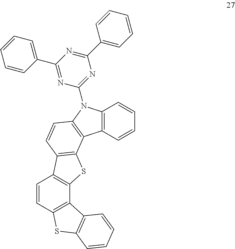


Hereinafter, an organic optoelectric device according to an example embodiment including an organic compound according to an embodiment is described.
According to the present example embodiment, the organic optoelectric device may be a suitable device to convert electrical energy into photoenergy or vice versa, and may be, for example, an organic photoelectric device, an organic light emitting diode, an organic solar cell, an organic photo-conductor drum, etc.
Herein, an organic light emitting diode as an example of an organic optoelectric device is described referring to the drawings.
In the example embodiment shown in FIG. 1 , an organic light emitting diode 100 includes an anode 120 and a cathode 110 facing each other, and an organic layer 105 interposed between the anode 120 and cathode 110.
The anode 120 may be made of a conductor having a high work function to help hole injection, and may be, for example, metal, metal oxide, and/or a conductive polymer. The anode 120 may be, for example, a metal nickel, platinum, vanadium, chromium, copper, zinc, gold, and the like or an alloy thereof; a metal oxide such as zinc oxide, indium oxide, indium tin oxide (ITO), indium zinc oxide (IZO), and the like; a combination of metal and oxide such as ZnO and Al or SnO2 and Sb; a conductive polymer such as poly(3-methylthiophene), poly(3,4-(ethylene-1,2-dioxy)thiophene) (PEDT), polypyrrole, and polyaniline, etc.
The cathode 110 may be made of a conductor having a low work function to help electron injection, and may be, for example, metal, metal oxide and/or a conductive polymer. The cathode 110 may be, for example, a metal or an alloy thereof such as magnesium, calcium, sodium, potassium, titanium, indium, yttrium, lithium, gadolinium, aluminum, silver, tin, lead, cesium, barium, and the like; a multi-layer structure material such as LiF/Al, LiO2/Al, LiF/Ca, LiF/Al and BaF2/Ca, etc.
The organic layer 105 may include an emission layer 130 including an above-described organic compound according to an embodiment.
The emission layer 130 may include for example, the organic compound alone, a mixture of at least two kinds of the organic compound, or a mixture of the organic compound and other compounds. When the organic compound is mixed with other compounds, for example, they may be mixed as a host and a dopant, and the organic compound may be, for example, a host. The host may be, for example, a phosphorescent host or fluorescent host, and may be, for example, a green phosphorescent host.
When the organic compound is included as a host, a dopant may be an inorganic, organic, or organic/inorganic compound, and may be selected from general dopants.
In the example embodiment shown in FIG. 2 , an organic light emitting diode 200 further includes a hole auxiliary layer 140 as well as the emission layer 130. The hole auxiliary layer 140 may further increase hole injection and/or hole mobility between the anode 120 and emission layer 130 and may block electrons. The hole auxiliary layer 140 may be, for example, a hole transport layer (HTL), a hole injection layer (HIL), and/or an electron blocking layer, and may include at least one layer. The organic compound may be included in the emission layer 130 and/or the hole auxiliary layer 140.
In an example embodiment, an organic light emitting diode may further include an auxiliary electron transport layer, an electron transport layer (ETL), an electron injection layer (EIL), an auxiliary hole injection layer, a hole injection layer (HIL), and the like, as an organic thin layer 105 in FIG. 1 or FIG. 2 . The organic compound may be included in the emission layer 130 and/or the hole auxiliary layer 140 or in the auxiliary electron transport layer (ETL), electron transport layer (ETL), electron injection layer (EIL), auxiliary hole transport layer (HTL), and/or hole injection layer (HIL).
The organic light emitting diodes 100 and 200 may be manufactured by, e.g., forming an anode or a cathode on a substrate, forming an organic layer in accordance with a dry coating method such as evaporation, sputtering, plasma plating, and ion plating, or a wet coating method such as spin coating, slit coating, dipping, flow coating, and inkjet printing; and forming a cathode or an anode thereon.
The organic light emitting diode may be applied to an organic light emitting diode (OLED) display.
The following Examples and Comparative Examples are provided in order to highlight characteristics of one or more embodiments, but it will be understood that the Examples and Comparative Examples are not to be construed as limiting the scope of the embodiments, nor are the Comparative Examples to be construed as being outside the scope of the embodiments. Further, it will be understood that the embodiments are not limited to the particular details described in the Examples and Comparative Examples.
Synthesis of Organic Compound


100 g (465 mmol) of methyl 2-bromobenzoate was dissolved in 1,200 mL of tetrahydrofuran (THF) under a nitrogen environment, 127 g (558 mmol) of dibenzothiophen-4-yl boronic acid and 4.65 g (5.37 mmol) of tetrakis(triphenylphosphine)palladium were added thereto, and the mixture was agitated. 161 g (1,162 mmol) of potassium carbonate saturated in water was added thereto, and the resulting mixture was heated and refluxed at 80° C. for 18 hours. When the reaction was complete, water was added to the reaction solution, the mixture was extracted with dichloromethane (DCM) and treated with anhydrous MgSO4 to remove moisture, and the extract was filtered and concentrated under a reduced pressure. The obtained residue was separated and purified through flash column chromatography, obtaining 120 g (81%) of an intermediate I-1.
HRMS (70 eV, EI+): m/z calcd for C20H14O2S: 318.0715. found: 318.
Elemental Analysis: C, 75%; H, 4%

110 g (345 mmol) of the intermediate I-1 was dissolved in 3,500 mL of tetrahydrofuran (THF) under a nitrogen environment, and the solution was cooled down to 0° C. 288 mL (864 mmol) of 3.0 M methyl magnesium bromide dissolved in diethyl ether was slowly added thereto in a dropwise fashion for 1 hour. The mixture was agitated at room temperature for 19 hours. When the reaction was complete, 55.4 g (1,035 mmol) of ammonium chloride dissolved in 300 mL of water was added thereto to neutralize the reaction solution. The mixture was extracted with dichloromethane and treated with anhydrous MgSO4 to remove moisture, and the extract was filtered and concentrated under reduced pressure, obtaining 108 g (98%) of an intermediate I-2.
HRMS (70 eV, EI+): m/z calcd for C21H18OS: 318.1078. found: 318.
Elemental Analysis: C, 79%; H, 6%

105 g (330 mmol) of the intermediate I-2 was dissolved in 900 mL of dichloromethane under a nitrogen environment, and the mixture was cooled down to 0° C. 70.3 g (495 mmol) of boron trifluoride diethyl etherate was slowly added in a dropwise fashion for one hour. Subsequently, the mixture was agitated at room temperature for 5 hours. When the reaction was complete, 41.6 g (495 mmol) of sodium bicarbonate dissolved in 450 mL of water was added to the reaction solution to neutralize the reaction solution. The mixture was extracted with dichloromethane and treated with anhydrous MgSO4 to remove moisture, and the obtained residue was separated and purified through flash column chromatography, obtaining 79.3 g (80%) of an intermediate I-3.
HRMS (70 eV, EI+): m/z calcd for C21H16S: 300.0973. found: 300.
Elemental Analysis: C, 84%; H, 5%

75 g (250 mmol) of the intermediate I-3 was dissolved in 2,500 mL of tetrahydrofuran (THF) under a nitrogen environment, and the mixture was cooled down to −78° C. 150 mL (375 mmol) of 2.5 M n-BuLi dissolved in hexane was slowly added thereto in a dropwise fashion for 10 minutes. Subsequently, the mixture was agitated at −78° C. for 6 hours, 70.5 g (375 mmol) of triisopropylborate was added thereto, and the mixture was agitated at room temperature for 16 hours. When the reaction was complete, 500 mL (500 mmol) of 1N HCl was added thereto to neutralize the reaction solution. The mixture was extracted with ethyl acetate (EA) and treated with anhydrous MgSO4 to remove moisture, and the obtained residue was washed with hexane and dichloromethane to remove impurities, obtaining 68.0 g (79%) of an intermediate I-4.
HRMS (70 eV, EI+): m/z calcd for C21H17BO2S: 344.1042. found: 344.
Elemental Analysis: C, 73%; H, 5%

31.8 g (157 mmol) of 1-bromo-2-nitrobenzene was dissolved in 500 mL of tetrahydrofuran (THF) under a nitrogen environment, 65 g (189 mmol) of the intermediate I-4 and 1.81 g (1.57 mmol) of tetrakis(triphenylphosphine)palladium were added thereto, and the mixture was agitated. 54.2 g (393 mmol) of potassium carbonate saturated in water was added thereto, and the mixture was heated and refluxed at 80° C. for 13 hours. When the reaction was complete, water was added to the reaction solution, the mixture was extracted with dichloromethane, and the extract wad treated with anhydrous MgSO4 to remove moisture and filtered and concentrated under a reduced pressure. The obtained residue was separated and purified through flash column chromatography, obtaining 61.5 g (93%) of an intermediate I-5.
HRMS (70 eV, EI+): m/z calcd for C27H19NO2S: 421.1136. found: 421.
Elemental Analysis: C, 77%; H, 5%

60 g (142 mmol) of the intermediate I-5 was dissolved in 300 mL of triethylphosphite under a nitrogen environment, and the solution was heated and refluxed at 180° C. for 5 hours. When the reaction was complete, water was added to the reaction solution, and the mixture for precipitation, and a precipitate produced therein was filtered. The obtained residue was separated and purified through flash column chromatography, obtaining 42.0 g (76%) of an intermediate I-6.
HRMS (70 eV, EI+): m/z calcd for C27H19NS: 389.1238. found: 389.
Elemental Analysis: C, 83%; H, 5%

100 g (465 mmol) of methyl 2-bromobenzoate was dissolved in 1,100 mL of tetrahydrofuran (THF) under a nitrogen environment, 118 g (558 mmol) of dibenzofuran-4-yl boronic acid and 4.65 g (5.37 mmol) of tetrakis(triphenylphosphine)palladium were added thereto, and the mixture was agitated. 161 g (1,162 mmol) of potassium carbonate saturated in water was added thereto, and the mixture was heated and refluxed at 80° C. for 20 hours. When the reaction was complete, water was added to the reaction solution, the mixture was extracted with dichloromethane and treated with anhydrous MgSO4 to remove moisture, and the extract was filtered and concentrated under a reduced pressure. The obtained residue was separated and purified through flash column chromatography, obtaining 110 g (78%) of an intermediate I-7.
HRMS (70 eV, EI+): m/z calcd for C20H14O3: 302.0943. found: 302.
Elemental Analysis: C, 79%; H, 5%

105 g (347 mmol) of the intermediate I-7 was dissolved in 1,100 mL of tetrahydrofuran (THF) under a nitrogen environment, and the solution was cooled down to 0° C. 289 mL (868 mmol) of 3.0 M methyl magnesium bromide dissolved in diethyl ether was slowly added thereto in a dropwise fashion for one hour. Then, the mixture was agitated at room temperature for 20 hours. When the reaction was complete, 55.7 g (1,041 mmol) of ammonium chloride dissolved in 300 mL of water was added thereto to neutralize the reaction solution. The resulting reaction solution was extracted with dichloromethane and treated with anhydrous MgSO4 to remove moisture, and the extract was filtered and concentrated under a reduced pressure, obtaining 97.6 g (93%) of an intermediate I-8.
HRMS (70 eV, EI+): m/z calcd for C21H18O2: 302.1307. found: 302.
Elemental Analysis: C, 83%; H, 6%

95 g (297 mmol) of the intermediate I-8 was dissolved in 500 mL of dichloromethane under a nitrogen environment, and the solution was cooled down to 0° C. 63.2 g (445 mmol) of boron trifluoride diethyl etherate was slowly added thereto in a dropwise fashion for one hour. Then, the mixture was agitated at room temperature for 5 hours. When the reaction was complete, 37.4 g (446 mmol) of sodium bicarbonate dissolved in 380 mL of water was added thereto to neutralize the reaction solution. The mixture was extracted with dichloromethane and treated with anhydrous MgSO4 to remove moisture, and the obtained residue was separated and purified through column chromatography, obtaining 64.2 g 76%) of an intermediate I-9.
HRMS (70 eV, EI+): m/z calcd for C21H16O: 284.1201. found: 284.
Elemental Analysis: C, 89%; H, 6%

60 g (211 mmol) of the intermediate I-9 was dissolved in 600 mL of tetrahydrofuran (THF) under a nitrogen environment, and the solution was cooled down to −78° C. 127 mL (367 mmol) of 2.5 M n-BuLi dissolved in hexane was slowly added thereto in a dropwise fashion for 10 minutes. Then, the mixture was agitated at −78° C. for 6 hours, 69.0 g (367 mmol) of triisopropylborate was added thereto, and the mixture was agitated at room temperature for 13 hours. When the reaction was complete, 422 mL (422 mmol) of 1N HCl was added thereto to neutralize the reaction solution. The resultant was extracted with ethyl acetate (EA) and treated with anhydrous MgSO4 to remove moisture, and the obtained residue was washed with hexane and dichloromethane to remove impurities, obtaining 53.3 g (77%) of an intermediate I-10.
HRMS (70 eV, EI+): m/z calcd for C21H17BO3: 328.1271. found: 328.
Elemental Analysis: C, 77%; H, 5%

25.6 g (127 mmol) of 1-bromo-2-nitrobenzene was dissolved in 400 mL of tetrahydrofuran (THF) under a nitrogen environment, 50 g (152 mmol) of the intermediate I-10 and 1.47 g (1.27 mmol) of tetrakis(triphenylphosphine)palladium was added thereto, and the mixture was agitated. 43.9 g (318 mmol) of potassium carbonate saturated in water was added thereto, and the mixture was heated and refluxed at 80° C. for 15 hours. When the reaction was complete, water was added to the reaction solution, the mixture was extracted with dichloromethane and treated with anhydrous MgSO4 to remove moisture, and the extract was filtered and concentrated under a reduced pressure. The obtained residue was separated and purified through flash column chromatography, obtaining 46.3 g (90%) of an intermediate I-11.
HRMS (70 eV, EI+): m/z calcd for C27H19NO3: 405.1365. found: 405.
Elemental Analysis: C, 80%; H, 5%

45 g (111 mmol) of the intermediate I-11 was dissolved in 250 mL of triethylphosphite under a nitrogen environment, and the solution was heated and refluxed at 180° C. for 7 hours. When the reaction was complete, water was added to the reaction solution for precipitation, and a precipitate produced therein was filtered. The obtained residue was separated and purified through flash column chromatography, obtaining 30.3 g (73%) of an intermediate I-12.
HRMS (70 eV, EI+): m/z calcd for C271-119NO: 373.1467. found: 373.
Elemental Analysis: C, 87%; H, 5%

100 g (374 mmol) of 2-chloro-4,6-diphenyl-1,3,5-triazine was dissolved in 900 mL of tetrahydrofuran (THF) under a nitrogen environment, 70.1 g (448 mmol) of 3-chlorophenylboronic acid and 4.32 g (3.74 mmol) of tetrakis(triphenylphosphine)palladium were added thereto, and the mixture was agitated. 129 g (935 mmol) of potassium carbonate was added thereto, and the mixture was heated and refluxed at 80° C. for 8 hours. When the reaction was complete, water was added to the reaction solution, the mixture was extracted with dichloromethane and treated with anhydrous MgSO4 to remove moisture, and the extract was filtered and concentrated under a reduced pressure. The obtained residue was separated and purified through flash column chromatography, obtaining 117 g (91%) of an intermediate I-13.
HRMS (70 eV, EI+): m/z calcd for C21H14ClN3: 343.0876. found: 343.
Elemental Analysis: C, 73%; H, 4%

20 g (51.3 mmol) of the intermediate I-6 was dissolved in 200 mL of toluene under a nitrogen environment, 12.6 g (61.6 mmol) of iodobenzene, 0.47 g (0.51 mmol) of tris(diphenylideneacetone)dipalladium(0), 0.52 g, (2.57 mmol) of tris-tert-butylphosphine, and 5.92 g (61.6 mmol) of sodium tert-butoxide were sequentially added thereto, and the mixture was heated and refluxed at 100° C. for 8 hours. When the reaction was complete, water was added to the reaction solution, the mixture was extracted with dichloromethane and treated with anhydrous MgSO4 to remove moisture, and the extract was filtered and concentrated under a reduced pressure. The obtained residue was separated and purified through flash column chromatography, obtaining 20.3 g (85%) of a compound 1.
HRMS (70 eV, EI+): m/z calcd for C33H23NS: 465.1551. found: 465.
Elemental Analysis: C, 85%; H, 5%

20 g (53.6 mmol) of the intermediate I-12 was dissolved in 170 mL of toluene nitrogen under a nitrogen environment, 13.1 g (64.3 mmol) of iodobenzene, 0.49 g (0.54 mmol) of tris(diphenylideneacetone)dipalladium( )), 0.54 g (2.68 mmol) of tris-tert-butylphosphine, and 6.18 g (64.3 mmol) of sodium tert-butoxide were sequentially added thereto, and the mixture was heated and refluxed at 100° C. for 10 hours. When the reaction was complete, water was added to the reaction solution, the mixture was extracted with dichloromethane and treated with anhydrous MgSO4 to remove moisture, and the extract was filtered and concentrated under a reduced pressure. The obtained residue was separated and purified through flash column chromatography, obtaining 19.5 g (81%) of a compound 2.
HRMS (70 eV, EI+): m/z calcd for C33H23NO: 449.1780. found: 449.
Elemental Analysis: C, 88%; H, 5%

20 g (51.3 mmol) of the intermediate I-6 was dissolved in 170 mL of toluene under a nitrogen environment, 13.7 g (51.3 mmol) of 2-chloro-4,6-diphenyl-1,3,5-triazine, 1.41 g (1.54 mmol) of tris(diphenylideneacetone)dipalladium(0), 1.56 g (7.70 mmol) of tris-tert-butylphosphine, and 5.92 g (61.6 mmol) of sodium tert-butoxide were sequentially added thereto, and the mixture was heated and refluxed at 100° C. for 15 hours. When the reaction was complete, water was added to the reaction solution, the mixture was extracted with dichloromethane and treated with anhydrous MgSO4 to remove moisture, and the extract was filtered and concentrated under a reduced pressure. The obtained residue was separated and purified through flash column chromatography, obtaining 25.5 g (80%) of a compound 25.
HRMS (70 eV, EI+): m/z calcd for C42H28N4S: 620.2035. found: 620.
Elemental Analysis: C, 81%; H, 5%

20 g (53.6 mmol) of the intermediate I-12 was dissolved in 170 mL of toluene under a nitrogen environment, 14.3 g (53.6 mmol) of 2-chloro-4,6-diphenyl-1,3,5-triazine, 1.47 g (1.61 mmol) of tris(diphenylideneacetone)dipalladium(0), 1.63 g (8.04 mmol) of tris-tert-butylphosphine, and 6.18 g (64.3 mmol) of sodium tert-butoxide were sequentially added thereto, and the mixture was heated and refluxed at 100° C. for 18 hours. When the reaction was complete, water was added to the reaction solution, the mixture was extracted with dichloromethane and treated with anhydrous MgSO4 to remove moisture, and the extract was filtered and concentrated under a reduced pressure. The obtained residue was separated and purified through flash column chromatography, obtaining 25.0 g (77%) of a compound 26.
HRMS (70 eV, EI+): m/z calcd for C42H28N4O: 604.2263. found: 604.
Elemental Analysis: C, 83%; H, 5%

20 g (51.3 mmol) of the intermediate I-6 was dissolved in 190 mL of toluene under a nitrogen environment, 17.6 g (51.3 mmol) of the intermediate I-13, 1.41 g (1.54 mmol) of tris(diphenylideneacetone)dipalladium(0), 1.56 g (7.70 mmol) of tris-tert-butylphosphine, and 5.92 g (61.6 mmol) of sodium tert-butoxide were sequentially added thereto, and the mixture was heated and refluxed at 100° C. for 16 hours. When the reaction was complete, water was added to the reaction solution, the mixture was extracted with dichloromethane and treated with anhydrous MgSO4 to remove moisture, and the extract was filtered and concentrated under a reduced pressure. The obtained residue was separated and purified through flash column chromatography, obtaining 27.9 g (78%) of a compound 57.
HRMS (70 eV, EI+): m/z calcd for C48H32N4S: 696.2348. found: 696.
Elemental Analysis: C, 83%; H, 5%

20 g (53.6 mmol) of the intermediate I-12 was dissolved in 200 mL of toluene under a nitrogen environment, 18.4 g (53.6 mmol) of the intermediate I-13, 1.47 g (1.61 mmol) of tris(diphenylideneacetone)dipalladium(0), 1.63 g (8.04 mmol) of tris-tert-butylphosphine, and 6.18 g (64.3 mmol) of sodium tert-butoxide were sequentially added thereto, and the mixture was heated and refluxed at 100° C. for 21 hours. When the reaction was complete, water was added to the reaction solution, the mixture was extracted with dichloromethane and treated with anhydrous MgSO4 to remove moisture, and the extract was filtered and concentrated under a reduced pressure. The obtained residue was separated and purified through flash column chromatography, obtaining 27.4 g (75%) of a compound 58.
FIRMS (70 eV, EI+): m/z calcd for C48H32N4O: 680.2576. found: 680.
Elemental Analysis: C, 85%; H, 5%
The compound 1 obtained in Example 1 was used as a host, and Ir(PPy)3 was used as a dopant to manufacture an organic light emitting diode. 1,000 Å-thick ITO was used as an anode, and 1,000 Å-thick aluminum (Al) was used as a cathode.
Specifically, an organic light emitting diode was manufactured by manufacturing the anode by cutting an ITO glass substrate having 15 Ω/cm2 of sheet resistance into a size of 50 mm×50 mm×0.7 mm and cleaning with a ultrasonic wave in acetone, isopropyl alcohol, and pure water respectively for 15 minutes and with UV ozone for 30 minutes. On the substrate upper, a 800 Å-thick hole transport layer (HTL) was formed by depositing N4,N4′-di(naphthalen-1-yl)-N4,N4′-diphenylbiphenyl-4,4′-diamine (NPB) (80 nm) at a vacuum degree of 650×10−7 Pa at a deposition speed ranging from 0.1 to 0.3 nm/s. Subsequently, a 300 Å-thick emission layer was formed by vacuum-depositing the compound 1 obtained in Example 1 under the same vacuum deposition condition in Example 1 and simultaneously depositing Ir(PPy)3 as a phosphorescent dopant. 7 wt % of the phosphorescent dopant was deposited by adjusting a depositing rate of the phosphorescent dopant based on 100 wt % of the total amount of the emission layer. On the emission layer, a 50 Å-thick hole blocking layer was formed by using bis(2-methyl-8-quinolinolate)-4-(phenylphenolato)aluminum (BAlq) under the same deposition condition. Subsequently, a 200 Å-thick electron transport layer (ETL) was formed by depositing Alq3 under the same vacuum deposition condition. LiF and Al were sequentially deposited to from a cathode on the electron transport layer (ETL), manufacturing an organic photoelectric device.
The organic photoelectric device has a structure of ITO/NPB (80 nm)/EML (compound 1 (93 wt %)+Ir(PPy)3 (7 wt %), 30 nm)/Balq (5 nm)/Alq3 (20 nm)/LiF (1 nm)/Al (100 nm).
An organic light emitting diode was manufactured according to the same method as Example 7 except for using the compound 2 of Example 2 instead of the compound 1 of Example 1.
An organic light emitting diode was manufactured according to the same method as Example 7 except for using the compound 25 of Example 3 instead of the compound 1 of Example 1.
An organic light emitting diode was manufactured according to the same method as Example 7 except for using the compound 26 of Example 4 instead of the compound 1 of Example 1.
An organic light emitting diode was manufactured according to the same method as Example 7 except for using the compound 57 of Example 5 instead of the compound 1 of Example 1.
An organic light emitting diode was manufactured according to the same method as Example 7 except for using the compound 58 of Example 6 instead of the compound 1 of Example 1.
An organic light emitting diode was manufactured according to the same method as Example 7 except for using CBP instead of the compound 1 of Example 1. The CBP has the structure shown below.
An organic light emitting diode was manufactured according to the same method as Example 7 except for using HOST1 instead of the compound 1 of Example 1. The HOST1 has the structure shown below.
An organic light emitting diode was manufactured according to the same method as Example 7 except for using HOST2 instead of the compound 1 of Example 1. The HOST2 has the structure shown below.
Structures of the NPB, BAlq, CBP, Ir(PPy)3, HOST1 and HOST2 used for manufacture the organic light emitting diode are as follows.

Measurement of Performance of Organic Light Emitting Diode
Current density and luminance changes depending on a voltage and luminous efficiency of each organic light emitting diode according to Examples 7 to 12 and Comparative Examples 1 to 3 were measured. The measurements were specifically performed in the following method, and the results are provided in the following Table 1.
(1) Measurement of Current Density Change Depending on Voltage Change
Current values flowing in the unit device of the manufactured organic light emitting diodes were measured for, while increasing the voltage from 0 V to 10 V using a current-voltage meter (Keithley 2400), and the measured current values were divided by an area to provide the results.
(2) Measurement of Luminance Change depending on Voltage Change
Luminance of the manufactured organic light emitting diodes was measured for luminance, while increasing the voltage from 0 V to 10 V using a luminance meter (Minolta Cs-1000A).
(3) Measurement of Luminous Efficiency
Current efficiency (cd/A) at the same current density (10 mA/cm2) were calculated by using the luminance, current density, and voltages (V) from the items (1) current density change depending on voltage change and (2) luminance change depending on voltage change.
| TABLE 1 | ||||
| Compound used in | Driving | Color | Efficiency | |
| Device | emission layer | voltage (V) | (EL color) | (cd/A) |
| Example 7 | Compound 1 | 4.5 | Green | 55.0 |
| Example 8 | Compound 2 | 4.6 | Green | 53.2 |
| Example 9 | Compound 25 | 4.3 | Green | 66.8 |
| Example 10 | Compound 26 | 4.3 | Green | 64.6 |
| Example 11 | Compound 57 | 4.4 | Green | 58.9 |
| Example 12 | Compound 58 | 4.5 | Green | 56.5 |
| Comparative | CBP | 4.8 | Green | 31.4 |
| Example 1 | ||||
| Comparative | HOST1 | 5.0 | Green | 45.0 |
| Example 2 | ||||
| Comparative | HOST2 | 4.8 | Green | 52.1 |
| Example 3 | ||||
Referring to Table 1, materials for the emission layers in Examples 7 to 12 increased luminous efficiency but decreased a driving voltage compared with materials for the emission layers according to Comparative Examples 1 to 3. The results suggest that a device having a low voltage but high efficiency may be manufactured.
By way of summation and review, examples of the organic optoelectric device may include an organic photoelectric device, an organic light emitting diode, an organic solar cell, and an organic photo-conductor drum, and the like.
Among them, the organic light emitting diode (OLED) has recently drawn attention due to an increase in demand for flat panel displays. The organic light emitting diode converts electrical energy into light by applying current to an organic light emitting material, and has a structure in which an organic layer is interposed between an anode and a cathode. The organic layer may include an emission layer and optionally an auxiliary layer, and the auxiliary layer may include at least one selected from, for example, a hole injection layer, a hole transport layer, an electron blocking layer, an electron transport layer, an electron injection layer, and a hole blocking layer in order to improve efficiency and stability of an organic light emitting diode.
Performance of an organic light emitting diode may be affected by characteristics of the organic layer, and among them, may be significantly affected by characteristics of an organic material of the organic layer. An organic material with increased hole and electron mobility and simultaneously increased electrochemical stability would be useful for an organic light emitting diode applied to a large-size flat panel display.
As described above, embodiments may provide an organic compound capable of realizing an organic optoelectric device having improved driving voltage and efficiency. Embodiments may also provide an organic optoelectric device including the organic compound. Embodiments may also provide a display device including the organic optoelectric device. Embodiments may provide organic optoelectric device having high efficiency and long life-span.
Example embodiments have been disclosed herein, and although specific terms are employed, they are used and are to be interpreted in a generic and descriptive sense only and not for purpose of limitation. In some instances, as would be apparent to one of ordinary skill in the art as of the filing of the present application, features, characteristics, and/or elements described in connection with a particular embodiment may be used singly or in combination with features, characteristics, and/or elements described in connection with other embodiments unless otherwise specifically indicated. Accordingly, it will be understood by those of skill in the art that various changes in form and details may be made without departing from the spirit and scope of the present invention as set forth in the following claims.
Claims (13)
1. An organic compound represented by a combination of a moiety represented by the following Chemical Formula 1, a moiety represented by the following Chemical Formula 2, and a moiety represented by the following Chemical Formula 3:

wherein, in the Chemical Formulae 1 to 3,
X1 and X3 are independently NRa, CRbRc, SiRdRe, O, S, SO, or SO2, provided that when one of X1 and X3 is NRa, the other of X1 and X3 is not NRa,
X2 is O, S, SO, or SO2,
each Z is independently CRf or N,
two *'s of the Chemical Formula 1 are bonded with adjacent two *'s of the Chemical Formula 2 to form a fused ring,
two *'s of the Chemical Formula 3 are bonded with another adjacent two *'s of the Chemical Formula 2 to form a fused ring,
*'s not forming a fused ring in the Chemical Formula 2 are independently CRg or N, and
R1 to R4 and Ra to Rg are independently hydrogen, deuterium, a substituted or unsubstituted C1 to C30 alkyl group, a substituted or unsubstituted C3 to C30 cycloalkyl group, a substituted or unsubstituted C3 to C30 heterocycloalkyl group, a substituted or unsubstituted C6 to C30 aryl group, a substituted or unsubstituted C3 to C30 heteroaryl group, a substituted or unsubstituted amine group, a substituted or unsubstituted C6 to C30 arylamine group, a substituted or unsubstituted C6 to C30 heteroarylamine group, a substituted or unsubstituted C1 to C30 alkoxy group, a substituted or unsubstituted C2 to C30 alkoxycarbonyl group, a substituted or unsubstituted C2 to C30 alkoxycarbonylamino group, a substituted or unsubstituted C7 to C30 aryloxycarbonylamino group, a substituted or unsubstituted C1 to C30 sulfamoylamino group, a substituted or unsubstituted C2 to C30 alkenyl group, a substituted or unsubstituted C2 to C30 alkynyl group, a substituted or unsubstituted silyl group, a substituted or unsubstituted silyloxy group, a substituted or unsubstituted C1 to C30 acyl group, a substituted or unsubstituted C1 to C20 acyloxy group, a substituted or unsubstituted C1 to C20 acylamino group, a substituted or unsubstituted C1 to C30 sulfonyl group, a substituted or unsubstituted C1 to C30 alkylthiol group, a substituted or unsubstituted C1 to C30 heterocyclothiol group, a substituted or unsubstituted C6 to C30 arylthiol group, a substituted or unsubstituted C1 to C30 heteroarylthiol group, a substituted or unsubstituted C1 to C30 ureide group, a halogen, a halogen-containing group, a cyano group, a hydroxyl group, an amino group, a nitro group, a carboxyl group, a ferrocenyl group, or a combination thereof.
2. The organic compound as claimed in claim 1 , wherein the organic compound is represented by one of the following Chemical Formulae 4 to 6:

wherein, in the Chemical Formulae 4 to 6,
X1 and X3 are independently NRa, CRbRc, SiRdRe, O, S, SO, or SO2, provided that when one of X1 of X1 and X3 is not NRa,
X2 is O, S, SO, or SO2,
each Z is independently CRf or N, and
R1 to R4 and Ra to Rf are independently hydrogen, deuterium, a substituted or unsubstituted C1 to C30 alkyl group, a substituted or unsubstituted C3 to C30 cycloalkyl group, a substituted or unsubstituted C3 to C30 heterocycloalkyl group, a substituted or unsubstituted C6 to C30 aryl group, a substituted or unsubstituted C3 to C30 heteroaryl group, a substituted or unsubstituted amine group, a substituted or unsubstituted C6 to C30 arylamine group, a substituted or unsubstituted C6 to C30 heteroarylamine group, a substituted or unsubstituted C7 to C30 alkoxy group, a substituted or unsubstituted C2 to C30 alkoxycarbonyl group, a substituted or unsubstituted C2 to C30 alkoxycarbonylamino group, a substituted or unsubstituted C7 to C30 aryloxycarbonylamino group, a substituted or unsubstituted C1 to C30 sulfamoylamino group, a substituted or unsubstituted C2 to C30 alkenyl group, a substituted or unsubstituted C2 to C30 alkynyl group, a substituted or unsubstituted silyl group, a substituted or unsubstituted silyloxy group, a substituted or unsubstituted C1 to C30 acyl group, a substituted or unsubstituted C1 to C20 acyloxy group, a substituted or unsubstituted C1 to C20 acylamino group, a substituted or unsubstituted C1 to C30 sulfonyl group, a substituted or unsubstituted C1 to C30 alkylthiol group, a substituted or unsubstituted C1 to C30 heterocyclothiol group, a substituted or unsubstituted C6 to C30 arylthiol group, a substituted or unsubstituted C1 to C30 heteroarylthiol group, a substituted or unsubstituted C1 to C30 ureide group, a halogen, a halogen-containing group, a cyano group, a hydroxyl group, an amino group, a nitro group, a carboxyl group, a ferrocenyl group, or a combination thereof.
3. The organic compound as claimed in claim 2 , wherein the organic compound represented by the Chemical Formula 4 is represented by one of the following Chemical Formulae 4a to 4c, the organic compound represented by the Chemical Formula 5 is represented by one of the following Chemical Formulae 5a to 5c, and the organic compound represented by the Chemical Formula 6 is represented by one of the following Chemical Formulae 6b and 6c:


wherein, in the Chemical Formulae 4a to 6c,
X1 and X3 are independently CRbRc, SiRdRe, O, S, SO, or SO2,
X2 is O, S, SO, or SO2,
each Z is independently CRf or N, and
R1 to R4 and Ra to Rf are independently hydrogen, deuterium, a substituted or unsubstituted C1 to C30 alkyl group, a substituted or unsubstituted C3 to C30 cycloalkyl group, a substituted or unsubstituted C3 to C30 heterocycloalkyl group, a substituted or unsubstituted C6 to C30 aryl group, a substituted or unsubstituted C3 to C30 heteroaryl group, a substituted or unsubstituted amine group, a substituted or unsubstituted C6 to C30 arylamine group, a substituted or unsubstituted C6 to C30 heteroarylamine group, a substituted or unsubstituted C1 to C30 alkoxy group, a substituted or unsubstituted C2 to C30 alkoxycarbonyl group, a substituted or unsubstituted C2 to C30 alkoxycarbonylamino group, a substituted or unsubstituted C7 to C30 aryloxycarbonylamino group, a substituted or unsubstituted C1 to C30 sulfamoylamino group, a substituted or unsubstituted C2 to C30 alkenyl group, a substituted or unsubstituted C2 to C30 alkynyl group, a substituted or unsubstituted silyl group, a substituted or unsubstituted silyloxy group, a substituted or unsubstituted C1 to C30 acyl group, a substituted or unsubstituted C1 to C20 acyloxy group, a substituted or unsubstituted C1 to C20 acylamino group, a substituted or unsubstituted C1 to C30 sulfonyl group, a substituted or unsubstituted C1 to C30 alkylthiol group, a substituted or unsubstituted C1 to C30 heterocyclothiol group, a substituted or unsubstituted C6 to C30 arylthiol group, a substituted or unsubstituted C1 to C30 heteroarylthiol group, a substituted or unsubstituted C1 to C30 ureide group, a halogen, a halogen-containing group, a cyano group, a hydroxyl group, an amino group, a nitro group, a carboxyl group, a ferrocenyl group, or a combination thereof.
4. The organic compound as claimed in claim 1 , wherein R1 to R4 and Ra to Rf are independently hydrogen, deuterium, a substituted or unsubstituted C1 to C30 alkyl group, a substituted or unsubstituted C6 to C30 aryl group, a substituted or unsubstituted C3 to C30 heteroaryl group, a substituted or unsubstituted amine group, a substituted or unsubstituted C6 to C30 arylamine group, a substituted or unsubstituted C6 to C30 heteroarylamine group, or a combination thereof.
5. The organic compound as claimed in claim 4 , wherein at least one of R1 to R4 and Ra to Rf is a substituted or unsubstituted C6 to C30 aryl group, a substituted or unsubstituted C3 to C30 heteroaryl group, a substituted or unsubstituted amine group, a substituted or unsubstituted C6 to C30 arylamine group, a substituted or unsubstituted C6 to C30 heteroarylamine group, or a combination thereof.
6. The organic compound as claimed in claim 5 , wherein at least one of R1 to R4 and Ra to Rf is one of the substituted or unsubstituted functional groups listed in the following Group 1:

wherein, in the Group 1,
each Z is independently N, C, or CRh,
each W is independently N, O, S, SO, SO2, NRi, CRj, or CRkRl,
wherein Rh to Rl are independently hydrogen, deuterium, a substituted or unsubstituted C1 to C30 alkyl group, a substituted or unsubstituted C3 to C30 cycloalkyl group, a substituted or unsubstituted C3 to C30 heterocycloalkyl group, a substituted or unsubstituted C6 to C30 aryl group, a substituted or unsubstituted C3 to C30 heteroaryl group, a substituted or unsubstituted amine group, a substituted or unsubstituted C6 to C30 arylamine group, a substituted or unsubstituted C6 to C30 heteroarylamine group, a substituted or unsubstituted C1 to C30 alkoxy group, a substituted or unsubstituted C2 to C30 alkoxycarbonyl group, a substituted or unsubstituted C2 to C30 alkoxycarbonylamino group, a substituted or unsubstituted C7 to C30 aryloxycarbonylamino group, a substituted or unsubstituted C1 to C30 sulfamoylamino group, a substituted or unsubstituted C2 to C30 alkenyl group, a substituted or unsubstituted C2 to C30 alkynyl group, a substituted or unsubstituted silyl group, a substituted or unsubstituted silyloxy group, a substituted or unsubstituted C1 to C30 acyl group, a substituted or unsubstituted C1 to C20 acyloxy group, a substituted or unsubstituted C1 to C20 acylamino group, a substituted or unsubstituted C1 to C30 sulfonyl group, a substituted or unsubstituted C1 to C30 alkylthiol group, a substituted or unsubstituted C1 to C30 heterocyclothiol group, a substituted or unsubstituted C6 to C30 arylthiol group, a substituted or unsubstituted C1 to C30 heteroarylthiol group, a substituted or unsubstituted C1 to C30 ureide group, a halogen, a halogen-containing group, a cyano group, a hydroxyl group, an amino group, a nitro group, a carboxyl group, a ferrocenyl group, or a combination thereof, and
* is a linking point, and is positioned at one of elements of the functional group.
7. The organic compound as claimed in claim 6 , wherein the functional groups listed in the Group 1 is one of the substituted or unsubstituted functional groups listed in the Group 2:


wherein, in the Group 2,
* is a linking point and is positioned at one of elements of the functional group.
8. The organic compound as claimed in claim 1 , wherein the organic compound is one of organic compounds listed in the following Group 3:


9. An organic optoelectric device, comprising:
an anode and a cathode facing each other, and
at least one organic layer positioned between the anode and the cathode, wherein the organic layer includes the organic compound as claimed in claim 1 .
10. The organic optoelectric device as claimed in claim 9 , wherein:
the organic layer includes an emission layer, and
the emission layer includes the organic compound.
11. The organic optoelectric device as claimed in claim 10 , wherein the organic compound is included in the emission layer as a host.
12. The organic optoelectric device as claimed in claim 10 , wherein:
the organic layer includes at least one auxiliary layer selected from a hole injection layer, a hole transport layer, an electron blocking layer, an electron transport layer, an electron injection layer, and a hole blocking layer, and
the auxiliary layer includes the organic compound.
13. A display device comprising the organic optoelectric device as claimed in claim 9 .
Applications Claiming Priority (2)
| Application Number | Priority Date | Filing Date | Title |
|---|---|---|---|
| KR10-2013-0092803 | 2013-08-05 | ||
| KR1020130092803A KR101653338B1 (en) | 2013-08-05 | 2013-08-05 | Organic compound and organic optoelectric device and display device |
Publications (2)
| Publication Number | Publication Date |
|---|---|
| US20150034914A1 US20150034914A1 (en) | 2015-02-05 |
| US9755157B2 true US9755157B2 (en) | 2017-09-05 |
Family
ID=52426815
Family Applications (1)
| Application Number | Title | Priority Date | Filing Date |
|---|---|---|---|
| US14/197,376 Active 2035-08-17 US9755157B2 (en) | 2013-08-05 | 2014-03-05 | Organic compound and organic optoelectric device and display device |
Country Status (2)
| Country | Link |
|---|---|
| US (1) | US9755157B2 (en) |
| KR (1) | KR101653338B1 (en) |
Families Citing this family (13)
| Publication number | Priority date | Publication date | Assignee | Title |
|---|---|---|---|---|
| WO2015108325A1 (en) * | 2014-01-16 | 2015-07-23 | 덕산네오룩스 주식회사 | Compound for organic electronic element, organic electronic element using same, and electronic device thereof |
| KR101680093B1 (en) * | 2014-01-16 | 2016-11-28 | 덕산네오룩스 주식회사 | Compound for organic electronic element, organic electronic element using the same, and an electronic device thereof |
| KR20160014556A (en) * | 2014-07-29 | 2016-02-11 | 롬엔드하스전자재료코리아유한회사 | Electron Buffering Material and Organic Electroluminescent Device |
| US10703762B2 (en) | 2015-08-28 | 2020-07-07 | Idemitsu Kosan Co., Ltd. | Compound, material for organic electroluminescence device, organic electroluminescence device and electronic apparatus |
| WO2017118155A1 (en) * | 2016-01-07 | 2017-07-13 | 广州华睿光电材料有限公司 | Organic optoelectronic material and use thereof |
| KR102447668B1 (en) * | 2016-06-22 | 2022-09-26 | 이데미쓰 고산 가부시키가이샤 | Specifically Substituted Benzofuro- and Benzothienoquinolines for Organic Light Emitting Diodes |
| WO2018110989A1 (en) | 2016-12-14 | 2018-06-21 | 주식회사 엘지화학 | Heterocyclic compound and organic light emitting device comprising same |
| US11616201B2 (en) | 2017-02-24 | 2023-03-28 | Idemitsu Kosan Co., Ltd. | Specific ladder type compounds for organic light emitting devices |
| KR102179861B1 (en) * | 2017-07-06 | 2020-11-17 | 주식회사 엘지화학 | Novel hetero-cyclic compound and organic light emitting device comprising the same |
| US11107939B2 (en) | 2019-01-25 | 2021-08-31 | Utica Leaseco, Llc | Systems and methods for shingling cells using an adhesive film |
| KR20210036315A (en) * | 2021-03-15 | 2021-04-02 | 에스에프씨 주식회사 | An organoelectro luminescent compounds and organoelectro luminescent device using the same |
| JP2023070414A (en) * | 2021-11-09 | 2023-05-19 | キヤノン株式会社 | Organic light-emitting element |
| CN114566205A (en) * | 2022-03-02 | 2022-05-31 | 长鑫存储技术有限公司 | Method and device for testing memory chip, storage medium and electronic equipment |
Citations (38)
| Publication number | Priority date | Publication date | Assignee | Title |
|---|---|---|---|---|
| US5942340A (en) | 1997-10-02 | 1999-08-24 | Xerox Corporation | Indolocarbazole electroluminescent devices |
| US5952115A (en) | 1997-10-02 | 1999-09-14 | Xerox Corporation | Electroluminescent devices |
| US20020132134A1 (en) | 2001-01-26 | 2002-09-19 | Xerox Corporation | Electroluminescent (EL) devices |
| JP2002326965A (en) | 2001-05-02 | 2002-11-15 | Sony Corp | Spirofluorene compound, method for producing the same, intermediate for synthesizing the same, and organic electroluminescent element using the spirofluorene compound |
| KR20060069089A (en) | 2004-12-17 | 2006-06-21 | 주식회사 두산 | Compounds and organic electroluminescence display device comprising the same |
| WO2006100896A1 (en) | 2005-03-18 | 2006-09-28 | Idemitsu Kosan Co., Ltd. | Aromatic amine derivative and organic electroluminescence device utilizing the same |
| US7138483B2 (en) | 2003-02-12 | 2006-11-21 | E.I. Du Pont De Nemours And Company | Monomers, conjugated polymers and electronic devices using such polymers |
| WO2006122630A1 (en) | 2005-05-20 | 2006-11-23 | Merck Patent Gmbh | Compounds for organic electronic devices |
| US20080145708A1 (en) | 2005-04-14 | 2008-06-19 | Merck Patent Gmbh | Compounds For Organic Electronic Devices |
| KR20100003624A (en) | 2008-07-01 | 2010-01-11 | 덕산하이메탈(주) | Novel condensed carbazole derivatives and organic electroluminescent device comprising same |
| KR20100130197A (en) | 2009-05-29 | 2010-12-10 | 메르크 파텐트 게엠베하 | Materials for organic electroluminescent devices |
| KR20110016288A (en) | 2009-08-11 | 2011-02-17 | 덕산하이메탈(주) | Compound containing 5-membered heterocycle and organic electronic element using the same, terminal thereof |
| KR20110015836A (en) | 2009-08-10 | 2011-02-17 | 다우어드밴스드디스플레이머티리얼 유한회사 | Novel organic electroluminescent compounds and organic electroluminescent device using the same |
| KR20110018340A (en) | 2008-06-05 | 2011-02-23 | 이데미쓰 고산 가부시키가이샤 | Halogen compound, polycyclic compound, and organic electroluminescence element comprising the polycyclic compound |
| KR20110102055A (en) | 2010-03-10 | 2011-09-16 | 제일모직주식회사 | Compound for organic photoelectric device and organic photoelectric device including the same |
| KR20110117548A (en) | 2010-04-21 | 2011-10-27 | 덕산하이메탈(주) | Compound containing dibenzothiophene, arylamine derivatives and organic electronic element using the same, terminal thereof |
| KR20110117549A (en) | 2010-04-21 | 2011-10-27 | 덕산하이메탈(주) | Compound containing dibenzothiophene, arylamine derivatives and organic electronic element using the same, terminal thereof |
| KR20110129766A (en) | 2010-05-26 | 2011-12-02 | 덕산하이메탈(주) | Compound containing five membered heterocyclic compound, and organic electronic element using the same, terminal thereof |
| KR20110129767A (en) | 2010-05-26 | 2011-12-02 | 덕산하이메탈(주) | Compound containing conjugated carbazole and fluorene and organic electronic element using the same, terminal thereof |
| KR20110133008A (en) | 2011-10-31 | 2011-12-09 | 덕산하이메탈(주) | Compound containing 5-membered heterocycle and organic electronic element using the same, terminal thereof |
| KR20110133010A (en) | 2011-10-31 | 2011-12-09 | 덕산하이메탈(주) | Compound containing 5-membered heterocycle and organic electronic element using the same, terminal thereof |
| KR20110133007A (en) | 2011-10-31 | 2011-12-09 | 덕산하이메탈(주) | Compound containing 5-membered heterocycle and organic electronic element using the same, terminal thereof |
| KR20110133011A (en) | 2011-10-31 | 2011-12-09 | 덕산하이메탈(주) | Compound containing 5-membered heterocycle and organic electronic element using the same, terminal thereof |
| KR20110133009A (en) | 2011-10-31 | 2011-12-09 | 덕산하이메탈(주) | Compound containing 5-membered heterocycle and organic electronic element using the same, terminal thereof |
| KR20120011445A (en) | 2010-07-29 | 2012-02-08 | 롬엔드하스전자재료코리아유한회사 | Novel organic electroluminescent compounds and organic electroluminescent device using the same |
| JP2012028548A (en) | 2010-07-23 | 2012-02-09 | Konica Minolta Holdings Inc | Material for organic electroluminescence element, and organic electroluminescence element, and display device and illuminating device using organic electroluminescence element |
| KR20120029751A (en) | 2010-09-17 | 2012-03-27 | 롬엔드하스전자재료코리아유한회사 | Novel organic electroluminescent compounds and organic electroluminescent device using the same |
| KR20120034140A (en) | 2010-07-30 | 2012-04-10 | 롬엔드하스전자재료코리아유한회사 | Novel organic electroluminescent compounds and organic electroluminescent device using the same |
| US20120097899A1 (en) * | 2009-06-30 | 2012-04-26 | Amir Hossain Parham | Materials for organic electroluminescent devices |
| KR20120042633A (en) | 2010-08-27 | 2012-05-03 | 롬엔드하스전자재료코리아유한회사 | Novel organic electroluminescent compounds and organic electroluminescent device using the same |
| KR20120047706A (en) | 2010-11-04 | 2012-05-14 | 제일모직주식회사 | Compound for organic photoelectric device and organic photoelectric device including the same |
| KR20120052879A (en) | 2010-11-16 | 2012-05-24 | 롬엔드하스전자재료코리아유한회사 | Novel compound for organic electronic material and organic electroluminescent device using the same |
| KR20120065214A (en) | 2010-12-10 | 2012-06-20 | (주)씨에스엘쏠라 | Organic light compound and organic light device using the same |
| KR20120078301A (en) | 2010-12-31 | 2012-07-10 | 제일모직주식회사 | Compound for organic photoelectric device and organic photoelectric device including the same |
| US20120305904A1 (en) | 2010-02-12 | 2012-12-06 | Nippon Steel Chemical Co., Ltd. | Organic Electroluminescent Device |
| WO2013041176A1 (en) | 2011-09-21 | 2013-03-28 | Merck Patent Gmbh | Carbazole derivatives for organic electroluminescence devices |
| US20140014940A1 (en) | 2011-04-05 | 2014-01-16 | Merck Patent Gmbh | Organic electroluminescent device |
| US20140353640A1 (en) | 2013-05-29 | 2014-12-04 | Idemitsu Kosan Co., Ltd. | Organic electroluminescence device |
-
2013
- 2013-08-05 KR KR1020130092803A patent/KR101653338B1/en active IP Right Grant
-
2014
- 2014-03-05 US US14/197,376 patent/US9755157B2/en active Active
Patent Citations (42)
| Publication number | Priority date | Publication date | Assignee | Title |
|---|---|---|---|---|
| US5942340A (en) | 1997-10-02 | 1999-08-24 | Xerox Corporation | Indolocarbazole electroluminescent devices |
| US5952115A (en) | 1997-10-02 | 1999-09-14 | Xerox Corporation | Electroluminescent devices |
| US20020132134A1 (en) | 2001-01-26 | 2002-09-19 | Xerox Corporation | Electroluminescent (EL) devices |
| JP2002326965A (en) | 2001-05-02 | 2002-11-15 | Sony Corp | Spirofluorene compound, method for producing the same, intermediate for synthesizing the same, and organic electroluminescent element using the spirofluorene compound |
| US7138483B2 (en) | 2003-02-12 | 2006-11-21 | E.I. Du Pont De Nemours And Company | Monomers, conjugated polymers and electronic devices using such polymers |
| KR20060069089A (en) | 2004-12-17 | 2006-06-21 | 주식회사 두산 | Compounds and organic electroluminescence display device comprising the same |
| WO2006065105A1 (en) | 2004-12-17 | 2006-06-22 | Doosan Corporation | Compounds and organic electroluminescence display device comprising the same |
| WO2006100896A1 (en) | 2005-03-18 | 2006-09-28 | Idemitsu Kosan Co., Ltd. | Aromatic amine derivative and organic electroluminescence device utilizing the same |
| US20080145708A1 (en) | 2005-04-14 | 2008-06-19 | Merck Patent Gmbh | Compounds For Organic Electronic Devices |
| WO2006122630A1 (en) | 2005-05-20 | 2006-11-23 | Merck Patent Gmbh | Compounds for organic electronic devices |
| EP2301926A1 (en) | 2008-06-05 | 2011-03-30 | Idemitsu Kosan Co., Ltd. | Halogen compound, polycyclic compound, and organic electroluminescence element comprising the polycyclic compound |
| KR20110018340A (en) | 2008-06-05 | 2011-02-23 | 이데미쓰 고산 가부시키가이샤 | Halogen compound, polycyclic compound, and organic electroluminescence element comprising the polycyclic compound |
| KR20100003624A (en) | 2008-07-01 | 2010-01-11 | 덕산하이메탈(주) | Novel condensed carbazole derivatives and organic electroluminescent device comprising same |
| KR20100130197A (en) | 2009-05-29 | 2010-12-10 | 메르크 파텐트 게엠베하 | Materials for organic electroluminescent devices |
| US20120068170A1 (en) | 2009-05-29 | 2012-03-22 | Merck Patent Gmbh | Materials for organic electroluminescent devices |
| US20120097899A1 (en) * | 2009-06-30 | 2012-04-26 | Amir Hossain Parham | Materials for organic electroluminescent devices |
| KR20110015836A (en) | 2009-08-10 | 2011-02-17 | 다우어드밴스드디스플레이머티리얼 유한회사 | Novel organic electroluminescent compounds and organic electroluminescent device using the same |
| KR20110016288A (en) | 2009-08-11 | 2011-02-17 | 덕산하이메탈(주) | Compound containing 5-membered heterocycle and organic electronic element using the same, terminal thereof |
| US20120168734A1 (en) | 2009-08-11 | 2012-07-05 | Duksan High Metal Co., Ltd. | Compound containing 5-membered heterocycles, organic light-emitting device using same, and terminal comprising the latter |
| US20120305904A1 (en) | 2010-02-12 | 2012-12-06 | Nippon Steel Chemical Co., Ltd. | Organic Electroluminescent Device |
| KR20110102055A (en) | 2010-03-10 | 2011-09-16 | 제일모직주식회사 | Compound for organic photoelectric device and organic photoelectric device including the same |
| KR20110117548A (en) | 2010-04-21 | 2011-10-27 | 덕산하이메탈(주) | Compound containing dibenzothiophene, arylamine derivatives and organic electronic element using the same, terminal thereof |
| KR20110117549A (en) | 2010-04-21 | 2011-10-27 | 덕산하이메탈(주) | Compound containing dibenzothiophene, arylamine derivatives and organic electronic element using the same, terminal thereof |
| KR20110129767A (en) | 2010-05-26 | 2011-12-02 | 덕산하이메탈(주) | Compound containing conjugated carbazole and fluorene and organic electronic element using the same, terminal thereof |
| KR20110129766A (en) | 2010-05-26 | 2011-12-02 | 덕산하이메탈(주) | Compound containing five membered heterocyclic compound, and organic electronic element using the same, terminal thereof |
| JP2012028548A (en) | 2010-07-23 | 2012-02-09 | Konica Minolta Holdings Inc | Material for organic electroluminescence element, and organic electroluminescence element, and display device and illuminating device using organic electroluminescence element |
| KR20120011445A (en) | 2010-07-29 | 2012-02-08 | 롬엔드하스전자재료코리아유한회사 | Novel organic electroluminescent compounds and organic electroluminescent device using the same |
| KR20120034140A (en) | 2010-07-30 | 2012-04-10 | 롬엔드하스전자재료코리아유한회사 | Novel organic electroluminescent compounds and organic electroluminescent device using the same |
| KR20120042633A (en) | 2010-08-27 | 2012-05-03 | 롬엔드하스전자재료코리아유한회사 | Novel organic electroluminescent compounds and organic electroluminescent device using the same |
| KR20120029751A (en) | 2010-09-17 | 2012-03-27 | 롬엔드하스전자재료코리아유한회사 | Novel organic electroluminescent compounds and organic electroluminescent device using the same |
| KR20120047706A (en) | 2010-11-04 | 2012-05-14 | 제일모직주식회사 | Compound for organic photoelectric device and organic photoelectric device including the same |
| KR20120052879A (en) | 2010-11-16 | 2012-05-24 | 롬엔드하스전자재료코리아유한회사 | Novel compound for organic electronic material and organic electroluminescent device using the same |
| KR20120065214A (en) | 2010-12-10 | 2012-06-20 | (주)씨에스엘쏠라 | Organic light compound and organic light device using the same |
| KR20120078301A (en) | 2010-12-31 | 2012-07-10 | 제일모직주식회사 | Compound for organic photoelectric device and organic photoelectric device including the same |
| US20140014940A1 (en) | 2011-04-05 | 2014-01-16 | Merck Patent Gmbh | Organic electroluminescent device |
| WO2013041176A1 (en) | 2011-09-21 | 2013-03-28 | Merck Patent Gmbh | Carbazole derivatives for organic electroluminescence devices |
| KR20110133007A (en) | 2011-10-31 | 2011-12-09 | 덕산하이메탈(주) | Compound containing 5-membered heterocycle and organic electronic element using the same, terminal thereof |
| KR20110133008A (en) | 2011-10-31 | 2011-12-09 | 덕산하이메탈(주) | Compound containing 5-membered heterocycle and organic electronic element using the same, terminal thereof |
| KR20110133010A (en) | 2011-10-31 | 2011-12-09 | 덕산하이메탈(주) | Compound containing 5-membered heterocycle and organic electronic element using the same, terminal thereof |
| KR20110133011A (en) | 2011-10-31 | 2011-12-09 | 덕산하이메탈(주) | Compound containing 5-membered heterocycle and organic electronic element using the same, terminal thereof |
| KR20110133009A (en) | 2011-10-31 | 2011-12-09 | 덕산하이메탈(주) | Compound containing 5-membered heterocycle and organic electronic element using the same, terminal thereof |
| US20140353640A1 (en) | 2013-05-29 | 2014-12-04 | Idemitsu Kosan Co., Ltd. | Organic electroluminescence device |
Also Published As
| Publication number | Publication date |
|---|---|
| US20150034914A1 (en) | 2015-02-05 |
| KR101653338B1 (en) | 2016-09-01 |
| KR20150016845A (en) | 2015-02-13 |
Similar Documents
| Publication | Publication Date | Title |
|---|---|---|
| US9755157B2 (en) | Organic compound and organic optoelectric device and display device | |
| US9735369B2 (en) | Luminescent material for organic optoelectric device and organic optoelectric device and display device | |
| US9520567B2 (en) | Luminescent material for organic optoelectric device and organic optoelectric device and display device | |
| US9653690B2 (en) | Organic compound, organic optoelectronic device and display device | |
| US10538510B2 (en) | Compound for organic optoelectronic device, composition for organic optoelectronic device and organic optoelectronic device and display device | |
| US10032990B2 (en) | Organic composition, and organic optoelectronic element and display device | |
| US10147891B2 (en) | Organic compound, organic optoelectronic device, and display device | |
| US10050212B2 (en) | Organic optoelectric device and display device | |
| US20170104163A1 (en) | Composition for organic optoelectric diode, organic optoelectric diode, and display device | |
| US10312454B2 (en) | Compound for organic optoelectric device, organic optoelectric device and display device | |
| US10944059B2 (en) | Compound for organic optoelectronic device, organic optoelectronic device, and display device | |
| US10074810B2 (en) | Organic optoelectric device and display device | |
| US20160126472A1 (en) | Composition for organic optoelectronic device, organic optoelectronic device, and display device | |
| US20150364694A1 (en) | Organic compound, organic optoelectronic element, and display device | |
| US9899607B2 (en) | Compound for organic optoelectronic device, organic light emitting diode including the same and display including the organic light emitting diode | |
| US20170077416A1 (en) | Compound, organic optoelectronic diode comprising same, and display | |
| US20160133851A1 (en) | Composition, organic optoelectronic element, and display device | |
| US10672990B2 (en) | Compound for organic optoelectronic device, composition for organic optoelectronic device and organic optoelectronic device and display device | |
| US20150340626A1 (en) | Organic compound, composition, organic optoelectric device, and display device | |
| US10505125B2 (en) | Compound for organic optoelectronic diode, organic optoelectronic diode comprising same, and display device | |
| US9728730B2 (en) | Compound for organic optoelectric device and composition and organic optoelectric device and display device | |
| US10270042B2 (en) | Compound for organic optoelectric device and organic optoelectric device and display device | |
| US9837623B2 (en) | Compound, organic optoelectronic device comprising the same, and display device |
Legal Events
| Date | Code | Title | Description |
|---|---|---|---|
| AS | Assignment |
Owner name: CHEIL INDUSTRIES, INC., KOREA, REPUBLIC OF Free format text: ASSIGNMENT OF ASSIGNORS INTEREST;ASSIGNORS:LEE, HAN-ILL;RYU, DONG-KYU;YU, EUN-SUN;AND OTHERS;REEL/FRAME:032352/0368 Effective date: 20140205 |
|
| STCF | Information on status: patent grant |
Free format text: PATENTED CASE |
|
| MAFP | Maintenance fee payment |
Free format text: PAYMENT OF MAINTENANCE FEE, 4TH YEAR, LARGE ENTITY (ORIGINAL EVENT CODE: M1551); ENTITY STATUS OF PATENT OWNER: LARGE ENTITY Year of fee payment: 4 |