US9766066B2 - Position sensing apparatus - Google Patents
Position sensing apparatus Download PDFInfo
- Publication number
- US9766066B2 US9766066B2 US14/381,963 US201314381963A US9766066B2 US 9766066 B2 US9766066 B2 US 9766066B2 US 201314381963 A US201314381963 A US 201314381963A US 9766066 B2 US9766066 B2 US 9766066B2
- Authority
- US
- United States
- Prior art keywords
- components
- molecular
- electronic systems
- component
- interaction
- Prior art date
- Legal status (The legal status is an assumption and is not a legal conclusion. Google has not performed a legal analysis and makes no representation as to the accuracy of the status listed.)
- Expired - Fee Related, expires
Links
Images


Classifications
-
- G—PHYSICS
- G06—COMPUTING; CALCULATING OR COUNTING
- G06F—ELECTRIC DIGITAL DATA PROCESSING
- G06F3/00—Input arrangements for transferring data to be processed into a form capable of being handled by the computer; Output arrangements for transferring data from processing unit to output unit, e.g. interface arrangements
- G06F3/01—Input arrangements or combined input and output arrangements for interaction between user and computer
- G06F3/03—Arrangements for converting the position or the displacement of a member into a coded form
- G06F3/041—Digitisers, e.g. for touch screens or touch pads, characterised by the transducing means
- G06F3/045—Digitisers, e.g. for touch screens or touch pads, characterised by the transducing means using resistive elements, e.g. a single continuous surface or two parallel surfaces put in contact
-
- G—PHYSICS
- G01—MEASURING; TESTING
- G01B—MEASURING LENGTH, THICKNESS OR SIMILAR LINEAR DIMENSIONS; MEASURING ANGLES; MEASURING AREAS; MEASURING IRREGULARITIES OF SURFACES OR CONTOURS
- G01B21/00—Measuring arrangements or details thereof, where the measuring technique is not covered by the other groups of this subclass, unspecified or not relevant
- G01B21/16—Measuring arrangements or details thereof, where the measuring technique is not covered by the other groups of this subclass, unspecified or not relevant for measuring distance of clearance between spaced objects
-
- G—PHYSICS
- G01—MEASURING; TESTING
- G01L—MEASURING FORCE, STRESS, TORQUE, WORK, MECHANICAL POWER, MECHANICAL EFFICIENCY, OR FLUID PRESSURE
- G01L1/00—Measuring force or stress, in general
- G01L1/20—Measuring force or stress, in general by measuring variations in ohmic resistance of solid materials or of electrically-conductive fluids; by making use of electrokinetic cells, i.e. liquid-containing cells wherein an electrical potential is produced or varied upon the application of stress
- G01L1/205—Measuring force or stress, in general by measuring variations in ohmic resistance of solid materials or of electrically-conductive fluids; by making use of electrokinetic cells, i.e. liquid-containing cells wherein an electrical potential is produced or varied upon the application of stress using distributed sensing elements
-
- G—PHYSICS
- G06—COMPUTING; CALCULATING OR COUNTING
- G06F—ELECTRIC DIGITAL DATA PROCESSING
- G06F3/00—Input arrangements for transferring data to be processed into a form capable of being handled by the computer; Output arrangements for transferring data from processing unit to output unit, e.g. interface arrangements
- G06F3/01—Input arrangements or combined input and output arrangements for interaction between user and computer
- G06F3/03—Arrangements for converting the position or the displacement of a member into a coded form
- G06F3/041—Digitisers, e.g. for touch screens or touch pads, characterised by the transducing means
- G06F3/042—Digitisers, e.g. for touch screens or touch pads, characterised by the transducing means by opto-electronic means
-
- G—PHYSICS
- G06—COMPUTING; CALCULATING OR COUNTING
- G06F—ELECTRIC DIGITAL DATA PROCESSING
- G06F2203/00—Indexing scheme relating to G06F3/00 - G06F3/048
- G06F2203/041—Indexing scheme relating to G06F3/041 - G06F3/045
- G06F2203/04102—Flexible digitiser, i.e. constructional details for allowing the whole digitising part of a device to be flexed or rolled like a sheet of paper
-
- G—PHYSICS
- G06—COMPUTING; CALCULATING OR COUNTING
- G06F—ELECTRIC DIGITAL DATA PROCESSING
- G06F2203/00—Indexing scheme relating to G06F3/00 - G06F3/048
- G06F2203/041—Indexing scheme relating to G06F3/041 - G06F3/045
- G06F2203/04103—Manufacturing, i.e. details related to manufacturing processes specially suited for touch sensitive devices
-
- G—PHYSICS
- G06—COMPUTING; CALCULATING OR COUNTING
- G06F—ELECTRIC DIGITAL DATA PROCESSING
- G06F2203/00—Indexing scheme relating to G06F3/00 - G06F3/048
- G06F2203/041—Indexing scheme relating to G06F3/041 - G06F3/045
- G06F2203/04105—Pressure sensors for measuring the pressure or force exerted on the touch surface without providing the touch position
Definitions
- This invention relates to position sensing apparatus, and more particularly to apparatus for sensing relative position of objects based on interaction between molecular components.
- Prominent applications include touch screens, accelerometers, strain gauges and various other applications in metrology. Typically in these applications, the electrical capacitance between two movable electrodes is measured and used to determine the electrode spacing.
- Optical methods e.g. laser interferometers, require large optics and sophisticated control functions. Other methods exist but these are typically less sensitive or achieve sensitivity only in combination with large form factors.
- Resistive strain gauges for instance, require large displacements to achieve the required resolution, rendering them unsuitable as probes for highly localized measurement.
- Other, more sensitive sensors such as those based on the piezo-resistive effect require a significant electronics overhead. Such sensors are also relatively expensive and do not meet the requirements of all applications. For example, in touch screen applications there is a requirement for transparency, and possibly also flexibility of the screen.
- German Patent Application No. DE102004013305A1 discloses a sensor layer in which electrically conductive atomic or molecular clusters are embedded in a matrix of insulating or poorly conductive material. Conductivity of the layer due to electron tunneling between clusters varies with changing inter-cluster distances caused by strain.
- a sensor apparatus for sensing relative position of two objects.
- the apparatus comprises:
- first and second molecular components each comprising at least one electronic system, the components being connected to respective objects and arranged in mutual proximity such that an interaction between the electronic systems of respective components varies with relative position of the objects, the interaction affecting an electrical or optical property of the components;
- a detector for detecting the property to produce an output dependent on relative position of the objects.
- FIG. 1 is a schematic representation of first sensor apparatus embodying the invention
- FIG. 2 illustrates operation of the embodiment of FIG. 1 ;
- FIG. 3 illustrates operation of second sensor apparatus embodying the invention
- FIG. 4 illustrates a modification to the FIG. 1 embodiment
- FIG. 5 illustrates another modification to the FIG. 1 embodiment
- FIGS. 6 a and 6 b illustrate different operational arrangements for sensor apparatus using a pair of molecular components
- FIGS. 7 a and 7 b illustrate exemplary arrangements for sensor apparatus using multiple pairs of molecular components
- FIG. 8 shows one example of an electronic system for use in embodiments of the invention.
- FIG. 9 shows one example of a molecular component for use in embodiments of the invention.
- FIGS. 10 a and 10 b show further examples of molecular components
- FIGS. 11 a and 11 b show examples of spacers for use in molecular components
- FIGS. 12 a and 12 b show respective modifications to the molecular component of FIG. 9 ;
- FIG. 13 illustrates an exemplary structure for a two-dimensional molecular component
- FIG. 14 indicates the basic structure of another two-dimensional molecular component
- FIGS. 15 and 16 illustrate different implementations for sensor apparatus using the component structure of FIG. 14 ;
- FIG. 17 illustrates a modification to the arrangement of FIG. 16 .
- relative position of two objects is sensed via the interaction between distinct electronic systems of molecular components attached to respective objects.
- This interaction affects an electrical and/or optical property of the interacting components and varies with relative position of the objects, whereby detection of the aforementioned property provides information on relative position.
- Each molecular component may be a molecule in its own right or may comprise one or more molecules, and/or atoms/ions with one or more additional constituent parts.
- An electronic system of a component may in general comprise any system involving electrons such as an atom, ion, molecule or part thereof. Electronic systems may in particular comprise free electron systems around atomic sites.
- embodiments of the invention may provide extremely sensitive positional measurements. Angstrom resolution and sensitivity to sub-molecular distances may be readily achievable. Very little electronics may be required for detection, obviating the overhead associated with conventional systems.
- the apparatus can also be made transparent and may thus offer a simple and practicable solution for touch screen applications.
- embodiments of the invention may permit ultimate miniaturization, high-density integration and cheap mass-fabrication.
- the detector may detect the aforementioned property directly or indirectly (to detect change in interaction between the molecular components) e.g. by detecting some parameter dependent thereon.
- the detector output may depend in a variety of ways on relative position of the objects, e.g. via electrical, chemical or optical interaction between the components.
- the output may, for instance, indicate object spacing or simply a change in relative position due to relative displacement (linear and/or angular) of the objects.
- the detector output can provide absolute positional information for the objects.
- Such an object may comprise a distinct component of a device or part of a larger component such as a localized region of a flexible touch screen. It will be appreciated, of course, that relative position of the objects may be sensed as a metric for numerous related physical quantities or effects, such as strain, pressure, acceleration, etc., as well as positional information per se, depending on the particular application in question.
- At least one, and most preferably both, of the molecular components comprises a plurality of electronic systems.
- the interaction between components can then be extended spatially, with the interaction, and hence detected property, varying with relative movement over the extent of more than one system.
- adjacent systems are preferably interconnected and electrically coupled by a spacer for spatially separating and supporting the systems.
- the spacer may, for example, comprise a chemical bond or may comprise one or more atoms, ions or molecules in its own right.
- the spacer provides support to give the component a required degree of rigidity for mechanical operation, while allowing the interaction range to be further extended spatially.
- the degree of electrical coupling via the spacer can vary as discussed below. In general, a spacer may be a good or a poor conductor while providing a least some minimum level of coupling as required for the detection mechanism.
- the arrangement is such that the discrete structure of one or both molecular components due to use of spacers is reflected in the variable interaction and hence detected property.
- molecular components can be constructed and arranged such that different groups of the electronic systems of respective components interact at different relative positions of the objects causing step-like changes in the property with relative position of the objects.
- the arrangement thus provides discrete interaction sites in operation leading to discrete signals on detection.
- the detector can be adapted to detect such discrete, step-like changes to produce the output. In this case the detector output can provide more accurate positional information than the effective spacing of the interaction systems given by the spacers, including absolute position information. This is discussed in more detail below.
- the spacer(s) may be adapted to permit electronic conjugation of adjacent electronic systems, whereby electrons, holes or ions can move freely between the systems.
- the spacer(s) may be adapted to inhibit electronic conjugation of the adjacent systems. The spacer may therefore be a poor electrical conductor in this case.
- Some preferred embodiments include one or more elongate components, e.g. comprising a linear array of electronic systems, the objects being relatively movable such that (at least a component of the) relative movement of the elongate molecular component is directed along its length.
- a particularly simple design employs (at least) two such elongate molecular components arranged laterally of one another. With such an arrangement, relative movement of the objects causes increasing/decreasing overlap of the side-by-side elongate components and the interaction between them varies accordingly.
- Such an arrangement may further include at least one molecular ring attached to one component and extending around the other component. The molecular ring here serves to constrain lateral spacing of the components, keeping the components at such a distance that interaction can take place. This may permit increased range of movement, e.g. beyond the interaction range of the two components as explained further below.
- the systems of the first component may be arranged at a first pitch and the systems of the second component at a second, different pitch.
- Such a different inter-system spacing on the two components can be achieved by appropriate selection of the electronic systems and/or spacers in each case. This feature allows sub-pitch resolution to be achieved, e.g. in the manner of a Vernier scale, as discussed further below.
- At least one of the molecular components comprises a two-dimensional network of electronic systems.
- both components comprise respective two-dimensional networks of like electronic systems with like network arrangements, the components being arranged in parallel with a rotational offset between the networks.
- the rotational offset here again permits sub-pitch resolution to be achieved as discussed below.
- the interaction between molecular components may comprise at least one of an ionic exchange force, hydrogen bridge force, dipole force and Van der Waals force.
- the interaction may affect at least one of electrical resistance and optical absorption of the interacting components.
- the interaction between molecular components may affect an electrical and/or an optical property of the components. Where both are effected, the detector may be adapted to detect each property to produce the output. This feature, discussed further below, can provide more efficient and/or accurate detection.
- a particular example here is a touch screen display having a flexible touch screen extending over a support structure, and a plurality of pairs of molecular components. Each pair of components is mounted between the support structure and a respective region of the touch screen such that the interaction between the pair of components varies in response to movement of that region of the screen caused by a user touching the screen.
- FIG. 1 shows the general structure of a first example of sensor apparatus embodying the invention.
- the apparatus 1 comprises first and second elongate molecular components 2 a , 2 b .
- the molecular components are respectively connected to contact regions, indicated schematically at 3 a and 3 b , of first and second objects (not shown further in the figure).
- the contacts 3 a , 3 b may be made of metal, semiconductor or other suitable material. These contacts may be provided on a variety of objects whose relative position is to be sensed, this relative position changing with e.g. mechanical motion, strain, pressure, thermal expansion, thermal shrinkage, etc., depending on the particular application of the sensor apparatus.
- Each molecular component 2 a , 2 b comprises a plurality of electronic systems (three being shown in this example) which are represented schematically by ovals 4 .
- the electronic systems 4 of each component are arranged in a linear array and are interconnected by spacers 5 which collectively provide a supporting “backbone” for the component.
- the spacers 5 spatially separate and support the electronic systems 4 and provide for electrical coupling along the backbone as discussed further below.
- An end spacer of each component is connected to the respective contact 3 a , 3 b by an anchor, indicated schematically at 6 , in this embodiment.
- Particular examples of electronic systems 4 , spacers 5 and anchors 6 will be given below.
- the elongate molecular components 2 a , 2 b are arranged laterally of one another, and substantially in parallel as shown, such that relative movement of objects 3 a , 3 b effects relative movement of each component in a direction along its length as indicated by the arrows in the figure.
- the components are thus relatively movable along substantially parallel directions aligned with the longitudinal axes of their backbones.
- the mutual proximity of the components 2 a , 2 b is such that the electronic systems 4 of respective components interact with one another. This interaction is indicated schematically by the shaded areas in the figure. In this first embodiment we consider electronic coupling as the basis for the interaction.
- a particular example here is the interaction of stacked ⁇ systems (delocalized electron systems) of phenyl (aryl, or benzene) rings as explained below. Due to proximity of the molecular components 2 a , 2 b , electronic systems 4 on respective components are in electronic contact with one another in such a way that the bonds formed between them are not chemical. Instead, the electronic states of the individual systems interact. The electronic conjugations of the systems 4 are altered by this interaction, leading to an electronic cross-talk/communication interaction between the electronic systems referred to as ⁇ - ⁇ stacking.
- the apparatus 1 includes a detector 7 for detecting this electrical property to produce an output dependent on relative position of the objects 3 a , 3 b .
- detector 7 detects electrical resistance (R) and may be implemented using a current (or voltage) meter for measuring current flowing through (or voltage dropped across) components 2 a , 2 b between contacts 3 a , 3 b on application of a known constant voltage (or current as appropriate).
- An output of detector 7 is based on the resistance metric so detected. The detector output thus depends on relative position of objects 3 a , 3 b .
- the detector 7 may simply output the measured current (or voltage) level as a metric for relative or absolute position.
- FIG. 2 illustrates the basic operating principles in more detail.
- the degree of interaction between the collective systems 4 of respective components 2 a , 2 b varies in a distinct but also continuous way.
- different groups of the electronic systems 4 of respective components interact at different relative positions of the objects. This is shown in successive stages from top to bottom of FIG. 2 .
- varying electronic interactions between the components cause a corresponding variation in the resistance of the interacting components, and the current (or voltage) measured by detector 7 will be strongly modulated as a result.
- the resistance R total decreases with increasing separation from approximately 3R C in the upper arrangement of FIG. 2 to approximately R C in the lower arrangement, where R C is the cross-talk resistance (assumed to be larger than the resistance R MOL of an individual molecular component here).
- the spacers are selected to be relatively poor conductors in order to inhibit electronic conjugation of adjacent electronic systems 4 . That is, adjacent systems 4 on each component do not hybridize and remain distinct/discrete, while the spacers still provide a level of conductivity necessary for the electrical detection mechanism. Due to the spatially and electrically distinct nature of the electronic systems 4 on each component, the measured resistance exhibits distinct steps on top of the underlying general trend as the components are moved. That is, in addition to a generally increasing/decreasing trend depending on direction of movement, the resistance exhibits more abrupt or step-like changes (compared to linear/steady change) due to distinct changes in the interaction occurring as the different groups of electronic systems 4 come into interaction at different stages of the movement.
- step-like changes occur at discrete positions dependent on the particular structure of the molecular components. These step-like changes offer more precise positional information than would be obtainable if the monitored property were simply linearly or steadily-varying, without such distinct features. This is because absolute resistance values may be subject to drift, and so may not correlate reliably with absolute position.
- the step-like changes in contrast, occur at known interaction positions determined by the particular design of components 2 a , 2 b . Hence, by identifying these features in the measured resistance R total , absolute positional information can be obtained without the need for external calibration and drift compensation.
- detector 7 can include logic for identifying the step-like resistance changes and relating measured resistance values to these reference points to correct for drift and effectively provide a self-calibration function.
- Suitable detector logic which may be implemented in hardware and/or software, will be readily apparent to those skilled in the art. If the detector is adapted to correlate the step-like resistance changes with predetermined positional measurements based on known component dimensions, measured resistance values can then converted to positional measurements to provide an output indicative of absolute position of one object with respect to the other (or to some predefined reference position).
- spacers 5 are poor conductors in this embodiment to inhibit conjugation of adjacent systems 4
- a spacer may be a good or a poor conductor while providing a least some minimum level of coupling as required for the detection mechanism e.g. to permit the variable property of the interacting components to be detected and/or to cause the property to be affected by the interaction.
- An embodiment employing highly-conductive spacers is illustrated in FIG. 3 .
- the sensor apparatus 9 of this embodiment has a broadly similar structure to the apparatus of FIG. 1 , employing elongate molecular components 10 a , 10 b connected to respective objects 11 a , 11 b by an anchor 12 .
- Each molecular component 10 a , 10 b comprises a linear array of electronic systems 13 interconnected by spacers 14 providing a supporting backbone.
- the spacers 14 are selected to be good conductors to permit conjugation of adjacent electronic systems 13 .
- free electrons can essentially move freely between the electronic systems of each individual molecular component.
- the proximity of components 10 a , 10 b results in electronic cross-talk between the systems of the two components as described above. The resulting interaction due to electronic coupling is indicated schematically by the shaded region in the figure.
- the relative position of objects 11 a , 11 b is sensed by detecting optical absorption of the interacting molecular components.
- Light absorption of the entire conjugated system can be considered as a “particle-in-a-box” quantum mechanical problem, where the moving electrons can travel over the length of the conjugated system. This length (indicated by the dashed arrow in the figure) is approximately 3L ES for the configuration at the top of FIG. 3 , where L BS denotes the pitch of adjacent electronic systems 13 .
- an optical detector 15 emits a spectrum of light wavelengths, which are incident on interacting components 10 a , 10 b , and detects the absorption wavelength ⁇ abs of the system by identifying the missing wavelength in the spectrum transmitted by the system.
- the optical detector 15 can be implemented in generally known manner as will be readily apparent to those skilled in the art. Note that electrical conductivity of objects 11 a , 11 b is not required for this optical detection mechanism.
- the absorption wavelength detected for the system will change accordingly. This is indicated schematically in FIG. 3 for three successive stages of the relative movement.
- the absorption wavelength ⁇ abs is approximately 3L ES .
- the absorption wavelength is approximately 4L ES .
- the absorption wavelength is approximately 5L ES .
- the output of detector 15 based on absorption wavelength ⁇ abs thus varies in a substantially continuous manner with relative movement of objects 11 , 11 b.
- the electrical detection mechanism of FIG. 1 could be employed with the conjugated system of FIG. 3 .
- the measured resistance may vary approximately linearly with relative movement.
- the spatial separation between electronic systems may of itself result in identifiable step-like features in the measurements, and particular spacers and/or electronic systems may be selected to achieve this for the reasons discussed above.
- the spacers in the above embodiments impart a required degree of rigidity to the molecular component backbone, and the interaction force assists in supporting the composite system.
- Alternative embodiments may employ additional means of support.
- An example is illustrated in FIG. 4 as a modification to the component structure of FIG. 1 .
- spacers at the component ends provide an extended backbone, and a molecular ring 16 is attached to each component backbone so as to extend around the other component backbone as indicated.
- the molecular rings here serve to constrain lateral spacing, providing mechanical stability if the device is not stabilized by the attractive interaction forces. This provides encapsulation in an electronic disturbing environment where the interaction forces are insufficient to “lock” the two components.
- the molecular rings can also be used to extend the dynamic range of the device beyond the interaction range given by the overlap of the electronic systems or into intermediate situations where the systems do not interact and another “locking” mechanism is required for operation.
- the device can then be operated in the non-interacting range, where the device is essentially “off”.
- FIG. 5 Another modification is illustrated in FIG. 5 .
- the systems of the first component are arranged at a first pitch p1 and the systems of the second component are arranged at a greater pitch p2.
- the different pitch can be the achieved by appropriate selection of the electronic systems and/or spacers in each case, conveniently by simply selecting spacers of different length for the two components.
- This feature allows sub-pitch resolution to be achieved in a similar manner to a conventional Vernier scale. Different pairs of systems from respective components will come into alignment with relative movement through different fractions of the inter-system pitch. Distinct changes in the measurement output, occurring at the alignment positions, can be achieved as discussed above, giving sub-pitch resolution in the positional measurement.
- the step-size and spacing of such discrete changes can be tailored as desired via appropriate selection of the spacers and/or electronic systems in one or both components. For example, where the spacers interrupt the conjugation between systems as discussed above, then very distinct changes, with discrete plateaus when systems are in alignment, can be achieved, and the length and form of these plateaus can be tailored as desired by modifying the size of the electronic systems with respect to the spacers.
- the size of the sensors described is on the molecular scale, sensitivity on the sub-molecular scale is readily achievable. Positional measurements can therefore be made with Angstrom accuracy, and even sub-Angstrom accuracy where sub-pitch resolution is achieved as discussed above.
- the sensors can be employed in numerous applications where highly localized sensing and/or extreme sensitivity is required, for example in strain gauges for nanotechnology or molecular-scale devices. Complex electronics is not required for detection, and the apparatus permits ultimate (since defined by molecular bonds) miniaturization, high-density integration and cheap mass-fabrication.
- FIGS. 6 a and 6 b are schematic illustrations of two exemplary arrangements.
- the applied force (indicated by the shaded arrows) is in the longitudinal direction of the components (the aforementioned spring being omitted here).
- FIG. 6 b shows an arrangement in which operation is effected by transversally-applied force.
- the spring force is given through bending of the flexible substrate.
- the displacement of interest is reduced here in order to trade dynamic range for sensitivity.
- FIG. 7 a One such arrangement is illustrated schematically in FIG. 7 a .
- the mechanical displacement to be measured is translated into opening of a gap.
- the cross-talk between one or more molecular component pairs changes as described above.
- An electrical detector 7 connected to all component pairs can detect displacement based on the signals from all pairs in combination.
- This embodiment is easy to fabricate because no accurate initial spacing has to be fabricated and the molecules can be assembled easily using self-assembly techniques well-known in the nanotechnology field.
- FIG. 7 b indicates structure of such a touch screen display 20 .
- the display has a flexible touch screen 21 extending over a support structure 22 .
- Multiple molecular component pairs like that of FIG. 1 are mounted between the screen 21 and support 22 in the form of an array which extends over the operative area of screen 21 .
- An electrical detector is connected via a two-dimensional electrode array (not shown) to the array of component pairs so as to detect the signal from each pair of components.
- Each pair of components is thus effectively mounted behind a respective region of the touch screen whereby the interaction between the pair of components varies in response to movement of that region of the screen caused by a user touching the screen.
- the detector can thus identify areas of the screen which are touched by a user by monitoring the signals from the array of component pairs. For example, touching of predefined spatially distinct, electrically independent areas can be identified by this process.
- molecular components of numerous designs can be constructed by selection of different electronic systems, spacers and configurations thereof, where electronic systems may in general comprise any systems involving electrons, e.g. free electron systems around atomic sites, and a spacer may comprise e.g. a chemical bond or one or more atoms, ions or molecules in its own right.
- electronic systems may in general comprise any systems involving electrons, e.g. free electron systems around atomic sites
- a spacer may comprise e.g. a chemical bond or one or more atoms, ions or molecules in its own right.
- atomic distances and spatial arrangements can be controlled on the Angstrom scale.
- Multiple electronic systems can be created within one single molecule and with a desired pitch or periodicity, whether of equal or unequal distance, linearly increasing distance, double linearly increasing distance, and so on.
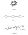
- FIG. 8 An example of an electronic system 4 , 13 providing a building block for these molecular components is illustrated schematically in FIG. 8 . This shows a phenyl (aryl, or benzene) ring providing a conjugated ⁇ -system. Spacers can comprise C—C single, double or triple bonds (or combinations thereof) with bond lengths:
- thiols can be used to attach components to metals and carbon to attach directly to semiconductor surfaces.
- a pair of such molecular components e.g. components 2 a , 2 b , 10 a , 10 b
- the phenyl systems are self-linking to each other due to the strong attraction of ⁇ - ⁇ stacking and the rotational symmetry.
- the delocalized ⁇ electron systems on respective components interact such that the electronic interaction leads to intermolecular crosstalk as described above.
- passive rings such as rotaxane rings or cyclodextrines can be used with these components.
- FIG. 9 This consists of three phenyl rings as respective electronic systems. Adjacent systems are interconnected by spacers formed by a suitable sequence of single-triple-single carbon bonds, with sulfur providing the anchor. Similar examples employing different spacers and variable pitch are illustrated in FIGS. 10 a and 10 b.
- the molecular component of FIG. 9 provides an implementation for components 10 a , 10 b of FIG. 3 where the conjugation extends over the entire molecule.
- Spacers can of course be selected to break the conjugation as, for example, in components 2 a , 2 b of FIG. 1 .
- Particular examples of such spacers, based on polyacetylenes, are illustrated in FIGS. 11 a and 11 b.
- FIGS. 12 a and 12 b show further examples of molecular components.
- side groups are used to promote the specific electronic interaction between components.
- the side group NO 2 is used in FIG. 12 a to increase the dipole moment of the central electronic system due to its electron-withdrawing property.
- the interaction is extended spatially in FIG. 12 b through addition of side group H 2 N which further enhances the dipole moment.
- Examples of other useful side groups include: —NO, —NO 2 , Ketones ( ⁇ O), hydroxyl groups (—OH), phosphate (as in DNA), or charged and redox-active entities like metal complexes.
- FIG. 13 shows an exemplary configuration for an elongate two-dimensional component.
- R here represents one or several electronic systems such as those described above, arranged with a linear periodicity of the interaction sites.
- one or both of the molecular components may comprise a two-dimensional network of electronic systems.
- a particular example here is a graphene sheet or nanoribbon.
- FIG. 14 illustrates the basic structure of graphene as a regular hexagonal array of interconnected phenyl rings as shown in FIG. 8 . Configuration of an exemplary sensor using graphene-based molecular components is indicated in FIG.
- FIG. 15 where the interaction sites (phenyl rings) are represented for simplicity as vertices of the hexagonal network.
- one component is formed by a single hexagonal unit and the other by a sheet of such units.
- FIG. 16 An alternative embodiment is shown in FIG. 16 where the lower component is formed by an elongate nanoribbon.
- fabrication issues move from placement of individual molecules to lithographic structuring of graphene electrodes.
- Such networks may of course be formed in various ways into three-dimensional components, e.g. by folding or bending.
- FIG. 15 a periodic signal with respect to displacement is expected.
- the measurement of absolute displacements therefore requires tracking of the signal similar to interferometry displacement sensing.
- This embodiment however, combines high resolution with a large dynamic range.
- the components can be arranged substantially in parallel but with a rotational offset between the networks as illustrated schematically in FIG. 17 . The interaction then leads to a more complex pattern of interacting sites and permits sub-pitch resolution (e.g. Vernier-like operation) to be achieved as discussed above.
- sub-pitch resolution e.g. Vernier-like operation
- any molecular force could be exploited to provide the required interaction.
- On or more of the following forces may therefore be exploited in embodiments of the invention: ionic exchange forces; hydrogen bridges; dipole forces; and Van-der-Waals forces.
- the ⁇ - ⁇ stacking interaction described above is based on quadrupole momentum effects and is generally speaking a dipole force. It reaches 50 kJ/mol binding force and so is sufficiently strong to create large effects but is not too strong so as still to allow mechanical motion. Molecules with dipole moments are considered particularly advantageous as building blocks for embodiments of the invention.
- Linear dipoles may be used in some embodiments to provide additional tunability over aromatic systems due to rotational effects enforcing the cross-talk.
- any of the forces given above may be exploited in different embodiments. Van-der-Waals forces, for example, are particularly feasible for electrical detection embodiments based on multiple interacting component pairs.
- the structure and/or arrangement of the two molecular components in an interacting pair may differ in various ways.
- Anchor points for components may be provided directly by spacers in some embodiments.
- Other electrical and optical properties of interacting components might also be employed as the basis for detection.
- the detector may be adapted to detect each of these properties.
- Optical detection for instance, might be used in a first detection stage to determine an appropriate probing current for a second, more accurate stage of electrical detection.
Abstract
Description
Claims (15)
Applications Claiming Priority (3)
| Application Number | Priority Date | Filing Date | Title |
|---|---|---|---|
| GB1203511.9 | 2012-02-29 | ||
| GBGB1203511.9A GB201203511D0 (en) | 2012-02-29 | 2012-02-29 | Position sensing apparatus |
| PCT/IB2013/051239 WO2013128321A2 (en) | 2012-02-29 | 2013-02-15 | Position sensing apparatus |
Publications (2)
| Publication Number | Publication Date |
|---|---|
| US20150077359A1 US20150077359A1 (en) | 2015-03-19 |
| US9766066B2 true US9766066B2 (en) | 2017-09-19 |
Family
ID=45991907
Family Applications (1)
| Application Number | Title | Priority Date | Filing Date |
|---|---|---|---|
| US14/381,963 Expired - Fee Related US9766066B2 (en) | 2012-02-29 | 2013-02-15 | Position sensing apparatus |
Country Status (3)
| Country | Link |
|---|---|
| US (1) | US9766066B2 (en) |
| GB (1) | GB201203511D0 (en) |
| WO (1) | WO2013128321A2 (en) |
Families Citing this family (1)
| Publication number | Priority date | Publication date | Assignee | Title |
|---|---|---|---|---|
| GB201203511D0 (en) | 2012-02-29 | 2012-04-11 | Ibm | Position sensing apparatus |
Citations (20)
| Publication number | Priority date | Publication date | Assignee | Title |
|---|---|---|---|---|
| US5268584A (en) * | 1988-11-28 | 1993-12-07 | The United States Of America As Represented By The Department Of Energy | Strong liquid-crystalline polymeric compositions |
| US5538655A (en) * | 1994-06-29 | 1996-07-23 | Arthur D. Little, Inc. | Molecular complexes for use as electrolyte components |
| US6031756A (en) * | 1997-02-06 | 2000-02-29 | International Business Machines Corporation | Molecule, layered medium and method for creating a pattern |
| US20030107927A1 (en) * | 2001-03-12 | 2003-06-12 | Yeda Research And Development Co. Ltd. | Method using a synthetic molecular spring device in a system for dynamically controlling a system property and a corresponding system thereof |
| DE102004013305A1 (en) | 2004-03-16 | 2005-09-29 | SCHULTES, Günter | Sensor layer for measuring e.g. torque, has electrically conducting atom or molecular clusters or particles distributed in matrix, where concentration and intercluster spacing of layer is determined by tunnel effect between clusters |
| US20060081838A1 (en) * | 2002-12-25 | 2006-04-20 | Eriko Matsui | Functional molecular element and functional molecular device |
| US20060099808A1 (en) * | 2002-08-05 | 2006-05-11 | Sony Corporation | Electric viscous fluid device and electronic equipment |
| US7166327B2 (en) * | 2003-03-21 | 2007-01-23 | International Business Machines Corporation | Method of preparing a conjugated molecular assembly |
| US7582897B2 (en) * | 2002-04-22 | 2009-09-01 | Konica Minolta Holdings, Inc. | Organic semiconductor composition, organic semiconductor element, and their manufacturing method |
| US20100052701A1 (en) * | 2008-08-26 | 2010-03-04 | Seoul National University Industry Foundation | Nanoscale Displacement Transducer |
| CN101734645A (en) | 2008-11-14 | 2010-06-16 | 清华大学 | Carbon nano-tube film |
| US7741197B1 (en) * | 2005-12-29 | 2010-06-22 | Nanosys, Inc. | Systems and methods for harvesting and reducing contamination in nanowires |
| CN101852935A (en) | 2010-06-02 | 2010-10-06 | 北京富纳特创新科技有限公司 | Touch liquid crystal display |
| US20100317409A1 (en) * | 2009-06-12 | 2010-12-16 | Tsinghua University | Carbon nanotube based flexible mobile phone |
| CN101930305A (en) | 2009-06-18 | 2010-12-29 | 清华大学 | Touch screen and display device |
| US8018563B2 (en) * | 2007-04-20 | 2011-09-13 | Cambrios Technologies Corporation | Composite transparent conductors and methods of forming the same |
| US20130010244A1 (en) * | 2011-06-29 | 2013-01-10 | Sony Corporation | Liquid crystal display and method of manufacturing the same |
| WO2013128321A2 (en) | 2012-02-29 | 2013-09-06 | International Business Machines Corporation | Position sensing apparatus |
| US20130320467A1 (en) * | 2010-12-08 | 2013-12-05 | Condalign As | Method for assembling conductive particles into conductive pathways and sensors thus formed |
| US9024297B2 (en) * | 2010-09-17 | 2015-05-05 | The Governors Of The University Of Alberta | Two- and three-terminal molecular electronic devices with ballistic electron transport |
-
2012
- 2012-02-29 GB GBGB1203511.9A patent/GB201203511D0/en not_active Ceased
-
2013
- 2013-02-15 US US14/381,963 patent/US9766066B2/en not_active Expired - Fee Related
- 2013-02-15 WO PCT/IB2013/051239 patent/WO2013128321A2/en active Application Filing
Patent Citations (20)
| Publication number | Priority date | Publication date | Assignee | Title |
|---|---|---|---|---|
| US5268584A (en) * | 1988-11-28 | 1993-12-07 | The United States Of America As Represented By The Department Of Energy | Strong liquid-crystalline polymeric compositions |
| US5538655A (en) * | 1994-06-29 | 1996-07-23 | Arthur D. Little, Inc. | Molecular complexes for use as electrolyte components |
| US6031756A (en) * | 1997-02-06 | 2000-02-29 | International Business Machines Corporation | Molecule, layered medium and method for creating a pattern |
| US20030107927A1 (en) * | 2001-03-12 | 2003-06-12 | Yeda Research And Development Co. Ltd. | Method using a synthetic molecular spring device in a system for dynamically controlling a system property and a corresponding system thereof |
| US7582897B2 (en) * | 2002-04-22 | 2009-09-01 | Konica Minolta Holdings, Inc. | Organic semiconductor composition, organic semiconductor element, and their manufacturing method |
| US20060099808A1 (en) * | 2002-08-05 | 2006-05-11 | Sony Corporation | Electric viscous fluid device and electronic equipment |
| US20060081838A1 (en) * | 2002-12-25 | 2006-04-20 | Eriko Matsui | Functional molecular element and functional molecular device |
| US7166327B2 (en) * | 2003-03-21 | 2007-01-23 | International Business Machines Corporation | Method of preparing a conjugated molecular assembly |
| DE102004013305A1 (en) | 2004-03-16 | 2005-09-29 | SCHULTES, Günter | Sensor layer for measuring e.g. torque, has electrically conducting atom or molecular clusters or particles distributed in matrix, where concentration and intercluster spacing of layer is determined by tunnel effect between clusters |
| US7741197B1 (en) * | 2005-12-29 | 2010-06-22 | Nanosys, Inc. | Systems and methods for harvesting and reducing contamination in nanowires |
| US8018563B2 (en) * | 2007-04-20 | 2011-09-13 | Cambrios Technologies Corporation | Composite transparent conductors and methods of forming the same |
| US20100052701A1 (en) * | 2008-08-26 | 2010-03-04 | Seoul National University Industry Foundation | Nanoscale Displacement Transducer |
| CN101734645A (en) | 2008-11-14 | 2010-06-16 | 清华大学 | Carbon nano-tube film |
| US20100317409A1 (en) * | 2009-06-12 | 2010-12-16 | Tsinghua University | Carbon nanotube based flexible mobile phone |
| CN101930305A (en) | 2009-06-18 | 2010-12-29 | 清华大学 | Touch screen and display device |
| CN101852935A (en) | 2010-06-02 | 2010-10-06 | 北京富纳特创新科技有限公司 | Touch liquid crystal display |
| US9024297B2 (en) * | 2010-09-17 | 2015-05-05 | The Governors Of The University Of Alberta | Two- and three-terminal molecular electronic devices with ballistic electron transport |
| US20130320467A1 (en) * | 2010-12-08 | 2013-12-05 | Condalign As | Method for assembling conductive particles into conductive pathways and sensors thus formed |
| US20130010244A1 (en) * | 2011-06-29 | 2013-01-10 | Sony Corporation | Liquid crystal display and method of manufacturing the same |
| WO2013128321A2 (en) | 2012-02-29 | 2013-09-06 | International Business Machines Corporation | Position sensing apparatus |
Non-Patent Citations (3)
| Title |
|---|
| Aljohm, Abdulkareem et al.; "Transaction-Centric Mobile-Payment classification model"; 2013 Seventh International Conference on Next Generation Mobile Apps, Services and Technologies; Copyrightt 2013 IEEE; pp. 68-74. |
| International Search Report Dated Jul. 18, 2013. PCT/IB2013/051239 Written Opinion. |
| International Search Report Dated Jul. 18, 2013. PCT/IB2013/051239. |
Also Published As
| Publication number | Publication date |
|---|---|
| US20150077359A1 (en) | 2015-03-19 |
| WO2013128321A2 (en) | 2013-09-06 |
| WO2013128321A3 (en) | 2016-09-01 |
| GB201203511D0 (en) | 2012-04-11 |
Similar Documents
| Publication | Publication Date | Title |
|---|---|---|
| EP2257821B1 (en) | Capacitive sensor having cyclic and absolute electrode sets | |
| CN100334420C (en) | Position sensor comprising elastomeric material | |
| JP6008970B2 (en) | Piezoelectric pressure sensor | |
| CN100478666C (en) | Micro structure, cantilever, scanning probe microscope and a method of measuring deformation quantity for the fine structure | |
| JP4757937B2 (en) | Measurement using tunneling current between extended conductors | |
| CN101685077A (en) | Chemical sensor using thin-film sensing member | |
| US20070034013A1 (en) | Contact-type electric capacitive displacement sensor | |
| JP2010522443A (en) | Sensors using composite diaphragms containing carbon nanotubes or semiconductor nanowires | |
| JP4150013B2 (en) | Tunnel effect element | |
| US20190368949A1 (en) | Spring sensor element | |
| US9766066B2 (en) | Position sensing apparatus | |
| US9953202B2 (en) | Nanostructure based super-capacitor for pressure and fingerprint sensor | |
| KR20230030547A (en) | Capacitive Pressure Sensor Arrangement | |
| JP2005300490A (en) | Mechanical detection element and detector | |
| Agrawal et al. | Analysis of electromechanical properties of electrode for enhancing electrostrictive capacitive sensor response | |
| US10101374B2 (en) | Electrostatic distribution measuring instrument | |
| US10209285B2 (en) | Electrometer | |
| KR101418389B1 (en) | Multi Nanosensor and Manufacturing Method Thereof | |
| US8081005B2 (en) | Capacitive sensors for nano-positioning and methods of using the same | |
| US20100052701A1 (en) | Nanoscale Displacement Transducer | |
| JP2007051899A (en) | Contact type capacitive displacement sensor | |
| AU762017B2 (en) | Measurements using tunnelling current between elongate conductors | |
| US10145879B2 (en) | Electrometer | |
| KR19980041111A (en) | External force sensing device | |
| Majeti et al. | A New Micro Electromechanical Capacitive Strain Sensor for SHM Applications |
Legal Events
| Date | Code | Title | Description |
|---|---|---|---|
| AS | Assignment |
Owner name: INTERNATIONAL BUSINESS MACHINES CORPORATION, NEW Y Free format text: ASSIGNMENT OF ASSIGNORS INTEREST;ASSIGNORS:GOTSMANN, BERND W.;LOERTSCHER, EMANUEL;SIGNING DATES FROM 20140804 TO 20140811;REEL/FRAME:033634/0635 |
|
| AS | Assignment |
Owner name: GLOBALFOUNDRIES U.S. 2 LLC, NEW YORK Free format text: ASSIGNMENT OF ASSIGNORS INTEREST;ASSIGNOR:INTERNATIONAL BUSINESS MACHINES CORPORATION;REEL/FRAME:036550/0001 Effective date: 20150629 |
|
| AS | Assignment |
Owner name: GLOBALFOUNDRIES INC., CAYMAN ISLANDS Free format text: ASSIGNMENT OF ASSIGNORS INTEREST;ASSIGNORS:GLOBALFOUNDRIES U.S. 2 LLC;GLOBALFOUNDRIES U.S. INC.;REEL/FRAME:036779/0001 Effective date: 20150910 |
|
| FEPP | Fee payment procedure |
Free format text: PAYER NUMBER DE-ASSIGNED (ORIGINAL EVENT CODE: RMPN) Free format text: PAYOR NUMBER ASSIGNED (ORIGINAL EVENT CODE: ASPN) |
|
| STCF | Information on status: patent grant |
Free format text: PATENTED CASE |
|
| AS | Assignment |
Owner name: WILMINGTON TRUST, NATIONAL ASSOCIATION, DELAWARE Free format text: SECURITY AGREEMENT;ASSIGNOR:GLOBALFOUNDRIES INC.;REEL/FRAME:049490/0001 Effective date: 20181127 |
|
| AS | Assignment |
Owner name: GLOBALFOUNDRIES U.S. INC., CALIFORNIA Free format text: ASSIGNMENT OF ASSIGNORS INTEREST;ASSIGNOR:GLOBALFOUNDRIES INC.;REEL/FRAME:054633/0001 Effective date: 20201022 |
|
| AS | Assignment |
Owner name: GLOBALFOUNDRIES INC., CAYMAN ISLANDS Free format text: RELEASE BY SECURED PARTY;ASSIGNOR:WILMINGTON TRUST, NATIONAL ASSOCIATION;REEL/FRAME:054636/0001 Effective date: 20201117 |
|
| FEPP | Fee payment procedure |
Free format text: MAINTENANCE FEE REMINDER MAILED (ORIGINAL EVENT CODE: REM.); ENTITY STATUS OF PATENT OWNER: LARGE ENTITY |
|
| AS | Assignment |
Owner name: GLOBALFOUNDRIES U.S. INC., NEW YORK Free format text: RELEASE BY SECURED PARTY;ASSIGNOR:WILMINGTON TRUST, NATIONAL ASSOCIATION;REEL/FRAME:056987/0001 Effective date: 20201117 |
|
| LAPS | Lapse for failure to pay maintenance fees |
Free format text: PATENT EXPIRED FOR FAILURE TO PAY MAINTENANCE FEES (ORIGINAL EVENT CODE: EXP.); ENTITY STATUS OF PATENT OWNER: LARGE ENTITY |
|
| STCH | Information on status: patent discontinuation |
Free format text: PATENT EXPIRED DUE TO NONPAYMENT OF MAINTENANCE FEES UNDER 37 CFR 1.362 |
|
| FP | Lapsed due to failure to pay maintenance fee |
Effective date: 20210919 |