US9791685B2 - Bessel beam plane illumination microscope - Google Patents
Bessel beam plane illumination microscope Download PDFInfo
- Publication number
- US9791685B2 US9791685B2 US14/216,015 US201414216015A US9791685B2 US 9791685 B2 US9791685 B2 US 9791685B2 US 201414216015 A US201414216015 A US 201414216015A US 9791685 B2 US9791685 B2 US 9791685B2
- Authority
- US
- United States
- Prior art keywords
- bessel
- light
- sample
- microscope
- numerical aperture
- Prior art date
- Legal status (The legal status is an assumption and is not a legal conclusion. Google has not performed a legal analysis and makes no representation as to the accuracy of the status listed.)
- Active, expires
Links
Images


Classifications
-
- G—PHYSICS
- G02—OPTICS
- G02B—OPTICAL ELEMENTS, SYSTEMS OR APPARATUS
- G02B21/00—Microscopes
- G02B21/36—Microscopes arranged for photographic purposes or projection purposes or digital imaging or video purposes including associated control and data processing arrangements
-
- G—PHYSICS
- G02—OPTICS
- G02B—OPTICAL ELEMENTS, SYSTEMS OR APPARATUS
- G02B21/00—Microscopes
- G02B21/0004—Microscopes specially adapted for specific applications
-
- G—PHYSICS
- G02—OPTICS
- G02B—OPTICAL ELEMENTS, SYSTEMS OR APPARATUS
- G02B21/00—Microscopes
- G02B21/0004—Microscopes specially adapted for specific applications
- G02B21/002—Scanning microscopes
-
- G—PHYSICS
- G02—OPTICS
- G02B—OPTICAL ELEMENTS, SYSTEMS OR APPARATUS
- G02B21/00—Microscopes
- G02B21/0096—Microscopes with photometer devices
-
- G—PHYSICS
- G02—OPTICS
- G02B—OPTICAL ELEMENTS, SYSTEMS OR APPARATUS
- G02B21/00—Microscopes
- G02B21/06—Means for illuminating specimens
-
- G—PHYSICS
- G02—OPTICS
- G02B—OPTICAL ELEMENTS, SYSTEMS OR APPARATUS
- G02B21/00—Microscopes
- G02B21/36—Microscopes arranged for photographic purposes or projection purposes or digital imaging or video purposes including associated control and data processing arrangements
- G02B21/361—Optical details, e.g. image relay to the camera or image sensor
-
- G—PHYSICS
- G02—OPTICS
- G02B—OPTICAL ELEMENTS, SYSTEMS OR APPARATUS
- G02B21/00—Microscopes
- G02B21/36—Microscopes arranged for photographic purposes or projection purposes or digital imaging or video purposes including associated control and data processing arrangements
- G02B21/365—Control or image processing arrangements for digital or video microscopes
-
- G—PHYSICS
- G02—OPTICS
- G02B—OPTICAL ELEMENTS, SYSTEMS OR APPARATUS
- G02B27/00—Optical systems or apparatus not provided for by any of the groups G02B1/00 - G02B26/00, G02B30/00
- G02B27/09—Beam shaping, e.g. changing the cross-sectional area, not otherwise provided for
- G02B27/0938—Using specific optical elements
- G02B27/095—Refractive optical elements
Definitions
- This disclosure relates to microscopy and, in particular, to Bessel beam plane illumination microscopy.
- Imaging technologies are commonly used to interrogate biological systems.
- Widefield imaging floods the specimen with light, and collects light from the entire specimen simultaneously, although high resolution information is only obtained from that portion of the sample close to the focal plane of the imaging objective lens.
- Confocal microscopy uses the objective lens to focus light within the specimen, and a pinhole in a corresponding image plane to pass to the detector only that light collected in the vicinity of the focus.
- the resulting images exhibit less out-of-focus background information on thick samples than is the case in widefield microscopy, but at the cost of slower speed, due to the requirement to scan the focus across the entire plane of interest.
- fluorescence For biological imaging, a powerful imaging modalities is fluorescence, since specific sub-cellular features of interest can be singled out for study by attaching fluorescent labels to one or more of their constituent proteins. Both widefield and confocal microscopy can take advantage of fluorescence contrast.
- fluorescence imaging is that fluorescent molecules can be optically excited for only a limited period of time before they are permanently extinguished (i.e., “photobleach”). Not only does such bleaching limit the amount of information that can be extracted from the specimen, it can also contribute to photo-induced changes in specimen behavior, phototoxicity, or even cell death.
- TPFE photon fluorescence excitation
- FIG. 1 is a schematic diagram of a light sheet microscopy (LSM) system 100 .
- LSM uses a beam-forming lens 102 , external to imaging optics, which include an objective 104 , to illuminate the portion of a specimen in the vicinity of the focal plane 106 of the objective.
- the lens 102 that provides illumination or excitation light to the sample is a cylindrical lens that focuses light in only one direction, thereby providing a beam of light 108 that creates a sheet of light coincident with the objective focal plane 106 .
- a detector 110 then records the signal generated across the entire illuminated plane of the specimen. Because the entire plane is illuminated at once, images can be obtained very rapidly.
- the lens 102 can be a circularly symmetric multi-element excitation lens (e.g., having a low numerical aperture (NA) objective) that corrects for optical aberrations (e.g., chromatic and spherical aberrations) that are prevalent in cylindrical lenses.
- NA numerical aperture
- the illumination beam 108 of light then is focused in two directions to form a pencil of light coincident with the focal plane 106 of the imaging objective 104 .
- the width of the pencil beam is proportional to the 1/NA, whereas its length is proportional to 1/(NA) 2 .
- the pencil beam 108 of the excitation light can be made sufficiently long to encompass the entire length of the desired field of view (FOV).
- the pencil beam can be scanned across the focal plane (e.g., with a galvanometer, as in confocal microscopy) while the imaging detector 110 integrates the signal that is collected by the detection optics 112 as the beam sweeps out the entire FOV.
- a principal limitation of these implementations is that, due to the diffraction of light, there is a tradeoff between the XY extent of the illumination across the focal plane of the imaging objective, and the thickness of the illumination in the Z direction perpendicular to this plane.
- the X direction is into the page
- the Y direction is in the direction of the illumination beam
- the Z direction is in the direction in which imaged light is received from the specimen.
- FIG. 2 is a schematic diagram of a profile 200 of a focused beam of light.
- Table 1 shows specific values of the relationship between the usable FOV, as defined by 2z R , and the minimum thickness 2w o of the illumination sheet, whether created by a cylindrical lens, or by scanning a pencil beam created by a low NA objective.
- the sheet thickness must be greater than the depth of focus of the imaging objective (typically, ⁇ 1 micron).
- the depth of focus of the imaging objective typically, ⁇ 1 micron.
- out-of-plane photobleaching and photodamage still remain (although less than in widefield or confocal microscopy, provided that the sheet thickness is less than the specimen thickness).
- the background from illumination outside the focal plane reduces contrast and introduces noise which can hinder the detection of small, weakly emitting objects.
- the Z positions of objects within the image cannot be determined to an accuracy better than the sheet thickness.
- a microscope can include a light source for generating a light beam having a wavelength, ⁇ , and beam-forming optics configured for receiving the light beam and generating a Bessel-like beam that is directed into a sample.
- the beam-forming optics can include an excitation objective having an axis oriented in a first direction.
- the microscope can include imaging optics configured for receiving light from a position within the sample that is illuminated by the Bessel-like beam and for imaging the received light on a detector.
- the imaging optics can include a detection objective having an axis oriented in a second direction that is non-parallel to the first direction.
- the microscope can also include a detector configured for detecting signal light received by the imaging optics, and an aperture mask positioned between the sample and the detector configured to prevent light illuminated by side lobes of the Bessel beam from reaching the detector, while allowing light illuminated by a central lobe of the Bessel beam to reach the detector.
- the microscope can also include beam scanning optics that can be configured for scanning the Bessel-like beam in a direction having a component perpendicular to the first direction.
- the microscope can also include image-positioning optics positioned in an optical path between the sample and the detector, and configured for imaging signal light from different positions with the sample while the Bessel-like beam is scanned by the beam scanning optics through a fixed position of the aperture mask.
- the aperture mask can define a slit.
- the detector can be a line detector.
- the Bessel-like beam can have a ratio of a Rayleigh length, z R to a minimum beam waist, w o , of more than 2w o / ⁇ and less than 100 ⁇ w o / ⁇ .
- the Bessel-like beam can have a non-zero ratio of a minimum numerical aperture to a maximum numerical aperture of less than 0.95.
- the Bessel-like beam can have a non-zero ratio of a minimum numerical aperture to a maximum numerical aperture of less than 0.90.
- the Bessel-like beam can have a minimum numerical aperture greater than zero and a ratio of energy in a first side of the beam to energy in the central lobe of the beam of less than 0.5.
- the microscope can also include a coverslip that supports the sample where a normal direction to a plane of the sample supports the sample forms and angle with the first direction of more than 10 degrees and less than 80 degrees.
- the sample can be less than ten micrometers thick.
- the signal light can have a wavelength of ⁇ /2.
- the signal light can be generated through a non-linear signal generation process.
- the signal light can include fluorescence light emitted from the sample after excitation by the Bessel-like beam.
- the signal light can be generated through a non-linear signal generation process.
- the microscope can also include an annular mask in a path of the light beam configured to generate an annular ring of light from which the Bessel-like beam is formed.
- a microscope can include a light source for generating a light beam having a wavelength, ⁇ , and beam-forming optics configured for receiving the light beam and generating a Bessel-like beam that is directed into a sample.
- the beam-forming optics can include an excitation objective having an axis oriented in a first direction.
- the microscope can include imaging optics configured for receiving light from a position within the sample that is illuminated by the Bessel-like beam and for imaging the received light on a detector.
- the imaging optics can include a detection objective having an axis oriented in a second direction that is non-parallel to the first direction.
- the microscope can also include a detector configured for detecting light received by the imaging optics where the detector includes a plurality of individual detection units.
- the microscope can also include a controller operably coupled to the detector and configured to selectively record image data from individual detection units that image portions of the sample that are illuminated by a central lobe of the Bessel-like beam while not recording data from individual detection units that image portions of the sample that are not illuminated by the central lobe of the Bessel-like beam, and can also include a processor configured to generate an image of the sample based on the selectively recorded image data that is recorded from different positions of the Bessel beam within the sample.
- the microscope can also include beam scanning optics configured for scanning the Bessel-like beam within the sample in a direction having a component perpendicular to the first direction.
- the beam scanning optics can be configured to scan the Bessel-like beam in the sample in steps that are greater than or approximately equal to a corresponding spacing between neighboring individual detector elements in the detector.
- the microscope can also include a beam blocking unit configured to block the Bessel-like beam from reaching the sample when the Bessel-like beam is scanned form one step position to a next step position.
- the microscope can also include a diffractive optical element (DOE) configured to generate a plurality of light beams from the light beam generated by the light source.
- DOE diffractive optical element
- the beam-forming optics can be configured for receiving the plurality of light beams and generating a plurality of Bessel-like beams that in the sample.
- the plurality of light beams can be spaced from each other by a spatial period that is greater than the diameter of a side lobe of the Bessel-like beams.
- the imaging optics can be further configured for simultaneously receiving light from positions within the sample that are illuminated by the plurality of Bessel-like beams and for imaging the received light on the detector.
- the controller can be further configured to selectively record image data simultaneously from individual detection units that image portions of the sample that are illuminated by a central lobe of the Bessel-like beams while not recording data from individual detection units that image portions of the sample that are not illuminated by the central lobes of the Bessel-like beams.
- the processor can be configured to generate an image of the sample based on the selectively recorded image data that is recorded from different positions of the Bessel beam within the sample, after the plurality of Bessel-like beams are scanned over the spatial period.
- the Bessel-like beam can have a ratio of a Rayleigh length, z R to a minimum beam waist, w o , of more than 2 ⁇ w o / ⁇ and less than 100 ⁇ w o / ⁇ .
- the Bessel-like beam can have a non-zero ratio of a minimum numerical aperture to a maximum numerical aperture of less than 0.95.
- the Bessel-like beam can have a non-zero ratio of a minimum numerical aperture to a maximum numerical aperture of less than 0.90.
- the Bessel-like beam can have a minimum numerical aperture greater than zero and a ratio of energy in a first side of the beam to energy in the central lobe of the beam of less than 0.5.
- the microscope can also include a coverslip that supports the sample where a normal direction to a plane of the sample that supports the sample forms and angle with the first direction of more than 10 degrees and less than 80 degrees.
- the sample can be less than ten micrometers thick.
- the microscope can also include an annular mask in a path of the light beam configured to generate an annular ring of light from which the Bessel-like beam is formed.
- a microscope can include a light source for generating a light beam having a wavelength, ⁇ , and beam-forming optics, including an optical element positioned in a path of the light beam and configured for generating an annular ring of light.
- the beam-forming optics being configured for generating from the light beam an excitation beam having a central lobe and at least one side lobe and also configured to direct the excitation beam to a position within a sample.
- the beam-forming optics can include an excitation objective having an axis oriented in a first direction, and a transverse profile of the excitation beam in the sample can be intermediate between a profile of a lowest order Bessel function and the Gaussian function.
- the microscope can also include imaging optics configured for receiving light from a position within the sample that is illuminated by the excitation beam and for imaging the received light on a detector.
- the imaging optics can include a detection objective having an axis oriented in a second direction that is non-parallel to the first direction.
- the microscope can also include a detector configured for detecting light received by the imaging optics.
- the optical element can be positioned in a path of the light beam and can be configured for generating an annular ring of light includes an annular apodization mask.
- the optical element can be positioned in a path of the light beam and can be configured for generating an annular ring of light includes a binary phase mask.
- the optical element can be positioned in a path of the light beam and can be configured for generating an annular ring of light includes a programmable spatial light modulator.
- the excitation beam can have a non-zero minimum numerical aperture and a maximum numerical aperture, and a ratio between the minimum numerical aperture and the maximum numerical aperture can be less than about 0.95.
- the excitation beam can have a non-zero minimum numerical aperture and a maximum numerical aperture, and a ratio between the minimum numerical aperture and the maximum numerical aperture can be less than about 0.90.
- An amount of energy in a highest-energy side lobe of the excitation beam can be less than about half of an amount of energy in the central lobe of the excitation beam.
- a ratio of a Rayleigh length, z R , of the excitation beam in the sample to a minimum beam waist, w o , of the excitation beam in the sample is more than about 2w o / ⁇ and less than about 100 ⁇ w o / ⁇ .
- the microscope can also include a cover slip having a planar surface upon which the sample is mounted or cultured. The planar surface can be tilted at an angle between 10 and 80 degrees with respect to the first direction.
- the sample can be less than ten micrometers thick.
- the microscope can also include beam scanning optics configured for scanning the excitation beam in a direction having a component perpendicular to the first direction.
- the signal light can have a wavelength of ⁇ /2.
- a microscope can include a light source for generating a light beam having a wavelength, ⁇ , and beam-forming optics configured for receiving the light beam and generating a Bessel-like beam that is directed into a sample.
- the beam-forming optics can include an excitation objective having an axis oriented in a first direction.
- the microscope can include imaging optics configured for receiving signal light from a position within the sample that is illuminated by the Bessel-like beam and for imaging the received light on a detector.
- the imaging optics can include a detection objective having an axis oriented in a second direction that is non-parallel to the first direction.
- the microscope can include beam-translation optics configured for translating the position of the Bessel-like beam within the sample in discrete steps of more than or about ⁇ /2NA to create a first excitation pattern of multiple Bessel-like beams having a spatial period, ⁇ , equal to the distance between beam positions of neighboring steps and configured to create N ⁇ 1 additional excitation patterns that are spatially phase shifted from the first excitation pattern by (N ⁇ 1) ⁇ /N.
- beam-translation optics configured for translating the position of the Bessel-like beam within the sample in discrete steps of more than or about ⁇ /2NA to create a first excitation pattern of multiple Bessel-like beams having a spatial period, ⁇ , equal to the distance between beam positions of neighboring steps and configured to create N ⁇ 1 additional excitation patterns that are spatially phase shifted from the first excitation pattern by (N ⁇ 1) ⁇ /N.
- the signal light can have a wavelength of ⁇ /2.
- the signal light can be generated through a non-linear signal generation process.
- N 3.
- the step size can be less than or about ⁇ /NA. In some implementations, N ⁇ 5.
- the step size can be greater than or about ⁇ /NA.
- the Bessel-like beam can have a ratio of a Rayleigh length, z R to a minimum beam waist, w o , of more than 2 ⁇ w o / ⁇ and less than 100 ⁇ w o / ⁇ .
- the Bessel-like beam can have a non-zero ratio of a minimum numerical aperture to a maximum numerical aperture of less than 0.95.
- the Bessel-like beam can have a non-zero ratio of a minimum numerical aperture to a maximum numerical aperture of less than 0.90.
- the Bessel-like beam can have a minimum numerical aperture greater than zero and a ratio of energy in a first side of the beam to energy in the central lobe of the beam of less than 0.5.
- the microscope an also include a coverslip that supports the sample where a normal direction to a plane of the sample that supports the sample forms and angle with the first direction of more than 10 degrees and less than 80 degrees.
- the sample can be less than ten micrometers thick.
- the microscope an also include an annular mask in a path of the light beam configured to generate an annular ring of light from which the Bessel-like beam is formed.
- a microscope can include a light source for generating a light beam having a wavelength, ⁇ , and beam-forming optics, including an optical element positioned in a path of the light beam and configured for generating an annular ring of light.
- the beam-forming optics being configured for generating from the light beam an excitation beam having a central lobe and at least one side lobe and also configured to direct the excitation beam to a position within a sample.
- the beam-forming optics can include an excitation objective having an axis oriented in a first direction. A transverse profile of the excitation beam in the sample is intermediate between a profile of a lowest order Bessel function and the Gaussian function.
- the microscope can also include imaging optics configured for receiving signal light from a position within the sample that is illuminated by the excitation beam and for imaging the received light on a detector.
- the imaging optics can include a detection objective having an axis oriented in a second direction that is non-parallel to the first direction where the signal light has a wavelength of ⁇ /2.
- the microscope can also include a detector configured for detecting the signal light received by the imaging optics.
- a microscope in another general aspect, includes a light source for generating a light beam having a wavelength, ⁇ , and first beam-forming optics configured for receiving the light beam and generating a first Bessel-like beam that is directed into a sample.
- the beam-forming optics include a first excitation objective having a numerical aperture (NA EO ) and an axis oriented in a first direction.
- the microscope further includes imaging optics configured for receiving signal light from a position within the sample that is illuminated by the first Bessel-like beam and for imaging the received light on a detector.
- the imaging optics include a detection objective having a numerical aperture (NA DO ) and an axis oriented in a second direction that is non-parallel to the first direction.
- NA DO numerical aperture
- the microscope includes first beam-translation optics configured for translating the position of the first Bessel-like beam within the sample in discrete steps of more than or about ⁇ /2NA EO to create a first excitation pattern of multiple first Bessel-like beams having a spatial period, ⁇ , equal to the distance between beam positions of neighboring steps and configured to create N ⁇ 1 additional excitation patterns that are spatially phase shifted from the first excitation pattern by (N ⁇ 1) ⁇ /N.
- the microscope includes a detector having individual detection units and configured for detecting first signal light received by the imaging optics, wherein the first signal light is emitted from the sample based an interaction of the first Bessel-like beam with the sample.
- the microscope includes a processor that is configured to generate a real space constituent image for each of the N excitation patterns, to Fourier transform each of the real space constituent images to generate reciprocal space constituent images for each of the excitation patterns, to combine the reciprocal space constituent images to generate a final reciprocal space image, and to re-transform the final reciprocal space image to generate a final real space image of the sample, where the final real space image of the sample has a resolution of less that ⁇ /2NA DO in a coordinate orthogonal to the first direction.
- FIG. 1 is a schematic diagram of a light sheet microscopy (LSM) system.
- LSM light sheet microscopy
- FIG. 2 is a schematic diagram of a profile of a focused beam of light.
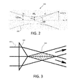
- FIG. 3 is a schematic diagram of a Bessel beam formed by an axicon.
- FIG. 4 is a schematic diagram of a Bessel beam formed by an annular apodization mask.
- FIG. 5 is a schematic diagram of a system for Bessel beam light sheet microscopy.
- FIG. 6A is a plot of the intensity profile of a Bessel beam.
- FIG. 6B shows a plot of the intensity profile of a conventional beam.
- FIG. 7A is a plot of the intensity profile of a Bessel beam of FIG. 6A in the directions transverse to the propagation direction of the beam.
- FIG. 7B is a plot of the intensity profile of the conventional beam of FIG. 6B in the directions transverse to the propagation direction of the beam.
- FIG. 8A is a plot of the intensity profile in the YZ plane of a Bessel beam generated from an annular mask having a thinner annulus in the annulus used to generate the intensity profile of the Bessel beam of FIG. 6A .
- FIG. 8B is a plot of the transverse intensity profile in the XZ directions for the beam of FIG. 8A .
- FIG. 9A is a schematic diagram of another system for implementing Bessel beam light sheet microscopy.
- FIG. 9B is a schematic diagram of another system for implementing Bessel beam light sheet microscopy.
- FIG. 10 shows a number of transverse intensity profiles for different Bessel-like beams.
- FIG. 11B shows an integrated intensity profile when the Bessel beam of FIG. 11A is swept in the X direction.
- FIG. 12A shows plots of the width of fluorescence excitation profiles of a swept beam, where the beam that is swept is created from annuli that have different thicknesses.
- FIG. 12B shows plots of the axial intensity profile of the beam that is swept in the Z direction.
- FIG. 13A is a schematic diagram of a surface of a detector having a two-dimensional array of individual detector elements in the X-Y plane.
- FIG. 13B is a schematic diagram of “combs” of multiple Bessel-like excitation beams that can be created in a given Z plane, where the spacing in the X direction between different beams is greater than the width of the fluorescence band generated by the side lobes of the excitation beams.
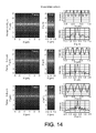
- FIG. 14 shows theoretical and experimental single-harmonic structured illumination patterns that can be created with Bessel-like beams having a maximum numerical aperture of 0.60 and the minimum vertical aperture of 0.58, which are created with 488 nm light.
- FIG. 15 shows theoretical and experimental higher-order harmonic structured illumination patterns that can be created with Bessel-like beams having a maximum numerical aperture of 0.60 and the minimum vertical aperture of 0.58, which are created with 488 nm light.
- FIG. 16 shows a system with a galvanometer-type mirror placed at a plane that is conjugate to the detection objective between the detection objective and the detector.
- FIG. 17A shows two overlapping structured patterns.
- FIG. 17B shows a reciprocal space representation of one of the patterns of FIG. 17A .
- FIG. 17C shows shows a reciprocal space representation of the other pattern of FIG. 17A .
- FIG. 17D shows an observable region of a reciprocal space representation of specimen structure shifted from the reciprocal space origin.
- FIG. 17E shows observable regions of reciprocal space representations of specimen structure shifted from the reciprocal space origin, where the different representations correspond to different orientations and/or phrase of a structured pattern overlayed with the specimen structure.
- This description discloses microscopy and imaging apparatus, systems, methods and techniques, which enable a light sheet or pencil beam to have a length that can be decoupled from its thickness, thus allowing the illumination of large fields of view (e.g., tens or even hundreds of microns) across a plane having a thickness on the order of, or smaller than, the depth of focus of the imaging objective by using illumination beams having a cross-sectional field distribution that is similar to a Bessel function.
- Such illumination beams can be known as Bessel beams.
- Bessel beams are created by focusing light, not in a continuum of azimuthal directions across a cone, as is customary, but rather at a single azimuthal angle or range of azimuthal angles with respect to the axis of the focusing element. Bessel beams can overcome the limitations of the diffraction relationship shown in FIG. 2 , because the relationship shown in FIG. 2 is only valid for lenses (cylindrical or objectives) that are uniformly illuminated.
- FIG. 3 is a schematic diagram of a Bessel beam formed by an axicon 300 .
- the axicon 300 is a conical optical element, which, when illuminated by an incoming plane wave 302 having an approximately-Gaussian intensity distribution in directions transverse to the beam axis, can form a Bessel beam 304 in a beam that exits the axicon.
- FIG. 4 is a schematic diagram of a Bessel beam 400 formed by an annular apodization mask 402 , where the annular mask 402 is illuminated to create a thin annulus of light at the back focal plane of a conventional lens 404 .
- the mask 402 is separated from the lens 404 by the focal length, f.
- An angle, ⁇ can be defined as the inverse tangent of half the distance, d, from the center of the annular ring to a point within the ring divided by the focal length, where d o can be used to denote the minimum diameter of the annular ring.
- d can be used to denote the minimum diameter of the annular ring.
- the axial wavevectors k z of all rays converging to the focus are the same, and hence there is no variation of the beam along this direction.
- the finite diameter of the axicon 300 or the finite width, ⁇ d, of the annular ring in the apodization mask 402 restricts the Bessel beam to a finite length.
- the optical system of the annular apodization mask 402 and the lens 404 can be characterized by a minimum and maximum numerical aperture, where the maximum numerical aperture is proportional to d o + ⁇ d, and the minimum numerical aperture is proportional to d o .
- different optical elements, other than an axicon or an apodization mask can be used to create an annulus of light.
- a binary phase mask or a programmable spatial light modulator can be used to create the annulus of light.
- FIG. 5 is a schematic diagram of a system 500 for Bessel beam light sheet microscopy.
- a light source 502 emits a light beam 504 that strikes an annular apodization mask 506 .
- An annulus of excitation light 508 illuminates the back focal plane of microscope objective 510 to create an elongated Bessel beam 512 of light in a sample 514 .
- FIG. 6A which shows a plot of the intensity profile of a Bessel beam
- FIG. 6B which shows a plot of the intensity profile of a conventional beam.
- Y is along the axis of the propagation direction of the beam
- X is the direction of the excitation polarization (when linearly polarized light is used)
- Z is along the axis of detection optics objective 522 and is orthogonal to X and Y.
- FIG. 7A is a plot of the intensity profile of a Bessel beam of FIG. 6A in the directions transverse to the propagation direction of the beam
- FIG. 7B is a plot of the Gaussian intensity profile of the conventional beam of FIG. 7A in the directions transverse to the propagation direction of the beam.
- annular illumination across a small range of angles results in a Bessel-like beam approximately 50 wavelengths ⁇ long in the Y direction, or roughly the same length obtained by conventional illumination using a plane wave having a Gaussian transverse intensity profile that is focused by a lens into an illumination beam having a cone half-angle of 12 degrees, as seen in FIG. 6 b .
- the thickness of the Bessel beam is much narrower than the thickness of the conventional beam, yielding a much thinner sheet of excitation when scanned across a plane.
- FIG. 8A is a plot of intensity profile in the YZ directions of a Bessel beam generated from an annular mask having a thinner annulus that is used to generate the intensity profile of the Bessel-like beam of FIG. 6A
- FIG. 8B is a plot of the transverse intensity profile for the beam in the XZ directions.
- annular illumination across a small range of angles results in the YZ intensity profile of the Bessel-like beam shown in FIG. 8A , where the Bessel-like beam has a length of approximately 100 wavelengths in the Y direction.
- the transverse intensity profile of the longer Bessel beam is relatively unchanged compared with shorter Bessel beam, as can be seen from a comparison of FIG. 7A and FIG. 8B , and the thickness of the beam is not significantly greater than the thickness of the beam whose intensity profile is shown in FIG. 6A .
- the usual approach of lengthening the beam by reducing the NA results in an unavoidably larger diffraction limited cross-section, roughly in accordance with Table 1.
- FIG. 9A is a schematic diagram of another system 900 for implementing Bessel beam light sheet microscopy.
- Collimated light 901 such as a laser beam having a Gaussian intensity profile, is reflected from first galvanometer-type mirror 902 and then imaged by relay lens pair 903 and 904 onto a second galvanometer-type mirror 905 positioned at a point optically conjugate to the first galvanometer-type mirror 902 .
- a second lens pair 906 and 907 then relays the light to annular apodization mask 908 conjugate with the second galvanometer-type mirror 905 .
- the annular light beam transmitted through this mask 908 is then relayed by a third lens pair 910 and 911 onto a conjugate plane coincident with the back focal plane of excitation objective 912 . Finally, the annular light is focused by objective 912 to form a Bessel-like beam 913 that is used provides excitation light to a specimen.
- the rotational axis of galvanometer mirror 902 is positioned such that tilting this galvanometer-type mirror 902 causes the Bessel-like beam 913 to sweep across the focal plane of detection objective 915 (i.e., in the X direction), whose axis is orthogonal to (or whose axis hasn't orthogonal complement to) the axis of the excitation objective 912 .
- the signal light 914 can be directed by detection optics, including the detection objective 915 , to a detection camera 917 .
- the galvanometers-type mirrors 902 , 905 can provide sweep rates of up to about 2 kHz, and with resonant galvanometer-type mirrors (e.g., Electro-Optical Products Corp, model SC-30) sweep rates can exceed 30 kHz. Extremely high frame rate imaging is then possible when the system is used in conjunction with a high frame rate detection camera (e.g., 500 frames/sec with an Andor iXon+DU-860 EMCCD, or >20,000 frames/sec with a Photron Fastcam SA-1 CMOS camera coupled to a Hamamatsu C10880-03 image intensifier/image booster).
- a high frame rate detection camera e.g., 500 frames/sec with an Andor iXon+DU-860 EMCCD, or >20,000 frames/sec with a Photron Fastcam SA-1 CMOS camera coupled to a Hamamatsu C10880-03 image intensifier/image booster.
- the rotational axis of the galvanometer mirror 905 is positioned such that tilting of this mirror causes Bessel-like beam 913 to translate along the axis of detection objective 915 .
- This mirror causes Bessel-like beam 913 to translate along the axis of detection objective 915 .
- either detection objective 915 In order to image each plane in focus, either detection objective 915 must be moved synchronously with the motion of the Bessel beam 913 imparted by the tilt of galvanometer-type mirror 905 (such as with a piezoelectric transducer (e.g., Physik Instrumente P-726)), or else the effective plane of focus of the detection objective 915 must be altered, such as by using a second objective to create a perfect image of the sample.
- the second galvanometer 905 and relay lenses 906 and 907 can be removed from the system shown in FIG.
- AOTF acousto-optical tunable filter
- the system in FIG. 9A is typically quite wasteful of the energy in light beam 901 , because most of this light is blocked by apodization mask 908 .
- a diffractive optical element such as a binary phase mask or spatial light modulator and a collimating lens can be used to create an approximately annular light beam prior to more exact definition of this beam and removal of higher diffractive orders by the apodization mask 908 .
- signal eight 914 received by detection objective 915 can be transmitted through relay lenses 920 , 922 and reflected off a galvanometer-type mirror 924 and then transmitted through relay lenses 926 and 928 and focused by a tube lens 930 onto a detector 932 .
- An aperture mask (e.g., an adjustable slit) 934 can be placed at a focal plane of lens 926 , and the when the mask defines a slit the width of the slit 934 can be selected to block signal light from positions in the sample corresponding to side lobes of the Bessel-like beam illumination light, while passing signal light from positions in the sample corresponding to the central peak of the Bessel-like beam illumination light.
- the galvanometer-type mirror 924 can be rotated in conjunction with galvanometer-type mirror 902 , so that when the Bessel-like beam is scanned in the X direction within the sample signal light from different positions within the sample passes through the slit 934 .
- Bessel-like beams include excitation intensity in rings other than the central excitation maximum, which as are evident in FIGS. 7A and 8B , and substantial energy resides in the side lobes of a Bessel-like beam. Indeed, for an ideal Bessel beam of infinite extent, each side lobe contains energy equal to that in the central peak. Also, for an ideal Bessel beam the ratio of the Rayleigh length of the beam to the minimum waist size of the beam is infinite.
- each row indicates the maximum and minimum numerical aperture of the annular ring of the mask.
- the maximum numerical aperture is 0.80, and the minimum numerical aperture is 0.76.
- the maximum numerical aperture is 0.60, and the minimum numerical aperture is 0.58.
- the maximum numerical aperture is 0.53 and the minimum numerical aperture is 0.51.
- the maximum numerical aperture is 0.40, and the minimum numerical aperture is 0.38.
- the maximum numerical aperture is 0.20, and the minimum numerical aperture is 0.18.
- the intensity profile shown in FIG. 11A is representative of a Bessel-like beam formed from an annular apodization mask that generates an annulus of 488 nm light at a rear pupil of an excitation objective, where the annulus has a maximum numerical aperture of 0.60 and a minimum numerical aperture of 0.58.
- FIG. 12B shows plots of the axial intensity profiles (i.e., in the Y direction) of the beams that are swept. For each of the beams whose intensity profiles are plotted in FIG. 12A and FIG. 12B , the maximum numerical aperture is 0.60.
- a beam with an intensity profile 1202 has a minimum numerical aperture equal to 0.58.
- a beam with an intensity profile 1204 has a minimum numerical aperture equal to 0.56.
- a beam with an intensity profile 1206 has a minimum numerical aperture people equal to 0.52.
- the beam with an intensity profile 1208 has a minimum numerical aperture equal to 0.45.
- a beam with an intensity profile 1210 has a minimum numerical aperture equal to 0.30.
- the different apodization masks 506 can have open regions with different widths, ⁇ d.
- a comparison of the plots in FIG. 12A and FIG. 12B shows the profiles of the beam changing from a profile that best approximates that of a lowest order (J 0 ) Bessel function (plot 1202 ) to a Gaussian profile ( 1212 ).
- This comparison indicates that the deleterious effect of the side lobes can be reduced by using a beam having a profile that is not substantially similar to that of a Bessel function, at the expense of having a beam with a shorter axial length.
- the selected beam can have a ratio of a Rayleigh length, z R to a minimum beam waist, w o , of more than 2 ⁇ w o / ⁇ and less than 100 ⁇ w o / ⁇ .
- the selected beam can have a non-zero ratio of a minimum numerical aperture to a maximum numerical aperture of less than 0.95.
- the selected beam can have a non-zero ratio of a minimum numerical aperture to a maximum numerical aperture of less than 0.9. In another implementation, the selected beam can have a ratio of a minimum numerical aperture to a maximum numerical aperture of less than 0.95 and greater than 0.80. In another implementation, the selected beam can have a non-zero ratio of a minimum numerical aperture to a maximum numerical aperture of less than 0.9. In another implementation, the selected beam can have a ratio of a minimum numerical aperture to a maximum numerical aperture of less than 0.95 and greater than 0.80. In another implementation, the selected beam can have a ratio of energy in a first side lobe of the beam to energy in the central lobe of the beam of less than 0.5.
- the length of the beam 516 which is necessary to image a specimen can be reduced by tilting a cover slip that supports the specimen with respect to the direction of the incoming beam 516 .
- a cover slip that supports the specimen with respect to the direction of the incoming beam 516 .
- the beam 516 would have to be 50 ⁇ m long to span the specimen.
- the plane of the cover slip at a 45° angle to the direction of the incoming beam 516 , then the beam would only need to be 5 ⁇ m ⁇ 2 long to span the sample.
- the beam 516 can be scanned in the X direction by tilting the galvanometer-type mirror 902 , and can be scanned in the Z direction either by introducing a third galvanometer (not shown) and a third pair of relay lenses (not shown) into the system 900 shown in FIG.
- Another approach to isolate the central peak fluorescence from that generated in the side lobes is to exclude the latter via confocal filtering with a virtual slit.
- the detector includes a plurality of individual detector elements, only those elements of the detector upon which an image the portion of the sample that is illuminated by the central lobe of the illumination beam can be activated to record information that is used to generate an image, while the individual detector elements upon which an image of the portion of the sample that is illuminated by side lobes of the illumination beam are not activated, such that they do not record information that is used to generate an image.
- FIG. 13A is a schematic diagram of a surface of a detector having a two-dimensional array of individual detector elements in the XY plane.
- FIG. 13A is a schematic diagram of a surface of a detector having a two-dimensional array of individual detector elements in the XY plane.
- FIG. 13B is a schematic diagram of “combs” of multiple Bessel-like excitation beams that can be created in a given Z plane.
- a comb of beams can be created by inserting a diffractive optical element (DOE, not shown) in the beam path between the light source and the galvanometer-type mirrors 902 , 905 , where the DOE diffracts a plurality of beams at different angles from the DOE, which end up being parallel to and spatially shifted from each other within the specimen.
- DOE diffractive optical element
- the spacing in the X direction between different beams of the comb is greater than the width of the fluorescence band generated by the side lobes of the beams. This allows information to be recorded simultaneously from rows of individual detector elements corresponding to the centers of the different beams of the comb, without the side lobes of neighboring beams interfering with the recorded signal for a particular beam.
- a comb of beams that illuminate a plane of a specimen 1308 can include the beams A1, B1, C1, D1, and E1, where the beams are separated by distances great enough so that side lobes of one beam in the comb do not overlap with a central portion of a neighboring beam.
- multiple “stripes” of an image can be simultaneously recorded. This process is then repeated, with additional images collected as the comb of Bessel-like illumination beams is translated in discrete steps having a width that corresponds to the spacing in the X direction between individual detector elements until all “stripes” of the final image have been recorded.
- the beams can be moved to new positions of A2, B2, C2, D2, and E2, where the spacing between the positions A1 and A2, the spacing between positions B1 and B2, etc. corresponds to the spacing between neighboring individual detector elements in the detector.
- fluorescence light from the beam position C1 could be detected at a detector element 1302
- fluorescence light from the beam position C2 can be detected at individual detector elements 1304 .
- the image is that then digitally constructed from the information in all of the different stripes of the image.
- An acousto-optical tunable filter (AOTF) 918 can be used to block all excitation light from reaching the specimen between steps.
- AOTF acousto-optical tunable filter
- SI structured illumination
- I is an intensity at a point in the image
- n is an index value indicating an image from which I n is taken. Equation (1) is by one example of a linear combination of the individual images that will remove the weakly modulated out-of-focus component and retain the strongly modulated information near the focal plane.
- the beam is not swept continuously, but rather is moved in discrete steps to create a pattern of illumination light from which an image I n can be generated.
- the stepping period is larger than or approximately equal to the minimum period of ⁇ /2NA Bessel max required to produce a resolvable grating, but smaller than or approximately equal to ⁇ /NA Bessel max , the imposed pattern of illumination light contains a single harmonic, as required for the three-image, three-phase SI algorithm.
- the Bessel-like beam 913 can be swept in the X direction in discrete steps having a period greater than or approximately equal to ⁇ /2NA Bessel max and less than or approximately equal to ⁇ /NA Bessel max by controlling the position of the galvanometer-type mirror 902 , and detection light can be received and signals corresponding to the detected light can be recorded by the detector 917 when the beam 913 is in each of the positions. While the galvanometer-type mirror is being moved from one position to the next position the illumination light can be blocked from reaching the sample by the AOTF. In this manner, an image I 1 can be generated from the detected light that is received when the illumination beam 913 is at each of its staff positions. Then, additional images, I 2 . .
- a final image of the specimen then can be constructed from the recorded signals through the use of equation (1).
- FIG. 14 shows a theoretical and experimental structured illumination patterns that can be created with a Bessel-like beams having a maximum numerical aperture of 0.60 and the minimum vertical aperture of 0.58, which are created with 488 nm light.
- the leftmost column of figures shows theoretical patterns
- the middle column shows experimentally-measured patterns
- the period the pattern i.e., the spacing between successive positions of the center of the Bessel-like being is the beam is stepped in the X direction
- the period of the pattern is 0.60 ⁇ m.
- the period of the pattern is 0.80 ⁇ m.
- a comb of multiple Bessel-like beams which are spaced by more than the width of the fringes of the beams in the comb, can be used to illuminate the specimen simultaneously, and then the comb of beams can be stepped in the X direction using the step size described above, so that different stripes of the specimen can be imaged in parallel and then an image of the specimen can be constructed from the multiple stripes.
- MTF excitation modulation transfer function
- Somewhat more energy can be transferred to the side bands using single harmonic excitation having a period far beyond the ⁇ /2NA Bessel max Abbe limit, but at the expense of proportionally poorer optical sectioning capability.
- An alternative that can better retain both signal and axial resolution is to create a multi-harmonic excitation pattern by stepping the beam at a fundamental period larger than ⁇ /NA Bessel max , as seen in FIG. 15 , which shows theoretical and experimental higher-order harmonic structured illumination patterns that can be created with Bessel-like beams having a maximum numerical aperture of 0.60 and the minimum vertical aperture of 0.58, which are created with 488 nm light.
- Eq. (1) is again used, except with N ⁇ H+2 images, each with the pattern phase shifted by 2 ⁇ /N relative to its neighbors.
- both single-harmonic and multi-harmonic SI modes still generate some excitation beyond the focal plane, and are thus not optimally efficient in their use of the photon budget.
- Both these issues can be addressed using two-photon excitation (TPE), which suppresses the Bessel side lobes sufficiently such that a thin light sheet can be obtained even with a continuously swept beam.
- TPE two-photon excitation
- high axial resolution and minimal out-of-focus excitation is achieved in fixed and living cells with only a single image per plane.
- Some additional improvement is also possible with TPE-SI, but the faster TPE sheet mode can be preferred for live cell imaging.
- TPE TPE
- CARS coherent anti-Stokes Raman scattering
- the improved confinement of the excitation light to the vicinity of the focal plane of the detection objective made possible by Bessel beam plane illumination leads to improved resolution in the axial direction (i.e., in the direction along the axis of the detection objective) and reduced photobleaching and phototoxicity, thereby enabling extended observations of living cells with isotropic resolution at high volumetric frame rates.
- extended imaging of the endoplasmic reticulum in a live human osteosarcoma cell (U2OS cell line) in the linear multi-harmonic SI mode was performed.
- U2OS cell line live human osteosarcoma cell
- Such ruffles can surround and engulf extracellular fluid to create large intracellular vacuoles, a process known as macropinocytosis, which was directly demonstrated using the techniques described herein.
- the visualization of these processes in four dimensional spatiotemporal detail (0.12 ⁇ 0.12 ⁇ 0.15 ⁇ m ⁇ 12.3 sec stack interval) across 15 minutes cannot currently be achieved with other fluorescence microscopy techniques.
- CMOS camera 125 MHz, Hamamatsu Orca Flash 2.8
- a third galvanometer-type mirror that can be tilted can be placed at a plane conjugate to the rear pupil of the detection objective and used to tile several image planes across the width of the detector, which were then are read out in parallel.
- FIG. 16 shows a system 1600 with a mirror placed at a plane that is conjugate to the detection objective between the detection objective and the detector.
- detection light collected by detection objective 1602 can be focused by a tube lens 1604 to form an image at the plane of an adjustable slit 1606 .
- the image cropped by the adjustable slit 1606 is reimaged by relay lenses 1608 onto a high-speed detection camera 1610 .
- a galvanometer-type mirror 1612 is placed the plane between the relay lenses 1608 that is conjugate to the back focal plane of the detection objective 1612 . By changing the angle of galvanometer-type mirror, multiple images can be exposed across the surface of the detection camera 1610 and then read out in parallel to exploit the full speed of the detection camera 1610 .
- Three-dimensional live cell imaging can be performed with Bessel-like beans with the use of fluorescent proteins to highlight selected portions of a specimen.
- a key aspect of fluorescent proteins (FPs) is that their spectral diversity permits investigation of the dynamic interactions between multiple proteins in the same living cell. For example, after transfection with mEmerald/MAP4 and tdTomato/H2B, microtubules in a pair of U2OS cells surrounding their respective nuclei, were imaged in the linear, nine-phase multi-harmonic SI mode. Nevertheless, although many vectors are available for linear imaging, the need for N frames of different phase per image plane can limits the use of SI with Bessel-like beams to processes which evolve on a scale that matches the time required to collect frames at the desired spatial resolution.
- the TPE sheet mode can be used for imaging multiple proteins exhibiting faster dynamics.
- the 3D isotropic resolution of the Bessel TPE sheet mode permits multiple proteins tagged with the same FP to be imaged simultaneously, as long as they are known a priori to be spatially segregated.
- Bessel beam plane illumination microscopy techniques offer 3D isotropic resolution down to ⁇ 0.3 ⁇ m, imaging speeds of nearly 200 planes/sec, and the ability, in TPE mode, to acquire hundreds of 3D data volumes from single living cells encompassing tens of thousands of image frames. Nevertheless, additional improvements are possible.
- substantially greater light collection making still better use of the photon budget would be obtained by using a detection objective with a numerical aperture of 1.0 or greater.
- mechanical constraints would thereby force the use of an excitation objective with a numerical aperture of less than 0.8 thus lead to a somewhat anisotropic point spread function (PSF), the volumetric resolution would remain similar, since the slight loss of axial resolution would be offset by the corresponding transverse gain.
- PSF point spread function
- An alternative would be to use the algorithms of 3D superresolution SI, which assign the sample spatial frequencies down-modulated by all bands of the excitation to their appropriate positions in an expanded frequency space. By doing so, shorter exposure times and fewer phases may be needed to record images of acceptable SNR, making linear Bessel SI a more viable option for high speed multicolor imaging.
- resolution could be extended to the sum of the excitation and detection MTF supports in each direction—an argument in favor of using three mutually orthogonal objectives. Indeed, the marriage of Bessel beam plane illumination and 3D superresolution SI may permit the latter to be applied to thicker, more densely fluorescent specimens than the conventional widefield approach, while more efficiently using the photon budget.
- Superresolution SI can be performed by extending the structured illumination techniques described above with respect to FIG. 14 and FIG. 15 .
- a structured illumination pattern normally inaccessible high-resolution information can be accessed.
- An image of a sample can be made accessible in the form of moiré fringes.
- a series of such images can be processed to extract this high-frequency information and to generate reconstruction of the image with improved resolution compared to the diffraction limited resolution.
- one of the patterns can be the unknown sample structure, for example, the unknown spatial distribution of regions of the sample that receive illumination light and that emit signal light—and the other pattern can be the purposely structured pattern of excitation light that is written in the form of parallel Bessel-like beams. Because the amount of signal light emitted from a point in the sample is proportional to the product of the local excitation light intensity and the relevant structure of the sample, the observed signal light image that is detected by the detector will show the beat pattern of the overlap of the two underlying patterns. Because the beat pattern can be coarser than those of the underlying patterns, then because the illumination pattern of the Bessel-like beams is known, the information in the beat pattern can be used to determine the normally unresolvable high-resolution information about the sample.
- the patterns shown in FIG. 17A can be Fourier transformed into reciprocal space.
- the Fourier transform of the structure of a sample that is imaged by an optical system is constrained by the Abbe resolution limit would be represented by a circle having a radius of 2NA/ ⁇ , as shown in FIG. 17B , where the low resolution components of the sample are close to the origin, and the high-resolution components are close to the edge of the circle.
- the Fourier transform of a 2D illumination pattern that consists of a sinusoidal variation in the illumination light in one dimension area having a period equal to the diffraction limit of the optical system has only three non-zero points that lie on the circle of FIG. 17B , as shown in FIG. 17C .
- One point resides at the origin and the other two points are offset from the origin in a direction defined by the orientation of the illumination pattern by distance a proportional to the inverse of the spatial period of the pattern.
- the resulting beat pattern between the specimen structure and the illumination structure represents information that has changed position in reciprocal space, such that the observable region of the sample in physical space then contains new high-frequency information represented by the two regions and FIG. 17D that are offset from the origin.
- three images can be recorded with the spatial phase of the illumination pattern shifted by 120° between each image in both the X direction and in the Z direction. Then, a Fourier transform can be performed on each of the three images, and the reciprocal space images are moved to their true positions in reciprocal space, combined through a weighted-average in reciprocal space, and then the weight-averaged reciprocal space image can be re-transformed to real space to provide an image of the sample. In this manner, a superresolution image of the sample can be obtained, where the resolution of the image in both the X and Z directions can be enhanced by a factor of two over the Abbe diffraction limited resolution.
- more than one excitation objective can be used to provide a structured illumination pattern to the sample, where the different excitation objectives can be oriented in different directions, so that super resolution of the sample can be obtained in the directions transverse to the Bessel-like beams of each of the orientation patterns.
- a first excitation objective can be oriented with its axis along the Y direction (as described above) and can illuminate the sample with an illumination pattern of Bessel-like beams that provides a superresolution image of the sample in the X and Z directions
- a second excitation objective can be oriented with its axis along the X direction and can illuminate the sample with an illumination pattern of Bessel-like beams that provides a superresolution image of the sample in the Y and Z directions.
- the superresolution information that can be derived from illumination patterns from the different excitation objectives
- highly inclined, objective-coupled sheet illumination has been used to image single molecules in thicker regions of the cell where autofluorescence and out-of-focus excitation would be otherwise prohibitive under widefield illumination.
- Bessel beam plane illumination only in-focus molecules would be excited, while out-of-focus ones would not be prematurely bleached. As such, it would be well suited to live cell 3D particle tracking and fixed cell photoactivated localization microscopy.
- the TPE sheet mode may be equally well suited to the imaging of large, multicellular specimens, since it combines the self-reconstructing property of Bessel beams with the improved depth penetration in scattering media characteristic of TPE.
- the TPE sheet mode may be equally well suited to the imaging of large, multicellular specimens, since it combines the self-reconstructing property of Bessel beams with the improved depth penetration in scattering media characteristic of TPE.
- large scale 3D anatomical mapping with isotropic resolution at high frame rates it might be fruitfully applied to the in vivo imaging of activity in populations of neurons.
- Implementations of the various techniques described herein may be implemented in digital electronic circuitry, or in computer hardware, firmware, software, or in combinations of them. Implementations may implemented as a computer program product, i.e., a computer program tangibly embodied in an information carrier, e.g., in a machine-readable storage device or in a propagated signal, for execution by, or to control the operation of, data processing apparatus, e.g., a programmable processor, a computer, or multiple computers.
- data processing apparatus e.g., a programmable processor, a computer, or multiple computers.
- a computer program such as the computer program(s) described above, can be written in any form of programming language, including compiled or interpreted languages, and can be deployed in any form, including as a stand-alone program or as a module, component, subroutine, or other unit suitable for use in a computing environment.
- a computer program can be deployed to be executed on one computer or on multiple computers at one site or distributed across multiple sites and interconnected by a communication network.
- Method steps may be performed by one or more programmable processors executing a computer program to perform functions by operating on input data and generating output. Method steps also may be performed by, and an apparatus may be implemented as, special purpose logic circuitry, e.g., an FPGA (field programmable gate array) or an ASIC (application-specific integrated circuit).
- FPGA field programmable gate array
- ASIC application-specific integrated circuit
- processors suitable for the execution of a computer program include, by way of example, both general and special purpose microprocessors, and any one or more processors of any kind of digital computer.
- a processor will receive instructions and data from a read-only memory or a random access memory or both.
- Elements of a computer may include at least one processor for executing instructions and one or more memory devices for storing instructions and data.
- a computer also may include, or be operatively coupled to receive data from or transfer data to, or both, one or more mass storage devices for storing data, e.g., magnetic, magneto-optical disks, or optical disks.
- Information carriers suitable for embodying computer program instructions and data include all forms of non-volatile memory, including by way of example semiconductor memory devices, e.g., EPROM, EEPROM, and flash memory devices; magnetic disks, e.g., internal hard disks or removable disks; magneto-optical disks; and CD-ROM and DVD-ROM disks.
- semiconductor memory devices e.g., EPROM, EEPROM, and flash memory devices
- magnetic disks e.g., internal hard disks or removable disks
- magneto-optical disks e.g., CD-ROM and DVD-ROM disks.
- the processor and the memory may be supplemented by, or incorporated in special purpose logic circuitry.
- implementations may be implemented on a computer having a display device, e.g., a cathode ray tube (CRT) or liquid crystal display (LCD) monitor, for displaying information to the user and a keyboard and a pointing device, e.g., a mouse or a trackball, by which the user can provide input to the computer.
- a display device e.g., a cathode ray tube (CRT) or liquid crystal display (LCD) monitor
- keyboard and a pointing device e.g., a mouse or a trackball
- Other kinds of devices can be used to provide for interaction with a user as well; for example, feedback provided to the user can be any form of sensory feedback, e.g., visual feedback, auditory feedback, or tactile feedback; and input from the user can be received in any form, including acoustic, speech, or tactile input.
Abstract
A microscope has a light source for generating a light beam having a wavelength, λ, and beam-forming optics configured for receiving the light beam and generating a Bessel-like beam that is directed into a sample. The beam-forming optics include an excitation objective having an axis oriented in a first direction. Imaging optics are configured for receiving light from a position within the sample that is illuminated by the Bessel-like beam and for imaging the received light on a detector. The imaging optics include a detection objective having an axis oriented in a second direction that is non-parallel to the first direction. A detector is configured for detecting signal light received by the imaging optics, and an aperture mask is positioned.
Description
This application is a Divisional of, and claims priority to, U.S. patent application Ser. No. 13/160,492, filed Jun. 14, 2011, entitled “BESSEL BEAM PLANE ILLUMINATION MICROSCOPE”, which, in turn, claims priority of U.S. Provisional Patent Application Nos. 61/354,532, filed Jun. 14, 2010, entitled “BESSEL BEAM PLANE ILLUMINATION MICROSCOPE”; 61/386,342, filed Sep. 24, 2010, entitled “BESSEL BEAM PLANE ILLUMINATION MICROSCOPE”; and 61/433,034, filed Jan. 14, 2011, entitled “BESSEL BEAM PLANE ILLUMINATION MICROSCOPE.” The subject matter of each of these earlier filed applications is hereby incorporated by reference.
This disclosure relates to microscopy and, in particular, to Bessel beam plane illumination microscopy.
Several imaging technologies are commonly used to interrogate biological systems. Widefield imaging floods the specimen with light, and collects light from the entire specimen simultaneously, although high resolution information is only obtained from that portion of the sample close to the focal plane of the imaging objective lens. Confocal microscopy uses the objective lens to focus light within the specimen, and a pinhole in a corresponding image plane to pass to the detector only that light collected in the vicinity of the focus. The resulting images exhibit less out-of-focus background information on thick samples than is the case in widefield microscopy, but at the cost of slower speed, due to the requirement to scan the focus across the entire plane of interest.
For biological imaging, a powerful imaging modalities is fluorescence, since specific sub-cellular features of interest can be singled out for study by attaching fluorescent labels to one or more of their constituent proteins. Both widefield and confocal microscopy can take advantage of fluorescence contrast. One limitation of fluorescence imaging, however, is that fluorescent molecules can be optically excited for only a limited period of time before they are permanently extinguished (i.e., “photobleach”). Not only does such bleaching limit the amount of information that can be extracted from the specimen, it can also contribute to photo-induced changes in specimen behavior, phototoxicity, or even cell death.
Unfortunately, both widefield and confocal microscopy excite fluorescence in every plane of the specimen, whereas the information rich, high resolution content comes only from the vicinity of the focal plane. Thus, both widefield and confocal microscopy are very wasteful of the overall fluorescence budget and potentially quite damaging to live specimens. A third approach, two photon fluorescence excitation (TPFE) microscopy, uses a nonlinear excitation process, proportional to the square of the incident light intensity, to restrict excitation to regions near the focus of the imaging objective. However, like confocal microscopy, TPFE requires scanning this focus to generate a complete image. Furthermore, the high intensities required for TPFE can give rise to other, nonlinear mechanisms of photodamage in addition to those present in the linear methods of widefield and confocal microscopy.
Thus, there is a need for the ability to: a) confine excitation predominantly to the focal plane of imaging optics, to reduce photodamage and photobleaching, as well as to reduce out-of-focus background; b) use widefield detection, to obtain images rapidly; and c) can be used with linear fluorescence excitation, to avoid nonlinear photodamage.
In another implementation, termed Digital Laser Scanned Light Sheet Microscopy (DSLM), the lens 102 can be a circularly symmetric multi-element excitation lens (e.g., having a low numerical aperture (NA) objective) that corrects for optical aberrations (e.g., chromatic and spherical aberrations) that are prevalent in cylindrical lenses. The illumination beam 108 of light then is focused in two directions to form a pencil of light coincident with the focal plane 106 of the imaging objective 104. The width of the pencil beam is proportional to the 1/NA, whereas its length is proportional to 1/(NA)2. Thus, by using the illumination lens 102 at sufficiently low NA (i.e., NA<<1), the pencil beam 108 of the excitation light can be made sufficiently long to encompass the entire length of the desired field of view (FOV). To cover the other direction defining the lateral width of the FOV, the pencil beam can be scanned across the focal plane (e.g., with a galvanometer, as in confocal microscopy) while the imaging detector 110 integrates the signal that is collected by the detection optics 112 as the beam sweeps out the entire FOV.
A principal limitation of these implementations is that, due to the diffraction of light, there is a tradeoff between the XY extent of the illumination across the focal plane of the imaging objective, and the thickness of the illumination in the Z direction perpendicular to this plane. In the coordinate system used in FIG. 1 , the X direction is into the page, the Y direction is in the direction of the illumination beam, and the Z direction is in the direction in which imaged light is received from the specimen.
| TABLE 1 | |||
| 2wo (μm, for λ = 500 nm) | 2zR (μm, for λ = 500 nm) | ||
| 0.2 | 0.06 | ||
| 0.4 | 0.25 | ||
| 0.6 | 0.57 | ||
| 0.8 | 1.00 | ||
| 1.0 | 1.57 | ||
| 2.0 | 6.28 | ||
| 5.0 | 39.3 | ||
| 10.0 | 157 | ||
| 20.0 | 628 | ||
From Table 1 it can be seen that, to cover FOVs larger than a few microns (as would be required image even small single cells in their entirety) the sheet thickness must be greater than the depth of focus of the imaging objective (typically, <1 micron). As a result, out-of-plane photobleaching and photodamage still remain (although less than in widefield or confocal microscopy, provided that the sheet thickness is less than the specimen thickness). Furthermore, the background from illumination outside the focal plane reduces contrast and introduces noise which can hinder the detection of small, weakly emitting objects. Finally, with only a single image, the Z positions of objects within the image cannot be determined to an accuracy better than the sheet thickness.
In one general aspect, a microscope can include a light source for generating a light beam having a wavelength, λ, and beam-forming optics configured for receiving the light beam and generating a Bessel-like beam that is directed into a sample. The beam-forming optics can include an excitation objective having an axis oriented in a first direction. The microscope can include imaging optics configured for receiving light from a position within the sample that is illuminated by the Bessel-like beam and for imaging the received light on a detector. The imaging optics can include a detection objective having an axis oriented in a second direction that is non-parallel to the first direction. The microscope can also include a detector configured for detecting signal light received by the imaging optics, and an aperture mask positioned between the sample and the detector configured to prevent light illuminated by side lobes of the Bessel beam from reaching the detector, while allowing light illuminated by a central lobe of the Bessel beam to reach the detector.
Implementations can include one or more of the following features. For example, the microscope can also include beam scanning optics that can be configured for scanning the Bessel-like beam in a direction having a component perpendicular to the first direction. The microscope can also include image-positioning optics positioned in an optical path between the sample and the detector, and configured for imaging signal light from different positions with the sample while the Bessel-like beam is scanned by the beam scanning optics through a fixed position of the aperture mask. The aperture mask can define a slit. The detector can be a line detector.
The Bessel-like beam can have a ratio of a Rayleigh length, zR to a minimum beam waist, wo, of more than 2wo/λ and less than 100πwo/λ. The Bessel-like beam can have a non-zero ratio of a minimum numerical aperture to a maximum numerical aperture of less than 0.95. The Bessel-like beam can have a non-zero ratio of a minimum numerical aperture to a maximum numerical aperture of less than 0.90. The Bessel-like beam can have a minimum numerical aperture greater than zero and a ratio of energy in a first side of the beam to energy in the central lobe of the beam of less than 0.5.
The microscope can also include a coverslip that supports the sample where a normal direction to a plane of the sample supports the sample forms and angle with the first direction of more than 10 degrees and less than 80 degrees. The sample can be less than ten micrometers thick. The signal light can have a wavelength of λ/2. The signal light can be generated through a non-linear signal generation process. The signal light can include fluorescence light emitted from the sample after excitation by the Bessel-like beam. The signal light can be generated through a non-linear signal generation process. The microscope can also include an annular mask in a path of the light beam configured to generate an annular ring of light from which the Bessel-like beam is formed.
In another general aspect, a microscope can include a light source for generating a light beam having a wavelength, λ, and beam-forming optics configured for receiving the light beam and generating a Bessel-like beam that is directed into a sample. The beam-forming optics can include an excitation objective having an axis oriented in a first direction. The microscope can include imaging optics configured for receiving light from a position within the sample that is illuminated by the Bessel-like beam and for imaging the received light on a detector. The imaging optics can include a detection objective having an axis oriented in a second direction that is non-parallel to the first direction. The microscope can also include a detector configured for detecting light received by the imaging optics where the detector includes a plurality of individual detection units. The microscope can also include a controller operably coupled to the detector and configured to selectively record image data from individual detection units that image portions of the sample that are illuminated by a central lobe of the Bessel-like beam while not recording data from individual detection units that image portions of the sample that are not illuminated by the central lobe of the Bessel-like beam, and can also include a processor configured to generate an image of the sample based on the selectively recorded image data that is recorded from different positions of the Bessel beam within the sample.
Implementations can include one or more of the following features. For example, the microscope can also include beam scanning optics configured for scanning the Bessel-like beam within the sample in a direction having a component perpendicular to the first direction. The beam scanning optics can be configured to scan the Bessel-like beam in the sample in steps that are greater than or approximately equal to a corresponding spacing between neighboring individual detector elements in the detector. The microscope can also include a beam blocking unit configured to block the Bessel-like beam from reaching the sample when the Bessel-like beam is scanned form one step position to a next step position.
The microscope can also include a diffractive optical element (DOE) configured to generate a plurality of light beams from the light beam generated by the light source. The beam-forming optics can be configured for receiving the plurality of light beams and generating a plurality of Bessel-like beams that in the sample. The plurality of light beams can be spaced from each other by a spatial period that is greater than the diameter of a side lobe of the Bessel-like beams. The imaging optics can be further configured for simultaneously receiving light from positions within the sample that are illuminated by the plurality of Bessel-like beams and for imaging the received light on the detector. The controller can be further configured to selectively record image data simultaneously from individual detection units that image portions of the sample that are illuminated by a central lobe of the Bessel-like beams while not recording data from individual detection units that image portions of the sample that are not illuminated by the central lobes of the Bessel-like beams.
The processor can be configured to generate an image of the sample based on the selectively recorded image data that is recorded from different positions of the Bessel beam within the sample, after the plurality of Bessel-like beams are scanned over the spatial period. The Bessel-like beam can have a ratio of a Rayleigh length, zR to a minimum beam waist, wo, of more than 2πwo/λ and less than 100πwo/λ. The Bessel-like beam can have a non-zero ratio of a minimum numerical aperture to a maximum numerical aperture of less than 0.95. The Bessel-like beam can have a non-zero ratio of a minimum numerical aperture to a maximum numerical aperture of less than 0.90. The Bessel-like beam can have a minimum numerical aperture greater than zero and a ratio of energy in a first side of the beam to energy in the central lobe of the beam of less than 0.5.
The microscope can also include a coverslip that supports the sample where a normal direction to a plane of the sample that supports the sample forms and angle with the first direction of more than 10 degrees and less than 80 degrees. The sample can be less than ten micrometers thick. The microscope can also include an annular mask in a path of the light beam configured to generate an annular ring of light from which the Bessel-like beam is formed.
In yet another general aspect, a microscope can include a light source for generating a light beam having a wavelength, λ, and beam-forming optics, including an optical element positioned in a path of the light beam and configured for generating an annular ring of light. The beam-forming optics being configured for generating from the light beam an excitation beam having a central lobe and at least one side lobe and also configured to direct the excitation beam to a position within a sample. The beam-forming optics can include an excitation objective having an axis oriented in a first direction, and a transverse profile of the excitation beam in the sample can be intermediate between a profile of a lowest order Bessel function and the Gaussian function. The microscope can also include imaging optics configured for receiving light from a position within the sample that is illuminated by the excitation beam and for imaging the received light on a detector. The imaging optics can include a detection objective having an axis oriented in a second direction that is non-parallel to the first direction. The microscope can also include a detector configured for detecting light received by the imaging optics.
Implementations can include one or more of the following features. For example, the optical element can be positioned in a path of the light beam and can be configured for generating an annular ring of light includes an annular apodization mask. The optical element can be positioned in a path of the light beam and can be configured for generating an annular ring of light includes a binary phase mask. The optical element can be positioned in a path of the light beam and can be configured for generating an annular ring of light includes a programmable spatial light modulator. The excitation beam can have a non-zero minimum numerical aperture and a maximum numerical aperture, and a ratio between the minimum numerical aperture and the maximum numerical aperture can be less than about 0.95. The excitation beam can have a non-zero minimum numerical aperture and a maximum numerical aperture, and a ratio between the minimum numerical aperture and the maximum numerical aperture can be less than about 0.90. An amount of energy in a highest-energy side lobe of the excitation beam can be less than about half of an amount of energy in the central lobe of the excitation beam.
A ratio of a Rayleigh length, zR, of the excitation beam in the sample to a minimum beam waist, wo, of the excitation beam in the sample is more than about 2wo/λ and less than about 100πwo/λ. The microscope can also include a cover slip having a planar surface upon which the sample is mounted or cultured. The planar surface can be tilted at an angle between 10 and 80 degrees with respect to the first direction. The sample can be less than ten micrometers thick. The microscope can also include beam scanning optics configured for scanning the excitation beam in a direction having a component perpendicular to the first direction. The signal light can have a wavelength of λ/2.
In yet another general aspect, a microscope can include a light source for generating a light beam having a wavelength, λ, and beam-forming optics configured for receiving the light beam and generating a Bessel-like beam that is directed into a sample. The beam-forming optics can include an excitation objective having an axis oriented in a first direction. The microscope can include imaging optics configured for receiving signal light from a position within the sample that is illuminated by the Bessel-like beam and for imaging the received light on a detector. The imaging optics can include a detection objective having an axis oriented in a second direction that is non-parallel to the first direction. The microscope can include beam-translation optics configured for translating the position of the Bessel-like beam within the sample in discrete steps of more than or about λ/2NA to create a first excitation pattern of multiple Bessel-like beams having a spatial period, Λ, equal to the distance between beam positions of neighboring steps and configured to create N−1 additional excitation patterns that are spatially phase shifted from the first excitation pattern by (N−1)Λ/N. The microscope can also include a detector configured for detecting signal light received by the imaging optics where the detector has individual detection units, and can also include a processor configured to generate N images from the received signal light where each n image, for n=1 to N, is based on detected light due to excitation of the sample by the nth excitation pattern and configured generate a final image of the sample by combining the individual images according to
Implementations can include one or more of the following features. For example, the signal light can have a wavelength of λ/2. The signal light can be generated through a non-linear signal generation process. In some implementations, N=3. The step size can be less than or about λ/NA. In some implementations, N≧5. The step size can be greater than or about λ/NA. The Bessel-like beam can have a ratio of a Rayleigh length, zR to a minimum beam waist, wo, of more than 2πwo/λ and less than 100πwo/λ. The Bessel-like beam can have a non-zero ratio of a minimum numerical aperture to a maximum numerical aperture of less than 0.95. The Bessel-like beam can have a non-zero ratio of a minimum numerical aperture to a maximum numerical aperture of less than 0.90. The Bessel-like beam can have a minimum numerical aperture greater than zero and a ratio of energy in a first side of the beam to energy in the central lobe of the beam of less than 0.5.
The microscope an also include a coverslip that supports the sample where a normal direction to a plane of the sample that supports the sample forms and angle with the first direction of more than 10 degrees and less than 80 degrees. The sample can be less than ten micrometers thick. The microscope an also include an annular mask in a path of the light beam configured to generate an annular ring of light from which the Bessel-like beam is formed.
In yet another general aspect, a microscope can include a light source for generating a light beam having a wavelength, λ, and beam-forming optics, including an optical element positioned in a path of the light beam and configured for generating an annular ring of light. The beam-forming optics being configured for generating from the light beam an excitation beam having a central lobe and at least one side lobe and also configured to direct the excitation beam to a position within a sample. The beam-forming optics can include an excitation objective having an axis oriented in a first direction. A transverse profile of the excitation beam in the sample is intermediate between a profile of a lowest order Bessel function and the Gaussian function. The microscope can also include imaging optics configured for receiving signal light from a position within the sample that is illuminated by the excitation beam and for imaging the received light on a detector. The imaging optics can include a detection objective having an axis oriented in a second direction that is non-parallel to the first direction where the signal light has a wavelength of λ/2. The microscope can also include a detector configured for detecting the signal light received by the imaging optics.
In another general aspect, a microscope includes a light source for generating a light beam having a wavelength, λ, and first beam-forming optics configured for receiving the light beam and generating a first Bessel-like beam that is directed into a sample. The beam-forming optics include a first excitation objective having a numerical aperture (NAEO) and an axis oriented in a first direction. The microscope further includes imaging optics configured for receiving signal light from a position within the sample that is illuminated by the first Bessel-like beam and for imaging the received light on a detector. The imaging optics include a detection objective having a numerical aperture (NADO) and an axis oriented in a second direction that is non-parallel to the first direction. The microscope includes first beam-translation optics configured for translating the position of the first Bessel-like beam within the sample in discrete steps of more than or about λ/2NAEO to create a first excitation pattern of multiple first Bessel-like beams having a spatial period, Λ, equal to the distance between beam positions of neighboring steps and configured to create N−1 additional excitation patterns that are spatially phase shifted from the first excitation pattern by (N−1)Λ/N. The microscope includes a detector having individual detection units and configured for detecting first signal light received by the imaging optics, wherein the first signal light is emitted from the sample based an interaction of the first Bessel-like beam with the sample. The microscope includes a processor that is configured to generate a real space constituent image for each of the N excitation patterns, to Fourier transform each of the real space constituent images to generate reciprocal space constituent images for each of the excitation patterns, to combine the reciprocal space constituent images to generate a final reciprocal space image, and to re-transform the final reciprocal space image to generate a final real space image of the sample, where the final real space image of the sample has a resolution of less that λ/2NADO in a coordinate orthogonal to the first direction.
The details of one or more implementations are set forth in the accompanying drawings and the description below. Other features will be apparent from the description and drawings, and from the claims.
This description discloses microscopy and imaging apparatus, systems, methods and techniques, which enable a light sheet or pencil beam to have a length that can be decoupled from its thickness, thus allowing the illumination of large fields of view (e.g., tens or even hundreds of microns) across a plane having a thickness on the order of, or smaller than, the depth of focus of the imaging objective by using illumination beams having a cross-sectional field distribution that is similar to a Bessel function. Such illumination beams can be known as Bessel beams. Such beams are created by focusing light, not in a continuum of azimuthal directions across a cone, as is customary, but rather at a single azimuthal angle or range of azimuthal angles with respect to the axis of the focusing element. Bessel beams can overcome the limitations of the diffraction relationship shown in FIG. 2 , because the relationship shown in FIG. 2 is only valid for lenses (cylindrical or objectives) that are uniformly illuminated.
How much thinner the sheet of excitation light can be with Bessel beam illumination than with conventional light sheet microscopy or DSLM can be seen from a comparison of FIG. 6A , which shows a plot of the intensity profile of a Bessel beam, and FIG. 6B , which shows a plot of the intensity profile of a conventional beam. In the plots of FIGS. 5 and 6 , Y is along the axis of the propagation direction of the beam, X is the direction of the excitation polarization (when linearly polarized light is used), and Z is along the axis of detection optics objective 522 and is orthogonal to X and Y. FIG. 7A is a plot of the intensity profile of a Bessel beam of FIG. 6A in the directions transverse to the propagation direction of the beam, and FIG. 7B is a plot of the Gaussian intensity profile of the conventional beam of FIG. 7A in the directions transverse to the propagation direction of the beam.
As seen in FIG. 6A , annular illumination across a small range of angles (θ=43 to 45 degrees) results in a Bessel-like beam approximately 50 wavelengths λ long in the Y direction, or roughly the same length obtained by conventional illumination using a plane wave having a Gaussian transverse intensity profile that is focused by a lens into an illumination beam having a cone half-angle of 12 degrees, as seen in FIG. 6b . However, the thickness of the Bessel beam is much narrower than the thickness of the conventional beam, yielding a much thinner sheet of excitation when scanned across a plane.
Furthermore, even longer Bessel-like beams can be made without compromising their cross-sectional width simply by restricting the annular illumination over an even smaller range of angles. FIG. 8A is a plot of intensity profile in the YZ directions of a Bessel beam generated from an annular mask having a thinner annulus that is used to generate the intensity profile of the Bessel-like beam of FIG. 6A , and FIG. 8B is a plot of the transverse intensity profile for the beam in the XZ directions. As shown in FIG. 8A , annular illumination across a small range of angles (θ=44 to 45 degrees) results in the YZ intensity profile of the Bessel-like beam shown in FIG. 8A , where the Bessel-like beam has a length of approximately 100 wavelengths in the Y direction. However, the transverse intensity profile of the longer Bessel beam is relatively unchanged compared with shorter Bessel beam, as can be seen from a comparison of FIG. 7A and FIG. 8B , and the thickness of the beam is not significantly greater than the thickness of the beam whose intensity profile is shown in FIG. 6A . In contrast, with conventional illumination the usual approach of lengthening the beam by reducing the NA results in an unavoidably larger diffraction limited cross-section, roughly in accordance with Table 1.
The rotational axis of galvanometer mirror 902 is positioned such that tilting this galvanometer-type mirror 902 causes the Bessel-like beam 913 to sweep across the focal plane of detection objective 915 (i.e., in the X direction), whose axis is orthogonal to (or whose axis hasn't orthogonal complement to) the axis of the excitation objective 912. The signal light 914 can be directed by detection optics, including the detection objective 915, to a detection camera 917. The galvanometers-type mirrors 902, 905 can provide sweep rates of up to about 2 kHz, and with resonant galvanometer-type mirrors (e.g., Electro-Optical Products Corp, model SC-30) sweep rates can exceed 30 kHz. Extremely high frame rate imaging is then possible when the system is used in conjunction with a high frame rate detection camera (e.g., 500 frames/sec with an Andor iXon+DU-860 EMCCD, or >20,000 frames/sec with a Photron Fastcam SA-1 CMOS camera coupled to a Hamamatsu C10880-03 image intensifier/image booster).
The rotational axis of the galvanometer mirror 905 is positioned such that tilting of this mirror causes Bessel-like beam 913 to translate along the axis of detection objective 915. By doing so, different planes within a specimen can be accessed by the Bessel beam, and a three dimensional (3D) image of the specimen can be constructed, with much higher axial resolution than in conventional light sheet microscopy, due to the much narrower sheet of excitation afforded by Bessel-like excitation. In order to image each plane in focus, either detection objective 915 must be moved synchronously with the motion of the Bessel beam 913 imparted by the tilt of galvanometer-type mirror 905 (such as with a piezoelectric transducer (e.g., Physik Instrumente P-726)), or else the effective plane of focus of the detection objective 915 must be altered, such as by using a second objective to create a perfect image of the sample. Of course, if 3D image stacks are not desired, the second galvanometer 905 and relay lenses 906 and 907 can be removed from the system shown in FIG. 9A , and the first galvanometer 902 and relay lenses 903 and 904 can be repositioned so that the apodization mask 908 is at a conjugate plane relative to galvanometer-type mirror 902. An acousto-optical tunable filter (AOTF) 918 can be used to block all excitation light from reaching the specimen when desired.
The system in FIG. 9A is typically quite wasteful of the energy in light beam 901, because most of this light is blocked by apodization mask 908. If greater efficiency is desired, a diffractive optical element such as a binary phase mask or spatial light modulator and a collimating lens can be used to create an approximately annular light beam prior to more exact definition of this beam and removal of higher diffractive orders by the apodization mask 908.
In another implementation, shown in FIG. 9B , signal eight 914 received by detection objective 915 can be transmitted through relay lenses 920, 922 and reflected off a galvanometer-type mirror 924 and then transmitted through relay lenses 926 and 928 and focused by a tube lens 930 onto a detector 932. An aperture mask (e.g., an adjustable slit) 934 can be placed at a focal plane of lens 926, and the when the mask defines a slit the width of the slit 934 can be selected to block signal light from positions in the sample corresponding to side lobes of the Bessel-like beam illumination light, while passing signal light from positions in the sample corresponding to the central peak of the Bessel-like beam illumination light. The galvanometer-type mirror 924 can be rotated in conjunction with galvanometer-type mirror 902, so that when the Bessel-like beam is scanned in the X direction within the sample signal light from different positions within the sample passes through the slit 934.
Bessel-like beams include excitation intensity in rings other than the central excitation maximum, which as are evident in FIGS. 7A and 8B , and substantial energy resides in the side lobes of a Bessel-like beam. Indeed, for an ideal Bessel beam of infinite extent, each side lobe contains energy equal to that in the central peak. Also, for an ideal Bessel beam the ratio of the Rayleigh length of the beam to the minimum waist size of the beam is infinite. FIG. 10 shows a number of transverse intensity profiles for different Bessel-like beams. In FIG. 10 , the first column shows theoretical two-dimensional intensity plots in the XZ plane, the second column shows experimental intensity plots in the third column shows a one-dimensional intensity profile at the X=0 plane. Different rows in FIG. 10 correspond to Bessel-like beams that are created using different annular apodization masks. Each row indicates the maximum and minimum numerical aperture of the annular ring of the mask. In the first row, the maximum numerical aperture is 0.80, and the minimum numerical aperture is 0.76. In the second row, the maximum numerical aperture is 0.60, and the minimum numerical aperture is 0.58. In a third row, the maximum numerical aperture is 0.53 and the minimum numerical aperture is 0.51. In the fourth row the maximum numerical aperture is 0.40, and the minimum numerical aperture is 0.38. In the fifth row, the maximum numerical aperture is 0.20, and the minimum numerical aperture is 0.18.
Because of the intensity in the side lobes, the integrated fluorescence excitation profile after the beam is swept in the X direction exhibits broad tails, as shown in FIG. 11 . FIG. 11A shows the theoretical and experimental intensity profile in the Z direction of a Bessel-like beam, when the center of the beam is fixed at the X=0 and Z=0 plane, where experimental values are shown by dots and theoretical values are shown by solid lines. The intensity profile shown in FIG. 11A is representative of a Bessel-like beam formed from an annular apodization mask that generates an annulus of 488 nm light at a rear pupil of an excitation objective, where the annulus has a maximum numerical aperture of 0.60 and a minimum numerical aperture of 0.58. When this Bessel-like beam is swept in the X direction to create a sheet of excitation light centered on the Z=0 plane, integrated fluorescence excitation profile shown in FIG. 11B results because of the side lobes in the beam. Thus, the side lobes of the Bessel beam can contribute out-of-focus background fluorescence and premature photobleaching of the sample. A number of techniques can be used to mitigate the effect of these lobes.
Choosing a thicker annulus in the annular mask 506 suppresses these tails, but it does so at the expense of the length of the beam, as the beam becomes more Gaussian and less Bessel-like in character. This effect can be seen in FIG. 12A and FIG. 12B . FIG. 12A shows plots of the width of fluorescence excitation profiles of beams swept in the X direction in the Z=0 plane, where the beams that are swept are created from annuli that have different thicknesses. FIG. 12B shows plots of the axial intensity profiles (i.e., in the Y direction) of the beams that are swept. For each of the beams whose intensity profiles are plotted in FIG. 12A and FIG. 12B , the maximum numerical aperture is 0.60. A beam with an intensity profile 1202 has a minimum numerical aperture equal to 0.58. A beam with an intensity profile 1204 has a minimum numerical aperture equal to 0.56. A beam with an intensity profile 1206 has a minimum numerical aperture people equal to 0.52. The beam with an intensity profile 1208 has a minimum numerical aperture equal to 0.45. A beam with an intensity profile 1210 has a minimum numerical aperture equal to 0.30. A beam with an intensity profile 1212 as a minimum numerical aperture equal to 0.00, i.e., it is equivalent to the Gaussian beam that fully illuminates a circular aperture.
Thus, as can be seen from a comparison of the plot FIG. 12A and FIG. 12B , a trade-off exists between minimizing the deleterious effects of the side lobes of the beam and maximizing the axial length of the field of view of the beam. Therefore, by selecting an annulus having a thickness that achieves a length of the field of view that is just sufficient to cover a region of interest in a specimen, but that is not substantially longer than the region of interest, the deleterious effects of the side lobes can be minimized. Therefore, the system 500 shown in FIG. 5 , can include a plurality of different apodization masks 506 in which the thickness of the open annular region various, and a particular one of the apodization masks 506 can be selected to image a region of the specimen 514, where the selected mask is chosen such that the length of the field of view of beam just covers the region of interest. When referring to FIG. 4 , the different apodization masks can have open regions with different widths, Δd.
Thus, a comparison of the plots in FIG. 12A and FIG. 12B shows the profiles of the beam changing from a profile that best approximates that of a lowest order (J0) Bessel function (plot 1202) to a Gaussian profile (1212). This comparison indicates that the deleterious effect of the side lobes can be reduced by using a beam having a profile that is not substantially similar to that of a Bessel function, at the expense of having a beam with a shorter axial length. This means that it can be advantageous to select a beam profile having a minimum length necessary to create the desired image, so that the effect of the side lobes of the beam, which create background haze and photobleaching, can be minimized. Thus, the beam that may be selected may not have a profile that approximates that of a Bessel function, but the beam also may not have a profile of a Gaussian beam, because the annular mask 506 blocks the portion of the incoming light 504 on the axis of the excitation objective 510 such that the kz=0 of the beam 516 are removed. In particular, in one implementation the selected beam can have a ratio of a Rayleigh length, zR to a minimum beam waist, wo, of more than 2πwo/λ and less than 100πwo/λ. In another implementation, the selected beam can have a non-zero ratio of a minimum numerical aperture to a maximum numerical aperture of less than 0.95. In another implementation, the selected beam can have a non-zero ratio of a minimum numerical aperture to a maximum numerical aperture of less than 0.9. In another implementation, the selected beam can have a ratio of a minimum numerical aperture to a maximum numerical aperture of less than 0.95 and greater than 0.80. In another implementation, the selected beam can have a non-zero ratio of a minimum numerical aperture to a maximum numerical aperture of less than 0.9. In another implementation, the selected beam can have a ratio of a minimum numerical aperture to a maximum numerical aperture of less than 0.95 and greater than 0.80. In another implementation, the selected beam can have a ratio of energy in a first side lobe of the beam to energy in the central lobe of the beam of less than 0.5.
The length of the beam 516, which is necessary to image a specimen can be reduced by tilting a cover slip that supports the specimen with respect to the direction of the incoming beam 516. For example, if a specimen that resides on a cover slip is 5 μm thick in the direction normal to the cover slip and has lateral dimensions of 50 μm×50 μm then, if the cover slip lies in the Z=0 plane, the beam 516 would have to be 50 μm long to span the specimen. However, by tilting the plane of the cover slip at a 45° angle to the direction of the incoming beam 516, then the beam would only need to be 5 μm×√2 long to span the sample. Thus, by placing a thin specimen on a cover slip and tilting the cover slip with respect to the direction of the incoming beam, a shorter length beam can be used, which has the advantage of reducing the effect of background haze and photobleaching due to side lobes of the beam. To image the specimen on a tilted cover slip, the beam 516 can be scanned in the X direction by tilting the galvanometer-type mirror 902, and can be scanned in the Z direction either by introducing a third galvanometer (not shown) and a third pair of relay lenses (not shown) into the system 900 shown in FIG. 9A to scan the beam 516 in the Z direction or by translating the Z position of the specimen, e.g., via a piezoelectric transducer (not shown and FIG. 9A ) coupled to the cover slide that supports the specimen. This mode of operation in which a specimen on a cover slip is imaged when the cover slip is tilted (e.g., at an angle between 10 and 80 degrees) with respect to the direction of the incoming illumination beam can be used to image thin (e.g., less than 10 μm thick) specimens, such as individual cells that are mounted or cultured on to the cover slip.
Another approach to isolate the central peak fluorescence from that generated in the side lobes is to exclude the latter via confocal filtering with a virtual slit. When the detector includes a plurality of individual detector elements, only those elements of the detector upon which an image the portion of the sample that is illuminated by the central lobe of the illumination beam can be activated to record information that is used to generate an image, while the individual detector elements upon which an image of the portion of the sample that is illuminated by side lobes of the illumination beam are not activated, such that they do not record information that is used to generate an image.
For example, FIG. 13A is a schematic diagram of a surface of a detector having a two-dimensional array of individual detector elements in the XY plane. When the center of the central lobe of the excitation beam is located at X=0 and side lobes are located at X>0 and X<0, then the detector elements 1302 onto which fluorescence or detection light is focused from the X=0 position within the specimen at the focal plane of the detection objective 915 (or detector elements corresponding to the smallest absolute value of X for a particular Y position) can be activated to record information, while neighboring detector elements corresponding to higher absolute values of X for the particular Y position can be un-activated such that they do not record information that is used to generate an image. As shown in FIG. 13A , detector elements 1302 located on the detector surface at positions that correspond most closely with fluorescence light from X=0 positions within the specimen can be activated to record information, while neighboring detector elements 1304, 1306 are unactivated, so they do not record fluorescence light from positions within the sample that are not illuminated by the central portion of the excitation beam.
For example, as shown in FIG. 13B , a comb of beams that illuminate a plane of a specimen 1308 can include the beams A1, B1, C1, D1, and E1, where the beams are separated by distances great enough so that side lobes of one beam in the comb do not overlap with a central portion of a neighboring beam. In this manner, multiple “stripes” of an image can be simultaneously recorded. This process is then repeated, with additional images collected as the comb of Bessel-like illumination beams is translated in discrete steps having a width that corresponds to the spacing in the X direction between individual detector elements until all “stripes” of the final image have been recorded. For example, the beams can be moved to new positions of A2, B2, C2, D2, and E2, where the spacing between the positions A1 and A2, the spacing between positions B1 and B2, etc. corresponds to the spacing between neighboring individual detector elements in the detector. Thus, fluorescence light from the beam position C1 could be detected at a detector element 1302, while fluorescence light from the beam position C2 can be detected at individual detector elements 1304. The image is that then digitally constructed from the information in all of the different stripes of the image. An acousto-optical tunable filter (AOTF) 918 can be used to block all excitation light from reaching the specimen between steps.
Another technique to reduce the influence of the side lobes and to improve the point reduce the Z-axis size of the field of view from which detection light is received to employ structured illumination (SI) based optical sectioning. In a widefield λ, microscopy implementation of SI, a periodic excitation pattern is projected through an epi-illumination objective to the focal plane of the objective, and three images of a sample, In (n=1, 2, 3), are acquired as the pattern is translated in steps of ⅓ of the period of the pattern. Since the observable amplitude of the pattern decreases as it becomes increasingly out of focus (i.e., in a direction perpendicular to the focal plane), combining the images according to:
with N=3 removes the weakly modulated out-of-focus component and retains the strongly modulated information near the focal plane. In equation (1), I is an intensity at a point in the image, and n is an index value indicating an image from which In is taken. Equation (1) is by one example of a linear combination of the individual images that will remove the weakly modulated out-of-focus component and retain the strongly modulated information near the focal plane.
To use SI using a Bessel-like beam with a wavelength, λ, that illuminates a thin plane of a specimen and where light is emitted in a direction perpendicular to (or in a direction with a component perpendicular to) the illumination plane, the beam is not swept continuously, but rather is moved in discrete steps to create a pattern of illumination light from which an image In can be generated. When the stepping period is larger than or approximately equal to the minimum period of λ/2NABessel max required to produce a resolvable grating, but smaller than or approximately equal to λ/NABessel max, the imposed pattern of illumination light contains a single harmonic, as required for the three-image, three-phase SI algorithm.
Thus, referring to FIG. 9A , the Bessel-like beam 913 can be swept in the X direction in discrete steps having a period greater than or approximately equal to λ/2NABessel max and less than or approximately equal to λ/NABessel max by controlling the position of the galvanometer-type mirror 902, and detection light can be received and signals corresponding to the detected light can be recorded by the detector 917 when the beam 913 is in each of the positions. While the galvanometer-type mirror is being moved from one position to the next position the illumination light can be blocked from reaching the sample by the AOTF. In this manner, an image I1 can be generated from the detected light that is received when the illumination beam 913 is at each of its staff positions. Then, additional images, I2 . . . IN, can be created by again stepping the beam 913 across the specimen in the X direction to create a pattern of illumination light, but with the patterns spatially shifted from the position of the first pattern by (i−1)/N of the period of the pattern, for i=2 to N. A final image of the specimen then can be constructed from the recorded signals through the use of equation (1).
The excellent optical sectioning of the single harmonic SI mode results from the removal of the kx=0 band in the excitation modulation transfer function (MTF) under application of Eq. (1). However, due to the energy in the Bessel side lobes, considerably more spectral energy exists in this band than in the two side bands, so that its removal proves wasteful of the photon budget and reduces the SNR of the final images substantially. Somewhat more energy can be transferred to the side bands using single harmonic excitation having a period far beyond the λ/2NABessel max Abbe limit, but at the expense of proportionally poorer optical sectioning capability.
An alternative that can better retain both signal and axial resolution is to create a multi-harmonic excitation pattern by stepping the beam at a fundamental period larger than λ/NABessel max, as seen in FIG. 15 , which shows theoretical and experimental higher-order harmonic structured illumination patterns that can be created with Bessel-like beams having a maximum numerical aperture of 0.60 and the minimum vertical aperture of 0.58, which are created with 488 nm light. To create a single SI image with a pattern having H harmonics, Eq. (1) is again used, except with N≧H+2 images, each with the pattern phase shifted by 2π/N relative to its neighbors. With increasing H, more side bands are generated in the MTF that contain a greater combined fraction of the total spectral energy relative to the kx=0 band, thus yielding higher signal-to-noise (SNR) images. Due to the greater weighting of these sidebands to lower kz, axial resolution (i.e., along the axis of the detection objective 915) of this multi-harmonic SI mode is slightly less (0.29 μm FWHM for N=9 phases) than in the single harmonic case, yet images of fixed and living cells still exhibit isotropic 3D resolution, albeit at the cost of more data frames required per image plane, and thus lower speed.
In addition to this speed penalty, both single-harmonic and multi-harmonic SI modes still generate some excitation beyond the focal plane, and are thus not optimally efficient in their use of the photon budget. Both these issues can be addressed using two-photon excitation (TPE), which suppresses the Bessel side lobes sufficiently such that a thin light sheet can be obtained even with a continuously swept beam. As a result, high axial resolution and minimal out-of-focus excitation is achieved in fixed and living cells with only a single image per plane. Some additional improvement is also possible with TPE-SI, but the faster TPE sheet mode can be preferred for live cell imaging. The benefits of TPE are not limited to structured illumination excitation of the specimen, but are beneficial during other modes of Bessel-like beam plane illumination of the specimen to reduce out of focus excitation and photo damage by the illumination beam. Other forms of non-linear excitation with a Bessel like beam, such as coherent anti-Stokes Raman scattering (CARS), can also reap similar benefits.
Thus, the improved confinement of the excitation light to the vicinity of the focal plane of the detection objective made possible by Bessel beam plane illumination leads to improved resolution in the axial direction (i.e., in the direction along the axis of the detection objective) and reduced photobleaching and phototoxicity, thereby enabling extended observations of living cells with isotropic resolution at high volumetric frame rates. For example, extended imaging of the endoplasmic reticulum in a live human osteosarcoma cell (U2OS cell line) in the linear multi-harmonic SI mode was performed. Despite the fact that over three-hundred image slices were required to construct each 3D image stack, the dynamics of the ER could be followed over 45 minutes at a rate of 1 stack/min with axial resolution of ˜0.3 μm.
Even longer duration observations were found to be possible in the TPE sheet mode. For example, portions of three consecutive image stacks from a series of one hundred such stacks showed the evolution of numerous filopodia on the apical surface of a HeLa cell transfected with mEmerald/Lifeact. Significantly, the imaging speeds achievable in this mode (51.4 image planes/sec, 6 sec stack interval) enable even complex, rapid 3D cellular processes to be visualized with sufficient time resolution. This is further underscored by consecutive images of the retrograde flow of membrane ruffles formed at the leading edge of a transformed African green monkey kidney cell (COS-7 cell line, transfected with mEmerald/c-src). Such ruffles can surround and engulf extracellular fluid to create large intracellular vacuoles, a process known as macropinocytosis, which was directly demonstrated using the techniques described herein. The visualization of these processes in four dimensional spatiotemporal detail (0.12×0.12×0.15 μm×12.3 sec stack interval) across 15 minutes cannot currently be achieved with other fluorescence microscopy techniques.
For sufficiently bright samples, the pixel rate of EMCCD cameras becomes a limiting factor. To achieve even higher imaging speeds in such cases, a scientific CMOS camera (125 MHz, Hamamatsu Orca Flash 2.8) can be used. To exploit the full speed of the camera, a third galvanometer-type mirror that can be tilted can be placed at a plane conjugate to the rear pupil of the detection objective and used to tile several image planes across the width of the detector, which were then are read out in parallel.
With this configuration, the 3D dynamics of chromatid separation in early anaphase could be studied in the TPE sheet mode at rates of 1 volume/sec. Significantly, even at these imaging rates, the excitation did not arrest mitosis. Moreover, the intracellular trafficking of vesicles in a COS-7 cell could be observed over the course of 7000 frames acquired in a single plane at 191 frames/sec.
Three-dimensional live cell imaging can be performed with Bessel-like beans with the use of fluorescent proteins to highlight selected portions of a specimen. A key aspect of fluorescent proteins (FPs) is that their spectral diversity permits investigation of the dynamic interactions between multiple proteins in the same living cell. For example, after transfection with mEmerald/MAP4 and tdTomato/H2B, microtubules in a pair of U2OS cells surrounding their respective nuclei, were imaged in the linear, nine-phase multi-harmonic SI mode. Nevertheless, although many vectors are available for linear imaging, the need for N frames of different phase per image plane can limits the use of SI with Bessel-like beams to processes which evolve on a scale that matches the time required to collect frames at the desired spatial resolution. Of course, this limitation does not apply for fixed cells, where the linear SI mode is preferred, due to its superior axial resolution and the availability of a wider array of fluorescent dyes as well as FPs for protein specific labeling. For example, three-color isotropic 3D imaging of the actin cytoskeleton of an LLC-PK1 cell stained with Alexa Fluor 568 phalloidin, the nuclear envelope tagged with mEmerald/lamin B1, and nuclear histones tagged with mNeptune/H2B was performed.
For imaging multiple proteins exhibiting faster dynamics, the TPE sheet mode can be used. However, this presents its own challenges: orange/red FPs such as tdTomato and mCherry do not have the same TPE brightness and photostability of green FPs such as EGFP or mEmerald and require a second expensive ultrafast light source, since the time required to retune and realign a single source is prohibitive for live cell imaging. Fortunately, the 3D isotropic resolution of the Bessel TPE sheet mode permits multiple proteins tagged with the same FP to be imaged simultaneously, as long as they are known a priori to be spatially segregated. For example, the fragmentation of the Golgi apparatus between metaphase (t=0 min) and anaphase (t=10 min) was observed, as identified by chromosome morphology (green), and the re-constitution of the Golgi (t=20 min) around the daughter nuclei in telophase (t=40 min).
As described herein, Bessel beam plane illumination microscopy techniques offer 3D isotropic resolution down to ˜0.3 μm, imaging speeds of nearly 200 planes/sec, and the ability, in TPE mode, to acquire hundreds of 3D data volumes from single living cells encompassing tens of thousands of image frames. Nevertheless, additional improvements are possible. First, substantially greater light collection making still better use of the photon budget would be obtained by using a detection objective with a numerical aperture of 1.0 or greater. Although mechanical constraints would thereby force the use of an excitation objective with a numerical aperture of less than 0.8 thus lead to a somewhat anisotropic point spread function (PSF), the volumetric resolution would remain similar, since the slight loss of axial resolution would be offset by the corresponding transverse gain.
As noted above, SI using the algorithm in Eq. (1) is also photon inefficient, as it achieves high axial resolution by removing substantial spectral energy that resides in the kx=0 band of the MTF. An alternative would be to use the algorithms of 3D superresolution SI, which assign the sample spatial frequencies down-modulated by all bands of the excitation to their appropriate positions in an expanded frequency space. By doing so, shorter exposure times and fewer phases may be needed to record images of acceptable SNR, making linear Bessel SI a more viable option for high speed multicolor imaging. In addition, resolution could be extended to the sum of the excitation and detection MTF supports in each direction—an argument in favor of using three mutually orthogonal objectives. Indeed, the marriage of Bessel beam plane illumination and 3D superresolution SI may permit the latter to be applied to thicker, more densely fluorescent specimens than the conventional widefield approach, while more efficiently using the photon budget.
Superresolution SI can be performed by extending the structured illumination techniques described above with respect to FIG. 14 and FIG. 15 . By illuminating the sample with a structured illumination pattern normally inaccessible high-resolution information can be accessed. An image of a sample can be made accessible in the form of moiré fringes. A series of such images can be processed to extract this high-frequency information and to generate reconstruction of the image with improved resolution compared to the diffraction limited resolution.
The concept of super resolution SI exploits the fact that when two patterns are superimposed multiplicatively a beat pattern will appear in the product of the two images, as seen in FIG. 17A . In the case of Bessel-like beam plane illumination microscopy, one of the patterns can be the unknown sample structure, for example, the unknown spatial distribution of regions of the sample that receive illumination light and that emit signal light—and the other pattern can be the purposely structured pattern of excitation light that is written in the form of parallel Bessel-like beams. Because the amount of signal light emitted from a point in the sample is proportional to the product of the local excitation light intensity and the relevant structure of the sample, the observed signal light image that is detected by the detector will show the beat pattern of the overlap of the two underlying patterns. Because the beat pattern can be coarser than those of the underlying patterns, then because the illumination pattern of the Bessel-like beams is known, the information in the beat pattern can be used to determine the normally unresolvable high-resolution information about the sample.
The patterns shown in FIG. 17A can be Fourier transformed into reciprocal space. For example, the Fourier transform of the structure of a sample that is imaged by an optical system is constrained by the Abbe resolution limit would be represented by a circle having a radius of 2NA/λ, as shown in FIG. 17B , where the low resolution components of the sample are close to the origin, and the high-resolution components are close to the edge of the circle. The Fourier transform of a 2D illumination pattern that consists of a sinusoidal variation in the illumination light in one dimension area having a period equal to the diffraction limit of the optical system has only three non-zero points that lie on the circle of FIG. 17B , as shown in FIG. 17C . One point resides at the origin and the other two points are offset from the origin in a direction defined by the orientation of the illumination pattern by distance a proportional to the inverse of the spatial period of the pattern. When the specimen is illuminated by structured illumination, the resulting beat pattern between the specimen structure and the illumination structure represents information that has changed position in reciprocal space, such that the observable region of the sample in physical space then contains new high-frequency information represented by the two regions and FIG. 17D that are offset from the origin.
In an implementation using a structured illumination pattern of Bessel-like beams, as explained above with respect to FIG. 14 and FIG. 15 , three images can be recorded with the spatial phase of the illumination pattern shifted by 120° between each image in both the X direction and in the Z direction. Then, a Fourier transform can be performed on each of the three images, and the reciprocal space images are moved to their true positions in reciprocal space, combined through a weighted-average in reciprocal space, and then the weight-averaged reciprocal space image can be re-transformed to real space to provide an image of the sample. In this manner, a superresolution image of the sample can be obtained, where the resolution of the image in both the X and Z directions can be enhanced by a factor of two over the Abbe diffraction limited resolution.
In another implementation, more than one excitation objective can be used to provide a structured illumination pattern to the sample, where the different excitation objectives can be oriented in different directions, so that super resolution of the sample can be obtained in the directions transverse to the Bessel-like beams of each of the orientation patterns. For example, a first excitation objective can be oriented with its axis along the Y direction (as described above) and can illuminate the sample with an illumination pattern of Bessel-like beams that provides a superresolution image of the sample in the X and Z directions, and a second excitation objective can be oriented with its axis along the X direction and can illuminate the sample with an illumination pattern of Bessel-like beams that provides a superresolution image of the sample in the Y and Z directions. The superresolution information that can be derived from illumination patterns from the different excitation objectives
In another implementation, highly inclined, objective-coupled sheet illumination has been used to image single molecules in thicker regions of the cell where autofluorescence and out-of-focus excitation would be otherwise prohibitive under widefield illumination. With the thinner light sheets possible with Bessel beam plane illumination, only in-focus molecules would be excited, while out-of-focus ones would not be prematurely bleached. As such, it would be well suited to live cell 3D particle tracking and fixed cell photoactivated localization microscopy.
At the other extreme, the TPE sheet mode may be equally well suited to the imaging of large, multicellular specimens, since it combines the self-reconstructing property of Bessel beams with the improved depth penetration in scattering media characteristic of TPE. In addition to large scale 3D anatomical mapping with isotropic resolution, at high frame rates it might be fruitfully applied to the in vivo imaging of activity in populations of neurons.
Implementations of the various techniques described herein may be implemented in digital electronic circuitry, or in computer hardware, firmware, software, or in combinations of them. Implementations may implemented as a computer program product, i.e., a computer program tangibly embodied in an information carrier, e.g., in a machine-readable storage device or in a propagated signal, for execution by, or to control the operation of, data processing apparatus, e.g., a programmable processor, a computer, or multiple computers. A computer program, such as the computer program(s) described above, can be written in any form of programming language, including compiled or interpreted languages, and can be deployed in any form, including as a stand-alone program or as a module, component, subroutine, or other unit suitable for use in a computing environment. A computer program can be deployed to be executed on one computer or on multiple computers at one site or distributed across multiple sites and interconnected by a communication network.
Method steps may be performed by one or more programmable processors executing a computer program to perform functions by operating on input data and generating output. Method steps also may be performed by, and an apparatus may be implemented as, special purpose logic circuitry, e.g., an FPGA (field programmable gate array) or an ASIC (application-specific integrated circuit).
Processors suitable for the execution of a computer program include, by way of example, both general and special purpose microprocessors, and any one or more processors of any kind of digital computer. Generally, a processor will receive instructions and data from a read-only memory or a random access memory or both. Elements of a computer may include at least one processor for executing instructions and one or more memory devices for storing instructions and data. Generally, a computer also may include, or be operatively coupled to receive data from or transfer data to, or both, one or more mass storage devices for storing data, e.g., magnetic, magneto-optical disks, or optical disks. Information carriers suitable for embodying computer program instructions and data include all forms of non-volatile memory, including by way of example semiconductor memory devices, e.g., EPROM, EEPROM, and flash memory devices; magnetic disks, e.g., internal hard disks or removable disks; magneto-optical disks; and CD-ROM and DVD-ROM disks. The processor and the memory may be supplemented by, or incorporated in special purpose logic circuitry.
To provide for interaction with a user, implementations may be implemented on a computer having a display device, e.g., a cathode ray tube (CRT) or liquid crystal display (LCD) monitor, for displaying information to the user and a keyboard and a pointing device, e.g., a mouse or a trackball, by which the user can provide input to the computer. Other kinds of devices can be used to provide for interaction with a user as well; for example, feedback provided to the user can be any form of sensory feedback, e.g., visual feedback, auditory feedback, or tactile feedback; and input from the user can be received in any form, including acoustic, speech, or tactile input.
While certain features of the described implementations have been illustrated as described herein, many modifications, substitutions, changes and equivalents will now occur to those skilled in the art. It is, therefore, to be understood that the appended claims are intended to cover all such modifications and changes as fall within the true spirit of the implementations.
Claims (27)
1. A microscope comprising:
a light source for generating a light beam having a wavelength, λ;
beam-forming optics configured for receiving the light beam and generating a Bessel-like beam that is directed into a sample, the beam-forming optics including an excitation objective having a numerical aperture (NA) and an axis oriented in a first direction;
imaging optics configured for receiving signal light from a position within the sample that is illuminated by the Bessel-like beam and for imaging the received light on a detector, the imaging optics including a detection objective having an axis oriented in a second direction that is non-parallel to the first direction;
beam-translation optics configured for translating the position of the Bessel-like beam within the sample in discrete steps of more than or equal to λ/2NA to create a first excitation pattern of multiple Bessel-like beams having a spatial period, Λ, equal to the distance between beam positions of neighboring steps and configured to create N−1 additional excitation patterns that are spatially phase shifted from the first excitation pattern by (N−1)Λ/N;
a detector configured for detecting signal light received by the imaging optics, the detector having individual detection units; and
a processor configured to generate N images from the received signal light, each n image, for n=1 to N, being based on detected light due to excitation of the sample by the nth excitation pattern and further configured generate a final image of the sample through a linear combination of the N individual images.
2. The microscope of claim 1 , wherein generating the final image of the sample through a linear combination of the N individual images, includes combining the individual images according to
3. The microscope of claim 1 , wherein the signal light has a wavelength of λ/2.
4. The microscope of claim 1 , wherein the signal light is generated though a non-linear signal generation process.
5. The microscope of claim 1 , wherein N=3.
6. The microscope of claim 1 , wherein the step size is less than or equal to λ/NA.
7. The microscope of claim 1 , wherein N≧5.
8. The microscope of claim 7 , wherein the step size is greater than or equal to λ/NA.
9. The microscope of claim 1 , wherein the Bessel-like beam has a ratio of a Rayleigh length, zR to a minimum beam waist, wo, of more than 2πwo/λ and less than 100πwo/λ.
10. The microscope of claim 1 , wherein the Bessel-like beam has a non-zero ratio of a minimum numerical aperture to a maximum numerical aperture of less than 0.95.
11. The microscope of claim 1 , wherein the Bessel-like beam has a non-zero ratio of a minimum numerical aperture to a maximum numerical aperture of less than 0.90.
12. The microscope of claim 1 , wherein the Bessel-like beam has a minimum numerical aperture greater than zero and a ratio of energy in a first side of the beam to energy in the central lobe of the beam of less than 0.5.
13. The microscope of claim 1 , further comprising a coverslip that supports the sample, wherein a normal direction to a plane of the sample that supports the sample forms and angle with the first direction of more than 10 degrees and less than 80 degrees.
14. The microscope of claim 13 , wherein the sample is less than ten micrometers thick.
15. The microscope of claim 1 , further comprising an annular mask in a path of the light beam configured to generate an annular ring of light from which the Bessel-like beam is formed.
16. A method comprising:
generating a Bessel-like beam having a wavelength, λ;
directing the Bessel-like beam through an excitation objective having a numerical aperture (NA) and an axis oriented in a first direction and into a sample;
receiving signal light through a detection objective having an axis oriented in a second direction that is non-parallel to the first direction from a position within the sample that is illuminated by the Bessel-like beam and imaging the received light onto a detector, wherein the detector includes individual detection units;
translating the position of the Bessel-like beam within the sample in discrete steps of more than or equal to λ/2NA to create a first excitation pattern of multiple Bessel-like beams having a spatial period, Λ, equal to the distance between beam positions of neighboring steps and configured to create N−1 additional excitation patterns that are spatially phase shifted from the first excitation pattern by (N−1)Λ/N;
generating N images from the received signal light, each n image, for n=1 to N, being based on detected light due to excitation of the sample by the nth excitation pattern; and
generating a final image of the sample through a linear combination of the N individual images.
17. The method of claim 16 , wherein generating the final image of the sample through a linear combination of the N individual images, includes combining the individual images according to
18. The method of claim 16 , wherein the signal light has a wavelength of λ/2.
19. The method of claim 16 , wherein the signal light is generated though a non-linear signal generation process.
20. The method of claim 16 , wherein N=3.
21. The method of claim 20 , wherein the step size is less than or equal to λ/NA.
22. The method of claim 16 , wherein N≧5.
23. The method of claim 22 , wherein the step size is greater than or equal to λ/NA.
24. The method of claim 16 , wherein the Bessel-like beam has a ratio of a Rayleigh length, zR to a minimum beam waist, wo, of more than 2πwo/λ and less than 100πwo/λ.
25. The method of claim 16 , wherein the Bessel-like beam has a non-zero ratio of a minimum numerical aperture to a maximum numerical aperture of less than 0.95.
26. The method of claim 16 , wherein the Bessel-like beam has a non-zero ratio of a minimum numerical aperture to a maximum numerical aperture of less than 0.90.
27. The method of claim 16 , wherein the Bessel-like beam has a minimum numerical aperture greater than zero and a ratio of energy in a first side of the beam to energy in the central lobe of the beam of less than 0.5.
Priority Applications (1)
| Application Number | Priority Date | Filing Date | Title |
|---|---|---|---|
| US14/216,015 US9791685B2 (en) | 2010-06-14 | 2014-03-17 | Bessel beam plane illumination microscope |
Applications Claiming Priority (5)
| Application Number | Priority Date | Filing Date | Title |
|---|---|---|---|
| US35453210P | 2010-06-14 | 2010-06-14 | |
| US38634210P | 2010-09-24 | 2010-09-24 | |
| US201161433034P | 2011-01-14 | 2011-01-14 | |
| US13/160,492 US8711211B2 (en) | 2010-06-14 | 2011-06-14 | Bessel beam plane illumination microscope |
| US14/216,015 US9791685B2 (en) | 2010-06-14 | 2014-03-17 | Bessel beam plane illumination microscope |
Related Parent Applications (1)
| Application Number | Title | Priority Date | Filing Date |
|---|---|---|---|
| US13/160,492 Division US8711211B2 (en) | 2010-06-14 | 2011-06-14 | Bessel beam plane illumination microscope |
Publications (2)
| Publication Number | Publication Date |
|---|---|
| US20140198201A1 US20140198201A1 (en) | 2014-07-17 |
| US9791685B2 true US9791685B2 (en) | 2017-10-17 |
Family
ID=45095937
Family Applications (7)
| Application Number | Title | Priority Date | Filing Date |
|---|---|---|---|
| US13/160,492 Active 2032-06-21 US8711211B2 (en) | 2010-06-14 | 2011-06-14 | Bessel beam plane illumination microscope |
| US14/216,015 Active 2032-02-14 US9791685B2 (en) | 2010-06-14 | 2014-03-17 | Bessel beam plane illumination microscope |
| US14/215,912 Active US9448395B2 (en) | 2010-06-14 | 2014-03-17 | Bessel beam plane illumination microscope |
| US14/215,955 Active US9223125B2 (en) | 2010-06-14 | 2014-03-17 | Bessel beam plane illumination microscope |
| US14/216,039 Active US9477074B2 (en) | 2010-06-14 | 2014-03-17 | Bessel beam plane illumination microscope |
| US14/215,976 Active 2032-06-26 US9891421B2 (en) | 2010-06-14 | 2014-03-17 | Bessel beam plane illumination microscope |
| US15/843,633 Active US10509217B2 (en) | 2010-06-14 | 2017-12-15 | Bessel beam plane illumination microscope |
Family Applications Before (1)
| Application Number | Title | Priority Date | Filing Date |
|---|---|---|---|
| US13/160,492 Active 2032-06-21 US8711211B2 (en) | 2010-06-14 | 2011-06-14 | Bessel beam plane illumination microscope |
Family Applications After (5)
| Application Number | Title | Priority Date | Filing Date |
|---|---|---|---|
| US14/215,912 Active US9448395B2 (en) | 2010-06-14 | 2014-03-17 | Bessel beam plane illumination microscope |
| US14/215,955 Active US9223125B2 (en) | 2010-06-14 | 2014-03-17 | Bessel beam plane illumination microscope |
| US14/216,039 Active US9477074B2 (en) | 2010-06-14 | 2014-03-17 | Bessel beam plane illumination microscope |
| US14/215,976 Active 2032-06-26 US9891421B2 (en) | 2010-06-14 | 2014-03-17 | Bessel beam plane illumination microscope |
| US15/843,633 Active US10509217B2 (en) | 2010-06-14 | 2017-12-15 | Bessel beam plane illumination microscope |
Country Status (1)
| Country | Link |
|---|---|
| US (7) | US8711211B2 (en) |
Cited By (3)
| Publication number | Priority date | Publication date | Assignee | Title |
|---|---|---|---|---|
| US20170168283A1 (en) * | 2010-09-24 | 2017-06-15 | Carl Zeiss Microscopy Gmbh | 3d localization microscopy and 4d localization microscopy and tracking methods and systems |
| US10509217B2 (en) | 2010-06-14 | 2019-12-17 | Howard Hughes Medical Institute | Bessel beam plane illumination microscope |
| US10721441B2 (en) | 2010-06-14 | 2020-07-21 | Howard Hughes Medical Institute | Structured plane illumination microscopy |
Families Citing this family (69)
| Publication number | Priority date | Publication date | Assignee | Title |
|---|---|---|---|---|
| DE10257423A1 (en) | 2002-12-09 | 2004-06-24 | Europäisches Laboratorium für Molekularbiologie (EMBL) | Microscope used in molecular biology comprises a focussing arrangement producing an extended planar object illumination region, a detection device, and a movement arrangement |
| DE102009044983A1 (en) | 2009-09-24 | 2011-03-31 | Carl Zeiss Microimaging Gmbh | microscope |
| US8913149B1 (en) * | 2010-11-30 | 2014-12-16 | Integrity Applications Incorporated | Apparatus and techniques for enhanced resolution imaging |
| US10908403B2 (en) * | 2011-02-14 | 2021-02-02 | European Molecular Biology Laboratory (Embl) | Light-pad microscope for high-resolution 3D fluorescence imaging and 2D fluctuation spectroscopy |
| DE102011007751B4 (en) | 2011-04-20 | 2023-10-19 | Carl Zeiss Microscopy Gmbh | Wide-field microscope and method for wide-field microscopy |
| DE102011051042B4 (en) * | 2011-06-14 | 2016-04-28 | Leica Microsystems Cms Gmbh | Scanning microscope and method for light microscopic imaging of an object |
| US20130034823A1 (en) * | 2011-08-02 | 2013-02-07 | Rongguang Liang | Adaptive illumination method and apparatus for dental shade matching |
| JP5562919B2 (en) * | 2011-09-30 | 2014-07-30 | オリンパス株式会社 | Super-resolution observation device |
| EP2771731B1 (en) * | 2011-10-25 | 2020-01-15 | Daylight Solutions Inc. | Infrared imaging microscope |
| JP6000554B2 (en) * | 2012-01-24 | 2016-09-28 | オリンパス株式会社 | Microscope system |
| US9581966B1 (en) | 2012-02-15 | 2017-02-28 | Integrity Applications Incorporated | Systems and methodologies related to 3-D imaging and viewing |
| DE102012013163B4 (en) | 2012-07-02 | 2022-08-25 | Carl Zeiss Microscopy Gmbh | Microscope and method of light sheet microscopy |
| US9354606B1 (en) | 2012-07-31 | 2016-05-31 | Integrity Applications Incorporated | Systems and methodologies related to generating projectable data for 3-D viewing |
| US9219905B1 (en) | 2012-08-31 | 2015-12-22 | Integrity Applications Incorporated | Systems and methodologies related to formatting data for 3-D viewing |
| US9404869B2 (en) | 2012-10-09 | 2016-08-02 | Howard Hughes Medical Institute | Multiview light-sheet microscopy |
| CN102944540B (en) * | 2012-10-11 | 2016-03-02 | 中国科学院西安光学精密机械研究所 | 3-D imaging system in a kind of deep layer scattering medium and method |
| DE102012020240A1 (en) * | 2012-10-12 | 2014-04-17 | Carl Zeiss Microscopy Gmbh | Microscope and method for SPIM microscopy |
| US9494785B2 (en) * | 2012-12-07 | 2016-11-15 | Purdue Research Foundation | Single image super-resolution microscopy and telescope systems |
| JP6121733B2 (en) * | 2013-01-31 | 2017-04-26 | 浜松ホトニクス株式会社 | Laser processing apparatus and laser processing method |
| JP6086366B2 (en) | 2013-04-05 | 2017-03-01 | 国立研究開発法人理化学研究所 | Microscope, focusing device, fluid holding device, and optical unit |
| DE102013107297A1 (en) * | 2013-07-10 | 2015-01-15 | Carl Zeiss Microscopy Gmbh | Arrangement for light-sheet microscopy |
| FR3010194B1 (en) | 2013-08-28 | 2017-10-27 | Imagine Optic | SYSTEM AND METHOD FOR TRENCH LIGHT MICROSCOPY |
| US9310600B2 (en) * | 2013-09-09 | 2016-04-12 | Bio-Rad Laboratories, Inc. | Double fold optics |
| US10048658B2 (en) * | 2013-09-12 | 2018-08-14 | Nec Corporation | Information processing device, predictive control method, and recording medium |
| US10539772B2 (en) * | 2013-10-09 | 2020-01-21 | Howard Hughes Medical Institute | Multiview light-sheet microscopy |
| DE102013112595A1 (en) * | 2013-11-15 | 2015-05-21 | Carl Zeiss Microscopy Gmbh | Arrangement for light-sheet microscopy |
| US9690086B2 (en) * | 2013-11-20 | 2017-06-27 | Leica Microsystems Cms Gmbh | Wide-field microscope illumination system and wide-field illumination method |
| EP3095004A4 (en) | 2014-01-14 | 2017-09-20 | Applied Scientific Instrumentation, Inc. | Light sheet generator |
| US9690085B2 (en) * | 2014-01-30 | 2017-06-27 | Olympus Corporation | Microscope illumination apparatus, microscope, and microscope illumination method |
| US10007100B2 (en) * | 2014-11-04 | 2018-06-26 | Olympus Corporation | Light sheet illumination microscope and light sheet illumination method |
| DE102014119255A1 (en) * | 2014-12-19 | 2016-06-23 | Carl Zeiss Microscopy Gmbh | Method for light-sheet microscopic examination of a sample |
| JP6544789B2 (en) * | 2015-01-20 | 2019-07-17 | オリンパス株式会社 | Pattern projection apparatus, pattern projection method, and phase modulation amount setting method |
| WO2016138003A1 (en) * | 2015-02-23 | 2016-09-01 | The Research Foundation For The State University Of New York | Method and apparatus for tiling light sheet selective plane illumination microscopy with real-time optimized light sheet |
| CN104677871A (en) * | 2015-02-27 | 2015-06-03 | 中国科学院自动化研究所 | Multi-photon exciting, illuminating and micro-imaging system of X-ray plate |
| WO2016188143A1 (en) * | 2015-05-22 | 2016-12-01 | The Hong Kong University Of Science And Technology | Methods and systems for generating non-diffracting light sheets for multicolor fluorescence microscopy |
| DE102015209758A1 (en) * | 2015-05-28 | 2016-12-01 | Carl Zeiss Microscopy Gmbh | Arrangement and method for beam shaping and light sheet microscopy |
| DE102015209756A1 (en) * | 2015-05-28 | 2016-12-01 | Carl Zeiss Microscopy Gmbh | Arrangement and method for light-sheet microscopy |
| US20170139079A1 (en) | 2015-07-23 | 2017-05-18 | Research Foundation Of The City University Of New York | Method for altering light interactions with complex structured light |
| US10466649B1 (en) | 2015-08-06 | 2019-11-05 | Centauri, Llc | Systems and methods for simultaneous multi-channel off-axis holography |
| CA3013946A1 (en) * | 2016-02-16 | 2017-08-24 | Louis THIBON | Method and system for improving lateral resolution in optical scanning microscopy |
| CN105824120A (en) * | 2016-03-04 | 2016-08-03 | 华侨大学 | Incoherent light source and non-diffraction beam imaging system |
| FR3048514B1 (en) * | 2016-03-04 | 2018-03-30 | Ecole Polytechnique | QUANTITATIVE NON-LINEAR OPTICAL MICROSCOPY |
| DE102016107595B4 (en) * | 2016-04-25 | 2018-12-13 | Precitec Gmbh & Co. Kg | Beam shaping optics for material processing by means of a laser beam and device with the same |
| JP2017203822A (en) * | 2016-05-09 | 2017-11-16 | オリンパス株式会社 | Illumination setting method, sheet illumination microscopic device, and program |
| WO2017223426A1 (en) | 2016-06-24 | 2017-12-28 | Howard Hughes Medical Institute | Automated adjustment of light sheet geometry in a microscope |
| CN106053346B (en) * | 2016-06-29 | 2018-06-08 | 华中科技大学 | A kind of mating plate micro-imaging conversion equipment |
| US10607316B2 (en) * | 2016-07-22 | 2020-03-31 | Panasonic Intellectual Property Management Co., Ltd. | Image generating apparatus and image generating method |
| WO2018029678A1 (en) * | 2016-08-07 | 2018-02-15 | Ramot At Tel-Aviv University Ltd. | Method and system for imaging internal medium |
| US10310246B2 (en) | 2016-09-28 | 2019-06-04 | SCREEN Holdings Co., Ltd. | Converter, illuminator, and light sheet fluorescence microscope |
| JP6423841B2 (en) | 2016-10-11 | 2018-11-14 | 浜松ホトニクス株式会社 | Sample observation apparatus and sample observation method |
| WO2018084355A1 (en) * | 2016-11-01 | 2018-05-11 | 한국식품연구원 | High-resolution terahertz wave concentrating module, scattered light detection module, and high-resolution inspection apparatus using terahertz bessel beam |
| JP2020502558A (en) | 2016-11-10 | 2020-01-23 | ザ トラスティーズ オブ コロンビア ユニバーシティ イン ザ シティ オブ ニューヨーク | High-speed, high-resolution imaging method for large samples |
| JP2018169502A (en) * | 2017-03-30 | 2018-11-01 | オリンパス株式会社 | Microscope apparatus |
| KR20180128647A (en) * | 2017-05-24 | 2018-12-04 | 삼성전자주식회사 | Optical measuring methods and apparatus, and method of manufacturing semiconductor devices using the same |
| EP3412400A1 (en) * | 2017-06-09 | 2018-12-12 | Bystronic Laser AG | Beam shaper and use thereof, device for laser beam treatment of a workpiece and use thereof, method for laser beam treatment of a workpiece |
| CN107065046B (en) * | 2017-06-28 | 2019-05-03 | 河南科技大学 | A kind of Bessel-Gauss beams mask plate based on Mittag-Leffler function |
| CN107329275B (en) * | 2017-08-30 | 2020-05-22 | 苏州大学 | Method and system for generating high-quality quasi-Bessel array beam |
| US11221476B2 (en) * | 2017-10-12 | 2022-01-11 | Howard Hughes Medical Institute | High-resolution, real-time imaging with adaptive optics and lattice light sheets |
| CN108051368B (en) * | 2017-11-28 | 2020-05-19 | 华中科技大学 | Periodic sub-wavelength small hole array sampling template and imaging method thereof |
| US10707130B2 (en) | 2018-03-05 | 2020-07-07 | The Chinese University Of Hong Kong | Systems and methods for dicing samples using a bessel beam matrix |
| DE102018210603A1 (en) | 2018-06-28 | 2020-01-02 | Carl Zeiss Microscopy Gmbh | Method for generating an overview image using a high aperture lens |
| WO2020036988A1 (en) | 2018-08-13 | 2020-02-20 | The Board Of Regents Of The University Of Texas System | Flexible light sheet generation by field synthesis |
| CN109143562B (en) * | 2018-09-12 | 2020-12-15 | 苏州大学 | Variable light sheet lighting system based on zooming principle |
| CN109254336B (en) * | 2018-11-01 | 2021-06-04 | 南开大学 | Non-complete symmetrical micro-medium axicon phase device |
| CN110646427B (en) * | 2019-09-23 | 2021-03-02 | 清华大学 | Mark-free high-speed microscopic imaging method and device |
| WO2021158642A1 (en) * | 2020-02-03 | 2021-08-12 | Arizona Board Of Regents On Behalf Of The University Of Arizona | System and method for measuring distorted illumination patterns and correcting image artifacts in structured illumination imaging |
| NL2025596B1 (en) | 2020-05-15 | 2021-11-30 | Univ Delft Tech | Methods for designing and fabricating a pupil intensity mask |
| WO2021247930A1 (en) * | 2020-06-03 | 2021-12-09 | Quadratic 3D, Inc. | Volumetric three-dimensional printing methods including a light sheet and systems |
| CN112540455A (en) * | 2020-12-23 | 2021-03-23 | 中国科学院长春应用化学研究所 | Reflective annular illumination Fourier laminated high-resolution microscopic imaging system |
Citations (32)
| Publication number | Priority date | Publication date | Assignee | Title |
|---|---|---|---|---|
| US4833633A (en) * | 1984-10-25 | 1989-05-23 | University Of Rochester | Opto-electronic random number generating system and computing systems based thereon |
| US5245619A (en) | 1992-01-03 | 1993-09-14 | Kronberg James W | Generation of low-divergence laser beams |
| US5856049A (en) | 1996-05-02 | 1999-01-05 | Lg Semicon Co., Ltd. | Phase shift mask and method for manufacturing same |
| US6480524B1 (en) | 1999-09-13 | 2002-11-12 | Nortel Networks Limited | Multiple beam antenna |
| US20040027889A1 (en) * | 2002-02-25 | 2004-02-12 | Stmicroelectronics S.R.L. | Optically readable molecular memory obtained using carbon nanotubes, and method for storing information in said molecular memory |
| US20040264897A1 (en) * | 2000-06-30 | 2004-12-30 | Lin Charles P. | Fiber-coupled multiplexed confocal microscope |
| US20050036136A1 (en) | 2003-08-14 | 2005-02-17 | Jon Opsal | Position modulated optical reflectance measurement system for semiconductor metrology |
| US6909105B1 (en) * | 1999-03-02 | 2005-06-21 | Max-Planck-Gesellschaft Zur Forderung Der Wissenschaften E.V. | Method and device for representing an object |
| US20050136510A1 (en) | 2003-10-28 | 2005-06-23 | Marc Hendriks | Methods of preparing crosslinked materials and bioprosthetic devices |
| US20050141082A1 (en) | 2003-02-03 | 2005-06-30 | Takehiro Yoshida | Spectroscope and confocal scanning microscope comprising thereof |
| US20050258375A1 (en) | 2004-01-26 | 2005-11-24 | Institut National De La Sante Et De La Recherche Medicale | Confocal laser scanning microscopy apparatus |
| US20060016989A1 (en) | 2004-07-08 | 2006-01-26 | Ebara Corporation | Electron beam apparatus and a device manufacturing method using the same apparatus |
| US20060257089A1 (en) | 2005-04-08 | 2006-11-16 | Arryx, Inc. | Apparatus for optically-based sorting within liquid core waveguides |
| US20070251543A1 (en) | 2006-04-28 | 2007-11-01 | Asml Netherlands B.V. | Methods to clean a surface, a device manufacturing method, a cleaning assembly, cleaning apparatus, and lithographic apparatus |
| US20070291353A1 (en) | 2004-08-09 | 2007-12-20 | Olympus Corporation | Super-Resolution Microscope |
| US20080057413A1 (en) * | 2006-08-31 | 2008-03-06 | Yeon-Ah Shim | Photomask for forming micro-patterns of semiconductor devices and method for manufacturing the same |
| US20080068588A1 (en) * | 2005-05-23 | 2008-03-20 | Hess Harald F | Optical microscopy with phototransformable optical labels |
| US20080123713A1 (en) | 2005-03-01 | 2008-05-29 | Meijo University | Two-light flux interference exposure device, two-light flux interference exposure method, semiconductor light emitting element manufacturing method, and semiconductor light emitting element |
| US20080240718A1 (en) | 2007-04-02 | 2008-10-02 | Werner Walter V | Free-Space Communications System and Method |
| US20080279558A1 (en) | 2007-05-08 | 2008-11-13 | Capron Barbara A | Method & apparatus for clearing an optical channel |
| US20080304397A1 (en) | 2007-06-08 | 2008-12-11 | Industrial Technology Research Institute | Optical head |
| US20090027747A1 (en) | 2007-01-26 | 2009-01-29 | New York University | Holographic microscopy of holographically trapped three-dimensional structures |
| US20090231689A1 (en) | 2007-05-04 | 2009-09-17 | Aperio Technologies, Inc. | Rapid Microscope Scanner for Volume Image Acquisition |
| US20100084384A1 (en) * | 2005-09-08 | 2010-04-08 | Imra America, Inc. | Transparent material processing with an ultrashort pulse laser |
| US20100103962A1 (en) * | 2007-02-26 | 2010-04-29 | Hamamatsu Photonics K.K. | Light source device, observation device, and processing device |
| US20100265575A1 (en) | 2007-12-20 | 2010-10-21 | Helmut Lippert | Microscope |
| US20110122488A1 (en) * | 2009-10-29 | 2011-05-26 | California Institute Of Technology | Multiple-photon excitation light sheet illumination microscope |
| US20110140009A1 (en) | 2009-12-14 | 2011-06-16 | Massachusetts Institute Of Technology | Efficient High-Harmonic-Generation-Based EUV Source Driven by Short Wavelength Light |
| US20110205352A1 (en) | 2010-02-23 | 2011-08-25 | California Institute Of Technology | High resolution imaging devices with wide field and extended focus |
| US20110304723A1 (en) | 2010-06-14 | 2011-12-15 | Howard Hughes Medical Institute | Bessel beam plane illumination microscope |
| US8413080B1 (en) | 2005-08-29 | 2013-04-02 | Lockheed Martin Corporation | Binary half-tone photolithographic optical apodization mask |
| US20130286181A1 (en) | 2010-06-14 | 2013-10-31 | Howard Hughes Medical Institute | Structured plane illumination microscopy |
Family Cites Families (13)
| Publication number | Priority date | Publication date | Assignee | Title |
|---|---|---|---|---|
| DE102006047912A1 (en) | 2006-10-06 | 2008-04-10 | Carl Zeiss Microimaging Gmbh | Method and device for parallelized microscopic imaging |
| US7916304B2 (en) | 2006-12-21 | 2011-03-29 | Howard Hughes Medical Institute | Systems and methods for 3-dimensional interferometric microscopy |
| DE102007047464B4 (en) | 2007-09-28 | 2023-03-02 | Carl Zeiss Microscopy Gmbh | Optical arrangement for photomanipulation |
| DE102008009216A1 (en) | 2008-02-13 | 2009-08-20 | Carl Zeiss Microimaging Gmbh | Apparatus and method for spatially high resolution imaging of a structure of a sample |
| EP2579084B1 (en) | 2010-06-03 | 2023-11-08 | Nikon Corporation | Microscope device |
| US9291562B2 (en) | 2011-11-15 | 2016-03-22 | Max-Planck-Gesellschaft Zur Foerderung Der Wissenschaften E.V. | Method and apparatus for tracking a particle, particularly a single molecule, in a sample |
| US9081175B2 (en) | 2012-03-23 | 2015-07-14 | Lumos Technology Co., Ltd. | Fluorescence observation device, domed base and fluorescence microscope provided with multiple light sources having different illumination angles |
| US9360660B2 (en) | 2012-05-24 | 2016-06-07 | Northwestern University | Methods and apparatus for laser scanning structured illumination microscopy and tomography |
| EP2976621A1 (en) | 2013-03-21 | 2016-01-27 | ETH Zürich | Method and device to achieve spatially confined photointeraction at the focal volume of a microscope |
| EP2801854B1 (en) | 2013-05-10 | 2017-07-19 | Ruprecht-Karls-Universität Heidelberg | Method and apparatus for combination of localization microscopy and structured illumination microscopy |
| US9518996B2 (en) | 2013-08-05 | 2016-12-13 | Howard Hughes Medical Institute | Fluorescent protein-based calcium integrators |
| US9500846B2 (en) | 2014-03-17 | 2016-11-22 | Howard Hughes Medical Institute | Rapid adaptive optical microscopy over large multicellular volumes |
| US10247672B2 (en) | 2014-09-29 | 2019-04-02 | Howard Hughes Medical Institute | Non-linear structured illumination microscopy |
-
2011
- 2011-06-14 US US13/160,492 patent/US8711211B2/en active Active
-
2014
- 2014-03-17 US US14/216,015 patent/US9791685B2/en active Active
- 2014-03-17 US US14/215,912 patent/US9448395B2/en active Active
- 2014-03-17 US US14/215,955 patent/US9223125B2/en active Active
- 2014-03-17 US US14/216,039 patent/US9477074B2/en active Active
- 2014-03-17 US US14/215,976 patent/US9891421B2/en active Active
-
2017
- 2017-12-15 US US15/843,633 patent/US10509217B2/en active Active
Patent Citations (46)
| Publication number | Priority date | Publication date | Assignee | Title |
|---|---|---|---|---|
| US4833633A (en) * | 1984-10-25 | 1989-05-23 | University Of Rochester | Opto-electronic random number generating system and computing systems based thereon |
| US5245619A (en) | 1992-01-03 | 1993-09-14 | Kronberg James W | Generation of low-divergence laser beams |
| US5856049A (en) | 1996-05-02 | 1999-01-05 | Lg Semicon Co., Ltd. | Phase shift mask and method for manufacturing same |
| US6909105B1 (en) * | 1999-03-02 | 2005-06-21 | Max-Planck-Gesellschaft Zur Forderung Der Wissenschaften E.V. | Method and device for representing an object |
| US6480524B1 (en) | 1999-09-13 | 2002-11-12 | Nortel Networks Limited | Multiple beam antenna |
| US20040264897A1 (en) * | 2000-06-30 | 2004-12-30 | Lin Charles P. | Fiber-coupled multiplexed confocal microscope |
| US20040027889A1 (en) * | 2002-02-25 | 2004-02-12 | Stmicroelectronics S.R.L. | Optically readable molecular memory obtained using carbon nanotubes, and method for storing information in said molecular memory |
| US20050141082A1 (en) | 2003-02-03 | 2005-06-30 | Takehiro Yoshida | Spectroscope and confocal scanning microscope comprising thereof |
| US20050036136A1 (en) | 2003-08-14 | 2005-02-17 | Jon Opsal | Position modulated optical reflectance measurement system for semiconductor metrology |
| US20050136510A1 (en) | 2003-10-28 | 2005-06-23 | Marc Hendriks | Methods of preparing crosslinked materials and bioprosthetic devices |
| US20050258375A1 (en) | 2004-01-26 | 2005-11-24 | Institut National De La Sante Et De La Recherche Medicale | Confocal laser scanning microscopy apparatus |
| US20060016989A1 (en) | 2004-07-08 | 2006-01-26 | Ebara Corporation | Electron beam apparatus and a device manufacturing method using the same apparatus |
| US20070291353A1 (en) | 2004-08-09 | 2007-12-20 | Olympus Corporation | Super-Resolution Microscope |
| US20080123713A1 (en) | 2005-03-01 | 2008-05-29 | Meijo University | Two-light flux interference exposure device, two-light flux interference exposure method, semiconductor light emitting element manufacturing method, and semiconductor light emitting element |
| US20060257089A1 (en) | 2005-04-08 | 2006-11-16 | Arryx, Inc. | Apparatus for optically-based sorting within liquid core waveguides |
| US7626695B2 (en) | 2005-05-23 | 2009-12-01 | Robert Eric Betzig | Optical microscopy with phototransformable optical labels |
| US7782457B2 (en) | 2005-05-23 | 2010-08-24 | Hestzig Llc | Optical microscopy with phototransformable optical labels |
| US20080068588A1 (en) * | 2005-05-23 | 2008-03-20 | Hess Harald F | Optical microscopy with phototransformable optical labels |
| US7710563B2 (en) | 2005-05-23 | 2010-05-04 | Hestzig Llc | Optical microscopy with phototransformable optical labels |
| US8599376B2 (en) | 2005-05-23 | 2013-12-03 | Hestzig Llc | Optical microscopy with phototransformable optical labels |
| US20130126759A1 (en) | 2005-05-23 | 2013-05-23 | Hestzig Llc | Optical microscopy with phototransformable optical labels |
| US7626703B2 (en) | 2005-05-23 | 2009-12-01 | Robert Eric Betzig | Optical microscopy with phototransformable optical labels |
| US8413080B1 (en) | 2005-08-29 | 2013-04-02 | Lockheed Martin Corporation | Binary half-tone photolithographic optical apodization mask |
| US20100084384A1 (en) * | 2005-09-08 | 2010-04-08 | Imra America, Inc. | Transparent material processing with an ultrashort pulse laser |
| US20070251543A1 (en) | 2006-04-28 | 2007-11-01 | Asml Netherlands B.V. | Methods to clean a surface, a device manufacturing method, a cleaning assembly, cleaning apparatus, and lithographic apparatus |
| US20080057413A1 (en) * | 2006-08-31 | 2008-03-06 | Yeon-Ah Shim | Photomask for forming micro-patterns of semiconductor devices and method for manufacturing the same |
| US20090027747A1 (en) | 2007-01-26 | 2009-01-29 | New York University | Holographic microscopy of holographically trapped three-dimensional structures |
| US20100103962A1 (en) * | 2007-02-26 | 2010-04-29 | Hamamatsu Photonics K.K. | Light source device, observation device, and processing device |
| US20080240718A1 (en) | 2007-04-02 | 2008-10-02 | Werner Walter V | Free-Space Communications System and Method |
| US20090231689A1 (en) | 2007-05-04 | 2009-09-17 | Aperio Technologies, Inc. | Rapid Microscope Scanner for Volume Image Acquisition |
| US20080279558A1 (en) | 2007-05-08 | 2008-11-13 | Capron Barbara A | Method & apparatus for clearing an optical channel |
| US20080304397A1 (en) | 2007-06-08 | 2008-12-11 | Industrial Technology Research Institute | Optical head |
| US20100265575A1 (en) | 2007-12-20 | 2010-10-21 | Helmut Lippert | Microscope |
| US20110122488A1 (en) * | 2009-10-29 | 2011-05-26 | California Institute Of Technology | Multiple-photon excitation light sheet illumination microscope |
| US20110134521A1 (en) | 2009-10-29 | 2011-06-09 | California Institute Of Technology | Dual-mode raster point scanning/light sheet illumination microscope |
| US20110140009A1 (en) | 2009-12-14 | 2011-06-16 | Massachusetts Institute Of Technology | Efficient High-Harmonic-Generation-Based EUV Source Driven by Short Wavelength Light |
| US20110205352A1 (en) | 2010-02-23 | 2011-08-25 | California Institute Of Technology | High resolution imaging devices with wide field and extended focus |
| US20110205339A1 (en) | 2010-02-23 | 2011-08-25 | California Institute Of Technology | Nondiffracting beam detection devices for three-dimensional imaging |
| US20130286181A1 (en) | 2010-06-14 | 2013-10-31 | Howard Hughes Medical Institute | Structured plane illumination microscopy |
| US20110304723A1 (en) | 2010-06-14 | 2011-12-15 | Howard Hughes Medical Institute | Bessel beam plane illumination microscope |
| US8711211B2 (en) | 2010-06-14 | 2014-04-29 | Howard Hughes Medical Institute | Bessel beam plane illumination microscope |
| US20140198200A1 (en) | 2010-06-14 | 2014-07-17 | Howard Hughes Medical Institute | Bessel beam plane illumination microscope |
| US20140284461A1 (en) | 2010-06-14 | 2014-09-25 | Howard Hughes Medical Institute | Bessel beam plane illumination microscope |
| US20140285651A1 (en) | 2010-06-14 | 2014-09-25 | Howard Hughes Medical Institute | Bessel beam plane illumination microscope |
| US20140285653A1 (en) | 2010-06-14 | 2014-09-25 | Howard Hughes Medical Institute | Bessel beam plane illumination microscope |
| US9223125B2 (en) | 2010-06-14 | 2015-12-29 | Howard Hughes Medical Institute | Bessel beam plane illumination microscope |
Non-Patent Citations (22)
| Title |
|---|
| Botcherby et al., "Scanning Two Photon Fluorescence Microscopy with Extended Depth of Field", ScienceDirect, Optics Communications 268, 2006, pp. 253-260. |
| Final Office Action for U.S. Appl. No. 13/844,405, mailed on Jul. 7, 2016, 31 pages. |
| Final Office Action for U.S. Appl. No. 14/215,912, mailed Oct. 28, 2015, 16 pages. |
| Final Office Action for U.S. Appl. No. 14/216,039, mailed Nov. 18, 2015, 18 Pages. |
| Huisken et al., "Selective Plane Illumination Microscopy Techniques in Developmental Biology", Development 136, 2009, pp. 1963-1975. |
| Non Final Office Action for U.S. Appl. No. 13/844,405, mailed Nov. 30, 2015, 60 Pages. |
| Non Final Office Action for U.S. Appl. No. 14/215,976, mailed Feb. 19, 2016, 11 Pages. |
| Non-Final Office Action for U.S. Appl. No. 13/844,405, mailed on Apr. 8, 2015, 67 pages. |
| Non-Final Office Action for U.S. Appl. No. 14/215,912, mailed on Apr. 10, 2015, 15 pages. |
| Non-Final Office Action for U.S. Appl. No. 14/216,039, mailed on Apr. 17, 2015, 14 pages. |
| Notice of Allowance for U.S. Appl. No. 13/160,492, mailed on Dec. 18, 2013, 10 pages. |
| Notice of Allowance for U.S. Appl. No. 14/215,912, mailed May 27, 2016, 9 pages. |
| Notice of Allowance for U.S. Appl. No. 14/215,955, mailed Aug. 18, 2015, 11 pages. |
| Notice of Allowance for U.S. Appl. No. 14/215,955, mailed May 1, 2015, 10 pages. |
| Notice of Allowance for U.S. Appl. No. 14/216,039, mailed on Jun. 24, 2016, 10 pages. |
| Response to Final Office Action for U.S. Appl. No. 14/215,912, filed Apr. 27, 2016, 10 pages. |
| Response to Non-Final Office Action for U.S. Appl. No. 13/844,405, filed Oct. 8, 2015, 35 pages. |
| Response to Non-Final Office Action for U.S. Appl. No. 14/215,912, filed Oct. 10, 2015, 8 pages. |
| Response to Non-Final Office Action for U.S. Appl. No. 14/216,039, filed Oct. 19, 2015, 7 pages. |
| Response to Restriction Requirement for U.S. Appl. No. 13/160,492, filed Oct. 15, 2013, 20 pages. |
| Restriction Requirement for U.S. Appl. No. 13/160,492, mailed on Aug. 22, 2013, 6 pages. |
| So, Peter TC, "Two-photon Fluorescence Light Microscopy", Encyclopedia of Life Sciences, 2002, pp. 1-5. |
Cited By (5)
| Publication number | Priority date | Publication date | Assignee | Title |
|---|---|---|---|---|
| US10509217B2 (en) | 2010-06-14 | 2019-12-17 | Howard Hughes Medical Institute | Bessel beam plane illumination microscope |
| US10721441B2 (en) | 2010-06-14 | 2020-07-21 | Howard Hughes Medical Institute | Structured plane illumination microscopy |
| US20170168283A1 (en) * | 2010-09-24 | 2017-06-15 | Carl Zeiss Microscopy Gmbh | 3d localization microscopy and 4d localization microscopy and tracking methods and systems |
| US10007103B2 (en) * | 2010-09-24 | 2018-06-26 | Carl Zeiss Microscopy Gmbh | 3D localization microscopy and 4D localization microscopy and tracking methods and systems |
| US10571674B2 (en) | 2010-09-24 | 2020-02-25 | Carl Zeiss Microscopy Gmbh | 3D localization microscopy and 4D localization microscopy and tracking methods and systems |
Also Published As
| Publication number | Publication date |
|---|---|
| US20140198200A1 (en) | 2014-07-17 |
| US9223125B2 (en) | 2015-12-29 |
| US10509217B2 (en) | 2019-12-17 |
| US20140284461A1 (en) | 2014-09-25 |
| US8711211B2 (en) | 2014-04-29 |
| US9448395B2 (en) | 2016-09-20 |
| US20180210184A1 (en) | 2018-07-26 |
| US20110304723A1 (en) | 2011-12-15 |
| US9477074B2 (en) | 2016-10-25 |
| US9891421B2 (en) | 2018-02-13 |
| US20140285653A1 (en) | 2014-09-25 |
| US20140198201A1 (en) | 2014-07-17 |
| US20140285651A1 (en) | 2014-09-25 |
Similar Documents
| Publication | Publication Date | Title |
|---|---|---|
| US10509217B2 (en) | Bessel beam plane illumination microscope | |
| US10721441B2 (en) | Structured plane illumination microscopy | |
| US9500846B2 (en) | Rapid adaptive optical microscopy over large multicellular volumes | |
| US10247672B2 (en) | Non-linear structured illumination microscopy | |
| US10795144B2 (en) | Microscopy with structured plane illumination and point accumulation for imaging and nanoscale topography | |
| CN107941763B (en) | Coaxial three-dimensional stimulated radiation loss super-resolution microscopic imaging method and device | |
| US9201008B2 (en) | Method and system for obtaining an extended-depth-of-field volumetric image using laser scanning imaging | |
| US10444520B2 (en) | High resolution imaging of extended volumes | |
| US20200150446A1 (en) | Method and System for Improving Lateral Resolution in Optical Scanning Microscopy | |
| JP2006243731A (en) | Spot scanning laser scanning microscope and method for adjusting the same | |
| US20160041099A1 (en) | Light sheet fluorescence and differential interference contrast microscope | |
| Shaw et al. | Structured illumination approaches for super-resolution in plant cells | |
| WO2013176549A1 (en) | Optical apparatus for multiple points of view three-dimensional microscopy and method | |
| JP2004317741A (en) | Microscope and its optical adjustment method | |
| Difato et al. | Spatial light modulators for complex spatiotemporal illumination of neuronal networks | |
| EP3627205A1 (en) | Confocal laser scanning microscope configured for generating line foci | |
| Reddy et al. | High-speed two-photon imaging | |
| Nylk et al. | Light-sheet fluorescence microscopy with structured light | |
| US11156818B2 (en) | Flexible light sheet generation by field synthesis | |
| Power et al. | Illumination in Light Sheet Fluorescence Microscopy | |
| CN116430564A (en) | Three-dimensional super-resolution microscope based on single objective lens architecture | |
| Reddy et al. | Development of a random access multiphoton microscope for fast three-dimensional functional recording of neuronal activity | |
| EP3911977A1 (en) | Apparatuses, systems and methods for solid immersion meniscus lenses | |
| Difato et al. | Spatial Light Modulators for Complex Spatiotemporal |
Legal Events
| Date | Code | Title | Description |
|---|---|---|---|
| AS | Assignment |
Owner name: HOWARD HUGHES MEDICAL INSTITUTE, VIRGINIA Free format text: ASSIGNMENT OF ASSIGNORS INTEREST;ASSIGNOR:BETZIG, ROBERT E.;REEL/FRAME:043293/0693 Effective date: 20110711 |
|
| STCF | Information on status: patent grant |
Free format text: PATENTED CASE |
|
| MAFP | Maintenance fee payment |
Free format text: PAYMENT OF MAINTENANCE FEE, 4TH YR, SMALL ENTITY (ORIGINAL EVENT CODE: M2551); ENTITY STATUS OF PATENT OWNER: SMALL ENTITY Year of fee payment: 4 |