US9793098B2 - Low pressure arc plasma immersion coating vapor deposition and ion treatment - Google Patents
Low pressure arc plasma immersion coating vapor deposition and ion treatment Download PDFInfo
- Publication number
- US9793098B2 US9793098B2 US14/064,617 US201314064617A US9793098B2 US 9793098 B2 US9793098 B2 US 9793098B2 US 201314064617 A US201314064617 A US 201314064617A US 9793098 B2 US9793098 B2 US 9793098B2
- Authority
- US
- United States
- Prior art keywords
- cathode
- magnetron
- plasma
- remote
- anode
- Prior art date
- Legal status (The legal status is an assumption and is not a legal conclusion. Google has not performed a legal analysis and makes no representation as to the accuracy of the status listed.)
- Active, expires
Links
Images


Classifications
-
- H—ELECTRICITY
- H01—ELECTRIC ELEMENTS
- H01J—ELECTRIC DISCHARGE TUBES OR DISCHARGE LAMPS
- H01J37/00—Discharge tubes with provision for introducing objects or material to be exposed to the discharge, e.g. for the purpose of examination or processing thereof
- H01J37/32—Gas-filled discharge tubes
- H01J37/34—Gas-filled discharge tubes operating with cathodic sputtering
- H01J37/3402—Gas-filled discharge tubes operating with cathodic sputtering using supplementary magnetic fields
- H01J37/3405—Magnetron sputtering
- H01J37/3408—Planar magnetron sputtering
-
- C—CHEMISTRY; METALLURGY
- C23—COATING METALLIC MATERIAL; COATING MATERIAL WITH METALLIC MATERIAL; CHEMICAL SURFACE TREATMENT; DIFFUSION TREATMENT OF METALLIC MATERIAL; COATING BY VACUUM EVAPORATION, BY SPUTTERING, BY ION IMPLANTATION OR BY CHEMICAL VAPOUR DEPOSITION, IN GENERAL; INHIBITING CORROSION OF METALLIC MATERIAL OR INCRUSTATION IN GENERAL
- C23C—COATING METALLIC MATERIAL; COATING MATERIAL WITH METALLIC MATERIAL; SURFACE TREATMENT OF METALLIC MATERIAL BY DIFFUSION INTO THE SURFACE, BY CHEMICAL CONVERSION OR SUBSTITUTION; COATING BY VACUUM EVAPORATION, BY SPUTTERING, BY ION IMPLANTATION OR BY CHEMICAL VAPOUR DEPOSITION, IN GENERAL
- C23C14/00—Coating by vacuum evaporation, by sputtering or by ion implantation of the coating forming material
- C23C14/22—Coating by vacuum evaporation, by sputtering or by ion implantation of the coating forming material characterised by the process of coating
- C23C14/34—Sputtering
- C23C14/35—Sputtering by application of a magnetic field, e.g. magnetron sputtering
- C23C14/352—Sputtering by application of a magnetic field, e.g. magnetron sputtering using more than one target
-
- C—CHEMISTRY; METALLURGY
- C23—COATING METALLIC MATERIAL; COATING MATERIAL WITH METALLIC MATERIAL; CHEMICAL SURFACE TREATMENT; DIFFUSION TREATMENT OF METALLIC MATERIAL; COATING BY VACUUM EVAPORATION, BY SPUTTERING, BY ION IMPLANTATION OR BY CHEMICAL VAPOUR DEPOSITION, IN GENERAL; INHIBITING CORROSION OF METALLIC MATERIAL OR INCRUSTATION IN GENERAL
- C23C—COATING METALLIC MATERIAL; COATING MATERIAL WITH METALLIC MATERIAL; SURFACE TREATMENT OF METALLIC MATERIAL BY DIFFUSION INTO THE SURFACE, BY CHEMICAL CONVERSION OR SUBSTITUTION; COATING BY VACUUM EVAPORATION, BY SPUTTERING, BY ION IMPLANTATION OR BY CHEMICAL VAPOUR DEPOSITION, IN GENERAL
- C23C14/00—Coating by vacuum evaporation, by sputtering or by ion implantation of the coating forming material
- C23C14/22—Coating by vacuum evaporation, by sputtering or by ion implantation of the coating forming material characterised by the process of coating
- C23C14/34—Sputtering
- C23C14/35—Sputtering by application of a magnetic field, e.g. magnetron sputtering
- C23C14/354—Introduction of auxiliary energy into the plasma
- C23C14/355—Introduction of auxiliary energy into the plasma using electrons, e.g. triode sputtering
-
- C—CHEMISTRY; METALLURGY
- C23—COATING METALLIC MATERIAL; COATING MATERIAL WITH METALLIC MATERIAL; CHEMICAL SURFACE TREATMENT; DIFFUSION TREATMENT OF METALLIC MATERIAL; COATING BY VACUUM EVAPORATION, BY SPUTTERING, BY ION IMPLANTATION OR BY CHEMICAL VAPOUR DEPOSITION, IN GENERAL; INHIBITING CORROSION OF METALLIC MATERIAL OR INCRUSTATION IN GENERAL
- C23C—COATING METALLIC MATERIAL; COATING MATERIAL WITH METALLIC MATERIAL; SURFACE TREATMENT OF METALLIC MATERIAL BY DIFFUSION INTO THE SURFACE, BY CHEMICAL CONVERSION OR SUBSTITUTION; COATING BY VACUUM EVAPORATION, BY SPUTTERING, BY ION IMPLANTATION OR BY CHEMICAL VAPOUR DEPOSITION, IN GENERAL
- C23C14/00—Coating by vacuum evaporation, by sputtering or by ion implantation of the coating forming material
- C23C14/22—Coating by vacuum evaporation, by sputtering or by ion implantation of the coating forming material characterised by the process of coating
- C23C14/54—Controlling or regulating the coating process
-
- H—ELECTRICITY
- H01—ELECTRIC ELEMENTS
- H01J—ELECTRIC DISCHARGE TUBES OR DISCHARGE LAMPS
- H01J37/00—Discharge tubes with provision for introducing objects or material to be exposed to the discharge, e.g. for the purpose of examination or processing thereof
- H01J37/32—Gas-filled discharge tubes
- H01J37/32009—Arrangements for generation of plasma specially adapted for examination or treatment of objects, e.g. plasma sources
- H01J37/32055—Arc discharge
-
- H—ELECTRICITY
- H01—ELECTRIC ELEMENTS
- H01J—ELECTRIC DISCHARGE TUBES OR DISCHARGE LAMPS
- H01J37/00—Discharge tubes with provision for introducing objects or material to be exposed to the discharge, e.g. for the purpose of examination or processing thereof
- H01J37/32—Gas-filled discharge tubes
- H01J37/32009—Arrangements for generation of plasma specially adapted for examination or treatment of objects, e.g. plasma sources
- H01J37/32357—Generation remote from the workpiece, e.g. down-stream
-
- H—ELECTRICITY
- H01—ELECTRIC ELEMENTS
- H01J—ELECTRIC DISCHARGE TUBES OR DISCHARGE LAMPS
- H01J37/00—Discharge tubes with provision for introducing objects or material to be exposed to the discharge, e.g. for the purpose of examination or processing thereof
- H01J37/32—Gas-filled discharge tubes
- H01J37/32431—Constructional details of the reactor
- H01J37/32532—Electrodes
- H01J37/32614—Consumable cathodes for arc discharge
-
- H—ELECTRICITY
- H01—ELECTRIC ELEMENTS
- H01J—ELECTRIC DISCHARGE TUBES OR DISCHARGE LAMPS
- H01J37/00—Discharge tubes with provision for introducing objects or material to be exposed to the discharge, e.g. for the purpose of examination or processing thereof
- H01J37/32—Gas-filled discharge tubes
- H01J37/32917—Plasma diagnostics
- H01J37/32935—Monitoring and controlling tubes by information coming from the object and/or discharge
-
- H—ELECTRICITY
- H01—ELECTRIC ELEMENTS
- H01J—ELECTRIC DISCHARGE TUBES OR DISCHARGE LAMPS
- H01J37/00—Discharge tubes with provision for introducing objects or material to be exposed to the discharge, e.g. for the purpose of examination or processing thereof
- H01J37/32—Gas-filled discharge tubes
- H01J37/34—Gas-filled discharge tubes operating with cathodic sputtering
- H01J37/3402—Gas-filled discharge tubes operating with cathodic sputtering using supplementary magnetic fields
- H01J37/3405—Magnetron sputtering
-
- H—ELECTRICITY
- H01—ELECTRIC ELEMENTS
- H01J—ELECTRIC DISCHARGE TUBES OR DISCHARGE LAMPS
- H01J37/00—Discharge tubes with provision for introducing objects or material to be exposed to the discharge, e.g. for the purpose of examination or processing thereof
- H01J37/32—Gas-filled discharge tubes
- H01J37/34—Gas-filled discharge tubes operating with cathodic sputtering
- H01J37/3411—Constructional aspects of the reactor
- H01J37/3414—Targets
- H01J37/3417—Arrangements
-
- H—ELECTRICITY
- H01—ELECTRIC ELEMENTS
- H01J—ELECTRIC DISCHARGE TUBES OR DISCHARGE LAMPS
- H01J37/00—Discharge tubes with provision for introducing objects or material to be exposed to the discharge, e.g. for the purpose of examination or processing thereof
- H01J37/32—Gas-filled discharge tubes
- H01J37/34—Gas-filled discharge tubes operating with cathodic sputtering
- H01J37/3411—Constructional aspects of the reactor
- H01J37/3438—Electrodes other than cathode
Abstract
A vacuum coating and plasma treatment system includes a magnetron cathode with a long edge and a short edge. The magnetic pole of the magnetron results in an electromagnetic barrier. At least one remote arc discharge is generated separate from the magnetron cathode and in close proximity to the cathode so that it is confined within a volume adjacent to the magnetron target. The remote arc discharge extends parallel to the long edge of the magnetron target and is defined by the surface of the target on one side and the electromagnetic barrier on all other sides. There is a remote arc discharge cathode hood and anode hood extending over the arc discharge and across the short edge of the magnetron cathode. Outside of the plasma assembly is a magnetic system creating magnetic field lines which extend into and confine the plasma in front of the substrate.
Description
This application is a continuation-in-part of U.S. application Ser. No. 13/840,305 filed Mar. 15, 2013, which is a continuation-in-part of U.S. application Ser. No. 13/617,005 filed Sep. 14, 2012, the disclosures of which are incorporated in their entirety by reference herein.
The present invention relates to plasma assisted deposition systems and related methods.
Physical vapor deposition (PVD) and low pressure Chemical vapor deposition (CVD) sources are used for deposition of coatings and surface treatment. Conventional metal vapor sources such as electron beam physical vapor deposition (EBPVD) and magnetron sputtering (MS) metal vapor sources can provide high deposition rates. However, the low energy of the metal vapor atoms and the low ionization rate of these processes result in coatings with low density, poor adhesion, poor structure and morphology. It is well established that assistance of the coating deposition process with bombardment by energetic particles dramatically improves coatings by densifying the depositing materials, reducing the grain size and improving coating adhesion. In these processes, the surface layer is affected by a high rate of bombardment by energetic ions which modifies the mobility of depositing metal vapor atoms and, in many cases, creates metastable structures with unique functional properties. Moreover, ion bombardment of the coating surface influences gas adsorption behavior by increasing the sticking coefficient of gases such as nitrogen and changing the nature of adsorption sites from lower energy physic-sorption sites to higher energy chemi-sorption sites. This approach is especially productive in the deposition of nanostructured composite coatings with ultra-fine or glass-like amorphous structures.
There are two different approaches to provide ion bombardment assistance during PVD or CVD processes. Ion beam assisted deposition (IBAD) is a method which holds great promise for forming dense ceramic coatings on polymers and other temperature sensitive materials. The IBAD process is typically carried out under vacuum (˜1×10⁻⁵ Torr) in which a ceramic is thermally evaporated onto a substrate and simultaneously bombarded with energetic ions. The ion beam causes the deposited atoms to mix with the substrate, creating a graded layer, which can improve coating adhesion and reduce film stress. The impinging ions also produce a “shot-peening effect” which compacts and densities the layer thereby reducing or eliminating columnar growth.
For example, during the IBAD processing of diamond-like carbon (DLC) films, carbon is evaporated by an electron beam source or sputtered by a magnetron source. Ion bombardment is provided by an independent broad-aperture ion beam source such as an argon ion beam. Such argon ion beams do not change the chemistry of the growing films and only influences its structure, morphology, binding energy and atom-to-atom bonding by lattice network modification. Addition of an appropriate gaseous precursor to the ion beam results in doping of the growing DLC films thereby providing a chemical vapor assistance during the IBAD process. An example of such silicon doping of DLC films are deposited from an Ar+SiH4 ion beam. Fluoride can be added to the films via an Ar and fluorohydrocarbon ion beam, nitrogen can be added by using an Ar and N2 ion beam, and boron can be added by using Ar+BH4 ion beam. IBAD is a flexible technological process which allows control of coating properties in a broadened area by variation of the processing parameters: the ion beam composition, ion energy, ion current and the ion-to-atom arrival ratio.
Although the IBAD process works reasonably well, it has limitations due to its line-in-sight nature which is detrimental to achieving uniform coating distribution over complex shape components when the conformity of the coating deposition process is important. In addition, the IBAD process has limited scale up capability. The plasma immersion ion deposition (PIID) process overcomes some of these limitations by providing a low pressure plasma environment which effectively envelops the substrates to be coated within the uniform plasma cloud. This results in a highly uniform rate of ion bombardment over both 3-D complex shape substrates and large loads. The PVD or CVD process is used to generate vapor species for treatment of the substrate surface. In contrast to IBAD, the PIID is a non-line-of-sight process capable of treating complex surfaces without manipulation. PIID utilizes plasma generated from a gas discharge that fills in the entire processing chamber thereby allowing complex compositions and architectures to be coated. Examples of plasma immersion ion treatment include ionitriding, carbonitriding, ion implantation and other gaseous ion treatment processes that may be performed by immersing a substrate to be coated in a nitrogen containing plasma under negative bias. In addition, the electron current extracted from the plasma when substrates are positively biased can be used for pre-heating and heat treatment processes. Clearly, the non-line-of-sight processing feature presents numerous advantages over the line-of-sight processing, particularly for the efficient processing of a large quantity of 3-D objects. The ionized gaseous environment used during the PIID processes can be generated by applying different types of plasma discharges, such as glow discharge, RF discharge, micro-wave (MW) discharge and low pressure arc discharge. Low pressure arc discharge is particularly advantageous in that it provides a dense, uniform highly ionized plasma over large processing volumes at low cost. In the arc discharge plasma assisted coating deposition or ion treatment processes, substrates are positioned between the arc cathode and the remote arc anode within the arc discharge plasma area. Thermionic filament cathodes, hollow cathodes, vacuum arc evaporating cold cathodes, and combinations thereof can be used as electron emitters for generating a gaseous low pressure arc plasma discharge environment. Alternatively, the conductive evaporative material itself can be used as a cathode or an anode of an ionizing arc discharge. This latter feature is provided in the vacuum cathodic arc deposition processes or in various arc plasma enhanced electron beam and thermal evaporation processes.
Deposition of a reacted coating like CrN may be accomplished by various physical vapor deposition techniques such as cathodic arc deposition, filtered arc deposition, electron beam evaporation and sputter deposition techniques. Electron beam physical vapor deposition (EBPVD) technology, both conventional and ionized, has been used in many applications, but is generally not considered a viable manufacturing technology in many fields because of batch-processing issues, difficulties of scaling up to achieve uniform coating distribution across large substrates and because of the difficulty of multi-elemental coating composition control due to thermodynamically driven distillation of the elements with different vapor pressures. In contrast, magnetron sputtering (MS) based PVD is used for a wide variety of applications due to the high uniformity of magnetron coatings at acceptable deposition rates, precise control of multi-elemental coating composition and the ability of the MS process to be easily integrated in fully automated industrial batch coating systems. Cathodic and anodic arc enhanced electron beam physical vapor deposition (EBPVD) processes dubbed hot evaporated cathode (HEC) and hot evaporated anode (HEA) respectively have demonstrated increased ionization rate, but suffer from arc spots instabilities and non-uniform distribution of the ionization rate across the EBPVD metal vapor flow. In these processes, the arc discharge is coupled with evaporation process making it difficult to provide independent control of ionization and evaporation rates in HEA and HEC processes. Therefore, it is extremely difficult to integrate PA-EBPVD processes in fully automated industrial batch coating systems.
Sputter techniques are well known in the art as being capable of cost effectively depositing thick reacted coatings although films beyond about one micron tend to develop haziness due to crystallization. The crystallization phenomenon or columnar film growth is associated with the inherent low energy of depositing atoms in sputter deposition techniques thereby creating an opportunity for energetically favored crystal structures. These crystal structures may have undesired anisotropic properties specific for wear and cosmetic applications. Various approaches have been developed over the last decade to enhance the ionization rate in a magnetron sputtering process. The main goal of these approaches is to increase the electron density along the pass of the magnetron sputtering atoms flow thereby increasing ionization of metal atoms by increasing the frequency of electron-atom collisions. The high power impulse magnetron sputtering (HIPIMS) process uses high power pulses applied to the magnetron target concurrently with DC power to increase electron emission and consequently increase the ionization rate of metal sputtering flow. This process demonstrates improved coating properties in the deposition of nitride wear resistant coatings for cutting tools. In the HIPIMS process, improved ionization is achieved only during short pulse times, while during pauses, the ionization rate is low as in conventional DC-MS processes. Since the pulse parameters are coupled with magnetron sputtering process parameters in the HIPIMS process, the sputtering rate, which is found to be almost three times lower than that of the conventional DC-MS process, can be adversely affected. Moreover, the high voltage pulses in the HIPIMS process may induce arcing on magnetron targets resulting in contamination of the growing films.
In order to generate a highly ionized discharge in a vicinity of magnetron targets, an inductively coupled plasma (ICP) source can be added in the region between the cathode and the substrate. A non-resonant induction coil is then placed parallel to the cathode in essentially a conventional DC-MS apparatus, immersed or adjacent to the plasma. The inductive coil is generally driven at 13.56 MHz using a 50Ω RF power supply through a capacitive matching network. The RF power is often coupled to the plasma across a dielectric window or wall. Inductively coupled discharges are commonly operated in the pressure range of 1-50 mTorr and applied power 200-1000 W resulting in an electron density in the range of 1016-1018 m−3 which is generally found to increase linearly with increasing applied power. In a magnetron sputtering discharge, metal atoms are sputtered from the cathode target using dc or RF power. The metal atoms transit the dense plasma, created by the RF coil, where they are ionized. A water cooled inductive coil placed between the magnetron target and substrates to be coated adversely affects the metal sputtering flow. The MS setup is therefore much more complicated, expensive, and difficult to integrate into existing batch coating and in-line coating system. These disadvantages are also true for the microwave assisted magnetron sputtering (MW-MS) process. In the MW-MS process, the vacuum processing chamber layout must be re-designed to allow the metal sputtering flow crossing an ionization zone. However, the RF, MW and ICP approaches to ionizing the PVD process experience difficulties with plasma distribution uniformity over a large processing area, which is an obstacle for integration into large area coating deposition systems.
Another prior art technique for producing energetic ions is plasma enhanced magnetron sputtering (PEMS) which has a thermionic hot filament cathode (HF-MS) or hollow cathode (HC-MS) as a source of ionized electrons to increase the ionization rate in the DC-MS process. In the HF-MS process, a distant thermionic filament cathode is used as a source of ionizing electrons making this process similar to the HC-MS process. However, this process typically exhibits plasma non-uniformity and is difficult to integrate in industrial large area coating systems. Moreover, both hot filaments and hollow arc cathodes are sensitive and degrade quickly in the reactive plasma atmosphere. The disadvantages of these plasma generating processes are overcome by utilizing a cold evaporative vacuum arc cathode as a source of electrons for ionization and activation of a vapor deposition processing environment.
The cosmetic appearance of the conventional cathodic arc deposited films includes particulates of un-reacted target material called macros that renders the deposited film with defects undesired in applications requiring specific wear, corrosion and cosmetic properties. However, arc deposited films do not have a crystalline character unlike sputtered films because the arc evaporation process produces highly ionized plasma with a high energy of depositing atoms believed to effectively randomize crystal structures in the developing film.
Accordingly, there is a need for additional techniques of producing energetic particles in coating processes to produce improved film properties.
The present invention solves one or more problems of the prior art by providing in at least one embodiment a system for vacuum coating and plasma treatment. A vacuum coating and plasma treatment system includes a plasma assembly facing a substrate having a magnetron cathode with a long edge, a short edge and a magnetic pole. The magnetic pole results in a sputtering racetrack in a target surface and an electromagnetic barrier. An anode is electrically connected to the magnetron cathode. At least one remote arc discharge is generated separate from the magnetron cathode and in close proximity to the cathode so that it is confined within a volume adjacent to the magnetron target. The remote arc discharge extends parallel to the long edge of the magnetron target and is defined by the surface of the target on one side and the electromagnetic barrier on all other sides. There is a remote arc discharge cathode hood and anode hood extending over the arc discharge and across the short edge of the magnetron cathode. Outside of the plasma assembly is a magnetic system creating magnetic field lines which extend into and confine the plasma in front of the plasma assembly and the substrate. A magnetron cathode power supply is connected to the magnetron cathode and to the anode, and a remote arc discharge power supply is connected between at least two remote arc discharge electrodes.
In another embodiment, a vacuum coating and plasma treatment system includes a plasma assembly facing a substrate having a magnetron cathode with a long edge, a short edge and a magnetic pole. The magnetic pole results in a sputtering racetrack in a target surface and an electromagnetic barrier. An anode is electrically connected to the magnetron cathode. At least one remote arc discharge is generated separate from the magnetron cathode and in close proximity to the cathode so that it is confined within a volume adjacent to the magnetron target. The remote arc discharge extends parallel to the long edge of the magnetron target and is defined by the surface of the target on one side and the electromagnetic barrier on all other sides. There is a remote arc discharge cathode hood and anode hood extending over the arc discharge and across the short edge of the magnetron cathode. A wire electrode is shaped in a convex direction toward the substrate. Outside of the plasma assembly is a magnetic system creating magnetic field lines which extend into and confine the plasma in front of the plasma assembly and the substrate. A magnetron cathode power supply is connected to the magnetron cathode and to the anode, and a remote arc discharge power supply is connected between at least two remote arc discharge electrodes.
In still another embodiment, a method of coating a substrate in the coating system set forth above is provided. The method includes a step of powering a cathode and powering an arc discharge. A magnetic coil is powered and gas is flowing in a vacuum chamber. The gas is pumped from the vacuum chamber while a coating is deposited onto a substrate.
Exemplary embodiments of the present invention will become more fully understood from the detailed description and the accompanying drawings, wherein:
Reference will now be made in detail to presently preferred compositions, embodiments and methods of the present invention, which constitute the best modes of practicing the invention presently known to the inventors. The Figures are not necessarily to scale. However, it is to be understood that the disclosed embodiments are merely exemplary of the invention that may be embodied in various and alternative forms. Therefore, specific details disclosed herein are not to be interpreted as limiting, but merely as a representative basis for any aspect of the invention and/or as a representative basis for teaching one skilled in the art to variously employ the present invention.
Except in the examples, or where otherwise expressly indicated, all numerical quantities in this description indicating amounts of material or conditions of reaction and/or use are to be understood as modified by the word “about” in describing the broadest scope of the invention. Practice within the numerical limits stated is generally preferred. Also, unless expressly stated to the contrary: percent, “parts of,” and ratio values are by weight; the description of a group or class of materials as suitable or preferred for a given purpose in connection with the invention implies that mixtures of any two or more of the members of the group or class are equally suitable or preferred; description of constituents in chemical terms refers to the constituents at the time of addition to any combination specified in the description, and does not necessarily preclude chemical interactions among the constituents of a mixture once mixed; the first definition of an acronym or other abbreviation applies to all subsequent uses herein of the same abbreviation and applies mutatis mutandis to normal grammatical variations of the initially defined abbreviation; and, unless expressly stated to the contrary, measurement of a property is determined by the same technique as previously or later referenced for the same property.
It is also to be understood that this invention is not limited to the specific embodiments and methods described below, as specific components and/or conditions may, of course, vary. Furthermore, the terminology used herein is used only for the purpose of describing particular embodiments of the present invention and is not intended to be limiting in any way.
It must also be noted that, as used in the specification and the appended claims, the singular form “a,” “an,” and “the” comprise plural referents unless the context clearly indicates otherwise. For example, reference to a component in the singular is intended to comprise a plurality of components.
Throughout this application, where publications are referenced, the disclosures of these publications in their entireties are hereby incorporated by reference into this application to more fully describe the state of the art to which this invention pertains.
With reference to FIGS. 1A, 1B, 1C and 1D , a coating system that uses a remote arc discharge plasma is provided. FIG. 1A is an idealized side view of the coating system. FIG. 1B is a front view perpendicular to the view of FIG. 1A . FIG. 1C is a schematic of the coating system including electrical wiring. The system of this embodiment is particularly useful for arc plasma enhancement of large area magnetron sputtering coating deposition processes. Coating system 10 includes vacuum chamber 12 with a coating assembly positioned therein. The coating assembly includes vapor source 16, cathode chamber assembly 18 positioned in vacuum chamber 12, and substrate holder 20 to hold substrates 22 to be coated. FIGS. 1A and 1B depict a variation in which vapor source 16 is a magnetron sputtering source so that the coating process of system 10 is a remote arc assisted magnetron sputtering (RAAMS) process. Such magnetron sputtering sources include a target Ts, a power supply Ps, and an anode As. It should be appreciated that other types of vapor sources may be utilized for vapor source 16. Examples of such vapor sources include, but are not limited to, thermal evaporators, electron beam evaporators, cathodic arc evaporators, and the like. Substrates 22 are positioned in front of the vapor source 16 during coating and move along direction d1 during deposition of the coating. In a refinement, substrates may be continuously introduced from a load-lock chamber at the right of vacuum chamber 12 and received by an output chamber at the left of vacuum chamber 12 in FIG. 1A . Cathode chamber assembly 18 includes a cathode enclosure 24 with openings 26 defined therein, electron emitting cathode 28, an optional separate primary anode 34 and shield 36. Shield 36 isolates electron emitting cathode 28 from vacuum chamber 12. In a refinement, optional separate anode 34, cathode enclosure 24, shield 36, or a ground connection operate as the primary cathode-coupled anode.
Still referring to FIGS. 1A, 1B, 1C, and 1D , a primary arc is initiated by arc igniter 60 in a cathode chamber 24 isolated from the discharge chamber by shield 36 with openings 38 for transmission of the electron current 40. Typically, the plasma potential near the screen is low, close to the plasma potential in cathode chamber assembly 18, while in the remote arc discharge plasma, the electric potential is high, close to the electrical potential of remote anode 44. FIG. 2 provides a typical distribution of the plasma potential between the screen and the remote anode obtained by finite element modeling. Surprisingly, the present coating system is found to produce a confined plasma arc that streams from cathode chamber assembly 18 to remote anode 44. FIG. 1D provides a schematic illustration showing the movement of the plasma density between remote anode 44 and cathode 28. A confined plasma streams (i.e., a plasma jet) between the remote anode and the cathode through the coating region. The ends of the confined plasma move along direction d4 as set forth in FIG. 1D . An arc spot 66 forms on cathode 28 along with erosion zone 68. The plasma field 62 at remote anode 44 and the plasma field 64 at cathode 28 are confined dimensionally in a space from about 1 to 5 inches along direction d4. In one refinement, magnetic fields are used to accomplish the rastering movement along d4. In another refinement, this rastering movement is accomplished by mechanically moving cathode 28 along direction d4. In still other refinements, an emission filament bombarding cathode with electrons is moved along d4. In still other refinements as shown in FIG. 1E , the cathode includes a plurality of cathode elements 28 1-6 which are sequentially activated in order to form a plasma jet moving along d4. The confinement of the plasma arc results in a high density and hot plasma jet connecting cathodic arc spots at the primary cathode with an associated area at the remote anode running through a relatively narrow corridor created between the chamber walls (with primary cathodes, anodes and magnetrons attached) and substrate holder. This results in a high current density in the moving plasma jet connecting the cathode and remote anode. In a refinement, the current density in RAAMS plasma within this narrow corridor is from 0.1 mA/cm2 up to 100 A/cm2. Typically, the electron density ne in the background remote arc plasma ranges from about ne˜108 cm−3 to about ne˜1010 cm−3 while within the confined arc plasma jet area the electron density ranges from about ne˜1010 cm−3 to about ne˜1013 cm−3. The confinement creating the plasma jet is a result of the physical dimensional relations between the components as set forth below as well as the application of magnetic fields. In particular, the discharge operates at very high plasma potential which corresponds to a high energy of ion bombardment (i.e., the ion bombardment energy is the difference between the plasma potential (vs. ground) and the substrate bias potential (vs. ground)). Even at floating and grounded substrates, ions with 50-70 eV are obtained because the plasma potential is above 50 V. In a refinement, the plasma potential is from 5V to 500V.
With reference to FIGS. 1A and 1B , an aspect of the relative sizing of various components of coating system 10 is provided. Remote anode 44 has a linear remote anode dimension Da. Vapor source 16 has a linear vapor source dimension Dv. Cathode target Ts has a linear cathode target dimension Dc. Substrate holder 20 has a linear holder dimension Dh. In a refinement, the linear remote anode dimension Da, the linear vapor source dimension Dv, the linear cathode target dimension Dc. and the linear holder dimension Dh are parallel to each other. In another refinement, the linear remote anode dimension Da is greater than or equal to the linear vapor source dimension Dv which is greater than or equal to the linear cathode target dimension Dc which is greater than or equal to the linear holder dimension Dh.
In a variation of the present embodiment, several remote anodes are associated with (i.e., electrically coupled to) at least one arc cathode positioned in the shielded cathodic chamber assembly 18. The remote anodes are positioned at strategic positions within the coating chamber.
In another variation, the perpendicular distances between each of the vapor sources (e.g., vapor source 16) and substrates 22 to be coated is substantially equal. Moreover, in a further refinement, the distance between cathode 28 and remote anode 44 is less than the distance at which breakdown occurs when an applied voltage of secondary power supply 52 exceeds 1.2 to 30 times the applied voltage of primary power supply 48.
In still another refinement of the present embodiment, plasma probes are installed between the cathode 28 and remote anode 44 to measure plasma density. Such measurements provide a feedback so that the second power supply 52 is adjusted to provide adjusting a remote anode current to remote anode 44 to obtain a uniform distribution of the plasma density between cathode chamber assembly 18 and remote anode 44.
Remote arc plasma modeling of the present embodiment is characterized by the electric potential distribution between cathode chamber assembly 18 and remote anode 44 and by the plasma density in the remote arc discharge plasma. The plasma potential in the remote arc discharge plasma and the anode potential increase as the remote discharge current increases. The plasma density in the remote arc discharge plasma increases almost proportional to the discharge current. This result is verified by optical emission spectroscopy of the remote arc discharge plasma. FIG. 3 shows the intensity of the radiation emitted by excited argon atoms (spectral line ArI 739.79 nm) from the remote arc discharge plasma versus discharge current. It can be seen that the intensity of light emission from the argon atoms excited by direct electron impact is nearly proportional to the discharge current. This phenomenon is explained by the direct proportional relationship between electron concentration in the remote arc plasma and the remote arc discharge current. The ion concentration in the remote arc discharge is nearly equal to the electron concentration such that plasma quasi-neutrality is maintained.
With reference to FIGS. 4A, 4B and 4C , variations of the present embodiment with a chain of magnetron sputtering sources installed inline between a shielded cathode chamber assembly on one side and a distant arc anode on the other side is provided. In this context, the term “inline” means that the components are linearly arranged such that the substrates may pass over the components while moving in a linear direction. FIG. 4A provides a schematic of a coating system having additional remote anodes positioned between the magnetron sputtering source with additional shielded cathode chamber assemblies added to secure the uniformity and high ionization of gaseous plasma environment. Deposition system 70 includes vacuum chamber 72 with associated vacuum and gas supply systems as set forth above. Deposition system 70 also includes vapor sources 76 and 78, cathode chamber assemblies 80 and 82, and substrate holder 84 to hold substrates 22 to be coated. FIG. 4A depicts a variation in which vapor sources 76, 78 are magnetron sputtering sources. The substrates are positioned in front of the vapor sources during coating. Typically, substrates 22 move along direction d1 during deposition of the coating. Cathode chamber assemblies 80 and 82, respectively, include cathode enclosures 90 and 92 with openings 94 and 96 defined therein, cathodes 98 and 100, optional primary anodes 102 and 104, and shields 106, 108. Shields 106, 108 respectively isolate cathodes 98, 100 from vacuum chamber 72. Shields 106, 108 each define openings for transmitting electron emission currents into vacuum chamber 72. In a refinement, cathodes 98, 100 are cathodic arc cathodes and primary anodes 102, 104 are cathodic arc anodes. System 70 also includes remote anodes 110, 112, respectively, electrically coupled to cathodes 98, 100. In a refinement as depicted in FIG. 4A , the shielded cathode chamber assemblies, the vapor sources (e.g., magnetron targets) and the remote anodes are aligned along the straight line which is suitable for the in-line coating systems.
In still another variation of the invention, an inline modular configuration of the RAAMS setup is provided in FIG. 5 . Such an inline system may include any number of deposition stations and/or surface treatment stations (e.g., plasma cleaning, ion implantation carburizing, nitriding, etc.). In the variation depicted in FIG. 5 , coating system 154 includes modules 156-164 which are aligned inline. Modules 156-164 are separated from the neighboring module by load-lock gate valve 166-176. Modular RAAMS surface engineering system 154 includes module 156 which is a chamber-module having a shielded cathodic arc chamber 178 and a remote anode 180 positioned along one wall of the chamber as set forth above. An optional set of magnetic coils 182, 184 which create a longitudinal magnetic field ranging from 1 to 100 Gs along the coating chamber is also shown in this Figure. This module 156 performs the following operations: substrate loading; ion etching or ion cleaning of the substrates by high energy (typically E>200 eV) ion bombardment in an argon with a remote anode arc discharge (RAAD) plasma generated between the cathode in a shielded cathode chamber and a remote anode; and conditioning of the substrates to be coated by soft ion bombardment (typically E<200 eV) in an argon RAAD plasma generated between the cathode in a shielded cathode chamber and a remote anode. Second module 158 ionitrides the substrate surfaces to be coated in nitrogen or argon-nitrogen mix RAAD plasma generated between the cathode in a shielded cathode chamber and remote anode. The rate of plasma immersion ionitriding of HSS, M2 and 440C steel in the RAAD plasma immersion ionitriding process reaches 0.5 to 1 μm/min at pressures from 0.1 mtorr to 200 mtorr and a remote anode current ranging from 10 to 300 amps, but typically within the pressure range 0.2-100 mtorr and remote anode range from 10 to 200 amps. The RAAD plasma immersion ionitriding is a low temperature treatment where substrate temperature typically does not exceed 350° C. In this process, the substrates may be floating, grounded or biased at very low negative bias voltages (e.g. below −100V). Ionitriding at such low bias voltages is due to the high positive RAAD plasma potential causing the plasma ions to receive excessive energy from the high plasma potential which exceeds the grounded substrate potential. Alternatively, a low energy ion implantation of such elements as nitrogen, phosphorus, silicon, carbon from the gaseous RAAD plasma can be also performed at relatively low substrate bias voltages typically ranging from −200 to −1500 volts. The diagram of potential distribution in RAAD plasma processing is illustrated in FIG. 6 . In a typical RAAD plasma process, the primary cathode has potential ranging from −20 to −50 volts relative to the ground primary anode. In a refinement, the floating substrate potential ranges from −10 to −50 volts relative to the primary cathode. The biased substrate potential in ionitriding, carburizing and other ion diffusion saturation processes is typically from −10 to −200 V relative to the primary cathode, while in the RAAD plasma immersion low energy ion implantation process, the substrate bias is typically from −200 to −1500 volts.
It is appreciated that the modular chamber layout of FIG. 5 can also be used to perform remote anode arc plasma assisted CVD (RAACVD) processes in gaseous RAAD plasma chambers (for instance, modules 156, 158 and 164 in FIG. 5 ). For example, this low pressure plasma immersion CVD process setup can be used for deposition of polycrystalline diamond coatings in the plasma-creating gas atmosphere consisting 0.1-1% methane and balance hydrogen or hydrogen—argon mix. RAAD plasma acts as a powerful activator of the reactive atmosphere with high density of atomic hydrogen and HC radicals which are contributing to formation of polycrystalline diamond coating. In this process the substrate to be coated can be either grounded, floating or biased to the negative potential not below −100 volts vs. the primary cathode. Independent radiation heater array can be used to maintain substrate temperature in the range from 200° C. to 1000° C. as necessary for the deposition of polycrystalline diamond coating in the plasma enhanced low pressure CVD processes.
In another embodiment, a coating system having plasma sources aligned along curvilinear walls is provided. FIG. 7A provides a schematic top view of a batch coating system with a centrally located shielded cathode chamber. FIG. 7B provides a schematic perspective view of the batch coating system of FIG. 7A . Coating system 190 includes vacuum chamber 192, cathode chamber 194 which includes cathode 196, and shield 198. Vacuum chamber 192 has a substantially circular cross section. System 190 also includes primary power supply 170 which sets the voltage potential between cathode 196 and primary anode 202. System 190 also includes magnetron sputtering sources 204-210 each of which includes target Ts, power supply Ps, and anode As. In a refinement, magnetron sputtering sources 204-210 are arranged along a circle having the same center as the cross section of vacuum chamber 192. System 190 also includes remote anodes 212 and 214 which are set at a voltage potential relative to cathode 194 by power supplies 216 and 218. In this embodiment, substrates 22 move axially along a circular direction d2 as they are coated. In each of the variations of FIGS. 7A and 7B , the plasma streams between cathode 196 and the remote anodes. This streaming is confined by the separation between the remote anode (or sputtering sources) and the substrates (i.e., top of the substrates) which is typically 2 to 20 inches. The confinement persists through the coating zone. Moreover, the plasma is rastered along the cathode in a direction perpendicular to the movement of the substrates as set forth above with respect to FIG. 1D .
As set forth above, remote anodes 212 and 214 have a linear remote anode dimension Da. Magnetron sputtering sources 204-210 have linear source dimension Ds. Cathode target 196 has a linear cathode target dimension Dc. Substrate holder 20 has a linear holder dimension Dh. In a refinement, the linear remote anode dimension Da, the linear cathode target dimension Dc. and the linear holder dimension Dh are parallel to each other. In another refinement, the linear remote anode dimension Da is greater than or equal to the linear cathode target dimension Dc which is greater than or equal to the linear holder dimension Dh.
It is appreciated that an external magnetic field can be applied in a coating chamber for the embodiments set forth above to further enhance the plasma density during arc plasma enhanced magnetron sputtering coating deposition processes. The preferable magnetic field will have magnetic field lines aligned generally parallel to the cathodic arc chamber and/or remote anode. This will contribute to the increase of the arc discharge voltage and, consequently, to the electron energy and arc plasma propagation length along the coating chamber. For example, the external magnetic field can be applied along the coating chambers in the inline coating system shown in FIG. 5 .
A uniform plasma density distribution in the coating chambers set forth above can be achieved by appropriately distributing both remote anodes and the electron emitting surface of the shielded vacuum arc cathode targets to evenly cover the coating deposition area. For example, if coating deposition area is 1 m high then both electron emitting surfaces of the shielded cathode target and electron current collecting remote anode surfaces have to be distributed to evenly cover this 1 m high coating deposition area. To achieve these requirements, several small cathode targets can be installed in a shielded cathode chamber, each of the cathode targets is connected to the negative pole of the independent power supply. The cathode targets are distributed generally evenly so the electron flows emitted by each of the cathode targets overlap outside the shielded cathode chamber providing a generally even distribution of electron density over the coating deposition area. The positive poles of the remote arc power supplies can be connected to one large anode plate having the height generally the same as a height of the coating deposition area and facing the substrate holder with substrates to be coated as shown in FIGS. 1 and 4-6 . The set of anode plates, each connected to the positive pole of the remote arc power supplies, can be used to provide even distribution of electron density over the coating deposition area. Similarly, instead of using a set of small cathode targets in a shielded cathode chamber, a single large cathode target having a linear dimension similar to the linear dimension of the coating deposition area can be used as a cathode of remote arc discharge. In this case, electron emission spots (i.e., cathodic arc spots) are rastered over the cathode target to provide a generally even distribution of electron emission current over the coating deposition area. The rastering of the cathodic arc spots over a large cathode target area can be achieved, for example, by magnetic steering of the cathodic arc spots over the arc evaporating area of the cathode target or by mechanical movement.
With reference to FIGS. 8A-8H , schematic illustrations depicting a refinement of coating system of FIGS. 7A and 7B which uses a magnetically steered cathodic arc spot is provided. The present variation incorporates features from U.S. Pat. No. 6,350,356, the entire disclosure of which is hereby incorporated by reference. Referring to FIG. 8A , system 190′ includes duct magnetic coil 270 surrounding plasma duct 272 which is formed within cathode chamber 194 between the two opposite sides of the housing 274. Coil 270 includes winding 270A facing side 196A of the cathode target 196 and an opposite winding 270B facing side 196B of the cathode target 196. Cathode target 196 is generally bar shaped with a long dimension dA. Duct coil 270 generates a magnetic field along the duct 272 with magnetic force lines generally parallel to the sides 196A and 196B of the cathode target 196. When cathodic arc spot 278 is ignited on the evaporating surfaces 196A or 196B, arc spot 278 moves along a long side of the bar-cathode 196. At the end of the bar, arc spot 278 switches sides and continues its movement in the opposite direction at the opposite side of the bar. Isolation ceramic plates (not shown) attached to the sides of the cathode bar perpendicular to the magnetic force lines prevent the arc spot escaping from the evaporating surface of the cathode 196. Shields 198 are optionally installed at the ends of the plasma duct 272 facing the coating area in the coating chamber 192. In a refinement, shields 198 are movable to permit opening and closing the plasma duct 272 depending on the stage of the coating process. When shields 198 are closed the RAAMS process can be conducted with enhance ionization of the magnetron sputtering environment by the RAAD plasma. When the ends of the duct 272 are opened, the cathodic arc plasma flows along the magnetic force lines generated by duct coil 270 toward substrates 22 to be coated which results in deposition of cathodic arc coatings from the cathodic arc metal vapor plasma which is magnetically filtered from undesirable neutral metal atoms and macroparticles. The filtered cathodic arc coating deposition may be conducted as a single process phase or in conjunction with magnetron sputtering by the magnetron sputtering sources 204-210. The ionization and activation of the plasma environment by the remote arc discharge established between the cathode 196 in the cathode chamber 194 and the remote anodes 210, 214 improves the density, smoothness and other physic-chemical and functional properties of the coatings.
Referring to FIGS. 8B and 8C , schematic illustrations depicting the mechanism of magnetic steering of the cathodic arc spots around an elongated rectangular bar cathode are provided. Rectangular bar-shaped cathode 196 is positioned between two portions of duct coil windings 270. Left winding 270 a and right winding 270B face the evaporating sides of the cathode 196. Cathode side 196A faces duct coil winding side 270A while cathode side 196B faces duct coil winding side 270B. The magnetic field B generated by the duct coil windings 270 is parallel to the sides of the cathode 196 facing the duct coil winding and at the same time is perpendicular to the axis dA of the elongated cathode 196 (i.e. the long sides of the cathode target 196). When cathodic arc spot 278 is ignited on a side of the cathode 196 facing the duct coil winding arc, current Iarc is generated perpendicular to the surface of the cathode target 196 and, therefore, perpendicular to the magnetic force lines B generated by duct coil 270. In this case, the cathode arc spot moves along the long side of the cathode with the average velocity Varc, which is proportional to the Ampere force defined by a product of arc current Iarc and magnetic field B, following the well-known Ampere law:
V arc.=(−/+)c*I arc *B, (1)
where c is a coefficient which is defined by the cathode material. The direction of the arc spot movement (the sign in the parenthesis in the above formulae) is also determined by the cathode target material since the magnetic field generated by theduct coil 270 is parallel to four sides of the cathode target (i.e., long in the same direction around the evaporative sides of cathode target 196). For example, when the cathode arc spot 278A is created on cathode side 196A facing the duct coil winding 270A, the arc spot moves down the cathode target 196 along the long side 196A. At the end of the cathode bar, the arc spots turn to the short side 196D followed by turning to the long side 196B and then continuing up along long side 196B, etc.
V arc.=(−/+)c*I arc *B, (1)
where c is a coefficient which is defined by the cathode material. The direction of the arc spot movement (the sign in the parenthesis in the above formulae) is also determined by the cathode target material since the magnetic field generated by the
Still referring to FIG. 8D , the issue of arc plasma enhancement of large area magnetron sputtering coating deposition process and hybrid processes is addressed by positioning at least one remote arc anode off line-in-sight with the cathode target bar 196. In this variation, at least one substrate 22 held by substrate holder 20′ and magnetron sputtering sources 204-210 are positioned in a coating chamber region outside of the plasma duct 272. The present RAAMS process effectively immerses the metal sputtering flow generated by conventional magnetron sources in the dense and highly ionized remote anode arc discharge (RAAD) gaseous plasma. The remote arc power supply (not shown) which powers the RAAD plasma is installed between the arc cathode target 196 and the at least one remote anode 212. The remote anodes 212, 214 provide at least 20% higher open circuit voltage than the power supply which powers the primary arc discharge in a cathode chamber which is ignited between the arc cathode 196 and the proximate anode. The proximate anode can be an inner wall of the plasma duct enclosures 296A, 296B or, optionally, an independent anode electrode within plasma duct 272. In another refinement, several additional remote anodes, each of them associated with at least one arc cathode positioned within plasma duct 272, may be utilized. The remote anodes are positioned at strategic positions within the coating chamber between the end-openings of the plasma duct 272 off line-in-sight from cathode 196. The minimal distance between the end-openings of the plasma duct 272 and the remote anodes 212, 214 must be less than the plasma discharge breakdown distance when the voltage applied between the cathode and remote anode exceeds 1.2 to 10 times the voltage drop between the cathode and the primary (proximate) anode, which can be either electrically grounded or isolated.
When the magnetic shutter is closed, cathode target 196 still generates a large electron current which can be extracted toward remote anodes to establish a remote arc assisted discharge plasma in the processing chamber. The RAAD plasma is characterized by high density, ranging from 1010-1013 cm−3, high electron temperature ranging from 3 to 20 eV, and high plasma potential which generally resembles the potential of the remote anode. An experimental study confirms that the magnetic shutter can seal the plasma duct 272 thereby preventing metal vapor plasma from reaching the substrates 20 when the magnetic shutter is closed. Cathode target bar 196 used in these experiments was made of stainless steel. The silicon wafers which are used as substrates 20 are installed on substrate holding shafts of the round table substrate holder which is rotated at 5 RPM during 2 hours of the coating deposition process. The current of trim coils 300 is set at 0.2 A while the duct coil 270 current is set to zero. The argon pressure is 1.5 mtorr while the current of the primary arc is 140 amperes. After a two hour exposure, the substrates are unloaded and the coating thickness is measured by means of optical interferometry using Veeco NT3300 Optical Profiler. The results are presented in Table 1 below.
| TABLE 1 | ||
| Measurement | Thickness (nm) Si chip | Thickness (nm) |
| 1 | 11 | 15 |
| 2 | 12 | 8.5 |
| Average | 11.5 | 11.75 |
| Combined Average | 11.625 |
From the results presented in Table 1, it follows that the deposition rate on a rotating substrate holder does not exceed 6 nm/hr when the magnetic shutter is closed. The average coating thickness produced in a coating deposition process, either by filtered cathodic arc deposition or magnetron sputtering sources, typically exceeds 1 nm/hr. In this case, leakage of the metal vapor does not increase doping elements in a coating over the usual level of impurity of the cathode targets used in industrial coating deposition processes.
The following processes can be conducted in a remote arc assisted surface engineering (RAASE) chamber:
ion cleaning/etching in dense RAAD plasma (magnetic shutter is closed);
low temperature ion nitriding or oxi-nitriding, plasma carburizing. The temperature of substrates during this process can be as low as 150° C. The ionitriding rate of M2 steel in RAAD nitrogen plasma is typically ranging from 0.1 to 0.5 μm/min. (magnetic shutter is closed);
low energy ion implantation (the substrate bias below 2 kV) (magnetic shutter is closed);
deposition of filtered arc coatings (magnetic shutter is open;
deposition of magnetron sputtering coating by remote arc assisted magnetron sputtering (RAAMS) process (magnetic shutter is closed); and
deposition of magnetron sputtering coatings modulated by filtered arc coatings (magnetic shutter OFF/ON as per duty cycle to achieve a required coating modulation period).
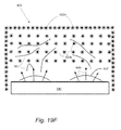
With reference to FIG. 9A-E , schematics of a filtered arc assisted magnetron sputtering (“FAAMS”) hybrid filtered arc-magnetron bi-directional system having additional magnetron sources are provided. In this variation, additional magnetron sputtering sources 310-316 are positioned adjacent to the arc cathode chamber 194 magnetically coupled with filtered arc source 196 and having the magnetron targets forming an open angle in the range from 10 degrees to 80 degrees. This opening angle Ao assists in focusing the magnetron sputtering flow toward the substrates. In this filtered arc assisted magnetron sputtering hybrid coating deposition process, the filtered arc metal plasma flows along the magnetic field lines of the transporting magnetic field created by the duct coil 270. Moreover, the magnetic field lines diverge at the exit of the plasma duct 272. This results in metal ions from the filtered arc cathode passing by the magnetron sputtering target area close to the target surface and crossing a magnetron discharge area with large close-loop magnetic field topology. A substantial portion of these metal ions are trapped in the magnetron magnetic field and contribute to the sputtering of the magnetron target, which can occur even without sputtering gas (argon or other noble gas) and within a broadened pressure range from 10−6 to 10−2 torr. Another portion of the metal ions generated by filtered arc cathodes continue towards substrates 22 where they mix with the focusing magnetron sputtering flow, providing an ionized metal fraction of the magnetron sputtering coating deposition process. It is well-known that increasing the ionization rate of the metal vapor improves coating adhesion, density, and other mechanical properties, and smoothness.
The FAAMS surface engineering system can operate in the following modes:
RAAD plasma immersion ion cleaning, ion nitriding, low energy ion implantation. In this mode the cathodic arc source is operating, both trim coils are ON, but the plasma transporting duct coil is OFF. Turning OFF the duct coil effectively prevents the metal plasma generated by the cathode positioned in a center of the plasma duct for reaching out of the plasma duct toward substrates to be coated in a coating chamber, but the gaseous dense and highly ionized RAAD plasma is filling the entire processing chamber including the interior of the plasma duct and the area in a chamber where substrates to be coated are positioned on the substrate holder. This dense gaseous plasma provides a highly ionized environment for plasma immersion ion cleaning, ion nitriding (as well as ion carburizing, oxi-carburizing, boronizing and other ion saturation processes) and low energy ion implantation. It can also be used for remote arc assisted CVD (RAACVD) processes, including deposition of a diamond-like carbon (DLC) coating when the hydrocarbon contained gaseous atmosphere is created in a coating chamber. In this mode, the remote arc plasma assisted CVD process can be conducted. Moreover, it is possible to deposit polycrystalline diamond coatings when substrates are heated to a deposition temperature ranging from 500 to 1000° C. (depending on type of substrate). In such a process, the gas pressure is typically ranging from 1 to 200 mTorr, the gas atmosphere typically includes 0.1-2% of methane in hydrogen at a hydrogen flow rate ranging from 50 to 200 sccm depending on pumping system capability with the balance being argon. The duct coil works as a magnetic shutter, effectively closing the way out of the metal plasma generated by the cathode in a plasma duct, while opening the way for the RAAD generated gaseous plasma.
When the duct coil is OFF (magnetic shutter is closed) and RAAD plasma is created within the coating chamber between the cathode in plasma duct and remote anode(s) in a coating deposition area outside of the plasma duct, the highly ionized plasma environment can be used for plasma assistant magnetron sputtering (RAAMS) processes. In this case, the magnetron sources positioned outside of the plasma duct in a coating area are turned ON and magnetron sputtering process is conducted in a highly ionized RAAD plasma environment. In this process, the productivity of the magnetron sputtering increases more than 30% and the coating is densified by the ion bombardment of the substrate surface by gaseous plasma-born ions.
When the plasma duct coil is ON, the magnetic shutter is open and metal plasma generated by the cathode in a plasma duct is flowing into the coating deposition area along the magnetic force lines of the transporting magnetic field generated by the duct coil. The filtered arc metal plasma can be used for deposition of the variety of coatings, including super hard hydrogen free tetrahedral amorphous carbon (ta-C) coating when graphite bar is used as a cathode target in a plasma duct. When magnetron sources positioned in the exit portion of the plasma duct and having their targets facing the substrates are turned ON, the hybrid filtered arc assisted magnetron sputtering (FAAMS) process starts. In this case, the filtered arc metal plasma which is 100% ionized is passing the magnetron sources mixing with the magnetron sputtering atomic metal flow which generally has a low ionization rate of <5%. The mixed filtered arc metal plasma and magnetron sputtering atomic metal flow is directed toward substrates in a coating area in front of the exit of the plasma duct, which provide hybrid filtered arc assisted magnetron sputtering coating deposition with high and controllable concentrations of the depositing metal atoms flow.
With reference to FIG. 11 , a schematic of a batch coating system with a peripherally located shielded cathode chamber assembly is provided. Coating system 330 includes vacuum chamber 332, cathode chamber assembly 334, which includes cathode chamber 336, cathode 338 and shield 340. System 330 also includes primary power supply 342 which sets the voltage potential between cathode 338 and primary anode 344. System 330 also includes magnetron sputtering sources 356-366 each of which includes target Ts, power supply Ps, and anode As. System 330 also includes remote anode 360 which is set at a voltage potential relative to cathode 338 by power supply 362. In this embodiment, substrates 22 move axially along direction d3 as they are coated.
In a refinement, the magnetrons 402, 404, 406 shown in FIG. 12 , can be replaced with planar heaters. The substrates to be coated can be placed at the heater surface, facing the center of the chamber where the shielded cathode chamber 382 is positioned with the cathode 384. In this case the substrates can be heated to 900° C. while at the same time highly ionized remote anode arc plasma can be established in the chamber 380 by remote anode arc discharge between the cathode 384 in a cathode chamber 382 and the remote anodes 536, 538, 540 positioned at the wall of the chamber 380. In this process, when gas atmosphere in a chamber 380 is composed of a mixture of methane, hydrogen and argon at the pressure range from 1 mTorr to 200 mTorr and methane concentration in hydrogen ranging from 0.1 to 2 at. weight % the polycrystalline diamond coatings can be deposited on substrates positioned at the heated surface of the heaters, heated to the deposition temperature ranging from 700 to 1000° C.
With reference to FIG. 13 , schematic illustrations of a system incorporating an electron emitting vacuum arc cold cathode source are provided. In particular, the present variation adopts the design of the electron emitting vacuum arc cold cathode source of the system of U.S. Pat. No. 5,269,898, the entire disclosure of which is hereby incorporated by reference. Rod-shaped cathode 430 is mounted within cathode chamber 432, which serves as a primary anode for the vacuum cathodic arc discharge powered by the primary arc power supply 434. Cathode 430 is connected to the negative output of an arc power supply 434, and the enclosure 436 of the cathode chamber 432 is connected to the positive output of arc power supply 434. The positive output of the primary arc can be optionally grounded as shown by the dashed line in FIG. 7D . An arc is struck repetitively by a striker 440, located at the end of cathode 430 that is opposite the connection to arc power supply 434. A helical electromagnet coil 442 is mounted coaxially with the cathode 430 and serves to generate a solenoidal magnetic field with flux lines substantially parallel to the cathode 430 axis, and having a magnitude proportional to the current furnished by a coil power supply 446. One or more substrates 20, upon which a coating is to be deposited, are disposed surrounding the cathode chamber 432 and optionally mounted on a substrate holding turntable platform (not shown) which will provide rotation of the substrates during deposition, if necessary, to achieve a uniform coating thickness distribution thereon. An arc spot 450 and a typical trajectory 452 thereof resulting from the influence of the applied magnetic field are also depicted. Arc spot travels all or part of the length of the cathode 430 toward the connection to arc power supply 434 before being re-struck. The insulator 454 prevents movement of the arc spot 450 off the desired evaporable surface of cathode 430. Electromagnet coil 442 may be electrically isolated from the arc circuit, or it may comprise a part of the anode by connection thereto as indicated by the dotted line 458. The electromagnetic coil 442 may alternatively serve as the sole primary anode for the primary arc discharge in the cathode chamber 432, in which case the electromagnetic coil 442 is isolated electrically from the chamber 430 and connected to the positive output of primary arc power supply 434, which is disconnected from the cathode chamber 432. One or more magnetron sputtering sources 460 are mounted along the walls 462 of the chamber 466 surrounded by the remote anodes 470. The remote anodes are connected to the positive output of the remote arc power supply 472, while its negative output is connected to the cathode 430 in the cathode chamber 432. The enclosure 436 of the cathode chamber 430 has openings 476 covered by shields 478 to prevent the heavy particles (ions, neutral atoms and macroparticles) emitted by the cathode 430 from reaching the deposition area outside of the cathode chamber 432, but the electrons are able to freely penetrate into the coating area throughout the openings 476 between the enclosure 436 and shields 478. The remote arc current is conducting between the cathode 430 within the cathode chamber 432 and remote anodes 470 surrounding the magnetron sputtering sources 460 at the wall of the coating chamber 466. The remote anode is connected to the positive output of the remote arc power supply 472, while the negative output of the remote arc power supply 472 is connected to the cathode 430 in the cathode chamber 432. The remote arc ionizes and activates the plasma environment during the magnetron sputtering coating deposition process, but can also serve as a source of ionization and creation of plasma environment in a coating area during preliminary ion cleaning of the substrates before the coating process starts, as well as for the plasma immersion ion implantation, ionitriding and plasma assisted low pressure CVD coating deposition processes.
With reference to FIGS. 14A-14C , a schematic illustration of a variation of a coating system incorporating a macroparticle filter are provided. In this variation, the design of the cathode chamber of U.S. Patent Publication No. 2012/0199070 is adopted, the entire disclosure of this patent application is hereby incorporated by reference. System 480 includes cathode chamber 484 which is configured as a macroparticles filter. Cathode chamber 484 includes an even number of duct assemblies symmetrically positioned around elongated cathode 486. The variation set forth in FIGS. 14A and 14B includes four duct assemblies, i.e., duct assemblies 488, 490, 492, 494, which effectively form an enclosure 496 around the cathode 486. The duct assemblies 488, 490, 492, 494 define ducts 500, 502, 504, 506 through which positively charged ions are guided from cathode target 486 to substrates 20. Duct assemblies 488, 490, 492, 494 define a magnetic field for guiding a plasma. Duct assemblies each include support component 510 and baffle component 512 for blocking macroparticles. In a refinement, baffle component 512 includes protrusions 514 for enhancing the ability of filtering out macroparticles. Electrical posts 516, 518 are used to connect to the filter power supply so that the duct assemblies are electrically biased for repelling positively charged ions. When the duct assemblies 488, 490, 492, 494 are positively biased in relationship to the cathode 486 it is also serving as a primary anode for the primary arc discharge established within the cathode chamber 484. The duct assemblies 488, 490, 492, 494 can also be isolated and have a floating potential. In this case the arc steering electromagnetic coil (not shown) can serve as a primary anode to the cathode 486 for igniting the primary arc discharge in the cathode chamber 484 as was explained above in relation to the embodiment of the invention shown in FIG. 14B . With reference to FIG. 14C a schematic perspective view of a cathode chamber enclosure-filter assembly 496 is provided. Filter assembly-cathode chamber enclosure 496 is made of a set of duct assemblies 488, 490, 492, 494, which are parallel to the cathode 486, preferably having a shape of a rod but which can also be made as a bar with any polygonal cross-section. During the filtered cathodic arc coating deposition process the filter is electrically activated by passing a current along the duct assemblies 488, 490, 492, 494 to establish a magnetic field.
Still referring to FIGS. 14A-14C , a magnetic field is optionally created by passing a current through the duct assemblies so as to create a magnetic field. In particular, adjacent duct assemblies generate magnetic fields with opposite magnetic polarities. Arrows 520, 522, 524, 526 indicate an example of the directions that current may flow to create such magnetic fields. The arrows show that the directions of the currents in the neighboring duct assemblies are opposite to each another. The magnetic field generated in this manner has an orientation normal to an elongated cathode surface and strength conductive to plasma guidance produced by passing current through the duct assemblies. In this filtered arc deposition mode, the metal vapor plasma emitted from the cathode 486 passes through the ducts between the duct assemblies thereby allowing undesirable macroparticles and neutral metal vapor constituencies to be eliminated and to deliver 100% ionized metal vapor plasma to the substrates.
In the remote anode arc plasma discharge (RAAD) mode, the current does not conduct through the duct assemblies 488, 490, 492, 494 and the metal vapor plasma extracting magnetic field is not generating. In this duct-passive mode, the electrons emitted from the surface of the cathode 486 can pass freely through the ducts 500, 502, 504, 506 which conduct the RAAD current between the cathode 486 in the cathode chamber 484 and the remote anodes 530, 532 and 534 which surround the magnetron sources 538 and 540 which are positioned along the chamber wall 506 of the coating system 380. At the same time, the duct assemblies 488, 490, 492, 494 serve as a barrier which stops the heavy particles such as metal vapor atoms, ions and macroparticles, emitted from the cathode 486 to reach substrates. The RAAD plasma ionizes and activates the plasma processing environment in a processing area of the system 380 where the substrates are positioned. This results in the ability to conduct ion plasma cleaning, ion implantation ionitriding and remote arc assisted magnetron sputtering (RAAMS) yielding advanced properties of plasma processing products.
With reference to FIGS. 15A and 15B , a schematic illustration of a variation of the RAAMS system is provided. FIG. 15A is a schematic side view of the RAAMS system while FIG. 15B is a schematic side view perpendicular to the view of FIG. 15A . System 530 includes chamber 532, substrate holder 534 with substrates 536 to be coated, primary cathodes 538A, b, magnetrons 540A, B and remote anodes 542A, B. Cathodes 538A, B are located at side 544 (i.e., the bottom) of the chamber 532 in a cathode section 548 separated from the coating section 550 of the chamber 532 by chevron shield 552, which is impermeable for heavy particle but allows the electrons to go through toward the remote anodes 542A, B in coating section 550. Shield 552 can be electrically floating or it can be connected to the positive terminal of either primary arc power supply 554 or an additional power supply (not shown). The primary arc anode 556 is located at the middle of the cathode chamber 548 between two arc cathodes: the cathode 538A in a left compartment of the cathode chamber 548 and the cathode 538B in a right compartment of the cathode chamber 548. The substrate holder 534 with substrates 536 to be coated is located between magnetrons 540A, B. The substrates face magnetron 540A on left side and magnetron 540B on right side. The remote anodes 542A, B are located above magnetrons 540A, B and are separated from one another by an optional separation baffle 560. Separating anode 556, substrate holder 534 with substrates 536 to be coated and optional separation baffle 560 effectively divide chamber 532 into two sides (i.e., a left side and right side) thereby preventing hot jet 562A associated with cathode 538A located on left side of chamber 532 from flowing through the right side of chamber 532 toward remote anode 542B from flowing into the left side of the chamber 532 toward remote anode 542A. Remote anode 542A is coupled with arc cathode 538A on left side of substrate holder 534 and remote anode 542B is coupled with the cathode 538B on right side of the substrate holder 534. Anode 556, substrate holder 534 and optional separating baffle 560 effectively divide coating chamber 550 into two sections: a left section housing left cathode 538A, left magnetron 540A and left remote anode 542A and a right section housing the right cathode 538B, right magnetron 540B and right remote anode 542B. This division forms two narrow discharge gaps or discharge corridors: a left gap separating left magnetron 540A and substrate holder 534 on the left side of the coating section 550 and a right gap separating the right magnetron 540B and substrate holder 534 on right side of the coating section 550. The width of the separating discharge gaps ranges from 2 to 20 inches.
In a refinement, the cathode target can be made of a metal having a gettering capability such as titanium alloy or zirconium alloy. In this case the shielded cathode electron emitting source also serves as a vacuum gettering pump which improves pumping efficiency of coating system 530. To further improve the gettering pumping efficiency, shield 552 facing the evaporating surface of the cathode target 538A in the cathode chamber 550 can be water cooled and optionally connected to high voltage bias power supply. When water cooled shield 552 is biased to high negative potential ranging from −50V to −1000V relative to cathode targets 538A and 538B, shield 552 is subjected to intense ion bombardment by metal ions generating by the cathodic arc evaporating process. Condensation of metal vapor under conditions of intense ion bombardment is favorable for pumping noble gases such as He, Ar, Ne, Xe, Kr as well as hydrogen. Moreover, water cooled primary anode 556 facing cathode targets 538A, B also contributes to the pumping capacity by increasing the metal vapor condensation/gettering area.
Still referring to FIGS. 15A and 15B , it can be seen that several magnetron sources 540 are located above cathode chamber 548 in coating section 550. Substrate holder 534 with substrates 536 moves along chamber 532 passing the magnetrons. Cathodic arc spot 564 moves along cathode target 566 of arc cathode 538 while being steered by magnetic steering coil 570 or other steering means. Experimental investigation of this system revealed that narrow plasma jet 562 has a high plasma density ranging from 1011 to 1013 cm−3 and an electron temperature exceeding 2 eV (typically ranging from 3 to 20 eV). The majority of the remote anode arc discharge current flows along the narrow hot plasma jet 562 and has an arc current density ranging from 0.1 mA/cm2 to 100 A/cm2. The rest of the coating section is filled by the cold and rare plasma with electron temperature typically below 3 eV and plasma density ranging from 108 to 1011 cm−3. The width of hot plasma jet 562 is typically from 1 to 5 cm while moving with the same speed as cathodic arc spot 564 which follows the steering movement of the cathodic arc spot 564 on cathode target 566. It is believed that the most of the remote arc current conducts between cathode 538 in cathode chamber 548 and remote anode 542 throughout hot plasma jet 562. It can be also seen from FIG. 15A that two hot plasma jets 562A and 562B form within the narrow discharge gaps between left magnetron 540A and substrate holder 534 on left side of the coating section 550 and between right magnetron 540B and substrate holder 534 on the right side of the coating section 550. Left jet 562A bridges left cathode 538A in a left compartment of the cathode chamber 548 and left remote anode 542A on the left side of the coating section 550. Right jet 562B bridges right cathode 538B in a right compartment of the cathode chamber 548 with right remote anode 542B on right side of the coating section 550.
With reference to FIG. 16 , a schematic illustration of a variation of FIGS. 15A and 15B with a cathode in one of the compartments of the cathode chamber and with two cathodic arc spots is provided. In this variation, two plasma jets 562A and 562B formed between chevron baffle 552 and remote anode 542 above each of cathodic arc spots 576A and 576B bridge the current connections between cathode 538 and remote anode 542. The direction of the remote arc current along jets 562A and 562B associated with cathodic arc spots 576A and 576B are shown by the vertical arrows on these jets. The plasma distribution has maximums 578A and 578B near each of the cathodic arc spots 576A and 576B moving along the erosion corridor 580 on cathode target 566 either by a steering magnetic field created by a steering coil located beyond the target 582 (not shown) or by other means as described below. In this variation, the dimensions of the high ionization area is Ai˜L (magnetron)×W (jet). In horizontally aligned systems set forth above, the ionization area is only Ai˜W (magnetron)×W (jet). The increase of the magnetron sputtering flow ionization area by vertical alignment of arc jet 562 (parallel to the long side of the magnetron 540) vs. horizontal alignment of the arc jet 562 (parallel to the short side of the magnetron 540 as in the parent case) is approximately L (magnetron)/W (magnetron).
Still referring to FIG. 16 , a confined plasma streams (i.e., a plasma jet) bridging the discharge gap between remote anode 542 and cathode target 566 through coating region 550, moves along direction d4 while remaining parallel to the long side of the magnetrons 540. The ends of confined plasma jets 562 move along direction d4 as set forth in FIG. 16 . Arc spot 576 forms on cathode 580 along the erosion zone 578. The plasma field 584 at remote anode 542 and the plasma field 578 at cathode target 580 are confined dimensionally in a space from about 1 to 5 inches along direction d4. In one refinement, magnetic steering fields are used to accomplish the rastering movement along d4. In other refinements, this rastering movement is accomplished by mechanically moving cathode 580 along direction d4. In still other refinements, a thermionic filament cathode with secondary emission electrons moves along d4.
With reference to FIGS. 15A, 15B, and 16 , an aspect of the relative sizing of various components of coating system 530 is provided. Remote anode 542 has a linear remote anode dimension Da parallel to the cathode target 538. The horizontal area of location of vapor sources 538 (i.e., the four magnetrons shown in FIG. 15B ) is also relevant. The area along the direction parallel to the short side of the magnetrons 538 has a linear vapor source dimension D. Cathode target 566 has a linear cathode target dimension Dc parallel to the remote anode 542 and also parallel to the short side of the magnetrons 538. In a refinement, the linear remote anode dimension Da, the linear vapor source dimension D, and the linear cathode target dimension Dc are parallel to each other. In another refinement, the linear remote anode dimension Da is greater than or equal to the linear cathode target dimension Dc which is greater than or equal to the linear vapor source dimension D.
With reference to FIGS. 18A and 18B , a refinement with separate primary cathode chambers 548 for each magnetron sputtering source 540 is provided. In the FIG. 18A , cathode chamber 548 is positioned under coating chamber 550. Magnetron 540 is positioned in coating chamber 550 immediately above the shield 552 separating cathode chamber 548 from the coating chamber 550. Cathodic arc source 538 as a powerful electron emitter is positioned below the magnetron 540. The size of the cathode target, which defines the dimension of arc spot steering zone, is ranging from ¼ to 2 times of the width of the magnetron target, but preferably within the range from 0.5 to 1.5 times the width of the magnetron target. Primary anode 556 is positioned above the cathode target 566 and has a dimension generally smaller or equal to cathodic arc target 566. Magnetic steering coil 570 is optionally positioned under the cathode 538 for steering arc spots at the surface of cathodic arc target 566. Remote anode 542 is positioned in a coating chamber 550 above the magnetron 540 providing that cathode 538; magnetron 540 and anode 542 are aligned generally along the same line. High density plasma jet 562 forms within coating chamber 550 between shield 552 and anode 542 along the surface of the magnetron 540 above the cathodic arc spot 602 which is moving over the surface of the cathode target 566 by the magnetic steering effect provided by the steering magnetic field of steering coil 570. Cathodic arc spots 602 and plasma jet 562 are aligned along a single vertical line parallel to the long side of the magnetron 540 bridging the discharge gap toward remote anode 542. In this arrangement, the steering of the cathodic arc spots 602 at the surface of the cathode target 566 provides a corresponding steering of the high density plasma jet 562 with remote anode arc current directed along the direction parallel to the long side of the magnetron 540, while the axes of the jet 562 is parallel to the long side of the magnetron 540. Plasma jet 562 crosses the magnetron discharge in front of the magnetron target bridging the distance between the shield and the remote anode 542 and ionizes the sputtering metal atoms flow and gaseous environment in front of the magnetron sputtering source 540 within the area where the plasma jet 562 crosses the magnetron discharge. The increase of ionization and activation of the metal sputtering atoms and gaseous species in front of magnetron 540 is distributed evenly both along the direction parallel to the long side of the magnetron 540 and along the direction parallel to the short side of the magnetron 540. The uniformity of the ionization ability of the plasma jet 562 along the direction parallel to the long side of the magnetron 540 is achieved by the uniform distribution of the plasma density and the electron temperature along the plasma jet 562. The uniformity of the ionization ability of plasma jet 562 along the direction parallel to the short side of the magnetron 540 is achieved by repeatedly moving the jet 562 back and forth across the magnetron discharge from one end of magnetron 540 to another by magnetically steering displacement of the cathodic arc spot 602 on cathodic arc target 566.
In a typical example, the primary arc discharge between the cathode 538 in the cathode chamber 548 and the primary anode 556 is powered by the power supply 554 a. The remote anode arc discharge between cathode 538 and remote anode 542 is powered by power supply 608. Ballast resistor 610 is installed between remote anode 542 and grounded coating chamber 550, which allows control of the voltage drop between remote anode 542 and grounded chamber 550. When the micro-arcing occurs at the coating chamber 550 walls, electronic switch 612 will be closed thereby short circuiting remote anode 542 to the ground and effectively eliminating arcing, followed by re-ignition of the remote arc when the position of electronic switch 612 is open. Switch 612 may be also open during the time of igniting of the RAAD plasma. Ignition of the RAAD can be provided by applying high voltage negative potential either to magnetron 540 which starts the magnetron discharge or, alternatively, by applying high negative voltage to the substrate holder 534 establishing the glow discharge across the discharge gap between cathode chamber 548 and remote anode 542. The high voltage discharge as a means for ignition of the RAAD can be used in either DC or pulse discharge mode. The dimensions of the magnetron sputtering target of the magnetron 540 are typically 10 cm width×100 cm tall. The dimension of the cathodic arc target 566 is typically about 10 cm, nearly equal to the width of the magnetron 540 target. The width of the plasma jet 562 is about 3 cm. The magnetically steered moving velocity of the arc spot 602 over the surface of the cathode target 566 is approximately 1000 cm/s. In this case, the repetition frequency of the plasma jet steering across the magnetron discharge zone will be approximately 50 Hz. Assuming the improved ionization rate within the area of the magnetron discharge crossed by the plasma jet 56 a is ˜30% the average ionization rate of the magnetron discharge plasma by the plasma jet 562 will reach ˜10%, which is at least an order of magnitude higher than that of the conventional magnetron sputtering flow. The improved ionization rate of the magnetron sputtering flow results in increased intensity of ion bombardment assistance during magnetron sputtering coating deposition process which yields coatings having nearly theoretical high density, low defects, high smoothness, and superior functional properties. The inline vacuum coating and plasma treatment system utilizing a plurality of magnetron sources, each provided with a separate cathode chamber, is shown in FIG. 18B .
With reference to FIG. 19A , a further advanced variation of the systems of FIG. 14-18 is provided. Intermediate electrode-grid 622 is installed in front of the magnetron 540, which effectively limits the area of the confinement of the high density plasma jet 562 in front of the magnetron sputtering target 540. In this arrangement, cathode chamber 548 is enclosed within the enclosure 628. Although enclosure 628 can be electrically grounded, it is preferable that it is insulated from the grounded chamber providing that there is no direct electrical coupling between the primary and the remote arc discharges. Enclosure 628 has opening 630 facing the discharge gap or plasma corridor 632 between the magnetron target 634 and the electrode-grid 622. The length of opening 630 is generally equal to that of the width of the magnetron target 634 while the width of the opening 630 is less than the width d of the discharge gap 632. Electrode-grid 622 can be composed of thin wires 638 made of refractory metals chosen from the group of W, Ta, Nab, He, Ti, Mo, and stainless steel. The diameters of the wires are typically from 0.01 mm to 2 mm. A diameter less than 0.01 mm may result in melting of the wire in a contact with RAAD plasma. A diameter thicker than 2 mm will absorb too much coating material from the sputtering flow. Wires 638 can be arranged in a screen of different patterns or as an array of single wires parallel to each another. Grid electrode 622 must be transparent to the sputtering metal flow with transparency better than 50%. The distance between the neighboring wires 638 in a screen or grid electrode 622 is typically from 0.5 mm to 10 mm. Distances between neighboring wires in grid electrode 622 less than 0.5 mm are impractical and can affect the transparency of grid electrode 622. Distances between neighboring wires 638 in grid electrode 622 greater than 10 mm may not have enough plasma confining properties to confine plasma jet 562 within the discharge gap or the plasma corridor 632. The distance d between the magnetron target 634 and the grid electrode 622 is typically from 10 mm to 100 mm. Distances less than 10 mm are too small to confine the arc jet 562A, while distances greater than 10 cm are too large to provide a narrow corridor which can squeeze the plasma jet, effectively increasing its electron density, electron temperature, and the metal sputtering flow ionization rate.
The remote arc current density in jet 562 the remote arc discharge gap defined between the anode grid 622 and the magnetron 540 is ranges from 0.1 to 500 A/cm2. A remote current density less than 0.1 A/cm2 are not enough to provide a desirable level of ionization of the magnetron sputtering flow. The remote arc current densities more than 500 A/cm2 requires too much power of the remote arc discharge power supply which is not practical for the applications. High current density of the remote arc discharge (i.e., jet (562) within the discharge gap defined between the anode grid 622 and magnetron 540 can be achieved by using a DC power supplies 646 and/or 608 which can provide a DC currents ranging from 10 to 2000 A to remote anode 542 and/or the grid anode 622 or, alternatively, by using a pulse power supplies which can apply a positive voltage pulses to the remote anode 542 and/or grid anode 622. The positive voltage pulses can range from 500 to 10,000 V and the associated current pulses can range from 1000 to 50,000 A.
With reference to FIG. 19B , a variation of the system of FIG. 19A is provided. Wires 638 in the grid-electrode array 622 are positioned parallel to each other and to the short side of the magnetron 540. Each wire 638 is connected to the remote anode 542 via capacitor 640 and shunt resistor 642 while the diodes secure the direction of the current toward wire element 638. During operation, before the remote discharge is ignited, capacitors 640 are charged to the maximum open circuit voltage of the remote anode arc power supply 608. This arrangement triggers the cascade ignition of the remote arc discharge by igniting the remote arc, first between the cathode 538 and first single wire 638 positioned closest to the cathode 538, followed by propagation of the remote arc discharge sequentially via all intermediate single wire electrodes 638 of the electrode grid array 622 toward remote anode 542. After the ignition phase, capacitors 640 will be discharged and the potential of each wire 638 and of the entire electrode grid array 622 will be determined by shunt resistors 642. If the remote anode arc discharge is extinguished, capacitors 640 will be charged again to the maximum open circuit voltage of the power supply 608 with the cascade ignition automatically repeated. Alternatively, the ignition is initiated by the control system. This approach can be also applied to the multi-magnetron system similar to that shown in FIGS. 16 and 18B . In this case the intermediate ignition electrodes of the cascade ignition arrangement can be positioned between within the gaps between the respective magnetron sputtering sources.
With reference to FIG. 19C , an additional advanced of the coating system of FIG. 19A is provided. Capacitively coupled RF electrodes 648, 650 are positioned at both cathode end 652 and remote anode end 654 of the remote arc discharge column 562. The RF generator and the matching network are installed in series with RF electrodes 648 to activate the plasma jet 562 by superimposing the RF oscillations along plasma jet 562. The frequency of the oscillations can range from 10 kHz to 500 MHz. In a refinement, the frequency of the generator ranges between 500 kHz and 100 MHz. The commonly used 13.56 MHz RF generator is suitable for this purpose. When intense RF oscillations are created within the plasma jet 562 the plasma density, electron temperature and, subsequently, the ionization rate of the magnetron sputtering and gaseous plasma increase thereby resulting in an increase in the remote anode arc discharge ionization efficiency and activation capabilities. This further improves the properties and performance of the coatings and plasma treated surfaces by RAAMS discharge plasma. In another variation as illustrated in FIG. 19C , a pulsed high voltage generator or pulsed RF generator 656 is used instead of a continuous-wave RF generator thereby providing high voltage unipolar or RF pulses for ignition of RAAMS discharge as well as superimposed high voltage high current pulses during the coating deposition process. The repetition frequency of the high voltage high current or RF pulses range from 1 Hz to 100 kHz.
With reference to FIG. 19E , a schematic of a system of another remote anode coating system is provided. Remote anode arc plasma cage 622 can be created in front of the magnetron target 634 of the magnetron vapor source 540 as shown illustratively in FIG. 19E . The remote arc discharge can be established between the primary arc cathode (not shown) in a cathode chamber 548 and the anode cage (i.e., grid 622) and/or the top remote anode 542. In this embodiment of the invention the remote anode arc plasma is streaming from the opening 630 in the cathode chamber 548 along the long side of the magnetron target 634 toward the grid anode 622 and/or the top remote anode 542. Although the cage-grid remote anode 622 can be made of wires aligned in many different patterns the embodiment of the invention shown in FIG. 19E utilizes the remote anode cage 622 composed of array of straight wires parallel to the long side of the magnetron target 634.
With reference to FIG. 19F , which is a transversal cross-section of the system shown in FIG. 19E , a schematic of a system using an array of wires is provided. This array of the parallel wires consists of the outer array of wires 622 a forming an outer boundary of the remote anode grid-cage 622. The remote anode arc plasma jet is confined within the anode cage formed by this outer array of anode cage wire 622 a. It can also optionally consist of the array of the inner wires 622 b which are positioned within the anode grid-cage 622. When the positive DC or pulse potential is applied to the anode grid-cage in reference to the cathode in the cathode chamber 548, the anodic plasma sheath is forming around each of the wire of the array of outer wires 622 a and the inner wires 622 b. The ionization efficiency within the anodic plasma sheath is greater than that of the background plasma which results in the improvement of the ionization rate of the magnetron sputtering flow hence contributing to further improvement of the coating properties. The role of the inner wires 622 b is also to divert the charged particles such as electrons and positive ions curling their trajectories, creating a pendulum effect, increasing the length of the trajectories of charged particles, and effectively trapping the charged particles within the anode grid-cage 622 hence increasing the ionization probabilities of the magnetron sputtering flow. This approach to plasma confinement can be also used along without a need of magnetic confinement. This allows using the sputtering target in a diode sputtering mode without magnets while the high density remote anode arc plasma is confined electrostatically within the anode grid-cage 622. The characteristic distance between the neighboring wires in the anode grid-cage 622 shown in FIG. 19E ranges from 0.5 mm to 30 mm. The thickness of each wire is typically ranges from 50 micrometers to 3000 micrometers. The remote anode arc current density streaming along the target 634 parallel to its long side from the cathode chamber opening 634 ranges from 0.1 to 500 A/cm2. The remote anode arc current can be provided either by DC power supplies or pulse power supplies. The cross-section of the magnetron sputtering source 540 surrounding by the anode grid cage 622 is shown illustratively in FIG. 19F . The magnetron discharge 647 is established above the magnetron target 7A inflicting a magnetron sputtering metal atomic flow 649. The anode cage consists of the outer array 622 a and the inner anodic wire array 622 b. When wire is energized by applying the positive potential vs. the cathode in a cathode chamber (not shown), the anodic plasma sheath with enhanced ionization rate is established around each of the wires of the anode grid-cage 622. The trajectories of charged particles (electrons and positive ions) 651 are diverting when the particle is approaching the anodic plasma sheath surrounding the array of the wires 622 a and 622 b. In a refinement the wires of the anode grid-cage 622 is made of refractory metals such as W or Ta and their temperature is maintained in a range of 500-2500° C., which allows effectively re-evaporate the metal atoms of the magnetron sputtering flow which can stick to the surface of the wire. It is believed that high ionization rate within the anode grid-cage will make it possible to operate the sputtering vapor source in a pressure range below 0.5 mtorr and even without noble gas such as argon or krypton which thereby eliminating detrimental inclusions of the noble gas atoms in a coating lattice.
With reference to FIG. 20 , a variation in which the electron emission cathodic arc source with a non-consumable cathode is provided. Cathode assembly 660 includes a water-cooled cathode with a cylindrical shape or rectangular cavity. Rectangular cavity 662 includes an internal evaporating and electron emission surface 664 and the primary anode 666 generally consisting of a cylindrical or a rectangular insert 668 attached to the anode plate 670. Anode insert 668 is extended within the cathode cavity 662. Anode 666 is made of refractory metals chosen from the group of W, Ta, Nb, Hf, Ti, Cr, Mo and stainless steel. Anode plate 670 is isolated from the cathode by ceramic spacers 672. Primary anode 666 is attached to the water-cooled plasma transfer vessel 676 via the spacers 678, having small cross section providing high thermal resistance between the plasma vessel 676 and the primary anode 666. The plasma vessel 676 includes opening 680 with facing the cathode 538 throughout the tubular anode insert 668 on side of the cathode 538 and the opening 682 facing the discharge gap between the electrode-grid 622 and the magnetron source 540 on the side of the coating chamber 550. The length of the opening 682 is generally equal to that of the width of the magnetron target 634 while the width of the opening 682 is less than the width d of the discharge gap 632. The spacers 678 can be made of refractory metal. In this case the plasma vessel 676 is electrically connected to the primary anode 666. Alternatively, the spacers 678 can be made of non-conductive ceramic, making the plasma vessel 676 electrically isolated from the primary anode 666. In any case the spacers 678 must have a small cross section providing a high thermal resistivity between the water-cooled plasma vessel 662 and the primary anode 668. In operation the primary anode is heated by the arc current reaching the temperature when the re-evaporation of the metal transferred from the cathode occurs effectively recycling the cathode metal evaporating from the internal cathode surface 669 in the cathodic arc discharge.
A coating assembly, including the remote anode arc discharge (RAAD) plasma or the arc discharge, can be confined magnetostatically in the vicinity of the magnetron cathode and in front of the magnetron target using a magnetic trap made by a magnetic confining field generated by magnetic coils strategically positioned outside of the vacuum chamber and outside of the magnetron sputtering area instead of an electrostatic trap made by a grid-anode positioned in front of the magnetron target. A magnetic trap can be created by a magnetic field half-cusp configuration where the converging side of the cusp is facing the substrate to be coated; the magnetic field is “pinched’ toward the substrate to be coated. This magnetic trap configuration, also known as magnetic mirror, effectively reflects the electrons back to the magnetron target preventing the diffusion losses of the arc discharge, the RAAD plasma, from the area adjacent to the magnetron target. Alternatively, the arc plasma can be trapped within a closed-loop magnetic field area along one or two long sides of the magnetron target.
With reference to FIG. 22A , showing a cross section view of the plasma assembly, the RAAD plasma is confined by the magnetic mirror-trap within the half-cusp created between the convexed magnetic field lines of rectangular confining magnetic coils 578 and 579 and the magnetron target 634. In this design both planar magnetrons with rectangular targets or rotating magnetrons with cylindrical targets can be used as sputtering sources. Alternatively, a cathode target without magnets can be also used as a sputtering source for diode sputtering.
The magnetron sputtering source 540 is enclosed in a housing 545 and a pair of confining magnetic coils 578 and 579 are positioned at opposite sides of the magnetron 540. The RAAMS module is equipped with a flange 546 for attachment to the coating chamber. Each of the rectangular confining magnetic coils 578 and 579 have a pair of linear conductors parallel to the long side of the magnetron target 634, the front linear conductors 578 a and 579 a adjacent the substrates to be coated in the coating chamber and the rear linear conductors 578 b, 579 b away from the substrate. The front and the rear linear conductors are connected via closing conductors perpendicular to the short side of the magnetron target 634, thus creating a coil. The confining magnetic coils 578 and 579 are setup in opposite polarity, e.g. the direction of the current in the front linear conductor 578 a is opposite to the direction of the current in the front linear conductor 579 a. The confining coils are positioned so that the field lines emanating from their center cross the surface of the magnetron target. In this magnetic coils configuration, the magnetic half-cusp is created between the convexed magnetic force lines 589 and the magnetron target 634. The plane of the magnetic force lines 589 is perpendicular to the plane of the magnetron target 634 as they are converging toward substrates to be coated in the coating chamber. The magnetic field due to a magnetron sputtering cathode 585 blends with the magnetic field lines 589 which confine an arc discharge 562 which are reflected at a point of convergence 571.
In reference to FIGS. 22B and 22C , a pair of coupled unbalanced magnetron sources 545 are installed opposite to each another. In this case the magnetic systems of magnetrons 545 can be setup in a mirror-like configuration shown in FIG. 22B when the magnetic field poles in front of the magnetron targets are the same and either north or south pole. This polarity of the magnetic systems is also named as a matched polarity. Alternatively, the configuration of magnetic field of two opposite coupled unbalanced magnetron sources 545 can be unmatched as shown in FIG. 22C . In both cases the polarity of magnetic field created by a pair of focusing plasma confining coils 578, 579 have to be the same as the polarity of the magnetic field created by the magnetron 545 magnets. The magnetron plasma is more dispersed in a mirror-like configuration shown in FIG. 22B vs. more focused, dense plasma flow in a configuration shown in FIG. 22C .
The side view of the RAAMS module with magnetic confinement is shown schematically in FIG. 22D . This configuration of the RAAMS module is similar to that shown in FIG. 19A except for the hoods positioned at the bottom and top of the RAAD plasma area along the magnetron target 634. The substrate holder 534 with substrates 536, face the plasma jet 562. A DC power supply 851 is used to power the cathode. The positive pole of the power supply 851 can be grounded or, alternatively, connected to the remote anode 8 a via switch 853. The cathode hood 18 b is installed at the top of the cathode chamber shield 18 and attached to the grounded wall flush-in with magnetron target 634, while the anode hood 8 b surrounds the remote anode 8A in front of the anode chamber 8. The cathode hood 18 b and anode hood 8 b are crossing the short edge of the magnetron target 634 erosion area (racetrack) and having their openings positioned beyond the short edge erosion area boundary within the magnetron target 634. Cathode chamber 1A and cathode chamber shield 18 include a primary arc anode 5, primary arc cathode 4, steering magnetic coil 15 and cathodic arc spot 66. The primary arc in a cathode chamber 1 a is powered by the primary arc power supply 10, while the plasma jet 562 is powered by the remote arc power supply 11. Steering magnetic coil 15 directs cathodic arc spot 66 at the cathode target front surface. Only one confining magnetic coil 578 with front linear conductor 578 a and rear linear conductor 578 b is shown in this view. The direction of the current along the magnetic coil 578 conductors is shown by the arrow. In operation the RAAD plasma jet 562 enters the cathode hood 18 b through the opening 18 a in the cathode chamber enclosure 18, crossing the magnetron magnetic field in the area of the short side magnetron target erosion corridor, and penetrates further in the area of the magnetron erosion zone parallel to the long sides of the magnetron target where it is confined within the magnetic half-cusp 571 (FIG. 22A ) above the magnetron target 634. This confinement is due to the magnetic mirror reflection effect by the converging convexed magnetic force lines 571 which effectively reflects the electrons back to the magnetic half-cusp creating plasma trap for RAAD plasma. The connection of the arc jet 562 to the remote anode 8 a in the anode chamber 8 is secured by the anode hood 8 b. The direction of the magnetic force lines 589 generated by confining coils 578 and 579 must coincide with the direction of the magnetron magnetic force lines 585, shown in FIG. 22A , created by magnetron magnetic system positioned behind the magnetron target 634. The cathode hood 18 b and the anode hood 8 b allow the remote arc plasma jet 562 crossing the magnetic barriers created by the magnetron magnetic field near the erosion area of the short sides of the magnetron target 634 and penetrate into the area of magnetic cusp confinement zone 571. The magnetic mirror configuration of RAAD plasma confinement can be combined with anodic grid shown in FIG. 19 , combining electrostatic and magnetostatic confinement of the plasma, which can further improve the confinement capability of the plasma trap in front of the magnetron target by imposing the arc plasma confining positive potential along the magnetic force lines surrounding the magnetic cusp arc plasma trapping area 571 and specifically at the end of the “pinched” magnetic field lines which will increase the reflecting of the ions back to the magnetron target 634 area effectively sealing the magnetic cusp plasma trap 571.
In a variation of the present embodiment, FIG. 22E shows a hybrid magnetostatic/electrostatic plasma trap for confinement of the RAAD plasma with a cathode 540. The wire electrodes 638, which are forming the anodic grid, should preferably have shape repeating the shape of the magnetic force 589 lines from coils 578 and 579 forming the border of the magnetic cusp 571 in front of the magnetron target 634. This anodic trap will effectively charge the border of the magnetic cusp with high positive “anodic” potential which will improve the confinement of remote arc plasma within the magnetic cusp trap area 571 and increase the concentration of plasma species at the substrate 536.
In accordance with the present embodiment, FIG. 23 shows the perspective view of the RAAMS vertical module with magnetic-mirror confinement of RAAD plasma using coils 578 and 579 to create magnetic cusp 571 in front of the magnetron target 634 and cathode 540. The magnetron cathode has a long edge 540 d and a short edge 540 c. The cathode hood 18 b and anode hood 8B are bridging the remote arc plasma jet throughout the magnetic barrier around the bottom and the top short sides of the magnetron target 634 and allow the RAAD plasma to be transferred into the magnetic cusp 571 without diffusion losses.
This approach can be also applied to the multi-magnetron system similar to that shown in FIG. 18 . In a refinement shown in FIG. 24A , the modular inline system 10 comprising a set of RAAMS modules with magnetic-mirror confinement of RAAD plasma previously shown in FIGS. 22-23 , is provided. The RAAMS modules are setup in line opposite to each other while a substrate holder 534 with substrates to be coated 536 is positioned between two rows of the RAAMS modules with ability of reciprocating and/or linear movement. To achieve the magnetic cusp configuration of the magnetic field in each of the RAAMS modules the polarity of the plasma confinement coils must be opposite in each pair of the coils on both sides of the magnetron sputtering source. The polarity of the confinement coils must be in agreement with the polarity of the permanent magnets of the magnetron sputtering source providing that the direction of the plasma confining magnetic field created by the magnetic confinement coil is same as a direction of the magnetron magnetic field at the same side of the magnetron target when the coil is positioned. For instance, the direction of the current in the front linear conductor 578 a of the coil 578 is opposite to the direction of the current in the front current conductor 579 a on the opposite side of the magnetron 540. In addition, the polarity of neighboring magnetron sources must be also opposite to each another. In this alignment the RAAD plasma jet 562 will be confined within magnetic cusp area 571 adjacent to the magnetron target providing improved ionization and activation rate of the magnetron metal sputtering flow as well as chamber gaseous plasma. This will result in high deposition rate and densification of the coatings deposited on substrates to be coated 536 on substrate holding cart 534. The exit magnetic-cusp field of the opposite modules in the inline system 10 can have the same polarity (as shown in FIG. 24B ) or opposite polarity to their counterparts on the opposite side of the inline system. When the opposite modules facing each another have the same polarity of the exit magnetic cusps the RAAMS plasma will get more dispersed spreading over larger areas of the coating zone within the chamber 10. In this case the RAAMS plasma is distributed more uniform along the path of the substrate holding cart 534 with substrates to be coated 536. In this case the energy conveyed from plasma toward substrates to be coated is also reduced by dispersing the flux of energetic particles over larger area. Alternatively, the polarity of the opposite RAAMS modules exit magnetic cusps can be opposite. In this case the RAAMS plasma generated by the opposite modules in the inline system 10 is focused in the area between the opposite modules facing each another. In this case the RAAMS plasma distribution along the inline chamber 10 is less uniform with maximum plasma density along the axes of each pair of the opposite magnetron sources 540 facing each another. In this case the flux of the energetic particles reaching the substrates to be coated 536 is greater along the axes of the opposite magnetron sources resulting in greater deposition rate and deposition temperature of the substrates to be coated in the area near the axes of the magnetron targets.
The map of magnetic force lines in the inline configuration, calculated by using the finite element modeling method is shown in FIGS. 24C , D, and E. In this system layout, the magnetron magnetic field has been modeled using a pair of current conductors 541 positioned behind the magnetron target 634. The polarity of the magnetic field is mirrored at the opposite side of the inline system, e.g. the opposite modules facing each another have the opposite polarity of the exit magnetic cusps forming a magnetically matched magnetic field configuration. In FIG. 24C the current density in the front linear conductors 578 a and closing linear conductors 578 b of the magnetic confinement coils 578 is 1.2×10⁶ A/m2, the current density in the linear conductors 541 a and 541 b, simulating permanent magnet-based magnetic system of the magnetron 540, is 2×10⁶ A/m2. The directions of the currents in linear conductors are shown by the cross and dot marks with the dot for example, 541 a, indicating current flow out of the paper and the cross for example, 541 b, indicating current flow into the paper. In this configuration the magnetron discharge is created in the area 585 adjacent to the magnetron target 634. The magnetic cusp 571 is forming in front of the magnetron target 634 between the front linear conductors of the magnetic confinement coils 578 and the magnetron target 634. It can be seen that strong magnetic beams 573 are forming along the plane of symmetry of the opposite magnetron sources 540. The magnetic beams 573 a and 573 b associated with the neighboring magnetrons are directed opposite to each other. When the currents in the confining magnetic coils are increasing the magnetic cusp 571 becomes more definitive featuring sharper narrowing toward opposite side of the system as illustrated in FIG. 24D in which the magnetic map of the same configuration as in FIG. 24C is shown, but with current densities of 2×10⁷ in the confining coils linear conductors 578 and 579; and 2×10⁶ in the simulating magnetron magnetic field linear conductors 541. In this case the magnetic cusps 571 are converging toward opposite side of the system. In comparison the magnetic map of inline system with opposite magnetrons 540 having unmatched magnetic polarity, but without currents in the confining coils is shown in FIG. 24E . In this example, the currents in the linear conductors 541 simulating magnetron magnetic system are 5×10⁶ A/m2. It can be seen that in this case the magnetic cusps 571 are not forming in front of the magnetrons 540, instead the magnetic field lines are diverging from the magnetron target toward opposite side of the system. At the same time the magnetic beams 573 are still forming along the plane of symmetry between the opposite magnetron sources 540. The magnetic beams 573 are transporting the ionized metal sputtering plasma from magnetron targets toward substrates to be coated positioned in the coating area between the two opposite rows of the magnetron sources 540.
In a variation of this refinement, FIG. 24B schematically shows the plan view of the hybrid inline system employing both magnetostatic and electrostatic confinement of the RAAD plasma. The wire electrode 638 is repeated for each magnetic cusp.
In a further refinement, FIG. 25A shows the RAAMS process with two remote arc jets propagating along the long sides of the magnetron discharge area is provided. In this case the remote arc discharge is transported from the cathode chamber 18 throughout the cathode hoods 18 a and 18 b into one of two long side portions of the magnetron discharge 667 a and 667 b. Cathode chamber 1 a and cathode chamber shield 18 enclose a primary arc anode 5, primary arc cathode 4, steering magnetic coil 15 and cathodic arc spot 66. In this case two separate remote arc plasma jets 562 a and 562 b are formed along the long sides 667 a and 667 b of the magnetron discharge 667. The penetration of the arc current throughout the magnetic barrier of the short side portion of the magnetron discharge 667 c into one of the long side portions of the magnetron discharge 667 a or 667 b is provided under the cathode hoods 18 a and 18 b which have the height typically equal or less than the thickness of the magnetron discharge. The width of each cathode hood 18 a and 18 b is less than or equal to the width of the magnetron racetrack erosion zone parallel to the long side of the magnetron target 634. Typically the height of the hood is ranging from 10 to 50 mm. Identical double-hood is provided for transporting remote arc plasma throughout the magnetic barrier of the short side portion of the magnetron discharge 667 d on side of the remote anodes 9 a and 9 b installed in the separate anode hoods 8 a and 8 b. The primary arc in the cathode chamber 1 a is powered by the power supply 10, while each remote arc 562 a and 562 b is powered by separate power supplies 11 a and 11 b. In this embodiment of the invention the remote arc plasma is trapped by the closed-loop magnetic field along the long sides of the magnetron discharge.
In yet another refinement, FIG. 25B illustrates the cathode hood 18 c penetrating the short portion 667 c of the magnetron discharge area 667 on cathode side. It is opened to the cathode chamber 18 via opening 18 d and has anode compartment 18 e on the other side of the short portion 667 c of the magnetron discharge area 667. The intermediate anode 9 c is installed within anode compartment 18 e of the cathode hood 18 c. The cathode hood 18 c also has two openings 18 a and 18 b facing opposite sides of the magnetron discharge area 667 a and 667 b at its short portion 667 c on arc cathode side. The remote arc discharge 562 shown in FIG. 22a is propagating throughout the cathode hood along the magnetron discharge areas 667 a, 667 b, and 667 c where the remote arc plasma is confined by the magnetron's closed loop magnetic field 669. Cathode chamber 1 a and cathode chamber shield 18 include a primary arc anode 5, primary arc cathode 4, steering magnetic coil 15 and cathodic arc spot 66. The primary arc in the cathode chamber 1 a is powered by the primary arc power supply 10, while the remote arc conducting between the primary cathode 4 and the remote anode (not shown) is powered by the remote arc power supply 11. In particular, the arc remote arc discharge propagates from the cathode chamber 18 via opening 18 d in the cathode hood 18 c toward intermediate anode 9 c which is powered by a separate power supply, while at the same time it propagates though the openings 18 a and 18 b into magnetically confined magnetron discharge area 667 within its short portion 667 c on cathode side and continue propagating along both long side portion of the magnetron discharge 667 a and 667 b toward remote anode on the other side of the magnetron target. The arrows show the direction of remote arc current toward remote anode positioned on the other side of the magnetron target (not shown). This will effectively confine the remote plasma jets 562 a and 562 b within magnetically confined long portions of the magnetron discharge 667 a and 667 b as illustrated in FIG. 25B .
In accordance with the present embodiment, FIG. 25C shows a cross-section of long portions of a cathode 540 with the magnetron discharge 564 and erosion groove 542 with embedded remote arc discharge 562. Note: the remote arc plasma magnetic confinement by closed loop magnetron magnetic field 585 shown in FIG. 25C can be combined with magnetic confinement by opposite confining coils and also with anodic grid as illustrated in FIGS. 22E and 24B . In a refinement, the primary arc discharge can be embedded within short portion of the magnetron discharge. In this case the arc discharge can be hot filament thermionic discharge or hollow cathode discharge with cathode fully immersed within the short portion of the magnetron discharge.
In a refinement, the confinement of the remote arc plasma in front of the magnetron target can be achieved without permanent magnets as illustrated in FIG. 25D . In this embodiment of the invention the electromagnetic coil 539 is positioned behind the magnetron target 541. The arch-shaped confining magnetic field lines 585 are created in front of the magnetron target as a portion of a close loop magnetic force lines created around the linear current conductors 539 a and 539 b. The racetrack erosion area 542 is developing under the magnetic field arches 585 while the remote arc 562 is created between a cathode chamber positioned at one end of the long magnetron target with the opening facing one of the short sides of the racetrack and a remote anode adjacent to the other short side of the racetrack at the opposite end of the magnetron target along its long side; the remote arc 562 is immersed within the racetrack plasma discharge area defined under the arched magnetic force lines 585. FIG. 25E illustrates a variation with two electromagnetic coils 538 and 539 positioned behind the magnetron target 54, extending away from the back side of the magnetron target 541. In this variation the linear current conductors 538 a and 539 a, have opposite direction of current, and are positioned immediately behind the magnetron target 541 to create an arch-shaped plasma confining magnetic fields 585 in front of the magnetron target 541. This magnetic field configuration is not creating a closed loop configuration used in conventional magnetron sputtering, but instead creates two distinct, parallel racetrack magnetic fields which are the portions of the circular closed loop field around the current conductors 539 a and 538 a. The closing linear conductors 538 b and 539 b are positioned away from the magnetron target 541. In this configuration two independent remote arc discharges 562 a and 562 b can be established within two racetracks areas under the arc magnetic force lines 585 a and 585 b in front of the magnetron sputtering target 541. Two parallel, not-connected erosion areas 542 a and 542 b, will be developed immediately under the racetrack's, magnetically confined, dense plasma, generated by remote arc discharges 562 a and 562 b. It is also possible to create a larger number of a parallel not connected racetrack areas 585 with magnetically confined parallel independent remote arcs 562 and associated parallel not connected erosion areas 542 by using a larger number of electromagnetic coils 539 with front linear conductors 538 a, 539 a and others positioned immediately behind of the magnetron target 541 and having opposite direction of the currents in the neighboring linear conductors 539 a and 538 a and additional linear conductors parallel to each another facing the magnetron target 541. The closing conductors of electromagnetic coils 538, 539 and additional conductors parallel to each another are positioned away from the magnetron target 541. The magnetic flux density generated by the linear conductors 538 a and 539 a within the racetrack area immediately in front of the magnetron target 541 should be sufficient for confining the remote arc plasma columns within the discharge area in the racetrack and can range from 5×10⁻³ Tesla to 2 Tesla. The highest magnetic flux density may be required for such diverse applications of the present invention as reactors for controlled plasma fusion, plasma thrusters and metal vapor ion lasers. To achieve the magnetic field density in the range of 0.5-1.5 T the electromagnetic coils with cryogenically cooled superconductor wire can be utilized. When electromagnetic coils are used to make the arch magnetic field configuration in the racetrack areas the sputtering of the sputtering target 541 can be achieved at much lower target voltage typically starting from 100 V in a sharp contrast to the conventional magnetron discharge which has a starting threshold around 300 V. In the case of using electromagnetic coils instead of permanent magnets the sputtering target can be energized by applying both DC power, RF power and/or DC pulse power to the magnetron target. The DC voltage can typically range from 100V to 2 kV while DC pulse voltage can range from 100V to 10 kV with pulse current amplitude ranging from 1 A to 100 kA. The low voltage sputtering mode can also be employed for ion cleaning of sputtering target 541 in reactive sputtering processes. Optionally, the sputtering target 541 can be movable in the direction parallel to the plane of the target as shown by the two-way arrow in FIG. 25E . Material utilization of the sputtering target 541 can be substantially improved by scanning the target 541 back and forth while keeping steady positions of the erosion corridors 542, which are defined by the linear conductors 538 and 539 positioned behind the target 541. In the reference to the FIG. 25F , the global view of the magnetron sputtering source 540 of the present invention is presented which utilizes 4 electromagnetic coils 536, 537, 538 and 539 to create four independent racetrack erosion areas at the sputtering of the target 541. The electromagnetic coils have front linear conductors 536 a, 537 a, 538 a and 539 a adjacent to the target 541, which create four parallel columns of arch-shaped magnetic field in front of the sputtering target 541 which are corresponding to four parallel independent racetracks in front of the sputtering target 541. The electromagnetic coils 536 through 539 have alternating directions of the currents as shown by the arrows in the FIG. 25F . The electromagnetic coils also have closing conductors 536 b, 537 b, 538 b and 539 b distant from the target 541 and parallel to the front linear conductors. The cathode chambers 1 a, 1 b, 1 c and 1 d with primary cathodic arc sources to generate four independent primary arcs are positioned adjacent to the bottom side of the target 541 while the remote arc anode, common to all four remote arcs, is positioned in the remote anode chamber 8 adjacent to the top side of the target 541. The remote arcs 562 a, 562 b, 562 c and 562 d are immersed within the corresponding racetracks in front of the magnetron target 541. The current directions of the remote arcs are in the same direction from the cathode on a bottom of the figure and toward the anode on a top of the figure. The remote arcs are entering into the corresponding racetracks area via openings 18 a, 18 b, 18 c, and 18 d in the cathode chambers 1 a, 1 b, 1 c and 1 d respectively. The remote arc plasma columns are confined to the target 541 by the arch-shaped magnetic field created by the linear conductors 536 a, 537 a, 538 a and 539 a. This advanced embodiment of the invention illustrates the opportunity of having a large number of parallel racetracks adjacent to a common sputtering target while using electromagnetic coils as the racetrack generating means. Alternatively, parallel arrays of permanent magnets, with alternating polarities of the neighboring arrays, can be also used to create a multiple racetrack magnetron discharge with immersed remote arc plasma columns in front of the large rectangular magnetron sputtering target 541. Referring to FIG. 25G , two parallel independent racetracks are developed by two sets of permanent magnet yoke- shape arrays 539 and 538. Each of these arrays consists of permanent magnets 539 a, 539 b, 538 a, 538 b adjacent to the back side of the magnetron target 541 which can be made of magnetic alloys such as Sm—Co alloy. The closing magnetic shunts 539 c and 538 c can be made of soft magnetic alloy such as pure iron alloy. The magnetic tunnels with embedded remote arc discharges 562, parallel to the long side of the target 541, are created under the arch-shaped magnetic force lines 585 between the north and south poles of respective magnetic yokes 538 and 539 creating two independent magnetic tunnels above racetracks 542 a and 542 b confining two independent remote arcs 562 a and 562 b which are primarily responsible for generating the plasma in front of the magnetron sputtering target 541. As illustrated by the arrow in FIG. 25G , the sputtering target is movable in a direction parallel to the plane of the target enabling an increase in target utilization rate. The rotating magnetron with permanent magnet array positioned adjacent to the rotating target can be also used which can substantially increase the utilization of sputtering target material. Referring to FIG. 25H , the yoke-shape permanent magnet array 539 similar to one shown in FIG. 25G , is aligned behind a rotating sputtering target 541 with the long side of the magnet array 539 parallel to the axes of rotation of the target, shown by the arrows in FIG. 25H . The remote arc plasma jet 562 is magnetically confined within the area of the target positioned between north and south poles of the magnetic array 539 and confining magnetic barrier defined by the arch-shaped magnetic field lines 585. Another variation of this embodiment of the invention is shown in FIG. 25I in which a movable thin-sheet of sputtering target 541 is made by roll-to-roll arrangement between two rolls 541 a and 541 b. In a refinement the sputtering target can be made in a form of a disk with parallel remote arc discharges as shown illustratively in FIG. 25J . In this arrangement the magnetron sputtering target 541 is in the form of a disk and is positioned within the grounded shield 541 a. Several parallel remote arc discharges 562 a, 562 b, 562 c and 562 d are created between the cathode chambers 1 a, 1 b, 1 c and 1 d on one side of the shield 541 a, and the mutual remote anode 8 on the opposite side of the shield 541 a, and are magnetically confined and extended along the shield 541 a by the parallel magnetic arrays or electromagnetic coils positioned behind the target 541. The remote arcs are penetrating within the racetrack area via openings 18 a, 18 b 18 c and 18 d in the cathode chambers 1 a, 1 b, 1 c and 1 d. The target 541 is energized by the magnetron power supply 12. When the target 541 is rotating in the direction shown by the arrows in FIG. 25J , the race track erosion is uniform on the target resulting in the increased target utilization rate. In a variation of the embodiment shown in FIG. 25C additional electromagnetic coil 581 can be added surrounding the cathode 540 as illustrated in FIG. 25K . The magnetic field lines 586 of the coil 581 must have same directions as magnetic field lines 585 created by the permanent magnets of the magnetron cathode 540. In this case the magnetic field created by the permanent magnets is blended with the magnetic field created by the coil 581 which will further improve the magnetic trap capability of the remote arc plasma assisted magnetron 540 and plasma density in front of the magnetron target 541. The inline configuration of the RAAMS with electromagnetic enhancement is shown schematically in FIG. 25L . In this figure also shown a magnetic mapping produced by computer modeling using FEM based software. In this model the current in the linear conductors 581 a, 581 b, 582 a, 582 b and others of the electromagnetic coils surrounding the magnetron cathodes are setup to 10,000 A. The permanent magnets 539 a, 539 b and 539 c of the magnetron magnetic yoke 539 made of hard magnetic materials such as Sm—Co alloy are simulated by the magnetization vectors, while the magnetic shunt 539 d, typically made of soft iron, is simulated by the non-linear BH curve. In the model shown in FIG. 25L the magnetization of the permanent magnets is setup to M=5×10⁵ A/m. The poles of the magnetrons 540 positioned in the opposite rows of the inline system 10 as well as poles of the magnetron positioned next to each another in one row, are opposite to each other. The substrate holding mechanism 534 capable of moving substrates to be coated in the lateral direction is positioned along the line parallel to the magnetron targets 541 in the middle between two opposite rows of magnetrons 540. In a refinement the electromagnetically enhanced RAAMS inline chamber with rotary magnetrons is shown in FIG. 25M . The rotary magnetrons 540 are positioned in vacuum chamber 10 forming two opposite rows facing the substrates installed at the laterally movable substrate holding platform 534. The rotary magnetrons consists of a rotatable cylindrical target 541 and the magnetic yoke 539. The electromagnetic coils 581, 582, 583 and others are installed outside of the vacuum chamber within the gaps between the neighboring magnetrons 540. The currents in a linear conductors positioned at opposite sides of the magnetron cathode have opposite directions. For example, the currents in conductors 581 a, 582 a, 583 a and 584 a are opposite to the currents in the conductors 581 b, 582 b, 583 b and 584 b. The polarities of the magnetron cathodes facing each another in the opposite rows as well as polarity of the neighboring cathodes in the same row are also opposite to each another. The remote arc discharge can be extended in the direction parallel to either short side of the magnetron target 541 as shown, for example, in FIG. 1A or in the direction parallel to the long side of the magnetron target 541 as shown, for example, in FIG. 18B .
In a variation, FIG. 26A shows a cross section side view of the primary vacuum arc between two opposite rod-electrodes positioned across the short portion of the magnetron discharge. Two coaxial rod electrodes, the primary cathode 701 and the primary anode 702, face each other and are immersed within the short portion of the magnetron discharge 564 with the axes of the rod-electrodes perpendicular to magnetron discharge. Both electrodes have water-cooling jackets. The rod electrodes can be made from tungsten, molybdenum, graphite or other refractory metal or alloy. The primary arc, powered by the power supply 10 can be ignited by using a magnetic spring-coil device consisting of a solenoid 704 and spring 705. Optionally it can also have a separate igniter which can trigger the vacuum arc discharge on the surface of the cathode 701. The separate igniter can be also positioned near the inter-electrode gap and powered by high voltage pulse power supply or RF power supply. It is appreciated that either rod-cathode 701 or rod-anode 702 or both rod electrodes can have channels to supply gas such as argon into the enter-electrode gap to ease the ignition of the primary arc discharge as shown illustratively in FIG. 26C . Referring to the FIG. 26C , the primary arc cathode rod 701 has a channel 736 to supply the plasma-creating gas into the inter-electrode gap 738. The plasma-creating gas, typically argon, is supplied via the cathode gas supply line 734. In this case RF pulse voltage can be supplied to the cathode 701 or the anode 702 using oscillator via separating capacitor to ignite the primary arc discharge. The inductance can be used in the primary arc DC power circuit to protect the DC power supply from high voltage RF pulses. The ignition pulses or RF voltage as well as gas flow in the primary cathode can be discontinued immediately after the ignition of the primary arc which will continue operating in the vacuum arc mode. Optionally, the cathode hood 18 a is covering the primary arc rod electrodes, preventing cathode erosion to contaminate the magnetron sputtering metal flow as illustrated in FIG. 26D . The cathode hood 18 a can be partially surrounding or fully covering a short portion of the magnetron discharge forming a discharge tube for confining a portion of the remote arc discharge within a short branch of the magnetron racetrack parallel to the short side of the magnetron target 634. The remote anode 9 in a form of a hood is partially surrounding or fully covering a short portion of the magnetron discharge on opposite side of the long magnetron target 541, is connected to the positive pole of the remote arc power supply 11, while its negative pole is connected to the primary cathode 701. Alternatively, the remote arc discharge can be established between the primary anode 702 and the remote anode 9. In this case the primary anode 702 is serving as intermediate cathode to the remote arc discharge 562. The primary arc power supply 10 can be alternative current power supply to establish AC primary arc between the primary arc rod- electrodes 701 and 702. In this case either of the electrodes 701 or 702 can serve as a cathode for the remote arc discharge 562. After ignition of the primary arc discharge between the primary cathode 701 and primary anode 702 the remote arc discharge 562 is immediately ignited between the primary cathode 701 and remote anode-hood 9. Two branches of the remote arc discharge are created along the long portions of the magnetron discharge 564 connecting the cathode 701 to remote anode 9. The direction of the remote anode arc is shown in FIG. 26A by the arrows. The remote arc 562 plasma is magnetically confined within the magnetron discharge by magnetron magnetic field 585 which magnetically isolates the plasma and preventing its losses by diffusion. The position of the primary arc electrodes within the short portion of the magnetron discharge parallel to the short portion of the magnetron target 541 is shown in more details in FIG. 26B . Both electrodes have water-cooling jackets, schematically shown in 706 and 703. The water cooling jacket 703 is shown on back side of the anode rod. The primary arc cathode-anode gap is positioned in the portion of the magnetron discharge 564 where the magnetic field lines of the magnetron magnetic field 585 are generally parallel to the axes of the cathode-anode coaxial electrode pair.
In accordance with the present embodiment, shown in FIG. 26B , the cathode 701 is typically frustoconical while the anode 702 may have a flat surface perpendicular to the anode axes. In this case of the frustoconical cathode shapes, the cathodic arc will preferably be located at the end of the cathode rod facing the anode. The interelectrode gap is typically ranging from 1 to 50 mm, generally not exceeding the racetrack width, while the diameter of the rod-electrodes is ranging from 5 to 30 mm. The distance from the cathode-anode axes to magnetron target 541 is generally ranging from 5 mm to 40 mm, but is preferably ranging from 10 mm to 25 mm.
Still referring to the present embodiment, FIG. 26D shows cathode 540 with a primary vacuum cathodic arc including the primary rod cathode 701 and the primary rod anode 702 positioned in the middle of one of short portions of the magnetron racetrack 667. The cathode-anode rods are setup coaxially across the magnetron racetrack 667. The primary arc discharge gap 4 between the primary cathode 701 and the primary anode 702 is positioned in the area where the magnetic force lines of the magnetron magnetic field are generally parallel to the cathode-anode axis. The spring coil 704 is used for moving the cathode to ignite the primary arc discharge within the cathode-to-anode gap 738. The primary arc is powered by the power supply 10. The remote anode 9 in a form of a hood is surrounding the short portion of the magnetron racetrack at the opposite side of the magnetron target. The remote anode is powered by the power supply 11 connected between the primary cathode 701 and the remote anode 9. The remote arc discharge 562 is embedded within the magnetron discharge 667 and the remote arc current is conducted through two parallel branches 562 a and 562 b of the remote arc discharge embedded with the corresponding long side parallel branches of the magnetron discharge 667 a and 667 b. The plasma of the magnetron discharge 667 with embedded remote arc discharge 562 is confined by the close-loop magnetron magnetic field 585. The arrows show the direction of remote arc current toward remote anode positioned on the other side of the magnetron target. The remote arc current density can be estimated as the following:
j RAAD =I RAAD /A M.D. =I RAAD/(W M.D. *H M.D.)
where IRAAD and jRAAD are remote anode arc discharge current and remote anode arc discharge current density respectively; WM.D., HM.D. is the magnetron discharge width, which is typically equal to the width of the racetrack on magnetron target and is the thickness or height of the magnetron discharge, which is typically equal or less than the width of the racetrack. The area of the magnetron confining zone AM.D.=WM.D.*HM.D.. The RAAD current density to be confined within the magnetron discharge which is necessary to secure high ionization of the magnetron sputtering flow is typically ranging from 1 to 500 A/cm2. For example, if HM.D.=5 cm, WM.D.=5 cm, AM.D.=25 cm and the RAAD current of the RAAD discharge embedded within one of two long-side branches of the magnetron discharge IRAAD=250 A then jRAAD=10 A/cm2. The confining coils and the anode cage surrounding the magnetron discharge can be also used in addition to magnetic confinement by the magnetron magnetic field itself as was discussed before and illustrated inFIGS. 22E and 24B .
j RAAD =I RAAD /A M.D. =I RAAD/(W M.D. *H M.D.)
where IRAAD and jRAAD are remote anode arc discharge current and remote anode arc discharge current density respectively; WM.D., HM.D. is the magnetron discharge width, which is typically equal to the width of the racetrack on magnetron target and is the thickness or height of the magnetron discharge, which is typically equal or less than the width of the racetrack. The area of the magnetron confining zone AM.D.=WM.D.*HM.D.. The RAAD current density to be confined within the magnetron discharge which is necessary to secure high ionization of the magnetron sputtering flow is typically ranging from 1 to 500 A/cm2. For example, if HM.D.=5 cm, WM.D.=5 cm, AM.D.=25 cm and the RAAD current of the RAAD discharge embedded within one of two long-side branches of the magnetron discharge IRAAD=250 A then jRAAD=10 A/cm2. The confining coils and the anode cage surrounding the magnetron discharge can be also used in addition to magnetic confinement by the magnetron magnetic field itself as was discussed before and illustrated in
In a refinement the primary arc discharge can be generated by the arcjet thruster positioned adjacent to the short portion of the magnetron discharge racetrack as illustrated in FIG. 26E , which is advanced variation of the embodiment of the present invention shown in FIG. 26C . The cathode 540 has an arcjet thruster 722 as a primary arc source consisting of the rod cathode 701 and anode-nozzle 703 which generates an arc plasma plume 705 which crosses the short portion of the magnetron racetrack 667 c while the remote anode 8 has a hood 9 surrounding the short portion of the magnetron discharge 667 d at the opposite side of the magnetron target. The primary arc within the arcjet thruster 722 is powered by the primary power supply 10. Optionally, the cathode hood 18 a is covering the arcjet thruster 722, preventing cathode erosion to contaminate the magnetron sputtering metal flow. The cathode hood 18 a can be extended to surround the entire short portion of the magnetron racetrack 667 c at the side of the primary arc source jet thruster 722 forming an arc plasma plume 705 in the shape of a discharge tube to guide the remote arc jet along the magnetron racetrack within the magnetron discharge plasma 667. The remote arc discharge 562 is propagating along the long portions of the magnetron racetrack discharge plasma 667 a and 667 b toward remote anode 9. The remote arc discharge current directions are shown by the arrows in FIG. 26E . One of the reasons why the remote arc discharge plasma can be embedded within the magnetron discharge is that the electrical resistivity across magnetic force lines is much higher than along the axis of the magnetron discharge, which makes it possible to magnetically confine the magnetron plasma along with embedded remote arc plasma near the magnetron target surface, preventing the remote arc current from escaping toward outside of the magnetron racetrack area. In RAAMS process the magnetron magnetic field causes both the magnetron plasma and remote arc plasma to be confined along the magnetron discharge racetrack. As a result, the plasma density within the discharge area in the racetrack increases, resulting in an increase of the magnetron sputtering rate and metal atoms ionization rate which contributes to the improvement in productivity of the coating deposition process and in the properties of the deposited coatings.
Another variation of the invention is presented in FIG. 26F . The arc discharge can be initiated within the magnetron discharge between two electrodes positioned adjacent to the short portion of the magnetron discharge racetrack at opposite sides of the magnetron target. The two rod- electrodes 822 and 821 are immersed into the magnetron discharge within the short portions of the magnetron racetrack at the opposite sides of the magnetron target. The rod electrodes are covered by the hoods 18 a and 9 positioned at the bottom electrode holder 18 and top electrode holder 8 respectively. The electrodes are connected to the DC pulse power supply 800 consisting of high voltage transformer 801, rectifier 803, and the energy-storage capacitor 805 and switch 807. The unipolar high voltage pulses are generated between the electrodes 821 and 822 when the trigger 807 is closed. The high voltage pulses with voltage amplitude typically ranging from 300V to 50 kV and current typically ranging from 1 A to 10 kA, applied between the electrodes 821 and 822 ignite the arc discharge embedded within the magnetron discharge racetrack, which dramatically increases the magnetron discharge plasma density and electron temperature leading to increase of ionization of magnetron sputtering metal atom flow. Concurrently DC power, RF power or DC pulse power can be applied to the magnetron sputtering target. The DC voltage can typically range from 300V to 2 kV while DC pulse voltage can range from 300V to 10 kV with pulse current amplitude ranging from 1 A to 100 kA.
In another refinement, FIG. 26G illustrates that the power supply 800 can be RF power supply or RF pulse power supply, consisting of RF generator 802 connected to the electrodes 821 and 822 via coaxial cable 810, consisting of the inner high voltage conductor 810 b and the grounded shell 810 a. The water-cooled rod electrodes 821 and 822, held by the dielectric flanges 823 and 824, are immersed into the short portions 667 c and 667 d of the magnetron racetrack respectively. The high voltage conductor 810 b is coupled to the RF generator via matching coil 804 and capacitor C. When a high voltage RF pulse is applied between the electrodes 821 and 822 the high current discharge is generating along the long portions 667 a and 667 b of the magnetron racetrack. The pulse discharge consists of the pulse arc columns 562 a and 562 b embedded within the magnetron discharge. In this case the magnetron discharge racetrack is serving as a waveguide for conducting the electromagnetic waves generating by the RF power supply. The magnetron plasma immersion arc discharge increases the electron density and electron temperature of the magnetron plasma resulting in substantial increase of the ionization of magnetron sputtering atom flow. It should be appreciated that high ionization, high density and high temperature, which can be obtained in RAAMS plasma can be also used for applications other than deposition of coatings and surface treatment. For instance, highly ionized metal vapor flow generated by RAAMS discharge can be used for plasma propellant in space plasma thrusters. The reverse RAAMS discharge with positive, floating or grounded potential applied to the magnetron target and high voltage pulses, either DC or RF, applied between the arc immersion electrodes 821 and 822, can be used for controlled plasma fusion in mixed deuterium and tritium plasma confined within the magnetron racetrack magnetic trap. The reversed RAAMS discharge can be also used for the inertial electrostatic controlled fusion (IECF) when the reversed RAAMS plasma source can create dense ion beam at lower pressures than conventional glow discharge. In this case the high voltage positive pulses are applied to the magnetron target while the background dense plasma is generated by the remote arc discharge. Optionally, the positive pulses can be also applied to the positive string electrodes positioned in front of the magnetron source as shown, for example, in FIGS. 22E and 24B . In this configuration, similar to one shown in FIG. 24B , the ion beams, generated by opposite reversed RAAMS plasma sources, can collide, initiating the plasma fusion reactions within the ion beam collision area.
where m′ and m′1 are mass flows of neutral vapor and metal ions respectively. For measurement of the ionization rate γi both sensors have identical gridded energy analyzer (GEA) head, but GEA will be activated only in one of these sensors, while GEA of the second sensor will remain passive. The
γi=(g 2 −g 1)/g 2
The chrome ionization levels of the sputtering flux shown in FIGS. 27A and 28B are the average amount of chrome ionization in the sputtering flow in a diameter from about 20 mm to 50 mm. The GQCM sensors as well as OES plasma monitor are measuring the ionization values of the metal sputtering flow with a relatively high integration time, on the order of one measurement per second. The instantaneous ionization degree in the area where the arc jet crosses the magnetron racetrack is up to 100%.
In another embodiment, a coated article formed by the methods and systems set forth above is provided. With reference to FIG. 29A , coated article 926 comprises substrate 928 having surface 930 and coating 932 disposed over surface 930. In a refinement, the coating is a protective coating. Typically, the coating has a dense microstructure and a characteristic color. In a refinement, the coating includes a refractory metal reacted with nitrogen, oxygen and/or carbon to form a refractory metal nitride, oxide, or carbide. Examples of suitable refractory metals include, but are not limited to, chromium, hafnium, tantalum, zirconium, titanium and zirconium-titanium alloy. Chromium nitride is an example of a particularly useful coating made by the methods set forth above. In a refinement, the coating has a thickness from about 1 to about 6 microns. With reference to FIG. 29B , a variation of a chromium nitride coating, which is a multilayer structure formed by the methods set forth above, is provided. Coated article 934 includes thin layer 936 of an unreacted chromium layer disposed over substrate 928 and a thick stoichiometric chromium nitride layer 938 disposed over unreacted chromium layer 936. In a further refinement, the multilayer structure further includes layer 940 of intermediate sub-stoichiometric chromium nitride layer disposed over the stoichiometric chromium nitride layer 938. Intermediate stoichiometric chromium nitride 940 has a stoichiometry given by CrN(1-x) where x is a number between 0.3 and 1.0. In a refinement, the thickness of the unreacted chromium layer 936 is between 0.05 and 0.5 microns, the thickness of the thick chromium nitride layer 938 is from 1 to 3 microns, and the intermediate stoichiometric chromium nitride 940 is from 0.5 to 1 micron.
While embodiments of the invention have been illustrated and described, it is not intended that these embodiments illustrate and describe all possible forms of the invention. Rather, the words used in the specification are words of description rather than limitation, and it is understood that various changes may be made without departing from the spirit and scope of the invention.
Claims (29)
1. A vacuum coating and plasma treatment system comprising:
a first plasma assembly facing a substrate, the first plasma assembly including:
a magnetron cathode including a magnetron target with a long edge and a short edge;
a remote anode electrically connected to the magnetron cathode;
a remote arc discharge generated separate from the magnetron cathode and adjacent to the magnetron target;
a remote arc discharge cathode hood extending over the remote arc discharge and across the short edge of the magnetron cathode; and
a primary cathode positioned in the remote arc discharge cathode hood;
a remote arc discharge anode hood, the remote arc discharge anode hood and the remote arc discharge cathode hood being positioned on opposing sides of the magnetron cathode wherein the remote anode is positioned in the remote arc discharge anode hood;
a magnetic system creating magnetic field lines which extends into and confines a plasma in front of the first plasma assembly and a substrate, the magnetic system including magnets that form a magnetic barrier and a sputtering racetrack such that the remote arc discharge is confined by the magnetic barrier and extends along a direction parallel to the long edge of the magnetron target, the remote arc discharge extending from the remote arc discharge cathode hood to the remote arc discharge anode hood;
a magnetron cathode power supply connected to the magnetron cathode and to the remote anode; and
a remote arc discharge power supply connected between the remote anode and the primary cathode.
2. The system of claim 1 wherein the magnetron cathode is powered by a DC power supply having an output voltage ranging from 100V to 2000V.
3. The system of claim 1 wherein the magnetron cathode is powered by a RF power supply.
4. The system of claim 1 wherein the magnetron cathode is powered by a DC pulse power supply.
5. The system of claim 4 wherein the DC pulse power supply has an output voltage ranging from 300V to 10 kV.
6. The system of claim 4 wherein a power density to the magnetron target ranges from 50 W/cm2 to 50 kW/cm2.
7. The system of claim 1 wherein there are two remote arc discharges having a voltage differential of 50V to 3000V.
8. The system of claim 1 , wherein the magnetron target moves into and out of the plasma.
9. The system of claim 1 wherein the magnets include an electromagnet located behind the magnetron target to generate a magnetic field in front of the magnetron target.
10. The system of claim 1 wherein the magnets include a permanent magnet located behind the magnetron target to generate a magnetic field in front of the magnetron target.
11. The system of claim 1 wherein the remote arc discharge has a current density from 1 to 300 amps/cm2.
12. The system of claim 1 further comprising a wire electrode shaped in a convex direction with an apex toward the substrate.
13. The system of claim 1 further comprising more than one vacuum coating and plasma treatment system attached adjacent each other where the magnetic system has field lines from magnetic coils that are alternating.
14. The system of claim 1 further comprising a second plasma assembly with magnetic coils, the second plasma assembly facing the first plasma assembly where a first side of a substrate holder faces the first plasma assembly and a second side of the substrate holder faces the second plasma assembly.
15. The system of claim 1 wherein the remote arc discharge enters the plasma from a side of the remote arc discharge cathode hood.
16. The system of claim 1 wherein the remote arc discharge is generated by a thrust from an arc jet.
17. The system of claim 1 wherein the remote arc discharge has a DC power supply.
18. The system of claim 1 wherein the remote arc discharge has a pulsed DC power supply.
19. The system of claim 18 has a pulsed current from 10 A to 100 kA.
20. The system of claim 1 wherein the remote arc discharge has a RF power supply.
21. The system of claim 1 wherein the remote arc discharge is generated by opposing rod electrodes with a rod axis extending from one rod electrode to an opposing rod electrode and one rod electrode has a central gas inlet.
22. The system of claim 21 wherein a distance between the rod axis and a magnetron target is from 5 to 40 mm.
23. The system of claim 21 wherein a distance between the rod axis and a magnetron target is from 10 to 25 mm.
24. The system of claim 21 wherein a distance between the opposing rod electrodes is 2 and 30 mm.
25. The system of claim 21 wherein a diameter of the rod electrodes is from 5 to 30 mm.
26. A vacuum coating and plasma treatment system comprising:
a plasma assembly facing a substrate, the plasma assembly including:
a magnetron cathode including a magnetron target with a long edge and a short edge;
a remote anode electrically connected to the magnetron cathode;
a remote arc discharge generated separate from the magnetron cathode and adjacent to the magnetron target;
a remote arc discharge cathode hood extending over the remote arc discharge and across the short edge of the magnetron cathode; and
a primary cathode positioned in the remote arc discharge cathode hood;
a remote arc discharge anode hood, the remote arc discharge anode hood and the remote arc discharge cathode hood being positioned on opposing sides of the magnetron cathode wherein the remote anode is positioned in the remote arc discharge anode hood;
a magnetic system creating magnetic field lines which extends into and confines a plasma in front of the plasma assembly and a substrate, the magnetic system including magnets that form a magnetic barrier and a sputtering racetrack such that the remote arc discharge is confined by the magnetic barrier and extends along a direction parallel to the long edge of the magnetron target, the remote arc discharge extending from the remote arc discharge cathode hood to the remote arc discharge anode hood;
a magnetron cathode power supply connected to the magnetron cathode and to the remote anode;
a remote arc discharge power supply connected between the primary cathode and the remote anode; and
a wire electrode shaped in a convex direction toward the substrate.
27. The system of claim 26 further comprising more than one vacuum coating and plasma treatment system attached adjacent each other where the magnetic system has field lines from magnetic coils that are alternating.
28. The system of claim 26 further comprising a second coating assembly with magnetic coils facing a first coating assembly where two sides of a substrate holder each face a coating assembly.
29. The system of claim 26 wherein the remote arc discharge is generated by opposing rod electrodes with a rod axis extending from one rod electrode to an opposing rod electrode.
Priority Applications (16)
| Application Number | Priority Date | Filing Date | Title |
|---|---|---|---|
| US14/064,617 US9793098B2 (en) | 2012-09-14 | 2013-10-28 | Low pressure arc plasma immersion coating vapor deposition and ion treatment |
| CA2867451A CA2867451C (en) | 2013-10-28 | 2014-10-10 | Low pressure arc plasma immersion coating vapor deposition and ion treatment |
| RU2014143206A RU2695685C2 (en) | 2013-10-28 | 2014-10-27 | Plasma-immersion ion treatment and deposition of coatings from vapour phase with help of low-pressure arc discharge |
| JP2014217893A JP6408862B2 (en) | 2013-10-28 | 2014-10-27 | Low pressure arc / plasma immersion coating vapor deposition and ion treatment |
| ARP140104054A AR098225A1 (en) | 2013-10-28 | 2014-10-28 | DISPOSITION OF VACUUM COATING AND PLASMA TREATMENT, AND A SUBSTRATE COATING METHOD |
| CL2014002921A CL2014002921A1 (en) | 2013-10-28 | 2014-10-28 | Plasma treatment system and vacuum coating and surface treatment, comprises a plasma mechanism, a magnetron tasting, an anodes, a remote arc discharge, a cathode cover, an anode cover, a magnetic system, a supply of cathode energy, and an arc discharge power supply; method to coat a substrate. |
| CN201410592209.1A CN104561916B (en) | 2013-10-28 | 2014-10-28 | Vacuum covering and plasma process system and method for coated substrate |
| EP14190737.8A EP2866246B1 (en) | 2013-10-28 | 2014-10-28 | Vacuum coating and plasma treatment system, and method for coating a substrate |
| BR102014026946A BR102014026946A2 (en) | 2013-10-28 | 2014-10-28 | vacuum coating and plasma treatment system and method |
| ES14190737T ES2792911T3 (en) | 2013-10-28 | 2014-10-28 | Plasma treatment and vacuum coating system and procedure for coating a substrate |
| PL14190737T PL2866246T3 (en) | 2013-10-28 | 2014-10-28 | Vacuum coating and plasma treatment system, and method for coating a substrate |
| US14/706,510 US20160326635A1 (en) | 2012-09-14 | 2015-05-07 | Remote Arc Discharge Plasma Assisted Processes |
| CA2928389A CA2928389A1 (en) | 2012-09-14 | 2016-04-28 | Remote arc discharge plasma assisted processes |
| ARP160101307A AR104551A1 (en) | 2012-09-14 | 2016-05-06 | REMOVAL ARC DISCHARGE PLASMA COATING SYSTEM |
| CL2016001093A CL2016001093A1 (en) | 2012-09-14 | 2016-05-06 | Assisted remote arc plasma discharge processes |
| JP2016093418A JP2017031501A (en) | 2012-09-14 | 2016-05-06 | Remote arc discharge plasma supporting process |
Applications Claiming Priority (3)
| Application Number | Priority Date | Filing Date | Title |
|---|---|---|---|
| US13/617,005 US9412569B2 (en) | 2012-09-14 | 2012-09-14 | Remote arc discharge plasma assisted processes |
| US13/840,305 US10056237B2 (en) | 2012-09-14 | 2013-03-15 | Low pressure arc plasma immersion coating vapor deposition and ion treatment |
| US14/064,617 US9793098B2 (en) | 2012-09-14 | 2013-10-28 | Low pressure arc plasma immersion coating vapor deposition and ion treatment |
Related Parent Applications (1)
| Application Number | Title | Priority Date | Filing Date |
|---|---|---|---|
| US13/840,305 Continuation-In-Part US10056237B2 (en) | 2012-09-14 | 2013-03-15 | Low pressure arc plasma immersion coating vapor deposition and ion treatment |
Publications (2)
| Publication Number | Publication Date |
|---|---|
| US20140076716A1 US20140076716A1 (en) | 2014-03-20 |
| US9793098B2 true US9793098B2 (en) | 2017-10-17 |
Family
ID=50273330
Family Applications (2)
| Application Number | Title | Priority Date | Filing Date |
|---|---|---|---|
| US14/064,617 Active 2034-03-03 US9793098B2 (en) | 2012-09-14 | 2013-10-28 | Low pressure arc plasma immersion coating vapor deposition and ion treatment |
| US14/706,510 Abandoned US20160326635A1 (en) | 2012-09-14 | 2015-05-07 | Remote Arc Discharge Plasma Assisted Processes |
Family Applications After (1)
| Application Number | Title | Priority Date | Filing Date |
|---|---|---|---|
| US14/706,510 Abandoned US20160326635A1 (en) | 2012-09-14 | 2015-05-07 | Remote Arc Discharge Plasma Assisted Processes |
Country Status (5)
| Country | Link |
|---|---|
| US (2) | US9793098B2 (en) |
| JP (1) | JP2017031501A (en) |
| AR (1) | AR104551A1 (en) |
| CA (1) | CA2928389A1 (en) |
| CL (1) | CL2016001093A1 (en) |
Cited By (4)
| Publication number | Priority date | Publication date | Assignee | Title |
|---|---|---|---|---|
| RU2726187C1 (en) * | 2019-11-28 | 2020-07-09 | Федеральное государственное бюджетное образовательное учреждение высшего образования "Московский государственный технологический университет "СТАНКИН" (ФГБОУ ВО "СТАНКИН") | Apparatus for treating articles with fast atoms |
| RU2752877C1 (en) * | 2020-12-11 | 2021-08-11 | Федеральное государственное бюджетное образовательное учреждение высшего образования "Московский государственный технологический университет "СТАНКИН" (ФГБОУ ВО "МГТУ "СТАНКИН") | Device for processing dielectric products with fast atoms |
| RU2778246C1 (en) * | 2021-12-02 | 2022-08-16 | Федеральное государственное бюджетное образовательное учреждение высшего образования "Московский государственный технологический университет "СТАНКИН" (ФГБОУ ВО "МГТУ "СТАНКИН") | Device for processing products with fast atoms |
| US11834204B1 (en) | 2018-04-05 | 2023-12-05 | Nano-Product Engineering, LLC | Sources for plasma assisted electric propulsion |
Families Citing this family (38)
| Publication number | Priority date | Publication date | Assignee | Title |
|---|---|---|---|---|
| US9761424B1 (en) | 2011-09-07 | 2017-09-12 | Nano-Product Engineering, LLC | Filtered cathodic arc method, apparatus and applications thereof |
| US10304665B2 (en) | 2011-09-07 | 2019-05-28 | Nano-Product Engineering, LLC | Reactors for plasma-assisted processes and associated methods |
| US9793098B2 (en) | 2012-09-14 | 2017-10-17 | Vapor Technologies, Inc. | Low pressure arc plasma immersion coating vapor deposition and ion treatment |
| US10056237B2 (en) | 2012-09-14 | 2018-08-21 | Vapor Technologies, Inc. | Low pressure arc plasma immersion coating vapor deposition and ion treatment |
| US9412569B2 (en) * | 2012-09-14 | 2016-08-09 | Vapor Technologies, Inc. | Remote arc discharge plasma assisted processes |
| TWI565353B (en) * | 2012-10-19 | 2017-01-01 | 逢甲大學 | Flexible heating element and manufacturing method thereof |
| US10135236B2 (en) * | 2013-02-20 | 2018-11-20 | The Board of Regents of the Nevada Systems of Higher Education on behalf of the University of Nevada, Las Vegas | Auto-triggered methods and systems for protecting against direct and indirect electronic attack |
| US9070538B2 (en) * | 2013-10-25 | 2015-06-30 | Varian Semiconductor Equipment Associates, Inc. | Pinched plasma bridge flood gun for substrate charge neutralization |
| US9984915B2 (en) * | 2014-05-30 | 2018-05-29 | Infineon Technologies Ag | Semiconductor wafer and method for processing a semiconductor wafer |
| US9837254B2 (en) | 2014-08-12 | 2017-12-05 | Lam Research Corporation | Differentially pumped reactive gas injector |
| US10825652B2 (en) | 2014-08-29 | 2020-11-03 | Lam Research Corporation | Ion beam etch without need for wafer tilt or rotation |
| US9406535B2 (en) | 2014-08-29 | 2016-08-02 | Lam Research Corporation | Ion injector and lens system for ion beam milling |
| US9536748B2 (en) | 2014-10-21 | 2017-01-03 | Lam Research Corporation | Use of ion beam etching to generate gate-all-around structure |
| WO2016100557A2 (en) * | 2014-12-17 | 2016-06-23 | Sio2 Medical Products, Inc. | Plasma treatment with non-polymerizing compounds that leads to reduced biomolecule adhesion to thermoplastic articles |
| KR102443097B1 (en) * | 2015-01-22 | 2022-09-14 | 치아 선 찬 | Non-thermal soft plasma cleaning |
| RU2016117814A (en) * | 2015-05-07 | 2017-11-14 | Вейпор Текнолоджиз Инк. | PROCESSES USING REMOTE ARC PLASMA |
| US10280512B2 (en) * | 2015-07-27 | 2019-05-07 | Varian Semiconductor Equipment Associates, Inc. | Apparatus and method for carbon film deposition profile control |
| DE102016215709A1 (en) * | 2015-08-28 | 2017-03-02 | Tsubakimoto Chain Co. | Chain component and chain |
| US9960199B2 (en) | 2015-12-29 | 2018-05-01 | Viavi Solutions Inc. | Dielectric mirror based multispectral filter array |
| US9923007B2 (en) | 2015-12-29 | 2018-03-20 | Viavi Solutions Inc. | Metal mirror based multispectral filter array |
| US9779955B2 (en) | 2016-02-25 | 2017-10-03 | Lam Research Corporation | Ion beam etching utilizing cryogenic wafer temperatures |
| CN109881166B (en) * | 2016-03-30 | 2021-04-20 | 京浜乐梦金属科技株式会社 | Sputtering cathode, sputtering device, and method for producing film-formed body |
| CN106714440B (en) * | 2017-02-24 | 2020-03-24 | 中国航天空气动力技术研究院 | Arcing system and arcing method applied to high-frequency induction plasma generator |
| US10847374B2 (en) | 2017-10-31 | 2020-11-24 | Lam Research Corporation | Method for etching features in a stack |
| US11476099B2 (en) | 2018-02-13 | 2022-10-18 | Evatec Ag | Methods of and apparatus for magnetron sputtering |
| US10361092B1 (en) | 2018-02-23 | 2019-07-23 | Lam Research Corporation | Etching features using metal passivation |
| US11037765B2 (en) * | 2018-07-03 | 2021-06-15 | Tokyo Electron Limited | Resonant structure for electron cyclotron resonant (ECR) plasma ionization |
| US10900117B2 (en) * | 2018-10-24 | 2021-01-26 | Vapor Technologies, Inc. | Plasma corridor for high volume PE-CVD processing |
| US10900116B2 (en) * | 2018-10-24 | 2021-01-26 | Vapor Technologies, Inc. | PVD system with remote arc discharge plasma assisted process |
| SG11202109137XA (en) | 2019-03-15 | 2021-09-29 | Nanofilm Tech International Limited | Improved coating processes |
| IL302734A (en) * | 2020-11-09 | 2023-07-01 | Tae Tech Inc | System, devices and methods for electron beam for plasma heating |
| US20220384062A1 (en) * | 2021-05-27 | 2022-12-01 | Westinghouse Electric Company Llc | Cathodic arc applied randomized grain structured coatings on zirconium alloy nuclear fuel cladding |
| US11664195B1 (en) * | 2021-11-11 | 2023-05-30 | Velvetch Llc | DC plasma control for electron enhanced material processing |
| US11688588B1 (en) | 2022-02-09 | 2023-06-27 | Velvetch Llc | Electron bias control signals for electron enhanced material processing |
| CN114481071B (en) * | 2022-02-11 | 2023-10-27 | 松山湖材料实验室 | Coating device and DLC coating process |
| CN114481017B (en) * | 2022-02-11 | 2023-10-27 | 松山湖材料实验室 | Coating device and cleaning process |
| WO2023204960A2 (en) * | 2022-04-01 | 2023-10-26 | Board Of Regents, The University Of Texas System | Techniques for enhanced confinement in magnetic fusion devices |
| US11869747B1 (en) | 2023-01-04 | 2024-01-09 | Velvetch Llc | Atomic layer etching by electron wavefront |
Citations (65)
| Publication number | Priority date | Publication date | Assignee | Title |
|---|---|---|---|---|
| US636270A (en) | 1898-12-15 | 1899-11-07 | John H Loos | Vacuum arc-lamp. |
| US3436332A (en) | 1965-07-15 | 1969-04-01 | Nippon Electric Co | Stabilized low pressure triode sputtering apparatus |
| US3583899A (en) | 1968-12-18 | 1971-06-08 | Norton Co | Sputtering apparatus |
| DE2321665A1 (en) | 1972-05-09 | 1973-11-22 | Balzers Hochvakuum | ARRANGEMENT FOR COLLECTING SUBSTANCES ON DOCUMENTS BY MEANS OF AN ELECTRIC LOW VOLTAGE DISCHARGE |
| US4111783A (en) | 1977-11-08 | 1978-09-05 | Bell Telephone Laboratories, Incorporated | Triode sputtering system |
| US4155825A (en) | 1977-05-02 | 1979-05-22 | Fournier Paul R | Integrated sputtering apparatus and method |
| US4254159A (en) | 1977-12-23 | 1981-03-03 | Balzers Aktiengesellschaft Fur Hochvakuumtechnik Und Dunne Schichten | Method of producing gold-color coatings |
| US4269137A (en) | 1979-03-19 | 1981-05-26 | Xerox Corporation | Pretreatment of substrates prior to thin film deposition |
| US4434038A (en) | 1980-09-15 | 1984-02-28 | Vac-Tec Systems, Inc. | Sputtering method and apparatus utilizing improved ion source |
| DE3413728A1 (en) * | 1983-04-21 | 1984-10-25 | Multi-Arc Vacuum Systems Inc., Saint Paul, Minn. | TRIGGER AND ARC IGNITION METHOD FOR ELECTRIC ARC EVAPORATION SYSTEMS |
| DE3426145A1 (en) | 1983-07-20 | 1985-03-07 | VEB Hochvakuum Dresden, DDR 8017 Dresden | Method for controlling the plasma parameters in vacuum-coating devices having arc discharges |
| US4588490A (en) | 1985-05-22 | 1986-05-13 | International Business Machines Corporation | Hollow cathode enhanced magnetron sputter device |
| US4730334A (en) | 1987-01-05 | 1988-03-08 | Collins George J | Ultraviolet metal ion laser |
| US4777908A (en) | 1986-11-26 | 1988-10-18 | Optical Coating Laboratory, Inc. | System and method for vacuum deposition of thin films |
| JPS63282259A (en) | 1987-05-15 | 1988-11-18 | Hitachi Ltd | Sputtering device |
| EP0306612A1 (en) | 1987-08-26 | 1989-03-15 | Balzers Aktiengesellschaft | Process for depositing layers on substrates |
| US4951604A (en) | 1989-02-17 | 1990-08-28 | Optical Coating Laboratory, Inc. | System and method for vacuum deposition of thin films |
| JPH03126865A (en) | 1989-10-13 | 1991-05-30 | Toshiba Corp | Electron beam evaporating device |
| US5250779A (en) | 1990-11-05 | 1993-10-05 | Balzers Aktiengesellschaft | Method and apparatus for heating-up a substrate by means of a low voltage arc discharge and variable magnetic field |
| US5262032A (en) | 1991-05-28 | 1993-11-16 | Leybold Aktiengesellschaft | Sputtering apparatus with rotating target and target cooling |
| US5294322A (en) | 1991-07-31 | 1994-03-15 | Multi-Arc Oberflachentechnik Gmbh | Electric arc coating device having an additional ionization anode |
| US5346600A (en) | 1992-08-14 | 1994-09-13 | Hughes Aircraft Company | Plasma-enhanced magnetron-sputtered deposition of materials |
| US5503725A (en) | 1991-04-29 | 1996-04-02 | Novatech | Method and device for treatment of products in gas-discharge plasma |
| US5635087A (en) | 1992-10-19 | 1997-06-03 | Fraunhofer-Gesellschaft Zur Foerderung Der Angewandten Forschung E.V. | Apparatus for plasma-assisted high rate electron beam vaporization |
| CN1179617A (en) | 1996-09-30 | 1998-04-22 | 摩托罗拉公司 | Electron emissive film and method |
| US6086962A (en) | 1997-07-25 | 2000-07-11 | Diamonex, Incorporated | Method for deposition of diamond-like carbon and silicon-doped diamond-like carbon coatings from a hall-current ion source |
| US6153067A (en) | 1998-12-30 | 2000-11-28 | Advanced Ion Technology, Inc. | Method for combined treatment of an object with an ion beam and a magnetron plasma with a combined magnetron-plasma and ion-beam source |
| US6238537B1 (en) | 1998-08-06 | 2001-05-29 | Kaufman & Robinson, Inc. | Ion assisted deposition source |
| US6296742B1 (en) | 1997-03-11 | 2001-10-02 | Chemfilt R & D Aktiebolag | Method and apparatus for magnetically enhanced sputtering |
| US6300720B1 (en) | 1997-04-28 | 2001-10-09 | Daniel Birx | Plasma gun and methods for the use thereof |
| US20020007796A1 (en) | 2000-04-10 | 2002-01-24 | Gorokhovsky Vladimir I. | Filtered cathodic arc deposition method and apparatus |
| US6365009B1 (en) * | 1997-06-17 | 2002-04-02 | Anelva Corporation | Combined RF-DC magnetron sputtering method |
| US20020157609A1 (en) | 2001-03-29 | 2002-10-31 | Nissin Electric Co. | Vacuum arc vapor deposition apparatus and vacuum arc vapor deposition method |
| US20030089601A1 (en) | 2001-11-14 | 2003-05-15 | Peijun Ding | Magnet array in conjunction with rotating magnetron for plasma sputtering |
| US6579421B1 (en) | 1999-01-07 | 2003-06-17 | Applied Materials, Inc. | Transverse magnetic field for ionized sputter deposition |
| US6692617B1 (en) | 1997-05-08 | 2004-02-17 | Applied Materials, Inc. | Sustained self-sputtering reactor having an increased density plasma |
| US20040168637A1 (en) | 2000-04-10 | 2004-09-02 | Gorokhovsky Vladimir I. | Filtered cathodic arc deposition method and apparatus |
| WO2005005684A1 (en) | 2003-07-10 | 2005-01-20 | Biocell Aktiebolag | Work piece processing by pulsed electric discharges in solid-gas plasma |
| US7147759B2 (en) * | 2002-09-30 | 2006-12-12 | Zond, Inc. | High-power pulsed magnetron sputtering |
| US7160616B2 (en) | 2000-04-12 | 2007-01-09 | Oc Oerlikon Balzers Ltd. | DLC layer system and method for producing said layer system |
| US20070087185A1 (en) | 2005-10-18 | 2007-04-19 | Southwest Research Institute | Erosion Resistant Coatings |
| US20070138003A1 (en) | 2005-12-21 | 2007-06-21 | Annaqin Llc | Lamination and conversion process and apparatus |
| EP1852891A2 (en) | 2006-05-01 | 2007-11-07 | Vapor Technologies, Inc. | Bi-directional filtered arc plasma source |
| WO2007124879A2 (en) | 2006-04-26 | 2007-11-08 | Systec System- Und Anlagentechnik Gmbh & Co. Kg | Homogeneous pvd coating device and method |
| US20070284255A1 (en) | 2006-05-17 | 2007-12-13 | Vladimir Gorokhovsky | Wear resistant vapor deposited coating, method of coating deposition and applications therefor |
| US7327089B2 (en) | 2002-09-19 | 2008-02-05 | Applied Process Technologies, Inc. | Beam plasma source |
| US20080035470A1 (en) | 2005-04-12 | 2008-02-14 | Hauzer Techno-Coating B.V. | Device For Plasma-Treating And/Or Coating Work Pieces |
| US20080110749A1 (en) | 2006-05-16 | 2008-05-15 | Siegfried Krassnitzer | Arc source and magnet configuration |
| JP2008274334A (en) | 2007-04-26 | 2008-11-13 | Sumitomo Heavy Ind Ltd | Reflection preventive film depositing apparatus and reflection preventive film manufacturing method |
| US20080292812A1 (en) | 2007-05-25 | 2008-11-27 | Juergen Ramm | Vacuum Treatment Installation and Vacuum Treatment Method |
| US20090214787A1 (en) | 2005-10-18 | 2009-08-27 | Southwest Research Institute | Erosion Resistant Coatings |
| US20100264016A1 (en) | 2007-12-14 | 2010-10-21 | The Regents Of The University Of California | Very low pressure high power impulse triggered magnetron sputtering |
| US20110100800A1 (en) | 2003-09-18 | 2011-05-05 | Vladimir Gorokhovsky | Rectangular Filtered Vapor Plasma Source and Method of Controlling Vapor Plasma Flow |
| US20110111190A1 (en) | 2009-11-11 | 2011-05-12 | Southwest Research Institute | Method For Applying A Diffusion Barrier Interlayer For High Temperature Components |
| US20110226617A1 (en) | 2010-03-22 | 2011-09-22 | Applied Materials, Inc. | Dielectric deposition using a remote plasma source |
| US20120019070A1 (en) | 2009-05-29 | 2012-01-26 | Toshiba Mitsubishi-Electric Indus. Sys. Corp. | Uninterruptible power supply device |
| EP2431995A1 (en) | 2010-09-17 | 2012-03-21 | Asociacion de la Industria Navarra (AIN) | Ionisation device |
| US20120114871A1 (en) | 2010-11-09 | 2012-05-10 | Southwest Research Institute | Method And Apparatus For Producing An Ionized Vapor Deposition Coating |
| WO2012062369A1 (en) | 2010-11-11 | 2012-05-18 | Nci Swissnanocoat Sa | Apparatus and method for surface processing |
| CN102628159A (en) | 2011-02-03 | 2012-08-08 | 蒸汽技术公司 | Arc deposition system and filter thereof |
| US8500975B2 (en) | 2004-01-07 | 2013-08-06 | Applied Materials, Inc. | Method and apparatus for sputtering onto large flat panels |
| US20140076716A1 (en) | 2012-09-14 | 2014-03-20 | Vapor Technologies, Inc. | Low Pressure Arc Plasma Immersion Coating Vapor Deposition And Ion Treatment |
| US20140076718A1 (en) | 2012-09-14 | 2014-03-20 | Vapor Technologies, Inc. | Remote Arc Discharge Plasma Assisted Processes |
| US20140076715A1 (en) | 2012-09-14 | 2014-03-20 | Vapor Technologies, Inc. | Low Pressure Arc Plasma Immersion Coating Vapor Deposition and Ion Treatment |
| EP2778254A1 (en) | 2013-03-15 | 2014-09-17 | Vapor Technologies, Inc. | Low pressure arc plasma immersion coating vapor deposition and ion treatment |
-
2013
- 2013-10-28 US US14/064,617 patent/US9793098B2/en active Active
-
2015
- 2015-05-07 US US14/706,510 patent/US20160326635A1/en not_active Abandoned
-
2016
- 2016-04-28 CA CA2928389A patent/CA2928389A1/en not_active Abandoned
- 2016-05-06 AR ARP160101307A patent/AR104551A1/en unknown
- 2016-05-06 JP JP2016093418A patent/JP2017031501A/en active Pending
- 2016-05-06 CL CL2016001093A patent/CL2016001093A1/en unknown
Patent Citations (70)
| Publication number | Priority date | Publication date | Assignee | Title |
|---|---|---|---|---|
| US636270A (en) | 1898-12-15 | 1899-11-07 | John H Loos | Vacuum arc-lamp. |
| US3436332A (en) | 1965-07-15 | 1969-04-01 | Nippon Electric Co | Stabilized low pressure triode sputtering apparatus |
| US3583899A (en) | 1968-12-18 | 1971-06-08 | Norton Co | Sputtering apparatus |
| DE2321665A1 (en) | 1972-05-09 | 1973-11-22 | Balzers Hochvakuum | ARRANGEMENT FOR COLLECTING SUBSTANCES ON DOCUMENTS BY MEANS OF AN ELECTRIC LOW VOLTAGE DISCHARGE |
| US4155825A (en) | 1977-05-02 | 1979-05-22 | Fournier Paul R | Integrated sputtering apparatus and method |
| US4111783A (en) | 1977-11-08 | 1978-09-05 | Bell Telephone Laboratories, Incorporated | Triode sputtering system |
| US4254159A (en) | 1977-12-23 | 1981-03-03 | Balzers Aktiengesellschaft Fur Hochvakuumtechnik Und Dunne Schichten | Method of producing gold-color coatings |
| US4269137A (en) | 1979-03-19 | 1981-05-26 | Xerox Corporation | Pretreatment of substrates prior to thin film deposition |
| US4434038A (en) | 1980-09-15 | 1984-02-28 | Vac-Tec Systems, Inc. | Sputtering method and apparatus utilizing improved ion source |
| DE3413728A1 (en) * | 1983-04-21 | 1984-10-25 | Multi-Arc Vacuum Systems Inc., Saint Paul, Minn. | TRIGGER AND ARC IGNITION METHOD FOR ELECTRIC ARC EVAPORATION SYSTEMS |
| DE3426145A1 (en) | 1983-07-20 | 1985-03-07 | VEB Hochvakuum Dresden, DDR 8017 Dresden | Method for controlling the plasma parameters in vacuum-coating devices having arc discharges |
| US4588490A (en) | 1985-05-22 | 1986-05-13 | International Business Machines Corporation | Hollow cathode enhanced magnetron sputter device |
| US4777908A (en) | 1986-11-26 | 1988-10-18 | Optical Coating Laboratory, Inc. | System and method for vacuum deposition of thin films |
| US4730334A (en) | 1987-01-05 | 1988-03-08 | Collins George J | Ultraviolet metal ion laser |
| JPS63282259A (en) | 1987-05-15 | 1988-11-18 | Hitachi Ltd | Sputtering device |
| EP0306612A1 (en) | 1987-08-26 | 1989-03-15 | Balzers Aktiengesellschaft | Process for depositing layers on substrates |
| US4877505A (en) * | 1987-08-26 | 1989-10-31 | Balzers Aktiengesellschaft | Method and apparatus for application of coatings on substrates |
| US4951604A (en) | 1989-02-17 | 1990-08-28 | Optical Coating Laboratory, Inc. | System and method for vacuum deposition of thin films |
| JPH03126865A (en) | 1989-10-13 | 1991-05-30 | Toshiba Corp | Electron beam evaporating device |
| US5250779A (en) | 1990-11-05 | 1993-10-05 | Balzers Aktiengesellschaft | Method and apparatus for heating-up a substrate by means of a low voltage arc discharge and variable magnetic field |
| US5503725A (en) | 1991-04-29 | 1996-04-02 | Novatech | Method and device for treatment of products in gas-discharge plasma |
| US5262032A (en) | 1991-05-28 | 1993-11-16 | Leybold Aktiengesellschaft | Sputtering apparatus with rotating target and target cooling |
| US5294322A (en) | 1991-07-31 | 1994-03-15 | Multi-Arc Oberflachentechnik Gmbh | Electric arc coating device having an additional ionization anode |
| US5346600A (en) | 1992-08-14 | 1994-09-13 | Hughes Aircraft Company | Plasma-enhanced magnetron-sputtered deposition of materials |
| US5635087A (en) | 1992-10-19 | 1997-06-03 | Fraunhofer-Gesellschaft Zur Foerderung Der Angewandten Forschung E.V. | Apparatus for plasma-assisted high rate electron beam vaporization |
| CN1179617A (en) | 1996-09-30 | 1998-04-22 | 摩托罗拉公司 | Electron emissive film and method |
| US6296742B1 (en) | 1997-03-11 | 2001-10-02 | Chemfilt R & D Aktiebolag | Method and apparatus for magnetically enhanced sputtering |
| US6300720B1 (en) | 1997-04-28 | 2001-10-09 | Daniel Birx | Plasma gun and methods for the use thereof |
| US6692617B1 (en) | 1997-05-08 | 2004-02-17 | Applied Materials, Inc. | Sustained self-sputtering reactor having an increased density plasma |
| US6365009B1 (en) * | 1997-06-17 | 2002-04-02 | Anelva Corporation | Combined RF-DC magnetron sputtering method |
| US6086962A (en) | 1997-07-25 | 2000-07-11 | Diamonex, Incorporated | Method for deposition of diamond-like carbon and silicon-doped diamond-like carbon coatings from a hall-current ion source |
| US6238537B1 (en) | 1998-08-06 | 2001-05-29 | Kaufman & Robinson, Inc. | Ion assisted deposition source |
| US6153067A (en) | 1998-12-30 | 2000-11-28 | Advanced Ion Technology, Inc. | Method for combined treatment of an object with an ion beam and a magnetron plasma with a combined magnetron-plasma and ion-beam source |
| US6579421B1 (en) | 1999-01-07 | 2003-06-17 | Applied Materials, Inc. | Transverse magnetic field for ionized sputter deposition |
| US20020007796A1 (en) | 2000-04-10 | 2002-01-24 | Gorokhovsky Vladimir I. | Filtered cathodic arc deposition method and apparatus |
| US7300559B2 (en) | 2000-04-10 | 2007-11-27 | G & H Technologies Llc | Filtered cathodic arc deposition method and apparatus |
| US6663755B2 (en) | 2000-04-10 | 2003-12-16 | G & H Technologies Llc | Filtered cathodic arc deposition method and apparatus |
| US20040168637A1 (en) | 2000-04-10 | 2004-09-02 | Gorokhovsky Vladimir I. | Filtered cathodic arc deposition method and apparatus |
| US7160616B2 (en) | 2000-04-12 | 2007-01-09 | Oc Oerlikon Balzers Ltd. | DLC layer system and method for producing said layer system |
| US20020157609A1 (en) | 2001-03-29 | 2002-10-31 | Nissin Electric Co. | Vacuum arc vapor deposition apparatus and vacuum arc vapor deposition method |
| US20030089601A1 (en) | 2001-11-14 | 2003-05-15 | Peijun Ding | Magnet array in conjunction with rotating magnetron for plasma sputtering |
| US7327089B2 (en) | 2002-09-19 | 2008-02-05 | Applied Process Technologies, Inc. | Beam plasma source |
| US7147759B2 (en) * | 2002-09-30 | 2006-12-12 | Zond, Inc. | High-power pulsed magnetron sputtering |
| WO2005005684A1 (en) | 2003-07-10 | 2005-01-20 | Biocell Aktiebolag | Work piece processing by pulsed electric discharges in solid-gas plasma |
| US20110100800A1 (en) | 2003-09-18 | 2011-05-05 | Vladimir Gorokhovsky | Rectangular Filtered Vapor Plasma Source and Method of Controlling Vapor Plasma Flow |
| US8500975B2 (en) | 2004-01-07 | 2013-08-06 | Applied Materials, Inc. | Method and apparatus for sputtering onto large flat panels |
| US20080035470A1 (en) | 2005-04-12 | 2008-02-14 | Hauzer Techno-Coating B.V. | Device For Plasma-Treating And/Or Coating Work Pieces |
| US20090214787A1 (en) | 2005-10-18 | 2009-08-27 | Southwest Research Institute | Erosion Resistant Coatings |
| US20070087185A1 (en) | 2005-10-18 | 2007-04-19 | Southwest Research Institute | Erosion Resistant Coatings |
| US20070138003A1 (en) | 2005-12-21 | 2007-06-21 | Annaqin Llc | Lamination and conversion process and apparatus |
| WO2007124879A2 (en) | 2006-04-26 | 2007-11-08 | Systec System- Und Anlagentechnik Gmbh & Co. Kg | Homogeneous pvd coating device and method |
| EP1852891A2 (en) | 2006-05-01 | 2007-11-07 | Vapor Technologies, Inc. | Bi-directional filtered arc plasma source |
| US7498587B2 (en) | 2006-05-01 | 2009-03-03 | Vapor Technologies, Inc. | Bi-directional filtered arc plasma source |
| US20080110749A1 (en) | 2006-05-16 | 2008-05-15 | Siegfried Krassnitzer | Arc source and magnet configuration |
| US20070284255A1 (en) | 2006-05-17 | 2007-12-13 | Vladimir Gorokhovsky | Wear resistant vapor deposited coating, method of coating deposition and applications therefor |
| JP2008274334A (en) | 2007-04-26 | 2008-11-13 | Sumitomo Heavy Ind Ltd | Reflection preventive film depositing apparatus and reflection preventive film manufacturing method |
| US20080292812A1 (en) | 2007-05-25 | 2008-11-27 | Juergen Ramm | Vacuum Treatment Installation and Vacuum Treatment Method |
| US20100264016A1 (en) | 2007-12-14 | 2010-10-21 | The Regents Of The University Of California | Very low pressure high power impulse triggered magnetron sputtering |
| US20120019070A1 (en) | 2009-05-29 | 2012-01-26 | Toshiba Mitsubishi-Electric Indus. Sys. Corp. | Uninterruptible power supply device |
| US20110111190A1 (en) | 2009-11-11 | 2011-05-12 | Southwest Research Institute | Method For Applying A Diffusion Barrier Interlayer For High Temperature Components |
| US20110226617A1 (en) | 2010-03-22 | 2011-09-22 | Applied Materials, Inc. | Dielectric deposition using a remote plasma source |
| EP2431995A1 (en) | 2010-09-17 | 2012-03-21 | Asociacion de la Industria Navarra (AIN) | Ionisation device |
| US20120114871A1 (en) | 2010-11-09 | 2012-05-10 | Southwest Research Institute | Method And Apparatus For Producing An Ionized Vapor Deposition Coating |
| WO2012062369A1 (en) | 2010-11-11 | 2012-05-18 | Nci Swissnanocoat Sa | Apparatus and method for surface processing |
| CN102628159A (en) | 2011-02-03 | 2012-08-08 | 蒸汽技术公司 | Arc deposition system and filter thereof |
| US20140076716A1 (en) | 2012-09-14 | 2014-03-20 | Vapor Technologies, Inc. | Low Pressure Arc Plasma Immersion Coating Vapor Deposition And Ion Treatment |
| US20140076718A1 (en) | 2012-09-14 | 2014-03-20 | Vapor Technologies, Inc. | Remote Arc Discharge Plasma Assisted Processes |
| US20140076715A1 (en) | 2012-09-14 | 2014-03-20 | Vapor Technologies, Inc. | Low Pressure Arc Plasma Immersion Coating Vapor Deposition and Ion Treatment |
| US9412569B2 (en) | 2012-09-14 | 2016-08-09 | Vapor Technologies, Inc. | Remote arc discharge plasma assisted processes |
| EP2778254A1 (en) | 2013-03-15 | 2014-09-17 | Vapor Technologies, Inc. | Low pressure arc plasma immersion coating vapor deposition and ion treatment |
Non-Patent Citations (21)
| Title |
|---|
| Andersson et al. Applied Physics Letters 2008, vol. 92, p. 221503-1-221503-3, "Gasless sputtering Opportunities for ultraclean metallization, coatings in space, and propulsion." |
| Bhat, D.G. et al, "Development of a Coating for Wear and Cracking Prevention in Die-Casting Dies by the Filtered Cathodic Arc Process," Transactions of the North American Die Casting Assn., 20th Int'l Die Casting Congress and Exposition, Cleveland, OH, Nov. 30, 1999, pp. 391-399. |
| Cuomo, J.J., "Hollow-cathode-enhanced magnetron sputtering," J. of Vac. Sci. Technol. A: Vacuum Surfaces and Films, v. 4, No. 3, May 1, 1986, pp. 393-396. |
| Degout et al. Surface and Coatings Technology 1993, vol. 57, p. 105-110, "High current density triode magnetron sputtering." |
| EP Communication mailed Jun. 26, 2014 forwarding EP Search Report completed Jun. 3, 2014 in EP Appn. No. 14160153 6 pgs). |
| European Extended Search Report dated Mar. 13, 2015 in EP Appn. No. 14190737.8, 13 pgs. |
| European Search Report dated May 21, 2014 in EP Appn. No. 13183572.0, 10 pgs. |
| Gorokhovsky et al. Surface and Coating Technology 2013, vol. 215, p. 431-439, "Ion Treatment by low pressure plasma immersion surface engineering processes." |
| Li et al. J. Phys. D Appl. Phys. 1999, vol. 32, p. 1039-1043, "A description of metal-vapour production in a hallow-cylindrical magnetron sputtering discharge." |
| Non-final Office Action mailed Apr. 10, 2017 in U.S. Appl. No. 14/706,510, filed Mar. 7, 2015, 13 pgs. |
| Non-final Office Action mailed Mar. 3, 2017 in U.S. Appl. No. 13/840,305, filed Mar. 14, 2013, 20 pgs. |
| Non-final Office Action of May 15, 2015 in U.S. Appl. No. 13/617,005 filed Sep. 14, 2012, 31 pgs. |
| Non-final Office Action of Nov. 17, 2015 in U.S. Appl. No. 13/840,305 filed Mar. 15, 2013, 16 pgs. |
| Novikov et al. Surface and Coating Technology Journal, Aug. 1991, vol. 47, Issues 1-3, p. 770-791, "Superhard i-C coatings used in complex processes of surface strengthening of tools and machine parts." |
| Posadowski., Multicomponent and Multilayered Thin Films for Advanced Microtechnologies: Techniques, Fundamentals and Devices, NATO ASI Series, Ed. by Orlando Auciello, Jurgen Engemann, vol. 234, 1993, p. 109-113, "Discharge Density Increase for High Rate Magnetron Sputtering". |
| Sagas et al. Vacuum 2011, vol. 85, p. 705-710, "Influence of electromagnetic confinement on the characteristics of a triode magnetron sputtering system." |
| Schneider, J.M., "Recent developments in plasma assisted physical vapour deposition," J. Phys. D: Appl. Phys., v. 33, Sep. 21, 2000, pp. R173-R186. |
| Spatenka et al. Plasma Sources Sci. Technol. 1997, vol. 6, p. 46-52, "A comparison of internal plasma parameters in a conventional planar magnetron and a magnetron with additional plasma confinement." |
| Tisone et al. J. Vac. Sci. Technol. Mar./Apr. 1974, vol. 11, No. 2, p. 519-527, "Low-voltage triode sputtering with a confined plasma: Part I-geometric aspects of deposition." |
| Tisone et al. J. Vac. Sci. Technol. Mar./Apr. 1974, vol. 11, No. 2, p. 519-527, "Low-voltage triode sputtering with a confined plasma: Part I—geometric aspects of deposition." |
| Wakeham et al. Thin Solid Films 2009, 4 Page, "Low temperature remote plasma sputtering of indium tin oxide for flexible display applications." |
Cited By (5)
| Publication number | Priority date | Publication date | Assignee | Title |
|---|---|---|---|---|
| US11834204B1 (en) | 2018-04-05 | 2023-12-05 | Nano-Product Engineering, LLC | Sources for plasma assisted electric propulsion |
| RU2726187C1 (en) * | 2019-11-28 | 2020-07-09 | Федеральное государственное бюджетное образовательное учреждение высшего образования "Московский государственный технологический университет "СТАНКИН" (ФГБОУ ВО "СТАНКИН") | Apparatus for treating articles with fast atoms |
| RU2752877C1 (en) * | 2020-12-11 | 2021-08-11 | Федеральное государственное бюджетное образовательное учреждение высшего образования "Московский государственный технологический университет "СТАНКИН" (ФГБОУ ВО "МГТУ "СТАНКИН") | Device for processing dielectric products with fast atoms |
| RU2778246C1 (en) * | 2021-12-02 | 2022-08-16 | Федеральное государственное бюджетное образовательное учреждение высшего образования "Московский государственный технологический университет "СТАНКИН" (ФГБОУ ВО "МГТУ "СТАНКИН") | Device for processing products with fast atoms |
| RU2817406C1 (en) * | 2023-10-17 | 2024-04-16 | Федеральное государственное бюджетное образовательное учреждение высшего образования "Московский государственный технологический университет "СТАНКИН" (ФГБОУ ВО "МГТУ "СТАНКИН") | Fast atom source for uniform etching of flat dielectric substrates |
Also Published As
| Publication number | Publication date |
|---|---|
| JP2017031501A (en) | 2017-02-09 |
| CA2928389A1 (en) | 2016-11-07 |
| US20160326635A1 (en) | 2016-11-10 |
| CL2016001093A1 (en) | 2016-10-07 |
| AR104551A1 (en) | 2017-07-26 |
| US20140076716A1 (en) | 2014-03-20 |
Similar Documents
| Publication | Publication Date | Title |
|---|---|---|
| US9793098B2 (en) | Low pressure arc plasma immersion coating vapor deposition and ion treatment | |
| EP2866246B1 (en) | Vacuum coating and plasma treatment system, and method for coating a substrate | |
| US10056237B2 (en) | Low pressure arc plasma immersion coating vapor deposition and ion treatment | |
| EP2778254B1 (en) | Low pressure arc plasma immersion coating vapor deposition and ion treatment | |
| EP3091560A1 (en) | Remote arc discharge plasma assisted system | |
| US9412569B2 (en) | Remote arc discharge plasma assisted processes | |
| US10679829B1 (en) | Reactors and methods for making diamond coatings | |
| Grigoriev et al. | Broad fast neutral molecule beam sources for industrial-scale beam-assisted deposition | |
| US9761424B1 (en) | Filtered cathodic arc method, apparatus and applications thereof | |
| US20180240656A1 (en) | Hybrid Filtered Arc-Magnetron Deposition Method, Apparatus And Applications Thereof | |
| EP3644343B1 (en) | A coating system for high volume pe-cvd processing | |
| Churkin et al. | Complex surface treatment by powerful source of multi-component atomic fluxes | |
| IL194400A (en) | Universal combined filtered plasma flux and neutral atom source |
Legal Events
| Date | Code | Title | Description |
|---|---|---|---|
| AS | Assignment |
Owner name: VAPOR TECHNOLOGIES, INC., COLORADO Free format text: ASSIGNMENT OF ASSIGNORS INTEREST;ASSIGNORS:GOROKHOVSKY, VLADIMIR;GRANT, WILLIAM;TAYLOR, EDWARD;AND OTHERS;SIGNING DATES FROM 20131008 TO 20131013;REEL/FRAME:031490/0689 |
|
| STCF | Information on status: patent grant |
Free format text: PATENTED CASE |
|
| MAFP | Maintenance fee payment |
Free format text: PAYMENT OF MAINTENANCE FEE, 4TH YEAR, LARGE ENTITY (ORIGINAL EVENT CODE: M1551); ENTITY STATUS OF PATENT OWNER: LARGE ENTITY Year of fee payment: 4 |