US9800809B2 - Imaging apparatus, imaging system, and method for reducing a difference in resolutions - Google Patents
Imaging apparatus, imaging system, and method for reducing a difference in resolutions Download PDFInfo
- Publication number
- US9800809B2 US9800809B2 US15/423,891 US201715423891A US9800809B2 US 9800809 B2 US9800809 B2 US 9800809B2 US 201715423891 A US201715423891 A US 201715423891A US 9800809 B2 US9800809 B2 US 9800809B2
- Authority
- US
- United States
- Prior art keywords
- signal
- amplitude
- comparison
- voltage
- time
- Prior art date
- Legal status (The legal status is an assumption and is not a legal conclusion. Google has not performed a legal analysis and makes no representation as to the accuracy of the status listed.)
- Active
Links
- 238000003384 imaging method Methods 0.000 title claims abstract description 62
- 238000000034 method Methods 0.000 title description 14
- 238000006243 chemical reaction Methods 0.000 claims abstract description 82
- 238000012545 processing Methods 0.000 claims description 36
- 239000003990 capacitor Substances 0.000 description 14
- 230000004069 differentiation Effects 0.000 description 12
- 230000008859 change Effects 0.000 description 11
- 230000035945 sensitivity Effects 0.000 description 10
- 238000012546 transfer Methods 0.000 description 10
- 230000006870 function Effects 0.000 description 9
- 230000003287 optical effect Effects 0.000 description 8
- 238000010586 diagram Methods 0.000 description 7
- 230000003321 amplification Effects 0.000 description 6
- 238000009792 diffusion process Methods 0.000 description 6
- 238000003199 nucleic acid amplification method Methods 0.000 description 6
- 238000013139 quantization Methods 0.000 description 6
- 101000622137 Homo sapiens P-selectin Proteins 0.000 description 3
- 102100023472 P-selectin Human genes 0.000 description 3
- 208000009989 Posterior Leukoencephalopathy Syndrome Diseases 0.000 description 3
- 230000000694 effects Effects 0.000 description 3
- 230000002194 synthesizing effect Effects 0.000 description 3
- 101000942118 Homo sapiens C-reactive protein Proteins 0.000 description 2
- 101000920800 Homo sapiens Endoplasmic reticulum-Golgi intermediate compartment protein 2 Proteins 0.000 description 2
- 101000583156 Homo sapiens Pituitary homeobox 1 Proteins 0.000 description 2
- 101000821827 Homo sapiens Sodium/nucleoside cotransporter 2 Proteins 0.000 description 2
- KJWMGLBVDNMNQW-VWTMXFPPSA-N Pectenotoxin 1 Chemical compound O[C@@H]1[C@H](C)CCO[C@]1(O)[C@H]1O[C@@H]2/C=C/C(/C)=C/[C@H](C)C[C@](C)(O3)CC[C@@H]3[C@](O3)(O4)CC[C@@]3(CO)C[C@@H]4[C@@H](O3)C(=O)C[C@]3(C)[C@@H](O)[C@@H](O3)CC[C@@]3(O3)CCC[C@H]3[C@@H](C)C(=O)O[C@@H]2C1 KJWMGLBVDNMNQW-VWTMXFPPSA-N 0.000 description 2
- 102100030345 Pituitary homeobox 1 Human genes 0.000 description 2
- 102100021541 Sodium/nucleoside cotransporter 2 Human genes 0.000 description 2
- 238000009825 accumulation Methods 0.000 description 2
- 230000008569 process Effects 0.000 description 2
- 230000002123 temporal effect Effects 0.000 description 2
- 101000685663 Homo sapiens Sodium/nucleoside cotransporter 1 Proteins 0.000 description 1
- 102100023116 Sodium/nucleoside cotransporter 1 Human genes 0.000 description 1
- 230000008901 benefit Effects 0.000 description 1
- 238000007796 conventional method Methods 0.000 description 1
- 230000010485 coping Effects 0.000 description 1
- 230000002708 enhancing effect Effects 0.000 description 1
- 239000011159 matrix material Substances 0.000 description 1
- 238000012986 modification Methods 0.000 description 1
- 230000004048 modification Effects 0.000 description 1
- 230000004044 response Effects 0.000 description 1
- 230000000630 rising effect Effects 0.000 description 1
- 238000005070 sampling Methods 0.000 description 1
Images


Classifications
-
- H04N5/3575—
-
- H—ELECTRICITY
- H04—ELECTRIC COMMUNICATION TECHNIQUE
- H04N—PICTORIAL COMMUNICATION, e.g. TELEVISION
- H04N25/00—Circuitry of solid-state image sensors [SSIS]; Control thereof
- H04N25/70—SSIS architectures; Circuits associated therewith
- H04N25/76—Addressed sensors, e.g. MOS or CMOS sensors
-
- H—ELECTRICITY
- H04—ELECTRIC COMMUNICATION TECHNIQUE
- H04N—PICTORIAL COMMUNICATION, e.g. TELEVISION
- H04N25/00—Circuitry of solid-state image sensors [SSIS]; Control thereof
- H04N25/70—SSIS architectures; Circuits associated therewith
- H04N25/71—Charge-coupled device [CCD] sensors; Charge-transfer registers specially adapted for CCD sensors
- H04N25/75—Circuitry for providing, modifying or processing image signals from the pixel array
-
- H—ELECTRICITY
- H04—ELECTRIC COMMUNICATION TECHNIQUE
- H04N—PICTORIAL COMMUNICATION, e.g. TELEVISION
- H04N25/00—Circuitry of solid-state image sensors [SSIS]; Control thereof
- H04N25/60—Noise processing, e.g. detecting, correcting, reducing or removing noise
- H04N25/616—Noise processing, e.g. detecting, correcting, reducing or removing noise involving a correlated sampling function, e.g. correlated double sampling [CDS] or triple sampling
-
- H—ELECTRICITY
- H01—ELECTRIC ELEMENTS
- H01L—SEMICONDUCTOR DEVICES NOT COVERED BY CLASS H10
- H01L27/00—Devices consisting of a plurality of semiconductor or other solid-state components formed in or on a common substrate
- H01L27/14—Devices consisting of a plurality of semiconductor or other solid-state components formed in or on a common substrate including semiconductor components sensitive to infrared radiation, light, electromagnetic radiation of shorter wavelength or corpuscular radiation and specially adapted either for the conversion of the energy of such radiation into electrical energy or for the control of electrical energy by such radiation
- H01L27/144—Devices controlled by radiation
- H01L27/146—Imager structures
-
- H—ELECTRICITY
- H04—ELECTRIC COMMUNICATION TECHNIQUE
- H04N—PICTORIAL COMMUNICATION, e.g. TELEVISION
- H04N25/00—Circuitry of solid-state image sensors [SSIS]; Control thereof
- H04N25/60—Noise processing, e.g. detecting, correcting, reducing or removing noise
-
- H—ELECTRICITY
- H04—ELECTRIC COMMUNICATION TECHNIQUE
- H04N—PICTORIAL COMMUNICATION, e.g. TELEVISION
- H04N25/00—Circuitry of solid-state image sensors [SSIS]; Control thereof
- H04N25/70—SSIS architectures; Circuits associated therewith
- H04N25/76—Addressed sensors, e.g. MOS or CMOS sensors
- H04N25/767—Horizontal readout lines, multiplexers or registers
-
- H—ELECTRICITY
- H04—ELECTRIC COMMUNICATION TECHNIQUE
- H04N—PICTORIAL COMMUNICATION, e.g. TELEVISION
- H04N25/00—Circuitry of solid-state image sensors [SSIS]; Control thereof
- H04N25/70—SSIS architectures; Circuits associated therewith
- H04N25/76—Addressed sensors, e.g. MOS or CMOS sensors
- H04N25/77—Pixel circuitry, e.g. memories, A/D converters, pixel amplifiers, shared circuits or shared components
- H04N25/772—Pixel circuitry, e.g. memories, A/D converters, pixel amplifiers, shared circuits or shared components comprising A/D, V/T, V/F, I/T or I/F converters
-
- H04N5/37455—
-
- H04N5/378—
Landscapes
- Engineering & Computer Science (AREA)
- Multimedia (AREA)
- Signal Processing (AREA)
- Physics & Mathematics (AREA)
- Power Engineering (AREA)
- Electromagnetism (AREA)
- Condensed Matter Physics & Semiconductors (AREA)
- General Physics & Mathematics (AREA)
- Computer Hardware Design (AREA)
- Microelectronics & Electronic Packaging (AREA)
- Transforming Light Signals Into Electric Signals (AREA)
- Facsimile Image Signal Circuits (AREA)
Abstract
An imaging apparatus comprises: a pixel generating a photoelectric conversion signal; a comparator configured to compare a base signal based on the pixel at a reset state with a time-changing first reference signal, and for comparing an effective signal based on the pixel at a non-reset state with a time-changing second reference signal, wherein the second reference signal has a larger time-changing ratio than that of the second reference signal; a counter configured to count a first count value until an inversion of a magnitude relation between the base signal and the first reference signal, and configured to count a second count value until an inversion of a magnitude relation between the effective signal and the second reference signal; a correcting unit configured to correct a difference of resolutions of the first and second count values, and configured to correct a difference between the first and second count values corrected.
Description
This application is a divisional of application Ser. No. 14/564,488, filed Dec. 9, 2014, which is a divisional of application Ser. No. 13/592,969, filed Aug. 23, 2012.
Field of the Invention
The present invention relates to an imaging apparatus.
Description of the Related Art
In recent years, a CMOS image sensor subjects a pixel signal to analog-digital conversion (hereinafter referred to as A/D conversion) in a sensor device. Here, a high-speed and high-resolution A/D conversion process technique is known. The technique of Japanese Patent Application Laid-Open No. 2007-281987 includes inputting an image signal into a plurality of comparators, comparing the image signal with reference signals having different time changes from each other, and synthesizing the count data of a reset level (hereinafter referred to as base signal) N of a pixel signal and an effective signal S, after S-N processing. Thereby, the technique can acquire the A/D conversion data with a large number of bits.
In a conventional technique, there is a problem of accuracy in the synthesized A/D conversion data. The technique of Japanese Patent Application Laid-Open No. 2007-281987 includes synthesizing an A/D conversion data as a high-accuracy data, by positioning the A/D conversion data (j bit) obtained with a reference signal having a small temporal change at the least significant bit including a quantization error of the A/D conversion data (i bit) obtained with a reference signal having a larger temporal change, but has a small effect of enhancing A/D conversion accuracy. In addition, the technique has two comparators provided in each row, and accordingly has a concern that a circuit scale increases.
According to the present invention, an imaging apparatus comprises: a pixel configured to generate a signal by a photoelectric conversion; a comparator configured to compare a base signal based on the pixel at a reset state with a time-changing first reference signal, and to compare an effective signal based on the pixel at a non-reset state with a time-changing second reference signal, wherein the second reference signal has a larger time-changing ratio than that of the second reference signal; a counter configured to count a first count value until an inversion of a magnitude relation between the base signal and the first reference signal, and configured to count a second count value until an inversion of a magnitude relation between the effective signal and the second reference signal; a correcting unit configured to correct a difference of resolutions of the first and second count values, and configured to correct a difference between the first and second count values corrected.
The technique according to the present disclosure can enhance the accuracy of the analog-digital conversion while suppressing the increase of a circuit scale.
Further features of the present invention will become apparent from the following description of exemplary embodiments with reference to the attached drawings.
Preferred embodiments of the present invention will now be described in detail in accordance with the accompanying drawings.
The pixel unit 10 has the plurality of the pixels 10-1 arranged on its area, but FIG. 1 illustrates only the 4 pixels for simplification. The lines of each of the pixels 10-1 are sequentially driven by driving pulses X-1 and X-2 to be sent from the vertical scanning circuit 15. The base signal (reset signal) of each of the pixels 10-1 based on the pixel 10-1 at a reset state, and an effective signal (photoelectric conversion signal) of each of the pixels 10-1 based on the pixel 10-1 at a non-reset state are led to the amplifying unit 20 through vertical output lines V-1 to V-n. Each circuit between the amplifying unit 20 and the memory unit 50 is provided with respect to each of the vertical output lines V-1 to V-n. Each amplifying circuit 20-1 of the amplifying unit 20 may have only a function of simply amplifying the signal sent from the pixel 10-1, and may also have a CDS processing function of reducing the noise by subjecting the effective signal and the base signal to the differentiation processing. The influence of the noise, which appears in the comparison unit 30, can be reduced by amplifying the signals in the amplifying unit 20. When the amplifying unit 20 is not provided with the CDS processing function, the inputting portion of the comparison unit 30 can perform the CDS processing.
The comparison unit 30 has a comparator 30-1 which corresponds to the pixel row connecting from the amplifying unit 20, and a selecting circuit 30-2 which selects one signal from the plurality of the ramp signals. The plurality of the ramp signals will be described later in FIG. 3 . The comparison unit 30 compares the base signal sent from the amplifying circuit 20-1 with a ramp signal having a smaller time-changing ratio, then determines whether the level of the effective signal is larger or smaller than a comparison voltage, selects the ramp signal to be compared with the effective signal according to the result, and compares the effective signal with the ramp signal. The above described comparison voltage is set in consideration of the SN ratio of the effective signal. The counter unit 40 performs conversion operations twice for one pixel. In the first time, the comparison unit 30 compares the base signal with the ramp signal having a smaller time-changing ratio, and the counter unit 40 down-counts the value from the rising edge of the ramp signal until the output signal of the comparison unit 30 is reversed. The base signal is, for instance, a signal to be output when the input into the amplifying unit 20 is reset, or if the imaging device is structured so as not to have the amplifying unit 20, is a signal to be output when the output of the pixel 10-1 is reset. In the second time, when the level of the effective signal is large, the comparison unit 30 compares the effective signal with a ramp signal having a larger time-changing ratio, and the counter unit 40 corrects resolution ratios of the cases in which the ramp signals have a smaller time-changing ratio and a larger time-changing ratio, and up-counts the value. The consequent A/D conversion data with a large number of bits is held in the memory circuit 50-1 of the memory unit 50. The effective signal is a signal obtained by amplifying a signal which is obtained in the pixel 10-1 through photoelectric conversion and is sent therefrom, with the amplifying unit 20, or is a signal sent from the pixel 10-1 when the imaging device does not have the amplifying unit 20 therein. When the level of the effective signal is small, the comparison unit 30 sequentially compares the effective signal with a ramp signal having a smaller time-changing ratio after the base signal has been down-counted, and the counter unit 40 up-counts the value. The result is held in the memory circuit 50-1 of the memory unit 50 as the A/D conversion data. The A/D conversion data which has been held in the memory circuit 50-1 is transferred to the output circuit 60 by a scanning pulse to be sent from the horizontal scanning circuit 65.
As has been described above, the imaging device 100 compares the base signal with the ramp signal having the smaller time-changing ratio regardless of the level of the effective signal, and accordingly has an effect of being capable of acquiring an A/D conversion data of the base signal with high resolution. The imaging device performs the processing of correcting the A/D conversion data of the effective signal according to the A/D conversion data of the base signal, and consequently can obtain an A/D conversion data with high accuracy and a large number of bits. In addition, one comparator 30-1 compares the effective signal with the ramp signal according to the level of the effective signal, accordingly performs an A/D conversion processing with a small number of bits, and can increase the speed of processing.
Then, the imaging device of the present embodiment achieves the high-speed readout by reducing the number of bits for the A/D conversion. If the level of a large amplitude signal is temporarily supposed to be 1 V, for instance, the optical shot noise 202 is large. Then, suppose that the optical shot noise is 100 pieces when the level of the large amplitude signal corresponds to 10,000 pieces of electric charges, and the SN ratio is 40 dB. In addition, when the level of a small amplitude signal is temporarily supposed to be 10 mV, the SN ratio is 20 dB. In other words, it is understood that the SN ratio of slightly more than 40 dB is satisfactory for the A/D conversion regardless of the amplitude of the signal.
In FIG. 2 , A/D conversion with 10 bits is considered for a large amplitude signal AD (H) and a small amplitude signal AD (L) which are classified by the border of 62.5 mV at which the voltage is 1/16 (equivalent to 4 bits) of the signal of 1 V. The resolution of the A/D conversion for the signal with an amplitude of 1 V is expressed by a chain double-dashed line 204, and the resolution of the A/D conversion for the signal with an amplitude of 62.5 mV is expressed by an alternate long and short dashed line 205. Then, the figure shows that two A/D conversions have both small A/D resolutions even in consideration of a quantization error for an optical shot noise 202 in spite of having A/D conversion accuracy with 10 bits. An A/D conversion data with the accuracy of 14 bits can be obtained in an A/D converter of 10 bits by shifting the bit of these two A/D conversion data. However, because there is the quantization error in the least significant bit of the A/D conversion data of the large amplitude signal AD (H), the A/D conversion data actually does not have the accuracy of 10 bits, and the quantization error becomes larger due to differentiation processing between the effective signal and the base signal.
The conversion for the large amplitude signal and the conversion for the small amplitude signal are performed with 10 bits, respectively, but it corresponds to the change of the resolution for 4 bits because of 24=16 to set the gradient of the ramp signal (reference signal) to be supplied during this conversion, in other words, a ratio of the time-changing ratio of the reference signal at 16. The resolution of 14 bits is created for a signal range of 1 V, by synthesizing both signals having such a relationship. Here, the conversion of the large amplitude signal will be considered. In the present embodiment, the signal is determined to be a large amplitude signal or not, according to whether the signal amplitude is larger than 1/16 of the maximum value of 1 V of the signal amplitude, which is the border. This value is 62.5 mV which is 1,000 mV/16. Accordingly, the border of the determination is 62.5 mV.
On the other hand, when the small amplitude signal is converted, the small amplitude signal up to 62.5 mV which is the border is subjected to the A/D conversion with the use of a ramp signal having a gradient of 1/16 of the ramp signal for the large amplitude signal. Because of this, the resolution 205 of the A/D conversion for the small amplitude signal becomes 1/16 of the resolution 204 of the A/D conversion for the large amplitude signal. Accordingly, the resolution of the A/D conversion with 10 bits for the signal with an amplitude of 62.5 mV becomes 0.0612 mV because of 62.5 mV/1024≈0.0612 mV. The resolution of 0.0612 mV is a sufficiently small value with respect to the value of 0.2 mV of the above described pixel-based noise 203. For information, the signal of 62.5 mV on the border may be handled as any one of the large amplitude signal and the small amplitude signal.
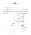
Next, the structure example and the operation of an imaging apparatus having no A/D converter will be described below, in order to facilitate the description of the present embodiment. FIG. 8 is a view illustrating a structure example of a pixel unit 210 and an amplifying circuit 220-1 in an imaging device, and is a view in which a comparison unit 30, a counter unit 40 and a memory unit 50 are omitted. A CDS circuit 119 is provided in the rear stage of the amplifying circuit 220-1. The pixel unit 210 is configured to include a plurality of pixels 210-1 which are arrayed according to a plurality of rows and lines. In FIG. 8 , signals which are output from the pixels in rows of the odd numbers when counted from the left are read by a readout circuit arranged in the lower part of the pixel unit 210. On the other hand, signals which are output from the pixels in the rows of the even numbers when counted from the left are read by a not-shown readout circuit arranged in the upper part of the pixel unit 210. Thus, by alternately providing the readout circuits, the area for two rows of the pixel unit 210 can be used when the readout circuit is laid out. The CDS circuit 119 has a function of sampling and holding signals, and reduces correlating components together with a differentiation processing unit 118.
Firstly, the pixel reset pulse PRES is shifted from a high level to a low level, and the reset of a gate electrode of an amplification MOSFET 104 is cleared. At this time, a potential corresponding to the clearance of the reset is held in a floating diffusion region FD connected to the gate electrode. Subsequently, when a line selecting pulse PSEL becomes a high level, then the output corresponding to the potential of the floating diffusion region FD appears in a vertical output line V-1 by a source follower circuit formed by the amplification MOSFET 104 and a constant current source 107. When a clamp pulse PCOR is activated to a high level in this state, a clamp switch 109 is turned ON, a variable amplifying unit 131 is turned into a voltage follower state, and the voltage of an electrode in a row amplifier side of a clamp capacitor 108 becomes approximately equal to a voltage VREF. After that, the clamp pulse PCOR is non-activated from a high level to a low level, and the output of the vertical output line V-1 is clamped.
Subsequently, an accumulation pulse PTN is activated to a high level, and the offset signal of an amplifying circuit 220-1 is stored in a holding capacitor 112 n through a transfer gate 110 n. After that, a transfer pulse PTX is activated to a high level, thereby the transfer switch 102 becomes a high level for a fixed period of time, and the photoelectric charge which has been accumulated in the photodiode 101 is transferred to the gate electrode of the amplification MOSFET 104. Here, the electric charge to be transferred is an electron, and when the absolute value of the amount of the transferred electric charge is represented by Q, and when the capacitance of the floating diffusion region FD is represented by CFD, the gate potential is lowered by Q/CFD. In correspondence to this, the potential of the vertical output line V-1 is changed. When the source follower gain is represented by Gsf, the change ΔVvl of the potential Vvl of the vertical output line V-1 due to the transfer of the electric charge from the photodiode 101 to the floating diffusion unit FD is expressed by Expression (1).
ΔVvl=−Q·Gsf/CFD (1)
ΔVvl=−Q·Gsf/CFD (1)
The voltage of this potential change ΔVvl is amplified by a variable amplifying unit 131 which includes a computation amplifier 120, a clamp capacitor 108 and a feedback capacitor 121, and the output Vct of the variable amplifying unit 131 is expressed by Expression (2).
Vct=VREF+Q·(Gsf/CFD)·(C0/Cf) (2)
Vct=VREF+Q·(Gsf/CFD)·(C0/Cf) (2)
Here, C0 represents the capacitance of the clamp capacitor 108, and Cf represents the capacitance values of feedback capacitors 121 a, 121 b and 121 c to be selected when sensitivity switching pulses ×1, ×2 and ×4 have been activated, respectively. For instance, C0 is 1 pF. When the feedback capacitor 121 a has been selected, Cf is 1 pF, when the feedback capacitor 121 b has been selected, Cf is 0.5 pF, and when the feedback capacitor 121 c has been selected, Cf is 0.25 pF. The voltage amplification ratios represented by −C0/Cf are −1 time, −2 times and −4 times, respectively. In other words, in a system in which negative feedback is applied to the computation amplifier 120, a feedback coefficient which is determined by a voltage division ratio of Cf and C0 is changed by switching the selection to any of the plurality of the feedback capacitors 121 a to 121 c, and thereby the voltage amplification ratio can be switched. For information, a negative sign attached to the voltage amplification ratio shows that the variable amplifying unit is a reversal amplifying circuit. The transfer pulse PTX becomes a low level, then the accumulation pulse PTS becomes a high level, and the level which is output from the amplifying circuit 220-1 at this time is accumulated in the holding capacitor 112 s through the transfer gate 110 s.
Subsequently, row selecting switches 114 s and 114 n are sequentially turned ON by scanning pulses COLSEL1, COLSEL2 and so on generated by a horizontal scanning circuit 65. Then, the signal which is accumulated in the holding capacitor 112 s is output to a horizontal output line 116 s in the order of the row, and the signal which is accumulated in the holding capacitor 112 n is output to a horizontal output line 116 n in the order of the row. Pairs of signals in a plurality of rows are sequentially output to the horizontal output lines 116 s and 116 n. A differentiation processing unit 118 outputs a difference between the pair of the signals in each row which has been output to the horizontal output lines 116 s and 116 n. Thereby, the noise component contained in the signal held in the holding capacitor 112 s can be reduced.
The ramp signal generating circuit 25 is controlled by a control signal CNT2 of a timing generating circuit 70, and generates a ramp signal VH/a comparison voltage VREF, and a ramp signal VL/a ramp signal VR. The ramp signal VH is a ramp signal for higher-order bits with a large gradient, and the ramp signal VL is a ramp signal for lower-order bits with a small gradient. In addition, the comparison voltage VREF is a comparison base signal for determining the level of the effective signal, and the ramp signal VR for the base signal is a ramp signal for comparing the effective signal with the base signal. These four types of ramp signals are selected by a selecting circuit 30-2 which is controlled by a control signal CNT1 of the timing generating circuit 70, and are input to the comparator 30-1. The timing generating circuit 70 also controls the ramp signal generating circuit 25 by the control signal CNT2.
Next, the comparison voltage VREF will be described below. The comparison voltage VREF may be generated from another power supply circuit, but can be generated in a ramp generating circuit 25. The ramp generating circuit 25 can generate the comparison voltage VREF by stopping a charging electric current on the way (for instance, approximately 60 mv) of generating the signal, in a similar way to that of forming the ramp signal VH. The comparison voltage VREF can be generated in a period of time of 1/16 with respect to that of the ramp signal VH. In order to further shorten this period of time, the charging electric current may be increased. In addition, the comparison voltage VREF needs to be set at lower than 62.5 my which is a finally attainable voltage VL(H) of the ramp signal VL. If the voltage is thus set, the effective signal can be surely comparison-processed with any one of the ramp signals VH and VL.
The comparator 30-1 compares the base signal with the ramp signal VR for the base signal during the A/D conversion period of time Td of the base signal, and suppose that Tr represents a period between the time when the ramp signal VR for the base signal has started the change and the time when the magnitude relation between the base signal and the ramp signal is inverted. The counter 40-1 down-counts the value during the period of time Tr, and the memory circuit 50-1 holds the down-counted value (first count value) as a digital datum of the base signal. The ramp signal VR for the base signal has the same gradient as that of the ramp signal VL. By setting the gradient of the ramp signal at the same value, a digital datum of a base signal with high resolution can be obtained. Next, in a signal amplitude determination period of time Tj, the comparator 30-1 compares the effective signal with the comparison voltage VREF. In the example illustrated in the figure, the comparator 30-1 outputs a high-level selection signal SEL which means that the effective signal is larger than the comparison voltage VREF, to the selecting circuit 30-2, in the signal amplitude determination period of time Tj. As a result, in an effective signal A/D conversion period of time Tu, the selecting circuit 30-2 selects the ramp signal VH having a large gradient, and outputs the ramp signal to the comparator 30-1. The comparator 30-1 compares the effective signal with the ramp signal VH. The period spent by the time when the magnitude relation between both of the signals is inverted is represented by Ts. The counter 40-1 up-counts the value for the period of time Ts subsequently to the above described down-counting for the base signal. The memory circuit 50-1 holds the up-counted value (second count value) as a digital datum of the effective signal. If the output of the comparator 30-1 is not inverted in a signal level determination period of time Tj, the selection signal SEL is kept at a low level, and selecting circuit 30-2 selects the ramp signal VL having a small gradient, because the level of the effective signal has been determined to be smaller than the comparison voltage VREF. In this case, the comparator 30-1 compares the effective signal with the ramp signal VL. The selecting circuit 30-2 selects any of the ramp signals VH and VL which have different gradients from each other, according to the level of the effective signal which has been amplified by the amplifying unit 20. In other words, the selecting circuit 30-2 sets the time-changing ratio of the ramp signal, according to the level of the effective signal based on the pixel. The comparator 30-1 compares the ramp signal which has been selected by the selecting circuit 30-2, with the effective signal which has been amplified by the amplifying unit 20. The counter 40-1 up-counts the value in a period between the time when the ramp signal has started the change and the time when the comparator 30-1 outputs a signal which indicates that the magnitude relation between the effective signal and the ramp signal has been inverted.
In FIG. 5 , the ramp signal VR for the base signal and the ramp signal VL have the same gradient, as described above. The ramp signal VR for the base signal is compared with the base signal, but the base signal is also a base signal for the effective signal, accordingly the ramp signal needs to have high accuracy. Because the ramp signal VR has the same gradient as that of the ramp signal VL for generating a datum with lower-order bits, there is such a merit as to be capable of using the same ramp generating circuit 25. The functions of the down-counting mode and the up-counting mode of the counter 40-1 will be described later with reference to FIGS. 6A to 6C .
Suppose that the pixel signal sent from the pixel unit 10 is a signal 201 described in FIG. 2 , and then the gain of the amplifying circuit 20-1 in FIG. 4 is 1. However, an imaging system which will be described later in FIG. 7 has a function of setting sensitivity suitable for a photographing environment. For instance, when the sensitivity setting is 16 times, the amplifying circuit shall amplify a signal level of 62.5 mV in FIG. 2 to 1 V and input the amplified signal to the comparator 30-1. At this time, an SN ratio necessary for A/D conversion shows its sufficient effect, if having the resolution of the A/D conversion with 10 bits, which is obtained by comparing the large amplitude signal with the ramp signal VH. Accordingly, if the sensitivity has been set at 16 times or more, the selecting circuit 30-2 may be controlled so as to select the ramp signal VH by the control signal CONT1 sent from the timing generating circuit 70, and output the ramp signal VH to the comparator 30-1. Because the SN ratio of the pixel unit 10 is largely affected by the aperture area of the pixel unit 10, the ratio of the gradients of the ramp signal VH and the ramp signal VL and the sensitivity setting for selecting the above described ramp signal VH vary according to the aperture area.
The counter 40-1 has an inverter 601, a 4 bit up/down counter 602, a 10 bit up/down counter 603, and switches SW1 and SW2. The count clock signal CLK is input into the switches SW1 and SW2. The inverter 601 outputs a logic reversal signal of the selection signal SEL. The switch SW1 is controlled by the output signal of the inverter 601. The switch SW2 is controlled by the selection signal SEL. The counter clock signal CLK is input into any one of clock terminals of the 4 bit up/down counter 602 and the 10 bit up/down counter 603, according to the selection signal SEL.
As described above, the imaging device uses such count data obtained by subjecting the base signal to comparison processing with the ramp signal VR for the base signal so as to have high resolution, when the effective signal and the base signal are subjected to the differentiation processing, regardless of whether the effective signal is the large amplitude signal or the small amplitude signal. Thereby, the imaging device can obtain an A/D conversion data which is little affected by a quantization noise and has high accuracy. In FIG. 6B , the imaging device can also acquire the A/D conversion data Da0 to Da13 with 14 bits by using 10 bits data D4 to D13 of which the bit has been shifted by 4 bits.
The comparator 30-1 compares the base signal based on the pixel with the ramp signal VR for the base signal in a period of time Td, and the counter 40-1 counts the first count value in the period of time Tr until the magnitude relation between the base signal based on the pixel and the ramp signal VR for the base signal is inverted. After that, the comparator 30-1 compares the effective signal based on the pixel with one of the ramp signals VH and VL for the effective signal in the period of time Tu, and the counter 40-1 counts the second count value in the period of time Ts until the magnitude relation between the effective signal based on the pixel and one of the ramp signals VH and VL for the effective signal is inverted. The counter 40-1 and the correcting unit of the memory unit 50 correct a difference between the resolutions of the first count value and the second count value, which corresponds to a difference between time-changing ratios of the ramp signal VR for the base signal and one of the ramp signals VH and VL for the effective signal. Then, the memory unit (correcting unit) 50 outputs difference data Da0 to Da13 of the first count value and the second count value, which have been corrected. Specifically, in the case of FIG. 6B , the memory unit (correcting unit) 50 corrects the difference of the resolutions by shifting the bit of the second count value.
In the above description, the first count value has been down-counted in the period of time Tr and the second count value has been up-counted in the period of time Ts, but the counting method may be reversed. The counter 40-1 may up-count the first count value in the period of time Tr and down-count the second count value in the period of time Ts to thereby output the difference data Da0 to Da13 of the first count value and the second count value. In other words, the counter 40-1 down-counts or up-counts the first count value, and counts the second count value so that the direction becomes an opposite direction to the up or down direction at the time when the first count value has been counted. Thereby, the memory unit (correcting unit) 50 can output the difference data Da0 to Da13 of the first count value and the second count value, which have been corrected.
In the above description, an example was described in which the counter 40-1 having count functions of the down-count mode and the up-count mode carries out the above described differentiation processing, but the method is not limited by this example. The differentiation processing for the effective signal and the base signal may also be carried out when the counter result is transferred from the memory unit 50 to the output circuit 60 after the counter result of the base signal and the effective signal has been stored in the memory, when the result is transferred from the output circuit 60 to the outside of the imaging device 100, or even in an external circuit (for instance, video signal processing circuit unit 830 in FIG. 7 ). At this time, if a flag data which recognizes a signal determination level (selection signal SEL) with respect to the comparison voltage VREF is added to the A/D conversion data, the imaging device results in easily coping with any bit shift method. The A/D conversion data which the counter unit 40 outputs is output together with the flag data that indicates the level of the effective signal.
The optical unit 810 that is an optical system such as a lens images light emitted from an object on a pixel unit 10 (FIG. 1 ) of the imaging device 100, on which a plurality of pixels are two-dimensionally arrayed, and forms an image of the object on the pixel unit 10. The imaging device 100 outputs signals according to the light imaged on the pixel unit 10, on the timing based on signals output from the timing control circuit unit 850. The signals output from the imaging device 100 are input into the signal processing circuit unit 830 that is a signal processing unit, and the signal processing circuit unit 830 processes the signal with a specified method by a program or the like. The signal processing circuit unit 830 may submit the input signals to signal processing such as bit shift processing and differentiation processing illustrated in FIG. 6 . The signals obtained by the processing in the signal processing circuit unit 830 are sent to the recording and communicating unit 840 as an image data. The recording and communicating unit 840 sends signals for forming an image to the play and display unit 870, and makes the play and display unit 870 play or display a moving image or a still image. The recording and communicating unit 840 also communicates with the system control circuit unit 860 by receiving the signal from the signal processing circuit unit 830, and also performs an operation of recording signals for forming an image on an unillustrated recording medium.
The system control circuit unit 860 is a unit for collectively controlling an operation of the imaging system, and controls a drive of each of the optical unit 810, the timing control circuit unit 850, the recording and communicating unit 840, and the play and display unit 870. In addition, the system control circuit unit 860 is provided, for instance, with an unillustrated storage unit that is a recording medium, and records a program and the like which are necessary for controlling the operation of the imaging system, in the storage unit. The system control circuit unit 860 also supplies, for instance, a signal which switches driving modes according to an operation of a user, into the imaging system. Specific examples include: a signal for a change of a line to be read or a line to be reset; a signal for a change of an angle of view, which accompanies an operation of an electronic zoom; and a signal for a shift of an angle of view, which accompanies electronic vibration control. The timing control circuit unit 850 controls the driving timings for the imaging device 100 and the signal processing circuit unit 830 based on the control by the system control circuit unit 860 which is a control unit.
As described above, according to the first and second embodiments, the imaging device compares a base signal of a pixel with a ramp signal VR for the base signal with high resolution, regardless of whether the effective signal of the pixel is a large amplitude signal or a small amplitude signal. The imaging device determines a level of the effective signal, then selects one of a ramp signal VH and a ramp signal VL, which is suitable for the determined signal, and acquires an A/D conversion data through differentiation processing which corrects a resolution ratio of the effective signal and the base signal; and thereby can obtain the A/D conversion data with high accuracy and multi-bits.
In a dark photographing environment, a pixel signal tends to be a small amplitude signal though depending on an exposing condition, and the sensitivity can be enhanced by amplifying the pixel signal. In the first embodiment, the sensitivity can be enhanced by amplifying a signal in an amplifying circuit 20-1. When a signal sent from the pixel unit 10 is input into a comparator 30-1 without being amplified, the sensitivity can be consequently enhanced by changing the gradient of the ramp signal. The imaging device in the first and second embodiments do not principally determine the gradient of the ramp signal, but can change the gradient of the ramp signal according to the requested enhancement of sensitivity, and when the sensitivity is intended to be enhanced by twice, for instance, can control the gradient of the ramp signal to one half.
Note that the above embodiments are merely examples how the present invention can be practiced, and the technical scope of the present invention should not be restrictedly interpreted by the embodiments. In other words, the present invention can be practiced in various ways without departing from the technical concept and main features of the invention. For instance, though a ramp signal of which the level changes linearly with respect to time has been described as a reference signal, a ramp signal of which the level changes stepwise with respect to time may be used.
While the present invention has been described with reference to exemplary embodiments, it is to be understood that the invention is not limited to the disclosed exemplary embodiments. The scope of the following claims is to be accorded the broadest interpretation so as to encompass all such modifications and equivalent structures and functions.
This application claims the benefit of Japanese Patent Application No. 2011-196349, filed Sep. 8, 2011, which is hereby incorporated by reference herein in its entirety.
Claims (7)
1. An imaging apparatus comprising:
a photoelectric conversion unit configured to generate an electric charge by photoelectric conversion; and
a comparator configured to perform a first comparison operation of comparing a signal based on the electric charge with a comparison signal, and configured to perform a second comparison operation,
wherein, in a first case that a result of the first comparison operation indicates that an amplitude of the signal based on the electric charge is less than an amplitude of the comparison signal, the second comparison operation is performed to compare the signal based on the electric charge with a first reference signal having a voltage changing to a first voltage in a first time-changing ratio,
in a second case that the result of the first comparison operation indicates that the amplitude of the signal based on the electric charge is greater than the amplitude of the comparison signal, the second comparison operation is performed to compare the signal based on the electric charge with a second reference signal having a voltage changing in a second time-changing ratio greater than the first time-changing ratio, and
an amplitude of the comparison signal is less than an amplitude of the first voltage.
2. The apparatus according to claim 1 ,
wherein the comparator compares a base voltage with the first reference signal to a second voltage having an amplitude that is less than an amplitude of the first voltage, and
the amplitude of the comparison signal is greater than the amplitude of the second voltage.
3. The apparatus according to claim 2 ,
wherein an amplitude of the voltage of the second reference signal changes to an amplitude of a third voltage, the amplitude of the third voltage being greater than the amplitude of the first voltage, and
the amplitude of the first voltage is greater than a value calculated by dividing the third voltage by a value calculated by dividing the second time-changing ratio by the first time-changing ratio.
4. The apparatus according to claim 1 , further comprising:
a selecting circuit configured to select the second reference signal among a plurality of reference signals, as a reference signal to be used in the second comparison operation, when a result of the first comparison operation indicates the amplitude of the signal based on the electric charge is greater than the amplitude of the comparison signal, and configured to select the first reference signal among the plurality of reference signals, as a reference signal to be used in the second comparison, when the result of the first comparison operation indicates the amplitude of the signal based on the electric charge is less than the amplitude of the comparison signal.
5. The apparatus according to claim 1 , further comprising:
an A/D conversion unit including the comparator, and configured to generate a first digital signal by the second comparing operation in the first case, and a second digital signal by the second comparing operation in the second case; and
a correcting unit configured to perform a correction of at least one of the first digital signal and the second digital signal, so as to reduce a difference between a resolution of the first digital signal and a resolution of the second digital signal.
6. The imaging apparatus according to claim 5 , wherein the correcting unit performs the correction by a bit shift of the second digital signal.
7. An imaging system comprising:
an imaging apparatus; and
a signal processing unit for processing a signal output from the imaging apparatus,
wherein the imaging apparatus comprises:
a photoelectric conversion unit configured to generate an electric charge by photoelectric conversion; and
a comparator configured to perform a first comparison operation of comparing a signal based on the electric charge with a comparison signal, and configured to perform a second comparison operation,
wherein, in a first case that a result of the first comparison operation indicates that an amplitude of the signal based on the electric charge is less than an amplitude of the comparison signal, the second comparison operation is performed to compare the signal based on the electric charge with a first reference signal having a voltage changing to a first voltage in a first time-changing ratio,
in a second case that a result of the first comparison operation indicates that the amplitude of the signal based on the electric charge is greater than the amplitude of the comparison signal, the second comparison operation is performed to compare the signal based on the electric charge with a second reference signal having a voltage changing in a second time-changing ratio greater than the first time-changing ratio, and
an amplitude of the comparison signal is less than an amplitude of the first voltage.
Priority Applications (1)
| Application Number | Priority Date | Filing Date | Title |
|---|---|---|---|
| US15/423,891 US9800809B2 (en) | 2011-09-08 | 2017-02-03 | Imaging apparatus, imaging system, and method for reducing a difference in resolutions |
Applications Claiming Priority (5)
| Application Number | Priority Date | Filing Date | Title |
|---|---|---|---|
| JP2011-196349 | 2011-09-08 | ||
| JP2011196349A JP5871531B2 (en) | 2011-09-08 | 2011-09-08 | Imaging apparatus and imaging system |
| US13/592,969 US8941753B2 (en) | 2011-09-08 | 2012-08-23 | Imaging apparatus |
| US14/564,488 US9602751B2 (en) | 2011-09-08 | 2014-12-09 | Imaging apparatus, imaging system, and method for reducing a difference in resolutions |
| US15/423,891 US9800809B2 (en) | 2011-09-08 | 2017-02-03 | Imaging apparatus, imaging system, and method for reducing a difference in resolutions |
Related Parent Applications (1)
| Application Number | Title | Priority Date | Filing Date |
|---|---|---|---|
| US14/564,488 Division US9602751B2 (en) | 2011-09-08 | 2014-12-09 | Imaging apparatus, imaging system, and method for reducing a difference in resolutions |
Publications (2)
| Publication Number | Publication Date |
|---|---|
| US20170150074A1 US20170150074A1 (en) | 2017-05-25 |
| US9800809B2 true US9800809B2 (en) | 2017-10-24 |
Family
ID=46832238
Family Applications (3)
| Application Number | Title | Priority Date | Filing Date |
|---|---|---|---|
| US13/592,969 Expired - Fee Related US8941753B2 (en) | 2011-09-08 | 2012-08-23 | Imaging apparatus |
| US14/564,488 Active 2032-11-16 US9602751B2 (en) | 2011-09-08 | 2014-12-09 | Imaging apparatus, imaging system, and method for reducing a difference in resolutions |
| US15/423,891 Active US9800809B2 (en) | 2011-09-08 | 2017-02-03 | Imaging apparatus, imaging system, and method for reducing a difference in resolutions |
Family Applications Before (2)
| Application Number | Title | Priority Date | Filing Date |
|---|---|---|---|
| US13/592,969 Expired - Fee Related US8941753B2 (en) | 2011-09-08 | 2012-08-23 | Imaging apparatus |
| US14/564,488 Active 2032-11-16 US9602751B2 (en) | 2011-09-08 | 2014-12-09 | Imaging apparatus, imaging system, and method for reducing a difference in resolutions |
Country Status (7)
| Country | Link |
|---|---|
| US (3) | US8941753B2 (en) |
| EP (2) | EP2568700A1 (en) |
| JP (1) | JP5871531B2 (en) |
| KR (1) | KR101517376B1 (en) |
| CN (1) | CN103002232B (en) |
| BR (1) | BR102012022644A2 (en) |
| RU (1) | RU2522991C2 (en) |
Families Citing this family (20)
| Publication number | Priority date | Publication date | Assignee | Title |
|---|---|---|---|---|
| JP5808162B2 (en) * | 2011-06-23 | 2015-11-10 | キヤノン株式会社 | Imaging device, imaging apparatus, and driving method of imaging device |
| TW201351889A (en) | 2012-05-21 | 2013-12-16 | Sony Corp | A/d converter, solid-state image pickup device and electronic device |
| JP5813067B2 (en) * | 2012-12-20 | 2015-11-17 | キヤノン株式会社 | Imaging device driving method, digital signal correction method, imaging device, imaging system driving method, and imaging system |
| JP6478467B2 (en) * | 2013-03-28 | 2019-03-06 | キヤノン株式会社 | Imaging device, driving method of imaging device, and imaging system |
| JP6226551B2 (en) * | 2013-05-08 | 2017-11-08 | キヤノン株式会社 | Imaging device |
| FR3012003B1 (en) * | 2013-10-14 | 2016-12-30 | E2V Semiconductors | DIGITAL ANALOG CONVERSION WITH RAMP, MULTIPLE CONVERSIONS OR SINGLE CONVERSION FOLLOWING THE LEVEL OF LIGHT RECEIVED BY A PIXEL |
| JP6413235B2 (en) * | 2013-12-06 | 2018-10-31 | 株式会社ニコン | Imaging device and imaging apparatus |
| JP2015162751A (en) | 2014-02-26 | 2015-09-07 | キヤノン株式会社 | Photoelectric conversion device and imaging system |
| JP6579744B2 (en) * | 2014-11-28 | 2019-09-25 | キヤノン株式会社 | Imaging device, imaging system, driving method of imaging device, and inspection method of imaging device |
| KR102553553B1 (en) * | 2015-06-12 | 2023-07-10 | 가부시키가이샤 한도오따이 에네루기 켄큐쇼 | Imaging device, method for operating the same, and electronic device |
| KR102332942B1 (en) * | 2015-11-27 | 2021-12-01 | 에스케이하이닉스 주식회사 | Counting apparatus for power consumption reduction, and analog-digital converting apparatus and cmos image sensor thereof using that |
| KR102527110B1 (en) * | 2016-05-23 | 2023-05-03 | 에스케이하이닉스 주식회사 | Analog-digital converting apparatus and operating method |
| KR102648189B1 (en) * | 2017-01-12 | 2024-03-14 | 에스케이하이닉스 주식회사 | Analog to digital conversion device, read out circuit and cmos image sensor including the same |
| JP7113368B2 (en) * | 2017-07-03 | 2022-08-05 | パナソニックIpマネジメント株式会社 | Imaging device and camera system |
| JP2019193085A (en) * | 2018-04-24 | 2019-10-31 | キヤノン株式会社 | Imaging device and control method of the same, and imaging apparatus |
| JP6766095B2 (en) | 2018-06-08 | 2020-10-07 | キヤノン株式会社 | Semiconductor substrates for imaging devices, imaging systems, mobiles, and stacks |
| JP7109998B2 (en) * | 2018-06-11 | 2022-08-01 | キヤノン株式会社 | IMAGING DEVICE AND METHOD OF CONTROLLING IMAGING DEVICE |
| CN109194331B (en) * | 2018-08-29 | 2021-10-26 | 苏州瑞迈斯医疗科技有限公司 | Electronic device and method for correcting comparator in electronic device |
| JP6759387B2 (en) * | 2019-02-18 | 2020-09-23 | キヤノン株式会社 | AD converter, AD converter, photoelectric converter, imaging system, and AD conversion method |
| KR20220105496A (en) * | 2021-01-20 | 2022-07-27 | 삼성전자주식회사 | Pulse generator and image sensor including the same |
Citations (20)
| Publication number | Priority date | Publication date | Assignee | Title |
|---|---|---|---|---|
| US4742392A (en) | 1983-08-04 | 1988-05-03 | Canon Kabushiki Kaisha | Clamp circuit with feed back |
| US4935808A (en) | 1982-12-07 | 1990-06-19 | Canon Kabushiki Kaisha | Low-noise image pickup device having readout transfer paths for divided image information |
| US6518910B2 (en) | 2000-02-14 | 2003-02-11 | Canon Kabushiki Kaisha | Signal processing apparatus having an analog/digital conversion function |
| JP2007218987A (en) | 2006-02-14 | 2007-08-30 | Canon Inc | Image forming apparatus |
| US20080136948A1 (en) | 2006-04-10 | 2008-06-12 | Sony Corporation | Solid-state image-pickup device, camera system, and method for driving same |
| JP2008136043A (en) | 2006-11-29 | 2008-06-12 | Sony Corp | Solid-state imaging device and imaging device |
| US20090027533A1 (en) | 2007-07-26 | 2009-01-29 | Keijirou Itakura | Solid state imaging device and method of driving the solid state imaging device |
| JP2009033305A (en) | 2007-07-25 | 2009-02-12 | Panasonic Corp | Solid-state imaging apparatus |
| EP2071831A1 (en) | 2006-10-06 | 2009-06-17 | Sony Corporation | Solid state imaging device, solid state imaging device drive method, and imaging device |
| CN101600057A (en) | 2008-06-06 | 2009-12-09 | 索尼株式会社 | Solid-state image capturing device and camera system |
| US20100039306A1 (en) | 2008-08-18 | 2010-02-18 | Stmicroelectronics Sa | Analog-to-digital converter |
| CN101753782A (en) | 2008-12-16 | 2010-06-23 | 比亚迪股份有限公司 | Method and device for dynamically adjusting slope initiation voltage |
| US20100194956A1 (en) | 2009-02-05 | 2010-08-05 | The Hong Kong University Of Science And Technology | Apparatus and method for improving dynamic range and linearity of CMOS image sensor |
| US20100253560A1 (en) | 2009-04-03 | 2010-10-07 | Sony Corporation | Electronic apparatus, AD converter, and AD conversion method |
| WO2010137244A1 (en) | 2009-05-29 | 2010-12-02 | パナソニック株式会社 | Solid-state image pickup device and camera |
| US20110013050A1 (en) | 2009-07-14 | 2011-01-20 | Sony Corporation | Solid-state imaging device, control method therefor, and camera system |
| US20110037868A1 (en) | 2009-08-13 | 2011-02-17 | Canon Kabushiki Kaisha | Solid-state image sensing element and image sensing system |
| US20110134295A1 (en) | 2009-12-04 | 2011-06-09 | Canon Kabushiki Kaisha | Imaging apparatus and method for driving the same |
| US20110292261A1 (en) | 2010-05-26 | 2011-12-01 | Chi Ho Hwang | Analog-to-digital converter and devices including the same |
| US20120008028A1 (en) | 2010-07-08 | 2012-01-12 | Kabushiki Kaisha Toshiba | Solid state imaging device |
Family Cites Families (5)
| Publication number | Priority date | Publication date | Assignee | Title |
|---|---|---|---|---|
| US6525304B1 (en) * | 2000-11-28 | 2003-02-25 | Foveon, Inc. | Circuitry for converting analog signals from pixel sensor to a digital and for storing the digital signal |
| JP4786631B2 (en) * | 2007-01-17 | 2011-10-05 | ソニー株式会社 | Solid-state imaging device, imaging device |
| JP2009159069A (en) * | 2007-12-25 | 2009-07-16 | Panasonic Corp | Solid-state imaging device and camera |
| JP5178458B2 (en) * | 2008-10-31 | 2013-04-10 | キヤノン株式会社 | Solid-state imaging device, imaging system, and driving method of solid-state imaging device |
| JP5695401B2 (en) * | 2010-12-01 | 2015-04-08 | オリンパス株式会社 | Imaging device |
-
2011
- 2011-09-08 JP JP2011196349A patent/JP5871531B2/en not_active Expired - Fee Related
-
2012
- 2012-08-23 US US13/592,969 patent/US8941753B2/en not_active Expired - Fee Related
- 2012-08-24 RU RU2012136427/07A patent/RU2522991C2/en active
- 2012-09-05 EP EP12183076A patent/EP2568700A1/en not_active Withdrawn
- 2012-09-05 EP EP17204607.0A patent/EP3324614B1/en active Active
- 2012-09-06 BR BR102012022644-8A patent/BR102012022644A2/en not_active Application Discontinuation
- 2012-09-06 KR KR1020120098618A patent/KR101517376B1/en active IP Right Grant
- 2012-09-07 CN CN201210330152.9A patent/CN103002232B/en active Active
-
2014
- 2014-12-09 US US14/564,488 patent/US9602751B2/en active Active
-
2017
- 2017-02-03 US US15/423,891 patent/US9800809B2/en active Active
Patent Citations (42)
| Publication number | Priority date | Publication date | Assignee | Title |
|---|---|---|---|---|
| US4935808A (en) | 1982-12-07 | 1990-06-19 | Canon Kabushiki Kaisha | Low-noise image pickup device having readout transfer paths for divided image information |
| US4742392A (en) | 1983-08-04 | 1988-05-03 | Canon Kabushiki Kaisha | Clamp circuit with feed back |
| US6518910B2 (en) | 2000-02-14 | 2003-02-11 | Canon Kabushiki Kaisha | Signal processing apparatus having an analog/digital conversion function |
| JP2007218987A (en) | 2006-02-14 | 2007-08-30 | Canon Inc | Image forming apparatus |
| US20100165164A1 (en) | 2006-04-10 | 2010-07-01 | Sony Corporation | Solid-state image-pickup device, camera system, and method for driving same |
| US20080136948A1 (en) | 2006-04-10 | 2008-06-12 | Sony Corporation | Solid-state image-pickup device, camera system, and method for driving same |
| US7705897B2 (en) | 2006-04-10 | 2010-04-27 | Sony Corporation | Solid-state image-pickup device, camera system, and method for driving same |
| EP2071831A1 (en) | 2006-10-06 | 2009-06-17 | Sony Corporation | Solid state imaging device, solid state imaging device drive method, and imaging device |
| JP2008136043A (en) | 2006-11-29 | 2008-06-12 | Sony Corp | Solid-state imaging device and imaging device |
| JP2009033305A (en) | 2007-07-25 | 2009-02-12 | Panasonic Corp | Solid-state imaging apparatus |
| JP2009033381A (en) | 2007-07-26 | 2009-02-12 | Panasonic Corp | Solid-state imaging device and operation method therefor |
| US7924335B2 (en) | 2007-07-26 | 2011-04-12 | Panasonic Corporation | Solid state imaging device and method of driving the solid state imaging device |
| US20110157442A1 (en) | 2007-07-26 | 2011-06-30 | Panasonic Corporation | Solid state imaging device and method of driving the solid state imaging device |
| US20090027533A1 (en) | 2007-07-26 | 2009-01-29 | Keijirou Itakura | Solid state imaging device and method of driving the solid state imaging device |
| US8310581B2 (en) | 2007-07-26 | 2012-11-13 | Panasonic Corporation | Solid state imaging device having improved dynamic range |
| CN101600057A (en) | 2008-06-06 | 2009-12-09 | 索尼株式会社 | Solid-state image capturing device and camera system |
| US20120194723A1 (en) | 2008-06-06 | 2012-08-02 | Sony Corporation | Solid state image capture device and camera system |
| US8174598B2 (en) | 2008-06-06 | 2012-05-08 | Sony Corporation | Solid state image capture device and camera system |
| US8810704B2 (en) | 2008-06-06 | 2014-08-19 | Sony Corporation | Solid state image capture device and camera system |
| US20090303362A1 (en) | 2008-06-06 | 2009-12-10 | Sony Corporation | Solid state image capture device and camera system |
| US7982652B2 (en) | 2008-08-18 | 2011-07-19 | Stmicroelectronics Sa | Analog-to-digital converter |
| US20100039306A1 (en) | 2008-08-18 | 2010-02-18 | Stmicroelectronics Sa | Analog-to-digital converter |
| JP2010045789A (en) | 2008-08-18 | 2010-02-25 | St Microelectronics Sa | Analog-to-digital converter |
| CN101753782A (en) | 2008-12-16 | 2010-06-23 | 比亚迪股份有限公司 | Method and device for dynamically adjusting slope initiation voltage |
| US20100194956A1 (en) | 2009-02-05 | 2010-08-05 | The Hong Kong University Of Science And Technology | Apparatus and method for improving dynamic range and linearity of CMOS image sensor |
| US8625012B2 (en) | 2009-02-05 | 2014-01-07 | The Hong Kong University Of Science And Technology | Apparatus and method for improving dynamic range and linearity of CMOS image sensor |
| CN101800837A (en) | 2009-02-05 | 2010-08-11 | 香港科技大学 | Improve the apparatus and method of the cmos image sensor dynamic range and the linearity |
| JP2010259051A (en) | 2009-04-03 | 2010-11-11 | Sony Corp | Electronic apparatus, ad converter, and ad conversion method |
| US20100253560A1 (en) | 2009-04-03 | 2010-10-07 | Sony Corporation | Electronic apparatus, AD converter, and AD conversion method |
| US7973695B2 (en) | 2009-04-03 | 2011-07-05 | Sony Corporation | Electronic apparatus, AD converter, and AD conversion method |
| WO2010137244A1 (en) | 2009-05-29 | 2010-12-02 | パナソニック株式会社 | Solid-state image pickup device and camera |
| US8325255B2 (en) | 2009-07-14 | 2012-12-04 | Sony Corporation | Solid-state imaging device, control method therefor, and camera system |
| US20130107082A1 (en) | 2009-07-14 | 2013-05-02 | Sony Corporation | Solid-state imaging device, control method therefor, and camera system |
| CN101959026A (en) | 2009-07-14 | 2011-01-26 | 索尼公司 | Solid state image pickup device, its control method, and camera arrangement |
| US8687098B2 (en) | 2009-07-14 | 2014-04-01 | Sony Corporation | Solid-state imaging device, control method therefor, and camera system |
| US20110013050A1 (en) | 2009-07-14 | 2011-01-20 | Sony Corporation | Solid-state imaging device, control method therefor, and camera system |
| JP2011041091A (en) | 2009-08-13 | 2011-02-24 | Canon Inc | Solid-state imaging element, and imaging system |
| US20110037868A1 (en) | 2009-08-13 | 2011-02-17 | Canon Kabushiki Kaisha | Solid-state image sensing element and image sensing system |
| US8922668B2 (en) | 2009-08-13 | 2014-12-30 | Canon Kabushiki Kaisha | Solid-state image sensing element and image sensing system including comparison units with switchable frequency band characteristics |
| US20110134295A1 (en) | 2009-12-04 | 2011-06-09 | Canon Kabushiki Kaisha | Imaging apparatus and method for driving the same |
| US20110292261A1 (en) | 2010-05-26 | 2011-12-01 | Chi Ho Hwang | Analog-to-digital converter and devices including the same |
| US20120008028A1 (en) | 2010-07-08 | 2012-01-12 | Kabushiki Kaisha Toshiba | Solid state imaging device |
Non-Patent Citations (5)
| Title |
|---|
| Chinese Office Action dated Jan. 23, 2015 in Chinese Patent Application No. 201210330152.9. |
| European Office Action dated Sep. 17, 2015 in EP Application No. 12 183 076.4. |
| European Search Report dated Dec. 18, 2012, in European Application No. 12183076.4-2202. |
| Japanese Office Action dated Jun. 2, 2015 in Japanese Patent Application No. 2011-196349. |
| Korean Office Action dated Sep. 18, 2014, in Korean Application No. 10-2012-0098618. |
Also Published As
| Publication number | Publication date |
|---|---|
| KR20130028007A (en) | 2013-03-18 |
| KR101517376B1 (en) | 2015-05-15 |
| RU2012136427A (en) | 2014-02-27 |
| US8941753B2 (en) | 2015-01-27 |
| BR102012022644A2 (en) | 2013-11-12 |
| US20130063627A1 (en) | 2013-03-14 |
| JP2013058930A (en) | 2013-03-28 |
| EP2568700A1 (en) | 2013-03-13 |
| RU2522991C2 (en) | 2014-07-20 |
| EP3324614B1 (en) | 2020-04-22 |
| EP3324614A1 (en) | 2018-05-23 |
| CN103002232B (en) | 2016-06-15 |
| JP5871531B2 (en) | 2016-03-01 |
| CN103002232A (en) | 2013-03-27 |
| US20150092097A1 (en) | 2015-04-02 |
| US9602751B2 (en) | 2017-03-21 |
| US20170150074A1 (en) | 2017-05-25 |
Similar Documents
| Publication | Publication Date | Title |
|---|---|---|
| US9800809B2 (en) | Imaging apparatus, imaging system, and method for reducing a difference in resolutions | |
| US9615044B2 (en) | Imaging apparatus and method of driving the same | |
| JP5893550B2 (en) | Imaging apparatus and imaging system | |
| US7315273B2 (en) | Analog-to-digital conversion method, analog-to-digital converter, semiconductor device for detecting distribution of physical quantity, and electronic apparatus | |
| JP2009284553A (en) | Solid-state imaging device, and imaging apparatus | |
| JP6293321B2 (en) | Imaging apparatus and imaging system | |
| JP2013051575A (en) | Solid-state imaging device, imaging device, and imaging method | |
| US10834353B2 (en) | Image sensor and control method therefor, and image capturing apparatus | |
| JP6320435B2 (en) | Imaging apparatus and imaging system | |
| JP6370510B2 (en) | Imaging device, imaging system, and AD conversion circuit driving method | |
| JP6075899B2 (en) | Imaging device and imaging apparatus | |
| JP6370413B2 (en) | Imaging apparatus, imaging system, and driving method of imaging apparatus |
Legal Events
| Date | Code | Title | Description |
|---|---|---|---|
| FEPP | Fee payment procedure |
Free format text: PETITION RELATED TO MAINTENANCE FEES GRANTED (ORIGINAL EVENT CODE: PTGR) |
|
| STCF | Information on status: patent grant |
Free format text: PATENTED CASE |
|
| MAFP | Maintenance fee payment |
Free format text: PAYMENT OF MAINTENANCE FEE, 4TH YEAR, LARGE ENTITY (ORIGINAL EVENT CODE: M1551); ENTITY STATUS OF PATENT OWNER: LARGE ENTITY Year of fee payment: 4 |