US9818800B2 - Self aligned semiconductor device and structure - Google Patents
Self aligned semiconductor device and structure Download PDFInfo
- Publication number
- US9818800B2 US9818800B2 US14/555,494 US201414555494A US9818800B2 US 9818800 B2 US9818800 B2 US 9818800B2 US 201414555494 A US201414555494 A US 201414555494A US 9818800 B2 US9818800 B2 US 9818800B2
- Authority
- US
- United States
- Prior art keywords
- layer
- transistors
- silicon
- illustrates
- wafer
- Prior art date
- Legal status (The legal status is an assumption and is not a legal conclusion. Google has not performed a legal analysis and makes no representation as to the accuracy of the status listed.)
- Active
Links
- 239000004065 semiconductor Substances 0.000 title claims description 28
- 230000015654 memory Effects 0.000 claims abstract description 233
- 230000002093 peripheral effect Effects 0.000 claims description 57
- 238000001459 lithography Methods 0.000 claims description 48
- 229910021420 polycrystalline silicon Inorganic materials 0.000 claims description 47
- 229920005591 polysilicon Polymers 0.000 claims description 45
- 239000013078 crystal Substances 0.000 claims description 29
- 239000010410 layer Substances 0.000 description 792
- 238000000034 method Methods 0.000 description 356
- 235000012431 wafers Nutrition 0.000 description 240
- VYPSYNLAJGMNEJ-UHFFFAOYSA-N Silicium dioxide Chemical compound O=[Si]=O VYPSYNLAJGMNEJ-UHFFFAOYSA-N 0.000 description 219
- 230000008569 process Effects 0.000 description 207
- 239000010703 silicon Substances 0.000 description 179
- 229910052710 silicon Inorganic materials 0.000 description 176
- XUIMIQQOPSSXEZ-UHFFFAOYSA-N Silicon Chemical compound [Si] XUIMIQQOPSSXEZ-UHFFFAOYSA-N 0.000 description 153
- 239000000377 silicon dioxide Substances 0.000 description 81
- 238000005516 engineering process Methods 0.000 description 75
- 235000012239 silicon dioxide Nutrition 0.000 description 75
- 238000012546 transfer Methods 0.000 description 62
- 239000001257 hydrogen Substances 0.000 description 52
- 229910052739 hydrogen Inorganic materials 0.000 description 52
- 238000002955 isolation Methods 0.000 description 44
- 229910052751 metal Inorganic materials 0.000 description 43
- 239000002184 metal Substances 0.000 description 43
- UFHFLCQGNIYNRP-UHFFFAOYSA-N Hydrogen Chemical compound [H][H] UFHFLCQGNIYNRP-UHFFFAOYSA-N 0.000 description 42
- 239000000463 material Substances 0.000 description 37
- 229910021421 monocrystalline silicon Inorganic materials 0.000 description 33
- 230000008859 change Effects 0.000 description 31
- 239000003989 dielectric material Substances 0.000 description 31
- 229910052814 silicon oxide Inorganic materials 0.000 description 28
- 230000015572 biosynthetic process Effects 0.000 description 24
- 239000002019 doping agent Substances 0.000 description 23
- 238000012545 processing Methods 0.000 description 22
- 238000007667 floating Methods 0.000 description 21
- 239000007943 implant Substances 0.000 description 21
- 239000007772 electrode material Substances 0.000 description 19
- 241000894007 species Species 0.000 description 18
- 238000000231 atomic layer deposition Methods 0.000 description 15
- 238000005530 etching Methods 0.000 description 15
- 238000010276 construction Methods 0.000 description 14
- 239000002070 nanowire Substances 0.000 description 14
- 229910000577 Silicon-germanium Inorganic materials 0.000 description 13
- 239000001307 helium Substances 0.000 description 13
- 229910052734 helium Inorganic materials 0.000 description 13
- SWQJXJOGLNCZEY-UHFFFAOYSA-N helium atom Chemical compound [He] SWQJXJOGLNCZEY-UHFFFAOYSA-N 0.000 description 13
- 229910052721 tungsten Inorganic materials 0.000 description 13
- 239000000758 substrate Substances 0.000 description 12
- 238000004519 manufacturing process Methods 0.000 description 11
- 229910052782 aluminium Inorganic materials 0.000 description 10
- XAGFODPZIPBFFR-UHFFFAOYSA-N aluminium Chemical compound [Al] XAGFODPZIPBFFR-UHFFFAOYSA-N 0.000 description 10
- 229910000449 hafnium oxide Inorganic materials 0.000 description 10
- WIHZLLGSGQNAGK-UHFFFAOYSA-N hafnium(4+);oxygen(2-) Chemical compound [O-2].[O-2].[Hf+4] WIHZLLGSGQNAGK-UHFFFAOYSA-N 0.000 description 10
- 238000001465 metallisation Methods 0.000 description 10
- 239000011229 interlayer Substances 0.000 description 9
- 239000000853 adhesive Substances 0.000 description 8
- 230000001070 adhesive effect Effects 0.000 description 8
- 239000010949 copper Substances 0.000 description 8
- 230000007547 defect Effects 0.000 description 8
- 150000002431 hydrogen Chemical class 0.000 description 8
- 238000002513 implantation Methods 0.000 description 8
- WFKWXMTUELFFGS-UHFFFAOYSA-N tungsten Chemical compound [W] WFKWXMTUELFFGS-UHFFFAOYSA-N 0.000 description 8
- 239000010937 tungsten Substances 0.000 description 8
- RYGMFSIKBFXOCR-UHFFFAOYSA-N Copper Chemical compound [Cu] RYGMFSIKBFXOCR-UHFFFAOYSA-N 0.000 description 7
- 229910052802 copper Inorganic materials 0.000 description 7
- 238000013461 design Methods 0.000 description 7
- 125000006850 spacer group Chemical group 0.000 description 7
- 239000000126 substance Substances 0.000 description 7
- 230000003213 activating effect Effects 0.000 description 6
- 229910021417 amorphous silicon Inorganic materials 0.000 description 6
- 229910052681 coesite Inorganic materials 0.000 description 6
- 229910052906 cristobalite Inorganic materials 0.000 description 6
- 238000000151 deposition Methods 0.000 description 6
- 230000008021 deposition Effects 0.000 description 6
- 230000037230 mobility Effects 0.000 description 6
- 238000001953 recrystallisation Methods 0.000 description 6
- 229910052682 stishovite Inorganic materials 0.000 description 6
- 229910052905 tridymite Inorganic materials 0.000 description 6
- 229910004166 TaN Inorganic materials 0.000 description 5
- 229910010037 TiAlN Inorganic materials 0.000 description 5
- NRTOMJZYCJJWKI-UHFFFAOYSA-N Titanium nitride Chemical compound [Ti]#N NRTOMJZYCJJWKI-UHFFFAOYSA-N 0.000 description 5
- 238000013459 approach Methods 0.000 description 5
- 238000005229 chemical vapour deposition Methods 0.000 description 5
- 230000010354 integration Effects 0.000 description 5
- 230000003287 optical effect Effects 0.000 description 5
- RVTZCBVAJQQJTK-UHFFFAOYSA-N oxygen(2-);zirconium(4+) Chemical compound [O-2].[O-2].[Zr+4] RVTZCBVAJQQJTK-UHFFFAOYSA-N 0.000 description 5
- 229910052707 ruthenium Inorganic materials 0.000 description 5
- 229910001928 zirconium oxide Inorganic materials 0.000 description 5
- ZOXJGFHDIHLPTG-UHFFFAOYSA-N Boron Chemical compound [B] ZOXJGFHDIHLPTG-UHFFFAOYSA-N 0.000 description 4
- 229910052796 boron Inorganic materials 0.000 description 4
- 230000000694 effects Effects 0.000 description 4
- 230000006870 function Effects 0.000 description 4
- 229910052732 germanium Inorganic materials 0.000 description 4
- GNPVGFCGXDBREM-UHFFFAOYSA-N germanium atom Chemical compound [Ge] GNPVGFCGXDBREM-UHFFFAOYSA-N 0.000 description 4
- 239000011521 glass Substances 0.000 description 4
- 150000004767 nitrides Chemical class 0.000 description 4
- 230000003647 oxidation Effects 0.000 description 4
- 238000007254 oxidation reaction Methods 0.000 description 4
- 238000005498 polishing Methods 0.000 description 4
- 238000003491 array Methods 0.000 description 3
- 230000008901 benefit Effects 0.000 description 3
- 230000000295 complement effect Effects 0.000 description 3
- 238000011049 filling Methods 0.000 description 3
- 239000012212 insulator Substances 0.000 description 3
- 238000005468 ion implantation Methods 0.000 description 3
- 229910044991 metal oxide Inorganic materials 0.000 description 3
- 150000004706 metal oxides Chemical class 0.000 description 3
- 150000002739 metals Chemical class 0.000 description 3
- 238000011160 research Methods 0.000 description 3
- OAKJQQAXSVQMHS-UHFFFAOYSA-N Hydrazine Chemical compound NN OAKJQQAXSVQMHS-UHFFFAOYSA-N 0.000 description 2
- -1 Hydrogen ions Chemical class 0.000 description 2
- 239000004642 Polyimide Substances 0.000 description 2
- 241000724291 Tobacco streak virus Species 0.000 description 2
- 230000004913 activation Effects 0.000 description 2
- 238000000137 annealing Methods 0.000 description 2
- YCIMNLLNPGFGHC-UHFFFAOYSA-N catechol Chemical compound OC1=CC=CC=C1O YCIMNLLNPGFGHC-UHFFFAOYSA-N 0.000 description 2
- 238000000407 epitaxy Methods 0.000 description 2
- 230000005669 field effect Effects 0.000 description 2
- 150000002500 ions Chemical class 0.000 description 2
- 238000004518 low pressure chemical vapour deposition Methods 0.000 description 2
- 230000014759 maintenance of location Effects 0.000 description 2
- 230000000873 masking effect Effects 0.000 description 2
- 238000005457 optimization Methods 0.000 description 2
- 238000000623 plasma-assisted chemical vapour deposition Methods 0.000 description 2
- 229920001721 polyimide Polymers 0.000 description 2
- 239000002861 polymer material Substances 0.000 description 2
- 238000003860 storage Methods 0.000 description 2
- OKTJSMMVPCPJKN-UHFFFAOYSA-N Carbon Chemical compound [C] OKTJSMMVPCPJKN-UHFFFAOYSA-N 0.000 description 1
- PIICEJLVQHRZGT-UHFFFAOYSA-N Ethylenediamine Chemical compound NCCN PIICEJLVQHRZGT-UHFFFAOYSA-N 0.000 description 1
- 241000933095 Neotragus moschatus Species 0.000 description 1
- 229910052581 Si3N4 Inorganic materials 0.000 description 1
- ATJFFYVFTNAWJD-UHFFFAOYSA-N Tin Chemical compound [Sn] ATJFFYVFTNAWJD-UHFFFAOYSA-N 0.000 description 1
- 239000006096 absorbing agent Substances 0.000 description 1
- 229910003481 amorphous carbon Inorganic materials 0.000 description 1
- 125000004429 atom Chemical group 0.000 description 1
- 230000004888 barrier function Effects 0.000 description 1
- 230000000903 blocking effect Effects 0.000 description 1
- 229910052799 carbon Inorganic materials 0.000 description 1
- 239000000969 carrier Substances 0.000 description 1
- 239000002800 charge carrier Substances 0.000 description 1
- 239000003795 chemical substances by application Substances 0.000 description 1
- 239000011248 coating agent Substances 0.000 description 1
- 238000000576 coating method Methods 0.000 description 1
- 238000005520 cutting process Methods 0.000 description 1
- 230000001419 dependent effect Effects 0.000 description 1
- 238000011982 device technology Methods 0.000 description 1
- 230000009977 dual effect Effects 0.000 description 1
- 230000008642 heat stress Effects 0.000 description 1
- 230000006872 improvement Effects 0.000 description 1
- 230000003993 interaction Effects 0.000 description 1
- 230000006386 memory function Effects 0.000 description 1
- 230000008520 organization Effects 0.000 description 1
- 238000004806 packaging method and process Methods 0.000 description 1
- 239000002245 particle Substances 0.000 description 1
- 238000000059 patterning Methods 0.000 description 1
- 229920002120 photoresistant polymer Polymers 0.000 description 1
- 229920000642 polymer Polymers 0.000 description 1
- 229910021426 porous silicon Inorganic materials 0.000 description 1
- 238000002360 preparation method Methods 0.000 description 1
- 230000005855 radiation Effects 0.000 description 1
- 230000009467 reduction Effects 0.000 description 1
- 239000003870 refractory metal Substances 0.000 description 1
- 238000012827 research and development Methods 0.000 description 1
- HQVNEWCFYHHQES-UHFFFAOYSA-N silicon nitride Chemical compound N12[Si]34N5[Si]62N3[Si]51N64 HQVNEWCFYHHQES-UHFFFAOYSA-N 0.000 description 1
- 239000002210 silicon-based material Substances 0.000 description 1
- 239000007784 solid electrolyte Substances 0.000 description 1
- 238000010561 standard procedure Methods 0.000 description 1
- 239000002344 surface layer Substances 0.000 description 1
- 230000003746 surface roughness Effects 0.000 description 1
- 229910052715 tantalum Inorganic materials 0.000 description 1
- GUVRBAGPIYLISA-UHFFFAOYSA-N tantalum atom Chemical compound [Ta] GUVRBAGPIYLISA-UHFFFAOYSA-N 0.000 description 1
- 239000010409 thin film Substances 0.000 description 1
- XLYOFNOQVPJJNP-UHFFFAOYSA-N water Substances O XLYOFNOQVPJJNP-UHFFFAOYSA-N 0.000 description 1
Images


Classifications
-
- H—ELECTRICITY
- H10—SEMICONDUCTOR DEVICES; ELECTRIC SOLID-STATE DEVICES NOT OTHERWISE PROVIDED FOR
- H10B—ELECTRONIC MEMORY DEVICES
- H10B63/00—Resistance change memory devices, e.g. resistive RAM [ReRAM] devices
- H10B63/80—Arrangements comprising multiple bistable or multi-stable switching components of the same type on a plane parallel to the substrate, e.g. cross-point arrays
- H10B63/84—Arrangements comprising multiple bistable or multi-stable switching components of the same type on a plane parallel to the substrate, e.g. cross-point arrays arranged in a direction perpendicular to the substrate, e.g. 3D cell arrays
-
- H01L27/2481—
-
- H—ELECTRICITY
- H01—ELECTRIC ELEMENTS
- H01L—SEMICONDUCTOR DEVICES NOT COVERED BY CLASS H10
- H01L21/00—Processes or apparatus adapted for the manufacture or treatment of semiconductor or solid state devices or of parts thereof
- H01L21/02—Manufacture or treatment of semiconductor devices or of parts thereof
- H01L21/04—Manufacture or treatment of semiconductor devices or of parts thereof the devices having at least one potential-jump barrier or surface barrier, e.g. PN junction, depletion layer or carrier concentration layer
- H01L21/18—Manufacture or treatment of semiconductor devices or of parts thereof the devices having at least one potential-jump barrier or surface barrier, e.g. PN junction, depletion layer or carrier concentration layer the devices having semiconductor bodies comprising elements of Group IV of the Periodic System or AIIIBV compounds with or without impurities, e.g. doping materials
- H01L21/26—Bombardment with radiation
- H01L21/263—Bombardment with radiation with high-energy radiation
- H01L21/268—Bombardment with radiation with high-energy radiation using electromagnetic radiation, e.g. laser radiation
-
- H—ELECTRICITY
- H01—ELECTRIC ELEMENTS
- H01L—SEMICONDUCTOR DEVICES NOT COVERED BY CLASS H10
- H01L21/00—Processes or apparatus adapted for the manufacture or treatment of semiconductor or solid state devices or of parts thereof
- H01L21/67—Apparatus specially adapted for handling semiconductor or electric solid state devices during manufacture or treatment thereof; Apparatus specially adapted for handling wafers during manufacture or treatment of semiconductor or electric solid state devices or components ; Apparatus not specifically provided for elsewhere
- H01L21/683—Apparatus specially adapted for handling semiconductor or electric solid state devices during manufacture or treatment thereof; Apparatus specially adapted for handling wafers during manufacture or treatment of semiconductor or electric solid state devices or components ; Apparatus not specifically provided for elsewhere for supporting or gripping
- H01L21/6835—Apparatus specially adapted for handling semiconductor or electric solid state devices during manufacture or treatment thereof; Apparatus specially adapted for handling wafers during manufacture or treatment of semiconductor or electric solid state devices or components ; Apparatus not specifically provided for elsewhere for supporting or gripping using temporarily an auxiliary support
-
- H—ELECTRICITY
- H01—ELECTRIC ELEMENTS
- H01L—SEMICONDUCTOR DEVICES NOT COVERED BY CLASS H10
- H01L21/00—Processes or apparatus adapted for the manufacture or treatment of semiconductor or solid state devices or of parts thereof
- H01L21/70—Manufacture or treatment of devices consisting of a plurality of solid state components formed in or on a common substrate or of parts thereof; Manufacture of integrated circuit devices or of parts thereof
- H01L21/71—Manufacture of specific parts of devices defined in group H01L21/70
- H01L21/76—Making of isolation regions between components
- H01L21/762—Dielectric regions, e.g. EPIC dielectric isolation, LOCOS; Trench refilling techniques, SOI technology, use of channel stoppers
- H01L21/7624—Dielectric regions, e.g. EPIC dielectric isolation, LOCOS; Trench refilling techniques, SOI technology, use of channel stoppers using semiconductor on insulator [SOI] technology
- H01L21/76251—Dielectric regions, e.g. EPIC dielectric isolation, LOCOS; Trench refilling techniques, SOI technology, use of channel stoppers using semiconductor on insulator [SOI] technology using bonding techniques
- H01L21/76254—Dielectric regions, e.g. EPIC dielectric isolation, LOCOS; Trench refilling techniques, SOI technology, use of channel stoppers using semiconductor on insulator [SOI] technology using bonding techniques with separation/delamination along an ion implanted layer, e.g. Smart-cut, Unibond
-
- H—ELECTRICITY
- H01—ELECTRIC ELEMENTS
- H01L—SEMICONDUCTOR DEVICES NOT COVERED BY CLASS H10
- H01L21/00—Processes or apparatus adapted for the manufacture or treatment of semiconductor or solid state devices or of parts thereof
- H01L21/70—Manufacture or treatment of devices consisting of a plurality of solid state components formed in or on a common substrate or of parts thereof; Manufacture of integrated circuit devices or of parts thereof
- H01L21/77—Manufacture or treatment of devices consisting of a plurality of solid state components or integrated circuits formed in, or on, a common substrate
- H01L21/78—Manufacture or treatment of devices consisting of a plurality of solid state components or integrated circuits formed in, or on, a common substrate with subsequent division of the substrate into plural individual devices
- H01L21/82—Manufacture or treatment of devices consisting of a plurality of solid state components or integrated circuits formed in, or on, a common substrate with subsequent division of the substrate into plural individual devices to produce devices, e.g. integrated circuits, each consisting of a plurality of components
- H01L21/822—Manufacture or treatment of devices consisting of a plurality of solid state components or integrated circuits formed in, or on, a common substrate with subsequent division of the substrate into plural individual devices to produce devices, e.g. integrated circuits, each consisting of a plurality of components the substrate being a semiconductor, using silicon technology
- H01L21/8221—Three dimensional integrated circuits stacked in different levels
-
- H—ELECTRICITY
- H01—ELECTRIC ELEMENTS
- H01L—SEMICONDUCTOR DEVICES NOT COVERED BY CLASS H10
- H01L21/00—Processes or apparatus adapted for the manufacture or treatment of semiconductor or solid state devices or of parts thereof
- H01L21/70—Manufacture or treatment of devices consisting of a plurality of solid state components formed in or on a common substrate or of parts thereof; Manufacture of integrated circuit devices or of parts thereof
- H01L21/77—Manufacture or treatment of devices consisting of a plurality of solid state components or integrated circuits formed in, or on, a common substrate
- H01L21/78—Manufacture or treatment of devices consisting of a plurality of solid state components or integrated circuits formed in, or on, a common substrate with subsequent division of the substrate into plural individual devices
- H01L21/82—Manufacture or treatment of devices consisting of a plurality of solid state components or integrated circuits formed in, or on, a common substrate with subsequent division of the substrate into plural individual devices to produce devices, e.g. integrated circuits, each consisting of a plurality of components
- H01L21/84—Manufacture or treatment of devices consisting of a plurality of solid state components or integrated circuits formed in, or on, a common substrate with subsequent division of the substrate into plural individual devices to produce devices, e.g. integrated circuits, each consisting of a plurality of components the substrate being other than a semiconductor body, e.g. being an insulating body
- H01L21/845—Manufacture or treatment of devices consisting of a plurality of solid state components or integrated circuits formed in, or on, a common substrate with subsequent division of the substrate into plural individual devices to produce devices, e.g. integrated circuits, each consisting of a plurality of components the substrate being other than a semiconductor body, e.g. being an insulating body including field-effect transistors with a horizontal current flow in a vertical sidewall of a semiconductor body, e.g. FinFET, MuGFET
-
- H—ELECTRICITY
- H01—ELECTRIC ELEMENTS
- H01L—SEMICONDUCTOR DEVICES NOT COVERED BY CLASS H10
- H01L27/00—Devices consisting of a plurality of semiconductor or other solid-state components formed in or on a common substrate
- H01L27/02—Devices consisting of a plurality of semiconductor or other solid-state components formed in or on a common substrate including semiconductor components specially adapted for rectifying, oscillating, amplifying or switching and having at least one potential-jump barrier or surface barrier; including integrated passive circuit elements with at least one potential-jump barrier or surface barrier
- H01L27/04—Devices consisting of a plurality of semiconductor or other solid-state components formed in or on a common substrate including semiconductor components specially adapted for rectifying, oscillating, amplifying or switching and having at least one potential-jump barrier or surface barrier; including integrated passive circuit elements with at least one potential-jump barrier or surface barrier the substrate being a semiconductor body
- H01L27/06—Devices consisting of a plurality of semiconductor or other solid-state components formed in or on a common substrate including semiconductor components specially adapted for rectifying, oscillating, amplifying or switching and having at least one potential-jump barrier or surface barrier; including integrated passive circuit elements with at least one potential-jump barrier or surface barrier the substrate being a semiconductor body including a plurality of individual components in a non-repetitive configuration
- H01L27/0688—Integrated circuits having a three-dimensional layout
-
- H01L27/10802—
-
- H01L27/10897—
-
- H01L27/11—
-
- H01L27/11529—
-
- H01L27/11551—
-
- H01L27/11578—
-
- H—ELECTRICITY
- H01—ELECTRIC ELEMENTS
- H01L—SEMICONDUCTOR DEVICES NOT COVERED BY CLASS H10
- H01L27/00—Devices consisting of a plurality of semiconductor or other solid-state components formed in or on a common substrate
- H01L27/02—Devices consisting of a plurality of semiconductor or other solid-state components formed in or on a common substrate including semiconductor components specially adapted for rectifying, oscillating, amplifying or switching and having at least one potential-jump barrier or surface barrier; including integrated passive circuit elements with at least one potential-jump barrier or surface barrier
- H01L27/12—Devices consisting of a plurality of semiconductor or other solid-state components formed in or on a common substrate including semiconductor components specially adapted for rectifying, oscillating, amplifying or switching and having at least one potential-jump barrier or surface barrier; including integrated passive circuit elements with at least one potential-jump barrier or surface barrier the substrate being other than a semiconductor body, e.g. an insulating body
- H01L27/1203—Devices consisting of a plurality of semiconductor or other solid-state components formed in or on a common substrate including semiconductor components specially adapted for rectifying, oscillating, amplifying or switching and having at least one potential-jump barrier or surface barrier; including integrated passive circuit elements with at least one potential-jump barrier or surface barrier the substrate being other than a semiconductor body, e.g. an insulating body the substrate comprising an insulating body on a semiconductor body, e.g. SOI
- H01L27/1211—Devices consisting of a plurality of semiconductor or other solid-state components formed in or on a common substrate including semiconductor components specially adapted for rectifying, oscillating, amplifying or switching and having at least one potential-jump barrier or surface barrier; including integrated passive circuit elements with at least one potential-jump barrier or surface barrier the substrate being other than a semiconductor body, e.g. an insulating body the substrate comprising an insulating body on a semiconductor body, e.g. SOI combined with field-effect transistors with a horizontal current flow in a vertical sidewall of a semiconductor body, e.g. FinFET, MuGFET
-
- H01L27/228—
-
- H01L27/2436—
-
- H01L27/249—
-
- H—ELECTRICITY
- H01—ELECTRIC ELEMENTS
- H01L—SEMICONDUCTOR DEVICES NOT COVERED BY CLASS H10
- H01L29/00—Semiconductor devices adapted for rectifying, amplifying, oscillating or switching, or capacitors or resistors with at least one potential-jump barrier or surface barrier, e.g. PN junction depletion layer or carrier concentration layer; Details of semiconductor bodies or of electrodes thereof ; Multistep manufacturing processes therefor
- H01L29/40—Electrodes ; Multistep manufacturing processes therefor
- H01L29/41—Electrodes ; Multistep manufacturing processes therefor characterised by their shape, relative sizes or dispositions
- H01L29/423—Electrodes ; Multistep manufacturing processes therefor characterised by their shape, relative sizes or dispositions not carrying the current to be rectified, amplified or switched
- H01L29/42312—Gate electrodes for field effect devices
- H01L29/42316—Gate electrodes for field effect devices for field-effect transistors
- H01L29/4232—Gate electrodes for field effect devices for field-effect transistors with insulated gate
- H01L29/42384—Gate electrodes for field effect devices for field-effect transistors with insulated gate for thin film field effect transistors, e.g. characterised by the thickness or the shape of the insulator or the dimensions, the shape or the lay-out of the conductor
- H01L29/42392—Gate electrodes for field effect devices for field-effect transistors with insulated gate for thin film field effect transistors, e.g. characterised by the thickness or the shape of the insulator or the dimensions, the shape or the lay-out of the conductor fully surrounding the channel, e.g. gate-all-around
-
- H—ELECTRICITY
- H01—ELECTRIC ELEMENTS
- H01L—SEMICONDUCTOR DEVICES NOT COVERED BY CLASS H10
- H01L29/00—Semiconductor devices adapted for rectifying, amplifying, oscillating or switching, or capacitors or resistors with at least one potential-jump barrier or surface barrier, e.g. PN junction depletion layer or carrier concentration layer; Details of semiconductor bodies or of electrodes thereof ; Multistep manufacturing processes therefor
- H01L29/66—Types of semiconductor device ; Multistep manufacturing processes therefor
- H01L29/68—Types of semiconductor device ; Multistep manufacturing processes therefor controllable by only the electric current supplied, or only the electric potential applied, to an electrode which does not carry the current to be rectified, amplified or switched
- H01L29/76—Unipolar devices, e.g. field effect transistors
- H01L29/772—Field effect transistors
- H01L29/78—Field effect transistors with field effect produced by an insulated gate
- H01L29/7841—Field effect transistors with field effect produced by an insulated gate with floating body, e.g. programmable transistors
-
- H—ELECTRICITY
- H01—ELECTRIC ELEMENTS
- H01L—SEMICONDUCTOR DEVICES NOT COVERED BY CLASS H10
- H01L29/00—Semiconductor devices adapted for rectifying, amplifying, oscillating or switching, or capacitors or resistors with at least one potential-jump barrier or surface barrier, e.g. PN junction depletion layer or carrier concentration layer; Details of semiconductor bodies or of electrodes thereof ; Multistep manufacturing processes therefor
- H01L29/66—Types of semiconductor device ; Multistep manufacturing processes therefor
- H01L29/68—Types of semiconductor device ; Multistep manufacturing processes therefor controllable by only the electric current supplied, or only the electric potential applied, to an electrode which does not carry the current to be rectified, amplified or switched
- H01L29/76—Unipolar devices, e.g. field effect transistors
- H01L29/772—Field effect transistors
- H01L29/78—Field effect transistors with field effect produced by an insulated gate
- H01L29/785—Field effect transistors with field effect produced by an insulated gate having a channel with a horizontal current flow in a vertical sidewall of a semiconductor body, e.g. FinFET, MuGFET
-
- H—ELECTRICITY
- H10—SEMICONDUCTOR DEVICES; ELECTRIC SOLID-STATE DEVICES NOT OTHERWISE PROVIDED FOR
- H10B—ELECTRONIC MEMORY DEVICES
- H10B10/00—Static random access memory [SRAM] devices
-
- H—ELECTRICITY
- H10—SEMICONDUCTOR DEVICES; ELECTRIC SOLID-STATE DEVICES NOT OTHERWISE PROVIDED FOR
- H10B—ELECTRONIC MEMORY DEVICES
- H10B12/00—Dynamic random access memory [DRAM] devices
- H10B12/20—DRAM devices comprising floating-body transistors, e.g. floating-body cells
-
- H—ELECTRICITY
- H10—SEMICONDUCTOR DEVICES; ELECTRIC SOLID-STATE DEVICES NOT OTHERWISE PROVIDED FOR
- H10B—ELECTRONIC MEMORY DEVICES
- H10B12/00—Dynamic random access memory [DRAM] devices
- H10B12/50—Peripheral circuit region structures
-
- H—ELECTRICITY
- H10—SEMICONDUCTOR DEVICES; ELECTRIC SOLID-STATE DEVICES NOT OTHERWISE PROVIDED FOR
- H10B—ELECTRONIC MEMORY DEVICES
- H10B41/00—Electrically erasable-and-programmable ROM [EEPROM] devices comprising floating gates
- H10B41/20—Electrically erasable-and-programmable ROM [EEPROM] devices comprising floating gates characterised by three-dimensional arrangements, e.g. with cells on different height levels
-
- H—ELECTRICITY
- H10—SEMICONDUCTOR DEVICES; ELECTRIC SOLID-STATE DEVICES NOT OTHERWISE PROVIDED FOR
- H10B—ELECTRONIC MEMORY DEVICES
- H10B41/00—Electrically erasable-and-programmable ROM [EEPROM] devices comprising floating gates
- H10B41/40—Electrically erasable-and-programmable ROM [EEPROM] devices comprising floating gates characterised by the peripheral circuit region
- H10B41/41—Electrically erasable-and-programmable ROM [EEPROM] devices comprising floating gates characterised by the peripheral circuit region of a memory region comprising a cell select transistor, e.g. NAND
-
- H—ELECTRICITY
- H10—SEMICONDUCTOR DEVICES; ELECTRIC SOLID-STATE DEVICES NOT OTHERWISE PROVIDED FOR
- H10B—ELECTRONIC MEMORY DEVICES
- H10B43/00—EEPROM devices comprising charge-trapping gate insulators
- H10B43/20—EEPROM devices comprising charge-trapping gate insulators characterised by three-dimensional arrangements, e.g. with cells on different height levels
-
- H—ELECTRICITY
- H10—SEMICONDUCTOR DEVICES; ELECTRIC SOLID-STATE DEVICES NOT OTHERWISE PROVIDED FOR
- H10B—ELECTRONIC MEMORY DEVICES
- H10B61/00—Magnetic memory devices, e.g. magnetoresistive RAM [MRAM] devices
- H10B61/20—Magnetic memory devices, e.g. magnetoresistive RAM [MRAM] devices comprising components having three or more electrodes, e.g. transistors
- H10B61/22—Magnetic memory devices, e.g. magnetoresistive RAM [MRAM] devices comprising components having three or more electrodes, e.g. transistors of the field-effect transistor [FET] type
-
- H—ELECTRICITY
- H10—SEMICONDUCTOR DEVICES; ELECTRIC SOLID-STATE DEVICES NOT OTHERWISE PROVIDED FOR
- H10B—ELECTRONIC MEMORY DEVICES
- H10B63/00—Resistance change memory devices, e.g. resistive RAM [ReRAM] devices
- H10B63/30—Resistance change memory devices, e.g. resistive RAM [ReRAM] devices comprising selection components having three or more electrodes, e.g. transistors
-
- H—ELECTRICITY
- H10—SEMICONDUCTOR DEVICES; ELECTRIC SOLID-STATE DEVICES NOT OTHERWISE PROVIDED FOR
- H10B—ELECTRONIC MEMORY DEVICES
- H10B63/00—Resistance change memory devices, e.g. resistive RAM [ReRAM] devices
- H10B63/80—Arrangements comprising multiple bistable or multi-stable switching components of the same type on a plane parallel to the substrate, e.g. cross-point arrays
- H10B63/84—Arrangements comprising multiple bistable or multi-stable switching components of the same type on a plane parallel to the substrate, e.g. cross-point arrays arranged in a direction perpendicular to the substrate, e.g. 3D cell arrays
- H10B63/845—Arrangements comprising multiple bistable or multi-stable switching components of the same type on a plane parallel to the substrate, e.g. cross-point arrays arranged in a direction perpendicular to the substrate, e.g. 3D cell arrays the switching components being connected to a common vertical conductor
-
- H—ELECTRICITY
- H01—ELECTRIC ELEMENTS
- H01L—SEMICONDUCTOR DEVICES NOT COVERED BY CLASS H10
- H01L29/00—Semiconductor devices adapted for rectifying, amplifying, oscillating or switching, or capacitors or resistors with at least one potential-jump barrier or surface barrier, e.g. PN junction depletion layer or carrier concentration layer; Details of semiconductor bodies or of electrodes thereof ; Multistep manufacturing processes therefor
- H01L29/66—Types of semiconductor device ; Multistep manufacturing processes therefor
- H01L29/68—Types of semiconductor device ; Multistep manufacturing processes therefor controllable by only the electric current supplied, or only the electric potential applied, to an electrode which does not carry the current to be rectified, amplified or switched
- H01L29/76—Unipolar devices, e.g. field effect transistors
- H01L29/772—Field effect transistors
- H01L29/78—Field effect transistors with field effect produced by an insulated gate
- H01L29/785—Field effect transistors with field effect produced by an insulated gate having a channel with a horizontal current flow in a vertical sidewall of a semiconductor body, e.g. FinFET, MuGFET
- H01L2029/7857—Field effect transistors with field effect produced by an insulated gate having a channel with a horizontal current flow in a vertical sidewall of a semiconductor body, e.g. FinFET, MuGFET of the accumulation type
-
- H—ELECTRICITY
- H01—ELECTRIC ELEMENTS
- H01L—SEMICONDUCTOR DEVICES NOT COVERED BY CLASS H10
- H01L2221/00—Processes or apparatus adapted for the manufacture or treatment of semiconductor or solid state devices or of parts thereof covered by H01L21/00
- H01L2221/67—Apparatus for handling semiconductor or electric solid state devices during manufacture or treatment thereof; Apparatus for handling wafers during manufacture or treatment of semiconductor or electric solid state devices or components; Apparatus not specifically provided for elsewhere
- H01L2221/683—Apparatus for handling semiconductor or electric solid state devices during manufacture or treatment thereof; Apparatus for handling wafers during manufacture or treatment of semiconductor or electric solid state devices or components; Apparatus not specifically provided for elsewhere for supporting or gripping
- H01L2221/68304—Apparatus for handling semiconductor or electric solid state devices during manufacture or treatment thereof; Apparatus for handling wafers during manufacture or treatment of semiconductor or electric solid state devices or components; Apparatus not specifically provided for elsewhere for supporting or gripping using temporarily an auxiliary support
- H01L2221/6835—Apparatus for handling semiconductor or electric solid state devices during manufacture or treatment thereof; Apparatus for handling wafers during manufacture or treatment of semiconductor or electric solid state devices or components; Apparatus not specifically provided for elsewhere for supporting or gripping using temporarily an auxiliary support used as a support during build up manufacturing of active devices
-
- H—ELECTRICITY
- H01—ELECTRIC ELEMENTS
- H01L—SEMICONDUCTOR DEVICES NOT COVERED BY CLASS H10
- H01L27/00—Devices consisting of a plurality of semiconductor or other solid-state components formed in or on a common substrate
- H01L27/02—Devices consisting of a plurality of semiconductor or other solid-state components formed in or on a common substrate including semiconductor components specially adapted for rectifying, oscillating, amplifying or switching and having at least one potential-jump barrier or surface barrier; including integrated passive circuit elements with at least one potential-jump barrier or surface barrier
- H01L27/04—Devices consisting of a plurality of semiconductor or other solid-state components formed in or on a common substrate including semiconductor components specially adapted for rectifying, oscillating, amplifying or switching and having at least one potential-jump barrier or surface barrier; including integrated passive circuit elements with at least one potential-jump barrier or surface barrier the substrate being a semiconductor body
- H01L27/10—Devices consisting of a plurality of semiconductor or other solid-state components formed in or on a common substrate including semiconductor components specially adapted for rectifying, oscillating, amplifying or switching and having at least one potential-jump barrier or surface barrier; including integrated passive circuit elements with at least one potential-jump barrier or surface barrier the substrate being a semiconductor body including a plurality of individual components in a repetitive configuration
- H01L27/105—Devices consisting of a plurality of semiconductor or other solid-state components formed in or on a common substrate including semiconductor components specially adapted for rectifying, oscillating, amplifying or switching and having at least one potential-jump barrier or surface barrier; including integrated passive circuit elements with at least one potential-jump barrier or surface barrier the substrate being a semiconductor body including a plurality of individual components in a repetitive configuration including field-effect components
-
- H01L27/10826—
-
- H01L27/10879—
-
- H01L27/11526—
-
- H01L27/11573—
-
- H01L45/04—
-
- H01L45/1226—
-
- H01L45/146—
-
- H—ELECTRICITY
- H10—SEMICONDUCTOR DEVICES; ELECTRIC SOLID-STATE DEVICES NOT OTHERWISE PROVIDED FOR
- H10B—ELECTRONIC MEMORY DEVICES
- H10B12/00—Dynamic random access memory [DRAM] devices
- H10B12/01—Manufacture or treatment
- H10B12/02—Manufacture or treatment for one transistor one-capacitor [1T-1C] memory cells
- H10B12/05—Making the transistor
- H10B12/056—Making the transistor the transistor being a FinFET
-
- H—ELECTRICITY
- H10—SEMICONDUCTOR DEVICES; ELECTRIC SOLID-STATE DEVICES NOT OTHERWISE PROVIDED FOR
- H10B—ELECTRONIC MEMORY DEVICES
- H10B12/00—Dynamic random access memory [DRAM] devices
- H10B12/30—DRAM devices comprising one-transistor - one-capacitor [1T-1C] memory cells
- H10B12/36—DRAM devices comprising one-transistor - one-capacitor [1T-1C] memory cells the transistor being a FinFET
-
- H—ELECTRICITY
- H10—SEMICONDUCTOR DEVICES; ELECTRIC SOLID-STATE DEVICES NOT OTHERWISE PROVIDED FOR
- H10B—ELECTRONIC MEMORY DEVICES
- H10B41/00—Electrically erasable-and-programmable ROM [EEPROM] devices comprising floating gates
- H10B41/40—Electrically erasable-and-programmable ROM [EEPROM] devices comprising floating gates characterised by the peripheral circuit region
-
- H—ELECTRICITY
- H10—SEMICONDUCTOR DEVICES; ELECTRIC SOLID-STATE DEVICES NOT OTHERWISE PROVIDED FOR
- H10B—ELECTRONIC MEMORY DEVICES
- H10B43/00—EEPROM devices comprising charge-trapping gate insulators
- H10B43/40—EEPROM devices comprising charge-trapping gate insulators characterised by the peripheral circuit region
-
- H—ELECTRICITY
- H10—SEMICONDUCTOR DEVICES; ELECTRIC SOLID-STATE DEVICES NOT OTHERWISE PROVIDED FOR
- H10N—ELECTRIC SOLID-STATE DEVICES NOT OTHERWISE PROVIDED FOR
- H10N70/00—Solid-state devices without a potential-jump barrier or surface barrier, and specially adapted for rectifying, amplifying, oscillating or switching
- H10N70/20—Multistable switching devices, e.g. memristors
-
- H—ELECTRICITY
- H10—SEMICONDUCTOR DEVICES; ELECTRIC SOLID-STATE DEVICES NOT OTHERWISE PROVIDED FOR
- H10N—ELECTRIC SOLID-STATE DEVICES NOT OTHERWISE PROVIDED FOR
- H10N70/00—Solid-state devices without a potential-jump barrier or surface barrier, and specially adapted for rectifying, amplifying, oscillating or switching
- H10N70/801—Constructional details of multistable switching devices
- H10N70/821—Device geometry
- H10N70/823—Device geometry adapted for essentially horizontal current flow, e.g. bridge type devices
-
- H—ELECTRICITY
- H10—SEMICONDUCTOR DEVICES; ELECTRIC SOLID-STATE DEVICES NOT OTHERWISE PROVIDED FOR
- H10N—ELECTRIC SOLID-STATE DEVICES NOT OTHERWISE PROVIDED FOR
- H10N70/00—Solid-state devices without a potential-jump barrier or surface barrier, and specially adapted for rectifying, amplifying, oscillating or switching
- H10N70/801—Constructional details of multistable switching devices
- H10N70/881—Switching materials
- H10N70/883—Oxides or nitrides
- H10N70/8833—Binary metal oxides, e.g. TaOx
Definitions
- This invention describes applications of monolithic 3D integration to semiconductor chips performing logic and memory functions.
- CMOS Complimentary Metal Oxide Semiconductor
- 3D stacking of semiconductor chips is one avenue to tackle issues with wires.
- transistors By arranging transistors in 3 dimensions instead of 2 dimensions (as was the case in the 1990s), one can place transistors in ICs closer to each other. This reduces wire lengths and keeps wiring delay low.
- barriers to practical implementation of 3D stacked chips include:
- 3D stacked memory In the NAND flash memory industry, several organizations have attempted to construct 3D stacked memory. These attempts predominantly use transistors constructed with poly-Si or selective epi technology as well as charge-trap concepts. References that describe these attempts to 3D stacked memory include “Integrated Interconnect Technologies for 3D Nanoelectronic Systems”, Artech House, 2009 by Bakir and Meindl (“Bakir”), “Bit Cost Scalable Technology with Punch and Plug Process for Ultra High Density Flash Memory”, Symp. VLSI Technology Tech. Dig. pp. 14-15, 2007 by H. Tanaka, M. Kido, K. Yahashi, et al.
- FIG. 1 shows process temperatures required for constructing different parts of a single-crystal silicon transistor.
- FIG. 2A-2E depict a layer transfer flow using ion-cut in which a top layer of doped Si is layer transferred atop a generic bottom layer.
- FIG. 3A-3E show process flow for forming a 3D stacked IC using layer transfer which requires >400° C. processing for source-drain region construction.
- FIG. 4 shows a junctionless transistor as a switch for logic applications (prior art).
- FIG. 5A-5F show a process flow for constructing 3D stacked logic chips using junctionless transistors as switches.
- FIG. 6A-6D show different types of junction-less transistors (JLT) that could be utilized for 3D stacking applications.
- JLT junction-less transistors
- FIG. 7A-7F show a process flow for constructing 3D stacked logic chips using one-side gated junctionless transistors as switches.
- FIG. 8A-8E show a process flow for constructing 3D stacked logic chips using two-side gated junctionless transistors as switches.
- FIG. 9A-9V show process flows for constructing 3D stacked logic chips using four-side gated junctionless transistors as switches.
- FIG. 10A-10D show types of recessed channel transistors.
- FIG. 11A-11F shows a procedure for layer transfer of silicon regions needed for recessed channel transistors.
- FIG. 12A-12F show a process flow for constructing 3D stacked logic chips using standard recessed channel transistors.
- FIG. 13A-13F show a process flow for constructing 3D stacked logic chips using RCATs.
- FIG. 14A-14I show construction of CMOS circuits using sub-400° C. transistors (e.g., junctionless transistors or recessed channel transistors).
- transistors e.g., junctionless transistors or recessed channel transistors.
- FIG. 15A-15F show a procedure for accurate layer transfer of thin silicon regions.
- FIG. 16A-16F show an alternative procedure for accurate layer transfer of thin silicon regions.
- FIG. 17A-17E show an alternative procedure for low-temperature layer transfer with ion-cut.
- FIG. 18A-18F show a procedure for layer transfer using an etch-stop layer controlled etch-back.
- FIG. 19 show a surface-activated bonding for low-temperature sub-400° C. processing.
- FIG. 20A-20E show description of Ge or III-V semiconductor Layer Transfer Flow using Ion-Cut.
- FIG. 21A-21C show laser-anneal based 3D chips (prior art).
- FIG. 22A-22E show a laser-anneal based layer transfer process.
- FIG. 23A-23C show window for alignment of top wafer to bottom wafer.
- FIG. 24A-24B show a metallization scheme for monolithic 3D integrated circuits and chips.
- FIG. 25A-25F show a process flow for 3D integrated circuits with gate-last high-k metal gate transistors and face-up layer transfer.
- FIG. 26A-26D show an alignment scheme for repeating pattern in X and Y directions.
- FIG. 27A-27F show an alternative alignment scheme for repeating pattern in X and Y directions.
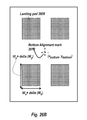
- FIG. 28 show floating-body DRAM as described in prior art.
- FIG. 29A-29H show a two-mask per layer 3D floating body DRAM.
- FIG. 30A-30M show a one-mask per layer 3D floating body DRAM.
- FIG. 31A-31K show a zero-mask per layer 3D floating body DRAM.
- FIG. 32A-32J show a zero-mask per layer 3D resistive memory with a junction-less transistor.
- FIG. 33A-33K show an alternative zero-mask per layer 3D resistive memory.
- FIG. 34A-34L show a one-mask per layer 3D resistive memory.
- FIG. 35A-35F show a two-mask per layer 3D resistive memory.
- FIG. 36A-36F show a two-mask per layer 3D charge-trap memory.
- FIG. 37A-37G show a zero-mask per layer 3D charge-trap memory.
- FIG. 38A-38D show a fewer-masks per layer 3D horizontally-oriented charge-trap memory.
- FIG. 39A-39F show a two-mask per layer 3D horizontally-oriented floating-gate memory.
- FIG. 40A-40H show a one-mask per layer 3D horizontally-oriented floating-gate memory.
- FIG. 41A-41B show periphery on top of memory layers.
- FIG. 42A-42E show a method to make high-aspect ratio vias in 3D memory architectures.
- FIG. 43A-43F depict an implementation of laser anneals for JFET devices.
- FIG. 44A-44D depict a process flow for constructing 3D integrated chips and circuits with misalignment tolerance techniques and repeating pattern in one direction.
- FIG. 45A-45D show a misalignment tolerance technique for constructing 3D integrated chips and circuits with repeating pattern in one direction.
- FIG. 46A-46G illustrate using a carrier wafer for layer transfer.
- FIG. 47A-47K illustrate constructing chips with nMOS and pMOS devices on either side of the wafer.
- FIG. 48 illustrates using a shield for blocking Hydrogen implants from gate areas.
- FIG. 49 illustrates constructing transistors with front gates and back gates on either side of the semiconductor layer.
- FIG. 50A-50E show polysilicon select devices for 3D memory and peripheral circuits at the bottom according to some embodiments of the current invention.
- FIG. 51A-51F show polysilicon select devices for 3D memory and peripheral circuits at the top according to some embodiments of the current invention.
- FIG. 52A-52D show a monolithic 3D SRAM according to some embodiments of the current invention.
- FIGS. 1-52 Embodiments of the present invention are now described with reference to FIGS. 1-52 , it being appreciated that the figures illustrate the subject matter not to scale or to measure.
- Many figures describe process flows for building devices. These process flows, which are essentially a sequence of steps for building a device, have many structures, numerals and labels that are common between two or more adjacent steps. In such cases, some labels, numerals and structures used for a certain step's figure may have been described in previous steps' figures.
- Section 1 Construction of 3D Stacked Semiconductor Circuits and Chips with Processing Temperatures below 400° C.
- This section of the document describes a technology to construct single-crystal silicon transistors atop wiring layers with less than 400° C. processing temperatures. This allows construction of 3D stacked semiconductor chips with high density of connections between different layers, because the top-level transistors are formed well-aligned to bottom-level wiring and transistor layers. Since the top-level transistor layers are very thin (preferably less than 200 nm), alignment can be done through these thin silicon and oxide layers to features in the bottom-level.
- FIG. 1 shows different parts of a standard transistor used in Complementary Metal Oxide Semiconductor (CMOS) logic and SRAM circuits.
- the transistor is constructed out of single crystal silicon material and may include a source 0106 , a drain 0104 , a gate electrode 0102 and a gate dielectric 0108 .
- Single crystal silicon layers 0110 can be formed atop wiring layers at less than 400° C. using an “ion-cut process.” Further details of the ion-cut process will be described in FIG. 2A-E . Note that the terms smart-cut, smart-cleave and nano-cleave are used interchangeably with the term ion-cut in this document.
- Gate dielectrics can be grown or deposited above silicon at less than 400° C.
- Gate electrodes can be deposited using CVD or ALD at sub-400° C. temperatures as well.
- the only part of the transistor that requires temperatures greater than 400° C. for processing is the source-drain region, which receive ion implantation which needs to be activated. It is clear based on FIG. 1 that novel transistors for 3D integrated circuits that do not need high-temperature source-drain region processing will be useful (to get a high density of inter-layer connections).
- FIG. 2A-E describes an ion-cut flow for layer transferring a single crystal silicon layer atop any generic bottom layer 0202 .
- the bottom layer 0202 can be a single crystal silicon layer. Alternatively, it can be a wafer having transistors with wiring layers above it.
- This process of ion-cut based layer transfer may include several steps, as described in the following sequence:
- FIG. 2A illustrates the structure after Step (A) is completed.
- FIG. 2B illustrates the structure after Step (B) is completed.
- another atomic species such as helium or boron can be implanted or co-implanted.
- FIG. 2C illustrates the structure after Step (C) is completed.
- FIG. 2D illustrates the structure after Step (D) is completed.
- FIG. 2E illustrates the structure after Step (E) is completed.
- Oxide layers such as oxide layer 0208 for example, may function as an isolation layer which may facilitate oxide to oxide wafer or substrate bonding and may electrically isolate, for example, one layer of devices/transistors or potential devices/transistors, such as bottom layer 0202 , from another layer of potential devices or devices, such as top layer 0206 .
- Isolation layers may include, for example, silicon and/or carbon containing oxides and/or low-k dielectrics and/or polymers, and may be utilized with any devices or 3D methods described herein.
- FIG. 3A-E A possible flow for constructing 3D stacked semiconductor chips with standard transistors is shown in FIG. 3A-E .
- the process flow may comprise several steps in the following sequence:
- a silicon dioxide layer 0302 is deposited above the bottom transistor layer 0306 and the bottom wiring layer 0304 .
- FIG. 3A illustrates the structure after Step (A) is completed.
- FIG. 3B illustrates the structure after Step (B) is completed.
- Step (C) Isolation regions (between adjacent transistors) on the top wafer are formed using a standard shallow trench isolation (STI) process. After this, a gate dielectric 0318 and a gate electrode 0316 are deposited, patterned and etched.
- FIG. 3C illustrates the structure after Step (C) is completed.
- FIG. 3D illustrates the structure after Step (D) is completed.
- FIG. 3E illustrates the structure after Step (E) is completed.
- FIG. 3A-E The challenge with following this flow to construct 3D integrated circuits with aluminum or copper wiring is apparent from FIG. 3A-E .
- Step (E) temperatures above 700° C. are utilized for constructing the top layer of transistors. This can damage copper or aluminum wiring in the bottom wiring layer 0304 . It is therefore apparent from FIG. 3A-E that forming source-drain regions and activating implanted dopants forms the primary concern with fabricating transistors with a low-temperature (sub-400° C.) process.
- JLTs Junction-Less Transistors
- FIG. 4 shows a schematic of a junction-less transistor (JLT) also referred to as a gated resistor or nano-wire.
- JLT junction-less transistor
- a heavily doped silicon layer (typically above 1 ⁇ 10 19 /cm 3 , but can be lower as well) forms source 0404 , drain 0402 as well as channel region of a JLT.
- a gate electrode 0406 and a gate dielectric 0408 are present over the channel region of the JLT.
- the JLT has a very small channel area (typically less than 20 nm on one side), so the gate can deplete the channel of charge carriers at 0V and turn it off I-V curves of n channel ( 0412 ) and p channel ( 0410 ) junctionless transistors are shown in FIG. 4 as well.
- JLT can show comparable performance to a tri-gate transistor that is commonly researched by transistor developers. Further details of the JLT can be found in “Junctionless multigate field-effect transistor,” Appl. Phys. Lett., vol. 94, pp. 053511 2009 by C.-W. Lee, A. Afzalian, N. Dehdashti Akhavan, R. Yan, I. Ferain and J. P. Colinge (“C-W. Lee”). Contents of this publication are incorporated herein by reference.
- FIG. 5A-F describes a process flow for constructing 3D stacked circuits and chips using JLTs as a building block.
- the process flow may comprise several steps, as described in the following sequence:
- FIG. 5A shows the structure after Step (A) is completed.
- FIG. 5B illustrates the structure after Step (B) is completed.
- Step (C) Using lithography (litho) and etch, the n+ Si layer is defined and is present only in regions where transistors are to be constructed. These transistors are aligned to the underlying alignment marks embedded in bottom layer 502 .
- FIG. 5C illustrates the structure after Step (C) is completed, showing structures of the gate dielectric material 511 and gate electrode material 509 as well as structures of the n+ silicon region 507 after Step (C).
- the gate dielectric material 510 could be hafnium oxide. Alternatively, silicon dioxide can be used. Other types of gate dielectric materials such as Zirconium oxide can be utilized as well.
- the gate electrode material could be Titanium Nitride. Alternatively, other materials such as TaN, W, Ru, TiAlN, polysilicon could be used.
- FIG. 5D illustrates the structure after Step (D) is completed.
- FIG. 5E illustrates the structure after Step (E) is completed.
- FIG. 5F illustrates the structure after Step (F) is completed. Note that top-level transistors are formed well-aligned to bottom-level wiring and transistor layers. Since the top-level transistor layers are made very thin (preferably less than 200 nm), the lithography equipment can see through these thin silicon layers and align to features at the bottom-level. While the process flow shown in FIG.
- 5A-F gives the key steps involved in forming a JLT for 3D stacked circuits and chips, it is conceivable to one skilled in the art that changes to the process can be made. For example, process steps and additional materials/regions to add strain to junctionless transistors can be added or a p+ silicon layer could be used. Furthermore, more than two layers of chips or circuits can be 3D stacked.
- FIG. 6A-D shows that JLTs that can be 3D stacked fall into four categories based on the number of gates they use: One-side gated JLTs as shown in FIG. 6A , two-side gated JLTs as shown in FIG. 6B , three-side gated JLTs as shown in FIG. 6C , and gate-all-around JLTs as shown in FIG. 6D .
- the JLTS shown may include n+ Si 602 , gate dielectric 604 , gate electrode 606 , n+ source region 608 , n+ drain region 610 , and n+ region under gate 612 .
- the JLT shown in FIG. 5A-F falls into the three-side gated JLT category.
- the gate gets more control of the channel, thereby reducing leakage of the JLT at 0V. Furthermore, the enhanced gate control can be traded-off for higher doping (which improves contact resistance to source-drain regions) or bigger JLT cross-sectional areas (which is easier from a process integration standpoint). However, adding more gates typically increases process complexity.
- FIG. 7A-F describes a process flow for using one-side gated JLTs as building blocks of 3D stacked circuits and chips.
- the process flow may include several steps as described in the following sequence:
- FIG. 7A illustrates the structure after Step (A) is completed.
- FIG. 7B illustrates the structure after Step (B) is completed.
- FIG. 7C illustrates the structure after Step (C) is completed.
- the gate dielectric material 708 could be hafnium oxide. Alternatively, silicon dioxide can be used. Other types of gate dielectric materials such as Zirconium oxide can be utilized as well.
- the gate electrode material could be Titanium Nitride. Alternatively, other materials such as TaN, W, Ru, TiAlN, polysilicon could be used.
- FIG. 7D illustrates the structure after Step (D) is completed.
- FIG. 7E illustrates the structure after Step (E) is completed.
- FIG. 7F illustrates the structure after Step (F) is completed. Following this, rest of the process flow continues, with contact and wiring layers being formed. Note that top-level transistors are formed well-aligned to bottom-level wiring and transistor layers.
- top-level transistor layers are made very thin (preferably less than 200 nm), the lithography equipment can see through these thin silicon layers and align to features at the bottom-level. While the process flow shown in FIG. 7A-F illustrates several steps involved in forming a one-side gated JLT for 3D stacked circuits and chips, it is conceivable to one skilled in the art that changes to the process can be made. For example, process steps and additional materials/regions to add strain to junction-less transistors can be added. Furthermore, more than two layers of chips or circuits can be 3D stacked.
- FIG. 8A-E describes a process flow for forming 3D stacked circuits and chips using two side gated JLTs.
- the process flow may include several steps, as described in the following sequence:
- FIG. 8A shows the structure after Step (A) is completed.
- a nitride (or oxide) layer 808 is deposited to function as a hard mask for later processing.
- FIG. 8B illustrates the structure after Step (B) is completed.
- FIG. 8C illustrates the structure after Step (C) is completed.
- the gate dielectric material 810 could be hafnium oxide. Alternatively, silicon dioxide can be used. Other types of gate dielectric materials such as Zirconium oxide can be utilized as well.
- the gate electrode material could be Titanium Nitride.
- FIG. 8D illustrates the structure after Step (D) is completed.
- Step (E) Litho and etch are conducted to leave the gate dielectric material 810 and the gate electrode material 808 only in regions where gates are to be formed. Structures remaining after Step (E) are gate dielectric 811 and gate electrode 809 .
- FIG. 8E illustrates the structure after Step (E) is completed. Note that top-level transistors are formed well-aligned to bottom-level wiring and transistor layers. Since the top-level transistor layers are made very thin (preferably less than 200 nm), the lithography equipment can see through these thin silicon layers and align to features at the bottom-level. While the process flow shown in FIG.
- 8A-E gives the key steps involved in forming a two side gated JLT for 3D stacked circuits and chips, it is conceivable to one skilled in the art that changes to the process can be made. For example, process steps and additional materials/regions to add strain to junction-less transistors can be added. Furthermore, more than two layers of chips or circuits can be 3D stacked.
- the layer transferred used for the construction is usually thin layer of less than 200 nm and in many applications even less than 40 nm. This is achieved by the depth of the implant of the H+ layer used for the ion-cut and by following this by thinning using etch and/or CMP.
- FIG. 9A-J describes a process flow for forming four-side gated JLTs in 3D stacked circuits and chips.
- Four-side gated JLTs can also be referred to as gate-all around JLTs or silicon nanowire JLTs. They offer excellent electrostatic control of the channel and provide high-quality I-V curves with low leakage and high drive currents.
- the process flow in FIG. 9A-J may include several steps in the following sequence:
- the Si and SiGe layers are carefully engineered in terms of thickness and stoichiometry to keep defect density due to lattice mismatch between Si and SiGe low. Some techniques for achieving this include keeping thickness of SiGe layers below the critical thickness for forming defects.
- a silicon dioxide layer 912 is deposited above the stack.
- FIG. 9A illustrates the structure after Step (A) is completed.
- FIG. 9B illustrates the structure after Step (B) is completed.
- FIG. 9C illustrates the structure after Step (C) is completed.
- FIG. 9D illustrates the structure after Step (D) is completed.
- Step (E) Using litho and etch, Si 918 and SiGe 916 regions are defined to be in locations where transistors are required. Oxide 920 is deposited to form isolation regions and to cover the Si/SiGe regions 916 and 918 .
- a CMP process is conducted.
- FIG. 9E illustrates the structure after Step (E) is completed.
- FIG. 9D illustrates the structure after Step (D) is completed.
- Step (E) Using litho and etch, Si 918 and SiGe 916 regions are defined to be in locations where transistors are required. Oxide 920 is deposited to form isolation regions and to cover the Si/SiGe regions 916 and 918 .
- Step (G) SiGe regions 916 in channel of the JLT are etched using an etching recipe that does not attack Si regions 918 .
- etching recipes are described in “High performance 5 nm radius twin silicon nanowire MOSFET(TSNWFET): Fabrication on bulk Si wafer, characteristics, and reliability,” in Proc. IEDM Tech. Dig., 2005, pp. 717-720 by S. D. Suk, S.-Y. Lee, S.-M. Kim, et al. (“Suk”).
- FIG. 9G illustrates the structure after Step (G) is completed.
- Step (H) This is an optional step where a hydrogen anneal can be utilized to reduce surface roughness of fabricated nanowires. The hydrogen anneal can also reduce thickness of nanowires. Following the hydrogen anneal, another optional step of oxidation (using plasma enhanced thermal oxidation) and etch-back of the produced silicon dioxide can be used. This process thins down the silicon nanowire further.
- FIG. 9H illustrates the structure after Step (H) is completed.
- FIG. 9I illustrates the structure after Step (I) is completed.
- FIG. 9J shows a cross-sectional view of structures after Step (I). It is clear that two nanowires are present for each transistor in the figure. It is possible to have one nanowire per transistor or more than two nanowires per transistor by changing the number of stacked Si/SiGe layers.
- top-level transistors are formed well-aligned to bottom-level wiring and transistor layers. Since the top-level transistor layers are very thin (preferably less than 200 nm), the top transistors can be aligned to features in the bottom-level. While the process flow shown in FIG. 9A-J gives the key steps involved in forming a four-side gated JLT with 3D stacked components, it is conceivable to one skilled in the art that changes to the process can be made. For example, process steps and additional materials/regions to add strain to junctionless transistors can be added. Furthermore, more than two layers of chips or circuits can be 3D stacked.
- FIG. 9K-V describes an alternative process flow for forming four-side gated JLTs in 3D stacked circuits and chips. It may include several steps as described in the following sequence.
- FIG. 9K illustrates the structure after Step (A) is completed.
- FIG. 9L shows the structure after Step (B) is completed.
- FIG. 9M shows the structure after Step (C) is completed.
- Step (D) The wafer after step (C) is bonded to a temporary carrier wafer 960 using a temporary bonding adhesive 958 .
- This temporary carrier wafer 960 could be constructed of glass. Alternatively, it could be constructed of silicon.
- the temporary bonding adhesive 958 could be a polymer material, such as a polyimide.
- FIG. 9N illustrates the structure after Step (D) is completed.
- FIG. 9O shows the structure after Step (E) is completed.
- FIG. 9P illustrates the structure after Step (F) is completed.
- FIG. 9Q illustrates the structure after Step (G) is completed.
- FIG. 9R illustrates the structure after Step (H) is completed.
- FIG. 9S illustrates the structure after this step.
- the patterned layer of n+ Si 970 and the patterned gate dielectric for the back gate (gate dielectric 980 ) are shown.
- Oxide is deposited and polished by CMP to planarize the surface and form a region of silicon dioxide 974 .
- FIG. 9T illustrates the structure after this step.
- FIG. 9U illustrates the structure after this step.
- a thin layer of gate dielectric and a thicker layer of gate electrode are then deposited and planarized.
- a lithography and etch step are performed to etch the gate dielectric and gate electrode.
- FIG. 9V illustrates the structure after these steps.
- the device structure after these process steps may include a front gate electrode 984 and a dielectric for the front gate 986 . Contacts can be made to the front gate electrode 984 and back gate electrode 976 after oxide deposition and planarization.
- top-level transistors are formed well-aligned to bottom-level wiring and transistor layers. While the process flow shown in FIG. 9K-V shows several steps involved in forming a four-side gated JLT with 3D stacked components, it is conceivable to one skilled in the art that changes to the process can be made. For example, process steps and additional materials/regions to add strain to junction-less transistors can be added.
- All the types of embodiments of this invention described in Section 1.1 utilize single crystal silicon or monocrystalline silicon transistors. Thicknesses of layer transferred regions of silicon are ⁇ 2 um, and many times can be ⁇ 1 um or ⁇ 0.4 um or even ⁇ 0.2 um. Interconnect (wiring) layers are preferably constructed substantially of copper or aluminum or some other high conductivity material.
- Section 1.2 Recessed Channel Transistors as a Building Block for 3D Stacked Circuits and Chips
- recessed channel inversion-mode transistors As a building block for 3D stacked semiconductor circuits and chips.
- the transistor structures described in this section can be considered horizontally-oriented transistors where current flow occurs between horizontally-oriented source and drain regions.
- planar transistor can also be used for the same in this document.
- the recessed channel transistors in this section are defined by a process including a step of etch to form the transistor channel.
- 3D stacked semiconductor circuits and chips using recessed channel transistors preferably have interconnect (wiring) layers including copper or aluminum or a material with higher conductivity.
- FIG. 10A-D shows different types of recessed channel inversion-mode transistors constructed atop a bottom layer of transistors and wires 1004 .
- FIG. 10A depicts a standard recessed channel transistor where the recess is made up to the p ⁇ region.
- the angle of the recess, Alpha 1002 can be anywhere in between 90° and 180°.
- a standard recessed channel transistor where angle Alpha >90° can also be referred to as a V-shape transistor or V-groove transistor.
- FIG. 10B depicts a RCAT (Recessed Channel Array Transistor) where part of the p ⁇ region is consumed by the recess.
- FIG. 10C depicts a S-RCAT (Spherical RCAT) where the recess in the p ⁇ region is spherical in shape.
- FIG. 10D depicts a recessed channel Finfet.
- FIG. 11A-F shows a procedure for layer transfer of silicon regions required for recessed channel transistors. Silicon regions that are layer transferred are ⁇ 2 um in thickness, and can be thinner than 1 um or even 0.4 um.
- the process flow in FIG. 11A-F may include several steps as described in the following sequence:
- FIG. 11A illustrates the structure after Step (A).
- FIG. 11B illustrates the structure after Step (B).
- a layer of silicon dioxide 1112 is deposited atop the layer of p ⁇ Si 1110 .
- An anneal (such as a rapid thermal anneal RTA or spike anneal or laser anneal) is conducted to activate dopants. Note that the terms laser anneal and optical anneal are used interchangeably in this document.
- FIG. 11C illustrates the structure after Step (C).
- the n+ Si layer 1108 and p ⁇ Si layer 1110 can be formed by a buried layer implant of n+ Si in the p ⁇ Si wafer 1106 .
- FIG. 11D illustrates the structure after Step (D).
- FIG. 11E illustrates the structure after Step (E).
- FIG. 11F illustrates the structure after Step (F).
- FIG. 12A-F describes a process flow for forming 3D stacked circuits and chips using standard recessed channel inversion-mode transistors.
- the process flow in FIG. 12A-F may include several steps as described in the following sequence:
- FIG. 12A illustrates the structure after Step (A).
- FIG. 12B illustrates the structure after Step (B).
- FIG. 12C illustrates the structure after Step (C). Regions of n+ Si 1209 and p ⁇ Si 1206 are left after this step.
- FIG. 12D illustrates the structure after Step (D).
- the gate dielectric material could be hafnium oxide. Alternatively, silicon dioxide can be used. Other types of gate dielectric materials such as Zirconium oxide can be utilized as well.
- the gate electrode material could be Titanium Nitride. Alternatively, other materials such as TaN, W, Ru, TiAlN, polysilicon could be used. Litho and etch are conducted to leave the gate dielectric material 1210 and the gate electrode material 1212 only in regions where gates are to be formed.
- FIG. 12E illustrates the structure after Step (E).
- FIG. 12F illustrates the structure after Step (F). It is apparent based on the process flow shown in FIG.
- top-level transistors are formed well-aligned to bottom-level wiring and transistor layers. This, in turn, is due to top-level transistor layers being very thin (preferably less than 200 nm). One can see through these thin silicon layers and align to features at the bottom-level.
- FIG. 13A-F depicts a process flow for constructing 3D stacked logic circuits and chips using RCATs (recessed channel array transistors). These types of devices are typically used for constructing 2D DRAM chips. These devices can be utilized for forming 3D stacked circuits and chips with no process steps performed at greater than 400° C. (after wafer to wafer bonding).
- the process flow in FIG. 13A-F may include several steps in the following sequence:
- FIG. 13A illustrates the structure after Step (A).
- FIG. 13B illustrates the structure after Step (B).
- FIG. 13C illustrates the structure after Step (C). n+ Si regions after this step are indicated as n+ Si 1308 and p ⁇ Si regions after this step are indicated as p-Si 1306 . Oxide regions are indicated as Oxide 1314 .
- RCAT Recess-Channel-Array Transistor
- FIG. 13D illustrates the structure after Step (D).
- the gate dielectric material could be hafnium oxide. Alternatively, silicon dioxide can be used. Other types of gate dielectric materials such as Zirconium oxide can be utilized as well.
- the gate electrode material could be Titanium Nitride. Alternatively, other materials such as TaN, W, Ru, TiAlN, polysilicon could be used. Litho and etch are conducted to leave the gate dielectric material 1310 and the gate electrode material 1312 only in regions where gates are to be formed. FIG.
- Step (E) An oxide layer 1320 is deposited and polished with CMP. Following this, rest of the process flow continues, with contact and wiring layers being formed.
- FIG. 13F illustrates the structure after Step (F). It is apparent based on the process flow shown in FIG. 13A-F that no process step at greater than 400° C. is required after stacking the top layer of transistors above the bottom layer of transistors and wires. While the process flow shown in FIG. 13A-F gives several steps involved in forming a RCATs for 3D stacked circuits and chips, it is conceivable to one skilled in the art that changes to the process can be made. For example, process steps and additional materials/regions to add strain to RCATs can be added.
- top-level transistors are formed well-aligned to bottom-level wiring and transistor layers. This, in turn, is due to top-level transistor layers being very thin (preferably less than 200 nm). One can look through these thin silicon layers and align to features at the bottom-level. Due to their extensive use in the DRAM industry, several technologies exist to optimize RCAT processes and devices. These are described in “The breakthrough in data retention time of DRAM using Recess-Channel-Array Transistor (RCAT) for 88 nm feature size and beyond,” VLSI Technology, 2003 . Digest of Technical Papers. 2003 Symposium on , vol., no., pp. 11-12, 10-12 Jun. 2003 by Kim, J.
- RCAT Recess-Channel-Array Transistor
- FIG. 13A-F showed the process flow for constructing RCATs for 3D stacked chips and circuits
- the process flow for S-RCATs shown in FIG. 10C is not very different.
- the main difference for a S-RCAT process flow is the silicon etch in Step (D) of FIG. 13A-F .
- a S-RCAT etch is more sophisticated, and an oxide spacer is used on the sidewalls along with an isotropic dry etch process. Further details of a S-RCAT etch and process are given in “S-RCAT (sphere-shaped-recess-channel-array transistor) technology for 70 nm DRAM feature size and beyond,” Digest of Technical Papers. 2005 Symposium on VLSI Technology, 2005 pp. 34-35, 14-16 Jun.
- the recessed channel Finfet shown in FIG. 10D can be constructed using a simple variation of the process flow shown in FIG. 13A-F .
- a recessed channel Finfet technology and its processing details are described in “Highly Scalable Saddle-Fin (S-Fin) Transistor for Sub-50 nm DRAM Technology,” VLSI Technology, 2006 . Digest of Technical Papers. 2006 Symposium on , vol., no., pp. 32-33 by Sung-Woong Chung; Sang-Don Lee; Se-Aug Jang, et al. (“S-W Chung”) and “A Proposal on an Optimized Device Structure With Experimental Studies on Recent Devices for the DRAM Cell Transistor,” Electron Devices, IEEE Transactions on , vol. 54, no. 12, pp. 3325-3335, December 2007 by Myoung Jin Lee; Seonghoon Jin; Chang-Ki Back, et al. (“M. J. Lee”). Contents of these publications are incorporated herein by reference.
- Single crystal silicon (this term used interchangeably with monocrystalline silicon) is used for constructing transistors in Section 1.3. Thickness of layer transferred silicon is typically ⁇ 2 um or ⁇ 1 um or could be even less than 0.2 um, unless stated otherwise.
- Interconnect (wiring) layers are constructed substantially of copper or aluminum or some other higher conductivity material.
- planar transistor or horizontally oriented transistor could be used to describe any constructed transistor where source and drain regions are in the same horizontal plane and current flows between them.
- Section 1.3.1 Construction of CMOS Circuits with Sub-400° C. Processed Transistors
- FIG. 14A-I show procedures for constructing CMOS circuits using sub-400° C. processed transistors (i.e. junction-less transistors and recessed channel transistors) described thus far in this document.
- transistors i.e. junction-less transistors and recessed channel transistors
- FIG. 14A-I show procedures for constructing CMOS circuits using sub-400° C. processed transistors (i.e. junction-less transistors and recessed channel transistors) described thus far in this document.
- junction-less transistors and recessed channel transistors it is easy to construct just nMOS transistors in a layer or just pMOS transistors in a layer.
- constructing CMOS circuits requires both nMOS transistors and pMOS transistors, so it requires additional ideas.
- FIG. 14A shows one procedure for forming CMOS circuits.
- CMOS and pMOS layers of CMOS circuits are stacked atop each other.
- a layer of n-channel sub-400° C. transistors (with none or one or more wiring layers) 1406 is first formed over a bottom layer of transistors and wires 1402 , including isolation silicon dioxide 1404 .
- a layer of p-channel sub-400° C. transistors (with none or one or more wiring layers) 1410 is formed, including isolation silicon dioxide 1408 and isolation silicon dioxide 1412 .
- This structure is important since CMOS circuits typically require both n-channel and p-channel transistors.
- the p-channel wafer 1410 could have its own optimized crystal structure that improves mobility of p-channel transistors while the re-channel wafer 1406 could have its own optimized crystal structure that improves mobility of n-channel transistors. For example, it is known that mobility of p-channel transistors is maximum in the (110) plane while the mobility of n-channel transistors is maximum in the (100) plane.
- the layers 1410 and 1406 could have these optimized crystal structures.
- FIG. 14B-F shows another procedure for forming CMOS circuits that utilizes junction-less transistors and repeating layouts in one direction.
- the procedure may include several steps, in the following sequence:
- Step (1) A bottom layer of transistors and wires 1414 is first constructed above which a layer of landing pads 1418 is constructed.
- a layer of silicon dioxide 1416 is then constructed atop the layer of landing pads 1418 .
- Size of the landing pads 1418 is W x +delta (W x ) in the X direction, where W x is the distance of one repeat of the repeating pattern in the (to be constructed) top layer.
- delta (W x ) is an offset added to account for some overlap into the adjacent region of the repeating pattern and some margin for rotational (angular) misalignment within one chip (IC).
- FIG. 14B is a drawing illustration after Step (1).
- Step (2) A top layer having regions of n+ Si 1424 and p+ Si 1422 repeating over-and-over again is constructed atop a p ⁇ Si wafer 1420 , including isolation oxide 1426 .
- the pattern repeats in the X direction with a repeat distance denoted by W. In the Y direction, there is no pattern at all; the wafer is completely uniform in that direction.
- FIG. 14C shows a drawing illustration after Step (2).
- Step (3) The top layer shown in Step (2) receives an H+ implant to create the cleaving plane in the p ⁇ silicon region and is flipped and bonded atop the bottom layer shown in Step (1).
- Step (2) A procedure similar to the one shown in FIG. 2A-E is utilized for this purpose.
- the top layer shown in Step (2) has had its dopants activated with an anneal before layer transfer.
- the top layer is cleaved and the remaining p ⁇ region is etched or polished (CMP) away until only the N+ and P+ stripes remain.
- CMP etched or polished
- a misalignment can occur in X and Y directions, while the angular alignment is typically small. This is because the misalignment is due to factors like wafer bow, wafer expansion due to thermal differences between bonded wafers, etc; these issues do not typically cause angular alignment problems, while they impact alignment in X and Y directions.
- FIG. 14D shows a drawing illustration after Step (3).
- Step (4) A virtual alignment mark is created by the lithography tool.
- X co-ordinate of this virtual alignment mark is at the location (x top +(an integer k)*W x ).
- Y co-ordinate of this virtual alignment mark is y bottom (since silicon thickness of the top layer is thin, the lithography tool can see the alignment mark of the bottom wafer and compute this quantity).
- -silicon connections 1428 are now constructed with alignment mark of this mask aligned to the virtual alignment mark.
- FIG. 14E is a drawing illustration after Step (4).
- Step (5) n channel and p channel junctionless transistors are constructed aligned to the virtual alignment mark.
- FIG. 14F is a drawing illustration after Step (5).
- FIG. 14G-I shows yet another procedure for forming CMOS circuits with processing temperatures below 400° C. such as the junction-less transistor and recessed channel transistors. While the explanation in FIG. 14G-I is shown for a junction-less transistor, similar procedures can also be used for recessed channel transistors. The procedure may include several steps as described in the following sequence:
- FIG. 14G is a drawing illustration after Step (A).
- the top wafer 1440 therefore include a bilayer of n+ and p+Si.
- FIG. 14H is a drawing illustration after Step (B).
- FIG. 14I is a drawing illustration after Step (C). Section 1.3.2: Accurate Transfer of Thin Layers of Silicon with Ion-Cut
- FIG. 15A-F An improved process for addressing this issue is shown in FIG. 15A-F .
- the process flow in FIG. 15A-F may include several steps as described in the following sequence:
- FIG. 15A illustrates the structure after Step (A).
- the buried oxide (BOX) of the SOI wafer is silicon dioxide 1505 .
- FIG. 15B illustrates the structure after Step (B).
- a silicon dioxide layer 1512 is deposited atop the p ⁇ Si layer 1510 .
- An anneal (such as a rapid thermal anneal RTA or spike anneal or laser anneal) is conducted to activate dopants.
- the n+ Si layer 1508 and p ⁇ Si layer 1510 can be formed by a buried layer implant of n+ Si in a p ⁇ SOI wafer. Hydrogen is then implanted into the p ⁇ Si layer 1506 at a certain depth 1514 .
- another atomic species such as helium can be implanted or co-implanted.
- Step (C) illustrates the structure after Step (C).
- Step (D) The top layer wafer shown after Step (C) is flipped and bonded atop the bottom layer wafer using oxide-to-oxide bonding.
- FIG. 15D illustrates the structure after Step (D).
- the buried oxide (BOX) 1505 acts as an etch stop.
- FIG. 15E illustrates the structure after Step (E).
- the etch process for Step (F) is preferentially chosen so that it etches silicon dioxide but does not attack Silicon.
- FIG. 15F illustrates the structure after Step (F). It is clear from the process shown in FIG. 15A-F that one can get excellent control of the n+ layer 1508 's thickness after layer transfer.
- FIG. 16A-F While the process shown in FIG. 15A-F results in accurate layer transfer of thin regions, it has some drawbacks. SOI wafers are typically quite costly, and utilizing an SOI wafer just for having an etch stop layer may not always be economically viable. In that case, an alternative process shown in FIG. 16A-F could be utilized.
- the process flow in FIG. 16A-F may include several steps as described in the following sequence:
- FIG. 16A illustrates the structure after Step (A).
- the p+ layer is doped above 1E20/cm 3 , and preferably above 1E21/cm 3 . It may be possible to use a p ⁇ Si layer instead of the p+ Si layer 1605 as well, and still achieve similar results. A p ⁇ Si wafer can be utilized instead of the n ⁇ Si wafer 1606 as well.
- FIG. 16B illustrates the structure after Step (B). Step (C): A n+ Si layer 1608 and a p ⁇ Si layer 1610 are epitaxially grown atop the p+ Si layer 1605 . A silicon dioxide layer 1612 is deposited atop the p ⁇ Si layer 1610 .
- FIG. 16C illustrates the structure after Step (C).
- Step (E) A cleave operation is performed at the hydrogen plane 1614 using an anneal. Alternatively, a sideways mechanical force may be used. Following this, an etching process that etches the n ⁇ Si layer 1606 but does not etch the p+ Si etch stop layer 1605 is utilized to etch through the n ⁇ Si layer 1606 remaining after cleave. Examples of etching agents that etch n ⁇ Si or p ⁇ Si but do not attack p+ Si doped above 1E20/cm 3 include KOH, EDP (ethylenediamine/pyrocatechol/water) and hydrazine.
- FIG. 16E illustrates the structure after Step (E).
- FIG. 16F illustrates the structure after Step (F). It is clear from the process shown in FIG. 16A-F that one can get excellent control of the n+ layer 1608 's thickness after layer transfer.
- etch stop layers While silicon dioxide and p+ Si were utilized as etch stop layers in FIG. 15A-F and FIG. 16A-F respectively, other etch stop layers such as SiGe could be utilized.
- An etch stop layer of SiGe can be incorporated in the middle of the structure shown in FIG. 16A-F using an epitaxy process.
- Section 1.3.3 Alternative Low-Temperature (Sub-300° C.) Ion-Cut Process for Sub-400° C. Processed Transistors
- FIG. 17A-E An alternative low-temperature ion-cut process is described in FIG. 17A-E .
- the process flow in FIG. 17A-E may include several steps as described in the following sequence:
- FIG. 17A illustrates the structure after Step (A).
- FIG. 17B illustrates the structure after Step (B).
- a silicon dioxide layer 1712 is grown or deposited atop the p ⁇ Si layer 1710 .
- An anneal (such as a rapid thermal anneal RTA or spike anneal or laser anneal) is conducted to activate dopants.
- the p+ Si layer 1705 , the n+ Si layer 1708 and the p ⁇ Si layer 1710 can be formed by a series of implants on a p ⁇ Si wafer 1706 . Hydrogen is then implanted into the p ⁇ Si layer 1706 at a certain depth 1714 .
- FIG. 17C illustrates the structure after Step (C).
- Step (D) The top layer wafer shown after Step (C) is flipped and bonded atop the bottom layer wafer using oxide-to-oxide bonding.
- FIG. 17D illustrates the structure after Step (D).
- FIG. 17E illustrates the structure after Step (E).
- FIG. 18A-F shows a procedure using etch-stop layer controlled etch-back for layer transfer.
- the process flow in FIG. 18A-F may include several steps in the following sequence:
- FIG. 18A illustrates the structure after Step (A).
- the buried oxide (BOX) of the SOI wafer is silicon dioxide 1805 .
- FIG. 18B illustrates the structure after Step (B).
- a silicon dioxide layer 1812 is grown/deposited atop the p ⁇ Si layer 1810 .
- An anneal (such as a rapid thermal anneal RTA or spike anneal or laser anneal) is conducted to activate dopants.
- FIG. 18C illustrates the structure after Step (C).
- the n+ Si layer 1808 and p ⁇ Si layer 1810 can be formed by a buried layer implant of n+ Si in a p ⁇ SOI wafer.
- FIG. 18D illustrates the structure after Step (D).
- Step (E) An etch process that etches Si but does not etch silicon dioxide is utilized to etch through the p ⁇ Si layer 1806 .
- the buried oxide (BOX) of silicon dioxide 1805 therefore acts as an etch stop.
- FIG. 18E illustrates the structure after Step (E).
- the etch process for Step (F) is preferentially chosen so that it etches silicon dioxide but does not attack Silicon.
- FIG. 18F illustrates the structure after Step (F). At the end of the process shown in FIG.
- FIG. 18A-F shows an etch-stop layer controlled etch-back using a silicon dioxide etch stop layer, other etch stop layers such as SiGe or p+ Si can be utilized in alternative process flows.
- FIG. 19 shows various methods one can use to bond a top layer wafer 1908 to a bottom wafer 1902 .
- Oxide-oxide bonding of a layer of silicon dioxide 1906 and a layer of silicon dioxide 1904 is used. Before bonding, various methods can be utilized to activate surfaces of the layer of silicon dioxide 1906 and the layer of silicon dioxide 1904 .
- a plasma-activated bonding process such as the procedure described in US. Patent 20090081848 or the procedure described in “Plasma-activated wafer bonding: the new low-temperature tool for MEMS fabrication”, Proc. SPIE 6589, 65890T (2007), DOI:10.1117/12.721937 by V. Dragoi, G. Mittendorfer, C. Thanner, and P.
- Lindner (“Dragoi”) can be used.
- an ion implantation process such as the one described in US Patent 20090081848 or elsewhere can be used.
- a wet chemical treatment can be utilized for activation.
- Other methods to perform oxide-to-oxide bonding can also be utilized. While oxide-to-oxide bonding has been described as a method to bond together different layers of the 3D stack, other methods of bonding such as metal-to-metal bonding can also be utilized.
- FIG. 20A-E depict layer transfer of a Germanium or a III-V semiconductor layer to form part of a 3D integrated circuit or chip or system. These layers could be utilized for forming optical components or form forming better quality (higher-performance or lower-power) transistors.
- FIG. 20A-E describes an ion-cut flow for layer transferring a single crystal Germanium or III-V semiconductor layer 2007 atop any generic bottom layer 2002 .
- the bottom layer 2002 can be a single crystal silicon layer or some other semiconductor layer. Alternatively, it can be a wafer having transistors with wiring layers above it. This process of ion-cut based layer transfer may include several steps as described in the following sequence:
- FIG. 20A illustrates the structure after Step (A).
- FIG. 20B illustrates the structure after Step (B).
- another atomic species such as helium can be (co-)implanted.
- FIG. 20C illustrates the structure after Step (C).
- Step (D) The top layer wafer shown after Step (C) is flipped and bonded atop the bottom layer wafer using oxide-to-oxide bonding.
- FIG. 20D illustrates the structure after Step (D).
- FIG. 20E illustrates the structure after Step (E).
- Section 1.3.5 Laser Anneal Procedure for 3D Stacked Components and Chips
- FIG. 21A-C describes a prior art process flow for constructing 3D stacked circuits and chips using laser anneal techniques. Note that the terms laser anneal and optical anneal are utilized interchangeably in this document. This procedure is described in “Electrical Integrity of MOS Devices in Laser Annealed 3D IC Structures” in the proceedings of VMIC 2004 by B. Rajendran, R. S. Shenoy, M. O. Thompson & R. F. W. Pease. The process may include several steps as described in the following sequence:
- the top wafer may include a layer of silicon 2108 with an oxide layer above it.
- the thickness of the silicon layer 2110 , t, is typically >50 um.
- FIG. 21A illustrates the structure after Step (A).
- FIG. 21B illustrates the structure after Step (B).
- FIG. 21C illustrates the structure after Step (C).
- FIG. 22A-E An alternative procedure for laser anneal of layer transferred silicon is shown in FIG. 22A-E .
- the process may include several steps as described in the following sequence.
- FIG. 22A illustrates the structure after Step (A).
- FIG. 22B illustrates the structure after Step (B).
- FIG. 22C illustrates the structure after Step (C).
- FIG. 22D shows that absorber layers 2218 may be used to efficiently heat the top layer of silicon 2224 while ensuring temperatures at the bottom wiring layer 2204 are low ( ⁇ 500° C.).
- FIG. 22E shows that one could use heat protection layers 2220 situated in between the top and bottom layers of silicon to keep temperatures at the bottom wiring layer 2204 low ( ⁇ 500° C.). These heat protection layers could be constructed of optimized materials that reflect laser radiation and reduce heat conducted to the bottom wiring layer.
- the terms heat protection layer and shield can be used interchangeably in this document.
- FIG. 23A-C shows a process flow for constructing 3D stacked chips and circuits when the thickness of the transferred/stacked piece of silicon is so high that light does not penetrate the transferred piece of silicon to observe the alignment marks on the bottom wafer.
- the process to allow for alignment to the bottom wafer may include several steps as described in the following sequence.
- FIG. 23A illustrates the structure after Step (A).
- FIG. 23B illustrates the structure after Step (B).
- FIG. 23C illustrates the structure after Step (C).
- FIG. 24A illustrates the prior art of silicon integrated circuit metallization schemes.
- the conventional transistor silicon layer 2402 is connected to the first metal layer 2410 thru the contact 2404 .
- the dimensions of this interconnect pair of contact and metal lines generally are at the minimum line resolution of the lithography and etch capability for that technology process node. Traditionally, this is called a “1 ⁇ ’ design rule metal layer.
- the next metal layer is also at the “1 ⁇ ’ design rule, the metal line 2412 and via below 2405 and via above 2406 that connects metals 2412 with 2410 or with 2414 where desired.
- metal line 2414 paired with via 2407 and metal line 2416 paired with via 2408 in FIG. 24A .
- the metal via pairs of 2418 with 2409 , and 2420 with bond pad opening 2422 represent the ‘4 ⁇ ’ metallization layers where the planar and thickness dimensions are again larger and thicker than the 2 ⁇ and 1 ⁇ layers.
- the precise number of 1 ⁇ or 2 ⁇ or 4 ⁇ layers may vary depending on interconnection needs and other requirements; however, the general flow is that of increasingly larger metal line, metal space, and via dimensions as the metal layers are farther from the silicon transistors and closer to the bond pads.
- the metallization layer scheme may be improved for 3D circuits as illustrated in FIG. 24B .
- the first crystallized silicon device layer 2454 is illustrated as the NMOS silicon transistor layer from the above 3D library cells, but may also be a conventional logic transistor silicon substrate or layer.
- the ‘1 ⁇ ’ metal layers 2450 and 2449 are connected with contact 2440 to the silicon transistors and vias 2438 and 2439 to each other or metal line 2448 .
- the 2 ⁇ layer pairs metal 2448 with via 2437 and metal 2447 with via 2436 .
- the 4 ⁇ metal layer 2446 is paired with via 2435 and metal 2445 , also at 4 ⁇ .
- via 2434 is constructed in 2 ⁇ design rules to enable metal line 2444 to be at 2 ⁇ .
- Metal line 2443 and via 2433 are also at 2 ⁇ design rules and thicknesses. Vias 2432 and 2431 are paired with metal lines 2442 and 2441 at the 1 ⁇ minimum design rule dimensions and thickness.
- the thru silicon via 2430 of the illustrated PMOS layer transferred silicon 2452 may then be constructed at the 1 ⁇ minimum design rules and provide for maximum density of the top layer. The precise numbers of 1 ⁇ or 2 ⁇ or 4 ⁇ layers may vary depending on circuit area and current carrying metallization requirements and tradeoffs.
- the layer transferred top transistor layer 2452 may be any of the low temperature devices illustrated herein.
- FIGS. 43A-F illustrate the formation of Junction Gate Field Effect Transistor (JFET) top transistors.
- FIG. 43A illustrates the structure after n ⁇ Si layer 4304 and n+ Si layer 4302 are transferred on top of a bottom layer of transistors and wires 4306 . This is done using procedures similar to those shown in FIG. 11A-F . Then the top transistor source 4308 and drain 4310 are defined by etching away the n+ from the region designated for gates 4312 and the isolation region between transistors 4314 . This step is aligned to the bottom layer of transistors and wires 4306 so the formed transistors could be properly connected to the underlying bottom layer of transistors and wires 4306 .
- JFET Junction Gate Field Effect Transistor
- FIG. 43D illustrates an optional formation of shallow p+ region 4318 for the JFET gate formation. In this option there might be a need for laser or other optical energy transfer anneal to activate the p+.
- FIG. 43E illustrates how to utilize the laser anneal and minimize the heat transfer to the bottom layer of transistors and wires 4306 .
- a layer of Aluminum 4322 or other light reflecting material, is applied as a reflective layer.
- An opening 4324 in the reflective layer is masked and etched, allowing the laser light 4326 to heat the p+ implanted area 4330 , and reflecting the majority of the laser energy 4326 away from layer 4306 .
- the open area 4324 is less than 10% of the total wafer area.
- a copper layer 4328 or, alternatively, a reflective Aluminum layer or other reflective material, may be formed in the layer 4306 that will additionally reflect any of the laser energy 4326 that might travel to layer 4306 . This same reflective & open laser anneal technique might be utilized on any of the other illustrated structures to enable implant activation for transistors in the second layer transfer process flow.
- absorptive materials may, alone or in combination with reflective materials, also be utilized in the above laser or other optical energy transfer anneal techniques.
- a photonic energy absorbing layer 4332 such as amorphous carbon of an appropriate thickness, may be deposited or sputtered at low temperature over the area that needs to be laser heated, and then masked and etched as appropriate, as shown in FIG. 43F . This allows the minimum laser energy to be employed to effectively heat the area to be implant activated, and thereby minimizes the heat stress on the reflective layers 4322 & 4328 and the base layer 4306 .
- the laser reflecting layer 4322 can then be etched or polished away and contacts can be made to various terminals of the transistor. This flow enables the formation of fully crystallized top JFET transistors that could be connected to the underlying multi-metal layer semiconductor device without exposing the underlying device to high temperature.
- Section 2 Construction of 3D Stacked Semiconductor Circuits and Chips where Replacement Gate High-k/Metal Gate Transistors can be Used. Misalignment-Tolerance Techniques are Utilized to Get High Density of Connections.
- Section 1 described the formation of 3D stacked semiconductor circuits and chips with sub-400° C. processing temperatures to build transistors and high density of vertical connections.
- Section 1 describes the formation of 3D stacked semiconductor circuits and chips with sub-400° C. processing temperatures to build transistors and high density of vertical connections.
- an alternative method is explained, in which a transistor is built with any replacement gate (or gate-last) scheme that is utilized widely in the industry. This method allows for high temperatures (above 400 C) to build the transistors.
- This method utilizes a combination of three concepts:
- the method mentioned in the previous paragraph is described in FIG. 25A-F .
- the procedure may include several steps as described in the following sequence:
- the term “dummy gates” is used since these gates will be replaced by high k gate dielectrics and metal gates later in the process flow, according to the standard replacement gate (or gate-last) process. Further details of replacement gate processes are described in “A 45 nm Logic Technology with High-k+Metal Gate Transistors, Strained Silicon, 9 Cu Interconnect Layers, 193 nm Dry Patterning, and 100% Pb-free Packaging,” IEDM Tech. Dig., pp. 247-250, 2007 by K. Mistry, et al.
- FIG. 25A illustrates the structure after Step (A).
- Step (B) Rest of the transistor fabrication flow proceeds with formation of source-drain regions 2506 , strain enhancement layers to improve mobility, high temperature anneal to activate source-drain regions 2506 , formation of inter-layer dielectric (ILD) 2508 , etc.
- FIG. 25B illustrates the structure after Step (B).
- Step (C) The wafer after step (C) is bonded to a temporary carrier wafer 2512 using a temporary bonding adhesive 2514 .
- This temporary carrier wafer 2512 could be constructed of glass. Alternatively, it could be constructed of silicon.
- the temporary bonding adhesive 2514 could be a polymer material, such as a polyimide.
- a anneal or a sideways mechanical force is utilized to cleave the wafer at the hydrogen plane 2510 .
- a CMP process is then conducted.
- FIG. 25D illustrates the structure after Step (D).
- the wafer is then bonded to the bottom layer of wires and transistors 2522 using oxide-to-oxide bonding.
- the bottom layer of wires and transistors 2522 could also be called a base wafer.
- the temporary carrier wafer 2512 is then removed by shining a laser onto the temporary bonding adhesive 2514 through the temporary carrier wafer 2512 (which could be constructed of glass). Alternatively, an anneal could be used to remove the temporary bonding adhesive 2514 .
- Through-silicon connections 2516 with a non-conducting (e.g. oxide) liner 2515 to the landing pads 2518 in the base wafer could be constructed at a very high density using special alignment methods to be described in FIG. 26A-D and FIG. 27A-F .
- FIG. 25E illustrates the structure after Step (E).
- partially-formed high performance transistors are layer transferred atop the base wafer (may also be called target wafer) followed by the completion of the transistor processing with a low (sub 400° C.) process.
- FIG. 25F illustrates the structure after Step (F). The remainder of the transistor, contact and wiring layers are then constructed. It will be obvious to someone skilled in the art that alternative versions of this flow are possible with various methods to attach temporary carriers and with various versions of the gate-last process flow.
- FIG. 26A-D describes an alignment method for forming CMOS circuits with a high density of connections between 3D stacked layers.
- the alignment method may include moving the top layer masks left or right and up or down until all the through-layer contacts are on top of their corresponding landing pads. This is done in several steps in the following sequence:
- FIG. 26A illustrates the top wafer.
- a repeating pattern of circuits 2604 in the top wafer in both X and Y directions is used.
- Oxide isolation regions 2602 in between adjacent (identical) repeating structures are used.
- the alignment mark in the top layer 2606 is located at (x top , y top ).
- FIG. 26B illustrates the bottom wafer.
- the bottom wafer has a transistor layer and multiple layers of wiring.
- the top-most wiring layer has a landing pad structure, where repeating landing pads 2608 of X dimension W x +delta (W x ) and Y dimension W y +delta (W y ) are used.
- delta (W x ) and delta (W y ) are quantities that are added to compensate for alignment offsets, and are small compared to W x and W y respectively.
- Alignment mark for the bottom wafer 2610 is located at (x bottom , y bottom ). Note that the terms landing pad and metal strip are utilized interchangeably in this document. After bonding the top and bottom wafers atop each other as described in FIG. 25A-F , the wafers look as shown in FIG. 26C . Note that the circuit regions 2604 in between oxide isolation regions 2602 are not shown for easy illustration and understanding. It can be seen the top alignment mark 2606 and bottom alignment mark 2610 are misaligned to each other. As previously described in the description of FIG.
- Y co-ordinate of this virtual alignment mark is at the location (y top +(an integer h)*W y ).
- the lithography tool can observe the alignment mark of the bottom wafer.
- -silicon connections 2612 are now constructed with alignment mark of this mask aligned to the virtual alignment mark. Since the X and Y co-ordinates of the virtual alignment mark are within the same area of the layout (of dimensions W x and W y ) as the bottom wafer X and Y alignment marks, the through-silicon connection 2612 always falls on the bottom landing pad 2608 (the bottom landing pad dimensions are W x added to delta (W x ) and W y added to delta (W y )).
- FIG. 27A-F show an alternative alignment method for forming CMOS circuits with a high density of connections between 3D stacked layers.
- the alignment method may include several steps in the following sequence:
- FIG. 27A describes the top wafer.
- a repeating pattern of circuits 2704 in the top wafer in both X and Y directions is used.
- Oxide isolation regions 2702 in between adjacent (identical) repeating structures are used.
- the alignment mark in the top layer 2706 is located at (x top , y top ).
- FIG. 27B describes the bottom wafer.
- the bottom wafer has a transistor layer and multiple layers of wiring.
- the top-most wiring layer has a landing pad structure, where repeating landing pads 2708 of X dimension W x +delta (W x ) and Y dimension F or 2F are used.
- delta (W x ) is a quantity that is added to compensate for alignment offsets, and are smaller compared to W x .
- Alignment mark for the bottom wafer 2710 is located at (x bottom , y bottom ). After bonding the top and bottom wafers atop each other as described in FIG. 25A-F , the wafers look as shown in FIG. 27C . Note that the circuit regions 2704 in between oxide isolation regions 2702 are not shown for easy illustration and understanding. It can be seen the top alignment mark 2706 and bottom alignment mark 2710 are misaligned to each other. As previously described in the description of FIG.
- FIG. 27D illustrates the alignment method during/after the next step.
- a virtual alignment mark is created by the lithography tool.
- X co-ordinate of this virtual alignment mark is at the location (x top +(an integer k)*W x ).
- Y co-ordinate of this virtual alignment mark is at the location (y top +(an integer h)*W y ).
- the virtual alignment mark is at the location (x virtual , y virtual ) where x virtual and y virtual are obtained as described earlier in this paragraph.
- FIG. 27E illustrates the alignment method during/after the next step.
- FIG. 27F shows a drawing illustration during/after the next step.
- a top landing pad 2716 is then constructed with X dimension F or 2F and Y dimension W y +delta (W y ).
- This mask is formed with alignment mark aligned to (x bottom , y virtual ). Essentially, it can be seen that the top landing pad 2716 compensates for misalignment in the Y direction, while the bottom landing pad 2708 compensates for misalignment in the X direction.
- the alignment scheme shown in FIG. 27A-F can give a higher density of connections between two layers than the alignment scheme shown in FIG. 26A-D .
- connection paths between two transistors located on two layers therefore may include: a first landing pad or metal strip substantially parallel to a certain axis, a through via and a second landing pad or metal strip substantially perpendicular to a certain axis.
- Features are formed using virtual alignment marks whose positions depend on misalignment during bonding.
- through-silicon connections in FIG. 26A-D have relatively high capacitance due to the size of the landing pads. It will be apparent to one skilled in the art that variations of this process flow are possible (e.g., different versions of regular layouts could be used along with replacement gate processes to get a high density of connections between 3D stacked circuits and chips).
- FIG. 44A-D and FIG. 45A-D show an alternative procedure for forming CMOS circuits with a high density of connections between stacked layers.
- the process utilizes a repeating pattern in one direction for the top layer of transistors.
- the procedure may include several steps in the following sequence:
- FIG. 44A illustrates the structure after Step (A).
- FIG. 44B illustrates the structure after Step (B).
- Step (C) Oxide isolation regions 4414 are formed between adjacent transistors to be defined. These isolation regions are formed by lithography and etch of gate and silicon regions and then fill with oxide.
- FIG. 44C illustrates the structure after Step (C).
- FIG. 44D illustrates the structure after Step (D). Following this, other process steps in the fabrication flow proceed as usual.
- FIG. 45A-D describe alignment schemes for the structures shown in FIG. 44A-D .
- FIG. 45B describes the bottom wafer.
- the bottom wafer has a transistor layer and multiple layers of wiring.
- the top-most wiring layer has a landing pad structure, where repeating landing pads 4506 of X dimension F or 2F and Y dimension W y +delta (W y ) are used.
- delta (W y ) is a quantity that is added to compensate for alignment offsets, and is smaller compared to W y .
- Alignment mark for the bottom wafer 4504 is located at (x bottom , y bottom ). After bonding the top and bottom wafers atop each other as described in FIG. 44A-D , the wafers look as shown in FIG. 45C .
- FIG. 45D illustrates the next step of the alignment procedure.
- a virtual alignment mark is created by the lithography tool.
- X co-ordinate of this virtual alignment mark is at the location (x bottom ).
- Y co-ordinate of this virtual alignment mark is at the location (y top +(an integer h)*W y ).
- FIG. 45D further illustrates the next step of the alignment procedure. Though-silicon connections 4508 are now constructed with alignment mark of this mask aligned to (x virtual , y virtual ).
- the through-silicon connection 4508 always falls on the bottom landing pad (the bottom landing pad dimension in the Y direction is W y added to delta (W y )).
- FIG. 46A-G illustrate using a carrier wafer for layer transfer.
- FIG. 46A illustrates the first step of preparing transistors with dummy gates 4602 on first donor wafer (or top wafer) 4606 . This completes the first phase of transistor formation.
- FIG. 46B illustrates forming a cleave line 4608 by implant 4616 of atomic particles such as H+.
- FIG. 46C illustrates permanently bonding the first donor wafer 4606 to a second donor wafer 4626 . The permanent bonding may be oxide to oxide wafer bonding as described previously.
- FIG. 46A illustrates the first step of preparing transistors with dummy gates 4602 on first donor wafer (or top wafer) 4606 . This completes the first phase of transistor formation.
- FIG. 46B illustrates forming a cleave line 4608 by implant 4616 of atomic particles such as H+.
- FIG. 46C illustrates permanently bonding the first donor wafer 4606 to a second donor wafer 4626 . The permanent
- FIG. 46D illustrates the second donor wafer 4626 acting as a carrier wafer after cleaving the first donor wafer off potentially at face 4632 ; leaving a thin layer 4606 with the now buried dummy gate transistors 4602 .
- FIG. 46E illustrates forming a second cleave line 4618 in the second donor wafer 4626 by implant 4646 of atomic species such as H+.
- FIG. 46F illustrates the second layer transfer step to bring the dummy gate transistors 4602 ready to be permanently bonded on top of the bottom layer of transistors and wires 4601 .
- 46G illustrates the bottom layer of transistors and wires 4601 with the dummy gate transistor 4602 on top after cleaving off the second donor wafer and removing the layers on top of the dummy gate transistors. Now we can proceed and replace the dummy gates with the final gates, form the metal interconnection layers, and continue the 3D fabrication process.
- an SOI (Silicon On Insulator) donor (or top) wafer 4700 may be processed in the normal state of the art high k metal gate gate-last manner with adjusted thermal cycles to compensate for later thermal processing up to the step prior to where CMP exposure of the polysilicon dummy gates 4704 takes place.
- FIG. 47A an SOI (Silicon On Insulator) donor (or top) wafer 4700 may be processed in the normal state of the art high k metal gate gate-last manner with adjusted thermal cycles to compensate for later thermal processing up to the step prior to where CMP exposure of the polysilicon dummy gates 4704 takes place.
- FIG. 47A illustrates a cross section of the SOI donor wafer substrate 4700 , the buried oxide (BOX) 4701 , the thin silicon layer 4702 of the SOI wafer, the isolation 4703 between transistors, the polysilicon 4704 and gate oxide 4705 of n-type CMOS transistors with dummy gates, their associated source and drains 4706 for NMOS, NMOS transistor channel regions 4707 , and the NMOS interlayer dielectric (ILD) 4708 .
- the PMOS device may be constructed at this stage. This completes the first phase of transistor formation.
- an implant of an atomic species 4710 is done to prepare the cleaving plane 4712 in the bulk of the donor substrate, as illustrated in FIG. 47B .
- the SOI donor wafer 4700 is now permanently bonded to a carrier wafer 4720 that has been prepared with an oxide layer 4716 for oxide to oxide bonding to the donor wafer surface 4714 as illustrated in FIG. 47C . The details have been described previously.
- the donor wafer 4700 may then be cleaved at the cleaving plane 4712 and may be thinned by chemical mechanical polishing (CMP) and surface 4722 may be prepared for transistor formation.
- CMP chemical mechanical polishing
- the donor wafer layer 4700 at surface 4722 may be processed in the normal state of the art gate last processing to form the PMOS transistors with dummy gates. During processing the wafer is flipped so that surface 4722 is on top, but for illustrative purposes this is not shown in the subsequent FIGS. 47E-G .
- FIG. 47E illustrates the cross section with the buried oxide (BOX) 4701 , the now thin silicon layer 4700 of the SOI substrate, the isolation 4733 between transistors, the polysilicon 4734 and gate oxide 4735 of p-type CMOS dummy gates, their associated source and drains 4736 for PMOS, PMOS transistor channel regions 4737 and the PMOS interlayer dielectric (ILD) 4738 .
- the PMOS transistors may be precisely aligned at state of the art tolerances to the NMOS transistors due to the shared substrate 4700 possessing the same alignment marks.
- the wafer could be put into high temperature cycle to activate both the dopants in the NMOS and the PMOS source drain regions.
- an implant of an atomic species 4740 such as H+, may prepare the cleaving plane 4721 in the bulk of the carrier wafer substrate 4720 for layer transfer suitability, as illustrated in FIG. 47F .
- the PMOS transistors are now ready for normal state of the art gate-last transistor formation completion.
- the inter layer dielectric 4738 may be chemical mechanically polished to expose the top of the polysilicon dummy gates 4734 .
- the dummy polysilicon gates 4734 may then be removed by etch and the PMOS hi-k gate dielectric 4740 and the PMOS specific work function metal gate 4741 may be deposited.
- An aluminum fill 4742 may be performed on the PMOS gates and the metal CMP'ed.
- a dielectric layer 4739 may be deposited and the normal gate 4743 and source/drain 4744 contact formation and metallization.
- the PMOS layer to NMOS layer via 4747 and metallization may be partially formed as illustrated in FIG. 47G and an oxide layer 4748 is deposited to prepare for bonding.
- the carrier wafer and two sided n/p layer is then permanently bonded to bottom wafer having transistors and wires 4799 with associated metal landing strip 4750 as illustrated in FIG. 47H .
- the carrier wafer 4720 may then be cleaved at the cleaving plane 4721 and may be thinned by chemical mechanical polishing (CMP) to oxide layer 4716 as illustrated in FIG. 47I .
- CMP chemical mechanical polishing
- the NMOS transistors are now ready for normal state of the art gate-last transistor formation completion.
- the oxide layer 4716 and the NMOS inter layer dielectric 4708 may be chemical mechanically polished to expose the top of the NMOS polysilicon dummy gates 4704 .
- the dummy polysilicon gates 4704 may then be removed by etch and the NMOS hi-k gate dielectric 4760 and the NMOS specific work function metal gate 4761 may be deposited.
- An aluminum fill 4762 may be performed on the NMOS gates and the metal CMP'ed.
- a dielectric layer 4769 may be deposited and the normal gate 4763 and source/drain 4764 contact formation and metallization.
- the NMOS layer to PMOS layer via 4767 to connect to 4747 and metallization may be formed.
- the layer-to-layer contacts 4772 to the landing pads in the base wafer are now made. This same contact etch could be used to make the connections 4773 between the NMOS and PMOS layer as well, instead of using the two step ( 4747 and 4767 ) method in FIG. 47H .
- FIG. 48 Another alternative is illustrated in FIG. 48 whereby the implant of an atomic species 4810 , such as H+, may be screened from the sensitive gate areas 4803 by first masking and etching a shield implant stopping layer of a dense material 4850 , for example 5,000 angstroms of Tantalum, and may be combined with 5,000 angstroms of photoresist 4852 .
- a shield implant stopping layer of a dense material 4850 for example 5,000 angstroms of Tantalum
- photoresist 4852 may create a segmented cleave plane 4812 in the bulk of the donor wafer silicon wafer 4800 and may require additional polishing to provide a smooth bonding surface for layer transfer suitability
- FIG. 49 where a transistor is constructed with front gate 4902 and back gate 4904 .
- the back gate could be utilized for many purposes such as threshold voltage control, reduction of variability, increase of drive current and other purposes.
- Section 3 Monolithic 3D DRAM.
- Section 1 and Section 2 describe applications of monolithic 3D integration to logic circuits and chips
- this Section describes novel monolithic 3D Dynamic Random Access Memories (DRAMs).
- DRAMs Dynamic Random Access Memories
- Some embodiments of this invention may involve floating body DRAM. Background information on floating body DRAM and its operation is given in “Floating Body RAM Technology and its Scalability to 32 nm Node and Beyond,” Electron Devices Meeting, 2006 . IEDM ' 06 . International , vol., no., pp. 1-4, 11-13 Dec. 2006 by T. Shino, N. Kusunoki, T.
- FIG. 28 describes fundamental operation of a prior art floating body DRAM.
- the floating body DRAM cell may include source 2804 , gate 2806 , drain 2808 , and BOX 2818 for the 1 state example (a), and source 2810 , gate 2812 , drain 2814 , and BOX 2816 for the ‘)’ state example (b).
- holes 2802 are present in the floating body 2820 and change the threshold voltage of the cell, as shown in FIG. 28( a ) .
- the ‘0’ bit corresponds to no charge being stored in the floating body, as shown in FIG. 28( b ) .
- the difference in threshold voltage between FIG. 28( a ) and FIG. 28( b ) may give rise to a change in drain current of the transistor at a particular gate voltage, as described in FIG. 28( c ) .
- This current differential can be sensed by a sense amplifier to differentiate between ‘0’ and ‘1’ states.
- FIG. 29A-H describe a process flow to construct a horizontally-oriented monolithic 3D DRAM. Two masks are utilized on a “per-memory-layer” basis for the monolithic 3D DRAM concept shown in FIG. 29A-H , while other masks are shared between all constructed memory layers.
- the process flow may include several steps in the following sequence.
- FIG. 29A illustrates the structure after Step (A).
- FIG. 29B illustrates the structure after Step (B).
- the stack is then cleaved at the hydrogen implant plane 2903 using either an anneal or a sideways mechanical force.
- a chemical mechanical polish (CMP) process is then conducted.
- peripheral circuits 2904 are such that they can withstand an additional rapid-thermal-anneal (RTA) and still remain operational, and preferably retain good performance.
- RTA rapid-thermal-anneal
- the peripheral circuits 2904 may be such that they have not had their RTA for activating dopants or they have had a weak RTA for activating dopants.
- FIG. 29C illustrates the structure after Step (C).
- Step (D) The transferred layer of p ⁇ silicon after Step (C) is then processed to form isolation regions using a STI process. Following, gate regions 2905 are deposited and patterned, following which source-drain regions 2908 are implanted using a self-aligned process. An inter-level dielectric (ILD) constructed of oxide (silicon dioxide) 2906 is then constructed. Note that no RTA is done to activate dopants in this layer of partially-depleted SOI (PD-SOI) transistors. Alternatively, transistors could be of fully-depleted SOI type.
- FIG. 29D illustrates the structure after Step (D).
- Step (E) Using steps similar to Step (A)-Step (D), another layer of memory 2909 is constructed. After all the desired memory layers are constructed, a RTA is conducted to activate dopants in all layers of memory (and potentially also the periphery).
- FIG. 29E illustrates the structure after Step (E).
- Bit-line (BL) wiring 2911 and Source-line (SL) wiring 2912 are connected to contact plugs 2910 .
- Gate regions 2913 of memory layers are connected together to form word-line (WL) wiring.
- FIG. 29F illustrates the structure after Step (F).
- FIG. 29G and FIG. 29H describe array organization of the floating-body DRAM. BLs 2916 in a direction substantially perpendicular to the directions of SLs 2915 and WLs 2914 .
- FIG. 30A-M describe an alternative process flow to construct a horizontally-oriented monolithic 3D DRAM.
- This monolithic 3D DRAM utilizes the floating body effect and double-gate transistors.
- One mask is utilized on a “per-memory-layer” basis for the monolithic 3D DRAM concept shown in FIG. 30A-M , while other masks are shared between different layers.
- the process flow may include several steps that occur in the following sequence.
- FIG. 30A illustrates the structure after Step (A).
- a wafer of p ⁇ Silicon 3006 has an oxide layer 3008 grown or deposited above it. Following this, hydrogen is implanted into the p ⁇ Silicon wafer at a certain depth indicated by 3010 . Alternatively, some other atomic species such as Helium could be (co-)implanted.
- This hydrogen implanted p ⁇ Silicon wafer 3006 forms the top layer 3012 .
- the bottom layer 3014 may include the peripheral circuits 3002 with oxide layer 3004 .
- the top layer 3012 is flipped and bonded to the bottom layer 3014 using oxide-to-oxide bonding.
- FIG. 30F illustrates the structure after Step (F).
- RTA rapid thermal anneal
- spike anneal or flash anneal or laser anneal is then done to activate all implanted layers 3022 , 3024 and 3026 (and possibly also the peripheral circuit layer 3002 ).
- the layers 3022 , 3024 and 3026 are annealed layer-by-layer as soon as their implantations are done using a laser anneal system.
- FIG. 30G illustrates the structure after Step (G). Lithography and etch processes are then utilized to make a structure as shown in the figure, including p ⁇ silicon 3019 , n+ silicon 3017 , and associated layer to layer bonding/isolation oxides.
- FIG. 30J illustrates the structure after Step (J).
- Bit-line (BL) contacts 3034 are formed by etching and deposition. These BL contacts are shared among all layers of memory.
- BLs 3036 are then constructed. Contacts are made to BLs, WLs and SLs of the memory array at its edges.
- SL contacts can be made into stair-like structures using techniques described in “Bit Cost Scalable Technology with Punch and Plug Process for Ultra High Density Flash Memory,” VLSI Technology, 2007 IEEE Symposium on , vol., no., pp. 14-15, 12-14 Jun. 2007 by Tanaka, H.; Kido, M.; Yahashi, K.; Oomura, M.; et al., following which contacts can be constructed to them. Formation of stair-like structures for SLs could be done in steps prior to Step (K) as well.
- FIG. 30L shows cross-sectional views of the array for clarity. The double-gated transistors in FIG. 30 L can be utilized along with the floating body effect for storing information.
- FIG. 30L shows cross-sectional views of the array for clarity. The double-gated transistors in FIG. 30 L can be utilized along with the floating body effect for storing information.
- a floating-body DRAM has thus been constructed, with (1) horizontally-oriented transistors—i.e., current flowing in substantially the horizontal direction in transistor channels, (2) some of the memory cell control lines, e.g., source-lines SL, constructed of heavily doped silicon and embedded in the memory cell layer, (3) side gates simultaneously deposited over multiple memory layers, and (4) monocrystalline (or single-crystal) silicon layers obtained by layer transfer techniques such as ion-cut.
- FIG. 31A-K describe an alternative process flow to construct a horizontally-oriented monolithic 3D DRAM.
- This monolithic 3D DRAM utilizes the floating body effect and double-gate transistors.
- No mask is utilized on a “per-memory-layer” basis for the monolithic 3D DRAM concept shown in FIG. 31A-K , and all other masks are shared between different layers.
- the process flow may include several steps in the following sequence.
- FIG. 31A shows a drawing illustration after Step (A).
- FIG. 31B illustrates the structure after Step (B).
- a wafer of p ⁇ Silicon 3108 has an oxide layer 3106 grown or deposited above it. Following this, hydrogen is implanted into the p ⁇ Silicon wafer at a certain depth indicated by 3114 . Alternatively, some other atomic species such as Helium could be (co-)implanted.
- This hydrogen implanted p ⁇ Silicon wafer 3108 forms the top layer 3110 .
- the bottom layer 3112 may include the peripheral circuits 3102 with oxide layer 3104 .
- the top layer 3110 is flipped and bonded to the bottom layer 3112 using oxide-to-oxide bonding.
- Step (B) The stack of top and bottom wafers after Step (B) is cleaved at the hydrogen plane 3014 using either a anneal or a sideways mechanical force or other means. A CMP process is then conducted. A layer of silicon oxide 3118 is then deposited atop the p ⁇ Silicon layer 3116 . At the end of this step, a single-crystal p ⁇ Si layer 3116 exists atop the peripheral circuits, and this has been achieved using layer-transfer techniques.
- FIG. 31H illustrates the structure after Step (H).
- a silicon oxide layer 3130 is then deposited and planarized. For clarity, the silicon oxide layer is shown transparent, along with word-line (WL) 3132 and source-line (SL) 3134 regions.
- Bit-line (BL) contacts 3136 are formed by etching and deposition. These BL contacts are shared among all layers of memory.
- FIG. 31J illustrates the structure after Step (J).
- BLs 3138 are then constructed. Contacts are made to BLs, WLs and SLs of the memory array at its edges.
- SL contacts can be made into stair-like structures using techniques described in “Bit Cost Scalable Technology with Punch and Plug Process for Ultra High Density Flash Memory,” VLSI Technology, 2007 IEEE Symposium on , vol., no., pp. 14-15, 12-14 Jun. 2007 by Tanaka, H.; Kido, M.; Yahashi, K.; Oomura, M.; et al., following which contacts can be constructed to them.
- FIG. 31K shows cross-sectional views of the array for clarity. Double-gated transistors may be utilized along with the floating body effect for storing information.
- a floating-body DRAM has thus been constructed, with (1) horizontally-oriented transistors—i.e. current flowing in substantially the horizontal direction in transistor channels (2) some of the memory cell control lines, e.g., source-lines SL, constructed of heavily doped silicon and embedded in the memory cell layer, (3) side gates simultaneously deposited over multiple memory layers, and (4) monocrystalline (or single-crystal) silicon layers obtained by layer transfer techniques such as ion-cut.
- resistive-memory types include phase change memory, Metal Oxide memory, resistive RAM (RRAM), memristors, solid-electrolyte memory, ferroelectric RAM, MRAM, etc. Background information on these resistive-memory types is given in “Overview of candidate device technologies for storage-class memory,” IBM Journal of Research and Development , vol. 52, no. 4.5, pp. 449-464, July 2008 by Burr, G. W.; Kurdi, B. N.; Scott, J. C.; Lam, C. H.; Gopalakrishnan, K.; Shenoy, R. S.
- FIG. 32A-J describe a novel memory architecture for resistance-based memories, and a procedure for its construction.
- the memory architecture utilizes junction-less transistors and has a resistance-based memory element in series with a transistor selector. No mask is utilized on a “per-memory-layer” basis for the monolithic 3D resistance change memory (or resistive memory) concept shown in FIG. 32A-J , and all other masks are shared between different layers.
- the process flow may include several steps that occur in the following sequence.
- FIG. 32A shows a drawing illustration after Step (A).
- FIG. 32B illustrates the structure after Step (B).
- a wafer of n+ Silicon 3208 has an oxide layer 3206 grown or deposited above it. Following this, hydrogen is implanted into the n+ Silicon wafer at a certain depth indicated by 3214 . Alternatively, some other atomic species such as Helium could be (co-)implanted. This hydrogen implanted n+ Silicon wafer 3208 forms the top layer 3210 .
- the bottom layer 3212 may include the peripheral circuits 3202 with oxide layer 3204 .
- the top layer 3210 is flipped and bonded to the bottom layer 3212 using oxide-to-oxide bonding.
- Step (B) The stack of top and bottom wafers after Step (B) is cleaved at the hydrogen plane 3214 using either a anneal or a sideways mechanical force or other means. A CMP process is then conducted. A layer of silicon oxide 3218 is then deposited atop the n+ Silicon layer 3216 . At the end of this step, a single-crystal n+ Si layer 3216 exists atop the peripheral circuits, and this has been achieved using layer-transfer techniques.
- FIG. 32H illustrates the structure after Step (H). Vias are etched through multiple layers of silicon and silicon dioxide as shown in the figure. A resistance change memory material 3236 is then deposited (preferably with atomic layer deposition (ALD)). Examples of such a material include hafnium oxide, well known to change resistance by applying voltage. An electrode for the resistance change memory element is then deposited (preferably using ALD) and is shown as electrode/BL contact 3240 . A CMP process is then conducted to planarize the surface. It can be observed that multiple resistance change memory elements in series with junctionless transistors are created after this step. Step (I): FIG. 32I illustrates the structure after Step (I). BLs 3238 are then constructed.
- ALD atomic layer deposition
- SL contacts are made into stair-like structures using techniques described in “Bit Cost Scalable Technology with Punch and Plug Process for Ultra High Density Flash Memory,” VLSI Technology, 2007 IEEE Symposium on , vol., no., pp. 14-15, 12-14 Jun. 2007 by Tanaka, H.; Kido, M.; Yahashi, K.; Oomura, M.; et al., following which contacts can be constructed to them. Formation of stair-like structures for SLs could be achieved in steps prior to Step (I) as well.
- FIG. 32J shows cross-sectional views of the array for clarity.
- a 3D resistance change memory has thus been constructed, with (1) horizontally-oriented transistors—i.e. current flowing in substantially the horizontal direction in transistor channels, (2) some of the memory cell control lines, e.g., source-lines SL, constructed of heavily doped silicon and embedded in the memory cell layer, (3) side gates that are simultaneously deposited over multiple memory layers for transistors, and (4) monocrystalline (or single-crystal) silicon layers obtained by layer transfer techniques such as ion-cut.
- horizontally-oriented transistors i.e. current flowing in substantially the horizontal direction in transistor channels
- some of the memory cell control lines e.g., source-lines SL, constructed of heavily doped silicon and embedded in the memory cell layer
- side gates that are simultaneously deposited over multiple memory layers for transistors
- monocrystalline (or single-crystal) silicon layers obtained by layer transfer techniques such as ion-cut.
- FIG. 33A-K describe an alternative process flow to construct a horizontally-oriented monolithic 3D resistive memory array.
- This embodiment has a resistance-based memory element in series with a transistor selector. No mask is utilized on a “per-memory-layer” basis for the monolithic 3D resistance change memory (or resistive memory) concept shown in FIG. 33A-K , and all other masks are shared between different layers.
- the process flow may include several steps as described in the following sequence.
- FIG. 33A shows a drawing illustration after Step (A).
- FIG. 33B illustrates the structure after Step (B).
- a wafer of p ⁇ Silicon 3308 has an oxide layer 3306 grown or deposited above it. Following this, hydrogen is implanted into the p ⁇ Silicon wafer at a certain depth indicated by 3314 . Alternatively, some other atomic species such as Helium could be (co-)implanted.
- This hydrogen implanted p ⁇ Silicon wafer 3308 forms the top layer 3310 .
- the bottom layer 3312 may include the peripheral circuits 3302 with oxide layer 3304 .
- the top layer 3310 is flipped and bonded to the bottom layer 3312 using oxide-to-oxide bonding.
- Step (B) The stack of top and bottom wafers after Step (B) is cleaved at the hydrogen plane 3314 using either a anneal or a sideways mechanical force or other means. A CMP process is then conducted. A layer of silicon oxide 3318 is then deposited atop the p ⁇ Silicon layer 3316 . At the end of this step, a single-crystal p ⁇ Si layer 3316 exists atop the peripheral circuits, and this has been achieved using layer-transfer techniques.
- FIG. 33H illustrates the structure after Step (H).
- a silicon oxide layer 3330 is then deposited and planarized. The silicon oxide layer is shown transparent in the figure for clarity, along with word-line (WL) 3332 and source-line (SL) 3334 regions.
- a resistance change memory material 3336 is then deposited (preferably with atomic layer deposition (ALD)). Examples of such a material include hafnium oxide, which is well known to change resistance by applying voltage.
- An electrode for the resistance change memory element is then deposited (preferably using ALD) and is shown as electrode/BL contact 3340 .
- a CMP process is then conducted to planarize the surface. It can be observed that multiple resistance change memory elements in series with transistors are created after this step.
- BLs 3338 are then constructed. Contacts are made to BLs, WLs and SLs of the memory array at its edges.
- SL contacts can be made into stair-like structures using techniques described in “Bit Cost Scalable Technology with Punch and Plug Process for Ultra High Density Flash Memory,” VLSI Technology, 2007 IEEE Symposium on , vol., no., pp. 14-15, 12-14 Jun. 2007 by Tanaka, H.; Kido, M.; Yahashi, K.; Oomura, M.; et al., following which contacts can be constructed to them. Formation of stair-like structures for SLs could be done in steps prior to Step (I) as well.
- FIG. 33K shows cross-sectional views of the array for clarity. A 3D resistance change memory has thus been constructed, with (1) horizontally-oriented transistors—i.e.
- FIG. 34A-L describes an alternative process flow to construct a horizontally-oriented monolithic 3D resistive memory array.
- This embodiment has a resistance-based memory element in series with a transistor selector.
- One mask is utilized on a “per-memory-layer” basis for the monolithic 3D resistance change memory (or resistive memory) concept shown in FIG. 34A-L , and all other masks are shared between different layers.
- the process flow may include several steps as described in the following sequence.
- FIG. 34A illustrates the structure after Step (A).
- FIG. 34B illustrates the structure after Step (B).
- a wafer of p ⁇ Silicon 3406 has an oxide layer 3408 grown or deposited above it. Following this, hydrogen is implanted into the p ⁇ Silicon wafer at a certain depth indicated by 3410 . Alternatively, some other atomic species such as Helium could be (co-)implanted.
- This hydrogen implanted p ⁇ Silicon wafer 3406 forms the top layer 3412 .
- the bottom layer 3414 may include the peripheral circuits 3402 with oxide layer 3404 .
- the top layer 3412 is flipped and bonded to the bottom layer 3414 using oxide-to-oxide bonding.
- FIG. 34F illustrates the structure after Step (F).
- RTA rapid thermal anneal
- spike anneal or flash anneal or laser anneal is then done to activate all implanted layers 3422 , 3424 and 3426 (and possibly also the peripheral circuit layer 3402 ).
- the layers 3422 , 3424 and 3426 are annealed layer-by-layer as soon as their implantations are done using a laser anneal system.
- G FIG.
- FIG. 34G illustrates the structure after Step (G). Lithography and etch processes are then utilized to make a structure as shown in the figure, including regions of p ⁇ silicon 3417 , n+ silicon 3415 , and associated bonding/isolation oxides.
- FIG. 34J illustrates the structure after Step (J). Vias are etched through multiple layers of silicon and silicon dioxide as shown in the figure.
- a resistance change memory material 3436 is then deposited (preferably with atomic layer deposition (ALD)). Examples of such a material include hafnium oxide, which is well known to change resistance by applying voltage.
- An electrode for the resistance change memory element is then deposited (preferably using ALD) and is shown as electrode/BL contact 3440 .
- a CMP process is then conducted to planarize the surface.
- BLs 3436 are then constructed. Contacts are made to BLs, WLs and SLs of the memory array at its edges. SL contacts can be made into stair-like structures using techniques described in “Bit Cost Scalable Technology with Punch and Plug Process for Ultra High Density Flash Memory,” VLSI Technology, 2007 IEEE Symposium on , vol., no., pp. 14-15, 12-14 Jun. 2007 by Tanaka, H.; Kido, M.; Yahashi, K.; Oomura, M.; et al., following which contacts can be constructed to them.
- FIG. 34L shows cross-sectional views of the array for clarity.
- a 3D resistance change memory has thus been constructed, with (1) horizontally-oriented transistors—i.e. current flowing in substantially the horizontal direction in transistor channels, (2) some of the memory cell control lines, e.g., source-lines SL, constructed of heavily doped silicon and embedded in the memory cell layer, (3) side gates simultaneously deposited over multiple memory layers for transistors, and (4) monocrystalline (or single-crystal) silicon layers obtained by layer transfer techniques such as ion-cut.
- FIG. 35A-F describes an alternative process flow to construct a horizontally-oriented monolithic 3D resistive memory array.
- This embodiment has a resistance-based memory element in series with a transistor selector.
- Two masks are utilized on a “per-memory-layer” basis for the monolithic 3D resistance change memory (or resistive memory) concept shown in FIG. 35A-F , and all other masks are shared between different layers.
- the process flow may include several steps as described in the following sequence.
- Step (A) The process flow starts with a p ⁇ silicon wafer 3502 with an oxide coating 3504 .
- FIG. 35A illustrates the structure after Step (A).
- the peripheral circuits 3506 preferably use tungsten wiring.
- STI shallow-trench-isolation
- ALD atomic layer deposition
- An electrode for the resistance change memory element is then deposited (preferably using ALD) and is shown as electrode 3526 .
- a CMP process is then conducted to planarize the surface. Contacts are made to drain terminals of transistors in different memory layer as well. Note that gates of transistors in each memory layer are connected together perpendicular to the plane of the figure to form word-lines (WLs 3520 ). Wiring for bit-lines (BLs 3518 ) and source-lines (SLs 3524 ) is constructed. Contacts are made between BLs, WLs and SLs with the periphery at edges of the memory array. Multiple resistance change memory elements in series with transistors may be created after this step.
- a 3D resistance change memory has thus been constructed, with (1) horizontally-oriented transistors—i.e. current flowing in substantially the horizontal direction in the transistor channels, and (2) monocrystalline (or single-crystal) silicon layers obtained by layer transfer techniques such as ion-cut.
- NAND flash memory forms one of the most common non-volatile memory types. It can be constructed of two main types of devices: floating-gate devices where charge is stored in a floating gate and charge-trap devices where charge is stored in a charge-trap layer such as Silicon Nitride.
- FIG. 36A-F describes a process flow to construct a horizontally-oriented monolithic 3D charge trap memory.
- Two masks are utilized on a “per-memory-layer” basis for the monolithic 3D charge trap memory concept shown in FIG. 36A-F , while other masks are shared between all constructed memory layers.
- the process flow may include several steps, that occur in the following sequence.
- FIG. 36A illustrates the structure after Step (A).
- a dielectric layer 3610 e.g.
- the gate regions deposited in Step (C) are patterned and etched. Following this, source-drain regions 3612 are implanted.
- An inter-layer dielectric 3614 is then deposited and planarized.
- a second NAND string 3616 is formed atop the first NAND string 3614 .
- Contacts 3618 are made to connect bit-lines (BL) [not shown] and source-lines (SL) [not shown] to the NAND string. Contacts to the well of the NAND string are also made. All these contacts could be constructed of heavily doped polysilicon or some other material. An anneal to activate dopants in source-drain regions of transistors in the NAND string (and potentially also the periphery) is conducted. Following this, wiring layers for the memory array is conducted. A 3D charge-trap memory has thus been constructed, with (1) horizontally-oriented transistors—i.e. current flowing in substantially the horizontal direction in transistor channels, and (2) monocrystalline (or single-crystal) silicon layers obtained by layer transfer techniques such as ion-cut.
- FIG. 37A-G describes a memory architecture for single-crystal 3D charge-trap memories, and a procedure for its construction. It utilizes junction-less transistors. No mask is utilized on a “per-memory-layer” basis for the monolithic 3D charge-trap memory concept shown in FIG. 37A-G , and all other masks are shared between different layers.
- the process flow may include several steps as described in the following sequence.
- FIG. 37A shows a drawing illustration after Step (A).
- FIG. 37B illustrates the structure after Step (B).
- a wafer of n+ Silicon 3708 has an oxide layer 3706 grown or deposited above it. Following this, hydrogen is implanted into the n+ Silicon wafer at a certain depth indicated by 3714 . Alternatively, some other atomic species such as Helium could be implanted.
- This hydrogen implanted n+ Silicon wafer 3708 forms the top layer 3710 .
- the bottom layer 3712 may include the peripheral circuits 3702 with oxide layer 3704 .
- the top layer 3710 is flipped and bonded to the bottom layer 3712 using oxide-to-oxide bonding.
- Step (B) The stack of top and bottom wafers after Step (B) is cleaved at the hydrogen plane 3714 using either a anneal or a sideways mechanical force or other means. A CMP process is then conducted. A layer of silicon oxide 3718 is then deposited atop the n+ Silicon layer 3716 . At the end of this step, a single-crystal n+ Si layer 3716 exists atop the peripheral circuits, and this has been achieved using layer-transfer techniques.
- SL contacts can be made into stair-like structures using techniques described in “Bit Cost Scalable Technology with Punch and Plug Process for Ultra High Density Flash Memory,” VLSI Technology, 2007 IEEE Symposium on , vol., no., pp. 14-15, 12-14 Jun. 2007 by Tanaka, H.; Kido, M.; Yahashi, K.; Oomura, M.; et al., following which contacts can be constructed to them. Formation of stair-like structures for SLs could be performed in steps prior to Step (G) as well. A 3D charge-trap memory has thus been constructed, with (1) horizontally-oriented transistors—i.e.
- FIG. 36A-F and FIG. 37A-G give two examples of how single-crystal silicon layers with ion-cut can be used to produce 3D charge-trap memories
- the ion-cut technique for 3D charge-trap memory is fairly general. It could be utilized to produce any horizontally-oriented 3D monocrystalline-silicon charge-trap memory.
- FIG. 38A-D further illustrate how general the process can be.
- One or more doped silicon layers 3802 including associated oxide layers 3804 , can be layer transferred atop any peripheral circuit layer 3806 using procedures shown in FIG. 2 . These are indicated in FIG. 38A , FIG. 38B and FIG. 38C . Following this, different procedures can be utilized to form different types of 3D charge-trap memories.
- floating-gate memory is another type. Background information on floating-gate flash memory can be found in “Introduction to Flash memory”, Proc. IEEE 91, 489-502 (2003) by R. Bez, et al. There are different types of floating-gate memory based on different materials and device structures. The architectures shown in FIG. 39A-F and FIG. 40A-H are relevant for any type of floating-gate memory.
- FIG. 39A-F describe a process flow to construct a horizontally-oriented monolithic 3D floating-gate memory. Two masks are utilized on a “per-memory-layer” basis for the monolithic 3D floating-gate memory concept shown in FIG. 39A-F , while other masks are shared between all constructed memory layers.
- the process flow may include several steps as described in the following sequence.
- FIG. 39A illustrates the structure after Step (A).
- a inter-poly-dielectric (IPD) layer eg. Oxide-nitride-oxide ONO layer
- a control gate electrode 3920 eg. polysilicon
- the gate regions deposited in Step (C) are patterned and etched.
- Source-drain regions 3912 are implanted.
- An inter-layer dielectric 3914 is then deposited and planarized.
- Step (F) illustrates the structure after Step (F).
- Contacts 3918 are made to connect bit-lines (BL) [not shown] and source-lines (SL) [not shown] to the NAND string.
- BL bit-lines
- SL source-lines
- Contacts to the well of the NAND string are also made. All these contacts could be constructed of heavily doped polysilicon or some other material.
- An anneal to activate dopants in source-drain regions of transistors in the NAND string (and potentially also the periphery) is conducted. Following this, wiring layers for the memory array is conducted.
- a 3D floating-gate memory has thus been constructed, with (1) horizontally-oriented transistors—i.e. current flow in substantially the horizontal direction in transistor channels, (2) monocrystalline (or single-crystal) silicon layers obtained by layer transfer techniques such as ion-cut.
- This use of monocrystalline silicon (or single crystal silicon) using ion-cut is a key differentiator for some embodiments of the current invention vis-à-vis prior work.
- Past work used selective epi technology or laser recrystallization or polysilicon.
- FIG. 40A-H show a novel memory architecture for 3D floating-gate memories, and a procedure for its construction.
- the memory architecture utilizes junction-less transistors.
- One mask is utilized on a “per-memory-layer” basis for the monolithic 3D floating-gate memory concept shown in FIG. 40A-H , and all other masks are shared between different layers.
- the process flow may include several steps that as described in the following sequence.
- FIG. 40A illustrates the structure after Step (A).
- FIG. 40B illustrates the structure after Step (B).
- a wafer of n+ Silicon 4008 has an oxide layer 4006 grown or deposited above it. Following this, hydrogen is implanted into the n+ Silicon wafer at a certain depth indicated by 4014 . Alternatively, some other atomic species such as Helium could be implanted. This hydrogen implanted n+ Silicon wafer 4008 forms the top layer 4010 .
- the bottom layer 4012 may include the peripheral circuits 4002 with oxide layer 4004 .
- the top layer 4010 is flipped and bonded to the bottom layer 4012 using oxide-to-oxide bonding.
- Step (B) The stack of top and bottom wafers after Step (B) is cleaved at the hydrogen plane 4014 using either a anneal or a sideways mechanical force or other means. A CMP process is then conducted. A layer of silicon oxide (not shown) is then deposited atop the n+ Silicon layer 4006 . At the end of this step, a single-crystal n+ Si layer 4006 exists atop the peripheral circuits, and this has been achieved using layer-transfer techniques.
- FIG. 40F illustrates the structure after Step (F). Using similar procedures, multiple levels of memory are formed with oxide layers in between.
- the polysilicon region for floating gates 4010 is etched to form the polysilicon region 4011 .
- Inter-poly dielectrics (IPD) 4012 and control gates 4014 are deposited and polished. While the steps shown in FIG.
- a 3D floating-gate memory has thus been constructed, with (1) horizontally-oriented transistors—i.e. current flowing in substantially the horizontal direction in transistor channels, (2) monocrystalline (or single-crystal) silicon layers obtained by layer transfer techniques such as ion-cut, (3) side gates that are simultaneously deposited over multiple memory layers for transistors, and (4) some of the memory cell control lines are in the same memory layer as the devices.
- monocrystalline silicon (or single crystal silicon) layer obtained by ion-cut in (2) is a key differentiate for some embodiments of the current invention vis-à-vis prior work. Past work used selective epi technology or laser recrystallization or polysilicon. Section 7: Alternative Implementations of Various Monolithic 3D Memory Concepts
- Section 1.3.4 Various layer transfer schemes described in Section 1.3.4 can be utilized for constructing single-crystal silicon layers for memory architectures described in Section 3, Section 4, Section 5 and Section 6.
- FIG. 41A-B show it is not the only option for the architecture, as depicted in FIG. 28 and FIG. 40A-H , to have the peripheral transistors, such as periphery 4102 , below the memory layers, including, for example, memory layer 4104 , memory layer 4106 , and/or memory layer 4108 .
- Peripheral transistors, such as periphery 4110 could also be constructed above the memory layers, including, for example, memory layer 4104 , memory layer 4106 , and/or memory layer 4108 , and substrate or memory layer 4112 , as shown in FIG. 41B .
- This periphery layer would utilize technologies described in Section 1 and Section 2, and could utilize transistors, for example, junction-less transistors or recessed channel transistors.
- the double gate devices shown in FIG. 28 and FIG. 40A-H have both gates connected to each other. Each gate terminal may be controlled independently, which may lead to design advantages for memory chips.
- n+ Silicon as a control line for 3D memory arrays
- high resistance Using lithography and (single-step of multi-step) ion-implantation, one could dope heavily the n+ silicon control lines while not doping transistor gates, sources and drains in the 3D memory array. This preferential doping may mitigate the concern of high resistance.
- FIG. 42A-E describe the process flow for a resistive memory implementation, similar processes can be used for DRAM, charge-trap memories and floating-gate memories as well. The process may include several steps that proceed in the following sequence:
- FIG. 42B illustrates the structure after Step B.
- FIG. 34A-K 3D resistive memories are constructed as shown in FIG. 34A-K but with a bare silicon wafer 4202 instead of a wafer with peripheral circuits on it. Due to aspect ratio limitations, the resistance change memory and BL contact 4236 can only be formed to the
- Step C illustrates the structure after Step C.
- Step (D) Resistance change memory material and BL contact layers 4241 are constructed for the bottom memory layers. They connect to the partially made top BL contacts 4236 with state-of-the-art alignment.
- FIG. 42D illustrates the structure after Step D.
- FIG. 42E illustrates the structure after Step E. Connections are made to various wiring layers.
- FIG. 36A-F and FIG. 40A-H are based on NAND flash memory. It will be obvious to one skilled in the art that these architectures can be modified into a NOR flash memory style as well.
- FIG. 50A-E shows one embodiment of the current invention, where polysilicon junctionless transistors are used to form a 3D resistance-based memory.
- the utilized junction-less transistors can have either positive or negative threshold voltages.
- the process may include the following steps as described in the following sequence:
- the amorphous silicon or polysilicon layers 5006 could be deposited using a chemical vapor deposition process, such as LPCVD or PECVD.
- the polysilicon region obtained after Step (C) is indicated as 5010 .
- the structure in FIG. 50D has multiple levels of junction-less transistor selectors for resistive memory devices.
- the resistance change memory is indicated as 5036 while its electrode and contact to the BL is indicated as 5040 .
- the WL is indicated as 5032 , while the SL is indicated as 5034 .
- FIG. 51A-F show another embodiment of the current invention, where polysilicon junction-less transistors are used to form a 3D resistance-based memory.
- the utilized junction-less transistors can have either positive or negative threshold voltages.
- the process may include the following steps occurring in sequence:
- the amorphous silicon or polysilicon layers 5106 could be deposited using a chemical vapor deposition process, such as LPCVD or PECVD abbreviated as above.
- RTA Rapid Thermal Anneal
- Step (C) The polysilicon region obtained after Step (C) is indicated as 5110 . Since there are no circuits under these layers of polysilicon, very high temperatures (such as 1400° C.) can be used for the anneal process, leading to very good quality polysilicon with few grain boundaries and very high mobilities approaching those of single crystal silicon. Alternatively, a laser anneal could be conducted, either for all layers 5106 at the same time or layer by layer at different times.
- Step (D) This is illustrated in FIG. 51D . Procedures similar to those described in FIG. 32E-H are utilized to get the structure shown in FIG. 51D that has multiple levels of junctionless transistor selectors for resistive memory devices.
- the resistance change memory is indicated as 5136 while its electrode and contact to the BL is indicated as 5140 .
- Bit lines (indicated as BL 5138 ) are constructed. Contacts are then made to peripheral circuits and various parts of the memory array as described in embodiments described previously.
- Section 9 Monolithic 3D SRAM
- FIG. 52A-D represent SRAM embodiment of the current invention, where ion-cut is utilized for constructing a monolithic 3D SRAM.
- Peripheral circuits are first constructed on a silicon substrate, and above this, two layers of nMOS transistors and one layer of pMOS transistors are formed using ion-cut and procedures described earlier in this patent application. Implants for each of these layers are performed when the layers are being constructed, and finally, after all layers have been constructed, a RTA is conducted to activate dopants. If high k dielectrics are utilized for this process, a gate-first approach may be preferred.
- FIG. 52A shows a standard six-transistor SRAM cell according to one embodiment of the current invention.
- Gates of nMOS pass transistors 5214 are represented by 5206 and are connected to word-lines (WL) using WL contacts 5208 .
- Supply voltage VDD is denoted as 5222 while ground voltage GND is denoted as 5224 .
- Nodes n 1 and n 2 within the SRAM cell are represented as 5210 .
- FIG. 52B shows a top view of the SRAM according to one embodiment of the current invention.
- the bottom layer is the periphery.
- the nMOS pull-down transistors are above the bottom layer.
- the pMOS pull-up transistors are above the nMOS pull-down transistors.
- the nMOS pass transistors are above the pMOS pull-up transistors.
- the nMOS pass transistors on the topmost layer 5204 are displayed in FIG. 52B .
- Gates 5206 for pass transistors 5204 are also shown in FIG. 52B . All other numerals have been described previously in respect of FIG. 52A .
- FIG. 52C shows a cross-sectional view of the SRAM according one embodiment of the current invention.
- Oxide isolation using a STI process is indicated as 5200 .
- Gates for pull-up pMOS transistors are indicated as 5218 while the vertical contact to the gate of the pull-up pMOS and nMOS transistors is indicated as 5220 .
- the periphery layer is indicated as 5298 . All other numerals have been described in respect of FIG. 52A and FIG. 52B .
- FIG. 52D shows another cross-sectional view of the SRAM according one embodiment of the current invention.
- the nodes n 1 and n 2 are connected to pull-up, pull-down and pass transistors by using a vertical via 5210 .
- 5226 is a heavily doped n+ Si region of the pull-down transistor
- 5228 is a heavily doped p+ Si region of the pull-up transistor
- 5230 is a heavily doped n+ region of a pass transistor. All other symbols have been described previously in respect of FIG. 52A , FIG. 52B and FIG. 52C .
- Wiring connects together different elements of the SRAM as shown in FIG. 52A .
- the SRAM cell shown in FIG. 52A-D is small in terms of footprint compared to a standard 6 transistor SRAM cell.
- Previous work has suggested building six-transistor SRAMs with nMOS and pMOS devices on different layers with layouts similar to the ones described in FIG. 52A-D . These are described in “The revolutionary and truly 3-dimensional 25F 2 SRAM technology with the smallest S 3 (stacked single-crystal Si) cell, 0.16 um 2 , and SSTFT (stacked single-crystal thin film transistor) for ultra high density SRAM,” VLSI Technology, 2004. Digest of Technical Papers. 2004 Symposium on, vol., no., pp. 228-229, 15-17 Jun.
- FIG. 52A-D is constructed with ion-cut technology and is thus far less prone to defect issues compared to selective epi technology.
- FIG. 52A-D Alternative layouts for 3D stacked SRAM cells are possible as well, where heavily doped silicon regions could be utilized as GND, VDD, bit line wiring and bit line complement wiring.
- the region 5226 in FIG. 52D
- the region 5228 in FIG. 52D
- the region 5230 could run all along the length of the memory array and serve as a bit line.
Abstract
Description
-
- Constructing transistors in ICs typically require high temperatures (higher than ˜700° C.) while wiring levels are constructed at low temperatures (lower than ˜400° C.). Copper or Aluminum wiring levels, in fact, can get damaged when exposed to temperatures higher than ˜400° C. If one would like to arrange transistors in 3 dimensions along with wires, it has the challenge described below. For example, let us consider a 2 layer stack of transistors and wires i.e. Bottom Transistor Layer, above it Bottom Wiring Layer, above it Top Transistor Layer and above it Top Wiring Layer. When the Top Transistor Layer is constructed using Temperatures higher than 700° C., it can damage the Bottom Wiring Layer.
- Due to the above mentioned problem with forming transistor layers above wiring layers at temperatures lower than 400° C., the semiconductor industry has largely explored alternative architectures for 3D stacking. In these alternative architectures, Bottom Transistor Layers, Bottom Wiring Layers and Contacts to the Top Layer are constructed on one silicon wafer. Top Transistor Layers, Top Wiring Layers and Contacts to the Bottom Layer are constructed on another silicon wafer. These two wafers are bonded to each other and contacts are aligned, bonded and connected to each other as well. Unfortunately, the size of Contacts to the other Layer is large and the number of these Contacts is small. In fact, prototypes of 3D stacked chips today utilize as few as 10,000 connections between two layers, compared to billions of connections within a layer. This low connectivity between layers is because of two reasons: (i) Landing pad size needs to be relatively large due to alignment issues during wafer bonding. These could be due to many reasons, including bowing of wafers to be bonded to each other, thermal expansion differences between the two wafers, and lithographic or placement misalignment. This misalignment between two wafers limits the minimum contact landing pad area for electrical connection between two layers; (ii) The contact size needs to be relatively large. Forming contacts to another stacked wafer typically involves having a Through-Silicon Via (TSV) on a chip. Etching deep holes in silicon with small lateral dimensions and filling them with metal to form TSVs is not easy. This places a restriction on lateral dimensions of TSVs, which in turn impacts TSV density and contact density to another stacked layer. Therefore, connectivity between two wafers is limited.
Step (D): The top layer wafer shown after Step (C) is flipped and bonded atop the bottom layer wafer using oxide-to-oxide bonding.
Step (E): A cleave operation is performed at the
Step (B): Using a procedure similar to
Step (C) Isolation regions (between adjacent transistors) on the top wafer are formed using a standard shallow trench isolation (STI) process. After this, a
Step (D):
Step (E): The top layer of transistors is annealed at high temperatures, typically in between 700° C. and 1200° C. This is done to activate dopants in implanted regions. Following this, contacts are made and further processing occurs.
The challenge with following this flow to construct 3D integrated circuits with aluminum or copper wiring is apparent from
Section 1.1: Junction-Less Transistors as a Building Block for 3D Stacked Chips
Step (B): A layer of
Step (C): Using lithography (litho) and etch, the n+ Si layer is defined and is present only in regions where transistors are to be constructed. These transistors are aligned to the underlying alignment marks embedded in
Step (D): The
Step (E): Litho and etch are conducted to leave the gate dielectric material and the gate electrode material only in regions where gates are to be formed.
Step (F): An
Note that top-level transistors are formed well-aligned to bottom-level wiring and transistor layers. Since the top-level transistor layers are made very thin (preferably less than 200 nm), the lithography equipment can see through these thin silicon layers and align to features at the bottom-level. While the process flow shown in
Step (B): A layer of
Step (C): Using lithography (litho) and etch, the
Step (D): The
Step (E): Litho and etch are conducted to leave the
Note that top-level transistors are formed well-aligned to bottom-level wiring and transistor layers. Since the top-level transistor layers are made very thin (preferably less than 200 nm), the lithography equipment can see through these thin silicon layers and align to features at the bottom-level. While the process flow shown in
Step (B): Hydrogen is implanted at a certain depth in the p− wafer, to form a
Step (C): The structure after Step (B) is flipped and bonded to another wafer on which bottom layers of transistors and
Step (D): A cleave process occurs at the hydrogen plane using a sideways mechanical force. Alternatively, an anneal could be used for cleaving purposes. A CMP process is conducted till one reaches the
Step (E): Using litho and etch,
Step (F): Using litho and etch,
Step (G):
Step (H): This is an optional step where a hydrogen anneal can be utilized to reduce surface roughness of fabricated nanowires. The hydrogen anneal can also reduce thickness of nanowires. Following the hydrogen anneal, another optional step of oxidation (using plasma enhanced thermal oxidation) and etch-back of the produced silicon dioxide can be used. This process thins down the silicon nanowire further.
Step (I): Gate dielectric and gate electrode regions are deposited or grown. Examples of gate dielectrics include hafnium oxide, silicon dioxide, etc. Examples of gate electrodes include polysilicon, TiN, TaN, etc. A CMP is conducted after gate electrode deposition. Following this, rest of the process flow for forming transistors, contacts and wires for the top layer continues.
Step (B): A
Step (C): Hydrogen ions are implanted into the
Step (D): The wafer after step (C) is bonded to a temporary carrier wafer 960 using a
Step (E): A anneal or a sideways mechanical force is utilized to cleave the wafer at the
Step (F): Layers of gate
Step (G): The wafer is then bonded to the bottom layer of wires and
Step (H): The temporary carrier wafer 960 is then removed by shining a laser onto the temporary bonding adhesive 958 through the temporary carrier wafer 960 (which could be constructed of glass). Alternatively, an anneal could be used to remove the
Step (I): The layer of
Step (J): The
Step (K): A silicon dioxide layer is deposited. The surface is then planarized with CMP to form the region of
Step (L): Trenches are etched in the region of
Note that top-level transistors are formed well-aligned to bottom-level wiring and transistor layers. While the process flow shown in
Step (D): Hydrogen H+ is implanted into the
Step (E): The top layer wafer shown after Step (D) is flipped and bonded atop the bottom layer wafer using oxide-to-oxide bonding.
Step (F): A cleave operation is performed at the
Step (B): Using the procedure shown in
Step (C): The stack shown after Step (A) is patterned lithographically and etched such that silicon regions are present only in regions where transistors are to be formed. Using a standard shallow trench isolation (STI) process, isolation regions in between transistor regions are formed. These oxide regions are indicated as 1216.
Step (D): Using litho and etch, a recessed channel is formed by etching away the
Step (E): The gate dielectric material and the gate electrode material are deposited, following which a CMP process is utilized for planarization. The gate dielectric material could be hafnium oxide. Alternatively, silicon dioxide can be used. Other types of gate dielectric materials such as Zirconium oxide can be utilized as well. The gate electrode material could be Titanium Nitride. Alternatively, other materials such as TaN, W, Ru, TiAlN, polysilicon could be used. Litho and etch are conducted to leave the
Step (F): An
It is apparent based on the process flow shown in
Step (B): Using the procedure shown in
Step (C): The stack shown after Step (A) is patterned lithographically and etched such that silicon regions are present only in regions where transistors are to be formed. Using a standard shallow trench isolation (STI) process, isolation regions in between transistor regions are formed.
Step (D): Using litho and etch, a recessed channel is formed by etching away the
Step (E): The gate dielectric material and the gate electrode material are deposited, following which a CMP process is utilized for planarization. The gate dielectric material could be hafnium oxide. Alternatively, silicon dioxide can be used. Other types of gate dielectric materials such as Zirconium oxide can be utilized as well. The gate electrode material could be Titanium Nitride. Alternatively, other materials such as TaN, W, Ru, TiAlN, polysilicon could be used. Litho and etch are conducted to leave the
Step (F): An
It is apparent based on the process flow shown in
Step (2): A top layer having regions of
Step (3): The top layer shown in Step (2) receives an H+ implant to create the cleaving plane in the p− silicon region and is flipped and bonded atop the bottom layer shown in Step (1). A procedure similar to the one shown in
Since the width of the landing pads is slightly wider than the width of the repeating n and p pattern in the X-direction and there's no pattern in the Y direction, the circuitry in the top layer can shifted left or right and up or down until the layer-to-layer contacts within the top circuitry are placed on top of the appropriate landing pad. This is further explained below:
Let us assume that after the bonding process, co-ordinates of alignment mark of the top wafer are (xtop, ytop) while co-ordinates of alignment mark of the bottom wafer are (xbottom, ybottom).
Step (4): A virtual alignment mark is created by the lithography tool. X co-ordinate of this virtual alignment mark is at the location (xtop+(an integer k)*Wx). The integer k is chosen such that modulus or absolute value of (xtop+(integer k)*Wx−xbottom)<=Wx/2. This guarantees that the X co-ordinate of the virtual alignment mark is within a repeat distance (or within the same section of width Wx) of the X alignment mark of the bottom wafer. Y co-ordinate of this virtual alignment mark is ybottom (since silicon thickness of the top layer is thin, the lithography tool can see the alignment mark of the bottom wafer and compute this quantity). Though-
Step (5): n channel and p channel junctionless transistors are constructed aligned to the virtual alignment mark.
From steps (1) to (5), it is clear that 3D stacked semiconductor circuits and chips can be constructed with misalignment tolerance techniques. Essentially, a combination of 3 key ideas—repeating patterns in one direction of length W, landing pads of length (Wx+delta (Wx)) and creation of virtual alignment marks—are used such that even if misalignment occurs, through silicon connections fall on their respective landing pads. While the explanation in
Step (C): p-
Section 1.3.2: Accurate Transfer of Thin Layers of Silicon with Ion-Cut
Alternatively, the
Hydrogen is then implanted into the p−
Step (D): The top layer wafer shown after Step (C) is flipped and bonded atop the bottom layer wafer using oxide-to-oxide bonding.
Step (E): A cleave operation is performed at the
Step (F): Once the
It is clear from the process shown in
Step (C): A
Alternatively, the
Hydrogen is then implanted into the p−
Step (D): The top layer wafer shown after Step (C) is flipped and bonded atop the bottom layer wafer using oxide-to-oxide bonding.
Step (E): A cleave operation is performed at the
Step (F): Once the
It is clear from the process shown in
Alternatively, the
Hydrogen is then implanted into the p−
Step (D): The top layer wafer shown after Step (C) is flipped and bonded atop the bottom layer wafer using oxide-to-oxide bonding.
Step (E): A cleave operation is performed at the
Alternatively, a sideways mechanical force may be used. An etch or CMP process is utilized to etch the
The purpose of hydrogen implantation into the
Section 1.3.4: Alternative Procedures for Layer Transfer
-
- Lift-off or laser lift-off: Background information for this technology is given in “Epitaxial lift-off and its applications”, 1993 Semicond. Sci. Technol. 8 1124 by P Demeester et al. (“Demesster”).
- Porous-Si approaches such as ELTRAN: Background information for this technology is given in “Eltran, Novel SOI Wafer Technology”, JSAP International,
Number 4, July 2001 by T. Yonehara and K. Sakaguchi (“Yonehara”) and also in “Frontiers of silicon-on-insulator,” J. Appl. Phys. 93, 4955-4978, 2003 by G. K. Celler and S. Cristoloveanu (“Celler”). - Time-controlled etch-back to thin an initial substrate, Polishing, Etch-stop layer controlled etch-back to thin an initial substrate: Background information on these technologies is given in Celler and in U.S. Pat. No. 6,806,171.
- Rubber-stamp based layer transfer: Background information on this technology is given in “Solar cells sliced and diced”, 19 May 2010, Nature News.
The above publications giving background information on various layer transfer procedures are incorporated herein by reference. It is obvious to one skilled in the art that one can form 3D integrated circuits and chips as described in this document with layer transfer schemes described in these publications.
Alternatively, the
Step (D): The top layer wafer shown after Step (C) is flipped and bonded atop the bottom layer wafer using oxide-to-oxide bonding.
Step (E): An etch process that etches Si but does not etch silicon dioxide is utilized to etch through the p−
Step (F): Once the
At the end of the process shown in
Step (B): The
Step (C): Transistors are then built on the
An alternative procedure described in prior art is the SOI-based layer transfer (shown in
Step (C): A portion of the p−
-
- Replacement gate (or gate-last) high k/metal gate fabrication
- Face-up layer transfer using a carrier wafer
- Misalignment tolerance techniques that utilize regular or repeating layouts. In these repeating layouts, transistors could be arranged in substantially parallel bands.
A very high density of vertical connections is possible with this method. Single crystal silicon (or monocrystalline silicon) layers that are transferred are less than 2 um thick, or could even be thinner than 0.4 um or 0.2 um.
Step (B): Rest of the transistor fabrication flow proceeds with formation of source-
Step (C): Hydrogen is implanted into the wafer at the dotted line regions indicated by 2510.
Step (D): The wafer after step (C) is bonded to a
Step (E): An
Step (F):
It will be obvious to someone skilled in the art that alternative versions of this flow are possible with various methods to attach temporary carriers and with various versions of the gate-last process flow.
After bonding the top and bottom wafers atop each other as described in
Since the landing pad dimensions are larger than the length of the repeating pattern in both X and Y direction, the top layer-to-layer contact (and other masks) are shifted left or right and up or down until this contact is on top of the corresponding landing pad. This method is further described below:
Next step in the process is described with
After bonding the top and bottom wafers atop each other as described in
The alignment scheme shown in
Step (B): Through-
Step (C):
Step (D): The
After bonding the top and bottom wafers atop each other as described in
Step (D): The transferred layer of p− silicon after Step (C) is then processed to form isolation regions using a STI process. Following,
Step (E): Using steps similar to Step (A)-Step (D), another layer of
Step (F): Contact plugs 2910 are made to source and drain regions of different layers of memory. Bit-line (BL)
Step (C):
Step (D):
Step (E):
Step (F):
Step (G):
Step (H):
Step (I):
Step (J):
Step (K):
A floating-body DRAM has thus been constructed, with (1) horizontally-oriented transistors—i.e., current flowing in substantially the horizontal direction in transistor channels, (2) some of the memory cell control lines, e.g., source-lines SL, constructed of heavily doped silicon and embedded in the memory cell layer, (3) side gates simultaneously deposited over multiple memory layers, and (4) monocrystalline (or single-crystal) silicon layers obtained by layer transfer techniques such as ion-cut.
Step (C):
Step (D):
Step (E):
Step (F):
Step (G):
Step (H):
Step (I):
Step (J):
A floating-body DRAM has thus been constructed, with (1) horizontally-oriented transistors—i.e. current flowing in substantially the horizontal direction in transistor channels (2) some of the memory cell control lines, e.g., source-lines SL, constructed of heavily doped silicon and embedded in the memory cell layer, (3) side gates simultaneously deposited over multiple memory layers, and (4) monocrystalline (or single-crystal) silicon layers obtained by layer transfer techniques such as ion-cut.
Step (C):
Step (D):
Step (E):
Step (F):
Step (G):
Step (H):
Step (I):
A 3D resistance change memory has thus been constructed, with (1) horizontally-oriented transistors—i.e. current flowing in substantially the horizontal direction in transistor channels, (2) some of the memory cell control lines, e.g., source-lines SL, constructed of heavily doped silicon and embedded in the memory cell layer, (3) side gates that are simultaneously deposited over multiple memory layers for transistors, and (4) monocrystalline (or single-crystal) silicon layers obtained by layer transfer techniques such as ion-cut.
Step (C):
Step (D):
Step (E):
Step (F):
Step (G):
Step (H):
Step (I):
Step (J):
A 3D resistance change memory has thus been constructed, with (1) horizontally-oriented transistors—i.e. current flowing in substantially the horizontal direction in transistor channels, (2) some of the memory cell control lines—e.g., source-lines SL, constructed of heavily doped silicon and embedded in the memory cell layer, (3) side gates simultaneously deposited over multiple memory layers for transistors, and (4) monocrystalline (or single-crystal) silicon layers obtained by layer transfer techniques such as ion-cut.
Step (C):
Step (D):
Step (E):
Step (F):
Step (G):
Step (H):
Step (I):
Step (J):
Step (K):
A 3D resistance change memory has thus been constructed, with (1) horizontally-oriented transistors—i.e. current flowing in substantially the horizontal direction in transistor channels, (2) some of the memory cell control lines, e.g., source-lines SL, constructed of heavily doped silicon and embedded in the memory cell layer, (3) side gates simultaneously deposited over multiple memory layers for transistors, and (4) monocrystalline (or single-crystal) silicon layers obtained by layer transfer techniques such as ion-cut.
Step (C):
Step (D):
Step (E):
Step (F):
A 3D resistance change memory has thus been constructed, with (1) horizontally-oriented transistors—i.e. current flowing in substantially the horizontal direction in the transistor channels, and (2) monocrystalline (or single-crystal) silicon layers obtained by layer transfer techniques such as ion-cut.
Step (C):
Step (D):
Step (E):
Step (F):
An anneal to activate dopants in source-drain regions of transistors in the NAND string (and potentially also the periphery) is conducted. Following this, wiring layers for the memory array is conducted.
A 3D charge-trap memory has thus been constructed, with (1) horizontally-oriented transistors—i.e. current flowing in substantially the horizontal direction in transistor channels, and (2) monocrystalline (or single-crystal) silicon layers obtained by layer transfer techniques such as ion-cut. This use of monocrystalline silicon (or single crystal silicon) using ion-cut can be a key differentiator for some embodiments of the current invention vis-à-vis prior work. Past work described by Bakir in his textbook used selective epi technology or laser recrystallization or polysilicon.
Step (C):
Step (D):
Step (E):
Step (F):
Step (G):
A 3D charge-trap memory has thus been constructed, with (1) horizontally-oriented transistors—i.e. current flowing in substantially the horizontal direction in transistor channels, (2) some of the memory cell control lines—e.g., bit lines BL, constructed of heavily doped silicon and embedded in the memory cell layer, (3) side gates simultaneously deposited over multiple memory layers for transistors, and (4) monocrystalline (or single-crystal) silicon layers obtained by layer transfer techniques such as ion-cut. This use of single-crystal silicon obtained with ion-cut is a key differentiator from past work on 3D charge-trap memories such as “A Highly Scalable 8-Layer 3D Vertical-Gate (VG) TFT NAND Flash Using Junction-Free Buried Channel BE-SONOS Device,” Symposium on VLSI Technology, 2010 by Hang-Ting Lue, et al. that used polysilicon.
Step (C):
This lithography step and all future lithography steps are formed with good alignment to features on the
Step (D):
Step (E):
Step (F):
An anneal to activate dopants in source-drain regions of transistors in the NAND string (and potentially also the periphery) is conducted. Following this, wiring layers for the memory array is conducted.
A 3D floating-gate memory has thus been constructed, with (1) horizontally-oriented transistors—i.e. current flow in substantially the horizontal direction in transistor channels, (2) monocrystalline (or single-crystal) silicon layers obtained by layer transfer techniques such as ion-cut. This use of monocrystalline silicon (or single crystal silicon) using ion-cut is a key differentiator for some embodiments of the current invention vis-à-vis prior work. Past work used selective epi technology or laser recrystallization or polysilicon.
Step (C):
Step (D):
Step (E):
Step (F):
Step (G):
Step (H):
While the steps shown in
A 3D floating-gate memory has thus been constructed, with (1) horizontally-oriented transistors—i.e. current flowing in substantially the horizontal direction in transistor channels, (2) monocrystalline (or single-crystal) silicon layers obtained by layer transfer techniques such as ion-cut, (3) side gates that are simultaneously deposited over multiple memory layers for transistors, and (4) some of the memory cell control lines are in the same memory layer as the devices. The use of monocrystalline silicon (or single crystal silicon) layer obtained by ion-cut in (2) is a key differentiate for some embodiments of the current invention vis-à-vis prior work. Past work used selective epi technology or laser recrystallization or polysilicon.
Section 7: Alternative Implementations of Various Monolithic 3D Memory Concepts
Step (B): Hydrogen is implanted into the
Step (C): The wafer with the structure after Step (B) is bonded to a
Step (D): Resistance change memory material and
Step (E):
Step (C): As illustrated in
Step (D): As illustrated in
Step (E): As illustrated in
Step (C): As illustrated in
Step (D): This is illustrated in
Step (E): This is illustrated in
Step (F): Using procedures described in
Section 9: Monolithic 3D SRAM
Claims (20)
Priority Applications (17)
| Application Number | Priority Date | Filing Date | Title |
|---|---|---|---|
| US14/555,494 US9818800B2 (en) | 2010-10-11 | 2014-11-26 | Self aligned semiconductor device and structure |
| US15/803,732 US10290682B2 (en) | 2010-10-11 | 2017-11-03 | 3D IC semiconductor device and structure with stacked memory |
| US16/409,813 US10825864B2 (en) | 2010-10-11 | 2019-05-11 | 3D semiconductor device and structure |
| US17/013,823 US10896931B1 (en) | 2010-10-11 | 2020-09-07 | 3D semiconductor device and structure |
| US17/114,155 US11018191B1 (en) | 2010-10-11 | 2020-12-07 | 3D semiconductor device and structure |
| US17/121,741 US11024673B1 (en) | 2010-10-11 | 2020-12-14 | 3D semiconductor device and structure |
| US17/121,731 US11158674B2 (en) | 2010-10-11 | 2020-12-14 | Method to produce a 3D semiconductor device and structure |
| US17/223,822 US11133351B2 (en) | 2010-10-11 | 2021-04-06 | 3D semiconductor device and structure |
| US17/402,526 US11227897B2 (en) | 2010-10-11 | 2021-08-14 | Method for producing a 3D semiconductor memory device and structure |
| US17/542,490 US11257867B1 (en) | 2010-10-11 | 2021-12-05 | 3D semiconductor device and structure with oxide bonds |
| US17/572,550 US11315980B1 (en) | 2010-10-11 | 2022-01-10 | 3D semiconductor device and structure with transistors |
| US17/683,322 US11335731B1 (en) | 2010-10-11 | 2022-02-28 | 3D semiconductor device and structure with transistors |
| US17/718,932 US11469271B2 (en) | 2010-10-11 | 2022-04-12 | Method to produce 3D semiconductor devices and structures with memory |
| US17/850,840 US11462586B1 (en) | 2010-10-11 | 2022-06-27 | Method to produce 3D semiconductor devices and structures with memory |
| US17/898,475 US11600667B1 (en) | 2010-10-11 | 2022-08-29 | Method to produce 3D semiconductor devices and structures with memory |
| US18/105,041 US11793005B2 (en) | 2010-10-11 | 2023-02-02 | 3D semiconductor devices and structures |
| US18/234,368 US11956976B2 (en) | 2010-10-11 | 2023-08-15 | 3D semiconductor devices and structures with transistors |
Applications Claiming Priority (4)
| Application Number | Priority Date | Filing Date | Title |
|---|---|---|---|
| US12/901,890 US8026521B1 (en) | 2010-10-11 | 2010-10-11 | Semiconductor device and structure |
| US13/173,999 US8203148B2 (en) | 2010-10-11 | 2011-06-30 | Semiconductor device and structure |
| US13/246,157 US8956959B2 (en) | 2010-10-11 | 2011-09-27 | Method of manufacturing a semiconductor device with two monocrystalline layers |
| US14/555,494 US9818800B2 (en) | 2010-10-11 | 2014-11-26 | Self aligned semiconductor device and structure |
Related Parent Applications (1)
| Application Number | Title | Priority Date | Filing Date |
|---|---|---|---|
| US13/246,157 Continuation US8956959B2 (en) | 2010-10-11 | 2011-09-27 | Method of manufacturing a semiconductor device with two monocrystalline layers |
Related Child Applications (1)
| Application Number | Title | Priority Date | Filing Date |
|---|---|---|---|
| US15/803,732 Continuation-In-Part US10290682B2 (en) | 2010-10-11 | 2017-11-03 | 3D IC semiconductor device and structure with stacked memory |
Publications (2)
| Publication Number | Publication Date |
|---|---|
| US20150123072A1 US20150123072A1 (en) | 2015-05-07 |
| US9818800B2 true US9818800B2 (en) | 2017-11-14 |
Family
ID=44652496
Family Applications (4)
| Application Number | Title | Priority Date | Filing Date |
|---|---|---|---|
| US12/901,890 Active US8026521B1 (en) | 2010-02-16 | 2010-10-11 | Semiconductor device and structure |
| US13/173,999 Active - Reinstated US8203148B2 (en) | 2010-10-11 | 2011-06-30 | Semiconductor device and structure |
| US13/246,157 Active US8956959B2 (en) | 2010-10-11 | 2011-09-27 | Method of manufacturing a semiconductor device with two monocrystalline layers |
| US14/555,494 Active US9818800B2 (en) | 2010-10-11 | 2014-11-26 | Self aligned semiconductor device and structure |
Family Applications Before (3)
| Application Number | Title | Priority Date | Filing Date |
|---|---|---|---|
| US12/901,890 Active US8026521B1 (en) | 2010-02-16 | 2010-10-11 | Semiconductor device and structure |
| US13/173,999 Active - Reinstated US8203148B2 (en) | 2010-10-11 | 2011-06-30 | Semiconductor device and structure |
| US13/246,157 Active US8956959B2 (en) | 2010-10-11 | 2011-09-27 | Method of manufacturing a semiconductor device with two monocrystalline layers |
Country Status (1)
| Country | Link |
|---|---|
| US (4) | US8026521B1 (en) |
Cited By (5)
| Publication number | Priority date | Publication date | Assignee | Title |
|---|---|---|---|---|
| US20170229174A1 (en) * | 2013-03-11 | 2017-08-10 | Monolithic 3D Inc. | 3D MEMORY DEVICE and STRUCTURE |
| US10504900B2 (en) | 2018-04-23 | 2019-12-10 | International Business Machines Corporation | Enhanced field Resistive RAM integrated with nanosheet technology |
| US10586765B2 (en) | 2017-06-22 | 2020-03-10 | Tokyo Electron Limited | Buried power rails |
| WO2021248667A1 (en) * | 2020-06-11 | 2021-12-16 | 武汉新芯集成电路制造有限公司 | Semiconductor structure |
| US11658116B2 (en) | 2021-03-02 | 2023-05-23 | International Business Machines Corporation | Interconnects on multiple sides of a semiconductor structure |
Families Citing this family (80)
| Publication number | Priority date | Publication date | Assignee | Title |
|---|---|---|---|---|
| US9853089B2 (en) * | 2009-10-12 | 2017-12-26 | Monolithic 3D Inc. | Semiconductor device and structure |
| US8148728B2 (en) * | 2009-10-12 | 2012-04-03 | Monolithic 3D, Inc. | Method for fabrication of a semiconductor device and structure |
| US8841777B2 (en) | 2010-01-12 | 2014-09-23 | International Business Machines Corporation | Bonded structure employing metal semiconductor alloy bonding |
| US8395942B2 (en) * | 2010-05-17 | 2013-03-12 | Sandisk Technologies Inc. | Junctionless TFT NAND flash memory |
| JP4948629B2 (en) * | 2010-07-20 | 2012-06-06 | ウシオ電機株式会社 | Laser lift-off method |
| EP2599112A4 (en) | 2010-07-30 | 2017-07-26 | MonolithIC 3D S.A. | Semiconductor device and structure |
| US11901210B2 (en) * | 2010-11-18 | 2024-02-13 | Monolithic 3D Inc. | 3D semiconductor device and structure with memory |
| US11443971B2 (en) * | 2010-11-18 | 2022-09-13 | Monolithic 3D Inc. | 3D semiconductor device and structure with memory |
| CN105938825B (en) * | 2011-05-24 | 2019-04-05 | 索尼公司 | Semiconductor image reception device |
| US8687399B2 (en) * | 2011-10-02 | 2014-04-01 | Monolithic 3D Inc. | Semiconductor device and structure |
| US8580635B2 (en) * | 2011-12-05 | 2013-11-12 | International Business Machines Corporation | Method of replacing silicon with metal in integrated circuit chip fabrication |
| US8575009B2 (en) * | 2012-03-08 | 2013-11-05 | International Business Machines Corporation | Two-step hydrogen annealing process for creating uniform non-planar semiconductor devices at aggressive pitch |
| US11616004B1 (en) * | 2012-04-09 | 2023-03-28 | Monolithic 3D Inc. | 3D semiconductor device and structure with metal layers and a connective path |
| US9330975B2 (en) | 2012-05-31 | 2016-05-03 | Micron Technology, Inc. | Integrated circuit substrates comprising through-substrate vias and methods of forming through-substrate vias |
| US8878251B2 (en) | 2012-10-17 | 2014-11-04 | Seoul National University R&Db Foundation | Silicon-compatible compound junctionless field effect transistor |
| US8984463B2 (en) | 2012-11-28 | 2015-03-17 | Qualcomm Incorporated | Data transfer across power domains |
| US9064077B2 (en) | 2012-11-28 | 2015-06-23 | Qualcomm Incorporated | 3D floorplanning using 2D and 3D blocks |
| US9536840B2 (en) | 2013-02-12 | 2017-01-03 | Qualcomm Incorporated | Three-dimensional (3-D) integrated circuits (3DICS) with graphene shield, and related components and methods |
| US9041448B2 (en) | 2013-03-05 | 2015-05-26 | Qualcomm Incorporated | Flip-flops in a monolithic three-dimensional (3D) integrated circuit (IC) (3DIC) and related methods |
| US9177890B2 (en) | 2013-03-07 | 2015-11-03 | Qualcomm Incorporated | Monolithic three dimensional integration of semiconductor integrated circuits |
| US9171608B2 (en) | 2013-03-15 | 2015-10-27 | Qualcomm Incorporated | Three-dimensional (3D) memory cell separation among 3D integrated circuit (IC) tiers, and related 3D integrated circuits (3DICS), 3DIC processor cores, and methods |
| US10224279B2 (en) * | 2013-03-15 | 2019-03-05 | Monolithic 3D Inc. | Semiconductor device and structure |
| US9000530B2 (en) | 2013-04-23 | 2015-04-07 | International Business Machines Corporation | 6T SRAM architecture for gate-all-around nanowire devices |
| US9236416B2 (en) * | 2013-05-30 | 2016-01-12 | Alexander Mikhailovich Shukh | High density nonvolatile memory |
| KR102069609B1 (en) | 2013-08-12 | 2020-01-23 | 삼성전자주식회사 | Semiconductor device and method for forming the same |
| US9202788B2 (en) * | 2013-10-02 | 2015-12-01 | Taiwan Semiconductor Manufacturing Company Limited | Multi-layer semiconductor device structure |
| FR3013896A1 (en) * | 2013-11-28 | 2015-05-29 | Commissariat Energie Atomique | METHOD FOR TRAPPING THE MAGNETIZATION DIRECTION OF A FERROMAGNETIC LAYER AND DEVICE OBTAINED THEREBY |
| CN105874571B (en) * | 2013-12-18 | 2019-12-17 | 英特尔公司 | system and method for local layer transfer |
| US9859286B2 (en) * | 2014-12-23 | 2018-01-02 | International Business Machines Corporation | Low-drive current FinFET structure for improving circuit density of ratioed logic in SRAM devices |
| KR101781175B1 (en) | 2015-08-31 | 2017-09-22 | 가천대학교 산학협력단 | Junctionless field-effect transistor having ultra-thin low-crystalline-silicon channel and fabrication method thereof |
| CN115942752A (en) | 2015-09-21 | 2023-04-07 | 莫诺利特斯3D有限公司 | 3D semiconductor device and structure |
| US9484405B1 (en) | 2015-09-29 | 2016-11-01 | International Business Machines Corporation | Stacked nanowire devices formed using lateral aspect ratio trapping |
| US9842651B2 (en) | 2015-11-25 | 2017-12-12 | Sunrise Memory Corporation | Three-dimensional vertical NOR flash thin film transistor strings |
| US11120884B2 (en) | 2015-09-30 | 2021-09-14 | Sunrise Memory Corporation | Implementing logic function and generating analog signals using NOR memory strings |
| US9892800B2 (en) | 2015-09-30 | 2018-02-13 | Sunrise Memory Corporation | Multi-gate NOR flash thin-film transistor strings arranged in stacked horizontal active strips with vertical control gates |
| US10121553B2 (en) | 2015-09-30 | 2018-11-06 | Sunrise Memory Corporation | Capacitive-coupled non-volatile thin-film transistor NOR strings in three-dimensional arrays |
| US10522225B1 (en) * | 2015-10-02 | 2019-12-31 | Monolithic 3D Inc. | Semiconductor device with non-volatile memory |
| CN115019859B (en) | 2015-11-25 | 2023-10-31 | 日升存储公司 | memory structure |
| US9761694B2 (en) | 2016-01-27 | 2017-09-12 | International Business Machines Corporation | Vertical FET with selective atomic layer deposition gate |
| US9859338B2 (en) * | 2016-03-21 | 2018-01-02 | Winbond Electronics Corp. | Three-dimensional resistive memory |
| US9881956B2 (en) * | 2016-05-06 | 2018-01-30 | International Business Machines Corporation | Heterogeneous integration using wafer-to-wafer stacking with die size adjustment |
| US10164061B2 (en) * | 2016-05-19 | 2018-12-25 | Taiwan Semiconductor Manufacturing Co., Ltd. | Method of fabricating non-volatile memory device array |
| US10079229B1 (en) | 2017-04-24 | 2018-09-18 | International Business Machines Corporation | Resistor fins |
| US11180861B2 (en) | 2017-06-20 | 2021-11-23 | Sunrise Memory Corporation | 3-dimensional NOR string arrays in segmented stacks |
| US10692874B2 (en) | 2017-06-20 | 2020-06-23 | Sunrise Memory Corporation | 3-dimensional NOR string arrays in segmented stacks |
| WO2018236937A1 (en) | 2017-06-20 | 2018-12-27 | Sunrise Memory Corporation | 3-dimensional nor memory array architecture and methods for fabrication thereof |
| US10608008B2 (en) | 2017-06-20 | 2020-03-31 | Sunrise Memory Corporation | 3-dimensional nor strings with segmented shared source regions |
| CN111418078B (en) * | 2017-09-29 | 2024-03-05 | 昕原半导体(上海)有限公司 | Resistive random access memory and fabrication technique |
| US10896916B2 (en) | 2017-11-17 | 2021-01-19 | Sunrise Memory Corporation | Reverse memory cell |
| US10381378B1 (en) | 2018-02-02 | 2019-08-13 | Sunrise Memory Corporation | Three-dimensional vertical NOR flash thin-film transistor strings |
| US10475812B2 (en) | 2018-02-02 | 2019-11-12 | Sunrise Memory Corporation | Three-dimensional vertical NOR flash thin-film transistor strings |
| CN112567516A (en) | 2018-07-12 | 2021-03-26 | 日升存储公司 | Method for manufacturing three-dimensional NOR memory array |
| US11751391B2 (en) | 2018-07-12 | 2023-09-05 | Sunrise Memory Corporation | Methods for fabricating a 3-dimensional memory structure of nor memory strings |
| TWI713195B (en) | 2018-09-24 | 2020-12-11 | 美商森恩萊斯記憶體公司 | Wafer bonding in fabrication of 3-dimensional nor memory circuits and integrated circuit formed therefrom |
| TWI723564B (en) * | 2018-10-01 | 2021-04-01 | 美商橫杆股份有限公司 | Resistive random access memory and fabrication techniques |
| CN113169041B (en) | 2018-12-07 | 2024-04-09 | 日升存储公司 | Method for forming multi-layer vertical NOR memory string array |
| CN113383415A (en) | 2019-01-30 | 2021-09-10 | 日升存储公司 | Device with embedded high bandwidth, high capacity memory using wafer bonding |
| CN113424319A (en) | 2019-02-11 | 2021-09-21 | 日升存储公司 | Vertical thin film transistor and application as bit line connector for three-dimensional memory array |
| US11296023B2 (en) * | 2019-04-10 | 2022-04-05 | United Microelectronics Corp. | Semiconductor device and method of fabricating the same |
| US11476363B2 (en) | 2019-04-10 | 2022-10-18 | United Microelectronics Corp. | Semiconductor device and method of fabricating the same |
| CN110598159A (en) * | 2019-06-10 | 2019-12-20 | 南京大学 | Local grid space analysis parallel computing method based on effective computing quantity |
| KR20220031033A (en) | 2019-07-09 | 2022-03-11 | 선라이즈 메모리 코포레이션 | Process for 3D Array of Horizontal NOR-type Memory Strings |
| US11917821B2 (en) | 2019-07-09 | 2024-02-27 | Sunrise Memory Corporation | Process for a 3-dimensional array of horizontal nor-type memory strings |
| JP2021044429A (en) * | 2019-09-12 | 2021-03-18 | キオクシア株式会社 | Magnetic storage device |
| KR20210058330A (en) * | 2019-11-14 | 2021-05-24 | 에스케이하이닉스 주식회사 | Method of forming thin films and Method of Manufacturing Non-Volatile Memory Device Using the Same |
| US11515309B2 (en) | 2019-12-19 | 2022-11-29 | Sunrise Memory Corporation | Process for preparing a channel region of a thin-film transistor in a 3-dimensional thin-film transistor array |
| FR3105578B1 (en) * | 2019-12-23 | 2021-12-24 | Commissariat Energie Atomique | 3D memory and manufacturing method |
| FR3105579A1 (en) * | 2019-12-23 | 2021-06-25 | Commissariat A L'energie Atomique Et Aux Energies Alternatives | Device comprising wrap-gate transistors and method of manufacturing such a device |
| CN115413367A (en) | 2020-02-07 | 2022-11-29 | 日升存储公司 | High capacity memory circuit with low effective delay |
| EP4100839A4 (en) | 2020-02-07 | 2024-03-13 | Sunrise Memory Corp | Quasi-volatile system-level memory |
| US11508693B2 (en) | 2020-02-24 | 2022-11-22 | Sunrise Memory Corporation | High capacity memory module including wafer-section memory circuit |
| WO2021173572A1 (en) | 2020-02-24 | 2021-09-02 | Sunrise Memory Corporation | Channel controller for shared memory access |
| US11507301B2 (en) | 2020-02-24 | 2022-11-22 | Sunrise Memory Corporation | Memory module implementing memory centric architecture |
| US11705496B2 (en) | 2020-04-08 | 2023-07-18 | Sunrise Memory Corporation | Charge-trapping layer with optimized number of charge-trapping sites for fast program and erase of a memory cell in a 3-dimensional NOR memory string array |
| WO2022047067A1 (en) | 2020-08-31 | 2022-03-03 | Sunrise Memory Corporation | Thin-film storage transistors in a 3-dimensional array or nor memory strings and process for fabricating the same |
| US11842777B2 (en) | 2020-11-17 | 2023-12-12 | Sunrise Memory Corporation | Methods for reducing disturb errors by refreshing data alongside programming or erase operations |
| US11848056B2 (en) | 2020-12-08 | 2023-12-19 | Sunrise Memory Corporation | Quasi-volatile memory with enhanced sense amplifier operation |
| FR3123150B1 (en) * | 2021-05-20 | 2023-05-26 | Commissariat Energie Atomique | 1T1R MEMORY WITH 3D STRUCTURE |
| US20220399342A1 (en) * | 2021-06-15 | 2022-12-15 | Intel Corporation | Three-dimensional transistor arrangements with recessed gates |
| TW202310429A (en) | 2021-07-16 | 2023-03-01 | 美商日升存儲公司 | 3-dimensional memory string array of thin-film ferroelectric transistors |
Citations (548)
| Publication number | Priority date | Publication date | Assignee | Title |
|---|---|---|---|---|
| US3007090A (en) | 1957-09-04 | 1961-10-31 | Ibm | Back resistance control for junction semiconductor devices |
| US3819959A (en) | 1970-12-04 | 1974-06-25 | Ibm | Two phase charge-coupled semiconductor device |
| US4197555A (en) | 1975-12-29 | 1980-04-08 | Fujitsu Limited | Semiconductor device |
| US4400715A (en) | 1980-11-19 | 1983-08-23 | International Business Machines Corporation | Thin film semiconductor device and method for manufacture |
| US4487635A (en) | 1982-03-25 | 1984-12-11 | Director-General Of The Agency Of Industrial Science & Technology | Method of fabricating a multi-layer type semiconductor device including crystal growth by spirally directing energy beam |
| US4522657A (en) | 1983-10-20 | 1985-06-11 | Westinghouse Electric Corp. | Low temperature process for annealing shallow implanted N+/P junctions |
| US4612083A (en) | 1984-07-20 | 1986-09-16 | Nec Corporation | Process of fabricating three-dimensional semiconductor device |
| US4643950A (en) | 1985-05-09 | 1987-02-17 | Agency Of Industrial Science And Technology | Semiconductor device |
| US4704785A (en) | 1986-08-01 | 1987-11-10 | Texas Instruments Incorporated | Process for making a buried conductor by fusing two wafers |
| US4711858A (en) | 1985-07-12 | 1987-12-08 | International Business Machines Corporation | Method of fabricating a self-aligned metal-semiconductor FET having an insulator spacer |
| US4721885A (en) | 1987-02-11 | 1988-01-26 | Sri International | Very high speed integrated microelectronic tubes |
| US4733288A (en) | 1982-06-30 | 1988-03-22 | Fujitsu Limited | Gate-array chip |
| US4732312A (en) | 1986-11-10 | 1988-03-22 | Grumman Aerospace Corporation | Method for diffusion bonding of alloys having low solubility oxides |
| US4829018A (en) | 1986-06-27 | 1989-05-09 | Wahlstrom Sven E | Multilevel integrated circuits employing fused oxide layers |
| US4854986A (en) | 1987-05-13 | 1989-08-08 | Harris Corporation | Bonding technique to join two or more silicon wafers |
| US4866304A (en) | 1988-05-23 | 1989-09-12 | Motorola, Inc. | BICMOS NAND gate |
| US4939568A (en) | 1986-03-20 | 1990-07-03 | Fujitsu Limited | Three-dimensional integrated circuit and manufacturing method thereof |
| US4956307A (en) | 1988-11-10 | 1990-09-11 | Texas Instruments, Incorporated | Thin oxide sidewall insulators for silicon-over-insulator transistors |
| US5012153A (en) | 1989-12-22 | 1991-04-30 | Atkinson Gary M | Split collector vacuum field effect transistor |
| US5032007A (en) | 1988-04-07 | 1991-07-16 | Honeywell, Inc. | Apparatus and method for an electronically controlled color filter for use in information display applications |
| US5047979A (en) | 1990-06-15 | 1991-09-10 | Integrated Device Technology, Inc. | High density SRAM circuit with ratio independent memory cells |
| US5087585A (en) | 1989-07-11 | 1992-02-11 | Nec Corporation | Method of stacking semiconductor substrates for fabrication of three-dimensional integrated circuit |
| US5093704A (en) | 1986-09-26 | 1992-03-03 | Canon Kabushiki Kaisha | Semiconductor device having a semiconductor region in which a band gap being continuously graded |
| US5106775A (en) | 1987-12-10 | 1992-04-21 | Hitachi, Ltd. | Process for manufacturing vertical dynamic random access memories |
| US5152857A (en) | 1990-03-29 | 1992-10-06 | Shin-Etsu Handotai Co., Ltd. | Method for preparing a substrate for semiconductor devices |
| US5162879A (en) | 1990-04-06 | 1992-11-10 | Texas Instruments Incorporated | Diffusionless conductor/oxide semiconductor field effect transistor and methods for making and using the same |
| US5217916A (en) | 1989-10-03 | 1993-06-08 | Trw Inc. | Method of making an adaptive configurable gate array |
| US5250460A (en) | 1991-10-11 | 1993-10-05 | Canon Kabushiki Kaisha | Method of producing semiconductor substrate |
| US5258643A (en) | 1991-07-25 | 1993-11-02 | Massachusetts Institute Of Technology | Electrically programmable link structures and methods of making same |
| US5265047A (en) | 1992-03-09 | 1993-11-23 | Monolithic System Technology | High density SRAM circuit with single-ended memory cells |
| US5266511A (en) | 1991-10-02 | 1993-11-30 | Fujitsu Limited | Process for manufacturing three dimensional IC's |
| US5277748A (en) | 1992-01-31 | 1994-01-11 | Canon Kabushiki Kaisha | Semiconductor device substrate and process for preparing the same |
| US5286670A (en) | 1991-05-08 | 1994-02-15 | Korea Electronics And Telecommunications Research Institute | Method of manufacturing a semiconductor device having buried elements with electrical characteristic |
| US5294556A (en) | 1990-07-20 | 1994-03-15 | Fujitsu Limited | Method for fabricating an SOI device in alignment with a device region formed in a semiconductor substrate |
| US5308782A (en) | 1992-03-02 | 1994-05-03 | Motorola | Semiconductor memory device and method of formation |
| US5312771A (en) | 1990-03-24 | 1994-05-17 | Canon Kabushiki Kaisha | Optical annealing method for semiconductor layer and method for producing semiconductor device employing the same semiconductor layer |
| US5317236A (en) | 1990-12-31 | 1994-05-31 | Kopin Corporation | Single crystal silicon arrayed devices for display panels |
| US5324980A (en) | 1989-09-22 | 1994-06-28 | Mitsubishi Denki Kabushiki Kaisha | Multi-layer type semiconductor device with semiconductor element layers stacked in opposite direction and manufacturing method thereof |
| US5355022A (en) | 1991-09-10 | 1994-10-11 | Mitsubishi Denki Kabushiki Kaisha | Stacked-type semiconductor device |
| US5371037A (en) | 1990-08-03 | 1994-12-06 | Canon Kabushiki Kaisha | Semiconductor member and process for preparing semiconductor member |
| US5374564A (en) | 1991-09-18 | 1994-12-20 | Commissariat A L'energie Atomique | Process for the production of thin semiconductor material films |
| US5374581A (en) | 1991-07-31 | 1994-12-20 | Canon Kabushiki Kaisha | Method for preparing semiconductor member |
| US5424560A (en) | 1994-05-31 | 1995-06-13 | Motorola, Inc. | Integrated multicolor organic led array |
| US5475280A (en) | 1992-03-04 | 1995-12-12 | Mcnc | Vertical microelectronic field emission devices |
| US5478762A (en) | 1995-03-16 | 1995-12-26 | Taiwan Semiconductor Manufacturing Company | Method for producing patterning alignment marks in oxide |
| US5485031A (en) | 1993-11-22 | 1996-01-16 | Actel Corporation | Antifuse structure suitable for VLSI application |
| US5498978A (en) | 1993-05-07 | 1996-03-12 | Kabushiki Kaisha Toshiba | Field programmable gate array |
| US5527423A (en) | 1994-10-06 | 1996-06-18 | Cabot Corporation | Chemical mechanical polishing slurry for metal layers |
| US5535342A (en) | 1992-11-05 | 1996-07-09 | Giga Operations Corporation | Pld connector for module having configuration of either first PLD or second PLD and reconfigurable bus for communication of two different bus protocols |
| US5554870A (en) | 1994-02-04 | 1996-09-10 | Motorola, Inc. | Integrated circuit having both vertical and horizontal devices and process for making the same |
| US5563084A (en) | 1994-09-22 | 1996-10-08 | Fraunhofer-Gesellschaft zur F orderung der angewandten Forschung e.V. | Method of making a three-dimensional integrated circuit |
| US5583350A (en) | 1995-11-02 | 1996-12-10 | Motorola | Full color light emitting diode display assembly |
| US5583349A (en) | 1995-11-02 | 1996-12-10 | Motorola | Full color light emitting diode display |
| US5594563A (en) | 1994-05-31 | 1997-01-14 | Honeywell Inc. | High resolution subtractive color projection system |
| US5604137A (en) | 1991-09-25 | 1997-02-18 | Semiconductor Energy Laboratory Co., Ltd. | Method for forming a multilayer integrated circuit |
| US5617991A (en) | 1995-12-01 | 1997-04-08 | Advanced Micro Devices, Inc. | Method for electrically conductive metal-to-metal bonding |
| US5627106A (en) | 1994-05-06 | 1997-05-06 | United Microelectronics Corporation | Trench method for three dimensional chip connecting during IC fabrication |
| US5656553A (en) | 1994-08-22 | 1997-08-12 | International Business Machines Corporation | Method for forming a monolithic electronic module by dicing wafer stacks |
| US5656548A (en) | 1993-09-30 | 1997-08-12 | Kopin Corporation | Method for forming three dimensional processor using transferred thin film circuits |
| US5670411A (en) | 1992-01-31 | 1997-09-23 | Canon Kabushiki Kaisha | Process of making semiconductor-on-insulator substrate |
| US5695557A (en) | 1993-12-28 | 1997-12-09 | Canon Kabushiki Kaisha | Process for producing a semiconductor substrate |
| US5701027A (en) | 1991-04-26 | 1997-12-23 | Quicklogic Corporation | Programmable interconnect structures and programmable integrated circuits |
| US5707745A (en) | 1994-12-13 | 1998-01-13 | The Trustees Of Princeton University | Multicolor organic light emitting devices |
| US5714395A (en) | 1995-09-13 | 1998-02-03 | Commissariat A L'energie Atomique | Process for the manufacture of thin films of semiconductor material |
| US5737748A (en) | 1995-03-15 | 1998-04-07 | Texas Instruments Incorporated | Microprocessor unit having a first level write-through cache memory and a smaller second-level write-back cache memory |
| US5739552A (en) | 1994-10-24 | 1998-04-14 | Mitsubishi Denki Kabushiki Kaisha | Semiconductor light emitting diode producing visible light |
| US5744979A (en) | 1992-07-23 | 1998-04-28 | Xilinx, Inc. | FPGA having logic cells configured by SRAM memory cells and interconnect configured by antifuses |
| US5748161A (en) | 1996-03-04 | 1998-05-05 | Motorola, Inc. | Integrated electro-optical package with independent menu bar |
| US5770881A (en) | 1996-09-12 | 1998-06-23 | International Business Machines Coproration | SOI FET design to reduce transient bipolar current |
| US5781031A (en) | 1995-11-21 | 1998-07-14 | International Business Machines Corporation | Programmable logic array |
| US5829026A (en) | 1994-11-22 | 1998-10-27 | Monolithic System Technology, Inc. | Method and structure for implementing a cache memory using a DRAM array |
| US5835396A (en) | 1996-10-17 | 1998-11-10 | Zhang; Guobiao | Three-dimensional read-only memory |
| US5854123A (en) | 1995-10-06 | 1998-12-29 | Canon Kabushiki Kaisha | Method for producing semiconductor substrate |
| US5861929A (en) | 1990-12-31 | 1999-01-19 | Kopin Corporation | Active matrix color display with multiple cells and connection through substrate |
| US5877070A (en) | 1997-05-31 | 1999-03-02 | Max-Planck Society | Method for the transfer of thin layers of monocrystalline material to a desirable substrate |
| US5882987A (en) | 1997-08-26 | 1999-03-16 | International Business Machines Corporation | Smart-cut process for the production of thin semiconductor material films |
| US5883525A (en) | 1994-04-01 | 1999-03-16 | Xilinx, Inc. | FPGA architecture with repeatable titles including routing matrices and logic matrices |
| US5889903A (en) | 1996-12-31 | 1999-03-30 | Intel Corporation | Method and apparatus for distributing an optical clock in an integrated circuit |
| US5893721A (en) | 1997-03-24 | 1999-04-13 | Motorola, Inc. | Method of manufacture of active matrix LED array |
| US5915167A (en) | 1997-04-04 | 1999-06-22 | Elm Technology Corporation | Three dimensional structure memory |
| US5937312A (en) | 1995-03-23 | 1999-08-10 | Sibond L.L.C. | Single-etch stop process for the manufacture of silicon-on-insulator wafers |
| US5943574A (en) | 1998-02-23 | 1999-08-24 | Motorola, Inc. | Method of fabricating 3D multilayer semiconductor circuits |
| US5952681A (en) | 1997-11-24 | 1999-09-14 | Chen; Hsing | Light emitting diode emitting red, green and blue light |
| US5952680A (en) | 1994-10-11 | 1999-09-14 | International Business Machines Corporation | Monolithic array of light emitting diodes for the generation of light at multiple wavelengths and its use for multicolor display applications |
| US5965875A (en) | 1998-04-24 | 1999-10-12 | Foveon, Inc. | Color separation in an active pixel cell imaging array using a triple-well structure |
| US5977579A (en) | 1998-12-03 | 1999-11-02 | Micron Technology, Inc. | Trench dram cell with vertical device and buried word lines |
| US5977961A (en) | 1996-06-19 | 1999-11-02 | Sun Microsystems, Inc. | Method and apparatus for amplitude band enabled addressing arrayed elements |
| US5985742A (en) | 1997-05-12 | 1999-11-16 | Silicon Genesis Corporation | Controlled cleavage process and device for patterned films |
| US5998808A (en) | 1997-06-27 | 1999-12-07 | Sony Corporation | Three-dimensional integrated circuit device and its manufacturing method |
| US6001693A (en) | 1994-10-06 | 1999-12-14 | Yeouchung; Yen | Method of making a metal to metal antifuse |
| US6009496A (en) | 1997-10-30 | 1999-12-28 | Winbond Electronics Corp. | Microcontroller with programmable embedded flash memory |
| US6020252A (en) | 1996-05-15 | 2000-02-01 | Commissariat A L'energie Atomique | Method of producing a thin layer of semiconductor material |
| US6020263A (en) | 1996-10-31 | 2000-02-01 | Taiwan Semiconductor Manufacturing Company, Ltd. | Method of recovering alignment marks after chemical mechanical polishing of tungsten |
| US6027958A (en) | 1996-07-11 | 2000-02-22 | Kopin Corporation | Transferred flexible integrated circuit |
| US6052498A (en) | 1997-12-19 | 2000-04-18 | Intel Corporation | Method and apparatus providing an optical input/output bus through the back side of an integrated circuit die |
| US6054370A (en) | 1998-06-30 | 2000-04-25 | Intel Corporation | Method of delaminating a pre-fabricated transistor layer from a substrate for placement on another wafer |
| US6057212A (en) | 1998-05-04 | 2000-05-02 | International Business Machines Corporation | Method for making bonded metal back-plane substrates |
| US6071795A (en) | 1998-01-23 | 2000-06-06 | The Regents Of The University Of California | Separation of thin films from transparent substrates by selective optical processing |
| US6075268A (en) | 1996-11-07 | 2000-06-13 | Advanced Micro Devices, Inc. | Ultra high density inverter using a stacked transistor arrangement |
| US6103597A (en) | 1996-04-11 | 2000-08-15 | Commissariat A L'energie Atomique | Method of obtaining a thin film of semiconductor material |
| US6111260A (en) | 1997-06-10 | 2000-08-29 | Advanced Micro Devices, Inc. | Method and apparatus for in situ anneal during ion implant |
| US6125217A (en) | 1998-06-26 | 2000-09-26 | Intel Corporation | Clock distribution network |
| US6153495A (en) | 1998-03-09 | 2000-11-28 | Intersil Corporation | Advanced methods for making semiconductor devices by low temperature direct bonding |
| US6191007B1 (en) | 1997-04-28 | 2001-02-20 | Denso Corporation | Method for manufacturing a semiconductor substrate |
| US20010000005A1 (en) | 1994-12-13 | 2001-03-15 | Forrest Stephen R. | Transparent contacts for organic devices |
| US6222203B1 (en) | 1996-06-18 | 2001-04-24 | Sony Corporation | Selfluminous display device having light emission sources having substantially non-overlapping spectra levels |
| US6229161B1 (en) | 1998-06-05 | 2001-05-08 | Stanford University | Semiconductor capacitively-coupled NDR device and its applications in high-density high-speed memories and in power switches |
| US6242778B1 (en) | 1998-09-22 | 2001-06-05 | International Business Machines Corporation | Cooling method for silicon on insulator devices |
| US6242324B1 (en) | 1999-08-10 | 2001-06-05 | The United States Of America As Represented By The Secretary Of The Navy | Method for fabricating singe crystal materials over CMOS devices |
| US6259623B1 (en) | 1999-06-17 | 2001-07-10 | Nec Corporation | Static random access memory (SRAM) circuit |
| US6264805B1 (en) | 1994-12-13 | 2001-07-24 | The Trustees Of Princeton University | Method of fabricating transparent contacts for organic devices |
| US6281102B1 (en) | 2000-01-13 | 2001-08-28 | Integrated Device Technology, Inc. | Cobalt silicide structure for improving gate oxide integrity and method for fabricating same |
| US6294018B1 (en) | 1999-09-15 | 2001-09-25 | Lucent Technologies | Alignment techniques for epitaxial growth processes |
| US20010028059A1 (en) | 1997-12-08 | 2001-10-11 | Emma Philip George | Merged logic and memory combining thin film and bulk Si transistors |
| US6306705B1 (en) | 1997-07-03 | 2001-10-23 | Micron Technology, Inc. | Methods of forming capacitors, DRAM arrays, and monolithic integrated circuits |
| US6321134B1 (en) | 1997-07-29 | 2001-11-20 | Silicon Genesis Corporation | Clustertool system software using plasma immersion ion implantation |
| US6322903B1 (en) | 1999-12-06 | 2001-11-27 | Tru-Si Technologies, Inc. | Package of integrated circuits and vertical integration |
| US6331790B1 (en) | 2000-03-10 | 2001-12-18 | Easic Corporation | Customizable and programmable cell array |
| US6331468B1 (en) | 1998-05-11 | 2001-12-18 | Lsi Logic Corporation | Formation of integrated circuit structure using one or more silicon layers for implantation and out-diffusion in formation of defect-free source/drain regions and also for subsequent formation of silicon nitride spacers |
| US20020025604A1 (en) | 2000-08-30 | 2002-02-28 | Sandip Tiwari | Low temperature semiconductor layering and three-dimensional electronic circuits using the layering |
| US20020024140A1 (en) | 2000-03-31 | 2002-02-28 | Takashi Nakajima | Semiconductor device |
| US6353492B2 (en) | 1997-08-27 | 2002-03-05 | The Microoptical Corporation | Method of fabrication of a torsional micro-mechanical mirror system |
| US6355501B1 (en) | 2000-09-21 | 2002-03-12 | International Business Machines Corporation | Three-dimensional chip stacking assembly |
| US6358631B1 (en) | 1994-12-13 | 2002-03-19 | The Trustees Of Princeton University | Mixed vapor deposited films for electroluminescent devices |
| US6376337B1 (en) | 1997-11-10 | 2002-04-23 | Nanodynamics, Inc. | Epitaxial SiOx barrier/insulation layer |
| US6380046B1 (en) | 1998-06-22 | 2002-04-30 | Semiconductor Energy Laboratory Co., Ltd. | Method of manufacturing a semiconductor device |
| US6392253B1 (en) | 1998-08-10 | 2002-05-21 | Arjun J. Saxena | Semiconductor device with single crystal films grown on arrayed nucleation sites on amorphous and/or non-single crystal surfaces |
| US20020074668A1 (en) | 2000-12-14 | 2002-06-20 | International Business Machines Corporation | Multi-chip integrated circuit module |
| US6417108B1 (en) | 1998-02-04 | 2002-07-09 | Canon Kabushiki Kaisha | Semiconductor substrate and method of manufacturing the same |
| US20020090758A1 (en) | 2000-09-19 | 2002-07-11 | Silicon Genesis Corporation | Method and resulting device for manufacturing for double gated transistors |
| US6420215B1 (en) | 2000-04-28 | 2002-07-16 | Matrix Semiconductor, Inc. | Three-dimensional memory array and method of fabrication |
| US6423614B1 (en) | 1998-06-30 | 2002-07-23 | Intel Corporation | Method of delaminating a thin film using non-thermal techniques |
| US20020096681A1 (en) | 1997-12-15 | 2002-07-25 | Semiconductor Energy Laboratory Co., Ltd. | Semiconductor device and method of manufacturing the semiconductor device |
| US6430734B1 (en) | 1999-04-15 | 2002-08-06 | Sycon Design, Inc. | Method for determining bus line routing for components of an integrated circuit |
| US6429481B1 (en) | 1997-11-14 | 2002-08-06 | Fairchild Semiconductor Corporation | Field effect transistor and method of its manufacture |
| US6429484B1 (en) | 2000-08-07 | 2002-08-06 | Advanced Micro Devices, Inc. | Multiple active layer structure and a method of making such a structure |
| US20020113289A1 (en) | 2000-02-04 | 2002-08-22 | Cordes Michael James | Method and apparatus for thermal management of integrated circuits |
| US20020132465A1 (en) | 1997-04-04 | 2002-09-19 | Elm Technology Corporation | Reconfigurable integrated circuit memory |
| US20020141233A1 (en) | 2001-03-29 | 2002-10-03 | Keiji Hosotani | Semiconductor memory device including memory cell portion and peripheral circuit portion |
| US6476493B2 (en) | 1999-08-10 | 2002-11-05 | Easic Corp | Semiconductor device |
| US6475869B1 (en) | 2001-02-26 | 2002-11-05 | Advanced Micro Devices, Inc. | Method of forming a double gate transistor having an epitaxial silicon/germanium channel region |
| US6479821B1 (en) | 2000-09-11 | 2002-11-12 | Ultratech Stepper, Inc. | Thermally induced phase switch for laser thermal processing |
| US20020180069A1 (en) | 1996-05-24 | 2002-12-05 | Houston Theodore W. | SOI DRAM having P-doped poly gate for a memory pass transistor |
| EP1267594A2 (en) | 2000-02-09 | 2002-12-18 | Matsushita Electric Industrial Co., Ltd. | Transfer material, method for producing the same and wiring substrate produced by using the same |
| US20020190232A1 (en) | 2001-06-18 | 2002-12-19 | Motorola, Inc. | Structure and method for fabricating semiconductor structures and devices for detecting smoke |
| US20020199110A1 (en) | 2001-06-13 | 2002-12-26 | Algotronix Ltd. | Method of protecting intellectual property cores on field programmable gate array |
| US20030015713A1 (en) | 2001-07-17 | 2003-01-23 | Yoo Myung Cheol | Diode having high brightness and method thereof |
| US6515511B2 (en) | 2000-02-17 | 2003-02-04 | Nec Corporation | Semiconductor integrated circuit and semiconductor integrated circuit device |
| US20030032262A1 (en) | 2000-08-29 | 2003-02-13 | Dennison Charles H. | Silicon on insulator DRAM process utilizing both fully and partially depleted devices |
| US6526559B2 (en) | 2001-04-13 | 2003-02-25 | Interface & Control Systems, Inc. | Method for creating circuit redundancy in programmable logic devices |
| US6534382B1 (en) | 1996-12-18 | 2003-03-18 | Canon Kabushiki Kaisha | Process for producing semiconductor article |
| US6534352B1 (en) | 2000-06-21 | 2003-03-18 | Hynix Semiconductor Inc. | Method for fabricating a MOSFET device |
| US20030061555A1 (en) | 2001-09-25 | 2003-03-27 | Kabushiki Kaisha Toshiba | Semiconductor integrated circuit |
| US20030060034A1 (en) | 1999-04-02 | 2003-03-27 | Imec Vzw, A Research Center In The Country Of Belgium | Method of transferring ultra-thin substrates and application of the method to the manufacture of a multi-layer thin film device |
| US20030059999A1 (en) * | 2000-06-12 | 2003-03-27 | Fernando Gonzalez | Methods of forming semiconductor constructions |
| US6545314B2 (en) | 1997-11-13 | 2003-04-08 | Micron Technology, Inc. | Memory using insulator traps |
| US6544837B1 (en) | 2000-03-17 | 2003-04-08 | International Business Machines Corporation | SOI stacked DRAM logic |
| US20030067043A1 (en) | 2001-10-07 | 2003-04-10 | Guobiao Zhang | Three-dimensional memory |
| US6555901B1 (en) | 1996-10-04 | 2003-04-29 | Denso Corporation | Semiconductor device including eutectic bonding portion and method for manufacturing the same |
| US6563139B2 (en) | 2001-09-11 | 2003-05-13 | Chang Hsiu Hen | Package structure of full color LED form by overlap cascaded die bonding |
| US20030102079A1 (en) | 2000-01-17 | 2003-06-05 | Edvard Kalvesten | Method of joining components |
| US20030107117A1 (en) | 2000-08-21 | 2003-06-12 | Agere Systems Inc. | Semiconductor manufacturing using modular substrates |
| US6580289B2 (en) | 2001-06-08 | 2003-06-17 | Viasic, Inc. | Cell architecture to reduce customization in a semiconductor device |
| US20030113963A1 (en) | 2001-07-24 | 2003-06-19 | Helmut Wurzer | Method for fabricating an integrated semiconductor circuit |
| US20030119279A1 (en) | 2000-03-22 | 2003-06-26 | Ziptronix | Three dimensional device integration method and integrated device |
| US20030139011A1 (en) | 2000-08-14 | 2003-07-24 | Matrix Semiconductor, Inc. | Multigate semiconductor device with vertical channel current and method of fabrication |
| US20030157748A1 (en) | 2002-02-20 | 2003-08-21 | Kim Sarah E. | Process of vertically stacking multiple wafers supporting different active integrated circuit (IC) devices |
| US20030160888A1 (en) | 2002-02-26 | 2003-08-28 | Kazuo Yoshikawa | Autofocus adapter |
| US6627518B1 (en) | 1998-02-27 | 2003-09-30 | Seiko Epson Corporation | Method for making three-dimensional device |
| US6630713B2 (en) | 1998-11-10 | 2003-10-07 | Micron Technology, Inc. | Low temperature silicon wafer bond process with bulk material bond strength |
| US6635588B1 (en) | 2000-06-12 | 2003-10-21 | Ultratech Stepper, Inc. | Method for laser thermal processing using thermally induced reflectivity switch |
| US20030206036A1 (en) | 2000-03-10 | 2003-11-06 | Easic Corporation | Customizable and programmable cell array |
| US6653209B1 (en) | 1999-09-30 | 2003-11-25 | Canon Kabushiki Kaisha | Method of producing silicon thin film, method of constructing SOI substrate and semiconductor device |
| US20030224596A1 (en) | 2002-05-29 | 2003-12-04 | Gerd Marxsen | Method and system for improving the manufacturing of metal damascene structures |
| US20030224582A1 (en) | 1996-08-27 | 2003-12-04 | Seiko Epson Corporation | Exfoliating method, transferring method of thin film device, and thin film device, thin film integrated circuit device, and liquid crystal display device produced by the same |
| US6661085B2 (en) | 2002-02-06 | 2003-12-09 | Intel Corporation | Barrier structure against corrosion and contamination in three-dimensional (3-D) wafer-to-wafer vertical stack |
| US20040007376A1 (en) | 2002-07-09 | 2004-01-15 | Eric Urdahl | Integrated thermal vias |
| US20040014299A1 (en) | 2000-11-06 | 2004-01-22 | Hubert Moriceau | Method for making a stacked structure comprising a thin film adhering to a target substrate |
| US6686253B2 (en) | 1999-10-28 | 2004-02-03 | Easic Corporation | Method for design and manufacture of semiconductors |
| US20040033676A1 (en) | 2002-04-23 | 2004-02-19 | Stmicroelectronics S.A. | Electronic components and method of fabricating the same |
| US20040036126A1 (en) | 2002-08-23 | 2004-02-26 | Chau Robert S. | Tri-gate devices and methods of fabrication |
| US6703328B2 (en) | 2001-01-31 | 2004-03-09 | Renesas Technology Corporation | Semiconductor device manufacturing method |
| US20040047539A1 (en) | 1998-10-27 | 2004-03-11 | Akihiko Okubora | Optical waveguide and method for producing same |
| US20040061176A1 (en) | 2002-09-25 | 2004-04-01 | Yutaka Takafuji | Single-crystal silicon substrate, SOI substrate, semiconductor device, display device, and manufacturing method of semiconductor device |
| US20040113207A1 (en) | 2002-12-11 | 2004-06-17 | International Business Machines Corporation | Vertical MOSFET SRAM cell |
| US6756633B2 (en) | 2001-12-27 | 2004-06-29 | Silicon Storage Technology, Inc. | Semiconductor memory array of floating gate memory cells with horizontally oriented floating gate edges |
| US6759282B2 (en) | 2001-06-12 | 2004-07-06 | International Business Machines Corporation | Method and structure for buried circuits and devices |
| US20040150068A1 (en) | 1992-04-08 | 2004-08-05 | Elm Technology Corporation | Membrane 3D IC fabrication |
| US20040152272A1 (en) | 2001-03-23 | 2004-08-05 | Denis Fladre | Fabrication method of so1 semiconductor devices |
| US6774010B2 (en) | 2001-01-25 | 2004-08-10 | International Business Machines Corporation | Transferable device-containing layer for silicon-on-insulator applications |
| US20040156233A1 (en) | 2003-02-10 | 2004-08-12 | Arup Bhattacharyya | TFT-based random access memory cells comprising thyristors |
| US20040164425A1 (en) | 2001-07-10 | 2004-08-26 | Yukihiro Urakawa | Memory chip and semiconductor device using the memory chip and manufacturing method of those |
| US20040166649A1 (en) | 2003-01-24 | 2004-08-26 | Soitec & Cea | Layer transfer method |
| US20040175902A1 (en) | 2001-08-14 | 2004-09-09 | Olivier Rayssac | Method of obtaining a self-supported thin semiconductor layer for electronic circuits |
| US20040178819A1 (en) | 2003-03-12 | 2004-09-16 | Xilinx, Inc. | Multi-chip programmable logic device having configurable logic circuitry and configuration data storage on different dice |
| US20040195572A1 (en) | 2003-02-12 | 2004-10-07 | Kiyoshi Kato | Semiconductor device |
| US6806171B1 (en) | 2001-08-24 | 2004-10-19 | Silicon Wafer Technologies, Inc. | Method of producing a thin layer of crystalline material |
| US6805979B2 (en) | 2001-05-18 | 2004-10-19 | Sharp Kabushiki Kaisha | Transfer film and process for producing organic electroluminescent device using the same |
| US6815781B2 (en) | 2001-09-25 | 2004-11-09 | Matrix Semiconductor, Inc. | Inverted staggered thin film transistor with salicided source/drain structures and method of making same |
| US6821826B1 (en) | 2003-09-30 | 2004-11-23 | International Business Machines Corporation | Three dimensional CMOS integrated circuits having device layers built on different crystal oriented wafers |
| US20040259312A1 (en) | 2001-05-29 | 2004-12-23 | Till Schlosser | DRAM cell arrangement with vertical MOS transistors, and method for its fabrication |
| US20040262635A1 (en) | 2003-06-24 | 2004-12-30 | Sang-Yun Lee | Three-dimensional integrated circuit structure and method of making same |
| US20040262772A1 (en) | 2003-06-30 | 2004-12-30 | Shriram Ramanathan | Methods for bonding wafers using a metal interlayer |
| US20050003592A1 (en) | 2003-06-18 | 2005-01-06 | Jones A. Brooke | All-around MOSFET gate and methods of manufacture thereof |
| US6841813B2 (en) | 2001-08-13 | 2005-01-11 | Matrix Semiconductor, Inc. | TFT mask ROM and method for making same |
| US20050010725A1 (en) | 2003-07-07 | 2005-01-13 | Eilert Sean E. | Method and apparatus for generating a device ID for stacked devices |
| US20050023656A1 (en) | 2002-08-08 | 2005-02-03 | Leedy Glenn J. | Vertical system integration |
| US6864534B2 (en) | 2000-10-25 | 2005-03-08 | Renesas Technology Corp. | Semiconductor wafer |
| US20050067625A1 (en) | 2003-09-29 | 2005-03-31 | Sanyo Electric Co., Ltd. | Semiconductor light-emitting device |
| US6875671B2 (en) | 2001-09-12 | 2005-04-05 | Reveo, Inc. | Method of fabricating vertical integrated circuits |
| US20050073060A1 (en) | 2003-10-02 | 2005-04-07 | Suman Datta | Method and apparatus for improving stability of a 6T CMOS SRAM cell |
| US20050082526A1 (en) | 2003-10-15 | 2005-04-21 | International Business Machines Corporation | Techniques for layer transfer processing |
| US6888375B2 (en) | 2000-09-02 | 2005-05-03 | Actel Corporation | Tileable field-programmable gate array architecture |
| US20050098822A1 (en) | 2003-11-10 | 2005-05-12 | Leo Mathew | Transistor having three electrically isolated electrodes and method of formation |
| US20050110041A1 (en) | 2001-05-08 | 2005-05-26 | Boutros Karim S. | Integrated semiconductor circuits on photo-active Germanium substrates |
| US20050121676A1 (en) | 2001-12-04 | 2005-06-09 | Fried David M. | FinFET SRAM cell using low mobility plane for cell stability and method for forming |
| US20050121789A1 (en) | 2003-12-04 | 2005-06-09 | Madurawe Raminda U. | Programmable structured arrays |
| US20050130351A1 (en) | 1992-04-08 | 2005-06-16 | Elm Technology Corporation | Methods for maskless lithography |
| US20050130429A1 (en) | 2003-12-10 | 2005-06-16 | Soitec | Surface treatment for multi-layer wafers formed from layers of materials chosen from among semiconducting materials |
| US20050148137A1 (en) | 2003-12-30 | 2005-07-07 | Brask Justin K. | Nonplanar transistors with metal gate electrodes |
| US6927431B2 (en) | 2001-02-28 | 2005-08-09 | Micron Technology, Inc. | Semiconductor circuit constructions |
| US6943067B2 (en) | 2002-01-08 | 2005-09-13 | Advanced Micro Devices, Inc. | Three-dimensional integrated semiconductor devices |
| US6943407B2 (en) | 2003-06-17 | 2005-09-13 | International Business Machines Corporation | Low leakage heterojunction vertical transistors and high performance devices thereof |
| US6949421B1 (en) | 2002-11-06 | 2005-09-27 | National Semiconductor Corporation | Method of forming a vertical MOS transistor |
| US20050218521A1 (en) | 2004-06-21 | 2005-10-06 | Sang-Yun Lee | Electronic circuit with embedded memory |
| US6953956B2 (en) | 2002-12-18 | 2005-10-11 | Easic Corporation | Semiconductor device having borderless logic array and flexible I/O |
| US20050225237A1 (en) | 2004-04-08 | 2005-10-13 | Eastman Kodak Company | Oled microcavity subpixels and color filter elements |
| US6967149B2 (en) | 2003-11-20 | 2005-11-22 | Hewlett-Packard Development Company, L.P. | Storage structure with cleaved layer |
| US20050266659A1 (en) | 2002-01-23 | 2005-12-01 | S.O.I.Tec Silicon On Insulator Technologies S.A. | Methods for transferring a useful layer of silicon carbide to a receiving substrate |
| US20050273749A1 (en) | 2004-06-04 | 2005-12-08 | Kirk Robert S | Structured ASIC device with configurable die size and selectable embedded functions |
| US20050280155A1 (en) | 2004-06-21 | 2005-12-22 | Sang-Yun Lee | Semiconductor bonding and layer transfer method |
| US20050280061A1 (en) | 2004-06-21 | 2005-12-22 | Sang-Yun Lee | Vertical memory device structures |
| US20050280090A1 (en) | 2003-11-05 | 2005-12-22 | Anderson Brent A | Method of fabricating a FinFET |
| US20050280156A1 (en) | 2004-06-21 | 2005-12-22 | Sang-Yun Lee | Semiconductor device with base support structure |
| US20050280154A1 (en) | 2004-06-21 | 2005-12-22 | Sang-Yun Lee | Semiconductor memory device |
| US20050282019A1 (en) | 2004-06-18 | 2005-12-22 | Sharp Kabushiki Kaisha | Method for manufacturing semiconductor substrate and semiconductor substrate |
| US20060014331A1 (en) | 2004-06-30 | 2006-01-19 | Intel Corporation | Floating-body DRAM in tri-gate technology |
| US20060024923A1 (en) | 2004-08-02 | 2006-02-02 | Chandrasekhar Sarma | Deep alignment marks on edge chips for subsequent alignment of opaque layers |
| US6995430B2 (en) | 2002-06-07 | 2006-02-07 | Amberwave Systems Corporation | Strained-semiconductor-on-insulator device structures |
| US6995456B2 (en) | 2004-03-12 | 2006-02-07 | International Business Machines Corporation | High-performance CMOS SOI devices on hybrid crystal-oriented substrates |
| US20060033110A1 (en) | 2004-08-16 | 2006-02-16 | Alam Syed M | Three dimensional integrated circuit and method of design |
| US20060043367A1 (en) | 2004-09-01 | 2006-03-02 | Mao-Yi Chang | Semiconductor device and method of fabricating a low temperature poly-silicon layer |
| US7015719B1 (en) | 2000-09-02 | 2006-03-21 | Actel Corporation | Tileable field-programmable gate array architecture |
| US7016569B2 (en) | 2002-07-31 | 2006-03-21 | Georgia Tech Research Corporation | Back-side-of-die, through-wafer guided-wave optical clock distribution networks, method of fabrication thereof, and uses thereof |
| US7018875B2 (en) | 2002-07-08 | 2006-03-28 | Viciciv Technology | Insulated-gate field-effect thin film transistors |
| US7019557B2 (en) | 2003-12-24 | 2006-03-28 | Viciciv Technology | Look-up table based logic macro-cells |
| US20060067122A1 (en) | 2004-09-29 | 2006-03-30 | Martin Verhoeven | Charge-trapping memory cell |
| US20060071332A1 (en) | 2004-09-29 | 2006-04-06 | Actel Corporation | Face-to-face bonded I/O circuit die and functional logic circuit die system |
| US20060071322A1 (en) | 2004-10-05 | 2006-04-06 | Tamotsu Kitamura | Automatic trace determination method and apparatus for automatically determining optimal trace positions on substrate using computation |
| US20060083280A1 (en) | 2004-10-19 | 2006-04-20 | Commissariat A L'energie Atomique | Method for producing multilayers on a substrate |
| US7043106B2 (en) | 2002-07-22 | 2006-05-09 | Applied Materials, Inc. | Optical ready wafers |
| US20060113522A1 (en) | 2003-06-23 | 2006-06-01 | Sharp Laboratories Of America, Inc. | Strained silicon fin structure |
| US20060118935A1 (en) | 2003-04-02 | 2006-06-08 | Eiji Kamiyama | Laminated semiconductor substrate process for producing the same |
| US20060121690A1 (en) | 2002-12-20 | 2006-06-08 | Pogge H B | Three-dimensional device fabrication method |
| US7064579B2 (en) | 2002-07-08 | 2006-06-20 | Viciciv Technology | Alterable application specific integrated circuit (ASIC) |
| US7067909B2 (en) | 2002-12-31 | 2006-06-27 | Massachusetts Institute Of Technology | Multi-layer integrated semiconductor structure having an electrical shielding portion |
| US7068072B2 (en) | 2003-06-30 | 2006-06-27 | Xilinx, Inc. | Integrated circuit with interface tile for coupling to a stacked-die second integrated circuit |
| US7078739B1 (en) | 2003-11-12 | 2006-07-18 | T-Ram Semiconductor, Inc. | Thyristor-based memory and its method of operation |
| US20060170046A1 (en) | 2005-01-31 | 2006-08-03 | Fujitsu Limited | Semiconductor device and manufacturing method thereof |
| US20060181202A1 (en) | 2004-02-06 | 2006-08-17 | Liang-Sheng Liao | Color organic OLED device |
| US7094667B1 (en) | 2000-12-28 | 2006-08-22 | Bower Robert W | Smooth thin film layers produced by low temperature hydrogen ion cut |
| US20060189095A1 (en) | 2000-11-27 | 2006-08-24 | S.O.I.Tec Silicon on Insulator Technologies S.A., a French company | Semiconductor substrates having useful and transfer layers |
| US7098691B2 (en) | 2004-07-27 | 2006-08-29 | Easic Corporation | Structured integrated circuit device |
| US20060195729A1 (en) | 2001-12-05 | 2006-08-31 | Arbor Company Llp | Reconfigurable processor module comprising hybrid stacked integrated circuit die elements |
| US20060194401A1 (en) | 2005-02-28 | 2006-08-31 | Texas Instruments, Incorporated | Method for manufacturing a semiconductor device having an alignment feature formed using an N-type dopant and a wet oxidation process |
| US7109092B2 (en) | 2003-05-19 | 2006-09-19 | Ziptronix, Inc. | Method of room temperature covalent bonding |
| US7110629B2 (en) | 2002-07-22 | 2006-09-19 | Applied Materials, Inc. | Optical ready substrates |
| US20060207087A1 (en) | 2005-03-21 | 2006-09-21 | Honeywell International, Inc. | Method of manufacturing vibrating micromechanical structures |
| US7115966B2 (en) | 2002-10-29 | 2006-10-03 | Renesas Technology Corp. | Semiconductor device |
| US20060249859A1 (en) | 2005-05-05 | 2006-11-09 | Eiles Travis M | Metrology system and method for stacked wafer alignment |
| US7148119B1 (en) | 1994-03-10 | 2006-12-12 | Canon Kabushiki Kaisha | Process for production of semiconductor substrate |
| US20070014508A1 (en) | 2005-07-13 | 2007-01-18 | Young-Kai Chen | Monlithically coupled waveguide and phototransistor |
| US7166520B1 (en) | 2005-08-08 | 2007-01-23 | Silicon Genesis Corporation | Thin handle substrate method and structure for fabricating devices using one or more films provided by a layer transfer process |
| US7170807B2 (en) | 2002-04-18 | 2007-01-30 | Innovative Silicon S.A. | Data storage device and refreshing method for use with such device |
| US7180379B1 (en) | 2004-05-03 | 2007-02-20 | National Semiconductor Corporation | Laser powered clock circuit with a substantially reduced clock skew |
| US7180091B2 (en) | 2001-08-01 | 2007-02-20 | Semiconductor Energy Laboratory Co., Ltd. | Semiconductor device and manufacturing method thereof |
| US7189489B2 (en) | 2001-06-11 | 2007-03-13 | Ciba Specialty Chemicals Corporation | Oxime ester photoiniators having a combined structure |
| US20070063259A1 (en) | 2004-09-02 | 2007-03-22 | Micron Technology, Inc. | Floating-gate memory cell |
| US20070072391A1 (en) | 2003-12-23 | 2007-03-29 | Commissariat A L'energie Atomique | Method of sealing two plates with the formation of an ohmic contact therebetween |
| US20070076509A1 (en) | 2002-08-28 | 2007-04-05 | Guobiao Zhang | Three-Dimensional Mask-Programmable Read-Only Memory |
| US20070077743A1 (en) | 2005-09-30 | 2007-04-05 | Rao Rajesh A | Multiple fin formation |
| US20070077694A1 (en) | 2003-06-24 | 2007-04-05 | Sang-Yun Lee | Three-dimensional integrated circuit structure |
| US7205204B2 (en) | 2003-10-22 | 2007-04-17 | Sharp Kabushiki Kaisha | Semiconductor device and fabrication method for the same |
| US7209384B1 (en) | 2005-12-08 | 2007-04-24 | Juhan Kim | Planar capacitor memory cell and its applications |
| US20070090416A1 (en) | 2005-09-28 | 2007-04-26 | Doyle Brian S | CMOS devices with a single work function gate electrode and method of fabrication |
| US20070102737A1 (en) | 2003-09-19 | 2007-05-10 | Mitsuhiro Kashiwabara | Display unit, method of manufacturing same, organic light emitting unit, and method of manufacturing same |
| US7217636B1 (en) | 2005-02-09 | 2007-05-15 | Translucent Inc. | Semiconductor-on-insulator silicon wafer |
| US20070111406A1 (en) | 2003-07-21 | 2007-05-17 | Joshi Rajiv V | FET Channel Having a Strained Lattice Structure Along Multiple Surfaces |
| US7223612B2 (en) | 2004-07-26 | 2007-05-29 | Infineon Technologies Ag | Alignment of MTJ stack to conductive lines in the absence of topography |
| US20070135013A1 (en) | 2001-09-12 | 2007-06-14 | Faris Sadeg M | Microchannel plate and method of manufacturing microchannel plate |
| US20070132049A1 (en) | 2005-12-12 | 2007-06-14 | Stipe Barry C | Unipolar resistance random access memory (RRAM) device and vertically stacked architecture |
| US20070158659A1 (en) | 2004-01-29 | 2007-07-12 | Rwe Space Solar Power Gmbh | Semiconductor Structure Comprising Active Zones |
| US20070158831A1 (en) | 2006-01-10 | 2007-07-12 | Samsung Electronics Co., Ltd. | Methods of manufacturing a three-dimensional semiconductor device and semiconductor devices fabricated thereby |
| US7256104B2 (en) | 2003-05-21 | 2007-08-14 | Canon Kabushiki Kaisha | Substrate manufacturing method and substrate processing apparatus |
| US20070187775A1 (en) | 2006-02-16 | 2007-08-16 | Serguei Okhonin | Multi-bit memory cell having electrically floating body transistor, and method of programming and reading same |
| US7259091B2 (en) | 2004-07-30 | 2007-08-21 | Advanced Micro Devices, Inc. | Technique for forming a passivation layer prior to depositing a barrier layer in a copper metallization layer |
| US20070194453A1 (en) | 2006-01-27 | 2007-08-23 | Kanad Chakraborty | Integrated circuit architecture for reducing interconnect parasitics |
| US20070210336A1 (en) | 2002-07-08 | 2007-09-13 | Madurawe Raminda U | Semiconductor devices fabricated with different processing options |
| US7271420B2 (en) | 2004-07-07 | 2007-09-18 | Cao Group, Inc. | Monolitholic LED chip to emit multiple colors |
| US20070218622A1 (en) | 2006-03-15 | 2007-09-20 | Sharp Laboratories Of America, Inc. | Method of fabricating local interconnects on a silicon-germanium 3D CMOS |
| US20070215903A1 (en) | 2006-03-15 | 2007-09-20 | Kozo Sakamoto | Power semiconductor device |
| US20070228383A1 (en) | 2006-03-31 | 2007-10-04 | Kerry Bernstein | 3-dimensional integrated circuit architecture, structure and method for fabrication thereof |
| US7284226B1 (en) | 2004-10-01 | 2007-10-16 | Xilinx, Inc. | Methods and structures of providing modular integrated circuits |
| US20070252203A1 (en) | 2004-09-30 | 2007-11-01 | International Business Machines Corporation | Structure and method for manufacturing mosfet with super-steep retrograded island |
| US7296201B2 (en) | 2005-10-29 | 2007-11-13 | Dafca, Inc. | Method to locate logic errors and defects in digital circuits |
| US20070262457A1 (en) | 1998-12-21 | 2007-11-15 | Mou-Shiung Lin | Top layers of metal for high performance IC's |
| US20070275520A1 (en) | 2006-05-25 | 2007-11-29 | Elpida Memory, Inc. | Method of manufacturing semiconductor device |
| US20070283298A1 (en) | 2006-03-31 | 2007-12-06 | Kerry Bernstein | Structure comprising 3-dimensional integrated circuit architecture, circuit structure, and instructions for fabrication thereof |
| US7312109B2 (en) | 2002-07-08 | 2007-12-25 | Viciciv, Inc. | Methods for fabricating fuse programmable three dimensional integrated circuits |
| US7335573B2 (en) | 2001-11-30 | 2008-02-26 | Semiconductor Energy Laboratory Co., Ltd. | Vehicle, display device and manufacturing method for a semiconductor device |
| US7338884B2 (en) | 2001-09-03 | 2008-03-04 | Nec Corporation | Interconnecting substrate for carrying semiconductor device, method of producing thereof and package of semiconductor device |
| US20080054359A1 (en) | 2006-08-31 | 2008-03-06 | International Business Machines Corporation | Three-dimensional semiconductor structure and method for fabrication thereof |
| US20080070340A1 (en) | 2006-09-14 | 2008-03-20 | Nicholas Francis Borrelli | Image sensor using thin-film SOI |
| US20080067573A1 (en) * | 2006-09-14 | 2008-03-20 | Young-Chul Jang | Stacked memory and method for forming the same |
| US20080072182A1 (en) | 2006-09-19 | 2008-03-20 | The Regents Of The University Of California | Structured and parameterized model order reduction |
| EP1909311A2 (en) | 2006-10-04 | 2008-04-09 | Samsung Electronics Co., Ltd. | Charge trap memory device |
| US7362133B2 (en) | 2002-07-08 | 2008-04-22 | Viciciv Technology, Inc. | Three dimensional integrated circuits |
| US20080099780A1 (en) | 2006-10-26 | 2008-05-01 | Anh Chuong Tran | Method for producing group iii - group v vertical light-emitting diodes |
| US7369435B2 (en) | 2002-06-21 | 2008-05-06 | Micron Technology, Inc. | Write once read only memory employing floating gates |
| US20080108171A1 (en) | 2006-09-20 | 2008-05-08 | Rogers John A | Release strategies for making transferable semiconductor structures, devices and device components |
| US20080124845A1 (en) | 2006-11-28 | 2008-05-29 | Taiwan Semiconductor Manufacturing Co., Ltd. | Stacked structures and methods of fabricating stacked structures |
| US20080128745A1 (en) | 2006-12-04 | 2008-06-05 | Mastro Michael A | Group iii-nitride growth on silicon or silicon germanium substrates and method and devices therefor |
| US20080136455A1 (en) | 2005-01-21 | 2008-06-12 | Novatrans Group Sa | Electronic Device and Method and Performing Logic Functions |
| US20080135949A1 (en) | 2006-12-08 | 2008-06-12 | Agency For Science, Technology And Research | Stacked silicon-germanium nanowire structure and method of forming the same |
| US20080142959A1 (en) | 2005-10-11 | 2008-06-19 | Demulder Edward M | Method and Structure for Optimizing Yield of 3-D Chip Manufacture |
| US7393722B1 (en) | 2001-10-02 | 2008-07-01 | Actel Corporation | Reprogrammable metal-to-metal antifuse employing carbon-containing antifuse material |
| US20080160726A1 (en) | 2006-12-27 | 2008-07-03 | Samsung Electronics Co., Ltd. | Methods of fabricating semiconductor devices including channel layers having improved defect density and surface roughness characteristics |
| US20080160431A1 (en) | 2006-11-22 | 2008-07-03 | Jeffrey Scott | Apparatus and method for conformal mask manufacturing |
| US7402483B2 (en) | 2004-07-30 | 2008-07-22 | Samsung Electronics Co., Ltd. | Methods of forming a multi-bridge-channel MOSFET |
| US20080179678A1 (en) | 2007-01-26 | 2008-07-31 | International Business Machines Corporation | Two-sided semiconductor-on-insulator structures and methods of manufacturing the same |
| US20080185648A1 (en) * | 2007-02-02 | 2008-08-07 | Samsung Electronics Co., Ltd. | One Transistor DRAM Device and Method of Forming the Same |
| US20080194068A1 (en) | 2007-02-13 | 2008-08-14 | Qimonda Ag | Method of manufacturing a 3-d channel field-effect transistor and an integrated circuit |
| US20080191312A1 (en) | 2003-06-24 | 2008-08-14 | Oh Choonsik | Semiconductor circuit |
| US20080191247A1 (en) | 2007-02-12 | 2008-08-14 | Samsung Electronics Co., Ltd. | Nonvolatile memory transistor having poly-silicon fin, stacked nonvolatile memory device having the transistor, method of fabricating the transistor, and method of fabricating the device |
| US20080203452A1 (en) | 2007-02-26 | 2008-08-28 | Samsung Electronics Co., Ltd. | Cmos image sensors including backside illumination structure and method of manufacturing image sensor |
| US7419844B2 (en) | 2006-03-17 | 2008-09-02 | Sharp Laboratories Of America, Inc. | Real-time CMOS imager having stacked photodiodes fabricated on SOI wafer |
| US20080213982A1 (en) | 2007-03-02 | 2008-09-04 | Samsung Electronics Co., Ltd. | Method of fabricating semiconductor wafer |
| US20080220565A1 (en) | 2007-03-09 | 2008-09-11 | Chao-Shun Hsu | Design techniques for stacking identical memory dies |
| US20080220558A1 (en) | 2007-03-08 | 2008-09-11 | Integrated Photovoltaics, Inc. | Plasma spraying for semiconductor grade silicon |
| US20080224260A1 (en) | 2007-03-13 | 2008-09-18 | Easic Corporation | Programmable Vias for Structured ASICs |
| US20080248618A1 (en) | 2005-02-10 | 2008-10-09 | Micron Technology, Inc. | ATOMIC LAYER DEPOSITION OF CeO2/Al2O3 FILMS AS GATE DIELECTRICS |
| US20080251862A1 (en) | 2007-04-12 | 2008-10-16 | Fonash Stephen J | Accumulation field effect microelectronic device and process for the formation thereof |
| US20080254561A2 (en) | 2003-06-04 | 2008-10-16 | Myung Yoo | Method of fabricating vertical structure compound semiconductor devices |
| US7439773B2 (en) | 2005-10-11 | 2008-10-21 | Casic Corporation | Integrated circuit communication techniques |
| US20080261378A1 (en) | 2005-04-04 | 2008-10-23 | Tohoku Techno Arch Co., Ltd. | Method for Growth of Gan Single Crystal, Method for Preparation of Gan Substrate, Process for Producing Gan-Based Element, and Gan-Based Element |
| US20080272492A1 (en) | 2007-05-01 | 2008-11-06 | Freescale Semiconductor, Inc. | Method of blocking a void during contact formation process and device having the same |
| US20080277778A1 (en) | 2007-05-10 | 2008-11-13 | Furman Bruce K | Layer Transfer Process and Functionally Enhanced Integrated Circuits Products Thereby |
| US20080283875A1 (en) | 2005-06-14 | 2008-11-20 | Koichi Mukasa | Field effect transistor, biosensor provided with it, and detecting method |
| US7459752B2 (en) | 2004-06-30 | 2008-12-02 | International Business Machines Corporation | Ultra thin body fully-depleted SOI MOSFETs |
| US20080296681A1 (en) | 2007-05-30 | 2008-12-04 | Infineon Technologies Agam Campeon | Contact structure for finfet device |
| US7463062B2 (en) | 2004-07-27 | 2008-12-09 | Easic Corporation | Structured integrated circuit device |
| US20080315351A1 (en) | 2007-06-20 | 2008-12-25 | Semiconductor Energy Laboratory Co., Ltd. | Semiconductor substrate and maehtod for manufacturing the same |
| US7470598B2 (en) | 2004-06-21 | 2008-12-30 | Sang-Yun Lee | Semiconductor layer structure and method of making the same |
| US7470142B2 (en) | 2004-06-21 | 2008-12-30 | Sang-Yun Lee | Wafer bonding method |
| US20090001504A1 (en) | 2006-03-28 | 2009-01-01 | Michiko Takei | Method for Transferring Semiconductor Element, Method for Manufacturing Semiconductor Device, and Semiconductor Device |
| US20090001469A1 (en) | 2007-06-29 | 2009-01-01 | Yasunori Yoshida | Display device and method for manufacturing the same |
| US7477540B2 (en) | 2004-12-22 | 2009-01-13 | Innovative Silicon Isi Sa | Bipolar reading technique for a memory cell having an electrically floating body transistor |
| US7476939B2 (en) | 2004-11-04 | 2009-01-13 | Innovative Silicon Isi Sa | Memory cell having an electrically floating body transistor and programming technique therefor |
| US20090016716A1 (en) | 2007-07-12 | 2009-01-15 | Aidi Corporation | Fiber array unit with integrated optical power monitor |
| US20090026618A1 (en) * | 2007-07-25 | 2009-01-29 | Samsung Electronics Co., Ltd. | Semiconductor device including interlayer interconnecting structures and methods of forming the same |
| US7486563B2 (en) | 2004-12-13 | 2009-02-03 | Innovative Silicon Isi Sa | Sense amplifier circuitry and architecture to write data into and/or read from memory cells |
| US7485968B2 (en) | 2005-08-11 | 2009-02-03 | Ziptronix, Inc. | 3D IC method and device |
| US20090032899A1 (en) | 2007-07-31 | 2009-02-05 | Nec Electronics Corporation | Integrated circuit design based on scan design technology |
| US20090032951A1 (en) | 2007-08-02 | 2009-02-05 | International Business Machines Corporation | Small Area, Robust Silicon Via Structure and Process |
| US7488980B2 (en) | 2003-09-18 | 2009-02-10 | Sharp Kabushiki Kaisha | Thin film semiconductor device and fabrication method therefor |
| US7492632B2 (en) | 2006-04-07 | 2009-02-17 | Innovative Silicon Isi Sa | Memory array having a programmable word length, and method of operating same |
| US7495473B2 (en) | 2004-12-29 | 2009-02-24 | Actel Corporation | Non-volatile look-up table for an FPGA |
| US20090055789A1 (en) | 2005-07-26 | 2009-02-26 | Mcilrath Lisa G | Methods and systems for computer aided design of 3d integrated circuits |
| US20090052827A1 (en) | 2006-10-09 | 2009-02-26 | Colorado School Of Mines | Silicon-Compatible Surface Plasmon Optical Elements |
| US7499352B2 (en) | 2006-05-19 | 2009-03-03 | Innovative Silicon Isi Sa | Integrated circuit having memory array including row redundancy, and method of programming, controlling and/or operating same |
| US7498675B2 (en) | 2003-03-31 | 2009-03-03 | Micron Technology, Inc. | Semiconductor component having plate, stacked dice and conductive vias |
| US7499358B2 (en) | 2005-09-19 | 2009-03-03 | Innovative Silicon Isi Sa | Method and circuitry to generate a reference current for reading a memory cell, and device implementing same |
| US20090061572A1 (en) | 2003-06-27 | 2009-03-05 | Intel Corporation | Nonplanar semiconductor device with partially or fully wrapped around gate electrode and methods of fabrication |
| US20090057879A1 (en) | 2007-08-28 | 2009-03-05 | Reseach Triangle Institute | Structure and process for electrical interconnect and thermal management |
| US20090066365A1 (en) | 2007-09-12 | 2009-03-12 | Solomon Research Llc | Reprogrammable three dimensional field programmable gate arrays |
| US20090070727A1 (en) | 2007-09-12 | 2009-03-12 | Solomon Research Llc | Three dimensional integrated circuits and methods of fabrication |
| US20090070721A1 (en) | 2007-09-12 | 2009-03-12 | Solomon Research Llc | Three dimensional memory in a system on a chip |
| US20090066366A1 (en) | 2007-09-12 | 2009-03-12 | Solomon Research Llc | Reprogrammable three dimensional intelligent system on a chip |
| US20090081848A1 (en) | 2007-09-21 | 2009-03-26 | Varian Semiconductor Equipment Associates, Inc. | Wafer bonding activated by ion implantation |
| US20090079000A1 (en) | 2007-09-21 | 2009-03-26 | Semiconductor Energy Laboratory Co., Ltd. | Semiconductor device |
| US20090087759A1 (en) | 2005-12-01 | 2009-04-02 | Akira Matsumoto | Oxime Ester Photoinitiators |
| US7514748B2 (en) | 2002-04-18 | 2009-04-07 | Innovative Silicon Isi Sa | Semiconductor device |
| US20090096024A1 (en) | 2007-10-16 | 2009-04-16 | Semiconductor Energy Laboratory Co., Ltd. | Semiconductor device and manufacturing method thereof |
| US20090096009A1 (en) | 2007-10-16 | 2009-04-16 | Promos Technologies Pte. Ltd. | Nonvolatile memories which combine a dielectric, charge-trapping layer with a floating gate |
| US7525186B2 (en) | 2006-09-30 | 2009-04-28 | Hynix Semiconductor Inc. | Stack package having guard ring which insulates through-via interconnection plug and method for manufacturing the same |
| US20090115042A1 (en) | 2004-06-04 | 2009-05-07 | Zycube Co., Ltd. | Semiconductor device having three-dimensional stacked structure and method of fabricating the same |
| US7535089B2 (en) | 2005-11-01 | 2009-05-19 | Massachusetts Institute Of Technology | Monolithically integrated light emitting devices |
| US20090128189A1 (en) | 2007-11-19 | 2009-05-21 | Raminda Udaya Madurawe | Three dimensional programmable devices |
| US20090134397A1 (en) | 2007-11-27 | 2009-05-28 | Semiconductor Energy Laboratory Co., Ltd. | Method for manufacturing semiconductor device, semiconductor device and electronic appliance |
| US7541616B2 (en) | 2001-06-18 | 2009-06-02 | Innovative Silicon Isi Sa | Semiconductor device |
| US20090144669A1 (en) | 2007-11-29 | 2009-06-04 | International Business Machines Corporation | Method and arrangement for enhancing process variability and lifetime reliability through 3d integration |
| US20090144678A1 (en) | 2007-11-30 | 2009-06-04 | International Business Machines Corporation | Method and on-chip control apparatus for enhancing process reliability and process variability through 3d integration |
| US20090146172A1 (en) | 2007-12-05 | 2009-06-11 | Luminus Devices, Inc. | Component Attach Methods and Related Device Structures |
| US7547589B2 (en) | 2003-05-15 | 2009-06-16 | Seiko Epson Corporation | Method for fabricating semiconductor device, and electro-optical device, integrated circuit and electronic apparatus including the semiconductor device |
| US20090160482A1 (en) | 2007-12-20 | 2009-06-25 | Xilinx, Inc. | Formation of a hybrid integrated circuit device |
| US20090161401A1 (en) | 2007-12-24 | 2009-06-25 | Christoph Bilger | Multi-die Memory, Apparatus and Multi-die Memory Stack |
| US20090159870A1 (en) | 2007-12-20 | 2009-06-25 | Hung-Cheng Lin | Light emitting diode element and method for fabricating the same |
| US7557367B2 (en) | 2004-06-04 | 2009-07-07 | The Board Of Trustees Of The University Of Illinois | Stretchable semiconductor elements and stretchable electrical circuits |
| US20090179268A1 (en) | 2008-01-11 | 2009-07-16 | International Business Machines Corporation | Design structures for high-voltage integrated circuits |
| US7563659B2 (en) | 2003-12-06 | 2009-07-21 | Samsung Electronics Co., Ltd. | Method of fabricating poly-crystalline silicon thin film and method of fabricating transistor using the same |
| US7566855B2 (en) | 2005-08-25 | 2009-07-28 | Richard Ian Olsen | Digital camera with integrated infrared (IR) response |
| US20090194152A1 (en) | 2008-02-04 | 2009-08-06 | National Taiwan University | Thin-film solar cell having hetero-junction of semiconductor and method for fabricating the same |
| US20090194836A1 (en) | 2007-12-27 | 2009-08-06 | Kim Jong-Man | Image sensor and method for manufacturing the same |
| US20090204933A1 (en) | 2008-01-28 | 2009-08-13 | Actel Corporation | Single event transient mitigation and measurement in integrated circuits |
| US20090212317A1 (en) | 2008-02-27 | 2009-08-27 | Lumination Llc | Circuit board for direct flip chip attachment |
| US20090218627A1 (en) | 2008-02-28 | 2009-09-03 | International Business Machines Corporation | Field effect device structure including self-aligned spacer shaped contact |
| US20090221110A1 (en) | 2006-10-23 | 2009-09-03 | Samsung Electro-Mechanics Co., Ltd. | Vertical light emitting diode and method of manufacturing the same |
| US7586778B2 (en) | 2006-10-24 | 2009-09-08 | Macronix International Co., Ltd. | Methods of operating a bistable resistance random access memory with multiple memory layers and multilevel memory states |
| US20090224364A1 (en) | 2003-06-24 | 2009-09-10 | Oh Choonsik | Semiconductor circuit and method of fabricating the same |
| US7589375B2 (en) | 2005-03-22 | 2009-09-15 | Samsung Electronics Co., Ltd. | Non-volatile memory devices including etching protection layers and methods of forming the same |
| US20090234331A1 (en) | 2004-11-29 | 2009-09-17 | Koninklijke Philips Electronics, N.V. | Electronically controlled pill and system having at least one sensor for delivering at least one medicament |
| US20090236749A1 (en) | 2008-03-18 | 2009-09-24 | Infineon Technologies Ag | Electronic device and manufacturing thereof |
| US20090242893A1 (en) | 2005-09-05 | 2009-10-01 | Kazuhide Tomiyasu | Semiconductor device, production method thereof, and display device |
| US20090250686A1 (en) | 2008-04-04 | 2009-10-08 | The Regents Of The University Of California | METHOD FOR FABRICATION OF SEMIPOLAR (Al, In, Ga, B)N BASED LIGHT EMITTING DIODES |
| US20090263942A1 (en) | 2008-04-18 | 2009-10-22 | Semiconductor Energy Laboratory Co., Ltd. | Semiconductor device and method for manufacturing the same |
| US20090262583A1 (en) | 2008-04-18 | 2009-10-22 | Macronix International Co., Ltd. | Floating gate memory device with interpoly charge trapping structure |
| US7608848B2 (en) | 2006-05-09 | 2009-10-27 | Macronix International Co., Ltd. | Bridge resistance random access memory device with a singular contact structure |
| US20090267233A1 (en) | 1996-11-04 | 2009-10-29 | Sang-Yun Lee | Bonded semiconductor structure and method of making the same |
| US20090272989A1 (en) | 2008-05-01 | 2009-11-05 | Frank Shum | Light emitting device having stacked multiple leds |
| US20090290434A1 (en) | 2006-12-22 | 2009-11-26 | Sidense Corp. | Dual function data register |
| US20090294822A1 (en) * | 2008-06-02 | 2009-12-03 | Commissariat A L'energie Atomique | Circuit with transistors integrated in three dimensions and having a dynamically adjustable threshold voltage vt |
| US20090294861A1 (en) | 2008-06-02 | 2009-12-03 | Commissariat A L'energie Atomique | Sram memory cell having transistors integrated at several levels and the threshold voltage vt of which is dynamically adjustable |
| US20090302387A1 (en) | 2006-04-07 | 2009-12-10 | International Business Machines Corporation | Integrated circuit chip with fets having mixed body thicknesses and method of manufacture thereof |
| US20090302394A1 (en) | 2008-06-10 | 2009-12-10 | Toshiba America Research, Inc. | Cmos integrated circuits with bonded layers containing functional electronic devices |
| US7632738B2 (en) | 2003-06-24 | 2009-12-15 | Sang-Yun Lee | Wafer bonding method |
| US20090309152A1 (en) | 2008-06-11 | 2009-12-17 | Roman Knoefler | Integrated Circuits Having a Contact Region and Methods for Manufacturing the Same |
| US20090317950A1 (en) | 2008-06-24 | 2009-12-24 | Oki Semiconductor Co., Ltd. | Method of manufacturing semiconductor device |
| US20090325343A1 (en) | 2003-06-24 | 2009-12-31 | Sang-Yun Lee | Bonded semiconductor structure and method of fabricating the same |
| US20090321830A1 (en) | 2006-05-15 | 2009-12-31 | Carnegie Mellon University | Integrated circuit device, system, and method of fabrication |
| US20090321853A1 (en) | 2007-06-27 | 2009-12-31 | International Business Machines Corporation | HIGH-k/METAL GATE MOSFET WITH REDUCED PARASITIC CAPACITANCE |
| US20090321948A1 (en) | 2008-06-27 | 2009-12-31 | Taiwan Semiconductor Manufacturing Company, Ltd. | Method for stacking devices |
| US20100001282A1 (en) | 2008-07-03 | 2010-01-07 | Semiconductor Manufacturing International (Shanghai) Corporation | Tft floating gate memory cell structures |
| US20100031217A1 (en) | 2008-07-30 | 2010-02-04 | Synopsys, Inc. | Method and system for facilitating floorplanning for 3d ic |
| US20100025766A1 (en) | 2006-12-15 | 2010-02-04 | Nxp, B.V. | Transistor device and method of manufacturing such a transistor device |
| US20100038743A1 (en) | 2003-06-24 | 2010-02-18 | Sang-Yun Lee | Information storage system which includes a bonded semiconductor structure |
| US7666723B2 (en) | 2007-02-22 | 2010-02-23 | International Business Machines Corporation | Methods of forming wiring to transistor and related transistor |
| US7671460B2 (en) | 2006-01-25 | 2010-03-02 | Teledyne Licensing, Llc | Buried via technology for three dimensional integrated circuits |
| US20100052134A1 (en) | 2008-08-29 | 2010-03-04 | Thomas Werner | 3-d integrated semiconductor device comprising intermediate heat spreading capabilities |
| US7674687B2 (en) | 2005-07-27 | 2010-03-09 | Silicon Genesis Corporation | Method and structure for fabricating multiple tiled regions onto a plate using a controlled cleaving process |
| US20100058580A1 (en) | 2008-09-06 | 2010-03-11 | Farhang Yazdani | Stacking Integrated Circuits containing Serializer and Deserializer Blocks using Through Silicon Via |
| US20100059796A1 (en) | 2008-09-09 | 2010-03-11 | Sandisk 3D Llc | Shared masks for x-lines and shared masks for y-lines for fabrication of 3D memory arrays |
| US7688619B2 (en) | 2005-11-28 | 2010-03-30 | Macronix International Co., Ltd. | Phase change memory cell and manufacturing method |
| US7687372B2 (en) | 2005-04-08 | 2010-03-30 | Versatilis Llc | System and method for manufacturing thick and thin film devices using a donee layer cleaved from a crystalline donor |
| US7697316B2 (en) | 2006-12-07 | 2010-04-13 | Macronix International Co., Ltd. | Multi-level cell resistance random access memory with metal oxides |
| US7709932B2 (en) | 2003-07-01 | 2010-05-04 | Renesas Technology Corp. | Semiconductor wafer having a separation portion on a peripheral area |
| US20100112753A1 (en) | 2003-06-24 | 2010-05-06 | Sang-Yun Lee | Semiconductor memory device |
| US20100112810A1 (en) | 2007-09-13 | 2010-05-06 | Macronix International Co., Ltd. | Resistive random access memory and method for manufacturing the same |
| US20100123202A1 (en) | 2008-11-14 | 2010-05-20 | Qimonda Ag | Integrated circuit with stacked devices |
| US7728326B2 (en) | 2001-06-20 | 2010-06-01 | Semiconductor Energy Laboratory Co., Ltd. | Light emitting device and electronic apparatus |
| US20100133695A1 (en) | 2003-01-12 | 2010-06-03 | Sang-Yun Lee | Electronic circuit with embedded memory |
| US20100137143A1 (en) | 2008-10-22 | 2010-06-03 | Ion Torrent Systems Incorporated | Methods and apparatus for measuring analytes |
| US20100133704A1 (en) | 2008-12-01 | 2010-06-03 | Stats Chippac, Ltd. | Semiconductor Device and Method of Forming an Interposer Package with Through Silicon Vias |
| US7732301B1 (en) | 2007-04-20 | 2010-06-08 | Pinnington Thomas Henry | Bonded intermediate substrate and method of making same |
| US20100139836A1 (en) | 2007-08-10 | 2010-06-10 | Takahiro Horikoshi | Substrate Bonding Apparatus and Substrate Bonding Method |
| US20100140790A1 (en) | 2008-12-05 | 2010-06-10 | Seagate Technology Llc | Chip having thermal vias and spreaders of cvd diamond |
| US7741673B2 (en) | 2006-12-13 | 2010-06-22 | Samsung Electronics Co., Ltd. | Floating body memory and method of fabricating the same |
| US7742331B2 (en) | 2007-03-29 | 2010-06-22 | Kabushiki Kaisha Toshiba | Nonvolatile semiconductor memory device and data erase/write method thereof |
| US20100159650A1 (en) * | 2008-12-18 | 2010-06-24 | Song Ho-Ju | Methods of fabricating semiconductor device having capacitorless one-transistor memory cell |
| US20100157117A1 (en) | 2008-12-18 | 2010-06-24 | Yu Wang | Vertical stack of image sensors with cutoff color filters |
| US7745250B2 (en) | 2006-12-27 | 2010-06-29 | Dongbu Hitek Co., Ltd. | Image sensor and method for manufacturing the same |
| US7750669B2 (en) | 2005-01-06 | 2010-07-06 | Justin Martin Spangaro | Reprogrammable integrated circuit |
| US7749884B2 (en) | 2008-05-06 | 2010-07-06 | Astrowatt, Inc. | Method of forming an electronic device using a separation-enhancing species |
| US7759043B2 (en) | 2004-08-18 | 2010-07-20 | Ciba Specialty Chemicals Corp. | Oxime ester photoinitiators |
| US20100190334A1 (en) | 2003-06-24 | 2010-07-29 | Sang-Yun Lee | Three-dimensional semiconductor structure and method of manufacturing the same |
| US7768115B2 (en) | 2006-01-26 | 2010-08-03 | Samsung Electronics Co., Ltd. | Stack chip and stack chip package having the same |
| US20100193964A1 (en) | 2009-02-03 | 2010-08-05 | International Business Machines Corporation | method of making 3d integrated circuits and structures formed thereby |
| US20100193884A1 (en) | 2009-02-02 | 2010-08-05 | Woo Tae Park | Method of Fabricating High Aspect Ratio Transducer Using Metal Compression Bonding |
| US7772096B2 (en) | 2008-07-10 | 2010-08-10 | International Machines Corporation | Formation of SOI by oxidation of silicon with engineered porosity gradient |
| US7774735B1 (en) | 2007-03-07 | 2010-08-10 | Cadence Design Systems, Inc | Integrated circuit netlist migration |
| US7777330B2 (en) | 2008-02-05 | 2010-08-17 | Freescale Semiconductor, Inc. | High bandwidth cache-to-processing unit communication in a multiple processor/cache system |
| US7776715B2 (en) | 2005-07-26 | 2010-08-17 | Micron Technology, Inc. | Reverse construction memory cell |
| US7786460B2 (en) | 2005-11-15 | 2010-08-31 | Macronix International Co., Ltd. | Phase change memory device and manufacturing method |
| US20100221867A1 (en) | 2009-05-06 | 2010-09-02 | International Business Machines Corporation | Low cost soi substrates for monolithic solar cells |
| US7790524B2 (en) | 2008-01-11 | 2010-09-07 | International Business Machines Corporation | Device and design structures for memory cells in a non-volatile random access memory and methods of fabricating such device structures |
| US20100225002A1 (en) | 2009-03-06 | 2010-09-09 | Taiwan Semiconductor Manufacturing Company, Ltd. | Three-Dimensional System-in-Package Architecture |
| US20100224915A1 (en) | 2006-01-16 | 2010-09-09 | Matsushita Electric Industrial Co., Ltd. | Method for producing semiconductor chip, and field effect transistor and method for manufacturing same |
| US7800099B2 (en) | 2001-10-01 | 2010-09-21 | Semiconductor Energy Laboratory Co., Ltd. | Light emitting device, electronic equipment, and organic polarizing film |
| US20100276662A1 (en) * | 2008-09-05 | 2010-11-04 | University College Cork, National University Of Ireland | Junctionless metal-oxide-semiconductor transistor |
| US7843718B2 (en) | 2007-07-26 | 2010-11-30 | Samsung Electronics Co., Ltd. | Non-volatile memory devices including stacked NAND-type resistive memory cell strings and methods of fabricating the same |
| US20100308211A1 (en) | 2009-06-04 | 2010-12-09 | Samsung Electronics Co., Ltd. | Optoelectronic shutter, method of operating the same and optical apparatus including the optoelectronic shutter |
| US20100307572A1 (en) | 2009-06-09 | 2010-12-09 | International Business Machines Corporation | Heterojunction III-V Photovoltaic Cell Fabrication |
| US20100308863A1 (en) | 2004-03-24 | 2010-12-09 | Gliese Joerg | Architecture of Function Blocks and Wirings in a Structured ASIC and Configurable Driver Cell of a Logic Cell Zone |
| US7863095B2 (en) | 2008-06-30 | 2011-01-04 | Headway Technologies, Inc. | Method of manufacturing layered chip package |
| US20110001172A1 (en) | 2005-03-29 | 2011-01-06 | Sang-Yun Lee | Three-dimensional integrated circuit structure |
| US20110003438A1 (en) | 2005-03-29 | 2011-01-06 | Sang-Yun Lee | Three-dimensional integrated circuit structure |
| US20110024724A1 (en) | 2008-02-21 | 2011-02-03 | Sunlight Photonics Inc. | Multi-layered electro-optic devices |
| US20110026263A1 (en) | 2008-06-27 | 2011-02-03 | Bridgelux, Inc. | Surface-textured encapsulations for use with light emitting diodes |
| US20110037052A1 (en) | 2006-12-11 | 2011-02-17 | The Regents Of The University Of California | Metalorganic chemical vapor deposition (mocvd) growth of high performance non-polar iii-nitride optical devices |
| US20110042696A1 (en) | 2004-08-04 | 2011-02-24 | Cambridge Display Technology Limited | Organic Electroluminescent Device |
| US20110049336A1 (en) | 2009-08-28 | 2011-03-03 | Sony Corporation | Solid-state imaging device, manufacturing method therefor, and electronic device |
| US20110053332A1 (en) | 2003-06-24 | 2011-03-03 | Sang-Yun Lee | Semiconductor circuit |
| US20110050125A1 (en) | 2005-01-10 | 2011-03-03 | Cree, Inc. | Multi-chip light emitting device lamps for providing high-cri warm white light and light fixtures including the same |
| US7915164B2 (en) | 2004-09-29 | 2011-03-29 | Sandisk 3D Llc | Method for forming doped polysilicon via connecting polysilicon layers |
| US20110101537A1 (en) | 2009-10-29 | 2011-05-05 | International Business Machines Corporation | Hybrid bonding interface for 3-dimensional chip integration |
| US20110143506A1 (en) | 2009-12-10 | 2011-06-16 | Sang-Yun Lee | Method for fabricating a semiconductor memory device |
| US20110147791A1 (en) | 2009-12-21 | 2011-06-23 | Alliance For Sustainable Energy, Llc | Growth of coincident site lattice matched semiconductor layers and devices on crystalline substrates |
| US20110147849A1 (en) | 2009-09-07 | 2011-06-23 | Commiss. A L'energie Atom. Et Aux Energ. Alterna. | Integrated circuit with electrostatically coupled mos transistors and method for producing such an integrated circuit |
| US7969193B1 (en) | 2010-07-06 | 2011-06-28 | National Tsing Hua University | Differential sensing and TSV timing control scheme for 3D-IC |
| US7968965B2 (en) | 2007-12-21 | 2011-06-28 | Dongbu Hitek Co., Ltd. | Semiconductor device and method for fabricating the same |
| US7982250B2 (en) | 2007-09-21 | 2011-07-19 | Semiconductor Energy Laboratory Co., Ltd. | Semiconductor device |
| US8014195B2 (en) | 2008-02-06 | 2011-09-06 | Micron Technology, Inc. | Single transistor memory cell |
| US20110221022A1 (en) | 2007-06-04 | 2011-09-15 | Sony Corporation | Optical member, solid-state imaging device, and manufacturing method |
| US8022493B2 (en) | 2007-09-27 | 2011-09-20 | Dongbu Hitek Co., Ltd. | Image sensor and manufacturing method thereof |
| US20110227158A1 (en) | 2009-12-04 | 2011-09-22 | Institute of Microelectronics, Chinese Academy of Sciences | 3d integrated circuit structure, semiconductor device and method of manufacturing same |
| US8030780B2 (en) | 2008-10-16 | 2011-10-04 | Micron Technology, Inc. | Semiconductor substrates with unitary vias and via terminals, and associated systems and methods |
| US8031544B2 (en) | 2008-01-15 | 2011-10-04 | Samsung Electronics Co., Ltd. | Semiconductor memory device with three-dimensional array and repair method thereof |
| US20110241082A1 (en) | 2006-05-16 | 2011-10-06 | International Business Machines Corporation | Double-sided integrated circuit chips |
| US20110284992A1 (en) | 2010-05-24 | 2011-11-24 | Institute of Microelectronics, Chinese Academy of Sciences | 3d integrated circuit and method of manufacturing the same |
| US20110286283A1 (en) | 2010-05-21 | 2011-11-24 | Macronix International Co., Ltd. | 3d two-bit-per-cell nand flash memory |
| US20110304765A1 (en) | 2009-02-18 | 2011-12-15 | Yogo Takanori | Imaging apparatus |
| US20120003815A1 (en) | 2010-07-02 | 2012-01-05 | Besang Inc. | Semiconductor structure and method of fabricating the same |
| US20120001184A1 (en) | 2010-07-02 | 2012-01-05 | Jae-Heung Ha | Organic light-emitting display device |
| US20120013013A1 (en) | 2010-07-19 | 2012-01-19 | Mariam Sadaka | Temporary semiconductor structure bonding methods and related bonded semiconductor structures |
| US8106520B2 (en) | 2008-09-11 | 2012-01-31 | Micron Technology, Inc. | Signal delivery in stacked device |
| US8107276B2 (en) | 2009-12-04 | 2012-01-31 | International Business Machines Corporation | Resistive memory devices having a not-and (NAND) structure |
| US20120025388A1 (en) | 2010-07-29 | 2012-02-02 | Taiwan Semiconductor Manufacturing Company, Ltd. | Three-dimensional integrated circuit structure having improved power and thermal management |
| US20120034759A1 (en) | 2009-04-06 | 2012-02-09 | Canon Kabushiki Kaisha | Method of manufacturing semiconductor device |
| US8129256B2 (en) | 2008-08-19 | 2012-03-06 | International Business Machines Corporation | 3D integrated circuit device fabrication with precisely controllable substrate removal |
| US20120063090A1 (en) | 2010-09-09 | 2012-03-15 | Taiwan Semiconductor Manufacturing Company, Ltd. | Cooling mechanism for stacked die package and method of manufacturing the same |
| US8138502B2 (en) | 2005-08-05 | 2012-03-20 | Semiconductor Energy Laboratory Co., Ltd. | Light-emitting device and manufacturing method thereof |
| US20120074466A1 (en) | 2010-09-28 | 2012-03-29 | Seagate Technology Llc | 3d memory array with vertical transistor |
| US8184463B2 (en) | 2008-12-18 | 2012-05-22 | Hitachi, Ltd. | Semiconductor apparatus |
| US8203187B2 (en) | 2009-03-03 | 2012-06-19 | Macronix International Co., Ltd. | 3D memory array arranged for FN tunneling program and erase |
| US8208279B2 (en) | 2009-03-03 | 2012-06-26 | Macronix International Co., Ltd. | Integrated circuit self aligned 3D memory array and manufacturing method |
| US20120161310A1 (en) | 2010-12-24 | 2012-06-28 | Io Semiconductor, Inc. | Trap Rich Layer for Semiconductor Devices |
| US20120178211A1 (en) | 2008-12-23 | 2012-07-12 | Intersil Americas Inc. | Co-packaging approach for power converters based on planar devices, structure and method |
| US20120182801A1 (en) | 2011-01-19 | 2012-07-19 | Macronix International Co., Ltd. | Memory Architecture of 3D NOR Array |
| US20120181654A1 (en) | 2011-01-19 | 2012-07-19 | Macronix International Co., Ltd. | Multi-Layer Single Crystal 3D Stackable Memory |
| US8264065B2 (en) | 2009-10-23 | 2012-09-11 | Synopsys, Inc. | ESD/antenna diodes for through-silicon vias |
| US20120241919A1 (en) | 2009-12-11 | 2012-09-27 | Sharp Kabushiki Kaisha | Method for manufacturing semiconductor device, and semiconductor device |
| US8343851B2 (en) | 2008-09-18 | 2013-01-01 | Samsung Electronics Co., Ltd. | Wafer temporary bonding method using silicon direct bonding |
| US8354308B2 (en) | 2010-08-30 | 2013-01-15 | Samsung Electronics Co., Ltd. | Conductive layer buried-type substrate, method of forming the conductive layer buried-type substrate, and method of fabricating semiconductor device using the conductive layer buried-type substrate |
| US20130026663A1 (en) | 2011-07-28 | 2013-01-31 | Soitec | Method for curing defects in a semiconductor layer |
| US20130082235A1 (en) | 2011-10-04 | 2013-04-04 | Qualcomm Incorporated | Monolithic 3-d integration using graphene |
| US8470689B2 (en) | 2010-11-10 | 2013-06-25 | Commissariat A L'energie Atomique Et Aux Energies Alternatives | Method for forming a multilayer structure |
| US20130196500A1 (en) | 2012-01-31 | 2013-08-01 | Commissariat A L'energie Atomique Et Aux Energies Alternatives | Method for forming a via contacting several levels of semiconductor layers |
| US20130193550A1 (en) | 2012-02-01 | 2013-08-01 | Commissariat A L'energie Atomique Et Aux Energies Alternatives | 3d integrated circuit |
| US20130203248A1 (en) | 2010-06-07 | 2013-08-08 | Commissariat A L'energie Atomique Et Aux Energies Alternatives | Integrated circuit having a junctionless depletion-mode fet device |
| US8525342B2 (en) | 2010-04-12 | 2013-09-03 | Qualcomm Incorporated | Dual-side interconnected CMOS for stacked integrated circuits |
| US8546956B2 (en) | 2011-11-03 | 2013-10-01 | International Business Machines Corporation | Three-dimensional (3D) integrated circuit with enhanced copper-to-copper bonding |
| US8566762B2 (en) | 2011-03-09 | 2013-10-22 | Panasonic Corportion | Three-dimensional integrated circuit design device, three-dimensional integrated circuit design, method, and program |
| US20140131885A1 (en) | 2012-11-14 | 2014-05-15 | Qualcomm Incorporated | Hard macro having blockage sites, integrated circuit including same and method of routing through a hard macro |
| US20140146630A1 (en) | 2012-11-28 | 2014-05-29 | Qualcomm Incorporated | Data transfer across power domains |
| US20140149958A1 (en) | 2012-11-28 | 2014-05-29 | Qualcomm Incorporated | 3d floorplanning using 2d and 3d blocks |
| US20140225235A1 (en) | 2013-02-12 | 2014-08-14 | Qualcomm Incorporated | Three-dimensional (3-d) integrated circuits (3dics) with graphene shield, and related components and methods |
| US20140225218A1 (en) | 2013-02-12 | 2014-08-14 | Qualcomm Incorporated | Ion reduced, ion cut-formed three-dimensional (3d) integrated circuits (ic) (3dics), and related methods and systems |
| US20140253196A1 (en) | 2013-03-05 | 2014-09-11 | Qualcomm Incorporated | Flip-flops in a monolithic three-dimensional (3d) integrated circuit (ic) (3dic) and related methods |
| US20140252306A1 (en) | 2013-03-07 | 2014-09-11 | Qualcomm Incorporated | Monolithic three dimensional integration of semiconductor integrated circuits |
Family Cites Families (2)
| Publication number | Priority date | Publication date | Assignee | Title |
|---|---|---|---|---|
| JP2009295694A (en) * | 2008-06-03 | 2009-12-17 | Toshiba Corp | Non-volatile semiconductor storage device and manufacturing method thereof |
| US8907316B2 (en) * | 2008-11-07 | 2014-12-09 | Macronix International Co., Ltd. | Memory cell access device having a pn-junction with polycrystalline and single crystal semiconductor regions |
-
2010
- 2010-10-11 US US12/901,890 patent/US8026521B1/en active Active
-
2011
- 2011-06-30 US US13/173,999 patent/US8203148B2/en active Active - Reinstated
- 2011-09-27 US US13/246,157 patent/US8956959B2/en active Active
-
2014
- 2014-11-26 US US14/555,494 patent/US9818800B2/en active Active
Patent Citations (654)
| Publication number | Priority date | Publication date | Assignee | Title |
|---|---|---|---|---|
| US3007090A (en) | 1957-09-04 | 1961-10-31 | Ibm | Back resistance control for junction semiconductor devices |
| US3819959A (en) | 1970-12-04 | 1974-06-25 | Ibm | Two phase charge-coupled semiconductor device |
| US4197555A (en) | 1975-12-29 | 1980-04-08 | Fujitsu Limited | Semiconductor device |
| US4400715A (en) | 1980-11-19 | 1983-08-23 | International Business Machines Corporation | Thin film semiconductor device and method for manufacture |
| US4487635A (en) | 1982-03-25 | 1984-12-11 | Director-General Of The Agency Of Industrial Science & Technology | Method of fabricating a multi-layer type semiconductor device including crystal growth by spirally directing energy beam |
| US4733288A (en) | 1982-06-30 | 1988-03-22 | Fujitsu Limited | Gate-array chip |
| US4522657A (en) | 1983-10-20 | 1985-06-11 | Westinghouse Electric Corp. | Low temperature process for annealing shallow implanted N+/P junctions |
| US4612083A (en) | 1984-07-20 | 1986-09-16 | Nec Corporation | Process of fabricating three-dimensional semiconductor device |
| US4643950A (en) | 1985-05-09 | 1987-02-17 | Agency Of Industrial Science And Technology | Semiconductor device |
| US4711858A (en) | 1985-07-12 | 1987-12-08 | International Business Machines Corporation | Method of fabricating a self-aligned metal-semiconductor FET having an insulator spacer |
| US4939568A (en) | 1986-03-20 | 1990-07-03 | Fujitsu Limited | Three-dimensional integrated circuit and manufacturing method thereof |
| US4829018A (en) | 1986-06-27 | 1989-05-09 | Wahlstrom Sven E | Multilevel integrated circuits employing fused oxide layers |
| US4704785A (en) | 1986-08-01 | 1987-11-10 | Texas Instruments Incorporated | Process for making a buried conductor by fusing two wafers |
| US5093704A (en) | 1986-09-26 | 1992-03-03 | Canon Kabushiki Kaisha | Semiconductor device having a semiconductor region in which a band gap being continuously graded |
| US4732312A (en) | 1986-11-10 | 1988-03-22 | Grumman Aerospace Corporation | Method for diffusion bonding of alloys having low solubility oxides |
| US4721885A (en) | 1987-02-11 | 1988-01-26 | Sri International | Very high speed integrated microelectronic tubes |
| US4854986A (en) | 1987-05-13 | 1989-08-08 | Harris Corporation | Bonding technique to join two or more silicon wafers |
| US5106775A (en) | 1987-12-10 | 1992-04-21 | Hitachi, Ltd. | Process for manufacturing vertical dynamic random access memories |
| US5032007A (en) | 1988-04-07 | 1991-07-16 | Honeywell, Inc. | Apparatus and method for an electronically controlled color filter for use in information display applications |
| US4866304A (en) | 1988-05-23 | 1989-09-12 | Motorola, Inc. | BICMOS NAND gate |
| US4956307A (en) | 1988-11-10 | 1990-09-11 | Texas Instruments, Incorporated | Thin oxide sidewall insulators for silicon-over-insulator transistors |
| US5087585A (en) | 1989-07-11 | 1992-02-11 | Nec Corporation | Method of stacking semiconductor substrates for fabrication of three-dimensional integrated circuit |
| US5324980A (en) | 1989-09-22 | 1994-06-28 | Mitsubishi Denki Kabushiki Kaisha | Multi-layer type semiconductor device with semiconductor element layers stacked in opposite direction and manufacturing method thereof |
| US5217916A (en) | 1989-10-03 | 1993-06-08 | Trw Inc. | Method of making an adaptive configurable gate array |
| US5012153A (en) | 1989-12-22 | 1991-04-30 | Atkinson Gary M | Split collector vacuum field effect transistor |
| US5312771A (en) | 1990-03-24 | 1994-05-17 | Canon Kabushiki Kaisha | Optical annealing method for semiconductor layer and method for producing semiconductor device employing the same semiconductor layer |
| US5152857A (en) | 1990-03-29 | 1992-10-06 | Shin-Etsu Handotai Co., Ltd. | Method for preparing a substrate for semiconductor devices |
| US5162879A (en) | 1990-04-06 | 1992-11-10 | Texas Instruments Incorporated | Diffusionless conductor/oxide semiconductor field effect transistor and methods for making and using the same |
| US5047979A (en) | 1990-06-15 | 1991-09-10 | Integrated Device Technology, Inc. | High density SRAM circuit with ratio independent memory cells |
| US5294556A (en) | 1990-07-20 | 1994-03-15 | Fujitsu Limited | Method for fabricating an SOI device in alignment with a device region formed in a semiconductor substrate |
| US5371037A (en) | 1990-08-03 | 1994-12-06 | Canon Kabushiki Kaisha | Semiconductor member and process for preparing semiconductor member |
| US5317236A (en) | 1990-12-31 | 1994-05-31 | Kopin Corporation | Single crystal silicon arrayed devices for display panels |
| US5861929A (en) | 1990-12-31 | 1999-01-19 | Kopin Corporation | Active matrix color display with multiple cells and connection through substrate |
| US5701027A (en) | 1991-04-26 | 1997-12-23 | Quicklogic Corporation | Programmable interconnect structures and programmable integrated circuits |
| US5286670A (en) | 1991-05-08 | 1994-02-15 | Korea Electronics And Telecommunications Research Institute | Method of manufacturing a semiconductor device having buried elements with electrical characteristic |
| US5258643A (en) | 1991-07-25 | 1993-11-02 | Massachusetts Institute Of Technology | Electrically programmable link structures and methods of making same |
| US5374581A (en) | 1991-07-31 | 1994-12-20 | Canon Kabushiki Kaisha | Method for preparing semiconductor member |
| US5355022A (en) | 1991-09-10 | 1994-10-11 | Mitsubishi Denki Kabushiki Kaisha | Stacked-type semiconductor device |
| US5374564A (en) | 1991-09-18 | 1994-12-20 | Commissariat A L'energie Atomique | Process for the production of thin semiconductor material films |
| US5604137A (en) | 1991-09-25 | 1997-02-18 | Semiconductor Energy Laboratory Co., Ltd. | Method for forming a multilayer integrated circuit |
| US5266511A (en) | 1991-10-02 | 1993-11-30 | Fujitsu Limited | Process for manufacturing three dimensional IC's |
| US5250460A (en) | 1991-10-11 | 1993-10-05 | Canon Kabushiki Kaisha | Method of producing semiconductor substrate |
| US5277748A (en) | 1992-01-31 | 1994-01-11 | Canon Kabushiki Kaisha | Semiconductor device substrate and process for preparing the same |
| US5670411A (en) | 1992-01-31 | 1997-09-23 | Canon Kabushiki Kaisha | Process of making semiconductor-on-insulator substrate |
| US5308782A (en) | 1992-03-02 | 1994-05-03 | Motorola | Semiconductor memory device and method of formation |
| US5475280A (en) | 1992-03-04 | 1995-12-12 | Mcnc | Vertical microelectronic field emission devices |
| US5265047A (en) | 1992-03-09 | 1993-11-23 | Monolithic System Technology | High density SRAM circuit with single-ended memory cells |
| US20050176174A1 (en) | 1992-04-08 | 2005-08-11 | Elm Technology Corporation | Methodof making an integrated circuit |
| US20050130351A1 (en) | 1992-04-08 | 2005-06-16 | Elm Technology Corporation | Methods for maskless lithography |
| US20040150068A1 (en) | 1992-04-08 | 2004-08-05 | Elm Technology Corporation | Membrane 3D IC fabrication |
| US7242012B2 (en) | 1992-04-08 | 2007-07-10 | Elm Technology Corporation | Lithography device for semiconductor circuit pattern generator |
| US5744979A (en) | 1992-07-23 | 1998-04-28 | Xilinx, Inc. | FPGA having logic cells configured by SRAM memory cells and interconnect configured by antifuses |
| US5535342A (en) | 1992-11-05 | 1996-07-09 | Giga Operations Corporation | Pld connector for module having configuration of either first PLD or second PLD and reconfigurable bus for communication of two different bus protocols |
| US5498978A (en) | 1993-05-07 | 1996-03-12 | Kabushiki Kaisha Toshiba | Field programmable gate array |
| US6624046B1 (en) | 1993-09-30 | 2003-09-23 | Kopin Corporation | Three dimensional processor using transferred thin film circuits |
| US5656548A (en) | 1993-09-30 | 1997-08-12 | Kopin Corporation | Method for forming three dimensional processor using transferred thin film circuits |
| US5485031A (en) | 1993-11-22 | 1996-01-16 | Actel Corporation | Antifuse structure suitable for VLSI application |
| US5980633A (en) | 1993-12-28 | 1999-11-09 | Canon Kabushiki Kaisha | Process for producing a semiconductor substrate |
| US5695557A (en) | 1993-12-28 | 1997-12-09 | Canon Kabushiki Kaisha | Process for producing a semiconductor substrate |
| US5554870A (en) | 1994-02-04 | 1996-09-10 | Motorola, Inc. | Integrated circuit having both vertical and horizontal devices and process for making the same |
| US7148119B1 (en) | 1994-03-10 | 2006-12-12 | Canon Kabushiki Kaisha | Process for production of semiconductor substrate |
| US5883525A (en) | 1994-04-01 | 1999-03-16 | Xilinx, Inc. | FPGA architecture with repeatable titles including routing matrices and logic matrices |
| US5627106A (en) | 1994-05-06 | 1997-05-06 | United Microelectronics Corporation | Trench method for three dimensional chip connecting during IC fabrication |
| US5424560A (en) | 1994-05-31 | 1995-06-13 | Motorola, Inc. | Integrated multicolor organic led array |
| US5594563A (en) | 1994-05-31 | 1997-01-14 | Honeywell Inc. | High resolution subtractive color projection system |
| US5681756A (en) | 1994-05-31 | 1997-10-28 | Motorola | Method of fabricating an integrated multicolor organic led array |
| US5656553A (en) | 1994-08-22 | 1997-08-12 | International Business Machines Corporation | Method for forming a monolithic electronic module by dicing wafer stacks |
| US5563084A (en) | 1994-09-22 | 1996-10-08 | Fraunhofer-Gesellschaft zur F orderung der angewandten Forschung e.V. | Method of making a three-dimensional integrated circuit |
| US6001693A (en) | 1994-10-06 | 1999-12-14 | Yeouchung; Yen | Method of making a metal to metal antifuse |
| US5527423A (en) | 1994-10-06 | 1996-06-18 | Cabot Corporation | Chemical mechanical polishing slurry for metal layers |
| US5952680A (en) | 1994-10-11 | 1999-09-14 | International Business Machines Corporation | Monolithic array of light emitting diodes for the generation of light at multiple wavelengths and its use for multicolor display applications |
| US5739552A (en) | 1994-10-24 | 1998-04-14 | Mitsubishi Denki Kabushiki Kaisha | Semiconductor light emitting diode producing visible light |
| US5829026A (en) | 1994-11-22 | 1998-10-27 | Monolithic System Technology, Inc. | Method and structure for implementing a cache memory using a DRAM array |
| US20010014391A1 (en) | 1994-12-13 | 2001-08-16 | Stephen Ross Forrest | Organic light emitting devices |
| US7173369B2 (en) | 1994-12-13 | 2007-02-06 | The Trustees Of Princeton University | Transparent contacts for organic devices |
| US5721160A (en) | 1994-12-13 | 1998-02-24 | The Trustees Of Princeton University | Multicolor organic light emitting devices |
| US6365270B2 (en) | 1994-12-13 | 2002-04-02 | The Trustees Of Princeton University | Organic light emitting devices |
| US5707745A (en) | 1994-12-13 | 1998-01-13 | The Trustees Of Princeton University | Multicolor organic light emitting devices |
| US6358631B1 (en) | 1994-12-13 | 2002-03-19 | The Trustees Of Princeton University | Mixed vapor deposited films for electroluminescent devices |
| US6264805B1 (en) | 1994-12-13 | 2001-07-24 | The Trustees Of Princeton University | Method of fabricating transparent contacts for organic devices |
| US20030213967A1 (en) | 1994-12-13 | 2003-11-20 | Forrest Stephen R. | Transparent contacts for organic devices |
| US5757026A (en) | 1994-12-13 | 1998-05-26 | The Trustees Of Princeton University | Multicolor organic light emitting devices |
| US6030700A (en) | 1994-12-13 | 2000-02-29 | The Trustees Of Princeton University | Organic light emitting devices |
| US20070132369A1 (en) | 1994-12-13 | 2007-06-14 | Forrest Stephen R | Transparent contacts for organic devices |
| US20010000005A1 (en) | 1994-12-13 | 2001-03-15 | Forrest Stephen R. | Transparent contacts for organic devices |
| US20020153243A1 (en) | 1994-12-13 | 2002-10-24 | Stephen R Forrest | Method of fabricating transparent contacts for organic devices |
| US5737748A (en) | 1995-03-15 | 1998-04-07 | Texas Instruments Incorporated | Microprocessor unit having a first level write-through cache memory and a smaller second-level write-back cache memory |
| US5478762A (en) | 1995-03-16 | 1995-12-26 | Taiwan Semiconductor Manufacturing Company | Method for producing patterning alignment marks in oxide |
| US5937312A (en) | 1995-03-23 | 1999-08-10 | Sibond L.L.C. | Single-etch stop process for the manufacture of silicon-on-insulator wafers |
| US5714395A (en) | 1995-09-13 | 1998-02-03 | Commissariat A L'energie Atomique | Process for the manufacture of thin films of semiconductor material |
| US5854123A (en) | 1995-10-06 | 1998-12-29 | Canon Kabushiki Kaisha | Method for producing semiconductor substrate |
| US5583350A (en) | 1995-11-02 | 1996-12-10 | Motorola | Full color light emitting diode display assembly |
| US5583349A (en) | 1995-11-02 | 1996-12-10 | Motorola | Full color light emitting diode display |
| US5781031A (en) | 1995-11-21 | 1998-07-14 | International Business Machines Corporation | Programmable logic array |
| US5617991A (en) | 1995-12-01 | 1997-04-08 | Advanced Micro Devices, Inc. | Method for electrically conductive metal-to-metal bonding |
| US5748161A (en) | 1996-03-04 | 1998-05-05 | Motorola, Inc. | Integrated electro-optical package with independent menu bar |
| US6103597A (en) | 1996-04-11 | 2000-08-15 | Commissariat A L'energie Atomique | Method of obtaining a thin film of semiconductor material |
| US6020252A (en) | 1996-05-15 | 2000-02-01 | Commissariat A L'energie Atomique | Method of producing a thin layer of semiconductor material |
| US7067396B2 (en) | 1996-05-15 | 2006-06-27 | Commissariat A L'energie Atomique | Method of producing a thin layer of semiconductor material |
| US6809009B2 (en) | 1996-05-15 | 2004-10-26 | Commissariat A L'energie Atomique | Method of producing a thin layer of semiconductor material |
| US20020180069A1 (en) | 1996-05-24 | 2002-12-05 | Houston Theodore W. | SOI DRAM having P-doped poly gate for a memory pass transistor |
| US6222203B1 (en) | 1996-06-18 | 2001-04-24 | Sony Corporation | Selfluminous display device having light emission sources having substantially non-overlapping spectra levels |
| US5977961A (en) | 1996-06-19 | 1999-11-02 | Sun Microsystems, Inc. | Method and apparatus for amplitude band enabled addressing arrayed elements |
| US6027958A (en) | 1996-07-11 | 2000-02-22 | Kopin Corporation | Transferred flexible integrated circuit |
| US20030224582A1 (en) | 1996-08-27 | 2003-12-04 | Seiko Epson Corporation | Exfoliating method, transferring method of thin film device, and thin film device, thin film integrated circuit device, and liquid crystal display device produced by the same |
| US5770881A (en) | 1996-09-12 | 1998-06-23 | International Business Machines Coproration | SOI FET design to reduce transient bipolar current |
| US6555901B1 (en) | 1996-10-04 | 2003-04-29 | Denso Corporation | Semiconductor device including eutectic bonding portion and method for manufacturing the same |
| US5835396A (en) | 1996-10-17 | 1998-11-10 | Zhang; Guobiao | Three-dimensional read-only memory |
| US6020263A (en) | 1996-10-31 | 2000-02-01 | Taiwan Semiconductor Manufacturing Company, Ltd. | Method of recovering alignment marks after chemical mechanical polishing of tungsten |
| US20090267233A1 (en) | 1996-11-04 | 2009-10-29 | Sang-Yun Lee | Bonded semiconductor structure and method of making the same |
| US6075268A (en) | 1996-11-07 | 2000-06-13 | Advanced Micro Devices, Inc. | Ultra high density inverter using a stacked transistor arrangement |
| US6534382B1 (en) | 1996-12-18 | 2003-03-18 | Canon Kabushiki Kaisha | Process for producing semiconductor article |
| US5889903A (en) | 1996-12-31 | 1999-03-30 | Intel Corporation | Method and apparatus for distributing an optical clock in an integrated circuit |
| US5893721A (en) | 1997-03-24 | 1999-04-13 | Motorola, Inc. | Method of manufacture of active matrix LED array |
| US20020132465A1 (en) | 1997-04-04 | 2002-09-19 | Elm Technology Corporation | Reconfigurable integrated circuit memory |
| US5915167A (en) | 1997-04-04 | 1999-06-22 | Elm Technology Corporation | Three dimensional structure memory |
| US6191007B1 (en) | 1997-04-28 | 2001-02-20 | Denso Corporation | Method for manufacturing a semiconductor substrate |
| US20020081823A1 (en) | 1997-05-12 | 2002-06-27 | Silicon Genesis Corporation | Generic layer transfer methodology by controlled cleavage process |
| US5985742A (en) | 1997-05-12 | 1999-11-16 | Silicon Genesis Corporation | Controlled cleavage process and device for patterned films |
| US7371660B2 (en) | 1997-05-12 | 2008-05-13 | Silicon Genesis Corporation | Controlled cleaving process |
| US6528391B1 (en) | 1997-05-12 | 2003-03-04 | Silicon Genesis, Corporation | Controlled cleavage process and device for patterned films |
| US5877070A (en) | 1997-05-31 | 1999-03-02 | Max-Planck Society | Method for the transfer of thin layers of monocrystalline material to a desirable substrate |
| US6111260A (en) | 1997-06-10 | 2000-08-29 | Advanced Micro Devices, Inc. | Method and apparatus for in situ anneal during ion implant |
| US5998808A (en) | 1997-06-27 | 1999-12-07 | Sony Corporation | Three-dimensional integrated circuit device and its manufacturing method |
| US6306705B1 (en) | 1997-07-03 | 2001-10-23 | Micron Technology, Inc. | Methods of forming capacitors, DRAM arrays, and monolithic integrated circuits |
| US6321134B1 (en) | 1997-07-29 | 2001-11-20 | Silicon Genesis Corporation | Clustertool system software using plasma immersion ion implantation |
| US5882987A (en) | 1997-08-26 | 1999-03-16 | International Business Machines Corporation | Smart-cut process for the production of thin semiconductor material films |
| US6353492B2 (en) | 1997-08-27 | 2002-03-05 | The Microoptical Corporation | Method of fabrication of a torsional micro-mechanical mirror system |
| US6009496A (en) | 1997-10-30 | 1999-12-28 | Winbond Electronics Corp. | Microcontroller with programmable embedded flash memory |
| US6376337B1 (en) | 1997-11-10 | 2002-04-23 | Nanodynamics, Inc. | Epitaxial SiOx barrier/insulation layer |
| US6545314B2 (en) | 1997-11-13 | 2003-04-08 | Micron Technology, Inc. | Memory using insulator traps |
| US6429481B1 (en) | 1997-11-14 | 2002-08-06 | Fairchild Semiconductor Corporation | Field effect transistor and method of its manufacture |
| US5952681A (en) | 1997-11-24 | 1999-09-14 | Chen; Hsing | Light emitting diode emitting red, green and blue light |
| US20010028059A1 (en) | 1997-12-08 | 2001-10-11 | Emma Philip George | Merged logic and memory combining thin film and bulk Si transistors |
| US6620659B2 (en) | 1997-12-08 | 2003-09-16 | International Business Machines Corporation | Merged logic and memory combining thin film and bulk Si transistors |
| US20020096681A1 (en) | 1997-12-15 | 2002-07-25 | Semiconductor Energy Laboratory Co., Ltd. | Semiconductor device and method of manufacturing the semiconductor device |
| US6052498A (en) | 1997-12-19 | 2000-04-18 | Intel Corporation | Method and apparatus providing an optical input/output bus through the back side of an integrated circuit die |
| US6071795A (en) | 1998-01-23 | 2000-06-06 | The Regents Of The University Of California | Separation of thin films from transparent substrates by selective optical processing |
| US6417108B1 (en) | 1998-02-04 | 2002-07-09 | Canon Kabushiki Kaisha | Semiconductor substrate and method of manufacturing the same |
| US7245002B2 (en) | 1998-02-04 | 2007-07-17 | Canon Kabushiki Kaisha | Semiconductor substrate having a stepped profile |
| US5943574A (en) | 1998-02-23 | 1999-08-24 | Motorola, Inc. | Method of fabricating 3D multilayer semiconductor circuits |
| US6627518B1 (en) | 1998-02-27 | 2003-09-30 | Seiko Epson Corporation | Method for making three-dimensional device |
| US6153495A (en) | 1998-03-09 | 2000-11-28 | Intersil Corporation | Advanced methods for making semiconductor devices by low temperature direct bonding |
| US5965875A (en) | 1998-04-24 | 1999-10-12 | Foveon, Inc. | Color separation in an active pixel cell imaging array using a triple-well structure |
| US6057212A (en) | 1998-05-04 | 2000-05-02 | International Business Machines Corporation | Method for making bonded metal back-plane substrates |
| US6331468B1 (en) | 1998-05-11 | 2001-12-18 | Lsi Logic Corporation | Formation of integrated circuit structure using one or more silicon layers for implantation and out-diffusion in formation of defect-free source/drain regions and also for subsequent formation of silicon nitride spacers |
| US6229161B1 (en) | 1998-06-05 | 2001-05-08 | Stanford University | Semiconductor capacitively-coupled NDR device and its applications in high-density high-speed memories and in power switches |
| US6380046B1 (en) | 1998-06-22 | 2002-04-30 | Semiconductor Energy Laboratory Co., Ltd. | Method of manufacturing a semiconductor device |
| US6125217A (en) | 1998-06-26 | 2000-09-26 | Intel Corporation | Clock distribution network |
| US6054370A (en) | 1998-06-30 | 2000-04-25 | Intel Corporation | Method of delaminating a pre-fabricated transistor layer from a substrate for placement on another wafer |
| US6423614B1 (en) | 1998-06-30 | 2002-07-23 | Intel Corporation | Method of delaminating a thin film using non-thermal techniques |
| US6392253B1 (en) | 1998-08-10 | 2002-05-21 | Arjun J. Saxena | Semiconductor device with single crystal films grown on arrayed nucleation sites on amorphous and/or non-single crystal surfaces |
| US6242778B1 (en) | 1998-09-22 | 2001-06-05 | International Business Machines Corporation | Cooling method for silicon on insulator devices |
| US20040047539A1 (en) | 1998-10-27 | 2004-03-11 | Akihiko Okubora | Optical waveguide and method for producing same |
| US6630713B2 (en) | 1998-11-10 | 2003-10-07 | Micron Technology, Inc. | Low temperature silicon wafer bond process with bulk material bond strength |
| US5977579A (en) | 1998-12-03 | 1999-11-02 | Micron Technology, Inc. | Trench dram cell with vertical device and buried word lines |
| US20070262457A1 (en) | 1998-12-21 | 2007-11-15 | Mou-Shiung Lin | Top layers of metal for high performance IC's |
| US20030060034A1 (en) | 1999-04-02 | 2003-03-27 | Imec Vzw, A Research Center In The Country Of Belgium | Method of transferring ultra-thin substrates and application of the method to the manufacture of a multi-layer thin film device |
| US6430734B1 (en) | 1999-04-15 | 2002-08-06 | Sycon Design, Inc. | Method for determining bus line routing for components of an integrated circuit |
| US6259623B1 (en) | 1999-06-17 | 2001-07-10 | Nec Corporation | Static random access memory (SRAM) circuit |
| US6242324B1 (en) | 1999-08-10 | 2001-06-05 | The United States Of America As Represented By The Secretary Of The Navy | Method for fabricating singe crystal materials over CMOS devices |
| US6476493B2 (en) | 1999-08-10 | 2002-11-05 | Easic Corp | Semiconductor device |
| US6294018B1 (en) | 1999-09-15 | 2001-09-25 | Lucent Technologies | Alignment techniques for epitaxial growth processes |
| US6653209B1 (en) | 1999-09-30 | 2003-11-25 | Canon Kabushiki Kaisha | Method of producing silicon thin film, method of constructing SOI substrate and semiconductor device |
| US6686253B2 (en) | 1999-10-28 | 2004-02-03 | Easic Corporation | Method for design and manufacture of semiconductors |
| US6322903B1 (en) | 1999-12-06 | 2001-11-27 | Tru-Si Technologies, Inc. | Package of integrated circuits and vertical integration |
| US6281102B1 (en) | 2000-01-13 | 2001-08-28 | Integrated Device Technology, Inc. | Cobalt silicide structure for improving gate oxide integrity and method for fabricating same |
| US20030102079A1 (en) | 2000-01-17 | 2003-06-05 | Edvard Kalvesten | Method of joining components |
| US20020113289A1 (en) | 2000-02-04 | 2002-08-22 | Cordes Michael James | Method and apparatus for thermal management of integrated circuits |
| EP1267594A2 (en) | 2000-02-09 | 2002-12-18 | Matsushita Electric Industrial Co., Ltd. | Transfer material, method for producing the same and wiring substrate produced by using the same |
| US6515511B2 (en) | 2000-02-17 | 2003-02-04 | Nec Corporation | Semiconductor integrated circuit and semiconductor integrated circuit device |
| US7068070B2 (en) | 2000-03-10 | 2006-06-27 | Easic Corporation | Customizable and programmable cell array |
| US20030206036A1 (en) | 2000-03-10 | 2003-11-06 | Easic Corporation | Customizable and programmable cell array |
| US6930511B2 (en) | 2000-03-10 | 2005-08-16 | Easic Corporation | Array of programmable cells with customized interconnections |
| US6756811B2 (en) | 2000-03-10 | 2004-06-29 | Easic Corporation | Customizable and programmable cell array |
| US6331790B1 (en) | 2000-03-10 | 2001-12-18 | Easic Corporation | Customizable and programmable cell array |
| US6819136B2 (en) | 2000-03-10 | 2004-11-16 | Easic Corporation | Customizable and programmable cell array |
| US6989687B2 (en) | 2000-03-10 | 2006-01-24 | Easic Corporation | Customizable and programmable cell array |
| US6985012B2 (en) | 2000-03-10 | 2006-01-10 | Easic Corporation | Customizable and programmable cell array |
| US6642744B2 (en) | 2000-03-10 | 2003-11-04 | Easic Corporation | Customizable and programmable cell array |
| US6544837B1 (en) | 2000-03-17 | 2003-04-08 | International Business Machines Corporation | SOI stacked DRAM logic |
| US20030119279A1 (en) | 2000-03-22 | 2003-06-26 | Ziptronix | Three dimensional device integration method and integrated device |
| US20020024140A1 (en) | 2000-03-31 | 2002-02-28 | Takashi Nakajima | Semiconductor device |
| US6420215B1 (en) | 2000-04-28 | 2002-07-16 | Matrix Semiconductor, Inc. | Three-dimensional memory array and method of fabrication |
| US20030059999A1 (en) * | 2000-06-12 | 2003-03-27 | Fernando Gonzalez | Methods of forming semiconductor constructions |
| US6638834B2 (en) | 2000-06-12 | 2003-10-28 | Micron Technology, Inc. | Methods of forming semiconductor constructions |
| US6635552B1 (en) | 2000-06-12 | 2003-10-21 | Micron Technology, Inc. | Methods of forming semiconductor constructions |
| US6635588B1 (en) | 2000-06-12 | 2003-10-21 | Ultratech Stepper, Inc. | Method for laser thermal processing using thermally induced reflectivity switch |
| US6844243B1 (en) | 2000-06-12 | 2005-01-18 | Micron Technology, Inc. | Methods of forming semiconductor constructions |
| US6534352B1 (en) | 2000-06-21 | 2003-03-18 | Hynix Semiconductor Inc. | Method for fabricating a MOSFET device |
| US6429484B1 (en) | 2000-08-07 | 2002-08-06 | Advanced Micro Devices, Inc. | Multiple active layer structure and a method of making such a structure |
| US20030139011A1 (en) | 2000-08-14 | 2003-07-24 | Matrix Semiconductor, Inc. | Multigate semiconductor device with vertical channel current and method of fabrication |
| US6677204B2 (en) | 2000-08-14 | 2004-01-13 | Matrix Semiconductor, Inc. | Multigate semiconductor device with vertical channel current and method of fabrication |
| US20030107117A1 (en) | 2000-08-21 | 2003-06-12 | Agere Systems Inc. | Semiconductor manufacturing using modular substrates |
| US20030032262A1 (en) | 2000-08-29 | 2003-02-13 | Dennison Charles H. | Silicon on insulator DRAM process utilizing both fully and partially depleted devices |
| US20020025604A1 (en) | 2000-08-30 | 2002-02-28 | Sandip Tiwari | Low temperature semiconductor layering and three-dimensional electronic circuits using the layering |
| US6600173B2 (en) * | 2000-08-30 | 2003-07-29 | Cornell Research Foundation, Inc. | Low temperature semiconductor layering and three-dimensional electronic circuits using the layering |
| US6888375B2 (en) | 2000-09-02 | 2005-05-03 | Actel Corporation | Tileable field-programmable gate array architecture |
| US7015719B1 (en) | 2000-09-02 | 2006-03-21 | Actel Corporation | Tileable field-programmable gate array architecture |
| US6479821B1 (en) | 2000-09-11 | 2002-11-12 | Ultratech Stepper, Inc. | Thermally induced phase switch for laser thermal processing |
| US20020090758A1 (en) | 2000-09-19 | 2002-07-11 | Silicon Genesis Corporation | Method and resulting device for manufacturing for double gated transistors |
| US6355501B1 (en) | 2000-09-21 | 2002-03-12 | International Business Machines Corporation | Three-dimensional chip stacking assembly |
| US6864534B2 (en) | 2000-10-25 | 2005-03-08 | Renesas Technology Corp. | Semiconductor wafer |
| US20040014299A1 (en) | 2000-11-06 | 2004-01-22 | Hubert Moriceau | Method for making a stacked structure comprising a thin film adhering to a target substrate |
| US20060189095A1 (en) | 2000-11-27 | 2006-08-24 | S.O.I.Tec Silicon on Insulator Technologies S.A., a French company | Semiconductor substrates having useful and transfer layers |
| US20020074668A1 (en) | 2000-12-14 | 2002-06-20 | International Business Machines Corporation | Multi-chip integrated circuit module |
| US7094667B1 (en) | 2000-12-28 | 2006-08-22 | Bower Robert W | Smooth thin film layers produced by low temperature hydrogen ion cut |
| US6774010B2 (en) | 2001-01-25 | 2004-08-10 | International Business Machines Corporation | Transferable device-containing layer for silicon-on-insulator applications |
| US6703328B2 (en) | 2001-01-31 | 2004-03-09 | Renesas Technology Corporation | Semiconductor device manufacturing method |
| US6475869B1 (en) | 2001-02-26 | 2002-11-05 | Advanced Micro Devices, Inc. | Method of forming a double gate transistor having an epitaxial silicon/germanium channel region |
| US6927431B2 (en) | 2001-02-28 | 2005-08-09 | Micron Technology, Inc. | Semiconductor circuit constructions |
| US20040152272A1 (en) | 2001-03-23 | 2004-08-05 | Denis Fladre | Fabrication method of so1 semiconductor devices |
| US20020141233A1 (en) | 2001-03-29 | 2002-10-03 | Keiji Hosotani | Semiconductor memory device including memory cell portion and peripheral circuit portion |
| US6526559B2 (en) | 2001-04-13 | 2003-02-25 | Interface & Control Systems, Inc. | Method for creating circuit redundancy in programmable logic devices |
| US20050110041A1 (en) | 2001-05-08 | 2005-05-26 | Boutros Karim S. | Integrated semiconductor circuits on photo-active Germanium substrates |
| US6805979B2 (en) | 2001-05-18 | 2004-10-19 | Sharp Kabushiki Kaisha | Transfer film and process for producing organic electroluminescent device using the same |
| US20040259312A1 (en) | 2001-05-29 | 2004-12-23 | Till Schlosser | DRAM cell arrangement with vertical MOS transistors, and method for its fabrication |
| US6580289B2 (en) | 2001-06-08 | 2003-06-17 | Viasic, Inc. | Cell architecture to reduce customization in a semiconductor device |
| US7189489B2 (en) | 2001-06-11 | 2007-03-13 | Ciba Specialty Chemicals Corporation | Oxime ester photoiniators having a combined structure |
| US6759282B2 (en) | 2001-06-12 | 2004-07-06 | International Business Machines Corporation | Method and structure for buried circuits and devices |
| US7141853B2 (en) | 2001-06-12 | 2006-11-28 | International Business Machines Corporation | Method and structure for buried circuits and devices |
| US20020199110A1 (en) | 2001-06-13 | 2002-12-26 | Algotronix Ltd. | Method of protecting intellectual property cores on field programmable gate array |
| US7541616B2 (en) | 2001-06-18 | 2009-06-02 | Innovative Silicon Isi Sa | Semiconductor device |
| US20020190232A1 (en) | 2001-06-18 | 2002-12-19 | Motorola, Inc. | Structure and method for fabricating semiconductor structures and devices for detecting smoke |
| US7728326B2 (en) | 2001-06-20 | 2010-06-01 | Semiconductor Energy Laboratory Co., Ltd. | Light emitting device and electronic apparatus |
| US20040164425A1 (en) | 2001-07-10 | 2004-08-26 | Yukihiro Urakawa | Memory chip and semiconductor device using the memory chip and manufacturing method of those |
| US20030015713A1 (en) | 2001-07-17 | 2003-01-23 | Yoo Myung Cheol | Diode having high brightness and method thereof |
| US20030113963A1 (en) | 2001-07-24 | 2003-06-19 | Helmut Wurzer | Method for fabricating an integrated semiconductor circuit |
| US7180091B2 (en) | 2001-08-01 | 2007-02-20 | Semiconductor Energy Laboratory Co., Ltd. | Semiconductor device and manufacturing method thereof |
| US6841813B2 (en) | 2001-08-13 | 2005-01-11 | Matrix Semiconductor, Inc. | TFT mask ROM and method for making same |
| US20040175902A1 (en) | 2001-08-14 | 2004-09-09 | Olivier Rayssac | Method of obtaining a self-supported thin semiconductor layer for electronic circuits |
| US6806171B1 (en) | 2001-08-24 | 2004-10-19 | Silicon Wafer Technologies, Inc. | Method of producing a thin layer of crystalline material |
| US7338884B2 (en) | 2001-09-03 | 2008-03-04 | Nec Corporation | Interconnecting substrate for carrying semiconductor device, method of producing thereof and package of semiconductor device |
| US6563139B2 (en) | 2001-09-11 | 2003-05-13 | Chang Hsiu Hen | Package structure of full color LED form by overlap cascaded die bonding |
| US6875671B2 (en) | 2001-09-12 | 2005-04-05 | Reveo, Inc. | Method of fabricating vertical integrated circuits |
| US20070135013A1 (en) | 2001-09-12 | 2007-06-14 | Faris Sadeg M | Microchannel plate and method of manufacturing microchannel plate |
| US20030061555A1 (en) | 2001-09-25 | 2003-03-27 | Kabushiki Kaisha Toshiba | Semiconductor integrated circuit |
| US6815781B2 (en) | 2001-09-25 | 2004-11-09 | Matrix Semiconductor, Inc. | Inverted staggered thin film transistor with salicided source/drain structures and method of making same |
| US7800099B2 (en) | 2001-10-01 | 2010-09-21 | Semiconductor Energy Laboratory Co., Ltd. | Light emitting device, electronic equipment, and organic polarizing film |
| US7393722B1 (en) | 2001-10-02 | 2008-07-01 | Actel Corporation | Reprogrammable metal-to-metal antifuse employing carbon-containing antifuse material |
| US7459763B1 (en) | 2001-10-02 | 2008-12-02 | Actel Corporation | Reprogrammable metal-to-metal antifuse employing carbon-containing antifuse material |
| US7304355B2 (en) | 2001-10-07 | 2007-12-04 | Guobiao Zhang | Three-dimensional-memory-based self-test integrated circuits and methods |
| US20030067043A1 (en) | 2001-10-07 | 2003-04-10 | Guobiao Zhang | Three-dimensional memory |
| US20040155301A1 (en) | 2001-10-07 | 2004-08-12 | Guobiao Zhang | Three-dimensional-memory-based self-test integrated circuits and methods |
| US7335573B2 (en) | 2001-11-30 | 2008-02-26 | Semiconductor Energy Laboratory Co., Ltd. | Vehicle, display device and manufacturing method for a semiconductor device |
| US20050121676A1 (en) | 2001-12-04 | 2005-06-09 | Fried David M. | FinFET SRAM cell using low mobility plane for cell stability and method for forming |
| US7282951B2 (en) | 2001-12-05 | 2007-10-16 | Arbor Company Llp | Reconfigurable processor module comprising hybrid stacked integrated circuit die elements |
| US20060195729A1 (en) | 2001-12-05 | 2006-08-31 | Arbor Company Llp | Reconfigurable processor module comprising hybrid stacked integrated circuit die elements |
| US6756633B2 (en) | 2001-12-27 | 2004-06-29 | Silicon Storage Technology, Inc. | Semiconductor memory array of floating gate memory cells with horizontally oriented floating gate edges |
| US6882572B2 (en) | 2001-12-27 | 2005-04-19 | Silicon Storage Technology, Inc. | Method of operating a semiconductor memory array of floating gate memory cells with horizontally oriented edges |
| US6943067B2 (en) | 2002-01-08 | 2005-09-13 | Advanced Micro Devices, Inc. | Three-dimensional integrated semiconductor devices |
| US20050266659A1 (en) | 2002-01-23 | 2005-12-01 | S.O.I.Tec Silicon On Insulator Technologies S.A. | Methods for transferring a useful layer of silicon carbide to a receiving substrate |
| US6661085B2 (en) | 2002-02-06 | 2003-12-09 | Intel Corporation | Barrier structure against corrosion and contamination in three-dimensional (3-D) wafer-to-wafer vertical stack |
| US20070111386A1 (en) | 2002-02-20 | 2007-05-17 | Kim Sarah E | Process of vertically stacking multiple wafers supporting different active integrated circuit (IC) devices |
| US6762076B2 (en) | 2002-02-20 | 2004-07-13 | Intel Corporation | Process of vertically stacking multiple wafers supporting different active integrated circuit (IC) devices |
| US20030157748A1 (en) | 2002-02-20 | 2003-08-21 | Kim Sarah E. | Process of vertically stacking multiple wafers supporting different active integrated circuit (IC) devices |
| US7157787B2 (en) | 2002-02-20 | 2007-01-02 | Intel Corporation | Process of vertically stacking multiple wafers supporting different active integrated circuit (IC) devices |
| US20030160888A1 (en) | 2002-02-26 | 2003-08-28 | Kazuo Yoshikawa | Autofocus adapter |
| US7514748B2 (en) | 2002-04-18 | 2009-04-07 | Innovative Silicon Isi Sa | Semiconductor device |
| US7170807B2 (en) | 2002-04-18 | 2007-01-30 | Innovative Silicon S.A. | Data storage device and refreshing method for use with such device |
| US20040033676A1 (en) | 2002-04-23 | 2004-02-19 | Stmicroelectronics S.A. | Electronic components and method of fabricating the same |
| US20030224596A1 (en) | 2002-05-29 | 2003-12-04 | Gerd Marxsen | Method and system for improving the manufacturing of metal damascene structures |
| US6995430B2 (en) | 2002-06-07 | 2006-02-07 | Amberwave Systems Corporation | Strained-semiconductor-on-insulator device structures |
| US7369435B2 (en) | 2002-06-21 | 2008-05-06 | Micron Technology, Inc. | Write once read only memory employing floating gates |
| US7362133B2 (en) | 2002-07-08 | 2008-04-22 | Viciciv Technology, Inc. | Three dimensional integrated circuits |
| US20060179417A1 (en) | 2002-07-08 | 2006-08-10 | Madurawe Raminda U | Alterable application specific integrated circuit (ASIC) |
| US20090039918A1 (en) | 2002-07-08 | 2009-02-12 | Raminda Udaya Madurawe | Three dimensional integrated circuits |
| US20080150579A1 (en) | 2002-07-08 | 2008-06-26 | Raminda Udaya Madurawe | Alterable Application Specific Integrated Circuit (ASIC) |
| US7064579B2 (en) | 2002-07-08 | 2006-06-20 | Viciciv Technology | Alterable application specific integrated circuit (ASIC) |
| US20110102014A1 (en) | 2002-07-08 | 2011-05-05 | Raminda Udaya Madurawe | Three dimensional integrated circuits |
| US7265421B2 (en) | 2002-07-08 | 2007-09-04 | Viciciv Technology | Insulated-gate field-effect thin film transistors |
| US7312109B2 (en) | 2002-07-08 | 2007-12-25 | Viciciv, Inc. | Methods for fabricating fuse programmable three dimensional integrated circuits |
| US20070210336A1 (en) | 2002-07-08 | 2007-09-13 | Madurawe Raminda U | Semiconductor devices fabricated with different processing options |
| US7018875B2 (en) | 2002-07-08 | 2006-03-28 | Viciciv Technology | Insulated-gate field-effect thin film transistors |
| US7446563B2 (en) | 2002-07-08 | 2008-11-04 | Tier Logic | Three dimensional integrated circuits |
| US20040007376A1 (en) | 2002-07-09 | 2004-01-15 | Eric Urdahl | Integrated thermal vias |
| US7110629B2 (en) | 2002-07-22 | 2006-09-19 | Applied Materials, Inc. | Optical ready substrates |
| US7043106B2 (en) | 2002-07-22 | 2006-05-09 | Applied Materials, Inc. | Optical ready wafers |
| US7016569B2 (en) | 2002-07-31 | 2006-03-21 | Georgia Tech Research Corporation | Back-side-of-die, through-wafer guided-wave optical clock distribution networks, method of fabrication thereof, and uses thereof |
| US20080254572A1 (en) | 2002-08-08 | 2008-10-16 | Elm Technology Corporation | Vertical system integration |
| US20080284611A1 (en) | 2002-08-08 | 2008-11-20 | Elm Technology Corporation | Vertical system integration |
| US20090194768A1 (en) | 2002-08-08 | 2009-08-06 | Leedy Glenn J | Vertical system integration |
| US20080237591A1 (en) | 2002-08-08 | 2008-10-02 | Elm Technology Corporation | Vertical system integration |
| US20050023656A1 (en) | 2002-08-08 | 2005-02-03 | Leedy Glenn J. | Vertical system integration |
| US20040036126A1 (en) | 2002-08-23 | 2004-02-26 | Chau Robert S. | Tri-gate devices and methods of fabrication |
| US20070076509A1 (en) | 2002-08-28 | 2007-04-05 | Guobiao Zhang | Three-Dimensional Mask-Programmable Read-Only Memory |
| US20040061176A1 (en) | 2002-09-25 | 2004-04-01 | Yutaka Takafuji | Single-crystal silicon substrate, SOI substrate, semiconductor device, display device, and manufacturing method of semiconductor device |
| US7508034B2 (en) | 2002-09-25 | 2009-03-24 | Sharp Kabushiki Kaisha | Single-crystal silicon substrate, SOI substrate, semiconductor device, display device, and manufacturing method of semiconductor device |
| US7115966B2 (en) | 2002-10-29 | 2006-10-03 | Renesas Technology Corp. | Semiconductor device |
| US6949421B1 (en) | 2002-11-06 | 2005-09-27 | National Semiconductor Corporation | Method of forming a vertical MOS transistor |
| US20040113207A1 (en) | 2002-12-11 | 2004-06-17 | International Business Machines Corporation | Vertical MOSFET SRAM cell |
| US6953956B2 (en) | 2002-12-18 | 2005-10-11 | Easic Corporation | Semiconductor device having borderless logic array and flexible I/O |
| US7105871B2 (en) | 2002-12-18 | 2006-09-12 | Easic Corporation | Semiconductor device |
| US20060033124A1 (en) | 2002-12-18 | 2006-02-16 | Easic Corporation | Method for fabrication of semiconductor device |
| US20060121690A1 (en) | 2002-12-20 | 2006-06-08 | Pogge H B | Three-dimensional device fabrication method |
| US7067909B2 (en) | 2002-12-31 | 2006-06-27 | Massachusetts Institute Of Technology | Multi-layer integrated semiconductor structure having an electrical shielding portion |
| US20100133695A1 (en) | 2003-01-12 | 2010-06-03 | Sang-Yun Lee | Electronic circuit with embedded memory |
| US20040166649A1 (en) | 2003-01-24 | 2004-08-26 | Soitec & Cea | Layer transfer method |
| US20040156233A1 (en) | 2003-02-10 | 2004-08-12 | Arup Bhattacharyya | TFT-based random access memory cells comprising thyristors |
| US20040195572A1 (en) | 2003-02-12 | 2004-10-07 | Kiyoshi Kato | Semiconductor device |
| US20040178819A1 (en) | 2003-03-12 | 2004-09-16 | Xilinx, Inc. | Multi-chip programmable logic device having configurable logic circuitry and configuration data storage on different dice |
| US6917219B2 (en) | 2003-03-12 | 2005-07-12 | Xilinx, Inc. | Multi-chip programmable logic device having configurable logic circuitry and configuration data storage on different dice |
| US7498675B2 (en) | 2003-03-31 | 2009-03-03 | Micron Technology, Inc. | Semiconductor component having plate, stacked dice and conductive vias |
| US20060118935A1 (en) | 2003-04-02 | 2006-06-08 | Eiji Kamiyama | Laminated semiconductor substrate process for producing the same |
| US7547589B2 (en) | 2003-05-15 | 2009-06-16 | Seiko Epson Corporation | Method for fabricating semiconductor device, and electro-optical device, integrated circuit and electronic apparatus including the semiconductor device |
| US7109092B2 (en) | 2003-05-19 | 2006-09-19 | Ziptronix, Inc. | Method of room temperature covalent bonding |
| US20070190746A1 (en) | 2003-05-21 | 2007-08-16 | Canon Kabushiki Kaisha | Substrate processing apparatus |
| US7256104B2 (en) | 2003-05-21 | 2007-08-14 | Canon Kabushiki Kaisha | Substrate manufacturing method and substrate processing apparatus |
| US20080254561A2 (en) | 2003-06-04 | 2008-10-16 | Myung Yoo | Method of fabricating vertical structure compound semiconductor devices |
| US6943407B2 (en) | 2003-06-17 | 2005-09-13 | International Business Machines Corporation | Low leakage heterojunction vertical transistors and high performance devices thereof |
| US20050003592A1 (en) | 2003-06-18 | 2005-01-06 | Jones A. Brooke | All-around MOSFET gate and methods of manufacture thereof |
| US7115945B2 (en) | 2003-06-23 | 2006-10-03 | Sharp Laboratories Of America, Inc. | Strained silicon fin structure |
| US20060113522A1 (en) | 2003-06-23 | 2006-06-01 | Sharp Laboratories Of America, Inc. | Strained silicon fin structure |
| US20070077694A1 (en) | 2003-06-24 | 2007-04-05 | Sang-Yun Lee | Three-dimensional integrated circuit structure |
| US20110053332A1 (en) | 2003-06-24 | 2011-03-03 | Sang-Yun Lee | Semiconductor circuit |
| US20090224364A1 (en) | 2003-06-24 | 2009-09-10 | Oh Choonsik | Semiconductor circuit and method of fabricating the same |
| US20040262635A1 (en) | 2003-06-24 | 2004-12-30 | Sang-Yun Lee | Three-dimensional integrated circuit structure and method of making same |
| US20060275962A1 (en) | 2003-06-24 | 2006-12-07 | Sang-Yun Lee | Three-dimensional integrated circuit structure and method of making same |
| US20100112753A1 (en) | 2003-06-24 | 2010-05-06 | Sang-Yun Lee | Semiconductor memory device |
| US20100190334A1 (en) | 2003-06-24 | 2010-07-29 | Sang-Yun Lee | Three-dimensional semiconductor structure and method of manufacturing the same |
| US7052941B2 (en) | 2003-06-24 | 2006-05-30 | Sang-Yun Lee | Method for making a three-dimensional integrated circuit structure |
| US20100038743A1 (en) | 2003-06-24 | 2010-02-18 | Sang-Yun Lee | Information storage system which includes a bonded semiconductor structure |
| US20080191312A1 (en) | 2003-06-24 | 2008-08-14 | Oh Choonsik | Semiconductor circuit |
| US7800199B2 (en) | 2003-06-24 | 2010-09-21 | Oh Choonsik | Semiconductor circuit |
| US7888764B2 (en) | 2003-06-24 | 2011-02-15 | Sang-Yun Lee | Three-dimensional integrated circuit structure |
| US7867822B2 (en) | 2003-06-24 | 2011-01-11 | Sang-Yun Lee | Semiconductor memory device |
| US7632738B2 (en) | 2003-06-24 | 2009-12-15 | Sang-Yun Lee | Wafer bonding method |
| US20090325343A1 (en) | 2003-06-24 | 2009-12-31 | Sang-Yun Lee | Bonded semiconductor structure and method of fabricating the same |
| US7799675B2 (en) | 2003-06-24 | 2010-09-21 | Sang-Yun Lee | Bonded semiconductor structure and method of fabricating the same |
| US20090061572A1 (en) | 2003-06-27 | 2009-03-05 | Intel Corporation | Nonplanar semiconductor device with partially or fully wrapped around gate electrode and methods of fabrication |
| US20040262772A1 (en) | 2003-06-30 | 2004-12-30 | Shriram Ramanathan | Methods for bonding wafers using a metal interlayer |
| US7068072B2 (en) | 2003-06-30 | 2006-06-27 | Xilinx, Inc. | Integrated circuit with interface tile for coupling to a stacked-die second integrated circuit |
| US7709932B2 (en) | 2003-07-01 | 2010-05-04 | Renesas Technology Corp. | Semiconductor wafer having a separation portion on a peripheral area |
| US20050010725A1 (en) | 2003-07-07 | 2005-01-13 | Eilert Sean E. | Method and apparatus for generating a device ID for stacked devices |
| US7111149B2 (en) | 2003-07-07 | 2006-09-19 | Intel Corporation | Method and apparatus for generating a device ID for stacked devices |
| US20070111406A1 (en) | 2003-07-21 | 2007-05-17 | Joshi Rajiv V | FET Channel Having a Strained Lattice Structure Along Multiple Surfaces |
| US7488980B2 (en) | 2003-09-18 | 2009-02-10 | Sharp Kabushiki Kaisha | Thin film semiconductor device and fabrication method therefor |
| US20070102737A1 (en) | 2003-09-19 | 2007-05-10 | Mitsuhiro Kashiwabara | Display unit, method of manufacturing same, organic light emitting unit, and method of manufacturing same |
| US20050067625A1 (en) | 2003-09-29 | 2005-03-31 | Sanyo Electric Co., Ltd. | Semiconductor light-emitting device |
| US6821826B1 (en) | 2003-09-30 | 2004-11-23 | International Business Machines Corporation | Three dimensional CMOS integrated circuits having device layers built on different crystal oriented wafers |
| US20050067620A1 (en) | 2003-09-30 | 2005-03-31 | International Business Machines Corporation | Three dimensional CMOS integrated circuits having device layers built on different crystal oriented wafers |
| US20050073060A1 (en) | 2003-10-02 | 2005-04-07 | Suman Datta | Method and apparatus for improving stability of a 6T CMOS SRAM cell |
| US20070281439A1 (en) | 2003-10-15 | 2007-12-06 | International Business Machines Corporation | Techniques for Layer Transfer Processing |
| US20050082526A1 (en) | 2003-10-15 | 2005-04-21 | International Business Machines Corporation | Techniques for layer transfer processing |
| US20070108523A1 (en) | 2003-10-22 | 2007-05-17 | Sharp Kabushiki Kaisha | Semiconductor device and fabrication method for the same |
| US7436027B2 (en) | 2003-10-22 | 2008-10-14 | Sharp Kabushiki Kaisha | Semiconductor device and fabrication method for the same |
| US7205204B2 (en) | 2003-10-22 | 2007-04-17 | Sharp Kabushiki Kaisha | Semiconductor device and fabrication method for the same |
| US20050280090A1 (en) | 2003-11-05 | 2005-12-22 | Anderson Brent A | Method of fabricating a FinFET |
| US20050098822A1 (en) | 2003-11-10 | 2005-05-12 | Leo Mathew | Transistor having three electrically isolated electrodes and method of formation |
| US7078739B1 (en) | 2003-11-12 | 2006-07-18 | T-Ram Semiconductor, Inc. | Thyristor-based memory and its method of operation |
| US6967149B2 (en) | 2003-11-20 | 2005-11-22 | Hewlett-Packard Development Company, L.P. | Storage structure with cleaved layer |
| US20050121789A1 (en) | 2003-12-04 | 2005-06-09 | Madurawe Raminda U. | Programmable structured arrays |
| US20120319728A1 (en) | 2003-12-04 | 2012-12-20 | Raminda Udaya Madurawe | Programmable structured arrays |
| US7563659B2 (en) | 2003-12-06 | 2009-07-21 | Samsung Electronics Co., Ltd. | Method of fabricating poly-crystalline silicon thin film and method of fabricating transistor using the same |
| US20050130429A1 (en) | 2003-12-10 | 2005-06-16 | Soitec | Surface treatment for multi-layer wafers formed from layers of materials chosen from among semiconducting materials |
| US20070072391A1 (en) | 2003-12-23 | 2007-03-29 | Commissariat A L'energie Atomique | Method of sealing two plates with the formation of an ohmic contact therebetween |
| US20070035329A1 (en) | 2003-12-24 | 2007-02-15 | Madurawe Raminda U | Look-up table based logic macro-cells |
| US7019557B2 (en) | 2003-12-24 | 2006-03-28 | Viciciv Technology | Look-up table based logic macro-cells |
| US20050148137A1 (en) | 2003-12-30 | 2005-07-07 | Brask Justin K. | Nonplanar transistors with metal gate electrodes |
| US7105390B2 (en) | 2003-12-30 | 2006-09-12 | Intel Corporation | Nonplanar transistors with metal gate electrodes |
| US20070158659A1 (en) | 2004-01-29 | 2007-07-12 | Rwe Space Solar Power Gmbh | Semiconductor Structure Comprising Active Zones |
| US7692202B2 (en) | 2004-01-29 | 2010-04-06 | Azur Space Solar Power Gmbh | Semiconductor structure comprising active zones |
| US20060181202A1 (en) | 2004-02-06 | 2006-08-17 | Liang-Sheng Liao | Color organic OLED device |
| US6995456B2 (en) | 2004-03-12 | 2006-02-07 | International Business Machines Corporation | High-performance CMOS SOI devices on hybrid crystal-oriented substrates |
| US20100308863A1 (en) | 2004-03-24 | 2010-12-09 | Gliese Joerg | Architecture of Function Blocks and Wirings in a Structured ASIC and Configurable Driver Cell of a Logic Cell Zone |
| US20050225237A1 (en) | 2004-04-08 | 2005-10-13 | Eastman Kodak Company | Oled microcavity subpixels and color filter elements |
| US7180379B1 (en) | 2004-05-03 | 2007-02-20 | National Semiconductor Corporation | Laser powered clock circuit with a substantially reduced clock skew |
| US20050273749A1 (en) | 2004-06-04 | 2005-12-08 | Kirk Robert S | Structured ASIC device with configurable die size and selectable embedded functions |
| US7622367B1 (en) | 2004-06-04 | 2009-11-24 | The Board Of Trustees Of The University Of Illinois | Methods and devices for fabricating and assembling printable semiconductor elements |
| US7557367B2 (en) | 2004-06-04 | 2009-07-07 | The Board Of Trustees Of The University Of Illinois | Stretchable semiconductor elements and stretchable electrical circuits |
| US7337425B2 (en) | 2004-06-04 | 2008-02-26 | Ami Semiconductor, Inc. | Structured ASIC device with configurable die size and selectable embedded functions |
| US20090115042A1 (en) | 2004-06-04 | 2009-05-07 | Zycube Co., Ltd. | Semiconductor device having three-dimensional stacked structure and method of fabricating the same |
| US20050282019A1 (en) | 2004-06-18 | 2005-12-22 | Sharp Kabushiki Kaisha | Method for manufacturing semiconductor substrate and semiconductor substrate |
| US20050280155A1 (en) | 2004-06-21 | 2005-12-22 | Sang-Yun Lee | Semiconductor bonding and layer transfer method |
| US7633162B2 (en) | 2004-06-21 | 2009-12-15 | Sang-Yun Lee | Electronic circuit with embedded memory |
| US7718508B2 (en) | 2004-06-21 | 2010-05-18 | Sang-Yun Lee | Semiconductor bonding and layer transfer method |
| US20050280061A1 (en) | 2004-06-21 | 2005-12-22 | Sang-Yun Lee | Vertical memory device structures |
| US20050280156A1 (en) | 2004-06-21 | 2005-12-22 | Sang-Yun Lee | Semiconductor device with base support structure |
| US7846814B2 (en) | 2004-06-21 | 2010-12-07 | Sang-Yun Lee | Semiconductor layer structure and method of making the same |
| US20080032463A1 (en) | 2004-06-21 | 2008-02-07 | Sang-Yun Lee | Semiconductor memory device |
| US20080048327A1 (en) | 2004-06-21 | 2008-02-28 | Sang-Yun Lee | Electronic circuit with embedded memory |
| US7470142B2 (en) | 2004-06-21 | 2008-12-30 | Sang-Yun Lee | Wafer bonding method |
| US7671371B2 (en) | 2004-06-21 | 2010-03-02 | Sang-Yun Lee | Semiconductor layer structure and method of making the same |
| US7470598B2 (en) | 2004-06-21 | 2008-12-30 | Sang-Yun Lee | Semiconductor layer structure and method of making the same |
| US20050280154A1 (en) | 2004-06-21 | 2005-12-22 | Sang-Yun Lee | Semiconductor memory device |
| US7378702B2 (en) | 2004-06-21 | 2008-05-27 | Sang-Yun Lee | Vertical memory device structures |
| US20050218521A1 (en) | 2004-06-21 | 2005-10-06 | Sang-Yun Lee | Electronic circuit with embedded memory |
| US20080038902A1 (en) | 2004-06-21 | 2008-02-14 | Sang-Yun Lee | Semiconductor bonding and layer transfer method |
| US7459752B2 (en) | 2004-06-30 | 2008-12-02 | International Business Machines Corporation | Ultra thin body fully-depleted SOI MOSFETs |
| US20060014331A1 (en) | 2004-06-30 | 2006-01-19 | Intel Corporation | Floating-body DRAM in tri-gate technology |
| US7271420B2 (en) | 2004-07-07 | 2007-09-18 | Cao Group, Inc. | Monolitholic LED chip to emit multiple colors |
| US7223612B2 (en) | 2004-07-26 | 2007-05-29 | Infineon Technologies Ag | Alignment of MTJ stack to conductive lines in the absence of topography |
| US7098691B2 (en) | 2004-07-27 | 2006-08-29 | Easic Corporation | Structured integrated circuit device |
| US7157937B2 (en) | 2004-07-27 | 2007-01-02 | Easic Corporation | Structured integrated circuit device |
| US7463062B2 (en) | 2004-07-27 | 2008-12-09 | Easic Corporation | Structured integrated circuit device |
| US7402483B2 (en) | 2004-07-30 | 2008-07-22 | Samsung Electronics Co., Ltd. | Methods of forming a multi-bridge-channel MOSFET |
| US7259091B2 (en) | 2004-07-30 | 2007-08-21 | Advanced Micro Devices, Inc. | Technique for forming a passivation layer prior to depositing a barrier layer in a copper metallization layer |
| US20060024923A1 (en) | 2004-08-02 | 2006-02-02 | Chandrasekhar Sarma | Deep alignment marks on edge chips for subsequent alignment of opaque layers |
| US20110042696A1 (en) | 2004-08-04 | 2011-02-24 | Cambridge Display Technology Limited | Organic Electroluminescent Device |
| US7723207B2 (en) | 2004-08-16 | 2010-05-25 | International Business Machines Corporation | Three dimensional integrated circuit and method of design |
| US20060033110A1 (en) | 2004-08-16 | 2006-02-16 | Alam Syed M | Three dimensional integrated circuit and method of design |
| US7312487B2 (en) | 2004-08-16 | 2007-12-25 | International Business Machines Corporation | Three dimensional integrated circuit |
| US20070287224A1 (en) | 2004-08-16 | 2007-12-13 | International Business Machines Corperation | Three dimensional integrated circuit and method of design |
| US7759043B2 (en) | 2004-08-18 | 2010-07-20 | Ciba Specialty Chemicals Corp. | Oxime ester photoinitiators |
| US20060043367A1 (en) | 2004-09-01 | 2006-03-02 | Mao-Yi Chang | Semiconductor device and method of fabricating a low temperature poly-silicon layer |
| US20070063259A1 (en) | 2004-09-02 | 2007-03-22 | Micron Technology, Inc. | Floating-gate memory cell |
| US7459772B2 (en) | 2004-09-29 | 2008-12-02 | Actel Corporation | Face-to-face bonded I/O circuit die and functional logic circuit die system |
| US7358601B1 (en) | 2004-09-29 | 2008-04-15 | Actel Corporation | Architecture for face-to-face bonding between substrate and multiple daughter chips |
| US20060071332A1 (en) | 2004-09-29 | 2006-04-06 | Actel Corporation | Face-to-face bonded I/O circuit die and functional logic circuit die system |
| US20060067122A1 (en) | 2004-09-29 | 2006-03-30 | Martin Verhoeven | Charge-trapping memory cell |
| US7915164B2 (en) | 2004-09-29 | 2011-03-29 | Sandisk 3D Llc | Method for forming doped polysilicon via connecting polysilicon layers |
| US20070252203A1 (en) | 2004-09-30 | 2007-11-01 | International Business Machines Corporation | Structure and method for manufacturing mosfet with super-steep retrograded island |
| US7284226B1 (en) | 2004-10-01 | 2007-10-16 | Xilinx, Inc. | Methods and structures of providing modular integrated circuits |
| US20060071322A1 (en) | 2004-10-05 | 2006-04-06 | Tamotsu Kitamura | Automatic trace determination method and apparatus for automatically determining optimal trace positions on substrate using computation |
| US20060083280A1 (en) | 2004-10-19 | 2006-04-20 | Commissariat A L'energie Atomique | Method for producing multilayers on a substrate |
| US7476939B2 (en) | 2004-11-04 | 2009-01-13 | Innovative Silicon Isi Sa | Memory cell having an electrically floating body transistor and programming technique therefor |
| US20090234331A1 (en) | 2004-11-29 | 2009-09-17 | Koninklijke Philips Electronics, N.V. | Electronically controlled pill and system having at least one sensor for delivering at least one medicament |
| US7486563B2 (en) | 2004-12-13 | 2009-02-03 | Innovative Silicon Isi Sa | Sense amplifier circuitry and architecture to write data into and/or read from memory cells |
| US7477540B2 (en) | 2004-12-22 | 2009-01-13 | Innovative Silicon Isi Sa | Bipolar reading technique for a memory cell having an electrically floating body transistor |
| US7495473B2 (en) | 2004-12-29 | 2009-02-24 | Actel Corporation | Non-volatile look-up table for an FPGA |
| US7750669B2 (en) | 2005-01-06 | 2010-07-06 | Justin Martin Spangaro | Reprogrammable integrated circuit |
| US20110050125A1 (en) | 2005-01-10 | 2011-03-03 | Cree, Inc. | Multi-chip light emitting device lamps for providing high-cri warm white light and light fixtures including the same |
| US20080136455A1 (en) | 2005-01-21 | 2008-06-12 | Novatrans Group Sa | Electronic Device and Method and Performing Logic Functions |
| US20060170046A1 (en) | 2005-01-31 | 2006-08-03 | Fujitsu Limited | Semiconductor device and manufacturing method thereof |
| US7795619B2 (en) | 2005-01-31 | 2010-09-14 | Fujitsu Semiconductor Limited | Semiconductor device |
| US7217636B1 (en) | 2005-02-09 | 2007-05-15 | Translucent Inc. | Semiconductor-on-insulator silicon wafer |
| US20080248618A1 (en) | 2005-02-10 | 2008-10-09 | Micron Technology, Inc. | ATOMIC LAYER DEPOSITION OF CeO2/Al2O3 FILMS AS GATE DIELECTRICS |
| US20060194401A1 (en) | 2005-02-28 | 2006-08-31 | Texas Instruments, Incorporated | Method for manufacturing a semiconductor device having an alignment feature formed using an N-type dopant and a wet oxidation process |
| US20060207087A1 (en) | 2005-03-21 | 2006-09-21 | Honeywell International, Inc. | Method of manufacturing vibrating micromechanical structures |
| US7589375B2 (en) | 2005-03-22 | 2009-09-15 | Samsung Electronics Co., Ltd. | Non-volatile memory devices including etching protection layers and methods of forming the same |
| US20110003438A1 (en) | 2005-03-29 | 2011-01-06 | Sang-Yun Lee | Three-dimensional integrated circuit structure |
| US20110001172A1 (en) | 2005-03-29 | 2011-01-06 | Sang-Yun Lee | Three-dimensional integrated circuit structure |
| US20080261378A1 (en) | 2005-04-04 | 2008-10-23 | Tohoku Techno Arch Co., Ltd. | Method for Growth of Gan Single Crystal, Method for Preparation of Gan Substrate, Process for Producing Gan-Based Element, and Gan-Based Element |
| US7687372B2 (en) | 2005-04-08 | 2010-03-30 | Versatilis Llc | System and method for manufacturing thick and thin film devices using a donee layer cleaved from a crystalline donor |
| US20060249859A1 (en) | 2005-05-05 | 2006-11-09 | Eiles Travis M | Metrology system and method for stacked wafer alignment |
| US20080283875A1 (en) | 2005-06-14 | 2008-11-20 | Koichi Mukasa | Field effect transistor, biosensor provided with it, and detecting method |
| US20070014508A1 (en) | 2005-07-13 | 2007-01-18 | Young-Kai Chen | Monlithically coupled waveguide and phototransistor |
| US20090064058A1 (en) | 2005-07-26 | 2009-03-05 | Mcilrath Lisa G | Methods and systems for computer aided design of 3d integrated circuits |
| US7776715B2 (en) | 2005-07-26 | 2010-08-17 | Micron Technology, Inc. | Reverse construction memory cell |
| US20090055789A1 (en) | 2005-07-26 | 2009-02-26 | Mcilrath Lisa G | Methods and systems for computer aided design of 3d integrated circuits |
| US7674687B2 (en) | 2005-07-27 | 2010-03-09 | Silicon Genesis Corporation | Method and structure for fabricating multiple tiled regions onto a plate using a controlled cleaving process |
| US8138502B2 (en) | 2005-08-05 | 2012-03-20 | Semiconductor Energy Laboratory Co., Ltd. | Light-emitting device and manufacturing method thereof |
| US8497512B2 (en) | 2005-08-05 | 2013-07-30 | Semiconductor Energy Laboratory Co., Ltd. | Light-emitting device and manufacturing method thereof |
| US7351644B2 (en) | 2005-08-08 | 2008-04-01 | Silicon Genesis Corporation | Thin handle substrate method and structure for fabricating devices using one or more films provided by a layer transfer process |
| US7166520B1 (en) | 2005-08-08 | 2007-01-23 | Silicon Genesis Corporation | Thin handle substrate method and structure for fabricating devices using one or more films provided by a layer transfer process |
| US7485968B2 (en) | 2005-08-11 | 2009-02-03 | Ziptronix, Inc. | 3D IC method and device |
| US7566855B2 (en) | 2005-08-25 | 2009-07-28 | Richard Ian Olsen | Digital camera with integrated infrared (IR) response |
| US20090242893A1 (en) | 2005-09-05 | 2009-10-01 | Kazuhide Tomiyasu | Semiconductor device, production method thereof, and display device |
| US7499358B2 (en) | 2005-09-19 | 2009-03-03 | Innovative Silicon Isi Sa | Method and circuitry to generate a reference current for reading a memory cell, and device implementing same |
| US20070090416A1 (en) | 2005-09-28 | 2007-04-26 | Doyle Brian S | CMOS devices with a single work function gate electrode and method of fabrication |
| US20070077743A1 (en) | 2005-09-30 | 2007-04-05 | Rao Rajesh A | Multiple fin formation |
| US20080142959A1 (en) | 2005-10-11 | 2008-06-19 | Demulder Edward M | Method and Structure for Optimizing Yield of 3-D Chip Manufacture |
| US7439773B2 (en) | 2005-10-11 | 2008-10-21 | Casic Corporation | Integrated circuit communication techniques |
| US7296201B2 (en) | 2005-10-29 | 2007-11-13 | Dafca, Inc. | Method to locate logic errors and defects in digital circuits |
| US7535089B2 (en) | 2005-11-01 | 2009-05-19 | Massachusetts Institute Of Technology | Monolithically integrated light emitting devices |
| US20090242935A1 (en) | 2005-11-01 | 2009-10-01 | Massachusetts Institute Of Technology | Monolithically integrated photodetectors |
| US7786460B2 (en) | 2005-11-15 | 2010-08-31 | Macronix International Co., Ltd. | Phase change memory device and manufacturing method |
| US7688619B2 (en) | 2005-11-28 | 2010-03-30 | Macronix International Co., Ltd. | Phase change memory cell and manufacturing method |
| US20090087759A1 (en) | 2005-12-01 | 2009-04-02 | Akira Matsumoto | Oxime Ester Photoinitiators |
| US7209384B1 (en) | 2005-12-08 | 2007-04-24 | Juhan Kim | Planar capacitor memory cell and its applications |
| US20070132049A1 (en) | 2005-12-12 | 2007-06-14 | Stipe Barry C | Unipolar resistance random access memory (RRAM) device and vertically stacked architecture |
| US20070158831A1 (en) | 2006-01-10 | 2007-07-12 | Samsung Electronics Co., Ltd. | Methods of manufacturing a three-dimensional semiconductor device and semiconductor devices fabricated thereby |
| US20100224915A1 (en) | 2006-01-16 | 2010-09-09 | Matsushita Electric Industrial Co., Ltd. | Method for producing semiconductor chip, and field effect transistor and method for manufacturing same |
| US7671460B2 (en) | 2006-01-25 | 2010-03-02 | Teledyne Licensing, Llc | Buried via technology for three dimensional integrated circuits |
| US7768115B2 (en) | 2006-01-26 | 2010-08-03 | Samsung Electronics Co., Ltd. | Stack chip and stack chip package having the same |
| US20070194453A1 (en) | 2006-01-27 | 2007-08-23 | Kanad Chakraborty | Integrated circuit architecture for reducing interconnect parasitics |
| US20070187775A1 (en) | 2006-02-16 | 2007-08-16 | Serguei Okhonin | Multi-bit memory cell having electrically floating body transistor, and method of programming and reading same |
| US20070218622A1 (en) | 2006-03-15 | 2007-09-20 | Sharp Laboratories Of America, Inc. | Method of fabricating local interconnects on a silicon-germanium 3D CMOS |
| US20070215903A1 (en) | 2006-03-15 | 2007-09-20 | Kozo Sakamoto | Power semiconductor device |
| US7419844B2 (en) | 2006-03-17 | 2008-09-02 | Sharp Laboratories Of America, Inc. | Real-time CMOS imager having stacked photodiodes fabricated on SOI wafer |
| US7800148B2 (en) | 2006-03-17 | 2010-09-21 | Sharp Laboratories Of America, Inc. | CMOS active pixel sensor |
| US20090001504A1 (en) | 2006-03-28 | 2009-01-01 | Michiko Takei | Method for Transferring Semiconductor Element, Method for Manufacturing Semiconductor Device, and Semiconductor Device |
| US20070228383A1 (en) | 2006-03-31 | 2007-10-04 | Kerry Bernstein | 3-dimensional integrated circuit architecture, structure and method for fabrication thereof |
| US20070283298A1 (en) | 2006-03-31 | 2007-12-06 | Kerry Bernstein | Structure comprising 3-dimensional integrated circuit architecture, circuit structure, and instructions for fabrication thereof |
| US7692944B2 (en) | 2006-03-31 | 2010-04-06 | International Business Machines Corporation | 3-dimensional integrated circuit architecture, structure and method for fabrication thereof |
| US7492632B2 (en) | 2006-04-07 | 2009-02-17 | Innovative Silicon Isi Sa | Memory array having a programmable word length, and method of operating same |
| US20090302387A1 (en) | 2006-04-07 | 2009-12-10 | International Business Machines Corporation | Integrated circuit chip with fets having mixed body thicknesses and method of manufacture thereof |
| US7608848B2 (en) | 2006-05-09 | 2009-10-27 | Macronix International Co., Ltd. | Bridge resistance random access memory device with a singular contact structure |
| US20090321830A1 (en) | 2006-05-15 | 2009-12-31 | Carnegie Mellon University | Integrated circuit device, system, and method of fabrication |
| US20110241082A1 (en) | 2006-05-16 | 2011-10-06 | International Business Machines Corporation | Double-sided integrated circuit chips |
| US7499352B2 (en) | 2006-05-19 | 2009-03-03 | Innovative Silicon Isi Sa | Integrated circuit having memory array including row redundancy, and method of programming, controlling and/or operating same |
| US20070275520A1 (en) | 2006-05-25 | 2007-11-29 | Elpida Memory, Inc. | Method of manufacturing semiconductor device |
| US20080054359A1 (en) | 2006-08-31 | 2008-03-06 | International Business Machines Corporation | Three-dimensional semiconductor structure and method for fabrication thereof |
| US20080067573A1 (en) * | 2006-09-14 | 2008-03-20 | Young-Chul Jang | Stacked memory and method for forming the same |
| US20080070340A1 (en) | 2006-09-14 | 2008-03-20 | Nicholas Francis Borrelli | Image sensor using thin-film SOI |
| US20080072182A1 (en) | 2006-09-19 | 2008-03-20 | The Regents Of The University Of California | Structured and parameterized model order reduction |
| US20080108171A1 (en) | 2006-09-20 | 2008-05-08 | Rogers John A | Release strategies for making transferable semiconductor structures, devices and device components |
| US7525186B2 (en) | 2006-09-30 | 2009-04-28 | Hynix Semiconductor Inc. | Stack package having guard ring which insulates through-via interconnection plug and method for manufacturing the same |
| EP1909311A2 (en) | 2006-10-04 | 2008-04-09 | Samsung Electronics Co., Ltd. | Charge trap memory device |
| US20090052827A1 (en) | 2006-10-09 | 2009-02-26 | Colorado School Of Mines | Silicon-Compatible Surface Plasmon Optical Elements |
| US20090221110A1 (en) | 2006-10-23 | 2009-09-03 | Samsung Electro-Mechanics Co., Ltd. | Vertical light emitting diode and method of manufacturing the same |
| US7586778B2 (en) | 2006-10-24 | 2009-09-08 | Macronix International Co., Ltd. | Methods of operating a bistable resistance random access memory with multiple memory layers and multilevel memory states |
| US20080099780A1 (en) | 2006-10-26 | 2008-05-01 | Anh Chuong Tran | Method for producing group iii - group v vertical light-emitting diodes |
| US20080160431A1 (en) | 2006-11-22 | 2008-07-03 | Jeffrey Scott | Apparatus and method for conformal mask manufacturing |
| US20080124845A1 (en) | 2006-11-28 | 2008-05-29 | Taiwan Semiconductor Manufacturing Co., Ltd. | Stacked structures and methods of fabricating stacked structures |
| US20080128745A1 (en) | 2006-12-04 | 2008-06-05 | Mastro Michael A | Group iii-nitride growth on silicon or silicon germanium substrates and method and devices therefor |
| US7697316B2 (en) | 2006-12-07 | 2010-04-13 | Macronix International Co., Ltd. | Multi-level cell resistance random access memory with metal oxides |
| US20080135949A1 (en) | 2006-12-08 | 2008-06-12 | Agency For Science, Technology And Research | Stacked silicon-germanium nanowire structure and method of forming the same |
| US20110037052A1 (en) | 2006-12-11 | 2011-02-17 | The Regents Of The University Of California | Metalorganic chemical vapor deposition (mocvd) growth of high performance non-polar iii-nitride optical devices |
| US7741673B2 (en) | 2006-12-13 | 2010-06-22 | Samsung Electronics Co., Ltd. | Floating body memory and method of fabricating the same |
| US20100025766A1 (en) | 2006-12-15 | 2010-02-04 | Nxp, B.V. | Transistor device and method of manufacturing such a transistor device |
| US20090290434A1 (en) | 2006-12-22 | 2009-11-26 | Sidense Corp. | Dual function data register |
| US20080160726A1 (en) | 2006-12-27 | 2008-07-03 | Samsung Electronics Co., Ltd. | Methods of fabricating semiconductor devices including channel layers having improved defect density and surface roughness characteristics |
| US7745250B2 (en) | 2006-12-27 | 2010-06-29 | Dongbu Hitek Co., Ltd. | Image sensor and method for manufacturing the same |
| US20080179678A1 (en) | 2007-01-26 | 2008-07-31 | International Business Machines Corporation | Two-sided semiconductor-on-insulator structures and methods of manufacturing the same |
| US20080185648A1 (en) * | 2007-02-02 | 2008-08-07 | Samsung Electronics Co., Ltd. | One Transistor DRAM Device and Method of Forming the Same |
| US20100330752A1 (en) * | 2007-02-02 | 2010-12-30 | Jae-Hun Jeong | Methods of Forming One Transistor DRAM Devices |
| US20080191247A1 (en) | 2007-02-12 | 2008-08-14 | Samsung Electronics Co., Ltd. | Nonvolatile memory transistor having poly-silicon fin, stacked nonvolatile memory device having the transistor, method of fabricating the transistor, and method of fabricating the device |
| US20080194068A1 (en) | 2007-02-13 | 2008-08-14 | Qimonda Ag | Method of manufacturing a 3-d channel field-effect transistor and an integrated circuit |
| US7666723B2 (en) | 2007-02-22 | 2010-02-23 | International Business Machines Corporation | Methods of forming wiring to transistor and related transistor |
| US20080203452A1 (en) | 2007-02-26 | 2008-08-28 | Samsung Electronics Co., Ltd. | Cmos image sensors including backside illumination structure and method of manufacturing image sensor |
| US20080213982A1 (en) | 2007-03-02 | 2008-09-04 | Samsung Electronics Co., Ltd. | Method of fabricating semiconductor wafer |
| US7774735B1 (en) | 2007-03-07 | 2010-08-10 | Cadence Design Systems, Inc | Integrated circuit netlist migration |
| US20080220558A1 (en) | 2007-03-08 | 2008-09-11 | Integrated Photovoltaics, Inc. | Plasma spraying for semiconductor grade silicon |
| US20080220565A1 (en) | 2007-03-09 | 2008-09-11 | Chao-Shun Hsu | Design techniques for stacking identical memory dies |
| US20080224260A1 (en) | 2007-03-13 | 2008-09-18 | Easic Corporation | Programmable Vias for Structured ASICs |
| US7742331B2 (en) | 2007-03-29 | 2010-06-22 | Kabushiki Kaisha Toshiba | Nonvolatile semiconductor memory device and data erase/write method thereof |
| US20080251862A1 (en) | 2007-04-12 | 2008-10-16 | Fonash Stephen J | Accumulation field effect microelectronic device and process for the formation thereof |
| US7732301B1 (en) | 2007-04-20 | 2010-06-08 | Pinnington Thomas Henry | Bonded intermediate substrate and method of making same |
| US20080272492A1 (en) | 2007-05-01 | 2008-11-06 | Freescale Semiconductor, Inc. | Method of blocking a void during contact formation process and device having the same |
| US20100081232A1 (en) | 2007-05-10 | 2010-04-01 | International Business Machines Corporation | Layer transfer process and functionally enhanced integrated circuits produced thereby |
| US20080277778A1 (en) | 2007-05-10 | 2008-11-13 | Furman Bruce K | Layer Transfer Process and Functionally Enhanced Integrated Circuits Products Thereby |
| US20080296681A1 (en) | 2007-05-30 | 2008-12-04 | Infineon Technologies Agam Campeon | Contact structure for finfet device |
| US20110221022A1 (en) | 2007-06-04 | 2011-09-15 | Sony Corporation | Optical member, solid-state imaging device, and manufacturing method |
| US20080315351A1 (en) | 2007-06-20 | 2008-12-25 | Semiconductor Energy Laboratory Co., Ltd. | Semiconductor substrate and maehtod for manufacturing the same |
| US20090321853A1 (en) | 2007-06-27 | 2009-12-31 | International Business Machines Corporation | HIGH-k/METAL GATE MOSFET WITH REDUCED PARASITIC CAPACITANCE |
| US20090001469A1 (en) | 2007-06-29 | 2009-01-01 | Yasunori Yoshida | Display device and method for manufacturing the same |
| US20090016716A1 (en) | 2007-07-12 | 2009-01-15 | Aidi Corporation | Fiber array unit with integrated optical power monitor |
| US20090026618A1 (en) * | 2007-07-25 | 2009-01-29 | Samsung Electronics Co., Ltd. | Semiconductor device including interlayer interconnecting structures and methods of forming the same |
| US7843718B2 (en) | 2007-07-26 | 2010-11-30 | Samsung Electronics Co., Ltd. | Non-volatile memory devices including stacked NAND-type resistive memory cell strings and methods of fabricating the same |
| US20090032899A1 (en) | 2007-07-31 | 2009-02-05 | Nec Electronics Corporation | Integrated circuit design based on scan design technology |
| US20090032951A1 (en) | 2007-08-02 | 2009-02-05 | International Business Machines Corporation | Small Area, Robust Silicon Via Structure and Process |
| US20100139836A1 (en) | 2007-08-10 | 2010-06-10 | Takahiro Horikoshi | Substrate Bonding Apparatus and Substrate Bonding Method |
| US20090057879A1 (en) | 2007-08-28 | 2009-03-05 | Reseach Triangle Institute | Structure and process for electrical interconnect and thermal management |
| US20090066365A1 (en) | 2007-09-12 | 2009-03-12 | Solomon Research Llc | Reprogrammable three dimensional field programmable gate arrays |
| US7692448B2 (en) | 2007-09-12 | 2010-04-06 | Neal Solomon | Reprogrammable three dimensional field programmable gate arrays |
| US20090066366A1 (en) | 2007-09-12 | 2009-03-12 | Solomon Research Llc | Reprogrammable three dimensional intelligent system on a chip |
| US20090070721A1 (en) | 2007-09-12 | 2009-03-12 | Solomon Research Llc | Three dimensional memory in a system on a chip |
| US20090070727A1 (en) | 2007-09-12 | 2009-03-12 | Solomon Research Llc | Three dimensional integrated circuits and methods of fabrication |
| US8136071B2 (en) | 2007-09-12 | 2012-03-13 | Neal Solomon | Three dimensional integrated circuits and methods of fabrication |
| US20100112810A1 (en) | 2007-09-13 | 2010-05-06 | Macronix International Co., Ltd. | Resistive random access memory and method for manufacturing the same |
| US20090079000A1 (en) | 2007-09-21 | 2009-03-26 | Semiconductor Energy Laboratory Co., Ltd. | Semiconductor device |
| US7982250B2 (en) | 2007-09-21 | 2011-07-19 | Semiconductor Energy Laboratory Co., Ltd. | Semiconductor device |
| US8044464B2 (en) | 2007-09-21 | 2011-10-25 | Semiconductor Energy Laboratory Co., Ltd. | Semiconductor device |
| US20090081848A1 (en) | 2007-09-21 | 2009-03-26 | Varian Semiconductor Equipment Associates, Inc. | Wafer bonding activated by ion implantation |
| US8022493B2 (en) | 2007-09-27 | 2011-09-20 | Dongbu Hitek Co., Ltd. | Image sensor and manufacturing method thereof |
| US20090096024A1 (en) | 2007-10-16 | 2009-04-16 | Semiconductor Energy Laboratory Co., Ltd. | Semiconductor device and manufacturing method thereof |
| US20090096009A1 (en) | 2007-10-16 | 2009-04-16 | Promos Technologies Pte. Ltd. | Nonvolatile memories which combine a dielectric, charge-trapping layer with a floating gate |
| US20090128189A1 (en) | 2007-11-19 | 2009-05-21 | Raminda Udaya Madurawe | Three dimensional programmable devices |
| US20090134397A1 (en) | 2007-11-27 | 2009-05-28 | Semiconductor Energy Laboratory Co., Ltd. | Method for manufacturing semiconductor device, semiconductor device and electronic appliance |
| US20090144669A1 (en) | 2007-11-29 | 2009-06-04 | International Business Machines Corporation | Method and arrangement for enhancing process variability and lifetime reliability through 3d integration |
| US20090144678A1 (en) | 2007-11-30 | 2009-06-04 | International Business Machines Corporation | Method and on-chip control apparatus for enhancing process reliability and process variability through 3d integration |
| US20090146172A1 (en) | 2007-12-05 | 2009-06-11 | Luminus Devices, Inc. | Component Attach Methods and Related Device Structures |
| US20090159870A1 (en) | 2007-12-20 | 2009-06-25 | Hung-Cheng Lin | Light emitting diode element and method for fabricating the same |
| US20090160482A1 (en) | 2007-12-20 | 2009-06-25 | Xilinx, Inc. | Formation of a hybrid integrated circuit device |
| US7968965B2 (en) | 2007-12-21 | 2011-06-28 | Dongbu Hitek Co., Ltd. | Semiconductor device and method for fabricating the same |
| US20090161401A1 (en) | 2007-12-24 | 2009-06-25 | Christoph Bilger | Multi-die Memory, Apparatus and Multi-die Memory Stack |
| US20090194836A1 (en) | 2007-12-27 | 2009-08-06 | Kim Jong-Man | Image sensor and method for manufacturing the same |
| US20090179268A1 (en) | 2008-01-11 | 2009-07-16 | International Business Machines Corporation | Design structures for high-voltage integrated circuits |
| US7786535B2 (en) | 2008-01-11 | 2010-08-31 | International Business Machines Corporation | Design structures for high-voltage integrated circuits |
| US7790524B2 (en) | 2008-01-11 | 2010-09-07 | International Business Machines Corporation | Device and design structures for memory cells in a non-volatile random access memory and methods of fabricating such device structures |
| US8031544B2 (en) | 2008-01-15 | 2011-10-04 | Samsung Electronics Co., Ltd. | Semiconductor memory device with three-dimensional array and repair method thereof |
| US20090204933A1 (en) | 2008-01-28 | 2009-08-13 | Actel Corporation | Single event transient mitigation and measurement in integrated circuits |
| US20090194152A1 (en) | 2008-02-04 | 2009-08-06 | National Taiwan University | Thin-film solar cell having hetero-junction of semiconductor and method for fabricating the same |
| US7777330B2 (en) | 2008-02-05 | 2010-08-17 | Freescale Semiconductor, Inc. | High bandwidth cache-to-processing unit communication in a multiple processor/cache system |
| US8014195B2 (en) | 2008-02-06 | 2011-09-06 | Micron Technology, Inc. | Single transistor memory cell |
| US20110024724A1 (en) | 2008-02-21 | 2011-02-03 | Sunlight Photonics Inc. | Multi-layered electro-optic devices |
| US20090212317A1 (en) | 2008-02-27 | 2009-08-27 | Lumination Llc | Circuit board for direct flip chip attachment |
| US20090218627A1 (en) | 2008-02-28 | 2009-09-03 | International Business Machines Corporation | Field effect device structure including self-aligned spacer shaped contact |
| US20090236749A1 (en) | 2008-03-18 | 2009-09-24 | Infineon Technologies Ag | Electronic device and manufacturing thereof |
| US20090250686A1 (en) | 2008-04-04 | 2009-10-08 | The Regents Of The University Of California | METHOD FOR FABRICATION OF SEMIPOLAR (Al, In, Ga, B)N BASED LIGHT EMITTING DIODES |
| US20090262583A1 (en) | 2008-04-18 | 2009-10-22 | Macronix International Co., Ltd. | Floating gate memory device with interpoly charge trapping structure |
| US20090263942A1 (en) | 2008-04-18 | 2009-10-22 | Semiconductor Energy Laboratory Co., Ltd. | Semiconductor device and method for manufacturing the same |
| US20090272989A1 (en) | 2008-05-01 | 2009-11-05 | Frank Shum | Light emitting device having stacked multiple leds |
| US7749884B2 (en) | 2008-05-06 | 2010-07-06 | Astrowatt, Inc. | Method of forming an electronic device using a separation-enhancing species |
| US8013399B2 (en) | 2008-06-02 | 2011-09-06 | Commissariat A L'energie Atomique | SRAM memory cell having transistors integrated at several levels and the threshold voltage VT of which is dynamically adjustable |
| US8183630B2 (en) | 2008-06-02 | 2012-05-22 | Commissariat A L'energie Atomique | Circuit with transistors integrated in three dimensions and having a dynamically adjustable threshold voltage VT |
| US20090294822A1 (en) * | 2008-06-02 | 2009-12-03 | Commissariat A L'energie Atomique | Circuit with transistors integrated in three dimensions and having a dynamically adjustable threshold voltage vt |
| US20090294861A1 (en) | 2008-06-02 | 2009-12-03 | Commissariat A L'energie Atomique | Sram memory cell having transistors integrated at several levels and the threshold voltage vt of which is dynamically adjustable |
| US20090302394A1 (en) | 2008-06-10 | 2009-12-10 | Toshiba America Research, Inc. | Cmos integrated circuits with bonded layers containing functional electronic devices |
| US20090309152A1 (en) | 2008-06-11 | 2009-12-17 | Roman Knoefler | Integrated Circuits Having a Contact Region and Methods for Manufacturing the Same |
| US20090317950A1 (en) | 2008-06-24 | 2009-12-24 | Oki Semiconductor Co., Ltd. | Method of manufacturing semiconductor device |
| US20110026263A1 (en) | 2008-06-27 | 2011-02-03 | Bridgelux, Inc. | Surface-textured encapsulations for use with light emitting diodes |
| US20090321948A1 (en) | 2008-06-27 | 2009-12-31 | Taiwan Semiconductor Manufacturing Company, Ltd. | Method for stacking devices |
| US7863095B2 (en) | 2008-06-30 | 2011-01-04 | Headway Technologies, Inc. | Method of manufacturing layered chip package |
| US20100001282A1 (en) | 2008-07-03 | 2010-01-07 | Semiconductor Manufacturing International (Shanghai) Corporation | Tft floating gate memory cell structures |
| US7772096B2 (en) | 2008-07-10 | 2010-08-10 | International Machines Corporation | Formation of SOI by oxidation of silicon with engineered porosity gradient |
| US20100031217A1 (en) | 2008-07-30 | 2010-02-04 | Synopsys, Inc. | Method and system for facilitating floorplanning for 3d ic |
| US8129256B2 (en) | 2008-08-19 | 2012-03-06 | International Business Machines Corporation | 3D integrated circuit device fabrication with precisely controllable substrate removal |
| US20100052134A1 (en) | 2008-08-29 | 2010-03-04 | Thomas Werner | 3-d integrated semiconductor device comprising intermediate heat spreading capabilities |
| US20100276662A1 (en) * | 2008-09-05 | 2010-11-04 | University College Cork, National University Of Ireland | Junctionless metal-oxide-semiconductor transistor |
| US20100058580A1 (en) | 2008-09-06 | 2010-03-11 | Farhang Yazdani | Stacking Integrated Circuits containing Serializer and Deserializer Blocks using Through Silicon Via |
| US20100059796A1 (en) | 2008-09-09 | 2010-03-11 | Sandisk 3D Llc | Shared masks for x-lines and shared masks for y-lines for fabrication of 3D memory arrays |
| US8106520B2 (en) | 2008-09-11 | 2012-01-31 | Micron Technology, Inc. | Signal delivery in stacked device |
| US8343851B2 (en) | 2008-09-18 | 2013-01-01 | Samsung Electronics Co., Ltd. | Wafer temporary bonding method using silicon direct bonding |
| US8030780B2 (en) | 2008-10-16 | 2011-10-04 | Micron Technology, Inc. | Semiconductor substrates with unitary vias and via terminals, and associated systems and methods |
| US20100137143A1 (en) | 2008-10-22 | 2010-06-03 | Ion Torrent Systems Incorporated | Methods and apparatus for measuring analytes |
| US20100123202A1 (en) | 2008-11-14 | 2010-05-20 | Qimonda Ag | Integrated circuit with stacked devices |
| US20100133704A1 (en) | 2008-12-01 | 2010-06-03 | Stats Chippac, Ltd. | Semiconductor Device and Method of Forming an Interposer Package with Through Silicon Vias |
| US20100140790A1 (en) | 2008-12-05 | 2010-06-10 | Seagate Technology Llc | Chip having thermal vias and spreaders of cvd diamond |
| US20100157117A1 (en) | 2008-12-18 | 2010-06-24 | Yu Wang | Vertical stack of image sensors with cutoff color filters |
| US20100159650A1 (en) * | 2008-12-18 | 2010-06-24 | Song Ho-Ju | Methods of fabricating semiconductor device having capacitorless one-transistor memory cell |
| US8184463B2 (en) | 2008-12-18 | 2012-05-22 | Hitachi, Ltd. | Semiconductor apparatus |
| US20120178211A1 (en) | 2008-12-23 | 2012-07-12 | Intersil Americas Inc. | Co-packaging approach for power converters based on planar devices, structure and method |
| US20100193884A1 (en) | 2009-02-02 | 2010-08-05 | Woo Tae Park | Method of Fabricating High Aspect Ratio Transducer Using Metal Compression Bonding |
| US8158515B2 (en) | 2009-02-03 | 2012-04-17 | International Business Machines Corporation | Method of making 3D integrated circuits |
| US20100193964A1 (en) | 2009-02-03 | 2010-08-05 | International Business Machines Corporation | method of making 3d integrated circuits and structures formed thereby |
| US20110304765A1 (en) | 2009-02-18 | 2011-12-15 | Yogo Takanori | Imaging apparatus |
| US8203187B2 (en) | 2009-03-03 | 2012-06-19 | Macronix International Co., Ltd. | 3D memory array arranged for FN tunneling program and erase |
| US8208279B2 (en) | 2009-03-03 | 2012-06-26 | Macronix International Co., Ltd. | Integrated circuit self aligned 3D memory array and manufacturing method |
| US20100225002A1 (en) | 2009-03-06 | 2010-09-09 | Taiwan Semiconductor Manufacturing Company, Ltd. | Three-Dimensional System-in-Package Architecture |
| US20120034759A1 (en) | 2009-04-06 | 2012-02-09 | Canon Kabushiki Kaisha | Method of manufacturing semiconductor device |
| US20100221867A1 (en) | 2009-05-06 | 2010-09-02 | International Business Machines Corporation | Low cost soi substrates for monolithic solar cells |
| US20100308211A1 (en) | 2009-06-04 | 2010-12-09 | Samsung Electronics Co., Ltd. | Optoelectronic shutter, method of operating the same and optical apparatus including the optoelectronic shutter |
| US20100307572A1 (en) | 2009-06-09 | 2010-12-09 | International Business Machines Corporation | Heterojunction III-V Photovoltaic Cell Fabrication |
| US20110049336A1 (en) | 2009-08-28 | 2011-03-03 | Sony Corporation | Solid-state imaging device, manufacturing method therefor, and electronic device |
| US20110147849A1 (en) | 2009-09-07 | 2011-06-23 | Commiss. A L'energie Atom. Et Aux Energ. Alterna. | Integrated circuit with electrostatically coupled mos transistors and method for producing such an integrated circuit |
| US8264065B2 (en) | 2009-10-23 | 2012-09-11 | Synopsys, Inc. | ESD/antenna diodes for through-silicon vias |
| US20110101537A1 (en) | 2009-10-29 | 2011-05-05 | International Business Machines Corporation | Hybrid bonding interface for 3-dimensional chip integration |
| US20110227158A1 (en) | 2009-12-04 | 2011-09-22 | Institute of Microelectronics, Chinese Academy of Sciences | 3d integrated circuit structure, semiconductor device and method of manufacturing same |
| US8107276B2 (en) | 2009-12-04 | 2012-01-31 | International Business Machines Corporation | Resistive memory devices having a not-and (NAND) structure |
| US20110143506A1 (en) | 2009-12-10 | 2011-06-16 | Sang-Yun Lee | Method for fabricating a semiconductor memory device |
| US20120241919A1 (en) | 2009-12-11 | 2012-09-27 | Sharp Kabushiki Kaisha | Method for manufacturing semiconductor device, and semiconductor device |
| US20110147791A1 (en) | 2009-12-21 | 2011-06-23 | Alliance For Sustainable Energy, Llc | Growth of coincident site lattice matched semiconductor layers and devices on crystalline substrates |
| US8525342B2 (en) | 2010-04-12 | 2013-09-03 | Qualcomm Incorporated | Dual-side interconnected CMOS for stacked integrated circuits |
| US20110286283A1 (en) | 2010-05-21 | 2011-11-24 | Macronix International Co., Ltd. | 3d two-bit-per-cell nand flash memory |
| US20110284992A1 (en) | 2010-05-24 | 2011-11-24 | Institute of Microelectronics, Chinese Academy of Sciences | 3d integrated circuit and method of manufacturing the same |
| US20130203248A1 (en) | 2010-06-07 | 2013-08-08 | Commissariat A L'energie Atomique Et Aux Energies Alternatives | Integrated circuit having a junctionless depletion-mode fet device |
| US20120001184A1 (en) | 2010-07-02 | 2012-01-05 | Jae-Heung Ha | Organic light-emitting display device |
| US20120003815A1 (en) | 2010-07-02 | 2012-01-05 | Besang Inc. | Semiconductor structure and method of fabricating the same |
| US7969193B1 (en) | 2010-07-06 | 2011-06-28 | National Tsing Hua University | Differential sensing and TSV timing control scheme for 3D-IC |
| US20120013013A1 (en) | 2010-07-19 | 2012-01-19 | Mariam Sadaka | Temporary semiconductor structure bonding methods and related bonded semiconductor structures |
| US20120025388A1 (en) | 2010-07-29 | 2012-02-02 | Taiwan Semiconductor Manufacturing Company, Ltd. | Three-dimensional integrated circuit structure having improved power and thermal management |
| US8354308B2 (en) | 2010-08-30 | 2013-01-15 | Samsung Electronics Co., Ltd. | Conductive layer buried-type substrate, method of forming the conductive layer buried-type substrate, and method of fabricating semiconductor device using the conductive layer buried-type substrate |
| US20120063090A1 (en) | 2010-09-09 | 2012-03-15 | Taiwan Semiconductor Manufacturing Company, Ltd. | Cooling mechanism for stacked die package and method of manufacturing the same |
| US20120074466A1 (en) | 2010-09-28 | 2012-03-29 | Seagate Technology Llc | 3d memory array with vertical transistor |
| US8470689B2 (en) | 2010-11-10 | 2013-06-25 | Commissariat A L'energie Atomique Et Aux Energies Alternatives | Method for forming a multilayer structure |
| US20120161310A1 (en) | 2010-12-24 | 2012-06-28 | Io Semiconductor, Inc. | Trap Rich Layer for Semiconductor Devices |
| US20120181654A1 (en) | 2011-01-19 | 2012-07-19 | Macronix International Co., Ltd. | Multi-Layer Single Crystal 3D Stackable Memory |
| US20120182801A1 (en) | 2011-01-19 | 2012-07-19 | Macronix International Co., Ltd. | Memory Architecture of 3D NOR Array |
| US8566762B2 (en) | 2011-03-09 | 2013-10-22 | Panasonic Corportion | Three-dimensional integrated circuit design device, three-dimensional integrated circuit design, method, and program |
| US20130026663A1 (en) | 2011-07-28 | 2013-01-31 | Soitec | Method for curing defects in a semiconductor layer |
| US20130082235A1 (en) | 2011-10-04 | 2013-04-04 | Qualcomm Incorporated | Monolithic 3-d integration using graphene |
| US8546956B2 (en) | 2011-11-03 | 2013-10-01 | International Business Machines Corporation | Three-dimensional (3D) integrated circuit with enhanced copper-to-copper bonding |
| US20130196500A1 (en) | 2012-01-31 | 2013-08-01 | Commissariat A L'energie Atomique Et Aux Energies Alternatives | Method for forming a via contacting several levels of semiconductor layers |
| US20130193550A1 (en) | 2012-02-01 | 2013-08-01 | Commissariat A L'energie Atomique Et Aux Energies Alternatives | 3d integrated circuit |
| US20140131885A1 (en) | 2012-11-14 | 2014-05-15 | Qualcomm Incorporated | Hard macro having blockage sites, integrated circuit including same and method of routing through a hard macro |
| US20140146630A1 (en) | 2012-11-28 | 2014-05-29 | Qualcomm Incorporated | Data transfer across power domains |
| US20140149958A1 (en) | 2012-11-28 | 2014-05-29 | Qualcomm Incorporated | 3d floorplanning using 2d and 3d blocks |
| US20140145347A1 (en) | 2012-11-28 | 2014-05-29 | Qualcomm Incorporated | Clock distribution network for 3d integrated circuit |
| US20140225235A1 (en) | 2013-02-12 | 2014-08-14 | Qualcomm Incorporated | Three-dimensional (3-d) integrated circuits (3dics) with graphene shield, and related components and methods |
| US20140225218A1 (en) | 2013-02-12 | 2014-08-14 | Qualcomm Incorporated | Ion reduced, ion cut-formed three-dimensional (3d) integrated circuits (ic) (3dics), and related methods and systems |
| US20140253196A1 (en) | 2013-03-05 | 2014-09-11 | Qualcomm Incorporated | Flip-flops in a monolithic three-dimensional (3d) integrated circuit (ic) (3dic) and related methods |
| US20140252306A1 (en) | 2013-03-07 | 2014-09-11 | Qualcomm Incorporated | Monolithic three dimensional integration of semiconductor integrated circuits |
Non-Patent Citations (281)
| Title |
|---|
| Ababei, C., et al., "Exploring Potential Benefits of 3D FPGA Integration", in book by Becker, J.et al. Eds., "Field Programmable Logic 2004", LNCS 3203, pp. 874-880, 2004, Springer-Verlag Berlin Heidelberg. |
| Abramovici, Breuer and Friedman, Digital Systems Testing and Testable Design, Computer Science Press, 1990, pp. 432-447. |
| Abramovici, M., "In-system silicon validation and debug", (2008) IEEE Design and Test of Computers, 25 (3), pp. 216-223. |
| Abrmovici, M., et al., A reconfigurable design-for-debug infrastructure for SoCs, (2006) Proceedings-Design Automation Conference, pp. 7-12. |
| Abrmovici, M., et al., A reconfigurable design-for-debug infrastructure for SoCs, (2006) Proceedings—Design Automation Conference, pp. 7-12. |
| Agarwal, A., et al., "Efficient production of silicon-on-insulator films by co-implantation of He+ with H+′" Applied Physics Letters, vol. 72, No. 9, Mar. 1998, pp. 1086-1088. |
| Agoura Technologies white paper, "Wire Grid Polarizers: a New High Contrast Polarizer Technology for Liquid Crystal Displays", 2008, pp. 1-12. |
| Ahn, J., et al., "High-quality MOSFET's with ultrathin LPCVD gate SiO2," IEEE Electron Device Lett., vol. 13, No. 4, pp. 186-188, Apr. 1992. |
| Ahn, S.W., "Fabrication of a 50 nm half-pitch wire grid polarizer using nanoimprint lithography," Nanotechnology, 2005, pp. 1874-1877, vol. 16, No. 9. |
| Akasaka, Y., "Three Dimensional IC Trends," Proceedings of the IEEE, vol. 24, No. 12, Dec. 1986. |
| Anis, E., et al., "Low cost debug architecture using lossy compression for silicon debug", (2007) Proceedings of the IEEE/ACM Design, pp. 225-230. |
| Anis, E., et al., "On using lossless compression of debug data in embedded logic analysis", (2007) Proceedings of the IEEE International Test Conference, paper 18.3, pp. 1-10. |
| Aspar, B., et al., "Transfer of structured and patterned thin silicon films using the Smart-Cut process", Electronics Letters, Oct. 10, 1996, vol. 32, No. 21, pp. 1985-1986. |
| Austin, T., et al., "Reliable Systems on Unreliable Fabrics", IEEE Design & Test of Computers, Jul./Aug. 2008, vol. 25, issue 4, pp. 322-332. |
| Auth, C., et al., "45nm High-k + Metal Gate Strain-Enhanced Transistors," Symposium on VLSI Technology Digest of Technical Papers, 2008, pp. 128-129. |
| Awano, M., et al., "Advanced DSS MOSFET Technology for Ultrahigh Performance Applications", 2008 Symposium on VLSI Technology Digest of Technical Papers, pp. 24-25. |
| Azevedo, I. L., et al., "The Transition to Solid-State Lighting", Proc. IEEE, vol. 97, No. 3, Mar. 2009, pp. 481-510. |
| Bae, Y.-D., "A Single-Chip Programmable Platform Based on a Multithreaded Processor and Configurable Logic Clusters," 2002 IEEE International Solid-State Circuits Conference, Feb. 3-7, 2002, Digest of Technical Papers, ISSCC, vol. 1, pp. 336-337. |
| Bakir and Meindl, "Integrated Interconnect Technologies for 3D Nanoelectronic Systems", Artech House, 2009, Chapter 13, pp. 389-419. |
| Bakir M., et al., "3D Device-Stacking Technology for Memory," Chptr. 13.4, pp. 407-410, in "Integrated Interconnect Technologies for 3D Nano Electronic Systems", published 2009, Artech House. |
| Bangsaruntip, S., et al., "Gate-all-around Silicon Nanowire 25-Stage CMOS Ring Oscillators with Diameter Down to 3 nm", 2010 Symposium on VLSI Technology Digest of papers, pp. 21-22. |
| Bangsaruntip, S., et al., "High performance and highly uniform gate-all-around silicon nanowire MOSFETs with wire size dependent scaling," Electron Devices Meeting (IEDM), 2009 IEEE International , pp. 297-300, Dec. 7-9, 2009. |
| Batude, P., et al., "3D Monolithic Integration," ISCAS 2011 pp. 2233-2236. |
| Batude, P., et al., "3D Sequential Integration: A Key Enabling Technology for Heterogeneous C-Integration of New Function With CMOS," IEEE Journal on Emerging and Selected Topics in Circuits and Systems (JETCAS), vol. 2, No. 4, Dec. 2012, pp. 714-722. |
| Batude, P., et al., "Advances in 3D CMOS Sequential Integration," 2009 IEEE International Electron Devices Meeting (Baltimore, Maryland), Dec. 7-9, 2009, pp. 345-348. |
| Batude, P., et al., "Advances, Challenges and Opportunities in 3D CMOS Sequential Integration," 2011 IEEE International Electron Devices Meeting, paper 7.3, Dec. 2011, pp. 151-154. |
| Batude, P., et al., "Demonstration of low temperature 3D sequential FDSOI integration down to 50nm gate length," 2011 Symposium on VLSI Technology Digest of Technical Papers, pp. 158-159. |
| Bernard, E., et al., "Novel integration process and performances analysis of Low STandby Power (LSTP) 3D Multi-Channel CMOSFET (MCFET) on SOI with Metal / High-K Gate stack", 2008 Symposium on VLSI Technology Digest of Technical Papers, pp. 16-17. |
| Bernstein, K., et al., "Interconnects in the Third Dimension: Design Challenges for 3DICs," Design Automation Conference, 2007, DAC'07, 44th ACM/IEEE, vol., No., pp. 562-567, Jun. 4-8, 2007. |
| Bez, R., et al., "Introduction to Flash memory," Proceedings IEEE, 91(4), 489-502 (2003). |
| Bobba, S., et al., "CELONCEL: Effective Design Technique for 3-D Monolithic Integration targeting High Performance Integrated Circuits", Asia pacific DAC 2011, paper 4A-4. |
| Bobba, S., et al., "Performance Analysis of 3-D Monolithic Integrated Circuits," 2010 IEEE International 3D Systems Integration Conference (3DIC), Nov. 2010, Munich, pp. 1-4. |
| Borkar, S., "Designing Reliable Systems from Unreliable Components: The Challenges of Transistor Variability and Degradation", IEEE Micro, IEEE Computer Society, Nov.-Dec. 2005, pp. 10-16. |
| Borland, J.O., "Low Temperature Activation of Ion Implanted Dopants: A Review", International Workshop on Junction technology 2002, S7-3, Japan Society of Applied Physics, pp. 85-88. |
| Boule, M., et al., "Adding debug enhancements to assertion checkers for hardware emulation and silicon debug", (2006) Proceedings of the IEEE International Conference on Computer Design, pp. 294-299. |
| Boule, M., et al., "Assertion checkers in verification, silicon debug and in-field diagnosis", (2007) Proceedings-Eighth International Symposium on Quality Electronic Design, ISQED 2007, pp. 613-618. |
| Boule, M., et al., "Assertion checkers in verification, silicon debug and in-field diagnosis", (2007) Proceedings—Eighth International Symposium on Quality Electronic Design, ISQED 2007, pp. 613-618. |
| Brebner, G., "Tooling up for Reconfigurable System Design," IEE Colloquium on Reconfigurable Systems, 1999, Ref. No. 1999/061, pp. 2/1-2/4. |
| Brillouet, M., "Emerging Technologies on Silicon", IEDM 2004, pp. 17-24. |
| Brumfiel, G., "Solar cells sliced and diced", May 19, 2010, Nature News. |
| Brunschweiler, T., et al., "Forced Convective Interlayer Cooling in Vertically Integrated Packages," Proc. Intersoc. Conference on Thermal Management (ITHERM), 2008, pp. 1114-1125. |
| Burr, G. W., et al., "Overview of candidate device technologies for storage-class memory," IBM Journal of Research and Development , vol. 52, No. 4.5, pp. 449-464, Jul. 2008. |
| Burtscher, M., et al., "The VPC trace-compression algorithms", (2005) IEEE Transactions on Computers, 54 (11), Nov. 2005, pp. 1329-1344. |
| Celler, G.K., et al., "Frontiers of silicon-on-insulator," J. App. Phys., May 1, 2003, pp. 4955-4978, vol. 93, No. 9. |
| Chan, M., et al., "3-Dimensional Integration for Interconnect Reduction in for Nano-CMOS Technologies", IEEE Tencon, Nov. 23, 2006, Hong Kong. |
| Chen, H. Y., et al., "HfOx Based Vertical Resistive Random Access Memory for Cost Effective 3D Cross-Point Architecture without Cell Selector," Proceedings IEDM 2012, pp. 497-499. |
| Chen, P., et al., "Effects of Hydrogen Implantation Damage on the Performance of InP/InGaAs/InP p-i-n Photodiodes, Transferred on Silicon," Applied Physics Letters, vol. 94, No. 1, Jan. 2009, pp. 012101-1 to 012101-3. |
| Chen, W., et al., "InP Layer Transfer with Masked Implantation," Electrochemical and Solid-State Letters, Issue 12, No. 4, Apr. 2009, H149-150. |
| Chin, Y.K., et al., "Excimer Laser-Annealed Dopant Segregated Schottky (ELA-DSS) Si Nanowire Gate-All-Around (GAA) pFET with Near Zero Effective Schottky Barrier Height (SBH)", IEDM 2009, pp. 935-938. |
| Choi, S.-J., "A Novel TFT with a Laterally Engineered Bandgap for of 3D Logic and Flash Memory", 2010 Symposium of VLSI Technology Digest, pp. 111-112. |
| Choi, S.-J., et al., "High Speed Flash Memory and 1T-DRAM on Dopant Segregated Schottky Barrier (DSSB) FinFET SONOS Device for Multi-functional SoC Applications", 2008 IEDM, pp. 223-226. |
| Choi, S.-J., et al., "Performance Breakthrough in NOR Flash Memory with Dopant-Segregated Schottky-Barrier (DSSB) SONOS Devices", 2009 Symposium of VLSI Technology Digest, pp. 222-223. |
| Choudhury, D., "3D Integration Technologies for Emerging Microsystems", IEEE Proceedings of the IMS 2010, pp. 1-4. |
| Chuai, D. X., et al., "A Trichromatic Phosphor-Free White Light-Emitting Diode by Using Adhesive Bonding Scheme," Proc. SPIE, 2009, vol. 7635. |
| Chung, S.-W., et al., "Highly Scalable Saddle-Fin (S-Fin) Transistor for Sub-50nm DRAM Technology," 2006 Symposium on VLSI Technology Digest of Technical Papers, pp. 32-33. |
| Clavelier, L., et al., "Engineered Substrates for Future More Moore and More Than Moore Integrated Devices", IEDM 2010, paper 2.6.1, pp. 42-45. |
| Colinge, J. P., et al., "Nanowire transistors without Junctions", Nature Nanotechnology, Feb. 21, 2010, pp. 1-5. |
| Cong, J., et al., "Quantitative Studies of Impact of 3D IC Design on Repeater Usage", Proceedings of International VLSI/ULSI Multilevel Interconnection Conference, pp. 344-348, 2008. |
| Cook III, G. O., et al., "Overview of transient liquid phase and partial transient liquid phase bonding," Journal of Material Science, vol. 46, 2011, pp. 5305-5323. |
| Coudrain, P., et al., "Setting up 3D Sequential Integration for Back-Illuminated CMOS Image Sensors with Highly Miniaturized Pixels with Low Temperature Fully-Depleted SOI Transistors," IEDM, 2008, pp. 1-4. |
| Crawford, M.H., "LEDs for Solid-State Lighting: Performance Challenges and Recent Advances", IEEE Journal of Selected Topics in Quantum Electronics, vol. 15, No. 4, Jul./Aug. 2009, pp. 1028-1040. |
| Crnogorac, F., et al., "Nano-graphoepitaxy of semiconductors for 3D integration", Microelectronic Engineering 84 (2007) 891-894. |
| Crnogorac, F., et al., "Semiconductor crystal islands for three-dimensional integration", J. Vac. Sci. Technol. B 28(6), Nov./Dec. 2010, pp. C6P53-C6P58. |
| Davis, J.A., et.al., "Interconnect Limits on Gigascale Integration(GSI) in the 21st Century", Proc. IEEE, vol. 89, No. 3, pp. 305-324, Mar. 2001. |
| Davis, W.R., et al., "Demystifying 3D Ics: Pros and Cons of Going Vertical", IEEE Design and Test of Computers, Nov.-Dec. 2005, pp. 498-510. |
| Demeester, P., et al., "Epitaxial lift-off and its applications," Semicond. Sci. Technol., 1993, pp. 1124-1135, vol. 8. |
| Derakhshandeh, J., et al., "A Study of the CMP Effect on the Quality of Thin Silicon Films Crystallized by Using the u-Czochralski Process," Journal of the Korean Physical Society, vol. 54, No. 1, 2009, pp. 432-436. |
| Diamant, G., et al., "Integrated Circuits based on Nanoscale Vacuum Phototubes", Applied Physics Letters 92, 262903-1 to 262903-3 (2008). |
| Dicioccio, L., et. al., "Direct bonding for wafer level 3D integration", ICICDT 2010, pp. 110-113, Jun. 2-4, 2010. |
| Dong, C., et al., "3-D nFPGA: A Reconfigurable Architecture for 3-D CMOS/Nanomaterial Hybrid Digital Circuits", IEEE Transactions on Circuits and Systems, vol. 54, No. 11, Nov. 2007, pp. 2489-2501. |
| Dong, C., et al., "Performance and Power Evaluation of a 3D CMOS/Nanomaterial Reconfigurable Architecture", ICCAD 2007, pp. 758-764. |
| Dong, C., et al., "Reconfigurable Circuit Design with Nanomaterials," Design, Automation & Test in Europe Conference & Exhibition, Apr. 20-24, 2009, pp. 442-447. |
| Dong, X., et al., "Chapter 10: System-Level 3D IC Cost Analysis and Design Exploration", in Xie, Y., et al., "Three-Dimensional Integrated Circuit Design", book in series "Integrated Circuits and Systems" ed. A. Andrakasan, Springer 2010. |
| Doucette, P., "Integrating Photonics: Hitachi, Oki Put LEDs on Silicon," Solid State Technology, Jan. 2007, p. 22, vol. 50, No. 1. |
| Dragoi, et al., "Plasma-activated wafer bonding: the new low-temperature tool for MEMS fabrication", Proc. SPIE, vol. 6589, 65890T (2007). |
| El-Gamal, A., "Trends in CMOS Image Sensor Technology and Design," International Electron Devices Meeting Digest of Technical Papers, Dec. 2002. |
| El-Maleh, A. H., et al., "Transistor-Level Defect Tolerant Digital System Design at the Nanoscale", Research Proposal Submitted to Internal Track Research Grant Programs, 2007. Internal Track Research Grant Programs. |
| En, W. G., et al., "The Genesis Process: A New SOI wafer fabrication method", Proceedings 1998 IEEE International SOI Conference, Oct. 1998, pp. 163-164. |
| Faynot, O. et al., "Planar Fully depleted SOI technology: A Powerful architecture for the 20nm node and beyond," Electron Devices Meeting (IEDM), 2010 IEEE International, vol., No., pp. 3.2.1, 3.2.4, Dec. 6-8, 2010. |
| Feng, J., et al., "Integration of Germanium-on-Insulator and Silicon MOSFETs on a Silicon Substrate," IEEE Electron Device Letters, vol. 27, No. 11, Nov. 2006, pp. 911-913. |
| Flamand, G., et al., "Towards Highly Efficient 4-Terminal Mechanical Photovoltaic Stacks," III-Vs Review, Sep.-Oct. 2006, pp. 24-27, vol. 19, Issue 7. |
| Franzon, P.D., et al., "Design and CAD for 3D Integrated Circuits," 45th ACM/IEEE Design, Automation Conference (DAC), Jun. 8-13, 2008, pp. 668-673. |
| Frieden, B., "Trace port on powerPC 405 cores", (2007) Electronic Product Design, 28 (6), pp. 12-14. |
| Froment, B., et al., "Nickel vs. Cobalt Silicide integration for sub-50nm CMOS", IMEC ESS Circuits, 2003. pp. 215-219. |
| Gaillardon, P-E., et al., "Can We Go Towards True 3-D Architectures?," DAC 2011, paper 58, pp. 282-283. |
| Gaudin, G., et al., "Low temperature direct wafer to wafer bonding for 3D integration", 3D Systems Integration Conference (3DIC), IEEE, 2010, Munich, Nov. 16-18, 2010, pp. 1-4. |
| Gawlik, G., et al., "GaAs on Si: towards a low-temperature "smart-cut" technology", Vacuum, vol. 70, pp. 103-107 (2003). |
| Gojman, B., et al., "3D Nanowire-Based Programmable Logic", International Conference on Nano-Networks (Nanonets 2006), Sep. 14-16, 2006. |
| Golshani, N., et al., "Monolithic 3D Integration of SRAM and Image Sensor Using Two Layers of Single Grain Silicon", 2010 IEEE International 3D Systems Integration Conference (3DIC), Nov. 16-18, 2010, pp. 1-4. |
| Goplen, B., et al., "Thermal Via Placement in 3DICs," Proceedings of the International Symposium on Physical Design, Apr. 3-6, 2005, San Francisco. |
| Gosele, U., et al., "Semiconductor Wafer Bonding," Annual Review of Materials Science, Aug. 1998, pp. 215-241, vol. 28. |
| Guarini, K. W., et al., "Electrical Integrity of State-of-the-Art 0.13um SOI Device and Circuits Transferred for Three-Dimensional (3D) Integrated Circuit (IC) Fabrication," IEDM 2002, paper 16.6, pp. 943-945. |
| Guo, X., et al., "Cascade single-chip phosphor-free white light emitting diodes," Applied Physics Letters, 2008, pp. 013507-1-013507-3, vol. 92. |
| Guseynov, N. A., et al., "Ultrasonic Treatment Restores the Photoelectric Parameters of Silicon Solar Cells Degraded under the Action of 60Cobalt Gamma Radiation," Technical Physics Letters, vol. 33, No. 1, pp. 18-21 (2007). |
| Gutmann, R.J., et al., "Wafer-Level Three-Dimensional Monolithic Integration for Intelligent Wireless Terminals", Journal of Semiconductor Technology and Science, vol. 4, No. 3, Sep. 2004, pp. 196-203. |
| Hamamoto, T., et al., "Overview and future challenges of floating body RAM (FBRAM) technology for 32 nm technology node and beyond", Solid-State Electronics, vol. 53, Issue 7, Papers Selected from the 38th European Solid-State Device Research Conference-ESSDERC'08, Jul. 2009, pp. 676-683. |
| Hamamoto, T., et al., "Overview and future challenges of floating body RAM (FBRAM) technology for 32 nm technology node and beyond", Solid-State Electronics, vol. 53, Issue 7, Papers Selected from the 38th European Solid-State Device Research Conference—ESSDERC'08, Jul. 2009, pp. 676-683. |
| Hayashi, Y., et al., "A New Three Dimensional IC Fabrication Technology Stacking Thin Film Dual-CMOS Layers", IEDM 1991, paper 25.6.1, pp. 657-660. |
| Hayashi, Y., et al., "Fabrication of Three Dimensional IC Using "Cumulatively Bonded IC" (CUBIC) Technology", 1990 Symposium on VLSI Technology, pp. 95-96. |
| He, M., et al., "Large Polycrystalline Silicon Grains Prepared by Excimer Laser Crystallization of Sputtered Amorphous Silicon Film with Process Temperature at 100 C," Japanese Journal of Applied Physics, vol. 46, No. 3B, 2007, pp. 1245-1249. |
| He, T., et al., "Controllable Molecular Modulation of Conductivity in Silicon-Based Devices", J. Am. Chem. Soc. 2009, 131, 10023-10030. |
| Henley, F., "Engineered Substrates Using the Nanocleave Process", SemiconWest, TechXPOT Conference-Challenges in Device Scaling, Jul. 19, 2006, San Francisco. |
| Henley, F., "Engineered Substrates Using the Nanocleave Process", SemiconWest, TechXPOT Conference—Challenges in Device Scaling, Jul. 19, 2006, San Francisco. |
| Henttinen, K. et al., "Cold ion-cutting of hydrogen implanted Si," J. Nucl. Instr. and Meth. in Phys. Res. B, 2002, pp. 761-766, vol. 190. |
| Henttinen, K. et al., "Mechanically Induced Si Layer Transfer in Hydrogen-Implanted Si Wafers," Applied Physics Letters, Apr. 24, 2000, p. 2370-2372, vol. 76, No. 17. |
| Hoechbauer, T., et al., "Comparison of thermally and mechanically induced Si layer transfer in hydrogen-implanted Si wafers", Nuclear Instruments and Methods in Physics Research B, vol. 216 (2004), pp. 257-263. |
| Hopkins, A.B.T., et al., "Debug support for complex systems on-chip: A review", (2006) IEEE Proceedings: Computers and Digital Techniques, 153 (4), Jul. 2006, pp. 197-207. |
| Hsu, Y.-C., et al., "Visibility enhancement for silicon debug", (2006) Proceedings-Design Automation Conference, Jul. 24-28, 2006, San Francisco, pp. 13-18. |
| Hsu, Y.-C., et al., "Visibility enhancement for silicon debug", (2006) Proceedings—Design Automation Conference, Jul. 24-28, 2006, San Francisco, pp. 13-18. |
| Hubert, A., et al., "A Stacked SONOS Technology, Up to 4 Levels and 6nm Crystalline Nanowires, with Gate-All-Around or Independent Gates (ΦFlash), Suitable for Full 3D Integration", International Electron Devices Meeting, 2009, pp. 637-640. |
| Huet, K., "Ultra Low Thermal Budget Laser Thermal Annealing for 3D Semiconductor and Photovoltaic Applications," NCCAVS 2012 Junction Technology Group, Semicon West, San Francisco, Jul. 12, 2012. |
| Huet, K., et al., "Ultra Low Thermal Budget Anneals for 3D Memories: Access Device Formation," Ion Implantation Technology 2012, AIP Conf Proceedings 1496, 135-138 (2012). |
| Hui, K. N., et al., "Design of vertically-stacked polychromatic light-emitting diodes," Optics Express, Jun. 8, 2009, pp. 9873-9878, vol. 17, No. 12. |
| Ishihara, R., et al., "Monolithic 3D-ICs with single grain Si thin film transistors," Solid-State Electronics 71 (2012) pp. 80-87. |
| Iwai, H., et.al., "NiSi Salicide Technology for Scaled CMOS," Microelectronic Engineering, 60 (2002), pp. 157-169. |
| James, D., "65 and 45-nm Devices-an Overview", Semicon West, Jul. 2008, paper No. ctr-024377. |
| James, D., "65 and 45-nm Devices—an Overview", Semicon West, Jul. 2008, paper No. ctr—024377. |
| Jan, C. H., et al., "A 32nm SoC Platform Technology with 2nd Generation High-k/Metal Gate Transistors Optimized for Ultra Low Power, High Performance, and High Density Product Applications," IEEE International Electronic Devices Meeting (IEDM), Dec. 7-9, 2009, pp. 1-4. |
| Johnson, R.C., "Switching LEDs on and off to enlighten wireless communications," EE Times, Jun. 2010, last accessed Oct. 11, 2010, <http://www.embeddedinternetdesign.com/design/225402094>. |
| Josephson, D., et al., "The crazy mixed up world of silicon debug", (2004) Proceedings of the Custom Integrated Circuits Conference, paper 30-1, pp. 665-670. |
| Josephson, D.D., "The manic depression of microprocessor debug", (2002) IEEE International Test Conference (TC), paper 23.4, pp. 657-663. |
| Joyner, J.W., "Opportunities and Limitations of Three-dimensional Integration for Interconnect Design", PhD Thesis, Georgia Institute of Technology, Jul. 2003. |
| Jung, S.-M., et al., "Highly Area Efficient and Cost Effective Double Stacked S3(Stacked Single-crystal Si) Peripheral CMOS SSTFT and SRAM Cell Technology for 512M bit density SRAM", IEDM 2003, pp. 265-268. |
| Jung, S.-M., et al., "Highly Cost Effective and High Performance 65nm S3( Stacked Single-crystal Si ) SRAM Technology with 25F2, 0.16um2 cell and doubly Stacked SSTFT Cell Transistors for Ultra High Density and High Speed Applications", 2005 Symposium on VLSI Technology Digest of Technical papers, pp. 220-221. |
| Jung, S.-M., et al., "Soft Error Immune 0.46pm2 SRAM Cell with MIM Node Capacitor by 65nm CMOS Technology for Ultra High Speed SRAM", IEDM 2003, pp. 289-292. |
| Jung, S.-M., et al., "The revolutionary and truly 3-dimensional 25F2 SRAM technology with the smallest S3 (stacked single-crystal Si) cell, 0.16um2, and SSTFT (stacked single-crystal thin film transistor) for ultra high density SRAM," VLSI Technology, 2004. Digest of Technical Papers, pp. 228-229, Jun. 15-17, 2004. |
| Jung, S.-M., et al., "Three Dimensionally Stacked NAND Flash Memory Technology Using Stacking Single Crystal Si Layers on ILD and TANOS Structure for Beyond 30nm Node", IEDM 2006, Dec. 11-13, 2006. |
| Kada, M., "Development of functionally innovative 3D-integrated circuit (dream chip) technology / high-density 3D-integration technology for multifunctional devices", (2009) IEEE International Conference on 3D System Integration, 3DIC 2009. |
| Kada, M., "Updated results of R&D on functionally innovative 3D-integrated circuit (dream chip) technology in FY2009", (2010) International Microsystems Packaging Assembly and Circuits Technology Conference, IMPACT 2010 and International 3D IC Conference, Proceedings. |
| Kaneko, A., et al., "High-Performance FinFET with Dopant-Segregated Schottky Source/Drain", IEDM 2006. |
| Khakifirooz, A., "ETSOI Technology for 20nm and Beyond", SOI Consortium Workshop: Fully Depleted SOI, Apr. 28, 2011, Hsinchu Taiwan. |
| Khater, M.H., et al., "High-k/Metal-Gate Fully Depleted SOI CMOS With Single-Silicide Schottky Source/Drain With Sub-30-nm Gate Length", IEEE Electron Device Letters, vol. 31, No. 4, Apr. 2010, pp. 275-277. |
| Kim, G.-S., et al., "A 25-mV-sensitivity 2-Gb/s optimum-logic-threshold capacitive-coupling receiver for wireless wafer probing systems", (2009) IEEE Transactions on Circuits and Systems II: Express Briefs, 56 (9), pp. 709-713. |
| Kim, I.-K., et al.,"Advanced Integration Technology for a Highly Scalable SOI DRAM with SOC (Silicon-On-Capacitors)", IEDM 1996, pp. 96-605-608, 22.5.4. |
| Kim, J., et al., "A Stacked Memory Device on Logic 3D Technology for Ultra-high-density Data Storage," Nanotechnology, vol. 22, 254006 (2011). |
| Kim, J.Y., et al., "S-RCAT (sphere-shaped-recess-channel-array transistor) technology for 70nm DRAM feature size and beyond," 2005 Symposium on VLSI Technology Digest of Technical Papers, 2005 pp. 34-35, Jun. 14-16, 2005. |
| Kim, J.Y., et al., "The breakthrough in data retention time of DRAM using Recess-Channel-Array Transistor (RCAT) for 88 nm feature size and beyond," 2003 Symposium on VLSI Technology Digest of Technical Papers, pp. 11-12, Jun. 10-12, 2003. |
| Kim, J.Y., et al., "The excellent scalability of the RCAT (recess-channel-array-transistor) technology for sub-70nm DRAM feature size and beyond," 2005 IEEE VLSI-TSA International Symposium, pp. 33-34, Apr. 25-27, 2005. |
| Kim, K., "From the Future Si Technology Perspective: Challenges and Opportunities", IEDM 2010, pp. 1.1.1-1.1.9. |
| Kim, S.D., et al., "Advanced source/drain engineering for box-shaped ultra shallow junction formation using laser annealing and pre-amorphization implantation in sub-100-nm SOI CMOS," IEEE Trans. Electron Devices, vol. 49, No. 10, pp. 1748-1754, Oct. 2002. |
| Kim, W., et al., "Multi-layered Vertical Gate NAND Flash overcoming stacking limit for terabit density storage", Symposium on VLSI Technology Digest of Technical Papers, 2009, pp. 188-189. |
| Kim, W., et al., "Multi-Layered Vertical Gate NAND Flash Overcoming Stacking Limit for Terabit Density Storage," Symposium on VLSI Technology, 2009, pp. 188-189. |
| Kim, Y., et al., "Three-Dimensional NAND Flash Architecture Design Based on Single-Crystalline Stacked Array," IEEE Transactions on Electron Devices, vol. 59, No. 1, Jan. 2012, pp. 35-45. |
| Kinoshita, A., et al., "Comprehensive Study on Injection Velocity Enhancement in Dopant-Segregated Schottky MOSFETs", IEDM 2006. |
| Kinoshita, A., et al., "High-performance 50-nm-Gate-Length Schottky-Source/Drain MOSFETs with Dopant-Segregation Junctions", 2005 Symposium on VLSI Technology Digest of Technical Papers, pp. 158-159. |
| Kinoshita, A., et al., "Solution for High-Performance Schottky-Source/Drain MOSFETs: Schottky Barrier Height Engineering with Dopant Segregation Technique", 2004 Symposium on VLSI Technology Digest of Technical Papers, pp. 168-169. |
| Kinoshita, A., et al., "Ultra Low Voltage Operations in Bulk CMOS Logic Circuits with Dopant Segregated Schottky Source/Drain Transistors", IEDM 2006. |
| Ko, C.H., et al., "NiSi Schottky Barrier Process-Strained Si (SB-PSS) CMOS Technology for High Performance Applications", 2006 Symposium on VLSI Technology Digest of Technical Papers. |
| Ko, H.F., et al., "Algorithms for state restoration and trace-signal selection for data acquisition in silicon debug", (2009) IEEE Transactions on Computer-Aided Design of Integrated Circuits and Systems, 28 (2), pp. 285-297. |
| Ko, H.F., et al., "Distributed embedded logic analysis for post-silicon validation of SOCs", (2008) Proceedings of the IEEE International Test Conference, paper 16.3, pp. 755-763. |
| Ko, H.F., et al., "Functional scan chain design at RTL for skewed-load delay fault testing", (2004) Proceedings of the Asian Test Symposium, pp. 454-459. |
| Ko, H.F., et al., "Resource-efficient programmable trigger units for post-silicon validation", (2009) Proceedings of the 14th IEEE European Test Symposium, ETS 2009, pp. 17-22. |
| Koyanagi, M, "Different Approaches to 3D Chips", 3D IC Review, Stanford University, May 2005. |
| Koyanagi, M, "Three-Dimensional Integration Technology and Integrated Systems", ASPDAC 2009 presentation. |
| Koyanagi, M., et al., "Three-Dimensional Integration Technology and Integrated Systems", ASPDAC 2009, paper 4D-1, pp. 409-415. |
| Kunio, T., et al., "Three Dimensional ICs, Having Four Stacked Active Device Layers," IEDM 1989, paper 34.6, pp. 837-840. |
| Kuroda, T., "ThruChip Interface for Heterogeneous Chip Stacking," ElectroChemicalSociety Transactions, 50 (14) 63-68 (2012). |
| Kuroda, T., "Wireless Proximity Communications for 3D System Integration," Future Directions in IC and Package Design Workshop, Oct. 29, 2007. |
| Lajevardi, P., "Design of a 3-Dimension FPGA," Thesis paper, University of British Columbia, Submitted to Dept. of Electrical Engineering and Computer Science, Massachusetts Institute of Technology, Jul. 2005, pp. 1-71. |
| Landesberger, C., et al., "Carrier techniques for thin wafer processing", CS MANTECH Conference, May 14-17, 2007 Austin, Texas, pp. 33-36. |
| Larrieu, G., et al., "Arsenic-Segregated Rare-Earth Silicide Junctions: Reduction of Schottky Barrier and Integration in Metallic n-MOSFETs on SOI", IEEE Electron Device Letters, vol. 30, No. 12, Dec. 2009, pp. 1266-1268. |
| Larrieu, G., et al., "Low Temperature Implementation of Dopant-Segregated Band-edger Metallic S/D junctions in Thin-Body SOI p-MOSFETs", Proceedings IEDM, 2007, pp. 147-150. |
| Lee, B.H., et al., "A Novel CMP Method for cost-effective Bonded SOI Wafer Fabrication," Proceedings 1995 IEEE International SOI Conference, Oct. 1995, pp. 60-61. |
| Lee, B.H., et al., "A Novel Pattern Transfer Process for Bonded SOI Giga-bit DRAMs," Proceedings 1996 IEEE International SOI Conference, Oct. 1996, pp. 114-115. |
| Lee, C.-W., et al., "Junctionless multigate field-effect transistor," Applied Physics Letters, vol. 94, pp. 053511-1 to 053511-2, 2009. |
| Lee, D., et al., "Single-Crystalline Silicon Micromirrors Actuated by Self-Aligned Vertical Electrostatic Combdrives with Piston-Motion and Rotation Capability," Sensors and Actuators A114, 2004, pp. 423-428. |
| Lee, K. W., et al., "Three-dimensional shared memory fabricated using wafer stacking technology," IEDM Tech. Dig., 2000, pp. 165-168. |
| Lee, M. J., et al., "A Proposal on an Optimized Device Structure With Experimental Studies on Recent Devices for the DRAM Cell Transistor," IEEE Transactions on Electron Devices, vol. 54, No. 12, pp. 3325-3335, Dec. 2007. |
| Lee, R. T.P., et al., "Novel Epitaxial Nickel Aluminide-Silicide with Low Schottky-Barrier and Series Resistance for Enhanced Performance of Dopant-Segregated Source/Drain N-channel MuGFETs", 2007 Symposium on VLSI Technology Digest of Technical Papers, pp. 108-109. |
| Lee, S. Y., et al., "3D IC Architecture for High Density Memories," IEEE International Memory Workshop, p. 1-6, May 2010. |
| Lee, S. Y., et al., "Architecture of 3D Memory Cell Array on 3D IC," IEEE International Memory Workshop, May 20, 2012, Monterey, CA. |
| Lee, Y.-J., et. al, "3D 65nm CMOS with 320° C. Microwave Dopant Activation", IEDM 2010, pp. 1-4. |
| Li, Y. A., et al., "Surface Roughness of Hydrogen Ion Cut Low Temperature Bonded Thin Film Layers", Japan Journal of Applied Physics, vol. 39 (2000), Part 1, No. 1, pp. 275-276. |
| Lin, M., et al., "Performance Benefits of Monolithically Stacked 3DFPGA", FPGA06, Feb. 22-24, 2006, Monterey, California, pp. 113-122. |
| Lin, X., et al., "Local Clustering 3-D Stacked CMOS Technology for Interconnect Loading Reduction", IEEE Transactions on electron Devices, vol. 53, No. 6, Jun. 2006, pp. 1405-1410. |
| Liu, X., et al., "On reusing test access mechanisms for debug data transfer in SoC post-silicon validation", (2008) Proceedings of the Asian Test Symposium, pp. 303-308. |
| Liu, X., et al., "Trace signal selection for visibility enhancement in post-silicon validation", (2009) Proceedings DATE, pp. 1338-1343. |
| Lu, N.C.C., et al., "A Buried-Trench DRAM Cell Using a Self-aligned Epitaxy Over Trench Technology," Electron Devices Meeting, IEDM '88 Technical Digest, International, 1988, pp. 588-591. |
| Lue, H.-T., et al., "A Highly Scalable 8-Layer 3D Vertical-Gate (VG) TFT NAND Flash Using Junction-Free Buried Channel BE-SONOS Device," Symposium on VLSI Technology, 2010, pp. 131-132. |
| Luo, Z.S., et al., "Enhancement of (In, Ga)N Light-emitting Diode Performance by Laser Liftoff and Transfer from Sapphire to Silicon," Photonics Technology Letters, Oct. 2002, pp. 1400-1402, vol. 14, No. 10. |
| Ma, X., et al., "A high-quality SOI structure fabricated by low-temperature technology with B+/H+ co-implantation and plasma bonding", Semiconductor Science and Technology, vol. 21, 2006, pp. 959-963. |
| Madan, N., et al., "Leveraging 3D Technology for Improved Reliability," Proceedings of the 40th Annual IEEE/ACM International Symposium on Microarchitecture (MICRO 2007), IEEE Computer Society. |
| Maeda, N., et al., "Development of Sub 10-μm Ultra-Thinning Technology using Device Wafers for 3D Manufacturing of Terabit Memory", 2010 Symposium on VLSI Technology Digest of Technical Papers, pp. 105-106. |
| Marchal, P., et al., "3-D technology assessment: Path-finding the technology/design sweet-spot", (2009) Proceedings of the IEEE, 97 (1), pp. 96-107. |
| McLaughlin, R., et al., "Automated debug of speed path failures using functional tests", (2009) Proceedings of the IEEE VLSI Test Symposium, pp. 91-96. |
| Meindl, J. D., "Beyond Moore's Law: The Interconnect Era", IEEE Computing in Science & Engineering, Jan./Feb. 2003, pp. 20-24. |
| Miller, D.A.B., "Optical interconnects to electronic chips," Applied Optics, vol. 49, No. 25, Sep. 1, 2010, pp. F59-F70. |
| Mistry, K., "A 45nm Logic Technology With High-K+Metal Gate Transistors, Strained Silicon, 9 Cu Interconnect Layers, 193nm Dry Patterning, and 100% Pb-Free Packaging," Electron Devices Meeting, 2007, IEDM 2007, IEEE International, Dec. 10-12, 2007, p. 247. |
| Miura, N., et al., "A Scalable 3D Heterogeneous Multi-Core Processor with Inductive-Coupling ThruChip Interface," IEEE Micro Cool Chips XVI, Yokohama, Apr. 17-19, 2013, pp. 1-3(2013). |
| Moore, B., et al., "High Throughput Non-contact SiP Testing", (2007) Proceedings-International Test Conference, paper 12.3. |
| Moore, B., et al., "High Throughput Non-contact SiP Testing", (2007) Proceedings—International Test Conference, paper 12.3. |
| Morris, K., "On-Chip Debugging-Built-in Logic Analyzers on your FPGA", (2004) Journal of FPGA and Structured ASIC, 2 (3). |
| Morris, K., "On-Chip Debugging—Built-in Logic Analyzers on your FPGA", (2004) Journal of FPGA and Structured ASIC, 2 (3). |
| Motoyoshi, M., "3D-IC Integration," 3rd Stanford and Tohoku University Joint Open Workshop, Dec. 4, 2009, pp. 1-52. |
| Moustris, G. P., et al., "Evolution of autonomous and semi-autonomous robotic surgical systems: a review of the literature," International Journal of Medical Robotics and Computer Assisted Surgery, Wiley Online Library, 2011, DOI: 10.10002/rcs.408. |
| Naito, T., et al., "World's first monolithic 3D-FPGA with TFT SRAM over 90nm 9 layer Cu CMOS", 2010 Symposium on VLSI Technology Digest of Technical Papers, pp. 219-220. |
| Nguyen, P., et al., "Systematic study of the splitting kinetic of H/He co-implanted substrate", SOI Conference, 2003, pp. 132-134. |
| Nicolici, N., et al., "Design-for-debug for post-silicon validation: Can high-level descriptions help?", (2009) Proceedings-IEEE International High-Level Design Validation and Test Workshop, HLDVT, pp. 172-175. |
| Nicolici, N., et al., "Design-for-debug for post-silicon validation: Can high-level descriptions help?", (2009) Proceedings—IEEE International High-Level Design Validation and Test Workshop, HLDVT, pp. 172-175. |
| Oh, H.J., et al., "High-density low-power-operating DRAM device adopting 6F2 cell scheme with novel S-RCAT structure on 80nm feature size and beyond," Solid-State Device Research Conference, ESSDERC 2005. Proceedings of 35th European , pp. 177-180, Sep. 12-16, 2005. |
| Ohsawa, et al.,"Autonomous Refresh of Floating Body Cell (FBC)", International Electron Device Meeting, 2008, pp. 801-804. |
| Okhonin, S., et al., "New Generation of Z-RAM", Electron Devices Meeting, 2007. IEDM 2007. IEEE International, pp. 925-928, Dec. 10-12, 2007. |
| Park, J.-H., et al., "N-Channel Germanium MOSFET Fabricated Below 360° C. by Cobalt-Induced Dopant Activation for Monolithic Three-Dimensional-ICs", IEEE Electron Device Letters, vol. 32, No. 3, Mar. 2011, pp. 234-236. |
| Park, S. G., et al., "Implementation of HfSiON gate dielectric for sub-60nm DRAM dual gate oxide with recess channel array transistor (RCAT) and tungsten gate," International Electron Devices Meeting, IEDM 2004, pp. 515-518, Dec. 13-15, 2004. |
| Park, S.-B., et al., "IFRA: Instruction Footprint Recording and Analysis for Post-Silicon Bug Localization", (2008) Design Automation Conference (DAC08), Jun. 8-13, 2008, Anaheim, CA, USA, pp. 373-378. |
| Park, S.-B., et al., "Post-silicon bug localization in processors using instruction footprint recording and analysis (IFRA)", (2009) IEEE Transactions on Computer-Aided Design of Integrated Circuits and Systems, 28 (10), pp. 1545-1558. |
| Qiang, J-Q, "3-D Hyperintegration and Packaging Technologies for Micro-Nano Systems," Proceedings of the IEEE, 97.1 (2009) pp. 18-30. |
| Qui, Z., et al., "A Comparative Study of Two Different Schemes to Dopant Segregation at NiSi/Si and PtSi/Si Interfaces for Schottky Barrier Height Lowering", IEEE Transactions on Electron Devices, vol. 55, No. 1, Jan. 2008, pp. 396-403. |
| Radu, I., et al., "Recent Developments of Cu-Cu non-thermo compression bonding for wafer-to-wafer 3D stacking", IEEE 3D Systems Integration Conference (3DIC), Nov. 16-18, 2010. |
| Radu, I., et al., "Recent Developments of Cu—Cu non-thermo compression bonding for wafer-to-wafer 3D stacking", IEEE 3D Systems Integration Conference (3DIC), Nov. 16-18, 2010. |
| Ragnarsson, L., et al., "Ultralow-EOT (5 Å) Gate-First and Gate-Last High Performance CMOS Achieved by Gate-Electrode Optimization," IEDM Tech. Dig., pp. 663-666, 2009. |
| Rajendran, B., "Sequential 3D IC Fabrication: Challenges and Prospects", Proceedings of VLSI Multi Level Interconnect Conference 2006, pp. 57-64. |
| Rajendran, B., et al., "CMOS transistor processing compatible with monolithic 3-D Integration," Proceedings VMIC 2005. |
| Rajendran, B., et al., "Electrical Integrity of MOS Devices in Laser Annealed 3D IC Structures", proceedings VLSI Multi Level Interconnect Conference 2004, pp. 73-74. |
| Rajendran, B., et al., "Thermal Simulation of laser Annealing for 3D Integration", Proceedings VMIC 2003. |
| Ramaswami, S., "3D TSV IC Processing", 3DIC Technology Forum Semicon Taiwan 2010, Sep. 9, 2010. |
| Razavi, S.A., et al., "A Tileable Switch Module Architecture for Homogeneous 3D FPGAs," IEEE International Conference on 3D System Integration (3DIC), Sep. 28-30, 2009, 4 pages. |
| Riley, M.W., et al., "Cell broadband engine debugging for unknown events", (2007) IEEE Design and Test of Computers, 24 (5), pp. 486-493. |
| Sadaka, M., et al., "Building Blocks for wafer level 3D integration", www.electroiq.com , Aug. 18, 2010, last accessed Aug. 18, 2010. |
| Saxena, P., et al., "Repeater Scaling and Its Impact on CAD", IEEE Transactions on Computer-Aided Design of Integrated Circuits and Systems, vol. 23, No. 4, Apr. 2004. |
| Sekar, D. C., et al., "A 3D-IC Technology with Integrated Microchannel Cooling", Proc. Intl. Interconnect Technology Conference, 2008, pp. 13-15. |
| Sellathamby, C.V., et al., "Non-contact wafer probe using wireless probe cards", (2005) Proceedings-International Test Conference, 2005, pp. 447-452. |
| Sellathamby, C.V., et al., "Non-contact wafer probe using wireless probe cards", (2005) Proceedings—International Test Conference, 2005, pp. 447-452. |
| Sen, P. & Kim, C.J., "A Fast Liquid-Metal Droplet Microswitch Using EWOD-Driven Contact-Line Sliding", Journal of Microelectromechanical Systems, vol. 18, No. 1, Feb. 2009, pp. 174-185. |
| Shen, W., et al., "Mercury Droplet Micro switch for Re-configurable Circuit Interconnect", The 12th International Conference on Solid State Sensors, Actuators and Microsystems. Boston, Jun. 8-12, 2003, pp. 464-467. |
| Shi, X., et al., "Characterization of Low-Temperature Processed Single-Crystalline Silicon Thin-Film Transistor on Glass," IEEE Electron Device Letters, vol. 24, No. 9, Sep. 2003, pp. 574-576. |
| Shino, T., et al., "Floating Body RAM Technology and its Scalability to 32nm Node and Beyond," Electron Devices Meeting, 2006, IEDM '06, International , pp. 1-4, Dec. 11-13, 2006. |
| Souri, S. J., "Interconnect Performance in 3-Dimensional Integrated Circuits", PhD Thesis, Stanford, Jul. 2003. |
| Souri, S., et al., "Multiple Si layers ICs: motivation, performance analysis, and design Implications", (2000) Proceedings-Design Automation Conference, pp. 213-220. |
| Souri, S., et al., "Multiple Si layers ICs: motivation, performance analysis, and design Implications", (2000) Proceedings—Design Automation Conference, pp. 213-220. |
| Spangler, L.J., et al., "A Technology for High Performance Single-Crystal Silicon-on-Insulator Transistors," IEEE Electron Device Letters, Apr. 1987, pp. 137-139, vol. 8, No. 4. |
| Srivastava, P., et al., "Silicon Substrate Removal of GaN DHFETs for enhanced (>1100V) Breakdown Voltage," Aug. 2010, IEEE Electron Device Letters, vol. 31, No. 8, pp. 851-852. |
| Steen, S.E., et al., "Overlay as the key to drive wafer scale 3D integration", Microelectronic Engineering 84 (2007) 1412-1415. |
| Subbarao, M., et al., "Depth from Defocus: A Spatial Domain Approach," International Journal of Computer Vision, vol. 13, No. 3, pp. 271-294 (1994). |
| Subbarao, M., et al., "Focused Image Recovery from Two Defocused Images Recorded with Different Camera Settings," IEEE Transactions on Image Processing, vol. 4, No. 12, Dec. 1995, pp. 1613-1628. |
| Suk, S. D., et al., "High performance 5 nm radius twin silicon nanowire MOSFET(TSNWFET): Fabrication on bulk Si wafer, characteristics, and reliability," in Proc. IEDM Tech. Dig., 2005, pp. 717-720. |
| Suntharalingam, V., et al., "Megapixel CMOS Image Sensor Fabricated in Three-Dimensional Integrated Circuit Technology," Solid-State Circuits Conference, Digest of Technical Papers, ISSCC, Aug. 29, 2005, pp. 356-357, vol. 1. |
| Takafuji, Y., et al., "Integration of Single Crystal Si TFTs and Circuits on a Large Glass Substrate," IEEE International Electron Devices Meeting (IEDM), Dec. 7-9, 2009, pp. 1-4. |
| Tan, C.S., et al., "Wafer Level 3-D ICs Process Technology," ISBN-10: 0387765328, Springer, 1st Ed., Sep. 19, 2008, pp. v-xii, 34, 58, and 59. |
| Tanaka, H., et al., "Bit Cost Scalable Technology with Punch and Plug Process for Ultra High Density Flash Memory," VLSI Technology, 2007 IEEE Symposium on , vol., No., pp. 14-15, Jun. 12-14, 2007. |
| Tong, Q.-Y., et al., "A "smarter-cut" approach to low temperature silicon layer transfer", Applied Physics Letters, vol. 72, No. 1, Jan. 5, 1998, pp. 49-51. |
| Tong, Q.-Y., et al., "Low Temperature Si Layer Splitting", Proceedings 1997 IEEE International SOI Conference, Oct. 1997, pp. 126-127. |
| Topol, A.W., et al., "Enabling SOI-Based Assembly Technology for Three-Dimensional (3D) Integrated Circuits (ICs)," IEDM Tech. Digest, Dec. 5, 2005, pp. 363-366. |
| Uchikoga, S., et al., "Low temperature poly-Si TFT-LCD by excimer laser anneal," Thin Solid Films, vol. 383 (2001), pp. 19-24. |
| Uemoto, Y., et al., "A High-Performance Stacked-CMOS SRAM Cell by Solid Phase Growth Technique", Symposium on VLSI Technology, 2010, pp. 21-22. |
| Unipixel Displays, Inc. white paper, "Time Multi-plexed Optical Shutter (TMOS) Displays", Jun. 2007, pp. 1-49. |
| Valsamakis, E.A., "Generator for a Custom Statistical Bipolar Transistor Model," IEEE Journal of Solid-State Circuits, Apr. 1985, pp. 586-589, vol. SC-20, No. 2. |
| Vanrootselaar, G. J., et al., "Silicon debug: scan chains alone are not enough", (1999) IEEE International Test Conference (TC), pp. 892-902. |
| Vengurlekar, A., et al., "Hydrogen Plasma Enhancement of Boron Activation in Shallow Junctions", Applied Physics Letters, vol. 85, No. 18, Nov. 1, 2004, pp. 4052-4054. |
| Vengurlekar, A., et al., "Mechanism of Dopant Activation Enhancement in Shallow Junctions by Hydrogen", Proceedings of the Materials Research Society, vol. 864, Spring 2005, E9.28.1-6. |
| Vermeulen, B., "Functional debug techniques for embedded systems", (2008) IEEE Design and Test of Computers, 25 (3), pp. 208-215. |
| Vermeulen, B., et al., "Automatic Generation of Breakpoint Hardware for Silicon Debug", Proceeding of the 41st Design Automation Conference, Jun. 7-11, 2004, p. 514-517. |
| Vermeulen, B., et al., "Core-based scan architecture for silicon debug", (2002) IEEE International Test Conference (TC), pp. 638-647. |
| Vermeulen, B., et al., "Design for debug: Catching design errors in digital chips", (2002) IEEE Design and Test of Computers, 19 (3), pp. 37-45. |
| Vinet, M., et.al., "3D monolithic integration: Technological challenges and electrical results", Microelectronic Engineering Apr. 2011 vol. 88, Issue 4, pp. 331-335. |
| Vinet, M., et.al., "Germanium on Insulator and new 3D architectures opportunities for integration", International Journal of Nanotechnology, vol. 7, No. 4, Aug. 2010, pp. 304-319. |
| Walker, A. J., "Sub-50nm Dual-Gate Thin-Film Transistors for Monolithic 3-D Flash", IEEE Trans. Elect. Dev., vol. 56, No. 11, pp. 2703-2710, Nov. 2009. |
| Weis, M., et al., "Stacked 3-Dimensional 6T SRAM Cell with Independent Double Gate Transistors," IC Design and Technology, May 18-20, 2009. |
| Weldon, M. K., et al., "Mechanism of Silicon Exfoliation Induced by Hydrogen/Helium Co-implantation," Applied Physics Letters, vol. 73, No. 25, pp. 3721-3723 (1998). |
| Wierer, J.J., et al., "High-power AlGaInN flip-chip light-emitting diodes, " Applied Physics Letters, May 28, 2001, pp. 3379-3381, vol. 78, No. 22. |
| Wong, S., et al., "Monolithic 3D Integrated Circuits," VLSI Technology, Systems and Applications, 2007, International Symposium on VLSI-TSA 2007, pp. 1-4. |
| Woo, H.-J., et al., "Hydrogen Ion Implantation Mechanism in GaAs-on-insulator Wafer Formation by Ion-cut Process", Journal of Semiconductor Technology and Science, vol. 6, No. 2, Jun. 2006, pp. 95-100. |
| Wu, B., et al., "Extreme ultraviolet lithography and three dimensional circuits," Applied Phyisics Reviews, 1, 011104 (2014). |
| Xie, Y., et al., "Design space exploration for 3D architectures", (2006) ACM Journal on Emerging Technologies in Computing Systems, 2 (2), Apr. 2006, pp. 65-103. |
| Yamada, M., et al., "Phosphor Free High-Luminous-Efficiency White Light-Emitting Diodes Composed of InGaN Multi-Quantum Well," Japanese Journal of Applied Physics, 2002, pp. L246-L248, vol. 41. |
| Yang, M., et al., "High Performance CMOS Fabricated on Hybrid Substrate with Different Crystal Orientation," Proceedings IEDM 2003. |
| Yin, H., et al., "Scalable 3-D finlike poly-Si TFT and its nonvolatile memory application," IEEE Trans. Electron Devices, vol. 55, No. 2, pp. 578-584, Feb. 2008. |
| Yonehara, T., et al., "ELTRAN: SOI-Epi Wafer by Epitaxial Layer transfer from porous Silicon", the 198th Electrochemical Society Meeting, abstract No. 438 (2000). |
| Yonehara, T., et al., "Eltran®, Novel SOI Wafer Technology," JSAP International, Jul. 2001, pp. 10-16, No. 4. |
| Yoon, J., et al., "GaAs Photovoltaics and optoelectronics using releasable multilayer epitaxial assemblies", Nature, vol. 465, May 20, 2010, pp. 329-334. |
| Yoon, S.W. et al., "Fabrication and Packaging of Microbump Interconnections for 3D TSV," IEEE International Conference on 3D System Integration (3DIC), Sep. 28-30, 2009, pp. 1-5. |
| Yu, C.Y., et al., "Low-temperature fabrication and characterization of Ge-on-insulator structures", Applied Physics Letters, vol. 89, 101913-1 to 101913-2 (2006). |
| Yu, H., et al., "Allocating Power Ground Vias in 3D ICs for Simultaneous Power and Thermal Integrity" ACM Transactions on Design Automation of Electronic Systems (TODAES), vol. 14, No. 3, Article 41, May 2009, pp. 41.1-41.31. |
| Yun, C. H., et al., "Transfer of patterned ion-cut silicon layers", Applied Physics Letters, vol. 73, No. 19, Nov. 1998, pp. 2772-2774. |
| Yun, J-G., et al., "Single-Crystalline Si Stacked Array (STAR) NAND Flash Memory," IEEE Transactions on Electron Devices, vol. 58, No. 4, Apr. 2011, pp. 1006-1014. |
| Zahler, J.M. et al., "Wafer Bonding and Layer Transfer Processes for High Efficiency Solar Cells," NCPV and Solar Program Review Meeting, 2003, pp. 723-726. |
| Zahler, J.M., et al., "Wafer Bonding and Layer Transfer Processes for High Efficiency Solar Cells," Photovoltaic Specialists Conference, Conference Record of the Twenty-Ninth IEEE, May 19-24, 2002, pp. 1039-1042. |
| Zhang, M., et al., "Schottky barrier height modulation using dopant segregation in Schottky-barrier SOI-MOSFETs", Proceeding of ESSDERC, Grenoble, France, 2005, pp. 457-460. |
| Zhang, S., et al., "Stacked CMOS Technology on SOI Substrate," IEEE Electron Device Letters, vol. 25, No. 9, Sep. 2004, pp. 661-663. |
| Zhang, Z., et al., "Sharp Reduction of Contact Resistivities by Effective Schottky Barrier Lowering With Silicides as Diffusion Sources," IEEE Electron Device Letters, vol. 31, No. 7, Jul. 2010, pp. 731-733. |
| Zhu, S., et al., "N-Type Schottky Barrier Source/Drain MOSFET Using Ytterbium Silicide", IEEE Electron Device Letters, vol. 25, No. 8, Aug. 2004, pp. 565-567. |
Cited By (7)
| Publication number | Priority date | Publication date | Assignee | Title |
|---|---|---|---|---|
| US20170229174A1 (en) * | 2013-03-11 | 2017-08-10 | Monolithic 3D Inc. | 3D MEMORY DEVICE and STRUCTURE |
| US10325651B2 (en) * | 2013-03-11 | 2019-06-18 | Monolithic 3D Inc. | 3D semiconductor device with stacked memory |
| US10586765B2 (en) | 2017-06-22 | 2020-03-10 | Tokyo Electron Limited | Buried power rails |
| US10504900B2 (en) | 2018-04-23 | 2019-12-10 | International Business Machines Corporation | Enhanced field Resistive RAM integrated with nanosheet technology |
| US10770461B2 (en) | 2018-04-23 | 2020-09-08 | International Business Machines Corporation | Enhanced field resistive RAM integrated with nanosheet technology |
| WO2021248667A1 (en) * | 2020-06-11 | 2021-12-16 | 武汉新芯集成电路制造有限公司 | Semiconductor structure |
| US11658116B2 (en) | 2021-03-02 | 2023-05-23 | International Business Machines Corporation | Interconnects on multiple sides of a semiconductor structure |
Also Published As
| Publication number | Publication date |
|---|---|
| US8026521B1 (en) | 2011-09-27 |
| US20150123072A1 (en) | 2015-05-07 |
| US20120086067A1 (en) | 2012-04-12 |
| US8956959B2 (en) | 2015-02-17 |
| US8203148B2 (en) | 2012-06-19 |
| US20120088355A1 (en) | 2012-04-12 |
Similar Documents
| Publication | Publication Date | Title |
|---|---|---|
| US9818800B2 (en) | Self aligned semiconductor device and structure | |
| US8440542B2 (en) | Semiconductor device and structure | |
| US8581349B1 (en) | 3D memory semiconductor device and structure | |
| US8536023B2 (en) | Method of manufacturing a semiconductor device and structure | |
| US8476145B2 (en) | Method of fabricating a semiconductor device and structure | |
| US9385088B2 (en) | 3D semiconductor device and structure | |
| US8379458B1 (en) | Semiconductor device and structure | |
| US10896931B1 (en) | 3D semiconductor device and structure | |
| US20180218946A1 (en) | 3d semiconductor device, fabrication method and system | |
| US11018191B1 (en) | 3D semiconductor device and structure | |
| US11335731B1 (en) | 3D semiconductor device and structure with transistors | |
| US20180350686A1 (en) | 3d semiconductor device and system | |
| US11315980B1 (en) | 3D semiconductor device and structure with transistors | |
| US11133351B2 (en) | 3D semiconductor device and structure | |
| US11793005B2 (en) | 3D semiconductor devices and structures | |
| US11462586B1 (en) | Method to produce 3D semiconductor devices and structures with memory | |
| US10290682B2 (en) | 3D IC semiconductor device and structure with stacked memory | |
| US11257867B1 (en) | 3D semiconductor device and structure with oxide bonds | |
| US11024673B1 (en) | 3D semiconductor device and structure | |
| US11600667B1 (en) | Method to produce 3D semiconductor devices and structures with memory | |
| US11956976B2 (en) | 3D semiconductor devices and structures with transistors | |
| US11469271B2 (en) | Method to produce 3D semiconductor devices and structures with memory | |
| US11158674B2 (en) | Method to produce a 3D semiconductor device and structure | |
| US11227897B2 (en) | Method for producing a 3D semiconductor memory device and structure | |
| US10825864B2 (en) | 3D semiconductor device and structure |
Legal Events
| Date | Code | Title | Description |
|---|---|---|---|
| AS | Assignment |
Owner name: MONOLITHIC 3D INC., CALIFORNIA Free format text: ASSIGNMENT OF ASSIGNORS INTEREST;ASSIGNORS:OR-BACH, ZVI;SEKAR, DEEPAK C.;SIGNING DATES FROM 20141201 TO 20141203;REEL/FRAME:034364/0987 |
|
| STCF | Information on status: patent grant |
Free format text: PATENTED CASE |
|
| AS | Assignment |
Owner name: SAMSUNG ELECTRONICS CO., LTD., KOREA, REPUBLIC OF Free format text: ASSIGNMENT OF ASSIGNORS INTEREST;ASSIGNOR:MONOLITHIC 3D INC.;REEL/FRAME:054576/0686 Effective date: 20201117 |
|
| FEPP | Fee payment procedure |
Free format text: ENTITY STATUS SET TO UNDISCOUNTED (ORIGINAL EVENT CODE: BIG.); ENTITY STATUS OF PATENT OWNER: LARGE ENTITY |
|
| MAFP | Maintenance fee payment |
Free format text: PAYMENT OF MAINTENANCE FEE, 4TH YEAR, LARGE ENTITY (ORIGINAL EVENT CODE: M1551); ENTITY STATUS OF PATENT OWNER: LARGE ENTITY Year of fee payment: 4 |
|
| AS | Assignment |
Owner name: SAMSUNG ELECTRONICS CO., LTD., KOREA, REPUBLIC OF Free format text: ASSIGNMENT OF ASSIGNORS INTEREST;ASSIGNOR:SAMSUNG ELECTRONICS CO., LTD.;REEL/FRAME:058625/0664 Effective date: 20220111 |