USRE31663E - Dynamic output buffer - Google Patents
Dynamic output buffer Download PDFInfo
- Publication number
- USRE31663E USRE31663E US06/376,795 US37679582A USRE31663E US RE31663 E USRE31663 E US RE31663E US 37679582 A US37679582 A US 37679582A US RE31663 E USRE31663 E US RE31663E
- Authority
- US
- United States
- Prior art keywords
- coupled
- transistor
- output
- electrode
- gate electrode
- Prior art date
- Legal status (The legal status is an assumption and is not a legal conclusion. Google has not performed a legal analysis and makes no representation as to the accuracy of the status listed.)
- Expired - Lifetime
Links
Images

Classifications
-
- G—PHYSICS
- G11—INFORMATION STORAGE
- G11C—STATIC STORES
- G11C7/00—Arrangements for writing information into, or reading information out from, a digital store
- G11C7/10—Input/output [I/O] data interface arrangements, e.g. I/O data control circuits, I/O data buffers
- G11C7/1051—Data output circuits, e.g. read-out amplifiers, data output buffers, data output registers, data output level conversion circuits
- G11C7/1057—Data output buffers, e.g. comprising level conversion circuits, circuits for adapting load
-
- G—PHYSICS
- G11—INFORMATION STORAGE
- G11C—STATIC STORES
- G11C11/00—Digital stores characterised by the use of particular electric or magnetic storage elements; Storage elements therefor
- G11C11/21—Digital stores characterised by the use of particular electric or magnetic storage elements; Storage elements therefor using electric elements
- G11C11/34—Digital stores characterised by the use of particular electric or magnetic storage elements; Storage elements therefor using electric elements using semiconductor devices
- G11C11/40—Digital stores characterised by the use of particular electric or magnetic storage elements; Storage elements therefor using electric elements using semiconductor devices using transistors
- G11C11/401—Digital stores characterised by the use of particular electric or magnetic storage elements; Storage elements therefor using electric elements using semiconductor devices using transistors forming cells needing refreshing or charge regeneration, i.e. dynamic cells
- G11C11/4063—Auxiliary circuits, e.g. for addressing, decoding, driving, writing, sensing or timing
- G11C11/407—Auxiliary circuits, e.g. for addressing, decoding, driving, writing, sensing or timing for memory cells of the field-effect type
- G11C11/409—Read-write [R-W] circuits
- G11C11/4093—Input/output [I/O] data interface arrangements, e.g. data buffers
-
- G—PHYSICS
- G11—INFORMATION STORAGE
- G11C—STATIC STORES
- G11C7/00—Arrangements for writing information into, or reading information out from, a digital store
- G11C7/10—Input/output [I/O] data interface arrangements, e.g. I/O data control circuits, I/O data buffers
- G11C7/1051—Data output circuits, e.g. read-out amplifiers, data output buffers, data output registers, data output level conversion circuits
-
- H—ELECTRICITY
- H03—ELECTRONIC CIRCUITRY
- H03K—PULSE TECHNIQUE
- H03K3/00—Circuits for generating electric pulses; Monostable, bistable or multistable circuits
- H03K3/02—Generators characterised by the type of circuit or by the means used for producing pulses
- H03K3/353—Generators characterised by the type of circuit or by the means used for producing pulses by the use, as active elements, of field-effect transistors with internal or external positive feedback
- H03K3/356—Bistable circuits
- H03K3/356017—Bistable circuits using additional transistors in the input circuit
- H03K3/356052—Bistable circuits using additional transistors in the input circuit using pass gates
- H03K3/35606—Bistable circuits using additional transistors in the input circuit using pass gates with synchronous operation
-
- H—ELECTRICITY
- H03—ELECTRONIC CIRCUITRY
- H03K—PULSE TECHNIQUE
- H03K3/00—Circuits for generating electric pulses; Monostable, bistable or multistable circuits
- H03K3/02—Generators characterised by the type of circuit or by the means used for producing pulses
- H03K3/353—Generators characterised by the type of circuit or by the means used for producing pulses by the use, as active elements, of field-effect transistors with internal or external positive feedback
- H03K3/356—Bistable circuits
- H03K3/356086—Bistable circuits with additional means for controlling the main nodes
- H03K3/356095—Bistable circuits with additional means for controlling the main nodes with synchronous operation
Definitions
- This invention relates, in general, to output buffers, and more particularly, to output buffers useful in digital memories.
- Buffers are used to buffer data from a memory to outside circuitry.
- the most common type of buffer used includes a cross coupled sense amplifier.
- MOS circuitry it is common to have the cross coupled sense amplifier enabled by one clock signal.
- clock signal because of the bidirectional conductivity of MOS transistors it is necessary to take special precautions with the clock signal, and the circuitry providing the clock signal, to insure that data stored in the cross coupled sense amplifier is not lost or discharged back through the clock signal circuitry when the clock signal is in a non-enabling state.
- Another object of the present invention is to provide an improved dynamic output buffer wherein the output data is maintained at substantially a constant amplitude even during switching of internal transistors of the buffer itself.
- a dynamic output buffer having a cross coupled sense amplifier which is used to receive the input data so that it can be outputted by output driver transistors upon command.
- Field effect transistors which are controlled by timing signals, are used to disconnect the cross coupled sense amplifier inputs from external circuitry.
- the circuit also includes additional dynamic loads coupled to the outputs of the cross coupled sense amplifier to restore or boost the output at the same time that the inputs are being disconnected from the external circuitry thereby preventing outputs of the cross coupled sense amplifier from decreasing substantially in amplitude.
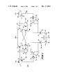
- FIG. 1 illustrates, in schematic form, an embodiment of the invention
- FIG. 2 is a timing diagram useful in understanding the operation of the circuitry of FIG. 1.
- FIG. 1 illustrates a dynamic output buffer useful for receiving data from within a memory and coupling it to the output of the memory itself.
- the dynamic output buffer receives data on lines 17 and 21 and stores the data in a cross coupled sense amplifier having transistors 10, 11, 12, and 13.
- Transistors 10 and 12 are coupled in series between an output latch clock signal OL and a reference terminal illustrated as ground.
- Transistors 11 and 13 are coupled in parallel with transistors 10 and 12.
- a node 15 which is formed between transistors 10 and 12 serves as one output for the cross coupled sense amplifier, and node 16 formed between transistors 11 and 13 serve as another output for the cross coupled sense amplifier.
- Transistor 12 has its gate electrode coupled to node 16, and transistor 13 has its gate electrode coupled to node 15.
- Transistor 10 has its gate electrode coupled to node 19 which serves as an input for the cross coupled sense amplifier, and transistor 11 has its gate electrode coupled to node 23 which serves as another input for the cross coupled sense amplifier.
- Node 19 is coupled to line 17 by transistor 18.
- Transistor 18 is enabled by a column address strobe CAS applied to its gate electrode.
- Node 23 is coupled to line 21 by transistor 22 which has its gate electrode enabled by the same timing signal CAS as transistor 18.
- the input signals to the cross coupled sense amplifier are complements of each other. If it is assumed that node 19 has an input signal sitting at a high level, which would mean the input signal at node 23 would be at a low level, then when clock signal OL goes high, transistor 10 would conduct thereby driving node 15 high. Since node 15 is coupled to the gate electrode of transistor 13, transistor 13 would conduct thereby placing node 16 at a low level. Transistor 12 would remain in a non-conducting state since its gate electrode is coupled to node 16. Node 15 is also coupled to a gate electrode of transistor 25. Transistor 25 is coupled between input node 23 and ground. Since node 15 was assumed to be at a high level, transistor 25 will conduct thereby maintaining input node 23 at a low level.
- timing signals CAS and RAS go high which causes node 19 to discharge to ground and effectively turns off transistor 10 thereby isolating node 15 from the circuitry which provides clock signal OL. This insures that node 15 remains at a high level.
- Transistor 28 is in parallel with transistor 25 and has its gate electrode coupled to the complement column address strobe timing signal CAS.
- Another transistor 31 is in parallel with transistor 28 and has its gate electrode coupled to a complement row address strobe timing signal RAS. Transistors 28 and 31 will maintain node 23 at a low level when their gate electrodes are enabled. In certain situations, timing signal CAS may be delayed and therefore timing signal RAS will insure that node 23 is maintained at a low level.
- Input node 19 also has three transistors 26, 27, and 30 coupling it to ground.
- Transistor 26 has its gate electrode coupled to node 16
- transistor 27 has its gate electrode coupled to timing signal CAS
- transistor 30 has its gate electrode coupled to timing signal RAS. Transistors 26, 27 and 30 operate in a similar manner to that explained, hereinbefore, for transistors 25, 28 and 31 and serve to shunt or clamp input 19 to ground.
- Output node 15 is coupled to a gate electrode of transistor 33, and output node 16 is coupled to a gate electrode of transistor 32.
- Transistors 32 and 33 are in series between a voltage potential terminal V DD and ground. The output for the dynamic output buffer is provided from an OUTPUT node between transistors 32 and 33. If node 16 goes high transistor 32 conducts and the OUTPUT node goes high. If output node 15 goes high, transistor 33 will conduct thereby providing a low level at the OUTPUT node.
- Transistor 34 is coupled from output node 16 to ground, and transistor 36 is coupled from output node 15 to ground.
- Transistors 34 and 36 both have their gate electrodes coupled to a control signal which is used as an output disable OD.
- control signal OD When control signal OD is at a high level, transistors 34 and 36 will conduct thereby discharging output nodes 15 and 16 and rendering transistors 32 and 33 non-conductive which causes the OUTPUT node to float or go to a high impedance state.
- the output transistors are in a state to be enabled when output disable OD is at a low level.
- Output node 16 has a voltage restorer comprising transistors 41 and 42 and capacitor 40 coupled to it. If node 16 is sitting at a high level and timing signal RAS goes high thereby enabling transistor 31, input node 23 can be caused to move to a low level which can be capacitively coupled through transistor 11 to output node 16 causing a decrease in the signal level at output node 16. To alleviate this potential problem, a restorer circuit or glitch eliminator is coupled to output node 16. Transistor 41 is coupled between voltage terminal V DD and output node 16. Transistor 42 is coupled between the gate electrode of transistor 41 and output node 16. Transistor 42 has its gate electrode coupled to voltage potential V DD and therefore transistor 42 will be enabled.
- Output node 15 also has a voltage restoring circuit coupled to it which operates in the same manner as does the voltage restoring circuit for output node 16.
- Transistor 45 is coupled from voltage V DD to output node 15, and transistor 46 is coupled from the gate electrode of transistor 45 to output node 15.
- a coupling capacitor 44 is coupled from the gate electrode of transistor 45 to timing signal RAS.
- Capacitors 40 and 44 can be implemented as MOS transistors.
- the capacitors can be field effect transistors having their drain and source electrodes connected together to input timing signal RAS while their gate electrode is coupled to the gate electrode of transistor 41 or 45.
- Timing waveforms found in the circuitry of FIG. 1 are illustrated in FIG. 2.
- the top waveform is timing signal RAS and generally leads timing signal CAS by a short period of time.
- input control signal CAS (not shown) goes high data sitting on line 17 and 21 are coupled to input nodes 19 and 23 respectively.
- node 23 goes high.
- transistor 11 is enabled and therefore output node 16 will go high when output latch clock signal OL goes high.
- a dynamic output buffer having a cross coupled sense amplifier which is effectively isolated from the memory or external circuit once the cross coupled sense amplifier is in a latched state thereby preventing any loss of data contained in the cross coupled sense amplifier.
- the cross coupled sense amplifier also has voltage restoring circuits coupled to its output so that as its input is pulled low the output will not be deteriorated.
Abstract
There is provided a dynamic output buffer useful for providing output data from a memory. The output buffer includes a cross coupled sense amplifier having inputs and outputs. The outputs of this sense amplifier are coupled by output transistors to the output of the dynamic output buffer. The outputs of the cross coupled sense amplifier are also coupled to dynamic load devices which are used to prevent the outputs from deteriorating when the inputs are shunted or clamped to ground. The inputs are clamped to ground by transistors which are controlled by timing signals and thereby insure that data stored by the cross coupled sense amplifier will not be lost.
Description
This invention relates, in general, to output buffers, and more particularly, to output buffers useful in digital memories.
Buffers are used to buffer data from a memory to outside circuitry. The most common type of buffer used includes a cross coupled sense amplifier. In MOS circuitry it is common to have the cross coupled sense amplifier enabled by one clock signal. However, because of the bidirectional conductivity of MOS transistors it is necessary to take special precautions with the clock signal, and the circuitry providing the clock signal, to insure that data stored in the cross coupled sense amplifier is not lost or discharged back through the clock signal circuitry when the clock signal is in a non-enabling state.
Accordingly, it is an object of the present invention to provide an improved dynamic output buffer which is capable of holding output data for long periods of time without appreciable deterioration of the data.
Another object of the present invention is to provide an improved dynamic output buffer wherein the output data is maintained at substantially a constant amplitude even during switching of internal transistors of the buffer itself.
In carrying out the above and other objects of the present invention, there is provided in one form, a dynamic output buffer having a cross coupled sense amplifier which is used to receive the input data so that it can be outputted by output driver transistors upon command. Field effect transistors, which are controlled by timing signals, are used to disconnect the cross coupled sense amplifier inputs from external circuitry. The circuit also includes additional dynamic loads coupled to the outputs of the cross coupled sense amplifier to restore or boost the output at the same time that the inputs are being disconnected from the external circuitry thereby preventing outputs of the cross coupled sense amplifier from decreasing substantially in amplitude.
The subject matter which is regarded as the invention is set forth in the appended claims. The invention itself, however, together with further objects and advantages thereof, may be better understood by referring to the following detailed description taken in conjunction with the accompanying drawings.
FIG. 1 illustrates, in schematic form, an embodiment of the invention; and
FIG. 2 is a timing diagram useful in understanding the operation of the circuitry of FIG. 1.
FIG. 1 illustrates a dynamic output buffer useful for receiving data from within a memory and coupling it to the output of the memory itself. The dynamic output buffer receives data on lines 17 and 21 and stores the data in a cross coupled sense amplifier having transistors 10, 11, 12, and 13. Transistors 10 and 12 are coupled in series between an output latch clock signal OL and a reference terminal illustrated as ground. Transistors 11 and 13 are coupled in parallel with transistors 10 and 12. A node 15 which is formed between transistors 10 and 12 serves as one output for the cross coupled sense amplifier, and node 16 formed between transistors 11 and 13 serve as another output for the cross coupled sense amplifier. Transistor 12 has its gate electrode coupled to node 16, and transistor 13 has its gate electrode coupled to node 15. Transistor 10 has its gate electrode coupled to node 19 which serves as an input for the cross coupled sense amplifier, and transistor 11 has its gate electrode coupled to node 23 which serves as another input for the cross coupled sense amplifier. Node 19 is coupled to line 17 by transistor 18. Transistor 18 is enabled by a column address strobe CAS applied to its gate electrode. Node 23 is coupled to line 21 by transistor 22 which has its gate electrode enabled by the same timing signal CAS as transistor 18.
The input signals to the cross coupled sense amplifier are complements of each other. If it is assumed that node 19 has an input signal sitting at a high level, which would mean the input signal at node 23 would be at a low level, then when clock signal OL goes high, transistor 10 would conduct thereby driving node 15 high. Since node 15 is coupled to the gate electrode of transistor 13, transistor 13 would conduct thereby placing node 16 at a low level. Transistor 12 would remain in a non-conducting state since its gate electrode is coupled to node 16. Node 15 is also coupled to a gate electrode of transistor 25. Transistor 25 is coupled between input node 23 and ground. Since node 15 was assumed to be at a high level, transistor 25 will conduct thereby maintaining input node 23 at a low level. As long as clock signal OL is high, and timing signals RAS and CAS are low, node 15 will remain high and OUTPUT data will be valid. Before clock signal OL goes low, timing signals CAS and RAS go high which causes node 19 to discharge to ground and effectively turns off transistor 10 thereby isolating node 15 from the circuitry which provides clock signal OL. This insures that node 15 remains at a high level.
Timing waveforms found in the circuitry of FIG. 1 are illustrated in FIG. 2. The top waveform is timing signal RAS and generally leads timing signal CAS by a short period of time. When input control signal CAS (not shown) goes high data sitting on line 17 and 21 are coupled to input nodes 19 and 23 respectively. As illustrated in FIG. 2, it is assumed that node 23 goes high. When node 23 goes high, transistor 11 is enabled and therefore output node 16 will go high when output latch clock signal OL goes high. When output disable signal OD goes low transistors 34 and 36 are no longer conductive and therefore no longer holding output nodes 15 and 16 at a low level, therefore, the high on output node 16 will cause transistor 32 to conduct thereby driving the OUTPUT node between transistors 32 and 33 to a high level which is indicated in FIG. 2 as DATA VALID. Note that when RAS goes high a slight glitch 50 is caused on the signal at output node 16 but because of the restoring circuit coupled to output node 16, output node 16 is not permanently deteriorated.
By now it should be appreciated that there has been provided a dynamic output buffer having a cross coupled sense amplifier which is effectively isolated from the memory or external circuit once the cross coupled sense amplifier is in a latched state thereby preventing any loss of data contained in the cross coupled sense amplifier. The cross coupled sense amplifier also has voltage restoring circuits coupled to its output so that as its input is pulled low the output will not be deteriorated.
Claims (1)
- output..]. 6. A dynamic output buffer for buffering data and having a first and a second input and providing a buffer output, comprising: a cross coupled sense amplifier coupled to the first and second inputs and providing a first and a second output; an output driver coupled to the first and second outputs and providing the buffer output; first means coupled to the first input and controlled by the first output for shunting the first input; second means coupled to the second input and controlled by the second output for shunting the second input; third means coupled to the first input and controlled by an enabling signal to shunt the first input upon command from the enabling signal; fourth means coupled to the second input and controlled by the enabling signal to shunt the second input upon command from the enabling signal, a first restorer circuit coupled to the first output to restore the first output when the third means is enabled; and a second restorer circuit coupled to the second output to restore the second output when the fourth means is activated. .Iadd. 7. A dynamic output buffer responsive to a clock signal, comprising:a pair of cross coupled amplifiers for providing a first and a second output on first and second output nodes, respectively;a first load transistor interposed between the clock signal and the first output node and having a control electrode for receiving a first data signal;a second load transistor interposed between the clock signal and the second output node and having a control electrode coupled to a second data signal, said second data signal being complementary to said first data signal;a first enable transistor having a control electrode for receiving an enable signal which occurs before the clock signal is terminated, a first current electrode coupled to the control electrode of the first load transistor, and a second current electrode coupled to a reference level; anda second enable transistor having a control electrode for receiving the enable signal, a first current electrode coupled to the control electrode of the second load transistor, and a second current electrode coupled to the reference level;whereby the enable signal causes the control electrodes of the load transistors to be shunted to the reference level to open the load transistors to isolate the pair of cross coupled amplifiers from the clock signal. .Iaddend. .Iadd. 8. The dynamic output buffer of claim 7 further comprising:a fifth transistor having a control electrode coupled to the enable signal, a first current electrode coupled to a supply voltage, and a second current electrode coupled to the first output node; anda sixth transistor having a first current electrode coupled to the control electrode of the fifth transistor, a second current electrode coupled to the first output node, and a control electrode coupled to the supply voltage;a first coupling capacitor coupled between the control electrode of the fifth transistor and the enable signal;a seventh transistor having a first current electrode coupled to the supply voltage, a second current electrode coupled to the second output node, and a control electrode;an eighth transistor having a first current electrode coupled to the control electrode of the seventh transistor, a second current electrode coupled to the second output node, and a control electrode coupled to the supply voltage; anda second coupling capacitor coupled between the control electrode of the seventh transistor and the enabling signal. .Iaddend.
Priority Applications (1)
| Application Number | Priority Date | Filing Date | Title |
|---|---|---|---|
| US06/376,795 USRE31663E (en) | 1979-03-05 | 1982-05-10 | Dynamic output buffer |
Applications Claiming Priority (2)
| Application Number | Priority Date | Filing Date | Title |
|---|---|---|---|
| US06/017,748 US4250412A (en) | 1979-03-05 | 1979-03-05 | Dynamic output buffer |
| US06/376,795 USRE31663E (en) | 1979-03-05 | 1982-05-10 | Dynamic output buffer |
Related Parent Applications (1)
| Application Number | Title | Priority Date | Filing Date |
|---|---|---|---|
| US06/017,748 Reissue US4250412A (en) | 1979-03-05 | 1979-03-05 | Dynamic output buffer |
Publications (1)
| Publication Number | Publication Date |
|---|---|
| USRE31663E true USRE31663E (en) | 1984-09-04 |
Family
ID=26690261
Family Applications (1)
| Application Number | Title | Priority Date | Filing Date |
|---|---|---|---|
| US06/376,795 Expired - Lifetime USRE31663E (en) | 1979-03-05 | 1982-05-10 | Dynamic output buffer |
Country Status (1)
| Country | Link |
|---|---|
| US (1) | USRE31663E (en) |
Citations (6)
| Publication number | Priority date | Publication date | Assignee | Title |
|---|---|---|---|---|
| US3363115A (en) * | 1965-03-29 | 1968-01-09 | Gen Micro Electronics Inc | Integral counting circuit with storage capacitors in the conductive path of steering gate circuits |
| US4038567A (en) * | 1976-03-22 | 1977-07-26 | International Business Machines Corporation | Memory input signal buffer circuit |
| US4081701A (en) * | 1976-06-01 | 1978-03-28 | Texas Instruments Incorporated | High speed sense amplifier for MOS random access memory |
| US4146802A (en) * | 1977-09-19 | 1979-03-27 | Motorola, Inc. | Self latching buffer |
| US4280070A (en) * | 1978-10-20 | 1981-07-21 | Texas Instruments Incorporated | Balanced input buffer circuit for semiconductor memory |
| US4353104A (en) * | 1980-06-27 | 1982-10-05 | Oki Electric Industry Co., Ltd. | Output interface circuits |
-
1982
- 1982-05-10 US US06/376,795 patent/USRE31663E/en not_active Expired - Lifetime
Patent Citations (6)
| Publication number | Priority date | Publication date | Assignee | Title |
|---|---|---|---|---|
| US3363115A (en) * | 1965-03-29 | 1968-01-09 | Gen Micro Electronics Inc | Integral counting circuit with storage capacitors in the conductive path of steering gate circuits |
| US4038567A (en) * | 1976-03-22 | 1977-07-26 | International Business Machines Corporation | Memory input signal buffer circuit |
| US4081701A (en) * | 1976-06-01 | 1978-03-28 | Texas Instruments Incorporated | High speed sense amplifier for MOS random access memory |
| US4146802A (en) * | 1977-09-19 | 1979-03-27 | Motorola, Inc. | Self latching buffer |
| US4280070A (en) * | 1978-10-20 | 1981-07-21 | Texas Instruments Incorporated | Balanced input buffer circuit for semiconductor memory |
| US4353104A (en) * | 1980-06-27 | 1982-10-05 | Oki Electric Industry Co., Ltd. | Output interface circuits |
Non-Patent Citations (2)
| Title |
|---|
| "Output Sense and Buffer", Drawing MK4116-032, MOS Aid. |
| Output Sense and Buffer , Drawing MK4116 032, MOS Aid. * |
Similar Documents
| Publication | Publication Date | Title |
|---|---|---|
| US4146802A (en) | Self latching buffer | |
| US4972101A (en) | Noise reduction in CMOS driver using capacitor discharge to generate a control voltage | |
| US4628218A (en) | Driving circuit suppressing peak value of charging current from power supply to capacitive load | |
| US5357468A (en) | Semiconductor memory device | |
| CA2033020C (en) | C-mos differential sense amplifier | |
| US4250412A (en) | Dynamic output buffer | |
| JPS6069898A (en) | Semiconductor storage device | |
| JP2743878B2 (en) | Input buffer circuit | |
| US4409677A (en) | Semiconductor integrated circuit device | |
| US5517142A (en) | Output buffer with a reduced transient bouncing phenomenon | |
| US4339809A (en) | Noise protection circuits | |
| US4093875A (en) | Field effect transistor (FET) circuit utilizing substrate potential for turning off depletion mode devices | |
| US4420823A (en) | Semiconductor memory | |
| US4508980A (en) | Sense and refresh amplifier circuit | |
| US3789312A (en) | Threshold independent linear amplifier | |
| JPH0541651A (en) | Semiconductor integrated circuit device for capacity load driving | |
| US4464581A (en) | Trigger pulse generator | |
| US4563599A (en) | Circuit for address transition detection | |
| JPH01200819A (en) | Data output presetting circuit | |
| US6674308B2 (en) | Low power wired OR | |
| US6037827A (en) | Noise isolation circuit | |
| US3736522A (en) | High gain field effect transistor amplifier using field effect transistor circuit as current source load | |
| CA1115843A (en) | Dynamic precharge circuitry | |
| USRE31663E (en) | Dynamic output buffer | |
| USRE31662E (en) | Output buffer with voltage sustainer circuit |