WO1986004676A2 - Device for optical determination of low-order errors in shape - Google Patents
Device for optical determination of low-order errors in shape Download PDFInfo
- Publication number
- WO1986004676A2 WO1986004676A2 PCT/DE1986/000037 DE8600037W WO8604676A2 WO 1986004676 A2 WO1986004676 A2 WO 1986004676A2 DE 8600037 W DE8600037 W DE 8600037W WO 8604676 A2 WO8604676 A2 WO 8604676A2
- Authority
- WO
- WIPO (PCT)
- Prior art keywords
- light receiving
- light
- angle
- receiving elements
- evaluation unit
- Prior art date
Links
Classifications
-
- G—PHYSICS
- G01—MEASURING; TESTING
- G01B—MEASURING LENGTH, THICKNESS OR SIMILAR LINEAR DIMENSIONS; MEASURING ANGLES; MEASURING AREAS; MEASURING IRREGULARITIES OF SURFACES OR CONTOURS
- G01B11/00—Measuring arrangements characterised by the use of optical techniques
- G01B11/30—Measuring arrangements characterised by the use of optical techniques for measuring roughness or irregularity of surfaces
- G01B11/303—Measuring arrangements characterised by the use of optical techniques for measuring roughness or irregularity of surfaces using photoelectric detection means
-
- G—PHYSICS
- G01—MEASURING; TESTING
- G01N—INVESTIGATING OR ANALYSING MATERIALS BY DETERMINING THEIR CHEMICAL OR PHYSICAL PROPERTIES
- G01N21/00—Investigating or analysing materials by the use of optical means, i.e. using sub-millimetre waves, infrared, visible or ultraviolet light
- G01N21/84—Systems specially adapted for particular applications
- G01N21/88—Investigating the presence of flaws or contamination
- G01N21/95—Investigating the presence of flaws or contamination characterised by the material or shape of the object to be examined
- G01N21/952—Inspecting the exterior surface of cylindrical bodies or wires
Definitions
- the invention relates to a device for determining shape deviations of low order and in particular shape deviations of first and second order.
- Shape deviations of the first to third order are called bumps, waves or grooves.
- Stecond-order design deviations are sometimes also referred to as "chatter marks”.
- Such design deviations and, in particular, second-order design deviations lead to noise developments, such as whistling, in the case of bearing surfaces of gear shafts in the low-frequency range.
- the appearance of whistles requires dismantling the gearbox to remove the shaft. In order to avoid this effort, it would be desirable to examine all shafts prior to installation, for example when assembling the gearbox, for shape deviations or shape errors of low order and, in particular, for the occurrence of noise-causing chatter marks.
- the invention has for its object to provide a device for the optical determination of shape deviations or surface defects of low order, with which design deviations of low order can be detected with high accuracy with comparatively little optical and electronic effort.
- This object is achieved in that of a device according to the preamble of claim 1, as described in "Annais of the CIRP, Vol. 33/1/1984, page 407 f.” is known, is assumed, and this device is further developed by the features of the characterizing part.
- the light receiving device consists of a multiplicity of light receiving elements arranged in cells and that the output signals of all light receiving elements are evaluated in order to determine the angle of inclination.
- This surprisingly makes it possible to resolve shifts in the center of gravity of the reflected light beam that are substantially less than the width of a light receiving element.
- the method according to the invention has the further surprising advantage that the measurement result obtained is practically not influenced by shape deviations of higher order such as roughness etc.
- the device according to the invention enables the simultaneous determination of several measured variables, such as the statistical local roughness, the roughness integrated over the measurement spot, the ripple, shape and position deviation in the integrated profile and the visual inspection or
- Ripple can be separated.
- the optical test head is less sensitive than a mechanical probe to interference vibrations emanating from the test object. This applies to both vibration directions in the specimen surface as well as perpendicular to it. This enables the device according to the invention to be integrated into a production line.
- the device according to the invention is also largely insensitive to changes in distance within a comparatively large range.
- Claim 2 specifies a simple relationship according to which the evaluation unit determines the angle of inclination of the scanned surface element from the output signals of the individual light-receiving elements. This relationship allows shifts in the center of gravity of the reflected light beam on the light-receiving element row, which can be less than 10% of the width of a light-receiving element, to be detected with little effort.
- the relationship used according to the invention also allows the automatic alignment of the device on an actual surface such that the optical axis lies in the surface normal. In contrast to mechanical pushbuttons, multiple probing is not required.
- the profile curve of the body to be examined can be determined in a simple manner by integration.
- the device according to the invention there is therefore a choice between slope and height profile depending on, for example, the ratio of wave amplitude / wavelength or of functional requirements.
- a particular advantage of the device according to the invention is its uniform frequency response, ie its largely constant transfer function over a large frequency Area.
- This uniform frequency response makes it possible to subject the output signal of the evaluation unit and / or the output signal of the integration circuit to a Fourier transformation over a large frequency range. From the Fourier spectrum obtained in this way, statements can be derived in a simple manner, which allow a quick overview of the quality of the workpiece: For example, maxima are characteristic of certain Fourier orders for chatter marks. On the basis of the occurrence or non-occurrence of these orders, it can easily be decided whether the shaft is usable or not.
- the Fourier analysis for example, the angle amplitudes of the individual orders, the maximum values can be determined and converted to the corresponding amplitudes of the height profile. This makes you independent of possible defects, such as scratches, etc.
- a particularly advantageous embodiment of the optical part of the device according to the invention is characterized in claim 5. Due to the "oblique impact" of the scanning light beam, a beam splitter can be dispensed with, so that the intensity is not reduced. Above all, however, the claimed distance relationship ensures that both the surface to be examined and the light receiving device are at a distance (measured from the respective main plane of the lens system) from the lens system that is approximately equal to the focal length of the lens system that that of a light receiving element rays emanating from the surface to be examined, which emanate from the illuminated surface element at a certain angle.
- the optical axis can be swiveled out of the surface normal to modify the field of view of the device.
- the design of the device according to claim 6 suppresses the influence of roughness in the surface perpendicular to
- the dimension of the light spot in the direction of cut can be used to determine the smallest detected wavelength of shape deviations.
- the dimension of the light spot in the scanning direction is chosen so large that just the smallest wavelengths that are still of interest for the measurement problem pending can be resolved (claim 7).
- the device according to the invention not only allows the design deviation of low order to be determined, the roughness of the surface can also be determined from the output signals of the individual light-receiving elements. For this, reference is made in detail to DE-OS 30 37 622 (claim 9).
- photodiodes as light receiving elements according to claim 10 has the advantage that diode rows with a small width of the individual light receiving elements and high sensitivity are available as standard at low prices.
- telescope optics allows the resolution of the device according to the invention to be increased in that the reflected light distribution on the light receiver line
- FIG. 1 an explanation of the measuring principle according to the invention
- FIG. 2 the basic structure of a device according to the invention
- FIGS. 3 a and b course of the center of gravity of the scatter distribution on a "whistling" stator shaft, and on a stator shaft which does not cause any noise
- FIG. 4 a and b Fourier transforms of the results shown in FIG. 3, and FIGS. 5 a and b for comparison the result of a mechanical shape test on these stator shafts.
- the beam from a light source 1 is imaged by a lens 3 on a surface 4 to be examined.
- the reflected light strikes a diode row 5.
- the center of gravity of the reflected light bundle lies at a different location (M1 or M2) on the diode row 5.
- the reflected light bundle has a distribution due to the roughness of the surface 4, which is shown schematically in FIG. 1 . Because of this distribution, which changes from surface element to surface element, the measurement of the location of the reflected light bundle with a light balance, for example, has a large, non-correctable error.
- the objective in FIG. 1 is a cylindrical lens, so that an elongated measuring spot 7 results.
- FIG. 2 shows a section or a view from above through an exemplary embodiment of a device according to the invention for the optical determination of surface defects of low order.
- the device which is only shown schematically, in turn has a light source 1, a collimator 2, a measurement objective 3 and a diode row 5.
- the surface 4 to be examined is at a distance from the device, ie from the front main plane of the measuring objective 3, which is approximately equal to the focal length f of the measuring objective.
- the light emanating from the light source 1, for example a laser or a light emitting diode is (if necessary) parallelized by the collimator 2 and strikes the measuring objective 3 outside the optical axis 6.
- the parallel light beam is focused by the measuring objective 3 on the surface 4 to be examined.
- the light beams emanating from the individual illuminated points of the measuring spot are in turn imaged by the measuring objective 3 on the diode row.
- the distance of the diode row 5 from the rear main plane of the measuring lens 3 is approximately equal to the focal length of the measuring lens.
- the measurement objective 3 and the sample surface or the diode row 5 form a Fourier system.
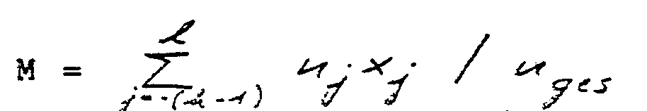
- the scattered light distribution shown schematically in the top view of the device according to the invention on the diode row 5 is used to determine the angle of inclination of the scanned surface element (shown in dashed lines in Fig. 2) against a reference element (solid line 4 in Fig. 2) according to the relationship
- J * * is the following the M value used, which is proportional to.
- the center of gravity of the light spot on the diode row is.
- a shift in the center of gravity of the scattered light distribution by 1/10 the width b of a diode can be resolved in any case.
- the resolution limit in practical use is about 1/100 of a diode width b.
- a diode width b 0.9 mm and a focal length f of the measuring objective 3 of 25 mm
- the inclination of the beam of the measuring objective against the optical axis 6 is between 10 and 20 degrees.
- Fig. 3a shows the course of the M value, i.e. the place of the
- FIG. 3b shows the dependence of the M value for a stator shaft that does not cause whistling.
- the stator wave which causes whistles, has a significantly changed optical M signal curve: the amplitudes are several times larger and the structure more regular. If one calculates the standard deviation for the scattering behavior of the M-value as its standard deviation, one obtains values ⁇ 0.1 as typical standard deviations for perfect waves, while the standard deviations for "whistling" waves are greater than 0.1 and typically greater than 0.15 are.
- the axis of the light receiver line and the feed direction can enclose an angle: This reduces the effective width of a light receiving element and thus increases the resolution.
- a wide variety of optical arrangements can also be used; Of course, it is also possible to have the scanning light beam strike the surface to be examined at almost 90 °. Instead of spherical imaging elements, those with a cylindrical effect can also be used, so that the gap geometry in the scanning direction or perpendicular to it can be adapted to the measurement problem.
- the device according to the invention has the advantage that it is also possible to measure across grooves, bores, etc. Furthermore, special surface designs can be hidden by software.
Abstract
Description

Claims


Priority Applications (2)
| Application Number | Priority Date | Filing Date | Title |
|---|---|---|---|
| AT86901332T ATE55487T1 (en) | 1985-02-05 | 1986-02-05 | DEVICE FOR THE OPTICAL DETERMINATION OF LOW-ORDER FORM DEFECTS. |
| DE8686901332T DE3673281D1 (en) | 1985-02-05 | 1986-02-05 | DEVICE FOR OPTICALLY DETECTING LOW-ORDER DESIGN ERRORS. |
Applications Claiming Priority (2)
| Application Number | Priority Date | Filing Date | Title |
|---|---|---|---|
| DE19853503858 DE3503858A1 (en) | 1985-02-05 | 1985-02-05 | DEVICE FOR DETERMINING LOW-ORDER DESIGN ERRORS |
| DEP3503858.6-52 | 1985-02-05 |
Publications (2)
| Publication Number | Publication Date |
|---|---|
| WO1986004676A2 true WO1986004676A2 (en) | 1986-08-14 |
| WO1986004676A3 WO1986004676A3 (en) | 1986-10-23 |
Family
ID=6261705
Family Applications (1)
| Application Number | Title | Priority Date | Filing Date |
|---|---|---|---|
| PCT/DE1986/000037 WO1986004676A2 (en) | 1985-02-05 | 1986-02-05 | Device for optical determination of low-order errors in shape |
Country Status (5)
| Country | Link |
|---|---|
| US (1) | US4763006A (en) |
| EP (1) | EP0210263B1 (en) |
| JP (1) | JPS62502216A (en) |
| DE (2) | DE3503858A1 (en) |
| WO (1) | WO1986004676A2 (en) |
Cited By (2)
| Publication number | Priority date | Publication date | Assignee | Title |
|---|---|---|---|---|
| DE4408226A1 (en) * | 1994-03-11 | 1995-09-14 | Peter Dipl Phys Lehmann | Process coupled technical surface roughness measurement appts. |
| DE19817664A1 (en) * | 1998-04-21 | 1999-11-04 | Peter Lehmann | Surface roughness measuring method |
Families Citing this family (14)
| Publication number | Priority date | Publication date | Assignee | Title |
|---|---|---|---|---|
| FR2620823B1 (en) * | 1987-09-17 | 1990-08-17 | Centre Tech Ind Papier | DEVICE FOR CONTINUOUSLY DETERMINING A SURFACE CONDITION INDEX OF A MOVING SHEET MATERIAL |
| US5028799A (en) * | 1988-08-01 | 1991-07-02 | Robotic Vision System, Inc. | Method and apparatus for three dimensional object surface determination using co-planar data from multiple sensors |
| US5083867A (en) * | 1988-11-28 | 1992-01-28 | Allegheny Ludlum Corporation | Slab surface contour monitor |
| JP3337702B2 (en) * | 1991-11-14 | 2002-10-21 | キヤノン株式会社 | Optical information recording / reproducing device |
| DE4206776C2 (en) * | 1992-03-04 | 1996-01-25 | Schoeller Felix Jun Papier | Process for the forecasting of error rates after the emulsion coating of photo carrier materials in a web |
| NL9401796A (en) * | 1994-10-28 | 1996-06-03 | Tno | Document recognition apparatus |
| US5781302A (en) * | 1996-07-22 | 1998-07-14 | Geneva Steel | Non-contact shape meter for flatness measurements |
| AU2003284613A1 (en) * | 2002-11-26 | 2004-06-23 | Arkray, Inc. | Light sensor, and detecting mechanism and light-measuring mechanism in analyzing device |
| JP4478669B2 (en) * | 2005-08-31 | 2010-06-09 | キヤノン株式会社 | Sensor and recording apparatus using the same |
| DE102006015627B4 (en) * | 2006-03-31 | 2008-03-27 | Innovent E.V. | Method and device for determining and measuring shape deviations and undulations on rotationally symmetrical parts |
| DE102014111320A1 (en) | 2014-08-08 | 2016-02-11 | Brodmann Technologies GmbH | Device for non-contact measurement on transmission shafts, in particular on worm shafts and working methods for this purpose |
| DE102014116966A1 (en) * | 2014-11-20 | 2016-05-25 | Brodmann Technologies GmbH | Method for contactless surface measurement with measurement correction |
| DE102015106737A1 (en) * | 2015-04-30 | 2016-11-03 | Brodmann Technologies GmbH | Method and device for assessing the surface quality according to the angle-resolved scattered light measuring method with automatic position detection of the workpiece |
| DE102015114065A1 (en) | 2015-08-25 | 2017-03-02 | Brodmann Technologies GmbH | Method and device for non-contact evaluation of the surface quality of a wafer |
Citations (7)
| Publication number | Priority date | Publication date | Assignee | Title |
|---|---|---|---|---|
| US3866038A (en) * | 1972-11-18 | 1975-02-11 | Ibm | Apparatus for measuring surface flatness |
| JPS5749805A (en) * | 1980-09-09 | 1982-03-24 | Matsushita Electric Works Ltd | Measuring device for roughness of surface |
| US4377341A (en) * | 1981-03-11 | 1983-03-22 | The United States Of America As Represented By The Secretary Of The Air Force | System for measuring angular deviation in a transparency |
| US4390277A (en) * | 1980-07-31 | 1983-06-28 | Mcdonnell Douglas Corporation | Flat sheet scatterometer |
| US4411528A (en) * | 1981-01-19 | 1983-10-25 | Control Data Corporation | Optical displacement and contour measuring |
| EP0110146A2 (en) * | 1982-11-03 | 1984-06-13 | Siemens Aktiengesellschaft | Optical sensor system to determine the position of objects |
| EP0145957A1 (en) * | 1983-11-25 | 1985-06-26 | Firma Carl Zeiss | Process and device for the contactless measuring of objects |
Family Cites Families (8)
| Publication number | Priority date | Publication date | Assignee | Title |
|---|---|---|---|---|
| DE2032314A1 (en) * | 1970-06-30 | 1972-01-05 | Ibm Deutschland | Method for non-contact optical testing and measuring of surfaces and devices for carrying out this method |
| DE2101689A1 (en) * | 1971-01-15 | 1972-07-20 | Ibm Deutschland | Arrangement for carrying out a method for contactless optical testing and measuring of surfaces |
| US3857637A (en) * | 1973-01-10 | 1974-12-31 | Ppg Industries Inc | Surface distortion analyzer |
| JPS5593008A (en) * | 1979-01-09 | 1980-07-15 | Canon Inc | Signal formation unit |
| JPS57132044A (en) * | 1981-02-10 | 1982-08-16 | Hitachi Metals Ltd | Discriminating method of surface defect |
| US4534650A (en) * | 1981-04-27 | 1985-08-13 | Inria Institut National De Recherche En Informatique Et En Automatique | Device for the determination of the position of points on the surface of a body |
| US4412743A (en) * | 1981-09-08 | 1983-11-01 | Discovision Associates | Off-axis light beam defect detector |
| DE8303856U1 (en) * | 1983-02-11 | 1985-11-14 | Optische Werke G. Rodenstock, 8000 Muenchen | Device for determining a surface structure, in particular the roughness |
-
1985
- 1985-02-05 DE DE19853503858 patent/DE3503858A1/en not_active Withdrawn
-
1986
- 1986-02-05 DE DE8686901332T patent/DE3673281D1/en not_active Expired - Fee Related
- 1986-02-05 US US06/925,802 patent/US4763006A/en not_active Expired - Fee Related
- 1986-02-05 EP EP86901332A patent/EP0210263B1/en not_active Expired - Lifetime
- 1986-02-05 JP JP61501168A patent/JPS62502216A/en active Pending
- 1986-02-05 WO PCT/DE1986/000037 patent/WO1986004676A2/en active IP Right Grant
Patent Citations (7)
| Publication number | Priority date | Publication date | Assignee | Title |
|---|---|---|---|---|
| US3866038A (en) * | 1972-11-18 | 1975-02-11 | Ibm | Apparatus for measuring surface flatness |
| US4390277A (en) * | 1980-07-31 | 1983-06-28 | Mcdonnell Douglas Corporation | Flat sheet scatterometer |
| JPS5749805A (en) * | 1980-09-09 | 1982-03-24 | Matsushita Electric Works Ltd | Measuring device for roughness of surface |
| US4411528A (en) * | 1981-01-19 | 1983-10-25 | Control Data Corporation | Optical displacement and contour measuring |
| US4377341A (en) * | 1981-03-11 | 1983-03-22 | The United States Of America As Represented By The Secretary Of The Air Force | System for measuring angular deviation in a transparency |
| EP0110146A2 (en) * | 1982-11-03 | 1984-06-13 | Siemens Aktiengesellschaft | Optical sensor system to determine the position of objects |
| EP0145957A1 (en) * | 1983-11-25 | 1985-06-26 | Firma Carl Zeiss | Process and device for the contactless measuring of objects |
Non-Patent Citations (3)
| Title |
|---|
| Optical Engineering, Vol 24, No. 3, June 1985, Bellingham, WA (USA) R. BRODMANN et al.: "Optical Roughness Measuring Instrument for Finemachined Surfaces", pages 408-419, see page 410, figure 1 * |
| Optics Communications, Vol. 46, No. 1, June 1983 Amsterdam (NL) D. BERTANI et al.: "A Fast Optical Profilometer", pages 1-3, see paragraph 2, pages 2,3; figure 1 * |
| PATENTS ABSTRACTS OF JAPAN, Vol. 6, No. 121-(P-126) (999) 6 July 1982 & JP- A- 57 49805 (Matsushita) 24 March 1982, see the whole document * |
Cited By (2)
| Publication number | Priority date | Publication date | Assignee | Title |
|---|---|---|---|---|
| DE4408226A1 (en) * | 1994-03-11 | 1995-09-14 | Peter Dipl Phys Lehmann | Process coupled technical surface roughness measurement appts. |
| DE19817664A1 (en) * | 1998-04-21 | 1999-11-04 | Peter Lehmann | Surface roughness measuring method |
Also Published As
| Publication number | Publication date |
|---|---|
| EP0210263B1 (en) | 1990-08-08 |
| WO1986004676A3 (en) | 1986-10-23 |
| US4763006A (en) | 1988-08-09 |
| DE3673281D1 (en) | 1990-09-13 |
| JPS62502216A (en) | 1987-08-27 |
| EP0210263A1 (en) | 1987-02-04 |
| DE3503858A1 (en) | 1986-08-21 |
Similar Documents
| Publication | Publication Date | Title |
|---|---|---|
| EP0210263B1 (en) | Device for optical determination of low-order errors in shape | |
| EP2458363B1 (en) | Measurement of the positions of curvature midpoints of optical areas of a multi-lens optical system | |
| EP0099023B1 (en) | Reflection measuring head | |
| CH654914A5 (en) | OPTOELECTRONIC MEASURING METHOD AND DEVICE FOR DETERMINING THE SURFACE QUALITY REFLECTIVELY REFLECTING OR TRANSPARENT SURFACES. | |
| DE3304780C2 (en) | ||
| DE2448651A1 (en) | Wire diameter contactless measuring device - is for the dimensional metrology of wires in a drawing plant | |
| DE60312406T2 (en) | Apparatus and method for measuring optical properties of a diffractive optical element | |
| DE102009036383B3 (en) | Apparatus and method for angle-resolved scattered light measurement | |
| DE102011083421A1 (en) | Method and device for measuring homogeneously reflecting surfaces | |
| DE4229313A1 (en) | Method and device for high-precision distance measurement of surfaces | |
| DE4105509C2 (en) | Scattered light measuring arrangement for examining the surface roughness | |
| DE112018007421T5 (en) | DISTANCE MEASURING UNIT AND LIGHT RADIATION DEVICE | |
| WO2004065904A1 (en) | Optical measuring process and precision measuring machine for determining the deviations from ideal shape of technically polished surfaces | |
| DE102004005019A1 (en) | Method for determining the depth of a defect in a glass ribbon | |
| EP1248071A2 (en) | Device for the quantitative assessment of the spatial position of two machine parts, workpieces or other objects relative to one another | |
| DE3924290C2 (en) | ||
| DE102021125813B4 (en) | Double-mirror shear interferometer and method for non-destructive measurement of a surface using interferometric measuring methods | |
| DE10027439B4 (en) | Method and device for evaluating topographic parameters of periodic surface structures | |
| DE3337468C2 (en) | ||
| DE10143812A1 (en) | Device for determination of the spatial position of two bodies relative to each other in either orthogonal or angular coordinate systems based on use of simple and low-cost reflective optical components | |
| DE102011077982B4 (en) | Method and device for the optical analysis of a test object | |
| DE2922163A1 (en) | OPTICAL DEVICE FOR DETERMINING THE GUETE OF A SURFACE | |
| DD252236A1 (en) | ARRANGEMENT FOR ROUGH TESTING ACCORDING TO THE SPREADING METHOD | |
| DE19545367C2 (en) | Device and method for optical profile measurement, in particular on curved object surfaces | |
| DE2448571C3 (en) | Arrangement for non-contact measurement of dimensions, such as diameter, cross-section or the like. of an object |
Legal Events
| Date | Code | Title | Description |
|---|---|---|---|
| AK | Designated states |
Kind code of ref document: A1 Designated state(s): JP US |
|
| AL | Designated countries for regional patents |
Kind code of ref document: A1 Designated state(s): AT BE CH DE FR GB IT LU NL SE |
|
| CR1 | Correction of entry in section i |
Free format text: IN PAT.BUL.18/86,UNDER PUBLISHED REPLACE "A1" BY "A2" |
|
| WWE | Wipo information: entry into national phase |
Ref document number: 1986901332 Country of ref document: EP |
|
| AK | Designated states |
Kind code of ref document: A3 Designated state(s): JP US |
|
| AL | Designated countries for regional patents |
Kind code of ref document: A3 Designated state(s): AT BE CH DE FR GB IT LU NL SE |
|
| WWP | Wipo information: published in national office |
Ref document number: 1986901332 Country of ref document: EP |
|
| WWG | Wipo information: grant in national office |
Ref document number: 1986901332 Country of ref document: EP |