WO1995009147A1 - Organic electroluminescent element and arylenediamine derivative - Google Patents

Organic electroluminescent element and arylenediamine derivative Download PDF

Info

Publication number
WO1995009147A1
WO1995009147A1 PCT/JP1994/001585 JP9401585W WO9509147A1 WO 1995009147 A1 WO1995009147 A1 WO 1995009147A1 JP 9401585 W JP9401585 W JP 9401585W WO 9509147 A1 WO9509147 A1 WO 9509147A1
Authority
WO
WIPO (PCT)
Prior art keywords
group
general formula
derivative
organic
phenylenediamine
Prior art date
Application number
PCT/JP1994/001585
Other languages
French (fr)
Japanese (ja)
Inventor
Hisayuki Kawamura
Chishio Hosokawa
Tadashi Kusumoto
Hiroaki Nakamura
Original Assignee
Idemitsu Kosan Co., Ltd.
Priority date (The priority date is an assumption and is not a legal conclusion. Google has not performed a legal analysis and makes no representation as to the accuracy of the date listed.)
Filing date
Publication date
Family has litigation
First worldwide family litigation filed litigation Critical https://patents.darts-ip.com/?family=17097741&utm_source=google_patent&utm_medium=platform_link&utm_campaign=public_patent_search&patent=WO1995009147(A1) "Global patent litigation dataset” by Darts-ip is licensed under a Creative Commons Attribution 4.0 International License.
Application filed by Idemitsu Kosan Co., Ltd. filed Critical Idemitsu Kosan Co., Ltd.
Priority to US08/615,281 priority Critical patent/US5837166A/en
Priority to DE69432054T priority patent/DE69432054T2/en
Priority to EP94927780A priority patent/EP0721935B1/en
Priority to JP51020995A priority patent/JP3295088B2/en
Publication of WO1995009147A1 publication Critical patent/WO1995009147A1/en

Links

Classifications

    • CCHEMISTRY; METALLURGY
    • C07ORGANIC CHEMISTRY
    • C07CACYCLIC OR CARBOCYCLIC COMPOUNDS
    • C07C211/00Compounds containing amino groups bound to a carbon skeleton
    • C07C211/43Compounds containing amino groups bound to a carbon skeleton having amino groups bound to carbon atoms of six-membered aromatic rings of the carbon skeleton
    • C07C211/54Compounds containing amino groups bound to a carbon skeleton having amino groups bound to carbon atoms of six-membered aromatic rings of the carbon skeleton having amino groups bound to two or three six-membered aromatic rings
    • CCHEMISTRY; METALLURGY
    • C07ORGANIC CHEMISTRY
    • C07CACYCLIC OR CARBOCYCLIC COMPOUNDS
    • C07C211/00Compounds containing amino groups bound to a carbon skeleton
    • C07C211/43Compounds containing amino groups bound to a carbon skeleton having amino groups bound to carbon atoms of six-membered aromatic rings of the carbon skeleton
    • C07C211/57Compounds containing amino groups bound to a carbon skeleton having amino groups bound to carbon atoms of six-membered aromatic rings of the carbon skeleton having amino groups bound to carbon atoms of six-membered aromatic rings being part of condensed ring systems of the carbon skeleton
    • C07C211/58Naphthylamines; N-substituted derivatives thereof
    • CCHEMISTRY; METALLURGY
    • C07ORGANIC CHEMISTRY
    • C07CACYCLIC OR CARBOCYCLIC COMPOUNDS
    • C07C211/00Compounds containing amino groups bound to a carbon skeleton
    • C07C211/43Compounds containing amino groups bound to a carbon skeleton having amino groups bound to carbon atoms of six-membered aromatic rings of the carbon skeleton
    • C07C211/57Compounds containing amino groups bound to a carbon skeleton having amino groups bound to carbon atoms of six-membered aromatic rings of the carbon skeleton having amino groups bound to carbon atoms of six-membered aromatic rings being part of condensed ring systems of the carbon skeleton
    • C07C211/61Compounds containing amino groups bound to a carbon skeleton having amino groups bound to carbon atoms of six-membered aromatic rings of the carbon skeleton having amino groups bound to carbon atoms of six-membered aromatic rings being part of condensed ring systems of the carbon skeleton with at least one of the condensed ring systems formed by three or more rings
    • CCHEMISTRY; METALLURGY
    • C07ORGANIC CHEMISTRY
    • C07CACYCLIC OR CARBOCYCLIC COMPOUNDS
    • C07C217/00Compounds containing amino and etherified hydroxy groups bound to the same carbon skeleton
    • C07C217/78Compounds containing amino and etherified hydroxy groups bound to the same carbon skeleton having amino groups and etherified hydroxy groups bound to carbon atoms of six-membered aromatic rings of the same carbon skeleton
    • C07C217/80Compounds containing amino and etherified hydroxy groups bound to the same carbon skeleton having amino groups and etherified hydroxy groups bound to carbon atoms of six-membered aromatic rings of the same carbon skeleton having amino groups and etherified hydroxy groups bound to carbon atoms of non-condensed six-membered aromatic rings
    • C07C217/82Compounds containing amino and etherified hydroxy groups bound to the same carbon skeleton having amino groups and etherified hydroxy groups bound to carbon atoms of six-membered aromatic rings of the same carbon skeleton having amino groups and etherified hydroxy groups bound to carbon atoms of non-condensed six-membered aromatic rings of the same non-condensed six-membered aromatic ring
    • C07C217/92Compounds containing amino and etherified hydroxy groups bound to the same carbon skeleton having amino groups and etherified hydroxy groups bound to carbon atoms of six-membered aromatic rings of the same carbon skeleton having amino groups and etherified hydroxy groups bound to carbon atoms of non-condensed six-membered aromatic rings of the same non-condensed six-membered aromatic ring the nitrogen atom of at least one of the amino groups being further bound to a carbon atom of a six-membered aromatic ring
    • CCHEMISTRY; METALLURGY
    • C09DYES; PAINTS; POLISHES; NATURAL RESINS; ADHESIVES; COMPOSITIONS NOT OTHERWISE PROVIDED FOR; APPLICATIONS OF MATERIALS NOT OTHERWISE PROVIDED FOR
    • C09KMATERIALS FOR MISCELLANEOUS APPLICATIONS, NOT PROVIDED FOR ELSEWHERE
    • C09K11/00Luminescent, e.g. electroluminescent, chemiluminescent materials
    • C09K11/06Luminescent, e.g. electroluminescent, chemiluminescent materials containing organic luminescent materials
    • HELECTRICITY
    • H05ELECTRIC TECHNIQUES NOT OTHERWISE PROVIDED FOR
    • H05BELECTRIC HEATING; ELECTRIC LIGHT SOURCES NOT OTHERWISE PROVIDED FOR; CIRCUIT ARRANGEMENTS FOR ELECTRIC LIGHT SOURCES, IN GENERAL
    • H05B33/00Electroluminescent light sources
    • H05B33/12Light sources with substantially two-dimensional radiating surfaces
    • H05B33/14Light sources with substantially two-dimensional radiating surfaces characterised by the chemical or physical composition or the arrangement of the electroluminescent material, or by the simultaneous addition of the electroluminescent material in or onto the light source
    • HELECTRICITY
    • H10SEMICONDUCTOR DEVICES; ELECTRIC SOLID-STATE DEVICES NOT OTHERWISE PROVIDED FOR
    • H10KORGANIC ELECTRIC SOLID-STATE DEVICES
    • H10K85/00Organic materials used in the body or electrodes of devices covered by this subclass
    • H10K85/60Organic compounds having low molecular weight
    • H10K85/615Polycyclic condensed aromatic hydrocarbons, e.g. anthracene
    • HELECTRICITY
    • H10SEMICONDUCTOR DEVICES; ELECTRIC SOLID-STATE DEVICES NOT OTHERWISE PROVIDED FOR
    • H10KORGANIC ELECTRIC SOLID-STATE DEVICES
    • H10K85/00Organic materials used in the body or electrodes of devices covered by this subclass
    • H10K85/60Organic compounds having low molecular weight
    • H10K85/631Amine compounds having at least two aryl rest on at least one amine-nitrogen atom, e.g. triphenylamine
    • H10K85/633Amine compounds having at least two aryl rest on at least one amine-nitrogen atom, e.g. triphenylamine comprising polycyclic condensed aromatic hydrocarbons as substituents on the nitrogen atom
    • CCHEMISTRY; METALLURGY
    • C07ORGANIC CHEMISTRY
    • C07CACYCLIC OR CARBOCYCLIC COMPOUNDS
    • C07C2601/00Systems containing only non-condensed rings
    • C07C2601/02Systems containing only non-condensed rings with a three-membered ring
    • CCHEMISTRY; METALLURGY
    • C07ORGANIC CHEMISTRY
    • C07CACYCLIC OR CARBOCYCLIC COMPOUNDS
    • C07C2601/00Systems containing only non-condensed rings
    • C07C2601/04Systems containing only non-condensed rings with a four-membered ring
    • CCHEMISTRY; METALLURGY
    • C07ORGANIC CHEMISTRY
    • C07CACYCLIC OR CARBOCYCLIC COMPOUNDS
    • C07C2601/00Systems containing only non-condensed rings
    • C07C2601/06Systems containing only non-condensed rings with a five-membered ring
    • C07C2601/08Systems containing only non-condensed rings with a five-membered ring the ring being saturated
    • CCHEMISTRY; METALLURGY
    • C07ORGANIC CHEMISTRY
    • C07CACYCLIC OR CARBOCYCLIC COMPOUNDS
    • C07C2601/00Systems containing only non-condensed rings
    • C07C2601/12Systems containing only non-condensed rings with a six-membered ring
    • C07C2601/14The ring being saturated
    • CCHEMISTRY; METALLURGY
    • C07ORGANIC CHEMISTRY
    • C07CACYCLIC OR CARBOCYCLIC COMPOUNDS
    • C07C2603/00Systems containing at least three condensed rings
    • C07C2603/02Ortho- or ortho- and peri-condensed systems
    • C07C2603/04Ortho- or ortho- and peri-condensed systems containing three rings
    • C07C2603/06Ortho- or ortho- and peri-condensed systems containing three rings containing at least one ring with less than six ring members
    • C07C2603/10Ortho- or ortho- and peri-condensed systems containing three rings containing at least one ring with less than six ring members containing five-membered rings
    • C07C2603/12Ortho- or ortho- and peri-condensed systems containing three rings containing at least one ring with less than six ring members containing five-membered rings only one five-membered ring
    • C07C2603/18Fluorenes; Hydrogenated fluorenes
    • CCHEMISTRY; METALLURGY
    • C07ORGANIC CHEMISTRY
    • C07CACYCLIC OR CARBOCYCLIC COMPOUNDS
    • C07C2603/00Systems containing at least three condensed rings
    • C07C2603/02Ortho- or ortho- and peri-condensed systems
    • C07C2603/04Ortho- or ortho- and peri-condensed systems containing three rings
    • C07C2603/06Ortho- or ortho- and peri-condensed systems containing three rings containing at least one ring with less than six ring members
    • C07C2603/10Ortho- or ortho- and peri-condensed systems containing three rings containing at least one ring with less than six ring members containing five-membered rings
    • C07C2603/12Ortho- or ortho- and peri-condensed systems containing three rings containing at least one ring with less than six ring members containing five-membered rings only one five-membered ring
    • C07C2603/20Acenaphthenes; Hydrogenated acenaphthenes
    • CCHEMISTRY; METALLURGY
    • C07ORGANIC CHEMISTRY
    • C07CACYCLIC OR CARBOCYCLIC COMPOUNDS
    • C07C2603/00Systems containing at least three condensed rings
    • C07C2603/02Ortho- or ortho- and peri-condensed systems
    • C07C2603/04Ortho- or ortho- and peri-condensed systems containing three rings
    • C07C2603/22Ortho- or ortho- and peri-condensed systems containing three rings containing only six-membered rings
    • C07C2603/24Anthracenes; Hydrogenated anthracenes
    • CCHEMISTRY; METALLURGY
    • C07ORGANIC CHEMISTRY
    • C07CACYCLIC OR CARBOCYCLIC COMPOUNDS
    • C07C2603/00Systems containing at least three condensed rings
    • C07C2603/02Ortho- or ortho- and peri-condensed systems
    • C07C2603/04Ortho- or ortho- and peri-condensed systems containing three rings
    • C07C2603/22Ortho- or ortho- and peri-condensed systems containing three rings containing only six-membered rings
    • C07C2603/26Phenanthrenes; Hydrogenated phenanthrenes
    • CCHEMISTRY; METALLURGY
    • C07ORGANIC CHEMISTRY
    • C07CACYCLIC OR CARBOCYCLIC COMPOUNDS
    • C07C2603/00Systems containing at least three condensed rings
    • C07C2603/02Ortho- or ortho- and peri-condensed systems
    • C07C2603/40Ortho- or ortho- and peri-condensed systems containing four condensed rings
    • C07C2603/42Ortho- or ortho- and peri-condensed systems containing four condensed rings containing only six-membered rings
    • C07C2603/50Pyrenes; Hydrogenated pyrenes
    • HELECTRICITY
    • H10SEMICONDUCTOR DEVICES; ELECTRIC SOLID-STATE DEVICES NOT OTHERWISE PROVIDED FOR
    • H10KORGANIC ELECTRIC SOLID-STATE DEVICES
    • H10K2102/00Constructional details relating to the organic devices covered by this subclass
    • H10K2102/10Transparent electrodes, e.g. using graphene
    • H10K2102/101Transparent electrodes, e.g. using graphene comprising transparent conductive oxides [TCO]
    • H10K2102/103Transparent electrodes, e.g. using graphene comprising transparent conductive oxides [TCO] comprising indium oxides, e.g. ITO
    • HELECTRICITY
    • H10SEMICONDUCTOR DEVICES; ELECTRIC SOLID-STATE DEVICES NOT OTHERWISE PROVIDED FOR
    • H10KORGANIC ELECTRIC SOLID-STATE DEVICES
    • H10K50/00Organic light-emitting devices
    • H10K50/10OLEDs or polymer light-emitting diodes [PLED]
    • H10K50/11OLEDs or polymer light-emitting diodes [PLED] characterised by the electroluminescent [EL] layers
    • HELECTRICITY
    • H10SEMICONDUCTOR DEVICES; ELECTRIC SOLID-STATE DEVICES NOT OTHERWISE PROVIDED FOR
    • H10KORGANIC ELECTRIC SOLID-STATE DEVICES
    • H10K85/00Organic materials used in the body or electrodes of devices covered by this subclass
    • H10K85/30Coordination compounds
    • H10K85/321Metal complexes comprising a group IIIA element, e.g. Tris (8-hydroxyquinoline) gallium [Gaq3]
    • H10K85/324Metal complexes comprising a group IIIA element, e.g. Tris (8-hydroxyquinoline) gallium [Gaq3] comprising aluminium, e.g. Alq3
    • HELECTRICITY
    • H10SEMICONDUCTOR DEVICES; ELECTRIC SOLID-STATE DEVICES NOT OTHERWISE PROVIDED FOR
    • H10KORGANIC ELECTRIC SOLID-STATE DEVICES
    • H10K85/00Organic materials used in the body or electrodes of devices covered by this subclass
    • H10K85/60Organic compounds having low molecular weight
    • H10K85/615Polycyclic condensed aromatic hydrocarbons, e.g. anthracene
    • H10K85/622Polycyclic condensed aromatic hydrocarbons, e.g. anthracene containing four rings, e.g. pyrene
    • HELECTRICITY
    • H10SEMICONDUCTOR DEVICES; ELECTRIC SOLID-STATE DEVICES NOT OTHERWISE PROVIDED FOR
    • H10KORGANIC ELECTRIC SOLID-STATE DEVICES
    • H10K85/00Organic materials used in the body or electrodes of devices covered by this subclass
    • H10K85/60Organic compounds having low molecular weight
    • H10K85/615Polycyclic condensed aromatic hydrocarbons, e.g. anthracene
    • H10K85/626Polycyclic condensed aromatic hydrocarbons, e.g. anthracene containing more than one polycyclic condensed aromatic rings, e.g. bis-anthracene
    • YGENERAL TAGGING OF NEW TECHNOLOGICAL DEVELOPMENTS; GENERAL TAGGING OF CROSS-SECTIONAL TECHNOLOGIES SPANNING OVER SEVERAL SECTIONS OF THE IPC; TECHNICAL SUBJECTS COVERED BY FORMER USPC CROSS-REFERENCE ART COLLECTIONS [XRACs] AND DIGESTS
    • Y10TECHNICAL SUBJECTS COVERED BY FORMER USPC
    • Y10STECHNICAL SUBJECTS COVERED BY FORMER USPC CROSS-REFERENCE ART COLLECTIONS [XRACs] AND DIGESTS
    • Y10S428/00Stock material or miscellaneous articles
    • Y10S428/917Electroluminescent

Definitions

  • the present invention relates to an organic electroluminescence device (hereinafter abbreviated as an organic EL device) and a novel arylenediamine derivative. More specifically, the use of arylene diamine derivatives as an organic EL device component, and particularly as a hole transport material, has led to a remarkable improvement in the luminescent lifetime of the organic EL device and the luminescent lifetime of the organic EL device. It relates to novel P-phenylenediamine derivatives and 4,4'-biphenylene derivatives which can be significantly improved.
  • the half-life was several tens of hours, which was insufficient for practical use.
  • Japanese Patent Application Laid-Open No. 5-107785 discloses that a triamine compound can be used as a charge transporting material of an EL device, but does not sufficiently satisfy the above demand.
  • an organic EL device having the above-mentioned preferable properties have conducted intensive studies to develop an organic EL device having the above-mentioned preferable properties, and as a result, have found that an arylene diamine derivative having a specific structure can be used as a component of an organic EL device, in particular, a hole. It has been found that an organic EL device having a long luminescent life can be obtained by using it as a transport material.
  • the present inventors have found that among the above arylenediamine derivatives, those having a certain structure and a p-phenylenediamine derivative and a 4,4′-biphenylenediamine derivative having a specific structure are not described in the literature. New compound It has also been found that an organic EL device having a remarkably improved luminescence lifetime can be obtained by using this as a component of an organic EL device, particularly as a hole transport material. The present invention has been completed based on such findings.
  • Z is p- phenylene group
  • a r 1, A r 2 , A r 3 and A r 4 are each an Ariru group having a carbon number of 6-2 0, they be the same or different from each other even if well, also Z, a r ', a r 2, a r 3 and a r 4 is Ku respectively Wakashi alkyl group of from 1 to 6 carbon may be substituted by alkoxy groups or Fuweniru group but, a r 1, a r 2 , a r 3 and a r 4 together with z of the central skeleton must have 6 or more benzene ring skeletons. ]
  • An organic EL device containing at least a p-phenylenediamine derivative having at least 6 benzene ring skeletons represented by
  • R 1G to R 17 each represent a hydrogen atom, an alkyl group or an alkoxy group having 1 to 6 carbon atoms, or a phenyl group, which may be the same or different;
  • R 10 and R 11, R 11 and R 13, R 12 and R 13, R 14 and R 15, R 15 and R 17 and R '6 and R 17 are its Re respectively bonded to form a ring You may.
  • R 10 and R 11, R 11 and R 13, R 12 and R 13, R 14 and R 15, R 15 and R 17 and R '6 and R 17 are its Re respectively bonded to form a ring You may.
  • FIG. 1, FIG. 2, FIG. 3, and FIG. 4 are ⁇ -NMR spectrum diagrams of the compounds obtained in Production Example 4, Production Example 5, Production Example 6, and Production Example 7, respectively. .
  • One of the arylene diamine derivatives used in the organic EL device of the present invention has a general formula (I)
  • Z represents a p-phenylene group
  • Ar S. Ar 3 and Ar 4 each represent an aryl group having 6 to 20 carbon atoms.
  • the aryl group include a phenyl group, a naphthyl group, a biphenyl group, an anthranyl group, an acenaphthyl group, a phenanthryl group and a pyrenyl group.
  • Z of p- phenylene group, ⁇ Li Lumpur group A r 1 ⁇ A r 4 are each an alkyl group of from 1 to 6 carbon atoms, such as methyl group, Echiru group, n- propyl group, Isopropyl group, cyclobutyl pill group, n-butyl group, isobutyl group, sec-butyl group, tert-butyl group, cyclobutyl group, n-pentyl group, cyclopentyl group, n-hexyl group, cyclohexyl A sil group or an alkoxy group having 1 to 6 carbon atoms, for example, methoxy group, ethoxy group, n-propoxy group, isopropoxy group, cyclopropoxy group, n-butoxy group, isobutoxy group, sec-butyl Toxic group, tert-butoxy group, cyclobutoxy group, n-pentoxy group, It may
  • a r ', A r 2, A r 3 and A r 4 are each may be filed by the same, may be different, and A r 1, A r 2, A r 3 and A r 4 It must have at least 6 benzene ring skeletons including the Z of the central skeleton.
  • R] to R 17 each represent a hydrogen atom or an alkyl group having 1 to 6 carbon atoms, for example, a methyl group, an ethyl group, an n-propyl group, an isopropyl group, a cycloalkyl group; Propyl group, n-butyl group, isobutyl group, sec-butyl group, tert-butyl group, cyclobutyl group, n-pentyl group, cyclopentyl group, n-hexyl group, cyclohexyl group, etc.
  • alkoxy groups such as methoxy, ethoxy, n-propoxy, isopropoxy, cyclopropoxy, n-butoxy, isobutoxy, sec-butoxy, tert-butoxy, cyclobutoxy, Indicates n-pentoxy group, cyclopentoxy group, n-hexoxy group, cyclohexoxy group, etc., or fujyl group.
  • R 1 to R a may be the same or different, and R 1 and R 2 , R 2 and R 4 , R 3 and R 4 , R 5 and R 6 , R 6 and R 8 , R 7 and R 8 , R 2 and R s , R 4 and R 9 , R 6 and R 9, R 8 and R 9 are each bonded to form a ring Is also good.
  • R 1 () to R 17 may be the same or different, and R 10 and R ′ 1 , R 11 and R 13 , R 12 and R 13 , R 14 and R 15, R 15 and R 17 and R 16 and R 17 may be bonded to each other to form a ring.
  • X is a halogen atom (fluorine, chlorine, bromine, iodine), and R 1 and R 2 are the same as above. ]
  • G and G ' are the same or different protecting groups, for example, acetyl group, benzyl group, trifluoroacetyl group, and -t-butoxycarbone.
  • protecting groups for example, acetyl group, benzyl group, trifluoroacetyl group, and -t-butoxycarbone.
  • Such group preferably an Asechiru group, R a is to be the same as above.
  • halogenated aminoaryl compound represented by the general formula (V) is condensed with the halogenated arylaryl compound represented by the general formula (V). It can be manufactured by such as.
  • halogenated aryl compounds represented by the general formula (V) include:
  • aminoaryl halide compound represented by the general formula (IX) include:
  • the condensation reaction may be performed in a solid phase without using a solvent, or may be performed in a solvent, but is preferably performed in a solvent.
  • the solvent is preferably one having a high boiling point, for example, nitrobenzene, dimethylsulfoxide, dimethylformamide, sulfolane and the like are used. Of these, dimethyl sulfoxide is particularly preferred.
  • the condensation reaction temperature is usually in the range of 100 to 400, preferably in the range of 150 to 250 ° C.
  • the pressure for the condensation reaction is usually normal pressure, but the reaction may be performed under pressure if necessary.
  • the condensation time depends on the type of raw material, catalyst, temperature, etc., and cannot be unconditionally determined, but is generally about 3 to 36 hours.
  • R le to R 13 are the same as described above.
  • halogenated aryl compounds represented by the general formula (XI) are as follows:
  • Examples of the dihalogenated aryl compound represented by the general formula ⁇ ⁇ ) include:
  • halogenated aminoaryl compound represented by the general formula (XIV) include H 2 , And the like.
  • a r], A r 2, A r 3 and A r 4 is intended preferably naphthyl or Bifuweniru group.
  • the organic EL device of the present invention includes a p-phenylenediamine derivative represented by the general formula (I) [including a compound represented by the general formula (II)]. Or at least a 4,4'-biphenylenediamine derivative represented by the general formula (III).
  • a p-phenylenediamine derivative represented by the general formula (I) [including a compound represented by the general formula (II)].
  • one kind of the diamine derivative may be contained, or two or more kinds thereof may be contained in combination.
  • the structure of the organic EL device is as follows: 1 Anode Organic light emitting layer Z cathode, 2 Positive hole transport layer / organic light emitting layer cathode, 3 Anode // organic light emitting layer Electron injection layer Z cathode, 4 Anode hole transport layer There are a Z organic light emitting layer, a Z electron injection layer, a cathode, and the like.
  • the organic EL device of the present invention comprises a compound layer sandwiched between a pair of electrodes (anode and cathode) (the organic light emitting layer, In the device with the configuration of 2, the hole transport layer and the organic light emitting layer, At least one of the organic light-emitting layer and the electron injection layer in the device having the structure, and the hole transport layer, the organic light-emitting layer, and the electron injection layer in the device having the structure 4, are represented by the above-mentioned general formula (I).
  • the organic light emitting layer In the device with the configuration of 2, the hole transport layer and the organic light emitting layer, At least one of the organic light-emitting layer and the electron injection layer in the device having the structure, and the hole transport layer, the organic light-emitting layer, and the electron injection layer in the device having the structure 4, are represented by the above-mentioned general formula (I).
  • —Phenylenediamine derivative [Including the compound represented by the general formula (II).
  • the substrate is not particularly limited, and those commonly used in conventional organic EL elements, for example, those made of glass, transparent plastic, quartz, or the like can be used.
  • the hole transport layer containing the p-phenylenediamine derivative or the 4,4′-biphenylenediamine derivative is composed of only the p-phenylenediamine derivative or the 4,4′-biphenylenediamine derivative. Or a layer of a substance conventionally used as a hole transport layer material of an organic EL device with a p-phenylenediamine derivative or a 4,4'-biphenylenediamine derivative. And a multilayer structure. Furthermore, a single-layer structure including a layer made of a mixture of the P-phenylenediamine derivative or the 4,4′-biphenylenediamine derivative and a substance conventionally used as a hole transport layer material of an organic EL device. Alternatively, it may have a multilayer structure.
  • the hole transporting layer containing the p-phenylenediamine derivative or the 4,4, -biphenylenediamine derivative is a p-phenylenediamine derivative.
  • a 4,4'-biphenylenediamine derivative and, if necessary, other materials for the hole transport layer are formed by a vacuum deposition method, a casting method, a coating method, a spin coating method, or the like. be able to.
  • a solution in which the p-phenylenediamine derivative or the 4,4'-biphenylenediamine derivative is dispersed in a transparent polymer such as polyforce—bone, polyurethane, polystyrene, polyarylate, or polyester is dispersed. It can also be formed by a casting method, a coating method, a spin coating method, or the like used, or a simultaneous vapor deposition with a transparent polymer.
  • the organic light emitting layer containing the P-phenylenediamine derivative or the 4,4′-biphenylenediamine derivative is a single layer composed of only the p-phenylenediamine derivative or the 4,4′-biphenylenediamine derivative. It may have a structure, or a multilayer of a p-phenylenediamine derivative or a 4,4'-biphenylenediamine derivative and a layer of a substance conventionally used as a material for an organic light emitting layer of an organic EL device. It may have a structure.
  • the organic EL device of the present invention is formed using the same material as that of the conventional organic EL device, except for the layer containing the p-f X-bendylenediamine derivative or the 4,4′-biphenylenediamine derivative. I can do this.
  • a metal, an alloy, an electrically conductive compound or a mixture thereof having a large work function (4 eV or more) is preferably used as the material of the anode.
  • Specific examples include metals such as Au, and dielectric transparent materials such as Cul, IT0, Sn02, and ⁇ 0.
  • the material of the cathode metals, alloys, electrically conductive compounds or mixtures thereof having a low work function (4 eV or less) are preferably used.
  • specific examples of the cathode material Na preparative potassium, lithium, mug Neshiumu Z copper mixtures, A 1 / A 1 2 0 3, etc.
  • Lee indium is like et be.
  • This cathode can be manufactured by forming a thin film of the above material by a method such as a vapor deposition method or a sputtering method. When light emitted from the organic light emitting layer is extracted from the cathode, the transmittance of the cathode is desirably greater than 10%.
  • the sheet resistance of the cathode is preferably several hundred square ⁇ or less.
  • the thickness of the cathode depends on the material, but is usually selected in the range of 10 nm to 10 nm, preferably in the range of 50 to 200 nm.
  • the organic light emitting layer in the organic EL device of the present invention is formed from the p-phenylenediamine derivative or the 4,4′-biphenylenediamine derivative and another substance
  • Rangeamine derivatives for example, a polycyclic fused aromatic compound or a fluorescent brightening agent such as a benzoxazole-based, benzothiazole-based, or benzimidabourne-based compound may be used.
  • Compounds with good thin-film forming properties such as agents, metal chelated oxanoide compounds, and distyrylbenzene compounds, can be used.
  • polycyclic fused aromatic compound examples include a condensed ring light-emitting substance containing an anthracene, naphthalene, phenanthrene, pyrene, chrysene, or perylene skeleton, and 8 to 20, preferably Include other condensed ring luminescent materials containing eight condensed rings.
  • benzoxazole-based, benzothiazole-based, benzoimidazole-based fluorescent whitening agents include, for example, JP-A-59-91.
  • metal chelated oxanoide compound for example, those disclosed in JP-A-63-956995 can be used.
  • Typical examples are tris (8-quinolinol) aluminum, bis (8-quinolinol) magnesium, bis [benzo
  • (f) -18-quinolinol) zinc bis (2-methyl-8-quinolinolate) aluminum oxide, tris (8-quinolinol) indium, tris (5— Methyl-8-quinolinol) aluminum, 8-quinolinollithium, tris (5-chloro-8-quinolinol) gallium, bis (5-crotinol.18-quinolinol) calcium, poly (Zinc (II) -bis (8-hydroxy-5-quinolinonyl) methane) and other 8—hydroxyquinoline-based metal complexes such as dilithium epinedridione.
  • distyrylbenzene-based compound for example, those disclosed in European Patent No. 0 735 582 can be used. Typical examples are 1,4-bis (2-methylstyryl) benzene; 1,4-bis (3-methylstyryl) benzene;
  • Rubirazine derivatives can also be used as a material for the organic light emitting layer.
  • Typical examples are 2,5-bis (4-methylstyryl) pyrazine; 2,5-bis (4-ethylstyryl) pyrazine; 2,5-bis [2- (1-naphthyl) butyl] pyrazine; 2,5— Bis (4-methoxystyryl) pyrazine; 2,5-bis [2— (4-biphenyl) vinyl] pyrazine; 2,5—bis [2— (1-pyrenyl) vinyl] pyrazine;
  • a dimethylidin derivative disclosed in European Patent No. 0 388 768 Japanese Unexamined Patent Application Publication No. 3-231970
  • Typical examples are 1,41-phenylenedimethylidin; 4,4'-biphenylenedimethylidin; 2,5-xylylenedimethylidin; 2,6-naphthylenedimethylidin; 1,4 -Biphenylenedimethylidin; 1,4—p—Telephenylenedimethylidin; 9,10—Anthracenediyldimethylidin; 4,4′-1 (2,2—Gt-butylphenylvinyl) biphenyl 4,4 '-(2,2-diphenylvinyl) biphenyl and the like; and derivatives thereof.
  • a coumarin derivative disclosed in Japanese Patent Application Laid-Open No. 2-196164 a perylene derivative disclosed in Japanese Patent Application Laid-Open No. 196885/1990, Naphthalene derivatives disclosed in US Pat. No. 5,578,893, and phthaloperinone derivatives disclosed in Japanese Patent Application Laid-Open Nos. 2-289676 and 2-88689
  • a styrylamine derivative disclosed in JP-A-2-250292 can be used as a material for the organic light-emitting layer.
  • organic light emitting layer materials are appropriately selected according to a desired light emitting color, performance, and the like.
  • the organic light emitting layer in the organic EL device of the present invention As disclosed in US Pat. No. 4,769,292, a fluorescent material may be added.
  • the base substance may be the p-phenylenediamine derivative or the 4,4′-biphenylenediamine derivative, or the p-phenylenediamine derivative or the p-phenylenediamine derivative.
  • Organic light-emitting layer materials other than the 4,4′-biphenylenediamine derivative may be used. Further, it may be a mixture of the P-phenylenediamine derivative or the 4,4′-biphenylenediamine derivative with an organic light emitting layer material.
  • the organic light emitting layer is formed by adding a fluorescent substance, the amount of the fluorescent substance added is preferably several mol% or less. Since the fluorescent substance emits light in response to recombination of electrons and holes, it plays a part in the light emitting function.
  • the hole transporting layer used as necessary is such that the organic light emitting layer contains the p-phenylenediamine derivative or the 4,4′-biphenylenediamine derivative. Or a layer containing a p-phenylenediamine derivative or a 4,4′-biphenylenediamine derivative, or a layer containing the p-phenylenediamine derivative or the 4,4′-biphenylenediamine derivative May be included.
  • the hole transport layer material other than the p_phenylene diamine derivative or the 4,4'-biphenylene diamine derivative various hole transport layer materials conventionally used as hole transport layer materials for organic EL devices can be used.
  • the hole transport layer Is a single-layer structure composed of only a p-phenylenediamine derivative or a 4,4′-biphenylenediamine derivative, a p-phenylenediamine derivative or a 4,4′-biphenylenediamine derivative as described above.
  • Organic EL devices have a multi-layered structure with a layer of a substance conventionally used as a hole transport layer material, or a p-phenylenediamine derivative or a 4,4'-biphenylenediamine derivative and a positive electrode of an organic EL device. It may have a single-layer structure or a multi-layer structure including a layer made of a mixture with a substance conventionally used as a hole transport layer material.
  • a preferred layer structure is a single-layer structure composed only of the P-phenylenediamine derivative or 4,4′-biphenylenediamine derivative or the p-phenylenediamine derivative layer or the 4,4′-biphenyl diamine. It has a multi-layer structure of a rangeamine derivative layer and a layer of a porphyrin compound (disclosed in JP-A-63-295695) or a layer of an organic semiconductor oligomer.
  • polyphenylene compounds include polyfin, 5,10,15,20—tetrafluoroethylene 21H—, 23H—borfin copper (II); 5,1 0, 15, 20 — Tetrafuline 21 H—, 23 H—porphyrin zinc (II); 5, 10, 15, 20 — Tetrax (perfluorophenyl) 121 H— , 23 H-porphin; silicon phthalocyanine oxide; aluminum phthalocyanine mouth lid; phthalocyanine (metal-free); dilithium phthalocyanine; copper tetramethyl phthalocyanine; copper phthalocyanine; chromium phthalocyanine; zinc phthalocyanine; Phthalocyanine; titanium lid Russian ninoxide; magnesium phthalocyanine: copper octamethyl phthalocyanine;
  • organic semiconductor oligomer is preferably represented by the general formula (XV)
  • R 18 , R 19 and R 2e each represent an alkyl group having 1 to 10 carbon atoms, an alkoxy group having 1 to 10 carbon atoms or a cyclohexyl group, and they may be the same or different.
  • K, m and n are each an integer of 1 to 3, and their total amount is 5 or less.
  • the compound represented by these is suitable.
  • the electron injection layer (electron injection / transport layer) provided as needed only needs to have a function of transmitting electrons injected from the cathode to the organic light emitting layer.
  • Preferred examples of the electron transfer compound include, for example,
  • the electron injection layer is a layer having any of an electron injecting property, a transporting property, and a barrier property.
  • Si-based and SiC A crystalline or non-crystalline material such as a CdS-based or CdS-based material can be used.
  • the organic EL device of the present invention has a layer for improving the adhesion between the layers, in addition to the anode, the cathode, the organic light emitting layer, the hole transport layer and the electron injection layer provided as needed. Is also good.
  • Specific examples of the material of such a layer for example, a layer for improving the adhesion between the organic light emitting layer and the cathode include tris (8-quinolinol) aluminum and tris (8-quinolinol). Quinolinol metal complex compounds such as indium.
  • the above-described organic EL device of the present invention can be manufactured according to the configuration, for example, as follows.
  • Anode Z organic light emitting layer (including p-phenylenediamine derivative or 4,4'-biphenylenediamine derivative) Production of organic EL device having Z-cathode structure First, a thin film made of a desired electrode material, for example, an anode material, is deposited and sputtered on a suitable substrate so as to have a thickness of 1 zm or less, preferably in the range of 10 to 200 nm. The anode is formed by such a method. Next, an organic light emitting layer is provided by forming a thin film of the p-phenylenediamine derivative or the 4,4′-biphenylenediamine derivative on the anode.
  • a desired electrode material for example, an anode material
  • This p-phenylenediamine derivative or 4,4′-biphenylenediamine derivative can be made into a thin film by a vacuum deposition method, a spin coating method, a casting method, or the like.
  • the vacuum deposition method is preferred because it is easy to obtain and it is difficult to form pinholes.
  • the deposition conditions are as follows: p-phenylenediamine derivative or 4,
  • the biphenylenediamine derivative depends on the type of crystal structure and association structure of the target organic light-emitting layer.
  • C vacuum degree of 1 0 - 6 ⁇ 1 0 _ 3 P a, the deposition rate 0. 0 1 ⁇ 5 0 nm / sec , substrate temperature one 5 0 tens 3 0 0 'C, thickness 5 Nm ⁇ 5 ⁇ m It is preferable to select appropriately within the range.
  • a thin film made of a cathode material is deposited or sputtered on the organic light emitting layer so as to have a thickness of l zm or less, preferably in the range of 10 to 200 nm. It is formed by a method such as a ring to produce a cathode. As a result, a desired organic EL device is obtained.
  • the production order may be reversed, and the cathode, the organic light-emitting layer, and the anode may be produced on the substrate in this order.
  • Anode Z organic light emitting layer (P-phenylenediamine derivative or 4, 4'-Including the bi-diene diamine derivative) Production of Organic EL Element Having Z-Cathode Configuration 1-First, an anode is produced on a suitable substrate in the same manner as in the above (a). Next, an organic light emitting layer is provided by applying a solution containing a material for the hole transport layer, a material for the organic light emitting layer, a material for the electron injecting layer, and a binder (such as polyvinyl carbabour) on the anode.
  • a binder such as polyvinyl carbabour
  • the organic light emitting layer may have a multilayer structure by forming a thin film of a desired organic light emitting layer material on the layer formed as described above by a vacuum deposition method or the like.
  • the organic light emitting layer material may be formed by co-evaporating the organic light emitting layer material together with the hole transport layer material and the electron injection layer material.
  • an anode is formed on a suitable substrate in the same manner as in the above (a).
  • a hole transport layer is provided by forming a thin film of the p-phenylenediamine derivative or the 4,4′-biphenylenediamine derivative on the anode.
  • the formation of the hole transport layer can be performed in the same manner as the formation of the organic light emitting layer (including the P-phenylenediamine derivative or the 4,4′-biphenylenediamine derivative) in the above (a).
  • an organic light emitting layer is provided on the hole transport layer using a desired organic light emitting layer material.
  • the organic light-emitting layer is formed by vacuum evaporation, spin coating, and casting. It can be formed by reducing the thickness of the organic light emitting layer material by a method such as a vacuum method. However, a vacuum deposition method is preferable because a uniform film is easily obtained and pinholes are hardly generated.
  • a thin film made of the cathode material is formed on the organic light emitting layer in the same manner as in the above (a), to produce a cathode. As a result, an intended organic EL device is obtained. In the production of this organic EL device, the production order can be reversed, and the cathode / organic light-emitting layer Z hole transport layer Z anode can be produced on the substrate in this order.
  • Anode Z hole transport layer (including p-fuylene diamine derivative or 4,4'-biff X-bene diamine derivative) Z organic light emitting layer
  • Electron injection layer Manufacture of organic EL device having cathode structure
  • An anode, a hole transport layer (including a P-phenylenediamine derivative or a 4,4'-biphenylenediamine derivative) and an organic light-emitting layer are formed on a suitable substrate in the same manner as in the above (c). I do.
  • a thin film made of an electron transfer compound is deposited on the organic light emitting layer so as to have a thickness of 1 ⁇ m or less, preferably in the range of 5 to 10 O nm by vapor deposition and sputtering.
  • a thin film made of a cathode material is formed on the electron injection layer in the same manner as in the above (c) to form a cathode.
  • the desired organic EL device is obtained.
  • the production order can be reversed and the cathode Z electron injection layer / organic light emitting layer / hole transport layer Z anode can be formed on the base electrode in this order.
  • the organic EL device of the present invention which can be manufactured in this manner, emits light by applying a direct current voltage of 5 to 40 V with the anode having ten polarities and the cathode having one polarity. Even if voltage is applied with the opposite polarity, current will not flow. No light emission occurs. When an AC voltage is applied, light emission occurs only when the anode has ten polarities and the cathode has one polarity. When an AC voltage is applied, the waveform of the AC may be arbitrary.
  • the organic EL device of the present invention is a device having at least one compound layer having a single-layer structure or a multi-layer structure containing at least an organic light-emitting layer and containing a p-phenylenediamine derivative having six or more benzene ring skeletons.
  • At least one of the compound layers having a single-layer structure or a multilayer structure including at least a light-emitting layer contains a 4,4′-biphenylenediamine derivative having five biphenyl groups, and has a luminescence lifetime of at least one. Is improved and the durability is extremely good.
  • N, N, diphenyl 1,4-phenylenediamine [manufactured by Kanto Chemical Co., Ltd.] 3.42 g (13.2 mimol), 4-dithiophene [manufactured by Nard Institute] 9.3 5 g (33.4 millimol), carbonic anhydride rim 5.22 g (37.8 millimol) and 1 g (16 mimol) of copper powder were added to 300 milliliter eggplant. The mixture was placed in a flask, suspended in 300 milliliters of dimethyl sulfoxide (DMS0), and reacted at 180 ° C for 5 hours.
  • DMS0 dimethyl sulfoxide
  • the inorganic substance was filtered, the mother liquor was extracted with methylene chloride, dried over anhydrous sodium sulfate, and the solvent was distilled off using an evaporator.
  • the obtained compound was purified using a column carrying Kogel C-200 (manufactured by Hiroshima Wako Co., Ltd.) using toluene as a developing solvent, to obtain 2.53 g of a pale yellow powder. .
  • N, ⁇ '-G (2-naphthyl) 1-1,4-phenylenediamine manufactured by Kanto Chemical Co., Ltd.
  • 6.84 g (49.6 millimoles) of anhydrous potassium carbonate and 1 g (16 millimoles) of copper powder were added to 300
  • the mixture was placed in a milliliter eggplant flask, suspended in 300 milliliters of DMS 0, and reacted at 180 for 5 hours.
  • the inorganic substance was filtered, and the mother liquor was washed with methylene chloride.
  • N, N, zzy (2-naphthyl) 1,4-phenylenediamine [manufactured by Kanto Chemical Co., Ltd.] 2.13 g (5.92 mimol), 4-dodiphenyl [ner Laboratories] 4.70 g (16.8 mimol), calcium anhydride (3.19 g, 23.3 mimol) and copper powder 1 g (16 mimol)
  • the mixture was placed in a 300-milliliter eggplant flask, suspended in 300-milliliter DMS0, and reacted at 180 ° C. for 5 hours. After the inorganic substance was filtered, the mother liquor was extracted with methylene chloride, dried over anhydrous sodium sulfate, and the solvent was distilled off using an evaporator.
  • the obtained compound was purified using toluene as a developing solvent using a column supporting Picogel C1200 (manufactured by Hiroshima Wako), and a pale yellow powder was obtained.
  • the pale yellow powder was identified as ⁇ , ⁇ , N ′, N′-tetrakis (4-biphenyl) -11,41-phenylenediamine [compound (27)].
  • the yield was 20% and the melting point was 310 ° C.
  • N, N'-Diacetyl-4,4'-I-benzidine (manufactured by Tokyo Chemical Industry Co., Ltd.) 5.03 g (18.8 mimol), 4-iododiphenyl 12.3 g (43.8 mimol), anhydrous Place 11 g (80 mimol) of potassium carbonate and lg (16 mimol) of copper powder in a 300-milliliter eggplant flask and suspend them in a DMS ⁇ 200-milliliter. Turbid, 180. After reacting with C for 5 hours, the inorganic substance was filtered, the filtrate was extracted with methylene chloride, dried over anhydrous sodium sulfate, and then the solvent was distilled off using an evaporator.
  • This intermediate 1.02 g (2.09 mimol), 4-iododiphenyl 1.54 g (5.50 mimol), anhydrous carbon dioxide 1.9 g (14.4 mi) 1 mol (16 mol) of copper powder was placed in a 300-milliliter three-necked flask, and suspended in 200 ml of DMS O2O. The reaction was carried out for 5 hours with TC. The inorganic substance was filtered, the mother liquor was extracted with methylene chloride, dried over anhydrous sodium sulfate, and the solvent was distilled off using an evaporator. Was purified using a column supporting Kogel Co., Ltd. [200] [manufactured by Hiroshima Wako Co., Ltd.] using toluene as a developing solvent, to obtain 0.50 g of a pale yellow powder.
  • a transparent support substrate was obtained by forming an ITO electrode with a thickness of 100 nm on a glass substrate of 25 mm ⁇ 75 mm ⁇ 1 mm. This was ultrasonically cleaned with pill alcohol at the outlet.
  • This transparent support substrate was fixed to the substrate holder of a vacuum evaporation system [manufactured by Nippon Vacuum Engineering Co., Ltd.], and tris was attached to a molybdenum resistance heating boat.
  • MT DATA (3-Methylphenylphenylamino) Triphenylamine (MT DATA) Add 20 mg of the compound and place it in another molybdenum resistance heating boat.
  • DPVB i 4,4′-bis (2,2-diphenylvinyl) biphenyl
  • Vacuum Chiyanba one in the 1 X 1 0 -. 4 P a was evacuated to, MTD A TA 0. heating the entering ports 1-0 at 311,111 sec rate of 1 ⁇ Ding 0 eight TA the I TO electrodes A 60 nm film was formed thereon. Thereafter, the boat containing the compound (1) was heated, and the compound (1) was deposited at a deposition rate of 0.1 to 0.3 nmZ seconds to form a hole transport layer having a thickness of 20 nm. Then, this On the hole transport layer, DPVB i was deposited as a shipping layer by 4 O nm from the other three layers. The deposition rate was between 0.1 and 0.2 nm.
  • a cathode was fabricated by depositing silver at a deposition rate of 0.1 nmZ seconds at a time of .8 nmZ seconds.
  • Example 1 was repeated except that the compound (1) obtained in Production Example 1 was replaced by the compound (2) obtained in Production Example 2 as the hole transporting material. Thus, an element was manufactured.
  • Example 1 was repeated in the same manner as in Example 1 except that the compound (1) obtained in Production Example 3 was replaced with the compound (3) obtained in Production Example 3 as the hole transporting material. Thus, an element was manufactured.
  • Example 5 In the same manner as in Example 1 except that the compound (27) obtained in Production Example 4 was used in place of the compound (1) obtained in Production Example 1 as the hole transporting material. Thus, an element was produced.
  • Example 5 In the same manner as in Example 1 except that the compound (27) obtained in Production Example 4 was used in place of the compound (1) obtained in Production Example 1 as the hole transporting material. Thus, an element was produced.
  • Example 1 was repeated except that the compound (28) obtained in Production Example 5 was used in place of the compound (1) obtained in Production Example 1 as the hole transporting material. Thus, an element was manufactured.
  • Example 1 was repeated except that the compound (61) obtained in Production Example 6 was used in place of the compound (1) obtained in Production Example 1 as the hole transporting material. Thus, an element was manufactured.
  • Example 1 instead of the compound (1) obtained in Production Example 1 as a hole transport material, N, N'-diphenyl N, N'-bis ((3-methylphenyl) 1-1,1 ' -A device was prepared in the same manner as in Example 1 except that biphenyl 2,4 'diamin (TPD) was used.
  • TPD biphenyl 2,4 'diamin
  • Example 1 except that the compound (1) obtained in Production Example 1 was replaced by N, N, ⁇ ', N'-tetraphenylene ⁇ -fuylenediamine as the hole transporting material in Example 1, A device was manufactured in the same manner as in Example 1.
  • Example 1 instead of the compound (1) obtained in Production Example 1 as a hole transporting material, ⁇ , —, ⁇ ′, N′—tetrakis (4-biphenyl) 1 m-phenylenediamine Example 1 and An element was produced in the same manner.
  • Example 1 the compound (1) obtained in Production Example 1 was replaced with N, N, ⁇ ', N'-tetrakis (4-biphenyl) -1,3,3,1-dimethyl A device was fabricated in the same manner as in Example 1, except that 4,4'-benzidine was used.
  • Table 1 shows the emission lifetimes of the devices of Examples 1 to 7 and Comparative Examples 1 to 4.
  • the emission lifetime is the time required for each element to be driven at a constant current and starting with an initial luminance of 10 O cdZ m 2 until the luminance is reduced by half to 50 cd / m 2 .
  • the devices of Examples 1 to 7 have remarkably improved luminescence lifetime as compared with TPD (Comparative Example 1) which is a hole transporting material having the longest luminescence lifetime among known techniques.
  • N, N, ⁇ ′, ⁇ ′-tetraphenyl- ⁇ -phenylenediamine of Comparative Example 2 is a well-known hole transporting material, but it has high crystallinity because there are only five benzene rings in the molecule. Dielectric breakdown occurred during the life measurement. In contrast, all of the compounds of Examples 1 to 7 do not crystallize because they have 6 or more benzene rings in the molecule, and can maintain a uniform thin film for a long time.
  • Comparative Example 3 also has no problem in thin-film property because it has six or more benzene rings in the molecule, but it emits light. The life was remarkably short.
  • N, N, N ', N'-tetrakis (4-biphenyl) -3,3'-dimethyl-1,4'-benzidine of Comparative Example 4 also has six or more benzene rings in the molecule, and thus has a thin film property. There was no problem, but the emission lifetime was extremely short. Table 1
  • the organic EL element of the present invention contains a p-phenylenediamine derivative or a 4,4′-biphenylenediamine derivative as an element component, and has an improved light emission lifetime and improved durability. It has features such as excellence.
  • the arylenediamine derivative of the present invention can significantly improve the light emission lifetime of an organic EL device.

Abstract

An organic electroluminescent (EL) element improved in luminescence life as compared with the conventional ones, and a novel arylenediamine derivative which can remarkably improve the luminescence life when used as a component of an organice EL element. Examples of the EL element are one containing at least a p-phenylenediamine derivative having at least six benzene rings and one containing at least a 4,4'-biphenylenediamine derivative having five biphenyl groups. Examples of the arylenediamine derivative are a p-phenylenediamine derivative having four biphenyl groups and a 4,4'-biphenylenediamine derivative having five biphenyl groups.

Description

明 細 書 有機ェレク ト口ルミ ネッセンス素子及びァ リ ーレンジア ミ ン誘導体 技術分野  Description Organic EL devices and arylenediamine derivatives
本発明は有機エレク トロルミ ネッセンス素子 (以下、 有機 E L素 子と略称する。 ) 及び新規なァリ一レンジアミ ン誘導体に関する。 さらに詳しく は、 ァリ一レンジアミ ン誘導体を有機 E L素子成分と して、 特に、 正孔輸送材料として用いることにより、 著しく発光寿 命が改善された有機 E L素子、 並びに有機 E L素子の発光寿命を著 しく改善しうる新規な P—フヱニレンジァミ ン誘導体及び 4, 4 ' ービフヱニレン誘導体に関するものである。  The present invention relates to an organic electroluminescence device (hereinafter abbreviated as an organic EL device) and a novel arylenediamine derivative. More specifically, the use of arylene diamine derivatives as an organic EL device component, and particularly as a hole transport material, has led to a remarkable improvement in the luminescent lifetime of the organic EL device and the luminescent lifetime of the organic EL device. It relates to novel P-phenylenediamine derivatives and 4,4'-biphenylene derivatives which can be significantly improved.
背景技術 Background art
従来、 有機 E L素子の構成については様々なものが知られている が、 I TO (Indium Tin Oxide) Z正孔輸送層ノ発光層/陰極の素 子構成における正孔輸送層の材料として、 芳香族第三級ァミ ンを用 いることが開示されており (特開昭 6 3 - 2 9 5 6 9 5号公報) 、 この素子構成により、 2 0 V以上の印加電圧で数百 c d/m2 の高 輝度が可能となった。 さらに、 芳香族第三級ァミ ンとして、 TP D CN, N' —ジフエ二ルー N, N' — ビス ( 3—メチルフエニル) - 1 , 1 ' ービフエ二ルー 4 , 4 ' ージァミ ン〕 を用いることによ り、 青色発光でも 8 V印加電圧で 1 0 0 c dZm2 の輝度が得られ ることが開示されている (特開平 3— 2 3 1 9 7 0号公報) 。 しか しながら、 ここで開示されているジァミ ン誘導体は、 2つのアミ ノ 基がそれぞれ離れた位置関係にあるので共鳴構造の寄与が弱く、 そ のイオン化ポテンシャルが高いという欠点を有しており、 そのため E L素子の駆動電圧を充分に低下させることができない上、 素子の . Conventionally, various configurations of organic EL devices have been known, but aromatic materials are used as the material of the hole transport layer in the device configuration of the ITO (Indium Tin Oxide) Z hole transport layer / cathode. It is disclosed that a group III tertiary amine is used (Japanese Patent Application Laid-Open No. 63-295695). With this element configuration, several hundred cd / s are applied at an applied voltage of 20 V or more. high brightness m 2 has become possible. In addition, TP D CN, N'-diphenyl N, N'-bis (3-methylphenyl) -1,1,1'-biphenyl 4,4'diamine] is used as the aromatic tertiary amine. particular Ri yo, is Rukoto 1 0 0 luminance of c DZM 2 at 8 V applied voltage blue emission is obtained is disclosed (JP-3- 2 3 1 9 7 0 JP). However, the diamine derivative disclosed herein has the disadvantage that the contribution of the resonance structure is weak because the two amino groups are located apart from each other, and that the ionization potential is high. Therefore, the driving voltage of the EL element cannot be sufficiently reduced, and .
半減時間が数十時間であり、 実用化には不充分であつた。 The half-life was several tens of hours, which was insufficient for practical use.
また、 ジア ミ ンとして m—フヱニレンジア ミ ンを用いた化合物が 開示されている (特開平 5 — 1 0 5 6 4 7号公報) 。 この化合物は 2つのアミ ノ基の間にフ ニレン基しか存在しないので充分な電子 供与性が期待されるが、 該化合物における m—フ 二レンジァミ ン 骨格は共鳴構造をとれないので、 前述したジァミ ン誘導体より もさ らにイオン化ポテンシャルが高く、 E L素子の駆動電圧を充分に低 下させることができず、 かつ発光寿命が短いという欠点を有してい o  Further, a compound using m-phenylenediamine as a diamine is disclosed (Japanese Patent Application Laid-Open No. H05-105467). Since this compound has only a phenylene group between two amino groups, it is expected to have a sufficient electron-donating property. However, since the m-phenylenediamine skeleton in the compound cannot take a resonance structure, the above-mentioned diamine O It has the drawback that the ionization potential is higher than that of an electron derivative, the driving voltage of the EL element cannot be reduced sufficiently, and the emission life is short.
ところで、 E L素子のフラッ トパネルディスプレーなどへの応用 を考えた場合、 発光寿命を改善する必要がある。 特開平 5 - 1 0 7 7 8 5号公報にはト リアミ ン化合物が E L素子の電荷輸送材料とし て利用できることが開示されているが、 上記要望を充分に満足させ るものではない。  By the way, considering the application of EL elements to flat panel displays, etc., it is necessary to improve the light emission lifetime. Japanese Patent Application Laid-Open No. 5-107785 discloses that a triamine compound can be used as a charge transporting material of an EL device, but does not sufficiently satisfy the above demand.
発明の開示 Disclosure of the invention
本発明は、 このような状況下で、 駆動電圧が低減された有機 E L 素子、 あるいは発光寿命が著しく改善された有機 E L素子を提供す るこ とを目的とする。  It is an object of the present invention to provide an organic EL device in which the driving voltage is reduced or an organic EL device in which the emission life is remarkably improved in such a situation.
そこで、 本発明者らは、 上記の好ま しい性質を有する有機 E L素 子を開発すべく鋭意研究を重ねた結果、 特定の構造を有するァリー レンジァミ ン誘導体を有機 E L素子の成分、 特に、 正孔輸送材料と して用いることにより、 発光寿命が長い有機 E L素子が得られるこ とを見出した。  Accordingly, the present inventors have conducted intensive studies to develop an organic EL device having the above-mentioned preferable properties, and as a result, have found that an arylene diamine derivative having a specific structure can be used as a component of an organic EL device, in particular, a hole. It has been found that an organic EL device having a long luminescent life can be obtained by using it as a transport material.
また、 本発明者らは、 上記ァリーレンジアミ ン誘導体の中で、 あ る種の構造のもの及び特定の構造の p —フ 二レンジアミ ン誘導体 及び 4 , 4 ' 一ビフヱ二レンジァ ミ ン誘導体が文献未載の新規化合 物であり、 このものを有機 E L素子の成分、 特に、 正孔輸送材料と して用いることにより、 著しく発光寿命が改善された有機 E L素子 が得られることも見出した。 本発明は、 かかる知見に基づいて完成 したものである。 In addition, the present inventors have found that among the above arylenediamine derivatives, those having a certain structure and a p-phenylenediamine derivative and a 4,4′-biphenylenediamine derivative having a specific structure are not described in the literature. New compound It has also been found that an organic EL device having a remarkably improved luminescence lifetime can be obtained by using this as a component of an organic EL device, particularly as a hole transport material. The present invention has been completed based on such findings.
すなわち、 本発明は、  That is, the present invention
( 1 ) 一般式 ( I )  (1) General formula (I)
A r A r
A r \  A r \
N- Z -N ( I )  N- Z -N (I)
A r A r  A r A r
〔式中、 Zは p—フエ二レン基、 A r 1 , A r 2 , A r 3 及び A r 4 は、 それぞれ炭素数 6〜 2 0のァリール基を示し、 それらはたがい に同一でも異なっていてもよく、 また Z、 A r ' , A r 2 , A r 3 及び A r 4 は、 それぞれ炭素数 1〜 6のアルキル基若しく はアルコ キシ基又はフヱニル基で置換されていてもよいが、 A r 1 , A r 2 , A r 3 及び A r 4 と中心骨格の zとを合わせて 6個以上のベンゼン 環骨格を有していなければならない。 〕 Wherein, Z is p- phenylene group, A r 1, A r 2 , A r 3 and A r 4 are each an Ariru group having a carbon number of 6-2 0, they be the same or different from each other even if well, also Z, a r ', a r 2, a r 3 and a r 4 is Ku respectively Wakashi alkyl group of from 1 to 6 carbon may be substituted by alkoxy groups or Fuweniru group but, a r 1, a r 2 , a r 3 and a r 4 together with z of the central skeleton must have 6 or more benzene ring skeletons. ]
で表される 6個以上のベンゼン環骨格を有する p—フヱニレンジァ ミ ン誘導体を少なく とも含有する有機 E L素子、 An organic EL device containing at least a p-phenylenediamine derivative having at least 6 benzene ring skeletons represented by
( 2 ) 一般式(II)  (2) General formula (II)
(II)
Figure imgf000005_0001
〔式中、 R 1 〜R9 は, それぞれ水素原子, 炭素数 1〜 6のアルキ ル基若しく はアルコキシ基又はフェニル基を示し、 それらはたがい に同一であっても異なっていてもよく、 また、 R 1 と R2 , R 2 と R4 , R 3 と R4 , R 6 と R6 , R 6 と R8 , R7 と R8 , R 2 と R 9 , R4 と R9 , R 6 と Rs 及び R8 と R9 は、 それぞれ結合し て環を形成していてもよい。 〕
(II)
Figure imgf000005_0001
[Wherein, R 1 to R 9 each represent a hydrogen atom, an alkyl group having 1 to 6 carbon atoms, an alkoxy group, or a phenyl group, which may be the same or different; R 1 and R 2 , R 2 and R 4 , R 3 and R 4 , R 6 and R 6 , R 6 and R 8 , R 7 and R 8 , R 2 and R 9 , R 4 and R 9 , R 6 and R s and R 8 and R 9 may be bonded to each other to form a ring. ]
で表される p—フ ヱニレンジアミ ン誘導体、 A p-phenylenediamine derivative represented by
( 3 ) —般式(II)で表される p—フエ二レンジアミ ン誘導体を少な く とも含有する有機 E L素子、  (3) an organic EL device containing at least a p-phenylenediamine derivative represented by the general formula (II),
( 4 ) 一般式(III)  (4) General formula (III)
Figure imgf000006_0001
〔式中、 R 1G〜R 17は、 それぞれ水素原子, 炭素数 1〜 6のアルキ ル基若しくはアルコキシ基又はフェニル基を示し、 それらはたがい に同一であっても異なっていてもよく、 また、 R10と R 11, R 11と R13, R12と R13, R14と R 15, R 15と R 17及び R '6と R 17は、 そ れぞれ結合して環を形成していてもよい。 〕 [Wherein, R 1G to R 17 each represent a hydrogen atom, an alkyl group or an alkoxy group having 1 to 6 carbon atoms, or a phenyl group, which may be the same or different; R 10 and R 11, R 11 and R 13, R 12 and R 13, R 14 and R 15, R 15 and R 17 and R '6 and R 17 are its Re respectively bonded to form a ring You may. ]
で表される 4, 4 ' ービフエ二レンジァミ ン誘導体、 4,4'-biphenylenediamine derivative represented by
( 5 ) —般式(III) で表される 4 , 4 ' 一ビフヱ二レンジアミ ン誘 導体を少なく とも含有する有機 E L素子、  (5) — an organic EL device containing at least the 4,4'-bi-bi-diamine derivative represented by the general formula (III),
を提供するものである。 図面の簡単な説明 Is provided. BRIEF DESCRIPTION OF THE FIGURES
第 1図, 第 2図, 第 3図及び第 4図は、 それぞれ製造例 4 , 製造 例 5 , 製造例 6及び製造例 7で得られた化合物の 'Η— NMRスぺ ク トル図である。  FIG. 1, FIG. 2, FIG. 3, and FIG. 4 are Η-NMR spectrum diagrams of the compounds obtained in Production Example 4, Production Example 5, Production Example 6, and Production Example 7, respectively. .
発明を実施するための最良の形態 BEST MODE FOR CARRYING OUT THE INVENTION
本発明の有機 E L素子に用いられるァ リ一レンジア ミ ン誘導体の うちのひとつは、 一般式 ( I )  One of the arylene diamine derivatives used in the organic EL device of the present invention has a general formula (I)
A r A r
A r  A r
N- Z-N ( I )  N- Z-N (I)
A r A r で表される 6個以上のベンゼン環骨格を有するものである。  It has 6 or more benzene ring skeletons represented by A r A r.
上記一般式 ( I ) において、 Zは p—フヱニレン基を示し、  In the general formula (I), Z represents a p-phenylene group,
A r ' . A r S . A r 3 及び A r 4 は、 それぞれ炭素数 6〜 2 0の ァ リール基を示す。 このァ リール基の具体的例としては、 フエニル 基, ナフチル基, ビフエ二ル基, アン トラニル基, ァセナフチル基, フエナンスリル基, ピレニル基などが挙げられる。 また、 Zの p— フエ二レン基、 A r 1 〜A r 4 のァ リ ール基は、 それぞれ炭素数 1〜 6のアルキル基、 例えば、 メチル基, ェチル基, n—プロ ピル 基, イ ソプロ ピル基, シクロブ口 ピル基, n—ブチル基, イ ソプチ ル基, s e c—ブチル基, t e r t —ブチル基, シクロブチル基, n—ペンチル基, シクロペンチル基, n—へキシル基, シクロへキ シル基などや、 炭素数 1〜 6のアルコキシ基、 例えば、 メ トキシ基, エ トキシ基, n _プロボキシ基, イ ソプロポキシ基, シクロプロボ キシ基, n—ブトキシ基, イ ソブ トキシ基, s e c—ブ トキシ基, t e r t —ブ トキシ基, シクロブトキシ基, n—ペン トキシ基, シ . クロペン トキシ基, n—へキソキシ基, シクロへキソキシ基など、 又はフヱニル基で置換されていてもよい。 Ar S. Ar 3 and Ar 4 each represent an aryl group having 6 to 20 carbon atoms. Specific examples of the aryl group include a phenyl group, a naphthyl group, a biphenyl group, an anthranyl group, an acenaphthyl group, a phenanthryl group and a pyrenyl group. Further, Z of p- phenylene group, § Li Lumpur group A r 1 ~A r 4 are each an alkyl group of from 1 to 6 carbon atoms, such as methyl group, Echiru group, n- propyl group, Isopropyl group, cyclobutyl pill group, n-butyl group, isobutyl group, sec-butyl group, tert-butyl group, cyclobutyl group, n-pentyl group, cyclopentyl group, n-hexyl group, cyclohexyl A sil group or an alkoxy group having 1 to 6 carbon atoms, for example, methoxy group, ethoxy group, n-propoxy group, isopropoxy group, cyclopropoxy group, n-butoxy group, isobutoxy group, sec-butyl Toxic group, tert-butoxy group, cyclobutoxy group, n-pentoxy group, It may be substituted with a clopentoxy group, an n-hexoxy group, a cyclohexoxy group or the like, or a phenyl group.
上記 A r ' , A r 2 , A r 3 及び A r 4 は、 たがいに同一であつ てもよく、 異なっていてもよいが、 A r 1 , A r 2 , A r 3 及び A r 4 と中心骨格の Zとを合わせて、 6個以上のベンゼン環骨格を 有していなけらばならない。 The A r ', A r 2, A r 3 and A r 4 are each may be filed by the same, may be different, and A r 1, A r 2, A r 3 and A r 4 It must have at least 6 benzene ring skeletons including the Z of the central skeleton.
さらに、 本発明者らは、 有機 E L素子の耐久性の向上を目的とし て、 特に、 正孔輸送層に関し種々の検討を行ってきた。  Furthermore, the present inventors have carried out various studies on the hole transport layer, with the aim of improving the durability of the organic EL device.
その結果、 前記一般式 ( I ) で表される p —フヱ二レンジァ ミ ン 誘導体の中で、 一般式(π) As a result, among the p-phenylenediamine derivatives represented by the general formula (I), the general formula (π)
Figure imgf000008_0001
で表される 4つのビフエ二ル基を有する p —フエ二レンジアミ ン誘 導体が、 特に正孔輸送層に用いた場合に、 有機 E L素子の発光寿命 を著しく改善させることを見出した。
Figure imgf000008_0001
It has been found that a p-phenylenediamine derivative having four biphenyl groups represented by the formula (1) significantly improves the emission lifetime of the organic EL device, particularly when used in a hole transport layer.
また本発明の有機 E L素子に用いられるァリーレンジアミ ン誘導 体のうちもうひとつは、 一般式(I I I)  Another one of the arylenediamine derivatives used in the organic EL device of the present invention is represented by the general formula (II)
Figure imgf000008_0002
で表される 5つのビフヱ二ル基を有する 4 , 4 ' 一ビフヱ二レンジ ァミ ン誘導体であり、 特に、 正孔輸送層に用いた場合に、 有機 E L 素子の耐久性を著しく向上させることを見出した。 また、 上記一般 式(II)及び(III) で表されるジアミ ン誘導体は文献未載の新規な化 合物である。
Figure imgf000008_0002
4,4'-single-biphenylenediamine derivative having five biphenyl groups represented by the following formula. Particularly, when used in a hole transport layer, significantly improves the durability of an organic EL device. Was found. The diamine derivatives represented by the general formulas (II) and (III) are novel compounds that have not been published in any literature.
上記一般式(II)及び(III) において、 R】 〜R17は、 それぞれ水 素原子、 炭素数 1〜 6のアルキル基、 例えば、 メチル基, ェチル基, n—プロピル基, イソブロピル基, シクロプロピル基, n—ブチル 基, イソブチル基, s e c—ブチル基, t e r t—ブチル基, シク ロブチル基, n—ペンチル基, シクロペンチル基, n—へキシル基, シクロへキシル基などや、 炭素数 1〜 6のアルコキシ基、 例えば、 メ トキシ基, エトキシ基, n—プロボキシ基, イソプロポキシ基, シクロプロボキシ基, n—ブトキシ基, イソブトキシ基, s e c— ブトキシ基, t e r t—ブトキシ基, シクロブトキシ基, n—ペン トキシ基, シクロペン トキシ基, n—へキソキシ基, シクロへキソ キシ基など、 又はフユ二ル基を示す。 In the general formulas (II) and (III), R] to R 17 each represent a hydrogen atom or an alkyl group having 1 to 6 carbon atoms, for example, a methyl group, an ethyl group, an n-propyl group, an isopropyl group, a cycloalkyl group; Propyl group, n-butyl group, isobutyl group, sec-butyl group, tert-butyl group, cyclobutyl group, n-pentyl group, cyclopentyl group, n-hexyl group, cyclohexyl group, etc. 6, alkoxy groups such as methoxy, ethoxy, n-propoxy, isopropoxy, cyclopropoxy, n-butoxy, isobutoxy, sec-butoxy, tert-butoxy, cyclobutoxy, Indicates n-pentoxy group, cyclopentoxy group, n-hexoxy group, cyclohexoxy group, etc., or fujyl group.
該一般式(II)において、 R1 〜Ra は, たがいに同一であっても 異なっていてもよく、 また R 1 と R2 , R 2 と R4 , R 3 と R4 , R 5 と R6 , R 6 と R8 , R7 と R8 , R 2 と Rs , R4 と R9 , R 6 と R9 及び R8 と R9 は、 それぞれ結合して環を形成していて もよい。 In the general formula (II), R 1 to R a may be the same or different, and R 1 and R 2 , R 2 and R 4 , R 3 and R 4 , R 5 and R 6 , R 6 and R 8 , R 7 and R 8 , R 2 and R s , R 4 and R 9 , R 6 and R 9, R 8 and R 9 are each bonded to form a ring Is also good.
さらに、 一般式(ΙΠ) において、 R 1 ()〜R 17は、 たがいに同一で あっても異なっていてもよく、 また R10と R '1, R 11と R13, R 12 と R 13, R 14と R 15, R15と R 17及び R 16と R 17は、 それぞれ結合 して環を形成していてもよい。 Further, in the general formula (ΙΠ), R 1 () to R 17 may be the same or different, and R 10 and R ′ 1 , R 11 and R 13 , R 12 and R 13 , R 14 and R 15, R 15 and R 17 and R 16 and R 17 may be bonded to each other to form a ring.
上記一般式(II)で表される p—フヱニレンジアミ ン誘導体及び上 . The p-phenylenediamine derivative represented by the above general formula (II) and the above .
記一般式(III) で表される 4 , 4 ' 一ビフヱ二レンジァ ミ ン誘導体 を、 有機 E L素子の成分、 特に、 正孔輸送層材料に用いることによ り、 E L素子の発光寿命を著しく改善することができる。 The use of the 4,4'-biphenylenediamine derivative represented by the general formula (III) as a component of an organic EL device, particularly as a material for a hole transport layer, significantly enhances the emission life of the EL device. Can be improved.
次に、 上記一般式(II)で表される ρ—フヱニレンジアミ ン誘導体 及び一般式(ΙΠ) で表される 4 , 4 ' ー ビフヱ二レンジァ ミ ン誘導 体の製造方法について説明する。  Next, a method for producing the ρ-phenylenediamine derivative represented by the general formula (II) and the 4,4′-biphenylenediamine derivative represented by the general formula (II) will be described.
該一般式(II)で表される ρ—フエ二レンジアミ ン誘導体は、 例え ば、 ①一般式(IV)  The ρ-phenylenediamine derivative represented by the general formula (II) includes, for example, (1) the general formula (IV)
Η2 Ν ΝΗ2 · · · (IV)Η 2 Ν ΝΗ 2
Figure imgf000010_0001
〔式中、 R9 は前記と同じである。 〕 [Wherein, R 9 is the same as described above. ]
で表される P—フヱニレンジア ミ ン類と、 一般式 ( V)
Figure imgf000010_0002
P-phenylenediamines represented by the general formula (V)
Figure imgf000010_0002
〔式中、 Xはハロゲン原子 (フッ素, 塩素, 臭素, ヨウ素) 、 R1 及び R 2 は前記と同じである。 〕 Wherein X is a halogen atom (fluorine, chlorine, bromine, iodine), and R 1 and R 2 are the same as above. ]
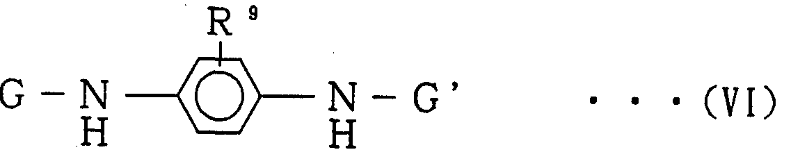
で表されるハロゲン化ァリ一ル化合物とを縮合させる方法、 ②一般式(VI) A method of condensing with a halogenated aryl compound represented by the formula: (2) General formula (VI)
Figure imgf000010_0003
〔式中、 G及び G' は、 同一又は異なる保護基、 例えば、 ァセチル 基, ベンジル基, ト リ フルォロアセチル基,— t一ブトキシカルボ二 ル基など、 好ましく はァセチル基を示し、 Ra は、 前記と同じであ る。 〕 [In the formula, G and G 'are the same or different protecting groups, for example, acetyl group, benzyl group, trifluoroacetyl group, and -t-butoxycarbone. Such group, preferably an Asechiru group, R a is to be the same as above. ]
で表される保護されたジアミ ン誘導体と上記一般式 (V) で表され るハロゲン化ァリール化合物とを縮合させたのち、 保護基 G, G' を外し、 さらに同様の縮合を行う方法、 After condensing the protected diamine derivative represented by the above with the aryl halide compound represented by the above general formula (V), removing the protecting groups G and G ', and conducting the same condensation,
③一般式(VII)③ General formula (VII)
Figure imgf000011_0001
〔式中、 R1 〜R4 は、 前記と同じである。 〕 [Wherein, R 1 to R 4 are the same as described above. ]
で表されるアミ ンと、 一般式(VI II)And the general formula (VI II)
Figure imgf000011_0002
〔式中、 X及び R9 は、 前記と同じであり、 2つの Xは、 たがいに 同じでも異なっていてもよい。 〕 [Wherein X and R 9 are the same as above, and two Xs may be the same or different. ]
で表されるジハロゲン化ァリ一ル化合物とを縮合させる方法、 ④上記一般式(VII) で表されるァミ ンと、 一般式(IX)
Figure imgf000011_0003
A method of condensing a dihalogenated aryl compound represented by the following formula: ④ an amine represented by the above general formula (VII);
Figure imgf000011_0003
〔式中、 X及び R9 は、 前記と同じである。 〕 Wherein X and R 9 are the same as above. ]
で表されるハロゲン化ァミ ノアリール化合物と、 上記一般式 (V) で表されるハロゲン化ァリ一ル化合物とを縮合させる方法、 などによって製造することができる。 Wherein the halogenated aminoaryl compound represented by the general formula (V) is condensed with the halogenated arylaryl compound represented by the general formula (V). It can be manufactured by such as.
上記一般式(I V)で表される p —フヱニレンジアミ ン類の具体例と しては、  Specific examples of the p-phenylenediamine represented by the above general formula (IV) include:
Figure imgf000012_0001
などが、 一般式 (V ) で表されるハロゲン化ァリール化合物の具体 例としては、
Figure imgf000012_0001
Specific examples of the halogenated aryl compounds represented by the general formula (V) include:
Figure imgf000012_0002
Figure imgf000012_0003
( t B u : t 一ブチル基、 以下同様) などが、 一般式(VI )で表される保護されたジァミ ン誘導体の具体例 としては、 C H C一 C H
Figure imgf000013_0001
などが、
(tBu: t monobutyl group, the same applies hereinafter), and the like, as specific examples of the protected diamine derivative represented by the general formula (VI). CHC-CH
Figure imgf000013_0001
etc,
—般式(VII) で表されるアミ ンの具体例としては  — Specific examples of amines represented by general formula (VII) include
Figure imgf000013_0002
Figure imgf000013_0003
Figure imgf000014_0001
などが、 一般式(VI U)で表されるジハロゲン化ァリール化合物の具 体例としては、
Figure imgf000013_0002
Figure imgf000013_0003
Figure imgf000014_0001
Examples of the dihalogenated aryl compounds represented by the general formula (VI U) include:
Figure imgf000014_0002
などが、 一般式(IX)で表されるハロゲン化ァミ ノアリール化合物の 具体例としては、
Figure imgf000014_0002
Specific examples of the aminoaryl halide compound represented by the general formula (IX) include:
Figure imgf000014_0003
などが挙げられる。
Figure imgf000014_0003
And the like.
なお、 上記②の方法においては、 保護基 G , G ' を段階的に外す ことにより、 非対称なジァミ ン誘導体を製造することも可能である, 上記①〜④の方法における縮合反応においては、 塩基が用いられ る。 この塩基としては、 例えば、 アルカ リ金属又はアルカ リ土類金 属の炭酸塩, 水酸化物、 水素化物、 さらには、 ァミ ン, アルキルリ チウムなどが用いられるが、 特に、 炭酸カ リウムが好適である。 こ の縮合反応においては、 所望により触媒を用いることができる。 こ の触媒としては、 例えば、 銅又はその塩、 ニッケル, パラジウムな どが挙げられる。 触媒の形状としては、 粉体が好ましく、 粒径は 1 O nm〜 l mmの範囲が好ましく、 特に、 1 0 0〜5 0 O nmの範 囲が好適である。 縮合反応は、 溶媒を用いずに固相で行ってもよ いし、 溶媒中で行ってもよいが、 溶媒中で行うのが有利である。 こ の場合、 溶媒としては、 高沸点のものが好ましく、 例えば、 ニトロ ベンゼン, ジメチルスルホキシド, ジメチルホルムアミ ド, スルホ ランなどが用いられる。 これらの中で、 特に、 ジメチルスルホキシ ドが好ましい。 In the above method (2), it is also possible to produce an asymmetric diamine derivative by removing the protecting groups G and G ′ in a stepwise manner. Is used You. Examples of the base include carbonates, hydroxides and hydrides of alkali metals or alkaline earth metals, and furthermore, amines, alkyllithiums, and the like are used, and potassium carbonate is particularly preferable. It is. In this condensation reaction, a catalyst can be used if desired. Examples of the catalyst include copper or a salt thereof, nickel, and palladium. The shape of the catalyst is preferably a powder, and the particle size is preferably in the range of 1 O nm to 1 mm, and particularly preferably in the range of 100 to 50 O nm. The condensation reaction may be performed in a solid phase without using a solvent, or may be performed in a solvent, but is preferably performed in a solvent. In this case, the solvent is preferably one having a high boiling point, for example, nitrobenzene, dimethylsulfoxide, dimethylformamide, sulfolane and the like are used. Of these, dimethyl sulfoxide is particularly preferred.
縮合反応温度は、 通常、 1 0 0〜4 0 0で、 好ましく は 1 5 0〜 2 5 0 °Cの範囲で選ばれる。 また、 縮合反応の圧力は、 通常は常圧 でよいが、 必要ならば加圧下で反応を行ってもよい。 縮合時間は、 原料や触媒の種類、 温度などによって左右され、 一概に定めること はできないが、 一般には 3〜3 6時間程度である。  The condensation reaction temperature is usually in the range of 100 to 400, preferably in the range of 150 to 250 ° C. The pressure for the condensation reaction is usually normal pressure, but the reaction may be performed under pressure if necessary. The condensation time depends on the type of raw material, catalyst, temperature, etc., and cannot be unconditionally determined, but is generally about 3 to 36 hours.
—方、 一般式(III) で表される 4 , 4 ' 一ビフヱ二レンジァミ ン 誘導体は、 例えば、 ① 一般式 (X)
Figure imgf000015_0001
On the other hand, the 4,4'-biphenylenediamine derivative represented by the general formula (III) is, for example, as follows: ① The general formula (X)
Figure imgf000015_0001
〔式中、 G及び G' は、 前記と同じである。 〕 Wherein G and G ′ are the same as above. ]
で表される保護されたジアミ ン誘導体と、 一般式(XI)
Figure imgf000016_0001
And a protected diamine derivative represented by the general formula (XI)
Figure imgf000016_0001
〔式中、 X, Rle及び R11は、 前記と同じである。 〕 [Wherein, X, R le and R 11 are the same as above. ]
で表されるハロゲン化ァリール化合物とを縮合させたのち、 保護基 G, G' を外し、 さらに同様の縮合を行う方法、 After condensing with a halogenated aryl compound represented by the formula, removing the protecting groups G and G ', and performing the same condensation,
②一般式(XII)
Figure imgf000016_0002
② General formula (XII)
Figure imgf000016_0002
〔式中、 Rle〜R13は、 前記と同じである [Wherein, R le to R 13 are the same as described above.
で表されるァミ ンと、 一般式(XIII)
Figure imgf000016_0003
And the general formula (XIII)
Figure imgf000016_0003
〔式中、 Xは前記と同じであり、 2つの Xはたがいに同じであって も異なつていてもよい。 〕  [Wherein, X is the same as described above, and two Xs may be the same or different. ]
で表されるジハロゲン化ァリール化合物とを縮合させる方法、 ③上記一般式(XII) で表されるアミ ンと、 一般式(XIV)
Figure imgf000016_0004
A method of condensing a dihalogenated aryl compound represented by the general formula (XII) with an amine represented by the general formula (XII)
Figure imgf000016_0004
〔式中、 Xは前記と同じであり、 また、 アミ ノ基は保護基で保護さ れていてもよい。 〕  [In the formula, X is the same as described above, and the amino group may be protected with a protecting group. ]
表されるハロゲン化ァリール化合物とを縮合させる方法、 A method of condensing with a halogenated aryl compound represented by
などによって製造することができる。 It can be manufactured by such as.
上記一般式 (X) で表される保護されたジアミ ン誘導体の具体例 で表されるハロゲン化アミ ノアリール化合物と、 上記一般式(XI)で としては、 Specific examples of the protected diamine derivative represented by the above general formula (X) And a halogenated aminoaryl compound represented by the following general formula (XI):
,〇〉- CH2
Figure imgf000017_0001
t B u - C - 0 - N- — <0)-N - 0 - C B u
, 〇〉-CH 2
Figure imgf000017_0001
t B u-C-0-N- — <0) -N-0-CB u
II H ^ H II  II H ^ H II
0
Figure imgf000017_0002
0
Figure imgf000017_0002
C H 3 - C - N-0-Q-N - 0 - C - t B υ CH 3 -C-N-0-QN-0-C-t B υ
0 0 などが、 一般式(XI)で表されるハロゲン化ァリール化合物の具体例 としては、  Specific examples of halogenated aryl compounds represented by the general formula (XI) are as follows:
Figure imgf000017_0003
l 5 ) )
Figure imgf000018_0001
以下同様) 基、 以下同様) ,
Figure imgf000017_0003
l 5 ))
Figure imgf000018_0001
The same applies hereinafter) groups, the same applies hereinafter),
、 以下同様) ,
Figure imgf000018_0002
ri Hex-<0-0-I (n Hex : nへキシル基、 以下同様)
, And so on),
Figure imgf000018_0002
ri Hex- <0-0-I (n Hex: n-hexyl group, and so on)
Figure imgf000019_0001
Figure imgf000019_0002
などが、 一般式(XII) で表されるアミ ンの具体例としては
Figure imgf000019_0003
Figure imgf000020_0001
などが、 一般式 αι π)で表されるジハロゲン化ァリ一ル化合物の具 体例としては、
Are specific examples of the amine represented by the general formula (XII).
Figure imgf000019_0003
Figure imgf000020_0001
Examples of the dihalogenated aryl compound represented by the general formula αι π) include:
Figure imgf000020_0002
などが、 一般式(XIV) で表されるハロゲン化アミ ノアリール化合物 の具体例としては、 H 2
Figure imgf000020_0003
などが挙げられる。
Figure imgf000020_0002
Specific examples of the halogenated aminoaryl compound represented by the general formula (XIV) include H 2 ,
Figure imgf000020_0003
And the like.
なお、 上記①の方法においては、 保護基 G , G ' を段階的に外す ことにより、 非対称なジァミ ン誘導体を製造することも可能である, また、 ③の方法においては、 一般式(XIV) で表されるハロゲン化 アミ ノアリール化合物のァミ ノ基を保護基で保護しておき、 この保 護基の脱離を段階的に行うことにより、 非対称なジァミ ン誘導体を 製造することも可能である。 この保護基としては、 前記 G, G ' の 説明で例示したものと同じものを挙げることができる。  In the above method (2), an asymmetric diamine derivative can be produced by removing the protecting groups G and G 'stepwise. In the method (3), the general formula (XIV) It is also possible to produce an asymmetric diamine derivative by protecting the amino group of the halogenated aminoaryl compound represented by the formula (1) with a protecting group and removing the protecting group stepwise. is there. Examples of the protecting group include the same as those exemplified in the description of G and G ′.
この①〜③の縮合反応における各条件は、 前記一般式(I I)で表さ れる p —フエ二レンジアミ ン誘導体の製造における場合と同様であ る o  The conditions in the condensation reactions (1) to (3) are the same as those in the production of the p-phenylenediamine derivative represented by the general formula (II).
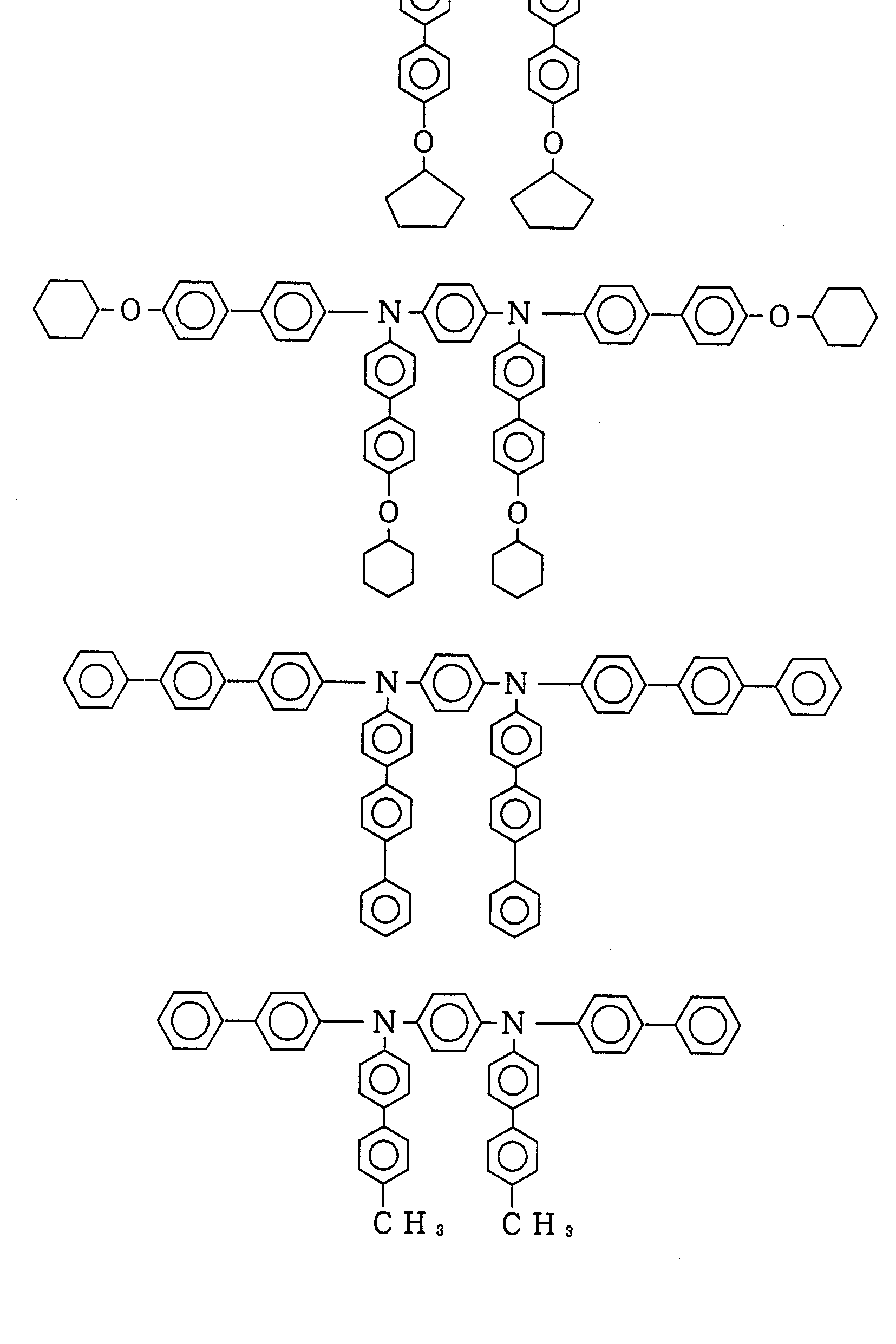
前記一般式 ( I ) で表される p — フ エ二レ ンジアミ ン誘導体の具 体例としては (ただし、 一般式(I I)の化合物は、 後で例示するので 除く。 ) 、  Specific examples of the p-phenylenediamine derivative represented by the general formula (I) (however, the compound of the general formula (II) is excluded since it will be exemplified later),
Figure imgf000021_0001
0 z
Figure imgf000021_0001
0 z
Figure imgf000022_0001
( )()
Figure imgf000022_0002
Figure imgf000022_0003
LH6Q/S6 OM (10)
Figure imgf000023_0001
LH6Q / S6 OM (Ten)
Figure imgf000023_0001
3
Figure imgf000023_0002
Three
Figure imgf000023_0002
(CH2) 3CH3 し F ) 3CH3 (CH2) 3CH3 then F) 3CH3
Figure imgf000023_0003
Figure imgf000024_0001
Figure imgf000023_0003
Figure imgf000024_0001
Figure imgf000024_0002
Figure imgf000025_0001
Figure imgf000024_0002
Figure imgf000025_0001
Figure imgf000025_0002
Figure imgf000026_0001
で表される化合物などを挙げることができる。
Figure imgf000025_0002
Figure imgf000026_0001
And the like.
これらの化合物の中で、 A r 】 , A r 2 , A r 3 及び A r 4 が、 ナフチル基又はビフヱニル基であるものが好ましい。 Among these compounds, A r], A r 2, A r 3 and A r 4 is intended preferably naphthyl or Bifuweniru group.
次に、 一般式(II)で表こされる p —フ 二レンジアミ ン誘導体の 具体例としては、  Next, as a specific example of the p-phenylenediamine derivative represented by the general formula (II),
Figure imgf000026_0002
9 Z
Figure imgf000026_0002
9 Z
S ) d
Figure imgf000027_0001
S) d
Figure imgf000027_0001
•i d u J J u  • id u J J u
Ό1 〔〇: Ό1 [〇:
[Ql [O] [Ql [O]
(S8) 1 d U-<Q-<0>- 〇 〈〇 d a (S8) 1 d U- <Q- <0>-〇 <〇 d a
H z3 gH z3 H z 3 g H z 3
) [O] [O] )
Figure imgf000027_0002
) [O] [O])
Figure imgf000027_0002
Figure imgf000027_0003
0/f6dT/X3d[ Z<W60/S6 OAV 9 Z
Figure imgf000027_0003
0 / f6dT / X3d [Z <W60 / S6 OAV 9 Z
Figure imgf000028_0001
n a 1- n g  n a 1- n g
( 8) n g < a  (8) n g <a
Figure imgf000028_0002
(SS) n g u 9 u
Figure imgf000028_0003
I0^6Jr/X3d[ Z-fI60/S6 OAV OAV0/S6 -368ss¾EVJLyi s
(SS) ngu 9 u
Figure imgf000028_0003
I0 ^ 6Jr / X3d [Z-fI60 / S6 OAV OAV0 / S6 -368ss¾EVJLyi s
e e
CO  CO
Figure imgf000029_0001
0 0
C3 C3
CD
Figure imgf000030_0001
CD
Figure imgf000030_0001
^  ^
o  o
CJl 2CH 〇
Figure imgf000031_0001
CJl 2CH 〇
Figure imgf000031_0001
0 0  0 0
(39) , 、(39),,
Figure imgf000031_0002
ngj 0 ngi 0  ngj 0 ngi 0
[O]  [O]
(6 (O) [O]  (6 (O) [O]
n a; o -OHO)— N-<0- N― <δ-<δ>- o n a  n a; o -OHO) — N- <0- N— <δ- <δ>-o n a
S8SI0/f6dT/X3d[ I60/S6 OAV OAVVJ蒙 dEd S8SI0 / f6dT / X3d [I60 / S6 OAV OAVVJ Mon dEd
Ol
Figure imgf000032_0001
Ol
Figure imgf000032_0001
Figure imgf000033_0001
で表される化合物などを挙げることができる。
Figure imgf000033_0001
And the like.
また、 一般式(III) で表される 4 , 4 ' —ビフエ二レンジァミ ン 誘導体の具体例としては、  Specific examples of the 4,4′-biphenylenediamine derivative represented by the general formula (III) include:
Figure imgf000033_0002
ζ ε
Figure imgf000033_0002
ζ ε
Figure imgf000034_0001
S8SI0/f6JT/13d LH60/S6 OAV
Figure imgf000035_0001
S8SI0 / f6JT / 13d LH60 / S6 OAV
Figure imgf000035_0001
ί- ε ί- ε
Χ3 Η υ Χ3 Η u Χ3 Η υ Χ3 Η u
Figure imgf000036_0001
S8SI0/fr6dT/XDd I60/S6 OAV s ε S8SI0 / fr6dT / XDd I60 / S6 OAV s ε
Figure imgf000037_0001
S8SI0/f6«ir/X3J LP160/S6 OAV 9 ε S8SI0 / f6 «ir / X3J LP160 / S6 OAV 9 ε
Figure imgf000038_0001
S8SI0/f6JT/XDd Z,fI60/S6 ΟΛ i ε
Figure imgf000039_0001
S8SI0 / f6JT / XDd Z, fI60 / S6 ΟΛ i ε
Figure imgf000039_0001
Figure imgf000039_0002
S8SlO/f6df/XDd 8 ε S8SlO / f6df / XDd 8 ε
ΧΧ
Figure imgf000040_0001
S8SI0/f6dr/X3d Z.M60/S6 OAV 6 ε S8SI0 / f6dr / X3d Z.M60 / S6 OAV 6 ε
Figure imgf000041_0001
(16) (16)
Figure imgf000041_0002
S8SlO/f 6dT/X3d I60/S6 OAV 一 CH;
Figure imgf000042_0001
S8SlO / f 6dT / X3d I60 / S6 OAV One CH;
Figure imgf000042_0001
( 95) (95)
Figure imgf000042_0002
で表される化合物などを挙げることができる。
Figure imgf000042_0002
And the like.
本発明の有機 E L素子は、 前記一般式 ( I ) で表される p -フエ 二レンジアミ ン誘導体 〔一般式(I I )で表される化合物も含む。 〕 又 は一般式(I I I ) で表される 4 , 4 ' 一ビフヱ二レンジァ ミ ン誘導体 を少なく とも含有するものである。 この際、 該ジアミ ン誘導体は一 種含有させてもよく、 二種以上を組み合わせて含有させてもよい。  The organic EL device of the present invention includes a p-phenylenediamine derivative represented by the general formula (I) [including a compound represented by the general formula (II)]. Or at least a 4,4'-biphenylenediamine derivative represented by the general formula (III). In this case, one kind of the diamine derivative may be contained, or two or more kinds thereof may be contained in combination.
有機 E L素子の構造としては、 ①陽極 有機発光層 Z陰極、 ②陽 極 正孔輸送層/有機発光層 陰極、 ③陽極/ /有機発光層ノ電子注 入層 Z陰極、 ④陽極 正孔輸送層 Z有機発光層 Z電子注入層 陰極 などがあるが、 本発明の有機 E L素子は、 一対の電極 (陽極と陰極) により挾持された化合物層 (上記①の構成の素子においては有機発 光層、 ②の構成の素子においては正孔輸送層及び有機発光層、 ③の 構成の素子においては有機発光層及び電子注入層、 ④の構成の素子 においては正孔輸送層, 有機発光層及び電子注入層) の少なく とも 一層が、 上記一般式 ( I ) で表される p—フヱニレンジアミ ン誘導 体 〔一般式(I I)で表される化合物も含む。 〕 又は一般式(I I I ) で表 される 4 , 4, ービフエ二レンジァミ ン誘導体を含んでいれば、 上 記①〜④のいずれの構成であってもよい。 なお、 これらの構成の有 機 E L素子は、 いずれも基板により支持されることが好ましい。 こ の基板については、 特に制限はなく、 従来の有機 E L素子に慣用さ れているもの、 例えば、 ガラス, 透明ブラスチッ ク, 石英などから なるもを用いることができる。 The structure of the organic EL device is as follows: ① Anode Organic light emitting layer Z cathode, ② Positive hole transport layer / organic light emitting layer cathode, ③ Anode // organic light emitting layer Electron injection layer Z cathode, ④ Anode hole transport layer There are a Z organic light emitting layer, a Z electron injection layer, a cathode, and the like. However, the organic EL device of the present invention comprises a compound layer sandwiched between a pair of electrodes (anode and cathode) (the organic light emitting layer, In the device with the configuration of ②, the hole transport layer and the organic light emitting layer, At least one of the organic light-emitting layer and the electron injection layer in the device having the structure, and the hole transport layer, the organic light-emitting layer, and the electron injection layer in the device having the structure ④, are represented by the above-mentioned general formula (I). —Phenylenediamine derivative [Including the compound represented by the general formula (II). Or any of the above-mentioned constitutions (1) to (4) as long as the composition contains the 4,4, -biphenylenediamine derivative represented by the general formula (III). In addition, it is preferable that all of the organic EL elements having these configurations are supported by the substrate. The substrate is not particularly limited, and those commonly used in conventional organic EL elements, for example, those made of glass, transparent plastic, quartz, or the like can be used.
本発明の有機 E L素子の特徴部分である該 p—フニ二レンジアミ ン誘導体又は 4 , 4 ' 一ビフヱ二レンジァミ ン誘導体を含む層は、 正孔輸送層又は有機発光層であることが望ましく、 特に正孔輸送層 であることが好ましい。  The layer containing the p-phenylenediamine derivative or the 4,4′-biphenylenediamine derivative, which is a characteristic part of the organic EL device of the present invention, is preferably a hole transport layer or an organic light-emitting layer. It is preferably a hole transport layer.
該 p—フエ二レンジァ ミ ン誘導体又は 4 , 4 ' ー ビフエ二レンジ 了ミ ン誘導体を含む正孔輸送層は、 p—フエ二レンジア ミ ン誘導体 又は 4 , 4 ' 一ビフヱ二レンジァミ ン誘導体のみからなる単層構造 でもよいし、 p—フエ二レンジァ ミ ン誘導体又は 4 , 4 ' — ビフエ 二レンジァミ ン誘導体と、 有機 E L素子の正孔輸送層材料として従 来より使用されている物質の層との複層構造であってもよい。 さら には、 該 P—フエ二レンジァミ ン誘導体又は 4, 4 ' ービフエニレ ンジアミ ン誘導体と有機 E L素子の正孔輸送層材料として従来より 使用されている物質との混合物からなる層を含む単層構造又は複層 構造であってもよい。  The hole transport layer containing the p-phenylenediamine derivative or the 4,4′-biphenylenediamine derivative is composed of only the p-phenylenediamine derivative or the 4,4′-biphenylenediamine derivative. Or a layer of a substance conventionally used as a hole transport layer material of an organic EL device with a p-phenylenediamine derivative or a 4,4'-biphenylenediamine derivative. And a multilayer structure. Furthermore, a single-layer structure including a layer made of a mixture of the P-phenylenediamine derivative or the 4,4′-biphenylenediamine derivative and a substance conventionally used as a hole transport layer material of an organic EL device. Alternatively, it may have a multilayer structure.
該 p—フエ二レンジァミ ン誘導体又は 4 , 4, ービフエ二レンジ ァミ ン誘導体を含む正孔輸送層は、 p—フヱニレンジア ミ ン誘導体 . 又は 4 , 4 ' 一ビフヱ二レンジァ ミ ン誘導体と、 必要に応じて他の 正孔輸送層材料とを用いて、 真空蒸着法, キャス ト法, 塗布法, ス ピンコー ト法などにより形成することができる。 さらには、 ポリ力 —ボネー ト, ポリウレタン, ボリスチレン, ポリアリ レー ト, ポリ エステルなどの透明ポリマーに、 該 p—フエ二レンジアミ ン誘導体 又は 4, 4 ' —ビフヱ二レンジァミ ン誘導体を分散させた溶液を用 いたキャス ト法、 塗布法あるいはスピンコー ト法などや、 透明ポリ マーとの同時蒸着などによっても形成することができる。 The hole transporting layer containing the p-phenylenediamine derivative or the 4,4, -biphenylenediamine derivative is a p-phenylenediamine derivative. Or a 4,4'-biphenylenediamine derivative and, if necessary, other materials for the hole transport layer, are formed by a vacuum deposition method, a casting method, a coating method, a spin coating method, or the like. be able to. Furthermore, a solution in which the p-phenylenediamine derivative or the 4,4'-biphenylenediamine derivative is dispersed in a transparent polymer such as polyforce—bone, polyurethane, polystyrene, polyarylate, or polyester is dispersed. It can also be formed by a casting method, a coating method, a spin coating method, or the like used, or a simultaneous vapor deposition with a transparent polymer.
また、 該 P—フエ二レンジァ ミ ン誘導体又は 4 , 4 ' ー ビフエ二 レンジアミ ン誘導体を含む有機発光層は、 p—フヱニレンジアミ ン 誘導体又は 4 , 4 ' 一ビフヱ二レンジァミ ン誘導体のみからなる単 層構造であつてもよいし、 p—フエ二レンジァミ ン誘導体又は 4 , 4 ' 一ビフヱ二レンジァミ ン誘導体と、 有機 E L素子の有機発光層 材料として従来より使用されている物質の層との複層構造であつも よい。 さらには、 P—フエ二レンジァミ ン誘導体又は 4, 4 ' ービ フエ二レンジアミ ン誘導体と有機 E L素子の有機発光層材料として 従来より使用されている物質との混合物からなる層を含む単層構造 又は複層構造であってもよい。 該 p—フヱニレンジアミ ン誘導体又 は 4 , 4 ' 一ビフヱ二レンジァミ ン誘導体を含む有機発光層は、 p 一フヱニレンジァミ ン誘導体又は 4, 4 ' ービフエ二レンジァミ ン 誘導体と、 必要に応じて他の有機発光層材料とを用いて、 真空蒸着 法, キャス ト法, 塗布法, スピンコー ト法などにより形成すること ができる。  Further, the organic light emitting layer containing the P-phenylenediamine derivative or the 4,4′-biphenylenediamine derivative is a single layer composed of only the p-phenylenediamine derivative or the 4,4′-biphenylenediamine derivative. It may have a structure, or a multilayer of a p-phenylenediamine derivative or a 4,4'-biphenylenediamine derivative and a layer of a substance conventionally used as a material for an organic light emitting layer of an organic EL device. It may have a structure. Furthermore, a single-layer structure including a layer composed of a mixture of a P-phenylenediamine derivative or a 4,4′-biphenylenediamine derivative and a substance conventionally used as an organic light emitting layer material of an organic EL device. Alternatively, it may have a multilayer structure. The organic light emitting layer containing the p-phenylenediamine derivative or the 4,4′-biphenylenediamine derivative is composed of the p-phenylenediamine derivative or the 4,4′-biphenylenediamine derivative and, if necessary, another organic light-emitting layer. It can be formed by vacuum evaporation, casting, coating, spin coating, etc. using layer materials.
本発明の有機 E L素子において、 該 p—フ X二レンジアミ ン誘導 体又は 4 , 4 ' 一ビフヱ二レンジァミ ン誘導体を含む層以外は、 従 来の有機 E L素子と同様の材料を用いて形成するこができる。 例えば、 陽極の材料としては、 仕事関数の大きい ( 4 e V以上) 金属, 合金, 電気伝導性化合物又はこれらの混合物が好ましく用い られる。 具体例としては、 A uなどの金属, C u l , I T 0, S n 02 , Ζ η 0などの誘電性透明材料が挙げられる。 この陽極は、 例 えば蒸着法やスパッタ リ ング法などの方法で、 上記材料の薄膜を形 成することにより作製することができる。 有機発光層からの発光を 陽極より取り出す場合、 該陽極の透過率は 1 0 より大きいことが 望ましい。 また、 陽極のシー ト抵抗は数百 以下が好ましい。 この陽極の膜厚は材料にもよるが、 通常 1 0 nm〜 l zm、 好まし く は 1 0〜2 0 O nmの範囲で選択される。 In the organic EL device of the present invention, the organic EL device is formed using the same material as that of the conventional organic EL device, except for the layer containing the p-f X-bendylenediamine derivative or the 4,4′-biphenylenediamine derivative. I can do this. For example, as the material of the anode, a metal, an alloy, an electrically conductive compound or a mixture thereof having a large work function (4 eV or more) is preferably used. Specific examples include metals such as Au, and dielectric transparent materials such as Cul, IT0, Sn02, and ηη0. This anode can be produced by forming a thin film of the above-mentioned material by a method such as a vapor deposition method or a sputtering method. When light emitted from the organic light emitting layer is extracted from the anode, the transmittance of the anode is desirably greater than 10. The sheet resistance of the anode is preferably several hundreds or less. The thickness of the anode depends on the material, but is usually selected in the range of 10 nm to lzm, preferably in the range of 10 to 20 O nm.
一方、 陰極の材料としては、 仕事関数の小さい ( 4 e V以下) 金 属, 合金, 電気伝導性化合物又はこれらの混合物が好ましく用いら れる。 該陰極材料の具体例としては、 ナ ト リウム, リチウム, マグ ネシゥム Z銅混合物, A 1 / A 1 2 03 , イ ンジウムなどが挙げら れる。 この陰極は、 蒸着法ゃスパッタ リ ング法などの方法で、 上記 材料の薄膜を形成することにより作製することができる。 有機発光 層からの発光を陰極より取り出す場合、 該陰極の透過率は 1 0 %よ り大きいことが望ましい。 また、 この陰極のシー ト抵抗は数百 □以下が好ましい。 該陰極の膜厚は材料にもよるが、 通常 1 0 nm 〜 l 〃m、 好ましく は 5 0〜2 0 0 n mの範囲で選択される。 On the other hand, as the material of the cathode, metals, alloys, electrically conductive compounds or mixtures thereof having a low work function (4 eV or less) are preferably used. Specific examples of the cathode material, Na preparative potassium, lithium, mug Neshiumu Z copper mixtures, A 1 / A 1 2 0 3, etc. Lee indium is like et be. This cathode can be manufactured by forming a thin film of the above material by a method such as a vapor deposition method or a sputtering method. When light emitted from the organic light emitting layer is extracted from the cathode, the transmittance of the cathode is desirably greater than 10%. The sheet resistance of the cathode is preferably several hundred square □ or less. The thickness of the cathode depends on the material, but is usually selected in the range of 10 nm to 10 nm, preferably in the range of 50 to 200 nm.
なお、 有機発光層からの発光を効率よく取り出す観点からは、 上 記陽極及び陰極の少なく とも一方を透明又は半透明物質により形成 するのが好ましい。  From the viewpoint of efficiently extracting light emitted from the organic light emitting layer, it is preferable that at least one of the anode and the cathode is formed of a transparent or translucent substance.
また、 本発明の有機 E L素子における有機発光層を、 該 p—フ 二レンジァ ミ ン誘導体又は 4 , 4 ' ー ビフエ二レンジァ ミ ン誘導体 と他の物質とにより形成する場合、 p —フ X二レンジァミ ン誘導体 又は 4 , 4 ' ービフ 二レンジァ ミ ン誘導体以外の他の有機発光層 材料としては、 例えば、 多環縮合芳香族化合物や、 ベンゾォキサゾ ール系, ベンゾチアゾール系, ベンゾイ ミ ダブール系などの蛍光増 白剤, 金属キレー ト化ォキサノイ ド化合物、 ジスチリルベンゼン系 化合物などの薄膜形成性の良い化合物を用いることができる。 Further, when the organic light emitting layer in the organic EL device of the present invention is formed from the p-phenylenediamine derivative or the 4,4′-biphenylenediamine derivative and another substance, Rangeamine derivatives Or, as an organic light emitting layer material other than the 4,4'-bifylenediamine derivative, for example, a polycyclic fused aromatic compound or a fluorescent brightening agent such as a benzoxazole-based, benzothiazole-based, or benzimidabourne-based compound may be used. Compounds with good thin-film forming properties, such as agents, metal chelated oxanoide compounds, and distyrylbenzene compounds, can be used.
ここで、 上記多環縮合芳香族化合物の具体例としては、 アン トラ セン, ナフタレン, フエナン ト レン, ピレン, ク リセン, ペリ レン 骨格などを含む縮合環発光物質や、 8〜 2 0個、 好ましく は 8個の 縮合環を含む他の縮合環発光物質などが挙げられる。  Here, specific examples of the polycyclic fused aromatic compound include a condensed ring light-emitting substance containing an anthracene, naphthalene, phenanthrene, pyrene, chrysene, or perylene skeleton, and 8 to 20, preferably Include other condensed ring luminescent materials containing eight condensed rings.
また、 上記べンゾォキサゾール系, ベンゾチアゾール系, ベンゾ ィ ミ ダゾール系などの蛍光増白剤としては、 例えば、 特開昭 5 9 一 Examples of the above-mentioned benzoxazole-based, benzothiazole-based, benzoimidazole-based fluorescent whitening agents include, for example, JP-A-59-91.
1 9 4 3 9 3号公報に開示されているものが挙げられる。 その代表 例としては、 2 , 5—ビス ( 5 , 7—ジー t一ペンチルー 2—ベン ゾォキサゾリル) 一 1 , 3, 4 ーチアジアゾール ; 4 , 4 ' 一ビスThe one disclosed in Japanese Patent Application Publication No. 194393 is known. Typical examples include 2,5-bis (5,7-di-pentyl-2-benzobenzoxazolyl) -1,3,4-thiadiazole; 4,4′-bis
( 5 , 7 - t一ペンチルー 2—べンゾォキサゾリル) スチルベン ; 4 , 4, 一ビス ( 5 , 7—ジー ( 2—メチルー 2—ブチル) 一 2 — ベンゾォキサゾリル) スチルベン ; 2 , 5 —ビス ( 5 , 7—ジ— t 一ペンチルー 2—べンゾォキサゾリル) チォフェン ; 2 , 5 —ビス(5,7-t-pentyl-2-benzoxazolyl) stilbene; 4,4,1-bis (5,7-di (2-methyl-2-butyl) -12-benzobenzoxazolyl) stilbene; 2,5— Bis (5,7-di-t-pentyl-2-benzobenzoxazolyl) thiophene; 2,5-bis
( 5 — ( , α—ジメチルベンジル) 一 2—べンゾォキサゾリル) チォフェン ; 2 , 5 —ビス ( 5 , 7—ジー ( 2 —メチル— 2 —ブチ ル) 一 2—べンゾォキサゾリル) 一 3 , 4 —ジフエ二ルチオフェン 2 , 5 —ビス ( 5 —メチルー 2—べンゾォキサゾリル) チォフェン 4 , 4 ' 一ビス ( 2—べンゾォキサゾリル) ビフエニル ; 5 —メチ ルー 2 — ( 2 - ( 4 一 ( 5 —メチルー 2—べンゾォキサゾリル) フ ェニル) ビニル) ベンゾォキサゾ一ル ; 2 — ( 2 — ( 4 一クロロフ ェニル) ビニル) ナフ ト ( 1 , 2 — d ) ォキサゾールなどのベンゾ ォキサゾ一ル系、 2 , 2 ' - ( ρ—フエ二レンジビニレン) 一ビス ベンゾチアゾ一ルなどのベンゾチアゾ一ル系、 2 — ( 2 — ( 4 —力 ルボキシフヱニル) ビニル) ベンゾイ ミ ダゾールなどのベンゾイ ミ ダゾ一ル系などの蛍光増白剤が挙げられる。 (5 — (, α-dimethylbenzyl) 1-2-benzoxazolyl) thiophene; 2, 5-bis (5, 7-di (2-methyl-2-butyl)-1-2-benzoxazolyl) 1, 3-4 — Diphenylthiophene 2,5-bis (5-methyl-2-benzobenzoxazolyl) thiophene 4,4'-bis (2-benzozoxazolyl) biphenyl; 5—methyl 2— (2— (4— (5—methyl-2 —Benzoxazolyl) phenyl) vinyl) benzoxazole; 2— (2— (4-chlorophenyl) vinyl) naphtho (1,2—d) Benzo such as oxazole Benzothiazoles such as oxazoles, 2,2 '-(ρ-phenylenedivinylene) -bis-benzothiazol, and benzoimidazoles such as 2 — (2— (4—force ruboxyphenyl) vinyl) benzimidazole Fluorescent whitening agents such as dazols.
上記金属キレー ト化ォキサノィ ド化合物としては、 例えば、 特開 昭 6 3 — 2 9 5 6 9 5号公報に開示されているものを用いるこ とが できる。 その代表例としては、 ト リ ス ( 8 —キノ リ ノ ール) アルミ 二ゥム, ビス ( 8 —キノ リ ノール) マグネシウム, ビス 〔ベンゾ As the above metal chelated oxanoide compound, for example, those disclosed in JP-A-63-956995 can be used. Typical examples are tris (8-quinolinol) aluminum, bis (8-quinolinol) magnesium, bis [benzo
( f ) 一 8 —キノ リ ノール〕 亜鉛, ビス ( 2 -メチルー 8 -キノ リ ノ ラ一 ト) アルミニウムォキシ ド, ト リス ( 8 —キノ リ ノ ール) ィ ンジゥム, ト リス ( 5 —メチルー 8 —キノ リ ノール) アルミニウム, 8 —キノ リ ノールリチウム, ト リス ( 5 —クロロー 8 —キノ リ ノ一 ル) ガリ ウム, ビス ( 5 —クロ口.一 8 —キノ リ ノール) カルシウム, ポリ (亜鉛 (Π) —ビス ( 8 — ヒ ドロキシー 5 —キノ リ ノニル) メ タ ン) などの 8 — ヒ ドロキシキノ リ ン系金属錯体ゃジリチウムェピ ン ドリ ジオンなどが挙げられる。 (f) -18-quinolinol) zinc, bis (2-methyl-8-quinolinolate) aluminum oxide, tris (8-quinolinol) indium, tris (5— Methyl-8-quinolinol) aluminum, 8-quinolinollithium, tris (5-chloro-8-quinolinol) gallium, bis (5-crotinol.18-quinolinol) calcium, poly (Zinc (II) -bis (8-hydroxy-5-quinolinonyl) methane) and other 8—hydroxyquinoline-based metal complexes such as dilithium epinedridione.
また、 上記ジスチリルベンゼン系化合物としては、 例えば、 欧州 特許第 0 3 7 3 5 8 2号明細書に開示されているものを用いるこ と ができる。 その代表例としては、 1 , 4 —ビス ( 2—メチルスチリ ル) ベンゼン ; 1 , 4 一ビス ( 3 —メチルスチリル) ベンゼン ; Further, as the distyrylbenzene-based compound, for example, those disclosed in European Patent No. 0 735 582 can be used. Typical examples are 1,4-bis (2-methylstyryl) benzene; 1,4-bis (3-methylstyryl) benzene;
1 , 4 —ビス ( 4 ーメチルスチリル) ベンゼン ; ジスチリルべンゼ ン ; 1 , 4 一ビス ( 2 —ェチルスチリル) ベンゼン ; 1 , 4 一ビス1,4-bis (4-methylstyryl) benzene; distyrylbenzene; 1,4-bis (2-ethylstyryl) benzene; 1,4-bis
( 3 —ェチルスチリル) ベンゼン ; 1 , 4 一ビス ( 2 — メチルスチ リル) — 2 —メチルベンゼン ; 1 , 4 一ビス ( 2—メチルスチリル) - 2 一ェチルベンゼンなどが挙げられる。 (3—Ethylstyryl) benzene; 1,4-bis (2-methylstyryl) —2-methylbenzene; 1,4-bis (2-methylstyryl) -2-ethylethylbenzene.
また、 特開平 2 — 2 5 2 7 9 3号公報に開示されているジスチリ ルビラジン誘導体も有機発光層の材料として用いることができる。 その代表例としては、 2 , 5 —ビス ( 4 ーメチルスチリル) ピラジ ン ; 2, 5 —ビス ( 4 ーェチルスチリル) ピラジン ; 2, 5 -ビス 〔 2 — ( 1 一ナフチル) ビュル〕 ピラジン ; 2 , 5 —ビス ( 4 ーメ トキシスチリル) ピラジン ; 2, 5 — ビス 〔 2 — ( 4 ー ビフエニル) ビニル〕 ピラジン ; 2 , 5 — ビス 〔 2 — ( 1 ー ピレニル) ビニル〕 ピラジンなどが挙げられる。 Also, a distiller disclosed in Japanese Patent Application Laid-Open No. 2-252793 is disclosed. Rubirazine derivatives can also be used as a material for the organic light emitting layer. Typical examples are 2,5-bis (4-methylstyryl) pyrazine; 2,5-bis (4-ethylstyryl) pyrazine; 2,5-bis [2- (1-naphthyl) butyl] pyrazine; 2,5— Bis (4-methoxystyryl) pyrazine; 2,5-bis [2— (4-biphenyl) vinyl] pyrazine; 2,5—bis [2— (1-pyrenyl) vinyl] pyrazine;
その他、 欧州特許第 0 3 8 8 7 6 8号明細書ゃ特開平 3 — 2 3 1 9 7 0号公報に開示されているジメチリディ ン誘導体を有機発光層 の材料として用いることもできる。 その代表例としては、 1, 4 一 フエ二レンジメチリディ ン ; 4, 4 ' — ビフエ二レンジメチリディ ン ; 2, 5 —キシリ レンジメチリディ ン ; 2, 6 —ナフチレンジメ チリディ ン ; 1 , 4 ー ビフエ二レンジメチリディ ン ; 1 , 4 — p — テレフエ二レンジメチリ ディ ン ; 9 , 1 0 —アン トラセンジィルジ メチリディ ン ; 4 , 4 ' 一 ( 2 , 2 —ジー t 一ブチルフエ二ルビ二 ル) ビフェニル ; 4 , 4 ' 一 ( 2, 2 —ジフェニルビニル) ビフエ ニルなど、 及びこれらの誘導体が挙げられる。  In addition, a dimethylidin derivative disclosed in European Patent No. 0 388 768 (Japanese Unexamined Patent Application Publication No. 3-231970) can be used as a material for the organic light emitting layer. Typical examples are 1,41-phenylenedimethylidin; 4,4'-biphenylenedimethylidin; 2,5-xylylenedimethylidin; 2,6-naphthylenedimethylidin; 1,4 -Biphenylenedimethylidin; 1,4—p—Telephenylenedimethylidin; 9,10—Anthracenediyldimethylidin; 4,4′-1 (2,2—Gt-butylphenylvinyl) biphenyl 4,4 '-(2,2-diphenylvinyl) biphenyl and the like; and derivatives thereof.
さらには、 特開平 2 — 1 9 1 6 9 4号公報に開示されているクマ リ ン誘導体、 特開平 2 — 1 9 6 8 8 5号公報に開示されているペリ レン誘導体、 特開平 2 — 2 5 5 7 8 9公報に開示されているナフタ レン誘導体、 特開平 2 — 2 8 9 6 7 6号公報及び同 2 — 8 8 6 8 9 号公報に開示されているフタロぺリ ノ ン誘導体、 特開平 2 — 2 5 0 2 9 2号公報に開示されているスチリルアミ ン誘導体も、 有機発光 層の材料として用いることができる。  Further, a coumarin derivative disclosed in Japanese Patent Application Laid-Open No. 2-196164, a perylene derivative disclosed in Japanese Patent Application Laid-Open No. 196885/1990, Naphthalene derivatives disclosed in US Pat. No. 5,578,893, and phthaloperinone derivatives disclosed in Japanese Patent Application Laid-Open Nos. 2-289676 and 2-88689 Also, a styrylamine derivative disclosed in JP-A-2-250292 can be used as a material for the organic light-emitting layer.
これらの有機発光層材料は、 所望の発光色や性能などに応じて適 宜選ばれる。 なお、 本発明の有機 E L素子における有機発光層は、 米国特許第 4 , 7 6 9, 2 9 2号明細書に開示されているように、 蛍光物質を加えて形成してもよい。 この場合のベースとなる物質は 該 p—フエ二レンジァミ ン誘導体又は 4 , 4 ' ービフエ二レンジァ ミ ン誘導体であってもよいし、 p—フヱニレンジアミ ン誘導体又はThese organic light emitting layer materials are appropriately selected according to a desired light emitting color, performance, and the like. Incidentally, the organic light emitting layer in the organic EL device of the present invention, As disclosed in US Pat. No. 4,769,292, a fluorescent material may be added. In this case, the base substance may be the p-phenylenediamine derivative or the 4,4′-biphenylenediamine derivative, or the p-phenylenediamine derivative or the p-phenylenediamine derivative.
4 , 4 ' 一ビフヱ二レンジァミ ン誘導体以外の有機発光層材料であ つてもよい。 さらには、 該 P—フエ二レンジァミ ン誘導体又は 4 , 4 ' ー ビフエ二レンジア ミ ン誘導体と有機発光層材料との混合物で あってもよい。 蛍光物質を加えて有機発光層を形成する場合、 蛍光 物質の添加量は数モル%以下が好ましい。 該蛍光物質は電子と正孔 との再結合に応答して発光するため、 発光機能の一部を担うことに なる。 Organic light-emitting layer materials other than the 4,4′-biphenylenediamine derivative may be used. Further, it may be a mixture of the P-phenylenediamine derivative or the 4,4′-biphenylenediamine derivative with an organic light emitting layer material. When the organic light emitting layer is formed by adding a fluorescent substance, the amount of the fluorescent substance added is preferably several mol% or less. Since the fluorescent substance emits light in response to recombination of electrons and holes, it plays a part in the light emitting function.
また、 有機発光層材料としては、 薄膜形成性を有していない化合 物を用いることもできる。 具体例としては、 1 , 4一ジフヱニル— 1, 3—ブタジエン ; 1 , し 4 , 4 ーテトラフエ二ルー 1, 3 — ブタジエン ; テトラフエニルシクロペン夕ジェンなどが挙げられる, しかし、 薄膜形成性を有しないこれらの材料を用いた有機 E L素子 は、 素子の寿命が短いという欠点を有する。  Further, as the organic light emitting layer material, a compound having no thin film forming property can be used. Specific examples include 1,4-diphenyl-1,3-butadiene; 1,4,4-tetraphenyl-1,3-butadiene; tetraphenylcyclopentene, and the like. Organic EL devices using these materials which do not have these materials have the disadvantage that the lifetime of the device is short.
本発明の有機 E L素子において、 必要に応じて用いられる正孔輸 送層は、 有機発光層が該 p—フエ二レンジァミ ン誘導体又は 4, 4 ' 一ビフヱ二レンジア ミ ン誘導体を含んでいれば、 p—フエ二レンジ ァ ミ ン誘導体又は 4, 4 ' 一ビフヱ二レンジァ ミ ン誘導体を含む層 であってもよいし、 該 p—フエ二レンジァミ ン誘導体又は 4 , 4 ' ビフヱ二レンジアミ ン誘導体を含まない層であつてもよい。 該 p _ フエ二レンジァ ミ ン誘導体又は 4 , 4 ' ー ビフエ二レンジア ミ ン誘 導体以外の正孔輸送層材料としては、 有機 E L素子の正孔輸送層材 料として従来より使用されている種々の物質を用いることができる, また、 本発明の有機 E L素子において必要に応じて設けられる正 孔輸送層として、 該 P—フヱニレンジァミ ン誘導体又は 4 , 4 ' 一 ビフエ二レンジアミ ン誘導体を含む層を設ける場合、 この正孔輸送 層は、 前記したように p—フヱニレンジァミ ン誘導体又は 4 , 4 ' - ビフヱ二レンジア ミ ン誘導体のみからなる単層構造、 p—フエニレ ンジァ ミ ン誘導体又は 4 , 4 ' 一ビフヱ二レンジァ ミ ン誘導体と有 機 E L素子の正孔輸送層材料として従来より使用されている物質の 層との複層構造、 あるいは p—フヱニレンジア ミ ン誘導体又は 4, 4 ' 一ビフヱ二レンジアミ ン誘導体と有機 E L素子の正孔輸送層材 料として従来より使用されている物質との混合物からなる層を含む 単層構造又は複層構造のいずれであってもよい。 この場合の好まし い層構造は、 該 P—フヱニレンジァ ミ ン誘導体又は 4 , 4 ' ー ビフ ェニレンジアミ ン誘導体のみからなる単層構造又は該 p—フヱニレ ンジァ ミ ン誘導体層又は 4 , 4 ' ービフヱ二レンジァミ ン誘導体層 と、 ボルフィ リ ン化合物 (特開昭 6 3— 2 9 5 6 9 5号公報などに 開示されているもの) の層又は有機半導体性ォリゴマーの層との複 層構造である。 In the organic EL device of the present invention, the hole transporting layer used as necessary is such that the organic light emitting layer contains the p-phenylenediamine derivative or the 4,4′-biphenylenediamine derivative. Or a layer containing a p-phenylenediamine derivative or a 4,4′-biphenylenediamine derivative, or a layer containing the p-phenylenediamine derivative or the 4,4′-biphenylenediamine derivative May be included. As the hole transport layer material other than the p_phenylene diamine derivative or the 4,4'-biphenylene diamine derivative, various hole transport layer materials conventionally used as hole transport layer materials for organic EL devices can be used. Substances can be used, In the case where a layer containing the P-phenylenediamine derivative or the 4,4′-biphenylenediamine derivative is provided as a hole transport layer provided as needed in the organic EL device of the present invention, the hole transport layer Is a single-layer structure composed of only a p-phenylenediamine derivative or a 4,4′-biphenylenediamine derivative, a p-phenylenediamine derivative or a 4,4′-biphenylenediamine derivative as described above. Organic EL devices have a multi-layered structure with a layer of a substance conventionally used as a hole transport layer material, or a p-phenylenediamine derivative or a 4,4'-biphenylenediamine derivative and a positive electrode of an organic EL device. It may have a single-layer structure or a multi-layer structure including a layer made of a mixture with a substance conventionally used as a hole transport layer material. In this case, a preferred layer structure is a single-layer structure composed only of the P-phenylenediamine derivative or 4,4′-biphenylenediamine derivative or the p-phenylenediamine derivative layer or the 4,4′-biphenyl diamine. It has a multi-layer structure of a rangeamine derivative layer and a layer of a porphyrin compound (disclosed in JP-A-63-295695) or a layer of an organic semiconductor oligomer.
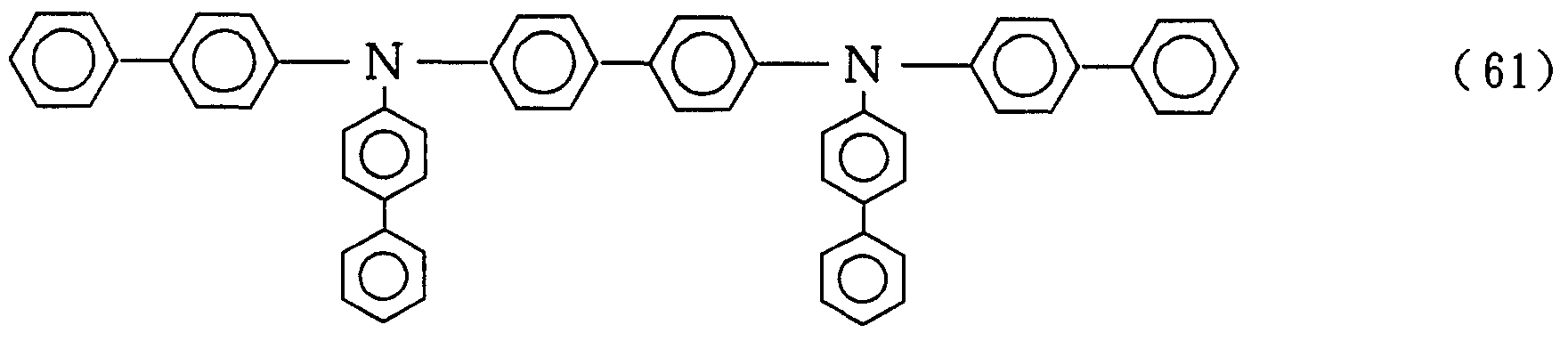
上記ポリ フイ リ ン化合物の代表例としては、 ポリ フィ ン、 5, 1 0 , 1 5 , 2 0—テ トラフエ二ルー 2 1 H—, 2 3 H—ボルフィ ン銅 (II) ; 5 , 1 0 , 1 5 , 2 0 —テ トラフエ二ルー 2 1 H—, 2 3 H—ポルフィ ン亜鉛 ( II) ; 5 , 1 0 , 1 5, 2 0 —テトラキ ス (ペルフルオロフェニル) 一 2 1 H—, 2 3 H—ポルフィ ン ; シ リ コ ンフタロシアニンォキシ ド ; アルミニウムフタロシアニンク口 リ ド ; フタロシアニン (無金属) ; ジリチウムフタロシアニン ; 銅 テ トラメチルフタロシアニン ; 銅フタロシアニン ; クロムフタロシ ァニン ; 亜鉛フタロシアニン ; 鉛フタロシアニン ; チタニウムフタ ロシアニンォキシ ド ; マグネシウムフタロシアニン : 銅ォクタメチ ルフタロシアニンンなどが挙げられる。 Representative examples of the above polyphenylene compounds include polyfin, 5,10,15,20—tetrafluoroethylene 21H—, 23H—borfin copper (II); 5,1 0, 15, 20 — Tetrafuline 21 H—, 23 H—porphyrin zinc (II); 5, 10, 15, 20 — Tetrax (perfluorophenyl) 121 H— , 23 H-porphin; silicon phthalocyanine oxide; aluminum phthalocyanine mouth lid; phthalocyanine (metal-free); dilithium phthalocyanine; copper tetramethyl phthalocyanine; copper phthalocyanine; chromium phthalocyanine; zinc phthalocyanine; Phthalocyanine; titanium lid Russian ninoxide; magnesium phthalocyanine: copper octamethyl phthalocyanine;
また、 上記有機半導体性オリゴマーとしては、 特に一般式 (XV)
Figure imgf000051_0001
In addition, the organic semiconductor oligomer is preferably represented by the general formula (XV)
Figure imgf000051_0001
〔式中、 R 18, R 19及び R2eは、 それぞれ炭素数 1〜 1 0のアルキ ル基, 炭素数 1〜 1 0のアルコキシ基又はシクロへキシル基を示し、 それらはたがいに同一でも異なっていてもよく、 k, m及び nは、 それぞれ 1 〜 3の整数であって、 それらの合計量は 5以下である。 〕 で表される化合物が好適である。 [In the formula, R 18 , R 19 and R 2e each represent an alkyl group having 1 to 10 carbon atoms, an alkoxy group having 1 to 10 carbon atoms or a cyclohexyl group, and they may be the same or different. K, m and n are each an integer of 1 to 3, and their total amount is 5 or less. ] The compound represented by these is suitable.
本発明の有機 E L素子において、 必要に応じて設けられる電子注 入層 (電子注入輸送層) は、 陰極より注入された電子を有機発光層 に伝達する機能を有していればよく、 その材料としては、 従来公知 の電子伝達化合物の中から任意のものを選択して用いることができ る o  In the organic EL device of the present invention, the electron injection layer (electron injection / transport layer) provided as needed only needs to have a function of transmitting electrons injected from the cathode to the organic light emitting layer. Can be selected from conventionally known electron transfer compounds and used.o
この電子伝達化合物の好ましいものとしては、 例えば、  Preferred examples of the electron transfer compound include, for example,
Figure imgf000051_0002
4 g
Figure imgf000052_0001
で表される化合物が挙げられる。
4 g
Figure imgf000052_0001
The compound represented by these is mentioned.
なお、 電子注入層は電子の注入性, 輸送性, 障害性のいずれかを 有する層であり、 上記 ( 9 8:) 〜 ( 1 0 2 ) の化合物の他に、 S i 系, S i C系, C d S系などの結晶性ないし非結晶性材料を用いる こともできる。  The electron injection layer is a layer having any of an electron injecting property, a transporting property, and a barrier property. In addition to the compounds (98 :) to (102), Si-based and SiC A crystalline or non-crystalline material such as a CdS-based or CdS-based material can be used.
本発明の有機 E L素子は、 前記の陽極, 陰極, 有機発光層, 必要 に応じて設けられる正孔輸送層及び電子注入層以外に、 層間の付着 性を改善するための層を有していてもよい。 このような層、 例えば. 有機発光層と陰極との付着性を改善するための層の材料の具体例と しては、 ト リス ( 8—キノ リ ノール) アルミニウム, ト リス ( 8— キノ リ ノール) インジウムなどのキノ リノール金属錯体系化合物を 挙げることができる。  The organic EL device of the present invention has a layer for improving the adhesion between the layers, in addition to the anode, the cathode, the organic light emitting layer, the hole transport layer and the electron injection layer provided as needed. Is also good. Specific examples of the material of such a layer, for example, a layer for improving the adhesion between the organic light emitting layer and the cathode include tris (8-quinolinol) aluminum and tris (8-quinolinol). Quinolinol metal complex compounds such as indium.
以上説明した本発明の有機 E L素子は、 その構成に応じて、 例え ば以下のようにして製造することができる。  The above-described organic EL device of the present invention can be manufactured according to the configuration, for example, as follows.
(a) 陽極 Z有機発光層 (p—フ 二レンジアミ ン誘導体又は 4, 4 ' 一ビフヱ二レンジァミ ン誘導体を含む) Z陰極の構成を 有する有機 E L素子の製造一 1 一 まず、 適当な基板上に、 所望の電極物質、 例えば陽極物質からな る薄膜を、 1 zm以下、 好ましく は 1 0〜2 0 0 n mの範囲の膜厚 になるように、 蒸着ゃスパッタ リ ングなどの方法により形成して陽 極を作製する。 次に、 この陽極上に該 p—フヱ二レンジァミ ン誘導 体又は 4 , 4 ' 一ビフヱ二レンジァミ ン誘導体の薄膜を形成するこ とにより、 有機発光層を設ける。 この p—フユ二レンジアミ ン誘導 体又は 4 , 4 ' 一ビフヱ二レンジァミ ン誘導体の薄膜化は真空蒸着 法, スピンコー ト法, キャス ト法などの方法により行うことができ るが、 均質な膜が得られやすく、 かつピンホールが生成しにく いな どの点から、 真空蒸着法が好ましい。 (a) Anode Z organic light emitting layer (including p-phenylenediamine derivative or 4,4'-biphenylenediamine derivative) Production of organic EL device having Z-cathode structure First, a thin film made of a desired electrode material, for example, an anode material, is deposited and sputtered on a suitable substrate so as to have a thickness of 1 zm or less, preferably in the range of 10 to 200 nm. The anode is formed by such a method. Next, an organic light emitting layer is provided by forming a thin film of the p-phenylenediamine derivative or the 4,4′-biphenylenediamine derivative on the anode. This p-phenylenediamine derivative or 4,4′-biphenylenediamine derivative can be made into a thin film by a vacuum deposition method, a spin coating method, a casting method, or the like. The vacuum deposition method is preferred because it is easy to obtain and it is difficult to form pinholes.
該 p—フエ二レンジァ ミ ン誘導体又は 4 , 4 ' ー ビフエ二レンジ ァミ ン誘導体を薄膜化するに当たって真空蒸着法を適用する場合、 その蒸着条件は、 使用する p—フヱニレンジアミ ン誘導体又は 4 , When applying a vacuum vapor deposition method for thinning the p-phenylenediamine derivative or 4,4′-biphenylenediamine derivative, the deposition conditions are as follows: p-phenylenediamine derivative or 4,
4 ' ー ビフエ二レンジァ ミ ン誘導体の種類、 目的とする有機発光層 の結晶構造や会合構造などにより異なるが、 一般にボー ト加熱温度4'- The biphenylenediamine derivative depends on the type of crystal structure and association structure of the target organic light-emitting layer.
5 0〜 4 0 0。C、 真空度 1 0 -6〜 1 0 _3P a、 蒸着速度 0. 0 1〜 5 0 n m/ s e c、 基板温度一 5 0〜十 3 0 0 'C、 膜厚 5 n m〜5 〃 mの範囲で適宜選択することが好ましい。 50 to 400. C, vacuum degree of 1 0 - 6 ~ 1 0 _ 3 P a, the deposition rate 0. 0 1~ 5 0 nm / sec , substrate temperature one 5 0 tens 3 0 0 'C, thickness 5 Nm~5 〃 m It is preferable to select appropriately within the range.
このようにして有機発光層を形成したのち、 この有機発光層上に 陰極物質からなる薄膜を l zm以下、 好ましく は 1 0〜2 0 0 n m の範囲の膜厚になるように、 蒸着やスパッタ リ ングなどの方法によ り形成して陰極を作製する。 これにより目的とする有機 E L素子が 得られる。 なお、 この有機 E L素子の製造においては、 製造順を逆 にして、 基板上に陰極 有機発光層 陽極の順に作製することも可 である。  After forming the organic light emitting layer in this way, a thin film made of a cathode material is deposited or sputtered on the organic light emitting layer so as to have a thickness of l zm or less, preferably in the range of 10 to 200 nm. It is formed by a method such as a ring to produce a cathode. As a result, a desired organic EL device is obtained. In the production of the organic EL device, the production order may be reversed, and the cathode, the organic light-emitting layer, and the anode may be produced on the substrate in this order.
(b ) 陽極 Z有機発光層 (P—フニ二レンジァミ ン誘導体又は 4, 4 ' ー ビフユ二レンジァ ミ ン誘導体を含む) Z陰極の構成を 有する有機 E L素子の製造一 2 - まず、 適当な基板上に、 上記 ( a ) の場合と同様にして陽極を作 製する。 次いで、 この陽極上に正孔輸送層材料, 有機発光層材料, 電子注入層材料, 結着剤 (ボリ ビニルカルバブールなど) などを含 む溶液を塗布することにより、 有機発光層を設ける。 (b) Anode Z organic light emitting layer (P-phenylenediamine derivative or 4, 4'-Including the bi-diene diamine derivative) Production of Organic EL Element Having Z-Cathode Configuration 1-First, an anode is produced on a suitable substrate in the same manner as in the above (a). Next, an organic light emitting layer is provided by applying a solution containing a material for the hole transport layer, a material for the organic light emitting layer, a material for the electron injecting layer, and a binder (such as polyvinyl carbabour) on the anode.
次に、 陰極物質からなる薄膜を、 上記 ( a ) の場合と同様にして 有機発光層上に形成して陰極を作製する。 これにより目的とする有 機 E L素子が得られる。  Next, a thin film made of a cathode material is formed on the organic light emitting layer in the same manner as in the above (a) to prepare a cathode. As a result, the intended organic EL element is obtained.
なお、 有機発光層は、 上記のようにして形成した層の上に、 所望 の有機発光層材料の薄膜を真空蒸着法などにより形成して複層構造 としてもよい。 あるいは、 正孔輸送層材料や電子注入層材料ととも に、 有機発光層材料を同時蒸着させることにより、 有機発光層を形 成してもよい。  The organic light emitting layer may have a multilayer structure by forming a thin film of a desired organic light emitting layer material on the layer formed as described above by a vacuum deposition method or the like. Alternatively, the organic light emitting layer material may be formed by co-evaporating the organic light emitting layer material together with the hole transport layer material and the electron injection layer material.
( c ) 陽極 正孔輸送層 (p—フニ二レンジアミ ン誘導体又は 4,  (c) Anode hole transport layer (p-phenylenediamine derivative or 4,
4 ' ー ビフ 二レンジァミ ン誘導体を含む) Z有機発光層 Z 陰極の構成を有する有機 E L素子の製造  4'-Bif Includes bile diamine derivative) Z organic light-emitting layer Manufacture of organic EL device having Z cathode structure
まず、 適当な基板上に、 上記 ( a ) の場合と同様にして陽極を作 製する。 次いで、 この陽極上に該 p—フヱニレンジアミ ン誘導体又 は 4, 4 ' 一ビフヱ二レンジァミ ン誘導体の薄膜を形成することに より正孔輸送層を設ける。 この正孔輸送層の形成は、 上記 ( a ) に おける有機発光層 ( P—フヱニレンジァミ ン誘導体又は 4 , 4 ' 一 ビフヱ二レンジアミ ン誘導体を含む) の形成と同様にして行うこと ができる。  First, an anode is formed on a suitable substrate in the same manner as in the above (a). Next, a hole transport layer is provided by forming a thin film of the p-phenylenediamine derivative or the 4,4′-biphenylenediamine derivative on the anode. The formation of the hole transport layer can be performed in the same manner as the formation of the organic light emitting layer (including the P-phenylenediamine derivative or the 4,4′-biphenylenediamine derivative) in the above (a).
次に、 正孔輸送層上に、 所望の有機発光層材料を用いて有機発光 層を設ける。 有機発光層は、 真空蒸着法, スピンコー ト法, キャス ト法などの方法により有機発光層材料を薄膜化することにより形成 することができるが、 均質な膜が得られやすく、 かつピンホールが 生成しにくいなどの点から、 真空蒸着法が好ましい。 この後、 陰極 物質からなる薄膜を上記 ( a ) の場合と同様にして有機発光層上に 形成して、 陰極を作製する。 これにより目的とする有機 E L素子が 得られる。 なお、 この有機 E L素子の製造においても、 製造順を逆 にして、 基板上に陰極/有機発光層 Z正孔輸送層 Z陽極の順に作製 することが可能である。 Next, an organic light emitting layer is provided on the hole transport layer using a desired organic light emitting layer material. The organic light-emitting layer is formed by vacuum evaporation, spin coating, and casting. It can be formed by reducing the thickness of the organic light emitting layer material by a method such as a vacuum method. However, a vacuum deposition method is preferable because a uniform film is easily obtained and pinholes are hardly generated. Thereafter, a thin film made of the cathode material is formed on the organic light emitting layer in the same manner as in the above (a), to produce a cathode. As a result, an intended organic EL device is obtained. In the production of this organic EL device, the production order can be reversed, and the cathode / organic light-emitting layer Z hole transport layer Z anode can be produced on the substrate in this order.
( d ) 陽極 Z正孔輸送層 ( p —フユ二レンジアミ ン誘導体又は 4 , 4 ' ー ビフ X二レンジァミ ン誘導体を含む) Z有機発光層 電子注入層 陰極の構成を有する有機 E L素子の製造 まず、 適当な基板上に、 上記 ( c ) の場合と同様にして陽極, 正 孔輸送層 ( P —フエ二レンジァミ ン誘導体又は 4 , 4 ' ービフエ二 レンジアミ ン誘導体を含む) 及び有機発光層を形成する。  (d) Anode Z hole transport layer (including p-fuylene diamine derivative or 4,4'-biff X-bene diamine derivative) Z organic light emitting layer Electron injection layer Manufacture of organic EL device having cathode structure First, An anode, a hole transport layer (including a P-phenylenediamine derivative or a 4,4'-biphenylenediamine derivative) and an organic light-emitting layer are formed on a suitable substrate in the same manner as in the above (c). I do.
有機発光層の形成後、 この有機発光層上に電子伝達化合物からな る薄膜を、 1 u m以下、 好ましく は 5〜 1 0 O n mの範囲の膜厚に なるように、 蒸着ゃスパッタ リ ングなどの方法により形成して、 電 子注入層を形成する。 この後、 陰極物質からなる薄膜を上記 ( c ) の場合と同様にして電子注入層上に形成して、 陰極を作成する。 こ れにより目的とする有機 E L素子が得られる。 なお、 この有機 E L 素子の製造においても、 製造順を逆にして、 基極上に陰極 Z電子注 入層/有機発光層ノ正孔輸送層 Z陽極の順に作成することが可能で める。  After the formation of the organic light emitting layer, a thin film made of an electron transfer compound is deposited on the organic light emitting layer so as to have a thickness of 1 μm or less, preferably in the range of 5 to 10 O nm by vapor deposition and sputtering. To form an electron injection layer. Thereafter, a thin film made of a cathode material is formed on the electron injection layer in the same manner as in the above (c) to form a cathode. Thereby, the desired organic EL device is obtained. In the production of this organic EL device, the production order can be reversed and the cathode Z electron injection layer / organic light emitting layer / hole transport layer Z anode can be formed on the base electrode in this order.
このようにして製造することができる本発明の有機 E L素子は、 陽極を十、 陰極を一の極性にして 5〜 4 0 Vの直流電圧を印加する ことにより、 発光を生じる。 逆の極性で電圧を印加しても電流は流 れず、 発光は全く生じない。 また、 交流電圧を印加した場合には、 陽極が十、 陰極が一の極性になった時にのみ発光が生じる。 なお、 交流電圧を印加する場合、 交流の波形は任意でよい。 The organic EL device of the present invention, which can be manufactured in this manner, emits light by applying a direct current voltage of 5 to 40 V with the anode having ten polarities and the cathode having one polarity. Even if voltage is applied with the opposite polarity, current will not flow. No light emission occurs. When an AC voltage is applied, light emission occurs only when the anode has ten polarities and the cathode has one polarity. When an AC voltage is applied, the waveform of the AC may be arbitrary.
本発明の有機 E L素子は、 有機発光層を少なく とも含む単層構造 又は複層構造の化合物層の少なく とも一層がベンゼン環骨格を 6個 以上有する p—フヱニレンジァミ ン誘導体を含むものであるか、 有 機発光層を少なく とも含む単層構造又は複層構造の化合物層の少な く とも一層が、 ビフヱ二ル基を 5つ有する 4 , 4 ' 一ビフヱ二レン ジァミ ン誘導体を含むものであり、 発光寿命が改善され、 耐久性が 極めて良い。  The organic EL device of the present invention is a device having at least one compound layer having a single-layer structure or a multi-layer structure containing at least an organic light-emitting layer and containing a p-phenylenediamine derivative having six or more benzene ring skeletons. At least one of the compound layers having a single-layer structure or a multilayer structure including at least a light-emitting layer contains a 4,4′-biphenylenediamine derivative having five biphenyl groups, and has a luminescence lifetime of at least one. Is improved and the durability is extremely good.
次に、 実施例により本発明をさらに詳細に説明するが、 本発明は これらの例によってなんら限定されるものではない。  Next, the present invention will be described in more detail with reference to examples, but the present invention is not limited to these examples.
製造例 1 Production Example 1
N, N, ージフエ二ルー 1 , 4 一フエ二レンジァ ミ ン 〔関東化学 (株) 製〕 3. 4 2 g ( 13. 2 ミ リモル) , 4 ーョー ドジフエニル 〔ナー ド研究所製〕 9. 3 5 g ( 33. 4 ミ リモル) , 無水炭酸力 リ ゥ ム 5. 2 2 g ( 37. 8 ミ リモル) 及び銅粉 1 g ( 1 6 ミ リモル) を 3 0 0 ミ リ リ ッ トルのナスフラスコに入れ、 3 0 0 ミ リ リ ッ トルの ジメチルスルホキシド (DMS 0) 中に懸濁させて 1 8 0 °Cで 5時 間反応させた。 次いで、 無機物を濾過し、 母液を塩化メチレンで抽 出したのち、 無水硫酸ナト リウムで乾燥し、 エバポレーターを用い て溶媒を留去した。 得られた化合物をヮコーゲル C一 2 0 0 〔広島 和光 (株) 製〕 を担持したカラムを用いて、 トルエンを展開溶媒と して精製したところ、 淡黄色粉末 2. 5 3 gが得られた。  N, N, diphenyl 1,4-phenylenediamine [manufactured by Kanto Chemical Co., Ltd.] 3.42 g (13.2 mimol), 4-dithiophene [manufactured by Nard Institute] 9.3 5 g (33.4 millimol), carbonic anhydride rim 5.22 g (37.8 millimol) and 1 g (16 mimol) of copper powder were added to 300 milliliter eggplant. The mixture was placed in a flask, suspended in 300 milliliters of dimethyl sulfoxide (DMS0), and reacted at 180 ° C for 5 hours. Next, the inorganic substance was filtered, the mother liquor was extracted with methylene chloride, dried over anhydrous sodium sulfate, and the solvent was distilled off using an evaporator. The obtained compound was purified using a column carrying Kogel C-200 (manufactured by Hiroshima Wako Co., Ltd.) using toluene as a developing solvent, to obtain 2.53 g of a pale yellow powder. .
このものについて、 I Rを測定したところ、 3 5 0 0, 3 0 5 0 , 1 6 1 0 , 1 5 2 0 , 1 5 0 0 , 1 3 3 0 , 1 3 0 0 , 1 2 8 0 , 8 5 0 , 7 7 0 , 7 1 0 , 5 4 0 c m-1に吸収が認められた。 さら に、 F D— MS (フィ ール ドディ フユ一ジョ ンマススぺク トロスコ ピー) を測定たところ、 C 42H32N2 = 5 6 4 に対して、 m/ z = 5 6 4のピークが得られたので、 N, N' 一ビス一 ( 4 —ビフエ二 ル) 一 N, N' ージフエ二ルー 1, 4一フエ二レンジァ ミ ン 〔化合 物 ( 1 ) 〕 と同定した。 収率 3 4 %、 融点 2 1 1〜 2 1 3 °Cであつ た。 When IR was measured for this sample, it was found that 350, 0, 350, 160, 150, 150, 130, 130, 130, 130, 280, Absorption was observed at 850, 770, 710, 540 cm- 1 . Resulting Furthermore, FD-MS (the Fi Lumpur Dodi Tilia one job Nmasusu Bae click Torosuko copy) at was measured for C 42 H 32 N 2 = 5 6 4, a peak of m / z = 5 6 4 is Therefore, it was identified as N, N'-bis- (4-biphenyl) -1-N, N'-diphenyl-1,4-phenylenediamine [compound (1)]. The yield was 34%, and the melting point was 211-213 ° C.
製造例 2 Production Example 2
N, Ν' ージー ( 2—ナフチル) 一 1 , 4一フエ二レンジァ ミ ン (関東化学 (株) 製〕 5. 0 2 g ( 13. 9 ミ リモル) , 4一ョー ドベ ンゼン 〔東京化成 (株) 製〕 8. 2 5 g ( 40. 4 ミ リモル) , 無水炭 酸カ リウム 6. 8 4 g ( 49. 6 ミ リモル) 及び銅粉 1 g ( 1 6 ミ リモ ル) を 3 0 0 ミ リ リ ッ トルのナスフラスコに入れ、 3 0 0 ミ リ リ ツ トルの DMS 0中に懸濁させ、 1 8 0でで 5時間反応させた。 無機 物を濾過し、 母液を塩化メチレンで抽出したのち、 無水硫酸ナト リ ゥムで乾燥し、 エバポレー夕一を用いて溶媒を留去した。 得られた 化合物をヮコーゲル C一 2 0 0 (広島和光社製) を担持した力ラム を用いて、 トルエンを展開溶媒として精製したところ、 淡黄色粉末 2. 9 5 gが得られた。  N, Ν'-G (2-naphthyl) 1-1,4-phenylenediamine (manufactured by Kanto Chemical Co., Ltd.) 5.0 2 g (13.9 mimol), 41-odd benzene (Tokyo Chemical 8.25 g (40.4 millimoles), 6.84 g (49.6 millimoles) of anhydrous potassium carbonate and 1 g (16 millimoles) of copper powder were added to 300 The mixture was placed in a milliliter eggplant flask, suspended in 300 milliliters of DMS 0, and reacted at 180 for 5 hours.The inorganic substance was filtered, and the mother liquor was washed with methylene chloride. After extraction, the extract was dried over anhydrous sodium sulfate, and the solvent was distilled off using an evaporator.The obtained compound was purified using a power ram loaded with Kogel C1200 (manufactured by Hiroshima Wako). Then, purification was performed using toluene as a developing solvent, to obtain 2.95 g of a pale yellow powder.
このものについて、 I Rを測定したところ、 3 4 5 0, 3 0 5 0 , 1 6 4 0 , 1 6 0 0 , 1 5 1 0 , 1 4 8 0 , 1 2 8 0, 7 5 0 , 7 0 0 c m—1に吸収が認められた。 さらに、 F D— MSを測定たと ころ、 C 38H28N2 = 5 1 2に対して、 mZz = 5 1 2のピークが 得られたので、 N, Ν' ージ— ( 2—ナフチル) — N, N' —ジフ ェニルー 1 , 4一フエ二レンジァ ミ ン 〔化合物 ( 2 ) 〕 と同定した ( 収率 4 1 %、 融点 1 9 0〜 1 9 3。Cであった。 . 製造例 3 The IR of this sample was measured to find that it was 3450, 3500, 1640, 1650, 1540, 1480, 1280, 750, 7 Absorption was observed at 0 cm- 1 . Furthermore, when FD-MS was measured, a peak of mZz = 5 12 was obtained for C 38 H 28 N 2 = 5 12, so that N, Ν'-di (2-naphthyl) — It was identified as N, N'-diphenyl-1,4-phenylenediamine [compound (2)] (yield 41%, melting point 190-193. C). Production Example 3
N, N, ージー ( 2—ナフチル) 一 1 , 4一フエ二レンジァ ミ ン 〔関東化学 (株) 製〕 2. 1 3 g (5. 9 2 ミ リモル) , 4—ョ一 ドジ フエニル 〔ナー ド研究所製〕 4. 7 0 g ( 1 6. 8 ミ リモル) , 無水炭 酸カ リ ウム 3. 1 9 g ( 23. 3 ミ リモル) 及び銅粉 1 g ( 1 6 ミ リモ ル) を 3 0 0 ミ リ リ ッ トルのナスフラスコに入れ、 3 0 0 ミ リ リ ツ トルの DMS 0中に懸濁させ、 1 8 0 °Cで 5時間反応させた。 無機 物を濾過し、 母液を塩化メチレンで抽出したのち、 無水硫酸ナ ト リ ゥムで乾燥し、 エバポレーターを用いて溶媒を留去した。 得られた 化合物をヮコ一ゲル C一 2 0 0 (広島和光社製) を担持したカラム を用いて、 トルエンを展開溶媒として精製したところ、 淡黄色粉末 N, N, zzy (2-naphthyl) 1,4-phenylenediamine [manufactured by Kanto Chemical Co., Ltd.] 2.13 g (5.92 mimol), 4-dodiphenyl [ner Laboratories] 4.70 g (16.8 mimol), calcium anhydride (3.19 g, 23.3 mimol) and copper powder 1 g (16 mimol) The mixture was placed in a 300-milliliter eggplant flask, suspended in 300-milliliter DMS0, and reacted at 180 ° C. for 5 hours. After the inorganic substance was filtered, the mother liquor was extracted with methylene chloride, dried over anhydrous sodium sulfate, and the solvent was distilled off using an evaporator. The obtained compound was purified using toluene as a developing solvent using a column supporting Picogel C1200 (manufactured by Hiroshima Wako), and a pale yellow powder was obtained.
I. 5 5 gが得られた。 I. 55 g were obtained.
このものについて、 I Rを測定したところ、 3 4 8 0, 3 0 6 0 , 1 6 4 0, 1 6 1 0 , 1 5 1 0 , 1 5 0 0 , 1 4 8 0 , 1 2 9 0 , 1 2 8 0 , 7 7 0 , 7 6 0 , 7 0 0 c m - 1に吸収が認められた。 さ らに、 F D— MSを測定たところ、 C 50H3eN2 = 6 6 4に対して. m/z = 6 6 4のピークが得られたので、 N, N' ー ジ - ( 2—ナ フチル) 一 N, N' —ジー ( 4 ー ビフエニル) 一 1 , 4一フエニレ ンジァ ミ ン 〔化合物 ( 3 ) 〕 と同定した。 収率 3 9 %、 融点 2 5 2 〜 2 5 3 °Cであつた。 The IR of this sample was measured to find that it was 3480, 3600, 1640, 1610, 1510, 1550, 1480, 1290, Absorption was observed at 1,280,770,770,700 cm- 1 . Et al is, FD-MS where was the measurement, C 50 the peak of H 3e N 2 = 6 6 4 relative to m / z = 6 6 4 is obtained, N, N 'over-di -. (2 —Naphthyl) 1 N, N ′ —g (4-biphenyl) 1-1,4-phenylenediamine [Compound (3)]. The yield was 39%, and the melting point was 252-253 ° C.
製造例 4 Production Example 4
1 , 4 ーフヱ二レンジァミ ン 〔東京化成 (株) 製〕 1. 0 0 g (9. 2 6 ミ リモル) 、 4 ーョ一 ドジフエニル 〔ナー ド研究所製〕  1,4-phenylenediamine [manufactured by Tokyo Chemical Industry Co., Ltd.] 1.0 g (9.26 mimol), 4-dodiphenyl (manufactured by Nard Institute)
I I. 0 g ( 39. 3 ミ リモル) 、 無水炭酸力 リウム 12. 2 g ( 88. 4 ミ リモル) 、 銅粉 1 g ( 1 6 ミ リモル) を 3 0 0 ミ リ リ ッ トルのナ スフラスコに入れ、 ジメチルスルホキシ ド (DM S 0) 2 0 0 ミ リ リ ッ トル中に懸濁させ、 1 8 0 °Cで 5時間反応させた。 次いで、 無 機物をろ過し、 母液を塩化メチレンで抽出したのち、 無水硫酸ナト リウムで乾燥後、 エバポレーターを用いて溶媒を留去した。 得られ た化合物をヮコーゲル C一 2 0 0 〔広島和光 (株) 製〕 を担持した カラムを用い、 トルエンを展開溶媒として精製したところ、 淡黄色 粉末 1. 4 gが得られた。 I I. 0 g (39.3 mimol), anhydrous carbon dioxide 12.2 g (88. 4 mimol), copper powder 1 g (16 mimol) were added to 300 milliliter Dimethyl sulfoxide (DMS 0) 200 milliliters It was suspended in a liter and reacted at 180 ° C for 5 hours. Next, the organic matter was filtered, the mother liquor was extracted with methylene chloride, dried over anhydrous sodium sulfate, and the solvent was distilled off using an evaporator. The obtained compound was purified using a column supporting Kogel C-1200 (manufactured by Hiroshima Wako Co., Ltd.) using toluene as a developing solvent to obtain 1.4 g of a pale yellow powder.
このものについて、 I Rを測定したところ、 3 5 0 0 , 3 0 8 0 , 1 6 2 0 , 1 5 3 0 , 1 5 1 0 , 1 3 4 0 , 1 3 0 0 , 1 2 8 0, 8 5 0 , 7 8 0 , 7 1 0 c m— 1に吸収が認められた。 さらに、 F D 一 MSを測定したところ、 C 54H40N2 = 7 1 6に対し、 mZz : 7 1 6のピークが得られた。 また、 'Η— NMRの測定を行った ( 1 , 4 一ジォキサン) 。 そのスペク トル図を第 1 図に示す。 When IR was measured for this sample, it was found that 350, 380, 1620, 150, 150, 130, 130, 130, 280, Absorption was observed at 850, 780 and 710 cm- 1 . Furthermore, measurement of the FD one MS, to C 54 H 40 N 2 = 7 1 6, mZz: 7 1 6 peaks were obtained. Further, 'Η-NMR measurement was performed (1,4-dioxane). Figure 1 shows the spectrum diagram.
これらの結果から、 該淡黄色粉末は、 Ν, Ν, N' , N' —テト ラキス ( 4 —ビフエニル) 一 1 , 4 一フヱニレンジァミ ン 〔化合物 ( 2 7 ) 〕 と同定された。 収率 2 0 %、 融点 3 1 0 °Cであった。  From these results, the pale yellow powder was identified as Ν, Ν, N ′, N′-tetrakis (4-biphenyl) -11,41-phenylenediamine [compound (27)]. The yield was 20% and the melting point was 310 ° C.
製造例 5 Production Example 5
1, 4 一フエ二レンジァミ ン 〔東京化成 (株) 製〕 0. 5 0 g 1,4 1-Fenylenediamine [Tokyo Kasei Co., Ltd.] 0.50 g
(4. 6 3 ミ リモル) 、 4 ーメチルー 4 ーョー ドジフエニル 〔ナー ド 研究所製〕 6. 6 8 g ( 22. 7 ミ リモル) 、 無水炭酸力 リウム 5 g(4.63 mimol), 4-methyl-4-iododiphenyl (Nard Institute) 6.68 g (22.7 mimol), anhydrous carbon dioxide 5 g
( 3 6 ミ リモル) 、 銅粉 1 g ( 1 6 ミ リモル) を 3 0 0 ミ リ リ ッ ト ルのナスフラスコに入れ、 DMS 02 0 0 ミ リ リ ッ トル中に懸濁さ せ、 1 8 0でで 5時間反応させた。 次いで、 無機物をろ過し、 母液 を塩化メチレンで抽出したのち、 無水硫酸ナ ト リ ウムで乾燥後、 ェ バポレーターを用いて溶媒を留去した。 得られた化合物をヮコーゲ ル C一 2 0 0 〔広島和光 (株) 製〕 を担持したカラムを用い、 トル ェンを展開溶媒として精製したところ、 淡黄色粉末 0. 4 0 gが得ら れた。 (36 millimoles) and 1 g of copper powder (16 millimoles) are placed in a 300 milliliter eggplant-shaped flask, and suspended in DMS 200 milliliters. The reaction was carried out at 0 for 5 hours. Next, the inorganic substance was filtered, the mother liquor was extracted with methylene chloride, dried over anhydrous sodium sulfate, and the solvent was distilled off using an evaporator. The resulting compound was purified using a column supporting Kogel C-200 (manufactured by Hiroshima Wako Co., Ltd.) using toluene as a developing solvent to obtain 0.40 g of a pale yellow powder. Was.
このものについて、 I Rを測定したところ、 3 5 0 0 , 3 0 6 0 , 1 6 0 0 , 1 5 3 0 , 1 4 9 0, 1 3 0 0 , 8 4 0 , 7 7 0 , 7 1 0 c m—1に吸収が認められた。 さらに、 F D— MSを測定したところ、 C 58H48N 2 = 7 7 2に対し、 mZz = 7 7 2のピークが得られた。 また 'Η— NMRの測定を行った ( 1 , 4一ジォキサン) 。 そのス ぺク トル図を第 2図に示す。 When IR was measured for this sample, it was found that 350, 0, 60, 160, 150, 140, 140, 84, 74, 77, 71 Absorption was observed at 0 cm- 1 . Furthermore, measurement of the FD-MS, with respect to C 58 H 48 N 2 = 7 7 2, peaks of mZz = 7 7 2 was obtained. 'Η-NMR measurements were also performed (1,4-dioxane). Figure 2 shows the spectrum diagram.
これらの結果から、 該淡黄色粉末は、 Ν, Ν, Ν' , N' —テト ラキス ( 4, ーメチルー 4 ービフエニル) 一 1 , 4一フエ二レンジ ァミ ン 〔化合物 ( 2 8 ) 〕 と同定した。 収率 1 0 %、 融点 2 9 5 °C であった。  From these results, the pale yellow powder was identified as Ν, Ν, Ν ′, N′—tetrakis (4, -methyl-4-biphenyl) 1-1,4-phenylenediamine [Compound (28)] did. The yield was 10% and the melting point was 295 ° C.
製造例 6 Production Example 6
N, N' —ジァセチルー 4 , 4 ' 一べンジジン 〔東京化成 (株) 製〕 5. 0 3 g ( 18. 8 ミ リモル) 、 4 ーョー ドジフエニル 12. 3 g ( 43. 8 ミ リモル) 、 無水炭酸力 リウム 1 1 g ( 8 0 ミ リモル) 、 銅粉 l g ( 1 6 ミ リモル) を 3 0 0 ミ リ リ ッ トルのナスフラスコに 入れ、 DMS〇 2 0 0 ミ リ リ ッ トル中に懸濁させ、 1 8 0。Cで 5時 間反応させた、 無機物をろ過し、 ろ過を塩化メチレンで抽出したの ち、 無水硫酸ナ ト リ ウムで乾燥後、 エバポレーターを用いて溶媒を 留去した。  N, N'-Diacetyl-4,4'-I-benzidine (manufactured by Tokyo Chemical Industry Co., Ltd.) 5.03 g (18.8 mimol), 4-iododiphenyl 12.3 g (43.8 mimol), anhydrous Place 11 g (80 mimol) of potassium carbonate and lg (16 mimol) of copper powder in a 300-milliliter eggplant flask and suspend them in a DMS〇200-milliliter. Turbid, 180. After reacting with C for 5 hours, the inorganic substance was filtered, the filtrate was extracted with methylene chloride, dried over anhydrous sodium sulfate, and then the solvent was distilled off using an evaporator.
次いで、 これをテトラヒ ドロフラン (THF) 5 0 0 ミ リ リ ッ ト ルに溶解し、 水酸化力 リウム 2 0 gを溶かした水溶液 5 0 ミ リ リ ツ トル及びエタノール 3 0 0 ミ リ リ ッ トルを加え、 1 リ ッ トルのフラ スコ中で 5時間加熱攪拌して加水分解した。 これを酸酸ェチルで抽 出し、 無水硫酸ナト リウムで乾燥した。 得られた化合物をヮコ一ゲ ル C一 2 0 0 〔広島和光 (株) 製〕 を担持したカラムを用い、 塩化 . メチレンを展開溶媒として精製したところ、 中間体の黄土色粉末Next, this was dissolved in 500 milliliters of tetrahydrofuran (THF), and 50 milliliters of an aqueous solution containing 20 g of potassium hydroxide and 300 milliliters of ethanol were dissolved. Was added, and the mixture was heated and stirred in a 1 liter flask for 5 hours to hydrolyze. This was extracted with acetic acid ethyl ester and dried over anhydrous sodium sulfate. The obtained compound was subjected to chloride by using a column carrying Co-gel C-200 [manufactured by Hiroshima Wako Co., Ltd.]. . Purification using methylene as eluent, intermediate ocher powder
9. 3 gが得られた。 9.3 g were obtained.
この中間体 1. 0 2 g (2. 0 9 ミ リモル) 、 4 —ョー ドジフエニル 1. 5 4 g (5. 5 0 ミ リモル) 、 無水炭酸力リ ウム 1. 9 9 g ( 14. 4 ミ リ モル) 、 銅粉 1 g ( 1 6 ミ リモル) を 3 0 0 ミ リ リ ッ トルの三 つ口フラスコに入れ、 DMS O 2 0 0 ミ リ リ ッ トル中に懸濁させ、 1 8 (TCで 5時間反応させた。 次いで、 無機物をろ過し、 母液を塩 化メチレンで抽出したのち、 無水硫酸ナト リゥムで乾燥後、 エバポ レー夕一を用いて溶媒を留去した。 得られた化合物をヮコーゲル C一 2 0 0 〔広島和光 (株) 製〕 を担持したカラムを用い、 トルエンを 展開溶媒として精製したところ、 淡黄色粉末 0. 5 0 gが得られた。  This intermediate 1.02 g (2.09 mimol), 4-iododiphenyl 1.54 g (5.50 mimol), anhydrous carbon dioxide 1.9 g (14.4 mi) 1 mol (16 mol) of copper powder was placed in a 300-milliliter three-necked flask, and suspended in 200 ml of DMS O2O. The reaction was carried out for 5 hours with TC.The inorganic substance was filtered, the mother liquor was extracted with methylene chloride, dried over anhydrous sodium sulfate, and the solvent was distilled off using an evaporator. Was purified using a column supporting Kogel Co., Ltd. [200] [manufactured by Hiroshima Wako Co., Ltd.] using toluene as a developing solvent, to obtain 0.50 g of a pale yellow powder.
このものについて、 I Rを測定したところ、 3 4 9 0 , 3 0 5 0 , 1 6 1 0 , 1 5 0 0, 1 4 3 0 , 1 3 0 0 , 8 5 0 , 7 7 0 , 7 1 0 c m-1に吸収が認められた。 さらに、 F D— MSを測定したところ、 C 60H 44N 2 = 7 9 2に対し、 mZz = 7 9 2のピークが得られた。 また、 'Η— NMRを測定した (溶媒 : 重クロ口ホルム、 基準物質 : テトラメチルシラン(TMS)) 。 そのスぺク トル図を第 3図に示す。 When IR was measured for this sample, it was found that 3490, 3500, 1610, 1550, 1430, 1300, 850, 7700, 711 Absorption was observed at 0 cm- 1 . Further, when FD-MS was measured, a peak of mZz = 792 was obtained for C60H44N2 = 792. 'Η-NMR was measured (solvent: double-mouthed form, reference substance: tetramethylsilane (TMS)). Fig. 3 shows the spectrum diagram.
これらの結果から、 該淡黄色粉末は、 Ν, Ν, Ν' , N' —テ ト ラキス ( 4 ービフエニル) 一 4, 4 ' 一べンジジン 〔化合物  From these results, it was found that the pale yellow powder was Ν, Ν, Ν ′, N′—tetrakis (4-biphenyl) -14,4′-benzidine [compound
( 6 1 ) 〕 と同定された。 収率 2 0 %、 融点 2 6 5 °Cであった。  (61)]. The yield was 20% and the melting point was 265 ° C.
製造例 7 Production Example 7
製造例 6で製造した中間体 1. 0 3 g (2. 1 2 ミ リモル) 、 4 ' 一 メチルー 4 —ョ一 ドジフエニル 2. 0 2 g (6. 8 7 ミ リモル) 、 無水 炭酸力 リ ウム 2. 0 0 g ( 14. 6 ミ リ モル) 、 銅粉 1 g ( 1 6 ミ リモ ル) を、 製造例 6 と同様にして反応させ、 淡黄色粉末 0. 4 7 gを得 た。 . このものの I Rを測定したところ、 3 4 9 0, 3 0 6 0 , Intermediate prepared in Preparation Example 6 1.03 g (2.12 mimol), 4'-methyl-4-iododiphenyl 2.02 g (6.87 mimol), anhydrous carbon dioxide 2.0 g (14.6 mimol) and 1 g (16 mimol) of copper powder were reacted in the same manner as in Production Example 6 to obtain 0.47 g of a pale yellow powder. When the IR of this product was measured, 3490, 3600,
1 6 0 0 , 1 5 0 0, 1 4 2 0, 1 2 9 0 , 8 5 0 , 7 7 0, 7 1 0 cm-1に吸収が認められた。 さらに、 F D— MSを測定したところ、 C62H48N2 = 8 2 0に対し、 mZz S S Oのピークが得られた。 また、 'Η— NMRの測定を行った (溶媒 : 重クロ口ホルム、 基準 物質 : テトラメチルシラン(TMS)) 。 そのスぺク トル図を第 4図に示す。 Absorption was observed at 160, 150, 140, 140, 290, 850, 770, 710 cm- 1 . Further, when FD-MS was measured, a peak of mZz SSO was obtained for C 62 H 48 N 2 = 820. In addition, 'Η-NMR measurement was performed (solvent: double-mouthed form, reference substance: tetramethylsilane (TMS)). Fig. 4 shows the spectrum diagram.
これらの結果から、 該淡黄色粉末は、 Ν, N' 一ビス ( 4ー ビフエ ニル) 一 Ν, N' 一ビス ( 4 ' ーメチルー 4ービフエニル) 一 4 , 4 ' 一べンジジン 〔化合物 ( 6 2 ) 〕 と同定した。 収率 2 7 %、 融点 2 5 7 °Cであつた。  From these results, it was found that the pale yellow powder was composed of Ν, N'-bis (4-biphenyl) 一, N'-bis (4'-methyl-4-biphenyl) -14,4'-benzidine [compound (62 )]]. The yield was 27% and the melting point was 257 ° C.
実施例 1 Example 1
2 5 mmx 7 5 mmxl. 1 mmのガラス基板上に、 I T 0電極を 1 0 0 nmの厚さで製膜したものを透明支持基板とした。 これをィ ソブ口ピルアルコールで超音波洗浄した。  A transparent support substrate was obtained by forming an ITO electrode with a thickness of 100 nm on a glass substrate of 25 mm × 75 mm × 1 mm. This was ultrasonically cleaned with pill alcohol at the outlet.
この透明支持基板を真空蒸着装置 〔日本真空技術 (株) 製〕 の基 板ホルダーに固定し、 モリブテン製の抵抗加熱ボー トに ト リス  This transparent support substrate was fixed to the substrate holder of a vacuum evaporation system [manufactured by Nippon Vacuum Engineering Co., Ltd.], and tris was attached to a molybdenum resistance heating boat.
( 3—メチルフエニルフエニルァ ミ ノ) ト リ フエニルァ ミ ン (MT DATA) 2 0 O mgを入れ、 別のモリブテン製抵抗加熱ボー トに 製造例 1で得られた化合物 ( 1 ) 2 0 0 m gを入れ、 さらに、 別の モリブテン製抵抗加熱ボー ドに 4 , 4 ' 一ビス ( 2, 2—ジフエ二 ルビニル) ビフエニル (D P V B i ) 2 0 0 m gを入れた。  (3-Methylphenylphenylamino) Triphenylamine (MT DATA) Add 20 mg of the compound and place it in another molybdenum resistance heating boat. Compound (1) 20 obtained in Production Example 1 0 mg was further added, and 200 mg of 4,4′-bis (2,2-diphenylvinyl) biphenyl (DPVB i) was further added to another molybdenum resistance heating board.
真空チヤンバ一内を 1 X 1 0 -4 P aまで減圧したのち、 MTD A TA入りのポー トを加熱して 0. 1〜0. 311111 秒の速度で1^丁0八 TAを I TO電極上に 6 0 nm製膜した。 その後、 化合物 ( 1 ) 入 りのボー トを加熱し、 化合物 ( 1 ) を蒸着速度 0. 1〜0. 3 nmZ秒 で堆積させ、 膜厚 2 0 nmの正孔輸送層を製膜した。 続いて、 この 正孔輸送層の上に、 もう 3のボ一 トより D P V B i を発送層とし て 4 O n m積層蒸着した。 蒸着速度は 0. 1 〜0. 2 n mであった。 Vacuum Chiyanba one in the 1 X 1 0 -. 4 P a was evacuated to, MTD A TA 0. heating the entering ports 1-0 at 311,111 sec rate of 1 ^ Ding 0 eight TA the I TO electrodes A 60 nm film was formed thereon. Thereafter, the boat containing the compound (1) was heated, and the compound (1) was deposited at a deposition rate of 0.1 to 0.3 nmZ seconds to form a hole transport layer having a thickness of 20 nm. Then, this On the hole transport layer, DPVB i was deposited as a shipping layer by 4 O nm from the other three layers. The deposition rate was between 0.1 and 0.2 nm.
次いで、 真空チャ ンバ一内を大気圧に戻し、 新たに ト リス ( 8 — キノ リ ノール) アルミニウム (A ^ q) 1 O O m gを入れたモリブ デン製ボー トを蒸着装置に取り付けたのち、 真空チャ ンバ一内を 1 X 1 0 -4P aまで減圧した。 このボー トから A ^ q (電子注入層) を 0. 1〜0. 2 nmZ秒で 2 0 nm堆積させた。 Then, the inside of the vacuum chamber was returned to the atmospheric pressure, and a molybdenum boat containing 100 mg of tris (8-quinolinol) aluminum (A ^ q) was newly attached to the vapor deposition apparatus. the pressure was reduced to 4 P a - a tea Nba in one 1 X 1 0. A ^ q (electron injection layer) was deposited from this boat to 20 nm in 0.1 to 0.2 nmZ seconds.
最後に、 これを真空チャ ンバ一から取り出し、 上記注入層の上に ステンレススチール製のマクスを設置し、 再び基板ホルダ一に固定 した。 また、 タングステンバスケッ トに銀ワイヤー 0. 5 gを入れ、 モリブテン製ボー トにマグネシウムリボン 1 gを入れたのち、 真空 チャンバ一内を 1 X 1 0 "4P aまで減圧して、 マグネシウムを 1. 8 nmZ秒、 同時に銀を 0. 1 nmZ秒の蒸着速度で蒸着して陰極を作 製した。 Finally, it was removed from the vacuum chamber, a stainless steel mask was placed on the injection layer, and it was fixed to the substrate holder again. Also, 0.5 g of silver wire was placed in a tungsten basket, 1 g of magnesium ribbon was placed in a molybdenum boat, and the inside of the vacuum chamber was depressurized to 1 X 10 " 4 Pa to reduce magnesium by 1 g. A cathode was fabricated by depositing silver at a deposition rate of 0.1 nmZ seconds at a time of .8 nmZ seconds.
実施例 2 Example 2
実施例 1 において、 正孔輸送材料として製造例 1 で得られた化合 物 ( 1 ) の代わりに、 製造例 2で得られた化合物 ( 2 ) を用いた以 外は、 実施例 1 と同様にして素子を作製した。  Example 1 was repeated except that the compound (1) obtained in Production Example 1 was replaced by the compound (2) obtained in Production Example 2 as the hole transporting material. Thus, an element was manufactured.
実施例 3 Example 3
実施例 1 において、 正孔輸送材料として製造例 1 で得られた化合 物 ( 1 ) の代わりに、 製造例 3で得られた化合物 ( 3 ) を用いた以 外は、 実施例 1 と同様にして素子を作製した。  Example 1 was repeated in the same manner as in Example 1 except that the compound (1) obtained in Production Example 3 was replaced with the compound (3) obtained in Production Example 3 as the hole transporting material. Thus, an element was manufactured.
実施例 4 Example 4
実施例 1 において、 正孔輸送材料として製造例 1 で得られた化合 物 ( 1 ) の代わりに、 製造例 4で得られた化合物 ( 2 7 ) を用いた 以外は、 実施例 1 と同様にして素子を作製した。 実施例 5 In the same manner as in Example 1 except that the compound (27) obtained in Production Example 4 was used in place of the compound (1) obtained in Production Example 1 as the hole transporting material. Thus, an element was produced. Example 5
実施例 1 において、 正孔輸送材料として製造例 1で得られた化合 物 ( 1 ) の代わりに、 製造例 5で得られた化合物 ( 2 8 ) を用いた 以外は、 実施例 1 と同様にして素子を作製した。  Example 1 was repeated except that the compound (28) obtained in Production Example 5 was used in place of the compound (1) obtained in Production Example 1 as the hole transporting material. Thus, an element was manufactured.
実施例 6 Example 6
実施例 1 において、 正孔輸送材料として製造例 1で得られた化合 物 ( 1 ) の代わりに、 製造例 6で得られた化合物 ( 6 1 ) を用いた 以外は、 実施例 1 と同様にして素子を作製した。  Example 1 was repeated except that the compound (61) obtained in Production Example 6 was used in place of the compound (1) obtained in Production Example 1 as the hole transporting material. Thus, an element was manufactured.
実施例 7 Example 7
実施例 1 において、 正孔輸送材料として製造例 1で得られた化合 物 ( 1 ) の代わりに、 製造例 7で得られた化合物 ( 6 2 ) を用いた 以外は、 実施例 1 と同様にして素子を作製した。  In the same manner as in Example 1 except that the compound (62) obtained in Production Example 7 was used in place of the compound (1) obtained in Production Example 1 as the hole transporting material. Thus, an element was manufactured.
比較例 1 Comparative Example 1
実施例 1 において、 正孔輸送材料として製造例 1で得られた化合 物 ( 1 ) の代わりに、 N, N' —ジフエ二ルー N, N' 一ビス ( 3 一メチルフエニル) 一 1 , 1 ' ー ビフエ二ルー 4 , 4 ' ージァ ミ ン (TPD) を用いた以外は、 実施例 1 と同様にして素子を作製した, 比較例 2  In Example 1, instead of the compound (1) obtained in Production Example 1 as a hole transport material, N, N'-diphenyl N, N'-bis ((3-methylphenyl) 1-1,1 ' -A device was prepared in the same manner as in Example 1 except that biphenyl 2,4 'diamin (TPD) was used.Comparative Example 2
実施例 1 において、 正孔輸送材料として製造例 1で得られた化合 物 ( 1 ) の代わりに、 N, N, Ν' , N' —テトラフエ二ルー ρ— フユ二レンジアミ ンを用いた以外は、 実施例 1 と同様にして素子を 作製した。  In Example 1, except that the compound (1) obtained in Production Example 1 was replaced by N, N, Ν ', N'-tetraphenylene ρ-fuylenediamine as the hole transporting material in Example 1, A device was manufactured in the same manner as in Example 1.
比較例 3 Comparative Example 3
実施例 1 において、 正孔輸送材料として製造例 1で得られた化合 物 ( 1 ) の代わりに、 Ν, Ν, Ν' , N' —テトラキスー ( 4—ビ フエニル) 一 m—フエ二レンジアミ ンを用いた以外は、 実施例 1 と 同様にして素子を作製した。 In Example 1, instead of the compound (1) obtained in Production Example 1 as a hole transporting material, Ν, —, Ν ′, N′—tetrakis (4-biphenyl) 1 m-phenylenediamine Example 1 and An element was produced in the same manner.
比較例 4 Comparative Example 4
実施例 1 において、 正孔輸送材料として製造例 1で得られた化合 物 ( 1 ) の代わりに、 N, N, Ν' , N' —テトラキスー ( 4ービ フエニル) 一 3, 3, 一ジメチルー 4, 4 ' 一べンジジンを用いた 以外は、 実施例 1 と同様にして素子を作製した。  In Example 1, the compound (1) obtained in Production Example 1 was replaced with N, N, Ν ', N'-tetrakis (4-biphenyl) -1,3,3,1-dimethyl A device was fabricated in the same manner as in Example 1, except that 4,4'-benzidine was used.
以上、 実施例 1〜7、 及び比較例 1〜 4の素子の発光寿命を第 1 表に示す。  Table 1 shows the emission lifetimes of the devices of Examples 1 to 7 and Comparative Examples 1 to 4.
発光寿命はそれぞれの素子を定電流駆動、 初期輝度 1 0 O cdZ m2 から始めて 5 0 cd/m2 に輝度が半減するまでの時間である。 実施例 1〜 7の素子は公知の技術のうちで最も発光寿命の長かつ た正孔輸送材料である TPD (比較例 1 ) に比べて著しく発光寿命 が改善されている。 The emission lifetime is the time required for each element to be driven at a constant current and starting with an initial luminance of 10 O cdZ m 2 until the luminance is reduced by half to 50 cd / m 2 . The devices of Examples 1 to 7 have remarkably improved luminescence lifetime as compared with TPD (Comparative Example 1) which is a hole transporting material having the longest luminescence lifetime among known techniques.
比較例 2の N, N, Ν' , Ν' ーテトラフエニル— ρ—フエニレ ンジアミ ンは公知の正孔輸送材料であるが、 これは分子内にベンゼ ン環が 5つしかないため結晶性が高く、 寿命測定中に絶縁破壊を起 こしてしまった。 これに対し、 実施例 1〜 7の化合物はいずれも分 子内にベンゼン環を 6つ以上有するため結晶化せず、 長時間均一な 薄膜を維持できる。  N, N, Ν ′, Ν′-tetraphenyl-ρ-phenylenediamine of Comparative Example 2 is a well-known hole transporting material, but it has high crystallinity because there are only five benzene rings in the molecule. Dielectric breakdown occurred during the life measurement. In contrast, all of the compounds of Examples 1 to 7 do not crystallize because they have 6 or more benzene rings in the molecule, and can maintain a uniform thin film for a long time.
比較例 3の Ν, Ν, N' , N' —テトラキス— ( 4ービフエニル) 一 m—フエ二レンジァミ ンもまた分子内にベンゼン環を 6つ以上有 するので薄膜性に問題はないが、 発光寿命は著しく短かった。  Ν, Ν, N ', N'-tetrakis- (4-biphenyl) -1m-phenylenediamine of Comparative Example 3 also has no problem in thin-film property because it has six or more benzene rings in the molecule, but it emits light. The life was remarkably short.
比較例 4の N, N, N' , N' —テ トラキスー ( 4ービフエニル) - 3, 3 ' ージメチル一 4, 4 ' —ベンジジンもまた分子内にベン ゼン環を 6つ以上有するので薄膜性に問題はないが、 発光寿命は著 しく短かった。 第 1表 N, N, N ', N'-tetrakis (4-biphenyl) -3,3'-dimethyl-1,4'-benzidine of Comparative Example 4 also has six or more benzene rings in the molecule, and thus has a thin film property. There was no problem, but the emission lifetime was extremely short. Table 1
Figure imgf000066_0001
産業上の利用可能性  Industrial applicability
本発明の有機 E L素子は、 p —フ エ二レ ンジアミ ン誘導体又は 4 , 4 ' 一 ビフ ヱ二レ ンジア ミ ン誘導体を素子成分として含有するもの であって、 発光寿命が改善され耐久性に優れるなどの特徴を有して いる。  The organic EL element of the present invention contains a p-phenylenediamine derivative or a 4,4′-biphenylenediamine derivative as an element component, and has an improved light emission lifetime and improved durability. It has features such as excellence.
また、 本発明のァリーレンジアミ ン誘導体は、 有機 E L素子の発 光寿命を著しく改善することができる。  Further, the arylenediamine derivative of the present invention can significantly improve the light emission lifetime of an organic EL device.

Claims

請求の範囲 The scope of the claims
( 1 ) 一般式 ( I ) (1) General formula (I)
A r  A r
A r 1 \ A r 1 \
N- Z -N ( I )  N- Z -N (I)
\  \
A r A r  A r A r
〔式中、 Zは p -フエ二レ ン基、 A r ' , A r 2 , A r 3 及び A r は、 それぞれ炭素数 6〜2 0のァリール基を示し、 それらはたがい に同一でも異なっていてもよく、 また Z, A r ' , A r 2 , A r 3 及び A r 4 は、 それぞれ炭素数 1〜 6のアルキル基若しく はアルコ キシ基又はフヱニル基で置換されていてもよいが、 A r】 , A r 2 , A r 3 及び A r 4 と中心骨格の Zとを合わせて 6個以上のベンゼン 環骨格を有していなければならない。 〕 Wherein, Z is p - phenylene les emission group, A r ', A r 2, A r 3 and A r are each an Ariru group having a carbon number of 6 to 2 0, they be the same or different from each other even if well, also Z, a r ', a r 2, a r 3 and a r 4 is Ku respectively Wakashi alkyl group of from 1 to 6 carbon may be substituted by alkoxy groups or Fuweniru group but, a r], must have a a r 2, a r 3 and a r 4 and Z and 6 or more benzene ring skeletons together the central skeleton. ]
で表される 6個以上のベンゼン環骨格を有する p—フエ二レ ンジァ ミ ン誘導体を少なく とも含有する有機エレク トロル ミ ネ ッセ ンス素 子。 An organic electroluminescent element containing at least a p-phenylenediamine derivative having at least six benzene ring skeletons represented by
( 2 ) 一般式 ( I ) で表され p—フ レ ンジアミ ン誘導体を正孔輸 送層材料として用いる請求項 1記載の有機ェレク ト口ルミ ネ ッセ ン ス素子。 (2) The organic electroluminescent device according to claim 1, wherein the p-frendiamin derivative represented by the general formula (I) is used as a hole transport layer material.
( 3 ) 一般式 ( I ) で表される p—フヱニレ ンジアミ ン誘導体が、 A r 1 , A r 2 , A r 3 及び A r 4 としてナフチル基又はビフエ二 ル基を少なく とも有するものである請求項 1記載の有機エレク トロ ル ミ ネ ッセンス素子。 (3) General formula p- Fuwenire Njiami down derivative of formula (I) are those having even a less naphthyl or Bifue two Le group as A r 1, A r 2, A r 3 and A r 4 The organic electroluminescent element according to claim 1.
( 4 ) 一般式(II) (4) General formula (II)
Figure imgf000068_0001
〔式中、 R1 〜R9 は、 それぞれ水素原子、 炭素数 1〜6のアルキ ル基若しく はアルコキシ基又はフ エ二ル基を示し、 それらはたがい に同一であっても異なっていてもよく、 また、 R 1 と R 2 , R 2 と R4 , R 3 と R4 , R 5 と R6 , R 6 と R8 , R 7 と R8 , R 2 と R 9 , R と R9 , R 6 と R9 及び R8 と R9 は、 それぞれ結合し て環を形成していてもよい。 〕 (Wherein, R 1 to R 9 each represent a hydrogen atom, an alkyl group having 1 to 6 carbon atoms, an alkoxy group, or a phenyl group, which are different even if they are the same. R 1 and R 2 , R 2 and R 4 , R 3 and R 4 , R 5 and R 6 , R 6 and R 8 , R 7 and R 8 , R 2 and R 9 , R and R 9 9 , R 6 and R 9 and R 8 and R 9 may be bonded to each other to form a ring. ]
で表される p—フ エ二レ ンジアミ ン誘導体。 A p-phenylenediamine derivative represented by
( 5 ) 一般式(II)で表される p— フ エ二レ ンジアミ ン誘導体を少な く と も含有する有機エレ ク ト ロル ミ ネ ッセンス素子。 (5) An organic electroluminescent element containing at least a p-phenylenediamine derivative represented by the general formula (II).
( 6 ) 一般式(II)で表される p— フ エ二レ ンジア ミ ン誘導体を正孔 輸送層材料として用いる請求項 5記載の有機エレク トロルミネッセ ッス 子。 (6) The organic electroluminescent device according to claim 5, wherein the p-phenylenediamine derivative represented by the general formula (II) is used as a hole transport layer material.
( 7 ) 一般式(III) (7) General formula (III)
(III)
Figure imgf000069_0001
(III)
Figure imgf000069_0001
〔式中、 R1()〜R17は、 それぞれ水素原子、 炭素数 1〜6のアルキ ル基若しく はアルコキシ基又はフユ二ル基を示し、 それらはたがい に同一であっても異なっていてもよく、 また、 R10と R11, R11と R13, R12と R13, R14と R15, R 15と R 17及び R 16と R 17は、 そ れぞれ結合して環を形成していてもよい。 〕 (Wherein, R 1 () to R 17 each represent a hydrogen atom, an alkyl group having 1 to 6 carbon atoms, an alkoxy group, or a fluorine group, and they are different even if they are the same. R 10 and R 11 , R 11 and R 13 , R 12 and R 13 , R 14 and R 15 , R 15 and R 17, and R 16 and R 17 are respectively bonded to each other. It may form a ring. ]
で表される 4, 4 ' ー ビフ エ二レ ンジァ ミ ン誘導体。 4,4'-biphenylenediamine derivative represented by
( 8 ) —般式(III) で表される 4 , 4 ' 一ビフ ヱ二レ ンジア ミ ン誘 導体を少なく とも含有する有機エレク ト ロノレ ミ ネ ッセ ンス素子。 (8) — An organic electroluminescence element containing at least a 4,4'-biphenylamine derivative represented by the general formula (III).
( 9 ) 一般式(III) で表される 4, 4 * ー ビフ エ二レ ンジア ミ ン誘 導体を正孔輸送層材料として用いる請求項 8記載の有機エレク ト口 ル ミ ネ ッセンス素子。 (9) The organic electroluminescent device according to claim 8, wherein the 4,4 * -biphenylenediamine derivative represented by the general formula (III) is used as a hole transport layer material.
PCT/JP1994/001585 1993-09-29 1994-09-28 Organic electroluminescent element and arylenediamine derivative WO1995009147A1 (en)

Priority Applications (4)

Application Number Priority Date Filing Date Title
US08/615,281 US5837166A (en) 1993-09-29 1994-09-28 Organic electroluminescence device and arylenediamine derivative
DE69432054T DE69432054T2 (en) 1993-09-29 1994-09-28 ORGANIC ELECTROLUMINESCENT ELEMENTS AND ARYLENE DIAMINE DERIVATIVES
EP94927780A EP0721935B1 (en) 1993-09-29 1994-09-28 Organic electroluminescent element and arylenediamine derivative
JP51020995A JP3295088B2 (en) 1993-09-29 1994-09-28 Organic electroluminescence device

Applications Claiming Priority (2)

Application Number Priority Date Filing Date Title
JP5/243024 1993-09-29
JP24302493 1993-09-29

Publications (1)

Publication Number Publication Date
WO1995009147A1 true WO1995009147A1 (en) 1995-04-06

Family

ID=17097741

Family Applications (1)

Application Number Title Priority Date Filing Date
PCT/JP1994/001585 WO1995009147A1 (en) 1993-09-29 1994-09-28 Organic electroluminescent element and arylenediamine derivative

Country Status (5)

Country Link
US (1) US5837166A (en)
EP (2) EP1162193B1 (en)
JP (2) JP3295088B2 (en)
DE (2) DE69432686T2 (en)
WO (1) WO1995009147A1 (en)

Cited By (163)

* Cited by examiner, † Cited by third party
Publication number Priority date Publication date Assignee Title
WO1997033193A2 (en) * 1996-02-23 1997-09-12 The Dow Chemical Company Cross-linkable or chain extendable polyarylpolyamines and films thereof
US5728801A (en) * 1996-08-13 1998-03-17 The Dow Chemical Company Poly (arylamines) and films thereof
JPH1088119A (en) * 1996-09-11 1998-04-07 Sharp Corp Organic electroluminescent element
US5929194A (en) * 1996-02-23 1999-07-27 The Dow Chemical Company Crosslinkable or chain extendable polyarylpolyamines and films thereof
US5948552A (en) * 1996-08-27 1999-09-07 Hewlett-Packard Company Heat-resistant organic electroluminescent device
JP2000133453A (en) * 1998-10-22 2000-05-12 Idemitsu Kosan Co Ltd Organic electroluminescent element and its manufacture
JP2000164358A (en) * 1998-11-24 2000-06-16 Matsushita Electric Ind Co Ltd Organic thin film electroluminescent element and drive method thereof
JPWO2002076922A1 (en) * 2001-03-16 2004-07-15 出光興産株式会社 Method for producing aromatic amino compound
JPWO2002094965A1 (en) * 2001-05-24 2004-09-09 出光興産株式会社 Organic electroluminescence device
JP2007269738A (en) * 2006-03-31 2007-10-18 Tdk Corp Compound for organic el element and organic el element
JP2009135511A (en) * 1994-02-08 2009-06-18 Tdk Corp Organic el element
WO2010083869A2 (en) 2009-01-23 2010-07-29 Merck Patent Gmbh Materials for organic electroluminescence devices
DE102009009277A1 (en) 2009-02-17 2010-08-19 Merck Patent Gmbh Organic electronic device
DE102009014513A1 (en) 2009-03-23 2010-09-30 Merck Patent Gmbh Organic electroluminescent device
DE102009017064A1 (en) 2009-04-09 2010-10-14 Merck Patent Gmbh Organic electroluminescent device
WO2010149259A2 (en) 2009-06-22 2010-12-29 Merck Patent Gmbh Conducting formulation
DE102009034625A1 (en) 2009-07-27 2011-02-03 Merck Patent Gmbh New materials for organic electroluminescent devices
DE102009041289A1 (en) 2009-09-16 2011-03-17 Merck Patent Gmbh Organic electroluminescent device
DE102009042680A1 (en) 2009-09-23 2011-03-24 Merck Patent Gmbh Organic electroluminescent device
WO2011035836A1 (en) 2009-09-23 2011-03-31 Merck Patent Gmbh Materials for electronic devices
DE102009053191A1 (en) 2009-11-06 2011-05-12 Merck Patent Gmbh Materials for electronic devices
DE102009052428A1 (en) 2009-11-10 2011-05-12 Merck Patent Gmbh Connection for electronic devices
WO2011076324A1 (en) 2009-12-23 2011-06-30 Merck Patent Gmbh Compositions comprising organic semiconducting compounds
WO2011076325A1 (en) 2009-12-23 2011-06-30 Merck Patent Gmbh Compositions comprising polymeric binders
DE102010010481A1 (en) 2010-03-06 2011-09-08 Merck Patent Gmbh Organic electroluminescent device
DE102010010631A1 (en) 2010-03-09 2011-09-15 Merck Patent Gmbh Materials for electronic devices
WO2011128035A1 (en) 2010-04-12 2011-10-20 Merck Patent Gmbh Composition and method for preparation of organic electronic devices
WO2011128034A1 (en) 2010-04-12 2011-10-20 Merck Patent Gmbh Composition having improved performance
WO2011141109A1 (en) 2010-05-11 2011-11-17 Merck Patent Gmbh Organic electroluminescent devices
WO2011147523A1 (en) 2010-05-27 2011-12-01 Merck Patent Gmbh Formulation and method for preparation of organic electronic devices
DE102010048074A1 (en) 2010-10-09 2012-04-12 Merck Patent Gmbh Materials for electronic devices
WO2012048780A1 (en) 2010-10-15 2012-04-19 Merck Patent Gmbh Compounds for electronic devices
WO2012095143A1 (en) 2011-01-13 2012-07-19 Merck Patent Gmbh Compounds for organic electroluminescent devices
WO2012149992A1 (en) 2011-05-04 2012-11-08 Merck Patent Gmbh Device for preserving fresh goods
WO2012171609A1 (en) 2011-06-17 2012-12-20 Merck Patent Gmbh Materials for organic electroluminescent devices
DE102012016192A1 (en) 2011-08-19 2013-02-21 Merck Patent Gmbh New compounds capable of forming hydrogen bonds are useful in electronic device, e.g. organic electroluminescent device, organic light-emitting transistor and organic light-emitting electrochemical cell
WO2013026515A1 (en) 2011-08-22 2013-02-28 Merck Patent Gmbh Organic electroluminescence device
WO2013050101A1 (en) 2011-10-06 2013-04-11 Merck Patent Gmbh Organic electroluminescent device
DE102012022880A1 (en) 2011-12-22 2013-06-27 Merck Patent Gmbh Electronic device e.g. organic integrated circuits, organic field-effect transistors, organic thin-film transistors, organic light emitting transistors, comprises an organic layer comprising substituted heteroaryl compounds
JP2013531658A (en) * 2010-06-17 2013-08-08 イー・アイ・デュポン・ドウ・ヌムール・アンド・カンパニー Electroactive materials
WO2013135352A1 (en) 2012-03-15 2013-09-19 Merck Patent Gmbh Electronic devices
WO2014044344A1 (en) 2012-09-18 2014-03-27 Merck Patent Gmbh Materials for electronic devices
WO2014067614A1 (en) 2012-10-31 2014-05-08 Merck Patent Gmbh Electronic device
WO2014082705A1 (en) 2012-11-30 2014-06-05 Merck Patent Gmbh Electronic device
KR20140072802A (en) * 2012-12-05 2014-06-13 유니버셜 디스플레이 코포레이션 Hole transporting materials with twisted aryl groups
WO2014106524A2 (en) 2013-01-03 2014-07-10 Merck Patent Gmbh Materials for electronic devices
WO2014106523A1 (en) 2013-01-03 2014-07-10 Merck Patent Gmbh Electronic device
WO2014106522A1 (en) 2013-01-03 2014-07-10 Merck Patent Gmbh Materials for electronic devices
WO2015082037A1 (en) 2013-12-06 2015-06-11 Merck Patent Gmbh Compositions containing a polymeric binder which comprises acrylic and/or methacrylic acid ester units
WO2015082046A2 (en) 2013-12-06 2015-06-11 Merck Patent Gmbh Substituted oxepines
WO2015165563A1 (en) 2014-04-30 2015-11-05 Merck Patent Gmbh Materials for electronic devices
JP2015201496A (en) * 2014-04-04 2015-11-12 セイコーエプソン株式会社 Light-emitting element, light-emitting device, display device and electronic apparatus
JP2015201279A (en) * 2014-04-04 2015-11-12 セイコーエプソン株式会社 Light-emitting element, light-emitting device, display device and electronic apparatus
WO2015192941A1 (en) 2014-06-18 2015-12-23 Merck Patent Gmbh Compositions for electronic devices
WO2016119992A1 (en) 2015-01-30 2016-08-04 Merck Patent Gmbh Materials for electronic devices
WO2016120007A1 (en) 2015-01-30 2016-08-04 Merck Patent Gmbh Formulations with a low particle content
WO2016124304A1 (en) 2015-02-03 2016-08-11 Merck Patent Gmbh Metal complexes
WO2017008883A1 (en) 2015-07-15 2017-01-19 Merck Patent Gmbh Composition comprising organic semiconducting compounds
WO2017012694A1 (en) 2015-07-23 2017-01-26 Merck Patent Gmbh Phenyl derivatives substituted with at least two electron acceptors and at least two electron donors for use in organic electronic devices
WO2017028940A1 (en) 2015-08-14 2017-02-23 Merck Patent Gmbh Phenoxazine derivatives for organic electroluminescent devices
WO2017036573A1 (en) 2015-08-28 2017-03-09 Merck Patent Gmbh Compounds for electronic devices
WO2017133829A1 (en) 2016-02-05 2017-08-10 Merck Patent Gmbh Materials for electronic devices
JP2017204492A (en) * 2016-05-09 2017-11-16 保土谷化学工業株式会社 Organic electroluminescent element
WO2018007421A1 (en) 2016-07-08 2018-01-11 Merck Patent Gmbh Materials for organic electroluminescent devices
WO2018069167A1 (en) 2016-10-10 2018-04-19 Merck Patent Gmbh Electronic device
WO2018083053A1 (en) 2016-11-02 2018-05-11 Merck Patent Gmbh Materials for electronic devices
WO2018095839A1 (en) 2016-11-22 2018-05-31 Merck Patent Gmbh Bridged triarylamines for electronic devices
WO2018095888A1 (en) 2016-11-25 2018-05-31 Merck Patent Gmbh Bisbenzofuran-fused 2,8-diaminoindeno[1,2-b]fluorene derivatives and related compounds as materials for organic electroluminescent devices (oled)
WO2018095940A1 (en) 2016-11-25 2018-05-31 Merck Patent Gmbh Bisbenzofuran-fused indeno[1,2-b]fluorene derivatives and related compounds as materials for organic electroluminescent devices (oled)
WO2018134392A1 (en) 2017-01-23 2018-07-26 Merck Patent Gmbh Materials for organic electroluminescent devices
WO2018141706A1 (en) 2017-02-02 2018-08-09 Merck Patent Gmbh Materials for electronic devices
WO2018157981A1 (en) 2017-03-02 2018-09-07 Merck Patent Gmbh Materials for organic electronic devices
WO2018158232A1 (en) 2017-03-01 2018-09-07 Merck Patent Gmbh Organic electroluminescent device
EP3378857A1 (en) 2012-11-12 2018-09-26 Merck Patent GmbH Materials for electronic devices
WO2018189134A1 (en) 2017-04-13 2018-10-18 Merck Patent Gmbh Composition for organic electronic devices
WO2018197447A1 (en) 2017-04-25 2018-11-01 Merck Patent Gmbh Compounds for electronic devices
WO2018234346A1 (en) 2017-06-23 2018-12-27 Merck Patent Gmbh Materials for organic electroluminescent devices
WO2019002198A1 (en) 2017-06-26 2019-01-03 Merck Patent Gmbh Homogeneous mixtures
WO2019002190A1 (en) 2017-06-28 2019-01-03 Merck Patent Gmbh Materials for electronic devices
WO2019007867A1 (en) 2017-07-05 2019-01-10 Merck Patent Gmbh Composition for organic electronic devices
WO2019007823A1 (en) 2017-07-03 2019-01-10 Merck Patent Gmbh Formulations with a low content of phenol type impurities
WO2019007866A1 (en) 2017-07-05 2019-01-10 Merck Patent Gmbh Composition for organic electronic devices
WO2019020538A1 (en) 2017-07-25 2019-01-31 Merck Patent Gmbh Metal complexes
WO2019020654A1 (en) 2017-07-28 2019-01-31 Merck Patent Gmbh Spirobifluorene derivatives for use in electronic devices
WO2019048443A1 (en) 2017-09-08 2019-03-14 Merck Patent Gmbh Materials for electronic devices
WO2019076789A1 (en) 2017-10-17 2019-04-25 Merck Patent Gmbh Materials for organic electroluminescent devices
WO2019096717A2 (en) 2017-11-14 2019-05-23 Merck Patent Gmbh Composition for organic electronic devices
WO2019101719A1 (en) 2017-11-23 2019-05-31 Merck Patent Gmbh Materials for electronic devices
WO2019101835A1 (en) 2017-11-24 2019-05-31 Merck Patent Gmbh Materials for organic electroluminescent devices
WO2019101833A1 (en) 2017-11-24 2019-05-31 Merck Patent Gmbh Materials for organic electroluminescent devices
WO2019115577A1 (en) 2017-12-15 2019-06-20 Merck Patent Gmbh Substituted aromatic amines for use in organic electroluminescent devices
WO2019115423A1 (en) 2017-12-13 2019-06-20 Merck Patent Gmbh Metal complexes
WO2019158453A1 (en) 2018-02-13 2019-08-22 Merck Patent Gmbh Metal complexes
WO2019170572A1 (en) 2018-03-06 2019-09-12 Merck Patent Gmbh Materials for organic electroluminescent devices
WO2019170578A1 (en) 2018-03-06 2019-09-12 Merck Patent Gmbh Materials for organic electroluminescent devices
WO2019175149A1 (en) 2018-03-16 2019-09-19 Merck Patent Gmbh Materials for organic electroluminescent devices
EP3553050A1 (en) 2018-04-10 2019-10-16 Samsung SDI Co., Ltd. Composition and organic optoelectronic device and display device
US10483329B2 (en) 2016-12-28 2019-11-19 Shanghai Tianma AM-OLED Co., Ltd. Hole transporting material, hole transporting layer, OLED display panel electronic device comprising the same
EP3575296A1 (en) 2018-05-28 2019-12-04 Samsung SDI Co., Ltd. Triazine compound, composition and organic optoelectronic device and display device
WO2019229011A1 (en) 2018-05-30 2019-12-05 Merck Patent Gmbh Composition for organic electronic devices
WO2020043646A1 (en) 2018-08-28 2020-03-05 Merck Patent Gmbh Materials for organic electroluminescent devices
WO2020043657A1 (en) 2018-08-28 2020-03-05 Merck Patent Gmbh Materials for organic electroluminescent devices
WO2020043640A1 (en) 2018-08-28 2020-03-05 Merck Patent Gmbh Materials for organic electroluminescent devices
WO2020053150A1 (en) 2018-09-12 2020-03-19 Merck Patent Gmbh Materials for organic electroluminescent devices
EP3647393A1 (en) 2013-07-30 2020-05-06 Merck Patent GmbH Materials for electronic devices
WO2020089138A1 (en) 2018-10-31 2020-05-07 Merck Patent Gmbh Materials for organic electroluminescent devices
EP3660012A1 (en) 2018-11-28 2020-06-03 Samsung SDI Co., Ltd. Compound for organic optoelectronic device and organic optoelectronic device and display device
WO2020130381A1 (en) 2018-12-21 2020-06-25 삼성에스디아이 주식회사 Compound for organic optoelectronic element, composition for organic optoelectronic element, organic optoelectronic element, and display device
WO2020145508A1 (en) 2019-01-10 2020-07-16 삼성에스디아이 주식회사 Compound for organic optoelectronic device, organic optoelectronic device, and display device
WO2020165064A1 (en) 2019-02-11 2020-08-20 Merck Patent Gmbh Mononuclear iridium complexes containing three ortho-metallated bidentate ligands and optical orientating anistrophy
WO2020169241A1 (en) 2019-02-18 2020-08-27 Merck Patent Gmbh Composition for organic electronic devices
WO2020178230A1 (en) 2019-03-04 2020-09-10 Merck Patent Gmbh Ligands for nano-sized materials
EP3712229A1 (en) 2013-07-30 2020-09-23 Merck Patent GmbH Materials for electronic devices
WO2020208051A1 (en) 2019-04-11 2020-10-15 Merck Patent Gmbh Materials for organic electroluminescent devices
WO2020263029A1 (en) 2019-06-28 2020-12-30 삼성에스디아이 주식회사 Compound for organic optoelectronic diode, composition for organic optoelectronic diode, organic optoelectronic diode, and display device
WO2021052921A1 (en) 2019-09-19 2021-03-25 Merck Patent Gmbh Mixture of two host materials, and organic electroluminescent device comprising same
WO2021089450A1 (en) 2019-11-04 2021-05-14 Merck Patent Gmbh Materials for organic electroluminescent devices
WO2021089447A1 (en) 2019-11-04 2021-05-14 Merck Patent Gmbh Organic electroluminescent apparatus
WO2021094269A1 (en) 2019-11-12 2021-05-20 Merck Patent Gmbh Materials for organic electroluminescent devices
WO2021110741A1 (en) 2019-12-04 2021-06-10 Merck Patent Gmbh Materials for organic electroluminescent devices
WO2021110720A1 (en) 2019-12-04 2021-06-10 Merck Patent Gmbh Metal complexes
WO2021180614A1 (en) 2020-03-11 2021-09-16 Merck Patent Gmbh Organic electroluminescent apparatus
WO2021180625A1 (en) 2020-03-11 2021-09-16 Merck Patent Gmbh Organic electroluminescent apparatus
WO2021180950A1 (en) 2020-03-13 2021-09-16 Merck Patent Gmbh Materials for organic electroluminescent devices
WO2021191058A1 (en) 2020-03-23 2021-09-30 Merck Patent Gmbh Materials for organic electroluminescent devices
WO2021239772A1 (en) 2020-05-29 2021-12-02 Merck Patent Gmbh Organic electroluminescent apparatus
US11217756B2 (en) 2018-05-04 2022-01-04 Samsung Sdi Co., Ltd. Compound for organic optoelectronic device, composition for organic optoelectronic device and organic optoelectronic device and display device
US11223019B2 (en) 2017-06-22 2022-01-11 Samsung Sdi Co., Ltd. Compound for organic optoelectronic device, composition for organic optoelectronic device and organic optoelectronic device and display device
WO2022017998A1 (en) 2020-07-22 2022-01-27 Merck Patent Gmbh Materials for organic electroluminescent devices
WO2022017997A1 (en) 2020-07-22 2022-01-27 Merck Patent Gmbh Materials for organic electroluminescent devices
WO2022055169A1 (en) 2020-09-09 2022-03-17 삼성에스디아이 주식회사 Compound for organic optoelectronic element, composition for organic optoelectronic element, organic optoelectronic element, and display device
WO2022069380A1 (en) 2020-09-29 2022-04-07 Merck Patent Gmbh Mononuclear tripodal hexadentate iridium complexes for use in oleds
US11329232B2 (en) * 2018-04-23 2022-05-10 Samsung Display Co., Ltd. Arylamine-based compound including thermally decomposable groups and organic light-emitting device including the same
WO2022112541A1 (en) 2020-11-30 2022-06-02 Merck Patent Gmbh Materials for organic electroluminescent devices
WO2022146011A1 (en) 2020-12-30 2022-07-07 삼성에스디아이 주식회사 Compound for organic optoelectronic element, composition for organic optoelectronic element, organic optoelectronic element, and display device
US11453659B2 (en) 2019-06-28 2022-09-27 Samsung Sdi Co., Ltd. Compound for organic optoelectronic device, composition for organic optoelectronic device, organic optoelectronic device and display device
US11459316B2 (en) 2019-05-30 2022-10-04 Samsung Sdi Co., Ltd. Compound for organic optoelectronic device, composition for organic optoelectronic device, organic optoelectronic device, and display device
WO2022211594A1 (en) 2021-04-01 2022-10-06 삼성에스디아이 주식회사 Composition for organic optoelectronic device, organic optoelectronic device, and display device
WO2022214507A1 (en) 2021-04-09 2022-10-13 Merck Patent Gmbh Materials for organic electroluminescent devices
WO2022214566A1 (en) 2021-04-09 2022-10-13 Merck Patent Gmbh Materials for organic electroluminescent devices
WO2022214506A1 (en) 2021-04-09 2022-10-13 Merck Patent Gmbh Materials for organic electroluminescent devices
EP4079742A1 (en) 2021-04-14 2022-10-26 Merck Patent GmbH Metal complexes
WO2023282603A1 (en) 2021-07-06 2023-01-12 삼성에스디아이 주식회사 Composition for organic optoelectronic device, organic optoelectronic device and display device
WO2023282602A1 (en) 2021-07-06 2023-01-12 삼성에스디아이 주식회사 Compound for organic optoelectronic device, organic optoelectronic device, and display device
WO2023282617A2 (en) 2021-07-06 2023-01-12 삼성에스디아이 주식회사 Composition for organic optoelectronic diode, organic optoelectronic diode, and display device
US11569455B2 (en) 2019-06-13 2023-01-31 Samsung Sdi Co., Ltd. Compound for organic optoelectronic device, organic optoelectronic device, and display device
WO2023036976A1 (en) 2021-09-13 2023-03-16 Merck Patent Gmbh Materials for organic electroluminescent devices
WO2023052313A1 (en) 2021-09-28 2023-04-06 Merck Patent Gmbh Materials for electronic devices
WO2023052314A1 (en) 2021-09-28 2023-04-06 Merck Patent Gmbh Materials for electronic devices
WO2023052272A1 (en) 2021-09-28 2023-04-06 Merck Patent Gmbh Materials for electronic devices
WO2023052275A1 (en) 2021-09-28 2023-04-06 Merck Patent Gmbh Materials for electronic devices
WO2023094412A1 (en) 2021-11-25 2023-06-01 Merck Patent Gmbh Materials for electronic devices
WO2023117837A1 (en) 2021-12-21 2023-06-29 Merck Patent Gmbh Process for preparing deuterated organic compounds
WO2023152346A1 (en) 2022-02-14 2023-08-17 Merck Patent Gmbh Materials for electronic devices
US11800794B2 (en) 2017-06-22 2023-10-24 Samsung Sdi Co., Ltd. Compound for organic optoelectronic device, composition for organic optoelectronic device and organic optoelectronic device and display device
WO2023208899A1 (en) 2022-04-28 2023-11-02 Merck Patent Gmbh Materials for organic electroluminescent devices
WO2023222559A1 (en) 2022-05-18 2023-11-23 Merck Patent Gmbh Process for preparing deuterated organic compounds
WO2023247663A1 (en) 2022-06-24 2023-12-28 Merck Patent Gmbh Composition for organic electronic devices
WO2023247662A1 (en) 2022-06-24 2023-12-28 Merck Patent Gmbh Composition for organic electronic devices
US11871659B2 (en) 2019-02-15 2024-01-09 Samsung Sdi Co., Ltd. Composition for optoelectronic device and organic optoelectronic device and display device
WO2024013004A1 (en) 2022-07-11 2024-01-18 Merck Patent Gmbh Materials for electronic devices
WO2024033282A1 (en) 2022-08-09 2024-02-15 Merck Patent Gmbh Materials for organic electroluminescent devices
US11932661B2 (en) 2020-03-23 2024-03-19 Samsung Sdi Co., Ltd. Composition for organic optoelectronic device, organic optoelectronic device, and display device

Families Citing this family (78)

* Cited by examiner, † Cited by third party
Publication number Priority date Publication date Assignee Title
JPH11199864A (en) * 1997-10-10 1999-07-27 Koto Gijutsu Kenkyuin Kenkyu Kumiai Production of electroluminescence device
JP4545243B2 (en) * 1997-12-16 2010-09-15 チッソ株式会社 Diaminonaphthalene derivative and organic electroluminescence device using the same
WO2000014174A1 (en) * 1998-09-09 2000-03-16 Idemitsu Kosan Co., Ltd. Organic electroluminescence device and phenylenediamine derivative
WO2000039247A1 (en) 1998-12-28 2000-07-06 Idemitsu Kosan Co., Ltd. Organic electroluminescent element
US6576340B1 (en) * 1999-11-12 2003-06-10 E. I. Du Pont De Nemours And Company Acid dyeable polyester compositions
WO2001056091A2 (en) * 2000-01-28 2001-08-02 Siemens Aktiengesellschaft Charge transport material having an increased glass transition temperature and the use of said material
US20020037427A1 (en) * 2000-03-31 2002-03-28 Toshiki Taguchi Organic light emitting device material, amine compound, heterocyclic compound and organic light emitting devices using the same
GB0031634D0 (en) * 2000-12-23 2001-02-07 Johnson Matthey Plc Organic materials
KR100900375B1 (en) * 2001-06-06 2009-06-02 이데미쓰 고산 가부시키가이샤 Organic electroluminescence device
JP2004262761A (en) * 2003-01-16 2004-09-24 Idemitsu Kosan Co Ltd Aromatic amine derivative and organic electroluminescent element using the same
KR100696470B1 (en) * 2004-06-15 2007-03-19 삼성에스디아이 주식회사 Organic electroluminescence display
KR100700013B1 (en) * 2004-11-26 2007-03-26 삼성에스디아이 주식회사 Organic Electroluminescence Display Device and Fabricating Method of the same
JP2007186461A (en) * 2006-01-13 2007-07-26 Idemitsu Kosan Co Ltd Aromatic amine derivative and organic electroluminescent element using the same
KR101277008B1 (en) * 2006-01-25 2013-06-24 호도가야 가가쿠 고교 가부시키가이샤 p-TERPHENYL COMPOUND MIXTURE AND ELECTROPHOTOGRAPHIC PHOTORECEPTORS MADE BY USING THE SAME
US20080299474A1 (en) * 2007-05-31 2008-12-04 Xerox Corporation High quality substituted aryl diamine and a photoreceptor
WO2011015265A2 (en) 2009-08-04 2011-02-10 Merck Patent Gmbh Electronic devices comprising multi cyclic hydrocarbons
WO2011032686A1 (en) 2009-09-16 2011-03-24 Merck Patent Gmbh Formulas for producing electronic devices
JP5897472B2 (en) 2009-12-22 2016-03-30 メルク パテント ゲーエムベーハー Electroluminescent functional surfactant
EP2517278B1 (en) 2009-12-22 2019-07-17 Merck Patent GmbH Electroluminescent formulations
EP2517275B1 (en) 2009-12-22 2018-11-07 Merck Patent GmbH Formulations comprising phase-separated functional materials
JP2013522816A (en) 2010-03-11 2013-06-13 メルク パテント ゲーエムベーハー Light emitting fiber
EP2544765A1 (en) 2010-03-11 2013-01-16 Merck Patent GmbH Fibers in therapy and cosmetics
EP2576723B1 (en) 2010-05-27 2017-09-20 Merck Patent GmbH Compositions comprising quantum dots
CN103026525B (en) 2010-07-26 2016-11-09 默克专利有限公司 Nanocrystal in the devices
WO2012013272A1 (en) 2010-07-26 2012-02-02 Merck Patent Gmbh Quantum dots and hosts
WO2012110178A1 (en) 2011-02-14 2012-08-23 Merck Patent Gmbh Device and method for treatment of cells and cell tissue
EP2688646A1 (en) 2011-03-24 2014-01-29 Merck Patent GmbH Organic ionic functional materials
WO2012152366A1 (en) 2011-05-12 2012-11-15 Merck Patent Gmbh Organic ionic compounds, compositions and electronic devices
KR20140036279A (en) 2011-06-01 2014-03-25 메르크 파텐트 게엠베하 Hybrid ambipolar tfts
EP2737553A1 (en) 2011-07-25 2014-06-04 Merck Patent GmbH Copolymers with functionalized side chains
DE102011117422A1 (en) 2011-10-28 2013-05-02 Merck Patent Gmbh Hyperbranched polymers, process for their preparation and their use in electronic devices
CN105409022B (en) 2013-07-29 2018-06-19 默克专利有限公司 Electro-optical device and application thereof
WO2015014429A1 (en) 2013-07-29 2015-02-05 Merck Patent Gmbh Electroluminescence device
EP2924753B1 (en) * 2014-03-25 2017-04-19 Novaled GmbH Polychromatic light emitting devices and versatile hole transporting matrix for them
KR101733151B1 (en) * 2014-08-21 2017-05-08 삼성디스플레이 주식회사 Organic light emitting diode and organic light emitting display device including the same
WO2016034262A1 (en) 2014-09-05 2016-03-10 Merck Patent Gmbh Formulations and electronic devices
TWI569492B (en) * 2014-12-22 2017-02-01 昱鐳光電科技股份有限公司 Organic light-emitting element
EP3241248A1 (en) 2014-12-30 2017-11-08 Merck Patent GmbH Formulations and electronic devices
JP6800879B2 (en) 2015-03-30 2020-12-16 メルク パテント ゲーエムベーハー Formulations of organic functional materials containing siloxane solvents
EP3307846B1 (en) 2015-06-12 2019-08-14 Merck Patent GmbH Esters containing non-aromatic cycles as solvents for oled formulations
JP2018527733A (en) 2015-08-28 2018-09-20 メルク パテント ゲーエムベーハー Formulation of organic functional material containing epoxy group-containing solvent
WO2017097391A1 (en) 2015-12-10 2017-06-15 Merck Patent Gmbh Formulations containing ketones comprising non-aromatic cycles
CN108369997B (en) 2015-12-15 2020-03-24 默克专利有限公司 Aromatic group-containing esters as solvents for organic electronic formulations
JP7438661B2 (en) 2015-12-16 2024-02-27 メルク パテント ゲーエムベーハー Formulations containing solid solvents
US11407916B2 (en) 2015-12-16 2022-08-09 Merck Patent Gmbh Formulations containing a mixture of at least two different solvents
EP3417033B1 (en) 2016-02-17 2021-02-24 Merck Patent GmbH Formulation of an organic functional material
DE102016003104A1 (en) 2016-03-15 2017-09-21 Merck Patent Gmbh Container comprising a formulation containing at least one organic semiconductor
JP2019523997A (en) 2016-06-16 2019-08-29 メルク パテント ゲーエムベーハー Formulation of organic functional materials
EP3472249B1 (en) 2016-06-17 2022-02-02 Merck Patent GmbH Formulation of an organic functional material
TW201815998A (en) 2016-06-28 2018-05-01 德商麥克專利有限公司 Formulation of an organic functional material
CN109563402B (en) 2016-08-04 2022-07-15 默克专利有限公司 Preparation of organic functional materials
KR102436600B1 (en) 2016-10-31 2022-08-25 메르크 파텐트 게엠베하 Formulation of organic functional materials
CN109863223B (en) 2016-10-31 2023-06-20 默克专利有限公司 Preparation of organic functional material
KR102472751B1 (en) 2016-12-06 2022-11-30 메르크 파텐트 게엠베하 Manufacturing method of electronic device
KR102486614B1 (en) 2016-12-13 2023-01-09 메르크 파텐트 게엠베하 Formulation of organic functional materials
WO2018114883A1 (en) 2016-12-22 2018-06-28 Merck Patent Gmbh Mixtures comprising at least two organofunctional compounds
CN106810456B (en) * 2016-12-28 2019-12-10 上海天马有机发光显示技术有限公司 Hole transport material, OLED display panel comprising hole transport material and electronic equipment
CN106748815B (en) * 2016-12-28 2019-07-05 上海天马有机发光显示技术有限公司 A kind of hole mobile material, OLED display panel and electronic equipment comprising it
CN107275362B (en) 2016-12-28 2020-10-09 上海天马有机发光显示技术有限公司 OLED display panel and contain its electronic equipment
TWI791481B (en) 2017-01-30 2023-02-11 德商麥克專利有限公司 Method for forming an organic electroluminescence (el) element
TWI763772B (en) 2017-01-30 2022-05-11 德商麥克專利有限公司 Method for forming an organic element of an electronic device
JP7123967B2 (en) 2017-03-31 2022-08-23 メルク パテント ゲーエムベーハー Printing method for organic light emitting diodes (OLEDs)
JP7200128B2 (en) 2017-04-10 2023-01-06 メルク パテント ゲーエムベーハー Formulation of organic functional material
KR20200003068A (en) 2017-05-03 2020-01-08 메르크 파텐트 게엠베하 Formulations of Organic Functional Materials
WO2019016184A1 (en) 2017-07-18 2019-01-24 Merck Patent Gmbh Formulation of an organic functional material
KR20200093653A (en) 2017-12-15 2020-08-05 메르크 파텐트 게엠베하 Formulation of organic functional materials
CN111712551A (en) 2018-02-26 2020-09-25 默克专利有限公司 Preparation of organic functional material
JP7379389B2 (en) 2018-06-15 2023-11-14 メルク パテント ゲーエムベーハー Formulations of organic functional materials
KR20210056432A (en) 2018-09-24 2021-05-18 메르크 파텐트 게엠베하 Method of manufacturing granular material
KR20210083347A (en) 2018-11-06 2021-07-06 메르크 파텐트 게엠베하 Method of Forming Organic Elements of Electronic Devices
KR20230002860A (en) 2020-04-21 2023-01-05 메르크 파텐트 게엠베하 Emulsion containing organic functional materials
CN115867426A (en) 2020-06-23 2023-03-28 默克专利有限公司 Method for producing a mixture
JP2023552761A (en) 2020-12-08 2023-12-19 メルク パテント ゲーエムベーハー Methods for ink-based and inkjet printing
EP4340969A1 (en) 2021-05-21 2024-03-27 Merck Patent GmbH Method for the continuous purification of at least one functional material and device for the continuous purification of at least one functional material
CN117730638A (en) 2021-08-02 2024-03-19 默克专利有限公司 Printing method by combining inks
WO2023031073A1 (en) 2021-08-31 2023-03-09 Merck Patent Gmbh Composition
TW202349760A (en) 2021-10-05 2023-12-16 德商麥克專利有限公司 Method for forming an organic element of an electronic device
WO2023237458A1 (en) 2022-06-07 2023-12-14 Merck Patent Gmbh Method of printing a functional layer of an electronic device by combining inks

Citations (7)

* Cited by examiner, † Cited by third party
Publication number Priority date Publication date Assignee Title
JPH03173095A (en) * 1989-11-30 1991-07-26 Pioneer Electron Corp Electroluminescent element
JPH04161480A (en) * 1990-10-25 1992-06-04 Mitsubishi Kasei Corp Organic electric field luminescent element
JPH04233195A (en) * 1990-07-26 1992-08-21 Eastman Kodak Co Electro luminescence device having enhanced cathode
JPH04233194A (en) * 1990-07-26 1992-08-21 Eastman Kodak Co Organic electro luminescence device having cathod cap layer for stabilization
EP0517542A1 (en) * 1991-06-05 1992-12-09 Sumitomo Chemical Company, Limited Organic electroluminescence devices
JPH05221060A (en) * 1992-02-08 1993-08-31 Roland D G Kk Carrier for recording medium
JPH05234681A (en) * 1990-07-26 1993-09-10 Eastman Kodak Co Electroluminescent device having organic electroluminescent medium

Patent Citations (7)

* Cited by examiner, † Cited by third party
Publication number Priority date Publication date Assignee Title
JPH03173095A (en) * 1989-11-30 1991-07-26 Pioneer Electron Corp Electroluminescent element
JPH04233195A (en) * 1990-07-26 1992-08-21 Eastman Kodak Co Electro luminescence device having enhanced cathode
JPH04233194A (en) * 1990-07-26 1992-08-21 Eastman Kodak Co Organic electro luminescence device having cathod cap layer for stabilization
JPH05234681A (en) * 1990-07-26 1993-09-10 Eastman Kodak Co Electroluminescent device having organic electroluminescent medium
JPH04161480A (en) * 1990-10-25 1992-06-04 Mitsubishi Kasei Corp Organic electric field luminescent element
EP0517542A1 (en) * 1991-06-05 1992-12-09 Sumitomo Chemical Company, Limited Organic electroluminescence devices
JPH05221060A (en) * 1992-02-08 1993-08-31 Roland D G Kk Carrier for recording medium

Non-Patent Citations (1)

* Cited by examiner, † Cited by third party
Title
See also references of EP0721935A4 *

Cited By (198)

* Cited by examiner, † Cited by third party
Publication number Priority date Publication date Assignee Title
JP2009135511A (en) * 1994-02-08 2009-06-18 Tdk Corp Organic el element
WO1997033193A2 (en) * 1996-02-23 1997-09-12 The Dow Chemical Company Cross-linkable or chain extendable polyarylpolyamines and films thereof
US5929194A (en) * 1996-02-23 1999-07-27 The Dow Chemical Company Crosslinkable or chain extendable polyarylpolyamines and films thereof
WO1997033193A3 (en) * 1996-02-23 2002-09-26 Dow Chemical Co Cross-linkable or chain extendable polyarylpolyamines and films thereof
US5728801A (en) * 1996-08-13 1998-03-17 The Dow Chemical Company Poly (arylamines) and films thereof
US5948552A (en) * 1996-08-27 1999-09-07 Hewlett-Packard Company Heat-resistant organic electroluminescent device
JPH1088119A (en) * 1996-09-11 1998-04-07 Sharp Corp Organic electroluminescent element
JP2000133453A (en) * 1998-10-22 2000-05-12 Idemitsu Kosan Co Ltd Organic electroluminescent element and its manufacture
JP2000164358A (en) * 1998-11-24 2000-06-16 Matsushita Electric Ind Co Ltd Organic thin film electroluminescent element and drive method thereof
JPWO2002076922A1 (en) * 2001-03-16 2004-07-15 出光興産株式会社 Method for producing aromatic amino compound
JPWO2002094965A1 (en) * 2001-05-24 2004-09-09 出光興産株式会社 Organic electroluminescence device
JP2007269738A (en) * 2006-03-31 2007-10-18 Tdk Corp Compound for organic el element and organic el element
WO2010083869A2 (en) 2009-01-23 2010-07-29 Merck Patent Gmbh Materials for organic electroluminescence devices
DE102009005746A1 (en) 2009-01-23 2010-07-29 Merck Patent Gmbh Materials for organic electroluminescent devices
US9006503B2 (en) 2009-01-23 2015-04-14 Merck Patent Gmbh Organic electroluminescence devices containing substituted benzo[C]phenanthrenes
US8710284B2 (en) 2009-01-23 2014-04-29 Merck Patent Gmbh Materials for organic electroluminescent devices containing substituted 10-benzo[c]phenanthrenes
DE102009009277A1 (en) 2009-02-17 2010-08-19 Merck Patent Gmbh Organic electronic device
WO2010094378A1 (en) 2009-02-17 2010-08-26 Merck Patent Gmbh Organic electronic device
DE102009009277B4 (en) 2009-02-17 2023-12-07 Merck Patent Gmbh Organic electronic device, process for its production and use of compounds
US9066410B2 (en) 2009-02-17 2015-06-23 Merck Patent Gmbh Organic electronic device
DE102009014513A1 (en) 2009-03-23 2010-09-30 Merck Patent Gmbh Organic electroluminescent device
WO2010108579A1 (en) 2009-03-23 2010-09-30 Merck Patent Gmbh Organic electroluminescent device
US9444064B2 (en) 2009-03-23 2016-09-13 Merck Patent Gmbh Organic electroluminescent device
DE102009017064A1 (en) 2009-04-09 2010-10-14 Merck Patent Gmbh Organic electroluminescent device
WO2010115498A1 (en) 2009-04-09 2010-10-14 Merck Patent Gmbh Organic electroluminescence device
WO2010149259A2 (en) 2009-06-22 2010-12-29 Merck Patent Gmbh Conducting formulation
WO2011012212A1 (en) 2009-07-27 2011-02-03 Merck Patent Gmbh Novel materials for organic electroluminescent devices
DE102009034625A1 (en) 2009-07-27 2011-02-03 Merck Patent Gmbh New materials for organic electroluminescent devices
WO2011032624A1 (en) 2009-09-16 2011-03-24 Merck Patent Gmbh Organic electroluminescent device
DE102009041289A1 (en) 2009-09-16 2011-03-17 Merck Patent Gmbh Organic electroluminescent device
WO2011035835A1 (en) 2009-09-23 2011-03-31 Merck Patent Gmbh Organic electroluminescent device
WO2011035836A1 (en) 2009-09-23 2011-03-31 Merck Patent Gmbh Materials for electronic devices
DE102009042680A1 (en) 2009-09-23 2011-03-24 Merck Patent Gmbh Organic electroluminescent device
WO2011054442A2 (en) 2009-11-06 2011-05-12 Merck Patent Gmbh Materials for electronic devices
DE102009053191A1 (en) 2009-11-06 2011-05-12 Merck Patent Gmbh Materials for electronic devices
DE102009052428A1 (en) 2009-11-10 2011-05-12 Merck Patent Gmbh Connection for electronic devices
WO2011057701A1 (en) 2009-11-10 2011-05-19 Merck Patent Gmbh Organic compounds for electroluminescent devices
WO2011076380A1 (en) 2009-12-23 2011-06-30 Merck Patent Gmbh Composition for the preparation of organic electronic (oe) devices
WO2011076325A1 (en) 2009-12-23 2011-06-30 Merck Patent Gmbh Compositions comprising polymeric binders
EP2725632A1 (en) 2009-12-23 2014-04-30 Merck Patent GmbH Use of compositions comprising polymeric inert binders for the fabricaiton of light-emitting diode
WO2011076324A1 (en) 2009-12-23 2011-06-30 Merck Patent Gmbh Compositions comprising organic semiconducting compounds
WO2011110262A1 (en) 2010-03-06 2011-09-15 Merck Patent Gmbh Organic electroluminescent device
DE102010010481A1 (en) 2010-03-06 2011-09-08 Merck Patent Gmbh Organic electroluminescent device
DE102010010631A1 (en) 2010-03-09 2011-09-15 Merck Patent Gmbh Materials for electronic devices
WO2011110276A1 (en) 2010-03-09 2011-09-15 Merck Patent Gmbh Materials for electronic devices
WO2011128034A1 (en) 2010-04-12 2011-10-20 Merck Patent Gmbh Composition having improved performance
WO2011128035A1 (en) 2010-04-12 2011-10-20 Merck Patent Gmbh Composition and method for preparation of organic electronic devices
DE102010020044A1 (en) 2010-05-11 2011-11-17 Merck Patent Gmbh Organic electroluminescent device
WO2011141109A1 (en) 2010-05-11 2011-11-17 Merck Patent Gmbh Organic electroluminescent devices
WO2011147523A1 (en) 2010-05-27 2011-12-01 Merck Patent Gmbh Formulation and method for preparation of organic electronic devices
JP2013531658A (en) * 2010-06-17 2013-08-08 イー・アイ・デュポン・ドウ・ヌムール・アンド・カンパニー Electroactive materials
WO2012045384A1 (en) 2010-10-09 2012-04-12 Merck Patent Gmbh Materials for electronic devices
DE102010048074A1 (en) 2010-10-09 2012-04-12 Merck Patent Gmbh Materials for electronic devices
WO2012048780A1 (en) 2010-10-15 2012-04-19 Merck Patent Gmbh Compounds for electronic devices
WO2012095143A1 (en) 2011-01-13 2012-07-19 Merck Patent Gmbh Compounds for organic electroluminescent devices
WO2012149992A1 (en) 2011-05-04 2012-11-08 Merck Patent Gmbh Device for preserving fresh goods
DE102011104745A1 (en) 2011-06-17 2012-12-20 Merck Patent Gmbh Materials for organic electroluminescent devices
WO2012171609A1 (en) 2011-06-17 2012-12-20 Merck Patent Gmbh Materials for organic electroluminescent devices
DE102012016192A1 (en) 2011-08-19 2013-02-21 Merck Patent Gmbh New compounds capable of forming hydrogen bonds are useful in electronic device, e.g. organic electroluminescent device, organic light-emitting transistor and organic light-emitting electrochemical cell
WO2013026515A1 (en) 2011-08-22 2013-02-28 Merck Patent Gmbh Organic electroluminescence device
WO2013050101A1 (en) 2011-10-06 2013-04-11 Merck Patent Gmbh Organic electroluminescent device
DE102012022880A1 (en) 2011-12-22 2013-06-27 Merck Patent Gmbh Electronic device e.g. organic integrated circuits, organic field-effect transistors, organic thin-film transistors, organic light emitting transistors, comprises an organic layer comprising substituted heteroaryl compounds
WO2013135352A1 (en) 2012-03-15 2013-09-19 Merck Patent Gmbh Electronic devices
EP3460864A1 (en) 2012-03-15 2019-03-27 Merck Patent GmbH Electronic devices
WO2014044344A1 (en) 2012-09-18 2014-03-27 Merck Patent Gmbh Materials for electronic devices
WO2014067614A1 (en) 2012-10-31 2014-05-08 Merck Patent Gmbh Electronic device
EP3806176A1 (en) 2012-10-31 2021-04-14 Merck Patent GmbH Electronic device
EP3378857A1 (en) 2012-11-12 2018-09-26 Merck Patent GmbH Materials for electronic devices
WO2014082705A1 (en) 2012-11-30 2014-06-05 Merck Patent Gmbh Electronic device
KR20140072802A (en) * 2012-12-05 2014-06-13 유니버셜 디스플레이 코포레이션 Hole transporting materials with twisted aryl groups
KR102166509B1 (en) * 2012-12-05 2020-10-19 유니버셜 디스플레이 코포레이션 Hole transporting materials with twisted aryl groups
WO2014106522A1 (en) 2013-01-03 2014-07-10 Merck Patent Gmbh Materials for electronic devices
WO2014106523A1 (en) 2013-01-03 2014-07-10 Merck Patent Gmbh Electronic device
WO2014106524A2 (en) 2013-01-03 2014-07-10 Merck Patent Gmbh Materials for electronic devices
EP3647393A1 (en) 2013-07-30 2020-05-06 Merck Patent GmbH Materials for electronic devices
EP3712229A1 (en) 2013-07-30 2020-09-23 Merck Patent GmbH Materials for electronic devices
WO2015082046A2 (en) 2013-12-06 2015-06-11 Merck Patent Gmbh Substituted oxepines
WO2015082037A1 (en) 2013-12-06 2015-06-11 Merck Patent Gmbh Compositions containing a polymeric binder which comprises acrylic and/or methacrylic acid ester units
JP2015201279A (en) * 2014-04-04 2015-11-12 セイコーエプソン株式会社 Light-emitting element, light-emitting device, display device and electronic apparatus
JP2015201496A (en) * 2014-04-04 2015-11-12 セイコーエプソン株式会社 Light-emitting element, light-emitting device, display device and electronic apparatus
WO2015165563A1 (en) 2014-04-30 2015-11-05 Merck Patent Gmbh Materials for electronic devices
EP3533794A2 (en) 2014-04-30 2019-09-04 Merck Patent GmbH Materials for electronic devices
DE102014008722A1 (en) 2014-06-18 2015-12-24 Merck Patent Gmbh Compositions for electronic devices
WO2015192941A1 (en) 2014-06-18 2015-12-23 Merck Patent Gmbh Compositions for electronic devices
WO2016119992A1 (en) 2015-01-30 2016-08-04 Merck Patent Gmbh Materials for electronic devices
WO2016120007A1 (en) 2015-01-30 2016-08-04 Merck Patent Gmbh Formulations with a low particle content
WO2016124304A1 (en) 2015-02-03 2016-08-11 Merck Patent Gmbh Metal complexes
WO2017008883A1 (en) 2015-07-15 2017-01-19 Merck Patent Gmbh Composition comprising organic semiconducting compounds
WO2017012694A1 (en) 2015-07-23 2017-01-26 Merck Patent Gmbh Phenyl derivatives substituted with at least two electron acceptors and at least two electron donors for use in organic electronic devices
WO2017028940A1 (en) 2015-08-14 2017-02-23 Merck Patent Gmbh Phenoxazine derivatives for organic electroluminescent devices
WO2017036573A1 (en) 2015-08-28 2017-03-09 Merck Patent Gmbh Compounds for electronic devices
WO2017133829A1 (en) 2016-02-05 2017-08-10 Merck Patent Gmbh Materials for electronic devices
JP2017204492A (en) * 2016-05-09 2017-11-16 保土谷化学工業株式会社 Organic electroluminescent element
WO2018007421A1 (en) 2016-07-08 2018-01-11 Merck Patent Gmbh Materials for organic electroluminescent devices
EP3792235A1 (en) 2016-07-08 2021-03-17 Merck Patent GmbH Materials for organic electroluminescent devices
WO2018069167A1 (en) 2016-10-10 2018-04-19 Merck Patent Gmbh Electronic device
EP4113643A1 (en) 2016-10-10 2023-01-04 Merck Patent GmbH Electronic device
EP4255151A2 (en) 2016-10-10 2023-10-04 Merck Patent GmbH Spiro[fluorene-9,9'-(thio)xanthene] compounds
WO2018083053A1 (en) 2016-11-02 2018-05-11 Merck Patent Gmbh Materials for electronic devices
WO2018095839A1 (en) 2016-11-22 2018-05-31 Merck Patent Gmbh Bridged triarylamines for electronic devices
WO2018095888A1 (en) 2016-11-25 2018-05-31 Merck Patent Gmbh Bisbenzofuran-fused 2,8-diaminoindeno[1,2-b]fluorene derivatives and related compounds as materials for organic electroluminescent devices (oled)
WO2018095940A1 (en) 2016-11-25 2018-05-31 Merck Patent Gmbh Bisbenzofuran-fused indeno[1,2-b]fluorene derivatives and related compounds as materials for organic electroluminescent devices (oled)
US10483329B2 (en) 2016-12-28 2019-11-19 Shanghai Tianma AM-OLED Co., Ltd. Hole transporting material, hole transporting layer, OLED display panel electronic device comprising the same
WO2018134392A1 (en) 2017-01-23 2018-07-26 Merck Patent Gmbh Materials for organic electroluminescent devices
WO2018141706A1 (en) 2017-02-02 2018-08-09 Merck Patent Gmbh Materials for electronic devices
WO2018158232A1 (en) 2017-03-01 2018-09-07 Merck Patent Gmbh Organic electroluminescent device
WO2018157981A1 (en) 2017-03-02 2018-09-07 Merck Patent Gmbh Materials for organic electronic devices
WO2018189134A1 (en) 2017-04-13 2018-10-18 Merck Patent Gmbh Composition for organic electronic devices
WO2018197447A1 (en) 2017-04-25 2018-11-01 Merck Patent Gmbh Compounds for electronic devices
US11223019B2 (en) 2017-06-22 2022-01-11 Samsung Sdi Co., Ltd. Compound for organic optoelectronic device, composition for organic optoelectronic device and organic optoelectronic device and display device
US11696498B2 (en) 2017-06-22 2023-07-04 Samsung Sdi Co., Ltd. Compound for an organic optoelectronic device, organic optoelectronic device, and display device using the same
US11800794B2 (en) 2017-06-22 2023-10-24 Samsung Sdi Co., Ltd. Compound for organic optoelectronic device, composition for organic optoelectronic device and organic optoelectronic device and display device
WO2018234346A1 (en) 2017-06-23 2018-12-27 Merck Patent Gmbh Materials for organic electroluminescent devices
WO2019002198A1 (en) 2017-06-26 2019-01-03 Merck Patent Gmbh Homogeneous mixtures
WO2019002190A1 (en) 2017-06-28 2019-01-03 Merck Patent Gmbh Materials for electronic devices
WO2019007823A1 (en) 2017-07-03 2019-01-10 Merck Patent Gmbh Formulations with a low content of phenol type impurities
WO2019007866A1 (en) 2017-07-05 2019-01-10 Merck Patent Gmbh Composition for organic electronic devices
EP4186898A1 (en) 2017-07-05 2023-05-31 Merck Patent GmbH Composition for organic electronic compounds
WO2019007867A1 (en) 2017-07-05 2019-01-10 Merck Patent Gmbh Composition for organic electronic devices
WO2019020538A1 (en) 2017-07-25 2019-01-31 Merck Patent Gmbh Metal complexes
WO2019020654A1 (en) 2017-07-28 2019-01-31 Merck Patent Gmbh Spirobifluorene derivatives for use in electronic devices
WO2019048443A1 (en) 2017-09-08 2019-03-14 Merck Patent Gmbh Materials for electronic devices
WO2019076789A1 (en) 2017-10-17 2019-04-25 Merck Patent Gmbh Materials for organic electroluminescent devices
WO2019096717A2 (en) 2017-11-14 2019-05-23 Merck Patent Gmbh Composition for organic electronic devices
WO2019101719A1 (en) 2017-11-23 2019-05-31 Merck Patent Gmbh Materials for electronic devices
EP4242286A2 (en) 2017-11-23 2023-09-13 Merck Patent GmbH Materials for electronic devices
WO2019101835A1 (en) 2017-11-24 2019-05-31 Merck Patent Gmbh Materials for organic electroluminescent devices
WO2019101833A1 (en) 2017-11-24 2019-05-31 Merck Patent Gmbh Materials for organic electroluminescent devices
WO2019115423A1 (en) 2017-12-13 2019-06-20 Merck Patent Gmbh Metal complexes
WO2019115577A1 (en) 2017-12-15 2019-06-20 Merck Patent Gmbh Substituted aromatic amines for use in organic electroluminescent devices
WO2019158453A1 (en) 2018-02-13 2019-08-22 Merck Patent Gmbh Metal complexes
WO2019170578A1 (en) 2018-03-06 2019-09-12 Merck Patent Gmbh Materials for organic electroluminescent devices
WO2019170572A1 (en) 2018-03-06 2019-09-12 Merck Patent Gmbh Materials for organic electroluminescent devices
WO2019175149A1 (en) 2018-03-16 2019-09-19 Merck Patent Gmbh Materials for organic electroluminescent devices
EP3553050A1 (en) 2018-04-10 2019-10-16 Samsung SDI Co., Ltd. Composition and organic optoelectronic device and display device
US11329232B2 (en) * 2018-04-23 2022-05-10 Samsung Display Co., Ltd. Arylamine-based compound including thermally decomposable groups and organic light-emitting device including the same
US11217756B2 (en) 2018-05-04 2022-01-04 Samsung Sdi Co., Ltd. Compound for organic optoelectronic device, composition for organic optoelectronic device and organic optoelectronic device and display device
EP3575296A1 (en) 2018-05-28 2019-12-04 Samsung SDI Co., Ltd. Triazine compound, composition and organic optoelectronic device and display device
US11616202B2 (en) 2018-05-28 2023-03-28 Samsung Sdi Co., Ltd. Compound, composition and organic optoelectronic device and display device
WO2019229011A1 (en) 2018-05-30 2019-12-05 Merck Patent Gmbh Composition for organic electronic devices
WO2020043640A1 (en) 2018-08-28 2020-03-05 Merck Patent Gmbh Materials for organic electroluminescent devices
WO2020043657A1 (en) 2018-08-28 2020-03-05 Merck Patent Gmbh Materials for organic electroluminescent devices
WO2020043646A1 (en) 2018-08-28 2020-03-05 Merck Patent Gmbh Materials for organic electroluminescent devices
WO2020053150A1 (en) 2018-09-12 2020-03-19 Merck Patent Gmbh Materials for organic electroluminescent devices
WO2020089138A1 (en) 2018-10-31 2020-05-07 Merck Patent Gmbh Materials for organic electroluminescent devices
US11637247B2 (en) 2018-11-28 2023-04-25 Samsung Sdi Co., Ltd. Compound for optoelectronic device and organic optoelectronic device and display device
EP3660012A1 (en) 2018-11-28 2020-06-03 Samsung SDI Co., Ltd. Compound for organic optoelectronic device and organic optoelectronic device and display device
WO2020130381A1 (en) 2018-12-21 2020-06-25 삼성에스디아이 주식회사 Compound for organic optoelectronic element, composition for organic optoelectronic element, organic optoelectronic element, and display device
WO2020145508A1 (en) 2019-01-10 2020-07-16 삼성에스디아이 주식회사 Compound for organic optoelectronic device, organic optoelectronic device, and display device
WO2020165064A1 (en) 2019-02-11 2020-08-20 Merck Patent Gmbh Mononuclear iridium complexes containing three ortho-metallated bidentate ligands and optical orientating anistrophy
US11871659B2 (en) 2019-02-15 2024-01-09 Samsung Sdi Co., Ltd. Composition for optoelectronic device and organic optoelectronic device and display device
WO2020169241A1 (en) 2019-02-18 2020-08-27 Merck Patent Gmbh Composition for organic electronic devices
WO2020178230A1 (en) 2019-03-04 2020-09-10 Merck Patent Gmbh Ligands for nano-sized materials
WO2020208051A1 (en) 2019-04-11 2020-10-15 Merck Patent Gmbh Materials for organic electroluminescent devices
US11459316B2 (en) 2019-05-30 2022-10-04 Samsung Sdi Co., Ltd. Compound for organic optoelectronic device, composition for organic optoelectronic device, organic optoelectronic device, and display device
US11569455B2 (en) 2019-06-13 2023-01-31 Samsung Sdi Co., Ltd. Compound for organic optoelectronic device, organic optoelectronic device, and display device
US11453659B2 (en) 2019-06-28 2022-09-27 Samsung Sdi Co., Ltd. Compound for organic optoelectronic device, composition for organic optoelectronic device, organic optoelectronic device and display device
WO2020263029A1 (en) 2019-06-28 2020-12-30 삼성에스디아이 주식회사 Compound for organic optoelectronic diode, composition for organic optoelectronic diode, organic optoelectronic diode, and display device
WO2021052921A1 (en) 2019-09-19 2021-03-25 Merck Patent Gmbh Mixture of two host materials, and organic electroluminescent device comprising same
WO2021089450A1 (en) 2019-11-04 2021-05-14 Merck Patent Gmbh Materials for organic electroluminescent devices
WO2021089447A1 (en) 2019-11-04 2021-05-14 Merck Patent Gmbh Organic electroluminescent apparatus
WO2021094269A1 (en) 2019-11-12 2021-05-20 Merck Patent Gmbh Materials for organic electroluminescent devices
WO2021110741A1 (en) 2019-12-04 2021-06-10 Merck Patent Gmbh Materials for organic electroluminescent devices
WO2021110720A1 (en) 2019-12-04 2021-06-10 Merck Patent Gmbh Metal complexes
WO2021180614A1 (en) 2020-03-11 2021-09-16 Merck Patent Gmbh Organic electroluminescent apparatus
WO2021180625A1 (en) 2020-03-11 2021-09-16 Merck Patent Gmbh Organic electroluminescent apparatus
WO2021180950A1 (en) 2020-03-13 2021-09-16 Merck Patent Gmbh Materials for organic electroluminescent devices
US11932661B2 (en) 2020-03-23 2024-03-19 Samsung Sdi Co., Ltd. Composition for organic optoelectronic device, organic optoelectronic device, and display device
WO2021191058A1 (en) 2020-03-23 2021-09-30 Merck Patent Gmbh Materials for organic electroluminescent devices
WO2021239772A1 (en) 2020-05-29 2021-12-02 Merck Patent Gmbh Organic electroluminescent apparatus
WO2022017998A1 (en) 2020-07-22 2022-01-27 Merck Patent Gmbh Materials for organic electroluminescent devices
WO2022017997A1 (en) 2020-07-22 2022-01-27 Merck Patent Gmbh Materials for organic electroluminescent devices
WO2022055169A1 (en) 2020-09-09 2022-03-17 삼성에스디아이 주식회사 Compound for organic optoelectronic element, composition for organic optoelectronic element, organic optoelectronic element, and display device
WO2022069380A1 (en) 2020-09-29 2022-04-07 Merck Patent Gmbh Mononuclear tripodal hexadentate iridium complexes for use in oleds
WO2022112541A1 (en) 2020-11-30 2022-06-02 Merck Patent Gmbh Materials for organic electroluminescent devices
WO2022146011A1 (en) 2020-12-30 2022-07-07 삼성에스디아이 주식회사 Compound for organic optoelectronic element, composition for organic optoelectronic element, organic optoelectronic element, and display device
WO2022211594A1 (en) 2021-04-01 2022-10-06 삼성에스디아이 주식회사 Composition for organic optoelectronic device, organic optoelectronic device, and display device
WO2022214566A1 (en) 2021-04-09 2022-10-13 Merck Patent Gmbh Materials for organic electroluminescent devices
WO2022214507A1 (en) 2021-04-09 2022-10-13 Merck Patent Gmbh Materials for organic electroluminescent devices
WO2022214506A1 (en) 2021-04-09 2022-10-13 Merck Patent Gmbh Materials for organic electroluminescent devices
EP4079742A1 (en) 2021-04-14 2022-10-26 Merck Patent GmbH Metal complexes
WO2023282602A1 (en) 2021-07-06 2023-01-12 삼성에스디아이 주식회사 Compound for organic optoelectronic device, organic optoelectronic device, and display device
WO2023282603A1 (en) 2021-07-06 2023-01-12 삼성에스디아이 주식회사 Composition for organic optoelectronic device, organic optoelectronic device and display device
WO2023282617A2 (en) 2021-07-06 2023-01-12 삼성에스디아이 주식회사 Composition for organic optoelectronic diode, organic optoelectronic diode, and display device
WO2023036976A1 (en) 2021-09-13 2023-03-16 Merck Patent Gmbh Materials for organic electroluminescent devices
WO2023052275A1 (en) 2021-09-28 2023-04-06 Merck Patent Gmbh Materials for electronic devices
WO2023052272A1 (en) 2021-09-28 2023-04-06 Merck Patent Gmbh Materials for electronic devices
WO2023052314A1 (en) 2021-09-28 2023-04-06 Merck Patent Gmbh Materials for electronic devices
WO2023052313A1 (en) 2021-09-28 2023-04-06 Merck Patent Gmbh Materials for electronic devices
WO2023094412A1 (en) 2021-11-25 2023-06-01 Merck Patent Gmbh Materials for electronic devices
WO2023117837A1 (en) 2021-12-21 2023-06-29 Merck Patent Gmbh Process for preparing deuterated organic compounds
WO2023152346A1 (en) 2022-02-14 2023-08-17 Merck Patent Gmbh Materials for electronic devices
WO2023208899A1 (en) 2022-04-28 2023-11-02 Merck Patent Gmbh Materials for organic electroluminescent devices
WO2023222559A1 (en) 2022-05-18 2023-11-23 Merck Patent Gmbh Process for preparing deuterated organic compounds
WO2023247663A1 (en) 2022-06-24 2023-12-28 Merck Patent Gmbh Composition for organic electronic devices
WO2023247662A1 (en) 2022-06-24 2023-12-28 Merck Patent Gmbh Composition for organic electronic devices
WO2024013004A1 (en) 2022-07-11 2024-01-18 Merck Patent Gmbh Materials for electronic devices
WO2024033282A1 (en) 2022-08-09 2024-02-15 Merck Patent Gmbh Materials for organic electroluminescent devices

Also Published As

Publication number Publication date
DE69432054D1 (en) 2003-02-27
DE69432686T2 (en) 2004-03-18
EP1162193A1 (en) 2001-12-12
US5837166A (en) 1998-11-17
JP2005314428A (en) 2005-11-10
EP0721935A4 (en) 1999-07-07
EP1162193B1 (en) 2003-05-14
JP3874782B2 (en) 2007-01-31
JP3295088B2 (en) 2002-06-24
EP0721935B1 (en) 2003-01-22
DE69432054T2 (en) 2003-10-09
EP0721935A1 (en) 1996-07-17
DE69432686D1 (en) 2003-06-18

Similar Documents

Publication Publication Date Title
WO1995009147A1 (en) Organic electroluminescent element and arylenediamine derivative
JP3290432B2 (en) Organic electroluminescence device
JP3649302B2 (en) Organic electroluminescence device
EP1612202B1 (en) Aromatic amine derivative and organic electroluminescent element employing the same
CN1271044C (en) Arylamine compound and organic electroluminescent device
EP1707550B1 (en) Asymmetric monoanthracene derivative, material for organic electroluminescent device and organic electroluminescent device utilizing the same
EP2415752B1 (en) Aromatic amine derivative and organic electroluminescent element using same
US20090009073A1 (en) Oligoarylene Derivatives and Organic Electroluminescent Devices Made By Using The Same
WO2007004364A1 (en) Pyrene derivative and organic electroluminescence device making use of the same
JPH0649079A (en) Silanamine derivative, its production and el element using the same silanamine derivative
US20030044640A1 (en) Novel styryl compound and organic electroluminescence device
JP2006151866A (en) Phenanthroline compound and light-emitting element
JP3549555B2 (en) Novel pyrene derivative and method for producing the same
JP4188616B2 (en) Functional thin film
JPH0625659A (en) Phosphamine derivative, its preparation, and electroluminescent element made using the same
EP0563811A1 (en) Silanamine derivative and process for the production thereof, and organical EL device using the said silanamine derivative
JP3168897B2 (en) Diamine derivative having naphthyl group and organic electroluminescence device using the derivative
JP2002175885A (en) Organic electroluminescent element
JP2003249371A (en) Organic electroluminescence element
JP3759273B2 (en) Organic electroluminescence device
JP2003249372A (en) Organic electroluminescence element
JP3643789B2 (en) p-Phenylenediamine derivatives
JP3949699B2 (en) Organic electroluminescence device
JP2004288640A (en) Organic electroluminescent element
JP2002151273A (en) Organic electroluminescent element

Legal Events

Date Code Title Description
AK Designated states

Kind code of ref document: A1

Designated state(s): JP US

AL Designated countries for regional patents

Kind code of ref document: A1

Designated state(s): AT BE CH DE DK ES FR GB GR IE IT LU MC NL PT SE

DFPE Request for preliminary examination filed prior to expiration of 19th month from priority date (pct application filed before 20040101)
121 Ep: the epo has been informed by wipo that ep was designated in this application
WWE Wipo information: entry into national phase

Ref document number: 1994927780

Country of ref document: EP

WWE Wipo information: entry into national phase

Ref document number: 08615281

Country of ref document: US

WWP Wipo information: published in national office

Ref document number: 1994927780

Country of ref document: EP

WWG Wipo information: grant in national office

Ref document number: 1994927780

Country of ref document: EP