WO2001026442A2 - Liquid crystal display element, optically anisotropic film, and methods for manufacturing them - Google Patents
Liquid crystal display element, optically anisotropic film, and methods for manufacturing them Download PDFInfo
- Publication number
- WO2001026442A2 WO2001026442A2 PCT/IB2000/001458 IB0001458W WO0126442A2 WO 2001026442 A2 WO2001026442 A2 WO 2001026442A2 IB 0001458 W IB0001458 W IB 0001458W WO 0126442 A2 WO0126442 A2 WO 0126442A2
- Authority
- WO
- WIPO (PCT)
- Prior art keywords
- liquid crystal
- crystal display
- alignment
- film
- pair
- Prior art date
Links
Classifications
-
- G—PHYSICS
- G02—OPTICS
- G02F—OPTICAL DEVICES OR ARRANGEMENTS FOR THE CONTROL OF LIGHT BY MODIFICATION OF THE OPTICAL PROPERTIES OF THE MEDIA OF THE ELEMENTS INVOLVED THEREIN; NON-LINEAR OPTICS; FREQUENCY-CHANGING OF LIGHT; OPTICAL LOGIC ELEMENTS; OPTICAL ANALOGUE/DIGITAL CONVERTERS
- G02F1/00—Devices or arrangements for the control of the intensity, colour, phase, polarisation or direction of light arriving from an independent light source, e.g. switching, gating or modulating; Non-linear optics
- G02F1/01—Devices or arrangements for the control of the intensity, colour, phase, polarisation or direction of light arriving from an independent light source, e.g. switching, gating or modulating; Non-linear optics for the control of the intensity, phase, polarisation or colour
- G02F1/13—Devices or arrangements for the control of the intensity, colour, phase, polarisation or direction of light arriving from an independent light source, e.g. switching, gating or modulating; Non-linear optics for the control of the intensity, phase, polarisation or colour based on liquid crystals, e.g. single liquid crystal display cells
- G02F1/133—Constructional arrangements; Operation of liquid crystal cells; Circuit arrangements
- G02F1/1333—Constructional arrangements; Manufacturing methods
- G02F1/1337—Surface-induced orientation of the liquid crystal molecules, e.g. by alignment layers
- G02F1/13378—Surface-induced orientation of the liquid crystal molecules, e.g. by alignment layers by treatment of the surface, e.g. embossing, rubbing or light irradiation
- G02F1/133788—Surface-induced orientation of the liquid crystal molecules, e.g. by alignment layers by treatment of the surface, e.g. embossing, rubbing or light irradiation by light irradiation, e.g. linearly polarised light photo-polymerisation
-
- G—PHYSICS
- G02—OPTICS
- G02F—OPTICAL DEVICES OR ARRANGEMENTS FOR THE CONTROL OF LIGHT BY MODIFICATION OF THE OPTICAL PROPERTIES OF THE MEDIA OF THE ELEMENTS INVOLVED THEREIN; NON-LINEAR OPTICS; FREQUENCY-CHANGING OF LIGHT; OPTICAL LOGIC ELEMENTS; OPTICAL ANALOGUE/DIGITAL CONVERTERS
- G02F1/00—Devices or arrangements for the control of the intensity, colour, phase, polarisation or direction of light arriving from an independent light source, e.g. switching, gating or modulating; Non-linear optics
- G02F1/01—Devices or arrangements for the control of the intensity, colour, phase, polarisation or direction of light arriving from an independent light source, e.g. switching, gating or modulating; Non-linear optics for the control of the intensity, phase, polarisation or colour
- G02F1/13—Devices or arrangements for the control of the intensity, colour, phase, polarisation or direction of light arriving from an independent light source, e.g. switching, gating or modulating; Non-linear optics for the control of the intensity, phase, polarisation or colour based on liquid crystals, e.g. single liquid crystal display cells
- G02F1/133—Constructional arrangements; Operation of liquid crystal cells; Circuit arrangements
- G02F1/1333—Constructional arrangements; Manufacturing methods
- G02F1/1337—Surface-induced orientation of the liquid crystal molecules, e.g. by alignment layers
- G02F1/133711—Surface-induced orientation of the liquid crystal molecules, e.g. by alignment layers by organic films, e.g. polymeric films
- G02F1/133719—Surface-induced orientation of the liquid crystal molecules, e.g. by alignment layers by organic films, e.g. polymeric films with coupling agent molecules, e.g. silane
-
- G—PHYSICS
- G02—OPTICS
- G02F—OPTICAL DEVICES OR ARRANGEMENTS FOR THE CONTROL OF LIGHT BY MODIFICATION OF THE OPTICAL PROPERTIES OF THE MEDIA OF THE ELEMENTS INVOLVED THEREIN; NON-LINEAR OPTICS; FREQUENCY-CHANGING OF LIGHT; OPTICAL LOGIC ELEMENTS; OPTICAL ANALOGUE/DIGITAL CONVERTERS
- G02F1/00—Devices or arrangements for the control of the intensity, colour, phase, polarisation or direction of light arriving from an independent light source, e.g. switching, gating or modulating; Non-linear optics
- G02F1/01—Devices or arrangements for the control of the intensity, colour, phase, polarisation or direction of light arriving from an independent light source, e.g. switching, gating or modulating; Non-linear optics for the control of the intensity, phase, polarisation or colour
- G02F1/13—Devices or arrangements for the control of the intensity, colour, phase, polarisation or direction of light arriving from an independent light source, e.g. switching, gating or modulating; Non-linear optics for the control of the intensity, phase, polarisation or colour based on liquid crystals, e.g. single liquid crystal display cells
- G02F1/133—Constructional arrangements; Operation of liquid crystal cells; Circuit arrangements
- G02F1/1333—Constructional arrangements; Manufacturing methods
- G02F1/1337—Surface-induced orientation of the liquid crystal molecules, e.g. by alignment layers
- G02F1/133753—Surface-induced orientation of the liquid crystal molecules, e.g. by alignment layers with different alignment orientations or pretilt angles on a same surface, e.g. for grey scale or improved viewing angle
- G02F1/133761—Surface-induced orientation of the liquid crystal molecules, e.g. by alignment layers with different alignment orientations or pretilt angles on a same surface, e.g. for grey scale or improved viewing angle with different pretilt angles
-
- G—PHYSICS
- G02—OPTICS
- G02F—OPTICAL DEVICES OR ARRANGEMENTS FOR THE CONTROL OF LIGHT BY MODIFICATION OF THE OPTICAL PROPERTIES OF THE MEDIA OF THE ELEMENTS INVOLVED THEREIN; NON-LINEAR OPTICS; FREQUENCY-CHANGING OF LIGHT; OPTICAL LOGIC ELEMENTS; OPTICAL ANALOGUE/DIGITAL CONVERTERS
- G02F1/00—Devices or arrangements for the control of the intensity, colour, phase, polarisation or direction of light arriving from an independent light source, e.g. switching, gating or modulating; Non-linear optics
- G02F1/01—Devices or arrangements for the control of the intensity, colour, phase, polarisation or direction of light arriving from an independent light source, e.g. switching, gating or modulating; Non-linear optics for the control of the intensity, phase, polarisation or colour
- G02F1/13—Devices or arrangements for the control of the intensity, colour, phase, polarisation or direction of light arriving from an independent light source, e.g. switching, gating or modulating; Non-linear optics for the control of the intensity, phase, polarisation or colour based on liquid crystals, e.g. single liquid crystal display cells
- G02F1/133—Constructional arrangements; Operation of liquid crystal cells; Circuit arrangements
- G02F1/1333—Constructional arrangements; Manufacturing methods
- G02F1/1343—Electrodes
- G02F1/134309—Electrodes characterised by their geometrical arrangement
- G02F1/134363—Electrodes characterised by their geometrical arrangement for applying an electric field parallel to the substrate, i.e. in-plane switching [IPS]
Definitions
- the present invention relates to a liquid crystal display element used in a flat panel display for displaying a TV or computer image, and a liquid crystal display element and a method of manufacturing the same. And an optically anisotropic film and a method for producing the same.
- a liquid crystal display element for example, a nematic liquid crystal having a positive dielectric anisotropy is used, and a liquid crystal display (TN) mode is used.
- LCDs liquid crystal display devices
- LCDs Liquid crystal display devices
- an electric field is applied perpendicularly to the substrate surface, and the liquid crystal molecules are oriented so that their major axes are parallel to the direction of the electric field. It is driven by changing.
- the polar angle anchoring energy of the entire pixel is increased.
- the influence of the horizontal electric field is small in the pixel area other than the peripheral area.
- the polar angle anchoring energy is large and a coloring phenomenon occurs.
- IPS in-plane switching
- an electric field is generated in a direction perpendicular to the substrate surface without generating a lateral electric field on the counter electrode. For this reason, the arrangement state of the liquid crystal on the electrode cannot be changed.
- an electric field is applied to an IPS mode LCD, there are areas in the liquid crystal layer that are likely to transition to a new alignment state and areas that are in the initial alignment state. It will be.
- the LCD of the IPS mode has a problem that the response speed becomes slower than that of the LCD of the conventional vertical electric field mode.
- the same antenna is mounted on the opposite substrate.
- a directional membrane with power ring energy is installed and installed.
- the liquid crystal molecules rotate up to about 90 ° on a substrate having an in-plane counter electrode.
- liquid crystal molecules hardly rotate.
- burning occurs (a phenomenon in which liquid crystal molecules do not return to the initial alignment state when the drive is switched off from the drive on), and the visual characteristics of the liquid crystal display element are reduced. It causes the problem of decline.
- a liquid crystal display element has a twisted nematic (TN) mode using a nematic liquid crystal having a positive dielectric anisotropy as described above.
- Liquid crystal display devices such as IPS mode, which drive liquid crystal molecules in a plane by driving the liquid crystal molecules in a plane with an extremely wide field of view, have been put to practical use.
- a refractive index change due to a rise angle change of each liquid crystal molecule in a state where liquid crystal molecules between substrates are in a bend alignment is used.
- a liquid crystal display device of the orientation type (OCB mode liquid crystal display device) The alignment change rate between the on-state and off-state of each bend-aligned liquid crystal molecule is more remarkable than the alignment change rate between the on-state and off-state of the TN type liquid crystal display device. This makes it possible to provide a liquid crystal display device that is fast and fast and has excellent responsiveness.
- liquid crystal molecules are entirely bend-aligned between the upper and lower substrates, self-compensation can be performed in an optical phase difference, and the liquid crystal display element can be compensated. Since the phase difference is compensated by the film phase difference plate, it has the potential to become a low-voltage, wide-field LCD device.
- the liquid crystal display element is usually manufactured such that the liquid crystal in the liquid crystal layer has a splay alignment under no voltage.
- the entire display unit In order to change the refractive index using the bend orientation using the force S, the entire display unit must be in the spray orientation state before the liquid crystal display element is started to be used. Uniform in bend alignment It is necessary to transfer to. Here, the transition to the bend state progresses around the transition angle. Further, the place where the transition angle occurs is not uniform, for example, it appears in the alignment unevenness or flaw at the interface of the alignment film. Further, since the location where the shift angle occurs is not always constant, display defects are likely to occur. Therefore, it is extremely important to uniformly transfer the entire display from the spray orientation to the bend orientation before starting use.
- a high driving voltage is required to make a transition from the splay alignment state to the bend alignment state, but generally, the driving voltage is also limited, so the above is also required. It is difficult to easily change the orientation state.
- the periphery of the display area of the liquid crystal display element does not participate in the liquid crystal display. Therefore, it is not necessary to inject a liquid crystal into the periphery of the display area.
- the conventional liquid crystal display device it is not easy to prevent the liquid crystal from being injected into the periphery of the display area, and the liquid crystal injected into the periphery of the display area is wasted. Then, there is a problem.
- the group of inventions is based on identical or similar ideas. Since each invention is embodied in a different embodiment, this document will not specifically refer to this group of inventions.
- Each of the inventions is classified into a first invention group and a second invention group. In the following, the content of each category (group of inventions) will be explained in order.
- the liquid crystal display element is a liquid crystal display element in which a liquid crystal is sandwiched between two opposite substrates via an alignment film, and the two alignment films have photosensitive groups.
- One of which has different orientational anisotropy by irradiating the molecule with polarized light.
- the tilt angle of the liquid crystal molecules corresponding to the alignment anisotropy of the alignment film provided inside the substrate is different from the alignment anisotropy of the alignment film provided inside the other opposite substrate. It is characterized in that it differs from the pre-tilt angle of liquid crystal molecules corresponding to the characteristics.
- a pretilt angle of liquid crystal molecules suitable for various liquid crystal display modes can be provided.
- An alignment film that can be easily formed can be easily provided.
- the polarized light irradiation may be, for example, a structure in which a molecule having a photosensitive group is irradiated with polarized light having different irradiation intensity.
- the configuration may be such that the molecules are irradiated with polarized light having different angles from the substrate.
- the one opposing substrate has an in-plane opposing electrode, and the liquid crystal molecules correspond to the alignment anisotropy of the alignment film provided inside the opposing substrate.
- the tilt angle is larger than the tilt angle of the liquid crystal molecules corresponding to the alignment anisotropy of the alignment film provided inside the other opposite substrate. Power.
- the above-mentioned liquid crystal display element has, for example, at least a photosensitive layer on a pair of substrates.
- one of the thin films and the other thin film can be irradiated with polarized light with different polarization irradiation intensities.
- the polarization plane of the polarized light applied to one of the thin films and the polarized plane of the polarized light applied to the other thin film are made parallel to each other, and the substrate of the polarized light applied to the one thin film is made parallel.
- the force S can be used to irradiate polarized light so that the angle of incidence on the surface and the angle of incidence of the polarized light irradiating the other thin film on the substrate surface are different from each other.
- one counter substrate has a counter electrode in the plane, and the pre-tilt angle of the liquid crystal molecules corresponding to the alignment anisotropy of the alignment film provided inside the counter substrate.
- the alignment treatment is performed under the alignment condition that is larger than the pre-tilt angle of the liquid crystal molecules corresponding to the alignment anisotropy of the alignment film provided inside the other counter substrate. You can also do it.
- a second invention group has been made to achieve the second object, and provides a liquid crystal display device capable of performing high-liquid crystal alignment.
- the liquid crystal display element has two opposing substrates.
- a liquid crystal display device in which liquid crystal is sandwiched on a plate via a directing film, and at least one alignment film is composed of molecules having a photosensitive group. By irradiating the molecule with polarized light, at least two regions having different orientational anisotropy are provided, and the region of the alignment film is provided. It is characterized in that the pretilt angles of the liquid crystal molecules differ according to the orientation anisotropy.
- the pretilt angle is controlled by irradiating polarized light
- the pretilt angle can be controlled with good reproducibility.
- the manufacturing process can be simplified and compared with the case of performing a rubbing process. There is no problem such as contamination of the alignment film by the protective film.
- Each region can be set by irradiating a molecule having a photosensitive group with polarized light having a different irradiation intensity.
- At least two regions having different orientations and anisotropy can be provided by being irradiated with polarized light having different angles with respect to the substrate. Wear .
- the alignment film having at least two regions having different orientation anisotropy as described above may have at least one of the alignment films.
- a directing film provided with at least two regions having different anisotropy is provided inside each of the opposing substrates, and has the same orientation of the orientation film. It is also possible to adopt a configuration in which regions having anisotropy are opposed to each other.
- the above liquid crystal display element can be manufactured, for example, by the following method.
- a shadow mask is formed on a thin film in a substrate surface, so that a plurality of orientation anisotropic elements are formed. It is possible to easily produce a oriented film having properties.
- the orientation anisotropy of each region can be easily controlled, so that the pletinolate angle of the liquid crystal molecules can be easily controlled.
- polarized light for example, it is possible to irradiate different portions of at least one thin film with polarized light having different irradiation intensity.
- the polarization plane of the polarized light applied to at least different portions of one of the thin films is made parallel, and the polarization of the polarized light applied to at least one of the thin films is changed.
- Polarized light may be applied so that at least two angles of incidence on the substrate surface are different.
- the 2-1st invention group has been made in order to achieve the above-mentioned second object, and is intended to prevent the occurrence of discrimination due to a transverse electric field. It is an object of the present invention to provide a TN mode liquid crystal display element which prevents the TN mode and prevents the reduction in contrast caused by the disk screening. Target.
- the liquid crystal display element of the present invention comprises a liquid crystal layer of a twisted mode in which the initial orientation state is twisted between a pair of substrates.
- the liquid crystal display element is in a twisted nematic orientation mode, and the periphery of a pixel region in the liquid crystal layer is more than the inner region of the pixel region.
- the lateral electric field suppression region in which the liquid crystal molecules are aligned at a high tilt angle It is characterized by the fact that the area is established.
- the peripheral area of the pixel area is affected by the lateral electric field, and thus the alignment abnormality such as reverse tilt occurs. This was the cause of disk distortion at the boundary between the edge and the pixel area other than the periphery.
- the generation of the discrimination caused by this transverse electric field (hereinafter referred to as the transverse electric field discrimination) is caused by the contrast of the contrast. This has led to a reduction in display characteristics.
- a method of aligning the liquid crystal molecules at a high pretilt angle can be considered.
- the liquid crystal molecules are oriented at a high pretilt angle, coloring is visually recognized on the display screen, and a new deterioration in display characteristics is not caused. .
- the corner pixel region is divided into a peripheral portion that is affected by a lateral electric field, and a so-called inner region.
- a lateral electric field suppression region is provided at the periphery where liquid crystal molecules are oriented at a higher tilt angle than in the inner region.
- an alignment film for aligning liquid crystal molecules in a predetermined direction is provided inside the pair of substrates, and the alignment film is Liquid crystal molecules are initially arranged at a high pretilt angle in the lateral electric field suppression region. While having a high pretilt angle region to be oriented, the lower region has a low pretilt angle region for initially aligning liquid crystal molecules at a low pretilt angle. It can be configured.
- the orientation film is configured to include at least a thin film component having a photosensitive group, and the photosensitive group is polymerized and fixed in a predetermined direction. You can do it with force S.
- the alignment film is a thin film in which a group of molecules including at least a silane-based compound molecule having a photosensitive group is bonded and fixed on the pair of substrates. You can also do it.
- the group of the molecules is inclined in a predetermined direction, and the photosensitive groups in the silane compound molecule are polymerized and fixed in the predetermined direction. You can do what you want.
- the alignment film may be a monomolecular film.
- the method for manufacturing a liquid crystal display element according to the present invention is directed to a twisted nematic material comprising: a liquid crystal display element including a liquid crystal layer having a twisted orientation mode in an initial alignment state between a pair of substrates.
- This is a method for manufacturing a liquid crystal display element in a liquid crystal orientation mode, comprising: an alignment film forming step of forming an alignment film on each of the pair of substrates; and an alignment method for each of the alignment films.
- the orientation processing is performed in a region corresponding to the peripheral portion of the pixel region in the liquid crystal layer and a region corresponding to the internal region other than the peripheral portion.
- a high pretilt angle region for orienting liquid crystal molecules at a high pretilt angle is formed in a region corresponding to the peripheral portion.
- Liquid crystal molecules in a region corresponding to the internal region.
- the liquid crystal layer is formed by injecting the liquid crystal.
- a lateral electric field suppressing region for orienting liquid crystal molecules at a higher pretilt angle than the internal region is formed at a peripheral portion of a pixel region in the liquid crystal layer.
- the alignment film formed on the substrate is subjected to an alignment process, and the liquid crystal molecules are aligned at a high pretilt angle in a region corresponding to a peripheral portion of the pixel region.
- a lateral electric field suppressing region is provided at the periphery of the pixel electrode, so that even if the lateral electric field is affected, the reverse electric field is suppressed.
- a liquid crystal display device capable of suppressing the occurrence of tilt can be manufactured. As a result, the occurrence of discrimination at the boundary between the peripheral portion and the inner region is prevented, and a liquid crystal display element having excellent display characteristics such as contrast is manufactured. it can .
- the alignment processing step is a polarization alignment step of irradiating polarized light to the substrate surface on which the alignment film is formed to perform alignment processing, and irradiates a peripheral portion of the pixel region to a first area.
- the polarized light irradiation can be performed by setting the irradiation intensity of the polarized light to be larger than the irradiation intensity of the second polarized light for irradiating the pixel region other than the peripheral portion.
- the alignment processing step is a polarization alignment step of irradiating polarized light to the substrate surface on which the alignment film is formed to perform alignment processing, and the first polarized light irradiating the formation region.
- the surface and the second polarization plane for irradiating the formation region are made parallel to each other, and the angle of incidence of the first polarization on the substrate surface is changed to the angle of incidence of the second polarization. It is possible to make the polarized light irradiation smaller than that.
- a silane-based compound having a photosensitive group is brought into contact with the substrate surface in a dry atmosphere to chemically adsorb the silane-based compound.
- the step of forming an alignment film can be performed.
- a step of washing the substrate surface on which the orientation film is formed by using a washing liquid to remove unadsorbed silane-based compounds is performed immediately after the orientation film forming step.
- the later-described substrate is set in a certain direction, and the cleaning liquid remaining on the substrate surface is drained and dried, whereby the silane-based compound molecules adsorbed on the substrate surface are provisionally distributed.
- a step of orienting the liquid, and the draining direction can be parallel to the polarization plane of the polarized light in the polarization direction step.
- the second to second inventions have been made in order to achieve the above-mentioned object, and the liquid crystal can be sufficiently driven even on the electrodes to achieve a high response speed. It is an object of the present invention to provide an IPS mode liquid crystal display device with good speed.
- a liquid crystal display element of the present invention has a liquid crystal layer provided between a pair of substrates, and a pair of substrates on one of the substrates.
- the liquid crystal layer is provided on the electrodes, and the liquid crystal array is provided on the electrodes.
- a first region which is controlled by the electric field component of the first region, and a second region which is a region corresponding to between the pair of electrodes and controls the alignment of the liquid crystal by the horizontal electric field component.
- the pretilt angle of the liquid crystal molecules in the first region is larger than the pretilt angle of the liquid crystal molecules in the second region.
- an alignment film for aligning liquid crystal molecules in substantially the same direction is provided on the inside of the one substrate, and the alignment film includes a liquid crystal on the pair of electrodes.
- the liquid crystal molecules have a high pretilt angle region in which molecules are initially oriented at a high pretilt angle, and the liquid crystal molecules are initially oriented at a low pretilt angle between the pair of electrodes.
- a structure having a low pre-tilt angle region can be applied.
- the alignment film has a configuration in which the orientation angle of the liquid crystal molecules is continuously or stepwise increased as it approaches the electrode to increase the pretilt angle. You can do it with force S.
- the pair of electrodes can be transparent electrodes.
- the alignment film is configured to include at least a thin film component molecule having a photosensitive group, and the photosensitive group is polymerized and fixed in a desired direction, and the alignment layer is polymerized and fixed. It is possible to have a different configuration.
- the alignment film is a thin film in which a group of molecules including at least a silane-based compound molecule having a photosensitive group is bonded and fixed on the pair of substrates. You can do that too.
- the photosensitive group in the silane-based compound molecule is polymerized and fixed in the predetermined direction. The ability to do something;
- the alignment film can be a monomolecular film.
- a method of manufacturing a liquid crystal display element includes the steps of: providing a liquid crystal layer between a pair of substrates; In an impedance switching type liquid crystal display element in which a pair of electrodes are provided on one substrate, a directing film is formed on the pair of substrates.
- a high pretilt angle region for orienting liquid crystal molecules at a high pretilt angle is formed in the region on the pair of electrodes.
- the alignment treatment step is an alignment treatment step of irradiating polarized light to the substrate surface on which the alignment film is formed to perform an alignment treatment, and irradiates the region on the pair of electrodes.
- the polarized light irradiation may be performed such that the irradiation intensity of the first polarized light is greater than the irradiation intensity of the second polarized light that irradiates the region corresponding to the space between the pair of electrodes. it can .
- the orientation treatment step is a polarization orientation step of irradiating polarized light to a substrate surface on which the orientation film is formed to perform orientation treatment, and irradiating the pair of electrodes with the polarized light.
- the polarization plane of the first polarized light and the second polarization plane for irradiating the region corresponding to the space between the pair of electrodes are made parallel to each other, and the polarization plane of the first polarization is formed on the substrate surface.
- polarized light irradiation can be performed with an incident angle smaller than the incident angle of the second polarized light.
- a silane-based compound having a photosensitive group is brought into contact with the surface of the substrate in a dry atmosphere to chemically adsorb the silane-based compound. This can be a step of forming an alignment film.
- the substrate surface on which the alignment film has been formed is cleaned using a cleaning liquid to remove unadsorbed silane-based compounds; and
- the substrate is oriented in a certain direction, and the cleaning liquid remaining on the substrate surface is drained off and dried, thereby temporarily aligning the silane compound molecules adsorbed on the substrate surface.
- the liquid draining direction can be parallel to the polarization plane of the polarized light in the polarization alignment step.
- the operation of the IPS mode liquid crystal display device according to the present invention is as follows. It is described in.
- IPs mode liquid crystal display elements generate a horizontal electric field between the pixel electrode and the opposite electrode to change the alignment state of the liquid crystal, while the substrate is placed on these electrodes. Since a vertical electric field component was generated on the surface, it was not possible to drive the liquid crystal molecules on the electrode. For this reason, in the liquid crystal layer, a region that is going to transition to a new alignment state and a region that is in the initial alignment state are mixed, so that there is a small number of regions. In particular, continuity could not be maintained in the alignment state of the liquid crystal (when an electric field was applied) at the boundary between both regions, and this was the cause of the decrease in responsiveness.
- a first region for changing the alignment of the liquid crystal by the electric field component on the electrode is provided on the pair of electrodes in the liquid crystal layer as in the present invention. Therefore, even when an electric field is applied, the alignment state of the liquid crystal is smoothly transferred by the transition while maintaining the continuity of the alignment state at the boundary between the electrode forming region and the non-forming region. Wear . As a result, the responsiveness can be improved.
- the first region is used to initially set the liquid crystal molecules in the first region at a pretilt angle larger than the pretilt angle of the liquid crystal molecules in the second region. This can be achieved by directing. This is because, when the liquid crystal molecules are initially aligned at a high pretilt angle, the direction of the long axis of the liquid crystal molecules can be easily aligned with the longitudinal electric field direction. It is.
- an alignment film having a high pretilt angle region on a pair of electrodes and a low pretilt angle region between the pair of electrodes is provided on one substrate.
- the operation region of the liquid crystal is expanded due to the formation of the first region, if a transparent electrode is used as a pair of electrodes, the formation region of the electrode is also reduced. It can be used for displaying images, and the efficiency of light utilization can be improved. As a result, a clearer display is possible.
- a region on the pair of electrodes and a region on the pair of electrodes are arranged with respect to the orientation film provided on the substrate having the pair of electrodes.
- the region on the electrode is provided with a high pretilt angle for the liquid crystal molecules.
- the region corresponding to the region between the pair of electrodes can be a region for aligning the liquid crystal molecules at a low pretilt angle.
- the conventional alignment processing is performed.
- the manufacturing process can be simplified and, at the same time, the deterioration of the alignment film surface caused by the development and peeling of the photoresist can be prevented.
- the light directing method does not generate dust, it is possible to prevent the alignment film from being contaminated.
- the second to third inventions have been made in order to achieve the above-mentioned purpose, and the spray angle is almost completely generated. It is an object of the present invention to provide a liquid crystal display element which is free from display defects and has excellent display quality, and a method for manufacturing the same, while reducing the one-side transition voltage.
- the liquid crystal display devices of the present invention are individually provided. In a liquid crystal display device in which a liquid crystal layer having a spray orientation is provided between a pair of substrates with electrodes provided with an orientation film,
- At least one of the alignment films of the pair of alignment curtains is composed of a thin-film constituent molecule having a photosensitive group, and the liquid crystal molecules have a higher pretilt angle than other regions.
- the liquid crystal layer has a high pre-tilt region that is oriented in the liquid crystal layer, and a voltage is applied to the electrode to change the orientation of the liquid crystal layer from the spray orientation to the bend orientation.
- a transition nucleus generating region for promoting the transition of the nucleus characterized by having a transition nucleus generating region formed by the high pretilt angle region.
- At least one transition nucleus generation region is provided for each pixel region in the liquid crystal layer.
- the one alignment film can be a thin film in which a group of silane compounds having a photosensitive group is bonded and fixed on the substrate. .
- the silane-based compound molecule can be a compound having a linear hydrocarbon chain.
- the silane-based compound molecule can be arranged neatly on the substrate, and a thin film can be obtained by chemisorption to a bulk density. Can be obtained. As a result, a liquid crystal display device having an alignment film having excellent alignment properties can be obtained.
- the structure may be such that the photosensitive base in the thin film constituent molecule is polymerized and fixed in a desired direction.
- orientation film can be a monomolecular film.
- the photosensitive base may be a cinnamo inole group or a carbonyl group.
- a method of manufacturing a liquid crystal display element involves a method in which a substrate having a pair of electrodes each having an alignment film is provided between the substrate and the substrate.
- a photosensitive substrate is provided on at least one of the pair of substrates.
- a voltage is applied to the electrode on the liquid crystal layer.
- This is a transition nucleus generation region that promotes the transition from the spray orientation to the bend orientation by applying a force D, and is formed by the high pretilt angle region. It is characterized by forming a transition nucleus generation region.
- the alignment treatment step includes irradiating a predetermined region with polarized light having an irradiation intensity higher than that of the polarized light irradiating the other region, so that the high pre-tilt is applied to the predetermined region. Corner regions can be formed.
- the alignment treatment step includes irradiating a predetermined area with polarized light having a smaller incident angle than that of the polarized light irradiating the other area.
- a root angle region can be formed.
- a silane-based compound having a photosensitive group is brought into contact with the surface of the substrate in a dry atmosphere to chemically adsorb the silane-based compound. This can be used as a process for forming the orientation film.
- the substrate surface on which the alignment film has been formed is cleaned using a cleaning liquid to remove unadsorbed silane-based compounds, and the substrate after the cleaning.
- the silane-based compound molecules adsorbed on the substrate surface by temporarily directing the silane-based compound molecules by removing the cleaning solution remaining on the substrate while drying in a predetermined direction.
- the draining direction is the same as the polarization arrangement. It can be parallel to the polarization plane of the polarized light in the directional process.
- the orientation film forms a high pretilt angle region in which liquid crystal molecules are oriented at a higher pretilt angle than other regions.
- a transition angle generating region is provided in the liquid crystal layer.
- the orientation of the liquid crystal in that region may be distorted. Wear .
- the liquid crystal molecules can rise and transition ⁇ transition> earlier than in other regions, and a transition angle is generated. .
- the generation of the transition angle further promotes the transition from the spray orientation to the bend orientation, and as a result, the spray-to-bead transition voltage is reduced. Can be obtained.
- the alignment film is a thin film in which a group of thin film components having a photosensitive group is bonded to a substrate, and the photosensitive base in the thin film component has a desired photosensitive base. It is possible to adopt a configuration in which polymerization is fixed in the direction. This makes it possible to control the orientation of the liquid crystal molecules in the direction in which the photosensitive base is polymerized and fixed, so that a liquid crystal display device having excellent uniformity of orientation can be obtained.
- the orientation process of the orientation film is performed using a photo-alignment method (a polarization orientation process). It is no longer necessary to form a photo-resist (protective film) by the photo-lithography method performed in the above. As a result, the manufacturing process can be simplified, and at the same time, the deterioration of the surface of the orientation film caused by the development and peeling of the photoresist can be prevented. . Furthermore, since the light directing method does not generate dust, the contamination of the alignment film can be prevented.
- a high pretilt is given to the predetermined area. Corner regions can be formed with good reproducibility. Further, even when a predetermined area is irradiated with polarized light having a larger incident angle than the polarized light 'irradiating another area, the high pretilt angle can be formed in the predetermined area. . Therefore, by employing any of these means or a means combining them, a transition angle generation region can be easily formed in the liquid crystal layer.
- the third group of inventions has been made to achieve the above-mentioned object, and is provided on two opposite substrates in a liquid crystal display device.
- a liquid crystal display device having excellent display characteristics is provided.
- a liquid crystal display device is a liquid crystal display device in which liquid crystal is sandwiched between two opposing substrates via an alignment film.
- the two alignment films are composed of molecules having a photosensitive group, and the alignment anisotropy is further different by irradiating the molecules with polarized light.
- the anchoring energy for the liquid crystal molecules of the alignment film which is provided inside one counter substrate, is provided inside the other counter substrate. It is characterized in that it is different from anchoring energy for liquid crystal molecules of the oriented film.
- a liquid crystal display having an alignment film having anchoring energy for liquid crystal molecules corresponding to various liquid crystal modes is provided.
- An element can be provided.
- an alignment film on a substrate having an in-plane counter electrode it is possible to increase the anchoring energy for liquid crystal molecules. it can .
- the alignment film of (1) does not require a very large azimuthal anchoring energy for the anchoring energy for the liquid crystal molecules, Anchoring energy can be reduced. In particular, since the polarization method is used, the anchoring energy can be controlled with good reproducibility.
- the two alignment films are composed of molecules having a photosensitive group, and the molecules are irradiated with polarized light having different irradiation intensities.
- a liquid crystal display device is obtained.
- the two alignment films are composed of molecules having a photosensitive group, and further, the molecules are irradiated with polarized light having a different angle with the substrate.
- the liquid crystal display device of the present invention can be obtained.
- the molecule having the photosensitive group may be a silane compound molecule, and a group of the molecules may be a thin film that is bonded and fixed on the pair of substrates. it can .
- the substrate may have a counter electrode provided on one of the substrates.
- the counter electrode is provided on the substrate, and the anchoring energy for the liquid crystal molecules of the alignment film provided on the inside of the substrate is opposite to that of the other electrode. Preferably, it is larger than the anchoring energy for the liquid crystal molecules of the alignment film provided inside the substrate.
- the anchoring energy may be an azimuth anchoring energy.
- a method of manufacturing a liquid crystal display element according to the present invention includes a thin film forming step of forming a thin film on a pair of substrates by using a molecule having at least a photosensitive group.
- a thin film forming step of forming a thin film on a pair of substrates by using a molecule having at least a photosensitive group.
- the orientation anisotropy of the one thin film and the orientation anisotropy of the other thin film are different.
- the liquid crystal component of the one thin film The orientation treatment is performed so that the anchoring energy for the child is different from the anchoring energy for the liquid crystal molecule of the other thin film.
- An alignment treatment step a step of forming a frame-shaped sealing agent lacking a liquid crystal injection port portion on one of the pair of substrates, and a step of bonding the pair of substrates together.
- a liquid crystal injecting step of injecting a liquid crystal between the pair of substrates from the liquid crystal injecting port to form a liquid crystal layer, the liquid crystal injecting step.
- the anchoring energy for the liquid crystal molecules of each alignment film can be easily changed by irradiating the liquid crystal molecules under different irradiation conditions of ultraviolet polarized light. Can be done.
- the anchoring energy can be easily controlled with good reproducibility according to the force, force, and polarization.
- an IPS mode liquid crystal display device for example, a large azimuth anchoring energy can be given to the surface having the counter electrode. Therefore, it is possible to optimally drive the liquid crystal element. For example, since the change in the transmittance near the threshold voltage in the voltage-transmittance characteristics is sharpened, the matrix drive requires more scanning lines.
- An IPS mode liquid crystal display device can be provided.
- the irradiation of the change may be performed by irradiating polarized light having different irradiation intensity.
- a molecule having a photosensitive group may be irradiated with polarized light having a different angle from the substrate.
- the one opposing substrate has an opposing electrode in a plane, and an anchoring energy for the liquid crystal molecules of a directing film provided inside the opposing substrate is provided.
- the gear is formed of an alignment film provided inside the other counter substrate. It is possible to adopt a configuration in which the alignment processing is performed under the alignment conditions that are larger than the anchoring energy for the liquid crystal molecules.
- a silane-based compound having a photosensitive group is brought into contact with the surface of the substrate to chemically adsorb the silane-based compound.
- the process of forming a thin film can be performed.
- the substrate surface on which the Ping film has been formed is cleaned with a cleaning liquid to remove unadsorbed silane-based compounds; and
- the silane compound molecules adsorbed on the substrate surface are temporarily oriented by standing the substrate in a certain direction, draining and drying the cleaning solution remaining on the substrate surface.
- a liquid draining direction can be made parallel to a polarization plane of polarized light in the polarization direction step.
- a liquid crystal display element is a liquid crystal display element in which liquid crystal is sandwiched between two opposing substrates via an alignment film.
- At least one alignment film is composed of a molecule having a photosensitive group, and further, by irradiating the molecule with polarized light, the alignment anisotropy is different.
- At least two regions are provided, and the anchoring energy for the liquid crystal molecules differs according to the alignment anisotropy of the region of the alignment film. It is characterized by the fact that
- a region having anchoring energy for two or more liquid crystal molecules is provided in one substrate by polarized light irradiation.
- Irradiation of polarized light can be performed by irradiating polarized light having different irradiation intensity.
- polarized light having a different angle from the substrate may be applied.
- a directing film in which at least two regions having different orientation anisotropy are provided is provided inside each of the opposing substrates, and the orientation film is provided. It is good even if the film has the same orientation anisotropy as the regions facing each other.
- a method of manufacturing a liquid crystal display element includes a thin film forming step of forming a thin film on a pair of substrates by using a molecule having at least a photosensitive group. By irradiating polarized light with different irradiation conditions to at least different portions of one of the thin films, it is possible to obtain an orientation anisotropy on at least one of the thin films. Forming at least two regions with different anchoring energies of the alignment film with respect to the liquid crystal molecules in the film by forming at least two regions having different anchoring energies. An orientation processing step, a seal forming step of forming a frame-shaped sealing agent lacking a liquid crystal injection port on one of the pair of substrates, and laminating the pair of substrates. Bonding step, and the liquid crystal injection port is provided between the pair of substrates. A liquid crystal injection step of forming a liquid crystal layer by injecting liquid crystal from the liquid crystal layer.
- a liquid crystal display element having an alignment film including a region in which an anchoring energy for a liquid crystal is different can be easily manufactured. it can .
- the irradiation with the polarized light for example, at least different portions of one of the thin films may be irradiated with polarized lights having different irradiation intensities.
- the polarization plane of the polarized light applied to different portions of the at least one thin film is made parallel to each other, and the polarized light applied to the at least one thin film is irradiated.
- the polarized light irradiation may be performed so that at least two incident angles with respect to the substrate surface are different.
- liquid crystal display device according to the fourth invention and a method for manufacturing the same will be described in detail.
- the fourteenth invention group has been made in order to achieve the above-mentioned object, and prevents the generation of a transverse electric field discrimination, Provided are a TN mode liquid crystal display element in which a decrease in contrast caused by the discrimination is suppressed, and a method of manufacturing the same.
- the liquid crystal display device has a twisted nematic alignment mode in which a liquid crystal layer whose initial alignment state is twisted is provided between a pair of substrates. It is a liquid crystal display element,
- An alignment film for directing liquid crystal molecules in a predetermined direction is provided inside the pair of substrates,
- the feature is that an area is set.
- each pixel region is divided into a peripheral portion that is affected by the lateral electric field and an internal region that is not.
- a lateral electric field suppression region having a larger anchoring energy of the alignment film for the liquid crystal molecules than the internal region is provided in the portion.
- the orientation film comprises at least a thin film component having a photosensitive group, and the photosensitive group is polymerized and fixed in a desired direction. You can do it.
- the alignment film is a thin film in which a group of molecules including at least a silane compound molecule having a photosensitive group is bonded and fixed on the pair of substrates. You can do it.
- the group of molecules is inclined in a predetermined direction, and the photosensitive groups in the silane-based compound molecule are polymerized and fixed in the predetermined direction. You can do what you want.
- the alignment film can be a monomolecular film.
- a method for manufacturing a liquid crystal display element includes: an alignment film forming step of forming an alignment film on the pair of substrates; and an alignment film forming step.
- a region corresponding to the peripheral portion of the pixel region in the alignment film and a region corresponding to the internal region other than the peripheral portion are included.
- the alignment film formed on the substrate is subjected to the orientation treatment, and the anchoring energy for the liquid crystal molecules in the region corresponding to the peripheral portion of the pixel region is large.
- a critical region By forming a critical region, a lateral electric field suppressing region is provided at the peripheral portion of the pixel electrode, so that reverse tilt is generated even if the lateral electric field is affected.
- a liquid crystal display element which can be suppressed can be manufactured.
- the alignment processing step is a polarization alignment step of irradiating polarized light to the substrate surface on which the alignment film is formed to perform alignment processing, and irradiates the periphery of the pixel region with first polarized light.
- the polarized light irradiation can be performed with the irradiation intensity of the second polarized light larger than the irradiation intensity of the second polarized light irradiating the pixel region other than the peripheral portion.
- the alignment treatment step is a polarization alignment step of irradiating polarized light to the substrate surface on which the alignment film is formed to perform alignment processing, and the polarized light of the first polarized light illuminated to the formation region.
- the surface and the second polarization plane for irradiating the formation region are made parallel to each other, and the angle of incidence of the first polarization on the substrate surface is changed to the angle of incidence of the second polarization. It is possible to make the polarized light irradiation smaller than that.
- the silane-based compound having a photosensitive group is brought into contact with the substrate surface in a dry atmosphere to chemically adsorb the silane-based compound.
- the step of forming an alignment film can be performed.
- the fourth and fourth inventions have been made in order to achieve the above-mentioned object, and are capable of sufficiently driving a liquid crystal even on an electrode.
- Response Provided are a liquid crystal display element in an IPs mode with good speed, and a method for manufacturing the same.
- a liquid crystal layer is provided between a pair of base plates, and a pair of electrodes is provided on one of the pair of substrates.
- an alignment film for aligning liquid crystal molecules in almost one direction is provided inside the one substrate.
- the liquid crystal layer is provided on the electrode, and a first region for controlling the alignment of the liquid crystal by an electric field component on the electrode, and a region corresponding to between the pair of-electrodes.
- a second region for controlling the alignment of the liquid crystal by a lateral electric field component, with respect to the liquid crystal molecules of the orientation film in the first region.
- Energy is an anchor for the liquid crystal molecules of the alignment film in the second region. The feature is that it is larger than ring energy.
- the electric field in the azimuth direction is strong on the electrode and weak in other regions. Therefore, it is desired that the azimuthal anchoring energy is large on the electrode and small in other regions.
- the electric field component in the polar direction exists on the electrode, but hardly exists in other regions. Therefore, it is desired that the polar angle anchoring energy is large on the electrode and small in other regions.
- the anchoring energy of the alignment film with respect to the liquid crystal molecules can be easily changed. It is possible to provide a liquid crystal display device having different areas of energy.
- the alignment film has, on the pair of electrodes, a region where anchoring energy for liquid crystal molecules is large, while the alignment film has a region between the pair of electrodes. It can be said that the anchoring energy for the liquid crystal molecules has a small area.
- the alignment film approaches the electrode, it continuously or stepwise increases the anchoring energy for the liquid crystal molecules and regulates the alignment of the liquid crystal molecules. can do .
- the pair of electrodes may be transparent electrodes.
- the alignment film may include at least a thin film constituent molecule having a photosensitive group, and the photosensitive group may be polymerized and fixed in a desired direction.
- the alignment film may be a thin film in which a group of molecules including at least a silane-based compound molecule having a photosensitive group is bonded and fixed on the pair of substrates. Ray.
- the group of the molecules may be inclined in a predetermined direction, and the photosensitive group in the silane compound molecule may be polymerized and fixed in the predetermined direction.
- the alignment film may be a monomolecular film.
- a liquid crystal layer is provided between a pair of substrates, and a pair of electrodes is provided on one of the pair of substrates.
- an alignment film forming step of forming an alignment film on the pair of substrates, and an alignment process to the alignment film are performed.
- the orientation treatment step the orientation treatment conditions are made different between a region on the pair of electrodes and a region corresponding to a region between the pair of electrodes, whereby the pair of electrodes is formed.
- the liquid crystal molecules are formed in the upper region.
- Anchoring anchoring energy Alignment treatment of you form a small meaningless area A bonding step of bonding the pair of substrates, and a liquid crystal injection step of forming the liquid crystal layer by injecting a liquid crystal between the pair of substrates.
- a first region provided on the electrode in the liquid crystal layer and controlling the alignment of the liquid crystal by an electric field component on the electrode corresponds to a region between the pair of electrodes.
- the liquid crystal molecules in the formation region can change the alignment state of the liquid crystal molecules by an electric field component on the electrode.
- the orientation treatment step is an orientation treatment step of irradiating polarized light to the substrate surface on which the orientation film is formed to perform orientation treatment, and irradiates a region on the pair of electrodes with the first polarized light.
- the irradiation intensity of the second polarized light for irradiating the region corresponding to the space between the pair of electrodes with the irradiation intensity of the second polarized light may be larger than the irradiation intensity of the second polarized light.
- the alignment treatment step is a polarization alignment step of irradiating polarized light onto the substrate surface on which the alignment film is formed to perform alignment processing, and the polarized light plane of the first polarized light irradiated onto the pair of electrodes. And a second polarization plane for irradiating a region corresponding to a space between the pair of electrodes, and an incident angle of the first polarization with respect to the substrate plane, The polarized light irradiation can be performed at a smaller angle than the incident angle of the second polarized light.
- a silane-based compound having a photosensitive group is brought into contact with the substrate surface in a dry atmosphere to chemically adsorb the silane-based compound. This can be a step of forming an alignment film.
- the substrate surface on which the alignment film has been formed is cleaned using a cleaning liquid to remove unadsorbed silane-based compounds; and
- the silane-based compound adsorbed on the substrate surface is obtained by standing the substrate in a certain direction and draining and drying the cleaning solution remaining on the substrate surface.
- a step of temporarily aligning the molecules is provided, and the draining direction can be parallel to the polarization plane of the polarized light in the polarization direction step.
- the fourth to third inventions have been made in order to achieve the above-mentioned object, and have a spray by generating a transition angle almost certainly.
- a liquid crystal display element which has a reduced display transition voltage, has no display defects, and is excellent in display quality, and a method of manufacturing the same.
- the liquid crystal display device is a liquid crystal display in which a liquid crystal layer having a spray orientation is provided between a pair of substrates each having an orientation film and having electrodes.
- at least one of the alignment films of the pair of alignment curtains is composed of a thin-film constituent molecule having a photosensitive group, and the alignment film with respect to liquid crystal molecules.
- the liquid crystal layer has a region where anchoring energy is larger than other regions, and the liquid crystal layer is applied with a voltage to the electrode to prevent the liquid crystal layer from being oriented from the spray alignment.
- This is a transition nucleus generation region that promotes transition to the orientation, and is formed by a region where the anchoring energy of the alignment film with respect to the liquid crystal molecules is large. It is characterized by having a translocation nucleus generation region.
- the same effect as the above-mentioned invention group of 2-3 is obtained.
- the region where the anchoring energy of the orientation film with respect to the liquid crystal molecules is large and the region where the anchoring energy is small are affected by the pretilt angle. Can be formed without giving Therefore, even if an area where the anchoring energy of the orientation film for the liquid crystal molecules is large in any part of the pixel area is set, it is not affected by the initial orientation of the liquid crystal. However, it can also function as a transition angle.
- the one orientation film can be a thin film in which a group of silane-based compounds having a photosensitive group is bonded and fixed on the substrate.
- the force S can be such that the silane compound molecule has a linear hydrocarbon chain.
- the photosensitive base in the thin-film constituent molecules may be polymerized and fixed in a desired direction.
- the orientation film can be a monomolecular film.
- the photosensitive base may be a cinnamo ole group or a phenol group.
- the method of manufacturing the liquid crystal display device according to the present invention is based on the fact that a liquid crystal layer having a spray orientation is provided between a pair of substrates each having an alignment film and having electrodes.
- an alignment film composed of a thin film component having a photosensitive group is formed on at least one of the pair of substrates.
- An alignment film forming step, and an alignment processing step of performing an alignment processing on the alignment film by a light directing method are changed.
- the liquid crystal layer is formed.
- a transition nucleus generation region that promotes the transition of the nucleus is formed by a region where the anchoring energy of the alignment film with respect to the liquid crystal molecules is large. It is characterized by forming.
- a liquid crystal display element similar to the manufacturing method of the group of the inventions of the above 2-3 can be manufactured.
- the alignment treatment step includes irradiating a predetermined region with polarized light having an irradiation intensity higher than that of the polarized light irradiating the other region, so that the predetermined region is irradiated with the liquid crystal molecules.
- the anchoring energy of the alignment film can form a large area.
- the directional processing step includes irradiating a predetermined area with polarized light having an incident angle smaller than that of the polarized light irradiating the other area, so that the liquid crystal molecules are applied to the predetermined area.
- a region where the anchoring energy of the alignment film is large can be formed.
- the silane-based compound having a photosensitive group is brought into contact with the substrate surface in a dry atmosphere to chemically adsorb the silane-based compound.
- the orientation film can be more formed.
- the substrate surface on which the orientation film has been formed is washed with a washing liquid to remove unadsorbed silane-based compounds; and A process of temporarily orienting the silane compound molecules adsorbed on the substrate surface by erecting the substrate in a certain direction and draining and drying the cleaning solution remaining on the substrate.
- the liquid draining direction may be parallel to the polarization plane of the polarized light in the polarization direction step.
- the fifth invention group has been made to achieve the above-mentioned object, and is a group of liquid crystal molecules corresponding to the alignment anisotropy of the alignment film on the opposing substrate.
- a liquid crystal display device of the present invention is a liquid crystal display device in which liquid crystal is sandwiched between two opposing substrates via an alignment film. And the two orientation films are composed of molecules having a photosensitive group. By irradiating the molecules with polarized lights having different irradiation intensities, the molecules have different orientational anisotropies, and are arranged inside one counter substrate.
- the pretilt angle of the liquid crystal molecules corresponding to the directional anisotropy of the oriented film and the anchoring energy of the orientation film with respect to the liquid crystal molecules are located inside the other counter substrate.
- the tilt angle of the liquid crystal molecules corresponding to the orientation anisotropy of the oriented film is different from the anchoring energy of the orientation film with respect to the liquid crystal molecules. It is characterized by
- each orientation film is required to have a pretilt angle of the liquid crystal molecules corresponding to the orientation anisotropy of the orientation film, or an orientation film of the orientation film to the liquid crystal molecules. It is possible to change the anchoring energy.
- the conditions of the modified irradiation are set such that each alignment film has a prism angle of liquid crystal molecules corresponding to the alignment anisotropy of the alignment film, and an angle of orientation of the alignment film with respect to the liquid crystal molecules. Enables you to change the carrying energy.
- the molecule is composed of a molecule having a photosensitive group, and the molecule can be irradiated with polarized light having a different irradiation intensity.
- the light emitting device may be composed of a molecule having a photosensitive group, and the molecule may be irradiated with polarized light having a different angle from the substrate. .
- the method for producing a liquid crystal display element according to the present invention comprises a thin film forming step of forming a thin film on a pair of substrates by using a molecule having at least a photosensitive group. By irradiating polarized light with different irradiation conditions between one thin film and the other thin film, the orientation anisotropy of the one thin film is different from the orientation anisotropy of the other thin film.
- each orientation film has a pretilt angle of liquid crystal molecules corresponding to the orientation anisotropy of each orientation film, and the liquid crystal molecules. It is possible to manufacture a liquid crystal display device having an anchoring energy of a directing film for the liquid crystal.
- one thin film and the other thin film can irradiate polarized light with different polarization irradiation intensities.
- the one thin film is irradiated with the polarization plane of the polarized light applied to the one thin film, and the other polarized light of the polarized light applied to the other thin film is made parallel to the one thin film.
- the polarized light may be irradiated so that the incident angle of the polarized light on the substrate surface is different from the incident angle of the polarized light applied to the other thin film on the substrate surface.
- the one opposing substrate has an in-plane opposing electrode, and the liquid crystal corresponding to the orientation anisotropy of the orientation film provided inside the opposing substrate.
- the pretilt angle of the molecules and the anchoring energy of the alignment film with respect to the liquid crystal molecules are influenced by the orientation anisotropy of the alignment film provided inside the other counter substrate.
- the alignment treatment may be performed under the alignment conditions that are larger than the corresponding tilt angles of the liquid crystal molecules and the anchoring energy of the alignment film with respect to the liquid crystal molecules. .
- the sixth group of inventions have been made to achieve the above objectives. Therefore, the plethynoret angle of the liquid crystal molecules corresponding to the orientation anisotropy of the alignment film on the same substrate and the anchoring energy of the orientation film with respect to the liquid crystal molecules are different.
- a liquid crystal display device having a region having a constant region, and a method for manufacturing the same.
- the liquid crystal display device of the present invention is a liquid crystal display device in which a liquid crystal is sandwiched between two opposing substrates via a directing film, and at least one of the liquid crystal display devices has a single orientation.
- the film is composed of a molecule having a photosensitive group, and at least two regions having different orientation anisotropy by irradiating the molecule with polarized light.
- the tilt angle of the liquid crystal molecule and the anchoring energy of the alignment film with respect to the liquid crystal molecules corresponding to the directional anisotropy of the region of the alignment film are provided. It is characterized by different types of gear.
- each of the alignment films corresponds to the pretilt angle of the liquid crystal molecules corresponding to the directional anisotropy of each of the alignment films, and to the liquid crystal molecules. It is possible to manufacture a liquid crystal display device having an anchoring energy of the orientation film.
- one thin film and the other thin film can be irradiated with polarized light with different polarization irradiation intensities.
- the orientation film provided with at least two regions having different orientation anisotropy is provided inside each of the opposing substrates, and the same orientation film as the orientation film is provided. Regions having one orientation anisotropy may be opposed.
- the method of manufacturing a liquid crystal display element according to the present invention includes a thin film forming step of forming a thin film on a pair of substrates by using a molecule having at least a photosensitive group. By irradiating polarized light with different irradiation conditions to different parts of one thin film, the orientation anisotropy is different on at least the one thin film.
- the pretilt angle of the liquid crystal molecules corresponding to the orientation anisotropy of the alignment film provided inside one of the opposing substrates and the anchoring energy of the alignment film with respect to the liquid crystal molecules is characterized in that a region different from the ring energy region is formed.
- different portions of the at least one thin film may be irradiated with polarized lights having different irradiation intensities.
- the polarization planes of the polarized light applied to different portions of the at least one thin film are made parallel to each other, and the polarized light applied to the at least one thin film is changed.
- the polarized light irradiation may be performed so that at least two incident angles with respect to the substrate surface are different.
- the seventh invention is a liquid crystal display device in which a liquid crystal is not injected into a portion which is not involved in image display, and which has been made to achieve the above-mentioned object. And a method for producing the same.
- the liquid crystal display element of the present invention is a liquid crystal display element in which liquid crystal is sandwiched on two opposing substrates via an alignment film.
- At least one alignment film is composed of a molecule having a photosensitive group, and furthermore, by irradiating the molecule with polarized light, a difference in alignment anisotropy is caused.
- At least two regions are provided, and the contact angle between the liquid crystal and the alignment film differs according to the direction anisotropy of the region of the direction film. This is the feature.
- the liquid crystal is A portion that is easy to enter and a portion that is difficult to inject are formed.
- the polarized light may be irradiated with polarized light having different irradiation intensity.
- the light may be irradiated with polarized light having a different angle from the substrate.
- the contact angle of a portion other than the display area in the liquid crystal display element is larger than the contact angle of the display area.
- the liquid crystal is not injected into the area other than the display area.
- the contact angle of a portion other than the display area in the liquid crystal display element is
- liquid crystal is filled in a portion other than the display region in the liquid crystal display element.
- the eighth invention group has been made in order to achieve the above-mentioned object, and in an orientation-divided liquid crystal display element, there is no coloring.
- an optically anisotropic film useful for making a liquid crystal display element having excellent display characteristics and a method for producing the same.
- the optically anisotropic film of the present invention comprises a liquid crystal polymer and a polymerizable polymer which exhibit optically positive uniaxiality.
- At least two different alignment structures are immobilized, so that each region of the alignment-divided liquid crystal display element has a fixed position.
- an optically anisotropic finolem can be provided that allows for the optimum tilt of the liquid crystal polymer.
- the liquid crystalline polymer may have a twist angle. It is preferable that the liquid crystalline polymer is a cholesteric liquid crystal polymer or a discotic liquid crystal polymer.
- the method for producing an optically anisotropic film according to the present invention includes a thin film forming step of forming a thin film on a pair of substrates by using molecules having at least a photosensitive group.
- the at least one of the thin films is irradiated with the polarized light.
- the liquid crystalline polymer Since the liquid crystalline polymer is oriented by using the orientation anisotropy of the alignment film, it can be used for liquid crystal display elements with divided domains, which can be used for liquid crystal pletiles.
- the resulting optically anisotropic film can be manufactured.
- different portions of the at least one thin film may be irradiated with polarized light having different irradiation intensity.
- the polarization plane of the polarized light applied to different portions of the at least one thin film is made parallel to each other, and the polarized light applied to the at least one thin film is changed.
- the polarized light irradiation may be performed so that at least two incident angles with respect to the substrate surface are different.
- the polarized light for irradiating a different part of the at least one thin film is made parallel to the polarization plane of the polarized light and the polarized light for irradiating the at least one thin film.
- the polarized light irradiation may be performed so that at least two incident directions on the substrate surface are different from each other.
- a group of molecules constituting a thin film is oriented in a direction in which a region facing the surface is different, thereby generating a twist angle. It is all right. .
- a ninth invention is directed to a liquid crystal display device having improved display characteristics, which has been made to achieve the above-mentioned object.
- a liquid crystal display device of the present invention is a liquid crystal display device in which a liquid crystal layer is provided between a pair of substrates each having an alignment film.
- One pixel of the liquid crystal display device can have a plurality of regions where liquid crystal molecules have different alignment states.
- the liquid crystal molecules can be divided into a plurality of regions having different alignment states. .
- the alignment structure of the optically anisotropic phenol may be different corresponding to the regions where the alignment states of the liquid crystal molecules are different.
- the direction of the director of a lima molecule with respect to the finolem plane can be different by 180 °.
- a plurality of regions where the twist of liquid crystal molecules in each of the above regions is different from the regions of the liquid crystal polymer in the above optically anisotropic phenol.
- the two or more different areas may be the same.
- liquid crystal molecules in each of the regions and the liquid crystal polymer in the optically anisotropic film may be reversed. No.
- the optically anisotropic phenol may be provided in a liquid crystal cell.
- FIG. 1 is a conceptual diagram for explaining an IPS mode liquid crystal display device according to the present invention.
- FIG. 2 is an explanatory view schematically showing main manufacturing steps in the method of manufacturing the liquid crystal display element according to the embodiment of the present invention.
- FIG. 3 is a perspective view schematically showing a TN mode 'liquid crystal display element according to the embodiment of the present invention.
- FIG. 4 is a perspective view schematically showing a state of orientation of liquid crystal molecules in one pixel in the above liquid crystal display element.
- FIG. 5 is a perspective view for explaining an alignment treatment of the alignment film by a light directing method in the method of manufacturing the liquid crystal display element.
- FIG. 6 is a perspective view schematically showing an IPS mode liquid crystal display element according to the embodiment of the present invention.
- FIG. 7 is a plan view schematically showing an electrode pair including a pixel electrode body and a counter electrode body in the liquid crystal display element.
- FIG. 8 is a perspective view schematically showing a state of orientation of liquid crystal molecules in the liquid crystal display element.
- Fig. 9 is a cross-sectional view schematically showing the orientation of the liquid crystal molecules in the first region and the second region in the liquid crystal display element.
- Fig. 7 (a) shows the case when no voltage is applied
- Fig. 7 ⁇ b> shows the case when voltage is applied.
- FIG. 10 is a perspective view for explaining a directing process of a directing film by a light directing method in the method of manufacturing the liquid crystal display element.
- FIG. 11 is a perspective view schematically showing an alignment state of liquid crystal molecules in one pixel of the alignment film according to the present invention.
- FIG. 12 is a perspective view for explaining the alignment treatment of the alignment film by the light directing method in the method of manufacturing the liquid crystal display element.
- the invention according to the first invention group of the invention is a liquid crystal display device in which a liquid crystal is sandwiched between two opposing substrates via a directing film.
- One orientation film is composed of molecules having a photosensitive group, and has different orientation anisotropy by irradiating the molecules with polarized light.
- the tilt angle of the liquid crystal molecules corresponding to the alignment anisotropy of the alignment film provided inside one of the opposing substrates is set inside the other opposing substrate.
- This is a liquid crystal display element characterized by having a different tilt angle from liquid crystal molecules corresponding to the alignment anisotropy of the oriented film provided.
- Examples of the compound having a photosensitive group include poly (vinyl alcohol), ethylene-vinyl alcohol copolymer, and polyimide. Polymers such as resin-based resins and their precursors are listed. These polymers and their precursors must have a photosensitive group, such as a cinnamoyl group or a non-conyl group, as a substitution. .
- silane-based compound having a photosensitive group can be used as the compound constituting the orientation film.
- This silane-based compound molecule having a photosensitive group is preferable since it is fixed on the substrate.
- Examples of the silane-based compound that can be used in the present invention include the compounds listed below. ⁇
- Y represents any one of hydrogen, an alkyl group, an alkanol group, a fluorine-containing alkyl group, and a fluorine-containing alkoxy group.
- silane-based compound a trichlorosilan-based compound can be used. Specifically, the following compounds (6) to (14) can be used.
- the compound shown in (12) has a cinnamo-inole group as a photosensitive group, and the compounds shown in (13) and (14) are photosensitive. It has a carbonyl group as a functional group.
- the chlorosilyl group is replaced with an isocyanate group or an alkoxy group.
- the chlorosilyl group is replaced with an oxosilicate group or an alkoxy group.
- an isocyanate-based conjugate or an alkoxy-based compound can prevent the generation of hydrochloric acid when it is brought into contact with a substrate and chemically adsorbed. For this reason, there is no damage such as TFTs and the like that are installed on the substrate, and there are also some advantages and excellent workability.
- the organic solvent for dissolving the silane compound includes water.
- solvents include hydrocarbon-based solvents, fluorine-based solvents, and silicone-based solvents.
- petroleum-based solvents that can be used include petroleum-based solvents. Petroleum naphtha, sonoben naphtha, petroleum ethereol, petroleum benzene, isono. Lafin, ⁇ ⁇ ⁇ ⁇ ⁇ . Raffine, Decalin, Industrial Gasoline Kerosene, Rig Port Ins, Dimethinoresilicon, Phenyl Silicone, Alkyl Modified Silicone And Polyester tenor silicones.
- the fluorinated solvents include fluorinated solvents, Fluorinert (trade name, product of 3M Company), and Aflow (trade name, product of Asahi Glass Co., Ltd.) Etc. can be used. These solvents may be used alone or as a mixture of two or more kinds of solvents that are compatible with each other.
- silicones have low water content, are difficult to absorb moisture, and are solvated with chlorosilan compounds to form Acts to prevent direct contact. Therefore, when a solution comprising a chlorosilan compound and a silicon carbonate is used, when the base layer is brought into contact with the underlayer, the adverse effect of moisture in the atmosphere is prevented. At the same time, the chlorosilan-based compound can be chemically adsorbed on the ⁇ H group exposed on the underlayer.
- a protective film such as a SiN x film is provided on the opposite substrate.
- an acrylic or silicone-based polymer film such as a color filter, is provided on the opposite substrate. Yes. Roughly, it is made of a polymer material of the acrylic or silicone type, which is integrated with either the substrate or the counter substrate. A pulser has been installed.
- the hydrophilization treatment various conventionally known methods can be employed, and specifically, a SiO 2 film is applied to a region to be hydrophilized.
- a method of forming a SiN x film and a UV—O 3 treatment in which ultraviolet irradiation is performed in an ozone atmosphere.
- a pair of opposing electrodes is formed on a substrate by a conventionally known method.
- a silane-based compound (chemically-adsorbed substance) having at least a photosensitive group is dissolved in the above-mentioned non-aqueous organic solvent to prepare a chemically-adsorbed liquid.
- the chemisorbing substance is brought into contact with the substrate, and the chemisorbing substance molecules in the adsorbing solution are chemisorbed on the substrate surface.
- silane-based compounds have high activity against water, and are deactivated when the chemical adsorption solution contains a large amount of water. Therefore, in order for the chemisorption reaction to proceed smoothly, it is preferable to use a non-aqueous solvent that does not contain active hydrogen such as OH groups, and furthermore, it makes contact with the substrate surface. It is preferable to perform the drying in a dry atmosphere. Further, a part of the silane compound may be in an undissolved state. Examples of such a solution include a chemisorbed solution in a supersaturated state.
- a polymer unidirectional film is used as the alignment film
- various conventionally known methods can be used for forming the polymer. Specifically, for example, an alignment material containing a precursor of a polymer having a photosensitive group is applied to the surface of the substrate, and then dried and fired. Thus, a polymer oriented film can be formed.
- a cleaning step is performed to remove the non-adsorbed silane-based compound present on the substrate, thereby forming a monomolecular film.
- a cleaning method used in this step for example, an immersion method, a steam cleaning method, and the like can be mentioned.
- the steam cleaning method is particularly effective because the excess unadsorbed silane-based compounds present on the front surface of the substrate can be removed more strongly by the permeation of steam. It is.
- a chlorosilan-based compound which is a kind of silane-based conjugate
- the chlorophoronem is used as a cleaning solution.
- N-methyl-2-pyrrolidinone is preferred.
- Coulolognolem is excellent in removing the chlorosilan polymer formed by the reaction of the chlorosilan compound with water. They are. Further, after the above-mentioned washing step, the substrate is pulled up from the washing layer, and the substrate is drained and dried while standing in a certain direction. As a result, the cleaning liquid can be removed only in the direction of gravity, and the adsorbed molecules constituting the thin film can be temporarily distributed in the drying direction. .
- a cleaning solution having a boiling point of 200 ° C. is preferable because it has excellent drying properties after draining.
- the cleaning liquid can be drained by using a plurality of gases on the substrate surface. .
- the cleaning solution can be drained in a short time only in the direction in which the gas is sprayed.
- the cleaning liquid can be drained without evaporating the cleaning liquid by spraying gas, which is effective. is there .
- an alignment process is performed on the alignment film formed on the substrate by a light directing method (a polarization alignment process).
- a polarization alignment process eliminates the need for masking using a protective film, simplifies the manufacturing process, and contaminates the alignment film due to the protective film. Can be prevented. Furthermore, unlike the case of rubbing, no dust or the like is generated.
- the alignment film is a thin film obtained by chemically adsorbing a group of silane-based compound molecules, and has a structure in which most of the thin film components are regularly exposed on the surface. For this reason, it is possible to give the film an orientational anisotropy with excellent sensitivity to polarized light and low irradiation intensity of polarized light. Further, since the thickness of the alignment film is an ultra-thin film, loss of driving voltage and occurrence of image sticking can be reduced, and display characteristics can be improved.
- one substrate 1 of a pair of opposing substrates for example, 300 ⁇ ! Irradiate polarized ultraviolet light having a wavelength distribution around ⁇ 400 nm.
- the irradiation direction of the polarized ultraviolet light is different from that of the substrate on the liquid drain direction side.
- Angle force 0 1 direction.
- the direction of irradiation of the polarized ultraviolet light shall be the direction in which the angular force S ⁇ 2 between the substrate and the substrate on the draining side is formed.
- the polarization plane of the polarized ultraviolet light coincides with the direction of drainage (that is, the thin film component) in the drainage step.
- the irradiation intensity of the polarized ultraviolet rays eg if 5 0 ⁇ 3 0 0 O m J / cm 2 ( wavelength: 3 6 5 nm) have good as long as it is within the range of.
- the pletinolate angle of the liquid crystal molecules is controlled by the irradiation intensity of the polarized ultraviolet light, the irradiation intensity of the polarized ultraviolet light is smaller than the irradiation intensity of the polarized ultraviolet light thereafter.
- the irradiation direction of the polarized ultraviolet light is more preferably in the range of 0 ° to 90 ° with respect to the angle between the liquid drainage side and the substrate and the angle between the substrate and the substrate. Is set to be in the range of 45 ° to 90 °.
- 0 1 in polarized ultraviolet light is larger than ⁇ 2 in polarized ultraviolet light. It is necessary to make settings so that
- the alignment substrate can be formed on a pair of opposing substrates to form an alignment substrate having a different pre-tilt angle between one substrate and the other substrate. Further, by appropriately setting the irradiation intensity of the polarized ultraviolet light and by appropriately determining the irradiation direction of the polarized ultraviolet light, the liquid crystal molecules are aligned at a predetermined pre-tilt angle. Directional films that can be regulated can be obtained with good reproducibility.
- the pretilt angle of the liquid crystal molecules on one substrate should be about 1 to 10 °, and the pretilt angle of the liquid crystal molecules on the other substrate should be about 1 to 9 °. Ray.
- the pair of substrates is aligned while maintaining a predetermined interval with the film-forming surface facing inward, and the periphery of the substrates is bonded and fixed to produce an empty cell. Furthermore, a liquid crystal is injected into the empty cell to produce a liquid crystal cell, and the liquid crystal cell is sandwiched between a pair of polarizing plates, whereby the liquid crystal display element of the present invention is obtained. Can be manufactured.
- the alignment processing by the light directing method is performed, and the conventional rubbing processing is performed.
- the manufacturing process can be simplified, the development and peeling of the photoresist is not required, and the deterioration of the surface of the orientation film can be prevented. it can .
- dust which has been a problem in the rubbing process, does not occur in the light directing method, contamination of the alignment film can be prevented. 'Ru.
- the liquid crystal molecules are oriented in a desired direction and a platter.
- Direction processing can be performed on the alignment film so that the direction can be regulated at the root angle.
- the reproducibility of the alignment process is extremely high and the mass productivity is excellent as compared with the rubbing process.
- the configuration of the liquid crystal display element in the IPS mode will be described.
- the first electrode group 31 placed in a comb shape, the TFT group 32 driving this electrode group, and the first electrode group 31 face each other.
- the second electrode group 33 placed in a comb shape and the first substrate 35 having wirings and the like connecting them are opposed to the first substrate 35.
- the first and second substrates 35, 38 are connected to the electrodes and the center of the color finolators 32 with a bead dispersed therein, and FIG. 1 shows an enlarged pixel.
- the end face is coated with a spacer 39 and adhesive is applied, and fixed so as to form a gap of about 3 ⁇ . ing .
- Homogeneous liquid crystal 40 is injected into the gap between the first and second substrates, and cross-nicols (polarized light that can be transmitted) are injected outside the first and second substrates.
- the first and second polarizers are attached so that the directions are perpendicular to each other.
- the liquid crystal 40 In the drive-off state (FIG. 1 (a)), the liquid crystal 40 is oriented in a homogenous manner in parallel with the comb-shaped electrode, and the polarized light transmitted through the first polarizing plate 41 is in the liquid crystal layer. Is transmitted without changing the polarization direction. As a result, the display cannot be transmitted through the first polarizing plate 41 and the second polarizing plate 42, which is in a relationship between crossed nicols. (One black block). In this state, when the drive voltage is increased, the liquid crystal near the first substrate is oriented in a direction perpendicular to the comb-shaped electrode as the drive voltage is increased.
- the liquid crystal near the first substrate is oriented perpendicular to the comb electrodes.
- the liquid crystal on the substrate is oriented at a predetermined tilt angle by the electric field.
- the liquid crystal near the second substrate is aligned in parallel with the comb electrode.
- the liquid crystal layer is twisted and finally twisted by 90 °.
- the polarized light transmitted through the first polarizer is transmitted through the liquid crystal layer by twisting the polarization direction due to the optical rotation of the liquid crystal, and finally the polarization direction. Is transmitted through a 90 ° twist.
- the light can pass through the second polarizer, which is in a relationship between the first polarizer and the cross polarizer, and the display changes from black to white. .
- the vicinity of the second substrate will increase.
- the liquid crystal is also arranged in a direction perpendicular to the comb-shaped electrode, so that the liquid crystal layer does not twist and the display becomes black again.
- the liquid crystal molecules on the electrodes are oriented with a certain pretilt angle. Orientation is possible, and the response speed is improved.
- a substrate for IPS mode prepares a substrate for IPS mode, and apply the solution to the surface of the substrate in a dry atmosphere (5% or less relative humidity).
- the coating was performed using a printing machine, and the thickness of the coating film was adjusted to about 1 ⁇ m.
- the substrate was baked for a predetermined time to form a directing film (see Fig. 2 (b)).
- the substrate on which the alignment film was formed was immersed and washed in a non-aqueous solvent such as porphyrinolone (cleaning process, see Fig. 2 (c)).
- a non-aqueous solvent such as porphyrinolone
- the substrate was pulled up from the mouth opening holm with the substrate standing in a predetermined direction, and the mouth opening hologram was drained (the draining orientation process, Fig. 2 (d )).
- the direction of draining is set parallel to the long side direction of the comb-shaped electrode portion provided on the substrate.
- the molecules constituting the alignment film could be oriented while being tilted in the liquid drain direction opposite to the pull-up direction.
- the other substrate was treated similarly.
- the substrate having the comb-shaped electrodes was irradiated with polarized ultraviolet light.
- the polarization direction of the ultraviolet light was the same as the liquid draining direction, but the irradiation direction was 45 ° from the liquid draining direction to the substrate surface.
- the irradiation intensity was 400 mJ / cm 2 .
- the other substrate was irradiated with polarized ultraviolet light under the following conditions.
- the direction of polarization of the ultraviolet light was made to coincide with the direction of liquid drainage, but the direction of irradiation was set to be perpendicular to the substrate surface from the direction of liquid drainage.
- the irradiation intensity was the same as the irradiation intensity.
- a spacer was sprayed on the substrate, and a seal material was applied to the edge of the substrate so that the application shape became a frame shape. Subsequently, the substrate and the opposite substrate were bonded together. At this time, the alignment is performed such that the alignment processing direction of the alignment film provided on the substrate and the alignment processing direction of the alignment film provided on the opposing substrate are parallel to each other. I did it. Next, a liquid crystal material was injected between the substrate and the opposing substrate to manufacture a liquid crystal display element A of the present invention.
- Comparative Example 1 In Comparative Example 1, when the substrate and the counter substrate were irradiated with polarized ultraviolet light, the polarization direction of the ultraviolet light was matched with the liquid draining direction, but the irradiation direction was liquid.
- a comparative liquid crystal display element B was produced in the same manner as in Example 1 except that the cutting direction was a direction perpendicular to the substrate surface. [Film fabrication conditions and display characteristics]
- the pretilt angle and the response speed of the liquid crystal at the time of driving were measured, respectively.
- Table 1 shows the results. Name your, response speed, the transmittance was by Ri order sought in the response time when changing to 1 from 0% to 9 0 0/0.
- the pretilt angle of the liquid crystal molecules of the substrate having the comb-shaped electrodes was about 5 °.
- the pretilt angle of the liquid crystal molecules on the substrate having the counter electrode was about 3 °.
- the response speed was about 3 Oms.
- the pretilt angles of the liquid crystal molecules of the substrate having the comb-shaped electrode and the substrate having the opposing electrode are as follows. It was about 3 °.
- the response speed was about 4 Oms. From the above, it can be seen that the liquid crystal display element A of the present invention has a higher response speed than the comparative liquid crystal display element B manufactured by the conventional manufacturing method. .
- the embodiment of the second invention group is basically the same as that of the first embodiment.
- the difference lies in the orientation processing step that forms at least two regions with different orientation anisotropy in at least one of the thin films.
- it is sufficient to perform the alignment process for each substrate, but in the second invention group, a photomask is used in the first embodiment.
- at least two regions having different orientation anisotropy are formed on the same substrate.
- the present invention provides a liquid crystal display element of a twisted nematic alignment mode, wherein a lateral electric field suppression region is provided around a pixel region in a liquid crystal layer.
- a lateral electric field suppression region is provided around a pixel region in a liquid crystal layer.
- the peripheral region of the pixel region is provided.
- the configuration is such that the pretilt angle of the liquid crystal molecules is larger than the pretilt angle of the liquid crystal molecules in a region other than the peripheral portion (hereinafter referred to as a partial region).
- the TN mode liquid crystal display device of the present invention will be described below with reference to FIG.
- FIG. 3 is a perspective view schematically showing the TN mode liquid crystal display device.
- FIG. 4 is a perspective view schematically showing an alignment state of liquid crystal molecules in one pixel.
- the liquid crystal display element 10 has a substrate 1, an opposing substrate 2 facing the substrate 1, and a liquid crystal layer 3 provided between the substrate 1 and the opposing substrate 2.
- the substrate 1 and the opposing substrate 2 include a glass substrate, for example.
- the pixel electrodes 4 are arranged on the matrix, and the noise lines (wirings) and TFTs are also shown. Is not formed).
- a directing film 6 for orienting the liquid crystal molecules in a direction indicated by an arrow X is formed on the inner surface of the counter substrate 2.
- an alignment film 6 for orienting liquid crystal molecules in the direction indicated by arrow Y is formed on the inner surface of the counter electrode 5.
- an electrode made of, for example, ITO (indium tin oxide) can be used as the pixel electrode 4 and the counter electrode 5.
- the alignment film 6 aligns the liquid crystal molecules at a low pretilt angle and a high pretinolate angle region 6a for aligning the liquid crystal molecules at a high pretilt angle for each pixel electrode. It has a low pre-tilt angle area 6b (see Fig. 4).
- the high pre-tilt angle region 6a is provided in a rectangular frame shape corresponding to the peripheral portion of the pixel region. Further, the low pretilt angle region 6b is provided corresponding to an internal region that is a region other than the peripheral portion.
- the high pre-tilt angle area 6a is a frame area having a width of 5 ⁇ m X 20 ⁇ m when the pixel area is 200 ⁇ m X 200 ⁇ m, for example. I just have to.
- the width of the pre-tilt angle area 6a is smaller than S 5 ⁇ m, it is not preferable because the generation of disk screening cannot be sufficiently suppressed. No. On the other hand, if it is larger than 20 zm, the coloring is visually recognized on the display screen, which is not preferable.
- the high pre-tilt angle area 6a can be, for example, a circular frame area in addition to the rectangular frame area described above. Further, in the present embodiment, the pixel region is described as being the same as the shape region of the pixel electrode 4 for the sake of convenience, but the pixel region is provided around the pixel region. It does not matter if the region enlarged to the position where the bus line is formed is awarded as the pixel region.
- the alignment film is composed of a group of adsorbed molecules (thin film constituent molecules) chemically adsorbed on the substrate surface, and the photosensitive base of the adsorbed molecules is polymerized and fixed in a predetermined direction. It is a monomolecular film-like chemisorption film with an irregular structure.
- the thin film component is a thin film having a structure in which the thin film component is oriented so as to be inclined in the direction indicated by the arrow A shown in FIG. 4 and the photosensitive base is also polymerized in the same direction. Therefore, unlike the alignment film used in the multi-domain type, the alignment film 6 has both the high pre-tilt angle region 6a and the low pre-tilt angle region 6b.
- the orientation control direction is the same for the liquid crystal molecules.
- the tilt angle of the thin film constituent molecules (the angle between the long axis direction of the thin film constituent molecules and the substrate surface) in the low pretilt angle region 6b It is adsorbed in a state smaller than the tilt angle of the constituent molecules of the thin film.
- the alignment film 6 is a monomolecular film-like chemisorption film in which a group of adsorbed molecules is chemisorbed on the substrate surface.
- the aggregate of the adsorbed molecules contains at least a small number of adsorbed molecules having a photosensitive group, and the photosensitive base is polymerized and fixed in a predetermined direction.
- the adsorbed molecules are arranged on the substrate in an orderly manner, it is possible to form a oriented film having excellent alignment uniformity.
- it since it is a monomolecular film, its thickness matches the molecular length. The film thickness can be controlled extremely uniformly. As a result, it is possible to reduce deterioration in display characteristics such as drive voltage unevenness and image sticking caused by film thickness unevenness.
- the alignment film 6 is not limited to a monomolecular film-shaped chemical adsorption film, and is made of, for example, polyvinyl, polyimid, etc., and has a light-sensitive group. It is also possible to use the polymer orientation film obtained.
- the photosensitive group a cinnamoyl group or a quinole-coninole group is preferable.
- the irradiation intensity of polarized ultraviolet light during light directing processing can be reduced, and the time required for contact can be shortened.
- the carbonyl group has a high sensitivity to ultraviolet light, so that the takt time can be further shortened.
- the adsorption molecule may have a linear hydrocarbon chain in its molecular structure. When a linear hydrocarbon chain is provided, silane-based compound molecules can be arranged neatly on a substrate and chemically adsorbed at a high density, and a oriented film having excellent orientation can be obtained.
- the orientation film 6 has been described, but basically the same applies to the orientation film 7 provided on the counter substrate 2 side.
- the liquid crystal layer 3 is configured to include a liquid crystal having a positive dielectric anisotropy, and the alignment direction is regulated by the alignment films 6 and 7, so that the long axis of the liquid crystal molecule is set on the substrate.
- a 90 ° continuous twisted TN orientation structure is formed between 1 and the counter substrate 2.
- the liquid crystal layer 3 is provided with a frame-shaped lateral electric field suppression region in which liquid crystal molecules are oriented at a high pretilt angle at the periphery of each pixel region. The structure is such that the liquid crystal molecules in the internal region other than the lateral electric field suppression region are oriented at a low pretilt angle.
- the high pre-tilt angle region 6a in the alignment film 6 causes the liquid crystal molecules 8 in the vicinity to be close to the pre-tilt angle. While the liquid crystal molecules 9 are oriented at ⁇ degrees, the liquid crystal molecules 9 near the low pretilt angle region 6b are oriented at the pretilt angle / 3 degrees (see FIG. 4).
- a lateral electric field suppression region for each pixel region in this way, even if a lateral electric field is applied to the region, the region is oriented at a high pretilt angle in advance. As a result, no orientation abnormality occurs. Therefore, it is possible to suppress the occurrence of the horizontal electric field discrimination, and it is possible to obtain a meteorological display element having a good contrast.
- the lateral electric field suppression region is formed in a frame shape for each pixel region because bus lines are wired on all sides of each pixel region. They are affected by the transverse electric field.
- the a is preferably in the range of 3 ° or more and 10 ° or less.
- Discretionion occurs due to the influence of the horizontal electric field when the angle is smaller than 3 °.
- the angle is larger than 10 °, and if the coloring phenomenon is visually recognized, the inconvenience may occur.
- the angle is larger than 7 °, if the colored phenomena are visually recognized, it may cause inconvenience.
- a and J3 are a> j3.
- the liquid crystal display element 10 Next, a method for manufacturing the liquid crystal display element 10 according to the present invention will be described.
- a monomolecular thin film formed by chemically adsorbing a group of silane-based compound molecules will be described as the alignment films 6 and 7.
- the pixel electrode 4 is formed on the substrate 1 by a conventionally known method.
- a silane compound having at least a photosensitive group (a chemisorbing substance) is dissolved in the non-aqueous organic solvent to prepare a chemisorption solution.
- the chemisorbed substance is brought into contact with the substrate 1 to cause the chemisorbed substance molecules in the adsorbent to be chemically adsorbed on the substrate surface.
- a silane-based compound a photosensitive group and trichlorosilane are used.
- Compounds example Bei the emissions groups, in particular C 6 H 5 - CH CH - C ⁇ one C 6 H 4 0 - (CH 2) 6 - 0 - when using S i C 1 3, below Chemical reaction
- the chemical adsorption reaction shown in equation (1) occurs. That is, the closylsilyl group in the compound and the OH group present on the substrate surface cause a dehydrochlorination reaction, and the compound is chemically adsorbed on the surface of the substrate 1. .
- a polymer alignment film is used as the alignment film
- various conventionally known methods can be used as a method for forming the alignment film. Specifically, for example, an alignment material containing a precursor of a polymer having a photosensitive group is applied to the surface of the substrate, and then dried and fired. Thereby, a polymer orientation film can be formed.
- a cleaning step is performed to remove unadsorbed silane-based compounds present on the substrate 1, thereby forming a monomolecular film.
- An alignment film is formed.
- the cleaning method used in this step includes, for example, an immersion method and a steam cleaning method. Steam cleaning method for the substrate This is particularly effective because the excess non-adsorbed silane-based compounds present on the front surface can be more strongly removed by the permeation of steam.
- a chlorosilane-based conjugate which is a kind of silane-based compound
- the cleaning solution may be used as a cleaning solution.
- Chloro honolem is a compound that has excellent removability of kuorokuchi silane polymers formed by the reaction of kuoroku silane compounds with water. They are.
- the substrate 1 is pulled up from the cleaning layer, and drained and dried while standing in a certain direction.
- the cleaning liquid can be removed only in the direction of gravity, and the adsorbed molecules constituting the thin film can be temporarily oriented in the liquid drying direction.
- a cleaning solution having a boiling point of 200 ° C. is preferable because it has excellent drying properties after draining.
- the cleaning liquid can be drained by forming a gas on the substrate surface. .
- the cleaning solution can be drained in a short time only in the direction in which the gas is sprayed.
- the cleaning liquid can be drained without the cleaning liquid being evaporated by the sprayed gas, which is effective. is there .
- an alignment process is performed on the alignment film formed on the substrate 1 by a photo alignment method (a polarization alignment step).
- This photoalignment method eliminates the need for masking using a protective film, simplifies the manufacturing process, and uses a protective film to provide an alignment film, as compared with conventional rubbing treatment. It is possible to prevent pollution and the like. Furthermore, unlike the case of rubbing, no dust or the like is generated.
- the alignment film 6 is a thin film in which a group of silane-based compound molecules is chemically adsorbed, and has a structure in which most of the thin film constituent parts are regularly exposed on the surface. As a result, it has excellent sensitivity to polarized light and requires less polarized light. With strength, the film can be provided with anisotropic orientation. Further, since the thickness of the alignment film is an ultra-thin film, loss of driving voltage and occurrence of burn-in can be reduced, and display characteristics can be improved. 'Specifically, light is directed by the following method.
- FIG. 5 is a perspective view for explaining the alignment processing by the optical alignment.
- the wavelength distribution is in the vicinity of 300 nm to 400 nm.
- the direction of irradiation of the polarized ultraviolet rays 21 is the direction in which the angle between the substrate and the substrate on the side of the liquid drainage side 23 is 01.
- the other substrate 2 is irradiated with polarized ultraviolet rays 22.
- the irradiation direction of the polarized ultraviolet ray 22 is a direction in which the angle formed with the substrate on the liquid draining direction 23 side is 0 2.
- the polarization planes of the polarized ultraviolet rays 21 and 22 are aligned with the liquid draining direction (that is, the thin film component) in the liquid draining step.
- the irradiation intensity of the polarized ultraviolet rays 21 and 22 may be in the range of, for example, 50 to 300 mJ / cm 2 (wavelength: 365 nm).
- the pretilt angle of the liquid crystal molecules is controlled by the irradiation intensity of the polarized ultraviolet light, the irradiation intensity of the preceding polarized ultraviolet light is smaller than the irradiation intensity of the subsequent polarized ultraviolet light. It must be set to be different.
- the direction of irradiation of the polarized ultraviolet light is preferably such that the angles 01 and 02 with the substrate are within the range of 0 ° to 90 ° from the liquid drain direction side. Set to be within the range of 45 ° to 90 °.
- ⁇ 1 in polarized ultraviolet light 21 is 0 2 in polarized ultraviolet light.
- 0 1 45 °
- 0 2
- the photosensitive groups of the thin film constituent molecules in the alignment film 6 can be selectively photopolymerized.
- the thin film components on the surface can be cross-linked in a direction parallel to the polarization direction.
- a high pre-tilt angle region 6a capable of regulating the liquid crystal molecules at a high pre-tilt angle can be formed, while in the non-formation region, It is possible to form a low pretilt angle region 6b in which the orientation of the liquid crystal molecules can be regulated at a low pretilt angle.
- the alignment film forming step and the alignment treatment are further performed on the counter electrode.
- the orientation film is formed by turning back.
- the substrate 1 and the opposing substrate 2 are aligned while keeping a predetermined distance with the film-forming surface inside, and the periphery of the substrate is bonded and fixed to form an empty cell.
- a liquid crystal is injected into the empty cell to form a liquid crystal cell, and the liquid crystal cell is sandwiched between a pair of polarizing plates, whereby the T of the present invention is obtained.
- An N-mode liquid crystal display device can be manufactured.
- the alignment processing by the photo-alignment method is performed, and the conventional rubbing processing is performed.
- the manufacturing process can be simplified, the development and peeling of the photoresist are not required, and the deterioration of the surface of the oriented film can be prevented.
- dust which has been a problem in the rubbing process, does not occur in the photo-alignment method, contamination of the alignment film can be prevented. .
- the liquid crystal molecules can be oriented in a desired direction and at a pre-tilt angle.
- the alignment treatment can be performed on the alignment film so that the alignment can be regulated.
- the reproducibility of the alignment process is extremely high and the mass productivity is excellent, as compared with the rubbing process.
- the orientation film is extremely thin.
- the present invention it is also possible to perform a directing process by a rubbing method on a directing film having no photosensitive group.
- a rubbing method it suffices to follow a conventionally known procedure.
- the alignment film having no photosensitive group include polyimide which does not have a photosensitive group.
- Y represents any one of hydrogen, an alkanol group, an alkoxy group, a fluorine-containing alkenyl group, and a fluorine-containing alkoxy group.
- silane compound a trichlorosilan compound can be used. Specifically, the following compounds (6) to (14) can be used.
- the compound shown in (12) has cinnamoyl as a photosensitive group, and the compounds shown in (13) and (14) are photosensitive. It has a carbonyl group as a functional group.
- chlorosilino group was replaced with an oxosilicate group or an alkoxy group. It is also possible to use sonicate compounds or anoreoxy compounds. Specifically, in the crosilan described in (6) above, The following compounds (15) and (16) in which the phenolic group or the alkoxy group is substituted for the phenolic group are listed below.
- an isocyanate compound or an anoreoxy compound can prevent the generation of hydrochloric acid when it is brought into contact with a substrate and chemically adsorbed. For this reason, there is a merit that there is no damage such as a TFT mounted on a substrate and that the workability is excellent.
- Examples of the organic solvent in which the silane compound is dissolved include a hydrocarbon solvent containing no water, a carbon fluoride solvent, and a silicone solvent.
- Examples of usable petroleum-based solvents include petroleum naphtha, recvent naphtha, petroleum ether, petroleum oil , Iso. Lafin, Noremar. Raffin, decalin, industrial gasoline kerosene, rig opening, dimethino silicone, fenanol silicone, benzoquinone modified silicone And Polyester Tenon Silicone can be listed.
- Carbon fluoride solvents include fluorinated solvents, Fluorinert (trade name, product of 3M Company), and Affluo (trade name, product of Asahi Glass Company). Which can be used.
- solvents may be used alone or as a mixture of two or more kinds of solvents that are compatible with each other.
- silicones have low water content, are less likely to absorb moisture, and are also solvated with chlorosilan compounds to reduce the water content of chlorosilan compounds. Acts to prevent direct contact with the Therefore, when a solution containing a chlorosilan compound and a silicon carbonate is used, when the base layer is brought into contact with the underlayer, the adverse effect of moisture in the atmosphere is prevented. Next, a chlorosilane-based compound can be chemically adsorbed to the OH groups exposed in the underlayer.
- a color finolator made of, for example, an acrylic or silicone polymer film is provided on the opposite substrate 2. I'll. In addition, an acrylic or silicone-based polymer material provided integrally with either the substrate or the counter substrate is provided. A user has been installed.
- various conventionally known methods can be used as the hydrophilization treatment. Specifically, SiO 2 O 2 is applied to the region to be hydrophilized. film or is or how to forming a S i N x film, cormorants line ultraviolet irradiation under O zone down atmosphere UV - o 3 processing, etc. is Ru is ani-up et al.
- Examples of the cleaning solution used in the above-mentioned cleaning step include, for example, a hydrocarbon solvent containing no water, a carbon fluoride solvent, and a silicone solvent.
- a hydrocarbon solvent containing no water e.g., a hydrocarbon solvent containing no water
- a carbon fluoride solvent e.g., a carbon fluoride solvent
- a silicone solvent e.g., a silicone solvent
- petroleum-based solvents that can be used include petroleum naphtha, sodium naphtha, petroleum ether, petroleum benzene, and oil naphtha.
- Carbon fluoride solvents include fluorinated solvents, Fluorinert (trade name, product of 3M Company), and Affluo (trade name, product of Asahi Glass Company). Etc. can be used. These solvents may be used alone or as a mixture of two or more solvents as long as they are compatible with each other.
- the liquid crystal display device of the present invention has a first region in which the alignment of the liquid crystal can be controlled by an electric field component on the electrode. By improving the response, the response speed is improved.
- the pretilt angle of the liquid crystal molecule on the electrode is set to the pretilt angle of the liquid crystal molecule on the region between the electrodes. A larger configuration is used.
- FIG. 3 is a perspective view schematically showing a liquid crystal display element of the present invention.
- FIG. 7 is a plan view schematically showing an electrode pair including a pixel electrode body and a counter electrode body.
- the head 8 is a perspective view schematically showing the orientation state of the liquid crystal molecules.
- the liquid crystal display element 110 is composed of a substrate 101 and a counter substrate facing the substrate.
- the substrate 101 and the counter substrate 102 for example, a glass substrate or the like is exemplified.
- a pixel electrode body 104 and a counter electrode body 105 as a pair of electrodes are provided on the inner surface of the substrate 101.
- a liquid solution in the vicinity is provided on the substrate having the pixel electrode body 104 and the counter electrode body 105.
- An alignment film 106 for orienting the crystal molecules in the same direction is provided on the substrate having the pixel electrode body 104 and the counter electrode body 105.
- a directional film 107 for arranging nearby liquid crystal molecules in the same direction is provided on the inner surface of the opposing substrate 102.
- the pixel electrode body 104 has a plurality of pixel electrode portions 104 a... And a connection electrode portion, and each pixel electrode portion 104 b. They are arranged in parallel. That is, the pixel electrode body 104 is a comb-shaped electrode.
- the counter electrode body also has the same shape as the pixel electrode body, has a plurality of counter electrode portions 105a and connecting electrode portions 105b, and each counter electrode portion has They are arranged parallel to each other.
- the pixel electrode body and the counter electrode body are arranged alternately in a state where the pixel electrode portion and the counter electrode portion are intermeshed with each other.
- an electrode made of a material such as IT (indium tin oxide) can be used as the pixel electrode body and the counter electrode body.
- the orientation film is composed of an aggregate of adsorbed molecules (thin film constituent molecules) chemically adsorbed on the substrate surface, and the photosensitive base of the adsorbed molecules is polymerized and fixed in a predetermined direction.
- This is a monomolecular film-like chemisorption film with a different structure.
- the thin film constituent components are oriented so as to be inclined in the direction indicated by arrow A shown in FIG. 4, and the thin film has a structure in which the photosensitive base is also polymerized in the same direction. Therefore, the alignment film 6 is different from the alignment film used in the multi-main type, and has a high pre-tilt angle region 6a and a low pre-tilt angle region 6b.
- the direction of regulating the orientation with respect to the liquid crystal molecules is the same.
- the tilt angle of the thin film constituent molecules (the angle between the long axis direction of the thin film constituent molecules and the substrate surface) in the high pretilt angle region 6a is in the low pretilt angle region 6b. It is adsorbed in a state smaller than the tilt angle of the constituent molecules of the thin film.
- the alignment film is a monomolecular film-like chemisorption film in which a group of adsorbed molecules is chemisorbed on the substrate surface.
- a group of adsorbed molecules includes a photosensitive group. It contains at least a small number of adsorbed molecules, and the photosensitive base is polymerized and fixed in a predetermined direction.
- the adsorbed molecules are arranged on the substrate in an orderly manner, it is possible to form a oriented film having excellent orientation uniformity.
- the film thickness is the same as the molecular length because of the monomolecular film shape, the film thickness can be extremely uniformly controlled. As a result, it is possible to reduce deterioration in display characteristics such as drive voltage unevenness and image sticking caused by film thickness unevenness.
- the alignment film 6 is not limited to a monomolecular film-shaped chemical adsorption film, and is made of, for example, polyvinyl, polyimid, etc., and has a light-sensitive group. It is also possible to use a polymer alignment film or the like.
- the photosensitive group a cinnamo inole group or a carbonyl group is preferred.
- the irradiation intensity of polarized ultraviolet light during light directing processing can be reduced, and the time required for contact can be shortened.
- the carbonyl group has a high sensitivity to ultraviolet light, so that the contact time can be further shortened.
- the adsorbed molecule may have a linear hydrocarbon chain in its molecular structure. When a linear hydrocarbon chain is provided, silane-based compound molecules can be arranged neatly on a substrate and chemically adsorbed at a high density, and an oriented film having excellent orientation can be obtained.
- the alignment film has a high pre-tilt angle region 106a in which nearby liquid crystal molecules are controlled to have a high pre-tilt angle, and a low pre-tilt area.
- a low pre-tilt angle region 106 b whose orientation is controlled to a tilt angle is included.
- the high pretilt angle region 106a is provided so as to match the formation region of the pixel electrode portion 104a and the counter electrode portion 105a.
- the thin film constituent molecules are arranged in the comb-teeth direction of the comb-teeth-shaped pixel electrode portion in the pixel electrode body (the direction indicated by arrow A in FIG. 8).
- the photosensitive base is also polymerized in the same direction.
- the orientation control direction for the liquid crystal molecules matches the comb tooth direction.
- the low pretilt angle region 106 b is aligned with the non-formed region where the pixel electrode body 104 and the counter electrode body 105 are not provided. It is set up in Also, the thin film constituent molecules in the low pretilt angle region 106 b are inclined and oriented in the same direction as the thin film constituent molecules in the high pretilt angle region 106 a.
- the photosensitive base is also polymerized in the same direction. That is, the alignment control force in the low pre-tilt angle region 106 b is set to match the alignment control force in the high pre-tilt angle region 106 a. I'm sorry.
- the tilt angle of the thin film constituent molecules (the angle between the long axis direction of the thin film constituent molecule and the substrate surface) is low pretilt angle. It is adsorbed in a state smaller than the tilt angle of the constituent molecules of the thin film in the angular region 106b.
- the liquid crystal layer 103 is composed of a liquid crystal having a positive dielectric anisotropy, and the orientation direction is regulated by the orientation films 106 and 107. It has a modular orientation structure.
- the liquid crystal layer 3 includes a first region provided on the pixel electrode body 104 and the counter electrode body 105, a pixel electrode part 105 a and a counter electrode part 105 b. And a second area provided between the two.
- the liquid crystal molecules are aligned at a high pretilt angle ( ⁇ degrees) as a result of the alignment control of the high pretilt angle region 106 a in the alignment film 106. This is an area that has been removed.
- the second region is a region in which the liquid crystal molecules are aligned at a low pretilt angle (i3 degrees) as a result of the alignment being regulated by the low pretilt angle region 106 b (see FIG. 8). ).
- ⁇ is preferably in the range of 1 ° or more and 10 ° or less. If the angle is smaller than 1 °, the disk screen is generated under the influence of the transverse electric field. On the other hand, if the angle is larger than 10 °, if the coloring phenomenon is visually recognized, a disadvantage may occur. Also, J3 is preferably 1 ° or less. If the angle is larger than 1 °, the coloring phenomenon may be visually recognized. However, ⁇ and / 3 are constant at ⁇ > / 3.
- FIG. 7 is a cross-sectional view schematically showing an alignment state of liquid crystal molecules in the first region and the second region, and FIG. 7A shows a case where no voltage is applied.
- FIG. 7 (b) shows the case when a voltage is applied.
- no voltage is applied, as shown in FIG. 7 (a)
- no transverse electric field is generated between the pixel electrode portion 104 a and the opposing electrode portion 104 b, and the liquid crystal molecules 118
- the substrates 119 are aligned in one direction in a plane parallel to the substrate 101 and the counter electrode portion 102.
- the liquid crystal molecules 118 near the center of the liquid crystal layer 103 change the orientation state in order to align the major axis in the direction of the electric field component on the electrode.
- the liquid crystal molecules on the electrodes are aligned in the same direction at the same pretilt angle as the liquid crystal molecules between the electrodes. Therefore, when a voltage is applied, a horizontal electric field is generated between the electrodes, so that the liquid crystal on the electrodes may change the alignment state. could not.
- the liquid crystal layer there are a plurality of regions that are to be transitioned to a new alignment state and a plurality of regions that remain in the initial alignment state, so that at least both regions are present.
- the liquid crystal molecules on the pixel electrode 104 and the counter electrode 105 can also change the orientation in the direction of the electric field. Therefore, even when a voltage is applied, continuity of the alignment state of the liquid crystal can be maintained at the boundary between the first region and the second region. Therefore, it seems that the transition of the liquid crystal molecule 119 is made smoother, which leads to an improvement in responsiveness.
- the operating area of the liquid crystal is expanded, so that the pixel electrode and the opposing electrode have transparency. The use of a transparent electrode such as I ⁇ o can improve the efficiency of use of light, thereby enabling a brighter display.
- liquid crystal display element 10 Next, a method for manufacturing the liquid crystal display element 10 according to the present invention will be described.
- a monomolecular thin film obtained by chemically adsorbing a group of silane-based compound molecules will be described as an alignment film.
- a pixel electrode is formed on the substrate 1 by a conventionally known method.
- a silane-based compound (chemically-adsorbed substance) having at least a photosensitive group is dissolved in the above-mentioned non-aqueous organic solvent to prepare a chemically-adsorbed liquid.
- the chemically adsorbed substance is brought into contact with the substrate 1 so that the molecules of the chemically adsorbed substance in the adsorption solution are chemically adsorbed on the substrate surface.
- a non-aqueous solvent that does not contain active hydrogen such as OH groups, and furthermore, it is preferable to use a non-aqueous solvent on the substrate surface. It is preferred that the contact be made in a dry atmosphere. Further, a part of the silane compound may be in an undissolved state. Examples of such a solution include a chemisorbed solution in a supersaturated state.
- a polymer alignment film is used as the alignment film
- various conventionally known methods can be used for forming the polymer alignment film. Specifically, for example, after an alignment material containing a precursor of a polymer having a photosensitive group is applied to the surface of the substrate, the material is dried and fired. Thereby, a polymer orientation film can be formed.
- a cleaning step is performed to remove the non-adsorbed silane-based compound present on the substrate, thereby forming a monomolecular alignment film.
- the cleaning method used in this step includes, for example, a dipping method and a steam cleaning method.
- the vapor cleaning method is particularly effective because it can strongly remove excess unadsorbed silane-based compounds present on the front surface of the substrate by the permeation of vapor. It is. If a chlorosilane compound, which is one of the silane compounds, is used as the chemisorbent, the cleaning solution can be used as a cleaning solution. Or N It is preferred to use chilled 2-pyrrolidinone.
- the mouth mouth honolem has excellent removability of the mouth mouth silane polymer formed by the reaction of the chlorosilan compound with water. They are.
- the substrate is pulled up from the cleaning layer, and drained and dried while standing in a certain direction.
- the cleaning liquid can be removed only in the direction of gravity, and the adsorbed molecules constituting the thin film can be temporarily oriented in the liquid drying direction.
- a washing solution having a boiling point of 200 ° C. is preferable because of its excellent drying property after draining.
- the cleaning liquid can be drained by using a plurality of gases on the substrate surface. .
- the cleaning solution can be drained in a short time only in the direction in which the gas is sprayed.
- the cleaning liquid can be drained without being evaporated by the spray gas, which is effective. .
- the alignment process is performed on the alignment film formed on the substrate by a light directing method (a polarization alignment process).
- a light directing method a polarization alignment process.
- this light distribution method eliminates the need for masking using a protective film, simplifies the manufacturing process, and prevents alignment film contamination due to the protective film. Etc. can be prevented. Furthermore, unlike the case of rubbing, no dust or the like is generated.
- the orientation film is a thin film in which a group of silane-based compound molecules is chemically adsorbed, and has a structure in which most of the thin film components are neatly exposed on the surface. .
- the film it is possible to give the film an orientational anisotropy with excellent sensitivity to polarized light and low irradiation intensity of polarized light.
- the thickness of the alignment film is an ultra-thin film, loss of driving voltage and occurrence of image sticking are reduced, and display characteristics can be improved.
- FIG. 4 is a perspective view for describing an orientation process according to a direction.
- the direction of irradiation of the polarized ultraviolet rays 121 is the direction that becomes the angular force S01 between the substrate and the substrate in the liquid drainage direction 123 side.
- the forming region is irradiated with polarized ultraviolet rays 122 (first polarized light).
- the direction of irradiation of the polarized ultraviolet rays 122 is such that the angle between the substrate and the substrate on the side of the liquid drainage direction 123 is 02.
- the polarization planes of the polarized ultraviolet rays 121 and 122 are aligned with the direction of liquid drainage (ie, a thin film component) in the liquid draining step.
- the irradiation intensity of the polarized ultraviolet light may be in the range of, for example, 50 to 300 mJ / cm 2 (wavelength: 365 nm).
- the irradiation intensity of the first polarized ultraviolet light is determined by the irradiation intensity of the second polarized ultraviolet light. It must be set to be small.
- the irradiation direction of the polarized ultraviolet ray is more preferably in the range of 0 ° to 90 ° with respect to the angles ⁇ 1 and ⁇ 2 with the substrate from the liquid draining side.
- the angle should be between 45 ° and 90 °.
- ⁇ 1 in polarized ultraviolet light is larger than 0 2 in polarized ultraviolet light.
- a high pretilt angle region 106a can be formed on the electrodes, which can control the orientation of the liquid crystal molecules at a high pretilt angle, while the region between the electrodes can be formed.
- a low pretilt angle region 106 b capable of controlling the alignment of liquid crystal molecules at a low pretilt angle can be formed.
- the liquid crystal can be formed at a predetermined pre-tilt angle.
- An orientation film that can regulate the orientation of molecules can be obtained with good reproducibility.
- the substrate having the pixel electrode body and the counter electrode body and the separately prepared counter substrate 2 are aligned while maintaining a predetermined interval with the film forming surface inside, and the substrate is positioned.
- An empty cell is produced by bonding and fixing the periphery of.
- the liquid crystal is injected into the empty cell to produce a liquid crystal cell, and the liquid crystal cell is sandwiched between a pair of polarizing plates, whereby the IPS mode of the present invention is obtained.
- a liquid crystal display device of the present invention can be manufactured.
- the alignment processing by the photo-alignment method is performed, and the conventional rubbing processing is performed.
- the formation of a photo resist (protective film) by the photolithography method, which has been performed at the time, is not required.
- the manufacturing process is simplified, the development and peeling of the photoresist are not required, and the deterioration of the surface of the wiring film is prevented. Can be obtained.
- dust which has been a problem in the rubbing process, does not occur in the light directing method, contamination of the alignment film can be prevented. .
- the liquid crystal molecules can be oriented in a desired direction and a pre-tilt.
- An alignment treatment can be performed on the alignment film so that the alignment can be regulated by the angle.
- the reproducibility of the orientation process is extremely high compared to the rubbing process, and the mass production is excellent.
- the directing film must be an ultrathin film. As a result, it is possible to manufacture a liquid crystal display element having improved display characteristics by reducing the loss of driving voltage and the occurrence of image sticking.
- orientation processing by a rubbing method on an alignment film having no photosensitive group.
- the orientation film having no photosensitive group include polyimid having no photosensitive group, and the like.
- p is an integer of 0 to 3
- q is an integer of 0 to 2
- s is an integer of 0 to 12
- t is an integer of 1 to 20
- u is an integer of 1 to 12.
- Integer V is an integer from 1 to 20 and w is:! Represents an integer of ⁇ 25.
- Y represents any one of hydrogen, an alkanol group, an alkoxy group, a fluorine-containing phenol group, or a fluorine-containing phenol group.
- trichlorosilan compounds include silane compounds. Can be used. Specifically, the following compounds (6) and (14) can be used.
- the compound shown in (12) has a cinnamo-inole group as a photosensitive group, and the compounds shown in (13) and (14) It has a carboxylic group as a photosensitive group.
- the chlorosilino group was replaced by an isocynate group or a phenol group. It is also possible to use an isocyanate compound or an alkoxy compound. Specifically, the chlorosilyl group is replaced with a cisocyanate group or an alkoxy group in the chlorosilane shown in the above (6).
- the following compounds (15) and (16) are listed.
- Examples of the organic solvent for dissolving the silane compound include a hydrocarbon solvent containing no water, a fluorocarbon solvent, and a silicone solvent.
- Examples of usable petroleum-based solvents include petroleum naphtha, sorbent naphtha, petroleum ether, petroleum benzene, and the like. Isola fin, Nonomaru rafin, Decalin, Industrial gasoline kerosene, Rig mouth in, Jiminori silicone, Phenyl silicone , Phenolic silicone, polysilicone silicone, and so on.
- carbon fluoride solvents include fluorinated solvents, Fluorinert (trade name, product of 3M Company), and Affluo (trade name, product of Asahi Glass Co., Ltd.) ) Can be used. These solvents may be used alone or as a mixture of two or more kinds of solvents that are compatible with each other.
- silicones have a low water content, are difficult to absorb moisture, and are solvated with chlorosilan-based compounds. Acts to prevent direct contact. Therefore, when a solution consisting of a chlorosilan compound and silicon carbonate is used, when the underlayer is brought into contact with the underlayer, the adverse effect of moisture in the atmosphere is prevented.
- the OH group exposed in the underlayer can be chemically adsorbed with a closylsilane compound.
- the substrate 101 in addition to the pixel electrode body 104 or the counter electrode 105, wiring or a wiring such as an ITO film or an A1 film is provided.
- a protective film such as a TFT SiO 2 film or a SiN x film is provided.
- an acrylic or silicone polymer film force such as a color filter, is provided. Let's do it.
- a spacer which is a polymer material of a nod type or silicone type, is installed.
- hydrophilization treatment various conventionally known methods can be used as the hydrophilization treatment.
- SiO 2 O 2 is applied to the region to be hydrophilized.
- the method include a method of forming a film or a SiN x film, and a UV—O 3 treatment in which ultraviolet irradiation is performed in an ozone atmosphere.
- Examples of the cleaning liquid used in the above-mentioned cleaning step include a hydrocarbon solvent containing no water, a carbon fluoride solvent, and a silicone solvent.
- Examples of petroleum solvents that can be used include petroleum naphtha, recvent naphtha, petroleum ether, petroleum benzene, Lee Seo 0 La off fin, Bruno Le Mas Norre La off fin, deca Li emissions, industrial gas source Li down lamp oil, rig b A 'emissions, di-methylation Shi Li co-over down, full-et-two Norre shea
- Examples include silicones, phenolic silicones, and polyester silicones.
- Carbon fluoride solvents include fluorinated solvents, Fluorinert (trade name, product of 3M Company), Affluo (trade name, product of Asahi Glass Co., Ltd.) ) Can be used. These solvents may be used alone or as a mixture of two or more solvents as long as they are compatible with each other.
- the electrodes may be alternately bent in different directions.
- the pixel electrode portion of the pixel electrode body and the counter electrode portion of the counter electrode body have a positional relationship parallel to each other.
- the present invention can be applied to a case where the thickness of one electrode and the thickness of the other electrode of the pair of electrodes are different from each other within the range of the thickness of the liquid crystal layer.
- the mode in which the alignment film 107 is provided also on the inner surface of the counter substrate 102 has been described, but the present invention is directed only to the case where the alignment film 107 is disposed only on the substrate 101.
- the membrane 106 may be in the provided mode.
- the alignment film according to the present invention has a high tilt angle region in which liquid crystal molecules are uniformly initially aligned at a predetermined tilt angle.
- the embodiment having a low pre-tilt angle region for uniformly initializing at a predetermined low pre-tilt angle while having a low pre-tilt angle has been described.
- the present invention is not limited to this embodiment in any way, for example, as it approaches the electrode, it plays continuously or stepwise.
- a mode in which the tilt angle is increased to control the alignment of the liquid crystal molecules may be used.
- the alignment state of the liquid crystal can be made more continuous at the boundary between the first region and the second region, and the transition of the alignment state of the liquid crystal can be achieved even when a voltage is applied. Can be easily performed, and the responsiveness can be further improved.
- the OCB mode liquid crystal display device uses an alignment film composed of a thin film component having a photosensitive group, and the liquid crystal molecules are highly plated on the alignment film.
- a high pretilt angle region for orientation at a tilt angle is formed, and thereby, a transition angle generation region is provided in the liquid crystal layer.
- the transition angle is reliably generated in the liquid crystal layer, and thus, the bend distribution is obtained from the spray alignment force. This facilitates the transition to the other direction, and reduces the spray-to-bead transition voltage.
- FIG. 11 is a perspective view schematically showing an alignment state of liquid crystal molecules in one pixel.
- the alignment film 201 shown in the figure has a high pre-tilt angle region 201 a that orients liquid crystal molecules at a high pre-tilt angle in the center of the pixel region, and a liquid crystal. It has a low pre-tilt angle region of 20 lb that orients molecules at a low pre-tilt angle. Further, since the high pretilt angle region 201a is provided, the region of the liquid crystal layer of the spray orientation has a large distortion of the liquid crystal alignment, Immediately, a transition angle generation region can be formed.
- the liquid crystal molecules in the transition angle generating region rise first to surely generate the transition angle.
- this transition angle as the center, the region in the bend alignment state expands, and the transition of the entire liquid crystal layer from the spray alignment to the bend alignment is extremely suppressed. To make it easier.
- the pletinolate angle ⁇ of the liquid crystal molecules in the high pretilt angle region 201 a is in the range of 5 ° or more and 20 ° or less. Yes.
- the plenotret angle / 3 of the liquid crystal molecules in 01b is in the range of 3 ° or more and 10 ° or less.
- the angle is smaller than 3 °, there is a disadvantage that no liquid crystal transition occurs in the entire pixel region.
- the angle is larger than 10 °, the disadvantage of coloring occurs.
- ⁇ and] 3 are constant at ⁇ > / 3.
- the high pre-tilt angle region 6a only has to have an area of, for example, about 10 to L000 ⁇ m 2 . If the area is smaller than 10 ⁇ m 2 , a disadvantage arises in that a transition angle generation region cannot be formed. On the other hand, if it is larger than 1000 / xm 2 , the disadvantage of coloring occurs.
- the orientation film is composed of an aggregate of adsorbed molecules (thin film constituent molecules) chemically adsorbed on the substrate surface, and the photosensitive base of the adsorbed molecules is polymerized and solidified in a predetermined direction.
- This is a monomolecular film-like chemisorption film with a defined structure.
- a group of molecules constituting the thin film constituting the alignment film 201 is oriented so as to be inclined in the direction indicated by the arrow A shown in FIG. 12, and the photosensitive base is also the same. It is a thin film with a structure polymerized in the direction. Therefore, the alignment film 201 is different from the alignment film used in a male-main-main type, and has a high pre-tilt angle 2
- the direction of the orientation control with respect to the liquid crystal molecules is the same.
- the tilt angle of the thin film constituent molecules is low low tilt angle region 2a. It is adsorbed in a state smaller than the tilt angle of the constituent molecules of the thin film in 01b.
- the alignment film 6 is a monomolecular film-like chemisorption film in which a group of adsorbed molecules is chemisorbed on the substrate surface.
- the aggregate of the adsorbed molecules contains at least a small number of adsorbed molecules having a photosensitive group, and the photosensitive base has been polymerized and fixed in a predetermined direction.
- the adsorbed molecules are organized on the substrate Since they are arranged, it is possible to provide a directionally oriented film having excellent uniformity of orientation.
- the film thickness is the same as the molecular length because it is a monomolecular film, the film thickness can be extremely uniformly controlled.
- the orientation film 6 is not limited to a monomolecular film-shaped chemical adsorption film, and is made of, for example, polyvinyl, polyimid, etc., and has a light-sensitive group. It is also possible to use a polymer alignment film or the like.
- the photosensitive group a cinnamoyl group or a canoleco-norre group is preferable. If these photosensitive groups are provided, the irradiation intensity of polarized ultraviolet light during photo-alignment treatment can be reduced, and the contact time can be shortened. is there .
- the carbonyl group has a high sensitivity to ultraviolet rays, so that the takt time can be further shortened.
- the adsorbed molecule may have a linear hydrocarbon chain in its molecular structure. When a linear hydrocarbon chain is provided, the silane-based compound molecules are arranged neatly on the substrate and can be chemically adsorbed at a high density, and an oriented film having excellent orientation can be obtained. In the above description, the orientation 201 has been described, but basically the same applies to the orientation film provided on the counter substrate side.
- FIG. 11 shows a case where the plane shape of the high pretilt region 201a is rectangular, but the present invention is not limited to this. It is not limited, and may be, for example, a circular one. Also, it is sufficient that at least one high pretilt area is provided in the entire display section for displaying pixels and the like.
- a pixel electrode is formed on the substrate 1 by a conventionally known method.
- a silane-based compound (chemically-adsorbed substance) having at least a photosensitive group is dissolved in the above-mentioned non-aqueous organic solvent to prepare a chemically-adsorbed liquid.
- the chemisorbed substance is brought into contact with the substrate 1, and the chemisorbed substance molecules in the adsorbent are chemically adsorbed on the substrate surface.
- the silane compound must be highly active in water.
- a non-aqueous solvent that does not contain active hydrogen such as an OH group.
- a part of the silane compound may be in an undissolved state.
- An example of such a solution is a chemisorbed solution in a supersaturated state.
- the formation of the polymer alignment film is required.
- various conventionally known methods can be adopted. Specifically, for example, after applying an alignment material containing a precursor of a polymer having a photosensitive group or the like to the surface of the substrate, the material is dried and fired. Thereby, a polymer unidirectional film can be formed.
- a cleaning step is performed to remove unadsorbed silane-based compounds present on the substrate, thereby forming a monomolecular alignment film.
- the washing method employed in this step includes, for example, an immersion method and a steam cleaning method.
- the steam cleaning method is particularly effective because the excess unadsorbed silane-based compounds present on the front surface of the substrate can be removed more powerfully by the steam penetration power. It is.
- the cleaning solution may be a chrome mouth film or a chrome mouth film. It is preferred to use N — methylone 2 — pyrrolidine.
- Kuroguchiranome is a compound that has excellent removability of kuroshiroran polymer formed by the reaction of kuroshirosilane compounds with water. It is.
- the substrate is pulled up from the cleaning layer, and the substrate is drained and dried while standing in a certain direction.
- the cleaning solution can be removed only in the direction of gravity, and the adsorbed molecules constituting the thin film can be temporarily oriented in the direction of drying and drying.
- a cleaning solution having a boiling point of 200 ° C. is preferable because of its excellent drying property after draining.
- the cleaning liquid can be drained by using a plurality of gases on the substrate surface. . As a result, the cleaning solution can be drained in a short time only in the direction in which the gas is sprayed.
- FIG. 12 is a perspective view for explaining the alignment treatment by the light directing method.
- this photoalignment method eliminates the need for masking using a protective film, simplifies the manufacturing process, and prevents alignment film contamination due to the protective film. Etc. can be prevented. Furthermore, unlike the case of rubbing, no dust or the like is generated.
- the alignment film 201 is a thin film in which a group of silane-based compound molecules is chemically adsorbed, and has a structure in which most of the thin film constituent parts are regularly exposed on the surface. . For this reason, it is possible to impart anisotropic orientation to the film with excellent sensitivity to polarized light and low polarized light irradiation intensity. Further, since the thickness of the alignment film is an ultra-thin film, loss of driving voltage and occurrence of burn-in can be reduced, and display characteristics can be improved.
- FIG. 12 is a perspective view for explaining the alignment processing by the light direction. As shown in the figure, first, only the region 202 a where the high pretinolet angle region 201 a is to be formed is masked (not shown), and the example is not shown. For example, polarized ultraviolet rays 203 having a wavelength distribution around 300 nm to 400 nm are irradiated. Polarized ultraviolet light
- the irradiation direction of 203 is the direction that becomes the angular force 61 between the substrate and the substrate in the liquid draining direction 205 side.
- the region where the low pretilt region 201b is to be formed is masked, and the region 202a is irradiated with polarized ultraviolet rays 204.
- the irradiation direction of the polarized ultraviolet rays 204 is such that the angle between the substrate and the substrate on the liquid draining direction 205 side is 02.
- the polarization plane of the polarized ultraviolet light coincides with the draining direction (that is, the thin film component) in the draining step.
- the irradiation intensity of polarized ultraviolet light is, for example, 50 to 300 mJ / cm 2 (wavelength: It may be within the range of 365 nm).
- the irradiation intensity of the polarized ultraviolet light is smaller than the irradiation intensity of the polarized light after the irradiation. It must be set to be lower.
- the irradiation direction of the polarized ultraviolet light is more preferably in the range of 0 ° to 90 ° with respect to the substrate and the angle between the liquid drainage side and the angle between the substrate and the substrate.
- the angle should be between 45 ° and 90 °.
- the photosensitive groups of the constituent molecules of the thin film in the alignment film can be selectively photopolymerized, and the thin film on the substrate surface can be obtained.
- the constituents can be cross-linked in a direction parallel to the polarization direction.
- a high pre-tilt angle region capable of regulating the orientation of liquid crystal molecules at a high pre-tilt angle can be formed. It is possible to form a low pretilt angle region where the orientation of the molecule can be controlled at a low pretilt angle.
- the liquid crystal molecules are arranged at a predetermined pretilt angle.
- An alignment film whose orientation can be regulated can be obtained with good reproducibility.
- the substrate 1 and the opposing substrate 2 are aligned while keeping a predetermined interval with the film formation surface inside, and the periphery of the substrate is bonded and fixed to produce an empty cell.
- a liquid crystal is injected into the empty cell to form a liquid crystal cell, and the liquid crystal cell is sandwiched between a pair of polarizing plates, whereby the T cell of the present invention is obtained.
- An N-mode liquid crystal display device can be manufactured.
- the alignment treatment by the photo-alignment method is performed, and the conventional rubbing treatment is performed.
- the manufacturing process can be simplified, and the development and peeling of the photoresist are not required, and the surface of the oriented film can be prevented from deteriorating. Wear .
- dust which has been a problem in the rubbing process, does not occur in the photo-alignment method, contamination of the alignment film can be prevented. .
- the liquid crystal molecules are oriented in a desired direction and at a pre-tilt angle.
- the alignment treatment can be performed on the alignment film so that the alignment can be regulated by the method.
- the reproducibility of the alignment process is extremely high and the mass productivity is excellent as compared with the rubbing process.
- the alignment film is an ultrathin film.
- an alignment treatment by a rubbing method can be performed on an alignment film having no photosensitive group.
- an alignment film having no photosensitive group a polyimide film having no photosensitive group is used. And so on.
- Y is any one of hydrogen, an ethoxy group, an alkoxy group, a fluorinated alkyl group, or a fluorinated ethoxy group.
- silane compound a trichlorosilan compound can be used. Specifically, the following compounds (6) and (14) can be used.
- the compound shown in (12) has a cinnamoyl group as a photosensitive group
- the chlorosilino group was replaced with an oxosilicate group or an alkoxy group. It is also possible to use sonicate compounds or anoreoxy compounds. Specifically, in the chlorosilane shown in the above (6), the chlorosilyl group is replaced with an oxosilicate group or an alkoxy group. The following compounds (15) and (16) are listed.
- an isocyanate-based compound or an alkoxy-based compound can prevent the generation of hydrochloric acid when it is brought into contact with a substrate and chemically adsorbed. For this reason, there is a merit that there is no damage such as TFT which is installed on the substrate and that the workability is excellent.
- the organic solvent for dissolving the silane compound includes water.
- Non-hydrocarbon solvents carbon fluoride solvents, silicone solvents, and the like.
- petroleum solvents that can be used include stone. Oil naphtha, sonoben naphtha, petroleum petrolatum, petroleum benzene, isoparaffin, normanoleparaffin, decalin, industrial Gasoline kerosene, rig mouth in, dimethyl silicone, phenyl silicone, alkoxylated denatured silicone, polyester silicone Can be listed.
- fluorocarbon solvents include fluorinated solvents and florinates.
- solvents may be used alone or as a mixture of two or more kinds of solvents that are compatible with each other.
- silicones have low water content, are less likely to absorb moisture, and are also solvated with chlorosilan compounds to reduce the water content of chlorosilan compounds. Acts to prevent direct contact with the Therefore, when a solution comprising a chlorosilan compound and silicon carbonate is used, when the base layer is brought into contact with the underlayer, the adverse effect of moisture in the atmosphere is prevented. At the same time, the OH-group exposed on the underlayer can be chemically adsorbed with a silane compound.
- a protective film such as a SiN x film is provided on the opposite substrate.
- a color filter made of a polymer film of an acrylic type or a silicone type.
- a member made of an acrylic or silicone-based polymer material integrated with either the substrate or the counter substrate is provided. User is set up.
- the hydrophilization treatment various conventionally known methods can be used as the hydrophilization treatment. Specifically, the SiO 2 film is applied to the region to be hydrophilized. Forming a S i N x film or And methods, cormorants line ultraviolet irradiation under O zone down atmosphere UV - o 3 processing, etc. is Ru is ani-up et al.
- the cleaning liquid used in the above-mentioned cleaning step includes, for example, a hydrocarbon solvent containing no water, a carbon fluoride solvent, and a silicone solvent.
- a hydrocarbon solvent containing no water e.g., a hydrocarbon solvent containing no water
- a carbon fluoride solvent e.g., a sorbent naphtha
- petroleum oil tenoré e.g., petroleum oil tenoré
- petroleum petroleum Jin tenoré
- Isono e.
- fluorinated solvents include fluorinated solvents, Fluorinert (trade name, product of 3M Company), and Affluid (trade name, Asahi Glass Co., Ltd.). Products) can be used. These solvents may be used alone or as a mixture of two or more anomalies as long as they are compatible solvents.
- a TN mode substrate on which pixel electrodes are pre-formed and in a dry atmosphere (with a relative humidity of 5% or less).
- the solution was applied to the surface of the substrate, and a printing machine was used to apply the solution, so that the thickness of the applied film was about 1 ⁇ m.
- the substrate was baked for a predetermined time to form an alignment film (see FIG. 2 (b)).
- the substrate on which the alignment film was formed was immersed in a non-aqueous solvent, such as a porcelain film, for cleaning (see FIG. 2 (c)).
- a non-aqueous solvent such as a porcelain film
- the substrate With the ⁇ standing in the predetermined direction the mouthpiece was pulled up from the mouthpiece and the mouthpiece was drained (see the orientation of the drainage orientation process, Fig. 2 (d)).
- the direction of drainage was set to be parallel to the long side direction of the comb electrode portion provided on the substrate. As a result, it was possible to orient the molecules constituting the alignment film by inclining in the liquid draining direction opposite to the pulling-up direction.
- polarized ultraviolet light was irradiated using a masking method using a photo mask. That is, the pixel area (80 ⁇ > ⁇ 240 ⁇ m) is divided into an internal area (50 / imX210 ⁇ m) and a rectangular frame area (peripheral part). Then, the rectangular frame-shaped area was masked and irradiated with polarized ultraviolet light. At this time, the direction of polarization of the ultraviolet light coincides with the direction of liquid drainage, and the direction of irradiation is the direction perpendicular to the substrate surface from the direction of liquid drainage. did.
- the irradiation intensity was 400 mJ / cm 2 .
- a photomask different from the above photomask was used, the inner region was masked, and polarized ultraviolet rays were irradiated again.
- the polarization direction of the ultraviolet light was matched with the liquid draining direction, but the irradiation direction was set at 45 ° from the liquid draining direction to the substrate surface.
- the irradiation intensity was 400 mj Z cm 2 .
- an alignment film having such a pretilt angle region and a low pretilt angle region is formed. Made.
- a spacer was sprayed on the substrate, and a sealing material was applied to the edge of the substrate so that the application shape became a frame. Subsequently, the substrate and the counter substrate were bonded together. At this time, the angle between the orientation processing direction of the alignment film provided on the substrate and the orientation processing direction of the alignment film provided on the opposite substrate is 90 °. The alignment was done so as to become.
- Crystal display element C was fabricated.
- Comparative Example 2 when irradiating the substrate with polarized ultraviolet light, the polarization direction of the ultraviolet light coincides with the draining direction, and the irradiation direction is from the liquid draining direction to the substrate surface.
- a comparative liquid crystal display element D was produced in the same manner as in Example 2 except that irradiation was performed without passing through a photomask from a direction perpendicular to the direction. (Comparative Example 3)
- Comparative Example 3 when the substrate was irradiated with polarized ultraviolet light, the polarization direction of the ultraviolet light coincided with the draining direction, and the irradiation direction was opposite to the substrate surface from the liquid draining direction.
- a comparative liquid crystal display element E was produced in the same manner as in Example 2 except that the light was irradiated in the direction of 45 ° without passing through a photomask.
- the pretilt angle was measured, and the alignment defect, color tone, and visual field of the liquid crystal during driving were measured. The corner was observed. Table 2 shows the results.
- the pretilt angle of the liquid crystal molecules in the lateral electric field suppression region was about 5 °.
- the pretilt angle of the liquid crystal molecules in the other internal regions was about 3 °.
- the liquid crystal had no defect, had good color tone, and had excellent viewing angle characteristics such as a symmetric viewing angle.
- the pretilt angle of the liquid crystal molecules was about 3 ° over the entire area of the pixel electrode.
- a horizontal electric field discrimination occurs at the edge of the pixel electrode, that is, at the edge of the pixel area, where the color tone and the viewing angle are good. It was confirmed that they were doing.
- the pretilt angle of liquid crystal molecules was about 5 ° over the entire area of the pixel electrode.
- no horizontal electric field discrimination occurred at the periphery of the pixel area, but the viewing angle was a little poor, and the viewing angle was asymmetric. The characteristics were not good either.
- the liquid crystal display element C of the present invention has less occurrence of alignment defects due to the transverse electric field as compared with the comparative liquid crystal display elements D and E manufactured by the conventional manufacturing method. It has excellent color tone and viewing angle characteristics, while preventing it.
- a substrate for the IPS mode is prepared, and the solution is applied to the surface of the substrate in a dry atmosphere (5% or less in relative humidity). did.
- a printing machine was used for the application.
- the thickness of the coating film was about 1 m.
- the substrate was baked for a predetermined time to form the orientation film (Fig. 2 (b)). See).
- the substrate on which the orientation film was formed was immersed in a non-aqueous solvent, such as a porcelain membrane, for cleaning (see the cleaning process, Figure 2 (c)).
- the substrate was pulled up from the mouthpiece and the mouthpiece was drained (the draining orientation process, FIG. d)).
- the draining direction was set to be parallel to the long side direction of the comb electrode portion provided on the substrate.
- the molecules constituting the alignment film could be oriented in such a manner that the molecules were inclined in the liquid draining direction opposite to the pulling-up direction.
- polarized ultraviolet light was irradiated using a masking method using a photo mask. That is, the region where the comb-shaped electrode was formed was masked with a photomask and irradiated with polarized ultraviolet light. At this time, the direction of polarization of the ultraviolet light coincides with the direction of liquid drainage, and the direction of irradiation is the direction perpendicular to the substrate surface from the direction of liquid drainage. did. Irradiation intensity was 4 0 O mj / cm 2.
- a photomask different from the photomask was used, and a region other than the region where the comb-shaped electrode was formed was masked and irradiated with polarized ultraviolet light again. .
- the polarization direction of the ultraviolet light was matched with the liquid draining direction, but the irradiation direction was 45 ° from the liquid draining direction to the substrate surface.
- the irradiation intensity was OO mj / cm 2 .
- an alignment film having a pre-tilt angle region and a low pre-tilt angle region is formed. Made.
- a spacer was sprayed on the substrate, and a sealing material was applied to the edge of the substrate so that the application shape became a frame shape. Subsequently, the substrate and the counter substrate were bonded together. At this time, the angle between the orientation processing direction of the orientation film provided on the substrate and the orientation processing direction of the orientation film provided on the opposing substrate is 90 °. It was aligned so that Next, a liquid crystal material was injected between the substrate and the opposing substrate, thereby producing a liquid crystal display element F of the present invention.
- Comparative Example 4 when irradiating the substrate with polarized ultraviolet light, the polarization direction of the ultraviolet light coincides with the liquid draining direction, and the irradiation direction is from the liquid draining direction to the substrate surface.
- Comparative liquid crystal display element G was produced in the same manner as in Example 3 except that irradiation was performed without passing through a photomask from a direction perpendicular to the direction.
- the pretilt angle and the response speed of the liquid crystal at the time of driving were measured, respectively.
- Table 3 shows the results.
- the response speed was determined from the response time when the transmittance was changed from 10% to 90%.
- Table 3 As can be seen from Table 3, in the liquid crystal display element F of the present invention, the pretilt angle of the liquid crystal molecules in the non-formation region of the comb electrode is about 5 °. Was. On the other hand, the pretilt angle of the liquid crystal molecules in the other non-formation regions was about 3 °.
- the response speed was about 30 ms.
- the pretilt angles of the liquid crystal molecules of the substrate having the comb-shaped electrode and the substrate having the counter electrode are both different. About 3 °.
- the response speed was about 40 ms. From the above, it can be seen that the liquid crystal display element F of the present invention has an excellent response speed as compared with the comparative liquid crystal display element G manufactured by the conventional manufacturing method. Powerful.
- a TN mode substrate on which pixel electrodes are pre-formed prepare a TN mode substrate on which pixel electrodes are pre-formed, and place it in a dry atmosphere (relative humidity 5% or less). Then, the solution was applied to the surface of the substrate. A printing machine was used for the application. The thickness of the coating film was set to about 1 ⁇ m. After evaporating hexamethyl disiloxane contained in the coating film, the substrate was baked for a predetermined time to form an alignment film (see FIG. 2 (b)). .
- the substrate on which the orientation film was formed was immersed in a nonaqueous solvent, such as a porcelain membrane, for cleaning (see the cleaning process, Figure 2 (c)).
- a nonaqueous solvent such as a porcelain membrane
- the substrate was set up in a predetermined direction and pulled up from the opening hologram card to drain off the opening hologram. (See (d)).
- the direction of draining was set to be parallel to the long side direction of the comb-shaped electrode portion provided on the substrate. As a result, the molecules constituting the alignment film could be oriented while being inclined in the liquid drain direction opposite to the pulling direction.
- polarized ultraviolet light was irradiated using a masking method using a photomask.
- Match for to Chi was irradiated with polarized ultraviolet heart portion (2 0 ⁇ ⁇ ⁇ 2 0 ⁇ ⁇ ) and Ma scan click within the pixel area (8 0 ⁇ ⁇ ⁇ 2 4 0 ⁇ m).
- the direction of polarization of the ultraviolet light was set to coincide with the direction of liquid drainage, and the direction of irradiation was set to be perpendicular to the substrate surface from the direction of liquid drainage.
- the irradiation intensity was AOO mj Z cm 2 .
- a photomask different from the above-mentioned photomask is used.
- the area was masked and irradiated again with polarized UV light.
- the polarization direction of the ultraviolet light was made to coincide with the liquid draining direction, but the irradiation direction was set at 45 ° from the liquid draining direction to the substrate surface.
- the irradiation intensity was 400 mJZ cm 2 .
- a spacer was sprayed on the substrate, and a sealing material was applied to the edge of the substrate so that the application shape became a frame. Then, the substrate and the opposing substrate were bonded together.
- Comparative Example 5 when the substrate was irradiated with polarized ultraviolet light, the polarization direction of the ultraviolet light was the same as the draining direction, and the irradiation direction was from the draining direction to the substrate surface.
- a comparative liquid crystal display element I was produced in the same manner as in Example 4 except that the light was applied without passing through a photomask from a direction perpendicular to the direction. (Comparative Example 6)
- Comparative Example 6 a directing film was formed on a substrate in the same manner as in Example 4 except that a rubbing treatment was performed instead of the photo-alignment method.
- the pressing amount is 0.1 mm.
- the surface was rubbed in a direction opposite to the draining direction at a rubbing speed of 500 m. As a result, an alignment film having each transition angle was formed on the substrate.
- a comparative liquid crystal display element J was produced in the same manner as in Example 4.
- the tilt angle of the liquid crystal molecules was about 7 °, respectively. It was also confirmed that a transition angle of about 5 ° was formed. Further, when each liquid crystal display element is driven by applying a voltage, the liquid crystal display element H of the present invention has a spray-bend transition more than the liquid crystal display elements H and J for comparison. The voltage was low and the force was low.
- the liquid crystal display element H of the present invention uses a photo-alignment method in the alignment processing step, and furthermore, a liquid crystal for comparison using a rubbing processing. Compared with the display element J, both the transition angle and other regions were excellent in the alignment uniformity. This corresponds to the register in the liquid crystal display element H of the present invention. This is because it is not necessary to peel off the film, and the deterioration of the mirror surface can be prevented.
- the present invention changes the anchoring energy for the liquid crystal molecules of each of the orientation films provided on two opposing substrates in a liquid crystal display device.
- a liquid crystal display element having excellent display characteristics is provided.
- the anchoring energy can be changed by irradiating the polarized energy under different irradiation conditions. Specifically, it can be changed by changing the irradiation intensity of the polarized light or the angle between the polarized light and the substrate.
- the irradiation intensity of polarized light is changed, the degree of cross-linking of the molecule having a photosensitive group and the degree of breaking of the bridge bond are different. As a result, the anchoring energy for the liquid crystal molecules of the alignment film is different.
- the photo-alignment method is preferable because the anchoring energy can be easily controlled depending on the conditions of the polarized light irradiation.
- the polarized ultraviolet light only needs to have a wavelength distribution in the vicinity of 300 nm to 400 nm, and the irradiation amount is 365 nm and the irradiation amount is approximately 50 nm to 300 nm.
- O mj / cm 2 is sufficient.
- the orientation of the liquid crystal display element tends to be a holographic orientation suitable for the liquid crystal display element of the IPS mode.
- the alignment film near the substrate on which the electrodes are formed is compared with the anchoring energy for the liquid crystal molecules of the alignment film.
- the threshold voltage does not change, but the voltage at which the liquid crystal layer is twisted to 90 ° decreases, and the voltage decreases. It is possible to sharply change the transmittance near the threshold voltage in the transmittance characteristics.
- the polarization intensity of ultraviolet light to the first substrate is l OOO mj Z cm 2 (365 nm), and the polarization intensity of ultraviolet light to the second substrate is 500 mJ / cm 2 (365 nm).
- An IPS mode liquid crystal display device K of the present invention was manufactured under the same conditions as in Example 1 except that the irradiation was performed.
- the initial orientation and the display characteristics of the liquid crystal display element K of the present invention and the comparative liquid crystal display elements L and M were examined.
- As the initial alignment characteristics we observed the liquid crystal alignment uniformity (brightness of brightness) using a polarizing microscope.
- a display characteristic a voltage-transmittance characteristic and a contrast ratio at that time were examined.
- Table 5 shows the results. The azimuth anchoring energy was measured for the liquid crystal display elements E and F in the IPS mode. Table 5
- the azimuth angle on the first substrate of the liquid crystal display element K in the IPS mode is measured.
- Ca Li down Gue, channel formic chromatography is, 1 2 X 1 0 -. . 4 J m 2, azimuth a down mosquitoes Li in g Energy and on the second substrate, 2 3 X 1 0 ⁇ 4 J / m 2 , where K is the IPS mode liquid crystal display element of the present invention.
- the azimuth anchoring angle of the second substrate is smaller than that of the liquid crystal display element M of the same IPS mode, because the azimuth anchoring energy of the first and second substrates is the same. It has been shown that the same initial alignment and the same contrast ratio can be obtained even with the liquid crystal display element K in the I pS mode, which has a small energy. .
- the steepness of the drive when the transmission difference between the transmittance of 10% and 90% was examined, it was found that K was smaller than L and M. That is, it was found that the drive was steeper.
- the IPS mode liquid crystal display element of the present invention can provide a multi-level IPS mode liquid crystal display element with a larger number of scanning lines in matrix driving. I was convinced.
- the liquid crystal display device is a liquid crystal display device in which liquid crystal is sandwiched between two opposing substrates via an alignment film, and at least one liquid crystal display device is provided.
- the alignment film is composed of a molecule having a photosensitive group, and at least two molecules having different alignment anisotropy by irradiating the molecule with polarized light. A region is provided, and the anchoring energy for the liquid crystal molecules is different depending on the alignment anisotropy of the region of the alignment film.
- the alignment film formed on the same substrate is irradiated with polarized light by changing the condition of the polarized light irradiation.
- anchoring energy for the liquid crystal molecules corresponding to the alignment anisotropy of each region of the alignment film is obtained for each region, and the display characteristics are improved.
- the same effect as when the pre-tilt angle is changed is obtained. Further, by changing the anchoring energy, the drive voltage of each region can be controlled.
- the liquid crystal display element of the present invention basically has the same configuration as that of Embodiment 2-1.
- the irradiation strength degree 8 0 O mj / a cm 2 of polarized light is a match to the Switching Operation Direction liquid by irradiating the internal
- the direction of irradiation is 45 ° with respect to the substrate and the irradiation intensity is 400 m
- a liquid crystal display element N of the present invention was produced in the same manner as in Example 2, except that irradiation was performed with the polarized light of j / cm 2 in the direction of drainage.
- T transmittance (5 2.30 2.23 2.67
- the liquid crystal display element ⁇ of the present invention has a low driving voltage, no liquid crystal defects, and a good color tone and viewing angle. Excellent characteristics and strength.
- the liquid crystal display element of the present invention basically has the same configuration as that of Embodiment 2-2.
- the electrode forming area is irradiated with polarized light having an irradiation direction perpendicular to the substrate and an irradiation intensity of 800 mj / cm 2 so as to match the liquid draining direction, and the irradiation direction is adjusted to the non-forming area.
- the liquid crystal display of the present invention was performed in the same manner as in Example 3 except that irradiation was performed with polarized light having an irradiation intensity of 400 mJ / cm 2 in a direction perpendicular to the direction of liquid drainage.
- Device Q was fabricated.
- the liquid crystal display element of the present invention basically has the same configuration as that of Embodiment 2-1.
- the transition energy generating region is formed by changing the anchoring energy. Therefore, since the transition angle generating region can be formed without changing the pretilt angle, no matter where the pixel region is, the transition angle can be formed without affecting the visual characteristics.
- the horn generation area can be formed. In particular, polar anchors are involved in the formation of the transition angle generation region. It is considered to be energy.
- the eccentric part in a pixel region, in pairs to 4 5 ° irradiation Direction is the substrate, the irradiation strength degree 4 0 O mj Z cm 2 of the polarization to match the Switching Operation Direction liquid irradiated, peripheral in parts to irradiation direction is 4 5 ° in pairs on a substrate, the polarization liquid switching Operation towards the irradiation intensity 8 0 0 m J / cm 2 . except irradiated by a match to the direction, the embodiment In the same manner as in 4, a liquid crystal display device U of the present invention was produced.
- irradiation Direction is a vertically against the substrate, the irradiation intensity is 8 0 O m J / cm scratch polarization in Switching Operation Direction liquid 2 ⁇ A liquid crystal display device W for comparison was produced in the same manner as in Example 8 except that irradiation was performed.
- the polar angle energy and the spray-bend transition voltage were measured. Specified.
- the polarization uniformity of the liquid crystal during driving was observed using a polarizing microscope (brightness of brightness). Table 8 shows the results. The uniformity of the orientation was evaluated as ⁇ when the brightness was uniform and good, and as ⁇ when the brightness was slightly non-uniform. Table 8
- the liquid crystal display device of the present invention was able to lower the spray-bead transition voltage. . Also, it was found that the liquid crystal display device of the present invention can improve the brightness glare. Nao. It was also found that in the OCB mode liquid crystal display element, the transition angle region should be at least 5 ⁇ m square.
- the liquid crystal display element according to the present invention is different in the tilt angle of the liquid crystal molecules corresponding to the alignment anisotropy of the alignment film and the anchoring energy of the alignment film with respect to the liquid crystal molecules. It has a certain area.
- the configuration of the present invention is common to Embodiments 1 and 3. A liquid crystal display element having both effects can be provided.
- the liquid crystal display device includes a liquid crystal molecule having a pretilt angle corresponding to the alignment anisotropy of the alignment film and an anchoring energy of the alignment film with respect to the liquid crystal molecule. Have different regions.
- the configuration of the present invention is common to the second and fourth embodiments.
- a liquid crystal display element having both effects can be provided.
- irradiation Direction is a vertically against the substrate, the irradiation intensity 4 0 O m J / cm scratch polarization in Switching Operation Direction liquid 2 ⁇ A liquid crystal display for comparison was performed in the same manner as in Example 13 except that the irradiation was performed.
- Device IV was fabricated.
- the TN mode liquid crystal display element of the present invention has no defects in the liquid crystal during driving, and has excellent color tone and viewing angle characteristics.
- power S power The electrode formation region (Example 1 5) pixel area, a vertical irradiation Direction is against the substrate, irradiation morphism strength 8 0 O mj and the polarization of Z cm 2 to match the Switching Operation Direction liquid Irradiation is performed by irradiating a polarized light having an irradiation direction of 45 ° with respect to the substrate and an irradiation intensity of 80 Omj / cm 2 to the electrode non-forming region of the pixel region in accordance with the draining direction.
- a liquid crystal display element i of the present invention was produced in the same manner as in Example 3 except for the above.
- the electrode formation region (Example 1 6) pixel area, a vertical irradiation Direction is against the substrate, irradiation morphism strength 4 0 O mj and the polarization of Z cm 2 to match the Switching Operation Direction liquid Irradiation is performed so that the polarization direction at an irradiation direction of 45 ° with respect to the substrate and an irradiation intensity of 800 mJ / cm 2 in the non-electrode formation region of the pixel region is matched with the drainage direction.
- a liquid crystal display element ⁇ of the present invention was produced in the same manner as in Example 3 except that the liquid crystal was illuminated.
- Non-formed area (J / m 2 )
- Non-formed area (J / m 2 )
- the IPS mode liquid crystal display element of the present invention has an improved response speed during driving. I did.
- the electrode formation region (Example 1 7) pixel region, the irradiation direction perpendicular to pairs substrate, morphism irradiation, irradiation intensity to match the polarization of the 8 0 O mj Z cm 2 in the liquid Switching Operation Direction and, irradiating direction to the electrode non-formation region of the pixel region is a vertically against the substrate, the irradiation intensity was morphism irradiation by matching the 4 0 O m J / cm 2 of polarized light in switching Operation direction liquid
- a liquid crystal display device iv of the present invention was manufactured in the same manner as in Example 3 except for the above.
- Example 18 In the electrode forming region of the pixel region, the polarized light having an irradiation direction of 45 ° with respect to the substrate and an irradiation intensity of 80 OmJ / cm 2 was aligned with the draining direction. irradiation morphism, and a vertically against the substrate irradiation side toward the electrode non-formation region of the pixel region, the irradiation intensity is 8 0 O mj Z cm 2 of polarized Shi morphism irradiation to match the switching Operation direction liquid A liquid crystal display device V of the present invention was produced in the same manner as in Example 3 except for the above.
- the liquid crystal display device of the IPS mode of the present invention was excellent in contrast ratio and response speed.
- the driving speed is steep, and an IPS mode liquid crystal display device having a larger number of scanning lines can be provided.
- liquid crystal is not injected into a portion that does not give an image display.
- at least one of the alignment films is composed of molecules having a photosensitive group, and the molecules are irradiated with polarized light.
- At least two regions are provided, and the contact angle between the liquid crystal and the alignment film differs according to the alignment anisotropy of the region of the alignment film. It depends on what you are doing.
- the term “contact angle” refers to the angle formed by the liquid crystal surface and the alignment film surface on the liquid crystal side.
- the contact angle may be 40 ° or more. If the contact angle of the region is 40 ° or more, the liquid crystal is not injected into the region.
- the method for giving the contact angle to the orientation film is the same as the method for giving the pretilt angle. Since the contact angle is intended to create a region into which the liquid crystal is not injected, the present invention can be formed irrespective of the pretilt angle and the pretilt direction. , Basically the same as in Embodiment 2. (Example 19)
- a substrate for OCB mode in which the pixel electrode is pre-formed, and in a dry atmosphere (5% or less relative humidity).
- the solution was applied to the surface of the substrate, and a printing machine was used to apply the solution, so that the thickness of the applied film was about 1 ⁇ m.
- the substrate was baked for a predetermined time to form an alignment film (see FIG. 2 (b)).
- the substrate on which the alignment film was formed was immersed in a non-aqueous solvent, such as a porcelain film, for cleaning (see the cleaning process, Figure 2 (c)). Further, the substrate was set up in a predetermined direction, and the substrate was pulled up from the opening cavity to remove the liquid from the opening cavity (the liquid orientation process, Figure 2 (d )). The direction of drainage was set to be parallel to the substrate. As a result, it was possible to orient the molecules constituting the alignment film by inclining in the liquid draining direction opposite to the pulling-up direction.
- a non-aqueous solvent such as a porcelain film
- polarized ultraviolet light was irradiated using a masking method using a photomask. That is, the display area of the liquid crystal display element was masked and irradiated with polarized ultraviolet light. At this time, the polarization direction of the ultraviolet light should be the same as the liquid draining direction, and the irradiation direction should be perpendicular to the substrate surface from the liquid draining direction.
- Irradiation intensity was 1 0 0 O m JZ cm 2 .
- This liquid crystal display element had excellent display characteristics.
- the production of liquid crystal display elements was easier than the conventional vacuum injection.
- the present invention provides an optically anisotropic film which is useful for providing a liquid crystal display element having no coloration and excellent display characteristics in a directionally divided liquid crystal display element.
- the purpose is to provide.
- the optically anisotropic film of the present invention is formed from a liquid crystalline polymer having optically positive uniaxiality and a polymerizable polymer.
- a liquid crystal polymer exhibiting optically positive uniaxiality is used.
- the liquid crystal polymer exhibiting optically positive uniaxiality is not particularly limited, but may be a cholesteric liquid crystal polymer or a discoline. It is preferable to use a sticky liquid crystalline polymer.
- These liquid crystalline polymers are a mixture of a high molecular weight liquid crystal with a high molecular weight liquid crystal or a low molecular weight liquid crystal.
- the polymerizable polymer is not particularly limited, but it is preferable that the polymer that becomes photoisotropic after polymerization is an optically anisotropic film of the present invention. It is preferable to enhance the effect of the norem. Specifically, for example, phenoxy ether type crosslinkable resin, epoxy resin, acrylic epoxy resin, melamin resin, phenyl resin, Such as melamine resin are listed.
- polymerizable polymers there are polyvinyl alcohol, ethylene-vinyl alcohol copolymer, polyimide resin, and polyimide resin. Linoranone type
- a polymer having self-orientation such as a resin, can further enhance the effects of the present invention.
- the retardation value is less than 60 nm, preferably less than 30 nm, and the visible light transmittance is more than 60%. Or more than 70%.
- an alignment film having a plurality of regions having different alignment anisotropy on a substrate is manufactured. It is sufficient that at least one of such a pair of alignment films is at least one of a pair.
- the plurality of regions may be formed by a conventionally known method such as a rubbing method and a light directing method.
- a rubbing method and a light directing method.
- a spacer is sprayed on the pair of substrates, and a sealing material is applied on the edges of the substrates so that the application state becomes a frame shape, and the substrates are laminated to form an empty cell. .
- the distance between both substrates is ⁇ ⁇ ⁇ ⁇ ! It should be about 200 / xm.
- the polymer is produced by polymerizing the polymerizable polymer and the liquid crystalline polymer.
- the polymerization method is not particularly limited, for example, the polymerization may be performed by heating or using light.
- the optically anisotropic film of the present invention can be obtained.
- a solution for preparing an alignment film was prepared for forming the alignment film.
- You Chi match for, in a dry atmosphere, the key service methylation di filtered off key support down to, C 6 H 5 - CH CH - CO - 0 - the S i C 1 3 - (CH 2) 6 - O
- the mixed solution was dissolved to obtain a solution of 10 to 3 mol / L.
- a substrate for the OCB mode in which the pixel electrode is pre-formed, and dry it in a dry atmosphere (relative humidity 5% or less).
- the solution was applied to the surface of the substrate.
- a printing machine was used for the application.
- the thickness of the coating film was set to about 1 ⁇ m.
- the substrate was baked for a predetermined time to form a directing film (see FIG. 2 (b)). )).
- the substrate on which the alignment film was formed was immersed in a non-aqueous solvent, ie, a black hole film, for cleaning (see the cleaning process, Figure 2 (c)).
- a non-aqueous solvent ie, a black hole film
- the mouthpiece was pulled up while the substrate was standing in a predetermined direction, and the mouthpiece was drained off (the draining orientation process, FIG. 2 (d)).
- the direction of liquid drain was set to be parallel to the substrate.
- the force S was able to orient the molecules constituting the alignment film by inclining the molecules in the liquid draining direction opposite to the pulling-up direction.
- polarized ultraviolet light was irradiated using a masking method using a photomask.
- a mask peripheral portion other than the central portion 50 /// ⁇ 2 10 / for the pixel (80 / zm X 240 / m) is irradiated with polarized ultraviolet rays.
- the polarization direction of the ultraviolet light should be the same as the direction of liquid drainage, and the direction of irradiation should be the direction perpendicular to the substrate surface from the direction of liquid drainage.
- Irradiation intensity was 4 0 O mj / cm 2.
- the center of the pixel was masked and irradiated with polarized ultraviolet light.
- the direction of polarization of the ultraviolet light should be the same as the direction of liquid drainage, and the direction of irradiation should be 45 ° with respect to the substrate surface from the direction of liquid drainage.
- the irradiation intensity was 40 O mj Z cm 2 .
- a spacer was sprayed on the substrate, and a sealing material was applied to the edge of the substrate so that the application shape became a frame. Subsequently, the substrate and the counter substrate were bonded together.
- polyvinyl alcohol and a liquid crystalline polymer are added at a weight ratio of 1900.
- the mixture was mixed, injected, and polymerized at 120 ° C. for 12 hours. Thereafter, the senole was decomposed to obtain an optically anisotropic film of the present invention.
- an alignment film capable of giving a pretilt angle of liquid crystal molecules suitable for various liquid crystal display modes is provided. can get .
- a lateral electric field suppression region where liquid crystal molecules are oriented at a higher tilt angle than the inner region of the pixel region should be provided. This prevents the occurrence of disclination due to the lateral electric field, and reduces the contrast caused by this discrimination. Thus, a TN-mode liquid crystal display device in which the above is suppressed can be obtained.
- the liquid crystal display device has two regions, and the pretilt angle of the liquid crystal molecules in the first region is larger than the pretilt angle of the liquid crystal molecules in the second region. IPS mode liquid crystal display with good response speed The obtained element is obtained.
- the liquid crystal layer has a high pletinolate region for orienting liquid crystal molecules at a higher pleangle angle than other regions, and the liquid crystal layer applies a voltage to the electrode.
- each subject of the present invention can be sufficiently achieved.
Abstract
Description


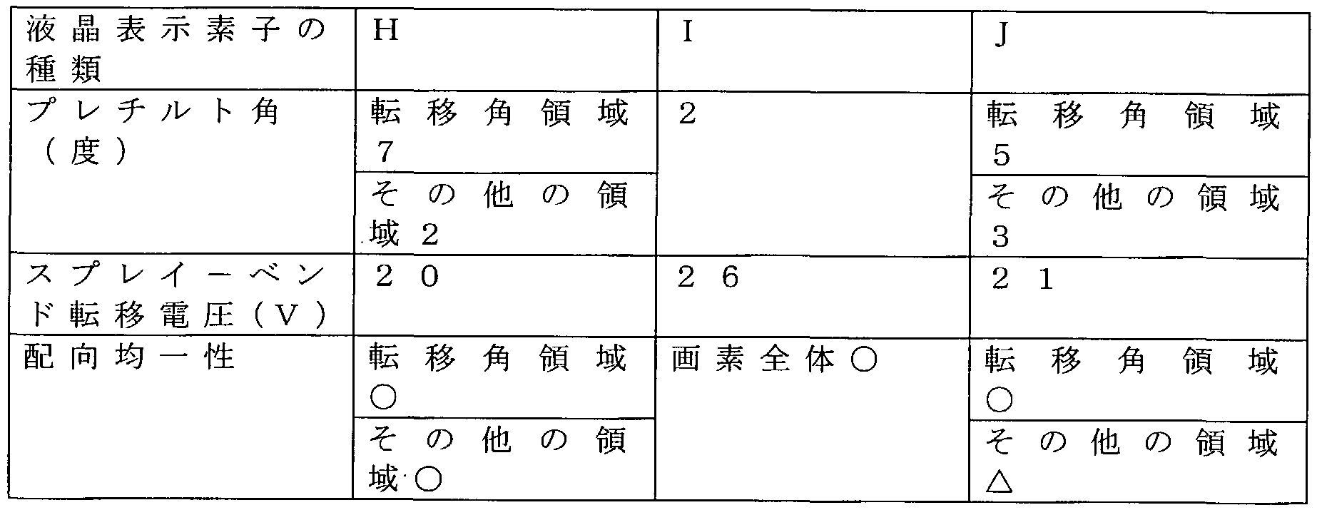


Claims
Priority Applications (5)
| Application Number | Priority Date | Filing Date | Title |
|---|---|---|---|
| EP00966348A EP1223604A1 (en) | 1999-10-12 | 2000-10-12 | Liquid crystal display element, optically anisotropic film, and methods for manufacturing them |
| US10/110,409 US6982774B1 (en) | 1999-10-12 | 2000-10-12 | Liquid crystal display element including an optically anisotropic film having at least two regions with different orientation anisotropies, and production methods of the same |
| KR1020027004336A KR20020064295A (en) | 1999-10-12 | 2000-10-12 | Liquid crystal display element, optically anisotropic film, and methods for manufacturing them |
| US11/042,517 US7038750B2 (en) | 1999-10-12 | 2005-01-26 | Liquid crystal display element, optically anisotropic film, and production methods of the same |
| US11/042,408 US7307683B2 (en) | 1999-10-12 | 2005-01-26 | Liquid crystal display element, optically anisotropic film, and production methods of the same |
Applications Claiming Priority (2)
| Application Number | Priority Date | Filing Date | Title |
|---|---|---|---|
| JP28958199A JP3099825B1 (en) | 1999-10-12 | 1999-10-12 | Liquid crystal display device and method of manufacturing the same |
| JP2000171886A JP2001350146A (en) | 2000-06-08 | 2000-06-08 | Liquid crystal display element and its manufacturing method |
Related Child Applications (3)
| Application Number | Title | Priority Date | Filing Date |
|---|---|---|---|
| US10110409 A-371-Of-International | 2000-10-12 | ||
| US11/042,517 Division US7038750B2 (en) | 1999-10-12 | 2005-01-26 | Liquid crystal display element, optically anisotropic film, and production methods of the same |
| US11/042,408 Division US7307683B2 (en) | 1999-10-12 | 2005-01-26 | Liquid crystal display element, optically anisotropic film, and production methods of the same |
Publications (3)
| Publication Number | Publication Date |
|---|---|
| WO2001026442A2 true WO2001026442A2 (en) | 2001-04-19 |
| WO2001026442A3 WO2001026442A3 (en) | 2002-02-28 |
| WO2001026442B1 WO2001026442B1 (en) | 2002-06-20 |
Family
ID=26557648
Family Applications (1)
| Application Number | Title | Priority Date | Filing Date |
|---|---|---|---|
| PCT/IB2000/001458 WO2001026442A2 (en) | 1999-10-12 | 2000-10-12 | Liquid crystal display element, optically anisotropic film, and methods for manufacturing them |
Country Status (4)
| Country | Link |
|---|---|
| US (3) | US6982774B1 (en) |
| EP (1) | EP1223604A1 (en) |
| KR (1) | KR20020064295A (en) |
| WO (1) | WO2001026442A2 (en) |
Cited By (1)
| Publication number | Priority date | Publication date | Assignee | Title |
|---|---|---|---|---|
| KR100431052B1 (en) * | 2001-10-08 | 2004-05-12 | 주식회사 네오텍리서치 | Liquid Crystal Displays with Multi-Domains Effect Formed by Surface Gratings |
Families Citing this family (24)
| Publication number | Priority date | Publication date | Assignee | Title |
|---|---|---|---|---|
| EP1223604A1 (en) * | 1999-10-12 | 2002-07-17 | Matsushita Electric Industrial Co., Ltd. | Liquid crystal display element, optically anisotropic film, and methods for manufacturing them |
| WO2003007398A1 (en) * | 2001-07-09 | 2003-01-23 | Plastic Logic Limited | Progressive aligned deposition |
| US20050260334A1 (en) * | 2004-05-24 | 2005-11-24 | The Hong Kong Univerisity Of Science And Technology | Method of achieving high pretilt angles in a lilquid crystal cell |
| JP4797468B2 (en) | 2004-07-07 | 2011-10-19 | 大日本印刷株式会社 | Phase difference control member, manufacturing method thereof, and liquid crystal display device |
| KR20060104092A (en) * | 2005-03-29 | 2006-10-09 | 삼성전자주식회사 | Organic thin film transistor array panel and method for manufacturing the same |
| JP2006317656A (en) * | 2005-05-12 | 2006-11-24 | Dainippon Printing Co Ltd | Anisotropic optical element |
| JP5116287B2 (en) * | 2005-11-21 | 2013-01-09 | 株式会社ジャパンディスプレイイースト | Liquid crystal display |
| JP2008107591A (en) * | 2006-10-26 | 2008-05-08 | Nitto Denko Corp | Manufacturing method of birefringent film, birefringent film and layered body |
| KR100831961B1 (en) * | 2006-10-27 | 2008-05-23 | 주식회사 에프엠디 | Optical film using the reactive mesogen and manufacturing of the same |
| JP2008129482A (en) * | 2006-11-24 | 2008-06-05 | Nec Lcd Technologies Ltd | Liquid crystal display device and manufacturing method thereof |
| JP5600874B2 (en) * | 2006-12-21 | 2014-10-08 | 日立化成株式会社 | Light control film |
| JP4265652B2 (en) * | 2006-12-22 | 2009-05-20 | ソニー株式会社 | Liquid crystal display element and manufacturing method thereof |
| JP4949073B2 (en) * | 2007-02-23 | 2012-06-06 | 株式会社 日立ディスプレイズ | Liquid crystal display |
| US8471999B2 (en) * | 2008-04-24 | 2013-06-25 | The Hong Kong University Of Science And Technology | Low voltage liquid crystal lens with variable focal length |
| CN102282506B (en) * | 2009-05-27 | 2014-06-04 | 夏普株式会社 | Liquid crystal display device |
| WO2011013396A1 (en) * | 2009-07-28 | 2011-02-03 | シャープ株式会社 | Liquid crystal display element |
| WO2011111273A1 (en) * | 2010-03-12 | 2011-09-15 | シャープ株式会社 | Display panel and process for production thereof |
| TWI442147B (en) * | 2010-12-30 | 2014-06-21 | Au Optronics Corp | Stereoscopic optical device and method of making the same |
| US8420541B2 (en) * | 2011-05-06 | 2013-04-16 | Nanya Technology Corporation | Method for increasing adhesion between polysilazane and silicon nitride |
| CN102681233B (en) * | 2011-08-01 | 2014-11-19 | 北京京东方光电科技有限公司 | Vacuum box-aligning device and box-aligning method |
| TWI467293B (en) * | 2011-12-09 | 2015-01-01 | Chimei Innolux Corp | Liquid crystal display and method for fabricating the same |
| KR102213920B1 (en) * | 2013-02-27 | 2021-02-10 | 시리얼 테크놀로지즈 에스.에이. | Optical liquid-crystal phase modulator |
| KR20150081626A (en) * | 2014-01-06 | 2015-07-15 | 삼성디스플레이 주식회사 | Display apparatus and fabrication method thereof |
| CN111208676B (en) * | 2020-03-05 | 2021-08-03 | Tcl华星光电技术有限公司 | Liquid crystal display panel and liquid crystal display device |
Citations (3)
| Publication number | Priority date | Publication date | Assignee | Title |
|---|---|---|---|---|
| US5602661A (en) * | 1993-02-17 | 1997-02-11 | Hoffmann-La Roche Inc. | Optical component |
| GB2310048A (en) * | 1995-12-29 | 1997-08-13 | Lg Electronics Inc | Alignment layers for liquid crystal cells |
| EP0942314A2 (en) * | 1998-03-11 | 1999-09-15 | Matsushita Electric Industrial Co., Ltd. | Method for producing an aligned chemically adsorbed monomolecular film |
Family Cites Families (18)
| Publication number | Priority date | Publication date | Assignee | Title |
|---|---|---|---|---|
| EP0492545B1 (en) | 1990-12-25 | 1998-03-25 | Matsushita Electric Industrial Co., Ltd. | Transparent substrate with monomolecular film thereon and method of manufacturing the same |
| US5473455A (en) * | 1991-12-20 | 1995-12-05 | Fujitsu Limited | Domain divided liquid crystal display device with particular pretilt angles and directions in each domain |
| EP0635748B1 (en) * | 1993-07-23 | 2001-12-12 | Sharp Kabushiki Kaisha | Liquid crystal display apparatus and method for producing the same |
| US5689322A (en) * | 1993-07-30 | 1997-11-18 | Sharp Kabushiki Kaisha | Liquid crystal display device having regions with different twist angles |
| TW259845B (en) * | 1993-07-30 | 1995-10-11 | Sharp Kk | |
| KR970000356B1 (en) * | 1993-09-18 | 1997-01-08 | 엘지전자 주식회사 | Light polymer alignment film forming method of liquid crystal display element |
| US5648829A (en) * | 1994-02-15 | 1997-07-15 | Kyocera Corporation | Method for fabricating a liquid crystal display including irradiating an alignment film with UV light |
| JP2780680B2 (en) * | 1995-08-11 | 1998-07-30 | 日本電気株式会社 | Liquid crystal display device and manufacturing method thereof |
| JP3417218B2 (en) * | 1996-07-03 | 2003-06-16 | 松下電器産業株式会社 | LCD panel |
| KR100247137B1 (en) | 1996-07-29 | 2000-03-15 | 구본준 | Method for manufacturing multi-domain lc cell |
| JPH10213802A (en) | 1997-01-29 | 1998-08-11 | Mitsubishi Electric Corp | Liquid crystal display device |
| JP3886592B2 (en) * | 1997-03-18 | 2007-02-28 | シャープ株式会社 | LCD panel |
| JP3945789B2 (en) | 1997-12-19 | 2007-07-18 | 林テレンプ株式会社 | Alignment film manufacturing method, alignment film, and liquid crystal display device provided with alignment film |
| JP3715771B2 (en) | 1998-01-26 | 2005-11-16 | 株式会社日立製作所 | Liquid crystal display device and manufacturing method thereof |
| JP3099812B2 (en) * | 1998-07-30 | 2000-10-16 | 日本電気株式会社 | Liquid crystal display |
| EP1223604A1 (en) * | 1999-10-12 | 2002-07-17 | Matsushita Electric Industrial Co., Ltd. | Liquid crystal display element, optically anisotropic film, and methods for manufacturing them |
| TW527508B (en) * | 2000-02-10 | 2003-04-11 | Matsushita Electric Ind Co Ltd | Liquid crystal display device and producing method |
| EP1331513A4 (en) * | 2000-10-17 | 2008-04-02 | Toshiba Matsushita Display Tec | Liquid crystal display and its producing method |
-
2000
- 2000-10-12 EP EP00966348A patent/EP1223604A1/en not_active Withdrawn
- 2000-10-12 KR KR1020027004336A patent/KR20020064295A/en not_active Application Discontinuation
- 2000-10-12 WO PCT/IB2000/001458 patent/WO2001026442A2/en active Search and Examination
- 2000-10-12 US US10/110,409 patent/US6982774B1/en not_active Expired - Lifetime
-
2005
- 2005-01-26 US US11/042,517 patent/US7038750B2/en not_active Expired - Lifetime
- 2005-01-26 US US11/042,408 patent/US7307683B2/en not_active Expired - Lifetime
Patent Citations (3)
| Publication number | Priority date | Publication date | Assignee | Title |
|---|---|---|---|---|
| US5602661A (en) * | 1993-02-17 | 1997-02-11 | Hoffmann-La Roche Inc. | Optical component |
| GB2310048A (en) * | 1995-12-29 | 1997-08-13 | Lg Electronics Inc | Alignment layers for liquid crystal cells |
| EP0942314A2 (en) * | 1998-03-11 | 1999-09-15 | Matsushita Electric Industrial Co., Ltd. | Method for producing an aligned chemically adsorbed monomolecular film |
Cited By (1)
| Publication number | Priority date | Publication date | Assignee | Title |
|---|---|---|---|---|
| KR100431052B1 (en) * | 2001-10-08 | 2004-05-12 | 주식회사 네오텍리서치 | Liquid Crystal Displays with Multi-Domains Effect Formed by Surface Gratings |
Also Published As
| Publication number | Publication date |
|---|---|
| KR20020064295A (en) | 2002-08-07 |
| US7038750B2 (en) | 2006-05-02 |
| US20050151915A1 (en) | 2005-07-14 |
| WO2001026442A3 (en) | 2002-02-28 |
| WO2001026442B1 (en) | 2002-06-20 |
| US6982774B1 (en) | 2006-01-03 |
| EP1223604A1 (en) | 2002-07-17 |
| US20050151908A1 (en) | 2005-07-14 |
| US7307683B2 (en) | 2007-12-11 |
Similar Documents
| Publication | Publication Date | Title |
|---|---|---|
| WO2001026442A2 (en) | Liquid crystal display element, optically anisotropic film, and methods for manufacturing them | |
| TWI467291B (en) | Liquid crystal display device and method for manufacturing the same | |
| US8174653B2 (en) | Liquid crystal display device | |
| KR100326965B1 (en) | A liquid crystal display device and a method of manufacture thereof, and a substrate and a method of manufacture thereof | |
| US7248318B2 (en) | Liquid crystal display device and method of producing the same | |
| TWI639872B (en) | Liquid crystal display and method for preparation thereof | |
| WO2010116565A1 (en) | Liquid crystal display device, method for manufacturing liquid crystal display device, composition for forming photopolymer film, and composition for forming liquid crystal layer | |
| JP6241058B2 (en) | Liquid crystal display | |
| JP2000122066A (en) | Liquid crystal display device | |
| WO1999017153A1 (en) | Liquid crystal alignment film and method of producing the same, and liquid crystal display using the same and method of producing the same | |
| JPH11305256A (en) | Active matrix type liquid crystal display device | |
| JP2002287151A (en) | Liquid crystal display element and manufacturing method therefor | |
| JP3099825B1 (en) | Liquid crystal display device and method of manufacturing the same | |
| TW201518822A (en) | Liquid crystal display device, and manufacturing method therefor | |
| TWI376554B (en) | Liquid crystal display device | |
| JP3301960B2 (en) | Liquid crystal alignment film, method for manufacturing liquid crystal alignment film, liquid crystal display device, and method for manufacturing liquid crystal display device | |
| US20230101325A1 (en) | Liquid crystal panel and liquid crystal display device | |
| JP2001350146A (en) | Liquid crystal display element and its manufacturing method | |
| JPH11125821A (en) | Liquid crystal alignment layer, its production, liquid crystal display device using the same and its production | |
| JP3255605B2 (en) | Liquid crystal display device and manufacturing method thereof | |
| JP3497119B2 (en) | Organic thin film and manufacturing method thereof, liquid crystal alignment film and manufacturing method thereof, and liquid crystal display device and manufacturing method thereof | |
| WO2013031497A1 (en) | Liquid-crystal display device and liquid-crystal composition | |
| KR20010030786A (en) | Liquid crystal alignment film and method of producing the same, and liquid crystal display using the same and method of producing the same | |
| JPH09211454A (en) | Production of light scattering type liquid crystal display element | |
| JP2001174836A (en) | Liquid crystal display panel and method for manufacturing the same |
Legal Events
| Date | Code | Title | Description |
|---|---|---|---|
| AK | Designated states |
Kind code of ref document: A2 Designated state(s): CN KR US |
|
| AL | Designated countries for regional patents |
Kind code of ref document: A2 Designated state(s): AT BE CH CY DE DK ES FI FR GB GR IE IT LU MC NL PT SE |
|
| 121 | Ep: the epo has been informed by wipo that ep was designated in this application | ||
| DFPE | Request for preliminary examination filed prior to expiration of 19th month from priority date (pct application filed before 20040101) | ||
| AK | Designated states |
Kind code of ref document: A3 Designated state(s): CN KR US |
|
| AL | Designated countries for regional patents |
Kind code of ref document: A3 Designated state(s): AT BE CH CY DE DK ES FI FR GB GR IE IT LU MC NL PT SE |
|
| WWE | Wipo information: entry into national phase |
Ref document number: 1020027004336 Country of ref document: KR |
|
| WWE | Wipo information: entry into national phase |
Ref document number: 10110409 Country of ref document: US |
|
| WWE | Wipo information: entry into national phase |
Ref document number: 2000966348 Country of ref document: EP |
|
| AK | Designated states |
Kind code of ref document: B1 Designated state(s): CN KR US |
|
| AL | Designated countries for regional patents |
Kind code of ref document: B1 Designated state(s): AT BE CH CY DE DK ES FI FR GB GR IE IT LU MC NL PT SE |
|
| WWP | Wipo information: published in national office |
Ref document number: 2000966348 Country of ref document: EP |
|
| WWP | Wipo information: published in national office |
Ref document number: 1020027004336 Country of ref document: KR |
|
| DPE2 | Request for preliminary examination filed before expiration of 19th month from priority date (pct application filed from 20040101) |