WO2003065394A2 - Photovoltaic cell components and materials - Google Patents
Photovoltaic cell components and materials Download PDFInfo
- Publication number
- WO2003065394A2 WO2003065394A2 PCT/US2003/002355 US0302355W WO03065394A2 WO 2003065394 A2 WO2003065394 A2 WO 2003065394A2 US 0302355 W US0302355 W US 0302355W WO 03065394 A2 WO03065394 A2 WO 03065394A2
- Authority
- WO
- WIPO (PCT)
- Prior art keywords
- photovoltaic cell
- nanoparticle
- flexible
- sensitizer
- photosensitized
- Prior art date
Links
Classifications
-
- H—ELECTRICITY
- H01—ELECTRIC ELEMENTS
- H01G—CAPACITORS; CAPACITORS, RECTIFIERS, DETECTORS, SWITCHING DEVICES OR LIGHT-SENSITIVE DEVICES, OF THE ELECTROLYTIC TYPE
- H01G9/00—Electrolytic capacitors, rectifiers, detectors, switching devices, light-sensitive or temperature-sensitive devices; Processes of their manufacture
- H01G9/20—Light-sensitive devices
- H01G9/2027—Light-sensitive devices comprising an oxide semiconductor electrode
- H01G9/2031—Light-sensitive devices comprising an oxide semiconductor electrode comprising titanium oxide, e.g. TiO2
-
- Y—GENERAL TAGGING OF NEW TECHNOLOGICAL DEVELOPMENTS; GENERAL TAGGING OF CROSS-SECTIONAL TECHNOLOGIES SPANNING OVER SEVERAL SECTIONS OF THE IPC; TECHNICAL SUBJECTS COVERED BY FORMER USPC CROSS-REFERENCE ART COLLECTIONS [XRACs] AND DIGESTS
- Y02—TECHNOLOGIES OR APPLICATIONS FOR MITIGATION OR ADAPTATION AGAINST CLIMATE CHANGE
- Y02E—REDUCTION OF GREENHOUSE GAS [GHG] EMISSIONS, RELATED TO ENERGY GENERATION, TRANSMISSION OR DISTRIBUTION
- Y02E10/00—Energy generation through renewable energy sources
- Y02E10/50—Photovoltaic [PV] energy
- Y02E10/542—Dye sensitized solar cells
-
- Y—GENERAL TAGGING OF NEW TECHNOLOGICAL DEVELOPMENTS; GENERAL TAGGING OF CROSS-SECTIONAL TECHNOLOGIES SPANNING OVER SEVERAL SECTIONS OF THE IPC; TECHNICAL SUBJECTS COVERED BY FORMER USPC CROSS-REFERENCE ART COLLECTIONS [XRACs] AND DIGESTS
- Y02—TECHNOLOGIES OR APPLICATIONS FOR MITIGATION OR ADAPTATION AGAINST CLIMATE CHANGE
- Y02P—CLIMATE CHANGE MITIGATION TECHNOLOGIES IN THE PRODUCTION OR PROCESSING OF GOODS
- Y02P70/00—Climate change mitigation technologies in the production process for final industrial or consumer products
- Y02P70/50—Manufacturing or production processes characterised by the final manufactured product
Definitions
- the invention relates generally to the field of photovoltaic devices, and more specifically to chemical structures, components, and materials for fabricating photovoltaic cells.
- Thin film solar cells composed of percolating networks of liquid electrolyte and dye-coated sintered titanium dioxide were developed by Dr. Michael GrStzel and coworkers at the Swiss Federal Institute of Technology. These photovoltaic devices fall within a general class of cells referred to as dye-sensitized solar cells ("DSSCs").
- DSSCs dye-sensitized solar cells
- fabrication of DSSCs requires a high temperature sintering process (> about 400 °C) to achieve sufficient interconnectivity between the nanoparticles and enhanced adhesion between the nanoparticles and a transparent substrate.
- the photovoltaic cells of Gratzel are fabricated from relatively inexpensive raw materials, the high temperature sintering technique used to make these cells limits the cell substrate to rigid transparent materials, such as glass, and consequently limits the manufacturing to batch processes and the applications to those tolerant of the rigid structure. Furthermore, the high temperature sintering process increases the cost of manufacturing a photovoltaic cell due to the energy required to perform the sintering.
- the invention in, one embodiment, addresses the deficiencies of the prior art by providing a polymeric linking agent that enables the fabrication of thin film solar cells at relatively low temperatures. This enables the manufacture of such cells on flexible substrates, including, for example, those substrates constructed from somewhat heat sensitive polymeric materials.
- the invention provides photovoltaic cells and methods of photovoltaic cell fabrication that facilitate their manufacture by a relatively simple, continuous manufacturing process. For example, a roll-to-roll process can be utilized instead of the batch processes that limited the prior art. More particularly, in one embodiment, the invention provides a method for interconnecting metal oxide nanoparticles in DSSCs, with reduced or no heating, using a polymeric linking agent.
- metal oxide nanoparticles may be interconnected by contacting the nanoparticles with a suitable polymeric linking agent dispersed in a solvent, such as n- butanol, at about room temperature or at elevated temperatures below about 300 °C.
- a suitable polymeric linking agent dispersed in a solvent, such as n- butanol
- the invention provides electrolyte compositions and methods of preparing solid or quasi-solid electrolyte compositions that addresses the deficiencies of the prior art. Replacing liquid electrolytes with solid or quasi-solid electrolytes facilitates the production of flexible photovoltaic cells using continuous manufacturing processes, such as roll-to-roll or web processes. Gel electrolytes also contribute to the amelioration of electrolyte leakage and help address the long-term stability problems associated with conventional DSSCs.
- the gel electrolyte compositions of the invention include appropriate redox active components and small amounts of multiple ligand-containing polymeric and non-polymeric molecules gelled by a metal ion complexing process.
- Organic compounds capable of complexing with a metal ion at a plurality of sites are used in various embodiments.
- a given redox component maybe a liquid by itself or have solid components dissolved in a liquid solvent.
- Ligating groups are functional units that contain at least one donor atom rich in electron density, e.g., oxygen, nitrogen, sulfur, phosphorous, among others. Multiple ligating groups, which may be present in non-polymeric material or polymeric material, may occur in either the side chain or part of the material's molecular backbone, in part of a dendrimer, or in a starburst molecule.
- the introduction of metal ions, and lithium ions in particular, in an ionic liquid electrolyte composition in accord with various aspects of the invention enhances the efficiency of the cells by improving both photocurrent and open circuit voltage. Further, the invention provides photovoltaic cells, electrolyte compositions, gelling compounds, and related methodologies that incorporate gel electrolytes and lithium containing compounds.
- the invention addresses the deficiencies of the prior art by providing methods and chemical structures that improve the adhesion of a photovoltaic material to a base material during the fabrication of a photovoltaic cell at low temperatures ( ⁇ about 300 °C).
- a photovoltaic material to a base material during the fabrication of a photovoltaic cell at low temperatures ( ⁇ about 300 °C).
- the methods and chemical structures of the invention enhance the performance of thin film solar cells manufactured by continuous manufacturing processes, while also reducing the cost of manufacturing.
- the invention addresses the deficiencies of the prior art by providing semiconductor oxide formulations, including dye-sensitized, metal-oxide nanoparticle materials that can be coated on flexible, transparent substrates at room temperature. More particularly, in one embodiment, the invention provides mechanically stable, titania nanoparticles that are sufficiently adhered to flexible, transparent substrates, or substrates coated with electrical conductors, upon drying at temperatures between about 50 °C and about 150 °C. The mechanically stable titania nanoparticles enable the fabrication of thin film solar cells at relatively low temperatures and using continuous manufacturing processes. The invention, in one embodiment, addresses the deficiencies of the prior art by providing a co-sensitizer that enhances the performance of sensitizing dyes.
- Co- sensitizers are co-adsorbed with the sensitizing dye on the surface of an interconnected semiconductor oxide nanoparticle material.
- Co-sensitizers have been demonstrated to increase the efficiency of photovoltaic cells by as much as 17% by improving their charge transfer efficiency and reducing the back transfer of electrons from the interconnected semiconductor oxide nanoparticle material to the sensitizing dye.
- Co-sensitizers belong to a class of materials that include aromatic amines, carbazoles, and other fused ring analogues that have the ability to donate electrons to an acceptor and form stable cation radicals.
- the invention provides a method of interconnecting nanoparticles at low temperature that includes providing a solution having a polymeric linking agent and a solvent and contacting a plurality of metal oxide nanoparticles with the solution at a temperature below about 300°C, where the solution contains the polymeric linking agent in a concentration sufficient to interconnect at least a portion of the plurality of metal oxide nanoparticles.
- the temperature is below about 200°C, below about 100°C, or at about room temperature.
- the polymeric linking agent includes a long chain macromolecule.
- the long chain macromolecule may have a backbone structure substantially similar to the chemical structure of the plurality of metal oxide nanoparticles, and one or more reactive groups chemically bonded to the backbone structure.
- the plurality of metal oxide nanoparticles has a chemical structure of the form M x O y , where x and y are integers.
- M can include Ti, Zrdon W, Nb, Ta, Tb, or Sn.
- the polymeric linking agent is poly(n-butyl titanate).
- the solvent of the solution is n-butanol.
- the mechanism for interconnecting at least a portion of the plurality of metal oxide nanoparticles is a mechanical or electrical bridge formed by the one or more reactive groups binding to the plurality of metal oxide nanoparticles.
- the plurality of metal oxide nanoparticles may be disposed, for example, as a thin film on a substrate.
- the metal oxide nanoparticles are disposed on the substrate by, for example, dipping the substrate into the solution including the polymeric linking agent, spraying the solution including the polymeric linking agent onto the substrate, or dispersing the solution including the polymeric linking agent on the substrate.
- the plurality of metal oxide nanoparticles are dispersed onto the substrate, and then the solution including the polymeric linking agent is deposited onto the substrate.
- the method includes the step of contacting the metal oxide nanoparticles with a modifier solution, hi yet another embodiment, the plurality of metal oxide nanoparticles includes nanoparticles of titanium oxides, zirconium oxides, zinc oxides, tungsten oxides, niobium oxides, lanthanum oxides, tantalum oxides, tin oxides, terbium oxides, and one or more combinations thereof.
- the invention provides a polymeric linking agent solution including (1) a polymeric linking agent of the formula -[O-M(OR)j ⁇ ] m -; (2) a plurality of metal oxide nanoparticles that have the formula M x O y ; and (3) a solvent; where i, m, x, and y are integers greater than zero.
- M is Ti, Zr, Sn, W, Nb, Ta, or Tb.
- R may be a hydrogen atom, an alkyl, an alkene, an alkyne, an aromatic, or an acyl group.
- the solution preferably contains the polymeric linking agent in a concentration sufficient to interconnect at least a portion of the plurality of metal oxide nanoparticles at a temperature below about 300°C.
- the polymeric linking agent solution contains the polymeric linking agent in a concentration sufficient to interconnect at least a portion of the plurality of nanoparticles at a temperature below about 100 °C.
- the polylinker solution is a 1% (by weight) poly(n-butyl titanate) in n-butanol.
- the invention provides a flexible photovoltaic cell including a photosensitized interconnected nanoparticle material and a charge carrier material, both of which are disposed between first and second flexible and significantly light transmitting substrates.
- the photosensitized interconnected nanoparticle material may include nanoparticles linked by a polymeric linking agent.
- the photosensitized interconnected nanoparticle material includes particles with an average size substantially in the range of about 5 nm to about 80 nm.
- the photosensitized interconnected nanoparticle material is interconnected titanium dioxide nanoparticles.
- the photosensitized interconnected nanoparticle material may be, for example, zirconium oxides, zinc oxides, tungsten oxides, niobium oxides, lanthanum oxides, tantalum oxides, tin oxides, terbium oxides, or one or more combinations thereof.
- the photosensitized interconnected nanoparticle material may include a photosensitizing agent such as a xanthine, cyanine, merocyanine, phthalocyanine, and/or pynole.
- the photosensitizing agent may include a metal ion, such as divalent or trivalent metals.
- the photosensitizing agent may also include at least one of a ruthenium transition metal complex, an osmium transition metal complex, and an iron transition metal complex.
- the charge carrier material includes a redox electrolyte system.
- the charge carrier media is a polymeric electrolyte. According to one feature, the charge carrier material transmits at least about 60% of incident visible light.
- At least one of the first and second flexible, significantly light transmitting substrates includes a transparent substrate (e.g., a polyethylene terephthalate or polyethylene naphthalate material).
- the photovoltaic cell includes a catalytic media layer disposed between the first and second flexible, significantly light transmitting substrates.
- the catalytic media layer is, for example, platinum.
- the photovoltaic cell includes an electrical conductor material disposed on at least one of the first and second flexible, significantly light transmitting substrates.
- the electrical conductor material is, for example, indium tin oxide.
- the invention provides an electrolyte composition adapted for use in a solar cell.
- the electrolyte composition includes a gelling compound having a metal ion and an organic compound capable of complexing with the metal ion at a plurality of sites.
- the organic compound is drawn from the class of polymeric compounds.
- the metal ion may be lithium.
- the organic compound includes, for example, poly(4-vinyl pyridine), poly(2-vinyl pyridine), polyethylene oxide, polyurethanes, polyamides, and/or other suitable compounds.
- the gelling compound may be a lithium salt having the chemical formula LiX, where X is a suitable anion, such as, for example, a halide, perchlorate, thiocyanate, trifluoromethyl sulfonate, or hexafluorophosphate.
- X is a suitable anion, such as, for example, a halide, perchlorate, thiocyanate, trifluoromethyl sulfonate, or hexafluorophosphate.
- the electrolyte composition includes iodine at a concentration of at least about 0.05 M.
- the invention provides an electrolyte solution for use in a solar cell.
- the electrolyte solution includes a compound of the formula MjXj.
- the i and j variables are > 1.
- X is a suitable monovalent or polyvalent anion such as a halide, perchlorate, thiocyanate, trifluoromethyl sulfonate, hexafluorophosphate, sulfate, carbonate, or phosphase
- M is a monovalent or polyvalent metal cation such as Li, Cu, Ba, Zn, Ni, lanthanides, Co, Ca, Al, Mg, or other suitable metals.
- the invention provides a photovoltaic cell including first and second significantly light transmitting substrates, a photosensitized interconnected nanoparticle material, and an electrolyte redox system, where the photosensitized interconnected nanoparticle material and the electrolyte redox system are both disposed between the two substrates of the flexible photovoltaic cell.
- the electrolyte redox system includes a gelling compound that itself includes a metal ion; a polymeric compound capable of complexing with the metal ion at a plurality of sites; and an electrolyte solution.
- the metal ion is lithium.
- the electrolyte solution includes an imidazolium iodide- based ionic liquid having an iodine concentration of at least 0.05 M and a passivating agent such as t-butylpyridine, methyl-benzimidazole, or other species that have free electron pairs and are capable of adsorbing onto titania.
- a passivating agent such as t-butylpyridine, methyl-benzimidazole, or other species that have free electron pairs and are capable of adsorbing onto titania.
- the invention provides a method of gelling an electrolyte solution for use in a DSSC.
- the method includes the steps of providing an electrolyte solution and adding to the electrolyte solution a material capable of complexing at a plurality of sites and a metal ion that complexes at those sites.
- the steps of this method are performed at a temperature below 50 °C and at standard pressure.
- the metal ion may be lithium.
- the electrolyte solution has a gelling rate controlled by changing a concentration of counter ions in the electrolyte solution. Changing the identity of the anions controls the rate and degree of gelling.
- the degree of gelling exhibited using iodide is higher than the degree of gelling found with chloride or thiocyanate under given experimental conditions and using an identical lithium ion concentration. Therefore, changing counter ion identity provides a mechanism for changing the gelling rate.
- the invention provides a method for reducing electron transfer to species within the electrolyte of a solar cell. This method includes the steps of initially providing a photovoltaic cell portion including a dye-sensitized layer and an electrolyte solution including a compound capable of complexing at a plurality of sites.
- a compound MX is added to the electrolyte solution in sufficient amounts to form a gel electrolyte, where M is an alkali metal and X is a suitable anion such as a halide, perchlorate, thiocyanate, trifluoromethyl sulfonate, or hexafluorophosphate.
- X is a suitable anion such as a halide, perchlorate, thiocyanate, trifluoromethyl sulfonate, or hexafluorophosphate.
- the gel electrolyte is incorporated into the photovoltaic cell portion in this aspect of the invention.
- the invention provides an electrolyte composition adapted for use in a solar cell.
- the electrolyte composition includes a mixture including about 90 wt% of an ionic liquid including an imidazolium iodide, from 0 to 10 wt% water, iodine at a concentration of at least 0.05 M, and methyl-benzimidazole.
- the imidazoliumiodide-based ionic liquid is selected from butylmethylimidazolium iodide, propylmethylimidazolium iodide, hexylmethylimidazolmm iodide, or combinations thereof and the like.
- the electrolyte composition may include LiCl.
- the amount of LiCl is ranges from about 1 wt% LiCl and 6 wt% LiCl, is at least about 1 wt% LiCl, or is less than about 6 wt% LiCl.
- the electrolyte composition includes Lil.
- the amount of Lil ranges from about 1 wt% Lil and 6 wt% Lil, is at least about 1 wt% Lil, or is less than about 6 wt% Lil.
- the invention provides a method of forming a semiconductor oxide nanoparticle layer on a base material.
- the method includes providing a base material, coating the base material with a primer layer including a semiconductor oxide, and coating a suspension of semiconductor oxide nanoparticles on the primer layer at temperatures below about 300 °C, where the primer layer improves the adhesion of the suspension of semiconductor oxide nanoparticles to the base material.
- the temperature is below about 150 °C or is about room temperature.
- the primer layer includes a vacuum-coated semiconductor-oxide film.
- the film may include titanium dioxide in the form of a film or a thin coating of fine particles of a semiconductor oxide.
- the thin coating of fine particles of a semiconductor oxide includes titanium dioxide or tin oxide.
- the primer layer includes a thin layer of a polylinker solution.
- the polylinker solution may be a titanium (IV) butoxide polymer or may include a long chain macromolecule.
- the base material includes a flexible, significantly light transmitting substrate.
- the base material may be an electrically conductive material (e.g. indium tin oxide).
- the base material also may include the electrically conductive material deposited onto a flexible, significantly light transmitting substrate.
- the invention provides a flexible photovoltaic cell including a primer layer disposed on a first flexible, significantly light transmitting substrate, a photosensitized interconnected nanoparticle material including a suspension of semiconductor oxide nanoparticles disposed on the primer layer, a charge carrier material, and a second flexible, significantly light transmitting substrate.
- the primer layer, the photosensitized interconnected nanoparticle material, and the charge carrier material are all disposed between the first and second flexible, significantly light transmitting substrates.
- the photosensitized nanoparticle material includes nanoparticles such as titanium oxides, zirconium oxides, zinc oxides, tungsten oxides, niobium oxides, lanthanum oxides, tin oxides, terbium oxides, tantalum oxides, or one or more combinations thereof.
- the primer layer may include a vacuum-coated semiconductor-oxide film, preferably a titanium dioxide film.
- the primer layer may include a thin coating of fine particles of a semiconductor oxide, e.g. titanium dioxide or tin oxide.
- the primer layer includes a thin layer of a polylinker solution.
- the polylinker solution may include a long chain macromolecule, or preferably titanium (IV) butoxide polymer.
- an electrically conductive material is disposed on the first flexible, significantly light transmitting substrate.
- the electrical conductor may be indium tin oxide.
- the invention provides a layer formulation for a photovoltaic cell.
- the formulation includes a nanoparticle material dispersed in a solvent and a polymer binder soluble in the solvent, both disposed on a base material to form a mechanically stable, nanoparticle film.
- the film may be formed at room temperature, and the formulation may include acetic acid.
- mechanically stable, nanoparticle film includes a semiconductor oxide.
- the film may include titanium dioxide nanoparticles. The ratio of the titanium dioxide nanoparticles to the polymer binder may be between about 100:0.1 to about 100:20 by weight, and preferably between about 100:1 to about 100:10 by weight.
- the solvent is water; alternatively, the solvent is an organic compound.
- the polymer binder is polyvinylpyrrolidone, polyethylene oxide, hydroxyethyl cellulose, ethylcellulose, hydroxypropyl cellulose, or polyvinyl alcohol.
- the formulation also may include a polymeric linking agent to interconnect the nanoparticle material.
- the base material is a flexible, significantly light transmitting substrate.
- the invention provides a method for forming a layer in a photovoltaic cell.
- the method includes providing a nanoparticle material dispersed in a solvent, dispersing a polymer binder in the solvent, and applying a solution that includes the nanoparticle material and the polymer binder to a base material to form a mechanically stable, nanoparticle film.
- the mechanically stable, nanoparticle film may be formed at room temperature.
- the method also may include the step of drying the base material at a temperature of between about 50 °C and about 150 °C after the solution has been applied.
- the invention provides a flexible photovoltaic cell including (1) a charge carrier material disposed between first and second flexible, significantly light transmitting substrates and (2) a photosensitized interconnected nanoparticle material including a semiconductor-oxide nanoparticle material dispersed in a solvent and a polymer binder soluble in the solvent.
- the photosensitized interconnected nanoparticle material is applied to the first flexible, significantly light transmitting substrate to complete the cell.
- the nanoparticle material may include nanoparticles linked by a polymeric linking agent.
- the photosensitized interconnected nanoparticle material includes nanoparticles such as titanium oxides, zirconium oxides, zinc oxides, tungsten oxides, niobium oxides, lanthanum oxides, tin oxides, terbium oxides, tantalum oxides, or combinations thereof.
- the photosensitized interconnected nanoparticle material may include a photosensitizing agent that itself includes a molecule such as, for example, xanthine, cyanine, merocyanine, phthalocyanine, and pyrrole.
- the photosensitizing agent also includes a metal ion.
- the photosensitizing agent may be a ruthenium transition metal complex, an osmium transition metal complex, or an iron transition metal complex.
- the charge carrier material includes a redox electrolyte system.
- the substrate material may be polyethylene terephthalate.
- the solvent is water; alternatively, the solvent may be an organic compound.
- the polymer binder is polyvinylpyrrolidone, polyethylene oxide, hydroxyethyl cellulose, ethylcellulose, hydroxypropyl cellulose, or polyvinyl alcohol.
- the invention provides a photosensitizing agent for a photovoltaic cell, where the photosensitizing agent includes a sensitizing dye for receiving electromagnetic energy and a co-sensitizer that includes a coordinating group for co- adsorbing with the sensitizing dye on a surface of a metal oxide nanoparticle layer.
- the sensitizing dye is c ⁇ - bis(isothiocyanato)bis(2,2'-bipyridyl-4,4 , -dicarboxylato)-mthenium( ⁇ ).
- the co-sensitizer includes either an aromatic amine or a carbazole.
- the co-sensitizer may include diphenylamino benzoic acid, 2,6 bis (4- benzoicacid)-4-(4-N,N-diphenylamino) phenylpyridine carboxylic acid, or N',N- diphenylaminophenylpropionic acid.
- the coordinating group of the co-sensitizer includes a carboxy derivative, a phosphate group, or a chelating group.
- the chelating group may be an oxime or an alpha- ketoenolate.
- the concentration of the co-sensitizer maybe below about 50 mol% of the sensitizing dye concentration, e.g., between about 1 mol% and about 20 mol%, and preferably between about 1 mol% and about 5 mol%.
- the ratio of the concentration of the sensitizing dye to the co-sensitizer may be about 20/1.
- the invention provides a photosensitized nanoparticle layer in a photovoltaic cell.
- the layer includes a sensitizing dye for receiving electromagnetic energy, a co-sensitizer having a coordinating group, and an interconnected nanoparticle material including a surface for co-absorbing the sensitizing dye and the co-sensitizer to form a photosensitized nanoparticle layer.
- the photosensitized nanoparticle layer may include semiconductor oxide nanoparticles.
- the invention provides a method for forming a photosensitized nanoparticle layer in a photovoltaic cell.
- the method includes providing a sensitizing dye for receiving electromagnetic energy and co- adsorbing a co-sensitizer having a coordinating group on a surface of an interconnected nanoparticle material to form a photosensitized nanoparticle layer.
- the photosensitized nanoparticle layer may include semiconductor oxide nanoparticles.
- the sensitizing dye is cw-bis(isothiocyanato)bis(2,2'-bipyridyl-4,4 , -dicarboxylato)- ruthenium( ⁇ ).
- the co-sensitizer includes either an aromatic amine or a carbazole, e.g., diphenylaminobenzoic acid, 2,6 bis (4-benzoicacid)-4-(4-N,N- diphenylamino) phenylpyridine carboxylic acid, orN',N -diphenylaminophernlpropionic acid.
- the concentration of the co-sensitizer is below about 50 mol% of the sensitizing dye concentration.
- the concentration of the co-sensitizer may be between about 1 mol% and about 20 mol%, and preferably between about 1 mol% and about 20 mol%.
- the invention provides a flexible photovoltaic cell including (1) a photosensitized interconnected nanoparticle material that includes (i) a sensitizing dye for receiving electromagnetic energy and (ii) a co-sensitizer having a coordinating group, and (2) a charge carrier material.
- the sensitizing dye and the co-sensitizer are both adsorbed on a surface of an interconnected nanoparticle material.
- the charge carrier material and the photosensitized interconnected nanoparticle material are both disposed between first and second flexible, significantly light transmitting substrates.
- the photosensitized interconnected nanoparticle material may include nanoparticles linked by a polymeric linking agent.
- the photosensitized interconnected nanoparticle material includes particles with an average size substantially in the range of about 10 nm to about 40 nm.
- the photosensitized interconnected nanoparticle material may be interconnected titanium dioxide nanoparticles, e.g., zirconium oxide, zinc oxide, tungsten oxide, niobium oxide, lanthanum oxide, tin oxides, terbium oxides, tantalum oxides, or one or more combinations thereof.
- the charge carrier material includes a redox electrolyte system.
- the charge carrier material is a polymeric electrolyte. According to one feature, the charge carrier material transmits at least about 60% of incident visible light.
- the flexible photovoltaic cell includes a polyethylene terephthalate material.
- the flexible photovoltaic cell includes a catalytic media layer disposed between the first and second flexible, significantly light transmitting substrates.
- the catalytic media layer is, for example, platinum.
- the photovoltaic cell includes an electrical conductor material disposed on at least one of the substrates.
- the electrical conductor material is, for example, indium tin oxide.
- Figure 1 depicts an exemplary chemical structure of an illustrative embodiment of a polylinker for nanoparticles of an oxide of metal M, in accordance with the invention
- Figure 2 depicts another exemplary chemical structure of an illustrative embodiment of a polylinker, according to the invention, for nanoparticles of an oxide of metal M;
- Figure 3A shows an exemplary chemical structure for an interconnected nanoparticle film with a polylinker, according to an illustrative embodiment of the invention
- Figure 3B shows the interconnected nanoparticle film of Figure 3 A attached to a substrate oxide layer, according to an illustrative embodiment of the invention
- Figure 4 depicts the chemical structure of poly(n-butyl titanate)
- Figure 5 A shows the chemical structure of a titanium dioxide nanoparticle film interconnected with poly(n-butyl titanate), according to the invention
- Figure 5B shows the interconnected titanium dioxide nanoparticle film of Figure 5 A attached to a substrate oxide layer, according to an illustrative embodiment of the invention
- Figure 6 is a cross-sectional view of a flexible photovoltaic cell, according to an illustrative embodiment of the invention.
- Figure 7 depicts an illustrative embodiment of a continuous manufacturing process that may be used to form the flexible photovoltaic cell shown in Figure 6;
- Figure 8 depicts a current- voltage curve for an exemplary solar cell, according to the invention
- Figure 9 shows a current- voltage curve for an exemplary solar cell, according to an illustrative embodiment of the invention
- Figure 10 shows current- voltage curves for two additional exemplary solar cells, according to an illustrative embodiment of the invention
- Figure 11 depicts the chemical structure of gelation induced by a complexing reaction of Li + ions with complexable poly(4-vinyl pyridine) compounds, in accordance with an illustrative embodiment of the invention
- Figure 12 shows the chemical structure of a lithium ion complexing with polyethylene oxide segments, according to another illustrative embodiment of the invention.
- Figures 13A-13C depict chemical structures for exemplary co-sensitizers, according to illustrative embodiments of the invention.
- Figures 14A-14B depict additional exemplary chemical structures of co- sensitizers, according to illustrative embodiments of the invention
- Figure 15 shows a graph of the absorbance of the 455 mn cut-off filter (GC455) used to characterize photovoltaic cells according to the invention
- Figure 16 shows a graph of the absorbance of diphenylaminobenzoic acid
- Figure 17 depicts an illustrative embodiment of the coating of a semiconductor primer layer coating, according to the invention. Description of the Illustrative Embodiments
- the invention in one embodiment, provides a polymeric linking agent (hereinafter a "polylinker”) that enables the fabrication of thin film solar cells at relatively low “sintering" temperatures ( ⁇ about 300 °C).
- a polymeric linking agent hereinafter a "polylinker”
- sintering conventionally refers to high temperature (> about 400 °C) processes
- the term “sintering” is not temperature specific, but instead refers generally to the process of interconnecting nanoparticles at any suitable temperature.
- the invention provides a method for using polylinkers to interconnect nanoparticles in a thin film solar cells.
- the relatively low temperature sintering process enables the manufacture of such photovoltaic cells using flexible polymer substrates.
- the invention also enables a continuous roll-to-roll or web manufacturing process to be employed.
- FIGS 1 and 2 schematically depict chemical structures of illustrative polylinkers, according to the invention.
- the particular polylinker structures depicted are for use with nanoparticles of the formula M x O y , where M may be, for example, titanium (Ti), zirconium (Zr), tungsten (W), niobium (Nb), lanthanum (La), tantalum (Ta), terbium (Tb), or tin (Sn) and x and y are integers greater than zero.
- the polylinker 100 includes a backbone structure 102, which is similar in structure to the metal oxide nanoparticles, and (OR)j reactive groups, where R may be, for example, acetate, an alkyl, alkene, alkyne, aromatic, or acyl group; or a hydrogen atom and i is an integer greater than zero.
- Suitable alkyl groups include, but are not limited to, ethyl, propyl, butyl, and pentyl groups.
- Suitable alkenes include, but are not limited to, ethene, propene, butene, and pentene.
- Suitable alkynes include, but are not limited to, ethyne, propyne, butyne, and pentyne.
- Suitable aromatic group include, but are not limited to, phenyl, benzyl, and phenol.
- Suitable acyl groups include, but are not limited to, acetyl and benzoyl.
- a halogen including, for example, chlorine, bromine, and iodine may be substituted for the (OR); reactive groups.
- the polylinker 110 has a branched backbone structure that includes two -M-O-M-O-M-O- backbone structures, which include (OR)i reactive groups and (OR) ⁇ + ⁇ reactive groups, where R may be, for example, one of the atoms, molecules, or compounds listed above and i is an integer greater than zero.
- the two backbone structures have similar structures to the metal oxide nanoparticles.
- the structure depicted in Figure 2 can be represented by -M(OR)i-O-(M(OR) ⁇ -O) n -M(OR)i +1 , where i and n are integers greater than zero.
- Figure 3 A depicts schematically the chemical structure 300 resulting from interconnecting the M x O y nanoparticles 302 with a polylinker 304.
- the polylinker 304 has the chemical structure of the polylinkers 100 and 110 depicted in Figures 1 and 2, respectively.
- the nanoparticles 302 are interconnected by contacting the nanoparticles 302 with a polylinker 304 at or below room temperature or at elevated temperatures that are less than about 300 °C.
- the polylinker 304 is dispersed in a solvent to facilitate contact with the nanoparticles 302.
- Suitable solvents include, but are not limited to, various alcohols, chlorohydrocarbons (e.g., chloroform), ketones, cyclic and linear chain ether derivatives, and aromatic solvents among others. It is believed that the reaction between surface hydroxyl groups of the nanoparticles 302 with alkoxy groups on the polymer chain of the polylinker 304 leads to bridging (or linking) the many nanoparticles 302 together through highly stable covalent links, and as a result, to interconnecting the nanoparticles 302.
- chlorohydrocarbons e.g., chloroform
- ketones cyclic and linear chain ether derivatives
- aromatic solvents among others. It is believed that the reaction between surface hydroxyl groups of the nanoparticles 302 with alkoxy groups on the polymer chain of the polylinker 304 leads to bridging (or linking) the many nanoparticles 302 together through highly stable covalent links, and as a result, to interconnecting the nanoparticles 302.
- the polylinker 304 is a polymeric material with a chemical structure similar to that of the nanoparticles 302, even a few binding (or linking) sites between the nanoparticles 302 and the polylinker 304 leads to a highly interconnected nanoparticle film with a combination of electrical and mechanical properties superior to those of a non-sintered or non-interconnected nanoparticle film.
- the electrical properties include, for example, electron and/or hole conducting properties that facilitate the transfer of electrons or holes from one nanoparticle to another through, for example, ⁇ -conjugation.
- the mechanical properties include, for example, improved flexibility.
- a single polylinker 304 polymer can link many nanoparticles 302 forming a cross-linked nanoparticle network.
- more polylinker 304 molecules may be attached to the surface of the nanoparticles 302 forming polymer-coated nanoparticles 300.
- Such polymer-coated nanoparticles 300 may be processed as thin films due to the flexibility of the polymer. It is believed that the electronic properties of the polymer-coated nanoparticles are not affected to a significant extent due to the similar electronic and structural properties between the polylinker polymer and the nanoparticles.
- Figure 3B depicts the chemical structure 306 of an illustrative embodiment of the interconnected nanoparticle film 300 from Figure 3A formed on a flexible substrate 308 that includes an oxide layer coating 310, which is an electrical conductor.
- the polylinkers may be used to facilitate the formation of such nanoparticle films 300 on flexible, significantly light transmitting substrates 308.
- the term "significantly light transmitting substrate” refers to a substrate that transmits at least about 60% of the visible light incident on the substrate in a wavelength range of operation.
- flexible substrates 308 include polyethylene terephthalates (PETs), polyimides, polyethylene naphthalates (PENs), polymeric hydrocarbons, cellulosics, combinations thereof, and the like.
- PET and PEN substrates may be coated with one or more electrical conducting, oxide layer coatings 310 of, for example, indium tin oxide (ITO), a fluorine-doped tin oxide, tin oxide, zinc oxide, and the like.
- ITO indium
- the methods of the invention intercomiect nanoparticles 302 at temperatures significantly below 400 °C, and preferably below about 300 °C. Operating in such a temperature range enables the use of the flexible substrates 308, which would otherwise be destructively deformed by conventional high temperature sintering methods.
- the exemplary structure 306 is formed by interconnecting the nanoparticles 302 using a polylinker 304 on a substrate 308 at temperatures below about 300 °C.
- the nanoparticles 302 are interconnected using a polylinker 304 at temperatures below about 100 °C.
- the nanoparticles 302 are interconnected using a polylinker 304 at about room temperature and room pressure, from about 18 to about 22 °C and about 760 mm Hg, respectively.
- the reactive groups of the polylinker bind with the substrate, substrate coating and/or substrate oxide layers.
- the reactive groups may bind to the substrate, substrate coating and/or substrate oxide layers by, for example, covalent, ionic and/or hydrogen bonding. It is believed that reactions between the reactive groups of the polylinker with oxide layers on the substrate result in connecting nanoparticles to the substrate via the polylinker.
- metal oxide nanoparticles are interconnected by contacting the nanoparticles with a suitable polylinker dispersed in a suitable solvent at or below room temperature or at elevated temperatures below about 300 °C.
- the nanoparticles may be contacted with a polylinker solution in many ways. For example, a nanoparticle film may be formed on a substrate and then dipped into a polylinker solution. A nanoparticle film may be formed on a substrate and the polylinker solution sprayed on the film. The polylinker and nanoparticles may be dispersed together in a solution and the solution deposited on a substrate.
- nanoparticle dispersions To prepare nanoparticle dispersions, techniques such as, for example, microfluidizing, attritting, and ball milling may be used. Further, a polylinker solution may be deposited on a substrate and a nanoparticle film deposited on the polylinker. In embodiments where the polylinker and nanoparticles are dispersed together m a solution, the> resultant polylinker-nanoparticle solution may be used to form an interconnected nanoparticle film on a substrate in a single step. In various versions of this embodiment, the viscosity of the polylinker-nanoparticle solution may be selected to facilitate film deposition using printing techniques such as, for example, screen-printing and gravure-printing techniques.
- the concentration of the polylinker can be adjusted to achieve a desired adhesive thickness.
- excess solvent may be removed from the deposited polylinker solution prior to deposition of the nanoparticle film.
- Suitable nanoparticle materials include, but are not limited to, sulfides, selenides, tellurides, and oxides of titanium, zirconium, lanthanum, niobium, tin, tantalum, terbium, and tungsten, and combinations thereof.
- TiO 2 , SrTiO 3 , CaTiO 3 , ZrO , WO 3 , La O , Nb O 5 , SnO 2 , sodium titanate, and potassium niobate are suitable nanoparticle materials.
- the polylinker may contain more than one type of reactive group.
- the illustrative embodiments of Figures 1-3B depict one type of reactive group OR.
- the polylinker may include several types of reactive groups, e.g., OR, OR', OR", etc.; where R, R' and R" are one or more of a hydrogen, alkyl, alkene, alkyne, aromatic, or acyl group or where one or more of OR, OR', and OR" are a halide.
- the polylinker may include polymer units of formulas such as, -[O- M(OR)i(OR') j -]-, and -[O-M(OR)i(OR')j(OR") k -]-, where i, j and k are integers greater than zero.
- Figure 4 depicts the chemical structure of a representative polylinker, polypi-butyl titanate) 400 for use with titanium dioxide (TiO ) nanoparticles.
- Suitable solvents for poly(n-butyl titanate) 400 include, but are not limited to, various alcohols, chlorohydrocarbons (e.g., chloroform), ketones, cyclic and linear chain ether derivatives, and aromatic solvents among others.
- the solvent is n-butanol.
- the poly(n- butyl titanate) polylinker 400 contains a branched -Ti-O-Ti-O-Ti-O- backbone structure with butoxy (OBu) reactive groups.
- Figure 5 A depicts the chemical structure of a nanoparticle film 500, which is constructed from titanium dioxide nanoparticles 502 interconnected by poly(n-butyl titanate) polylinker molecules 504.
- Figure 5B depicts the chemical structure 508 of the nanoparticle film 500 from Figure 5A formed on a substrate 510, which includes an electrically-conducting oxide layer coating 512, by applying the polylinker solution to the substrate 510 and then depositing the nanoparticles 502 on the polylinker 504.
- a polylinker solution including poly(n-butyl titanate) 504 is dissolved in n-butanol and applied to the substrate 510.
- the concentration of the polylinker 504 can be adjusted to achieve a desired adhesive thickness for the polylinker solution.
- a titanium dioxide nanoparticulate film 500 is then deposited on the polylinker coated substrate 510.
- Reaction between the surface hydroxyl groups of the TiO 2 nanoparticles with reactive butoxy groups 506 (or other alkoxy groups) of poly(n-butyl titanate) 504 results in interconnecting the nanoparticles 502, as well as connecting nanoparticles 502 with the oxide layers 512 on the substrate 510.
- Figure 6 depicts a flexible photovoltaic cell 600, in accordance with the invention, that includes a photosensitized interconnected nanoparticle material 603 and a charge carrier material 606 disposed between a first flexible, significantly light transmitting substrate 609 and a second flexible, significantly light transmitting substrate 612.
- the flexible photovoltaic cell further includes a catalytic media layer 615 disposed between the first substrate 609 and second substrate 612.
- the photovoltaic cell 600 also includes an electrical conductor 618 deposited on one or both of the substrates 609 and 612.
- the methods of nanoparticle interconnection provided herein enable construction of the flexible photovoltaic cell 600 at temperatures and heating times compatible with such substrates 609 and 612.
- the flexible, significantly light transmitting substrates 609 and 612 of the photovoltaic cell 600 preferably include polymeric materials. Suitable substrate materials include, but are not limited to, PET, polyimide, PEN, polymeric hydrocarbons, cellulosics, or combinations thereof. Further, the substrates 609 and 612 may include materials that facilitate the fabrication of photovoltaic cells by a continuous manufacturing process such as, for example, a roll-to-roll or web process. The substrate 609 and 612 may be colored or colorless. Preferably, the substrates 609 and 612 are clear and transparent. The substrates 609 and 612 may have one or more substantially planar surfaces or may be substantially non-planar. For example, a non-planar substrate may have a curved or stepped surface (e.g., to form a Fresnel lens) or be otherwise patterned.
- a non-planar substrate may have a curved or stepped surface (e.g., to form a Fresnel lens) or be otherwise patterned
- an electrical conductor 618 is deposited on one or both of the substrates 609 and 612.
- the electrical conductor 618 is a significantly light transmitting material such as, for example, ITO, a fluorine-doped tin oxide, tin oxide, zinc oxide, or the like.
- the electrical conductor 618 is deposited as a layer between about 100 nm and about 500 nm thick.
- the electrical conductor 618 is between about 150 nm and about 300 nm thick.
- a wire or lead line may be connected to the electrical conductor 618 to electrically comiect the photovoltaic cell 600 to an external load.
- the photosensitized interconnected nanoparticle material 603 may include one or more types of metal oxide nanoparticles, as described in detail above.
- the photosensitized interconnected nanoparticle material 603 includes nanoparticles with an average size of between about 2 nm and about 100 nm.
- the photosensitized nanoparticle material 603 includes nanoparticles with an average size of between about 10 mn and about 40 nm.
- the nanoparticles are titanium dioxide particles having an average particle size of about 20 mn.
- a wide variety of photosensitizing agents may be applied to and/or associated with the nanoparticles to produce the photosensitized intercoimected nanoparticle material 603.
- the photosensitizing agent facilitates conversion of incident visible light into electricity to produce the desired photovoltaic effect. It is believed that the photosensitizing agent absorbs incident light resulting in the excitation of electrons in the photosensitizing agent. The energy of the excited electrons is then transfened from the excitation levels of the photosensitizing agent into a conduction band of the interconnected nanoparticles 603. This electron transfer results in an effective separation of charge and the desired photovoltaic effect. Accordingly, the electrons in the conduction band of the intercoimected nanoparticles are made available to drive an external load electrically connected to the photovoltaic cell.
- the photosensitizing agent is sorbed (e.g., chemisorbed and/or physisorbed) on the interconnected nanoparticles 603.
- the photosensitizing agent may be sorbed on the surfaces of the interconnected nanoparticles 603, throughout the interconnected nanoparticles 603, or both.
- the photosensitizing agent is selected, for example, based on its ability to absorb photons in a wavelength range of operation, its ability to produce free electrons (or electron holes) in a conduction band of the intercomiected nanoparticles 603, and its effectiveness in complexing with or sorbing to the intercomiected nanoparticles 603.
- Suitable photosensitizing agents may include, for example, dyes that include functional groups, such as carboxyl and/or hydroxyl groups, that can chelate to the nanoparticles, e.g., to Ti(IN) sites on a TiO 2 surface.
- Suitable dyes include, but are not limited to, anthocyanins, porphyrins, phthalocyanines, merocyanines, cyanines, squarates, eosins, and metal-containing dyes such as, for example, cw-bis(isothiocyanato)bis(2,2'-bipyridyl-4,4'- dicarboxylato)-ruthenium(II) (" ⁇ 3 dye”); tris(isothiocyanato)-ruthenium(II)-2,2':6',2"- terpyridine-4,4',4"- tricarboxylic acid; cw-bis(isothiocyanato)bis(2,2'-bipyridyl-4,4'- dicarboxylato)-ruthenium(II) bis-tetrabutylammonium; cw-bis(isocyanato) (2,2'-bipyridyl- 4,4
- the charge carrier material 606 portion of the photovoltaic cells may form a layer in the photovoltaic cell, be interspersed with the material that forms the photosensitized interconnected nanoparticle material 603, or be a combination of both.
- the charge carrier material 606 may be any material that facilitates the transfer of electrical charge from a ground potential or a current source to the interconnected nanoparticles 603 (and/or a photosensitizing agent associated therewith).
- a general class of suitable charge earner materials can include, but are not limited to solvent based liquid electrolytes, polyelectrolytes, polymeric electrolytes, solid electrolytes, n-type and p-type transporting materials (e.g., conducting polymers), and gel electrolytes, which are described in more detail below.
- the electrolyte composition may include a lithium salt that has the formula LiX, where X is an iodide, bromide, chloride, perchlorate, thiocyanate, trifluoromethyl sulfonate, or hexafluorophosphate.
- the charge carrier material 606 includes a redox system. Suitable redox systems may include organic and/or inorganic redox systems. Examples of such systems include, but are not limited to, cerium(IH) sulfate/cerium(IV), sodium bromide/bromine, lithium iodide/iodine, Fe /Fe , Co /Co , and viologens.
- an electrolyte solution may have the formula MjX j , where i and j are > 1.
- X is an anion
- M is selected from the group consisting of Li, Cu, Ba, Zn, Ni, lanthanides, Co, Ca, Al, and Mg.
- Suitable anions include, but are not limited to, chloride, perchlorate, thiocyanate, trifluoromethyl sulfonate, and hexafluorophosphate.
- the charge carrier material 606 includes a polymeric electrolyte.
- the polymeric electrolyte includes poly( vinyl imidazolium halide) and lithium iodide.
- the polymeric electrolyte includes poly(vinyl pyridinium salts).
- the charge carrier material 606 includes a solid electrolyte.
- the solid electrolyte includes lithium iodide and pyridinium iodide.
- the solid electrolyte includes substituted imidazolium iodide.
- the charge carrier material 606 includes various types of polymeric polyelectrolytes.
- the polyelectrolyte includes between about 5% and about 100% (e.g., 5-60%, 5-40%, or 5-20%) by weight of a polymer, e.g., an ion-conducting polymer, about 5% to about 95%), e.g., about 35-95%), 60-95%, or 80-95%), by weight of a plasticizer and about 0.05 M to about 10 M of a redox electrolyte, e.g., about 0.05 M to about 10 M, e.g., 0.05-2 M, 0.05-1 M, or 0.05-0.5 M, of organic or inorganic iodides, and about 0.01 M to about 1 M, e.g., 0.05-5 M, 0.05-2 M, or 0.05-1 M, of iodine.
- a polymer e.g., an ion-conducting polymer, about 5% to about 95%)
- the ion-conducting polymer may include, for example, polyethylene oxide (PEO), polyacrylonitrile (PAN), polymethylmethacrylate (acrylic) (PMMA), polyethers, and polyphenols.
- suitable plasticizers include, but are not limited to, ethyl carbonate, propylene carbonate, mixtures of carbonates, organic phosphates, butyrolactone, and dialkylphthalates.
- the flexible photovoltaic cell 600 also includes a catalytic media layer 615 disposed between the substrates 609 and 612.
- the catalytic media layer 615 is in electrical contact with the charge carrier material 606.
- the catalytic media 615 may include, for example, ruthenium, osmium, cobalt, rhodium, iridium, nickel, activated carbon, palladium, platinum, or hole transporting polymers (e.g., poly(3,4-ethylene dioxythiophene and polyaniline).
- the catalytic media 615 further includes titanium, or some other suitable metal, to facilitate adhesion of the catalytic media to a substrate and/or substrate coating.
- the titanium is deposited in regions or a layer about 10 A thick.
- the catalytic media 615 includes a platinum layer between about 13 A and about 35 A thick.
- the catalytic media 615 includes a platinum layer between about 15 A and about 50 A thick.
- the catalytic media 615 includes a platinum layer between about 50 A and about 800 A thick.
- the catalytic media 615 includes a platinum layer about 25 A thick.
- the invention also provides methods of forming a layer of intercomiected metal oxide nanoparticles on a substrate using a continuous manufacturing process, such as, for example, a roll-to-roll or web process. These methods may be used, for example, to produce DSSCs.
- a continuous manufacturing process such as, for example, a roll-to-roll or web process.
- These methods may be used, for example, to produce DSSCs.
- the current processes for producing DSSCs in large numbers, for example using a continuous and cost effective assembly line process, are extremely difficult at best.
- the difficulties associated with a continuous assembly process for a DSSC may arise from the cell support or substrate, which is generally rigid and typically includes thermally resistant materials such as glass and metal. The primary reason for this is related to the high temperature sintering process for producing fused nanocrystals (typically about 400-500 °C ).
- Rigid substrate materials by their very naturej generally do not lend themselves to a continuous process for manufacture, but rather to a more expensive
- Figure 7 depicts an illustrative embodiment of a continuous manufacturing process 700 that may be used to form the photovoltaic cell shown in Figure 6.
- an interconnected nanoparticle film is formed on an advancing substrate sheet 705, which may be continuously advanced, periodically advanced, and/or irregularly advanced during a manufacturing run using rollers 708.
- the electrical conductor material 710 which serves as the basis for one electrode of a photovoltaic cell, is deposited on the advancing substrate 705.
- the electrical conductor material 710 may be deposited on a target region of the substrate 705 by thermal evaporation or low temperature sputtering.
- the electrical conductor material 710 may be deposited, for example, by vacuum deposition. According to the illustrative embodiment shown in Figure 7, the photosensitized nanoparticle material 715 is then deposited. As described above, the photosensitized nanoparticle material 715 may be formed by applying a solution having a polylinker and metal oxide nanoparticles onto the advancing substrate sheet 705.
- the polylinker- nanoparticle solution may be applied by any suitable technique including, but not limited to, dip tanks, extrusion coating, spray coating, screen printing, and gravure printing. In other illustrative embodiments, the polylinker solution and metal oxide nanoparticles are separately applied to the advancing substrate sheet 705 to form the photosensitized nanoparticle material 715.
- the polylinker solution is applied to the advancing substrate 705 and the metal oxide nanoparticles (preferably dispersed in a solvent) are disposed on the polylinker.
- the metal oxide nanoparticles preferably dispersed in a solvent
- the polylinker solution is applied to the nanoparticles to form the photosensitized nanoparticle material 715.
- photosensitizing agents may be applied to and/or associated with the nanoparticles to produce the photosensitized nanoparticle material 715.
- the substrate sheet 705 may proceed to further processing stations depending on the ultimate product desired.
- the charge carrier material 720 which facilitates the transfer of electrical charge from a ground potential or a current source to the photosensitized nanoparticle material 715, is deposited.
- the charge carrier material 720 may be applied by, for example, spray coating, roller coating, knife coating, or blade coating.
- the charge carrier media 720 may be prepared by forming a solution having an ion-conducting polymer, a plasticizer, and a mixture of iodides and iodine.
- the polymer provides mechanical and/or dimensional stability; the plasticizer helps the gel/liquid phase transition temperature; and the iodides and iodine act as redox electrolytes.dite pitch _. , . , thought
- the catalytic media layer 725 which facilitates the transfer of electrons ejected by the photoexcited molecules within the photovoltaic cell, is then deposited. Subsequently, a second electrical conductor layer 730 is deposited. The second electrical conductor layer 730 serves as the basis for a second electrode of the photovoltaic cell. A second, flexible substrate 735 is then unwound and applied to the advancing sheet 705 to complete the photovoltaic cell using the continuous manufacturing process 700.
- a DSSC including titanium dioxide nanoparticles are provided below.
- the following examples are illustrative and not intended to be limiting. Accordingly, it is to be understood that the invention may be applied to a wide range of nanoparticles including, but not limited to, SrTiO 3 , CaTiO 3 , ZrO , WO 3 , La 2 O 3 , Nb 2 O 5 , sodium titanate, and potassium niobate nanoparticles.
- the invention is generally applicable to formation of intercomiected nanoparticles for a wide variety of applications in addition to DSSC, such as, for example, metal oxide and semiconductor coatings.
- a DSSC was formed as follows.
- a titanium dioxide nanoparticle film was coated on a SnO :F coated glass slide.
- the polylinker solution was a 1% (by weight) solution of the poly(n-butyl titanate) in n-butanol.
- the concentration of the polylinker in the solvent was preferably less than 5% by weight.
- the nanoparticle film coated slide was dipped in the polylinker solution for 15 minutes and then heated at 150 °C for 30 minutes.
- the polylinker treated TiO film was then photosensitized with a 3 x 10 "4 N3 dye solution for 1 hour.
- the polylinker treated TiO 2 film coated slide was then fabricated into a 0.6 cm 2 photovoltaic cell by sandwiching a triiodide based liquid redox electrolyte between the TiO 2 film coated slide a platinum coated SnO 2 :F glass slide using 2 mil SURLYN 1702 hot melt adhesive available from DuPont.
- the platinum coating was approximately 60 mn thick.
- the cell exhibited a solar conversion efficiency of as high as 3.33% at AM 1.5 solar simulator conditions (i.e., uradiation with light having an intensity of 1000 W/m ).
- the completed solar cells exhibited an average solar conversion efficiency (" ⁇ ") of
- Figure 8 depicts a graph 800 that shows the curcent- voltage curve 802 for the dip-coated photovoltaic cell.
- a 5.0 mL suspension of titanium dioxide (P25, which is a titania that includes approximately 80%> anatase and 20%> rutile crystalline TiO nanoparticles and which is available from Degussa-Huls) in n-butanol was added to 0.25 g of poly(n-butyl titanate) in 1 mL of n-butanol.
- concentration of the polylinker in the polylinker-nanoparticle solution was preferably less than about 50%> by weight. The viscosity of the suspension changed from milk-like to toothpaste-like with no apparent particle separation.
- the paste was spread on a patterned SnO 2 :F coated glass slide using a Gardner knife with a 60 ⁇ m thick tape determining the thickness of wet film thickness.
- the coatings were dried at room temperature forming the films.
- the air-dried films were subsequently heat treated at 150 °C for 30 minutes to remove solvent, and sensitized overnight with a 3 x 10 " M N3 dye solution in ethanol.
- the sensitized photoelectrodes were cut into desired sizes and sandwiched between a platinum (60 nm thick) coated SnO 2 :F coated glass slide and a tri-iodide based liquid electrolyte.
- the completed solar cells exhibited an average ⁇ of 2.9% (2.57% to 3.38%) for six cells at AM 1.5 conditions.
- Figure 9 depicts a graph 900 showing the current- voltage curve 902 for the photovoltaic cell formed from the polylinker-nanoparticle solution.
- an aqueous titanium dioxide suspension (P25) containing about 37.5 % solid content was prepared using a microfluidizer and was spin coated on a fluorinated SnO conducting electrode (15 ⁇ /cm 2 ) that was itself coated onto a coated glass slide.
- the titanium dioxide coated slides were air dried for about 15 minutes and heat treated at 150 °C for 15 minutes.
- the slides were removed from the oven, cooled to about 80 °C, and dipped into 3 x 10 "4 M N3 dye solution in ethanol for about 1 hour.
- the sensitized titanium dioxide photoelectrodes were removed from dye solution rinsed with ethanol and dried over a slide warmer at 40 °C.
- the sensitized photoelectrodes were cut into small pieces (0.7 cm x 0.5-1 cm active area) and sandwiched between platinum coated SnO :F-transparent conducting glass slides.
- a liquid electrolyte containing 1 M Lil, 0.05 M iodine, and 1 M t-butyl pyridine in 3- methoxybutyronitrile was applied between the photoelectrode and platinized conducting electrode through capillary action.
- Thus constructed photocells exhibited an average solar conversion efficiency of about 3.83 %> at AM 1.5 conditions.
- FIG. 10 depicts a graph 1000 showing the current- voltage curve 1002 for the photovoltaic cell formed without the polylinker.
- Example 4 DSSC Cells Formed With Various Concentrations of Polylinker Solution
- a P25 suspension containing about 37.5 % solid content was prepared using a microfluidizer and was spin coated on fluorinated SnO conducting electrode (15 ⁇ /cm ) coated glass slide.
- the titanium dioxide coated slides were air dried for about 15 minutes and heat treated at 150 °C for 15 minutes.
- the titanium dioxide coated conducting glass slide were dipped into a polylinker solution including poly(n-butyl titanate) in n-butanol for 5 minutes in order to carry out interconnection (polylinlcing) of nanoparticles.
- the polylinker solutions used were 0.1 wt% poly(n-butyl titanate), 0.4 wt% poly(n-butyl titanate), 1 wt% poly(n-butyl titanate), and 2 wt% poly(n-butyl titanate).
- the slides were removed from the polylinker solution, air dried for about 15 minutes and heat treated in an oven at 150 °C for 15 minutes to remove solvent.
- the slides were removed from the oven, cooled to about 80 °C, and dipped into 3 x 10 '4 M N3 dye solution in ethanol for about 1 hour.
- the sensitized titanium dioxide photoelectrodes were removed from dye solution, rinsed with ethanol, and dried over a slide warmer at 40 °C.
- the sensitized photoelectrodes were cut into small pieces (0.7 cm x 0.5-1 cm active area) and sandwiched between platinum coated SnO 2 :F-transparent conducting glass slides.
- a liquid electrolyte containing 1 M Lil, 0.05 M iodine, and 1 M t-butyl pyridine in 3-methoxybutyronitrile was applied between the photoelectrode and platinized conducting electrode through capillary action.
- Example 5 Modifier Solutions
- titanium dioxide coated transparent conducting oxide coated glass slides were prepared by spin coating process as described in Example 4.
- the titanium oxide coated conducting glass slides were treated with polylinker solution including a 0.01 M poly(n-butyl titanate) solution in n-butanol for 5 minutes to interconnect the nanoparticles.
- the slides were air dried for about 5 minutes after removing from the polylinker solution.
- the slides were later dipped into a modifier solution for about 1 minute.
- the modifier solutions used were 1:1 water/ethanol mixture, 1 M solution of t-butyl pyridine in 1:1 water/ethanol mixture, 0.05 M HCl solution in 1:1 water/ethanol mixture.
- One of the slides was treated with steam from humidifier for 15 seconds.
- the slides were air dried for 15 minutes and heat-treated at 150 °C for 15 minutes to remove solvent and then sensitized with a 3 x 10 "4 M N3 dye solution for 1 hour.
- the sensitized photoelectrodes were sandwiched between platinized SnO 2 :F coated glass slides and studied for photovoltaic characteristics using a liquid electrolyte containing 1 M Lil, 0.05 M iodine, and 1 M t-butyl pyridine in 3-methoxybutyronitrile. Acid seems to help in increasing the photoconductivity and efficiency of these photocells.
- the ⁇ at AM 1.5 conditions and the photovoltaic characteristics of the cells of this example are listed in Table 2 as follows: slides not dipped into a modifier solution and not treated with polylinker solution (column A); slides not dipped into a modifier, but treated with polylinlcer solution (column B); slides were first treated with polylinker solution and then dipped in 1 : 1 water/ethanol mixture (column C); slides were first treated with polylinker solution and then dipped in 1 M solution of t-butyl pyridine in 1:1 water/ethanol mixture (column D); slides were first treated with polylinlcer solution and then dipped in 0.05 M HCl solution in 1:1 water/ethanol mixture (column E); and slides were first treated with polylinlcer solution and then treated with steam from humidifier (column F).
- a titanium-dioxide-coated, transparent-conducting- oxide-coated glass slide was prepared by a spin coating process as described in Example 4.
- the slide was dipped into 0.01 M poly(n-butyl titanate) in n-butanol for 30 seconds and was air-dried for 15 minutes.
- the slide was later heat treated at 150 °C for 10 minutes in an oven.
- the heat-treated titanium oxide layer was sensitized with N3 dye solution for 1 hour, washed with ethanol, and warmed on a slide warmer at 40 °C for 10 minutes.
- the sensitized photoelectrodes were cut into 0.7 cm x 0.7 cm active area photocells and were sandwiched between platinized conducting electrodes.
- a liquid electrolyte containing 1 M Lil, 0.05 M iodine, and 1 M t-butyl pyridine in 3- methoxybutyronitrile was applied between the photoelectrode and platinized conducting electrode through capillary action.
- the photocells exhibited an average ⁇ of 3.88 % (3.83, 3.9 and 3.92), an average V oc of 0.73 V (0.73, 0.74 and 0.73 V), and an average I sc of 9.6 mA/cm 2 (9.88, 9.65 and 9.26), all at AM 1.5 conditions.
- a titanium-dioxide-coated, transparent-conducting- oxide-coated glass slide was prepared by a spin coating process as described in Example 4.
- the slide was dipped into 0.01 M poly(n-butyl titanate) in n-butanol for 30 seconds and was air-dried for 15 minutes.
- the slide was later heat treated at 70 °C for 10 minutes in an oven.
- the heat-treated titanium oxide layer was sensitized with N3 dye solution for 1 hour, washed with ethanol, and warmed on a slide warmer at 40 °C for 10 minutes.
- the sensitized photoelectrodes were cut into 0.7 cm x 0.7 cm active area photocells and were sandwiched between platinized conducting electrodes.
- a liquid electrolyte containing 1 M Lil, 0.05 M iodine, and 1 M t-butyl pyridine in 3-methoxybutyronitrile was applied between the photoelectrode and platinized conducting electrode through capillary action.
- the photocells exhibited an average ⁇ of 3.62 % (3.55, 3.73 and 3.58), an average V oc of 0.75 V (0.74, 0.74 and 0.76 V), and average I sc of 7.96 mA/cm 2 (7.69, 8.22 and 7.97), all at AM 1.5 conditions.
- a PET substrate about 200 ⁇ m thick and about 5 inches by 8 feet square was coated with ITO and loaded onto a loop coater.
- An 18.0 mL suspension of titanium dioxide (P25 with 25%) solid content) in n-butanol and 0.5 g of poly(n-butyl titanate) in 10 mL of n-butanol were in-line blended and coated onto the ITO coated PET sheet. After deposition, the coating was heated at about 50 °C for about 1 minute.
- the interconnected nanoparticle layer was then dye-sensitized by coating with a 3 x 10 "4 M solution of N3 dye in ethanol.
- the invention provides electrolyte compositions that include multi-complexable molecules (i.e., molecules containing 2 or more ligands capable of complexing) and redox electrolyte solutions, which are gelled using metal ions, such as lithium ions.
- the multi-complexable compounds are typically organic compounds capable of complexing with a metal ion at a plurality of sites.
- the electrolyte composition can be a reversible redox species that may be liquid by itself or solid components dissolved in a non-redox active solvent, which serves as a solvent for the redox species and does not participate in reduction-oxidation reaction cycle.
- Examples include common organic solvents and molten salts that do not contain redox active ions.
- Examples of redox species include, for example, iodide/triiodide, Fe 2+ /Fe 3+ , Co 2+ /Co 3+ , and viologens, among others.
- the redox components are dissolved in non- aqueous solvents, which include all molten salts.
- Iodide based molten salts e.g., methylpropylimidazolium iodide, methylbutylimidazolium iodide, methylhexylimidazolium iodide, etc.
- Multi-dendate inorganic ligands may also be a source of gelling compounds.
- FIG 11 depicts an illustrative embodiment of an electrolyte gelled using metal ions.
- Lithium ions are shown complexed with poly(4-vinyl pyridine).
- the lithium ions and the organic compounds, in this instance poly(4-vinyl pyridine) molecules capable of complexing at a plurality of sites with the lithium ions, can be used to gel a suitable electrolyte solution.
- An electrolyte composition prepared in accordance with the invention may include small amounts of water, molten iodide salts, an organic polymer, and other suitable compound gels upon the addition of a metal ion such as lithium.
- Gelled electrolytes may be incorporated into individual flexible photovoltaic cells, traditional solar cells, photovoltaic fibers, intercoimected photovoltaic modules, and other suitable devices.
- the dotted lines shown in Figure 11 represent the type of bonding that occurs in a photovoltaic gel electrolyte when the constituent electrolyte solution and organic compounds gel after the introduction of a suitable metal ion.
- organic compounds that are capable of complexing with the metal ion at a plurality of sites, and which are suitable for use in the invention, include various polymers, starburst/dendrimeric molecules, and other molecules containing multiple functional groups, e.g., urethanes, esters, ethylene/propylene oxide/imines segments, pyridines, pyrimidines, N-oxides, imidazoles, oxazoles, triazoles, bipyridines, quinolines, polyamines, polyamides, ureas, ⁇ -diketones, and ⁇ -hydroxy ketones.
- functional groups e.g., urethanes, esters, ethylene/propylene oxide/imines segments, pyridines, pyrimidines, N-oxides, imidazoles, oxazoles, triazoles, bipyridines, quinolines, polyamines, polyamides, ureas, ⁇ -diketones, and ⁇ -hydroxy keto
- the multi-complexable molecules employed in various embodiments may be polymeric or small organic molecules that possess two or more ligand or ligating groups capable of forming complexes.
- Ligating groups are functional groups that contain at least one donor atom rich in electron density, e.g., oxygen, nitrogen, sulfur, or phosphorous, among others and form monodentate or multidentate complexes with an appropriate metal ion.
- the ligating groups may be present in non-polymeric or polymeric material either in a side chain or part of the backbone, or as part of a dendrimer or starburst molecule.
- Examples of monodentate ligands include, for example, ethyleneoxy, alkyl-oxy groups, pyridine, and allcyl-imine compounds, among others.
- Examples of bi- and multidentate ligands include bipyridines, polypyridines, urethane groups, carboxylate groups, and amides.
- dye-sensitized photovoltaic cells having a gel electrolyte 1100 including lithium ions are fabricated at or below room temperature or at elevated temperatures below about 300 °C.
- the temperature may be below about 100 °C, and preferably, the gelling of the electrolyte solution is perfonned at room temperature and at standard pressure.
- the viscosity of the electrolyte solution may be adjusted to facilitate gel electrolyte deposition using printing techniques such as, for example, screen-printing and gravure-printing techniques.
- the complexing of lithium ions with various ligands can be broken at higher temperatures, thereby permitting the gel electrolyte compositions to be easily processed during DSSC based photovoltaic module fabrication.
- Other metal ions may also be used to form thermally reversible or irreversible gels. Examples of suitable metal ions include: Li + , Cu 2+ , Ba 2+ , Zn 2+ , Ni 2+ , Ln 3+ (or other lanthanides), Co 2+ , Ca 2+ , Al 3+ , Mg 2+ , and any metal ion that complexes with a ligand.
- Figure 12 depicts a gel electrolyte 1200 formed by the complexing of an organic polymer, polyethylene oxide (PEO), by lithium ions.
- PEO polyethylene oxide
- the PEO polymer segments are shown as being complexed about the lithium ions and crosslinked with each other.
- the metal ion complexed with various polymer chains can be incorporated into a reversible redox electrolyte species to promote gelation.
- the gel electrolyte composition that results from the combination is suitable for use in various photovoltaic cell embodiments such as photovoltaic fibers, photovoltaic cells, and electrically interconnected photovoltaic modules.
- the charge carrier material 606 can include an electrolyte composition having an organic compound capable of complexing with a metal ion at a plurality of sites; a metal ion such as lithium; and an electrolyte solution. These materials can be combined to produce a gelled electrolyte composition suitable for use in the charge carrier material 606 layer.
- the charge carrier material 606 includes a redox system. Suitable redox systems may include organic and/or inorganic redox systems.
- Examples of such systems include, but are not limited to, cerium(III) sulfate/cerium(IV), sodium bromide/bromine, lithium iodide/iodine, Fe /Fe , Co /Co , and viologens.
- aqueous, titania suspension (P25, which was prepared using a suspension preparation technique with total solid content in the range of 30-37 %) was spun cast on SnO :F coated glass slides (15 ⁇ /cm ). The typical thickness of the titanium oxide coatings was around 8 ⁇ m.
- the coated slides were air dried at room temperature and sintered at 450 °C for 30 minutes. After cooling the slides to about 80 °C, the slides were immersed into 3 x 10 "4 M N3 dye solution in ethanol for 1 hour.
- the slides were removed and rinsed with ethanol and dried over slide a warmer at 40 °C for about 10 minutes.
- the slides were cut into about 0.7 cm x 0.7 cm square active area cells.
- the prepared gels were applied onto photoelectrodes using a glass rod and were sandwiched between platinum-coated, SnO 2 :F coated, conducting glass slides.
- the cell performance was measured at AM 1.5 solar simulator conditions (i.e., irradiation with light having an intensity of 1000 W/m 2 ).
- Example 9 Effect of Lithium Iodide in Standard Ionic Liquid Based Electrolyte Composition
- the standard, ionic, liquid-based redox electrolyte composition that was used contained a mixture containing 99 % (by weight) imidazolium iodide based ionic liquid and 1 % water (by weight), combined with 0.25 M iodine and 0.3 M methylbenzimidazole.
- electrolyte solutions with at least a 0.10 M iodine concentration exhibit the best solar conversion efficiency.
- butylmethylimidazolium iodide (MeBuIml) was used as the ionic liquid.
- Adding lithium iodide to the standard composition enhanced the photovoltaic characteristics V oc and I sc and the ⁇ . Therefore, in addition to lithimn's use as a gelling agent, it may serve to improve overall photovoltaic efficiency.
- Table 3 summarizes the effect of Lil on photovoltaic characteristics.
- FF fill factor
- Example 10 The Effect of Cations on the Enhancement in Photovoltaic Characteristics
- controlled experimental trials using various iodides in conjunction with cations including lithium, potassium, cesium and tetrapropylammonium iodide were conducted.
- the iodide concentration was fixed at 376 ⁇ mols/gram of standard electrolyte composition.
- the standard composition used was a mixture containing 99 % MeBuIml and 1 % water, combined with 0.25 M iodine and 0.3 M methylbenzimidazole.
- MeBulml-based electrolyte compositions have been found to perform slightly better than MePrlml based electrolytes.
- experimental results demonstrate that a 1/1 blend of MeBuIml and MePrlml exhibit better performance than MeBuIml, as shown in Table 5.
- Example 12 Using Li-induced Gelling in Composition A instead of a D ⁇ bromocompound
- a Composition A was prepared by dissolving 0.09 M of iodine in a mixed solvent consisting of 99.5%) by weight of l-methyl-3 -propyl imidazolium iodide and 0.5% by weight of water.
- P4NP poly(4-vinylpyridine)
- 1,6-dibromohexane an organic bromide
- Example 13 Effect of Anions of Lithium Salts on the Efficiency and Photovoltage of DSSCs
- 376 ⁇ mols of Lil, LiBr, and LiCl were used per gram of the electrolyte composition containing MePrlml, 1 %> water, 0.25 M iodine and 0.3 M methylbenzimidazole in order to study the photovoltaic characteristics of the cells.
- the photovoltaic characteristics of cells containing these electrolytes are presented in Table 8. Table 8
- passivation refers to the process of reducing electron transfer to species within the electrolyte of a solar cell. Passivation typically includes treating a nanoparticle layer by immersion in a solution of t- butylpyridine in methoxypropionitrile or other suitable compound. After the nanomatrix layer, such as a titania sponge, of a photovoltaic cell has been treated with a dye, regions in the nanomatrix layer where the dye has failed to adsorb may exist. A passivation process is typically performed on a DSSC to prevent the reversible electron transfer reaction from terminating as result of reducing agents existing at the undyed regions.
- the typical passivation process does not appear to be necessary when ionic liquid compositions containing various lithium salts and/or other alkali metal salts are used in the DSSCs.
- a photovoltage greater than 0.65 N was achieved using a chloride salt of lithium without a passivation process.
- a DSSC was passivated by immersing it in a solution containing 10 wt % of t-butylpyridine in methoxypropionitrile for 15 minutes. After passivation, the DSSC was dried on a slide warmer maintained at 40 °C for about 10 minutes. Electrolyte compositions containing MePrlml, 1%> water, 0.3 M methylbenzimidazole, and 0.25 M iodine were gelled using 376 ⁇ moles of Lil, LiBr, and LiCl per gram of standard electrolyte composition used during this study.
- Example 15 Lithium 's Role in Gelling the Electrolyte Compositions Containing
- Other alkali metal ions such as sodium, potassium, and cesium were used to carry out gelling experiments.
- Alkali metal salts such as lithium iodide, sodium chloride, potassium iodide, cesium iodide were added to portions of electrolyte composition containing propylmethylimidazolium iodide (MePrlml), 1%> water, 0.25 M iodine, and 0.3 M methylbenzimidazole.
- compositions containing lithium iodide gelled under the experimental conditions used. The remaining three compositions containing sodium, potassium, and cesium did not gel at the experimental conditions used.
- Divalent metal ions such as calcium, magnesium, and zinc, or trivalent metals, such as aluminum or other transition metal ions, are other potential gelling salts.
- Example 16 Effect of Iodine and Lithium Concentration on Ionic Liquid Electrolyte Gels
- gels were prepared by adding lithium salts to an electrolyte composition containing MeBuIml, iodine, and 2 wt % P4NP.
- the photovoltaic characteristics of the gels were tested using high-temperature sintered, ⁇ 3 dye sensitized titanium-oxide photoelectrodes and platinized SnO 2 :F coated glass slides.
- Example 17 Effect of Polymer Concentration on Gelability and Photovoltaic Characteristics of Redox Electrolyte Gels
- polymer concentration was varied to study its effect on gel viscosity and photovoltaic characteristics.
- the electrolyte composition used for this study was a mixture containing 99 %> MeBuIml, 1 % water, 0.25 M iodine, 0.6 M Lil, and 0.3 M methylbenzimidazole.
- the concentration of the polymer, P4NP was varied from 1% to 5%.
- the electrolyte composition with 1% P4VP did flow slowly when the vial containing the gel was tilted down.
- the gels with 2%, 3%>, and 5%> did not flow.
- the gel with 5% P4VP appeared much more solid when compared to the 2% P4VP preparation.
- Table 11 summarizes the photovoltaic characteristics of the gels containing the various P4VP contents that were studied.
- the photosensitizing agent described above includes a first sensitizing dye and second electron donor species, the "co- sensitizer.”
- the first sensitizing dye and the co-sensitizer may be added together or separately to form the photosensitized interconnected nanoparticle material 603 shown in Figure 6.
- the sensitizing dye facilitates conversion of incident visible light into electricity to produce the desired photovoltaic effect.
- the co-sensitizer donates electrons to an acceptor to form stable cation radicals, which improves the efficiency of charge transfer from the sensitizing dye to the semiconductor oxide nanoparticle material and reduces back electron transfer to the sensitizing dye or co-sensitizer.
- the co-sensitizer preferably includes (1) conjugation of the free electron pair on a nitrogen atom with the hybridized orbitals of the aromatic rings to which the nitrogen atom is bonded and, subsequent to electron transfer, the resulting resonance stabilization of the cation radicals by these hybridized orbitals; and (2) a coordinating group, such as a carboxy or a phosphate, the function of which is to anchor the co-sensitizer to the semiconductor oxide.
- suitable co-sensitizers include, but are not limited to, aromatic amines (e.g., such as triphenylamine and its derivatives), carbazoles, and other fused-ring analogues.
- Suitable coordinating groups include, but are not limited to, carboxylate groups, phosphates groups, or chelating groups, such as, for example, oximes or alpha lceto enolates.
- Tables 12-18 below present results showing the increase in photovoltaic cell efficiency when co-sensitizers are co-adsorbed along with sensitizing dyes on the surface ofhigh temperature sintered or low temperature intercoimected titania.
- characterization was conducted using AM 1.5 solar simulator conditions (i.e., irradiation with light having an intensity of 1000 W/m 2 ).
- the data shown in the tables indicates an enhancement of one or more operating cell parameters for both low- temperature-interconnected (Tables 15, 17 and 18) and high-temperature-sintered (Tables 12, 13, 14 and 16) titania nanoparticles.
- the solar cells characteristics listed include ⁇ , V oc , I sc , FF, V m , and I m .
- the ratios of sensitizer to co-sensitizer are based on the concentrations of photosensitizing agents in the sensitizing solution.
- aromatic amines enhance cell performance of dye sensitized titania solar cells if the concentration of the co-sensitizer is below about 50 mol% of the dye concentration.
- An example of the general molecular structure of the preferred aromatic amines is shown in Figures 13 and 14.
- the concentration of the co-sensitizer is in the range of about 1 mol% to about 20 mol%, and more preferably in the range of about 1 mol% to about 5 mol%.
- Figure 13 A depicts a chemical structure 1300 that may serve as a co-sensitizer.
- the molecule 1300 adsorbs to the surface of a nanoparticle layer via its coordinating group or chelating group, A.
- A may be a carboxylic acid group or derivative thereof, a phosphate group, an oxime or an alpha ketoenolate, as described above.
- Figure 13C depicts another specific amine 1320 referred to as DEAPA (N', N-diphenylaminophenylpropionic acid), with A as the carboxy derivative COOH.
- DEAPA N', N-diphenylaminophenylpropionic acid
- Figure 14A shows a chemical structure 1330 that may serve as either a co- sensitizer, or a sensitizing dye.
- the molecule does not absorb radiation above 500 nm, and adsorbs to a surface of the nanoparticle layer via its coordinating or chelating groups, A.
- A may be a carboxylic acid group or derivative thereof, a phosphate group, an oxime or an alpha ketoenolate.
- Ri and R 2 may each be a phenyl, alkyl, substituted phenyl, or benzyl group.
- the alkyl may contain between 1 and 10 carbons.
- Figure 14B depicts a specific embodiment 1340 of the structure 1330, namely DP AC A (2,6 bis (4- benzoicacid)-4-(4-N,N-diphenylamino) phenylpyridine carboxylic acid), where R ⁇ and R are phenyl and A is COOH.
- DP ACA 1340 may be synthesized as follows.
- Table 12 shows the results for high-temperature-sintered titania; photosensitized by overnight soaking in solutions of 1 mM N3 dye and three concentrations of DP ABA. Table 12 also shows that the average ⁇ is greatest for the preferred 20/1 (dye/co- sensitizer) ratio.
- Table 13 shows the results of using a cut-off filter (third and fourth entries) while inadiating a cell to test its I-V characteristics. Table 13 also shows that the efficiency of the cell still improves when DPABA is present, indicating that its effect when no filter is present is not simply due to absorption of UV light by DPABA followed by charge injection.
- Figure 15 shows a plot 1400 of the absorbance versus wavelength for the cutoff filter used to characterize the photovoltaic cells, according to an illustrative embodiment of the invention.
- Figure 16 shows a plot 1500 of the absorbance versus wavelength for DPABA, which absorbs below 400 mn. Because the absorbance of the cut-off is large, little light reaches the absorption bands of DPABA. Table 13
- Table 14 shows that the addition of triphenylamine itself (i.e., no titania complexing groups such as carboxy) does not significantly enhance efficiency under the stated conditions.
- Table 15 shows that the effect is present using low temperature interconnected titania and that the 20/1 (dye/co-sensitizer) ratio is preferred.
- Table 16 shows results for high-temperature-sintered titania sensitized with a high concentration of N3 dye while maintaining a 20/1 ratio of dye to co-sensitizer.
- Entries 1 and 2 show the increase in cell performance due to co-sensitizer.
- Entry 3 shows the effect of DPABA alone as a sensitizer, demonstrating that this material acts as a sensitizer by itself when irradiated with the full solar spectrum, which includes low-intensity UV radiation.
- Table 17 shows results for low-temperature-interconnected titania. Entry 5 shows the affect of DP AC A alone as a sensitizer, demonstrating that this material acts as a sensitizer by itself when irradiated with the full solar spectrum, which includes low- intensity UV radiation.
- Table 18 shows results for low-temperature-interconnected titania. Entry 6 shows the affect of DEAPA alone as a sensitizer, demonstrating that this material acts as a sensitizer by itself when irradiated with the full solar spectrum, which includes low- intensity UV radiation.
- the invention provides semiconductor oxide formulations for use with DSSCs formed using a low temperature semiconductor oxide nanoparticle interconnection, as described above.
- the semiconductor oxide formulations may be coated at room temperature and, upon drying at temperatures between about 50 °C and about 150 °C, yield mechanically stable semiconductor nanoparticle films with good adhesion to the transparent conducting oxide (TCO) coated plastic substrates.
- TCO transparent conducting oxide
- the nanoparticle semiconductor of the photosensitized interconnected nanoparticle material 603 is formed from a dispersion of commercially available TiO 2 nanoparticles in water, a polymer binder, with or without acetic acid.
- the polymer binders used include, but are not limited to, polyvinylpyrrolidone (PVP), polyethylene oxide (PEO), hydroxyethyl cellulose (HOEC), hydroxypropyl cellulose, polyvinyl alcohol (PNA) and other water-soluble polymers.
- PVP polyvinylpyrrolidone
- PEO polyethylene oxide
- HOEC hydroxyethyl cellulose
- PNA polyvinyl alcohol
- the ratio of semiconductor oxide particles, e.g., TiO 2 , to polymer can be between about 100:0.1 to 100:20 by weight, and preferably is between about 100: 1 to 100: 10 by weight.
- the presence of acetic acid in the formulation helps to improve the adhesion of the coating to the TCO coated substrate.
- the TiO 2 nanoparticles are dispersed in an organic solvent, such as, e.g., isopropyl alcohol, with polymeric binders such as, e.g., PVP, butvar, ethylcellulose, etc.
- organic solvent such as, e.g., isopropyl alcohol
- polymeric binders such as, e.g., PVP, butvar, ethylcellulose, etc.
- the mechanical integrity of the semiconductor oxide coatings and the photovoltaic performance of the dye sensitized cells based on these coatings can be further improved by using a crosslinking agent to interconnect the semiconductor nanoparticles.
- the polylinkers described above may be used for this purpose.
- These crosslinking agents can be applied, e.g., in the titania coating formulation directly or in a step subsequent to drying the titania coating as a solution in an organic solvent such as ethanol, isopropanol or butanol.
- subsequent heating of the films to temperatures in the range of about 70 °C to about 140 °C leads to the formation of TiO 2 bridges between the TiO nanoparticles.
- the concentration of the polylinlcer in this example ranges from about 0.01 to about 20 weight % based on titania.
- the invention provides semiconductor oxide materials and methods of coating semiconductor oxide nanoparticle layers on a base material to form DSSCs.
- Figure 17 depicts an illustrative embodiment 1600 of the coating process, according to the invention.
- a base material 1610 is coated with a first primer layer 1620 of a semiconductor oxide, and then a suspension of nanoparticles 1630 of the semiconductor oxide is coated over the primer layer 1620.
- the primer layer 1620 may include a vacuum-coated semiconductor oxide film (e.g., a TiO film).
- the primer layer 1620 may include a thin coating with fine particles of a semiconductor oxide (e.g. TiO 2 , SnO 2 ).
- the primer layer 1620 may also include a thin layer of a polylinker or precursor solution, one example of which is the Ti (IV) butoxide polymer 400 shown in Figure 4 above.
- the base material 1610 is the first flexible, significantly light transmitting substrate 609 referred to in Figure 6. Additionally, the base material 1610 is a transparent, conducting, plastic substrate.
- the suspension of nanoparticles 1630 is the photosensitized interconnected nanoparticle material 603 of Figure 6.
- the primer layer 1620 improves the adhesion of nano-structured semiconductor oxide films, like layer 1630, to the base material 1610. Enhancements in the performance of DSSCs with such primer layers have been observed and will be described below. The enhancement arises from an increase in the adhesion between the semiconductor oxide nanoparticles (or photoelectrodes) and the transparent conducting oxide coated plastic substrates, as well as from higher shunt resistance.
- Example 18 Vacuum Coated TiC*2 as Prime Layers for Nanoparticle ⁇ O 2 Photoelectrodes
- thin TiO 2 films with thicknesses ranging from 2.5 nm to 100 nm were sputter-coated under vacuum on an ITO layer coated on a polyester (here, PET) substrate.
- a water based TiO (P25, with an average particle size of 21 nm) slurry was spin-coated on both the ITO/PET with sputter-coated thin Ti0 2 and on the plain ITO/PET (i.e., the portion without sputter-coated thin TiO 2 ).
- the coated films were soaked in poly [Ti(OBu) ] solution in butanol and then heat treated at 120 ° C for 2 minutes.
- the low- temperature reactively interconnected films were placed into an aprotic, polar solvent-based N3 dye solution (8 mM) for 2 minutes.
- Photovoltaic cells were made with platinum (Pt) counter-electrodes, an I7I 3 " liquid electrolyte, 2 mil SURLYN, and copper conducting tapes. I-V characterization measurements were performed with a solar simulator.
- Adhesion of nanostructured TiO 2 films from the P25 slurry coated on the ITO/PET with sputter-coated, thin TiO 2 was superior to films on the plain ITO/PET. Better photovoltaic performance was also observed from the PV cells prepared on the ITO/PET with sputter-coated, thin TiO 2 as compared to those on the plain ITO/PET. Improvement on the fill-factor was achieved as well.
- a FF as high as 0.67 was measured for the photovoltaic cells made on the ITO/PETs with sputter-coated, thin TiO . For the photovoltaic cells made on the plain ITO/PET, the FF observed was not greater than 0.60.
- fine particles of TiO 2 small enough such that they would stick in the valleys between spikes of ITO on the PET substrate, were prepared by hydrolyzing titanium (IV) isopropoxide. The fine particles were then spin coated at 800 rpm onto the ITO layer. A 37% TiO (P25) suspension of approximately 21 nm average particle size was then spin coated at 800 rpm onto the fine particle layer. The coated TiO 2 was low temperature interconnected by dipping in 0.01 molar Ti (IV) butoxide polymer in butanol for 15 minutes followed drying on a slide warmer at 50 ° C before heating at 120 ° C for 2 minutes.
- the interconnected coating was dyed with N3 dye by dipping into an 8 mM aprotic polar solvent solution for 2 minutes, then rinsed with ethanol and dried on a slide warmer at 50 ° C for 2 minutes.
- Control coatings were prepared in the same way, except without the fine particle prime coat. The cells' performance characteristics were measured using a solar simulator. Results for test and control are listed below in Table 19. Fine particles of tin oxide as primer coating for TiO suspensions yielded similar improvements. Table 19
- Example 20 Titanium (IV) Butoxide Polymer in Butanol (Precursor Solution) as Primer Layer for TiO ⁇
- titanium (IV) butoxide polymer in butanol at 0.01 molar was spin coated on an ITO/PET plastic base at 800 lpm.
- a 43% TiO 2 (P25) suspension of approximately 21 nm average particle size was spin coated at 800 rpm.
- the coated TiO 2 was interconnected at low temperature by dipping in 0.01 M titanium (IV) butoxide polymer in butanol for 15 minutes and then drying on a slide warmer at 50 ° C before heating at 120 ° C for 2 minutes.
- the sintered coating was dyed with N3 dye by dipping into an 8 mM aprotic, polar solvent solution for 2 minutes, then rinsed with ethanol and dried on a slide warmer at 50 ° C for 2 minutes.
- Control coatings were prepared in the same way only without the primer layer coating.
- the I-V properties of the cells were measured with a solar simulator. Results for test and control are listed below in Table 20.
Abstract
Description

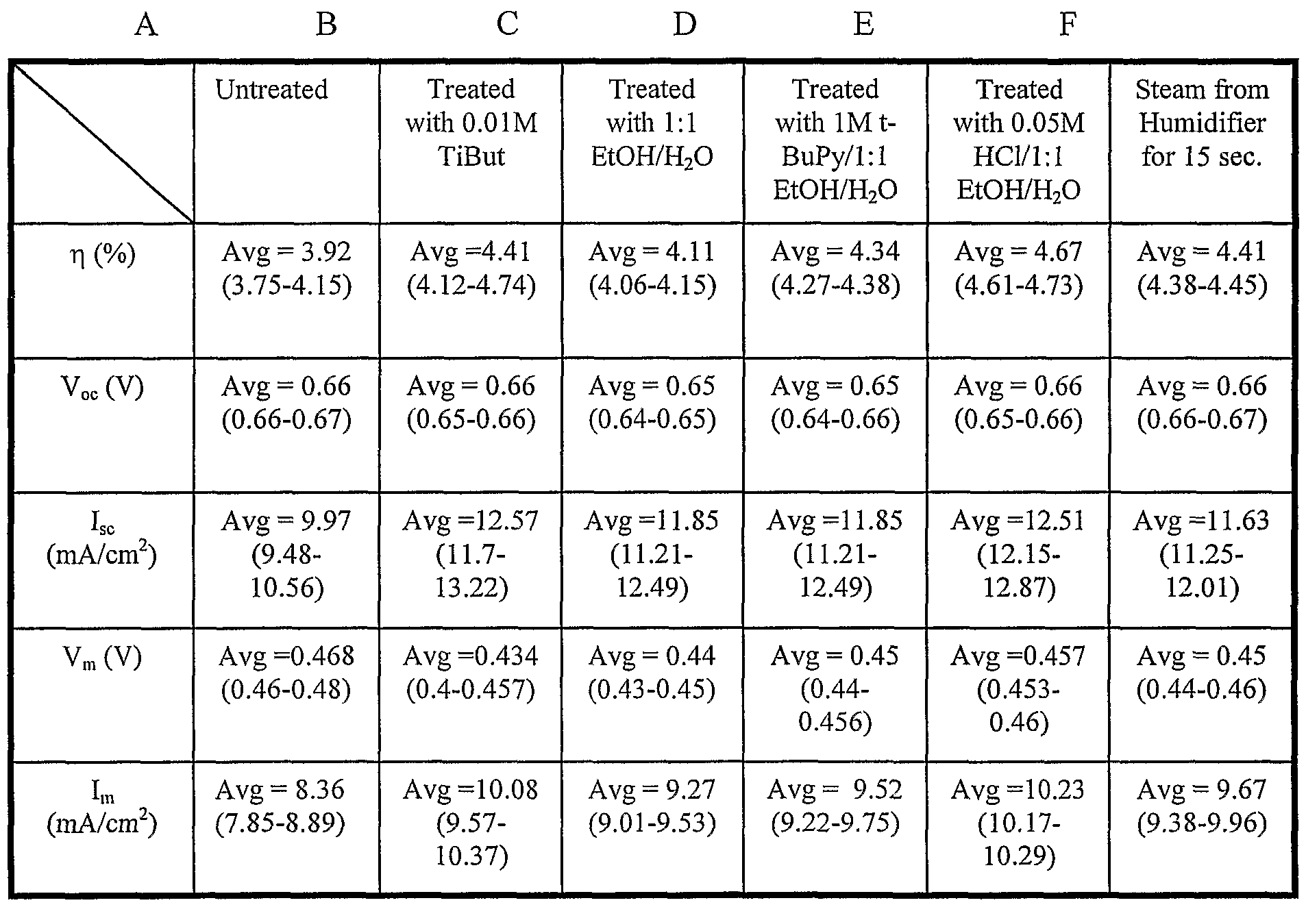


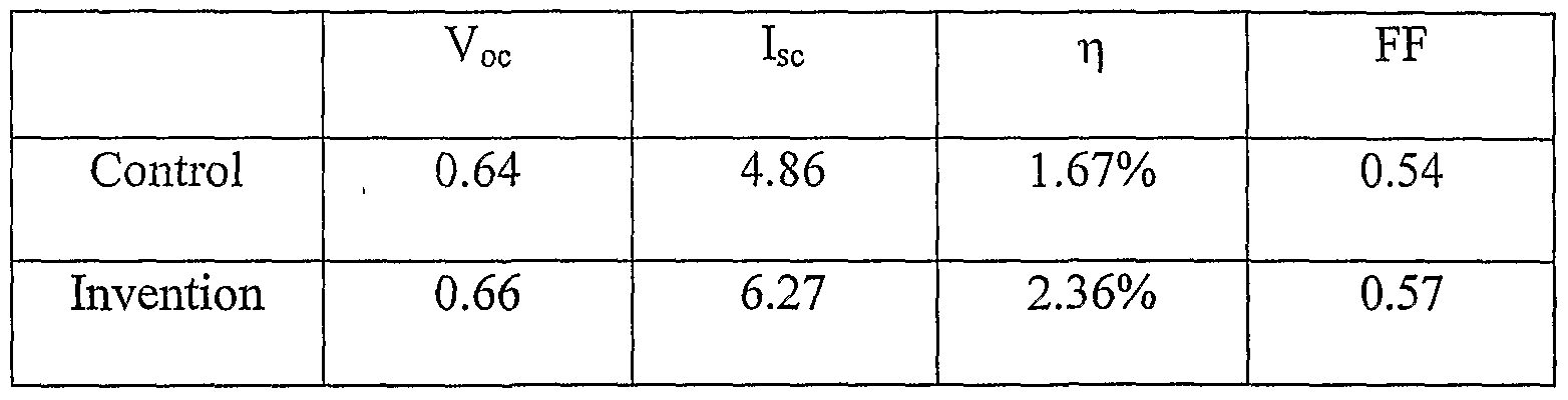

Claims
Priority Applications (3)
| Application Number | Priority Date | Filing Date | Title |
|---|---|---|---|
| CA002474494A CA2474494A1 (en) | 2002-01-25 | 2003-01-24 | Photovoltaic cell components and materials |
| JP2003564892A JP4644427B2 (en) | 2002-01-25 | 2003-01-24 | Method for bonding photosensitive nanoparticles to each other at low temperature for use in solar cells and polymer binder solution used in the method |
| EP03710755A EP1470563A2 (en) | 2002-01-25 | 2003-01-24 | Photovoltaic cell components and materials |
Applications Claiming Priority (8)
| Application Number | Priority Date | Filing Date | Title |
|---|---|---|---|
| US35169102P | 2002-01-25 | 2002-01-25 | |
| US10/057,394 | 2002-01-25 | ||
| US60/351,691 | 2002-01-25 | ||
| US10/057,394 US6706963B2 (en) | 2002-01-25 | 2002-01-25 | Photovoltaic cell interconnection |
| US36883202P | 2002-03-29 | 2002-03-29 | |
| US60/368,832 | 2002-03-29 | ||
| US40028902P | 2002-07-31 | 2002-07-31 | |
| US60/400,289 | 2002-07-31 |
Publications (2)
| Publication Number | Publication Date |
|---|---|
| WO2003065394A2 true WO2003065394A2 (en) | 2003-08-07 |
| WO2003065394A3 WO2003065394A3 (en) | 2004-04-22 |
Family
ID=27670969
Family Applications (1)
| Application Number | Title | Priority Date | Filing Date |
|---|---|---|---|
| PCT/US2003/002355 WO2003065394A2 (en) | 2002-01-25 | 2003-01-24 | Photovoltaic cell components and materials |
Country Status (6)
| Country | Link |
|---|---|
| US (2) | US6858158B2 (en) |
| EP (1) | EP1470563A2 (en) |
| JP (1) | JP4644427B2 (en) |
| CN (1) | CN1643629A (en) |
| CA (1) | CA2474494A1 (en) |
| WO (1) | WO2003065394A2 (en) |
Cited By (4)
| Publication number | Priority date | Publication date | Assignee | Title |
|---|---|---|---|---|
| EP2085985A2 (en) | 2003-04-30 | 2009-08-05 | Ecole Polytechnique Fédérale de Lausanne (EPFL) | Dye sensitized solar cell |
| WO2011141481A1 (en) | 2010-05-11 | 2011-11-17 | Bangor University | Ultra-low temperature sintering of dye-sensitised solar cells |
| WO2012054964A1 (en) * | 2010-10-26 | 2012-05-03 | Dyesol Industries Pty Ltd | An electrolyte formulation for use in photoelectrochemical devices |
| US9017573B2 (en) | 2008-08-19 | 2015-04-28 | Batlelle Japan Corporation | Organic-inorganic complexes containing a luminescent rare earth-metal nanocluster and an antenna ligand, luminescent articles, and methods of making luminescent compositions |
Families Citing this family (121)
| Publication number | Priority date | Publication date | Assignee | Title |
|---|---|---|---|---|
| US6607829B1 (en) | 1997-11-13 | 2003-08-19 | Massachusetts Institute Of Technology | Tellurium-containing nanocrystalline materials |
| US6207392B1 (en) | 1997-11-25 | 2001-03-27 | The Regents Of The University Of California | Semiconductor nanocrystal probes for biological applications and process for making and using such probes |
| US6913713B2 (en) | 2002-01-25 | 2005-07-05 | Konarka Technologies, Inc. | Photovoltaic fibers |
| US6706963B2 (en) * | 2002-01-25 | 2004-03-16 | Konarka Technologies, Inc. | Photovoltaic cell interconnection |
| US7186911B2 (en) * | 2002-01-25 | 2007-03-06 | Konarka Technologies, Inc. | Methods of scoring for fabricating interconnected photovoltaic cells |
| US20050284513A1 (en) * | 2002-08-08 | 2005-12-29 | Christoph Brabec | Chip card comprising an integrated energy converter |
| US6900382B2 (en) * | 2002-01-25 | 2005-05-31 | Konarka Technologies, Inc. | Gel electrolytes for dye sensitized solar cells |
| US7205473B2 (en) * | 2002-01-25 | 2007-04-17 | Konarka Technologies, Inc. | Photovoltaic powered multimedia greeting cards and smart cards |
| US6949400B2 (en) * | 2002-01-25 | 2005-09-27 | Konarka Technologies, Inc. | Ultrasonic slitting of photovoltaic cells and modules |
| US20030192584A1 (en) * | 2002-01-25 | 2003-10-16 | Konarka Technologies, Inc. | Flexible photovoltaic cells and modules formed using foils |
| US20030192585A1 (en) * | 2002-01-25 | 2003-10-16 | Konarka Technologies, Inc. | Photovoltaic cells incorporating rigid substrates |
| US7414188B2 (en) * | 2002-01-25 | 2008-08-19 | Konarka Technologies, Inc. | Co-sensitizers for dye sensitized solar cells |
| US7323635B2 (en) * | 2001-06-15 | 2008-01-29 | University Of Massachusetts | Photovoltaic cell |
| US7989695B2 (en) * | 2001-12-18 | 2011-08-02 | Steven Allen Carlson | Organic photovoltaic cells |
| JP4979878B2 (en) * | 2002-01-25 | 2012-07-18 | コナルカ テクノロジーズ インコーポレイテッド | Structure and material of dye-sensitized solar cell |
| WO2003065393A2 (en) * | 2002-01-25 | 2003-08-07 | Konarka Technologies, Inc. | Displays with integrated photovoltaic cells |
| WO2003065394A2 (en) * | 2002-01-25 | 2003-08-07 | Konarka Technologies, Inc. | Photovoltaic cell components and materials |
| US8507253B2 (en) * | 2002-05-13 | 2013-08-13 | Algae Systems, LLC | Photobioreactor cell culture systems, methods for preconditioning photosynthetic organisms, and cultures of photosynthetic organisms produced thereby |
| EP1576655B1 (en) * | 2002-08-15 | 2014-05-21 | Moungi G. Bawendi | Stabilized semiconductor nanocrystals |
| JP3791922B2 (en) * | 2002-09-06 | 2006-06-28 | 富士通株式会社 | Moving picture decoding apparatus and method |
| US7122481B2 (en) * | 2003-07-25 | 2006-10-17 | Intel Corporation | Sealing porous dielectrics with silane coupling reagents |
| WO2005101510A2 (en) * | 2004-04-16 | 2005-10-27 | The University Of Toledo | Light-assisted electrochemical shunt passivation for photovoltaic devices |
| US7229690B2 (en) * | 2004-07-26 | 2007-06-12 | Massachusetts Institute Of Technology | Microspheres including nanoparticles |
| KR100582552B1 (en) * | 2004-09-23 | 2006-05-23 | 한국전자통신연구원 | Method for forming nanoparticle oxide electrode of plastic-type dye-sensitized solar cells using binder-free and high viscosity nanoparticle oxide pastes |
| EP1672653B1 (en) * | 2004-12-20 | 2019-07-17 | Merck Patent GmbH | Patterned photovoltaic cell |
| US20100193768A1 (en) * | 2005-06-20 | 2010-08-05 | Illuminex Corporation | Semiconducting nanowire arrays for photovoltaic applications |
| US20090050204A1 (en) * | 2007-08-03 | 2009-02-26 | Illuminex Corporation. | Photovoltaic device using nanostructured material |
| CN101375205B (en) * | 2005-08-22 | 2012-03-28 | 科纳卡技术股份有限公司 | Displays with integrated photovoltaic cells |
| US7256140B2 (en) * | 2005-09-20 | 2007-08-14 | United Solar Ovonic Llc | Higher selectivity, method for passivating short circuit current paths in semiconductor devices |
| US20070079867A1 (en) * | 2005-10-12 | 2007-04-12 | Kethinni Chittibabu | Photovoltaic fibers |
| JP4811642B2 (en) * | 2005-10-24 | 2011-11-09 | 独立行政法人産業技術総合研究所 | Ionic gel electrolyte, dye-sensitized photoelectric conversion element and solar cell |
| KR100656367B1 (en) * | 2005-11-24 | 2006-12-13 | 한국전자통신연구원 | Composition of semiconductor electrode enable to sintering at low temperature, and dye-sensitized solar cells comprising the composition |
| GB2432723B (en) * | 2005-11-25 | 2010-12-08 | Seiko Epson Corp | Electrochemical cell and method of manufacture |
| GB2432719A (en) * | 2005-11-25 | 2007-05-30 | Seiko Epson Corp | Electrochemical cell using metal oxide dispersion |
| GB2432720A (en) * | 2005-11-25 | 2007-05-30 | Seiko Epson Corp | Electrochemical cell structure and method of fabrication |
| GB2432966A (en) * | 2005-11-25 | 2007-06-06 | Seiko Epson Corp | Dye-sensitised electrochemical cell |
| GB2432721B (en) * | 2005-11-25 | 2011-06-22 | Seiko Epson Corp | Electrochemical cell structure and method of fabrication |
| GB2432722A (en) * | 2005-11-25 | 2007-05-30 | Seiko Epson Corp | Electrochemical cell and method of manufacture |
| AU2006330627A1 (en) * | 2005-12-16 | 2007-07-05 | University Of Kansas | Nanoclusters for delivery of therapeutics |
| US8110395B2 (en) | 2006-07-10 | 2012-02-07 | Algae Systems, LLC | Photobioreactor systems and methods for treating CO2-enriched gas and producing biomass |
| GB2441178B (en) * | 2006-08-25 | 2011-08-17 | Alan Jones | Solar panel |
| US9112447B2 (en) * | 2006-11-03 | 2015-08-18 | Solera Laboratories, Inc. | Nano power cell and method of use |
| US8319092B1 (en) | 2006-11-03 | 2012-11-27 | Solera Laboratories, Inc. | Nano power cell and method of use |
| US7940447B2 (en) * | 2006-12-04 | 2011-05-10 | 3M Innovative Properties Company | Electrochromic device |
| US7764416B2 (en) * | 2006-12-04 | 2010-07-27 | 3M Innovative Properties Company | Electrochromic device based on layer by layer deposition |
| US20080128665A1 (en) * | 2006-12-04 | 2008-06-05 | 3M Innovative Properties Company | Nanoparticle based thin films |
| JP5163849B2 (en) * | 2007-01-17 | 2013-03-13 | セイコーエプソン株式会社 | Method for manufacturing photoelectric conversion element, photoelectric conversion element and electronic device |
| WO2008093113A2 (en) * | 2007-02-02 | 2008-08-07 | G24 Innovations Limited | A method of manufacturing an electrode array for photovoltaic electrochemical cell arrays |
| KR100857590B1 (en) * | 2007-02-12 | 2008-09-09 | 충남대학교산학협력단 | Method for Room Temperature Chemical Vapor Deposition on Flexible Polymer Substrates |
| KR20080079894A (en) * | 2007-02-28 | 2008-09-02 | 삼성에스디아이 주식회사 | Dye-sensitized solar cell and preparing method thereof |
| US7980024B2 (en) | 2007-04-27 | 2011-07-19 | Algae Systems, Inc. | Photobioreactor systems positioned on bodies of water |
| US8389099B1 (en) | 2007-06-01 | 2013-03-05 | Rubicon Technology, Inc. | Asymmetrical wafer configurations and method for creating the same |
| US7923341B2 (en) * | 2007-08-13 | 2011-04-12 | United Solar Ovonic Llc | Higher selectivity, method for passivating short circuit current paths in semiconductor devices |
| KR20100056552A (en) * | 2007-09-10 | 2010-05-27 | 다이솔 인더스트리즈 피티와이 엘티디 | A method for manufacturing solar cells |
| TW200915583A (en) * | 2007-09-17 | 2009-04-01 | Univ Nat Taiwan Science Tech | Photoelectric electrodes capable of absorbing solar energy, fabrication methods, and applications thereof |
| US20100304512A1 (en) * | 2007-11-30 | 2010-12-02 | University Of Toledo | System for Diagnosis and Treatment of Photovoltaic and Other Semiconductor Devices |
| JP5937300B2 (en) * | 2007-12-20 | 2016-06-22 | シーマ ナノ テック イスラエル リミティド | Transparent conductive coating with filler material |
| US8933320B2 (en) | 2008-01-18 | 2015-01-13 | Tenksolar, Inc. | Redundant electrical architecture for photovoltaic modules |
| US8212139B2 (en) | 2008-01-18 | 2012-07-03 | Tenksolar, Inc. | Thin-film photovoltaic module |
| US8748727B2 (en) | 2008-01-18 | 2014-06-10 | Tenksolar, Inc. | Flat-plate photovoltaic module |
| US8491815B1 (en) | 2008-02-07 | 2013-07-23 | Jeffrey R. Dimaio | Omnino nanocomposite crosslinked networks |
| EP2259377B1 (en) * | 2008-03-19 | 2020-06-03 | Sharp Kabushiki Kaisha | Solar cell |
| US8574944B2 (en) * | 2008-03-28 | 2013-11-05 | The University Of Toledo | System for selectively filling pin holes, weak shunts and/or scribe lines in photovoltaic devices and photovoltaic cells made thereby |
| CA2723395C (en) | 2008-05-05 | 2014-11-25 | Dow Global Technologies Inc. | Photovoltaic device assembly and method |
| WO2009137637A2 (en) * | 2008-05-09 | 2009-11-12 | Board Of Regents, The University Of Texas System | Nanoparticles and methods of making and using |
| US8357425B2 (en) * | 2008-05-30 | 2013-01-22 | Corning Incorporated | Process of making a coated substrate by crosslinking nanoparticles |
| JP5340656B2 (en) | 2008-07-02 | 2013-11-13 | シャープ株式会社 | Solar array |
| US20100055718A1 (en) * | 2008-08-29 | 2010-03-04 | Kwangyeol Lee | Nanoplate dye platform and methods of making and using the same |
| EP2352201B1 (en) | 2008-10-29 | 2018-10-17 | FUJIFILM Corporation | Dye, photoelectric conversion element and photoelectrochemical cell each comprising the dye, and process for producing dye |
| WO2010069797A1 (en) * | 2008-12-18 | 2010-06-24 | Basf Se | Electrochromic films prepared by supramolecular self-assembly |
| KR101032925B1 (en) * | 2009-03-13 | 2011-05-06 | 주식회사 티지에너지 | Method and Apparatus for Production of DSSC |
| GB0905082D0 (en) * | 2009-03-26 | 2009-05-06 | Univ Bangor | Low temperature sintering of dye-sensitised solar cells |
| US20100242483A1 (en) | 2009-03-30 | 2010-09-30 | United Technologies Corporation | Combustor for gas turbine engine |
| JP5155231B2 (en) * | 2009-03-30 | 2013-03-06 | 富士フイルム株式会社 | EL element, photosensitive material for forming conductive film, and conductive film |
| EP2443666A4 (en) | 2009-06-15 | 2013-06-05 | Tenksolar Inc | Illumination agnostic solar panel |
| US20100319759A1 (en) * | 2009-06-22 | 2010-12-23 | John Fisher | Nanostructure and methods of making the same |
| KR101369824B1 (en) | 2009-08-13 | 2014-03-07 | 다우 글로벌 테크놀로지스 엘엘씨 | A multi-layer laminate structure and manufacturing method |
| JP5524557B2 (en) | 2009-09-28 | 2014-06-18 | 富士フイルム株式会社 | Method for producing photoelectric conversion element, photoelectric conversion element, and photoelectrochemical cell |
| JP5620081B2 (en) | 2009-09-28 | 2014-11-05 | 富士フイルム株式会社 | Method for manufacturing photoelectric conversion element |
| TWI443892B (en) * | 2009-10-29 | 2014-07-01 | Ind Tech Res Inst | Method for manufacturing an electrode |
| WO2011056921A1 (en) | 2009-11-04 | 2011-05-12 | Dow Global Technologies Llc | Building integrated photovoltaic having injection molded component |
| US9416970B2 (en) | 2009-11-30 | 2016-08-16 | United Technologies Corporation | Combustor heat panel arrangement having holes offset from seams of a radially opposing heat panel |
| US20110168257A1 (en) * | 2010-01-11 | 2011-07-14 | Vladimir Kochergin | Solar Cell Structure |
| CN102834472B (en) * | 2010-02-05 | 2015-04-22 | 凯博瑞奥斯技术公司 | Photosensitive ink compositions and transparent conductors and method of using the same |
| US9773933B2 (en) | 2010-02-23 | 2017-09-26 | Tenksolar, Inc. | Space and energy efficient photovoltaic array |
| US9202954B2 (en) | 2010-03-03 | 2015-12-01 | Q1 Nanosystems Corporation | Nanostructure and photovoltaic cell implementing same |
| BR112012026335A2 (en) | 2010-03-12 | 2016-07-19 | Dow Global Technologies Llc | photovoltaic device |
| WO2012058271A2 (en) | 2010-10-27 | 2012-05-03 | Pixelligent Technologies, Llc | Synthesis, capping and dispersion of nanocrystals |
| CN102947218B (en) | 2010-04-23 | 2016-05-11 | 皮瑟莱根特科技有限责任公司 | Synthetic, the block of nanocrystal and disperseing |
| KR20110133717A (en) * | 2010-06-07 | 2011-12-14 | 삼성전자주식회사 | Organic solar cell and method of manufacturing the same |
| US9299861B2 (en) | 2010-06-15 | 2016-03-29 | Tenksolar, Inc. | Cell-to-grid redundandt photovoltaic system |
| EP2603932A4 (en) | 2010-08-10 | 2017-07-05 | Tenksolar, Inc. | Highly efficient solar arrays |
| US9147788B2 (en) | 2010-09-07 | 2015-09-29 | Dow Global Technologies Llc | Photovoltaic cell assembly |
| EP2617065A2 (en) | 2010-09-17 | 2013-07-24 | Dow Global Technologies LLC | Improved photovoltaic cell assembly and method |
| JP5898216B2 (en) | 2010-09-30 | 2016-04-06 | ダウ グローバル テクノロジーズ エルエルシー | Improved connector and electronic circuit assembly for improved wet insulation resistance |
| EP2652797A1 (en) | 2010-12-17 | 2013-10-23 | Dow Global Technologies LLC | Improved photovoltaic device |
| EP2652799A2 (en) | 2010-12-17 | 2013-10-23 | Dow Global Technologies LLC | Improved photovoltaic device |
| JP5643440B2 (en) | 2010-12-17 | 2014-12-17 | ダウ グローバル テクノロジーズ エルエルシー | Improved photovoltaic device |
| US9564545B2 (en) | 2011-03-22 | 2017-02-07 | Dow Global Technologies Llc | Photovoltaic sheathing element with one or more tabs |
| BR112013024180A2 (en) | 2011-03-22 | 2016-12-13 | Dow Global Technologies Llc | photovoltaic roof element kit, installation method and kit |
| BR112013024182A2 (en) | 2011-03-22 | 2016-12-13 | Dow Global Technologies Llc | set and arrangement of sets |
| CN102290246B (en) * | 2011-06-20 | 2012-10-17 | 华东师范大学 | Polymer gel electrolyte and preparation method thereof |
| AU2012282810A1 (en) | 2011-07-11 | 2014-01-23 | Cornell University | Ionic-liquid nanoscale ionic material (IL-NIM) compositions, methods and applications |
| US9537033B2 (en) | 2011-07-29 | 2017-01-03 | Dow Global Technologies Llc | Interface system and method for photovoltaic cladding to standard cladding |
| JP5673477B2 (en) * | 2011-10-06 | 2015-02-18 | コニカミノルタ株式会社 | Photoelectric conversion element |
| US9359689B2 (en) | 2011-10-26 | 2016-06-07 | Pixelligent Technologies, Llc | Synthesis, capping and dispersion of nanocrystals |
| US9082911B2 (en) | 2013-01-28 | 2015-07-14 | Q1 Nanosystems Corporation | Three-dimensional metamaterial device with photovoltaic bristles |
| JP5972811B2 (en) | 2013-02-22 | 2016-08-17 | 富士フイルム株式会社 | Photoelectric conversion element, method for producing photoelectric conversion element, and dye-sensitized solar cell |
| US9954126B2 (en) | 2013-03-14 | 2018-04-24 | Q1 Nanosystems Corporation | Three-dimensional photovoltaic devices including cavity-containing cores and methods of manufacture |
| US20140264998A1 (en) | 2013-03-14 | 2014-09-18 | Q1 Nanosystems Corporation | Methods for manufacturing three-dimensional metamaterial devices with photovoltaic bristles |
| WO2014201418A2 (en) * | 2013-06-14 | 2014-12-18 | OneSun, LLC | Multi-layer mesoporous coatings for conductive surfaces, and methods of preparing thereof |
| WO2015002285A1 (en) * | 2013-07-05 | 2015-01-08 | 積水化学工業株式会社 | Method for manufacturing semiconductor film, raw-material particles for semiconductor film manufacture, semiconductor film, photoelectrode, and dye-sensitized solar cell |
| JP6063361B2 (en) * | 2013-09-05 | 2017-01-18 | 富士フイルム株式会社 | Photoelectric conversion element, dye-sensitized solar cell, and electron transfer accelerator for photoelectric conversion element |
| EP3113199B1 (en) * | 2014-02-26 | 2018-11-21 | Sumitomo Osaka Cement Co., Ltd. | Porous semiconductor layer, porous-semiconductor-layer paste, and dye-sensitized solar cell |
| WO2015199857A1 (en) | 2014-06-26 | 2015-12-30 | Dow Global Technologies Llc | Photovoltaic devices with sealant layer and laminate assembly for improved wet insulation resistance |
| JP6505469B2 (en) * | 2015-02-25 | 2019-04-24 | 積水化学工業株式会社 | Method of manufacturing photo electrode |
| WO2018035281A1 (en) | 2016-08-17 | 2018-02-22 | North Carolina State University | Northern-southern route to synthesis of bacteriochlorins |
| US10782014B2 (en) | 2016-11-11 | 2020-09-22 | Habib Technologies LLC | Plasmonic energy conversion device for vapor generation |
| WO2018102252A1 (en) | 2016-11-30 | 2018-06-07 | North Carolina State University | Methods for making bacteriochlorin macrocycles comprising an annulated isocyclic ring and related compounds |
| JP6716489B2 (en) * | 2017-04-03 | 2020-07-01 | 三菱重工業株式会社 | Method for evaluating structure used in nuclide conversion reaction, evaluation apparatus, apparatus for manufacturing structure including the same, and nuclide conversion system |
| CN113363473B (en) * | 2021-03-19 | 2022-03-18 | 万向一二三股份公司 | Preparation method of high-first-efficiency SiO graphite composite negative electrode material |
Citations (3)
| Publication number | Priority date | Publication date | Assignee | Title |
|---|---|---|---|---|
| WO1993018532A1 (en) * | 1992-03-11 | 1993-09-16 | Ecole Polytechnique Federale De Lausanne (Epfl) | Process for producing a photoelectrochemical cell and cell thus produced |
| WO1996000198A1 (en) * | 1994-06-23 | 1996-01-04 | Bernd Penth | Production of ceramic layers and their use |
| WO2001025316A1 (en) * | 1999-10-05 | 2001-04-12 | Commonwealth Scientific And Industrial Research Organisation | Three dimensional array films |
Family Cites Families (126)
| Publication number | Priority date | Publication date | Assignee | Title |
|---|---|---|---|---|
| US3206831A (en) * | 1965-09-21 | Miniature photocells and method op making the same | ||
| US3037122A (en) * | 1958-07-23 | 1962-05-29 | West Pont Mfg Company | Multiple photocells |
| US3069487A (en) * | 1960-01-04 | 1962-12-18 | West Point Mfg Co | Miniature photocells and method of making the same |
| US3206832A (en) * | 1960-01-04 | 1965-09-21 | West Point Mfg Co | Miniature photocell array and method of making the same |
| CA918297A (en) * | 1969-09-24 | 1973-01-02 | Tanimura Shigeru | Semiconductor device and method of making |
| US3872047A (en) * | 1972-12-04 | 1975-03-18 | Hana Jandourek | Composition and method for improving adherence of polymeric materials to substrates |
| US3969163A (en) * | 1974-09-19 | 1976-07-13 | Texas Instruments Incorporated | Vapor deposition method of forming low cost semiconductor solar cells including reconstitution of the reacted gases |
| US3984256A (en) * | 1975-04-25 | 1976-10-05 | Nasa | Photovoltaic cell array |
| US4080488A (en) * | 1976-11-11 | 1978-03-21 | Optel Corporation | Dye-titanium dioxide photogalvanic cell |
| US4243432A (en) | 1978-09-25 | 1981-01-06 | Photon Power, Inc. | Solar cell array |
| US4232108A (en) | 1979-05-01 | 1980-11-04 | E. I. Du Pont De Nemours And Company | Marking transfer sheets |
| DE3013991A1 (en) * | 1980-04-11 | 1981-10-15 | Bayer Ag, 5090 Leverkusen | LARGE-SCALE PHOTOVOLTAIC CELL |
| US4295329A (en) | 1980-06-10 | 1981-10-20 | E. I. Du Pont De Nemours And Company | Cobulked continuous filament heather yarn method and product |
| US4436558A (en) * | 1980-12-15 | 1984-03-13 | The United States Of America As Represented By The United States Department Of Energy | Electrochemical photovoltaic cell having ternary alloy film |
| US4500880A (en) | 1981-07-06 | 1985-02-19 | Motorola, Inc. | Real time, computer-driven retail pricing display system |
| US4492743A (en) * | 1982-10-15 | 1985-01-08 | Standard Oil Company (Indiana) | Multilayer photoelectrodes and photovoltaic cells |
| JPS59125670A (en) | 1983-01-06 | 1984-07-20 | Toppan Printing Co Ltd | Solar battery |
| JPS59144177A (en) | 1983-02-07 | 1984-08-18 | Seiko Epson Corp | Solar battery |
| US4589194A (en) | 1983-12-29 | 1986-05-20 | Atlantic Richfield Company | Ultrasonic scribing of thin film solar cells |
| US4684537A (en) * | 1984-04-30 | 1987-08-04 | R. E. Stiftung | Process for the sensitization of an oxidation/reduction photocatalyst, and photocatalyst thus obtained |
| US4937586A (en) | 1986-09-22 | 1990-06-26 | Stevens John K | Radio broadcast communication systems with multiple loop antennas |
| US4821291A (en) | 1986-09-22 | 1989-04-11 | Stevens John K | Improvements in or relating to signal communication systems |
| DE8700578U1 (en) * | 1987-01-13 | 1988-11-10 | Hoegl, Helmut, Dr., 8023 Pullach, De | |
| US4962466A (en) | 1987-03-27 | 1990-10-09 | Viscom Systems, Inc. | Electronic product information display system |
| US4872925A (en) * | 1987-10-29 | 1989-10-10 | Glasstech, Inc. | Photovoltaic cell fabrication method and panel made thereby |
| CH674596A5 (en) * | 1988-02-12 | 1990-06-15 | Sulzer Ag | |
| ES2080313T3 (en) * | 1990-04-17 | 1996-02-01 | Ecole Polytech | PHOTOVOLTAIC CELLS. |
| US5273911A (en) | 1991-03-07 | 1993-12-28 | Mitsubishi Denki Kabushiki Kaisha | Method of producing a thin-film solar cell |
| US5178685A (en) * | 1991-06-11 | 1993-01-12 | Mobil Solar Energy Corporation | Method for forming solar cell contacts and interconnecting solar cells |
| CH686206A5 (en) * | 1992-03-26 | 1996-01-31 | Asulab Sa | Cellule photoelectrochimique regeneratrice transparent. |
| US5248349A (en) | 1992-05-12 | 1993-09-28 | Solar Cells, Inc. | Process for making photovoltaic devices and resultant product |
| DE4221084A1 (en) | 1992-06-26 | 1994-01-05 | Esw Quinten Gmbh | Photovoltaic cell array - comprises series connected cell rows between two glass panes |
| FR2694451B1 (en) * | 1992-07-29 | 1994-09-30 | Asulab Sa | Photovoltaic cell. |
| US5331183A (en) * | 1992-08-17 | 1994-07-19 | The Regents Of The University Of California | Conjugated polymer - acceptor heterojunctions; diodes, photodiodes, and photovoltaic cells |
| GB9217811D0 (en) * | 1992-08-21 | 1992-10-07 | Graetzel Michael | Organic compounds |
| GB9309246D0 (en) | 1993-05-05 | 1993-06-16 | Esselte Meto Int Gmbh | Rechargeable shelf edge tag |
| US5385614A (en) * | 1993-05-06 | 1995-01-31 | Photon Energy Inc. | Series interconnected photovoltaic cells and method for making same |
| DE9308513U1 (en) | 1993-05-25 | 1994-01-20 | Hoffmann Thomas | Arrangement for a series connection of photoelectrochemical (PEC) solar cells |
| EP0641029A3 (en) * | 1993-08-27 | 1998-01-07 | Twin Solar-Technik Entwicklungs-GmbH | Element for a photovoltaic solar cell and process of fabrication as well as its arrangement in a solar cell |
| US5343519A (en) | 1993-09-07 | 1994-08-30 | Peter Feldman | Autodialer with pin feature |
| US5415688A (en) * | 1993-09-20 | 1995-05-16 | Ameron, Inc. | Water-borne polysiloxane/polysilicate binder |
| JP3363544B2 (en) * | 1993-10-27 | 2003-01-08 | 三井化学株式会社 | Method for crosslinking semiconductor ultrafine particles and semiconductor ultrafine particle crosslinked material |
| DE69416428T2 (en) * | 1993-12-29 | 1999-09-16 | Ecole Polytech | PHOTOELECTROCHEMICAL CELL AND ELECTROLYTE FOR THIS CELL |
| FR2715508B1 (en) * | 1994-01-21 | 1996-03-29 | Renata Ag | Primary or secondary electrochemical generator with nanoparticulate electrode. |
| US5437736A (en) * | 1994-02-15 | 1995-08-01 | Cole; Eric D. | Semiconductor fiber solar cells and modules |
| US5454879A (en) * | 1994-03-17 | 1995-10-03 | Bolger; Stephen R. | Helically grown monolithic high voltage photovoltaic devices and method therefor |
| AU697111B2 (en) * | 1994-05-02 | 1998-09-24 | Ecole Polytechnique Federale De Lausanne | Phosphonated polypyridyl compounds and their complexes |
| US5474621A (en) * | 1994-09-19 | 1995-12-12 | Energy Conversion Devices, Inc. | Current collection system for photovoltaic cells |
| US5637156A (en) * | 1994-09-22 | 1997-06-10 | Semiconductor Energy Laboratory Co., Ltd. | Resin Composition and an electronic device using the same |
| DE19680102B4 (en) | 1995-03-23 | 2007-04-12 | Ecole polytechnique fédérale de Lausanne (EPFL) | Method for producing a long-term stable module of photoelectric cells |
| US5751257A (en) | 1995-04-28 | 1998-05-12 | Teletransactions, Inc. | Programmable shelf tag and method for changing and updating shelf tag information |
| DE19514156A1 (en) | 1995-04-15 | 1996-10-24 | Heidelberger Druckmasch Ag | Photochemical cell |
| DE19528401A1 (en) | 1995-08-02 | 1997-02-06 | Fraunhofer Ges Forschung | Photoelectrochemical cell system giving increased voltage without external connection - has cells with transparent conducting layer, semiconducting layer, polymeric solid electrolyte contg. redox system and conducting layer, connected directly in series |
| DE19533850A1 (en) * | 1995-09-13 | 1997-03-27 | Hoechst Ag | Photovoltaic cell |
| EP0852804B1 (en) * | 1995-09-25 | 1999-10-27 | Ecole Polytechnique Federale De Lausanne | Process for manufacturing an electrode for an electrochemical device |
| AU728725B2 (en) * | 1995-10-31 | 2001-01-18 | Ecole Polytechnique Federale De Lausanne | A battery of photovoltaic cells and process for manufacturing the same |
| US5641362A (en) * | 1995-11-22 | 1997-06-24 | Ebara Solar, Inc. | Structure and fabrication process for an aluminum alloy junction self-aligned back contact silicon solar cell |
| JP4024858B2 (en) * | 1996-03-15 | 2007-12-19 | エコール ポリテクニーク フェデラル ドゥ ローザンヌ | Electrochromophoric compounds and photosensitive compounds |
| JP3292441B2 (en) | 1996-03-21 | 2002-06-17 | 松下電器産業株式会社 | Electrode containing organic disulfide compound and method for producing the same |
| DE19710685B4 (en) * | 1997-03-14 | 2005-12-01 | Fraunhofer-Gesellschaft zur Förderung der angewandten Forschung e.V. | Material containing nanocrystalline particles, process for its preparation and its use |
| DE19711713A1 (en) * | 1997-03-20 | 1998-10-01 | Hoechst Ag | Photovoltaic cell |
| US6215060B1 (en) * | 1997-04-21 | 2001-04-10 | Canon Kabushiki Kaisha | Method for manufacturing a solar cell module |
| AU743120B2 (en) * | 1997-05-07 | 2002-01-17 | Ecole Polytechnique Federale De Lausanne | Metal complex photosensitizer and photovoltaic cell |
| EP0887817B1 (en) * | 1997-06-23 | 2008-05-28 | Sharp Kabushiki Kaisha | Photoelectric material using organic photosensitising dyes and manufacturing method thereof |
| CA2292627C (en) * | 1997-06-23 | 2005-04-26 | Micrilor, Inc. | Wireless communications system for transmitting and receiving data with increased data rates and robustness |
| US7150881B2 (en) * | 1997-06-26 | 2006-12-19 | Mylan Technologies, Inc. | Adhesive mixture for transdermal delivery of highly plasticizing drugs |
| US6013871A (en) * | 1997-07-02 | 2000-01-11 | Curtin; Lawrence F. | Method of preparing a photovoltaic device |
| US5881083A (en) * | 1997-07-03 | 1999-03-09 | The Regents Of The University Of California | Conjugated polymers as materials for solid state laser |
| JPH11144773A (en) * | 1997-09-05 | 1999-05-28 | Fuji Photo Film Co Ltd | Photoelectric converting element and light regenerating type photoelectric chemical battery |
| US5986206A (en) * | 1997-12-10 | 1999-11-16 | Nanogram Corporation | Solar cell |
| WO1999048136A2 (en) | 1998-03-13 | 1999-09-23 | Steffen Keller | Solar cell arrangement |
| US6175075B1 (en) * | 1998-04-21 | 2001-01-16 | Canon Kabushiki Kaisha | Solar cell module excelling in reliability |
| US5906004A (en) * | 1998-04-29 | 1999-05-25 | Motorola, Inc. | Textile fabric with integrated electrically conductive fibers and clothing fabricated thereof |
| US6080690A (en) * | 1998-04-29 | 2000-06-27 | Motorola, Inc. | Textile fabric with integrated sensing device and clothing fabricated thereof |
| JPH11312541A (en) * | 1998-04-30 | 1999-11-09 | Minolta Co Ltd | Solar cell |
| US6444189B1 (en) | 1998-05-18 | 2002-09-03 | E. I. Du Pont De Nemours And Company | Process for making and using titanium oxide particles |
| US6075203A (en) * | 1998-05-18 | 2000-06-13 | E. I. Du Pont Nemours And Company | Photovoltaic cells |
| AU753205B2 (en) * | 1998-05-29 | 2002-10-10 | Catalysts & Chemicals Industries Co., Ltd. | Method of manufacturing photoelectric cell and oxide semiconductor for photoelectric cell |
| US6121540A (en) * | 1998-06-30 | 2000-09-19 | Kabushiki Kaisha Toshiba | Composite material substrate for solar cells, and solar cell |
| US6077722A (en) * | 1998-07-14 | 2000-06-20 | Bp Solarex | Producing thin film photovoltaic modules with high integrity interconnects and dual layer contacts |
| JP2997773B1 (en) * | 1998-07-15 | 2000-01-11 | 工業技術院長 | Metal complexes, oxide semiconductor electrodes and solar cells useful as sensitizers |
| AU1311900A (en) * | 1998-10-09 | 2000-05-01 | Trustees Of Columbia University In The City Of New York, The | Solid-state photoelectric device |
| JP2000196192A (en) * | 1998-12-24 | 2000-07-14 | Sony Corp | Fine particle structure body, light-emitting device, and method for manufacturing fine particle structure body |
| SE518454C2 (en) | 1999-01-15 | 2002-10-08 | Forskarpatent I Uppsala Ab | Method for making an electrochemical cell and electrochemical cell |
| DE19909417A1 (en) | 1999-03-04 | 2000-11-16 | Manfred Baumgaertner | Solar collector made of fibers |
| JP3966638B2 (en) * | 1999-03-19 | 2007-08-29 | 株式会社東芝 | Multicolor dye-sensitized transparent semiconductor electrode member and production method thereof, multicolor dye-sensitized solar cell, and display element |
| DE60034840T3 (en) * | 1999-03-23 | 2011-02-24 | Kaneka Corp., Osaka-shi | Photovoltaic module |
| EP1041649A1 (en) | 1999-03-29 | 2000-10-04 | ANTEC Solar GmbH | Method of manufacturing a tin film solar module and an apparatus for cutting |
| DE19915223A1 (en) * | 1999-04-03 | 2000-10-05 | Forschungszentrum Juelich Gmbh | Photovoltaic solar cell and its manufacture by covalent growth of one phase, generating charge carrier pair |
| US6291763B1 (en) * | 1999-04-06 | 2001-09-18 | Fuji Photo Film Co., Ltd. | Photoelectric conversion device and photo cell |
| JP2000294306A (en) | 1999-04-06 | 2000-10-20 | Fuji Photo Film Co Ltd | Photoelectric converting element and photoelectric chemical battery |
| AUPP967799A0 (en) | 1999-04-09 | 1999-05-06 | Sustainable Technologies Australia Ltd | Methods to implement sealing and electrical connections to single cell and multi-cell regenerative photovoltaic photoelectrochemical devices |
| WO2000076660A1 (en) | 1999-06-15 | 2000-12-21 | Ppg Industries Ohio, Inc. | Fiber glass carrier having increased surface area and photo-active matrices formed therefrom |
| US6580026B1 (en) | 1999-06-30 | 2003-06-17 | Catalysts & Chemicals Industries Co., Ltd. | Photovoltaic cell |
| JP4292634B2 (en) * | 1999-07-21 | 2009-07-08 | 凸版印刷株式会社 | Method for manufacturing antireflection laminate |
| EP1075005B1 (en) * | 1999-08-04 | 2006-04-26 | Fuji Photo Film Co., Ltd. | Electrolyte composition, and photo-electro-chemical cell |
| JP2001085076A (en) * | 1999-09-10 | 2001-03-30 | Fuji Photo Film Co Ltd | Photoelectric transducer and photocell |
| AU739381B2 (en) | 1999-09-24 | 2001-10-11 | Kabushiki Kaisha Toshiba | Electrolyte composition, photosensitized solar cell using said electrolyte composition, and method of manufacturing photosensitized solar cell |
| EP1089305B1 (en) | 1999-09-29 | 2008-02-06 | FUJIFILM Corporation | Electrolyte composition, photoelectric conversion device and photo-electrochemical cell |
| JP2001148491A (en) * | 1999-11-19 | 2001-05-29 | Fuji Xerox Co Ltd | Photoelectric conversion element |
| JP2001160425A (en) * | 1999-12-02 | 2001-06-12 | Japan Gore Tex Inc | Optical semiconductor electrode and its manufacturing method |
| JP4414036B2 (en) * | 1999-12-27 | 2010-02-10 | シャープ株式会社 | Method for producing dye-sensitized solar cell |
| JP4477729B2 (en) * | 2000-01-19 | 2010-06-09 | シャープ株式会社 | Photoelectric conversion element and solar cell using the same |
| US6479745B2 (en) * | 2000-01-26 | 2002-11-12 | Sharp Kabushiki Kaisha | Dye-sensitized solar cell and method of manufacturing the same |
| JP4439672B2 (en) * | 2000-04-10 | 2010-03-24 | 株式会社日本触媒 | Surface-modified inorganic fine particles and surface modification method of inorganic fine particles |
| US6913713B2 (en) * | 2002-01-25 | 2005-07-05 | Konarka Technologies, Inc. | Photovoltaic fibers |
| US6949400B2 (en) * | 2002-01-25 | 2005-09-27 | Konarka Technologies, Inc. | Ultrasonic slitting of photovoltaic cells and modules |
| US20030192584A1 (en) * | 2002-01-25 | 2003-10-16 | Konarka Technologies, Inc. | Flexible photovoltaic cells and modules formed using foils |
| US7022910B2 (en) * | 2002-03-29 | 2006-04-04 | Konarka Technologies, Inc. | Photovoltaic cells utilizing mesh electrodes |
| US7414188B2 (en) * | 2002-01-25 | 2008-08-19 | Konarka Technologies, Inc. | Co-sensitizers for dye sensitized solar cells |
| US6706963B2 (en) * | 2002-01-25 | 2004-03-16 | Konarka Technologies, Inc. | Photovoltaic cell interconnection |
| US20030192585A1 (en) * | 2002-01-25 | 2003-10-16 | Konarka Technologies, Inc. | Photovoltaic cells incorporating rigid substrates |
| US7186911B2 (en) * | 2002-01-25 | 2007-03-06 | Konarka Technologies, Inc. | Methods of scoring for fabricating interconnected photovoltaic cells |
| US7205473B2 (en) * | 2002-01-25 | 2007-04-17 | Konarka Technologies, Inc. | Photovoltaic powered multimedia greeting cards and smart cards |
| US6900382B2 (en) * | 2002-01-25 | 2005-05-31 | Konarka Technologies, Inc. | Gel electrolytes for dye sensitized solar cells |
| US20020042343A1 (en) | 2000-05-16 | 2002-04-11 | Kansai Paint Co., Ltd. | Coating composition for forming titanium oxide film, process for forming titanium oxide film and photocatalyst |
| EP1209708B1 (en) | 2000-11-24 | 2007-01-17 | Sony Deutschland GmbH | Hybrid solar cells with thermal deposited semiconductive oxide layer |
| US6580027B2 (en) | 2001-06-11 | 2003-06-17 | Trustees Of Princeton University | Solar cells using fullerenes |
| US7323635B2 (en) * | 2001-06-15 | 2008-01-29 | University Of Massachusetts | Photovoltaic cell |
| US7126054B2 (en) * | 2001-06-28 | 2006-10-24 | Kabushiki Kaisha Toshiba | Raw material kit for electrolytic composition, electrolytic composition, and dye-sensitized solar cell |
| US6656990B2 (en) * | 2001-07-11 | 2003-12-02 | Corning Incorporated | Curable high refractive index compositions |
| JP3735570B2 (en) * | 2001-12-28 | 2006-01-18 | 株式会社東芝 | Raw material kit for electrolyte composition, electrolyte composition for gel electrolyte of photosensitized solar cell, photosensitized solar cell, and method for producing photosensitized solar cell |
| JP4979878B2 (en) * | 2002-01-25 | 2012-07-18 | コナルカ テクノロジーズ インコーポレイテッド | Structure and material of dye-sensitized solar cell |
| WO2003065394A2 (en) * | 2002-01-25 | 2003-08-07 | Konarka Technologies, Inc. | Photovoltaic cell components and materials |
| WO2003065393A2 (en) * | 2002-01-25 | 2003-08-07 | Konarka Technologies, Inc. | Displays with integrated photovoltaic cells |
| KR20030065957A (en) * | 2002-02-02 | 2003-08-09 | 한국전자통신연구원 | Dye-sensitized solar cells including polymer electrolyte gel containing poly(vinylidene fluoride) |
-
2003
- 2003-01-24 WO PCT/US2003/002355 patent/WO2003065394A2/en not_active Application Discontinuation
- 2003-01-24 CN CNA038067684A patent/CN1643629A/en active Pending
- 2003-01-24 US US10/350,913 patent/US6858158B2/en not_active Expired - Lifetime
- 2003-01-24 JP JP2003564892A patent/JP4644427B2/en not_active Expired - Fee Related
- 2003-01-24 EP EP03710755A patent/EP1470563A2/en not_active Withdrawn
- 2003-01-24 CA CA002474494A patent/CA2474494A1/en not_active Abandoned
-
2004
- 2004-08-13 US US10/918,493 patent/US7094441B2/en not_active Expired - Lifetime
Patent Citations (3)
| Publication number | Priority date | Publication date | Assignee | Title |
|---|---|---|---|---|
| WO1993018532A1 (en) * | 1992-03-11 | 1993-09-16 | Ecole Polytechnique Federale De Lausanne (Epfl) | Process for producing a photoelectrochemical cell and cell thus produced |
| WO1996000198A1 (en) * | 1994-06-23 | 1996-01-04 | Bernd Penth | Production of ceramic layers and their use |
| WO2001025316A1 (en) * | 1999-10-05 | 2001-04-12 | Commonwealth Scientific And Industrial Research Organisation | Three dimensional array films |
Non-Patent Citations (2)
| Title |
|---|
| BLUM Y D ET AL: "Nanocomposites by covalent bonding between inorganic nanoparticles and polymers" SYNTHESIS, FUNCTIONAL PROPERTIES AND APPLICATIONS OF NANOSTRUCTURES. SYMPOSIUM (MATERIALS RESEARCH SOCIETY SYMPOSIUM PROCEEDINGS VOL.676), SYNTHESIS, FUNCTIONAL PROPERTIES AND APPLICATIONS OF NANOSTRUCTURES. SYMPOSIUM, SAN FRANCISCO, CA, USA, 17-20 A, pages Y1.8.1-6, XP008021281 2002, Warrendale, PA, USA, Mater. Res. Soc, USA ISBN: 1-55899-612-5 * |
| NAZEERUDDIN M K ET AL: "CONVERSION OF LIGHT INTO ELECTRICITY WITH TRINUCLEAR RUTHENIUM COMPLEXES ADSORBED ON TEXTURED TIO2 FILMS" HELVETICA CHIMICA ACTA, VERLAG HELVETICA CHIMICA ACTA. BASEL, CH, vol. 73, 1990, pages 1788-1803, XP000828141 ISSN: 0018-019X * |
Cited By (5)
| Publication number | Priority date | Publication date | Assignee | Title |
|---|---|---|---|---|
| EP2085985A2 (en) | 2003-04-30 | 2009-08-05 | Ecole Polytechnique Fédérale de Lausanne (EPFL) | Dye sensitized solar cell |
| US9337435B2 (en) | 2003-04-30 | 2016-05-10 | Ecole Polytechnique Federal De Lausanne (Epfl) | Dye sensitized solar cell |
| US9017573B2 (en) | 2008-08-19 | 2015-04-28 | Batlelle Japan Corporation | Organic-inorganic complexes containing a luminescent rare earth-metal nanocluster and an antenna ligand, luminescent articles, and methods of making luminescent compositions |
| WO2011141481A1 (en) | 2010-05-11 | 2011-11-17 | Bangor University | Ultra-low temperature sintering of dye-sensitised solar cells |
| WO2012054964A1 (en) * | 2010-10-26 | 2012-05-03 | Dyesol Industries Pty Ltd | An electrolyte formulation for use in photoelectrochemical devices |
Also Published As
| Publication number | Publication date |
|---|---|
| JP2005516365A (en) | 2005-06-02 |
| WO2003065394A3 (en) | 2004-04-22 |
| US7094441B2 (en) | 2006-08-22 |
| CA2474494A1 (en) | 2003-08-07 |
| CN1643629A (en) | 2005-07-20 |
| EP1470563A2 (en) | 2004-10-27 |
| JP4644427B2 (en) | 2011-03-02 |
| US20040025934A1 (en) | 2004-02-12 |
| US20050011550A1 (en) | 2005-01-20 |
| US6858158B2 (en) | 2005-02-22 |
Similar Documents
| Publication | Publication Date | Title |
|---|---|---|
| US7094441B2 (en) | Low temperature interconnection of nanoparticles | |
| US7414188B2 (en) | Co-sensitizers for dye sensitized solar cells | |
| US7572974B2 (en) | Gel electrolytes for dye sensitized solar cells | |
| US20050019414A1 (en) | Low temperature interconnection of nanoparticles | |
| US7894694B2 (en) | Photovoltaic fibers | |
| US8071874B2 (en) | Photovoltaic cells incorporating rigid substrates | |
| EP1606845B1 (en) | Photovoltaic cells utilizing mesh electrodes | |
| US6924427B2 (en) | Wire interconnects for fabricating interconnected photovoltaic cells | |
| US7186911B2 (en) | Methods of scoring for fabricating interconnected photovoltaic cells | |
| US20070079867A1 (en) | Photovoltaic fibers | |
| US20070251570A1 (en) | Photovoltaic cells utilizing mesh electrodes | |
| US20030192584A1 (en) | Flexible photovoltaic cells and modules formed using foils | |
| WO2003065471A2 (en) | Photovoltaic fibers |
Legal Events
| Date | Code | Title | Description |
|---|---|---|---|
| AK | Designated states |
Kind code of ref document: A2 Designated state(s): AE AG AL AM AT AU AZ BA BB BG BR BY BZ CA CH CN CO CR CU CZ DE DK DM DZ EC EE ES FI GB GD GE GH GM HR HU ID IL IN IS JP KE KG KP KR KZ LC LK LR LS LT LU LV MA MD MG MK MN MW MX MZ NO NZ OM PH PL PT RO RU SC SD SE SG SK SL TJ TM TN TR TT TZ UA UG UZ VC VN YU ZA ZM ZW |
|
| AL | Designated countries for regional patents |
Kind code of ref document: A2 Designated state(s): GH GM KE LS MW MZ SD SL SZ TZ UG ZM ZW AM AZ BY KG KZ MD RU TJ TM AT BE BG CH CY CZ DE DK EE ES FI FR GB GR HU IE IT LU MC NL PT SE SI SK TR BF BJ CF CG CI CM GA GN GQ GW ML MR NE SN TD TG |
|
| 121 | Ep: the epo has been informed by wipo that ep was designated in this application | ||
| WWE | Wipo information: entry into national phase |
Ref document number: 2474494 Country of ref document: CA |
|
| WWE | Wipo information: entry into national phase |
Ref document number: 2003564892 Country of ref document: JP |
|
| WWE | Wipo information: entry into national phase |
Ref document number: 2003710755 Country of ref document: EP |
|
| WWE | Wipo information: entry into national phase |
Ref document number: 20038067684 Country of ref document: CN |
|
| WWP | Wipo information: published in national office |
Ref document number: 2003710755 Country of ref document: EP |
|
| WWW | Wipo information: withdrawn in national office |
Ref document number: 2003710755 Country of ref document: EP |