WO2004038070A2 - Pulse reverse electrolysis of acidic copper electroplating solutions - Google Patents

Pulse reverse electrolysis of acidic copper electroplating solutions Download PDF

Info

Publication number
WO2004038070A2
WO2004038070A2 PCT/US2003/024498 US0324498W WO2004038070A2 WO 2004038070 A2 WO2004038070 A2 WO 2004038070A2 US 0324498 W US0324498 W US 0324498W WO 2004038070 A2 WO2004038070 A2 WO 2004038070A2
Authority
WO
WIPO (PCT)
Prior art keywords
copper
plating
pulse
concentration
polyether
Prior art date
Application number
PCT/US2003/024498
Other languages
French (fr)
Other versions
WO2004038070A3 (en
Inventor
Roderick D. Herdman
Michael R. Crary
Ernest Long
Original Assignee
Macdermid Acumen, Inc.
Priority date (The priority date is an assumption and is not a legal conclusion. Google has not performed a legal analysis and makes no representation as to the accuracy of the date listed.)
Filing date
Publication date
Application filed by Macdermid Acumen, Inc. filed Critical Macdermid Acumen, Inc.
Priority to AU2003265370A priority Critical patent/AU2003265370A1/en
Publication of WO2004038070A2 publication Critical patent/WO2004038070A2/en
Publication of WO2004038070A3 publication Critical patent/WO2004038070A3/en

Links

Classifications

    • CCHEMISTRY; METALLURGY
    • C25ELECTROLYTIC OR ELECTROPHORETIC PROCESSES; APPARATUS THEREFOR
    • C25DPROCESSES FOR THE ELECTROLYTIC OR ELECTROPHORETIC PRODUCTION OF COATINGS; ELECTROFORMING; APPARATUS THEREFOR
    • C25D3/00Electroplating: Baths therefor
    • C25D3/02Electroplating: Baths therefor from solutions
    • C25D3/38Electroplating: Baths therefor from solutions of copper
    • CCHEMISTRY; METALLURGY
    • C25ELECTROLYTIC OR ELECTROPHORETIC PROCESSES; APPARATUS THEREFOR
    • C25DPROCESSES FOR THE ELECTROLYTIC OR ELECTROPHORETIC PRODUCTION OF COATINGS; ELECTROFORMING; APPARATUS THEREFOR
    • C25D5/00Electroplating characterised by the process; Pretreatment or after-treatment of workpieces
    • C25D5/18Electroplating using modulated, pulsed or reversing current
    • CCHEMISTRY; METALLURGY
    • C25ELECTROLYTIC OR ELECTROPHORETIC PROCESSES; APPARATUS THEREFOR
    • C25DPROCESSES FOR THE ELECTROLYTIC OR ELECTROPHORETIC PRODUCTION OF COATINGS; ELECTROFORMING; APPARATUS THEREFOR
    • C25D5/00Electroplating characterised by the process; Pretreatment or after-treatment of workpieces
    • C25D5/60Electroplating characterised by the structure or texture of the layers
    • C25D5/605Surface topography of the layers, e.g. rough, dendritic or nodular layers
    • C25D5/611Smooth layers
    • CCHEMISTRY; METALLURGY
    • C25ELECTROLYTIC OR ELECTROPHORETIC PROCESSES; APPARATUS THEREFOR
    • C25DPROCESSES FOR THE ELECTROLYTIC OR ELECTROPHORETIC PRODUCTION OF COATINGS; ELECTROFORMING; APPARATUS THEREFOR
    • C25D5/00Electroplating characterised by the process; Pretreatment or after-treatment of workpieces
    • C25D5/627Electroplating characterised by the visual appearance of the layers, e.g. colour, brightness or mat appearance

Definitions

  • This invention relates to the use of pulse reverse plating to deposit copper from acid solutions onto decorative substrates, to produce a more even distribution of the copper deposit.
  • One of these applications is plating aluminium alloy automobile wheels, whereby the aluminium alloy surface is cleaned and degreased prior to immersion in a zincate solution, which leaves a thin zinc coating on the alloy surface. Because of the acidic nature of the copper plating solution, the zincate film would be destroyed upon immersion. To avoid destruction of the zincate film, a thin nickel coating is normally electrodeposited from a mildly acidic bath onto the zincate film, and then copper is subsequently deposited onto the nickel by electroplating from the highly acidic copper solution. The zmcate/nickel treatment facilitates the plating of the copper onto aluminium alloy substrates, which cannot be electroplated directly. In the specific example of aluminium alloy automobile wheels, it is common practice to deposit a relatively thick copper film, which is usually subjected to a polishing operation prior to electrodeposition of the final nickel and chromium finish.
  • the deposition of copper serves two purposes: (1) it can have levelling properties and thus can be used to hide blemishes in the cast aluminium wheel, and (2) it is soft and easily polished. Polishing of the copper surface leaves a smooth finish that looks attractive when the final finish is applied. In addition, polishing the surface spreads the soft copper and effectively seals any pores in the copper deposit, thus improving the corrosion resistance of the deposit.
  • One of the drawbacks of the current technique is that a minimum thickness of copper must be deposited onto the aluminium base to ensure that no areas of the copper deposit are removed completely during the polishing operation, and to provide adequate protection of the aluminium during subsequent processing stages.
  • the distribution of the copper plate is generally uneven. To achieve the required minimum thickness in recesses, excess copper is plated onto the more exposed areas of the wheel, which is very wasteful and costly for the plater.
  • Another application for copper deposition is electroplating onto plastic substrates, which is very common in the automotive industry.
  • the plastic substrate is pre-freated to allow it to accept a thin nickel deposit that is deposited by elecfroless means.
  • a substantial layer of copper is applied before the final finish of nickel and chromium is applied.
  • a minimum copper thickness is normally specified by the end-user of the plated part, for example the automotive manufacturer. Due to the poor distribution of copper metal deposited from conventional decorative electrolytes, achieving this minimum copper thickness in the recesses of complex-shaped parts results in excessive amounts of copper deposited on the exposed areas.
  • Treeing and burning are familiar terms well known to those skilled in the electroplating art and describe faults in the plated deposit that can occur on exposed areas of an electroplated article.
  • the basic chemistry of the additives used for electronics applications, and their performance under pulse reverse current plating conditions as compared to direct current conditions is explained by T. Pearson, "Effect of Pulsed Current On The Electrodeposition of Chromium and Copper", PhD thesis, Aston University, United Kingdom, 1989, the subject matter of which is herein incorporated by reference in it is entirety.
  • the additives are broadly similar to those used in general rack plating applications, and broadly comprise a sulphopropyl sulphide and a polyalkylene glycol that operate in conjunction with chloride ion.
  • the use of pulse reverse current with these additives results in an electrochemical effect that causes an improved metal distribution. It is this effect that is utilised to plate copper into the holes on circuit boards. These holes are typically 0.5 mm diameter and 2-3 mm deep. The effective current density in these holes is extremely low and outside of the normal range expected in a general rack plating applications such as plating of alloy wheels.
  • plating bath compositions formulated for printed circuit board applications are generally very simple and do not provide a fully bright and levelled copper deposit. Conversely, in general rack plating applications, it is the appearance of the copper deposit that is of prime importance. Because pulse plating is not used, the effect of further levellers and brightening agents on this distribution effect is inconsequential.
  • the base c omposition of the electrolyte used f or e lectronics applications is also different from that used in a typical rack plating application.
  • a plating bath used for electronic/circuit board applications will contain 75 g/1 of copper sulphate pentahydrate, 115 ml/1 of concentrated sulphuric acid, 40 mg/1 of chloride ion, and proprietary additives (a "low-metal/high acid bath"), hi contrast, a bath used for general- purpose rack plating typically contains 220 g/1 of copper sulphate pentahydrate, 35 ml/1 of concentrated sulphuric acid, 80 m g/1 o f chloride ion and proprietary additives (a "high- metal/low acid” bath).
  • the inventors have surprisingly found that the pulse reverse current plating techniques used for printed circuit boards can translate very well to the application of plating copper in general rack plating applications including the aforementioned aluminium alloy automobile wheels and plastic substrates. This is surprising in that the current density range is very different from that applied to printed circuit b oards.
  • the inventors have found that the use of pulse reverse current plating in general rack plating applications causes less waste of copper as compared to conventional baths in various applications where articles are plated to a minimum thickness.
  • the copper plating stage may consist of a period of pulse reverse electrolysis followed by a period of direct current electrolysis to leave the final deposit brighter than if pulse reverse electrolysis only had been applied.
  • the low current density regions of an article plated with pulse reverse electrolysis retain a bright appearance when suitable proprietary additives are used, thus leaving a bright appearance across the whole item.
  • the use of the pulse reverse current technique is ideally suited to applications where a more even distribution of the copper deposit is desirable, for example when plating to a minimum thickness specification, such as for alloy wheels or when plating plastic parts for automotive use.
  • the u se o f p ulse r everse p lating to d eposit copper can b e u sed f or a m ethod o f plating decorative articles in an acidic copper electroplating bath comprising the steps of:
  • the acid copper-plating bath further comprises a polyether and a divalent sulphur compound.
  • the present invention utilizes pulse-reverse current for plating decorative articles with copper in an acidic copper plating bath to produce a desired thickness of copper on the surfaces of the decorative articles.
  • the present invention is particularly useful for plating a more uniform thickness of copper onto aluminium alloy wheels and plastic parts for automotive use.
  • the acidic copper plating bath of the invention generally comprises copper ions, a source of counter ions, and chloride ions. Other additives may also be added to the bath to improve the copper deposit.
  • Copper ions are present in the plating bath at a concentration of about 10 to 50 g/1.
  • Copper sulphate pentahydrate is an example of a copper compound that is useful in the baths of the present invention, although other copper compounds would also be known to one skilled in the art.
  • the plating bath generally comprises copper sulphate pentahydrate at a concentration of about 50 to 100 g/1, preferably about 75 g/1.
  • the source of counter ions in the plating bath is generally sulphate ions or methanesulphonate/methanesulphonic acid.
  • a preferred source of sulphate ions is sulphuric acid.
  • the counter ion is present in the plating bath at a concentration of about 50-250 ml/1, preferably about 100-150 ml/1, and most preferably about 115 ml/1.
  • Chloride ions are present in the plating bath at a concentration of about 10-500 mg/1, preferably about 50-150 mg/1.
  • the plating bath of the present invention further comprises a polyether and a divalent sulphur compound.
  • the polyether is generally present in the plating bath at a concentration of about 50-5,000 mg/1, preferably about 300 mg/1.
  • the polyether generally has a molecular weight of between 500 and 100,000.
  • Preferred polyethers include polyethylene glycol and an ethylene oxide/propylene oxide co-polymer.
  • the divalent sulphur compound is generally present in the plating bath at a concentration of about 1-150 mg/1, preferably about 30-50 mg/1.
  • Preferred divalent sulphur compounds include mercatopropanesulponic acid or an alkali metal salt thereof, bis-(propane-3-sulphonic acid) disulphide or an alkali metal salt thereof, and bis-(ethane- 2-sulphuric acid)disulphide or an alkali metal salt thereof.
  • Commercially available levelling compounds and brighteners may also be added to the plating bath compositions of the instant invention. The brighteners and levellers are added to enhance the visual performance of the deposit produced from the plating bath.
  • the pulse plating regime of the plating bath consists of alternating cathodic and anodic pulses.
  • the cathodic pulse time is generally between 5 and 100 ms, and the anodic pulse time is generally between 0.1 and 10 ms.
  • the plating regime may comprise a final cathodic period of extended time, up to about 1 hour.
  • the average applied current density is generally between 0.5 - 5.0 A/dm 2 .
  • the current density during the anodic pulse is typically between 1 and 5 times the current density during the cathodic pulse.
  • the Hull cell tests were done with a steel panel in order for the copper deposit thickness to be measured by X-ray fluorescence (XRF) technique.
  • XRF X-ray fluorescence
  • the panels were first plated with a minimal thickness of copper (approximately 0.1 - 0.2 ⁇ m) from a cyanide copper solution before being transferred to the Hull cell. All Hull cell tests were carried out at 25°C using a "sulfast" copper anode.
  • the pulse current regime was 10 ms cathodic, 0.5 ms anodic, which is a normal pulse regime for printed circuit board applications.
  • Examples 1 - 5 are illustrative of the prior art and represent the current technology for general acid copper plating.
  • the compositions and plating conditions used in these examples are set forth below in Table 1. Table 1. Prior art acid copper plating conditions
  • disodium salt bis-(ethane-2-sulphate)disulphide disodium salt
  • a solution was prepared containing 210 g/1 copper sulphate pentahydrate, 32 ml/1 sulphuric acid and 85 mg/1 of chloride ion.
  • Proprietary additives (Cumac 8000SL, a MacDermid process for general rack acid copper plating) were added.
  • a Hull cell panel was plated at 1 amp for 15 minutes with direct current. The thickness was measured at points on the panel corresponding to primary current densities of 2.0 A/dm 2 and 0.1 A/dm 2 . The thickness at 2.0 A/dm 2 was divided by the thickness at 0.1 A/dm 2 to give a thickness ratio 6.07: 1. The panel appearance was bright across the whole range.
  • a solution was prepared as in example 1 and a Hull cell panel was plated for 15 minutes using a pulse reverse current regime with an average current of 1 amp and an anodic: cathodic current density of approximately 3:1. The thickness ratio was calculated as before and was 6.8:1. The panel appearance was smooth matte in high current density areas and bright in low current density areas.
  • Example 3 A solution was prepared c ontaining 75 g/1 of copper sulphate p entahydrate, 1 15 ml/1 of sulphuric acid, 85 mg/1 of chloride ion and Cumac 8000SL additives. A Hull cell panel was plated at 1 amp for 15 minutes using direct current and the thickness ratio was calculated as 4.0: 1. The deposit was fully bright across the whole panel.
  • a solution was prepared as in example 3 and a Hull cell panel was plated for 15 minutes using a pulse reverse current regime with an average current of 1 amp and an anodic: cathodic current density of approximately 2:1. The thickness ratio was calculated as before and was 3 .0:1. The deposit was smooth matte in high current density areas and bright in low current density areas.
  • a solution was prepared c ontaining 75 g/1 of copper sulphate p entahydrate, 1 15 ml/1 of sulphuric acid and 75 mg/1 of chloride ion. 300 mg/1 of a polyalkyleneglycol and 30 mg/1 of bis-(ethane-2-sulphate)disulphide disodium salt was added.
  • a Hull cell panel was plated at 1 amp for 15 minutes using direct current and the thickness ratio was calculated as 4.0: 1. The deposit was semi-bright across the whole range.
  • Examples 6-12 illustrate non-limiting plating baths of the instant invention.
  • the compositions and plating conditions used in these examples are set forth below in Tables 2-3.
  • disodium salt bis-(ethane-2-sulphate)disulphide disodium salt
  • disodium salt bis-(3-sulphopropyl)disulphide disodium salt Table 3.
  • disodium salt bis-(ethane-2-suIphate)disulphide disodium salt
  • disodium salt bis-(3-sul ⁇ hopropyl)disulphide disodium salt
  • a solution was prepared c ontaining 75 g/1 o f copper sulphate p entahydrate, 1 15 ml/1 of sulphuric acid and 75 mg/1 of chloride ion. 300 mg/1 of a polyalkyleneglycol and 30 mg/1 of bis-(ethane-2-sulphate)disulphide disodium salt was added.
  • a Hull cell panel was plated for 15 minutes using a pulse reverse current regime with an average current of 1 amp and an anodicxathodic current density of approximately 2:1. The thickness ratio was calculated as 2.20:1. The panel was smooth matte in high current density areas and semi- bright in low current density areas.
  • a solution was prepared containing 75 g/1 copper sulphate pentahydrate, 115 ml/1 sulphuric acid and 75 mg/1 of chloride ion.
  • Proprietary additives MacuSpec PPR, a MacDermid process for plating of printed circuit boards
  • Hull cell panel was plated for 15 minutes using a pulse reverse current regime with an average current of 1 amp and an anodicxathodic current density of approximately 2:1.
  • the thickness ratio was calculated as 1.9:1.
  • the deposit was smooth matte in high current density areas and semi-bright in low current density areas.
  • a solution was prepared containing 75 g/1 copper sulphate pentahydrate, 115 ml/1 sulphuric acid and 150 mg/1 of chloride ion. 300 mg/1 of polyalkyleneglycol and 30 mg/1 of bis-(3-sulphopropyl)disulphide disodium salt were added.
  • a Hull cell panel was plated for 15 minutes using a pulse reverse current regime with an average current of 1 amp and an anodic: cathodic current density of approximately 2:1. The thickness ratio was calculated as 2.20:1. The deposit was smooth matte in high current density areas and semi-bright in low current density areas.
  • a solution was prepared containing 75 g/1 copper sulphate pentahydrate, 115 ml/1 sulphuric acid and 150 mg/1 of chloride ion. 300 mg/1 of polyalkyleneglycol and 50 mg/1 of bis-(3-sulphopropyl)disulphide disodium salt were added.
  • a Hull cell panel was plated for 15 minutes using a pulse reverse current regime with an average current of 1 amp and an anodic: cathodic current density of approximately 2:1. The thickness ratio was calculated as 2.15:1. The deposit was smooth matte in high current density areas and semi-bright in low current density areas.
  • a solution was prepared containing 75 g/1 copper sulphate pentahydrate, 115 ml/1 sulphuric acid and 75 mg/1 of chloride ion. 300 mg/1 of polyalkyleneglycol, 30 mg/1 of bis- (ethane-2-sulphate)disulphide disodium salt and 40 mg/1 of commercially available levelling compound A were added.
  • a Hull cell panel was plated for 15 minutes using a pulse reverse current regime with an average current of 1 amp and an anodic: cathodic current density of approximately 2 :1. The thickness ratio was calculated as 1.70:1.
  • the deposit was smooth matte in high current density areas and fully bright in low current density areas.
  • a solution was prepared containing 75 g/1 copper sulphate pentahydrate, 115 ml/1 sulphuric acid and 75 mg/1 of chloride ion. 300 mg/1 of polyalkyleneglycol, 30 mg/1 of bis- (3-sulphopropyl)disulphide disodium salt and 50 mg/1 of commercially available levelling compound B were added.
  • a Hull cell panel was plated for 15 minutes using a pulse reverse current regime with an average current of 1 amp and an anodic: cathodic current density of approximately 2 :1. The thickness ratio was calculated as 2.20:1. The deposit was smooth matte in high current density areas and fully bright in low current density areas.
  • a solution was prepared containing 75 g/1 copper sulphate pentahydrate, 115 ml/1 sulphuric acid and 75 mg/1 of chloride ion. 300 mg/1 of polyalkyleneglycol, 30 mg/1 of bis- (3-sulphopropy ⁇ )disulphide disodium salt and 40 mg/1 of commercially available levelling compound A were added.
  • a Hull cell panel was plated for 15 minutes using a pulse reverse current regime with an average current of 1 amp and an anodic: cathodic current density of approximately 2:1, followed by 1 amp for 5 minutes of direct current. The thickness ratio was calculated as 2.15:1. The deposit was bright across the entire panel.

Abstract

Pulse reverse electrolysis of acid copper solutions is used for applying copper to decorative articles, such as aluminium alloy automotive wheels and plastic parts for automotive use. The benefits include an improved thickness distribution of the copper electrodeposited on the plated article, reduced metal waste, reduced plating times and increased production capacity.

Description

PULSE REVERSE ELECTROLYSIS OF ACIDIC COPPER ELECTROPLATING
SOLUTIONS
FIELD OF THE INVENTION This invention relates to the use of pulse reverse plating to deposit copper from acid solutions onto decorative substrates, to produce a more even distribution of the copper deposit.
BACKGROUND OF THE INVENTION , The plating of copper from acid solutions is well known, with numerous industrial applications. In most applications the articles to be plated are suspended in the electrolyte, a technique hereafter called rack plating.
One of these applications is plating aluminium alloy automobile wheels, whereby the aluminium alloy surface is cleaned and degreased prior to immersion in a zincate solution, which leaves a thin zinc coating on the alloy surface. Because of the acidic nature of the copper plating solution, the zincate film would be destroyed upon immersion. To avoid destruction of the zincate film, a thin nickel coating is normally electrodeposited from a mildly acidic bath onto the zincate film, and then copper is subsequently deposited onto the nickel by electroplating from the highly acidic copper solution. The zmcate/nickel treatment facilitates the plating of the copper onto aluminium alloy substrates, which cannot be electroplated directly. In the specific example of aluminium alloy automobile wheels, it is common practice to deposit a relatively thick copper film, which is usually subjected to a polishing operation prior to electrodeposition of the final nickel and chromium finish.
The deposition of copper serves two purposes: (1) it can have levelling properties and thus can be used to hide blemishes in the cast aluminium wheel, and (2) it is soft and easily polished. Polishing of the copper surface leaves a smooth finish that looks attractive when the final finish is applied. In addition, polishing the surface spreads the soft copper and effectively seals any pores in the copper deposit, thus improving the corrosion resistance of the deposit. One of the drawbacks of the current technique is that a minimum thickness of copper must be deposited onto the aluminium base to ensure that no areas of the copper deposit are removed completely during the polishing operation, and to provide adequate protection of the aluminium during subsequent processing stages. However, due to the nature of the electrolyte and additives used in the acidic copper plating stage, the distribution of the copper plate is generally uneven. To achieve the required minimum thickness in recesses, excess copper is plated onto the more exposed areas of the wheel, which is very wasteful and costly for the plater.
Another application for copper deposition is electroplating onto plastic substrates, which is very common in the automotive industry. Generally in these applications, the plastic substrate is pre-freated to allow it to accept a thin nickel deposit that is deposited by elecfroless means. Once the thin layer of nickel renders the plastic component electrically conductive, a substantial layer of copper is applied before the final finish of nickel and chromium is applied. A minimum copper thickness is normally specified by the end-user of the plated part, for example the automotive manufacturer. Due to the poor distribution of copper metal deposited from conventional decorative electrolytes, achieving this minimum copper thickness in the recesses of complex-shaped parts results in excessive amounts of copper deposited on the exposed areas. Again, this results in wasted copper for the plater and can also result in other problems such as treeing or burning of the deposit, or rejects due to failure on dimensional tolerances. Treeing and burning are familiar terms well known to those skilled in the electroplating art and describe faults in the plated deposit that can occur on exposed areas of an electroplated article.
Therefore it would be advantageous for a process to provide for a greatly improved distribution of the copper deposit over the surface of the plated articles. This can increase production capacity by reducing the processing time required to achieve the minimum thickness of copper. In addition, it can reduce the amount of copper wasted, and also reduce the possibility of rejects because of dimensional tolerance, burning or freeing of the copper deposit. Other applications where a more even distribution of a copper deposit is advantageous are also contemplated by the present invention.
The use of pulse reverse plating techniques to deposit copper from acidic solutions is well-known within the electronics industry, for plating copper from acidic solutions onto printed circuit boards and other substrates. U.S. Patent No. 6,319,384, to Taylor et al., the subject matter of which is herein incorporated by reference in its entirety, discloses a method for the electrodeposition of copper onto a semiconductor substrate, wherein the acidic copper plating bath is substantially devoid of brighteners and and/or levellers.
The basic chemistry of the additives used for electronics applications, and their performance under pulse reverse current plating conditions as compared to direct current conditions is explained by T. Pearson, "Effect of Pulsed Current On The Electrodeposition of Chromium and Copper", PhD thesis, Aston University, United Kingdom, 1989, the subject matter of which is herein incorporated by reference in it is entirety. The additives are broadly similar to those used in general rack plating applications, and broadly comprise a sulphopropyl sulphide and a polyalkylene glycol that operate in conjunction with chloride ion. The use of pulse reverse current with these additives results in an electrochemical effect that causes an improved metal distribution. It is this effect that is utilised to plate copper into the holes on circuit boards. These holes are typically 0.5 mm diameter and 2-3 mm deep. The effective current density in these holes is extremely low and outside of the normal range expected in a general rack plating applications such as plating of alloy wheels.
Unfortunately, this distribution effect can be destroyed by other additives. For this reason, plating bath compositions formulated for printed circuit board applications are generally very simple and do not provide a fully bright and levelled copper deposit. Conversely, in general rack plating applications, it is the appearance of the copper deposit that is of prime importance. Because pulse plating is not used, the effect of further levellers and brightening agents on this distribution effect is inconsequential. The base c omposition of the electrolyte used f or e lectronics applications is also different from that used in a typical rack plating application. Typically, a plating bath used for electronic/circuit board applications will contain 75 g/1 of copper sulphate pentahydrate, 115 ml/1 of concentrated sulphuric acid, 40 mg/1 of chloride ion, and proprietary additives (a "low-metal/high acid bath"), hi contrast, a bath used for general- purpose rack plating typically contains 220 g/1 of copper sulphate pentahydrate, 35 ml/1 of concentrated sulphuric acid, 80 m g/1 o f chloride ion and proprietary additives (a "high- metal/low acid" bath).
The inventors have surprisingly found that the pulse reverse current plating techniques used for printed circuit boards can translate very well to the application of plating copper in general rack plating applications including the aforementioned aluminium alloy automobile wheels and plastic substrates. This is surprising in that the current density range is very different from that applied to printed circuit b oards. The inventors have found that the use of pulse reverse current plating in general rack plating applications causes less waste of copper as compared to conventional baths in various applications where articles are plated to a minimum thickness.
When plating alloy wheels the use of pulse reverse plating in conjunction with an electronic-type electrolyte formulation, and an additive system optimised for pulse reverse electrolysis, results in a much improved distribution of copper deposit on the wheel. This has two distinct advantages to the plater: (1) there is less excess copper deposited on the exposed areas of the wheel, and (2) the recessed areas of the wheel can be plated to the minimum thickness in less time than in previous applications, thereby increasing production capacity.
To the best of the inventors' knowledge this technique has not previously been suggested or applied for use in conventional rack plating plants, possibly because the use of pulse reverse current causes the deposit to become dull in high current density regions on the plated article. However, in the case of alloy automobile wheels, it is usual for the copper deposit to be polished and this negative effect is no longer a factor. Alternatively, the copper plating stage may consist of a period of pulse reverse electrolysis followed by a period of direct current electrolysis to leave the final deposit brighter than if pulse reverse electrolysis only had been applied.
Additionally, the low current density regions of an article plated with pulse reverse electrolysis retain a bright appearance when suitable proprietary additives are used, thus leaving a bright appearance across the whole item.
Therefore as demonstrated by the examples below, the use of the pulse reverse current technique is ideally suited to applications where a more even distribution of the copper deposit is desirable, for example when plating to a minimum thickness specification, such as for alloy wheels or when plating plastic parts for automotive use.
SUMMARY OF THE INVENTION
The u se o f p ulse r everse p lating to d eposit copper can b e u sed f or a m ethod o f plating decorative articles in an acidic copper electroplating bath comprising the steps of:
(a) suspending the decorative article in an plating bath comprising copper ions, counter ions, and chloride ions; and
(b) plating the decorative article for a period of time with pulse-reverse current to produce a desired thickness of copper on at least one surface of said decorative article.
In a preferred embodiment, the acid copper-plating bath further comprises a polyether and a divalent sulphur compound.
DETAILED DESCRIPTION OF THE INVENTION
The present invention utilizes pulse-reverse current for plating decorative articles with copper in an acidic copper plating bath to produce a desired thickness of copper on the surfaces of the decorative articles. The present invention is particularly useful for plating a more uniform thickness of copper onto aluminium alloy wheels and plastic parts for automotive use. The acidic copper plating bath of the invention generally comprises copper ions, a source of counter ions, and chloride ions. Other additives may also be added to the bath to improve the copper deposit.
Copper ions are present in the plating bath at a concentration of about 10 to 50 g/1.
Copper sulphate pentahydrate is an example of a copper compound that is useful in the baths of the present invention, although other copper compounds would also be known to one skilled in the art. The plating bath generally comprises copper sulphate pentahydrate at a concentration of about 50 to 100 g/1, preferably about 75 g/1.
The source of counter ions in the plating bath is generally sulphate ions or methanesulphonate/methanesulphonic acid. A preferred source of sulphate ions is sulphuric acid. The counter ion is present in the plating bath at a concentration of about 50-250 ml/1, preferably about 100-150 ml/1, and most preferably about 115 ml/1.
Chloride ions are present in the plating bath at a concentration of about 10-500 mg/1, preferably about 50-150 mg/1.
In a preferred embodiment, the plating bath of the present invention further comprises a polyether and a divalent sulphur compound.
The polyether is generally present in the plating bath at a concentration of about 50-5,000 mg/1, preferably about 300 mg/1. The polyether generally has a molecular weight of between 500 and 100,000. Preferred polyethers include polyethylene glycol and an ethylene oxide/propylene oxide co-polymer.
The divalent sulphur compound is generally present in the plating bath at a concentration of about 1-150 mg/1, preferably about 30-50 mg/1. Preferred divalent sulphur compounds include mercatopropanesulponic acid or an alkali metal salt thereof, bis-(propane-3-sulphonic acid) disulphide or an alkali metal salt thereof, and bis-(ethane- 2-sulphuric acid)disulphide or an alkali metal salt thereof. Commercially available levelling compounds and brighteners may also be added to the plating bath compositions of the instant invention. The brighteners and levellers are added to enhance the visual performance of the deposit produced from the plating bath.
The pulse plating regime of the plating bath consists of alternating cathodic and anodic pulses. The cathodic pulse time is generally between 5 and 100 ms, and the anodic pulse time is generally between 0.1 and 10 ms. Optionally, the plating regime may comprise a final cathodic period of extended time, up to about 1 hour.
The average applied current density is generally between 0.5 - 5.0 A/dm2. The current density during the anodic pulse is typically between 1 and 5 times the current density during the cathodic pulse.
Examples
The following non-limiting examples demonstrate various attributes of the instant invention. In the examples, the Hull cell tests were done with a steel panel in order for the copper deposit thickness to be measured by X-ray fluorescence (XRF) technique. To avoid immersion copper deposition on the steel panel, the panels were first plated with a minimal thickness of copper (approximately 0.1 - 0.2 μm) from a cyanide copper solution before being transferred to the Hull cell. All Hull cell tests were carried out at 25°C using a "sulfast" copper anode.
The pulse current regime was 10 ms cathodic, 0.5 ms anodic, which is a normal pulse regime for printed circuit board applications.
Examples 1 - 5 are illustrative of the prior art and represent the current technology for general acid copper plating. The compositions and plating conditions used in these examples are set forth below in Table 1. Table 1. Prior art acid copper plating conditions
Figure imgf000009_0001
disodium salt = bis-(ethane-2-sulphate)disulphide disodium salt
Example 1
A solution was prepared containing 210 g/1 copper sulphate pentahydrate, 32 ml/1 sulphuric acid and 85 mg/1 of chloride ion. Proprietary additives (Cumac 8000SL, a MacDermid process for general rack acid copper plating) were added. A Hull cell panel was plated at 1 amp for 15 minutes with direct current. The thickness was measured at points on the panel corresponding to primary current densities of 2.0 A/dm2 and 0.1 A/dm2. The thickness at 2.0 A/dm2 was divided by the thickness at 0.1 A/dm2 to give a thickness ratio 6.07: 1. The panel appearance was bright across the whole range.
Example 2
A solution was prepared as in example 1 and a Hull cell panel was plated for 15 minutes using a pulse reverse current regime with an average current of 1 amp and an anodic: cathodic current density of approximately 3:1. The thickness ratio was calculated as before and was 6.8:1. The panel appearance was smooth matte in high current density areas and bright in low current density areas.
Example 3 A solution was prepared c ontaining 75 g/1 of copper sulphate p entahydrate, 1 15 ml/1 of sulphuric acid, 85 mg/1 of chloride ion and Cumac 8000SL additives. A Hull cell panel was plated at 1 amp for 15 minutes using direct current and the thickness ratio was calculated as 4.0: 1. The deposit was fully bright across the whole panel.
Example 4
A solution was prepared as in example 3 and a Hull cell panel was plated for 15 minutes using a pulse reverse current regime with an average current of 1 amp and an anodic: cathodic current density of approximately 2:1. The thickness ratio was calculated as before and was 3 .0:1. The deposit was smooth matte in high current density areas and bright in low current density areas.
Example 5
A solution was prepared c ontaining 75 g/1 of copper sulphate p entahydrate, 1 15 ml/1 of sulphuric acid and 75 mg/1 of chloride ion. 300 mg/1 of a polyalkyleneglycol and 30 mg/1 of bis-(ethane-2-sulphate)disulphide disodium salt was added. A Hull cell panel was plated at 1 amp for 15 minutes using direct current and the thickness ratio was calculated as 4.0: 1. The deposit was semi-bright across the whole range.
Examples 6-12 illustrate non-limiting plating baths of the instant invention. The compositions and plating conditions used in these examples are set forth below in Tables 2-3.
Figure imgf000010_0001
2disodium salt = bis-(ethane-2-sulphate)disulphide disodium salt 3disodium salt = bis-(3-sulphopropyl)disulphide disodium salt Table 3. Various copper plating baths of the instant invention
Figure imgf000011_0001
2disodium salt = bis-(ethane-2-suIphate)disulphide disodium salt 3disodium salt = bis-(3-sulρhopropyl)disulphide disodium salt
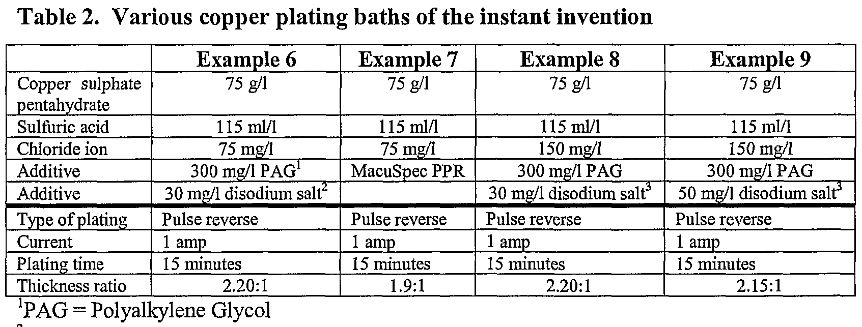
Example 6
A solution was prepared c ontaining 75 g/1 o f copper sulphate p entahydrate, 1 15 ml/1 of sulphuric acid and 75 mg/1 of chloride ion. 300 mg/1 of a polyalkyleneglycol and 30 mg/1 of bis-(ethane-2-sulphate)disulphide disodium salt was added. A Hull cell panel was plated for 15 minutes using a pulse reverse current regime with an average current of 1 amp and an anodicxathodic current density of approximately 2:1. The thickness ratio was calculated as 2.20:1. The panel was smooth matte in high current density areas and semi- bright in low current density areas.
Example 7
A solution was prepared containing 75 g/1 copper sulphate pentahydrate, 115 ml/1 sulphuric acid and 75 mg/1 of chloride ion. Proprietary additives (MacuSpec PPR, a MacDermid process for plating of printed circuit boards) were added and a Hull cell panel was plated for 15 minutes using a pulse reverse current regime with an average current of 1 amp and an anodicxathodic current density of approximately 2:1. The thickness ratio was calculated as 1.9:1. The deposit was smooth matte in high current density areas and semi-bright in low current density areas. Example 8
A solution was prepared containing 75 g/1 copper sulphate pentahydrate, 115 ml/1 sulphuric acid and 150 mg/1 of chloride ion. 300 mg/1 of polyalkyleneglycol and 30 mg/1 of bis-(3-sulphopropyl)disulphide disodium salt were added. A Hull cell panel was plated for 15 minutes using a pulse reverse current regime with an average current of 1 amp and an anodic: cathodic current density of approximately 2:1. The thickness ratio was calculated as 2.20:1. The deposit was smooth matte in high current density areas and semi-bright in low current density areas.
Example 9
A solution was prepared containing 75 g/1 copper sulphate pentahydrate, 115 ml/1 sulphuric acid and 150 mg/1 of chloride ion. 300 mg/1 of polyalkyleneglycol and 50 mg/1 of bis-(3-sulphopropyl)disulphide disodium salt were added. A Hull cell panel was plated for 15 minutes using a pulse reverse current regime with an average current of 1 amp and an anodic: cathodic current density of approximately 2:1. The thickness ratio was calculated as 2.15:1. The deposit was smooth matte in high current density areas and semi-bright in low current density areas.
Example 10
A solution was prepared containing 75 g/1 copper sulphate pentahydrate, 115 ml/1 sulphuric acid and 75 mg/1 of chloride ion. 300 mg/1 of polyalkyleneglycol, 30 mg/1 of bis- (ethane-2-sulphate)disulphide disodium salt and 40 mg/1 of commercially available levelling compound A were added. A Hull cell panel was plated for 15 minutes using a pulse reverse current regime with an average current of 1 amp and an anodic: cathodic current density of approximately 2 :1. The thickness ratio was calculated as 1.70:1. The deposit was smooth matte in high current density areas and fully bright in low current density areas.
Example 11
A solution was prepared containing 75 g/1 copper sulphate pentahydrate, 115 ml/1 sulphuric acid and 75 mg/1 of chloride ion. 300 mg/1 of polyalkyleneglycol, 30 mg/1 of bis- (3-sulphopropyl)disulphide disodium salt and 50 mg/1 of commercially available levelling compound B were added. A Hull cell panel was plated for 15 minutes using a pulse reverse current regime with an average current of 1 amp and an anodic: cathodic current density of approximately 2 :1. The thickness ratio was calculated as 2.20:1. The deposit was smooth matte in high current density areas and fully bright in low current density areas.
Example 12
A solution was prepared containing 75 g/1 copper sulphate pentahydrate, 115 ml/1 sulphuric acid and 75 mg/1 of chloride ion. 300 mg/1 of polyalkyleneglycol, 30 mg/1 of bis- (3-sulphopropyι)disulphide disodium salt and 40 mg/1 of commercially available levelling compound A were added. A Hull cell panel was plated for 15 minutes using a pulse reverse current regime with an average current of 1 amp and an anodic: cathodic current density of approximately 2:1, followed by 1 amp for 5 minutes of direct current. The thickness ratio was calculated as 2.15:1. The deposit was bright across the entire panel.

Claims

WHAT IS CLAIMED IS:
1. A method of plating decorative articles in an acidic copper electroplating bath comprising the steps of:
(a) suspending said decorative article in an plating bath comprising copper ions, counter ions, and chloride ions; and
(b) plating said decorative article for a period of time with pulse-reverse current to produce a desired thickness of copper on at least one surface of said decorative article.
2. The method according to claim 1, wherein the counter ion is sulfate.
3. The method according to claim 1, wherein the electroplating bath contains copper ions at a concentration of about 10 - 50 g/1.
4. The method according to claim 1, wherein the electroplating bath comprises sulphuric acid at a concentration of about 50 - 250 ml/1.
5. The method according to claim 4, wherein the electroplating bath comprises sulphuric acid at a concentration of about 100- 150 ml/1.
6. The method according to claim 1, wherein the electroplating bath comprises chloride ions at a concentration of about 10 - 500 mg/1.
7. The method according to claim 6, wherein the electroplating bath comprises chloride ions at a concentration of about 50-150 mg/1.
8. The method according to claim 1, wherein the plating bath further comprises a polyether and a divalent sulphur compound.
The method according to claim 8, wherein the polyether is present at a concentration of about 50 - 5000 mg/1.
10. The method according to claim 9, wherein the polyether is present at a concentration of about 300 mg/1.
11. The method according to claim 8, wherein the polyether has a molecular weight between 500 and 100,000.
12. The method according to claim 11 , wherein the polyether is polyethyleneglycol.
13. The method according to claim 11, wherein the polyether is an ethylene oxide/propylene oxide co-polymer.
14. The method according to claim 8, wherein the divalent sulphur compound is present in the plating bath at a concentration of about 1 - 150 mg/1.
15. The method according to claim 14, wherein the divalent sulphur compound is present in the plating bath at a concentration of about 30-50 mg/1.
16. The method according to claim 8, wherein the divalent sulphur compound is mercaptopropanesulphonic acid or an alkali metal salt thereof.
17. The method according to claim 8, wherein the divalent sulphur compound is bis- (propane-3-sulphonic acid) disulphide or an alkali metal salt thereof.
18. The method according to claim 8, wherein the divalent sulphur compound is bis- (ethane-2-sulphuric acid) disulphide or an alkali metal salt thereof.
19. The method according to claim 1, wherein the plating bath further comprises an element selected from the group consisting of brighteners and levellers.
20. The method according to claim 8, wherein the plating bath further comprises an element selected from the group consisting of brighteners and levellers.
21. The method according to claim 1, wherein the pulse plating regime consists of alternating cathodic and anodic pulses.
22. The method according to claim 21, wherein the cathodic pulse time is 5 - 100 ms.
23. The method according to claim 21 wherein the anodic pulse time is 0.1 - 10 ms.
24. The method according to claim 21, wherein the pulse plating regime further comprises a final cathodic period of extended time.
25. The method according to claim 24, wherein the final cathodic pulse is up to 1 hour.
26. The method according to claim 1, wherein the average applied current density is 0.5 - 5.0 A/dm2.
27. The method according to claim 26, wherein the current density during the anodic pulse is between 1 and 5 times the current density during the cathodic pulse.
28. The method according to claim 1, wherein the thickness ratio of the copper deposited is less than 2.5: 1.
29. A decorative subsfrate produced in accordance with the process of claim 1.
30. The decorative substrate of claim 29, wherein a subsequent coating is applied over the copper layer.
31 An aluminium alloy wheel produced in accordance with the process of claim 1.
32. The aluminium alloy wheel of claim 31, wherein a subsequent coating is applied over the copper layer.
33. A plastic subsfrate produced in accordance with the process of claim 1.
34. The plastic substrate of claim 33, wherein a subsequent coating is applied over the copper layer.
PCT/US2003/024498 2002-10-21 2003-08-06 Pulse reverse electrolysis of acidic copper electroplating solutions WO2004038070A2 (en)

Priority Applications (1)

Application Number Priority Date Filing Date Title
AU2003265370A AU2003265370A1 (en) 2002-10-21 2003-08-06 Pulse reverse electrolysis of acidic copper electroplating solutions

Applications Claiming Priority (2)

Application Number Priority Date Filing Date Title
US10/274,634 US20040074775A1 (en) 2002-10-21 2002-10-21 Pulse reverse electrolysis of acidic copper electroplating solutions
US10/274,634 2002-10-21

Publications (2)

Publication Number Publication Date
WO2004038070A2 true WO2004038070A2 (en) 2004-05-06
WO2004038070A3 WO2004038070A3 (en) 2004-07-01

Family

ID=32093089

Family Applications (1)

Application Number Title Priority Date Filing Date
PCT/US2003/024498 WO2004038070A2 (en) 2002-10-21 2003-08-06 Pulse reverse electrolysis of acidic copper electroplating solutions

Country Status (4)

Country Link
US (1) US20040074775A1 (en)
AU (1) AU2003265370A1 (en)
TW (1) TWI261075B (en)
WO (1) WO2004038070A2 (en)

Cited By (1)

* Cited by examiner, † Cited by third party
Publication number Priority date Publication date Assignee Title
US7666283B2 (en) 2005-04-12 2010-02-23 Enthone Inc. Insoluble anode

Families Citing this family (12)

* Cited by examiner, † Cited by third party
Publication number Priority date Publication date Assignee Title
US7105082B2 (en) * 2003-02-27 2006-09-12 Novellus Systems, Inc. Composition and method for electrodeposition of metal on a work piece
US20050284766A1 (en) * 2004-06-25 2005-12-29 Herdman Roderick D Pulse reverse electrolysis of acidic copper electroplating solutions
US20080283404A1 (en) * 2007-05-14 2008-11-20 Nec Electronics Corporation Method of manufacturing semiconductor device to decrease defect number of plating film
US7905994B2 (en) * 2007-10-03 2011-03-15 Moses Lake Industries, Inc. Substrate holder and electroplating system
US20090188553A1 (en) * 2008-01-25 2009-07-30 Emat Technology, Llc Methods of fabricating solar-cell structures and resulting solar-cell structures
US8262894B2 (en) 2009-04-30 2012-09-11 Moses Lake Industries, Inc. High speed copper plating bath
EP2568063A1 (en) * 2011-09-09 2013-03-13 Rohm and Haas Electronic Materials LLC Low internal stress copper electroplating method
DE102012206800B3 (en) 2012-04-25 2013-09-05 Atotech Deutschland Gmbh Method and apparatus for the electrolytic deposition of a deposition metal on a workpiece
CN103334135A (en) * 2013-06-19 2013-10-02 西北工业大学 Preparation method of ultra-fine grain copper wire
CN103668370A (en) * 2013-12-19 2014-03-26 潮州市连思科技发展有限公司 Method for pulse plating of disk
CN103911635B (en) * 2014-03-21 2016-02-24 复旦大学 A kind of copper electroplating solution
CN106757193B (en) * 2016-11-24 2018-07-13 中国地质大学(武汉) A kind of method without cyanogen acid bright copper plating of leaf

Citations (4)

* Cited by examiner, † Cited by third party
Publication number Priority date Publication date Assignee Title
US5972192A (en) * 1997-07-23 1999-10-26 Advanced Micro Devices, Inc. Pulse electroplating copper or copper alloys
US20020036144A1 (en) * 2000-09-27 2002-03-28 Lee Sun-Jung Copper-plating elecrolyte containing polyvinylpyrrolidone and method for forming copper interconnect of semiconductor device using the same
US20030085133A1 (en) * 2001-07-26 2003-05-08 Electroplating Engineers Of Japan Limited (Japanese Corporation) Copper plating solution for embedding fine wiring, and copper plating method using the same
US6610192B1 (en) * 2000-11-02 2003-08-26 Shipley Company, L.L.C. Copper electroplating

Family Cites Families (7)

* Cited by examiner, † Cited by third party
Publication number Priority date Publication date Assignee Title
US2558090A (en) * 1947-12-11 1951-06-26 Westinghouse Electric Corp Periodic reverse current electroplating apparatus
US2700019A (en) * 1951-07-05 1955-01-18 Westinghouse Electric Corp Acid copper plating
US3328273A (en) * 1966-08-15 1967-06-27 Udylite Corp Electro-deposition of copper from acidic baths
US3682788A (en) * 1970-07-28 1972-08-08 M & T Chemicals Inc Copper electroplating
US3956078A (en) * 1972-12-14 1976-05-11 M & T Chemicals Inc. Electrodeposition of copper
US4673469A (en) * 1984-06-08 1987-06-16 Mcgean-Rohco, Inc. Method of plating plastics
US20040011654A1 (en) * 2001-10-16 2004-01-22 Kenji Nakamura Method of copper plating small diameter hole

Patent Citations (4)

* Cited by examiner, † Cited by third party
Publication number Priority date Publication date Assignee Title
US5972192A (en) * 1997-07-23 1999-10-26 Advanced Micro Devices, Inc. Pulse electroplating copper or copper alloys
US20020036144A1 (en) * 2000-09-27 2002-03-28 Lee Sun-Jung Copper-plating elecrolyte containing polyvinylpyrrolidone and method for forming copper interconnect of semiconductor device using the same
US6610192B1 (en) * 2000-11-02 2003-08-26 Shipley Company, L.L.C. Copper electroplating
US20030085133A1 (en) * 2001-07-26 2003-05-08 Electroplating Engineers Of Japan Limited (Japanese Corporation) Copper plating solution for embedding fine wiring, and copper plating method using the same

Cited By (1)

* Cited by examiner, † Cited by third party
Publication number Priority date Publication date Assignee Title
US7666283B2 (en) 2005-04-12 2010-02-23 Enthone Inc. Insoluble anode

Also Published As

Publication number Publication date
AU2003265370A1 (en) 2004-05-13
AU2003265370A8 (en) 2004-05-13
TWI261075B (en) 2006-09-01
WO2004038070A3 (en) 2004-07-01
US20040074775A1 (en) 2004-04-22
TW200407467A (en) 2004-05-16

Similar Documents

Publication Publication Date Title
US6071398A (en) Programmed pulse electroplating process
JP3354767B2 (en) Alkaline zinc and zinc alloy electroplating baths and processes
CN101243211B (en) Pretreatment of magnesium substrates for electroplating
US3915811A (en) Method and composition for electroplating aluminum alloys
GB2075063A (en) Process for plating polumeric substrates
CN101435099A (en) Copper plating method
US4765871A (en) Zinc-nickel electroplated article and method for producing the same
US20040074775A1 (en) Pulse reverse electrolysis of acidic copper electroplating solutions
EP1789611A2 (en) Controlling the hardness of electrodeposited copper coatings by variation of current profile
US4462874A (en) Cyanide-free copper plating process
US3669854A (en) Zinc electroplating electrolyte and process
US3691027A (en) Method of producing corrosion resistant chromium plated articles
Krishnan et al. Electroplating of Copper from a Non-cyanide Electrolyte
US3684666A (en) Copper electroplating in a citric acid bath
JP4586020B2 (en) Use of the above aqueous solutions in addition to acidic aqueous solutions and methods for electrolytically depositing copper coatings
WO2006011922A2 (en) Pulse reverse electrolysis of acidic copper electroplating solutions
EP0097643B1 (en) Zinc-nickel electroplated article and method for producing the same
US4549942A (en) Process for electrodepositing composite nickel layers
EP0278044A1 (en) High performance electrodeposited chromium layers
GB2167447A (en) Cyanide free copper plating process
WO2010101212A1 (en) Copper-zinc alloy electroplating bath and method of plating using same
US3428441A (en) Article coated with a composite particulate,microporous chromium coating and method of producing said article
WO2010039323A1 (en) Novel cyanide-free electroplating process for zinc and zinc alloy die-cast components
CA2162230C (en) Passivate for tungsten alloy electroplating
Pletcher et al. Metal finishing

Legal Events

Date Code Title Description
AK Designated states

Kind code of ref document: A2

Designated state(s): AE AG AL AM AT AU AZ BA BB BG BR BY BZ CA CH CN CO CR CU CZ DE DK DM DZ EC EE ES FI GB GD GE GH GM HR HU ID IL IN IS JP KE KG KP KR KZ LC LK LR LS LT LU LV MA MD MG MK MN MW MX MZ NI NO NZ OM PG PH PL PT RO RU SC SD SE SG SK SL SY TJ TM TN TR TT TZ UA UG UZ VC VN YU ZA ZM ZW

AL Designated countries for regional patents

Kind code of ref document: A2

Designated state(s): GH GM KE LS MW MZ SD SL SZ TZ UG ZM ZW AM AZ BY KG KZ MD RU TJ TM AT BE BG CH CY CZ DE DK EE ES FI FR GB GR HU IE IT LU MC NL PT RO SE SI SK TR BF BJ CF CG CI CM GA GN GQ GW ML MR NE SN TD TG

121 Ep: the epo has been informed by wipo that ep was designated in this application
122 Ep: pct application non-entry in european phase
NENP Non-entry into the national phase

Ref country code: JP

WWW Wipo information: withdrawn in national office

Country of ref document: JP