WO2004047499A1 - Organic electroluminescence element - Google Patents
Organic electroluminescence element Download PDFInfo
- Publication number
- WO2004047499A1 WO2004047499A1 PCT/JP2003/014425 JP0314425W WO2004047499A1 WO 2004047499 A1 WO2004047499 A1 WO 2004047499A1 JP 0314425 W JP0314425 W JP 0314425W WO 2004047499 A1 WO2004047499 A1 WO 2004047499A1
- Authority
- WO
- WIPO (PCT)
- Prior art keywords
- group
- emitting layer
- organic
- dopant
- light emitting
- Prior art date
Links
Classifications
-
- H—ELECTRICITY
- H10—SEMICONDUCTOR DEVICES; ELECTRIC SOLID-STATE DEVICES NOT OTHERWISE PROVIDED FOR
- H10K—ORGANIC ELECTRIC SOLID-STATE DEVICES
- H10K85/00—Organic materials used in the body or electrodes of devices covered by this subclass
- H10K85/60—Organic compounds having low molecular weight
- H10K85/615—Polycyclic condensed aromatic hydrocarbons, e.g. anthracene
-
- C—CHEMISTRY; METALLURGY
- C09—DYES; PAINTS; POLISHES; NATURAL RESINS; ADHESIVES; COMPOSITIONS NOT OTHERWISE PROVIDED FOR; APPLICATIONS OF MATERIALS NOT OTHERWISE PROVIDED FOR
- C09K—MATERIALS FOR MISCELLANEOUS APPLICATIONS, NOT PROVIDED FOR ELSEWHERE
- C09K11/00—Luminescent, e.g. electroluminescent, chemiluminescent materials
- C09K11/06—Luminescent, e.g. electroluminescent, chemiluminescent materials containing organic luminescent materials
-
- H—ELECTRICITY
- H05—ELECTRIC TECHNIQUES NOT OTHERWISE PROVIDED FOR
- H05B—ELECTRIC HEATING; ELECTRIC LIGHT SOURCES NOT OTHERWISE PROVIDED FOR; CIRCUIT ARRANGEMENTS FOR ELECTRIC LIGHT SOURCES, IN GENERAL
- H05B33/00—Electroluminescent light sources
- H05B33/12—Light sources with substantially two-dimensional radiating surfaces
- H05B33/14—Light sources with substantially two-dimensional radiating surfaces characterised by the chemical or physical composition or the arrangement of the electroluminescent material, or by the simultaneous addition of the electroluminescent material in or onto the light source
-
- H—ELECTRICITY
- H10—SEMICONDUCTOR DEVICES; ELECTRIC SOLID-STATE DEVICES NOT OTHERWISE PROVIDED FOR
- H10K—ORGANIC ELECTRIC SOLID-STATE DEVICES
- H10K50/00—Organic light-emitting devices
- H10K50/10—OLEDs or polymer light-emitting diodes [PLED]
- H10K50/11—OLEDs or polymer light-emitting diodes [PLED] characterised by the electroluminescent [EL] layers
-
- H—ELECTRICITY
- H10—SEMICONDUCTOR DEVICES; ELECTRIC SOLID-STATE DEVICES NOT OTHERWISE PROVIDED FOR
- H10K—ORGANIC ELECTRIC SOLID-STATE DEVICES
- H10K85/00—Organic materials used in the body or electrodes of devices covered by this subclass
- H10K85/60—Organic compounds having low molecular weight
- H10K85/615—Polycyclic condensed aromatic hydrocarbons, e.g. anthracene
- H10K85/622—Polycyclic condensed aromatic hydrocarbons, e.g. anthracene containing four rings, e.g. pyrene
-
- H—ELECTRICITY
- H10—SEMICONDUCTOR DEVICES; ELECTRIC SOLID-STATE DEVICES NOT OTHERWISE PROVIDED FOR
- H10K—ORGANIC ELECTRIC SOLID-STATE DEVICES
- H10K85/00—Organic materials used in the body or electrodes of devices covered by this subclass
- H10K85/60—Organic compounds having low molecular weight
- H10K85/615—Polycyclic condensed aromatic hydrocarbons, e.g. anthracene
- H10K85/624—Polycyclic condensed aromatic hydrocarbons, e.g. anthracene containing six or more rings
-
- H—ELECTRICITY
- H10—SEMICONDUCTOR DEVICES; ELECTRIC SOLID-STATE DEVICES NOT OTHERWISE PROVIDED FOR
- H10K—ORGANIC ELECTRIC SOLID-STATE DEVICES
- H10K85/00—Organic materials used in the body or electrodes of devices covered by this subclass
- H10K85/60—Organic compounds having low molecular weight
- H10K85/615—Polycyclic condensed aromatic hydrocarbons, e.g. anthracene
- H10K85/626—Polycyclic condensed aromatic hydrocarbons, e.g. anthracene containing more than one polycyclic condensed aromatic rings, e.g. bis-anthracene
-
- H—ELECTRICITY
- H10—SEMICONDUCTOR DEVICES; ELECTRIC SOLID-STATE DEVICES NOT OTHERWISE PROVIDED FOR
- H10K—ORGANIC ELECTRIC SOLID-STATE DEVICES
- H10K85/00—Organic materials used in the body or electrodes of devices covered by this subclass
- H10K85/60—Organic compounds having low molecular weight
- H10K85/631—Amine compounds having at least two aryl rest on at least one amine-nitrogen atom, e.g. triphenylamine
- H10K85/633—Amine compounds having at least two aryl rest on at least one amine-nitrogen atom, e.g. triphenylamine comprising polycyclic condensed aromatic hydrocarbons as substituents on the nitrogen atom
-
- H—ELECTRICITY
- H10—SEMICONDUCTOR DEVICES; ELECTRIC SOLID-STATE DEVICES NOT OTHERWISE PROVIDED FOR
- H10K—ORGANIC ELECTRIC SOLID-STATE DEVICES
- H10K50/00—Organic light-emitting devices
- H10K50/10—OLEDs or polymer light-emitting diodes [PLED]
- H10K50/11—OLEDs or polymer light-emitting diodes [PLED] characterised by the electroluminescent [EL] layers
- H10K50/125—OLEDs or polymer light-emitting diodes [PLED] characterised by the electroluminescent [EL] layers specially adapted for multicolour light emission, e.g. for emitting white light
-
- H—ELECTRICITY
- H10—SEMICONDUCTOR DEVICES; ELECTRIC SOLID-STATE DEVICES NOT OTHERWISE PROVIDED FOR
- H10K—ORGANIC ELECTRIC SOLID-STATE DEVICES
- H10K50/00—Organic light-emitting devices
- H10K50/10—OLEDs or polymer light-emitting diodes [PLED]
- H10K50/17—Carrier injection layers
- H10K50/171—Electron injection layers
-
- H—ELECTRICITY
- H10—SEMICONDUCTOR DEVICES; ELECTRIC SOLID-STATE DEVICES NOT OTHERWISE PROVIDED FOR
- H10K—ORGANIC ELECTRIC SOLID-STATE DEVICES
- H10K85/00—Organic materials used in the body or electrodes of devices covered by this subclass
- H10K85/30—Coordination compounds
- H10K85/321—Metal complexes comprising a group IIIA element, e.g. Tris (8-hydroxyquinoline) gallium [Gaq3]
- H10K85/324—Metal complexes comprising a group IIIA element, e.g. Tris (8-hydroxyquinoline) gallium [Gaq3] comprising aluminium, e.g. Alq3
-
- H—ELECTRICITY
- H10—SEMICONDUCTOR DEVICES; ELECTRIC SOLID-STATE DEVICES NOT OTHERWISE PROVIDED FOR
- H10K—ORGANIC ELECTRIC SOLID-STATE DEVICES
- H10K85/00—Organic materials used in the body or electrodes of devices covered by this subclass
- H10K85/60—Organic compounds having low molecular weight
- H10K85/649—Aromatic compounds comprising a hetero atom
- H10K85/656—Aromatic compounds comprising a hetero atom comprising two or more different heteroatoms per ring
- H10K85/6565—Oxadiazole compounds
-
- Y—GENERAL TAGGING OF NEW TECHNOLOGICAL DEVELOPMENTS; GENERAL TAGGING OF CROSS-SECTIONAL TECHNOLOGIES SPANNING OVER SEVERAL SECTIONS OF THE IPC; TECHNICAL SUBJECTS COVERED BY FORMER USPC CROSS-REFERENCE ART COLLECTIONS [XRACs] AND DIGESTS
- Y10—TECHNICAL SUBJECTS COVERED BY FORMER USPC
- Y10S—TECHNICAL SUBJECTS COVERED BY FORMER USPC CROSS-REFERENCE ART COLLECTIONS [XRACs] AND DIGESTS
- Y10S428/00—Stock material or miscellaneous articles
- Y10S428/917—Electroluminescent
-
- Y—GENERAL TAGGING OF NEW TECHNOLOGICAL DEVELOPMENTS; GENERAL TAGGING OF CROSS-SECTIONAL TECHNOLOGIES SPANNING OVER SEVERAL SECTIONS OF THE IPC; TECHNICAL SUBJECTS COVERED BY FORMER USPC CROSS-REFERENCE ART COLLECTIONS [XRACs] AND DIGESTS
- Y10—TECHNICAL SUBJECTS COVERED BY FORMER USPC
- Y10T—TECHNICAL SUBJECTS COVERED BY FORMER US CLASSIFICATION
- Y10T428/00—Stock material or miscellaneous articles
- Y10T428/24—Structurally defined web or sheet [e.g., overall dimension, etc.]
- Y10T428/24942—Structurally defined web or sheet [e.g., overall dimension, etc.] including components having same physical characteristic in differing degree
Definitions
- the present invention relates to an organic electroluminescent device, and more particularly, to an organic electroluminescent device having a two-layer light emitting layer.
- An electroluminescent device using electroluminescence (hereinafter, abbreviated as “EL”) has high visibility due to self-luminescence, and has excellent impact resistance because it is a completely solid device. Because of its features, its use as a light-emitting element in various display devices has attracted attention.
- These EL elements include an inorganic EL element using an inorganic compound as a light emitting material and an organic EL element using an organic compound.
- the organic EL element has a significantly lower applied voltage.
- the configuration of the organic EL device is based on the configuration of the anode / light-emitting layer / cathode.
- This organic EL device 10 has a light emitting layer 14 sandwiched between a pair of electrodes consisting of an anode 12 and a cathode 13.
- the light emitting layer 14 is usually a laminate of a plurality of layers.
- the electrons and holes recombine in the light-emitting layer 14 to generate an excited state, and emit energy as light when the excited state returns to the ground state.
- FIG. 4 shows an energy diagram of the organic EL device of FIG.
- FIG. 4 shows a valence level EVO (HOMO) and a conduction level ECO (LUMO), which are energy levels of the light emitting layer 14. Holes enter from the anode 12 side, electrons enter from the cathode 13 side, and these holes and electrons combine in the light emitting layer 14 to emit light.
- EVO valence level
- ECO conduction level
- a hole injection / transport layer and an electron injection layer are appropriately provided on this.
- those having the structure of anode / hole injection / transport layer / light emitting layer Z cathode and anode / hole injection / transport layer Z light emitting layer Z electron injection layer Z cathode are known.
- the light emitting layer has the following functions.
- Injection function A function that can inject holes from the anode or hole injection layer when applying an electric field, and can inject electrons from the cathode or electron injection layer.
- Transport function Function to move injected charges (electrons and holes) by electric field force
- Light-emitting function a function that provides a field for the recombination of electrons and holes, which is linked to light emission
- the hole injecting / transporting layer has a function of injecting holes from the anode and transporting the holes to the organic light emitting layer, and may be formed separately from the hole injecting layer and the hole transporting layer.
- the electron injection layer has a function of injecting electrons from the cathode and transporting them to the organic light emitting layer.
- a technique of adding a small amount of a fluorescent molecule (dopant) to further enhance the light emission in the light emitting layer is known.
- FIG. 5 shows an energy diagram of an organic EL device to which a dopant is added.
- E Ch indicates the conduction level of the host
- E V h indicates the valence level of the host
- E C d indicates the conduction level of the dopant
- E V d indicates the valence level of the dopant.
- E gh indicates the energy gap of the host (difference between E C h and E V h)
- E g d indicates the energy gap of the dopant (difference between E C d and E V d).
- the dopant efficiently receives the energy of the excited host and increases the luminous efficiency.
- the organic light emitting layer has a two-layer structure, the first light emitting layer on the anode side is a blue light emitting layer made of an aluminum complex compound, and the second light emitting layer on the cathode side is an aluminum complex containing a red fluorescent substance.
- a method of extracting white light as a red light-emitting layer made of a compound for example, see European Patent No. 0 634 549).
- the organic light-emitting layer has a two-layer structure, the first light-emitting layer on the anode side is a blue light-emitting layer made of a distyrylarylene-based compound, and the second light-emitting layer on the cathode side is a red fluorescent compound that emits green light.
- a method for extracting white light as a light emitting layer to which a substance is added for example, see US Pat. No. 5,530,910).
- a luminescent layer composed of a mixed layer of an electron transporting compound composed of an aluminum complex and a hole transporting compound composed of a diamine compound contains coumarin and ruprene as dopants to emit light having a green component and an orange component. (See, for example, WO 98/086360 pamphlet.)
- an object of the present invention is to provide an organic EL device that emits narrow band light with high color purity and has a long life. Disclosure of the invention
- the present inventor has proposed an organic EL device having at least two light-emitting layers, in which light emission of the second light-emitting layer is suppressed or two light-emitting layers are fixed.
- the relationship is satisfied, it has been found that the color purity and / or the life of the device can be improved, and the present invention has been completed.
- the following organic electroluminescent element is provided.
- a first light-emitting layer comprising at least a first host material and a first dopant
- a second light emitting layer comprising at least a second host material and a second dopant
- the energy gap E gh 1 of the first host material, the E Nerugi one gap E gd 1 of the first dopant, the energy formic Yap E gd 2 of the energy gap E gh 2 ⁇ beauty the second dopant of the second host material is below Satisfy the expression
- the emission intensity I 1 of the emission maximum wavelength of the emission spectrum derived from the first emission layer and the emission intensity I 2 of the emission maximum wavelength of the emission spectrum derived from the second emission layer satisfy the following formulas.
- a first light-emitting layer comprising at least a first host material and a first dopant
- a second light emitting layer comprising at least a second host material and a second dopant
- the energy gap E gh 1 of the first host material, the E Nerugigiyappu E gd 1 of the first dopant, the energy formic Yap E gh 2 ⁇ beauty the second de one punt energy formic Yap E gd 2 of the second host material Specially satisfy the following formula An organic electorescence luminescent element referred to as ⁇ .
- a ratio of the second dopant to the second host material is 0.1 to 1 Omo 1%.
- Ar 1 is an aromatic ring having 6 to 50 nuclear carbon atoms, and X is a substituent.
- n is an integer of 0 to 6.
- Ar may be the same or different.
- X may be the same or different.
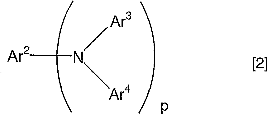
- Ar 2 to Ar 4 are a substituted or unsubstituted aromatic group having 6 to 50 nuclear carbon atoms, a substituted or unsubstituted styryl group, and p is an integer of 1 to 4. When p ⁇ 2, Ar 3 and Ar 4 may be the same or different. ]
- an electron injection layer between the second emitting layer and the cathode, the electron mobility of the electron injection layer, and having is at 10- 4 cm 2 / (V ⁇ sec) or more
- the organic electroluminescent device according to any one of [1] to [11].
- FIG. 1 is a schematic sectional view of the organic EL device of the present invention.
- FIG. 2 is an energy diagram of the organic EL device of the present invention.
- FIG. 3 is a schematic sectional view of a general organic EL device.
- Figure 4 is the energy diagram of the organic EL device.
- FIG. 5 is an energy diagram of the organic EL device to which the dopant is added.
- the first organic EL device of the present invention comprises an anode, a first light emitting layer comprising at least a first host material and a first dopant, and a second light emitting layer comprising at least a second host material and a second dopant.
- the energy gap E gh l of the first host material, the energy gap E gd 1 of the first dopant, the second host materials of energy formic Yap E gh 2 and the second dopant energy formic Yap E gd 2 satisfies the following formula
- the emission intensity I 1 of the maximum emission wavelength of the emission spectrum derived from the first emission layer and the emission intensity I of the maximum emission wavelength of the emission spectrum derived from the second emission layer I 2 satisfies the following equation.
- FIG. 1 is a schematic sectional view of the organic EL device of the present invention.
- the organic EL element 1 has at least an anode 2, a first light-emitting layer 3, a second light-emitting layer 4, and a cathode 5, which are stacked in this order.
- FIG. 2 is an energy diagram of the organic EL device 1.
- the energy levels of the anode 2, the first light emitting layer 3, the second light emitting layer 4, and the cathode 5 are shown. Further, the energy gap E gh l of the first host material, and the energy gap E gd 1 of the first dopant, the energy formic Yap E gd 2 of the energy formic Yap E sh 2 and the second dopant of the second host materials is shown.
- the energy gap corresponds to the energy difference between the valence level and the conduction level of the organic EL material, and is usually determined from the absorption edge of the light absorption spectrum of the material.
- the first dopant and the second dopant are doped into different light-emitting layers 3 and 4, respectively, and the light-emitting layer has a two-layer structure, so that the dopant having a large energy gap can be obtained.
- the first light-emitting layer 3 is mainly configured to emit light. ing.
- the light-emitting layer has only a two-layer structure, as can be seen from the example of the prior art, since the first light-emitting layer 3 and the second light-emitting layer 4 emit light, a narrow band emission with high color purity can be obtained. I can't.
- the first light emitting layer 3 is provided on the anode 2 side having a high recombination probability.
- the second light emitting layer 4 is provided on the side of the cathode 5 having a low recombination probability.
- an electron injection layer is provided between the second light emitting layer 4 and the cathode 5, and the electron injection layer has an electric field strength (E) in an electric field region of 1 ⁇ 10 5 to 10 6 VZcm.
- electron mobility is preferably at 10- 4 cm 2 / (V ⁇ sec) or more.
- the light emitting region can be more stably set in the first light emitting layer 3. Therefore, the first light emitting layer 3 can emit light more selectively, so that narrow band light emission with better color purity can be obtained, and the life can be significantly prolonged.
- Time off 1 ight method a method of calculating from a measurement of a traveling time of a charge in an organic film
- a method of calculating from a voltage characteristic of a space-limited current [Electr on ic Processin Org anic Crystals (M. Poe, CE Sweden), Organic Molecular Solids (W. Jones)].
- it is calculated by the Time off 1 ig method. Specifically, for the ITO / organic layer (electron injection layer, etc.) / A1 structure, the time characteristic (transient characteristic time) of the transient current generated by light irradiation was measured, and the electron The mobility is calculated.
- Electron mobility (organic layer thickness) V (transient characteristic time ⁇ electric field strength)
- a material with a large energy gap has less half-life than a material with a small energy gap, and it is difficult to select a material.However, with this configuration, the second light-emitting layer contributes almost to light emission. Nevertheless, the life of the organic EL element can be extended.
- the energy gap ( Egh1 ) of the first host material is larger than the energy gap Egdl of the first dopant. In other words, satisfy the relationship of E gh l> E gd l.
- the energy gap E gdl of the first dopant is preferably larger than 2.7 eV.
- many dopants having a large energy gap have a shorter half-life of the organic EL device than doping dopants having a small energy gap. Therefore, it has been particularly difficult to extend the life of a pure blue organic EL element used in full color.
- the present invention can achieve extremely long life pure blue light emission by adopting the above configuration.
- the second light emitting layer contains at least a second host material and a second dopant.
- the energy gap E gh 2 of the second host material is larger than the energy-gap E gd 2 of the second dopant. That is, the relationship of E sh 2> E gd 2 is satisfied.
- the energy gap E gd 1 of the first dopant is larger than the energy-gap E gd 2 of the second dopant, that is, the relationship of E sd l> E gd 2 is satisfied.
- the energy gap E gd 2 of the second dopant is larger than 2.7 eV, that is, it satisfies the relationship of E gd 2> 2.7 eV.
- This organic EL device has an emission intensity I1 of the emission maximum wavelength of the emission spectrum of light originating from the first emission layer and an emission intensity 1 of the emission maximum wavelength of the emission spectrum of light originating from the second emission layer. 2 satisfies the relationship of I 1> 3.5 5 ⁇ 12. Satisfy this relationship Thus, narrow band emission with good color purity can be obtained.
- I 1> 5 XI 2 more preferably I 1> 10 XI 2.
- the light emission intensity I 2 from the second light emitting layer is 0.
- the life of the organic EL element can be extended.
- the present invention is a technique for extending the life of a pure blue light-emitting material known so far. In other words, it is a technology to extend the life of the EL element by dare using a material that is known to have a long life, by using it adjacent to the light emitting layer, and by limiting light emission therefrom as much as possible.
- the second organic EL device of the present invention comprises: an anode; a first light emitting layer comprising at least a first host material and a first dopant; and a second light emitting layer comprising at least a second host material and a second dopant.
- a layer comprising a cathode in that order, the energy gap E gh l of the first host material, the energy gap E gd 1 of the first dopant, the energy formic Yap E gh 2 and the second dopant of a second phosphite Bok materials
- Energy gap E gd 2 satisfies the following equation.
- the basic configuration is the same as that of the organic EL device described above.
- This organic EL device satisfies the relationship of E gdl > E Bd 2> 2.7 eV . To satisfy this relationship, unlike the above-mentioned organic EL device, even if both the first light emitting layer and the second light emitting layer emit light, both emit blue light, so that blue light with high color purity can be obtained. It is possible.
- the host material used for the first light emitting layer and the second light emitting layer it is possible to use a material known as a long-lived light emitting material, and the material represented by the general formula [1] is used as the host material of the light emitting material. It is preferable to use it as a material.
- Ar 1 is an aromatic ring having 6 to 50 nuclear carbon atoms, and X is a substituent.
- m is an integer of 1 to 5
- n is an integer of 0 to 6.
- a r 1 may be the same or different.
- X may be the same or different.
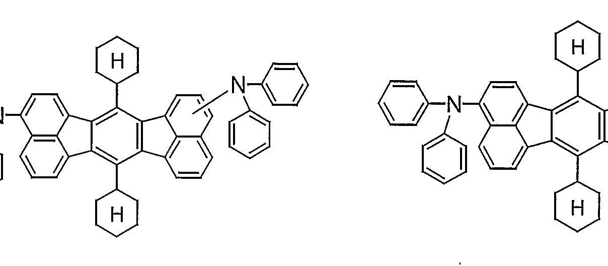
- a r 1 include a phenyl ring, a naphthyl ring, an anthracene ring, a biphenylene ring, an azulene ring, an acenaphthylene ring, a fluorene ring, a phenanthrene ring, a fluoranthene ring, an acephenanthrylene ring, a triphenylene ring, Pyrene ring, chrysene ring, naphthacene ring, picene ring, perylene ring, pentaphenene ring, pentacene ring, tetraphenylene ring, hexaphene ring, hexacene ring, rubicene ring, coronene ring, trinaphthylene ring, etc. No.
- Preferable examples include a phenyl ring, a naphthyl ring, an anthracene ring, an acenaphthylene ring, a fluorene ring, a phenanthrene ring, a fluoranthene ring, a triphenylene ring, a pyrene ring, a chrysene ring, a perylene ring, and a trinaphthylene ring.
- a phenyl ring More preferred are a phenyl ring, naphthyl ring, anthracene ring, fluorene ring, phenanthrene ring, fluoranthene ring, pyrene ring, chrysene ring, perylene ring and the like.
- X is a substituted or unsubstituted aromatic group having 6 to 50 nuclear carbon atoms, a substituted or unsubstituted aromatic heterocyclic group having 5 to 50 nuclear atoms, a substituted or unsubstituted An alkyl group having 1 to 50 carbon atoms, a substituted or unsubstituted alkoxy group having 1 to 50 carbon atoms, a substituted or unsubstituted aralkyl group having 1 to 50 carbon atoms, a substituted or unsubstituted nuclear atom An aryloxy group having a number of 5 to 50, a substituted or unsubstituted nuclear atom, an arylthio group having a number of 5 to 50, a substituted or unsubstituted carboxyl group having 1 to 50 carbon atoms, a substituted or unsubstituted styryl Group, halogen group, cyano group, nitro group, hydrid And a mouth
- Examples of the substituted or unsubstituted aromatic group having 6 to 50 nuclear carbon atoms include phenyl, 1-naphthyl, 2-naphthyl, 1-anthryl, 2-anthryl, 9-anthryl, 1 1-phenanthryl, 2-phenanthryl, 3-phenanthryl, 4-1-phenanthryl, 9-phenanthryl, 1-naphthacenyl, 2-naphthacenyl, 9-naphthacenyl, 1-pyrenyl, 2-pyrenyl, 4 —Pyrenyl group, 2-biphenylyl group, 3-biphenylyl group, 4-biphenylyl group, p-terphenyl-2-yl group, p-terphenyl-2-yl group, p—terphenyl-2-yl group 2-yl group, m-evening group 4-yl group, m-terphenyl 2-yl group, m-terphenyl 2-
- Examples include a fluorenyl group, 9,9-dimethyl-2-fluorenyl group, and 3-fluoranthenyl group.
- Examples of the substituted or unsubstituted aromatic heterocyclic group having 5 to 50 nuclear atoms include: 11-pyrrolyl, 2-pyrrolyl, 3-pyrrolyl, pyrazinyl, 2-pyridinyl, 3-pyridinyl , 4-pyridinyl, 1-indolyl, 2-indolyl, 3-indolyl, 4-indolyl, 5-indolyl, 6_indolyl, 7-indolyl, 1-isoindolyl, 2-isoindolyl , 3-isoindolyl, 4-isoindolyl, 5-isoindolyl, 6-isoindolyl, 7-isoindolyl, 2-furyl, 3-furyl, 2-benzofuranyl, 3-benzofuranyl, 4-benzofuranyl group, 5-benzofuranyl group, 6-benzofuranyl group, 7-benzofuranyl group, 1-isobenzofur
- Examples of the substituted or unsubstituted alkyl group having 1 to 50 carbon atoms include a methyl group, an ethyl group, a propyl group, an isopropyl group, an n-butyl group, an s_butyl group, an isobutyl group, a t-butyl group, n-pentyl, n-hexyl, n-heptyl, n-octyl, hydroxymethyl, 1-hydroxyethyl, 2-hydroxyethyl, 2-hydroxyisobutyl, 1,2-dihydroxy Ethyl group, 1, 3-dihydroxyisopropyl group, 2,3-dihydroxy-t-butyl group, 1,2,3-trihydroxypropyl group, chloromethyl group, 1-chloroethyl group, 2-chloroethyl group, 2_chloroethyl group Isobutyl group, 1,2-dichloroethyl group, 1,3
- Amino group aminomethyl group, 1-aminoethyl group, 2-aminoethyl group, 2-aminoisobutyl group, 1,2-diaminoethyl group, 1,3-diaminoisopropyl group, 2,3-diaminot Butyl, 1,2,3-triaminopropyl, cyanomethyl,
- a substituted or unsubstituted alkoxy group having 1 to 50 carbon atoms is a group represented by —OY, and examples of Y include methyl, ethyl, propyl, isopropyl, n-butyl, and s-butyl.
- Y include methyl, ethyl, propyl, isopropyl, n-butyl, and s-butyl.
- Examples of the substituted or unsubstituted aralkyl group having 1 to 50 carbon atoms include a benzyl group, a 1-phenylethyl group, a 2-phenylethyl group, a 1-phenylisopropyl group, a 2-phenylisopropyl group, and a phenylt group.
- -Naphthylmethyl group 1- ⁇ -naphthylethyl group, 2-—naphthylethyl group, I-a-naphthylisopropyl group, 2-1-naphthylisopropyl group, ⁇ -naphthylmethyl group, 1- iS-naphthylethyl group, 2-—3-naphthylethyl group, 1- ⁇ -naphthylisopropyl group, 2-—naphthylisopropyl group, 1_pyrrolylmethyl group, 2- (1-pyrrolyl) ethyl group, ⁇ _methylbenzyl group, m-methylbenzyl, o-methylbenzyl, p-chlorobenzyl, m-chlorobenzyl, o-benzyl, p-bromobenzyl, m Bromobenzyl group, o-bro
- a substituted or unsubstituted aryloxy group having 5 to 50 nuclear atoms is represented by 1 OY ′, and examples of Y ′ are phenyl, 1-naphthyl, 2-naphthyl, 1-anthryl, 2-anthryl.
- a substituted or unsubstituted arylthio group having 5 to 50 nuclear atoms is represented by 1 SY ", and examples of Y" include phenyl, 1-naphthyl, 2-naphthyl, and '1-a Nothryl, 2-anthrylyl, 9-anthryl, 1-phenanthryl, 2-phenanthryl, 3-phenanthryl, 4-phenanthryl, 9-phenanthryl, 1-naphthenylsenyl, 2-naphthacenyl Group, 9-naphthacenyl group, 1-pyrenyl group, 2-pyrenyl group, 4-pyrenyl group, 2-biphenylyl group, 3-biphenylyl group, 4-piphenylyl group, p-phenylenyl 4-p Group, p-terphenyl-3-yl group, p-terphenyl-2-yl group, m-terphenyl-2-yl 4-
- a substituted or unsubstituted carbonyl group having 1 to 50 carbon atoms is represented by one COOZ, and examples of Z include methyl, ethyl, propyl, isopropyl, n-butyl, s_butyl, Isobutyl, t-butyl, n-pentyl, n-hexyl, n-heptyl, n-octyl, hydroxymethyl, 1-hydroxyethyl, 2-hydroxyethyl, 2- Hydroxyisobutyl group, 1,2-dihydroxyethyl group, 1,3-dihydroxyisopropyl group, 2,3-dihydroxyt-butyl group, 1,2,3-trihydroxypropyl group, chloromethyl group, Cloethyl group, 2-chloroethyl group, 2-chloroisobutyl group, 1,2-dichloroethyl group, 1,3-dichloroisopropyl group, 2,3-d
- Examples of the substituted or unsubstituted styryl group include a 2-phenyl-1-vinyl group, a 2,2-diphenyl_1-vinyl group, a 1,2,2-triphenyl-11-vinyl group, and the like. .
- halogen groups include fluorine, chlorine, bromine, iodine and the like.
- n is preferably 0-4. Specific examples of the compound of the general formula [1] are shown below.
- the first host material and the second host material may be the same in order to simplify the vapor deposition.
- the dopant used for the first and second light emitting layers is a long-lived light emitting material.
- a known material can be used, it is preferable to use a material represented by the general formula [2] as a dopant material of a light emitting material.
- a r 2 ⁇ A r 4 is a substituted or unsubstituted aromatic group having a carbon number of 6-5 0, location ⁇ is unsubstituted styryl group.
- p is an integer of 1-4. When p ⁇ 2, A r 3 and A r 4 may be the same or different.
- Examples of the substituted or unsubstituted aromatic group having 6 to 50 nuclear carbon atoms include phenyl, 1-naphthyl, 2-naphthyl, 1-anthryl, 2-anthryl, 9-anthryl, 1-phenanthryl, 2-phenanthryl, 3-phenanthryl, 4-phenanthryl, 9-phenanthryl, 1-naphthacenyl, 2-naphthenyl, 9-naphthacenyl, 1-pyrenyl, 2-pyrenyl Group, 4-pyrenyl group, 2-biphenylyl group, 3-biphenylyl group, 4-biphenylyl group, p-terfenyl 4-yl group, p-terphenyl-3-yl group , P 1-1 ⁇ 2-yl, m-1 ⁇ 4- ⁇ , m-1-3 ⁇ , m- ⁇ ⁇ 2-2 , O-tolyl, m-tolyl, P-tolyl,
- Examples of the substituted or unsubstituted styryl group include a 2-phenyl-1-vinyl group, a 2-diphenyl-1-pinyl group, and a 1,2,2-triphenyl-1-vinyl group. .
- the ratio of the first dopant to the first host material is 0.1-1 Omo 1%. 11 Omo 1% is preferred. 0. Imo less than 1%, ten Light emission cannot be obtained, and if the content exceeds 1 Omo 1%, concentration quenching may occur, and luminous efficiency may be reduced.
- the ratio of the second dopant to the second host material is preferably 0.1 to 10 mol 1%, particularly preferably 0.1 to 5 mol 1%.
- the thickness of the first light emitting layer is preferably 10 nm or more, particularly preferably 10 nm to 40 nm. If it is less than 10 nm, a sufficient concentration of holes reaches the second light emitting layer, and the second light emitting layer emits more light than necessary, which may degrade color purity. Therefore, the first light emitting layer can be thicker than the second light emitting layer.
- the thickness of the second light emitting layer is adjusted according to the first light emitting layer, but is preferably 10 ⁇ m to 40 nm, particularly preferably 10 nm to 30 nm.
- the light emitting layer is particularly preferably a molecular deposition film.
- the molecular deposition film is a thin film formed by deposition from a material compound in a gaseous phase or a film formed by solidification from a material compound in a solution state or a liquid phase.
- a binder such as a resin and a material compound are dissolved in a solvent to form a solution, which is then subjected to a spin coating method or the like.
- the light emitting layer can also be formed by making the film thinner.
- another organic or inorganic layer is interposed between the first light emitting layer and the second light emitting layer, between the anode and the first light emitting layer, or between the second light emitting layer and the cathode. It can be done.
- the configuration of viii) is usually preferably used.
- the organic EL device of the present invention is manufactured on a light-transmitting substrate.
- the translucent substrate referred to here is a substrate that supports the organic EL element, and is preferably a smooth substrate having a transmittance of light in the visible region of 400 to 700 nm of 50% or more.
- Specific examples include a glass plate and a polymer plate.
- the glass plate include soda-lime glass, palladium / strontium-containing glass, lead glass, aluminosilicate glass, borosilicate glass, barium borosilicate glass, and quartz.
- the polymer plate include polycarbonate, acryl, polyethylene terephthalate, polyether sulfide, and borosulfone.
- the anode of the organic thin film EL element plays a role of injecting holes into the hole transport layer or the light emitting layer, and it is effective to have a work function of 4.5 eV or more.
- Specific examples of the anode material used in the present invention include indium tin oxide alloy (ITO), tin oxide (NESA), gold, silver, platinum, and copper.
- ITO indium tin oxide alloy
- NESA tin oxide
- gold gold
- silver platinum
- copper copper
- As the cathode electron
- a material having a small work function is preferable.
- the anode can be formed by forming a thin film from these electrode substances by a method such as a vapor deposition method or a sputtering method.
- the transmittance of the anode with respect to the light emission be greater than 10%.
- the sheet resistance of the anode is preferably several hundreds ⁇ or less.
- the thickness of the anode depends on the material, but is usually selected in the range of 10 nm to 1 m, preferably 10 to 200 nm.
- the hole injection / transport layer is a layer that assists hole injection into the light emitting layer and transports the light to the light emitting region.
- the hole mobility is high, and the ionization energy is usually as low as 5.5 eV or less.
- Such a hole injecting, to that material preferably transported to the light emitting layer a hole at a lower electric field intensity.
- Transporting layer further hole mobility of, for example, applying an electric field 10 4 ⁇ 10 6 V / cm sometimes, preferably it is at least 10- 4 cm 2 ZV ⁇ sec.
- the material for forming the hole injecting / transporting layer is not particularly limited as long as it has the above-mentioned preferable properties, and a material conventionally used as a hole charge transporting material in a photoconductive material, an organic EL, Any known materials used for the hole injection layer of the device can be selected and used.
- the above-mentioned materials can be used, and porphyrin compounds (those disclosed in JP-A-63-2956965, etc.), aromatic tertiary amine compounds and styrylamine compounds (US Patent No. 4,127,412, JP-A-53-27033, JP-A-54-58445, JP-A-54-14 9634, 54-64299, 55-79450, 55-144250, 56-119132, 61-295558, 61-98353, 63-
- NPD 4,4'-bis (N- (1-naphthyl) -1-N-phenylamino ) Biphenyl
- MTDATA Triphenylamine
- inorganic compounds such as P-type Si and p-type SiC can also be used as the material of the hole injection layer.
- the hole injection / transport layer can be formed by thinning the above-mentioned compound by a known method such as a vacuum evaporation method, a spin coating method, a casting method, and an LB method.
- the thickness of the hole injection / transport layer is not particularly limited, but is usually 5 nm to 5 ⁇ .
- the hole injection / transport layer may be composed of one or two or more of the above-mentioned materials as long as the compound of the present invention is contained in the hole transport zone. A layer obtained by laminating a hole injection / transport layer made of a different kind of compound from the transport layer may be used.
- the organic semiconductor layer is a layer which assists hole injection or electron injection into the light emitting layer, and preferably has a conductivity of 10_1 Q S / cm or more.
- Examples of the material of such an organic semiconductor layer include thiophene-containing oligomers, conductive oligomers such as arylamine-containing oligomers disclosed in Japanese Patent Application Laid-Open No. 8-193191, and arylamine-containing oligomers.
- a conductive dendrimer such as a dendrimer can be used.
- the electron injection layer is a layer that assists the injection of electrons into the light emitting layer, has a high electron mobility
- the adhesion improving layer is a layer made of a material having particularly good adhesion to the cathode in the electron injection layer.
- the material used for the electron injection layer 8-hydroxyquinoline and a metal complex of a derivative thereof, or a nitrogen-containing heterocyclic derivative are preferable.
- metal complex of 8-hydroxyquinoline or a derivative thereof include a metal chelate oxoxide compound containing a chelate of oxine (generally, 8-quinolinol or 8-hydroxyquinoline).
- A1q described in the section of the light emitting material can be used as the electron injection layer.
- examples of the nitrogen-containing heterocyclic derivative include oxaziazole derivatives.
- Examples of the oxadiazole derivative include electron transfer compounds represented by the following general formulas [3] to [5].
- Ar 5 , Ar 6 , Ar 7 , Ar 9 , Ar 10 , and Ar 13 each represent a substituted or unsubstituted aryl group, which may be the same or different.
- Ar 8 , Ar 11 , and Ar 12 each represent a substituted or unsubstituted arylene group, which may be the same or different.
- examples of the aryl group include a phenyl group, a biphenyl group, an anthranyl group, a perylenyl group, and a pyrenyl group.
- the arylene group includes a phenylene group, a naphthylene group, a biphenylene group, an anthranylene group, a peryleneylene group, a pyrenylene group and the like.
- examples of the substituent include an alkyl group having 1 to 10 carbon atoms, an alkoxy group having 1 to 0 carbon atoms, and a cyano group. This electron transfer compound Those which can form a thin film are preferred.
- electron-transporting compound examples include the following.
- examples of the other nitrogen-containing heterocyclic derivative organic compound include a compound represented by the general formula [6].
- HAr is a nitrogen-containing heterocyclic ring having 3 to 40 carbon atoms which may have a substituent
- L 1 is a single bond or 6 to 60 carbon atoms which may have a substituent.
- Ar 14 may have a substituent.
- Ar 15 is a divalent aromatic hydrocarbon group having a good carbon number of 6 to 60
- Ar 15 is a carbon atom which may have a substituent or an aryl group having 6 to 60 or a carbon atom which may have a substituent. It is a heteroaryl group of the number 3 to 60.
- the compound of the above formula [6] can be synthesized by the method described in Japanese Patent Application No. 2003-004139.
- an imidazopyrazine derivative and an imidazole derivative are preferable.
- Examples of the imidazopyrazine derivative include a compound represented by the general formula [7].
- Hache-eight 3 is a nitrogen atom or a carbon atom
- R represents Ariru group which has good carbon atoms 6 to be 60 substituted, which may have a substituent carbon
- q is an integer of 2 or more
- a plurality of Rs may be the same or different from each other, and may be bonded to each other by a plurality of adjacent R groups to form a substituted or unsubstituted carbocyclic aliphatic ring.
- Ar 16 may be a substituted or unsubstituted carbocyclic aromatic ring, and may have a substituted or unsubstituted aryl group having 6 to 60 carbon atoms. It is also good heteroaryl group having 3 to 60 carbon atoms to the have, Ar 17 is a hydrogen atom, an alkyl group having 1 to 20 carbon atoms, atoms 1 20 octaalkyl groups, 1 to 20 carbon alkoxy groups, 6 to 60 carbon atoms which may have a substituent, 3 to 60 carbon atoms which may have a substituent A teloaryl group, wherein one of Ar 16 and Ar 17 is a condensed ring group having 10 to 60 carbon atoms which may have a substituent, and 3 carbon atoms which may have a substituent; L 2 and L 3 each may be a single bond, an optionally substituted fused ring having 6 to 60 carbon atoms, or a substituent.
- the compound of the above formula [7] is prepared by the method described in Japanese Patent Application No. 2003-005184. Can be combined.
- imidazole derivative examples include compounds represented by the general formula [8] or [9].
- R 1 represents a hydrogen atom, an aryl group having 6 to 60 carbon atoms which may have a substituent, a pyridyl group which may have a substituent, A quinolyl group, an alkyl group having 1 to 20 carbon atoms which may have a substituent or an alkoxy group having 1 to 20 carbon atoms which may have a substituent, and r is 0 to 4 Is an integer of
- R 2 represents an aryl group having 6 to 60 carbon atoms which may have a substituent, a pyridyl group which may have a substituent, a quinolyl group which may have a substituent, and a substituent
- R 3 has a hydrogen atom or a substituent.
- the compound of the above formula [8] can be synthesized by the method described in Japanese Patent Application No. 2003-67847.
- the electron injection layer in the region of the electric field strength (E) is 1 0 4 ⁇ 1 0 6 VZ cm , that electron mobility of 1 0- 4 cm 2 / (V ⁇ sec) or more favorable Better.
- the driving voltage of the organic EL element can be reduced.
- the light emitting region can be shifted to the first light emitting layer on the anode side, the light emission of the second light emitting layer can be suppressed, so that narrow band light emission with better color purity can be obtained, and high efficiency and long life can be obtained. can do.
- a compound having a particularly high electron mobility for example, the above-mentioned nitrogen-containing heterocyclic derivative organic compound, particularly an imidazopyrazine derivative and Z or an imidazole derivative for the electron injection layer.
- the above-mentioned compounds form an electron injection layer by taking a form such as lamination and mixing as necessary. It may be formed.
- a reducing dopant in a region for transporting electrons or an interface region between the cathode and the organic layer.
- a reducing dopant is defined as a substance that can reduce an electron transporting compound. Therefore, various substances having a certain reducing property are used, for example, alkali metals, alkaline earth metals, rare earth metals, alkali metal oxides, alkali metal halides, and alkaline earth metals.
- Group consisting of metal oxides, alkali earth metal halides, rare earth metal oxides or rare earth metal halides, alkali metal organic complexes, alkaline earth metal organic complexes, and rare earth metal organic complexes At least one substance selected from the group consisting of:
- preferable reducing dopants include Na (work function: 2.36 eV), K (work function: 2.28 eV), and Rb (work function: 2.1). 6 e V) and at least one alkali metal selected from the group consisting of C s (work function: 1.95 e V), C a (work function: 2.9 e V), and S r (work function) : 2.0 to 2.5 eV), and a work function including at least one alkaline earth metal selected from the group consisting of Ba (work function: 2.52 eV) is 2.9 e. V or less is particularly preferred.
- more preferred reducing dopants are at least one alkali metal selected from the group consisting of K, Rb and Cs, more preferably 13 or ⁇ 3, most preferably , Cs.
- alkali metals have particularly high reducing ability, and by adding a relatively small amount to the electron injection region, it is possible to improve the emission luminance and extend the life of the organic EL device.
- a combination of these two or more kinds of alkali metals is also preferable, and in particular, a combination containing Cs, for example, Cs and Na, A combination of Cs and K, Cs and Rb or Cs, Na and ⁇ is preferred.
- Cs By including Cs in combination, the reducing ability can be efficiently exhibited, and by adding the compound to the electron injection region, it is possible to improve the emission luminance and extend the life of the organic EL device.
- an electron injection layer composed of an insulator or a semiconductor may be further provided between the cathode and the organic layer.
- insulators include alkali metal chalcogens
- the electron injecting layer is composed of these alkali metal chalcogenides or the like, since the electron injecting property can be further improved.
- alkali metal chalcogenides for example, L i 2 0, L I_ ⁇ , Na 2 S, N a 2 S e and N A_ ⁇ .
- alkali earth metal chalcogenides for example, Ca ⁇ , Ba ⁇ , SrO, BeO, BaS, and CaSe.
- Preferred alkali metal halides include, for example, LiF, NaF, KF, LiC1, KC1, and NaC1.
- Preferable halides of alkaline earth metals for example, fluorides such as CaF 2, BaF 2, S rF 2, M g F 2 and B e F 2, Ha port Gen products other than full Tsu fluoride No.
- an electron transport layer may be provided.
- a semiconductor constituting the electron transport layer at least one of Ba, Ca, Sr, Yb, Al, Ga, In, Li, Na, Cd, Mg, Si, Ta, Sb, and Zn
- An oxide containing an element, a nitride, an oxynitride, or the like may be used alone or in combination of two or more.
- the inorganic compound constituting the electron transport layer is a microcrystalline or amorphous insulating thin film. If the electron transport layer is composed of these insulating thin films, a more uniform thin film is formed, so that pixel defects such as dark spots can be reduced. Examples of such inorganic compounds include the above-mentioned alkali metal chalcogenides, alkaline earth metal chalcogenides, alkali metal halides and alkaline earth metal halides.
- a metal, an alloy, an electrically conductive compound having a low work function (4 eV or less), and a mixture thereof as an electrode material are used.
- an electrode material include sodium, sodium-potassium alloy, magnesium, lithium, magnesium-silver alloy, aluminum / aluminum oxide, aluminum-lithium alloy, indium, rare earth metal and the like.
- This cathode can be produced by forming a thin film from these electrode substances by a method such as vapor deposition and sputtering.
- a method such as vapor deposition and sputtering.
- the transmittance of the cathode with respect to the emitted light be greater than 10%.
- the sheet resistance as the cathode is preferably several hundreds ⁇ or less, and the film thickness is usually 10 nm to 1 m, preferably 50 to 200 nm.
- an organic EL element applies an electric field to an ultrathin film, pixel defects due to leaks and short circuits are likely to occur. In order to prevent this, it is preferable to insert an insulating thin film layer between the pair of electrodes.
- Examples of a material used for the insulating layer include aluminum oxide, lithium fluoride, lithium oxide, cesium fluoride, cesium oxide, magnesium oxide, magnesium fluoride, calcium oxide, calcium fluoride, aluminum nitride, titanium oxide, and silicon oxide. Silicon, germanium oxide, silicon nitride, boron nitride, molybdenum oxide, ruthenium oxide, vanadium oxide, and the like.
- an anode, a light-emitting layer, a hole injection layer as needed, and an electron injection layer as needed are formed by the exemplified materials and methods. it can.
- an organic EL device can be manufactured in the reverse order from the cathode to the anode.
- an organic EL device having a configuration in which an anode Z hole injection layer, a light emitting layer, an electron injection layer, and a cathode are sequentially provided on a translucent substrate will be described.
- a thin film made of an anode material is formed on a suitable translucent substrate by a method such as vapor deposition or sputtering so as to have a thickness of 1 xm or less, preferably in the range of 10 to 200 nm. Is prepared.
- the hole injection layer can be formed by a method such as a vacuum evaporation method, a spin coating method, a casting method, and an LB method.However, a uniform film is easily obtained and pinholes are not easily generated. From the viewpoint of the above, it is preferable to form by a vacuum evaporation method.
- the deposition conditions vary depending on the compound to be used (the material of the hole injection layer), the crystal structure and the recombination structure of the target hole injection layer, etc.
- Source temperature 50 to 450 ° C, degree of vacuum 10 to 7 to 10 -3 torr, deposition rate 0.01 to 50 nmZ seconds,
- the substrate temperature is appropriately selected within a range of 50 to 300 ° (:, a film thickness of 5 nm to 5 xm).
- the formation of the light-emitting layer is also performed by using a desired organic light-emitting material by a method such as vacuum evaporation, sputtering, spin coating, or casting.
- a desired organic light-emitting material such as vacuum evaporation, sputtering, spin coating, or casting.
- it can be formed by thinning, it is preferable to form the film by a vacuum evaporation method because a uniform film is easily obtained and a pinhole is hardly generated.
- the evaporation conditions vary depending on the compound used, but can be generally selected from the same condition range as the hole injection layer.
- an electron injection layer is provided on the light emitting layer.
- the film is formed by a vacuum evaporation method from the viewpoint of obtaining a uniform film.
- the deposition conditions can be selected from the same condition ranges as for the hole injection layer and the light emitting layer.
- the cathode is made of metal, and can be formed by vapor deposition or sputtering. However, vacuum deposition is preferred to protect the underlying organic layer from damage during film formation.
- the method for forming each layer of the organic EL device of the present invention is not particularly limited.
- a conventionally known formation method such as a vacuum evaporation method and a spin coating method can be used.
- the organic thin film layer is applied by a coating method such as a vacuum evaporation method, a molecular beam evaporation method (MBE method), a diving method of a solution dissolved in a solvent, a spin coating method, a casting method, a bar coating method, and a roll coating method.
- MBE method molecular beam evaporation method
- each organic layer of the organic EL device of the present invention is not particularly limited. However, if the thickness is too small, defects such as pinholes are likely to occur. Conversely, if the thickness is too large, a high applied voltage is required, resulting in poor efficiency. Therefore, the range of several nm to 1 is usually preferable.
- the organic EL device of the present invention emits a narrow band with good color purity, and is particularly excellent as a device that emits blue light. In addition, the service life has been improved.
- (1) Energy gap Measured from the absorption edge of absorption spectrum in benzene. Specifically, the absorption spectrum is measured using a commercially available visible ultraviolet spectrophotometer, and the absorption spectrum is calculated from the wavelength at which the absorption spectrum starts to rise.
- Emission intensity at the maximum emission wavelength Single-layer films of the first and second light-emitting layers were prepared under the same conditions as the EL device to be manufactured, and the respective single-layer films were measured using a commercially available fluorescence measurement device. Measure the fluorescence spectrum. From the obtained fluorescent spectrum of the first light emitting layer, the fluorescence intensity Ia of the first light emitting layer is measured at the maximum emission wavelength a of the first light emitting layer. Similarly, the fluorescence intensity I b of the second light emitting layer is measured at the maximum emission wavelength b of the second light emitting layer from the obtained fluorescence spectrum of the second light emitting layer.
- the emission intensities I a and I b at the wavelengths a and b in the emission spectrum of the EL element are I 1 and I b, respectively. Can be approximated.
- the emission spectrum of the entire EL element is equal to the emission spectrum of the first emission layer and the emission spectrum of the second emission layer.
- the fluorescence intensities Ila and Ilb at the wavelengths a and b are measured.
- the fluorescence intensities I 2a and I 2b at the wavelengths a and b are measured.
- I a I l * I l a + I 2 * I 2 a
- I b I l * I l b + I 2 * I 2b
- Luminous efficiency Calculated from the current density value measured using a multimedia and the luminance (10 On It).
- Electron mobility Calculated by the Timeoff1light method. Specifically, for the ITO / organic layer (electron injection layer, etc., layer thickness l ⁇ 2 xm) / A1, the time characteristic (transient characteristic time) of the transient current caused by light irradiation was measured. Then, the electron mobility was calculated by the following equation.
- Electron mobility (organic layer thickness) V (transient characteristic time ⁇ electric field strength)
- the glass substrate with the transparent electrode lines after cleaning is mounted on a substrate holder of a vacuum evaporation apparatus.
- the transparent electrode lines are formed on the surface on the side where the transparent electrode lines are formed so that the transparent electrode is covered with a 60 nm-thick N, N, N-bis (N, N, 1-diphenyl-14-aminophenyl) N, N-diphenyl-4,4'-diamino-1,1'-biphenyl film (hereinafter abbreviated as "TPD232 film”).
- TPD232 film 60 nm-thick N, N, N-bis (N, N, 1-diphenyl-14-aminophenyl) N, N-diphenyl-4,4'-diamino-1,1'-biphenyl film.
- TPD232 film A film was formed.
- This TPD 232 film functions as a hole injection layer.
- N, N, N ', N'-tetra (4-biphenyl) -diaminobiphenylene layer or less "TB DB layer" is formed on the TPD 232 film. did. This film functions as a hole transport layer.
- HI was deposited as a host material of the first light emitting layer
- D1 was deposited as a first dopant
- a D1: HI ratio of 1.0: 20 (weight ratio) was formed to form a layer having a thickness of 20 nm. (5.4 mol% of the first dopant). This layer functions as a first light emitting layer.
- HI was deposited as the host material of the second light emitting layer
- D 2 was deposited as the second dopant
- D 2: HI was deposited so that the ratio of D 2: HI was 1.0: 20 (weight ratio).
- a layer was formed (approximately 5.7 mol% of the second dopant). This layer functions as a second light emitting layer.
- An A1QL film having a thickness of 10 nm was formed on this film. This functions as an electron injection layer.
- a reducing dopant Li Li source: manufactured by SAES GE Yuichi Co., Ltd.
- A1q Li film (film thickness) is used as an electron injection layer (cathode). 10 nm).
- Metal A1 was vapor-deposited on the A1q: Li film to form a metal cathode, thereby forming an organic EL light emitting device.
- Example 2 The thickness of the first light emitting layer is 10 nm, the ratio of D1: HI is 0.3: 10 (weight ratio), the thickness of the second light emitting layer is 30nm, and the ratio of D2: H1 is 1.4: 1.4.
- An organic EL device was produced in exactly the same manner as in Example 1 except that the ratio was 30 (weight ratio) (about 3.3 mol% of the first dopant and about 5.3 mol% of the second dopant).
- the thickness of the first light emitting layer is 20 nm
- the ratio of D1: HI is 0.5: 20 (weight ratio)
- the thickness of the second light emitting layer is 20nm
- the ratio of D2: HI is 1.0: 20.
- An organic EL device was produced in exactly the same manner as in Example 1 except that the ratio was 20 (weight ratio) (about 2.8 mol% of the first dopant and about 5.7 mol% of the second dopant).
- the thickness of the first light emitting layer is 20 nm
- D 2 is used instead of D 1
- the ratio of D 2: HI is 1.0: 20 (weight ratio)
- the thickness of the second light emitting layer is 20 nm.
- An organic EL device was manufactured in exactly the same manner as in Example 1 except that D3 was used instead of D2 and the D3: HI ratio was set to 1.0: 20 (weight ratio). 5.7 mol%, about 4.8 mol% of the second peptide).
- An organic EL device was produced in the same manner as in Example 4, except that ETM-020 was used instead of A 1 (1) for forming an electron injection layer.
- Example 1 Example 1 except that the thickness of the first light emitting layer was 20 nm, the ratio of D1: HI was 1.0: 20 (weight ratio), the thickness of the second light emitting layer was 20 nm, and D2 was not used.
- An organic EL device was fabricated in exactly the same manner as described above (about 5.4 mol% of the first dopant and 0 mol% of the second dopant).
- the thickness of the first light-emitting layer is 20 nm, D2 is used instead of D1, the ratio of D2: H1 is 1.0: 20 (weight ratio), and the thickness of the second light-emitting layer is 20 nm.
- An organic EL device was produced in exactly the same manner as in Example 1 except that D2 was not used (about 5.7 mol% of the first dopant and 0 mol% of the second dopant). Comparative Example 3
- the thickness of the first light emitting layer is 20 nm
- D 2 is used in place of D 1
- the ratio of D 2: H 1 is 1.0: 20 (weight ratio)
- the thickness of the second light emitting layer is 20 nm
- An organic EL device was manufactured in exactly the same manner as in Example 1 except that the ratio of D 1: H 1 was changed to 1.0: 20 (weight ratio) (about 5.7 mol% of the first dopant, and second dopant). About 5.4 mol%). Comparative Example 4
- the thickness of the first light emitting layer is 20 nm
- D 3 is used instead of D 1
- the ratio of D 3: H 1 is 1.0: 20 (weight ratio)
- the thickness of the second light emitting layer is 20 nm.
- An organic EL device was produced in exactly the same manner as in Example 1 except that D2 and D2 were not used (about 4.8 mol% of the first dopant and 0 mol% of the second dopant).
- the thickness of the first light emitting layer is 20 nm, D 3 is used instead of D 1, the D 3: H 1 ratio is 1.0: 20 (weight ratio), and the D 2: HI ratio is 1.0. : 20 (weight ratio), except that the organic EL device was manufactured in exactly the same manner as in Example 1 (about 4.8 mol% of the first dopant and about 5.7 mol% of the second dopant).
- An organic EL device was manufactured in the same manner as in Example 5, except that the second light emitting layer had the same configuration as the first light emitting layer.
- the organic EL device using only the dopant having a large energy gap had good color purity but low luminous efficiency and short half-life.
- organic EL devices using only dopants with a small energy gap have high luminous efficiency and long half-life, but have poor color purity and are not suitable for full-color applications.
- the organic EL device of the present invention has both improved lifetime and luminous efficiency as compared to the case where only a dopant having a large energy gap is used, and has little change in color purity. It proved very suitable.
- the half-life can be significantly improved, and it has been confirmed that the effect of the present invention is enormous.
- an organic EL device that emits narrow band light with high color purity and has a long life.
Abstract
Description


Claims

Priority Applications (3)
| Application Number | Priority Date | Filing Date | Title |
|---|---|---|---|
| EP03774010A EP1565041A4 (en) | 2002-11-18 | 2003-11-13 | Organic electroluminescence element |
| US10/535,310 US7663304B2 (en) | 2002-11-18 | 2003-11-13 | Organic electroluminescence element |
| US12/654,965 US8766534B2 (en) | 2002-11-18 | 2010-01-11 | Organic electroluminescence element |
Applications Claiming Priority (4)
| Application Number | Priority Date | Filing Date | Title |
|---|---|---|---|
| JP2002333812 | 2002-11-18 | ||
| JP2002-333812 | 2002-11-18 | ||
| JP2003152276A JP4287198B2 (en) | 2002-11-18 | 2003-05-29 | Organic electroluminescence device |
| JP2003-152276 | 2003-05-29 |
Related Child Applications (2)
| Application Number | Title | Priority Date | Filing Date |
|---|---|---|---|
| US10535310 A-371-Of-International | 2003-11-13 | ||
| US12/654,965 Continuation US8766534B2 (en) | 2002-11-18 | 2010-01-11 | Organic electroluminescence element |
Publications (1)
| Publication Number | Publication Date |
|---|---|
| WO2004047499A1 true WO2004047499A1 (en) | 2004-06-03 |
Family
ID=32328313
Family Applications (1)
| Application Number | Title | Priority Date | Filing Date |
|---|---|---|---|
| PCT/JP2003/014425 WO2004047499A1 (en) | 2002-11-18 | 2003-11-13 | Organic electroluminescence element |
Country Status (6)
| Country | Link |
|---|---|
| US (2) | US7663304B2 (en) |
| EP (1) | EP1565041A4 (en) |
| JP (1) | JP4287198B2 (en) |
| KR (1) | KR101008769B1 (en) |
| TW (2) | TW201036225A (en) |
| WO (1) | WO2004047499A1 (en) |
Cited By (52)
| Publication number | Priority date | Publication date | Assignee | Title |
|---|---|---|---|---|
| WO2006059512A1 (en) * | 2004-12-01 | 2006-06-08 | Idemitsu Kosan Co., Ltd. | Organic electroluminescent device |
| US7615925B2 (en) | 2006-07-04 | 2009-11-10 | Semiconductor Energy Laboratory Co., Ltd. | Light-emitting element, light-emitting device, and electronic device |
| US7732811B2 (en) | 2006-12-04 | 2010-06-08 | Semiconductor Energy Laboratory Co., Ltd. | Light-emitting element, light-emitting device, and electronic device |
| US7745016B2 (en) | 2003-07-11 | 2010-06-29 | Idemitsu Kosan Co., Ltd. | White organic electroluminescence device |
| WO2010083869A2 (en) | 2009-01-23 | 2010-07-29 | Merck Patent Gmbh | Materials for organic electroluminescence devices |
| DE102009009277A1 (en) | 2009-02-17 | 2010-08-19 | Merck Patent Gmbh | Organic electronic device |
| WO2010149259A2 (en) | 2009-06-22 | 2010-12-29 | Merck Patent Gmbh | Conducting formulation |
| US7902742B2 (en) | 2006-07-04 | 2011-03-08 | Semiconductor Energy Laboratory Co., Ltd. | Light-emitting element, light-emitting device, and electronic device |
| WO2011035836A1 (en) | 2009-09-23 | 2011-03-31 | Merck Patent Gmbh | Materials for electronic devices |
| DE102009053191A1 (en) | 2009-11-06 | 2011-05-12 | Merck Patent Gmbh | Materials for electronic devices |
| KR101036513B1 (en) | 2005-12-20 | 2011-05-24 | 캐논 가부시끼가이샤 | Organic light-emitting device |
| WO2011076324A1 (en) | 2009-12-23 | 2011-06-30 | Merck Patent Gmbh | Compositions comprising organic semiconducting compounds |
| WO2011076325A1 (en) | 2009-12-23 | 2011-06-30 | Merck Patent Gmbh | Compositions comprising polymeric binders |
| DE102010005697A1 (en) | 2010-01-25 | 2011-07-28 | Merck Patent GmbH, 64293 | Connections for electronic devices |
| JP2011165398A (en) * | 2010-02-05 | 2011-08-25 | Fujifilm Corp | Organic electroluminescent element |
| DE102010009903A1 (en) | 2010-03-02 | 2011-09-08 | Merck Patent Gmbh | Connections for electronic devices |
| JP2011176267A (en) * | 2010-01-28 | 2011-09-08 | Fujifilm Corp | Organic electroluminescent element |
| WO2011116869A1 (en) | 2010-03-26 | 2011-09-29 | Merck Patent Gmbh | Compounds for electronic devices |
| WO2011128035A1 (en) | 2010-04-12 | 2011-10-20 | Merck Patent Gmbh | Composition and method for preparation of organic electronic devices |
| WO2011128034A1 (en) | 2010-04-12 | 2011-10-20 | Merck Patent Gmbh | Composition having improved performance |
| US8053980B2 (en) | 2007-03-23 | 2011-11-08 | Semiconductor Energy Laboratory Co., Ltd. | Light-emitting device and electronic device |
| WO2011147523A1 (en) | 2010-05-27 | 2011-12-01 | Merck Patent Gmbh | Formulation and method for preparation of organic electronic devices |
| DE102010024542A1 (en) | 2010-06-22 | 2011-12-22 | Merck Patent Gmbh | Materials for electronic devices |
| DE102010024335A1 (en) | 2010-06-18 | 2011-12-22 | Merck Patent Gmbh | Connections for electronic devices |
| WO2012016630A1 (en) | 2010-08-05 | 2012-02-09 | Merck Patent Gmbh | Materials for electronic devices |
| US8115382B2 (en) | 2007-09-20 | 2012-02-14 | Semiconductor Energy Laboratory Co., Ltd. | Light-emitting element, light-emitting device, and electronic device, comprising controlled carrier transport |
| WO2012045384A1 (en) | 2010-10-09 | 2012-04-12 | Merck Patent Gmbh | Materials for electronic devices |
| DE102010054525A1 (en) | 2010-12-15 | 2012-04-26 | Merck Patent Gmbh | Organic electroluminescent device |
| DE102010055901A1 (en) | 2010-12-23 | 2012-06-28 | Merck Patent Gmbh | Organic electroluminescent device |
| DE102011011539A1 (en) | 2011-02-17 | 2012-08-23 | Merck Patent Gmbh | Connections for electronic devices |
| WO2012139692A1 (en) | 2011-04-13 | 2012-10-18 | Merck Patent Gmbh | Materials for electronic devices |
| WO2012139693A1 (en) | 2011-04-13 | 2012-10-18 | Merck Patent Gmbh | Compounds for electronic devices |
| WO2012143079A1 (en) | 2011-04-18 | 2012-10-26 | Merck Patent Gmbh | Compounds for electronic devices |
| WO2012149999A1 (en) | 2011-05-05 | 2012-11-08 | Merck Patent Gmbh | Compounds for electronic devices |
| WO2012149992A1 (en) | 2011-05-04 | 2012-11-08 | Merck Patent Gmbh | Device for preserving fresh goods |
| DE102011104745A1 (en) | 2011-06-17 | 2012-12-20 | Merck Patent Gmbh | Materials for organic electroluminescent devices |
| WO2013017192A1 (en) | 2011-08-03 | 2013-02-07 | Merck Patent Gmbh | Materials for electronic devices |
| WO2013017189A1 (en) | 2011-07-29 | 2013-02-07 | Merck Patent Gmbh | Compounds for electronic devices |
| DE102012016192A1 (en) | 2011-08-19 | 2013-02-21 | Merck Patent Gmbh | New compounds capable of forming hydrogen bonds are useful in electronic device, e.g. organic electroluminescent device, organic light-emitting transistor and organic light-emitting electrochemical cell |
| US8384283B2 (en) | 2007-09-20 | 2013-02-26 | Semiconductor Energy Laboratory Co., Ltd. | Light-emitting element, light-emitting device, and electronic device |
| WO2013060418A1 (en) | 2011-10-27 | 2013-05-02 | Merck Patent Gmbh | Materials for electronic devices |
| DE102011121022A1 (en) | 2011-12-13 | 2013-06-13 | Merck Patent Gmbh | Organic sensitizers for up-conversion |
| WO2013120577A1 (en) | 2012-02-14 | 2013-08-22 | Merck Patent Gmbh | Spirobifluorene compounds for organic electroluminescent devices |
| WO2015082037A1 (en) | 2013-12-06 | 2015-06-11 | Merck Patent Gmbh | Compositions containing a polymeric binder which comprises acrylic and/or methacrylic acid ester units |
| WO2015086108A1 (en) | 2013-12-12 | 2015-06-18 | Merck Patent Gmbh | Materials for electronic devices |
| JP2015165524A (en) * | 2014-02-28 | 2015-09-17 | セイコーエプソン株式会社 | Light-emitting element, light-emitting device, authentication device, and electronic apparatus |
| US9269906B2 (en) | 2007-09-13 | 2016-02-23 | Semiconductor Energy Laboratory Co., Ltd. | Light-emitting element, light-emitting device, and electronic device |
| WO2016120007A1 (en) | 2015-01-30 | 2016-08-04 | Merck Patent Gmbh | Formulations with a low particle content |
| WO2016193243A1 (en) | 2015-06-03 | 2016-12-08 | Udc Ireland Limited | Highly efficient oled devices with very short decay times |
| WO2017008883A1 (en) | 2015-07-15 | 2017-01-19 | Merck Patent Gmbh | Composition comprising organic semiconducting compounds |
| WO2019007823A1 (en) | 2017-07-03 | 2019-01-10 | Merck Patent Gmbh | Formulations with a low content of phenol type impurities |
| US10347851B2 (en) | 2013-12-20 | 2019-07-09 | Udc Ireland Limited | Highly efficient OLED devices with very short decay times |
Families Citing this family (44)
| Publication number | Priority date | Publication date | Assignee | Title |
|---|---|---|---|---|
| JP4287198B2 (en) * | 2002-11-18 | 2009-07-01 | 出光興産株式会社 | Organic electroluminescence device |
| EP1437395B2 (en) * | 2002-12-24 | 2015-08-26 | LG Display Co., Ltd. | Organic electroluminescent device |
| TWI428053B (en) * | 2004-02-09 | 2014-02-21 | Idemitsu Kosan Co | Organic electroluminescent element |
| US7479330B2 (en) * | 2005-05-26 | 2009-01-20 | Au Optronics Corporation | Anthracene derivatives for organic electroluminescent device |
| CN100555708C (en) * | 2005-12-20 | 2009-10-28 | 佳能株式会社 | Organic luminescent device |
| US20080007160A1 (en) * | 2006-02-28 | 2008-01-10 | Idemitsu Kosan Co., Ltd. | Organic electroluminescent device using fluoranthene derivative and indenoperylene derivative |
| KR101415018B1 (en) * | 2006-04-28 | 2014-07-04 | 가부시키가이샤 한도오따이 에네루기 켄큐쇼 | Anthracene derivative, and light-emitting element, light-emitting device, electronic device using anthracene derivative |
| EP1863105B1 (en) | 2006-06-02 | 2020-02-19 | Semiconductor Energy Laboratory Co., Ltd. | Light-emitting element, light-emitting device, and electronic device |
| JP2009540574A (en) * | 2006-06-05 | 2009-11-19 | イー・アイ・デュポン・ドウ・ヌムール・アンド・カンパニー | Liquid compositions for depositing organic active materials in the field of OLED printing |
| CN101473464B (en) | 2006-06-22 | 2014-04-23 | 出光兴产株式会社 | Organic electroluminescent element using heterocyclic aromatic amine derivative |
| JP5205584B2 (en) * | 2006-09-06 | 2013-06-05 | ユー・ディー・シー アイルランド リミテッド | Organic electroluminescence device and display device |
| DE602007008337D1 (en) * | 2006-10-24 | 2010-09-23 | Semiconductor Energy Lab | Anthracene derivative and light emitting element, light emitting device and electronic device with anthracene derivative |
| JP2010509775A (en) * | 2006-11-13 | 2010-03-25 | イー・アイ・デュポン・ドウ・ヌムール・アンド・カンパニー | Organic electronic devices |
| TWI502049B (en) * | 2006-12-28 | 2015-10-01 | Semiconductor Energy Lab | Organic compound and method for synthesizing organic compound and anthracene derivative |
| TWI393479B (en) * | 2007-01-03 | 2013-04-11 | Nat Univ Tsing Hua | High efficiency organic light emitting diode and manufacturing method thereof |
| WO2008102713A1 (en) * | 2007-02-21 | 2008-08-28 | Semiconductor Energy Laboratory Co., Ltd. | Light-emitting element, light-emitting device, electronic device and quinoxaline derivative |
| JP2008270557A (en) * | 2007-04-20 | 2008-11-06 | Idemitsu Kosan Co Ltd | Organic el element |
| US8294142B2 (en) | 2007-07-07 | 2012-10-23 | Idemitsu Kosan Co., Ltd. | Organic EL device |
| JPWO2009008357A1 (en) * | 2007-07-07 | 2010-09-09 | 出光興産株式会社 | Organic EL device |
| EP2166589A4 (en) | 2007-07-07 | 2012-04-04 | Idemitsu Kosan Co | Organic el device |
| TW200920178A (en) | 2007-07-07 | 2009-05-01 | Idemitsu Kosan Co | Organic electroluminescence device and organic electroluminescence material containing solution |
| JP5185591B2 (en) * | 2007-10-17 | 2013-04-17 | 出光興産株式会社 | Organic EL device |
| CN101803058B (en) * | 2007-10-19 | 2012-07-11 | 株式会社半导体能源研究所 | Light-emitting element, light-emitting device, and electronic device |
| JP2009130141A (en) * | 2007-11-22 | 2009-06-11 | Idemitsu Kosan Co Ltd | Organic el device and solution containing organic el material |
| JP2009147324A (en) * | 2007-11-22 | 2009-07-02 | Idemitsu Kosan Co Ltd | Organic el element and solution containing organic el material |
| JP4628417B2 (en) * | 2007-12-25 | 2011-02-09 | 財団法人山形県産業技術振興機構 | Organic electroluminescent material and device using the same |
| EP2075860A3 (en) * | 2007-12-28 | 2013-03-20 | Semiconductor Energy Laboratory Co., Ltd. | Light-emitting element, light-emitting device and electronic device |
| CN100484353C (en) | 2008-01-29 | 2009-04-29 | 清华大学 | Organic electroluminescent part |
| WO2009139607A2 (en) * | 2008-05-16 | 2009-11-19 | 주식회사 엘지화학 | Stacked organic light-emitting diode |
| WO2009145062A1 (en) | 2008-05-16 | 2009-12-03 | Semiconductor Energy Laboratory Co., Ltd. | Light-emitting element, light-emitting device, and electronic device |
| JP5432487B2 (en) * | 2008-08-20 | 2014-03-05 | 出光興産株式会社 | Organic electroluminescence device |
| KR101691395B1 (en) * | 2009-09-04 | 2017-01-02 | 가부시키가이샤 한도오따이 에네루기 켄큐쇼 | Light-emitting element, light-emitting device, and method for manufacturing the same |
| JP5479009B2 (en) * | 2009-09-24 | 2014-04-23 | キヤノン株式会社 | Organic light emitting device |
| KR101111120B1 (en) | 2009-10-16 | 2012-02-13 | 에스에프씨 주식회사 | Aromatic compound and organic electroluminescent device using the same |
| JP2011139044A (en) | 2009-12-01 | 2011-07-14 | Semiconductor Energy Lab Co Ltd | Luminous element, luminous device, electronic equipment, and lighting device |
| JP5211123B2 (en) * | 2010-09-06 | 2013-06-12 | 出光興産株式会社 | Organic electroluminescence device |
| KR102018418B1 (en) * | 2011-03-25 | 2019-09-04 | 이데미쓰 고산 가부시키가이샤 | Organic electroluminescent element |
| TW202339325A (en) | 2013-08-09 | 2023-10-01 | 日商半導體能源研究所股份有限公司 | Light-emitting element, display module, lighting module, light-emitting device, display device, electronic device, and lighting device |
| KR102107472B1 (en) * | 2014-03-24 | 2020-05-08 | 엘지디스플레이 주식회사 | White Organic Light Emitting Device |
| JPWO2016047661A1 (en) * | 2014-09-26 | 2017-07-27 | コニカミノルタ株式会社 | Organic electroluminescence device |
| KR102399570B1 (en) | 2015-11-26 | 2022-05-19 | 삼성디스플레이 주식회사 | Organic light emitting device |
| US11910707B2 (en) | 2015-12-23 | 2024-02-20 | Samsung Display Co., Ltd. | Organic light-emitting device |
| KR102642199B1 (en) | 2016-04-07 | 2024-03-05 | 삼성디스플레이 주식회사 | Organic light emitting device |
| KR20170127101A (en) | 2016-05-10 | 2017-11-21 | 삼성디스플레이 주식회사 | Organic light emitting device |
Citations (8)
| Publication number | Priority date | Publication date | Assignee | Title |
|---|---|---|---|---|
| JPH0765958A (en) * | 1993-08-27 | 1995-03-10 | Sanyo Electric Co Ltd | Organic el element |
| JP2000164362A (en) * | 1998-05-19 | 2000-06-16 | Sanyo Electric Co Ltd | Organic electroluminescent element |
| JP2000182768A (en) * | 1998-10-09 | 2000-06-30 | Denso Corp | Organic el element |
| JP2000344691A (en) * | 1999-06-03 | 2000-12-12 | Tdk Corp | Compound for organic electroluminescent element and organic electroluminescent element |
| WO2001021729A1 (en) * | 1999-09-21 | 2001-03-29 | Idemitsu Kosan Co., Ltd. | Organic electroluminescence and organic luminous medium |
| WO2002076922A1 (en) * | 2001-03-16 | 2002-10-03 | Idemitsu Kosan Co., Ltd. | Method for producing aromatic amino compound |
| JP2003059668A (en) * | 2001-08-06 | 2003-02-28 | Eastman Kodak Co | Organic light-emitting device |
| JP2003151776A (en) * | 2001-08-27 | 2003-05-23 | Denso Corp | Organic el element |
Family Cites Families (22)
| Publication number | Priority date | Publication date | Assignee | Title |
|---|---|---|---|---|
| WO1994006157A1 (en) * | 1992-08-28 | 1994-03-17 | Idemitsu Kosan Co., Ltd. | Charge injection assistant and organic electroluminescence device containing the same |
| US5405709A (en) | 1993-09-13 | 1995-04-11 | Eastman Kodak Company | White light emitting internal junction organic electroluminescent device |
| US5503910A (en) * | 1994-03-29 | 1996-04-02 | Idemitsu Kosan Co., Ltd. | Organic electroluminescence device |
| US5773130A (en) * | 1996-06-06 | 1998-06-30 | Motorola, Inc. | Multi-color organic electroluminescent device |
| JP3866293B2 (en) | 1996-08-19 | 2007-01-10 | Tdk株式会社 | Organic EL device |
| JP3949214B2 (en) * | 1997-03-18 | 2007-07-25 | 出光興産株式会社 | Organic electroluminescence device |
| JP2000068057A (en) * | 1998-06-12 | 2000-03-03 | Idemitsu Kosan Co Ltd | Organic electroluminescent element |
| CN1219747C (en) | 1998-12-28 | 2005-09-21 | 出光兴产株式会社 | Organic electroluminescent device |
| JP2001052868A (en) | 1999-08-05 | 2001-02-23 | Idemitsu Kosan Co Ltd | Organic electroluminescent element |
| JP2001118681A (en) * | 1999-10-14 | 2001-04-27 | Futaba Corp | Organic el element and its method of driving |
| JP4255610B2 (en) | 1999-12-28 | 2009-04-15 | 出光興産株式会社 | White organic electroluminescence device |
| US20010043043A1 (en) * | 2000-01-07 | 2001-11-22 | Megumi Aoyama | Organic electroluminescent display panel and organic electroluminescent device used therefor |
| JP4631122B2 (en) | 2000-02-21 | 2011-02-16 | Tdk株式会社 | Organic EL device |
| JP4068279B2 (en) * | 2000-02-23 | 2008-03-26 | パイオニア株式会社 | Organic electroluminescence device |
| JP3904793B2 (en) * | 2000-02-23 | 2007-04-11 | パイオニア株式会社 | Organic electroluminescence device |
| JP2001338761A (en) * | 2000-05-26 | 2001-12-07 | Toyota Motor Corp | Organic el element |
| US6696177B1 (en) * | 2000-08-30 | 2004-02-24 | Eastman Kodak Company | White organic electroluminescent devices with improved stability and efficiency |
| JP4040249B2 (en) * | 2000-11-16 | 2008-01-30 | 富士フイルム株式会社 | Light emitting element |
| JP4718025B2 (en) * | 2001-03-16 | 2011-07-06 | 保土谷化学工業株式会社 | Benzimidazole derivatives and organic electroluminescent devices |
| JP4593825B2 (en) | 2001-04-27 | 2010-12-08 | 株式会社豊田中央研究所 | Organic electroluminescence device |
| FR2826256B1 (en) * | 2001-06-21 | 2004-07-16 | Depuy France | PROSTHESIS FOR TRAUMATIC SHOULDER |
| JP4287198B2 (en) * | 2002-11-18 | 2009-07-01 | 出光興産株式会社 | Organic electroluminescence device |
-
2003
- 2003-05-29 JP JP2003152276A patent/JP4287198B2/en not_active Expired - Fee Related
- 2003-11-13 EP EP03774010A patent/EP1565041A4/en not_active Withdrawn
- 2003-11-13 WO PCT/JP2003/014425 patent/WO2004047499A1/en active Application Filing
- 2003-11-13 US US10/535,310 patent/US7663304B2/en active Active
- 2003-11-13 KR KR1020057008946A patent/KR101008769B1/en active IP Right Grant
- 2003-11-17 TW TW099116519A patent/TW201036225A/en unknown
- 2003-11-17 TW TW092132164A patent/TW200414803A/en not_active IP Right Cessation
-
2010
- 2010-01-11 US US12/654,965 patent/US8766534B2/en active Active
Patent Citations (8)
| Publication number | Priority date | Publication date | Assignee | Title |
|---|---|---|---|---|
| JPH0765958A (en) * | 1993-08-27 | 1995-03-10 | Sanyo Electric Co Ltd | Organic el element |
| JP2000164362A (en) * | 1998-05-19 | 2000-06-16 | Sanyo Electric Co Ltd | Organic electroluminescent element |
| JP2000182768A (en) * | 1998-10-09 | 2000-06-30 | Denso Corp | Organic el element |
| JP2000344691A (en) * | 1999-06-03 | 2000-12-12 | Tdk Corp | Compound for organic electroluminescent element and organic electroluminescent element |
| WO2001021729A1 (en) * | 1999-09-21 | 2001-03-29 | Idemitsu Kosan Co., Ltd. | Organic electroluminescence and organic luminous medium |
| WO2002076922A1 (en) * | 2001-03-16 | 2002-10-03 | Idemitsu Kosan Co., Ltd. | Method for producing aromatic amino compound |
| JP2003059668A (en) * | 2001-08-06 | 2003-02-28 | Eastman Kodak Co | Organic light-emitting device |
| JP2003151776A (en) * | 2001-08-27 | 2003-05-23 | Denso Corp | Organic el element |
Non-Patent Citations (1)
| Title |
|---|
| See also references of EP1565041A4 * |
Cited By (97)
| Publication number | Priority date | Publication date | Assignee | Title |
|---|---|---|---|---|
| US7745016B2 (en) | 2003-07-11 | 2010-06-29 | Idemitsu Kosan Co., Ltd. | White organic electroluminescence device |
| JP4653469B2 (en) * | 2004-12-01 | 2011-03-16 | 出光興産株式会社 | Organic electroluminescence device |
| JP2006156888A (en) * | 2004-12-01 | 2006-06-15 | Idemitsu Kosan Co Ltd | Organic electroluminescent element |
| US7528542B2 (en) | 2004-12-01 | 2009-05-05 | Idemitsu Kosan Co., Ltd. | Organic electroluminescent device |
| WO2006059512A1 (en) * | 2004-12-01 | 2006-06-08 | Idemitsu Kosan Co., Ltd. | Organic electroluminescent device |
| CN100565964C (en) * | 2004-12-01 | 2009-12-02 | 出光兴产株式会社 | organic electroluminescent element |
| KR101232530B1 (en) | 2004-12-01 | 2013-02-12 | 이데미쓰 고산 가부시키가이샤 | Organic electroluminescent device |
| KR101036513B1 (en) | 2005-12-20 | 2011-05-24 | 캐논 가부시끼가이샤 | Organic light-emitting device |
| US7902742B2 (en) | 2006-07-04 | 2011-03-08 | Semiconductor Energy Laboratory Co., Ltd. | Light-emitting element, light-emitting device, and electronic device |
| US8786183B2 (en) | 2006-07-04 | 2014-07-22 | Semiconductor Energy Laboratory Co., Ltd. | Light-emitting element, light-emitting device, and electronic device |
| US9041282B2 (en) | 2006-07-04 | 2015-05-26 | Semiconductor Energy Laboratory Co., Ltd. | Light-emitting element, light-emitting device, and electronic device including first and second light-emitting units |
| US8314548B2 (en) | 2006-07-04 | 2012-11-20 | Semiconductor Energy Laboratory Co., Ltd. | Light-emitting element, light-emitting device, and electronic device |
| US7615925B2 (en) | 2006-07-04 | 2009-11-10 | Semiconductor Energy Laboratory Co., Ltd. | Light-emitting element, light-emitting device, and electronic device |
| US8587193B2 (en) | 2006-07-04 | 2013-11-19 | Semiconductor Energy Laboratory Co., Ltd. | Light-emitting element, light-emitting device and electronic device |
| US8471465B2 (en) | 2006-07-04 | 2013-06-25 | Semiconductor Energy Laboratory Co., Ltd. | Light-emitting element, light-emitting device, and electronic device |
| US8410688B2 (en) | 2006-07-04 | 2013-04-02 | Semiconductor Energy Laboratory Co., Ltd. | Light-emitting element, light-emitting device, and electronic device |
| US8916857B2 (en) | 2006-12-04 | 2014-12-23 | Semiconductor Energy Laboratory Co., Ltd. | Light-emitting element, light-emitting device, and electronic device |
| US7732811B2 (en) | 2006-12-04 | 2010-06-08 | Semiconductor Energy Laboratory Co., Ltd. | Light-emitting element, light-emitting device, and electronic device |
| US8319210B2 (en) | 2006-12-04 | 2012-11-27 | Semiconductor Energy Laboratory Co., Ltd. | Light-emitting element, light-emitting device, and electronic device |
| US8053980B2 (en) | 2007-03-23 | 2011-11-08 | Semiconductor Energy Laboratory Co., Ltd. | Light-emitting device and electronic device |
| US9269906B2 (en) | 2007-09-13 | 2016-02-23 | Semiconductor Energy Laboratory Co., Ltd. | Light-emitting element, light-emitting device, and electronic device |
| US10193097B2 (en) | 2007-09-13 | 2019-01-29 | Semiconductor Energy Laboratory Co., Ltd. | Light-emitting element, light-emitting device, and electronic device |
| US8901812B2 (en) | 2007-09-20 | 2014-12-02 | Semiconductor Energy Laboratory Co., Ltd. | Light-emitting element, light-emitting device, and electronic device |
| US8115382B2 (en) | 2007-09-20 | 2012-02-14 | Semiconductor Energy Laboratory Co., Ltd. | Light-emitting element, light-emitting device, and electronic device, comprising controlled carrier transport |
| US8803419B2 (en) | 2007-09-20 | 2014-08-12 | Semiconductor Energy Laboratory Co., Ltd. | Light-emitting element, light-emitting device, and electronic device |
| US8384283B2 (en) | 2007-09-20 | 2013-02-26 | Semiconductor Energy Laboratory Co., Ltd. | Light-emitting element, light-emitting device, and electronic device |
| DE102009005746A1 (en) | 2009-01-23 | 2010-07-29 | Merck Patent Gmbh | Materials for organic electroluminescent devices |
| US8710284B2 (en) | 2009-01-23 | 2014-04-29 | Merck Patent Gmbh | Materials for organic electroluminescent devices containing substituted 10-benzo[c]phenanthrenes |
| US9006503B2 (en) | 2009-01-23 | 2015-04-14 | Merck Patent Gmbh | Organic electroluminescence devices containing substituted benzo[C]phenanthrenes |
| WO2010083869A2 (en) | 2009-01-23 | 2010-07-29 | Merck Patent Gmbh | Materials for organic electroluminescence devices |
| DE102009009277B4 (en) | 2009-02-17 | 2023-12-07 | Merck Patent Gmbh | Organic electronic device, process for its production and use of compounds |
| US9066410B2 (en) | 2009-02-17 | 2015-06-23 | Merck Patent Gmbh | Organic electronic device |
| WO2010094378A1 (en) | 2009-02-17 | 2010-08-26 | Merck Patent Gmbh | Organic electronic device |
| DE102009009277A1 (en) | 2009-02-17 | 2010-08-19 | Merck Patent Gmbh | Organic electronic device |
| WO2010149259A2 (en) | 2009-06-22 | 2010-12-29 | Merck Patent Gmbh | Conducting formulation |
| WO2011035836A1 (en) | 2009-09-23 | 2011-03-31 | Merck Patent Gmbh | Materials for electronic devices |
| WO2011054442A2 (en) | 2009-11-06 | 2011-05-12 | Merck Patent Gmbh | Materials for electronic devices |
| DE102009053191A1 (en) | 2009-11-06 | 2011-05-12 | Merck Patent Gmbh | Materials for electronic devices |
| EP2725632A1 (en) | 2009-12-23 | 2014-04-30 | Merck Patent GmbH | Use of compositions comprising polymeric inert binders for the fabricaiton of light-emitting diode |
| WO2011076380A1 (en) | 2009-12-23 | 2011-06-30 | Merck Patent Gmbh | Composition for the preparation of organic electronic (oe) devices |
| WO2011076325A1 (en) | 2009-12-23 | 2011-06-30 | Merck Patent Gmbh | Compositions comprising polymeric binders |
| WO2011076324A1 (en) | 2009-12-23 | 2011-06-30 | Merck Patent Gmbh | Compositions comprising organic semiconducting compounds |
| WO2011088877A1 (en) | 2010-01-25 | 2011-07-28 | Merck Patent Gmbh | Compounds for electronic devices |
| DE102010005697A1 (en) | 2010-01-25 | 2011-07-28 | Merck Patent GmbH, 64293 | Connections for electronic devices |
| KR101757294B1 (en) | 2010-01-28 | 2017-07-12 | 유디씨 아일랜드 리미티드 | Organic electroluminescence element |
| JP2011176267A (en) * | 2010-01-28 | 2011-09-08 | Fujifilm Corp | Organic electroluminescent element |
| JP2011165398A (en) * | 2010-02-05 | 2011-08-25 | Fujifilm Corp | Organic electroluminescent element |
| WO2011107186A2 (en) | 2010-03-02 | 2011-09-09 | Merck Patent Gmbh | Compounds for electronic devices |
| DE102010009903A1 (en) | 2010-03-02 | 2011-09-08 | Merck Patent Gmbh | Connections for electronic devices |
| WO2011116869A1 (en) | 2010-03-26 | 2011-09-29 | Merck Patent Gmbh | Compounds for electronic devices |
| DE102010013068A1 (en) | 2010-03-26 | 2011-09-29 | Merck Patent Gmbh | Connections for electronic devices |
| WO2011128035A1 (en) | 2010-04-12 | 2011-10-20 | Merck Patent Gmbh | Composition and method for preparation of organic electronic devices |
| WO2011128034A1 (en) | 2010-04-12 | 2011-10-20 | Merck Patent Gmbh | Composition having improved performance |
| WO2011147523A1 (en) | 2010-05-27 | 2011-12-01 | Merck Patent Gmbh | Formulation and method for preparation of organic electronic devices |
| DE102010024335A1 (en) | 2010-06-18 | 2011-12-22 | Merck Patent Gmbh | Connections for electronic devices |
| WO2011157346A1 (en) | 2010-06-18 | 2011-12-22 | Merck Patent Gmbh | Compounds for electronic devices |
| DE102010024542A1 (en) | 2010-06-22 | 2011-12-22 | Merck Patent Gmbh | Materials for electronic devices |
| WO2011160757A1 (en) | 2010-06-22 | 2011-12-29 | Merck Patent Gmbh | Materials for electronic devices |
| DE102010033548A1 (en) | 2010-08-05 | 2012-02-09 | Merck Patent Gmbh | Materials for electronic devices |
| WO2012016630A1 (en) | 2010-08-05 | 2012-02-09 | Merck Patent Gmbh | Materials for electronic devices |
| DE102010048074A1 (en) | 2010-10-09 | 2012-04-12 | Merck Patent Gmbh | Materials for electronic devices |
| WO2012045384A1 (en) | 2010-10-09 | 2012-04-12 | Merck Patent Gmbh | Materials for electronic devices |
| WO2012079673A1 (en) | 2010-12-15 | 2012-06-21 | Merck Patent Gmbh | Organic electroluminescent device |
| DE102010054525A1 (en) | 2010-12-15 | 2012-04-26 | Merck Patent Gmbh | Organic electroluminescent device |
| DE102010055901A1 (en) | 2010-12-23 | 2012-06-28 | Merck Patent Gmbh | Organic electroluminescent device |
| WO2012084114A1 (en) | 2010-12-23 | 2012-06-28 | Merck Patent Gmbh | Organic electroluminescent device |
| WO2012110182A1 (en) | 2011-02-17 | 2012-08-23 | Merck Patent Gmbh | Compounds for electronic devices |
| DE102011011539A1 (en) | 2011-02-17 | 2012-08-23 | Merck Patent Gmbh | Connections for electronic devices |
| WO2012139693A1 (en) | 2011-04-13 | 2012-10-18 | Merck Patent Gmbh | Compounds for electronic devices |
| WO2012139692A1 (en) | 2011-04-13 | 2012-10-18 | Merck Patent Gmbh | Materials for electronic devices |
| WO2012143079A1 (en) | 2011-04-18 | 2012-10-26 | Merck Patent Gmbh | Compounds for electronic devices |
| WO2012149992A1 (en) | 2011-05-04 | 2012-11-08 | Merck Patent Gmbh | Device for preserving fresh goods |
| WO2012149999A1 (en) | 2011-05-05 | 2012-11-08 | Merck Patent Gmbh | Compounds for electronic devices |
| WO2012171609A1 (en) | 2011-06-17 | 2012-12-20 | Merck Patent Gmbh | Materials for organic electroluminescent devices |
| DE102011104745A1 (en) | 2011-06-17 | 2012-12-20 | Merck Patent Gmbh | Materials for organic electroluminescent devices |
| WO2013017189A1 (en) | 2011-07-29 | 2013-02-07 | Merck Patent Gmbh | Compounds for electronic devices |
| WO2013017192A1 (en) | 2011-08-03 | 2013-02-07 | Merck Patent Gmbh | Materials for electronic devices |
| EP3439065A1 (en) | 2011-08-03 | 2019-02-06 | Merck Patent GmbH | Materials for electronic devices |
| DE102012016192A1 (en) | 2011-08-19 | 2013-02-21 | Merck Patent Gmbh | New compounds capable of forming hydrogen bonds are useful in electronic device, e.g. organic electroluminescent device, organic light-emitting transistor and organic light-emitting electrochemical cell |
| WO2013060418A1 (en) | 2011-10-27 | 2013-05-02 | Merck Patent Gmbh | Materials for electronic devices |
| DE102011121022A1 (en) | 2011-12-13 | 2013-06-13 | Merck Patent Gmbh | Organic sensitizers for up-conversion |
| WO2013087162A1 (en) | 2011-12-13 | 2013-06-20 | Merck Patent Gmbh | Organic sensitizers for up-conversion |
| EP3235892A1 (en) | 2012-02-14 | 2017-10-25 | Merck Patent GmbH | Materials for organic electroluminescent devices |
| EP3101088A1 (en) | 2012-02-14 | 2016-12-07 | Merck Patent GmbH | Materials for organic electroluminescent devices |
| WO2013120577A1 (en) | 2012-02-14 | 2013-08-22 | Merck Patent Gmbh | Spirobifluorene compounds for organic electroluminescent devices |
| WO2015082037A1 (en) | 2013-12-06 | 2015-06-11 | Merck Patent Gmbh | Compositions containing a polymeric binder which comprises acrylic and/or methacrylic acid ester units |
| WO2015086108A1 (en) | 2013-12-12 | 2015-06-18 | Merck Patent Gmbh | Materials for electronic devices |
| EP3916822A1 (en) | 2013-12-20 | 2021-12-01 | UDC Ireland Limited | Highly efficient oled devices with very short decay times |
| US10347851B2 (en) | 2013-12-20 | 2019-07-09 | Udc Ireland Limited | Highly efficient OLED devices with very short decay times |
| US11075346B2 (en) | 2013-12-20 | 2021-07-27 | Udc Ireland Limited | Highly efficient OLED devices with very short decay times |
| US11765967B2 (en) | 2013-12-20 | 2023-09-19 | Udc Ireland Limited | Highly efficient OLED devices with very short decay times |
| JP2015165524A (en) * | 2014-02-28 | 2015-09-17 | セイコーエプソン株式会社 | Light-emitting element, light-emitting device, authentication device, and electronic apparatus |
| WO2016120007A1 (en) | 2015-01-30 | 2016-08-04 | Merck Patent Gmbh | Formulations with a low particle content |
| WO2016193243A1 (en) | 2015-06-03 | 2016-12-08 | Udc Ireland Limited | Highly efficient oled devices with very short decay times |
| EP4060757A1 (en) | 2015-06-03 | 2022-09-21 | UDC Ireland Limited | Highly efficient oled devices with very short decay times |
| WO2017008883A1 (en) | 2015-07-15 | 2017-01-19 | Merck Patent Gmbh | Composition comprising organic semiconducting compounds |
| WO2019007823A1 (en) | 2017-07-03 | 2019-01-10 | Merck Patent Gmbh | Formulations with a low content of phenol type impurities |
Also Published As
| Publication number | Publication date |
|---|---|
| JP4287198B2 (en) | 2009-07-01 |
| KR20050086729A (en) | 2005-08-30 |
| US20060043859A1 (en) | 2006-03-02 |
| JP2004221045A (en) | 2004-08-05 |
| US20100141129A1 (en) | 2010-06-10 |
| TW201036225A (en) | 2010-10-01 |
| US7663304B2 (en) | 2010-02-16 |
| TWI357774B (en) | 2012-02-01 |
| EP1565041A4 (en) | 2008-11-26 |
| EP1565041A1 (en) | 2005-08-17 |
| KR101008769B1 (en) | 2011-01-14 |
| US8766534B2 (en) | 2014-07-01 |
| TW200414803A (en) | 2004-08-01 |
Similar Documents
| Publication | Publication Date | Title |
|---|---|---|
| JP4287198B2 (en) | Organic electroluminescence device | |
| JP5317386B2 (en) | Nitrogen-containing heterocyclic derivative and organic electroluminescence device using the same | |
| KR101232530B1 (en) | Organic electroluminescent device | |
| JP5199066B2 (en) | Organic electroluminescence device | |
| EP1651011B1 (en) | Organic electroluminescent device and display using same | |
| JP5684135B2 (en) | Organic light emitting device and materials for use in the same | |
| EP1968131A1 (en) | Material for organic electroluminescent device and organic electroluminescent device | |
| EP1753271A1 (en) | White organic electroluminescent device | |
| JPWO2007007463A1 (en) | Nitrogen-containing heterocyclic derivative having electron-withdrawing substituent and organic electroluminescence device using the same | |
| JP5032317B2 (en) | Biphenyl derivative, material for organic electroluminescence device, and organic electroluminescence device using the same | |
| JPWO2007007464A1 (en) | Nitrogen-containing heterocyclic derivative and organic electroluminescence device using the same | |
| WO2004105445A1 (en) | Organic electroluminescent device and display | |
| JP2007153778A (en) | Nitrogen-containing heterocyclic derivative and organic electroluminescent (el) element using the same | |
| JPWO2007111263A1 (en) | Nitrogen-containing heterocyclic derivative and organic electroluminescence device using the same | |
| JPWO2008123178A1 (en) | Organic EL device | |
| JP5084208B2 (en) | ORGANIC ELECTROLUMINESCENT ELEMENT AND MATERIAL FOR ORGANIC ELECTROLUMINESCENT ELEMENT | |
| JP2008150310A (en) | Aromatic amine derivative and organic electroluminescent element using the same | |
| JP2007039406A (en) | Nitrogen-containing heterocyclic derivative and organic electroluminescent element using the same | |
| JPWO2007111262A1 (en) | Nitrogen-containing heterocyclic derivative and organic electroluminescence device using the same | |
| JPWO2008001551A1 (en) | Aromatic amine derivatives and organic electroluminescence devices using them | |
| JPWO2007105448A1 (en) | Naphthacene derivative and organic electroluminescence device using the same | |
| JP2008162921A (en) | Benzothiadiazole derivative and organic electroluminescent element using the same | |
| WO2010050496A1 (en) | Nitrogen-containing heterocyclic derivative and organic electroluminescence element using nitrogen-containing heterocyclic derivative | |
| JP5211123B2 (en) | Organic electroluminescence device | |
| JP2007230974A (en) | Organic electroluminescent device and material for organic electroluminescent device |
Legal Events
| Date | Code | Title | Description |
|---|---|---|---|
| AK | Designated states |
Kind code of ref document: A1 Designated state(s): CN KR US |
|
| AL | Designated countries for regional patents |
Kind code of ref document: A1 Designated state(s): AT BE BG CH CY CZ DE DK EE ES FI FR GB GR HU IE IT LU MC NL PT RO SE SI SK TR |
|
| 121 | Ep: the epo has been informed by wipo that ep was designated in this application | ||
| REEP | Request for entry into the european phase |
Ref document number: 2003774010 Country of ref document: EP |
|
| WWE | Wipo information: entry into national phase |
Ref document number: 2003774010 Country of ref document: EP |
|
| ENP | Entry into the national phase |
Ref document number: 2006043859 Country of ref document: US Kind code of ref document: A1 |
|
| WWE | Wipo information: entry into national phase |
Ref document number: 10535310 Country of ref document: US Ref document number: 1020057008946 Country of ref document: KR |
|
| WWE | Wipo information: entry into national phase |
Ref document number: 20038A68764 Country of ref document: CN |
|
| WWP | Wipo information: published in national office |
Ref document number: 2003774010 Country of ref document: EP |
|
| WWP | Wipo information: published in national office |
Ref document number: 1020057008946 Country of ref document: KR |
|
| WWP | Wipo information: published in national office |
Ref document number: 10535310 Country of ref document: US |