WO2006014599A2 - Stable and efficient electroluminescent materials - Google Patents
Stable and efficient electroluminescent materials Download PDFInfo
- Publication number
- WO2006014599A2 WO2006014599A2 PCT/US2005/024295 US2005024295W WO2006014599A2 WO 2006014599 A2 WO2006014599 A2 WO 2006014599A2 US 2005024295 W US2005024295 W US 2005024295W WO 2006014599 A2 WO2006014599 A2 WO 2006014599A2
- Authority
- WO
- WIPO (PCT)
- Prior art keywords
- ring
- alkyl
- independently
- metal
- aryl
- Prior art date
Links
- 0 CCC(*)(C1(C(*)(*)*CC=CCCCC*1C)c1c(**)c(C)c(*C=CC)c(*)c1-c1c(C)c(*)c2*)*1c2O Chemical compound CCC(*)(C1(C(*)(*)*CC=CCCCC*1C)c1c(**)c(C)c(*C=CC)c(*)c1-c1c(C)c(*)c2*)*1c2O 0.000 description 12
Classifications
-
- C—CHEMISTRY; METALLURGY
- C07—ORGANIC CHEMISTRY
- C07F—ACYCLIC, CARBOCYCLIC OR HETEROCYCLIC COMPOUNDS CONTAINING ELEMENTS OTHER THAN CARBON, HYDROGEN, HALOGEN, OXYGEN, NITROGEN, SULFUR, SELENIUM OR TELLURIUM
- C07F15/00—Compounds containing elements of Groups 8, 9, 10 or 18 of the Periodic System
- C07F15/0006—Compounds containing elements of Groups 8, 9, 10 or 18 of the Periodic System compounds of the platinum group
- C07F15/006—Palladium compounds
-
- C—CHEMISTRY; METALLURGY
- C07—ORGANIC CHEMISTRY
- C07F—ACYCLIC, CARBOCYCLIC OR HETEROCYCLIC COMPOUNDS CONTAINING ELEMENTS OTHER THAN CARBON, HYDROGEN, HALOGEN, OXYGEN, NITROGEN, SULFUR, SELENIUM OR TELLURIUM
- C07F15/00—Compounds containing elements of Groups 8, 9, 10 or 18 of the Periodic System
- C07F15/0006—Compounds containing elements of Groups 8, 9, 10 or 18 of the Periodic System compounds of the platinum group
- C07F15/0033—Iridium compounds
-
- C—CHEMISTRY; METALLURGY
- C09—DYES; PAINTS; POLISHES; NATURAL RESINS; ADHESIVES; COMPOSITIONS NOT OTHERWISE PROVIDED FOR; APPLICATIONS OF MATERIALS NOT OTHERWISE PROVIDED FOR
- C09K—MATERIALS FOR MISCELLANEOUS APPLICATIONS, NOT PROVIDED FOR ELSEWHERE
- C09K11/00—Luminescent, e.g. electroluminescent, chemiluminescent materials
- C09K11/06—Luminescent, e.g. electroluminescent, chemiluminescent materials containing organic luminescent materials
-
- H—ELECTRICITY
- H05—ELECTRIC TECHNIQUES NOT OTHERWISE PROVIDED FOR
- H05B—ELECTRIC HEATING; ELECTRIC LIGHT SOURCES NOT OTHERWISE PROVIDED FOR; CIRCUIT ARRANGEMENTS FOR ELECTRIC LIGHT SOURCES, IN GENERAL
- H05B33/00—Electroluminescent light sources
- H05B33/12—Light sources with substantially two-dimensional radiating surfaces
- H05B33/14—Light sources with substantially two-dimensional radiating surfaces characterised by the chemical or physical composition or the arrangement of the electroluminescent material, or by the simultaneous addition of the electroluminescent material in or onto the light source
-
- H—ELECTRICITY
- H10—SEMICONDUCTOR DEVICES; ELECTRIC SOLID-STATE DEVICES NOT OTHERWISE PROVIDED FOR
- H10K—ORGANIC ELECTRIC SOLID-STATE DEVICES
- H10K50/00—Organic light-emitting devices
- H10K50/10—OLEDs or polymer light-emitting diodes [PLED]
- H10K50/11—OLEDs or polymer light-emitting diodes [PLED] characterised by the electroluminescent [EL] layers
-
- H—ELECTRICITY
- H10—SEMICONDUCTOR DEVICES; ELECTRIC SOLID-STATE DEVICES NOT OTHERWISE PROVIDED FOR
- H10K—ORGANIC ELECTRIC SOLID-STATE DEVICES
- H10K85/00—Organic materials used in the body or electrodes of devices covered by this subclass
- H10K85/30—Coordination compounds
- H10K85/341—Transition metal complexes, e.g. Ru(II)polypyridine complexes
- H10K85/342—Transition metal complexes, e.g. Ru(II)polypyridine complexes comprising iridium
-
- C—CHEMISTRY; METALLURGY
- C09—DYES; PAINTS; POLISHES; NATURAL RESINS; ADHESIVES; COMPOSITIONS NOT OTHERWISE PROVIDED FOR; APPLICATIONS OF MATERIALS NOT OTHERWISE PROVIDED FOR
- C09K—MATERIALS FOR MISCELLANEOUS APPLICATIONS, NOT PROVIDED FOR ELSEWHERE
- C09K2211/00—Chemical nature of organic luminescent or tenebrescent compounds
- C09K2211/10—Non-macromolecular compounds
- C09K2211/1018—Heterocyclic compounds
- C09K2211/1025—Heterocyclic compounds characterised by ligands
- C09K2211/1029—Heterocyclic compounds characterised by ligands containing one nitrogen atom as the heteroatom
-
- C—CHEMISTRY; METALLURGY
- C09—DYES; PAINTS; POLISHES; NATURAL RESINS; ADHESIVES; COMPOSITIONS NOT OTHERWISE PROVIDED FOR; APPLICATIONS OF MATERIALS NOT OTHERWISE PROVIDED FOR
- C09K—MATERIALS FOR MISCELLANEOUS APPLICATIONS, NOT PROVIDED FOR ELSEWHERE
- C09K2211/00—Chemical nature of organic luminescent or tenebrescent compounds
- C09K2211/18—Metal complexes
- C09K2211/185—Metal complexes of the platinum group, i.e. Os, Ir, Pt, Ru, Rh or Pd
-
- H—ELECTRICITY
- H10—SEMICONDUCTOR DEVICES; ELECTRIC SOLID-STATE DEVICES NOT OTHERWISE PROVIDED FOR
- H10K—ORGANIC ELECTRIC SOLID-STATE DEVICES
- H10K2101/00—Properties of the organic materials covered by group H10K85/00
- H10K2101/10—Triplet emission
-
- Y—GENERAL TAGGING OF NEW TECHNOLOGICAL DEVELOPMENTS; GENERAL TAGGING OF CROSS-SECTIONAL TECHNOLOGIES SPANNING OVER SEVERAL SECTIONS OF THE IPC; TECHNICAL SUBJECTS COVERED BY FORMER USPC CROSS-REFERENCE ART COLLECTIONS [XRACs] AND DIGESTS
- Y02—TECHNOLOGIES OR APPLICATIONS FOR MITIGATION OR ADAPTATION AGAINST CLIMATE CHANGE
- Y02E—REDUCTION OF GREENHOUSE GAS [GHG] EMISSIONS, RELATED TO ENERGY GENERATION, TRANSMISSION OR DISTRIBUTION
- Y02E10/00—Energy generation through renewable energy sources
- Y02E10/50—Photovoltaic [PV] energy
- Y02E10/549—Organic PV cells
Definitions
- the present invention relates to organic light emitting devices (OLEDs), and more specifically to phosphorescent organic materials used in such devices. More specifically, the present invention relates to phosphorescent emitting materials with improved electroluminescent efficiency when incorporated into an OLED.
- Opto-electronic devices that make use of organic materials are becoming increasingly desirable for a number of reasons. Many of the materials used to make such devices are relatively inexpensive, so organic opto-electronic devices have the potential for cost advantages over inorganic devices. In addition, the inherent properties of organic materials, such as their flexibility, may make them well suited for particular applications such as fabrication on a flexible substrate. Examples of organic opto-electronic devices include organic light emitting devices (OLEDs), organic phototransistors, organic photovoltaic cells, and organic photodetectors. For OLEDs, the organic materials may have performance advantages over conventional materials. For example, the wavelength at which an organic emissive layer emits light may generally be readily tuned with appropriate dopants.
- OLEDs organic light emitting devices
- the wavelength at which an organic emissive layer emits light may generally be readily tuned with appropriate dopants.
- organic includes polymeric materials as well as small molecule organic materials that maybe used to fabricate organic opto-electronic devices.
- Small molecule refers to any organic material that is not a polymer, and "small molecules” may actually be quite large. Small molecules may include repeat units in some circumstances. For example, using a long chain alkyl group as a substituent does not remove a molecule from the "small molecule” class. Small molecules may also be incorporated into polymers, for example as a pendent group on a polymer backbone or as a part of the backbone. Small molecules may also serve as the core moiety of a dendrimer, which consists of a series of chemical shells built on the core moiety.
- the core moiety of a dendrimer may be a fluorescent or phosphorescent small molecule emitter.
- a dendrimer may be a "small molecule," and it is believed that all dendrimers currently used in the field of OLEDs are small molecules, hi general, a small molecule has a well-defined chemical formula with a single molecular weight, whereas a polymer has a chemical formula and a molecular weight that may vary from molecule to molecule.
- OLEDs make use of thin organic films that emit light when voltage is applied across the device. OLEDs are becoming an increasingly interesting technology for use in applications such as flat panel displays, illumination, and backlighting. Several OLED materials and configurations are described in U.S. Patent Nos. 5,844,363, 6,303,238, and 5,707,745, which are incorporated herein by reference in their entirety.
- OLED devices are generally (but not always) intended to emit light through at least one of the electrodes, and one or more transparent electrodes may be useful in an organic opto-electronic device.
- a transparent electrode material such as indium tin oxide (ITO)
- ITO indium tin oxide
- a transparent top electrode such as disclosed in U.S. Patent Nos. 5,703,436 and 5,707,7 '45, which are incorporated by reference in their entireties, may also be used.
- the top electrode does not need to be transparent, and may be comprised of a thick and reflective metal layer having a high electrical conductivity.
- the bottom electrode may be opaque and / or reflective.
- an electrode does not need to be transparent, using a thicker layer may provide better conductivity, and using a reflective electrode may increase the amount of light emitted through the other electrode, by reflecting light back towards the transparent electrode.
- Fully transparent devices may also be fabricated, where both electrodes are transparent. Side emitting OLEDs may also be fabricated, and one or both electrodes may be opaque or reflective in such devices.
- top means furthest away from the substrate
- bottom means closest to the substrate.
- the bottom electrode is the electrode closest to the substrate, and is generally the first electrode fabricated.
- the bottom electrode has two surfaces, a bottom surface closest to the substrate, and a top surface further away from the substrate.
- a first layer is described as "disposed over” a second layer
- the first layer is disposed further away from substrate.
- a cathode may be described as “disposed over” an anode, even though there are various organic layers in between.
- solution processible means capable of being dissolved, dispersed, or transported in and/or deposited from a liquid medium, either in solution or suspension form.
- HOMO Highest Occupied Molecular Orbital
- LUMO "Lowest Unoccupied Molecular Orbital” energy level is "greater than” a second HOMO or LUMO energy level if the first energy level is closer to the vacuum energy level. Since ionization potentials (IP) are measured as a negative energy relative to a vacuum level, a greater HOMO corresponds to an IP having a smaller absolute value (an IP that is less negative). Similarly, a greater LUMO corresponds to an electron affinity (EA) having a smaller absolute value (an EA that is less negative). On a conventional energy level diagram, with the vacuum level at the top, the LUMO of a material is higher than the HOMO of the same material. A "greater" HOMO or LUMO appears closer to the top of such a diagram than a "lesser” HOMO or LUMO.
- phosphorescent emissive molecules are full color display.
- Industry standards for such a display call for pixels adapted to emit particular colors, referred to as "saturated" colors.
- these standards call for saturated red, green, and blue pixels. Color may be measured using CIE coordinates, which are well known to the art.
- One example of a green emissive molecule is tris(2-phenylpyridine) iridium, denoted Ir(ppy) 3 , which has the structure:
- An organic light emitting device has an anode, a cathode, and an emissive layer disposed between the anode and the cathode.
- the emissive layer further comprises an emissive material having the structure:
- M is a metal selected from Ir, Pt, Rh or Pd;
- m is a value from 1 to the maximum number of ligands that may be attached to the metal
- n is the maximum number of ligands that may be attached to the metal
- (X-Y) is an ancillary ligand
- ring A is an aromatic heterocyclic or a fused aromatic heterocyclic ring having an alkyl substituent at the R' 5 position and having at least one nitrogen atom, N, that is coordinated to the metal M, wherein the ring A can be optionally substituted with one or more substituents at the R' 3 , R' 4 and R' 6 positions; additionally or alternatively the R 3 and R' 4 substituted positions on ring A together form, independently a fused ring, wherein the fused ring may be optionally substituted;
- ring B is an aromatic ring with at least one carbon atom coordinated to metal M, wherein ring B can be optionally substituted with one or more substituents at the R 3 ,
- R' 3 R 4 and R 6 are each independently H, alkyl, alkenyl, alkynyl, heteroalkyl, alkenyl, alkynyl, heteroalkyl, aryl, heteroaryl, aralkyl; and wherein R 3 R' 4 and R 6 are optionally substituted by one or more substituents Z; and
- R 3 , R 4 5 R 5 and R 6 are each independently selected from the group consisting of H, alkyl, alkenyl, alkynyl, alkylaryl, CN, CO 2 R, C(O)R, NR 2 , NO 2 , OR, halo, aryl, heteroaryl, substituted aryl, substituted heteroaryl or a heterocyclic group
- R. R. R- and R are also all H or at least one of R 4 , R 5 and R 6 is a linking group covalently linking two or more of the maximum number of ligands that maybe attached to the metal , an unsubstituted phenyl ring, a fluoro-substituted phenyl ring or a phenyl ring substituted with a substituent that renders the phenyl ring equally or less coplanar than the unsubstituted phenyl ring with respect to Ring B;
- each R is independently H, alkyl, alkenyl, alkynyl, heteroalkyl, aryl, heteroaryl, or aralkyl; wherein R is optionally substituted by one or more substituents Z;
- each Z is independently a halogen, R', O R 1 , N( R') 2 , S R 1 , C(O) R 1 , C(O)O R 1 , C(0)N( R) 2 , CN, SO 2 , SO R', SO 2 R, or SO 3 R; and
- each R is independently H, alkyl, alkenyl, alkynyl, heteroalkyl, aryl, or heteroaryl;
- the emissive material itself is also provided.
- the emissive material may have improved efficiency and stability when incorporated into a light emitting device, hi particular, the devices of the present " invention may exhibit dramatically improved efficiency over known devices.
- the emissive layer comprises an emissive material having the structure:
- M is a metal selected from Ir, Pt, Rh or Pd;
- (X-Y) is an ancillary ligand
- m is a value from 1 to the maximum number of ligands that may be attached to the metal
- m + n is the maximum number of ligands that may be attached to the metal
- ring A is an aromatic heterocyclic or a fused aromatic heterocyclic ring having at least one nitrogen atom, N, that is coordinated to the metal M, wherein the ring A can be optionally substituted with one or more substituents at the R' 3 , R' 4 R' 5 and R' 6 positions;
- R' 3 and R' 4 substituted positions on ring A together form, independently a fused ring, wherein the fused ring may be optionally substituted;
- ring B is an aromatic ring with at least one carbon atom coordinated to metal M, wherein ring B can be optionally substituted with one or more substituents at the R 3 ,
- R 1 S R 4 R * 5 and R' ⁇ are each independently H 3 alkyl, alkenyl, alkynyl, heteroalkyl, alkenyl, alkynyl, heteroalkyl, aryl, heteroaryl, aralkyl; and wherein R' 3 R' 4 and R' 6 are optionally substituted by one or more substituents Z; and
- R 3 , R 4 5 R 5 and R 6 are each independently selected from the group consisting of H, alkyl, alkenyl, alkynyl, alkylaryl, CN, CO 2 R, C(O)R, NR 2 , NO 2 , OR, halo, aryl, heteroaryl, substituted aryl, substituted heteroaryl or a heterocyclic group
- each R is independently H, alkyl, alkenyl, alkynyl, heteroalkyl, aryl, heteroaryl, or aralkyl; wherein R is optionally substituted by one or more substituents Z;
- each Z is independently a halogen, R', O R', N( R') 2 , S R 1 , C(O) R 1 , C(O)O R', C(O)N( R) 2 , CN, SO 2 , SO, R 1 , SO 2 R 1 , or SO 3 R'; and
- each R is independently H, alkyl, alkenyl, alkynyl, heteroalkyl, aryl, or heteroaryl;
- R 4 ⁇ R 5 ,R 6 R' 3 R' 4 R' 5 and R' 6 is an alkyl or aryl substituent.
- the emissive material in this embodiment is also provided.
- the emissive material may have improved efficiency and stability when incorporated into a light emitting device.
- Fig. 1 shows an organic light emitting device having separate electron transport, hole transport, and emissive layers, as well as other layers.
- Fig. 2 shows an inverted organic light emitting device that does not have a separate electron transport layer.
- Fig. 3 shows the plots comparing current density (mA/cm 2 ) vs. voltage (V) in devices with either 100 A of aluminum(IH)bis(2-methyl-8-hydroxyquinolinato)4- phenylphenolate (BAIq) as the ETL2 " (Experimental Device 1) or 100 A of HPT as the ETL2 (Experimental Device 2) using Ir( 5'-Meppy) 3 as the emissive material doped at 6% (all dopant concentrations are in wt% unless otherwise specified).
- BAIq aluminum(IH)bis(2-methyl-8-hydroxyquinolinato)4- phenylphenolate
- Fig. 4 shows the plots comparing luminous efficiency (cd/A) vs. brightness (cd/m 2 ) comparing devices with either 100 A of aluminum(i ⁇ )bis(2-methyl-8- hydroxyquinolinato)4-phenylphenolate (BAIq) as the ETL2 (Experimental Device 1) or 100 A of HPT as the ETL2 (Experimental Device 2) using Ir(5'-Meppy) 3 as the emissive material doped at 6%.
- BAIq aluminum(i ⁇ )bis(2-methyl-8- hydroxyquinolinato)4-phenylphenolate
- Fig. 5 shows the external quantum efficiency ()/ e ⁇ t ) as a function of current density (mA/cm 2 ) comparing devices with either 100 A of aluminum(HI)bis(2-niethyl-8- hydroxyquinolinato)4-phenylphenolate (BAIq) as the ETL2 (Experimental Device 1) or 100 A of HPT as the ETL2 (Experimental Device 2) using Ir( 5'-Meppy) 3 as the emissive material doped at 6%.
- BAIq aluminum(HI)bis(2-niethyl-8- hydroxyquinolinato)4-phenylphenolate
- Fig. 6 shows the normalized electroluminescence spectra (normalized EL intensity vs. wavelength) at a current density of lOmA/cm 2 comparing devices with either 100 A of alurainum(i ⁇ )bis(2-methyl-8-hydroxyquinolinato)4-phenylphenolate (BAIq) as the ETL2 (Experimental Device 1) or 100 A of HPT as the ETL2 (Experimental Device 2) using Ir( 5'- Meppy) 3 as the emissive material doped at 6%.
- BAIq alurainum(i ⁇ )bis(2-methyl-8-hydroxyquinolinato)4-phenylphenolate
- Fig. 7 shows the normalized luminance decay comparing devices with either 100 A of aluminum(i ⁇ )bis(2-methyl-8-hydroxyquinolmato)4-phenylphenolate (BAIq) as the ETL2 (Experimental Device 1) or 100 A of HPT as the ETL2 (Experimental Device 2) using Ir(5'- Meppy) 3 as the emissive material doped at 6% under constant current drive of 40 mA/cm 2 at room temperature.
- BAIq aluminum(i ⁇ )bis(2-methyl-8-hydroxyquinolmato)4-phenylphenolate
- Fig. 8 shows the plots of the current density (mA/cm 2 ) vs. the voltage (V) comparing devices using 100 A of aluminum(ffl)bis(2-methyl-8-hydroxyquinolinato)4- phenylphenolate (BAIq) as the ETL2 and using Ir(5'-Me-5-Phppy) 3 as the emissive material doped at 6% (Experimental Device 3), 8% (Experimental Device 5), 10% (Experimental Device 7) and 12% (Experimental Device 9).
- BAIq aluminum(ffl)bis(2-methyl-8-hydroxyquinolinato)4- phenylphenolate
- Fig. 9 shows the plots of luminous efficiency (cd/A) vs. brightness (cd/m 2 ) for devices using 100 A of aluminum(rn)bis(2-methyl-8-hydroxyquinolinato)4-phenylphenolate (BAIq) as the ETL2 and using I ⁇ r( 5'-Me-5-Phppy) 3 as the emissive material doped at 6% (Experimental De-vice 3), 8% (Experimental Device 5), 10% (Experimental Device 7) and 12% (Experimental Device 9).
- BAIq aluminum(rn)bis(2-methyl-8-hydroxyquinolinato)4-phenylphenolate
- Fig. 10 shows the external quantum efficiency (r/ ext ) as a function of current density (mA/cm 2 ) for devices using 100 A of aluminum(i ⁇ )bis(2-methyl-8- hydroxyquinolinato)4-phenylphenolate (BAIq) as the ETL2 and using Ir(5 I -Me-5-Phppy) 3 as the emissive material doped at 6% (Experimental Device 3), 8% (Experimental Device 5), 10% (Experimental Device 7) and 12% (Experimental Device 9).
- BAIq aluminum(i ⁇ )bis(2-methyl-8- hydroxyquinolinato)4-phenylphenolate
- Fig. 11 shows the normalized electroluminescence spectra (normalized EL intensity vs. wavelength) at a current density of lOniA/cm 2 for devices using 100 A of aluminum(i ⁇ )bis(2-methyl-8-hydroxyqumolinato)4-phenylphenolate (BAIq) as the ETL2 and using Ir(5'-Me-5-Phppy) 3 as the emissive material doped at 6% (Experimental Device 3), 8% (Experimental Device 5), 10% (Experimental Device 7) and 12% (Experimental Device 9).
- BAIq aluminum(i ⁇ )bis(2-methyl-8-hydroxyqumolinato)4-phenylphenolate
- Fig. 12 shows the plots of the current density (mA/cm2) vs. the voltage (V) comparing devices using 50 A of HPT as the ETL2 and using Ir(5'-Me-5-Phppy) 3 as the emissive material doped at 6% (Experimental Device 4), 8% (Experimental Device 6), 10% (Experimental Device 8) and 12% (Experimental Device 10).
- Fig. 13 shows the plots of luminous efficiency (cd/A) vs. brightness (cd/m 2 ) comparing devices using 50 A of HPT as the ETL2 and using Ir(5'-Me-5-Phppy) 3 as the emissive material doped at 6% (Experimental Device 4), 8% (Experimental Device 6), 10% (Experimental Device 8) and 12% (Experimental Device 10).
- Fig. 14 shows the external quantum efficiency ( ⁇ ext ) as a function of current density (mA/cm 2 ) comparing devices using 50 A of HPT as the ETL2 and using Ir(5'-Me-5- Phppy) 3 as the emissive material doped at 6% (Experimental Device 4), 8% (Experimental Device 6), 10% (Experimental Device 8) and 12% (Experimental Device 10).
- Fig. 15 shows the normalized electroluminescence spectra (normalized EL intensity vs. wavelength) at a current density of lOmA/cm 2 comparing devices using 50 A of HPT as the ETL2 and using Ir(5'-Me-5-Phppy) 3 as the emissive material doped at 6% (Experimental Device 4), 8% (Experimental Device 6), 10% (Experimental Device 8) and 12% (Experimental Device 10).
- Fig. 15 shows the normalized electroluminescence spectra (normalized EL intensity vs. wavelength) at a current density of lOmA/cm 2 comparing devices using 50 A of HPT as the ETL2 and using Ir(5'-Me-5-Phppy) 3 as the emissive material doped at 6% (Experimental Device 4), 8% (Experimental Device 6), 10% (Experimental Device 8) and 12% (Experimental Device 10).
- Fig. 15 shows the normalized electroluminescence
- 16 shows the ⁇ ' ndrmalized luminance decay comparing devices with either 100 A of aluminum(III)bis(2-methyl-8-hydroxyquinolinato)4-phenylphenolate (BAIq) as the ETL2 (Experimental Device 5) or 50 A of HPT as the ETL2 (Experimental Device 6) using Ir(5'-Me- 5-Phppy) 3 as the emissive material doped at 8% under constant current drive of 40 mA/cm 2 at room temperature.
- BAIq aluminum(III)bis(2-methyl-8-hydroxyquinolinato)4-phenylphenolate
- Fig. 17 shows the normalized electroluminescence spectra (normalized EL intensity vs. wavelength) at a current density of lOmA/cm 2 for Experimental devices 11-16 usingyac-tristS-methyl-Sjo-dihydrobenzofhjquinolinato-NjCl'] iridium(IH) (Compound Example V) as the emissive material doped at 6%-10% in CBP.
- Fig. 18 shows the plots of luminous efficiency (cd/A) vs. brightness (cd/m 2 ) comparing devices with either 100 A of aluminum(i ⁇ )bis(2-methyl-8-hydroxyqumolinato)4- phenylphenolate (BAIq) as the ETL2 (Experimental Devices 11, 13 and 15 ) or 50 A of HPT as the ETL2 (Experimental Devices 12, 14 and 16) usingyac-tris[3-methyl-5,6- dihydrobenzo[h]quinolinato-N,C2'] iridiumOH) (Compound Example V) as the emissive material doped at 6%-10% in CBP.
- BAIq aluminum(i ⁇ )bis(2-methyl-8-hydroxyqumolinato)4- phenylphenolate
- Fig. 19 shows the plots of the current density (mA/cm 2 ) vs. the voltage
- Fig. 20 shows the normalized luminance decay for Experimental Devices 13 and
- Fig. 21 shows the normalized electroluminescence spectra (normalized EL intensity vs. wavelength) at a current density of lOmA/cm for Experimental Devices 17-22 using ⁇ c-tris[2-(2'-methylbiphenyl-3-yl)pyridinato-N,C 2 ] iridium(i ⁇ ) (Compound Example VI) in the emissive layer doped at 6%-12% in CBP.
- Fig. 22 shows the plots of luminous efficiency (cd/A) vs. brightness (cd/m 2 ) for devices Experimental Devices 18-22 comparing devices with either 100 A of aluminum(III)bis(2-methyl-8-hydroxyquinolinato)4-phenylphenolate (BAIq) as the ETL2 (Experimental Devices 17, 19 and 21 ) or 50 A of HPT as the ETL2 (Experimental Devices 18 ,20, and 22) using/ ⁇ c-tris[2-(2'-methylbiphenyl-3-yl)pyridinato-N,C 2 ] iridium(III) (Compound Example VI) as the emissive material doped at 6%-12% in CBP.
- BAIq aluminum(III)bis(2-methyl-8-hydroxyquinolinato)4-phenylphenolate
- Fig. 23 shows the plots of the current density (mA/cm 2 ) vs. the voltage (V) comparing devices with either 100 A of aluminum(III)bis(2-methyl-8-hydroxyqumolinato)4- phenylphenolate (BAIq) as the ETL2 (Experimental Devices 17, 19 and 21 ) or 50 A of HPT as the ETL2 (Experimental Devices 18 ,20, and 22) using/ ⁇ c-tris[2-(2'-methylbiphenyl-3- yl)pyridinato-N,C 2 ] iridium(i ⁇ ) (Compound Example VI) as the emissive material doped at 6%-12% in CBP.
- BAIq aluminum(III)bis(2-methyl-8-hydroxyqumolinato)4- phenylphenolate
- Fig. 24 shows the normalized luminance as a function of time at a current density of 40 mA/cm 2 for annealed Experimental Devices 19, 21 and 22.
- Fig. 25 shows the normalized luminance as a function of time at an initial luminance of 1000 cd/m 2 for Experimental Devices 17, 19, 20 and 22.
- Fig. 26 shows the normalized electroluminescence spectra (normalized EL intensity vs. wavelength) at a current density of lOmA/cm 2 for Experimental Devices 23-26 using a Hexadentate Ligand Complex (Compound Example VII) as the emissive material in the emissive layer doped at 6%-10% in CBP.
- Compound Example VII Hexadentate Ligand Complex
- Fig. 27 shows the plots of luminous efficiency (cd/A) vs. brightness (cd/m 2 ) comparing devices with either 100 A of aluminum(m)bis(2-methyl-8-hydroxyquinolinato)4- phenylphenolate (BAIq) as the ETL2 (Experimental Devices 23 and 25 ) or 50 A of HPT as the ETL2 (Experimental Devices 24 and 26) using a Hexadentate Ligand Complex (Compound Example VE) as the emissive material in the emissive layer doped at 6%-10% in CBP.
- BAIq aluminum(m)bis(2-methyl-8-hydroxyquinolinato)4- phenylphenolate
- HPT the ETL2
- Compound Example VE Hexadentate Ligand Complex
- Fig. 28 shows the plots of the current density (mA/cm 2 ) vs. the voltage (V) comparing devices with either 100 A of aluminum(i ⁇ )bis(2-methyl-8-hydroxyquinolinato)4- phenylphenolate (BAIq) as the ETL2 (Experimental Devices 23 and 25 ) or 50 A of HPT as the ETL2 (Experimental Devices 24 and 26) using a Hexadentate Ligand Complex (Compound Example V ⁇ ) as the emissive material in the emissive layer doped at 6%-10% in CBP.
- BAIq aluminum(i ⁇ )bis(2-methyl-8-hydroxyquinolinato)4- phenylphenolate
- Fig. 29 shows the normalized luminance as a function of time at a current density of 40 mA/cm 2 for Experimental Devices 23 and 26.
- Fig. 30 shows the normalized electroluminescence spectra (normalized EL intensity vs.
- Fig. 31 shows the plots of luminous efficiency (cd/A) vs. brightness (cd/m 2 ) voltage comparing devices having neat emissive layers with either 100 A of aluminum(m)bis(2-methyl-8-hydroxyquinolinato)4-phenylphenolate (BAIq) as the ETL2 (Experimental Device 27 and Comparative Example Device 3) or 50 A of HPT as the ETL2 (Experimental Device 28 and- Comparative Example Device 4 ).
- BAIq aluminum(m)bis(2-methyl-8-hydroxyquinolinato)4-phenylphenolate
- Fig. 32 shows the plots of the current density (mA/cm 2 ) vs. the voltage (V) having neat emissive layers with either 100 A of aluminum(i ⁇ )bis(2-methyl-8- hydroxyquinolinato)4-phenylphenolate (BAIq) as the ETL2 (Experimental Device 27 and Comparative Example Device3) or 50 A of HPT as the ETL2 (Experimental Device 28 and Comparative Example Device4).
- BAIq aluminum(i ⁇ )bis(2-methyl-8- hydroxyquinolinato)4-phenylphenolate
- Fig. 33 shows the plots of the current density (mA/cm 2 ) vs. the voltage (V) comparing devices with either 100 A of aluminum(III)bis(2-methyl-8-hydroxyquinolinato)4- phenylphenolate (BAIq) as the ETL2 (Experimental Devices 29, 31 and 33 ) or 50 A of HPT as the ETL2 (Experimental Devices 30, 32 and 34) using Ir[ 5'-Me-5-(4-FPh)p ⁇ y] 3 (Compound Example VIE) as the emissive material in the emissive layer doped at 6%, 8% and 10% in CBP.
- BAIq aluminum(III)bis(2-methyl-8-hydroxyquinolinato)4- phenylphenolate
- Fig. 34 shows the plots of the luminous efficiency (cd/A) vs. brightness (cd/m 2 ) comparing devices with either 100 A of aluminum(i ⁇ )bis(2-methyl-8-hydroxyquinolinato)4- phenylphenolate (BAIq) as the ETL2 (Experimental Devices 29, 31 and 33 ) or 50 A of HPT as the ETL2 (Experimental Devices 30, 32 and 34) using Ir[ 5'-Me-5-(4-FPh)p ⁇ y] 3 (Compound Example VIE) as the emissive material in the emissive layer doped at 6%, 8% and 10% in CBP.
- BAIq aluminum(i ⁇ )bis(2-methyl-8-hydroxyquinolinato)4- phenylphenolate
- HPT HPT
- Compound Example VIE Compound Example VIE
- Fig. 35 shows the plots of the external quantum efficiency (%) vs. current density (mA/cm 2 ) comparing devices with either 100 A of aluminum( ⁇ T)bis(2-methyl-8- hydroxyquinolinato)4-phenylpneno ⁇ ate (BAIq) as the ETL2 (Experimental Devices 29, 31 and 33) or 50 A of HPT as the ETL2 (Experimental Devices 30, 32 and 34) using Ir[ 5'-Me-5-(4- FPh)ppy] 3 (Compound Example VJII) as the emissive material in the emissive layer doped at 6%, 8% and 10% in CBP.
- BAIq aluminum( ⁇ T)bis(2-methyl-8- hydroxyquinolinato)4-phenylpneno ⁇ ate
- Fig. 36 shows the normalized electroluminescence spectra (normalized EL intensity vs. wavelength) at a current density of 10 niA/cm 2 for Experimental Devices 29-34 using Ir[ 5'-Me-5-(4-FPh)p ⁇ y] 3 (Compound Example VET) as the emissive material in the emissive layer doped at 6%, 8% and 10% in CBP.
- Fig. 37 shows the plots of the current density (mA/cm 2 ) vs. the voltage (V) comparing devices with either 100 A of aluminum(HI)bis(2-methyl-8-hydroxyquinolinato)4- phenylphenolate (BAIq) as the ETL2 (Experimental Devices 35, 37 and 39 ) or 50 A of HPT as the ETL2 (Experimental Devices 36, 38 and 40) using Ir[ 5'-Me-5-(3-FPh)ppy] 3 (Compound Example IX) as the emissive material in the emissive layer doped at 6%, 8% and 10% in CBP.
- BAIq aluminum(HI)bis(2-methyl-8-hydroxyquinolinato)4- phenylphenolate
- Fig. 38 shows the plots of the luminous efficiency (cd/A) vs. brightness (cd/m 2 ) comparing devices with either 100 A of aluminum(IH)bis(2-methyl-8-hydroxyquinolinato)4- phenylphenolate (BAIq) as the ETL2 (Experimental Devices 35, 37 and 39) or 50 A of HPT as the ETL2 (Experimental Devices 36, 38 and 40) using Ir[ 5'-Me-5-(3-FPh) ⁇ py] 3 (Compound Example IX) as the emissive material in the emissive layer doped at 6%, 8% and 10% in CBP.
- BAIq aluminum(IH)bis(2-methyl-8-hydroxyquinolinato)4- phenylphenolate
- Fig. 39 shows the plots of the external quantum efficiency (%) vs. current density (mA/cm 2 ) comparing devices with either 100 A of aluminum(HI)bis(2-methyl-8- hydroxyquinolinato)4-phenylphenolate (BAIq) as the ETL2 (Experimental Devices 35, 37 and 39) or 50 A of HPT as the ETL2 (Experimental Devices 36, 38 and 40) using Ir[ 5'-Me-5-(3- FPh)ppy] 3 (Compound Example Vffi) as the emissive material in the emissive layer doped at 6%, 8% and 10% in CBP.
- BAIq aluminum(HI)bis(2-methyl-8- hydroxyquinolinato)4-phenylphenolate
- Fig. 40 shows the normalized electroluminescence spectra (normalized EL intensity vs. wavelength) at a current density of 10 mA/cm 2 for Experimental Devices 35-40 using Ir[ 5'-Me-5-(3-FPh)ppy] 3 (Compound Example VIH) as the emissive material in the emissive layer doped at 6%, 8% and 10% in CBP.
- Fig. 41 shows the plots of the current density (mA/cm 2 ) vs. the voltage
- Fig. 42 shows the plots of luminous efficiency (cd/A) vs. brightness (cd/m 2 ) comparing devices with either 100 A of aluminum(III)bis(2-methyl-8-hydroxyquinolinato)4- phenylphenolate (BAIq) as the ETL2 (Experimental Devices 61, 63 and 65 ) or 50 A of HPT as the ETL2 (Experimental Devices 62, 64 and 66) u ⁇ ngfac tris[2-(2'-fluorobiphenyl-3- yl)pyridine] iridium(i ⁇ ) (Compound Example X) as the emissive material doped at 6%-10% in CBP.
- BAIq aluminum(III)bis(2-methyl-8-hydroxyquinolinato)4- phenylphenolate
- Fig. 43 shows the plots of the external quantum efficiency (%) vs. current density (niA/cm 2 ) comparing devices with either 100 A of aluminum(III)bis(2-methyl-8- hydroxyquinolinato)4-phenylphenolate (BAIq) as the ETL2 (Experimental Devices 61, 63 and 65) or 50 A of HPT as the ETL2 (Experimental Devices 62, 64 and 66) using/ ⁇ c tris[2-(2'- fluorobiphenyl-3-yl)pyridine] iridium(i ⁇ ) (Compound Example X) as the emissive material in the emissive layer doped at 6%, 8% and 10% in CBP.
- BAIq aluminum(III)bis(2-methyl-8- hydroxyquinolinato)4-phenylphenolate
- Fig. 44 shows the normalized electroluminescence spectra (normalized EL intensity vs. wavelength) at a current density of lOmA/cm 2 for Experimental devices 61-66 using/ ⁇ c tris[2-(2'-fluorobiphenyl-3-yl)pyridine] iridium(i ⁇ ) (Compound Example X) as the emissive material doped at 6%-10% in CBP.
- an OLED comprises at least one organic layer disposed between and electrically connected to an anode and a cathode.
- the anode injects holes and the cathode injects electrons into the organic layer(s).
- the injected holes and electrons each migrate toward the oppositely charged electrode.
- an "exciton” which is a localized electron-hole pair having an excited energy state, is formed.
- Light is emitted when the exciton relaxes via a photoemissive mechanism.
- the exciton may be localized on an excimer or an exciplex. Non-radiative mechanisms, such as thermal relaxation, may also occur, but are generally considered undesirable.
- the initial OLEDs used emissive molecules that emitted light from their singlet states ("fluorescence") as disclosed, for example, in U.S. Patent No. 4,769,292, which is incorporated by reference in its entirety. Fluorescent emission generally occurs in a time frame of less than 10 nanoseconds.
- Phosphorescence may be referred to as a "forbidden" transition because the transition requires a change in spin states, and quantum mechanics indicates that such a transition is not favored.
- phosphorescence generally occurs in a time frame exceeding at least 10 nanoseconds, and typically greater than 100 nanoseconds. If the natural radiative lifetime of phosphorescence is too long, triplets may decay by a non-radiative mechanism, such that no light is emitted.
- Organic phosphorescence is also often observed in molecules containing heteroatoms with unshared pairs of electrons at very low temperatures. 2,2'-bipyridine is such a molecule.
- Non- radiative decay mechanisms are typically temperature dependent, such that a material that exhibits phosphorescence at liquid nitrogen temperatures may not exhibit phosphorescence at room temperature. But, as demonstrated by Baldo, this problem may be addressed by selecting phosphorescent compounds that do phosphoresce at room temperature.
- Representative emissive layers include doped or un-doped phosphorescent organo-metallic materials such as disclosed in U.S. Patent Nos. 6,303,238 and 6,310,360; U.S. Patent Application Publication Nos. 2002-0034656; 2002-0182441; and 2003-0072964; and WO-02/074015.
- the excitons in an OLED are believed to be created in a ratio of about 3:1, i.e., approximately 75% triplets and 25% singlets.
- Adachi et al. "Nearly 100% Internal Phosphorescent Efficiency hi An Organic Light Emitting Device," J. Appl. Phys., 90, 5048 (2001), which is incorporated by reference in its entirety, m many cases, singlet excitons may readily transfer their energy to triplet excited states via "intersystem crossing," whereas triplet excitons may not readily transfer their energy to singlet excited states. As a result, 100% internal quantum efficiency is theoretically possible with phosphorescent OLEDs.
- Phosphorescence may be preceded by a transition from a triplet excited state to an intermediate non-triplet state from which the emissive decay occurs.
- organic molecules coordinated to lanthanide elements often phosphoresce from excited states localized on the lanthanide metal.
- such materials do not phosphoresce directly from a triplet excited state but instead emit from an atomic excited state centered on the lanthanide metal ion.
- the europium diketonate complexes illustrate one group of these types of species.
- Phosphorescence from triplets can be enhanced over fluorescence by confining, preferably through bonding, the organic molecule in close proximity to an atom of high atomic number. This phenomenon, called the heavy atom effect, is created by a mechanism known as spin-orbit coupling. Such a phosphorescent transition may be observed from an excited metal-to-ligand charge transfer (MLCT) state of an organometallic molecule such as tris(2-phenylpyridme)iridium(IH).
- MLCT excited metal-to-ligand charge transfer
- triplet energy refers to an energy corresponding to the highest energy feature discernable in the phosphorescence spectrum of a given material.
- the highest energy feature is not necessarily the peak having the greatest intensity in the phosphorescence spectrum, and could, for example, be a local maximum of a clear shoulder on the high energy side of such a peak.
- organometallic refers to compounds which have an organic group bonded to a metal through a carbon-metal bond. This class does not include per se coordination compounds, which are substances having only donor bonds from heteroatoms, such as metal complexes of anines, halides, pseudohalides (CN, etc.), and the like. In practice organometallic compounds generally comprise, in addition to one or more carbon-metal bonds to an organic species, one or more donor bonds from a heteroatom.
- the carbon-metal bond to an organic species refers to a direct bond between a metal and a carbon atom of an organic group, such as phenyl, alkyl, alkenyl, etc., but does not refer to a metal bond to an "inorganic carbon," such as the carbon of CN.
- Fig. 1 shows an organic light emitting device 100.
- Device 100 may include a substrate 110, an anode 115, a hole injection layer 120, a hole transport layer 125, an electron blocking layer 130, an emissive layer 135, a hole blocking layer 140, an electron transport layer (ETL) 145, an electron injection layer 150, a protective layer 155, and a cathode 160.
- Cathode 160 is a compound cathode having a first conductive layer 162 and a second conductive layer 164.
- Device 100 may be fabricated by depositing the layers described, in order.
- Substrate 110 may be any suitable substrate that provides desired structural properties.
- Substrate 110 may be flexible or rigid.
- Substrate 110 may be transparent, translucent or opaque.
- Plastic and glass are examples of preferred rigid substrate materials.
- Plastic and metal foils are examples of preferred flexible substrate materials.
- Substrate 110 may be a semiconductor material in order to facilitate the fabrication of circuitry.
- substrate 110 may be a silicon wafer upon which circuits are fabricated, capable of controlling OLEDs subsequently deposited on the substrate. Other substrates may be used.
- the material and thickness of substrate 110 may be chosen to obtain desired structural and optical properties.
- Anode 115 may be any suitable anode that is sufficiently conductive to transport holes to the organic layers.
- the material of anode 115 preferably has a work function higher than about 4 eV (a "high work function material").
- Preferred anode materials include conductive metal oxides, such as indium tin oxide (ITO) and indium zinc oxide (IZO), aluminum zinc oxide (AlZnO), and metals.
- Anode 115 (and substrate 110) may be sufficiently transparent to create a bottom-emitting device.
- a preferred transparent substrate and anode combination is commercially available ITO (anode) deposited on glass or plastic (substrate).
- a flexible and transparent substrate-anode combination is disclosed in United States Patent Nos.
- Anode 115 may be opaque and / or reflective. A reflective anode 115 may be preferred for some top- emitting devices, to increase the amount of light emitted from the top of the device.
- the material and thickness of anode 115 may be chosen to obtain desired conductive and optical properties. Where anode 115 is transparent, there may be a range of thickness for a particular material that is thick enough to provide the desired conductivity, yet thin enough to provide the desired degree of transparency. " " Oilier anode materials and structures maybe used.
- Hole transport layer 125 may include a material capable of transporting holes.
- Hole transport layer 130 may be intrinsic (undoped), or doped. Doping may be used to enhance conductivity.
- ⁇ -NPD and TPD are examples of intrinsic hole transport layers.
- An example of a p-doped hole transport layer is m-MTDATA doped with F 4 -TCNQ at a molar ratio of 50:1, as disclosed in United States Patent Application Publication No. 2002-0071963 Al to Forrest et al., which is incorporated by reference in its entirety. Other hole transport layers may be used.
- Emissive layer 135 may include an organic material capable of emitting light when a current is passed between anode 115 and cathode 160.
- emissive layer 135 contains a phosphorescent emissive material, although fluorescent emissive materials may also be used. Phosphorescent materials are preferred because of the higher luminescent efficiencies associated with such materials.
- Emissive layer 135 may also comprise a host material capable of transporting electrons and / or holes, doped with an emissive material that may trap electrons, holes, and / or excitons, such that excitons relax from the emissive material via a photoemissive mechanism.
- Emissive layer 135 may comprise a single material that combines transport and emissive properties.
- emissive layer 135 may comprise other materials, such as dopants that tune the emission of the emissive material.
- Emissive layer 135 may include a plurality of emissive materials capable of, in combination, emitting a desired spectrum of light. Examples of phosphorescent emissive materials include Ir(ppy) 3 . Examples of fluorescent emissive materials include DCM and DMQA. Examples of host materials include AIq 3 , CBP and mCP. Examples of emissive and host materials are disclosed in U.S. Patent No. 6,303,238 to Thompson et al., which is incorporated by reference in its entirety.
- Emissive material may be included in emissive layer 135 in a number of ways.
- an emissive small molecule may be incorporated into a polymer.
- an emissive small molecule may be incorporated into a polymer. This may be accomplished by several ways: by doping the small molecule into the polymer either as a separate and distinct molecular species; or by incorporating the small molecule into the backbone of the polymer, so as to form a co-polymer; or by bonding the small molecule as a pendant group on the polymer.
- Other emissive layer materials and structures may be used.
- a small molecule emissive material may be present as the core of a dendrimer.
- a ligand may be referred to as "photoactive” if it contributes directly to the photoactive properties of an organometallic emissive material.
- a "photoactive" ligand may provide, in conjunction with a metal, the energy levels from which and to which an electron moves when a photon is emitted.
- Other ligands may be referred to as "ancillary.”
- Ancillary ligands may modify the photoactive properties of the molecule, for example by shifting the energy levels of a photoactive ligand, but ancillary ligands do not directly provide the energy levels directly involved in light emission.
- a ligand that is photoactive in one molecule may be ancillary in another.
- Electron transport layer (ETL) 140 may include a material capable of transporting electrons. Electron transport layer 140 may be intrinsic (undoped), or doped. Doping may be used to enhance conductivity. AIq 3 is an example of an intrinsic electron transport layer. An example of an n-doped electron transport layer is BPhen doped with Li at a molar ratio of 1:1, as disclosed in United States Patent Application Publication No. 2002- 0071963 Al to Forrest et al., which is incorporated by reference in its entirety. Other electron transport layers may be used.
- the charge carrying component of the electron transport layer may be selected such that electrons can be efficiently injected from the cathode into the LUMO (Lowest Unoccupied Molecular Orbital) level of the electron transport layer.
- the "charge carrying component” is the material responsible for the LUMO that actually transports electrons. This component may be the base material, or it may be a dopant.
- the LUMO level of an organic material may be generally characterized by the electron affinity of that material and the relative electron injection efficiency of a cathode may be generally characterized in terms of the work function of the cathode material.
- the preferred properties of an electron transport layer and the adjacent cathode may be specified in terms of the electron affinity of the charge carrying component of the ETL and the work function of the cathode material.
- the work function of the cathode material is preferably not greater than the electron affinity of the charge carrying component of the electron transport layer by more than about 0.75 eV, more preferably, by not more than about 0.5 eV. Similar considerations apply to any layer into which electrons are being injected.
- Cathode 160 may be any suitable material or combination of materials known to the art, such that cathode 160 is capable of conducting electrons and injecting them into the organic layers of device 100.
- Cathode 160 may be transparent or opaque, and may be reflective. Metals and metal oxides are examples of suitable cathode materials. Cathode 160 may be a single layer, or may have a compound structure. Figure 1 shows a compound cathode 160 having a thin metal layer 162 and a thicker conductive metal oxide layer 164. hi a compound cathode, preferred materials for the thicker layer 164 include ITO, IZO, and other materials known to the art. U.S. Patent Nos.
- cathodes including compound cathodes having a thin layer of metal such as Mg: Ag with an overlying transparent, electrically-conductive, sputter-deposited ITO layer.
- the part of cathode 160 that is in contact with the underlying organic layer, whether it is a single layer cathode 160, the thin metal layer 162 of a compound cathode, or some other part, is preferably made of a material having a work function lower than about 4 eV (a "low work function material").
- Other cathode materials and structures may be used.
- Blocking layers may be used to reduce the number of charge carriers
- An electron blocking layer 130 maybe disposed between emissive layer 135 and the hole transport layer 125, to block electrons from leaving emissive layer 135 in the direction of hole transport layer 125.
- a hole blocking layer 140 may be disposed between emissive layer 135 and electron transport layer 145, to block holes from leaving emissive layer 135 in the direction of electron transport layer 140. Blocking layers may also be used to block excitons from diffusing out of the emissive layer.
- the theory and use of blocking layers is described in more detail in United States Patent No. 6,097,147 and United States Patent Application Publication No. 2002- 0071963 Al to Forrest et al., which are incorporated by reference in their entireties.
- blocking layer means that the layer provides a barrier that significantly inhibits transport of charge carriers and/or excitons through the device, without suggesting that the layer necessarily completely blocks the charge carriers and/or excitons.
- the presence of such a blocking layer in a device may result in substantially higher efficiencies as compared to a similar device lacking a blocking layer.
- a blocking layer may be used to confine emission to a desired region of an OLED.
- injection layers are comprised of a material that may improve the injection of charge carriers from one layer, such as an electrode or an organic layer, into an adjacent organic layer.
- Injection layers may also perform a charge transport function
- hole injection layer 120 may be any layer that improves the injection of holes from anode 115 into hole transport layer 125.
- CuPc is an example of a material that may be used as a hole injection layer from an ITO anode 115, and other anodes.
- Bi device 100, electron injection layer 150 may be any layer that improves the injection of electrons into electron transport layer 145.
- LiF / Al is an example of a material that may be used as an electron injection layer into an electron transport layer from an adjacent layer. Other materials or combinations of materials may be used for injection layers.
- injection layers may be disposed at locations different than those shown in device 100. More examples of injection layers are provided in U.S.
- a hole injection layer may comprise a solution deposited material, such as a spin-coated polymer, e.g., PEDOT:PSS, or it maybe a vapor deposited small molecule material, e.g., CuPc or MTDATA.
- a solution deposited material such as a spin-coated polymer, e.g., PEDOT:PSS, or it maybe a vapor deposited small molecule material, e.g., CuPc or MTDATA.
- a hole injection layer may planarize or wet the anode surface so as to provide efficient hole injection from the anode into the hole injecting material.
- a hole injection layer may also have a charge carrying component having HOMO (Highest Occupied Molecular Orbital) energy levels that favorably match up, as defined by their herein-described relative ionization potential (IP) energies, with the adjacent anode layer on one side of the HIL and the hole transporting layer on the opposite side of the HEL.
- the "charge carrying component” is the material responsible for the HOMO that actually transports holes. This component may be the base material of the HIL, or it may be a dopant.
- a doped HIL allows the dopant to be selected for its electrical properties, and the host to be selected for morphological properties such as wetting, flexibility, toughness, etc.
- Preferred properties for the HIL material are such that holes can be efficiently injected from the anode into the HIL material, hi particular, the charge carrying component of the HEL preferably has an IP not more than about 0.7 eV greater that the IP of the anode material. More preferably, the charge carrying component has an E? not more than about 0.5 eV greater than the anode material. Similar considerations apply to any layer into which holes are being injected.
- HEL materials are further distinguished from conventional hole transporting materials that are typically used in the hole transporting layer of an OLED in that such HEL materials may have a hole conductivity that is substantially less than the hole conductivity of conventional hole transporting materials.
- the thickness of the HIL of the present invention may be thick enough to help planarize or wet the surface of the anode layer. For example, an HIL thickness of as little as 10 nm maybe acceptable for a very smooth anode surface. However, since anode surfaces tend to be very rough, a thickness for the HIL of up to 50 nm may be desired in some cases.
- a protective layer may be used to protect underlying layers during subsequent fabrication processes.
- the processes used to fabricate metal or metal oxide top electrodes may damage organic layers, and a protective layer may be used to reduce or eliminate such damage.
- protective layer 155 may reduce damage to underlying organic layers during the fabrication of cathode 160.
- a protective layer has a high carrier mobility for the type of carrier that it transports (electrons in device 100), such that it does not significantly increase the operating voltage of device 100.
- CuPc, BCP, and various metal phthalocyanines are examples of materials that may be used in protective layers. Other materials or combinations of materials maybe used.
- protective layer 155 is preferably thick enough that there is little or no damage to underlying layers due to fabrication processes that occur after organic protective layer 160 is deposited, yet not so thick as to significantly increase the operating voltage of device 100.
- Protective layer 155 may be doped to increase its conductivity.
- a CuPc or BCP protective layer 160 may be doped with Li.
- Figure 2 shows an inverted OLED 200.
- the device includes a substrate
- Device 200 may be fabricated by depositing the layers described, in order. Because the most common OLED configuration has a cathode disposed over the anode, and device 200 has cathode 215 disposed under anode 230, device 200 may be referred to as an "inverted" OLED. Materials similar to those described with respect to device 100 may be used in the corresponding layers of device 200. Figure 2 provides one example of how some layers maybe omitted from the structure of device 100.
- hole transport layer 225 transports holes and injects holes into emissive layer 220, and maybe described as a hole transport layer or a hole injection layer.
- an OLED may be described as having an "organic layer" disposed between a cathode and an anode. This organic layer may comprise a single layer, or may further comprise multiple layers of different organic materials as described, for example, with respect to Figures 1 and 2.
- OLEDs comprised of polymeric materials (PLEDs) such as disclosed in U.S. Pat. No. 5,247,190, Friend et al., which is incorporated by reference in its entirety.
- PLEDs polymeric materials
- OLEDs having a single organic layer may be used.
- OLEDs may be stacked, for example as described in U.S. Patent No. 5,707,745 to Forrest et al, which is incorporated by reference in its entirety.
- the OLED structure may deviate from the simple layered structure illustrated in Figures 1 and 2.
- the substrate may include an angled reflective surface to improve out-coupling, such as a mesa structure as described in U.S. Patent No. 6,091,195 to Forrest et al., and / or a pit structure as described in U.S. Patent No. 5,834,893 to Bulovic et al., which are incorporated by reference in their entireties.
- any of the layers of the various embodiments may be deposited by any suitable method.
- preferred methods include thermal evaporation, ink-jet, such as described in U.S. Patent Nos. 6,013,982 and 6,087,196, which are incorporated by reference in their entireties, organic vapor phase deposition (OVPD), such as described in U.S. Patent No. 6,337,102 to Forrest et al., which is incorporated by reference in its entirety, and deposition by organic vapor jet printing (OVJP), such as described in U.S. Patent Application No. 10/233,470, which is incorporated by reference in its entirety.
- OVPD organic vapor phase deposition
- OJP organic vapor jet printing
- Other suitable deposition methods include spin coating and other solution based processes.
- Solution based processes are preferably carried out in nitrogen or an inert atmosphere.
- preferred methods include thermal evaporation.
- Preferred patterning methods include deposition through a mask, cold welding such as described in U.S. Patent Nos. 6,294,398 and 6,468,819, which are incorporated by reference in their entireties, and patterning associated with some of the deposition methods such as ink-jet and OVJD. Other methods may also be used.
- the materials to be deposited may be modified to make them compatible with a particular deposition method. For example, substituents such as alkyl and aryl groups, branched or unbranched, and preferably containing at least 3 carbons, may be used in small molecules to enhance their ability to undergo solution processing.
- Substituents having 20 carbons or more maybe used, and 3-20 carbons is a preferred range.
- Materials with asymmetric structures may have better solution processibility than those having symmetric structures, because asymmetric materials may have a lower tendency to recrystallize.
- Dendrimer substituents may be used to enhance the ability of small molecules to undergo solution processing.
- substituents may be added to a compound having three bidentate ligands, such that after the substituents are added, one or more of the bidentate ligands are linked together via a linking group to form, for example, a tetradentate or hexadentate ligand having linking group that covalently links a first ligand to a second ligand.
- a linking group to form, for example, a tetradentate or hexadentate ligand having linking group that covalently links a first ligand to a second ligand.
- Other linkages may be formed. Suitable linking groups and linkages are described, for example, in U.S. Patent Application Serial No2. 10/771,423 and 10/859,796 which are incorporated by reference herein in their entireties.
- the multidentate ligand systems are prepared by the metal catalyzed coupling of the linking group to the ligand. See, for example, Beeston et al., Inorg. Chem. 1998, 37, 4368- 4379.
- the linking group X provides no ⁇ -conjugation between the linked ligands. Having ⁇ -conjugation between the linked ligands may change the electronic properties of the ligands and the resulting metal complexes, such as a red-shift in the luminescence. It is desirable to link the ligands together to without significantly altering the electronic properties of the ligands and the resulting metal complex.
- a non-conjugated linking group may comprise at least one atom in the linkage which contains no ⁇ -electrons, such as an sp 3 hybridized carbon or silicon, hi a preferred embodiment of the invention, the linking group, X, is selected from the group consisting of -(CR 2 ) d -, -[0(CR 2 )JO-, or a group having the formula
- A is -(CR 2 )r, or -Z-(CR 2 ) g -;
- Z is -O-, -NR-, or -SiR 2 -;
- B 2 is -N- , -CR- , alkyl, aryl, heteroaryl, cycloalkyl, or a heterocyclic group; a. each R is independently selected from H, alkyl, aralkyl, aryl and heteroaryl, i. d is 1 to 6, ii. e is 1 to 6, iii. f is 1 to 4, and iv. g is 1 to 4.
- Devices fabricated in accordance with embodiments of the invention may be incorporated into a wide variety of consumer products, including flat panel displays, computer monitors, televisions, billboards, lights for interior or exterior illumination and / or signaling, heads up displays, fully transparent displays, flexible displays, laser printers, telephones, cell phones, personal digital assistants (PDAs), laptop computers, digital cameras, camcorders, viewfinders, micro-displays, vehicles, a large area wall, theater or stadium screen, or a sign.
- PDAs personal digital assistants
- Various control mechanisms may be used to control devices fabricated in accordance with the present invention, including passive matrix and active matrix. Many of the devices are intended for use in a temperature range comfortable to humans, such as 18 degrees C to 30 degrees C, and more preferably at room temperature (20 - 25 degrees C).
- the materials and structures described herein may have applications in devices other than OLEDs.
- other optoelectronic devices such as organic solar cells and organic photodetectors may employ the materials and structures.
- organic devices such as organic transistors, may employ the materials and structures.
- alkyl as used herein contemplates both straight and branched chain alkyl radicals. Preferred alkyl groups are those containing from one to fifteen carbon atoms and includes methyl, ethyl, propyl, isopropyl, butyl, isobutyl, tert-butyl, and the like. Additionally, the alkyl group may be optionally substituted with one or more substituents selected from halo, CN, CO 2 R, C(O)R, NR 2 , cyclic-amino, NO 2 , and OR.
- cycloalkyl as used herein contemplates cyclic alkyl radicals.
- Preferred cycloalkyl groups are those containing 3 to 7 carbon atoms and includes cyclopropyl, cyclopentyl, cyclohexyl, and the like. Additionally, the cycloalkyl group maybe optionally substituted with one or more substituents selected from halo, CN, CO 2 R, C(O)R, NR 2 , cyclic- amino, NO 2 , and OR.
- alkenyl as used herein contemplates both straight and branched chain alkene radicals.
- Preferred alkenyl groups are those containing two to fifteen carbon atoms. Additionally, the alkenyl group may be optionally substituted with one or more substituents selected from halo, CN, CO 2 R, C(O)R, NR 2 , cyclic-amino, NO 2 , and OR.
- alkynyl as used herein contemplates both straight and branched chain alkyne radicals. Preferred alkyl groups are those containing two to fifteen carbon atoms. Additionally, the alkynyl group may be optionally substituted with one or more substituents selected from halo, CN, CO 2 R, C(O)R, NR 2 , cyclic-amino, NO 2 , and OR.
- alkylaryl as used herein contemplates an alkyl group that has as a substituent an aromatic group. Additionally, the alkylaryl group may be optionally substituted on the aryl with one or more substituents selected from halo, CN, CO 2 R, C(O)R, NR 2 , cyclic- amino, NO 2 , and OR.
- heterocyclic group as used herein contemplates non-aromatic cyclic radicals.
- Preferred heterocyclic groups are those containing 3 or 7 ring atoms which includes at least one hetero atom, and includes cyclic amines such as morpholino, piperdino, pyrrolidino, and the like, and cyclic ethers, such as tetrahydrofuran, tetrahydropyran, and the like.
- aryl or "aromatic group” as used herein contemplates single-ring groups and polycyclic ring systems.
- the polycyclic rings may have two or more rings in which two carbons are common by two adjoining rings (the rings are "fused") wherein at least one of the rings is aromatic, e.g., the other rings can be cycloalkyls, cycloalkenyls, aryl, heterocycles and/or heteroaryls.
- heteroaryl as used herein contemplates single-ring hetero-aromatic groups that may include from one to three heteroatoms, for example, pyrrole, furan, thiophene, imidazole, oxazole, thiazole, triazole, pyrazole, pyridine, pyrazine and pyrimidine, and the like.
- heteroaryl also includes polycyclic hetero-aromatic systems having two or more rings in which two atoms are common to two adjoining rings (the rings are "fused") wherein at least one of the rings is a heteroaryl, e.g., the other rings can be cycloalkyls, cycloalkenyls, aryl, heterocycles and/or heteroaryls.
- AU value ranges are inclusive over the entire range. Thus, for example, a range between 0-4 would include the values 0, 1, 2, 3 and 4.
- the phosphorescent dopants used are Ir( 5'-alkyl-2-phenylpyridine) type metal complexes. Many alkyl substituted on Ir(2- phenylpyridine) complexes are known. However, we have found that 5'-alkyl substituted analogs have unexpected properties such that, when they are incorporated into an organic light emitting device, unexpected results are attained. In some embodiments, the phosphorescent dopants used are Ir( 5'-alkyl substituted phenyl-isoquinoline) type metal complexes. By incorporating the phosphorescent materials of the present invention into organic light emitting devices (OLEDs), unexpected and exceptionally high device efficiencies have been demonstrated.
- OLEDs organic light emitting devices
- a phosphorescent emissive material having improved efficiency when incorporated into an organic light emitting device is provided, the emissive material having the formula I
- M is a metal selected from Ir, Pt, Rh or Pd;
- ring A is an aromatic heterocyclic or a fused aromatic heterocyclic ring having an alkyl substituent at the R' 5 position and having at least one nitrogen atom, N, that is coordinated to the metal M, wherein the ring A can be optionally substituted with one or more substituents at the R 3 , R 4 and R' 6 positions; and additionally or alternatively the R' 3 and R 4 substituted positions on ring A together form, independently a fused ring, wherein the fused ring may be optionally substituted;
- ring B is an aromatic ring with at least one carbon atom coordinated to metal M, wherein ring B can be optionally substituted with one or more substituents at the R 3 , R 4 R 5 and R 6 positions;
- R 3 R' 4 and R' 6 are each independently H, alkyl, alkenyl, alkynyl, heteroalkyl, alkenyl, alkynyl, heteroalkyl, aryl, heteroaryl, aralkyl; and wherein R' 3 , R' 4 and R' 6 are optionally substituted by one or more substituents Z; and R 3 R 4 R 5 R 6 are each independently selected from the group consisting of H, alkyl, alkenyl, alkynyl, alkylaryl, CN, CO 2 R, C(O)R, NR 2 , NO 2 , OR, halo, aryl, heteroaryl, substituted aryl, substituted heteroaryl or a heterocyclic group such that when R 3 , R 4 , and R' 6 are all H, R 3 , R 4) R 55 and R 6 are also all H or at least one of R 4 , R 5 and R 6 is a linking group covalently linking two or more of the maximum number of
- Each R' is independently H, alkyl, alkenyl, alkynyl, heteroalkyl, aryl, or heteroaryl;
- (X-Y) is an ancillary ligand;
- m is a value from 1 to the maximum number of ligands that may be attached to the metal; and m + n is the maximum number of ligands that may be attached to the metal.
- This embodiment includes a photoactive ligand having the following ligand structure:
- This ligand is referred to as "photoactive" because it is believed that it contributes to the photoactive properties of the emissive material.
- the emissive material comprises at least one photoactive ligand and a heavy metal ion such that the resulting material has (i) a carbon- metal bond between ring B and the metal and (ii) the nitrogen of ring A is coordinated to the metal.
- the emissive materials of Formula I comprise a partial structure having the following formula
- M may be Ir, Pt, Rh or Pd.
- the metal is Ir or Pt. Most preferably, the metal is Ir.
- the numb " er of photoactive ligands of a particular type may be any integer from 1 to the maximum number of ligands that may be attached to the metal.
- m may be 1, 2 or 3.
- the number of "ancillary" ligands of a particular type may be any integer from zero to one less than the maximum number of ligands that maybe attached to the metal.
- (X-Y) represents an ancillary ligand.
- n may be 0, 1 or 2 for bidentate ligands.
- Ancillary ligands for use in the emissive material may be selected from those known in the art.
- Non-limiting examples of ancillary ligands may be found in PCT Application Publication WO 02/15645 Al to Lamansky et al. at pages 89-90, which is incorporated herein by reference.
- Preferred ancillary ligands include acetylacetonate (acac) and picolinate (pic), and derivatives thereof.
- the preferred ancillary ligands have the following structures:
- the emissive materials of Formula I include an emissive material having a formula where n is zero and m is the maximum number of ligands that may be attached to the metal as depicted in the following structure:
- m is three in this preferred embodiment, and the structure may be referred to as a "tris" structure.
- the tris structure is preferred because it is believed to be particularly stable.
- R 3 , R 4 , R 5 ,R 6 R 3 , R 4 , R' 5 and R' 6 are defined according to the definitions of Formula I.
- m " + n is equal to the total number of bidentate ligands that may be attached to the metal in question — for example, 3 for Ir.
- m + n may be less than the maximum number of bidentate ligands that may be attached to the metal, in which case other ligands ⁇ ancillary, photoactive, or otherwise — may also be attached to the metal.
- M is Ir and m is 3, giving an emissive material of the formula:
- R 3 , R 4 , R 5 ,R 6 , R' 3 , R 4 , R' 5 and R' 6 are defined according to the definitions of Formula I.
- ring A is pyridyl.
- substituents at R 3 and R 4 form a fused ring.
- An example of a red emitting embodiment of the present invention includes an emissive material of Formula I having the following structure:
- M may be Ir, Pt 3 Rh or Pd.
- the metal is Ir or Pt.
- the metal is Ir.
- This embodiment includes an emissive material wherein M is indium and R' 5 is methyl having the structural formula:
- Another preferred embodiment where M is indium and R' 5 is methyl includes an emissive material having the structural formula:
- At least one ofR 3 , R 4 , R 5 ,R 6 R' 3 , R 4 , and R 6 is a phenyl substituent.
- This embodiment includes an emissive material of Formula I where n is zero, and m is the maximum number of ligands that maybe attached to the metal as depicted in the following structures:
- m is three in this preferred embodiment, and the structure may be referred to as a "tr ⁇ " structure.
- the tris structure is preferred because it is believed to be particularly stable.
- R 3 , R 4 , R 5 , R 6 , R' 3; , R 4 , R' 5 , and R ? 6 are defined according to the definitions of Formula I.
- m + n is equal to the total number of bidentate ligands that may be attached to the metal in question ⁇ for example, 3 for Ir.
- m + n may be less than the maximum number of bidentate ligands that may be attached to the metal, in which case other ligands — ancillary, photoactive, or otherwise — may also be attached to the metal.
- ring A is a non-fused pyridyl ring, at least one of R 3 , R 4 , R 5 , R 6 , R' 3 , R 4 , and R' 6 comprises a phenyl moiety.
- at least one OfR 4 , R 5 , R 6 is an unsubstituted phenyl ring, a fluoro- substituted phenyl ring or a phenyl ring substituted with a substituent that renders the phenyl ring equally or less coplanar than the unsubstituted phenyl ring with respect to Ring B.
- the substituent that renders the phenyl ring equally or less coplanar than the unsubstituted phenyl ring with respect to Ring B is an alkyl substituent.
- This embodiment includes an emissive material having the formula
- R 7 is H, F or a substituent that renders the phenyl substituent at Ring B equally coplanar with or less coplanar than the unsubstituted phenyl ring with respect to Ring B.
- R 7 is selected from the group consisting of H, F and alkyl —
- These emissive materials include a ligand structure of the formula
- R' 5 is methyl and m is 3, giving an emissive material of the formula:
- R 5 is unsubstituted phenyl, giving an emissive material of the formula
- R 3 , R 4 , R 6 , R' 3 R 4 , R' 5 , and R' 6 are defined according to the definitions of Formula I.
- R 5 is unsubstituted phenyl, M is Ir and m is 3, giving an emissive material of the formula:
- R 3 , R 4 , R 6 T R r 3 ' R 4 , R' 5 , and R 6 are defined according to the definitions of Formula I.
- R' 5 is methyl
- R 5 is unsubstituted phenyl
- the emissive material of this embodiment has the following structure:
- R 5 is methyl, m is 3, M is Ir and R 5 is alkyl-substituted phenyl, preferably methyl-substituted phenyl giving an emissive material of the formula:
- R 5 is methyl, m is 3, M is Ir and R 5 is fluoro- substituted phenyl giving an emissive material of the formula:
- n is zero
- m is the maximum number of ligands that may be attached to the metal.
- m is three in this preferred embodiment, and the structure may be referred to as a "tris" structure.
- the tris structure is preferred because it is believed to be particularly stable.
- R 5 > is alkyl as defined in Formula I.
- m + n is equal to the total number of bidentate ligands that may be attached to the metal in question - for example, 3 for Ir.
- m + n may be less than the maximum number of bidentate ligands that may be attached to the metal, in which case other ligands - ancillary, photoactive, or otherwise — may also be attached to the metal.
- each photoactive ligand has the structure indicated in Formula I.
- M is Ir and m is 3, giving an emissive material of the formula:
- R 5 > is alkyl as defined in Formula I. hi a particularly preferred embodiment, R' 5 is methyl.
- the emissive material of this embodiment has the following structure:
- R' 3 , R' 4 and R' 6 are alkyl in addition to R' 5 being alkyl.
- the remaining positions can be optionally substituted according to the definitions of Formula I.
- This embodiment includes emissive materials in which at least one of R' 3 , R 4 and R ⁇ is methyl as depicted in the following structural formulas
- n is zero
- m is the maximum number of ligands that may be attached to the metal as depicted in the structures below:
- Another embodiment of the invention comprises an emissive material having a formula in which at least one of R' 3> R 4 , and R 6 is alkyl and at least one of R 3 , R 4 , R 5 and R 6 is aryl, preferably phenyl or substituted phenyl.
- R 5 is a phenyl substituent and at least one of R 3 , R 4 , and R 6 is a methyl substituent.
- R 5 is phenyl and R 4 is methyl
- hi another embodiment R 5 is phenyl and R' 3 is methyl.
- R 5 is phenyl and R' 6 is methyl.
- n is zero
- m is the maximum number of ligands that may be attached to the metal.
- n is zero
- m is the maximum number of ligands that may be attached to the metal.
- the emissive materials comprises a molecule having a formula where M is Pr and m is 3 as depicted below:
- R 5 ⁇ s defined according to the definitions of Formula I.
- R' 5 is methyl giving an emissive material of the formula:
- the alkyl substituent at position R 5 as disclosed in Formula I leads to an emissive material resulting in high efficiency and operational stability when incorporated into an OLED device, hi addition to exceptional efficiency, the light emitting devices of the present invention may exhibit an operational half-life in excess of about 50 hours, or preferably 100 hours, or even more preferably 200 hours at initial luminance of about 10,700 cd/m 2 or preferably 12,000 cd/m 2 , or even more preferably 16,000 cd/m 2 or most preferably 17,000 cd/m 2 .
- substitution at the R' 3 position to increase device lifetime as disclosed in United States Patent Application No. 10/765, 295 to Kwong et al which is incorporated by reference herein in its entirety.
- substitution at the R 5 position has also been shown to increase device lifetime, as disclosed in United States Patent Application No. 10/289,915 to Brown et al., which is also incorporated by reference in its entirety.
- alkyl substitution at the R 5 position shows exceptional efficiency in particular devices.
- Substitution at the R 5 in addition to alkyl substitution R' 5 position may show a further improvement in efficiency over alkyl substitution at only the R 5 position.
- specific substituents shown in Formula I provide a particularly efficient molecule, when R 5 is phenyl and R 5 is methyl, both un-substituted. It is further believed that the enhanced efficiency is still present if the phenyl and/or methyl in the R 5 and R 5 positions, respectively, are substituted.
- the term “external quantum efficiency” refers to the percentage of charge carriers injected into a device that result in the emission of a photon from the device in the forward direction. A number of factors can affect the external quantum efficiency, including the “internal quantum efficiency,” which is the percentage of charge carriers injected into a device that result in the creation of a photon, and the “outcouplmg efficiency,” which is the percentage of photons created that are emitted from a device towards a viewer.
- an organic layer comprising a 5'alkyl substituted dopant may enhance the internal quantum efficiency and thus the external quantum efficiency of the device.
- HPT aromatic hydrocarbon layer
- unmodified external quantum efficiency refers to the external quantum efficiency of a device, after multiplication by a factor to account for any differences in the outcoupling efficiency of that device and the outcouplmg efficiency of the devices described experimentally herein. For example, a device having an external quantum efficiency of 5%, but having an outcoupling efficiency 3 times better than the devices described herein, would have an "unmodified external quantum efficiency" of 1.33% (one third of 5%). A typical outcoupling efficiency for the types of devices described herein is about 20-30%. There are device structures having better outcoupling efficiencies than the devices described herein, and it is anticipated that improvements to outcoupling efficiency will be made over time. Such improvements would enhance external quantum efficiency, but should not affect "unmodified" external quantum efficiency, and devices having such improvements may fall within the scope of the present invention.
- Devices in accordance with embodiments of the present invention can advantageously have an operational half-life in excess of about 50 hours, preferably about 100 hours, more preferably about 200 hours at initial luminance of about 10,700 cd/m 2 preferably about 12,000 cd/m 2 , more preferably abo ⁇ t ' l 6,OOO ' c " d7ni ⁇ T most preferably about 17,000 cd/m 2 or higher.
- the emissive material of the present invention may comprise a compound of Formula I such that the device has an unmodified external quantum efficiency of at least about 10% at current densities between about 0.1 to about 1000 mA/cm 2 ; and a lifetime of at least about 50 hours at an initial luminance of at least about 10700 cd/m 2 .
- the emissive material may comprise a compound of Formula I such that the device has an unmodified external quantum efficiency of at least about 15%, preferably at least about 20 % at current densities from about 0.1 to about 1000 mA/cm 2 ; and a lifetime of at least about 50 hours at an initial luminance of at least about 10,700 cd/m .
- the emissive layer may be in direct contact with an electron transport layer comprising a material having a molecular dipole moment less than about 2.0 debyes, such that the device has an external quantum efficiency of at least about 10% at about at current densities between about 0.1 to about 1000 mA/cm 2 .
- a second electron transport layer including an aromatic hydrocarbon having a zero or low molecular dipole moment (TPD) adjacent to the emissive layer may further enhance device performance, as disclosed in U.S. patent application serial number 10/785, 287 which is incorporated by reference in its entirety herein. Without intending to limit all embodiments with a particular theory of how the invention works, it is believed that this symmetric energy structure may improve electron injection from ETL2 into the emissive layer.
- the (ETL2) maybe in direct contact with the cathode, or there may be a separate organic layer between the organic enhancement layer and the cathode. Other aromatic hydrocarbon materials may be used.
- alkyl and aryl substitutions offer a wide range of tunability in terms of evaporation temperature, solubility, energy levels, device efficiency, and are stable functional groups chemically and in device operation.
- alkyl groups i.e., by appropriately substituting one or more alkyl groups (i.e., by appropriately substituting one or more alkyl groups (i.e., by appropriately substituting one or more alkyl groups (i.e., by appropriately substituting one or more alkyl groups (i.e.
- dopant emitters for OLED devices
- the properties observed gave unexpected improvements in material and device properties including sublimability (lower depositions temperatures and remaining residue in the boat), solubility, color tunability, device stability, and device efficiencies.
- the color of emission can be fine-tuned to give greater saturation and more desired CIE color requirements.
- a 4',5'-dimethyl substituted PPY tris Iridium emitter exhibited a 15 nm blue shift in emission when compared with the unsubstitued Ir(ppy) 3 and a 3',4'- dimethyl substituted PPY tris Iridium emitter exhibited improved device stability.
- Some examples of the alkyl and aryl substituted emissive materials of the invention have chemical structures as follows:
- AIq 3 8-tris-hydroxyquinoline aluminum
- n-BPhen n-doped BPhen (doped with lithium)
- F 4 -TCNQ tetrafluoro-tetracyano-quinodimethane
- p-MTDATA p-doped m-MTDATA (doped with F 4 -TCNQ)
- Ir(p ⁇ y)s tris(2-phenylpyridine)-iridium
- Ir(PpZ) 3 tris( 1 -phenylpyrazoloto,N,C(2')iridium( ⁇ i)
- BCP 2,9-dimethyl-4,7-diphenyl- 1 , 10-phenanthroline
- TAZ 3-phenyl-4-(l'-naphthyl)-5-phenyl-l,2,4-triazole
- CuPc copper phthalocyanine
- ITO indium tin oxide
- NPD N,N'-diphenyl-N-N'-di(l-naphthyl)-benzidine
- TPD N,N'-diphenyl-N-N'-di(3-toly)-benzidine
- BAIq a aluminum(m)bis(2-methyl-8-hydroxyquinolinato)4-phenylphenolate
- DCM 4-(dicyanoethylene)-6-(4-dimethylammostyryl-2-methyl)-4H-pyran
- PEDOT poly(3,4-ethylenedioxythiophene) with polystyrenesulfonate (PSS)
- COMPOUND II tris[2-(biphenyI-3-yl)-5-methylpyridine]iridium(III) [Ir( 5'-M Phppy) 3 ]
- Step 3 Synthesis of tris[2-(bi ⁇ henyl-3-yl)-5-methylpyridine-N,C 2 ] iridium (JS).
- COMPOUND III Comparative Example Compound, tris(2-[3- biphenyl]pyridine) Iridium (III): [Ir(5-Phppy) 3 ] Synthesis
- COMPOUND IV fac tris[l-phenyI-4-methylisoquinolinolato-N,C 2' ] iridium(III) [Ir(4-Me-l-piq) 3 ] Synthesis
- Step 3 Synthesis of l-phenyl-4-methylisoquinoline.
- Step 4 Synthesis of Bis[l-phenyl-4-methylisoquinolinato-N,C2']iridium (HI) ⁇ -dichloro-bridged dimer.
- Step 6 tris[l-phenyl-4-methylisoquinolinolato-N,C2'] iridium(i ⁇ ).
- COMPOUND V fac tris[3-methyl-5,6 dihydrobenzo [h] quinolinato- N,C 2 Z 'i] iridium(III) [Ir(3-Me-dhbq) 3 ] Synthesis
- Step l 2-methylene-3,4-dihydronaphthalen-l-one
- Step 4 fac tris[3-methyl-5,6-dihydrobenzo[h]quinolinato-N,C 2' ] iridium(i ⁇ )
- COMPOUND VI fac tris [2-(2'-methylbiphenyl-3-yI)pyridinato-N,Cr ⁇ 2 ⁇ ] iridium(III ) (Ir[ 5'-Me-5-(2-MePh)ppy] 3 ) Synthesis
- Step 4 fac tris[2-(2'-methylbiphenyl-3-yl)pyridinato-N,C 2' ] iridium(m)
- Step 1 2-(4-bromophenyl)-5-methylpyridine -
- Step 3 / ⁇ c tris[2-(4'-fluorobiphenyl-3-yl)-5-methylpyridine] iridium(III)
- COMPOUND IX fac trisr2-(3'-fluorobiphenvI-3-yl)pyridme1 iridium(III) ("Ir[ 5'-Me-5-(3-FPh)ppy] 3 ") Synthesis [0(U025lf '" ' ' " Stepi: " "
- dimer 8.5 g, 5.7 mmol
- silver triflate 2.9 g, 11.3 mmol
- COMPOUND X fac tris[2-(2'-fluorobiphenyl-3-yl)pyridine] iridium(III)
- Step l 2-(2'-fluorobiphenyl-3-yl)pyridine
- triphenylphosphine (1.3g, 4.8 mmol), sodium carbonate (13.0 g, 131 mmol), water (70 mL.) and
- COMPOUND XII fac tris[2-(2',4'-difluorobiphenyl-3-yl)pvridme] iridium(m)
- COMPOUND XIII fac tris[2-(2',5 l -difluorobi ⁇ henyl-3-yl) ⁇ yridine] iridium(IH)
- All devices are fabricated by high vacuum ( ⁇ 10 ⁇ 7 Torr) thermal evaporation.
- the anode electrode is -1200 A of indium tin oxide (ITO).
- the cathode consists of 10 A of LiF followed by 1,000 A of Al.
- All devices are encapsulated with a glass lid sealed with an epoxy resin in a nitrogen glove box ( ⁇ 1 ppm of H 2 O and O 2 ) immediately after fabrication, and a moisture getter was incorporated inside the package. Operational lifetests are performed at constant direct current at room temperature.
- the organic stack was fabricated to consist of, sequentially from the ITO surface, CuPc as a hole injection layer (HIL) at a thickness of 100 A , NPD as a hole transport layer (HTL) at a thickness of 300 A; CBP doped with 6-12 wt% of the dopant emitter (invention compounds and comparative compounds) as the emissive layer at a thickness of 300 A.
- Adjacent to the emissive layer was an electron transport layer (ETL2) consisting of 50 or 100 A of HPT (Devices 2, 4, 6, 8, 10 and Comparative Example Device 2) or 100 A of BAIq (Devices 1, 3, 5, 7, 9 and Comparative Example Device 1).
- Adjacent to layer ETL2 was another electron transport layer (ETLl) consisting of AIq 3 at a thickness of 400 or 450 A.
- Table 2 shows the operational stability of the devices using the 5'-alkyl substituted invention compounds compared to the devices using Ir(5-Phppy) 3 which has no 5'- alkyl group (Comparative Example Device 1).
- Comparative Example Device 1 When scaled to display operation brightness (L 0 - 300 cd/m 2 for red emitting devices and 600 cd/m 2 for green emitting devices) the operational half life of Comparative Example Device 1 (a green emitting device) is at least 10,000 hours (as disclosed in U.S. Application Publication No. 2004/0086743 which is incorporated by reference herein in its entirety).
- the T o.
- devices comprising the present invention compounds have superior properties as compared with known devices. While those devices exemplified in Experimental Devices 1-10 herein are green emitting devices comprising phenylpyridine type ligands, devices of the present invention can emit at any color. For example, phenylisoquinoline ligands can be coordinated to a metal atom for use in red-emitting devices as disclosed in U.S. Publication No. 2003/0072964 and US. Application Serial No. 10/829/011, incorporated herein by reference in their entireties. When the substituents taught herein are incorporated into the emissive material of these devices, it is expected they will similarly exhibit high external quantum and luminous efficiencies and long lifetimes.
- the present invention encompasses methods of increasing device efficiency, such as can be measured for a device comprising a compound of the present invention, relative to that from a device comprising a reference compound having the same structure, but without the substituents at the substitution site(s) disclosed herein.
- Experimental Devices 11-26, and 29-40 were fabricated similarly to the Experimental Devices 1-10.
- Experimental Devices 27 and 28 and Comparative Example Devices 3 and 4 were also similarly fabricated except their emissive layers consisted of a neat layer of emissive material Ir[5'-Me-5-(2-MePh)ppy] 3 for Experimental Devices 27 and 28 and Ir(3'-Meppy) 3 for Comparative Example Devices Device 3 and 4.
- the luminous efficiency and external quantum efficiency of Experimental Devices 11-40 and Comparative Example Devices 3 and 4 were measured and are summarized in Table 3. Table 3
- the phosphorescent light emitting devices fabricated according to the present invention showed very high external quantum efficiency.
- the voltage is also low (typically ⁇ 9 V at 10 mA/cm2) for devices having HPT ETL2.
- the voltage is about 9.5-10 V for the same device architecture (Comparative Example Device 2).
- the driving voltages of the devices with the invention compounds are about 1 to 1.5 V lower than the devices with previously known analogs having no alkyl substitution at the 5' position. These low driving voltages further increase the power efficiency of the devices
- the invention compounds also evaporate at mild temperatures. Lower evaporation temperatures can reduce damage due to thermal degradation under prolonged heating during OLED manufacturing by thermal vacuum deposition or other deposition processes that require vapor transport of the materials.
- the evaporated temperature of organic materials used in OLEDs is an important aspect in OLED manufacturing.
- the evaporation temperature is the deposition temperature at a deposition rate of -0.2 A/s at the substrate under a vacuum of ⁇ 10 "7 torr where the source and the substrate distance is about 50 cm.
- phenyl ring C may have substituents that cause ring C to be equally or less co- planar with respect to ring B than when ring C is un-substituted. Substituents on ring C that cause ⁇ ngs B and C to be more co-planar, especially substituents resulting in dihedral angles less than 20° may be less desirable. It is expected that compounds where ring C has bridging
- substituents such as would not lower evaporation temperatures over the compounds where ring C is unsubstituted due to increased molecular packing when the phenyl rings are coplanar.
- preferred substituents are those that result in a dihedral angle between Rings B and C of at least 20° , more preferably at least 45° and most preferably greater than 45°.
- Examples VIE and IX exhibit evaporation temperatures that are 35 0 C lower than that of Example II.
- conjugated substituents on Ring C may not be desirable.
- Conjugated substituents such as a fused benzene or other fused aromatic ring, tend to delocalize the electrons in the ligand and lead to a lower triplet energy for the organometallic complex (resulting in a red-shift in the phosphorescence).
- Fused benzene or other aromatic ring substituent on ring C is also believed to increase the evaporation temperature as the fused rings may induce additional molecular packing of the compounds in the solid state.
- substituents on Ring C are non-conjugated substituents that do not cause electron derealization and those that result in increased non-coplanarity between Rings B and C relative to the degree of coplanarity when Ring C (for example, phenyl) is unsubstituted.
- 2-bromophenylboronic acid (35.0 g, 0.174 mol) was reacted with 2-bromopyridine (55.1 g, 0.348 mol) under standard Suzuki coupling condition.
- the excess 2-bromopyridine was removed via vacuum distillation at 125°C.
- the product was collected at 180°C as a light yellow liquid (29 g, 71%) and used for the next reaction without additional purification.
- Step 2 2-(2'-methylbiphenyl-3-yl)pyridine
- Step 3 / ⁇ c-tris[2-(2'-methylbiphenyl-3-yl)pyridine] JxQJT)
- Ethylene glycol (40 mL) and 2-(2'-methylbiphenyl-3-yl)pyridine (7.7 g, 31.4 mmol) were combinded in a 100 mL, three-necked flask equipped with a stir bar, reflux condenser, and a nitrogen inlet and heated to reflux.
- Ir(acac) 3 (3.8 g, 7.8 mmol) was then added and the reaction mixture was maintained at reflux for 24 hours and cooled to room temperature.
- Step 2 2-(4'-tert-butylbiphenyl-3-yl)pyridine
- Step 3 / ⁇ c-tris[2-(4'-tert-butylbiphenyl-3-yl)pyridine] Ir(JE)
- Step 2 / ⁇ c-tris[2-(bi ⁇ henyl-3-yl)-4-methylpyridine] Ir(HI)
- Step 2 / ⁇ c-trisr2-(4-methyl ⁇ henyl) ⁇ yridinel iridium(Tff)
- Step 1 2-amino-4,5-dimethylpyridine and 2-amino-3,4-dimethylpyridine
- Step 2 2-bromo-4,5-dimethylpyridine and 2-bromo-3,4-dimethylpyridine
- Step 3 2-phenyl-4,5-dimethylpyridine and 2-phenyl-3,4-dimethylpyridine
- Step 2 mixture 12.0 g (0.0645 mol) of the Step 2 mixture was added to 9.1 g (0.071 mol) of phenylboronic acid, 2.2 g (0.002mol) of Pd(Ph 3 ) 4 , 24 g (0.174 mol) OfK 2 CO 3 , 100 mL of DME and 100 mL of water.
- the reaction mixture was refluxed for 20 hours and separated on silica gel column with 10% ethyl acetate in hexane. - 7.5 g of 2-phenyl-3,4- dimethylpyridine and 2.5 g of 2-phenyl-4,5-dimethylpyridine were obtained which are confirmed by NMR and MS.
- Step 4 / ⁇ c-tris(2- ⁇ henyl-4,5-dimethylpyridine) Lr(In) and/ ⁇ c-tris(2-phenyl-3,4- dimethylpyridine) Ir(III)
- reaction mixture was separated on silica gel column to obtain tris(2-phenyl-3,4-dimethylpyridine) Ir(IH) complex as Compound XX.
- the complex was further purified by zone sublimation method and confirmed by both MS and NMR.
- Step 3 2-(biphenyl-3 -yl)-4-tert-butylpyridine
- Phenylboronic acid (42.6 g, 0.349 mol) was reacted with 2-bromo-6-methylpyridine (50.0 g, 0.290 mol) under standard Suzuki coupling condition. Vacuum distillation of the product (10 mm Hg, 135-150 0 C) afforded 32.0 g (76 %) of 2-(4-methylphenyl)-5- methylpyridine as a colorless liquid.
- Step 1 2-(biphenyl-3-yi)-5-bromopyridme
- Step 2 2-(biphenyl-3-yl)-5-tert-butylpyridine
- Step 2 2-(3'-ethylbiphenyl-3-yl)-5-methylpyridine
- Step 2 / ⁇ c-trisr2-(4'-n-propylbiphenyl-3-ylV5-methylpyridinel Ir(IH)
- Step 4 / ⁇ c-tris(2-phenyl-3,4-5-trimethylpyridine) Jr(TH)
- the organic stack consisted of sequentially, from the ITO surface, 100 A thick of copper phthalocyanine (CuPc) as the hole injection layer (HEL), 300 A of 4,4'-bis[N-(l-naphthyi)-N- phenylaminojbiphenyl ( ⁇ -NPD), as the hole transporting layer (HTL), 300 A of 4,4'-bis(N- carbazolyl)biphenyl (CBP) doped with 6-12 wt% of the dopant emitter (invention compounds and comparative compounds) as the emissive layer (EML), 50 A of HPT as the ETL2, and 400 A of tris(8-hydroxyquinolinato)aluminum (AIq 3 ) as the ETLl.
- the current- voltage-luminance (FVL) characteristics and operational lifetimes are measured and summarized in the Table 5.
- a typical display brightness level of 1000 cd/m 2 for green emitting devices is chosen for the comparison between different devices.
- Device Example 48 shows an efficiency of 36.4 cd/A at 1000 cd/m 2 and a device stability of 6.43x10 7 cd-hr/W' [defined as Ti /2 (hr)xLo(cd/nr) where Tm is the time for the initial luminance L 0 to drop to 50%] under a constant current drive of 40 mA/cm 2 at room temperature.
- Ir(5-Phppy) 3 (Comparative Example 5) is 38.3 cd/A and 5.34x10 7 cd-hr/m 2
- Ir(3'Meppy) 3 (Comparative Example 6) is 35.1 cd/A and 5.45x10 7 cd-hr/m 2 .
- the present invention is described with respect to particular examples and preferred embodiments, it is understood that the present invention is not limited to these examples and embodiments.
- the phosphorescent materials may contain stereo and/or structural isomers.
- the phosphorescent materials can also be of heteroleptic nature, i.e., a metal complex ligating to more than one type of ligand.
- the present invention as claimed therefore includes variations from the particular examples and preferred embodiments described herein and set forth below, as will be apparent to one of skill in the art.
Abstract
Description


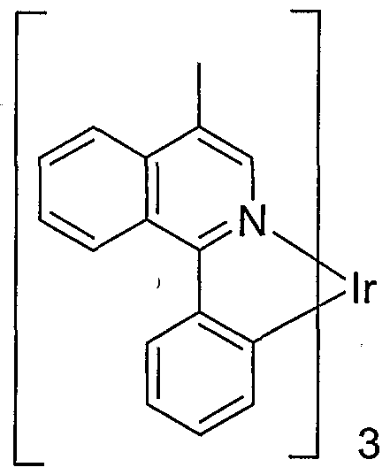
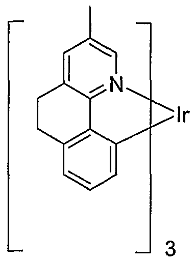


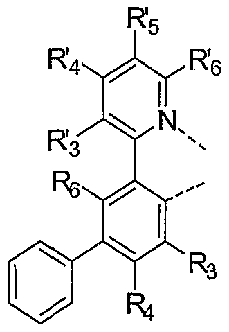


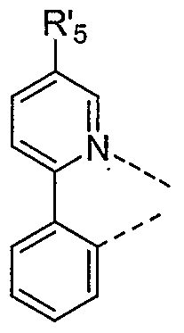


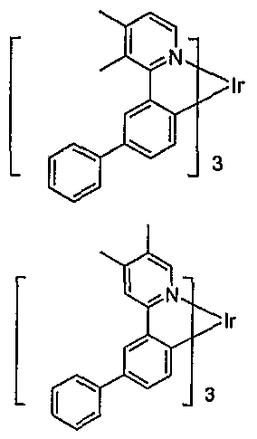


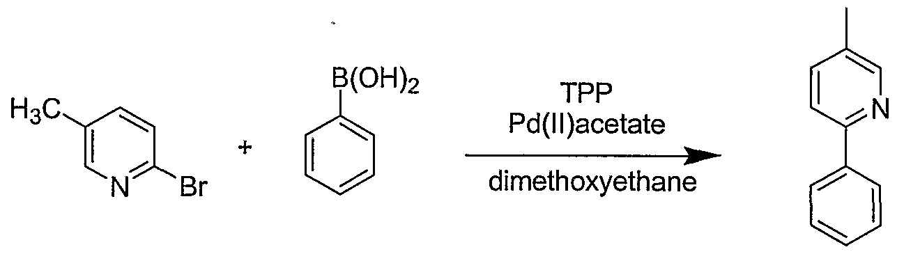


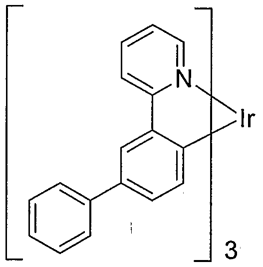
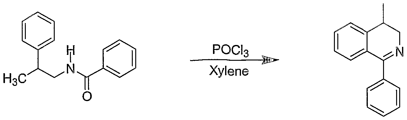


Claims
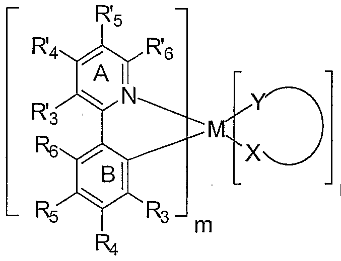

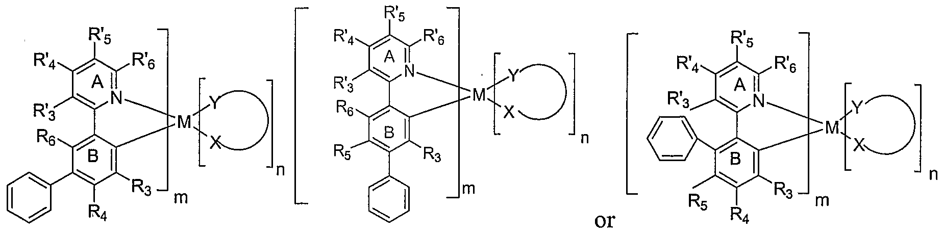

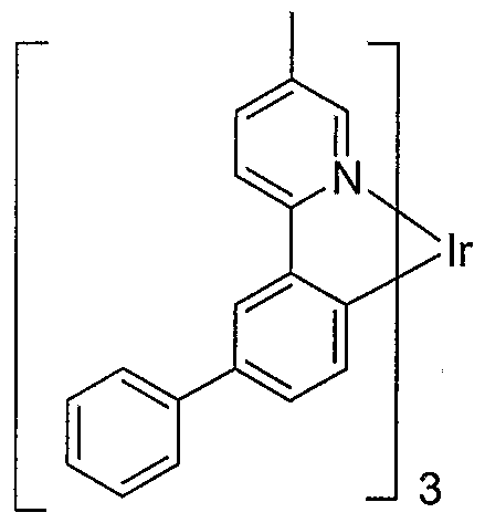


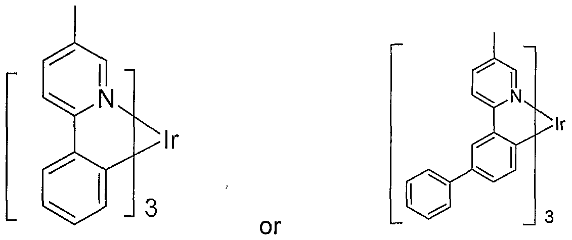


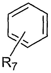


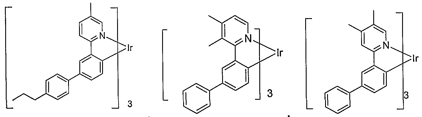


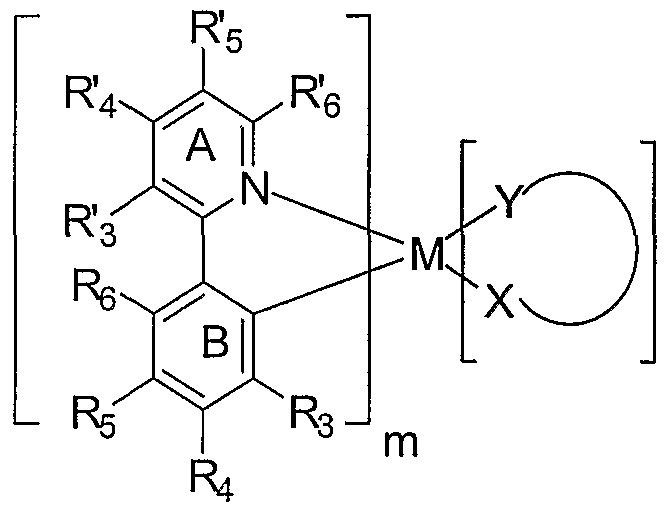


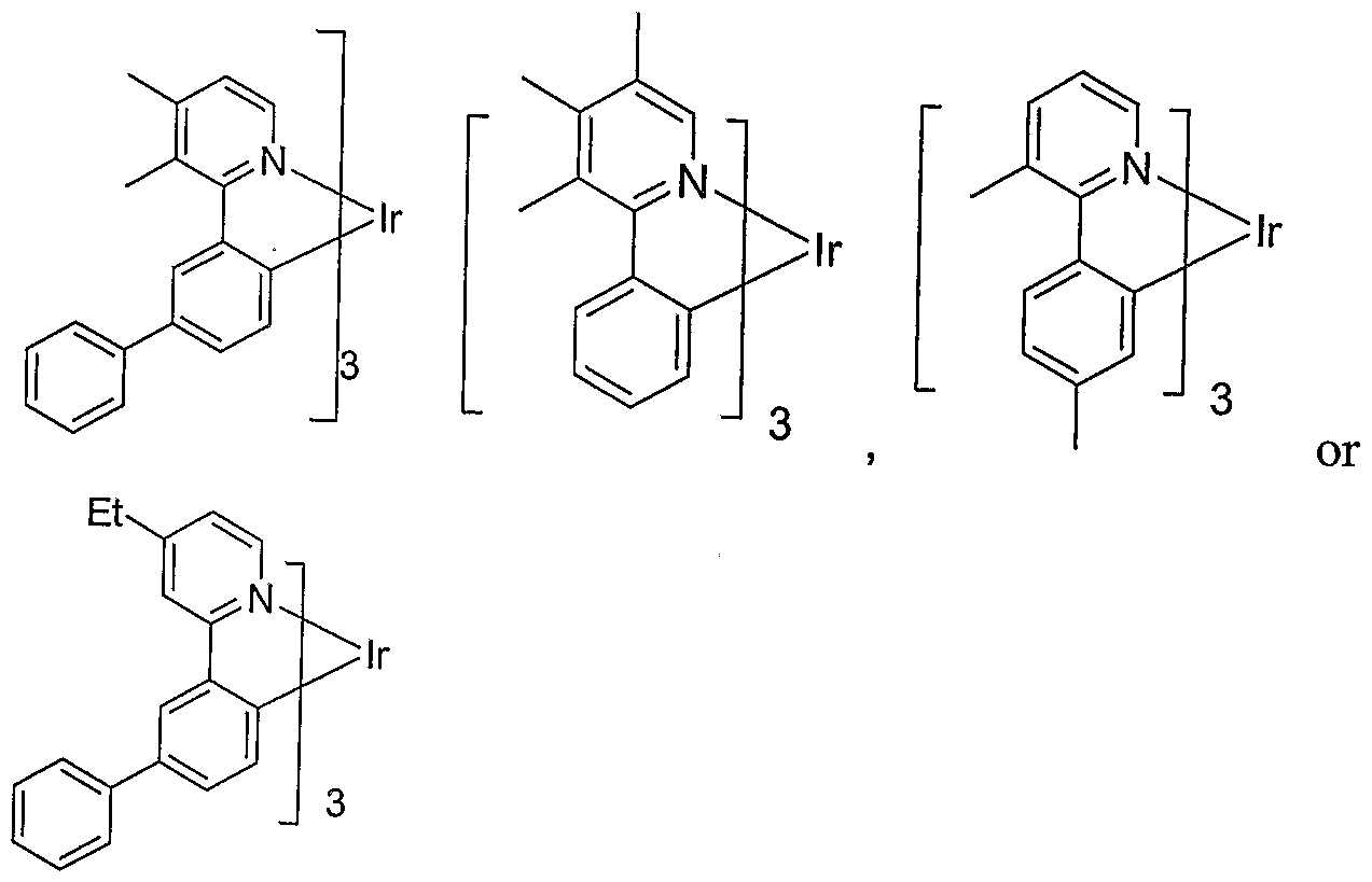
Priority Applications (6)
| Application Number | Priority Date | Filing Date | Title |
|---|---|---|---|
| EP20217507.1A EP3855519A3 (en) | 2004-07-07 | 2005-07-07 | Stable and efficient electroluminescent materials |
| KR1020127018882A KR101258042B1 (en) | 2004-07-07 | 2005-07-07 | Stable and efficient electroluminescent materials |
| EP18190646.2A EP3428986B1 (en) | 2004-07-07 | 2005-07-07 | Stable and efficient electroluminescent materials |
| EP05770339.9A EP1763902B1 (en) | 2004-07-07 | 2005-07-07 | Stable and efficient electroluminescent materials |
| CN2005800227847A CN101076902B (en) | 2004-07-07 | 2005-07-07 | Stable and effective electroluminescent material |
| JP2007520546A JP5009154B2 (en) | 2004-07-07 | 2005-07-07 | Stable and efficient electroluminescent material |
Applications Claiming Priority (6)
| Application Number | Priority Date | Filing Date | Title |
|---|---|---|---|
| US10/886,367 | 2004-07-07 | ||
| US10/886,367 US20060008671A1 (en) | 2004-07-07 | 2004-07-07 | Electroluminescent efficiency |
| US11/018,453 US7709100B2 (en) | 2004-07-07 | 2004-12-21 | Electroluminescent efficiency |
| US11/018,453 | 2004-12-21 | ||
| US68269005P | 2005-05-19 | 2005-05-19 | |
| US60/682,690 | 2005-05-19 |
Publications (2)
| Publication Number | Publication Date |
|---|---|
| WO2006014599A2 true WO2006014599A2 (en) | 2006-02-09 |
| WO2006014599A3 WO2006014599A3 (en) | 2006-06-22 |
Family
ID=35385734
Family Applications (1)
| Application Number | Title | Priority Date | Filing Date |
|---|---|---|---|
| PCT/US2005/024295 WO2006014599A2 (en) | 2004-07-07 | 2005-07-07 | Stable and efficient electroluminescent materials |
Country Status (5)
| Country | Link |
|---|---|
| EP (3) | EP3855519A3 (en) |
| JP (2) | JP5009154B2 (en) |
| KR (2) | KR101214539B1 (en) |
| TW (2) | TWI399421B (en) |
| WO (1) | WO2006014599A2 (en) |
Cited By (43)
| Publication number | Priority date | Publication date | Assignee | Title |
|---|---|---|---|---|
| EP1784057A1 (en) * | 2005-11-07 | 2007-05-09 | LG Electronics Inc. | Red phosphorescent compounds and organic electroluminescent devices using the same |
| WO2007086505A1 (en) * | 2006-01-27 | 2007-08-02 | Idemitsu Kosan Co., Ltd. | Transition metal complex compound and organic electroluminescent device using same |
| WO2007102350A1 (en) * | 2006-02-22 | 2007-09-13 | Sumitomo Chemical Company, Limited | Metal complex, polymeric compound, and element comprising these |
| JP2007302624A (en) * | 2006-05-12 | 2007-11-22 | Mitsubishi Chemicals Corp | Organic compound, charge transport material, composition for organic electroluminescent element and organic electroluminescent element |
| WO2008073440A2 (en) * | 2006-12-08 | 2008-06-19 | Universal Display Corporation | Cross-linkable iridium complexes and organic light-emitting devices using the same |
| WO2008111658A1 (en) | 2007-03-09 | 2008-09-18 | Sumitomo Chemical Company, Limited | Polymer compound and composition containing the same |
| WO2009073245A1 (en) * | 2007-12-06 | 2009-06-11 | Universal Display Corporation | Light-emitting organometallic complexes |
| WO2009073246A1 (en) * | 2007-12-06 | 2009-06-11 | Universal Display Corporation | Method for the synthesis of iridium (iii) complexes with sterically demanding ligands |
| JP2010515255A (en) * | 2006-12-28 | 2010-05-06 | ユニバーサル ディスプレイ コーポレイション | Long-life phosphorescent organic light-emitting device (OLED) structure |
| US8431243B2 (en) | 2007-03-08 | 2013-04-30 | Universal Display Corporation | Phosphorescent materials containing iridium complexes |
| WO2013133218A1 (en) * | 2012-03-05 | 2013-09-12 | 富士フイルム株式会社 | Photoelectric conversion element, method for using same, imaging element, optical sensor, and chemical |
| US8608986B2 (en) | 2006-12-27 | 2013-12-17 | Sumitomo Chemical Company, Limited | Metal complex, polymer compound and device containing those |
| WO2014042405A1 (en) * | 2012-09-11 | 2014-03-20 | Rohm And Haas Electronic Materials Korea Ltd. | A novel combination of a host compound and a dopant compound and an organic electroluminescence device comprising the same |
| US9023489B2 (en) | 2005-11-07 | 2015-05-05 | Lg Display Co., Ltd. | Red phosphorescent compounds and organic electroluminescent devices using the same |
| WO2015063046A1 (en) | 2013-10-31 | 2015-05-07 | Basf Se | Azadibenzothiophenes for electronic applications |
| WO2016016791A1 (en) | 2014-07-28 | 2016-02-04 | Idemitsu Kosan Co., Ltd (Ikc) | 2,9-functionalized benzimidazolo[1,2-a]benzimidazoles as hosts for organic light emitting diodes (oleds) |
| EP2982676A1 (en) | 2014-08-07 | 2016-02-10 | Idemitsu Kosan Co., Ltd. | Benzimidazo[2,1-B]benzoxazoles for electronic applications |
| EP2993215A1 (en) | 2014-09-04 | 2016-03-09 | Idemitsu Kosan Co., Ltd. | Azabenzimidazo[2,1-a]benzimidazoles for electronic applications |
| EP3015469A1 (en) | 2014-10-30 | 2016-05-04 | Idemitsu Kosan Co., Ltd. | 5-((benz)imidazol-2-yl)benzimidazo[1,2-a]benzimidazoles for electronic applications |
| WO2016079667A1 (en) | 2014-11-17 | 2016-05-26 | Idemitsu Kosan Co., Ltd. | Indole derivatives for electronic applications |
| US9359549B2 (en) | 2009-04-06 | 2016-06-07 | Universal Display Corporation | Organic electroluminescent materials and devices |
| EP3034507A1 (en) | 2014-12-15 | 2016-06-22 | Idemitsu Kosan Co., Ltd | 1-functionalized dibenzofurans and dibenzothiophenes for organic light emitting diodes (OLEDs) |
| EP3034506A1 (en) | 2014-12-15 | 2016-06-22 | Idemitsu Kosan Co., Ltd | 4-functionalized carbazole derivatives for electronic applications |
| EP3053918A1 (en) | 2015-02-06 | 2016-08-10 | Idemitsu Kosan Co., Ltd | 2-carbazole substituted benzimidazoles for electronic applications |
| EP3054498A1 (en) | 2015-02-06 | 2016-08-10 | Idemitsu Kosan Co., Ltd. | Bisimidazodiazocines |
| EP3061759A1 (en) | 2015-02-24 | 2016-08-31 | Idemitsu Kosan Co., Ltd | Nitrile substituted dibenzofurans |
| EP3070144A1 (en) | 2015-03-17 | 2016-09-21 | Idemitsu Kosan Co., Ltd. | Seven-membered ring compounds |
| EP3072943A1 (en) | 2015-03-26 | 2016-09-28 | Idemitsu Kosan Co., Ltd. | Dibenzofuran/carbazole-substituted benzonitriles |
| EP3075737A1 (en) | 2015-03-31 | 2016-10-05 | Idemitsu Kosan Co., Ltd | Benzimidazolo[1,2-a]benzimidazole carrying aryl- or heteroarylnitril groups for organic light emitting diodes |
| US9466804B2 (en) | 2013-01-17 | 2016-10-11 | Canon Kabushiki Kaisha | Organic light-emitting element |
| WO2017032439A1 (en) * | 2015-08-25 | 2017-03-02 | Merck Patent Gmbh | Metal complexes |
| EP3150604A1 (en) | 2015-10-01 | 2017-04-05 | Idemitsu Kosan Co., Ltd. | Benzimidazolo[1,2-a]benzimidazole carrying benzimidazolo[1,2-a]benzimidazolyl groups, carbazolyl groups, benzofurane groups or benzothiophene groups for organic light emitting diodes |
| EP3150606A1 (en) | 2015-10-01 | 2017-04-05 | Idemitsu Kosan Co., Ltd. | Benzimidazolo[1,2-a]benzimidazoles carrying benzofurane or benzothiophene groups for organic light emitting diodes |
| WO2017056055A1 (en) | 2015-10-01 | 2017-04-06 | Idemitsu Kosan Co., Ltd. | Benzimidazolo[1,2-a]benzimidazole carrying triazine groups for organic light emitting diodes |
| WO2017056053A1 (en) | 2015-10-01 | 2017-04-06 | Idemitsu Kosan Co., Ltd. | Benzimidazolo[1,2-a]benzimidazole carrying benzimidazolo[1,2-a]benzimidazolyl groups, carbazolyl groups, benzofurane groups or benzothiophene groups for organic light emitting diodes |
| WO2017078182A1 (en) | 2015-11-04 | 2017-05-11 | Idemitsu Kosan Co., Ltd. | Benzimidazole fused heteroaryls |
| WO2017093958A1 (en) | 2015-12-04 | 2017-06-08 | Idemitsu Kosan Co., Ltd. | Benzimidazolo[1,2-a]benzimidazole derivatives for organic light emitting diodes |
| WO2017178864A1 (en) | 2016-04-12 | 2017-10-19 | Idemitsu Kosan Co., Ltd. | Seven-membered ring compounds |
| US9853227B2 (en) | 2007-03-08 | 2017-12-26 | Universal Display Corporation | Organic electroluminescent materials and devices |
| US9917264B2 (en) | 2013-01-21 | 2018-03-13 | Canon Kabushiki Kaisha | Organometallic complex and organic light-emitting element using the complex |
| EP3318566A1 (en) | 2012-09-20 | 2018-05-09 | UDC Ireland Limited | Azadibenzofurans for electronic applications |
| US10008677B2 (en) | 2011-01-13 | 2018-06-26 | Universal Display Corporation | Materials for organic light emitting diode |
| CN110862420A (en) * | 2019-12-05 | 2020-03-06 | 陕西师范大学 | Energy transfer luminescent material based on triplet donor material and acceptor material and application thereof |
Families Citing this family (27)
| Publication number | Priority date | Publication date | Assignee | Title |
|---|---|---|---|---|
| EP3855519A3 (en) * | 2004-07-07 | 2021-09-22 | Universal Display Corporation | Stable and efficient electroluminescent materials |
| US20130032785A1 (en) * | 2011-08-01 | 2013-02-07 | Universal Display Corporation | Materials for organic light emitting diode |
| JP5279234B2 (en) * | 2007-11-02 | 2013-09-04 | キヤノン株式会社 | Platinum complex and organic light emitting device using the same |
| US8476822B2 (en) | 2007-11-09 | 2013-07-02 | Universal Display Corporation | Saturated color organic light emitting devices |
| JP2009238910A (en) * | 2008-03-26 | 2009-10-15 | Canon Inc | Organic light emitting device |
| JP5707704B2 (en) * | 2009-02-03 | 2015-04-30 | 三菱化学株式会社 | Organometallic complex, organometallic complex-containing composition, luminescent material, organic electroluminescent element material, organic electroluminescent element, organic EL display and organic EL lighting |
| JP5332690B2 (en) * | 2009-02-13 | 2013-11-06 | 三菱化学株式会社 | Organometallic complex composition, organometallic complex-containing composition, organic electroluminescence device, organic EL display and organic EL lighting |
| JP4474493B1 (en) * | 2009-07-31 | 2010-06-02 | 富士フイルム株式会社 | Organic electroluminescence device |
| JP2010185068A (en) | 2009-08-31 | 2010-08-26 | Fujifilm Corp | Organic electroluminescent device |
| JP5632274B2 (en) * | 2010-09-30 | 2014-11-26 | ユー・ディー・シー アイルランド リミテッド | Material for organic electroluminescent element, film containing the same, and organic electroluminescent element |
| JP5914500B2 (en) | 2011-09-12 | 2016-05-11 | 新日鉄住金化学株式会社 | Organic electroluminescence device |
| EP2762483A1 (en) | 2011-09-12 | 2014-08-06 | Nippon Steel & Sumikin Chemical Co., Ltd. | Organic electroluminescent element material having silicon-containing four membered ring structure, and organic electroluminescent element |
| US9142785B2 (en) | 2011-09-12 | 2015-09-22 | Nippon Steel & Sumikin Chemical Co., Ltd. | Organic electroluminescent element |
| EP2793280B1 (en) | 2011-12-12 | 2017-03-29 | Nippon Steel & Sumikin Chemical Co., Ltd. | Organic electroluminescent element material and organic electroluminescent element using same |
| US9985219B2 (en) | 2012-03-12 | 2018-05-29 | Nippon Steel & Sumikin Chemical Co., Ltd. | Organic electroluminescent element |
| CN104203968B (en) * | 2012-03-23 | 2017-05-03 | E.I.内穆尔杜邦公司 | Green luminescent materials |
| KR101431645B1 (en) * | 2012-06-26 | 2014-08-20 | 롬엔드하스전자재료코리아유한회사 | Light-Emitting Layer and Organic Electroluminescence Device comprising the same |
| CN104396042B (en) | 2012-06-28 | 2016-10-12 | 新日铁住金化学株式会社 | Material for organic electroluminescence device and organic electroluminescent device |
| WO2014013936A1 (en) | 2012-07-19 | 2014-01-23 | 新日鉄住金化学株式会社 | Organic electroluminescent element |
| TWI599570B (en) | 2012-09-28 | 2017-09-21 | 新日鐵住金化學股份有限公司 | Compounds for organic electroluminescent devices and organic electroluminescent devices |
| JP6357422B2 (en) | 2012-12-17 | 2018-07-11 | 新日鉄住金化学株式会社 | Organic electroluminescence device |
| WO2014189072A1 (en) | 2013-05-22 | 2014-11-27 | コニカミノルタ株式会社 | Electronic device, organic electroluminescent element, organic thin-film solar cell, and dye-sensitized solar cell |
| JP5403179B1 (en) | 2013-05-22 | 2014-01-29 | コニカミノルタ株式会社 | Charge transfer thin film |
| KR102418886B1 (en) * | 2014-12-29 | 2022-07-08 | 엘지디스플레이 주식회사 | Phosphorescent compound and Light emitting diode and Display device using the same |
| TWI650325B (en) * | 2017-12-11 | 2019-02-11 | 輔仁大學學校財團法人輔仁大學 | Organometallic ruthenium complex and simple synthesis method and use thereof |
| CN111868955A (en) | 2018-03-19 | 2020-10-30 | 日铁化学材料株式会社 | Organic electroluminescent element |
| KR102402410B1 (en) * | 2019-11-13 | 2022-05-26 | 고려대학교 산학협력단 | Iridium phosphorescent materials, the manufacturing method there of the same and the photophysical properties of the same |
Citations (5)
| Publication number | Priority date | Publication date | Assignee | Title |
|---|---|---|---|---|
| DE674400C (en) * | 1937-03-12 | 1939-04-14 | J D Riedel E De Haeen A G | Process for the dehydrogenation of dihydroisoquinoline compounds |
| EP1191613A2 (en) * | 2000-09-26 | 2002-03-27 | Canon Kabushiki Kaisha | Luminescence device, display apparatus and metal coordination compound |
| WO2003040257A1 (en) * | 2001-11-07 | 2003-05-15 | E. I. Du Pont De Nemours And Company | Electroluminescent platinum compounds and devices made with such compounds |
| WO2003069961A1 (en) * | 2002-02-14 | 2003-08-21 | E.I. Du Pont De Nemours And Company | Electroluminescent iridium compounds with phosphinoalkoxides and phenylpyridines or phenylpyrimidines and devices made with such compounds |
| EP1348711A1 (en) * | 2000-11-30 | 2003-10-01 | Canon Kabushiki Kaisha | Luminescent element and display |
Family Cites Families (65)
| Publication number | Priority date | Publication date | Assignee | Title |
|---|---|---|---|---|
| US78504A (en) | 1868-06-02 | Jonathan wolfrom | ||
| US287A (en) | 1837-07-19 | And john ericsson | ||
| JPS62138471A (en) * | 1985-12-12 | 1987-06-22 | Chisso Corp | Pyridine derivative |
| JPS62242665A (en) * | 1986-04-15 | 1987-10-23 | Chisso Corp | Pyridine derivative |
| JPS6363662A (en) * | 1986-09-05 | 1988-03-22 | Dainippon Ink & Chem Inc | Novel halogen-containing pyridine derivative |
| JP2534486B2 (en) * | 1987-01-13 | 1996-09-18 | セイコーエプソン株式会社 | Biphenyl pyridine derivative |
| US4769292A (en) | 1987-03-02 | 1988-09-06 | Eastman Kodak Company | Electroluminescent device with modified thin film luminescent zone |
| JPH01306493A (en) * | 1988-06-03 | 1989-12-11 | Chisso Corp | Ferroelectric liquid crystal composition |
| DE68917233T2 (en) * | 1988-09-08 | 1995-02-09 | Dainippon Ink & Chemicals | Liquid crystal device. |
| GB8909011D0 (en) | 1989-04-20 | 1989-06-07 | Friend Richard H | Electroluminescent devices |
| TW304203B (en) * | 1994-04-28 | 1997-05-01 | Chisso Corp | |
| US5703436A (en) | 1994-12-13 | 1997-12-30 | The Trustees Of Princeton University | Transparent contacts for organic devices |
| US5707745A (en) | 1994-12-13 | 1998-01-13 | The Trustees Of Princeton University | Multicolor organic light emitting devices |
| US6548956B2 (en) | 1994-12-13 | 2003-04-15 | The Trustees Of Princeton University | Transparent contacts for organic devices |
| US5844363A (en) * | 1997-01-23 | 1998-12-01 | The Trustees Of Princeton Univ. | Vacuum deposited, non-polymeric flexible organic light emitting devices |
| WO1998007173A1 (en) | 1996-08-12 | 1998-02-19 | The Trustees Of Princeton University | Non-polymeric flexible organic light emitting device |
| US6091195A (en) | 1997-02-03 | 2000-07-18 | The Trustees Of Princeton University | Displays having mesa pixel configuration |
| US6013982A (en) | 1996-12-23 | 2000-01-11 | The Trustees Of Princeton University | Multicolor display devices |
| US5834893A (en) | 1996-12-23 | 1998-11-10 | The Trustees Of Princeton University | High efficiency organic light emitting devices with light directing structures |
| US6303238B1 (en) | 1997-12-01 | 2001-10-16 | The Trustees Of Princeton University | OLEDs doped with phosphorescent compounds |
| US6337102B1 (en) | 1997-11-17 | 2002-01-08 | The Trustees Of Princeton University | Low pressure vapor phase deposition of organic thin films |
| US6087196A (en) | 1998-01-30 | 2000-07-11 | The Trustees Of Princeton University | Fabrication of organic semiconductor devices using ink jet printing |
| US6097147A (en) | 1998-09-14 | 2000-08-01 | The Trustees Of Princeton University | Structure for high efficiency electroluminescent device |
| US6830828B2 (en) | 1998-09-14 | 2004-12-14 | The Trustees Of Princeton University | Organometallic complexes as phosphorescent emitters in organic LEDs |
| GB9822963D0 (en) | 1998-10-20 | 1998-12-16 | Agner Erik | Improvements in or relating to chromatography |
| US6310360B1 (en) * | 1999-07-21 | 2001-10-30 | The Trustees Of Princeton University | Intersystem crossing agents for efficient utilization of excitons in organic light emitting devices |
| US6294398B1 (en) | 1999-11-23 | 2001-09-25 | The Trustees Of Princeton University | Method for patterning devices |
| US6821645B2 (en) * | 1999-12-27 | 2004-11-23 | Fuji Photo Film Co., Ltd. | Light-emitting material comprising orthometalated iridium complex, light-emitting device, high efficiency red light-emitting device, and novel iridium complex |
| DE60143106D1 (en) * | 2000-07-17 | 2010-11-04 | Fujifilm Corp | Light-emitting element and azole compound |
| JP4712232B2 (en) * | 2000-07-17 | 2011-06-29 | 富士フイルム株式会社 | Light emitting device and azole compound |
| JP4340401B2 (en) * | 2000-07-17 | 2009-10-07 | 富士フイルム株式会社 | Light emitting device and iridium complex |
| KR100884039B1 (en) | 2000-08-11 | 2009-02-19 | 더 트러스티즈 오브 프린스턴 유니버시티 | Organometallic compounds and emission-shifting organic electrophosphorescence |
| US6939624B2 (en) | 2000-08-11 | 2005-09-06 | Universal Display Corporation | Organometallic compounds and emission-shifting organic electrophosphorescence |
| JP2002184581A (en) * | 2000-12-13 | 2002-06-28 | Sanyo Electric Co Ltd | Organic luminescent element |
| JP4048525B2 (en) * | 2000-12-25 | 2008-02-20 | 富士フイルム株式会社 | Novel indole derivative and light emitting device using the same |
| JP3812730B2 (en) * | 2001-02-01 | 2006-08-23 | 富士写真フイルム株式会社 | Transition metal complex and light emitting device |
| JP3988915B2 (en) * | 2001-02-09 | 2007-10-10 | 富士フイルム株式会社 | Transition metal complex, light emitting device material comprising the same, and light emitting device |
| WO2002066552A1 (en) * | 2001-02-20 | 2002-08-29 | Isis Innovation Limited | Metal-containing dendrimers |
| JP4438042B2 (en) * | 2001-03-08 | 2010-03-24 | キヤノン株式会社 | Metal coordination compound, electroluminescent element and display device |
| US7294849B2 (en) | 2001-03-14 | 2007-11-13 | The Trustees Of Princeton University | Materials and devices for blue phosphorescence based organic light emitting diodes |
| JP4035976B2 (en) * | 2001-10-02 | 2008-01-23 | 昭和電工株式会社 | Polymerizable compound and method for producing the same |
| US6835469B2 (en) | 2001-10-17 | 2004-12-28 | The University Of Southern California | Phosphorescent compounds and devices comprising the same |
| JP4073211B2 (en) * | 2002-01-16 | 2008-04-09 | 三井化学株式会社 | Liquid crystal composition and liquid crystal element |
| JP2003253128A (en) * | 2002-02-28 | 2003-09-10 | Jsr Corp | Luminescent composition |
| JP4424996B2 (en) * | 2002-03-18 | 2010-03-03 | イシス イノベイション リミテッド | Phosphorescent dendrimer |
| JP4496709B2 (en) * | 2002-03-26 | 2010-07-07 | 住友化学株式会社 | Metal complex compound, polymer compound, and organic electroluminescence device |
| TWI277617B (en) * | 2002-03-26 | 2007-04-01 | Sumitomo Chemical Co | Metal complexes and organic electro luminescence elements |
| JP3890242B2 (en) * | 2002-03-26 | 2007-03-07 | キヤノン株式会社 | Polymer compound and electroluminescent device |
| JP3902981B2 (en) * | 2002-06-04 | 2007-04-11 | キヤノン株式会社 | Organic light emitting device and display device |
| JP2004027088A (en) * | 2002-06-27 | 2004-01-29 | Jsr Corp | Phosphorescent luminous agent, its preparing method and luminous composition |
| US6916554B2 (en) * | 2002-11-06 | 2005-07-12 | The University Of Southern California | Organic light emitting materials and devices |
| WO2004016711A1 (en) * | 2002-08-16 | 2004-02-26 | The University Of Southern California | Organic light emitting materials and devices |
| DE10238903A1 (en) * | 2002-08-24 | 2004-03-04 | Covion Organic Semiconductors Gmbh | New heteroaromatic rhodium and iridium complexes, useful in electroluminescent and/or phosphorescent devices as the emission layer and for use in solar cells, photovoltaic devices and organic photodetectors |
| GB0220080D0 (en) * | 2002-08-29 | 2002-10-09 | Isis Innovation | Blended dendrimers |
| GB0222268D0 (en) * | 2002-09-25 | 2002-10-30 | Isis Innovation | Fluorene-containing dendrimers |
| DE10249926A1 (en) * | 2002-10-26 | 2004-05-06 | Covion Organic Semiconductors Gmbh | Rhodium and iridium complexes |
| US20040086743A1 (en) * | 2002-11-06 | 2004-05-06 | Brown Cory S. | Organometallic compounds for use in electroluminescent devices |
| JP2004161661A (en) * | 2002-11-12 | 2004-06-10 | Takasago Internatl Corp | Method for producing iridium complex |
| KR100520937B1 (en) * | 2002-12-03 | 2005-10-17 | 엘지전자 주식회사 | Phenyl pyridine - iridium metal complex compounds for organic electroluminescent device, process for preparing them and organic electroluminescent device using them |
| JP2004319438A (en) * | 2003-03-28 | 2004-11-11 | Konica Minolta Holdings Inc | Organic electroluminescent element, display device, lighting system, and rhodium complex compound |
| JP2004292766A (en) * | 2003-03-28 | 2004-10-21 | Tokuyama Corp | Organic electroluminescent element material |
| JP2004355899A (en) * | 2003-05-28 | 2004-12-16 | Konica Minolta Holdings Inc | Organic electroluminescent element, illumination device, and display device |
| US7279232B2 (en) * | 2004-01-26 | 2007-10-09 | Universal Display Corporation | Electroluminescent stability |
| EP3855519A3 (en) * | 2004-07-07 | 2021-09-22 | Universal Display Corporation | Stable and efficient electroluminescent materials |
| US20060222886A1 (en) | 2005-04-04 | 2006-10-05 | Raymond Kwong | Arylpyrene compounds |
-
2005
- 2005-07-07 EP EP20217507.1A patent/EP3855519A3/en active Pending
- 2005-07-07 WO PCT/US2005/024295 patent/WO2006014599A2/en active Application Filing
- 2005-07-07 EP EP18190646.2A patent/EP3428986B1/en active Active
- 2005-07-07 JP JP2007520546A patent/JP5009154B2/en active Active
- 2005-07-07 TW TW094123051A patent/TWI399421B/en active
- 2005-07-07 TW TW102114261A patent/TWI479008B/en active
- 2005-07-07 KR KR1020077003035A patent/KR101214539B1/en active IP Right Grant
- 2005-07-07 KR KR1020127018882A patent/KR101258042B1/en active IP Right Grant
- 2005-07-07 EP EP05770339.9A patent/EP1763902B1/en active Active
-
2012
- 2012-03-29 JP JP2012076267A patent/JP5577370B2/en active Active
Patent Citations (5)
| Publication number | Priority date | Publication date | Assignee | Title |
|---|---|---|---|---|
| DE674400C (en) * | 1937-03-12 | 1939-04-14 | J D Riedel E De Haeen A G | Process for the dehydrogenation of dihydroisoquinoline compounds |
| EP1191613A2 (en) * | 2000-09-26 | 2002-03-27 | Canon Kabushiki Kaisha | Luminescence device, display apparatus and metal coordination compound |
| EP1348711A1 (en) * | 2000-11-30 | 2003-10-01 | Canon Kabushiki Kaisha | Luminescent element and display |
| WO2003040257A1 (en) * | 2001-11-07 | 2003-05-15 | E. I. Du Pont De Nemours And Company | Electroluminescent platinum compounds and devices made with such compounds |
| WO2003069961A1 (en) * | 2002-02-14 | 2003-08-21 | E.I. Du Pont De Nemours And Company | Electroluminescent iridium compounds with phosphinoalkoxides and phenylpyridines or phenylpyrimidines and devices made with such compounds |
Non-Patent Citations (8)
| Title |
|---|
| ABRAMOVITCH R A ET AL: "Orientation in the reaction of phenyllithium with 3-substituted pyridines" TETRAHEDRON LETTERS, vol. 1, no. 8, 1959, pages 1-3, XP002359275 ISSN: 0040-4039 * |
| BROOKS J ET AL: "Synthesis and characterization of phosphorescent cyclometalated platimun complexes" INORGANIC CHEMISTRY, vol. 41, no. 12, 2002, pages 3055-3066, XP002982403 ISSN: 0020-1669 * |
| GOLDSMITH J I ET AL: "Discovery and high-throughput screening of heteroleptic iridium complexes for photoinduced hydrogen production" JOURNAL OF THE AMERICAN CHEMICAL SOCIETY, vol. 127, no. 20, May 2005 (2005-05), pages 7502-7510, XP009057979 ISSN: 0002-7863 * |
| JUNG S ET AL: "Effect of substitution of methyl groups on the luminescence performance of IrIII complexes: Preparation, structures, electrochemistry, photophysical properties and their applications in organic light-emitting diodes (OLEDs)" EUROPEAN JOURNAL OF INORGANIC CHEMISTRY, no. 17, September 2004 (2004-09), pages 3415-2323, XP002359271 ISSN: 1434-1948 * |
| KOBAYASHI K ET AL: "New synthesis of isoquinoline derivatives by reactions of 2-(2-methoxyethenyl)benzonitriles with organolithiums and lithium dialkylamides" CHEMISTRY LETTERS, vol. 33, no. 3, 2004, pages 236-237, XP002359274 ISSN: 0366-7022 * |
| LOWRY M S ET AL: "Accelerated luminophore discovery through combinatorial synthesis" JOURNAL OF THE AMERICAN CHEMICAL SOCIETY, vol. 126, no. 43, 3 November 2004 (2004-11-03), pages 14129-14135, XP009057980 ISSN: 0002-7863 * |
| SLINKER J D ET AL: "Green electroluminescence from an ionic iridium complex" APPLIED PHYSICS LETTERS, vol. 86, no. 17, 25 April 2005 (2005-04-25), pages 173506-1, XP009057981 ISSN: 0003-6951 * |
| THOMAS S W ET AL: "Towards chemosensing phosphorescent conjugated polymers: cyclometalated platinum(II) poly(phenylene)s" JOURNAL OF MATERIALS CHEMISTRY, vol. 15, no. 27/28, 21 July 2005 (2005-07-21), pages 2829-2835, XP009057982 ISSN: 0959-9428 * |
Cited By (71)
| Publication number | Priority date | Publication date | Assignee | Title |
|---|---|---|---|---|
| EP1784057A1 (en) * | 2005-11-07 | 2007-05-09 | LG Electronics Inc. | Red phosphorescent compounds and organic electroluminescent devices using the same |
| US9023489B2 (en) | 2005-11-07 | 2015-05-05 | Lg Display Co., Ltd. | Red phosphorescent compounds and organic electroluminescent devices using the same |
| US8501328B2 (en) | 2005-11-07 | 2013-08-06 | Lg Display Co., Ltd. | Red phosphorescent compounds and organic electroluminescent devices using the same |
| WO2007086505A1 (en) * | 2006-01-27 | 2007-08-02 | Idemitsu Kosan Co., Ltd. | Transition metal complex compound and organic electroluminescent device using same |
| GB2478452B (en) * | 2006-02-22 | 2011-11-16 | Sumitomo Chemical Co | Fused ring metal complex, polymer compound and device containing it |
| GB2449796B (en) * | 2006-02-22 | 2011-11-16 | Sumitomo Chemical Co | Metal complex, polymer compound and device containing it |
| GB2478452A (en) * | 2006-02-22 | 2011-09-07 | Sumitomo Chemical Co | Fused ring metal complexes |
| GB2478450A (en) * | 2006-02-22 | 2011-09-07 | Sumitomo Chemical Co | Bridged ring metal complexes |
| WO2007102350A1 (en) * | 2006-02-22 | 2007-09-13 | Sumitomo Chemical Company, Limited | Metal complex, polymeric compound, and element comprising these |
| GB2449796A (en) * | 2006-02-22 | 2008-12-03 | Sumitomo Chemical Co | Metal complex,polymeric compound,and element comprising these |
| GB2478450B (en) * | 2006-02-22 | 2011-11-16 | Sumitomo Chemical Co | Bridged metal complex, polymer compound and device containing it |
| JP2008169192A (en) * | 2006-02-22 | 2008-07-24 | Sumitomo Chemical Co Ltd | Metal complex, polymer compound, and element containing them |
| JP2007302624A (en) * | 2006-05-12 | 2007-11-22 | Mitsubishi Chemicals Corp | Organic compound, charge transport material, composition for organic electroluminescent element and organic electroluminescent element |
| WO2008073440A2 (en) * | 2006-12-08 | 2008-06-19 | Universal Display Corporation | Cross-linkable iridium complexes and organic light-emitting devices using the same |
| US8119255B2 (en) | 2006-12-08 | 2012-02-21 | Universal Display Corporation | Cross-linkable iridium complexes and organic light-emitting devices using the same |
| US9065062B2 (en) | 2006-12-08 | 2015-06-23 | Universal Display Corporation | Cross-linkable iridium complexes and organic light-emitting devices using the same |
| US8778508B2 (en) | 2006-12-08 | 2014-07-15 | Universal Display Corporation | Light-emitting organometallic complexes |
| US8519130B2 (en) | 2006-12-08 | 2013-08-27 | Universal Display Corporation | Method for synthesis of iriduim (III) complexes with sterically demanding ligands |
| WO2008073440A3 (en) * | 2006-12-08 | 2008-12-18 | Universal Display Corp | Cross-linkable iridium complexes and organic light-emitting devices using the same |
| US8608986B2 (en) | 2006-12-27 | 2013-12-17 | Sumitomo Chemical Company, Limited | Metal complex, polymer compound and device containing those |
| JP2014041846A (en) * | 2006-12-28 | 2014-03-06 | Universal Display Corp | Long life phosphorescent organic light emitting device (oled) structure |
| JP2010515255A (en) * | 2006-12-28 | 2010-05-06 | ユニバーサル ディスプレイ コーポレイション | Long-life phosphorescent organic light-emitting device (OLED) structure |
| US8866377B2 (en) | 2006-12-28 | 2014-10-21 | Universal Display Corporation | Long lifetime phosphorescent organic light emitting device (OLED) structures |
| US10600975B2 (en) | 2007-03-08 | 2020-03-24 | Universal Display Corporation | Organic electroluminescent materials and devices |
| JP2014012710A (en) * | 2007-03-08 | 2014-01-23 | Universal Display Corp | Phosphorescent materials |
| US10230060B2 (en) | 2007-03-08 | 2019-03-12 | Universal Display Corporation | Organic electroluminescent materials and devices |
| US9911930B2 (en) | 2007-03-08 | 2018-03-06 | Universal Display Corporation | Organic electroluminescent materials and devices |
| US9853227B2 (en) | 2007-03-08 | 2017-12-26 | Universal Display Corporation | Organic electroluminescent materials and devices |
| US8431243B2 (en) | 2007-03-08 | 2013-04-30 | Universal Display Corporation | Phosphorescent materials containing iridium complexes |
| US11495755B2 (en) | 2007-03-08 | 2022-11-08 | Universal Display Corporation | Organic electroluminescent materials and devices |
| WO2008111658A1 (en) | 2007-03-09 | 2008-09-18 | Sumitomo Chemical Company, Limited | Polymer compound and composition containing the same |
| WO2009073245A1 (en) * | 2007-12-06 | 2009-06-11 | Universal Display Corporation | Light-emitting organometallic complexes |
| WO2009073246A1 (en) * | 2007-12-06 | 2009-06-11 | Universal Display Corporation | Method for the synthesis of iridium (iii) complexes with sterically demanding ligands |
| US9359549B2 (en) | 2009-04-06 | 2016-06-07 | Universal Display Corporation | Organic electroluminescent materials and devices |
| US10680189B2 (en) | 2011-01-13 | 2020-06-09 | Universal Display Corporation | Materials for organic light emitting diodes |
| US11374180B2 (en) | 2011-01-13 | 2022-06-28 | Universal Display Corporation | Organic electroluminescent materials and devices |
| US10008677B2 (en) | 2011-01-13 | 2018-06-26 | Universal Display Corporation | Materials for organic light emitting diode |
| WO2013133218A1 (en) * | 2012-03-05 | 2013-09-12 | 富士フイルム株式会社 | Photoelectric conversion element, method for using same, imaging element, optical sensor, and chemical |
| WO2014042405A1 (en) * | 2012-09-11 | 2014-03-20 | Rohm And Haas Electronic Materials Korea Ltd. | A novel combination of a host compound and a dopant compound and an organic electroluminescence device comprising the same |
| US10249827B2 (en) | 2012-09-20 | 2019-04-02 | Udc Ireland Limited | Azadibenzofurans for electronic applications |
| EP3318566A1 (en) | 2012-09-20 | 2018-05-09 | UDC Ireland Limited | Azadibenzofurans for electronic applications |
| US9466804B2 (en) | 2013-01-17 | 2016-10-11 | Canon Kabushiki Kaisha | Organic light-emitting element |
| US9917264B2 (en) | 2013-01-21 | 2018-03-13 | Canon Kabushiki Kaisha | Organometallic complex and organic light-emitting element using the complex |
| WO2015063046A1 (en) | 2013-10-31 | 2015-05-07 | Basf Se | Azadibenzothiophenes for electronic applications |
| WO2016016791A1 (en) | 2014-07-28 | 2016-02-04 | Idemitsu Kosan Co., Ltd (Ikc) | 2,9-functionalized benzimidazolo[1,2-a]benzimidazoles as hosts for organic light emitting diodes (oleds) |
| EP2982676A1 (en) | 2014-08-07 | 2016-02-10 | Idemitsu Kosan Co., Ltd. | Benzimidazo[2,1-B]benzoxazoles for electronic applications |
| EP2993215A1 (en) | 2014-09-04 | 2016-03-09 | Idemitsu Kosan Co., Ltd. | Azabenzimidazo[2,1-a]benzimidazoles for electronic applications |
| EP3015469A1 (en) | 2014-10-30 | 2016-05-04 | Idemitsu Kosan Co., Ltd. | 5-((benz)imidazol-2-yl)benzimidazo[1,2-a]benzimidazoles for electronic applications |
| WO2016067261A1 (en) | 2014-10-30 | 2016-05-06 | Idemitsu Kosan Co., Ltd. | 5-((benz)imidazol-2-yl)benzimidazo[1,2-a]benzimidazoles for electronic applications |
| WO2016079667A1 (en) | 2014-11-17 | 2016-05-26 | Idemitsu Kosan Co., Ltd. | Indole derivatives for electronic applications |
| EP3034507A1 (en) | 2014-12-15 | 2016-06-22 | Idemitsu Kosan Co., Ltd | 1-functionalized dibenzofurans and dibenzothiophenes for organic light emitting diodes (OLEDs) |
| EP3034506A1 (en) | 2014-12-15 | 2016-06-22 | Idemitsu Kosan Co., Ltd | 4-functionalized carbazole derivatives for electronic applications |
| EP3053918A1 (en) | 2015-02-06 | 2016-08-10 | Idemitsu Kosan Co., Ltd | 2-carbazole substituted benzimidazoles for electronic applications |
| EP3054498A1 (en) | 2015-02-06 | 2016-08-10 | Idemitsu Kosan Co., Ltd. | Bisimidazodiazocines |
| WO2016125110A1 (en) | 2015-02-06 | 2016-08-11 | Idemitsu Kosan Co., Ltd. | Bisimidazolodiazocines |
| EP3061759A1 (en) | 2015-02-24 | 2016-08-31 | Idemitsu Kosan Co., Ltd | Nitrile substituted dibenzofurans |
| EP3070144A1 (en) | 2015-03-17 | 2016-09-21 | Idemitsu Kosan Co., Ltd. | Seven-membered ring compounds |
| EP3072943A1 (en) | 2015-03-26 | 2016-09-28 | Idemitsu Kosan Co., Ltd. | Dibenzofuran/carbazole-substituted benzonitriles |
| EP3075737A1 (en) | 2015-03-31 | 2016-10-05 | Idemitsu Kosan Co., Ltd | Benzimidazolo[1,2-a]benzimidazole carrying aryl- or heteroarylnitril groups for organic light emitting diodes |
| WO2016157113A1 (en) | 2015-03-31 | 2016-10-06 | Idemitsu Kosan Co., Ltd. | Benzimidazolo[1,2-a]benzimidazole carrying aryl- or heteroarylnitril groups for organic light emitting diodes |
| US11031562B2 (en) | 2015-08-25 | 2021-06-08 | Merck Patent Gmbh | Metal complexes |
| WO2017032439A1 (en) * | 2015-08-25 | 2017-03-02 | Merck Patent Gmbh | Metal complexes |
| WO2017056053A1 (en) | 2015-10-01 | 2017-04-06 | Idemitsu Kosan Co., Ltd. | Benzimidazolo[1,2-a]benzimidazole carrying benzimidazolo[1,2-a]benzimidazolyl groups, carbazolyl groups, benzofurane groups or benzothiophene groups for organic light emitting diodes |
| WO2017056055A1 (en) | 2015-10-01 | 2017-04-06 | Idemitsu Kosan Co., Ltd. | Benzimidazolo[1,2-a]benzimidazole carrying triazine groups for organic light emitting diodes |
| WO2017056052A1 (en) | 2015-10-01 | 2017-04-06 | Idemitsu Kosan Co., Ltd. | Benzimidazolo[1,2-a]benzimidazole carrying benzimidazolo[1,2-a]benzimidazolyl groups, carbazolyl groups, benzofurane groups or benzothiophene groups for organic light emitting diodes |
| EP3150606A1 (en) | 2015-10-01 | 2017-04-05 | Idemitsu Kosan Co., Ltd. | Benzimidazolo[1,2-a]benzimidazoles carrying benzofurane or benzothiophene groups for organic light emitting diodes |
| EP3150604A1 (en) | 2015-10-01 | 2017-04-05 | Idemitsu Kosan Co., Ltd. | Benzimidazolo[1,2-a]benzimidazole carrying benzimidazolo[1,2-a]benzimidazolyl groups, carbazolyl groups, benzofurane groups or benzothiophene groups for organic light emitting diodes |
| WO2017078182A1 (en) | 2015-11-04 | 2017-05-11 | Idemitsu Kosan Co., Ltd. | Benzimidazole fused heteroaryls |
| WO2017093958A1 (en) | 2015-12-04 | 2017-06-08 | Idemitsu Kosan Co., Ltd. | Benzimidazolo[1,2-a]benzimidazole derivatives for organic light emitting diodes |
| WO2017178864A1 (en) | 2016-04-12 | 2017-10-19 | Idemitsu Kosan Co., Ltd. | Seven-membered ring compounds |
| CN110862420A (en) * | 2019-12-05 | 2020-03-06 | 陕西师范大学 | Energy transfer luminescent material based on triplet donor material and acceptor material and application thereof |
Also Published As
| Publication number | Publication date |
|---|---|
| KR20070050438A (en) | 2007-05-15 |
| JP2008505925A (en) | 2008-02-28 |
| TW201333161A (en) | 2013-08-16 |
| KR20120089376A (en) | 2012-08-09 |
| KR101214539B1 (en) | 2012-12-24 |
| TWI399421B (en) | 2013-06-21 |
| EP1763902A2 (en) | 2007-03-21 |
| EP3428986A1 (en) | 2019-01-16 |
| JP5009154B2 (en) | 2012-08-22 |
| EP3855519A2 (en) | 2021-07-28 |
| TW200621935A (en) | 2006-07-01 |
| WO2006014599A3 (en) | 2006-06-22 |
| EP1763902B1 (en) | 2018-08-29 |
| JP2012149083A (en) | 2012-08-09 |
| JP5577370B2 (en) | 2014-08-20 |
| KR101258042B1 (en) | 2013-04-24 |
| TWI479008B (en) | 2015-04-01 |
| EP3428986B1 (en) | 2021-01-20 |
| EP3855519A3 (en) | 2021-09-22 |
Similar Documents
| Publication | Publication Date | Title |
|---|---|---|
| EP1763902B1 (en) | Stable and efficient electroluminescent materials | |
| EP2378582A1 (en) | Stable and efficient electroluminescent materials | |
| US8603645B2 (en) | Stable and efficient electroluminescent materials | |
| EP2267097B1 (en) | Improved electroluminescent stability | |
| US6858327B2 (en) | Organic light emitting materials and devices | |
| US20060088728A1 (en) | Arylcarbazoles as hosts in PHOLEDs | |
| US20040102632A1 (en) | Organic light emitting materials with anionic ligand | |
| WO2005076380A2 (en) | Oleds utilizing multidentate ligand systems | |
| WO2006046980A1 (en) | Organic light emitting materials and devices | |
| WO2008054584A1 (en) | Improved stability oled materials and devices | |
| EP1534799A1 (en) | Organic light emitting materials and devices | |
| WO2006121811A1 (en) | Stability oled materials and devices with improved stability | |
| US20060008671A1 (en) | Electroluminescent efficiency |
Legal Events
| Date | Code | Title | Description |
|---|---|---|---|
| AK | Designated states |
Kind code of ref document: A2 Designated state(s): AE AG AL AM AT AU AZ BA BB BG BR BW BY BZ CA CH CN CO CR CU CZ DE DK DM DZ EC EE EG ES FI GB GD GE GH GM HR HU ID IL IN IS JP KE KG KM KP KR KZ LC LK LR LS LT LU LV MA MD MG MK MN MW MX MZ NA NG NI NO NZ OM PG PH PL PT RO RU SC SD SE SG SK SL SM SY TJ TM TN TR TT TZ UA UG US UZ VC VN YU ZA ZM ZW |
|
| AL | Designated countries for regional patents |
Kind code of ref document: A2 Designated state(s): BW GH GM KE LS MW MZ NA SD SL SZ TZ UG ZM ZW AM AZ BY KG KZ MD RU TJ TM AT BE BG CH CY CZ DE DK EE ES FI FR GB GR HU IE IS IT LT LU LV MC NL PL PT RO SE SI SK TR BF BJ CF CG CI CM GA GN GQ GW ML MR NE SN TD TG |
|
| 121 | Ep: the epo has been informed by wipo that ep was designated in this application | ||
| WWE | Wipo information: entry into national phase |
Ref document number: 2005770339 Country of ref document: EP |
|
| WWE | Wipo information: entry into national phase |
Ref document number: 7643/DELNP/2006 Country of ref document: IN |
|
| WWE | Wipo information: entry into national phase |
Ref document number: 2007520546 Country of ref document: JP Ref document number: 200580022784.7 Country of ref document: CN |
|
| NENP | Non-entry into the national phase |
Ref country code: DE |
|
| WWW | Wipo information: withdrawn in national office |
Ref document number: DE |
|
| WWE | Wipo information: entry into national phase |
Ref document number: 1020077003035 Country of ref document: KR |
|
| WWP | Wipo information: published in national office |
Ref document number: 2005770339 Country of ref document: EP |