WO2006033836A2 - Treating agent materials - Google Patents
Treating agent materials Download PDFInfo
- Publication number
- WO2006033836A2 WO2006033836A2 PCT/US2005/031936 US2005031936W WO2006033836A2 WO 2006033836 A2 WO2006033836 A2 WO 2006033836A2 US 2005031936 W US2005031936 W US 2005031936W WO 2006033836 A2 WO2006033836 A2 WO 2006033836A2
- Authority
- WO
- WIPO (PCT)
- Prior art keywords
- solvent
- dielectric film
- organosilicate glass
- composition
- glass dielectric
- Prior art date
Links
Classifications
-
- H—ELECTRICITY
- H01—ELECTRIC ELEMENTS
- H01L—SEMICONDUCTOR DEVICES NOT COVERED BY CLASS H10
- H01L21/00—Processes or apparatus adapted for the manufacture or treatment of semiconductor or solid state devices or of parts thereof
- H01L21/02—Manufacture or treatment of semiconductor devices or of parts thereof
- H01L21/04—Manufacture or treatment of semiconductor devices or of parts thereof the devices having at least one potential-jump barrier or surface barrier, e.g. PN junction, depletion layer or carrier concentration layer
- H01L21/18—Manufacture or treatment of semiconductor devices or of parts thereof the devices having at least one potential-jump barrier or surface barrier, e.g. PN junction, depletion layer or carrier concentration layer the devices having semiconductor bodies comprising elements of Group IV of the Periodic System or AIIIBV compounds with or without impurities, e.g. doping materials
- H01L21/30—Treatment of semiconductor bodies using processes or apparatus not provided for in groups H01L21/20 - H01L21/26
- H01L21/31—Treatment of semiconductor bodies using processes or apparatus not provided for in groups H01L21/20 - H01L21/26 to form insulating layers thereon, e.g. for masking or by using photolithographic techniques; After treatment of these layers; Selection of materials for these layers
- H01L21/3105—After-treatment
-
- H—ELECTRICITY
- H01—ELECTRIC ELEMENTS
- H01L—SEMICONDUCTOR DEVICES NOT COVERED BY CLASS H10
- H01L21/00—Processes or apparatus adapted for the manufacture or treatment of semiconductor or solid state devices or of parts thereof
- H01L21/02—Manufacture or treatment of semiconductor devices or of parts thereof
- H01L21/02104—Forming layers
- H01L21/02107—Forming insulating materials on a substrate
- H01L21/02109—Forming insulating materials on a substrate characterised by the type of layer, e.g. type of material, porous/non-porous, pre-cursors, mixtures or laminates
- H01L21/02112—Forming insulating materials on a substrate characterised by the type of layer, e.g. type of material, porous/non-porous, pre-cursors, mixtures or laminates characterised by the material of the layer
- H01L21/02123—Forming insulating materials on a substrate characterised by the type of layer, e.g. type of material, porous/non-porous, pre-cursors, mixtures or laminates characterised by the material of the layer the material containing silicon
- H01L21/02126—Forming insulating materials on a substrate characterised by the type of layer, e.g. type of material, porous/non-porous, pre-cursors, mixtures or laminates characterised by the material of the layer the material containing silicon the material containing Si, O, and at least one of H, N, C, F, or other non-metal elements, e.g. SiOC, SiOC:H or SiONC
-
- H—ELECTRICITY
- H01—ELECTRIC ELEMENTS
- H01L—SEMICONDUCTOR DEVICES NOT COVERED BY CLASS H10
- H01L21/00—Processes or apparatus adapted for the manufacture or treatment of semiconductor or solid state devices or of parts thereof
- H01L21/02—Manufacture or treatment of semiconductor devices or of parts thereof
- H01L21/02104—Forming layers
- H01L21/02107—Forming insulating materials on a substrate
- H01L21/02109—Forming insulating materials on a substrate characterised by the type of layer, e.g. type of material, porous/non-porous, pre-cursors, mixtures or laminates
- H01L21/02203—Forming insulating materials on a substrate characterised by the type of layer, e.g. type of material, porous/non-porous, pre-cursors, mixtures or laminates the layer being porous
-
- H—ELECTRICITY
- H01—ELECTRIC ELEMENTS
- H01L—SEMICONDUCTOR DEVICES NOT COVERED BY CLASS H10
- H01L21/00—Processes or apparatus adapted for the manufacture or treatment of semiconductor or solid state devices or of parts thereof
- H01L21/70—Manufacture or treatment of devices consisting of a plurality of solid state components formed in or on a common substrate or of parts thereof; Manufacture of integrated circuit devices or of parts thereof
- H01L21/71—Manufacture of specific parts of devices defined in group H01L21/70
- H01L21/768—Applying interconnections to be used for carrying current between separate components within a device comprising conductors and dielectrics
- H01L21/76801—Applying interconnections to be used for carrying current between separate components within a device comprising conductors and dielectrics characterised by the formation and the after-treatment of the dielectrics, e.g. smoothing
- H01L21/76802—Applying interconnections to be used for carrying current between separate components within a device comprising conductors and dielectrics characterised by the formation and the after-treatment of the dielectrics, e.g. smoothing by forming openings in dielectrics
- H01L21/76814—Applying interconnections to be used for carrying current between separate components within a device comprising conductors and dielectrics characterised by the formation and the after-treatment of the dielectrics, e.g. smoothing by forming openings in dielectrics post-treatment or after-treatment, e.g. cleaning or removal of oxides on underlying conductors
-
- H—ELECTRICITY
- H01—ELECTRIC ELEMENTS
- H01L—SEMICONDUCTOR DEVICES NOT COVERED BY CLASS H10
- H01L21/00—Processes or apparatus adapted for the manufacture or treatment of semiconductor or solid state devices or of parts thereof
- H01L21/02—Manufacture or treatment of semiconductor devices or of parts thereof
- H01L21/02104—Forming layers
- H01L21/02107—Forming insulating materials on a substrate
- H01L21/02109—Forming insulating materials on a substrate characterised by the type of layer, e.g. type of material, porous/non-porous, pre-cursors, mixtures or laminates
- H01L21/02205—Forming insulating materials on a substrate characterised by the type of layer, e.g. type of material, porous/non-porous, pre-cursors, mixtures or laminates the layer being characterised by the precursor material for deposition
- H01L21/02208—Forming insulating materials on a substrate characterised by the type of layer, e.g. type of material, porous/non-porous, pre-cursors, mixtures or laminates the layer being characterised by the precursor material for deposition the precursor containing a compound comprising Si
- H01L21/02214—Forming insulating materials on a substrate characterised by the type of layer, e.g. type of material, porous/non-porous, pre-cursors, mixtures or laminates the layer being characterised by the precursor material for deposition the precursor containing a compound comprising Si the compound comprising silicon and oxygen
- H01L21/02216—Forming insulating materials on a substrate characterised by the type of layer, e.g. type of material, porous/non-porous, pre-cursors, mixtures or laminates the layer being characterised by the precursor material for deposition the precursor containing a compound comprising Si the compound comprising silicon and oxygen the compound being a molecule comprising at least one silicon-oxygen bond and the compound having hydrogen or an organic group attached to the silicon or oxygen, e.g. a siloxane
-
- H—ELECTRICITY
- H01—ELECTRIC ELEMENTS
- H01L—SEMICONDUCTOR DEVICES NOT COVERED BY CLASS H10
- H01L21/00—Processes or apparatus adapted for the manufacture or treatment of semiconductor or solid state devices or of parts thereof
- H01L21/02—Manufacture or treatment of semiconductor devices or of parts thereof
- H01L21/02104—Forming layers
- H01L21/02107—Forming insulating materials on a substrate
- H01L21/02109—Forming insulating materials on a substrate characterised by the type of layer, e.g. type of material, porous/non-porous, pre-cursors, mixtures or laminates
- H01L21/02205—Forming insulating materials on a substrate characterised by the type of layer, e.g. type of material, porous/non-porous, pre-cursors, mixtures or laminates the layer being characterised by the precursor material for deposition
- H01L21/02208—Forming insulating materials on a substrate characterised by the type of layer, e.g. type of material, porous/non-porous, pre-cursors, mixtures or laminates the layer being characterised by the precursor material for deposition the precursor containing a compound comprising Si
- H01L21/02219—Forming insulating materials on a substrate characterised by the type of layer, e.g. type of material, porous/non-porous, pre-cursors, mixtures or laminates the layer being characterised by the precursor material for deposition the precursor containing a compound comprising Si the compound comprising silicon and nitrogen
- H01L21/02222—Forming insulating materials on a substrate characterised by the type of layer, e.g. type of material, porous/non-porous, pre-cursors, mixtures or laminates the layer being characterised by the precursor material for deposition the precursor containing a compound comprising Si the compound comprising silicon and nitrogen the compound being a silazane
-
- H—ELECTRICITY
- H01—ELECTRIC ELEMENTS
- H01L—SEMICONDUCTOR DEVICES NOT COVERED BY CLASS H10
- H01L21/00—Processes or apparatus adapted for the manufacture or treatment of semiconductor or solid state devices or of parts thereof
- H01L21/02—Manufacture or treatment of semiconductor devices or of parts thereof
- H01L21/02104—Forming layers
- H01L21/02107—Forming insulating materials on a substrate
- H01L21/02225—Forming insulating materials on a substrate characterised by the process for the formation of the insulating layer
- H01L21/0226—Forming insulating materials on a substrate characterised by the process for the formation of the insulating layer formation by a deposition process
- H01L21/02282—Forming insulating materials on a substrate characterised by the process for the formation of the insulating layer formation by a deposition process liquid deposition, e.g. spin-coating, sol-gel techniques, spray coating
-
- H—ELECTRICITY
- H01—ELECTRIC ELEMENTS
- H01L—SEMICONDUCTOR DEVICES NOT COVERED BY CLASS H10
- H01L21/00—Processes or apparatus adapted for the manufacture or treatment of semiconductor or solid state devices or of parts thereof
- H01L21/02—Manufacture or treatment of semiconductor devices or of parts thereof
- H01L21/02104—Forming layers
- H01L21/02107—Forming insulating materials on a substrate
- H01L21/02296—Forming insulating materials on a substrate characterised by the treatment performed before or after the formation of the layer
- H01L21/02318—Forming insulating materials on a substrate characterised by the treatment performed before or after the formation of the layer post-treatment
- H01L21/02343—Forming insulating materials on a substrate characterised by the treatment performed before or after the formation of the layer post-treatment treatment by exposure to a liquid
-
- H—ELECTRICITY
- H01—ELECTRIC ELEMENTS
- H01L—SEMICONDUCTOR DEVICES NOT COVERED BY CLASS H10
- H01L21/00—Processes or apparatus adapted for the manufacture or treatment of semiconductor or solid state devices or of parts thereof
- H01L21/02—Manufacture or treatment of semiconductor devices or of parts thereof
- H01L21/02104—Forming layers
- H01L21/02107—Forming insulating materials on a substrate
- H01L21/02296—Forming insulating materials on a substrate characterised by the treatment performed before or after the formation of the layer
- H01L21/02318—Forming insulating materials on a substrate characterised by the treatment performed before or after the formation of the layer post-treatment
- H01L21/02359—Forming insulating materials on a substrate characterised by the treatment performed before or after the formation of the layer post-treatment treatment to change the surface groups of the insulating layer
Definitions
- the invention concerns a treating agent composition for organosilicate glass dielectric films. More particularly, the invention pertains to a method for restoring hydrophobicity to the surfaces of organosilicate glass dielectric films which have been subjected to an etching or ashing treatment in such a way as to remove at least a portion of previously existing carbon containing moieties, resulting in a film having reduced hydrophobicity.
- These treated films are used as insulating materials in the manufacture of semiconductor devices such as integrated circuits ("ICs"), in order to ensure low dielectric constant and stable dielectric properties in these films.
- compositions include a silane based monomer with reactive leaving groups, an activating agent which may be an acid, a base, an onium compound, a dehydrating agent, and combinations thereof and a solvent or mixture of a main solvent and a co-solvent.
- an activating agent which may be an acid, a base, an onium compound, a dehydrating agent, and combinations thereof and a solvent or mixture of a main solvent and a co-solvent.
- Porous low k's have even more catastrophic effects from reactive etch and ash gases due to diffusion through the film, which causes a greater extent of damage at the internal pore walls.
- the films rehydroxylate and hydrogen bond with water. Because water has a dielectric constant of 70, small amounts that are absorbed for porous materials and adsorbed for dense materials cause the dielectric constant to go up significantly. Also, porous materials tend to void after copper annealing due to the high tensile stress fields which will destroy device yields. None of these are acceptable and lead to unviable materials.
- low dielectric constant materials for interlevel dielectric (ILD) and intermetal dielectric (IMD) applications will help to solve these problems. While there have been previous efforts to apply low dielectric constant materials to integrated circuits, there remains a longstanding need in the art for further improvements in processing methods and in the optimization of both the dielectric and mechanical properties of such materials. Device scaling in future integrated circuits clearly requires the use of low dielectric constant materials as a part of the interconnect structure. Most candidates for low dielectric constant materials for use in sub-lOOnm generation ICs are carbon containing SiO 2 films formed by either CVD or spin-on methods.
- Treating agents react with the damaged re-hydroxylated surfaces and re-alkylate or re-arylate them which in- turn restores the dielectric constant.
- the following reaction describes the an exemplary -re-methylation process: SiOH (damaged surface) + RxSi(OCOCH 3 )y (TA) yields SiOSiRx (repaired surface) + (CH 3 COOH)y (acetic acid).
- the re-methylation prevents void formation.
- a treating agent allows for conventional etch and ash processes to be utilized with low and ultra low dielectric constant materials.
- the treatment could result in replenishment of carbon to the low-k film, thereby restoring hydrophobicity and resistance to further damage during a wet cleaning operation.
- Silylating agents can methylate the surface of SiO 2 based materials. Contemplated exposure includes vapor exposure (with or without plasma), spin coating and supercritical CO 2 .
- SiCOH based porous low- k materials are susceptible to void formation in ILD during Cu damascene processing. After a treating agent treatment, the resulting structure is significantly more resistant to void formation. Without being bound to any specific theory or mechanism, it is believed that plasma damage causes carbon depletion in the dielectric, by replacing Si-CH 3 bonds with Si-OH bonds. In damaged porous dielectrics, the pore surface is now covered with Si-OH bonds, hi the presence of tensile stress (such as after Cu annealing), adjacent Si-OH groups can condense, thus causing local densification. The evolving reaction products and the stretching of the molecules due to the new links formed, causes voids to occur near the center of the ILD space. Treating agents prevent void formation by replacing most Si-OH bonds by Si-O-Si-Rx bonds, which avoid condensation reactions. Therefore void formation does not occur.
- the treating agent composition treatment performed after dielectric trench and via formation and etching and ashing steps repairs carbon depletion and damage to the low-k materials.
- voids are deterred and the later can withstand internal stresses caused by annealing treatments to the metal filling the trenches and vias.
- the treating agent composition treatment is conducted by exposing the wafer surface to the silylating agent in liquid or gas form for a period sufficient to complete the reaction with the damaged low-K region.
- a high temperature bake can be performed to remove remaining solvent and excess treating agent.
- a wet cleaning operation can be performed immediately after the treating agent application, or after the baking step, using a commercially available chemical compatible with the low-k dielectric.
- a dehydration bake may be performed before the treating agent treatment, to increase effectiveness of the treating agent treatment.
- the effectiveness of the treating agent treatment can be verified using unpatterned low-k dielectric films subjected to etching and ashing processing followed by the treating agent treatment.
- a successful treating agent treatment results in increased carbon concentration that can be measured by FTIR, EDX, or XPS techniques. Additionally, a water contact angle increase is seen, which demonstrates the hydrophobic nature of the post-treatment surface.
- the treating agent treated film also shows a lower dielectric constant extracted from C-V measurements, compared to an etched/ashed film that is not treated with treating agent.
- the effectiveness of the treating agent treatment is demonstrated by reduction or elimination of voids in the low-k dielectric in narrow spaces between Cu trenches after a copper anneal treatment following electroplating of copper, and also by lower profile change in trenches or vias after exposure to reactive solvents.
- treating agents are made by using silane based monomers with reactive leaving groups together with an activating agent which may be an amine, an onium compound, an alkali metal hydroxide, or combinations thereof.
- the composition further comprises a solvent which comprises ethylacetoacetate, methyl acetoacetate, t-butyl acetoacetate, 2- methoxyethyl acetoacetate, allyl acetoacetate, benzyl acetoacetate, nonyl acetate, 2-(2-butoxyethoxy)ethyl acetate, phenthyl acetate, 2-butoxyethyl acetate, 2- ethylhexyl acetate, alpha-methylbenzyl acetate, dimethylsulfoxide, N-methyl-N- methoxyacetamide, N,N-diethyl-2-phenylacetamide, N,N-dimethylacetamide, N,N-diethylacetamide, N,N-diphenylacetamide, N,N-dimethypropionamide, N 5 N- dimethylisobutyramide, 1,2-dichlorobenzene, chlorotolu
- the composition further comprises a mixture, preferably a miscible mixture of a main solvent and a co-solvent, which mixture is capable of solubilizing the component capable of alkylating or arylating silanol moieties of the organosilicate glass dielectric film via silylation and the activating agent; which co-solvent has a higher vapor pressure and/or boiling point than the main solvent.
- the invention provides a composition for treating an organosilicate glass dielectric film which comprises: a) a component capable of alkylating or arylating silanol moieties of an organosilicate glass dielectric film via silylation, and b) an activating agent.
- the invention also provides a method which comprises: a) forming an organosilicate glass dielectric film; b) contacting the organosilicate glass dielectric film with a composition which comprises a component capable of alkylating or arylating silanol moieties of the organosilicate glass dielectric film via silylation; and an activating agent.
- the invention further provides a method for deterring the formation of stress- induced voids in an organosilicate glass dielectric film on a substrate, which organosilicate glass dielectric film has been subjected to at least one step which removes at least a portion of previously existing carbon containing moieties or reduces hydrophobicity of said organosilicate glass dielectric film, comprising contacting the organosilicate glass dielectric film, after being subjected to at least one step which removes at least a portion of previously existing carbon containing moieties or reduces hydrophobicity of said organosilicate glass dielectric film, with a composition at a concentration and for a time period effective to restore at least some of the carbon containing moieties hydrophobicity or increase the hydrophobicity of the organosilicate glass dielectric film, wherein the composition comprises: a) a component capable of alkylating or arylating silanol moieties of a organosilicate glass dielectric film via silylation, and
- the invention still further provides a method for forming a microelectronic device which comprises: a) forming an organosilicate glass dielectric film on a substrate; b) subjecting the organosilicate glass dielectric film to at least one step which removes at least a portion of previously existing carbon containing moieties or reduces hydrophobicity of said organosilicate glass dielectric film; c) contacting the organosilicate glass dielectric film with a composition at a concentration and for a time period effective to restore at least a portion of previously existing carbon containing moieties or increase the hydrophobicity of the organosilicate glass dielectric film, wherein the composition comprises a component capable of alkylating or arylating silanol moieties of the organosilicate glass dielectric film via silylation; and an activating agent.
- the invention still further provides a method for forming a microelectronic device which comprises: a) applying an organosilicate glass dielectric film onto a substrate; b) forming a pattern of vias and trenches in the organosilicate glass dielectric film, and subjecting the organosilicate glass dielectric film to at least one treatment which removes at least a portion of previously existing carbon containing moieties or reduces hydrophobicity of said organosilicate glass dielectric film; c) contacting the organosilicate glass dielectric film with a treating agent composition at a concentration and for a time period effective to increase the hydrophobicity of the organosilicate glass dielectric film, wherein the treating agent composition comprises a component capable of alkylating or arylating silanol moieties of the organosilicate glass dielectric film via silylation, and an activating agent.
- dielectric materials having low dielectric constants typically below 3 are especially desirable because they typically allow faster signal propagation, reduce capacitive effects and cross talk between conductor lines, and lower voltages to drive integrated circuits.
- This invention relates to both porous and non-porous dielectric materials.
- One material with a low dielectric constant is silica which can be applied as a foamed dielectric material.
- air is introduced into silica dielectric materials. Air has a dielectric constant of 1, and when air is introduced into a silica dielectric material in the form of nanoporous or nanometer-scale pore structures, relatively low dielectric constants ("k") are achieved.
- the term "silica” as used herein, for example, with reference to porous and non-porous dielectric films, is intended to refer to dielectric films prepared by the inventive methods from an organic or inorganic glass base material, e.g., any suitable starting material containing one or more silicon-based dielectric precursors. It should also be understood that the use of singular terms herein is not intended to be so limited, but, where appropriate, also encompasses the plural, e.g., exemplary processes of the invention may be described as applying to and producing a "film” but it is intended that multiple films can be produced by the described, exemplified and claimed processes, as desired.
- nanoporous silica is attractive because it employs similar precursors, including organic-substituted silanes, e.g., tetramethoxysilane ("TMOS”) and/or tetraethoxysilane (“TEOS”), as are used for the currently employed spin-on-glasses (“SOG”) and chemical vapor disposition (“CVD”) silica SiO 2 .
- TMOS tetramethoxysilane
- TEOS tetraethoxysilane
- SOG spin-on-glasses
- CVD chemical vapor disposition
- the composition of the gas is generally not critical, and appropriate gases include relatively pure gases and mixtures thereof, including air.
- the nanoporous polymer may comprise a plurality of pores. Pores are typically spherical, but may alternatively or additionally have any suitable shape, including tubular, lamellar, discoidal, or other shapes. The pores may be uniformly or randomly dispersed within the porous polymer. It is also contemplated that the pores may have any appropriate diameter. It is further contemplated that at least some pores may connect with adjacent pores to create a structure with a significant amount of connected or "open" porosity.
- Nanoporous silica films have previously been fabricated by a number of methods. Suitable silicon-based precursor compositions and methods for forming nanoporous silica dielectric films, are described, for example, by the following co-owned U.S. patents 6,048,804, 6,022,812; 6,410,149; 6,372,666; 6,509,259; 6,218,497; 6,143,855, 6,037,275; 6,042,994; 6,048,804; 6,090,448; 6,126,733; 6,140,254; 6,204,202; 6,208,041; 6,318,124 and 6,319,855 all incorporated herein by reference herein.
- dielectric and low dielectric materials comprise inorganic-based compounds, such as the silicon-based disclosed in commonly assigned pending U.S. patent application serial No. 10/078919 filed February 19, 2002; (for example NANOGLASS® and HOSP® products commercially available from Honeywell International Inc.).
- the dielectric and low dielectric materials may be applied by spin coating the material on to the surface, dip coating, spray coating, chemical vapor deposition (CVD), rolling the material onto the surface, dripping the material on to the surface, and/or spreading the material onto the surface.
- CVD chemical vapor deposition
- Dielectrics useful for this invention include CVD deposited materials, such as carbon doped oxides for example, Black Diamond, commercially available from Applied Materials, Inc., Coral, commercially available from Novellus, Aurora, which is commercially available from ASM, and Orion, which is commercially available from Trikon.
- CVD deposited materials such as carbon doped oxides for example, Black Diamond, commercially available from Applied Materials, Inc., Coral, commercially available from Novellus, Aurora, which is commercially available from ASM, and Orion, which is commercially available from Trikon.
- spin-on material As used herein, the phrases "spin-on material”, “spin-on organic material”, “spin- on composition” and “spin-on inorganic composition” may be used interchangeable and refer to those solutions and compositions that can be spun-on to a substrate or surface using the spin coating application process.
- silicon-based compounds comprise siloxane compounds, such as methylsiloxane, methylsilsesquioxane, phenylsiloxane, phenylsilsesquioxane, methylphenylsiloxane, methylphenylsilsesquioxane, silazane polymers, silicate polymers and mixtures thereof.
- a contemplated silazane polymer is perhydrosilazane, which has a "transparent" polymer backbone where chromophores can be attached.
- Spin-on-glass materials also includes siloxane polymers and block polymers, hydrogensiloxane polymers of the general formula (Ho-i.oSiOi.5.2.o)x and hydrogensilsesquioxane polymers, which have the formula (HSiOLs) x , where x is greater than about four. Also included are copolymers of hydrogensilsesquioxane and an alkoxyhydridosiloxane or hydroxyhydridosiloxane.
- Spin-on glass materials additionally include organohydridosiloxane polymers of the general formula (Ho-i.oSiOi.5.2.o)n(Ro-i.oSiOi.5..2.o)inj and organohydridosilsesquioxane polymers of the general formula (HSiOLs) n (RSiOLs) n I 5 where m is greater than zero and the sum of n and m is greater than about four and R is alkyl or aryl.
- organohydridosiloxane polymers have the sum of n and m from about four to about 5000 where R is a C 1 -C 20 alkyl group or a C 6 -C 12 aryl group.
- organohydridosiloxane and organohydridosilsesquioxane polymers are alternatively denoted spin-on-polymers.
- Some specific examples include alkylhydridosiloxanes, such as methylhydridosiloxanes, ethylhydridosiloxanes, propylhydridosiloxanes, t-butylhydridosiloxanes, phenylhydridosiloxanes; and alkylhydridosilsesquioxanes, such as methylhydridosilsesquioxanes, ethylhydridosilsesquioxanes, propylhydridosilsesquioxanes, t-butylhydridosilsequioxanes, phenylhydridosilsesquioxanes, and combinations thereof.
- organohydridosiloxane and organosiloxane resins can be utilized for forming caged siloxane polymer films that are useful in the fabrication of a variety of electronic devices, micro-electronic devices, particularly semiconductor integrated circuits and various layered materials for electronic and semiconductor components, including hard mask layers, dielectric layers, etch stop layers and buried etch stop layers.
- These organohydridosiloxane resin layers are compatible with other materials that might be used for layered materials and devices, such as adamantane-based compounds, diamantane-based compounds, silicon-core compounds, organic dielectrics, and nanoporous dielectrics.
- Compounds that are considerably compatible with the organohydridosiloxane resin layers contemplated herein are disclosed in U.S.
- Suitable organohydridosiloxane resins utilized herein have the following general formulas:
- R is selected from substituted and unsubstituted, normal and branched alkyls (methyl, ethyl, butyl, propyl, pentyl), alkenyl groups (vinyl, allyl, isopropenyl), cycloalkyls, cycloalkenyl groups, aryls (phenyl groups, benzyl groups, naphthalenyl groups, anthracenyl groups and phenanthrenyl groups), and mixtures thereof; and wherein the specific mole percent of carbon containing substituents is a function of the ratio of the amounts of starting materials.
- LOSP embodiments particularly favorable results are obtained with the mole percent of carbon containing substituents being in the range of between about 15 mole percent to about 25 mole percent. In some HOSP embodiments, favorable results are obtained with the mole percent of carbon containing substituents are in the range of between about 55 mole percent to about 75 mole percent.
- Nanoporous silica dielectric films with dielectric constants ranging from about 1.5 to about 4 can also be used as one of the layers. Nanoporous silica films are laid down as a silicon-based precursor, aged or condensed in the presence of water and heated sufficiently to remove substantially all of the porogen and to form voids in the film.
- the silicon-based precursor composition comprises monomers or prepolymers that have the formula: R x -Si-Ly, wherein R is independently selected from alkyl groups, aryl groups, hydrogen and combinations thereof, L is an electronegative moiety, such as alkoxy, carboxy, amino, amido, halide, isocyanato and combinations thereof, x is an integer ranging from 0 to about 2, and y is an integer ranging from about 2 to about 4.
- R is independently selected from alkyl groups, aryl groups, hydrogen and combinations thereof
- L is an electronegative moiety, such as alkoxy, carboxy, amino, amido, halide, isocyanato and combinations thereof
- x is an integer ranging from 0 to about 2
- y is an integer ranging from about 2 to about 4.
- Other nanoporous compounds and methods can be found in U.S. patents 6,171,687; 6,172,128; 6,214,746; 6,313,185; 6,380,347; and 6,380,
- cage structure refers to a molecule having at least 10 atoms arranged such that at least one bridge covalently connects two or more atoms of a ring system.
- a cage structure, cage molecule or cage compound comprises a plurality of rings formed by covalently bound atoms, wherein the structure, molecule or compound defines a volume, such that a point located with the volume can not leave the volume without passing through the ring.
- the bridge and/or the ring system may comprise one or more heteroatoms, and may be aromatic, partially saturated, or unsaturated.
- Further contemplated cage structures include fullerenes, and crown ethers having at least one bridge.
- an adamantane or diamantane is considered a cage structure, while a naphthalene compound or an aromatic spiro compound are not considered a cage structure under the scope of this definition, because a naphthalene compound or an aromatic spiro compound do not have one, or more than one bridge.
- Contemplated cage compounds need not necessarily be limited to being comprised solely of carbon atoms, but may also include heteroatoms such as N, S, O, P, etc. Heteroatoms may advantageously introduce non-tetragonal bond angle configurations. With respect to substituents and derivatizations of contemplated cage compounds, it should be recognized that many substituents and derivatizations are appropriate.
- hydrophilic substituents may be introduced to increase solubility in hydrophilic solvents, or vice versa.
- polar side groups may be added to the cage compound.
- appropriate substituents may also include thermolabile groups, nucleophilic and electrophilic groups.
- Cage molecules or compounds can also be groups that are attached to a polymer backbone, and therefore, can form nanoporous materials where the cage compound forms one type of void (intramolecular) and where the crosslinking of at least one part of the backbone with itself or another backbone can form another type of void (intermolecular). Additional cage molecules, cage compounds and variations of these molecules and compounds are described in detail in PCT/USO 1/32569 filed on October 18, 2001, which is herein incorporated by reference in its entirety.
- Contemplated polymers may also comprise a wide range of functional or structural moieties, including aromatic systems, and halogenated groups.
- appropriate polymers may have many configurations, including a homopolymer, and a heteropolymer.
- alternative polymers may have various forms, such as linear, branched, super-branched, or three- dimensional.
- the molecular weight of contemplated polymers spans a wide range, typically between 400 Dalton and 400000 Dalton or more.
- Additives can also be used to enhance or impart particular properties, as is conventionally known in the polymer art, including stabilizers, flame retardants, pigments, plasticizers, surfactants, and the like.
- Compatible or non-compatible polymers can be blended in to give a desired property.
- Adhesion promoters can also be used. Such promoters are typified by hexamethyldisilazane, which can be used to interact with available hydroxyl functionality that may be present on a surface, such as silicon dioxide, that was exposed to moisture or humidity. Polymers for microelectronic applications desirably contain low levels (generally less than 1 ppm, preferably less than 10 ppb) of ionic impurities, particularly for dielectric interlayers.
- the materials, precursors and layers described herein can be and in many ways are designed to be solvated or dissolved in any suitable solvent, so long as the resulting solutions can be applied to a substrate, a surface, a wafer or layered material.
- Typical solvents are also those solvents that are able to solvate the monomers, isomeric monomer mixtures and polymers.
- Contemplated solvents include any suitable pure or mixture of organic or inorganic molecules that are volatilized at a desired temperature, such as the critical temperature, or that can facilitate any of the above-mentioned design goals or needs.
- the solvent may also comprise any suitable single polar and non-polar compounds or mixture thereof.
- the term “polar” means that characteristic of a molecule or compound that creates an unequal charge, partial charge or spontaneous charge distribution at one point of or along the molecule or compound.
- the term “non-polar” means that characteristic of a molecule or compound that creates an equal charge, partial charge or spontaneous charge distribution at one point of or along the molecule or compound.
- the solvent or solvent mixture (comprising at least two solvents) comprises those solvents that are considered part of the hydrocarbon family of solvents.
- Hydrocarbon solvents are those solvents that comprise carbon and hydrogen. It should be understood that a majority of hydrocarbon solvents are non-polar; however, there are a few hydrocarbon solvents that could be considered polar.
- Hydrocarbon solvents are generally broken down into three classes: aliphatic, cyclic and aromatic.
- Aliphatic hydrocarbon solvents may comprise both straight-chain compounds and compounds that are branched and possibly crosslinked, however, aliphatic hydrocarbon solvents are not considered cyclic.
- Cyclic hydrocarbon solvents are those solvents that comprise at least three carbon atoms oriented in a ring structure with properties similar to aliphatic hydrocarbon solvents.
- Aromatic hydrocarbon solvents are those solvents that comprise generally three or more unsaturated bonds with a single ring or multiple rings attached by a common bond and/or multiple rings fused together.
- Contemplated hydrocarbon solvents include toluene, xylene, p-xylene, m-xylene, mesitylene, solvent naphtha H, solvent naphtha A, alkanes, such as pentane, hexane, isohexane, heptane, nonane, octane, dodecane, 2-methylbutane, hexadecane, tridecane, pentadecane, cyclopentane, 2,2,4-trimethylpentane, petroleum ethers, halogenated hydrocarbons, such as chlorinated hydrocarbons, nitrated hydrocarbons, benzene, 1,2-dimethylbenzene, 1,2,4-trimethylbenzene, mineral spirits, kerosene, isobutylbenzene, methylnaphthalene, ethyltoluene, ligroine. Particularly contemplated solvents include, but are not limited to
- the solvent or solvent mixture may comprise those solvents that are not considered part of the hydrocarbon solvent family of compounds, such as ketones, such as acetone, 3-pentanone, diethyl ketone, methyl ethyl ketone and the like, alcohols, ketones, esters, ethers and amines.
- the solvent or solvent mixture may comprise a combination of any of the solvents mentioned herein.
- the solvent comprises water, ethanol, propanol, acetone, ethylene oxide, benzene, toluene, ethers, cyclohexanone, butyrolactone, methylethylketone, and anisole.
- alternative low dielectric constant material may also comprise additional components.
- softeners or other protective agents may be added.
- adhesion promoters may advantageously employed.
- detergents or antifoam agents may be desirable.
- a precursor in the form of, e.g., a spin-on-glass composition that includes one or more removable solvents, is applied to a substrate, and then polymerized and subjected to solvent removal in such a way as to form a dielectric film comprising nanometer-scale pores.
- the film coating is typically catalyzed with an acid or base catalyst and water to cause polymerization/gelation ("aging") during an initial heating step.
- the film is then cured, e.g., by subjecting the film to one or more higher temperature heating steps to, inter alia, remove any remaining solvent and complete the polymerization process, as needed.
- Other curing methods include subjecting the film to radiant energy, e.g., ultraviolet, electron beam, microwave energy, and the like.
- Co-owned U.S. patents 6,204,202 and 6,413,882, incorporated by reference herein, provide silicon-based precursor compositions and methods for forming nanoporous silica dielectric films by degrading or vaporizing one or more polymers or oligomers present in the precursor composition.
- Co-owned U.S. patent 6,495,479 provides silicon-based precursor compositions and methods for forming nanoporous silica dielectric films by degrading or vaporizing one or more compounds or polymers present in the precursor composition.
- patent 5,895,263 describes forming a nanoporous silica dielectric film on a substrate, e.g., a wafer, by applying a composition comprising decomposable polymer and organic polysilica i.e., including condensed or polymerized silicon polymer, heating the composition to further condense the polysilica, and decomposing the decomposable polymer to form a porous dielectric layer.
- a composition comprising decomposable polymer and organic polysilica i.e., including condensed or polymerized silicon polymer
- Substrates and wafers contemplated herein may comprise any desirable substantially solid material.
- Particularly desirable substrate layers would comprise films, glass, ceramic, plastic, metal or coated metal, or composite material.
- the substrate comprises a silicon or germanium arsenide die or wafer surface, a packaging surface such as found in a copper, silver, nickel or gold plated leadframe, a copper surface such as found in a circuit board or package interconnect trace, a via-wall or stiffener interface ("copper” includes considerations of bare copper and it's oxides), a polymer-based packaging or board interface such as found in a polyimide-based flex package, lead or other metal alloy solder ball surface, glass and polymers such as polyimide.
- the "substrate” may even be defined as another polymer chain when considering cohesive interfaces.
- the substrate comprises a material common in the packaging and circuit board industries such as silicon, copper, glass, and another polymer.
- Subsequent semiconductor manufacturing processes such as deposition of cap film by PECVD techniques, and via and trench formation by patterning by means of etching and ashing, atomic layer deposition , physical vapor deposition, and a chemical vapor deposition treatment tend to remove carbon containing moieties which are hydrophobic groups from the organosilicate glass dielectric films and replace them with silanol groups.
- Undesirable properties result when the organosilicate glass dielectric films contain silanol groups.
- Silanols, and the water that they can adsorb from the air are highly polarizable in an electric field, and thus will raise the dielectric constant of the film, and will lower resistance to wet cleaning chemistries and increase volatile evolution.
- metal shrinkage induces a stress on the via and trench walls and cause undesirable voids to form inside the dielectric material between the vias and/or trenches.
- the organosilicate glass dielectric films are made substantially free of silanols and water by treatment with a treating agent to restore carbon containing moieties or increase the hydrophobicity of the organosilicate glass dielectric film.
- This makes the film resistant to stresses on the via and trench walls, such as induced by metal shrinkage during annealing, stress from other dielectric layers, and stress during packaging, thus deters undesirable voids from forming inside the dielectric material between the vias and/or trenches.
- Etching and plasma remove hydrophobic functional groups. Damage to organosilicate glass dielectric films during semiconductor manufacturing processes results from the application of aggressive plasmas and/or etching reagents to etch trenches and vias into dielectric films. Plasmas are also used to remove photoresist films during fabrication of semiconductor devices. The plasmas used are typically composed of the elements oxygen, fluorine, hydrogen, carbon, argon, helium or nitrogen (in the form of free atoms, compounds, ions and/or radicals).
- Dielectric films which are exposed to these plasmas during trench, via, etch and/or photoresist removal are easily degraded or damaged.
- Porous dielectric films have a very high surface area and are therefore particularly vulnerable to plasmas damage.
- silica based dielectric films which have organic content (such as methyl groups bonded to Si atoms) are readily degraded by oxygen plasmas. The organic group is oxidized into CO 2 and a silanol or Si-OH group remains on the dielectric surface where the organic group formerly resided.
- Porous and non-porous low dielectric constant silica films depend on such organic groups (on surfaces) to remain hydrophobic. Loss of the hydrophobicity makes the dielectric constant rise (the low dielectric constant of such films is the key desired property of such materials) .
- wet chemical etchants include, for example, amides, such as N-methylpyrrolidinone, dimethylformamide, dimethylacetamide; alcohols such as ethanol and 2-propanol; alcoholamines such as ethanolamine; amines such as triethylamine; diamines such as ethylenediamine and N 5 N- diethylethylenediamine; triamines such as diethylenetriamine, diamine acids such as ethylenediaminetetracetic acid "EDTA”; organic acids such as acetic acid and formic acid; the ammonium salts of organic acids such as tetramethylammonium acetate; inorganic acids such as sulfuric acid, phosphoric acid, hydrofluoric acid; fluoride salts such as ammonium fluoride; and bases such as ammonium hydroxide and tetramethyl ammonium hydroxide; and hydroxyl amine; commercial formulations developed for post etch wet cleaning such as EKC 505, 525, 450, 265, 270,
- the invention provides methods of imparting hydrophobic properties to organosilicate glass dielectric films present on a substrate during the process of fabricating a semiconductor or IC device.
- the methods of the invention include the steps of contacting the organosilicate glass dielectric film, after being subjected to at least one etchant or ashing reagent, but before said metal has been subjected to an annealing treatment, with a treating agent composition at a concentration and for a time period effective to restore at least some of the carbon containing moieties to the organosilicate glass dielectric film and increase the hydrophobicity of the organosilicate glass dielectric film; and (b) removing unreacted treating agent composition, reaction products and mixtures thereof.
- the treating agent composition includes at least one treating agent, i.e., a compound or charged derivative thereof, suitable for removing silanol moieties from the damaged silica dielectric film.
- the etchant-damaged silica dielectric film is then subjected to wet cleaning step.
- the overall treating agent composition comprises a component capable of alkylating or arylating silanol moieties of the organosilicate glass dielectric film via silylation, an activating agent which may be an acid, a base, an onium compound, a dehydrating agent, and combinations thereof.
- the composition optionally, but preferably also contains a selected solvent, or mixture of a main solvent and a co-solvent capable of solubilizing with the component capable of alkylating or arylating silanol moieties of the organosilicate glass dielectric film via silylation, and the activating agent.
- a suitable treating agent composition includes one or more treating agents able to remove silanol groups from the surface of an etched and/or ashed organosilicate glass dielectric film that it is desired to render hydrophobic. These may be silane, silazane, silanols, or carboxysilyl.
- a treating agent is a compound having a Formula:
- each R is an independently selected from hydrogen and a hydrophobic organic moiety.
- the R groups are preferably independently organic moieties consisting of alkyl, aryl and combinations thereof.
- the R 5 group may be H 5 alkyl, aryl, or carbonyl such as COR, CONR 3 CO 2 R.
- the R" may be alkyl or carbonyl such as COR, CONR, CO 2 R
- hydrolysis may occur spontaneously with moisture present during the treating agent application and process, or pre-hydrolysis may be forced during the formulation process.
- the alkyl moiety is either functionalized or non-functionalized and is derived from groups of straight alkyl, branched alkyl, cyclic alkyl and combinations thereof, and wherein said alkyl moiety ranges in size from C 1 to about C 18 .
- the functionalization may be a carbonyl, a halide, an amine, an alcohol, an ether, a sulfonyl or sulfide.
- the treating agent is an acetoxysilane, or, for example, a monomer compound such as acetoxysilane, diacetoxysilane, triacetoxysilane, acetoxytrimethylsilane, diacetoxydimethylsilane, methyltriacetoxysilane, phenyltriacetoxysilane, diphenyldiacetoxysilane, methyltriethoxysilane, dimethyldiethoxysilane, trimethylethoxysilane, methyltrimethoxysilane, dimethyldimethoxysilane, trimethylmethoxysilane, methyltrichlorosilane, dimethyldichlorosilane, trimethylchlorsilane, methylsilane, dimethylsilane, trimethylsilane, hexamethyldisilazane, he
- Additional treating agents include multifunctional surface modification agents as described in detail in U.S. patent 6,208,014, incorporated by reference herein, as described above. Such multifunctional surface modification agents can be applied in either vapor or liquid form, optionally with or without co-solvents.
- certain preferred surface modification agents will have two or more functional groups and react with surface silanol functional groups while minimizing mass present outside the structural framework of the film, and include, e.g., surface silanols may condense with suitable silanols such as R x Si(OH 2 ) 4 - x
- each R is independently selected moieties, such as H and/or an organic moiety such as an alkyl, aryl or derivatives of these.
- R is an alkyl
- the alkyl moiety is optionally substituted or unsubstituted, and may be straight, branched or cyclic, and preferably ranges in size from C 1 to about C 18 , or greater, and more preferably from C 1 to about C 8 .
- R is aryl
- the aryl moiety preferably consists of a single aromatic ring that is optionally substituted or unsubstituted, and ranges in size from C 5 to about C 18 , or greater, and more preferably from C 5 to about Cg.
- the aryl moiety is a heteroaryl.
- alkoxy silanes may be used as the treating agent, e.g. suitable alkoxy silanes such as wherein R are independently selected moieties, such as H and/or an organic moiety such as an alkyl, aryl or derivatives of these; R' are independently selected alkyl or aryl moieties.
- R or R' is an alkyl
- the alkyl moiety is optionally substituted or unsubstituted, and may be straight, branched or cyclic, and preferably ranges in size from C 1 to about C 18 , or greater, and more preferably from C 1 to about C 8 .
- the aryl moiety preferably consists of a single aromatic ring that is optionally substituted or unsubstituted, and ranges in size from C 5 to about C 18 , or greater, and more preferably from C 5 to about C 8 .
- the aryl moiety is a heteroaryl.
- the R groups independently selected from H, methyl, ethyl, propyl, phenyl, and/or derivatives thereof, provided that at least one R is organic.
- both R groups are methyl
- a tri-functional surface modification agent is methyltrimethoxysilane.
- a suitable silane according to the invention has the general formula of RxSi(NR 2 ) 4- ⁇
- tri-functional treating agents include, e.g., tris(dimethylamino)methylsilane, tris(dimethylamino)phenylsilane, and/or tris(dimethylamino)silane.
- disubstituted silanes may be used such as hexamethylcyclotrisilazane, bisdimethylaminodimethylsilane, and bisdiethylaminodimethylsilane.
- a suitable silane according to the invention has the general formula of
- modification agents include, e ⁇ g., methyltris(methylethylketoxime)silane or 2- trimethylsiloxypent-2-ene-4-one respectively .
- a suitable silane according to the invention has the general formula of
- surface modification agents include, e.g., dimethylsilyldiformamide, dimethylsilyldiacetamide, dimethylsilyldiisocyante, trimethylsilyltriisocyante .
- a suitable silane according to the invention has the general formula of
- tri-functional surface modification agents include, e.g., methyltrichlorosilane.
- the treating agent includes one or more organoacetoxysilanes which have the following general formula, (RO x Si(OCOR 2 ) J ,
- x is an integer ranging in value from 1 to 2
- x and y can be the same or different and y is an integer ranging from about 2 to about 3, or greater.
- organoacetoxysilanes including multifunctional alkylacetoxysilane and/or arylacetoxysilane compounds, include, simply by way of example and without limitation, methyltriacetoxysilane ("MTAS"), dimethyldiacetoxysilane (DMDAS) 3 phenyltriacetoxysilane and diphenyldiacetoxysilane and combinations thereof.
- MTAS methyltriacetoxysilane
- DDAS dimethyldiacetoxysilane
- the component capable of alkylating or arylating silanol moieties of the organosilicate glass dielectric film via silylation is usually present in the treating agent composition in an amount of from about 0.1 weight percent to about 100 weight percent, more usually from about 1 weight percent to about 50 weight percent, and most usually from about 3 weight percent to about 30 weight percent.
- the treating agent composition then contains an activating agent may be an activating agent which may be an acid, a base, an onium compound, a dehydrating agent, a hydroxide, or combinations thereof.
- activating agents include amines, ammonium compounds, phosphonium compounds, sulfonium compounds, iodonium compounds, hydroxides, alkoxides, acid halides, silanolates, amine salts, and combinations thereof. Included are activating agents which may be alkyl amines, aryl amines, alcohol amines and mixtures thereof which suitably have a boiling point of about 100 0 C or higher, usually about 125 0 C or higher and more usually about 150 0 C or higher.
- Useful acid activating agents non-exclusively include hydrochloric acid, sulfuric acid, nitric acid, boric acid, ethylsulfuric acid, chlorosulfuric acid, phosphonitrile chloride, iron chloride, zinc chloride, tin chloride, aluminum chloride, boron trifluoride, methanesulfonic acid, trifluoromethanesulfonic acid, iron chloride hexahydrate or combinations thereof.
- Useful activating agents which are dehydrating agents non-exclusively include phosphorous halides, phosphorous pentoxide, phenylphosphonic dichloride, and phenyl phosphorodichloridate, and combinations thereof.
- Useful amine activating agent include primary amines, secondary amines, tertiary amines, ammonia, and quaternary ammonium salts.
- Useful amines are monoethanolamine, diethanolamine, triethanolamine, monoisopropanolamine, tetraethylenepentatnine, 2-(2-aminoethoxy)ethanol; 2-(2- aminoethylamino)ethanol and mixtures thereof.
- the activating agent comprises tetramethylammonium acetate, tetrabutylammonium acetate or combinations thereof.
- Other activating agents include sodium hydroxide, cesium hydroxide, potassium hydroxide, lithium hydroxide and ammonium hydroxide.
- the activating agent is usually present in the treating agent composition in an amount of from about 0.0001 weight percent to about 10 weight percent, more usually from about 0.001 weight percent to about 1 weight percent, and most usually from about 0.01 weight percent to about 0.1 weight percent.
- the treating agent composition includes a solvent capable of solubilizing with the component capable of alkylating or arylating silanol moieties of the organosilicate glass dielectric film via silylation, and the activating agent.
- the solvent comprises a solvent or a mixture of a main solvent and a co-solvent, which mixture is capable of solubilizing the component capable of alkylating or arylating silanol moieties of the organosilicate glass dielectric film via silylation and the activating agent; and which co-solvent has a higher vapor pressure and/or boiling point than the main solvent.
- the main solvent has a boiling point of from about 100 0 C to about 300 0 C, preferably from about 110 0 C to about 250 0 C, and more preferably from about 130 0 C to about 180 0 C.
- the co-solvent has a boiling point of from about 1 0 C to about 100 0 C higher than the main solvent.
- the co-solvent has a boiling point of from about 10 0 C to about 70 0 C higher than the main solvent. In another embodiment, the co-solvent has a boiling point of from about 20 0 C to about 50 0 C higher than the main solvent.
- the solvents and main solvent may be one or more ketones, ethers, esters, hydrocarbons, alcohols, carboxylic acids, amines, amides, and combinations thereof.
- Useful main solvents non-exclusively include 3-pentanone, 2- heptanone, gammabutyrolactone, propylene glycol methyl ether acetate, acetic acid, and combinations thereof.
- Solvents and co-solvents may be ethylacetoacetate, methyl acetoacetate, t-butyl acetoacetate, 2-methoxyethyl acetoacetate, allyl acetoacetate, benzyl acetoacetate, nonyl acetate, 2-(2-butoxyethoxy)ethyl acetate, phenthyl acetate, 2-butoxyethyl acetate, 2-ethylhexyl acetate, alpha-methylbenzyl acetate, dimethylsulfoxide, N- methyl-N-methoxyacetamide, N,N-diethyl-2-phenylacetamide, N 5 N- dimethylacetamide, N,N-diethylacetamide, N,N-diphenylacetamide, N 5 N- dimethypropionamide, N,N-dimethylisobutyramide, 1,2-dichlorobenzene, chlorotoluene,
- the co-solvent comprises ethylacetoacetate, dimethylsulfoxide, 1-hexanol, or combinations thereof.
- the main solvent is present in the mixture in an amount of from about 0.1 to about 99.9 percent by weight of the miscible mixture, more preferably from about 50 to about 99 percent by weight of the miscible mixture, and still more preferably from about 70 to about 97 percent by weight of the miscible mixture.
- the co-solvent is present in the mixture in an amount of from about 0.1 to about 99.9 based on the percent by weight of the miscible mixture, more preferably from about 0.5 to about 50 percent by weight of the miscible mixture, and still more preferably from about 1 to about 30 percent by weight of the miscible mixture.
- the total amount of solvent present in the treating agent composition may be an amount of from about 0.1 weight percent to about 99.9 weight percent, more usually from about 50 weight percent to about 99 weight percent, and most usually from about 70 weight percent to about 97 weight percent.
- the treating agent composition includes a supercritical solvent, such as supercritical carbon dioxide.
- the treating agent composition includes a corrosion inhibitor, such as a corrosion inhibitor which chelates with copper.
- a corrosion inhibitor such as a corrosion inhibitor which chelates with copper.
- Such may include benzotriazole, tolyltriazole, and combinations thereof.
- the corrosion inhibitor when employed, is usually present in the treating agent composition in an amount of from about 0.001 weight percent to about 10 weight percent, more usually from about 0.01 weight percent to abo ' ut 5 weight percent, and most usually from about 0.2 weight percent to about 1 weight percent.
- the treating agent composition is formed by blending the selected components into a mixture.
- the treating agent composition contacts the damaged silica dielectric film as a liquid, vapor or gas, and/or plasma. If in the form of a plasma, the plasma can be derived from a silane compound, a hydrocarbon, an aldehyde, an ester, an ether, and/or combinations thereof.
- the terms, "agent” or “agents” herein should be considered to be synonymous with the terms, “reagent” or “reagents,” unless otherwise indicated.
- the treatment further comprises the subsequent step of removing unreacted treating agent composition, reaction products and mixtures thereof and/or the subsequent step of heating the increased hydrophobicity organosilicate glass dielectric film.
- a wet clean using chemicals such as AP395 or dilute HF is performed after the bake step in the above-mentioned embodiments.
- the wet clean is useful to remove any resist residues remaining after the ash.
- Untreated low-k dielectric materials after etch and ash are prone to attack by the wet clean agents.
- the treating agent treatment significantly improves resistance of the low-k dielectric to attack by wet clean.
- a copper surface may be exposed during the treating agent treatment, especially at the bottom of via.
- the wet clean can also remove any reaction product between treating agent and an exposed copper surface.
- a wet clean using AP395 can clean a copper (or any suitable metal or metal alloy) surface that is previously exposed to a treating agent treatment using DMDAS.
- metal means those elements that are in the d-block and f-block of the Periodic Chart of the Elements, along with those elements that have metal-like properties, such as silicon and germanium.
- d-block means those elements that have electrons filling the 3d, 4d, 5d, and 6d orbitals surrounding the nucleus of the element.
- f- block means those elements that have electrons filling the 4f and 5f orbitals surrounding the nucleus of the element, including the lanthanides and the actinides.
- Preferred metals include indium, silver, copper, aluminum, tin, bismuth, gallium and alloys thereof, silver coated copper, and silver coated aluminum.
- metal also includes alloys, metal/metal composites, metal ceramic composites, metal polymer composites, as well as other metal composites.
- the wet clean can be performed before the bake process in the first contemplated embodiment.
- the high temperature bake step is performed after the wet clean.
- an additional dehydration bake at 100 - 400 0 C from 1 min to 120 min is performed before the treating agent (TA) treatment.
- the dehydration bake removes any moisture adsorbed in the damaged low-k dielectric. Removal of moisture from the dielectric prior to treating agent treatment renders the treatment more effective.
- the treating agent composition is provided by exposing the etchant-damaged organosilicate glass dielectric film to a plasma which is derived from any of the above mentioned treating agent.
- a plasma generating chamber such as a plasma enhanced chemical vapor deposition (PECVD) system
- the vapor of a treating agent composition and argon vapor are passed through the plasma generating chamber; then an RF energy source is activated to create a plasma; the argon gas is included to help promote the formation of plasma.
- the plasma is composed of ionic fragments derived from the treating agent composition; for example, the ion fragment CH 3 Si + is generated from methylsilane (CH 3 SiH 3 ). This fragment reacts with silanol groups to form hydrophobic Si-CH 3 moieties. Any of the above mentioned treating agent compositions can be used for this plasma induced surface treatment.
- suitable treating agent compositions for a plasma induced surface treatment include C 1 - C 12 alkyl and aromatic hydrocarbons. The most preferred hydrocarbon is methane.
- Other reagents for plasma induced treating agent compositions include aldehydes, esters, acid chlorides, and ethers. Suitable aldehydes include acetaldehyde and benzaldehyde; suitable esters include ethyl acetate and methyl benzoate; suitable acid chlorides include acetyl chloride and benzyl chloride; and suitable ethers include diethyl ether and anisole.
- a wide variety of single wafer or multiple wafer (batch) plasma systems can be used for this process; these systems include so called downstream ashers, such as the Gasonics L3510 photoresist asher, PECVD dielectric deposition systems such as the Applied Materials P5000, or reactive ion etch ("RIE") systems.
- downstream ashers such as the Gasonics L3510 photoresist asher, PECVD dielectric deposition systems such as the Applied Materials P5000, or reactive ion etch ("RIE") systems.
- the conditions for the plasma process are within the following ranges: chamber temperature, 2OC to 45O 0 C; RF power, 5OW to 100OW; chamber pressure, 0.05 to 100 torr; plasma treatment time, 5 seconds to 5 minutes; and surface modification flow rate, 100 - 2000 seem; inert gas flow rate (typically argon), 100- 2000sccm.
- the invention is also contemplated to encompass methods of imparting a hydrophobic surface to silica dielectric films, porous and/or nonporous, whether damaged or not, by application of the above-described plasma surface treatments.
- Microelectronic devices such as semiconductor devices or ICs manufactured using these methods are also a part of the present invention.
- a microelectronic device may be produced by a process comprising: a) applying an organosilicate glass dielectric film onto a substrate; b) forming a pattern of vias and/or trenches in the organosilicate glass dielectric film, and subjecting the organosilicate glass dielectric film to at least one treatment which removes at least a portion of previously existing carbon containing moieties or reduces hydrophobicity of said organosilicate glass dielectric film; c) contacting the organosilicate glass dielectric film with a treating agent composition at a concentration and for a time period effective to increase the hydrophobicity of the organosilicate glass dielectric film, wherein the treating agent composition comprises a component capable of alkylating or arylating silanol moieties of the organosilicate glass dielectric film via silylation, an activating agent which may be an amine, an onium compound, an alkali metal hydroxide, and combinations thereof; and either a miscible mixture of a
- baking may be done by heating at temperatures of from about 90 0 C to about 450 0 C. In another embodiment, heating may be done at temperatures of from about 100 0 C to about 400 0 C, in yet another embodiment, heating may be done at temperatures of from about 125 0 C to about 350 0 C. Such heating may be done for from about 10 seconds or more, preferably for from about 10 seconds to about 60 minutes.
- the next step is d) filling the vias and/or trenches with a metal by any method known in the art; and then e) optionally subjecting the metal to an annealing treatment. In one embodiment, annealing may be done by heating the device at temperatures of from about 150 0 C to about 350 0 C. In another embodiment, annealing may be done by heating the device at temperatures of from about 200 0 C to about 250 0 C, Annealing may be done for from about 10 seconds to about 60 minutes.
- microelectronic devices, dielectric layers and materials may be utilized or incorporated into any suitable electronic component.
- Electronic components are generally thought to comprise any dielectric component or layered dielectric component that can be utilized in an electronic-based product.
- Contemplated electronic components comprise circuit boards, chip packaging, dielectric components of circuit boards, printed- wiring boards, and other components of circuit boards, such as capacitors, inductors, and resistors.
- Electronic-based products can be "finished” in the sense that they are ready to be used in industry or by other consumers.
- finished consumer products are a television, a computer, a cell phone, a pager, a palm-type organizer, a portable radio, a car stereo, and a remote control.
- intermediate products such as circuit boards, chip packaging, and keyboards that are potentially utilized in finished products.
- Electronic products may also comprise a prototype component, at any stage of development from conceptual model to final scale-up mock-up.
- a prototype may or may not contain all of the actual components intended in a finished product, and a prototype may have some components that are constructed out of composite material in order to negate their initial effects on other components while being initially tested.
- Electronic products and components may comprise layered materials, layered components, and components that are laminated in preparation for use in the component or product.
- 0.0126g tetramethylammonium acetate (Aldrich Chemical Company, Milwaukee, WI 53201), were added to 1.247g 1-Hexanol, the mix was stirred until dissolution, then 44.24 g of 2-heptanone (Ultra Pure Solutions Inc., Castroville, CA 85012), and 4.49 g of dimethyldiacetoxysilane (Gelest, Tullytone, PA 19007) were added in a 60 ml particle free high density polyethylene bottle. The solution was mixed vigorously for one minute. After mixing, the diluted precursor was hand filtered to 0.1 ⁇ m using a teflon filter.
- 0.0126g tetramethylammonium acetate (Aldrich Chemical Company, Milwaukee, WI 53201), were added to 1.247g dimethylsulfoxide, the mix was stirred until dissolution, then 44.24 g of 2-heptanone (Ultra Pure Solutions Inc., Castroville, CA 85012), and 4.49 g of dimethyldiacetoxysilane (Gelest, Tullytone, PA 19007) were added in a 60 ml particle free high density polyethylene bottle. The solution was mixed vigorously for one minute. After mixing, the diluted precursor was hand filtered to 0.1 ⁇ m using a teflon filter.
- 0.0126g tetramethylammonium acetate (Aldrich Chemical Company, Milwaukee, WI 53201), were added to 45.49 g ethyl acetoacetate, the mix was stirred until dissolution, then 4.49 g of dimethyldiacetoxysilane (Gelest, Tullytone, PA 19007) were added in a 60 ml particle free high density polyethylene bottle. The solution was mixed vigorously for one minute. After mixing, the diluted precursor was hand filtered to 0.1 ⁇ m using a teflon filter.
- 0.0126g tetramethylammonium acetate (Aldrich Chemical Company, Milwaukee, WI 53201), were added to 1.247g dimethylsulfoxide, the mix was stirred until dissolution, then 44.24 g of 2-heptanone (Ultra Pure Solutions Inc., Castroville, CA 85012), and 4.49 g of dimethyldiacetoxysilane (Gelest, Tullytone, PA 19007) were added in a 60 ml particle free high density polyethylene bottle. The solution was mixed vigorously for one minute. After mixing, the diluted precursor was hand filtered to 0.1 ⁇ m using a teflon filter.
- 0.0126g tetramethylammonium acetate (Aldrich Chemical Company, Milwaukee, WI 53201), were added to 1.247g ethyl acetoacetate, the mix was stirred until dissolution, then 44.24 g of 2-heptanone (Ultra Pure Solutions Inc., Castroville, CA 85012), and 4.49 g of dimethyldiacetoxysilane (Gelest, Tullytone, PA 19007) were added in a 60 ml particle free high density polyethylene bottle. The solution was mixed vigorously for one minute. After mixing, the diluted precursor was hand filtered to 0.1 ⁇ m using a teflon filter.
- the solution was mixed vigorously for one minute. After mixing, the diluted precursor was subjected to 2-pass filtration using 0.04 micron filter (Meissner CSPMO.04-442). Approximately 2.0-3.0 ml of The formulation was deposited onto an 8" etched (C 4 Fg; 20s.) & ashed (plasma O 2 ; 20s.) carbon depleted porous SiCOH film (-4000A thick NANOGLASS-E ® ). After deposition, the wafer was spun at 2500 rpm for 30 seconds to form a film. The films were heated at elevated temperatures for 1 min. each at 125 0 C, 200 0 C and 350 0 C in N 2 . The following results were observed:
- a precursor was made by adding 9.72 g of dimethyldiacetoxysilane (Gelest, Tullytone, PA 19007), 26.0 g of 3- ⁇ entanone (Ultra Pure Solutions Inc., Castroville, CA 85012), 280 ppm of tetramethylammonium acetate (Aldrich Chemical Company, Milwaukee, WI 53201), together in a 60 ml particle free high density polyethylene bottle. The solution was mixed vigorously for one minute. After mixing the diluted precursor was hand filtered to 0.2 ⁇ m using a teflon filter.
- a precursor was made by adding 9.72 g of dimethyldiacetoxysilane (Gelest,
- a precursor was made by adding 9.72 g of dimethyldiacetoxysilane (Gelest, Tullytone, PA 19007), 26.0 g of propylene glycol methyl ether acetate (General Chemical., Hollister, CA 95023), 280 ppm of tetramethylammonium acetate (Aldrich Chemical Company, Milwaukee, WI 53201), together in a 60 ml particle free high density polyethylene bottle. The solution was mixed vigorously for one minute. After mixing, the diluted precursor was hand filtered to 0.2 ⁇ m using a teflon filter.
- the precursor was made by adding 9.72 g of dimethyldiacetoxysilane (Gelest, Tullytone, PA 19007), 26.0 g of 2-heptanone (Ultra Pure Solutions Inc., Castroville, CA 85012), 2800 ppm of tetramethylammonium acetate (Aldrich Chemical Company, Milwaukee, WI 53201), together in a 60 ml particle free high density polyethylene bottle. The solution was mixed vigorously for one minute. After mixing, the diluted precursor was hand filtered to 0.2 ⁇ m using a teflon filter.
- the precursor was made by adding 2.65 g of dimethyldiacetoxysilane (Gelest, Tullytone, PA 19007), 26.0 g of 2-heptanone (Ultra Pure Solutions Inc., Castroville, CA 85012), 2800 ppm of tetramethylammonium acetate (Aldrich Chemical Company, Milwaukee, WI 53201), together in a 60 ml particle free high density polyethylene bottle. The solution was mixed vigorously for one minute. After mixing, the diluted precursor was hand filtered to 0.2 ⁇ m using a teflon filter.
- the precursor was made by adding 2.65 g of dimethyldiacetoxysilane (Gelest, Tullytone, PA 19007), 26.0 g of 2-he ⁇ tanone (Ultra Pure Solutions Inc., Castro ville, CA 85012), 4200 ppm of tetramethylammonium acetate (Aldrich Chemical Company, Milwaukee, WI 53201), together in a 60 ml particle free high density polyethylene bottle. The solution was mixed vigorously for one minute. After mixing, the diluted precursor was hand filtered to 0.2 ⁇ m using a teflon filter.
- the precursor was made by adding 0.810 g of dimethyldiacetoxysilane (Gelest, Tullytone, PA 19007), 26.0 g of 2-heptanone (Ultra Pure Solutions Inc., Castroville, CA 85012), 4200 ppm of tetramethylammonium acetate (Aldrich Chemical Company, Milwaukee, WI 53201), together in a 60 ml particle free high density polyethylene bottle. The solution was mixed vigorously for one minute. After mixing, the diluted precursor was hand filtered to 0.2 ⁇ m using a teflon filter.
- the precursor was made by adding 9.72 g of dimethyldiacetoxysilane (Gelest, Tullytone, PA 19007), 26.0 g of 2-heptanone (Ultra Pure Solutions Inc., Castro ville, CA 85012), 4200 ppm of tetramethylammonium acetate (Aldrich Chemical Company, Milwaukee, WI 53201), together in a 60 ml particle free high density polyethylene bottle. The solution was mixed vigorously for one minute. After mixing, the diluted precursor was hand filtered to 0.2 ⁇ m using a teflon filter.
- Two precursors were made to compare the effects of treating agent with and without tetramethylamrnonium acetate.
- One precursor was made by adding 9.72 g of dimethyldiacetoxysilane (Gelest, Tullytone, PA 19007), 26.0 g of 3- pentanone (Ultra Pure Solutions Inc., Castroville, CA 85012), 280 ppm of tetramethylammonium acetate (TMAA) (Aldrich Chemical Company, Milwaukee, WI 53201), together in a 60 ml particle free high density polyethylene bottle. The solution was mixed vigorously for one minute. After mixing, the diluted precursor was hand filtered to 0.2 ⁇ m using a teflon filter.
- TMAA tetramethylammonium acetate
- the second precursor was made by adding 9.72 g of dimethyldiacetoxysilane (Gelest, Tullytone, PA 19007), and 26.0 g of 2-heptanone (Ultra Pure Solutions Inc., Castroville, CA 85012), together in a 60 ml particle free high density polyethylene bottle. The solution was mixed vigorously for one minute. After mixing, the diluted precursor was hand filtered to 0.2 ⁇ m using a teflon filter. Approximately 2.0-3.0 mis of each precursor were deposited onto separate 8" etched (C 4 F 8; 20s.) & ashed (plasma O 2 ; 20s.) carbon depleted porous films ( ⁇ 4OO ⁇ A thick). After deposition, each film was spun at 2500 rpm for 30 seconds to remove all volatile species. Each films were heated at elevated temperatures for 1 min. each at 125 0 C, 200 0 C and 350 0 C in air. The following results were observed:
- the precursor was made by adding 3.25g of hexamethylcyclotrisilazane (Gelest, Tullytone, PA 19007) and 25.0 g of 2-heptanone (Ultra Pure Solutions Inc., Castro ville, CA 85012) together in a 60 ml particle free high-density polyethylene bottle. The solution was mixed vigorously for one minute. After mixing, the diluted precursor was hand filtered to 0.2 ⁇ m using a teflon filter. Approximately 2.0-3.0 ml of the precursor was deposited onto an 8" etched (C 4 F 8; 20s.) & ashed (plasma O 2 ; 20s.) carbon depleted porous film ( ⁇ 4000A thick). After deposition, the film was spun at 2500 rpm for 30 seconds to remove all volatile species. The films were heated at elevated temperatures for 1 min. each at 125 0 C, 200 0 C and 350 0 C in air. The following results were observed:
- the precursor was made by adding 6.5g of bis(dimethylamino)dimethylsilane (Gelest, Tullytone, PA 19007) and 22.Og of 2-heptanone (Ultra Pure Solutions Inc., Castroville, CA 85012) together in a 60 ml particle free high-density polyethylene bottle. The solution was mixed vigorously for one minute. After mixing, the diluted precursor was hand filtered to 0.2 ⁇ m using a teflon filter. Approximately 2.0-3.0 ml of the precursor was deposited onto an 8" etched (C 4 F 8 ; 20s.) & ashed (plasma O 2 ; 20s.) carbon depleted porous film (-4000A thick). After deposition, the film was spun at 2500 rpm for 30 seconds to remove all volatile species. The films were heated at elevated temperatures for 1 min. each at 125 0 C, 200 0 C and 350 0 C in air. The following results were observed:
Abstract
Description


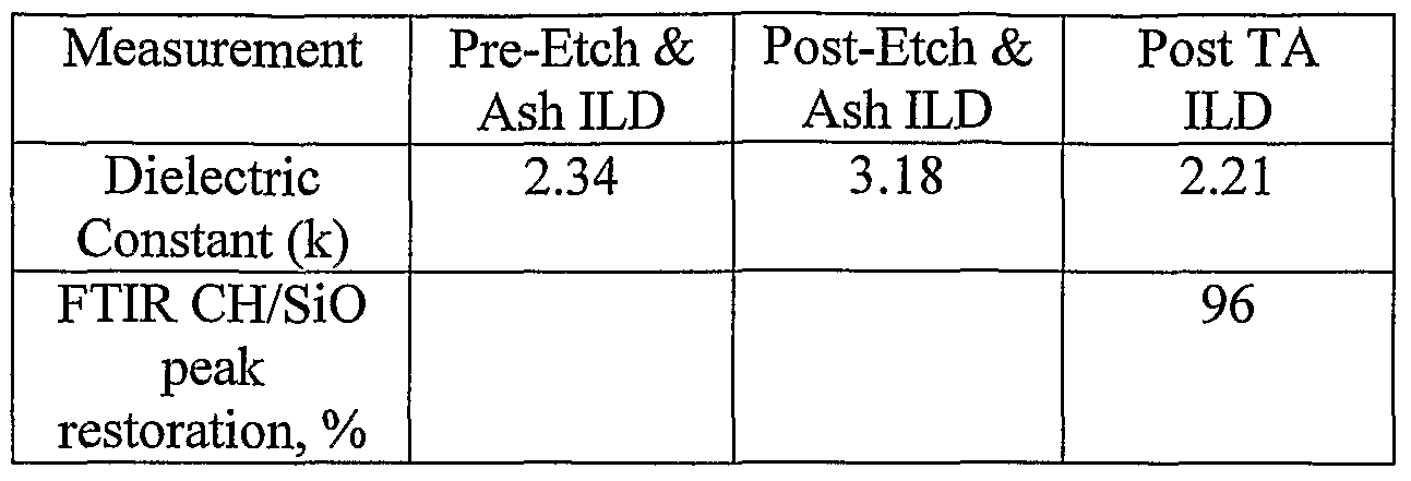


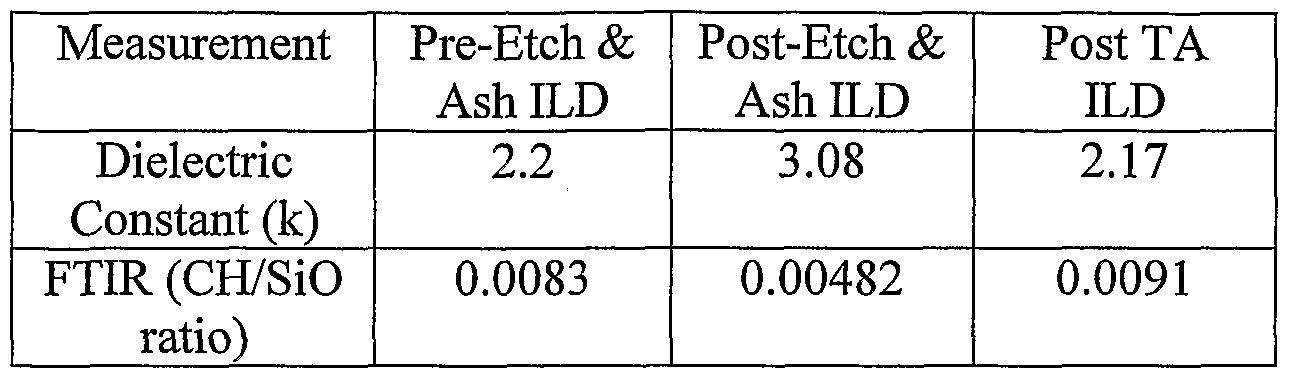


Claims
Priority Applications (2)
| Application Number | Priority Date | Filing Date | Title |
|---|---|---|---|
| JP2007531317A JP5161571B2 (en) | 2004-09-15 | 2005-09-07 | Treatment material |
| EP05806419A EP1803149A2 (en) | 2004-09-15 | 2005-09-07 | Treating agent materials |
Applications Claiming Priority (4)
| Application Number | Priority Date | Filing Date | Title |
|---|---|---|---|
| US10/940,686 | 2004-09-15 | ||
| US10/940,686 US8475666B2 (en) | 2004-09-15 | 2004-09-15 | Method for making toughening agent materials |
| US11/203,558 | 2005-08-12 | ||
| US11/203,558 US7915159B2 (en) | 2004-09-15 | 2005-08-12 | Treating agent materials |
Publications (2)
| Publication Number | Publication Date |
|---|---|
| WO2006033836A2 true WO2006033836A2 (en) | 2006-03-30 |
| WO2006033836A3 WO2006033836A3 (en) | 2006-07-27 |
Family
ID=36090456
Family Applications (1)
| Application Number | Title | Priority Date | Filing Date |
|---|---|---|---|
| PCT/US2005/031936 WO2006033836A2 (en) | 2004-09-15 | 2005-09-07 | Treating agent materials |
Country Status (5)
| Country | Link |
|---|---|
| EP (1) | EP1803149A2 (en) |
| JP (1) | JP5161571B2 (en) |
| KR (1) | KR20070060117A (en) |
| SG (1) | SG141441A1 (en) |
| WO (1) | WO2006033836A2 (en) |
Cited By (4)
| Publication number | Priority date | Publication date | Assignee | Title |
|---|---|---|---|---|
| JP2006210774A (en) * | 2005-01-31 | 2006-08-10 | Taiyo Nippon Sanso Corp | Method of restoring film with low dielectric constant from damages |
| JP2009543339A (en) * | 2006-06-27 | 2009-12-03 | ラム リサーチ コーポレーション | Method of repairing and restoring the strength of etch-damaged low-k dielectric materials |
| EP2690132A1 (en) * | 2011-03-23 | 2014-01-29 | KRI, Inc. | Solvent used for dissolving polysaccharide and method for manufacturing molded article and polysaccharide derivative using this solvent |
| US20200062968A1 (en) * | 2018-08-27 | 2020-02-27 | Tokyo Ohka Kogyo Co., Ltd. | Surface treatment agent and surface treatment method |
Families Citing this family (7)
| Publication number | Priority date | Publication date | Assignee | Title |
|---|---|---|---|---|
| US7999355B2 (en) * | 2008-07-11 | 2011-08-16 | Air Products And Chemicals, Inc. | Aminosilanes for shallow trench isolation films |
| WO2010104979A2 (en) * | 2009-03-10 | 2010-09-16 | L'air Liquide - Société Anonyme Pour L'Étude Et L'exploitation Des Procédes Georges Claude | Cyclic amino compounds for low-k silylation |
| JP5404361B2 (en) | 2009-12-11 | 2014-01-29 | 株式会社東芝 | Semiconductor substrate surface treatment apparatus and method |
| US9029171B2 (en) | 2012-06-25 | 2015-05-12 | Taiwan Semiconductor Manufacturing Co., Ltd. | Self repairing process for porous dielectric materials |
| KR101847033B1 (en) | 2015-11-30 | 2018-04-09 | 김태관 | Coating solution composition for silver coating and coating method using the same |
| JP7194372B2 (en) | 2017-06-09 | 2022-12-22 | 株式会社 高秋化学 | METHOD FOR FORMING COATING OF RESIN MOLDED PRODUCT |
| WO2021176913A1 (en) * | 2020-03-04 | 2021-09-10 | 富士フイルム株式会社 | Processing solution and processing solution container |
Citations (6)
| Publication number | Priority date | Publication date | Assignee | Title |
|---|---|---|---|---|
| WO2002001621A2 (en) * | 2000-06-23 | 2002-01-03 | Honeywell International, Inc. | Method to restore hydrophobicity in dielectric films and materials |
| US6395651B1 (en) * | 1998-07-07 | 2002-05-28 | Alliedsignal | Simplified process for producing nanoporous silica |
| US6448331B1 (en) * | 1997-07-15 | 2002-09-10 | Asahi Kasei Kabushiki Kaisha | Alkoxysilane/organic polymer composition for thin insulating film production and use thereof |
| US20030003765A1 (en) * | 2001-06-28 | 2003-01-02 | Gibson Gerald W. | Split barrier layer including nitrogen-containing portion and oxygen-containing portion |
| WO2003088344A1 (en) * | 2002-04-10 | 2003-10-23 | Honeywell International, Inc. | Low metal porous silica dielectric for integral circuit applications |
| US20030198895A1 (en) * | 2002-03-04 | 2003-10-23 | Toma Dorel Ioan | Method of passivating of low dielectric materials in wafer processing |
Family Cites Families (5)
| Publication number | Priority date | Publication date | Assignee | Title |
|---|---|---|---|---|
| JP2001118842A (en) * | 1999-10-15 | 2001-04-27 | Nec Corp | Semiconductor device and its manufacturing method |
| JP2002353308A (en) * | 2001-05-28 | 2002-12-06 | Toshiba Corp | Semiconductor device and its manufacturing method |
| JP2003282698A (en) * | 2002-03-22 | 2003-10-03 | Sony Corp | Method for fabricating semiconductor and the same |
| JP4225765B2 (en) * | 2002-10-31 | 2009-02-18 | 日揮触媒化成株式会社 | Method for forming low dielectric constant amorphous silica coating and low dielectric constant amorphous silica coating obtained by the method |
| WO2005034194A2 (en) * | 2003-10-08 | 2005-04-14 | Honeywell International Inc. | Repairing damage to low-k dielectric materials using silylating agents |
-
2005
- 2005-09-07 SG SG200802085-1A patent/SG141441A1/en unknown
- 2005-09-07 EP EP05806419A patent/EP1803149A2/en not_active Withdrawn
- 2005-09-07 WO PCT/US2005/031936 patent/WO2006033836A2/en active Application Filing
- 2005-09-07 KR KR1020077008636A patent/KR20070060117A/en not_active Application Discontinuation
- 2005-09-07 JP JP2007531317A patent/JP5161571B2/en not_active Expired - Fee Related
Patent Citations (6)
| Publication number | Priority date | Publication date | Assignee | Title |
|---|---|---|---|---|
| US6448331B1 (en) * | 1997-07-15 | 2002-09-10 | Asahi Kasei Kabushiki Kaisha | Alkoxysilane/organic polymer composition for thin insulating film production and use thereof |
| US6395651B1 (en) * | 1998-07-07 | 2002-05-28 | Alliedsignal | Simplified process for producing nanoporous silica |
| WO2002001621A2 (en) * | 2000-06-23 | 2002-01-03 | Honeywell International, Inc. | Method to restore hydrophobicity in dielectric films and materials |
| US20030003765A1 (en) * | 2001-06-28 | 2003-01-02 | Gibson Gerald W. | Split barrier layer including nitrogen-containing portion and oxygen-containing portion |
| US20030198895A1 (en) * | 2002-03-04 | 2003-10-23 | Toma Dorel Ioan | Method of passivating of low dielectric materials in wafer processing |
| WO2003088344A1 (en) * | 2002-04-10 | 2003-10-23 | Honeywell International, Inc. | Low metal porous silica dielectric for integral circuit applications |
Cited By (6)
| Publication number | Priority date | Publication date | Assignee | Title |
|---|---|---|---|---|
| JP2006210774A (en) * | 2005-01-31 | 2006-08-10 | Taiyo Nippon Sanso Corp | Method of restoring film with low dielectric constant from damages |
| JP2009543339A (en) * | 2006-06-27 | 2009-12-03 | ラム リサーチ コーポレーション | Method of repairing and restoring the strength of etch-damaged low-k dielectric materials |
| EP2690132A1 (en) * | 2011-03-23 | 2014-01-29 | KRI, Inc. | Solvent used for dissolving polysaccharide and method for manufacturing molded article and polysaccharide derivative using this solvent |
| EP2690132A4 (en) * | 2011-03-23 | 2014-09-03 | Kri Inc | Solvent used for dissolving polysaccharide and method for manufacturing molded article and polysaccharide derivative using this solvent |
| US9200085B2 (en) | 2011-03-23 | 2015-12-01 | Kri, Inc. | Solvent used for dissolving polysaccharide and method for manufacturing molded article and polysaccharide derivative using this solvent |
| US20200062968A1 (en) * | 2018-08-27 | 2020-02-27 | Tokyo Ohka Kogyo Co., Ltd. | Surface treatment agent and surface treatment method |
Also Published As
| Publication number | Publication date |
|---|---|
| JP2008513552A (en) | 2008-05-01 |
| WO2006033836A3 (en) | 2006-07-27 |
| SG141441A1 (en) | 2008-04-28 |
| EP1803149A2 (en) | 2007-07-04 |
| KR20070060117A (en) | 2007-06-12 |
| JP5161571B2 (en) | 2013-03-13 |
Similar Documents
| Publication | Publication Date | Title |
|---|---|---|
| US7915159B2 (en) | Treating agent materials | |
| US7709371B2 (en) | Repairing damage to low-k dielectric materials using silylating agents | |
| US7678712B2 (en) | Vapor phase treatment of dielectric materials | |
| JP5161571B2 (en) | Treatment material | |
| WO2005034194A2 (en) | Repairing damage to low-k dielectric materials using silylating agents | |
| KR100984195B1 (en) | Activated chemical process for enhancing material properties of dielectric film | |
| JP5307963B2 (en) | Method for restoring hydrophobicity in dielectric films and materials | |
| JP2004165613A (en) | Manufacture of electronic device | |
| US8283260B2 (en) | Process for restoring dielectric properties | |
| JP2007173795A (en) | Method for forming interconnect structure | |
| WO2004027850A1 (en) | Interlayer adhesion promoter for low k materials | |
| EP1588411A2 (en) | Repair and restoration of damaged dielectric materials and films | |
| KR101064336B1 (en) | Repairing Damage To Low-K-Dielectric Materials Using Silylating Agents |
Legal Events
| Date | Code | Title | Description |
|---|---|---|---|
| AK | Designated states |
Kind code of ref document: A2 Designated state(s): AE AG AL AM AT AU AZ BA BB BG BR BW BY BZ CA CH CN CO CR CU CZ DE DK DM DZ EC EE EG ES FI GB GD GE GH GM HR HU ID IL IN IS JP KE KG KM KP KR KZ LC LK LR LS LT LU LV MA MD MG MK MN MW MX MZ NA NG NI NO NZ OM PG PH PL PT RO RU SC SD SE SG SK SL SM SY TJ TM TN TR TT TZ UA UG US UZ VC VN YU ZA ZM ZW |
|
| AL | Designated countries for regional patents |
Kind code of ref document: A2 Designated state(s): GM KE LS MW MZ NA SD SL SZ TZ UG ZM ZW AM AZ BY KG KZ MD RU TJ TM AT BE BG CH CY CZ DE DK EE ES FI FR GB GR HU IE IS IT LT LU LV MC NL PL PT RO SE SI SK TR BF BJ CF CG CI CM GA GN GQ GW ML MR NE SN TD TG |
|
| WWE | Wipo information: entry into national phase |
Ref document number: 2007531317 Country of ref document: JP |
|
| WWE | Wipo information: entry into national phase |
Ref document number: 200580030450.4 Country of ref document: CN |
|
| NENP | Non-entry into the national phase |
Ref country code: DE |
|
| WWE | Wipo information: entry into national phase |
Ref document number: 2005806419 Country of ref document: EP |
|
| WWE | Wipo information: entry into national phase |
Ref document number: 1020077008636 Country of ref document: KR |
|
| 121 | Ep: the epo has been informed by wipo that ep was designated in this application | ||
| WWP | Wipo information: published in national office |
Ref document number: 2005806419 Country of ref document: EP |