WO2009084413A1 - Organic electroluminescent device and method for manufacturing organic electroluminescent device - Google Patents
Organic electroluminescent device and method for manufacturing organic electroluminescent device Download PDFInfo
- Publication number
- WO2009084413A1 WO2009084413A1 PCT/JP2008/072756 JP2008072756W WO2009084413A1 WO 2009084413 A1 WO2009084413 A1 WO 2009084413A1 JP 2008072756 W JP2008072756 W JP 2008072756W WO 2009084413 A1 WO2009084413 A1 WO 2009084413A1
- Authority
- WO
- WIPO (PCT)
- Prior art keywords
- group
- light emitting
- organic
- layer
- dopant
- Prior art date
Links
- VYHKBDVTDPZQKP-UHFFFAOYSA-N Cc1cc(-[n]2c(ccnc3)c3c3c2ccnc3)ccc1-c(cc1)c(C)cc1-[n]1c(ccnc2)c2c2c1ccnc2 Chemical compound Cc1cc(-[n]2c(ccnc3)c3c3c2ccnc3)ccc1-c(cc1)c(C)cc1-[n]1c(ccnc2)c2c2c1ccnc2 VYHKBDVTDPZQKP-UHFFFAOYSA-N 0.000 description 1
Classifications
-
- C—CHEMISTRY; METALLURGY
- C09—DYES; PAINTS; POLISHES; NATURAL RESINS; ADHESIVES; COMPOSITIONS NOT OTHERWISE PROVIDED FOR; APPLICATIONS OF MATERIALS NOT OTHERWISE PROVIDED FOR
- C09K—MATERIALS FOR MISCELLANEOUS APPLICATIONS, NOT PROVIDED FOR ELSEWHERE
- C09K11/00—Luminescent, e.g. electroluminescent, chemiluminescent materials
- C09K11/06—Luminescent, e.g. electroluminescent, chemiluminescent materials containing organic luminescent materials
-
- C—CHEMISTRY; METALLURGY
- C08—ORGANIC MACROMOLECULAR COMPOUNDS; THEIR PREPARATION OR CHEMICAL WORKING-UP; COMPOSITIONS BASED THEREON
- C08G—MACROMOLECULAR COMPOUNDS OBTAINED OTHERWISE THAN BY REACTIONS ONLY INVOLVING UNSATURATED CARBON-TO-CARBON BONDS
- C08G61/00—Macromolecular compounds obtained by reactions forming a carbon-to-carbon link in the main chain of the macromolecule
- C08G61/12—Macromolecular compounds containing atoms other than carbon in the main chain of the macromolecule
- C08G61/122—Macromolecular compounds containing atoms other than carbon in the main chain of the macromolecule derived from five- or six-membered heterocyclic compounds, other than imides
- C08G61/123—Macromolecular compounds containing atoms other than carbon in the main chain of the macromolecule derived from five- or six-membered heterocyclic compounds, other than imides derived from five-membered heterocyclic compounds
- C08G61/124—Macromolecular compounds containing atoms other than carbon in the main chain of the macromolecule derived from five- or six-membered heterocyclic compounds, other than imides derived from five-membered heterocyclic compounds with a five-membered ring containing one nitrogen atom in the ring
-
- C—CHEMISTRY; METALLURGY
- C08—ORGANIC MACROMOLECULAR COMPOUNDS; THEIR PREPARATION OR CHEMICAL WORKING-UP; COMPOSITIONS BASED THEREON
- C08G—MACROMOLECULAR COMPOUNDS OBTAINED OTHERWISE THAN BY REACTIONS ONLY INVOLVING UNSATURATED CARBON-TO-CARBON BONDS
- C08G61/00—Macromolecular compounds obtained by reactions forming a carbon-to-carbon link in the main chain of the macromolecule
- C08G61/12—Macromolecular compounds containing atoms other than carbon in the main chain of the macromolecule
- C08G61/122—Macromolecular compounds containing atoms other than carbon in the main chain of the macromolecule derived from five- or six-membered heterocyclic compounds, other than imides
- C08G61/123—Macromolecular compounds containing atoms other than carbon in the main chain of the macromolecule derived from five- or six-membered heterocyclic compounds, other than imides derived from five-membered heterocyclic compounds
- C08G61/125—Macromolecular compounds containing atoms other than carbon in the main chain of the macromolecule derived from five- or six-membered heterocyclic compounds, other than imides derived from five-membered heterocyclic compounds with a five-membered ring containing one oxygen atom in the ring
-
- H—ELECTRICITY
- H05—ELECTRIC TECHNIQUES NOT OTHERWISE PROVIDED FOR
- H05B—ELECTRIC HEATING; ELECTRIC LIGHT SOURCES NOT OTHERWISE PROVIDED FOR; CIRCUIT ARRANGEMENTS FOR ELECTRIC LIGHT SOURCES, IN GENERAL
- H05B33/00—Electroluminescent light sources
- H05B33/12—Light sources with substantially two-dimensional radiating surfaces
- H05B33/14—Light sources with substantially two-dimensional radiating surfaces characterised by the chemical or physical composition or the arrangement of the electroluminescent material, or by the simultaneous addition of the electroluminescent material in or onto the light source
-
- H—ELECTRICITY
- H10—SEMICONDUCTOR DEVICES; ELECTRIC SOLID-STATE DEVICES NOT OTHERWISE PROVIDED FOR
- H10K—ORGANIC ELECTRIC SOLID-STATE DEVICES
- H10K50/00—Organic light-emitting devices
- H10K50/10—OLEDs or polymer light-emitting diodes [PLED]
- H10K50/11—OLEDs or polymer light-emitting diodes [PLED] characterised by the electroluminescent [EL] layers
-
- H—ELECTRICITY
- H10—SEMICONDUCTOR DEVICES; ELECTRIC SOLID-STATE DEVICES NOT OTHERWISE PROVIDED FOR
- H10K—ORGANIC ELECTRIC SOLID-STATE DEVICES
- H10K71/00—Manufacture or treatment specially adapted for the organic devices covered by this subclass
- H10K71/10—Deposition of organic active material
- H10K71/12—Deposition of organic active material using liquid deposition, e.g. spin coating
- H10K71/13—Deposition of organic active material using liquid deposition, e.g. spin coating using printing techniques, e.g. ink-jet printing or screen printing
- H10K71/135—Deposition of organic active material using liquid deposition, e.g. spin coating using printing techniques, e.g. ink-jet printing or screen printing using ink-jet printing
-
- C—CHEMISTRY; METALLURGY
- C08—ORGANIC MACROMOLECULAR COMPOUNDS; THEIR PREPARATION OR CHEMICAL WORKING-UP; COMPOSITIONS BASED THEREON
- C08G—MACROMOLECULAR COMPOUNDS OBTAINED OTHERWISE THAN BY REACTIONS ONLY INVOLVING UNSATURATED CARBON-TO-CARBON BONDS
- C08G2261/00—Macromolecular compounds obtained by reactions forming a carbon-to-carbon link in the main chain of the macromolecule
- C08G2261/10—Definition of the polymer structure
- C08G2261/22—Molecular weight
- C08G2261/226—Oligomers, i.e. up to 10 repeat units
-
- C—CHEMISTRY; METALLURGY
- C08—ORGANIC MACROMOLECULAR COMPOUNDS; THEIR PREPARATION OR CHEMICAL WORKING-UP; COMPOSITIONS BASED THEREON
- C08G—MACROMOLECULAR COMPOUNDS OBTAINED OTHERWISE THAN BY REACTIONS ONLY INVOLVING UNSATURATED CARBON-TO-CARBON BONDS
- C08G2261/00—Macromolecular compounds obtained by reactions forming a carbon-to-carbon link in the main chain of the macromolecule
- C08G2261/30—Monomer units or repeat units incorporating structural elements in the main chain
- C08G2261/32—Monomer units or repeat units incorporating structural elements in the main chain incorporating heteroaromatic structural elements in the main chain
- C08G2261/324—Monomer units or repeat units incorporating structural elements in the main chain incorporating heteroaromatic structural elements in the main chain condensed
- C08G2261/3241—Monomer units or repeat units incorporating structural elements in the main chain incorporating heteroaromatic structural elements in the main chain condensed containing one or more nitrogen atoms as the only heteroatom, e.g. carbazole
-
- C—CHEMISTRY; METALLURGY
- C08—ORGANIC MACROMOLECULAR COMPOUNDS; THEIR PREPARATION OR CHEMICAL WORKING-UP; COMPOSITIONS BASED THEREON
- C08G—MACROMOLECULAR COMPOUNDS OBTAINED OTHERWISE THAN BY REACTIONS ONLY INVOLVING UNSATURATED CARBON-TO-CARBON BONDS
- C08G2261/00—Macromolecular compounds obtained by reactions forming a carbon-to-carbon link in the main chain of the macromolecule
- C08G2261/30—Monomer units or repeat units incorporating structural elements in the main chain
- C08G2261/32—Monomer units or repeat units incorporating structural elements in the main chain incorporating heteroaromatic structural elements in the main chain
- C08G2261/324—Monomer units or repeat units incorporating structural elements in the main chain incorporating heteroaromatic structural elements in the main chain condensed
- C08G2261/3242—Monomer units or repeat units incorporating structural elements in the main chain incorporating heteroaromatic structural elements in the main chain condensed containing one or more oxygen atoms as the only heteroatom, e.g. benzofuran
-
- C—CHEMISTRY; METALLURGY
- C09—DYES; PAINTS; POLISHES; NATURAL RESINS; ADHESIVES; COMPOSITIONS NOT OTHERWISE PROVIDED FOR; APPLICATIONS OF MATERIALS NOT OTHERWISE PROVIDED FOR
- C09K—MATERIALS FOR MISCELLANEOUS APPLICATIONS, NOT PROVIDED FOR ELSEWHERE
- C09K2211/00—Chemical nature of organic luminescent or tenebrescent compounds
- C09K2211/10—Non-macromolecular compounds
- C09K2211/1003—Carbocyclic compounds
- C09K2211/1007—Non-condensed systems
-
- C—CHEMISTRY; METALLURGY
- C09—DYES; PAINTS; POLISHES; NATURAL RESINS; ADHESIVES; COMPOSITIONS NOT OTHERWISE PROVIDED FOR; APPLICATIONS OF MATERIALS NOT OTHERWISE PROVIDED FOR
- C09K—MATERIALS FOR MISCELLANEOUS APPLICATIONS, NOT PROVIDED FOR ELSEWHERE
- C09K2211/00—Chemical nature of organic luminescent or tenebrescent compounds
- C09K2211/10—Non-macromolecular compounds
- C09K2211/1003—Carbocyclic compounds
- C09K2211/1011—Condensed systems
-
- C—CHEMISTRY; METALLURGY
- C09—DYES; PAINTS; POLISHES; NATURAL RESINS; ADHESIVES; COMPOSITIONS NOT OTHERWISE PROVIDED FOR; APPLICATIONS OF MATERIALS NOT OTHERWISE PROVIDED FOR
- C09K—MATERIALS FOR MISCELLANEOUS APPLICATIONS, NOT PROVIDED FOR ELSEWHERE
- C09K2211/00—Chemical nature of organic luminescent or tenebrescent compounds
- C09K2211/10—Non-macromolecular compounds
- C09K2211/1018—Heterocyclic compounds
- C09K2211/1025—Heterocyclic compounds characterised by ligands
- C09K2211/1029—Heterocyclic compounds characterised by ligands containing one nitrogen atom as the heteroatom
-
- C—CHEMISTRY; METALLURGY
- C09—DYES; PAINTS; POLISHES; NATURAL RESINS; ADHESIVES; COMPOSITIONS NOT OTHERWISE PROVIDED FOR; APPLICATIONS OF MATERIALS NOT OTHERWISE PROVIDED FOR
- C09K—MATERIALS FOR MISCELLANEOUS APPLICATIONS, NOT PROVIDED FOR ELSEWHERE
- C09K2211/00—Chemical nature of organic luminescent or tenebrescent compounds
- C09K2211/10—Non-macromolecular compounds
- C09K2211/1018—Heterocyclic compounds
- C09K2211/1025—Heterocyclic compounds characterised by ligands
- C09K2211/1044—Heterocyclic compounds characterised by ligands containing two nitrogen atoms as heteroatoms
-
- C—CHEMISTRY; METALLURGY
- C09—DYES; PAINTS; POLISHES; NATURAL RESINS; ADHESIVES; COMPOSITIONS NOT OTHERWISE PROVIDED FOR; APPLICATIONS OF MATERIALS NOT OTHERWISE PROVIDED FOR
- C09K—MATERIALS FOR MISCELLANEOUS APPLICATIONS, NOT PROVIDED FOR ELSEWHERE
- C09K2211/00—Chemical nature of organic luminescent or tenebrescent compounds
- C09K2211/10—Non-macromolecular compounds
- C09K2211/1018—Heterocyclic compounds
- C09K2211/1025—Heterocyclic compounds characterised by ligands
- C09K2211/1088—Heterocyclic compounds characterised by ligands containing oxygen as the only heteroatom
-
- C—CHEMISTRY; METALLURGY
- C09—DYES; PAINTS; POLISHES; NATURAL RESINS; ADHESIVES; COMPOSITIONS NOT OTHERWISE PROVIDED FOR; APPLICATIONS OF MATERIALS NOT OTHERWISE PROVIDED FOR
- C09K—MATERIALS FOR MISCELLANEOUS APPLICATIONS, NOT PROVIDED FOR ELSEWHERE
- C09K2211/00—Chemical nature of organic luminescent or tenebrescent compounds
- C09K2211/18—Metal complexes
- C09K2211/185—Metal complexes of the platinum group, i.e. Os, Ir, Pt, Ru, Rh or Pd
-
- H—ELECTRICITY
- H10—SEMICONDUCTOR DEVICES; ELECTRIC SOLID-STATE DEVICES NOT OTHERWISE PROVIDED FOR
- H10K—ORGANIC ELECTRIC SOLID-STATE DEVICES
- H10K2101/00—Properties of the organic materials covered by group H10K85/00
- H10K2101/10—Triplet emission
-
- H—ELECTRICITY
- H10—SEMICONDUCTOR DEVICES; ELECTRIC SOLID-STATE DEVICES NOT OTHERWISE PROVIDED FOR
- H10K—ORGANIC ELECTRIC SOLID-STATE DEVICES
- H10K2101/00—Properties of the organic materials covered by group H10K85/00
- H10K2101/80—Composition varying spatially, e.g. having a spatial gradient
-
- H—ELECTRICITY
- H10—SEMICONDUCTOR DEVICES; ELECTRIC SOLID-STATE DEVICES NOT OTHERWISE PROVIDED FOR
- H10K—ORGANIC ELECTRIC SOLID-STATE DEVICES
- H10K85/00—Organic materials used in the body or electrodes of devices covered by this subclass
- H10K85/30—Coordination compounds
- H10K85/341—Transition metal complexes, e.g. Ru(II)polypyridine complexes
- H10K85/342—Transition metal complexes, e.g. Ru(II)polypyridine complexes comprising iridium
Definitions
- the present invention relates to an organic electroluminescence element and a method for producing the organic electroluminescence element. Specifically, the present invention relates to an organic electroluminescent element that can be manufactured by a simple process and has improved light emission efficiency and lifetime, and a method for manufacturing the organic electroluminescent element.
- ELD electroluminescence display
- an inorganic electroluminescence element hereinafter also referred to as an inorganic EL element
- an organic electroluminescence element hereinafter also referred to as an organic EL element
- Inorganic EL elements have been used as planar light sources, but an alternating high voltage is required to drive the light emitting elements.
- an organic electroluminescence device has a structure in which a light emitting layer containing a compound that emits light is sandwiched between a cathode and an anode, and excitons (excitons) by injecting electrons and holes into the light emitting layer and recombining them. Is generated. It is an element that emits light using the emission of light (fluorescence / phosphorescence) when this exciton is deactivated, and can emit light at a voltage of several V to several tens V, and it is self-luminous. In addition, it is attracting attention from the viewpoints of space saving, portability and the like because it is a thin film type complete solid element with a wide viewing angle and high visibility.
- the organic electroluminescence element is also a major feature that it is a surface light source, unlike the main light sources that have been used in the past, such as light-emitting diodes and cold-cathode tubes.
- Applications that can effectively utilize this characteristic include illumination light sources and various display backlights.
- it is also suitable to be used as a backlight of a liquid crystal full color display whose demand has been increasing in recent years.
- Improvement of luminous efficiency is mentioned as a problem for putting an organic electroluminescence element into practical use as such a light source for illumination or a backlight of a display.
- a so-called host / guest structure in which a part of the organic functional layer constituting the organic electroluminescence element is composed of a mixture of materials having different functions. It is becoming.
- a combination of a host material / a light emitting dopant in the light emitting layer may be mentioned.
- the ratio of the light-emitting dopant to the light-emitting host in the light-emitting layer is continuously changed in the light-emitting layer, indicating that the lifetime is improved (for example, see Patent Documents 1 and 2).
- What is clearly shown as the means for changing to is only the control of the deposition rate in the vacuum deposition method, and cannot be said to be a proposal of means suitable for productivity.
- the present invention has been made in view of the above problems, and an object of the present invention is to provide an organic electroluminescence element that has high luminous efficiency and long life and can be stably produced by a wet process, and a method for producing the organic electroluminescence element Is to provide.
- the light emitting layer is formed by a wet process
- the manufacturing method of the organic electroluminescent element characterized by changing continuously the density
- R 1 represents a substituent.
- Z represents a group of nonmetallic atoms necessary to form a 5- to 7-membered ring.
- N1 represents an integer of 0 to 5.
- B 1 to B 5 represent carbon. Represents an atom, a nitrogen atom, an oxygen atom or a sulfur atom, at least one of B 1 to B 5 represents a nitrogen atom, M 1 represents a group 8 to group 10 metal in the periodic table, and X 1 and X 2 Represents a carbon atom, a nitrogen atom or an oxygen atom, L 1 represents an atomic group forming a bidentate ligand with X 1 and X 2 , m1 represents an integer of 1, 2 or 3, and m2 represents 0 Represents an integer of 1 or 2, and m1 + m2 is 2 or 3.) 4).
- the light emitting host is a compound having a molecular weight of 700 or more represented by
- Y 1 and Y 2 represent O, S or NR 0 , and R 0 , R 11 to R 18 and R 21 to R 28 represent a hydrogen atom or a substituent, provided that R 11 At least one of ⁇ R 18 and R 0 is used in connection with X 1, R 21 ⁇ R 28 and at least one .X 1 which is used for connection with the X 1 represented by the following general formula R 0 (3 ) or (4 .n1 that represents a divalent linking group represented by) represents an integer of 1 or more, when n1 is 2 or more, X 1 is may be the same or different.
- the light emitting dopant / light emitting host ratio of the solution coated on the most anode side is 100 to 10% by mass, and the light emitting dopant / light emitting host of the solution coated on the most cathode side. 8. The method for producing an organic electroluminescent element as described in 7 above, wherein the ratio is 5 to 0% by mass.
- an organic electroluminescence element that has high luminous efficiency and long life and can be stably produced by a wet process, and a method for producing the organic electroluminescence element.
- the present invention provides an organic electroluminescent device having at least an anode, a cathode, and a light emitting layer containing a light emitting host and a light emitting dopant sandwiched between the anode and the cathode on a substrate, wherein the light emitting layer is formed by a wet process.
- concentration of the light emission dopant contained in this light emitting layer changes continuously toward the cathode side from an anode side, It is characterized by the above-mentioned.
- the concentration of the luminescent dopant decreases from the anode side toward the cathode side.
- the light emitting layer according to the present invention is a layer that emits light by recombination of electrons and holes injected from the electrode, the electron transport layer, or the hole transport layer, and the light emitting portion is in the layer of the light emitting layer. May be the interface
- the thickness of the light emitting layer is not particularly limited, but it is 2 to 2 from the viewpoint of the uniformity of the film to be formed and the application of unnecessary high voltage during light emission, and the improvement of the stability of the emission color with respect to the driving current. It is preferable to adjust to a range of 200 nm, more preferably to a range of 5 nm or more and 100 nm or less.
- the light emitting layer of the organic electroluminescence device of the present invention is formed by a wet process.
- Known wet process coating methods include spin coating, die coating, casting, inkjet, spraying, printing, etc., but it is easy to obtain a homogeneous film and it is difficult to generate pinholes.
- film formation by a coating method such as a spin coating method, a die coating method, an ink jet method, a spray method, or a printing method is preferable.
- the light emitting layer of the organic electroluminescence device of the present invention contains a light emitting host and at least one light emitting dopant, and the concentration of the light emitting dopant in the light emitting layer is continuously changed from the anode side to the cathode side.
- the atmospheric temperature in contact with the back side of the coating film may be lowered by 10 ° C. or more from the atmospheric temperature in contact with the front side of the coating film and dried.
- a method of controlling the atmospheric temperature of the front and back of the coating film a method of separately controlling the temperature of the drying air sent to the front side and the drying air sent to the back side using an isolated drying box for each of the coated samples, coating
- a method of controlling the drying air temperature on the front side and the back side is preferable in order to avoid damage to the coating film due to contact.
- the solvent of the luminescent layer solution has a boiling point of the solvent with the higher luminescent dopant solubility for the mixed solvent of two liquids having different boiling point and luminescent dopant solubility.
- the dopant solubility is higher than the boiling point of the lower solvent.
- the light-emitting host has a mass ratio of 20% or more in a compound contained in a light-emitting layer, and a phosphorescence quantum yield of phosphorescence emission is 0 at room temperature (25 ° C.). Less than 1 compound.
- the phosphorescence quantum yield is preferably less than 0.01.
- the mass ratio in the layer is 20% or more among the compounds contained in a light emitting layer.
- a compound having a molecular weight of 700 or more represented by the general formula (2) as a luminescent host.
- the light emitting host according to the present invention has a molecular weight of 700 or more, preferably a molecular weight of 800 or more and 3,000 or less, 800 or more and 2,000 or less, 800 or more and 1,500 or less, and most preferably a molecular weight of 1,000 or more and 1,500 or less. .
- Y 1 and Y 2 represent O, S or NR 0 , and R 0 , R 11 to R 18 and R 21 to R 28 represent a hydrogen atom or a substituent. However, at least one of R 11 to R 18 and R 0 is used for connection with X 1, and at least one of R 21 to R 28 and R 0 is used for connection with X 1 .
- X 1 represents a divalent linking group represented by the following general formula (3) or (4).
- n1 represents an integer of 1 or more, and when n1 is 2 or more, X 1 may be the same or different.
- Y 3 represents O, S or NR 30
- R 30 to R 38 and R 41 to R 46 represent a hydrogen atom or a substituent.
- at least two of each of R 30 to R 38 and R 41 to R 46 are used for connection, and when R 41 and R 44 are used for connection, at least R 42 , R 43 , R 45 , R 46 are used.
- R 0 , R 11 to R 18 and R 21 to R 28 , and R 30 to R 38 and R 41 to R 46 have the same meaning as the substituent represented by R 1 in the general formula (1). is there.
- the light emitting host a known light emitting host may be used alone, or a plurality of kinds may be used in combination.
- the movement of charges can be adjusted, and the organic EL element can be made highly efficient.
- the light emitting host used in the present invention may be a conventionally known low molecular compound or a high molecular compound having a repeating unit, and a low molecular compound having a polymerizable group such as a vinyl group or an epoxy group (deposition polymerization property). Light emitting host).
- a compound that has a hole transporting ability and an electron transporting ability, prevents the emission of longer wavelengths, and has a high Tg (glass transition temperature) is preferable.
- Luminescent dopant The light emitting dopant according to the present invention will be described.
- a fluorescent dopant or a phosphorescent dopant can be used. From the viewpoint of obtaining an organic EL element with higher luminous efficiency, it is used for the light-emitting layer and the light-emitting unit of the organic EL element of the present invention.
- the light emitting dopant it is preferable to contain a phosphorescent dopant at the same time as containing the above light emitting host.
- the phosphorescent dopant according to the present invention is a compound in which light emission from an excited triplet is observed.
- the phosphorescent dopant is a compound that emits phosphorescence at room temperature (25 ° C.) and has a phosphorescence quantum yield of 25. It is a compound of 0.01 or more at ° C., and a preferable phosphorescence quantum yield is 0.1 or more.
- the phosphorescent quantum yield can be measured by the method described in Spectroscopic II, page 398 (1992 edition, Maruzen) of the Fourth Edition Experimental Chemistry Course 7. Although the phosphorescence quantum yield in a solution can be measured using various solvents, the phosphorescence dopant according to the present invention achieves the phosphorescence quantum yield (0.01 or more) in any solvent. That's fine.
- phosphorescent dopants There are two types of emission of phosphorescent dopants in principle. One is the recombination of carriers on the light-emitting host on which carriers are transported to generate the excited state of the light-emitting host, and this energy is transferred to the phosphorescent dopant. Energy transfer type to obtain light emission from the phosphorescent dopant, another is that the phosphorescent dopant becomes a carrier trap, carrier recombination occurs on the phosphorescent dopant, and light emission from the phosphorescent dopant is obtained It is a carrier trap type. In any case, it is a condition that the excited state energy of the phosphorescent dopant is lower than the excited state energy of the light emitting host.
- the phosphorescent dopant can be appropriately selected from known materials used for the light emitting layer of the organic EL element.
- a phosphorescent dopant represented by the general formula (1) it is preferable to use a phosphorescent dopant represented by the general formula (1) as a light emitting dopant.
- examples of the substituent represented by R 1 include an alkyl group (for example, methyl group, ethyl group, propyl group, isopropyl group, t- Butyl group, pentyl group, hexyl group, octyl group, dodecyl group, tridecyl group, tetradecyl group, pentadecyl group, etc.), cycloalkyl group (eg, cyclopentyl group, cyclohexyl group, etc.), alkenyl group (eg, vinyl group, allyl group) Etc.), alkynyl groups (for example, ethynyl group, propargyl group, etc.), aromatic hydrocarbon ring groups (aromatic carbocyclic group, aryl group, etc.), for example, phenyl group, p-chlorophenyl group, mesity
- Z represents a nonmetallic atom group necessary for forming a 5- to 7-membered ring.
- the 5- to 7-membered ring formed by Z include a benzene ring, naphthalene ring, pyridine ring, pyrimidine ring, pyrrole ring, thiophene ring, pyrazole ring, imidazole ring, oxazole ring and thiazole ring. Of these, a benzene ring is preferred.
- B 1 to B 5 each represent a carbon atom, a nitrogen atom, an oxygen atom or a sulfur atom, and at least one represents a nitrogen atom.
- the aromatic nitrogen-containing heterocycle formed by these five atoms is preferably a monocycle. Examples include pyrrole ring, pyrazole ring, imidazole ring, triazole ring, tetrazole ring, oxazole ring, isoxazole ring, thiazole ring, isothiazole ring, oxadiazole ring, and thiadiazole ring.
- a pyrazole ring and an imidazole ring are preferable, and an imidazole ring is more preferable.
- These rings may be further substituted with the above substituents.
- Preferred as the substituent are an alkyl group and an aryl group, and more preferably an aryl group.
- L 1 represents an atomic group that forms a bidentate ligand together with X 1 and X 2 .
- Specific examples of the bidentate ligand represented by X 1 -L 1 -X 2 include, for example, substituted or unsubstituted phenylpyridine, phenylpyrazole, phenylimidazole, phenyltriazole, phenyltetrazole, pyrazabol, picolinic acid And acetylacetone. These groups may be further substituted with the above substituents.
- M1 represents an integer of 1, 2 or 3
- m2 represents an integer of 0, 1 or 2
- m1 + m2 is 2 or 3.
- m2 is 0 is preferable.
- a transition metal element of Group 8 to Group 10 (also referred to simply as a transition metal) in the periodic table of elements is used.
- iridium and platinum are preferable, and iridium is more preferable.
- the light-emitting dopant represented by the general formula (1) according to the present invention may or may not have a polymerizable group or a reactive group.
- fluorescent dopant As fluorescent dopants, coumarin dyes, pyran dyes, cyanine dyes, croconium dyes, squalium dyes, oxobenzanthracene dyes, fluorescein dyes, rhodamine dyes, pyrylium dyes, perylene dyes, stilbene dyes , Polythiophene dyes, or rare earth complex phosphors.
- Injection layer electron injection layer, hole injection layer >> The injection layer is provided as necessary, and there are an electron injection layer and a hole injection layer, and as described above, it exists between the anode and the light emitting layer or the hole transport layer and between the cathode and the light emitting layer or the electron transport layer. May be.
- An injection layer is a layer provided between an electrode and an organic layer in order to reduce drive voltage and improve light emission luminance.
- Organic EL element and its forefront of industrialization (issued by NTT Corporation on November 30, 1998) 2), Chapter 2, “Electrode Materials” (pages 123 to 166) in detail, and includes a hole injection layer (anode buffer layer) and an electron injection layer (cathode buffer layer).
- anode buffer layer hole injection layer
- copper phthalocyanine is used.
- examples thereof include a phthalocyanine buffer layer represented by an oxide, an oxide buffer layer represented by vanadium oxide, an amorphous carbon buffer layer, and a polymer buffer layer using a conductive polymer such as polyaniline (emeraldine) or polythiophene.
- cathode buffer layer (electron injection layer) The details of the cathode buffer layer (electron injection layer) are described in JP-A-6-325871, JP-A-9-17574, JP-A-10-74586, and the like. Specifically, strontium, aluminum, etc.
- Metal buffer layer typified by lithium, alkali metal compound buffer layer typified by lithium fluoride, alkaline earth metal compound buffer layer typified by magnesium fluoride, oxide buffer layer typified by aluminum oxide, etc.
- the buffer layer (injection layer) is preferably a very thin film, and the film thickness is preferably in the range of 0.1 nm to 5 ⁇ m, although it depends on the material.
- ⁇ Blocking layer hole blocking layer, electron blocking layer>
- the blocking layer is provided as necessary in addition to the basic constituent layer of the organic compound thin film as described above. For example, it is described in JP-A Nos. 11-204258 and 11-204359, and “Organic EL elements and the forefront of industrialization (published by NTT Corporation on November 30, 1998)” on page 237. There is a hole blocking (hole blocking) layer.
- the hole blocking layer has a function of an electron transport layer in a broad sense, and is made of a hole blocking material that has a function of transporting electrons and has a remarkably small ability to transport holes. The probability of recombination of electrons and holes can be improved by blocking. Moreover, the structure of the electron carrying layer mentioned later can be used as a hole-blocking layer concerning this invention as needed.
- the hole blocking layer of the organic EL device of the present invention is preferably provided adjacent to the light emitting layer.
- the hole blocking layer contains the carbazole derivative mentioned as the light emitting host.
- the light emitting layer having the shortest wavelength of light emission is preferably closest to the anode among all the light emitting layers.
- 50% by mass or more of the compound contained in the hole blocking layer provided at the position has an ionization potential of 0.3 eV or more larger than the light emitting host of the shortest wave emitting layer.
- the ionization potential is defined by the energy required to emit electrons at the HOMO (highest occupied molecular orbital) level of the compound to the vacuum level, and can be obtained by, for example, the following method.
- Gaussian 98 (Gaussian 98, Revision A.11.4, MJ Frisch, et al, Gaussian, Inc., Pittsburgh PA, 2002.), a molecular orbital calculation software manufactured by Gaussian, USA, is used as a keyword.
- the ionization potential can be obtained as a value obtained by rounding off the second decimal place of a value (eV unit converted value) calculated by performing structural optimization using B3LYP / 6-31G *. This calculation value is effective because the correlation between the calculation value obtained by this method and the experimental value is high.
- the ionization potential can also be obtained by a method of directly measuring by photoelectron spectroscopy.
- a low energy electron spectrometer “Model AC-1” manufactured by Riken Keiki Co., Ltd. or a method known as ultraviolet photoelectron spectroscopy can be suitably used.
- the electron blocking layer has a function of a hole transport layer in a broad sense, and is made of a material that has a function of transporting holes and has an extremely small ability to transport electrons. By blocking, the recombination probability of electrons and holes can be improved. Moreover, the structure of the positive hole transport layer mentioned later can be used as an electron blocking layer as needed.
- the film thickness of the hole blocking layer and the electron transporting layer according to the present invention is preferably 3 to 100 nm, more preferably 5 to 30 nm.
- the hole transport layer is made of a hole transport material having a function of transporting holes, and in a broad sense, a hole injection layer and an electron blocking layer are also included in the hole transport layer.
- the hole transport layer can be provided as a single layer or a plurality of layers.
- the hole transport material has either hole injection or transport or electron barrier properties, and may be either organic or inorganic.
- triazole derivatives oxadiazole derivatives, imidazole derivatives, polyarylalkane derivatives, pyrazoline derivatives and pyrazolone derivatives, phenylenediamine derivatives, arylamine derivatives, amino-substituted chalcone derivatives, oxazole derivatives, styrylanthracene derivatives, fluorenone derivatives, hydrazone derivatives
- Examples thereof include stilbene derivatives, silazane derivatives, aniline copolymers, and conductive polymer oligomers, particularly thiophene oligomers.
- the above-mentioned materials can be used as the hole transport material, but it is preferable to use a porphyrin compound, an aromatic tertiary amine compound and a styrylamine compound, particularly an aromatic tertiary amine compound.
- aromatic tertiary amine compounds and styrylamine compounds include N, N, N ′, N′-tetraphenyl-4,4′-diaminophenyl; N, N′-diphenyl-N, N′— Bis (3-methylphenyl)-[1,1′-biphenyl] -4,4′-diamine (TPD); 2,2-bis (4-di-p-tolylaminophenyl) propane; 1,1-bis (4-di-p-tolylaminophenyl) cyclohexane; N, N, N ′, N′-tetra-p-tolyl-4,4′-diaminobiphenyl; 1,1-bis (4-di-p-tolyl) Aminophenyl) -4-phenylcyclohexane; bis (4-dimethylamino-2-methylphenyl) phenylmethane; bis (4-di-p-tolylaminoph
- No. 5,061,569 Having a condensed aromatic ring of, for example, 4,4'-bis [N- (1-naphthyl) -N-phenylamino] biphenyl (NPD), JP-A-4-308 4,4 ′, 4 ′′ -tris [N- (3-methylphenyl) -N-phenylamino] triphenylamine in which three triphenylamine units described in Japanese Patent No. 88 are linked in a starburst type ( MTDATA) and the like.
- NPD 4,4'-bis [N- (1-naphthyl) -N-phenylamino] biphenyl
- JP-A-4-308 4,4 ′, 4 ′′ -tris [N- (3-methylphenyl) -N-phenylamino] triphenylamine in which three triphenylamine units described in Japanese Patent No. 88 are linked in a starburst type ( MTDATA) and the
- a polymer material in which these materials are introduced into a polymer chain or these materials are used as a polymer main chain can also be used.
- inorganic compounds such as p-type-Si and p-type-SiC can also be used as the hole injection material and the hole transport material.
- JP-A-11-251067, J. Org. Huang et. al. A so-called p-type hole transport material described in a book (Applied Physics Letters 80 (2002), p. 139) can also be used.
- these materials are preferably used because a light-emitting element with higher efficiency can be obtained.
- the hole transport layer can be formed by thinning the hole transport material by a known method such as a vacuum deposition method, a spin coating method, a casting method, a printing method including an ink jet method, or an LB method. it can.
- the thickness of the hole transport layer is not particularly limited, but is usually about 5 nm to 5 ⁇ m, preferably 5 to 200 nm.
- the hole transport layer may have a single layer structure composed of one or more of the above materials.
- a hole transport layer having a high p property doped with impurities examples thereof include JP-A-4-297076, JP-A-2000-196140, JP-A-2001-102175, J. Pat. Appl. Phys. 95, 5773 (2004), and the like.
- a hole transport layer having such a high p property because a device with lower power consumption can be produced.
- the electron transport layer is made of a material having a function of transporting electrons, and in a broad sense, an electron injection layer and a hole blocking layer are also included in the electron transport layer.
- the electron transport layer can be provided as a single layer or a plurality of layers.
- an electron transport material also serving as a hole blocking material used for an electron transport layer adjacent to the light emitting layer on the cathode side is injected from the cathode.
- Any material may be used as long as it has a function of transferring electrons to the light-emitting layer, and any material can be selected from conventionally known compounds. Examples include nitro-substituted fluorene derivatives, diphenylquinone derivatives, thiopyran dioxide derivatives, carbodiimides, fluorenylidenemethane derivatives, anthraquinodimethane and anthrone derivatives, oxadiazole derivatives, and the like.
- a thiadiazole derivative in which the oxygen atom of the oxadiazole ring is substituted with a sulfur atom, and a quinoxaline derivative having a quinoxaline ring known as an electron withdrawing group can also be used as an electron transport material.
- a polymer material in which these materials are introduced into a polymer chain or these materials are used as a polymer main chain can also be used.
- metal complexes of 8-quinolinol derivatives such as tris (8-quinolinol) aluminum (Alq), tris (5,7-dichloro-8-quinolinol) aluminum, tris (5,7-dibromo-8-quinolinol) aluminum Tris (2-methyl-8-quinolinol) aluminum, tris (5-methyl-8-quinolinol) aluminum, bis (8-quinolinol) zinc (Znq), and the like, and the central metals of these metal complexes are In, Mg, Metal complexes replaced with Cu, Ca, Sn, Ga or Pb can also be used as the electron transport material.
- metal-free or metal phthalocyanine or those having terminal ends substituted with an alkyl group or a sulfonic acid group can be preferably used as the electron transporting material.
- the distyrylpyrazine derivative exemplified as the material for the light emitting layer can also be used as an electron transport material, and an inorganic semiconductor such as n-type-Si, n-type-SiC, etc. as in the case of the hole injection layer and the hole transport layer. Can also be used as an electron transporting material.
- the electron transport layer can be formed by thinning the electron transport material by a known method such as a vacuum deposition method, a spin coating method, a casting method, a printing method including an ink jet method, or an LB method.
- the thickness of the electron transport layer is not particularly limited, but is usually about 5 nm to 5 ⁇ m, preferably 5 to 200 nm.
- the electron transport layer may have a single layer structure composed of one or more of the above materials.
- an electron transport layer having a high n property doped with impurities may be used.
- examples thereof include JP-A-4-297076, JP-A-10-270172, JP-A-2000-196140, JP-A-2001-102175, J. Pat. Appl. Phys. 95, 5773 (2004), and the like.
- an electron transport layer having such a high n property because an element with lower power consumption can be produced.
- an organic compound having a reactive group may be used.
- reactive organic compound There is no restriction
- Reactive organic compounds can be reacted on a substrate to form a network polymer with organic molecules.
- production of a network polymer can suppress element deterioration by Tg (glass transition point) adjustment of a structure layer. It is also possible to change the emission wavelength of the organic EL element, suppress deterioration of the specific wavelength, etc. by adjusting the reaction accompanied by the cleavage or generation of the conjugated system of the molecule using the active radical in use. is there.
- the lower layer is not dissolved in the upper layer coating solution, and upper layer coating can be made possible by resinating the lower layer and degrading solvent solubility.
- an electrode material made of a metal, an alloy, an electrically conductive compound, or a mixture thereof having a high work function (4 eV or more) is preferably used.
- electrode substances include metals such as Au, and conductive transparent materials such as CuI, indium tin oxide (ITO), SnO 2 , and ZnO.
- conductive transparent materials such as CuI, indium tin oxide (ITO), SnO 2 , and ZnO.
- an amorphous material such as IDIXO (In 2 O 3 —ZnO) that can form a transparent conductive film may be used.
- these electrode materials may be formed into a thin film by a method such as vapor deposition or sputtering, and a pattern having a desired shape may be formed by a photolithography method, or when pattern accuracy is not so high (about 100 ⁇ m or more)
- a pattern may be formed through a mask having a desired shape at the time of vapor deposition or sputtering of the electrode material.
- wet film-forming methods such as a printing system and a coating system, can also be used.
- the transmittance is greater than 10%, and the sheet resistance as the anode is preferably several hundred ⁇ / ⁇ or less.
- the film thickness depends on the material, it is usually selected in the range of 10 to 1000 nm, preferably 10 to 200 nm.
- cathode a material having a low work function (4 eV or less) metal (referred to as an electron injecting metal), an alloy, an electrically conductive compound, and a mixture thereof as an electrode material is used.
- electrode materials include sodium, sodium-potassium alloy, magnesium, lithium, magnesium / copper mixture, magnesium / silver mixture, magnesium / aluminum mixture, magnesium / indium mixture, aluminum / aluminum oxide (Al 2 O 3 ) Mixtures, indium, lithium / aluminum mixtures, rare earth metals and the like.
- a mixture of an electron injecting metal and a second metal which is a stable metal having a larger work function than this for example, a magnesium / silver mixture
- a magnesium / aluminum mixture a magnesium / aluminum mixture, a magnesium / indium mixture, an aluminum / aluminum oxide (Al 2 O 3 ) mixture, a lithium / aluminum mixture, aluminum and the like.
- the cathode can be produced by forming a thin film of these electrode materials by a method such as vapor deposition or sputtering.
- the sheet resistance as the cathode is preferably several hundred ⁇ / ⁇ or less, and the film thickness is usually selected in the range of 10 nm to 5 ⁇ m, preferably 50 to 200 nm.
- the light emission luminance is improved, which is convenient.
- a transparent or semi-transparent cathode can be produced by producing the conductive transparent material mentioned in the description of the anode on the cathode after producing the metal with a film thickness of 1 to 20 nm. By applying this, an element in which both the anode and the cathode are transmissive can be manufactured.
- a support substrate (hereinafter also referred to as a substrate, substrate, substrate, support, etc.) that can be used in the organic EL device of the present invention, there is no particular limitation on the type of glass, plastic, etc., and it is transparent. May be opaque. When extracting light from the support substrate side, the support substrate is preferably transparent. Examples of the transparent support substrate preferably used include glass, quartz, and a transparent resin film. A particularly preferable support substrate is a resin film capable of giving flexibility to the organic EL element.
- polyesters such as polyethylene terephthalate (PET) and polyethylene naphthalate (PEN), polyethylene, polypropylene, cellophane, cellulose diacetate, cellulose triacetate, cellulose acetate butyrate, cellulose acetate propionate (CAP), Cellulose esters such as cellulose acetate phthalate (TAC) and cellulose nitrate or derivatives thereof, polyvinylidene chloride, polyvinyl alcohol, polyethylene vinyl alcohol, syndiotactic polystyrene, polycarbonate, norbornene resin, polymethylpentene, polyether ketone, polyimide , Polyethersulfone (PES), polyphenylene sulfide, polysulfone , Polyetherimide, polyether ketone imide, polyamide, fluorine resin, nylon, polymethyl methacrylate, acrylic or polyarylates, and cycloolefin resins such as ARTON (manufactured by J
- An inorganic or organic film or a hybrid film of both may be formed on the surface of the resin film, and it is preferably a barrier film having a water vapor permeability of 0.01 g / m 2 / day ⁇ atm or less. Furthermore, a high barrier film having an oxygen permeability of 10 ⁇ 3 g / m 2 / day or less and a water vapor permeability of 10 ⁇ 5 g / m 2 / day or less is preferable.
- the material for forming the barrier film may be any material that has a function of suppressing the intrusion of elements that cause deterioration of elements such as moisture and oxygen.
- silicon oxide, silicon dioxide, silicon nitride, or the like can be used.
- the method for forming the barrier film is not particularly limited.
- the vacuum deposition method, sputtering method, reactive sputtering method, molecular beam epitaxy method, cluster ion beam method, ion plating method, plasma polymerization method, atmospheric pressure plasma weight A combination method, a plasma CVD method, a laser CVD method, a thermal CVD method, a coating method, and the like can be used, but an atmospheric pressure plasma polymerization method as described in JP-A-2004-68143 is particularly preferable.
- the opaque support substrate examples include metal plates such as aluminum and stainless steel, films, opaque resin substrates, ceramic substrates, and the like.
- the external extraction quantum efficiency at room temperature of light emission of the organic EL device of the present invention is preferably 1% or more, more preferably 5% or more.
- the external extraction quantum efficiency (%) the number of photons emitted to the outside of the organic EL element / the number of electrons sent to the organic EL element ⁇ 100.
- a hue improvement filter such as a color filter may be used in combination, or a color conversion filter that converts the emission color from the organic EL element into multiple colors using a phosphor may be used in combination.
- the ⁇ max of light emission of the organic EL element is preferably 480 nm or less.
- a sealing means used for this invention the method of adhere
- a sealing member it should just be arrange
- Specific examples include a glass plate, a polymer plate / film, and a metal plate / film.
- the glass plate include soda-lime glass, barium / strontium-containing glass, lead glass, aluminosilicate glass, borosilicate glass, barium borosilicate glass, and quartz.
- the polymer plate include polycarbonate, acrylic, polyethylene terephthalate, polyether sulfide, and polysulfone.
- the metal plate include those made of one or more metals or alloys selected from the group consisting of stainless steel, iron, copper, aluminum, magnesium, nickel, zinc, chromium, titanium, molybdenum, silicon, germanium, and tantalum.
- a polymer film and a metal film can be preferably used because the element can be thinned.
- the polymer film oxygen permeability measured by the method based on JIS K 7126-1987 is 1 ⁇ 10 -3 ml / m 2 / 24h or less, as measured by the method based on JIS K 7129-1992, water vapor permeability (25 ⁇ 0.5 ° C., relative humidity (90 ⁇ 2)%) is preferably that of 1 ⁇ 10 -3 g / (m 2 / 24h) or less.
- sealing member For processing the sealing member into a concave shape, sandblasting, chemical etching, or the like is used.
- the adhesive include photocuring and thermosetting adhesives having reactive vinyl groups of acrylic acid oligomers and methacrylic acid oligomers, and moisture curing adhesives such as 2-cyanoacrylates. be able to.
- hot-melt type polyamide, polyester, and polyolefin can be mentioned.
- a cationic curing type ultraviolet curing epoxy resin adhesive can be mentioned.
- an organic EL element may deteriorate by heat processing, what can be adhesively cured from room temperature to 80 ° C. is preferable.
- a desiccant may be dispersed in the adhesive.
- coating of the adhesive agent to a sealing part may use commercially available dispenser, and may print like screen printing.
- the electrode and the organic layer are coated on the outside of the electrode facing the support substrate with the organic layer interposed therebetween, and an inorganic or organic layer is formed in contact with the support substrate to form a sealing film.
- the material for forming the film may be a material having a function of suppressing intrusion of elements that cause deterioration of elements such as moisture and oxygen.
- silicon oxide, silicon dioxide, silicon nitride, or the like may be used. it can.
- the method for forming these films is not particularly limited.
- vacuum deposition method sputtering method, reactive sputtering method, molecular beam epitaxy method, cluster ion beam method, ion plating method, plasma polymerization method, atmospheric pressure plasma
- a polymerization method a plasma CVD method, a laser CVD method, a thermal CVD method, a coating method, or the like can be used.
- an inert gas such as nitrogen or argon, or an inert liquid such as fluorinated hydrocarbon or silicon oil can be injected in the gas phase and liquid phase.
- a vacuum can also be used.
- a hygroscopic compound can also be enclosed inside.
- hygroscopic compound examples include metal oxides (for example, sodium oxide, potassium oxide, calcium oxide, barium oxide, magnesium oxide, aluminum oxide) and sulfates (for example, sodium sulfate, calcium sulfate, magnesium sulfate, cobalt sulfate).
- metal oxides for example, sodium oxide, potassium oxide, calcium oxide, barium oxide, magnesium oxide, aluminum oxide
- sulfates for example, sodium sulfate, calcium sulfate, magnesium sulfate, cobalt sulfate.
- metal halides eg calcium chloride, magnesium chloride, cesium fluoride, tantalum fluoride, cerium bromide, magnesium bromide, barium iodide, magnesium iodide etc.
- perchloric acids eg perchloric acid Barium, magnesium perchlorate, and the like
- anhydrous salts are preferably used in sulfates, metal halides, and perchloric acids.
- a protective film or a protective plate may be provided on the outer side of the sealing film on the side facing the support substrate with the organic layer interposed therebetween or on the sealing film.
- the mechanical strength is not necessarily high, and thus it is preferable to provide such a protective film and a protective plate.
- the same glass plate, polymer plate / film, metal plate / film, etc. used for the sealing can be used. It is preferable to use a film.
- the organic EL element emits light inside a layer having a refractive index higher than that of air (refractive index is about 1.7 to 2.1) and can extract only about 15% to 20% of the light generated in the light emitting layer. It is generally said. This is because light incident on the interface (interface between the transparent substrate and air) at an angle ⁇ greater than the critical angle causes total reflection and cannot be taken out of the device, or between the transparent electrode or light emitting layer and the transparent substrate. This is because the light is totally reflected between the light and the light is guided through the transparent electrode or the light emitting layer, and as a result, the light escapes in the side surface direction of the element.
- a method of improving the light extraction efficiency for example, a method of forming irregularities on the surface of the transparent substrate and preventing total reflection at the transparent substrate and the air interface (US Pat. No. 4,774,435), A method for improving efficiency by giving light condensing property to a substrate (Japanese Patent Laid-Open No. 63-314795), a method of forming a reflective surface on the side surface of an element (Japanese Patent Laid-Open No. 1-220394), and light emission from the substrate A method of forming an antireflection film by introducing a flat layer having an intermediate refractive index between the bodies (Japanese Patent Laid-Open No.
- these methods can be used in combination with the organic EL device of the present invention.
- a method of introducing a flat layer having a lower refractive index than the substrate between the substrate and the light emitter, or a substrate, transparent A method of forming a diffraction grating between any layers of the electrode layer and the light emitting layer (including between the substrate and the outside) can be suitably used.
- the low refractive index layer examples include aerogel, porous silica, magnesium fluoride, and a fluorine-based polymer. Since the refractive index of the transparent substrate is generally about 1.5 to 1.7, the low refractive index layer preferably has a refractive index of about 1.5 or less. Further, it is preferably 1.35 or less.
- the thickness of the low refractive index medium is preferably at least twice the wavelength in the medium. This is because the effect of the low refractive index layer is diminished when the thickness of the low refractive index medium is about the wavelength of light and the electromagnetic wave that has exuded by evanescent enters the substrate.
- the method of introducing a diffraction grating into an interface or any medium that causes total reflection is characterized by a high effect of improving light extraction efficiency.
- This method uses the property that the diffraction grating can change the direction of light to a specific direction different from refraction by so-called Bragg diffraction such as first-order diffraction and second-order diffraction.
- Light that cannot be emitted due to total internal reflection between layers is diffracted by introducing a diffraction grating in any layer or medium (in a transparent substrate or transparent electrode), and the light is removed. I want to take it out.
- the diffraction grating to be introduced has a two-dimensional periodic refractive index. This is because light emitted from the light-emitting layer is randomly generated in all directions, so in a general one-dimensional diffraction grating having a periodic refractive index distribution only in a certain direction, only light traveling in a specific direction is diffracted. Therefore, the light extraction efficiency does not increase so much. However, by making the refractive index distribution a two-dimensional distribution, light traveling in all directions is diffracted, and light extraction efficiency is increased.
- the position where the diffraction grating is introduced may be in any of the layers or in the medium (in the transparent substrate or the transparent electrode), but is preferably in the vicinity of the organic light emitting layer where light is generated.
- the period of the diffraction grating is preferably about 1/2 to 3 times the wavelength of light in the medium.
- the arrangement of the diffraction grating is preferably two-dimensionally repeated such as a square lattice, a triangular lattice, or a honeycomb lattice.
- the organic EL device of the present invention is processed on the light extraction side of the substrate so as to provide, for example, a microlens array structure, or combined with a so-called condensing sheet, for example, with respect to a specific direction, for example, the device light emitting surface.
- a specific direction for example, the device light emitting surface.
- quadrangular pyramids having a side of 30 ⁇ m and an apex angle of 90 degrees are arranged two-dimensionally on the light extraction side of the substrate.
- One side is preferably 10 to 100 ⁇ m. If it becomes smaller than this, the effect of diffraction will generate
- the condensing sheet it is possible to use, for example, a sheet that has been put to practical use in an LED backlight of a liquid crystal display device.
- a sheet for example, Sumitomo 3M brightness enhancement film (BEF) can be used.
- BEF Sumitomo 3M brightness enhancement film
- the base material may be formed by forming a ⁇ -shaped stripe having a vertex angle of 90 degrees and a pitch of 50 ⁇ m, or the vertex angle is rounded and the pitch is changed randomly. Other shapes may be used.
- a light diffusion plate / film may be used in combination with the light collecting sheet.
- a diffusion film (light-up) manufactured by Kimoto Co., Ltd. can be used.
- a desired electrode material for example, a thin film made of an anode material is formed on a suitable substrate by a method such as vapor deposition or sputtering so as to have a film thickness of 1 ⁇ m or less, preferably 10 to 200 nm, thereby producing an anode.
- the light emitting layer of the organic EL device of the present invention is formed by a wet process as described above.
- a method for forming an organic layer other than the light emitting layer there are a vapor deposition method, a wet process (spin coating method, die coating method, casting method, ink jet method, spray method, printing method), etc., but a homogeneous film is easily obtained.
- film formation by a coating method such as a spin coating method, a die coating method, an ink jet method, a spray method, a printing method, or the like is preferable for part or all of the organic layer in view of the difficulty of generating pinholes.
- liquid medium for dissolving or dispersing the organic EL material according to the present invention examples include ketones such as methyl ethyl ketone and cyclohexanone, fatty acid esters such as ethyl acetate, halogenated hydrocarbons such as dichlorobenzene, toluene, xylene, and mesitylene.
- Aromatic hydrocarbons such as cyclohexylbenzene, aliphatic hydrocarbons such as cyclohexane, decalin, and dodecane, and organic solvents such as DMF and DMSO can be used.
- a dispersion method it can disperse
- a thin film made of a cathode material is formed thereon by a method such as vapor deposition or sputtering so as to have a film thickness of 1 ⁇ m or less, preferably in the range of 50 to 200 nm, and a cathode is provided.
- a desired organic EL element can be obtained.
- a DC voltage is applied to the multicolor display device thus obtained, light emission can be observed by applying a voltage of about 2 to 40 V with the positive polarity of the anode and the negative polarity of the cathode.
- An alternating voltage may be applied.
- the alternating current waveform to be applied may be arbitrary.
- Example 1 Production of organic EL element >> [Production of Organic EL Element 111] After patterning a substrate (NH technoglass NA45) formed by depositing 100 nm of ITO (indium tin oxide) on a 100 mm ⁇ 100 mm ⁇ 1.1 mm glass substrate as an anode, a substrate provided with this ITO transparent electrode was formed. Ultrasonic cleaning with isopropyl alcohol, drying with dry nitrogen gas, and UV ozone cleaning were performed for 5 minutes.
- ITO indium tin oxide
- This substrate was transferred to a nitrogen atmosphere, and a solution obtained by dissolving 60 mg of Exemplified Compound 4-1 in 10 ml of toluene on the first hole transport layer was formed into a film (film thickness) by spin coating under conditions of 1000 rpm and 30 seconds. About 40 nm) and irradiated with ultraviolet light for 30 seconds, followed by heat drying at 120 ° C. for 30 minutes to form a second hole transport layer.
- the light emitting layer composition 1 having the following composition was discharged and injected using an inkjet head (manufactured by Epson; MJ800C) so that the wet film thickness was 4 ⁇ m.
- This substrate was fixed to a substrate holder of a drying box provided with upper and lower partition walls and provided with an independent drying air temperature controller at the upper and lower portions of the partition wall, and heating controlled to 120 ° C. on the upper surface of the substrate (light emitting layer coating surface). Dry nitrogen was circulated, and heated dry nitrogen circulated at 80 ° C. on the back side of the substrate. In this state, the light emitting layer was dried by performing a drying process for 10 minutes. It was confirmed that the temperature of dry nitrogen circulated on both sides of the substrate was controlled within ⁇ 1 ° C. from the start to the end of drying.
- the organic EL element 111 was formed in the same manner except that the temperature of nitrogen to be circulated to the substrate upper surface side and the substrate rear surface side in the drying step after the discharge injection of the light emitting layer composition 1 was changed as shown in Table 1. EL elements 112 to 114 were produced.
- Organic EL Elements 121-123, 131-133, 141-142 are produced in the production of the organic EL element 111, the material constituting the light emitting layer composition 1 is changed as shown in Table 1, and nitrogen circulated between the substrate upper surface side and the substrate back surface side in the drying step after the discharge injection of the light emitting layer composition.
- Organic EL elements 121 to 123, 131 to 133, and 141 to 142 were fabricated in the same manner except that the temperature was changed as shown in Table 1.
- the concentration distribution of the light-emitting dopant contained in the light-emitting layer of the obtained organic EL element is detected by analyzing the Ir distribution in the film thickness direction by TOF-SIMS (time-of-flight secondary ion mass spectrometry). Can do.
- Table 1 shows the concentration distribution from the anode side to the cathode side in the light emitting layers of the organic EL devices 111 to 114, 121 to 123, 131 to 133, and 141 to 142.
- the external extraction quantum efficiency of the organic EL elements 121 to 123 is a relative value with the measured value of the organic EL element 123 (comparative) as 100, and the external extraction efficiency of the organic EL elements 131 to 133 is a measurement of the organic EL element 133 (comparative).
- the relative value with the value of 100, the external extraction quantum efficiency of the organic EL elements 141 to 143 is the relative value with the measured value of the organic EL element 143 (comparison) as 100, and the external extraction efficiency of the organic EL elements 151 to 153 is the organic EL
- the relative value when the measured value of the element 153 (comparison) is 100 and the external extraction efficiency of the organic EL elements 161 to 162 are expressed as relative values when the measured value of the organic EL element 162 (comparative) is 100. .
- the produced organic EL element was continuously driven by applying a current that would give a front luminance of 1000 cd / m 2 .
- the time required for the front luminance to reach the initial half value (500 cd / m 2 ) is obtained, and the light emission lifetimes of the organic EL elements 111 to 116 are relative values with the measured value of the organic EL element 116 (comparative) as 100. expressed.
- the light emission lifetimes of the organic EL elements 121 to 123 are relative values with the measured value of the organic EL element 123 (comparative) as 100, and the light emission lifetimes of the organic EL elements 131 to 133 are the measured value of the organic EL element 133 (comparative) as 100.
- the relative lifetimes of the organic EL elements 141 to 143 are relative values with the measured value of the organic EL element 143 (comparison) as 100, and the emission lifetimes of the organic EL elements 151 to 153 are those of the organic EL element 153 (comparative).
- the relative value when the measured value is 100, and the light emission lifetimes of the organic EL elements 161 to 162 are expressed as relative values when the measured value of the organic EL element 162 (comparative) is 100.
- the organic EL device of the present invention can continuously change the concentration of the light-emitting dopant in the light-emitting layer even in the manufacturing method using the wet process. As a result, the external extraction quantum efficiency and the light emission lifetime are improved. It can be seen that it has improved.
- Example 2 Production of organic EL element >> [Production of Organic EL Element 211] After patterning a substrate (NH technoglass NA45) formed by depositing 100 nm of ITO (indium tin oxide) on a 100 mm ⁇ 100 mm ⁇ 1.1 mm glass substrate as an anode, a substrate provided with this ITO transparent electrode was formed. Ultrasonic cleaning with isopropyl alcohol, drying with dry nitrogen gas, and UV ozone cleaning were performed for 5 minutes.
- ITO indium tin oxide
- polystyrene sulfonate PEDOT / PSS, Bayer, Baytron P Al 4083
- PEDOT / PSS polystyrene sulfonate
- the film was dried at 200 ° C. for 1 hour to provide a first hole transport layer having a thickness of 30 nm.
- This substrate was transferred to a nitrogen atmosphere, and a solution obtained by dissolving 60 mg of Exemplified Compound 4-1 in 10 ml of toluene on the first hole transport layer was formed into a film (film thickness) by spin coating under conditions of 1000 rpm and 30 seconds. About 40 nm) and irradiated with ultraviolet light for 30 seconds, followed by heat drying at 120 ° C. for 30 minutes to form a second hole transport layer.
- the light emitting layer composition 1 having the following composition was discharged and injected using an inkjet head (manufactured by Epson; MJ800C) so that the wet film thickness was 4 ⁇ m.
- the substrate was subjected to a drying treatment for 10 minutes in a 120 ° C. drying box to form the light emitting layer 1.
- Light emitting layer composition 1 (2) -16 1.0 part by mass (1) -79 0.18 part by mass Toluene 100 parts by mass
- a light emitting layer composition 2 having the following composition was wet filmed using an inkjet head (manufactured by Epson; MJ800C). The discharge was injected so that the thickness was 2 ⁇ m. This substrate was subjected to a drying treatment for 10 minutes in a drying box at 120 ° C. to form a 20 nm light emitting layer 2.
- (Light emitting layer composition 2) (2) -16 1.0 part by mass (1) -79 0.02 part by mass Toluene 100 parts by mass This substrate was fixed to the substrate holder of the vacuum evaporation apparatus, while 200 mg of ET-A was added to a molybdenum resistance heating boat. Then, 100 mg of CsF was put into another resistance heating boat made of molybdenum, and attached to a vacuum deposition apparatus. The vacuum chamber was depressurized to 4 ⁇ 10 ⁇ 4 Pa, and then heated by energizing the heating boat containing ET-A and CsF, and the light emitting layer was deposited at a deposition rate of 0.2 nm / second and 0.03 nm / second, respectively. An electron transport layer having a film thickness of 40 nm was further provided. Subsequently, 110 nm of aluminum was deposited to form a cathode, and an organic EL element 211 was produced.
- the light emitting dopant / light emitting host ratio of the solution coated on the most anode side among the two or more kinds of light emitting layer solutions having different light emitting dopant concentrations of claim 7 and claim 8 is 100. This corresponds to an emission dopant / emission host ratio of 5 to 0% by mass of the solution coated on the cathode side, and in this case, the emission dopant / emission host ratio of the solution applied on the anode side is 18%.
- the light emitting dopant / light emitting host ratio of the solution applied on the most cathode side is 2% by mass.
- organic EL elements 212 to 218 were produced in the same manner except that the compositions and film thicknesses of the light emitting layer compositions 1 and 2 were changed as shown in Table 2.
- the organic EL elements 212 and 213 are also equivalent to claims 7 and 8, respectively, and the emission dopant / emission host ratio of the solution coated on the most anode side is 20% by mass, 40% by mass, and most on the cathode side, respectively.
- the ratio of the luminescent dopant / luminescent host of the solution applied to is 0% by mass and 0% by mass, respectively.
- the organic EL element 214 is claimed in claim 7, but the light emitting dopant / light emitting host ratio of the solution coated on the most anode side is 14% by mass, and the light emitting dopant / light emitting host ratio of the solution coated on the most cathode side is mass. Since it is 6%, it does not correspond to Claim 8.
- the solubility of the luminescent dopant ((1) -79) in chlorobenzene is higher than that of toluene, and the boiling point of chlorobenzene is higher. That is, it corresponds to claim 9.
- the organic EL element 218 has a higher solubility in the luminescent dopant ((1) -79) in chlorobenzene than p-xylene, and conversely, the boiling point of p-xylene is equal to or higher than that of chlorobenzene. Does not correspond to 9.
- the organic EL device of the present invention can continuously change the concentration of the light-emitting dopant in the light-emitting layer even in the manufacturing method using the wet process, and as a result, the external extraction quantum efficiency and the light emission lifetime are improved. It can be seen that it has improved.
Abstract
Disclosed is a method for manufacturing an organic electroluminescent device having high luminous efficiency and long life, wherein an organic electroluminescent device can be stably produced by a wet process. Specifically disclosed is a method for manufacturing an organic electroluminescent device which at least comprises, on a substrate, an anode, a cathode and a light-emitting layer interposed between the anode and the cathode and containing a luminescent host and a luminescent dopant. This method for manufacturing an organic electroluminescent device is characterized in that the light-emitting layer is formed by a wet process and the concentration of the luminescent dopant contained in the light-emitting layer is continuously varied from the anode side toward the cathode side.
Description
本発明は有機エレクトロルミネッセンス素子、及び該有機エレクトロルミネッセンス素子の製造方法に関する。詳しくは、簡便なプロセスで製造可能であり、発光効率と寿命が改善された有機エレクトロルミネッセンス素子、及び該有機エレクトロルミネッセンス素子の製造方法に関する。
The present invention relates to an organic electroluminescence element and a method for producing the organic electroluminescence element. Specifically, the present invention relates to an organic electroluminescent element that can be manufactured by a simple process and has improved light emission efficiency and lifetime, and a method for manufacturing the organic electroluminescent element.
発光型の電子ディスプレイデバイスとして、エレクトロルミネッセンスディスプレイ(以下、ELDと略記する)がある。ELDの構成要素としては、無機エレクトロルミネッセンス素子(以下、無機EL素子とも言う)や有機エレクトロルミネッセンス素子(以下、有機EL素子とも言う)が挙げられる。無機EL素子は平面型光源として使用されてきたが、発光素子を駆動させるためには交流の高電圧が必要である。
There is an electroluminescence display (hereinafter abbreviated as ELD) as a light-emitting electronic display device. As an ELD component, an inorganic electroluminescence element (hereinafter also referred to as an inorganic EL element) and an organic electroluminescence element (hereinafter also referred to as an organic EL element) can be given. Inorganic EL elements have been used as planar light sources, but an alternating high voltage is required to drive the light emitting elements.
一方、有機エレクトロルミネッセンス素子は、発光する化合物を含有する発光層を陰極と陽極で挟んだ構成を有し、発光層に電子及び正孔を注入して、再結合させることにより励起子(エキシトン)を生成させる。このエキシトンが失活する際の光の放出(蛍光・リン光)を利用して発光する素子であり、数V~数十V程度の電圧で発光が可能であり、更に自己発光型であるために視野角に富み、視認性が高く、薄膜型の完全固体素子であるために省スペース、携帯性等の観点から注目されている。
On the other hand, an organic electroluminescence device has a structure in which a light emitting layer containing a compound that emits light is sandwiched between a cathode and an anode, and excitons (excitons) by injecting electrons and holes into the light emitting layer and recombining them. Is generated. It is an element that emits light using the emission of light (fluorescence / phosphorescence) when this exciton is deactivated, and can emit light at a voltage of several V to several tens V, and it is self-luminous. In addition, it is attracting attention from the viewpoints of space saving, portability and the like because it is a thin film type complete solid element with a wide viewing angle and high visibility.
また、有機エレクトロルミネッセンス素子は、従来実用に供されてきた主要な光源、例えば、発光ダイオードや冷陰極管と異なり、面光源であることも大きな特徴である。この特性を有効に活用できる用途として、照明用光源や様々なディスプレイのバックライトがある。特に近年、需要の増加が著しい液晶フルカラーディスプレイのバックライトとして用いることも好適である。
In addition, the organic electroluminescence element is also a major feature that it is a surface light source, unlike the main light sources that have been used in the past, such as light-emitting diodes and cold-cathode tubes. Applications that can effectively utilize this characteristic include illumination light sources and various display backlights. In particular, it is also suitable to be used as a backlight of a liquid crystal full color display whose demand has been increasing in recent years.
有機エレクトロルミネッセンス素子をこのような照明用光源、あるいはディスプレイのバックライトとして実用するための課題として発光効率の向上が挙げられる。発光効率の向上のためには、有機エレクトロルミネッセンス素子を構成する有機機能層の一部において、それぞれ別個の機能を有する材料を複数混合して構成する、所謂ホスト/ゲスト構造を組み入れることが一般的となりつつある。
Improvement of luminous efficiency is mentioned as a problem for putting an organic electroluminescence element into practical use as such a light source for illumination or a backlight of a display. In order to improve luminous efficiency, it is common to incorporate a so-called host / guest structure in which a part of the organic functional layer constituting the organic electroluminescence element is composed of a mixture of materials having different functions. It is becoming.
具体的には、発光層におけるホスト材料/発光ドーパントの組み合わせが挙げられる。発光層における発光ホストに対する発光ドーパントの比率が発光層内で連続的に変化することで寿命が向上することを示している(例えば、特許文献1、2参照)が、発光ドーパントの濃度を連続的に変化させる手段として明示しているのは真空蒸着法における蒸着レートの制御のみであり、生産性に適した手段の提案とは言えない。
Specifically, a combination of a host material / a light emitting dopant in the light emitting layer may be mentioned. The ratio of the light-emitting dopant to the light-emitting host in the light-emitting layer is continuously changed in the light-emitting layer, indicating that the lifetime is improved (for example, see Patent Documents 1 and 2). What is clearly shown as the means for changing to is only the control of the deposition rate in the vacuum deposition method, and cannot be said to be a proposal of means suitable for productivity.
一方、これら有機エレクトロルミネッセンス素子の製造方法としては、蒸着法、ウエットプロセス(スピンコート法、ダイコート法、キャスト法、インクジェット法、スプレー法、印刷法)等があるが、真空プロセスを必要とせず、連続生産が簡便であるという理由で近年はウエットプロセスにおける製造方法が注目されている。
On the other hand, as a manufacturing method of these organic electroluminescent elements, there are a vapor deposition method, a wet process (spin coating method, die coating method, casting method, ink jet method, spray method, printing method), but a vacuum process is not required, In recent years, a manufacturing method in a wet process has been attracting attention because continuous production is simple.
隣接する2層間の成分を連続的に混合させる手段が開示されている(例えば、特許文献3、4参照)が、この場合は隣接する2層の材料の溶解性の差を利用しており、同一材料を用いた単一層内でのドーパント濃度を連続変化させる手段としては適用できない問題がある。また、隣接する2層間、例えば、正孔輸送層と発光層の成分を連続的に混合させることで正孔輸送層と発光層の間の界面の障壁を緩和させることができ、発光層への正孔注入の効率を向上させることができるが、反面、電子ブロックの機能は低下することになり、この技術のみで発光効率を高めることは困難である。
特開2004-6102号公報
特開2005-38672号公報
特開平11-74083号公報
特開2007-42312号公報
Means for continuously mixing components between two adjacent layers is disclosed (see, for example, Patent Documents 3 and 4), but in this case, a difference in solubility between adjacent two layers is utilized, There is a problem that it cannot be applied as means for continuously changing the dopant concentration in a single layer using the same material. Moreover, the barrier of the interface between a positive hole transport layer and a light emitting layer can be relieve | moderated by mixing the components of two adjacent layers, for example, a positive hole transport layer, and a light emitting layer continuously, and to the light emitting layer. Although the efficiency of hole injection can be improved, on the other hand, the function of the electronic block is lowered, and it is difficult to increase the light emission efficiency only by this technique.
Japanese Patent Laid-Open No. 2004-6102 JP 2005-38672 A Japanese Patent Laid-Open No. 11-74083 JP 2007-42312 A
本発明は、上記課題に鑑みなされたものであり、その目的は、高発光効率、且つ長寿命であり、ウエットプロセスで安定に製造可能な有機エレクトロルミネッセンス素子、及び該有機エレクトロルミネッセンス素子の製造方法を提供することにある。
The present invention has been made in view of the above problems, and an object of the present invention is to provide an organic electroluminescence element that has high luminous efficiency and long life and can be stably produced by a wet process, and a method for producing the organic electroluminescence element Is to provide.
本発明の上記目的は,下記の構成により達成される。
The above object of the present invention is achieved by the following configuration.
1.基板上に少なくとも陽極、陰極、及び該陽極、陰極間に挟まれた発光ホスト及び発光ドーパントを含有する発光層を少なくとも有する有機エレクトロルミネッセンス素子の製造方法において、該発光層がウエットプロセスで形成され、且つ該発光層に含まれる発光ドーパントの濃度を陽極側から陰極側に向かって連続的に変化させることを特徴とする有機エレクトロルミネッセンス素子の製造方法。
1. In a method for producing an organic electroluminescence device having at least an anode, a cathode, and a light emitting host containing at least an anode, a cathode, and a light emitting host and a light emitting dopant sandwiched between the anode and the cathode, the light emitting layer is formed by a wet process, And the manufacturing method of the organic electroluminescent element characterized by changing continuously the density | concentration of the light emission dopant contained in this light emitting layer toward the cathode side from an anode side.
2.前記発光ドーパントの濃度が陽極側から陰極側に向かって減少することを特徴とする前記1に記載の有機エレクトロルミネッセンス素子の製造方法。
2. 2. The method for producing an organic electroluminescent element according to 1 above, wherein the concentration of the luminescent dopant decreases from the anode side toward the cathode side.
3.前記発光ドーパントが下記一般式(1)で表されることを特徴とする前記1または2に記載の有機エレクトロルミネッセンス素子の製造方法。
3. 3. The method for producing an organic electroluminescent element according to 1 or 2, wherein the light-emitting dopant is represented by the following general formula (1).

(式中、R1は置換基を表す。Zは5~7員環を形成するのに必要な非金属原子群を表す。n1は0~5の整数を表す。B1~B5は炭素原子、窒素原子、酸素原子もしくは硫黄原子を表し、B1~B5の少なくとも一つは窒素原子を表す。M1は元素周期表における8族~10族の金属を表す。X1及びX2は炭素原子、窒素原子もしくは酸素原子を表し、L1はX1及びX2とともに2座の配位子を形成する原子群を表す。m1は1、2または3の整数を表し、m2は0、1または2の整数を表すが、m1+m2は2または3である。)
4.前記発光ホストが下記一般式(2)で表される分子量700以上の化合物であることを特徴とする前記1~3のいずれか1項に記載の有機エレクトロルミネッセンス素子の製造方法。 (In the formula, R 1 represents a substituent. Z represents a group of nonmetallic atoms necessary to form a 5- to 7-membered ring. N1 represents an integer of 0 to 5. B 1 to B 5 represent carbon. Represents an atom, a nitrogen atom, an oxygen atom or a sulfur atom, at least one of B 1 to B 5 represents a nitrogen atom, M 1 represents a group 8 to group 10 metal in the periodic table, and X 1 and X 2 Represents a carbon atom, a nitrogen atom or an oxygen atom, L 1 represents an atomic group forming a bidentate ligand with X 1 and X 2 , m1 represents an integer of 1, 2 or 3, and m2 represents 0 Represents an integer of 1 or 2, and m1 + m2 is 2 or 3.)
4). 4. The method for producing an organic electroluminescent element according to any one of 1 to 3, wherein the light emitting host is a compound having a molecular weight of 700 or more represented by the following general formula (2).

(一般式(2)中、Y1及びY2はO、SまたはNR0を表し、R0、R11~R18及びR21~R28は水素原子または置換基を表す。但し、R11~R18及びR0の少なくとも1つはX1との連結に用いられ、R21~R28及びR0の少なくとも1つはX1との連結に用いられる。X1は下記一般式(3)または(4)で表される2価の連結基を表す。n1は1以上の整数を表し、n1が2以上の場合、X1は同じでも異なっていてもよい。)
(In General Formula (2), Y 1 and Y 2 represent O, S or NR 0 , and R 0 , R 11 to R 18 and R 21 to R 28 represent a hydrogen atom or a substituent, provided that R 11 At least one of ~ R 18 and R 0 is used in connection with X 1, R 21 ~ R 28 and at least one .X 1 which is used for connection with the X 1 represented by the following general formula R 0 (3 ) or (4 .n1 that represents a divalent linking group represented by) represents an integer of 1 or more, when n1 is 2 or more, X 1 is may be the same or different.)

(式中、Y3はO、SまたはNR30を表し、R30~R38及びR41~R46は水素原子または置換基を表す。但し、R30~R38、R41~R46は各々少なくとも2つは連結に用いられ、またR41とR44が連結に用いられる場合はR42、R43、R45、R46の少なくとも1つは水素原子以外の置換基を有する。)
5.前記1~4のいずれか1項に記載の有機エレクトロルミネッセンス素子の製造方法において、塗膜の裏側に接する雰囲気温度を塗膜の表側に接する雰囲気温度より低く制御しながら乾燥することによって発光層を形成することを特徴とする有機エレクトロルミネッセンス素子の製造方法。 (Wherein Y 3 represents O, S or NR 30 , and R 30 to R 38 and R 41 to R 46 represent a hydrogen atom or a substituent, provided that R 30 to R 38 and R 41 to R 46 represent At least two of each are used for linking, and when R 41 and R 44 are used for linking, at least one of R 42 , R 43 , R 45 and R 46 has a substituent other than a hydrogen atom.)
5. 5. The method for producing an organic electroluminescence device according to any one of 1 to 4, wherein the light emitting layer is dried by controlling the atmospheric temperature in contact with the back side of the coating film to be lower than the atmospheric temperature in contact with the front side of the coating film. A method for producing an organic electroluminescence element, comprising forming the organic electroluminescence element.
6.前記塗膜の裏側の雰囲気温度を塗膜の表側の雰囲気温度より10℃以上低く制御することを特徴とする前記5に記載の有機エレクトロルミネッセンス素子の製造方法。
6. 6. The method for producing an organic electroluminescence device as described in 5 above, wherein the atmospheric temperature on the back side of the coating film is controlled to be 10 ° C. lower than the atmospheric temperature on the front side of the coating film.
7.前記1~4のいずれか1項に記載の有機エレクトロルミネッセンス素子の製造方法において、発光ドーパント濃度の異なる2種以上の発光層溶液の積層塗布を、最も陽極側に塗布する溶液の発光ドーパント/発光ホスト比が最も陰極側に塗布する溶液の発光ドーパント/発光ホスト比より高くして行い、その後乾燥することによって発光層を形成することを特徴とする有機エレクトロルミネッセンス素子の製造方法。
7. 5. The method for producing an organic electroluminescence device according to any one of 1 to 4, wherein a layer coating of two or more types of light emitting layer solutions having different light emitting dopant concentrations is applied, and the light emitting dopant / light emission of the solution to be applied to the most anode side A method for producing an organic electroluminescent device, wherein a light emitting layer is formed by performing a host ratio higher than a light emitting dopant / light emitting host ratio of a solution coated on the most cathode side and then drying.
8.前記発光ドーパント濃度の異なる2種以上の発光層溶液の内、最も陽極側に塗布する溶液の発光ドーパント/発光ホスト比が100~10質量%、最も陰極側に塗布する溶液の発光ドーパント/発光ホスト比が5~0質量%であることを特徴とする前記7に記載の有機エレクトロルミネッセンス素子の製造方法。
8. Among the two or more kinds of light emitting layer solutions having different light emitting dopant concentrations, the light emitting dopant / light emitting host ratio of the solution coated on the most anode side is 100 to 10% by mass, and the light emitting dopant / light emitting host of the solution coated on the most cathode side. 8. The method for producing an organic electroluminescent element as described in 7 above, wherein the ratio is 5 to 0% by mass.
9.前記1~4のいずれか1項に記載の有機エレクトロルミネッセンス素子の製造方法において、発光層の溶液の溶媒が沸点と発光ドーパント溶解度の異なる2液の混合溶媒であって、発光ドーパント溶解度が高い方の溶媒の沸点が発光ドーパント溶解度が低い方の溶媒の沸点より高いことを特徴とする有機エレクトロルミネッセンス素子の製造方法。
9. 5. The method of manufacturing an organic electroluminescence device according to any one of 1 to 4, wherein the solvent of the light emitting layer solution is a two-component mixed solvent having a boiling point and a light emitting dopant solubility, and has a higher light emitting dopant solubility. A method for producing an organic electroluminescent device, wherein the solvent has a boiling point higher than that of the solvent having the lower emission dopant solubility.
10.前記1~9のいずれか1項に記載の有機エレクトロルミネッセンス素子の製造方法によって製造されたことを特徴とする有機エレクトロルミネッセンス素子。
10. 10. An organic electroluminescence device manufactured by the method for manufacturing an organic electroluminescence device according to any one of 1 to 9 above.
本発明により、高発光効率、且つ長寿命であり、ウエットプロセスで安定に製造可能な有機エレクトロルミネッセンス素子、及び該有機エレクトロルミネッセンス素子の製造方法を提供することができる。
According to the present invention, it is possible to provide an organic electroluminescence element that has high luminous efficiency and long life and can be stably produced by a wet process, and a method for producing the organic electroluminescence element.
以下、本発明を詳述する。
Hereinafter, the present invention will be described in detail.
本発明は、基板上に少なくとも陽極、陰極、及び該陽極、陰極間に挟まれた発光ホスト及び発光ドーパントを含有する発光層を少なくとも有する有機エレクトロルミネッセンス素子において、該発光層がウエットプロセスで形成され、且つ該発光層に含まれる発光ドーパントの濃度が陽極側から陰極側に向かって連続的に変化することを特徴とする。特に、発光ドーパントの濃度が陽極側から陰極側に向かって減少することが好ましい。
The present invention provides an organic electroluminescent device having at least an anode, a cathode, and a light emitting layer containing a light emitting host and a light emitting dopant sandwiched between the anode and the cathode on a substrate, wherein the light emitting layer is formed by a wet process. And the density | concentration of the light emission dopant contained in this light emitting layer changes continuously toward the cathode side from an anode side, It is characterized by the above-mentioned. In particular, it is preferable that the concentration of the luminescent dopant decreases from the anode side toward the cathode side.
以下、本発明の有機エレクトロルミネッセンス素子(以下、本発明の有機EL素子とも言う)の各構成要素の詳細について、順次説明する。
Hereinafter, details of each component of the organic electroluminescence element of the present invention (hereinafter also referred to as the organic EL element of the present invention) will be sequentially described.
《有機EL素子の層構成》
次に、本発明の有機EL素子の層構成の好ましい具体例を以下に示すが、本発明はこれらに限定されない。 << Layer structure of organic EL element >>
Next, although the preferable specific example of the layer structure of the organic EL element of this invention is shown below, this invention is not limited to these.
次に、本発明の有機EL素子の層構成の好ましい具体例を以下に示すが、本発明はこれらに限定されない。 << Layer structure of organic EL element >>
Next, although the preferable specific example of the layer structure of the organic EL element of this invention is shown below, this invention is not limited to these.
(i)陽極/発光層ユニット/電子輸送層/陰極
(ii)陽極/正孔輸送層/発光層ユニット/電子輸送層/陰極
(iii)陽極/正孔輸送層/発光層ユニット/正孔阻止層/電子輸送層/陰極
(iv)陽極/正孔輸送層/発光層ユニット/正孔阻止層/電子輸送層/陰極バッファー層/陰極
(v)陽極/陽極バッファー層/正孔輸送層/発光層ユニット/正孔阻止層/電子輸送層/陰極バッファー層/陰極
《発光層》
本発明に係る発光層は、電極または電子輸送層、正孔輸送層から注入されてくる電子及び正孔が再結合して発光する層であり、発光する部分は発光層の層内であっても発光層と隣接層との界面であってもよい。 (I) Anode / light emitting layer unit / electron transport layer / cathode (ii) Anode / hole transport layer / light emitting layer unit / electron transport layer / cathode (iii) Anode / hole transport layer / light emitting layer unit / hole blocking Layer / electron transport layer / cathode (iv) anode / hole transport layer / light emitting layer unit / hole blocking layer / electron transport layer / cathode buffer layer / cathode (v) anode / anode buffer layer / hole transport layer / light emission Layer unit / hole blocking layer / electron transport layer / cathode buffer layer / cathode << light emitting layer >>
The light emitting layer according to the present invention is a layer that emits light by recombination of electrons and holes injected from the electrode, the electron transport layer, or the hole transport layer, and the light emitting portion is in the layer of the light emitting layer. May be the interface between the light emitting layer and the adjacent layer.
発光層の膜厚は特に制限はないが、形成する膜の均質性や発光時に不必要な高電圧を印加するのを防止し、且つ駆動電流に対する発光色の安定性向上の観点から、2~200nmの範囲に調整することが好ましく、更に好ましくは5nm以上、100nm以下の範囲に調整される。
The thickness of the light emitting layer is not particularly limited, but it is 2 to 2 from the viewpoint of the uniformity of the film to be formed and the application of unnecessary high voltage during light emission, and the improvement of the stability of the emission color with respect to the driving current. It is preferable to adjust to a range of 200 nm, more preferably to a range of 5 nm or more and 100 nm or less.
本発明の有機エレクトロルミネッセンス素子の発光層は、ウエットプロセスにより形成される。既知のウエットプロセスの塗布方法としては、スピンコート法、ダイコート法、キャスト法、インクジェット法、スプレー法、印刷法等があるが、均質な膜が得られやすく、且つピンホールが生成しにくい等の点から、本発明においてはスピンコート法、ダイコート法、インクジェット法、スプレー法、印刷法等の塗布法による成膜が好ましい。
The light emitting layer of the organic electroluminescence device of the present invention is formed by a wet process. Known wet process coating methods include spin coating, die coating, casting, inkjet, spraying, printing, etc., but it is easy to obtain a homogeneous film and it is difficult to generate pinholes. From the viewpoint, in the present invention, film formation by a coating method such as a spin coating method, a die coating method, an ink jet method, a spray method, or a printing method is preferable.
本発明の有機エレクトロルミネッセンス素子の発光層には、発光ホストと発光ドーパントの少なくとも一種とを含有し、発光層内における発光ドーパントの濃度を陽極側から陰極側に向かって連続的に変化させることを特徴とする。
The light emitting layer of the organic electroluminescence device of the present invention contains a light emitting host and at least one light emitting dopant, and the concentration of the light emitting dopant in the light emitting layer is continuously changed from the anode side to the cathode side. Features.
濃度を連続的に変化させる手段としては、下記の手段のいづれか、もしくは複数の手段の組み合わせを用いる。
As a means for continuously changing the concentration, one of the following means or a combination of a plurality of means is used.
1)発光層溶液を塗布した後に乾燥させる際、塗膜の裏側に接する雰囲気温度を塗膜の表側に接する雰囲気温度より低く制御しながら乾燥し、塗膜の厚み方向における乾燥速度を制御することで生じる濃度勾配を利用する方法。発光ドーパントの濃度を陽極側から陰極側に向かって減少させるには、塗膜の裏側に接する雰囲気温度を塗膜の表側に接する雰囲気温度より10℃以上低くして、乾燥させればよい。塗膜の表裏の雰囲気温度を制御する方法としては、塗布試料の表裏それぞれをを隔離された乾燥箱を用いて表側に送る乾燥風と裏側に送る乾燥風をそれぞれ別個に温度制御する方法、塗布試料の表側と裏側にそれぞれ別個に温度制御されたヒーターを接触させる方法等があるが、接触による塗膜の損傷を避けるうえでは表側と裏側の乾燥風温度を制御する方法が好ましい。
1) When drying after applying the light emitting layer solution, drying is performed while controlling the atmospheric temperature in contact with the back side of the coating film to be lower than the atmospheric temperature in contact with the front side of the coating film, and the drying speed in the thickness direction of the coating film is controlled. Using the concentration gradient generated in In order to decrease the concentration of the luminescent dopant from the anode side toward the cathode side, the atmospheric temperature in contact with the back side of the coating film may be lowered by 10 ° C. or more from the atmospheric temperature in contact with the front side of the coating film and dried. As a method of controlling the atmospheric temperature of the front and back of the coating film, a method of separately controlling the temperature of the drying air sent to the front side and the drying air sent to the back side using an isolated drying box for each of the coated samples, coating Although there is a method of bringing a temperature-controlled heater into contact with the front side and the back side of the sample, respectively, a method of controlling the drying air temperature on the front side and the back side is preferable in order to avoid damage to the coating film due to contact.
2)発光層溶液を予め発光ホスト発光ドーパントの比率が異なる2種以上準備し、それらを順次積層塗布し、乾燥時に発光ホストと発光ドーパントが相互に拡散して連続的な濃度変化を生じさせる方法。発光ドーパントの濃度を陽極側から陰極側に向かって減少させるには、発光ドーパント濃度の異なる2種以上の発光層溶液の塗布を、最も陽極側に塗布する溶液の発光ドーパント/発光ホスト比が最も陰極側に塗布する溶液の発光ドーパント/発光ホスト比より高くして行い、その後乾燥させればよい。
2) A method in which two or more kinds of light emitting layer solutions having different ratios of light emitting host light emitting dopants are prepared in advance, and these are sequentially laminated and coated so that the light emitting host and the light emitting dopant diffuse to each other and cause a continuous concentration change. . In order to decrease the concentration of the light-emitting dopant from the anode side toward the cathode side, the light-emitting dopant / light-emitting host ratio of the solution to be applied to the anode side is the highest when two or more types of light-emitting layer solutions having different light-emitting dopant concentrations are applied. What is necessary is just to make it higher than the light emission dopant / light emission host ratio of the solution apply | coated to the cathode side, and to dry after that.
3)発光層溶液の溶媒として、沸点と発光ドーパントに対する溶解度が異なる2種以上の混合溶媒を用い、乾燥過程における発光ホストと発光ドーパントの過飽和点の違いを利用する方法。発光ドーパントの濃度を陽極側から陰極側に向かって減少させるには、発光層溶液の溶媒が沸点と発光ドーパント溶解度の異なる2液の混合溶媒について、発光ドーパント溶解度が高い方の溶媒の沸点が発光ドーパント溶解度が低い方の溶媒の沸点より高いことである。
3) A method in which two or more mixed solvents having different boiling points and different solubilities with respect to the luminescent dopant are used as the solvent of the luminescent layer solution, and the difference between the supersaturation points of the luminescent host and the luminescent dopant in the drying process is used. In order to decrease the concentration of the luminescent dopant from the anode side toward the cathode side, the solvent of the luminescent layer solution has a boiling point of the solvent with the higher luminescent dopant solubility for the mixed solvent of two liquids having different boiling point and luminescent dopant solubility. The dopant solubility is higher than the boiling point of the lower solvent.
以下、発光層に含まれる発光ドーパント、発光ホストについて説明する。
Hereinafter, the light emitting dopant and the light emitting host contained in the light emitting layer will be described.
(発光ホスト)
本発明において発光ホストとは、発光層に含有される化合物の内でその層中での質量比が20%以上であり、且つ室温(25℃)においてリン光発光のリン光量子収率が、0.1未満の化合物である。好ましくはリン光量子収率が0.01未満である。また、発光層に含有される化合物の中で、その層中での質量比が20%以上であることが好ましい。 (Light emitting host)
In the present invention, the light-emitting host has a mass ratio of 20% or more in a compound contained in a light-emitting layer, and a phosphorescence quantum yield of phosphorescence emission is 0 at room temperature (25 ° C.). Less than 1 compound. The phosphorescence quantum yield is preferably less than 0.01. Moreover, it is preferable that the mass ratio in the layer is 20% or more among the compounds contained in a light emitting layer.
本発明においては、前記一般式(2)で表される分子量700以上の化合物を発光ホストとして用いることが好ましい。本発明に係る発光ホストは分子量700以上であるが、分子量800以上3,000以下、800以上2,000以下、800以上1,500以下が好ましく、分子量1,000以上1,500以下が最も好ましい。
In the present invention, it is preferable to use a compound having a molecular weight of 700 or more represented by the general formula (2) as a luminescent host. The light emitting host according to the present invention has a molecular weight of 700 or more, preferably a molecular weight of 800 or more and 3,000 or less, 800 or more and 2,000 or less, 800 or more and 1,500 or less, and most preferably a molecular weight of 1,000 or more and 1,500 or less. .
一般式(2)中、Y1及びY2はO、SまたはNR0を表し、R0、R11~R18及びR21~R28は水素原子または置換基を表す。但し、R11~R18及びR0の少なくとも1つはX1との連結に用いられ、R21~R28及びR0の少なくとも1つはX1との連結に用いられる。X1は下記一般式(3)または(4)で表される2価の連結基を表す。n1は1以上の整数を表し、n1が2以上の場合、X1は同じでも異なっていてもよい。
In general formula (2), Y 1 and Y 2 represent O, S or NR 0 , and R 0 , R 11 to R 18 and R 21 to R 28 represent a hydrogen atom or a substituent. However, at least one of R 11 to R 18 and R 0 is used for connection with X 1, and at least one of R 21 to R 28 and R 0 is used for connection with X 1 . X 1 represents a divalent linking group represented by the following general formula (3) or (4). n1 represents an integer of 1 or more, and when n1 is 2 or more, X 1 may be the same or different.
一般式(3)、(4)中、Y3はO、SまたはNR30を表し、R30~R38及びR41~R46は水素原子または置換基を表す。但し、R30~R38、R41~R46は各々少なくとも2つは連結に用いられ、またR41とR44が連結に用いられる場合はR42、R43、R45、R46の少なくとも1つは水素原子以外の置換基を有する。
In general formulas (3) and (4), Y 3 represents O, S or NR 30 , and R 30 to R 38 and R 41 to R 46 represent a hydrogen atom or a substituent. However, at least two of each of R 30 to R 38 and R 41 to R 46 are used for connection, and when R 41 and R 44 are used for connection, at least R 42 , R 43 , R 45 , R 46 are used. One has a substituent other than a hydrogen atom.
R0、R11~R18及びR21~R28、更にR30~R38及びR41~R46が表す置換基は、前記一般式(1)における下記R1が表す置換基と同義である。
The substituents represented by R 0 , R 11 to R 18 and R 21 to R 28 , and R 30 to R 38 and R 41 to R 46 have the same meaning as the substituent represented by R 1 in the general formula (1). is there.
以下、一般式(2)で表される分子量700以上の化合物例を下記に示すが、これらに限定されるわけではない。
Hereinafter, examples of a compound having a molecular weight of 700 or more represented by the general formula (2) are shown below, but are not limited thereto.

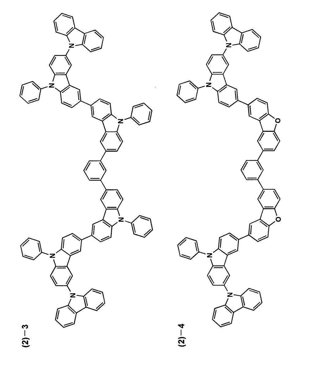


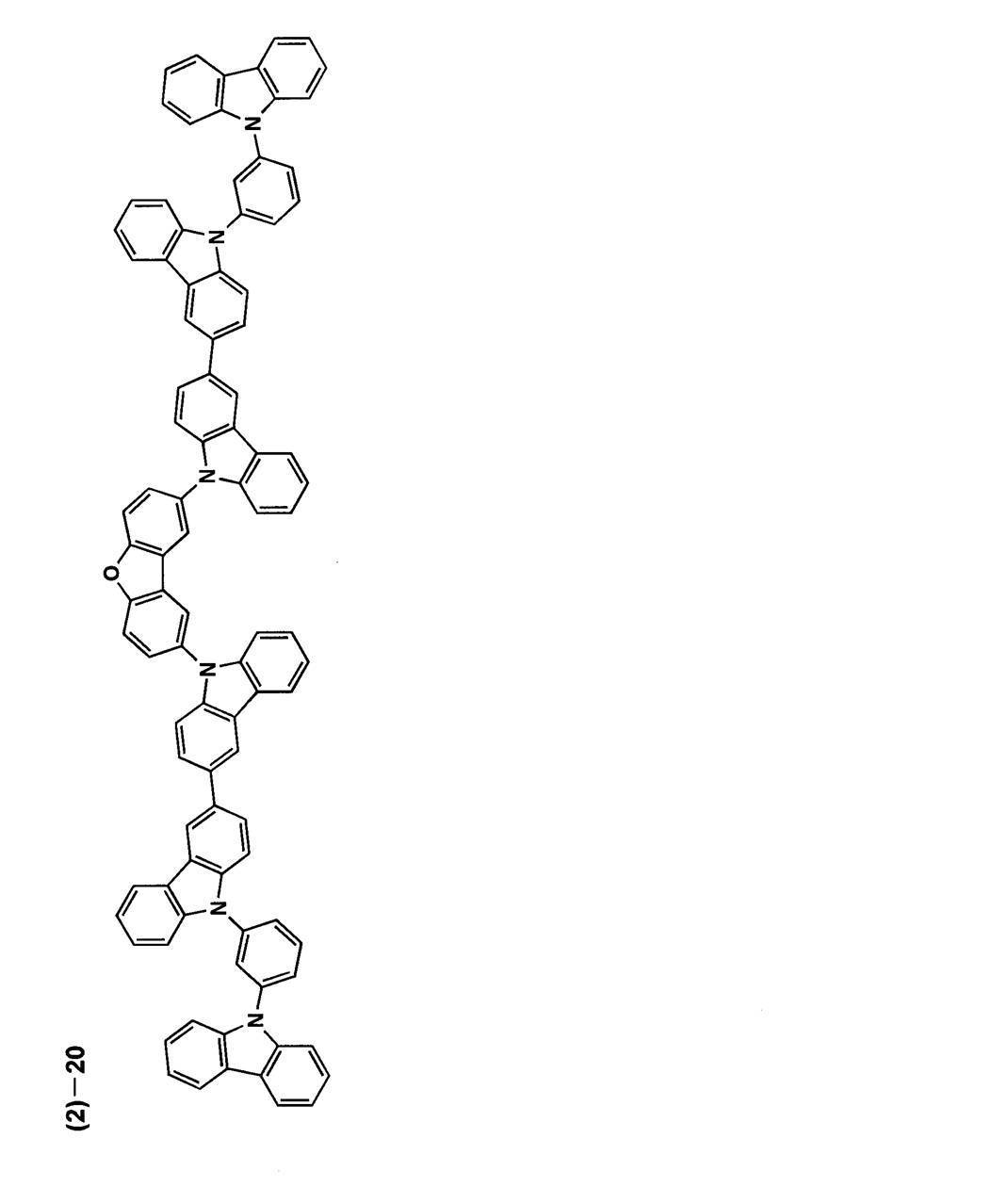
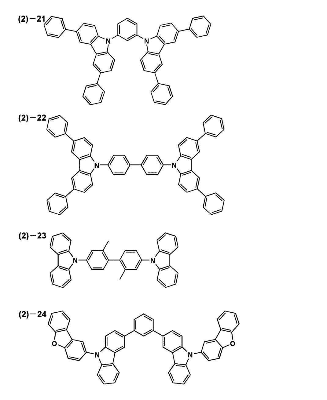

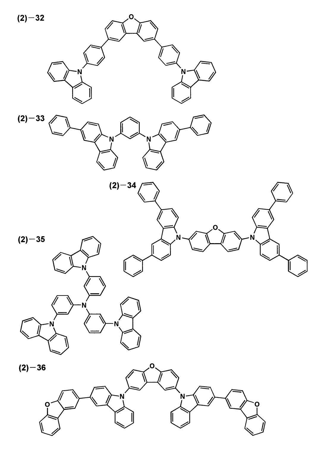

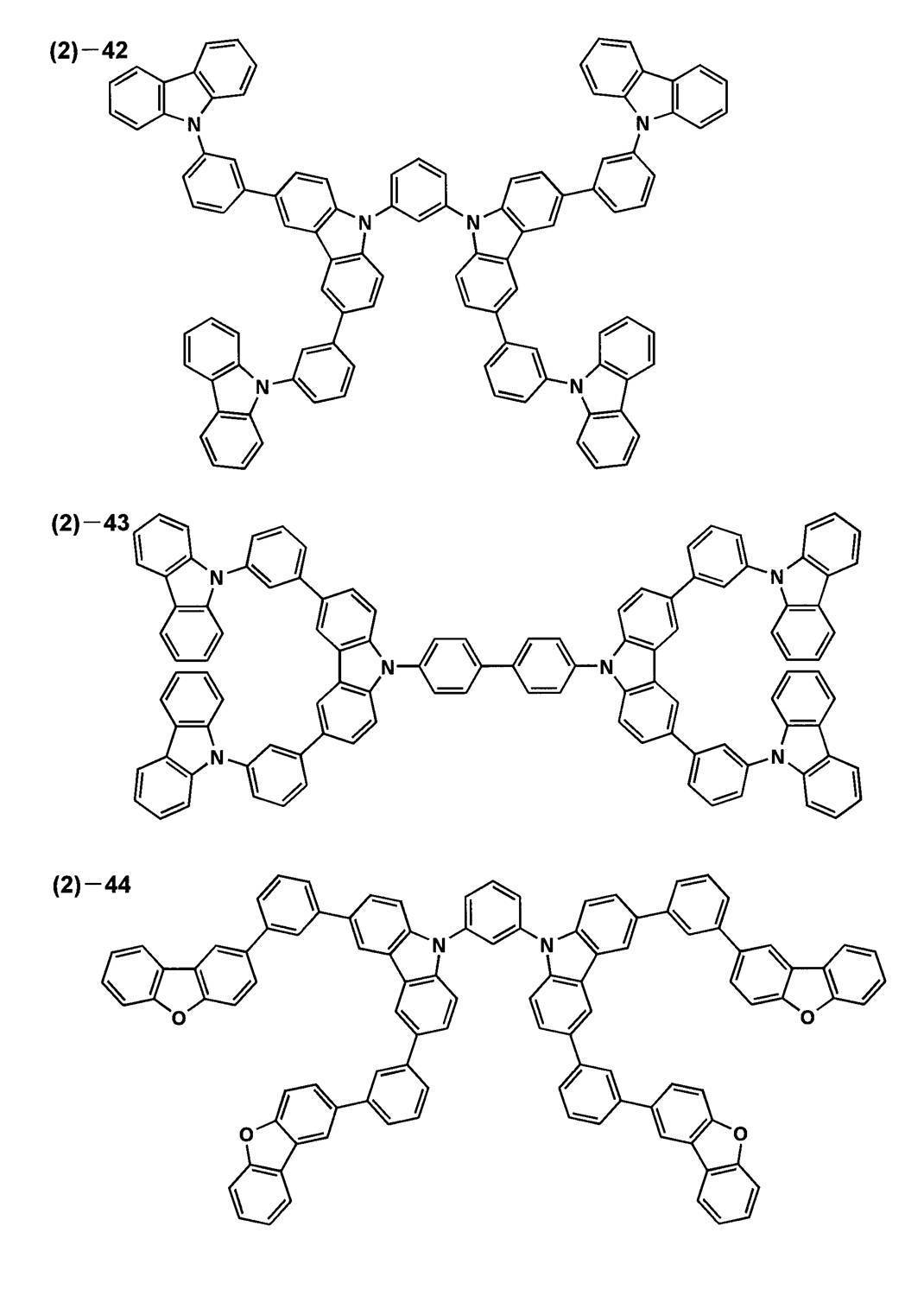


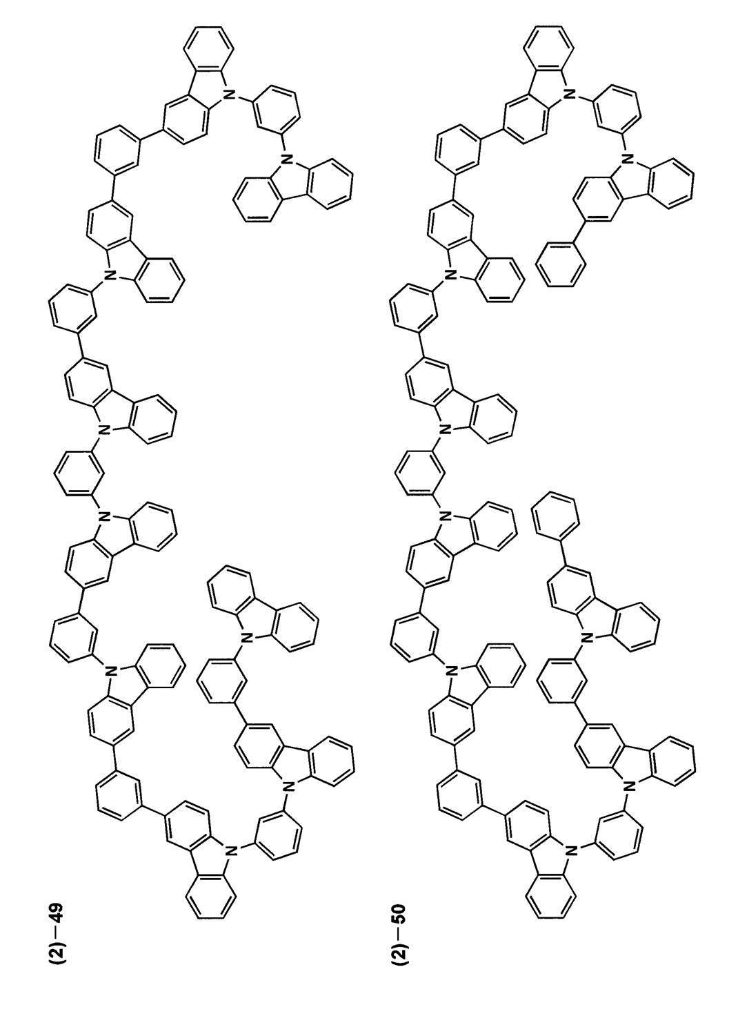


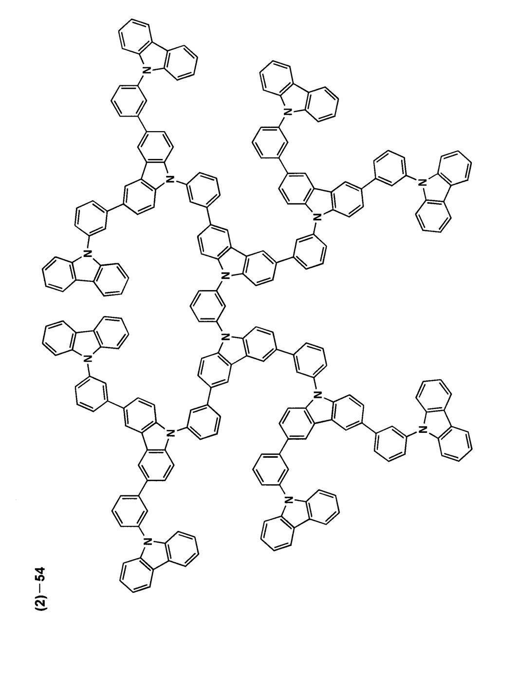
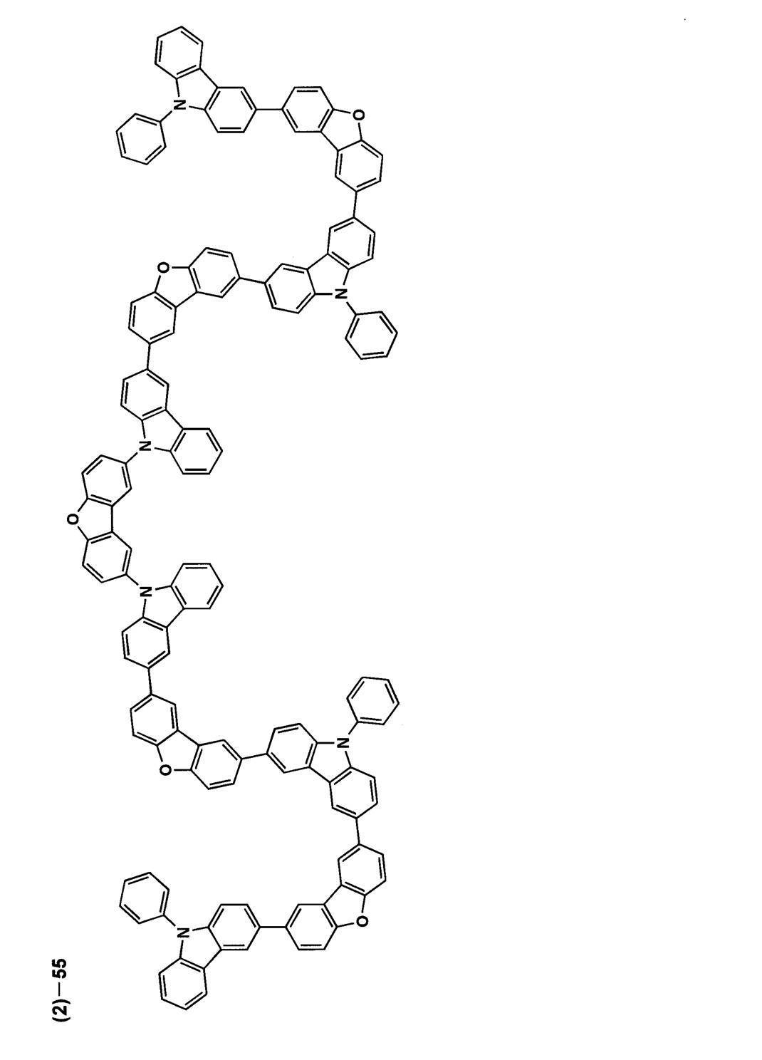

発光ホストとしては公知の発光ホスト単独で用いてもよく、または複数種併用して用いてもよい。発光ホストを複数種用いることで電荷の移動を調整することが可能であり、有機EL素子を高効率化することができる。また、後述する発光ドーパントを複数種用いることで、異なる発光を混ぜることが可能となり、これにより任意の発光色を得ることができる。
As the light emitting host, a known light emitting host may be used alone, or a plurality of kinds may be used in combination. By using a plurality of types of light-emitting hosts, the movement of charges can be adjusted, and the organic EL element can be made highly efficient. Moreover, it becomes possible to mix different light emission by using multiple types of light emission dopants mentioned later, and, thereby, arbitrary luminescent colors can be obtained.
また、本発明に用いられる発光ホストとしては、従来公知の低分子化合物でも、繰り返し単位を持つ高分子化合物でもよく、ビニル基やエポキシ基のような重合性基を有する低分子化合物(蒸着重合性発光ホスト)でもよい。
In addition, the light emitting host used in the present invention may be a conventionally known low molecular compound or a high molecular compound having a repeating unit, and a low molecular compound having a polymerizable group such as a vinyl group or an epoxy group (deposition polymerization property). Light emitting host).
併用してもよい公知の発光ホストとしては、正孔輸送能、電子輸送能を有しつつ、且つ発光の長波長化を防ぎ、なお且つ高Tg(ガラス転移温度)である化合物が好ましい。
As the known light-emitting host that may be used in combination, a compound that has a hole transporting ability and an electron transporting ability, prevents the emission of longer wavelengths, and has a high Tg (glass transition temperature) is preferable.
公知の発光ホストの具体例としては、以下の文献に記載されている化合物が挙げられる。
Specific examples of known light-emitting hosts include compounds described in the following documents.
特開2001-257076号公報、同2002-308855号公報、同2001-313179号公報、同2002-319491号公報、同2001-357977号公報、同2002-334786号公報、同2002-8860号公報、同2002-334787号公報、同2002-15871号公報、同2002-334788号公報、同2002-43056号公報、同2002-334789号公報、同2002-75645号公報、同2002-338579号公報、同2002-105445号公報、同2002-343568号公報、同2002-141173号公報、同2002-352957号公報、同2002-203683号公報、同2002-363227号公報、同2002-231453号公報、同2003-3165号公報、同2002-234888号公報、同2003-27048号公報、同2002-255934号公報、同2002-260861号公報、同2002-280183号公報、同2002-299060号公報、同2002-302516号公報、同2002-305083号公報、同2002-305084号公報、同2002-308837号公報等。
JP-A-2001-257076, 2002-308855, 2001-313179, 2002-319491, 2001-357777, 2002-334786, 2002-8860, 2002-334787, 2002-15871, 2002-334788, 2002-43056, 2002-334789, 2002-75645, 2002-338579, 2002-105445, 2002-343568, 2002-141173, 2002-352957, 2002-203683, 2002-363227, 2002-231453, 2003-3165, 2002-234888, 2003-27048, 2002-255934, 2002-260861, 2002-280183, 2002-299060, 2002 -302516, 2002-305083, 2002-305084, 2002-308837, and the like.
(発光ドーパント)
本発明に係る発光ドーパントについて説明する。 (Luminescent dopant)
The light emitting dopant according to the present invention will be described.
本発明に係る発光ドーパントについて説明する。 (Luminescent dopant)
The light emitting dopant according to the present invention will be described.
本発明に係る発光ドーパントとしては、蛍光ドーパント、リン光ドーパントを用いることができるが、より発光効率の高い有機EL素子を得る観点からは、本発明の有機EL素子の発光層や発光ユニットに使用される発光ドーパントとしては、上記の発光ホストを含有すると同時にリン光ドーパントを含有することが好ましい。
As the light-emitting dopant according to the present invention, a fluorescent dopant or a phosphorescent dopant can be used. From the viewpoint of obtaining an organic EL element with higher luminous efficiency, it is used for the light-emitting layer and the light-emitting unit of the organic EL element of the present invention. As the light emitting dopant, it is preferable to contain a phosphorescent dopant at the same time as containing the above light emitting host.
(リン光ドーパント)
本発明に係るリン光ドーパントについて説明する。 (Phosphorescent dopant)
The phosphorescent dopant according to the present invention will be described.
本発明に係るリン光ドーパントについて説明する。 (Phosphorescent dopant)
The phosphorescent dopant according to the present invention will be described.
本発明に係るリン光ドーパントは、励起三重項からの発光が観測される化合物であり、具体的には、室温(25℃)にてリン光発光する化合物であり、リン光量子収率が、25℃において0.01以上の化合物であり、好ましいリン光量子収率は0.1以上である。
The phosphorescent dopant according to the present invention is a compound in which light emission from an excited triplet is observed. Specifically, the phosphorescent dopant is a compound that emits phosphorescence at room temperature (25 ° C.) and has a phosphorescence quantum yield of 25. It is a compound of 0.01 or more at ° C., and a preferable phosphorescence quantum yield is 0.1 or more.
上記リン光量子収率は、第4版実験化学講座7の分光IIの398頁(1992年版、丸善)に記載の方法により測定できる。溶液中でのリン光量子収率は種々の溶媒を用いて測定できるが、本発明に係るリン光ドーパントは、任意の溶媒のいずれかにおいて上記リン光量子収率(0.01以上)が達成されればよい。
The phosphorescent quantum yield can be measured by the method described in Spectroscopic II, page 398 (1992 edition, Maruzen) of the Fourth Edition Experimental Chemistry Course 7. Although the phosphorescence quantum yield in a solution can be measured using various solvents, the phosphorescence dopant according to the present invention achieves the phosphorescence quantum yield (0.01 or more) in any solvent. That's fine.
リン光ドーパントの発光は原理としては2種挙げられ、一つはキャリアが輸送される発光ホスト上でキャリアの再結合が起こって発光ホストの励起状態が生成し、このエネルギーをリン光ドーパントに移動させることでリン光ドーパントからの発光を得るというエネルギー移動型、もう一つはリン光ドーパントがキャリアトラップとなり、リン光ドーパント上でキャリアの再結合が起こり、リン光ドーパントからの発光が得られるというキャリアトラップ型である。いずれの場合においても、リン光ドーパントの励起状態のエネルギーは発光ホストの励起状態のエネルギーよりも低いことが条件である。
There are two types of emission of phosphorescent dopants in principle. One is the recombination of carriers on the light-emitting host on which carriers are transported to generate the excited state of the light-emitting host, and this energy is transferred to the phosphorescent dopant. Energy transfer type to obtain light emission from the phosphorescent dopant, another is that the phosphorescent dopant becomes a carrier trap, carrier recombination occurs on the phosphorescent dopant, and light emission from the phosphorescent dopant is obtained It is a carrier trap type. In any case, it is a condition that the excited state energy of the phosphorescent dopant is lower than the excited state energy of the light emitting host.
リン光ドーパントは、有機EL素子の発光層に使用される公知のものの中から適宜選択して用いることができる。
The phosphorescent dopant can be appropriately selected from known materials used for the light emitting layer of the organic EL element.
本発明においては、発光ドーパントとして、前記一般式(1)で表されるリン光ドーパントを用いることが好ましい。
In the present invention, it is preferable to use a phosphorescent dopant represented by the general formula (1) as a light emitting dopant.
本発明に係る前記一般式(1)で表される発光ドーパントにおいて、R1で表される置換基としては、例えば、アルキル基(例えば、メチル基、エチル基、プロピル基、イソプロピル基、t-ブチル基、ペンチル基、ヘキシル基、オクチル基、ドデシル基、トリデシル基、テトラデシル基、ペンタデシル基等)、シクロアルキル基(例えば、シクロペンチル基、シクロヘキシル基等)、アルケニル基(例えば、ビニル基、アリル基等)、アルキニル基(例えば、エチニル基、プロパルギル基等)、芳香族炭化水素環基(芳香族炭素環基、アリール基等ともいい、例えば、フェニル基、p-クロロフェニル基、メシチル基、トリル基、キシリル基、ナフチル基、アントリル基、アズレニル基、アセナフテニル基、フルオレニル基、フェナントリル基、インデニル基、ピレニル基、ビフェニリル基等)、芳香族複素環基(例えば、ピリジル基、ピリミジニル基、フリル基、ピロリル基、イミダゾリル基、ベンゾイミダゾリル基、ピラゾリル基、ピラジニル基、トリアゾリル基(例えば、1,2,4-トリアゾール-1-イル基、1,2,3-トリアゾール-1-イル基等)、オキサゾリル基、ベンゾオキサゾリル基、チアゾリル基、イソオキサゾリル基、イソチアゾリル基、フラザニル基、チエニル基、キノリル基、ベンゾフリル基、ジベンゾフリル基、ベンゾチエニル基、ジベンゾチエニル基、インドリル基、カルバゾリル基、カルボリニル基、ジアザカルバゾリル基(前記カルボリニル基のカルボリン環を構成する炭素原子の一つが窒素原子で置き換わったものを示す)、キノキサリニル基、ピリダジニル基、トリアジニル基、キナゾリニル基、フタラジニル基等)、複素環基(例えば、ピロリジル基、イミダゾリジル基、モルホリル基、オキサゾリジル基等)、アルコキシ基(例えば、メトキシ基、エトキシ基、プロピルオキシ基、ペンチルオキシ基、ヘキシルオキシ基、オクチルオキシ基、ドデシルオキシ基等)、シクロアルコキシ基(例えば、シクロペンチルオキシ基、シクロヘキシルオキシ基等)、アリールオキシ基(例えば、フェノキシ基、ナフチルオキシ基等)、アルキルチオ基(例えば、メチルチオ基、エチルチオ基、プロピルチオ基、ペンチルチオ基、ヘキシルチオ基、オクチルチオ基、ドデシルチオ基等)、シクロアルキルチオ基(例えば、シクロペンチルチオ基、シクロヘキシルチオ基等)、アリールチオ基(例えば、フェニルチオ基、ナフチルチオ基等)、アルコキシカルボニル基(例えば、メチルオキシカルボニル基、エチルオキシカルボニル基、ブチルオキシカルボニル基、オクチルオキシカルボニル基、ドデシルオキシカルボニル基等)、アリールオキシカルボニル基(例えば、フェニルオキシカルボニル基、ナフチルオキシカルボニル基等)、スルファモイル基(例えば、アミノスルホニル基、メチルアミノスルホニル基、ジメチルアミノスルホニル基、ブチルアミノスルホニル基、ヘキシルアミノスルホニル基、シクロヘキシルアミノスルホニル基、オクチルアミノスルホニル基、ドデシルアミノスルホニル基、フェニルアミノスルホニル基、ナフチルアミノスルホニル基、2-ピリジルアミノスルホニル基等)、アシル基(例えば、アセチル基、エチルカルボニル基、プロピルカルボニル基、ペンチルカルボニル基、シクロヘキシルカルボニル基、オクチルカルボニル基、2-エチルヘキシルカルボニル基、ドデシルカルボニル基、フェニルカルボニル基、ナフチルカルボニル基、ピリジルカルボニル基等)、アシルオキシ基(例えば、アセチルオキシ基、エチルカルボニルオキシ基、ブチルカルボニルオキシ基、オクチルカルボニルオキシ基、ドデシルカルボニルオキシ基、フェニルカルボニルオキシ基等)、アミド基(例えば、メチルカルボニルアミノ基、エチルカルボニルアミノ基、ジメチルカルボニルアミノ基、プロピルカルボニルアミノ基、ペンチルカルボニルアミノ基、シクロヘキシルカルボニルアミノ基、2-エチルヘキシルカルボニルアミノ基、オクチルカルボニルアミノ基、ドデシルカルボニルアミノ基、フェニルカルボニルアミノ基、ナフチルカルボニルアミノ基等)、カルバモイル基(例えば、アミノカルボニル基、メチルアミノカルボニル基、ジメチルアミノカルボニル基、プロピルアミノカルボニル基、ペンチルアミノカルボニル基、シクロヘキシルアミノカルボニル基、オクチルアミノカルボニル基、2-エチルヘキシルアミノカルボニル基、ドデシルアミノカルボニル基、フェニルアミノカルボニル基、ナフチルアミノカルボニル基、2-ピリジルアミノカルボニル基等)、ウレイド基(例えば、メチルウレイド基、エチルウレイド基、ペンチルウレイド基、シクロヘキシルウレイド基、オクチルウレイド基、ドデシルウレイド基、フェニルウレイド基ナフチルウレイド基、2-ピリジルアミノウレイド基等)、スルフィニル基(例えば、メチルスルフィニル基、エチルスルフィニル基、ブチルスルフィニル基、シクロヘキシルスルフィニル基、2-エチルヘキシルスルフィニル基、ドデシルスルフィニル基、フェニルスルフィニル基、ナフチルスルフィニル基、2-ピリジルスルフィニル基等)、アルキルスルホニル基(例えば、メチルスルホニル基、エチルスルホニル基、ブチルスルホニル基、シクロヘキシルスルホニル基、2-エチルヘキシルスルホニル基、ドデシルスルホニル基等)、アリールスルホニル基またはヘテロアリールスルホニル基(例えば、フェニルスルホニル基、ナフチルスルホニル基、2-ピリジルスルホニル基等)、アミノ基(例えば、アミノ基、エチルアミノ基、ジメチルアミノ基、ブチルアミノ基、シクロペンチルアミノ基、2-エチルヘキシルアミノ基、ドデシルアミノ基、アニリノ基、ナフチルアミノ基、2-ピリジルアミノ基等)、シアノ基、ニトロ基、ヒドロキシ基、メルカプト基、シリル基(例えば、トリメチルシリル基、トリイソプロピルシリル基、トリフェニルシリル基、フェニルジエチルシリル基等)等が挙げられる。
In the light-emitting dopant represented by the general formula (1) according to the present invention, examples of the substituent represented by R 1 include an alkyl group (for example, methyl group, ethyl group, propyl group, isopropyl group, t- Butyl group, pentyl group, hexyl group, octyl group, dodecyl group, tridecyl group, tetradecyl group, pentadecyl group, etc.), cycloalkyl group (eg, cyclopentyl group, cyclohexyl group, etc.), alkenyl group (eg, vinyl group, allyl group) Etc.), alkynyl groups (for example, ethynyl group, propargyl group, etc.), aromatic hydrocarbon ring groups (aromatic carbocyclic group, aryl group, etc.), for example, phenyl group, p-chlorophenyl group, mesityl group, tolyl group , Xylyl, naphthyl, anthryl, azulenyl, acenaphthenyl, fluorenyl, phenanthri Group, indenyl group, pyrenyl group, biphenylyl group, etc.), aromatic heterocyclic group (for example, pyridyl group, pyrimidinyl group, furyl group, pyrrolyl group, imidazolyl group, benzoimidazolyl group, pyrazolyl group, pyrazinyl group, triazolyl group (for example, 1,2,4-triazol-1-yl group, 1,2,3-triazol-1-yl group, etc.), oxazolyl group, benzoxazolyl group, thiazolyl group, isoxazolyl group, isothiazolyl group, furazanyl group, thienyl Group, quinolyl group, benzofuryl group, dibenzofuryl group, benzothienyl group, dibenzothienyl group, indolyl group, carbazolyl group, carbolinyl group, diazacarbazolyl group (one of the carbon atoms constituting the carboline ring of the carbolinyl group is (Represented by nitrogen atom substitution), quinoxari Nyl group, pyridazinyl group, triazinyl group, quinazolinyl group, phthalazinyl group, etc.), heterocyclic group (eg, pyrrolidyl group, imidazolidyl group, morpholyl group, oxazolidyl group, etc.), alkoxy group (eg, methoxy group, ethoxy group, propyloxy) Group, pentyloxy group, hexyloxy group, octyloxy group, dodecyloxy group, etc.), cycloalkoxy group (eg, cyclopentyloxy group, cyclohexyloxy group, etc.), aryloxy group (eg, phenoxy group, naphthyloxy group, etc.) , Alkylthio groups (for example, methylthio group, ethylthio group, propylthio group, pentylthio group, hexylthio group, octylthio group, dodecylthio group, etc.), cycloalkylthio groups (for example, cyclopentylthio group, cyclohexylthio group, etc.), aryl O group (eg, phenylthio group, naphthylthio group, etc.), alkoxycarbonyl group (eg, methyloxycarbonyl group, ethyloxycarbonyl group, butyloxycarbonyl group, octyloxycarbonyl group, dodecyloxycarbonyl group, etc.), aryloxycarbonyl group (Eg, phenyloxycarbonyl group, naphthyloxycarbonyl group, etc.), sulfamoyl group (eg, aminosulfonyl group, methylaminosulfonyl group, dimethylaminosulfonyl group, butylaminosulfonyl group, hexylaminosulfonyl group, cyclohexylaminosulfonyl group, octyl) Aminosulfonyl groups, dodecylaminosulfonyl groups, phenylaminosulfonyl groups, naphthylaminosulfonyl groups, 2-pyridylaminosulfonyl groups, etc.), acyl groups (eg Acetyl, ethylcarbonyl, propylcarbonyl, pentylcarbonyl, cyclohexylcarbonyl, octylcarbonyl, 2-ethylhexylcarbonyl, dodecylcarbonyl, phenylcarbonyl, naphthylcarbonyl, pyridylcarbonyl, etc.), acyloxy Groups (for example, acetyloxy group, ethylcarbonyloxy group, butylcarbonyloxy group, octylcarbonyloxy group, dodecylcarbonyloxy group, phenylcarbonyloxy group, etc.), amide groups (for example, methylcarbonylamino group, ethylcarbonylamino group, Dimethylcarbonylamino group, propylcarbonylamino group, pentylcarbonylamino group, cyclohexylcarbonylamino group, 2-ethylhexylcarbonylamino group, octyl Tilcarbonylamino group, dodecylcarbonylamino group, phenylcarbonylamino group, naphthylcarbonylamino group, etc.), carbamoyl group (for example, aminocarbonyl group, methylaminocarbonyl group, dimethylaminocarbonyl group, propylaminocarbonyl group, pentylaminocarbonyl group) Cyclohexylaminocarbonyl group, octylaminocarbonyl group, 2-ethylhexylaminocarbonyl group, dodecylaminocarbonyl group, phenylaminocarbonyl group, naphthylaminocarbonyl group, 2-pyridylaminocarbonyl group, etc.), ureido group (for example, methylureido group, An ethylureido group, a pentylureido group, a cyclohexylureido group, an octylureido group, a dodecylureido group, a phenylureido group, a naphthylureido group, -Pyridylaminoureido group, etc.), sulfinyl groups (for example, methylsulfinyl group, ethylsulfinyl group, butylsulfinyl group, cyclohexylsulfinyl group, 2-ethylhexylsulfinyl group, dodecylsulfinyl group, phenylsulfinyl group, naphthylsulfinyl group, 2-pyridylsulfinyl group) Group), alkylsulfonyl group (for example, methylsulfonyl group, ethylsulfonyl group, butylsulfonyl group, cyclohexylsulfonyl group, 2-ethylhexylsulfonyl group, dodecylsulfonyl group, etc.), arylsulfonyl group or heteroarylsulfonyl group (for example, phenyl) Sulfonyl group, naphthylsulfonyl group, 2-pyridylsulfonyl group, etc.), amino group (for example, amino group, ethylamino group, dimethylamino group, Tilamino group, cyclopentylamino group, 2-ethylhexylamino group, dodecylamino group, anilino group, naphthylamino group, 2-pyridylamino group, etc., cyano group, nitro group, hydroxy group, mercapto group, silyl group (for example, trimethylsilyl group) , Triisopropylsilyl group, triphenylsilyl group, phenyldiethylsilyl group, etc.).
これらの置換基の内、好ましいものはアルキル基もしくはアリール基である。
Of these substituents, preferred are an alkyl group and an aryl group.
Zは5~7員環を形成するのに必要な非金属原子群を表す。Zにより形成される5~7員環としては、例えば、ベンゼン環、ナフタレン環、ピリジン環、ピリミジン環、ピロール環、チオフェン環、ピラゾール環、イミダゾール環、オキサゾール環及びチアゾール環等が挙げられる。これらの内で好ましいものはベンゼン環である。
Z represents a nonmetallic atom group necessary for forming a 5- to 7-membered ring. Examples of the 5- to 7-membered ring formed by Z include a benzene ring, naphthalene ring, pyridine ring, pyrimidine ring, pyrrole ring, thiophene ring, pyrazole ring, imidazole ring, oxazole ring and thiazole ring. Of these, a benzene ring is preferred.
B1~B5は炭素原子、窒素原子、酸素原子もしくは硫黄原子を表し、少なくとも一つは窒素原子を表す。これら5つの原子により形成される芳香族含窒素複素環としては単環が好ましい。例えば、ピロール環、ピラゾール環、イミダゾール環、トリアゾール環、テトラゾール環、オキサゾール環、イソオキサゾール環、チアゾール環、イソチアゾール環、オキサジアゾール環及びチアジアゾー環ル等が挙げられる。
B 1 to B 5 each represent a carbon atom, a nitrogen atom, an oxygen atom or a sulfur atom, and at least one represents a nitrogen atom. The aromatic nitrogen-containing heterocycle formed by these five atoms is preferably a monocycle. Examples include pyrrole ring, pyrazole ring, imidazole ring, triazole ring, tetrazole ring, oxazole ring, isoxazole ring, thiazole ring, isothiazole ring, oxadiazole ring, and thiadiazole ring.
これらの内で好ましいものは、ピラゾール環、イミダゾール環であり、更に好ましくはイミダゾール環である。これらの環は上記の置換基によって更に置換されていてもよい。置換基として好ましいものはアルキル基及びアリール基であり、更に好ましくはアリール基である。
Of these, a pyrazole ring and an imidazole ring are preferable, and an imidazole ring is more preferable. These rings may be further substituted with the above substituents. Preferred as the substituent are an alkyl group and an aryl group, and more preferably an aryl group.
L1はX1、X2と共に2座の配位子を形成する原子群を表す。X1-L1-X2で表される2座の配位子の具体例としては、例えば、置換または無置換のフェニルピリジン、フェニルピラゾール、フェニルイミダゾール、フェニルトリアゾール、フェニルテトラゾール、ピラザボール、ピコリン酸及びアセチルアセトン等が挙げられる。これらの基は上記の置換基によって更に置換されていてもよい。
L 1 represents an atomic group that forms a bidentate ligand together with X 1 and X 2 . Specific examples of the bidentate ligand represented by X 1 -L 1 -X 2 include, for example, substituted or unsubstituted phenylpyridine, phenylpyrazole, phenylimidazole, phenyltriazole, phenyltetrazole, pyrazabol, picolinic acid And acetylacetone. These groups may be further substituted with the above substituents.
m1は1、2または3の整数を表し、m2は0、1または2の整数を表すが、m1+m2は2または3である。中でも、m2は0である場合が好ましい。
M1 represents an integer of 1, 2 or 3, m2 represents an integer of 0, 1 or 2, but m1 + m2 is 2 or 3. Especially, the case where m2 is 0 is preferable.
M1で表される金属としては、元素周期表の8族~10族の遷移金属元素(単に遷移金属とも言う)が用いられるが、中でもイリジウム、白金が好ましく、更に好ましくはイリジウムである。
As the metal represented by M 1 , a transition metal element of Group 8 to Group 10 (also referred to simply as a transition metal) in the periodic table of elements is used. Among them, iridium and platinum are preferable, and iridium is more preferable.
なお、本発明に係る一般式(1)で表される発光ドーパントは、重合性基または反応性基を有していてもいなくてもよい。
Note that the light-emitting dopant represented by the general formula (1) according to the present invention may or may not have a polymerizable group or a reactive group.
以下に、発光ドーパントとして用いられる化合物の具体例を示すが、本発明はこれらに限定されない。
Specific examples of the compound used as the light emitting dopant are shown below, but the present invention is not limited thereto.
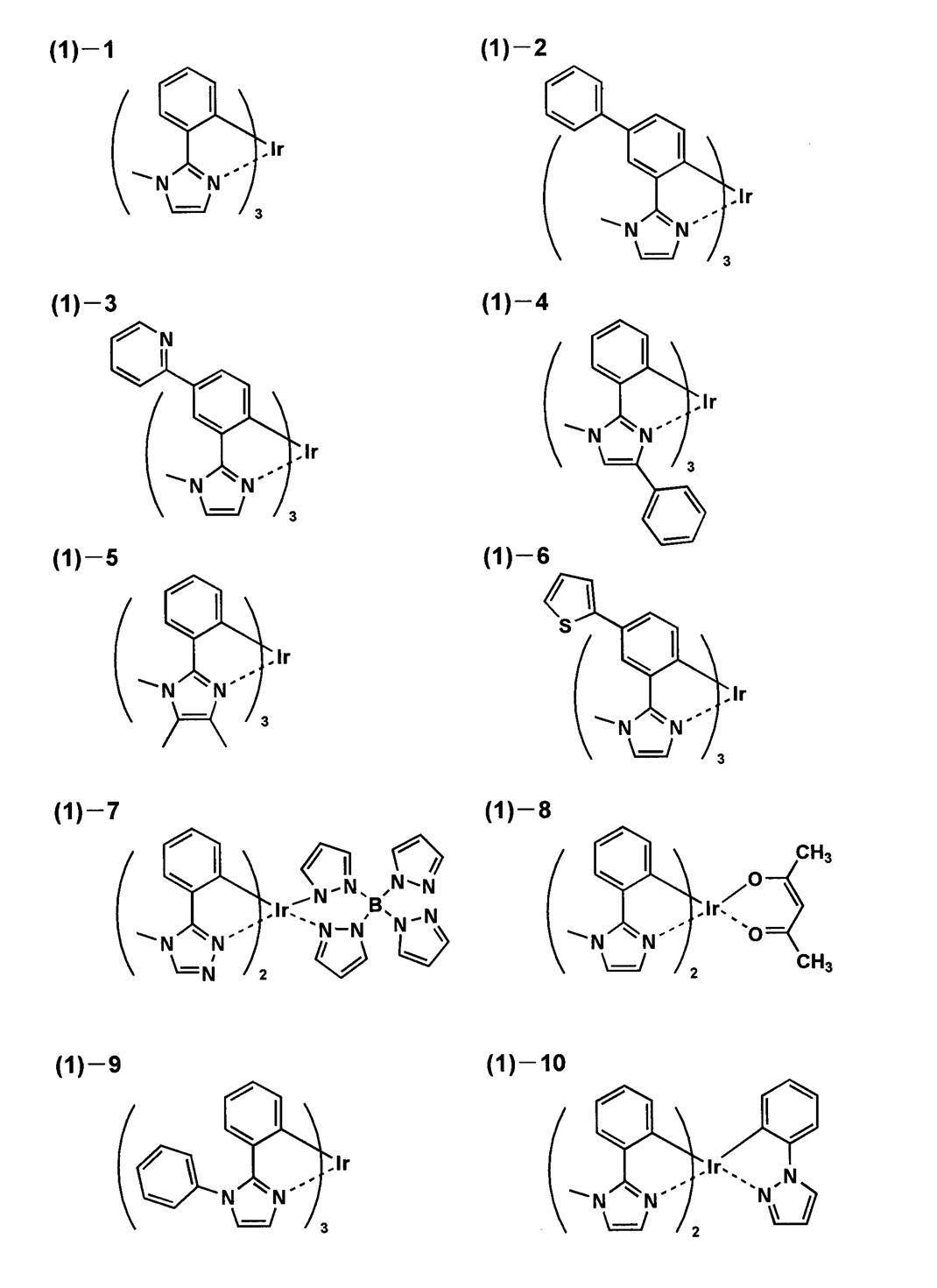
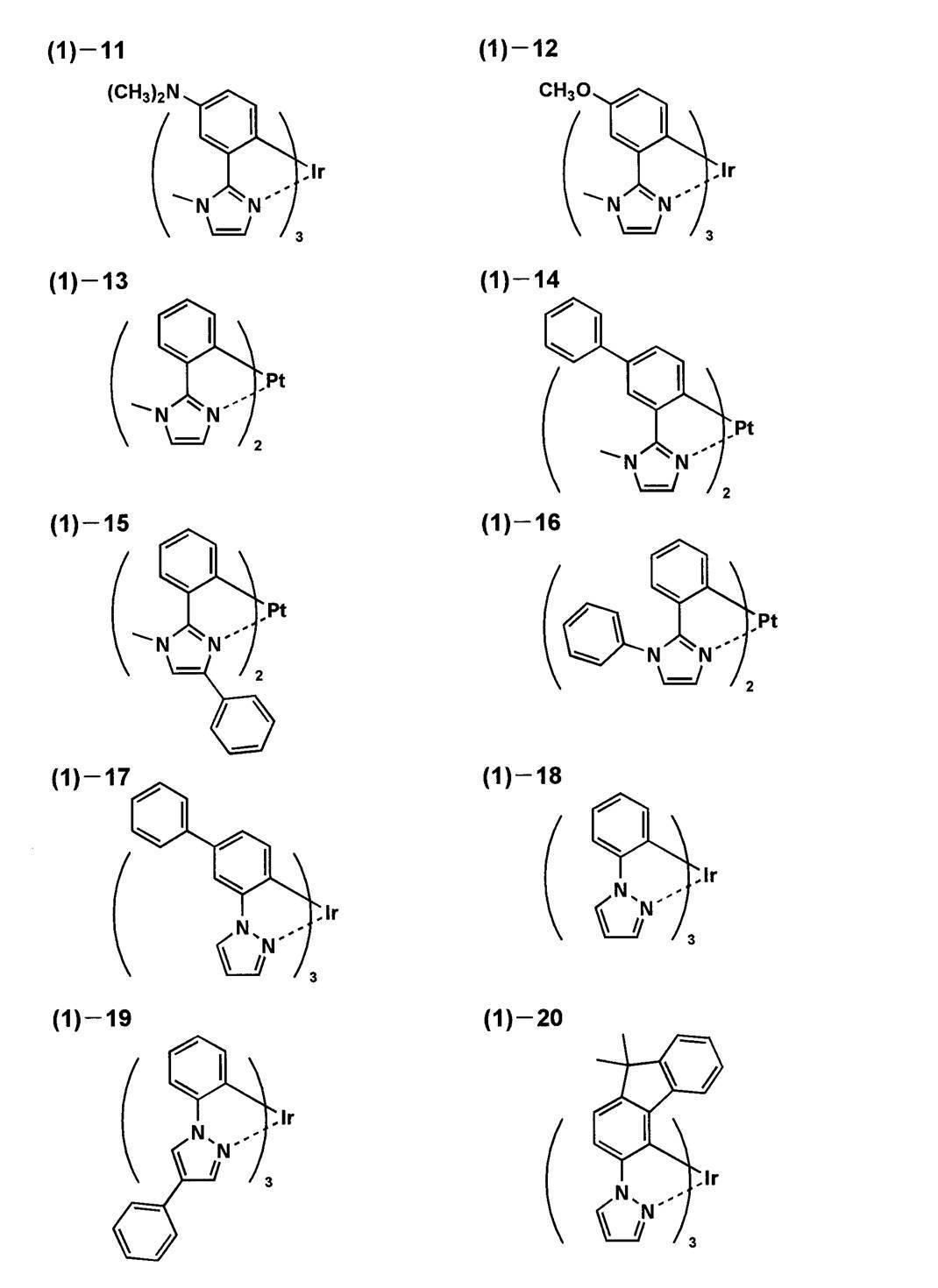

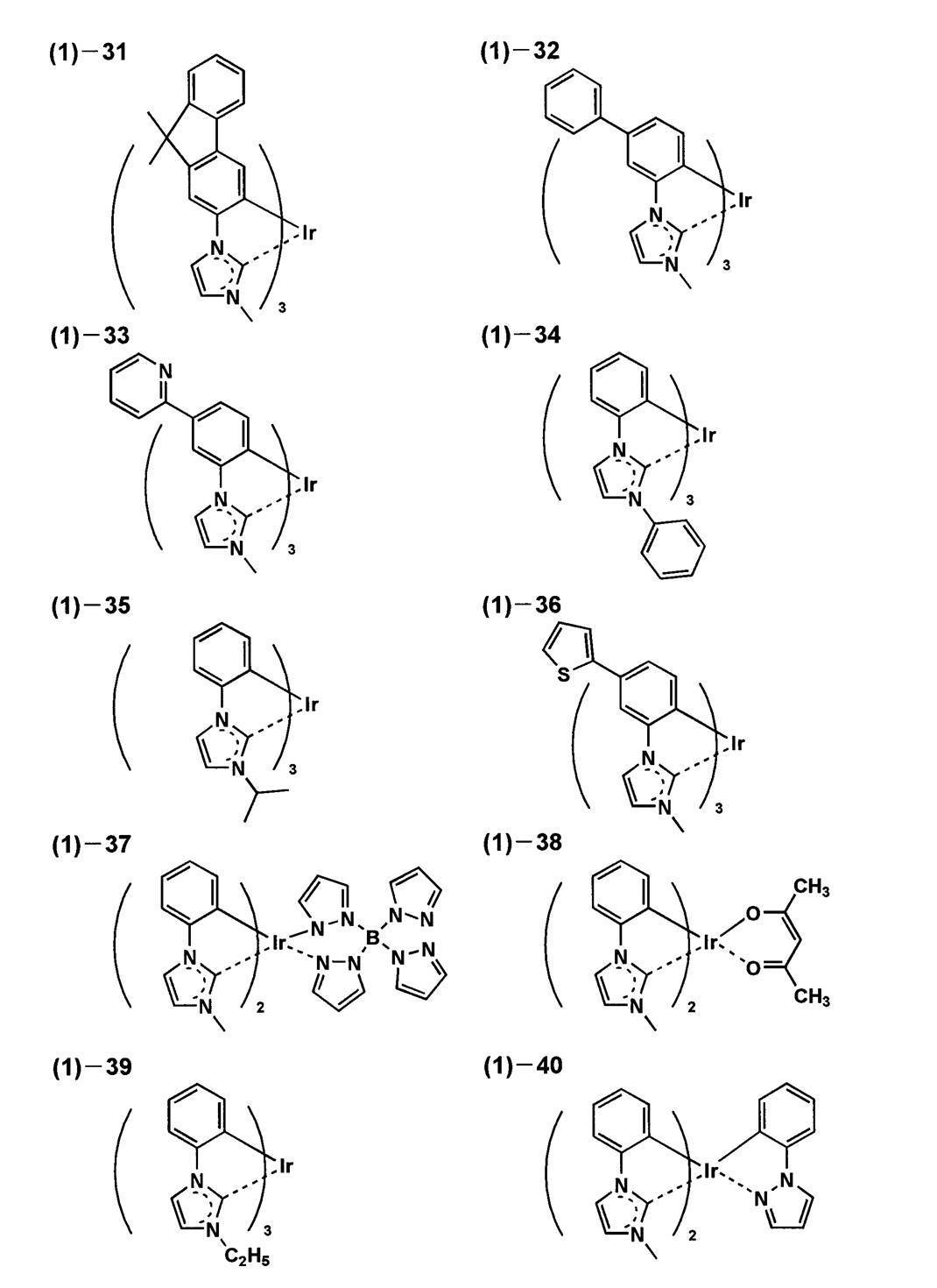
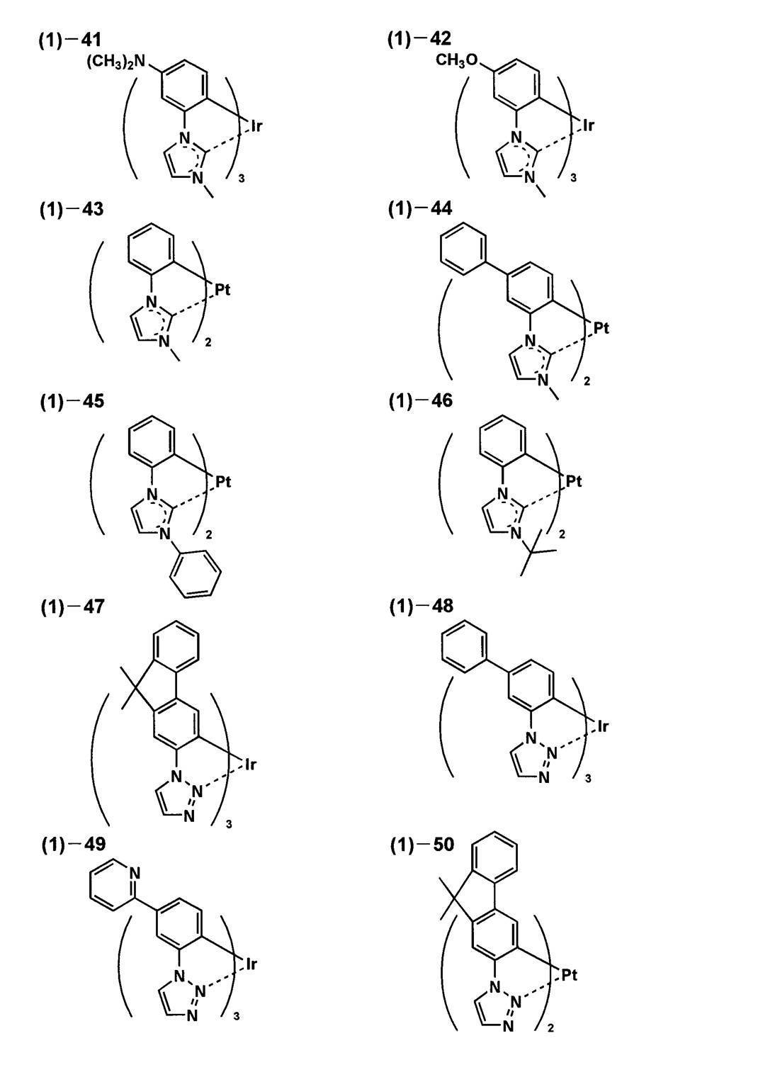


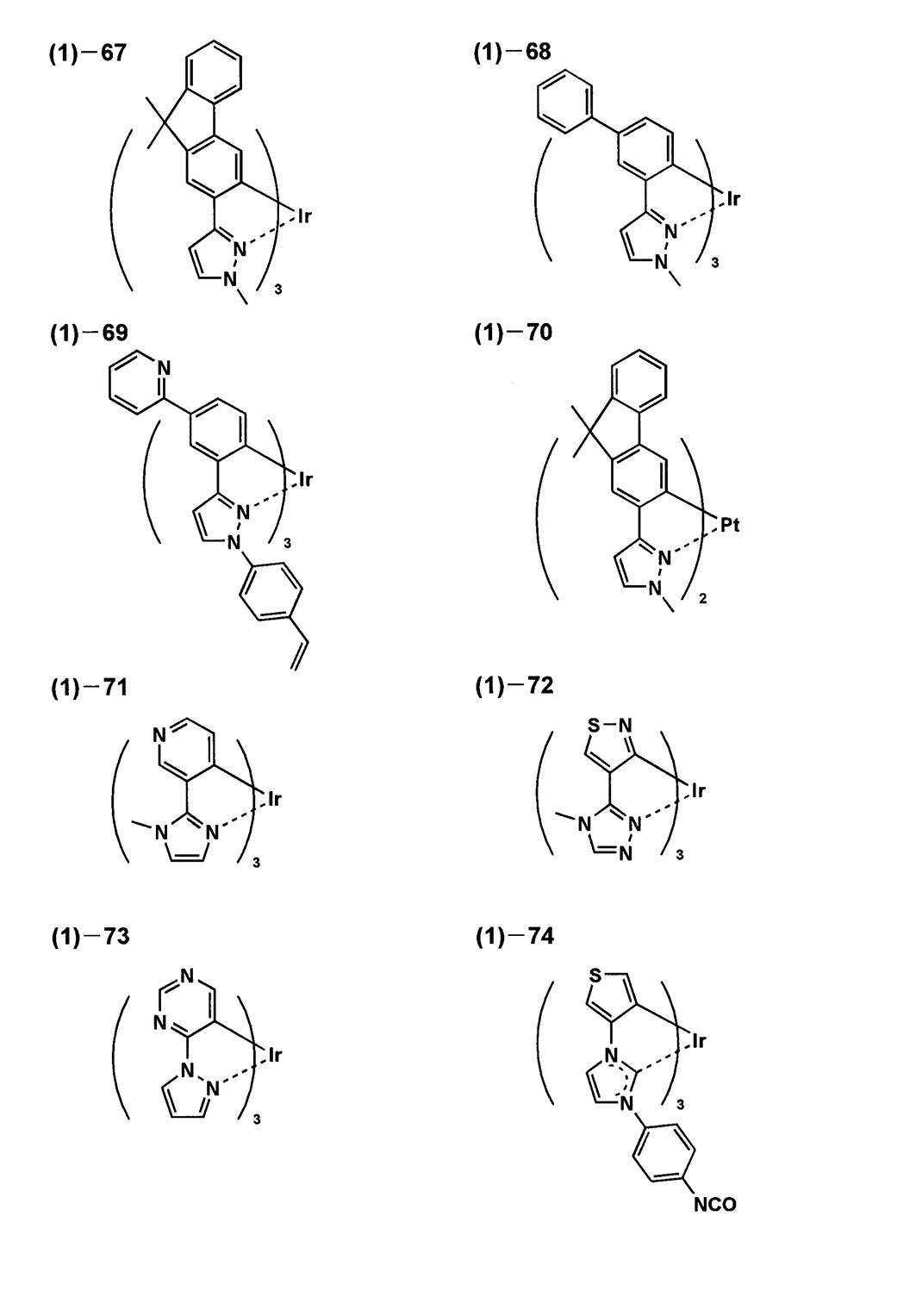


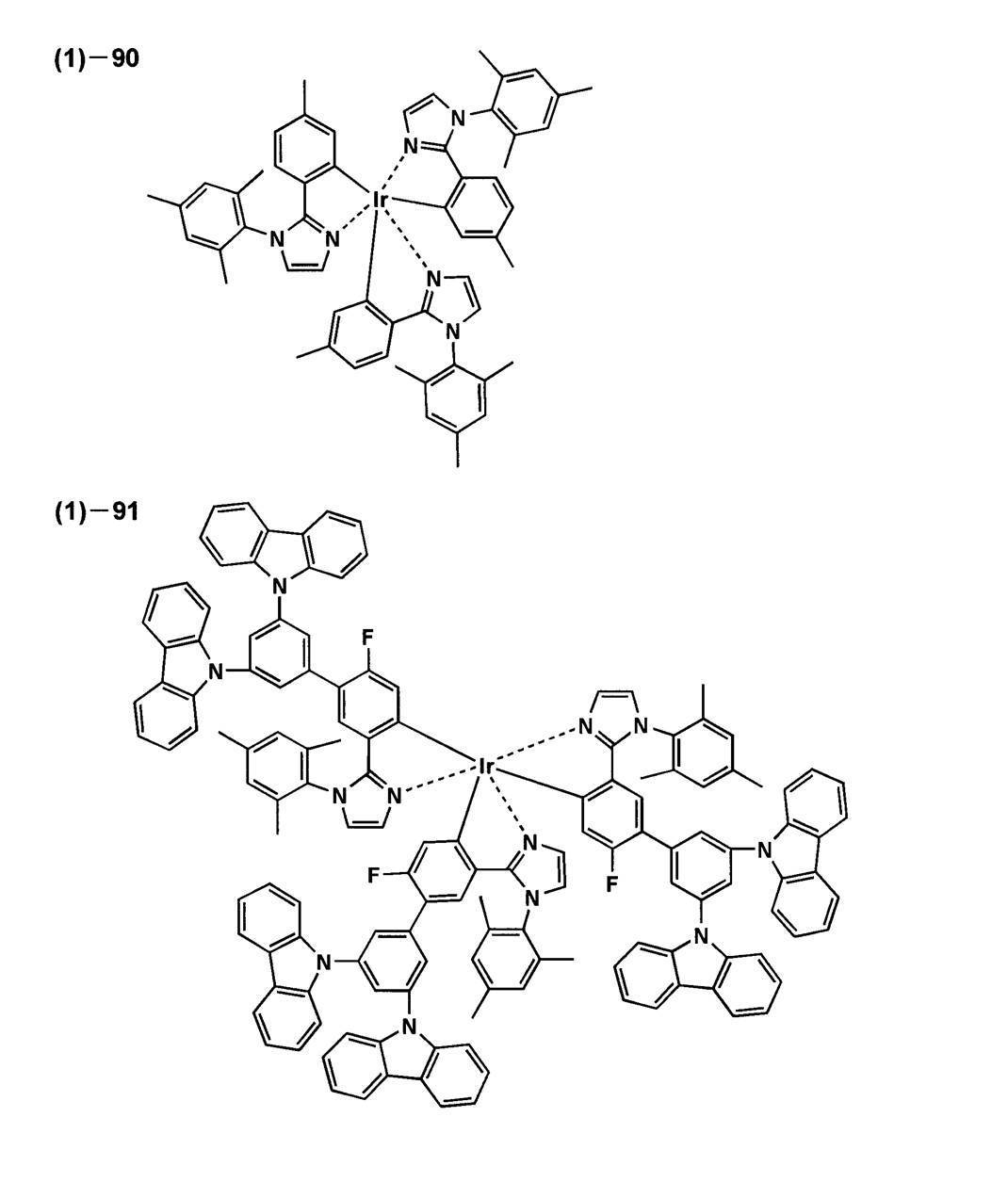
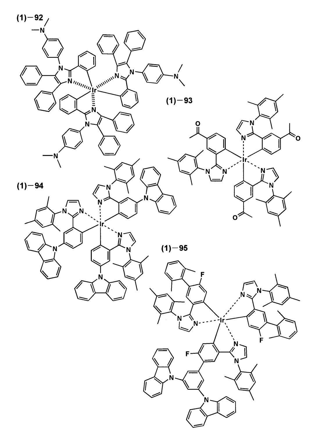
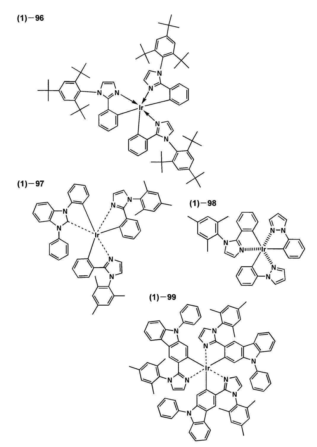

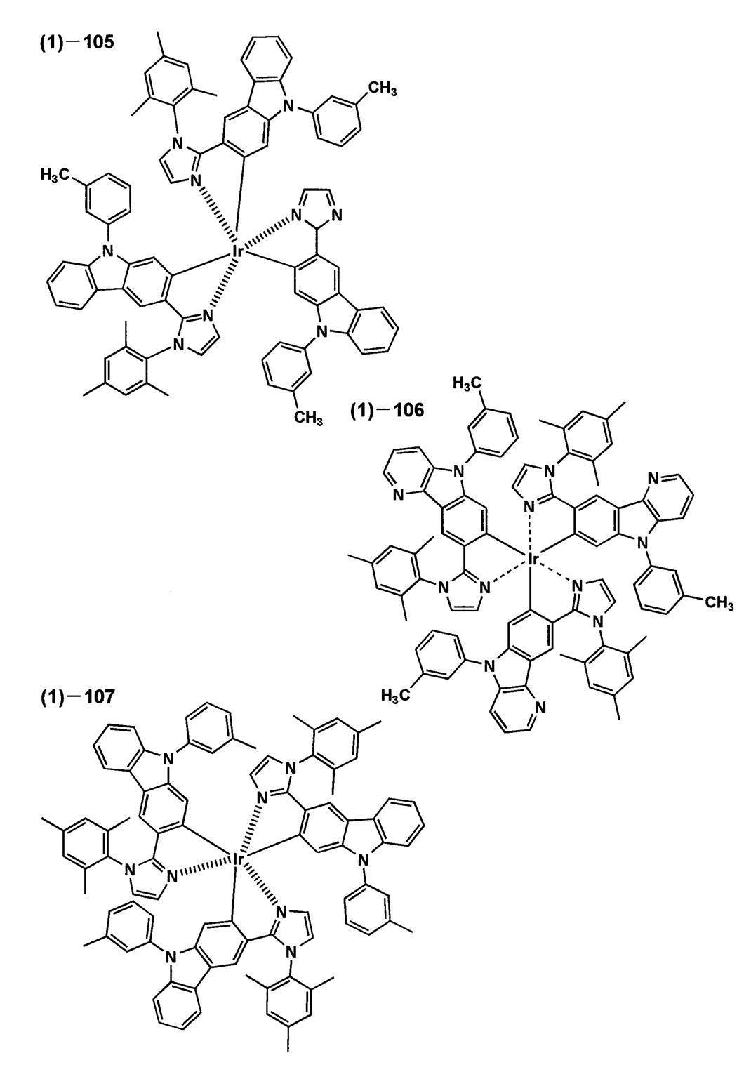
これらの金属錯体は、例えば、Organic Letter誌、vol3、No.16、2579~2581頁(2001)、Inorganic Chemistry,第30巻、第8号、1685~1687頁(1991年)、J.Am.Chem.Soc.,123巻、4304頁(2001年)、Inorganic Chemistry,第40巻、第7号、1704~1711頁(2001年)、Inorganic Chemistry,第41巻、第12号、3055~3066頁(2002年)、New Journal of Chemistry.,第26巻、1171頁(2002年)、European Journal of Organic Chemistry,第4巻、695~709頁(2004年)、更にこれらの文献中に記載の参考文献等の方法を適用することにより合成できる。
These metal complexes are described in, for example, Organic Letter, vol. 16, 2579-2581 (2001), Inorganic Chemistry, Vol. 30, No. 8, pp. 1685-1687 (1991), J. Am. Am. Chem. Soc. , 123, 4304 (2001), Inorganic Chemistry, Vol. 40, No. 7, pages 1704-1711 (2001), Inorganic Chemistry, Vol. 41, No. 12, pages 3055-3066 (2002) , New Journal of Chemistry. 26, 1171 (2002), European Journal of Organic Chemistry, Vol. 4, pages 695-709 (2004), and further synthesized by applying methods such as references described in these documents. it can.
(蛍光ドーパント)
蛍光ドーパントとしては、クマリン系色素、ピラン系色素、シアニン系色素、クロコニウム系色素、スクアリウム系色素、オキソベンツアントラセン系色素、フルオレセイン系色素、ローダミン系色素、ピリリウム系色素、ペリレン系色素、スチルベン系色素、ポリチオフェン系色素、または希土類錯体系蛍光体等が挙げられる。 (Fluorescent dopant)
As fluorescent dopants, coumarin dyes, pyran dyes, cyanine dyes, croconium dyes, squalium dyes, oxobenzanthracene dyes, fluorescein dyes, rhodamine dyes, pyrylium dyes, perylene dyes, stilbene dyes , Polythiophene dyes, or rare earth complex phosphors.
次に、本発明の有機EL素子の構成層として用いられる、注入層、阻止層、電子輸送層等について説明する。
Next, an injection layer, a blocking layer, an electron transport layer, and the like used as a constituent layer of the organic EL element of the present invention will be described.
《注入層:電子注入層、正孔注入層》
注入層は必要に応じて設け、電子注入層と正孔注入層があり、上記の如く陽極と発光層または正孔輸送層の間、及び陰極と発光層または電子輸送層との間に存在させてもよい。 << Injection layer: electron injection layer, hole injection layer >>
The injection layer is provided as necessary, and there are an electron injection layer and a hole injection layer, and as described above, it exists between the anode and the light emitting layer or the hole transport layer and between the cathode and the light emitting layer or the electron transport layer. May be.
注入層とは、駆動電圧低下や発光輝度向上のために電極と有機層間に設けられる層のことで、「有機EL素子とその工業化最前線(1998年11月30日エヌ・ティー・エス社発行)」の第2編第2章「電極材料」(123~166頁)に詳細に記載されており、正孔注入層(陽極バッファー層)と電子注入層(陰極バッファー層)とがある。
An injection layer is a layer provided between an electrode and an organic layer in order to reduce drive voltage and improve light emission luminance. “Organic EL element and its forefront of industrialization (issued by NTT Corporation on November 30, 1998) 2), Chapter 2, “Electrode Materials” (pages 123 to 166) in detail, and includes a hole injection layer (anode buffer layer) and an electron injection layer (cathode buffer layer).
陽極バッファー層(正孔注入層)は、特開平9-45479号公報、同9-260062号公報、同8-288069号公報等にもその詳細が記載されており、具体例として、銅フタロシアニンに代表されるフタロシアニンバッファー層、酸化バナジウムに代表される酸化物バッファー層、アモルファスカーボンバッファー層、ポリアニリン(エメラルディン)やポリチオフェン等の導電性高分子を用いた高分子バッファー層等が挙げられる。
The details of the anode buffer layer (hole injection layer) are described in JP-A-9-45479, JP-A-9-260062, JP-A-8-288069 and the like. As a specific example, copper phthalocyanine is used. Examples thereof include a phthalocyanine buffer layer represented by an oxide, an oxide buffer layer represented by vanadium oxide, an amorphous carbon buffer layer, and a polymer buffer layer using a conductive polymer such as polyaniline (emeraldine) or polythiophene.
陰極バッファー層(電子注入層)は、特開平6-325871号公報、同9-17574号公報、同10-74586号公報等にもその詳細が記載されており、具体的にはストロンチウムやアルミニウム等に代表される金属バッファー層、フッ化リチウムに代表されるアルカリ金属化合物バッファー層、フッ化マグネシウムに代表されるアルカリ土類金属化合物バッファー層、酸化アルミニウムに代表される酸化物バッファー層等が挙げられる。上記バッファー層(注入層)はごく薄い膜であることが望ましく、素材にもよるがその膜厚は0.1nm~5μmの範囲が好ましい。
The details of the cathode buffer layer (electron injection layer) are described in JP-A-6-325871, JP-A-9-17574, JP-A-10-74586, and the like. Specifically, strontium, aluminum, etc. Metal buffer layer typified by lithium, alkali metal compound buffer layer typified by lithium fluoride, alkaline earth metal compound buffer layer typified by magnesium fluoride, oxide buffer layer typified by aluminum oxide, etc. . The buffer layer (injection layer) is preferably a very thin film, and the film thickness is preferably in the range of 0.1 nm to 5 μm, although it depends on the material.
《阻止層:正孔阻止層、電子阻止層》
阻止層は、上記の如く有機化合物薄膜の基本構成層の他に必要に応じて設けられるものである。例えば、特開平11-204258号公報、同11-204359号公報、及び「有機EL素子とその工業化最前線(1998年11月30日エヌ・ティー・エス社発行)」の237頁等に記載されている正孔阻止(ホールブロック)層がある。 <Blocking layer: hole blocking layer, electron blocking layer>
The blocking layer is provided as necessary in addition to the basic constituent layer of the organic compound thin film as described above. For example, it is described in JP-A Nos. 11-204258 and 11-204359, and “Organic EL elements and the forefront of industrialization (published by NTT Corporation on November 30, 1998)” on page 237. There is a hole blocking (hole blocking) layer.
正孔阻止層とは広い意味では電子輸送層の機能を有し、電子を輸送する機能を有しつつ正孔を輸送する能力が著しく小さい正孔阻止材料からなり、電子を輸送しつつ正孔を阻止することで電子と正孔の再結合確率を向上させることができる。また、後述する電子輸送層の構成を必要に応じて、本発明に係る正孔阻止層として用いることができる。
The hole blocking layer has a function of an electron transport layer in a broad sense, and is made of a hole blocking material that has a function of transporting electrons and has a remarkably small ability to transport holes. The probability of recombination of electrons and holes can be improved by blocking. Moreover, the structure of the electron carrying layer mentioned later can be used as a hole-blocking layer concerning this invention as needed.
本発明の有機EL素子の正孔阻止層は、発光層に隣接して設けられていることが好ましい。
The hole blocking layer of the organic EL device of the present invention is preferably provided adjacent to the light emitting layer.
正孔阻止層には、前述の発光ホストとして挙げたカルバゾール誘導体を含有することが好ましい。
It is preferable that the hole blocking layer contains the carbazole derivative mentioned as the light emitting host.
また、本発明においては、複数の発光色の異なる複数の発光層を有する場合、その発光極大波長が最も短波にある発光層が、全発光層中、最も陽極に近いことが好ましいが、このような場合、該最短波層と該層の次に陽極に近い発光層との間に正孔阻止層を追加して設けることが好ましい。更には、該位置に設けられる正孔阻止層に含有される化合物の50質量%以上が、前記最短波発光層の発光ホストに対しそのイオン化ポテンシャルが0.3eV以上大きいことが好ましい。
In the present invention, when a plurality of light emitting layers having different light emission colors are provided, the light emitting layer having the shortest wavelength of light emission is preferably closest to the anode among all the light emitting layers. In this case, it is preferable to additionally provide a hole blocking layer between the shortest wave layer and the light emitting layer next to the anode next to the anode. Further, it is preferable that 50% by mass or more of the compound contained in the hole blocking layer provided at the position has an ionization potential of 0.3 eV or more larger than the light emitting host of the shortest wave emitting layer.
イオン化ポテンシャルは化合物のHOMO(最高被占分子軌道)レベルにある電子を真空準位に放出するのに必要なエネルギーで定義され、例えば、下記に示すような方法により求めることができる。
The ionization potential is defined by the energy required to emit electrons at the HOMO (highest occupied molecular orbital) level of the compound to the vacuum level, and can be obtained by, for example, the following method.
(1)米国Gaussian製の分子軌道計算用ソフトウェアであるGaussian98(Gaussian98、Revision A.11.4,M.J.Frisch,et al,Gaussian,Inc.,Pittsburgh PA,2002.)を用い、キーワードとしてB3LYP/6-31G*を用いて構造最適化を行うことにより算出した値(eV単位換算値)の小数点第2位を四捨五入した値としてイオン化ポテンシャルを求めることができる。この計算値が有効な背景には、この手法で求めた計算値と実験値の相関が高いためである。
(1) Gaussian 98 (Gaussian 98, Revision A.11.4, MJ Frisch, et al, Gaussian, Inc., Pittsburgh PA, 2002.), a molecular orbital calculation software manufactured by Gaussian, USA, is used as a keyword. The ionization potential can be obtained as a value obtained by rounding off the second decimal place of a value (eV unit converted value) calculated by performing structural optimization using B3LYP / 6-31G *. This calculation value is effective because the correlation between the calculation value obtained by this method and the experimental value is high.
(2)イオン化ポテンシャルは光電子分光法で直接測定する方法により求めることもできる。例えば、理研計器製の低エネルギー電子分光装置「Model AC-1」を用いて、あるいは紫外光電子分光として知られている方法を好適に用いることができる。
(2) The ionization potential can also be obtained by a method of directly measuring by photoelectron spectroscopy. For example, a low energy electron spectrometer “Model AC-1” manufactured by Riken Keiki Co., Ltd. or a method known as ultraviolet photoelectron spectroscopy can be suitably used.
一方、電子阻止層とは広い意味では正孔輸送層の機能を有し、正孔を輸送する機能を有しつつ電子を輸送する能力が著しく小さい材料からなり、正孔を輸送しつつ電子を阻止することで電子と正孔の再結合確率を向上させることができる。また、後述する正孔輸送層の構成を必要に応じて電子阻止層として用いることができる。本発明に係る正孔阻止層、電子輸送層の膜厚としては、好ましくは3~100nmであり、更に好ましくは5~30nmである。
On the other hand, the electron blocking layer has a function of a hole transport layer in a broad sense, and is made of a material that has a function of transporting holes and has an extremely small ability to transport electrons. By blocking, the recombination probability of electrons and holes can be improved. Moreover, the structure of the positive hole transport layer mentioned later can be used as an electron blocking layer as needed. The film thickness of the hole blocking layer and the electron transporting layer according to the present invention is preferably 3 to 100 nm, more preferably 5 to 30 nm.
《正孔輸送層》
正孔輸送層とは正孔を輸送する機能を有する正孔輸送材料からなり、広い意味で正孔注入層、電子阻止層も正孔輸送層に含まれる。正孔輸送層は単層または複数層設けることができる。 《Hole transport layer》
The hole transport layer is made of a hole transport material having a function of transporting holes, and in a broad sense, a hole injection layer and an electron blocking layer are also included in the hole transport layer. The hole transport layer can be provided as a single layer or a plurality of layers.
正孔輸送材料としては、正孔の注入または輸送、電子の障壁性のいずれかを有するものであり、有機物、無機物のいずれであってもよい。例えば、トリアゾール誘導体、オキサジアゾール誘導体、イミダゾール誘導体、ポリアリールアルカン誘導体、ピラゾリン誘導体及びピラゾロン誘導体、フェニレンジアミン誘導体、アリールアミン誘導体、アミノ置換カルコン誘導体、オキサゾール誘導体、スチリルアントラセン誘導体、フルオレノン誘導体、ヒドラゾン誘導体、スチルベン誘導体、シラザン誘導体、アニリン系共重合体、また導電性高分子オリゴマー、特にチオフェンオリゴマー等が挙げられる。
The hole transport material has either hole injection or transport or electron barrier properties, and may be either organic or inorganic. For example, triazole derivatives, oxadiazole derivatives, imidazole derivatives, polyarylalkane derivatives, pyrazoline derivatives and pyrazolone derivatives, phenylenediamine derivatives, arylamine derivatives, amino-substituted chalcone derivatives, oxazole derivatives, styrylanthracene derivatives, fluorenone derivatives, hydrazone derivatives, Examples thereof include stilbene derivatives, silazane derivatives, aniline copolymers, and conductive polymer oligomers, particularly thiophene oligomers.
正孔輸送材料としては上記のものを使用することができるが、ポルフィリン化合物、芳香族第3級アミン化合物及びスチリルアミン化合物、特に芳香族第3級アミン化合物を用いることが好ましい。
The above-mentioned materials can be used as the hole transport material, but it is preferable to use a porphyrin compound, an aromatic tertiary amine compound and a styrylamine compound, particularly an aromatic tertiary amine compound.
芳香族第3級アミン化合物及びスチリルアミン化合物の代表例としては、N,N,N′,N′-テトラフェニル-4,4′-ジアミノフェニル;N,N′-ジフェニル-N,N′-ビス(3-メチルフェニル)-〔1,1′-ビフェニル〕-4,4′-ジアミン(TPD);2,2-ビス(4-ジ-p-トリルアミノフェニル)プロパン;1,1-ビス(4-ジ-p-トリルアミノフェニル)シクロヘキサン;N,N,N′,N′-テトラ-p-トリル-4,4′-ジアミノビフェニル;1,1-ビス(4-ジ-p-トリルアミノフェニル)-4-フェニルシクロヘキサン;ビス(4-ジメチルアミノ-2-メチルフェニル)フェニルメタン;ビス(4-ジ-p-トリルアミノフェニル)フェニルメタン;N,N′-ジフェニル-N,N′-ジ(4-メトキシフェニル)-4,4′-ジアミノビフェニル;N,N,N′,N′-テトラフェニル-4,4′-ジアミノジフェニルエーテル;4,4′-ビス(ジフェニルアミノ)クオードリフェニル;N,N,N-トリ(p-トリル)アミン;4-(ジ-p-トリルアミノ)-4′-〔4-(ジ-p-トリルアミノ)スチリル〕スチルベン;4-N,N-ジフェニルアミノ-(2-ジフェニルビニル)ベンゼン;3-メトキシ-4′-N,N-ジフェニルアミノスチルベンゼン;N-フェニルカルバゾール、更には米国特許第5,061,569号明細書に記載されている2個の縮合芳香族環を分子内に有するもの、例えば、4,4′-ビス〔N-(1-ナフチル)-N-フェニルアミノ〕ビフェニル(NPD)、特開平4-308688号公報に記載されているトリフェニルアミンユニットが3つスターバースト型に連結された4,4′,4″-トリス〔N-(3-メチルフェニル)-N-フェニルアミノ〕トリフェニルアミン(MTDATA)等が挙げられる。
Representative examples of aromatic tertiary amine compounds and styrylamine compounds include N, N, N ′, N′-tetraphenyl-4,4′-diaminophenyl; N, N′-diphenyl-N, N′— Bis (3-methylphenyl)-[1,1′-biphenyl] -4,4′-diamine (TPD); 2,2-bis (4-di-p-tolylaminophenyl) propane; 1,1-bis (4-di-p-tolylaminophenyl) cyclohexane; N, N, N ′, N′-tetra-p-tolyl-4,4′-diaminobiphenyl; 1,1-bis (4-di-p-tolyl) Aminophenyl) -4-phenylcyclohexane; bis (4-dimethylamino-2-methylphenyl) phenylmethane; bis (4-di-p-tolylaminophenyl) phenylmethane; N, N'-diphenyl-N, N ' Di (4-methoxyphenyl) -4,4'-diaminobiphenyl; N, N, N ', N'-tetraphenyl-4,4'-diaminodiphenyl ether; 4,4'-bis (diphenylamino) quadriphenyl N, N, N-tri (p-tolyl) amine; 4- (di-p-tolylamino) -4 '-[4- (di-p-tolylamino) styryl] stilbene; 4-N, N-diphenylamino -(2-diphenylvinyl) benzene; 3-methoxy-4'-N, N-diphenylaminostilbenzene; N-phenylcarbazole, and also two described in US Pat. No. 5,061,569 Having a condensed aromatic ring of, for example, 4,4'-bis [N- (1-naphthyl) -N-phenylamino] biphenyl (NPD), JP-A-4-308 4,4 ′, 4 ″ -tris [N- (3-methylphenyl) -N-phenylamino] triphenylamine in which three triphenylamine units described in Japanese Patent No. 88 are linked in a starburst type ( MTDATA) and the like.
更にこれらの材料を高分子鎖に導入した、またはこれらの材料を高分子の主鎖とした高分子材料を用いることもできる。また、p型-Si、p型-SiC等の無機化合物も正孔注入材料、正孔輸送材料として使用することができる。また、特開平11-251067号公報、J.Huang et.al.著文献(Applied Physics Letters 80(2002),p.139)に記載されているような、所謂p型正孔輸送材料を用いることもできる。本発明においては、より高効率の発光素子が得られることからこれらの材料を用いることが好ましい。
Further, a polymer material in which these materials are introduced into a polymer chain or these materials are used as a polymer main chain can also be used. In addition, inorganic compounds such as p-type-Si and p-type-SiC can also be used as the hole injection material and the hole transport material. JP-A-11-251067, J. Org. Huang et. al. A so-called p-type hole transport material described in a book (Applied Physics Letters 80 (2002), p. 139) can also be used. In the present invention, these materials are preferably used because a light-emitting element with higher efficiency can be obtained.
正孔輸送層は上記正孔輸送材料を、例えば、真空蒸着法、スピンコート法、キャスト法、インクジェット法を含む印刷法、LB法等の公知の方法により、薄膜化することにより形成することができる。正孔輸送層の膜厚については特に制限はないが、通常は5nm~5μm程度、好ましくは5~200nmである。この正孔輸送層は上記材料の1種または2種以上からなる一層構造であってもよい。
The hole transport layer can be formed by thinning the hole transport material by a known method such as a vacuum deposition method, a spin coating method, a casting method, a printing method including an ink jet method, or an LB method. it can. The thickness of the hole transport layer is not particularly limited, but is usually about 5 nm to 5 μm, preferably 5 to 200 nm. The hole transport layer may have a single layer structure composed of one or more of the above materials.
また、不純物をドープしたp性の高い正孔輸送層を用いることもできる。その例としては、特開平4-297076号公報、特開2000-196140号公報、特開2001-102175号公報、J.Appl.Phys.,95,5773(2004)等に記載されたものが挙げられる。
It is also possible to use a hole transport layer having a high p property doped with impurities. Examples thereof include JP-A-4-297076, JP-A-2000-196140, JP-A-2001-102175, J. Pat. Appl. Phys. 95, 5773 (2004), and the like.
本発明においては、このようなp性の高い正孔輸送層を用いることが、より低消費電力の素子を作製することができるため好ましい。
In the present invention, it is preferable to use a hole transport layer having such a high p property because a device with lower power consumption can be produced.
《電子輸送層》
電子輸送層とは電子を輸送する機能を有する材料からなり、広い意味で電子注入層、正孔阻止層も電子輸送層に含まれる。電子輸送層は単層または複数層設けることができる。 《Electron transport layer》
The electron transport layer is made of a material having a function of transporting electrons, and in a broad sense, an electron injection layer and a hole blocking layer are also included in the electron transport layer. The electron transport layer can be provided as a single layer or a plurality of layers.
従来、単層の電子輸送層、及び複数層とする場合は発光層に対して陰極側に隣接する電子輸送層に用いられる電子輸送材料(正孔阻止材料を兼ねる)としては、陰極より注入された電子を発光層に伝達する機能を有していればよく、その材料としては従来公知の化合物の中から任意のものを選択して用いることができる。例えば、ニトロ置換フルオレン誘導体、ジフェニルキノン誘導体、チオピランジオキシド誘導体、カルボジイミド、フレオレニリデンメタン誘導体、アントラキノジメタン及びアントロン誘導体、オキサジアゾール誘導体等が挙げられる。更に上記オキサジアゾール誘導体において、オキサジアゾール環の酸素原子を硫黄原子に置換したチアジアゾール誘導体、電子吸引基として知られているキノキサリン環を有するキノキサリン誘導体も、電子輸送材料として用いることができる。更にこれらの材料を高分子鎖に導入した、またはこれらの材料を高分子の主鎖とした高分子材料を用いることもできる。
Conventionally, in the case of a single electron transport layer and a plurality of layers, an electron transport material (also serving as a hole blocking material) used for an electron transport layer adjacent to the light emitting layer on the cathode side is injected from the cathode. Any material may be used as long as it has a function of transferring electrons to the light-emitting layer, and any material can be selected from conventionally known compounds. Examples include nitro-substituted fluorene derivatives, diphenylquinone derivatives, thiopyran dioxide derivatives, carbodiimides, fluorenylidenemethane derivatives, anthraquinodimethane and anthrone derivatives, oxadiazole derivatives, and the like. Furthermore, in the above oxadiazole derivative, a thiadiazole derivative in which the oxygen atom of the oxadiazole ring is substituted with a sulfur atom, and a quinoxaline derivative having a quinoxaline ring known as an electron withdrawing group can also be used as an electron transport material. Furthermore, a polymer material in which these materials are introduced into a polymer chain or these materials are used as a polymer main chain can also be used.
また、8-キノリノール誘導体の金属錯体、例えば、トリス(8-キノリノール)アルミニウム(Alq)、トリス(5,7-ジクロロ-8-キノリノール)アルミニウム、トリス(5,7-ジブロモ-8-キノリノール)アルミニウム、トリス(2-メチル-8-キノリノール)アルミニウム、トリス(5-メチル-8-キノリノール)アルミニウム、ビス(8-キノリノール)亜鉛(Znq)等、及びこれらの金属錯体の中心金属がIn、Mg、Cu、Ca、Sn、GaまたはPbに置き替わった金属錯体も、電子輸送材料として用いることができる。
In addition, metal complexes of 8-quinolinol derivatives such as tris (8-quinolinol) aluminum (Alq), tris (5,7-dichloro-8-quinolinol) aluminum, tris (5,7-dibromo-8-quinolinol) aluminum Tris (2-methyl-8-quinolinol) aluminum, tris (5-methyl-8-quinolinol) aluminum, bis (8-quinolinol) zinc (Znq), and the like, and the central metals of these metal complexes are In, Mg, Metal complexes replaced with Cu, Ca, Sn, Ga or Pb can also be used as the electron transport material.
その他、メタルフリーもしくはメタルフタロシアニン、またはそれらの末端がアルキル基やスルホン酸基等で置換されているものも、電子輸送材料として好ましく用いることができる。また、発光層の材料として例示したジスチリルピラジン誘導体も、電子輸送材料として用いることができるし、正孔注入層、正孔輸送層と同様にn型-Si、n型-SiC等の無機半導体も電子輸送材料として用いることができる。
In addition, metal-free or metal phthalocyanine, or those having terminal ends substituted with an alkyl group or a sulfonic acid group can be preferably used as the electron transporting material. In addition, the distyrylpyrazine derivative exemplified as the material for the light emitting layer can also be used as an electron transport material, and an inorganic semiconductor such as n-type-Si, n-type-SiC, etc. as in the case of the hole injection layer and the hole transport layer. Can also be used as an electron transporting material.
電子輸送層は上記電子輸送材料を、例えば、真空蒸着法、スピンコート法、キャスト法、インクジェット法を含む印刷法、LB法等の公知の方法により、薄膜化することにより形成することができる。電子輸送層の膜厚については特に制限はないが、通常は5nm~5μm程度、好ましくは5~200nmである。電子輸送層は上記材料の1種または2種以上からなる一層構造であってもよい。
The electron transport layer can be formed by thinning the electron transport material by a known method such as a vacuum deposition method, a spin coating method, a casting method, a printing method including an ink jet method, or an LB method. The thickness of the electron transport layer is not particularly limited, but is usually about 5 nm to 5 μm, preferably 5 to 200 nm. The electron transport layer may have a single layer structure composed of one or more of the above materials.
また、不純物をドープしたn性の高い電子輸送層を用いてもよい。その例としては、特開平4-297076号公報、特開平10-270172号公報、特開2000-196140号公報、特開2001-102175号公報、J.Appl.Phys.,95,5773(2004)等に記載されたものが挙げられる。
Further, an electron transport layer having a high n property doped with impurities may be used. Examples thereof include JP-A-4-297076, JP-A-10-270172, JP-A-2000-196140, JP-A-2001-102175, J. Pat. Appl. Phys. 95, 5773 (2004), and the like.
本発明においては、このようなn性の高い電子輸送層を用いることがより低消費電力の素子を作製することができるため好ましい。
In the present invention, it is preferable to use an electron transport layer having such a high n property because an element with lower power consumption can be produced.
《反応性有機化合物》
本発明では、反応性基を持つ有機化合物(反応性有機化合物)を用いてもよい。反応性有機化合物を用いる層としては特に制限はなく、各層に用いることができる。 《Reactive organic compound》
In the present invention, an organic compound having a reactive group (reactive organic compound) may be used. There is no restriction | limiting in particular as a layer using a reactive organic compound, It can use for each layer.
反応性有機化合物を基板上で反応させ、有機分子によるネットワークポリマーを形成させることができる。ネットワークポリーマーが生成することで、構成層のTg(ガラス転移点)調整による素子劣化の抑制させることができる。また、素子使用中の活性ラジカルを用いて分子の共役系の切断または生成を伴う反応を調整することにより、有機EL素子の発光波長を変えたり、特定波長の劣化を抑制すること等も可能である。
Reactive organic compounds can be reacted on a substrate to form a network polymer with organic molecules. Generation | occurrence | production of a network polymer can suppress element deterioration by Tg (glass transition point) adjustment of a structure layer. It is also possible to change the emission wavelength of the organic EL element, suppress deterioration of the specific wavelength, etc. by adjusting the reaction accompanied by the cleavage or generation of the conjugated system of the molecule using the active radical in use. is there.
一方、製造面では、例えば、塗布で積層する工程の場合では下層が上層の塗布液に溶解しないことが好ましく、下層を樹脂化し溶剤溶解性を劣化させることで上層塗布を可能とすることができる。
On the other hand, on the manufacturing side, for example, in the case of a step of laminating by coating, it is preferable that the lower layer is not dissolved in the upper layer coating solution, and upper layer coating can be made possible by resinating the lower layer and degrading solvent solubility. .
本発明に用いることのできる反応性基の一例を示す。
An example of a reactive group that can be used in the present invention is shown below.

また、反応性有機化合物の一例を示す。
Moreover, an example of a reactive organic compound is shown.
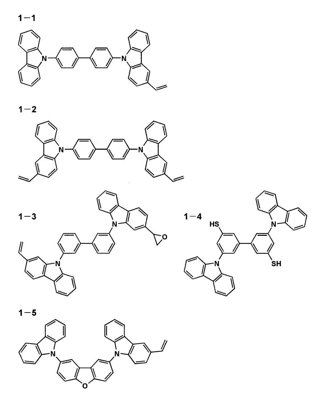


《陽極》
有機EL素子における陽極としては、仕事関数の大きい(4eV以上)金属、合金、電気伝導性化合物及びこれらの混合物を電極物質とするものが好ましく用いられる。このような電極物質の具体例としては、Au等の金属、CuI、インジウムチンオキシド(ITO)、SnO2、ZnO等の導電性透明材料が挙げられる。また、IDIXO(In2O3-ZnO)等非晶質で透明導電膜を作製可能な材料を用いてもよい。 "anode"
As the anode in the organic EL element, an electrode material made of a metal, an alloy, an electrically conductive compound, or a mixture thereof having a high work function (4 eV or more) is preferably used. Specific examples of such electrode substances include metals such as Au, and conductive transparent materials such as CuI, indium tin oxide (ITO), SnO 2 , and ZnO. Alternatively, an amorphous material such as IDIXO (In 2 O 3 —ZnO) that can form a transparent conductive film may be used.
陽極はこれらの電極物質を蒸着やスパッタリング等の方法により薄膜を形成させ、フォトリソグラフィー法で所望の形状のパターンを形成してもよく、あるいはパターン精度をあまり必要としない場合は(100μm以上程度)、上記電極物質の蒸着やスパッタリング時に所望の形状のマスクを介してパターンを形成してもよい。あるいは、有機導電性化合物のように塗布可能な物質を用いる場合には、印刷方式、コーティング方式等湿式成膜法を用いることもできる。
For the anode, these electrode materials may be formed into a thin film by a method such as vapor deposition or sputtering, and a pattern having a desired shape may be formed by a photolithography method, or when pattern accuracy is not so high (about 100 μm or more) A pattern may be formed through a mask having a desired shape at the time of vapor deposition or sputtering of the electrode material. Or when using the substance which can be apply | coated like an organic electroconductivity compound, wet film-forming methods, such as a printing system and a coating system, can also be used.
この陽極より発光を取り出す場合には、透過率を10%より大きくすることが望ましく、また陽極としてのシート抵抗は数百Ω/□以下が好ましい。更に膜厚は材料にもよるが、通常10~1000nm、好ましくは10~200nmの範囲で選ばれる。
When light emission is taken out from the anode, it is desirable that the transmittance is greater than 10%, and the sheet resistance as the anode is preferably several hundred Ω / □ or less. Further, although the film thickness depends on the material, it is usually selected in the range of 10 to 1000 nm, preferably 10 to 200 nm.
《陰極》
一方、陰極としては仕事関数の小さい(4eV以下)金属(電子注入性金属と称する)、合金、電気伝導性化合物及びこれらの混合物を電極物質とするものが用いられる。このような電極物質の具体例としては、ナトリウム、ナトリウム-カリウム合金、マグネシウム、リチウム、マグネシウム/銅混合物、マグネシウム/銀混合物、マグネシウム/アルミニウム混合物、マグネシウム/インジウム混合物、アルミニウム/酸化アルミニウム(Al2O3)混合物、インジウム、リチウム/アルミニウム混合物、希土類金属等が挙げられる。 "cathode"
On the other hand, as the cathode, a material having a low work function (4 eV or less) metal (referred to as an electron injecting metal), an alloy, an electrically conductive compound, and a mixture thereof as an electrode material is used. Specific examples of such electrode materials include sodium, sodium-potassium alloy, magnesium, lithium, magnesium / copper mixture, magnesium / silver mixture, magnesium / aluminum mixture, magnesium / indium mixture, aluminum / aluminum oxide (Al 2 O 3 ) Mixtures, indium, lithium / aluminum mixtures, rare earth metals and the like.
これらの中で、電子注入性及び酸化等に対する耐久性の点から、電子注入性金属とこれより仕事関数の値が大きく安定な金属である第二金属との混合物、例えば、マグネシウム/銀混合物、マグネシウム/アルミニウム混合物、マグネシウム/インジウム混合物、アルミニウム/酸化アルミニウム(Al2O3)混合物、リチウム/アルミニウム混合物、アルミニウム等が好適である。
Among these, from the point of durability against electron injection and oxidation, etc., a mixture of an electron injecting metal and a second metal which is a stable metal having a larger work function than this, for example, a magnesium / silver mixture, Suitable are a magnesium / aluminum mixture, a magnesium / indium mixture, an aluminum / aluminum oxide (Al 2 O 3 ) mixture, a lithium / aluminum mixture, aluminum and the like.
陰極はこれらの電極物質を蒸着やスパッタリング等の方法により薄膜を形成させることにより、作製することができる。また、陰極としてのシート抵抗は数百Ω/□以下が好ましく、膜厚は通常10nm~5μm、好ましくは50~200nmの範囲で選ばれる。なお、発光した光を透過させるため、有機EL素子の陽極または陰極のいずれか一方が透明または半透明であれば発光輝度が向上し好都合である。
The cathode can be produced by forming a thin film of these electrode materials by a method such as vapor deposition or sputtering. The sheet resistance as the cathode is preferably several hundred Ω / □ or less, and the film thickness is usually selected in the range of 10 nm to 5 μm, preferably 50 to 200 nm. In order to transmit the emitted light, if either one of the anode or the cathode of the organic EL element is transparent or translucent, the light emission luminance is improved, which is convenient.
また、陰極に上記金属を1~20nmの膜厚で作製した後に、陽極の説明で挙げた導電性透明材料をその上に作製することで、透明または半透明の陰極を作製することができ、これを応用することで陽極と陰極の両方が透過性を有する素子を作製することができる。
In addition, a transparent or semi-transparent cathode can be produced by producing the conductive transparent material mentioned in the description of the anode on the cathode after producing the metal with a film thickness of 1 to 20 nm. By applying this, an element in which both the anode and the cathode are transmissive can be manufactured.
《支持基板》
本発明の有機EL素子に用いることのできる支持基板(以下、基体、基板、基材、支持体等とも言う)としては、ガラス、プラスチック等の種類には特に限定はなく、また透明であっても不透明であってもよい。支持基板側から光を取り出す場合には、支持基板は透明であることが好ましい。好ましく用いられる透明な支持基板としては、ガラス、石英、透明樹脂フィルムを挙げることができる。特に好ましい支持基板は、有機EL素子にフレキシブル性を与えることが可能な樹脂フィルムである。 《Support substrate》
As a support substrate (hereinafter also referred to as a substrate, substrate, substrate, support, etc.) that can be used in the organic EL device of the present invention, there is no particular limitation on the type of glass, plastic, etc., and it is transparent. May be opaque. When extracting light from the support substrate side, the support substrate is preferably transparent. Examples of the transparent support substrate preferably used include glass, quartz, and a transparent resin film. A particularly preferable support substrate is a resin film capable of giving flexibility to the organic EL element.
樹脂フィルムとしては、例えば、ポリエチレンテレフタレート(PET)、ポリエチレンナフタレート(PEN)等のポリエステル、ポリエチレン、ポリプロピレン、セロファン、セルロースジアセテート、セルローストリアセテート、セルロースアセテートブチレート、セルロースアセテートプロピオネート(CAP)、セルロースアセテートフタレート(TAC)、セルロースナイトレート等のセルロースエステル類またはそれらの誘導体、ポリ塩化ビニリデン、ポリビニルアルコール、ポリエチレンビニルアルコール、シンジオタクティックポリスチレン、ポリカーボネート、ノルボルネン樹脂、ポリメチルペンテン、ポリエーテルケトン、ポリイミド、ポリエーテルスルホン(PES)、ポリフェニレンスルフィド、ポリスルホン類、ポリエーテルイミド、ポリエーテルケトンイミド、ポリアミド、フッ素樹脂、ナイロン、ポリメチルメタクリレート、アクリルあるいはポリアリレート類、アートン(JSR製)あるいはアペル(三井化学製)といったシクロオレフィン系樹脂等を挙げられる。
Examples of the resin film include polyesters such as polyethylene terephthalate (PET) and polyethylene naphthalate (PEN), polyethylene, polypropylene, cellophane, cellulose diacetate, cellulose triacetate, cellulose acetate butyrate, cellulose acetate propionate (CAP), Cellulose esters such as cellulose acetate phthalate (TAC) and cellulose nitrate or derivatives thereof, polyvinylidene chloride, polyvinyl alcohol, polyethylene vinyl alcohol, syndiotactic polystyrene, polycarbonate, norbornene resin, polymethylpentene, polyether ketone, polyimide , Polyethersulfone (PES), polyphenylene sulfide, polysulfone , Polyetherimide, polyether ketone imide, polyamide, fluorine resin, nylon, polymethyl methacrylate, acrylic or polyarylates, and cycloolefin resins such as ARTON (manufactured by JSR) or APEL (manufactured by Mitsui Chemicals).
樹脂フィルムの表面には、無機物、有機物の被膜またはその両者のハイブリッド被膜が形成されていてもよく、水蒸気透過度が0.01g/m2/日・atm以下のバリア性フィルムであることが好ましく、更には酸素透過度10-3g/m2/日以下、水蒸気透過度10-5g/m2/日以下の高バリア性フィルムであることが好ましい。
An inorganic or organic film or a hybrid film of both may be formed on the surface of the resin film, and it is preferably a barrier film having a water vapor permeability of 0.01 g / m 2 / day · atm or less. Furthermore, a high barrier film having an oxygen permeability of 10 −3 g / m 2 / day or less and a water vapor permeability of 10 −5 g / m 2 / day or less is preferable.
バリア膜を形成する材料としては、水分や酸素等素子の劣化をもたらすものの浸入を抑制する機能を有する材料であればよく、例えば、酸化珪素、二酸化珪素、窒化珪素等を用いることができる。更に該膜の脆弱性を改良するために、これら無機層と有機材料からなる層の積層構造を持たせることがより好ましい。無機層と有機層の積層順については特に制限はないが、両者を交互に複数回積層させることが好ましい。
The material for forming the barrier film may be any material that has a function of suppressing the intrusion of elements that cause deterioration of elements such as moisture and oxygen. For example, silicon oxide, silicon dioxide, silicon nitride, or the like can be used. Further, in order to improve the brittleness of the film, it is more preferable to have a laminated structure of these inorganic layers and organic material layers. Although there is no restriction | limiting in particular about the lamination | stacking order of an inorganic layer and an organic layer, It is preferable to laminate | stack both alternately several times.
バリア膜の形成方法については特に限定はなく、例えば、真空蒸着法、スパッタリング法、反応性スパッタリング法、分子線エピタキシー法、クラスタ-イオンビーム法、イオンプレーティング法、プラズマ重合法、大気圧プラズマ重合法、プラズマCVD法、レーザーCVD法、熱CVD法、コーティング法等を用いることができるが、特開2004-68143号公報に記載されているような大気圧プラズマ重合法によるものが特に好ましい。
The method for forming the barrier film is not particularly limited. For example, the vacuum deposition method, sputtering method, reactive sputtering method, molecular beam epitaxy method, cluster ion beam method, ion plating method, plasma polymerization method, atmospheric pressure plasma weight A combination method, a plasma CVD method, a laser CVD method, a thermal CVD method, a coating method, and the like can be used, but an atmospheric pressure plasma polymerization method as described in JP-A-2004-68143 is particularly preferable.
不透明な支持基板としては、例えば、アルミ、ステンレス等の金属板、フィルムや不透明樹脂基板、セラミック製の基板等が挙げられる。
Examples of the opaque support substrate include metal plates such as aluminum and stainless steel, films, opaque resin substrates, ceramic substrates, and the like.
本発明の有機EL素子の発光の室温における外部取り出し量子効率は、1%以上であることが好ましく、より好ましくは5%以上である。ここに、外部取り出し量子効率(%)=有機EL素子外部に発光した光子数/有機EL素子に流した電子数×100である。
The external extraction quantum efficiency at room temperature of light emission of the organic EL device of the present invention is preferably 1% or more, more preferably 5% or more. Here, the external extraction quantum efficiency (%) = the number of photons emitted to the outside of the organic EL element / the number of electrons sent to the organic EL element × 100.
また、カラーフィルター等の色相改良フィルター等を併用しても、有機EL素子からの発光色を蛍光体を用いて多色へ変換する色変換フィルターを併用してもよい。色変換フィルターを用いる場合においては、有機EL素子の発光のλmaxは480nm以下が好ましい。
Also, a hue improvement filter such as a color filter may be used in combination, or a color conversion filter that converts the emission color from the organic EL element into multiple colors using a phosphor may be used in combination. In the case of using a color conversion filter, the λmax of light emission of the organic EL element is preferably 480 nm or less.
《封止》
本発明に用いられる封止手段としては、例えば、封止部材と電極、支持基板とを接着剤で接着する方法を挙げることができる。封止部材としては、有機EL素子の表示領域を覆うように配置されておればよく、凹板状でも平板状でもよい。また、透明性、電気絶縁性は特に問わない。 <Sealing>
As a sealing means used for this invention, the method of adhere | attaching a sealing member, an electrode, and a support substrate with an adhesive agent can be mentioned, for example. As a sealing member, it should just be arrange | positioned so that the display area | region of an organic EL element may be covered, and concave plate shape or flat plate shape may be sufficient. Further, transparency and electrical insulation are not particularly limited.
具体的には、ガラス板、ポリマー板・フィルム、金属板・フィルム等が挙げられる。ガラス板としては、特にソーダ石灰ガラス、バリウム・ストロンチウム含有ガラス、鉛ガラス、アルミノケイ酸ガラス、ホウケイ酸ガラス、バリウムホウケイ酸ガラス、石英等を挙げることができる。また、ポリマー板としては、ポリカーボネート、アクリル、ポリエチレンテレフタレート、ポリエーテルサルファイド、ポリサルフォン等を挙げることができる。金属板としては、ステンレス、鉄、銅、アルミニウム、マグネシウム、ニッケル、亜鉛、クロム、チタン、モリブテン、シリコン、ゲルマニウム及びタンタルからなる群から選ばれる一種以上の金属または合金からなるものが挙げられる。
Specific examples include a glass plate, a polymer plate / film, and a metal plate / film. Examples of the glass plate include soda-lime glass, barium / strontium-containing glass, lead glass, aluminosilicate glass, borosilicate glass, barium borosilicate glass, and quartz. Examples of the polymer plate include polycarbonate, acrylic, polyethylene terephthalate, polyether sulfide, and polysulfone. Examples of the metal plate include those made of one or more metals or alloys selected from the group consisting of stainless steel, iron, copper, aluminum, magnesium, nickel, zinc, chromium, titanium, molybdenum, silicon, germanium, and tantalum.
本発明においては、素子を薄膜化できるということからポリマーフィルム、金属フィルムを好ましく使用することができる。
In the present invention, a polymer film and a metal film can be preferably used because the element can be thinned.
更には、ポリマーフィルムはJIS K 7126-1987に準拠した方法で測定された酸素透過度が1×10⁻³ml/m2/24h以下、JIS K 7129-1992に準拠した方法で測定された、水蒸気透過度(25±0.5℃、相対湿度(90±2)%)が、1×10⁻³g/(m2/24h)以下のものであることが好ましい。
Furthermore, the polymer film oxygen permeability measured by the method based on JIS K 7126-1987 is 1 × 10 -3 ml / m 2 / 24h or less, as measured by the method based on JIS K 7129-1992, water vapor permeability (25 ± 0.5 ° C., relative humidity (90 ± 2)%) is preferably that of 1 × 10 -3 g / (m 2 / 24h) or less.
封止部材を凹状に加工するのは、サンドブラスト加工、化学エッチング加工等が使われる。
For processing the sealing member into a concave shape, sandblasting, chemical etching, or the like is used.
接着剤として具体的には、アクリル酸系オリゴマー、メタクリル酸系オリゴマーの反応性ビニル基を有する光硬化及び熱硬化型接着剤、2-シアノアクリル酸エステル等の湿気硬化型等の接着剤を挙げることができる。また、エポキシ系等の熱及び化学硬化型(二液混合)を挙げることができる。また、ホットメルト型のポリアミド、ポリエステル、ポリオレフィンを挙げることができる。また、カチオン硬化タイプの紫外線硬化型エポキシ樹脂接着剤を挙げることができる。
Specific examples of the adhesive include photocuring and thermosetting adhesives having reactive vinyl groups of acrylic acid oligomers and methacrylic acid oligomers, and moisture curing adhesives such as 2-cyanoacrylates. be able to. Moreover, heat | fever and chemical curing types (two-component mixing), such as an epoxy type, can be mentioned. Moreover, hot-melt type polyamide, polyester, and polyolefin can be mentioned. Moreover, a cationic curing type ultraviolet curing epoxy resin adhesive can be mentioned.
なお、有機EL素子が熱処理により劣化する場合があるので、室温から80℃までに接着硬化できるものが好ましい。また、前記接着剤中に乾燥剤を分散させておいてもよい。封止部分への接着剤の塗布は市販のディスペンサーを使ってもよいし、スクリーン印刷のように印刷してもよい。
In addition, since an organic EL element may deteriorate by heat processing, what can be adhesively cured from room temperature to 80 ° C. is preferable. A desiccant may be dispersed in the adhesive. Application | coating of the adhesive agent to a sealing part may use commercially available dispenser, and may print like screen printing.
また、有機層を挟み支持基板と対向する側の電極の外側に該電極と有機層を被覆し、支持基板と接する形で無機物、有機物の層を形成し封止膜とすることも好適にできる。この場合、該膜を形成する材料としては、水分や酸素等素子の劣化をもたらすものの浸入を抑制する機能を有する材料であればよく、例えば、酸化珪素、二酸化珪素、窒化珪素等を用いることができる。
In addition, it is also preferable that the electrode and the organic layer are coated on the outside of the electrode facing the support substrate with the organic layer interposed therebetween, and an inorganic or organic layer is formed in contact with the support substrate to form a sealing film. . In this case, the material for forming the film may be a material having a function of suppressing intrusion of elements that cause deterioration of elements such as moisture and oxygen. For example, silicon oxide, silicon dioxide, silicon nitride, or the like may be used. it can.
更に該膜の脆弱性を改良するために、これら無機層と有機材料からなる層の積層構造を持たせることが好ましい。これらの膜の形成方法については特に限定はなく、例えば、真空蒸着法、スパッタリング法、反応性スパッタリング法、分子線エピタキシー法、クラスタ-イオンビーム法、イオンプレーティング法、プラズマ重合法、大気圧プラズマ重合法、プラズマCVD法、レーザーCVD法、熱CVD法、コーティング法等を用いることができる。
In order to further improve the brittleness of the film, it is preferable to have a laminated structure of these inorganic layers and layers made of organic materials. The method for forming these films is not particularly limited. For example, vacuum deposition method, sputtering method, reactive sputtering method, molecular beam epitaxy method, cluster ion beam method, ion plating method, plasma polymerization method, atmospheric pressure plasma A polymerization method, a plasma CVD method, a laser CVD method, a thermal CVD method, a coating method, or the like can be used.
封止部材と有機EL素子の表示領域との間隙には、気相及び液相では、窒素、アルゴン等の不活性気体やフッ化炭化水素、シリコンオイルのような不活性液体を注入することが好ましい。また、真空とすることも可能である。また、内部に吸湿性化合物を封入することもできる。
In the gap between the sealing member and the display area of the organic EL element, an inert gas such as nitrogen or argon, or an inert liquid such as fluorinated hydrocarbon or silicon oil can be injected in the gas phase and liquid phase. preferable. A vacuum can also be used. Moreover, a hygroscopic compound can also be enclosed inside.
吸湿性化合物としては、例えば、金属酸化物(例えば、酸化ナトリウム、酸化カリウム、酸化カルシウム、酸化バリウム、酸化マグネシウム、酸化アルミニウム等)、硫酸塩(例えば、硫酸ナトリウム、硫酸カルシウム、硫酸マグネシウム、硫酸コバルト等)、金属ハロゲン化物(例えば、塩化カルシウム、塩化マグネシウム、フッ化セシウム、フッ化タンタル、臭化セリウム、臭化マグネシウム、沃化バリウム、沃化マグネシウム等)、過塩素酸類(例えば、過塩素酸バリウム、過塩素酸マグネシウム等)等が挙げられ、硫酸塩、金属ハロゲン化物及び過塩素酸類においては無水塩が好適に用いられる。
Examples of the hygroscopic compound include metal oxides (for example, sodium oxide, potassium oxide, calcium oxide, barium oxide, magnesium oxide, aluminum oxide) and sulfates (for example, sodium sulfate, calcium sulfate, magnesium sulfate, cobalt sulfate). Etc.), metal halides (eg calcium chloride, magnesium chloride, cesium fluoride, tantalum fluoride, cerium bromide, magnesium bromide, barium iodide, magnesium iodide etc.), perchloric acids (eg perchloric acid) Barium, magnesium perchlorate, and the like), and anhydrous salts are preferably used in sulfates, metal halides, and perchloric acids.
《保護膜、保護板》
有機層を挟み支持基板と対向する側の前記封止膜、あるいは前記封止用フィルムの外側に、素子の機械的強度を高めるために保護膜、あるいは保護板を設けてもよい。特に封止が前記封止膜により行われている場合には、その機械的強度は必ずしも高くないため、このような保護膜、保護板を設けることが好ましい。これに使用することができる材料としては、前記封止に用いたのと同様なガラス板、ポリマー板・フィルム、金属板・フィルム等を用いることができるが、軽量、且つ薄膜化ということからポリマーフィルムを用いることが好ましい。 《Protective film, protective plate》
In order to increase the mechanical strength of the element, a protective film or a protective plate may be provided on the outer side of the sealing film on the side facing the support substrate with the organic layer interposed therebetween or on the sealing film. In particular, when the sealing is performed by the sealing film, the mechanical strength is not necessarily high, and thus it is preferable to provide such a protective film and a protective plate. As a material that can be used for this, the same glass plate, polymer plate / film, metal plate / film, etc. used for the sealing can be used. It is preferable to use a film.
《光取り出し》
有機EL素子は空気よりも屈折率の高い(屈折率が1.7~2.1程度)層の内部で発光し、発光層で発生した光のうち15%から20%程度の光しか取り出せないことが一般的に言われている。これは、臨界角以上の角度θで界面(透明基板と空気との界面)に入射する光は、全反射を起こし素子外部に取り出すことができないことや、透明電極ないし発光層と透明基板との間で光が全反射を起こし、光が透明電極乃至発光層を導波し、結果として光が素子側面方向に逃げるためである。 《Light extraction》
The organic EL element emits light inside a layer having a refractive index higher than that of air (refractive index is about 1.7 to 2.1) and can extract only about 15% to 20% of the light generated in the light emitting layer. It is generally said. This is because light incident on the interface (interface between the transparent substrate and air) at an angle θ greater than the critical angle causes total reflection and cannot be taken out of the device, or between the transparent electrode or light emitting layer and the transparent substrate. This is because the light is totally reflected between the light and the light is guided through the transparent electrode or the light emitting layer, and as a result, the light escapes in the side surface direction of the element.
この光の取り出しの効率を向上させる手法としては、例えば、透明基板表面に凹凸を形成し、透明基板と空気界面での全反射を防ぐ方法(米国特許第4,774,435号明細書)、基板に集光性を持たせることにより効率を向上させる方法(特開昭63-314795号公報)、素子の側面等に反射面を形成する方法(特開平1-220394号公報)、基板と発光体の間に中間の屈折率を持つ平坦層を導入し、反射防止膜を形成する方法(特開昭62-172691号公報)、基板と発光体の間に基板よりも低屈折率を持つ平坦層を導入する方法(特開2001-202827号公報)、基板、透明電極層や発光層のいずれかの層間(含む、基板と外界間)に回折格子を形成する方法(特開平11-283751号公報)等がある。
As a method of improving the light extraction efficiency, for example, a method of forming irregularities on the surface of the transparent substrate and preventing total reflection at the transparent substrate and the air interface (US Pat. No. 4,774,435), A method for improving efficiency by giving light condensing property to a substrate (Japanese Patent Laid-Open No. 63-314795), a method of forming a reflective surface on the side surface of an element (Japanese Patent Laid-Open No. 1-220394), and light emission from the substrate A method of forming an antireflection film by introducing a flat layer having an intermediate refractive index between the bodies (Japanese Patent Laid-Open No. 62-172691), a flat having a lower refractive index between the substrate and the light emitter than the substrate A method of introducing a layer (Japanese Patent Laid-Open No. 2001-202827), a method of forming a diffraction grating between any one of a substrate, a transparent electrode layer and a light emitting layer (including between the substrate and the outside) (Japanese Patent Laid-Open No. 11-283951) Gazette).
本発明においては、これらの方法を本発明の有機EL素子と組み合わせて用いることができるが、基板と発光体の間に基板よりも低屈折率を持つ平坦層を導入する方法、あるいは基板、透明電極層や発光層のいずれかの層間(含む、基板と外界間)に回折格子を形成する方法を好適に用いることができる。
In the present invention, these methods can be used in combination with the organic EL device of the present invention. However, a method of introducing a flat layer having a lower refractive index than the substrate between the substrate and the light emitter, or a substrate, transparent A method of forming a diffraction grating between any layers of the electrode layer and the light emitting layer (including between the substrate and the outside) can be suitably used.
本発明はこれらの手段を組み合わせることにより、更に高輝度あるいは耐久性に優れた素子を得ることができる。
In the present invention, by combining these means, it is possible to obtain an element having higher brightness or durability.
透明電極と透明基板の間に低屈折率の媒質を光の波長よりも長い厚みで形成すると、透明電極から出てきた光は、媒質の屈折率が低いほど外部への取り出し効率が高くなる。
When a medium having a low refractive index is formed between the transparent electrode and the transparent substrate with a thickness longer than the wavelength of light, the efficiency of taking out the light from the transparent electrode to the outside increases as the refractive index of the medium decreases.
低屈折率層としては、例えば、エアロゲル、多孔質シリカ、フッ化マグネシウム、フッ素系ポリマー等が挙げられる。透明基板の屈折率は一般に1.5~1.7程度であるので、低屈折率層は屈折率がおよそ1.5以下であることが好ましい。また、更に1.35以下であることが好ましい。
Examples of the low refractive index layer include aerogel, porous silica, magnesium fluoride, and a fluorine-based polymer. Since the refractive index of the transparent substrate is generally about 1.5 to 1.7, the low refractive index layer preferably has a refractive index of about 1.5 or less. Further, it is preferably 1.35 or less.
また、低屈折率媒質の厚みは媒質中の波長の2倍以上となるのが望ましい。これは低屈折率媒質の厚みが、光の波長程度になってエバネッセントで染み出した電磁波が基板内に入り込む膜厚になると、低屈折率層の効果が薄れるからである。
Also, the thickness of the low refractive index medium is preferably at least twice the wavelength in the medium. This is because the effect of the low refractive index layer is diminished when the thickness of the low refractive index medium is about the wavelength of light and the electromagnetic wave that has exuded by evanescent enters the substrate.
全反射を起こす界面もしくはいずれかの媒質中に回折格子を導入する方法は、光取り出し効率の向上効果が高いという特徴がある。この方法は回折格子が1次の回折や2次の回折といった所謂ブラッグ回折により、光の向きを屈折とは異なる特定の向きに変えることができる性質を利用して、発光層から発生した光のうち層間での全反射等により外に出ることができない光を、いずれかの層間もしくは、媒質中(透明基板内や透明電極内)に回折格子を導入することで光を回折させ、光を外に取り出そうとするものである。
The method of introducing a diffraction grating into an interface or any medium that causes total reflection is characterized by a high effect of improving light extraction efficiency. This method uses the property that the diffraction grating can change the direction of light to a specific direction different from refraction by so-called Bragg diffraction such as first-order diffraction and second-order diffraction. Light that cannot be emitted due to total internal reflection between layers is diffracted by introducing a diffraction grating in any layer or medium (in a transparent substrate or transparent electrode), and the light is removed. I want to take it out.
導入する回折格子は、二次元的な周期屈折率を持っていることが望ましい。これは発光層で発光する光はあらゆる方向にランダムに発生するので、ある方向にのみ周期的な屈折率分布を持っている一般的な1次元回折格子では、特定の方向に進む光しか回折されず、光の取り出し効率がさほど上がらない。しかしながら、屈折率分布を二次元的な分布にすることによりあらゆる方向に進む光が回折され、光の取り出し効率が上がる。
It is desirable that the diffraction grating to be introduced has a two-dimensional periodic refractive index. This is because light emitted from the light-emitting layer is randomly generated in all directions, so in a general one-dimensional diffraction grating having a periodic refractive index distribution only in a certain direction, only light traveling in a specific direction is diffracted. Therefore, the light extraction efficiency does not increase so much. However, by making the refractive index distribution a two-dimensional distribution, light traveling in all directions is diffracted, and light extraction efficiency is increased.
回折格子を導入する位置としては前述の通り、いずれかの層間もしくは媒質中(透明基板内や透明電極内)でもよいが、光が発生する場所である有機発光層の近傍が望ましい。
As described above, the position where the diffraction grating is introduced may be in any of the layers or in the medium (in the transparent substrate or the transparent electrode), but is preferably in the vicinity of the organic light emitting layer where light is generated.
このとき、回折格子の周期は媒質中の光の波長の約1/2~3倍程度が好ましい。
At this time, the period of the diffraction grating is preferably about 1/2 to 3 times the wavelength of light in the medium.
回折格子の配列は正方形のラチス状、三角形のラチス状、ハニカムラチス状等、2次元的に配列が繰り返されることが好ましい。
The arrangement of the diffraction grating is preferably two-dimensionally repeated such as a square lattice, a triangular lattice, or a honeycomb lattice.
《集光シート》
本発明の有機EL素子は基板の光取り出し側に、例えば、マイクロレンズアレイ状の構造を設けるように加工したり、あるいは所謂集光シートと組み合わせることにより、特定方向、例えば、素子発光面に対し正面方向に集光することにより、特定方向上の輝度を高めることができる。 <Condenser sheet>
The organic EL device of the present invention is processed on the light extraction side of the substrate so as to provide, for example, a microlens array structure, or combined with a so-called condensing sheet, for example, with respect to a specific direction, for example, the device light emitting surface. By condensing in the front direction, the luminance in a specific direction can be increased.
マイクロレンズアレイの例としては、基板の光取り出し側に一辺が30μmでその頂角が90度となるような四角錐を2次元に配列する。一辺は10~100μmが好ましい。これより小さくなると回折の効果が発生して色付く、大きすぎると厚みが厚くなり好ましくない。
As an example of a microlens array, quadrangular pyramids having a side of 30 μm and an apex angle of 90 degrees are arranged two-dimensionally on the light extraction side of the substrate. One side is preferably 10 to 100 μm. If it becomes smaller than this, the effect of diffraction will generate | occur | produce and color, and if too large, thickness will become thick and is not preferable.
集光シートとしては、例えば、液晶表示装置のLEDバックライトで実用化されているものを用いることが可能である。このようなシートとして、例えば、住友スリーエム製輝度上昇フィルム(BEF)等を用いることができる。プリズムシートの形状としては、例えば、基材に頂角90度、ピッチ50μmの△状のストライプが形成されたものであってもよいし、頂角が丸みを帯びた形状、ピッチをランダムに変化させた形状、その他の形状であってもよい。
As the condensing sheet, it is possible to use, for example, a sheet that has been put to practical use in an LED backlight of a liquid crystal display device. As such a sheet, for example, Sumitomo 3M brightness enhancement film (BEF) can be used. As the shape of the prism sheet, for example, the base material may be formed by forming a △ -shaped stripe having a vertex angle of 90 degrees and a pitch of 50 μm, or the vertex angle is rounded and the pitch is changed randomly. Other shapes may be used.
また、発光素子からの光放射角を制御するために、光拡散板・フィルムを集光シートと併用してもよい。例えば、(株)きもと製拡散フィルム(ライトアップ)等を用いることができる。
Further, in order to control the light emission angle from the light emitting element, a light diffusion plate / film may be used in combination with the light collecting sheet. For example, a diffusion film (light-up) manufactured by Kimoto Co., Ltd. can be used.
《有機EL素子の作製方法》
本発明の有機EL素子の作製方法の一例として、陽極/正孔注入層/正孔輸送層/発光層/電子輸送層/電子注入層/陰極からなる有機EL素子の作製法を説明する。 << Method for producing organic EL element >>
As an example of the method for producing the organic EL device of the present invention, a method for producing an organic EL device comprising an anode / hole injection layer / hole transport layer / light emitting layer / electron transport layer / electron injection layer / cathode will be described.
まず、適当な基体上に所望の電極物質、例えば、陽極用物質からなる薄膜を1μm以下、好ましくは10~200nmの膜厚になるように蒸着やスパッタリング等の方法により形成させ陽極を作製する。
First, a desired electrode material, for example, a thin film made of an anode material is formed on a suitable substrate by a method such as vapor deposition or sputtering so as to have a film thickness of 1 μm or less, preferably 10 to 200 nm, thereby producing an anode.
次に、この上に有機EL素子材料である正孔注入層、正孔輸送層、発光層、電子輸送層、電子注入層、正孔阻止層の有機化合物薄膜を形成させる。
Next, an organic compound thin film of a hole injection layer, a hole transport layer, a light emitting layer, an electron transport layer, an electron injection layer, and a hole blocking layer, which are organic EL element materials, is formed thereon.
本発明の有機EL素子の発光層は前述の通り、ウエットプロセスで形成される。発光層以外の有機層の形成方法としては、蒸着法、ウエットプロセス(スピンコート法、ダイコート法、キャスト法、インクジェット法、スプレー法、印刷法)等があるが、均質な膜が得られやすく、且つピンホールが生成しにくい等の点から、本発明においては有機層の一部もしくは全部について、スピンコート法、ダイコート法、インクジェット法、スプレー法、印刷法等の塗布法による成膜が好ましい。
The light emitting layer of the organic EL device of the present invention is formed by a wet process as described above. As a method for forming an organic layer other than the light emitting layer, there are a vapor deposition method, a wet process (spin coating method, die coating method, casting method, ink jet method, spray method, printing method), etc., but a homogeneous film is easily obtained. Further, in the present invention, film formation by a coating method such as a spin coating method, a die coating method, an ink jet method, a spray method, a printing method, or the like is preferable for part or all of the organic layer in view of the difficulty of generating pinholes.
本発明に係る有機EL材料を溶解または分散する液媒体としては、例えば、メチルエチルケトン、シクロヘキサノン等のケトン類、酢酸エチル等の脂肪酸エステル類、ジクロロベンゼン等のハロゲン化炭化水素類、トルエン、キシレン、メシチレン、シクロヘキシルベンゼン等の芳香族炭化水素類、シクロヘキサン、デカリン、ドデカン等の脂肪族炭化水素類、DMF、DMSO等の有機溶媒を用いることができる。また分散方法としては、超音波、高剪断力分散やメディア分散等の分散方法により分散することができる。
Examples of the liquid medium for dissolving or dispersing the organic EL material according to the present invention include ketones such as methyl ethyl ketone and cyclohexanone, fatty acid esters such as ethyl acetate, halogenated hydrocarbons such as dichlorobenzene, toluene, xylene, and mesitylene. Aromatic hydrocarbons such as cyclohexylbenzene, aliphatic hydrocarbons such as cyclohexane, decalin, and dodecane, and organic solvents such as DMF and DMSO can be used. Moreover, as a dispersion method, it can disperse | distribute by dispersion methods, such as an ultrasonic wave, high shear force dispersion | distribution, and media dispersion | distribution.
これらの層を形成後、その上に陰極用物質からなる薄膜を1μm以下、好ましくは50~200nmの範囲の膜厚になるように、例えば、蒸着やスパッタリング等の方法により形成させ、陰極を設けることにより所望の有機EL素子が得られる。
After these layers are formed, a thin film made of a cathode material is formed thereon by a method such as vapor deposition or sputtering so as to have a film thickness of 1 μm or less, preferably in the range of 50 to 200 nm, and a cathode is provided. Thus, a desired organic EL element can be obtained.
また、作製順序を逆にして、陰極、電子注入層、電子輸送層、発光層、正孔輸送層、正孔注入層、陽極の順に作製することも可能である。このようにして得られた多色の表示装置に、直流電圧を印加する場合には陽極を+、陰極を-の極性として電圧2~40V程度を印加すると発光が観測できる。また、交流電圧を印加してもよい。なお、印加する交流の波形は任意でよい。
It is also possible to reverse the production order to produce a cathode, an electron injection layer, an electron transport layer, a light emitting layer, a hole transport layer, a hole injection layer, and an anode in this order. When a DC voltage is applied to the multicolor display device thus obtained, light emission can be observed by applying a voltage of about 2 to 40 V with the positive polarity of the anode and the negative polarity of the cathode. An alternating voltage may be applied. The alternating current waveform to be applied may be arbitrary.
以下、実施例を挙げて本発明を具体的に説明するが、本発明はこれらに限定されるものではない。なお、実施例において「部」あるいは「%」の表示を用いるが、特に断りがない限り「質量部」あるいは「質量%」を表す。
Hereinafter, the present invention will be specifically described with reference to examples, but the present invention is not limited thereto. In addition, although the display of "part" or "%" is used in an Example, unless otherwise indicated, "part by mass" or "mass%" is represented.
実施例1
《有機EL素子の作製》
〔有機EL素子111の作製〕
陽極として100mm×100mm×1.1mmのガラス基板上に、ITO(インジウムチンオキシド)を100nm製膜した基板(NHテクノグラス製NA45)にパターニングを行った後、このITO透明電極を設けた基板をイソプロピルアルコールで超音波洗浄し、乾燥窒素ガスで乾燥し、UVオゾン洗浄を5分間行った。この基板上に、ポリ(3,4-エチレンジオキシチオフェン)-ポリスチレンスルホネート(PEDOT/PSS、Bayer製、Baytron P Al 4083)を純水で70%に希釈した溶液を3000rpm、30秒でスピンコート法により製膜した後、200℃にて1時間乾燥し、膜厚30nmの第1正孔輸送層を設けた。 Example 1
<< Production of organic EL element >>
[Production of Organic EL Element 111]
After patterning a substrate (NH technoglass NA45) formed by depositing 100 nm of ITO (indium tin oxide) on a 100 mm × 100 mm × 1.1 mm glass substrate as an anode, a substrate provided with this ITO transparent electrode was formed. Ultrasonic cleaning with isopropyl alcohol, drying with dry nitrogen gas, and UV ozone cleaning were performed for 5 minutes. A solution obtained by diluting poly (3,4-ethylenedioxythiophene) -polystyrene sulfonate (PEDOT / PSS, Bayer, Baytron P Al 4083) to 70% with pure water on this substrate was spin-coated at 3000 rpm for 30 seconds. After film formation by the method, the film was dried at 200 ° C. for 1 hour to provide a first hole transport layer having a thickness of 30 nm.
この基板を窒素雰囲気下に移し、第1正孔輸送層上に60mgの例示化合物4-1を10mlのトルエンに溶解した溶液を1000rpm、30秒の条件下、スピンコート法により製膜(膜厚約40nm)し、紫外光を30秒照射した後、120℃で30分間加熱乾燥し、第2正孔輸送層とした。
This substrate was transferred to a nitrogen atmosphere, and a solution obtained by dissolving 60 mg of Exemplified Compound 4-1 in 10 ml of toluene on the first hole transport layer was formed into a film (film thickness) by spin coating under conditions of 1000 rpm and 30 seconds. About 40 nm) and irradiated with ultraviolet light for 30 seconds, followed by heat drying at 120 ° C. for 30 minutes to form a second hole transport layer.
更に、下記組成の発光層組成物1をインクジェットヘッド(エプソン製;MJ800C)を用いてウエット膜厚が4μmになるように吐出注入した。この基板を、上下隔壁を設け、隔壁上部と下部とにそれぞれ独立の乾燥風温度調整機を備えた乾燥箱の基板ホルダに固定し、基板上面(発光層塗布面)に120℃に制御した加熱乾燥窒素を循環させ、基板裏面側は80℃に制御した加熱乾燥窒素を循環させた。この状態で、10分間の乾燥処理を施すことにより発光層を乾燥させた。なお、基板両面にそれぞれ循環させた乾燥窒素の温度は乾燥開始から終了まで±1℃以内に制御されていることを確認した。
Furthermore, the light emitting layer composition 1 having the following composition was discharged and injected using an inkjet head (manufactured by Epson; MJ800C) so that the wet film thickness was 4 μm. This substrate was fixed to a substrate holder of a drying box provided with upper and lower partition walls and provided with an independent drying air temperature controller at the upper and lower portions of the partition wall, and heating controlled to 120 ° C. on the upper surface of the substrate (light emitting layer coating surface). Dry nitrogen was circulated, and heated dry nitrogen circulated at 80 ° C. on the back side of the substrate. In this state, the light emitting layer was dried by performing a drying process for 10 minutes. It was confirmed that the temperature of dry nitrogen circulated on both sides of the substrate was controlled within ± 1 ° C. from the start to the end of drying.
これは、請求の範囲5、更には請求の範囲6の陽極側の温度を陰極側の温度より10℃以上(この場合40℃)低くするに相当する。
This corresponds to lowering the temperature on the anode side in claims 5 and 6 further by 10 ° C. (in this case, 40 ° C.) lower than the temperature on the cathode side.
(発光層組成物1)
(2)-37 1.0質量部
(1)-79 0.1質量部
トルエン 100質量部
この基板を真空蒸着装置の基板ホルダに固定し、一方、モリブデン製抵抗加熱ボートにET-Aを200mg入れ、別のモリブデン製抵抗加熱ボートにCsFを100mg入れ、真空蒸着装置に取り付けた。真空槽を4×10⁻⁴Paまで減圧した後、ET-AとCsFの入った前記加熱ボートに通電して加熱し、それぞれ蒸着速度0.2nm/秒、0.03nm/秒で前記発光層の上に蒸着して、更に膜厚40nmの電子輸送層を設けた。引き続きアルミニウム110nmを蒸着して陰極を形成し、有機EL素子111を作製した。 (Light emitting layer composition 1)
(2) -37 1.0 part by mass (1) -79 0.1 part by mass Toluene 100 parts by mass This substrate was fixed to the substrate holder of the vacuum evaporation apparatus, while 200 mg of ET-A was added to the resistance heating boat made of molybdenum. Then, 100 mg of CsF was put into another resistance heating boat made of molybdenum, and attached to a vacuum deposition apparatus. The vacuum chamber was depressurized to 4 × 10 −4 Pa, and then heated by energizing the heating boat containing ET-A and CsF, and the light emitting layer was deposited at a deposition rate of 0.2 nm / second and 0.03 nm / second, respectively. An electron transport layer having a film thickness of 40 nm was further provided. Subsequently, 110 nm of aluminum was deposited to form a cathode, and an organic EL element 111 was produced.
〔有機EL素子112~114の作製〕
有機EL素子111の作製において、発光層組成物1の吐出注入後の乾燥工程における基板上面側と基板裏面側に循環させる窒素の温度を表1のように変化させた以外は同様にして、有機EL素子112~114を作製した。 [Production of organic EL elements 112 to 114]
In the production of the organic EL element 111, the organic EL element 111 was formed in the same manner except that the temperature of nitrogen to be circulated to the substrate upper surface side and the substrate rear surface side in the drying step after the discharge injection of the light emitting layer composition 1 was changed as shown in Table 1. EL elements 112 to 114 were produced.
〔有機EL素子121~123、131~133、141~142の作製〕
有機EL素子111の作製において、発光層組成物1を構成する材料を表1のように変更し、発光層組成物の吐出注入後の乾燥工程における基板上面側と基板裏面側に循環させる窒素の温度を表1のように変化させた以外は同様にして、有機EL素子121~123、131~133、141~142を作製した。 [Production of Organic EL Elements 121-123, 131-133, 141-142]
In the production of the organic EL element 111, the material constituting the light emitting layer composition 1 is changed as shown in Table 1, and nitrogen circulated between the substrate upper surface side and the substrate back surface side in the drying step after the discharge injection of the light emitting layer composition. Organic EL elements 121 to 123, 131 to 133, and 141 to 142 were fabricated in the same manner except that the temperature was changed as shown in Table 1.
得られた有機EL素子の発光層中に含まれる発光ドーパントの濃度分布は、TOF-SIMS(飛行時間型二次イオン質量分析)により、膜厚方向でのIr分布を分析することで検出することができる。有機EL素子111~114、121~123、131~133、141~142の発光層における陽極側から陰極側へ向けた濃度分布は表1に示す通りであった。
The concentration distribution of the light-emitting dopant contained in the light-emitting layer of the obtained organic EL element is detected by analyzing the Ir distribution in the film thickness direction by TOF-SIMS (time-of-flight secondary ion mass spectrometry). Can do. Table 1 shows the concentration distribution from the anode side to the cathode side in the light emitting layers of the organic EL devices 111 to 114, 121 to 123, 131 to 133, and 141 to 142.
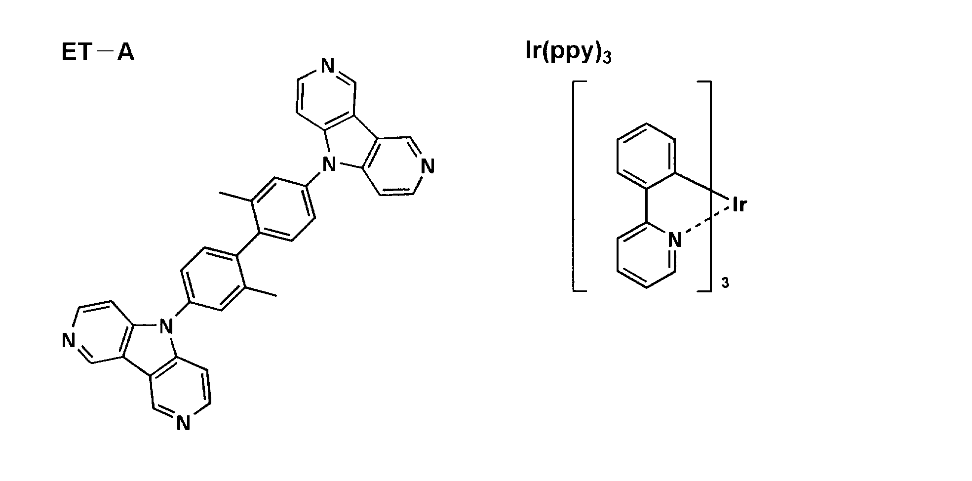
《有機EL素子の評価》
作製した有機EL素子について、下記のようにして外部取り出し量子効率及び発光寿命を評価した。 << Evaluation of organic EL elements >>
About the produced organic EL element, the external extraction quantum efficiency and the light emission lifetime were evaluated as follows.
作製した有機EL素子について、下記のようにして外部取り出し量子効率及び発光寿命を評価した。 << Evaluation of organic EL elements >>
About the produced organic EL element, the external extraction quantum efficiency and the light emission lifetime were evaluated as follows.
〔外部取り出し量子効率〕
作製した有機EL素子に対し、2.5mA/cm2定電流を印加したときの外部取り出し量子効率(%)を測定した。なお、測定には分光放射輝度計CS-1000(コニカミノルタセンシング製)を用いた。有機EL素子111~116の外部取り出し量子効率は、有機EL素子116(比較)の測定値を100とした相対値で表した。 [External extraction quantum efficiency]
External quantum efficiency (%) was measured when a 2.5 mA / cm 2 constant current was applied to the produced organic EL element. For the measurement, a spectral radiance meter CS-1000 (manufactured by Konica Minolta Sensing) was used. The external extraction quantum efficiencies of the organic EL elements 111 to 116 were expressed as relative values with the measured value of the organic EL element 116 (comparative) as 100.
有機EL素子121~123の外部取り出し量子効率は、有機EL素子123(比較)の測定値を100とした相対値、有機EL素子131~133の外部取り出し効率は有機EL素子133(比較)の測定値を100とした相対値、有機EL素子141~143の外部取り出し量子効率は有機EL素子143(比較)の測定値を100とした相対値、有機EL素子151~153の外部取り出し効率は有機EL素子153(比較)の測定値を100としたときの相対値、有機EL素子161~162の外部取り出し効率は有機EL素子162(比較)の測定値を100としたときの相対値でそれぞれ現した。
The external extraction quantum efficiency of the organic EL elements 121 to 123 is a relative value with the measured value of the organic EL element 123 (comparative) as 100, and the external extraction efficiency of the organic EL elements 131 to 133 is a measurement of the organic EL element 133 (comparative). The relative value with the value of 100, the external extraction quantum efficiency of the organic EL elements 141 to 143 is the relative value with the measured value of the organic EL element 143 (comparison) as 100, and the external extraction efficiency of the organic EL elements 151 to 153 is the organic EL The relative value when the measured value of the element 153 (comparison) is 100 and the external extraction efficiency of the organic EL elements 161 to 162 are expressed as relative values when the measured value of the organic EL element 162 (comparative) is 100. .
〔発光寿命〕
作製した有機EL素子に対し、正面輝度1000cd/m2となるような電流を与え、連続駆動した。正面輝度が初期の半減値(500cd/m2)になるまでに掛かる時間を求め、有機EL素子111~116の発光寿命は、有機EL素子116(比較)の測定値を100とした相対値で表した。 [Luminescence life]
The produced organic EL element was continuously driven by applying a current that would give a front luminance of 1000 cd / m 2 . The time required for the front luminance to reach the initial half value (500 cd / m 2 ) is obtained, and the light emission lifetimes of the organic EL elements 111 to 116 are relative values with the measured value of the organic EL element 116 (comparative) as 100. expressed.
有機EL素子121~123の発光寿命は、有機EL素子123(比較)の測定値を100とした相対値、有機EL素子131~133の発光寿命は有機EL素子133(比較)の測定値を100とした相対値、有機EL素子141~143の発光寿命は有機EL素子143(比較)の測定値を100とした相対値、有機EL素子151~153の発光寿命は有機EL素子153(比較)の測定値を100としたときの相対値、有機EL素子161~162の発光寿命は有機EL素子162(比較)の測定値を100としたときの相対値でそれぞれ表した。
The light emission lifetimes of the organic EL elements 121 to 123 are relative values with the measured value of the organic EL element 123 (comparative) as 100, and the light emission lifetimes of the organic EL elements 131 to 133 are the measured value of the organic EL element 133 (comparative) as 100. The relative lifetimes of the organic EL elements 141 to 143 are relative values with the measured value of the organic EL element 143 (comparison) as 100, and the emission lifetimes of the organic EL elements 151 to 153 are those of the organic EL element 153 (comparative). The relative value when the measured value is 100, and the light emission lifetimes of the organic EL elements 161 to 162 are expressed as relative values when the measured value of the organic EL element 162 (comparative) is 100.
得られた結果を表1に示す。
The results obtained are shown in Table 1.

表1から、本発明の有機EL素子は、ウエットプロセスを用いた作製方法でも発光層中での発光ドーパントの濃度を連続的に変化させることができ、その結果、外部取り出し量子効率と発光寿命が向上していることがわかる。
From Table 1, the organic EL device of the present invention can continuously change the concentration of the light-emitting dopant in the light-emitting layer even in the manufacturing method using the wet process. As a result, the external extraction quantum efficiency and the light emission lifetime are improved. It can be seen that it has improved.
実施例2
《有機EL素子の作製》
〔有機EL素子211の作製〕
陽極として100mm×100mm×1.1mmのガラス基板上に、ITO(インジウムチンオキシド)を100nm製膜した基板(NHテクノグラス製NA45)にパターニングを行った後、このITO透明電極を設けた基板をイソプロピルアルコールで超音波洗浄し、乾燥窒素ガスで乾燥し、UVオゾン洗浄を5分間行った。この基板上に、ポリ(3,4-エチレンジオキシチオフェン)-ポリスチレンスルホネート(PEDOT/PSS、Bayer製、Baytron P Al 4083)を純水で70%に希釈した溶液を3000rpm、30秒でスピンコート法により製膜した後、200℃にて1時間乾燥し、膜厚30nmの第1正孔輸送層を設けた。 Example 2
<< Production of organic EL element >>
[Production of Organic EL Element 211]
After patterning a substrate (NH technoglass NA45) formed by depositing 100 nm of ITO (indium tin oxide) on a 100 mm × 100 mm × 1.1 mm glass substrate as an anode, a substrate provided with this ITO transparent electrode was formed. Ultrasonic cleaning with isopropyl alcohol, drying with dry nitrogen gas, and UV ozone cleaning were performed for 5 minutes. On this substrate, poly (3,4-ethylenedioxythiophene) -polystyrene sulfonate (PEDOT / PSS, Bayer, Baytron P Al 4083) diluted to 70% with pure water was spin-coated at 3000 rpm for 30 seconds. After film formation by the method, the film was dried at 200 ° C. for 1 hour to provide a first hole transport layer having a thickness of 30 nm.
この基板を窒素雰囲気下に移し、第1正孔輸送層上に60mgの例示化合物4-1を10mlのトルエンに溶解した溶液を1000rpm、30秒の条件下、スピンコート法により製膜(膜厚約40nm)し、紫外光を30秒照射した後、120℃で30分間加熱乾燥し、第2正孔輸送層とした。
This substrate was transferred to a nitrogen atmosphere, and a solution obtained by dissolving 60 mg of Exemplified Compound 4-1 in 10 ml of toluene on the first hole transport layer was formed into a film (film thickness) by spin coating under conditions of 1000 rpm and 30 seconds. About 40 nm) and irradiated with ultraviolet light for 30 seconds, followed by heat drying at 120 ° C. for 30 minutes to form a second hole transport layer.
更に下記組成の発光層組成物1を、インクジェットヘッド(エプソン製;MJ800C)を用いてウエット膜厚が4μmになるように吐出注入した。この基板を120℃の乾燥箱中で10分間の乾燥処理を施すことにより発光層1を形成した。
Further, the light emitting layer composition 1 having the following composition was discharged and injected using an inkjet head (manufactured by Epson; MJ800C) so that the wet film thickness was 4 μm. The substrate was subjected to a drying treatment for 10 minutes in a 120 ° C. drying box to form the light emitting layer 1.
(発光層組成物1)
(2)-16 1.0質量部
(1)-79 0.18質量部
トルエン 100質量部
続けて、下記組成の発光層組成物2を、インクジェットヘッド(エプソン製;MJ800C)を用いてウエット膜厚が2μmになるように吐出注入した。この基板を120℃の乾燥箱中で10分間の乾燥処理を施すことにより20nmの発光層2を形成した。 (Light emitting layer composition 1)
(2) -16 1.0 part by mass (1) -79 0.18 part by mass Toluene 100 parts by mass Subsequently, a light emitting layer composition 2 having the following composition was wet filmed using an inkjet head (manufactured by Epson; MJ800C). The discharge was injected so that the thickness was 2 μm. This substrate was subjected to a drying treatment for 10 minutes in a drying box at 120 ° C. to form a 20 nm light emitting layer 2.
(発光層組成物2)
(2)-16 1.0質量部
(1)-79 0.02質量部
トルエン 100質量部
この基板を真空蒸着装置の基板ホルダに固定し、一方、モリブデン製抵抗加熱ボートにET-Aを200mg入れ、別のモリブデン製抵抗加熱ボートにCsFを100mg入れ、真空蒸着装置に取り付けた。真空槽を4×10⁻⁴Paまで減圧した後、ET-AとCsFの入った前記加熱ボートに通電して加熱し、それぞれ蒸着速度0.2nm/秒、0.03nm/秒で前記発光層の上に蒸着して、更に膜厚40nmの電子輸送層を設けた。引き続き、アルミニウム110nmを蒸着して陰極を形成し、有機EL素子211を作製した。 (Light emitting layer composition 2)
(2) -16 1.0 part by mass (1) -79 0.02 part by mass Toluene 100 parts by mass This substrate was fixed to the substrate holder of the vacuum evaporation apparatus, while 200 mg of ET-A was added to a molybdenum resistance heating boat. Then, 100 mg of CsF was put into another resistance heating boat made of molybdenum, and attached to a vacuum deposition apparatus. The vacuum chamber was depressurized to 4 × 10 −4 Pa, and then heated by energizing the heating boat containing ET-A and CsF, and the light emitting layer was deposited at a deposition rate of 0.2 nm / second and 0.03 nm / second, respectively. An electron transport layer having a film thickness of 40 nm was further provided. Subsequently, 110 nm of aluminum was deposited to form a cathode, and an organic EL element 211 was produced.
有機EL素子211については、請求の範囲7、更には請求の範囲8の発光ドーパント濃度の異なる2種以上の発光層溶液の内、最も陽極側に塗布する溶液の発光ドーパント/発光ホスト比が100~10質量%、最も陰極側に塗布する溶液の発光ドーパント/発光ホスト比が5~0質量%であるに相当し、この場合、最も陽極側に塗布する溶液の発光ドーパント/発光ホスト比は18質量%、最も陰極側に塗布する溶液の発光ドーパント/発光ホスト比は2質量%となっている。
Regarding the organic EL element 211, the light emitting dopant / light emitting host ratio of the solution coated on the most anode side among the two or more kinds of light emitting layer solutions having different light emitting dopant concentrations of claim 7 and claim 8 is 100. This corresponds to an emission dopant / emission host ratio of 5 to 0% by mass of the solution coated on the cathode side, and in this case, the emission dopant / emission host ratio of the solution applied on the anode side is 18%. The light emitting dopant / light emitting host ratio of the solution applied on the most cathode side is 2% by mass.
〔有機EL素子212~218の作製〕
有機EL素子211の作製において、発光層組成物1及び2の組成及び膜厚を表2のように変化させた以外は同様にして、有機EL素子211~218を作製した。 [Production of organic EL elements 212 to 218]
In the production of the organic EL element 211, organic EL elements 211 to 218 were produced in the same manner except that the compositions and film thicknesses of the light emitting layer compositions 1 and 2 were changed as shown in Table 2.
有機EL素子212、213については、やはり請求の範囲7、請求の範囲8相当で、最も陽極側に塗布する溶液の発光ドーパント/発光ホスト比は、それぞれ20質量%、40質量%、最も陰極側に塗布する溶液の発光ドーパント/発光ホスト比は、それぞれ0質量%、0質量%となる。
The organic EL elements 212 and 213 are also equivalent to claims 7 and 8, respectively, and the emission dopant / emission host ratio of the solution coated on the most anode side is 20% by mass, 40% by mass, and most on the cathode side, respectively. The ratio of the luminescent dopant / luminescent host of the solution applied to is 0% by mass and 0% by mass, respectively.
有機EL素子214については、請求の範囲7であるが、最も陽極側に塗布する溶液の発光ドーパント/発光ホスト比は質量14%、最も陰極側に塗布する溶液の発光ドーパント/発光ホスト比は質量6%となるため、請求の範囲8相当ではない。
The organic EL element 214 is claimed in claim 7, but the light emitting dopant / light emitting host ratio of the solution coated on the most anode side is 14% by mass, and the light emitting dopant / light emitting host ratio of the solution coated on the most cathode side is mass. Since it is 6%, it does not correspond to Claim 8.
有機EL素子217については、発光ドーパント((1)-79)に対する溶解度はクロルベンゼンの方がトルエンよりも高く、沸点もクロルベンゼンの方が高い。即ち、請求の範囲9に相当する。一方、有機EL素子218は、発光ドーパント((1)-79)に対する溶解度はクロルベンゼンの方がp-キシレンよりも高く、沸点は逆にp-キシレンがクロルベンゼン同等以上であり、請求の範囲9には相当しない。
Regarding the organic EL element 217, the solubility of the luminescent dopant ((1) -79) in chlorobenzene is higher than that of toluene, and the boiling point of chlorobenzene is higher. That is, it corresponds to claim 9. On the other hand, the organic EL element 218 has a higher solubility in the luminescent dopant ((1) -79) in chlorobenzene than p-xylene, and conversely, the boiling point of p-xylene is equal to or higher than that of chlorobenzene. Does not correspond to 9.
《有機EL素子211~218の評価》
作製した有機EL素子211~218について、実施例1と同様の方法で外部取り出し量子効率と発光寿命の評価を行った。得られた結果は表2に示す。なお、外部取り出し量子効率及び発光寿命は有機EL素子216(比較)の測定値を100としたときの相対値で表した。 << Evaluation of organic EL elements 211 to 218 >>
The produced organic EL elements 211 to 218 were evaluated for external extraction quantum efficiency and light emission lifetime in the same manner as in Example 1. The results obtained are shown in Table 2. The external extraction quantum efficiency and the emission lifetime were expressed as relative values when the measured value of the organic EL element 216 (comparison) was 100.
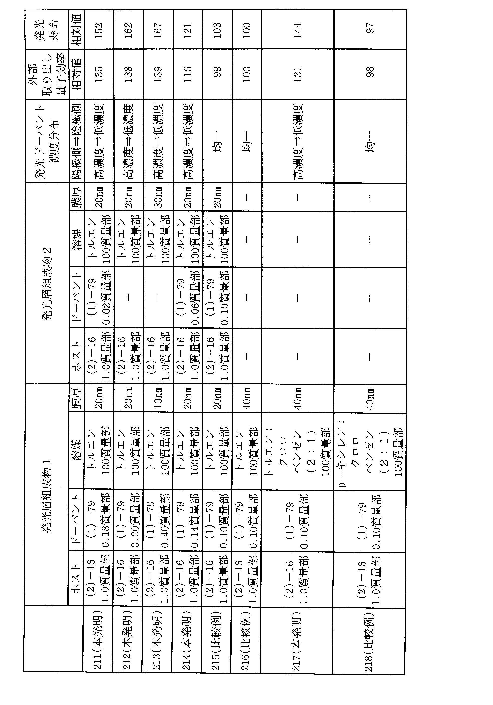
表2から、本発明の有機EL素子は、ウエットプロセスを用いた作製方法でも発光層中での発光ドーパントの濃度を連続的に変化させることができ、その結果、外部取り出し量子効率と発光寿命が向上していることがわかる。
From Table 2, the organic EL device of the present invention can continuously change the concentration of the light-emitting dopant in the light-emitting layer even in the manufacturing method using the wet process, and as a result, the external extraction quantum efficiency and the light emission lifetime are improved. It can be seen that it has improved.
Claims (10)
- 基板上に少なくとも陽極、陰極、及び該陽極、陰極間に挟まれた発光ホスト及び発光ドーパントを含有する発光層を少なくとも有する有機エレクトロルミネッセンス素子の製造方法において、該発光層がウエットプロセスで形成され、且つ該発光層に含まれる発光ドーパントの濃度を陽極側から陰極側に向かって連続的に変化させることを特徴とする有機エレクトロルミネッセンス素子の製造方法。 In a method for producing an organic electroluminescence device having at least an anode, a cathode, and a light emitting host containing at least an anode, a cathode, and a light emitting host and a light emitting dopant sandwiched between the anode and the cathode, the light emitting layer is formed by a wet process, And the manufacturing method of the organic electroluminescent element characterized by changing continuously the density | concentration of the light emission dopant contained in this light emitting layer toward the cathode side from an anode side.
- 前記発光ドーパントの濃度が陽極側から陰極側に向かって減少することを特徴とする請求の範囲第1項に記載の有機エレクトロルミネッセンス素子の製造方法。 2. The method of manufacturing an organic electroluminescence element according to claim 1, wherein the concentration of the luminescent dopant decreases from the anode side toward the cathode side.
- 前記発光ドーパントが下記一般式(1)で表されることを特徴とする請求の範囲第1項または第2項に記載の有機エレクトロルミネッセンス素子の製造方法。

(式中、R1は置換基を表す。Zは5~7員環を形成するのに必要な非金属原子群を表す。n1は0~5の整数を表す。B1~B5は炭素原子、窒素原子、酸素原子もしくは硫黄原子を表し、B1~B5の少なくとも一つは窒素原子を表す。M1は元素周期表における8族~第10族の金属を表す。X1及びX2は炭素原子、窒素原子もしくは酸素原子を表し、L1はX1及びX2とともに2座の配位子を形成する原子群を表す。m1は1、2または第3項の整数を表し、m2は0、1または2の整数を表すが、m1+m2は2または3である。) The method for producing an organic electroluminescent element according to claim 1 or 2, wherein the light-emitting dopant is represented by the following general formula (1).
(In the formula, R 1 represents a substituent. Z represents a group of nonmetallic atoms necessary to form a 5- to 7-membered ring. N1 represents an integer of 0 to 5. B 1 to B 5 represent carbon. Represents an atom, a nitrogen atom, an oxygen atom or a sulfur atom, at least one of B 1 to B 5 represents a nitrogen atom, M 1 represents a metal of Group 8 to Group 10 in the periodic table, X 1 and X 2 represents a carbon atom, a nitrogen atom or an oxygen atom, L 1 represents an atomic group forming a bidentate ligand with X 1 and X 2 , m1 represents an integer of 1, 2 or 3; m2 represents an integer of 0, 1 or 2, and m1 + m2 is 2 or 3.) - 前記発光ホストが下記一般式(2)で表される分子量700以上の化合物であることを特徴とする請求の範囲第1項~第3項のいずれか1項に記載の有機エレクトロルミネッセンス素子の製造方法。
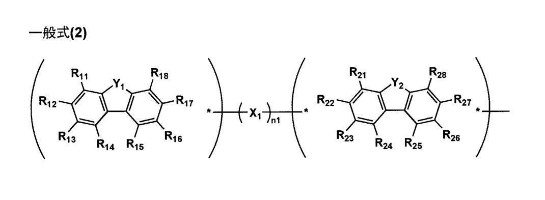
(一般式(2)中、Y1及びY2はO、SまたはNR0を表し、R0、R11~R18及びR21~R28は水素原子または置換基を表す。但し、R11~R18及びR0の少なくとも1つはX1との連結に用いられ、R21~R28及びR0の少なくとも1つはX1との連結に用いられる。X1は下記一般式(3)または(4)で表される2価の連結基を表す。n1は1以上の整数を表し、n1が2以上の場合、X1は同じでも異なっていてもよい。)
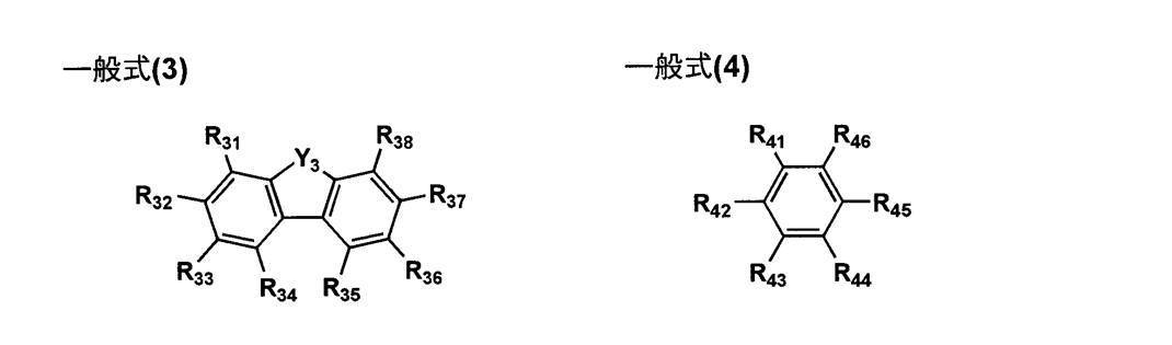
(式中、Y3はO、SまたはNR30を表し、R30~R38及びR41~R46は水素原子または置換基を表す。但し、R30~R38、R41~R46は各々少なくとも2つは連結に用いられ、またR41とR44が連結に用いられる場合はR42、R43、R45、R46の少なくとも1つは水素原子以外の置換基を有する。) The organic electroluminescence device according to any one of claims 1 to 3, wherein the luminescent host is a compound having a molecular weight of 700 or more represented by the following general formula (2). Method.
(In General Formula (2), Y 1 and Y 2 represent O, S or NR 0 , and R 0 , R 11 to R 18 and R 21 to R 28 represent a hydrogen atom or a substituent, provided that R 11 At least one of ~ R 18 and R 0 is used in connection with X 1, R 21 ~ R 28 and at least one .X 1 which is used for connection with the X 1 represented by the following general formula R 0 (3 ) or (4 .n1 that represents a divalent linking group represented by) represents an integer of 1 or more, when n1 is 2 or more, X 1 is may be the same or different.)
(Wherein Y 3 represents O, S or NR 30 , and R 30 to R 38 and R 41 to R 46 represent a hydrogen atom or a substituent, provided that R 30 to R 38 and R 41 to R 46 represent At least two of each are used for linking, and when R 41 and R 44 are used for linking, at least one of R 42 , R 43 , R 45 and R 46 has a substituent other than a hydrogen atom.) - 請求の範囲第1項~第4項のいずれか1項に記載の有機エレクトロルミネッセンス素子の製造方法において、塗膜の裏側に接する雰囲気温度を塗膜の表側に接する雰囲気温度より低く制御しながら乾燥することによって発光層を形成することを特徴とする有機エレクトロルミネッセンス素子の製造方法。 5. The method of manufacturing an organic electroluminescence device according to claim 1, wherein the drying is performed while controlling the atmospheric temperature in contact with the back side of the coating film to be lower than the atmospheric temperature in contact with the front side of the coating film. A light emitting layer is formed by doing so, The manufacturing method of the organic electroluminescent element characterized by the above-mentioned.
- 前記塗膜の裏側の雰囲気温度を塗膜の表側の雰囲気温度より10℃以上低く制御することを特徴とする請求の範囲第5項に記載の有機エレクトロルミネッセンス素子の製造方法。 The method for producing an organic electroluminescent element according to claim 5, wherein the atmospheric temperature on the back side of the coating film is controlled to be lower by 10 ° C or more than the atmospheric temperature on the front side of the coating film.
- 請求の範囲第1項~第4項のいずれか1項に記載の有機エレクトロルミネッセンス素子の製造方法において、発光ドーパント濃度の異なる2種以上の発光層溶液の積層塗布を、最も陽極側に塗布する溶液の発光ドーパント/発光ホスト比が最も陰極側に塗布する溶液の発光ドーパント/発光ホスト比より高くして行い、その後乾燥することによって発光層を形成することを特徴とする有機エレクトロルミネッセンス素子の製造方法。 5. The method of manufacturing an organic electroluminescence device according to claim 1, wherein the lamination coating of two or more light emitting layer solutions having different light emitting dopant concentrations is applied to the most anode side. Production of an organic electroluminescent device characterized in that the emission dopant / emission host ratio of the solution is higher than the emission dopant / emission host ratio of the solution coated on the cathode side, and then dried to form the emission layer Method.
- 前記発光ドーパント濃度の異なる2種以上の発光層溶液の内、最も陽極側に塗布する溶液の発光ドーパント/発光ホスト比が100~10質量%、最も陰極側に塗布する溶液の発光ドーパント/発光ホスト比が5~0質量%であることを特徴とする請求の範囲第7項に記載の有機エレクトロルミネッセンス素子の製造方法。 Among the two or more kinds of light emitting layer solutions having different light emitting dopant concentrations, the light emitting dopant / light emitting host ratio of the solution coated on the most anode side is 100 to 10% by mass, and the light emitting dopant / light emitting host of the solution coated on the most cathode side. The method for producing an organic electroluminescent element according to claim 7, wherein the ratio is 5 to 0% by mass.
- 請求の範囲第1項~第4項のいずれか1項に記載の有機エレクトロルミネッセンス素子の製造方法において、発光層の溶液の溶媒が沸点と発光ドーパント溶解度の異なる2液の混合溶媒であって、発光ドーパント溶解度が高い方の溶媒の沸点が発光ドーパント溶解度が低い方の溶媒の沸点より高いことを特徴とする有機エレクトロルミネッセンス素子の製造方法。 The method for producing an organic electroluminescent element according to any one of claims 1 to 4, wherein the solvent of the solution of the light emitting layer is a mixed solvent of two liquids having different boiling points and luminescent dopant solubilitys, The manufacturing method of the organic electroluminescent element characterized by the boiling point of the solvent with higher luminescent dopant solubility being higher than the boiling point of the solvent with lower luminescent dopant solubility.
- 請求の範囲第1項~第9項のいずれか1項に記載の有機エレクトロルミネッセンス素子の製造方法によって製造されたことを特徴とする有機エレクトロルミネッセンス素子。 An organic electroluminescent device manufactured by the method for manufacturing an organic electroluminescent device according to any one of claims 1 to 9.
Priority Applications (1)
| Application Number | Priority Date | Filing Date | Title |
|---|---|---|---|
| JP2009547981A JPWO2009084413A1 (en) | 2007-12-28 | 2008-12-15 | ORGANIC ELECTROLUMINESCENT ELEMENT AND METHOD FOR PRODUCING ORGANIC ELECTROLUMINESCENT ELEMENT |
Applications Claiming Priority (2)
| Application Number | Priority Date | Filing Date | Title |
|---|---|---|---|
| JP2007-339104 | 2007-12-28 | ||
| JP2007339104 | 2007-12-28 |
Publications (1)
| Publication Number | Publication Date |
|---|---|
| WO2009084413A1 true WO2009084413A1 (en) | 2009-07-09 |
Family
ID=40824134
Family Applications (1)
| Application Number | Title | Priority Date | Filing Date |
|---|---|---|---|
| PCT/JP2008/072756 WO2009084413A1 (en) | 2007-12-28 | 2008-12-15 | Organic electroluminescent device and method for manufacturing organic electroluminescent device |
Country Status (2)
| Country | Link |
|---|---|
| JP (1) | JPWO2009084413A1 (en) |
| WO (1) | WO2009084413A1 (en) |
Cited By (48)
| Publication number | Priority date | Publication date | Assignee | Title |
|---|---|---|---|---|
| WO2011051404A1 (en) | 2009-10-28 | 2011-05-05 | Basf Se | Heteroleptic carbene complexes and use thereof in organic electronics |
| WO2011073149A1 (en) | 2009-12-14 | 2011-06-23 | Basf Se | Metal complexes comprising diazabenzimidazol carbene-ligands and the use thereof in oleds |
| WO2011132550A1 (en) * | 2010-04-20 | 2011-10-27 | コニカミノルタホールディングス株式会社 | Organic electroluminescent element, display device, and illumination device |
| WO2012039241A1 (en) * | 2010-09-24 | 2012-03-29 | コニカミノルタホールディングス株式会社 | Organic electroluminescent element, and method for manufacturing organic electroluminescent element |
| JP2012084415A (en) * | 2010-10-13 | 2012-04-26 | Konica Minolta Holdings Inc | Method for manufacturing organic electroluminescent element and organic electroluminescent element |
| WO2012077714A1 (en) * | 2010-12-09 | 2012-06-14 | コニカミノルタホールディングス株式会社 | Organic electroluminescent element and illumination device |
| WO2013008835A1 (en) * | 2011-07-12 | 2013-01-17 | 株式会社日立製作所 | Material for forming organic light-emitting layer, coating liquid for forming organic light-emitting element, organic light-emitting element and light source device, and method for manufacturing same |
| WO2013046265A1 (en) * | 2011-09-28 | 2013-04-04 | パナソニック株式会社 | Method for producing organic light-emitting element, organic light-emitting element, organic display device, organic light-emitting device, method for forming functional layer, functional material, display device and light-emitting device |
| WO2013046264A1 (en) * | 2011-09-28 | 2013-04-04 | パナソニック株式会社 | Ink for organic light-emitting element, and method for producing said ink |
| WO2013168534A1 (en) * | 2012-05-09 | 2013-11-14 | コニカミノルタ株式会社 | Organic electroluminescence element, production method for organic electroluminescence element, display device, and illumination device |
| WO2014012972A1 (en) | 2012-07-19 | 2014-01-23 | Basf Se | Dinuclear metal complexes comprising carbene ligands and the use thereof in oleds |
| US8691401B2 (en) | 2010-04-16 | 2014-04-08 | Basf Se | Bridged benzimidazole-carbene complexes and use thereof in OLEDS |
| WO2014147134A1 (en) | 2013-03-20 | 2014-09-25 | Basf Se | Azabenzimidazole carbene complexes as efficiency booster in oleds |
| JP2014526144A (en) * | 2011-07-05 | 2014-10-02 | プレックストロニクス インコーポレーティッド | Vertically separated organic semiconductor material layer |
| WO2014177518A1 (en) | 2013-04-29 | 2014-11-06 | Basf Se | Transition metal complexes with carbene ligands and the use thereof in oleds |
| WO2015000955A1 (en) | 2013-07-02 | 2015-01-08 | Basf Se | Monosubstituted diazabenzimidazole carbene metal complexes for use in organic light emitting diodes |
| US9142792B2 (en) | 2010-06-18 | 2015-09-22 | Basf Se | Organic electronic devices comprising a layer comprising at least one metal organic compound and at least one metal oxide |
| WO2016016791A1 (en) | 2014-07-28 | 2016-02-04 | Idemitsu Kosan Co., Ltd (Ikc) | 2,9-functionalized benzimidazolo[1,2-a]benzimidazoles as hosts for organic light emitting diodes (oleds) |
| EP2982676A1 (en) | 2014-08-07 | 2016-02-10 | Idemitsu Kosan Co., Ltd. | Benzimidazo[2,1-B]benzoxazoles for electronic applications |
| EP2993215A1 (en) | 2014-09-04 | 2016-03-09 | Idemitsu Kosan Co., Ltd. | Azabenzimidazo[2,1-a]benzimidazoles for electronic applications |
| US9315724B2 (en) | 2011-06-14 | 2016-04-19 | Basf Se | Metal complexes comprising azabenzimidazole carbene ligands and the use thereof in OLEDs |
| EP3015469A1 (en) | 2014-10-30 | 2016-05-04 | Idemitsu Kosan Co., Ltd. | 5-((benz)imidazol-2-yl)benzimidazo[1,2-a]benzimidazoles for electronic applications |
| WO2016079667A1 (en) | 2014-11-17 | 2016-05-26 | Idemitsu Kosan Co., Ltd. | Indole derivatives for electronic applications |
| WO2016079169A1 (en) | 2014-11-18 | 2016-05-26 | Basf Se | Pt- or pd-carbene complexes for use in organic light emitting diodes |
| US9373802B2 (en) | 2011-02-07 | 2016-06-21 | Idemitsu Kosan Co., Ltd. | Biscarbazole derivatives and organic electroluminescence device employing the same |
| EP3034507A1 (en) | 2014-12-15 | 2016-06-22 | Idemitsu Kosan Co., Ltd | 1-functionalized dibenzofurans and dibenzothiophenes for organic light emitting diodes (OLEDs) |
| EP3034506A1 (en) | 2014-12-15 | 2016-06-22 | Idemitsu Kosan Co., Ltd | 4-functionalized carbazole derivatives for electronic applications |
| EP3053918A1 (en) | 2015-02-06 | 2016-08-10 | Idemitsu Kosan Co., Ltd | 2-carbazole substituted benzimidazoles for electronic applications |
| EP3054498A1 (en) | 2015-02-06 | 2016-08-10 | Idemitsu Kosan Co., Ltd. | Bisimidazodiazocines |
| EP3061759A1 (en) | 2015-02-24 | 2016-08-31 | Idemitsu Kosan Co., Ltd | Nitrile substituted dibenzofurans |
| US9450193B2 (en) | 2009-11-03 | 2016-09-20 | Samsung Sdi Co., Ltd. | Compound for organic photoelectric device and organic photoelectric device including the same |
| EP3070144A1 (en) | 2015-03-17 | 2016-09-21 | Idemitsu Kosan Co., Ltd. | Seven-membered ring compounds |
| EP3072943A1 (en) | 2015-03-26 | 2016-09-28 | Idemitsu Kosan Co., Ltd. | Dibenzofuran/carbazole-substituted benzonitriles |
| EP3075737A1 (en) | 2015-03-31 | 2016-10-05 | Idemitsu Kosan Co., Ltd | Benzimidazolo[1,2-a]benzimidazole carrying aryl- or heteroarylnitril groups for organic light emitting diodes |
| US9478755B2 (en) | 2009-11-03 | 2016-10-25 | Cheil Industries, Inc. | Compound for organic photoelectric device and organic photoelectric device including the same |
| WO2016193243A1 (en) | 2015-06-03 | 2016-12-08 | Udc Ireland Limited | Highly efficient oled devices with very short decay times |
| EP3150606A1 (en) | 2015-10-01 | 2017-04-05 | Idemitsu Kosan Co., Ltd. | Benzimidazolo[1,2-a]benzimidazoles carrying benzofurane or benzothiophene groups for organic light emitting diodes |
| EP3150604A1 (en) | 2015-10-01 | 2017-04-05 | Idemitsu Kosan Co., Ltd. | Benzimidazolo[1,2-a]benzimidazole carrying benzimidazolo[1,2-a]benzimidazolyl groups, carbazolyl groups, benzofurane groups or benzothiophene groups for organic light emitting diodes |
| WO2017056055A1 (en) | 2015-10-01 | 2017-04-06 | Idemitsu Kosan Co., Ltd. | Benzimidazolo[1,2-a]benzimidazole carrying triazine groups for organic light emitting diodes |
| WO2017056053A1 (en) | 2015-10-01 | 2017-04-06 | Idemitsu Kosan Co., Ltd. | Benzimidazolo[1,2-a]benzimidazole carrying benzimidazolo[1,2-a]benzimidazolyl groups, carbazolyl groups, benzofurane groups or benzothiophene groups for organic light emitting diodes |
| WO2017078182A1 (en) | 2015-11-04 | 2017-05-11 | Idemitsu Kosan Co., Ltd. | Benzimidazole fused heteroaryls |
| WO2017093958A1 (en) | 2015-12-04 | 2017-06-08 | Idemitsu Kosan Co., Ltd. | Benzimidazolo[1,2-a]benzimidazole derivatives for organic light emitting diodes |
| WO2017109722A1 (en) | 2015-12-21 | 2017-06-29 | Idemitsu Kosan Co., Ltd. | Nitrogen-containing heterocyclic compounds and organic electroluminescence devices containing them |
| WO2017178864A1 (en) | 2016-04-12 | 2017-10-19 | Idemitsu Kosan Co., Ltd. | Seven-membered ring compounds |
| EP3239161A1 (en) | 2013-07-31 | 2017-11-01 | UDC Ireland Limited | Luminescent diazabenzimidazole carbene metal complexes |
| US9862739B2 (en) | 2014-03-31 | 2018-01-09 | Udc Ireland Limited | Metal complexes, comprising carbene ligands having an O-substituted non-cyclometalated aryl group and their use in organic light emitting diodes |
| EP3415521A1 (en) | 2011-06-14 | 2018-12-19 | UDC Ireland Limited | Metal complexes comprising azabenzimidazole carbene ligands and the use thereof in oleds |
| US10347851B2 (en) | 2013-12-20 | 2019-07-09 | Udc Ireland Limited | Highly efficient OLED devices with very short decay times |
Citations (8)
| Publication number | Priority date | Publication date | Assignee | Title |
|---|---|---|---|---|
| JPH1174083A (en) * | 1997-09-01 | 1999-03-16 | Seiko Epson Corp | Electroluminescent element and manufacture thereof |
| JP2003229272A (en) * | 2002-01-31 | 2003-08-15 | Toyota Industries Corp | Organic el element |
| JP2004006102A (en) * | 2002-05-31 | 2004-01-08 | Canon Inc | Electroluminescent element |
| JP2005038672A (en) * | 2003-07-18 | 2005-02-10 | Konica Minolta Holdings Inc | Organic electroluminescent element, lighting device, and display device |
| JP2006066294A (en) * | 2004-08-27 | 2006-03-09 | Hitachi Displays Ltd | Method of manufacturing electronic device, and ink composition for amorphous thin film formation used for this manufacture |
| JP2007042314A (en) * | 2005-08-01 | 2007-02-15 | Konica Minolta Holdings Inc | Organic electroluminescent element, display device, and lighting device |
| JP2007221132A (en) * | 2006-02-13 | 2007-08-30 | Samsung Sdi Co Ltd | Organic light emitting device |
| JP2007250716A (en) * | 2006-03-15 | 2007-09-27 | Konica Minolta Holdings Inc | Organic electroluminescence element, display and illuminator |
Family Cites Families (4)
| Publication number | Priority date | Publication date | Assignee | Title |
|---|---|---|---|---|
| KR20020025918A (en) * | 2002-02-15 | 2002-04-04 | 박병주 | Organic semiconducting devices and organic electroluminescent devices produced by using wet process |
| JP2004273423A (en) * | 2002-09-27 | 2004-09-30 | Katsuo Orihara | Polymer device and its manufacturing method |
| DE202005012650U1 (en) * | 2005-08-11 | 2005-11-24 | Lichtenhagen, Stefan | Cable binder for electrical cables and garden and tree use has binding head with a thrust bearing on an inserting strip having cross fins |
| EP2615153B1 (en) * | 2006-03-23 | 2017-03-01 | Konica Minolta Holdings, Inc. | Organic electroluminescent device, display and illuminating device |
-
2008
- 2008-12-15 WO PCT/JP2008/072756 patent/WO2009084413A1/en active Application Filing
- 2008-12-15 JP JP2009547981A patent/JPWO2009084413A1/en active Pending
Patent Citations (8)
| Publication number | Priority date | Publication date | Assignee | Title |
|---|---|---|---|---|
| JPH1174083A (en) * | 1997-09-01 | 1999-03-16 | Seiko Epson Corp | Electroluminescent element and manufacture thereof |
| JP2003229272A (en) * | 2002-01-31 | 2003-08-15 | Toyota Industries Corp | Organic el element |
| JP2004006102A (en) * | 2002-05-31 | 2004-01-08 | Canon Inc | Electroluminescent element |
| JP2005038672A (en) * | 2003-07-18 | 2005-02-10 | Konica Minolta Holdings Inc | Organic electroluminescent element, lighting device, and display device |
| JP2006066294A (en) * | 2004-08-27 | 2006-03-09 | Hitachi Displays Ltd | Method of manufacturing electronic device, and ink composition for amorphous thin film formation used for this manufacture |
| JP2007042314A (en) * | 2005-08-01 | 2007-02-15 | Konica Minolta Holdings Inc | Organic electroluminescent element, display device, and lighting device |
| JP2007221132A (en) * | 2006-02-13 | 2007-08-30 | Samsung Sdi Co Ltd | Organic light emitting device |
| JP2007250716A (en) * | 2006-03-15 | 2007-09-27 | Konica Minolta Holdings Inc | Organic electroluminescence element, display and illuminator |
Cited By (86)
| Publication number | Priority date | Publication date | Assignee | Title |
|---|---|---|---|---|
| US11871654B2 (en) | 2009-10-28 | 2024-01-09 | Udc Ireland Limited | Heteroleptic carbene complexes and the use thereof in organic electronics |
| WO2011051404A1 (en) | 2009-10-28 | 2011-05-05 | Basf Se | Heteroleptic carbene complexes and use thereof in organic electronics |
| US11189806B2 (en) | 2009-10-28 | 2021-11-30 | Udc Ireland Limited | Heteroleptic carbene complexes and the use thereof in organic electronics |
| US9450193B2 (en) | 2009-11-03 | 2016-09-20 | Samsung Sdi Co., Ltd. | Compound for organic photoelectric device and organic photoelectric device including the same |
| US9478755B2 (en) | 2009-11-03 | 2016-10-25 | Cheil Industries, Inc. | Compound for organic photoelectric device and organic photoelectric device including the same |
| US10916716B2 (en) | 2009-12-14 | 2021-02-09 | Udc Ireland Limited | Metal complexes comprising diazabenzmidazolocarbene ligands and the use thereof in OLEDS |
| WO2011073149A1 (en) | 2009-12-14 | 2011-06-23 | Basf Se | Metal complexes comprising diazabenzimidazol carbene-ligands and the use thereof in oleds |
| US11839140B2 (en) | 2009-12-14 | 2023-12-05 | Udc Ireland Limited | Metal complexes comprising diazabenzmidazolocarbene ligands and the use thereof in OLEDS |
| US11444254B2 (en) | 2009-12-14 | 2022-09-13 | Udc Ireland Limited | Metal complexes comprising diazabenzmidazolocarbene ligands and the use thereof in OLEDs |
| US10090476B2 (en) | 2009-12-14 | 2018-10-02 | Udc Ireland Limited | Metal complexes comprising diazabenzmidazolocarbene ligands and the use thereof in OLEDs |
| US9487548B2 (en) | 2009-12-14 | 2016-11-08 | Udc Ireland Limited | Metal complexes comprising diazabenzimidazolocarbene ligands and the use thereof in OLEDs |
| US8691401B2 (en) | 2010-04-16 | 2014-04-08 | Basf Se | Bridged benzimidazole-carbene complexes and use thereof in OLEDS |
| JPWO2011132550A1 (en) * | 2010-04-20 | 2013-07-18 | コニカミノルタ株式会社 | Organic electroluminescence element, display device and lighting device |
| WO2011132550A1 (en) * | 2010-04-20 | 2011-10-27 | コニカミノルタホールディングス株式会社 | Organic electroluminescent element, display device, and illumination device |
| US9142792B2 (en) | 2010-06-18 | 2015-09-22 | Basf Se | Organic electronic devices comprising a layer comprising at least one metal organic compound and at least one metal oxide |
| WO2012039241A1 (en) * | 2010-09-24 | 2012-03-29 | コニカミノルタホールディングス株式会社 | Organic electroluminescent element, and method for manufacturing organic electroluminescent element |
| JP2012084415A (en) * | 2010-10-13 | 2012-04-26 | Konica Minolta Holdings Inc | Method for manufacturing organic electroluminescent element and organic electroluminescent element |
| JPWO2012077714A1 (en) * | 2010-12-09 | 2014-05-22 | コニカミノルタ株式会社 | ORGANIC ELECTROLUMINESCENT ELEMENT AND LIGHTING DEVICE |
| JP5831459B2 (en) * | 2010-12-09 | 2015-12-09 | コニカミノルタ株式会社 | ORGANIC ELECTROLUMINESCENT ELEMENT AND LIGHTING DEVICE |
| WO2012077714A1 (en) * | 2010-12-09 | 2012-06-14 | コニカミノルタホールディングス株式会社 | Organic electroluminescent element and illumination device |
| US9373802B2 (en) | 2011-02-07 | 2016-06-21 | Idemitsu Kosan Co., Ltd. | Biscarbazole derivatives and organic electroluminescence device employing the same |
| US10230057B2 (en) | 2011-02-07 | 2019-03-12 | Idemitsu Kosan Co., Ltd. | Biscarbazole derivatives and organic electroluminescence device employing the same |
| US9818958B2 (en) | 2011-02-07 | 2017-11-14 | Idemitsu Kosan Co., Ltd. | Biscarbazole derivatives and organic electroluminescence device employing the same |
| EP3415521A1 (en) | 2011-06-14 | 2018-12-19 | UDC Ireland Limited | Metal complexes comprising azabenzimidazole carbene ligands and the use thereof in oleds |
| US9315724B2 (en) | 2011-06-14 | 2016-04-19 | Basf Se | Metal complexes comprising azabenzimidazole carbene ligands and the use thereof in OLEDs |
| JP2014526144A (en) * | 2011-07-05 | 2014-10-02 | プレックストロニクス インコーポレーティッド | Vertically separated organic semiconductor material layer |
| WO2013008835A1 (en) * | 2011-07-12 | 2013-01-17 | 株式会社日立製作所 | Material for forming organic light-emitting layer, coating liquid for forming organic light-emitting element, organic light-emitting element and light source device, and method for manufacturing same |
| US9954193B2 (en) | 2011-07-12 | 2018-04-24 | Hitachi, Ltd. | Material for forming organic light-emitting layer, coating liquid for forming organic light-emitting element, organic light-emitting element and light source device, and method for manufacturing same |
| US8822986B2 (en) | 2011-09-28 | 2014-09-02 | Panasonic Corporation | Method for manufacturing organic light-emitting element, organic light-emitting element, organic display device, organic light-emitting device, method for forming functional layer, functional member, display device, and light-emitting device |
| JPWO2013046265A1 (en) * | 2011-09-28 | 2015-03-26 | パナソニック株式会社 | Organic light emitting device manufacturing method, organic light emitting device, organic display device, organic light emitting device, functional layer forming method, functional member, display device, and light emitting device |
| WO2013046265A1 (en) * | 2011-09-28 | 2013-04-04 | パナソニック株式会社 | Method for producing organic light-emitting element, organic light-emitting element, organic display device, organic light-emitting device, method for forming functional layer, functional material, display device and light-emitting device |
| JPWO2013046264A1 (en) * | 2011-09-28 | 2015-03-26 | パナソニック株式会社 | Ink for organic light emitting device and method for producing the ink |
| US9023239B2 (en) | 2011-09-28 | 2015-05-05 | Joled Inc. | Ink for organic light-emitting element and a method for producing the same |
| WO2013046264A1 (en) * | 2011-09-28 | 2013-04-04 | パナソニック株式会社 | Ink for organic light-emitting element, and method for producing said ink |
| KR101900960B1 (en) | 2011-09-28 | 2018-09-20 | 가부시키가이샤 제이올레드 | Ink for organic light emitting device, and method for manufacturing the ink |
| CN103125030A (en) * | 2011-09-28 | 2013-05-29 | 松下电器产业株式会社 | Ink for organic light-emitting element, and method for producing said ink |
| CN103141158B (en) * | 2011-09-28 | 2016-06-22 | 株式会社日本有机雷特显示器 | The manufacture method of organic illuminating element, organic illuminating element, organic display device, organic light emitting apparatus, the forming method of functional layer, functional parts, display device and light-emitting device |
| CN103141158A (en) * | 2011-09-28 | 2013-06-05 | 松下电器产业株式会社 | Method for producing organic light-emitting element, organic light-emitting element, organic display device, organic light-emitting device, method for forming functional layer, functional material, display device and light-emitting device |
| WO2013168534A1 (en) * | 2012-05-09 | 2013-11-14 | コニカミノルタ株式会社 | Organic electroluminescence element, production method for organic electroluminescence element, display device, and illumination device |
| JPWO2013168534A1 (en) * | 2012-05-09 | 2016-01-07 | コニカミノルタ株式会社 | ORGANIC ELECTROLUMINESCENT ELEMENT, METHOD FOR PRODUCING ORGANIC ELECTROLUMINESCENT ELEMENT, DISPLAY DEVICE AND LIGHTING DEVICE |
| US9590196B2 (en) | 2012-07-19 | 2017-03-07 | Udc Ireland Limited | Dinuclear metal complexes comprising carbene ligands and the use thereof in OLEDs |
| EP3133079A1 (en) | 2012-07-19 | 2017-02-22 | UDC Ireland Limited | Dinuclear metal complexes comprising carbene ligands and the use thereof in oleds |
| WO2014012972A1 (en) | 2012-07-19 | 2014-01-23 | Basf Se | Dinuclear metal complexes comprising carbene ligands and the use thereof in oleds |
| WO2014147134A1 (en) | 2013-03-20 | 2014-09-25 | Basf Se | Azabenzimidazole carbene complexes as efficiency booster in oleds |
| WO2014177518A1 (en) | 2013-04-29 | 2014-11-06 | Basf Se | Transition metal complexes with carbene ligands and the use thereof in oleds |
| EP3608329A1 (en) | 2013-07-02 | 2020-02-12 | UDC Ireland Limited | Monosubstituted diazabenzimidazole carbene metal complexes for use in organic light emitting diodes |
| EP3266789A1 (en) | 2013-07-02 | 2018-01-10 | UDC Ireland Limited | Monosubstituted diazabenzimidazole carbene metal complexes for use in organic light emitting diodes |
| WO2015000955A1 (en) | 2013-07-02 | 2015-01-08 | Basf Se | Monosubstituted diazabenzimidazole carbene metal complexes for use in organic light emitting diodes |
| EP3239161A1 (en) | 2013-07-31 | 2017-11-01 | UDC Ireland Limited | Luminescent diazabenzimidazole carbene metal complexes |
| US10347851B2 (en) | 2013-12-20 | 2019-07-09 | Udc Ireland Limited | Highly efficient OLED devices with very short decay times |
| US11765967B2 (en) | 2013-12-20 | 2023-09-19 | Udc Ireland Limited | Highly efficient OLED devices with very short decay times |
| US11075346B2 (en) | 2013-12-20 | 2021-07-27 | Udc Ireland Limited | Highly efficient OLED devices with very short decay times |
| EP3916822A1 (en) | 2013-12-20 | 2021-12-01 | UDC Ireland Limited | Highly efficient oled devices with very short decay times |
| US10118939B2 (en) | 2014-03-31 | 2018-11-06 | Udc Ireland Limited | Metal complexes, comprising carbene ligands having an o-substituted non-cyclometalated aryl group and their use in organic light emitting diodes |
| US9862739B2 (en) | 2014-03-31 | 2018-01-09 | Udc Ireland Limited | Metal complexes, comprising carbene ligands having an O-substituted non-cyclometalated aryl group and their use in organic light emitting diodes |
| US10370396B2 (en) | 2014-03-31 | 2019-08-06 | Udc Ireland Limited | Metal complexes, comprising carbene ligands having an O-substituted non-cyclometallated aryl group and their use in organic light emitting diodes |
| WO2016016791A1 (en) | 2014-07-28 | 2016-02-04 | Idemitsu Kosan Co., Ltd (Ikc) | 2,9-functionalized benzimidazolo[1,2-a]benzimidazoles as hosts for organic light emitting diodes (oleds) |
| EP2982676A1 (en) | 2014-08-07 | 2016-02-10 | Idemitsu Kosan Co., Ltd. | Benzimidazo[2,1-B]benzoxazoles for electronic applications |
| EP2993215A1 (en) | 2014-09-04 | 2016-03-09 | Idemitsu Kosan Co., Ltd. | Azabenzimidazo[2,1-a]benzimidazoles for electronic applications |
| EP3015469A1 (en) | 2014-10-30 | 2016-05-04 | Idemitsu Kosan Co., Ltd. | 5-((benz)imidazol-2-yl)benzimidazo[1,2-a]benzimidazoles for electronic applications |
| WO2016067261A1 (en) | 2014-10-30 | 2016-05-06 | Idemitsu Kosan Co., Ltd. | 5-((benz)imidazol-2-yl)benzimidazo[1,2-a]benzimidazoles for electronic applications |
| WO2016079667A1 (en) | 2014-11-17 | 2016-05-26 | Idemitsu Kosan Co., Ltd. | Indole derivatives for electronic applications |
| WO2016079169A1 (en) | 2014-11-18 | 2016-05-26 | Basf Se | Pt- or pd-carbene complexes for use in organic light emitting diodes |
| WO2016097983A1 (en) | 2014-12-15 | 2016-06-23 | Idemitsu Kosan Co., Ltd. | 1-functionalized dibenzofurans and dibenzothiophenes for organic light emitting diodes (oleds) |
| EP3034507A1 (en) | 2014-12-15 | 2016-06-22 | Idemitsu Kosan Co., Ltd | 1-functionalized dibenzofurans and dibenzothiophenes for organic light emitting diodes (OLEDs) |
| EP3034506A1 (en) | 2014-12-15 | 2016-06-22 | Idemitsu Kosan Co., Ltd | 4-functionalized carbazole derivatives for electronic applications |
| WO2016125110A1 (en) | 2015-02-06 | 2016-08-11 | Idemitsu Kosan Co., Ltd. | Bisimidazolodiazocines |
| EP3053918A1 (en) | 2015-02-06 | 2016-08-10 | Idemitsu Kosan Co., Ltd | 2-carbazole substituted benzimidazoles for electronic applications |
| EP3054498A1 (en) | 2015-02-06 | 2016-08-10 | Idemitsu Kosan Co., Ltd. | Bisimidazodiazocines |
| EP3061759A1 (en) | 2015-02-24 | 2016-08-31 | Idemitsu Kosan Co., Ltd | Nitrile substituted dibenzofurans |
| EP3070144A1 (en) | 2015-03-17 | 2016-09-21 | Idemitsu Kosan Co., Ltd. | Seven-membered ring compounds |
| EP3072943A1 (en) | 2015-03-26 | 2016-09-28 | Idemitsu Kosan Co., Ltd. | Dibenzofuran/carbazole-substituted benzonitriles |
| EP3075737A1 (en) | 2015-03-31 | 2016-10-05 | Idemitsu Kosan Co., Ltd | Benzimidazolo[1,2-a]benzimidazole carrying aryl- or heteroarylnitril groups for organic light emitting diodes |
| WO2016157113A1 (en) | 2015-03-31 | 2016-10-06 | Idemitsu Kosan Co., Ltd. | Benzimidazolo[1,2-a]benzimidazole carrying aryl- or heteroarylnitril groups for organic light emitting diodes |
| WO2016193243A1 (en) | 2015-06-03 | 2016-12-08 | Udc Ireland Limited | Highly efficient oled devices with very short decay times |
| EP4060757A1 (en) | 2015-06-03 | 2022-09-21 | UDC Ireland Limited | Highly efficient oled devices with very short decay times |
| EP3150604A1 (en) | 2015-10-01 | 2017-04-05 | Idemitsu Kosan Co., Ltd. | Benzimidazolo[1,2-a]benzimidazole carrying benzimidazolo[1,2-a]benzimidazolyl groups, carbazolyl groups, benzofurane groups or benzothiophene groups for organic light emitting diodes |
| EP3150606A1 (en) | 2015-10-01 | 2017-04-05 | Idemitsu Kosan Co., Ltd. | Benzimidazolo[1,2-a]benzimidazoles carrying benzofurane or benzothiophene groups for organic light emitting diodes |
| WO2017056052A1 (en) | 2015-10-01 | 2017-04-06 | Idemitsu Kosan Co., Ltd. | Benzimidazolo[1,2-a]benzimidazole carrying benzimidazolo[1,2-a]benzimidazolyl groups, carbazolyl groups, benzofurane groups or benzothiophene groups for organic light emitting diodes |
| WO2017056055A1 (en) | 2015-10-01 | 2017-04-06 | Idemitsu Kosan Co., Ltd. | Benzimidazolo[1,2-a]benzimidazole carrying triazine groups for organic light emitting diodes |
| WO2017056053A1 (en) | 2015-10-01 | 2017-04-06 | Idemitsu Kosan Co., Ltd. | Benzimidazolo[1,2-a]benzimidazole carrying benzimidazolo[1,2-a]benzimidazolyl groups, carbazolyl groups, benzofurane groups or benzothiophene groups for organic light emitting diodes |
| WO2017078182A1 (en) | 2015-11-04 | 2017-05-11 | Idemitsu Kosan Co., Ltd. | Benzimidazole fused heteroaryls |
| WO2017093958A1 (en) | 2015-12-04 | 2017-06-08 | Idemitsu Kosan Co., Ltd. | Benzimidazolo[1,2-a]benzimidazole derivatives for organic light emitting diodes |
| WO2017109722A1 (en) | 2015-12-21 | 2017-06-29 | Idemitsu Kosan Co., Ltd. | Nitrogen-containing heterocyclic compounds and organic electroluminescence devices containing them |
| WO2017109727A1 (en) | 2015-12-21 | 2017-06-29 | Idemitsu Kosan Co., Ltd. | Hetero-condensed phenylquinazolines and their use in electronic devices |
| WO2017178864A1 (en) | 2016-04-12 | 2017-10-19 | Idemitsu Kosan Co., Ltd. | Seven-membered ring compounds |
Also Published As
| Publication number | Publication date |
|---|---|
| JPWO2009084413A1 (en) | 2011-05-19 |
Similar Documents
| Publication | Publication Date | Title |
|---|---|---|
| JP5967057B2 (en) | ORGANIC ELECTROLUMINESCENCE ELEMENT AND ITS MANUFACTURING METHOD, LIGHTING DEVICE AND DISPLAY DEVICE | |
| JP5181676B2 (en) | Organic electroluminescence element, display device and lighting device | |
| JP5609641B2 (en) | Organic electroluminescence element, display device and lighting device | |
| JP5765223B2 (en) | MANUFACTURING METHOD FOR ORGANIC ELECTROLUMINESCENT ELEMENT, AND LIGHTING DEVICE AND DISPLAY DEVICE PROVIDED WITH ORGANIC ELECTROLUMINESCENT ELEMENT | |
| JP5359869B2 (en) | ORGANIC ELECTROLUMINESCENT ELEMENT, METHOD FOR PRODUCING ORGANIC ELECTROLUMINESCENT ELEMENT, DISPLAY DEVICE AND LIGHTING DEVICE | |
| JP5018891B2 (en) | ORGANIC ELECTROLUMINESCENT ELEMENT MATERIAL, ORGANIC ELECTROLUMINESCENT ELEMENT, DISPLAY DEVICE AND LIGHTING DEVICE | |
| JP5103781B2 (en) | COMPOUND, ORGANIC ELECTROLUMINESCENT ELEMENT CONTAINING THE COMPOUND, AND LIGHTING DEVICE | |
| JP5600894B2 (en) | White organic electroluminescence element, display device and lighting device | |
| WO2009084413A1 (en) | Organic electroluminescent device and method for manufacturing organic electroluminescent device | |
| JP5076899B2 (en) | ORGANIC ELECTROLUMINESCENT ELEMENT, ITS MANUFACTURING METHOD, DISPLAY DEVICE AND LIGHTING DEVICE HAVING THE ORGANIC ELECTROLUMINESCENT ELEMENT | |
| JP5201054B2 (en) | Organic electroluminescent material, organic electroluminescent element, blue phosphorescent light emitting element, display device and lighting device | |
| JP5499890B2 (en) | Organic electroluminescence device and method for manufacturing the same | |
| WO2010032663A1 (en) | Organic electroluminescent element, display device, lighting device, and organic electroluminescent element material | |
| WO2009104488A1 (en) | White light-emitting organic electroluminescent device | |
| JP2008207520A (en) | Organic thin film, method for producing the same, electronic device, organic luminescence element, display device and lightening equipment | |
| JPWO2008090795A1 (en) | Organic electroluminescence element, display device and lighting device | |
| WO2010119891A1 (en) | Organic electroluminescent element | |
| WO2011052250A1 (en) | Organic electroluminescent element, organic electroluminescent element material, display device, and lighting device | |
| JP2010118591A (en) | Organic electroluminescent element, display device, illuminating device and organic electroluminescent element material | |
| JP5423363B2 (en) | Organic electroluminescence element, display device and lighting device | |
| JP2011009517A (en) | Organic electroluminescent element | |
| JP5521753B2 (en) | Organic electroluminescence device | |
| WO2012039241A1 (en) | Organic electroluminescent element, and method for manufacturing organic electroluminescent element | |
| JP5655616B2 (en) | ORGANIC ELECTROLUMINESCENT ELEMENT AND METHOD FOR PRODUCING ORGANIC ELECTROLUMINESCENT ELEMENT | |
| JP5835217B2 (en) | Organic electroluminescence device |
Legal Events
| Date | Code | Title | Description |
|---|---|---|---|
| 121 | Ep: the epo has been informed by wipo that ep was designated in this application |
Ref document number: 08866750 Country of ref document: EP Kind code of ref document: A1 |
|
| WWE | Wipo information: entry into national phase |
Ref document number: 2009547981 Country of ref document: JP |
|
| NENP | Non-entry into the national phase |
Ref country code: DE |
|
| 122 | Ep: pct application non-entry in european phase |
Ref document number: 08866750 Country of ref document: EP Kind code of ref document: A1 |