WO2009098804A1 - Method for manufacturing liquid crystal display, and liquid crystal display - Google Patents

Method for manufacturing liquid crystal display, and liquid crystal display Download PDF

Info

Publication number
WO2009098804A1
WO2009098804A1 PCT/JP2008/069789 JP2008069789W WO2009098804A1 WO 2009098804 A1 WO2009098804 A1 WO 2009098804A1 JP 2008069789 W JP2008069789 W JP 2008069789W WO 2009098804 A1 WO2009098804 A1 WO 2009098804A1
Authority
WO
WIPO (PCT)
Prior art keywords
liquid crystal
birefringent layer
polarizer
crystal display
display device
Prior art date
Application number
PCT/JP2008/069789
Other languages
French (fr)
Japanese (ja)
Inventor
Akira Sakai
Original Assignee
Sharp Kabushiki Kaisha
Priority date (The priority date is an assumption and is not a legal conclusion. Google has not performed a legal analysis and makes no representation as to the accuracy of the date listed.)
Filing date
Publication date
Application filed by Sharp Kabushiki Kaisha filed Critical Sharp Kabushiki Kaisha
Priority to EP08872220.2A priority Critical patent/EP2239625A4/en
Priority to CN2008801185563A priority patent/CN101884005B/en
Priority to JP2009552383A priority patent/JP5000729B2/en
Priority to US12/863,154 priority patent/US20110051062A1/en
Priority to BRPI0822272-0A priority patent/BRPI0822272A2/en
Publication of WO2009098804A1 publication Critical patent/WO2009098804A1/en

Links

Images

Classifications

    • GPHYSICS
    • G02OPTICS
    • G02BOPTICAL ELEMENTS, SYSTEMS OR APPARATUS
    • G02B5/00Optical elements other than lenses
    • G02B5/30Polarising elements
    • G02B5/3083Birefringent or phase retarding elements
    • BPERFORMING OPERATIONS; TRANSPORTING
    • B29WORKING OF PLASTICS; WORKING OF SUBSTANCES IN A PLASTIC STATE IN GENERAL
    • B29CSHAPING OR JOINING OF PLASTICS; SHAPING OF MATERIAL IN A PLASTIC STATE, NOT OTHERWISE PROVIDED FOR; AFTER-TREATMENT OF THE SHAPED PRODUCTS, e.g. REPAIRING
    • B29C55/00Shaping by stretching, e.g. drawing through a die; Apparatus therefor
    • B29C55/02Shaping by stretching, e.g. drawing through a die; Apparatus therefor of plates or sheets
    • B29C55/04Shaping by stretching, e.g. drawing through a die; Apparatus therefor of plates or sheets uniaxial, e.g. oblique
    • B29C55/06Shaping by stretching, e.g. drawing through a die; Apparatus therefor of plates or sheets uniaxial, e.g. oblique parallel with the direction of feed
    • BPERFORMING OPERATIONS; TRANSPORTING
    • B29WORKING OF PLASTICS; WORKING OF SUBSTANCES IN A PLASTIC STATE IN GENERAL
    • B29CSHAPING OR JOINING OF PLASTICS; SHAPING OF MATERIAL IN A PLASTIC STATE, NOT OTHERWISE PROVIDED FOR; AFTER-TREATMENT OF THE SHAPED PRODUCTS, e.g. REPAIRING
    • B29C55/00Shaping by stretching, e.g. drawing through a die; Apparatus therefor
    • B29C55/02Shaping by stretching, e.g. drawing through a die; Apparatus therefor of plates or sheets
    • B29C55/04Shaping by stretching, e.g. drawing through a die; Apparatus therefor of plates or sheets uniaxial, e.g. oblique
    • B29C55/08Shaping by stretching, e.g. drawing through a die; Apparatus therefor of plates or sheets uniaxial, e.g. oblique transverse to the direction of feed
    • BPERFORMING OPERATIONS; TRANSPORTING
    • B32LAYERED PRODUCTS
    • B32BLAYERED PRODUCTS, i.e. PRODUCTS BUILT-UP OF STRATA OF FLAT OR NON-FLAT, e.g. CELLULAR OR HONEYCOMB, FORM
    • B32B37/00Methods or apparatus for laminating, e.g. by curing or by ultrasonic bonding
    • B32B37/14Methods or apparatus for laminating, e.g. by curing or by ultrasonic bonding characterised by the properties of the layers
    • B32B37/16Methods or apparatus for laminating, e.g. by curing or by ultrasonic bonding characterised by the properties of the layers with all layers existing as coherent layers before laminating
    • B32B37/20Methods or apparatus for laminating, e.g. by curing or by ultrasonic bonding characterised by the properties of the layers with all layers existing as coherent layers before laminating involving the assembly of continuous webs only
    • B32B37/203One or more of the layers being plastic
    • BPERFORMING OPERATIONS; TRANSPORTING
    • B32LAYERED PRODUCTS
    • B32BLAYERED PRODUCTS, i.e. PRODUCTS BUILT-UP OF STRATA OF FLAT OR NON-FLAT, e.g. CELLULAR OR HONEYCOMB, FORM
    • B32B38/00Ancillary operations in connection with laminating processes
    • B32B38/0012Mechanical treatment, e.g. roughening, deforming, stretching
    • CCHEMISTRY; METALLURGY
    • C08ORGANIC MACROMOLECULAR COMPOUNDS; THEIR PREPARATION OR CHEMICAL WORKING-UP; COMPOSITIONS BASED THEREON
    • C08JWORKING-UP; GENERAL PROCESSES OF COMPOUNDING; AFTER-TREATMENT NOT COVERED BY SUBCLASSES C08B, C08C, C08F, C08G or C08H
    • C08J5/00Manufacture of articles or shaped materials containing macromolecular substances
    • C08J5/18Manufacture of films or sheets
    • GPHYSICS
    • G02OPTICS
    • G02BOPTICAL ELEMENTS, SYSTEMS OR APPARATUS
    • G02B5/00Optical elements other than lenses
    • G02B5/30Polarising elements
    • G02B5/3025Polarisers, i.e. arrangements capable of producing a definite output polarisation state from an unpolarised input state
    • G02B5/3033Polarisers, i.e. arrangements capable of producing a definite output polarisation state from an unpolarised input state in the form of a thin sheet or foil, e.g. Polaroid
    • BPERFORMING OPERATIONS; TRANSPORTING
    • B29WORKING OF PLASTICS; WORKING OF SUBSTANCES IN A PLASTIC STATE IN GENERAL
    • B29CSHAPING OR JOINING OF PLASTICS; SHAPING OF MATERIAL IN A PLASTIC STATE, NOT OTHERWISE PROVIDED FOR; AFTER-TREATMENT OF THE SHAPED PRODUCTS, e.g. REPAIRING
    • B29C65/00Joining or sealing of preformed parts, e.g. welding of plastics materials; Apparatus therefor
    • B29C65/48Joining or sealing of preformed parts, e.g. welding of plastics materials; Apparatus therefor using adhesives, i.e. using supplementary joining material; solvent bonding
    • B29C65/4805Joining or sealing of preformed parts, e.g. welding of plastics materials; Apparatus therefor using adhesives, i.e. using supplementary joining material; solvent bonding characterised by the type of adhesives
    • B29C65/481Non-reactive adhesives, e.g. physically hardening adhesives
    • B29C65/4825Pressure sensitive adhesives
    • BPERFORMING OPERATIONS; TRANSPORTING
    • B29WORKING OF PLASTICS; WORKING OF SUBSTANCES IN A PLASTIC STATE IN GENERAL
    • B29CSHAPING OR JOINING OF PLASTICS; SHAPING OF MATERIAL IN A PLASTIC STATE, NOT OTHERWISE PROVIDED FOR; AFTER-TREATMENT OF THE SHAPED PRODUCTS, e.g. REPAIRING
    • B29C65/00Joining or sealing of preformed parts, e.g. welding of plastics materials; Apparatus therefor
    • B29C65/48Joining or sealing of preformed parts, e.g. welding of plastics materials; Apparatus therefor using adhesives, i.e. using supplementary joining material; solvent bonding
    • B29C65/52Joining or sealing of preformed parts, e.g. welding of plastics materials; Apparatus therefor using adhesives, i.e. using supplementary joining material; solvent bonding characterised by the way of applying the adhesive
    • BPERFORMING OPERATIONS; TRANSPORTING
    • B29WORKING OF PLASTICS; WORKING OF SUBSTANCES IN A PLASTIC STATE IN GENERAL
    • B29CSHAPING OR JOINING OF PLASTICS; SHAPING OF MATERIAL IN A PLASTIC STATE, NOT OTHERWISE PROVIDED FOR; AFTER-TREATMENT OF THE SHAPED PRODUCTS, e.g. REPAIRING
    • B29C66/00General aspects of processes or apparatus for joining preformed parts
    • B29C66/40General aspects of joining substantially flat articles, e.g. plates, sheets or web-like materials; Making flat seams in tubular or hollow articles; Joining single elements to substantially flat surfaces
    • B29C66/41Joining substantially flat articles ; Making flat seams in tubular or hollow articles
    • B29C66/45Joining of substantially the whole surface of the articles
    • BPERFORMING OPERATIONS; TRANSPORTING
    • B29WORKING OF PLASTICS; WORKING OF SUBSTANCES IN A PLASTIC STATE IN GENERAL
    • B29CSHAPING OR JOINING OF PLASTICS; SHAPING OF MATERIAL IN A PLASTIC STATE, NOT OTHERWISE PROVIDED FOR; AFTER-TREATMENT OF THE SHAPED PRODUCTS, e.g. REPAIRING
    • B29C66/00General aspects of processes or apparatus for joining preformed parts
    • B29C66/70General aspects of processes or apparatus for joining preformed parts characterised by the composition, physical properties or the structure of the material of the parts to be joined; Joining with non-plastics material
    • B29C66/71General aspects of processes or apparatus for joining preformed parts characterised by the composition, physical properties or the structure of the material of the parts to be joined; Joining with non-plastics material characterised by the composition of the plastics material of the parts to be joined
    • BPERFORMING OPERATIONS; TRANSPORTING
    • B29WORKING OF PLASTICS; WORKING OF SUBSTANCES IN A PLASTIC STATE IN GENERAL
    • B29CSHAPING OR JOINING OF PLASTICS; SHAPING OF MATERIAL IN A PLASTIC STATE, NOT OTHERWISE PROVIDED FOR; AFTER-TREATMENT OF THE SHAPED PRODUCTS, e.g. REPAIRING
    • B29C66/00General aspects of processes or apparatus for joining preformed parts
    • B29C66/70General aspects of processes or apparatus for joining preformed parts characterised by the composition, physical properties or the structure of the material of the parts to be joined; Joining with non-plastics material
    • B29C66/73General aspects of processes or apparatus for joining preformed parts characterised by the composition, physical properties or the structure of the material of the parts to be joined; Joining with non-plastics material characterised by the intensive physical properties of the material of the parts to be joined, by the optical properties of the material of the parts to be joined, by the extensive physical properties of the parts to be joined, by the state of the material of the parts to be joined or by the material of the parts to be joined being a thermoplastic or a thermoset
    • B29C66/733General aspects of processes or apparatus for joining preformed parts characterised by the composition, physical properties or the structure of the material of the parts to be joined; Joining with non-plastics material characterised by the intensive physical properties of the material of the parts to be joined, by the optical properties of the material of the parts to be joined, by the extensive physical properties of the parts to be joined, by the state of the material of the parts to be joined or by the material of the parts to be joined being a thermoplastic or a thermoset characterised by the optical properties of the material of the parts to be joined, e.g. fluorescence, phosphorescence
    • B29C66/7338General aspects of processes or apparatus for joining preformed parts characterised by the composition, physical properties or the structure of the material of the parts to be joined; Joining with non-plastics material characterised by the intensive physical properties of the material of the parts to be joined, by the optical properties of the material of the parts to be joined, by the extensive physical properties of the parts to be joined, by the state of the material of the parts to be joined or by the material of the parts to be joined being a thermoplastic or a thermoset characterised by the optical properties of the material of the parts to be joined, e.g. fluorescence, phosphorescence at least one of the parts to be joined being polarising
    • BPERFORMING OPERATIONS; TRANSPORTING
    • B29WORKING OF PLASTICS; WORKING OF SUBSTANCES IN A PLASTIC STATE IN GENERAL
    • B29CSHAPING OR JOINING OF PLASTICS; SHAPING OF MATERIAL IN A PLASTIC STATE, NOT OTHERWISE PROVIDED FOR; AFTER-TREATMENT OF THE SHAPED PRODUCTS, e.g. REPAIRING
    • B29C66/00General aspects of processes or apparatus for joining preformed parts
    • B29C66/70General aspects of processes or apparatus for joining preformed parts characterised by the composition, physical properties or the structure of the material of the parts to be joined; Joining with non-plastics material
    • B29C66/73General aspects of processes or apparatus for joining preformed parts characterised by the composition, physical properties or the structure of the material of the parts to be joined; Joining with non-plastics material characterised by the intensive physical properties of the material of the parts to be joined, by the optical properties of the material of the parts to be joined, by the extensive physical properties of the parts to be joined, by the state of the material of the parts to be joined or by the material of the parts to be joined being a thermoplastic or a thermoset
    • B29C66/737General aspects of processes or apparatus for joining preformed parts characterised by the composition, physical properties or the structure of the material of the parts to be joined; Joining with non-plastics material characterised by the intensive physical properties of the material of the parts to be joined, by the optical properties of the material of the parts to be joined, by the extensive physical properties of the parts to be joined, by the state of the material of the parts to be joined or by the material of the parts to be joined being a thermoplastic or a thermoset characterised by the state of the material of the parts to be joined
    • B29C66/7371General aspects of processes or apparatus for joining preformed parts characterised by the composition, physical properties or the structure of the material of the parts to be joined; Joining with non-plastics material characterised by the intensive physical properties of the material of the parts to be joined, by the optical properties of the material of the parts to be joined, by the extensive physical properties of the parts to be joined, by the state of the material of the parts to be joined or by the material of the parts to be joined being a thermoplastic or a thermoset characterised by the state of the material of the parts to be joined oriented or heat-shrinkable
    • B29C66/73711General aspects of processes or apparatus for joining preformed parts characterised by the composition, physical properties or the structure of the material of the parts to be joined; Joining with non-plastics material characterised by the intensive physical properties of the material of the parts to be joined, by the optical properties of the material of the parts to be joined, by the extensive physical properties of the parts to be joined, by the state of the material of the parts to be joined or by the material of the parts to be joined being a thermoplastic or a thermoset characterised by the state of the material of the parts to be joined oriented or heat-shrinkable oriented
    • B29C66/73712General aspects of processes or apparatus for joining preformed parts characterised by the composition, physical properties or the structure of the material of the parts to be joined; Joining with non-plastics material characterised by the intensive physical properties of the material of the parts to be joined, by the optical properties of the material of the parts to be joined, by the extensive physical properties of the parts to be joined, by the state of the material of the parts to be joined or by the material of the parts to be joined being a thermoplastic or a thermoset characterised by the state of the material of the parts to be joined oriented or heat-shrinkable oriented mono-axially
    • BPERFORMING OPERATIONS; TRANSPORTING
    • B29WORKING OF PLASTICS; WORKING OF SUBSTANCES IN A PLASTIC STATE IN GENERAL
    • B29CSHAPING OR JOINING OF PLASTICS; SHAPING OF MATERIAL IN A PLASTIC STATE, NOT OTHERWISE PROVIDED FOR; AFTER-TREATMENT OF THE SHAPED PRODUCTS, e.g. REPAIRING
    • B29C66/00General aspects of processes or apparatus for joining preformed parts
    • B29C66/80General aspects of machine operations or constructions and parts thereof
    • B29C66/83General aspects of machine operations or constructions and parts thereof characterised by the movement of the joining or pressing tools
    • B29C66/834General aspects of machine operations or constructions and parts thereof characterised by the movement of the joining or pressing tools moving with the parts to be joined
    • B29C66/8341Roller, cylinder or drum types; Band or belt types; Ball types
    • B29C66/83411Roller, cylinder or drum types
    • B29C66/83413Roller, cylinder or drum types cooperating rollers, cylinders or drums
    • BPERFORMING OPERATIONS; TRANSPORTING
    • B29WORKING OF PLASTICS; WORKING OF SUBSTANCES IN A PLASTIC STATE IN GENERAL
    • B29KINDEXING SCHEME ASSOCIATED WITH SUBCLASSES B29B, B29C OR B29D, RELATING TO MOULDING MATERIALS OR TO MATERIALS FOR MOULDS, REINFORCEMENTS, FILLERS OR PREFORMED PARTS, e.g. INSERTS
    • B29K2995/00Properties of moulding materials, reinforcements, fillers, preformed parts or moulds
    • B29K2995/0018Properties of moulding materials, reinforcements, fillers, preformed parts or moulds having particular optical properties, e.g. fluorescent or phosphorescent
    • B29K2995/0031Refractive
    • B29K2995/0032Birefringent
    • BPERFORMING OPERATIONS; TRANSPORTING
    • B29WORKING OF PLASTICS; WORKING OF SUBSTANCES IN A PLASTIC STATE IN GENERAL
    • B29KINDEXING SCHEME ASSOCIATED WITH SUBCLASSES B29B, B29C OR B29D, RELATING TO MOULDING MATERIALS OR TO MATERIALS FOR MOULDS, REINFORCEMENTS, FILLERS OR PREFORMED PARTS, e.g. INSERTS
    • B29K2995/00Properties of moulding materials, reinforcements, fillers, preformed parts or moulds
    • B29K2995/0018Properties of moulding materials, reinforcements, fillers, preformed parts or moulds having particular optical properties, e.g. fluorescent or phosphorescent
    • B29K2995/0034Polarising
    • BPERFORMING OPERATIONS; TRANSPORTING
    • B32LAYERED PRODUCTS
    • B32BLAYERED PRODUCTS, i.e. PRODUCTS BUILT-UP OF STRATA OF FLAT OR NON-FLAT, e.g. CELLULAR OR HONEYCOMB, FORM
    • B32B38/00Ancillary operations in connection with laminating processes
    • B32B38/0012Mechanical treatment, e.g. roughening, deforming, stretching
    • B32B2038/0028Stretching, elongating
    • BPERFORMING OPERATIONS; TRANSPORTING
    • B32LAYERED PRODUCTS
    • B32BLAYERED PRODUCTS, i.e. PRODUCTS BUILT-UP OF STRATA OF FLAT OR NON-FLAT, e.g. CELLULAR OR HONEYCOMB, FORM
    • B32B2457/00Electrical equipment
    • B32B2457/20Displays, e.g. liquid crystal displays, plasma displays
    • B32B2457/202LCD, i.e. liquid crystal displays
    • BPERFORMING OPERATIONS; TRANSPORTING
    • B32LAYERED PRODUCTS
    • B32BLAYERED PRODUCTS, i.e. PRODUCTS BUILT-UP OF STRATA OF FLAT OR NON-FLAT, e.g. CELLULAR OR HONEYCOMB, FORM
    • B32B37/00Methods or apparatus for laminating, e.g. by curing or by ultrasonic bonding
    • B32B37/12Methods or apparatus for laminating, e.g. by curing or by ultrasonic bonding characterised by using adhesives
    • GPHYSICS
    • G02OPTICS
    • G02FOPTICAL DEVICES OR ARRANGEMENTS FOR THE CONTROL OF LIGHT BY MODIFICATION OF THE OPTICAL PROPERTIES OF THE MEDIA OF THE ELEMENTS INVOLVED THEREIN; NON-LINEAR OPTICS; FREQUENCY-CHANGING OF LIGHT; OPTICAL LOGIC ELEMENTS; OPTICAL ANALOGUE/DIGITAL CONVERTERS
    • G02F1/00Devices or arrangements for the control of the intensity, colour, phase, polarisation or direction of light arriving from an independent light source, e.g. switching, gating or modulating; Non-linear optics
    • G02F1/01Devices or arrangements for the control of the intensity, colour, phase, polarisation or direction of light arriving from an independent light source, e.g. switching, gating or modulating; Non-linear optics for the control of the intensity, phase, polarisation or colour 
    • G02F1/13Devices or arrangements for the control of the intensity, colour, phase, polarisation or direction of light arriving from an independent light source, e.g. switching, gating or modulating; Non-linear optics for the control of the intensity, phase, polarisation or colour  based on liquid crystals, e.g. single liquid crystal display cells
    • G02F1/133Constructional arrangements; Operation of liquid crystal cells; Circuit arrangements
    • G02F1/1333Constructional arrangements; Manufacturing methods
    • G02F1/1335Structural association of cells with optical devices, e.g. polarisers or reflectors
    • G02F1/13363Birefringent elements, e.g. for optical compensation
    • G02F1/133634Birefringent elements, e.g. for optical compensation the refractive index Nz perpendicular to the element surface being different from in-plane refractive indices Nx and Ny, e.g. biaxial or with normal optical axis
    • GPHYSICS
    • G02OPTICS
    • G02FOPTICAL DEVICES OR ARRANGEMENTS FOR THE CONTROL OF LIGHT BY MODIFICATION OF THE OPTICAL PROPERTIES OF THE MEDIA OF THE ELEMENTS INVOLVED THEREIN; NON-LINEAR OPTICS; FREQUENCY-CHANGING OF LIGHT; OPTICAL LOGIC ELEMENTS; OPTICAL ANALOGUE/DIGITAL CONVERTERS
    • G02F1/00Devices or arrangements for the control of the intensity, colour, phase, polarisation or direction of light arriving from an independent light source, e.g. switching, gating or modulating; Non-linear optics
    • G02F1/01Devices or arrangements for the control of the intensity, colour, phase, polarisation or direction of light arriving from an independent light source, e.g. switching, gating or modulating; Non-linear optics for the control of the intensity, phase, polarisation or colour 
    • G02F1/13Devices or arrangements for the control of the intensity, colour, phase, polarisation or direction of light arriving from an independent light source, e.g. switching, gating or modulating; Non-linear optics for the control of the intensity, phase, polarisation or colour  based on liquid crystals, e.g. single liquid crystal display cells
    • G02F1/133Constructional arrangements; Operation of liquid crystal cells; Circuit arrangements
    • G02F1/1333Constructional arrangements; Manufacturing methods
    • G02F1/1335Structural association of cells with optical devices, e.g. polarisers or reflectors
    • G02F1/13363Birefringent elements, e.g. for optical compensation
    • G02F1/133637Birefringent elements, e.g. for optical compensation characterised by the wavelength dispersion
    • GPHYSICS
    • G02OPTICS
    • G02FOPTICAL DEVICES OR ARRANGEMENTS FOR THE CONTROL OF LIGHT BY MODIFICATION OF THE OPTICAL PROPERTIES OF THE MEDIA OF THE ELEMENTS INVOLVED THEREIN; NON-LINEAR OPTICS; FREQUENCY-CHANGING OF LIGHT; OPTICAL LOGIC ELEMENTS; OPTICAL ANALOGUE/DIGITAL CONVERTERS
    • G02F2413/00Indexing scheme related to G02F1/13363, i.e. to birefringent elements, e.g. for optical compensation, characterised by the number, position, orientation or value of the compensation plates
    • G02F2413/02Number of plates being 2
    • GPHYSICS
    • G02OPTICS
    • G02FOPTICAL DEVICES OR ARRANGEMENTS FOR THE CONTROL OF LIGHT BY MODIFICATION OF THE OPTICAL PROPERTIES OF THE MEDIA OF THE ELEMENTS INVOLVED THEREIN; NON-LINEAR OPTICS; FREQUENCY-CHANGING OF LIGHT; OPTICAL LOGIC ELEMENTS; OPTICAL ANALOGUE/DIGITAL CONVERTERS
    • G02F2413/00Indexing scheme related to G02F1/13363, i.e. to birefringent elements, e.g. for optical compensation, characterised by the number, position, orientation or value of the compensation plates
    • G02F2413/12Biaxial compensators

Abstract

A method for manufacturing a liquid crystal display conveniently at a low cost while achieving high contrast over a wide visual angle range. A liquid crystal display is also provided. The method is provided for manufacturing the liquid crystal display having a first polarizer, a first kind double refraction layer, a liquid crystal cell, a second kind double refraction layer, and a second polarizer having an absorption axis intersecting that of the first polarizer perpendicularly, in this order. The method comprises at least one of a first step for producing a first kind double refraction layer by laterally drawing a master roll film composed of a material having positive peculiar double refraction and then bonding the first polarizer and the first kind double refraction layer by roll-to-roll, and a second step for producing a second kind double refraction layer by laterally drawing a master roll film composed of a material having negative peculiar double refraction and then bonding the second polarizer and the second kind double refraction layer by roll-to-roll.

Description

液晶表示装置の製造方法、及び、液晶表示装置Manufacturing method of liquid crystal display device and liquid crystal display device
本発明は、液晶表示装置の製造方法、及び、液晶表示装置に関する。より詳しくは、クロスニコル配置された一対の偏光子間に複屈折層を有する液晶表示装置の製造方法、及び、液晶表示装置に関するものである。 The present invention relates to a method for manufacturing a liquid crystal display device and a liquid crystal display device. More specifically, the present invention relates to a method for manufacturing a liquid crystal display device having a birefringent layer between a pair of polarizers arranged in crossed Nicols, and a liquid crystal display device.
液晶表示装置は、コンピュータやテレビジョンをはじめとする様々な情報処理装置の表示装置として、広く用いられている。特にTFT方式の液晶表示装置(以下「TFT-LCD」ともいう)が広く普及し、市場の一層の拡大が期待されており、これに伴って、画質のより一層の向上が要望されている。以下、TFT-LCDを例として説明するが、本発明は、TFT-LCDに限定されるものではなく、単純マトリクス方式のLCDや、プラズマアドレス方式のLCD等にも適用可能であり、一般的に、それぞれに電極が形成された一対の基板間に液晶を狭持し、それぞれの電極間に電圧を印加することで表示を行うLCD全般に適用可能なものである。 Liquid crystal display devices are widely used as display devices for various information processing devices such as computers and televisions. In particular, TFT-type liquid crystal display devices (hereinafter also referred to as “TFT-LCDs”) are widely spread, and further expansion of the market is expected. Along with this, further improvement in image quality is demanded. Hereinafter, a TFT-LCD will be described as an example. However, the present invention is not limited to a TFT-LCD, and can be applied to a simple matrix LCD, a plasma address LCD, and the like. The liquid crystal is sandwiched between a pair of substrates each having an electrode formed thereon, and can be applied to all LCDs that perform display by applying a voltage between the electrodes.
現在まで、TFT-LCDで最も広く使用されてきた方式は、正の誘電率異方性を有する液晶を、相互に対向する基板間に水平配向させた、いわゆるTNモードであった。TNモードの液晶表示装置は、一方の基板に隣接する液晶分子の配向方向が、他方の基板に隣接する液晶分子の配向方向に対して90°ツイストしていることを特徴とする。このようなTNモードの液晶表示装置では、安価な製造技術も確立し、産業的には成熟しているが、高いコントラスト比を実現することが難しいという点で改善の余地がある。 To date, the most widely used method in TFT-LCDs is a so-called TN mode in which liquid crystals having positive dielectric anisotropy are horizontally aligned between substrates facing each other. The TN mode liquid crystal display device is characterized in that the alignment direction of liquid crystal molecules adjacent to one substrate is twisted by 90 ° with respect to the alignment direction of liquid crystal molecules adjacent to the other substrate. In such a TN mode liquid crystal display device, an inexpensive manufacturing technique is established and industrially mature, but there is room for improvement in that it is difficult to achieve a high contrast ratio.
これに対し、負の誘電率異方性を有する液晶を、相互に対向する基板間に垂直配向させた、いわゆるVAモードの液晶表示装置が開示されている。VAモードの液晶表示装置においては、電圧無印加時において、液晶分子が基板面に対し略垂直な方向に配向しているため、液晶セルはほとんど複屈折性も旋光性も示さず、光はその偏光状態をほとんど変化させることなく液晶セルを通過する。従って、液晶セルの上下に一対の偏光子をその吸収軸が互いに直交するように配することにより、電圧無印加時において、略完全な黒表示状態を実現できる。電圧印加時には、液晶分子が傾斜して基板に略平行となり、大きな複屈折性を示して白表示となる。従って、このようなVAモードの液晶表示装置は、TNモードでは不可能な、非常に高いコントラスト比を容易に実現することができる。 On the other hand, a so-called VA mode liquid crystal display device is disclosed in which liquid crystals having negative dielectric anisotropy are vertically aligned between mutually opposing substrates. In a VA mode liquid crystal display device, when no voltage is applied, liquid crystal molecules are aligned in a direction substantially perpendicular to the substrate surface, so that the liquid crystal cell exhibits almost no birefringence or optical rotation, and light is not It passes through the liquid crystal cell with almost no change in the polarization state. Therefore, by arranging a pair of polarizers above and below the liquid crystal cell so that their absorption axes are orthogonal to each other, a substantially complete black display state can be realized when no voltage is applied. When a voltage is applied, the liquid crystal molecules tilt and become substantially parallel to the substrate, exhibiting a large birefringence and displaying white. Therefore, such a VA mode liquid crystal display device can easily realize a very high contrast ratio, which is impossible in the TN mode.
しかしながら、VAモードの液晶表示装置においては、視野角の拡大が難しいという点で改善の余地があった。上述したように、電圧無印加時において、正面方向では液晶セルがほとんど複屈折性を示さず、また一対の偏光子も完全に直交するため、略完全な黒表示状態が実現されるが、斜め方向では液晶セルが複屈折性を示し、見かけ上位相差を有することとなり、また一対の偏光子の幾何学的な相対関係も見かけ上直交ではなくなるために光漏れしてコントラスト比が低下し、結果として視野角が狭くなるためである。 However, the VA mode liquid crystal display device has room for improvement in that it is difficult to increase the viewing angle. As described above, when no voltage is applied, the liquid crystal cell exhibits almost no birefringence in the front direction, and the pair of polarizers are also completely orthogonal, so that a substantially complete black display state is realized. In the direction, the liquid crystal cell exhibits birefringence and apparently has a phase difference. Also, the geometrical relative relationship between the pair of polarizers is apparently not orthogonal, so light leaks and the contrast ratio decreases. This is because the viewing angle becomes narrow.
そのため、VAモードの液晶表示装置には、液晶セルの斜め方向における余分な位相差のキャンセルや、クロスニコル配置された偏光子の直交性を斜め方向において保持する目的で、位相差フィルムが設けられることが多い。例えば、垂直配向液晶セルの両側に偏光子を配し、該偏光子と該液晶セルとの間に、面内に光軸をもち異常光屈折率>常光屈折率の1軸性位相差フィルム(いわゆるポジティブAプレート)、面外(フィルム法線方向)に光軸をもち異常光屈折率<常光屈折率の1軸性位相差フィルム(いわゆるネガティブCプレート)、又は、2軸性位相差フィルムのいずれかを少なくとも1枚配することにより、視野角を拡大する技術が開示されている(例えば、特許文献1~3参照。)。また、複数枚の位相差フィルムを組み合わせた技術としては、ポジティブAプレート及びポジティブCプレートを配する技術(例えば、特許文献4参照。)、ネガティブAプレート及びネガティブCプレートを配する技術(例えば、特許文献5参照。)、面内位相差=250~300nm、Nz=0.1~0.4なる複屈折特性を有する二軸性の位相差板と、面内位相差=250~300nm、Nz=0.6~1.1なる複屈折特性を有する二軸性の位相差板とを配する技術(例えば、特許文献6参照。)が開示されている。 Therefore, the VA mode liquid crystal display device is provided with a retardation film for the purpose of canceling an excessive retardation in the oblique direction of the liquid crystal cell and maintaining the orthogonality of the crossed Nicols polarizer in the oblique direction. There are many cases. For example, a polarizer is disposed on both sides of a vertically aligned liquid crystal cell, and an uniaxial retardation film having an in-plane optical axis between the polarizer and the liquid crystal cell and an extraordinary refractive index> ordinary refractive index ( A so-called positive A plate), an uniaxial retardation film having an optical axis outside the plane (in the film normal direction) and an extraordinary refractive index <ordinary refractive index (so-called negative C plate), or a biaxial retardation film. A technique for enlarging the viewing angle by disposing at least one of these is disclosed (for example, see Patent Documents 1 to 3). In addition, as a technique for combining a plurality of retardation films, a technique for arranging a positive A plate and a positive C plate (for example, see Patent Document 4), a technique for arranging a negative A plate and a negative C plate (for example, Patent Document 5), in-plane retardation = 250 to 300 nm, biaxial retardation plate having birefringence characteristics of Nz = 0.1 to 0.4, and in-plane retardation = 250 to 300 nm, Nz A technique for disposing a biaxial retardation plate having a birefringence characteristic of = 0.6 to 1.1 (see, for example, Patent Document 6) is disclosed.
また、VAモード以外の液晶表示装置として、表面に平行配向処理を施した上下2枚の基板間に液晶を狭持した水平配向液晶セルに横方向電界を印加し、液晶分子を基板に対して略平行な面内で回転動作させて表示を行う、いわゆるIPSモードの液晶表示装置が開示されている。IPSモードの液晶表示装置においては、液晶分子は基板と常に略平行のまま、液晶分子の長軸方向と偏光子の吸収軸とのなす角を変化させることにより表示を行うため、斜め方向においても液晶セルの複屈折の変化が少なく、視野角が広い。 Further, as a liquid crystal display device other than the VA mode, a horizontal electric field is applied to a horizontal alignment liquid crystal cell having a liquid crystal sandwiched between two upper and lower substrates subjected to parallel alignment treatment on the surface, and the liquid crystal molecules are applied to the substrate. A so-called IPS mode liquid crystal display device is disclosed that performs display by rotating in a substantially parallel plane. In the IPS mode liquid crystal display device, display is performed by changing the angle between the major axis direction of the liquid crystal molecules and the absorption axis of the polarizer while the liquid crystal molecules are always substantially parallel to the substrate. The change in birefringence of the liquid crystal cell is small and the viewing angle is wide.
しかしながら、IPSモードの液晶表示装置においても、VAモードの液晶表示装置と同様に、コントラスト比を高めるために、一対の偏光子を直交(クロスニコル)配置するものの、斜め方向においては、一対の偏光子の幾何学的な相対関係が見かけ上直交ではなくなるため、黒表示時に光漏れしてコントラスト比が低下するという点で改善の余地がある。そのため、このようなコントラスト比の低下を改善するため、IPSモードの液晶表示装置においても位相差フィルムを設けることが検討されており、例えば、偏光子と液晶セルとの間に、面内位相差と厚み方向位相差とを制御した適当な2軸性位相差フィルム(面内リタデーションが190~390nmであり、Nz=0.3~0.65)を配する技術が開示されている(例えば、特許文献7参照。)。また、複数枚の位相差フィルムを組み合わせた技術としては、観察面側偏光子(吸収軸90°)と背面側偏光子(吸収軸0°)との間に、ネガティブ一軸性Aプレート(光学軸0°)とポジティブ一軸性Aプレート(光学軸90°)とを配置する技術が開示されている(例えば、非特許文献1参照。)。更に、Nz(550)=1を満たす正の略一軸性光学フィルム、Nz(550)=-0.3を満たす負の光学フィルム及び偏光フィルムが少なくともこの順に積層されてなり、かつ、正の略1軸性光学フィルムの遅相軸、及び、負の光学フィルムの遅相軸が偏光フィルムの吸収軸といずれも略平行である積層偏光フィルム(以下「第一の積層偏光フィルム」とする。)、並びに、Nz(550)=0を満たす負の略一軸性光学フィルム、Nz(550)=1.2~1.3を満たす正の光学フィルム、及び、偏光フィルムが少なくともこの順に積層されてなり、かつ、負の略1軸性光学フィルムの遅相軸、及び、正の光学フィルムの遅相軸が偏光フィルムの吸収軸といずれも略平行である積層偏光フィルム(以下「第二の積層偏光フィルム」とする。)が開示されている(例えば、特許文献8及び9参照。)。
米国特許第6141075号明細書 米国特許第6661488号明細書 米国特許第7057689号明細書 国際公開第06/001448号パンフレット 特表2006-514754号公報 特開2001-350022号公報 特開平11-305217号公報 特開2007-232873号公報 特開2007-232874号公報 XiNzhu、外1名、「Super Wide View In-plane Switching LCD with Positive and Negative Uniaxial A-Films Compensation」、SID 05 DIGEST、p.1164-1167
However, in the IPS mode liquid crystal display device as well as the VA mode liquid crystal display device, a pair of polarizers are arranged orthogonally (crossed Nicols) in order to increase the contrast ratio. Since the geometrical relations of the children are not apparently orthogonal, there is room for improvement in that the contrast ratio decreases due to light leakage during black display. Therefore, in order to improve such a decrease in contrast ratio, it has been studied to provide a retardation film even in an IPS mode liquid crystal display device. For example, an in-plane retardation is provided between a polarizer and a liquid crystal cell. And an appropriate biaxial retardation film in which the thickness direction retardation is controlled (in-plane retardation is 190 to 390 nm, Nz = 0.3 to 0.65) is disclosed (for example, (See Patent Document 7). Further, as a technique combining a plurality of retardation films, a negative uniaxial A plate (optical axis) is provided between an observation surface side polarizer (absorption axis 90 °) and a back side polarizer (absorption axis 0 °). 0 °) and a positive uniaxial A plate (optical axis 90 °) are disclosed (for example, see Non-Patent Document 1). Further, a positive substantially uniaxial optical film satisfying Nz (550) = 1, a negative optical film satisfying Nz (550) = − 0.3, and a polarizing film are laminated at least in this order. A laminated polarizing film in which the slow axis of the uniaxial optical film and the slow axis of the negative optical film are both substantially parallel to the absorption axis of the polarizing film (hereinafter referred to as “first laminated polarizing film”). And a negative substantially uniaxial optical film satisfying Nz (550) = 0, a positive optical film satisfying Nz (550) = 1.2 to 1.3, and a polarizing film are laminated at least in this order. And a laminated polarizing film in which the slow axis of the negative substantially uniaxial optical film and the slow axis of the positive optical film are substantially parallel to the absorption axis of the polarizing film (hereinafter referred to as “second laminated polarized light”). Film " That.) It has been disclosed (e.g., see Patent Documents 8 and 9.).
US Pat. No. 6,141,075 US Pat. No. 6,661,488 US Pat. No. 7,057,689 WO 06/001448 Pamphlet JP-T-2006-514754 JP 2001-350022 A JP-A-11-305217 JP 2007-232873 A JP 2007-232874 A XiNzhu, 1 other person, "Super Wide View In-plane Switching LCD with Positive and Negative Universal A-Films Compensation", SID 05 DIGEST, p. 1164-1167
ところで、一般的に偏光子は、ポリビニルアルコール(PVA)フィルムに2色性を有するヨウ素錯体等の異方性材料を吸着配向させたものであるため、機械強度及び耐湿熱性等が弱い。そのため、偏光子は、通常、トリアセチルセルロース(TAC)フィルム等の保護フィルムで両側をサンドイッチするように貼合された状態で製造される。しかしながら、TACフィルム等の保護フィルムは、余分な位相差を有する(面外位相差が30~80nm程度のネガティブCプレートである)ため、光学補償の精度を高める観点からも、低コスト化の観点からも、本来はこの保護フィルムを省略することが望ましい。 By the way, in general, a polarizer is obtained by adsorbing and orienting an anisotropic material such as an iodine complex having dichroism on a polyvinyl alcohol (PVA) film, and thus has low mechanical strength, moist heat resistance, and the like. Therefore, a polarizer is normally manufactured in the state bonded so that both sides might be sandwiched with protective films, such as a triacetyl cellulose (TAC) film. However, since a protective film such as a TAC film has an extra phase difference (a negative C plate having an out-of-plane retardation of about 30 to 80 nm), from the viewpoint of improving the accuracy of optical compensation, the viewpoint of cost reduction. Therefore, it is originally desirable to omit this protective film.
しかしながら、特許文献1~7及び非特許文献1では、偏光子に複屈折層(位相差フィルム)を枚葉貼合すると分かっている場合であっても、図9に示すように、TACフィルム10等の保護フィルムを省略することができないため、光学補償の精度を高めることができないだけでなく、高コストの負担を余儀なくされるという点で改善の余地があった。なお、光学補償の精度を高めることを目的として、図10に示すように、保護フィルムとして、位相差が少ない保護フィルム(「ゼロ位相差保護フィルム」、「無配向保護フィルム」等という。)24を用いることも検討されている。しかしながら、ゼロ位相差保護フィルム24の製造方法は一般に複雑であるため、高コスト化を助長してしまうという点で改善の余地があった。 However, in Patent Documents 1 to 7 and Non-Patent Document 1, even when it is known that a birefringent layer (retardation film) is bonded to a polarizer, as shown in FIG. Since such a protective film cannot be omitted, there is room for improvement in that not only the accuracy of optical compensation cannot be increased, but also a high cost burden is required. For the purpose of increasing the accuracy of optical compensation, as shown in FIG. 10, a protective film having a small retardation (referred to as “zero retardation protective film”, “non-oriented protective film”, etc.) 24 is used. The use of is also being considered. However, since the manufacturing method of the zero phase difference protective film 24 is generally complicated, there is room for improvement in terms of promoting an increase in cost.
これらに対し、特許文献8及び9の積層偏光フィルムによれば、IPSモードの液晶表示装置の視野角拡大を可能にするとともに、上記第一の積層偏光フィルムの場合には、正の略一軸性光学フィルムと負の光学フィルムと偏光フィルム(偏光子)とをロール・ツー・ロールで貼り合わせることができ、上記第二の積層フィルムの場合には、負の略一軸性光学フィルムと正の光学フィルムと偏光フィルム(偏光子)とをロール・ツー・ロールで貼り合わせることができるため、保護フィルムをいくつか省略することができる。しかしながら、IPSモードの液晶表示装置の場合、黒表示時に液晶セルを光学的に機能させないようにするには、正の光学フィルム及び負の光学フィルムの両方を液晶セルに対して一方の側に配置する必要があるため、正の光学フィルム及び負の光学フィルムが配置された側では、保護フィルムを省略することができるものの、他方の側では保護フィルムを全く削減することができないという点で改善の余地があった。 On the other hand, according to the laminated polarizing films of Patent Documents 8 and 9, the viewing angle of the IPS mode liquid crystal display device can be increased, and in the case of the first laminated polarizing film, positive substantially uniaxiality is obtained. An optical film, a negative optical film, and a polarizing film (polarizer) can be bonded together in a roll-to-roll manner. In the case of the second laminated film, a negative substantially uniaxial optical film and a positive optical Since a film and a polarizing film (polarizer) can be bonded together in a roll-to-roll manner, some protective films can be omitted. However, in the case of an IPS mode liquid crystal display device, in order to prevent the liquid crystal cell from optically functioning during black display, both the positive optical film and the negative optical film are arranged on one side with respect to the liquid crystal cell. Since the protective film can be omitted on the side where the positive optical film and the negative optical film are disposed, the protective film cannot be reduced at all on the other side. There was room.
また、特許文献4~6の技術によれば、各位相差層(ポジティブCプレート以外)に必要とされる位相差|Rxy(550)|が大きいため、逆波長分散位相差フィルム(広帯域位相差フィルム)の製造が一般的に難しいという点で改善の余地があった。逆波長分散位相差フィルムは、本質的に位相差を発現しにくいからである。また、特許文献4の技術によれば、ポジティブCプレートを製造するのに、膜厚方向に屈折率が大きくなるような特殊な延伸方法が必要となるため、一般的に製造が難しいという点でも改善の余地があった。 In addition, according to the techniques of Patent Documents 4 to 6, since the retardation | Rxy (550) | required for each retardation layer (other than the positive C plate) is large, an inverse wavelength dispersion retardation film (broadband retardation film) There was room for improvement in that it was generally difficult to manufacture. This is because the reverse wavelength dispersion retardation film hardly inherently exhibits a retardation. In addition, according to the technique of Patent Document 4, a special stretching method that increases the refractive index in the film thickness direction is required to manufacture the positive C plate, and thus it is generally difficult to manufacture. There was room for improvement.
更に、特許文献7の構成によれば、材料が限定されるうえに、Nz≒0.5に制御するにはnx>nz>nyとする必要があるが、nx>nz>nyとするには、特殊延伸が必要になるため、作製が困難になるおそれがあるという点で改善の余地があった。そして、非特許文献1の構成によれば、ポジティブ一軸性Aプレート及びネガティブ一軸性Aプレートの位相差|Rxy(550)|が低減されているものの、単波長(通常550nm付近)でのみ位相差条件が最適設計されているため、設計波長以外では黒表示時に光漏れが起こり、黒表示時に斜め方向において着色(色付き)が発生するという点で改善の余地があった。 Furthermore, according to the configuration of Patent Document 7, the material is limited, and nx> nz> ny is required to control Nz≈0.5, but nx> nz> ny is required. Since special stretching is required, there is room for improvement in that production may be difficult. According to the configuration of Non-Patent Document 1, although the phase difference | Rxy (550) | between the positive uniaxial A plate and the negative uniaxial A plate is reduced, the phase difference is only at a single wavelength (usually around 550 nm). Since the conditions are optimally designed, there is room for improvement in that light leakage occurs during black display except for the design wavelength, and coloring (colored) occurs in an oblique direction during black display.
本発明は、上記現状に鑑みてなされたものであり、低コストかつ簡便に製造することができるとともに、広い視角範囲において高いコントスラト比を実現することができる液晶表示装置の製造方法、及び、液晶表示装置を提供することを目的とするものである。 The present invention has been made in view of the above-described present situation, and can be manufactured at low cost and easily, and a liquid crystal display device manufacturing method capable of realizing a high contrast ratio in a wide viewing angle range, and liquid crystal The object is to provide a display device.
本発明者は、低コストかつ簡便に製造することができるとともに、広い視角範囲において高いコントスラト比を実現することができる液晶表示装置の製造方法について種々検討したところ、第一の偏光子用の原反フィルムを縦延伸することで第一の偏光子を製造し、正の固有複屈折を持つ材料で構成される第一種の複屈折層用の原反フィルムを横延伸することで第一種の複屈折層を製造し、上記第一種の複屈折層と第一の偏光子とをロール・ツー・ロールで貼り合わせる第一の工程、及び、第二の偏光子用の原反フィルムを縦延伸することで第二の偏光子を製造し、負の固有複屈折を持つ材料で構成される第二種の複屈折層用の原反フィルムを横延伸することで第二種の複屈折層を製造し、上記第二種の複屈折層と第二の偏光子とをロール・ツー・ロールで貼り合わせる第二の工程の少なくとも一方を行うことにより、第一の偏光子又は第二の偏光子自体の機械強度及び耐湿熱性が弱い場合であっても、例えば図11に示すように、第一種の複屈折層21及び第二種の複屈折層22をそれぞれ第一の偏光子11及び第二の偏光子12の保護フィルムとして用いることで、すなわち、第一種の複屈折層21、第一の偏光子11及びTACフィルム(保護フィルム)10をこの順に接着剤5により貼り合わせた偏光板と、第二種の複屈折層22、第二の偏光子12及びTACフィルム(保護フィルム)10をこの順に接着剤5により貼り合わせた偏光板とを用いることで、保護フィルムの枚数を低減することができ、その結果、低コスト化及び性能向上を実現することができることを見いだした。また、上記製造方法によれば、延伸という簡便な方法によって第一の複屈折層及び第二の複屈折層のNz係数をそれぞれ適切に調整することができ、第一の複屈折層と第一の偏光子との軸関係、及び、第二の複屈折層と第二の偏光子との軸関係についても適切に調整することができる。その結果、上記製造方法を用いて製造された液晶表示装置によれば、正面方向における第一の偏光子と第二の偏光子との直交性を保持しつつ、斜め方向においても第一の偏光子と第二の偏光子との直交性を保持することができ、広い視角範囲において高いコントラスト比を実現することができることを見いだし、上記課題をみごとに解決することができることに想到し、本発明に到達したものである。 The present inventor has made various studies on a method of manufacturing a liquid crystal display device that can be manufactured at low cost and easily and can achieve a high contrast ratio in a wide viewing angle range. The first polarizer is manufactured by longitudinally stretching the anti-film, and the first type is obtained by transversely stretching the original film for the first kind of birefringent layer composed of a material having positive intrinsic birefringence. A first step of bonding the first birefringent layer and the first polarizer by roll-to-roll, and an original film for the second polarizer. A second polarizer is produced by longitudinal stretching, and a second birefringence is produced by transversely stretching an original film for a second birefringent layer composed of a material having negative intrinsic birefringence. A second birefringent layer and a second polarizer -Even if the mechanical strength and heat-and-moisture resistance of the first polarizer or the second polarizer itself are weak by performing at least one of the second steps of bonding with a roll, for example, as shown in FIG. In addition, the first-type birefringent layer 21 and the second-type birefringent layer 22 are used as protective films for the first polarizer 11 and the second polarizer 12, respectively. The polarizing plate in which the layer 21, the first polarizer 11 and the TAC film (protective film) 10 are bonded together in this order by the adhesive 5, the second birefringent layer 22, the second polarizer 12 and the TAC film ( By using the polarizing plate in which the protective film 10 is bonded together with the adhesive 5 in this order, the number of protective films can be reduced, and as a result, cost reduction and performance improvement can be realized. However. Moreover, according to the said manufacturing method, the Nz coefficient of a 1st birefringent layer and a 2nd birefringent layer can each be adjusted appropriately with the simple method of extending | stretching, a 1st birefringent layer and a 1st birefringent layer The axial relationship with the polarizer and the axial relationship between the second birefringent layer and the second polarizer can also be adjusted appropriately. As a result, according to the liquid crystal display device manufactured using the above manufacturing method, the first polarization also in the oblique direction while maintaining the orthogonality between the first polarizer and the second polarizer in the front direction. The inventors have found that the orthogonality between the polarizer and the second polarizer can be maintained, and that a high contrast ratio can be realized in a wide viewing angle range, and that the above problem can be solved brilliantly. Has reached
すなわち、本発明は、第一の偏光子、第一種の複屈折層、液晶セル、第二種の複屈折層、及び、上記第一の偏光子の吸収軸に対して吸収軸が直交する第二の偏光子をこの順に有する液晶表示装置を製造する方法であって、上記第一種の複屈折層は、正の固有複屈折を持つ材料で構成され、上記第二種の複屈折層は、負の固有複屈折を持つ材料で構成され、上記製造方法は、上記第一の偏光子用の原反フィルムを縦延伸することで上記第一の偏光子を製造し、上記第一種の複屈折層用の原反フィルムを横延伸することで上記第一種の複屈折層を製造し、上記第一の偏光子と上記第一種の複屈折層とをロール・ツー・ロールで貼り合わせる第一の工程、及び、上記第二の偏光子用の原反フィルムを縦延伸することで上記第二の偏光子を製造し、上記第二種の複屈折層用の原反フィルムを横延伸することで上記第二種の複屈折層を製造し、上記第二の偏光子と上記第二種の複屈折層とをロール・ツー・ロールで貼り合わせる第二の工程の少なくとも一方を含む液晶表示装置の製造方法である。
以下に本発明を詳述する。
That is, according to the present invention, the absorption axis of the first polarizer, the first type birefringent layer, the liquid crystal cell, the second type birefringent layer, and the absorption axis of the first polarizer is orthogonal. A method of manufacturing a liquid crystal display device having a second polarizer in this order, wherein the first type birefringent layer is made of a material having positive intrinsic birefringence, and the second type birefringent layer. Is made of a material having negative intrinsic birefringence, and the manufacturing method manufactures the first polarizer by longitudinally stretching the original film for the first polarizer, and the first type The first type birefringent layer is produced by transversely stretching the original film for the birefringent layer, and the first polarizer and the first type birefringent layer are roll-to-roll. The first polarizer is manufactured by longitudinally stretching the first film to be bonded and the original film for the second polarizer. The second-type birefringent layer is produced by transversely stretching a second-type birefringent layer raw film, and the second polarizer and the second-type birefringent layer are rolled to each other. -It is a manufacturing method of the liquid crystal display device containing at least one of the 2nd process bonded together with a roll.
The present invention is described in detail below.
本発明の液晶表示装置の製造方法は、第一の偏光子、第一種の複屈折層、液晶セル、第二種の複屈折層、及び、上記第一の偏光子の吸収軸に対して吸収軸が直交する第二の偏光子をこの順に有する液晶表示装置を製造するものである。上記液晶表示装置において、第一種の複屈折層が第一の偏光子の保護フィルムとして機能し、第二種の複屈折層が第二の偏光子の保護フィルムとして機能する場合、第一種及び第二種の複屈折層の両方が液晶セルに対して第一又は第二の偏光子の側にのみ配置される形態に比べて、TACフィルム等の保護フィルムの枚数を低減することができる。本発明の液晶表示装置のような積層構造は、液晶セル中の液晶分子を基板面に対して平行に配向させることで黒表示を行うIPSモード等の液晶表示装置には採用することができず、液晶セル中の液晶分子を基板面に対して垂直に配向させることで黒表示を行う液晶表示装置にのみ採用することができる。したがって、保護フィルムの枚数を低減するためには、上記液晶表示装置は、液晶セル中の液晶分子を基板面に対して垂直に配向させることで黒表示を行うものであることが好ましい。液晶セル中の液晶分子を基板面に垂直に配向させることで黒表示を行う液晶表示モードとしては、TNモード、ECBモード、VAモード、OCBモード等が挙げられる。このように、本明細書で「液晶分子を基板面に対して垂直に配向させる」とは、液晶分子を基板面に対して厳密に垂直に配向させる必要はなく、液晶分子を基板面に対して実質的に垂直に配向させてもよい。本明細書で「偏光子」とは、自然光を直線偏光に変える機能を有する素子のことである。第一及び第二の偏光子は、いずれがポーラライザ(背面側の偏光子)であってもよく、アナライザ(観察面側の偏光子)であってもよい。液晶セルは、通常、一対の基板と、上記一対の基板間に挟まれた液晶層とを有するものである。第一の偏光子と第二の偏光子とは、吸収軸が互いに直交するように配置(クロスニコル配置)されており、液晶セルは、電圧無印加時において正面方向では複屈折性を示さないため、本発明の液晶表示装置は、電圧無印加時に正面方向において略完全な黒表示状態を実現することができる。なお、本明細書で、ある二つの軸又は方向が直交する(直交である)とは、両軸又は両方向のなす角が厳密に90°であることが好ましいが、必ずしも厳密に90°である必要はなく、両軸又は両方向が実質的に直交していればよい。具体的には、90°から±1°の範囲内であれば本発明の作用効果が充分に得られる。また、本明細書で、ある二つの軸又は方向が平行である(平行する)とは、両軸又は両方向のなす角が厳密に0°であることが好ましいが、必ずしも厳密に0°である必要はなく、両軸又は両方向が実質的に平行であればよい。具体的には、0°から±1°の範囲内であれば本発明の作用効果が充分に得られる。本明細書で「複屈折層」とは、光学的異方性を有する層のことであり、位相差フィルム、位相差板、光学異方性層、複屈折媒体等と同義である。 The manufacturing method of the liquid crystal display device of the present invention includes the first polarizer, the first type birefringent layer, the liquid crystal cell, the second type birefringent layer, and the absorption axis of the first polarizer. A liquid crystal display device having a second polarizer with the absorption axes orthogonal to each other in this order is manufactured. In the liquid crystal display device, when the first birefringent layer functions as a protective film for the first polarizer and the second birefringent layer functions as a protective film for the second polarizer, And the number of protective films such as TAC films can be reduced as compared with a mode in which both of the birefringent layers of the second and second types are disposed only on the first or second polarizer side with respect to the liquid crystal cell. . A laminated structure such as the liquid crystal display device of the present invention cannot be employed in a liquid crystal display device such as an IPS mode that performs black display by aligning liquid crystal molecules in a liquid crystal cell in parallel to the substrate surface. It can be employed only in a liquid crystal display device that performs black display by aligning liquid crystal molecules in a liquid crystal cell perpendicularly to the substrate surface. Therefore, in order to reduce the number of protective films, the liquid crystal display device preferably performs black display by aligning liquid crystal molecules in the liquid crystal cell perpendicularly to the substrate surface. Examples of the liquid crystal display mode for performing black display by aligning liquid crystal molecules in the liquid crystal cell perpendicularly to the substrate surface include a TN mode, an ECB mode, a VA mode, and an OCB mode. Thus, in this specification, “aligning liquid crystal molecules perpendicular to the substrate surface” does not require the liquid crystal molecules to be aligned exactly perpendicular to the substrate surface, and the liquid crystal molecules are aligned with respect to the substrate surface. May be oriented substantially vertically. In this specification, the “polarizer” is an element having a function of changing natural light into linearly polarized light. Any of the first and second polarizers may be a polarizer (a polarizer on the back surface side) or an analyzer (a polarizer on the observation surface side). A liquid crystal cell usually has a pair of substrates and a liquid crystal layer sandwiched between the pair of substrates. The first polarizer and the second polarizer are arranged so that their absorption axes are orthogonal to each other (crossed Nicols arrangement), and the liquid crystal cell does not exhibit birefringence in the front direction when no voltage is applied. Therefore, the liquid crystal display device of the present invention can realize a substantially complete black display state in the front direction when no voltage is applied. In this specification, it is preferable that an angle between two axes or directions is orthogonal (orthogonal), and the angle formed by both axes or directions is preferably exactly 90 °, but is not necessarily exactly 90 °. There is no need, and both axes or both directions may be substantially orthogonal. Specifically, if it is within the range of 90 ° to ± 1 °, the effects of the present invention are sufficiently obtained. In the present specification, it is preferable that two axes or directions are parallel (parallel), and the angle formed by both axes or directions is preferably strictly 0 °, but is strictly strictly 0 °. It is not necessary that both axes or both directions be substantially parallel. Specifically, if it is within the range of 0 ° to ± 1 °, the effects of the present invention are sufficiently obtained. In the present specification, the “birefringent layer” refers to a layer having optical anisotropy, and is synonymous with a retardation film, a retardation plate, an optically anisotropic layer, a birefringent medium, and the like.
上記第一種の複屈折層は、正の固有複屈折を持つ材料で構成され、上記第二種の複屈折層は、負の固有複屈折を持つ材料で構成され、上記製造方法は、上記第一の偏光子用の原反フィルムを縦延伸することで上記第一の偏光子を製造し、上記第一種の複屈折層用の原反フィルムを横延伸することで上記第一種の複屈折層を製造し、上記第一の偏光子と上記第一種の複屈折層とをロール・ツー・ロールで貼り合わせる第一の工程、及び、上記第二の偏光子用の原反フィルムを縦延伸することで上記第二の偏光子を製造し、上記第二種の複屈折層用の原反フィルムを横延伸することで上記第二種の複屈折層を製造し、上記第二の偏光子と上記第二種の複屈折層とをロール・ツー・ロールで貼り合わせる第二の工程の少なくとも一方を含む。このようにロール・ツー・ロールで連続的に接着処理することにより、偏光子と複屈折層とをそれぞれ所望のサイズに切り出してから粘着剤を用いて枚葉貼合する(それぞれ所望サイズに切り出された偏光子と複屈折層とを接着剤を用いて一枚一枚貼り合わせる)よりも、製造コストを削減することができる。また、第一種の複屈折層及び第二種の複屈折層をそれぞれ第一の偏光子及び第二の偏光子の保護フィルムとして用いることにより、保護フィルムの枚数を低減することができるため、低コスト化及び性能向上を実現することができる。 The first type birefringent layer is composed of a material having positive intrinsic birefringence, the second type birefringent layer is composed of a material having negative intrinsic birefringence, and the manufacturing method includes the above The first polarizer is produced by longitudinally stretching the original film for the first polarizer, and the first type of film is formed by transversely stretching the original film for the first birefringent layer. A first step of producing a birefringent layer, and laminating the first polarizer and the first kind of birefringent layer by a roll-to-roll, and a raw film for the second polarizer The second polarizer is produced by longitudinally stretching the above, the second birefringent layer is produced by transversely stretching the original film for the second type of birefringent layer, and the second And at least one of the second steps of laminating the above-mentioned polarizer and the second birefringent layer by roll-to-roll. In this way, the polarizer and the birefringent layer are cut to a desired size by continuous bonding with a roll-to-roll process, and then single-wafer bonding using an adhesive (each cut to the desired size). Manufacturing cost can be reduced compared to the case where the polarizer and the birefringent layer are bonded together one by one using an adhesive. In addition, by using the first type birefringent layer and the second type birefringent layer as protective films for the first polarizer and the second polarizer, respectively, the number of protective films can be reduced. Cost reduction and performance improvement can be realized.
更に、上記製造方法により製造される液晶表示装置によれば、正面方向における第一の偏光子と第二の偏光子との直交性を保持しつつ、斜め方向においても第一の偏光子と第二の偏光子との直交性を保持することができるため、広い視角範囲において高いコントスラト比を実現することができる。以下、具体的に説明する。本発明においては、第一の偏光子及び第二の偏光子として、ポリビニルアルコール(PVA)フィルムに2色性を有するヨウ素錯体等の異方性材料を吸着配向させた、いわゆるOタイプ偏光子を用いることを前提としているため、第一の偏光子及び第二の偏光子用の原反フィルムの延伸方向は、第一の偏光子及び第二の偏光子の吸収軸方向となる。これに対し、第一種の複屈折層用の原反フィルムは、正の固有複屈折を持つ材料で構成されるため、第一種の複屈折層用の原反フィルムの延伸方向は、第一種の複屈折層の面内遅相軸方向となる。また、第二種の複屈折層用の原反フィルムは、負の固有複屈折を持つ材料で構成されるため、第二種の複屈折層用の原反フィルムの延伸方向は、第二種の複屈折層の面内遅相軸に直交する方向(面内進相軸方向)となる。そうすると、上記製造方法において、第一の偏光子用の原反フィルムの延伸方向と第一種の複屈折層用の原反フィルムの延伸方向とは直交し、第二の偏光子用の原反フィルムの延伸方向と第二種の複屈折層用の原反フィルムの延伸方向とは直交するため、上記製造方法により製造された液晶表示装置において、第一の偏光子の吸収軸と第一種の複屈折層の面内遅相軸とは直交しており、第二の偏光子の吸収軸と第二種の複屈折層の面内遅相軸とは平行している。更に、横延伸の場合、延伸時にロール幅方向の伸張に伴い、フィルム厚み方向は自由に収縮できる一方、ロール流れ方向はフィルム巻き取りのためのローラにより拘束されているため、自由収縮が阻害され、ロール幅方向だけでなくロール流れ方向にも延伸(縦横二軸延伸)したのと同様の効果が得られる。したがって、正の固有複屈折を持つ材料で構成される原反フィルムを横延伸することで製造された第一種の複屈折層は、結果として、nx>>ny>nzでNz>1を満たすことが多く、負の固有複屈折を持つ材料で構成される原反フィルムを横延伸することで製造された第二種の複屈折層は、結果として、nx<<ny<nzでNz<0を満たすことが多い。したがって、本発明の製造方法により製造された液晶表示装置によれば、第一種の複屈折層のNz係数、第一種の複屈折層と第一の偏光子との軸関係、第二種の複屈折層のNz係数、及び、第二種の複屈折層と第二の偏光子との軸関係が適切に調整されていることから、正面方向における第一の偏光子と第二の偏光子との直交性を保持しつつ、斜め方向においても第一の偏光子と第二の偏光子との直交性を保持することができ、その結果、広い視角範囲において高いコントスラト比を実現することができる。 Furthermore, according to the liquid crystal display device manufactured by the above-described manufacturing method, the first polarizer and the second polarizer in the oblique direction are maintained while maintaining the orthogonality between the first polarizer and the second polarizer in the front direction. Since the orthogonality between the two polarizers can be maintained, a high contrast ratio can be realized in a wide viewing angle range. This will be specifically described below. In the present invention, as the first polarizer and the second polarizer, a so-called O-type polarizer in which an anisotropic material such as an iodine complex having dichroism is adsorbed and oriented on a polyvinyl alcohol (PVA) film. Since it is assumed to be used, the stretching direction of the original film for the first polarizer and the second polarizer is the absorption axis direction of the first polarizer and the second polarizer. On the other hand, since the original film for the first type birefringent layer is made of a material having positive intrinsic birefringence, the stretching direction of the original film for the first type birefringent layer is This is the in-plane slow axis direction of a kind of birefringent layer. Further, since the original film for the second type birefringent layer is composed of a material having negative intrinsic birefringence, the stretching direction of the original film for the second type birefringent layer is the second type. The direction is perpendicular to the in-plane slow axis of the birefringent layer (in-plane fast axis direction). Then, in the above production method, the stretching direction of the first polarizer original film and the stretching direction of the first kind of birefringent layer original film are orthogonal to each other, and the second polarizer original film Since the stretching direction of the film is perpendicular to the stretching direction of the original film for the second type birefringent layer, in the liquid crystal display device manufactured by the above manufacturing method, the absorption axis of the first polarizer and the first type The in-plane slow axis of the birefringent layer is orthogonal, and the absorption axis of the second polarizer and the in-plane slow axis of the second birefringent layer are parallel. Furthermore, in the case of transverse stretching, the film thickness direction can be freely shrunk with stretching in the roll width direction during stretching, while the roll flow direction is constrained by a roller for winding the film, so that free shrinkage is hindered. The same effect as that obtained by stretching in the roll flow direction as well as in the roll width direction (longitudinal and transverse biaxial stretching) can be obtained. Therefore, the first-type birefringent layer manufactured by transversely stretching an original film made of a material having positive intrinsic birefringence satisfies Nz> 1 with nx >> ny> nz as a result. In many cases, the second type birefringent layer produced by transversely stretching an original film made of a material having a negative intrinsic birefringence results in nx << ny <nz and Nz <0. Often fulfills. Therefore, according to the liquid crystal display device manufactured by the manufacturing method of the present invention, the Nz coefficient of the first type birefringent layer, the axial relationship between the first type birefringent layer and the first polarizer, the second type Since the Nz coefficient of the birefringent layer and the axial relationship between the second birefringent layer and the second polarizer are appropriately adjusted, the first polarizer and the second polarized light in the front direction are adjusted. While maintaining the orthogonality with the polarizer, the orthogonality between the first polarizer and the second polarizer can be maintained even in the oblique direction, and as a result, a high contrast ratio can be realized in a wide viewing angle range. Can do.
なお、本発明においては、偏光子(第一の偏光子、第二の偏光子)と複屈折層(第一種の複屈折層、第二種の複屈折層)とをロール・ツー・ロールで貼り合わせる際、偏光子用の原反フィルムを縦延伸し、複屈折層用の原反フィルムを横延伸しているが、偏光子用の原反フィルムの延伸方向と複屈折層用の原反フィルムの延伸方向とが直交する関係にある限り、偏光子用の原反フィルムを横延伸し、複屈折層用の原反フィルムを縦延伸する方法であってもよいように思われる。しかしながら、横延伸の場合、上述したように、実質的に縦横二軸延伸をしたのと同様の効果を生じることから、偏光子用の原反フィルムを横延伸すると、ヨウ素錯体等の二色性物質の配向度が低下し、高い偏光度を得られなくなるおそれがある。したがって、本発明においては、偏光子用の原反フィルムを横延伸し、複屈折層用の原反フィルムを縦延伸するのではなく、偏光子用の原反フィルムを縦延伸し、複屈折層用の原反フィルムを横延伸することで、偏光子と複屈折層とのロール・ツー・ロールによる貼り合わせを実現している。 In the present invention, a polarizer (first polarizer, second polarizer) and a birefringent layer (first-type birefringent layer, second-type birefringent layer) are roll-to-roll. When pasting together, the original film for the polarizer is stretched longitudinally and the original film for the birefringent layer is stretched laterally, but the stretching direction of the original film for the polarizer and the original for the birefringent layer are stretched. As long as the stretching direction of the anti-film is in a perpendicular relationship, it may be a method in which the original film for the polarizer is stretched horizontally and the original film for the birefringent layer is stretched longitudinally. However, in the case of lateral stretching, as described above, the same effect as in the case of longitudinal and lateral biaxial stretching is produced. Therefore, when the original film for polarizer is laterally stretched, dichroism such as iodine complex is obtained. There is a possibility that the degree of orientation of the substance is lowered and a high degree of polarization cannot be obtained. Therefore, in the present invention, the original film for the polarizer is not horizontally stretched and the original film for the birefringent layer is longitudinally stretched, but the original film for the polarizer is longitudinally stretched to obtain the birefringent layer. The film is stretched laterally to achieve a roll-to-roll bonding of the polarizer and the birefringent layer.
本明細書で「原反フィルム」とは、延伸前のフィルム(未延伸フィルム)のことである。「縦延伸」とは、原反フィルムをロール流れ方向に延伸することである。「横延伸」とは、原反フィルムをロール流れ方向に対して直交方向(ロール幅方向)に延伸することである。 In this specification, the “raw film” is a film before stretching (unstretched film). “Longitudinal stretching” refers to stretching the raw film in the roll flow direction. “Lateral stretching” refers to stretching the original film in a direction perpendicular to the roll flow direction (roll width direction).
本発明の液晶表示装置の製造方法は、上記第一の工程及び第二の工程の少なくとも一方を構成要素として含むものである限り、その他の工程を構成要素として含んでいても含んでいなくてもよく、特に限定されるものではない。製造の更なる簡略化の観点から、本発明の液晶表示装置の製造方法は、上記第一の工程及び第二の工程の両方を含むことが好ましい。なお、第一の工程と第二の工程とを行う順番、時期等は特に限定されるものではなく、第一の工程と第二の工程とを並行して行ってもよいし、第一の工程を行ってから、第二の工程を行ってもよいし、第二の工程を行ってから、第一の工程を行ってもよい。 The method for producing a liquid crystal display device according to the present invention may or may not include other steps as a component as long as at least one of the first step and the second step is included as a component. There is no particular limitation. From the viewpoint of further simplification of production, the method for producing a liquid crystal display device of the present invention preferably includes both the first step and the second step. Note that the order and timing of performing the first step and the second step are not particularly limited, and the first step and the second step may be performed in parallel, After performing the step, the second step may be performed, or after performing the second step, the first step may be performed.
上記第一種の複屈折層は、1.1≦Nz(550)≦2を満たし、面内遅相軸が上記第一の偏光子の吸収軸に対して90°の角度をなすことが好ましい。これによれば、正面方向でのコントラスト比を低下させることなく、広い視角範囲において高いコントラスト比を実現する(視野角補償を行う)ことができる。また、このような形態の液晶表示装置は、上記製造方法を用いることにより、容易に製造されるものである。このように、上記第一種の複屈折層は、1.1≦Nz(550)≦2を満たし、面内遅相軸が上記第一の偏光子の吸収軸と直交する(実質的に直交する)してもよい。本明細書で「Nz(λ)」は、波長λnmにおけるNz係数を表す。Nz係数は、複屈折層の面内方向の主屈折率をnx、ny(nx>ny)とし、面外方向の主屈折率をnzとしたとき、Nz=(nx-nz)/(nx-ny)で定義される。第一種の複屈折層は、1.2≦Nz(550)≦1.6を満たすことがより好ましい。特に波長λの記載がない時は、本明細書中で主屈折率や位相差の測定波長は550nmとする。また、同じNz係数をもつ複屈折層でも、複屈折層の平均屈折率=(nx+ny+nz)/3が異なれば、屈折角の影響で斜め方向からの入射に対して複屈折層の実効的な位相差が異なり、設計指針が複雑になってしまう。この問題を避けるため、本明細書では特に断りのない限り、各複屈折層の平均屈折率を1.5に統一してNz係数を算出している。実際の平均屈折率が1.5と異なる複屈折層についても平均屈折率1.5を想定して換算してある。後出の位相差Rxzについても同様の扱いをしている。 The first type birefringent layer preferably satisfies 1.1 ≦ Nz (550) ≦ 2, and the in-plane slow axis forms an angle of 90 ° with respect to the absorption axis of the first polarizer. . According to this, a high contrast ratio can be realized in a wide viewing angle range (viewing angle compensation is performed) without reducing the contrast ratio in the front direction. Moreover, the liquid crystal display device of such a form is easily manufactured by using the said manufacturing method. As described above, the first birefringent layer satisfies 1.1 ≦ Nz (550) ≦ 2, and the in-plane slow axis is orthogonal to the absorption axis of the first polarizer (substantially orthogonal). You may). In this specification, “Nz (λ)” represents the Nz coefficient at the wavelength λnm. The Nz coefficient is Nz = (nx−nz) / (nx−) where the main refractive index in the in-plane direction of the birefringent layer is nx, ny (nx> ny), and the main refractive index in the out-of-plane direction is nz. ny). More preferably, the first type birefringent layer satisfies 1.2 ≦ Nz (550) ≦ 1.6. In particular, when the wavelength λ is not described, the measurement wavelength of the main refractive index and the phase difference is 550 nm in this specification. Even in the case of a birefringent layer having the same Nz coefficient, if the average refractive index of the birefringent layer = (nx + ny + nz) / 3 is different, the effective position of the birefringent layer with respect to incidence from an oblique direction is affected by the refraction angle. The phase difference is different and the design guideline becomes complicated. In order to avoid this problem, the Nz coefficient is calculated in this specification by unifying the average refractive index of each birefringent layer to 1.5 unless otherwise specified. Birefringent layers having an actual average refractive index different from 1.5 are also converted assuming an average refractive index of 1.5. The following phase difference Rxz is handled in the same manner.
上記第二種の複屈折層は、-1≦Nz(550)≦-0.1を満たし、面内遅相軸が上記第二の偏光子の吸収軸に対して0°の角度をなすことが好ましい。これによれば、正面方向でのコントラスト比を低下させることなく、広い視角範囲において高いコントラスト比を実現する(視野角補償を行う)ことができる。また、このような形態の液晶表示装置は、上記製造方法を用いることにより、容易に製造されるものである。このように、上記第二種の複屈折層は、-1≦Nz(550)≦-0.1を満たし、面内遅相軸が上記第二の偏光子の吸収軸と平行する(実質的に平行する)してもよい。第二種の複屈折層は、-0.6≦Nz(550)≦-0.2を満たすことがより好ましい。 The second birefringent layer satisfies −1 ≦ Nz (550) ≦ −0.1, and the in-plane slow axis forms an angle of 0 ° with respect to the absorption axis of the second polarizer. Is preferred. According to this, a high contrast ratio can be realized in a wide viewing angle range (viewing angle compensation is performed) without reducing the contrast ratio in the front direction. Moreover, the liquid crystal display device of such a form is easily manufactured by using the said manufacturing method. Thus, the second birefringent layer satisfies −1 ≦ Nz (550) ≦ −0.1, and the in-plane slow axis is parallel to the absorption axis of the second polarizer (substantially). May be parallel). More preferably, the second type birefringent layer satisfies −0.6 ≦ Nz (550) ≦ −0.2.
本発明はまた、第一の偏光子、第一種の複屈折層、液晶セル、第二種の複屈折層、及び、上記第一の偏光子の吸収軸に対して吸収軸が直交する第二の偏光子をこの順に有する液晶表示装置であって、上記第一種の複屈折層は、1.1≦Nz(550)≦2を満たし、面内遅相軸が上記第一の偏光子の吸収軸に直交し、上記第二種の複屈折層は、-1≦Nz(550)≦-0.1を満たし、面内遅相軸が上記第二の偏光子の吸収軸と平行である液晶表示装置でもある。このような液晶表示装置によれば、正面方向でのコントラスト比を低下させることなく、広い視角範囲において高いコントラスト比を実現する(視野角補償を行う)ことができる。また、この液晶表示装置の製造方法は特に限定されるものではないが、例えば、本発明の液晶表示装置の製造方法によって容易に製造することができる。 The present invention also provides a first polarizer, a first birefringent layer, a liquid crystal cell, a second birefringent layer, and a first polarizer whose absorption axis is orthogonal to the absorption axis of the first polarizer. A liquid crystal display device having two polarizers in this order, wherein the first type birefringent layer satisfies 1.1 ≦ Nz (550) ≦ 2 and an in-plane slow axis is the first polarizer. The birefringent layer of the second type satisfies -1 ≦ Nz (550) ≦ −0.1, and the in-plane slow axis is parallel to the absorption axis of the second polarizer. It is also a liquid crystal display device. According to such a liquid crystal display device, it is possible to realize a high contrast ratio (perform viewing angle compensation) in a wide viewing angle range without reducing the contrast ratio in the front direction. Moreover, the manufacturing method of this liquid crystal display device is not specifically limited, For example, it can manufacture easily with the manufacturing method of the liquid crystal display device of this invention.
上述したように、保護フィルムの枚数を削減するためには、上記液晶表示装置は、液晶セル中の液晶分子を基板面に対して垂直に配向させることで黒表示を行うものであることが好ましい。液晶セル中の液晶分子を基板面に垂直に配向させることで黒表示を行う液晶表示モードとしては、TNモード、ECBモード、VAモード、OCBモード等が挙げられる。第一種の複屈折層は、1.2≦Nz(550)≦1.6を満たすことが好ましい。第二種の複屈折層は、-0.6≦Nz(550)≦-0.2を満たすことが好ましい。 As described above, in order to reduce the number of protective films, the liquid crystal display device preferably performs black display by aligning liquid crystal molecules in the liquid crystal cell perpendicularly to the substrate surface. . Examples of the liquid crystal display mode for performing black display by aligning liquid crystal molecules in the liquid crystal cell perpendicularly to the substrate surface include a TN mode, an ECB mode, a VA mode, and an OCB mode. The first birefringent layer preferably satisfies 1.2 ≦ Nz (550) ≦ 1.6. The second birefringent layer preferably satisfies −0.6 ≦ Nz (550) ≦ −0.2.
なお、正面方向でのコントラスト比を低下させることなく、広い視角範囲において高いコントラスト比を実現する(視野角補償を行う)ためには、基本的には、第一種の複屈折層の面内遅相軸と第一の偏光子の吸収軸とは、90°の角度をなし、かつ、第二種の複屈折層の面内遅相軸と第二の偏光子の吸収軸とは、0°の角度をなしている必要がある。しかしながら、第一種の複屈折層の面内遅相軸と第一の偏光子の吸収軸とは、90°から多少ずれた角度をなしていてもよく、第二種の複屈折層の面内遅相軸と第二の偏光子の吸収軸とは、0°から多少ずれた角度をなしていてもよい。その理由説明は次の通りである。正面方向でのコントラスト比を低下させないためには、(1)複屈折層が正面方向で機能しないことが必要であり、視野角補償を行うためには、(2)複屈折層が斜め方向で有効に機能する必要がある。そして、(1)の条件を満足するためには、複屈折層と偏光子との軸関係は、(a)正面方向から観察したときに、偏光子の光学軸と複屈折層の光学軸とが平行であること(図12(a))、及び、(b)正面方向から観察したときに、偏光子の光学軸と複屈折層の光学軸とが直交であること(図13(a))のいずれかの関係を満足する必要がある。なお、本明細書で「光学軸」とは、結晶光学分野でいう厳密な意味での光学軸とは異なり、次の定義に従うとする。すなわち、「光学軸」とは、複屈折層の三つの主屈折率のうち、それらの平均値との差の絶対値が最大である主屈折率に対応する主軸を意味する。そのため、複屈折層が光学的に二軸性を有するときも、該複屈折層の「光学軸」は二本ではなく一本である。このように、二軸性の複屈折層の「光学軸」は、それを一軸性の複屈折層に光学的に近似した場合の従来定義の光学軸に相当する。更に、上記(2)の条件を満足するためには、(a)の関係ではなく、(b)の関係を満足する必要がある。なぜなら、偏光子と複屈折層との積層体に光が斜め方向から入射する場合、該斜め方向から観察したときの偏光子の実効的な透過軸と、該斜め方向からの入射光に対する複屈折層の2つの固有振動モードの振動方向(電位変位ベクトルDの振動方向)の一つとが平行であれば、複屈折層は該斜め方向において実質的に全く寄与しない。すなわち、該斜め方向において複屈折層が有効に機能するためには、該斜め方向から観察したときの偏光子の実効的な透過軸と複屈折層の固有偏光モードの振動方向とが平行でも直交でもないことが必要である。(a)のように、偏光子の光学軸と複屈折層の光学軸とが平行であると、図12(b)に示すように、どの方向から観察したときも、偏光子の実効的な透過軸と、複屈折層の2つの固有振動モードの振動方向の一つとが平行となるため、複屈折層は有効に機能しない。これに対し、(b)のように、偏光子の光学軸と複屈折層の光学軸とが直交していると、図13(b)に示すように、斜め方向において、偏光子の実効的な透過軸と複屈折層の固有偏光モードの振動方向とが平行でも直交でもなくなるため、複屈折層は有効に機能する。本発明においては、偏光子として、PVAフィルムに2色性を有するヨウ素錯体等の異方性材料を吸着配向させた、いわゆるOタイプ偏光子を用いることが好ましい。Oタイプ偏光子とは、素子平面内の特定の方向(吸収軸と定義)に振動する光を吸収し、素子平面内で吸収軸に直交する方向(透過軸と定義)に振動する光、及び、素子法線方向に振動する光を透過する偏光子のことである。すなわち、Oタイプ偏光子とは、1本の吸収軸と2本の透過軸とを有する偏光子のことであり、Oタイプ偏光子の光学軸は、吸収軸の方向を向いている。一方、第一種の複屈折層は、Nz=1を満たすとき、一軸性の複屈折層となり、面内進相軸が光学軸となるので、1.1≦Nz(550)≦2を満たすときも、第一種の複屈折層の光学軸は、面内遅相軸と平行な方向を向いている。したがって、第一種の複屈折層の面内遅相軸と第一の偏光子の吸収軸とは、基本的には、90°の角度をなしている必要があるが、正面方向でのコントラスト比を低下させることなく、視野角補償を行うことができる範囲であれば、90°から多少ずれていてもよい。具体的には、90°から±1°の範囲内であれば本発明の作用効果が充分に得られる。一方、第二種の複屈折層は、Nz=0を満たすとき、一軸性の複屈折層となり、面内遅相軸に直交する軸(面内進相軸)が光学軸となるので、-1≦Nz(550)≦-0.1を満たすときも、第二種の複屈折層の光学軸は、面内進相軸と平行な方向を向いている。したがって、第二種の複屈折層の面内遅相軸と第二の偏光子の吸収軸とは、基本的には、0°の角度をなしている必要があるが、正面方向でのコントラスト比を低下させることなく、視野角補償を行うことができる範囲であれば、0°から多少ずれていてもよい。具体的には、0°から±1°の範囲内であれば本発明の作用効果が充分に得られる。 In order to realize a high contrast ratio in a wide viewing angle range (with viewing angle compensation) without reducing the contrast ratio in the front direction, basically, the in-plane of the first type birefringent layer is used. The slow axis and the absorption axis of the first polarizer form an angle of 90 °, and the in-plane slow axis of the second birefringent layer and the absorption axis of the second polarizer are 0. Must be at an angle of °. However, the in-plane slow axis of the first type birefringent layer and the absorption axis of the first polarizer may be slightly deviated from 90 °. The inner slow axis and the absorption axis of the second polarizer may form an angle slightly deviated from 0 °. The reason is as follows. In order not to reduce the contrast ratio in the front direction, (1) it is necessary that the birefringent layer does not function in the front direction, and in order to perform viewing angle compensation, (2) the birefringent layer is inclined. It needs to function effectively. In order to satisfy the condition of (1), the axial relationship between the birefringent layer and the polarizer is as follows: (a) When observed from the front direction, the optical axis of the polarizer and the optical axis of the birefringent layer Are parallel (FIG. 12 (a)), and (b) when observed from the front direction, the optical axis of the polarizer and the optical axis of the birefringent layer are orthogonal (FIG. 13 (a)). ) It is necessary to satisfy one of the relationships. In the present specification, the “optical axis” is different from the optical axis in the strict sense referred to in the field of crystal optics, and is defined according to the following definition. That is, the “optical axis” means a main axis corresponding to the main refractive index having the maximum absolute value of the difference from the average value among the three main refractive indexes of the birefringent layer. Therefore, even when the birefringent layer is optically biaxial, the “optical axis” of the birefringent layer is not two but one. Thus, the “optical axis” of the biaxial birefringent layer corresponds to a conventionally defined optical axis when it is optically approximated to a uniaxial birefringent layer. Furthermore, in order to satisfy the condition (2), it is necessary to satisfy the relationship (b) instead of the relationship (a). Because, when light is incident on the laminate of the polarizer and the birefringent layer from an oblique direction, the effective transmission axis of the polarizer when observed from the oblique direction, and the birefringence with respect to the incident light from the oblique direction If the vibration direction of the two natural vibration modes of the layer (vibration direction of the potential displacement vector D) is parallel, the birefringent layer substantially does not contribute at all in the oblique direction. That is, in order for the birefringent layer to function effectively in the oblique direction, the effective transmission axis of the polarizer when observed from the oblique direction and the vibration direction of the intrinsic polarization mode of the birefringent layer are parallel or orthogonal. But it is necessary not to. When the optical axis of the polarizer and the optical axis of the birefringent layer are parallel as shown in (a), as shown in FIG. Since the transmission axis and one of the vibration directions of the two natural vibration modes of the birefringent layer are parallel, the birefringent layer does not function effectively. On the other hand, when the optical axis of the polarizer and the optical axis of the birefringent layer are orthogonal to each other as shown in FIG. 13B, as shown in FIG. The birefringent layer functions effectively because the transmission axis and the vibration direction of the intrinsic polarization mode of the birefringent layer are neither parallel nor orthogonal. In the present invention, it is preferable to use a so-called O-type polarizer in which an anisotropic material such as an iodine complex having dichroism is adsorbed and oriented on a PVA film. An O-type polarizer absorbs light oscillating in a specific direction (defined as an absorption axis) in the element plane, oscillates in a direction (defined as a transmission axis) orthogonal to the absorption axis in the element plane, and A polarizer that transmits light that vibrates in the normal direction of the element. That is, the O-type polarizer is a polarizer having one absorption axis and two transmission axes, and the optical axis of the O-type polarizer faces the absorption axis. On the other hand, when the first type birefringent layer satisfies Nz = 1, it becomes a uniaxial birefringent layer, and the in-plane fast axis becomes the optical axis, so that 1.1 ≦ Nz (550) ≦ 2 is satisfied. Sometimes, the optical axis of the first type birefringent layer is oriented in a direction parallel to the in-plane slow axis. Therefore, the in-plane slow axis of the first type birefringent layer and the absorption axis of the first polarizer need to be basically at an angle of 90 °, but the contrast in the front direction is required. As long as the viewing angle can be compensated without reducing the ratio, the angle may be slightly shifted from 90 °. Specifically, if it is within the range of 90 ° to ± 1 °, the effects of the present invention are sufficiently obtained. On the other hand, the second birefringent layer becomes a uniaxial birefringent layer when Nz = 0 is satisfied, and the axis (in-plane fast axis) perpendicular to the in-plane slow axis becomes the optical axis. Even when 1 ≦ Nz (550) ≦ −0.1 is satisfied, the optical axis of the second birefringent layer is oriented in a direction parallel to the in-plane fast axis. Therefore, the in-plane slow axis of the second birefringent layer and the absorption axis of the second polarizer need to be basically at an angle of 0 °, but the contrast in the front direction is required. As long as the viewing angle can be compensated without reducing the ratio, the angle may slightly deviate from 0 °. Specifically, if it is within the range of 0 ° to ± 1 °, the effects of the present invention are sufficiently obtained.
このように、本発明は、第一の偏光子、第一種の複屈折層、液晶セル、第二種の複屈折層、及び、上記第一の偏光子の吸収軸に対して吸収軸が直交する第二の偏光子をこの順に有する液晶表示装置であって、上記第一種の複屈折層は、1.1≦Nz(550)≦2を満たし、面内遅相軸が上記第一の偏光子の吸収軸に対して90°(実質的に90°)の角度をなし、上記第二種の複屈折層は、-1≦Nz(550)≦-0.1を満たし、面内遅相軸が上記第二の偏光子の吸収軸に対して0°(実質的に0°)の角度をなす液晶表示装置でもある。 Thus, the present invention has an absorption axis relative to the absorption axis of the first polarizer, the first type birefringent layer, the liquid crystal cell, the second type birefringent layer, and the first polarizer. A liquid crystal display device having second polarizers in this order, wherein the first kind of birefringent layer satisfies 1.1 ≦ Nz (550) ≦ 2 and the in-plane slow axis is the first. An angle of 90 ° (substantially 90 °) with respect to the absorption axis of the polarizer, and the second birefringent layer satisfies −1 ≦ Nz (550) ≦ −0.1, and is in-plane It is also a liquid crystal display device in which the slow axis forms an angle of 0 ° (substantially 0 °) with respect to the absorption axis of the second polarizer.
本発明の液晶表示装置は、上記第一の偏光子、第二の偏光子、液晶セル、第一種の複屈折層及び第二種の複屈折層を構成要素として備えるものである限り、その他の部材を構成要素として有していても有していなくてもよく、特に限定されるものではない。 As long as the liquid crystal display device of the present invention includes the first polarizer, the second polarizer, the liquid crystal cell, the first type birefringent layer, and the second type birefringent layer as components, other These members may or may not be included as a component, and are not particularly limited.
本発明の液晶表示装置における好ましい形態について以下に詳しく説明する。なお、これらの好ましい形態の液晶表示装置を製造する方法は、特に限定されるものではないが、本発明の液晶表示装置の製造方法によって容易に製造することができるものである。すなわち、本発明の液晶表示装置の製造方法は、本発明の液晶表示装置の製造に適している。 A preferred embodiment of the liquid crystal display device of the present invention will be described in detail below. In addition, the method of manufacturing the liquid crystal display device of these preferable forms is not particularly limited, but can be easily manufactured by the method of manufacturing a liquid crystal display device of the present invention. That is, the method for manufacturing a liquid crystal display device of the present invention is suitable for manufacturing the liquid crystal display device of the present invention.
上記第一種の複屈折層は、正の固有複屈折を持つ材料で構成されることが好ましい。これにより、本発明の液晶表示装置の製造方法を用いて本発明の液晶表示装置を容易に作製することができるので、本発明の液晶表示装置の性能向上及び生産性向上を実現することができる。 The first type birefringent layer is preferably made of a material having positive intrinsic birefringence. As a result, the liquid crystal display device of the present invention can be easily manufactured using the method for manufacturing a liquid crystal display device of the present invention, and thus the performance and productivity of the liquid crystal display device of the present invention can be improved. .
上記第二種の複屈折層は、負の固有複屈折を持つ材料で構成されることが好ましい。これにより、本発明の液晶表示装置の製造方法を用いて本発明の液晶表示装置を容易に作製することができるので、本発明の液晶表示装置の性能向上及び生産性向上を実現することができる。 The second birefringent layer is preferably made of a material having negative intrinsic birefringence. As a result, the liquid crystal display device of the present invention can be easily manufactured using the method for manufacturing a liquid crystal display device of the present invention, and thus the performance and productivity of the liquid crystal display device of the present invention can be improved. .
上記液晶表示装置は、上記第一種の複屈折層のNz(550)と上記第二種の複屈折層のNz(550)との相加平均をNz’(550)と定義するとき、0≦Nz’(550)≦1を満たすことが好ましい。これによれば、斜め方向においても第一の偏光子と第二の偏光子との直交性を良好に保持することができるため、広い視角範囲において、より高いコントラスト比を実現することができる。斜め方向においても第一の偏光子と第二の偏光子との直交性をより良好に保持するためには、上記液晶表示装置は、0.3≦Nz’(550)≦0.7を満たすことがより好ましく、0.4≦Nz’(550)≦0.6を満たすことが更に好ましく、Nz’(550)=0.5を満たすことが特に好ましい。 When the arithmetic mean of Nz (550) of the first type birefringent layer and Nz (550) of the second type birefringent layer is defined as Nz ′ (550), the liquid crystal display device is 0. It is preferable that ≦ Nz ′ (550) ≦ 1 is satisfied. According to this, since the orthogonality between the first polarizer and the second polarizer can be favorably maintained even in the oblique direction, a higher contrast ratio can be realized in a wide viewing angle range. In order to better maintain the orthogonality between the first polarizer and the second polarizer even in the oblique direction, the liquid crystal display device satisfies 0.3 ≦ Nz ′ (550) ≦ 0.7. Is more preferable, 0.4 ≦ Nz ′ (550) ≦ 0.6 is more preferably satisfied, and Nz ′ (550) = 0.5 is particularly preferable.
上記第一種の複屈折層及び上記第二種の複屈折層の少なくとも一方は、|Rxy(550)|≦130nmを満たすことが好ましく、|Rxy(550)|≦110nmを満たすことがより好ましく、|Rxy(550)|≦100nmを満たすことが更に好ましい。上記第一種の複屈折層及び上記第二種の複屈折層の両方が|Rxy(550)|≦130nmを満たすことがより好ましく、|Rxy(550)|≦110nmを満たすことが更に好ましく、|Rxy(550)|≦100nmを満たすことが特に好ましい。|Rxy(550)|の数値が小さければ小さいほど、|Rxy(450)|≦|Rxy(550)|≦|Rxy(650)|を満たすフィルム(逆波長分散位相差フィルム)としやすく、逆波長分散位相差フィルムとすれば、広い視角範囲において、黒表示時における着色を低減することができ、コントラスト比が高い液晶表示を実現することができるからである。 At least one of the first birefringent layer and the second birefringent layer preferably satisfies | Rxy (550) | ≦ 130 nm, and more preferably satisfies | Rxy (550) | ≦ 110 nm. , | Rxy (550) | ≦ 100 nm is more preferably satisfied. It is more preferable that both of the first type birefringent layer and the second type birefringent layer satisfy | Rxy (550) | ≦ 130 nm, and more preferably satisfy | Rxy (550) | ≦ 110 nm. It is particularly preferable that | Rxy (550) | ≦ 100 nm is satisfied. The smaller the value of | Rxy (550) |, the easier it is to form a film (reverse wavelength dispersion retardation film) that satisfies | Rxy (450) | ≦ | Rxy (550) | ≦ | Rxy (650) | This is because the dispersion retardation film can reduce coloration during black display in a wide viewing angle range, and can realize a liquid crystal display with a high contrast ratio.
上記液晶表示装置の好適な形態としては、第一種及び第二種の複屈折層の2軸性の度合いの差から、次のように分類することができる。第一種の複屈折層は、一軸性の複屈折層のとき、Nz=1を満たし、第二種の複屈折層は、一軸性の複屈折層のとき、Nz=0を満たすことから、上記第一種の複屈折層の二軸性パラメータΔNz1を|Nz(550)-1|と定義し、上記第二種の複屈折層の二軸性パラメータΔNz2を|Nz(550)|と定義する。なお、上記第一種の複屈折層は、1.1≦Nz(550)≦2を満たし、上記第二種の複屈折層は、-1≦Nz(550)≦-0.1を満たすため、上記液晶表示装置は、0.1≦ΔNz1≦1、かつ、0.1≦ΔNz2≦1を満たす。このとき、上記液晶表示装置の好適な形態としては、(1)ΔNz1=ΔNz2を満たす形態、(2)ΔNz1<ΔNz2を満たす形態、(3)ΔNz1>ΔNz2を満たす形態が挙げられる。 The preferred form of the liquid crystal display device can be classified as follows from the difference in the biaxiality of the first and second birefringent layers. The first type birefringent layer satisfies Nz = 1 when it is a uniaxial birefringent layer, and the second type birefringent layer satisfies Nz = 0 when it is a uniaxial birefringent layer. The biaxial parameter ΔNz1 of the first birefringent layer is defined as | Nz (550) -1 |, and the biaxial parameter ΔNz2 of the second birefringent layer is defined as | Nz (550) |. To do. The first type birefringent layer satisfies 1.1 ≦ Nz (550) ≦ 2, and the second type birefringent layer satisfies −1 ≦ Nz (550) ≦ −0.1. The liquid crystal display device satisfies 0.1 ≦ ΔNz1 ≦ 1 and 0.1 ≦ ΔNz2 ≦ 1. At this time, preferable forms of the liquid crystal display device include (1) a form satisfying ΔNz1 = ΔNz2, (2) a form satisfying ΔNz1 <ΔNz2, and (3) a form satisfying ΔNz1> ΔNz2.
上記(1)の形態は、第一種及び第二種の複屈折層の2軸性の度合いが同一の形態であり、Nz’(550)=0.5を満たす。この形態によれば、第一種及び第二種の複屈折層に必要な位相差|Rxy(550)|を互いに略等しくし、かつ、低減することができるため、第一種及び第二種の複屈折層の少なくとも一方を、|Rxy(450)|≦|Rxy(550)|≦|Rxy(650)|を満たすフィルム(逆波長分散位相差フィルム)とすることができ、その結果、広い視角範囲において、黒表示時における着色を低減することができ、コントラスト比が高い液晶表示を実現することができる。図14及び下記表1は、ΔNz1=ΔNz2を満たすときの、ΔNz1及びΔNz2と最適な|Rxy(550)|との関係を示す図である(図中の■は、第一種の複屈折層を表し、△は、第二種の複屈折層を表す。)。 The form (1) is a form in which the biaxiality of the first and second birefringent layers is the same, and satisfies Nz ′ (550) = 0.5. According to this aspect, the phase difference | Rxy (550) | required for the first and second birefringent layers can be made substantially equal to each other and reduced. At least one of the birefringent layers can be a film satisfying | Rxy (450) | ≦ | Rxy (550) | ≦ | Rxy (650) | In the viewing angle range, coloring during black display can be reduced, and a liquid crystal display with a high contrast ratio can be realized. FIG. 14 and Table 1 below show the relationship between ΔNz1 and ΔNz2 and the optimal | Rxy (550) | when ΔNz1 = ΔNz2 is satisfied (in the figure, ■ indicates a first type birefringent layer) (Triangle | delta) represents a 2nd type birefringent layer.).
Figure JPOXMLDOC01-appb-T000001
図14及び表1より、|Rxy(550)|が64nm未満であると、ΔNz1及びΔNz2が最大(ΔNz1=ΔNz2=1)のときにも、本発明の作用効果が得られないおそれがある。|Rxy(550)|が87nmを超えると、ΔNz1及びΔNz2が最小(ΔNz1=ΔNz2=0.1)のときにも、本発明の作用効果が得られないおそれがある。 14 and Table 1, when | Rxy (550) | is less than 64 nm, there is a possibility that the function and effect of the present invention cannot be obtained even when ΔNz1 and ΔNz2 are maximum (ΔNz1 = ΔNz2 = 1). If | Rxy (550) | exceeds 87 nm, the effects of the present invention may not be obtained even when ΔNz1 and ΔNz2 are minimum (ΔNz1 = ΔNz2 = 0.1).
上記(2)の形態は、第一種の複屈折層の二軸性パラメータが相対的に小さく、第二種の複屈折層の二軸性パラメータが相対的に大きい形態である。この形態によれば、上記(1)の形態に比べて、第二種の複屈折層に必要な位相差|Rxy(550)|を低減することができるため、第二種の複屈折層を、|Rxy(450)|≦|Rxy(550)|≦|Rxy(650)|を満たすフィルム(逆波長分散位相差フィルム)とすることができ、その結果、広い視角範囲において、黒表示時における着色を低減することができ、コントラスト比が高い液晶表示を実現することができる。図15及び下記表2は、ΔNz1=0かつ0<ΔNz2を満たすときの、ΔNz1及びΔNz2と最適な|Rxy(550)|との関係を示す図である(図中の■は、第一種の複屈折層を表し、△は、第二種の複屈折層を表す。)。 The form (2) is a form in which the biaxial parameter of the first type birefringent layer is relatively small and the biaxial parameter of the second type birefringent layer is relatively large. According to this embodiment, the phase difference | Rxy (550) | required for the second type birefringent layer can be reduced as compared with the mode (1). , | Rxy (450) | ≦ | Rxy (550) | ≦ | Rxy (650) |, a film (inverse wavelength dispersion phase difference film) can be obtained. Coloring can be reduced and a liquid crystal display with a high contrast ratio can be realized. FIG. 15 and Table 2 below are diagrams showing the relationship between ΔNz1 and ΔNz2 and the optimum | Rxy (550) | when ΔNz1 = 0 and 0 <ΔNz2 are satisfied (■ in the figure is the first type) ) Represents a birefringent layer of the second kind).
Figure JPOXMLDOC01-appb-T000002
本発明では、0.1≦ΔNz1であるが、ΔNz1がΔNz2に近づけば近づくほど、上記(1)の形態(ΔNz1=ΔNz2)に近づく。したがって、上記(2)の形態について、ΔNz1及びΔNz2に対する最適な|Rxy(550)|は、表1から読み取れる最適|Rxy(550)|と、表2から読み取れる最適|Rxy(550)|との間にあると考えられる。 In the present invention, 0.1 ≦ ΔNz1, but the closer to ΔNz2, the closer to the form (ΔNz1 = ΔNz2) of (1). Therefore, for the form of (2) above, the optimal | Rxy (550) | for ΔNz1 and ΔNz2 is the optimal | Rxy (550) | that can be read from Table 1 and the optimal | Rxy (550) | that can be read from Table 2. It seems to be in between.
上記(3)の形態は、第一種の複屈折層の二軸性パラメータが相対的に大きく、第二種の複屈折層の二軸性パラメータが相対的に小さい形態である。この形態によれば、上記(1)の形態に比べて、第一種の複屈折層に必要な位相差|Rxy(550)|を低減することができるため、第一種の複屈折層を、|Rxy(450)|≦|Rxy(550)|≦|Rxy(650)|を満たすフィルム(逆波長分散位相差フィルム)とすることができ、その結果、広い視角範囲において、黒表示時における着色を低減することができ、コントラスト比が高い液晶表示を実現することができる。図16及び下記表3は、ΔNz2=0かつ0<ΔNz1を満たすときの、ΔNz1及びΔNz2と最適な|Rxy(550)|との関係を示す図である(図中の■は、第一種の複屈折層を表し、△は、第二種の複屈折層を表す。)。 The form (3) is a form in which the biaxial parameter of the first type birefringent layer is relatively large and the biaxial parameter of the second type birefringent layer is relatively small. According to this aspect, the phase difference | Rxy (550) | required for the first type birefringent layer can be reduced as compared with the form (1). , | Rxy (450) | ≦ | Rxy (550) | ≦ | Rxy (650) |, a film (inverse wavelength dispersion phase difference film) can be obtained. Coloring can be reduced and a liquid crystal display with a high contrast ratio can be realized. FIG. 16 and Table 3 below are diagrams showing the relationship between ΔNz1 and ΔNz2 and the optimal | Rxy (550) | when ΔNz2 = 0 and 0 <ΔNz1 are satisfied. ) Represents a birefringent layer of the second kind).
Figure JPOXMLDOC01-appb-T000003
本発明では、0.1≦ΔNz1であるが、ΔNz2がΔNz1に近づけば近づくほど、上記(1)の形態(ΔNz1=ΔNz2)に近づく。したがって、上記(3)の形態について、各ΔNz1及びΔNz2に対する最適な|Rxy(550)|は、表1から読み取れる最適|Rxy(550)|と、表3から読み取れる最適|Rxy(550)|との間にあると考えられる。 In the present invention, 0.1 ≦ ΔNz1, but the closer to ΔNz1, the closer to the form (ΔNz1 = ΔNz2) of (1). Therefore, for the form of (3) above, the optimal | Rxy (550) | for each ΔNz1 and ΔNz2 is the optimal | Rxy (550) | that can be read from Table 1, and the optimal | Rxy (550) | that can be read from Table 3. It is considered to be between.
上記第一種の複屈折層及び上記第二種の複屈折層の少なくとも一方は、|Rxy(450)|≦|Rxy(550)|≦|Rxy(650)|を満たすことが好ましい。これによれば、第一種及び第二種の複屈折層の少なくとも一方が逆波長分散位相差フィルムであるため、広い視角範囲において、黒表示時における着色を低減することができ、コントラスト比が高い液晶表示を実現することができる。本明細書で「Rxy(λ)」及び「Rxz(λ)」は、それぞれ波長λnmにおける位相差Rxy及びRxzを表す。Rxy、Rxzは、複屈折層の厚みをdとしたとき、Rxy=(nx-ny)×d(単位:nm)で定義され、Rxz=(nx-nz)×d(単位:nm)で定義される。そして、「複屈折層の面内遅相軸」とは主屈折率nxに対応する誘電主軸の方向(x軸方向)のことである。上記液晶表示装置は、上記第一種の複屈折層の波長分散性α=Rxy(450)/Rxy(550)と上記第二種の複屈折層の波長分散性α=Rxy(450)/Rxy(550)との相加平均をα’と定義し、上記第一種の複屈折層の波長分散性β=Rxy(650)/Rxy(550)と上記第二種の複屈折層の波長分散性β=Rxy(650)/Rxy(550)との相加平均をβ’と定義するとき、α’≦1かつ1≦β’を満たすことがより好ましい。これによれば、クロスニコル配置された一対の偏光子(第一及び第二の偏光子)の間に配置される一対の複屈折層(第一種及び第二種の複屈折層)の実効的な波長分散条件を逆波長分散とすることができるため、黒表示における着色をより低減することができる。上記第一種及び第二種の複屈折層の両方が、|Rxy(450)|≦|Rxy(550)|≦|Rxy(650)|を満たすことがより好ましい。 At least one of the first type birefringent layer and the second type birefringent layer preferably satisfies | Rxy (450) | ≦ | Rxy (550) | ≦ | Rxy (650) |. According to this, since at least one of the first-type and second-type birefringent layers is a reverse wavelength dispersion retardation film, it is possible to reduce coloring during black display in a wide viewing angle range, and a contrast ratio. High liquid crystal display can be realized. In this specification, “Rxy (λ)” and “Rxz (λ)” represent the phase differences Rxy and Rxz at the wavelength λnm, respectively. Rxy and Rxz are defined as Rxy = (nx−ny) × d (unit: nm) when the thickness of the birefringent layer is d, and defined as Rxz = (nx−nz) × d (unit: nm). Is done. The “in-plane slow axis of the birefringent layer” refers to the direction of the dielectric main axis (x-axis direction) corresponding to the main refractive index nx. The liquid crystal display device includes a wavelength dispersion α = Rxy (450) / Rxy (550) of the first birefringent layer and a wavelength dispersion α = Rxy (450) / Rxy of the second birefringent layer. The arithmetic mean of (550) is defined as α ′, and the wavelength dispersion of the first birefringent layer β = Rxy (650) / Rxy (550) and the wavelength dispersion of the second birefringent layer When the arithmetic mean of the property β = Rxy (650) / Rxy (550) is defined as β ′, it is more preferable that α ′ ≦ 1 and 1 ≦ β ′. According to this, the effectiveness of a pair of birefringent layers (first and second birefringent layers) arranged between a pair of polarizers (first and second polarizers) arranged in crossed Nicols. Since the typical wavelength dispersion condition can be reverse wavelength dispersion, coloring in black display can be further reduced. It is more preferable that both the first and second birefringent layers satisfy | Rxy (450) | ≦ | Rxy (550) | ≦ | Rxy (650) |.
上記液晶表示装置は、上記液晶セル中の液晶分子を基板面に垂直に配向させることで黒表示を行うものであり、上記第一の偏光子と上記第二の偏光子との間に、Rxy≦10nmかつRxz≧100nmを満たす第三種の複屈折層を有することが好ましい。これにより、黒表示時に液晶セルが斜め方向に持つ余分な位相差をキャンセルすることができるため、広い視角範囲において、黒表示時における着色をより低減することができ、より高いコントラスト比を実現することができる。第三種の複屈折層は、0nm≦Rxy≦10nmかつ100nm≦Rxz≦400nmを満たすことがより好ましい。本発明の作用効果を効果的に得るためには、上記第三種の複屈折層は、上記液晶セルと隣接配置されていることが好ましい。本明細書で「隣接配置」とは、液晶セルと第三種の複屈折層との間に複屈折媒体が設けられないことを意味し、例えば、第三種の複屈折層と液晶セルとの間に等方性フィルムが配置された形態も含まれる。 The liquid crystal display device performs black display by aligning liquid crystal molecules in the liquid crystal cell perpendicularly to the substrate surface, and Rxy is provided between the first polarizer and the second polarizer. It is preferable to have a third birefringent layer that satisfies ≦ 10 nm and Rxz ≧ 100 nm. As a result, an extra phase difference that the liquid crystal cell has in an oblique direction during black display can be canceled, so that coloring during black display can be further reduced and a higher contrast ratio can be realized in a wide viewing angle range. be able to. More preferably, the third birefringent layer satisfies 0 nm ≦ Rxy ≦ 10 nm and 100 nm ≦ Rxz ≦ 400 nm. In order to effectively obtain the effects of the present invention, the third birefringent layer is preferably disposed adjacent to the liquid crystal cell. In this specification, “adjacent arrangement” means that no birefringent medium is provided between the liquid crystal cell and the third type birefringent layer. For example, the third type birefringent layer and the liquid crystal cell A form in which an isotropic film is disposed between the two is also included.
本発明の液晶表示装置の製造方法によれば、低コストかつ簡便に製造することができるとともに、広い視角範囲において高いコントスラト比を実現することができる。 According to the method for manufacturing a liquid crystal display device of the present invention, it can be manufactured at low cost and easily, and a high contrast ratio can be realized in a wide viewing angle range.
(複屈折層)
本発明に用いられる複屈折層としては、材料やその他の光学的性能について特に限定されず、例えば、無機材料から構成される薄板、ポリマーフィルムを延伸したもの、液晶性分子の配向を固定したもの等、いずれのものも用いることができる。複屈折層の製造方法については後述する。以下、複屈折層の種類別にさらに具体的に説明する。
(Birefringent layer)
The birefringent layer used in the present invention is not particularly limited in terms of materials and other optical performances. For example, a thin plate made of an inorganic material, a stretched polymer film, or a liquid crystal molecule with fixed orientation Any of these can be used. A method for producing the birefringent layer will be described later. Hereinafter, more specific description will be given for each type of birefringent layer.
(第一種の複屈折層)
第一種の複屈折層には、固有複屈折が正のポリマーフィルムを延伸加工したもの等、従来のものを適宜用いることができる。固有複屈折が正のポリマーフィルム材料としては、例えば、ポリカーボネート、ポリサルフォン、ポリエーテルサルフォン、ポリエチレンテレフタレート、ポリエチレン、ポリビニルアルコール、ノルボルネン、トリアセチルセルロース、ジアチルセルロース等が挙げられる。
(First birefringent layer)
As the first type of birefringent layer, a conventional layer such as a stretched polymer film having a positive intrinsic birefringence can be appropriately used. Examples of the polymer film material having a positive intrinsic birefringence include polycarbonate, polysulfone, polyethersulfone, polyethylene terephthalate, polyethylene, polyvinyl alcohol, norbornene, triacetylcellulose, and diacylcellulose.
(第二種の複屈折層)
第二種の複屈折層には、固有複屈折が負のポリマーフィルムを延伸加工したもの、固有複屈折が正の樹脂フィルムを熱収縮性フィルムの収縮力の作用下で延伸加工したもの等、従来のものが適宜用いることができるが、製造方法の簡便化の観点からは、固有複屈折が負のポリマーフィルムを延伸加工したものが好ましい。固有複屈折が負のポリマーフィルム材料としては、例えば、ポリスチレン、ポリビニルナフタレン、ポリビニルビフェニル、ポリビニルピリジン、ポリメチルメタクリレート、ポリメチルアクリレート、N置換マレイミド共重合体、フルオレン骨格を有するポリカーボネート等が挙げられる。
(Second birefringent layer)
For the second birefringent layer, a polymer film having a negative intrinsic birefringence is stretched, a resin film having a positive intrinsic birefringence is stretched under the action of the shrinkage force of a heat-shrinkable film, etc. Conventional ones can be used as appropriate, but from the viewpoint of simplifying the production method, one obtained by stretching a polymer film having a negative intrinsic birefringence is preferable. Examples of the polymer film material having a negative intrinsic birefringence include polystyrene, polyvinyl naphthalene, polyvinyl biphenyl, polyvinyl pyridine, polymethyl methacrylate, polymethyl acrylate, an N-substituted maleimide copolymer, and a polycarbonate having a fluorene skeleton.
(第三種の複屈折層)
第三種の複屈折層には、固有複屈折が正のポリマーフィルムを延伸加工したもの、カイラルネマチック液晶、ディスコチック液晶等の液晶性化合物を塗布したもの、ポリイミドやポリアミド等を含む非液晶化合物を塗布したもの等、従来のものを適宜用いることができる。
(Third kind of birefringent layer)
The third birefringent layer is made by stretching a polymer film having a positive intrinsic birefringence, applying a liquid crystalline compound such as chiral nematic liquid crystal or discotic liquid crystal, and non-liquid crystal compounds including polyimide and polyamide. Conventional ones such as those coated with can be used as appropriate.
(偏光子)
偏光子には、従来のものが適宜用いることができ、例えば、ポリビニルアルコール(PVA)フィルムに2色性を有するヨウ素錯体等の異方性材料を吸着配向させたもの等が挙げられる。
(液晶セル)
液晶セルには、従来のものが適宜用いることができる。このような液晶表示パネルとしては、例えば、TNモード、ECBモード、VAモード、OCBモード、IPSモードの液晶セルが挙げられる。VAモードには、MVAモード、PVAモード、BVAモード、ReverseTNモード等が含まれる。
(Polarizer)
As the polarizer, a conventional one can be used as appropriate, and examples thereof include a material obtained by adsorbing and orienting an anisotropic material such as an iodine complex having dichroism on a polyvinyl alcohol (PVA) film.
(Liquid crystal cell)
Conventional liquid crystal cells can be used as appropriate. Examples of such a liquid crystal display panel include TN mode, ECB mode, VA mode, OCB mode, and IPS mode liquid crystal cells. The VA mode includes an MVA mode, a PVA mode, a BVA mode, a Reverse TN mode, and the like.
(位相差Rxy(550)、Rxz(550)の測定方法)
分光エリプソメータ(商品名:M-220、日本分光社製)を用いて測定した。Rxy(550)は位相差フィルムの法線方向から実測した。Rxz(550)は位相差フィルムの法線方向、法線方向から40°傾斜した斜め方向、-40°傾斜した斜め方向の各方向から位相差を測定し、公知の屈折率楕円体式のカーブフィッティングにより算出した。傾斜方位は面内遅相軸と直交する方位とした。
(Measurement method of phase difference Rxy (550), Rxz (550))
Measurement was performed using a spectroscopic ellipsometer (trade name: M-220, manufactured by JASCO Corporation). Rxy (550) was measured from the normal direction of the retardation film. Rxz (550) measures the phase difference from the normal direction of the retardation film, the oblique direction inclined by 40 ° from the normal direction, and the oblique direction inclined by -40 °, and a known refractive index ellipsoidal curve fitting. Calculated by The tilt direction was set to be perpendicular to the in-plane slow axis.
(Nz、nx、ny、nzの測定方法)
デュアル・リターダー・ローテート方式のポーラリメータ(Axometrics社製、商品名:Axo-scan)を用いて測定した。nx、ny、nz及びNzは、複屈折層の法線方向、法線方向から-50°~50°傾斜した各斜め方向から位相差を測定し、公知の屈折率楕円体式のカーブフィッティングにより算出した。傾斜方位は面内遅相軸と直交する方位とした。また、nx、ny、nz及びNzは、カーブフィッティングの計算条件として与える平均屈折率=(nx+ny+nz)/3に依存するが、各複屈折層の平均屈折率を1.5に統一して計算した。実際の平均屈折率が1.5と異なる複屈折層についても平均屈折率1.5を想定して換算した。
(Measurement method of Nz, nx, ny, nz)
The measurement was performed using a dual retarder rotation type polarimeter (manufactured by Axometrics, trade name: Axo-scan). nx, ny, nz and Nz are calculated by measuring the phase difference from the normal direction of the birefringent layer and each oblique direction inclined by −50 ° to 50 ° from the normal direction, and calculating by a known refractive index ellipsoidal curve fitting. did. The tilt direction was set to be perpendicular to the in-plane slow axis. Nx, ny, nz, and Nz depend on the average refractive index = (nx + ny + nz) / 3 given as the curve fitting calculation condition, but the average refractive index of each birefringent layer was calculated to be 1.5. . The birefringent layer having an actual average refractive index different from 1.5 was also converted assuming an average refractive index of 1.5.
(液晶表示装置のコントラスト視野角測定方法)
視野角測定装置(ELDIM社製、商品名:EZContrast160)を用いて測定した。光源にはシャープ社製液晶テレビ(商品名:LC37-GH1)搭載のバックライトを用いた。方位45°、極60°の斜め方向における白表示と黒表示の輝度を測定し、その比をCR(45、60)とした。
(Method for measuring contrast viewing angle of liquid crystal display device)
It measured using the viewing angle measuring apparatus (ELDIM company make, brand name: EZContrast160). A backlight mounted on a liquid crystal television (trade name: LC37-GH1) manufactured by Sharp Corporation was used as the light source. The luminance of white display and black display in an oblique direction with an azimuth of 45 ° and a pole of 60 ° was measured, and the ratio was defined as CR (45, 60).
以下に実施例を掲げ、本発明を更に詳細に説明するが、本発明はこれらの実施例のみに限定されるものではない。 The present invention will be described in more detail with reference to the following examples, but the present invention is not limited to these examples.
(実施例1)
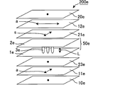
図1は、実施例1の液晶表示装置の構成を模式的に示す斜視図である。
本発明に係る実施例1の液晶表示装置は、図1に示すように、TACフィルム10a、第一の偏光子11a、正の固有複屈折を持つ材料で構成された第一種の複屈折層21a、第三種の複屈折層23a、VAモード液晶セル50a、負の固有複屈折を持つ材料で構成された第二種の複屈折層22a、第二の偏光子12a、TACフィルム20aをこの順に積層して得られたVAモードの液晶表示装置100aである。本実施例の各種複屈折フィルム、偏光子、液晶セルの光学特性及び軸設定については表4に示すとおりである。VAモード液晶セル50aは、対向する背面側基板1a及び観察面側基板2aと、両基板1a、2aに狭持され、液晶分子3aを含む液晶層とを有する。液晶分子3aは、電圧無印加時に長軸Lが両基板1a、2aに対して略垂直に向くように配向する。
Example 1
FIG. 1 is a perspective view schematically showing the configuration of the liquid crystal display device according to the first embodiment.
As shown in FIG. 1, the liquid crystal display device according to the first embodiment of the present invention includes a TAC film 10a, a first polarizer 11a, and a first type birefringent layer made of a material having positive intrinsic birefringence. 21a, the third birefringent layer 23a, the VA mode liquid crystal cell 50a, the second birefringent layer 22a made of a material having negative intrinsic birefringence, the second polarizer 12a, and the TAC film 20a. This is a VA mode liquid crystal display device 100a obtained by sequentially laminating. Table 4 shows optical properties and axis settings of various birefringent films, polarizers, and liquid crystal cells of this example. The VA mode liquid crystal cell 50a includes a rear substrate 1a and an observation surface substrate 2a facing each other, and a liquid crystal layer sandwiched between both substrates 1a and 2a and including liquid crystal molecules 3a. The liquid crystal molecules 3a are aligned so that the major axis L is substantially perpendicular to the substrates 1a and 2a when no voltage is applied.
なお、偏光子の外側(液晶セルに近い方を内側と定義し、遠い方を外側と定義する)のTACフィルムは、透明でさえあれば液晶表示装置の性能に影響を与えないので、表4では光学特性の説明は省略してある。以下の各例についても同様である。表中、各複屈折層の軸は面内遅相軸の方位角で定義し、各偏光子の軸は吸収軸で定義してある。表中、各複屈折層の材料名及び固有複屈折(複屈折)Δnについては、以下の略号を用いて示してある。
PMMA:ポリメチルメタクリレート(固有複屈折Δn:負)
NB:ノルボルネン(固有複屈折Δn:正)
TAC:トリアセチルセルロース(固有複屈折Δn:アセチル化度によって異なるが、一般には正)
Z:等方性フィルム(固有複屈折Δn:正)
G:逆分散性樹脂フィルム(固有複屈折Δn:正)
PC:ポリカーボネート(固有複屈折Δn:正)
NM:N置換マレイミド共重合体(固有複屈折Δn:負)
ChLC:コレステリック液晶(複屈折Δn:負)
Note that the TAC film on the outside of the polarizer (the one closer to the liquid crystal cell is defined as the inner side and the far side is defined as the outer side) does not affect the performance of the liquid crystal display device as long as it is transparent. The description of the optical characteristics is omitted. The same applies to the following examples. In the table, the axis of each birefringent layer is defined by the azimuth angle of the in-plane slow axis, and the axis of each polarizer is defined by the absorption axis. In the table, the material name and intrinsic birefringence (birefringence) Δn of each birefringent layer are indicated using the following abbreviations.
PMMA: Polymethyl methacrylate (Intrinsic birefringence Δn: Negative)
NB: Norbornene (Intrinsic birefringence Δn: Positive)
TAC: triacetyl cellulose (inherent birefringence Δn: varies depending on the degree of acetylation, but is generally positive)
Z: isotropic film (intrinsic birefringence Δn: positive)
G: Reverse dispersible resin film (intrinsic birefringence Δn: positive)
PC: Polycarbonate (Intrinsic birefringence Δn: Positive)
NM: N-substituted maleimide copolymer (intrinsic birefringence Δn: negative)
ChLC: Cholesteric liquid crystal (birefringence Δn: negative)
また、表中、α、β、α’及びβ’については、下記式(1)~(4)で表される。
α=|Rxy(450)|/|Rxy(550)|   (1)
β=|Rxy(650)|/|Rxy(550)|   (2)
α’=(α1+α2)/2   (3)
β’=(β1+β2)/2   (4)
なお、α1、α2はそれぞれ、第一種の複屈折層、第二種の複屈折層のαのことであり、β1、β2はそれぞれ、第一種の複屈折層、第二種の複屈折層のβのことである。
In the table, α, β, α ′ and β ′ are represented by the following formulas (1) to (4).
α = | Rxy (450) | / | Rxy (550) | (1)
β = | Rxy (650) | / | Rxy (550) | (2)
α ′ = (α1 + α2) / 2 (3)
β ′ = (β1 + β2) / 2 (4)
Α1 and α2 are α of the first birefringent layer and the second birefringent layer, respectively, and β1 and β2 are the first birefringent layer and the second birefringent layer, respectively. It is β of the layer.
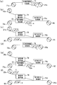
以下、実施例1の液晶表示装置の製造方法について説明する。
(1)ロール状部材の製造
まず、ロール状のTACフィルム10a、20a、ロール状の第一種の複屈折層21a、ロール状の第二種の複屈折層22a、及び、ロール状の第三種の複屈折層23aを製造する。
具体的には、ロール状のTACフィルム10a、20a、及び、ロール状の第三種の複屈折層23aは、溶融流延法(キャスト法)等を用いて製造される。
ロール状の第一種の複屈折層21aは、図2(a)に示すように、位相差機能付加部71において、正の固有複屈折を持つ材料で構成される第一種の複屈折層用の原反フィルム71aを横延伸(ロール幅方向に延伸)し、ロール状に巻き取ることで製造される。
ロール状の第二種の複屈折層22aは、図2(d)に示すように、位相差機能付加部72において、負の固有複屈折を持つ材料で構成される第二種の複屈折層用の原反フィルム72aを横延伸(ロール幅方向に延伸)し、ロール状に巻き取ることで製造される。
A method for manufacturing the liquid crystal display device of Example 1 will be described below.
(1) Manufacture of roll-shaped member First, roll-shaped TAC films 10a and 20a, a roll-shaped first-type birefringent layer 21a, a roll-shaped second-type birefringent layer 22a, and a roll-shaped third A seed birefringent layer 23a is produced.
Specifically, the roll-shaped TAC films 10a and 20a and the roll-shaped third birefringent layer 23a are manufactured using a melt casting method (casting method) or the like.
As shown in FIG. 2A, the roll-type first birefringent layer 21a is a first birefringent layer made of a material having positive intrinsic birefringence in the phase difference function adding unit 71. It is manufactured by laterally stretching (stretching in the roll width direction) the original film 71a for use and winding it into a roll.
As shown in FIG. 2 (d), the roll type second birefringent layer 22a is a second type birefringent layer made of a material having negative intrinsic birefringence in the phase difference function adding unit 72. It is manufactured by transversely stretching the original film 72a for use (stretching in the roll width direction) and winding it into a roll.
(2)ロール・ツー・ロールによる貼り合わせ
図2(b)に示すように、偏光機能付加部73において第一の偏光子用の原反フィルム73aを縦延伸(ロール流れ方向に延伸)することで、第一の偏光子11aを製造し、接着剤塗布部74においてTACフィルム10aに接着剤を塗布し、貼り合わせ処理部75aにおいて第一の偏光子11aとTACフィルム10aとを接着剤を介してロール・ツー・ロールで連続的に貼り合わせ、ロール状に巻き取る(ロール状部材90を製造する)。次に、図2(c)に示すように、接着剤塗布部76において第一種の複屈折層21aに接着剤を塗布し、貼り合わせ処理部75bにおいてTACフィルムが貼り合わされた第一の偏光子90と第一種の複屈折層21aとを接着剤を介してロール・ツー・ロールで連続的に貼り合わせ、ロール状に巻き取る(ロール状部材91を製造する)。同様に、第一の偏光子11a等に貼り合わされた第一種の複屈折層21aと第三種の複屈折層23aとを接着剤を介してロール・ツー・ロールで連続的に貼り合わせる。これにより得られた第一の偏光板80aは、乾燥した後、ロール状に巻き取られる。
(2) Bonding by roll-to-roll As shown in FIG. 2 (b), longitudinally stretching the original film 73a for the first polarizer (stretching in the roll flow direction) in the polarization function adding unit 73. Then, the first polarizer 11a is manufactured, the adhesive is applied to the TAC film 10a in the adhesive application unit 74, and the first polarizer 11a and the TAC film 10a are bonded to each other through the adhesive in the bonding processing unit 75a. Then, they are continuously bonded in a roll-to-roll manner and wound into a roll (manufacturing the roll-shaped member 90). Next, as shown in FIG. 2C, the first polarized light in which the adhesive is applied to the first type birefringent layer 21a in the adhesive application unit 76 and the TAC film is bonded in the bonding processing unit 75b. The child 90 and the first type birefringent layer 21a are continuously bonded with a roll-to-roll via an adhesive, and wound into a roll (a roll-shaped member 91 is manufactured). Similarly, the first-type birefringent layer 21a and the third-type birefringent layer 23a bonded to the first polarizer 11a and the like are continuously bonded by a roll-to-roll through an adhesive. The first polarizing plate 80a thus obtained is dried and then wound up into a roll.
他方、図2(e)に示すように、偏光機能付加部77において第二の偏光子の原反フィルム77aを縦延伸することで、第二の偏光子12aを製造し、接着剤塗布部78においてTACフィルム20aに接着剤を塗布し、貼り合わせ処理部75cにおいて第二の偏光子12aとTACフィルム20aとを接着剤を介してロール・ツー・ロールで連続的に貼り合わせ、ロール状に巻き取る(ロール状部材92を製造する)。次に、図2(f)に示すように、接着剤塗布部79において第二種の複屈折層22aに接着剤を塗布し、貼り合わせ処理部75dにおいてTACフィルムが貼り合わされた第二の偏光子92と第二種の複屈折層22aとを接着剤を介してロール・ツー・ロールで連続的に貼り合わせる。これにより得られた第二の偏光板81aは、乾燥した後、ロール状に巻き取られる。 On the other hand, as shown in FIG. 2 (e), the second polarizer 12 a is manufactured by longitudinally stretching the second polarizer original film 77 a in the polarization function adding section 77, and the adhesive application section 78. The adhesive is applied to the TAC film 20a, and the second polarizer 12a and the TAC film 20a are continuously bonded to each other by the roll-to-roll through the adhesive in the bonding processing section 75c, and wound into a roll shape. Take (manufacture roll member 92). Next, as shown in FIG. 2 (f), the second polarized light obtained by applying an adhesive to the second birefringent layer 22a in the adhesive application unit 79 and bonding the TAC film in the bonding processing unit 75d. The child 92 and the second birefringent layer 22a are continuously bonded to each other by a roll-to-roll through an adhesive. The second polarizing plate 81a thus obtained is dried and then wound up into a roll.
(3)液晶セルへの貼り付け
第一及び第二の偏光板80a、81aからそれぞれ離型フィルム(PETフィルム等)を剥がし、その中にある粘着剤を介してVAモード液晶セル50aに貼り付ける。
これにより、実施例1の液晶表示装置は完成する。
(3) Affixing to the liquid crystal cell The release films (PET film, etc.) are peeled off from the first and second polarizing plates 80a and 81a, respectively, and affixed to the VA mode liquid crystal cell 50a via the adhesive therein. .
Thereby, the liquid crystal display device of Example 1 is completed.
(実施例2~5)
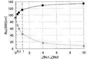
本発明に係る実施例2~5の液晶表示装置は、ΔNz1及びΔNz2の値(同値)を0.1、0.2、0.6、1.0に変更したことを除いては、実施例1とほとんど同様の液晶表示装置である。本実施例の各種複屈折フィルム、偏光子、液晶セルの光学特性及び軸設定については表4に示すとおりである。
(Examples 2 to 5)
The liquid crystal display devices of Examples 2 to 5 according to the present invention are the same as those of Example 2 except that the values (same values) of ΔNz1 and ΔNz2 are changed to 0.1, 0.2, 0.6, and 1.0. 1 is a liquid crystal display device almost the same as 1. Table 4 shows optical properties and axis settings of various birefringent films, polarizers, and liquid crystal cells of this example.
Figure JPOXMLDOC01-appb-T000004
(実施例6)
本発明に係る実施例6の液晶表示装置は、第二種の複屈折層の材料を変更したことを除いては、実施例1とほとんど同様の液晶表示装置である。本実施例の各種複屈折フィルム、偏光子、液晶セルの光学特性及び軸設定については表5に示すとおりである。
(Example 6)
The liquid crystal display device of Example 6 according to the present invention is almost the same as the liquid crystal display device of Example 1 except that the material of the second birefringent layer is changed. The optical properties and axis settings of various birefringent films, polarizers, and liquid crystal cells of this example are as shown in Table 5.
Figure JPOXMLDOC01-appb-T000005
(実施例7)
本発明に係る実施例7の液晶表示装置は、第一種の複屈折層の材料を逆波長分散性を示す材料に変更したことを除いては、実施例1とほとんど同様の液晶表示装置である。本実施例の各種複屈折フィルム、偏光子、液晶セルの光学特性及び軸設定については表6に示すとおりである。
(Example 7)
The liquid crystal display device of Example 7 according to the present invention is a liquid crystal display device almost the same as that of Example 1 except that the material of the first type birefringent layer is changed to a material exhibiting reverse wavelength dispersion. is there. Table 6 shows optical characteristics and axis settings of various birefringent films, polarizers, and liquid crystal cells of this example.
Figure JPOXMLDOC01-appb-T000006
(実施例8)
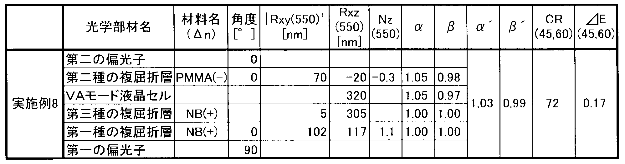
本発明に係る実施例8の液晶表示装置は、ΔNz1<ΔNz2(ΔNz1=0.1、ΔNz2=0.3)に変更したことを除いては、実施例1とほとんど同様の液晶表示装置である。本実施例の各種複屈折フィルム、偏光子、液晶セルの光学特性及び軸設定については表7に示すとおりである。
(Example 8)
The liquid crystal display device according to the eighth embodiment of the present invention is almost the same as the liquid crystal display device according to the first embodiment except that ΔNz1 <ΔNz2 (ΔNz1 = 0.1, ΔNz2 = 0.3). . Table 7 shows optical characteristics and axis settings of various birefringent films, polarizers, and liquid crystal cells of this example.
Figure JPOXMLDOC01-appb-T000007
(実施例9)
本発明に係る実施例9の液晶表示装置は、ΔNz1>ΔNz2(ΔNz1=0.3、ΔNz2=0.1)に変更したことを除いては、実施例1とほとんど同様の液晶表示装置である。本実施例の各種複屈折フィルム、偏光子、液晶セルの光学特性及び軸設定については表8に示すとおりである。
Example 9
The liquid crystal display device of Example 9 according to the present invention is almost the same as that of Example 1 except that ΔNz1> ΔNz2 (ΔNz1 = 0.3, ΔNz2 = 0.1). . Table 8 shows optical characteristics and axis settings of various birefringent films, polarizers, and liquid crystal cells of this example.
Figure JPOXMLDOC01-appb-T000008
(実施例10)
本発明に係る実施例10の液晶表示装置は、第一種の複屈折層のΔNz1を実施例9よりも大きくしたものである。本実施例の各種複屈折フィルム、偏光子、液晶セルの光学特性及び軸設定については表9に示すとおりである。
(Example 10)
In the liquid crystal display device of Example 10 according to the present invention, ΔNz1 of the first type birefringent layer is made larger than that of Example 9. The optical characteristics and axis settings of various birefringent films, polarizers, and liquid crystal cells of this example are as shown in Table 9.
Figure JPOXMLDOC01-appb-T000009
(実施例11)
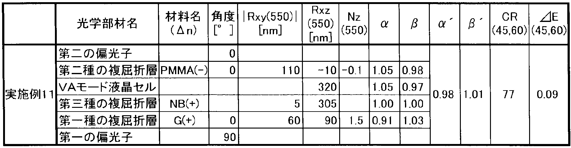
本発明に係る実施例11の液晶表示装置は、第一種の複屈折層の材料を逆波長分散性を示す材料に変更したことを除いては、実施例10とほとんど同様の液晶表示装置である。本実施例の各種複屈折フィルム、偏光子、液晶セルの光学特性及び軸設定については表10に示すとおりである。
(Example 11)
The liquid crystal display device of Example 11 according to the present invention is a liquid crystal display device almost the same as that of Example 10 except that the material of the first type birefringent layer is changed to a material exhibiting reverse wavelength dispersion. is there. Table 10 shows optical characteristics and axis settings of various birefringent films, polarizers, and liquid crystal cells of this example.
Figure JPOXMLDOC01-appb-T000010
(実施例12)
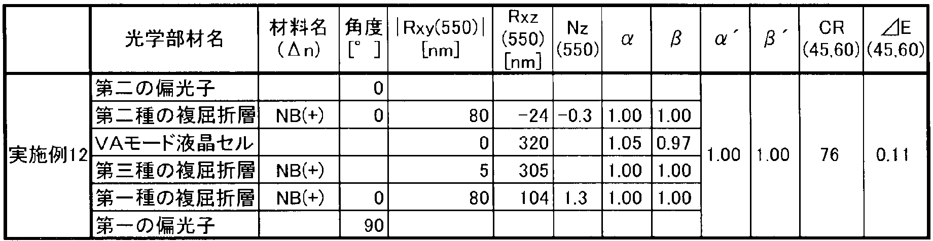
本発明に係る実施例12の液晶表示装置は、第二種の複屈折層の材料を正の固有複屈折を持つ材料に変更したことを除いては、実施例1とほとんど同様の液晶表示装置である。本実施例の各種複屈折フィルム、偏光子、液晶セルの光学特性及び軸設定については表11に示すとおりである。
Example 12
The liquid crystal display device of Example 12 according to the present invention is almost the same as that of Example 1 except that the material of the second birefringent layer is changed to a material having positive intrinsic birefringence. It is. Table 11 shows optical characteristics and axis settings of various birefringent films, polarizers, and liquid crystal cells of this example.
Figure JPOXMLDOC01-appb-T000011
(実施例13)
本発明に係る実施例13の液晶表示装置は、第一種の複屈折層の材料を逆波長分散性を示す材料に変更したことを除いては、実施例12とほとんど同様の液晶表示装置である。本実施例の各種複屈折フィルム、偏光子、液晶セルの光学特性及び軸設定については表12に示すとおりである。
(Example 13)
The liquid crystal display device of Example 13 according to the present invention is a liquid crystal display device almost the same as that of Example 12 except that the material of the first birefringent layer is changed to a material exhibiting reverse wavelength dispersion. is there. Table 12 shows the optical characteristics and axis settings of various birefringent films, polarizers, and liquid crystal cells of this example.
Figure JPOXMLDOC01-appb-T000012
(実施例14)
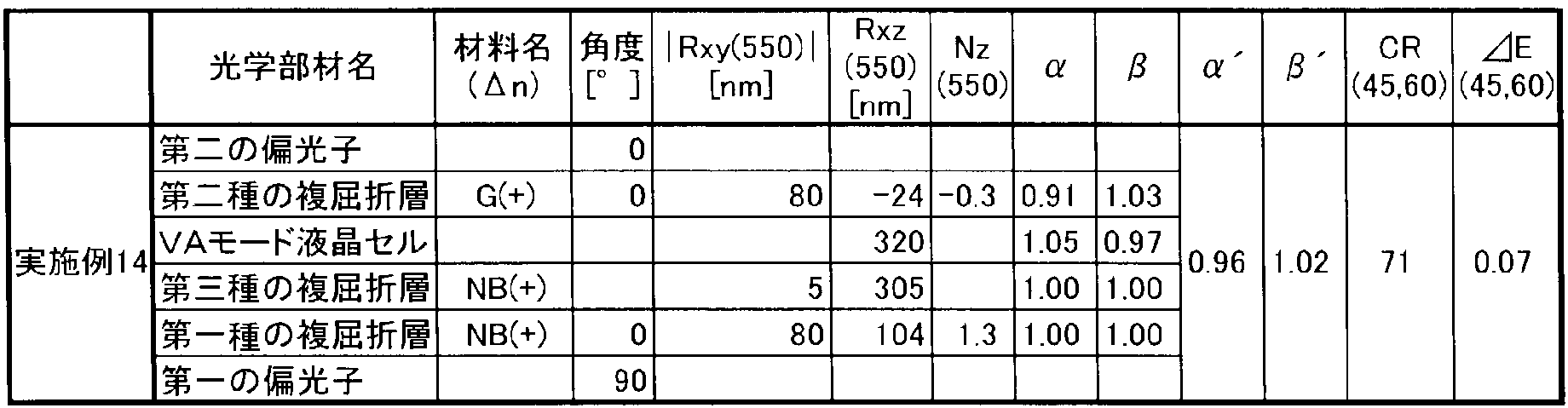
本発明に係る実施例14の液晶表示装置は、第二種の複屈折層の材料を逆波長分散性を示す材料に変更したことを除いては、実施例12とほとんど同様の液晶表示装置である。本実施例の各種複屈折フィルム、偏光子、液晶セルの光学特性及び軸設定については表13に示すとおりである。
(Example 14)
The liquid crystal display device of Example 14 according to the present invention is a liquid crystal display device almost the same as that of Example 12 except that the material of the second birefringent layer is changed to a material exhibiting reverse wavelength dispersion. is there. Table 13 shows optical characteristics and axis settings of various birefringent films, polarizers, and liquid crystal cells of this example.
Figure JPOXMLDOC01-appb-T000013
(実施例15)
本発明に係る実施例15の液晶表示装置は、第一種及び第二種の複屈折層の材料を逆波長分散性を示す材料に変更したことを除いては、実施例12とほとんど同様の液晶表示装置である。本実施例の各種複屈折フィルム、偏光子、液晶セルの光学特性及び軸設定については表14に示すとおりである。
(Example 15)
The liquid crystal display device of Example 15 according to the present invention is almost the same as Example 12 except that the materials of the first and second birefringent layers are changed to materials exhibiting reverse wavelength dispersion. It is a liquid crystal display device. Table 14 shows optical characteristics and axis settings of various birefringent films, polarizers, and liquid crystal cells of this example.
Figure JPOXMLDOC01-appb-T000014
(比較例1)
図3は、比較例1の液晶表示装置の構成を模式的に示す斜視図である。
比較例1の液晶表示装置は、図3に示すように、TACフィルム10b、第一の偏光子11b、TACフィルム20b、VAモード液晶セル50b、TACフィルム30b、第二の偏光子12b、TACフィルム40bをこの順に積層して得られたVAモードの液晶表示装置200bである。本比較例の各種複屈折フィルム、偏光子、液晶セルの光学特性及び軸設定については表15に示すとおりである。
(Comparative Example 1)
FIG. 3 is a perspective view schematically showing the configuration of the liquid crystal display device of Comparative Example 1.
As shown in FIG. 3, the liquid crystal display device of Comparative Example 1 includes a TAC film 10b, a first polarizer 11b, a TAC film 20b, a VA mode liquid crystal cell 50b, a TAC film 30b, a second polarizer 12b, and a TAC film. This is a VA mode liquid crystal display device 200b obtained by stacking 40b in this order. Table 15 shows optical characteristics and axis settings of various birefringent films, polarizers, and liquid crystal cells of this comparative example.
(比較例2)
図4は、比較例2の液晶表示装置の構成を模式的に示す斜視図である。
比較例2の液晶表示装置は、図4に示すように、TACフィルム10c、第一の偏光子11c、2軸性位相差フィルム60c、VAモード液晶セル50c、TACフィルム20c、第二の偏光子12c、TACフィルム30cをこの順に積層して得られたVAモードの液晶表示装置200cである。本比較例の各種複屈折フィルム、偏光子、液晶セルの光学特性及び軸設定については表15に示すとおりである。
(Comparative Example 2)
FIG. 4 is a perspective view schematically showing the configuration of the liquid crystal display device of Comparative Example 2.
As shown in FIG. 4, the liquid crystal display device of Comparative Example 2 includes a TAC film 10c, a first polarizer 11c, a biaxial retardation film 60c, a VA mode liquid crystal cell 50c, a TAC film 20c, and a second polarizer. This is a VA mode liquid crystal display device 200c obtained by laminating 12c and the TAC film 30c in this order. Table 15 shows optical characteristics and axis settings of various birefringent films, polarizers, and liquid crystal cells of this comparative example.
(比較例3)
図5は、比較例3の液晶表示装置の構成を模式的に示す斜視図である。
比較例3の液晶表示装置は、図5に示すように、TACフィルム10d、第一の偏光子11d、第一の2軸性位相差フィルム60d、VAモード液晶セル50d、第二の2軸性位相差フィルム61d、第二の偏光子12d、TACフィルム20dをこの順に積層して得られたVAモードの液晶表示装置200dである。本比較例の各種複屈折フィルム、偏光子、液晶セルの光学特性及び軸設定については表15に示すとおりである。
(Comparative Example 3)
FIG. 5 is a perspective view schematically showing the configuration of the liquid crystal display device of Comparative Example 3.
As shown in FIG. 5, the liquid crystal display device of Comparative Example 3 includes a TAC film 10d, a first polarizer 11d, a first biaxial retardation film 60d, a VA mode liquid crystal cell 50d, and a second biaxial property. This is a VA mode liquid crystal display device 200d obtained by laminating a retardation film 61d, a second polarizer 12d, and a TAC film 20d in this order. Table 15 shows optical characteristics and axis settings of various birefringent films, polarizers, and liquid crystal cells of this comparative example.
Figure JPOXMLDOC01-appb-T000015
(参考例1)
図6は、参考例1の液晶表示装置の構成を模式的に示す斜視図である。
参考例1の液晶表示装置は、図6に示すように、TACフィルム10e、第一の偏光子11e、ネガティブCプレート23e、VAモード液晶セル50e、ポジティブAプレート21e、第二の偏光子12e、TACフィルム20eをこの順に積層して得られたVAモードの液晶表示装置200eである。本参考例の各種複屈折フィルム、偏光子、液晶セルの光学特性及び軸設定については表16に示すとおりである
(Reference Example 1)
6 is a perspective view schematically showing the configuration of the liquid crystal display device of Reference Example 1. FIG.
As shown in FIG. 6, the liquid crystal display device of Reference Example 1 includes a TAC film 10e, a first polarizer 11e, a negative C plate 23e, a VA mode liquid crystal cell 50e, a positive A plate 21e, a second polarizer 12e, This is a VA mode liquid crystal display device 200e obtained by laminating the TAC film 20e in this order. The optical properties and axis settings of various birefringent films, polarizers, and liquid crystal cells of this reference example are as shown in Table 16.
(参考例2)
図7は、参考例2の液晶表示装置の構成を模式的に示す斜視図である。
参考例2の液晶表示装置は、図7に示すように、TACフィルム10f、第一の偏光子11f、ネガティブCプレート23f、VAモード液晶セル50f、ポジティブCプレート25f、ポジティブAプレート21f、第二の偏光子12f、TACフィルム20fをこの順に積層して得られたVAモードの液晶表示装置200fである。本参考例の各種複屈折フィルム、偏光子、液晶セルの光学特性及び軸設定については表16に示すとおりである。
(Reference Example 2)
FIG. 7 is a perspective view schematically showing the configuration of the liquid crystal display device of Reference Example 2.
As shown in FIG. 7, the liquid crystal display device of Reference Example 2 includes a TAC film 10f, a first polarizer 11f, a negative C plate 23f, a VA mode liquid crystal cell 50f, a positive C plate 25f, a positive A plate 21f, a second VA mode liquid crystal display device 200f obtained by laminating the polarizer 12f and the TAC film 20f in this order. Table 16 shows optical characteristics and axis settings of various birefringent films, polarizers, and liquid crystal cells of this reference example.
(参考例3)
図8は、参考例3の液晶表示装置の構成を模式的に示す斜視図である。
参考例3の液晶表示装置は、図8に示すように、TACフィルム10g、第一の偏光子11g、ネガティブCプレート23g、VAモード液晶セル50g、3枚の2軸性位相差フィルム60g~62g、第二の偏光子12g、TACフィルム20gをこの順に積層して得られたVAモードの液晶表示装置200gである。本参考例の各種複屈折フィルム、偏光子、液晶セルの光学特性及び軸設定については表16に示すとおりである。
(Reference Example 3)
FIG. 8 is a perspective view schematically showing the configuration of the liquid crystal display device of Reference Example 3.
As shown in FIG. 8, the liquid crystal display device of Reference Example 3 includes a TAC film 10g, a first polarizer 11g, a negative C plate 23g, a VA mode liquid crystal cell 50g, and three biaxial retardation films 60g to 62g. VA mode liquid crystal display device 200g obtained by laminating the second polarizer 12g and the TAC film 20g in this order. Table 16 shows optical characteristics and axis settings of various birefringent films, polarizers, and liquid crystal cells of this reference example.
Figure JPOXMLDOC01-appb-T000016
(評価結果)
各例の液晶表示装置のコントラスト視野角及び色度視野角を測定し、CR(45、60)及びΔE(45、60)を表4~16に整理した。
本発明の実施例1~15の液晶表示装置のCR(45、60)は、比較例1~3のそれと同等以上であり、目視評価においても比較例1~3と同等以上のコントラスト視野角を有していた。また、本発明の実施例1の液晶表示装置のΔE(45、60)は、CR(45、60)が同程度の比較例2及び3のそれよりも小さく、目視評価においても視角を変化させたときの色度変化感が小さく、比較例1~3よりも良好な色度視野角を有していた。
(Evaluation results)
The contrast viewing angle and chromaticity viewing angle of the liquid crystal display device of each example were measured, and CR (45, 60) and ΔE (45, 60) were arranged in Tables 4 to 16.
The CR (45, 60) of the liquid crystal display devices of Examples 1 to 15 of the present invention is equal to or greater than that of Comparative Examples 1 to 3, and the visual field evaluation also has a contrast viewing angle equal to or greater than that of Comparative Examples 1 to 3. Had. In addition, ΔE (45, 60) of the liquid crystal display device of Example 1 of the present invention is smaller than that of Comparative Examples 2 and 3 in which CR (45, 60) is comparable, and the viewing angle is also changed in visual evaluation. The chromaticity change feeling was small, and the chromaticity viewing angle was better than those of Comparative Examples 1 to 3.
参考例1~3の液晶表示装置のΔE(45、60)は、本発明の実施例1の液晶表示装置のそれよりも更に小さく、良好な色度視野角を有していたが、製造の難しいポジティブCプレート、Nz≒0.5に制御された2軸性位相差フィルム、118nm以上の|Rxy(550)|を有する逆波長分散位相差フィルムのいずれか一つの位相差フィルムを用いている。 ΔE (45, 60) of the liquid crystal display devices of Reference Examples 1 to 3 was smaller than that of the liquid crystal display device of Example 1 of the present invention and had a good chromaticity viewing angle. Any one of a difficult positive C plate, a biaxial retardation film controlled to Nz≈0.5, and a reverse wavelength dispersion retardation film having | Rxy (550) | of 118 nm or more is used. .
更に、本発明の実施例1~11の液晶表示装置は、第一種の複屈折層が正の固有複屈折を持つ材料で構成され、第二種の複屈折層が負の固有複屈折を持つ材料で構成されており、第一の偏光子と第一種の複屈折層、及び、第二の偏光子と第二種の複屈折層とをそれぞれロール・ツー・ロールで貼り合わせることができるため、TACフィルム等の保護フィルムを削減することができ、その結果、性能向上及び生産性向上を実現することもできた。 Further, in the liquid crystal display devices of Examples 1 to 11 of the present invention, the first type birefringent layer is made of a material having positive intrinsic birefringence, and the second type birefringent layer exhibits negative intrinsic birefringence. The first polarizer and the first type of birefringent layer, and the second polarizer and the second type of birefringent layer can be bonded together in a roll-to-roll manner. Therefore, it was possible to reduce the number of protective films such as a TAC film, and as a result, it was possible to improve performance and improve productivity.
本願は、2008年2月7日に出願された日本国特許出願2008-27998号を基礎として、パリ条約ないし移行する国における法規に基づく優先権を主張するものである。該出願の内容は、その全体が本願中に参照として組み込まれている。 The present application claims priority based on the Paris Convention or the laws and regulations in the country of transition based on Japanese Patent Application No. 2008-27998 filed on Feb. 7, 2008. The contents of the application are hereby incorporated by reference in their entirety.
実施例1の液晶表示装置の構成を模式的に示す斜視図である。1 is a perspective view schematically showing a configuration of a liquid crystal display device of Example 1. FIG. 実施例1の液晶表示装置の製造工程の一部を示す模式図である。(a)は、第一種の複屈折層用の原反フィルムを横延伸することで第一種の複屈折層を製造する工程、(b)は、第一の偏光子用の原反フィルムを縦延伸することで第一の偏光子を製造し、第一の偏光子とTACフィルムとをロール・ツー・ロールで貼り合わせる工程、(c)は、TACフィルムが貼り合わされた第一の偏光子と第一種の複屈折層とをロール・ツー・ロールで貼り合わせる工程、(d)は、第二種の複屈折層用の原反フィルムを横延伸することで第二種の複屈折層を製造する工程、(e)は、第二の偏光子用の原反フィルムを縦延伸することで第二の偏光子を製造し、第二の偏光子とTACフィルムとをロール・ツー・ロールで貼り合わせる工程、(f)は、TACフィルムが貼り合わされた第二の偏光子と第二種の複屈折層とをロール・ツー・ロールで貼り合わせる工程を示す。6 is a schematic diagram illustrating a part of the manufacturing process of the liquid crystal display device of Example 1. FIG. (A) is a step of producing a first type birefringent layer by transversely stretching a first type birefringent layer original film, and (b) is a first polarizer original film. The first polarizer is manufactured by longitudinally stretching the first polarizer, and the first polarizer and the TAC film are bonded together in a roll-to-roll manner. (C) is the first polarized light in which the TAC film is bonded. The step of laminating the child and the first type birefringent layer by roll-to-roll, (d) is the second type birefringence by transversely stretching the original film for the second type birefringent layer (E) is a step of producing a second polarizer by longitudinally stretching an original film for the second polarizer, and rolling the second polarizer and the TAC film. The step of laminating with a roll, (f) is a second polarizer with a TAC film and a second birefringence. Door to show the process of attaching a roll-to-roll. 比較例1の液晶表示装置の構成を模式的に示す斜視図である。It is a perspective view which shows typically the structure of the liquid crystal display device of the comparative example 1. 比較例2の液晶表示装置の構成を模式的に示す斜視図である。It is a perspective view which shows typically the structure of the liquid crystal display device of the comparative example 2. 比較例3の液晶表示装置の構成を模式的に示す斜視図である。It is a perspective view which shows typically the structure of the liquid crystal display device of the comparative example 3. FIG. 参考例1の液晶表示装置の構成を模式的に示す斜視図である。It is a perspective view which shows typically the structure of the liquid crystal display device of the reference example 1. FIG. 参考例2の液晶表示装置の構成を模式的に示す斜視図である。It is a perspective view which shows typically the structure of the liquid crystal display device of the reference example 2. FIG. 参考例3の液晶表示装置の構成を模式的に示す斜視図である。It is a perspective view which shows typically the structure of the liquid crystal display device of the reference example 3. 従来の液晶表示装置の構成を模式的に示す断面図である。It is sectional drawing which shows the structure of the conventional liquid crystal display device typically. 従来の液晶表示装置の構成を模式的に示す断面図である。It is sectional drawing which shows the structure of the conventional liquid crystal display device typically. 本発明の液晶表示装置の構成の一例を模式的に示す断面図である。It is sectional drawing which shows typically an example of a structure of the liquid crystal display device of this invention. 偏光子の光学軸と複屈折層の光学軸とが平行である形態を示す斜視図である。(a)は、正面方向から観察したときであり、(b)は、斜め方向から観察したときである。It is a perspective view which shows the form with which the optical axis of a polarizer and the optical axis of a birefringent layer are parallel. (A) is when observed from the front direction, (b) is when observed from an oblique direction. 偏光子の光学軸と複屈折層の光学軸とが直交である形態を示す斜視図である。(a)は、正面方向から観察したときであり、(b)は、斜め方向から観察したときである。It is a perspective view which shows the form with which the optical axis of a polarizer and the optical axis of a birefringent layer are orthogonal. (A) is when observed from the front direction, (b) is when observed from an oblique direction. ΔNz1=ΔNz2を満たすときの、ΔNz1及びΔNz2と最適な|Rxy(550)|との関係を示す図である。■は、第一種の複屈折層を表し、△は、第二種の複屈折層を表す。It is a figure which shows the relationship between (DELTA) Nz1 and (DELTA) Nz2, and optimal | Rxy (550) | when satisfy | filling (DELTA) Nz1 = (DELTA) Nz2. (1) represents the first type birefringent layer, and (Δ) represents the second type birefringent layer. ΔNz1=0かつ0<ΔNz2を満たすときの、ΔNz1及びΔNz2と最適な|Rxy(550)|との関係を示す図である。■は、第一種の複屈折層を表し、△は、第二種の複屈折層を表す。FIG. 10 is a diagram illustrating a relationship between ΔNz1 and ΔNz2 and an optimal | Rxy (550) | when ΔNz1 = 0 and 0 <ΔNz2. (1) represents the first type birefringent layer, and (Δ) represents the second type birefringent layer. ΔNz2=0かつ0<ΔNz1を満たすときの、ΔNz1及びΔNz2と最適な|Rxy(550)|との関係を示す図である。■は、第一種の複屈折層を表し、△は、第二種の複屈折層を表す。It is a figure which shows the relationship between (DELTA) Nz1 and (DELTA) Nz2, and optimal | Rxy (550) | when (DELTA) Nz2 = 0 and 0 <(DELTA) Nz1 are satisfy | filled. (1) represents the first type birefringent layer, and (Δ) represents the second type birefringent layer.
符号の説明Explanation of symbols
1a~1g:背面側基板
2a~2g:観察面側基板
3a~3g:液晶分子
5:接着剤
7:粘着剤
8:偏光子
9:複屈折層
10、10a~10g、20a~20g、30b、30c、40b:TACフィルム(保護フィルム)
11、11a~11g:第一の偏光子
12、12a~12g:第二の偏光子
21、21a~21f:第一種の複屈折層
22、22a:第二種の複屈折層
23a~23g:第三種の複屈折層
24:等方性フィルム(ゼロ位相差保護フィルム)
25f:ポジティブCプレート
50a~50g:VAモード液晶セル
60c~60g、61d、61g、62g:2軸性位相差フィルム
71、72:位相差機能付加部
71a:第一種の複屈折層用の原反フィルム
72a:第二種の複屈折層用の原反フィルム
73、77:偏光機能付加部
73a:第一の偏光子用の原反フィルム
74、76、78、79:接着剤塗布部
75a~75d:貼り合わせ処理部
77a:第二の偏光子用の原反フィルム
80a:第一の偏光板
81a:第二の偏光板
90:TACフィルムが貼り合わされた第一の偏光子
91:TACフィルム及び第一種の複屈折層が貼り合わされた第一の偏光子
92:TACフィルムが貼り合わされた第二の偏光子
100a、200b~200g:VAモード液晶表示装置
a:偏光子の吸収軸
a(o):偏光子の吸収軸(偏光子の光学軸)
e1(o):固有モード(複屈折層の光学軸)
e2:固有モード
L:液晶分子の長軸
s:遅相軸
t:偏光子の透過軸
1a to 1g: Back side substrate 2a to 2g: Observation surface side substrate 3a to 3g: Liquid crystal molecule 5: Adhesive 7: Adhesive 8: Polarizer 9: Birefringent layer 10, 10a to 10g, 20a to 20g, 30b, 30c, 40b: TAC film (protective film)
11, 11a to 11g: first polarizer 12, 12a to 12g: second polarizer 21, 21a to 21f: first type birefringent layer 22, 22a: second type birefringent layers 23a to 23g: Third kind of birefringent layer 24: isotropic film (zero retardation protective film)
25f: Positive C plates 50a to 50g: VA mode liquid crystal cells 60c to 60g, 61d, 61g, 62g: Biaxial retardation films 71, 72: Retardation function adding part 71a: Original for first type birefringent layer Anti-film 72a: second-type birefringent layer original film 73, 77: polarization function adding portion 73a: first polarizer original film 74, 76, 78, 79: adhesive application portions 75a- 75d: Bonding processing unit 77a: Original film 80a for the second polarizer 80a: First polarizing plate 81a: Second polarizing plate 90: First polarizer 91 bonded with a TAC film 91: TAC film and First polarizer 92 with first birefringent layer bonded: Second polarizer 100a, 200b to 200g with TAC film bonded: VA mode liquid crystal display device a: Absorption of polarizer Axis a (o): the absorption axis of the polarizer (optic axis of the polarizer)
e1 (o): Eigen mode (optical axis of birefringent layer)
e2: natural mode L: long axis s of liquid crystal molecule s: slow axis t: transmission axis of polarizer

Claims (15)

  1. 第一の偏光子、第一種の複屈折層、液晶セル、第二種の複屈折層、及び、該第一の偏光子の吸収軸に対して吸収軸が直交する第二の偏光子をこの順に有する液晶表示装置を製造する方法であって、
    該第一種の複屈折層は、正の固有複屈折を持つ材料で構成され、
    該第二種の複屈折層は、負の固有複屈折を持つ材料で構成され、
    該製造方法は、該第一の偏光子用の原反フィルムを縦延伸することで該第一の偏光子を製造し、該第一種の複屈折層用の原反フィルムを横延伸することで該第一種の複屈折層を製造し、該第一の偏光子と該第一種の複屈折層とをロール・ツー・ロールで貼り合わせる第一の工程、及び、
    該第二の偏光子用の原反フィルムを縦延伸することで該第二の偏光子を製造し、該第二種の複屈折層用の原反フィルムを横延伸することで該第二種の複屈折層を製造し、該第二の偏光子と該第二種の複屈折層とをロール・ツー・ロールで貼り合わせる第二の工程の少なくとも一方を含むことを特徴とする液晶表示装置の製造方法。
    A first polarizer, a first birefringent layer, a liquid crystal cell, a second birefringent layer, and a second polarizer having an absorption axis perpendicular to the absorption axis of the first polarizer. A method of manufacturing a liquid crystal display device having this order,
    The first type birefringent layer is made of a material having positive intrinsic birefringence,
    The second birefringent layer is made of a material having negative intrinsic birefringence,
    The production method comprises producing the first polarizer by longitudinally stretching the original film for the first polarizer, and transversely stretching the original film for the first birefringent layer. A first step of producing the first type birefringent layer, and laminating the first polarizer and the first type birefringent layer by roll-to-roll; and
    The second polarizer is produced by longitudinally stretching the original film for the second polarizer, and the second type is obtained by transversely stretching the original film for the second type of birefringent layer. A liquid crystal display device comprising at least one of a second step of producing a birefringent layer of the above, and laminating the second polarizer and the second type of birefringent layer by roll-to-roll. Manufacturing method.
  2. 前記第一種の複屈折層は、1.1≦Nz(550)≦2を満たし、面内遅相軸が前記第一の偏光子の吸収軸に対して90°の角度をなし、
    前記第二種の複屈折層は、-1≦Nz(550)≦-0.1を満たし、面内遅相軸が前記第二の偏光子の吸収軸に対して0°の角度をなすことを特徴とする請求項1記載の液晶表示装置の製造方法。
    The first birefringent layer satisfies 1.1 ≦ Nz (550) ≦ 2, and an in-plane slow axis forms an angle of 90 ° with respect to the absorption axis of the first polarizer;
    The second birefringent layer satisfies −1 ≦ Nz (550) ≦ −0.1, and the in-plane slow axis forms an angle of 0 ° with respect to the absorption axis of the second polarizer. The method of manufacturing a liquid crystal display device according to claim 1.
  3. 第一の偏光子、第一種の複屈折層、液晶セル、第二種の複屈折層、及び、該第一の偏光子の吸収軸に対して吸収軸が直交する第二の偏光子をこの順に有する液晶表示装置であって、
    該第一種の複屈折層は、1.1≦Nz(550)≦2を満たし、面内遅相軸が該第一の偏光子の吸収軸に直交し、
    該第二種の複屈折層は、-1≦Nz(550)≦-0.1を満たし、面内遅相軸が該第二の偏光子の吸収軸と平行であることを特徴とする液晶表示装置。
    A first polarizer, a first birefringent layer, a liquid crystal cell, a second birefringent layer, and a second polarizer having an absorption axis perpendicular to the absorption axis of the first polarizer. A liquid crystal display device having this order,
    The first type birefringent layer satisfies 1.1 ≦ Nz (550) ≦ 2, the in-plane slow axis is orthogonal to the absorption axis of the first polarizer,
    The second type of birefringent layer satisfies −1 ≦ Nz (550) ≦ −0.1, and an in-plane slow axis is parallel to the absorption axis of the second polarizer. Display device.
  4. 前記第一種の複屈折層は、正の固有複屈折を持つ材料で構成されることを特徴とする請求項3記載の液晶表示装置。 4. The liquid crystal display device according to claim 3, wherein the first type birefringent layer is made of a material having positive intrinsic birefringence.
  5. 前記第二種の複屈折層は、負の固有複屈折を持つ材料で構成されることを特徴とする請求項3又は4記載の液晶表示装置。 5. The liquid crystal display device according to claim 3, wherein the second birefringent layer is made of a material having negative intrinsic birefringence.
  6. 前記液晶表示装置は、前記第一種の複屈折層のNz(550)と前記第二種の複屈折層のNz(550)との相加平均をNz’(550)と定義するとき、0≦Nz’(550)≦1を満たすことを特徴とする請求項3~5のいずれかに記載の液晶表示装置。 When the arithmetic mean of Nz (550) of the first type birefringent layer and Nz (550) of the second type birefringent layer is defined as Nz ′ (550), the liquid crystal display device is 0. 6. The liquid crystal display device according to claim 3, wherein ≦ Nz ′ (550) ≦ 1 is satisfied.
  7. 前記液晶表示装置は、0.3≦Nz’(550)≦0.7を満たすことを特徴とする請求項6記載の液晶表示装置。 The liquid crystal display device according to claim 6, wherein the liquid crystal display device satisfies 0.3 ≦ Nz ′ (550) ≦ 0.7.
  8. 前記第一種の複屈折層及び前記第二種の複屈折層の少なくとも一方は、|Rxy(550)|≦130nmを満たすことを特徴とする請求項3~7のいずれかに記載の液晶表示装置。 8. The liquid crystal display according to claim 3, wherein at least one of the first birefringent layer and the second birefringent layer satisfies | Rxy (550) | ≦ 130 nm. apparatus.
  9. 前記液晶表示装置は、前記第一種の複屈折層の二軸性パラメータΔNz1を|Nz(550)-1|と定義し、前記第二種の複屈折層の二軸性パラメータΔNz2を|Nz(550)|と定義するとき、ΔNz1=ΔNz2を満たすことを特徴とする請求項8記載の液晶表示装置。 In the liquid crystal display device, the biaxial parameter ΔNz1 of the first birefringent layer is defined as | Nz (550) -1 |, and the biaxial parameter ΔNz2 of the second birefringent layer is defined as | Nz. 9. The liquid crystal display device according to claim 8, wherein ΔNz1 = ΔNz2 is satisfied when defined as (550) |.
  10. 前記液晶表示装置は、前記第一種の複屈折層の二軸性パラメータΔNz1を|Nz(550)-1|と定義し、前記第二種の複屈折層の二軸性パラメータΔNz2を|Nz(550)|と定義するとき、ΔNz1<ΔNz2を満たすことを特徴とする請求項8記載の液晶表示装置。 In the liquid crystal display device, the biaxial parameter ΔNz1 of the first birefringent layer is defined as | Nz (550) -1 |, and the biaxial parameter ΔNz2 of the second birefringent layer is defined as | Nz. 9. The liquid crystal display device according to claim 8, wherein ΔNz1 <ΔNz2 is satisfied when defined as (550) |.
  11. 前記液晶表示装置は、前記第一種の複屈折層の二軸性パラメータΔNz1を|Nz(550)-1|と定義し、前記第二種の複屈折層の二軸性パラメータΔNz2を|Nz(550)|と定義するとき、ΔNz1>ΔNz2を満たすことを特徴とする請求項8記載の液晶表示装置。 In the liquid crystal display device, the biaxial parameter ΔNz1 of the first birefringent layer is defined as | Nz (550) -1 |, and the biaxial parameter ΔNz2 of the second birefringent layer is defined as | Nz. 9. The liquid crystal display device according to claim 8, wherein ΔNz1> ΔNz2 is satisfied when defined as (550) |.
  12. 前記第一種の複屈折層及び前記第二種の複屈折層の少なくとも一方は、|Rxy(450)|≦|Rxy(550)|≦|Rxy(650)|を満たすことを特徴とする請求項3~11のいずれかに記載の液晶表示装置。 At least one of the first-type birefringent layer and the second-type birefringent layer satisfies | Rxy (450) | ≦ | Rxy (550) | ≦ | Rxy (650) |. Item 12. The liquid crystal display device according to any one of Items 3 to 11.
  13. 前記液晶表示装置は、前記第一種の複屈折層の波長分散性α=Rxy(450)/Rxy(550)と前記第二種の複屈折層の波長分散性α=Rxy(450)/Rxy(550)との相加平均をα’と定義し、前記第一種の複屈折層の波長分散性β=Rxy(650)/Rxy(550)と前記第二種の複屈折層の波長分散性β=Rxy(650)/Rxy(550)との相加平均をβ’と定義するとき、α’≦1かつ1≦β’を満たすことを特徴とする請求項3~12のいずれかに記載の液晶表示装置。 In the liquid crystal display device, the wavelength dispersibility α = Rxy (450) / Rxy (550) of the first type birefringent layer and the wavelength dispersibility α = Rxy (450) / Rxy of the second type birefringent layer. The arithmetic mean of (550) is defined as α ′, and the wavelength dispersion of the first birefringent layer β = Rxy (650) / Rxy (550) and the wavelength dispersion of the second birefringent layer The characteristic β = Rxy (650) / Rxy (550) is defined as β ′, wherein α ′ ≦ 1 and 1 ≦ β ′ are satisfied. The liquid crystal display device described.
  14. 前記液晶表示装置は、前記液晶セル中の液晶分子を基板面に垂直に配向させることで黒表示を行うものであり、前記第一の偏光子と前記第二の偏光子との間に、Rxy≦10nmかつRxz≧100nmを満たす第三種の複屈折層を有することを特徴とする請求項3~13のいずれかに記載の液晶表示装置。 The liquid crystal display device performs black display by aligning liquid crystal molecules in the liquid crystal cell perpendicularly to the substrate surface, and Rxy is provided between the first polarizer and the second polarizer. 14. The liquid crystal display device according to claim 3, comprising a third birefringent layer satisfying ≦ 10 nm and Rxz ≧ 100 nm.
  15. 前記第三種の複屈折層は、前記液晶セルと隣接配置されていることを特徴とする請求項14記載の液晶表示装置。 15. The liquid crystal display device according to claim 14, wherein the third birefringent layer is disposed adjacent to the liquid crystal cell.
PCT/JP2008/069789 2008-02-07 2008-10-30 Method for manufacturing liquid crystal display, and liquid crystal display WO2009098804A1 (en)

Priority Applications (5)

Application Number Priority Date Filing Date Title
EP08872220.2A EP2239625A4 (en) 2008-02-07 2008-10-30 Method for manufacturing liquid crystal display, and liquid crystal display
CN2008801185563A CN101884005B (en) 2008-02-07 2008-10-30 Method for manufacturing liquid crystal display, and liquid crystal display
JP2009552383A JP5000729B2 (en) 2008-02-07 2008-10-30 Manufacturing method of liquid crystal display device and liquid crystal display device
US12/863,154 US20110051062A1 (en) 2008-02-07 2008-10-30 Method for producing liquid crystal display device, and liquid crystal display device
BRPI0822272-0A BRPI0822272A2 (en) 2008-02-07 2008-10-30 Method for producing liquid crystal display device, and liquid crystal display device

Applications Claiming Priority (2)

Application Number Priority Date Filing Date Title
JP2008-027998 2008-02-07
JP2008027998 2008-02-07

Publications (1)

Publication Number Publication Date
WO2009098804A1 true WO2009098804A1 (en) 2009-08-13

Family

ID=40951889

Family Applications (1)

Application Number Title Priority Date Filing Date
PCT/JP2008/069789 WO2009098804A1 (en) 2008-02-07 2008-10-30 Method for manufacturing liquid crystal display, and liquid crystal display

Country Status (6)

Country Link
US (1) US20110051062A1 (en)
EP (1) EP2239625A4 (en)
JP (1) JP5000729B2 (en)
CN (1) CN101884005B (en)
BR (1) BRPI0822272A2 (en)
WO (1) WO2009098804A1 (en)

Cited By (5)

* Cited by examiner, † Cited by third party
Publication number Priority date Publication date Assignee Title
JP2011213052A (en) * 2010-04-01 2011-10-27 Oji Paper Co Ltd Surface fine irregular body and method for manufacturing the same
JP2012145766A (en) * 2011-01-12 2012-08-02 Sumitomo Chemical Co Ltd Manufacturing method for polarizing laminated film and polarizing plate
KR20140087610A (en) * 2012-12-31 2014-07-09 엘지디스플레이 주식회사 polarizer, manufacturing method thereof, and liquid crystal display including the same
JP2014182283A (en) * 2013-03-19 2014-09-29 Nippon Zeon Co Ltd Multi-layered film, manufacturing method therefor, manufacturing method for phase difference film laminate, phase difference film, polarizing plate, and ips liquid crystal panel
JP2018205362A (en) * 2017-05-30 2018-12-27 大日本印刷株式会社 Polarization plate compensation film, liquid crystal panel

Families Citing this family (13)

* Cited by examiner, † Cited by third party
Publication number Priority date Publication date Assignee Title
KR101253048B1 (en) * 2008-12-31 2013-04-12 엘지디스플레이 주식회사 Liquid crystal display device having wide viewing angel
JP5905761B2 (en) 2011-05-20 2016-04-20 日東電工株式会社 Optical display panel continuous manufacturing method and optical display panel continuous manufacturing system
JP5945143B2 (en) * 2011-05-20 2016-07-05 日東電工株式会社 Optical film roll set and method for producing optical film roll set
KR101521226B1 (en) * 2011-12-02 2015-06-17 삼성전자 주식회사 Optical compensation film
KR101525998B1 (en) * 2011-12-12 2015-06-04 제일모직주식회사 Polarized film for organic light emitting diodes and display device comprising the same
US8836898B2 (en) * 2012-11-06 2014-09-16 Shenzhen China Star Optoelectronics Technology Co., Ltd Compensation system for liquid crystal panels and liquid crystal display
CN102944954B (en) * 2012-11-21 2015-11-25 深圳市华星光电技术有限公司 For bucking-out system and the liquid crystal indicator of liquid crystal panel
CN103558710B (en) 2013-11-11 2016-04-13 京东方科技集团股份有限公司 TFT LCD panel
CN105856794B (en) * 2016-04-18 2018-06-22 开思茂电子科技(苏州)有限公司 OCA wind-force feed devices
US20200255573A1 (en) * 2017-05-31 2020-08-13 Zeon Corporation Retardation film and production method
EP3633424B1 (en) * 2017-05-31 2023-04-19 Zeon Corporation Retardation film and production method
KR20200010277A (en) * 2017-05-31 2020-01-30 니폰 제온 가부시키가이샤 Retardation film and manufacturing method
WO2019188205A1 (en) * 2018-03-30 2019-10-03 日本ゼオン株式会社 Optical anisotropic layered body, polarizing plate, and image display device

Citations (12)

* Cited by examiner, † Cited by third party
Publication number Priority date Publication date Assignee Title
JPH11305217A (en) 1998-04-16 1999-11-05 Internatl Business Mach Corp <Ibm> Liquid crystal display device
US6141075A (en) 1996-02-28 2000-10-31 Fujitsu Limited Liquid crystal display device operating in a vertically aligned mode
JP2001350022A (en) 2000-04-07 2001-12-21 Tatsuo Uchida Wide viewing angle polarizing plate
US6661488B1 (en) 1997-06-12 2003-12-09 Fujitsu Limited Vertically-alligned (VA) liquid crystal display device
JP2005309110A (en) * 2004-04-22 2005-11-04 Sumitomo Chemical Co Ltd Liquid crystal display
JP2005326818A (en) * 2004-04-16 2005-11-24 Sharp Corp Circularly polarizing plate and liquid crystal display device
WO2006001448A1 (en) 2004-06-29 2006-01-05 Sharp Kabushiki Kaisha Phase difference film, polarization film, liquid crystal display unit, and method of designing phase difference film
JP2006514754A (en) 2003-01-28 2006-05-11 エルジー・ケム・リミテッド Vertical alignment liquid crystal display device having negative compensation film
US7057689B2 (en) 1997-08-29 2006-06-06 Sharp Kabushiki Kaisha Liquid crystal display with at least one phase compensation element
WO2006118234A1 (en) * 2005-04-28 2006-11-09 Zeon Corporation Optically anisotropic body and liquid crystal display device
JP2007232873A (en) 2006-02-28 2007-09-13 Teijin Ltd Laminated polarizing film, retardation film and liquid crystal display device
JP2007232874A (en) 2006-02-28 2007-09-13 Teijin Ltd Laminated polarizing film, retardation film and liquid crystal display device

Family Cites Families (14)

* Cited by examiner, † Cited by third party
Publication number Priority date Publication date Assignee Title
US6292242B1 (en) * 1993-12-15 2001-09-18 Ois Optical Imaging Systems, Inc. Normally white twisted nematic LCD with positive uniaxial and negative biaxial retarders
JP2000098385A (en) * 1998-09-25 2000-04-07 Alps Electric Co Ltd Reflection type liquid crystal display device
JP2004199045A (en) * 2002-12-04 2004-07-15 Sharp Corp Optical film and liquid crystal display using it
JP4882375B2 (en) * 2003-11-21 2012-02-22 日本ゼオン株式会社 Liquid crystal display
JP4383903B2 (en) * 2004-01-23 2009-12-16 株式会社 日立ディスプレイズ Polarizing plate and liquid crystal display device using the same
US7400371B2 (en) * 2004-02-03 2008-07-15 Sumitomo Chemical Company, Limited Liquid crystal display having particular retardation plate
JP4618675B2 (en) * 2005-02-08 2011-01-26 日東電工株式会社 Retardation film, polarizing element, liquid crystal panel, and liquid crystal display device
JP2006267625A (en) * 2005-03-24 2006-10-05 Nitto Denko Corp Liquid crystal panel, liquid crystal television, and liquid crystal display device
EP1724632A1 (en) * 2005-05-20 2006-11-22 Nemoptic A single-polarizer reflective bistable twisted nematic (BTN) liquid crystal display device
US20100062361A1 (en) * 2005-06-08 2010-03-11 Koji Iwase Liquid developing agent and process for producing the same
US8111459B2 (en) * 2006-02-28 2012-02-07 Teijin Limited Laminated polarizing film, phase retardation film, and liquid crystal display device
JP2008020670A (en) * 2006-07-13 2008-01-31 Nitto Denko Corp Liquid crystal panel and liquid crystal display
JP5131510B2 (en) * 2006-07-18 2013-01-30 Nltテクノロジー株式会社 Liquid crystal display device and terminal device
JP2008197638A (en) * 2007-01-18 2008-08-28 Fujifilm Corp Polarizing plate and liquid crystal display device

Patent Citations (12)

* Cited by examiner, † Cited by third party
Publication number Priority date Publication date Assignee Title
US6141075A (en) 1996-02-28 2000-10-31 Fujitsu Limited Liquid crystal display device operating in a vertically aligned mode
US6661488B1 (en) 1997-06-12 2003-12-09 Fujitsu Limited Vertically-alligned (VA) liquid crystal display device
US7057689B2 (en) 1997-08-29 2006-06-06 Sharp Kabushiki Kaisha Liquid crystal display with at least one phase compensation element
JPH11305217A (en) 1998-04-16 1999-11-05 Internatl Business Mach Corp <Ibm> Liquid crystal display device
JP2001350022A (en) 2000-04-07 2001-12-21 Tatsuo Uchida Wide viewing angle polarizing plate
JP2006514754A (en) 2003-01-28 2006-05-11 エルジー・ケム・リミテッド Vertical alignment liquid crystal display device having negative compensation film
JP2005326818A (en) * 2004-04-16 2005-11-24 Sharp Corp Circularly polarizing plate and liquid crystal display device
JP2005309110A (en) * 2004-04-22 2005-11-04 Sumitomo Chemical Co Ltd Liquid crystal display
WO2006001448A1 (en) 2004-06-29 2006-01-05 Sharp Kabushiki Kaisha Phase difference film, polarization film, liquid crystal display unit, and method of designing phase difference film
WO2006118234A1 (en) * 2005-04-28 2006-11-09 Zeon Corporation Optically anisotropic body and liquid crystal display device
JP2007232873A (en) 2006-02-28 2007-09-13 Teijin Ltd Laminated polarizing film, retardation film and liquid crystal display device
JP2007232874A (en) 2006-02-28 2007-09-13 Teijin Ltd Laminated polarizing film, retardation film and liquid crystal display device

Non-Patent Citations (2)

* Cited by examiner, † Cited by third party
Title
See also references of EP2239625A4 *
XINZHU ET AL.: "Super Wide View In-plane Switching LCD with Positive and Negative Uniaxial A-Films Compensation", SID 05 DIGEST, pages 1164 - 1167

Cited By (6)

* Cited by examiner, † Cited by third party
Publication number Priority date Publication date Assignee Title
JP2011213052A (en) * 2010-04-01 2011-10-27 Oji Paper Co Ltd Surface fine irregular body and method for manufacturing the same
JP2012145766A (en) * 2011-01-12 2012-08-02 Sumitomo Chemical Co Ltd Manufacturing method for polarizing laminated film and polarizing plate
KR20140087610A (en) * 2012-12-31 2014-07-09 엘지디스플레이 주식회사 polarizer, manufacturing method thereof, and liquid crystal display including the same
KR102078021B1 (en) * 2012-12-31 2020-02-17 엘지디스플레이 주식회사 polarizer, manufacturing method thereof, and liquid crystal display including the same
JP2014182283A (en) * 2013-03-19 2014-09-29 Nippon Zeon Co Ltd Multi-layered film, manufacturing method therefor, manufacturing method for phase difference film laminate, phase difference film, polarizing plate, and ips liquid crystal panel
JP2018205362A (en) * 2017-05-30 2018-12-27 大日本印刷株式会社 Polarization plate compensation film, liquid crystal panel

Also Published As

Publication number Publication date
CN101884005A (en) 2010-11-10
EP2239625A1 (en) 2010-10-13
JPWO2009098804A1 (en) 2011-05-26
US20110051062A1 (en) 2011-03-03
EP2239625A4 (en) 2014-05-21
CN101884005B (en) 2012-01-11
JP5000729B2 (en) 2012-08-15
BRPI0822272A2 (en) 2015-06-23

Similar Documents

Publication Publication Date Title
JP5000729B2 (en) Manufacturing method of liquid crystal display device and liquid crystal display device
JP5265614B2 (en) Circular polarizer
EP2487536B1 (en) Liquid-crystal display device
JP4475507B2 (en) Method for producing laminated retardation layer
US8179508B2 (en) Liquid crystal display device having first and second polarizers and first and second birefringent layers
JP2009122715A (en) Ips liquid crystal display comprising compensation film for angular field of view using positive a-plate and positve c-plate
JPWO2009113208A1 (en) Liquid crystal display
JP5508427B2 (en) Liquid crystal display
JP2005309386A (en) Ips mode liquid crystal display device
WO2012133137A1 (en) Liquid crystal display device
WO2018151295A1 (en) Liquid crystal display device
JP5301927B2 (en) Liquid crystal display element
JP2007225648A (en) Compound polarizing plate of wide viewing angle and liquid crystal display device
JP4307181B2 (en) Optically anisotropic layer, retardation plate using the same, elliptically polarizing plate and liquid crystal display device
JP2004309598A (en) Retardation plate, elliptical polarizing plate and liquid crystal display device
JP2004309596A (en) Elliptical polarizing plate and liquid crystal display device
KR20100060091A (en) Upper plate polarizer and in-plane switching mode liquid crystal display comprising the same
KR101565009B1 (en) Bottom plate polarizer and in-plane switching mode liquid crystal display comprising the same
JP2005062671A (en) Optical anisotropic layer, retardation plate using the same, elliptic polarization plate and liquid crystal display device
WO2012133155A1 (en) Liquid crystal display device
KR20090101871A (en) In-plane switching liquid crystal display comprising biaxial retardation film with negative refractive property and protective film with negative c-plate property
KR20100064522A (en) Upper plate polarizer and in-plane switching mode liquid crystal display comprising the same
KR20100071457A (en) Bottom plate polarizer and in-plane switching mode liquid crystal display comprising the same
JP2009075549A (en) Liquid crystal display device
JP2005062669A (en) Optical anisotropic layer, retardation plate using the same, elliptic polarization plate and liquid crystal display device

Legal Events

Date Code Title Description
WWE Wipo information: entry into national phase

Ref document number: 200880118556.3

Country of ref document: CN

121 Ep: the epo has been informed by wipo that ep was designated in this application

Ref document number: 08872220

Country of ref document: EP

Kind code of ref document: A1

WWE Wipo information: entry into national phase

Ref document number: 2009552383

Country of ref document: JP

WWE Wipo information: entry into national phase

Ref document number: 3359/DELNP/2010

Country of ref document: IN

WWE Wipo information: entry into national phase

Ref document number: 2008872220

Country of ref document: EP

NENP Non-entry into the national phase

Ref country code: DE

ENP Entry into the national phase

Ref document number: PI0822272

Country of ref document: BR

Kind code of ref document: A2

Effective date: 20100806