WO2009141982A1 - Linear white light source, and backlight and liquid crystal display device using linear white light source - Google Patents
Linear white light source, and backlight and liquid crystal display device using linear white light source Download PDFInfo
- Publication number
- WO2009141982A1 WO2009141982A1 PCT/JP2009/002136 JP2009002136W WO2009141982A1 WO 2009141982 A1 WO2009141982 A1 WO 2009141982A1 JP 2009002136 W JP2009002136 W JP 2009002136W WO 2009141982 A1 WO2009141982 A1 WO 2009141982A1
- Authority
- WO
- WIPO (PCT)
- Prior art keywords
- light source
- white light
- light emitting
- emitting diode
- phosphor
- Prior art date
Links
Images


Classifications
-
- G—PHYSICS
- G02—OPTICS
- G02F—OPTICAL DEVICES OR ARRANGEMENTS FOR THE CONTROL OF LIGHT BY MODIFICATION OF THE OPTICAL PROPERTIES OF THE MEDIA OF THE ELEMENTS INVOLVED THEREIN; NON-LINEAR OPTICS; FREQUENCY-CHANGING OF LIGHT; OPTICAL LOGIC ELEMENTS; OPTICAL ANALOGUE/DIGITAL CONVERTERS
- G02F1/00—Devices or arrangements for the control of the intensity, colour, phase, polarisation or direction of light arriving from an independent light source, e.g. switching, gating or modulating; Non-linear optics
- G02F1/01—Devices or arrangements for the control of the intensity, colour, phase, polarisation or direction of light arriving from an independent light source, e.g. switching, gating or modulating; Non-linear optics for the control of the intensity, phase, polarisation or colour
- G02F1/13—Devices or arrangements for the control of the intensity, colour, phase, polarisation or direction of light arriving from an independent light source, e.g. switching, gating or modulating; Non-linear optics for the control of the intensity, phase, polarisation or colour based on liquid crystals, e.g. single liquid crystal display cells
- G02F1/133—Constructional arrangements; Operation of liquid crystal cells; Circuit arrangements
- G02F1/1333—Constructional arrangements; Manufacturing methods
- G02F1/1335—Structural association of cells with optical devices, e.g. polarisers or reflectors
- G02F1/1336—Illuminating devices
- G02F1/133615—Edge-illuminating devices, i.e. illuminating from the side
-
- C—CHEMISTRY; METALLURGY
- C09—DYES; PAINTS; POLISHES; NATURAL RESINS; ADHESIVES; COMPOSITIONS NOT OTHERWISE PROVIDED FOR; APPLICATIONS OF MATERIALS NOT OTHERWISE PROVIDED FOR
- C09K—MATERIALS FOR MISCELLANEOUS APPLICATIONS, NOT PROVIDED FOR ELSEWHERE
- C09K11/00—Luminescent, e.g. electroluminescent, chemiluminescent materials
- C09K11/08—Luminescent, e.g. electroluminescent, chemiluminescent materials containing inorganic luminescent materials
- C09K11/77—Luminescent, e.g. electroluminescent, chemiluminescent materials containing inorganic luminescent materials containing rare earth metals
- C09K11/7728—Luminescent, e.g. electroluminescent, chemiluminescent materials containing inorganic luminescent materials containing rare earth metals containing europium
- C09K11/7734—Aluminates
-
- C—CHEMISTRY; METALLURGY
- C09—DYES; PAINTS; POLISHES; NATURAL RESINS; ADHESIVES; COMPOSITIONS NOT OTHERWISE PROVIDED FOR; APPLICATIONS OF MATERIALS NOT OTHERWISE PROVIDED FOR
- C09K—MATERIALS FOR MISCELLANEOUS APPLICATIONS, NOT PROVIDED FOR ELSEWHERE
- C09K11/00—Luminescent, e.g. electroluminescent, chemiluminescent materials
- C09K11/08—Luminescent, e.g. electroluminescent, chemiluminescent materials containing inorganic luminescent materials
- C09K11/77—Luminescent, e.g. electroluminescent, chemiluminescent materials containing inorganic luminescent materials containing rare earth metals
- C09K11/7728—Luminescent, e.g. electroluminescent, chemiluminescent materials containing inorganic luminescent materials containing rare earth metals containing europium
- C09K11/7737—Phosphates
- C09K11/7738—Phosphates with alkaline earth metals
- C09K11/7739—Phosphates with alkaline earth metals with halogens
-
- C—CHEMISTRY; METALLURGY
- C09—DYES; PAINTS; POLISHES; NATURAL RESINS; ADHESIVES; COMPOSITIONS NOT OTHERWISE PROVIDED FOR; APPLICATIONS OF MATERIALS NOT OTHERWISE PROVIDED FOR
- C09K—MATERIALS FOR MISCELLANEOUS APPLICATIONS, NOT PROVIDED FOR ELSEWHERE
- C09K11/00—Luminescent, e.g. electroluminescent, chemiluminescent materials
- C09K11/08—Luminescent, e.g. electroluminescent, chemiluminescent materials containing inorganic luminescent materials
- C09K11/77—Luminescent, e.g. electroluminescent, chemiluminescent materials containing inorganic luminescent materials containing rare earth metals
- C09K11/7783—Luminescent, e.g. electroluminescent, chemiluminescent materials containing inorganic luminescent materials containing rare earth metals containing two or more rare earth metals one of which being europium
- C09K11/7798—Antimonates; Arsenates
-
- G—PHYSICS
- G02—OPTICS
- G02B—OPTICAL ELEMENTS, SYSTEMS OR APPARATUS
- G02B6/00—Light guides; Structural details of arrangements comprising light guides and other optical elements, e.g. couplings
- G02B6/0001—Light guides; Structural details of arrangements comprising light guides and other optical elements, e.g. couplings specially adapted for lighting devices or systems
- G02B6/0011—Light guides; Structural details of arrangements comprising light guides and other optical elements, e.g. couplings specially adapted for lighting devices or systems the light guides being planar or of plate-like form
- G02B6/0013—Means for improving the coupling-in of light from the light source into the light guide
- G02B6/0023—Means for improving the coupling-in of light from the light source into the light guide provided by one optical element, or plurality thereof, placed between the light guide and the light source, or around the light source
-
- G—PHYSICS
- G02—OPTICS
- G02B—OPTICAL ELEMENTS, SYSTEMS OR APPARATUS
- G02B6/00—Light guides; Structural details of arrangements comprising light guides and other optical elements, e.g. couplings
- G02B6/0001—Light guides; Structural details of arrangements comprising light guides and other optical elements, e.g. couplings specially adapted for lighting devices or systems
- G02B6/0011—Light guides; Structural details of arrangements comprising light guides and other optical elements, e.g. couplings specially adapted for lighting devices or systems the light guides being planar or of plate-like form
- G02B6/0033—Means for improving the coupling-out of light from the light guide
- G02B6/0035—Means for improving the coupling-out of light from the light guide provided on the surface of the light guide or in the bulk of it
- G02B6/0045—Means for improving the coupling-out of light from the light guide provided on the surface of the light guide or in the bulk of it by shaping at least a portion of the light guide
- G02B6/0046—Tapered light guide, e.g. wedge-shaped light guide
-
- G—PHYSICS
- G02—OPTICS
- G02B—OPTICAL ELEMENTS, SYSTEMS OR APPARATUS
- G02B6/00—Light guides; Structural details of arrangements comprising light guides and other optical elements, e.g. couplings
- G02B6/0001—Light guides; Structural details of arrangements comprising light guides and other optical elements, e.g. couplings specially adapted for lighting devices or systems
- G02B6/0011—Light guides; Structural details of arrangements comprising light guides and other optical elements, e.g. couplings specially adapted for lighting devices or systems the light guides being planar or of plate-like form
- G02B6/0065—Manufacturing aspects; Material aspects
-
- G—PHYSICS
- G02—OPTICS
- G02B—OPTICAL ELEMENTS, SYSTEMS OR APPARATUS
- G02B6/00—Light guides; Structural details of arrangements comprising light guides and other optical elements, e.g. couplings
- G02B6/0001—Light guides; Structural details of arrangements comprising light guides and other optical elements, e.g. couplings specially adapted for lighting devices or systems
- G02B6/0011—Light guides; Structural details of arrangements comprising light guides and other optical elements, e.g. couplings specially adapted for lighting devices or systems the light guides being planar or of plate-like form
- G02B6/0066—Light guides; Structural details of arrangements comprising light guides and other optical elements, e.g. couplings specially adapted for lighting devices or systems the light guides being planar or of plate-like form characterised by the light source being coupled to the light guide
- G02B6/0068—Arrangements of plural sources, e.g. multi-colour light sources
-
- G—PHYSICS
- G02—OPTICS
- G02B—OPTICAL ELEMENTS, SYSTEMS OR APPARATUS
- G02B6/00—Light guides; Structural details of arrangements comprising light guides and other optical elements, e.g. couplings
- G02B6/0001—Light guides; Structural details of arrangements comprising light guides and other optical elements, e.g. couplings specially adapted for lighting devices or systems
- G02B6/0011—Light guides; Structural details of arrangements comprising light guides and other optical elements, e.g. couplings specially adapted for lighting devices or systems the light guides being planar or of plate-like form
- G02B6/0066—Light guides; Structural details of arrangements comprising light guides and other optical elements, e.g. couplings specially adapted for lighting devices or systems the light guides being planar or of plate-like form characterised by the light source being coupled to the light guide
- G02B6/0073—Light emitting diode [LED]
-
- G—PHYSICS
- G02—OPTICS
- G02F—OPTICAL DEVICES OR ARRANGEMENTS FOR THE CONTROL OF LIGHT BY MODIFICATION OF THE OPTICAL PROPERTIES OF THE MEDIA OF THE ELEMENTS INVOLVED THEREIN; NON-LINEAR OPTICS; FREQUENCY-CHANGING OF LIGHT; OPTICAL LOGIC ELEMENTS; OPTICAL ANALOGUE/DIGITAL CONVERTERS
- G02F1/00—Devices or arrangements for the control of the intensity, colour, phase, polarisation or direction of light arriving from an independent light source, e.g. switching, gating or modulating; Non-linear optics
- G02F1/01—Devices or arrangements for the control of the intensity, colour, phase, polarisation or direction of light arriving from an independent light source, e.g. switching, gating or modulating; Non-linear optics for the control of the intensity, phase, polarisation or colour
- G02F1/13—Devices or arrangements for the control of the intensity, colour, phase, polarisation or direction of light arriving from an independent light source, e.g. switching, gating or modulating; Non-linear optics for the control of the intensity, phase, polarisation or colour based on liquid crystals, e.g. single liquid crystal display cells
- G02F1/133—Constructional arrangements; Operation of liquid crystal cells; Circuit arrangements
- G02F1/1333—Constructional arrangements; Manufacturing methods
- G02F1/1335—Structural association of cells with optical devices, e.g. polarisers or reflectors
- G02F1/1336—Illuminating devices
- G02F1/133602—Direct backlight
- G02F1/133603—Direct backlight with LEDs
-
- G—PHYSICS
- G02—OPTICS
- G02F—OPTICAL DEVICES OR ARRANGEMENTS FOR THE CONTROL OF LIGHT BY MODIFICATION OF THE OPTICAL PROPERTIES OF THE MEDIA OF THE ELEMENTS INVOLVED THEREIN; NON-LINEAR OPTICS; FREQUENCY-CHANGING OF LIGHT; OPTICAL LOGIC ELEMENTS; OPTICAL ANALOGUE/DIGITAL CONVERTERS
- G02F1/00—Devices or arrangements for the control of the intensity, colour, phase, polarisation or direction of light arriving from an independent light source, e.g. switching, gating or modulating; Non-linear optics
- G02F1/01—Devices or arrangements for the control of the intensity, colour, phase, polarisation or direction of light arriving from an independent light source, e.g. switching, gating or modulating; Non-linear optics for the control of the intensity, phase, polarisation or colour
- G02F1/13—Devices or arrangements for the control of the intensity, colour, phase, polarisation or direction of light arriving from an independent light source, e.g. switching, gating or modulating; Non-linear optics for the control of the intensity, phase, polarisation or colour based on liquid crystals, e.g. single liquid crystal display cells
- G02F1/133—Constructional arrangements; Operation of liquid crystal cells; Circuit arrangements
- G02F1/1333—Constructional arrangements; Manufacturing methods
- G02F1/1335—Structural association of cells with optical devices, e.g. polarisers or reflectors
- G02F1/1336—Illuminating devices
- G02F1/133602—Direct backlight
- G02F1/133606—Direct backlight including a specially adapted diffusing, scattering or light controlling members
-
- G—PHYSICS
- G02—OPTICS
- G02B—OPTICAL ELEMENTS, SYSTEMS OR APPARATUS
- G02B6/00—Light guides; Structural details of arrangements comprising light guides and other optical elements, e.g. couplings
- G02B6/0001—Light guides; Structural details of arrangements comprising light guides and other optical elements, e.g. couplings specially adapted for lighting devices or systems
- G02B6/0011—Light guides; Structural details of arrangements comprising light guides and other optical elements, e.g. couplings specially adapted for lighting devices or systems the light guides being planar or of plate-like form
- G02B6/0033—Means for improving the coupling-out of light from the light guide
- G02B6/005—Means for improving the coupling-out of light from the light guide provided by one optical element, or plurality thereof, placed on the light output side of the light guide
- G02B6/0055—Reflecting element, sheet or layer
-
- G—PHYSICS
- G02—OPTICS
- G02F—OPTICAL DEVICES OR ARRANGEMENTS FOR THE CONTROL OF LIGHT BY MODIFICATION OF THE OPTICAL PROPERTIES OF THE MEDIA OF THE ELEMENTS INVOLVED THEREIN; NON-LINEAR OPTICS; FREQUENCY-CHANGING OF LIGHT; OPTICAL LOGIC ELEMENTS; OPTICAL ANALOGUE/DIGITAL CONVERTERS
- G02F1/00—Devices or arrangements for the control of the intensity, colour, phase, polarisation or direction of light arriving from an independent light source, e.g. switching, gating or modulating; Non-linear optics
- G02F1/01—Devices or arrangements for the control of the intensity, colour, phase, polarisation or direction of light arriving from an independent light source, e.g. switching, gating or modulating; Non-linear optics for the control of the intensity, phase, polarisation or colour
- G02F1/13—Devices or arrangements for the control of the intensity, colour, phase, polarisation or direction of light arriving from an independent light source, e.g. switching, gating or modulating; Non-linear optics for the control of the intensity, phase, polarisation or colour based on liquid crystals, e.g. single liquid crystal display cells
- G02F1/133—Constructional arrangements; Operation of liquid crystal cells; Circuit arrangements
- G02F1/1333—Constructional arrangements; Manufacturing methods
- G02F1/1335—Structural association of cells with optical devices, e.g. polarisers or reflectors
- G02F1/1336—Illuminating devices
- G02F1/133614—Illuminating devices using photoluminescence, e.g. phosphors illuminated by UV or blue light
-
- H—ELECTRICITY
- H01—ELECTRIC ELEMENTS
- H01L—SEMICONDUCTOR DEVICES NOT COVERED BY CLASS H10
- H01L2224/00—Indexing scheme for arrangements for connecting or disconnecting semiconductor or solid-state bodies and methods related thereto as covered by H01L24/00
- H01L2224/01—Means for bonding being attached to, or being formed on, the surface to be connected, e.g. chip-to-package, die-attach, "first-level" interconnects; Manufacturing methods related thereto
- H01L2224/42—Wire connectors; Manufacturing methods related thereto
- H01L2224/47—Structure, shape, material or disposition of the wire connectors after the connecting process
- H01L2224/48—Structure, shape, material or disposition of the wire connectors after the connecting process of an individual wire connector
- H01L2224/4805—Shape
- H01L2224/4809—Loop shape
- H01L2224/48091—Arched
-
- H—ELECTRICITY
- H01—ELECTRIC ELEMENTS
- H01L—SEMICONDUCTOR DEVICES NOT COVERED BY CLASS H10
- H01L25/00—Assemblies consisting of a plurality of individual semiconductor or other solid state devices ; Multistep manufacturing processes thereof
- H01L25/03—Assemblies consisting of a plurality of individual semiconductor or other solid state devices ; Multistep manufacturing processes thereof all the devices being of a type provided for in the same subgroup of groups H01L27/00 - H01L33/00, or in a single subclass of H10K, H10N, e.g. assemblies of rectifier diodes
- H01L25/04—Assemblies consisting of a plurality of individual semiconductor or other solid state devices ; Multistep manufacturing processes thereof all the devices being of a type provided for in the same subgroup of groups H01L27/00 - H01L33/00, or in a single subclass of H10K, H10N, e.g. assemblies of rectifier diodes the devices not having separate containers
- H01L25/075—Assemblies consisting of a plurality of individual semiconductor or other solid state devices ; Multistep manufacturing processes thereof all the devices being of a type provided for in the same subgroup of groups H01L27/00 - H01L33/00, or in a single subclass of H10K, H10N, e.g. assemblies of rectifier diodes the devices not having separate containers the devices being of a type provided for in group H01L33/00
- H01L25/0753—Assemblies consisting of a plurality of individual semiconductor or other solid state devices ; Multistep manufacturing processes thereof all the devices being of a type provided for in the same subgroup of groups H01L27/00 - H01L33/00, or in a single subclass of H10K, H10N, e.g. assemblies of rectifier diodes the devices not having separate containers the devices being of a type provided for in group H01L33/00 the devices being arranged next to each other
-
- H—ELECTRICITY
- H01—ELECTRIC ELEMENTS
- H01L—SEMICONDUCTOR DEVICES NOT COVERED BY CLASS H10
- H01L2924/00—Indexing scheme for arrangements or methods for connecting or disconnecting semiconductor or solid-state bodies as covered by H01L24/00
- H01L2924/013—Alloys
- H01L2924/0132—Binary Alloys
- H01L2924/01322—Eutectic Alloys, i.e. obtained by a liquid transforming into two solid phases
-
- H—ELECTRICITY
- H01—ELECTRIC ELEMENTS
- H01L—SEMICONDUCTOR DEVICES NOT COVERED BY CLASS H10
- H01L33/00—Semiconductor devices with at least one potential-jump barrier or surface barrier specially adapted for light emission; Processes or apparatus specially adapted for the manufacture or treatment thereof or of parts thereof; Details thereof
- H01L33/48—Semiconductor devices with at least one potential-jump barrier or surface barrier specially adapted for light emission; Processes or apparatus specially adapted for the manufacture or treatment thereof or of parts thereof; Details thereof characterised by the semiconductor body packages
- H01L33/50—Wavelength conversion elements
-
- Y—GENERAL TAGGING OF NEW TECHNOLOGICAL DEVELOPMENTS; GENERAL TAGGING OF CROSS-SECTIONAL TECHNOLOGIES SPANNING OVER SEVERAL SECTIONS OF THE IPC; TECHNICAL SUBJECTS COVERED BY FORMER USPC CROSS-REFERENCE ART COLLECTIONS [XRACs] AND DIGESTS
- Y02—TECHNOLOGIES OR APPLICATIONS FOR MITIGATION OR ADAPTATION AGAINST CLIMATE CHANGE
- Y02B—CLIMATE CHANGE MITIGATION TECHNOLOGIES RELATED TO BUILDINGS, e.g. HOUSING, HOUSE APPLIANCES OR RELATED END-USER APPLICATIONS
- Y02B20/00—Energy efficient lighting technologies, e.g. halogen lamps or gas discharge lamps
Definitions
- the present invention relates to a linear white light source, and a backlight and a liquid crystal display device using the linear white light source, and in particular, a linear white light source in which a plurality of light emitting diode chips generating ultraviolet light are linearly arranged and the same are used.
- the present invention relates to a backlight and a liquid crystal display device.
- a cold cathode tube (CCFL: Cold Cathode Fluorescent Lamp) is used as a light source of a backlight in a liquid crystal display device or the like.
- CCFL Cold Cathode Fluorescent Lamp
- a cold cathode tube is used as the light source of the backlight, there are problems such as low color reproducibility and high environmental load due to the use of mercury.
- a light source using a light-emitting diode chip is expected to be a component of various display devices because it has a long life and high reliability, and reduces replacement work.
- the color tone of the light emitted from the light source is not limited to the emission wavelength of the light-emitting diode chip, but from blue to red depending on the type of phosphor contained in the phosphor layer formed on the surface of the light-emitting diode chip. Light in the visible light region according to the intended use can be obtained.
- a white light-emitting light source is expected as a light source for a backlight of a liquid crystal display device of a mobile communication device or a liquid crystal display device of a PC.
- ⁇ Backlights are mainly divided into direct type backlights and sidelight type backlights depending on the position where the light source is arranged, and they are properly used according to the application.
- the sidelight type backlight has a light source disposed on a side surface that serves as an incident surface of the light guide plate.
- a light source of a sidelight type backlight for example, a plurality of light emitting diodes arranged at predetermined intervals on an incident side surface of a light guide plate is known (see, for example, Patent Document 1).
- a light source using a light emitting diode chip as described above is almost a point light source even if a phosphor layer is formed thereon because the size of the light emitting diode chip as an excitation light source is 1 mm ⁇ or less. End up. For this reason, when using as light sources, such as illumination and a backlight, it is necessary to disperse
- the linear white light source of the present invention covers a base, a plurality of light-emitting diode chips arranged linearly on the base and generating ultraviolet light having a wavelength of 330 nm or more and 410 nm or less, and the plurality of light-emitting diode chips. And a phosphor layer containing a red light-emitting phosphor, a green light-emitting phosphor, and a blue light-emitting phosphor.
- the backlight of the present invention is a backlight having a linear light source that emits white light, and is characterized by using the linear white light source of the present invention as described above.
- the liquid crystal display device of the present invention is a liquid crystal display device having a backlight, and is characterized by including the backlight of the present invention as described above.
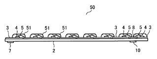
- Sectional drawing which shows an example of the linear white light source of this invention The top view of the linear white light source shown in FIG. The top view of the back surface side of the linear white light source shown in FIG. The partial expanded sectional view of the linear white light source shown in FIG. The top view which shows the other example of the linear white light source of this invention. The partially expanded sectional view which shows the other example of the linear white light source of this invention. Sectional drawing which shows the manufacture example of the linear white light source of this invention. Sectional drawing which shows the other manufacture example of the linear white light source of this invention. Sectional drawing which shows an example of the backlight of this invention. Sectional drawing which shows an example of the liquid crystal display device of this invention. Sectional drawing which shows the linear white light source produced by the comparative example. The top view which showed the measuring method of the brightness
- FIG. 1 is a cross-sectional view showing an example of a linear white light source 1 of the present invention
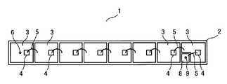
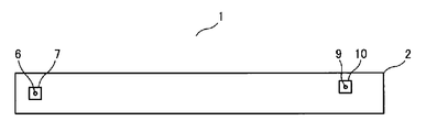
- FIG. 2 is a plan view showing a light emitting surface side of the linear white light source 1 shown in FIG. 1, and FIG. It is the top view which showed the non-light-emitting surface side (back surface side) of the linear white light source 1 shown in FIG.
- the phosphor layer is omitted so that the inside can be seen.
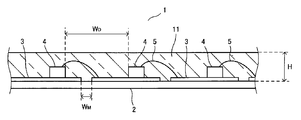
- FIG. 4 is an enlarged cross-sectional view showing a part of the linear white light source 1 shown in FIG.
- the linear white light source 1 of the present invention has a rectangular base 2 as shown in FIGS. 1 and 2, for example, and a plurality of, for example, a substantially square shape is provided on the base 2 along the longitudinal direction thereof.
- a metal pattern 3 is formed.
- a light emitting diode chip 4 (hereinafter simply referred to as a light emitting diode chip 4) that generates ultraviolet light having a wavelength of 330 nm or more and 410 nm or less is mounted.
- each light emitting diode chip 4 is electrically connected to the metal pattern 3 on which it is mounted.
- the upper electrode of each light emitting diode chip 4 is adjacent to the metal pattern 3 adjacent to the metal pattern 3 on which they are mounted (in FIGS. 1 and 2, adjacent to the right side of the metal pattern 3 on which each light emitting diode chip 4 is mounted).
- the metal pattern 3) is electrically connected by a conductive wire 5.
- the metal pattern 3 formed on one end side (left side in FIGS. 1 and 2) of the base 2 is connected via a via conductor 6 penetrating the base 2 in the front-back direction as shown in FIG. 2, for example. As shown in FIG. 3, it is electrically connected to an electrode pad 7 formed on the back side of the base 2.
- the metal pattern 3 on the other end side (right side in FIGS. 1 and 2) of the base body 2 has a shape lacking a part of a substantially square shape as shown in FIG. 2, for example.
- a substantially square electrode pad 8 is formed in the portion.
- the electrode pad 8 is connected to the conductive wire 5 from the upper electrode of the light emitting diode chip 4 mounted on the metal pattern 3.
- the electrode pad 8 is electrically connected to an electrode pad 10 formed on the back surface side of the base body 2 as shown in FIG. 3 via via conductors 9 penetrating the base body 2 in the front and back direction.
- a phosphor layer 11 is continuously formed on the side of the base 2 on which the metal pattern 3 and the light-emitting diode chip 4 are mounted so as to cover almost the entire metal pattern 3 and light-emitting diode chip 4. Is formed. That is, the phosphor layer 11 is shared by the plurality of light emitting diode chips 4.
- the phosphor layer 11 is made of a transparent resin containing a red light-emitting phosphor, a green light-emitting phosphor, and a blue light-emitting phosphor.
- a linear white light source 1 of the present invention a plurality of light emitting diode chips 4 arranged in a line are electrically connected through the metal patterns 3 and the conductive wires 5.
- ultraviolet light having a wavelength of 330 nm or more and 410 nm or less can be generated from each light emitting diode chip 4.
- the phosphor layer 11 contains a red light emitting phosphor, a green light emitting phosphor and a blue light emitting phosphor
- the phosphor layer 11 is excited by ultraviolet light having a wavelength of 330 nm or more and 410 nm or less generated from the light emitting diode chip 4. Red light, green light, and blue light are emitted, and by mixing these colors, white light can be obtained as the entire linear white light source 1.
- linear white light source 1 of the present invention in particular, a plurality of light emitting diode chips 4 are arranged in a line, and a phosphor layer 11 is continuously provided so as to cover the whole of the plurality of light emitting diode chips 4.
- a phosphor layer 11 is continuously provided so as to cover the whole of the plurality of light emitting diode chips 4.
- shape of the linear white light source 1 is similar to that of a conventional cold cathode tube or the like, a new optical design is applied to illumination or backlight using the conventional cold cathode tube or the like. It can use suitably, without doing.
- the substrate 2 in the linear white light source 1 of the present invention is made of, for example, an aluminum oxide sintered body, an aluminum nitride sintered body, a mullite sintered body, ceramics such as glass ceramics, or a glass insulator such as silica. It consists of It is preferable that the substrate 2 has a coefficient of thermal expansion comparable to that of the light emitting diode chip 4. Further, from the viewpoint of thermal conductivity, it is more preferable if it is made of an aluminum nitride sintered body.
- An aluminum nitride sintered body can provide a sintered body having a thermal conductivity of 200 W / m ⁇ K or more.
- the metal pattern 3 is used for supplying electric power to each light emitting diode chip 4 and has a role as a reflective layer.
- the planar shape of the metal pattern 3 is not particularly limited, but is preferably a large area from the viewpoint of functioning as a reflective layer. For example, a substantially square shape as shown in FIG. 2 ensures a large area. Is preferable.
- the interval between adjacent metal patterns 3 can be reduced to, for example, about 0.03 mm.
- the number of metal patterns 3 and the positions to be formed are appropriately determined according to the number of LED chips 4, the arrangement interval, and the like because the metal pattern 3 is mounted with the LED chips 4. is there.
- the metal pattern 3 is used as a power supply means to the light emitting diode chip 4 and a reflective layer, the metal pattern 3 is made of at least one metal selected from, for example, Au, Al, Ag, Pt, Ti, and Ni. preferable.
- the metal pattern 3 does not necessarily have to be a single layer.
- a Ti layer is first provided on the substrate 2, and a layer of Au, Al, Ag, Pt or the like is provided thereon. It is good also as what provided.
- the light emitting diode chip 4 is mounted on the surface portion of the metal pattern 3 and a gold pad is provided at a position connected to the lower electrode.
- the electrode pad 8 formed on the light emitting surface side of the substrate 1 and the electrode pads 7 and 10 formed on the back surface side as shown in FIG. 3 are also made of a metal material substantially the same as the metal pattern 3. can do.
- the light emitting diode chip 4 used in the present invention emits ultraviolet light having a wavelength of 330 nm or more and 410 nm or less.
- the type of the light-emitting diode chip 4 is not particularly limited as long as it can generate ultraviolet light having the above-described wavelength, and includes, for example, an In x Ga 1-x N system. The well-known thing can be used.
- the distance (W D ) is not particularly limited, but the power consumption due to the improvement of the arrangement density. From the viewpoint of suppressing an increase in the thickness, it is preferably 1 mm or more.
- the interval (W D ) is the distance between the opposing ends of the adjacent light emitting diode chips 4 as shown in FIG.
- the phosphor layer 11 is provided not only on the top surface and side surface of each light emitting diode chip 4 but also on the space between adjacent light emitting diode chips 4, so that such a relatively wide space of 1 mm or more ( Even when the light emitting diode chip 4 is provided with a gap (W D ), it is possible to reduce the difference in luminance between the portion where the light emitting diode chip 4 is arranged and the space between them, and to suppress luminance unevenness. Become.
- the distance (W D) of and how light-emitting diode chips 4 adjacent is preferably set to 5mm or less.
- the number of light emitting diode chips 4 mounted on the substrate 2 may be two or more. However, from the viewpoint of using as a light source instead of a conventional cold cathode tube or the like, a certain number of light emitting diode chips 4 are collected. Is preferably mounted. For example, it is preferable that five or more light emitting diode chips 4 are mounted.
- the upper limit of the number of light-emitting diode chips 4 mounted on the substrate 2 is not necessarily limited, and the number can be appropriately increased by changing the size of the substrate 2. In consideration of handling of the linear white light source, the number of chips is preferably 10 or less.
- the phosphor layer 11 is made of a transparent resin containing a red light-emitting phosphor, a green light-emitting phosphor, and a blue light-emitting phosphor.
- the phosphor layer 11 preferably has a height (H) of 0.5 mm or more from the surface of the base 2 to the surface of the phosphor layer 11 at least in a portion where the light emitting diode chip 4 is disposed. If the height (H) of the phosphor layer 11 is less than the above height, there is a possibility that sufficient white light cannot be obtained, which is not preferable. Moreover, since the brightness
- the transparent resin constituting the phosphor layer 11 for example, an acrylic resin, an epoxy resin, a silicone resin, a polyimide resin, or the like is used.
- red phosphor powder that emits red light having a peak wavelength of 620 nm or more and 780 nm or less is used as the red light emitting phosphor.
- red phosphor powder made of europium-activated lanthanum oxysulfide having a composition represented by the following formula (1) and a red phosphor powder having a composition represented by the following formula (2) is used. .
- M is at least one element selected from Sb, Sm, Ga and Sn, and x and y are values satisfying 0.01 ⁇ x ⁇ 0.15 and 0 ⁇ y ⁇ 0.03. .
- M is at least one element selected from Sb, Sm, Ga and Sn because the luminous efficiency of the red phosphor powder is high.
- x is in the above range because the wavelength range of light from the red phosphor powder is appropriate, the emission efficiency is high, and the balance between the wavelength range and the emission efficiency is good.
- the light from the red phosphor powder tends to have a shorter wavelength, and as the x decreases within the above range, the luminous efficiency of the red phosphor powder tends to increase.
- green phosphor powder that emits green light having a peak wavelength of 490 nm to 575 nm is used.
- a europium manganese activated aluminate having a composition represented by the following formula (3) and a green phosphor powder having a composition represented by the following formula (4) is used.
- z and u are each in the above-mentioned range because the green phosphor powder has high luminous efficiency. It is preferable that x and y are within the above ranges because the green phosphor powder has a good balance between the lifetime and the luminance. If x is 0.2 or more, the life of the green phosphor powder may be reduced, and if x is 0, the short wavelength component of the light from the green phosphor powder may increase and the luminance may be reduced. .
- x is in the above range because the wavelength of light from the green phosphor powder is suitable for a backlight. As x increases within the above range, the wavelength of the light from the green phosphor powder becomes shorter and more suitable for backlight use. Moreover, it is preferable for y to be in the above range because Mn is sufficiently dissolved in the green phosphor powder. Furthermore, it is preferable that z is in the above range because the luminous efficiency of the green phosphor powder is high. Moreover, it is preferable that u is in the above range because the wavelength of light from the green phosphor powder is suitable for backlight.
- a blue phosphor powder that emits blue light having a peak wavelength of 430 nm to 460 nm is used.
- a blue phosphor powder having a composition represented by the following formula (5) is used.
- x and y are in the above ranges because the wavelength of light from the blue phosphor powder is suitable for a white light source for backlight use.
- z is in the above range because the luminous efficiency of the blue phosphor powder is high.
- red light emitting phosphors for example, Eu-activated yttrium oxysulfide phosphors, Cu and Mn activated zinc sulfide phosphors, and as green light emitting phosphors, for example, Cu and Al activated zinc sulfide phosphors
- green light emitting phosphors for example, Cu and Al activated zinc sulfide phosphors
- Eu-activated aluminate phosphor, Eu-activated alkaline earth silicate, Eu / Mn-activated alkaline earth magnesium silicate, or the like is used as a blue light-emitting phosphor, it is suitable as a white light source. Shows color reproducibility and luminance characteristics.
- the phosphor content in the phosphor layer 11 is preferably 20 to 70% by mass. If the content is less than 20% by mass, the phosphor amount may be insufficient. On the other hand, if it exceeds 70% by mass, it may be difficult to uniformly mix phosphors of respective colors. On the other hand, if the phosphor content exceeds 90% by mass, the light from the light emitting diode may not be uniformly transmitted into the phosphor layer. Further, the luminance unevenness can be improved to 50% or more by adjusting the phosphor amount.
- luminance unevenness can be suppressed while improving luminance.
- the luminance unevenness can be suppressed to 1% or more while the efficiency on the light emitting surface is set to 20 lm / W or more.
- the luminance is measured at the portion where each light emitting diode chip 4 is mounted and at each intermediate portion between adjacent light emitting diode chips 4, and the lowest luminance among them is set as the minimum luminance value, and the highest luminance is obtained. Is the maximum luminance.
- the linear white light source 1 of the present invention is not necessarily limited to that shown in FIG. 1 and the like, for example, the one shown in FIG. As shown in FIG. 5, three units may be arranged in a line. In this case, adjacent units are connected to one unit electrode pad 10 and the other adjacent unit part electrode pad 7 by various electrical connection means 12.
- the unit number to connect is not necessarily restricted to such a unit number.
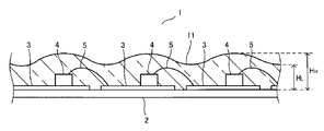
- the linear white light source 1 of the present invention is mounted with a light emitting diode chip 4 as shown in FIG. 6, for example, in addition to the surface of the phosphor layer 11 being flat as shown in FIG.
- the portion of the phosphor layer 11 may be convex and high in height, and the portion of the phosphor layer 11 between adjacent light emitting diode chips 4 may be concave and low in height. . By doing in this way, it can be set as the linear white light source 1 excellent in light extraction efficiency, for example.
- the height (recess height) from the surface of the substrate 2 to the recess surface of the phosphor layer 11 with respect to the height from the surface of the substrate 2 to the protrusion surface of the phosphor layer 11 is preferably 50% or more.
- the height ratio is less than the above value, the height of the phosphor layer 11 in the space between adjacent light emitting diode chips 4 is too low, and the effect of suppressing luminance unevenness may not be sufficient. Absent.
- the convex height (H H) is 1mm or more, it is preferable to 2mm or less.
- a method for manufacturing the linear white light source 1 of the present invention will be described.
- a plurality of substantially square metal patterns 3 are formed on the substrate 2.
- the method for forming the metal pattern 3 on the substrate 2 is not particularly limited, and can be formed using a known metallization method. Note that the planar shape, the number of formed metal patterns 3 and the like are appropriately determined according to the number of light-emitting diode chips 4 mounted.
- a well-known eutectic metal such as Au, Pb / Sn, Au / Sn, Au / Ge, Au / Sn / Ge, Au / Pb / Sn or Cu / Pb / Sn is formed on each metal pattern 3.
- the upper electrode of each light emitting diode chip 4 and the metal pattern 3 adjacent to the metal pattern 3 on which the light emitting diode chip 4 is mounted are connected by the conductive wire 5. .
- the phosphor layer 11 is formed on the substrate 2 on which the metal pattern 3 and the light emitting diode chip 4 are mounted. That is, first, as a resin composition used to form the phosphor layer 11 (hereinafter simply referred to as a resin composition), a red light emitting fluorescence is applied to a transparent resin such as an acrylic resin, an epoxy resin, a silicone resin, or a polyimide resin. Body, green light emitting phosphor and blue light emitting phosphor are mixed and dispersed.
- a resin composition used to form the phosphor layer 11 hereinafter simply referred to as a resin composition
- a red light emitting fluorescence is applied to a transparent resin such as an acrylic resin, an epoxy resin, a silicone resin, or a polyimide resin.
- Body, green light emitting phosphor and blue light emitting phosphor are mixed and dispersed.
- this resin composition is injected into, for example, a dispenser, and the resin composition is discharged from the dispenser from one end side to the other end side of the substrate 2 on which the metal pattern 3 or the light emitting diode chip 4 is mounted. Then, the phosphor layer 11 is continuously formed by curing the coating and moving the coating.
- the mold 20 is filled with the resin composition 21 as described above, and the metal pattern 3 and the light-emitting diode chip 4 are formed.
- the substrate 2 mounted is inserted into the mold 20 with the side on which the metal pattern 3 or the light-emitting diode chip 4 is mounted facing the mold 20, and the resin composition 21 is cured in this state to fluoresce.
- the body layer 11 can be formed continuously.
- the resin composition 21 is filled, and the base body 2 on which the metal pattern 3 and the light-emitting diode chip 4 are mounted faces the mold frame 22 with the side on which the metal pattern 3 and the light-emitting diode chip 4 are mounted facing the mold frame 22 side. It inserts in and the resin composition 21 is hardened in the state.
- the light emitting diode chip 4 is formed in the linear white light source 1 finally obtained as shown in FIG.
- the mounted phosphor layer 11 has a convex shape, and the phosphor layer 11 in the space between adjacent light emitting diode chips 4 has a concave shape.
- Such a linear white light source 1 of the present invention is suitably used as a light source of a backlight.
- the light emitting device 1 of the present invention is linear and has a shape similar to that of a conventional cold cathode tube or the like, a new optical design is made for illumination or backlight using the conventional cold cathode tube or the like. It can use suitably, without.
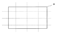
- FIG. 9 shows a sidelight type backlight 30 as an example of the backlight of the present invention.
- the sidelight type backlight 30 is mainly composed of a linear white light source 1 and a light guide plate 31.
- the light guide plate 31 has a substantially plate shape whose thickness gradually decreases from the incident surface 32 side as one side surface to the other side surface, and the linear white light source 1 of the present invention is disposed on the incident surface 32. Yes.
- a reflective layer 33 is provided on the side of the light guide plate 31 opposite to the light emitting surface.
- FIG. 10 shows an example of the liquid crystal display device 40 of the present invention, in which the above-described sidelight-type backlight 30 of the present invention is used as the light source. Since the linear white light source of the present invention can provide a linear light source with improved luminance unevenness despite the use of a light emitting diode, the light guide plate used in the CCFL is used as it is even when applied to a sidelight type backlight. Since it is applicable, it is not necessary to change the design of the light guide plate.
- the liquid crystal display device 40 includes, for example, a flat liquid crystal panel 41 as a display means and a sidelight type backlight 30 that illuminates the liquid crystal panel 41 from the back.
- a flat liquid crystal panel 41 for example, an array substrate, which is a glass plate on which transparent electrodes are formed, and a color filter substrate are arranged to face each other between two polarizing plates, and a liquid crystal is placed between the array substrate and the color filter substrate.
- a liquid crystal layer is formed by injection.
- red (R), green (G), and blue (B) color filters are formed corresponding to each pixel.
- Examples 1 to 10 Using a base 2 (aluminum nitride sintered body having a thermal conductivity of 200 W / m ⁇ K) having a length of 18 mm, a width of 2 mm, and a thickness of 0.635 mm, a plurality of substantially Ti / Pt / Au layers on the surface thereof. A square metal pattern 3 was formed. The number of metal patterns 3 formed was adjusted to the number of light-emitting diode chips 4 to be described later, and the interval (W M ) between adjacent metal patterns 3 was 0.1 mm. Further, the electrode pad 7 and the electrode pad 10 were formed on the back surface side of the substrate 2.
- a light emitting diode chip 4 that emits ultraviolet light having an excitation wavelength of 390 nm was joined on each metal pattern 3, and the lower electrode of the light emitting diode chip 4 and the metal pattern 3 were electrically connected. Furthermore, the upper electrode of each light emitting diode chip 4 and the metal pattern 3 adjacent to the metal pattern 3 on which the light emitting diode chip 4 is mounted are electrically connected by a conductive wire 5.
- the size of the light-emitting diode chip 4 is 0.4 mm long ⁇ 0.4 mm wide ⁇ 0.2 mm high, and the height from the surface of the substrate 2 to the top surface of the light-emitting diode chip 4 is 0.2 mm.
- the number of light-emitting diode chips 4 mounted and the interval (W D ) between adjacent light-emitting diode chips 4 were as shown in Table 1.
- the phosphor layer 11 was formed on the base 2 on which the light emitting diode chip 4 was mounted. Specifically, europium-activated alkaline earth chlorophosphate (Sr 0.99 Eu 0.01 ) 10 (PO 4 ) 6 ⁇ Cl 2 is used as the blue phosphor, and europium and manganese-activated aluminate phosphors as the green phosphor.
- a mold 20 having a flat inner bottom as shown in FIG. 7 or a mold 22 having a concavo-convex portion at the inner bottom as shown in FIG. 8 is used, and the resin composition 21 for forming the phosphor layer is formed therein. Filled. Further, the base body 2 on which the light emitting diode chip 4 is mounted in the mold 20 or 22 is inserted with the side on which the light emitting diode chip 4 or the like is mounted facing the mold 20 or 22 side.
- the resin composition 21 for forming the phosphor layer is cured to form the phosphor layer 11 on the substrate 2 on which the light emitting diode chip 4 and the like are mounted, and the phosphor layer 11 as shown in FIG.
- Table 1 shows the height from the phosphor layer 11 to the convex surface (H H ) and the height to the concave surface (H L ).
- Example 11 A linear white light source was produced in the same manner as in Example 1 except that the type and content of the phosphor used were changed. That is, (Sr 0.01 Ca 0.99 ) SiAlN 3 : Eu as a red phosphor, (Sr 1.58 Ba 0.11 Mg 0.2 Eu 0.1 Mn 0.01 ) SiO 4 as a green phosphor, (Sr 0.85 Ba 0.01 Ca 0.09 Eu 0.05 ) 10 (PO 4 ) 3 Cl as a blue phosphor was mixed with a silicone resin at a concentration of 30% by mass to obtain a slurry. And these slurry was mixed in the ratio of 30 mass%, 40 mass%, and 30 mass%, and it was set as the resin composition for fluorescent substance layer formation.
- Comparative Example 1 In the same manner as in Example 1, the light emitting diode chip 4 was mounted, and the conductive wire 5 was formed. Then, a phosphor layer forming resin composition similar to that used in Examples 1 to 10 was poured into a dispenser, and the resin composition of the phosphor layer forming resin composition was discharged from this dispenser. 11, the phosphor layer 51 was formed only on the periphery of the light-emitting diode chip 4 to obtain a linear white light source 50.
- the range (plane direction) in which the phosphor layer 51 is formed in Comparative Example 1 is from the end of each light emitting diode chip 4 to a range of 0.6 mm, and the height from the surface of the substrate 2 to the surface of the phosphor layer 50 is high.
- the thickness was 1.2 mm.
- the same reference numerals as those in the embodiment are attached to the portions indicating the same portions as in the embodiment.
- the luminance and luminance unevenness of the linear white light source 1 of the example and the linear white light source 50 of the comparative example were measured.
- the luminance was measured using a luminance meter for the portion where each light emitting diode chip 4 was mounted, and the maximum value of the measured luminance was taken.
- the luminance unevenness is calculated by the following equation by measuring the luminance of the portion where each light-emitting diode chip 4 is mounted and the luminance of the intermediate portion of the adjacent light-emitting diode chips 4 from the maximum value and the minimum value of the luminance. did.
- the results are shown in Table 1.
- Luminance unevenness (minimum luminance value / maximum luminance value) x 100 [%]
- Comparative Example 1 is a point light source, there are portions that shine and portions that do not shine.
- Examples 12 to 22, Comparative Example 2 Using the linear white light source 1 of Examples 1 to 11, sidelight type backlights 30 of Examples 12 to 22 as shown in FIG. 9 were produced.
- the sidelight type backlight 30 is for an 8-inch liquid crystal display device.
- 10 linear white light sources were arranged vertically to form a linear light source for 8 inches.
- a sidelight type backlight was similarly produced using the linear white light source 50 of Comparative Example 1.
- the measurement of luminance unevenness was performed as follows. That is, first, as shown in FIG. 12, with respect to the light-emitting surface of the sidelight-type backlight 30, a center line is drawn at the center in the vertical and horizontal directions, and an equal line is drawn on both sides thereof. ) As a measurement point. Then, the intersection between the center lines in the vertical and horizontal directions was measured with a luminance meter to obtain the central luminance.
- the luminance of the remaining eight locations was measured with a luminance meter, and the luminance unevenness was calculated by the following formula using the luminance that had the largest difference compared to the central luminance. Note that the luminance unevenness is closer to 100%, which is preferable because the luminance difference between portions on the light emitting surface decreases.
- Luminance unevenness (Luminance with the greatest difference compared to the central luminance / central luminance) x 100 [%]
- the center luminance is high and the luminance unevenness on the light emitting surface is also effectively suppressed. Is recognized. Further, since the linear light source according to the present embodiment is a linear light source, it can be replaced without changing the design of the light guide plate from the conventional CCFL. On the other hand, in the comparative example, the luminance unevenness is bad and the design of the light guide plate needs to be changed in order to apply it to the sidelight type backlight.
- the linear white light source of the present invention covers a substrate, a plurality of light emitting diode chips arranged linearly on the substrate, and generating ultraviolet light having a wavelength of 330 nm or more and 410 nm or less, and the plurality of light emitting diode chips. And a phosphor layer containing a red light emitting phosphor, a green light emitting phosphor and a blue light emitting phosphor. With such a configuration, luminance unevenness on the light-emitting surface is suppressed, and it is excellent in manufacturability and can be suitably used in place of a conventional cold cathode tube or the like. Can be used effectively.
- SYMBOLS 1 Linear white light source, 2 ... Base
Abstract
A linear white light source (1) is provided with a base body (2); a plurality of light emitting diode chips (4) which are linearly arranged on the base body (2) and generate ultraviolet rays having a wavelength of 330nm or more but not more than 410nm; and a phosphor layer (11), which is continuously formed to cover the light emitting diode chips (4) and contains a red light emitting fluorescent material, a green light emitting fluorescent material and a blue light emitting fluorescent material.
Description
本発明は、線状白色光源ならびにそれを用いたバックライトおよび液晶表示装置に係り、特に紫外光を発生する複数の発光ダイオードチップが線状に配置されてなる線状白色光源ならびにそれを用いたバックライトおよび液晶表示装置に関する。
The present invention relates to a linear white light source, and a backlight and a liquid crystal display device using the linear white light source, and in particular, a linear white light source in which a plurality of light emitting diode chips generating ultraviolet light are linearly arranged and the same are used. The present invention relates to a backlight and a liquid crystal display device.
従来、液晶表示装置等におけるバックライトの光源として冷陰極管(CCFL:Cold Cathode Fluorescent Lamp)が用いられている。しかし、バックライトの光源として冷陰極管を用いた場合、色再現性が低く、また水銀を使用していることから環境負荷が大きい等の課題がある。
Conventionally, a cold cathode tube (CCFL: Cold Cathode Fluorescent Lamp) is used as a light source of a backlight in a liquid crystal display device or the like. However, when a cold cathode tube is used as the light source of the backlight, there are problems such as low color reproducibility and high environmental load due to the use of mercury.
一方、近年、青色発光ダイオードチップや紫外発光できる発光ダイオードチップが開発・商品化され、LED照明が盛んに開発されるようになっている。LED照明には、B-発光ダイオードチップと黄色発光する蛍光体とを組み合わせる方式、R-発光ダイオードチップ、G-発光ダイオードチップおよびB-発光ダイオードチップの光を混合する方式、紫外発光するUV-発光ダイオードチップとRGB蛍光体とを組み合わせる方式の3方式がある。前2者はそれぞれ、色再現性、色制御・色混合の点において課題があり、UV-発光ダイオードチップ+RGB蛍光体方式に期待が高まっている。
On the other hand, in recent years, blue light emitting diode chips and light emitting diode chips capable of emitting ultraviolet light have been developed and commercialized, and LED lighting has been actively developed. For LED lighting, a method in which a B-light emitting diode chip and a phosphor emitting yellow light are combined, a method in which light from an R-light emitting diode chip, a G-light emitting diode chip, and a B-light emitting diode chip are mixed, a UV-light emitting UV- There are three methods of combining light emitting diode chips and RGB phosphors. The former two have problems in terms of color reproducibility, color control, and color mixing, and expectations are rising for the UV-light emitting diode chip + RGB phosphor system.
発光ダイオードチップを用いた光源は長寿命でかつ信頼性が高く、交換作業等が軽減されることから、各種表示装置の構成部品として期待されている。光源から放射される光の色調は発光ダイオードチップの発光波長に限られるものではなく、発光ダイオードチップの表面などに形成される蛍光体層中に含有される蛍光体の種類により、青色から赤色まで使用用途に応じた可視光領域の光を得ることができる。特に、白色発光型の光源は携帯通信機器の液晶表示装置やPCの液晶表示装置等のバックライトの光源として期待されている。
A light source using a light-emitting diode chip is expected to be a component of various display devices because it has a long life and high reliability, and reduces replacement work. The color tone of the light emitted from the light source is not limited to the emission wavelength of the light-emitting diode chip, but from blue to red depending on the type of phosphor contained in the phosphor layer formed on the surface of the light-emitting diode chip. Light in the visible light region according to the intended use can be obtained. In particular, a white light-emitting light source is expected as a light source for a backlight of a liquid crystal display device of a mobile communication device or a liquid crystal display device of a PC.
バックライトは光源を配置する位置により主として直下型バックライトとサイドライト型バックライトとに分けられ、用途に応じて使い分けられている。このうちサイドライト型バックライトは、導光板の入射面となる側面に光源が配置されている。サイドライト型バックライトの光源としては、例えば導光板の入射側面に所定の間隔をあけて配置される複数の発光ダイオードが知られている(例えば、特許文献1参照。)。
¡Backlights are mainly divided into direct type backlights and sidelight type backlights depending on the position where the light source is arranged, and they are properly used according to the application. Among these, the sidelight type backlight has a light source disposed on a side surface that serves as an incident surface of the light guide plate. As a light source of a sidelight type backlight, for example, a plurality of light emitting diodes arranged at predetermined intervals on an incident side surface of a light guide plate is known (see, for example, Patent Document 1).
しかしながら、上記したような発光ダイオードチップを用いた光源は、励起光源である発光ダイオードチップの大きさが1mm□以下であるため、その上に蛍光体層を形成したとしてもほぼ点光源となってしまう。このため、照明やバックライト等の光源として用いる場合、レンズ状の透明樹脂層や拡散シート等を設けて放射される光を分散させる必要がある。
However, a light source using a light emitting diode chip as described above is almost a point light source even if a phosphor layer is formed thereon because the size of the light emitting diode chip as an excitation light source is 1 mm □ or less. End up. For this reason, when using as light sources, such as illumination and a backlight, it is necessary to disperse | distribute the emitted light by providing a lens-shaped transparent resin layer, a diffusion sheet, etc.
また、このようなレンズ状の透明樹脂層や拡散シート等を設けた場合であっても、必ずしも発光ダイオードチップを設けた部分とそれらの間の部分との輝度の差を十分に小さくすることはできず、このようなレンズ状の透明樹脂層や拡散シート等を設ける工程が必要となることから製造性も低下する。さらに、従来の冷陰極管の代わりに照明やバックライト等の光源として用いる場合、その形状が冷陰極管の形状とは異なることから、照明やバックライト等において新たな光学設計が必要となる。
Moreover, even when such a lens-like transparent resin layer, a diffusion sheet, etc. are provided, it is not always possible to sufficiently reduce the difference in luminance between the portion where the light emitting diode chip is provided and the portion between them. However, since a process of providing such a lens-like transparent resin layer, a diffusion sheet and the like is necessary, the productivity is also lowered. Further, when the light source is used as a light source such as an illumination or a backlight instead of the conventional cold cathode tube, since the shape thereof is different from the shape of the cold cathode tube, a new optical design is required for the illumination and the backlight.
本発明の目的は、発光面における輝度ムラが抑制されると共に、製造が容易であり、従来の冷陰極管等の代わりに好適に用いられる線状白色光源を提供することにある。また、本発明の目的は、このような線状白色光源を光源として用いたバックライト、液晶表示装置を提供することにある。
An object of the present invention is to provide a linear white light source that can suppress luminance unevenness on a light emitting surface, is easy to manufacture, and is preferably used in place of a conventional cold cathode tube or the like. Another object of the present invention is to provide a backlight and a liquid crystal display device using such a linear white light source as a light source.
本発明の線状白色光源は、基体と、前記基体上に線状に配置され、波長330nm以上、410nm以下の紫外光を発生する複数の発光ダイオードチップと、前記複数の発光ダイオードチップを覆うように連続して形成され、赤色発光蛍光体、緑色発光蛍光体および青色発光蛍光体を含有する蛍光体層と、を有することを特徴としている。
The linear white light source of the present invention covers a base, a plurality of light-emitting diode chips arranged linearly on the base and generating ultraviolet light having a wavelength of 330 nm or more and 410 nm or less, and the plurality of light-emitting diode chips. And a phosphor layer containing a red light-emitting phosphor, a green light-emitting phosphor, and a blue light-emitting phosphor.
本発明のバックライトは、白色光を発光する線状の光源を具備するバックライトであって、この光源として上記したような本発明の線状白色光源を用いることを特徴としている。
The backlight of the present invention is a backlight having a linear light source that emits white light, and is characterized by using the linear white light source of the present invention as described above.
また、本発明の液晶表示装置は、バックライトを具備する液晶表示装置であって、このバックライトとして上記したような本発明のバックライトを具備することを特徴としている。
The liquid crystal display device of the present invention is a liquid crystal display device having a backlight, and is characterized by including the backlight of the present invention as described above.
以下、本発明の線状白色光源について説明する。図1は本発明の線状白色光源1の一例を示した断面図であり、図2は図1に示す線状白色光源1の発光面側を示した平面図であり、図3は図1に示す線状白色光源1の非発光面側(裏面側)を示した平面図である。なお、図2については、内部の様子が見えるように蛍光体層を省略して図示している。また、図4は図1に示す線状白色光源1の一部を拡大して示した断面図である。
Hereinafter, the linear white light source of the present invention will be described. 1 is a cross-sectional view showing an example of a linear white light source 1 of the present invention, FIG. 2 is a plan view showing a light emitting surface side of the linear white light source 1 shown in FIG. 1, and FIG. It is the top view which showed the non-light-emitting surface side (back surface side) of the linear white light source 1 shown in FIG. In FIG. 2, the phosphor layer is omitted so that the inside can be seen. FIG. 4 is an enlarged cross-sectional view showing a part of the linear white light source 1 shown in FIG.
本発明の線状白色光源1は、例えば図1、2に示すように、長方形状の基体2を有するものであり、この基体2上にはその長手方向に沿って例えば略正方形状の複数の金属パターン3が形成されている。また、各金属パターン3上には波長330nm以上、410nm以下の紫外光を発生する発光ダイオードチップ4(以下、単に発光ダイオードチップ4と呼ぶ。)が搭載されている。
The linear white light source 1 of the present invention has a rectangular base 2 as shown in FIGS. 1 and 2, for example, and a plurality of, for example, a substantially square shape is provided on the base 2 along the longitudinal direction thereof. A metal pattern 3 is formed. On each metal pattern 3, a light emitting diode chip 4 (hereinafter simply referred to as a light emitting diode chip 4) that generates ultraviolet light having a wavelength of 330 nm or more and 410 nm or less is mounted.
各発光ダイオードチップ4の下部電極はそれが搭載される金属パターン3と電気的に接続されている。また、各発光ダイオードチップ4の上部電極はそれらが搭載される金属パターン3に隣接する金属パターン3(図1、2においては、各発光ダイオードチップ4が搭載される金属パターン3の右側に隣接する金属パターン3)に導電性ワイヤ5により電気的に接続されている。
The lower electrode of each light emitting diode chip 4 is electrically connected to the metal pattern 3 on which it is mounted. The upper electrode of each light emitting diode chip 4 is adjacent to the metal pattern 3 adjacent to the metal pattern 3 on which they are mounted (in FIGS. 1 and 2, adjacent to the right side of the metal pattern 3 on which each light emitting diode chip 4 is mounted). The metal pattern 3) is electrically connected by a conductive wire 5.
なお、基体2の一方の端部側(図1、2中、左側)に形成される金属パターン3については、例えば図2に示すように基体2を表裏方向に貫通するビア導体6を介して、図3に示すように基体2の裏面側に形成された電極パッド7に電気的に接続されている。
Note that the metal pattern 3 formed on one end side (left side in FIGS. 1 and 2) of the base 2 is connected via a via conductor 6 penetrating the base 2 in the front-back direction as shown in FIG. 2, for example. As shown in FIG. 3, it is electrically connected to an electrode pad 7 formed on the back side of the base 2.
一方、基体2の他方の端部側(図1、2中、右側)の金属パターン3については、例えば図2に示すように略正方形状の一部を欠いた形状とされており、その欠落部分に略正方形状の電極パッド8が形成されている。そして、この電極パッド8には当該金属パターン3に搭載されている発光ダイオードチップ4の上部電極からの導電性ワイヤ5が接続されている。さらに、電極パッド8は、基体2を表裏方向に貫通するビア導体9を介して、図3に示すように基体2の裏面側に形成された電極パッド10に電気的に接続されている。
On the other hand, the metal pattern 3 on the other end side (right side in FIGS. 1 and 2) of the base body 2 has a shape lacking a part of a substantially square shape as shown in FIG. 2, for example. A substantially square electrode pad 8 is formed in the portion. The electrode pad 8 is connected to the conductive wire 5 from the upper electrode of the light emitting diode chip 4 mounted on the metal pattern 3. Furthermore, the electrode pad 8 is electrically connected to an electrode pad 10 formed on the back surface side of the base body 2 as shown in FIG. 3 via via conductors 9 penetrating the base body 2 in the front and back direction.
また、図1に示すように基体2の金属パターン3や発光ダイオードチップ4が搭載された側には、これら金属パターン3や発光ダイオードチップ4のほぼ全体を覆うように蛍光体層11が連続的に形成されている。すなわち、蛍光体層11は複数の発光ダイオードチップ4により共有されている。この蛍光体層11は、透明樹脂に赤色発光蛍光体、緑色発光蛍光体および青色発光蛍光体が含有されたものである。
Further, as shown in FIG. 1, a phosphor layer 11 is continuously formed on the side of the base 2 on which the metal pattern 3 and the light-emitting diode chip 4 are mounted so as to cover almost the entire metal pattern 3 and light-emitting diode chip 4. Is formed. That is, the phosphor layer 11 is shared by the plurality of light emitting diode chips 4. The phosphor layer 11 is made of a transparent resin containing a red light-emitting phosphor, a green light-emitting phosphor, and a blue light-emitting phosphor.
このような本発明の線状白色光源1については、線状に配置された複数の発光ダイオードチップ4が各金属パターン3や導電性ワイヤ5を介することによって電気的に接続されているため、基体2の裏面側に形成されている電極パッド7と電極パッド10とを電源に接続することで、各発光ダイオードチップ4から波長330nm以上、410nm以下の紫外光を発生させることができる。
In such a linear white light source 1 of the present invention, a plurality of light emitting diode chips 4 arranged in a line are electrically connected through the metal patterns 3 and the conductive wires 5. By connecting the electrode pad 7 and the electrode pad 10 formed on the back surface side of 2 to a power source, ultraviolet light having a wavelength of 330 nm or more and 410 nm or less can be generated from each light emitting diode chip 4.
また、蛍光体層11には赤色発光蛍光体、緑色発光蛍光体および青色発光蛍光体が含まれているため、発光ダイオードチップ4から発生された波長330nm以上、410nm以下の紫外光により励起されて赤色光、緑色光および青色光が発光され、これらの混色により線状白色光源1全体として白色光を得ることができる。
Further, since the phosphor layer 11 contains a red light emitting phosphor, a green light emitting phosphor and a blue light emitting phosphor, the phosphor layer 11 is excited by ultraviolet light having a wavelength of 330 nm or more and 410 nm or less generated from the light emitting diode chip 4. Red light, green light, and blue light are emitted, and by mixing these colors, white light can be obtained as the entire linear white light source 1.
本発明の線状白色光源1については、特に複数の発光ダイオードチップ4を線状に配置すると共に、これら複数の発光ダイオードチップ4の全体を覆うように連続して蛍光体層11を設けることで、発光面における輝度ムラを抑制しやすくなると共に、線状白色光源1の製造性を向上させることができる。また、このような線状白色光源1については、その形状等が従来の冷陰極管等と類似しているため、従来の冷陰極管等を用いた照明やバックライト等において新たな光学設計をすることなく好適に用いることができる。
Regarding the linear white light source 1 of the present invention, in particular, a plurality of light emitting diode chips 4 are arranged in a line, and a phosphor layer 11 is continuously provided so as to cover the whole of the plurality of light emitting diode chips 4. In addition, it is possible to easily suppress luminance unevenness on the light emitting surface and improve the manufacturability of the linear white light source 1. Further, since the shape of the linear white light source 1 is similar to that of a conventional cold cathode tube or the like, a new optical design is applied to illumination or backlight using the conventional cold cathode tube or the like. It can use suitably, without doing.
このような本発明の線状白色光源1における基体2は、例えば酸化アルミニウム質焼結体、窒化アルミニウム質焼結体、ムライト質焼結体、ガラスセラミックス等のセラミックス、またはシリカ等のガラス絶縁体からなるものである。基体2は、熱膨張係数が発光ダイオードチップ4の熱膨張係数と同程度のものであれば好ましい。また、熱伝導性の観点からは、窒化アルミニウム質焼結体からなるものであればより好ましい。窒化アルミニウム質焼結体であれば熱伝導率200W/m・K以上の焼結体を提供できる。
The substrate 2 in the linear white light source 1 of the present invention is made of, for example, an aluminum oxide sintered body, an aluminum nitride sintered body, a mullite sintered body, ceramics such as glass ceramics, or a glass insulator such as silica. It consists of It is preferable that the substrate 2 has a coefficient of thermal expansion comparable to that of the light emitting diode chip 4. Further, from the viewpoint of thermal conductivity, it is more preferable if it is made of an aluminum nitride sintered body. An aluminum nitride sintered body can provide a sintered body having a thermal conductivity of 200 W / m · K or more.
金属パターン3は、各発光ダイオードチップ4への電力の供給に用いられると共に、反射層としての役割を有するものである。金属パターン3の平面形状は特に限定されるものではないが、反射層として機能させる観点からは面積が広いことが好ましく、例えば図2に示すような略正方形状のものが広い面積を確保することができることから好ましい。
The metal pattern 3 is used for supplying electric power to each light emitting diode chip 4 and has a role as a reflective layer. The planar shape of the metal pattern 3 is not particularly limited, but is preferably a large area from the viewpoint of functioning as a reflective layer. For example, a substantially square shape as shown in FIG. 2 ensures a large area. Is preferable.
このような金属パターン3については、反射層として機能する面積を増やす観点や導電性ワイヤ5による接続を容易にする観点から、図4に示すような隣接する金属パターン3どうしの間隔(WM)を極力狭くすることが好ましく、例えば0.2mm以下とすることが好ましい。隣接する金属パターン3どうしの間隔は、例えば0.03mm程度まで狭めることができる。
With respect to such a metal pattern 3, from the viewpoint of increasing the area functioning as the reflective layer and facilitating connection by the conductive wire 5, the interval (W M ) between adjacent metal patterns 3 as shown in FIG. Is preferably as narrow as possible, for example, 0.2 mm or less. The interval between adjacent metal patterns 3 can be reduced to, for example, about 0.03 mm.
なお、金属パターン3の個数や形成する位置については、金属パターン3が発光ダイオードチップ4を搭載するものであることから、発光ダイオードチップ4の個数、配置間隔等に応じて適宜決定されるものである。
The number of metal patterns 3 and the positions to be formed are appropriately determined according to the number of LED chips 4, the arrangement interval, and the like because the metal pattern 3 is mounted with the LED chips 4. is there.
金属パターン3は、発光ダイオードチップ4への電力供給手段および反射層として用いられることから、例えばAu、Al、Ag、Pt、TiおよびNiから選ばれる少なくとも1種の金属からなるものとすることが好ましい。なお、金属パターン3は必ずしも単層である必要はなく、例えば基体2との密着性を向上させる観点から、まず基体2上にTi層を設けその上にAu、Al、Ag、Pt等の層を設けたものとしてもよい。また、金属パターン3の表面部分のうち発光ダイオードチップ4が搭載され、その下部電極と接続される位置には金パッドが設けられていればより好ましい。
Since the metal pattern 3 is used as a power supply means to the light emitting diode chip 4 and a reflective layer, the metal pattern 3 is made of at least one metal selected from, for example, Au, Al, Ag, Pt, Ti, and Ni. preferable. The metal pattern 3 does not necessarily have to be a single layer. For example, from the viewpoint of improving the adhesion to the substrate 2, a Ti layer is first provided on the substrate 2, and a layer of Au, Al, Ag, Pt or the like is provided thereon. It is good also as what provided. Further, it is more preferable that the light emitting diode chip 4 is mounted on the surface portion of the metal pattern 3 and a gold pad is provided at a position connected to the lower electrode.
また、基体1の発光面側に形成される電極パッド8や、図3に示すような裏面側に形成される電極パッド7、10についても、金属パターン3と略同様な金属材料からなるものとすることができる。
Further, the electrode pad 8 formed on the light emitting surface side of the substrate 1 and the electrode pads 7 and 10 formed on the back surface side as shown in FIG. 3 are also made of a metal material substantially the same as the metal pattern 3. can do.
本発明に用いられる発光ダイオードチップ4は波長330nm以上、410nm以下の紫外光を発生するものである。このような発光ダイオードチップ4としては、上記したような波長の紫外光を発生させることができるものであれば特にその種類は限定されるものではなく、例えばInxGa1-xN系をはじめとする公知のものを使用することができる。
The light emitting diode chip 4 used in the present invention emits ultraviolet light having a wavelength of 330 nm or more and 410 nm or less. The type of the light-emitting diode chip 4 is not particularly limited as long as it can generate ultraviolet light having the above-described wavelength, and includes, for example, an In x Ga 1-x N system. The well-known thing can be used.
発光ダイオードチップ4としては、通常、発光部面積が0.3mm□以上、0.6mm□以下であるものが用いられる。このような発光ダイオードチップ4はその複数が基体2の長手方向に略線状に配置されていれば特にそれらの間隔(WD)は制限されるものではないが、配置密度の向上による消費電力の増加等を抑制する観点から、1mm以上とすることが好ましい。ここで、間隔(WD)とは、図4に示すように、隣接する発光ダイオードチップ4の対向する端部どうしの距離である。
As the light emitting diode chip 4, one having a light emitting portion area of 0.3 mm □ or more and 0.6 mm □ or less is usually used. As long as a plurality of such light emitting diode chips 4 are arranged substantially linearly in the longitudinal direction of the substrate 2, the distance (W D ) is not particularly limited, but the power consumption due to the improvement of the arrangement density. From the viewpoint of suppressing an increase in the thickness, it is preferably 1 mm or more. Here, the interval (W D ) is the distance between the opposing ends of the adjacent light emitting diode chips 4 as shown in FIG.
本発明では、個々の発光ダイオードチップ4の上面や側面だけでなく、隣接する発光ダイオードチップ4どうしの間隔部分にも蛍光体層11を設けることで、このような1mm以上と比較的広い間隔(WD)をあけて発光ダイオードチップ4を設けた場合であっても、発光ダイオードチップ4を配置した部分とそれらの間隔部分との輝度の違いを少なくし、輝度ムラを抑制することが可能となる。
In the present invention, the phosphor layer 11 is provided not only on the top surface and side surface of each light emitting diode chip 4 but also on the space between adjacent light emitting diode chips 4, so that such a relatively wide space of 1 mm or more ( Even when the light emitting diode chip 4 is provided with a gap (W D ), it is possible to reduce the difference in luminance between the portion where the light emitting diode chip 4 is arranged and the space between them, and to suppress luminance unevenness. Become.
なお、隣接する発光ダイオードチップ4どうしの間隔(WD)は5mm以下とすることが好ましい。本発明では隣接する発光ダイオードチップ4どうしの間隔部分にも蛍光体層11を設けることで輝度ムラを抑制することが可能となるが、間隔(WD)が上記値を超える場合、この間隔部分に蛍光体層11が設けられていても輝度の差が大きくなってしまうため好ましくない。
The distance (W D) of and how light-emitting diode chips 4 adjacent is preferably set to 5mm or less. In the present invention, it is possible to suppress the luminance unevenness by providing the phosphor layer 11 in the space portion between the adjacent light emitting diode chips 4, but when the space (W D ) exceeds the above value, this space portion Even if the phosphor layer 11 is provided, the difference in luminance becomes large, which is not preferable.
また、基体2上に搭載される発光ダイオードチップ4の数は2以上であればよいが、従来の冷陰極管等の代わりに光源として用いる観点等から、ある程度のまとまった個数の発光ダイオードチップ4が搭載されていることが好ましく、例えば5個以上の発光ダイオードチップ4が搭載されていることが好ましい。基体2上に搭載される発光ダイオードチップ4の個数の上限は必ずしも制限されるものではなく、基体2の大きさを変更する等して適宜個数を増やすことができる。なお、線状白色光源の取扱性を考慮するとチップの数は10個以下が好ましい。
Further, the number of light emitting diode chips 4 mounted on the substrate 2 may be two or more. However, from the viewpoint of using as a light source instead of a conventional cold cathode tube or the like, a certain number of light emitting diode chips 4 are collected. Is preferably mounted. For example, it is preferable that five or more light emitting diode chips 4 are mounted. The upper limit of the number of light-emitting diode chips 4 mounted on the substrate 2 is not necessarily limited, and the number can be appropriately increased by changing the size of the substrate 2. In consideration of handling of the linear white light source, the number of chips is preferably 10 or less.
また、蛍光体層11は透明樹脂に赤色発光蛍光体、緑色発光蛍光体および青色発光蛍光体が含有されたものである。蛍光体層11は、少なくとも発光ダイオードチップ4が配置された部分において、基体2の表面からこの蛍光体層11の表面までの高さ(H)が0.5mm以上となっていることが好ましい。蛍光体層11の高さ(H)が上記高さ未満であると、十分な白色光を得られないおそれがあり好ましくない。また、蛍光体層11の高さ(H)が過度に高くなると輝度が低下するおそれがあり、また製造性も低下することから、2mm以下とすることが好ましい。
The phosphor layer 11 is made of a transparent resin containing a red light-emitting phosphor, a green light-emitting phosphor, and a blue light-emitting phosphor. The phosphor layer 11 preferably has a height (H) of 0.5 mm or more from the surface of the base 2 to the surface of the phosphor layer 11 at least in a portion where the light emitting diode chip 4 is disposed. If the height (H) of the phosphor layer 11 is less than the above height, there is a possibility that sufficient white light cannot be obtained, which is not preferable. Moreover, since the brightness | luminance may fall when the height (H) of the fluorescent substance layer 11 becomes high too much and manufacturability also falls, it is preferable to set it as 2 mm or less.
蛍光体層11を構成する透明樹脂としては、例えばアクリル樹脂、エポキシ樹脂、シリコーン樹脂、ポリイミド樹脂等が用いられる。
As the transparent resin constituting the phosphor layer 11, for example, an acrylic resin, an epoxy resin, a silicone resin, a polyimide resin, or the like is used.
蛍光体層11を構成する各色蛍光体のうち、赤色発光蛍光体としては、ピーク波長620nm以上780nm以下の赤色光を発光する赤色蛍光体粉末が用いられる。例えば、下記式(1)で表される組成のユーロピウム付活酸硫化ランタンからなる赤色蛍光体粉末、および下記式(2)で表される組成を有する赤色蛍光体粉末の少なくとも1種が用いられる。
Among the phosphors of each color constituting the phosphor layer 11, red phosphor powder that emits red light having a peak wavelength of 620 nm or more and 780 nm or less is used as the red light emitting phosphor. For example, at least one of a red phosphor powder made of europium-activated lanthanum oxysulfide having a composition represented by the following formula (1) and a red phosphor powder having a composition represented by the following formula (2) is used. .
(La1-x-yEuxMy)2O2S ……(1)
(式中、Mは、Sb、Sm、GaおよびSnから選ばれる少なくとも1種の元素であり、xおよびyは、0.01<x<0.15、0≦y<0.03を満たす値である。) (La 1-x-y Eu x M y) 2 O 2 S ...... (1)
(In the formula, M is at least one element selected from Sb, Sm, Ga and Sn, and x and y are values satisfying 0.01 <x <0.15 and 0 ≦ y <0.03. .)
(式中、Mは、Sb、Sm、GaおよびSnから選ばれる少なくとも1種の元素であり、xおよびyは、0.01<x<0.15、0≦y<0.03を満たす値である。) (La 1-x-y Eu x M y) 2 O 2 S ...... (1)
(In the formula, M is at least one element selected from Sb, Sm, Ga and Sn, and x and y are values satisfying 0.01 <x <0.15 and 0 ≦ y <0.03. .)
式(1)中、MがSb、Sm、GaおよびSnから選ばれる少なくとも1種の元素であると、赤色蛍光体粉末の発光効率が高いため好ましい。
In the formula (1), it is preferable that M is at least one element selected from Sb, Sm, Ga and Sn because the luminous efficiency of the red phosphor powder is high.
(SrxCa1-x)SiAlN3:Eu ……(2)
(式中、xは、0≦x<0.4を満たす値である。) (Sr x Ca 1-x ) SiAlN 3 : Eu (2)
(In the formula, x is a value satisfying 0 ≦ x <0.4.)
(式中、xは、0≦x<0.4を満たす値である。) (Sr x Ca 1-x ) SiAlN 3 : Eu (2)
(In the formula, x is a value satisfying 0 ≦ x <0.4.)
式(2)中、xが上記範囲内にあると、赤色蛍光体粉末からの光の波長域が適切になると共に、発光効率が高く、波長域と発光効率とのバランスがよいため好ましい。xは上記範囲内で大きくなるほど赤色蛍光体粉末からの光が短波長化しやすく、上記範囲内で小さくなるほど赤色蛍光体粉末の発光効率が高くなりやすい。
In the formula (2), it is preferable that x is in the above range because the wavelength range of light from the red phosphor powder is appropriate, the emission efficiency is high, and the balance between the wavelength range and the emission efficiency is good. As x increases within the above range, the light from the red phosphor powder tends to have a shorter wavelength, and as the x decreases within the above range, the luminous efficiency of the red phosphor powder tends to increase.
緑色発光蛍光体としては、ピーク波長490nm~575nmの緑色光を発光する緑色蛍光体粉末が用いられる。例えば、下記式(3)で表される組成のユーロピウムマンガン付活アルミン酸塩および下記式(4)で表される組成を有する緑色蛍光体粉末の少なくとも1種が用いられる。
As the green light emitting phosphor, green phosphor powder that emits green light having a peak wavelength of 490 nm to 575 nm is used. For example, at least one of a europium manganese activated aluminate having a composition represented by the following formula (3) and a green phosphor powder having a composition represented by the following formula (4) is used.
(Ba1-x-y-zSrxCayEuz)(Mg1-uMnu)Al10O17 ……(3)
(式中、x、y、zおよびuは、0≦x<0.2、0≦y<0.1、0.005<z<0.5、0.1<u<0.5を満たす値である。) (Ba 1-xyz Sr x Ca y Eu z ) (Mg 1-u Mn u ) Al 10 O 17 (3)
(Wherein x, y, z, and u satisfy 0 ≦ x <0.2, 0 ≦ y <0.1, 0.005 <z <0.5, and 0.1 <u <0.5. Value.)
(式中、x、y、zおよびuは、0≦x<0.2、0≦y<0.1、0.005<z<0.5、0.1<u<0.5を満たす値である。) (Ba 1-xyz Sr x Ca y Eu z ) (Mg 1-u Mn u ) Al 10 O 17 (3)
(Wherein x, y, z, and u satisfy 0 ≦ x <0.2, 0 ≦ y <0.1, 0.005 <z <0.5, and 0.1 <u <0.5. Value.)
式(3)中、zおよびuがそれぞれ上記範囲内にあると、緑色蛍光体粉末の発光効率が高いため好ましい。xおよびyはそれぞれ上記範囲内にあると、緑色蛍光体粉末の寿命と輝度のバランスがよいため好ましい。xが0.2以上であると緑色蛍光体粉末の寿命が低下するおそれがあり、xが0であると緑色蛍光体粉末からの光の短波長成分が増加し、輝度が低下するおそれがある。
In formula (3), it is preferable that z and u are each in the above-mentioned range because the green phosphor powder has high luminous efficiency. It is preferable that x and y are within the above ranges because the green phosphor powder has a good balance between the lifetime and the luminance. If x is 0.2 or more, the life of the green phosphor powder may be reduced, and if x is 0, the short wavelength component of the light from the green phosphor powder may increase and the luminance may be reduced. .
(Sr2-x-y-z-uBaxMgyEuzMnu)SiO4 ……(4)
(式中、x、y、zおよびuは、0.1<x<0.4、0.005<y<0.21、0.05<z<0.3、0.001<u<0.04を満たす値である。) (Sr 2-x-y- z-u Ba x Mg y Eu z Mn u) SiO 4 ...... (4)
(Wherein x, y, z and u are 0.1 <x <0.4, 0.005 <y <0.21, 0.05 <z <0.3, 0.001 <u <0. 0.04)
(式中、x、y、zおよびuは、0.1<x<0.4、0.005<y<0.21、0.05<z<0.3、0.001<u<0.04を満たす値である。) (Sr 2-x-y- z-u Ba x Mg y Eu z Mn u) SiO 4 ...... (4)
(Wherein x, y, z and u are 0.1 <x <0.4, 0.005 <y <0.21, 0.05 <z <0.3, 0.001 <u <0. 0.04)
式(4)中、xが上記範囲内にあると、緑色蛍光体粉末からの光の波長がバックライト用に適するため好ましい。xは上記範囲内で大きくなるほど、緑色蛍光体粉末からの光の波長が短波長化しバックライト用により適するようになる。また、yが上記範囲内にあると、緑色蛍光体粉末中でMnの固溶が十分に行われるため好ましい。さらに、zが上記範囲内にあると、緑色蛍光体粉末の発光効率が高いため好ましい。また、uが上記範囲内にあると、緑色蛍光体粉末からの光の波長がバックライト用に適するため好ましい。
In the formula (4), it is preferable that x is in the above range because the wavelength of light from the green phosphor powder is suitable for a backlight. As x increases within the above range, the wavelength of the light from the green phosphor powder becomes shorter and more suitable for backlight use. Moreover, it is preferable for y to be in the above range because Mn is sufficiently dissolved in the green phosphor powder. Furthermore, it is preferable that z is in the above range because the luminous efficiency of the green phosphor powder is high. Moreover, it is preferable that u is in the above range because the wavelength of light from the green phosphor powder is suitable for backlight.
青色発光蛍光体としては、ピーク波長430nm~460nmの青色光を発光する青色蛍光体粉末が用いられる。例えば、下記式(5)で表される組成を有する青色蛍光体粉末が用いられる。
As the blue light emitting phosphor, a blue phosphor powder that emits blue light having a peak wavelength of 430 nm to 460 nm is used. For example, a blue phosphor powder having a composition represented by the following formula (5) is used.
(Sr1-x-y-zBaxCayEuz)5(PO4)3Cl ……(5)
(式中、x、yおよびzは、0≦x<0.5、0≦y<0.1、0.005<z<0.1を満たす値である。) (Sr 1-xyz Ba x Ca y Eu z ) 5 (PO 4 ) 3 Cl (5)
(In the formula, x, y and z are values satisfying 0 ≦ x <0.5, 0 ≦ y <0.1, 0.005 <z <0.1.)
(式中、x、yおよびzは、0≦x<0.5、0≦y<0.1、0.005<z<0.1を満たす値である。) (Sr 1-xyz Ba x Ca y Eu z ) 5 (PO 4 ) 3 Cl (5)
(In the formula, x, y and z are values satisfying 0 ≦ x <0.5, 0 ≦ y <0.1, 0.005 <z <0.1.)
式(5)中、xおよびyがそれぞれ上記範囲内にあると、青色蛍光体粉末からの光の波長がバックライト用途の白色光源に適するため好ましい。xおよびyはそれぞれ上記範囲内で小さくなるほど、青色蛍光体粉末からの光のスペクトル幅が狭くなるため白色光源がバックライト用途により適するようになる。また、zが上記範囲内にあると、青色蛍光体粉末の発光効率が高いため好ましい。
In the formula (5), it is preferable that x and y are in the above ranges because the wavelength of light from the blue phosphor powder is suitable for a white light source for backlight use. The smaller x and y are within the above ranges, the narrower the spectral width of the light from the blue phosphor powder, so that a white light source is more suitable for backlight applications. Moreover, it is preferable that z is in the above range because the luminous efficiency of the blue phosphor powder is high.
上記した蛍光体以外でも、赤色発光蛍光体として、例えばEu付活酸硫化イットリウム蛍光体、CuおよびMn付活硫化亜鉛蛍光体、緑色発光蛍光体として、例えばCuおよびAl付活硫化亜鉛蛍光体、青色発光蛍光体として、例えばEu付活アルミン酸塩蛍光体、Eu付活アルカリ土類ケイ酸塩、Eu・Mn付活アルカリ土類マグネシウムケイ酸塩等を使用しても、白色光源として良好な色再現性、輝度特性を示す。
Other than the phosphors described above, as red light emitting phosphors, for example, Eu-activated yttrium oxysulfide phosphors, Cu and Mn activated zinc sulfide phosphors, and as green light emitting phosphors, for example, Cu and Al activated zinc sulfide phosphors, Even if, for example, Eu-activated aluminate phosphor, Eu-activated alkaline earth silicate, Eu / Mn-activated alkaline earth magnesium silicate, or the like is used as a blue light-emitting phosphor, it is suitable as a white light source. Shows color reproducibility and luminance characteristics.
蛍光体層11中の蛍光体の含有量は20~70質量%が好ましい。含有量が20質量%未満では蛍光体量が足りなくなる恐れがあり、一方、70質量%を超えると各色の蛍光体同士を均一に混合することが困難になるおそれがある。また、蛍光体の含有量が90質量%を超えると発光ダイオードからの光が蛍光体層中に均一に伝わらないおそれがある。また、蛍光体量の調整により輝度ムラを50%以上と向上させることができる。
The phosphor content in the phosphor layer 11 is preferably 20 to 70% by mass. If the content is less than 20% by mass, the phosphor amount may be insufficient. On the other hand, if it exceeds 70% by mass, it may be difficult to uniformly mix phosphors of respective colors. On the other hand, if the phosphor content exceeds 90% by mass, the light from the light emitting diode may not be uniformly transmitted into the phosphor layer. Further, the luminance unevenness can be improved to 50% or more by adjusting the phosphor amount.
このような本発明の線状白色光源1によれば輝度を向上させつつ、輝度ムラを抑制することができる。例えば、発光面における効率を20lm/W以上としつつ、輝度ムラを1%以上と抑制することができる。
According to such a linear white light source 1 of the present invention, luminance unevenness can be suppressed while improving luminance. For example, the luminance unevenness can be suppressed to 1% or more while the efficiency on the light emitting surface is set to 20 lm / W or more.
ここで、輝度ムラとは、線状白色光源1の発光面における輝度の最大値に対する最小値の割合(=(輝度の最小値/輝度の最大値)×100[%])である。従って、この輝度ムラの値が100%に近ければ近いほど、線状白色光源1の発光面における部分毎の輝度差が少ないこととなり、輝度ムラが抑制されていることになる。なお、輝度の測定は各発光ダイオードチップ4が搭載されている部分と、隣接する発光ダイオードチップ4の各中間部分において行われ、それらのうちの最も低い輝度を輝度の最小値とし、最も高い輝度を輝度の最大値とする。
Here, the luminance unevenness is a ratio of the minimum value to the maximum value of luminance on the light emitting surface of the linear white light source 1 (= (minimum luminance value / maximum luminance value) × 100 [%]). Therefore, the closer the value of the luminance unevenness is to 100%, the smaller the luminance difference between the portions on the light emitting surface of the linear white light source 1, and the luminance unevenness is suppressed. The luminance is measured at the portion where each light emitting diode chip 4 is mounted and at each intermediate portion between adjacent light emitting diode chips 4, and the lowest luminance among them is set as the minimum luminance value, and the highest luminance is obtained. Is the maximum luminance.
以上、本発明の線状白色光源1について説明したが、本発明の線状白色光源1は必ずしも図1等に示されるようなものに限られず、例えば図1に示すようなものを1単位として、図5に示すように3単位を線状に配置したものであってもよい。この場合、隣接する単位どうしは一方の単位の電極パッド10と隣接する他方の単位部分の電極パッド7とが各種の電気的接続手段12によって接続される。なお、図5においては3単位を接続した例を示したが、接続する単位数は必ずしもこのような単位数に限られるものではない。
Although the linear white light source 1 of the present invention has been described above, the linear white light source 1 of the present invention is not necessarily limited to that shown in FIG. 1 and the like, for example, the one shown in FIG. As shown in FIG. 5, three units may be arranged in a line. In this case, adjacent units are connected to one unit electrode pad 10 and the other adjacent unit part electrode pad 7 by various electrical connection means 12. In addition, although the example which connected 3 units was shown in FIG. 5, the unit number to connect is not necessarily restricted to such a unit number.
また、本発明の線状白色光源1については、例えば図4に示すように、蛍光体層11の表面が平坦上であるものの他、例えば図6に示すように、発光ダイオードチップ4が搭載されている部分の蛍光体層11が凸部状で高さが高くなっており、隣接する発光ダイオードチップ4どうしの間隔部分の蛍光体層11が凹部状で高さが低くなっていても構わない。このようにすることで、例えば光取り出し効率に優れた線状白色光源1とすることができる。
Further, the linear white light source 1 of the present invention is mounted with a light emitting diode chip 4 as shown in FIG. 6, for example, in addition to the surface of the phosphor layer 11 being flat as shown in FIG. The portion of the phosphor layer 11 may be convex and high in height, and the portion of the phosphor layer 11 between adjacent light emitting diode chips 4 may be concave and low in height. . By doing in this way, it can be set as the linear white light source 1 excellent in light extraction efficiency, for example.
この場合、基体2の表面から蛍光体層11の凸部表面までの高さ(凸部高さ(HH))に対する基体2の表面から蛍光体層11の凹部表面までの高さ(凹部高さ(HL))の比(=(凹部高さ(HL)/凸部高さ(HH))×100[%])が50%以上となっていることが好ましい。高さの比が上記値未満となると、隣接する発光ダイオードチップ4どうしの間隔部分における蛍光体層11の高さが低すぎることとなり、輝度ムラを抑制する効果等が十分でなくなるおそれがあり好ましくない。なお、凸部高さ(HH)は1mm以上、2mm以下とすることが好ましい。
In this case, the height (recess height) from the surface of the substrate 2 to the recess surface of the phosphor layer 11 with respect to the height from the surface of the substrate 2 to the protrusion surface of the phosphor layer 11 (projection height (H H )). (H L )) ratio (= (recess height (H L ) / convex height (H H )) × 100 [%]) is preferably 50% or more. When the height ratio is less than the above value, the height of the phosphor layer 11 in the space between adjacent light emitting diode chips 4 is too low, and the effect of suppressing luminance unevenness may not be sufficient. Absent. Incidentally, the convex height (H H) is 1mm or more, it is preferable to 2mm or less.
次に、本発明の線状白色光源1の製造方法について説明する。まず、基体2上に例えば略正方形状の複数の金属パターン3を形成する。基体2上へ金属パターン3を形成する方法は特に制限されるものではなく、公知のメタライズ方法を用いて形成することができる。なお、金属パターン3の平面形状、形成数等は、発光ダイオードチップ4の搭載数に応じて適宜決定される。
Next, a method for manufacturing the linear white light source 1 of the present invention will be described. First, a plurality of substantially square metal patterns 3 are formed on the substrate 2. The method for forming the metal pattern 3 on the substrate 2 is not particularly limited, and can be formed using a known metallization method. Note that the planar shape, the number of formed metal patterns 3 and the like are appropriately determined according to the number of light-emitting diode chips 4 mounted.
さらに、各金属パターン3上には、Au,Pb/Sn、Au/Sn、Au/Ge、Au/Sn/Ge、Au/Pb/SnまたはCu/Pb/Snのような周知の共融金属を用いて発光ダイオードチップ4を接合、搭載した後、各発光ダイオードチップ4の上面電極とその発光ダイオードチップ4が搭載されている金属パターン3に隣接する金属パターン3とを導電性ワイヤ5により接続する。
Furthermore, a well-known eutectic metal such as Au, Pb / Sn, Au / Sn, Au / Ge, Au / Sn / Ge, Au / Pb / Sn or Cu / Pb / Sn is formed on each metal pattern 3. After joining and mounting the light emitting diode chip 4, the upper electrode of each light emitting diode chip 4 and the metal pattern 3 adjacent to the metal pattern 3 on which the light emitting diode chip 4 is mounted are connected by the conductive wire 5. .
その後、この金属パターン3や発光ダイオードチップ4が搭載された基体2上に蛍光体層11を形成する。すなわち、まず蛍光体層11を形成するために用いられる樹脂組成物(以下、単に樹脂組成物と呼ぶ。)として、アクリル樹脂、エポキシ樹脂、シリコーン樹脂あるいはポリイミド樹脂等の透明樹脂に、赤色発光蛍光体、緑色発光蛍光体および青色発光蛍光体を混合、分散させたものを用意する。
Thereafter, the phosphor layer 11 is formed on the substrate 2 on which the metal pattern 3 and the light emitting diode chip 4 are mounted. That is, first, as a resin composition used to form the phosphor layer 11 (hereinafter simply referred to as a resin composition), a red light emitting fluorescence is applied to a transparent resin such as an acrylic resin, an epoxy resin, a silicone resin, or a polyimide resin. Body, green light emitting phosphor and blue light emitting phosphor are mixed and dispersed.
そして、この樹脂組成物を例えばディスペンサに注入し、金属パターン3や発光ダイオードチップ4が搭載された基体2の一方の端部側から他方の端部側に向かってディスペンサから樹脂組成物を吐出させながら移動させることにより塗布した後、これを硬化させて蛍光体層11を連続的に形成する。
Then, this resin composition is injected into, for example, a dispenser, and the resin composition is discharged from the dispenser from one end side to the other end side of the substrate 2 on which the metal pattern 3 or the light emitting diode chip 4 is mounted. Then, the phosphor layer 11 is continuously formed by curing the coating and moving the coating.
一方、蛍光体層11を形成する他の方法として、例えば図7に示すように、型枠20内に上記したような樹脂組成物21を充填しておき、金属パターン3や発光ダイオードチップ4が搭載された基体2をこの金属パターン3や発光ダイオードチップ4が搭載された側を型枠20側に向けて型枠20内に挿入し、その状態で樹脂組成物21を硬化させることによっても蛍光体層11を連続的に形成することができる。
On the other hand, as another method for forming the phosphor layer 11, for example, as shown in FIG. 7, the mold 20 is filled with the resin composition 21 as described above, and the metal pattern 3 and the light-emitting diode chip 4 are formed. The substrate 2 mounted is inserted into the mold 20 with the side on which the metal pattern 3 or the light-emitting diode chip 4 is mounted facing the mold 20, and the resin composition 21 is cured in this state to fluoresce. The body layer 11 can be formed continuously.
また、図6に示すような表面に凹凸がある蛍光体層11を形成する場合には、図8に示すような内側底部に凹凸部を有する型枠22を用い、その内部に上記したような樹脂組成物21を充填しておき、金属パターン3や発光ダイオードチップ4が搭載された基体2をこの金属パターン3や発光ダイオードチップ4が搭載された側を型枠22側に向けて型枠22内に挿入し、その状態で樹脂組成物21を硬化させる。
In addition, when forming the phosphor layer 11 having irregularities on the surface as shown in FIG. 6, a mold 22 having irregularities on the inner bottom as shown in FIG. The resin composition 21 is filled, and the base body 2 on which the metal pattern 3 and the light-emitting diode chip 4 are mounted faces the mold frame 22 with the side on which the metal pattern 3 and the light-emitting diode chip 4 are mounted facing the mold frame 22 side. It inserts in and the resin composition 21 is hardened in the state.
ここで、型枠22の内側底部は、発光ダイオードチップ4に対向する部分が凹部とされているため、図6に示すように、最終的に得られる線状白色光源1において発光ダイオードチップ4が搭載された部分の蛍光体層11が凸状となり、隣接する発光ダイオードチップ4どうしの間隔部分の蛍光体層11が凹状となる。
Here, since the inner bottom portion of the mold 22 has a concave portion facing the light emitting diode chip 4, the light emitting diode chip 4 is formed in the linear white light source 1 finally obtained as shown in FIG. The mounted phosphor layer 11 has a convex shape, and the phosphor layer 11 in the space between adjacent light emitting diode chips 4 has a concave shape.
このような本発明の線状白色光源1はバックライトの光源として好適に用いられる。特に、本発明の発光装置1は線状であり、従来の冷陰極管等と形状が類似しているため、従来の冷陰極管等を用いた照明やバックライト等において新たな光学設計をすることなく好適に用いることができる。
Such a linear white light source 1 of the present invention is suitably used as a light source of a backlight. In particular, since the light emitting device 1 of the present invention is linear and has a shape similar to that of a conventional cold cathode tube or the like, a new optical design is made for illumination or backlight using the conventional cold cathode tube or the like. It can use suitably, without.
図9は本発明のバックライトの一例として、サイドライト型バックライト30を示したものである。サイドライト型バックライト30は主として線状白色光源1と導光板31とからなるものである。導光板31は一方の側面である入射面32側から他方の側面にかけて徐々に厚さが減少する略板状のものであり、この入射面32に本発明の線状白色光源1が配置されている。また、導光板31の発光面とは反対側には反射層33が設けられている。
FIG. 9 shows a sidelight type backlight 30 as an example of the backlight of the present invention. The sidelight type backlight 30 is mainly composed of a linear white light source 1 and a light guide plate 31. The light guide plate 31 has a substantially plate shape whose thickness gradually decreases from the incident surface 32 side as one side surface to the other side surface, and the linear white light source 1 of the present invention is disposed on the incident surface 32. Yes. A reflective layer 33 is provided on the side of the light guide plate 31 opposite to the light emitting surface.
また、本発明の液晶表示装置はこのようなバックライトを用いて製造されるものである。図10は、本発明の液晶表示装置40の一例を示したものであり、その光源として上記したような本発明のサイドライト型バックライト30を用いたものである。本発明の線状白色光源は発光ダイオードを用いているにも関わらず輝度ムラの改善された線状光源を提供できるのでサイドライト型バックライトに適用したとしてもCCFLに用いていた導光板をそのまま適用できるので導光板の設計変更を行わなくて済む。
Further, the liquid crystal display device of the present invention is manufactured using such a backlight. FIG. 10 shows an example of the liquid crystal display device 40 of the present invention, in which the above-described sidelight-type backlight 30 of the present invention is used as the light source. Since the linear white light source of the present invention can provide a linear light source with improved luminance unevenness despite the use of a light emitting diode, the light guide plate used in the CCFL is used as it is even when applied to a sidelight type backlight. Since it is applicable, it is not necessary to change the design of the light guide plate.
液晶表示装置40は、例えば表示手段としての平板状の液晶パネル41と、この液晶パネル41を背面から照明するサイドライト型バックライト30とからなるものである。液晶パネル41は、例えば2枚の偏光板の間に、それぞれ透明電極を形成したガラス板であるアレイ基板とカラーフィルタ基板とを対向して配置し、これらアレイ基板とカラーフィルタ基板との間に液晶を注入して液晶層が構成されたものである。カラーフィルタ基板には、各画素に対応して赤(R)、緑(G)、青(B)のカラーフィルタが形成されている。
The liquid crystal display device 40 includes, for example, a flat liquid crystal panel 41 as a display means and a sidelight type backlight 30 that illuminates the liquid crystal panel 41 from the back. In the liquid crystal panel 41, for example, an array substrate, which is a glass plate on which transparent electrodes are formed, and a color filter substrate are arranged to face each other between two polarizing plates, and a liquid crystal is placed between the array substrate and the color filter substrate. A liquid crystal layer is formed by injection. On the color filter substrate, red (R), green (G), and blue (B) color filters are formed corresponding to each pixel.
次に、本発明について実施例を参照してさらに詳細に説明する。
Next, the present invention will be described in more detail with reference to examples.
実施例1~10
縦18mm×横2mm×厚さ0.635mmの基体2(熱伝導率200W/m・Kの窒化アルミニウム質焼結体)を用い、その表面に順にTi/Pt/Auの各層からなる複数の略正方形状の金属パターン3を形成した。なお、金属パターン3の形成個数は後述する発光ダイオードチップ4の搭載数に合わせるものとし、また隣接する金属パターン3どうしの間隔(WM)は0.1mmとした。また、基体2の裏面側には電極パッド7や電極パッド10を形成した。 Examples 1 to 10
Using a base 2 (aluminum nitride sintered body having a thermal conductivity of 200 W / m · K) having a length of 18 mm, a width of 2 mm, and a thickness of 0.635 mm, a plurality of substantially Ti / Pt / Au layers on the surface thereof. Asquare metal pattern 3 was formed. The number of metal patterns 3 formed was adjusted to the number of light-emitting diode chips 4 to be described later, and the interval (W M ) between adjacent metal patterns 3 was 0.1 mm. Further, the electrode pad 7 and the electrode pad 10 were formed on the back surface side of the substrate 2.
縦18mm×横2mm×厚さ0.635mmの基体2(熱伝導率200W/m・Kの窒化アルミニウム質焼結体)を用い、その表面に順にTi/Pt/Auの各層からなる複数の略正方形状の金属パターン3を形成した。なお、金属パターン3の形成個数は後述する発光ダイオードチップ4の搭載数に合わせるものとし、また隣接する金属パターン3どうしの間隔(WM)は0.1mmとした。また、基体2の裏面側には電極パッド7や電極パッド10を形成した。 Examples 1 to 10
Using a base 2 (aluminum nitride sintered body having a thermal conductivity of 200 W / m · K) having a length of 18 mm, a width of 2 mm, and a thickness of 0.635 mm, a plurality of substantially Ti / Pt / Au layers on the surface thereof. A
さらに、各金属パターン3上に励起波長390nmの紫外線を発光する発光ダイオードチップ4を接合し、この発光ダイオードチップ4の下部電極と金属パターン3とを電気的に接続した。さらに、各発光ダイオードチップ4の上部電極と、その発光ダイオードチップ4が搭載されている金属パターン3に隣接する金属パターン3とを導電性ワイヤ5により電気的に接続した。
Further, a light emitting diode chip 4 that emits ultraviolet light having an excitation wavelength of 390 nm was joined on each metal pattern 3, and the lower electrode of the light emitting diode chip 4 and the metal pattern 3 were electrically connected. Furthermore, the upper electrode of each light emitting diode chip 4 and the metal pattern 3 adjacent to the metal pattern 3 on which the light emitting diode chip 4 is mounted are electrically connected by a conductive wire 5.
なお、発光ダイオードチップ4の大きさは縦0.4mm×横0.4mm×高さ0.2mmであり、基体2の表面から発光ダイオードチップ4の上面までの高さは0.2mmであり、発光ダイオードチップ4の搭載個数、隣接する発光ダイオードチップ4どうしの間隔(WD)は表1に示す通りとした。
The size of the light-emitting diode chip 4 is 0.4 mm long × 0.4 mm wide × 0.2 mm high, and the height from the surface of the substrate 2 to the top surface of the light-emitting diode chip 4 is 0.2 mm. The number of light-emitting diode chips 4 mounted and the interval (W D ) between adjacent light-emitting diode chips 4 were as shown in Table 1.
そして、この発光ダイオードチップ4が搭載された基体2上に蛍光体層11を形成した。すなわち、まず青色蛍光体としてユーロピウム付活アルカリ土類クロロリン酸塩(Sr0.99Eu0.01)10(PO4)6・Cl2、緑色蛍光体としてユーロピウム、マンガン付活アルミン酸塩蛍光体(Ba0.726Eu0.274)(Mg0.55Mn0.45)Al10O17、赤色蛍光体としてユーロピウム付活酸硫化ランタン(La0.883Sb0.002Eu0.115)2O2Sをそれぞれシリコーン樹脂に30質量%の濃度で混合してスラリーを得た。そして、これらのスラリーを20.1質量%、19.5質量%、60.4質量%の割合で混合して蛍光体層形成用の樹脂組成物とした。
Then, the phosphor layer 11 was formed on the base 2 on which the light emitting diode chip 4 was mounted. Specifically, europium-activated alkaline earth chlorophosphate (Sr 0.99 Eu 0.01 ) 10 (PO 4 ) 6 · Cl 2 is used as the blue phosphor, and europium and manganese-activated aluminate phosphors as the green phosphor. (Ba 0.726 Eu 0.274 ) (Mg 0.55 Mn 0.45 ) Al 10 O 17 , europium activated lanthanum oxysulfide as a red phosphor (La 0.883 Sb 0.002 Eu 0.115 ) 2 O 2 S was mixed with silicone resin at a concentration of 30% by mass to obtain a slurry. And these slurries were mixed in the ratio of 20.1 mass%, 19.5 mass%, and 60.4 mass%, and it was set as the resin composition for fluorescent substance layer formation.
そして、図7に示すような内側底部が平坦な型枠20あるいは図8に示すような内側底部に凹凸部を有する型枠22を用い、その内部に上記蛍光体層形成用の樹脂組成物21を充填した。さらに、この型枠20あるいは型枠22内に発光ダイオードチップ4が搭載された基体2をその発光ダイオードチップ4等が搭載された側を型枠20あるいは22側に向けて挿入した。
Then, a mold 20 having a flat inner bottom as shown in FIG. 7 or a mold 22 having a concavo-convex portion at the inner bottom as shown in FIG. 8 is used, and the resin composition 21 for forming the phosphor layer is formed therein. Filled. Further, the base body 2 on which the light emitting diode chip 4 is mounted in the mold 20 or 22 is inserted with the side on which the light emitting diode chip 4 or the like is mounted facing the mold 20 or 22 side.
そして、この蛍光体層形成用の樹脂組成物21を硬化させて、発光ダイオードチップ4等が搭載された基体2上に蛍光体層11を形成して、図4に示すような蛍光体層11の表面が平坦な線状白色光源1あるいは、図6に示すような蛍光体層11の表面に凹凸が形成された線状白色光源1を作製した。
Then, the resin composition 21 for forming the phosphor layer is cured to form the phosphor layer 11 on the substrate 2 on which the light emitting diode chip 4 and the like are mounted, and the phosphor layer 11 as shown in FIG. A linear white light source 1 having a flat surface or a linear white light source 1 having irregularities formed on the surface of the phosphor layer 11 as shown in FIG.
なお、蛍光体層11の表面が平坦な場合における基体2の表面から蛍光体層11の表面までの高さ(H)、または、蛍光体層11の表面が凹凸状の場合における基体2の表面からの蛍光体層11の凸部表面までの高さ(HH)および凹部表面までの高さ(HL)は表1に示すとおりである。
The height (H) from the surface of the substrate 2 to the surface of the phosphor layer 11 when the surface of the phosphor layer 11 is flat, or the surface of the substrate 2 when the surface of the phosphor layer 11 is uneven. Table 1 shows the height from the phosphor layer 11 to the convex surface (H H ) and the height to the concave surface (H L ).
実施例11
使用する蛍光体の種類、含有量を変更する以外は実施例1と同様の方法にて、線状白色光源を作製した。すなわち、赤色蛍光体として(Sr0.01Ca0.99)SiAlN3:Eu、緑色蛍光体として(Sr1.58Ba0.11Mg0.2Eu0.1Mn0.01)SiO4、青色蛍光体として(Sr0.85Ba0.01Ca0.09Eu0.05)10(PO4)3Clをそれぞれシリコーン樹脂に30質量%の濃度で混合してスラリーを得た。そして、これらのスラリーを30質量%、40質量%、30質量%の割合で混合して蛍光体層形成用の樹脂組成物とした。 Example 11
A linear white light source was produced in the same manner as in Example 1 except that the type and content of the phosphor used were changed. That is, (Sr 0.01 Ca 0.99 ) SiAlN 3 : Eu as a red phosphor, (Sr 1.58 Ba 0.11 Mg 0.2 Eu 0.1 Mn 0.01 ) SiO 4 as a green phosphor, (Sr 0.85 Ba 0.01 Ca 0.09 Eu 0.05 ) 10 (PO 4 ) 3 Cl as a blue phosphor was mixed with a silicone resin at a concentration of 30% by mass to obtain a slurry. And these slurry was mixed in the ratio of 30 mass%, 40 mass%, and 30 mass%, and it was set as the resin composition for fluorescent substance layer formation.
比較例1
実施例1と同様にして発光ダイオードチップ4を搭載し、導電性ワイヤ5を形成した。そして、実施例1~10で用いたものと同様な蛍光体層形成用の樹脂組成物をディスペンサに注入し、このディスペンサから蛍光体層形成用の樹脂組成物の樹脂組成物を吐出し、図11に示すように、発光ダイオードチップ4の周辺部のみに蛍光体層51を形成して線状白色光源50を得た。 Comparative Example 1
In the same manner as in Example 1, the light emittingdiode chip 4 was mounted, and the conductive wire 5 was formed. Then, a phosphor layer forming resin composition similar to that used in Examples 1 to 10 was poured into a dispenser, and the resin composition of the phosphor layer forming resin composition was discharged from this dispenser. 11, the phosphor layer 51 was formed only on the periphery of the light-emitting diode chip 4 to obtain a linear white light source 50.
実施例1と同様にして発光ダイオードチップ4を搭載し、導電性ワイヤ5を形成した。そして、実施例1~10で用いたものと同様な蛍光体層形成用の樹脂組成物をディスペンサに注入し、このディスペンサから蛍光体層形成用の樹脂組成物の樹脂組成物を吐出し、図11に示すように、発光ダイオードチップ4の周辺部のみに蛍光体層51を形成して線状白色光源50を得た。 Comparative Example 1
In the same manner as in Example 1, the light emitting
なお、比較例1における蛍光体層51を形成する範囲(平面方向)は各発光ダイオードチップ4の端部から0.6mmの範囲までとし、基体2の表面から蛍光体層50の表面までの高さは1.2mmとした。また、図11においては実施例と同様の箇所を示す部分には、実施例と同様の符号を付している。
In addition, the range (plane direction) in which the phosphor layer 51 is formed in Comparative Example 1 is from the end of each light emitting diode chip 4 to a range of 0.6 mm, and the height from the surface of the substrate 2 to the surface of the phosphor layer 50 is high. The thickness was 1.2 mm. Further, in FIG. 11, the same reference numerals as those in the embodiment are attached to the portions indicating the same portions as in the embodiment.
次に、実施例の線状白色光源1および比較例の線状白色光源50について、輝度および輝度ムラの測定を行った。輝度の測定は各発光ダイオードチップ4が搭載された部分について輝度計を用いて行い、測定された輝度の最高値とした。また、輝度ムラは各発光ダイオードチップ4が搭載された部分の輝度、および、隣接する発光ダイオードチップ4の中間部分の輝度を測定し、その輝度の最高値と最低値とから以下の式により算出した。結果を表1に示す。
Next, the luminance and luminance unevenness of the linear white light source 1 of the example and the linear white light source 50 of the comparative example were measured. The luminance was measured using a luminance meter for the portion where each light emitting diode chip 4 was mounted, and the maximum value of the measured luminance was taken. In addition, the luminance unevenness is calculated by the following equation by measuring the luminance of the portion where each light-emitting diode chip 4 is mounted and the luminance of the intermediate portion of the adjacent light-emitting diode chips 4 from the maximum value and the minimum value of the luminance. did. The results are shown in Table 1.
輝度ムラ=(輝度の最低値/輝度の最高値)×100[%]
Luminance unevenness = (minimum luminance value / maximum luminance value) x 100 [%]

表1に示されるように、実施例の線状白色光源1によれば輝度が高く、輝度ムラも有効に抑制されていることが認められた。それに対し、比較例1は点状光源であるため光るところと光らない部分があるため輝度ムラ0%であった。
As shown in Table 1, according to the linear white light source 1 of the example, it was recognized that the luminance was high and the luminance unevenness was effectively suppressed. On the other hand, since Comparative Example 1 is a point light source, there are portions that shine and portions that do not shine.
実施例12~22、比較例2
実施例1~11の線状白色光源1を用いて、図9に示すような実施例12~22のサイドライト型バックライト30を作製した。なお、サイドライト型バックライト30は8インチ液晶表示装置用のものとした。また、各線状白色光源を10個縦に並べて8インチ用の線状光源とした。また、比較例1の線状白色光源50を用いて、同様にサイドライト型バックライトを作製した。 Examples 12 to 22, Comparative Example 2
Using the linearwhite light source 1 of Examples 1 to 11, sidelight type backlights 30 of Examples 12 to 22 as shown in FIG. 9 were produced. The sidelight type backlight 30 is for an 8-inch liquid crystal display device. In addition, 10 linear white light sources were arranged vertically to form a linear light source for 8 inches. In addition, a sidelight type backlight was similarly produced using the linear white light source 50 of Comparative Example 1.
実施例1~11の線状白色光源1を用いて、図9に示すような実施例12~22のサイドライト型バックライト30を作製した。なお、サイドライト型バックライト30は8インチ液晶表示装置用のものとした。また、各線状白色光源を10個縦に並べて8インチ用の線状光源とした。また、比較例1の線状白色光源50を用いて、同様にサイドライト型バックライトを作製した。 Examples 12 to 22, Comparative Example 2
Using the linear
次に、このサイドライト型バックライト30の発光面における輝度ムラを測定した。結果を表2に示す。
Next, luminance unevenness on the light emitting surface of the sidelight type backlight 30 was measured. The results are shown in Table 2.
なお、輝度ムラの測定は、以下のようにして行った。すなわち、まず図12に示すようにサイドライト型バックライト30の発光面に対し、縦方向、横方向の中心に中心線を引き、さらにその両側に等分線を引き、それらの交点(9箇所)を測定点とした。そして、縦方向および横方向の中心線どうしの交点を輝度計にて測定して中心輝度とした。
In addition, the measurement of luminance unevenness was performed as follows. That is, first, as shown in FIG. 12, with respect to the light-emitting surface of the sidelight-type backlight 30, a center line is drawn at the center in the vertical and horizontal directions, and an equal line is drawn on both sides thereof. ) As a measurement point. Then, the intersection between the center lines in the vertical and horizontal directions was measured with a luminance meter to obtain the central luminance.
そして、残り8箇所の輝度を輝度計にて測定し、中心輝度と比較してもっとも差の大きかった輝度を用いて、以下の式により輝度ムラを算出した。なお、輝度ムラは100%に近いほど発光面における部分毎の輝度差が少なくなり好ましいものとなる。
Then, the luminance of the remaining eight locations was measured with a luminance meter, and the luminance unevenness was calculated by the following formula using the luminance that had the largest difference compared to the central luminance. Note that the luminance unevenness is closer to 100%, which is preferable because the luminance difference between portions on the light emitting surface decreases.
輝度ムラ=(中心輝度と比較して最も差の大きかった輝度/中心輝度)×100[%]
Luminance unevenness = (Luminance with the greatest difference compared to the central luminance / central luminance) x 100 [%]

表2に示されるように、本発明の線状白色光源1を用いた実施例のサイドライト型バックライト30によれば中心輝度が高く、発光面における輝度ムラも有効に抑制されていることが認められる。また、本実施例にかかる線状光源は線状光源であることから従来のCCFLから導光板の設計変更なく代替可能である。それに対し、比較例のものは輝度ムラが悪くサイドライト型バックライトに適用するには導光板の設計変更が必要である。
As shown in Table 2, according to the sidelight type backlight 30 of the embodiment using the linear white light source 1 of the present invention, the center luminance is high and the luminance unevenness on the light emitting surface is also effectively suppressed. Is recognized. Further, since the linear light source according to the present embodiment is a linear light source, it can be replaced without changing the design of the light guide plate from the conventional CCFL. On the other hand, in the comparative example, the luminance unevenness is bad and the design of the light guide plate needs to be changed in order to apply it to the sidelight type backlight.
本発明の線状白色光源は、基体と、この基体上に線状に配置され、波長330nm以上、410nm以下の紫外光を発生する複数の発光ダイオードチップと、この複数の発光ダイオードチップを覆うように連続して形成され、赤色発光蛍光体、緑色発光蛍光体および青色発光蛍光体を含有する蛍光体層と、を有する。このようなものとすることで、発光面における輝度ムラが抑制されると共に、製造性に優れ、従来の冷陰極管等の代わりに好適に用いるものとすることができ、バックライトあるいは液晶表示装置に有効利用することができる。
The linear white light source of the present invention covers a substrate, a plurality of light emitting diode chips arranged linearly on the substrate, and generating ultraviolet light having a wavelength of 330 nm or more and 410 nm or less, and the plurality of light emitting diode chips. And a phosphor layer containing a red light emitting phosphor, a green light emitting phosphor and a blue light emitting phosphor. With such a configuration, luminance unevenness on the light-emitting surface is suppressed, and it is excellent in manufacturability and can be suitably used in place of a conventional cold cathode tube or the like. Can be used effectively.
1…線状白色光源、2…基体、3…金属パターン、4…発光ダイオードチップ、5…導電性ワイヤ、6…ビア導体、7…電極パッド、8…電極パッド、9…ビア導体、10…電極パッド、11…蛍光体層、12…電気的接続手段、30…バックライト、40…液晶表示装置
DESCRIPTION OF SYMBOLS 1 ... Linear white light source, 2 ... Base | substrate, 3 ... Metal pattern, 4 ... Light emitting diode chip, 5 ... Conductive wire, 6 ... Via conductor, 7 ... Electrode pad, 8 ... Electrode pad, 9 ... Via conductor, 10 ... Electrode pad, 11 ... phosphor layer, 12 ... electrical connection means, 30 ... backlight, 40 ... liquid crystal display device
Claims (11)
- 基体と、前記基体上に線状に配置され、波長330nm以上、410nm以下の紫外光を発生する複数の発光ダイオードチップと、前記複数の発光ダイオードチップを覆うように連続して形成され、赤色発光蛍光体、緑色発光蛍光体および青色発光蛍光体を含有する蛍光体層と、を有することを特徴とする線状白色光源。 A substrate, a plurality of light emitting diode chips that are linearly arranged on the substrate and generate ultraviolet light having a wavelength of 330 nm or more and 410 nm or less, and are continuously formed so as to cover the plurality of light emitting diode chips, and emit red light And a phosphor layer containing a phosphor, a green-emitting phosphor and a blue-emitting phosphor.
- 前記発光ダイオードチップの個数が5個以上であることを特徴とする請求項1記載の線状白色光源。 The linear white light source according to claim 1, wherein the number of the light emitting diode chips is 5 or more.
- 前記複数の発光ダイオードチップは1mm以上の間隔をあけて配置されていることを特徴とする請求項1記載の線状白色光源。 The linear white light source according to claim 1, wherein the plurality of light emitting diode chips are arranged with an interval of 1 mm or more.
- 前記発光ダイオードチップが配置された部分における前記基体の表面から前記蛍光体層の表面までの高さが0.5mm以上であることを特徴とする請求項1記載の線状白色光源。 The linear white light source according to claim 1, wherein a height from a surface of the base to a surface of the phosphor layer in a portion where the light emitting diode chip is disposed is 0.5 mm or more.
- 前記線状白色光源の輝度ムラが1%以上100%以下であることを特徴とする請求項1記載の線状白色光源。 The linear white light source according to claim 1, wherein brightness unevenness of the linear white light source is 1% or more and 100% or less.
- 前記線状白色光源の輝度ムラが50%以上100%以下であることを特徴とする請求項1記載の線状白色光源。 The linear white light source according to claim 1, wherein brightness unevenness of the linear white light source is 50% or more and 100% or less.
- 前記赤色発光蛍光体は、下記式(1)で表わされる組成の蛍光体粉末
(La1-x-yEuxMy)2O2S ……(1)
(式中、MはSb、Sm、Ga、およびSnから選ばれる少なくとも1種の元素であり、xおよびyは0.01<x<0.15、0≦y<0.03を満たす値である。)
および/または、
下記式(2)で表わされる組成の蛍光体粉末
(SrxCa1-x)SiAlN3:Eu ……(2)
(式中、xは0≦x<0.4を満たす値である。)
であることを特徴とする請求項1記載の線状白色光源。 The red light-emitting phosphor, a phosphor powder having a composition represented by the following formula (1) (La 1-x -y Eu x M y) 2 O 2 S ...... (1)
(In the formula, M is at least one element selected from Sb, Sm, Ga, and Sn, and x and y are values satisfying 0.01 <x <0.15 and 0 ≦ y <0.03. is there.)
And / or
Phosphor powder (Sr x Ca 1-x ) SiAlN 3 : Eu (2) having a composition represented by the following formula (2)
(In the formula, x is a value satisfying 0 ≦ x <0.4.)
The linear white light source according to claim 1, wherein - 前記緑色発光蛍光体は、下記式(3)で表わされる組成の蛍光体粉末
(Ba1-x-y-zSrxCayEuz)(Mg1-uMnu)Al10O17 ……(3)
(式中、x、y、z、およびuは、0≦x<0.2、0≦y<0.1、0.005<z<0.5、0.1<u<0.5を満たす値である。)
および/または、
下記式(4)で表わされる組成の蛍光体粉末
(Sr2-x-y-z-uBaxMgyEuzMnu)SiO4 ……(4)
(式中、x、y、z、およびuは、0.1<x<0.4、0.005<y<0.21、0.05<z<0.3、0.001<u<0.04を満たす値である。)
であることを特徴とする請求項1記載の線状白色光源。 The green light emitting phosphor is a phosphor powder (Ba 1-xyz Sr x Ca y Eu z ) (Mg 1-u Mn u ) Al 10 O 17 ... Having the composition represented by the following formula (3). (3)
(In the formula, x, y, z, and u are 0 ≦ x <0.2, 0 ≦ y <0.1, 0.005 <z <0.5, and 0.1 <u <0.5. (The value to satisfy.)
And / or
Phosphor powder having a composition represented by the following formula (4) (Sr 2-x -y-z-u Ba x Mg y Eu z Mn u) SiO 4 ...... (4)
(Wherein x, y, z, and u are 0.1 <x <0.4, 0.005 <y <0.21, 0.05 <z <0.3, 0.001 <u < (It is a value satisfying 0.04.)
The linear white light source according to claim 1, wherein - 前記青色発光蛍光体は、下記式(5)で表わされる組成の蛍光体粉末
(Sr1-x-y―zBaxCayEuz)5(PO4)3Cl ……(5)
(式中、x、yおよびzは、0≦x<0.5、0≦y<0.1、0.005<z<0.1を満たす値である。)
であることを特徴とする請求項1記載の線状白色光源。 The blue light emitting phosphor is phosphor powder (Sr 1-xyz Ba x Ca y Eu z ) 5 (PO 4 ) 3 Cl (5) represented by the following formula (5).
(In the formula, x, y and z are values satisfying 0 ≦ x <0.5, 0 ≦ y <0.1, 0.005 <z <0.1.)
The linear white light source according to claim 1, wherein - 白色光を発光する線状の光源を具備するバックライトであって、
前記光源として請求項1に記載された線状白色光源を具備することを特徴とするバックライト。 A backlight comprising a linear light source that emits white light,
A backlight comprising the linear white light source according to claim 1 as the light source. - バックライトを具備する液晶表示装置であって、
前記バックライトとして請求項10に記載されたバックライトを具備することを特徴とする液晶表示装置。 A liquid crystal display device having a backlight,
A liquid crystal display device comprising the backlight according to claim 10 as the backlight.
Priority Applications (2)
| Application Number | Priority Date | Filing Date | Title |
|---|---|---|---|
| JP2010512931A JP5390516B2 (en) | 2008-05-19 | 2009-05-15 | LINEAR WHITE LIGHT SOURCE, BACKLIGHT AND LIQUID CRYSTAL DISPLAY DEVICE USING THE SAME |
| US12/950,851 US8461756B2 (en) | 2008-05-19 | 2010-11-19 | Linear white light source, and backlight and liquid crystal display device using the same |
Applications Claiming Priority (2)
| Application Number | Priority Date | Filing Date | Title |
|---|---|---|---|
| JP2008-130949 | 2008-05-19 | ||
| JP2008130949 | 2008-05-19 |
Related Child Applications (1)
| Application Number | Title | Priority Date | Filing Date |
|---|---|---|---|
| US12/950,851 Continuation US8461756B2 (en) | 2008-05-19 | 2010-11-19 | Linear white light source, and backlight and liquid crystal display device using the same |
Publications (1)
| Publication Number | Publication Date |
|---|---|
| WO2009141982A1 true WO2009141982A1 (en) | 2009-11-26 |
Family
ID=41339922
Family Applications (1)
| Application Number | Title | Priority Date | Filing Date |
|---|---|---|---|
| PCT/JP2009/002136 WO2009141982A1 (en) | 2008-05-19 | 2009-05-15 | Linear white light source, and backlight and liquid crystal display device using linear white light source |
Country Status (4)
| Country | Link |
|---|---|
| US (1) | US8461756B2 (en) |
| JP (1) | JP5390516B2 (en) |
| TW (1) | TWI485347B (en) |
| WO (1) | WO2009141982A1 (en) |
Cited By (24)
| Publication number | Priority date | Publication date | Assignee | Title |
|---|---|---|---|---|
| WO2011105571A1 (en) | 2010-02-26 | 2011-09-01 | 三菱化学株式会社 | Halophosphate phosphor and white light emitting device |
| JP2011243935A (en) * | 2010-04-20 | 2011-12-01 | Toshiba Lighting & Technology Corp | Light-emitting device and lighting device |
| JP2011258611A (en) * | 2010-06-04 | 2011-12-22 | Sharp Corp | Light-emitting device |
| WO2012001927A1 (en) * | 2010-06-28 | 2012-01-05 | 株式会社 東芝 | Led bulb |
| WO2012114640A1 (en) | 2011-02-25 | 2012-08-30 | 三菱化学株式会社 | Halophosphate fluorescent body and white light emitting device |
| JP2012253111A (en) * | 2011-06-01 | 2012-12-20 | Toshiba Lighting & Technology Corp | Light-emitting device and luminaire |
| US20130063020A1 (en) * | 2010-05-17 | 2013-03-14 | Koito Manufacturing Co., Ltd. | Illumination device |
| JP2013197294A (en) * | 2012-03-19 | 2013-09-30 | Toshiba Lighting & Technology Corp | Luminaire |
| JP2014505994A (en) * | 2010-11-22 | 2014-03-06 | クリー インコーポレイテッド | Light emitting device and method |
| JP2014241448A (en) * | 2011-04-20 | 2014-12-25 | パナソニック株式会社 | Light source, back light unit, liquid crystal display device, and illumination device |
| JP2015095601A (en) * | 2013-11-13 | 2015-05-18 | 日亜化学工業株式会社 | Light emitting device and light emitting device manufacturing method |
| EP2544252A4 (en) * | 2010-03-03 | 2015-06-03 | Koito Mfg Co Ltd | Light emitting device |
| USD736725S1 (en) | 2011-10-26 | 2015-08-18 | Cree, Inc. | Light emitting device component |
| USD739565S1 (en) | 2013-06-27 | 2015-09-22 | Cree, Inc. | Light emitter unit |
| USD740453S1 (en) | 2013-06-27 | 2015-10-06 | Cree, Inc. | Light emitter unit |
| US9194567B2 (en) | 2011-02-16 | 2015-11-24 | Cree, Inc. | High voltage array light emitting diode (LED) devices and fixtures |
| US9203004B2 (en) | 2010-11-22 | 2015-12-01 | Cree, Inc. | Light emitting devices for light emitting diodes (LEDs) |
| US9300062B2 (en) | 2010-11-22 | 2016-03-29 | Cree, Inc. | Attachment devices and methods for light emitting devices |
| JP5989775B2 (en) * | 2013-03-29 | 2016-09-07 | 株式会社東芝 | Phosphor, method for manufacturing the same, and light emitting device using the same |
| US9490235B2 (en) | 2010-11-22 | 2016-11-08 | Cree, Inc. | Light emitting devices, systems, and methods |
| USD823492S1 (en) | 2016-10-04 | 2018-07-17 | Cree, Inc. | Light emitting device |
| US10134961B2 (en) | 2012-03-30 | 2018-11-20 | Cree, Inc. | Submount based surface mount device (SMD) light emitter components and methods |
| KR20190114792A (en) | 2018-03-30 | 2019-10-10 | 다이덴 가부시키가이샤 | Blue light-emitting phosphor, light-emitting element, light-emitting device, and white light-emitting device |
| US11004890B2 (en) | 2012-03-30 | 2021-05-11 | Creeled, Inc. | Substrate based light emitter devices, components, and related methods |
Families Citing this family (11)
| Publication number | Priority date | Publication date | Assignee | Title |
|---|---|---|---|---|
| US9261246B2 (en) * | 2010-03-11 | 2016-02-16 | Panasonic Intellectual Property Management Co., Ltd. | Light-emitting module, light source device, liquid crystal display device, and method of manufacturing light-emitting module |
| CN102244189A (en) * | 2011-07-19 | 2011-11-16 | 彩虹集团公司 | LED encapsulated by ceramic substrate in integrated mode |
| JP2013161967A (en) * | 2012-02-06 | 2013-08-19 | Koito Mfg Co Ltd | Semiconductor light-emitting device |
| US20130279194A1 (en) * | 2012-04-22 | 2013-10-24 | Liteideas, Llc | Light emitting systems and related methods |
| WO2014182104A1 (en) * | 2013-05-09 | 2014-11-13 | 서울반도체 주식회사 | Light source module and backlight unit having same |
| KR102090200B1 (en) * | 2013-08-08 | 2020-03-18 | 삼성디스플레이 주식회사 | Organic light emitting diode display |
| JP2015050302A (en) * | 2013-08-30 | 2015-03-16 | 東芝ライテック株式会社 | Light-emitting device |
| CN104637927B (en) * | 2013-11-12 | 2019-01-22 | 中国科学院微电子研究所 | A kind of three-dimension packaging structure and process based on flexible base board |
| CN206610054U (en) * | 2016-09-30 | 2017-11-03 | 深圳市玲涛光电科技有限公司 | Light source assembly and its display device |
| KR102434443B1 (en) * | 2016-10-11 | 2022-08-22 | 서울반도체 주식회사 | Fluorescent body and production method therefor, and light-emitting device |
| CN109991778A (en) * | 2019-04-11 | 2019-07-09 | 京东方科技集团股份有限公司 | Backlight module and display equipment |
Citations (6)
| Publication number | Priority date | Publication date | Assignee | Title |
|---|---|---|---|---|
| JP2005330459A (en) * | 2003-10-28 | 2005-12-02 | Nichia Chem Ind Ltd | Fluorescent substance and light-emitting device |
| JP2005353507A (en) * | 2004-06-14 | 2005-12-22 | Toyoda Gosei Co Ltd | Backlight device |
| JP2007305672A (en) * | 2006-05-09 | 2007-11-22 | Toyoda Gosei Co Ltd | Led light emitting device, and its manufacturing method |
| JP2007329511A (en) * | 2001-09-03 | 2007-12-20 | Matsushita Electric Ind Co Ltd | Semiconductor light-emitting device |
| JP2008074890A (en) * | 2006-09-19 | 2008-04-03 | Koito Mfg Co Ltd | Light-emitting module |
| WO2008096545A1 (en) * | 2007-02-09 | 2008-08-14 | Kabushiki Kaisha Toshiba | White light-emitting lamp and illuminating device using the same |
Family Cites Families (16)
| Publication number | Priority date | Publication date | Assignee | Title |
|---|---|---|---|---|
| JP2000258749A (en) | 1999-03-08 | 2000-09-22 | Nitto Denko Corp | Surface light source device and liquid crystal display device |
| KR100923804B1 (en) | 2001-09-03 | 2009-10-27 | 파나소닉 주식회사 | Semiconductor light emitting device, light emitting apparatus and production method for semiconductor light emitting device |
| KR101044366B1 (en) * | 2002-06-12 | 2011-06-29 | 어플라이드 머티어리얼스, 인코포레이티드 | Plasma method and apparatus for processing a substrate |
| EP1512181B1 (en) * | 2002-06-13 | 2009-01-14 | Cree, Inc. | Semiconductor emitter comprising a saturated phosphor |
| US7723740B2 (en) * | 2003-09-18 | 2010-05-25 | Nichia Corporation | Light emitting device |
| US7488432B2 (en) * | 2003-10-28 | 2009-02-10 | Nichia Corporation | Fluorescent material and light-emitting device |
| JP2005208412A (en) * | 2004-01-23 | 2005-08-04 | Denso:Kk | Light emitting display device |
| TWI260799B (en) * | 2005-05-06 | 2006-08-21 | Harvatek Corp | Multi-wavelength white light light-emitting diode |
| JP4661735B2 (en) * | 2005-09-21 | 2011-03-30 | 日本ビクター株式会社 | Surface light source device |
| JP4462249B2 (en) * | 2005-09-22 | 2010-05-12 | ソニー株式会社 | Light emitting diode manufacturing method, integrated light emitting diode manufacturing method, and nitride III-V compound semiconductor growth method |
| US20070165186A1 (en) * | 2006-01-13 | 2007-07-19 | Copner Nigel J | Light source system and an image projection system |
| KR100783251B1 (en) * | 2006-04-10 | 2007-12-06 | 삼성전기주식회사 | Multi-Layered White Light Emitting Diode Using Quantum Dots and Method of Preparing The Same |
| TW200742111A (en) * | 2006-04-18 | 2007-11-01 | Harvatek Corp | LED chip encapsulation structure and method |
| US8035287B2 (en) * | 2006-04-25 | 2011-10-11 | Koninklijke Philips Electronics N.V. | Fluorescent lighting creating white light |
| JP2007329155A (en) * | 2006-06-06 | 2007-12-20 | Fujikura Ltd | Light-emitting diode light source device and manufacturing method thereof, lighting apparatus, display, and traffic signal |
| JP2008000403A (en) * | 2006-06-23 | 2008-01-10 | Daiichi Shokai Co Ltd | Game machine |
-
2009
- 2009-05-15 WO PCT/JP2009/002136 patent/WO2009141982A1/en active Application Filing
- 2009-05-15 JP JP2010512931A patent/JP5390516B2/en active Active
- 2009-05-18 TW TW098116411A patent/TWI485347B/en active
-
2010
- 2010-11-19 US US12/950,851 patent/US8461756B2/en active Active
Patent Citations (6)
| Publication number | Priority date | Publication date | Assignee | Title |
|---|---|---|---|---|
| JP2007329511A (en) * | 2001-09-03 | 2007-12-20 | Matsushita Electric Ind Co Ltd | Semiconductor light-emitting device |
| JP2005330459A (en) * | 2003-10-28 | 2005-12-02 | Nichia Chem Ind Ltd | Fluorescent substance and light-emitting device |
| JP2005353507A (en) * | 2004-06-14 | 2005-12-22 | Toyoda Gosei Co Ltd | Backlight device |
| JP2007305672A (en) * | 2006-05-09 | 2007-11-22 | Toyoda Gosei Co Ltd | Led light emitting device, and its manufacturing method |
| JP2008074890A (en) * | 2006-09-19 | 2008-04-03 | Koito Mfg Co Ltd | Light-emitting module |
| WO2008096545A1 (en) * | 2007-02-09 | 2008-08-14 | Kabushiki Kaisha Toshiba | White light-emitting lamp and illuminating device using the same |
Cited By (40)
| Publication number | Priority date | Publication date | Assignee | Title |
|---|---|---|---|---|
| WO2011105571A1 (en) | 2010-02-26 | 2011-09-01 | 三菱化学株式会社 | Halophosphate phosphor and white light emitting device |
| EP2544252A4 (en) * | 2010-03-03 | 2015-06-03 | Koito Mfg Co Ltd | Light emitting device |
| US8872198B2 (en) | 2010-04-20 | 2014-10-28 | Toshiba Lighting & Technology Corporation | Luminaire and light-emitting apparatus with light-emitting device |
| JP2011243935A (en) * | 2010-04-20 | 2011-12-01 | Toshiba Lighting & Technology Corp | Light-emitting device and lighting device |
| US9627362B2 (en) * | 2010-05-17 | 2017-04-18 | Koito Manufacturing Co., Ltd. | Illumination device |
| US20130063020A1 (en) * | 2010-05-17 | 2013-03-14 | Koito Manufacturing Co., Ltd. | Illumination device |
| JP2011258611A (en) * | 2010-06-04 | 2011-12-22 | Sharp Corp | Light-emitting device |
| WO2012001927A1 (en) * | 2010-06-28 | 2012-01-05 | 株式会社 東芝 | Led bulb |
| CN102959310A (en) * | 2010-06-28 | 2013-03-06 | 株式会社东芝 | Led bulb |
| US8955996B2 (en) | 2010-06-28 | 2015-02-17 | Kabushiki Kaisha Toshiba | LED light bulb |
| US9300062B2 (en) | 2010-11-22 | 2016-03-29 | Cree, Inc. | Attachment devices and methods for light emitting devices |
| US9203004B2 (en) | 2010-11-22 | 2015-12-01 | Cree, Inc. | Light emitting devices for light emitting diodes (LEDs) |
| JP2014505994A (en) * | 2010-11-22 | 2014-03-06 | クリー インコーポレイテッド | Light emitting device and method |
| US9209354B2 (en) | 2010-11-22 | 2015-12-08 | Cree, Inc. | Light emitting devices for light emitting diodes (LEDs) |
| US9490235B2 (en) | 2010-11-22 | 2016-11-08 | Cree, Inc. | Light emitting devices, systems, and methods |
| US9194567B2 (en) | 2011-02-16 | 2015-11-24 | Cree, Inc. | High voltage array light emitting diode (LED) devices and fixtures |
| EP2568513A1 (en) * | 2011-02-25 | 2013-03-13 | Mitsubishi Chemical Corporation | Halophosphate fluorescent body and white light emitting device |
| WO2012114640A1 (en) | 2011-02-25 | 2012-08-30 | 三菱化学株式会社 | Halophosphate fluorescent body and white light emitting device |
| EP2568513A4 (en) * | 2011-02-25 | 2014-01-22 | Mitsubishi Chem Corp | Halophosphate fluorescent body and white light emitting device |
| EP2703469A1 (en) | 2011-02-25 | 2014-03-05 | Mitsubishi Chemical Corporation | Halophosphate phosphor and white light-emitting device |
| EP2535392A1 (en) * | 2011-02-25 | 2012-12-19 | Mitsubishi Chemical Corporation | Halophosphate phosphor and white light-emitting device |
| USRE47780E1 (en) | 2011-04-20 | 2019-12-24 | Panasonic Intellectual Property Management Co., Ltd. | Light-emitting apparatus, backlight unit, liquid crystal display apparatus, and illumination apparatus |
| JP2014241448A (en) * | 2011-04-20 | 2014-12-25 | パナソニック株式会社 | Light source, back light unit, liquid crystal display device, and illumination device |
| JP2015216405A (en) * | 2011-04-20 | 2015-12-03 | パナソニックIpマネジメント株式会社 | Illumination device |
| US9601669B2 (en) | 2011-04-20 | 2017-03-21 | Panasonic Intellectual Property Management Co., Ltd. | Light-emitting apparatus, backlight unit, liquid crystal display apparatus, and illumination apparatus |
| US9299743B2 (en) | 2011-04-20 | 2016-03-29 | Panasonic Intellectual Property Management Co., Ltd. | Light-emitting apparatus, backlight unit, liquid crystal display apparatus, and illumination apparatus |
| EP2701215B1 (en) * | 2011-04-20 | 2018-01-03 | Panasonic Intellectual Property Management Co., Ltd. | Light-emitting apparatus, backlight unit, liquid crystal display apparatus, and illumination apparatus |
| JP2018046284A (en) * | 2011-04-20 | 2018-03-22 | パナソニックIpマネジメント株式会社 | Light-emitting device, liquid crystal display device and lighting equipment |
| JP2012253111A (en) * | 2011-06-01 | 2012-12-20 | Toshiba Lighting & Technology Corp | Light-emitting device and luminaire |
| USD736725S1 (en) | 2011-10-26 | 2015-08-18 | Cree, Inc. | Light emitting device component |
| JP2013197294A (en) * | 2012-03-19 | 2013-09-30 | Toshiba Lighting & Technology Corp | Luminaire |
| US11004890B2 (en) | 2012-03-30 | 2021-05-11 | Creeled, Inc. | Substrate based light emitter devices, components, and related methods |
| US10134961B2 (en) | 2012-03-30 | 2018-11-20 | Cree, Inc. | Submount based surface mount device (SMD) light emitter components and methods |
| JPWO2014156201A1 (en) * | 2013-03-29 | 2017-02-16 | 株式会社東芝 | Phosphor, method for manufacturing the same, and light emitting device using the same |
| JP5989775B2 (en) * | 2013-03-29 | 2016-09-07 | 株式会社東芝 | Phosphor, method for manufacturing the same, and light emitting device using the same |
| USD740453S1 (en) | 2013-06-27 | 2015-10-06 | Cree, Inc. | Light emitter unit |
| USD739565S1 (en) | 2013-06-27 | 2015-09-22 | Cree, Inc. | Light emitter unit |
| JP2015095601A (en) * | 2013-11-13 | 2015-05-18 | 日亜化学工業株式会社 | Light emitting device and light emitting device manufacturing method |
| USD823492S1 (en) | 2016-10-04 | 2018-07-17 | Cree, Inc. | Light emitting device |
| KR20190114792A (en) | 2018-03-30 | 2019-10-10 | 다이덴 가부시키가이샤 | Blue light-emitting phosphor, light-emitting element, light-emitting device, and white light-emitting device |
Also Published As
| Publication number | Publication date |
|---|---|
| US20110116005A1 (en) | 2011-05-19 |
| US8461756B2 (en) | 2013-06-11 |
| JPWO2009141982A1 (en) | 2011-09-29 |
| TWI485347B (en) | 2015-05-21 |
| TW201007051A (en) | 2010-02-16 |
| JP5390516B2 (en) | 2014-01-15 |
Similar Documents
| Publication | Publication Date | Title |
|---|---|---|
| JP5390516B2 (en) | LINEAR WHITE LIGHT SOURCE, BACKLIGHT AND LIQUID CRYSTAL DISPLAY DEVICE USING THE SAME | |
| JP5226323B2 (en) | Light emitting module and backlight and liquid crystal display device using the same | |
| JP5127455B2 (en) | White light emitting device and method for manufacturing the same, backlight using the same, and liquid crystal display device | |
| TWI407589B (en) | White light emitting diodes and the use of its backlight and liquid crystal display device | |
| KR100946015B1 (en) | White led device and light source module for lcd backlight using the same | |
| JP4987711B2 (en) | Backlight and liquid crystal display device using the same | |
| JP4945436B2 (en) | White light-emitting lamp, backlight using the same, display device, and lighting device | |
| JP5823111B2 (en) | LED package structure | |
| JP5181505B2 (en) | Light emitting device | |
| WO2006003930A1 (en) | Light emitting device and illuminator employing it, back light for display, and display | |
| JP2004241282A (en) | Surface light emitting device and its manufacturing method | |
| KR20100000173A (en) | Sub-mount, light emitting device using the same and fabricating method of sub-mount, fabricating method of light emitting device using the same | |
| JP2007273562A (en) | Semiconductor light-emitting device | |
| WO2006003931A1 (en) | Light emitting device, backlight unit for lighting, display unit and display unit | |
| JP2011228344A (en) | Led light-emitting device | |
| JP2016157795A (en) | Light-emitting module | |
| JP2013072905A (en) | Backlight for liquid crystal display | |
| JP2010129698A (en) | Light emitting device, backlight, and liquid crystal display device | |
| JP2009073914A (en) | Green light emitting phosphor and light emitting module using the same | |
| CN1854863B (en) | Backlight unit for LCD using LED | |
| JP2004288760A (en) | Multilayered led | |
| KR20110096923A (en) | White light emitting diode light source | |
| KR20090004344A (en) | White led device | |
| CN117293251A (en) | High-color-gamut LED backlight device and backlight module |
Legal Events
| Date | Code | Title | Description |
|---|---|---|---|
| 121 | Ep: the epo has been informed by wipo that ep was designated in this application |
Ref document number: 09750344 Country of ref document: EP Kind code of ref document: A1 |
|
| WWE | Wipo information: entry into national phase |
Ref document number: 2010512931 Country of ref document: JP |
|
| NENP | Non-entry into the national phase |
Ref country code: DE |
|
| 122 | Ep: pct application non-entry in european phase |
Ref document number: 09750344 Country of ref document: EP Kind code of ref document: A1 |