WO2010049323A1 - Diketopyrrolopyrrole polymers for use in organic semiconductor devices - Google Patents
Diketopyrrolopyrrole polymers for use in organic semiconductor devices Download PDFInfo
- Publication number
- WO2010049323A1 WO2010049323A1 PCT/EP2009/063769 EP2009063769W WO2010049323A1 WO 2010049323 A1 WO2010049323 A1 WO 2010049323A1 EP 2009063769 W EP2009063769 W EP 2009063769W WO 2010049323 A1 WO2010049323 A1 WO 2010049323A1
- Authority
- WO
- WIPO (PCT)
- Prior art keywords
- formula
- group
- independently
- alkyl group
- alkyl
- Prior art date
Links
- 0 CC(N(*)C(C1=C(C)N2*)=O)=C1C2=O Chemical compound CC(N(*)C(C1=C(C)N2*)=O)=C1C2=O 0.000 description 8
- AOJXAKMKFDBHHT-UHFFFAOYSA-N CC1(C)OB(c2ccc(B3OC(C)(C)C(C)(C)O3)[s]2)OC1(C)C Chemical compound CC1(C)OB(c2ccc(B3OC(C)(C)C(C)(C)O3)[s]2)OC1(C)C AOJXAKMKFDBHHT-UHFFFAOYSA-N 0.000 description 1
- UMIFJXCOURCUKZ-UHFFFAOYSA-N CCCCCCc(cc(C(N(CC(CC)CCCC)C(C1=C(c([s]2)cc(CCCCCC)c2Br)N2CC(CC)CCCC)=O)=C1C2=O)[s]1)c1Br Chemical compound CCCCCCc(cc(C(N(CC(CC)CCCC)C(C1=C(c([s]2)cc(CCCCCC)c2Br)N2CC(CC)CCCC)=O)=C1C2=O)[s]1)c1Br UMIFJXCOURCUKZ-UHFFFAOYSA-N 0.000 description 1
Classifications
-
- C—CHEMISTRY; METALLURGY
- C08—ORGANIC MACROMOLECULAR COMPOUNDS; THEIR PREPARATION OR CHEMICAL WORKING-UP; COMPOSITIONS BASED THEREON
- C08G—MACROMOLECULAR COMPOUNDS OBTAINED OTHERWISE THAN BY REACTIONS ONLY INVOLVING UNSATURATED CARBON-TO-CARBON BONDS
- C08G61/00—Macromolecular compounds obtained by reactions forming a carbon-to-carbon link in the main chain of the macromolecule
- C08G61/12—Macromolecular compounds containing atoms other than carbon in the main chain of the macromolecule
- C08G61/122—Macromolecular compounds containing atoms other than carbon in the main chain of the macromolecule derived from five- or six-membered heterocyclic compounds, other than imides
- C08G61/123—Macromolecular compounds containing atoms other than carbon in the main chain of the macromolecule derived from five- or six-membered heterocyclic compounds, other than imides derived from five-membered heterocyclic compounds
- C08G61/124—Macromolecular compounds containing atoms other than carbon in the main chain of the macromolecule derived from five- or six-membered heterocyclic compounds, other than imides derived from five-membered heterocyclic compounds with a five-membered ring containing one nitrogen atom in the ring
-
- C—CHEMISTRY; METALLURGY
- C08—ORGANIC MACROMOLECULAR COMPOUNDS; THEIR PREPARATION OR CHEMICAL WORKING-UP; COMPOSITIONS BASED THEREON
- C08G—MACROMOLECULAR COMPOUNDS OBTAINED OTHERWISE THAN BY REACTIONS ONLY INVOLVING UNSATURATED CARBON-TO-CARBON BONDS
- C08G61/00—Macromolecular compounds obtained by reactions forming a carbon-to-carbon link in the main chain of the macromolecule
- C08G61/12—Macromolecular compounds containing atoms other than carbon in the main chain of the macromolecule
- C08G61/122—Macromolecular compounds containing atoms other than carbon in the main chain of the macromolecule derived from five- or six-membered heterocyclic compounds, other than imides
- C08G61/123—Macromolecular compounds containing atoms other than carbon in the main chain of the macromolecule derived from five- or six-membered heterocyclic compounds, other than imides derived from five-membered heterocyclic compounds
- C08G61/126—Macromolecular compounds containing atoms other than carbon in the main chain of the macromolecule derived from five- or six-membered heterocyclic compounds, other than imides derived from five-membered heterocyclic compounds with a five-membered ring containing one sulfur atom in the ring
-
- C—CHEMISTRY; METALLURGY
- C08—ORGANIC MACROMOLECULAR COMPOUNDS; THEIR PREPARATION OR CHEMICAL WORKING-UP; COMPOSITIONS BASED THEREON
- C08G—MACROMOLECULAR COMPOUNDS OBTAINED OTHERWISE THAN BY REACTIONS ONLY INVOLVING UNSATURATED CARBON-TO-CARBON BONDS
- C08G73/00—Macromolecular compounds obtained by reactions forming a linkage containing nitrogen with or without oxygen or carbon in the main chain of the macromolecule, not provided for in groups C08G12/00 - C08G71/00
- C08G73/06—Polycondensates having nitrogen-containing heterocyclic rings in the main chain of the macromolecule
-
- C—CHEMISTRY; METALLURGY
- C08—ORGANIC MACROMOLECULAR COMPOUNDS; THEIR PREPARATION OR CHEMICAL WORKING-UP; COMPOSITIONS BASED THEREON
- C08L—COMPOSITIONS OF MACROMOLECULAR COMPOUNDS
- C08L65/00—Compositions of macromolecular compounds obtained by reactions forming a carbon-to-carbon link in the main chain; Compositions of derivatives of such polymers
-
- C—CHEMISTRY; METALLURGY
- C09—DYES; PAINTS; POLISHES; NATURAL RESINS; ADHESIVES; COMPOSITIONS NOT OTHERWISE PROVIDED FOR; APPLICATIONS OF MATERIALS NOT OTHERWISE PROVIDED FOR
- C09B—ORGANIC DYES OR CLOSELY-RELATED COMPOUNDS FOR PRODUCING DYES, e.g. PIGMENTS; MORDANTS; LAKES
- C09B69/00—Dyes not provided for by a single group of this subclass
- C09B69/10—Polymeric dyes; Reaction products of dyes with monomers or with macromolecular compounds
- C09B69/109—Polymeric dyes; Reaction products of dyes with monomers or with macromolecular compounds containing other specific dyes
-
- H—ELECTRICITY
- H10—SEMICONDUCTOR DEVICES; ELECTRIC SOLID-STATE DEVICES NOT OTHERWISE PROVIDED FOR
- H10K—ORGANIC ELECTRIC SOLID-STATE DEVICES
- H10K10/00—Organic devices specially adapted for rectifying, amplifying, oscillating or switching; Organic capacitors or resistors having a potential-jump barrier or a surface barrier
-
- H—ELECTRICITY
- H10—SEMICONDUCTOR DEVICES; ELECTRIC SOLID-STATE DEVICES NOT OTHERWISE PROVIDED FOR
- H10K—ORGANIC ELECTRIC SOLID-STATE DEVICES
- H10K85/00—Organic materials used in the body or electrodes of devices covered by this subclass
- H10K85/10—Organic polymers or oligomers
- H10K85/111—Organic polymers or oligomers comprising aromatic, heteroaromatic, or aryl chains, e.g. polyaniline, polyphenylene or polyphenylene vinylene
- H10K85/113—Heteroaromatic compounds comprising sulfur or selene, e.g. polythiophene
-
- H—ELECTRICITY
- H10—SEMICONDUCTOR DEVICES; ELECTRIC SOLID-STATE DEVICES NOT OTHERWISE PROVIDED FOR
- H10K—ORGANIC ELECTRIC SOLID-STATE DEVICES
- H10K99/00—Subject matter not provided for in other groups of this subclass
-
- H—ELECTRICITY
- H10—SEMICONDUCTOR DEVICES; ELECTRIC SOLID-STATE DEVICES NOT OTHERWISE PROVIDED FOR
- H10K—ORGANIC ELECTRIC SOLID-STATE DEVICES
- H10K85/00—Organic materials used in the body or electrodes of devices covered by this subclass
- H10K85/10—Organic polymers or oligomers
- H10K85/151—Copolymers
-
- H—ELECTRICITY
- H10—SEMICONDUCTOR DEVICES; ELECTRIC SOLID-STATE DEVICES NOT OTHERWISE PROVIDED FOR
- H10K—ORGANIC ELECTRIC SOLID-STATE DEVICES
- H10K85/00—Organic materials used in the body or electrodes of devices covered by this subclass
- H10K85/60—Organic compounds having low molecular weight
- H10K85/615—Polycyclic condensed aromatic hydrocarbons, e.g. anthracene
- H10K85/621—Aromatic anhydride or imide compounds, e.g. perylene tetra-carboxylic dianhydride or perylene tetracarboxylic di-imide
-
- Y—GENERAL TAGGING OF NEW TECHNOLOGICAL DEVELOPMENTS; GENERAL TAGGING OF CROSS-SECTIONAL TECHNOLOGIES SPANNING OVER SEVERAL SECTIONS OF THE IPC; TECHNICAL SUBJECTS COVERED BY FORMER USPC CROSS-REFERENCE ART COLLECTIONS [XRACs] AND DIGESTS
- Y02—TECHNOLOGIES OR APPLICATIONS FOR MITIGATION OR ADAPTATION AGAINST CLIMATE CHANGE
- Y02E—REDUCTION OF GREENHOUSE GAS [GHG] EMISSIONS, RELATED TO ENERGY GENERATION, TRANSMISSION OR DISTRIBUTION
- Y02E10/00—Energy generation through renewable energy sources
- Y02E10/50—Photovoltaic [PV] energy
- Y02E10/549—Organic PV cells
Definitions
- the present invention relates to polymers comprising one or more (repeating) unit(s) of the formula , and at least one (repeating) unit(s) which is selected from repeating
- the polymers according to the invention have excellent solubility in organic solvents and excellent film-forming properties. In addition, high efficiency of energy conversion, excellent field-effect mobility, good on/off current ratios and/or excellent stability can be observed, when the polymers according to the invention are used in organic field effect transistors, organic photovoltaics (solar cells) and photodiodes.
- n being numbers from 1 to 10
- R 1 and R 2 independently from each other stand for H, Ci-Ci 8 alkyl, -C(O)O-Ci-Ci 8 alkyl, perfluoro-Ci-Ci 2 alkyl, unsubstituted C 6 -Ci 2 aryl or one to three times with d-C ⁇ alkyl, d-
- R 3 and R 4 preferably stand for hydrogen, d-C ⁇ alkyl, d-C ⁇ alkoxy, unsubstituted C 6 -Ci 2 aryl or one to three times with d-d 2 alkyl, d-d 2 alkoxy, or halogen substituted C 6 -Ci 2 aryl or perfluoro-d-d 2 alkyl, and
- R 5 preferably stands for d-d 2 alkyl, Ci-Ci 2 alkoxy, unsubstituted C 6 -Ci 2 aryl or one to three times with d-d 2 alkyl, Ci-Ci 2 alkoxy, or halogen substituted drd 2 aryl, or perfluoro-d- d 2 alkyl, and their use in EL devices.
- the following polymer
- WO05/049695 discloses diketopyrrolopyrrole (DPP) based polymers and their use in PLEDs, organic integrated circuits (O-ICs), organic field effect transistors (OFETs), organic thin film transistors (OTFTs), organic solar cells (0-SCs), or organic laser diodes, but fails to disclose the specific DPP based polymers of formula I.
- DPP diketopyrrolopyrrole
- R 1 and R 2 are independently of each other a Ci-C 25 alkyl group, especially a C 4 -Ci 2 alkyl group, which can be interrupted by one or more oxygen atoms, and Ar 1 and Ar 2 are independently of each other a group of formula
- R 6 is hydrogen, d-Ci 8 alkyl, or d-Ci 8 alkoxy
- R 32 is methyl, Cl, or OMe
- R 8 is H, C r Ci 8 alkyl, or d-Ci 8 alkyl which is substituted by E and/or interrupted by D, especially d- d 8 alkyl which is interrupted by -O-.
- Example 12 the preparation of the following polymer is described:
- WO08/000664 describes polymers comprising (repeating) unit(s) of the formula
- Ar 1 and Ar 1 are preferably the same and are a group of formula
- Ar 2 , Ar 2 , Ar 3 , Ar 3 , Ar 4 and Ar 4 are independently of each other a group of formula
- R 3 may be the same or different within one group and is selected from CrC 2 5alkyl, which may optionally be substituted by E and/or interrupted by D, or d- Ci 8 alkoxy, which may optionally be substituted by E and/or interrupted by D;
- R 4 is C 6 -C 2 5alkyl, which may optionally be substituted by E and/or interrupted by D, C 6 - Ci 4 aryl, such as phenyl, naphthyl, or biphenylyl, which may optionally be substituted by G, CrC 2 5alkoxy, which may optionally be substituted by E and/or interrupted by D, or C 7 - Ci 5 aralkyl, wherein ar may optionally be substituted by G, D is -CO-, -COO-, -S-, -SO-, -SO 2 -, -O-, -NR 25 -, wherein R 25 is d-Ci
- E is -OR 29 ; -SR 29 ; -NR 25 R 25 ; -COR 28 ; -COOR 27 ; -CONR 25 R 25 ; or -CN; wherein R 25 , R 27 , R 28 and R 29 are independently of each other d-C ⁇ alkyl, such as methyl, ethyl, n-propyl, iso- propyl, n-butyl, isobutyl, sec-butyl, hexyl, octyl, or 2-ethyl-hexyl, or C 6 -Ci 4 aryl, such as phenyl, naphthyl, or biphenylyl,
- G has the same preferences as E, or is CrCi 8 alkyl, especially d-C ⁇ alkyl, such as methyl, ethyl, n-propyl, iso-propyl, n-butyl, isobutyl, sec-butyl, hexyl, octyl, or 2-ethyl-hexyl.
- d-C ⁇ alkyl such as methyl, ethyl, n-propyl, iso-propyl, n-butyl, isobutyl, sec-butyl, hexyl, octyl, or 2-ethyl-hexyl.
- Ar 23 is a group of formula
- Ar is a group of formula
- R 26 and R 26 are independently of each other a Ci-C 25 alkyl group, especially a C 4 -Ci 8 alkyl group,
- A is a group of formula
- Ar 21 , Ar 21' , Ar 24 , Ar 24' , Ar 25 , Ar 27 , Ar 29 , Ar 31 , Ar 31' , Ar 38 , Ar 34 , Ar 36 , Ar 39 , Ar 1 and Ar 1' are independently of each other a group of formula
- Ar 3 and Ar 3 independently of each other have the meaning of Ar 1 , or are a group of formula
- Ar 2 , Ar 2' , Ar 26 , Ar 28 , Ar 33 , Ar 35 , Ar 37 , Ar 32 , Ar 32' , Ar 22 and Ar 22' are independently of each other a group of formula
- one of X 1 and X 2 is N and the other is CH, one of X 3 and X 4 is N and the other is CR 3' ,
- R 1 , R 2 , R 24 and R 25 may be the same or different and are selected from hydrogen, a Cr
- Ciooalkyl group especially a C 6 -C 24 alkyl group, a C 6 -C 24 aryl, in particular phenyl or 1 - or
- 2-naphthyl which can be substituted one to three times with d-Csalkyl, d-Csthioalkoxy, and/or d-C 8 alkoxy, or pentafluorophenyl,
- R 3 and R 3 are independently of each other a Ci-C 25 alkyl group, especially a C 4 -C 25 alkyl, which may optionally be interrupted by one or more oxygen atoms, and
- B, D and E are independently of each other a group of formula • + A ' 4 if A ' 5 - ⁇ f A ' ⁇ -]7f A ' 7 -t (II), or formula I, with the proviso that in case B, D and E are a group of formula I, they are different from A, wherein k is 1 , I is 0, or 1 , r is 0, or 1 , z is 0, or 1 , and Ar 4 , Ar 5 , Ar 6 and Ar 7 are independently of each other a group of formula
- X 5 and X 6 are N and the other is CR 14 , c is an integer of 1 , 2, or 3, d is an integer of 1 , 2, or 3,
- Ar 8 and Ar 8 are independently of each other a group of formula X 1 and X 2 are as defined above,
- R 1 and R 2 may be the same or different and are selected from hydrogen, a C-i-Cs ⁇ alkyl group, especially a C 6 -C 24 alkyl group, a C 6 -C 24 aryl, in particular phenyl or 1 - or 2-naphthyl which can be substituted one to three times with d-Csalkyl, d-Csthioalkoxy, and/or d- C 8 alkoxy, or pentafluorophenyl,
- R 14 , R 14 , R 17 and R 17 are independently of each other H, or a Ci-C 25 alkyl group, especially a C 6 -C 2 5alkyl, which may optionally be interrupted by one or more oxygen atoms.
- Polymers comprising (repeating) unit(s) of the formula + A -H- , and at least one
- repeating unit(s) which is selected from repeating units of the formula
- polymers of the formula III, or IV are preferred against polymers of the formula III, or IV.
- A, B, D and E are different from each other. If the polymers comprise repeating units of the
- the polymers of the present invention are preferably prepared (are obtainable) by (Suzuki) polymerisation of a dihalogenide, such as a dibromide or dichloride, especially a dibromide of formula r and r with an (equimolar) amount of a diboronic
- X 11 is as defined below, is reacted with an (equimolar) amount of a dihalogenide, such as a dibromide or dichloride, especially a dibromide of formula B r -°— Br and optionally Br ⁇ E — Br .
- a dihalogenide such as a dibromide or dichloride, especially a dibromide of formula B r -°— Br and optionally Br ⁇ E — Br .
- the polymer of the present invention or an organic semiconductor material, layer or component, comprising the polymer of the present invention can be used in organic photovoltaics (solar cells) and photodiodes, or in an organic field effect transistor (OFET).
- organic photovoltaics solar cells
- OFET organic field effect transistor
- the polymers of the present invention are copolymers.
- a copolymer is a polymer derived from more than one species of monomer, e.g. bipolymer, terpolymer, quaterpolymer, etc.
- the term polymer comprises oligomers as well as polymers.
- the oligomers of this invention have a weight average molecular weight of ⁇ 4,000 Daltons.
- the polymers of this invention preferably have a weight average molecular weight of 4,000 Daltons or greater, especially 4,000 to 2,000,000 Daltons, more preferably 10,000 to 1 ,000,000 and most preferably 10,000 to 100,000 Daltons.
- the at present most preferred polymers have a weight average molecular weight of 30,000 to 80,000 Daltons.
- Molecular weights are determined according to high-temperature gel permeation chromatography (HT-GPC) using polystyrene standards.
- the polymers of this invention preferably have a polydispersibility of 1.01 to 10, more preferably 1.1 to 3.0, most preferred 1.5 to 2.5.
- Ar 21 and Ar 21' , Ar 24 and Ar 24' , Ar 31 and Ar 31' , Ar 8 and Ar 8' , Ar 1 and Ar 1' can be the same and can be different, but are preferably the same.
- Ar 34 , Ar 36 , Ar 39 , Ar 8 , Ar 8' , Ar 1 and Ar 1' can be a group of formula , or
- Ar 3 and Ar 3 have preferably the meaning of Ar 1 .
- Ar 2 and Ar 2 , Ar 32 and Ar 32 , Ar 22 and Ar 22 can be the same and can be different, but are preferably the same.
- Ar 2 , Ar 2' , Ar 26 , Ar 28 , Ar 33 , Ar 35 , Ar 37 , Ar 32 , Ar 32' , Ar 22 and Ar 22' can be a
- a r 2 can be composed of groups of formula , and
- the notation should comprise both possibilities.
- the group can be attached to the DPP basic unit, or arranged in the polymer
- the notation should comprise both possibilities.
- the group can be attached to the DPP basic unit, or arranged in the polymer
- the notation should comprise both possibilities.
- R and R , R and R can be different, but are preferably the same.
- R , R , R and R can be linear, but are preferably branched.
- R 24 , R 25 , R 1 and R 2 are preferably a C 8 -C 36 alkyl group, especially a Ci 2 -C 24 alkyl group, such as n-dodecyl, tridecyl, tetradecyl, pentadecyl, hexadecyl, 2-ethyl-hexyl, 2-butyl-hexyl, 2-butyl-octyl, 2-hexyldecyl, 2-decyl-tetradecyl, heptadecyl, octadecyl, eicosyl, heneicosyl, docosyl, or tetracosyl.
- the C 8 -C 3 6alkyl and Ci 2 - C 24 alkyl group can be linear, or branched, but are preferably branched.
- R 24 , R 25 , R 1 and R 2 are a 2-hexyldecyl or 2- decyl-tetradecyl group.
- R 24 , R 25 , R 1 and R 2 can be represented by formula
- Chiral side chains such as R 24 , R 25 , R 1 and R 2 , can either be homochiral, or racemic, which can influence the morphology of the polymers.
- R 1 and R 2 may be the same or different and are selected from hydrogen, a Ci-C 36 alkyl group, especially a C 6 -C 24 alkyl group.
- R 3 and R 3 are independently of each other a CrC 2 5alkyl group.
- R 3 and R 3 can be branched, bbuutt aarree
- R 3 and R 3 are especially a linear C 4 -C 2 5alkyl group, very especially n-hexyl.
- groups R 15 and R 3 are present in a polymer of the presence invention, they are preferably iiddeennttiiccaall.
- polymers are preferred, wherein at least 5 thiophenes are present between two
- VIIe wherein x is 0.01 to 0.99, especially 0.8 to 0.4 and y is 0.99 to 0.01 , especially 0.2 to 0.6, R 1 is a C 8 -C 36 alkyl group, especially hexyl-decyl, and R 3 and R 15 are a Ci-Ci 8 alkyl group, especially n-hexyl.
- A is preferably a group of formula I, wherein Ar 3 and Ar 3 have the meaning of Ar 1 .
- A is preferably a group of formula
- R 15 , R 15 , R 17 and R 17 are independently of each other H, or a Ci-C 25 alkyl group, especially a C6-C 2 5alkyl, which may optionally be interrupted by one or more oxygen atoms, and R 14 is a Ci-C 2 5alkyl group, especially a C 6 -C 2 5alkyl, which may optionally be interrupted by one or
- B, D and E are more preferably a group of formula , wherein one of X 5 and X 6 is N and the other is CR 14 , or CH, and
- R ⁇ >1'4 4 , r R-,15 , I R-.1'5 3 ' and R" are independently of each other a C 6 -C 25 alkyl.
- B, D and E are a group of formula , they are preferably a group of
- the head to tail arrangement of R is important to introduce more solubility.
- B is preferably a group of formula
- X 1 , X 2 R 1 and R 2 are as defined above.
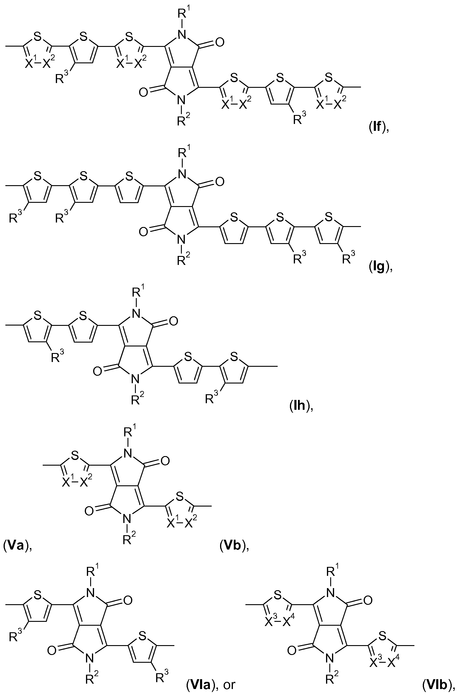
- B is a group of formula Ia, Ib, Ic, Id, Ie, If, Ig, or Ih, provided that B is different from A.
- R 1 and R 2 are a C 8 -C 3 5alkyl group
- R 3 is a Ci-Ci 8 alkyl group
- R 15 is a C 4 -Ci 8 alkyl group
- A is a group of formula Ia, Ib, Ic, Id, Ie, If, Ig, or Ih,
- R 1 and R 2 are a C 8 -C 35 alkyl group
- R 3 is a C 4 -Ci 8 alkyl group
- B is a group of formula Va, Hb, Mc, Hd, Me, Hf, Mg, Hh, or Mi, or a group of formula Ia, Ib, Ic,
- R 1 and R 2 are a C 8 -C 35 alkyl group, one of X 1 and X 2 is N and the other is CH,
- A is a group of formula I and B is a group of formula Il x is preferably 0.2 to 0.8 and y is preferably 0.8 to 0.2. If A and B are both a group of formula Il x is preferably 0.99 to 0.3 and y is preferably 0.01 to 0.7.
- polymers are even more preferred, comprising repeating units of the formula
- A is a group of formula
- R 1 and R 2 are a C 8 -C 3 5alkyl group
- R 3 is a C 4 -Ci 8 alkyl group
- R 1 and R 2 are a C 8 -C 3 5alkyl group
- D is a group of formula
- x 0.995 to 0.005
- A is a group of formula (Ia)
- R 1 and R 2 are a C 8 -C 3 5alkyl group
- R 3 is a C 4 -Ci 8 alkyl group
- R 1 and R 2 are a C 8 -C 35 alkyl group
- R 3 is a C 4 -Ci 8 alkyl group
- R 24 , R 1 and R 1 are a C 8 -C 36 alkyl group
- R 15 , R 15' , R 3 and R 26 are a d-Ci 8 alkyl group, especially a C 4 -Ci 8 alkyl group, R 1 ' is C 8 -C 36 alkyl,
- n 4 to 200, very especially 5 to 100.
- Copolymers of formula VII can be obtained, for example, by the Suzuki reaction.
- the condensation reaction of an aromatic boronate and a halogenide, especially a bromide, commonly referred to as the "Suzuki reaction" is tolerant of the presence of a variety of organic functional groups as reported by N. Miyaura and A. Suzuki in Chemical Reviews, Vol. 95, pp. 457-2483 (1995).
- Preferred catalysts are 2-dicyclohexylphosphino-2',6'-di- alkoxybiphenyl/palladium(ll)acetates, tri-alykl-phosphonium salts/palladium (0) derivatives and tri-alkylphosphine/palladium (0) derivatives.
- Especially preferred catalysts are 2- dicyclohexylphosphino-2',6'-di-methoxybiphenyl (sPhos)/palladium(ll)acetate and, tri-tert- butylphosphonium tetrafluoroborate ((t-Bu)sP * HBF 4 )/tris(dibenzylideneacetone) dipalladium (0) (Pd 2 (dba) 3 ) and tri-tert-butylphosphine (t-Bu) 3 P/tris(dibenzylideneacetone) dipalladium (0) (Pd 2 (dba) 3 ).
- This reaction can be applied to preparing high molecular weight polymers and copolymers.
- a dihalogenide such as a dibromide or dichloride, especially a dibromide corresponding to formula r Br and r Br is reacted with an (equimolar) amount of a diboronic acid or diboronate corresponding to formula , wherein X 11 is independently in each occurrence -B(OH) 2 , -B(OY 1 ) 2 ,
- Ci-Cioalkyl group and Y 2 is independently in each occurrence a C 2 -Ci 0 alkylene group, such as -CYV-CY 5 Y 6 -, or -CYV-CY 9 Y 10 - CY 11 Y 12 -, wherein Y 3 , Y 4 , Y 5 , Y 6 , Y 7 , Y 8 , Y 9 , Y 10 , Y 11 and Y 12 are independently of each other hydrogen, or a Ci-Ci O alkyl group, especially -C(CHs) 2 C(CHs) 2 -, -CH 2 C(CHs) 2 CH 2 -, or -C(CH 3 ) 2 CH 2 C(CH 3 ) 2 -, and Y 13 and Y 14 are independently of each other hydrogen, or a Ci-Ci O alkyl group, under the catalytic action of Pd and triphenylphosphine.
- the reaction is typically conducted at about 0 0 C to 180 0 C in an aromatic hydrocarbon solvent such as toluene, xylene.
- aromatic hydrocarbon solvent such as toluene, xylene.
- Other solvents such as dimethylformamide, dioxane, dimethoxyethan and tetrahydrofuran can also be used alone, or in mixtures with an aromatic hydrocarbon.
- An aqueous base preferably sodium carbonate or bicarbonate, potassium phosphate, potassium carbonate or bicarbonate is used as activation agent for the boronic acid, boronate and as the HBr scavenger.
- a polymerization reaction may take 0.2 to 100 hours.
- Organic bases such as, for example, tetraalkylammonium hydroxide, and phase transfer catalysts, such as, for example TBAB, can promote the activity of the boron (see, for example, Leadbeater & Marco; Angew. Chem. Int. Ed. Eng. 42 (2003) 1407 and references cited therein).
- phase transfer catalysts such as, for example TBAB
- Other variations of reaction conditions are given by T. I. Wallow and B. M. Novak in J. Org. Chem. 59 (1994) 5034-5037; and M. Remmers, M. Schulze, and G. Wegner in Macromol. Rapid Commun. 17 (1996) 239-252. Controll of molecular weight is possible by using either an excess of dibromide, diboronic acid, or diboronate, or a chain terminator.
- a monofunctional aryl halide or aryl boronate may be used as a chain-terminator in such reactions, which will result in the formation of a terminal aryl group.
- the polymers of the present invention can also be sythesized by the Stille coupling (see, for example, Babudri et al, J. Mater. Chem., 2004, 14, 11-34; J. K. Stille, Angew. Chemie Int. Ed. Engl. 1986, 25, 508).
- a dihalogenide such as a dibromide or dichloride, especially a dibromide corresponding to formula
- Br ⁇ A Br and Br ⁇ B Br is reacted with a compound of formula x ⁇ D ⁇ X , wherein X 21 is a group -SnR 207 R 208 R 209 , in an inert solvent at a temperature in range from 0 0 C to 200 0 C in the presence of a palladium-containing catalyst, wherein R 207 , R 208 and R 209 are identical or different and are H or CrC 6 alkyl, wherein two radicals optionally form a common ring and these radicals are optionally branched or unbranched. It must be ensured here that the totality of all monomers used has a highly balanced ratio of organotin functions to halogen functions.
- the tin compounds and the halogen compounds are preferably introduced into one or more inert organic solvents and stirred at a temperature of from 0 to 200 0 C, preferably from 30 to 170 0 C for a period of from 1 hour to 200 hours, preferably from 5 hours to 150 hours.
- the crude product can be purified by methods known to the person skilled in the art and appropriate for the respective polymer, for example repeated re-precipitation or even by dialysis.
- Suitable organic solvents for the process described are, for example, ethers, for example diethyl ether, dimethoxyethane, diethylene glycol dimethyl ether, tetrahydrofuran, dioxane, dioxolane, diisopropyl ether and tert-butyl methyl ether, hydrocarbons, for example hexane, isohexane, heptane, cyclohexane, benzene, toluene and xylene, alcohols, for example methanol, ethanol, 1-propanol, 2-propanol, ethylene glycol, 1-butanol, 2-butanol and tert- butanol, ketones, for example acetone, ethyl methyl ketone and isobutyl methyl ketone, amides, for example dimethylformamide (DMF), dimethylacetamide and N-methylpyrrolidone, nitriles, for example
- the palladium and phosphine components should be selected analogously to the description for the Suzuki variant.
- the polymers of the present invention can also be synthesized by the Negishi reaction using zinc reagents A-(ZnX 22 ) 2 and B-(ZnX 22 ) 2 , wherein X 22 is halogen and halides, and D-(X 23 ) 2 , wherein X 23 is halogen or triflate, or using A-(X 22 ) 2 , B-(X 22 ) 2 , and D-(ZnX 23 ) 2 .
- A-(ZnX 22 ) 2 and B-(ZnX 22 ) 2 wherein X 22 is halogen and halides
- D-(X 23 ) 2 wherein X 23 is halogen or triflate
- the polymers of the present invention can also be synthesized by the Hiyama reaction using organosilicon reagents A-(SiR 210 R 211 R 212 ) 2 and B-(SiR 210 R 211 R 212 ) 2 , wherein R 210 , R 211 and R 212 are identical or different and are halogen, C r C 6 alkyl and D-(X 23 ) 2 , wherein X 23 is halogen or triflate, or using A-(X 22 ) 2 , B-(X 22 ) 2 , and D-(SiR 210 R 211 R 212 ) 2 .
- organosilicon reagents A-(SiR 210 R 211 R 212 ) 2 and B-(SiR 210 R 211 R 212 ) 2 , wherein R 210 , R 211 and R 212 are identical or different and are halogen, C r C 6 alkyl and D-(X 23 ) 2 , where
- the polymers, wherein R 1 and/or R 2 are hydrogen can be obtained by using a protecting group which can be removed after polymerization (see, for example, EP-A-O 648 770, EP-A-O 648 817, EP-A-O 742 255, EP-A-O 761 772, WO98/32802, WO98/45757, WO98/58027, WO99/0151 1 , WO00/17275, WO00/39221 , WO00/63297 and EP-A- 1 086 984). Conversion of the pigment precursor into its pigmentary form is carried out by means of fragmentation under known conditions, for example thermally, optionally in the presence of an additional catalyst, for example the catalysts described in WO00/36210.
- L is preferably a group of formula , wherein Z 1 , Z 2 and Z 3 are independently of each other Ci-C 6 alkyl,
- Z 4 and Z 8 are independently of each other d-C 6 alkyl, d-C 6 alkyl interrupted by oxygen, sulfur or N(Z 12 ) 2 , or unsubstituted or d-C 6 alkyl-, d-C 6 alkoxy-, halo-, cyano- or nitro-substituted phenyl or biphenyl, Z 5 , Z 6 and Z 7 are independently of each other hydrogen or d-C ⁇ alkyl,
- Z 9 is hydrogen, d-C 6 alkyl or a group of formula or O
- -O-Z Z 10 an idd ZZ 1111 are each independently of the other hydrogen, d-C 6 alkyl, d-C 6 alkoxy, halogen, cyano, nitro, N(Z 12 ) 2 , or unsubstituted or halo-, cyano-, nitro-, d-C 6 alkyl- or d-C 6 alkoxy- substituted phenyl,
- Z 12 and Z 13 are d-C 6 alkyl
- Z 14 is hydrogen or d-C 6 alkyl
- Z 15 is hydrogen, d-C 6 alkyl, or unsubstituted or d-C 6 alkyl-substituted phenyl
- Q is p,q-C 2 -C 6 alkylene unsubstituted or mono- or poly-substituted by d-C 6 alkoxy, d-C ⁇ alkylthio or C2-Ci2dialkylamino, wherein p and q are different position numbers, X is a hetero atom selected from the group consisting of nitrogen, oxygen and sulfur, m' being the number 0 when X is oxygen or sulfur and m being the number 1 when X is nitrogen, and
- L 1 and L 2 are independently of each other unsubstituted or mono- or poly-Ci-Ci 2 alkoxy-, -d-C ⁇ alkylthio-, -C 2 -C 24 dialkylamino-, -Ce-C ⁇ aryloxy-, -Ce-C ⁇ arylthio-,
- Ci-C 6 alkyl or [-(p',q'- C 2 -C 6 alkylene)-Z-] n -Ci-C 6 alkyl , n' being a number from 1 to 1000, p' and q' being different position numbers, each Z independently of any others being a hetero atom oxygen, sulfur or CrCi 2 alkyl-substituted nitrogen, and it being possible for C 2 -C6alkylene in the repeating [-C 2 -C 6 alkylene-Z-] units to be the same or different, and L 1 and L 2 may be saturated or unsaturated from one to ten times, may be uninterrupted or interrupted at any location by from 1 to 10 groups selected from the group consisting of -(C O)- and -CeH 4 -, and may carry no further substituents or from 1 to 10 further substitu
- N-aryl substituted compounds of formula r can be done in analogy to the methods described in US-A-5,354,869 and WO03/022848.
- Halogen is fluorine, chlorine, bromine and iodine.
- Ci-C 2 5alkyl (d-Ci 8 alkyl) is typically linear or branched, where possible. Examples are methyl, ethyl, n-propyl, isopropyl, n-butyl, sec. -butyl, isobutyl, tert.
- Ci-C 8 alkyl is typically methyl, ethyl, n-propyl, isopropyl, n-butyl, sec. -butyl, isobutyl, tert. -butyl, n-pentyl, 2-pentyl, 3-pentyl, 2,2-dimethyl-propyl, n- hexyl, n-heptyl, n-octyl, 1 ,1 ,3,3-tetramethylbutyl and 2-ethylhexyl.
- CrC 4 alkyl is typically methyl, ethyl, n-propyl, isopropyl, n-butyl, sec.
- Ci-C 2 5alkoxy groups are straight-chain or branched alkoxy groups, e.g. methoxy, ethoxy, n-propoxy, isopropoxy, n-butoxy, sec-butoxy, tert-butoxy, amyloxy, isoamyloxy or tert-amyloxy, heptyloxy, octyloxy, isooctyloxy, nonyloxy, decyloxy, undecyloxy, dodecyloxy, tetradecyloxy, pentadecyloxy, hexadecyloxy, heptadecyloxy and octadecyloxy.
- Ci-C 8 alkoxy examples are methoxy, ethoxy, n-propoxy, isopropoxy, n-butoxy, sec-butoxy, isobutoxy, tert.-butoxy, n-pentoxy, 2-pentoxy, 3-pentoxy, 2,2-dimethylpropoxy, n-hexoxy, n- heptoxy, n-octoxy, 1 ,1 ,3,3-tetramethylbutoxy and 2-ethylhexoxy, preferably CrC 4 alkoxy such as typically methoxy, ethoxy, n-propoxy, isopropoxy, n-butoxy, sec-butoxy, isobutoxy, tert.-butoxy.
- alkylthio group means the same groups as the alkoxy groups, except that the oxygen atom of the ether linkage is replaced by a sulfur atom.
- C 6 -C 24 aryl is typically phenyl, indenyl, azulenyl, naphthyl, biphenyl, as-indacenyl, s-indacenyl, acenaphthylenyl, fluorenyl, phenanthryl, fluoranthenyl, triphenlenyl, chrysenyl, naphthacen, picenyl, perylenyl, pentaphenyl, hexacenyl, pyrenyl, or anthracenyl, preferably phenyl, 1 -naphthyl, 2-naphthyl, 4-biphenyl, 9-phenanthryl, 2- or 9-fluorenyl, 3- or 4-biphenyl, which may be unsubstituted or substituted.
- C 6 -Ci 2 aryl examples include phenyl, 1 -naphthyl, 2-naphthyl, 3- or 4-biphenyl, 2- or 9-fluorenyl or 9-phenanthryl, which may be unsubstituted or substituted.
- Ci-C 8 alkyl Possible substituents of the above-mentioned groups are Ci-C 8 alkyl, a hydroxyl group, a mercapto group, Ci-C 8 alkoxy, Ci-C 8 alkylthio, halogen, halo-Ci-C 8 alkyl, a cyano group, a carbamoyl group, a nitro group or a silyl group, especially Ci-C 8 alkyl, Ci-C 8 alkoxy, d- C 8 alkylthio, halogen, halo-Ci-C 8 alkyl, or a cyano group.
- Ci-Ci 8 alkyl interrupted by one or more O is, for example, (CH 2 CH 2 O) I-9 -R", where R x is H or d-Cioalkyl, CH 2 -CH(OR y ')-CH 2 -O-R y , where R y is C r Ci 8 alkyl, and R y ' embraces the same definitions as R y or is H.
- a substituent such as, for example Ar 24 , occurs more than one time in a group, it can be different in each occurrence.
- a mixture containing a polymer of the present invention results in a semi-conducting layer comprising a polymer of the present invention (typically 5% to 99.9999% by weight, especially 20 to 85 % by weight) and at least another material.
- the other material can be, but is not restricted to a fraction of the same polymer of the present invention with different molecular weight, another polymer of the present invention, a semi-conducting polymer, organic small molecules, carbon nanotubes, a fullerene derivative, inorganic particles (quantum dots, quantum rods, quantum tripods, TiO 2 , ZnO etc.), conductive particles (Au, Ag etc.), insulator materials like the ones described for the gate dielectric (PET, PS etc.).
- the polymers of the present invention can be blended with small molecules described, for example, in European patent application no. 09155919.5, WO09/047104, US6, 690,029, WO2007082584, and WO2008107089: WO2007082584:
- R is cyclic, straight-chain or branched alkyl or alkoxy having 1 to 20 C-atoms, or aryl having
- R' is H, F, Cl, Br, I, CN, straight-chain or branched alkyl or alkoxy having 1 to 20 C-atoms and optionally being fluorinated or perfluorinated, optionally fluorinated or perfluorinated aryl having 6 to 30 C-atoms, or CO 2 R", with R" being H, optionally fluorinated alkyl having 1 to 20
- R"' is H or cyclic, straight-chain or branched alkyl with 1 to 10 C-atoms, y is 0, or 1 , x is 0, or 1.
- the polymer can contain a small molecule, or a mixture of two, or more small molecule compounds.
- the present invention also relates to an organic semiconductor material, layer or component, comprising a polymer according to the present invention.
- the polymers of the invention can be used as the semiconductor layer in semiconductor devices. Accordingly, the present invention also relates to semiconductor devices, comprising a polymer of the present invention, or an organic semiconductor material, layer or component.
- the semiconductor device is especially an organic photovoltaic (PV) device (solar cell), a photodiode, or an organic field effect transistor.
- PV organic photovoltaic
- Such devices include rectifiers, transistors (of which there are many types, including p-n-p, n-p-n, and thin-film transistors), light emitting semiconductor devices (for example, organic light emitting diodes in display applications or backlight in e.g. liquid crystal displays), photoconductors, current limiters, solar cells, thermistors, p-n junctions, field-effect diodes, Schottky diodes, and so forth.
- the semiconductor material is combined with one or more metals, metal oxides, such as, for example, indium tin oxide (ITO), and/or insulators to form the device.
- ITO indium tin oxide
- Semiconductor devices can be prepared or manufactured by known methods such as, for example, those described by Peter Van Zant in Microchip Fabrication, Fourth Edition, McGraw-Hill, New York (2000).
- organic electronic components can be manufactured as described by D. R. Gamota et al. in Printed Organic and Molecular Electronics, Kluver Academic Publ., Boston, 2004.
- a particularly useful type of transistor device generally includes a gate electrode, a gate dielectric on the gate electrode, a source electrode and a drain electrode adjacent to the gate dielectric, and a semiconductor layer adjacent to the gate dielectric and adjacent to the source and drain electrodes (see, for example, S. M. Sze, Physics of Semiconductor Devices, 2 nd edition, John Wiley and Sons, page 492, New York (1981 )). These components can be assembled in a variety of configurations. More specifically, an OFET has an organic semiconductor layer.
- a substrate supports the OFET during manufacturing, testing, and/or use.
- the substrate can provide an electrical function for the OFET.
- Useful substrate materials include organic and inorganic materials.
- the substrate can comprise silicon materials inclusive of various appropriate forms of silicon, inorganic glasses, ceramic foils, polymeric materials (for example, acrylics, polyester, epoxies, polyamides, polycarbonates, polyimides, polyketones, poly(oxy-1 ,4-phenyleneoxy-1 ,4- phenylenecarbonyl-1 ,4-phenylene) (sometimes referred to as poly(ether ether ketone) or PEEK), polynorbornenes, polyphenyleneoxides, poly(ethylene naphthalenedicarboxylate) (PEN), poly(ethylene terephthalate) (PET), poly(phenylene sulfide) (PPS)), filled polymeric materials (for example, fiber-reinforced plastics (FRP)), and coated metallic foils.
- polymeric materials for example,
- the gate electrode can be any useful conductive material.
- the gate electrode can comprise doped silicon, or a metal, such as aluminum, chromium, gold, silver, nickel, palladium, platinum, tantalum, and titanium.
- Conductive oxides such as indium tin oxide, or conducting inks/pastes comprised of carbon black/graphite or colloidal silver dispersions, optionally containing polymer binders can also be used.
- Conductive polymers also can be used, for example polyaniline or poly(3,4-ethylenedioxythiophene)/poly(styrene sulfonate) (PEDOT:PSS).
- PEDOT:PSS poly(3,4-ethylenedioxythiophene)/poly(styrene sulfonate)
- alloys, combinations, and multilayers of these materials can be useful.
- the same material can provide the gate electrode function and also provide the support function of the substrate.
- doped silicon can function as the gate electrode and support the OF
- the gate dielectric is generally provided on the gate electrode. This gate dielectric electrically insulates the gate electrode from the balance of the OFET device.
- Useful materials for the gate dielectric can comprise, for example, an inorganic electrically insulating material.
- the gate dielectric (insulator) can be a material, such as, an oxide, nitride, or it can be a material selected from the family of ferroelectric insulators (e.g. organic materials such as poly(vinylidene fluoride/trifluoroethylene or poly(m-xylylene adipamide)), or it can be an organic polymeric insulator (e.g. poly(methacrylate)s, poly(acrylate)s, polyimides, benzocyclobutenes (BCBs), parylenes, polyvinylalcohol, polyvinylphenol (PVP), polystyrenes, polyester, polycarbonates) as for example described in J. Veres et al. Chem. Mat.
- ferroelectric insulators e.g. organic materials such as poly(vinylidene fluoride/trifluoroethylene or poly(m-xylylene adipamide)
- organic polymeric insulator e.g. poly(methacrylate
- materials useful for the gate dielectric include strontiates, tantalates, titanates, zirconates, aluminum oxides, silicon oxides, tantalum oxides, titanium oxides, silicon nitrides, barium titanate, barium strontium titanate, barium zirconate titanate, zinc selenide, and zinc sulphide, including but not limited to PbZr x Ti 1-x O 3 (PZT), Bi 4 Ti 3 Oi 2 , BaMgF 4 , Ba(Zr 1-x Ti x )O 3 (BZT).
- alloys, hybride materials e.g.
- the thickness of the dielectric layer is, for example, from about 10 to 1000 nm, with a more specific thickness being about 100 to 500 nm, providing a capacitance in the range of 0.1 - 100 nanofarads (nF).
- the source electrode and drain electrode are separated from the gate electrode by the gate dielectric, while the organic semiconductor layer can be over or under the source electrode and drain electrode.
- the source and drain electrodes can be any useful conductive material favourably providing a low resistance ohmic contact to the semiconductor layer.
- Useful materials include most of those materials described above for the gate electrode, for example, aluminum, barium, calcium, chromium, gold, silver, nickel, palladium, platinum, titanium, polyaniline, PEDOT:PSS, other conducting polymers, alloys thereof, combinations thereof, and multilayers thereof. Some of these materials are appropriate for use with n-type semiconductor materials and others are appropriate for use with p-type semiconductor materials, as is known in the art.
- the thin film electrodes can be provided by any useful means such as physical vapor deposition (for example, thermal evaporation or sputtering) or (ink jet) printing methods.
- the patterning of these electrodes can be accomplished by known methods such as shadow masking, additive photolithography, subtractive photolithography, printing, microcontact printing, and pattern coating.
- the present invention further provides an organic field effect transistor device comprising a plurality of electrically conducting gate electrodes disposed on a substrate; a gate insulator layer disposed on said electrically conducting gate electrodes; a plurality of sets of electrically conductive source and drain electrodes disposed on said insulator layer such that each of said sets is in alignment with each of said gate electrodes; an organic semiconductor layer disposed in the channel between source and drain electrodes on said insulator layer substantially overlapping said gate electrodes; wherein said organic semiconductor layer comprises a polymer of the present invention, or a mixture containing a polymer of the present invention.
- the present invention further provides a process for preparing a thin film transistor device comprising the steps of: depositing a plurality of electrically conducting gate electrodes on a substrate; depositing a gate insulator layer on said electrically conducting gate electrodes; depositing a plurality of sets of electrically conductive source and drain electrodes on said layer such that each of said sets is in alignment with each of said gate electrodes; depositing a layer of a polymer of the present invention on said insulator layer such that said layer of the compound of the present invention , or a mixture containing a polymer of the present invention , substantially overlaps said gate electrodes; thereby producing the thin film transistor device.
- an OFET is fabricated by, for example, by solution deposition of a polymer on a highly doped silicon substrate covered with a thermally grown oxide layer followed by vacuum deposition and patterning of source and drain electrodes.
- an OFET is fabricated by deposition of source and drain electrodes on a highly doped silicon substrate covered with a thermally grown oxide and then solution deposition of the polymer to form a thin film.
- the gate electrode could also be a patterned metal gate electrode on a substrate or a conducting material such as, a conducting polymer, which is then coated with an insulator applied either by solution coating or by vacuum deposition on the patterned gate electrodes.
- Suitable organic solvents for processing the semiconductors of the invention include, but are not limited to, aromatic or aliphatic hydrocarbons, halogenated such as chlorinated or fluorinated hydrocarbons, esters, ethers amides, such as chloroform, tetrachloroethane, tetrahydrofuran, toluene, tetraline, decaline, anisole, xylene, ethyl acetate, methyl ethyl ketone, dimethyl formamide, chloroform, chlorobenzene, dichlorobenzene, trichlorobenzene, propylene glycol monomethyl ether acetate (PGMEA) and mixtures thereof.
- PGMEA propylene glycol monomethyl ether acetate
- Preferred solvents are xylene, toluene, tetraline, decaline, chlorinated ones such as chloroform, chlorobenzene, ortho-dichlorobenzene, trichlorobenzene and mixtures thereof.
- the solution, and/or dispersion is then applied by a method, such as, spin-coating, dip-coating, screen printing, microcontact printing, doctor blading or other solution application techniques known in the art on the substrate to obtain thin films of the semiconducting material.
- the term "dispersion” covers any composition comprising the semiconductor material of the present invention, which is not fully dissolved in a solvent.
- the dispersion can be done selecting a composition including at least a polymer of the present invention, or a mixture containing a polymer of the present invention, and a solvent, wherein the polymer exhibits lower solubility in the solvent at room temperature but exhibits greater solubility in the solvent at an elevated temperature, wherein the composition gels when the elevated temperature is lowered to a first lower temperature without agitation;
- the dispersion can also be constituted of (a) a continuous phase comprising a solvent, a binder resin, and optionally a dispersing agent, and (b) a disperse phase comprising a polymer of the present invention, or a mixture containing a polymer of the present invention.
- the degree of solubility of the polymer of the present invention in the solvent may vary for example from 0% to about 20% solubility, particularly from 0% to about 5% solubility.
- the thickness of the organic semiconductor layer is in the range of from about 5 to about 1000 nm, especially the thickness is in the range of from about 10 to about 100 nm.
- the polymers of the invention can be used alone or in combination as the organic semiconductor layer of the semiconductor device.
- the layer can be provided by any useful means, such as, for example, vapor deposition (for materials with relatively low molecular weight) and printing techniques.
- the compounds of the invention may be sufficiently soluble in organic solvents and can be solution deposited and patterned (for example, by spin coating, dip coating, ink jet printing, gravure printing, flexo printing, offset printing, screen printing, microcontact (wave)-printing, drop or zone casting, or other known techniques).
- the polymers of the invention can be used in integrated circuits comprising a plurality of OTFTs, as well as in various electronic articles.
- Such articles include, for example, radio- frequency identification (RFID) tags, backplanes for flexible displays (for use in, for example, personal computers, cell phones, or handheld devices), smart cards, memory devices, sensors (e.g. light-, image-, bio-, chemo-, mechanical- or temperature sensors), especially photodiodes, or security devices and the like. Due to its ambi-polarity the material can also be used in Organic Light Emitting Transistors (OLET).
- OFID radio- frequency identification
- OLET Organic Light Emitting Transistors
- a further aspect of the present invention is an organic semiconductor material, layer or component comprising one or more polymers of the present invention.
- a further aspect is the use of the polymers or materials of the present invention in an organic photovoltaic (PV) device (solar cell), a photodiode, or an organic field effect transistor (OFET).
- a further aspect is an organic photovoltaic (PV) device (solar cell), a photodiode, or an organic field effect transistor (OFET) comprising a polymer or material of the present invention.
- the polymers of the present invention are typically used as organic semiconductors in form of thin organic layers or films, preferably less than 30 microns thick.
- the thickness may also be less than about 1 micron thick.
- the layer thickness may typically be 100 nm or less. The exact thickness of the layer will depend, for example, upon the requirements of the electronic device in which the layer is used.
- the active semiconductor channel between the drain and source in an OFET may comprise a layer of the present invention.
- An OFET device preferably comprises:
- the semiconductor layer comprises one or more polymers of the present invention.
- the gate, source and drain electrodes and the insulating and semiconducting layer in the OFET device may be arranged in any sequence, provided that the source and drain electrode are separated from the gate electrode by the insulating layer, the gate electrode and the semiconductor layer both contact the insulating layer, and the source electrode and the drain electrode both contact the semiconducting layer.
- the OFET comprises an insulator having a first side and a second side, a gate electrode located on the first side of the insulator, a layer comprising a polymer of the present invention located on the second side of the insulator, and a drain electrode and a source electrode located on the polymer layer.
- the OFET device can be a top gate device or a bottom gate device.
- the gate insulator layer may comprise for example a fluoropolymer, like e.g. the commercially available Cytop 809M®, or Cytop 107M® (from Asahi Glass).
- the gate insulator layer is deposited, e.g. by spin-coating, doctor blading, wire bar coating, spray or dip coating or other known methods, from a formulation comprising an insulator material and one or more solvents with one or more fluoro atoms (fluorosolvents), preferably a perfluorosolvent.
- fluorosolvents fluoro atoms
- perfluorosolvent e.g.
- FC75® available from Acros, catalogue number 12380.
- Other suitable fluoropolymers and fluorosolvents are known in prior art, like for example the perfluoropolymers Teflon AF® 1600 or 2400 (from DuPont), or Fluoropel® (from Cytonix) or the perfluorosolvent FC 43® (Acros, No. 12377).
- the semiconducting layer comprising a polymer of the present invention may additionally comprise at least another material.
- the other material can be, but is not restricted to another polymer of the present invention, a semi-conducting polymer, a polymeric binder, organic small molecules different from a polymer of the present invention, carbon nanotubes, a fullerene derivative, inorganic particles (quantum dots, quantum rods, quantum tripods, TiO 2 , ZnO etc.), conductive particles (Au, Ag etc.), and insulator materials like the ones described for the gate dielectric (PET, PS etc.).
- the semiconductive layer can also be composed of a mixture of one or more polymers of the present invention and a polymeric binder.
- the ratio of the polymers of the present invention to the polymeric binder can vary from 5 to 95 percent.
- the polymeric binder is a semicristalline polymer such as polystyrene (PS), high-density polyethylene (HDPE), polypropylene (PP) and polymethylmethacrylate (PMMA).
- PS polystyrene
- HDPE high-density polyethylene
- PP polypropylene
- PMMA polymethylmethacrylate
- the polymers of the present invention are advantageously used in organic photovoltaic (PV) devices (solar cells). Accordingly, the invention provides PV devices comprising a polymer according to the present invention. A device of this construction will also have rectifying properties so may also be termed a photodiode. Photoresponsive devices have application as solar cells which generate electricity from light and as photodetectors which measure or detect light.
- PV organic photovoltaic
- the PV device comprise in this order:
- a transition layer such as an alkali halogenide, especially lithium fluoride
- a photoactive layer such as an alkali halogenide, especially lithium fluoride
- the photoactive layer comprises the polymers of the present invention.
- the photoactive layer is made of a conjugated polymer of the present invention, as an electron donor and an acceptor material, like a fullerene, particularly a functionalized fullerene PCBM, as an electron acceptor.
- the photoactive layer may also contain a polymeric binder.
- the ratio of the small molecules of formula III to the polymeric binder can vary from 5 to 95 percent.
- the polymeric binder is a semicristalline polymer such as polystyrene (PS), high-density polyethylene (HDPE), polypropylene (PP) and polymethylmethacrylate (PMMA).
- the fullerenes useful in this invention may have a broad range of sizes (number of carbon atoms per molecule).
- fullerene as used herein includes various cage-like molecules of pure carbon, including Buckminsterfullerene (Ceo) and the related "spherical" fullerenes as well as carbon nanotubes.
- Fullerenes may be selected from those known in the art ranging from, for example, C 2 o-Ciooo- Preferably, the fullerene is selected from the range of C 6 o to C 9 6- Most preferably the fullerene is C 6 o or C 70 , such as [6O]PCBM, or [7O]PCBM. It is also permissible to utilize chemically modified fullerenes, provided that the modified fullerene retains acceptor- type and electron mobility characteristics.
- the acceptor material can also be a material selected from the group consisting of any semi-conducting polymer, such as, for example, a polymer of the present invention, provided that the polymers retain acceptor-type and electron mobility characteristics, organic small molecules, carbon nanotubes, inorganic particles (quantum dots, quantum rods, quantum tripods, TiO 2 , ZnO etc.).
- the photoactive layer is made of a polymer of the present invention as an electron donor and a fullerene, particularly functionalized fullerene PCBM, as an electron acceptor. These two components are mixed with a solvent and applied as a solution onto the smoothing layer by, for example, the spin-coating method, the drop casting method, the Langmuir-Blodgett ("LB") method, the ink jet printing method and the dripping method. A squeegee or printing method could also be used to coat larger surfaces with such a photoactive layer.
- a dispersion agent such as chlorobenzene is preferably used as a solvent.
- the vacuum deposition method, the spin-coating method, the ink jet printing method and the casting method are particularly preferred in view of ease of operation and cost.
- the coating can be carried out using a solution and/or dispersion prepared by dissolving, or dispersing the composition in a concentration of from 0.01 to 90% by weight in an appropriate organic solvent such as benzene, toluene, xylene, tetrahydrofurane, methyltetrahydrofurane, N,N-dimethylformamide, acetone, acetonitrile, anisole, dichloromethane, dimethylsulfoxide, chlorobenzene, 1 ,2-dichlorobenzene and mixtures thereof.
- an appropriate organic solvent such as benzene, toluene, xylene, tetrahydrofurane, methyltetrahydrofurane, N,N-dimethylformamide, acetone, acetonitrile, anisole, dichloromethane, dimethylsulfoxide, chlorobenzene, 1 ,2-dichlorobenzene and mixtures thereof.
- the photovoltaic (PV) device can also consist of multiple junction solar cells that are processed on top of each other in order to absorb more of the solar spectrum.
- Such structures are, for example, described in App. Phys. Let. 90, 143512 (2007), Adv. Funct. Mater. 16, 1897-1903 (2006) and WO2004/112161.
- a so called 'tandem solar cell' comprise in this order:
- a transition layer such as an alkali halogenide, especially lithium fluoride
- a photoactive layer such as an alkali halogenide, especially lithium fluoride
- a middle electrode such as Au, Al, ZnO, TiO 2 etc.
- a transition layer such as an alkali halogenide, especially lithium fluoride
- a photoactive layer such as an alkali halogenide, especially lithium fluoride
- the PV device can also be processed on a fiber as described, for example, in US20070079867 and US 20060013549.
- the materials or films comprising the polymers of the present invention can also be used alone or together with other materials in or as alignment layers in LCD or OLED devices, as described for example in US2003/0021913.
- the following examples are included for illustrative purposes only and do not limit the scope of the claims. Unless otherwise stated, all parts and percentages are by weight.
- HT-GPC Heat Temperature Gel Permeation Chromatography
- PS 1 '930OOO PS 1 '460OOO
- PS 1 O75O00 PS 560O00
- PS 330O00 PS 96'00O
- PS 52O00 PS 30'300
- PS 10'100 PS 5'050 Da.
- a polynomic calibration is used to calculate the molecular weight.
- Polymers 8-20 (Example 2-14) shown in table 1 below are prepared in analogy to Example 1 , varying the R-groups and/or the ratio of the two dibromides used in the synthesis. All starting materials are prepared according to, or in analogy to example 1 and WO2008000664.
- Polymer 29 (Example 16) shown in table 2 below is prepared in analogy to Example 15, varying the R-groups and/or the ratio of the two dibromides used in the synthesis.
- Example 18-19 Preparation of random copolymers 31 and 32
- Polymers 31 and 32 (Example 16 and 17) shown in table 3 below are prepared in analogy to Example 15, varying the R-groups and/or the ratio of the two dibromides used in the synthesis.
- Example 21 Preparation of random copolymer 36
- Polymer 36 (Example 21 ) shown in table 4 below is prepared in analogy to Example 20, varying the R-groups and/or the ratio of the two dibromides used in the synthesis.
- Polymer 52 (Example 26) shown in table 5 below is prepared in analogy to Example 25, varying the ratio of the two dibromides used in the synthesis
- reaction mixture is cooled to room temperature and 100 ml water are added.
- the reaction mixture is extracted with ethylacetate and the organic layer is dried and evaporated under reduced pressure. It is further purified with column chromatography using a gradient of hexane / ehtylacetate on silicagel. 8.Og of 2-thiophen-2-yl-thiazole 53 is obtained, spectral data correspond to the ones described in literature using Negishi-cross coupling reaction. (J. Jensen et al., Synthesis, 2001 , 1 , 128).
- Polymer 58 is obtained in analogy to Example 1 using 0.2 equivalent of 5, 1.0 equivalent of 6 and 0.8 equivalent 57.
- Polymers 59-63 (Example 28-32) shown in table 6 below are prepared in analogy to Example 1 , varying the R-groups and/or the ratio of the two dibromides. All starting materials are prepared according to, or in analogy to example 27 and WO2008000664.
- Example 33 Preparation of random Copolymer 67 a)
- Starting material 64 for boronic ester 65 is prepared according to Example 2a of WO2008000664.
- To a solution of 5.0 g Dithienyl-DPP (64) and 3.73 g 2-lsopropoxy-4,4,5,5- tetramethyl-1 ,3,2-dioxoborolane in 30 ml THF under nitrogen at -25 0 C is added drop-wise a freshly prepared LDA solution (from 5.4 ml butyllithium 2.7 M and 2.2 ml diisopropylamin in 20 ml THF,) over 15 minutes.
- the resulting reaction mixture is stirred for 1 hour at 0 0 C and then quenched with 100 ml 1 M HCI.
- the product is extracted with 2 x 50 ml TBME and the combined organic layers are washed twice with brine and dried with sodium sulfate. After evaporation of the solvent the residue is dissolved in 20 ml methylenchloride and then slowly added to 200 ml of heavily stirred acetone. The precipitate is collected by filtration, washed several times with acetone and dried at 40 0 C in a vacuum-oven, affording 6.3 g of pinkish- violet powder.
- Polymer 67 is obtained in analogy to Example 1 using 0.5 equivalent of 5, 1.0 equivalent of 65 and 0.5 equivalent 67.
- Example 35 Preparation of random Copolymer 72 Polymer 72 (Example 35) shown below is prepared in analogy to example 34, varying the ratio of the two dibromides used in the synthesis
- TFT bottom-gate thin film transistor
- the SiC> 2 surface Prior to deposition of the organic semiconductor the SiC> 2 surface is derivatized either with hexadimethylsilazane (HMDS) by exposing to a saturated silane vapour at 160 0 C for 2 hours, by spin coating the HMDS at a spinning speed of 800 rpm (rounds per minute) for about a minute or by treating the substrate at 60 0 C with a 0.1 m solution of octadecyltrichlorosilane (OTS) in toluene for 20 minutes. After rinsing with iso-propanol the substrates are dried.
- HMDS hexadimethylsilazane
- OTS octadecyltrichlorosilane
- the semiconductor thin film is prepared either by spin-coating or drop casting the DPP derivative of the formula 7 obtained in example 1 in a 0.5% (w/w) solution in ortho-dichlorobenzene.
- the spin coating is accomplished at a spinning speed of 1000 rpm (rounds per minute) for about 60 seconds in ambient conditions.
- the devices are evaluated as-deposited and after drying at 100 0 C for 15 minutes.
- the transistor behaviour is measured on an automated transistor prober (TP-10). From a linear fit to the square root of the saturated transfer characteristics a field effect mobility of 1.0x10 "2 cm 2 ⁇ /s with an on/off current ratio of 1.8x10 5 can be determined after drying.
- the threshold voltage is at 8.2 V.
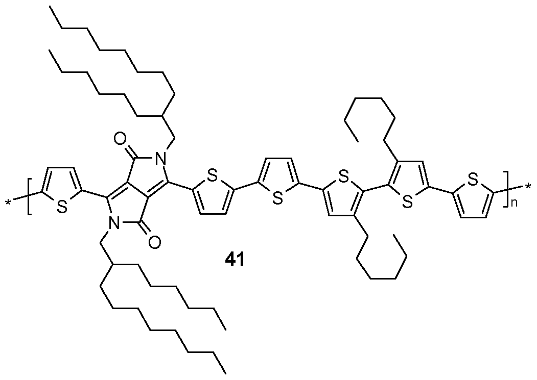
- Additional organic field effect transistors are prepared by replacing polymer 7 by polymers 10, 12, 15, 16, 18, 19, 20, 28, 29, 30, 31, 32, 35, 41, 42 , 49, 51, 52, 71, 72, 75, 76 and 77. Reference is made to table 9.
- the solar cell has the following structure: Al electrode/LiF layer/organic layer, including compound of the invention/[poly(3,4-ethylenedioxy-thiophene) (PEDOT): poly(styrenesulfonic acid) (PSS)]/ITO electrode/glass substrate.
- PEDOT poly(3,4-ethylenedioxy-thiophene)
- PSS poly(styrenesulfonic acid)
- the solar cells are made by spin coating a layer of the PEDOT:PSS on a pre-patterned ITO on glass substrate. Then a 1 :1 mixture of the compound of formula 7 (1 % by weight) : [6O]PCBM or [7O]PCBM (a substituted C 60 or C 70 fullerene) is spin coated (organic layer). LiF and Al are sublimed under high vacuum through a shadow-mask.
Landscapes
- Chemical & Material Sciences (AREA)
- Organic Chemistry (AREA)
- Health & Medical Sciences (AREA)
- Chemical Kinetics & Catalysis (AREA)
- Medicinal Chemistry (AREA)
- Polymers & Plastics (AREA)
- Engineering & Computer Science (AREA)
- Materials Engineering (AREA)
- Polyoxymethylene Polymers And Polymers With Carbon-To-Carbon Bonds (AREA)
- Thin Film Transistor (AREA)
- Photovoltaic Devices (AREA)
Abstract
Description


Claims


Priority Applications (5)
| Application Number | Priority Date | Filing Date | Title |
|---|---|---|---|
| KR1020117012291A KR101764436B1 (en) | 2008-10-31 | 2009-10-21 | Diketopyrrolopyrrole polymers for use in organic semiconductor devices |
| JP2011533679A JP5611217B2 (en) | 2008-10-31 | 2009-10-21 | Diketopyrrolopyrrole polymers for use in organic semiconductor devices |
| US13/126,178 US8975359B2 (en) | 2008-10-31 | 2009-10-21 | Diketopyrrolopyrrole polymers for use in organic semiconductor devices |
| CN200980143419XA CN102203160B (en) | 2008-10-31 | 2009-10-21 | Diketopyrrolopyrrole polymers for use in organic semiconductor devices |
| EP09736978.9A EP2350160B1 (en) | 2008-10-31 | 2009-10-21 | Diketopyrrolopyrrole polymers for use in organic semiconductor devices |
Applications Claiming Priority (4)
| Application Number | Priority Date | Filing Date | Title |
|---|---|---|---|
| EP08168010 | 2008-10-31 | ||
| EP08168010.0 | 2008-10-31 | ||
| EP08170823 | 2008-12-05 | ||
| EP08170823.2 | 2008-12-05 |
Publications (1)
| Publication Number | Publication Date |
|---|---|
| WO2010049323A1 true WO2010049323A1 (en) | 2010-05-06 |
Family
ID=41351893
Family Applications (1)
| Application Number | Title | Priority Date | Filing Date |
|---|---|---|---|
| PCT/EP2009/063769 WO2010049323A1 (en) | 2008-10-31 | 2009-10-21 | Diketopyrrolopyrrole polymers for use in organic semiconductor devices |
Country Status (7)
| Country | Link |
|---|---|
| US (1) | US8975359B2 (en) |
| EP (1) | EP2350160B1 (en) |
| JP (1) | JP5611217B2 (en) |
| KR (1) | KR101764436B1 (en) |
| CN (1) | CN102203160B (en) |
| TW (1) | TWI476226B (en) |
| WO (1) | WO2010049323A1 (en) |
Cited By (47)
| Publication number | Priority date | Publication date | Assignee | Title |
|---|---|---|---|---|
| WO2010115767A1 (en) * | 2009-04-08 | 2010-10-14 | Basf Se | Pyrrolopyrrole derivatives, their manufacture and use as semiconductors |
| WO2011161078A1 (en) | 2010-06-24 | 2011-12-29 | Basf Se | An organic field effect transistor with improved current on/off ratio and controllable threshold shift |
| WO2011144566A3 (en) * | 2010-05-19 | 2012-03-01 | Basf Se | Diketopyrrolopyrrole polymers for use in organic semiconductor devices |
| WO2012059386A1 (en) | 2010-11-01 | 2012-05-10 | Basf Se | Polyimides as dielectric |
| WO2012084757A1 (en) | 2010-12-22 | 2012-06-28 | Basf Se | Semiconductor structure and method for its production |
| WO2012095796A1 (en) * | 2011-01-13 | 2012-07-19 | Basf Se | Organic photovoltaic device and manufacturing method thereof |
| JP2012214681A (en) * | 2010-11-02 | 2012-11-08 | Sumitomo Chemical Co Ltd | Polymeric compound and organic photoelectric conversion element using the same |
| JP2012229394A (en) * | 2010-10-13 | 2012-11-22 | Sumitomo Chemical Co Ltd | Polymeric compound, and organic photoelectric conversion device using the same |
| WO2012175530A1 (en) | 2011-06-22 | 2012-12-27 | Basf Se | Diketopyrrolopyrrole oligomers for use in organic semiconductor devices |
| WO2013030325A1 (en) | 2011-09-02 | 2013-03-07 | Basf Se | Diketopyrrolopyrrole oligomers and compositions, comprising diketopyrrolopyrrole oligomers |
| KR101265511B1 (en) | 2011-05-06 | 2013-05-20 | 한국과학기술연구원 | Low band gap polymers, the synthesis of the polymers, and the organic photovoltaic cell comprising the polymers |
| WO2013072853A1 (en) * | 2011-11-15 | 2013-05-23 | Basf Se | Organic semiconductor device and manufacturing method thereof |
| WO2013028441A3 (en) * | 2011-08-19 | 2013-06-06 | University Of Washington | New poly(heteroarylene vinylene)s based on diketopyrrolopyrrole |
| WO2013083506A1 (en) | 2011-12-07 | 2013-06-13 | Basf Se | Diketopyrrolopyrrole polymers for use in organic semiconductor devices |
| WO2013083507A1 (en) | 2011-12-07 | 2013-06-13 | Basf Se | An organic field effect transistor |
| JP2013201252A (en) * | 2012-03-23 | 2013-10-03 | Konica Minolta Inc | Conjugated polymer compound, and organic photoelectric conversion element using the same |
| WO2013149897A1 (en) | 2012-04-02 | 2013-10-10 | Basf Se | Phenanthro[9,10-b]furan polymers and small molecules for electronic applications |
| US8629238B2 (en) | 2009-05-27 | 2014-01-14 | Basf Se | Diketopyrrolopyrrole polymers for use in organic semiconductor devices |
| WO2014016219A1 (en) | 2012-07-23 | 2014-01-30 | Basf Se | Dithienobenzofuran polymers and small molecules for electronic application |
| WO2014086722A1 (en) | 2012-12-04 | 2014-06-12 | Basf Se | Functionnalized benzodithiophene polymers for electronic application |
| US8796469B2 (en) | 2009-03-23 | 2014-08-05 | Basf Se | Diketopyrrolopyrrole polymers for use in organic semiconductor devices |
| US8835579B2 (en) | 2009-05-27 | 2014-09-16 | Basf Se | Process for polymerising (hetero)aromatic compounds |
| US8912305B2 (en) | 2008-10-31 | 2014-12-16 | Basf Se | Diketopyrrolopyrrole polymers for use in organic field effect transistors |
| US8946376B2 (en) | 2010-09-29 | 2015-02-03 | Basf Se | Semiconductors based on diketopyrrolopyrroles |
| WO2015036075A1 (en) | 2013-09-11 | 2015-03-19 | Merck Patent Gmbh | Cyclohexadiene fullerene derivatives |
| WO2015064937A3 (en) * | 2013-10-28 | 2015-06-25 | 주식회사 엘지화학 | Single molecule and organic solar cell comprising same |
| US9074050B2 (en) | 2011-05-30 | 2015-07-07 | Basf Se | Process for the production of polymers by using coupling reactions |
| EP2773687A4 (en) * | 2011-10-31 | 2015-09-16 | Corning Inc | Fused thiophenes, methods of making fused thiophenes, and uses thereof |
| WO2015149905A1 (en) | 2014-03-31 | 2015-10-08 | Merck Patent Gmbh | Fused bis-aryl fullerene derivatives |
| US9187600B2 (en) | 2010-11-01 | 2015-11-17 | Basf Se | Polyimides as dielectric |
| WO2015192942A1 (en) | 2014-06-17 | 2015-12-23 | Merck Patent Gmbh | Fullerene derivatives |
| US9293718B2 (en) | 2012-04-04 | 2016-03-22 | Basf Se | Diketopyrrolopyrrole polymers and small molecules |
| EP3173435A1 (en) | 2015-11-26 | 2017-05-31 | Merck Patent GmbH | Semiconducting mixtures |
| US9786409B2 (en) | 2013-06-27 | 2017-10-10 | Basf Se | Metathesis polymers as dielectrics |
| TWI602844B (en) * | 2010-05-19 | 2017-10-21 | 巴地斯顏料化工廠 | Diketopyrrolopyrrole polymers for use in organic semiconductor devices |
| WO2017202635A1 (en) | 2016-05-25 | 2017-11-30 | Basf Se | Semiconductors |
| US9847220B2 (en) | 2013-07-08 | 2017-12-19 | Basf Se | Azide-based crosslinking agents |
| US9929364B2 (en) | 2013-05-06 | 2018-03-27 | Basf Se | Soluble cyclic imides containing polymers as dielectrics in organic electronic applications |
| WO2018060016A1 (en) | 2016-09-27 | 2018-04-05 | Basf Se | Star-shaped and triblock polymers with enhanced crosslinkability |
| WO2018060015A1 (en) | 2016-09-27 | 2018-04-05 | Basf Se | Star-shaped styrene polymers with enhanced glass transition temperature |
| CN107955158A (en) * | 2016-10-14 | 2018-04-24 | 徐州工程学院 | A kind of siliceous main chain aryl oxide ketone copolymers and preparation method thereof |
| US10020456B2 (en) | 2014-09-25 | 2018-07-10 | Basf Se | Ether-based polymers as photo-crosslinkable dielectrics |
| US10224484B2 (en) | 2008-10-31 | 2019-03-05 | Basf Se | Diketopyrrolopyrrole polymers for use in organic field effect transistors |
| WO2019170719A1 (en) | 2018-03-08 | 2019-09-12 | Basf Se | Organic field effect transistor comprising semiconducting single-walled carbon nanotubes and organic semiconducting material |
| WO2019170481A1 (en) | 2018-03-07 | 2019-09-12 | Basf Se | Patterning method for preparing top-gate, bottom-contact organic field effect transistors |
| US10424737B2 (en) | 2006-06-30 | 2019-09-24 | Basf Se | Diketopyrrolopyrrole polymers as organic semiconductors |
| WO2020001865A1 (en) | 2018-06-26 | 2020-01-02 | Basf Se | Vinylether-based polymer as dielectric |
Families Citing this family (15)
| Publication number | Priority date | Publication date | Assignee | Title |
|---|---|---|---|---|
| US20130085256A1 (en) * | 2004-09-14 | 2013-04-04 | Mingqian He | Fused thiophenes, methods of making fused thiophenes, and uses thereof |
| WO2010136401A2 (en) | 2009-05-27 | 2010-12-02 | Basf Se | Polycyclic dithiophenes |
| US8563851B2 (en) | 2012-03-19 | 2013-10-22 | Xerox Corporation | Method to increase field effect mobility of donor-acceptor semiconductors |
| US8558109B2 (en) | 2012-03-19 | 2013-10-15 | Xerox Corporation | Semiconductor composition for high performance organic devices |
| WO2014031733A1 (en) * | 2012-08-22 | 2014-02-27 | University Of Washington Through Its Center For Commercialization | Diketopyrrolopyrrole polymers for electronics and optoelectronics |
| CN104703685B (en) * | 2012-08-27 | 2017-03-15 | 康宁股份有限公司 | Quasiconductor fused thiophene polymer ink formulations |
| CN103012751B (en) * | 2012-11-30 | 2015-05-20 | 四川大学 | Preparation method of bis-thienyl pyrrolo-[3,4-c] pyrrole-1,4-diketone and (hybrid) arene copolymer |
| US9166168B2 (en) * | 2012-12-24 | 2015-10-20 | Samsung Electronics Co., Ltd. | Organic semiconductor polymer, organic thin film transistor, and electronic device |
| KR102094742B1 (en) * | 2012-12-24 | 2020-03-30 | 삼성전자주식회사 | Organic semiconductor polymer, organic thin film transistor and electronic device |
| US8575477B1 (en) | 2012-12-27 | 2013-11-05 | Xerox Corporation | Diketopyrrolopyrrole-based polymers containing a diene group for semiconductors |
| US9399698B2 (en) | 2014-01-31 | 2016-07-26 | Xerox Corporation | Processes for purifying diketopyrrolopyrrole copolymers |
| KR102099612B1 (en) * | 2014-03-27 | 2020-04-10 | 경상대학교산학협력단 | Diketopyrrolopyrrole polymer and organic electronic device using the same |
| CN105061435A (en) * | 2015-08-27 | 2015-11-18 | 华南理工大学 | Pyrrolo-pyrrolidone unit monomer and synthesizing method and polymers thereof |
| CN110669209B (en) * | 2019-10-21 | 2021-08-06 | 中国科学院上海硅酸盐研究所 | Ternary conjugated polymer thermoelectric material with different side chain polarities and preparation method and application thereof |
| CN113512178A (en) * | 2021-04-29 | 2021-10-19 | 南昌航空大学 | N-type pyrrolopyrrolidinone COF (COF) dendritic conjugated polymer electrolyte cathode interface layer and preparation method thereof |
Citations (5)
| Publication number | Priority date | Publication date | Assignee | Title |
|---|---|---|---|---|
| WO2005049695A1 (en) * | 2003-10-28 | 2005-06-02 | Ciba Specialty Chemicals Holding Inc. | Novel diketopyrrolopyrrole polymers |
| WO2008000664A1 (en) * | 2006-06-30 | 2008-01-03 | Ciba Holding Inc. | Diketopyrrolopyrrole polymers as organic semiconductors |
| EP2034537A2 (en) * | 2007-09-06 | 2009-03-11 | Xerox Corporation | Diketopyrrolopyrrole-based derivatives for thin film transistors |
| WO2009047104A2 (en) * | 2007-10-09 | 2009-04-16 | Basf Se | Pyrrolopyrrole derivatives, their manufacture and use |
| EP2075274A1 (en) * | 2007-12-27 | 2009-07-01 | Industrial Technology Research Institute | Soluble polythiophene derivatives |
Family Cites Families (5)
| Publication number | Priority date | Publication date | Assignee | Title |
|---|---|---|---|---|
| DE4331401A1 (en) | 1993-09-15 | 1995-03-16 | Hoechst Ag | Use of polymers with isolated chromophores as electroluminescent materials |
| TWI290164B (en) | 1999-08-26 | 2007-11-21 | Ciba Sc Holding Ag | DPP-containing conjugated polymers and electroluminescent devices |
| US7932344B2 (en) * | 2007-09-06 | 2011-04-26 | Xerox Corporation | Diketopyrrolopyrrole-based polymers |
| CN107099023B (en) | 2008-10-31 | 2019-10-22 | 巴斯夫欧洲公司 | Diketopyrrolo-pyrrole polymer for organic field effect tube |
| CN104854175A (en) * | 2012-12-18 | 2015-08-19 | 默克专利股份有限公司 | Polymer comprising a thiadiazol group, the production of such polymer and its use in organic electronic devices |
-
2009
- 2009-10-21 EP EP09736978.9A patent/EP2350160B1/en active Active
- 2009-10-21 KR KR1020117012291A patent/KR101764436B1/en active IP Right Grant
- 2009-10-21 US US13/126,178 patent/US8975359B2/en active Active
- 2009-10-21 CN CN200980143419XA patent/CN102203160B/en active Active
- 2009-10-21 JP JP2011533679A patent/JP5611217B2/en active Active
- 2009-10-21 WO PCT/EP2009/063769 patent/WO2010049323A1/en active Application Filing
- 2009-10-30 TW TW098137022A patent/TWI476226B/en active
Patent Citations (5)
| Publication number | Priority date | Publication date | Assignee | Title |
|---|---|---|---|---|
| WO2005049695A1 (en) * | 2003-10-28 | 2005-06-02 | Ciba Specialty Chemicals Holding Inc. | Novel diketopyrrolopyrrole polymers |
| WO2008000664A1 (en) * | 2006-06-30 | 2008-01-03 | Ciba Holding Inc. | Diketopyrrolopyrrole polymers as organic semiconductors |
| EP2034537A2 (en) * | 2007-09-06 | 2009-03-11 | Xerox Corporation | Diketopyrrolopyrrole-based derivatives for thin film transistors |
| WO2009047104A2 (en) * | 2007-10-09 | 2009-04-16 | Basf Se | Pyrrolopyrrole derivatives, their manufacture and use |
| EP2075274A1 (en) * | 2007-12-27 | 2009-07-01 | Industrial Technology Research Institute | Soluble polythiophene derivatives |
Non-Patent Citations (2)
| Title |
|---|
| LUKAS BÜRGI ET AL.: "High-Mobility Ambipolar Near-Infrared Light-Emitting Polymer Field-Effect Transistors", ADVANCED MATERIALS, vol. 20, 4 June 2008 (2008-06-04), Wiley-VCH Verlag, Weinheim, DE, pages 2217 - 2224, XP002558731 * |
| PEET J ET AL: "Small molecule sensitizers for near-infrared absorption in polymer bulk heterojunction solar cells", APPLIED PHYSICS LETTERS, AIP, AMERICAN INSTITUTE OF PHYSICS, MELVILLE, NY, US, vol. 93, no. 16, 22 October 2008 (2008-10-22), pages 163306 - 163306, XP012112015, ISSN: 0003-6951 * |
Cited By (72)
| Publication number | Priority date | Publication date | Assignee | Title |
|---|---|---|---|---|
| US11217752B2 (en) | 2006-06-30 | 2022-01-04 | Basf Se | Diketopyrrolopyrrole polymers as organic semiconductors |
| US10424737B2 (en) | 2006-06-30 | 2019-09-24 | Basf Se | Diketopyrrolopyrrole polymers as organic semiconductors |
| US10224484B2 (en) | 2008-10-31 | 2019-03-05 | Basf Se | Diketopyrrolopyrrole polymers for use in organic field effect transistors |
| US10431745B2 (en) | 2008-10-31 | 2019-10-01 | Basf Se | Diketopyrrolopyrrole polymers for use in organic field effect transistors |
| US9893288B2 (en) | 2008-10-31 | 2018-02-13 | Basf Se | Diketopyrrolopyrrole polymers for use in organic field effect transistors |
| US8912305B2 (en) | 2008-10-31 | 2014-12-16 | Basf Se | Diketopyrrolopyrrole polymers for use in organic field effect transistors |
| EP2350161B1 (en) * | 2008-10-31 | 2018-11-21 | Basf Se | Diketopyrrolopyrrole polymers for use in organic field effect transistors |
| EP3456756A3 (en) * | 2008-10-31 | 2019-05-01 | Basf Se | Diketopyrrolopyrrole polymers for use in organic field effect transistors |
| US9478745B2 (en) | 2009-03-23 | 2016-10-25 | Basf Se | Diketopyrrolopyrrole polymers for use in organic semiconductor devices |
| US8796469B2 (en) | 2009-03-23 | 2014-08-05 | Basf Se | Diketopyrrolopyrrole polymers for use in organic semiconductor devices |
| US10177313B2 (en) | 2009-03-23 | 2019-01-08 | Basf Se | Diketopyrrolopyrrole polymers for use in organic semiconductor devices |
| WO2010115767A1 (en) * | 2009-04-08 | 2010-10-14 | Basf Se | Pyrrolopyrrole derivatives, their manufacture and use as semiconductors |
| US9067942B2 (en) | 2009-04-08 | 2015-06-30 | Basf Se | Pyrrolopyrrole derivatives, their manufacture and use as semiconductors |
| US8835579B2 (en) | 2009-05-27 | 2014-09-16 | Basf Se | Process for polymerising (hetero)aromatic compounds |
| US8629238B2 (en) | 2009-05-27 | 2014-01-14 | Basf Se | Diketopyrrolopyrrole polymers for use in organic semiconductor devices |
| CN102892807A (en) * | 2010-05-19 | 2013-01-23 | 巴斯夫欧洲公司 | Diketopyrrolopyrrole polymers for use in organic semiconductor devices |
| TWI602844B (en) * | 2010-05-19 | 2017-10-21 | 巴地斯顏料化工廠 | Diketopyrrolopyrrole polymers for use in organic semiconductor devices |
| KR101839636B1 (en) * | 2010-05-19 | 2018-03-16 | 바스프 에스이 | Diketopyrrolopyrrole polymers for use in organic semiconductor devices |
| WO2011144566A3 (en) * | 2010-05-19 | 2012-03-01 | Basf Se | Diketopyrrolopyrrole polymers for use in organic semiconductor devices |
| WO2011161078A1 (en) | 2010-06-24 | 2011-12-29 | Basf Se | An organic field effect transistor with improved current on/off ratio and controllable threshold shift |
| US8946376B2 (en) | 2010-09-29 | 2015-02-03 | Basf Se | Semiconductors based on diketopyrrolopyrroles |
| JP2012229394A (en) * | 2010-10-13 | 2012-11-22 | Sumitomo Chemical Co Ltd | Polymeric compound, and organic photoelectric conversion device using the same |
| US9187600B2 (en) | 2010-11-01 | 2015-11-17 | Basf Se | Polyimides as dielectric |
| WO2012059386A1 (en) | 2010-11-01 | 2012-05-10 | Basf Se | Polyimides as dielectric |
| JP2012214681A (en) * | 2010-11-02 | 2012-11-08 | Sumitomo Chemical Co Ltd | Polymeric compound and organic photoelectric conversion element using the same |
| WO2012084757A1 (en) | 2010-12-22 | 2012-06-28 | Basf Se | Semiconductor structure and method for its production |
| US9608219B2 (en) | 2010-12-22 | 2017-03-28 | Basf Se | Semiconductor structure and method for its production |
| CN103282421A (en) * | 2011-01-13 | 2013-09-04 | 巴斯夫欧洲公司 | Organic photovoltaic device and manufacturing method thereof |
| CN103282421B (en) * | 2011-01-13 | 2015-05-27 | 巴斯夫欧洲公司 | Organic photovoltaic device and manufacturing method thereof |
| WO2012095796A1 (en) * | 2011-01-13 | 2012-07-19 | Basf Se | Organic photovoltaic device and manufacturing method thereof |
| KR101265511B1 (en) | 2011-05-06 | 2013-05-20 | 한국과학기술연구원 | Low band gap polymers, the synthesis of the polymers, and the organic photovoltaic cell comprising the polymers |
| US9074050B2 (en) | 2011-05-30 | 2015-07-07 | Basf Se | Process for the production of polymers by using coupling reactions |
| WO2012175530A1 (en) | 2011-06-22 | 2012-12-27 | Basf Se | Diketopyrrolopyrrole oligomers for use in organic semiconductor devices |
| WO2013028441A3 (en) * | 2011-08-19 | 2013-06-06 | University Of Washington | New poly(heteroarylene vinylene)s based on diketopyrrolopyrrole |
| US9209412B2 (en) | 2011-09-02 | 2015-12-08 | Basf Se | Diketopyrrolopyrrole oligomers and compositions, comprising diketopyrrolopyrrole oligomers |
| WO2013030325A1 (en) | 2011-09-02 | 2013-03-07 | Basf Se | Diketopyrrolopyrrole oligomers and compositions, comprising diketopyrrolopyrrole oligomers |
| EP2773687A4 (en) * | 2011-10-31 | 2015-09-16 | Corning Inc | Fused thiophenes, methods of making fused thiophenes, and uses thereof |
| WO2013072853A1 (en) * | 2011-11-15 | 2013-05-23 | Basf Se | Organic semiconductor device and manufacturing method thereof |
| US9543521B2 (en) | 2011-11-15 | 2017-01-10 | Basf Se | Organic semiconductor device and process for its production |
| US9276215B2 (en) | 2011-12-07 | 2016-03-01 | Basf Se | Diketopyrrolopyrrole polymers for use in organic semiconductor devices |
| WO2013083506A1 (en) | 2011-12-07 | 2013-06-13 | Basf Se | Diketopyrrolopyrrole polymers for use in organic semiconductor devices |
| US9978943B2 (en) | 2011-12-07 | 2018-05-22 | Basf Se | Organic field effect transistor |
| WO2013083507A1 (en) | 2011-12-07 | 2013-06-13 | Basf Se | An organic field effect transistor |
| JP2013201252A (en) * | 2012-03-23 | 2013-10-03 | Konica Minolta Inc | Conjugated polymer compound, and organic photoelectric conversion element using the same |
| WO2013149897A1 (en) | 2012-04-02 | 2013-10-10 | Basf Se | Phenanthro[9,10-b]furan polymers and small molecules for electronic applications |
| US9505877B2 (en) | 2012-04-02 | 2016-11-29 | Basf Se | Phenanthro[9,10-B]furan polymers and small molecules for electronic applications |
| US9293718B2 (en) | 2012-04-04 | 2016-03-22 | Basf Se | Diketopyrrolopyrrole polymers and small molecules |
| US9359470B2 (en) | 2012-07-23 | 2016-06-07 | Basf Se | Dithienobenzofuran polymers and small molecules for electronic application |
| WO2014016219A1 (en) | 2012-07-23 | 2014-01-30 | Basf Se | Dithienobenzofuran polymers and small molecules for electronic application |
| WO2014086722A1 (en) | 2012-12-04 | 2014-06-12 | Basf Se | Functionnalized benzodithiophene polymers for electronic application |
| US9929364B2 (en) | 2013-05-06 | 2018-03-27 | Basf Se | Soluble cyclic imides containing polymers as dielectrics in organic electronic applications |
| US9786409B2 (en) | 2013-06-27 | 2017-10-10 | Basf Se | Metathesis polymers as dielectrics |
| US9847220B2 (en) | 2013-07-08 | 2017-12-19 | Basf Se | Azide-based crosslinking agents |
| WO2015036075A1 (en) | 2013-09-11 | 2015-03-19 | Merck Patent Gmbh | Cyclohexadiene fullerene derivatives |
| WO2015064937A3 (en) * | 2013-10-28 | 2015-06-25 | 주식회사 엘지화학 | Single molecule and organic solar cell comprising same |
| WO2015149905A1 (en) | 2014-03-31 | 2015-10-08 | Merck Patent Gmbh | Fused bis-aryl fullerene derivatives |
| WO2015192942A1 (en) | 2014-06-17 | 2015-12-23 | Merck Patent Gmbh | Fullerene derivatives |
| EP4008708A1 (en) | 2014-06-17 | 2022-06-08 | Nano-C, Inc. | Fullerene derivatives for organic semiconductors |
| US10020456B2 (en) | 2014-09-25 | 2018-07-10 | Basf Se | Ether-based polymers as photo-crosslinkable dielectrics |
| EP3173435A1 (en) | 2015-11-26 | 2017-05-31 | Merck Patent GmbH | Semiconducting mixtures |
| WO2017088955A1 (en) | 2015-11-26 | 2017-06-01 | Merck Patent Gmbh | Semiconducting mixtures |
| WO2017202635A1 (en) | 2016-05-25 | 2017-11-30 | Basf Se | Semiconductors |
| US11384197B2 (en) | 2016-05-25 | 2022-07-12 | Clap Co., Ltd. | Semiconductors |
| WO2018060015A1 (en) | 2016-09-27 | 2018-04-05 | Basf Se | Star-shaped styrene polymers with enhanced glass transition temperature |
| US11319396B2 (en) | 2016-09-27 | 2022-05-03 | Basf Se | Star-shaped and triblock polymers with enhanced crosslinkability |
| WO2018060016A1 (en) | 2016-09-27 | 2018-04-05 | Basf Se | Star-shaped and triblock polymers with enhanced crosslinkability |
| CN107955158A (en) * | 2016-10-14 | 2018-04-24 | 徐州工程学院 | A kind of siliceous main chain aryl oxide ketone copolymers and preparation method thereof |
| WO2019170481A1 (en) | 2018-03-07 | 2019-09-12 | Basf Se | Patterning method for preparing top-gate, bottom-contact organic field effect transistors |
| US11296290B2 (en) | 2018-03-07 | 2022-04-05 | Clap Co., Ltd. | Patterning method for preparing top-gate, bottom-contact organic field effect transistors |
| US11690236B2 (en) | 2018-03-07 | 2023-06-27 | Clap Co., Ltd. | Patterning method for preparing top-gate, bottom-contact organic field effect transistors |
| WO2019170719A1 (en) | 2018-03-08 | 2019-09-12 | Basf Se | Organic field effect transistor comprising semiconducting single-walled carbon nanotubes and organic semiconducting material |
| WO2020001865A1 (en) | 2018-06-26 | 2020-01-02 | Basf Se | Vinylether-based polymer as dielectric |
Also Published As
| Publication number | Publication date |
|---|---|
| JP5611217B2 (en) | 2014-10-22 |
| TWI476226B (en) | 2015-03-11 |
| US20110215313A1 (en) | 2011-09-08 |
| CN102203160A (en) | 2011-09-28 |
| EP2350160A1 (en) | 2011-08-03 |
| KR20110093820A (en) | 2011-08-18 |
| JP2012506930A (en) | 2012-03-22 |
| CN102203160B (en) | 2013-07-17 |
| US8975359B2 (en) | 2015-03-10 |
| EP2350160B1 (en) | 2018-04-11 |
| TW201026738A (en) | 2010-07-16 |
| KR101764436B1 (en) | 2017-08-14 |
Similar Documents
| Publication | Publication Date | Title |
|---|---|---|
| EP2350160B1 (en) | Diketopyrrolopyrrole polymers for use in organic semiconductor devices | |
| US10177313B2 (en) | Diketopyrrolopyrrole polymers for use in organic semiconductor devices | |
| US8629238B2 (en) | Diketopyrrolopyrrole polymers for use in organic semiconductor devices | |
| EP2350161B1 (en) | Diketopyrrolopyrrole polymers for use in organic field effect transistors | |
| EP2571919B1 (en) | Diketopyrrolopyrrole polymers for use in organic semiconductor devices | |
| EP2035428B1 (en) | Diketopyrrolopyrrole polymers as organic semiconductors | |
| US20110317628A1 (en) | Method of performing wireless communication in multi-carrier system | |
| EP2789024A1 (en) | Diketopyrrolopyrrole polymers for use in organic semiconductor devices |
Legal Events
| Date | Code | Title | Description |
|---|---|---|---|
| WWE | Wipo information: entry into national phase |
Ref document number: 200980143419.X Country of ref document: CN |
|
| 121 | Ep: the epo has been informed by wipo that ep was designated in this application |
Ref document number: 09736978 Country of ref document: EP Kind code of ref document: A1 |
|
| WWE | Wipo information: entry into national phase |
Ref document number: 2009736978 Country of ref document: EP |
|
| NENP | Non-entry into the national phase |
Ref country code: DE |
|
| WWE | Wipo information: entry into national phase |
Ref document number: 2011533679 Country of ref document: JP |
|
| WWE | Wipo information: entry into national phase |
Ref document number: 13126178 Country of ref document: US |
|
| WWE | Wipo information: entry into national phase |
Ref document number: 3662/CHENP/2011 Country of ref document: IN |
|
| ENP | Entry into the national phase |
Ref document number: 20117012291 Country of ref document: KR Kind code of ref document: A |