WO2010065497A2 - Electroactive materials - Google Patents

Electroactive materials Download PDF

Info

Publication number
WO2010065497A2
WO2010065497A2 PCT/US2009/066188 US2009066188W WO2010065497A2 WO 2010065497 A2 WO2010065497 A2 WO 2010065497A2 US 2009066188 W US2009066188 W US 2009066188W WO 2010065497 A2 WO2010065497 A2 WO 2010065497A2
Authority
WO
WIPO (PCT)
Prior art keywords
groups
group
formula
occurrence
compound
Prior art date
Application number
PCT/US2009/066188
Other languages
French (fr)
Other versions
WO2010065497A3 (en
Inventor
Kyung-Ho Park
Nora Sabina Radu
Original Assignee
E. I. Du Pont De Nemours And Company
Priority date (The priority date is an assumption and is not a legal conclusion. Google has not performed a legal analysis and makes no representation as to the accuracy of the date listed.)
Filing date
Publication date
Application filed by E. I. Du Pont De Nemours And Company filed Critical E. I. Du Pont De Nemours And Company
Priority to KR1020117015117A priority Critical patent/KR101817808B1/en
Priority to EP09830951.1A priority patent/EP2352801B1/en
Priority to JP2011538724A priority patent/JP2012510474A/en
Publication of WO2010065497A2 publication Critical patent/WO2010065497A2/en
Publication of WO2010065497A3 publication Critical patent/WO2010065497A3/en

Links

Classifications

    • CCHEMISTRY; METALLURGY
    • C09DYES; PAINTS; POLISHES; NATURAL RESINS; ADHESIVES; COMPOSITIONS NOT OTHERWISE PROVIDED FOR; APPLICATIONS OF MATERIALS NOT OTHERWISE PROVIDED FOR
    • C09KMATERIALS FOR MISCELLANEOUS APPLICATIONS, NOT PROVIDED FOR ELSEWHERE
    • C09K11/00Luminescent, e.g. electroluminescent, chemiluminescent materials
    • C09K11/06Luminescent, e.g. electroluminescent, chemiluminescent materials containing organic luminescent materials
    • CCHEMISTRY; METALLURGY
    • C07ORGANIC CHEMISTRY
    • C07CACYCLIC OR CARBOCYCLIC COMPOUNDS
    • C07C211/00Compounds containing amino groups bound to a carbon skeleton
    • C07C211/43Compounds containing amino groups bound to a carbon skeleton having amino groups bound to carbon atoms of six-membered aromatic rings of the carbon skeleton
    • C07C211/54Compounds containing amino groups bound to a carbon skeleton having amino groups bound to carbon atoms of six-membered aromatic rings of the carbon skeleton having amino groups bound to two or three six-membered aromatic rings
    • CCHEMISTRY; METALLURGY
    • C07ORGANIC CHEMISTRY
    • C07CACYCLIC OR CARBOCYCLIC COMPOUNDS
    • C07C211/00Compounds containing amino groups bound to a carbon skeleton
    • C07C211/43Compounds containing amino groups bound to a carbon skeleton having amino groups bound to carbon atoms of six-membered aromatic rings of the carbon skeleton
    • C07C211/57Compounds containing amino groups bound to a carbon skeleton having amino groups bound to carbon atoms of six-membered aromatic rings of the carbon skeleton having amino groups bound to carbon atoms of six-membered aromatic rings being part of condensed ring systems of the carbon skeleton
    • C07C211/58Naphthylamines; N-substituted derivatives thereof
    • HELECTRICITY
    • H05ELECTRIC TECHNIQUES NOT OTHERWISE PROVIDED FOR
    • H05BELECTRIC HEATING; ELECTRIC LIGHT SOURCES NOT OTHERWISE PROVIDED FOR; CIRCUIT ARRANGEMENTS FOR ELECTRIC LIGHT SOURCES, IN GENERAL
    • H05B33/00Electroluminescent light sources
    • H05B33/12Light sources with substantially two-dimensional radiating surfaces
    • H05B33/20Light sources with substantially two-dimensional radiating surfaces characterised by the chemical or physical composition or the arrangement of the material in which the electroluminescent material is embedded
    • HELECTRICITY
    • H10SEMICONDUCTOR DEVICES; ELECTRIC SOLID-STATE DEVICES NOT OTHERWISE PROVIDED FOR
    • H10KORGANIC ELECTRIC SOLID-STATE DEVICES
    • H10K50/00Organic light-emitting devices
    • H10K50/10OLEDs or polymer light-emitting diodes [PLED]
    • H10K50/11OLEDs or polymer light-emitting diodes [PLED] characterised by the electroluminescent [EL] layers
    • HELECTRICITY
    • H10SEMICONDUCTOR DEVICES; ELECTRIC SOLID-STATE DEVICES NOT OTHERWISE PROVIDED FOR
    • H10KORGANIC ELECTRIC SOLID-STATE DEVICES
    • H10K50/00Organic light-emitting devices
    • H10K50/10OLEDs or polymer light-emitting diodes [PLED]
    • H10K50/14Carrier transporting layers
    • HELECTRICITY
    • H10SEMICONDUCTOR DEVICES; ELECTRIC SOLID-STATE DEVICES NOT OTHERWISE PROVIDED FOR
    • H10KORGANIC ELECTRIC SOLID-STATE DEVICES
    • H10K85/00Organic materials used in the body or electrodes of devices covered by this subclass
    • H10K85/10Organic polymers or oligomers
    • H10K85/111Organic polymers or oligomers comprising aromatic, heteroaromatic, or aryl chains, e.g. polyaniline, polyphenylene or polyphenylene vinylene
    • CCHEMISTRY; METALLURGY
    • C09DYES; PAINTS; POLISHES; NATURAL RESINS; ADHESIVES; COMPOSITIONS NOT OTHERWISE PROVIDED FOR; APPLICATIONS OF MATERIALS NOT OTHERWISE PROVIDED FOR
    • C09KMATERIALS FOR MISCELLANEOUS APPLICATIONS, NOT PROVIDED FOR ELSEWHERE
    • C09K2211/00Chemical nature of organic luminescent or tenebrescent compounds
    • C09K2211/10Non-macromolecular compounds
    • C09K2211/1003Carbocyclic compounds
    • C09K2211/1007Non-condensed systems
    • CCHEMISTRY; METALLURGY
    • C09DYES; PAINTS; POLISHES; NATURAL RESINS; ADHESIVES; COMPOSITIONS NOT OTHERWISE PROVIDED FOR; APPLICATIONS OF MATERIALS NOT OTHERWISE PROVIDED FOR
    • C09KMATERIALS FOR MISCELLANEOUS APPLICATIONS, NOT PROVIDED FOR ELSEWHERE
    • C09K2211/00Chemical nature of organic luminescent or tenebrescent compounds
    • C09K2211/10Non-macromolecular compounds
    • C09K2211/1003Carbocyclic compounds
    • C09K2211/1011Condensed systems
    • CCHEMISTRY; METALLURGY
    • C09DYES; PAINTS; POLISHES; NATURAL RESINS; ADHESIVES; COMPOSITIONS NOT OTHERWISE PROVIDED FOR; APPLICATIONS OF MATERIALS NOT OTHERWISE PROVIDED FOR
    • C09KMATERIALS FOR MISCELLANEOUS APPLICATIONS, NOT PROVIDED FOR ELSEWHERE
    • C09K2211/00Chemical nature of organic luminescent or tenebrescent compounds
    • C09K2211/10Non-macromolecular compounds
    • C09K2211/1003Carbocyclic compounds
    • C09K2211/1014Carbocyclic compounds bridged by heteroatoms, e.g. N, P, Si or B

Definitions

  • the present invention relates to novel electroactive compounds.
  • the invention further relates to electronic devices having at least one active layer comprising such an electroactive compound. Description of the Related Art
  • organic photoactive electronic devices such as organic light emitting diodes (“OLED”), that make up OLED displays
  • OLED organic light emitting diodes
  • the organic active layer is sandwiched between two electrical contact layers in an OLED display.
  • the organic photoactive layer emits light through the light-transmitting electrical contact layer upon application of a voltage across the electrical contact layers.
  • Devices that use photoactive materials frequently include one or more charge transport layers, which are positioned between a photoactive (e.g., light-emitting) layer and a contact layer (hole-injecting contact layer).
  • a device can contain two or more contact layers.
  • a hole transport layer can be positioned between the photoactive layer and the hole-injecting contact layer.
  • the hole-injecting contact layer may also be called the anode.
  • An electron transport layer can be positioned between the photoactive layer and the electron-injecting contact layer.
  • the electron-injecting contact layer may also be called the cathode.
  • Ar 1 is the same or different at each occurrence and is selected from the group consisting of a single bond and an arylene;
  • Ar 2 is the same or different at each occurrence and is an aryl group
  • Ar 3 is the same or different at each occurrence and is selected from the group consisting of a single bond and an arylene;
  • R 1 is the same or different at each occurrence and is selected from the group consisting of H, D, aryl groups, alkyl groups, silyl groups, siloxane groups, fluoroalkyl groups, alkoxy groups, and fluoroalkoxy groups, or the two R 1 groups may be joined together to form an aliphatic ring having 5-10 carbons;
  • R 2 is the same or different at each occurrence and is selected from the group consisting of D, aryl groups, alkyl groups, silyl groups, siloxane groups, fluoroalkyl groups, alkoxy groups, and fluoroalkoxy groups; M is the same or different at each occurrence and is a conjugated moiety; a is the same or different at each occurrence and is an integer from
  • FIG. 1 includes an illustration of one example of an organic electronic device.
  • Ar 1 is the same or different at each occurrence and is selected from the group consisting of a single bond and an arylene;
  • Ar 2 is the same or different at each occurrence and is an aryl group
  • Ar 3 is the same or different at each occurrence and is selected from the group consisting of a single bond and an arylene;
  • R 1 is the same or different at each occurrence and is selected from the group consisting of H, D, aryl groups, alkyl groups, silyl groups, siloxane groups, fluoroalkyl groups, alkoxy groups, and fluoroalkoxy groups, or the two R 1 groups may be joined together to form an aliphatic ring having 5-10 carbons;
  • an electronic device having at least one layer comprising a compound having Formula I or Formula II.
  • alkyl includes branched and straight- chain saturated aliphatic hydrocarbon groups. Unless otherwise indicated, the term is also intended to include cyclic groups. Examples of alkyl groups include methyl, ethyl, propyl, isopropyl, isobutyl, secbutyl, tertbutyl, pentyl, isopentyl, neopentyl, cyclopentyl, hexyl, cyclohexyl, isohexyl and the like.
  • alkyl further includes both substituted and unsubstituted hydrocarbon groups. In some embodiments, the alkyl group may be mono-, di- and th-substituted.
  • substituted alkyl group is trifluoromethyl.
  • Other substituted alkyl groups are formed from one or more of the substituents described herein.
  • alkyl groups have 1 to 20 carbon atoms.
  • the group has 1 to 6 carbon atoms.
  • the term is intended to include heteroalkyl groups. Heteroalkyl groups may have from 1 -20 carbon atoms.
  • aryl means an aromatic carbocyclic moiety, which may be a single ring (monocyclic) or multiple rings (bicyclic, or more) fused together or linked covalently. Any suitable ring position of the aryl moiety may be covalently linked to the defined chemical structure. Examples of aryl moieties include, but are not limited to, phenyl, 1 -naphthyl, 2-naphthyl, dihydronaphthyl, tetrahydronaphthyl, biphenyl.
  • aryl groups have 6 to 60 carbon atoms; in some embodiments 6 to 48 carbon atoms.
  • the term is intended to include heteroaryl groups. Heteroaryl groups may have from 4-50 carbon atoms.
  • alkoxy is intended to mean the group -OR, where R is alky I.
  • aryloxy is intended to mean the group -OR, where R is aryl.
  • Each R' and R" is independently an optionally substituted alkyl, cycloalkyl, or aryl group.
  • R' and R" together with the nitrogen atom to which they are bound, can form a ring system in certain embodiments.
  • Substituents may also be crosslinking groups.
  • the term "charge transport,” when referring to a layer, material, member, or structure is intended to mean such layer, material, member, or structure facilitates migration of such charge through the thickness of such layer, material, member, or structure with relative efficiency and small loss of charge. Hole transport materials facilitate positive charge; electron transport material facilitate negative charge. Although light-emitting materials may also have some charge transport properties, the term "charge transport layer, material, member, or structure" is not intended to include a layer, material, member, or structure whose primary function is light emission.
  • compound is intended to mean an electrically uncharged substance made up of molecules that further include atoms, wherein the atoms cannot be separated from their corresponding molecules by physical means without breaking chemical bonds.
  • the term is intended to include oligomers and polymers.
  • crosslinkable group or “crosslinking group” is intended to mean a group than can lead to crosslinking via thermal treatment or exposure to radiation.
  • the radiation is UV or visible.
  • active refers to a layer or a material
  • active materials include, but are not limited to, materials which conduct, inject, transport, or block a charge, where the charge can be either an electron or a hole, or materials which emit radiation or exhibit a change in concentration of electron-hole pairs when receiving radiation.
  • inactive materials include, but are not limited to, planarization materials, insulating materials, and environmental barrier materials.
  • fluoro is intended to indicate that one or more hydrogens in a group has been replaced with fluorine.
  • hetero indicates that one or more carbon atoms has been replaced with a different atom.
  • the heteroatom is O, N, S, or combinations thereof.
  • oxyalkyl is intended to mean a heteroalkyl group having one or more carbons replaced with oxygens.
  • the term includes groups which are linked via an oxygen.
  • photoactive is intended to mean to any material that exhibits electroluminescence or photosensitivity.
  • silyl refers to the group R 3 Si-, where R is H, D, C1 -20 alkyl, fluoroalkyl, or aryl. In some embodiments, one or more carbons in an R alkyl group are replaced with Si. In some embodiments, the silyl groups are ⁇ eXyI) 2 Si(Me)CH 2 CH 2 Si(Me) 2 - and [CF 3 (CF 2 ) 6 CH 2 CH 2 ] 2 SiMe- .
  • siloxane refers to the group (RO) 3 Si-, where R is H, D , C1-20 alkyl, or fluoroalkyl.
  • adjacent to when used to refer to layers in a device, does not necessarily mean that one layer is immediately next to another layer.
  • adjacent R groups is used to refer to R groups that are next to each other in a chemical formula (i.e., R groups that are on atoms joined by a bond).
  • the terms “comprises,” “comprising,” “includes,” “including,” “has,” “having” or any other variation thereof, are intended to cover a non-exclusive inclusion.
  • a process, method, article, or apparatus that comprises a list of elements is not necessarily limited to only those elements but may include other elements not expressly listed or inherent to such process, method, article, or apparatus.
  • “or” refers to an inclusive or and not to an exclusive or. For example, a condition A or B is satisfied by any one of the following: A is true (or present) and B is false (or not present), A is false (or not present) and B is true (or present), and both A and B are true (or present).
  • Ar 1 is the same or different at each occurrence and is selected from the group consisting of a single bond and an arylene;
  • Ar 2 is the same or different at each occurrence and is an aryl group
  • Ar 3 is the same or different at each occurrence and is selected from the group consisting of a single bond and an arylene;
  • R 1 is the same or different at each occurrence and is selected from the group consisting of H, D, aryl groups, alkyl groups, silyl groups, siloxane groups, fluoroalkyl groups, alkoxy groups, and fluoroalkoxy groups, or the two R 1 groups may be joined together to form an aliphatic ring having 5-10 carbons;
  • a bond drawn through the center of a fused ring system indicates that the substituent can be bonded to any available carbon in the fused ring.
  • the compounds of Formula I and Formula Il have a 1 , 1 '-binaphthyl core which has aryl amino groups further linked through a meta linkage.
  • the compounds have good hole transport properties. When these materials are used in the hole transport layer of OLEDs, the resulting devices can have good efficiency and lifetime.
  • the compounds can be used as hosts for light-emitting materials in light- emitting layers of devices.
  • the compound has Formula Ia with a 3,3'-binaphthyl linkage.
  • the compound has Formula Ib with a 4,4'-binaphthyl linkage.
  • the compound has Formula Ic with a 5,5'-binaphthyl linkage.
  • the compound has Formula Id with a 6,6'-binaphthyl linkage.
  • the compound has Formula Ie with a 7,7'-binaphthyl linkage.
  • Ar 1 , Ar 2 , Ar 3 , R 1 , R 2 and n are as defined above; b is the same or different at each occurrence and is an integer from
  • d is the same or different at each occurrence and is an integer from
  • the compound is selected from the group consisting of Formula Ma having a 3,3'-binaphthyl linkage; Formula Mb having a 4,4'-binaphthyl linkage; Formula Mc having a 5,5'-binaphthyl linkage; Formula Md having a 6,6'-binaphthyl linkage; and Formula Me having a 7,7'-binaphthyl linkage.
  • Ar 1 , Ar 2 , Ar 3 , R 1 , R 2 , and M are as defined above; b is the same or different at each occurrence and is an integer from
  • d is the same or different at each occurrence and is an integer from
  • Ar 1 has Formula III
  • R 3 is the same or different at each occurrence and is selected from the group consisting of D, alkyl, alkoxy, siloxane and silyl; b is the same or different at each occurrence and is an integer from 0-4; and m is the same or different at each occurrence and is an integer from
  • R 3 is the same or different at each occurrence and is selected from the group consisting of alkyl, alkoxy, siloxane and silyl; a is an integer from 0 to 5; b is the same or different at each occurrence and is an integer from
  • any of Ar 1 , Ar 2 and Ar 3 when not a single bond, may be substituted at any position.
  • the substituents may be present to improve one or more physical properties of the compound, such as solubility.
  • the substituents are selected from the group consisting of D, alkyl groups, silyl groups, siloxane groups, and alkoxy groups.
  • the groups have from 1 -12 carbon atoms.
  • adjacent alkyl groups are joined together to form a non- aromatic ring.
  • crosslinking substituents are present on at least one Ar 2 .
  • crosslinkable groups include, but are not limited to vinyl, acrylate, perfluorovinylether, 1 - benzo-3,4-cyclobutane, siloxane, cyanate groups, cyclic ethers (epoxides), cycloalkenes, and acetylenic groups.
  • the crosslinkable group is vinyl.
  • R 1 is selected from an alkyl group having 1 - 12 carbon atoms and an alkoxy group having 1 -12 carbon atoms.
  • R 2 is selected an alkyl group having 1 -12 carbon atoms and an alkoxy group having 1-12 carbon atoms.
  • n 1 and the compound is not polymeric. In some embodiments, n is 2 or greater and the compound is an oligomer or polymer. In some embodiments, n is greater than 20.
  • Formula Il represents a copolymer in which there is at least one other conjugated moiety. In some embodiments, x is at least 0.4. In some embodiments, x is in the range of 0.4 to 0.6. The copolymers can be random, alternating, or block copolymers.
  • M is an aromatic unit having triarylamine units. In some embodiments, M is an aromatic group. In some embodiments, M is an aromatic unit having a crosslinkable substituent. The amount of M having a crosslinkable substituent is generally between 4 and 20 mole percent.
  • the substituted binaphthyl group introduces non-planarity into the backbone of the compound having Formula I or Formula II.
  • the first naphthyl group is oriented in a plane that is different from the second naphthyl group to which it is linked. Because of the non- planarity, the compounds are chiral. In general, they are formed as racemic mixtures.
  • Some non-limiting examples of compounds having Formula I include Compounds A - D below.
  • Compound D The new compounds can be made using any technique that will yield a C-C or C-N bond. A variety of such techniques are known, such as Suzuki, Yamamoto, Stille, and other transition metal catalyzed coupling reactions.
  • the compounds can be formed into layers using solution processing techniques.
  • the term "layer” is used interchangeably with the term “film” and refers to a coating covering a desired area. The term is not limited by size. The area can be as large as an entire device or as small as a specific functional area such as the actual visual display, or as small as a single sub-pixel. Layers and films can be formed by any conventional deposition technique, including vapor deposition, liquid deposition (continuous and discontinuous techniques), and thermal transfer.
  • Continuous deposition techniques include but are not limited to, spin coating, gravure coating, curtain coating, dip coating, slot-die coating, spray coating, and continuous nozzle coating.
  • Discontinuous deposition techniques include, but are not limited to, ink jet printing, gravure printing, and screen printing.
  • crosslinking groups are present, the films can be heated and/or treated with UV light to form crosslinked films.
  • the crosslinked films are more robust to additional processing steps and generally are not soluble in processing solvents.
  • the new compounds described herein have can be used as hole transport materials, as photoactive materials, and as hosts for photoactive materials.
  • the new compounds have hole mobilities and HOMO/LUMO energies similar to efficient small molecule hole transport compounds such as N,N'-diphenyl-N,N'-bis(3-methylphenyl)-[1 ,1 '-biphenyl]-4,4'-diamine (TPD) and N,N'-bis(naphthalen-1 -yl)-N,N'-bis-(phenyl)benzidine ( ⁇ -NPB).
  • TPD N,N'-diphenyl-N,N'-bis(3-methylphenyl)-[1 ,1 '-biphenyl]-4,4'-diamine
  • ⁇ -NPB N,N'-bis(naphthalen-1 -yl)-N,N'-bis-(phenyl)benzidine
  • Compounds such as TPD and NPD generally must be applied using
  • the new compounds are useful as hosts for photoactive materials. 3. Electronic Devices
  • Organic electronic devices that may benefit from having one or more layers comprising at least one compound as described herein include, but are not limited to, (1 ) devices that convert electrical energy into radiation (e.g., a light-emitting diode, light emitting diode display, or diode laser), (2) devices that detect signals through electronics processes (e.g., photodetectors, photoconductive cells, photoresistors, photoswitches, phototransistors, phototubes, IR detectors), (3) devices that convert radiation into electrical energy, (e.g., a photovoltaic device or solar cell), and (4) devices that include one or more electronic components that include one or more organic semi-conductor layers (e.g., a transistor or diode).
  • Other uses for the compositions according to the present invention include coating materials for memory storage devices, antistatic films, biosensors, electrochromic devices, solid electrolyte capacitors, energy storage devices such as a rechargeable battery, and electromagnetic shielding applications.
  • the device 100 has an anode layer 110 and a cathode layer 150, and a photoactive layer 130 between them. Adjacent to the anode is a layer 120 comprising a charge transport material, for example, a hole transport material. Adjacent to the cathode may be a charge transport layer 140 comprising an electron transport material. As an option, devices may use one or more additional hole injection or hole transport layers (not shown) next to the anode 110 and/or one or more additional electron injection or electron transport layers (not shown) next to the cathode 150.
  • photoactive refers to a material that emits light when activated by an applied voltage (such as in a light-emitting diode or light-emitting electrochemical cell), or responds to radiant energy and generates a signal with or without an applied bias voltage (such as in a photodetector).
  • a photoactive layer is an emitter layer.
  • the photoactive layer 130 can be a light-emitting layer that is activated by an applied voltage (such as in a light-emitting diode or light-emitting electrochemical cell), a layer of material that responds to radiant energy and generates a signal with or without an applied bias voltage (such as in a photodetector).
  • an applied voltage such as in a light-emitting diode or light-emitting electrochemical cell
  • a layer of material that responds to radiant energy and generates a signal with or without an applied bias voltage
  • Examples of photodetectors include photoconductive cells, photoresistors, photoswitches, phototransistors, and phototubes, and photovoltaic cells, as these terms are described in Kirk-Othmer Concise Encyclopedia of Chemical Technology, 4 th edition, p.1537, (1999).
  • the hole transport layer 120 comprises at least one new electroactive compound as described herein.
  • the photoactive layer 130 comprises at least one new electroactive compound as described herein, wherein the electroactive compound is photoactive. In some embodiments, the photoactive layer 130 comprises at least one new electroactive compound as described herein, wherein the electroactive compound serves as a host having a photoactive material dispersed therein.
  • the other layers in the device can be made of any materials which are known to be useful in such layers.
  • the anode 110 is an electrode that is particularly efficient for injecting positive charge carriers. It can be made of, for example materials containing a metal, mixed metal, alloy, metal oxide or mixed-metal oxide, or it can be a conducting polymer, and mixtures thereof. Suitable metals include the Group 11 metals, the metals in Groups 4, 5, and 6, and the Group 8 10 transition metals. If the anode is to be light-transmitting, mixed-metal oxides of Groups 12, 13 and 14 metals, such as indium-tin-oxide, are generally used.
  • the anode 110 may also comprise an organic material such as polyaniline as described in “Flexible light-emitting diodes made from soluble conducting polymer,” Nature vol. 357, pp 477 479 (11 June 1992). At least one of the anode and cathode should be at least partially transparent to allow the generated light to be observed.
  • the device further comprises a buffer layer between the anode and the layer comprising the new polymer.
  • buffer layer is intended to mean a layer comprising electrically conductive or semiconductive materials and may have one or more functions in an organic electronic device, including but not limited to, planahzation of the underlying layer, charge transport and/or charge injection properties, scavenging of impurities such as oxygen or metal ions, and other aspects to facilitate or to improve the performance of the organic electronic device.
  • Buffer materials may be polymers, oligomers, or small molecules, and may be in the form of solutions, dispersions, suspensions, emulsions, colloidal mixtures, or other compositions.
  • the buffer layer can be formed with polymeric materials, such as polyaniline (PANI) or polyethylenedioxythiophene (PEDOT), which are often doped with protonic acids.
  • the protonic acids can be, for example, poly(styrenesulfonic acid), poly(2-acrylamido-2-methyl-1 -propanesulfonic acid), and the like.
  • the buffer layer can comprise charge transfer compounds, and the like, such as copper phthalocyanine and the tetrathiafulvalene- tetracyanoquinodimethane system (TTF-TCNQ).
  • TTF-TCNQ tetrathiafulvalene- tetracyanoquinodimethane system
  • the buffer layer is made from a dispersion of a conducting polymer and a colloid-forming polymeric acid. Such materials have been described in, for example, published U.S. patent applications 2004-0102577, 2004- 0127637, and 2005/205860.
  • hole transport layer 120 comprises the new electroactive compound described herein.
  • layer 120 comprises other hole transport materials. Examples of other hole transport materials for layer 120 have been summarized for example, in Kirk Othmer Encyclopedia of Chemical Technology, Fourth Edition, Vol. 18, p. 837 860, 1996, by Y. Wang. Both hole transporting molecules and polymers can be used.
  • Commonly used hole transporting molecules include, but are not limited to: N,N'-diphenyl-N,N'-bis(3-methylphenyl)- [1 ,1 '-biphenyl]-4,4'-diamine (TPD), 1 ,1 -bis[(di-4-tolylamino) phenyl]cyclohexane (TAPC), N,N'-bis(4-methylphenyl)-N,N'-bis(4- ethylphenyl)-[1 ,1 '-(3,3'-dimethyl)biphenyl]-4,4'-diamine (ETPD), tetrakis (3- methylphenyl)-N,N,N',N'-2,5-phenylenediamine (PDA), a-phenyl 4-N,N- diphenylaminostyrene (TPS), p- (diethylamino)benzaldehyde diphenylhydra
  • hole transporting polymers include, but are not limited to, polyvinylcarbazole, (phenylmethyl)polysilane, and polyaniline. It is also possible to obtain hole transporting polymers by doping hole transporting molecules such as those mentioned above into polymers such as polystyrene and polycarbonate. Buffer layers and/or hole transport layer can also comprise polymers of thiophene, aniline, or pyrrole with polymeric fluorinated sulfonic acids, as described in published US applications 2004/102577, 2004/127637, and 2005/205860.
  • any organic electroluminescent (“EL”) material can be used as the photoactive material in layer 130, including, but not limited to, small molecule organic fluorescent compounds, fluorescent and phosphorescent metal complexes, conjugated polymers, and mixtures thereof.
  • fluorescent compounds include, but are not limited to, chrysenes, pyrenes, perylenes, rubrenes, coumarins, anthracenes, thiadiazoles, derivatives thereof, and mixtures thereof.
  • metal complexes include, but are not limited to, metal chelated oxinoid compounds, such as ths(8-hydroxyquinolato)aluminum (Alq3); cyclometalated iridium and platinum electroluminescent compounds, such as complexes of iridium with phenylpyhdine, phenylquinoline, or phenylpyhmidine ligands as disclosed in Petrov et al., U.S.
  • metal chelated oxinoid compounds such as ths(8-hydroxyquinolato)aluminum (Alq3)
  • cyclometalated iridium and platinum electroluminescent compounds such as complexes of iridium with phenylpyhdine, phenylquinoline, or phenylpyhmidine ligands as disclosed in Petrov et al., U.S.
  • the small molecule fluorescent or organometallic materials are deposited as a dopant with a host material to improve processing and/or electronic properties.
  • conjugated polymers include, but are not limited to poly(phenylenevinylenes), polyfluorenes, poly(spirobifluorenes), polythiophenes, poly(p-phenylenes), copolymers thereof, and mixtures thereof.
  • the materials may also be present in admixture with a host material.
  • the host material is a hole transport material or an electron transport material.
  • the host is the new electroactive compound described herein.
  • the ratio of host material to photoactive material is in the range of 5:1 to 20:1 ; in some embodiments, 10:1 to 15:1.
  • Examples of electron transport materials which can be used in the electron transport layer 140 and/or the optional layer between layer 140 and the cathode include metal chelated oxinoid compounds, such as tris(8-hydroxyquinolato)aluminum (AIQ), bis(2-methyl-8-quinolinolato)(p- phenylphenolato) aluminum (BAIq), tetrakis-(8-hydroxyquinolato)hafnium (HfQ) and tetrakis-(8-hydroxyquinolato)zirconium (ZrQ); and azole compounds such as 2- (4-biphenylyl)-5-(4-t-butylphenyl)-1 ,3,4-oxadiazole (PBD), 3-(4-biphenylyl)-4-phenyl-5-(4-t-butylphenyl)-1 ,2,4-triazole (TAZ), and 1 ,3,5-th(phenyl-2-benzimidazole)benzene (TP
  • the cathode 150 is an electrode that is particularly efficient for injecting electrons or negative charge carriers.
  • the cathode can be any metal or nonmetal having a lower work function than the anode.
  • Materials for the cathode can be selected from alkali metals of Group 1 (e.g., Li, Cs), the Group 2 (alkaline earth) metals, the Group 12 metals, including the rare earth elements and lanthanides, and the actinides. Materials such as aluminum, indium, calcium, barium, samarium and magnesium, as well as combinations, can be used.
  • Li-containing organometallic compounds, LiF, and Li 2 O can also be deposited between the organic layer and the cathode layer to lower the operating voltage.
  • the choice of materials for each of the component layers is preferably determined by balancing the goals of providing a device with high device efficiency with device operational lifetime.
  • Other layers may also be present in the device.
  • the device can be prepared by a variety of techniques, including sequentially depositing the individual layers on a suitable substrate. Substrates such as glass and polymeric films can be used. Conventional vapor deposition techniques can be used, such as thermal evaporation, chemical vapor deposition, and the like. Alternatively, the organic layers can be applied by liquid deposition using suitable solvents.
  • the liquid can be in the form of solutions, dispersions, or emulsions.
  • Typical liquid deposition techniques include, but are not limited to, continuous deposition techniques such as spin coating, gravure coating, curtain coating, dip coating, slot-die coating, spray-coating, and continuous nozzle coating; and discontinuous deposition techniques such as ink jet printing, gravure printing, and screen printing, any conventional coating or printing technique, including but not limited to spin-coating, dip-coating, roll-to-roll techniques, ink jet printing, screen-printing, gravure printing and the like.
  • the new electroactive compounds described herein can be applied by liquid deposition from a liquid composition.
  • liquid composition is intended to mean a liquid medium in which a material is dissolved to form a solution, a liquid medium in which a material is dispersed to form a dispersion, or a liquid medium in which a material is suspended to form a suspension or an emulsion.
  • a liquid medium in which the compound is dissolved or dispersed and from which it will form a film can be used.
  • the liquid medium consists essentially of one or more organic solvents.
  • the organic solvent is an aromatic solvent.
  • the organic liquid is selected from chloroform, dichloromethane, toluene, anisole, and mixtures thereof.
  • the new compound can be present in the liquid medium in a concentration of 0.2 to 2 percent by weight. Other weight percentages of the new compound may be used depending upon the liquid medium.
  • the different layers have the following range of thicknesses: anode 110, 500-5000 A, in one embodiment 1000-2000 A; hole transport layer 120, 50-2000 A, in one embodiment 200-1000 A; photoactive layer 130, 10-2000 A, in one embodiment 100-1000 A; layer 140, 50-2000 A, in one embodiment 100-1000 A; cathode 150, 200-10000 A, in one embodiment 300-5000 A.
  • the location of the electron-hole recombination zone in the device, and thus the emission spectrum of the device, can be affected by the relative thickness of each layer.
  • the thickness of the electron-transport layer should be chosen so that the electron-hole recombination zone is in the light-emitting layer.
  • the desired ratio of layer thicknesses will depend on the exact nature of the materials used.
  • the device has the following structure, in order: anode, buffer layer, hole transport layer, photoactive layer, electron transport layer, electron injection layer, cathode.
  • the anode is made of indium tin oxide or indium zinc oxide.
  • the buffer layer comprises a conducting polymer selected from the group consisting of polythiophenes, polyanilines, polypyrroles, copolymers thereof, and mixtures thereof.
  • the buffer layer comprises a complex of a conducting polymer and a colloid-forming polymeric acid.
  • the hole transport layer comprises the new compound described herein. In one embodiment, the hole transport layer consists essentially of the new electroactive compound described herein. In one embodiment, the photoactive layer comprises the new electroactive compound described herein and a photoactive compound. In one embodiment, the photoactive layer further comprises a second host material. In some embodiments, the photoactive layer consists essentially of the new electroactive compound described herein and a photoactive compound. In some embodiments, the photoactive material is present in an amount of at least 1 % by weight. In some embodiments, the photoactive material is 2-20% by weight.
  • the electron transport layer comprises a metal complex of a hydroxyaryl-N-heterocycle.
  • the hydroxyaryl-N-heterocycle is unsubstituted or substituted 8- hydroxyquinoline.
  • the electron injection layer is LiF or Li 2 O.
  • the cathode is Al or Ba/AI.
  • the device is fabricated by liquid deposition of the buffer layer, the hole transport layer, and the photoactive layer, and by vapor deposition of the electron transport layer, the electron injection layer, and the cathode.
  • This example illustrates the preparation of a monomer which can be used to form an electroactive compound, Compound C.
  • ditriflate 1 (2 g, 2.73 mmol) and 4- octylaniline (1.18 g, 5.73 mmol, 2.1 eq.) were dissolved in toluene (40 ml_) in a 100 ml_ of round bottom flask, followed by the addition of the toluene (10 ml_) solution of ths(dibenzylideneacetone)dipalladium(0) (25 mg, 0.027 eq.) and 1 ,1 '-bis(diphenylphosphino)ferrocene (30 mg, 0.053 eq) to the mixture.
  • diamine 2 (0.98 g, 1.16 mmol) and 3-bromo-1 -iodobenzene (0.99 g, 3.50 mmol) were dissolved in toluene (30 ml_) in a 100 ml_ of round bottom flask, followed by the addition of the toluene (8 ml_) solution of ths(dibenzylideneacetone)dipalladium(0) (29 mg, 0.027 eq.) and 1 ,1 '-bis(diphenylphosphino)ferrocene (34 mg, 0.053 eq) to the mixture.
  • the monomer from Example 1 can be polymerized to form Compound C. This can be done using Yamamoto coupling according to the following scheme:
  • 2,2'-Dipyridyl (0.284 g, 1.818 mmol) and 1 ,5-cyclooctadiene (0.197 g, 1.818 mmol) were weighed into a scintillation vial and dissolved in 5.5 ml_ N 1 N'- dimethylformamide.
  • the solution was added to the Schlenk tube.
  • the Schlenk tube was inserted into an aluminum block and the block was heated and stirred on a hotplate/stirrer at a setpoint that resulted in an internal temperature of 60 0 C.
  • the catalyst system was held at 60 0 C for 30 minutes and then raised to 70°C.
  • the monomer solution in toluene was added to the Schlenk tube and the tube was sealed.
  • the polymerization mixture was stirred at 70 0 C for 18 h. After 18 h,the Schlenk tube was removed from the block and allowed to cool to room temperature. The tube was removed from the glovebox and the contents were poured into a solution of cone. HCI/MeOH (1.5% v/v cone. HCI). After stirring for 2 h, the polymer was collected by vacuum filtration and dried under high vacuum. The polymer was purified by successive precipitations from toluene into HCI/MeOH (1 % v/v cone. HCI), MeOH, toluene (CMOS grade), and 3-pentanone. A white, fibrous polymer (0.200 g) was obtained.
  • This example illustrates the preparation of a monomer which can be used to form an electroactive compound, Compound D.
  • the monomer 12 was synthesized according to the following scheme:
  • ditriflate 10 (2.72 g, 4.70 mmol) and 4-octylaniline (2.03 g, 9.87 mmol, 2.1 eq.) were dissolved in toluene (30 ml_) in a 100 ml_ of round bottom flask, followed by the addition of the toluene (10 ml_) solution of ths(dibenzylideneacetone)dipalladium(0) (43 mg, 0.01 eq.) and 1 ,1 '-bis(diphenylphosphino)ferrocene (52 mg, 0.02 eq) to the mixture.
  • diamine 11 (1.45 g, 2.10 mmol) and 3-bromo-1 -iodobenzene (1.78 g, 6.3 mmol, 3eq.) were dissolved in toluene (30 ml_) in a 100 ml_ of round bottom flask, followed by the addition of the toluene (8 ml_) solution of ths(dibenzylideneacetone)dipalladiunn(0) (52 mg, 0.027 eq.) and 1 ,1 '-bis(diphenylphosphino)ferrocene (62 mg, 0.053 eq) to the mixture.
  • the monomer from Example 3 can be polymerized to form Compound D. This can be done using Yamamoto coupling according to the following scheme:
  • the polymerization of compound 12 performed as described for compound C.
  • the polymer was obtained as a white solid in 84.6% yield.
  • Example 5 This example illustrates the preparation of a monomer which can be used to form an electroactive compound, Compound A.
  • the monomer 15 was synthesized according to the following scheme:
  • ditriflate 13 (1.7 g, 2.33 mmol) and 3-octylaniline (1 g, 4.89 mmol) were dissolved in toluene (20 ml_) in a 100 ml_ of round bottom flask, followed by the addition of the toluene (10 ml_) solution of ths(dibenzylideneacetone)dipalladium(0) (58 mg, 0.027 eq.) and 1 ,1 '-bis(diphenylphosphino)ferrocene (68 mg, 0.053 eq) to the mixture.
  • 3-bromo-1 -iodobenzene (1.51 g, 5.35 mmol) were dissolved in toluene (40 ml_) in a 100 ml_ of round bottom flask, followed by the addition of the toluene (7 ml_) solution of ths(dibenzylideneacetone)dipalladiunn(0) (47 mg, 0.027 eq.) and 1 ,1 '-bis(diphenylphosphino)ferrocene (53 mg, 0.053 eq) to the mixture. After stirring the mixture for 5 min, sodium t-butoxide (0.428 g, 4.45 mmol, 2.5 eq) was added to the resultant solution.
  • reaction mixture was stirred for 4 days at 9O 0 C under nitrogen outside glove box.
  • the mixture was passed through a pad of silica gel, which was rinsed with toluene.
  • the combined solution was concentrated on a rotary evaporator, followed by flash column chromatography (5% toluene in hexane) to afford 1.6 g of a white solid.
  • NMR analysis confirmed the structure of compound 15.
  • the monomer from Example 5 can be polymerized to form Compound A. This can be done using Yamamoto coupling according to the following scheme:
  • This example illustrates the preparation of a monomer which can be used to form an electroactive compound, Compound B.
  • the monomer 18 was synthesized according to the following scheme:
  • ditriflate 16 (1.67 g, 2.28 mmol)
  • 4-octylaniline(0.984 g, 4.79 mmol) were dissolved in toluene (20 ml_) in a 50 ml_ of round bottom flask, followed by the addition of the toluene (2 ml_) solution of tris(dibenzylideneacetone)dipalladium(0) (21 mg, 0.027 eq.) and 1 ,1 '-bis(diphenylphosphino)ferrocene (25 mg, 0.053 eq) to the mixture. After stirring the mixture for 5 min, sodium t-butoxide (0.548 g, 5.71 mmol, 2.5 eq) was added to the resultant solution.
  • diamine 17 (1.02 g, 1.212 mmol) and 3-bromo-1-iodobenzene (1.029 g, 3.636 mmol) were dissolved in toluene (20 ml_) in a 50 ml_ of round bottom flask, followed by the addition of the toluene (2 ml_) solution of ths(dibenzylideneacetone)dipalladium(0) (30 mg, 0.027 eq.) and 1 ,1 '-bis(diphenylphosphino)ferrocene (36 mg, 0.053 eq) to the mixture.
  • the monomer from Example 7 can be polymerized to form Compound B. This can be done using Yamamoto coupling according to the following scheme:
  • the polymerization of compound 18 was performed as described for compound B.
  • the polymer was obtained as a white solid in 50% yield.

Abstract

There is provided a compound having Formula (I) or Formula (II): In the Formulae: Ar1 is a single bond or an arylene; Ar2 is an aryl group; Ar3 is a single bond or an arylene; R1 is selected from H, D, aryl groups, alkyl groups, silyl groups, siloxane groups, fluoroalkyl groups, alkoxy groups, and fluoroalkoxy groups, or the two R1 groups may be joined together to form an aliphatic ring having 5-10 carbons; R2 is selected from D, aryl groups, alkyl groups, silyl groups, siloxane groups, fluoroalkyl groups, alkoxy groups, or fluoroalkoxy groups; M is a conjugated moiety; a is an integer from 0 to 2; b is an integer from 0 to 3; n is an integer equal to or greater than 1; and x and y are mole fractions where x + y = 1.0.

Description

TITLE ELECTROACTIVE MATERIALS
RELATED APPLICATION
This application claims priority under 35 U. S. C. § 119(e) from U.S. Provisional Application No. 61 /118,717 filed December 1 , 2008 which is incorporated by reference in its entirety.
BACKGROUND INFORMATION
Field of the Disclosure
The present invention relates to novel electroactive compounds. The invention further relates to electronic devices having at least one active layer comprising such an electroactive compound. Description of the Related Art
In organic photoactive electronic devices, such as organic light emitting diodes ("OLED"), that make up OLED displays, the organic active layer is sandwiched between two electrical contact layers in an OLED display. In an OLED the organic photoactive layer emits light through the light-transmitting electrical contact layer upon application of a voltage across the electrical contact layers.
It is well known to use organic electroluminescent compounds as the active component in light-emitting diodes. Simple organic molecules, conjugated polymers, and organometallic complexes have been used. Devices that use photoactive materials frequently include one or more charge transport layers, which are positioned between a photoactive (e.g., light-emitting) layer and a contact layer (hole-injecting contact layer). A device can contain two or more contact layers. A hole transport layer can be positioned between the photoactive layer and the hole-injecting contact layer. The hole-injecting contact layer may also be called the anode. An electron transport layer can be positioned between the photoactive layer and the electron-injecting contact layer. The electron-injecting contact layer may also be called the cathode. There is a continuing need for charge transport materials for use in electronic devices.
SUMMARY There is provided a compound having Formula I or Formula II:
Formula I
Figure imgf000003_0001
Figure imgf000004_0001
wherein:
Ar1 is the same or different at each occurrence and is selected from the group consisting of a single bond and an arylene;
Ar2 is the same or different at each occurrence and is an aryl group;
Ar3 is the same or different at each occurrence and is selected from the group consisting of a single bond and an arylene;
R1 is the same or different at each occurrence and is selected from the group consisting of H, D, aryl groups, alkyl groups, silyl groups, siloxane groups, fluoroalkyl groups, alkoxy groups, and fluoroalkoxy groups, or the two R1 groups may be joined together to form an aliphatic ring having 5-10 carbons;
R2 is the same or different at each occurrence and is selected from the group consisting of D, aryl groups, alkyl groups, silyl groups, siloxane groups, fluoroalkyl groups, alkoxy groups, and fluoroalkoxy groups; M is the same or different at each occurrence and is a conjugated moiety; a is the same or different at each occurrence and is an integer from
O to 5; n is an integer equal to or greater than 2; and x and y are mole fractions such that x + y = 1.0, with the proviso that x and y are not zero.
There is also provided an electronic device having at least one layer comprising above compound having Formula I or Formula II. The foregoing general description and the following detailed description are exemplary and explanatory only and are not restrictive of the invention, as defined in the appended claims.
BRIEF DESCRIPTION OF THE DRAWINGS Embodiments are illustrated in the accompanying figures to improve understanding of concepts as presented herein.
FIG. 1 includes an illustration of one example of an organic electronic device.
Skilled artisans appreciate that objects in the figures are illustrated for simplicity and clarity and have not necessarily been drawn to scale. For example, the dimensions of some of the objects in the figures may be exaggerated relative to other objects to help to improve understanding of embodiments.
DETAILED DESCRIPTION
There is provided a compound having Formula I or Formula II:
Formula I
Figure imgf000006_0001
Figure imgf000007_0001
wherein:
Ar1 is the same or different at each occurrence and is selected from the group consisting of a single bond and an arylene;
Ar2 is the same or different at each occurrence and is an aryl group;
Ar3 is the same or different at each occurrence and is selected from the group consisting of a single bond and an arylene;
R1 is the same or different at each occurrence and is selected from the group consisting of H, D, aryl groups, alkyl groups, silyl groups, siloxane groups, fluoroalkyl groups, alkoxy groups, and fluoroalkoxy groups, or the two R1 groups may be joined together to form an aliphatic ring having 5-10 carbons;
R2 is the same or different at each occurrence and is selected from the group consisting of D, aryl groups, alkyl groups, silyl groups, siloxane groups, fluoroalkyl groups, alkoxy groups, and fluoroalkoxy groups; M is the same or different at each occurrence and is a conjugated moiety; a is the same or different at each occurrence an integer from 0 to 5; n is an integer equal to or greater than 2; and x and y are mole fractions such that x + y = 1.0, with the proviso that x and y are not zero.
There is also provided an electronic device having at least one layer comprising a compound having Formula I or Formula II.
Many aspects and embodiments have been described above and are merely exemplary and not limiting. After reading this specification, skilled artisans appreciate that other aspects and embodiments are possible without departing from the scope of the invention. Other features and benefits of any one or more of the embodiments will be apparent from the following detailed description, and from the claims. The detailed description first addresses Definitions and Clarification of Terms followed by the Electroactive Compound, the Electronic Device, and finally Examples. 1. Definitions and Clarification of Terms
Before addressing details of embodiments described below, some terms are defined or clarified.
As used herein, the term "alkyl" includes branched and straight- chain saturated aliphatic hydrocarbon groups. Unless otherwise indicated, the term is also intended to include cyclic groups. Examples of alkyl groups include methyl, ethyl, propyl, isopropyl, isobutyl, secbutyl, tertbutyl, pentyl, isopentyl, neopentyl, cyclopentyl, hexyl, cyclohexyl, isohexyl and the like. The term "alkyl" further includes both substituted and unsubstituted hydrocarbon groups. In some embodiments, the alkyl group may be mono-, di- and th-substituted. One example of a substituted alkyl group is trifluoromethyl. Other substituted alkyl groups are formed from one or more of the substituents described herein. In certain embodiments alkyl groups have 1 to 20 carbon atoms. In other embodiments, the group has 1 to 6 carbon atoms. The term is intended to include heteroalkyl groups. Heteroalkyl groups may have from 1 -20 carbon atoms.
The term "aryl" means an aromatic carbocyclic moiety, which may be a single ring (monocyclic) or multiple rings (bicyclic, or more) fused together or linked covalently. Any suitable ring position of the aryl moiety may be covalently linked to the defined chemical structure. Examples of aryl moieties include, but are not limited to, phenyl, 1 -naphthyl, 2-naphthyl, dihydronaphthyl, tetrahydronaphthyl, biphenyl. anthryl, phenanthryl, fluorenyl, indanyl, biphenylenyl, acenaphthenyl, acenaphthylenyl, and the like. In some embodiments, aryl groups have 6 to 60 carbon atoms; in some embodiments 6 to 48 carbon atoms. The term is intended to include heteroaryl groups. Heteroaryl groups may have from 4-50 carbon atoms.
The term "alkoxy" is intended to mean the group -OR, where R is alky I. The term "aryloxy" is intended to mean the group -OR, where R is aryl.
Unless otherwise indicated, all groups can be substituted or unsubstituted. An optionally substituted group, such as, but not limited to, alkyl or aryl, may be substituted with one or more substituents which may be the same or different. Suitable substituents include alkyl, aryl, nitro, cyano, -N(R7)(R8), halo, hydroxy, carboxy, alkenyl, alkynyl, cycloalkyl, heteroaryl, alkoxy, aryloxy, heteroaryloxy, alkoxycarbonyl, perfluoroalkyl, perfluoroalkoxy, arylalkyl, silyl, siloxane, thioalkoxy, -S(O)2-N(R')(R"), - C(=O)-N(R')(R"), (R')(R")N-alkyl, (R')(R")N-alkoxyalkyl, (R')(R")N- al kyl aryloxyal kyl , -S(O)s-aryl (where s=0-2) or -S(O)s-heteroaryl (where s=0-2). Each R' and R" is independently an optionally substituted alkyl, cycloalkyl, or aryl group. R' and R", together with the nitrogen atom to which they are bound, can form a ring system in certain embodiments. Substituents may also be crosslinking groups. The term "charge transport," when referring to a layer, material, member, or structure is intended to mean such layer, material, member, or structure facilitates migration of such charge through the thickness of such layer, material, member, or structure with relative efficiency and small loss of charge. Hole transport materials facilitate positive charge; electron transport material facilitate negative charge. Although light-emitting materials may also have some charge transport properties, the term "charge transport layer, material, member, or structure" is not intended to include a layer, material, member, or structure whose primary function is light emission.
The term "compound" is intended to mean an electrically uncharged substance made up of molecules that further include atoms, wherein the atoms cannot be separated from their corresponding molecules by physical means without breaking chemical bonds. The term is intended to include oligomers and polymers.
The term "crosslinkable group" or "crosslinking group" is intended to mean a group than can lead to crosslinking via thermal treatment or exposure to radiation. In some embodiments, the radiation is UV or visible.
The term "electroactive" as it refers to a layer or a material, is intended to indicate a layer or material which electronically facilitates the operation of the device. Examples of active materials include, but are not limited to, materials which conduct, inject, transport, or block a charge, where the charge can be either an electron or a hole, or materials which emit radiation or exhibit a change in concentration of electron-hole pairs when receiving radiation. Examples of inactive materials include, but are not limited to, planarization materials, insulating materials, and environmental barrier materials. The prefix "fluoro" is intended to indicate that one or more hydrogens in a group has been replaced with fluorine.
The prefix "hetero" indicates that one or more carbon atoms has been replaced with a different atom. In some embodiments, the heteroatom is O, N, S, or combinations thereof. The term "oxyalkyl" is intended to mean a heteroalkyl group having one or more carbons replaced with oxygens. The term includes groups which are linked via an oxygen. The term "photoactive" is intended to mean to any material that exhibits electroluminescence or photosensitivity.
The term "silyl" refers to the group R3Si-, where R is H, D, C1 -20 alkyl, fluoroalkyl, or aryl. In some embodiments, one or more carbons in an R alkyl group are replaced with Si. In some embodiments, the silyl groups are ^eXyI)2Si(Me)CH2CH2Si(Me) 2- and [CF3(CF2)6CH2CH2] 2SiMe- .
The term "siloxane" refers to the group (RO)3Si-, where R is H, D , C1-20 alkyl, or fluoroalkyl.
The phrase "adjacent to," when used to refer to layers in a device, does not necessarily mean that one layer is immediately next to another layer. On the other hand, the phrase "adjacent R groups," is used to refer to R groups that are next to each other in a chemical formula (i.e., R groups that are on atoms joined by a bond).
As used herein, the terms "comprises," "comprising," "includes," "including," "has," "having" or any other variation thereof, are intended to cover a non-exclusive inclusion. For example, a process, method, article, or apparatus that comprises a list of elements is not necessarily limited to only those elements but may include other elements not expressly listed or inherent to such process, method, article, or apparatus. Further, unless expressly stated to the contrary, "or" refers to an inclusive or and not to an exclusive or. For example, a condition A or B is satisfied by any one of the following: A is true (or present) and B is false (or not present), A is false (or not present) and B is true (or present), and both A and B are true (or present). Also, use of "a" or "an" are employed to describe elements and components described herein. This is done merely for convenience and to give a general sense of the scope of the invention. This description should be read to include one or at least one and the singular also includes the plural unless it is obvious that it is meant otherwise. Group numbers corresponding to columns within the Periodic Table of the elements use the "New Notation" convention as seen in the CRC Handbook of Chemistry and Physics, 81st Edition (2000-2001 ). Unless otherwise defined, all technical and scientific terms used herein have the same meaning as commonly understood by one of ordinary skill in the art to which this invention belongs. Although methods and materials similar or equivalent to those described herein can be used in the practice or testing of embodiments of the present invention, suitable methods and materials are described below. All publications, patent applications, patents, and other references mentioned herein are incorporated by reference in their entirety, unless a particular passage is cited. In case of conflict, the present specification, including definitions, will control. In addition, the materials, methods, and examples are illustrative only and not intended to be limiting.
To the extent not described herein, many details regarding specific materials, processing acts, and circuits are conventional and may be found in textbooks and other sources within the organic light-emitting diode display, photodetector, photovoltaic, and semiconductive member arts. 2. Electroactive Compound
The compound described herein has Formula I or Formula II:
Formula I
Figure imgf000013_0001
Figure imgf000014_0001
wherein:
Ar1 is the same or different at each occurrence and is selected from the group consisting of a single bond and an arylene;
Ar2 is the same or different at each occurrence and is an aryl group;
Ar3 is the same or different at each occurrence and is selected from the group consisting of a single bond and an arylene;
R1 is the same or different at each occurrence and is selected from the group consisting of H, D, aryl groups, alkyl groups, silyl groups, siloxane groups, fluoroalkyl groups, alkoxy groups, and fluoroalkoxy groups, or the two R1 groups may be joined together to form an aliphatic ring having 5-10 carbons;
R2 is the same or different at each occurrence and is selected from the group consisting of D, aryl groups, alkyl groups, silyl groups, siloxane groups, fluoroalkyl groups, alkoxy groups, and fluoroalkoxy groups; M is the same or different at each occurrence and is a conjugated moiety; a is the same or different at each occurrence an integer from 0 to 5; n is an integer equal to or greater than 2; and x and y are mole fractions such that x + y = 1.0, with the proviso that x and y are not zero.
In the formulae, a bond drawn through the center of a fused ring system indicates that the substituent can be bonded to any available carbon in the fused ring.
The compounds of Formula I and Formula Il have a 1 , 1 '-binaphthyl core which has aryl amino groups further linked through a meta linkage. The compounds have good hole transport properties. When these materials are used in the hole transport layer of OLEDs, the resulting devices can have good efficiency and lifetime. In some embodiments, the compounds can be used as hosts for light-emitting materials in light- emitting layers of devices.
In some embodiments, the compound has Formula Ia with a 3,3'-binaphthyl linkage.
Figure imgf000015_0001
In some embodiments, the compound has Formula Ib with a 4,4'-binaphthyl linkage. Formula Ib
Figure imgf000016_0001
In some embodiments, the compound has Formula Ic with a 5,5'-binaphthyl linkage.
Figure imgf000016_0002
Formula Ic
In some embodiments, the compound has Formula Id with a 6,6'-binaphthyl linkage.
Figure imgf000017_0001
In some embodiments, the compound has Formula Ie with a 7,7'-binaphthyl linkage.
Formula Ie
Figure imgf000017_0002
In Formulae la-e:
Ar1, Ar2, Ar3, R1, R2 and n are as defined above; b is the same or different at each occurrence and is an integer from
O to 4; c is the same or different at each occurrence and is an integer from
0 to 1 ; d is the same or different at each occurrence and is an integer from
0 to 2; and e is the same or different at each occurrence and is an integer from
O to 3.
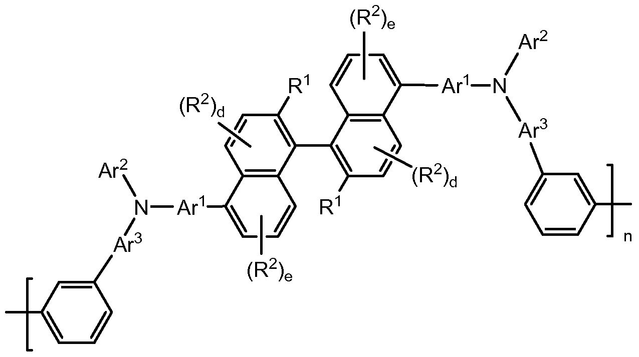
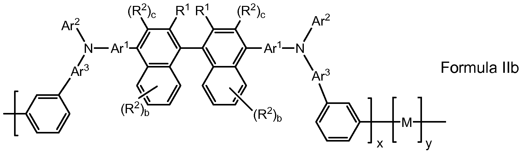
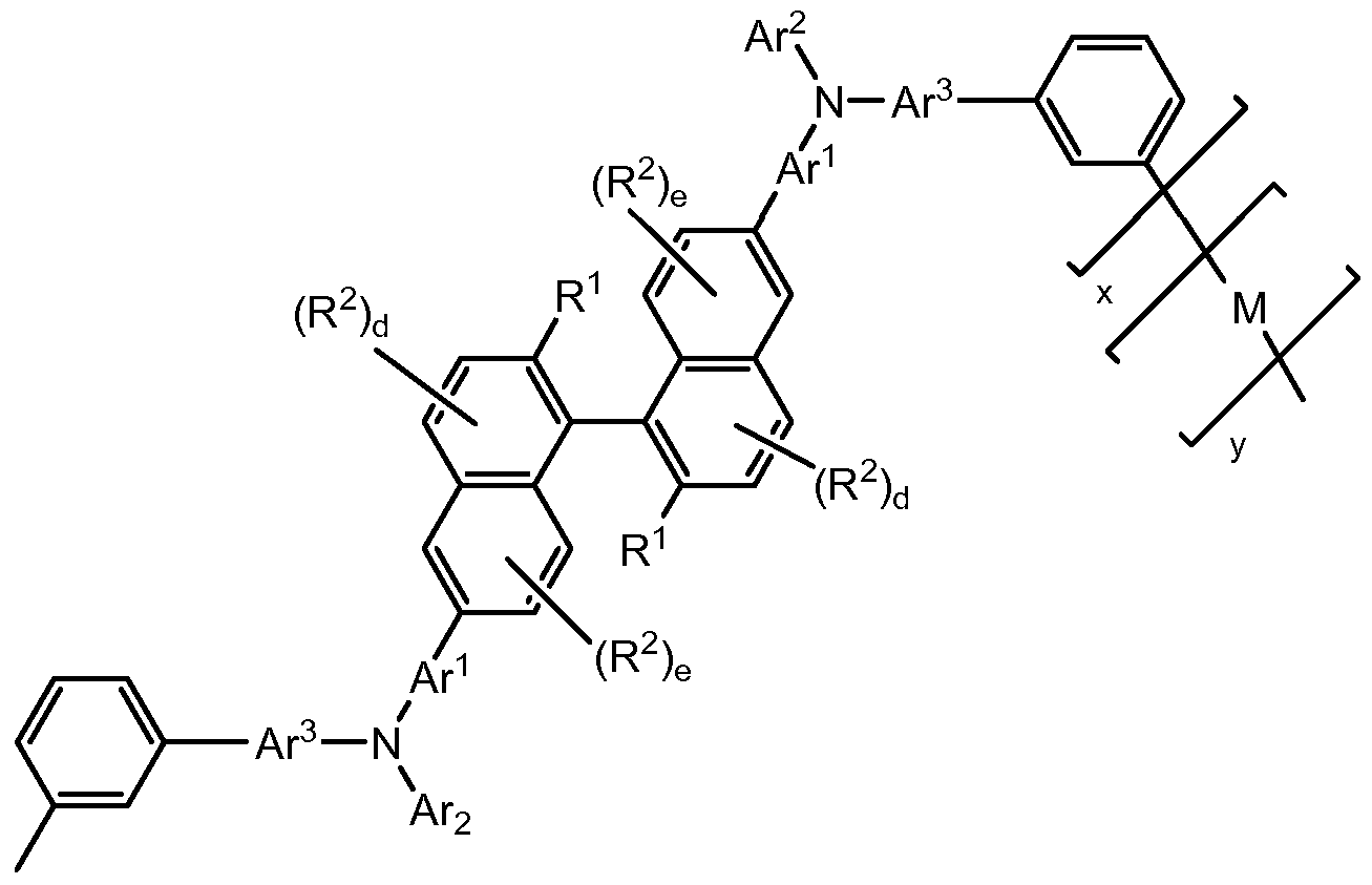
In some embodiments, the compound is selected from the group consisting of Formula Ma having a 3,3'-binaphthyl linkage; Formula Mb having a 4,4'-binaphthyl linkage; Formula Mc having a 5,5'-binaphthyl linkage; Formula Md having a 6,6'-binaphthyl linkage; and Formula Me having a 7,7'-binaphthyl linkage.
Figure imgf000018_0001
Figure imgf000018_0002
Formula Mc
Figure imgf000019_0001
Formula Md
Figure imgf000019_0002
Formula Me
Figure imgf000020_0001
ulae lla-e:
Ar1, Ar2, Ar3, R1, R2, and M are as defined above; b is the same or different at each occurrence and is an integer from
O to 4; c is the same or different at each occurrence and is an integer from
0 to 1 ; d is the same or different at each occurrence and is an integer from
0 to 2; and e is the same or different at each occurrence and is an integer from
O to 3. In some embodiments, Ar1 has Formula III
Formula
Figure imgf000020_0002
where:
R3 is the same or different at each occurrence and is selected from the group consisting of D, alkyl, alkoxy, siloxane and silyl; b is the same or different at each occurrence and is an integer from 0-4; and m is the same or different at each occurrence and is an integer from
1 to 6.
In some embodiments, at least one of one b is not zero. In some embodiments, m = 1 -3. In some embodiments, Ar1 is selected from the group consisting of a single bond, phenylene, p-biphenylene, p-terphenylene, naphthylene, phenylenenaphthylene, and naphthylenephenylene. In some embodiments, Ar1 is selected from the group consisting of phenylene and biphenylene. In some embodiments, Ar2 has Formula IV
Formula IV
Figure imgf000021_0001
where:
R3 is the same or different at each occurrence and is selected from the group consisting of alkyl, alkoxy, siloxane and silyl; a is an integer from 0 to 5; b is the same or different at each occurrence and is an integer from
0 to 4; and m is the same or different at each occurrence and is an integer from
1 to 6. In some embodiments of Formula IV, at least one of one a and b is not zero. In some embodiments, m = 1 -3. In some embodiments, Ar2 is selected from the group consisting phenyl, biphenyl, terphenyl, and naphthyl. In some embodiments, Ar3 has Formula III, as defined above. In some embodiments of Formula III, at least one b is not zero. In some embodiments, m = 1 -3. In some embodiments, Ar3 is selected from the group consisting of a single bond, phenylene, biphenylene, and naphthylene. In some embodiments, Ar3 is selected from the group consisting of phenylene and biphenylene.
Any of Ar1, Ar2 and Ar3, when not a single bond, may be substituted at any position. The substituents may be present to improve one or more physical properties of the compound, such as solubility. In some embodiments, the substituents are selected from the group consisting of D, alkyl groups, silyl groups, siloxane groups, and alkoxy groups. In some embodiments, the groups have from 1 -12 carbon atoms. In some embodiments, adjacent alkyl groups are joined together to form a non- aromatic ring. In some embodiments, there is at least one substituent which includes a crosslinkable group. In some embodiments, crosslinking substituents are present on at least one Ar2. Examples of crosslinkable groups include, but are not limited to vinyl, acrylate, perfluorovinylether, 1 - benzo-3,4-cyclobutane, siloxane, cyanate groups, cyclic ethers (epoxides), cycloalkenes, and acetylenic groups. In one embodiment, the crosslinkable group is vinyl.
In some embodiments, R1 is selected from an alkyl group having 1 - 12 carbon atoms and an alkoxy group having 1 -12 carbon atoms.
In some embodiments, R2 is selected an alkyl group having 1 -12 carbon atoms and an alkoxy group having 1-12 carbon atoms. In some embodiments, a and b are selected from 0 and 1. In some embodiments, a = b = 0.
In some embodiments, n=1 and the compound is not polymeric. In some embodiments, n is 2 or greater and the compound is an oligomer or polymer. In some embodiments, n is greater than 20. Formula Il represents a copolymer in which there is at least one other conjugated moiety. In some embodiments, x is at least 0.4. In some embodiments, x is in the range of 0.4 to 0.6. The copolymers can be random, alternating, or block copolymers. In some embodiments, M is an aromatic unit having triarylamine units. In some embodiments, M is an aromatic group. In some embodiments, M is an aromatic unit having a crosslinkable substituent. The amount of M having a crosslinkable substituent is generally between 4 and 20 mole percent.
When R1 is not H or D, the substituted binaphthyl group introduces non-planarity into the backbone of the compound having Formula I or Formula II. The first naphthyl group is oriented in a plane that is different from the second naphthyl group to which it is linked. Because of the non- planarity, the compounds are chiral. In general, they are formed as racemic mixtures. Some non-limiting examples of compounds having Formula I include Compounds A - D below.
Compound A
Figure imgf000023_0001
Compound B:
Figure imgf000024_0001
Compound C:
Figure imgf000024_0002
Compound D:
Figure imgf000024_0003
The new compounds can be made using any technique that will yield a C-C or C-N bond. A variety of such techniques are known, such as Suzuki, Yamamoto, Stille, and other transition metal catalyzed coupling reactions. The compounds can be formed into layers using solution processing techniques. The term "layer" is used interchangeably with the term "film" and refers to a coating covering a desired area. The term is not limited by size. The area can be as large as an entire device or as small as a specific functional area such as the actual visual display, or as small as a single sub-pixel. Layers and films can be formed by any conventional deposition technique, including vapor deposition, liquid deposition (continuous and discontinuous techniques), and thermal transfer. Continuous deposition techniques, include but are not limited to, spin coating, gravure coating, curtain coating, dip coating, slot-die coating, spray coating, and continuous nozzle coating. Discontinuous deposition techniques include, but are not limited to, ink jet printing, gravure printing, and screen printing. When crosslinking groups are present, the films can be heated and/or treated with UV light to form crosslinked films. The crosslinked films are more robust to additional processing steps and generally are not soluble in processing solvents.
The new compounds described herein have can be used as hole transport materials, as photoactive materials, and as hosts for photoactive materials. The new compounds have hole mobilities and HOMO/LUMO energies similar to efficient small molecule hole transport compounds such as N,N'-diphenyl-N,N'-bis(3-methylphenyl)-[1 ,1 '-biphenyl]-4,4'-diamine (TPD) and N,N'-bis(naphthalen-1 -yl)-N,N'-bis-(phenyl)benzidine (α-NPB). Compounds such as TPD and NPD generally must be applied using a vapor deposition technique.
In some embodiments, the new compounds are useful as hosts for photoactive materials. 3. Electronic Devices
Organic electronic devices that may benefit from having one or more layers comprising at least one compound as described herein include, but are not limited to, (1 ) devices that convert electrical energy into radiation (e.g., a light-emitting diode, light emitting diode display, or diode laser), (2) devices that detect signals through electronics processes (e.g., photodetectors, photoconductive cells, photoresistors, photoswitches, phototransistors, phototubes, IR detectors), (3) devices that convert radiation into electrical energy, (e.g., a photovoltaic device or solar cell), and (4) devices that include one or more electronic components that include one or more organic semi-conductor layers (e.g., a transistor or diode). Other uses for the compositions according to the present invention include coating materials for memory storage devices, antistatic films, biosensors, electrochromic devices, solid electrolyte capacitors, energy storage devices such as a rechargeable battery, and electromagnetic shielding applications.
One illustration of an organic electronic device structure is shown in Figure 1. The device 100 has an anode layer 110 and a cathode layer 150, and a photoactive layer 130 between them. Adjacent to the anode is a layer 120 comprising a charge transport material, for example, a hole transport material. Adjacent to the cathode may be a charge transport layer 140 comprising an electron transport material. As an option, devices may use one or more additional hole injection or hole transport layers (not shown) next to the anode 110 and/or one or more additional electron injection or electron transport layers (not shown) next to the cathode 150.
As used herein, the term "photoactive" refers to a material that emits light when activated by an applied voltage (such as in a light-emitting diode or light-emitting electrochemical cell), or responds to radiant energy and generates a signal with or without an applied bias voltage (such as in a photodetector). In one embodiment, a photoactive layer is an emitter layer.
Depending upon the application of the device 100, the photoactive layer 130 can be a light-emitting layer that is activated by an applied voltage (such as in a light-emitting diode or light-emitting electrochemical cell), a layer of material that responds to radiant energy and generates a signal with or without an applied bias voltage (such as in a photodetector). Examples of photodetectors include photoconductive cells, photoresistors, photoswitches, phototransistors, and phototubes, and photovoltaic cells, as these terms are described in Kirk-Othmer Concise Encyclopedia of Chemical Technology, 4th edition, p.1537, (1999). In some embodiments, the hole transport layer 120 comprises at least one new electroactive compound as described herein.
In some embodiments, the photoactive layer 130 comprises at least one new electroactive compound as described herein, wherein the electroactive compound is photoactive. In some embodiments, the photoactive layer 130 comprises at least one new electroactive compound as described herein, wherein the electroactive compound serves as a host having a photoactive material dispersed therein.
The other layers in the device can be made of any materials which are known to be useful in such layers. The anode 110, is an electrode that is particularly efficient for injecting positive charge carriers. It can be made of, for example materials containing a metal, mixed metal, alloy, metal oxide or mixed-metal oxide, or it can be a conducting polymer, and mixtures thereof. Suitable metals include the Group 11 metals, the metals in Groups 4, 5, and 6, and the Group 8 10 transition metals. If the anode is to be light-transmitting, mixed-metal oxides of Groups 12, 13 and 14 metals, such as indium-tin-oxide, are generally used. The anode 110 may also comprise an organic material such as polyaniline as described in "Flexible light-emitting diodes made from soluble conducting polymer," Nature vol. 357, pp 477 479 (11 June 1992). At least one of the anode and cathode should be at least partially transparent to allow the generated light to be observed.
In some embodiments, the device further comprises a buffer layer between the anode and the layer comprising the new polymer. The term "buffer layer" is intended to mean a layer comprising electrically conductive or semiconductive materials and may have one or more functions in an organic electronic device, including but not limited to, planahzation of the underlying layer, charge transport and/or charge injection properties, scavenging of impurities such as oxygen or metal ions, and other aspects to facilitate or to improve the performance of the organic electronic device. Buffer materials may be polymers, oligomers, or small molecules, and may be in the form of solutions, dispersions, suspensions, emulsions, colloidal mixtures, or other compositions. The buffer layer can be formed with polymeric materials, such as polyaniline (PANI) or polyethylenedioxythiophene (PEDOT), which are often doped with protonic acids. The protonic acids can be, for example, poly(styrenesulfonic acid), poly(2-acrylamido-2-methyl-1 -propanesulfonic acid), and the like. The buffer layer can comprise charge transfer compounds, and the like, such as copper phthalocyanine and the tetrathiafulvalene- tetracyanoquinodimethane system (TTF-TCNQ). In one embodiment, the buffer layer is made from a dispersion of a conducting polymer and a colloid-forming polymeric acid. Such materials have been described in, for example, published U.S. patent applications 2004-0102577, 2004- 0127637, and 2005/205860.
In some embodiments, hole transport layer 120 comprises the new electroactive compound described herein. In some embodiments, layer 120 comprises other hole transport materials. Examples of other hole transport materials for layer 120 have been summarized for example, in Kirk Othmer Encyclopedia of Chemical Technology, Fourth Edition, Vol. 18, p. 837 860, 1996, by Y. Wang. Both hole transporting molecules and polymers can be used. Commonly used hole transporting molecules include, but are not limited to: N,N'-diphenyl-N,N'-bis(3-methylphenyl)- [1 ,1 '-biphenyl]-4,4'-diamine (TPD), 1 ,1 -bis[(di-4-tolylamino) phenyl]cyclohexane (TAPC), N,N'-bis(4-methylphenyl)-N,N'-bis(4- ethylphenyl)-[1 ,1 '-(3,3'-dimethyl)biphenyl]-4,4'-diamine (ETPD), tetrakis (3- methylphenyl)-N,N,N',N'-2,5-phenylenediamine (PDA), a-phenyl 4-N,N- diphenylaminostyrene (TPS), p- (diethylamino)benzaldehyde diphenylhydrazone (DEH), thphenylamine (TPA), bis[4 (N,N-diethylamino)- 2-methylphenyl](4-methylphenyl)methane (MPMP), 1 -phenyl-3-[p- (diethylamino)styryl]-5-[p-(diethylamino)phenyl] pyrazoline (PPR or DEASP), 1 ,2-trans-bis(9H-carbazol-9-yl)cyclobutane (DCZB), N,N,N\N' tetrakis(4-methylphenyl)-(1 ,1 '-biphenyl)-4,4'-diamine (TTB), N1N'- Bis(naphthalen-1 -yl)-N,N'-bis-(phenyl)benzidine (α-NPB), and porphyrinic compounds, such as copper phthalocyanine. Commonly used hole transporting polymers include, but are not limited to, polyvinylcarbazole, (phenylmethyl)polysilane, and polyaniline. It is also possible to obtain hole transporting polymers by doping hole transporting molecules such as those mentioned above into polymers such as polystyrene and polycarbonate. Buffer layers and/or hole transport layer can also comprise polymers of thiophene, aniline, or pyrrole with polymeric fluorinated sulfonic acids, as described in published US applications 2004/102577, 2004/127637, and 2005/205860.
Any organic electroluminescent ("EL") material can be used as the photoactive material in layer 130, including, but not limited to, small molecule organic fluorescent compounds, fluorescent and phosphorescent metal complexes, conjugated polymers, and mixtures thereof. Examples of fluorescent compounds include, but are not limited to, chrysenes, pyrenes, perylenes, rubrenes, coumarins, anthracenes, thiadiazoles, derivatives thereof, and mixtures thereof. Examples of metal complexes include, but are not limited to, metal chelated oxinoid compounds, such as ths(8-hydroxyquinolato)aluminum (Alq3); cyclometalated iridium and platinum electroluminescent compounds, such as complexes of iridium with phenylpyhdine, phenylquinoline, or phenylpyhmidine ligands as disclosed in Petrov et al., U.S. Patent 6,670,645 and Published PCT Applications WO 03/063555 and WO 2004/016710, and organometallic complexes described in, for example, Published PCT Applications WO 03/008424, WO 03/091688, and WO 03/040257, and mixtures thereof. In some cases the small molecule fluorescent or organometallic materials are deposited as a dopant with a host material to improve processing and/or electronic properties. Examples of conjugated polymers include, but are not limited to poly(phenylenevinylenes), polyfluorenes, poly(spirobifluorenes), polythiophenes, poly(p-phenylenes), copolymers thereof, and mixtures thereof. The materials may also be present in admixture with a host material. In some embodiments, the host material is a hole transport material or an electron transport material. In some embodiments, the host is the new electroactive compound described herein. In some embodiments, the ratio of host material to photoactive material is in the range of 5:1 to 20:1 ; in some embodiments, 10:1 to 15:1. Examples of electron transport materials which can be used in the electron transport layer 140 and/or the optional layer between layer 140 and the cathode include metal chelated oxinoid compounds, such as tris(8-hydroxyquinolato)aluminum (AIQ), bis(2-methyl-8-quinolinolato)(p- phenylphenolato) aluminum (BAIq), tetrakis-(8-hydroxyquinolato)hafnium (HfQ) and tetrakis-(8-hydroxyquinolato)zirconium (ZrQ); and azole compounds such as 2- (4-biphenylyl)-5-(4-t-butylphenyl)-1 ,3,4-oxadiazole (PBD), 3-(4-biphenylyl)-4-phenyl-5-(4-t-butylphenyl)-1 ,2,4-triazole (TAZ), and 1 ,3,5-th(phenyl-2-benzimidazole)benzene (TPBI); quinoxaline derivatives such as 2,3-bis(4-fluorophenyl)quinoxaline; phenanthrolines such as 4,7-diphenyl-1 ,10-phenanthroline (DPA) and 2,9-dimethyl-4,7- diphenyl-1 ,10-phenanthroline (DDPA); and mixtures thereof.
The cathode 150, is an electrode that is particularly efficient for injecting electrons or negative charge carriers. The cathode can be any metal or nonmetal having a lower work function than the anode. Materials for the cathode can be selected from alkali metals of Group 1 (e.g., Li, Cs), the Group 2 (alkaline earth) metals, the Group 12 metals, including the rare earth elements and lanthanides, and the actinides. Materials such as aluminum, indium, calcium, barium, samarium and magnesium, as well as combinations, can be used. Li-containing organometallic compounds, LiF, and Li2O can also be deposited between the organic layer and the cathode layer to lower the operating voltage.
The choice of materials for each of the component layers is preferably determined by balancing the goals of providing a device with high device efficiency with device operational lifetime. Other layers may also be present in the device. There may be one or more hole injection and/or hole transport layers between the buffer layer and the organic active layer. There may be one or more electron transport layers and/or electron injection layers between the organic active layer and the cathode. The device can be prepared by a variety of techniques, including sequentially depositing the individual layers on a suitable substrate. Substrates such as glass and polymeric films can be used. Conventional vapor deposition techniques can be used, such as thermal evaporation, chemical vapor deposition, and the like. Alternatively, the organic layers can be applied by liquid deposition using suitable solvents. The liquid can be in the form of solutions, dispersions, or emulsions. Typical liquid deposition techniques include, but are not limited to, continuous deposition techniques such as spin coating, gravure coating, curtain coating, dip coating, slot-die coating, spray-coating, and continuous nozzle coating; and discontinuous deposition techniques such as ink jet printing, gravure printing, and screen printing, any conventional coating or printing technique, including but not limited to spin-coating, dip-coating, roll-to-roll techniques, ink jet printing, screen-printing, gravure printing and the like. The new electroactive compounds described herein can be applied by liquid deposition from a liquid composition. The term "liquid composition" is intended to mean a liquid medium in which a material is dissolved to form a solution, a liquid medium in which a material is dispersed to form a dispersion, or a liquid medium in which a material is suspended to form a suspension or an emulsion. Any liquid medium in which the compound is dissolved or dispersed and from which it will form a film can be used. In one embodiment, the liquid medium consists essentially of one or more organic solvents. In one embodiment the organic solvent is an aromatic solvent. In one embodiment, the organic liquid is selected from chloroform, dichloromethane, toluene, anisole, and mixtures thereof. The new compound can be present in the liquid medium in a concentration of 0.2 to 2 percent by weight. Other weight percentages of the new compound may be used depending upon the liquid medium.
In one embodiment, the different layers have the following range of thicknesses: anode 110, 500-5000 A, in one embodiment 1000-2000 A; hole transport layer 120, 50-2000 A, in one embodiment 200-1000 A; photoactive layer 130, 10-2000 A, in one embodiment 100-1000 A; layer 140, 50-2000 A, in one embodiment 100-1000 A; cathode 150, 200-10000 A, in one embodiment 300-5000 A. The location of the electron-hole recombination zone in the device, and thus the emission spectrum of the device, can be affected by the relative thickness of each layer. Thus the thickness of the electron-transport layer should be chosen so that the electron-hole recombination zone is in the light-emitting layer. The desired ratio of layer thicknesses will depend on the exact nature of the materials used.
In one embodiment, the device has the following structure, in order: anode, buffer layer, hole transport layer, photoactive layer, electron transport layer, electron injection layer, cathode. In one embodiment, the anode is made of indium tin oxide or indium zinc oxide. In one embodiment, the buffer layer comprises a conducting polymer selected from the group consisting of polythiophenes, polyanilines, polypyrroles, copolymers thereof, and mixtures thereof. In one embodiment, the buffer layer comprises a complex of a conducting polymer and a colloid-forming polymeric acid.
In one embodiment, the hole transport layer comprises the new compound described herein. In one embodiment, the hole transport layer consists essentially of the new electroactive compound described herein. In one embodiment, the photoactive layer comprises the new electroactive compound described herein and a photoactive compound. In one embodiment, the photoactive layer further comprises a second host material. In some embodiments, the photoactive layer consists essentially of the new electroactive compound described herein and a photoactive compound. In some embodiments, the photoactive material is present in an amount of at least 1 % by weight. In some embodiments, the photoactive material is 2-20% by weight.
In one embodiment, the electron transport layer comprises a metal complex of a hydroxyaryl-N-heterocycle. In one embodiment, the hydroxyaryl-N-heterocycle is unsubstituted or substituted 8- hydroxyquinoline.
In one embodiment, the electron injection layer is LiF or Li2O. In one embodiment, the cathode is Al or Ba/AI. In one embodiment, the device is fabricated by liquid deposition of the buffer layer, the hole transport layer, and the photoactive layer, and by vapor deposition of the electron transport layer, the electron injection layer, and the cathode. Although methods and materials similar or equivalent to those described herein can be used in the practice or testing of the present invention, suitable methods and materials are described below. In addition, the materials, methods, and examples are illustrative only and not intended to be limiting. All publications, patent applications, patents, and other references mentioned herein are incorporated by reference in their entirety.
EXAMPLES
The concepts described herein will be further described in the following examples, which do not limit the scope of the invention described in the claims. Example 1
This example illustrates the preparation of a monomer which can be used to form an electroactive compound, Compound C.
(a) The starting material ditriflate 1 was synthesized from the scheme described below.
(H
Figure imgf000034_0001
(b) The monomer 3 was synthesized according to the following scheme:
Figure imgf000034_0002
In a nitrogen purged glove box, ditriflate 1 (2 g, 2.73 mmol) and 4- octylaniline (1.18 g, 5.73 mmol, 2.1 eq.) were dissolved in toluene (40 ml_) in a 100 ml_ of round bottom flask, followed by the addition of the toluene (10 ml_) solution of ths(dibenzylideneacetone)dipalladium(0) (25 mg, 0.027 eq.) and 1 ,1 '-bis(diphenylphosphino)ferrocene (30 mg, 0.053 eq) to the mixture. After stirring the mixture for 5 min, sodium t-butoxide (0.657 g, 6.82 mmol, 2.5 eq) was added to the resultant solution. The reaction mixture was stirred for 3 days at 9O0C under nitrogen outside glove box. The mixture was passed through a pad of silica gel, which was rinsed with toluene. The combined solution was concentrated on a rotary evaporator, followed by flash column chromatography (30% methylene chloride in hexane) to afford 0.98 g of a white solid as a product. NMR analysis confirmed the structure of intermediate compound 1.
In a nitrogen purged glove box, diamine 2 (0.98 g, 1.16 mmol) and 3-bromo-1 -iodobenzene (0.99 g, 3.50 mmol) were dissolved in toluene (30 ml_) in a 100 ml_ of round bottom flask, followed by the addition of the toluene (8 ml_) solution of ths(dibenzylideneacetone)dipalladium(0) (29 mg, 0.027 eq.) and 1 ,1 '-bis(diphenylphosphino)ferrocene (34 mg, 0.053 eq) to the mixture. After stirring the mixture for 5 min, sodium t-butoxide (280 mg, 2.91 mmol, 2.5 eq) was added to the resultant solution. The reaction mixture was stirred for 4 days at 90 0C under nitrogen outside glove box. The mixture was passed through a pad of silica gel, which was rinsed with toluene. The combined solution was concentrated on a rotary evaporator, followed by flash column chromatography (hexane) to afford 1.2 g of a white solid. NMR analysis confirmed the structure of compound 3. (polymer H-1661 )
Example 2
The monomer from Example 1 can be polymerized to form Compound C. This can be done using Yamamoto coupling according to the following scheme:
Figure imgf000036_0001
Compound C
All operations were carried out in a nitrogen purged glovebox unless otherwise noted. Monomer 3 (1.036 g, 0.90 mmol) was added to a scintillation vial and dissolved in 22 ml_ toluene. A clean, dry 50 ml_ Schlenk tube was charged with bis(1 ,5- cyclooctadiene)nickel(O) (0.500 g, 1.818 mmol). 2,2'-Dipyridyl (0.284 g, 1.818 mmol) and 1 ,5-cyclooctadiene (0.197 g, 1.818 mmol) were weighed into a scintillation vial and dissolved in 5.5 ml_ N1N'- dimethylformamide. The solution was added to the Schlenk tube. The Schlenk tube was inserted into an aluminum block and the block was heated and stirred on a hotplate/stirrer at a setpoint that resulted in an internal temperature of 600C. The catalyst system was held at 600C for 30 minutes and then raised to 70°C. The monomer solution in toluene was added to the Schlenk tube and the tube was sealed. The polymerization mixture was stirred at 700C for 18 h. After 18 h,the Schlenk tube was removed from the block and allowed to cool to room temperature. The tube was removed from the glovebox and the contents were poured into a solution of cone. HCI/MeOH (1.5% v/v cone. HCI). After stirring for 2 h, the polymer was collected by vacuum filtration and dried under high vacuum. The polymer was purified by successive precipitations from toluene into HCI/MeOH (1 % v/v cone. HCI), MeOH, toluene (CMOS grade), and 3-pentanone. A white, fibrous polymer (0.200 g) was obtained. The molecular weight of the polymer was determined by GPC (THF mobile phase, polystyrene standards): Mw=20,486; Mn=5.049; Mw/Mn=4.06. NMR analysis confirmed the structure of Compound C.
Example 3
This example illustrates the preparation of a monomer which can be used to form an electroactive compound, Compound D. The monomer 12 was synthesized according to the following scheme:
Figure imgf000037_0001
12
In a nitrogen purged glove box, ditriflate 10 (2.72 g, 4.70 mmol) and 4-octylaniline (2.03 g, 9.87 mmol, 2.1 eq.) were dissolved in toluene (30 ml_) in a 100 ml_ of round bottom flask, followed by the addition of the toluene (10 ml_) solution of ths(dibenzylideneacetone)dipalladium(0) (43 mg, 0.01 eq.) and 1 ,1 '-bis(diphenylphosphino)ferrocene (52 mg, 0.02 eq) to the mixture. After stirring the mixture for 5 min, sodium t-butoxide (1.13 g, 11.75 mmol, 2.5 eq) was added to the resultant solution. The reaction mixture was stirred overnight at 850C under nitrogen outside glove box. The mixture was passed through a pad of silica gel, which was rinsed with toluene. The combined solution was concentrated on a rotary evaporator, followed by flash column chromatography (2% to 10 ethylacetate in hexane, gradient) to afford 2.37 g of a white solid as a product. NMR analysis confirmed the structure of intermediate compound 11.
In a nitrogen purged glove box, diamine 11 (1.45 g, 2.10 mmol) and 3-bromo-1 -iodobenzene (1.78 g, 6.3 mmol, 3eq.) were dissolved in toluene (30 ml_) in a 100 ml_ of round bottom flask, followed by the addition of the toluene (8 ml_) solution of ths(dibenzylideneacetone)dipalladiunn(0) (52 mg, 0.027 eq.) and 1 ,1 '-bis(diphenylphosphino)ferrocene (62 mg, 0.053 eq) to the mixture. After stirring the mixture for 5 min, sodium t-butoxide (504 mg, 5.25 mmol, 2.5 eq) was added to the resultant solution. The reaction mixture was stirred for 3 days at 9O0C under nitrogen outside glove box. The mixture was passed through a pad of silica gel, which was rinsed with toluene. The combined solution was concentrated on a rotary evaporator, followed by flash column chromatography (3% toluene in hexane) to afford 1.5 g of a white solid. NMR analysis confirmed the structure of compound 12.
Example 4
The monomer from Example 3 can be polymerized to form Compound D. This can be done using Yamamoto coupling according to the following scheme:
Figure imgf000038_0001
12
Compound D
The polymerization of compound 12 performed as described for compound C. The polymer was obtained as a white solid in 84.6% yield. The molecular weight of the polymer was determined by GPC (THF mobile phase, polystyrene standards): Mw=1 ,846; Mn=I , 291 ; Mw/Mn=1.43. NMR analysis confirmed the structure of Compound D.
Example 5 This example illustrates the preparation of a monomer which can be used to form an electroactive compound, Compound A. The monomer 15 was synthesized according to the following scheme:
Figure imgf000039_0001
14 15
In a nitrogen purged glove box, ditriflate 13 (1.7 g, 2.33 mmol) and 3-octylaniline (1 g, 4.89 mmol) were dissolved in toluene (20 ml_) in a 100 ml_ of round bottom flask, followed by the addition of the toluene (10 ml_) solution of ths(dibenzylideneacetone)dipalladium(0) (58 mg, 0.027 eq.) and 1 ,1 '-bis(diphenylphosphino)ferrocene (68 mg, 0.053 eq) to the mixture. After stirring the mixture for 5 min, sodium t-butoxide (0.56 g, 5.82 mmol, 2.5 eq) was added to the resultant solution. The reaction mixture was stirred for 16 h at 850C under nitrogen outside glove box. The mixture was passed through a pad of silica gel, which was rinsed with toluene. The combined solution was concentrated on a rotary evaporator, followed by flash column chromatography (10% to 40% methylene chloride in hexane, gradiently) to afford 1.6 g of product. NMR analysis confirmed the structure of intermediate compound 14. In a nitrogen purged glove box, diamine 14 (1.5 g, 1.78 mmol) and
3-bromo-1 -iodobenzene (1.51 g, 5.35 mmol) were dissolved in toluene (40 ml_) in a 100 ml_ of round bottom flask, followed by the addition of the toluene (7 ml_) solution of ths(dibenzylideneacetone)dipalladiunn(0) (47 mg, 0.027 eq.) and 1 ,1 '-bis(diphenylphosphino)ferrocene (53 mg, 0.053 eq) to the mixture. After stirring the mixture for 5 min, sodium t-butoxide (0.428 g, 4.45 mmol, 2.5 eq) was added to the resultant solution. The reaction mixture was stirred for 4 days at 9O0C under nitrogen outside glove box. The mixture was passed through a pad of silica gel, which was rinsed with toluene. The combined solution was concentrated on a rotary evaporator, followed by flash column chromatography (5% toluene in hexane) to afford 1.6 g of a white solid. NMR analysis confirmed the structure of compound 15.
Example 6
The monomer from Example 5 can be polymerized to form Compound A. This can be done using Yamamoto coupling according to the following scheme:
The polymerization of compound 15 was performed as described for compound C. The polymer was obtained as a white solid in 38% yield. The molecular weight of the polymer was determined by GPC (THF mobile phase, polystyrene standards): Mw=210,638; Mn=33,194; Mw/Mn=6.35. NMR analysis confirmed the structure of Compound A.
Figure imgf000041_0001
15 Compound A
Example 7
This example illustrates the preparation of a monomer which can be used to form an electroactive compound, Compound B. The monomer 18 was synthesized according to the following scheme:
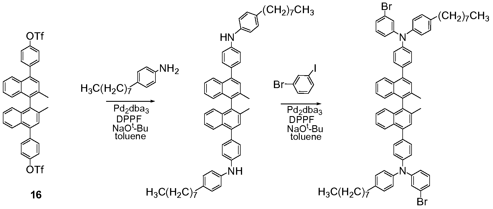
Figure imgf000041_0002
17 18
In a nitrogen purged glove box, ditriflate 16 (1.67 g, 2.28 mmol) and
4-octylaniline(0.984 g, 4.79 mmol) were dissolved in toluene (20 ml_) in a 50 ml_ of round bottom flask, followed by the addition of the toluene (2 ml_) solution of tris(dibenzylideneacetone)dipalladium(0) (21 mg, 0.027 eq.) and 1 ,1 '-bis(diphenylphosphino)ferrocene (25 mg, 0.053 eq) to the mixture. After stirring the mixture for 5 min, sodium t-butoxide (0.548 g, 5.71 mmol, 2.5 eq) was added to the resultant solution. The reaction mixture was stirred for 2Oh at 850C under nitrogen outside glove box. The mixture was passed through a pad of silica gel, which was rinsed with toluene. The combined solution was concentrated on a rotary evaporator, followed by flash column chromatography (25% methylenechloride in hexane) to afford 1.04 g of a white solid. NMR analysis confirmed the structure of intermediate compound 17.
In a nitrogen purged glove box, diamine 17 (1.02 g, 1.212 mmol) and 3-bromo-1-iodobenzene (1.029 g, 3.636 mmol) were dissolved in toluene (20 ml_) in a 50 ml_ of round bottom flask, followed by the addition of the toluene (2 ml_) solution of ths(dibenzylideneacetone)dipalladium(0) (30 mg, 0.027 eq.) and 1 ,1 '-bis(diphenylphosphino)ferrocene (36 mg, 0.053 eq) to the mixture. After stirring the mixture for 5 min, sodium t- butoxide (291 mg, 3.03 mmol, 2.5 eq) was added to the resultant solution. The reaction mixture was stirred for 24h at 850C under nitrogen outside glove box. The mixture was passed through a pad of silica gel, which was rinsed with toluene. The combined solution was concentrated on a rotary evaporator, followed by flash column chromatography (10% toluene in hexane) to afford 1.2 g of a white solid. NMR analysis confirmed the structure of compound 18.
Example 8
The monomer from Example 7 can be polymerized to form Compound B. This can be done using Yamamoto coupling according to the following scheme:
Figure imgf000043_0001
18
Compound B
The polymerization of compound 18 was performed as described for compound B. The polymer was obtained as a white solid in 50% yield. The molecular weight of the polymer was determined by GPC (THF mobile phase, polystyrene standards): Mw=213,649; Mn=I 02,594; Mw/Mn=2.08. NMR analysis confirmed the structure of compound B.
Note that not all of the activities described above in the general description or the examples are required, that a portion of a specific activity may not be required, and that one or more further activities may be performed in addition to those described. Still further, the order in which activities are listed are not necessarily the order in which they are performed.
In the foregoing specification, the concepts have been described with reference to specific embodiments. However, one of ordinary skill in the art appreciates that various modifications and changes can be made without departing from the scope of the invention as set forth in the claims below. Accordingly, the specification and figures are to be regarded in an illustrative rather than a restrictive sense, and all such modifications are intended to be included within the scope of invention.
Benefits, other advantages, and solutions to problems have been described above with regard to specific embodiments. However, the benefits, advantages, solutions to problems, and any feature(s) that may cause any benefit, advantage, or solution to occur or become more pronounced are not to be construed as a critical, required, or essential feature of any or all the claims.
It is to be appreciated that certain features are, for clarity, described herein in the context of separate embodiments, may also be provided in combination in a single embodiment. Conversely, various features that are, for brevity, described in the context of a single embodiment, may also be provided separately or in any subcombination. Further, reference to values stated in ranges include each and every value within that range.

Claims

CLAIMS What is claimed is:
1. A compound having Formula I or Formula II:
Formula I
Figure imgf000045_0001
Figure imgf000046_0001
wherein:
Ar1 is the same or different at each occurrence and is selected from the group consisting of a single bond and an arylene;
Ar2 is the same or different at each occurrence and is an aryl group;
Ar3 is the same or different at each occurrence and is selected from the group consisting of a single bond and an arylene;
R1 is the same or different at each occurrence and is selected from the group consisting of H, D, aryl groups, alkyl groups, silyl groups, siloxane groups, fluoroalkyl groups, alkoxy groups, and fluoroalkoxy groups, or the two R1 groups may be joined together to form an aliphatic ring having 5-10 carbons;
R2 is the same or different at each occurrence and is selected from the group consisting of D, aryl groups, alkyl groups, silyl groups, siloxane groups, fluoroalkyl groups, alkoxy groups, and fluoroalkoxy groups; M is the same or different at each occurrence and is a conjugated moiety; a is the same or different at each occurrence and is an integer from
O to 5; n is an integer equal to or greater than 2; and x and y are mole fractions such that x + y = 1.0, with the proviso that x and y are not zero.
2. The compound of Claim 1 , having a formula selected from the group consisting of Formulae Ia through Ie
Figure imgf000047_0001
Formula Ib
Figure imgf000047_0002
Figure imgf000048_0001
Formula Ic
Figure imgf000048_0002
Formula Ie
Figure imgf000049_0001
where; b is the same or different at each occurrence and is an integer from
O to 4; c is the same or different at each occurrence and is an integer from
0 to 1 ; d is the same or different at each occurrence and is an integer from
0 to 2; and e is the same or different at each occurrence and is an integer from
O to 3.
3. The compound of Claim 1 , having a formula selected from the group consisting of Formulae Na through Me
Figure imgf000050_0001
Figure imgf000050_0002
Formula Mc
Figure imgf000050_0003
Formula Md
Figure imgf000051_0001
Formula Me
Figure imgf000051_0002
where: b is the same or different at each occurrence and is an integer from
Oto 4; c is the same or different at each occurrence and is an integer from
0to 1; d is the same or different at each occurrence and is an integer from
0 to 2; and e is the same or different at each occurrence and is an integer from
O to 3.
4. The compound of Claim 1 , wherein Ar1 has Formula III
Formula
Figure imgf000052_0001
where:
R3 is the same or different at each occurrence and is selected from the group consisting of D, alkyl, alkoxy, siloxane and silyl; c is the same or different at each occurrence and is an integer from 0-4; and m is an integer from 1 to 6.
5. The compound of Claim 1 , wherein Ar1 is selected from the group consisting of a single bond, phenylene, p-biphenylene, p- terphenylene, naphthylene, phenylenenaphthylene, and naphthylenephenylene.
6. The compound of Claim 1 , wherein Ar2 is selected from the group consisting of naphthyl and a group having Formula IV Formula IV
Figure imgf000053_0001
where:
R3 is the same or different at each occurrence and is selected from the group consisting of alkyl, alkoxy, siloxane and silyl; c is the same or different at each occurrence and is an integer from 0-4; d is an integer from 0-5; and m is an integer from 1 to 6.
7. The compound of Claim 1 , wherein Ar3 is selected from the group consisting of a single bond, naphthylene, and a group having Formula III
Formula
Figure imgf000053_0002
where:
R3 is the same or different at each occurrence and is selected from the group consisting of alkyl, alkoxy, siloxane and silyl; c is the same or different at each occurrence and is an integer from
0-4; and m is an integer from 1 to 6.
8. The compound of Claim 1 , wherein crosslinking substituents are present on at least one Ar2.
9. The compound of Claim 1 , wherein R1 is selected from an alkyl group having 1 -12 carbon atoms and an alkoxy group having 1 -12 carbon atoms.
10. The compound of Claim 1 , wherein R2 is selected from an alkyl group having 1 -12 carbon atoms and an alkoxy group having 1 -12 carbon atoms.
11. The compound of Claim 1 having Formula II, wherein x is at least 0.4.
12. The compound of Claim 1 having Formula II, wherein M is selected from the group consisting of an aromatic group having triarylamine units and an aromatic unit having a crosslinkable substituent.
13. An organic electronic device comprising a first electrical contact layer, a second electrical contact layer and an active layer therebetween, wherein the active layer comprises a compound of any one of the foregoing claims.
14. The device of Claim 13, wherein the active layer is a photoactive layer.
15. The device of Claim 14, wherein the active layer further comprises a photoactive material and wherein the compound is selected from the group consisting of a compound of Formula I and a compound of Formula II.
PCT/US2009/066188 2008-12-01 2009-12-01 Electroactive materials WO2010065497A2 (en)

Priority Applications (3)

Application Number Priority Date Filing Date Title
KR1020117015117A KR101817808B1 (en) 2008-12-01 2009-12-01 Electroactive materials
EP09830951.1A EP2352801B1 (en) 2008-12-01 2009-12-01 Electroactive materials
JP2011538724A JP2012510474A (en) 2008-12-01 2009-12-01 Electroactive materials

Applications Claiming Priority (2)

Application Number Priority Date Filing Date Title
US11871708P 2008-12-01 2008-12-01
US61/118,717 2008-12-01

Publications (2)

Publication Number Publication Date
WO2010065497A2 true WO2010065497A2 (en) 2010-06-10
WO2010065497A3 WO2010065497A3 (en) 2010-07-22

Family

ID=42233810

Family Applications (1)

Application Number Title Priority Date Filing Date
PCT/US2009/066188 WO2010065497A2 (en) 2008-12-01 2009-12-01 Electroactive materials

Country Status (5)

Country Link
US (1) US9099653B2 (en)
EP (1) EP2352801B1 (en)
JP (1) JP2012510474A (en)
KR (1) KR101817808B1 (en)
WO (1) WO2010065497A2 (en)

Cited By (3)

* Cited by examiner, † Cited by third party
Publication number Priority date Publication date Assignee Title
WO2012021315A3 (en) * 2010-08-11 2012-05-24 E. I. Du Pont De Nemours And Company Electroactive compound and composition and electronic device made with the composition
JP2012214732A (en) * 2011-03-25 2012-11-08 Sumitomo Chemical Co Ltd Polymer compound, and light-emitting element using the same
US8551624B2 (en) 2008-12-01 2013-10-08 E I Du Pont De Nemours And Company Electroactive materials

Families Citing this family (14)

* Cited by examiner, † Cited by third party
Publication number Priority date Publication date Assignee Title
US8440324B2 (en) * 2005-12-27 2013-05-14 E I Du Pont De Nemours And Company Compositions comprising novel copolymers and electronic devices made with such compositions
WO2008024378A2 (en) 2006-08-24 2008-02-28 E. I. Du Pont De Nemours And Company Hole transport polymers
US8465848B2 (en) * 2006-12-29 2013-06-18 E I Du Pont De Nemours And Company Benzofluorenes for luminescent applications
CN102603459A (en) 2007-06-01 2012-07-25 E.I.内穆尔杜邦公司 Charge transport materials for luminescent applications
US8063399B2 (en) 2007-11-19 2011-11-22 E. I. Du Pont De Nemours And Company Electroactive materials
US8343381B1 (en) 2008-05-16 2013-01-01 E I Du Pont De Nemours And Company Hole transport composition
KR20140116526A (en) * 2008-12-04 2014-10-02 이 아이 듀폰 디 네모아 앤드 캄파니 Electroactive materials
US8759818B2 (en) 2009-02-27 2014-06-24 E I Du Pont De Nemours And Company Deuterated compounds for electronic applications
KR101582707B1 (en) * 2009-04-03 2016-01-05 이 아이 듀폰 디 네모아 앤드 캄파니 Electroactive materials
JP4934704B2 (en) * 2009-07-27 2012-05-16 株式会社日立製作所 Lithium ion secondary battery and overcharge inhibitor for lithium ion secondary battery
TW201111326A (en) 2009-09-29 2011-04-01 Du Pont Deuterated compounds for luminescent applications
CN102596950A (en) 2009-10-29 2012-07-18 E.I.内穆尔杜邦公司 Deuterated compounds for electronic applications
EP2655547A1 (en) 2010-12-20 2013-10-30 E.I. Du Pont De Nemours And Company Compositions for electronic applications
CN103483556A (en) * 2013-09-11 2014-01-01 华南理工大学 Hydroxyethyl-containing biradicals conjugated polymer and application thereof

Citations (10)

* Cited by examiner, † Cited by third party
Publication number Priority date Publication date Assignee Title
WO2002051958A1 (en) 2000-12-23 2002-07-04 Johnson Matthey Public Limited Company Electroactive polyarylamine-type compositions
WO2003008424A1 (en) 2001-07-18 2003-01-30 E.I. Du Pont De Nemours And Company Luminescent lanthanide complexes with imine ligands and devices made with such complexes
WO2003040257A1 (en) 2001-11-07 2003-05-15 E. I. Du Pont De Nemours And Company Electroluminescent platinum compounds and devices made with such compounds
WO2003063555A1 (en) 2001-12-26 2003-07-31 E. I. Du Pont De Nemours And Company Electroluminescent iridium compounds wiht fluorinated phenylpyridines, phenylpyrimidines, and phenylquinolines and devices made with such compounds
WO2003091688A2 (en) 2001-07-05 2003-11-06 E.I. Du Pont De Nemours And Company Photoactive lanthanide complexes with phosphine oxides, phosphine oxide-sulfides, pyridine n-oxides, and phosphine oxide-pyridine n-oxides, and devices made with such complexes
US6670645B2 (en) 2000-06-30 2003-12-30 E. I. Du Pont De Nemours And Company Electroluminescent iridium compounds with fluorinated phenylpyridines, phenylpyrimidines, and phenylquinolines and devices made with such compounds
WO2004016710A1 (en) 2002-08-15 2004-02-26 E.I. Du Pont De Nemours And Company Compounds comprising phosphorus-containing metal complexes
US20040102577A1 (en) 2002-09-24 2004-05-27 Che-Hsiung Hsu Water dispersible polythiophenes made with polymeric acid colloids
US20040127637A1 (en) 2002-09-24 2004-07-01 Che-Hsiung Hsu Water dispersible polyanilines made with polymeric acid colloids for electronics applications
US20050205860A1 (en) 2004-03-17 2005-09-22 Che-Hsiung Hsu Water dispersible polypyrroles made with polymeric acid colloids for electronics applications

Family Cites Families (72)

* Cited by examiner, † Cited by third party
Publication number Priority date Publication date Assignee Title
EP0650955B1 (en) * 1993-11-01 1998-08-19 Hodogaya Chemical Co., Ltd. Amine compound and electro-luminescence device comprising same
DE69511755T2 (en) 1994-04-26 2000-01-13 Tdk Corp Phenylanthracene derivative and organic EL element
JP3586906B2 (en) 1994-12-14 2004-11-10 凸版印刷株式会社 Method for manufacturing transparent conductive film
US5708130A (en) * 1995-07-28 1998-01-13 The Dow Chemical Company 2,7-aryl-9-substituted fluorenes and 9-substituted fluorene oligomers and polymers
US5929194A (en) * 1996-02-23 1999-07-27 The Dow Chemical Company Crosslinkable or chain extendable polyarylpolyamines and films thereof
WO1997048115A1 (en) * 1996-06-12 1997-12-18 The Trustees Of Princeton University Plasma treatment of conductive layers
US6309763B1 (en) * 1997-05-21 2001-10-30 The Dow Chemical Company Fluorene-containing polymers and electroluminescent devices therefrom
US6303238B1 (en) * 1997-12-01 2001-10-16 The Trustees Of Princeton University OLEDs doped with phosphorescent compounds
JP3835917B2 (en) 1998-02-04 2006-10-18 三井化学株式会社 Organic electroluminescence device
JPH11338172A (en) 1998-05-27 1999-12-10 Chisso Corp Naphthalene derivative and organic electroluminescent element using same
JP2000068073A (en) 1998-08-27 2000-03-03 Futaba Corp Organic electroluminescent element and its manufacture
JP4006862B2 (en) 1998-12-22 2007-11-14 コニカミノルタホールディングス株式会社 Novel amino compound, its production method and use
CN100382354C (en) * 1999-02-15 2008-04-16 出光兴产株式会社 Organic electroluminescent element and method for manufacturing the same
US6008399A (en) 1999-03-11 1999-12-28 Mobil Oil Corporation Process for preparing organic carbonates
CN100407448C (en) 1999-05-13 2008-07-30 普林斯顿大学理事会 Very high efficiency organic light emitting devices based on electrophosphorescence
JP4220624B2 (en) 1999-07-30 2009-02-04 三井化学株式会社 Amine compounds
EP2270895A3 (en) 1999-12-01 2011-03-30 The Trustees of Princeton University Complexes for OLEDs
JP4220644B2 (en) 2000-02-14 2009-02-04 三井化学株式会社 Amine compound and organic electroluminescent device containing the compound
DE60140720D1 (en) * 2000-03-29 2010-01-21 Idemitsu Kosan Co ANTHRACEN DERIVATIVES AND ORGANIC ELECTROLUMINESCENT DEVICE PRODUCED BY USING THESE DERIVATIVES
KR100867495B1 (en) * 2000-11-24 2008-11-06 도레이 가부시끼가이샤 Luminescent Element Material and Luminescent Element Comprising the Same
GB0028867D0 (en) * 2000-11-28 2001-01-10 Avecia Ltd Field effect translators,methods for the manufacture thereof and materials therefor
GB0116644D0 (en) * 2001-07-09 2001-08-29 Elam T Ltd Electroluminescent materials and devices
JP4066619B2 (en) * 2001-07-13 2008-03-26 三菱化学株式会社 Binaphthyl compound, method for producing the same, and organic electroluminescent device
TW588105B (en) 2001-07-19 2004-05-21 Sumitomo Chemical Co Polymeric fluorescent substance and polymer light-emitting device using the same
JP2003238501A (en) 2002-02-18 2003-08-27 Idemitsu Kosan Co Ltd Aromatic oligoamine derivative and organic electroluminescent element containing the same
JP2003282274A (en) * 2002-03-25 2003-10-03 Dainippon Printing Co Ltd Manufacturing method for el electrode
US7241512B2 (en) * 2002-04-19 2007-07-10 3M Innovative Properties Company Electroluminescent materials and methods of manufacture and use
JP3988539B2 (en) 2002-06-04 2007-10-10 三菱化学株式会社 Organic electroluminescence device
US20040004433A1 (en) * 2002-06-26 2004-01-08 3M Innovative Properties Company Buffer layers for organic electroluminescent devices and methods of manufacture and use
ATE529494T1 (en) * 2002-07-19 2011-11-15 Idemitsu Kosan Co ORGANIC ELECTROLUMINescent DEVICES AND ORGANIC LIGHT EMITTING MEDIUM
US7189989B2 (en) * 2002-08-22 2007-03-13 Fuji Photo Film Co., Ltd. Light emitting element
JP2004107292A (en) 2002-09-20 2004-04-08 Tosoh Corp New binaphthalene derivative and method for producing the same
GB0226010D0 (en) 2002-11-08 2002-12-18 Cambridge Display Tech Ltd Polymers for use in organic electroluminescent devices
US6872475B2 (en) * 2002-12-03 2005-03-29 Canon Kabushiki Kaisha Binaphthalene derivatives for organic electro-luminescent devices
WO2004075607A1 (en) * 2003-02-20 2004-09-02 Fujitsu Limited Organic el element and production method therefor
JP3848306B2 (en) * 2003-06-27 2006-11-22 キヤノン株式会社 Anthryl derivative-substituted compound and organic light emitting device using the same
US6953705B2 (en) * 2003-07-22 2005-10-11 E. I. Du Pont De Nemours And Company Process for removing an organic layer during fabrication of an organic electronic device
JP3915757B2 (en) * 2003-08-14 2007-05-16 ソニーケミカル&インフォメーションデバイス株式会社 Electroluminescent polymer, organic EL device and display device
JP2005063892A (en) * 2003-08-19 2005-03-10 Seiko Epson Corp Organic electroluminescent device, manufacturing method of organic electroluminescent el device, and electronic equipment
GB0321781D0 (en) * 2003-09-17 2003-10-15 Toppan Printing Company Ltd Electroluminescent device
WO2005049546A1 (en) 2003-11-14 2005-06-02 Sumitomo Chemical Company, Limited Halogenated bisdiarylaminopolycylic aromatic compounds and polymers thereof
TW201219350A (en) * 2003-11-17 2012-05-16 Sumitomo Chemical Co Crosslinkable arylamine compounds
US7956350B2 (en) 2003-11-17 2011-06-07 Sumitomo Chemical Company, Limited Crosslinkable substituted fluorene compounds
KR20050073233A (en) 2004-01-09 2005-07-13 삼성코닝 주식회사 Manufacturing method of indium tin oxide thin film
US7365230B2 (en) * 2004-02-20 2008-04-29 E.I. Du Pont De Nemours And Company Cross-linkable polymers and electronic devices made with such polymers
JP2005243300A (en) * 2004-02-24 2005-09-08 Sanyo Electric Co Ltd Organic electroluminescent element and manufacturing method of the same
DE102004020299A1 (en) * 2004-04-26 2005-12-01 Covion Organic Semiconductors Gmbh Conjugated polymers, their preparation and use
US7023013B2 (en) * 2004-06-16 2006-04-04 Eastman Kodak Company Array of light-emitting OLED microcavity pixels
JP2006013222A (en) * 2004-06-28 2006-01-12 Fuji Photo Film Co Ltd Organic electroluminescence element and method for manufacturing the same
US7540978B2 (en) * 2004-08-05 2009-06-02 Novaled Ag Use of an organic matrix material for producing an organic semiconductor material, organic semiconductor material and electronic component
EP1624500B1 (en) 2004-08-05 2016-03-16 Novaled GmbH Spiro bifluorene compounds as organic semiconductor matrix materials
TW200639193A (en) * 2004-12-18 2006-11-16 Merck Patent Gmbh Electroluminescent polymers and their use
US20070181874A1 (en) * 2004-12-30 2007-08-09 Shiva Prakash Charge transport layers and organic electron devices comprising same
JP4832017B2 (en) * 2005-04-25 2011-12-07 ケミプロ化成株式会社 Binaphthyl derivative, host material comprising the same, hole transport material, and organic EL device using the same
EP1933603A1 (en) 2005-09-12 2008-06-18 Idemitsu Kosan Co., Ltd. Conductive laminate and organic el device
JP5009516B2 (en) * 2005-09-14 2012-08-22 出光興産株式会社 Method for producing aromatic compound and aromatic compound obtained by the method
DE102005058557A1 (en) 2005-12-08 2007-06-14 Merck Patent Gmbh Organic electroluminescent device
JP5162891B2 (en) 2005-12-08 2013-03-13 三菱化学株式会社 Organic compound, charge transport material, charge transport material composition, and organic electroluminescent device
US8440324B2 (en) * 2005-12-27 2013-05-14 E I Du Pont De Nemours And Company Compositions comprising novel copolymers and electronic devices made with such compositions
JP2007220772A (en) * 2006-02-15 2007-08-30 Idemitsu Kosan Co Ltd Polymer compound for organic electroluminescence element and its manufacturing method
KR100765728B1 (en) 2006-03-31 2007-10-11 성균관대학교산학협력단 Surface treatment method of ito using oxygen plasma and thermal treatment and oled device using the same method
JPWO2007116828A1 (en) * 2006-04-03 2009-08-20 出光興産株式会社 Bisanthracene derivative and organic electroluminescence device using the same
JP5461181B2 (en) * 2006-07-25 2014-04-02 メルク パテント ゲーエムベーハー Polymer blends and their use in organic light-emitting devices
EP2074635A2 (en) * 2006-08-24 2009-07-01 E.I. Du Pont De Nemours And Company Crosslinkable hole transport polymers
WO2008024378A2 (en) * 2006-08-24 2008-02-28 E. I. Du Pont De Nemours And Company Hole transport polymers
JP2010509775A (en) * 2006-11-13 2010-03-25 イー・アイ・デュポン・ドウ・ヌムール・アンド・カンパニー Organic electronic devices
JP2010529037A (en) * 2007-06-01 2010-08-26 イー・アイ・デュポン・ドウ・ヌムール・アンド・カンパニー Hole transport material
US8063399B2 (en) * 2007-11-19 2011-11-22 E. I. Du Pont De Nemours And Company Electroactive materials
US8343381B1 (en) * 2008-05-16 2013-01-01 E I Du Pont De Nemours And Company Hole transport composition
JP2012510705A (en) 2008-12-01 2012-05-10 イー・アイ・デュポン・ドウ・ヌムール・アンド・カンパニー Anode for organic electronic devices
JP2012510540A (en) * 2008-12-01 2012-05-10 イー・アイ・デュポン・ドウ・ヌムール・アンド・カンパニー Electroactive materials
KR20140116526A (en) * 2008-12-04 2014-10-02 이 아이 듀폰 디 네모아 앤드 캄파니 Electroactive materials

Patent Citations (10)

* Cited by examiner, † Cited by third party
Publication number Priority date Publication date Assignee Title
US6670645B2 (en) 2000-06-30 2003-12-30 E. I. Du Pont De Nemours And Company Electroluminescent iridium compounds with fluorinated phenylpyridines, phenylpyrimidines, and phenylquinolines and devices made with such compounds
WO2002051958A1 (en) 2000-12-23 2002-07-04 Johnson Matthey Public Limited Company Electroactive polyarylamine-type compositions
WO2003091688A2 (en) 2001-07-05 2003-11-06 E.I. Du Pont De Nemours And Company Photoactive lanthanide complexes with phosphine oxides, phosphine oxide-sulfides, pyridine n-oxides, and phosphine oxide-pyridine n-oxides, and devices made with such complexes
WO2003008424A1 (en) 2001-07-18 2003-01-30 E.I. Du Pont De Nemours And Company Luminescent lanthanide complexes with imine ligands and devices made with such complexes
WO2003040257A1 (en) 2001-11-07 2003-05-15 E. I. Du Pont De Nemours And Company Electroluminescent platinum compounds and devices made with such compounds
WO2003063555A1 (en) 2001-12-26 2003-07-31 E. I. Du Pont De Nemours And Company Electroluminescent iridium compounds wiht fluorinated phenylpyridines, phenylpyrimidines, and phenylquinolines and devices made with such compounds
WO2004016710A1 (en) 2002-08-15 2004-02-26 E.I. Du Pont De Nemours And Company Compounds comprising phosphorus-containing metal complexes
US20040102577A1 (en) 2002-09-24 2004-05-27 Che-Hsiung Hsu Water dispersible polythiophenes made with polymeric acid colloids
US20040127637A1 (en) 2002-09-24 2004-07-01 Che-Hsiung Hsu Water dispersible polyanilines made with polymeric acid colloids for electronics applications
US20050205860A1 (en) 2004-03-17 2005-09-22 Che-Hsiung Hsu Water dispersible polypyrroles made with polymeric acid colloids for electronics applications

Non-Patent Citations (5)

* Cited by examiner, † Cited by third party
Title
"Flexible light-emitting diodes made from soluble conducting polymer", NATURE, vol. 357, 11 June 1992 (1992-06-11), pages 477 479
"Handbook of Chemistry and Physics, 81st ed.", 2000, CRC
KIRK-OTHMER: "Concise Encyclopedia of Chemical Technology, 4th ed.", 1999, pages: 1537
See also references of EP2352801A4
Y. WANG: "Kirk Othmer Encyclopedia of Chemical Technology, 4th ed.", vol. 18, 1996, pages: 837 860

Cited By (3)

* Cited by examiner, † Cited by third party
Publication number Priority date Publication date Assignee Title
US8551624B2 (en) 2008-12-01 2013-10-08 E I Du Pont De Nemours And Company Electroactive materials
WO2012021315A3 (en) * 2010-08-11 2012-05-24 E. I. Du Pont De Nemours And Company Electroactive compound and composition and electronic device made with the composition
JP2012214732A (en) * 2011-03-25 2012-11-08 Sumitomo Chemical Co Ltd Polymer compound, and light-emitting element using the same

Also Published As

Publication number Publication date
EP2352801A4 (en) 2012-11-07
WO2010065497A3 (en) 2010-07-22
EP2352801B1 (en) 2017-06-21
US9099653B2 (en) 2015-08-04
JP2012510474A (en) 2012-05-10
US20100187506A1 (en) 2010-07-29
KR20110110139A (en) 2011-10-06
EP2352801A2 (en) 2011-08-10
KR101817808B1 (en) 2018-01-11

Similar Documents

Publication Publication Date Title
EP2352801B1 (en) Electroactive materials
US10199577B2 (en) Electroactive materials
US8551624B2 (en) Electroactive materials
EP2217674B1 (en) Electroactive materials
EP2352803B1 (en) Electroactive materials
US8497495B2 (en) Electroactive materials
EP2162424A1 (en) Hole transport materials
US9685613B2 (en) Electroactive materials
US9947872B2 (en) Hole transport materials

Legal Events

Date Code Title Description
121 Ep: the epo has been informed by wipo that ep was designated in this application

Ref document number: 09830951

Country of ref document: EP

Kind code of ref document: A2

REEP Request for entry into the european phase

Ref document number: 2009830951

Country of ref document: EP

WWE Wipo information: entry into national phase

Ref document number: 2009830951

Country of ref document: EP

WWE Wipo information: entry into national phase

Ref document number: 2011538724

Country of ref document: JP

NENP Non-entry into the national phase

Ref country code: DE

ENP Entry into the national phase

Ref document number: 20117015117

Country of ref document: KR

Kind code of ref document: A