WO2010067746A1 - Organic electroluminescence element, display device and illumination device - Google Patents
Organic electroluminescence element, display device and illumination device Download PDFInfo
- Publication number
- WO2010067746A1 WO2010067746A1 PCT/JP2009/070321 JP2009070321W WO2010067746A1 WO 2010067746 A1 WO2010067746 A1 WO 2010067746A1 JP 2009070321 W JP2009070321 W JP 2009070321W WO 2010067746 A1 WO2010067746 A1 WO 2010067746A1
- Authority
- WO
- WIPO (PCT)
- Prior art keywords
- group
- organic
- layer
- compound
- organic electroluminescence
- Prior art date
Links
- 0 *c(cc1)ccc1N(c(cc1)ccc1Br)c(cc1)ccc1Br Chemical compound *c(cc1)ccc1N(c(cc1)ccc1Br)c(cc1)ccc1Br 0.000 description 3
- KKLCYBZPQDOFQK-UHFFFAOYSA-N CC1(C)OB(c2ccccc2)OC1(C)C Chemical compound CC1(C)OB(c2ccccc2)OC1(C)C KKLCYBZPQDOFQK-UHFFFAOYSA-N 0.000 description 1
Images


Classifications
-
- C—CHEMISTRY; METALLURGY
- C07—ORGANIC CHEMISTRY
- C07F—ACYCLIC, CARBOCYCLIC OR HETEROCYCLIC COMPOUNDS CONTAINING ELEMENTS OTHER THAN CARBON, HYDROGEN, HALOGEN, OXYGEN, NITROGEN, SULFUR, SELENIUM OR TELLURIUM
- C07F15/00—Compounds containing elements of Groups 8, 9, 10 or 18 of the Periodic System
- C07F15/0006—Compounds containing elements of Groups 8, 9, 10 or 18 of the Periodic System compounds of the platinum group
- C07F15/0033—Iridium compounds
-
- C—CHEMISTRY; METALLURGY
- C08—ORGANIC MACROMOLECULAR COMPOUNDS; THEIR PREPARATION OR CHEMICAL WORKING-UP; COMPOSITIONS BASED THEREON
- C08G—MACROMOLECULAR COMPOUNDS OBTAINED OTHERWISE THAN BY REACTIONS ONLY INVOLVING UNSATURATED CARBON-TO-CARBON BONDS
- C08G61/00—Macromolecular compounds obtained by reactions forming a carbon-to-carbon link in the main chain of the macromolecule
- C08G61/12—Macromolecular compounds containing atoms other than carbon in the main chain of the macromolecule
-
- C—CHEMISTRY; METALLURGY
- C09—DYES; PAINTS; POLISHES; NATURAL RESINS; ADHESIVES; COMPOSITIONS NOT OTHERWISE PROVIDED FOR; APPLICATIONS OF MATERIALS NOT OTHERWISE PROVIDED FOR
- C09K—MATERIALS FOR MISCELLANEOUS APPLICATIONS, NOT PROVIDED FOR ELSEWHERE
- C09K11/00—Luminescent, e.g. electroluminescent, chemiluminescent materials
- C09K11/06—Luminescent, e.g. electroluminescent, chemiluminescent materials containing organic luminescent materials
-
- H—ELECTRICITY
- H05—ELECTRIC TECHNIQUES NOT OTHERWISE PROVIDED FOR
- H05B—ELECTRIC HEATING; ELECTRIC LIGHT SOURCES NOT OTHERWISE PROVIDED FOR; CIRCUIT ARRANGEMENTS FOR ELECTRIC LIGHT SOURCES, IN GENERAL
- H05B33/00—Electroluminescent light sources
- H05B33/10—Apparatus or processes specially adapted to the manufacture of electroluminescent light sources
-
- H—ELECTRICITY
- H10—SEMICONDUCTOR DEVICES; ELECTRIC SOLID-STATE DEVICES NOT OTHERWISE PROVIDED FOR
- H10K—ORGANIC ELECTRIC SOLID-STATE DEVICES
- H10K85/00—Organic materials used in the body or electrodes of devices covered by this subclass
- H10K85/10—Organic polymers or oligomers
- H10K85/141—Organic polymers or oligomers comprising aliphatic or olefinic chains, e.g. poly N-vinylcarbazol, PVC or PTFE
-
- H—ELECTRICITY
- H10—SEMICONDUCTOR DEVICES; ELECTRIC SOLID-STATE DEVICES NOT OTHERWISE PROVIDED FOR
- H10K—ORGANIC ELECTRIC SOLID-STATE DEVICES
- H10K85/00—Organic materials used in the body or electrodes of devices covered by this subclass
- H10K85/10—Organic polymers or oligomers
- H10K85/151—Copolymers
-
- H—ELECTRICITY
- H10—SEMICONDUCTOR DEVICES; ELECTRIC SOLID-STATE DEVICES NOT OTHERWISE PROVIDED FOR
- H10K—ORGANIC ELECTRIC SOLID-STATE DEVICES
- H10K85/00—Organic materials used in the body or electrodes of devices covered by this subclass
- H10K85/30—Coordination compounds
- H10K85/341—Transition metal complexes, e.g. Ru(II)polypyridine complexes
- H10K85/342—Transition metal complexes, e.g. Ru(II)polypyridine complexes comprising iridium
-
- C—CHEMISTRY; METALLURGY
- C08—ORGANIC MACROMOLECULAR COMPOUNDS; THEIR PREPARATION OR CHEMICAL WORKING-UP; COMPOSITIONS BASED THEREON
- C08G—MACROMOLECULAR COMPOUNDS OBTAINED OTHERWISE THAN BY REACTIONS ONLY INVOLVING UNSATURATED CARBON-TO-CARBON BONDS
- C08G2261/00—Macromolecular compounds obtained by reactions forming a carbon-to-carbon link in the main chain of the macromolecule
- C08G2261/30—Monomer units or repeat units incorporating structural elements in the main chain
- C08G2261/31—Monomer units or repeat units incorporating structural elements in the main chain incorporating aromatic structural elements in the main chain
- C08G2261/316—Monomer units or repeat units incorporating structural elements in the main chain incorporating aromatic structural elements in the main chain bridged by heteroatoms, e.g. N, P, Si or B
- C08G2261/3162—Arylamines
-
- C—CHEMISTRY; METALLURGY
- C09—DYES; PAINTS; POLISHES; NATURAL RESINS; ADHESIVES; COMPOSITIONS NOT OTHERWISE PROVIDED FOR; APPLICATIONS OF MATERIALS NOT OTHERWISE PROVIDED FOR
- C09K—MATERIALS FOR MISCELLANEOUS APPLICATIONS, NOT PROVIDED FOR ELSEWHERE
- C09K2211/00—Chemical nature of organic luminescent or tenebrescent compounds
- C09K2211/10—Non-macromolecular compounds
- C09K2211/1003—Carbocyclic compounds
- C09K2211/1007—Non-condensed systems
-
- C—CHEMISTRY; METALLURGY
- C09—DYES; PAINTS; POLISHES; NATURAL RESINS; ADHESIVES; COMPOSITIONS NOT OTHERWISE PROVIDED FOR; APPLICATIONS OF MATERIALS NOT OTHERWISE PROVIDED FOR
- C09K—MATERIALS FOR MISCELLANEOUS APPLICATIONS, NOT PROVIDED FOR ELSEWHERE
- C09K2211/00—Chemical nature of organic luminescent or tenebrescent compounds
- C09K2211/10—Non-macromolecular compounds
- C09K2211/1003—Carbocyclic compounds
- C09K2211/1011—Condensed systems
-
- C—CHEMISTRY; METALLURGY
- C09—DYES; PAINTS; POLISHES; NATURAL RESINS; ADHESIVES; COMPOSITIONS NOT OTHERWISE PROVIDED FOR; APPLICATIONS OF MATERIALS NOT OTHERWISE PROVIDED FOR
- C09K—MATERIALS FOR MISCELLANEOUS APPLICATIONS, NOT PROVIDED FOR ELSEWHERE
- C09K2211/00—Chemical nature of organic luminescent or tenebrescent compounds
- C09K2211/10—Non-macromolecular compounds
- C09K2211/1018—Heterocyclic compounds
- C09K2211/1025—Heterocyclic compounds characterised by ligands
- C09K2211/1029—Heterocyclic compounds characterised by ligands containing one nitrogen atom as the heteroatom
- C09K2211/1033—Heterocyclic compounds characterised by ligands containing one nitrogen atom as the heteroatom with oxygen
-
- C—CHEMISTRY; METALLURGY
- C09—DYES; PAINTS; POLISHES; NATURAL RESINS; ADHESIVES; COMPOSITIONS NOT OTHERWISE PROVIDED FOR; APPLICATIONS OF MATERIALS NOT OTHERWISE PROVIDED FOR
- C09K—MATERIALS FOR MISCELLANEOUS APPLICATIONS, NOT PROVIDED FOR ELSEWHERE
- C09K2211/00—Chemical nature of organic luminescent or tenebrescent compounds
- C09K2211/10—Non-macromolecular compounds
- C09K2211/1018—Heterocyclic compounds
- C09K2211/1025—Heterocyclic compounds characterised by ligands
- C09K2211/1044—Heterocyclic compounds characterised by ligands containing two nitrogen atoms as heteroatoms
-
- C—CHEMISTRY; METALLURGY
- C09—DYES; PAINTS; POLISHES; NATURAL RESINS; ADHESIVES; COMPOSITIONS NOT OTHERWISE PROVIDED FOR; APPLICATIONS OF MATERIALS NOT OTHERWISE PROVIDED FOR
- C09K—MATERIALS FOR MISCELLANEOUS APPLICATIONS, NOT PROVIDED FOR ELSEWHERE
- C09K2211/00—Chemical nature of organic luminescent or tenebrescent compounds
- C09K2211/14—Macromolecular compounds
- C09K2211/1408—Carbocyclic compounds
- C09K2211/1416—Condensed systems
-
- C—CHEMISTRY; METALLURGY
- C09—DYES; PAINTS; POLISHES; NATURAL RESINS; ADHESIVES; COMPOSITIONS NOT OTHERWISE PROVIDED FOR; APPLICATIONS OF MATERIALS NOT OTHERWISE PROVIDED FOR
- C09K—MATERIALS FOR MISCELLANEOUS APPLICATIONS, NOT PROVIDED FOR ELSEWHERE
- C09K2211/00—Chemical nature of organic luminescent or tenebrescent compounds
- C09K2211/14—Macromolecular compounds
- C09K2211/1408—Carbocyclic compounds
- C09K2211/1425—Non-condensed systems
-
- C—CHEMISTRY; METALLURGY
- C09—DYES; PAINTS; POLISHES; NATURAL RESINS; ADHESIVES; COMPOSITIONS NOT OTHERWISE PROVIDED FOR; APPLICATIONS OF MATERIALS NOT OTHERWISE PROVIDED FOR
- C09K—MATERIALS FOR MISCELLANEOUS APPLICATIONS, NOT PROVIDED FOR ELSEWHERE
- C09K2211/00—Chemical nature of organic luminescent or tenebrescent compounds
- C09K2211/14—Macromolecular compounds
- C09K2211/1408—Carbocyclic compounds
- C09K2211/1433—Carbocyclic compounds bridged by heteroatoms, e.g. N, P, Si or B
-
- C—CHEMISTRY; METALLURGY
- C09—DYES; PAINTS; POLISHES; NATURAL RESINS; ADHESIVES; COMPOSITIONS NOT OTHERWISE PROVIDED FOR; APPLICATIONS OF MATERIALS NOT OTHERWISE PROVIDED FOR
- C09K—MATERIALS FOR MISCELLANEOUS APPLICATIONS, NOT PROVIDED FOR ELSEWHERE
- C09K2211/00—Chemical nature of organic luminescent or tenebrescent compounds
- C09K2211/14—Macromolecular compounds
- C09K2211/1441—Heterocyclic
- C09K2211/145—Heterocyclic containing oxygen as the only heteroatom
-
- C—CHEMISTRY; METALLURGY
- C09—DYES; PAINTS; POLISHES; NATURAL RESINS; ADHESIVES; COMPOSITIONS NOT OTHERWISE PROVIDED FOR; APPLICATIONS OF MATERIALS NOT OTHERWISE PROVIDED FOR
- C09K—MATERIALS FOR MISCELLANEOUS APPLICATIONS, NOT PROVIDED FOR ELSEWHERE
- C09K2211/00—Chemical nature of organic luminescent or tenebrescent compounds
- C09K2211/14—Macromolecular compounds
- C09K2211/1441—Heterocyclic
- C09K2211/1458—Heterocyclic containing sulfur as the only heteroatom
-
- C—CHEMISTRY; METALLURGY
- C09—DYES; PAINTS; POLISHES; NATURAL RESINS; ADHESIVES; COMPOSITIONS NOT OTHERWISE PROVIDED FOR; APPLICATIONS OF MATERIALS NOT OTHERWISE PROVIDED FOR
- C09K—MATERIALS FOR MISCELLANEOUS APPLICATIONS, NOT PROVIDED FOR ELSEWHERE
- C09K2211/00—Chemical nature of organic luminescent or tenebrescent compounds
- C09K2211/14—Macromolecular compounds
- C09K2211/1441—Heterocyclic
- C09K2211/1466—Heterocyclic containing nitrogen as the only heteroatom
-
- C—CHEMISTRY; METALLURGY
- C09—DYES; PAINTS; POLISHES; NATURAL RESINS; ADHESIVES; COMPOSITIONS NOT OTHERWISE PROVIDED FOR; APPLICATIONS OF MATERIALS NOT OTHERWISE PROVIDED FOR
- C09K—MATERIALS FOR MISCELLANEOUS APPLICATIONS, NOT PROVIDED FOR ELSEWHERE
- C09K2211/00—Chemical nature of organic luminescent or tenebrescent compounds
- C09K2211/18—Metal complexes
- C09K2211/185—Metal complexes of the platinum group, i.e. Os, Ir, Pt, Ru, Rh or Pd
-
- H—ELECTRICITY
- H10—SEMICONDUCTOR DEVICES; ELECTRIC SOLID-STATE DEVICES NOT OTHERWISE PROVIDED FOR
- H10K—ORGANIC ELECTRIC SOLID-STATE DEVICES
- H10K2101/00—Properties of the organic materials covered by group H10K85/00
- H10K2101/10—Triplet emission
-
- H—ELECTRICITY
- H10—SEMICONDUCTOR DEVICES; ELECTRIC SOLID-STATE DEVICES NOT OTHERWISE PROVIDED FOR
- H10K—ORGANIC ELECTRIC SOLID-STATE DEVICES
- H10K50/00—Organic light-emitting devices
- H10K50/10—OLEDs or polymer light-emitting diodes [PLED]
- H10K50/11—OLEDs or polymer light-emitting diodes [PLED] characterised by the electroluminescent [EL] layers
-
- H—ELECTRICITY
- H10—SEMICONDUCTOR DEVICES; ELECTRIC SOLID-STATE DEVICES NOT OTHERWISE PROVIDED FOR
- H10K—ORGANIC ELECTRIC SOLID-STATE DEVICES
- H10K85/00—Organic materials used in the body or electrodes of devices covered by this subclass
- H10K85/60—Organic compounds having low molecular weight
- H10K85/649—Aromatic compounds comprising a hetero atom
- H10K85/657—Polycyclic condensed heteroaromatic hydrocarbons
- H10K85/6572—Polycyclic condensed heteroaromatic hydrocarbons comprising only nitrogen in the heteroaromatic polycondensed ring system, e.g. phenanthroline or carbazole
-
- H—ELECTRICITY
- H10—SEMICONDUCTOR DEVICES; ELECTRIC SOLID-STATE DEVICES NOT OTHERWISE PROVIDED FOR
- H10K—ORGANIC ELECTRIC SOLID-STATE DEVICES
- H10K85/00—Organic materials used in the body or electrodes of devices covered by this subclass
- H10K85/60—Organic compounds having low molecular weight
- H10K85/649—Aromatic compounds comprising a hetero atom
- H10K85/657—Polycyclic condensed heteroaromatic hydrocarbons
- H10K85/6574—Polycyclic condensed heteroaromatic hydrocarbons comprising only oxygen in the heteroaromatic polycondensed ring system, e.g. cumarine dyes
-
- H—ELECTRICITY
- H10—SEMICONDUCTOR DEVICES; ELECTRIC SOLID-STATE DEVICES NOT OTHERWISE PROVIDED FOR
- H10K—ORGANIC ELECTRIC SOLID-STATE DEVICES
- H10K85/00—Organic materials used in the body or electrodes of devices covered by this subclass
- H10K85/60—Organic compounds having low molecular weight
- H10K85/649—Aromatic compounds comprising a hetero atom
- H10K85/657—Polycyclic condensed heteroaromatic hydrocarbons
- H10K85/6576—Polycyclic condensed heteroaromatic hydrocarbons comprising only sulfur in the heteroaromatic polycondensed ring system, e.g. benzothiophene
-
- Y—GENERAL TAGGING OF NEW TECHNOLOGICAL DEVELOPMENTS; GENERAL TAGGING OF CROSS-SECTIONAL TECHNOLOGIES SPANNING OVER SEVERAL SECTIONS OF THE IPC; TECHNICAL SUBJECTS COVERED BY FORMER USPC CROSS-REFERENCE ART COLLECTIONS [XRACs] AND DIGESTS
- Y02—TECHNOLOGIES OR APPLICATIONS FOR MITIGATION OR ADAPTATION AGAINST CLIMATE CHANGE
- Y02B—CLIMATE CHANGE MITIGATION TECHNOLOGIES RELATED TO BUILDINGS, e.g. HOUSING, HOUSE APPLIANCES OR RELATED END-USER APPLICATIONS
- Y02B20/00—Energy efficient lighting technologies, e.g. halogen lamps or gas discharge lamps
Definitions
- the present invention relates to an organic electroluminescence element, a display device, and a lighting device.
- an organic electroluminescence device hereinafter also referred to as an organic EL device
- development focusing on the structure of the contained compound has progressed, and as a result, there is a possibility that it can withstand practical use.
- organic EL device organic electroluminescence device
- organic EL elements using a polymer material having a specific weight average molecular weight have been introduced as a known technique (for example, see Patent Document 3).
- An object of the present invention is to provide an organic electroluminescence element, a display device, and a lighting device that do not increase in driving voltage even after long-time driving and have a long lifetime.
- an organic compound layer containing at least a phosphorescent dopant and a polymer compound containing a partial structure represented by the following general formula (1) and end-capped at the end is sandwiched.
- An organic electroluminescence device comprising: a ligand in which the phosphorescent dopant is bonded to a 5-membered or 6-membered aromatic hydrocarbon ring or aromatic heterocycle and a 5-membered nitrogen-containing aromatic heterocycle
- Ar 1 and Ar 3 each independently represent an arylene group which may have a substituent, and Ar 1 and Ar 3 may be bonded via a linking group.
- Ar 2 and Ar 4 each independently represents an aryl group or an aromatic heterocyclic group which may have a substituent.
- n1 and n2 represent integers of 0 to 2, and n1 and n2 are not 0 at the same time.
- n3 represents an integer of 10 to 1000.
- P and Q represent a carbon atom or a nitrogen atom
- A1 represents an atomic group which forms an aromatic hydrocarbon ring or an aromatic heterocyclic ring together with P—C.
- A3 represents an atomic group that forms an aromatic heterocycle with NQN.
- P 1 -L1-P 2 represents a bidentate ligand, and P 1 and P 2 each independently represent a carbon atom, a nitrogen atom, or an oxygen atom.
- L1 represents an atomic group forming a bidentate ligand together with P 1 and P 2 .
- j1 represents an integer of 1 to 3
- j2 represents an integer of 0 to 2
- j1 + j2 is 2 or 3.
- M 1 represents a group 8-10 transition metal element in the periodic table.
- Z represents a substituent.
- Ar 5 and Ar 7 each independently represent an arylene group which may have a substituent
- Ar 6 represents an aryl group or an aromatic heterocyclic group which may have a substituent
- n4 represents an integer of 10 to 1000.
- Ar 8 represents an aryl group or an aromatic heterocyclic group which may have a substituent
- n5 represents an integer of 10 to 1,000.
- An illuminating device comprising the organic electroluminescent element according to any one of 1 to 8 above.
- a display device comprising the organic electroluminescence element according to any one of 1 to 8 above.
- an organic electroluminescence element a blue light emitting element, a white light emitting element, a display device, and a lighting device that do not increase in driving voltage even when driven for a long time and have a long lifetime.
- FIG. 1 It is the schematic of an illuminating device. It is a schematic diagram of an illuminating device. It is the schematic diagram which showed an example of the display apparatus comprised from an organic EL element. 4 is a schematic diagram of a display unit A. FIG.
- the present inventors have studied various solutions to the above conventional problems, but the voltage increase is suppressed by using a high molecular weight polymer compound than has been studied so far. As a result, it was found that long life can be realized by suppressing the voltage rise, and the present invention has been achieved.
- a layer having a high solvent resistance suitable for a wet process and a smooth surface can be obtained. Further, it has become possible to form a laminated structure by a wet process.
- the dopant concentration of the dopant used in the light emitting layer is used in a range of up to about 10%, and there are many suitable concentrations within this range, but in the organic EL device of the present invention, it is higher. It has been found that there are optimum points of efficiency and light emission lifetime in the concentration range of 10% to 40%, and that higher light emission efficiency can be obtained than using conventional dopants.
- the organic electroluminescence device of the present invention comprises an organic compound layer containing a phosphorescent dopant and a polymer compound having a partial structure represented by any one of the general formulas (1) to (3) according to the present invention.
- a constituent layer By using it as a constituent layer, it is possible to suppress contamination between layers that occurs when applying a wet process, and it is possible to optimize the doping concentration, and as a result, it is possible to provide an organic electroluminescence device with high luminous efficiency became.
- examples of the arylene group which may have a substituent represented by Ar 1 , Ar 3 , Ar 5 , or Ar 7 include a phenylene group and a biphenyldiyl group (for example, , [1,1′-biphenyl] -4,4′-diyl group, 3,3′-biphenyldiyl group, 3,6-biphenyldiyl group, etc.). These groups may have a substituent such as a lower alkyl group or a lower alkoxy group.
- Ar 1 , Ar 3 , Ar 5 , or Ar 7 may be bonded via a bonding group. What is a linking group?
- Preferred Ar 1 , Ar 3 , Ar 5 , or Ar 7 is
- Ar 2 , Ar 4 , Ar 6 , or Ar 8 each independently represents an aryl group that may have a substituent, such as a phenyl group, a biphenylyl group, or a heterocyclic group such as thienyl, furyl, and the like. These groups may have a substituent such as an alkyl group or an alkoxy group.
- Ar 2 , Ar 4 , Ar 6 , or Ar 8 is a phenyl group having a phenyl group, an alkyl group, or an alkoxy group as a substituent.
- N1 represents an integer of 0 to 2, preferably 0 to 1.
- n2 represents an integer of 0 to 2, preferably 0 to 1.
- n1 and n2 are not 0 at the same time.
- n3, n4 or n5 each independently represents an integer of 10 to 1000, preferably 20 to 1000.
- substituents that can be substituted in the general formulas (1) to (3) include alkyl groups (for example, methyl group, ethyl group, propyl group, isopropyl group, tert-butyl group, pentyl group, hexyl group, Octyl group, dodecyl group, tridecyl group, tetradecyl group, pentadecyl group, etc.), cycloalkyl group (eg, cyclopentyl group, cyclohexyl group, etc.), alkenyl group (eg, vinyl group, allyl group, etc.), alkynyl group (eg, ethynyl) Group, propargyl group, etc.), aromatic hydrocarbon group (aromatic hydrocarbon ring group, aromatic carbocyclic group, aryl group, etc.), for example, phenyl group, p-chlorophenyl group, mesityl group, tolyl group, xyl
- substituents may be further substituted with the above substituents.
- a plurality of these substituents may be bonded to each other to form a ring.
- the polymer compound having a partial structure represented by any one of the general formulas (1) to (3) according to the present invention is characterized in that the end of the polymer compound is end-capped.
- an end-capping agent a compound that stops polymer growth
- an end-capping agent a compound that stops polymer growth
- the endcapping agent is added in excess (eg, at a step where it is desirable to stop the polymerization)
- further growth of the polymer chain is substantially increased. (For example, substantially stopped).
- the end-capping agent adds end groups to the polymer chain that are substantially incapable of undergoing coupling under polymerization conditions (eg, with other polymer precursors and / or other portions of the polymer chain)
- the end groups end-cap the polymer chain and substantially reduce (preferably stop) the possibility of further polymerization by blocking sites where the polymer chain would grow under polymerization conditions if not end-capped. ) Work like that.
- the polymerization sites are blocked by at least one terminal substituent. More preferably, substantially all sites are blocked (in one case).
- the purpose of the end cap treatment according to the present invention is to suppress the polymerization reaction by adding an end capping agent during the polymerization reaction, but also inactivate the reaction site remaining at the polymer terminal after the polymerization reaction. Is one of the important purposes.
- end caps include a hydrogen atom, an alkyl group (eg, methyl group, ethyl group, butyl group, etc.), an aryl group (eg, phenyl group, tolyl group, etc.), a heteroaryl group (eg, thienyl group, pyridyl group). Etc.), disubstituted amino groups (eg, diethylamino group, diphenylamino group, etc.), trisubstituted silyl groups (trimethylsilyl group, triphenylsilyl group, etc.), and the like.
- an alkyl group eg, methyl group, ethyl group, butyl group, etc.
- an aryl group eg, phenyl group, tolyl group, etc.
- a heteroaryl group eg, thienyl group, pyridyl group.
- Etc. disubstituted amino groups (eg, diethy
- the end cap treatment include a method of adding the above-mentioned end capping agent during the reaction or after the completion of the reaction, and a reduction using an alkylated metal such as hydrogenation, a grinder reagent, or butyl lithium as preferable examples. be able to.
- the content of halogen at the end of the polymer after end cap is preferably 1% (1000 ppm) or less, and preferably 100 ppm or less.
- n represents the degree of polymerization and represents an integer of 10 to 1000.
- Exemplified Compound 50a (19.0 g, weight average molecular weight 5000, molecular weight distribution 2.2). It was.
- the structure of the exemplary compound 50a was confirmed using 1 H-NMR, 13 C-NMR and the like.
- each of the exemplary compounds 50b, 50c, and 50d was confirmed using 1 H-NMR, 13 C-NMR, and the like.
- the formed precipitate was collected by filtration, washed repeatedly with methanol and pure water, and then dried in a vacuum oven at 60 ° C. for 10 hours to obtain Compound 62Br (18.0 g, weight average molecular weight 8000, molecular weight distribution 2.3). Obtained.
- reaction solution was cooled to 60 ° C. and slowly added with stirring to a mixture of 2 L of methanol and 200 ml of pure water.
- the precipitate was collected by filtration, washed repeatedly with methanol and pure water, and then dried in a vacuum oven at 60 ° C. for 10 hours to obtain Compound 62 (9.8 g, weight average molecular weight 8000, molecular weight distribution 2.3). .
- the polymer compound having a partial structure represented by any one of the general formulas (1) to (3) according to the present invention is less contaminated with low molecular weight components and heavy metals from the viewpoint of light emission efficiency and device lifetime, and has a molecular weight. It is preferable that the distribution is small.
- the content of the organic component having a weight average molecular weight of 1000 or less is preferably 1% or less, and the content of the organic component having a weight average molecular weight of 1000 or less is preferably 1% or less.
- the range of the weight average molecular weight of the polymer compound containing the partial structure represented by the general formulas (1) to (3) according to the present invention is preferably in the range of 50,000 to 500,000, Preferably, it is in the range of 70,000 to 100,000.
- the molecular weight distribution (Mw / Mn) is preferably 3 or less, more preferably 2.5 or less.
- the content of heavy metals (Pd, Cu, Pt, etc.) in the polymer compound containing the partial structure represented by the general formulas (1) to (3) according to the present invention is preferably 500 ppm or less, more preferably 50 ppm or less.
- the weight average molecular weight (Mw) and number average molecular weight (Mn) of the polymer compound containing the partial structure represented by the general formulas (1) to (3) according to the present invention are measured using THF (tetrahydrofuran) as a column solvent. Molecular weight measurement can be performed using GPC (gel permeation chromatography) to be used.
- GPC measurement conditions are measured by stabilizing the column at 40 ° C., flowing THF (tetrahydrofuran) at a flow rate of 1 ml / min, and injecting about 100 ⁇ l of a sample having a concentration of 1 mg / ml.
- the column it is preferable to use a combination of commercially available polystyrene gel columns.
- RI detector refractive index detector
- UV detector UV detector
- the molecular weight distribution of the sample is calculated using a calibration curve created using monodisperse polystyrene standard particles. About 10 points are preferably used as polystyrene for preparing a calibration curve.
- molecular weight was measured under the following measurement conditions.
- examples of the aromatic hydrocarbon ring that A1 forms with PC include a benzene ring, a biphenyl ring, a naphthalene ring, an azulene ring, an anthracene ring, a phenanthrene ring, a pyrene ring, a chrysene ring, Naphthacene ring, triphenylene ring, o-terphenyl ring, m-terphenyl ring, p-terphenyl ring, acenaphthene ring, coronene ring, fluorene ring, fluoranthrene ring, naphthacene ring, pentacene ring, perylene ring, pentaphen ring, Examples include a picene ring, a pyrene ring, a pyranthrene ring, and
- the aromatic heterocycle formed by A1 together with P—C includes furan ring, thiophene ring, oxazole ring, pyrrole ring, pyridine ring, pyridazine ring, pyrimidine ring, pyrazine ring, triazine.
- the diazacarbazole ring refers to one in which one or more carbon atoms of the benzene ring constituting the carboline ring are replaced with nitrogen atoms. These rings may further have a substituent.
- Examples of the substituent of the aromatic hydrocarbon ring or aromatic heterocycle include the substituents that can be substituted in the above general formulas (1) to (3).
- Examples of the aromatic heterocycle in which A3 forms an aromatic heterocycle with NQN in the general formula (D-1) include an imidazole ring, a triazole ring, a tetrazole ring, a benzimidazole ring, a thiadiazole ring, An azole ring, a pyrimidine ring, a purine ring, etc. are mentioned.
- the structure formed by A1 and A3 is preferably a phenylimidazole skeleton.
- Z represents a substituent, and examples of the substituent that can be substituted in the general formulas (1) to (3) can be given as preferable examples of the substituent.
- the type of the ligand used in the compound represented by the general formula (D-1) according to the present invention may be one type or a plurality of types.
- the number of ligands in the complex is preferably 1 to 3, more preferably 1, 2 and even more preferably 1.
- examples of the transition metal element of group 8 to 10 in the periodic table of elements represented by M 1 include iridium and platinum as preferable transition metal elements.
- a white light emitting layer may be formed by laminating at least three of these light emitting layers.
- a non-light emitting intermediate layer may be provided between the light emitting layers.
- the organic EL element according to the present invention is preferably a white light emitting layer, and is preferably a lighting device using these.
- the light emitting layer according to the present invention is a layer that emits light by recombination of electrons and holes injected from the electrode, the electron transport layer, or the hole transport layer, and the light emitting portion is in the layer of the light emitting layer. May be the interface between the light emitting layer and the adjacent layer.
- the total film thickness of the light emitting layer is not particularly limited, but from the viewpoint of improving the uniformity of the film, preventing unnecessary application of high voltage during light emission, and improving the stability of the emission color with respect to the drive current. It is preferable to adjust in the range of 2 nm to 5 ⁇ m, more preferably in the range of 2 nm to 200 nm, and particularly preferably in the range of 10 nm to 20 nm.
- a polymer compound containing a partial structure represented by the general formula (1) and a phosphorescent dopant are used, for example, a vacuum deposition method, a spin coating method, a casting method, an LB method, an ink jet method, etc.
- the film can be formed by a known thinning method.
- the light emitting layer of the organic EL device of the present invention contains a light emitting dopant (phosphorescent dopant, fluorescent dopant, etc.) compound and a light emitting host compound.
- a light emitting dopant phosphorescent dopant, fluorescent dopant, etc.
- Luminescent dopant compound The luminescent dopant compound will be described.
- the luminescent dopant compound As the luminescent dopant compound, a fluorescent dopant compound (also referred to as a fluorescent compound) and a phosphorescent dopant (also referred to as a phosphorescent emitter, a phosphorescent compound, a phosphorescent compound, etc.) can be used.
- the light-emitting dopant compound used in the light-emitting layer or light-emitting unit of the organic EL device of the present invention is a compound represented by the general formula (D-1). Is contained as a phosphorescent dopant.
- the phosphorescent dopant according to the present invention is a compound in which light emission from an excited triplet is observed. Specifically, it is a compound that emits phosphorescence at room temperature (25 ° C.) and has a phosphorescence quantum yield.
- the phosphorescence quantum yield is preferably 0.1 or more, although it is defined as a compound of 0.01 or more at 25 ° C.
- the phosphorescent quantum yield can be measured by the method described in Spectroscopic II, page 398 (1992 edition, Maruzen) of the Fourth Edition Experimental Chemistry Course 7. Although the phosphorescence quantum yield in a solution can be measured using various solvents, the phosphorescence emitting dopant according to the present invention achieves the above phosphorescence quantum yield (0.01 or more) in any solvent. It only has to be done.
- the energy transfer type is to obtain light emission from the phosphorescent dopant by moving to the light emitting dopant, and the other is that the phosphorescent dopant becomes a carrier trap, and recombination of carriers on the phosphorescent dopant is performed.
- This is a carrier trap type in which light emission from the phosphorescent dopant can be obtained, but in any case, the excited state energy of the phosphorescent dopant must be lower than the excited state energy of the host compound. It is.
- the phosphorescent dopant can be appropriately selected from the compounds represented by the general formula (D-1).
- the light emitting layer of the organic EL device of the present invention preferably contains two or more phosphorescent light emitting dopants.
- the dopant concentration in the light emitting layer is 10% by mass to 40% by mass. It is preferable to adjust to the range, and more preferably to adjust to the range of 15% by mass to 30% by mass.
- the light-emitting host compound has a mass ratio in the layer of 20% or more among the compounds contained in the light-emitting layer, and a phosphorescence quantum yield of phosphorescence emission at room temperature (25 ° C.). It is defined as a compound of less than 0.1.
- the phosphorescence quantum yield is preferably less than 0.01.
- the mass ratio in the layer is 20% or more among the compounds contained in a light emitting layer.
- the light-emitting host that can be used in the present invention is not particularly limited, and compounds conventionally used in organic EL devices can be used.
- a compound that has a hole transporting ability and an electron transporting ability, prevents the emission of light from becoming longer wavelength, and has a high Tg (glass transition temperature) is preferable.
- the light-emitting host of the present invention may be used alone or in combination of two or more.
- the light emitting host used in the present invention may be a low molecular compound, a high molecular compound having a repeating unit, or a low molecular compound having a polymerizable group such as a vinyl group or an epoxy group (polymerizable light emitting host). Of course, one or more of such compounds may be used.
- Injection layer electron injection layer, hole injection layer >> The injection layer is provided as necessary, and there are an electron injection layer and a hole injection layer, and as described above, it exists between the anode and the light emitting layer or the hole transport layer and between the cathode and the light emitting layer or the electron transport layer. May be.
- An injection layer is a layer provided between an electrode and an organic layer in order to reduce drive voltage and improve light emission luminance.
- Organic EL element and its forefront of industrialization (issued by NTT Corporation on November 30, 1998) 2), Chapter 2, “Electrode Materials” (pages 123 to 166) in detail, and includes a hole injection layer (anode buffer layer) and an electron injection layer (cathode buffer layer).
- anode buffer layer hole injection layer
- copper phthalocyanine is used.
- examples thereof include a phthalocyanine buffer layer represented by an oxide, an oxide buffer layer represented by vanadium oxide, an amorphous carbon buffer layer, and a polymer buffer layer using a conductive polymer such as polyaniline (emeraldine) or polythiophene.
- cathode buffer layer (electron injection layer) The details of the cathode buffer layer (electron injection layer) are described in JP-A-6-325871, JP-A-9-17574, JP-A-10-74586, and the like. Specifically, strontium, aluminum, etc.
- Metal buffer layer typified by lithium, alkali metal compound buffer layer typified by lithium fluoride, alkaline earth metal compound buffer layer typified by magnesium fluoride, oxide buffer layer typified by aluminum oxide, etc. .
- LiF is used as a commonly used electron injection material, but KF, CsF, etc. are preferably used from the viewpoint of lowering the driving voltage of the element.
- the buffer layer (injection layer) is preferably a very thin film, and the film thickness is preferably in the range of 0.1 nm to 5 ⁇ m, depending on the material.
- ⁇ Blocking layer hole blocking layer, electron blocking layer>
- the blocking layer is provided as necessary in addition to the basic constituent layer of the organic compound thin film as described above. For example, it is described in JP-A Nos. 11-204258 and 11-204359, and “Organic EL elements and the forefront of industrialization (published by NTT Corporation on November 30, 1998)” on page 237. There is a hole blocking (hole blocking) layer.
- the hole blocking layer has a function of an electron transport layer in a broad sense, and is made of a hole blocking material that has a function of transporting electrons and has a remarkably small ability to transport holes. The probability of recombination of electrons and holes can be improved by blocking.
- the structure of the electron transport layer described later can be used as a hole blocking layer according to the present invention, if necessary.
- the hole blocking layer of the organic EL device according to the present invention is preferably provided adjacent to the light emitting layer.
- the hole blocking layer preferably contains the carbazole derivative, carboline derivative or diazacarbazole derivative mentioned as the host compound.
- the light emitting layer having the shortest wavelength of light emission is preferably closest to the anode among all the light emitting layers.
- 50% by mass or more of the compound contained in the hole blocking layer provided at the position has an ionization potential of 0.3 eV or more larger than the host compound of the shortest wave emitting layer.
- the electron blocking layer has a function of a hole transport layer in a broad sense, and is made of a material that has a function of transporting holes and has an extremely small ability to transport electrons, and transports electrons while transporting holes. By blocking, the recombination probability of electrons and holes can be improved.
- the structure of the hole transport layer described later can be used as an electron blocking layer as necessary.
- the film thickness of the hole blocking layer and the electron transport layer according to the present invention is preferably in the range of 3 nm to 100 nm, and more preferably in the range of 5 nm to 30 nm.
- the hole transport layer is made of a hole transport material having a function of transporting holes, and in a broad sense, a hole injection layer and an electron blocking layer are also included in the hole transport layer.
- the hole transport layer can be provided as a single layer or a plurality of layers.
- the hole transport material has either hole injection or transport or electron barrier properties, and may be either organic or inorganic.
- the polymer compound containing the partial structure represented by the general formula (1) is used, but the following known compounds may be used in combination.
- triazole derivatives for example, triazole derivatives, oxadiazole derivatives, imidazole derivatives, polyarylalkane derivatives, pyrazoline derivatives and pyrazolone derivatives, phenylenediamine derivatives, arylamine derivatives, amino-substituted chalcone derivatives, oxazole derivatives, styrylanthracene derivatives, fluorenone derivatives, hydrazone derivatives,
- stilbene derivatives silazane derivatives, aniline copolymers, and conductive polymer oligomers, particularly thiophene oligomers.
- the above-mentioned materials can be used as the hole transport material, but porphyrin compounds, aromatic tertiary amine compounds and styrylamine compounds, particularly aromatic tertiary amine compounds may be used.
- the hole transport layer can be prepared by thinning the hole transport material by a known method such as a vacuum deposition method, a spin coating method, a casting method, a printing method including an ink jet method, or an LB method. it can.
- the film thickness of the hole transport layer is not particularly limited, but is usually about 5 nm to 5 ⁇ m, preferably 5 to 200 nm.
- the hole transport layer may have a single layer structure composed of one or more of the above materials.
- a hole transport layer having a high p property doped with impurities examples thereof include JP-A-4-297076, JP-A-2000-196140, JP-A-2001-102175, J. Pat. Appl. Phys. 95, 5773 (2004), and the like.
- the electron transport layer is made of a material having a function of transporting electrons, and in a broad sense, an electron injection layer and a hole blocking layer are also included in the electron transport layer.
- the electron transport layer can be provided as a single layer or a plurality of layers.
- an electron transport material also serving as a hole blocking material used for an electron transport layer adjacent to the light emitting layer on the cathode side is injected from the cathode.
- any material can be selected and used from among conventionally known compounds. For example, nitro-substituted fluorene derivatives, diphenylquinone derivatives Thiopyrandioxide derivatives, carbodiimides, fluorenylidenemethane derivatives, anthraquinodimethane and anthrone derivatives, oxadiazole derivatives and the like.
- a thiadiazole derivative in which the oxygen atom of the oxadiazole ring is substituted with a sulfur atom a quinoxaline derivative having a quinoxaline ring known as an electron-withdrawing group, a carboline derivative (of the carbon atom constituting the carbazole ring)
- a compound in which one is replaced with a nitrogen atom a multiazacarbazole derivative (a compound in which one or more of carbon atoms constituting the carboline ring is replaced with a nitrogen atom), or a pyridine-containing compound can also be used as an electron transporting material.
- a pyridine-containing compound or a multiazacarbazole derivative having an N content of 2 to 5 is preferable from the viewpoint of the driving voltage of the organic EL device.
- a polymer material in which these materials are introduced into a polymer chain or these materials are used as a polymer main chain can also be used.
- metal complexes of 8-quinolinol derivatives such as tris (8-quinolinol) aluminum (Alq) 3 , tris (5,7-dichloro-8-quinolinol) aluminum, tris (5,7-dibromo-8-quinolinol) Aluminum, tris (2-methyl-8-quinolinol) aluminum, tris (5-methyl-8-quinolinol) aluminum, bis (8-quinolinol) zinc (Znq), etc.
- Mg Metal complexes replaced with Cu, Ca, Sn, Ga, or Pb can also be used as electron transport materials.
- metal-free or metal phthalocyanine or those having terminal ends substituted with an alkyl group or a sulfonic acid group can be preferably used as the electron transporting material.
- the distyrylpyrazine derivative exemplified as the material for the light emitting layer can also be used as an electron transport material, and an inorganic semiconductor such as n-type-Si, n-type-SiC, etc. as in the case of the hole injection layer and the hole transport layer. Can also be used as an electron transporting material.
- the electron transport layer can be produced by thinning the electron transport material by a known method such as a vacuum deposition method, a spin coating method, a casting method, a printing method including an ink jet method, or an LB method.
- the film thickness of the electron transport layer is preferably adjusted in the range of 5 nm to 5 ⁇ m, more preferably in the range of 5 nm to 200 nm.
- the electron transport layer may have a single layer structure composed of one or more of the above materials.
- an electron transport layer having a high n property doped with impurities can be used.
- JP-A-4-297076, JP-A-10-270172, JP-A-2000-196140, 2001-102175 are disclosed. J. et al. Appl. Phys. 95, 5773 (2004), and the like.
- an electron transport layer having such a high n property because an element with lower power consumption can be produced.
- an electrode material made of a metal, an alloy, an electrically conductive compound, or a mixture thereof having a high work function (4 eV or more) is preferably used.
- electrode materials include metals such as Au, and conductive transparent materials such as CuI, indium tin oxide (ITO), SnO 2 , and ZnO.
- conductive transparent materials such as CuI, indium tin oxide (ITO), SnO 2 , and ZnO.
- an amorphous material such as IDIXO (In 2 O 3 —ZnO) capable of forming a transparent conductive film may be used.
- these electrode materials may be formed into a thin film by vapor deposition or sputtering, and a pattern having a desired shape may be formed by photolithography, or when pattern accuracy is not so high (about 100 ⁇ m or more) A pattern may be formed through a mask having a desired shape at the time of vapor deposition or sputtering of the electrode material.
- wet film-forming methods such as a printing system and a coating system, can also be used.
- the transmittance be greater than 10%, and the sheet resistance as the anode is preferably several hundred ⁇ / ⁇ or less.
- the film thickness is preferably in the range of 10 nm to 1000 nm, more preferably in the range of 10 nm to 200 nm, although it depends on the material.
- cathode a material having a low work function (4 eV or less) metal (referred to as an electron injecting metal), an alloy, an electrically conductive compound, and a mixture thereof as an electrode material is used.
- Electrode materials include sodium, sodium-potassium alloy, magnesium, lithium, magnesium / copper mixture, magnesium / silver mixture, magnesium / aluminum mixture, magnesium / indium mixture, aluminum / aluminum oxide (Al 2 O 3 ) Mixtures, indium, lithium / aluminum mixtures, rare earth metals and the like.
- a mixture of an electron injecting metal and a second metal which is a stable metal having a larger work function than this for example, a magnesium / silver mixture, Magnesium / aluminum mixtures, magnesium / indium mixtures, aluminum / aluminum oxide (Al 2 O 3 ) mixtures, lithium / aluminum mixtures, aluminum and the like are preferred.
- the cathode can be produced by forming a thin film of these electrode materials by a method such as vapor deposition or sputtering.
- the sheet resistance as a cathode is preferably several hundred ⁇ / ⁇ or less, and the film thickness is preferably in the range of 10 nm to 5 ⁇ m, more preferably in the range of 50 nm to 200 nm.
- a transparent or semi-transparent cathode can be produced by producing the conductive transparent material mentioned in the description of the anode on the cathode after producing the metal with a film thickness of 1 nm to 20 nm. By applying this, an element in which both the anode and the cathode are transmissive can be manufactured.
- a support substrate (hereinafter also referred to as a substrate, substrate, substrate, support, etc.) that can be used in the organic EL device according to the present invention, there is no particular limitation on the type of glass, plastic, etc., and it is transparent. Or opaque.
- the support substrate When extracting light from the support substrate side, the support substrate is preferably transparent.
- the transparent instruction substrate include glass, quartz, and a transparent resin film.
- Particularly preferred support substrates include resin films that can give flexibility to organic EL elements.
- polyesters such as polyethylene terephthalate (PET) and polyethylene naphthalate (PEN), polyethylene, polypropylene, cellophane, cellulose diacetate, cellulose triacetate, cellulose acetate butyrate, cellulose acetate propionate (CAP), Cellulose esters such as cellulose acetate phthalate (TAC) and cellulose nitrate or derivatives thereof, polyvinylidene chloride, polyvinyl alcohol, polyethylene vinyl alcohol, syndiotactic polystyrene, polycarbonate, norbornene resin, polymethylpentene, polyether ketone, polyimide , Polyethersulfone (PES), polyphenylene sulfide, polysulfone , Polyetherimide, polyetherketoneimide, polyamide, fluororesin, nylon, polymethylmethacrylate, acrylic or polyarylates, cyclone resins such as Arton (trade name, manufactured by JSR) or Appel (trade
- the water vapor permeability (25 ⁇ 0.5 ° C.) measured by a method according to JIS K 7129-1992. , Relative humidity (90 ⁇ 2)% RH) is preferably 0.01 g / (m 2 ⁇ 24 h) or less, and further, oxygen measured by a method according to JIS K 7126-1987.
- a high barrier film having a permeability of 10 ⁇ 3 cm 3 / (m 2 ⁇ 24 h ⁇ atm) or less and a water vapor permeability of 10 ⁇ 3 g / (m 2 ⁇ 24 h) or less is preferable. More preferably, the transmittance is 10 ⁇ 5 g / (m 2 ⁇ 24 h) or less.
- the material for forming the barrier film may be any material as long as it has a function of suppressing intrusion of elements that cause deterioration of elements such as moisture and oxygen.
- silicon oxide, silicon dioxide, silicon nitride, or the like can be used.
- the method for producing the barrier film is not particularly limited.
- the vacuum deposition method, the sputtering method, the reactive sputtering method, the molecular beam epitaxy method, the cluster ion beam method, the ion plating method, the plasma polymerization method, the atmospheric pressure plasma weight A combination method, a plasma CVD method, a laser CVD method, a thermal CVD method, a coating method, and the like can be used, but an atmospheric pressure plasma polymerization method as described in JP-A-2004-68143 is particularly preferable.
- the opaque support substrate examples include metal plates such as aluminum and stainless steel, films, opaque resin substrates, ceramic substrates, and the like.
- the external extraction efficiency at room temperature of light emission of the organic EL element of the present invention is preferably 1% or more, more preferably 5% or more.
- the external extraction quantum efficiency (%) the number of photons emitted to the outside of the organic EL element / the number of electrons sent to the organic EL element ⁇ 100.
- a hue improvement filter such as a color filter may be used in combination, or a color conversion filter that converts the emission color from the organic EL element into multiple colors using a phosphor may be used in combination.
- the ⁇ max of light emission of the organic EL element is preferably 480 nm or less.
- ⁇ Sealing> As a sealing means used for this invention, the method of adhere
- the sealing member may be disposed so as to cover the display area of the organic EL element, and may be a concave plate shape or a flat plate shape. Further, transparency and electrical insulation are not particularly limited.
- Specific examples include a glass plate, a polymer plate / film, and a metal plate / film.
- the glass plate include soda-lime glass, barium / strontium-containing glass, lead glass, aluminosilicate glass, borosilicate glass, barium borosilicate glass, and quartz.
- the polymer plate include polycarbonate, acrylic, polyethylene terephthalate, polyether sulfide, and polysulfone.
- the metal plate include those made of one or more metals or alloys selected from the group consisting of stainless steel, iron, copper, aluminum, magnesium, nickel, zinc, chromium, titanium, molybdenum, silicon, germanium, and tantalum.
- a polymer film and a metal film can be preferably used because the element can be thinned.
- the polymer film has an oxygen permeability measured by a method according to JIS K 7126-1987 of 1 ⁇ 10 ⁇ 3 cm 3 / (m 2 ⁇ 24 h ⁇ atm) or less, according to JIS K 7129-1992.
- the water vapor permeability (25 ⁇ 0.5 ° C., relative humidity (90 ⁇ 2)% RH) measured by the above method is preferably 1 ⁇ 10 ⁇ 3 g / (m 2 ⁇ 24 h) or less.
- sealing member For processing the sealing member into a concave shape, sandblasting, chemical etching, or the like is used.
- the adhesive include photocuring and thermosetting adhesives having reactive vinyl groups of acrylic acid oligomers and methacrylic acid oligomers, and moisture curing adhesives such as 2-cyanoacrylates. be able to.
- hot-melt type polyamide, polyester, and polyolefin can be mentioned.
- a cationic curing type ultraviolet curing epoxy resin adhesive can be mentioned.
- an organic EL element may deteriorate by heat processing, what can be adhesively cured from room temperature to 80 ° C. is preferable.
- a desiccant may be dispersed in the adhesive.
- coating of the adhesive agent to a sealing part may use commercially available dispenser, and may print like screen printing.
- an inorganic or organic layer as a sealing film by covering the organic layer with the electrode and the organic layer on the outer side of the electrode facing the support substrate, in contact with the support substrate.
- the material for forming the film may be any material that has a function of suppressing intrusion of elements that cause deterioration of elements such as moisture and oxygen.
- silicon oxide, silicon dioxide, silicon nitride, or the like may be used. it can.
- the method for producing these films is not particularly limited.
- vacuum deposition method sputtering method, reactive sputtering method, molecular beam epitaxy method, cluster ion beam method, ion plating method, plasma polymerization method, atmospheric pressure plasma
- a polymerization method a plasma CVD method, a laser CVD method, a thermal CVD method, a coating method, or the like can be used.
- an inert gas such as nitrogen or argon, or an inert liquid such as fluorinated hydrocarbon or silicon oil can be injected in the gas phase and liquid phase.
- an inert gas such as nitrogen or argon, or an inert liquid such as fluorinated hydrocarbon or silicon oil
- a vacuum is also possible.
- a hygroscopic compound can also be enclosed inside.
- hygroscopic compound examples include metal oxides (for example, sodium oxide, potassium oxide, calcium oxide, barium oxide, magnesium oxide, aluminum oxide) and sulfates (for example, sodium sulfate, calcium sulfate, magnesium sulfate, cobalt sulfate).
- metal oxides for example, sodium oxide, potassium oxide, calcium oxide, barium oxide, magnesium oxide, aluminum oxide
- sulfates for example, sodium sulfate, calcium sulfate, magnesium sulfate, cobalt sulfate.
- metal halides eg calcium chloride, magnesium chloride, cesium fluoride, tantalum fluoride, cerium bromide, magnesium bromide, barium iodide, magnesium iodide etc.
- perchloric acids eg perchloric acid Barium, magnesium perchlorate, and the like
- anhydrous salts are preferably used in sulfates, metal halides, and perchloric acids.
- a protective film or a protective plate may be provided on the outer side of the sealing film on the side facing the support substrate with the organic layer interposed therebetween or on the sealing film.
- the sealing is performed by the sealing film, the mechanical strength is not necessarily high. Therefore, it is preferable to provide such a protective film and a protective plate.
- the same glass plate, polymer plate / film, metal plate / film, etc. used for the sealing can be used, but the polymer film is light and thin. Is preferably used.
- the organic EL element emits light inside a layer having a refractive index higher than that of air (refractive index is about 1.7 to 2.1) and can extract only about 15% to 20% of the light generated in the light emitting layer. It is generally said.
- a method for improving the light extraction efficiency for example, a method of making irregularities on the surface of the transparent substrate and preventing total reflection at the transparent substrate and the air interface (US Pat. No. 4,774,435), A method for improving efficiency by giving light condensing property to a substrate (Japanese Patent Laid-Open No. Sho 63-314795), a method for producing a reflecting surface on a side surface of an element (Japanese Patent Laid-Open No. Hei 1-220394), light emission from a substrate A method of producing an antireflection film by introducing a flat layer having an intermediate refractive index between the bodies (Japanese Patent Laid-Open No.
- these methods can be used in combination with the organic EL device according to the present invention.
- a method of introducing a flat layer having a lower refractive index than the substrate between the substrate and the light emitter, or a substrate A method of forming a diffraction grating between any layers of the transparent electrode layer and the light emitting layer (including between the substrate and the outside) can be suitably used.
- the low refractive index layer examples include aerogel, porous silica, magnesium fluoride, and a fluorine-based polymer. Since the refractive index of the transparent substrate is generally about 1.5 to 1.7, the low refractive index layer preferably has a refractive index of about 1.5 or less, more preferably 1.35 or less.
- the thickness of the low refractive index medium is preferably at least twice the wavelength in the medium. This is because the effect of the low refractive index layer is diminished when the thickness of the low refractive index medium is about the wavelength of light and the electromagnetic wave that has exuded in the evanescent field enters the substrate.
- the method of introducing a diffraction grating into an interface or any medium that causes total reflection is characterized by a high effect of improving light extraction efficiency.
- This method uses the property that the diffraction grating can change the direction of light to a specific direction different from refraction by so-called Bragg diffraction such as first-order diffraction and second-order diffraction.
- Light that cannot be emitted due to total internal reflection between layers is diffracted by introducing a diffraction grating in any layer or medium (in a transparent substrate or transparent electrode), and the light is removed. I want to take it out.
- the diffraction grating to be introduced has a two-dimensional periodic refractive index. This is because light emitted from the light-emitting layer is randomly generated in all directions, so in a general one-dimensional diffraction grating having a periodic refractive index distribution only in a certain direction, only light traveling in a specific direction is diffracted. Therefore, the light extraction efficiency does not increase so much.
- the refractive index distribution a two-dimensional distribution
- the light traveling in all directions is diffracted, and the light extraction efficiency is increased.
- the position where the diffraction grating is introduced may be in any of the layers or in the medium (in the transparent substrate or the transparent electrode), but is preferably in the vicinity of the organic light emitting layer where light is generated.
- the period of the diffraction grating is preferably about 1/2 to 3 times the wavelength of light in the medium.
- the arrangement of the diffraction grating is preferably two-dimensionally repeated such as a square lattice, a triangular lattice, or a honeycomb lattice.
- the organic EL device according to the present invention can be processed on the light extraction side of the substrate, for example, by providing a microlens array-like structure, or combined with a so-called condensing sheet, for example, in a specific direction, for example, the device light emitting surface.
- luminance in a specific direction can be raised by condensing in a front direction.
- quadrangular pyramids having a side of 30 ⁇ m and an apex angle of 90 degrees are arranged two-dimensionally on the light extraction side of the substrate.
- One side is preferably 10 ⁇ m to 100 ⁇ m. If it becomes smaller than this, the effect of diffraction will generate
- the condensing sheet it is possible to use, for example, a sheet that has been put to practical use in an LED backlight of a liquid crystal display device.
- a brightness enhancement film (BEF) manufactured by Sumitomo 3M Limited can be used.
- BEF brightness enhancement film
- the shape of the prism sheet for example, the base material may be formed by forming a ⁇ -shaped stripe having a vertex angle of 90 degrees and a pitch of 50 ⁇ m, or the vertex angle is rounded and the pitch is changed randomly. Other shapes may be used.
- a light diffusion plate / film may be used in combination with the light collecting sheet.
- a diffusion film (light-up) manufactured by Kimoto Co., Ltd. can be used.
- a desired electrode material for example, a thin film made of an anode material is formed on a suitable substrate by a method such as vapor deposition or sputtering so as to have a film thickness of 1 ⁇ m or less, preferably 10 nm to 200 nm.
- a method for producing each of these layers there are a vapor deposition method, a wet process (spin coating method, casting method, ink jet method, printing method) and the like as described above, but a homogeneous film is easily obtained and pinholes are not easily generated.
- a wet process is preferable, and film formation by a coating method such as a spin coating method, an ink jet method, or a printing method is particularly preferable.
- three or more organic compound layers are formed and produced by a wet process.
- liquid medium for dissolving or dispersing the organic EL material according to the present invention examples include ketones such as methyl ethyl ketone and cyclohexanone, fatty acid esters such as ethyl acetate, halogenated hydrocarbons such as dichlorobenzene, toluene, xylene, and mesitylene.
- Aromatic hydrocarbons such as cyclohexylbenzene, aliphatic hydrocarbons such as cyclohexane, decalin, and dodecane, and organic solvents such as DMF and DMSO can be used.
- a dispersion method it can disperse
- a thin film made of a cathode material is formed thereon by a method such as vapor deposition or sputtering so as to have a film thickness of 1 ⁇ m or less, preferably in the range of 50 nm to 200 nm.
- a DC voltage is applied to the multicolor display device thus obtained, light emission can be observed by applying a voltage of about 2 V to 40 V with the positive polarity of the anode and the negative polarity of the cathode.
- An alternating voltage may be applied.
- the alternating current waveform to be applied may be arbitrary.
- the organic EL element of the present invention can be used as a display device, a display, and various light emission sources.
- lighting devices home lighting, interior lighting
- clock and liquid crystal backlights billboard advertisements, traffic lights, light sources of optical storage media, light sources of electrophotographic copying machines, light sources of optical communication processors, light Examples include, but are not limited to, a sensor light source.
- it can be effectively used as a backlight of a liquid crystal display device and an illumination light source.
- patterning may be performed by a metal mask, an ink jet printing method, or the like during film formation, if necessary.
- the electrode In the case of patterning, only the electrode may be patterned, the electrode and the light emitting layer may be patterned, or the entire layer of the element may be patterned. In the fabrication of the element, a conventionally known method is used. Can do.
- the light emission color of the organic EL device of the present invention and the compound according to the present invention is shown in FIG. 4.16 on page 108 of “New Color Science Handbook” (edited by the Japan Color Society, University of Tokyo Press, 1985). It is determined by the color when the result measured with a total CS-1000 (manufactured by Konica Minolta Sensing) is applied to the CIE chromaticity coordinates.
- the organic EL element according to the present invention is a white element
- Example 1 Production of Organic EL Element 1-1 >> After patterning on a substrate (NH Techno Glass Co., Ltd. NA-45) having a 150 nm ITO film on glass as the anode, the transparent support substrate provided with this ITO transparent electrode was ultrasonically cleaned with iso-propyl alcohol. Then, it was dried with dry nitrogen gas, and UV ozone cleaning was performed for 5 minutes. This substrate was transferred to a nitrogen atmosphere, a film was formed by spin coating at 1000 rpm for 30 seconds using a solution of compound 50a (60 mg) dissolved in 6 ml of toluene, and then dried in vacuum at 150 ° C. for 1 hour. A hole transport layer having a thickness of 30 nm was provided.
- this transparent support substrate is fixed to a substrate holder of a commercially available vacuum deposition apparatus, while CBP, D-9, BCP, and Alq 3 are placed in five tantalum resistance heating boats, respectively. Attached to the tank). Further, lithium fluoride was placed in a resistance heating boat made of tantalum, and aluminum was placed in a resistance heating boat made of tungsten, and attached to the second vacuum tank of the vacuum evaporation apparatus.
- the heating boat containing CBP and the boat containing D-9 are energized independently to adjust the deposition rate of CBP as a light emitting host and D-9 as a light emitting dopant to 100: 6. Then, a light emitting layer was provided by vapor deposition to a thickness of 30 nm.
- the heating boat containing BCP was energized and heated to provide a first electron transport layer having a thickness of 10 nm at a deposition rate of 0.1 to 0.2 nm / second. Further, the heating boat containing Alq 3 was heated by energization to provide a second electron transport layer having a film thickness of 20 nm at a deposition rate of 0.1 to 0.2 nm / second.
- a stainless steel rectangular perforated mask is arranged on the electron transport layer from the outside of the apparatus. Installed with remote control. After depressurizing the second vacuum tank to 2 ⁇ 10 ⁇ 4 Pa, a current was passed through a boat containing lithium fluoride to provide a cathode buffer layer having a thickness of 0.5 nm at a deposition rate of 0.01 to 0.02 nm / second, Next, a boat containing aluminum was energized, a cathode having a film thickness of 150 nm was attached at a deposition rate of 1 to 2 nm / second, and an organic EL device 1-1 was produced.
- Organic EL elements 1-2 to 1-4 were prepared in the same manner as in the preparation of organic EL element 1-1 except that the hole transport material was changed as shown in Table 1.
- FIG. 1 shows a schematic diagram of a lighting device, in which an organic EL element 101 is covered with a glass cover 102 (in addition, sealing with a glass cover is performed in a nitrogen atmosphere without bringing the organic EL element 101 into contact with the atmosphere.
- FIG. 2 shows a cross-sectional view of the lighting device.
- 105 denotes a cathode
- 106 denotes an organic EL layer
- 107 denotes a glass substrate with a transparent electrode.
- the glass cover 102 is filled with nitrogen gas 108 and a water catching agent 109 is provided.
- CS-1000 manufactured by Konica Minolta Sensing
- the external extraction quantum efficiency was expressed as a relative value where the organic EL element 1-1 was 100.
- the organic EL element was continuously lit at a constant current of 2.5 mA / cm 2 at room temperature, and the time ( ⁇ 1/2 ) required to reach half the initial luminance was measured.
- the light emission lifetime was expressed as a relative value where the organic EL element 1-1 was set to 100.
- the voltage when the luminance is halved with respect to the initial voltage at the start of lighting is compared, and the rate of increase is expressed as the rate of voltage increase.
- the rate of voltage increase in the organic EL element 1-1 is 100. Expressed as a relative value to set.
- the organic EL device 1-1 produced using the hole transport material 50a (weight average molecular weight 5000) according to the present invention exhibited excellent characteristics in all of the external extraction quantum efficiency, the light emission lifetime, and the voltage increase rate.
- the organic EL devices 1-1 to 1-4 prepared using the hole transport material according to the present invention each have excellent characteristics in terms of external extraction quantum efficiency, emission lifetime, and voltage increase rate.
- the organic EL device using the hole transport material having a weight average molecular weight in the range of 50,000 to 500,000 (50b, 50c, 50d) as compared with the one using the compound 50a having a weight average molecular weight of 5,000 It has been found that improvement in characteristics such as prolonging the light emission lifetime and drastically reducing the voltage increase rate can be achieved.
- Example 2 Preparation of organic EL element 2-1 >> After patterning on a substrate (NH Techno Glass Co., Ltd. NA-45) having a 150 nm ITO film on glass as the anode, the transparent support substrate provided with this ITO transparent electrode was ultrasonically cleaned with iso-propyl alcohol. Then, it was dried with dry nitrogen gas, and UV ozone cleaning was performed for 5 minutes.
- a substrate NH Techno Glass Co., Ltd. NA-45
- UV ozone cleaning was performed for 5 minutes.
- This substrate was transferred to a nitrogen atmosphere, a film was formed by spin coating at 1000 rpm for 30 seconds using a solution of compound 50a (60 mg) dissolved in 6 ml of toluene, and then dried in vacuum at 150 ° C. for 1 hour.
- a hole transport layer having a thickness of 30 nm was provided.
- a film obtained by dissolving Host-25 (60 mg) and D-26 (6.0 mg) in 6 ml of toluene was formed on the hole transport layer by spin coating at 1000 rpm for 30 seconds. Then, it heated at 150 degreeC in vacuum for 1 hour, and was set as the light emitting layer with a film thickness of 40 nm. Furthermore, a film in which Host-19 (20 mg) was dissolved in 6 ml of butanol was used, and a film was formed by spin coating under conditions of 1000 rpm and 30 seconds. Heating was performed in vacuum at 100 ° C. for 1 hour to form a first electron transport layer having a thickness of 20 nm.
- this substrate was fixed to a substrate holder of a vacuum deposition apparatus, 200 mg of Alq 3 was placed in a molybdenum resistance heating boat, and attached to the vacuum deposition apparatus.
- the vacuum chamber was depressurized to 4 ⁇ 10 ⁇ 4 Pa, and then heated by energizing the heating boat containing Alq 3 and deposited on the first electron transport layer at a deposition rate of 0.1 nm / second, Further, a second electron transport layer having a thickness of 40 nm was provided.
- the substrate temperature at the time of vapor deposition was room temperature. Subsequently, 0.5 nm of lithium fluoride and 110 nm of aluminum were vapor-deposited to produce a cathode, and an organic EL element 2-1 was produced.
- Organic EL elements 2-2 to 2-4 were prepared in the same manner as in the preparation of organic EL element 2-1, except that the hole transport material was changed as shown in Table 2.
- the organic EL element 2-1 produced using the hole transport material 50a according to the present invention and the phosphorescent dopant D-26 according to the present invention is more externally extracted than the organic EL element 1-1 of Example 1. Excellent characteristics were exhibited in all of the quantum efficiency, emission lifetime, and voltage increase rate.
- the hole transport material has a weight average molecular weight in the range of 50,000 to 500,000 (50b, 50c, 50d) as compared with the organic EL device 2-1 using the compound 50a having a weight average molecular weight of 5,000. It has been found that the organic EL device using the material exhibits further excellent characteristics in improving the characteristics such as the extension of the light emission lifetime and the significant reduction in the voltage increase rate.
- Example 3 Provide of full-color display device> (Production of blue light emitting element)
- the organic EL element 2-4 of Example 2 was used as a blue light emitting element.
- a green light emitting device was produced in the same manner as in the organic EL device 1-4 of Example 1 except that D-9 was changed to D-1, and this was used as the green light emitting device.
- red light emitting device was produced in the same manner as in the organic EL device 1-4 of Example 1 except that D-9 was changed to D-6, and this was used as a red light emitting device.
- the red, green, and blue light-emitting organic EL elements produced above were juxtaposed on the same substrate to produce an active matrix type full-color display device having a configuration as shown in FIG.
- FIG. 4 only the schematic diagram of the display part A of the produced display device is shown. That is, a plurality of pixels 3 (light emission color is a red region pixel, a green region pixel, a blue region pixel, etc.) juxtaposed with a wiring portion including a plurality of scanning lines 5 and data lines 6 on the same substrate.
- the scanning lines 5 and the plurality of data lines 6 in the wiring portion are each made of a conductive material, and the scanning lines 5 and the data lines 6 are orthogonal to each other in a lattice shape and are connected to the pixels 3 at the orthogonal positions (for details, see FIG. Not shown).
- the plurality of pixels 3 are driven by an active matrix system provided with an organic EL element corresponding to each emission color, a switching transistor as an active element, and a driving transistor, and a scanning signal is applied from a scanning line 5.
- the image data signal is received from the data line 6 and light is emitted according to the received image data. In this way, a full color display device was produced by appropriately juxtaposing red, green, and blue pixels.
- Example 4 Preparation of white light emitting element and white lighting device >> Patterning was performed on a substrate (NA-45 manufactured by NH Techno Glass Co., Ltd.) on which a 100 nm ⁇ 100 mm ⁇ 1.1 mm glass substrate as a positive electrode on a 100 mm ⁇ 100 mm ⁇ 1.1 mm glass substrate was formed, and then this ITO transparent electrode was provided.
- the transparent support substrate was ultrasonically cleaned with isopropyl alcohol, dried with dry nitrogen gas, and subjected to UV ozone cleaning for 5 minutes.
- This substrate was transferred to a nitrogen atmosphere, a film was formed by spin coating at 1000 rpm for 30 seconds using a solution of compound 50d (60 mg) dissolved in 6 ml of toluene, and then dried at 150 ° C. for 1 hour in a vacuum. A hole transport layer having a thickness of 30 nm was provided.
- this substrate was fixed to a substrate holder of a vacuum vapor deposition apparatus, and 200 mg of Alq 3 was put into a molybdenum resistance heating boat and attached to the vacuum vapor deposition apparatus.
- the vacuum chamber was depressurized to 4 ⁇ 10 ⁇ 4 Pa, and then heated by energizing the heating boat containing Alq 3 and deposited on the first electron transport layer at a deposition rate of 0.1 nm / second, Further, a second electron transport layer having a thickness of 40 nm was provided.
- the substrate temperature at the time of vapor deposition was room temperature.
- Example 5 Preparation of organic EL element 5-1 >> After patterning on a substrate (NH Techno Glass Co., Ltd. NA-45) having a 150 nm ITO film on glass as the anode, the transparent support substrate provided with this ITO transparent electrode was ultrasonically cleaned with iso-propyl alcohol. Then, it was dried with dry nitrogen gas, and UV ozone cleaning was performed for 5 minutes.
- a substrate NH Techno Glass Co., Ltd. NA-45
- UV ozone cleaning was performed for 5 minutes.
- the substrate was transferred to a nitrogen atmosphere, a film obtained by dissolving Compound 62 (60 mg) in 6 ml of toluene was formed by spin coating at 1000 rpm for 30 seconds, and then dried in vacuum at 150 ° C. for 1 hour.
- a hole transport layer having a thickness of 30 nm was provided.
- a film obtained by dissolving Host-25 (60 mg) and D-26 (6.0 mg) in 6 ml of toluene was formed on the hole transport layer by spin coating at 1000 rpm for 30 seconds. Then, it heated at 150 degreeC in vacuum for 1 hour, and was set as the light emitting layer with a film thickness of 40 nm.
- a film was formed by spin coating under conditions of 1000 rpm and 30 seconds, and then heated at 100 ° C. in a vacuum for 1 hour to obtain a film thickness of 20 nm.
- the first electron transport layer was used.
- this substrate was fixed to a substrate holder of a vacuum deposition apparatus, and 200 mg of Alq 3 was placed in a molybdenum resistance heating boat and attached to the vacuum deposition apparatus.
- the vacuum chamber was depressurized to 4 ⁇ 10 ⁇ 4 Pa, and then heated by energizing the heating boat containing Alq 3 and deposited on the first electron transport layer at a deposition rate of 0.1 nm / second, Further, a second electron transport layer having a thickness of 40 nm was provided.
- the substrate temperature at the time of vapor deposition was room temperature. Subsequently, 0.5 nm of lithium fluoride and 110 nm of aluminum were vapor-deposited to produce a cathode, and an organic EL device 5-1 was produced.
- the halogen content of compounds 62Br and 62 was measured by the inductively coupled plasma mass spectrometry (ICP-MS) measurement method (apparatus name: SPQ9700, manufacturer: SII nanotechnology) and shown in Table 3.
- ICP-MS inductively coupled plasma mass spectrometry
- the organic EL device 5-1 of the present invention subjected to the end cap treatment compared with the comparative organic EL device 5-2 manufactured using the hole transport material 62Br without the end cap treatment has the light emission. It is clear that the efficiency and device lifetime are greatly improved.
- Example 6 As described below, organic EL elements 5-3 and 5-4 were produced as comparative elements of the organic EL element 5-1 of Example 5. The organic EL element 5-1 was produced in the same manner as in Example 5.
- the substrate was transferred to a nitrogen atmosphere, and a film was formed by spin coating using a solution of compound 6 (compound described in WO 02/094965) (60 mg) dissolved in 6 ml of toluene at 1000 rpm for 30 seconds. Then, it was dried in vacuum at 150 ° C. for 1 hour to provide a 30 nm-thick hole transport layer.
- compound 6 compound described in WO 02/094965
- a film obtained by dissolving Host-25 (60 mg) and D-26 (6.0 mg) in 6 ml of toluene was formed on the hole transport layer by spin coating at 1000 rpm for 30 seconds. Then, it heated at 150 degreeC in vacuum for 1 hour, and was set as the light emitting layer with a film thickness of 40 nm.
- this substrate was fixed to a substrate holder of a vacuum deposition apparatus, and 200 mg of Alq 3 was placed in a molybdenum resistance heating boat and attached to the vacuum deposition apparatus.
- the vacuum chamber was depressurized to 4 ⁇ 10 ⁇ 4 Pa, and then heated by energizing the heating boat containing Alq 3 and deposited on the first electron transport layer at a deposition rate of 0.1 nm / second, Further, a second electron transport layer having a thickness of 40 nm was provided.
- the substrate temperature at the time of vapor deposition was room temperature. Subsequently, 0.5 nm of lithium fluoride and 110 nm of aluminum were vapor-deposited to produce a cathode, and an organic EL element 5-3 was produced.
- This substrate was transferred to a nitrogen atmosphere, and a solution prepared by dissolving A-2 (compound described in WO08 / 090795 pamphlet) (60 mg) in 6 ml of toluene was spin-coated at 1000 rpm for 30 seconds (film thickness). 30 nm) and vacuum-dried at 60 ° C. for 1 hour, and then irradiated with ultraviolet light for 5 minutes to form a hole transport layer.
- A-2 compound described in WO08 / 090795 pamphlet
- a film obtained by dissolving Host-25 (60 mg) and D-26 (6.0 mg) in 6 ml of toluene was formed on the hole transport layer by spin coating at 1000 rpm for 30 seconds. Then, it heated at 150 degreeC in vacuum for 1 hour, and was set as the light emitting layer with a film thickness of 40 nm.
- a film in which Host-19 (20 mg) was dissolved in 6 ml of butanol was used, and a film was formed by spin coating under conditions of 1000 rpm and 30 seconds. Heating was performed in vacuum at 100 ° C. for 1 hour to form a first electron transport layer having a thickness of 20 nm.
- this substrate was fixed to a substrate holder of a vacuum deposition apparatus, and 200 mg of Alq 3 was placed in a molybdenum resistance heating boat and attached to the vacuum deposition apparatus.
- the vacuum chamber was depressurized to 4 ⁇ 10 ⁇ 4 Pa, and then heated by energizing the heating boat containing Alq 3 and deposited on the first electron transport layer at a deposition rate of 0.1 nm / second, Further, a second electron transport layer having a thickness of 40 nm was provided.
- the substrate temperature at the time of vapor deposition was room temperature. Subsequently, 0.5 nm of lithium fluoride and 110 nm of aluminum were vapor-deposited to produce a cathode, and an organic EL element 5-4 was produced.
- the organic EL device 5-1 of the present invention using the polymer compound shows significantly higher light emission efficiency and device lifetime than the comparative organic EL devices 5-3 and 5-4. It is clear.
- the organic EL element 5-3 does not function sufficiently as a light emitting element due to the mixture of the hole transport material layer and the light emitting layer, and the organic EL element 5-4 is subject to the ultraviolet ray transport during the hole transport layer preparation. It can be seen that the layer is damaged and the characteristics of the device are deteriorated.
- Example 7 (dopant concentration) ⁇ Preparation of organic EL elements 7-1 to 7-4 >> In the production of the organic EL element 5-1, the addition amount of D-26 was adjusted so that the doping concentration (mass ratio of dopant in the light emitting layer) described in Table 5 was obtained, and the organic EL elements 7-1 to 7-4 was prepared.
- Organic EL elements 7-5 to 7-16 were prepared in the same manner except that the dopant and the doping concentration were changed as shown in Table 5 in the production of the organic EL element 5-1.
- the organic EL elements 7-1 to 7-8 of the present invention using the phosphorescent dopant according to the present invention are comparative organic EL elements 7-9 to 7-7 using the conventional phosphorescent dopant.
- 7-12 using D-1
- comparative organic EL elements 7-13 to 7-16 using D-9
Abstract
Description

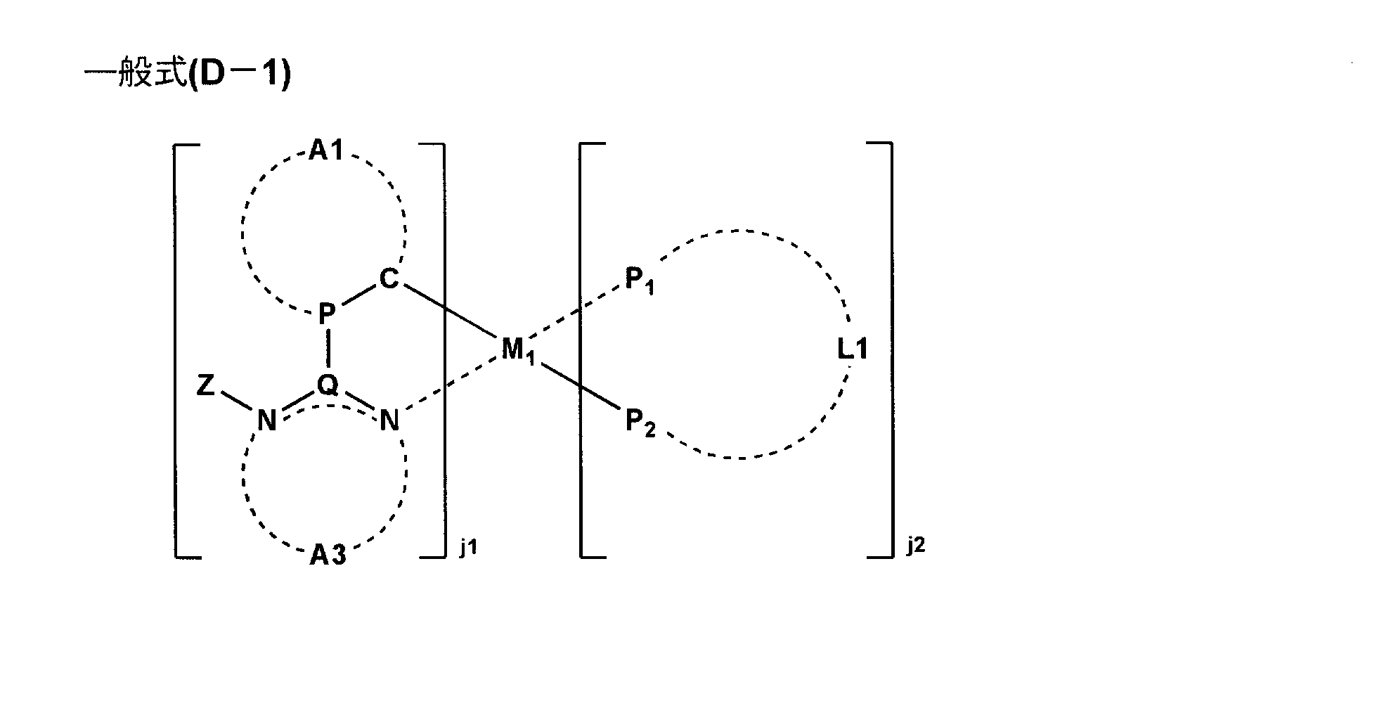


本発明に係る一般式(1)~(3)のいずれかで表される部分構造について説明する。 << Partial structure represented by any one of formulas (1) to (3) >>
The partial structure represented by any one of the general formulas (1) to (3) according to the present invention will be described.
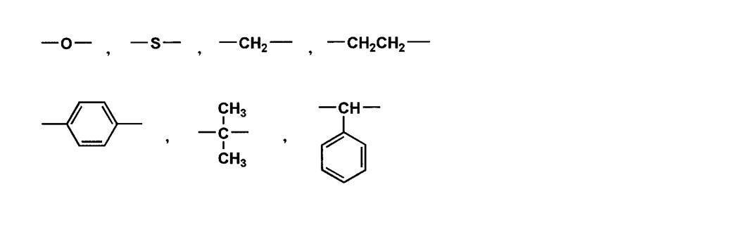


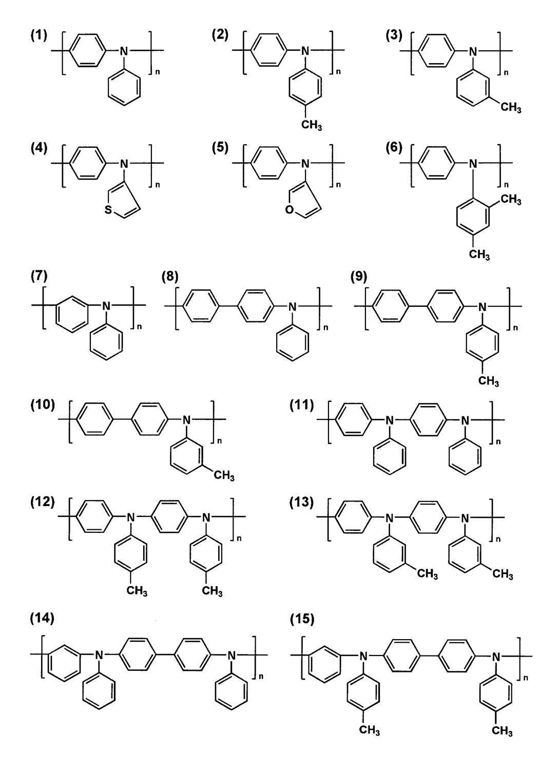


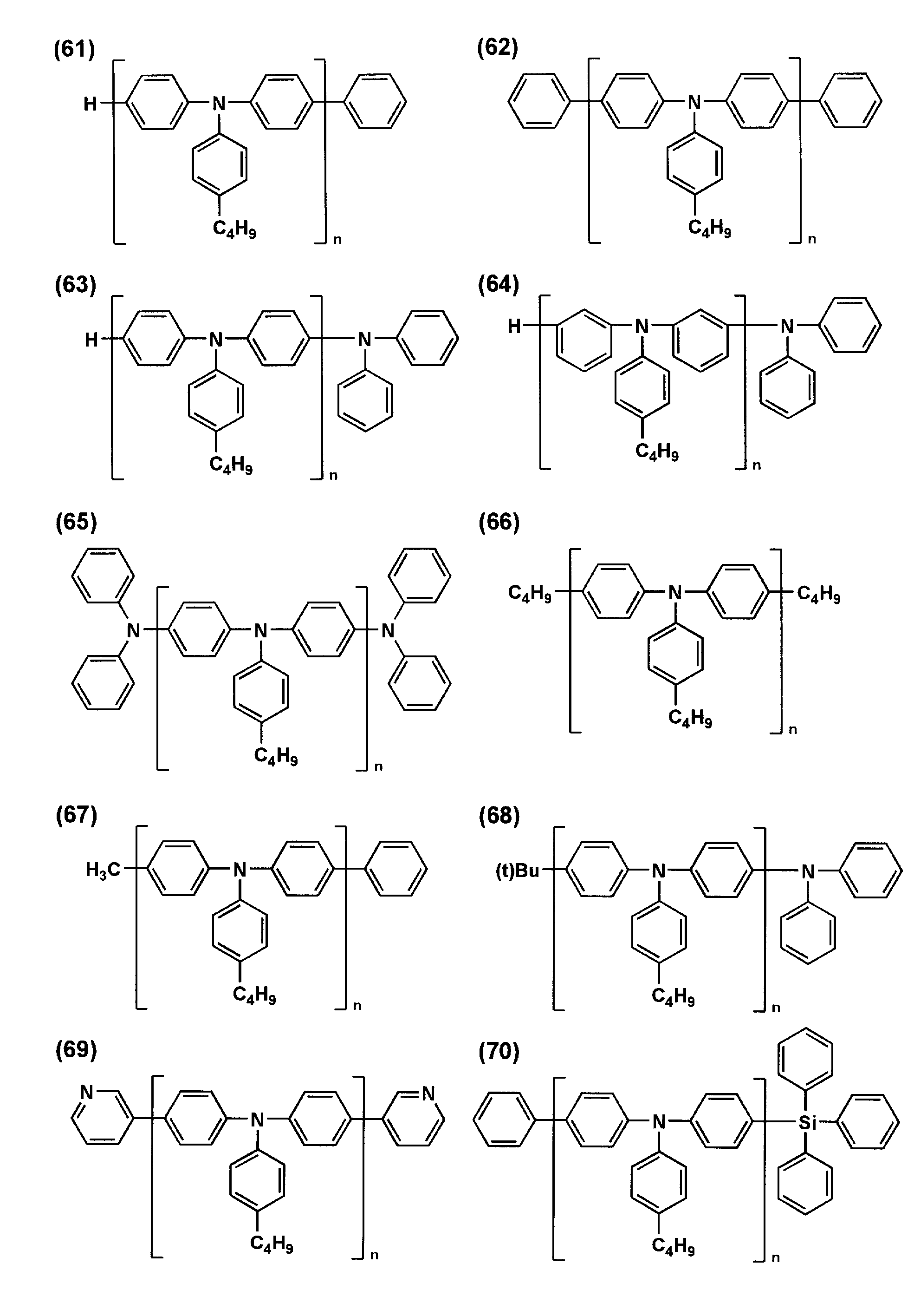

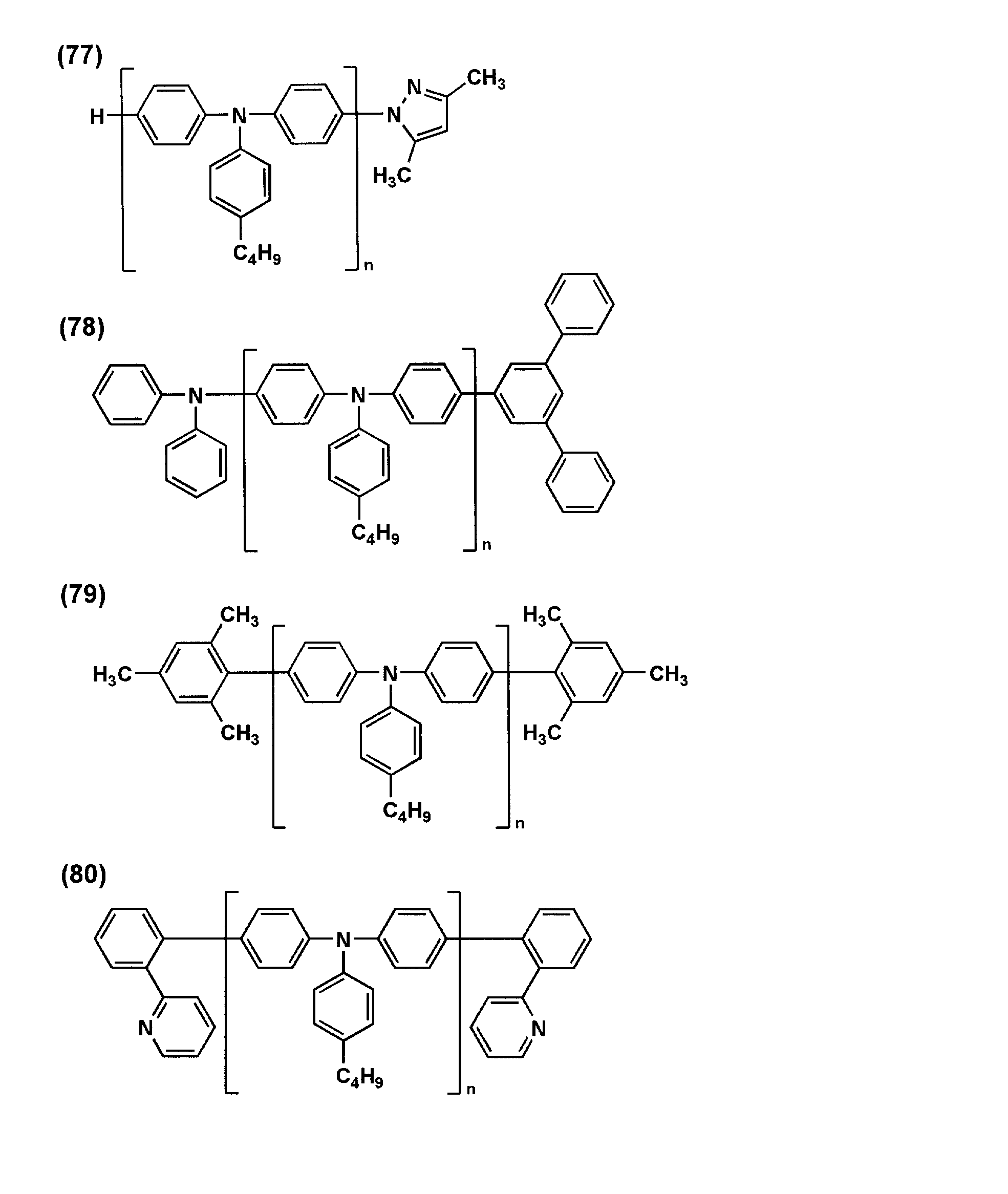

反応時間を2時間から10時間に変更した以外は同様の処理を行い、化合物50b(重量平均分子量55000、分子量分布2.0)を、反応時間を2時間から20時間に変更した以外は同様の処理を行い、化合物50c(重量平均分子量80000、分子量分布1.9)を、反応時間を2時間から50時間に変更した以外は同様の処理を行い、化合物50d(重量平均分子量150000、分子量分布1.9)を得た。 << Synthesis of Exemplified Compounds 50b, 50c, 50d >>
The same treatment was performed except that the reaction time was changed from 2 hours to 10 hours, and compound 50b (weight average molecular weight 55000, molecular weight distribution 2.0) was the same except that the reaction time was changed from 2 hours to 20 hours. The compound 50c (weight average molecular weight 80000, molecular weight distribution 1.9) was subjected to the same treatment except that the reaction time was changed from 2 hours to 50 hours to give compound 50d (weight average molecular weight 150,000, molecular weight distribution 1). .9) was obtained.
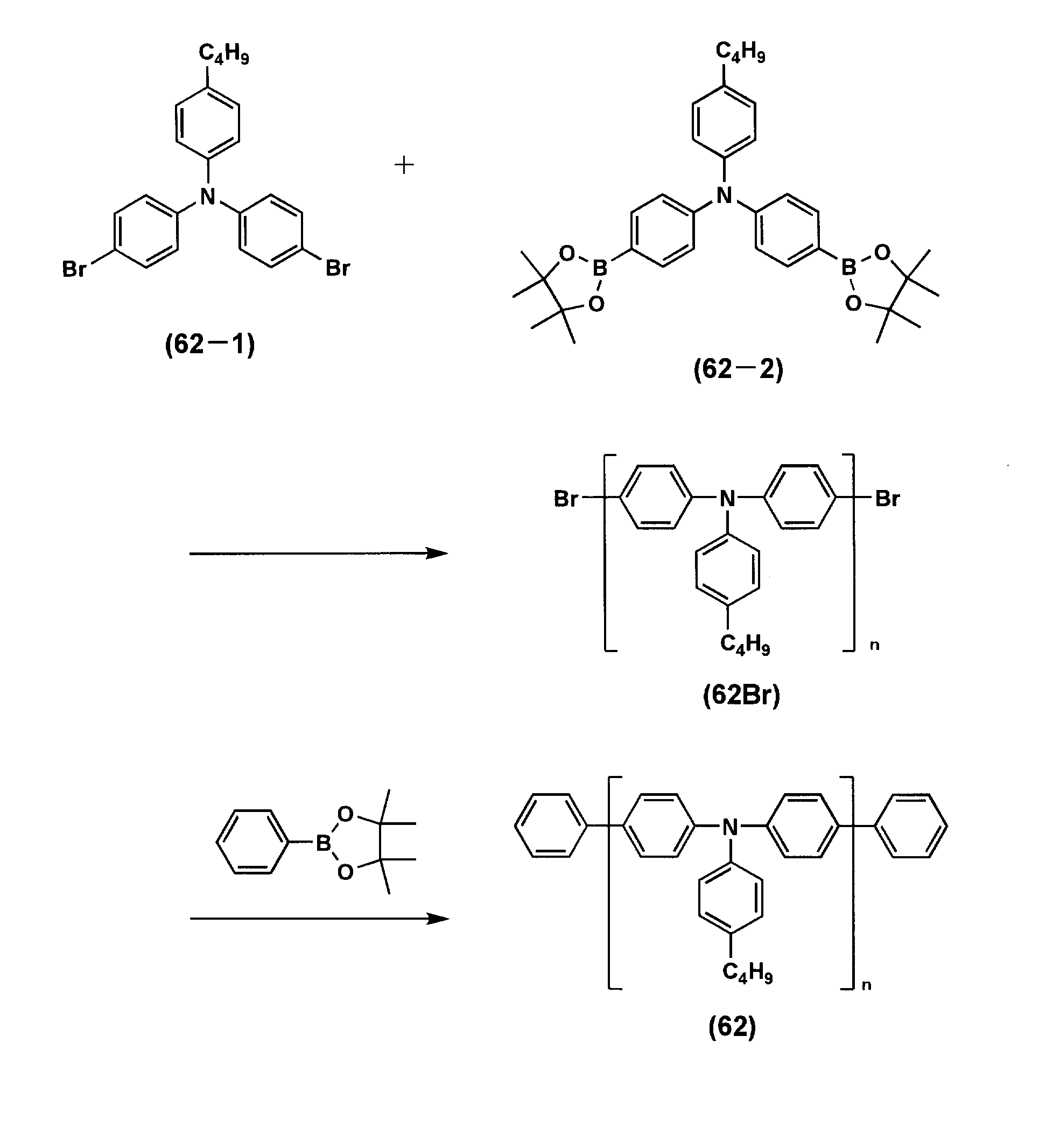
装置:東ソー高速GPC装置 HLC-8220GPC
カラム:TOSOH TSKgel Super HM-M
検出器:RI及び/またはUV
溶出液流速:0.6ml/分
試料濃度:0.1質量%
試料量:100μl
検量線:標準ポリスチレンにて作製:標準ポリスチレンSTK standard ポリスチレン(東ソー(株)製)Mw=1000000~500迄の13サンプルを用いて検量線(校正曲線ともいう)を作成、分子量の算出に使用した。13サンプルは、ほぼ等間隔にすることが好ましい。 (Measurement condition)
Equipment: Tosoh High Speed GPC Equipment HLC-8220GPC
Column: TOSOH TSKgel Super HM-M
Detector: RI and / or UV
Eluent flow rate: 0.6 ml / min Sample concentration: 0.1% by mass
Sample volume: 100 μl
Calibration curve: Prepared with standard polystyrene: Standard polystyrene STK standard polystyrene (manufactured by Tosoh Corporation) Mw = 130,000 to 500 was used to create a calibration curve (also referred to as a calibration curve) and used to calculate the molecular weight . It is preferable that the 13 samples are substantially equally spaced.
一般式(D-1)において、A1が、P-Cと共に形成する芳香族炭化水素環としては、ベンゼン環、ビフェニル環、ナフタレン環、アズレン環、アントラセン環、フェナントレン環、ピレン環、クリセン環、ナフタセン環、トリフェニレン環、o-テルフェニル環、m-テルフェニル環、p-テルフェニル環、アセナフテン環、コロネン環、フルオレン環、フルオラントレン環、ナフタセン環、ペンタセン環、ペリレン環、ペンタフェン環、ピセン環、ピレン環、ピラントレン環、アンスラアントレン環等が挙げられる。これらの環は更に置換基を有してもよい。 << Compound Represented by Formula (D-1) >>
In the general formula (D-1), examples of the aromatic hydrocarbon ring that A1 forms with PC include a benzene ring, a biphenyl ring, a naphthalene ring, an azulene ring, an anthracene ring, a phenanthrene ring, a pyrene ring, a chrysene ring, Naphthacene ring, triphenylene ring, o-terphenyl ring, m-terphenyl ring, p-terphenyl ring, acenaphthene ring, coronene ring, fluorene ring, fluoranthrene ring, naphthacene ring, pentacene ring, perylene ring, pentaphen ring, Examples include a picene ring, a pyrene ring, a pyranthrene ring, and an anthraanthrene ring. These rings may further have a substituent.


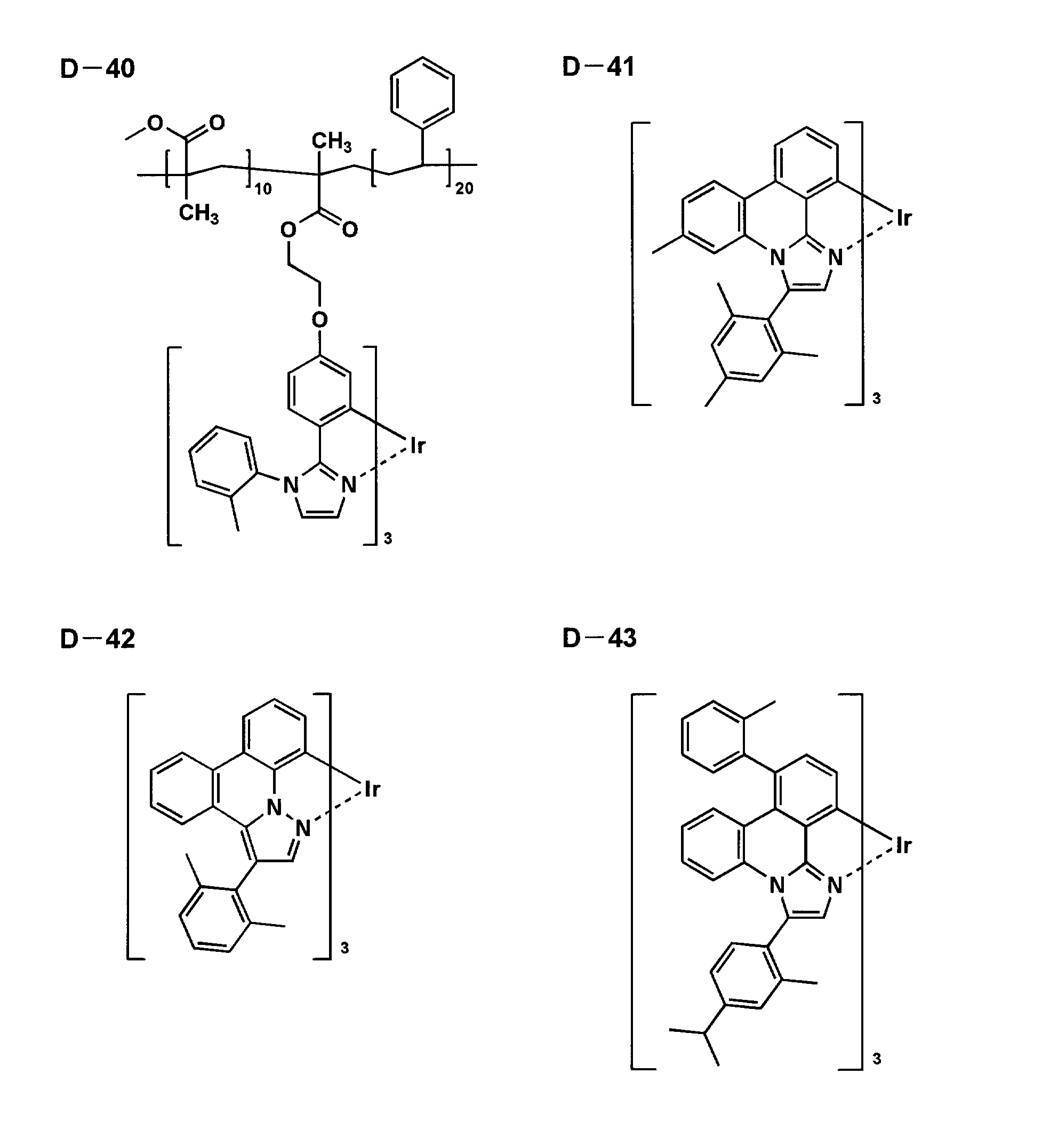
本発明に係る有機EL素子の構成層について説明する。本発明において、有機EL素子の層構成の好ましい具体例を以下に示すが、本発明はこれらに限定されない。
(i)陽極/発光層/電子輸送層/陰極
(ii)陽極/正孔輸送層/発光層/電子輸送層/陰極
(iii)陽極/正孔輸送層/発光層/正孔阻止層/電子輸送層/陰極
(iv)陽極/正孔輸送層/発光層/正孔阻止層/電子輸送層/陰極バッファー層/陰極
(v)陽極/陽極バッファー層/正孔輸送層/発光層/正孔阻止層/電子輸送層/陰極バッファー層/陰極
本発明に係る有機EL素子においては、青色発光層の発光極大波長は430nm~480nmにあるものが好ましく、緑色発光層は発光極大波長が510nm~550nm、赤色発光層は発光極大波長が600nm~640nmの範囲にある単色発光層であることが好ましく、これらを用いた表示装置であることが好ましい。 << Constituent layers of organic EL elements >>
The constituent layers of the organic EL element according to the present invention will be described. In this invention, although the preferable specific example of the layer structure of an organic EL element is shown below, this invention is not limited to these.
(I) Anode / light emitting layer / electron transport layer / cathode (ii) Anode / hole transport layer / light emitting layer / electron transport layer / cathode (iii) Anode / hole transport layer / light emitting layer / hole blocking layer / electron Transport layer / cathode (iv) anode / hole transport layer / light emitting layer / hole blocking layer / electron transport layer / cathode buffer layer / cathode (v) anode / anode buffer layer / hole transport layer / light emitting layer / hole Blocking layer / electron transport layer / cathode buffer layer / cathode In the organic EL device according to the present invention, the blue light emitting layer preferably has a light emission maximum wavelength of 430 nm to 480 nm, and the green light emitting layer has a light emission maximum wavelength of 510 nm to 550 nm. The red light emitting layer is preferably a monochromatic light emitting layer having a light emission maximum wavelength in the range of 600 nm to 640 nm, and is preferably a display device using these.
本発明に係る発光層は、電極または電子輸送層、正孔輸送層から注入されてくる電子及び正孔が再結合して発光する層であり、発光する部分は発光層の層内であっても発光層と隣接層との界面であってもよい。 <Light emitting layer>
The light emitting layer according to the present invention is a layer that emits light by recombination of electrons and holes injected from the electrode, the electron transport layer, or the hole transport layer, and the light emitting portion is in the layer of the light emitting layer. May be the interface between the light emitting layer and the adjacent layer.
発光性ドーパント化合物について説明する。 (Luminescent dopant compound)
The luminescent dopant compound will be described.
本発明に係るリン光発光性ドーパントについて説明する。 (Phosphorescent dopant)
The phosphorescent dopant according to the present invention will be described.


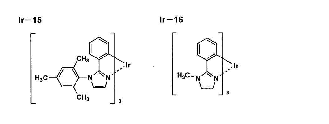
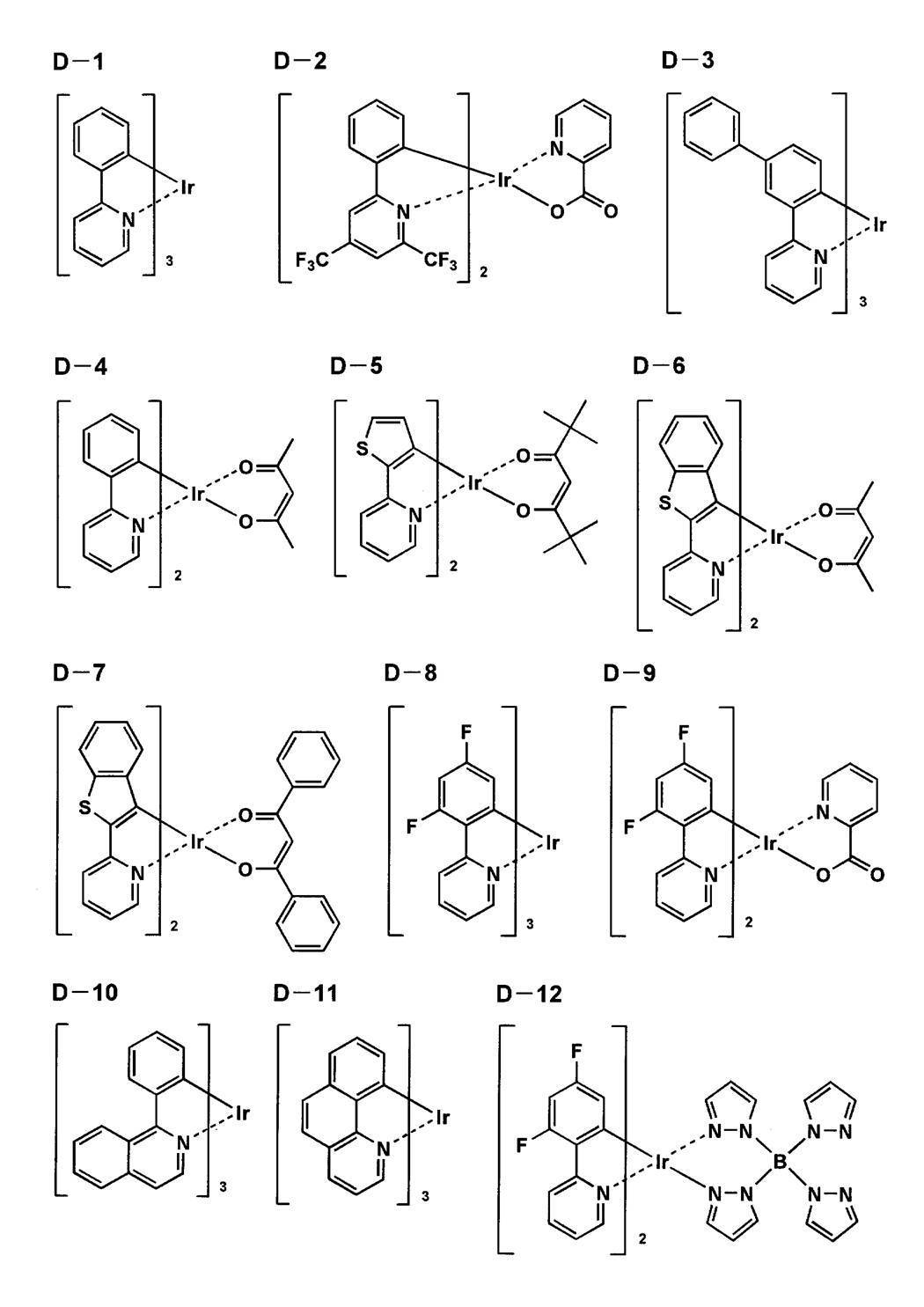


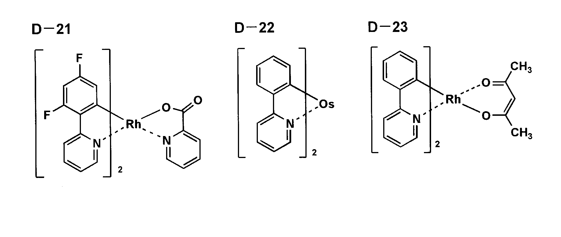
本発明において発光ホスト化合物は、発光層に含有される化合物の内で、その層中での質量比が20%以上であり、且つ室温(25℃)においてリン光発光のリン光量子収率が、0.1未満の化合物と定義される。好ましくはリン光量子収率が0.01未満である。また、発光層に含有される化合物の中で、その層中での質量比が20%以上であることが好ましい。 (Luminescent host compound (also referred to as luminescent host))
In the present invention, the light-emitting host compound has a mass ratio in the layer of 20% or more among the compounds contained in the light-emitting layer, and a phosphorescence quantum yield of phosphorescence emission at room temperature (25 ° C.). It is defined as a compound of less than 0.1. The phosphorescence quantum yield is preferably less than 0.01. Moreover, it is preferable that the mass ratio in the layer is 20% or more among the compounds contained in a light emitting layer.
注入層は必要に応じて設け、電子注入層と正孔注入層があり、上記の如く陽極と発光層または正孔輸送層の間、及び陰極と発光層または電子輸送層との間に存在させてもよい。 << Injection layer: electron injection layer, hole injection layer >>
The injection layer is provided as necessary, and there are an electron injection layer and a hole injection layer, and as described above, it exists between the anode and the light emitting layer or the hole transport layer and between the cathode and the light emitting layer or the electron transport layer. May be.
阻止層は、上記の如く有機化合物薄膜の基本構成層の他に必要に応じて設けられるものである。例えば、特開平11-204258号公報、同11-204359号公報、及び「有機EL素子とその工業化最前線(1998年11月30日エヌ・ティー・エス社発行)」の237頁等に記載されている正孔阻止(ホールブロック)層がある。 <Blocking layer: hole blocking layer, electron blocking layer>
The blocking layer is provided as necessary in addition to the basic constituent layer of the organic compound thin film as described above. For example, it is described in JP-A Nos. 11-204258 and 11-204359, and “Organic EL elements and the forefront of industrialization (published by NTT Corporation on November 30, 1998)” on page 237. There is a hole blocking (hole blocking) layer.
正孔輸送層とは正孔を輸送する機能を有する正孔輸送材料からなり、広い意味で正孔注入層、電子阻止層も正孔輸送層に含まれる。正孔輸送層は単層または複数層設けることができる。 《Hole transport layer》
The hole transport layer is made of a hole transport material having a function of transporting holes, and in a broad sense, a hole injection layer and an electron blocking layer are also included in the hole transport layer. The hole transport layer can be provided as a single layer or a plurality of layers.
電子輸送層とは電子を輸送する機能を有する材料からなり、広い意味で電子注入層、正孔阻止層も電子輸送層に含まれる。電子輸送層は単層または複数層設けることができる。 《Electron transport layer》
The electron transport layer is made of a material having a function of transporting electrons, and in a broad sense, an electron injection layer and a hole blocking layer are also included in the electron transport layer. The electron transport layer can be provided as a single layer or a plurality of layers.


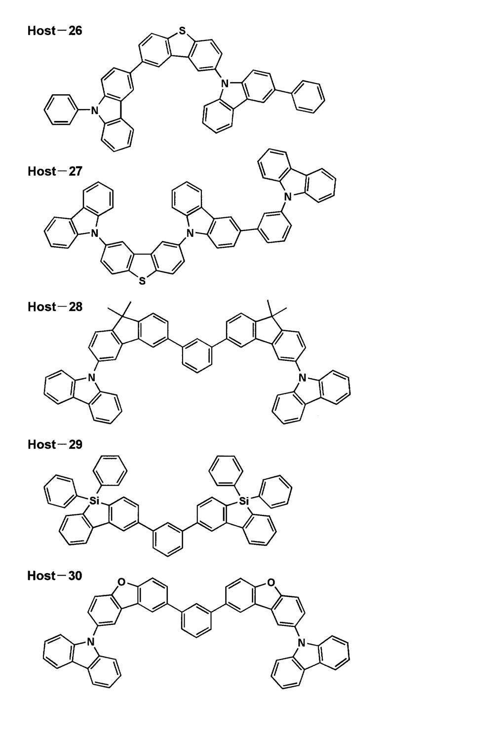
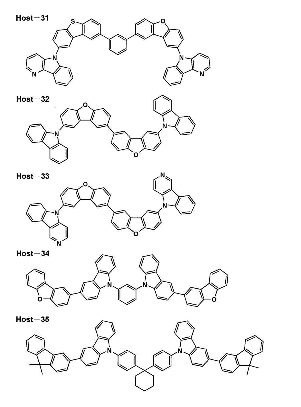
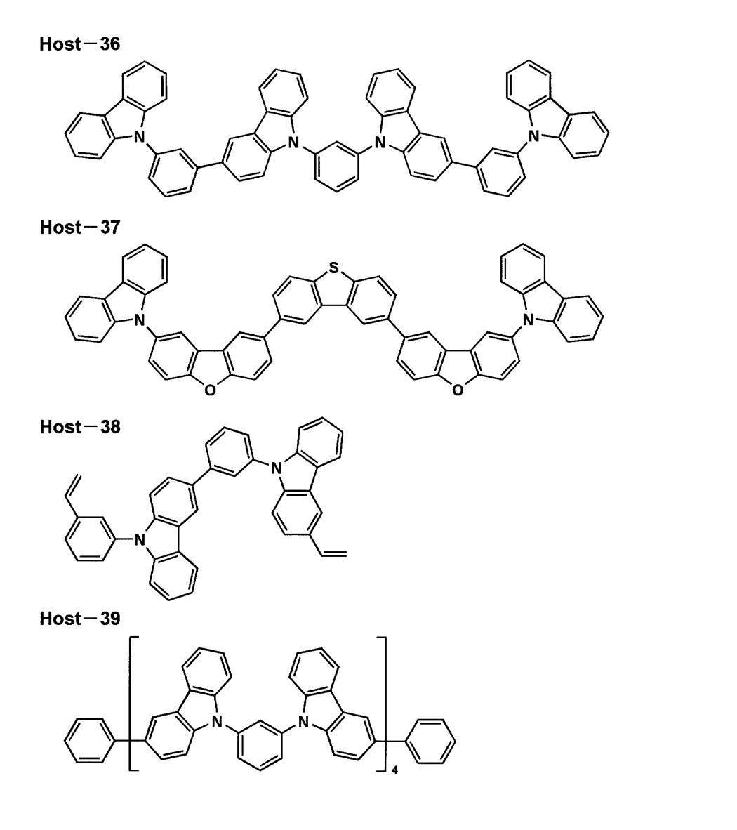

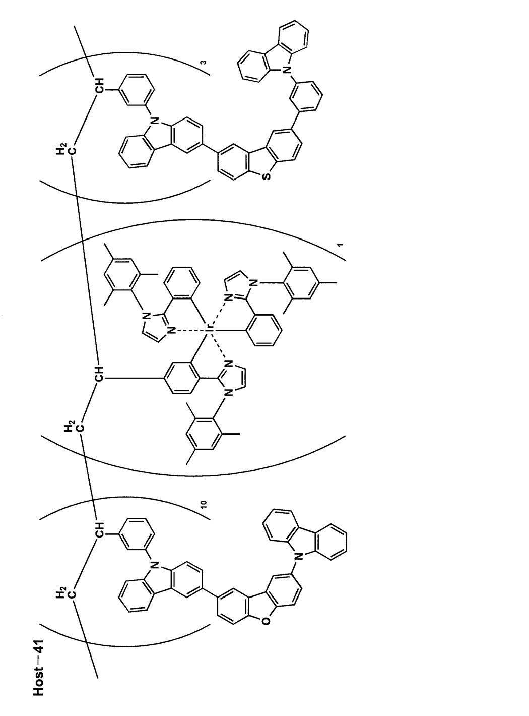


有機EL素子における陽極としては、仕事関数の大きい(4eV以上)金属、合金、電気伝導性化合物及びこれらの混合物を電極物質とするものが好ましく用いられる。このような電極物質の具体例としては、Au等の金属、CuI、インジウムチンオキシド(ITO)、SnO2、ZnO等の導電性透明材料が挙げられる。また、IDIXO(In2O3-ZnO)等非晶質で透明導電膜を作製可能な材料を用いてもよい。陽極はこれらの電極物質を蒸着やスパッタリング等の方法により薄膜を作製させ、フォトリソグラフィー法で所望の形状のパターンを形成してもよく、あるいはパターン精度をあまり必要としない場合は(100μm以上程度)、上記電極物質の蒸着やスパッタリング時に所望の形状のマスクを介してパターンを形成してもよい。あるいは、有機導電性化合物のように塗布可能な物質を用いる場合には、印刷方式、コーティング方式等湿式成膜法を用いることもできる。この陽極より発光を取り出す場合には、透過率を10%より大きくすることが望ましく、また陽極としてのシート抵抗は数百Ω/□以下が好ましい。 "anode"
As the anode in the organic EL element, an electrode material made of a metal, an alloy, an electrically conductive compound, or a mixture thereof having a high work function (4 eV or more) is preferably used. Specific examples of such electrode materials include metals such as Au, and conductive transparent materials such as CuI, indium tin oxide (ITO), SnO 2 , and ZnO. Alternatively, an amorphous material such as IDIXO (In 2 O 3 —ZnO) capable of forming a transparent conductive film may be used. For the anode, these electrode materials may be formed into a thin film by vapor deposition or sputtering, and a pattern having a desired shape may be formed by photolithography, or when pattern accuracy is not so high (about 100 μm or more) A pattern may be formed through a mask having a desired shape at the time of vapor deposition or sputtering of the electrode material. Or when using the substance which can be apply | coated like an organic electroconductivity compound, wet film-forming methods, such as a printing system and a coating system, can also be used. When light emission is extracted from the anode, it is desirable that the transmittance be greater than 10%, and the sheet resistance as the anode is preferably several hundred Ω / □ or less.
一方、陰極としては仕事関数の小さい(4eV以下)金属(電子注入性金属と称する)、合金、電気伝導性化合物及びこれらの混合物を電極物質とするものが用いられる。 "cathode"
On the other hand, as the cathode, a material having a low work function (4 eV or less) metal (referred to as an electron injecting metal), an alloy, an electrically conductive compound, and a mixture thereof as an electrode material is used.
本発明に係る有機EL素子に用いることのできる支持基板(以下、基体、基板、基材、支持体等とも言う)としては、ガラス、プラスチック等の種類には特に限定はなく、また透明であっても不透明であってもよい。 《Support substrate》
As a support substrate (hereinafter also referred to as a substrate, substrate, substrate, support, etc.) that can be used in the organic EL device according to the present invention, there is no particular limitation on the type of glass, plastic, etc., and it is transparent. Or opaque.
本発明に用いられる封止手段としては、例えば、封止部材と電極、支持基板とを接着剤で接着する方法を挙げることができる。 <Sealing>
As a sealing means used for this invention, the method of adhere | attaching a sealing member, an electrode, and a support substrate with an adhesive agent can be mentioned, for example.
有機層を挟み支持基板と対向する側の前記封止膜、あるいは前記封止用フィルムの外側に、素子の機械的強度を高めるために保護膜、あるいは保護板を設けてもよい。 《Protective film, protective plate》
In order to increase the mechanical strength of the element, a protective film or a protective plate may be provided on the outer side of the sealing film on the side facing the support substrate with the organic layer interposed therebetween or on the sealing film.
有機EL素子は空気よりも屈折率の高い(屈折率が1.7~2.1程度)層の内部で発光し、発光層で発生した光のうち15%~20%程度の光しか取り出せないことが一般的に言われている。 《Light extraction》
The organic EL element emits light inside a layer having a refractive index higher than that of air (refractive index is about 1.7 to 2.1) and can extract only about 15% to 20% of the light generated in the light emitting layer. It is generally said.
本発明に係る有機EL素子は基板の光取り出し側に、例えば、マイクロレンズアレイ状の構造を設けるように加工したり、あるいは所謂集光シートと組み合わせることにより、特定方向、例えば、素子発光面に対し正面方向に集光することにより、特定方向上の輝度を高めることができる。 <Condenser sheet>
The organic EL device according to the present invention can be processed on the light extraction side of the substrate, for example, by providing a microlens array-like structure, or combined with a so-called condensing sheet, for example, in a specific direction, for example, the device light emitting surface. On the other hand, the brightness | luminance in a specific direction can be raised by condensing in a front direction.
本発明に係る有機EL素子の作製方法の一例として、陽極/正孔注入層/正孔輸送層/発光層/電子輸送層/電子注入層/陰極からなる有機EL素子の作製法を説明する。 << Method for producing organic EL element >>
As an example of a method for producing an organic EL device according to the present invention, a method for producing an organic EL device comprising an anode / hole injection layer / hole transport layer / light emitting layer / electron transport layer / electron injection layer / cathode will be described.
本発明の有機EL素子は、表示デバイス、ディスプレイ、各種発光光源として用いることができる。 <Application>
The organic EL element of the present invention can be used as a display device, a display, and various light emission sources.

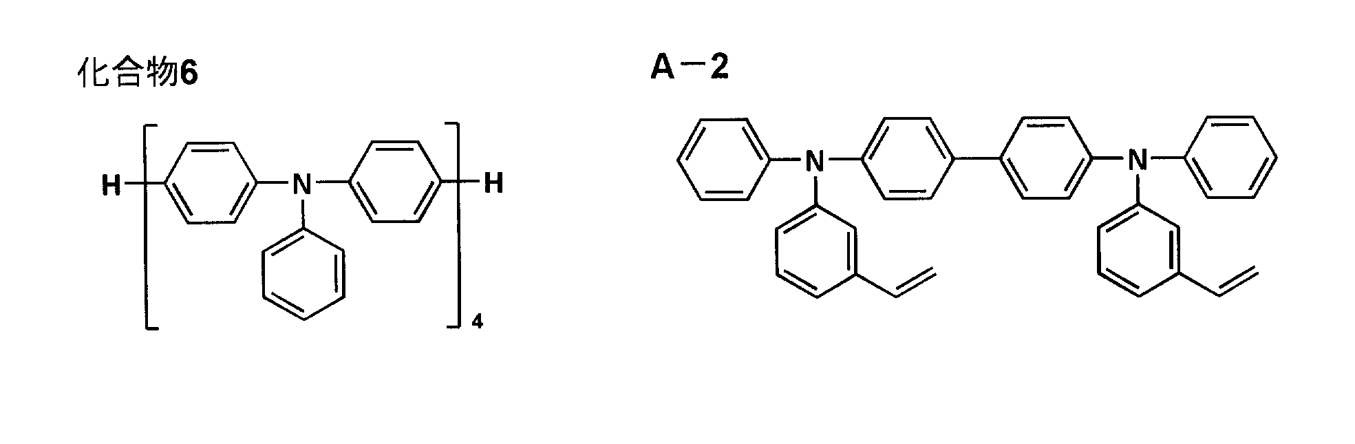
《有機EL素子1-1の作製》
陽極としてガラス上にITOを150nm成膜した基板(NHテクノグラス社製:NA-45)にパターニングを行った後、このITO透明電極を設けた透明支持基板をiso-プロピルアルコールで超音波洗浄し、乾燥窒素ガスで乾燥し、UVオゾン洗浄を5分間行った。この基板を窒素雰囲気下に移し、化合物50a(60mg)をトルエン6mlに溶解した溶液を用い1000rpm、30秒の条件にてスピンコート法により成膜した後、真空中150℃にて1時間乾燥し、膜厚30nmの正孔輸送層を設けた。 Example 1
<< Production of Organic EL Element 1-1 >>
After patterning on a substrate (NH Techno Glass Co., Ltd. NA-45) having a 150 nm ITO film on glass as the anode, the transparent support substrate provided with this ITO transparent electrode was ultrasonically cleaned with iso-propyl alcohol. Then, it was dried with dry nitrogen gas, and UV ozone cleaning was performed for 5 minutes. This substrate was transferred to a nitrogen atmosphere, a film was formed by spin coating at 1000 rpm for 30 seconds using a solution of compound 50a (60 mg) dissolved in 6 ml of toluene, and then dried in vacuum at 150 ° C. for 1 hour. A hole transport layer having a thickness of 30 nm was provided.
有機EL素子1-1の作製において、表1に記載のように正孔輸送材料を変更した以外は同様にして、有機EL素子1-2~1-4を作製した。 << Preparation of organic EL elements 1-2 to 1-4 >>
Organic EL elements 1-2 to 1-4 were prepared in the same manner as in the preparation of organic EL element 1-1 except that the hole transport material was changed as shown in Table 1.
得られた有機EL素子1-1~1-4を評価するに際しては、作製後の各有機EL素子の非発光面をガラスケースで覆い、厚み300μmのガラス基板を封止用基板として用いて、周囲にシール材として、エポキシ系光硬化型接着剤(東亞合成社製ラックストラックLC0629B)を適用し、これを上記陰極上に重ねて前記透明支持基板と密着させ、ガラス基板側からUV光を照射して、硬化させて、封止して、図1、図2に示すような照明装置を作製して評価した。 << Evaluation of organic EL elements >>
When evaluating the obtained organic EL elements 1-1 to 1-4, the non-light emitting surface of each organic EL element after production was covered with a glass case, and a glass substrate having a thickness of 300 μm was used as a sealing substrate. An epoxy-based photo-curing adhesive (Lux Track LC0629B manufactured by Toagosei Co., Ltd.) is applied as a sealing material in the periphery, and this is placed on the cathode to be in close contact with the transparent support substrate and irradiated with UV light from the glass substrate side. Then, it was cured and sealed, and a lighting device as shown in FIGS. 1 and 2 was produced and evaluated.
有機EL素子を室温(約23℃~25℃)、2.5mA/cm2の定電流条件下による点灯を行い、点灯開始直後の発光輝度(L)[cd/m2]を測定することにより、外部取り出し量子効率(η)を算出した。 (External quantum efficiency)
By lighting the organic EL element under a constant current condition of 2.5 mA / cm 2 at room temperature (about 23 ° C. to 25 ° C.) and measuring the light emission luminance (L) [cd / m 2 ] immediately after the start of lighting. The external extraction quantum efficiency (η) was calculated.
有機EL素子を室温下、2.5mA/cm2の定電流条件下による連続点灯を行い、初期輝度の半分の輝度になるのに要する時間(τ1/2)を測定した。発光寿命は有機EL素子1-1を100と設定する相対値で表した。 (Luminescence life and voltage increase rate)
The organic EL element was continuously lit at a constant current of 2.5 mA / cm 2 at room temperature, and the time (τ 1/2 ) required to reach half the initial luminance was measured. The light emission lifetime was expressed as a relative value where the organic EL element 1-1 was set to 100.

《有機EL素子2-1の作製》
陽極としてガラス上にITOを150nm成膜した基板(NHテクノグラス社製:NA-45)にパターニングを行った後、このITO透明電極を設けた透明支持基板をiso-プロピルアルコールで超音波洗浄し、乾燥窒素ガスで乾燥し、UVオゾン洗浄を5分間行った。 Example 2
<< Preparation of organic EL element 2-1 >>
After patterning on a substrate (NH Techno Glass Co., Ltd. NA-45) having a 150 nm ITO film on glass as the anode, the transparent support substrate provided with this ITO transparent electrode was ultrasonically cleaned with iso-propyl alcohol. Then, it was dried with dry nitrogen gas, and UV ozone cleaning was performed for 5 minutes.
有機EL素子2-1の作製において、表2に記載のように正孔輸送材料を変更した以外は同様にして、有機EL素子2-2~2-4を作製した。 << Production of organic EL elements 2-2 to 2-4 >>
Organic EL elements 2-2 to 2-4 were prepared in the same manner as in the preparation of organic EL element 2-1, except that the hole transport material was changed as shown in Table 2.
得られた有機EL素子2-1~2-4を評価するに際しては、実施例1と同様の方法を用いて評価を行い、外部取り出し量子効率及び発光寿命は有機EL素子2-1を100と設定する相対値で表した。 << Evaluation of organic EL elements >>
When evaluating the obtained organic EL elements 2-1 to 2-4, the evaluation was performed using the same method as in Example 1. The external extraction quantum efficiency and the light emission lifetime were set to 100 for the organic EL element 2-1. Expressed as a relative value to set.

《フルカラー表示装置の作製》
(青色発光素子の作製)
実施例2の有機EL素子2-4を青色発光素子として用いた。 Example 3
<Production of full-color display device>
(Production of blue light emitting element)
The organic EL element 2-4 of Example 2 was used as a blue light emitting element.
実施例1の有機EL素子1-4において、D-9をD-1に変更した以外は同様にして、緑色発光素子を作製し、これを緑色発光素子として用いた。 (Production of green light emitting element)
A green light emitting device was produced in the same manner as in the organic EL device 1-4 of Example 1 except that D-9 was changed to D-1, and this was used as the green light emitting device.
実施例1の有機EL素子1-4において、D-9をD-6に変更した以外は同様にして、赤色発光素子を作製し、これを赤色発光素子として用いた。 (Production of red light emitting element)
A red light emitting device was produced in the same manner as in the organic EL device 1-4 of Example 1 except that D-9 was changed to D-6, and this was used as a red light emitting device.
《白色発光素子及び白色照明装置の作製》
陽極として100mm×100mm×1.1mmのガラス基板上にITO(インジウムチンオキシド)を100nm成膜した基板(NHテクノグラス社製NA-45)にパターニングを行った後、このITO透明電極を設けた透明支持基板をイソプロピルアルコールで超音波洗浄し、乾燥窒素ガスで乾燥し、UVオゾン洗浄を5分間行った。 Example 4
<< Preparation of white light emitting element and white lighting device >>
Patterning was performed on a substrate (NA-45 manufactured by NH Techno Glass Co., Ltd.) on which a 100 nm × 100 mm × 1.1 mm glass substrate as a positive electrode on a 100 mm × 100 mm × 1.1 mm glass substrate was formed, and then this ITO transparent electrode was provided. The transparent support substrate was ultrasonically cleaned with isopropyl alcohol, dried with dry nitrogen gas, and subjected to UV ozone cleaning for 5 minutes.
《有機EL素子5-1の作製》
陽極としてガラス上にITOを150nm成膜した基板(NHテクノグラス社製:NA-45)にパターニングを行った後、このITO透明電極を設けた透明支持基板をiso-プロピルアルコールで超音波洗浄し、乾燥窒素ガスで乾燥し、UVオゾン洗浄を5分間行った。 Example 5
<< Preparation of organic EL element 5-1 >>
After patterning on a substrate (NH Techno Glass Co., Ltd. NA-45) having a 150 nm ITO film on glass as the anode, the transparent support substrate provided with this ITO transparent electrode was ultrasonically cleaned with iso-propyl alcohol. Then, it was dried with dry nitrogen gas, and UV ozone cleaning was performed for 5 minutes.
有機EL素子5-1の作製において、化合物62を化合物62Brに変更した以外は同様にして有機EL素子5-2を作製した。 << Production of Organic EL Element 5-2 >>
An organic EL element 5-2 was produced in the same manner as in the production of the organic EL element 5-1, except that the compound 62 was changed to the compound 62Br.
有機EL素子5-1、5-2の各正孔輸送層の作製に用いられた化合物62、62Brについては、エンドキャップ処理の有無をハロゲン含有率の測定により確認した。 <Measurement of halogen content of hole transport material>
With respect to the compounds 62 and 62Br used for the production of the respective hole transport layers of the organic EL elements 5-1, 5-2, the presence or absence of the end cap treatment was confirmed by measuring the halogen content.
得られた有機EL素子5-1、5-2を評価するに際しては、実施例1と同様の方法を用いて評価を行い、外部取り出し量子効率及び発光寿命は有機EL素子5-1を100と設定する相対値で表した。 << Evaluation of organic EL elements >>
When evaluating the obtained organic EL elements 5-1 and 5-2, the evaluation was performed using the same method as in Example 1. The external extraction quantum efficiency and the light emission lifetime were set to 100 for the organic EL element 5-1. Expressed as a relative value to set.

以下に記載のように、実施例5の有機EL素子5-1の比較素子として、有機EL素子5-3、5-4を作製した。尚、有機EL素子5-1は、実施例5と同様にして作製した。 Example 6
As described below, organic EL elements 5-3 and 5-4 were produced as comparative elements of the organic EL element 5-1 of Example 5. The organic EL element 5-1 was produced in the same manner as in Example 5.
陽極としてガラス上にITOを150nm成膜した基板(NHテクノグラス社製:NA-45)にパターニングを行った後、このITO透明電極を設けた透明支持基板をiso-プロピルアルコールで超音波洗浄し、乾燥窒素ガスで乾燥し、UVオゾン洗浄を5分間行った。 << Preparation of organic EL element 5-3 >>
After patterning on a substrate (NH Techno Glass Co., Ltd. NA-45) having a 150 nm ITO film on glass as the anode, the transparent support substrate provided with this ITO transparent electrode was ultrasonically cleaned with iso-propyl alcohol. Then, it was dried with dry nitrogen gas, and UV ozone cleaning was performed for 5 minutes.
陽極としてガラス上にITOを150nm成膜した基板(NHテクノグラス社製:NA-45)にパターニングを行った後、このITO透明電極を設けた透明支持基板をiso-プロピルアルコールで超音波洗浄し、乾燥窒素ガスで乾燥し、UVオゾン洗浄を5分間行った。 << Preparation of organic EL element 5-4 >>
After patterning on a substrate (NH Techno Glass Co., Ltd. NA-45) having a 150 nm ITO film on glass as the anode, the transparent support substrate provided with this ITO transparent electrode was ultrasonically cleaned with iso-propyl alcohol. Then, it was dried with dry nitrogen gas, and UV ozone cleaning was performed for 5 minutes.
得られた有機EL素子5-1、5-3、5-4を評価するに際しては、実施例1と同様の方法を用いて評価を行い、外部取り出し量子効率及び発光寿命は有機EL素子5-1を100と設定する相対値で表した。 << Evaluation of organic EL elements >>
When evaluating the obtained organic EL elements 5-1, 5-3, and 5-4, the evaluation was performed using the same method as in Example 1, and the external extraction quantum efficiency and the emission lifetime were determined according to the organic EL element 5- 1 was expressed as a relative value set to 100.
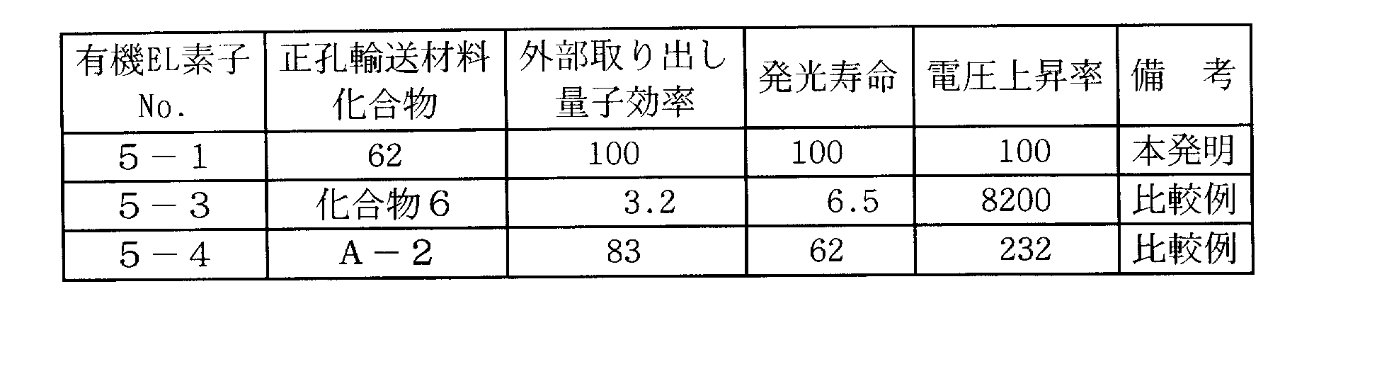
《有機EL素子7-1~7-4の作製》
有機EL素子5-1の作製において、表5に記載したドープ濃度(発光層におけるドーパントの質量比)になるようにD-26の添加量を調製し、有機EL素子7-1~7-4を調製した。 Example 7 (dopant concentration)
<< Preparation of organic EL elements 7-1 to 7-4 >>
In the production of the organic EL element 5-1, the addition amount of D-26 was adjusted so that the doping concentration (mass ratio of dopant in the light emitting layer) described in Table 5 was obtained, and the organic EL elements 7-1 to 7-4 Was prepared.
有機EL素子5-1の作製において、ドーパント及びドープ濃度を表5に記載したように変更した以外は同様にして、有機EL素子7-5~7-16を各々作製した。 << Preparation of organic EL elements 7-5 to 7-16 >>
Organic EL elements 7-5 to 7-16 were prepared in the same manner except that the dopant and the doping concentration were changed as shown in Table 5 in the production of the organic EL element 5-1.
得られた有機EL素子7-1~7-16を評価は、実施例1と同様の方法を用いて行い、外部取り出し量子効率及び発光寿命は有機EL素子7-1を100と設定する相対値で表した。 << Evaluation of organic EL elements >>
The obtained organic EL elements 7-1 to 7-16 were evaluated using the same method as in Example 1. The external extraction quantum efficiency and the emission lifetime were relative values at which the organic EL element 7-1 was set to 100. Expressed in
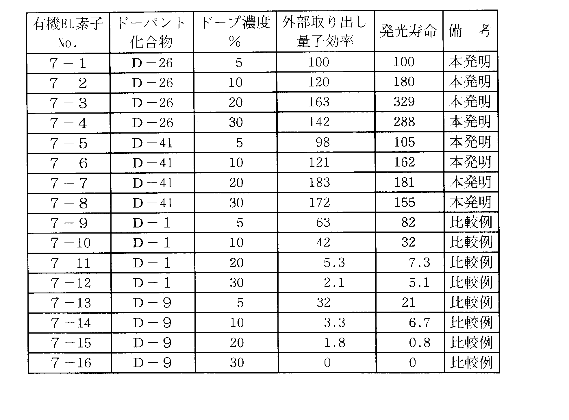
3 画素
5 走査線
6 データ線
A 表示部
B 制御部
101 有機EL素子
102 ガラスカバー
105 陰極
106 有機EL層
107 透明電極付きガラス基板
108 窒素ガス
109 捕水剤 DESCRIPTION OF
Claims (10)
- 陽極と陰極の間に、少なくともリン光発光性ドーパントと、下記一般式(1)で表される部分構造を含み、末端がエンドキャップ処理された高分子化合物とを含有する有機化合物層が挟持されてなる有機エレクトロルミネッセンス素子であって、該リン光発光性ドーパントが5員または6員の芳香族炭化水素環または芳香族複素環と、5員の含窒素芳香族複素環が結合した配位子を有する金属錯体であることを特徴とする有機エレクトロルミネッセンス素子。

(式中、Ar1、Ar3はそれぞれ独立して、置換基を有してもよいアリーレン基を表し、Ar1、Ar3はそれぞれ連結基を介して結合していてもよい。Ar2、Ar4は、それぞれ独立して、置換基を有してもよいアリール基または芳香族複素環基を表す。n1、n2は0~2の整数を表し、n1とn2が同時に0となることはない。n3は10~1000の整数を表す。) Between the anode and the cathode, an organic compound layer containing at least a phosphorescent dopant and a polymer compound containing a partial structure represented by the following general formula (1) and end-capped at the end is sandwiched. An organic electroluminescence device comprising: a ligand in which the phosphorescent dopant is bonded to a 5-membered or 6-membered aromatic hydrocarbon ring or aromatic heterocycle and a 5-membered nitrogen-containing aromatic heterocycle An organic electroluminescence device characterized in that the organic electroluminescence device is a metal complex comprising
(In the formula, Ar 1 and Ar 3 each independently represent an arylene group which may have a substituent, and Ar 1 and Ar 3 may each be bonded via a linking group. Ar 2 , Ar 4 each independently represents an aryl group or an aromatic heterocyclic group which may have a substituent, n1 and n2 each represents an integer of 0 to 2, and n1 and n2 may be 0 at the same time. N3 represents an integer of 10 to 1000.) - 前記リン光発光性ドーパントが下記一般式(D-1)で表される化合物であることを特徴とする請求項1に記載の有機エレクトロルミネッセンス素子。

- 前記一般式(1)で表される部分構造を含む高分子化合物が下記一般式(2)で表される部分構造を含むことを特徴とする請求項1または2に記載の有機エレクトロルミネッセンス素子。

(式中、Ar5、Ar7はそれぞれ独立して、置換基を有してもよいアリーレン基を表し、Ar6は置換基を有してもよいアリール基または芳香族複素環基を表し、n4は10~1000の整数を表す。) The organic electroluminescence device according to claim 1 or 2, wherein the polymer compound containing the partial structure represented by the general formula (1) includes a partial structure represented by the following general formula (2).
(In the formula, Ar 5 and Ar 7 each independently represent an arylene group which may have a substituent, Ar 6 represents an aryl group or an aromatic heterocyclic group which may have a substituent, n4 represents an integer of 10 to 1000.) - 前記一般式(1)で表される部分構造を含む高分子化合物が下記一般式(3)で表される部分構造を含むことを特徴とする請求項1または2に記載の有機エレクトロルミネッセンス素子。
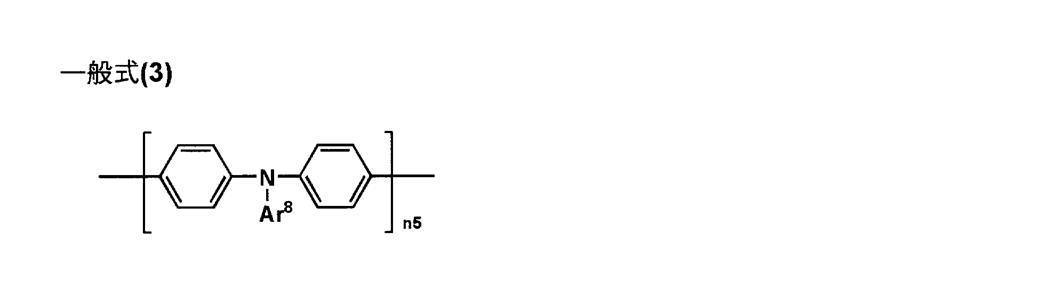
(式中、Ar8は置換基を有してもよいアリール基または芳香族複素環基を表し、n5は10~1000の整数を表す。) The organic electroluminescence device according to claim 1 or 2, wherein the polymer compound containing the partial structure represented by the general formula (1) includes a partial structure represented by the following general formula (3).
(In the formula, Ar 8 represents an aryl group or an aromatic heterocyclic group which may have a substituent, and n5 represents an integer of 10 to 1,000.) - 前記一般式(1)で表される部分構造を含む高分子化合物の重量平均分子量が、ポリスチレン換算で50000~500000であることを特徴とする請求項1~4のいずれか一項に記載の有機エレクトロルミネッセンス素子。 5. The organic compound according to claim 1, wherein the polymer compound containing the partial structure represented by the general formula (1) has a weight average molecular weight of 50,000 to 500,000 in terms of polystyrene. Electroluminescence element.
- 前記リン光発光性ドーパントが青色リン光発光性ドーパントであることを特徴とする請求項1~5のいずれか一項に記載の有機エレクトロルミネッセンス素子。 The organic electroluminescent device according to any one of claims 1 to 5, wherein the phosphorescent dopant is a blue phosphorescent dopant.
- 前記有機化合物層の少なくとも2層がウェットプロセスにより成膜、形成される工程を経て作製されたことを特徴とする請求項1~6のいずれか一項に記載の有機エレクトロルミネッセンス素子。 The organic electroluminescence device according to any one of claims 1 to 6, wherein at least two layers of the organic compound layer are formed through a process of forming and forming by a wet process.
- 白色に発光することを特徴とする請求項1~6のいずれか一項に記載の有機エレクトロルミネッセンス素子。 The organic electroluminescence device according to any one of claims 1 to 6, which emits white light.
- 請求項1~8のいずれか一項に記載の有機エレクトロルミネッセンス素子を備えたことを特徴とする照明装置。 An illumination device comprising the organic electroluminescence element according to any one of claims 1 to 8.
- 請求項1~8のいずれか一項に記載の有機エレクトロルミネッセンス素子を備えたことを特徴とする表示装置。 A display device comprising the organic electroluminescence element according to any one of claims 1 to 8.
Priority Applications (2)
| Application Number | Priority Date | Filing Date | Title |
|---|---|---|---|
| JP2010542086A JP5402942B2 (en) | 2008-12-08 | 2009-12-03 | Organic electroluminescence element, display device, and lighting device |
| US13/132,685 US20120037889A1 (en) | 2008-12-08 | 2009-12-03 | Organic electroluminescence element, display device and illumination device |
Applications Claiming Priority (2)
| Application Number | Priority Date | Filing Date | Title |
|---|---|---|---|
| JP2008311884 | 2008-12-08 | ||
| JP2008-311884 | 2008-12-08 |
Publications (1)
| Publication Number | Publication Date |
|---|---|
| WO2010067746A1 true WO2010067746A1 (en) | 2010-06-17 |
Family
ID=42242734
Family Applications (1)
| Application Number | Title | Priority Date | Filing Date |
|---|---|---|---|
| PCT/JP2009/070321 WO2010067746A1 (en) | 2008-12-08 | 2009-12-03 | Organic electroluminescence element, display device and illumination device |
Country Status (3)
| Country | Link |
|---|---|
| US (1) | US20120037889A1 (en) |
| JP (1) | JP5402942B2 (en) |
| WO (1) | WO2010067746A1 (en) |
Cited By (45)
| Publication number | Priority date | Publication date | Assignee | Title |
|---|---|---|---|---|
| WO2011051404A1 (en) | 2009-10-28 | 2011-05-05 | Basf Se | Heteroleptic carbene complexes and use thereof in organic electronics |
| WO2011073149A1 (en) | 2009-12-14 | 2011-06-23 | Basf Se | Metal complexes comprising diazabenzimidazol carbene-ligands and the use thereof in oleds |
| US20120302762A1 (en) * | 2011-05-27 | 2012-11-29 | Semiconductor Energy Laboratory Co., Ltd. | Carbazole Compound, Light-Emitting Element, Light-Emitting Device, Electronic Device, and Lighting Device |
| EP2539913A1 (en) * | 2010-02-25 | 2013-01-02 | Universal Display Corporation | Phosphorescent emitters |
| JP2013187211A (en) * | 2012-03-06 | 2013-09-19 | Konica Minolta Inc | Organic electroluminescent element, display device and lighting device |
| WO2014012972A1 (en) | 2012-07-19 | 2014-01-23 | Basf Se | Dinuclear metal complexes comprising carbene ligands and the use thereof in oleds |
| US8691401B2 (en) | 2010-04-16 | 2014-04-08 | Basf Se | Bridged benzimidazole-carbene complexes and use thereof in OLEDS |
| WO2014147134A1 (en) | 2013-03-20 | 2014-09-25 | Basf Se | Azabenzimidazole carbene complexes as efficiency booster in oleds |
| WO2014177518A1 (en) | 2013-04-29 | 2014-11-06 | Basf Se | Transition metal complexes with carbene ligands and the use thereof in oleds |
| WO2015000955A1 (en) | 2013-07-02 | 2015-01-08 | Basf Se | Monosubstituted diazabenzimidazole carbene metal complexes for use in organic light emitting diodes |
| JP2015038195A (en) * | 2013-07-17 | 2015-02-26 | 住友化学株式会社 | Polymeric compound and light-emitting element using the same |
| US9142792B2 (en) | 2010-06-18 | 2015-09-22 | Basf Se | Organic electronic devices comprising a layer comprising at least one metal organic compound and at least one metal oxide |
| WO2016009908A1 (en) * | 2014-07-16 | 2016-01-21 | 住友化学株式会社 | Method for manufacturing light emitting element |
| WO2016016791A1 (en) | 2014-07-28 | 2016-02-04 | Idemitsu Kosan Co., Ltd (Ikc) | 2,9-functionalized benzimidazolo[1,2-a]benzimidazoles as hosts for organic light emitting diodes (oleds) |
| EP2982676A1 (en) | 2014-08-07 | 2016-02-10 | Idemitsu Kosan Co., Ltd. | Benzimidazo[2,1-B]benzoxazoles for electronic applications |
| EP2993215A1 (en) | 2014-09-04 | 2016-03-09 | Idemitsu Kosan Co., Ltd. | Azabenzimidazo[2,1-a]benzimidazoles for electronic applications |
| US9315724B2 (en) | 2011-06-14 | 2016-04-19 | Basf Se | Metal complexes comprising azabenzimidazole carbene ligands and the use thereof in OLEDs |
| EP3015469A1 (en) | 2014-10-30 | 2016-05-04 | Idemitsu Kosan Co., Ltd. | 5-((benz)imidazol-2-yl)benzimidazo[1,2-a]benzimidazoles for electronic applications |
| WO2016079169A1 (en) | 2014-11-18 | 2016-05-26 | Basf Se | Pt- or pd-carbene complexes for use in organic light emitting diodes |
| WO2016079667A1 (en) | 2014-11-17 | 2016-05-26 | Idemitsu Kosan Co., Ltd. | Indole derivatives for electronic applications |
| EP3034507A1 (en) | 2014-12-15 | 2016-06-22 | Idemitsu Kosan Co., Ltd | 1-functionalized dibenzofurans and dibenzothiophenes for organic light emitting diodes (OLEDs) |
| EP3034506A1 (en) | 2014-12-15 | 2016-06-22 | Idemitsu Kosan Co., Ltd | 4-functionalized carbazole derivatives for electronic applications |
| EP3054498A1 (en) | 2015-02-06 | 2016-08-10 | Idemitsu Kosan Co., Ltd. | Bisimidazodiazocines |
| EP3053918A1 (en) | 2015-02-06 | 2016-08-10 | Idemitsu Kosan Co., Ltd | 2-carbazole substituted benzimidazoles for electronic applications |
| EP3061759A1 (en) | 2015-02-24 | 2016-08-31 | Idemitsu Kosan Co., Ltd | Nitrile substituted dibenzofurans |
| EP3070144A1 (en) | 2015-03-17 | 2016-09-21 | Idemitsu Kosan Co., Ltd. | Seven-membered ring compounds |
| EP3072943A1 (en) | 2015-03-26 | 2016-09-28 | Idemitsu Kosan Co., Ltd. | Dibenzofuran/carbazole-substituted benzonitriles |
| EP3075737A1 (en) | 2015-03-31 | 2016-10-05 | Idemitsu Kosan Co., Ltd | Benzimidazolo[1,2-a]benzimidazole carrying aryl- or heteroarylnitril groups for organic light emitting diodes |
| WO2016193243A1 (en) | 2015-06-03 | 2016-12-08 | Udc Ireland Limited | Highly efficient oled devices with very short decay times |
| JP2017052709A (en) * | 2015-09-07 | 2017-03-16 | 住友化学株式会社 | Metal complex and light emitting element comprising metal complex |
| EP3150604A1 (en) | 2015-10-01 | 2017-04-05 | Idemitsu Kosan Co., Ltd. | Benzimidazolo[1,2-a]benzimidazole carrying benzimidazolo[1,2-a]benzimidazolyl groups, carbazolyl groups, benzofurane groups or benzothiophene groups for organic light emitting diodes |
| EP3150606A1 (en) | 2015-10-01 | 2017-04-05 | Idemitsu Kosan Co., Ltd. | Benzimidazolo[1,2-a]benzimidazoles carrying benzofurane or benzothiophene groups for organic light emitting diodes |
| WO2017056053A1 (en) | 2015-10-01 | 2017-04-06 | Idemitsu Kosan Co., Ltd. | Benzimidazolo[1,2-a]benzimidazole carrying benzimidazolo[1,2-a]benzimidazolyl groups, carbazolyl groups, benzofurane groups or benzothiophene groups for organic light emitting diodes |
| WO2017056055A1 (en) | 2015-10-01 | 2017-04-06 | Idemitsu Kosan Co., Ltd. | Benzimidazolo[1,2-a]benzimidazole carrying triazine groups for organic light emitting diodes |
| WO2017078182A1 (en) | 2015-11-04 | 2017-05-11 | Idemitsu Kosan Co., Ltd. | Benzimidazole fused heteroaryls |
| WO2017093958A1 (en) | 2015-12-04 | 2017-06-08 | Idemitsu Kosan Co., Ltd. | Benzimidazolo[1,2-a]benzimidazole derivatives for organic light emitting diodes |
| WO2017109727A1 (en) | 2015-12-21 | 2017-06-29 | Idemitsu Kosan Co., Ltd. | Hetero-condensed phenylquinazolines and their use in electronic devices |
| US9761812B2 (en) | 2012-11-26 | 2017-09-12 | Semiconductor Energy Laboratory Co., Ltd. | Light-emitting element, light-emitting device, electronic device, and lighting device |
| WO2017178864A1 (en) | 2016-04-12 | 2017-10-19 | Idemitsu Kosan Co., Ltd. | Seven-membered ring compounds |
| EP3239161A1 (en) | 2013-07-31 | 2017-11-01 | UDC Ireland Limited | Luminescent diazabenzimidazole carbene metal complexes |
| US9862739B2 (en) | 2014-03-31 | 2018-01-09 | Udc Ireland Limited | Metal complexes, comprising carbene ligands having an O-substituted non-cyclometalated aryl group and their use in organic light emitting diodes |
| WO2018143438A1 (en) * | 2017-02-03 | 2018-08-09 | 日立化成株式会社 | Organic electronics material and use thereof |
| EP3415521A1 (en) | 2011-06-14 | 2018-12-19 | UDC Ireland Limited | Metal complexes comprising azabenzimidazole carbene ligands and the use thereof in oleds |
| CN109980125A (en) * | 2014-10-23 | 2019-07-05 | 剑桥显示技术有限公司 | Organic luminescent device |
| US10347851B2 (en) | 2013-12-20 | 2019-07-09 | Udc Ireland Limited | Highly efficient OLED devices with very short decay times |
Families Citing this family (4)
| Publication number | Priority date | Publication date | Assignee | Title |
|---|---|---|---|---|
| GB201108865D0 (en) * | 2011-05-26 | 2011-07-06 | Ct For Process Innovation The Ltd | Semiconductor compounds |
| GB201108864D0 (en) | 2011-05-26 | 2011-07-06 | Ct For Process Innovation The Ltd | Transistors and methods of making them |
| EP3045486B1 (en) * | 2013-09-11 | 2024-03-06 | Sumitomo Chemical Company, Limited | Polymer compound and light-emitting element using same |
| CN107216257A (en) * | 2017-06-13 | 2017-09-29 | 合肥大麦灯箱器材有限公司 | A kind of organic hole transport material and its synthetic method |
Citations (8)
| Publication number | Priority date | Publication date | Assignee | Title |
|---|---|---|---|---|
| JP2001527102A (en) * | 1997-12-19 | 2001-12-25 | アベシア・リミテッド | Compounds, compositions and uses |
| JP2004292782A (en) * | 2003-02-06 | 2004-10-21 | Tosoh Corp | New triarylamine polymer, method for producing the same and its application |
| JP2004532348A (en) * | 2001-06-22 | 2004-10-21 | ケンブリッジ ディスプレイ テクノロジー リミテッド | Polymer containing substituted triphenylamine repeating units |
| JP2005259442A (en) * | 2004-03-10 | 2005-09-22 | Fuji Xerox Co Ltd | Organic electroluminescent element |
| JP2005276815A (en) * | 2004-02-24 | 2005-10-06 | Sanyo Electric Co Ltd | Organic electroluminescent element |
| WO2008014037A2 (en) * | 2006-07-28 | 2008-01-31 | General Electric Company | Organic iridium compositions and their use in electronic devices |
| JP2008106125A (en) * | 2006-10-25 | 2008-05-08 | Sumitomo Chemical Co Ltd | Polymer light emission element, organic transistor and composition useful for them |
| WO2008146838A1 (en) * | 2007-05-30 | 2008-12-04 | Konica Minolta Holdings, Inc. | Organic electroluminescent device, display device and illuminating device |
Family Cites Families (3)
| Publication number | Priority date | Publication date | Assignee | Title |
|---|---|---|---|---|
| JP2004200141A (en) * | 2002-10-24 | 2004-07-15 | Toyota Industries Corp | Organic el element |
| US9051344B2 (en) * | 2005-05-06 | 2015-06-09 | Universal Display Corporation | Stability OLED materials and devices |
| GB2442885B (en) * | 2005-06-09 | 2011-07-13 | Konica Minolta Holdings Inc | Organic electroluminescence element, illuminator and display |
-
2009
- 2009-12-03 WO PCT/JP2009/070321 patent/WO2010067746A1/en active Application Filing
- 2009-12-03 US US13/132,685 patent/US20120037889A1/en not_active Abandoned
- 2009-12-03 JP JP2010542086A patent/JP5402942B2/en active Active
Patent Citations (8)
| Publication number | Priority date | Publication date | Assignee | Title |
|---|---|---|---|---|
| JP2001527102A (en) * | 1997-12-19 | 2001-12-25 | アベシア・リミテッド | Compounds, compositions and uses |
| JP2004532348A (en) * | 2001-06-22 | 2004-10-21 | ケンブリッジ ディスプレイ テクノロジー リミテッド | Polymer containing substituted triphenylamine repeating units |
| JP2004292782A (en) * | 2003-02-06 | 2004-10-21 | Tosoh Corp | New triarylamine polymer, method for producing the same and its application |
| JP2005276815A (en) * | 2004-02-24 | 2005-10-06 | Sanyo Electric Co Ltd | Organic electroluminescent element |
| JP2005259442A (en) * | 2004-03-10 | 2005-09-22 | Fuji Xerox Co Ltd | Organic electroluminescent element |
| WO2008014037A2 (en) * | 2006-07-28 | 2008-01-31 | General Electric Company | Organic iridium compositions and their use in electronic devices |
| JP2008106125A (en) * | 2006-10-25 | 2008-05-08 | Sumitomo Chemical Co Ltd | Polymer light emission element, organic transistor and composition useful for them |
| WO2008146838A1 (en) * | 2007-05-30 | 2008-12-04 | Konica Minolta Holdings, Inc. | Organic electroluminescent device, display device and illuminating device |
Cited By (78)
| Publication number | Priority date | Publication date | Assignee | Title |
|---|---|---|---|---|
| WO2011051404A1 (en) | 2009-10-28 | 2011-05-05 | Basf Se | Heteroleptic carbene complexes and use thereof in organic electronics |
| US11871654B2 (en) | 2009-10-28 | 2024-01-09 | Udc Ireland Limited | Heteroleptic carbene complexes and the use thereof in organic electronics |
| US11189806B2 (en) | 2009-10-28 | 2021-11-30 | Udc Ireland Limited | Heteroleptic carbene complexes and the use thereof in organic electronics |
| US11444254B2 (en) | 2009-12-14 | 2022-09-13 | Udc Ireland Limited | Metal complexes comprising diazabenzmidazolocarbene ligands and the use thereof in OLEDs |
| WO2011073149A1 (en) | 2009-12-14 | 2011-06-23 | Basf Se | Metal complexes comprising diazabenzimidazol carbene-ligands and the use thereof in oleds |
| US9487548B2 (en) | 2009-12-14 | 2016-11-08 | Udc Ireland Limited | Metal complexes comprising diazabenzimidazolocarbene ligands and the use thereof in OLEDs |
| US10090476B2 (en) | 2009-12-14 | 2018-10-02 | Udc Ireland Limited | Metal complexes comprising diazabenzmidazolocarbene ligands and the use thereof in OLEDs |
| US10916716B2 (en) | 2009-12-14 | 2021-02-09 | Udc Ireland Limited | Metal complexes comprising diazabenzmidazolocarbene ligands and the use thereof in OLEDS |
| US11839140B2 (en) | 2009-12-14 | 2023-12-05 | Udc Ireland Limited | Metal complexes comprising diazabenzmidazolocarbene ligands and the use thereof in OLEDS |
| EP2539913A1 (en) * | 2010-02-25 | 2013-01-02 | Universal Display Corporation | Phosphorescent emitters |
| EP2539913A4 (en) * | 2010-02-25 | 2013-11-06 | Universal Display Corp | Phosphorescent emitters |
| JP2013520508A (en) * | 2010-02-25 | 2013-06-06 | ユニバーサル ディスプレイ コーポレイション | Phosphorescent emitter |
| US8691401B2 (en) | 2010-04-16 | 2014-04-08 | Basf Se | Bridged benzimidazole-carbene complexes and use thereof in OLEDS |
| US9142792B2 (en) | 2010-06-18 | 2015-09-22 | Basf Se | Organic electronic devices comprising a layer comprising at least one metal organic compound and at least one metal oxide |
| US9079855B2 (en) * | 2011-05-27 | 2015-07-14 | Semiconductor Energy Laboratory Co., Ltd. | Carbazole compound, light-emitting element, light-emitting device, electronic device, and lighting device |
| US20120302762A1 (en) * | 2011-05-27 | 2012-11-29 | Semiconductor Energy Laboratory Co., Ltd. | Carbazole Compound, Light-Emitting Element, Light-Emitting Device, Electronic Device, and Lighting Device |
| JP2013010749A (en) * | 2011-05-27 | 2013-01-17 | Semiconductor Energy Lab Co Ltd | Carbazole compound, light-emitting element, light-emitting device, electronic device and lighting system |
| US9315724B2 (en) | 2011-06-14 | 2016-04-19 | Basf Se | Metal complexes comprising azabenzimidazole carbene ligands and the use thereof in OLEDs |
| EP3415521A1 (en) | 2011-06-14 | 2018-12-19 | UDC Ireland Limited | Metal complexes comprising azabenzimidazole carbene ligands and the use thereof in oleds |
| JP2013187211A (en) * | 2012-03-06 | 2013-09-19 | Konica Minolta Inc | Organic electroluminescent element, display device and lighting device |
| WO2014012972A1 (en) | 2012-07-19 | 2014-01-23 | Basf Se | Dinuclear metal complexes comprising carbene ligands and the use thereof in oleds |
| US9590196B2 (en) | 2012-07-19 | 2017-03-07 | Udc Ireland Limited | Dinuclear metal complexes comprising carbene ligands and the use thereof in OLEDs |
| EP3133079A1 (en) | 2012-07-19 | 2017-02-22 | UDC Ireland Limited | Dinuclear metal complexes comprising carbene ligands and the use thereof in oleds |
| US10629823B2 (en) | 2012-11-26 | 2020-04-21 | Semiconductor Energy Laboratory Co., Ltd. | Light-emitting element, light-emitting device, electronic device, and lighting device |
| US9761812B2 (en) | 2012-11-26 | 2017-09-12 | Semiconductor Energy Laboratory Co., Ltd. | Light-emitting element, light-emitting device, electronic device, and lighting device |
| WO2014147134A1 (en) | 2013-03-20 | 2014-09-25 | Basf Se | Azabenzimidazole carbene complexes as efficiency booster in oleds |
| WO2014177518A1 (en) | 2013-04-29 | 2014-11-06 | Basf Se | Transition metal complexes with carbene ligands and the use thereof in oleds |
| EP3608329A1 (en) | 2013-07-02 | 2020-02-12 | UDC Ireland Limited | Monosubstituted diazabenzimidazole carbene metal complexes for use in organic light emitting diodes |
| WO2015000955A1 (en) | 2013-07-02 | 2015-01-08 | Basf Se | Monosubstituted diazabenzimidazole carbene metal complexes for use in organic light emitting diodes |
| EP3266789A1 (en) | 2013-07-02 | 2018-01-10 | UDC Ireland Limited | Monosubstituted diazabenzimidazole carbene metal complexes for use in organic light emitting diodes |
| JP2018138658A (en) * | 2013-07-17 | 2018-09-06 | 住友化学株式会社 | Polymeric compound and light-emitting element using the same |
| JP2015038195A (en) * | 2013-07-17 | 2015-02-26 | 住友化学株式会社 | Polymeric compound and light-emitting element using the same |
| EP3239161A1 (en) | 2013-07-31 | 2017-11-01 | UDC Ireland Limited | Luminescent diazabenzimidazole carbene metal complexes |
| US10347851B2 (en) | 2013-12-20 | 2019-07-09 | Udc Ireland Limited | Highly efficient OLED devices with very short decay times |
| US11075346B2 (en) | 2013-12-20 | 2021-07-27 | Udc Ireland Limited | Highly efficient OLED devices with very short decay times |
| EP3916822A1 (en) | 2013-12-20 | 2021-12-01 | UDC Ireland Limited | Highly efficient oled devices with very short decay times |
| US11765967B2 (en) | 2013-12-20 | 2023-09-19 | Udc Ireland Limited | Highly efficient OLED devices with very short decay times |
| US10370396B2 (en) | 2014-03-31 | 2019-08-06 | Udc Ireland Limited | Metal complexes, comprising carbene ligands having an O-substituted non-cyclometallated aryl group and their use in organic light emitting diodes |
| US10118939B2 (en) | 2014-03-31 | 2018-11-06 | Udc Ireland Limited | Metal complexes, comprising carbene ligands having an o-substituted non-cyclometalated aryl group and their use in organic light emitting diodes |
| US9862739B2 (en) | 2014-03-31 | 2018-01-09 | Udc Ireland Limited | Metal complexes, comprising carbene ligands having an O-substituted non-cyclometalated aryl group and their use in organic light emitting diodes |
| TWI601734B (en) * | 2014-07-16 | 2017-10-11 | 住友化學股份有限公司 | Manufacturing process for luminescence elements |
| CN106538059A (en) * | 2014-07-16 | 2017-03-22 | 住友化学株式会社 | Method for manufacturing light emitting element |
| WO2016009908A1 (en) * | 2014-07-16 | 2016-01-21 | 住友化学株式会社 | Method for manufacturing light emitting element |
| WO2016016791A1 (en) | 2014-07-28 | 2016-02-04 | Idemitsu Kosan Co., Ltd (Ikc) | 2,9-functionalized benzimidazolo[1,2-a]benzimidazoles as hosts for organic light emitting diodes (oleds) |
| EP2982676A1 (en) | 2014-08-07 | 2016-02-10 | Idemitsu Kosan Co., Ltd. | Benzimidazo[2,1-B]benzoxazoles for electronic applications |
| EP2993215A1 (en) | 2014-09-04 | 2016-03-09 | Idemitsu Kosan Co., Ltd. | Azabenzimidazo[2,1-a]benzimidazoles for electronic applications |
| CN109980125A (en) * | 2014-10-23 | 2019-07-05 | 剑桥显示技术有限公司 | Organic luminescent device |
| EP3015469A1 (en) | 2014-10-30 | 2016-05-04 | Idemitsu Kosan Co., Ltd. | 5-((benz)imidazol-2-yl)benzimidazo[1,2-a]benzimidazoles for electronic applications |
| WO2016067261A1 (en) | 2014-10-30 | 2016-05-06 | Idemitsu Kosan Co., Ltd. | 5-((benz)imidazol-2-yl)benzimidazo[1,2-a]benzimidazoles for electronic applications |
| WO2016079667A1 (en) | 2014-11-17 | 2016-05-26 | Idemitsu Kosan Co., Ltd. | Indole derivatives for electronic applications |
| WO2016079169A1 (en) | 2014-11-18 | 2016-05-26 | Basf Se | Pt- or pd-carbene complexes for use in organic light emitting diodes |
| EP3034506A1 (en) | 2014-12-15 | 2016-06-22 | Idemitsu Kosan Co., Ltd | 4-functionalized carbazole derivatives for electronic applications |
| WO2016097983A1 (en) | 2014-12-15 | 2016-06-23 | Idemitsu Kosan Co., Ltd. | 1-functionalized dibenzofurans and dibenzothiophenes for organic light emitting diodes (oleds) |
| EP3034507A1 (en) | 2014-12-15 | 2016-06-22 | Idemitsu Kosan Co., Ltd | 1-functionalized dibenzofurans and dibenzothiophenes for organic light emitting diodes (OLEDs) |
| EP3054498A1 (en) | 2015-02-06 | 2016-08-10 | Idemitsu Kosan Co., Ltd. | Bisimidazodiazocines |
| WO2016125110A1 (en) | 2015-02-06 | 2016-08-11 | Idemitsu Kosan Co., Ltd. | Bisimidazolodiazocines |
| EP3053918A1 (en) | 2015-02-06 | 2016-08-10 | Idemitsu Kosan Co., Ltd | 2-carbazole substituted benzimidazoles for electronic applications |
| EP3061759A1 (en) | 2015-02-24 | 2016-08-31 | Idemitsu Kosan Co., Ltd | Nitrile substituted dibenzofurans |
| EP3070144A1 (en) | 2015-03-17 | 2016-09-21 | Idemitsu Kosan Co., Ltd. | Seven-membered ring compounds |
| EP3072943A1 (en) | 2015-03-26 | 2016-09-28 | Idemitsu Kosan Co., Ltd. | Dibenzofuran/carbazole-substituted benzonitriles |
| WO2016157113A1 (en) | 2015-03-31 | 2016-10-06 | Idemitsu Kosan Co., Ltd. | Benzimidazolo[1,2-a]benzimidazole carrying aryl- or heteroarylnitril groups for organic light emitting diodes |
| EP3075737A1 (en) | 2015-03-31 | 2016-10-05 | Idemitsu Kosan Co., Ltd | Benzimidazolo[1,2-a]benzimidazole carrying aryl- or heteroarylnitril groups for organic light emitting diodes |
| EP4060757A1 (en) | 2015-06-03 | 2022-09-21 | UDC Ireland Limited | Highly efficient oled devices with very short decay times |
| WO2016193243A1 (en) | 2015-06-03 | 2016-12-08 | Udc Ireland Limited | Highly efficient oled devices with very short decay times |
| JP2017052709A (en) * | 2015-09-07 | 2017-03-16 | 住友化学株式会社 | Metal complex and light emitting element comprising metal complex |
| EP3150604A1 (en) | 2015-10-01 | 2017-04-05 | Idemitsu Kosan Co., Ltd. | Benzimidazolo[1,2-a]benzimidazole carrying benzimidazolo[1,2-a]benzimidazolyl groups, carbazolyl groups, benzofurane groups or benzothiophene groups for organic light emitting diodes |
| WO2017056055A1 (en) | 2015-10-01 | 2017-04-06 | Idemitsu Kosan Co., Ltd. | Benzimidazolo[1,2-a]benzimidazole carrying triazine groups for organic light emitting diodes |
| WO2017056052A1 (en) | 2015-10-01 | 2017-04-06 | Idemitsu Kosan Co., Ltd. | Benzimidazolo[1,2-a]benzimidazole carrying benzimidazolo[1,2-a]benzimidazolyl groups, carbazolyl groups, benzofurane groups or benzothiophene groups for organic light emitting diodes |
| WO2017056053A1 (en) | 2015-10-01 | 2017-04-06 | Idemitsu Kosan Co., Ltd. | Benzimidazolo[1,2-a]benzimidazole carrying benzimidazolo[1,2-a]benzimidazolyl groups, carbazolyl groups, benzofurane groups or benzothiophene groups for organic light emitting diodes |
| EP3150606A1 (en) | 2015-10-01 | 2017-04-05 | Idemitsu Kosan Co., Ltd. | Benzimidazolo[1,2-a]benzimidazoles carrying benzofurane or benzothiophene groups for organic light emitting diodes |
| WO2017078182A1 (en) | 2015-11-04 | 2017-05-11 | Idemitsu Kosan Co., Ltd. | Benzimidazole fused heteroaryls |
| WO2017093958A1 (en) | 2015-12-04 | 2017-06-08 | Idemitsu Kosan Co., Ltd. | Benzimidazolo[1,2-a]benzimidazole derivatives for organic light emitting diodes |
| WO2017109722A1 (en) | 2015-12-21 | 2017-06-29 | Idemitsu Kosan Co., Ltd. | Nitrogen-containing heterocyclic compounds and organic electroluminescence devices containing them |
| WO2017109727A1 (en) | 2015-12-21 | 2017-06-29 | Idemitsu Kosan Co., Ltd. | Hetero-condensed phenylquinazolines and their use in electronic devices |
| WO2017178864A1 (en) | 2016-04-12 | 2017-10-19 | Idemitsu Kosan Co., Ltd. | Seven-membered ring compounds |
| JPWO2018143438A1 (en) * | 2017-02-03 | 2019-12-26 | 日立化成株式会社 | Organic electronics materials and their use |
| CN110235269A (en) * | 2017-02-03 | 2019-09-13 | 日立化成株式会社 | Organic electronic material and its utilization |
| WO2018143438A1 (en) * | 2017-02-03 | 2018-08-09 | 日立化成株式会社 | Organic electronics material and use thereof |
Also Published As
| Publication number | Publication date |
|---|---|
| JP5402942B2 (en) | 2014-01-29 |
| JPWO2010067746A1 (en) | 2012-05-17 |
| US20120037889A1 (en) | 2012-02-16 |
Similar Documents
| Publication | Publication Date | Title |
|---|---|---|
| JP5402942B2 (en) | Organic electroluminescence element, display device, and lighting device | |
| JP5304010B2 (en) | Organic electroluminescence element, display device and lighting device | |
| JP5967057B2 (en) | ORGANIC ELECTROLUMINESCENCE ELEMENT AND ITS MANUFACTURING METHOD, LIGHTING DEVICE AND DISPLAY DEVICE | |
| JP5708781B2 (en) | Organic electroluminescence device | |
| JP5332614B2 (en) | Organic electroluminescence element, lighting device and display device | |
| JP5600894B2 (en) | White organic electroluminescence element, display device and lighting device | |
| JP5724204B2 (en) | Organic electroluminescence element, display device, and lighting device | |
| JP5577650B2 (en) | ORGANIC ELECTROLUMINESCENT ELEMENT, ORGANIC ELECTROLUMINESCENT ELEMENT MATERIAL, DISPLAY DEVICE AND LIGHTING DEVICE | |
| WO2010044342A1 (en) | Organic el element, organic el element manufacturing method, white organic el element, display device, and illumination device | |
| JP5561272B2 (en) | Organic electroluminescence device | |
| JP2008311608A (en) | Organic electroluminescent element, display device and illuminating device | |
| JP2008066569A (en) | Organic electroluminescence element, lighting system and display device | |
| JP2009059767A (en) | Organic electroluminescent element, illumination apparatus, and display device | |
| JP2009182298A (en) | Organic electroluminescence element, lighting device, and display device | |
| JP2010267847A (en) | Organic electroluminescence element, display device and lighting device | |
| JP5699603B2 (en) | Organic electroluminescence element, display device and lighting device | |
| JP2011187783A (en) | Organic electroluminescent device, display device, and lighting apparatus | |
| JP5636630B2 (en) | ORGANIC ELECTROLUMINESCENT ELEMENT MATERIAL, ORGANIC ELECTROLUMINESCENT ELEMENT, DISPLAY DEVICE AND LIGHTING DEVICE | |
| JP5600884B2 (en) | ORGANIC ELECTROLUMINESCENT ELEMENT, ORGANIC ELECTROLUMINESCENT ELEMENT MATERIAL, DISPLAY DEVICE AND LIGHTING DEVICE | |
| WO2013080696A1 (en) | Organic el element | |
| JP5515283B2 (en) | Organic electroluminescence element, display device and lighting device | |
| WO2018221173A1 (en) | Organic electroluminescent element, display device, and lighting device | |
| JP2010028014A (en) | Organic electroluminescence element, organic electroluminescence element material, display device, and illumination device | |
| JP2008047428A (en) | Organic electroluminescence element, manufacturing method therefor, lighting device, and display device | |
| JP5724987B2 (en) | Organic electroluminescence element, display device and lighting device |
Legal Events
| Date | Code | Title | Description |
|---|---|---|---|
| 121 | Ep: the epo has been informed by wipo that ep was designated in this application |
Ref document number: 09831850 Country of ref document: EP Kind code of ref document: A1 |
|
| ENP | Entry into the national phase |
Ref document number: 2010542086 Country of ref document: JP Kind code of ref document: A |
|
| NENP | Non-entry into the national phase |
Ref country code: DE |
|
| WWE | Wipo information: entry into national phase |
Ref document number: 13132685 Country of ref document: US |
|
| 122 | Ep: pct application non-entry in european phase |
Ref document number: 09831850 Country of ref document: EP Kind code of ref document: A1 |