WO2010079678A1 - Organic electroluminescent element, display device, and lighting device - Google Patents
Organic electroluminescent element, display device, and lighting device Download PDFInfo
- Publication number
- WO2010079678A1 WO2010079678A1 PCT/JP2009/071120 JP2009071120W WO2010079678A1 WO 2010079678 A1 WO2010079678 A1 WO 2010079678A1 JP 2009071120 W JP2009071120 W JP 2009071120W WO 2010079678 A1 WO2010079678 A1 WO 2010079678A1
- Authority
- WO
- WIPO (PCT)
- Prior art keywords
- organic
- light
- layer
- light emitting
- organic electroluminescence
- Prior art date
Links
Images


Classifications
-
- H—ELECTRICITY
- H10—SEMICONDUCTOR DEVICES; ELECTRIC SOLID-STATE DEVICES NOT OTHERWISE PROVIDED FOR
- H10K—ORGANIC ELECTRIC SOLID-STATE DEVICES
- H10K50/00—Organic light-emitting devices
- H10K50/10—OLEDs or polymer light-emitting diodes [PLED]
- H10K50/11—OLEDs or polymer light-emitting diodes [PLED] characterised by the electroluminescent [EL] layers
-
- H—ELECTRICITY
- H10—SEMICONDUCTOR DEVICES; ELECTRIC SOLID-STATE DEVICES NOT OTHERWISE PROVIDED FOR
- H10K—ORGANIC ELECTRIC SOLID-STATE DEVICES
- H10K71/00—Manufacture or treatment specially adapted for the organic devices covered by this subclass
- H10K71/10—Deposition of organic active material
- H10K71/12—Deposition of organic active material using liquid deposition, e.g. spin coating
-
- H—ELECTRICITY
- H10—SEMICONDUCTOR DEVICES; ELECTRIC SOLID-STATE DEVICES NOT OTHERWISE PROVIDED FOR
- H10K—ORGANIC ELECTRIC SOLID-STATE DEVICES
- H10K85/00—Organic materials used in the body or electrodes of devices covered by this subclass
- H10K85/30—Coordination compounds
- H10K85/341—Transition metal complexes, e.g. Ru(II)polypyridine complexes
- H10K85/342—Transition metal complexes, e.g. Ru(II)polypyridine complexes comprising iridium
-
- H—ELECTRICITY
- H10—SEMICONDUCTOR DEVICES; ELECTRIC SOLID-STATE DEVICES NOT OTHERWISE PROVIDED FOR
- H10K—ORGANIC ELECTRIC SOLID-STATE DEVICES
- H10K85/00—Organic materials used in the body or electrodes of devices covered by this subclass
- H10K85/30—Coordination compounds
- H10K85/341—Transition metal complexes, e.g. Ru(II)polypyridine complexes
- H10K85/346—Transition metal complexes, e.g. Ru(II)polypyridine complexes comprising platinum
-
- H—ELECTRICITY
- H10—SEMICONDUCTOR DEVICES; ELECTRIC SOLID-STATE DEVICES NOT OTHERWISE PROVIDED FOR
- H10K—ORGANIC ELECTRIC SOLID-STATE DEVICES
- H10K85/00—Organic materials used in the body or electrodes of devices covered by this subclass
- H10K85/30—Coordination compounds
- H10K85/341—Transition metal complexes, e.g. Ru(II)polypyridine complexes
- H10K85/348—Transition metal complexes, e.g. Ru(II)polypyridine complexes comprising osmium
-
- H—ELECTRICITY
- H10—SEMICONDUCTOR DEVICES; ELECTRIC SOLID-STATE DEVICES NOT OTHERWISE PROVIDED FOR
- H10K—ORGANIC ELECTRIC SOLID-STATE DEVICES
- H10K85/00—Organic materials used in the body or electrodes of devices covered by this subclass
- H10K85/60—Organic compounds having low molecular weight
- H10K85/631—Amine compounds having at least two aryl rest on at least one amine-nitrogen atom, e.g. triphenylamine
-
- H—ELECTRICITY
- H10—SEMICONDUCTOR DEVICES; ELECTRIC SOLID-STATE DEVICES NOT OTHERWISE PROVIDED FOR
- H10K—ORGANIC ELECTRIC SOLID-STATE DEVICES
- H10K85/00—Organic materials used in the body or electrodes of devices covered by this subclass
- H10K85/60—Organic compounds having low molecular weight
- H10K85/649—Aromatic compounds comprising a hetero atom
- H10K85/657—Polycyclic condensed heteroaromatic hydrocarbons
Definitions
- the present invention relates to an organic electroluminescence element, a display device, and a lighting device.
- ELD electroluminescence display
- constituent elements of ELD include inorganic electroluminescent elements and organic electroluminescent elements (hereinafter also referred to as organic EL elements).
- Inorganic electroluminescent elements have been used as planar light sources, but an alternating high voltage is required to drive the light emitting elements.
- An organic EL device has a structure in which a light emitting layer containing a compound that emits light is sandwiched between a cathode and an anode, injects electrons and holes into the light emitting layer, and recombines them to generate excitons (exciton). It is an element that emits light using the emission of light (fluorescence / phosphorescence) when this exciton is deactivated, and can emit light at a voltage of several V to several tens V, and it is self-luminous. In addition, it is attracting attention from the viewpoints of space saving, portability and the like because it is a thin film type complete solid element with a wide viewing angle and high visibility.
- a small amount of a phosphor is doped into a stilbene derivative, a distyrylarylene derivative or a tristyrylarylene derivative to achieve improvement in light emission luminance and a longer device lifetime.
- an element having an organic light-emitting layer in which 8-hydroxyquinoline aluminum complex is used as a host compound and a small amount of phosphor is doped thereto for example, JP-A 63-264692
- 8-hydroxyquinoline aluminum complex is used as a host compound.
- an element having an organic light emitting layer doped with a quinacridone dye for example, JP-A-3-255190 is known.
- the generation ratio of the singlet exciton and the triplet exciton is 1: 3. Therefore, the generation probability of the luminescent excited species is 25%.
- the limit of the external extraction quantum efficiency ( ⁇ ext) is set to 5%.
- the upper limit of the internal quantum efficiency is 100%.
- the luminous efficiency is four times that of the excited singlet, and there is a possibility that almost the same performance as a cold cathode tube can be obtained. Therefore, it is attracting attention as a lighting application.
- the organic EL element is an all-solid element composed of an organic material film having a thickness of only about 0.1 ⁇ m between the electrodes, and can emit light at a relatively low voltage of about 2 to 20V. Therefore, it is a technology that is expected as a next-generation flat display and illumination.
- the configuration of the organic EL element is simple, in which an organic layer is sandwiched between a transparent electrode and a counter electrode, and the manufacturing cost is also low because the number of parts is overwhelmingly smaller than that of a liquid crystal display that is a typical flat display. Although it should be kept low, this is not always the case at present, and a large amount of water is drained into the liquid crystal display in terms of performance and cost.
- the coating method in which the organic layer is manufactured by processes such as spin coating, ink jet, printing, and spraying can produce a thin film at normal pressure, and is suitable for producing a uniform film over a larger area.
- the light emitting layer is prepared by coating
- the light emitting dopant and the light emitting host are dissolved and applied in the same solution, and therefore, due to the difference in solubility between the light emitting dopant and the light emitting host or the difference in interaction with the solvent.
- phase separation and non-uniform distribution which were not observed in the deposited film, occurred, and this was a major factor in performance degradation.
- An object of the present invention is to provide an organic electroluminescence element exhibiting high emission luminance and having a low driving voltage, and an illumination device and a display device using the element.
- an organic electroluminescence device having at least an anode and a cathode on a support substrate and having a light emitting layer composed of at least an organic substance between the anode and the cathode, the light emitting layer contains at least a light emitting dopant and a host compound, and the light emission
- an organic electroluminescence device wherein an absolute value of a difference between a dopant and a dipole moment of the host compound is 2 Debye or less, and the light emitting layer is formed by coating.
- Ar 1 represents an aromatic hydrocarbon ring or an aromatic heterocyclic ring
- Ar 2 represents an aromatic heterocyclic ring.
- a display device comprising the organic electroluminescence element as described in 1 to 12 above.
- An illumination device comprising the organic electroluminescence element as described in 1 to 12 above.
- an organic electroluminescence element exhibiting high emission luminance and having a low driving voltage, and an illumination device and a display device using the element.
- FIG. 4 is a schematic diagram of a display unit A.
- FIG. It is a schematic diagram of a pixel. It is a schematic diagram of a passive matrix type full-color display device. It is the schematic of an illuminating device. It is sectional drawing of an illuminating device.
- organic electroluminescence device of the present invention by adopting the configuration defined in any one of claims 1 to 12, it was possible to obtain an organic electroluminescence device having high emission luminance and low driving voltage. .
- the light emitting layer contains at least a light emitting dopant and a host compound, the absolute value of the difference between the dipole moments is 2 Debye or less, and the light emitting layer is formed by coating. It is characterized by.
- the dipole moment is calculated using a general-purpose computer simulation tool. Most molecules were optimized for the Hamiltonian AM1 or PM3 using a MOPAC97 engine on a Chembridge 3 Chembrand soft.
- the central metal is a heavy metal such as Ir
- the calculation was performed by the ab initio molecular orbital method. Specifically, the calculation was performed using Gaussian 98W manufactured by Gaussian.
- a LANL2DZ basis in which the third and lower periods of the periodic table are represented by an effective shell potential was used.
- Anode / hole transport layer / light emitting layer / hole blocking layer / electron transport layer / cathode (ii) Anode / electron blocking layer / light emitting layer / hole blocking layer / electron transport layer / cathode (iii) Anode / Hole transport layer / electron blocking layer / light emitting layer / hole blocking layer / electron transport layer / cathode (iv) Anode / hole transport layer / electron blocking layer / light emitting layer / hole blocking layer / electron transport layer / cathode ( v) Anode / hole transport layer / electron blocking layer / light emitting layer / hole blocking layer / electron transport layer / cathode buffer layer / cathode (vi) Anode / anode buffer layer / hole transport layer / electron blocking layer / light emitting layer / Hole blocking layer / electron transport layer / cathode buffer layer / cathode (vii) Anode / an
- the electron transport layer is made of a material having a function of transporting electrons, and in a broad sense, an electron injection layer and a hole blocking layer are also included in the electron transport layer.
- the electron transport layer can be provided as a single layer or a plurality of layers.
- an electron transport material also serving as a hole blocking material used for an electron transport layer adjacent to the light emitting layer on the cathode side is injected from the cathode.
- any material selected from conventionally known compounds can be selected and used. For example, nitro-substituted fluorene derivatives, diphenylquinone derivatives Thiopyrandioxide derivatives, carbodiimides, fluorenylidenemethane derivatives, anthraquinodimethane and anthrone derivatives, oxadiazole derivatives and the like.
- a thiadiazole derivative in which the oxygen atom of the oxadiazole ring is substituted with a sulfur atom, and a quinoxaline derivative having a quinoxaline ring known as an electron withdrawing group can also be used as an electron transport material.
- a polymer material in which these materials are introduced into a polymer chain or these materials are used as a polymer main chain can also be used.
- metal complexes of 8-quinolinol derivatives such as tris (8-quinolinol) aluminum (Alq), tris (5,7-dichloro-8-quinolinol) aluminum, tris (5,7-dibromo-8-quinolinol) aluminum Tris (2-methyl-8-quinolinol) aluminum, tris (5-methyl-8-quinolinol) aluminum, bis (8-quinolinol) zinc (Znq), and the like, and the central metals of these metal complexes are In, Mg, Metal complexes replaced with Cu, Ca, Sn, Ga or Pb can also be used as the electron transport material.
- metal-free or metal phthalocyanine or those having terminal ends substituted with an alkyl group or a sulfonic acid group can be preferably used as the electron transporting material.
- the distyrylpyrazine derivative exemplified as the material for the light emitting layer can also be used as an electron transport material, and an inorganic semiconductor such as n-type-Si, n-type-SiC, etc. as in the case of the hole injection layer and the hole transport layer. Can also be used as an electron transporting material.
- the electron transport layer can be formed by thinning the electron transport material by a known method such as a vacuum deposition method, a spin coating method, a casting method, a printing method including an ink jet method, or an LB method.
- the thickness of the electron transport layer is not particularly limited, but is usually about 5 nm to 5 ⁇ m, preferably 5 to 200 nm.
- the electron transport layer may have a single layer structure composed of one or more of the above materials.
- an electron transport layer having a high n property doped with impurities examples thereof include JP-A-4-297076, JP-A-10-270172, JP-A-2000-196140, 2001-102175, J.A. Appl. Phys. 95, 5773 (2004), and the like.
- an electron transport layer having such a high n property because an element with lower power consumption can be produced.
- the light emitting layer according to the present invention is a layer that emits light by recombination of electrons and holes injected from the electrode, the electron transport layer, or the hole transport layer, and the light emitting portion is in the layer of the light emitting layer. May be the interface between the light emitting layer and the adjacent layer.
- the total thickness of the light emitting layer is not particularly limited, but from the viewpoint of preventing the application of a high voltage unnecessary for the film uniformity and light emission, and improving the stability of the emitted color with respect to the driving current. It is preferable to adjust to a range of 5 ⁇ m, more preferably to a range of 2 to 200 nm, and particularly preferably in a range of 10 to 20 nm.
- the light emitting layer according to the present invention is produced by, for example, a coating method such as a spin coating method, a casting method, a die coating method, or an ink jet method. If the dipole moment of the coating solvent is too low, the light emitting dopant and the host compound are produced. In order not to disperse or dissolve uniformly, it is preferably 1 Debye or more. When using multiple types together, it is preferable if the dipole moment as an average value is obtained and the dipole moment of the coating solvent is 1 Debye or more.
- the light emitting layer of the organic EL device of the present invention contains at least one of a host compound and a light emitting dopant (phosphorescent dopant, fluorescent dopant, etc.).
- the absolute value of the difference between the dipole moments of the luminescent dopant and the host compound is preferably 2 Debye or less, and the dipole moment of the host compound is preferably 4 Debye or more.
- the host compound is preferably a carbazole derivative or an azacarbazole derivative, and these further preferably have a 5-membered or 6-membered aromatic heterocyclic group having a nitrogen atom.
- the aromatic heterocyclic ring in the 5- or 6-membered aromatic heterocyclic group having a nitrogen atom include pyridine, imidazole, pyrazine, triazine, indole and indazole.
- the host compound is a compound having a phosphorescence quantum yield of phosphorescence emission of less than 0.1 at room temperature (25 ° C.).
- the phosphorescence quantum yield is preferably less than 0.01.
- the mass ratio in the layer is 20% or more among the compounds contained in a light emitting layer.
- known host compounds may be used alone or in combination of two or more.
- the organic EL element can be made highly efficient.
- the dipole moment as an average value is obtained, and if the absolute value of the difference from the dipole moment of the luminescent dopant is 2 debyes or less, it is within the present invention.
- host compounds that may be used in combination with the present invention, there are compounds having a hole transporting ability and an electron transporting ability, preventing the emission of longer wavelengths, and having a high Tg (glass transition temperature). preferable.
- Table 1 shows dipole moments (calculated values) of typical host compounds according to the present invention.
- Luminescent dopant The light emitting dopant according to the present invention will be described.
- the dipole moment of the luminescent dopant when the dipole moment of the luminescent dopant becomes high, it becomes a trap for charge transport, and the charge transport mobility tends to decrease and the drive voltage tends to increase. Therefore, the dipole moment of the luminescent dopant is not particularly limited, but is preferably 4 Debye or less.
- a fluorescent dopant or a phosphorescent dopant can be used. From the viewpoint of obtaining an organic EL element with higher luminous efficiency, it is used for the light-emitting layer and the light-emitting unit of the organic EL element of the present invention.
- the light-emitting dopant it is preferable to contain the above-mentioned host compound according to the present invention and simultaneously contain a phosphorescent dopant.
- the phosphorescent dopant according to the present invention is a compound in which light emission from an excited triplet is observed.
- the phosphorescent dopant is a compound that emits phosphorescence at room temperature (25 ° C.) and has a phosphorescence quantum yield of 25 ° C.
- a preferable phosphorescence quantum yield is 0.1 or more.
- the phosphorescent quantum yield can be measured by the method described in Spectroscopic II, page 398 (1992 edition, Maruzen) of the Fourth Edition Experimental Chemistry Course 7. Although the phosphorescence quantum yield in a solution can be measured using various solvents, the phosphorescence dopant according to the present invention achieves the phosphorescence quantum yield (0.01 or more) in any solvent. That's fine.
- the energy transfer type that obtains light emission from the phosphorescent dopant, and the other is that the phosphorescent dopant becomes a carrier trap, carrier recombination occurs on the phosphorescent dopant, and light emission from the phosphorescent dopant is obtained.
- the excited state energy of the phosphorescent dopant is required to be lower than the excited state energy of the host compound.
- the phosphorescent dopant can be appropriately selected from known materials used for the light emitting layer of the organic EL element.
- the phosphorescent dopant according to the present invention is preferably a complex compound containing a group 8-10 metal in the periodic table of elements, more preferably an iridium complex, an osmium complex, or a platinum complex (platinum complex compound), Rare earth complexes, most preferably iridium complexes.
- the band gap between the ground state and the triplet excited state of the iridium complex is preferably 2.7 eV or less.
- the iridium complex is an iridium complex represented by the general formula (A).
- the aromatic hydrocarbon ring represented by Ar 1 includes a benzene ring, biphenyl ring, naphthalene ring, azulene ring, anthracene ring, phenanthrene ring, pyrene ring, chrysene ring, naphthacene ring, triphenylene.
- the aromatic heterocycle represented by Ar 2 has the same meaning as the aromatic heterocycle represented by Ar 1 described above.
- these rings may have a substituent.
- the luminescent dopant in addition to the above phosphorescent dopant, a known luminescent dopant may be used alone, or a plurality of kinds may be used in combination. When a plurality of types are used in combination, the dipole moment as an average value is obtained, and if the absolute value of the difference from the dipole moment of the host compound is 2 debyes or less, it is within the present invention.
- phosphorescent dopants that can be used alone or in combination with the phosphorescent dopant according to the present invention include the following.
- Fluorescent dopants include coumarin dyes, pyran dyes, cyanine dyes, croconium dyes, squalium dyes, oxobenzanthracene dyes, fluorescein dyes, rhodamine dyes, pyrylium dyes, perylene dyes, stilbene dyes , Polythiophene dyes, or rare earth complex phosphors.
- the charge transport layer used as the constituent layer of the organic EL device of the present invention that is, the injection layer, the blocking layer, etc. will be described.
- Injection layer electron injection layer, hole injection layer >> The injection layer is provided as necessary, and there are an electron injection layer and a hole injection layer, and as described above, it exists between the anode and the light emitting layer or the hole transport layer and between the cathode and the light emitting layer or the electron transport layer. May be.
- An injection layer is a layer provided between an electrode and an organic layer in order to reduce drive voltage and improve light emission luminance.
- Organic EL element and its forefront of industrialization (issued by NTT Corporation on November 30, 1998) 2), Chapter 2, “Electrode Materials” (pages 123 to 166) in detail, and includes a hole injection layer (anode buffer layer) and an electron injection layer (cathode buffer layer).
- anode buffer layer hole injection layer
- copper phthalocyanine is used.
- examples thereof include a phthalocyanine buffer layer represented by an oxide, an oxide buffer layer represented by vanadium oxide, an amorphous carbon buffer layer, and a polymer buffer layer using a conductive polymer such as polyaniline (emeraldine) or polythiophene.
- cathode buffer layer (electron injection layer) The details of the cathode buffer layer (electron injection layer) are described in JP-A-6-325871, JP-A-9-17574, JP-A-10-74586, and the like. Specifically, strontium, aluminum, etc.
- Metal buffer layer typified by lithium, alkali metal compound buffer layer typified by lithium fluoride, alkaline earth metal compound buffer layer typified by magnesium fluoride, oxide buffer layer typified by aluminum oxide, etc.
- the buffer layer (injection layer) is preferably a very thin film, and the film thickness is preferably in the range of 0.1 nm to 5 ⁇ m, although it depends on the material.
- ⁇ Blocking layer hole blocking layer, electron blocking layer>
- the blocking layer is provided as necessary in addition to the basic constituent layer of the organic compound thin film as described above. For example, it is described in JP-A Nos. 11-204258 and 11-204359, and “Organic EL elements and the forefront of industrialization (published by NTT Corporation on November 30, 1998)” on page 237. There is a hole blocking (hole blocking) layer.
- the hole blocking layer has a function of an electron transport layer in a broad sense, and is made of a hole blocking material that has a function of transporting electrons and has a remarkably small ability to transport holes. The probability of recombination of electrons and holes can be improved by blocking.
- the structure of the electron transport layer described later can be used as the hole blocking layer according to the present invention, if necessary.
- the hole blocking layer of the organic EL device of the present invention is preferably provided adjacent to the light emitting layer.
- the hole blocking layer contains the carbazole derivative, carboline derivative, or diazacarbazole derivative (showed by replacing one of the carbon atoms constituting the carboline ring of the carboline derivative with a nitrogen atom) as the host compound. It is preferable to do.
- the light emitting layer having the shortest wavelength of light emission is preferably closest to the anode among all the light emitting layers.
- 50% by mass or more of the compound contained in the hole blocking layer provided at the position has an ionization potential of 0.3 eV or more larger than the host compound of the shortest wave emitting layer.
- the ionization potential is defined by the energy required to emit electrons at the HOMO (highest occupied molecular orbital) level of the compound to the vacuum level, and can be obtained by the following method, for example.
- Gaussian 98 Gaussian 98, Revision A.11.4, MJ Frisch, et al, Gaussian, Inc., Pittsburgh PA, 2002.
- the ionization potential can be obtained as a value obtained by rounding off the second decimal place of the value (eV unit converted value) calculated by performing structural optimization using B3LYP / 6-31G *.
- the reason why this calculated value is effective is that there is a high correlation between the calculated value obtained by this method and the experimental value.
- the ionization potential can also be obtained by a method of directly measuring by photoelectron spectroscopy.
- a low energy electron spectrometer “Model AC-1” manufactured by Riken Keiki Co., Ltd. or a method known as ultraviolet photoelectron spectroscopy can be suitably used.
- the electron blocking layer has a function of a hole transport layer in a broad sense, and is made of a material that has a function of transporting holes and has an extremely small ability to transport electrons, and transports electrons while transporting holes. By blocking, the recombination probability of electrons and holes can be improved.
- the structure of the hole transport layer described later can be used as an electron blocking layer as necessary.
- the film thickness of the hole blocking layer and the electron transporting layer according to the present invention is preferably 3 to 100 nm, more preferably 5 to 30 nm.
- the hole transport layer is made of a hole transport material having a function of transporting holes, and in a broad sense, a hole injection layer and an electron blocking layer are also included in the hole transport layer.
- the hole transport layer can be provided as a single layer or a plurality of layers.
- the hole transport material has either hole injection or transport or electron barrier properties, and may be either organic or inorganic.
- triazole derivatives oxadiazole derivatives, imidazole derivatives, polyarylalkane derivatives, pyrazoline derivatives and pyrazolone derivatives, phenylenediamine derivatives, arylamine derivatives, amino-substituted chalcone derivatives, oxazole derivatives, styrylanthracene derivatives, fluorenone derivatives, hydrazone derivatives
- Examples thereof include stilbene derivatives, silazane derivatives, aniline copolymers, and conductive polymer oligomers, particularly thiophene oligomers.
- the above-mentioned materials can be used as the hole transport material, but it is preferable to use a porphyrin compound, an aromatic tertiary amine compound and a styrylamine compound, particularly an aromatic tertiary amine compound.
- aromatic tertiary amine compounds and styrylamine compounds include N, N, N ′, N′-tetraphenyl-4,4′-diaminophenyl; N, N′-diphenyl-N, N′— Bis (3-methylphenyl)-[1,1′-biphenyl] -4,4′-diamine (TPD); 2,2-bis (4-di-p-tolylaminophenyl) propane; 1,1-bis (4-di-p-tolylaminophenyl) cyclohexane; N, N, N ′, N′-tetra-p-tolyl-4,4′-diaminobiphenyl; 1,1-bis (4-di-p-tolyl) Aminophenyl) -4-phenylcyclohexane; bis (4-dimethylamino-2-methylphenyl) phenylmethane; bis (4-di-p-tolylaminoph
- No. 5,061,569 Having a condensed aromatic ring of, for example, 4,4'-bis [N- (1-naphthyl) -N-phenylamino] biphenyl (NPD), JP-A-4-308 4,4 ′, 4 ′′ -tris [N- (3-methylphenyl) -N-phenylamino] triphenylamine in which three triphenylamine units described in Japanese Patent No. 88 are linked in a starburst type ( MTDATA) and the like.
- NPD 4,4'-bis [N- (1-naphthyl) -N-phenylamino] biphenyl
- JP-A-4-308 4,4 ′, 4 ′′ -tris [N- (3-methylphenyl) -N-phenylamino] triphenylamine in which three triphenylamine units described in Japanese Patent No. 88 are linked in a starburst type ( MTDATA) and the
- a polymer material in which these materials are introduced into a polymer chain or these materials are used as a polymer main chain can also be used.
- inorganic compounds such as p-type-Si and p-type-SiC can also be used as the hole injection material and the hole transport material.
- JP-A-11-251067, J. Pat. Huang et. al. A so-called p-type hole transport material described in a book (Applied Physics Letters 80 (2002), p. 139) can also be used.
- these materials are preferably used because a light-emitting element with higher efficiency can be obtained.
- the hole transport layer can be formed by thinning the hole transport material by a known method such as a vacuum deposition method, a spin coating method, a casting method, a printing method including an ink jet method, or an LB method. it can.
- the thickness of the hole transport layer is not particularly limited, but is usually about 5 nm to 5 ⁇ m, preferably 5 to 200 nm.
- the hole transport layer may have a single layer structure composed of one or more of the above materials.
- a hole transport layer having a high p property doped with impurities examples thereof include JP-A-4-297076, JP-A-2000-196140, JP-A-2001-102175, J. Pat. Appl. Phys. 95, 5773 (2004), and the like.
- an electrode material made of a metal, an alloy, an electrically conductive compound, or a mixture thereof having a high work function (4 eV or more) is preferably used.
- electrode materials include metals such as Au, and conductive transparent materials such as CuI, indium tin oxide (ITO), SnO 2 , and ZnO.
- a wet film forming method such as a printing method or a coating method can be used.
- the transmittance be greater than 10%, and the sheet resistance as the anode is preferably several hundred ⁇ / ⁇ or less.
- the film thickness depends on the material, it is usually selected in the range of 10 to 1000 nm, preferably 10 to 200 nm.
- cathode a material having a low work function (4 eV or less) metal (referred to as an electron injecting metal), an alloy, an electrically conductive compound, and a mixture thereof as an electrode material is used.
- electrode materials include sodium, sodium-potassium alloy, magnesium, lithium, magnesium / copper mixture, magnesium / silver mixture, magnesium / aluminum mixture, magnesium / indium mixture, aluminum / aluminum oxide (Al 2 O 3 ) Mixtures, indium, lithium / aluminum mixtures, rare earth metals and the like.
- a mixture of an electron injecting metal and a second metal which is a stable metal having a larger work function than this for example, a magnesium / silver mixture, Magnesium / aluminum mixtures, magnesium / indium mixtures, aluminum / aluminum oxide (Al 2 O 3 ) mixtures, lithium / aluminum mixtures, aluminum and the like are preferred.
- the cathode can be produced by forming a thin film of these electrode materials by a method such as vapor deposition or sputtering.
- the sheet resistance as the cathode is preferably several hundred ⁇ / ⁇ or less, and the film thickness is usually selected in the range of 10 nm to 5 ⁇ m, preferably 50 to 200 nm.
- the anode or the cathode of the organic EL element is transparent or translucent, the light emission luminance is improved, which is convenient.
- a transparent or semi-transparent cathode can be produced by producing the conductive transparent material mentioned in the description of the anode on the cathode after producing the metal with a film thickness of 1 to 20 nm. By applying this, an element in which both the anode and the cathode are transmissive can be manufactured.
- a support substrate (hereinafter also referred to as a substrate, substrate, substrate, support, etc.) that can be used in the organic EL device of the present invention, there is no particular limitation on the type of glass, plastic, etc., and it is transparent. May be opaque.
- the support substrate When extracting light from the support substrate side, the support substrate is preferably transparent.
- the transparent support substrate preferably used include glass, quartz, and a transparent resin film.
- a particularly preferable support substrate is a resin film capable of giving flexibility to the organic EL element.
- polyesters such as polyethylene terephthalate (PET) and polyethylene naphthalate (PEN), polyethylene, polypropylene, cellophane, cellulose diacetate, cellulose triacetate, cellulose acetate butyrate, cellulose acetate propionate (CAP), Cellulose esters such as cellulose acetate phthalate (TAC) and cellulose nitrate or derivatives thereof, polyvinylidene chloride, polyvinyl alcohol, polyethylene vinyl alcohol, syndiotactic polystyrene, polycarbonate, norbornene resin, polymethylpentene, polyether ketone, polyimide , Polyethersulfone (PES), polyphenylene sulfide, polysulfone , Polyetherimide, polyetherketoneimide, polyamide, fluororesin, nylon, polymethylmethacrylate, acrylic or polyarylates, cyclone resins such as Arton (trade name, manufactured by JSR) or Appel (trade
- an inorganic film, an organic film or a hybrid film of both may be formed on the surface of the resin film.
- a high barrier film having a degree of 10 ⁇ 3 ml / (m 2 ⁇ 24 h ⁇ atm) or less and a water vapor permeability of 10 ⁇ 5 g / (m 2 ⁇ 24 h) or less is preferable.
- the material for forming the barrier film may be any material that has a function of suppressing the intrusion of elements that cause deterioration of elements such as moisture and oxygen.
- silicon oxide, silicon dioxide, silicon nitride, or the like can be used.
- the method for forming the barrier film is not particularly limited.
- the vacuum deposition method, the sputtering method, the reactive sputtering method, the molecular beam epitaxy method, the cluster ion beam method, the ion plating method, the plasma polymerization method, the atmospheric pressure plasma weight A combination method, a plasma CVD method, a laser CVD method, a thermal CVD method, a coating method, and the like can be used.
- an atmospheric pressure plasma polymerization method described in JP-A-2004-68143 is particularly preferable.
- the opaque support substrate examples include metal plates such as aluminum and stainless steel, films, opaque resin substrates, ceramic substrates, and the like.
- the external extraction efficiency at room temperature of light emission of the organic EL element of the present invention is preferably 1% or more, more preferably 5% or more.
- the external extraction quantum efficiency (%) the number of photons emitted to the outside of the organic EL element / the number of electrons sent to the organic EL element ⁇ 100.
- a hue improvement filter such as a color filter may be used in combination, or a color conversion filter that converts the emission color from the organic EL element into multiple colors using a phosphor may be used in combination.
- the ⁇ max of light emission of the organic EL element is preferably 480 nm or less.
- a sealing means used for this invention the method of adhere
- a sealing member it should just be arrange
- Specific examples include a glass plate, a polymer plate / film, and a metal plate / film.
- the glass plate include soda-lime glass, barium / strontium-containing glass, lead glass, aluminosilicate glass, borosilicate glass, barium borosilicate glass, and quartz.
- the polymer plate include polycarbonate, acrylic, polyethylene terephthalate, polyether sulfide, and polysulfone.
- the metal plate include those made of one or more metals or alloys selected from the group consisting of stainless steel, iron, copper, aluminum, magnesium, nickel, zinc, chromium, titanium, molybdenum, silicon, germanium, and tantalum.
- a polymer film and a metal film can be preferably used because the element can be thinned.
- the polymer film has an oxygen permeability measured by a method according to JIS K 7126-1987 of 1 ⁇ 10 ⁇ 3 ml / (m 2 ⁇ 24 h ⁇ atm) or less, and a method according to JIS K 7129-1992. It is preferable that the water vapor permeability (25 ⁇ 0.5 ° C., relative humidity (90 ⁇ 2)% RH) measured in (1) is 1 ⁇ 10 ⁇ 3 g / (m 2 ⁇ 24 h) or less.
- the adhesive include photocuring and thermosetting adhesives having reactive vinyl groups of acrylic acid oligomers and methacrylic acid oligomers, and moisture curing adhesives such as 2-cyanoacrylates. be able to.
- fever and chemical curing types (two-component mixing), such as an epoxy type, can be mentioned.
- hot-melt type polyamide, polyester, and polyolefin can be mentioned.
- a cationic curing type ultraviolet curing epoxy resin adhesive can be mentioned.
- an organic EL element may deteriorate by heat processing, what can be adhesively cured from room temperature to 80 ° C. is preferable.
- a desiccant may be dispersed in the adhesive.
- Application of the adhesive to the sealing portion may be performed using a commercially available dispenser or may be printed like screen printing.
- the electrode and the organic layer are coated on the outside of the electrode facing the support substrate with the organic layer interposed therebetween, and an inorganic or organic layer is formed in contact with the support substrate to form a sealing film.
- the material for forming the film may be any material that has a function of suppressing intrusion of elements that cause deterioration of elements such as moisture and oxygen.
- silicon oxide, silicon dioxide, silicon nitride, or the like may be used. it can.
- the method for forming these films is not particularly limited.
- vacuum deposition method sputtering method, reactive sputtering method, molecular beam epitaxy method, cluster ion beam method, ion plating method, plasma polymerization method, atmospheric pressure plasma
- a polymerization method a plasma CVD method, a laser CVD method, a thermal CVD method, a coating method, or the like can be used.
- an inert gas such as nitrogen or argon, or an inert liquid such as fluorinated hydrocarbon or silicon oil can be injected in the gas phase and liquid phase.
- a vacuum is also possible.
- a hygroscopic compound can also be enclosed inside. Examples of the hygroscopic compound include metal oxides (for example, sodium oxide, potassium oxide, calcium oxide, barium oxide, magnesium oxide, aluminum oxide) and sulfates (for example, sodium sulfate, calcium sulfate, magnesium sulfate, cobalt sulfate).
- metal halides eg calcium chloride, magnesium chloride, cesium fluoride, tantalum fluoride, cerium bromide, magnesium bromide, barium iodide, magnesium iodide etc.
- perchloric acids eg perchloric acid Barium, magnesium perchlorate, and the like
- anhydrous salts are preferably used in sulfates, metal halides, and perchloric acids.
- a protective film or a protective plate may be provided on the outer side of the sealing film on the side facing the support substrate with the organic layer interposed therebetween or on the sealing film.
- the mechanical strength is not necessarily high, and thus it is preferable to provide such a protective film and a protective plate.
- the same glass plate, polymer plate / film, metal plate / film, and the like used for the sealing can be used, but the polymer film is light and thin. Is preferably used.
- the organic EL element emits light inside a layer having a refractive index higher than that of air (refractive index is about 1.7 to 2.1) and can extract only about 15% to 20% of the light generated in the light emitting layer. It is generally said. This is because the light incident on the interface (interface between the transparent substrate and air) at an angle ⁇ greater than the critical angle causes total reflection and cannot be taken out of the element, or between the transparent electrode or the light emitting layer and the transparent substrate. This is because the light is totally reflected between the light and the light is guided through the transparent electrode or the light emitting layer, and as a result, the light escapes in the direction of the element side surface.
- a method of improving the light extraction efficiency for example, a method of forming irregularities on the surface of the transparent substrate and preventing total reflection at the transparent substrate and the air interface (US Pat. No. 4,774,435), A method for improving efficiency by providing light condensing property to a substrate (Japanese Patent Laid-Open No. 63-314795), a method of forming a reflective surface on a side surface of an organic EL element (Japanese Patent Laid-Open No. 1-220394), a substrate A method of forming an antireflection film by introducing a flat layer having an intermediate refractive index between the substrate and the light emitter (Japanese Patent Laid-Open No.
- a method of introducing a flat layer having a structure Japanese Patent Laid-Open No. 2001-202827, a method of forming a diffraction grating between any one of the substrate, the transparent electrode layer and the light emitting layer (including between the substrate and the outside world) No. 283751) That.
- these methods can be used in combination with the organic EL device of the present invention.
- a method of introducing a flat layer having a lower refractive index than the substrate between the substrate and the light emitter, or a substrate, transparent A method of forming a diffraction grating between any layers of the electrode layer and the light emitting layer (including between the substrate and the outside) can be suitably used.
- the low refractive index layer examples include aerogel, porous silica, magnesium fluoride, and a fluorine-based polymer. Since the refractive index of the transparent substrate is generally about 1.5 to 1.7, the low refractive index layer preferably has a refractive index of about 1.5 or less, more preferably 1.35 or less. preferable.
- the thickness of the low refractive index medium is preferably at least twice the wavelength in the medium. This is because the effect of the low refractive index layer is diminished when the thickness of the low refractive index medium is about the wavelength of light and the electromagnetic wave that has exuded by evanescent enters the substrate.
- the method of introducing a diffraction grating into an interface or any medium that causes total reflection is characterized by a high effect of improving light extraction efficiency.
- This method uses the property that the diffraction grating can change the direction of light to a specific direction different from refraction by so-called Bragg diffraction such as first-order diffraction and second-order diffraction.
- Introducing a diffraction grating into any layer or medium (inside a transparent substrate or transparent electrode) diffracts light that cannot be emitted outside due to total internal reflection between layers. It is intended to be taken out.
- the diffraction grating to be introduced has a two-dimensional periodic refractive index. This is because light emitted from the light-emitting layer is randomly generated in all directions, so in a general one-dimensional diffraction grating having a periodic refractive index distribution only in a certain direction, only light traveling in a specific direction is diffracted. Therefore, the light extraction efficiency does not increase so much.
- the refractive index distribution a two-dimensional distribution
- the light traveling in all directions is diffracted, and the light extraction efficiency is increased.
- the position where the diffraction grating is introduced may be in any of the layers or in the medium (in the transparent substrate or the transparent electrode), but is preferably in the vicinity of the organic light emitting layer where light is generated.
- the period of the diffraction grating is preferably about 1/2 to 3 times the wavelength of light in the medium.
- the arrangement of the diffraction grating is preferably two-dimensionally repeated such as a square lattice, a triangular lattice, or a honeycomb lattice.
- the organic EL device of the present invention is processed to provide, for example, a microlens array-like structure on the light extraction side of the substrate, or in combination with a so-called condensing sheet, so that the organic EL device is in front of a specific direction, for example, the device light emitting surface.
- a specific direction for example, the device light emitting surface.
- quadrangular pyramids having a side of 30 ⁇ m and an apex angle of 90 degrees are arranged two-dimensionally on the light extraction side of the substrate.
- One side is preferably 10 to 100 ⁇ m. If it becomes smaller than this, the effect of diffraction will generate
- the condensing sheet it is possible to use, for example, a sheet that has been put to practical use in an LED backlight of a liquid crystal display device.
- a sheet for example, Sumitomo 3M brightness enhancement film (BEF) can be used.
- the base material may be formed by forming a ⁇ -shaped stripe having a vertex angle of 90 degrees and a pitch of 50 ⁇ m, or the vertex angle is rounded and the pitch is changed randomly. Other shapes may be used.
- a light diffusion plate / film may be used in combination with the light collecting sheet.
- a diffusion film (light-up) manufactured by Kimoto Co., Ltd. can be used.
- Method for producing organic EL element As an example of the method for producing the organic EL device of the present invention, a method for producing an organic EL device comprising an anode / hole injection layer / hole transport layer / light emitting layer / hole blocking layer / electron transport layer / cathode buffer layer / cathode. Will be described.
- a thin film made of a desired electrode material for example, a material for an anode is formed on a suitable substrate by a method such as vapor deposition or sputtering so as to have a film thickness of 1 ⁇ m or less, preferably 10 to 200 nm to produce an anode.
- a thin film containing an organic compound such as a hole injection layer, a hole transport layer, a light emitting layer, a hole blocking layer, or an electron transport layer, which is an element material, is formed thereon.
- a method for thinning a thin film containing an organic compound there are a spin coat method, a cast method, an ink jet method, a vapor deposition method, a printing method, etc., but a homogeneous film is easily obtained and pinholes are not easily generated. From this point, the vacuum deposition method or the spin coating method is particularly preferable. Further, different film forming methods may be applied for each layer, but the light emitting layer of the present invention is formed by coating, and preferably a spin coating method.
- the vapor deposition conditions vary depending on the type of compound used, but generally a boat heating temperature of 50 to 450 ° C., a degree of vacuum of 10 ⁇ 6 to 10 ⁇ 2 Pa, and a vapor deposition rate of 0.01 to It is desirable to select appropriately within a range of 50 nm / second, a substrate temperature of ⁇ 50 to 300 ° C., and a film thickness of 0.1 to 5 ⁇ m.
- a thin film made of a cathode material is formed thereon by a method such as vapor deposition or sputtering so as to have a film thickness of 1 ⁇ m or less, preferably in the range of 50 to 200 nm, and a cathode is provided.
- a desired organic EL element can be obtained.
- cathode a cathode buffer layer, an electron transport layer, a hole blocking layer, a light emitting layer, a hole transport layer, a hole injection layer, and an anode in this order.
- a DC voltage When a DC voltage is applied to the multicolor display device thus obtained, light emission can be observed by applying a voltage of about 2 V to 40 V with the positive polarity of the anode and the negative polarity of the cathode.
- An alternating voltage may be applied.
- the alternating current waveform to be applied may be arbitrary.
- the light emitting layer is produced by coating, but other layers may be subjected to different film forming methods.
- the operation is performed in a dry inert gas atmosphere.
- the organic EL element of the present invention can be used as a display device, a display, and various light emission sources.
- lighting devices home lighting, interior lighting
- clock and liquid crystal backlights billboard advertisements, traffic lights, light sources of optical storage media, light sources of electrophotographic copying machines, light sources of optical communication processors, light
- the light source of a sensor etc. are mentioned, It is not limited to this, Especially, it can use effectively for the use as a backlight of a liquid crystal display device, and a light source for illumination.
- patterning may be performed by a metal mask, an ink jet printing method, or the like during film formation, if necessary.
- patterning only the electrode may be patterned, the electrode and the light emitting layer may be patterned, or the entire layer of the element may be patterned, and a conventionally known method may be used in the fabrication of the element. it can.
- the light emission color of the organic EL device of the present invention and the compound according to the present invention is shown in FIG. 4.16 on page 108 of “New Color Science Handbook” (edited by the Japan Color Society, University of Tokyo Press, 1985). It is determined by the color when the result measured with a total CS-1000 (manufactured by Konica Minolta Sensing) is applied to the CIE chromaticity coordinates.
- the display device of the present invention comprises the organic EL element of the present invention.
- the configuration of the organic EL element included in the display device is selected from the above-described configuration examples of the organic EL element as necessary.
- the manufacturing method of the organic EL element is as shown in the embodiment of the manufacturing of the organic EL element of the present invention.
- a DC voltage When a DC voltage is applied to the obtained display device, light emission can be observed by applying a voltage of about 2 V to 40 V with the positive polarity of the anode and the negative polarity of the cathode. Further, even when a voltage is applied with the opposite polarity, no current flows and no light emission occurs. Further, when an AC voltage is applied, light is emitted only when the anode is in the + state and the cathode is in the-state.
- the alternating current waveform to be applied may be arbitrary.
- the display device can be used as a display device, a display, and various light emission sources.
- Display devices and displays include televisions, personal computers, mobile devices, AV devices, teletext displays, information displays in automobiles, and the like. In particular, it may be used as a display device for reproducing still images and moving images, and the driving method when used as a display device for reproducing moving images may be either a simple matrix (passive matrix) method or an active matrix method.
- Light emitting sources include home lighting, interior lighting, clock and liquid crystal backlights, billboard advertisements, traffic lights, light sources for optical storage media, light sources for electrophotographic copying machines, light sources for optical communication processors, light sources for optical sensors, etc.
- the present invention is not limited to these.
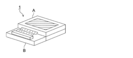
- FIG. 1 is a schematic view showing an example of a display device composed of organic EL elements. It is a schematic diagram of a display such as a mobile phone that displays image information by light emission of an organic EL element.
- the display 1 includes a display unit A having a plurality of pixels, a control unit B that performs image scanning of the display unit A based on image information, and the like.
- the control unit B is electrically connected to the display unit A, and sends a scanning signal and an image data signal to each of a plurality of pixels based on image information from the outside, and the pixels for each scanning line respond to the image data signal by the scanning signal.
- the image information is sequentially emitted to scan the image and display the image information on the display unit A.
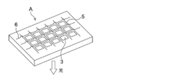
- FIG. 2 is a schematic diagram of the display unit A.
- the display unit A includes a wiring unit including a plurality of scanning lines 5 and data lines 6 and a plurality of pixels 3 on the substrate. The main members of the display unit A will be described below.
- the light emitted from the pixel 3 is extracted in the direction of the white arrow (downward).
- the scanning line 5 and the plurality of data lines 6 in the wiring portion are each made of a conductive material, and the scanning lines 5 and the data lines 6 are orthogonal to each other in a grid pattern and are connected to the pixels 3 at the orthogonal positions (details are illustrated). Not) When a scanning signal is applied from the scanning line 5, the pixel 3 receives an image data signal from the data line 6 and emits light according to the received image data.
- a full color display can be achieved by appropriately arranging pixels in the red region, the green region, and the blue region on the same substrate.
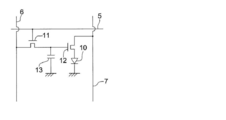
- FIG. 3 is a schematic diagram of a pixel.
- the pixel includes an organic EL element 10, a switching transistor 11, a driving transistor 12, a capacitor 13, and the like.
- a full color display can be performed by using red, green, and blue light emitting organic EL elements as the organic EL elements 10 in a plurality of pixels, and juxtaposing them on the same substrate.
- an image data signal is applied from the control unit B to the drain of the switching transistor 11 via the data line 6.
- a scanning signal is applied from the control unit B to the gate of the switching transistor 11 via the scanning line 5
- the driving of the switching transistor 11 is turned on, and the image data signal applied to the drain is supplied to the capacitor 13 and the driving transistor 12. Is transmitted to the gate.
- the capacitor 13 is charged according to the potential of the image data signal, and the drive transistor 12 is turned on.
- the drive transistor 12 has a drain connected to the power supply line 7 and a source connected to the electrode of the organic EL element 10, and the power supply line 7 connects to the organic EL element 10 according to the potential of the image data signal applied to the gate. Current is supplied.
- the driving of the switching transistor 11 is turned off. However, even if the driving of the switching transistor 11 is turned off, the capacitor 13 maintains the potential of the charged image data signal, so that the driving of the driving transistor 12 is kept on and the next scanning signal is applied. Until then, the light emission of the organic EL element 10 continues.
- the driving transistor 12 is driven according to the potential of the next image data signal synchronized with the scanning signal, and the organic EL element 10 emits light.
- the light emission of the organic EL element 10 is performed by providing the switching transistor 11 and the drive transistor 12 which are active elements with respect to the organic EL element 10 of each of the plurality of pixels. It is carried out.
- Such a light emitting method is called an active matrix method.
- the light emission of the organic EL element 10 may be light emission of a plurality of gradations by a multi-value image data signal having a plurality of gradation potentials, or on / off of a predetermined light emission amount by a binary image data signal. But you can.
- the potential of the capacitor 13 may be held continuously until the next scanning signal is applied, or may be discharged immediately before the next scanning signal is applied.
- the present invention not only the active matrix method described above, but also a passive matrix light emission drive in which an organic EL element emits light according to a data signal only when a scanning signal is scanned.
- FIG. 4 is a schematic view of a passive matrix display device.
- a plurality of scanning lines 5 and a plurality of image data lines 6 are provided in a lattice shape so as to face each other with the pixel 3 interposed therebetween.
- the scanning signal of the scanning line 5 is applied by sequential scanning, the pixels 3 connected to the applied scanning line 5 emit light according to the image data signal.
- the pixel 3 has no active element, and the manufacturing cost can be reduced.
- the lighting device of the present invention will be described.
- the illuminating device of this invention has the said organic EL element.
- the organic EL element of the present invention may be used as an organic EL element having a resonator structure.
- the purpose of use of the organic EL element having such a resonator structure is as follows.
- the light source of a machine, the light source of an optical communication processing machine, the light source of a photosensor, etc. are mentioned, However, It is not limited to these. Moreover, you may use for the said use by making a laser oscillation.
- the organic EL element of the present invention may be used as a kind of lamp for illumination or exposure light source, a projection device for projecting an image, or a display for directly viewing a still image or a moving image. It may be used as a device (display).
- the drive method when used as a display device for moving image reproduction may be either a simple matrix (passive matrix) method or an active matrix method.
- a full-color display device can be manufactured by using two or more organic EL elements of the present invention having different emission colors.
- the organic EL material of the present invention can be applied to an organic EL element that emits substantially white light as a lighting device.
- a plurality of emission colors are simultaneously emitted by a plurality of emission dopants to obtain white emission by color mixing.
- the combination of a plurality of emission colors may include three emission maximum wavelengths of the three primary colors of blue, green, and blue, or two using the relationship of complementary colors such as blue and yellow, blue green and orange, etc. The thing containing the light emission maximum wavelength may be used.
- the combination of light emitting dopants for obtaining a plurality of emission colors is a combination of a plurality of phosphorescent or fluorescent materials, a light emitting dopant that emits fluorescence or phosphorescence, and excitation of light from the light emitting dopant.
- Any combination with a dye material that emits light as light may be used, but in the white organic EL device according to the present invention, it is only necessary to mix and mix a plurality of light emitting dopants. It is only necessary to provide a mask only when forming a light emitting layer, a hole transport layer, an electron transport layer, etc., and simply arrange them separately by coating with the mask. Since other layers are common, patterning of the mask or the like is not necessary.
- an electrode film can be formed by a vapor deposition method, a cast method, a spin coating method, an ink jet method, a printing method, etc., and productivity is also improved.
- the elements themselves are luminescent white.
- the light emitting dopant used in the light emitting layer is not particularly limited.
- the metal complex according to the present invention or the metal complex according to the present invention so as to conform to the wavelength range corresponding to the CF (color filter) characteristics Any one of known light-emitting dopants may be selected and combined to whiten.
- the non-light emitting surface of the organic EL element of the present invention is covered with a glass case, a 300 ⁇ m thick glass substrate is used as a sealing substrate, and an epoxy photo-curing adhesive (Lux Track LC0629B manufactured by Toagosei Co., Ltd.) is used as a sealing material. ), And this is placed on the cathode and adhered to the transparent support substrate, irradiated with UV light from the glass substrate side, cured and sealed, and an illumination device as shown in FIGS. Can be formed.
- an epoxy photo-curing adhesive Lux Track LC0629B manufactured by Toagosei Co., Ltd.
- FIG. 5 shows a schematic diagram of the lighting device, and the organic EL element 101 of the present invention is covered with a glass cover 102 (in addition, the sealing operation with the glass cover is performed without bringing the organic EL element 101 into contact with the atmosphere. (This was performed in a glove box under a nitrogen atmosphere (in an atmosphere of high-purity nitrogen gas having a purity of 99.999% or more)).
- FIG. 6 shows a cross-sectional view of the lighting device.
- 105 denotes a cathode
- 106 denotes an organic EL layer
- 107 denotes a glass substrate with a transparent electrode.
- the glass cover 102 is filled with nitrogen gas 108 and a water catching agent 109 is provided.
- Example 1 Production of Organic EL Element 1 >> After patterning on a substrate (made of NH Techno Glass: NA-45) having a 150 nm ITO film on glass as an anode, the transparent support substrate provided with this ITO transparent electrode was ultrasonically cleaned with iso-propyl alcohol, Drying was performed with dry nitrogen gas, and UV ozone cleaning was performed for 5 minutes.
- This transparent support substrate was fixed to a substrate holder of a commercially available vacuum deposition apparatus, while ⁇ -NPD, BAlq, and Alq 3 were placed in three tantalum resistance heating boats, respectively, and attached to the vacuum deposition apparatus (first vacuum chamber). .
- lithium fluoride was put into a resistance heating boat made of tantalum and aluminum was put into a resistance heating boat made of tungsten, respectively, and attached to the second vacuum tank of the vacuum evaporation apparatus.
- the first vacuum chamber is depressurized to 4 ⁇ 10 ⁇ 4 Pa, and then heated by energizing the heating boat containing ⁇ -NPD, and the transparent support substrate is deposited at a deposition rate of 0.1 to 0.2 nm / sec.
- the film was deposited to a thickness of 20 nm, and a hole injection / transport layer was provided.
- the heating boat containing BAlq was energized and heated to provide a 10 nm thick hole blocking layer at a deposition rate of 0.1 to 0.2 nm / second. Further, the heating boat containing Alq 3 was heated by energization to provide an electron transport layer having a film thickness of 20 nm at a deposition rate of 0.1 to 0.2 nm / second.
- the element formed up to the electron transport layer is transferred to the second vacuum chamber while being vacuumed, and then remotely controlled from outside the device so that a stainless steel rectangular perforated mask is placed on the electron transport layer. Installed.
- a current was passed through a boat containing lithium fluoride to provide a cathode buffer layer having a thickness of 0.5 nm at a deposition rate of 0.01 to 0.02 nm / second,
- a boat containing aluminum was energized, a cathode having a film thickness of 150 nm was attached at a deposition rate of 1 to 2 nm / second, and an organic EL element 1 was produced.
- Organic EL elements 2 to 25 were prepared in the same manner as in the production of organic EL element 1, except that BD-15 and H1 of the light emitting layer were changed to the combinations described in the column of evaluation results in Table 2.
- FIG. 5 is a schematic view of the lighting device, and the organic EL element 101 is covered with a glass cover 102 (in addition, the sealing operation with the glass cover is performed in a nitrogen atmosphere without bringing the organic EL element 101 into contact with the atmosphere. (In a high purity nitrogen gas atmosphere with a purity of 99.999% or more).
- FIG. 6 shows a cross-sectional view of the lighting device.
- 105 denotes a cathode
- 106 denotes an organic EL layer
- 107 denotes a glass substrate with a transparent electrode.
- the glass cover 102 is filled with nitrogen gas 108 and a water catching agent 109 is provided.
- CS-1000 manufactured by Konica Minolta Sensing was used for measurement of light emission luminance.
- the organic EL elements 3 to 6, 10 to 14, 17 to 21 and 23 to 25 of the present invention emit higher light than the comparative organic EL elements 1, 2, 7, 8, 9, 15, 16 and 22. It is clear that a reduction in efficiency and drive voltage can be achieved.
- the band gaps of the light-emitting dopants used in the examples are BD-16 (2.66 eV), BD-17 (2.70 eV), BD-36 (2.70 eV), and BD-37 (2.70 eV), respectively. ).
- Example 2 ⁇ Production of full-color display device> (Production of blue light emitting element)
- the organic EL element 5 of Example 1 was used as a blue light emitting element.
- a green light emitting device was produced in the same manner as in the organic EL device 5 of Example 1 except that BD-36 was changed to BD-15, and this was used as the green light emitting device.
- red light emitting device was produced in the same manner as in the organic EL device 5 of Example 1 except that BD-36 was changed to Ir-8, and this was used as a red light emitting device.
- the red, green, and blue light emitting organic EL elements produced above were juxtaposed on the same substrate to produce an active matrix type full color display device having a configuration as shown in FIG. In FIG. 2, only the schematic diagram of the display part A of the produced display device is shown.
- a plurality of pixels 3 (light emission color is a red region pixel, a green region pixel, a blue region pixel, etc.) juxtaposed with a wiring portion including a plurality of scanning lines 5 and data lines 6 on the same substrate.
- the scanning lines 5 and the plurality of data lines 6 in the wiring portion are each made of a conductive material, and the scanning lines 5 and the data lines 6 are orthogonal to each other in a lattice shape and are connected to the pixels 3 at the orthogonal positions (for details, see FIG. Not shown).
- the plurality of pixels 3 are driven by an active matrix system provided with an organic EL element corresponding to each emission color, a switching transistor as an active element, and a driving transistor, and a scanning signal is applied from a scanning line 5.
- the image data signal is received from the data line 6 and light is emitted according to the received image data. In this way, a full color display device was produced by appropriately juxtaposing red, green, and blue pixels.
- BAlq was deposited to a thickness of 10 nm to provide a hole blocking layer. Furthermore, H42 was deposited at 40 nm to provide an electron transport layer.
- Example 2 a square perforated mask having the same shape as the transparent electrode made of stainless steel was placed on the electron injection layer, and lithium fluoride 0.5 nm was used as the cathode buffer layer and aluminum 150 nm was used as the cathode. Evaporated film was formed.
- This device was equipped with a sealing can having the same method and the same structure as in Example 1, and a flat lamp as shown in FIGS. 5 and 6 was produced. When this flat lamp was energized, almost white light was obtained, and it was found that it could be used as a lighting device.
Abstract
Disclosed is an organic electroluminescent element having high light-emission luminance and a low driving voltage. The organic electroluminescent element comprises a supporting substrate and at least an anode and a cathode both arranged on the supporting substrate, and additionally comprises a light-emitting layer comprising at least an organic substance and arranged between the anode and the cathode. The light-emitting layer comprises at least a light-emitting dopant and a host compound, wherein the absolute value of the difference between the bipolar moment of the light-emitting dopant and the bipolar moment of the host compound is 2 debyes or less, and the light-emitting layer is formed by coating.
Description
本発明は、有機エレクトロルミネッセンス素子、表示装置及び照明装置に関する。
The present invention relates to an organic electroluminescence element, a display device, and a lighting device.
従来、発光型の電子ディスプレイデバイスとして、エレクトロルミネッセンスディスプレイ(以下、ELDと言う)がある。ELDの構成要素としては、無機エレクトロルミネッセンス素子や有機エレクトロルミネッセンス素子(以下、有機EL素子とも言う)が挙げられる。
Conventionally, as a light-emitting electronic display device, there is an electroluminescence display (hereinafter referred to as ELD). Examples of constituent elements of ELD include inorganic electroluminescent elements and organic electroluminescent elements (hereinafter also referred to as organic EL elements).
無機エレクトロルミネッセンス素子は平面型光源として使用されてきたが、発光素子を駆動させるためには交流の高電圧が必要である。有機EL素子は発光する化合物を含有する発光層を陰極と陽極で挟んだ構成を有し、発光層に電子及び正孔を注入して、再結合させることにより励起子(エキシトン)を生成させ、このエキシトンが失活する際の光の放出(蛍光・リン光)を利用して発光する素子であり、数V~数十V程度の電圧で発光が可能であり、更に自己発光型であるために視野角に富み、視認性が高く、薄膜型の完全固体素子であるために省スペース、携帯性等の観点から注目されている。
Inorganic electroluminescent elements have been used as planar light sources, but an alternating high voltage is required to drive the light emitting elements. An organic EL device has a structure in which a light emitting layer containing a compound that emits light is sandwiched between a cathode and an anode, injects electrons and holes into the light emitting layer, and recombines them to generate excitons (exciton). It is an element that emits light using the emission of light (fluorescence / phosphorescence) when this exciton is deactivated, and can emit light at a voltage of several V to several tens V, and it is self-luminous. In addition, it is attracting attention from the viewpoints of space saving, portability and the like because it is a thin film type complete solid element with a wide viewing angle and high visibility.
しかしながら、今後の実用化に向けた有機EL素子においては、更に低消費電力で効率よく高輝度に発光する有機EL素子の開発が望まれている。
However, in the organic EL element for practical use in the future, it is desired to develop an organic EL element that emits light with high power and efficiency with lower power consumption.
特許第3093796号公報では、スチルベン誘導体、ジスチリルアリーレン誘導体またはトリススチリルアリーレン誘導体に微量の蛍光体をドープし、発光輝度の向上、素子の長寿命化を達成している。また、8-ヒドロキシキノリンアルミニウム錯体をホスト化合物として、これに微量の蛍光体をドープした有機発光層を有する素子(例えば、特開昭63-264692号公報)、8-ヒドロキシキノリンアルミニウム錯体をホスト化合物として、これにキナクリドン系色素をドープした有機発光層を有する素子(例えば、特開平3-255190号公報)等が知られている。
In Japanese Patent No. 3093796, a small amount of a phosphor is doped into a stilbene derivative, a distyrylarylene derivative or a tristyrylarylene derivative to achieve improvement in light emission luminance and a longer device lifetime. Further, an element having an organic light-emitting layer in which 8-hydroxyquinoline aluminum complex is used as a host compound and a small amount of phosphor is doped thereto (for example, JP-A 63-264692), 8-hydroxyquinoline aluminum complex is used as a host compound. For example, an element having an organic light emitting layer doped with a quinacridone dye (for example, JP-A-3-255190) is known.
上記文献に開示されている技術では、励起一重項からの発光を用いる場合一重項励起子と三重項励起子の生成比が1:3であるため、発光性励起種の生成確率が25%であることと、光の取り出し効率が約20%であるため外部取り出し量子効率(ηext)の限界は5%とされている。
In the technique disclosed in the above document, when the emission from the excited singlet is used, the generation ratio of the singlet exciton and the triplet exciton is 1: 3. Therefore, the generation probability of the luminescent excited species is 25%. In addition, since the light extraction efficiency is about 20%, the limit of the external extraction quantum efficiency (ηext) is set to 5%.
ところが、プリンストン大より励起三重項からのリン光発光を用いる有機EL素子の報告(M.A.Baldo et al.,Nature、395巻、151~154頁(1998年))がされて以来、室温でリン光を示す材料の研究が活発になってきている。
However, since the University of Princeton reported on organic EL devices using phosphorescence emission from excited triplets (MA Baldo et al., Nature, 395, 151-154 (1998)), Research on materials that exhibit phosphorescence has become active.
例えば、M.A.Baldo et al.,Nature、403巻、17号、750~753頁(2000年)、また米国特許第6,097,147号明細書等にも開示されている。
For example, M.M. A. Baldo et al. , Nature, 403, 17, 750-753 (2000), US Pat. No. 6,097,147, and the like.
励起三重項を使用すると、内部量子効率の上限が100%となるため励起一重項の場合に比べて原理的に発光効率が4倍となり、冷陰極管とほぼ同等の性能が得られる可能性があることから照明用途としても注目されている。
When the excited triplet is used, the upper limit of the internal quantum efficiency is 100%. In principle, the luminous efficiency is four times that of the excited singlet, and there is a possibility that almost the same performance as a cold cathode tube can be obtained. Therefore, it is attracting attention as a lighting application.
例えば、S.Lamansky et al.,J.Am.Chem.Soc.,123巻、4304頁(2001年)等においては、多くの化合物がイリジウム錯体系等重金属錯体を中心に合成検討されている。
For example, S. Lamansky et al. , J .; Am. Chem. Soc. , 123, 4304 (2001), etc., many compounds are being studied for synthesis centering on heavy metal complexes such as iridium complexes.
また、前述のM.A.Baldo et al.,Nature,403巻、17号、750~753頁(2000年)においては、ドーパントとして、トリス(2-フェニルピリジン)イリジウムを用いた検討がされている。
Also, the above-mentioned M.M. A. Baldo et al. , Nature, 403, 17, 750-753 (2000), studies have been made using tris (2-phenylpyridine) iridium as a dopant.
また、有機EL素子は電極と電極の間を厚さわずか0.1μm程度の有機材料の膜で構成するオールソリッド素子であり、なお且つその発光が2~20V程度の比較的低い電圧で達成できることから、次世代の平面ディスプレイや照明として期待されている技術である。
The organic EL element is an all-solid element composed of an organic material film having a thickness of only about 0.1 μm between the electrodes, and can emit light at a relatively low voltage of about 2 to 20V. Therefore, it is a technology that is expected as a next-generation flat display and illumination.
しかしながら、有機EL素子の構成は透明電極と対抗電極に有機層が挟まれただけの単純なものであり、平面ディスプレイの代表である液晶ディスプレイに比べ、部品点数が圧倒的に少ないため製造コストも低く抑えられるはずであるが、現状では必ずしもそうではなく、性能的にもコスト的にも液晶ディスプレイに大きく水をあけられている。
However, the configuration of the organic EL element is simple, in which an organic layer is sandwiched between a transparent electrode and a counter electrode, and the manufacturing cost is also low because the number of parts is overwhelmingly smaller than that of a liquid crystal display that is a typical flat display. Although it should be kept low, this is not always the case at present, and a large amount of water is drained into the liquid crystal display in terms of performance and cost.
特にコストに対しては、生産性の悪さがその要因と考えられる。現在商品化されている有機ELの殆どが低分子材料を蒸着して成膜する、所謂蒸着法で製造されている。この蒸着法は精製が容易な低分子化合物を有機EL材料として用いることができる(高純度材料が得やすい)こと、更に積層構造を作るのが容易なことから、効率、寿命という面で非常に優れているが、反面10-4Pa以下という高真空条件下で蒸着を行うため、成膜する装置に制約が加わり、実際には小さい面積の基板にしか適用できず、更に複数層積層するとなると成膜に時間がかかり、スループットが低いことが欠点である。特に照明用途や大面積の電子ディスプレイに適用する場合は問題となり、有機ELがそのようなアプリケーションに実用されていない一つの原因となっている。
In particular, in terms of cost, poor productivity is considered as a factor. Most of the organic ELs currently commercialized are manufactured by a so-called vapor deposition method in which a low molecular material is deposited to form a film. In this vapor deposition method, a low-molecular compound that can be easily purified can be used as an organic EL material (high-purity material is easy to obtain), and a laminated structure can be easily formed. Although it is excellent, on the other hand, since the deposition is performed under a high vacuum condition of 10 −4 Pa or less, restrictions are imposed on the film forming apparatus, and in practice it can be applied only to a substrate with a small area, and more layers are laminated. The disadvantages are that the film formation takes time and the throughput is low. In particular, it becomes a problem when applied to lighting applications or large-area electronic displays, and organic EL is one of the causes that are not practically used in such applications.
一方、有機層をスピンコート、インクジェット、印刷、スプレーといったプロセスで製造する塗布法は常圧で薄膜を作製することでき、更に大面積に均一な膜を作製するのに適している。
On the other hand, the coating method in which the organic layer is manufactured by processes such as spin coating, ink jet, printing, and spraying can produce a thin film at normal pressure, and is suitable for producing a uniform film over a larger area.
しかしながら、例えば、発光層を塗布で作製する場合、発光ドーパントと発光ホストを同じ溶液中に溶解し塗布するため、発光ドーパントと発光ホストの溶解性の差、あるいは溶媒との相互作用の差などにより、蒸着膜では観測されなかった相分離や不均一分布が起こり、これが性能低下の大きな要因となっている。
However, for example, when the light emitting layer is prepared by coating, the light emitting dopant and the light emitting host are dissolved and applied in the same solution, and therefore, due to the difference in solubility between the light emitting dopant and the light emitting host or the difference in interaction with the solvent. However, phase separation and non-uniform distribution, which were not observed in the deposited film, occurred, and this was a major factor in performance degradation.
また、より長寿命化を達成するために、発光層と隣接層の界面のコントロールすべく用いる材料の双極子モーメントに着目した技術(例えば、特許文献1、2参照)、塗布法での素子作製で溶液の増粘等を抑制するために、溶媒の双極子モーメントを規定した技術(例えば、特許文献3参照)、有機発光層と電子注入層との間に、孤立した島状である双極子モーメントが3デバイ以上の分子からなる制御層を設けたときに長時間安定な素子を実現できるとした技術(例えば、特許文献4参照)、有機発光層に双極子モーメントが大きなホスト材料と電子吸引性基を有するドーパントを含む場合に駆動電圧が低減できるとした技術(例えば、特許文献5参照)が知られているが、いずれも双極子モーメントには着目しているが、発光層内での発光ドーパントとホスト化合物の双極子モーメントの差に注目した本発明とは異なる。
In addition, in order to achieve a longer lifetime, a technique that focuses on the dipole moment of a material used to control the interface between the light emitting layer and the adjacent layer (see, for example, Patent Documents 1 and 2), and device fabrication by a coating method In order to suppress the thickening of the solution, a technique that defines the dipole moment of the solvent (see, for example, Patent Document 3), a dipole that is an isolated island between the organic light emitting layer and the electron injection layer Technology that can realize a device that is stable for a long time when a control layer composed of molecules having a moment of 3 debyes or more is provided (see, for example, Patent Document 4), a host material having a large dipole moment in an organic light emitting layer, and electron attraction Although the technique (for example, refer patent document 5) that drive voltage can be reduced when including the dopant which has a sex group is known, all pay attention to the dipole moment, It differs from the present invention with a focus on the difference in the dipole moment of a light dopant and a host compound.
本発明の目的は、高い発光輝度を示し、且つ低駆動電圧の有機エレクトロルミネッセンス素子、及び該素子を用いた照明装置、表示装置を提供することである。
An object of the present invention is to provide an organic electroluminescence element exhibiting high emission luminance and having a low driving voltage, and an illumination device and a display device using the element.
本発明の上記課題は、下記構成により達成される。
The above object of the present invention is achieved by the following configuration.
1.支持基板上に少なくとも陽極、陰極を有し、該陽極と該陰極間に少なくとも有機物からなる発光層を有する有機エレクトロルミネッセンス素子において、該発光層は少なくとも発光ドーパントとホスト化合物とを含有し、該発光ドーパントと該ホスト化合物の双極子モーメントの差の絶対値が2デバイ以下であり、該発光層は塗布により形成されることを特徴とする有機エレクトロルミネッセンス素子。
1. In an organic electroluminescence device having at least an anode and a cathode on a support substrate and having a light emitting layer composed of at least an organic substance between the anode and the cathode, the light emitting layer contains at least a light emitting dopant and a host compound, and the light emission An organic electroluminescence device, wherein an absolute value of a difference between a dopant and a dipole moment of the host compound is 2 Debye or less, and the light emitting layer is formed by coating.
2.前記ホスト化合物の双極子モーメントが4デバイ以上であることを特徴とする前記1に記載の有機エレクトロルミネッセンス素子。
2. 2. The organic electroluminescent device according to 1 above, wherein the dipole moment of the host compound is 4 Debye or more.
3.前記ホスト化合物がカルバゾール誘導体あるいはアザカルバゾール誘導体であることを特徴とする前記1または2に記載の有機エレクトロルミネッセンス素子。
3. 3. The organic electroluminescence device as described in 1 or 2 above, wherein the host compound is a carbazole derivative or an azacarbazole derivative.
4.前記カルバゾール誘導体あるいはアザカルバゾール誘導体が窒素原子を有する5員あるいは6員の芳香族複素環基を有することを特徴とする前記3に記載の有機エレクトロルミネッセンス素子。
4. 4. The organic electroluminescence device according to 3 above, wherein the carbazole derivative or azacarbazole derivative has a 5-membered or 6-membered aromatic heterocyclic group having a nitrogen atom.
5.前記窒素原子を有する5員あるいは6員の芳香族複素環基における芳香族複素環がピリジン、イミダゾール、ピラジン、トリアジン、インドールまたはインダゾールであることを特徴とする前記4に記載の有機エレクトロルミネッセンス素子。
5. 5. The organic electroluminescent device according to 4 above, wherein the aromatic heterocyclic ring in the 5- or 6-membered aromatic heterocyclic group having a nitrogen atom is pyridine, imidazole, pyrazine, triazine, indole or indazole.
6.前記発光ドーパントの双極子モーメントが4デバイ以下であることを特徴とする前記1~5のいずれか1項に記載の有機エレクトロルミネッセンス素子。
6. 6. The organic electroluminescence device according to any one of 1 to 5, wherein a dipole moment of the luminescent dopant is 4 Debye or less.
7.前記発光ドーパントがリン光ドーパントであることを特徴とする前記1~6のいずれか1項に記載の有機エレクトロルミネッセンス素子。
7. 7. The organic electroluminescence device according to any one of 1 to 6, wherein the light emitting dopant is a phosphorescent dopant.
8.前記リン光ドーパントがイリジウム錯体であることを特徴とする前記7に記載の有機エレクトロルミネッセンス素子。
8. 8. The organic electroluminescence device as described in 7 above, wherein the phosphorescent dopant is an iridium complex.
9.前記イリジウム錯体が、下記一般式(A)で表されるイリジウム錯体であることを特徴とする前記8に記載の有機エレクトロルミネッセンス素子。
9. 9. The organic electroluminescence device as described in 8 above, wherein the iridium complex is an iridium complex represented by the following general formula (A).

(式中、Ar1は芳香族炭化水素環または芳香族複素環を表し、Ar2は芳香族複素環を表す。)
10.前記イリジウム錯体の基底状態と三重項励起状態とのバンドギャップが2.7eV以下であることを特徴とする前記8または9に記載の有機エレクトロルミネッセンス素子。 (In the formula, Ar 1 represents an aromatic hydrocarbon ring or an aromatic heterocyclic ring, and Ar 2 represents an aromatic heterocyclic ring.)
10. 10. The organic electroluminescence device as described in 8 or 9 above, wherein the band gap between the ground state and the triplet excited state of the iridium complex is 2.7 eV or less.
11.前記発光層を塗布する溶媒の双極子モーメントが1デバイ以上であることを特徴とする前記1~10のいずれか1項に記載の有機エレクトロルミネッセンス素子。
11. 11. The organic electroluminescence device as described in any one of 1 to 10 above, wherein a dipole moment of a solvent for applying the light emitting layer is 1 Debye or more.
12.白色に発光することを特徴とする前記1~11のいずれか1項に記載の有機エレクトロルミネッセンス素子。
12. 12. The organic electroluminescence device as described in any one of 1 to 11 above, which emits white light.
13.前記1~12に記載の有機エレクトロルミネッセンス素子を備えたことを特徴とする表示装置。
13. 13. A display device comprising the organic electroluminescence element as described in 1 to 12 above.
14.前記1~12に記載の有機エレクトロルミネッセンス素子を備えたことを特徴とする照明装置。
14. 13. An illumination device comprising the organic electroluminescence element as described in 1 to 12 above.
本発明により、高い発光輝度を示し、且つ低駆動電圧の有機エレクトロルミネッセンス素子、及び該素子を用いた照明装置、表示装置を提供することができた。
According to the present invention, it was possible to provide an organic electroluminescence element exhibiting high emission luminance and having a low driving voltage, and an illumination device and a display device using the element.
以下、本発明について詳述する。
Hereinafter, the present invention will be described in detail.
本発明の有機エレクトロルミネッセンス素子においては、請求項1~12のいずれか1項に規定の構成にすることにより、高い発光輝度を示し、且つ低駆動電圧の有機エレクトロルミネッセンス素子を得ることができた。
In the organic electroluminescence device of the present invention, by adopting the configuration defined in any one of claims 1 to 12, it was possible to obtain an organic electroluminescence device having high emission luminance and low driving voltage. .
本発明の有機エレクトロルミネッセンス素子は、発光層が少なくとも発光ドーパントとホスト化合物とを含有し、両者の双極子モーメントの差の絶対値が2デバイ以下であり、該発光層は塗布により形成されることを特徴とする。
In the organic electroluminescence device of the present invention, the light emitting layer contains at least a light emitting dopant and a host compound, the absolute value of the difference between the dipole moments is 2 Debye or less, and the light emitting layer is formed by coating. It is characterized by.
なお、本発明において、双極子モーメントは汎用の計算機シミュレーションツールを用いて計算したものである。ほとんどの分子はChambridgesoft製Chem3D上でMOPAC97エンジンを用いてハミルトニアンAM1またはPM3で最適化構造を求めた。中心金属がIrなど重金属の場合は、非経験的分子軌道法により計算を行った。具体的には、Gaussian社製Gaussian98Wを用いて計算を行った。Ir等重金属を含む錯体の計算は、周期表の第3周期以下を有効殻ポテンシャルで表したLANL2DZ基底を用いた。
In the present invention, the dipole moment is calculated using a general-purpose computer simulation tool. Most molecules were optimized for the Hamiltonian AM1 or PM3 using a MOPAC97 engine on a Chembridge 3 Chembrand soft. When the central metal is a heavy metal such as Ir, the calculation was performed by the ab initio molecular orbital method. Specifically, the calculation was performed using Gaussian 98W manufactured by Gaussian. For the calculation of a complex containing a heavy metal such as Ir, a LANL2DZ basis in which the third and lower periods of the periodic table are represented by an effective shell potential was used.
以下、本発明の有機EL素子の構成層について説明する。
Hereinafter, the constituent layers of the organic EL element of the present invention will be described.
《有機EL素子の構成層》
本発明の有機EL素子の層構成の好ましい具体例を以下に示すが、本発明はこれらに限定されない。 << Constituent layers of organic EL elements >>
Although the preferable specific example of the layer structure of the organic EL element of this invention is shown below, this invention is not limited to these.
本発明の有機EL素子の層構成の好ましい具体例を以下に示すが、本発明はこれらに限定されない。 << Constituent layers of organic EL elements >>
Although the preferable specific example of the layer structure of the organic EL element of this invention is shown below, this invention is not limited to these.
(i)陽極/正孔輸送層/発光層/正孔阻止層/電子輸送層/陰極
(ii)陽極/電子阻止層/発光層/正孔阻止層/電子輸送層/陰極
(iii)陽極/正孔輸送層/電子阻止層/発光層/正孔阻止層/電子輸送層/陰極
(iv)陽極/正孔輸送層/電子阻止層/発光層/正孔阻止層/電子輸送層/陰極
(v)陽極/正孔輸送層/電子阻止層/発光層/正孔阻止層/電子輸送層/陰極バッファー層/陰極
(vi)陽極/陽極バッファー層/正孔輸送層/電子阻止層/発光層/正孔阻止層/電子輸送層/陰極バッファー層/陰極
(vii)陽極/陽極バッファー層/正孔輸送層/電子阻止層/発光層/正孔阻止層/電子輸送層/陰極バッファー層/陰極。 (I) Anode / hole transport layer / light emitting layer / hole blocking layer / electron transport layer / cathode (ii) Anode / electron blocking layer / light emitting layer / hole blocking layer / electron transport layer / cathode (iii) Anode / Hole transport layer / electron blocking layer / light emitting layer / hole blocking layer / electron transport layer / cathode (iv) Anode / hole transport layer / electron blocking layer / light emitting layer / hole blocking layer / electron transport layer / cathode ( v) Anode / hole transport layer / electron blocking layer / light emitting layer / hole blocking layer / electron transport layer / cathode buffer layer / cathode (vi) Anode / anode buffer layer / hole transport layer / electron blocking layer / light emitting layer / Hole blocking layer / electron transport layer / cathode buffer layer / cathode (vii) Anode / anode buffer layer / hole transport layer / electron blocking layer / light emitting layer / hole blocking layer / electron transport layer / cathode buffer layer / cathode .
《電子輸送層》
電子輸送層とは電子を輸送する機能を有する材料からなり、広い意味で電子注入層、正孔阻止層も電子輸送層に含まれる。電子輸送層は単層または複数層設けることができる。 《Electron transport layer》
The electron transport layer is made of a material having a function of transporting electrons, and in a broad sense, an electron injection layer and a hole blocking layer are also included in the electron transport layer. The electron transport layer can be provided as a single layer or a plurality of layers.
従来、単層の電子輸送層、及び複数層とする場合は発光層に対して陰極側に隣接する電子輸送層に用いられる電子輸送材料(正孔阻止材料を兼ねる)としては、陰極より注入された電子を発光層に伝達する機能を有していればよく、その材料としては従来公知の化合物の中から任意のものを選択して用いることもでき、例えば、ニトロ置換フルオレン誘導体、ジフェニルキノン誘導体、チオピランジオキシド誘導体、カルボジイミド、フレオレニリデンメタン誘導体、アントラキノジメタン及びアントロン誘導体、オキサジアゾール誘導体等が挙げられる。
Conventionally, in the case of a single electron transport layer and a plurality of layers, an electron transport material (also serving as a hole blocking material) used for an electron transport layer adjacent to the light emitting layer on the cathode side is injected from the cathode. As long as it has a function of transferring electrons to the light-emitting layer, any material selected from conventionally known compounds can be selected and used. For example, nitro-substituted fluorene derivatives, diphenylquinone derivatives Thiopyrandioxide derivatives, carbodiimides, fluorenylidenemethane derivatives, anthraquinodimethane and anthrone derivatives, oxadiazole derivatives and the like.
更に上記オキサジアゾール誘導体において、オキサジアゾール環の酸素原子を硫黄原子に置換したチアジアゾール誘導体、電子吸引基として知られているキノキサリン環を有するキノキサリン誘導体も、電子輸送材料として用いることができる。更にこれらの材料を高分子鎖に導入した、またはこれらの材料を高分子の主鎖とした高分子材料を用いることもできる。
Furthermore, in the above oxadiazole derivative, a thiadiazole derivative in which the oxygen atom of the oxadiazole ring is substituted with a sulfur atom, and a quinoxaline derivative having a quinoxaline ring known as an electron withdrawing group can also be used as an electron transport material. Furthermore, a polymer material in which these materials are introduced into a polymer chain or these materials are used as a polymer main chain can also be used.
また、8-キノリノール誘導体の金属錯体、例えば、トリス(8-キノリノール)アルミニウム(Alq)、トリス(5,7-ジクロロ-8-キノリノール)アルミニウム、トリス(5,7-ジブロモ-8-キノリノール)アルミニウム、トリス(2-メチル-8-キノリノール)アルミニウム、トリス(5-メチル-8-キノリノール)アルミニウム、ビス(8-キノリノール)亜鉛(Znq)等、及びこれらの金属錯体の中心金属がIn、Mg、Cu、Ca、Sn、GaまたはPbに置き替わった金属錯体も、電子輸送材料として用いることができる。
Also, metal complexes of 8-quinolinol derivatives such as tris (8-quinolinol) aluminum (Alq), tris (5,7-dichloro-8-quinolinol) aluminum, tris (5,7-dibromo-8-quinolinol) aluminum Tris (2-methyl-8-quinolinol) aluminum, tris (5-methyl-8-quinolinol) aluminum, bis (8-quinolinol) zinc (Znq), and the like, and the central metals of these metal complexes are In, Mg, Metal complexes replaced with Cu, Ca, Sn, Ga or Pb can also be used as the electron transport material.
その他、メタルフリーもしくはメタルフタロシアニン、またはそれらの末端がアルキル基やスルホン酸基等で置換されているものも、電子輸送材料として好ましく用いることができる。また、発光層の材料として例示したジスチリルピラジン誘導体も、電子輸送材料として用いることができるし、正孔注入層、正孔輸送層と同様にn型-Si、n型-SiC等の無機半導体も電子輸送材料として用いることができる。
In addition, metal-free or metal phthalocyanine, or those having terminal ends substituted with an alkyl group or a sulfonic acid group can be preferably used as the electron transporting material. In addition, the distyrylpyrazine derivative exemplified as the material for the light emitting layer can also be used as an electron transport material, and an inorganic semiconductor such as n-type-Si, n-type-SiC, etc. as in the case of the hole injection layer and the hole transport layer. Can also be used as an electron transporting material.
電子輸送層は上記電子輸送材料を、例えば、真空蒸着法、スピンコート法、キャスト法、インクジェット法を含む印刷法、LB法等の公知の方法により、薄膜化することにより形成することができる。電子輸送層の膜厚については特に制限はないが、通常は5nm~5μm程度、好ましくは5~200nmである。電子輸送層は上記材料の1種または2種以上からなる一層構造であってもよい。
The electron transport layer can be formed by thinning the electron transport material by a known method such as a vacuum deposition method, a spin coating method, a casting method, a printing method including an ink jet method, or an LB method. The thickness of the electron transport layer is not particularly limited, but is usually about 5 nm to 5 μm, preferably 5 to 200 nm. The electron transport layer may have a single layer structure composed of one or more of the above materials.
また、不純物をドープしたn性の高い電子輸送層を用いることもできる。その例としては、特開平4-297076号公報、同10-270172号公報、特開2000-196140号公報、同2001-102175号公報、J.Appl.Phys.,95,5773(2004)等に記載されたものが挙げられる。
It is also possible to use an electron transport layer having a high n property doped with impurities. Examples thereof include JP-A-4-297076, JP-A-10-270172, JP-A-2000-196140, 2001-102175, J.A. Appl. Phys. 95, 5773 (2004), and the like.
本発明においては、このようなn性の高い電子輸送層を用いることがより低消費電力の素子を作製することができるため好ましい。
In the present invention, it is preferable to use an electron transport layer having such a high n property because an element with lower power consumption can be produced.
《発光層》
本発明に係る発光層は、電極または電子輸送層、正孔輸送層から注入されてくる電子及び正孔が再結合して発光する層であり、発光する部分は発光層の層内であっても発光層と隣接層との界面であってもよい。 <Light emitting layer>
The light emitting layer according to the present invention is a layer that emits light by recombination of electrons and holes injected from the electrode, the electron transport layer, or the hole transport layer, and the light emitting portion is in the layer of the light emitting layer. May be the interface between the light emitting layer and the adjacent layer.
発光層の膜厚の総和は特に制限はないが、膜の均質性や発光時に不必要な高電圧を印加するのを防止し、且つ駆動電流に対する発光色の安定性向上の観点から、2nm~5μmの範囲に調整することが好ましく、更に好ましくは2~200nmの範囲に調整され、特に好ましくは10~20nmの範囲である。
The total thickness of the light emitting layer is not particularly limited, but from the viewpoint of preventing the application of a high voltage unnecessary for the film uniformity and light emission, and improving the stability of the emitted color with respect to the driving current. It is preferable to adjust to a range of 5 μm, more preferably to a range of 2 to 200 nm, and particularly preferably in a range of 10 to 20 nm.
本発明に係る発光層の作製は、例えば、スピンコート法、キャスト法、ダイコート法、インクジェット法などの塗布法で行われ、塗布溶媒の双極子モーメントについては、低すぎると発光ドーパント及びホスト化合物が均一に分散あるいは溶解しないために、好ましくは1デバイ以上である。複数種併用する場合は、平均値としての双極子モーメントを求め、塗布溶媒の双極子モーメントが1デバイ以上であれば、好ましい。
The light emitting layer according to the present invention is produced by, for example, a coating method such as a spin coating method, a casting method, a die coating method, or an ink jet method. If the dipole moment of the coating solvent is too low, the light emitting dopant and the host compound are produced. In order not to disperse or dissolve uniformly, it is preferably 1 Debye or more. When using multiple types together, it is preferable if the dipole moment as an average value is obtained and the dipole moment of the coating solvent is 1 Debye or more.
本発明の有機EL素子の発光層には、ホスト化合物と発光ドーパント(リン光ドーパントや蛍光ドーパント等)の少なくとも1種類を含有する。
The light emitting layer of the organic EL device of the present invention contains at least one of a host compound and a light emitting dopant (phosphorescent dopant, fluorescent dopant, etc.).
(ホスト化合物)
本発明に用いられるホスト化合物について説明する。 (Host compound)
The host compound used in the present invention will be described.
本発明に用いられるホスト化合物について説明する。 (Host compound)
The host compound used in the present invention will be described.
本発明において、発光ドーパントとホスト化合物の双極子モーメントの差の絶対値が2デバイ以下であり、該ホスト化合物の双極子モーメントは4デバイ以上であることが好ましい。
In the present invention, the absolute value of the difference between the dipole moments of the luminescent dopant and the host compound is preferably 2 Debye or less, and the dipole moment of the host compound is preferably 4 Debye or more.
本発明において、ホスト化合物として、好ましくはカルバゾール誘導体あるいはアザカルバゾール誘導体であり、これらは窒素原子を有する5員あるいは6員の芳香族複素環基を有することが更に好ましい。窒素原子を有する5員あるいは6員の芳香族複素環基における芳香族複素環としては、ピリジン、イミダゾール、ピラジン、トリアジン、インドールまたはインダゾールが挙げられる。
In the present invention, the host compound is preferably a carbazole derivative or an azacarbazole derivative, and these further preferably have a 5-membered or 6-membered aromatic heterocyclic group having a nitrogen atom. Examples of the aromatic heterocyclic ring in the 5- or 6-membered aromatic heterocyclic group having a nitrogen atom include pyridine, imidazole, pyrazine, triazine, indole and indazole.
ここで、本発明においてホスト化合物とは、室温(25℃)においてリン光発光のリン光量子収率が0.1未満の化合物である。好ましくはリン光量子収率が0.01未満である。また、発光層に含有される化合物の中で、その層中での質量比が20%以上であることが好ましい。
Here, in the present invention, the host compound is a compound having a phosphorescence quantum yield of phosphorescence emission of less than 0.1 at room temperature (25 ° C.). The phosphorescence quantum yield is preferably less than 0.01. Moreover, it is preferable that the mass ratio in the layer is 20% or more among the compounds contained in a light emitting layer.
ホスト化合物としては、公知のホスト化合物を単独で用いてもよく、または複数種併用して用いてもよい。ホスト化合物を複数種用いることで、電荷の移動を調整することが可能であり、有機EL素子を高効率化することができる。また、後述する発光ドーパントを複数種用いることで異なる発光を混ぜることが可能となり、これにより任意の発光色を得ることができる。複数種併用する場合は、平均値としての双極子モーメントを求め、発光ドーパントの双極子モーメントとの差の絶対値が2デバイ以下であれば、本発明内である。
As the host compound, known host compounds may be used alone or in combination of two or more. By using a plurality of types of host compounds, it is possible to adjust the movement of charges, and the organic EL element can be made highly efficient. Moreover, it becomes possible to mix different light emission by using multiple types of light emission dopants mentioned later, and, thereby, arbitrary light emission colors can be obtained. In the case of using a plurality of types together, the dipole moment as an average value is obtained, and if the absolute value of the difference from the dipole moment of the luminescent dopant is 2 debyes or less, it is within the present invention.
本発明に併用してもよい公知のホスト化合物としては、正孔輸送能、電子輸送能を有しつつ、且つ発光の長波長化を防ぎ、なお且つ高Tg(ガラス転移温度)である化合物が好ましい。
As known host compounds that may be used in combination with the present invention, there are compounds having a hole transporting ability and an electron transporting ability, preventing the emission of longer wavelengths, and having a high Tg (glass transition temperature). preferable.
以下に、本発明に係るホスト化合物の具体例を示すが、本発明はこれらに限定されない。
Specific examples of the host compound according to the present invention are shown below, but the present invention is not limited thereto.

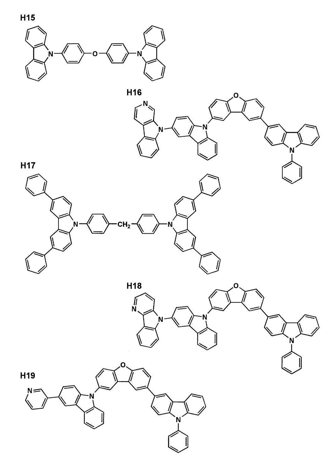


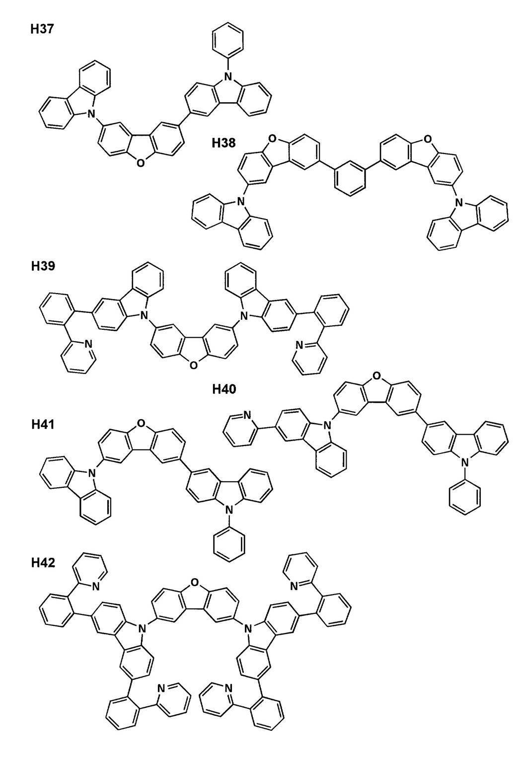
また、本発明に係る代表的なホスト化合物の双極子モーメント(計算値)を表1に示した。
In addition, Table 1 shows dipole moments (calculated values) of typical host compounds according to the present invention.
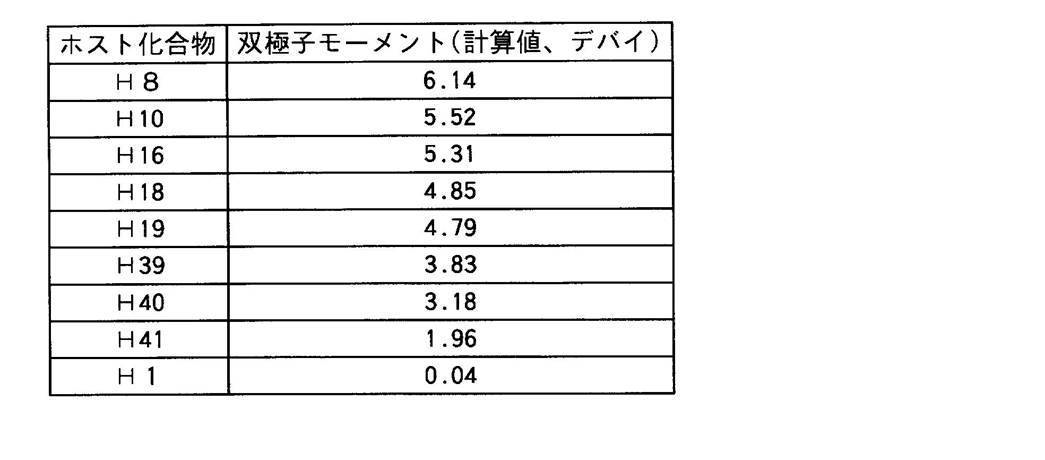
単独使用または併用してもよい公知のホスト化合物の具体例としては、更に以下の文献に記載されている化合物が挙げられる。
Specific examples of known host compounds that may be used alone or in combination include compounds described in the following documents.
特開2001-257076号公報、同2002-308855号公報、同2001-313179号公報、同2002-319491号公報、同2001-357977号公報、同2002-334786号公報、同2002-8860号公報、同2002-334787号公報、同2002-15871号公報、同2002-334788号公報、同2002-43056号公報、同2002-334789号公報、同2002-75645号公報、同2002-338579号公報、同2002-105445号公報、同2002-343568号公報、同2002-141173号公報、同2002-352957号公報、同2002-203683号公報、同2002-363227号公報、同2002-231453号公報、同2003-3165号公報、同2002-234888号公報、同2003-27048号公報、同2002-255934号公報、同2002-260861号公報、同2002-280183号公報、同2002-299060号公報、同2002-302516号公報、同2002-305083号公報、同2002-305084号公報、同2002-308837号公報等。
JP-A-2001-257076, 2002-308855, 2001-313179, 2002-319491, 2001-357777, 2002-334786, 2002-8860, 2002-334787, 2002-15871, 2002-334788, 2002-43056, 2002-334789, 2002-75645, 2002-338579, 2002-105445, 2002-343568, 2002-141173, 2002-352957, 2002-203683, 2002-363227, 2002-231453, 2003-3165, 2002-234888, 2003-27048, 2002-255934, 2002-260861, 2002-280183, 2002-299060, 2002 -302516, 2002-305083, 2002-305084, 2002-308837, and the like.
(発光ドーパント)
本発明に係る発光ドーパントについて説明する。 (Luminescent dopant)
The light emitting dopant according to the present invention will be described.
本発明に係る発光ドーパントについて説明する。 (Luminescent dopant)
The light emitting dopant according to the present invention will be described.
本発明において、発光ドーパントの双極子モーメントについては、高くなると電荷輸送のトラップとなってしまい電荷輸送移動度が下がり、駆動電圧が上がる傾向にある。従って、発光ドーパントの双極子モーメントは特に限定はしないが、好ましくは4デバイ以下である。
In the present invention, when the dipole moment of the luminescent dopant becomes high, it becomes a trap for charge transport, and the charge transport mobility tends to decrease and the drive voltage tends to increase. Therefore, the dipole moment of the luminescent dopant is not particularly limited, but is preferably 4 Debye or less.
本発明に係る発光ドーパントとしては、蛍光ドーパント、リン光ドーパントを用いることができるが、より発光効率の高い有機EL素子を得る観点からは、本発明の有機EL素子の発光層や発光ユニットに使用される発光ドーパントとしては、本発明に係る上記のホスト化合物を含有すると同時にリン光ドーパントを含有することが好ましい。
As the light-emitting dopant according to the present invention, a fluorescent dopant or a phosphorescent dopant can be used. From the viewpoint of obtaining an organic EL element with higher luminous efficiency, it is used for the light-emitting layer and the light-emitting unit of the organic EL element of the present invention. As the light-emitting dopant, it is preferable to contain the above-mentioned host compound according to the present invention and simultaneously contain a phosphorescent dopant.
〈リン光ドーパント〉
本発明に係るリン光ドーパントについて説明する。 <Phosphorescent dopant>
The phosphorescent dopant according to the present invention will be described.
本発明に係るリン光ドーパントについて説明する。 <Phosphorescent dopant>
The phosphorescent dopant according to the present invention will be described.
本発明に係るリン光ドーパントは、励起三重項からの発光が観測される化合物であり、具体的には、室温(25℃)にてリン光発光する化合物であり、リン光量子収率が25℃において0.01以上の化合物であるが、好ましいリン光量子収率は0.1以上である。
The phosphorescent dopant according to the present invention is a compound in which light emission from an excited triplet is observed. Specifically, the phosphorescent dopant is a compound that emits phosphorescence at room temperature (25 ° C.) and has a phosphorescence quantum yield of 25 ° C. However, a preferable phosphorescence quantum yield is 0.1 or more.
上記リン光量子収率は、第4版実験化学講座7の分光IIの398頁(1992年版、丸善)に記載の方法により測定できる。溶液中でのリン光量子収率は種々の溶媒を用いて測定できるが、本発明に係るリン光ドーパントは、任意の溶媒のいずれかにおいて上記リン光量子収率(0.01以上)が達成されればよい。
The phosphorescent quantum yield can be measured by the method described in Spectroscopic II, page 398 (1992 edition, Maruzen) of the Fourth Edition Experimental Chemistry Course 7. Although the phosphorescence quantum yield in a solution can be measured using various solvents, the phosphorescence dopant according to the present invention achieves the phosphorescence quantum yield (0.01 or more) in any solvent. That's fine.
リン光ドーパントの発光は原理としては2種挙げられ、一つはキャリアが輸送されるホスト化合物上でキャリアの再結合が起こってホスト化合物の励起状態が生成し、このエネルギーをリン光ドーパントに移動させることでリン光ドーパントからの発光を得るというエネルギー移動型、もう一つはリン光ドーパントがキャリアトラップとなり、リン光ドーパント上でキャリアの再結合が起こりリン光ドーパントからの発光が得られるというキャリアトラップ型であるが、いずれの場合においても、リン光ドーパントの励起状態のエネルギーはホスト化合物の励起状態のエネルギーよりも低いことが条件である。
There are two types of light emission of phosphorescent dopants in principle. One is the recombination of carriers on the host compound to which carriers are transported to generate an excited state of the host compound, and this energy is transferred to the phosphorescent dopant. The energy transfer type that obtains light emission from the phosphorescent dopant, and the other is that the phosphorescent dopant becomes a carrier trap, carrier recombination occurs on the phosphorescent dopant, and light emission from the phosphorescent dopant is obtained. Although it is a trap type, in any case, the excited state energy of the phosphorescent dopant is required to be lower than the excited state energy of the host compound.
リン光ドーパントは、有機EL素子の発光層に使用される公知のものの中から適宜選択して用いることができる。
The phosphorescent dopant can be appropriately selected from known materials used for the light emitting layer of the organic EL element.
本発明に係るリン光ドーパントは、好ましくは元素の周期表で8~10族の金属を含有する錯体系化合物であり、更に好ましくはイリジウム錯体、オスミウム錯体、または白金錯体(白金錯体系化合物)、希土類錯体であり、中でも最も好ましいのはイリジウム錯体である。
The phosphorescent dopant according to the present invention is preferably a complex compound containing a group 8-10 metal in the periodic table of elements, more preferably an iridium complex, an osmium complex, or a platinum complex (platinum complex compound), Rare earth complexes, most preferably iridium complexes.
また、本発明においては、イリジウム錯体の基底状態と三重項励起状態とのバンドギャップが2.7eV以下であることが好ましい。
In the present invention, the band gap between the ground state and the triplet excited state of the iridium complex is preferably 2.7 eV or less.
さらに、本発明においては、特に好ましくは、イリジウム錯体が前記一般式(A)で表されるイリジウム錯体であることである。
Furthermore, in the present invention, it is particularly preferable that the iridium complex is an iridium complex represented by the general formula (A).
前記一般式(A)において、Ar1で表される芳香族炭化水素環としては、ベンゼン環、ビフェニル環、ナフタレン環、アズレン環、アントラセン環、フェナントレン環、ピレン環、クリセン環、ナフタセン環、トリフェニレン環、o-テルフェニル環、m-テルフェニル環、p-テルフェニル環、アセナフテン環、コロネン環、フルオレン環、フルオラントレン環、ナフタセン環、ペンタセン環、ペリレン環、ペンタフェン環、ピセン環、ピレン環、ピラントレン環、アンスラアントレン環等が挙げられ、Ar1で表される芳香族複素環としては、フラン環、チオフェン環、オキサゾール環、ピロール環、ピリジン環、ピリダジン環、ピリミジン環、ピラジン環、トリアジン環、ベンゾイミダゾール環、オキサジアゾール環、トリアゾール環、イミダゾール環、ピラゾール環、チアゾール環、インドール環、インダゾール環、ベンゾイミダゾール環、ベンゾチアゾール環、ベンゾオキサゾール環、キノキサリン環、キナゾリン環、シンノリン環、キノリン環、イソキノリン環、フタラジン環、ナフチリジン環、カルバゾール環、カルボリン環、ジアザカルバゾール環(カルボリン環を構成する炭素原子の一つが更に窒素原子で置換されている環を示す)等が挙げられる。
In the general formula (A), the aromatic hydrocarbon ring represented by Ar 1 includes a benzene ring, biphenyl ring, naphthalene ring, azulene ring, anthracene ring, phenanthrene ring, pyrene ring, chrysene ring, naphthacene ring, triphenylene. Ring, o-terphenyl ring, m-terphenyl ring, p-terphenyl ring, acenaphthene ring, coronene ring, fluorene ring, fluoranthrene ring, naphthacene ring, pentacene ring, perylene ring, pentaphen ring, picene ring, pyrene Ring, pyranthrene ring, anthraanthrene ring and the like, and examples of the aromatic heterocycle represented by Ar 1 include a furan ring, a thiophene ring, an oxazole ring, a pyrrole ring, a pyridine ring, a pyridazine ring, a pyrimidine ring, and a pyrazine ring. , Triazine ring, benzimidazole ring, oxadiazole ring, triazol Ring, imidazole ring, pyrazole ring, thiazole ring, indole ring, indazole ring, benzimidazole ring, benzothiazole ring, benzoxazole ring, quinoxaline ring, quinazoline ring, cinnoline ring, quinoline ring, isoquinoline ring, phthalazine ring, naphthyridine ring, And a carbazole ring, a carboline ring, a diazacarbazole ring (which represents a ring in which one of the carbon atoms constituting the carboline ring is further substituted with a nitrogen atom).
Ar2で表される芳香族複素環としては、上述したAr1で表される芳香族複素環と同義である。
The aromatic heterocycle represented by Ar 2 has the same meaning as the aromatic heterocycle represented by Ar 1 described above.
さらに、これらの環は置換基を有していてもよい。
Furthermore, these rings may have a substituent.
以下に、本発明に係るリン光ドーパントの具体例とその双極子モーメント(計算値)を示す。
Hereinafter, specific examples of the phosphorescent dopant according to the present invention and dipole moments (calculated values) thereof will be shown.


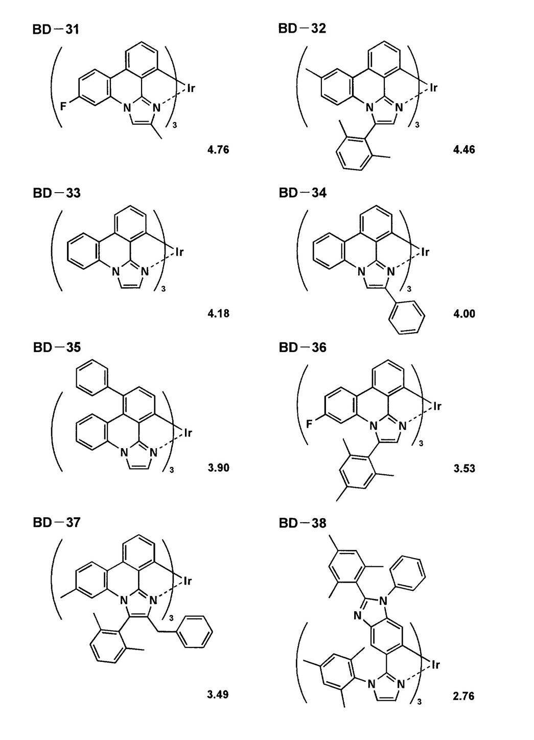


発光ドーパントとしては、上記のリン光ドーパントの他に公知の発光ドーパントを単独で用いてもよく、または複数種併用して用いてもよい。複数種併用する場合は、平均値としての双極子モーメントを求め、ホスト化合物の双極子モーメントとの差の絶対値が2デバイ以下であれば、本発明内である。
As the luminescent dopant, in addition to the above phosphorescent dopant, a known luminescent dopant may be used alone, or a plurality of kinds may be used in combination. When a plurality of types are used in combination, the dipole moment as an average value is obtained, and if the absolute value of the difference from the dipole moment of the host compound is 2 debyes or less, it is within the present invention.
単独使用または本発明に係るリン光ドーパントと併用可能なリン光ドーパントの具体例としては、下記が挙げられる。
Specific examples of phosphorescent dopants that can be used alone or in combination with the phosphorescent dopant according to the present invention include the following.


〈蛍光ドーパント〉
蛍光ドーパントとしては、クマリン系色素、ピラン系色素、シアニン系色素、クロコニウム系色素、スクアリウム系色素、オキソベンツアントラセン系色素、フルオレセイン系色素、ローダミン系色素、ピリリウム系色素、ペリレン系色素、スチルベン系色素、ポリチオフェン系色素、または希土類錯体系蛍光体等が挙げられる。 <Fluorescent dopant>
Fluorescent dopants include coumarin dyes, pyran dyes, cyanine dyes, croconium dyes, squalium dyes, oxobenzanthracene dyes, fluorescein dyes, rhodamine dyes, pyrylium dyes, perylene dyes, stilbene dyes , Polythiophene dyes, or rare earth complex phosphors.
次に、本発明の有機EL素子の構成層として用いられる電荷輸送層、即ち、注入層、阻止層等について説明する。
Next, the charge transport layer used as the constituent layer of the organic EL device of the present invention, that is, the injection layer, the blocking layer, etc. will be described.
《注入層:電子注入層、正孔注入層》
注入層は必要に応じて設け、電子注入層と正孔注入層があり、上記の如く陽極と発光層または正孔輸送層の間、及び陰極と発光層または電子輸送層との間に存在させてもよい。 << Injection layer: electron injection layer, hole injection layer >>
The injection layer is provided as necessary, and there are an electron injection layer and a hole injection layer, and as described above, it exists between the anode and the light emitting layer or the hole transport layer and between the cathode and the light emitting layer or the electron transport layer. May be.
注入層とは、駆動電圧低下や発光輝度向上のために電極と有機層間に設けられる層のことで、「有機EL素子とその工業化最前線(1998年11月30日エヌ・ティー・エス社発行)」の第2編第2章「電極材料」(123~166頁)に詳細に記載されており、正孔注入層(陽極バッファー層)と電子注入層(陰極バッファー層)とがある。
An injection layer is a layer provided between an electrode and an organic layer in order to reduce drive voltage and improve light emission luminance. “Organic EL element and its forefront of industrialization (issued by NTT Corporation on November 30, 1998) 2), Chapter 2, “Electrode Materials” (pages 123 to 166) in detail, and includes a hole injection layer (anode buffer layer) and an electron injection layer (cathode buffer layer).
陽極バッファー層(正孔注入層)は、特開平9-45479号公報、同9-260062号公報、同8-288069号公報等にもその詳細が記載されており、具体例として、銅フタロシアニンに代表されるフタロシアニンバッファー層、酸化バナジウムに代表される酸化物バッファー層、アモルファスカーボンバッファー層、ポリアニリン(エメラルディン)やポリチオフェン等の導電性高分子を用いた高分子バッファー層等が挙げられる。
The details of the anode buffer layer (hole injection layer) are described in JP-A-9-45479, JP-A-9-260062, JP-A-8-288069 and the like. As a specific example, copper phthalocyanine is used. Examples thereof include a phthalocyanine buffer layer represented by an oxide, an oxide buffer layer represented by vanadium oxide, an amorphous carbon buffer layer, and a polymer buffer layer using a conductive polymer such as polyaniline (emeraldine) or polythiophene.
陰極バッファー層(電子注入層)は、特開平6-325871号公報、同9-17574号公報、同10-74586号公報等にもその詳細が記載されており、具体的にはストロンチウムやアルミニウム等に代表される金属バッファー層、フッ化リチウムに代表されるアルカリ金属化合物バッファー層、フッ化マグネシウムに代表されるアルカリ土類金属化合物バッファー層、酸化アルミニウムに代表される酸化物バッファー層等が挙げられる。上記バッファー層(注入層)はごく薄い膜であることが望ましく、素材にもよるがその膜厚は0.1nm~5μmの範囲が好ましい。
The details of the cathode buffer layer (electron injection layer) are described in JP-A-6-325871, JP-A-9-17574, JP-A-10-74586, and the like. Specifically, strontium, aluminum, etc. Metal buffer layer typified by lithium, alkali metal compound buffer layer typified by lithium fluoride, alkaline earth metal compound buffer layer typified by magnesium fluoride, oxide buffer layer typified by aluminum oxide, etc. . The buffer layer (injection layer) is preferably a very thin film, and the film thickness is preferably in the range of 0.1 nm to 5 μm, although it depends on the material.
《阻止層:正孔阻止層、電子阻止層》
阻止層は、上記の如く有機化合物薄膜の基本構成層の他に必要に応じて設けられるものである。例えば、特開平11-204258号公報、同11-204359号公報、及び「有機EL素子とその工業化最前線(1998年11月30日エヌ・ティー・エス社発行)」の237頁等に記載されている正孔阻止(ホールブロック)層がある。 <Blocking layer: hole blocking layer, electron blocking layer>
The blocking layer is provided as necessary in addition to the basic constituent layer of the organic compound thin film as described above. For example, it is described in JP-A Nos. 11-204258 and 11-204359, and “Organic EL elements and the forefront of industrialization (published by NTT Corporation on November 30, 1998)” on page 237. There is a hole blocking (hole blocking) layer.
正孔阻止層とは広い意味では電子輸送層の機能を有し、電子を輸送する機能を有しつつ正孔を輸送する能力が著しく小さい正孔阻止材料からなり、電子を輸送しつつ正孔を阻止することで電子と正孔の再結合確率を向上させることができる。
The hole blocking layer has a function of an electron transport layer in a broad sense, and is made of a hole blocking material that has a function of transporting electrons and has a remarkably small ability to transport holes. The probability of recombination of electrons and holes can be improved by blocking.
また、後述する電子輸送層の構成を必要に応じて、本発明に係る正孔阻止層として用いることができる。
Moreover, the structure of the electron transport layer described later can be used as the hole blocking layer according to the present invention, if necessary.
本発明の有機EL素子の正孔阻止層は、発光層に隣接して設けられていることが好ましい。正孔阻止層には、前述のホスト化合物として挙げたカルバゾール誘導体、カルボリン誘導体、ジアザカルバゾール誘導体(カルボリン誘導体のカルボリン環を構成する炭素原子の一つが窒素原子で置き換わったものを示す。)を含有することが好ましい。
The hole blocking layer of the organic EL device of the present invention is preferably provided adjacent to the light emitting layer. The hole blocking layer contains the carbazole derivative, carboline derivative, or diazacarbazole derivative (showed by replacing one of the carbon atoms constituting the carboline ring of the carboline derivative with a nitrogen atom) as the host compound. It is preferable to do.
また、本発明においては、複数の発光色の異なる複数の発光層を有する場合、その発光極大波長が最も短波にある発光層が、全発光層中、最も陽極に近いことが好ましいが、このような場合、該最短波層と該層の次に陽極に近い発光層との間に正孔阻止層を追加して設けることが好ましい。更には、該位置に設けられる正孔阻止層に含有される化合物の50質量%以上が、前記最短波発光層のホスト化合物に対しそのイオン化ポテンシャルが0.3eV以上大きいことが好ましい。
In the present invention, when a plurality of light emitting layers having different light emission colors are provided, the light emitting layer having the shortest wavelength of light emission is preferably closest to the anode among all the light emitting layers. In this case, it is preferable to additionally provide a hole blocking layer between the shortest wave layer and the light emitting layer next to the anode next to the anode. Furthermore, it is preferable that 50% by mass or more of the compound contained in the hole blocking layer provided at the position has an ionization potential of 0.3 eV or more larger than the host compound of the shortest wave emitting layer.
イオン化ポテンシャルは化合物のHOMO(最高被占分子軌道)レベルにある電子を真空準位に放出するのに必要なエネルギーで定義され、例えば下記に示すような方法により求めることができる。
The ionization potential is defined by the energy required to emit electrons at the HOMO (highest occupied molecular orbital) level of the compound to the vacuum level, and can be obtained by the following method, for example.
(1)米国Gaussian社製の分子軌道計算用ソフトウェアであるGaussian98(Gaussian98、Revision A.11.4,M.J.Frisch,et al,Gaussian,Inc.,Pittsburgh PA,2002.)を用い、キーワードとしてB3LYP/6-31G*を用いて構造最適化を行うことにより算出した値(eV単位換算値)の小数点第2位を四捨五入した値としてイオン化ポテンシャルを求めることができる。この計算値が有効な背景には、この手法で求めた計算値と実験値の相関が高いためである。
(1) Using Gaussian 98 (Gaussian 98, Revision A.11.4, MJ Frisch, et al, Gaussian, Inc., Pittsburgh PA, 2002.), a molecular orbital calculation software manufactured by Gaussian, USA The ionization potential can be obtained as a value obtained by rounding off the second decimal place of the value (eV unit converted value) calculated by performing structural optimization using B3LYP / 6-31G *. The reason why this calculated value is effective is that there is a high correlation between the calculated value obtained by this method and the experimental value.
(2)イオン化ポテンシャルは光電子分光法で直接測定する方法により求めることもできる。例えば、理研計器社製の低エネルギー電子分光装置「Model AC-1」を用いて、あるいは紫外光電子分光として知られている方法を好適に用いることができる。
(2) The ionization potential can also be obtained by a method of directly measuring by photoelectron spectroscopy. For example, a low energy electron spectrometer “Model AC-1” manufactured by Riken Keiki Co., Ltd. or a method known as ultraviolet photoelectron spectroscopy can be suitably used.
一方、電子阻止層とは広い意味では正孔輸送層の機能を有し、正孔を輸送する機能を有しつつ電子を輸送する能力が著しく小さい材料からなり、正孔を輸送しつつ電子を阻止することで電子と正孔の再結合確率を向上させることができる。
On the other hand, the electron blocking layer has a function of a hole transport layer in a broad sense, and is made of a material that has a function of transporting holes and has an extremely small ability to transport electrons, and transports electrons while transporting holes. By blocking, the recombination probability of electrons and holes can be improved.
また、後述する正孔輸送層の構成を必要に応じて電子阻止層として用いることができる。本発明に係る正孔阻止層、電子輸送層の膜厚としては、好ましくは3~100nmであり、更に好ましくは5~30nmである。
Moreover, the structure of the hole transport layer described later can be used as an electron blocking layer as necessary. The film thickness of the hole blocking layer and the electron transporting layer according to the present invention is preferably 3 to 100 nm, more preferably 5 to 30 nm.
《正孔輸送層》
正孔輸送層とは正孔を輸送する機能を有する正孔輸送材料からなり、広い意味で正孔注入層、電子阻止層も正孔輸送層に含まれる。正孔輸送層は単層または複数層設けることができる。 《Hole transport layer》
The hole transport layer is made of a hole transport material having a function of transporting holes, and in a broad sense, a hole injection layer and an electron blocking layer are also included in the hole transport layer. The hole transport layer can be provided as a single layer or a plurality of layers.
正孔輸送材料としては、正孔の注入または輸送、電子の障壁性のいずれかを有するものであり、有機物、無機物のいずれであってもよい。例えば、トリアゾール誘導体、オキサジアゾール誘導体、イミダゾール誘導体、ポリアリールアルカン誘導体、ピラゾリン誘導体及びピラゾロン誘導体、フェニレンジアミン誘導体、アリールアミン誘導体、アミノ置換カルコン誘導体、オキサゾール誘導体、スチリルアントラセン誘導体、フルオレノン誘導体、ヒドラゾン誘導体、スチルベン誘導体、シラザン誘導体、アニリン系共重合体、また導電性高分子オリゴマー、特にチオフェンオリゴマー等が挙げられる。
The hole transport material has either hole injection or transport or electron barrier properties, and may be either organic or inorganic. For example, triazole derivatives, oxadiazole derivatives, imidazole derivatives, polyarylalkane derivatives, pyrazoline derivatives and pyrazolone derivatives, phenylenediamine derivatives, arylamine derivatives, amino-substituted chalcone derivatives, oxazole derivatives, styrylanthracene derivatives, fluorenone derivatives, hydrazone derivatives, Examples thereof include stilbene derivatives, silazane derivatives, aniline copolymers, and conductive polymer oligomers, particularly thiophene oligomers.
正孔輸送材料としては上記のものを使用することができるが、ポルフィリン化合物、芳香族第3級アミン化合物及びスチリルアミン化合物、特に芳香族第3級アミン化合物を用いることが好ましい。
The above-mentioned materials can be used as the hole transport material, but it is preferable to use a porphyrin compound, an aromatic tertiary amine compound and a styrylamine compound, particularly an aromatic tertiary amine compound.
芳香族第3級アミン化合物及びスチリルアミン化合物の代表例としては、N,N,N′,N′-テトラフェニル-4,4′-ジアミノフェニル;N,N′-ジフェニル-N,N′-ビス(3-メチルフェニル)-〔1,1′-ビフェニル〕-4,4′-ジアミン(TPD);2,2-ビス(4-ジ-p-トリルアミノフェニル)プロパン;1,1-ビス(4-ジ-p-トリルアミノフェニル)シクロヘキサン;N,N,N′,N′-テトラ-p-トリル-4,4′-ジアミノビフェニル;1,1-ビス(4-ジ-p-トリルアミノフェニル)-4-フェニルシクロヘキサン;ビス(4-ジメチルアミノ-2-メチルフェニル)フェニルメタン;ビス(4-ジ-p-トリルアミノフェニル)フェニルメタン;N,N′-ジフェニル-N,N′-ジ(4-メトキシフェニル)-4,4′-ジアミノビフェニル;N,N,N′,N′-テトラフェニル-4,4′-ジアミノジフェニルエーテル;4,4′-ビス(ジフェニルアミノ)クオードリフェニル;N,N,N-トリ(p-トリル)アミン;4-(ジ-p-トリルアミノ)-4′-〔4-(ジ-p-トリルアミノ)スチリル〕スチルベン;4-N,N-ジフェニルアミノ-(2-ジフェニルビニル)ベンゼン;3-メトキシ-4′-N,N-ジフェニルアミノスチルベンゼン;N-フェニルカルバゾール、更には米国特許第5,061,569号明細書に記載されている2個の縮合芳香族環を分子内に有するもの、例えば、4,4′-ビス〔N-(1-ナフチル)-N-フェニルアミノ〕ビフェニル(NPD)、特開平4-308688号公報に記載されているトリフェニルアミンユニットが3つスターバースト型に連結された4,4′,4″-トリス〔N-(3-メチルフェニル)-N-フェニルアミノ〕トリフェニルアミン(MTDATA)等が挙げられる。
Representative examples of aromatic tertiary amine compounds and styrylamine compounds include N, N, N ′, N′-tetraphenyl-4,4′-diaminophenyl; N, N′-diphenyl-N, N′— Bis (3-methylphenyl)-[1,1′-biphenyl] -4,4′-diamine (TPD); 2,2-bis (4-di-p-tolylaminophenyl) propane; 1,1-bis (4-di-p-tolylaminophenyl) cyclohexane; N, N, N ′, N′-tetra-p-tolyl-4,4′-diaminobiphenyl; 1,1-bis (4-di-p-tolyl) Aminophenyl) -4-phenylcyclohexane; bis (4-dimethylamino-2-methylphenyl) phenylmethane; bis (4-di-p-tolylaminophenyl) phenylmethane; N, N'-diphenyl-N, N ' Di (4-methoxyphenyl) -4,4'-diaminobiphenyl; N, N, N ', N'-tetraphenyl-4,4'-diaminodiphenyl ether; 4,4'-bis (diphenylamino) quadriphenyl N, N, N-tri (p-tolyl) amine; 4- (di-p-tolylamino) -4 '-[4- (di-p-tolylamino) styryl] stilbene; 4-N, N-diphenylamino -(2-diphenylvinyl) benzene; 3-methoxy-4'-N, N-diphenylaminostilbenzene; N-phenylcarbazole, and also two described in US Pat. No. 5,061,569 Having a condensed aromatic ring of, for example, 4,4'-bis [N- (1-naphthyl) -N-phenylamino] biphenyl (NPD), JP-A-4-308 4,4 ′, 4 ″ -tris [N- (3-methylphenyl) -N-phenylamino] triphenylamine in which three triphenylamine units described in Japanese Patent No. 88 are linked in a starburst type ( MTDATA) and the like.
更にこれらの材料を高分子鎖に導入した、またはこれらの材料を高分子の主鎖とした高分子材料を用いることもできる。また、p型-Si、p型-SiC等の無機化合物も正孔注入材料、正孔輸送材料として使用することができる。また、特開平11-251067号公報、J.Huang et.al.著文献(Applied Physics Letters 80(2002),p.139)に記載されているような、所謂p型正孔輸送材料を用いることもできる。本発明においては、より高効率の発光素子が得られることからこれらの材料を用いることが好ましい。
Further, a polymer material in which these materials are introduced into a polymer chain or these materials are used as a polymer main chain can also be used. In addition, inorganic compounds such as p-type-Si and p-type-SiC can also be used as the hole injection material and the hole transport material. JP-A-11-251067, J. Pat. Huang et. al. A so-called p-type hole transport material described in a book (Applied Physics Letters 80 (2002), p. 139) can also be used. In the present invention, these materials are preferably used because a light-emitting element with higher efficiency can be obtained.
正孔輸送層は上記正孔輸送材料を、例えば、真空蒸着法、スピンコート法、キャスト法、インクジェット法を含む印刷法、LB法等の公知の方法により、薄膜化することにより形成することができる。正孔輸送層の膜厚については特に制限はないが、通常は5nm~5μm程度、好ましくは5~200nmである。この正孔輸送層は上記材料の1種または2種以上からなる一層構造であってもよい。
The hole transport layer can be formed by thinning the hole transport material by a known method such as a vacuum deposition method, a spin coating method, a casting method, a printing method including an ink jet method, or an LB method. it can. The thickness of the hole transport layer is not particularly limited, but is usually about 5 nm to 5 μm, preferably 5 to 200 nm. The hole transport layer may have a single layer structure composed of one or more of the above materials.
また、不純物をドープしたp性の高い正孔輸送層を用いることもできる。その例としては、特開平4-297076号公報、特開2000-196140号公報、同2001-102175号公報の各公報、J.Appl.Phys.,95,5773(2004)等に記載されたものが挙げられる。本発明においては、このようなp性の高い正孔輸送層を用いることがより低消費電力の素子を作製することができるため好ましい。
It is also possible to use a hole transport layer having a high p property doped with impurities. Examples thereof include JP-A-4-297076, JP-A-2000-196140, JP-A-2001-102175, J. Pat. Appl. Phys. 95, 5773 (2004), and the like. In the present invention, it is preferable to use a hole transport layer having such a high p property because a device with lower power consumption can be produced.
《陽極》
有機EL素子における陽極としては、仕事関数の大きい(4eV以上)金属、合金、電気伝導性化合物及びこれらの混合物を電極物質とするものが好ましく用いられる。このような電極物質の具体例としては、Au等の金属、CuI、インジウムチンオキシド(ITO)、SnO2、ZnO等の導電性透明材料が挙げられる。 "anode"
As the anode in the organic EL element, an electrode material made of a metal, an alloy, an electrically conductive compound, or a mixture thereof having a high work function (4 eV or more) is preferably used. Specific examples of such electrode materials include metals such as Au, and conductive transparent materials such as CuI, indium tin oxide (ITO), SnO 2 , and ZnO.
また、IDIXO(In2O3-ZnO)等非晶質で透明導電膜を作製可能な材料を用いてもよい。陽極はこれらの電極物質を蒸着やスパッタリング等の方法により薄膜を形成させ、フォトリソグラフィー法で所望の形状のパターンを形成してもよく、あるいはパターン精度をあまり必要としない場合は(100μm以上程度)、上記電極物質の蒸着やスパッタリング時に所望の形状のマスクを介してパターンを形成してもよい。
Alternatively, an amorphous material such as IDIXO (In 2 O 3 —ZnO) capable of forming a transparent conductive film may be used. For the anode, these electrode materials may be formed into a thin film by a method such as vapor deposition or sputtering, and a pattern having a desired shape may be formed by a photolithography method, or when pattern accuracy is not required (about 100 μm or more) A pattern may be formed through a mask having a desired shape at the time of vapor deposition or sputtering of the electrode material.
あるいは、有機導電性化合物のように塗布可能な物質を用いる場合には、印刷方式、コーティング方式等湿式成膜法を用いることもできる。この陽極より発光を取り出す場合には、透過率を10%より大きくすることが望ましく、また陽極としてのシート抵抗は数百Ω/□以下が好ましい。更に膜厚は材料にもよるが、通常10~1000nm、好ましくは10~200nmの範囲で選ばれる。
Alternatively, when a material that can be applied such as an organic conductive compound is used, a wet film forming method such as a printing method or a coating method can be used. When light emission is extracted from the anode, it is desirable that the transmittance be greater than 10%, and the sheet resistance as the anode is preferably several hundred Ω / □ or less. Further, although the film thickness depends on the material, it is usually selected in the range of 10 to 1000 nm, preferably 10 to 200 nm.
《陰極》
一方、陰極としては仕事関数の小さい(4eV以下)金属(電子注入性金属と称する)、合金、電気伝導性化合物及びこれらの混合物を電極物質とするものが用いられる。このような電極物質の具体例としては、ナトリウム、ナトリウム-カリウム合金、マグネシウム、リチウム、マグネシウム/銅混合物、マグネシウム/銀混合物、マグネシウム/アルミニウム混合物、マグネシウム/インジウム混合物、アルミニウム/酸化アルミニウム(Al2O3)混合物、インジウム、リチウム/アルミニウム混合物、希土類金属等が挙げられる。 "cathode"
On the other hand, as the cathode, a material having a low work function (4 eV or less) metal (referred to as an electron injecting metal), an alloy, an electrically conductive compound, and a mixture thereof as an electrode material is used. Specific examples of such electrode materials include sodium, sodium-potassium alloy, magnesium, lithium, magnesium / copper mixture, magnesium / silver mixture, magnesium / aluminum mixture, magnesium / indium mixture, aluminum / aluminum oxide (Al 2 O 3 ) Mixtures, indium, lithium / aluminum mixtures, rare earth metals and the like.
これらの中で、電子注入性及び酸化等に対する耐久性の点から、電子注入性金属とこれより仕事関数の値が大きく安定な金属である第二金属との混合物、例えば、マグネシウム/銀混合物、マグネシウム/アルミニウム混合物、マグネシウム/インジウム混合物、アルミニウム/酸化アルミニウム(Al2O3)混合物、リチウム/アルミニウム混合物、アルミニウム等が好適である。
Among these, from the point of durability against electron injection and oxidation, etc., a mixture of an electron injecting metal and a second metal which is a stable metal having a larger work function than this, for example, a magnesium / silver mixture, Magnesium / aluminum mixtures, magnesium / indium mixtures, aluminum / aluminum oxide (Al 2 O 3 ) mixtures, lithium / aluminum mixtures, aluminum and the like are preferred.
陰極はこれらの電極物質を蒸着やスパッタリング等の方法により薄膜を形成させることにより、作製することができる。また、陰極としてのシート抵抗は数百Ω/□以下が好ましく、膜厚は通常10nm~5μm、好ましくは50~200nmの範囲で選ばれる。なお、発光した光を透過させるため、有機EL素子の陽極または陰極のいずれか一方が透明または半透明であれば発光輝度が向上し好都合である。
The cathode can be produced by forming a thin film of these electrode materials by a method such as vapor deposition or sputtering. The sheet resistance as the cathode is preferably several hundred Ω / □ or less, and the film thickness is usually selected in the range of 10 nm to 5 μm, preferably 50 to 200 nm. In order to transmit the emitted light, if either the anode or the cathode of the organic EL element is transparent or translucent, the light emission luminance is improved, which is convenient.
また、陰極に上記金属を1~20nmの膜厚で作製した後に、陽極の説明で挙げた導電性透明材料をその上に作製することで、透明または半透明の陰極を作製することができ、これを応用することで陽極と陰極の両方が透過性を有する素子を作製することができる。
In addition, a transparent or semi-transparent cathode can be produced by producing the conductive transparent material mentioned in the description of the anode on the cathode after producing the metal with a film thickness of 1 to 20 nm. By applying this, an element in which both the anode and the cathode are transmissive can be manufactured.
《支持基板》
本発明の有機EL素子に用いることのできる支持基板(以下、基体、基板、基材、支持体等とも言う)としては、ガラス、プラスチック等の種類には特に限定はなく、また透明であっても不透明であってもよい。 《Support substrate》
As a support substrate (hereinafter also referred to as a substrate, substrate, substrate, support, etc.) that can be used in the organic EL device of the present invention, there is no particular limitation on the type of glass, plastic, etc., and it is transparent. May be opaque.
支持基板側から光を取り出す場合には、支持基板は透明であることが好ましい。好ましく用いられる透明な支持基板としては、ガラス、石英、透明樹脂フィルムを挙げることができる。特に好ましい支持基板は、有機EL素子にフレキシブル性を与えることが可能な樹脂フィルムである。
When extracting light from the support substrate side, the support substrate is preferably transparent. Examples of the transparent support substrate preferably used include glass, quartz, and a transparent resin film. A particularly preferable support substrate is a resin film capable of giving flexibility to the organic EL element.
樹脂フィルムとしては、例えば、ポリエチレンテレフタレート(PET)、ポリエチレンナフタレート(PEN)等のポリエステル、ポリエチレン、ポリプロピレン、セロファン、セルロースジアセテート、セルローストリアセテート、セルロースアセテートブチレート、セルロースアセテートプロピオネート(CAP)、セルロースアセテートフタレート(TAC)、セルロースナイトレート等のセルロースエステル類またはそれらの誘導体、ポリ塩化ビニリデン、ポリビニルアルコール、ポリエチレンビニルアルコール、シンジオタクティックポリスチレン、ポリカーボネート、ノルボルネン樹脂、ポリメチルペンテン、ポリエーテルケトン、ポリイミド、ポリエーテルスルホン(PES)、ポリフェニレンスルフィド、ポリスルホン類、ポリエーテルイミド、ポリエーテルケトンイミド、ポリアミド、フッ素樹脂、ナイロン、ポリメチルメタクリレート、アクリルあるいはポリアリレート類、アートン(商品名JSR社製)あるいはアペル(商品名三井化学社製)といったシクロオレフィン系樹脂等を挙げられる。
Examples of the resin film include polyesters such as polyethylene terephthalate (PET) and polyethylene naphthalate (PEN), polyethylene, polypropylene, cellophane, cellulose diacetate, cellulose triacetate, cellulose acetate butyrate, cellulose acetate propionate (CAP), Cellulose esters such as cellulose acetate phthalate (TAC) and cellulose nitrate or derivatives thereof, polyvinylidene chloride, polyvinyl alcohol, polyethylene vinyl alcohol, syndiotactic polystyrene, polycarbonate, norbornene resin, polymethylpentene, polyether ketone, polyimide , Polyethersulfone (PES), polyphenylene sulfide, polysulfone , Polyetherimide, polyetherketoneimide, polyamide, fluororesin, nylon, polymethylmethacrylate, acrylic or polyarylates, cyclone resins such as Arton (trade name, manufactured by JSR) or Appel (trade name, manufactured by Mitsui Chemicals) Etc.
樹脂フィルムの表面には、無機物、有機物の被膜またはその両者のハイブリッド被膜が形成されていてもよく、JIS K 7129-1992に準拠した方法で測定された、水蒸気透過度(25±0.5℃、相対湿度(90±2)%RH)が0.01g/(m2・24h)以下のバリア性フィルムであることが好ましく、更にはJIS K 7126-1987に準拠した方法で測定された酸素透過度が10-3ml/(m2・24h・atm)以下、水蒸気透過度が10-5g/(m2・24h)以下の高バリア性フィルムであることが好ましい。
On the surface of the resin film, an inorganic film, an organic film or a hybrid film of both may be formed. The water vapor permeability (25 ± 0.5 ° C.) measured by a method according to JIS K 7129-1992. And a relative humidity (90 ± 2)% RH) of 0.01 g / (m 2 · 24 h) or less is preferable, and oxygen permeability measured by a method according to JIS K 7126-1987. A high barrier film having a degree of 10 −3 ml / (m 2 · 24 h · atm) or less and a water vapor permeability of 10 −5 g / (m 2 · 24 h) or less is preferable.
バリア膜を形成する材料としては、水分や酸素等素子の劣化をもたらすものの浸入を抑制する機能を有する材料であればよく、例えば、酸化珪素、二酸化珪素、窒化珪素等を用いることができる。更に該膜の脆弱性を改良するために、これら無機層と有機材料からなる層の積層構造を持たせることがより好ましい。無機層と有機層の積層順については特に制限はないが、両者を交互に複数回積層させることが好ましい。
The material for forming the barrier film may be any material that has a function of suppressing the intrusion of elements that cause deterioration of elements such as moisture and oxygen. For example, silicon oxide, silicon dioxide, silicon nitride, or the like can be used. Further, in order to improve the brittleness of the film, it is more preferable to have a laminated structure of these inorganic layers and organic material layers. Although there is no restriction | limiting in particular about the lamination | stacking order of an inorganic layer and an organic layer, It is preferable to laminate | stack both alternately several times.
バリア膜の形成方法については特に限定はなく、例えば、真空蒸着法、スパッタリング法、反応性スパッタリング法、分子線エピタキシー法、クラスタ-イオンビーム法、イオンプレーティング法、プラズマ重合法、大気圧プラズマ重合法、プラズマCVD法、レーザーCVD法、熱CVD法、コーティング法等を用いることができるが、特開2004-68143号公報に記載の大気圧プラズマ重合法によるものが特に好ましい。
The method for forming the barrier film is not particularly limited. For example, the vacuum deposition method, the sputtering method, the reactive sputtering method, the molecular beam epitaxy method, the cluster ion beam method, the ion plating method, the plasma polymerization method, the atmospheric pressure plasma weight A combination method, a plasma CVD method, a laser CVD method, a thermal CVD method, a coating method, and the like can be used. However, an atmospheric pressure plasma polymerization method described in JP-A-2004-68143 is particularly preferable.
不透明な支持基板としては、例えば、アルミ、ステンレス等の金属板、フィルムや不透明樹脂基板、セラミック製の基板等が挙げられる。
Examples of the opaque support substrate include metal plates such as aluminum and stainless steel, films, opaque resin substrates, ceramic substrates, and the like.
本発明の有機EL素子の発光の室温における外部取り出し効率は、1%以上であることが好ましく、より好ましくは5%以上である。ここに、外部取り出し量子効率(%)=有機EL素子外部に発光した光子数/有機EL素子に流した電子数×100である。
The external extraction efficiency at room temperature of light emission of the organic EL element of the present invention is preferably 1% or more, more preferably 5% or more. Here, the external extraction quantum efficiency (%) = the number of photons emitted to the outside of the organic EL element / the number of electrons sent to the organic EL element × 100.
また、カラーフィルター等の色相改良フィルター等を併用しても、有機EL素子からの発光色を蛍光体を用いて多色へ変換する色変換フィルターを併用してもよい。色変換フィルターを用いる場合においては、有機EL素子の発光のλmaxは480nm以下が好ましい。
Also, a hue improvement filter such as a color filter may be used in combination, or a color conversion filter that converts the emission color from the organic EL element into multiple colors using a phosphor may be used in combination. In the case of using a color conversion filter, the λmax of light emission of the organic EL element is preferably 480 nm or less.
《封止》
本発明に用いられる封止手段としては、例えば、封止部材と電極、支持基板とを接着剤で接着する方法を挙げることができる。封止部材としては、有機EL素子の表示領域を覆うように配置されておればよく、凹板状でも平板状でもよい。また、透明性、電気絶縁性は特に問わない。 <Sealing>
As a sealing means used for this invention, the method of adhere | attaching a sealing member, an electrode, and a support substrate with an adhesive agent can be mentioned, for example. As a sealing member, it should just be arrange | positioned so that the display area | region of an organic EL element may be covered, and concave plate shape or flat plate shape may be sufficient. Further, transparency and electrical insulation are not particularly limited.
具体的には、ガラス板、ポリマー板・フィルム、金属板・フィルム等が挙げられる。ガラス板としては、特にソーダ石灰ガラス、バリウム・ストロンチウム含有ガラス、鉛ガラス、アルミノケイ酸ガラス、ホウケイ酸ガラス、バリウムホウケイ酸ガラス、石英等を挙げることができる。また、ポリマー板としては、ポリカーボネート、アクリル、ポリエチレンテレフタレート、ポリエーテルサルファイド、ポリサルフォン等を挙げることができる。金属板としては、ステンレス、鉄、銅、アルミニウム、マグネシウム、ニッケル、亜鉛、クロム、チタン、モリブテン、シリコン、ゲルマニウム及びタンタルからなる群から選ばれる一種以上の金属または合金からなるものが挙げられる。
Specific examples include a glass plate, a polymer plate / film, and a metal plate / film. Examples of the glass plate include soda-lime glass, barium / strontium-containing glass, lead glass, aluminosilicate glass, borosilicate glass, barium borosilicate glass, and quartz. Examples of the polymer plate include polycarbonate, acrylic, polyethylene terephthalate, polyether sulfide, and polysulfone. Examples of the metal plate include those made of one or more metals or alloys selected from the group consisting of stainless steel, iron, copper, aluminum, magnesium, nickel, zinc, chromium, titanium, molybdenum, silicon, germanium, and tantalum.
本発明においては、素子を薄膜化できるということからポリマーフィルム、金属フィルムを好ましく使用することができる。更には、ポリマーフィルムは、JIS K 7126-1987に準拠した方法で測定された酸素透過度が1×10⁻³ml/(m2・24h・atm)以下、JIS K 7129-1992に準拠した方法で測定された、水蒸気透過度(25±0.5℃、相対湿度(90±2)%RH)が、1×10⁻³g/(m2・24h)以下のものであることが好ましい。
In the present invention, a polymer film and a metal film can be preferably used because the element can be thinned. Furthermore, the polymer film has an oxygen permeability measured by a method according to JIS K 7126-1987 of 1 × 10 −3 ml / (m 2 · 24 h · atm) or less, and a method according to JIS K 7129-1992. It is preferable that the water vapor permeability (25 ± 0.5 ° C., relative humidity (90 ± 2)% RH) measured in (1) is 1 × 10 −3 g / (m 2 · 24 h) or less.
封止部材を凹状に加工するのは、サンドブラスト加工、化学エッチング加工等が使われる。接着剤として具体的には、アクリル酸系オリゴマー、メタクリル酸系オリゴマーの反応性ビニル基を有する光硬化及び熱硬化型接着剤、2-シアノアクリル酸エステル等の湿気硬化型等の接着剤を挙げることができる。また、エポキシ系等の熱及び化学硬化型(二液混合)を挙げることができる。また、ホットメルト型のポリアミド、ポリエステル、ポリオレフィンを挙げることができる。また、カチオン硬化タイプの紫外線硬化型エポキシ樹脂接着剤を挙げることができる。
For processing the sealing member into a concave shape, sandblasting, chemical etching, or the like is used. Specific examples of the adhesive include photocuring and thermosetting adhesives having reactive vinyl groups of acrylic acid oligomers and methacrylic acid oligomers, and moisture curing adhesives such as 2-cyanoacrylates. be able to. Moreover, heat | fever and chemical curing types (two-component mixing), such as an epoxy type, can be mentioned. Moreover, hot-melt type polyamide, polyester, and polyolefin can be mentioned. Moreover, a cationic curing type ultraviolet curing epoxy resin adhesive can be mentioned.
なお、有機EL素子が熱処理により劣化する場合があるので、室温から80℃までに接着硬化できるものが好ましい。また、前記接着剤中に乾燥剤を分散させておいてもよい。
In addition, since an organic EL element may deteriorate by heat processing, what can be adhesively cured from room temperature to 80 ° C. is preferable. A desiccant may be dispersed in the adhesive.
封止部分への接着剤の塗布は市販のディスペンサーを使ってもよいし、スクリーン印刷のように印刷してもよい。
Application of the adhesive to the sealing portion may be performed using a commercially available dispenser or may be printed like screen printing.
また、有機層を挟み支持基板と対向する側の電極の外側に該電極と有機層を被覆し、支持基板と接する形で無機物、有機物の層を形成し封止膜とすることも好適にできる。この場合、該膜を形成する材料としては、水分や酸素等素子の劣化をもたらすものの浸入を抑制する機能を有する材料であればよく、例えば、酸化珪素、二酸化珪素、窒化珪素等を用いることができる。
In addition, it is also preferable that the electrode and the organic layer are coated on the outside of the electrode facing the support substrate with the organic layer interposed therebetween, and an inorganic or organic layer is formed in contact with the support substrate to form a sealing film. . In this case, the material for forming the film may be any material that has a function of suppressing intrusion of elements that cause deterioration of elements such as moisture and oxygen. For example, silicon oxide, silicon dioxide, silicon nitride, or the like may be used. it can.
更に該膜の脆弱性を改良するために、これら無機層と有機材料からなる層の積層構造を持たせることが好ましい。これらの膜の形成方法については特に限定はなく、例えば、真空蒸着法、スパッタリング法、反応性スパッタリング法、分子線エピタキシー法、クラスタ-イオンビーム法、イオンプレーティング法、プラズマ重合法、大気圧プラズマ重合法、プラズマCVD法、レーザーCVD法、熱CVD法、コーティング法等を用いることができる。
In order to further improve the brittleness of the film, it is preferable to have a laminated structure of these inorganic layers and layers made of organic materials. The method for forming these films is not particularly limited. For example, vacuum deposition method, sputtering method, reactive sputtering method, molecular beam epitaxy method, cluster ion beam method, ion plating method, plasma polymerization method, atmospheric pressure plasma A polymerization method, a plasma CVD method, a laser CVD method, a thermal CVD method, a coating method, or the like can be used.
封止部材と有機EL素子の表示領域との間隙には、気相及び液相では、窒素、アルゴン等の不活性気体やフッ化炭化水素、シリコンオイルのような不活性液体を注入することが好ましい。また真空とすることも可能である。また、内部に吸湿性化合物を封入することもできる。吸湿性化合物としては、例えば、金属酸化物(例えば、酸化ナトリウム、酸化カリウム、酸化カルシウム、酸化バリウム、酸化マグネシウム、酸化アルミニウム等)、硫酸塩(例えば、硫酸ナトリウム、硫酸カルシウム、硫酸マグネシウム、硫酸コバルト等)、金属ハロゲン化物(例えば、塩化カルシウム、塩化マグネシウム、フッ化セシウム、フッ化タンタル、臭化セリウム、臭化マグネシウム、沃化バリウム、沃化マグネシウム等)、過塩素酸類(例えば、過塩素酸バリウム、過塩素酸マグネシウム等)等が挙げられ、硫酸塩、金属ハロゲン化物及び過塩素酸類においては無水塩が好適に用いられる。
In the gap between the sealing member and the display area of the organic EL element, an inert gas such as nitrogen or argon, or an inert liquid such as fluorinated hydrocarbon or silicon oil can be injected in the gas phase and liquid phase. preferable. A vacuum is also possible. Moreover, a hygroscopic compound can also be enclosed inside. Examples of the hygroscopic compound include metal oxides (for example, sodium oxide, potassium oxide, calcium oxide, barium oxide, magnesium oxide, aluminum oxide) and sulfates (for example, sodium sulfate, calcium sulfate, magnesium sulfate, cobalt sulfate). Etc.), metal halides (eg calcium chloride, magnesium chloride, cesium fluoride, tantalum fluoride, cerium bromide, magnesium bromide, barium iodide, magnesium iodide etc.), perchloric acids (eg perchloric acid) Barium, magnesium perchlorate, and the like), and anhydrous salts are preferably used in sulfates, metal halides, and perchloric acids.
《保護膜、保護板》
有機層を挟み支持基板と対向する側の前記封止膜、あるいは前記封止用フィルムの外側に、素子の機械的強度を高めるために保護膜、あるいは保護板を設けてもよい。特に封止が前記封止膜により行われている場合には、その機械的強度は必ずしも高くないため、このような保護膜、保護板を設けることが好ましい。これに使用することができる材料としては、前記封止に用いたのと同様なガラス板、ポリマー板・フィルム、金属板・フィルム等を用いることができるが、軽量且つ薄膜化ということからポリマーフィルムを用いることが好ましい。 《Protective film, protective plate》
In order to increase the mechanical strength of the element, a protective film or a protective plate may be provided on the outer side of the sealing film on the side facing the support substrate with the organic layer interposed therebetween or on the sealing film. In particular, when the sealing is performed by the sealing film, the mechanical strength is not necessarily high, and thus it is preferable to provide such a protective film and a protective plate. As a material that can be used for this, the same glass plate, polymer plate / film, metal plate / film, and the like used for the sealing can be used, but the polymer film is light and thin. Is preferably used.
《光取り出し》
有機EL素子は空気よりも屈折率の高い(屈折率が1.7~2.1程度)層の内部で発光し、発光層で発生した光の内15%から20%程度の光しか取り出せないことが一般的に言われている。これは、臨界角以上の角度θで界面(透明基板と空気との界面)に入射する光は、全反射を起こし素子外部に取り出すことができないことや、透明電極ないし発光層と透明基板との間で光が全反射を起こし、光が透明電極ないし発光層を導波し、結果として光が素子側面方向に逃げるためである。 《Light extraction》
The organic EL element emits light inside a layer having a refractive index higher than that of air (refractive index is about 1.7 to 2.1) and can extract only about 15% to 20% of the light generated in the light emitting layer. It is generally said. This is because the light incident on the interface (interface between the transparent substrate and air) at an angle θ greater than the critical angle causes total reflection and cannot be taken out of the element, or between the transparent electrode or the light emitting layer and the transparent substrate. This is because the light is totally reflected between the light and the light is guided through the transparent electrode or the light emitting layer, and as a result, the light escapes in the direction of the element side surface.
この光の取り出しの効率を向上させる手法としては、例えば、透明基板表面に凹凸を形成し、透明基板と空気界面での全反射を防ぐ方法(米国特許第4,774,435号明細書)、基板に集光性を持たせることにより効率を向上させる方法(特開昭63-314795号公報)、有機EL素子の側面等に反射面を形成する方法(特開平1-220394号公報)、基板と発光体の間に中間の屈折率を持つ平坦層を導入し、反射防止膜を形成する方法(特開昭62-172691号公報)、基板と発光体の間に基板よりも低屈折率を持つ平坦層を導入する方法(特開2001-202827号公報)、基板、透明電極層や発光層のいずれかの層間(含む、基板と外界間)に回折格子を形成する方法(特開平11-283751号公報)等がある。
As a method of improving the light extraction efficiency, for example, a method of forming irregularities on the surface of the transparent substrate and preventing total reflection at the transparent substrate and the air interface (US Pat. No. 4,774,435), A method for improving efficiency by providing light condensing property to a substrate (Japanese Patent Laid-Open No. 63-314795), a method of forming a reflective surface on a side surface of an organic EL element (Japanese Patent Laid-Open No. 1-220394), a substrate A method of forming an antireflection film by introducing a flat layer having an intermediate refractive index between the substrate and the light emitter (Japanese Patent Laid-Open No. 62-172691), and lowering the refractive index between the substrate and the light emitter than the substrate. A method of introducing a flat layer having a structure (Japanese Patent Laid-Open No. 2001-202827), a method of forming a diffraction grating between any one of the substrate, the transparent electrode layer and the light emitting layer (including between the substrate and the outside world) No. 283751) That.
本発明においては、これらの方法を本発明の有機EL素子と組み合わせて用いることができるが、基板と発光体の間に基板よりも低屈折率を持つ平坦層を導入する方法、あるいは基板、透明電極層や発光層のいずれかの層間(含む、基板と外界間)に回折格子を形成する方法を好適に用いることができる。
In the present invention, these methods can be used in combination with the organic EL device of the present invention. However, a method of introducing a flat layer having a lower refractive index than the substrate between the substrate and the light emitter, or a substrate, transparent A method of forming a diffraction grating between any layers of the electrode layer and the light emitting layer (including between the substrate and the outside) can be suitably used.
本発明はこれらの手段を組み合わせることにより、更に高輝度あるいは耐久性に優れた有機EL素子を得ることができる。
In the present invention, by combining these means, it is possible to obtain an organic EL device having higher luminance or durability.
透明電極と透明基板の間に低屈折率の媒質を光の波長よりも長い厚みで形成すると、透明電極から出てきた光は、媒質の屈折率が低いほど外部への取り出し効率が高くなる。
When a medium having a low refractive index is formed between the transparent electrode and the transparent substrate with a thickness longer than the wavelength of light, the efficiency of taking out the light from the transparent electrode to the outside increases as the refractive index of the medium decreases.
低屈折率層としては、例えば、エアロゲル、多孔質シリカ、フッ化マグネシウム、フッ素系ポリマー等が挙げられる。透明基板の屈折率は一般に1.5~1.7程度であるので、低屈折率層は屈折率がおよそ1.5以下であることが好ましいく、更に好ましくは1.35以下であることが好ましい。
Examples of the low refractive index layer include aerogel, porous silica, magnesium fluoride, and a fluorine-based polymer. Since the refractive index of the transparent substrate is generally about 1.5 to 1.7, the low refractive index layer preferably has a refractive index of about 1.5 or less, more preferably 1.35 or less. preferable.
また、低屈折率媒質の厚みは媒質中の波長の2倍以上となるのが望ましい。これは低屈折率媒質の厚みが、光の波長程度になってエバネッセントで染み出した電磁波が基板内に入り込む膜厚になると、低屈折率層の効果が薄れるからである。
Also, the thickness of the low refractive index medium is preferably at least twice the wavelength in the medium. This is because the effect of the low refractive index layer is diminished when the thickness of the low refractive index medium is about the wavelength of light and the electromagnetic wave that has exuded by evanescent enters the substrate.
全反射を起こす界面もしくはいずれかの媒質中に回折格子を導入する方法は、光取り出し効率の向上効果が高いという特徴がある。この方法は回折格子が1次の回折や2次の回折といった所謂ブラッグ回折により、光の向きを屈折とは異なる特定の向きに変えることができる性質を利用して、発光層から発生した光の内、層間での全反射等により外に出ることができない光を、いずれかの層間もしくは、媒質中(透明基板内や透明電極内)に回折格子を導入することで光を回折させ、光を外に取り出そうとするものである。
The method of introducing a diffraction grating into an interface or any medium that causes total reflection is characterized by a high effect of improving light extraction efficiency. This method uses the property that the diffraction grating can change the direction of light to a specific direction different from refraction by so-called Bragg diffraction such as first-order diffraction and second-order diffraction. Introducing a diffraction grating into any layer or medium (inside a transparent substrate or transparent electrode) diffracts light that cannot be emitted outside due to total internal reflection between layers. It is intended to be taken out.
導入する回折格子は、二次元的な周期屈折率を持っていることが望ましい。これは発光層で発光する光はあらゆる方向にランダムに発生するので、ある方向にのみ周期的な屈折率分布を持っている一般的な1次元回折格子では、特定の方向に進む光しか回折されず、光の取り出し効率がさほど上がらない。
It is desirable that the diffraction grating to be introduced has a two-dimensional periodic refractive index. This is because light emitted from the light-emitting layer is randomly generated in all directions, so in a general one-dimensional diffraction grating having a periodic refractive index distribution only in a certain direction, only light traveling in a specific direction is diffracted. Therefore, the light extraction efficiency does not increase so much.
しかしながら、屈折率分布を二次元的な分布にすることにより、あらゆる方向に進む光が回折され、光の取り出し効率が上がる。
However, by making the refractive index distribution a two-dimensional distribution, the light traveling in all directions is diffracted, and the light extraction efficiency is increased.
回折格子を導入する位置としては前述の通り、いずれかの層間もしくは媒質中(透明基板内や透明電極内)でもよいが、光が発生する場所である有機発光層の近傍が望ましい。
As described above, the position where the diffraction grating is introduced may be in any of the layers or in the medium (in the transparent substrate or the transparent electrode), but is preferably in the vicinity of the organic light emitting layer where light is generated.
このとき、回折格子の周期は媒質中の光の波長の約1/2~3倍程度が好ましい。
At this time, the period of the diffraction grating is preferably about 1/2 to 3 times the wavelength of light in the medium.
回折格子の配列は、正方形のラチス状、三角形のラチス状、ハニカムラチス状等、2次元的に配列が繰り返されることが好ましい。
The arrangement of the diffraction grating is preferably two-dimensionally repeated such as a square lattice, a triangular lattice, or a honeycomb lattice.
《集光シート》
本発明の有機EL素子は基板の光取り出し側に、例えば、マイクロレンズアレイ状の構造を設けるように加工し、あるいは所謂集光シートと組み合わせることにより、特定方向、例えば、素子発光面に対し正面方向に集光することにより、特定方向上の輝度を高めることができる。 <Condenser sheet>
The organic EL device of the present invention is processed to provide, for example, a microlens array-like structure on the light extraction side of the substrate, or in combination with a so-called condensing sheet, so that the organic EL device is in front of a specific direction, for example, the device light emitting surface. By condensing in the direction, the luminance in a specific direction can be increased.
マイクロレンズアレイの例としては、基板の光取り出し側に一辺が30μmでその頂角が90度となるような四角錐を2次元に配列する。一辺は10~100μmが好ましい。これより小さくなると回折の効果が発生して色付く、大きすぎると厚みが厚くなり好ましくない。
As an example of a microlens array, quadrangular pyramids having a side of 30 μm and an apex angle of 90 degrees are arranged two-dimensionally on the light extraction side of the substrate. One side is preferably 10 to 100 μm. If it becomes smaller than this, the effect of diffraction will generate | occur | produce and color, and if too large, thickness will become thick and is not preferable.
集光シートとしては、例えば、液晶表示装置のLEDバックライトで実用化されているものを用いることが可能である。このようなシートとして、例えば、住友スリーエム製輝度上昇フィルム(BEF)等を用いることができる。
As the condensing sheet, it is possible to use, for example, a sheet that has been put to practical use in an LED backlight of a liquid crystal display device. As such a sheet, for example, Sumitomo 3M brightness enhancement film (BEF) can be used.
プリズムシートの形状としては、例えば、基材に頂角90度、ピッチ50μmの△状のストライプが形成されたものであってもよいし、頂角が丸みを帯びた形状、ピッチをランダムに変化させた形状、その他の形状であってもよい。
As the shape of the prism sheet, for example, the base material may be formed by forming a △ -shaped stripe having a vertex angle of 90 degrees and a pitch of 50 μm, or the vertex angle is rounded and the pitch is changed randomly. Other shapes may be used.
また、発光素子からの光放射角を制御するために、光拡散板・フィルムを集光シートと併用してもよい。例えば、(株)きもと製拡散フィルム(ライトアップ)等を用いることができる。
Further, in order to control the light emission angle from the light emitting element, a light diffusion plate / film may be used in combination with the light collecting sheet. For example, a diffusion film (light-up) manufactured by Kimoto Co., Ltd. can be used.
《有機EL素子の作製方法》
本発明の有機EL素子の作製方法の一例として、陽極/正孔注入層/正孔輸送層/発光層/正孔阻止層/電子輸送層/陰極バッファー層/陰極からなる有機EL素子の作製法について説明する。 << Method for producing organic EL element >>
As an example of the method for producing the organic EL device of the present invention, a method for producing an organic EL device comprising an anode / hole injection layer / hole transport layer / light emitting layer / hole blocking layer / electron transport layer / cathode buffer layer / cathode. Will be described.
まず、適当な基体上に所望の電極物質、例えば、陽極用物質からなる薄膜を1μm以下、好ましくは10~200nmの膜厚になるように蒸着やスパッタリング等の方法により形成させ、陽極を作製する。次に、この上に素子材料である正孔注入層、正孔輸送層、発光層、正孔阻止層、電子輸送層等の有機化合物を含有する薄膜を形成させる。
First, a thin film made of a desired electrode material, for example, a material for an anode is formed on a suitable substrate by a method such as vapor deposition or sputtering so as to have a film thickness of 1 μm or less, preferably 10 to 200 nm to produce an anode. . Next, a thin film containing an organic compound such as a hole injection layer, a hole transport layer, a light emitting layer, a hole blocking layer, or an electron transport layer, which is an element material, is formed thereon.
この有機化合物を含有する薄膜の薄膜化の方法としては、スピンコート法、キャスト、インクジェット法、蒸着法、印刷法等があるが、均質な膜が得られやすく、且つピンホールが生成しにくい等の点から、真空蒸着法またはスピンコート法が特に好ましい。更に層毎に異なる製膜法を適用してもよいが、本発明の発光層は塗布により製膜され、好ましくはスピンコート法である。
As a method for thinning a thin film containing an organic compound, there are a spin coat method, a cast method, an ink jet method, a vapor deposition method, a printing method, etc., but a homogeneous film is easily obtained and pinholes are not easily generated. From this point, the vacuum deposition method or the spin coating method is particularly preferable. Further, different film forming methods may be applied for each layer, but the light emitting layer of the present invention is formed by coating, and preferably a spin coating method.
製膜に蒸着法を採用する場合、その蒸着条件は使用する化合物の種類等により異なるが、一般にボート加熱温度50~450℃、真空度10-6~10-2Pa、蒸着速度0.01~50nm/秒、基板温度-50~300℃、膜厚0.1~5μmの範囲で適宜選ぶことが望ましい。
When a vapor deposition method is employed for film formation, the vapor deposition conditions vary depending on the type of compound used, but generally a boat heating temperature of 50 to 450 ° C., a degree of vacuum of 10 −6 to 10 −2 Pa, and a vapor deposition rate of 0.01 to It is desirable to select appropriately within a range of 50 nm / second, a substrate temperature of −50 to 300 ° C., and a film thickness of 0.1 to 5 μm.
これらの層の形成後、その上に陰極用物質からなる薄膜を1μm以下、好ましくは50~200nmの範囲の膜厚になるように、例えば、蒸着やスパッタリング等の方法により形成させ、陰極を設けることにより所望の有機EL素子が得られる。
After these layers are formed, a thin film made of a cathode material is formed thereon by a method such as vapor deposition or sputtering so as to have a film thickness of 1 μm or less, preferably in the range of 50 to 200 nm, and a cathode is provided. Thus, a desired organic EL element can be obtained.
また、作製順序を逆にして、陰極、陰極バッファー層、電子輸送層、正孔阻止層、発光層、正孔輸送層、正孔注入層、陽極の順に作製することも可能である。
It is also possible to reverse the production order to produce a cathode, a cathode buffer layer, an electron transport layer, a hole blocking layer, a light emitting layer, a hole transport layer, a hole injection layer, and an anode in this order.
このようにして得られた多色の表示装置に直流電圧を印加する場合には、陽極を+、陰極を-の極性として電圧2V~40V程度を印加すると発光が観測できる。また、交流電圧を印加してもよい。なお、印加する交流の波形は任意でよい。
When a DC voltage is applied to the multicolor display device thus obtained, light emission can be observed by applying a voltage of about 2 V to 40 V with the positive polarity of the anode and the negative polarity of the cathode. An alternating voltage may be applied. The alternating current waveform to be applied may be arbitrary.
本発明の有機EL素子の作製は、発光層は塗布により作製されるが、その他の層は異なる製膜法を施しても構わない。真空引きで作製する際、作業を乾燥不活性ガス雰囲気下で行う等の配慮が必要となる。
In the production of the organic EL device of the present invention, the light emitting layer is produced by coating, but other layers may be subjected to different film forming methods. When producing by evacuation, it is necessary to consider that the operation is performed in a dry inert gas atmosphere.
《用途》
本発明の有機EL素子は、表示デバイス、ディスプレイ、各種発光光源として用いることができる。発光光源として、例えば、照明装置(家庭用照明、車内照明)、時計や液晶用バックライト、看板広告、信号機、光記憶媒体の光源、電子写真複写機の光源、光通信処理機の光源、光センサーの光源等が挙げられるがこれに限定するものではないが、特に液晶表示装置のバックライト、照明用光源としての用途に有効に用いることができる。 <Application>
The organic EL element of the present invention can be used as a display device, a display, and various light emission sources. For example, lighting devices (home lighting, interior lighting), clock and liquid crystal backlights, billboard advertisements, traffic lights, light sources of optical storage media, light sources of electrophotographic copying machines, light sources of optical communication processors, light Although the light source of a sensor etc. are mentioned, It is not limited to this, Especially, it can use effectively for the use as a backlight of a liquid crystal display device, and a light source for illumination.
本発明の有機EL素子においては、必要に応じ成膜時にメタルマスクやインクジェットプリンティング法等でパターニングを施してもよい。パターニングする場合は、電極のみをパターニングしてもよいし、電極と発光層をパターニングしてもよいし、素子全層をパターニングしてもよく、素子の作製においては従来公知の方法を用いることができる。
In the organic EL device of the present invention, patterning may be performed by a metal mask, an ink jet printing method, or the like during film formation, if necessary. In the case of patterning, only the electrode may be patterned, the electrode and the light emitting layer may be patterned, or the entire layer of the element may be patterned, and a conventionally known method may be used in the fabrication of the element. it can.
本発明の有機EL素子や本発明に係る化合物の発光する色は、「新編色彩科学ハンドブック」(日本色彩学会編、東京大学出版会、1985)の108頁の図4.16において、分光放射輝度計CS-1000(コニカミノルタセンシング製)で測定した結果をCIE色度座標に当てはめたときの色で決定される。また、本発明に係る有機EL白色素子の白色とは、2度視野角正面輝度を上記方法により測定した際に1000cd/m2での色温度が7000K~2500K(黒体軌跡からの偏差Δuv=±0.02)の領域内にあることを言う。
The light emission color of the organic EL device of the present invention and the compound according to the present invention is shown in FIG. 4.16 on page 108 of “New Color Science Handbook” (edited by the Japan Color Society, University of Tokyo Press, 1985). It is determined by the color when the result measured with a total CS-1000 (manufactured by Konica Minolta Sensing) is applied to the CIE chromaticity coordinates. The white color of the organic EL white element according to the present invention means that the color temperature at 1000 cd / m 2 is 7000 K to 2500 K (deviation from the black body locus Δuv = It is in the range of ± 0.02).
《表示装置》
本発明の表示装置について説明する。 <Display device>
The display device of the present invention will be described.
本発明の表示装置について説明する。 <Display device>
The display device of the present invention will be described.
本発明の表示装置は、本発明の有機EL素子を具備したものである。
The display device of the present invention comprises the organic EL element of the present invention.
表示装置に具備される有機EL素子の構成は、必要に応じて上記の有機EL素子の構成例の中から選択される。
The configuration of the organic EL element included in the display device is selected from the above-described configuration examples of the organic EL element as necessary.
また、有機EL素子の製造方法は、上記の本発明の有機EL素子の製造の一態様に示した通りである。
Moreover, the manufacturing method of the organic EL element is as shown in the embodiment of the manufacturing of the organic EL element of the present invention.
得られた表示装置に直流電圧を印加する場合には、陽極を+、陰極を-の極性として電圧2V~40V程度を印加すると発光が観測できる。また、逆の極性で電圧を印加しても電流は流れずに発光は全く生じない。更に交流電圧を印加する場合には、陽極が+、陰極が-の状態になったときのみ発光する。なお、印加する交流の波形は任意でよい。
When a DC voltage is applied to the obtained display device, light emission can be observed by applying a voltage of about 2 V to 40 V with the positive polarity of the anode and the negative polarity of the cathode. Further, even when a voltage is applied with the opposite polarity, no current flows and no light emission occurs. Further, when an AC voltage is applied, light is emitted only when the anode is in the + state and the cathode is in the-state. The alternating current waveform to be applied may be arbitrary.
表示装置は、表示デバイス、ディスプレイ、各種発光光源として用いることができる。
The display device can be used as a display device, a display, and various light emission sources.
表示デバイス、ディスプレイとしては、テレビ、パソコン、モバイル機器、AV機器、文字放送表示、自動車内の情報表示等が挙げられる。特に静止画像や動画像を再生する表示装置として使用してもよく、動画再生用の表示装置として使用する場合の駆動方式は、単純マトリクス(パッシブマトリクス)方式でもアクティブマトリクス方式でもどちらでもよい。
Display devices and displays include televisions, personal computers, mobile devices, AV devices, teletext displays, information displays in automobiles, and the like. In particular, it may be used as a display device for reproducing still images and moving images, and the driving method when used as a display device for reproducing moving images may be either a simple matrix (passive matrix) method or an active matrix method.
発光光源としては、家庭用照明、車内照明、時計や液晶用のバックライト、看板広告、信号機、光記憶媒体の光源、電子写真複写機の光源、光通信処理機の光源、光センサーの光源等が挙げられるが、本発明はこれらに限定されない。
Light emitting sources include home lighting, interior lighting, clock and liquid crystal backlights, billboard advertisements, traffic lights, light sources for optical storage media, light sources for electrophotographic copying machines, light sources for optical communication processors, light sources for optical sensors, etc. However, the present invention is not limited to these.
以下、本発明の有機EL素子を有する表示装置の一例を図面に基づいて説明する。
Hereinafter, an example of a display device having the organic EL element of the present invention will be described with reference to the drawings.
図1は有機EL素子から構成される表示装置の一例を示した模式図である。有機EL素子の発光により画像情報の表示を行う、例えば、携帯電話等のディスプレイの模式図である。
FIG. 1 is a schematic view showing an example of a display device composed of organic EL elements. It is a schematic diagram of a display such as a mobile phone that displays image information by light emission of an organic EL element.
ディスプレイ1は複数の画素を有する表示部A、画像情報に基づいて表示部Aの画像走査を行う制御部B等からなる。
The display 1 includes a display unit A having a plurality of pixels, a control unit B that performs image scanning of the display unit A based on image information, and the like.
制御部Bは表示部Aと電気的に接続され、複数の画素それぞれに外部からの画像情報に基づいて走査信号と画像データ信号を送り、走査信号により走査線毎の画素が画像データ信号に応じて順次発光して画像走査を行って画像情報を表示部Aに表示する。
The control unit B is electrically connected to the display unit A, and sends a scanning signal and an image data signal to each of a plurality of pixels based on image information from the outside, and the pixels for each scanning line respond to the image data signal by the scanning signal. The image information is sequentially emitted to scan the image and display the image information on the display unit A.
図2は表示部Aの模式図である。表示部Aは、基板上に複数の走査線5及びデータ線6を含む配線部と複数の画素3等とを有する。表示部Aの主要な部材の説明を以下に行う。
FIG. 2 is a schematic diagram of the display unit A. The display unit A includes a wiring unit including a plurality of scanning lines 5 and data lines 6 and a plurality of pixels 3 on the substrate. The main members of the display unit A will be described below.
図においては、画素3の発光した光が白矢印方向(下方向)へ取り出される場合を示している。
In the figure, the light emitted from the pixel 3 is extracted in the direction of the white arrow (downward).
配線部の走査線5及び複数のデータ線6はそれぞれ導電材料からなり、走査線5とデータ線6は格子状に直交して、直交する位置で画素3に接続している(詳細は図示していない)。画素3は走査線5から走査信号が印加されると、データ線6から画像データ信号を受け取り、受け取った画像データに応じて発光する。
The scanning line 5 and the plurality of data lines 6 in the wiring portion are each made of a conductive material, and the scanning lines 5 and the data lines 6 are orthogonal to each other in a grid pattern and are connected to the pixels 3 at the orthogonal positions (details are illustrated). Not) When a scanning signal is applied from the scanning line 5, the pixel 3 receives an image data signal from the data line 6 and emits light according to the received image data.
発光の色が赤領域の画素、緑領域の画素、青領域の画素を適宜同一基板上に並置することによって、フルカラー表示が可能となる。
A full color display can be achieved by appropriately arranging pixels in the red region, the green region, and the blue region on the same substrate.
次に、画素の発光プロセスを説明する。
Next, the light emission process of the pixel will be described.
図3は画素の模式図である。画素は有機EL素子10、スイッチングトランジスタ11、駆動トランジスタ12、コンデンサ13等を備えている。複数の画素に有機EL素子10として、赤色、緑色、青色発光の有機EL素子を用い、これらを同一基板上に並置することでフルカラー表示を行うことができる。
FIG. 3 is a schematic diagram of a pixel. The pixel includes an organic EL element 10, a switching transistor 11, a driving transistor 12, a capacitor 13, and the like. A full color display can be performed by using red, green, and blue light emitting organic EL elements as the organic EL elements 10 in a plurality of pixels, and juxtaposing them on the same substrate.
図3において、制御部Bからデータ線6を介してスイッチングトランジスタ11のドレインに画像データ信号が印加される。そして、制御部Bから走査線5を介してスイッチングトランジスタ11のゲートに走査信号が印加されると、スイッチングトランジスタ11の駆動がオンし、ドレインに印加された画像データ信号がコンデンサ13と駆動トランジスタ12のゲートに伝達される。
3, an image data signal is applied from the control unit B to the drain of the switching transistor 11 via the data line 6. When a scanning signal is applied from the control unit B to the gate of the switching transistor 11 via the scanning line 5, the driving of the switching transistor 11 is turned on, and the image data signal applied to the drain is supplied to the capacitor 13 and the driving transistor 12. Is transmitted to the gate.
画像データ信号の伝達により、コンデンサ13が画像データ信号の電位に応じて充電されるとともに、駆動トランジスタ12の駆動がオンする。駆動トランジスタ12は、ドレインが電源ライン7に接続され、ソースが有機EL素子10の電極に接続されており、ゲートに印加された画像データ信号の電位に応じて電源ライン7から有機EL素子10に電流が供給される。
By transmitting the image data signal, the capacitor 13 is charged according to the potential of the image data signal, and the drive transistor 12 is turned on. The drive transistor 12 has a drain connected to the power supply line 7 and a source connected to the electrode of the organic EL element 10, and the power supply line 7 connects to the organic EL element 10 according to the potential of the image data signal applied to the gate. Current is supplied.
制御部Bの順次走査により走査信号が次の走査線5に移ると、スイッチングトランジスタ11の駆動がオフする。しかし、スイッチングトランジスタ11の駆動がオフしてもコンデンサ13は充電された画像データ信号の電位を保持するので、駆動トランジスタ12の駆動はオン状態が保たれて、次の走査信号の印加が行われるまで有機EL素子10の発光が継続する。順次走査により次に走査信号が印加されたとき、走査信号に同期した次の画像データ信号の電位に応じて駆動トランジスタ12が駆動して有機EL素子10が発光する。
When the scanning signal moves to the next scanning line 5 by the sequential scanning of the control unit B, the driving of the switching transistor 11 is turned off. However, even if the driving of the switching transistor 11 is turned off, the capacitor 13 maintains the potential of the charged image data signal, so that the driving of the driving transistor 12 is kept on and the next scanning signal is applied. Until then, the light emission of the organic EL element 10 continues. When the scanning signal is next applied by sequential scanning, the driving transistor 12 is driven according to the potential of the next image data signal synchronized with the scanning signal, and the organic EL element 10 emits light.
即ち、有機EL素子10の発光は、複数の画素それぞれの有機EL素子10に対して、アクティブ素子であるスイッチングトランジスタ11と駆動トランジスタ12を設けて、複数の画素3それぞれの有機EL素子10の発光を行っている。このような発光方法をアクティブマトリクス方式と呼んでいる。
That is, the light emission of the organic EL element 10 is performed by providing the switching transistor 11 and the drive transistor 12 which are active elements with respect to the organic EL element 10 of each of the plurality of pixels. It is carried out. Such a light emitting method is called an active matrix method.
ここで、有機EL素子10の発光は、複数の階調電位を持つ多値の画像データ信号による複数の階調の発光でもよいし、2値の画像データ信号による所定の発光量のオン、オフでもよい。また、コンデンサ13の電位の保持は次の走査信号の印加まで継続して保持してもよいし、次の走査信号が印加される直前に放電させてもよい。
Here, the light emission of the organic EL element 10 may be light emission of a plurality of gradations by a multi-value image data signal having a plurality of gradation potentials, or on / off of a predetermined light emission amount by a binary image data signal. But you can. The potential of the capacitor 13 may be held continuously until the next scanning signal is applied, or may be discharged immediately before the next scanning signal is applied.
本発明においては、上述したアクティブマトリクス方式に限らず、走査信号が走査されたときのみデータ信号に応じて有機EL素子を発光させるパッシブマトリクス方式の発光駆動でもよい。
In the present invention, not only the active matrix method described above, but also a passive matrix light emission drive in which an organic EL element emits light according to a data signal only when a scanning signal is scanned.
図4はパッシブマトリクス方式による表示装置の模式図である。図4において、複数の走査線5と複数の画像データ線6が画素3を挟んで対向して格子状に設けられている。順次走査により走査線5の走査信号が印加されたとき、印加された走査線5に接続している画素3が画像データ信号に応じて発光する。
FIG. 4 is a schematic view of a passive matrix display device. In FIG. 4, a plurality of scanning lines 5 and a plurality of image data lines 6 are provided in a lattice shape so as to face each other with the pixel 3 interposed therebetween. When the scanning signal of the scanning line 5 is applied by sequential scanning, the pixels 3 connected to the applied scanning line 5 emit light according to the image data signal.
パッシブマトリクス方式では画素3にアクティブ素子がなく、製造コストの低減が計れる。
In the passive matrix method, the pixel 3 has no active element, and the manufacturing cost can be reduced.
《照明装置》
本発明の照明装置について説明する。本発明の照明装置は上記有機EL素子を有する。 《Lighting device》
The lighting device of the present invention will be described. The illuminating device of this invention has the said organic EL element.
本発明の照明装置について説明する。本発明の照明装置は上記有機EL素子を有する。 《Lighting device》
The lighting device of the present invention will be described. The illuminating device of this invention has the said organic EL element.
本発明の有機EL素子に共振器構造を持たせた有機EL素子として用いてもよく、このような共振器構造を有した有機EL素子の使用目的としては、光記憶媒体の光源、電子写真複写機の光源、光通信処理機の光源、光センサーの光源等が挙げられるが、これらに限定されない。また、レーザー発振をさせることにより上記用途に使用してもよい。
The organic EL element of the present invention may be used as an organic EL element having a resonator structure. The purpose of use of the organic EL element having such a resonator structure is as follows. The light source of a machine, the light source of an optical communication processing machine, the light source of a photosensor, etc. are mentioned, However, It is not limited to these. Moreover, you may use for the said use by making a laser oscillation.
また、本発明の有機EL素子は照明用や露光光源のような一種のランプとして使用してもよいし、画像を投影するタイプのプロジェクション装置や、静止画像や動画像を直接視認するタイプの表示装置(ディスプレイ)として使用してもよい。
Further, the organic EL element of the present invention may be used as a kind of lamp for illumination or exposure light source, a projection device for projecting an image, or a display for directly viewing a still image or a moving image. It may be used as a device (display).
動画再生用の表示装置として使用する場合の駆動方式は、単純マトリクス(パッシブマトリクス)方式でもアクティブマトリクス方式でもどちらでもよい。または、異なる発光色を有する本発明の有機EL素子を2種以上使用することにより、フルカラー表示装置を作製することが可能である。
The drive method when used as a display device for moving image reproduction may be either a simple matrix (passive matrix) method or an active matrix method. Alternatively, a full-color display device can be manufactured by using two or more organic EL elements of the present invention having different emission colors.
また、本発明の有機EL材料は照明装置として、実質白色の発光を生じる有機EL素子に適用できる。複数の発光ドーパントにより複数の発光色を同時に発光させて混色により白色発光を得る。複数の発光色の組み合わせとしては、青色、緑色、青色の3原色の3つの発光極大波長を含有させたものでもよいし、青色と黄色、青緑と橙色等の補色の関係を利用した2つの発光極大波長を含有したものでもよい。
Moreover, the organic EL material of the present invention can be applied to an organic EL element that emits substantially white light as a lighting device. A plurality of emission colors are simultaneously emitted by a plurality of emission dopants to obtain white emission by color mixing. The combination of a plurality of emission colors may include three emission maximum wavelengths of the three primary colors of blue, green, and blue, or two using the relationship of complementary colors such as blue and yellow, blue green and orange, etc. The thing containing the light emission maximum wavelength may be used.
また、複数の発光色を得るための発光ドーパントの組み合わせは、複数のリン光または蛍光で発光する材料を複数組み合わせたもの、蛍光またはリン光で発光する発光ドーパントと、発光ドーパントからの光を励起光として発光する色素材料との組み合わせたもののいずれでもよいが、本発明に係る白色有機EL素子においては、発光ドーパントを複数組み合わせ混合するだけでよい。発光層、正孔輸送層あるいは電子輸送層等の形成時のみマスクを設け、マスクにより塗り分ける等単純に配置するだけでよく、他層は共通であるのでマスク等のパターニングは不要であり、一面に蒸着法、キャスト法、スピンコート法、インクジェット法、印刷法等で例えば電極膜を形成でき、生産性も向上する。
In addition, the combination of light emitting dopants for obtaining a plurality of emission colors is a combination of a plurality of phosphorescent or fluorescent materials, a light emitting dopant that emits fluorescence or phosphorescence, and excitation of light from the light emitting dopant. Any combination with a dye material that emits light as light may be used, but in the white organic EL device according to the present invention, it is only necessary to mix and mix a plurality of light emitting dopants. It is only necessary to provide a mask only when forming a light emitting layer, a hole transport layer, an electron transport layer, etc., and simply arrange them separately by coating with the mask. Since other layers are common, patterning of the mask or the like is not necessary. In addition, for example, an electrode film can be formed by a vapor deposition method, a cast method, a spin coating method, an ink jet method, a printing method, etc., and productivity is also improved.
この方法によれば、複数色の発光素子をアレー状に並列配置した白色有機EL装置と異なり、素子自体が発光白色である。
According to this method, unlike the white organic EL device in which light emitting elements of a plurality of colors are arranged in parallel in an array, the elements themselves are luminescent white.
発光層に用いる発光ドーパントとしては特に制限はなく、例えば、液晶表示素子におけるバックライトであれば、CF(カラーフィルター)特性に対応した波長範囲に適合するように、本発明に係る金属錯体、また公知の発光ドーパントの中から任意のものを選択して組み合わせて白色化すればよい。
The light emitting dopant used in the light emitting layer is not particularly limited. For example, in the case of a backlight in a liquid crystal display element, the metal complex according to the present invention or the metal complex according to the present invention so as to conform to the wavelength range corresponding to the CF (color filter) characteristics, Any one of known light-emitting dopants may be selected and combined to whiten.
《本発明の照明装置の一態様》
本発明の有機EL素子を具備した、本発明の照明装置の一態様について説明する。 << One Embodiment of Lighting Device of the Present Invention >>
One aspect of the lighting device of the present invention that includes the organic EL element of the present invention will be described.
本発明の有機EL素子を具備した、本発明の照明装置の一態様について説明する。 << One Embodiment of Lighting Device of the Present Invention >>
One aspect of the lighting device of the present invention that includes the organic EL element of the present invention will be described.
本発明の有機EL素子の非発光面をガラスケースで覆い、厚み300μmのガラス基板を封止用基板として用いて、周囲にシール材として、エポキシ系光硬化型接着剤(東亞合成製ラックストラックLC0629B)を適用し、これを陰極上に重ねて透明支持基板と密着させ、ガラス基板側からUV光を照射して、硬化させて、封止し、図5、図6に示すような照明装置を形成することができる。
The non-light emitting surface of the organic EL element of the present invention is covered with a glass case, a 300 μm thick glass substrate is used as a sealing substrate, and an epoxy photo-curing adhesive (Lux Track LC0629B manufactured by Toagosei Co., Ltd.) is used as a sealing material. ), And this is placed on the cathode and adhered to the transparent support substrate, irradiated with UV light from the glass substrate side, cured and sealed, and an illumination device as shown in FIGS. Can be formed.
図5は照明装置の概略図を示し、本発明の有機EL素子101はガラスカバー102で覆われている(なお、ガラスカバーでの封止作業は、有機EL素子101を大気に接触させることなく窒素雰囲気下のグローブボックス(純度99.999%以上の高純度窒素ガスの雰囲気下)で行った。)。
FIG. 5 shows a schematic diagram of the lighting device, and the organic EL element 101 of the present invention is covered with a glass cover 102 (in addition, the sealing operation with the glass cover is performed without bringing the organic EL element 101 into contact with the atmosphere. (This was performed in a glove box under a nitrogen atmosphere (in an atmosphere of high-purity nitrogen gas having a purity of 99.999% or more)).
図6は照明装置の断面図を示し、図6において、105は陰極、106は有機EL層、107は透明電極付きガラス基板を示す。なお、ガラスカバー102内には窒素ガス108が充填され、捕水剤109が設けられている。
FIG. 6 shows a cross-sectional view of the lighting device. In FIG. 6, 105 denotes a cathode, 106 denotes an organic EL layer, and 107 denotes a glass substrate with a transparent electrode. The glass cover 102 is filled with nitrogen gas 108 and a water catching agent 109 is provided.
以下、実施例により本発明を説明するが、本発明はこれらに限定されない。また、以下の実施例において用いられる化合物の構造を下記に示す。
Hereinafter, although an example explains the present invention, the present invention is not limited to these. The structures of the compounds used in the following examples are shown below.

実施例1
《有機EL素子1の作製》
陽極としてガラス上にITOを150nm成膜した基板(NHテクノグラス製:NA-45)にパターニングを行った後、このITO透明電極を設けた透明支持基板をiso-プロピルアルコールで超音波洗浄し、乾燥窒素ガスで乾燥し、UVオゾン洗浄を5分間行った。 Example 1
<< Production of Organic EL Element 1 >>
After patterning on a substrate (made of NH Techno Glass: NA-45) having a 150 nm ITO film on glass as an anode, the transparent support substrate provided with this ITO transparent electrode was ultrasonically cleaned with iso-propyl alcohol, Drying was performed with dry nitrogen gas, and UV ozone cleaning was performed for 5 minutes.
この透明支持基板を市販の真空蒸着装置の基板ホルダーに固定し、一方3つのタンタル製抵抗加熱ボートにα-NPD、BAlq、Alq3をそれぞれ入れ、真空蒸着装置(第1真空槽)に取り付けた。
This transparent support substrate was fixed to a substrate holder of a commercially available vacuum deposition apparatus, while α-NPD, BAlq, and Alq 3 were placed in three tantalum resistance heating boats, respectively, and attached to the vacuum deposition apparatus (first vacuum chamber). .
更に、タンタル製抵抗加熱ボートにフッ化リチウムをタングステン製抵抗加熱ボートにアルミニウムをそれぞれ入れ、真空蒸着装置の第2真空槽に取り付けた。
Furthermore, lithium fluoride was put into a resistance heating boat made of tantalum and aluminum was put into a resistance heating boat made of tungsten, respectively, and attached to the second vacuum tank of the vacuum evaporation apparatus.
まず、第1の真空槽を4×10⁻⁴Paまで減圧した後、α-NPDの入った前記加熱ボートに通電して加熱し、蒸着速度0.1~0.2nm/秒で透明支持基板に膜厚20nmの厚さになるように蒸着し、正孔注入/輸送層を設けた。
First, the first vacuum chamber is depressurized to 4 × 10 −4 Pa, and then heated by energizing the heating boat containing α-NPD, and the transparent support substrate is deposited at a deposition rate of 0.1 to 0.2 nm / sec. The film was deposited to a thickness of 20 nm, and a hole injection / transport layer was provided.
続いて、5mgのBD-15(バンドギャップ2.51eV)を1Lのメタノールとアセトニトリルの混合溶媒(メタノール/アセトニトリル=85/15)に溶解した溶液を調製し、この溶液10mlで50mgのH1を溶解し、塗布液を調製した。なお、メタノールの双極子モーメントは1.7、アセトニトリルの双極子モーメントは3.92であることより、混合溶媒(メタノール/アセトニトリル=85/15)の双極子モーメントは、溶媒の混合比から擬似的に1.7×0.85+3.92×0.15=2.03とする。この塗布液にて上記層上に1500rpm、30秒の条件下、スピンコート法により製膜し発光層を設けた。
Subsequently, a solution in which 5 mg of BD-15 (band gap 2.51 eV) was dissolved in 1 L of a mixed solvent of methanol and acetonitrile (methanol / acetonitrile = 85/15) was prepared, and 50 mg of H1 was dissolved in 10 ml of this solution. Then, a coating solution was prepared. Since the dipole moment of methanol is 1.7 and the dipole moment of acetonitrile is 3.92, the dipole moment of the mixed solvent (methanol / acetonitrile = 85/15) is pseudo from the mixing ratio of the solvent. 1.7 × 0.85 + 3.92 × 0.15 = 2.03. With this coating solution, a light emitting layer was provided by spin coating on the above layer under conditions of 1500 rpm and 30 seconds.
次いで、BAlqの入った前記加熱ボートに通電して加熱し、蒸着速度0.1~0.2nm/秒で厚さ10nmの正孔阻止層を設けた。更にAlq3の入った前記加熱ボートを通電して加熱し、蒸着速度0.1~0.2nm/秒で膜厚20nmの電子輸送層を設けた。
Next, the heating boat containing BAlq was energized and heated to provide a 10 nm thick hole blocking layer at a deposition rate of 0.1 to 0.2 nm / second. Further, the heating boat containing Alq 3 was heated by energization to provide an electron transport layer having a film thickness of 20 nm at a deposition rate of 0.1 to 0.2 nm / second.
次に、電子輸送層まで成膜した素子を真空のまま第2真空槽に移した後、電子輸送層の上にステンレス鋼製の長方形穴あきマスクが配置されるように、装置外部からリモートコントロールして設置した。
Next, the element formed up to the electron transport layer is transferred to the second vacuum chamber while being vacuumed, and then remotely controlled from outside the device so that a stainless steel rectangular perforated mask is placed on the electron transport layer. Installed.
第2真空槽を2×10⁻⁴Paまで減圧した後、フッ化リチウム入りのボートに通電して蒸着速度0.01~0.02nm/秒で膜厚0.5nmの陰極バッファー層を設け、次いでアルミニウムの入ったボートに通電して、蒸着速度1~2nm/秒で膜厚150nmの陰極をつけ、有機EL素子1を作製した。
After depressurizing the second vacuum tank to 2 × 10 −4 Pa, a current was passed through a boat containing lithium fluoride to provide a cathode buffer layer having a thickness of 0.5 nm at a deposition rate of 0.01 to 0.02 nm / second, Next, a boat containing aluminum was energized, a cathode having a film thickness of 150 nm was attached at a deposition rate of 1 to 2 nm / second, and an organic EL element 1 was produced.
《有機EL素子2~25の作製》
有機EL素子1の作製において、発光層のBD-15及びH1を表2の評価結果の欄に記載の組み合わせに変更した以外は同様にして、有機EL素子2~25を作製した。 << Production of organic EL elements 2 to 25 >>
Organic EL elements 2 to 25 were prepared in the same manner as in the production of organic EL element 1, except that BD-15 and H1 of the light emitting layer were changed to the combinations described in the column of evaluation results in Table 2.
《有機EL素子の評価》
得られた有機EL素子1~25を評価するに際しては、作製後の各有機EL素子の非発光面をガラスケースで覆い、厚み300μmのガラス基板を封止用基板として用いて、周囲にシール材として、エポキシ系光硬化型接着剤(東亞合成製ラックストラックLC0629B)を適用し、これを上記陰極上に重ねて前記透明支持基板と密着させ、ガラス基板側からUV光を照射して、硬化させて、封止して、図5、図6に示すような照明装置を形成して評価した。 << Evaluation of organic EL elements >>
When evaluating the obtained organic EL elements 1 to 25, the non-light-emitting surface of each organic EL element after production was covered with a glass case, and a glass substrate having a thickness of 300 μm was used as a sealing substrate, and a sealing material around it. As an epoxy-based photo-curing adhesive (Lux Track LC0629B manufactured by Toagosei Co., Ltd.), it is placed on the cathode and brought into close contact with the transparent support substrate, and UV light is irradiated from the glass substrate side to cure. Then, the lighting device as shown in FIGS. 5 and 6 was formed and evaluated.
図5は照明装置の概略図を示し、有機EL素子101はガラスカバー102で覆われている(なお、ガラスカバーでの封止作業は、有機EL素子101を大気に接触させることなく窒素雰囲気下のグローブボックス(純度99.999%以上の高純度窒素ガスの雰囲気下)で行った)。
FIG. 5 is a schematic view of the lighting device, and the organic EL element 101 is covered with a glass cover 102 (in addition, the sealing operation with the glass cover is performed in a nitrogen atmosphere without bringing the organic EL element 101 into contact with the atmosphere. (In a high purity nitrogen gas atmosphere with a purity of 99.999% or more).
図6は照明装置の断面図を示し、図6において、105は陰極、106は有機EL層、107は透明電極付きガラス基板を示す。なお、ガラスカバー102内には窒素ガス108が充填され、捕水剤109が設けられている。
FIG. 6 shows a cross-sectional view of the lighting device. In FIG. 6, 105 denotes a cathode, 106 denotes an organic EL layer, and 107 denotes a glass substrate with a transparent electrode. The glass cover 102 is filled with nitrogen gas 108 and a water catching agent 109 is provided.
(外部取り出し量子効率)
有機EL素子を室温(約23~25℃)、2.5mA/cm2の定電流条件下による点灯を行い、点灯開始直後の発光輝度(L)[cd/m2]を測定することにより、外部取り出し量子効率(ηext)を算出した。 (External quantum efficiency)
By lighting the organic EL element under a constant current condition of room temperature (about 23 to 25 ° C.) and 2.5 mA / cm 2 , and measuring the emission luminance (L) [cd / m 2 ] immediately after the start of lighting, External extraction quantum efficiency (ηext) was calculated.
ここで、発光輝度の測定はCS-1000(コニカミノルタセンシング製)を用いた。
Here, CS-1000 (manufactured by Konica Minolta Sensing) was used for measurement of light emission luminance.
外部取り出し量子効率は有機EL素子1を100とする相対値で表した。
External quantum efficiency was expressed as a relative value with the organic EL element 1 as 100.
(駆動電圧)
有機EL素子を室温(約23℃~25℃)、2.5mA/cm2の定電流条件下により駆動したときの電圧を各々測定し、測定結果を下記に示すように、有機EL素子1(比較例)を100として各々相対値で示した。 (Drive voltage)
Each voltage was measured when the organic EL element was driven at room temperature (about 23 ° C. to 25 ° C.) under a constant current condition of 2.5 mA / cm 2 , and the measurement results are as follows. Comparative example) is taken as 100, and each is shown as a relative value.
電圧=(各素子の駆動電圧/有機EL素子1の駆動電圧)×100
なお、値が小さいほうが比較に対して駆動電圧が低いことを示す。 Voltage = (drive voltage of each element / drive voltage of the organic EL element 1) × 100
A smaller value indicates a lower drive voltage for comparison.
なお、値が小さいほうが比較に対して駆動電圧が低いことを示す。 Voltage = (drive voltage of each element / drive voltage of the organic EL element 1) × 100
A smaller value indicates a lower drive voltage for comparison.

上記から、本発明の有機EL素子3~6、10~14、17~21及び23~25は比較の有機EL素子1、2、7、8、9、15、16及び22に比べ、高い発光効率と駆動電圧の低下を達成できることが明らかである。なお、実施例で用いた発光ドーパントのバンドギャップは、それぞれ、BD-16(2.66eV)、BD-17(2.70eV)、BD-36(2.70eV)、BD-37(2.70eV)である。
From the above, the organic EL elements 3 to 6, 10 to 14, 17 to 21 and 23 to 25 of the present invention emit higher light than the comparative organic EL elements 1, 2, 7, 8, 9, 15, 16 and 22. It is clear that a reduction in efficiency and drive voltage can be achieved. The band gaps of the light-emitting dopants used in the examples are BD-16 (2.66 eV), BD-17 (2.70 eV), BD-36 (2.70 eV), and BD-37 (2.70 eV), respectively. ).
実施例2
《フルカラー表示装置の作製》
(青色発光素子の作製)
実施例1の有機EL素子5を青色発光素子として用いた。 Example 2
<Production of full-color display device>
(Production of blue light emitting element)
Theorganic EL element 5 of Example 1 was used as a blue light emitting element.
《フルカラー表示装置の作製》
(青色発光素子の作製)
実施例1の有機EL素子5を青色発光素子として用いた。 Example 2
<Production of full-color display device>
(Production of blue light emitting element)
The
(緑色発光素子の作製)
実施例1の有機EL素子5において、BD-36をBD-15に変更した以外は、同様にして緑色発光素子を作製し、これを緑色発光素子として用いた。 (Production of green light emitting element)
A green light emitting device was produced in the same manner as in theorganic EL device 5 of Example 1 except that BD-36 was changed to BD-15, and this was used as the green light emitting device.
実施例1の有機EL素子5において、BD-36をBD-15に変更した以外は、同様にして緑色発光素子を作製し、これを緑色発光素子として用いた。 (Production of green light emitting element)
A green light emitting device was produced in the same manner as in the
(赤色発光素子の作製)
実施例1の有機EL素子5において、BD-36をIr-8に変更した以外は、同様にして、赤色発光素子を作製し、これを赤色発光素子として用いた。 (Production of red light emitting element)
A red light emitting device was produced in the same manner as in theorganic EL device 5 of Example 1 except that BD-36 was changed to Ir-8, and this was used as a red light emitting device.
実施例1の有機EL素子5において、BD-36をIr-8に変更した以外は、同様にして、赤色発光素子を作製し、これを赤色発光素子として用いた。 (Production of red light emitting element)
A red light emitting device was produced in the same manner as in the
上記で作製した赤色、緑色、青色発光有機EL素子を同一基板上に並置し、図1に記載のような形態を有するアクティブマトリクス方式フルカラー表示装置を作製した。図2には、作製した前記表示装置の表示部Aの模式図のみを示した。
The red, green, and blue light emitting organic EL elements produced above were juxtaposed on the same substrate to produce an active matrix type full color display device having a configuration as shown in FIG. In FIG. 2, only the schematic diagram of the display part A of the produced display device is shown.
即ち、同一基板上に複数の走査線5及びデータ線6を含む配線部と並置した複数の画素3(発光の色が赤領域の画素、緑領域の画素、青領域の画素等)とを有し、配線部の走査線5及び複数のデータ線6はそれぞれ導電材料からなり、走査線5とデータ線6は格子状に直交して、直交する位置で画素3に接続している(詳細は図示せず)。
That is, a plurality of pixels 3 (light emission color is a red region pixel, a green region pixel, a blue region pixel, etc.) juxtaposed with a wiring portion including a plurality of scanning lines 5 and data lines 6 on the same substrate. The scanning lines 5 and the plurality of data lines 6 in the wiring portion are each made of a conductive material, and the scanning lines 5 and the data lines 6 are orthogonal to each other in a lattice shape and are connected to the pixels 3 at the orthogonal positions (for details, see FIG. Not shown).
前記複数画素3は、それぞれの発光色に対応した有機EL素子、アクティブ素子であるスイッチングトランジスタと駆動トランジスタそれぞれが設けられたアクティブマトリクス方式で駆動されており、走査線5から走査信号が印加されるとデータ線6から画像データ信号を受け取り、受け取った画像データに応じて発光する。このように赤、緑、青の画素を適宜、並置することによって、フルカラー表示装置を作製した。
The plurality of pixels 3 are driven by an active matrix system provided with an organic EL element corresponding to each emission color, a switching transistor as an active element, and a driving transistor, and a scanning signal is applied from a scanning line 5. The image data signal is received from the data line 6 and light is emitted according to the received image data. In this way, a full color display device was produced by appropriately juxtaposing red, green, and blue pixels.
このフルカラー表示装置は駆動することにより、輝度が高く、高耐久性を有し、且つ鮮明なフルカラー動画表示が得られることが分かった。
It was found that when this full-color display device is driven, high brightness, high durability, and a clear full-color moving image display can be obtained.
実施例3
《白色発光素子及び白色照明装置の作製》
実施例1の透明電極基板の電極を20mm×20mmにパターニングし、その上に実施例1と同様に正孔注入/輸送層としてα-NPDを25nmの厚さで成膜し、BD-36、BD-15、及びIr-8をそれぞれ5mgずつ計りとり混合し、1Lのメタノールとアセトニトリルの混合溶媒(メタノール/アセトニトリル=85/15)に溶解した溶液を調製し、この溶液10mlで50mgのH8を溶解し、塗布液を調製した。この塗布液にて上記層上に1500rpm、30秒の条件下、スピンコート法により製膜し発光層を設けた。 Example 3
<< Preparation of white light emitting element and white lighting device >>
The electrode of the transparent electrode substrate of Example 1 was patterned to 20 mm × 20 mm, and α-NPD was formed as a hole injection / transport layer with a thickness of 25 nm thereon as in Example 1, and BD-36, BD-15 and Ir-8 were each weighed in an amount of 5 mg and mixed to prepare a solution dissolved in 1 L of a mixed solvent of methanol and acetonitrile (methanol / acetonitrile = 85/15). 50 ml of H8 was dissolved in 10 ml of this solution. It melt | dissolved and the coating liquid was prepared. Using this coating solution, a film was formed by spin coating on the above layer under conditions of 1500 rpm and 30 seconds to provide a light emitting layer.
次いで、BAlqを10nm成膜して正孔阻止層を設けた。更に、H42を40nmで成膜し、電子輸送層を設けた。
Next, BAlq was deposited to a thickness of 10 nm to provide a hole blocking layer. Furthermore, H42 was deposited at 40 nm to provide an electron transport layer.
次に、実施例1と同様に電子注入層の上にステンレス鋼製の透明電極とほぼ同じ形状の正方形穴あきマスクを設置し、陰極バッファー層としてフッ化リチウム0.5nm及び陰極としてアルミニウム150nmを蒸着成膜した。
Next, as in Example 1, a square perforated mask having the same shape as the transparent electrode made of stainless steel was placed on the electron injection layer, and lithium fluoride 0.5 nm was used as the cathode buffer layer and aluminum 150 nm was used as the cathode. Evaporated film was formed.
この素子を実施例1と同様な方法及び同様な構造の封止缶を具備させ、図5、図6に示すような平面ランプを作製した。この平面ランプに通電したところほぼ白色の光が得られ、照明装置として使用できることが分かった。
This device was equipped with a sealing can having the same method and the same structure as in Example 1, and a flat lamp as shown in FIGS. 5 and 6 was produced. When this flat lamp was energized, almost white light was obtained, and it was found that it could be used as a lighting device.
1 ディスプレイ
3 画素
5 走査線
6 データ線
7 電源ライン
10 有機EL素子
11 スイッチングトランジスタ
12 駆動トランジスタ
13 コンデンサ
A 表示部
B 制御部
102 ガラスカバー
105 陰極
106 有機EL層
107 透明電極付きガラス基板
108 窒素ガス
109 捕水剤 DESCRIPTION OF SYMBOLS 1Display 3 Pixel 5 Scan line 6 Data line 7 Power supply line 10 Organic EL element 11 Switching transistor 12 Drive transistor 13 Capacitor A Display part B Control part 102 Glass cover 105 Cathode 106 Organic EL layer 107 Glass substrate with a transparent electrode 108 Nitrogen gas 109 Water catcher
3 画素
5 走査線
6 データ線
7 電源ライン
10 有機EL素子
11 スイッチングトランジスタ
12 駆動トランジスタ
13 コンデンサ
A 表示部
B 制御部
102 ガラスカバー
105 陰極
106 有機EL層
107 透明電極付きガラス基板
108 窒素ガス
109 捕水剤 DESCRIPTION OF SYMBOLS 1
Claims (14)
- 支持基板上に少なくとも陽極、陰極を有し、該陽極と該陰極間に少なくとも有機物からなる発光層を有する有機エレクトロルミネッセンス素子において、該発光層は少なくとも発光ドーパントとホスト化合物とを含有し、該発光ドーパントと該ホスト化合物の双極子モーメントの差の絶対値が2デバイ以下であり、該発光層は塗布により形成されることを特徴とする有機エレクトロルミネッセンス素子。 In an organic electroluminescence device having at least an anode and a cathode on a support substrate and having a light emitting layer composed of at least an organic substance between the anode and the cathode, the light emitting layer contains at least a light emitting dopant and a host compound, and the light emission An organic electroluminescence device, wherein an absolute value of a difference between a dopant and a dipole moment of the host compound is 2 Debye or less, and the light emitting layer is formed by coating.
- 前記ホスト化合物の双極子モーメントが4デバイ以上であることを特徴とする請求項1に記載の有機エレクトロルミネッセンス素子。 2. The organic electroluminescence device according to claim 1, wherein the dipole moment of the host compound is 4 Debye or more.
- 前記ホスト化合物がカルバゾール誘導体あるいはアザカルバゾール誘導体であることを特徴とする請求項1または2に記載の有機エレクトロルミネッセンス素子。 3. The organic electroluminescence device according to claim 1, wherein the host compound is a carbazole derivative or an azacarbazole derivative.
- 前記カルバゾール誘導体あるいはアザカルバゾール誘導体が窒素原子を有する5員あるいは6員の芳香族複素環基を有することを特徴とする請求項3に記載の有機エレクトロルミネッセンス素子。 4. The organic electroluminescence device according to claim 3, wherein the carbazole derivative or azacarbazole derivative has a 5-membered or 6-membered aromatic heterocyclic group having a nitrogen atom.
- 前記窒素原子を有する5員あるいは6員の芳香族複素環基における芳香族複素環がピリジン、イミダゾール、ピラジン、トリアジン、インドールまたはインダゾールであることを特徴とする請求項4に記載の有機エレクトロルミネッセンス素子。 The organic electroluminescent device according to claim 4, wherein the aromatic heterocyclic ring in the 5-membered or 6-membered aromatic heterocyclic group having a nitrogen atom is pyridine, imidazole, pyrazine, triazine, indole or indazole. .
- 前記発光ドーパントの双極子モーメントが4デバイ以下であることを特徴とする請求項1~5のいずれか1項に記載の有機エレクトロルミネッセンス素子。 6. The organic electroluminescence device according to claim 1, wherein a dipole moment of the luminescent dopant is 4 Debye or less.
- 前記発光ドーパントがリン光ドーパントであることを特徴とする請求項1~6のいずれか1項に記載の有機エレクトロルミネッセンス素子。 The organic electroluminescence device according to any one of claims 1 to 6, wherein the light-emitting dopant is a phosphorescent dopant.
- 前記リン光ドーパントがイリジウム錯体であることを特徴とする請求項7に記載の有機エレクトロルミネッセンス素子。 The organic electroluminescence device according to claim 7, wherein the phosphorescent dopant is an iridium complex.
- 前記イリジウム錯体が、下記一般式(A)で表されるイリジウム錯体であることを特徴とする請求項8に記載の有機エレクトロルミネッセンス素子。

- 前記イリジウム錯体の基底状態と三重項励起状態とのバンドギャップが2.7eV以下であることを特徴とする請求項8または9に記載の有機エレクトロルミネッセンス素子。 10. The organic electroluminescence device according to claim 8, wherein a band gap between the ground state and the triplet excited state of the iridium complex is 2.7 eV or less.
- 前記発光層を塗布する溶媒の双極子モーメントが1デバイ以上であることを特徴とする請求項1~10のいずれか1項に記載の有機エレクトロルミネッセンス素子。 The organic electroluminescent device according to any one of claims 1 to 10, wherein a dipole moment of a solvent for applying the light emitting layer is 1 Debye or more.
- 白色に発光することを特徴とする請求項1~11のいずれか1項に記載の有機エレクトロルミネッセンス素子。 The organic electroluminescence device according to any one of claims 1 to 11, which emits white light.
- 請求項1~12に記載の有機エレクトロルミネッセンス素子を備えたことを特徴とする表示装置。 A display device comprising the organic electroluminescence element according to any one of claims 1 to 12.
- 請求項1~12に記載の有機エレクトロルミネッセンス素子を備えたことを特徴とする照明装置。 An illumination device comprising the organic electroluminescence element according to any one of claims 1 to 12.
Priority Applications (1)
| Application Number | Priority Date | Filing Date | Title |
|---|---|---|---|
| JP2010545698A JP5810529B2 (en) | 2009-01-09 | 2009-12-18 | Organic electroluminescence element, display device and lighting device |
Applications Claiming Priority (2)
| Application Number | Priority Date | Filing Date | Title |
|---|---|---|---|
| JP2009-003341 | 2009-01-09 | ||
| JP2009003341 | 2009-01-09 |
Publications (1)
| Publication Number | Publication Date |
|---|---|
| WO2010079678A1 true WO2010079678A1 (en) | 2010-07-15 |
Family
ID=42316447
Family Applications (1)
| Application Number | Title | Priority Date | Filing Date |
|---|---|---|---|
| PCT/JP2009/071120 WO2010079678A1 (en) | 2009-01-09 | 2009-12-18 | Organic electroluminescent element, display device, and lighting device |
Country Status (2)
| Country | Link |
|---|---|
| JP (1) | JP5810529B2 (en) |
| WO (1) | WO2010079678A1 (en) |
Cited By (42)
| Publication number | Priority date | Publication date | Assignee | Title |
|---|---|---|---|---|
| WO2011051404A1 (en) | 2009-10-28 | 2011-05-05 | Basf Se | Heteroleptic carbene complexes and use thereof in organic electronics |
| WO2011073149A1 (en) | 2009-12-14 | 2011-06-23 | Basf Se | Metal complexes comprising diazabenzimidazol carbene-ligands and the use thereof in oleds |
| WO2012141273A1 (en) * | 2011-04-12 | 2012-10-18 | 富士フイルム株式会社 | Organic electroluminescent element, material for organic electroluminescent elements, film, light-emitting layer, and method for manufacturing organic electroluminescent element |
| WO2014012972A1 (en) | 2012-07-19 | 2014-01-23 | Basf Se | Dinuclear metal complexes comprising carbene ligands and the use thereof in oleds |
| US8691401B2 (en) | 2010-04-16 | 2014-04-08 | Basf Se | Bridged benzimidazole-carbene complexes and use thereof in OLEDS |
| WO2014147134A1 (en) | 2013-03-20 | 2014-09-25 | Basf Se | Azabenzimidazole carbene complexes as efficiency booster in oleds |
| WO2014177518A1 (en) | 2013-04-29 | 2014-11-06 | Basf Se | Transition metal complexes with carbene ligands and the use thereof in oleds |
| WO2015000955A1 (en) | 2013-07-02 | 2015-01-08 | Basf Se | Monosubstituted diazabenzimidazole carbene metal complexes for use in organic light emitting diodes |
| EP2760059A4 (en) * | 2011-09-21 | 2015-08-05 | Konica Minolta Inc | Organic electroluminescent element, display device, and illumination device |
| US9142792B2 (en) | 2010-06-18 | 2015-09-22 | Basf Se | Organic electronic devices comprising a layer comprising at least one metal organic compound and at least one metal oxide |
| WO2016016791A1 (en) | 2014-07-28 | 2016-02-04 | Idemitsu Kosan Co., Ltd (Ikc) | 2,9-functionalized benzimidazolo[1,2-a]benzimidazoles as hosts for organic light emitting diodes (oleds) |
| EP2982676A1 (en) | 2014-08-07 | 2016-02-10 | Idemitsu Kosan Co., Ltd. | Benzimidazo[2,1-B]benzoxazoles for electronic applications |
| EP2993215A1 (en) | 2014-09-04 | 2016-03-09 | Idemitsu Kosan Co., Ltd. | Azabenzimidazo[2,1-a]benzimidazoles for electronic applications |
| US9315724B2 (en) | 2011-06-14 | 2016-04-19 | Basf Se | Metal complexes comprising azabenzimidazole carbene ligands and the use thereof in OLEDs |
| EP3015469A1 (en) | 2014-10-30 | 2016-05-04 | Idemitsu Kosan Co., Ltd. | 5-((benz)imidazol-2-yl)benzimidazo[1,2-a]benzimidazoles for electronic applications |
| WO2016079667A1 (en) | 2014-11-17 | 2016-05-26 | Idemitsu Kosan Co., Ltd. | Indole derivatives for electronic applications |
| WO2016079169A1 (en) | 2014-11-18 | 2016-05-26 | Basf Se | Pt- or pd-carbene complexes for use in organic light emitting diodes |
| EP3034507A1 (en) | 2014-12-15 | 2016-06-22 | Idemitsu Kosan Co., Ltd | 1-functionalized dibenzofurans and dibenzothiophenes for organic light emitting diodes (OLEDs) |
| EP3034506A1 (en) | 2014-12-15 | 2016-06-22 | Idemitsu Kosan Co., Ltd | 4-functionalized carbazole derivatives for electronic applications |
| EP3053918A1 (en) | 2015-02-06 | 2016-08-10 | Idemitsu Kosan Co., Ltd | 2-carbazole substituted benzimidazoles for electronic applications |
| EP3054498A1 (en) | 2015-02-06 | 2016-08-10 | Idemitsu Kosan Co., Ltd. | Bisimidazodiazocines |
| EP3061759A1 (en) | 2015-02-24 | 2016-08-31 | Idemitsu Kosan Co., Ltd | Nitrile substituted dibenzofurans |
| EP3070144A1 (en) | 2015-03-17 | 2016-09-21 | Idemitsu Kosan Co., Ltd. | Seven-membered ring compounds |
| EP3072943A1 (en) | 2015-03-26 | 2016-09-28 | Idemitsu Kosan Co., Ltd. | Dibenzofuran/carbazole-substituted benzonitriles |
| EP3075737A1 (en) | 2015-03-31 | 2016-10-05 | Idemitsu Kosan Co., Ltd | Benzimidazolo[1,2-a]benzimidazole carrying aryl- or heteroarylnitril groups for organic light emitting diodes |
| WO2016193243A1 (en) | 2015-06-03 | 2016-12-08 | Udc Ireland Limited | Highly efficient oled devices with very short decay times |
| EP3150604A1 (en) | 2015-10-01 | 2017-04-05 | Idemitsu Kosan Co., Ltd. | Benzimidazolo[1,2-a]benzimidazole carrying benzimidazolo[1,2-a]benzimidazolyl groups, carbazolyl groups, benzofurane groups or benzothiophene groups for organic light emitting diodes |
| EP3150606A1 (en) | 2015-10-01 | 2017-04-05 | Idemitsu Kosan Co., Ltd. | Benzimidazolo[1,2-a]benzimidazoles carrying benzofurane or benzothiophene groups for organic light emitting diodes |
| WO2017056053A1 (en) | 2015-10-01 | 2017-04-06 | Idemitsu Kosan Co., Ltd. | Benzimidazolo[1,2-a]benzimidazole carrying benzimidazolo[1,2-a]benzimidazolyl groups, carbazolyl groups, benzofurane groups or benzothiophene groups for organic light emitting diodes |
| WO2017056055A1 (en) | 2015-10-01 | 2017-04-06 | Idemitsu Kosan Co., Ltd. | Benzimidazolo[1,2-a]benzimidazole carrying triazine groups for organic light emitting diodes |
| CN106632498A (en) * | 2016-12-09 | 2017-05-10 | 南京远淑医药科技有限公司 | Phosphor material containing iridium complex and application thereof |
| WO2017078182A1 (en) | 2015-11-04 | 2017-05-11 | Idemitsu Kosan Co., Ltd. | Benzimidazole fused heteroaryls |
| WO2017093958A1 (en) | 2015-12-04 | 2017-06-08 | Idemitsu Kosan Co., Ltd. | Benzimidazolo[1,2-a]benzimidazole derivatives for organic light emitting diodes |
| WO2017104242A1 (en) * | 2015-12-15 | 2017-06-22 | コニカミノルタ株式会社 | Organic electroluminescent element material, organic electroluminescent element, display device and lighting device |
| WO2017109727A1 (en) | 2015-12-21 | 2017-06-29 | Idemitsu Kosan Co., Ltd. | Hetero-condensed phenylquinazolines and their use in electronic devices |
| WO2017178864A1 (en) | 2016-04-12 | 2017-10-19 | Idemitsu Kosan Co., Ltd. | Seven-membered ring compounds |
| EP3239161A1 (en) | 2013-07-31 | 2017-11-01 | UDC Ireland Limited | Luminescent diazabenzimidazole carbene metal complexes |
| US9847501B2 (en) | 2011-11-22 | 2017-12-19 | Idemitsu Kosan Co., Ltd. | Aromatic heterocyclic derivative, material for organic electroluminescent element, and organic electroluminescent element |
| US9862739B2 (en) | 2014-03-31 | 2018-01-09 | Udc Ireland Limited | Metal complexes, comprising carbene ligands having an O-substituted non-cyclometalated aryl group and their use in organic light emitting diodes |
| EP3415521A1 (en) | 2011-06-14 | 2018-12-19 | UDC Ireland Limited | Metal complexes comprising azabenzimidazole carbene ligands and the use thereof in oleds |
| US10193077B2 (en) | 2010-04-20 | 2019-01-29 | Idemitsu Kosan Co., Ltd. | Biscarbazole derivative, material for organic electroluminescence device and organic electroluminescence device using the same |
| US10347851B2 (en) | 2013-12-20 | 2019-07-09 | Udc Ireland Limited | Highly efficient OLED devices with very short decay times |
Citations (4)
| Publication number | Priority date | Publication date | Assignee | Title |
|---|---|---|---|---|
| JP2003288988A (en) * | 2002-03-28 | 2003-10-10 | Matsushita Electric Ind Co Ltd | Light emitting device and manufacturing method therefor |
| WO2007095118A2 (en) * | 2006-02-10 | 2007-08-23 | Universal Display Corporation | METAL COMPLEXES OF CYCLOMETALLATED IMIDAZO[1,2-f]PHENANTHRIDINE AND DIIMIDAZO[1,2-A:1',2'-C]QUINAZOLINE LIGANDS AND ISOELECTRONIC AND BENZANNULATED ANALOGS THEREOF |
| JP2008053557A (en) * | 2006-08-25 | 2008-03-06 | Matsushita Electric Works Ltd | Organic electroluminescent element |
| JP2008311607A (en) * | 2007-05-16 | 2008-12-25 | Konica Minolta Holdings Inc | Organic electroluminescence element, organic electroluminescence element material, display device, and illuminating device |
Family Cites Families (6)
| Publication number | Priority date | Publication date | Assignee | Title |
|---|---|---|---|---|
| JP2746800B2 (en) * | 1991-09-03 | 1998-05-06 | 株式会社アールテック・ウエノ | Preparation of prostaglandin intermediate |
| JP4085776B2 (en) * | 2002-10-29 | 2008-05-14 | コニカミノルタホールディングス株式会社 | Organic electroluminescence element and display device |
| JP2007053044A (en) * | 2005-08-19 | 2007-03-01 | Konica Minolta Holdings Inc | Organic electroluminescent element, display device, and lighting system |
| WO2008093546A1 (en) * | 2007-02-01 | 2008-08-07 | Konica Minolta Holdings, Inc. | Organic electroluminescence element material, organic electroluminescence element, display device, and illuminating device |
| WO2008143059A1 (en) * | 2007-05-16 | 2008-11-27 | Konica Minolta Holdings, Inc. | Organic electroluminescence element, organic electroluminescence element material, display device and illuminating device |
| EP2752901A4 (en) * | 2011-08-30 | 2015-07-29 | Konica Minolta Inc | Organic electroluminescence element |
-
2009
- 2009-12-18 WO PCT/JP2009/071120 patent/WO2010079678A1/en active Application Filing
- 2009-12-18 JP JP2010545698A patent/JP5810529B2/en active Active
Patent Citations (4)
| Publication number | Priority date | Publication date | Assignee | Title |
|---|---|---|---|---|
| JP2003288988A (en) * | 2002-03-28 | 2003-10-10 | Matsushita Electric Ind Co Ltd | Light emitting device and manufacturing method therefor |
| WO2007095118A2 (en) * | 2006-02-10 | 2007-08-23 | Universal Display Corporation | METAL COMPLEXES OF CYCLOMETALLATED IMIDAZO[1,2-f]PHENANTHRIDINE AND DIIMIDAZO[1,2-A:1',2'-C]QUINAZOLINE LIGANDS AND ISOELECTRONIC AND BENZANNULATED ANALOGS THEREOF |
| JP2008053557A (en) * | 2006-08-25 | 2008-03-06 | Matsushita Electric Works Ltd | Organic electroluminescent element |
| JP2008311607A (en) * | 2007-05-16 | 2008-12-25 | Konica Minolta Holdings Inc | Organic electroluminescence element, organic electroluminescence element material, display device, and illuminating device |
Cited By (67)
| Publication number | Priority date | Publication date | Assignee | Title |
|---|---|---|---|---|
| WO2011051404A1 (en) | 2009-10-28 | 2011-05-05 | Basf Se | Heteroleptic carbene complexes and use thereof in organic electronics |
| US11189806B2 (en) | 2009-10-28 | 2021-11-30 | Udc Ireland Limited | Heteroleptic carbene complexes and the use thereof in organic electronics |
| US11871654B2 (en) | 2009-10-28 | 2024-01-09 | Udc Ireland Limited | Heteroleptic carbene complexes and the use thereof in organic electronics |
| US11839140B2 (en) | 2009-12-14 | 2023-12-05 | Udc Ireland Limited | Metal complexes comprising diazabenzmidazolocarbene ligands and the use thereof in OLEDS |
| WO2011073149A1 (en) | 2009-12-14 | 2011-06-23 | Basf Se | Metal complexes comprising diazabenzimidazol carbene-ligands and the use thereof in oleds |
| US10090476B2 (en) | 2009-12-14 | 2018-10-02 | Udc Ireland Limited | Metal complexes comprising diazabenzmidazolocarbene ligands and the use thereof in OLEDs |
| US10916716B2 (en) | 2009-12-14 | 2021-02-09 | Udc Ireland Limited | Metal complexes comprising diazabenzmidazolocarbene ligands and the use thereof in OLEDS |
| US9487548B2 (en) | 2009-12-14 | 2016-11-08 | Udc Ireland Limited | Metal complexes comprising diazabenzimidazolocarbene ligands and the use thereof in OLEDs |
| US11444254B2 (en) | 2009-12-14 | 2022-09-13 | Udc Ireland Limited | Metal complexes comprising diazabenzmidazolocarbene ligands and the use thereof in OLEDs |
| US8691401B2 (en) | 2010-04-16 | 2014-04-08 | Basf Se | Bridged benzimidazole-carbene complexes and use thereof in OLEDS |
| US10193077B2 (en) | 2010-04-20 | 2019-01-29 | Idemitsu Kosan Co., Ltd. | Biscarbazole derivative, material for organic electroluminescence device and organic electroluminescence device using the same |
| US9142792B2 (en) | 2010-06-18 | 2015-09-22 | Basf Se | Organic electronic devices comprising a layer comprising at least one metal organic compound and at least one metal oxide |
| WO2012141273A1 (en) * | 2011-04-12 | 2012-10-18 | 富士フイルム株式会社 | Organic electroluminescent element, material for organic electroluminescent elements, film, light-emitting layer, and method for manufacturing organic electroluminescent element |
| JP2012231134A (en) * | 2011-04-12 | 2012-11-22 | Fujifilm Corp | Organic electroluminescent element, material for organic electroluminescent element, film, luminescent layer, and manufacturing method of organic electroluminescent element |
| US9315724B2 (en) | 2011-06-14 | 2016-04-19 | Basf Se | Metal complexes comprising azabenzimidazole carbene ligands and the use thereof in OLEDs |
| EP3415521A1 (en) | 2011-06-14 | 2018-12-19 | UDC Ireland Limited | Metal complexes comprising azabenzimidazole carbene ligands and the use thereof in oleds |
| EP2760059A4 (en) * | 2011-09-21 | 2015-08-05 | Konica Minolta Inc | Organic electroluminescent element, display device, and illumination device |
| US9847501B2 (en) | 2011-11-22 | 2017-12-19 | Idemitsu Kosan Co., Ltd. | Aromatic heterocyclic derivative, material for organic electroluminescent element, and organic electroluminescent element |
| WO2014012972A1 (en) | 2012-07-19 | 2014-01-23 | Basf Se | Dinuclear metal complexes comprising carbene ligands and the use thereof in oleds |
| US9590196B2 (en) | 2012-07-19 | 2017-03-07 | Udc Ireland Limited | Dinuclear metal complexes comprising carbene ligands and the use thereof in OLEDs |
| EP3133079A1 (en) | 2012-07-19 | 2017-02-22 | UDC Ireland Limited | Dinuclear metal complexes comprising carbene ligands and the use thereof in oleds |
| WO2014147134A1 (en) | 2013-03-20 | 2014-09-25 | Basf Se | Azabenzimidazole carbene complexes as efficiency booster in oleds |
| WO2014177518A1 (en) | 2013-04-29 | 2014-11-06 | Basf Se | Transition metal complexes with carbene ligands and the use thereof in oleds |
| EP3266789A1 (en) | 2013-07-02 | 2018-01-10 | UDC Ireland Limited | Monosubstituted diazabenzimidazole carbene metal complexes for use in organic light emitting diodes |
| WO2015000955A1 (en) | 2013-07-02 | 2015-01-08 | Basf Se | Monosubstituted diazabenzimidazole carbene metal complexes for use in organic light emitting diodes |
| EP3608329A1 (en) | 2013-07-02 | 2020-02-12 | UDC Ireland Limited | Monosubstituted diazabenzimidazole carbene metal complexes for use in organic light emitting diodes |
| EP3239161A1 (en) | 2013-07-31 | 2017-11-01 | UDC Ireland Limited | Luminescent diazabenzimidazole carbene metal complexes |
| US11075346B2 (en) | 2013-12-20 | 2021-07-27 | Udc Ireland Limited | Highly efficient OLED devices with very short decay times |
| US11765967B2 (en) | 2013-12-20 | 2023-09-19 | Udc Ireland Limited | Highly efficient OLED devices with very short decay times |
| US10347851B2 (en) | 2013-12-20 | 2019-07-09 | Udc Ireland Limited | Highly efficient OLED devices with very short decay times |
| EP3916822A1 (en) | 2013-12-20 | 2021-12-01 | UDC Ireland Limited | Highly efficient oled devices with very short decay times |
| US9862739B2 (en) | 2014-03-31 | 2018-01-09 | Udc Ireland Limited | Metal complexes, comprising carbene ligands having an O-substituted non-cyclometalated aryl group and their use in organic light emitting diodes |
| US10118939B2 (en) | 2014-03-31 | 2018-11-06 | Udc Ireland Limited | Metal complexes, comprising carbene ligands having an o-substituted non-cyclometalated aryl group and their use in organic light emitting diodes |
| US10370396B2 (en) | 2014-03-31 | 2019-08-06 | Udc Ireland Limited | Metal complexes, comprising carbene ligands having an O-substituted non-cyclometallated aryl group and their use in organic light emitting diodes |
| WO2016016791A1 (en) | 2014-07-28 | 2016-02-04 | Idemitsu Kosan Co., Ltd (Ikc) | 2,9-functionalized benzimidazolo[1,2-a]benzimidazoles as hosts for organic light emitting diodes (oleds) |
| EP2982676A1 (en) | 2014-08-07 | 2016-02-10 | Idemitsu Kosan Co., Ltd. | Benzimidazo[2,1-B]benzoxazoles for electronic applications |
| EP2993215A1 (en) | 2014-09-04 | 2016-03-09 | Idemitsu Kosan Co., Ltd. | Azabenzimidazo[2,1-a]benzimidazoles for electronic applications |
| WO2016067261A1 (en) | 2014-10-30 | 2016-05-06 | Idemitsu Kosan Co., Ltd. | 5-((benz)imidazol-2-yl)benzimidazo[1,2-a]benzimidazoles for electronic applications |
| EP3015469A1 (en) | 2014-10-30 | 2016-05-04 | Idemitsu Kosan Co., Ltd. | 5-((benz)imidazol-2-yl)benzimidazo[1,2-a]benzimidazoles for electronic applications |
| WO2016079667A1 (en) | 2014-11-17 | 2016-05-26 | Idemitsu Kosan Co., Ltd. | Indole derivatives for electronic applications |
| WO2016079169A1 (en) | 2014-11-18 | 2016-05-26 | Basf Se | Pt- or pd-carbene complexes for use in organic light emitting diodes |
| EP3034506A1 (en) | 2014-12-15 | 2016-06-22 | Idemitsu Kosan Co., Ltd | 4-functionalized carbazole derivatives for electronic applications |
| WO2016097983A1 (en) | 2014-12-15 | 2016-06-23 | Idemitsu Kosan Co., Ltd. | 1-functionalized dibenzofurans and dibenzothiophenes for organic light emitting diodes (oleds) |
| EP3034507A1 (en) | 2014-12-15 | 2016-06-22 | Idemitsu Kosan Co., Ltd | 1-functionalized dibenzofurans and dibenzothiophenes for organic light emitting diodes (OLEDs) |
| EP3053918A1 (en) | 2015-02-06 | 2016-08-10 | Idemitsu Kosan Co., Ltd | 2-carbazole substituted benzimidazoles for electronic applications |
| EP3054498A1 (en) | 2015-02-06 | 2016-08-10 | Idemitsu Kosan Co., Ltd. | Bisimidazodiazocines |
| WO2016125110A1 (en) | 2015-02-06 | 2016-08-11 | Idemitsu Kosan Co., Ltd. | Bisimidazolodiazocines |
| EP3061759A1 (en) | 2015-02-24 | 2016-08-31 | Idemitsu Kosan Co., Ltd | Nitrile substituted dibenzofurans |
| EP3070144A1 (en) | 2015-03-17 | 2016-09-21 | Idemitsu Kosan Co., Ltd. | Seven-membered ring compounds |
| EP3072943A1 (en) | 2015-03-26 | 2016-09-28 | Idemitsu Kosan Co., Ltd. | Dibenzofuran/carbazole-substituted benzonitriles |
| WO2016157113A1 (en) | 2015-03-31 | 2016-10-06 | Idemitsu Kosan Co., Ltd. | Benzimidazolo[1,2-a]benzimidazole carrying aryl- or heteroarylnitril groups for organic light emitting diodes |
| EP3075737A1 (en) | 2015-03-31 | 2016-10-05 | Idemitsu Kosan Co., Ltd | Benzimidazolo[1,2-a]benzimidazole carrying aryl- or heteroarylnitril groups for organic light emitting diodes |
| WO2016193243A1 (en) | 2015-06-03 | 2016-12-08 | Udc Ireland Limited | Highly efficient oled devices with very short decay times |
| EP4060757A1 (en) | 2015-06-03 | 2022-09-21 | UDC Ireland Limited | Highly efficient oled devices with very short decay times |
| EP3150604A1 (en) | 2015-10-01 | 2017-04-05 | Idemitsu Kosan Co., Ltd. | Benzimidazolo[1,2-a]benzimidazole carrying benzimidazolo[1,2-a]benzimidazolyl groups, carbazolyl groups, benzofurane groups or benzothiophene groups for organic light emitting diodes |
| WO2017056052A1 (en) | 2015-10-01 | 2017-04-06 | Idemitsu Kosan Co., Ltd. | Benzimidazolo[1,2-a]benzimidazole carrying benzimidazolo[1,2-a]benzimidazolyl groups, carbazolyl groups, benzofurane groups or benzothiophene groups for organic light emitting diodes |
| WO2017056055A1 (en) | 2015-10-01 | 2017-04-06 | Idemitsu Kosan Co., Ltd. | Benzimidazolo[1,2-a]benzimidazole carrying triazine groups for organic light emitting diodes |
| WO2017056053A1 (en) | 2015-10-01 | 2017-04-06 | Idemitsu Kosan Co., Ltd. | Benzimidazolo[1,2-a]benzimidazole carrying benzimidazolo[1,2-a]benzimidazolyl groups, carbazolyl groups, benzofurane groups or benzothiophene groups for organic light emitting diodes |
| EP3150606A1 (en) | 2015-10-01 | 2017-04-05 | Idemitsu Kosan Co., Ltd. | Benzimidazolo[1,2-a]benzimidazoles carrying benzofurane or benzothiophene groups for organic light emitting diodes |
| WO2017078182A1 (en) | 2015-11-04 | 2017-05-11 | Idemitsu Kosan Co., Ltd. | Benzimidazole fused heteroaryls |
| WO2017093958A1 (en) | 2015-12-04 | 2017-06-08 | Idemitsu Kosan Co., Ltd. | Benzimidazolo[1,2-a]benzimidazole derivatives for organic light emitting diodes |
| JPWO2017104242A1 (en) * | 2015-12-15 | 2018-10-04 | コニカミノルタ株式会社 | ORGANIC ELECTROLUMINESCENT ELEMENT MATERIAL, ORGANIC ELECTROLUMINESCENT ELEMENT, DISPLAY DEVICE AND LIGHTING DEVICE |
| WO2017104242A1 (en) * | 2015-12-15 | 2017-06-22 | コニカミノルタ株式会社 | Organic electroluminescent element material, organic electroluminescent element, display device and lighting device |
| WO2017109722A1 (en) | 2015-12-21 | 2017-06-29 | Idemitsu Kosan Co., Ltd. | Nitrogen-containing heterocyclic compounds and organic electroluminescence devices containing them |
| WO2017109727A1 (en) | 2015-12-21 | 2017-06-29 | Idemitsu Kosan Co., Ltd. | Hetero-condensed phenylquinazolines and their use in electronic devices |
| WO2017178864A1 (en) | 2016-04-12 | 2017-10-19 | Idemitsu Kosan Co., Ltd. | Seven-membered ring compounds |
| CN106632498A (en) * | 2016-12-09 | 2017-05-10 | 南京远淑医药科技有限公司 | Phosphor material containing iridium complex and application thereof |
Also Published As
| Publication number | Publication date |
|---|---|
| JPWO2010079678A1 (en) | 2012-06-21 |
| JP5810529B2 (en) | 2015-11-11 |
Similar Documents
| Publication | Publication Date | Title |
|---|---|---|
| JP5810529B2 (en) | Organic electroluminescence element, display device and lighting device | |
| JP5493309B2 (en) | ORGANIC ELECTROLUMINESCENT ELEMENT MATERIAL, ORGANIC ELECTROLUMINESCENT ELEMENT, DISPLAY DEVICE AND LIGHTING DEVICE | |
| JP5549053B2 (en) | ORGANIC ELECTROLUMINESCENT ELEMENT MATERIAL, ORGANIC ELECTROLUMINESCENT ELEMENT, METHOD FOR PRODUCING ORGANIC ELECTROLUMINESCENT ELEMENT, DISPLAY DEVICE AND LIGHTING DEVICE | |
| JP5747736B2 (en) | Organic electroluminescence element, display device and lighting device | |
| JP5293875B2 (en) | Organic electroluminescence element, display device and lighting device | |
| JP2016054149A (en) | Method for manufacturing organic electroluminescent element | |
| JP6146415B2 (en) | Organic electroluminescence element, lighting device and display device | |
| JP5783290B2 (en) | Organic electroluminescence element material | |
| JP2010118381A (en) | White organic electroluminescence element, display device, and lighting device | |
| JP2006237306A (en) | Organic electroluminescent element, its manufacturing method, display device and illumination device | |
| JP5186757B2 (en) | Method for manufacturing organic electroluminescent element, organic electroluminescent element, display device and lighting device | |
| JP2007005211A (en) | Organic electroluminescent element, its manufacturing method, display device, and illumination device | |
| JPWO2007119420A1 (en) | ORGANIC ELECTROLUMINESCENT ELEMENT, METHOD FOR STABILIZING ELECTROMAGNETIC ELECTROLUMINESCENT ELEMENT, LIGHTING DEVICE, AND ELECTRONIC DISPLAY DEVICE | |
| WO2016175068A1 (en) | Material for organic electroluminescent elements, organic electroluminescent element, display device and lighting device | |
| JP6020466B2 (en) | Organic electroluminescence element, display device and lighting device | |
| JP5532563B2 (en) | ORGANIC ELECTROLUMINESCENT ELEMENT MATERIAL, ORGANIC ELECTROLUMINESCENT ELEMENT, DISPLAY DEVICE AND LIGHTING DEVICE | |
| WO2019107424A1 (en) | Organic electroluminescence element, organic electroluminescence material, display device, and illumination device | |
| JP2009152033A (en) | Method of manufacturing organic electroluminescent element, organic electroluminescent element, display device, and illumination device | |
| JPWO2020012685A1 (en) | Thin films, electronic devices, organic electroluminescent devices, materials for organic electroluminescence, display devices, and lighting devices | |
| WO2019176384A1 (en) | Organic electroluminescence element, material for organic electroluminescence, display device, and illumination device | |
| JP5930005B2 (en) | ORGANIC ELECTROLUMINESCENT ELEMENT MATERIAL, ORGANIC ELECTROLUMINESCENT ELEMENT AND ITS MANUFACTURING METHOD, DISPLAY DEVICE AND LIGHTING DEVICE | |
| JP5673746B2 (en) | Organic electroluminescence device | |
| JP5708759B2 (en) | ORGANIC ELECTROLUMINESCENT ELEMENT MATERIAL, ORGANIC ELECTROLUMINESCENT ELEMENT, DISPLAY DEVICE AND LIGHTING DEVICE | |
| JP5359441B2 (en) | ORGANIC ELECTROLUMINESCENT ELEMENT MATERIAL, ORGANIC ELECTROLUMINESCENT ELEMENT, DISPLAY DEVICE AND LIGHTING DEVICE | |
| WO2018079211A1 (en) | Organic electroluminescence element and material for organic electroluminescence |
Legal Events
| Date | Code | Title | Description |
|---|---|---|---|
| 121 | Ep: the epo has been informed by wipo that ep was designated in this application |
Ref document number: 09837563 Country of ref document: EP Kind code of ref document: A1 |
|
| ENP | Entry into the national phase |
Ref document number: 2010545698 Country of ref document: JP Kind code of ref document: A |
|
| NENP | Non-entry into the national phase |
Ref country code: DE |
|
| 122 | Ep: pct application non-entry in european phase |
Ref document number: 09837563 Country of ref document: EP Kind code of ref document: A1 |