WO2010090077A1 - 有機エレクトロルミネッセンス素子、該素子を備えた照明装置及び表示装置 - Google Patents
有機エレクトロルミネッセンス素子、該素子を備えた照明装置及び表示装置 Download PDFInfo
- Publication number
- WO2010090077A1 WO2010090077A1 PCT/JP2010/050692 JP2010050692W WO2010090077A1 WO 2010090077 A1 WO2010090077 A1 WO 2010090077A1 JP 2010050692 W JP2010050692 W JP 2010050692W WO 2010090077 A1 WO2010090077 A1 WO 2010090077A1
- Authority
- WO
- WIPO (PCT)
- Prior art keywords
- group
- ring
- organic
- general formula
- substituent
- Prior art date
Links
Images


Classifications
-
- C—CHEMISTRY; METALLURGY
- C07—ORGANIC CHEMISTRY
- C07D—HETEROCYCLIC COMPOUNDS
- C07D471/00—Heterocyclic compounds containing nitrogen atoms as the only ring hetero atoms in the condensed system, at least one ring being a six-membered ring with one nitrogen atom, not provided for by groups C07D451/00 - C07D463/00
- C07D471/02—Heterocyclic compounds containing nitrogen atoms as the only ring hetero atoms in the condensed system, at least one ring being a six-membered ring with one nitrogen atom, not provided for by groups C07D451/00 - C07D463/00 in which the condensed system contains two hetero rings
- C07D471/04—Ortho-condensed systems
-
- C—CHEMISTRY; METALLURGY
- C07—ORGANIC CHEMISTRY
- C07D—HETEROCYCLIC COMPOUNDS
- C07D405/00—Heterocyclic compounds containing both one or more hetero rings having oxygen atoms as the only ring hetero atoms, and one or more rings having nitrogen as the only ring hetero atom
- C07D405/14—Heterocyclic compounds containing both one or more hetero rings having oxygen atoms as the only ring hetero atoms, and one or more rings having nitrogen as the only ring hetero atom containing three or more hetero rings
-
- C—CHEMISTRY; METALLURGY
- C07—ORGANIC CHEMISTRY
- C07D—HETEROCYCLIC COMPOUNDS
- C07D409/00—Heterocyclic compounds containing two or more hetero rings, at least one ring having sulfur atoms as the only ring hetero atoms
- C07D409/14—Heterocyclic compounds containing two or more hetero rings, at least one ring having sulfur atoms as the only ring hetero atoms containing three or more hetero rings
-
- C—CHEMISTRY; METALLURGY
- C07—ORGANIC CHEMISTRY
- C07D—HETEROCYCLIC COMPOUNDS
- C07D413/00—Heterocyclic compounds containing two or more hetero rings, at least one ring having nitrogen and oxygen atoms as the only ring hetero atoms
- C07D413/14—Heterocyclic compounds containing two or more hetero rings, at least one ring having nitrogen and oxygen atoms as the only ring hetero atoms containing three or more hetero rings
-
- C—CHEMISTRY; METALLURGY
- C07—ORGANIC CHEMISTRY
- C07D—HETEROCYCLIC COMPOUNDS
- C07D417/00—Heterocyclic compounds containing two or more hetero rings, at least one ring having nitrogen and sulfur atoms as the only ring hetero atoms, not provided for by group C07D415/00
- C07D417/14—Heterocyclic compounds containing two or more hetero rings, at least one ring having nitrogen and sulfur atoms as the only ring hetero atoms, not provided for by group C07D415/00 containing three or more hetero rings
-
- C—CHEMISTRY; METALLURGY
- C07—ORGANIC CHEMISTRY
- C07D—HETEROCYCLIC COMPOUNDS
- C07D421/00—Heterocyclic compounds containing two or more hetero rings, at least one ring having selenium, tellurium, or halogen atoms as ring hetero atoms
- C07D421/14—Heterocyclic compounds containing two or more hetero rings, at least one ring having selenium, tellurium, or halogen atoms as ring hetero atoms containing three or more hetero rings
-
- C—CHEMISTRY; METALLURGY
- C07—ORGANIC CHEMISTRY
- C07D—HETEROCYCLIC COMPOUNDS
- C07D495/00—Heterocyclic compounds containing in the condensed system at least one hetero ring having sulfur atoms as the only ring hetero atoms
- C07D495/02—Heterocyclic compounds containing in the condensed system at least one hetero ring having sulfur atoms as the only ring hetero atoms in which the condensed system contains two hetero rings
- C07D495/04—Ortho-condensed systems
-
- C—CHEMISTRY; METALLURGY
- C07—ORGANIC CHEMISTRY
- C07D—HETEROCYCLIC COMPOUNDS
- C07D519/00—Heterocyclic compounds containing more than one system of two or more relevant hetero rings condensed among themselves or condensed with a common carbocyclic ring system not provided for in groups C07D453/00 or C07D455/00
-
- C—CHEMISTRY; METALLURGY
- C09—DYES; PAINTS; POLISHES; NATURAL RESINS; ADHESIVES; COMPOSITIONS NOT OTHERWISE PROVIDED FOR; APPLICATIONS OF MATERIALS NOT OTHERWISE PROVIDED FOR
- C09K—MATERIALS FOR MISCELLANEOUS APPLICATIONS, NOT PROVIDED FOR ELSEWHERE
- C09K11/00—Luminescent, e.g. electroluminescent, chemiluminescent materials
- C09K11/06—Luminescent, e.g. electroluminescent, chemiluminescent materials containing organic luminescent materials
-
- H—ELECTRICITY
- H05—ELECTRIC TECHNIQUES NOT OTHERWISE PROVIDED FOR
- H05B—ELECTRIC HEATING; ELECTRIC LIGHT SOURCES NOT OTHERWISE PROVIDED FOR; CIRCUIT ARRANGEMENTS FOR ELECTRIC LIGHT SOURCES, IN GENERAL
- H05B33/00—Electroluminescent light sources
- H05B33/12—Light sources with substantially two-dimensional radiating surfaces
- H05B33/18—Light sources with substantially two-dimensional radiating surfaces characterised by the nature or concentration of the activator
-
- H—ELECTRICITY
- H05—ELECTRIC TECHNIQUES NOT OTHERWISE PROVIDED FOR
- H05B—ELECTRIC HEATING; ELECTRIC LIGHT SOURCES NOT OTHERWISE PROVIDED FOR; CIRCUIT ARRANGEMENTS FOR ELECTRIC LIGHT SOURCES, IN GENERAL
- H05B33/00—Electroluminescent light sources
- H05B33/12—Light sources with substantially two-dimensional radiating surfaces
- H05B33/20—Light sources with substantially two-dimensional radiating surfaces characterised by the chemical or physical composition or the arrangement of the material in which the electroluminescent material is embedded
-
- H—ELECTRICITY
- H10—SEMICONDUCTOR DEVICES; ELECTRIC SOLID-STATE DEVICES NOT OTHERWISE PROVIDED FOR
- H10K—ORGANIC ELECTRIC SOLID-STATE DEVICES
- H10K85/00—Organic materials used in the body or electrodes of devices covered by this subclass
- H10K85/60—Organic compounds having low molecular weight
- H10K85/649—Aromatic compounds comprising a hetero atom
- H10K85/657—Polycyclic condensed heteroaromatic hydrocarbons
- H10K85/6572—Polycyclic condensed heteroaromatic hydrocarbons comprising only nitrogen in the heteroaromatic polycondensed ring system, e.g. phenanthroline or carbazole
-
- H—ELECTRICITY
- H10—SEMICONDUCTOR DEVICES; ELECTRIC SOLID-STATE DEVICES NOT OTHERWISE PROVIDED FOR
- H10K—ORGANIC ELECTRIC SOLID-STATE DEVICES
- H10K85/00—Organic materials used in the body or electrodes of devices covered by this subclass
- H10K85/60—Organic compounds having low molecular weight
- H10K85/649—Aromatic compounds comprising a hetero atom
- H10K85/657—Polycyclic condensed heteroaromatic hydrocarbons
- H10K85/6574—Polycyclic condensed heteroaromatic hydrocarbons comprising only oxygen in the heteroaromatic polycondensed ring system, e.g. cumarine dyes
-
- C—CHEMISTRY; METALLURGY
- C09—DYES; PAINTS; POLISHES; NATURAL RESINS; ADHESIVES; COMPOSITIONS NOT OTHERWISE PROVIDED FOR; APPLICATIONS OF MATERIALS NOT OTHERWISE PROVIDED FOR
- C09K—MATERIALS FOR MISCELLANEOUS APPLICATIONS, NOT PROVIDED FOR ELSEWHERE
- C09K2211/00—Chemical nature of organic luminescent or tenebrescent compounds
- C09K2211/10—Non-macromolecular compounds
- C09K2211/1018—Heterocyclic compounds
- C09K2211/1025—Heterocyclic compounds characterised by ligands
- C09K2211/1029—Heterocyclic compounds characterised by ligands containing one nitrogen atom as the heteroatom
-
- C—CHEMISTRY; METALLURGY
- C09—DYES; PAINTS; POLISHES; NATURAL RESINS; ADHESIVES; COMPOSITIONS NOT OTHERWISE PROVIDED FOR; APPLICATIONS OF MATERIALS NOT OTHERWISE PROVIDED FOR
- C09K—MATERIALS FOR MISCELLANEOUS APPLICATIONS, NOT PROVIDED FOR ELSEWHERE
- C09K2211/00—Chemical nature of organic luminescent or tenebrescent compounds
- C09K2211/10—Non-macromolecular compounds
- C09K2211/1018—Heterocyclic compounds
- C09K2211/1025—Heterocyclic compounds characterised by ligands
- C09K2211/1044—Heterocyclic compounds characterised by ligands containing two nitrogen atoms as heteroatoms
-
- C—CHEMISTRY; METALLURGY
- C09—DYES; PAINTS; POLISHES; NATURAL RESINS; ADHESIVES; COMPOSITIONS NOT OTHERWISE PROVIDED FOR; APPLICATIONS OF MATERIALS NOT OTHERWISE PROVIDED FOR
- C09K—MATERIALS FOR MISCELLANEOUS APPLICATIONS, NOT PROVIDED FOR ELSEWHERE
- C09K2211/00—Chemical nature of organic luminescent or tenebrescent compounds
- C09K2211/10—Non-macromolecular compounds
- C09K2211/1018—Heterocyclic compounds
- C09K2211/1025—Heterocyclic compounds characterised by ligands
- C09K2211/1088—Heterocyclic compounds characterised by ligands containing oxygen as the only heteroatom
-
- C—CHEMISTRY; METALLURGY
- C09—DYES; PAINTS; POLISHES; NATURAL RESINS; ADHESIVES; COMPOSITIONS NOT OTHERWISE PROVIDED FOR; APPLICATIONS OF MATERIALS NOT OTHERWISE PROVIDED FOR
- C09K—MATERIALS FOR MISCELLANEOUS APPLICATIONS, NOT PROVIDED FOR ELSEWHERE
- C09K2211/00—Chemical nature of organic luminescent or tenebrescent compounds
- C09K2211/14—Macromolecular compounds
- C09K2211/1441—Heterocyclic
- C09K2211/1466—Heterocyclic containing nitrogen as the only heteroatom
-
- C—CHEMISTRY; METALLURGY
- C09—DYES; PAINTS; POLISHES; NATURAL RESINS; ADHESIVES; COMPOSITIONS NOT OTHERWISE PROVIDED FOR; APPLICATIONS OF MATERIALS NOT OTHERWISE PROVIDED FOR
- C09K—MATERIALS FOR MISCELLANEOUS APPLICATIONS, NOT PROVIDED FOR ELSEWHERE
- C09K2211/00—Chemical nature of organic luminescent or tenebrescent compounds
- C09K2211/18—Metal complexes
- C09K2211/185—Metal complexes of the platinum group, i.e. Os, Ir, Pt, Ru, Rh or Pd
-
- H—ELECTRICITY
- H10—SEMICONDUCTOR DEVICES; ELECTRIC SOLID-STATE DEVICES NOT OTHERWISE PROVIDED FOR
- H10K—ORGANIC ELECTRIC SOLID-STATE DEVICES
- H10K50/00—Organic light-emitting devices
- H10K50/10—OLEDs or polymer light-emitting diodes [PLED]
- H10K50/14—Carrier transporting layers
-
- H—ELECTRICITY
- H10—SEMICONDUCTOR DEVICES; ELECTRIC SOLID-STATE DEVICES NOT OTHERWISE PROVIDED FOR
- H10K—ORGANIC ELECTRIC SOLID-STATE DEVICES
- H10K85/00—Organic materials used in the body or electrodes of devices covered by this subclass
- H10K85/30—Coordination compounds
- H10K85/321—Metal complexes comprising a group IIIA element, e.g. Tris (8-hydroxyquinoline) gallium [Gaq3]
- H10K85/324—Metal complexes comprising a group IIIA element, e.g. Tris (8-hydroxyquinoline) gallium [Gaq3] comprising aluminium, e.g. Alq3
Definitions
- the present invention relates to an organic electroluminescence element, a lighting device and a display device including the element.
- ELD electroluminescence display
- inorganic electroluminescent elements and organic electroluminescent elements (hereinafter also referred to as organic EL elements).
- organic electroluminescent elements have been used as planar light sources, but an alternating high voltage is required to drive the light emitting elements.
- an organic EL element has a configuration in which a light emitting layer containing a compound that emits light is sandwiched between a cathode and an anode, and injects electrons and holes into the light emitting layer to recombine excitons. It is an element that emits light by utilizing the emission of light (fluorescence / phosphorescence) when this exciton is deactivated, and can emit light at a voltage of several volts to several tens of volts. Therefore, it has a wide viewing angle, high visibility, and since it is a thin-film type completely solid element, it has attracted attention from the viewpoints of space saving and portability.
- the organic EL device using phosphorescence emission is greatly different from the organic EL device using fluorescence emission, and the method for controlling the position of the emission center, particularly the emission layer, is particularly different.
- An important technical issue in capturing the efficiency and lifetime of the device is how to recombine inside to stably emit light.
- An object of the present invention is to provide an organic electroluminescence element having high luminous efficiency, low driving voltage, excellent heat resistance, raw storage stability, and long life, and an illumination device and a display device including the element. It is.
- an organic electroluminescence device in which a plurality of constituent layers including a light emitting layer are sandwiched between an anode and a cathode,
- the constituent layer has an electron transporting layer containing at least one compound represented by the following general formula (1), at least one of the light emitting layers contains a phosphorescent organometallic complex, and A metal or metal compound of an element belonging to Group 1 or Group 2 of the periodic table is contained in the cathode or a constituent layer in contact with the cathode, and the metal ion (M n + ) / metal (M) standard electrode of the element
- the potential is -3Vvs.
- An organic electroluminescence device characterized by being larger than SHE.
- R1 to R7 each represents a hydrogen atom or a substituent.
- A represents a phenyl group or an aromatic heterocyclic group. However, A contains at least one carbazole ring, azacarbazole ring, dibenzofuran ring or dibenzothiophene ring as a partial structure.
- 2. The organic electroluminescence device according to 1 above, wherein the compound represented by the general formula (1) is a compound represented by the following general formula (2).
- R11 to R17 each represent a hydrogen atom or a substituent
- X represents —O—, —S—, or —N (R10) —
- R10 represents a hydrogen atom or a substituent
- X11 to X17 each represents —C (R18) ⁇ or —N ⁇
- R18 represents a hydrogen atom or a substituent.
- R18 may be the same or different. However, at least one of R10 to R18 represents a substituent.
- X in the general formula (2) represents —N (R10) —, R11 to R14, R16, and R17 each represent a hydrogen atom, and X11, X12, and X14 to X17 each represent —CH ⁇ or — 3.
- N is represented.
- X in the general formula (2) represents —O— or —S—
- R11 to R14, R16, and R17 each represent a hydrogen atom
- X11, X12, and X14 to X17 each represent —CH ⁇ 2.
- R21 to R27 each represents a hydrogen atom or a substituent.
- X21 to X28 each represent —C (R28) ⁇ or —N ⁇ , and R28 represents a hydrogen atom or a substituent.
- R28 may be the same or different. However, at least one of R21 to R28 represents a substituent.
- R21 to R24, R26, and R27 each represent a hydrogen atom, and X21, X22, X24, X25, X27, and X28 each represent —CH ⁇ or —N ⁇ . 6.
- the organic electroluminescence device as described in 5 above.
- R31 to R37 each represent a hydrogen atom or a substituent.
- X31 to X35 each represent —C (R38) ⁇ or —N ⁇ , and R38 represents a hydrogen atom or a substituent.
- at least one of X31 to X35 is —C (R38) ⁇ in which R38 represents a substituent.
- R38 may be the same or different.
- the compound represented by any one of the general formulas (1) to (4) has at least one pyridine ring or a condensed aromatic heterocycle containing the pyridine ring as a partial structure.
- P and Q each represent a carbon atom or a nitrogen atom
- A1 represents an atomic group forming an aromatic hydrocarbon ring or an aromatic heterocyclic ring together with PC.
- A2 represents an atomic group that forms an aromatic heterocycle with QN.
- P 1 -L1-P 2 represents a bidentate ligand, and P 1 and P 2 each independently represents a carbon atom, a nitrogen atom, or an oxygen atom.
- L1 represents an atomic group that forms a bidentate ligand together with P 1 and P 2 .
- j1 represents an integer of 1 to 3
- j2 represents an integer of 0 to 2
- j1 + j2 is 2 or 3.
- M 1 represents a metal element of Group 8 to Group 10 in the periodic table.
- 12 12 12 The organic electroluminescence device as described in 11 above, wherein the compound represented by the general formula (5) is a compound represented by the following general formula (6).
- Z represents a hydrocarbon ring group or a heterocyclic group.
- P and Q each represent a carbon atom or a nitrogen atom
- A1 represents an atomic group that forms an aromatic hydrocarbon ring or an aromatic heterocyclic ring together with P—C.
- Each represents a hydrogen atom or a substituent.
- P 1 -L1-P 2 represents a bidentate ligand
- P 1 and P 2 each independently represents a carbon atom, a nitrogen atom, or an oxygen atom.
- L1 represents an atomic group that forms a bidentate ligand together with P 1 and P 2 .
- j1 represents an integer of 1 to 3
- j2 represents an integer of 0 to 2
- j1 + j2 is 2 or 3.
- M 1 represents a group 8-10 transition metal element in the periodic table. ] 13. 13
- R 03 represents a substituent
- R 04 represents a hydrogen atom or a substituent
- n01 represents an integer of 1 to 4.
- R 05 represents a hydrogen atom or a substituent, and a plurality of R 05 may be bonded to each other to form a ring.
- n02 represents an integer of 1 to 2.
- R 06 represents a hydrogen atom or a substituent, and may combine with each other to form a ring.
- n03 represents an integer of 1 to 4.
- Z1 represents an atomic group necessary for forming a 6-membered aromatic hydrocarbon ring or a 5-membered or 6-membered aromatic heterocycle together with C—C.
- Z2 represents an atomic group necessary for forming a hydrocarbon ring or a heterocyclic ring.
- P 1 -L1-P 2 represents a bidentate ligand, and P 1 and P 2 each independently represents a carbon atom, a nitrogen atom or an oxygen atom.
- L1 represents an atomic group that forms a bidentate ligand together with P 1 and P 2 .
- j1 represents an integer of 1 to 3
- j2 represents an integer of 0 to 2
- j1 + j2 is 2 or 3.
- M 1 represents a group 8-10 transition metal element in the periodic table.
- R 03 and R 06 , R 04 and R 06, and R 05 and R 06 may be bonded to each other to form a ring.
- R 03 represents a substituent
- R 04 represents a hydrogen atom or a substituent
- n01 represents an integer of 1 to 4.
- R 05 represents a hydrogen atom or a substituent, and a plurality of R 05 may be bonded to each other to form a ring.
- n02 represents an integer of 1 to 2.
- R 06 represents a hydrogen atom or a substituent, and may combine with each other to form a ring.
- n03 represents an integer of 1 to 3.
- R 07 represents a substituent or a single bond.
- P 1 -L1-P 2 represents a bidentate ligand, and P 1 and P 2 each independently represents a carbon atom, a nitrogen atom or an oxygen atom.
- L1 represents an atomic group that forms a bidentate ligand together with P 1 and P 2 .
- j1 represents an integer of 1 to 3
- j2 represents an integer of 0 to 2
- j1 + j2 is 2 or 3.
- M 1 represents a group 8-10 transition metal element in the periodic table. ] 15.
- the organic electroluminescence device according to any one of 11 to 14, wherein M 1 represents iridium.
- An illuminating device comprising the organic electroluminescent element according to any one of 1 to 16 above.
- a display device comprising the organic electroluminescence element as described in any one of 1 to 16 above.
- an organic electroluminescence device having high luminous efficiency, low driving voltage, excellent heat resistance and raw storability, and long life.
- FIG. 4 is a schematic diagram of a display unit A.
- FIG. It is a schematic diagram of a pixel. It is a schematic diagram of a passive matrix type full-color display device. It is the schematic of an illuminating device. It is a schematic diagram of an illuminating device. The schematic block diagram of an organic electroluminescent full color display apparatus is shown.
- the organic EL device of the present invention has the structure described in any one of claims 1 to 17, so that it has high luminous efficiency, low driving voltage, excellent heat resistance and raw storage, and long It was possible to provide an organic electroluminescence device having a lifetime.
- the present inventors have achieved high efficiency and long life by using the compound represented by the general formula (1) for the electron transport layer of the organic electroluminescence device. It has been found that an organic electroluminescence element can be obtained.
- the dibenzofuran ring has high planarity, and it has become possible to provide a material having a high glass transition temperature (Tg) by using it for the core skeleton.
- the aromatic ring having a skeleton similar to that of dibenzofuran includes a carbazole ring and a fluorene ring, but the NH site at the 9-position of the carbazole ring and the CH 2 site at the 9-position of the fluorene ring have high reaction activity and are unstable. Therefore, it is necessary to substitute the 9-position, but the planarity is destroyed by introducing a substituent.
- the dibenzofuran ring does not have such high activity as described above, it is not necessary to introduce a substituent at the same position as the NH site at the 9-position of the carbazole ring or the CH 2 site at the 9-position of the fluorene ring, thereby maintaining the flatness. Is possible. As a result, a dense thin film can be formed, the stability of the film is improved, and the storage stability is improved.
- the general formula (1) according to the present invention including oxygen atoms as constituent atoms is obtained. It was found that a dibenzofuran derivative such as the represented compound can easily pass electrons, and as a result, carriers can move easily and a low driving voltage can be achieved.
- substitution position A in the general formula (1) is a position that does not extend the conjugate length, that is, a position that can be linked to another skeleton while maintaining a high triplet energy (T1), and further a dibenzofuran ring. Since it is easier to introduce a substituent in the synthesis than the 4-position, the method is suitable for mass production.
- the electron injection material alkali metals and alkaline earth metals typified by lithium fluoride having a small work function are well known, but the present inventors have described in detail the combination with the electron transport material of the present invention.
- it is an element belonging to Group 1 or Group 2 of the periodic table, and the standard electrode potential of the M n + / M system is ⁇ 3 Vvs.
- the organic EL element can be driven at a very low voltage while being highly efficient.
- the organic EL element is composed of an anode, a cathode, and constituent layers sandwiched between the anode and the cathode (such as a hole injection layer, a hole transport layer, a light emitting layer, an electron transport layer, and an electron injection layer).
- constituent layers sandwiched between the anode and the cathode (such as a hole injection layer, a hole transport layer, a light emitting layer, an electron transport layer, and an electron injection layer).
- the organic layer will be described in detail later.
- examples of the substituents represented by R1 to R7 are alkyl groups (eg, methyl group, ethyl group, propyl group, isopropyl group, tert-butyl group, pentyl group, hexyl group, octyl group).
- substituents may be further substituted with the above substituents.
- a plurality of these substituents may be bonded to each other to form a ring.
- the phenyl group represented by A includes at least one carbazole ring, azacarbazole ring, dibenzofuran ring or dibenzothiophene ring as a partial structure.
- the azacarbazole ring means one in which at least one carbon atom of the benzene ring constituting the carbazole ring is replaced with a nitrogen atom.
- the partial structure may be unsubstituted or may have a substituent, and the substituent is synonymous with the substituents represented by R1 to R7 in the general formula (1).
- examples of the aromatic heterocyclic group represented by A include a pyridyl group, pyrimidinyl group, furyl group, pyrrolyl group, imidazolyl group, benzoimidazolyl group, pyrazolyl group, pyrazinyl group, triazolyl group (for example, 1,2,4-triazol-1-yl group, 1,2,3-triazol-1-yl group, etc.), oxazolyl group, benzoxazolyl group, thiazolyl group, isoxazolyl group, isothiazolyl group, furazanyl group, Thienyl group, quinolyl group, benzofuryl group, dibenzofuryl group, benzothienyl group, dibenzothienyl group, indolyl group, carbazolyl group, carbolinyl group, diazacarbazolyl group (one of the carbon atoms constituting the carboline ring of the carbolinyl group
- the aromatic heterocyclic group includes at least one carbazole ring, azacarbazole ring, dibenzofuran ring or dibenzothiophene ring as a partial structure.
- X in the general formula (2) represents —N (R10) —, R11 to R14, R16, and R17 each represent a hydrogen atom, and X11, X12, and X14 to X17 each represent —CH ⁇ or
- -N is represented
- X in the general formula (2) represents —O— or —S—, R11 to R14, R16, and R17 each represent a hydrogen atom, and X11, X12, and X14 to X17 each represent —CH ⁇ Represents It is.
- a preferred embodiment includes the following embodiment (d).
- a pyridine ring or a condensed aromatic heterocyclic ring containing the pyridine ring It is preferable to have at least one of the partial structures.
- the condensed aromatic heterocyclic ring containing a pyridine ring refers to a condensed aromatic heterocyclic ring in which at least one of the rings constituting the condensed ring is a pyridine ring, such as ⁇ -carboline.
- Tg (glass transition temperature ° C) ⁇ Tg (glass transition temperature ° C)
- a condensed ring such as a naphthalene ring or an anthracene ring Is effectively introduced into the compound.
- the condensed aromatic hydrocarbon ring has a small T1 (showing a triplet excited state or an excited triplet state) and is not particularly suitable for use simultaneously with a blue phosphorescent dopant.
- an aromatic heterocondensed ring such as a carbazole ring or a dibenzofuran ring as a means for improving Tg without lowering T1.
- Constituent layer preferably contained and method for producing the constituent layer
- the compound represented by any one of the general formulas (1), (2), (3) or (4) according to the present invention is contained in at least the electron transport layer, but a layer other than the electron transport layer, for example, holes It may be contained in the transport layer or the light emitting layer.
- a wet method also referred to as a wet process
- a vapor deposition method or the like.
- a wet method is preferably used from the viewpoint that a homogeneous film is easily obtained and pinholes are hardly generated.
- the wet method there are a spin coating method, a casting method, a die coating method, a blade coating method, a roll coating method, an ink jet method, a printing method, a spray coating method, a curtain coating method, etc., but a precise thin film can be formed.
- a method having high suitability for a roll-to-roll method such as a die coating method, a roll coating method, an ink jet method, or a spray coating method is preferable. Different film forming methods may be applied for each layer.
- Formula (1) Tg + 10 ° C. ⁇ Tb
- the cathode may be formed by coating using silver nanoparticles or the like.
- the compound represented by the general formula (5) will be described.
- the phosphorescent metal complex represented by the general formula (5) is a preferred embodiment that is contained as a light emitting dopant in the light emitting layer of the organic EL device of the present invention. (The constituent layers of the organic EL device of the present invention will be described in detail later).
- the aromatic hydrocarbon ring formed by A1 together with P—C includes a benzene ring, biphenyl ring, naphthalene ring, azulene ring, anthracene ring, phenanthrene ring, pyrene ring, chrysene ring, naphthacene ring, Triphenylene ring, o-terphenyl ring, m-terphenyl ring, p-terphenyl ring, acenaphthene ring, coronene ring, fluorene ring, fluoranthrene ring, naphthacene ring, pentacene ring, perylene ring, pentaphen ring, picene ring, Examples include a pyrene ring, a pyrantolen ring, and anthraanthrene ring.
- These rings may further have substituents represented by R1 to R7 in the general formula (1).
- the aromatic heterocycle formed by A1 together with P—C includes a furan ring, a thiophene ring, an oxazole ring, a pyrrole ring, a pyridine ring, a pyridazine ring, a pyrimidine ring, a pyrazine ring, a triazine ring, Benzimidazole ring, oxadiazole ring, triazole ring, imidazole ring, pyrazole ring, thiazole ring, indole ring, benzimidazole ring, benzothiazole ring, benzoxazole ring, quinoxaline ring, quinazoline ring, phthalazine ring, carbazole ring, azacarbazole A ring etc. are mentioned.
- the azacarbazole ring means one in which at least one carbon atom of the benzene ring constituting the carbazole ring is replaced with a nitrogen atom.
- These rings may further have substituents represented by R1 to R7 in the general formula (1).
- the aromatic heterocycle formed by A2 together with QN includes an oxazole ring, an oxadiazole ring, an oxatriazole ring, an isoxazole ring, a tetrazole ring, a thiadiazole ring, a thiatriazole ring, Examples include a thiazole ring, a pyrrole ring, a pyridine ring, a pyridazine ring, a pyrimidine ring, a pyrazine ring, a triazine ring, an imidazole ring, a pyrazole ring, and a triazole ring.
- These rings may further have substituents represented by R1 to R7 in the general formula (1).
- bidentate ligand represented by P 1 -L1-P 2 in the general formula (5) include phenylpyridine, phenylpyrazole, phenylimidazole, phenyltriazole, phenyltetrazole, pyrazabol, acetylacetone, picoline An acid etc. are mentioned.
- j1 represents an integer of 1 to 3
- j2 represents an integer of 0 to 2
- j1 + j2 represents 2 or 3
- j2 is preferably 0.
- M 1 is a transition metal element of Group 8 to Group 10 (also simply referred to as transition metal) in the periodic table of elements, and iridium is particularly preferable.
- examples of the hydrocarbon ring group represented by Z include a non-aromatic hydrocarbon ring group and an aromatic hydrocarbon ring group, and examples of the non-aromatic hydrocarbon ring group include a cyclopropyl group. , Cyclopentyl group, cyclohexyl group and the like. These groups may be unsubstituted or have a substituent described later.
- aromatic hydrocarbon ring group examples include, for example, phenyl group, p-chlorophenyl group, mesityl group, tolyl group, xylyl group, naphthyl group, anthryl group, azulenyl. Group, acenaphthenyl group, fluorenyl group, phenanthryl group, indenyl group, pyrenyl group, biphenylyl group and the like.
- examples of the heterocyclic group represented by Z include a non-aromatic heterocyclic group and an aromatic heterocyclic group.
- examples of the non-aromatic heterocyclic group include an epoxy ring and an aziridine group. Ring, thiirane ring, oxetane ring, azetidine ring, thietane ring, tetrahydrofuran ring, dioxolane ring, pyrrolidine ring, pyrazolidine ring, imidazolidine ring, oxazolidine ring, tetrahydrothiophene ring, sulfolane ring, thiazolidine ring, ⁇ -caprolactone ring, ⁇ - Caprolactam ring, piperidine ring, hexahydropyridazine ring, hexahydropyrimidine ring, piperazine ring, morpholine ring, tetrahydropyran ring
- aromatic heterocyclic group examples include a pyridyl group, pyrimidinyl group, furyl group, pyrrolyl group, imidazolyl group, benzoimidazolyl group, pyrazolyl group, pyrazinyl group, triazolyl group (for example, 1,2,4-triazol-1-yl).
- oxazolyl group 1,2,3-triazol-1-yl group, etc.
- benzoxazolyl group thiazolyl group, isoxazolyl group, isothiazolyl group, furazanyl group, thienyl group, quinolyl group, benzofuryl group, dibenzofuryl group , Benzothienyl group, dibenzothienyl group, indolyl group, carbazolyl group, carbolinyl group, diazacarbazolyl group (indicating that one of the carbon atoms constituting the carboline ring of the carbolinyl group is replaced by a nitrogen atom), quinoxalinyl Group, pyridazinyl group, triazinyl group, Nazoriniru group, phthalazinyl group, and the like.
- the group represented by Z is an aromatic hydrocarbon ring group or an aromatic heterocyclic group.
- Z in the general formula (6) may be unsubstituted, may further have a substituent other than the following examples, and is not limited to these examples.
- * represents a bonding position.
- the aromatic hydrocarbon ring that A1 forms with P—C includes benzene ring, biphenyl ring, naphthalene ring, azulene ring, anthracene ring, phenanthrene ring, pyrene ring, chrysene ring, naphthacene ring , Triphenylene ring, o-terphenyl ring, m-terphenyl ring, p-terphenyl ring, acenaphthene ring, coronene ring, fluorene ring, fluoranthrene ring, naphthacene ring, pentacene ring, perylene ring, pentaphen ring, picene ring , Pyrene ring, pyranthrene ring, anthraanthrene ring and the like.
- These rings may further have substituents represented by R1 to R7 in the general formula (1).
- the aromatic heterocycle formed by A1 together with P—C includes a furan ring, a thiophene ring, an oxazole ring, a pyrrole ring, a pyridine ring, a pyridazine ring, a pyrimidine ring, a pyrazine ring, a triazine ring, Benzimidazole ring, oxadiazole ring, triazole ring, imidazole ring, pyrazole ring, thiazole ring, indole ring, benzimidazole ring, benzothiazole ring, benzoxazole ring, quinoxaline ring, quinazoline ring, phthalazine ring, carbazole ring, carboline ring And azacarbazole ring.
- the azacarbazole ring means one in which at least one carbon atom of the benzene ring constituting the carbazole ring is replaced with a nitrogen atom.
- These rings may further have substituents represented by R1 to R7 in the general formula (1).
- R 01 C (R 02 )-
- -N C (R 02 )-
- -C (R 01 ) N- represented by A3 in the general formula (6)
- R 01 The substituent represented by R 02 has the same meaning as the substituent represented by R 1 to R 7 in the general formula (1).
- bidentate ligand represented by P 1 -L1-P 2 in the general formula (6) include phenylpyridine, phenylpyrazole, phenylimidazole, phenyltriazole, phenyltetrazole, pyrazabol, acetylacetone, picoline An acid etc. are mentioned.
- J1 represents an integer of 1 to 3
- j2 represents an integer of 0 to 2
- j1 + j2 represents 2 or 3
- j2 is preferably 0.
- the transition metal element of group 8 to 10 in the periodic table of elements represented by M 1 (also simply referred to as transition metal) is the element period represented by M 1 in general formula (5). It is synonymous with the transition metal element of Group 8 to Group 10 in the table.
- One preferred embodiment of the compound represented by the general formula (6) is a compound represented by the general formula (7).
- the 6-membered aromatic hydrocarbon ring formed by Z1 together with C—C includes a benzene ring.
- These rings may further have substituents represented by R1 to R7 in the general formula (1).
- examples of the 5- or 6-membered aromatic heterocycle formed by Z1 together with C—C include, for example, an oxazole ring, an oxadiazole ring, an oxatriazole ring, an isoxazole ring, a tetrazole ring, and a thiadiazole And a ring, a thiatriazole ring, an isothiazole ring, a thiophene ring, a furan ring, a pyrrole ring, a pyridine ring, a pyridazine ring, a pyrimidine ring, a pyrazine ring, a triazine ring, an imidazole ring, a pyrazole ring, and a triazole ring.
- These rings may further have substituents represented by R1 to R7 in the general formula (1).
- bidentate ligand represented by P 1 -L1-P 2 are the compounds of formula (5), bidentate ligand represented by P 1 -L1-P 2 It is synonymous with.
- the transition metal element group 8-10 of the periodic table represented by M 1 are the compounds of formula (5), group 8-10 of the periodic table represented by M 1 It is synonymous with the transition metal element.
- bidentate ligand represented by P 1 -L1-P 2 are the compounds of formula (5), bidentate ligand represented by P 1 -L1-P 2 It is synonymous with.
- a transition metal element group 8-10 of the periodic table represented by M 1 are the compounds of formula (5), group 8-10 of the periodic table represented by M 1 It is synonymous with the transition metal element.
- the compounds represented by the general formula (5), (6), (7) or (8) according to the present invention are those described in Eur. J. et al. Chem. 2005, 1637-1643 or the like, or a halogen compound corresponding to a nitrogen-containing ring compound or an imidazole compound is reacted, or the corresponding amine, glyoxal, and aldehyde described in SYNTHESIS 2003, 17, 2661-2666, or the like It can be synthesized by referring to the reaction of ammonium chloride with ammonium chloride.
- complex B 7.5 g (0.009214 mol) and 2-phenyl- (2,4,6-trimethylphenyl) -1H-imidazole, 6.0 g (0.02287 mol) were suspended in 400 ml of glycerin. Made cloudy. The reaction was carried out at a reaction temperature of 150 to 160 ° C. for 2 hours under a nitrogen atmosphere, and when the disappearance of complex B was confirmed, the reaction was completed.
- the reaction solution was cooled, 500 ml of methanol was added, and the precipitated crystals were collected by filtration.
- the phosphorescence emission wavelength of the solution of Exemplified Compound D-26 measured using Hitachi F-4500 was 466 nm (in 2-methyltetrahydrofuran).
- the organic EL element of the present invention is preferably a white light emitting layer, and is preferably a lighting device using these.
- the compound represented by any one of the general formulas (1), (2), (3), or (4) according to the present invention is included in at least one electron transport layer that is a constituent layer of the organic EL device of the present invention. Although it is contained, it may be contained in other constituent layers (which will be described in detail later) of the organic EL device of the present invention.
- the electron transport layer is made of a material having a function of transporting electrons, and in a broad sense, an electron injection layer and a hole blocking layer are also included in the electron transport layer.
- the electron transport layer can be provided with a single layer or a plurality of layers.
- the electron transport layer only needs to have a function of transmitting electrons injected from the cathode to the light emitting layer.
- any conventionally known compound may be selected and used in combination. Is possible.
- electron transport materials examples include heterocyclic tetracarboxylic acid anhydrides such as nitro-substituted fluorene derivatives, diphenylquinone derivatives, thiopyran dioxide derivatives, naphthalene perylene, Carbodiimide, fluorenylidenemethane derivative, anthraquinodimethane and anthrone derivative, oxadiazole derivative, carboline derivative, or at least one carbon atom of the hydrocarbon ring constituting the carboline ring of the carboline derivative is substituted with a nitrogen atom. And derivatives having a cyclic structure.
- heterocyclic tetracarboxylic acid anhydrides such as nitro-substituted fluorene derivatives, diphenylquinone derivatives, thiopyran dioxide derivatives, naphthalene perylene, Carbodiimide, fluorenylidenemethane derivative, anthraquinodimethane and anthro
- a thiadiazole derivative in which the oxygen atom of the oxadiazole ring is substituted with a sulfur atom, and a quinoxaline derivative having a quinoxaline ring known as an electron-withdrawing group can also be used as an electron transport material.
- metal complexes of 8-quinolinol derivatives such as tris (8-quinolinol) aluminum (Alq), tris (5,7-dichloro-8-quinolinol) aluminum, tris (5,7-dibromo-8-quinolinol) aluminum Tris (2-methyl-8-quinolinol) aluminum, tris (5-methyl-8-quinolinol) aluminum, bis (8-quinolinol) zinc (Znq), and the like, and the central metals of these metal complexes are In, Mg, Metal complexes replaced with Cu, Ca, Sn, Ga or Pb can also be used as the electron transport material.
- metal-free or metal phthalocyanine or those having terminal ends substituted with an alkyl group or a sulfonic acid group can also be used as the electron transport material.
- inorganic semiconductors such as n-type-Si and n-type-SiC can also be used as the electron transport material.
- the electron transport layer when the electron transport layer is adjacent to the cathode, the electron transport layer is an element belonging to Group 1 or Group 2 of the periodic table, and a metal ion (M n + ) / metal (M) system of the element Standard electrode potential of ⁇ 3 Vvs.
- M n + metal ion
- M metal
- a metal or metal compound of an element larger than SHE may be contained.
- the electron transport layer is made of an electron transport material such as a vacuum deposition method, a wet method (also referred to as a wet process, such as a spin coating method, a casting method, a die coating method, a blade coating method, a roll coating method, an ink jet method, a printing method, or a spraying method. It is preferably formed by thinning by a coating method, a curtain coating method, an LB method (such as Langmuir's Blodgett method).
- a vacuum deposition method such as a vacuum deposition method, a wet method (also referred to as a wet process, such as a spin coating method, a casting method, a die coating method, a blade coating method, a roll coating method, an ink jet method, a printing method, or a spraying method. It is preferably formed by thinning by a coating method, a curtain coating method, an LB method (such as Langmuir's Blodgett method).
- the film thickness of the electron transport layer is not particularly limited, but is usually about 5 nm to 5000 nm, preferably 5 nm to 200 nm.
- This electron transport layer may have a single layer structure composed of one or more of the above materials.
- the light emitting layer according to the present invention is a layer that emits light by recombination of electrons and holes injected from the electrode, the electron transport layer, or the hole transport layer, and the light emitting portion is in the layer of the light emitting layer. May be the interface between the light emitting layer and the adjacent layer.
- the total film thickness of the light emitting layer is not particularly limited, but from the viewpoint of improving the uniformity of the film, preventing unnecessary application of high voltage during light emission, and improving the stability of the emission color with respect to the drive current. It is preferable to adjust in the range of 2 nm to 5 ⁇ m, more preferably in the range of 2 nm to 200 nm, and particularly preferably in the range of 5 nm to 100 nm.
- a light emitting dopant or host compound described later is used, for example, a vacuum deposition method, a wet method (also referred to as a wet process, for example, a spin coating method, a casting method, a die coating method, a blade coating method, a roll coating method, It can be formed by forming a film by an inkjet method, a printing method, a spray coating method, a curtain coating method, an LB method (such as Langmuir-Blodgett method), etc. (in the present invention).
- the light emitting layer of the organic EL device of the present invention contains a light emitting dopant (phosphorescent dopant (also referred to as phosphorescent dopant, phosphorescent dopant group) or fluorescent dopant) compound and a light emitting host compound. Is preferred.
- a light emitting dopant phosphorescent dopant (also referred to as phosphorescent dopant, phosphorescent dopant group) or fluorescent dopant) compound and a light emitting host compound. Is preferred.
- Luminescent dopant compound A light-emitting dopant compound (also referred to as a light-emitting dopant) will be described.
- Fluorescent dopants also referred to as fluorescent compounds
- phosphorescent dopants also referred to as phosphorescent emitters, phosphorescent compounds, phosphorescent compounds, etc.
- the luminescent dopant can be used as the luminescent dopant.
- Phosphorescent dopant also called phosphorescent dopant
- the phosphorescent dopant according to the present invention will be described.
- the phosphorescent dopant compound according to the present invention is a compound in which light emission from an excited triplet is observed, specifically, a compound that emits phosphorescence at room temperature (25 ° C.), and has a phosphorescence quantum yield of 25. Although it is defined as a compound of 0.01 or more at ° C., a preferable phosphorescence quantum yield is 0.1 or more.
- the phosphorescent quantum yield can be measured by the method described in Spectroscopic II, page 398 (1992 edition, Maruzen) of the Fourth Edition Experimental Chemistry Course 7. Although the phosphorescence quantum yield in a solution can be measured using various solvents, the phosphorescence dopant according to the present invention achieves the phosphorescence quantum yield (0.01 or more) in any solvent. That's fine.
- the phosphorescent dopant There are two types of light emission of the phosphorescent dopant in principle. One is the recombination of carriers on the host compound to which carriers are transported to generate an excited state of the luminescent host compound, and this energy is used as the phosphorescent dopant.
- the energy transfer type is to obtain light emission from the phosphorescent dopant, and the other is that the phosphorescent dopant becomes a carrier trap, carrier recombination occurs on the phosphorescent dopant, and light emission from the phosphorescent dopant compound occurs.
- the excited state energy of the phosphorescent dopant is required to be lower than the excited state energy of the host compound.
- At least one of the light-emitting layers contains a phosphorescent organometallic complex (also referred to as a phosphorescent dopant or a phosphorescent dopant).
- a phosphorescent organometallic complex also referred to as a phosphorescent dopant or a phosphorescent dopant.
- M 1 represents a transition metal element of Group 8 to Group 10 in the periodic table. Of these, iridium is preferred.
- the light-emitting layer according to the present invention may be used in combination with compounds described in the following patent publications.
- JP 2002-280178 A JP 2001-181616 A, JP 2002-280179 A, JP 2001-181617 A, JP 2002-280180 A.
- JP-A-2001-247859, JP-A-2002-299060 JP-A-2001-313178, JP-A-2002-302671, JP-A-2001-345183, JP-A-2002-324679, international JP 02/15645 pamphlet, JP 2002-332291 A, JP 2002-50484 A, JP 2002-332292 A, JP 2002-83684 A, JP 2002-540572 A, JP No.
- fluorescent dopant also called fluorescent compound
- fluorescent dopants include coumarin dyes, pyran dyes, cyanine dyes, croconium dyes, squalium dyes, oxobenzanthracene dyes, fluorescein dyes, rhodamine dyes, pyrylium dyes, perylene dyes, stilbene dyes , Polythiophene dyes, rare earth complex phosphors, and the like, and compounds having a high fluorescence quantum yield such as laser dyes.
- the light-emitting dopant according to the present invention may be used in combination of a plurality of compounds, and may be a combination of phosphorescent dopants having different structures, or a combination of a phosphorescent dopant and a fluorescent dopant.
- the host compound has a mass ratio of 20% or more among the compounds contained in the light emitting layer, and a phosphorescence quantum yield of phosphorescence emission is 0 at room temperature (25 ° C.). Defined as less than 1 compound.
- the phosphorescence quantum yield is preferably less than 0.01.
- the mass ratio in the layer is 20% or more among the compounds contained in a light emitting layer.
- the light-emitting host that can be used in the present invention is not particularly limited, and compounds conventionally used in organic EL devices can be used.
- a compound that has a hole transporting ability and an electron transporting ability, prevents the emission of light from becoming longer wavelength, and has a high Tg (glass transition temperature) is preferable.
- the light-emitting host of the present invention may be used alone or in combination of two or more.
- the light emitting host used in the present invention may be a low molecular compound, a high molecular compound having a repeating unit, or a low molecular compound having a polymerizable group such as a vinyl group or an epoxy group (polymerizable light emitting host). Of course, one or more of such compounds may be used.
- cathode a material having a low work function (4 eV or less) metal (referred to as an electron injecting metal), an alloy, an electrically conductive compound, and a mixture thereof as an electrode material is used.
- electrode materials include sodium, sodium-potassium alloy, magnesium, lithium, magnesium / copper mixture, magnesium / silver mixture, magnesium / aluminum mixture, magnesium / indium mixture, aluminum / aluminum oxide (Al 2 O 3 ) Mixtures, indium, lithium / aluminum mixtures, rare earth metals and the like.
- the element belongs to Group 1 or Group 2 of the periodic table, which is an electron injecting metal, and includes metal ions ( M n + ) / metal (M) standard electrode potential is ⁇ 3 Vvs.
- a mixture of a metal or metal compound of an element larger than SHE and a second metal which is a metal of an element belonging to a group other than Group 1 or Group 2 of the periodic table having a larger work function value and more stable than this, or only the second metal For example, a magnesium / silver mixture, a magnesium / aluminum mixture, a magnesium / indium mixture, a potassium / aluminum mixture, aluminum or the like is used.
- the cathode can be produced by forming a thin film of these electrode materials by a method such as vapor deposition or sputtering.
- the sheet resistance as the cathode is preferably several hundred ⁇ / ⁇ or less, and the film thickness is usually selected in the range of 10 nm to 5 ⁇ m, preferably 50 nm to 200 nm.
- the light emission luminance is improved, which is convenient.
- a transparent or semi-transparent cathode can be produced by producing the conductive transparent material mentioned in the description of the anode on the cathode after producing the metal with a film thickness of 1 nm to 20 nm. By applying this, an element in which both the anode and the cathode are transmissive can be manufactured.
- Injection layer electron injection layer (cathode buffer layer), hole injection layer >> The injection layer is provided as necessary, and there are an electron injection layer and a hole injection layer, and as described above, it exists between the anode and the light emitting layer or the hole transport layer and between the cathode and the light emitting layer or the electron transport layer. May be.
- An injection layer is a layer provided between an electrode and an organic layer in order to reduce drive voltage and improve light emission luminance.
- Organic EL element and its forefront of industrialization (issued by NTT Corporation on November 30, 1998) 2), Chapter 2, “Electrode Materials” (pages 123 to 166) in detail, and includes a hole injection layer (anode buffer layer) and an electron injection layer (cathode buffer layer).
- anode buffer layer hole injection layer
- copper phthalocyanine is used.
- examples thereof include a phthalocyanine buffer layer represented by an oxide, an oxide buffer layer represented by vanadium oxide, an amorphous carbon buffer layer, and a polymer buffer layer using a conductive polymer such as polyaniline (emeraldine) or polythiophene.
- the cathode buffer layer is a metal buffer layer typified by strontium or aluminum, an oxide buffer layer typified by aluminum oxide, a periodic table group 1 typified by potassium fluoride or calcium fluoride, or An element belonging to Group 2, wherein the standard electrode potential of the metal ion (M n + ) / metal (M) system of the element is ⁇ 3 Vvs.
- Examples include a metal layer of an element larger than SHE or a buffer layer of a metal compound.
- the buffer layer (injection layer) is preferably a very thin film, and the film thickness is preferably in the range of 0.1 nm to 5 ⁇ m, depending on the material.
- the above-described cathode or a constituent layer in contact with the cathode is an element belonging to Group 1 or Group 2 of the periodic table
- the standard electrode potential of the elemental metal ion (M n + ) / metal (M) system is ⁇ 3 Vvs. It is characterized by containing a metal or metal compound of an element larger than SHE.
- a metal compound means a chloride, a complex, a metal organic compound, or the like.
- the standard electrode potential E ° of the M n + / M system is an electrode potential with respect to a standard hydrogen electrode in an aqueous solution having a temperature of 25 ° C. and an solute activity of all 1.
- “Revised Third Edition Chemical Handbook” You can refer to the values in Tables 12 and 46 on page II-474 of “Basic edition II” (Edited by Chemical Society of Japan).
- the element belongs to Group 1 or Group 2 of the periodic table, and the standard electrode potential of the metal ion (M n + ) / metal (M) system of the element is ⁇ 3 Vvs.
- the elements constituting the metal or metal compound of an element larger than SHE include K (-2.925 (V)), Ca (-2.840 (V)), Na (-2.714). (V)), Mg (-2.356 (V)), Cs (-2.923 (V)) and the like.
- K, Na, and Cs are preferable from the viewpoints of electron injection properties and stability.
- ⁇ Blocking layer hole blocking layer, electron blocking layer>
- the blocking layer is provided as necessary in addition to the basic constituent layer of the organic compound thin film as described above. For example, it is described in JP-A Nos. 11-204258 and 11-204359, and “Organic EL elements and the forefront of industrialization (published by NTT Corporation on November 30, 1998)” on page 237. There is a hole blocking (hole blocking) layer.
- the hole blocking layer has a function of an electron transport layer in a broad sense, and is made of a hole blocking material that has a function of transporting electrons and has a remarkably small ability to transport holes. The probability of recombination of electrons and holes can be improved by blocking.
- the structure of the electron transport layer described later can be used as a hole blocking layer according to the present invention, if necessary.
- the hole blocking layer of the organic EL device of the present invention is preferably provided adjacent to the light emitting layer.
- the hole blocking layer includes a carbazole derivative, a carboline derivative, a diazacarbazole derivative (herein, a diazacarbazole derivative is a nitrogen atom in which any one of carbon atoms constituting the carboline ring) It is preferable to contain (represented by).
- the light emitting layer having the shortest wavelength of light emission is preferably closest to the anode among all the light emitting layers.
- 50% by mass or more of the compound contained in the hole blocking layer provided at the position has an ionization potential of 0.3 eV or more larger than the host compound of the shortest wave emitting layer.
- the ionization potential is defined by the energy required to emit electrons at the HOMO (highest occupied orbital) level of the compound to the vacuum level, and can be determined by, for example, the following method.
- Gaussian 98 Gaussian 98, Revision A.11.4, MJ Frisch, et al, Gaussian, Inc., Pittsburgh PA, 2002.
- eV unit converted value As a value (eV unit converted value) calculated by performing structure optimization using B3LYP / 6-31G *. The reason why this calculated value is effective is that there is a high correlation between the calculated value obtained by this method and the experimental value.
- the ionization potential can also be obtained by a method of directly measuring by photoelectron spectroscopy.
- a low energy electron spectrometer “Model AC-1” manufactured by Riken Keiki Co., Ltd. or a method known as ultraviolet photoelectron spectroscopy can be suitably used.
- the electron blocking layer has a function of a hole transport layer in a broad sense, and is made of a material that has a function of transporting holes and has an extremely small ability to transport electrons, and transports electrons while transporting holes. By blocking, the recombination probability of electrons and holes can be improved.
- the structure of the hole transport layer described later can be used as an electron blocking layer as necessary.
- the film thickness of the hole blocking layer and the electron transport layer according to the present invention is preferably 3 nm to 100 nm, and more preferably 5 nm to 30 nm.
- the hole transport layer is made of a hole transport material having a function of transporting holes, and in a broad sense, a hole injection layer and an electron blocking layer are also included in the hole transport layer.
- the hole transport layer can be provided as a single layer or a plurality of layers.
- the hole transport material has either hole injection or transport or electron barrier properties, and may be either organic or inorganic.
- triazole derivatives for example, triazole derivatives, oxadiazole derivatives, imidazole derivatives, polyarylalkane derivatives, pyrazoline derivatives and pyrazolone derivatives, phenylenediamine derivatives, arylamine derivatives, amino-substituted chalcone derivatives, oxazole derivatives, styrylanthracene derivatives, fluorenone derivatives, hydrazone derivatives,
- stilbene derivatives silazane derivatives, aniline copolymers, and conductive polymer oligomers, particularly thiophene oligomers.
- the above-mentioned materials can be used as the hole transport material, but it is preferable to use a porphyrin compound, an aromatic tertiary amine compound and a styrylamine compound, particularly an aromatic tertiary amine compound.
- aromatic tertiary amine compounds and styrylamine compounds include N, N, N ′, N′-tetraphenyl-4,4′-diaminophenyl; N, N′-diphenyl-N, N′— Bis (3-methylphenyl)-[1,1′-biphenyl] -4,4′-diamine (TPD); 2,2-bis (4-di-p-tolylaminophenyl) propane; 1,1-bis (4-di-p-tolylaminophenyl) cyclohexane; N, N, N ′, N′-tetra-p-tolyl-4,4′-diaminobiphenyl; 1,1-bis (4-di-p-tolyl) Aminophenyl) -4-phenylcyclohexane; bis (4-dimethylamino-2-methylphenyl) phenylmethane; bis (4-di-p-tolylaminoph
- No. 5,061,569 Having a condensed aromatic ring of, for example, 4,4'-bis [N- (1-naphthyl) -N-phenylamino] biphenyl (NPD), JP-A-4-308 4,4 ′, 4 ′′ -tris [N- (3-methylphenyl) -N-phenylamino] triphenylamine in which three triphenylamine units described in Japanese Patent No. 88 are linked in a starburst type ( MTDATA) and the like.
- NPD 4,4'-bis [N- (1-naphthyl) -N-phenylamino] biphenyl
- JP-A-4-308 4,4 ′, 4 ′′ -tris [N- (3-methylphenyl) -N-phenylamino] triphenylamine in which three triphenylamine units described in Japanese Patent No. 88 are linked in a starburst type ( MTDATA) and the
- a polymer material in which these materials are introduced into a polymer chain or these materials are used as a polymer main chain can also be used.
- inorganic compounds such as p-type-Si and p-type-SiC can be used as the hole injection material and the hole transport material.
- JP-A-11-251067 J. Org. Huang et. al.
- a so-called p-type hole transport material described in a book (Applied Physics Letters 80 (2002), p. 139) can also be used.
- these materials are preferably used because a light-emitting element with higher efficiency can be obtained.
- the hole transport layer can be formed by thinning the hole transport material by a known method such as a vacuum deposition method, a spin coating method, a casting method, a printing method including an ink jet method, or an LB method. it can.
- the film thickness of the hole transport layer is not particularly limited, but is usually about 5 nm to 5 ⁇ m, preferably 5 nm to 200 nm.
- the hole transport layer may have a single layer structure composed of one or more of the above materials.
- a hole transport layer having a high p property doped with impurities examples thereof include JP-A-4-297076, JP-A-2000-196140, JP-A-2001-102175, J. Pat. Appl. Phys. 95, 5773 (2004), and the like.
- a hole transport layer having such a high p property because a device with lower power consumption can be produced.
- an electrode material made of a metal, an alloy, an electrically conductive compound, or a mixture thereof having a high work function (4 eV or more) is preferably used.
- electrode materials include metals such as Au, and conductive transparent materials such as CuI, indium tin oxide (ITO), SnO 2 , and ZnO.
- an amorphous material such as IDIXO (In 2 O 3 —ZnO) capable of forming a transparent conductive film may be used.
- these electrode materials may be formed into a thin film by a method such as vapor deposition or sputtering, and a pattern having a desired shape may be formed by a photolithography method, or when pattern accuracy is not required (about 100 ⁇ m or more)
- a pattern may be formed through a mask having a desired shape at the time of vapor deposition or sputtering of the electrode material.
- a wet film forming method such as a printing method or a coating method can be used.
- the transmittance be greater than 10%, and the sheet resistance as the anode is preferably several hundred ⁇ / ⁇ or less.
- the film thickness depends on the material, it is usually selected in the range of 10 nm to 1000 nm, preferably 10 nm to 200 nm.
- a support substrate (hereinafter also referred to as a substrate, substrate, substrate, support, etc.) that can be used in the organic EL device of the present invention, there is no particular limitation on the type of glass, plastic, etc., and it is transparent. May be opaque. When extracting light from the support substrate side, the support substrate is preferably transparent. Examples of the transparent support substrate preferably used include glass, quartz, and a transparent resin film. A particularly preferable support substrate is a resin film capable of giving flexibility to the organic EL element.
- polyesters such as polyethylene terephthalate (PET) and polyethylene naphthalate (PEN), polyethylene, polypropylene, cellophane, cellulose diacetate, cellulose triacetate, cellulose acetate butyrate, cellulose acetate propionate (CAP), Cellulose esters such as cellulose acetate phthalate (TAC) and cellulose nitrate or derivatives thereof, polyvinylidene chloride, polyvinyl alcohol, polyethylene vinyl alcohol, syndiotactic polystyrene, polycarbonate, norbornene resin, polymethylpentene, polyether ketone, polyimide , Polyethersulfone (PES), polyphenylene sulfide, polysulfone , Polyetherimide, polyetherketoneimide, polyamide, fluororesin, nylon, polymethylmethacrylate, acrylic or polyarylates, cyclone resins such as Arton (trade name, manufactured by JSR) or Appel (trade
- an inorganic film, an organic film or a hybrid film of both may be formed on the surface of the resin film.
- the water vapor permeability (25 ⁇ 0.5 ° C.) measured by a method according to JIS K 7129-1992. , Relative humidity (90 ⁇ 2)% RH) is preferably 0.01 g / (m 2 ⁇ 24 h) or less, and further, oxygen measured by a method according to JIS K 7126-1987.
- a high barrier film having a permeability of 10 ⁇ 3 ml / (m 2 ⁇ 24 h ⁇ atm) or less and a water vapor permeability of 10 ⁇ 5 g / (m 2 ⁇ 24 h) or less is preferable.
- the material for forming the barrier film may be any material that has a function of suppressing the intrusion of elements that cause deterioration of elements such as moisture and oxygen.
- silicon oxide, silicon dioxide, silicon nitride, or the like can be used.
- the method for forming the barrier film is not particularly limited.
- the vacuum deposition method, sputtering method, reactive sputtering method, molecular beam epitaxy method, cluster ion beam method, ion plating method, plasma polymerization method, atmospheric pressure plasma weight A combination method, a plasma CVD method, a laser CVD method, a thermal CVD method, a coating method, and the like can be used, but an atmospheric pressure plasma polymerization method as described in JP-A-2004-68143 is particularly preferable.
- the opaque support substrate examples include metal plates such as aluminum and stainless steel, films, opaque resin substrates, ceramic substrates, and the like.
- the external extraction efficiency at room temperature of light emission of the organic EL element of the present invention is preferably 1% or more, more preferably 5% or more.
- the external extraction quantum efficiency (%) the number of photons emitted to the outside of the organic EL element / the number of electrons sent to the organic EL element ⁇ 100.
- a hue improvement filter such as a color filter may be used in combination, or a color conversion filter that converts the emission color from the organic EL element into multiple colors using a phosphor may be used in combination.
- the ⁇ max of light emission of the organic EL element is preferably 480 nm or less.
- a thin film made of a desired electrode material for example, a material for an anode is formed on a suitable substrate so as to have a thickness of 1 ⁇ m or less, preferably 10 nm to 200 nm, thereby producing an anode.
- a thin film containing an organic compound such as a hole injection layer, a hole transport layer, a light emitting layer, a hole blocking layer, an electron transport layer, and a cathode buffer layer, which are element materials, is formed thereon.
- Wet methods include spin coating, casting, die coating, blade coating, roll coating, ink jet, printing, spray coating, curtain coating, and LB, but precise thin films can be formed.
- a method having high suitability for a roll-to-roll method such as a die coating method, a roll coating method, an ink jet method, or a spray coating method is preferable. Different film forming methods may be applied for each layer.
- liquid medium for dissolving or dispersing the organic EL material according to the present invention examples include ketones such as methyl ethyl ketone and cyclohexanone, fatty acid esters such as ethyl acetate, halogenated hydrocarbons such as dichlorobenzene, toluene, xylene, and mesitylene.
- ketones such as methyl ethyl ketone and cyclohexanone
- fatty acid esters such as ethyl acetate
- halogenated hydrocarbons such as dichlorobenzene, toluene, xylene, and mesitylene.
- Aromatic hydrocarbons such as cyclohexylbenzene, aliphatic hydrocarbons such as cyclohexane, decalin, and dodecane
- organic solvents such as DMF and DMSO
- a dispersion method it can be dispersed by a dispersion method such as ultrasonic wave, high shearing force dispersion or media dispersion.
- a thin film made of a cathode material is formed thereon so as to have a film thickness of 1 ⁇ m or less, preferably in the range of 50 nm to 200 nm, and a desired organic EL device can be obtained by providing a cathode. .
- the cathode, cathode buffer layer, electron transport layer, hole blocking layer, light emitting layer, hole transport layer, hole injection layer, and anode can be formed in the reverse order.
- a DC voltage When a DC voltage is applied to the multicolor display device obtained in this way, light emission can be observed by applying a voltage of about 2V to 40V with the positive polarity of the anode and the negative polarity of the cathode.
- An alternating voltage may be applied.
- the alternating current waveform to be applied may be arbitrary.
- the production of the organic EL device of the present invention is preferably produced from the hole injection layer to the cathode consistently by a single evacuation, but it may be taken out halfway and subjected to different film forming methods. At that time, it is preferable to perform the work in a dry inert gas atmosphere.
- ⁇ Sealing> As a sealing means used for this invention, the method of adhere
- the sealing member may be disposed so as to cover the display area of the organic EL element, and may be a concave plate shape or a flat plate shape. Further, transparency and electrical insulation are not particularly limited.
- Specific examples include a glass plate, a polymer plate / film, and a metal plate / film.
- the glass plate include soda-lime glass, barium / strontium-containing glass, lead glass, aluminosilicate glass, borosilicate glass, barium borosilicate glass, and quartz.
- examples of the polymer plate include polycarbonate, acrylic, polyethylene terephthalate, polyether sulfide, and polysulfone.
- examples of the metal plate include those made of one or more metals or alloys selected from the group consisting of stainless steel, iron, copper, aluminum, magnesium, nickel, zinc, chromium, titanium, molybdenum, silicon, germanium, and tantalum.
- a polymer film and a metal film can be preferably used because the element can be thinned.
- the polymer film has an oxygen permeability measured by a method according to JIS K 7126-1987 of 1 ⁇ 10 ⁇ 3 ml / (m 2 ⁇ 24 h ⁇ atm) or less, and a method according to JIS K 7129-1992. It is preferable that the water vapor permeability (25 ⁇ 0.5 ° C., relative humidity (90 ⁇ 2)% RH) measured in (1) is 1 ⁇ 10 ⁇ 3 g / (m 2 ⁇ 24 h) or less.
- sealing member For processing the sealing member into a concave shape, sandblasting, chemical etching, or the like is used.
- the adhesive include photocuring and thermosetting adhesives having reactive vinyl groups of acrylic acid oligomers and methacrylic acid oligomers, and moisture curing adhesives such as 2-cyanoacrylates. be able to.
- hot-melt type polyamide, polyester, and polyolefin can be mentioned.
- a cationic curing type ultraviolet curing epoxy resin adhesive can be mentioned.
- an organic EL element may deteriorate by heat processing, what can be adhesively cured from room temperature to 80 ° C. is preferable.
- a desiccant may be dispersed in the adhesive.
- coating of the adhesive agent to a sealing part may use commercially available dispenser, and may print like screen printing.
- the electrode and the organic layer are coated on the outside of the electrode facing the support substrate with the organic layer interposed therebetween, and an inorganic or organic layer is formed in contact with the support substrate to form a sealing film.
- the material for forming the film may be any material that has a function of suppressing intrusion of elements that cause deterioration of elements such as moisture and oxygen.
- silicon oxide, silicon dioxide, silicon nitride, or the like may be used. it can.
- the method for forming these films is not particularly limited.
- a polymerization method, a plasma CVD method, a laser CVD method, a thermal CVD method, a coating method, or the like can be used.
- an inert gas such as nitrogen or argon, or an inert liquid such as fluorinated hydrocarbon or silicon oil can be injected in the gas phase and liquid phase.
- an inert gas such as nitrogen or argon, or an inert liquid such as fluorinated hydrocarbon or silicon oil
- a vacuum is also possible.
- a hygroscopic compound can also be enclosed inside.
- Examples of the hygroscopic compound include metal oxides (eg, sodium oxide, potassium oxide, calcium oxide, barium oxide, magnesium oxide, aluminum oxide), sulfates (eg, sodium sulfate, calcium sulfate, magnesium sulfate, cobalt sulfate). Etc.), metal halides (eg calcium chloride, magnesium chloride, cesium fluoride, tantalum fluoride, cerium bromide, magnesium bromide, barium iodide, magnesium iodide etc.), perchloric acids (eg perchloric acid) Barium, magnesium perchlorate, and the like), and anhydrous salts are preferably used in sulfates, metal halides, and perchloric acids.
- metal oxides eg, sodium oxide, potassium oxide, calcium oxide, barium oxide, magnesium oxide, aluminum oxide
- sulfates eg, sodium sulfate, calcium sulfate, magnesium sulfate, cobalt
- a protective film or a protective plate may be provided on the outer side of the sealing film on the side facing the support substrate with the organic layer interposed therebetween or on the sealing film.
- the mechanical strength is not necessarily high, and thus it is preferable to provide such a protective film and a protective plate.
- the same glass plate, polymer plate / film, metal plate / film, and the like used for the sealing can be used, but the polymer film is light and thin. Is preferably used.
- the organic EL element emits light inside a layer having a refractive index higher than that of air (refractive index is about 1.7 to 2.1) and can extract only about 15% to 20% of the light generated in the light emitting layer. It is generally said. This is because the light incident on the interface (interface between the transparent substrate and air) at an angle ⁇ greater than the critical angle causes total reflection and cannot be taken out of the element, or between the transparent electrode or the light emitting layer and the transparent substrate. This is because the light is totally reflected between the light and the light is guided through the transparent electrode or the light emitting layer, and as a result, the light escapes in the direction of the element side surface.
- a method of improving the light extraction efficiency for example, a method of forming irregularities on the surface of the transparent substrate and preventing total reflection at the transparent substrate and the air interface (US Pat. No. 4,774,435), A method for improving efficiency by giving light condensing property to a substrate (Japanese Patent Laid-Open No. 63-314795), a method of forming a reflective surface on the side surface of an element (Japanese Patent Laid-Open No. 1-220394), and light emission from the substrate A method of forming an antireflection film by introducing a flat layer having an intermediate refractive index between the bodies (Japanese Patent Laid-Open No.
- these methods can be used in combination with the organic EL device of the present invention.
- a method of introducing a flat layer having a lower refractive index than the substrate between the substrate and the light emitter, or a substrate, transparent A method of forming a diffraction grating between any layers of the electrode layer and the light emitting layer (including between the substrate and the outside) can be suitably used.
- the low refractive index layer examples include aerogel, porous silica, magnesium fluoride, and a fluorine-based polymer. Since the refractive index of the transparent substrate is generally about 1.5 to 1.7, the low refractive index layer preferably has a refractive index of about 1.5 or less. Further, it is preferably 1.35 or less.
- the thickness of the low refractive index medium is preferably at least twice the wavelength in the medium. This is because the effect of the low refractive index layer is diminished when the thickness of the low refractive index medium is about the wavelength of light and the electromagnetic wave that has exuded by evanescent enters the substrate.
- the method of introducing a diffraction grating into an interface or any medium that causes total reflection is characterized by a high effect of improving light extraction efficiency.
- This method uses the property that the diffraction grating can change the direction of light to a specific direction different from refraction by so-called Bragg diffraction such as first-order diffraction and second-order diffraction.
- Light that cannot be emitted due to total internal reflection between layers is diffracted by introducing a diffraction grating in any layer or medium (in a transparent substrate or transparent electrode), and the light is removed. I want to take it out.
- the diffraction grating to be introduced has a two-dimensional periodic refractive index. This is because light emitted from the light-emitting layer is randomly generated in all directions, so in a general one-dimensional diffraction grating having a periodic refractive index distribution only in a certain direction, only light traveling in a specific direction is diffracted. Therefore, the light extraction efficiency does not increase so much.
- the refractive index distribution a two-dimensional distribution
- the light traveling in all directions is diffracted, and the light extraction efficiency is increased.
- the position where the diffraction grating is introduced may be in any of the layers or in the medium (in the transparent substrate or the transparent electrode), but is preferably in the vicinity of the organic light emitting layer where light is generated.
- the period of the diffraction grating is preferably about 1/2 to 3 times the wavelength of light in the medium.
- the arrangement of the diffraction grating is preferably two-dimensionally repeated such as a square lattice, a triangular lattice, or a honeycomb lattice.
- the organic EL element of the present invention is processed on the light extraction side of the substrate, for example, so as to provide a microlens array-like structure, or in combination with a so-called condensing sheet, for example, with respect to a specific direction, for example, the element light emitting surface.
- a specific direction for example, the element light emitting surface.
- quadrangular pyramids having a side of 30 ⁇ m and an apex angle of 90 degrees are arranged two-dimensionally on the light extraction side of the substrate.
- One side is preferably 10 ⁇ m to 100 ⁇ m. If it becomes smaller than this, the effect of diffraction will generate
- the condensing sheet it is possible to use, for example, a sheet that has been put to practical use in an LED backlight of a liquid crystal display device.
- a brightness enhancement film (BEF) manufactured by Sumitomo 3M Limited can be used.
- the base material may be formed by forming a ⁇ -shaped stripe having a vertex angle of 90 degrees and a pitch of 50 ⁇ m, or the vertex angle is rounded and the pitch is changed randomly. Other shapes may be used.
- a light diffusion plate / film may be used in combination with the light collecting sheet.
- a diffusion film (light-up) manufactured by Kimoto Co., Ltd. can be used.
- the organic EL element of the present invention can be used as a display device, a display, and various light emission sources.
- lighting devices home lighting, interior lighting
- clock and liquid crystal backlights billboard advertisements, traffic lights, light sources of optical storage media, light sources of electrophotographic copying machines, light sources of optical communication processors, light
- the light source of a sensor etc. are mentioned, It is not limited to this, Especially, it can use effectively for the use as a backlight of a liquid crystal display device, and a light source for illumination.
- patterning may be performed by a metal mask, an ink jet printing method, or the like during film formation, if necessary.
- patterning only the electrode may be patterned, the electrode and the light emitting layer may be patterned, or the entire layer of the element may be patterned.
- a conventionally known method is used. Can do.
- the light emission color of the organic EL device of the present invention and the compound according to the present invention is shown in FIG. 4.16 on page 108 of “New Color Science Handbook” (Edited by the Japan Color Society, University of Tokyo Press, 1985). It is determined by the color when the result measured with a total of CS-1000 (manufactured by Konica Minolta Sensing Co., Ltd.) is applied to the CIE chromaticity coordinates.
- the display device of the present invention comprises the organic EL element of the present invention.
- the display device of the present invention may be monochromatic or multicolor, but here, the multicolor display device will be described.
- a shadow mask is provided only at the time of forming a light emitting layer, and a film can be formed on one surface by vapor deposition, casting, spin coating, ink jet, printing, or the like.
- the method is not limited, but is preferably a vapor deposition method, an ink jet method, a spin coating method, or a printing method.
- the configuration of the organic EL element included in the display device is selected from the above-described configuration examples of the organic EL element as necessary.
- the manufacturing method of an organic EL element is as having shown in the one aspect
- a DC voltage When a DC voltage is applied to the obtained multicolor display device, light emission can be observed by applying a voltage of about 2V to 40V with the positive polarity of the anode and the negative polarity of the cathode. Further, even when a voltage is applied with the opposite polarity, no current flows and no light emission occurs. Further, when an AC voltage is applied, light is emitted only when the anode is in the + state and the cathode is in the-state.
- the alternating current waveform to be applied may be arbitrary.
- the multicolor display device can be used as a display device, a display, and various light sources.
- a display device or display full-color display is possible by using three types of organic EL elements of blue, red, and green light emission.
- Display devices and displays include televisions, personal computers, mobile devices, AV devices, teletext displays, information displays in automobiles, and the like. In particular, it may be used as a display device for reproducing still images and moving images, and the driving method when used as a display device for reproducing moving images may be either a simple matrix (passive matrix) method or an active matrix method.
- Light sources include home lighting, interior lighting, clock and liquid crystal backlights, billboard advertisements, traffic lights, light sources for optical storage media, light sources for electrophotographic copying machines, light sources for optical communication processors, light sources for optical sensors, etc.
- the present invention is not limited to these examples.
- FIG. 1 is a schematic view showing an example of a display device composed of organic EL elements. It is a schematic diagram of a display such as a mobile phone that displays image information by light emission of an organic EL element.
- the display 1 includes a display unit A having a plurality of pixels, a control unit B that performs image scanning of the display unit A based on image information, and the like.
- the control unit B is electrically connected to the display unit A, and sends a scanning signal and an image data signal to each of a plurality of pixels based on image information from the outside, and the pixels for each scanning line respond to the image data signal by the scanning signal.
- the image information is sequentially emitted to scan the image and display the image information on the display unit A.
- FIG. 2 is a schematic diagram of the display unit A.
- the display unit A has a wiring unit including a plurality of scanning lines 5 and data lines 6 and a plurality of pixels 3 on the substrate.
- the main members of the display unit A will be described below.
- the light emitted from the pixel 3 is extracted in the direction of the white arrow (downward).
- the scanning line 5 and the plurality of data lines 6 in the wiring portion are each made of a conductive material, and the scanning lines 5 and the data lines 6 are orthogonal to each other in a grid pattern and are connected to the pixels 3 at the orthogonal positions (details are illustrated). Not)
- the pixel 3 When the scanning signal is applied from the scanning line 5, the pixel 3 receives the image data signal from the data line 6 and emits light according to the received image data.
- a full color display can be achieved by appropriately arranging pixels in the red region, the green region, and the blue region on the same substrate.
- FIG. 3 is a schematic diagram of a pixel.
- the pixel includes an organic EL element 10, a switching transistor 11, a driving transistor 12, a capacitor 13, and the like.
- a full color display can be performed by using red, green, and blue light emitting organic EL elements as the organic EL elements 10 in a plurality of pixels, and juxtaposing them on the same substrate.
- an image data signal is applied from the control unit B to the drain of the switching transistor 11 via the data line 6.
- a scanning signal is applied from the control unit B to the gate of the switching transistor 11 via the scanning line 5
- the driving of the switching transistor 11 is turned on, and the image data signal applied to the drain is supplied to the capacitor 13 and the driving transistor 12. Is transmitted to the gate.
- the capacitor 13 is charged according to the potential of the image data signal, and the drive transistor 12 is turned on.
- the drive transistor 12 has a drain connected to the power supply line 7 and a source connected to the electrode of the organic EL element 10, and the power supply line 7 connects to the organic EL element 10 according to the potential of the image data signal applied to the gate. Current is supplied.
- the driving of the switching transistor 11 is turned off. However, even if the driving of the switching transistor 11 is turned off, the capacitor 13 maintains the potential of the charged image data signal, so that the driving of the driving transistor 12 is kept on and the next scanning signal is applied. Until then, the light emission of the organic EL element 10 continues.
- the driving transistor 12 is driven according to the potential of the next image data signal synchronized with the scanning signal, and the organic EL element 10 emits light.
- the light emission of the organic EL element 10 is performed by providing the switching transistor 11 and the drive transistor 12 which are active elements with respect to the organic EL element 10 of each of the plurality of pixels. It is carried out.
- Such a light emitting method is called an active matrix method.
- the light emission of the organic EL element 10 may be light emission of a plurality of gradations by a multi-value image data signal having a plurality of gradation potentials, or by turning on / off a predetermined light emission amount by a binary image data signal. Good.
- the potential of the capacitor 13 may be held continuously until the next scanning signal is applied, or may be discharged immediately before the next scanning signal is applied.
- the present invention not only the active matrix method described above, but also a passive matrix light emission drive in which an organic EL element emits light according to a data signal only when a scanning signal is scanned.
- FIG. 4 is a schematic view of a passive matrix display device.
- a plurality of scanning lines 5 and a plurality of image data lines 6 are provided in a lattice shape so as to face each other with the pixel 3 interposed therebetween.
- the pixel 3 connected to the applied scanning line 5 emits light according to the image data signal.
- the lighting device of the present invention will be described.
- the illuminating device of this invention has the said organic EL element.
- the organic EL element of the present invention may be used as an organic EL element having a resonator structure.
- the purpose of use of the organic EL element having such a resonator structure is as follows.
- the light source of a machine, the light source of an optical communication processing machine, the light source of a photosensor, etc. are mentioned, However, It is not limited to these. Moreover, you may use for the said use by making a laser oscillation.
- the organic EL element of the present invention may be used as a kind of lamp for illumination or exposure light source, a projection device for projecting an image, or a display for directly viewing a still image or a moving image. It may be used as a device (display).
- the drive method when used as a display device for moving image reproduction may be either a simple matrix (passive matrix) method or an active matrix method.
- a full-color display device can be manufactured by using two or more organic EL elements of the present invention having different emission colors.
- the organic EL material of the present invention can be applied to an organic EL element that emits substantially white light as a lighting device.
- a plurality of light emitting colors are simultaneously emitted by a plurality of light emitting materials to obtain white light emission by color mixing.
- the combination of a plurality of emission colors may include three emission maximum wavelengths of the three primary colors of blue, green, and blue, or two using the relationship of complementary colors such as blue and yellow, blue green and orange, etc. The thing containing the light emission maximum wavelength may be used.
- a combination of light emitting materials for obtaining a plurality of emission colors is a combination of a plurality of phosphorescent or fluorescent materials, a light emitting material that emits fluorescence or phosphorescence, and light from the light emitting material as excitation light. Any of those combined with a dye material that emits light may be used, but in the white organic EL device according to the present invention, only a combination of a plurality of light-emitting dopants may be mixed.
- an electrode film can be formed by a vapor deposition method, a cast method, a spin coating method, an ink jet method, a printing method, or the like, and productivity is also improved.
- the elements themselves are luminescent white.
- luminescent material used for a light emitting layer For example, if it is a backlight in a liquid crystal display element, the metal complex which concerns on this invention so that it may suit the wavelength range corresponding to CF (color filter) characteristic, Any one of known luminescent materials may be selected and combined to whiten.
- CF color filter
- the non-light emitting surface of the organic EL device of the present invention is covered with a glass case, a glass substrate having a thickness of 300 ⁇ m is used as a sealing substrate, and an epoxy-based photocurable adhesive (LUX TRACK manufactured by Toagosei Co., Ltd.) is used as a sealing material.
- LC0629B is applied, and this is overlaid on the cathode and brought into close contact with the transparent support substrate, irradiated with UV light from the glass substrate side, cured and sealed, and an illumination device as shown in FIGS. Can be formed.
- FIG. 5 shows a schematic diagram of a lighting device, and the organic EL element 101 of the present invention is covered with a glass cover 102 (in the sealing operation with the glass cover, the organic EL element 101 is brought into contact with the atmosphere. And a glove box under a nitrogen atmosphere (in an atmosphere of high-purity nitrogen gas having a purity of 99.999% or more).
- FIG. 6 shows a cross-sectional view of the lighting device.
- 105 denotes a cathode
- 106 denotes an organic EL layer
- 107 denotes a glass substrate with a transparent electrode.
- the glass cover 102 is filled with nitrogen gas 108 and a water catching agent 109 is provided.
- Example 1 Production of Organic EL Element 1-1 >> This ITO transparent electrode was provided after patterning was performed on a substrate (NA-45 manufactured by NH Techno Glass Co., Ltd.) formed by depositing 100 nm of ITO (indium tin oxide) on a 100 mm ⁇ 100 mm ⁇ 1.1 mm glass substrate as an anode.
- the transparent support substrate was ultrasonically cleaned with isopropyl alcohol, dried with dry nitrogen gas, and subjected to UV ozone cleaning for 5 minutes.
- This substrate was transferred to a nitrogen atmosphere, and a solution prepared by dissolving 50 mg of the hole transport material 1 in 10 ml of toluene was spin-coated on the hole transport layer on the hole transport layer under conditions of 1500 rpm and 30 seconds to form a thin film. Formed. Further, ultraviolet light was irradiated for 180 seconds to carry out photopolymerization and crosslinking, thereby forming a second hole transport layer having a thickness of about 20 nm.
- a thin film was formed on this second hole transport layer by spin coating using a solution of 100 mg Host-24 and 10 mg D-1 dissolved in 10 ml toluene at 600 rpm for 30 seconds. It vacuum-dried at 60 degreeC for 1 hour, and was set as the light emitting layer with a film thickness of about 70 nm.
- a thin film was formed on this light emitting layer by a spin coating method using a solution of 50 mg of electron transport compound 1 dissolved in 10 ml of hexafluoroisopropanol (HFIP) at 1000 rpm for 30 seconds. Furthermore, it vacuum-dried at 60 degreeC for 1 hour, and was set as the electron carrying layer with a film thickness of about 30 nm.
- HFIP hexafluoroisopropanol
- this substrate was fixed to a substrate holder of a vacuum deposition apparatus, the vacuum chamber was depressurized to 4 ⁇ 10 ⁇ 4 Pa, sodium fluoride was deposited at 0.4 nm as a cathode buffer layer, and aluminum was deposited at 110 nm as a cathode. Thus, a cathode was formed, and an organic EL element 1-1 was produced.
- Organic EL elements 1-2 to 1-4 were prepared in the same manner as in the production of the organic EL element 1-1 except that the electron transport compound 1 was changed to the following compound.
- Organic EL device Electron transport material Stability over time Remarks (%) 1-1 Electron Transport Compound 1 147 Comparative Example 1-2 47 123 Present Invention 1-3 45 119 Present Invention 1-4 1 114 Present Invention From the above, the organic EL device of the present invention is more effective than the comparative device after storage. It is clear that the increase in voltage is suppressed and the stability over time (preservability) is excellent.
- Example 2 ⁇ Preparation of organic EL element 2-1 >> Transparent support provided with this ITO transparent electrode after patterning on a substrate (NH45 manufactured by NH Techno Glass) made of ITO (indium tin oxide) with a thickness of 100 nm on a glass substrate of 100 mm ⁇ 100 mm ⁇ 1.1 mm as an anode
- the substrate was ultrasonically cleaned with isopropyl alcohol, dried with dry nitrogen gas, and subjected to UV ozone cleaning for 5 minutes.
- This transparent support substrate is fixed to a substrate holder of a commercially available vacuum evaporation apparatus, while 200 mg of hole transport material 2 (NPD) is put in a molybdenum resistance heating boat, and Host-34 is used as a host compound in another molybdenum resistance heating boat.
- 200 mg, D-25 was placed in another molybdenum resistance heating boat, and the electron transport compound 2 was placed in another resistance heating boat made of molybdenum, and attached to a vacuum deposition apparatus.
- the heating boat containing the hole transport material 2 is energized and heated, and deposited on the transparent support substrate at a deposition rate of 0.1 nm / second.
- a hole transport layer was provided.
- the heating boat containing Host-34 and D-25 is energized and heated, and co-deposited on the hole transport layer at a deposition rate of 0.2 nm / second and 0.012 nm / second, respectively, to form a light emitting layer.
- the substrate temperature at the time of vapor deposition was room temperature. Furthermore, the heating boat containing the electron transport compound 2 was energized and heated, and deposited on the light emitting layer at a deposition rate of 0.1 nm / second to provide an electron transport layer. In addition, the substrate temperature at the time of vapor deposition was room temperature.
- Organic EL elements 2-2 to 2-4 were prepared in the same manner as in the production of the organic EL element 2-1, except that the electron transport compound 2 was changed to the following compound.
- Organic EL device Electron transport material Stability over time Remarks (%) 2-1 Electron Transport Compound 2 136 Comparative Example 2-2 41 121 Present Invention 2-3 40 116 Present Invention 2-4 36 110 Present Invention From the above, the organic EL device of the present invention is more conserved than the comparative device. The subsequent increase in voltage is suppressed, and it is clear that the stability over time (storability) is excellent.
- Example 3 Preparation of organic EL element 3-1 >> Transparent support provided with this ITO transparent electrode after patterning on a substrate (NH45 manufactured by NH Techno Glass) made of ITO (indium tin oxide) with a thickness of 100 nm on a glass substrate of 100 mm ⁇ 100 mm ⁇ 1.1 mm as an anode
- the substrate was ultrasonically cleaned with isopropyl alcohol, dried with dry nitrogen gas, and subjected to UV ozone cleaning for 5 minutes.
- This transparent support substrate is fixed to a substrate holder of a commercially available vacuum evaporation apparatus, while 200 mg of hole transport material 2 (NPD) is put in a molybdenum resistance heating boat, and Host-30 as a host compound is put in another molybdenum resistance heating boat. 200 mg, D-26 was placed in another molybdenum resistance heating boat, and the electron transport compound 3 was placed in another molybdenum resistance heating boat, which was attached to a vacuum deposition apparatus.
- NPD hole transport material 2
- the heating boat containing the hole transporting material 2 is heated by being energized and deposited on the hole transporting layer at a deposition rate of 0.1 nm / second.
- the hole transport layer 2 was provided.
- the heating boat containing Host-30 and D-26 was energized and heated, and co-evaporated on the hole transport layer 2 at a deposition rate of 0.2 nm / second and 0.012 nm / second, respectively, to emit light.
- a layer was provided.
- the substrate temperature at the time of vapor deposition was room temperature. Further, the heating boat containing the electron transport compound 3 was energized and heated, and deposited on the light emitting layer at a deposition rate of 0.1 nm / second to provide an electron transport layer. In addition, the substrate temperature at the time of vapor deposition was room temperature.
- Organic EL devices 3-2 to 3-4 were prepared in the same manner as in the production of the organic EL device 3-1, except that the electron transport compound 3 was changed to the following compound.
- the obtained organic EL device was evaluated as follows.
- the organic EL device is allowed to emit light at room temperature (about 23 ° C. to 25 ° C.) under a constant current condition of 2.5 mA / cm 2 , and the light emission luminance (L) [cd / m 2 ] immediately after the start of light emission is measured.
- the external extraction quantum efficiency ( ⁇ ) was calculated.
- CS-1000 manufactured by Konica Minolta Sensing
- the external extraction quantum efficiency was expressed as a relative value where the organic EL element 3-1 was 100.
- the organic EL device continuously emitted light at room temperature under a constant current condition of 2.5 mA / cm 2 , and the time ( ⁇ 1/2 ) required to reach half the initial luminance was measured.
- the light emission lifetime is expressed as a relative value where the organic EL element 3-1 is set to 100.
- Organic EL device Electron transport material External extraction Life Remarks Quantum efficiency (%) 3-1 Electron Transport Compound 3 100 100 Comparative Example 3-2 42 124 330 Present Invention 3-3 43 123 410 Present Invention 3-4 27 127 500 Present Invention From the above, compared to the comparative device, the organic EL of the present invention It is clear that the device has a high external extraction quantum efficiency and a long lifetime.
- Organic EL elements 4-1 to 4-5 were prepared in the same manner as in the production of the organic EL element 4-1, except that BCP was changed to the following compound.
- the obtained organic EL device was evaluated as follows.
- Luminance brightness The light emission luminance (cd / m 2 ) when a 4 V DC voltage was applied to each organic EL element at room temperature (about 23 ° C. to 25 ° C.) was measured.
- the light emission luminance and the external extraction quantum efficiency are expressed as relative values with the organic EL element 4-1 being 100.
- Example 5 Preparation of organic EL element 5-1 >> In the production of the organic EL device 1-1, Host-24 is replaced with Host-9, D-1 is replaced with D-24, the electron transport compound 1 is replaced with the electron transport compound 5, and fluoride is used instead of sodium fluoride. An organic EL element 5-1 was produced in the same manner except that lithium was used.
- Organic EL elements 5-2 to 5-5 were respectively prepared in the same manner as in the manufacture of organic EL element 5-1, except that lithium fluoride and the electron transporting material were changed to the following combinations.
- the part extraction quantum efficiency and voltage under a constant current condition of 2.5 mA / cm 2 were determined in the same manner as in the organic EL devices 3-1 to 3-4 of Example 3.
- Example 6 Production of Organic EL Element 6-1 >> In the production of the organic EL element 3-1, the organic material was changed in the same manner except that Host-30 was replaced with Host-25, D-26 was replaced with D-9, and the electron transport compound 3 was replaced with the electron transport compound 6. An EL element 6-1 was produced.
- Organic EL elements 6-2 to 6-4 were prepared in the same manner as in the production of the organic EL element 6-1, except that D-9 and the electron transport compound 6 were replaced with the following combinations.
- the external extraction quantum efficiency and the light emission lifetime under a constant current condition of 2.5 mA / cm 2 were determined in the same manner as in the organic EL devices 3-1 to 3-4 of Example 3.
- Example 7 Production of Organic EL Element 7-1 >> In the production of the organic EL device 1-1, organic matters were similarly obtained except that Host-24 was replaced with Host-15, D-1 was replaced with D-10, and the electron transport compound 1 was replaced with the electron transport compound 4. An EL element 7-1 was produced.
- Organic EL elements 7-2 and 7-3 were prepared in the same manner as in the production of the organic EL element 7-1 except that the combination of the host compound and the electron transporting material was changed as follows.
- the part extraction quantum efficiency and the light emission lifetime under a constant current condition of 2.5 mA / cm 2 were determined in the same manner as in the organic EL devices 3-1 to 3-4 of Example 3.
- the data of the organic EL element 7-1 is expressed as a relative value with 100 as each.
- FIG. 7 shows a schematic configuration diagram of an organic EL full-color display device. After patterning at a pitch of 100 ⁇ m on a substrate (NH45 manufactured by NH Techno Glass Co., Ltd.) having a 100 nm thick ITO transparent electrode (202) formed on a glass substrate 201 as an anode, non-between the ITO transparent electrodes on this glass substrate. A photosensitive polyimide partition 203 (width 20 ⁇ m, thickness 2.0 ⁇ m) was formed by photolithography.
- a hole injection layer composition having the following composition was ejected and injected between polyimide partition walls on the ITO electrode using an inkjet head (manufactured by Epson Corporation; MJ800C), irradiated with ultraviolet light for 150 seconds, and dried at 60 ° C. for 10 minutes.
- a hole injection layer 204 having a thickness of 40 nm was produced by the treatment.
- each light emitting layer (205B, 205G, 205R) was formed.
- Compound Example 25 was vapor-deposited to a thickness of 20 nm on the light-emitting layer, and sodium fluoride was 0.6 nm, and Al (206) was vacuum-deposited as a cathode at 130 nm to produce an organic EL device.
- the produced organic EL element showed blue, green and red light emission by applying a voltage to each electrode, and could be used as a full color display device.
- the substrate was transferred to a nitrogen atmosphere, and a solution of 50 mg of the hole transport material 6 dissolved in 10 ml of toluene was formed on the first hole transport layer by spin coating at 1000 rpm for 30 seconds. After irradiating with ultraviolet light for 180 seconds to carry out photopolymerization / crosslinking, vacuum drying was performed at 60 ° C. for 1 hour to form a second hole transport layer.
- a solution prepared by dissolving Host-25 (60 mg), D-6 (3.0 mg), and D-24 (3.0 mg) in 6 ml of toluene was prepared by spin coating at 1000 rpm for 30 seconds. Filmed. It vacuum-dried at 60 degreeC for 1 hour, and was set as the light emitting layer.
- this substrate was fixed to a substrate holder of a vacuum vapor deposition apparatus, and 200 mg of Alq 3 was put into a molybdenum resistance heating boat and attached to the vacuum vapor deposition apparatus.
- the vacuum chamber was depressurized to 4 ⁇ 10 ⁇ 4 Pa, heated by energizing the heating boat containing Alq 3 , evaporated onto the electron transport layer at a deposition rate of 0.1 nm / second, and further coated with a film.
- a second electron transport layer having a thickness of 40 nm was provided.
- the substrate temperature during vapor deposition was room temperature (23 ° C. to 25 ° C.).
Abstract
高発光効率、低駆動電圧であり、耐熱性や生保存性に優れ、且つ、長寿命である有機エレクトロルミネッセンス素子を提供する。
Description
本発明は、有機エレクトロルミネッセンス素子、該素子を備えた照明装置及び表示装置に関する。
従来、発光型の電子ディスプレイデバイスとして、エレクトロルミネッセンスディスプレイ(ELD)がある。ELDの構成要素としては、無機エレクトロルミネッセンス素子や有機エレクトロルミネッセンス素子(以下、有機EL素子ともいう)が挙げられる。無機エレクトロルミネッセンス素子は平面型光源として使用されてきたが、発光素子を駆動させるためには交流の高電圧が必要である。
一方、有機EL素子は、発光する化合物を含有する発光層を陰極と陽極で挟んだ構成を有し、発光層に電子及び正孔を注入して、再結合させることにより励起子(エキシトン)を生成させ、このエキシトンが失活する際の光の放出(蛍光・燐光)を利用して発光する素子であり、数V~数十V程度の電圧で発光が可能であり、更に自己発光型であるために視野角に富み、視認性が高く、薄膜型の完全固体素子であるために省スペース、携帯性等の観点から注目されている。
実用化に向けた有機EL素子の開発としては、M.A.Baldo et al.,nature、395巻、151~154ページ(1998年)により、プリンストン大より、励起三重項からのリン光発光を用いる有機EL素子の報告がされて以来、M.A.Baldo et al.,nature、403巻、17号、750~753頁(2000年)、米国特許第6,097,147号明細書により、室温で燐光を示す材料の研究が活発になってきている。
更に、最近発見されたリン光発光を利用する有機EL素子では、以前の蛍光発光を利用する素子に比べ原理的に約4倍の発光効率が実現可能であることから、その材料開発を初めとし、発光素子の層構成や電極の研究開発が世界中で行われている。
例えば、S.Lamansky et al.,J.Am.Chem.Soc.,123巻、4304頁(2001年)には、多くの化合物がイリジウム錯体系等重金属錯体を中心に合成検討がなされている。
このように大変ポテンシャルの高い方式であるが、リン光発光を利用する有機ELデバイスにおいては、蛍光発光を利用する有機ELデバイスとは大きく異なり、発光中心の位置をコントロールする方法、とりわけ発光層の内部で再結合を行い、いかに発光を安定に行わせることができるかが、素子の効率・寿命を捕らえる上で重要な技術的な課題となっている。
そこで近年、発光層に隣接する形で、(発光層の陽極側に位置する)正孔輸送層と(発光層の陰極側に位置する)電子輸送層を備えた多層積層型の素子が良く知られている(例えば、特許文献1参照)。
特に、青色リン光発光を利用するにあたっては、青色リン光発光材料自身が高T1であるため、周辺材料の開発と精密な発光中心の制御が強く求められている。
近年、リン光発光材料を用いて有機EL素子の発光層においては、ホスト材料としてジベンゾチオフェン誘導体を用いる技術(例えば、特許文献1参照。)や、正孔注入成分及び/または発光成分として、ジベンゾチオフェン誘導体やジベンゾフラン誘導体を用いる技術(例えば、特許文献2参照。)などが開示されている。
しかしながら、高発光効率、低駆動電圧であり、耐熱性、生保存性に優れ、なおかつ、長寿命である有機EL素子を提供するという観点からは、いまだに不十分であり、更なる解決方法が模索されている。
一方で、大面積化、低コスト化、高生産性に対する要求から、湿式法(ウエットプロセス等ともいう)に対する期待が大きく、真空プロセスでの成膜に比して低温で成膜可能であるため、下層の有機層のダメージを低減でき、発光効率や素子寿命の改善の面からも大きな期待が寄せられている。
しかしながら、青色リン光発光を利用する有機EL素子において、ウエット成膜を実現するためには、とりわけ電子輸送材料が課題となり、実用上の観点から、現在知られている電子輸送材料では、溶液安定性、駆動電圧等の点で、まだ不十分であり、更なる改良技術が不可欠であることが判ってきた。
本発明の目的は、高発光効率、低駆動電圧であり、耐熱性、生保存性に優れ、なおかつ、長寿命である有機エレクトロルミネッセンス素子、該素子を備えた照明装置及び表示装置を提供することである。
本発明の上記目的は下記の構成により達成された。
1.陽極と陰極の間に発光層を含む複数の構成層が狭持されてなる有機エレクトロルミネッセンス素子において、
該構成層として、下記一般式(1)で表される化合物を少なくとも一種含有する電子輸送層を有し、該発光層の少なくとも1つがリン光発光性の有機金属錯体を含有し、かつ、該陰極または該陰極に接する構成層中に、周期表第1族または第2族に属する元素の金属または金属化合物を含有し、該元素の金属イオン(Mn+)/金属(M)系の標準電極電位が-3Vvs.SHEよりも大きいことを特徴とする有機エレクトロルミネッセンス素子。
該構成層として、下記一般式(1)で表される化合物を少なくとも一種含有する電子輸送層を有し、該発光層の少なくとも1つがリン光発光性の有機金属錯体を含有し、かつ、該陰極または該陰極に接する構成層中に、周期表第1族または第2族に属する元素の金属または金属化合物を含有し、該元素の金属イオン(Mn+)/金属(M)系の標準電極電位が-3Vvs.SHEよりも大きいことを特徴とする有機エレクトロルミネッセンス素子。

〔式中、R1~R7は、各々水素原子または置換基を表す。Aは、フェニル基または芳香族複素環基を表す。但し、Aは部分構造として、少なくとも1つのカルバゾール環、アザカルバゾール環、ジベンゾフラン環またはジベンゾチオフェン環を含む。〕
2.前記一般式(1)で表される化合物が下記一般式(2)で表される化合物であることを特徴とする前記1に記載の有機エレクトロルミネッセンス素子。
2.前記一般式(1)で表される化合物が下記一般式(2)で表される化合物であることを特徴とする前記1に記載の有機エレクトロルミネッセンス素子。
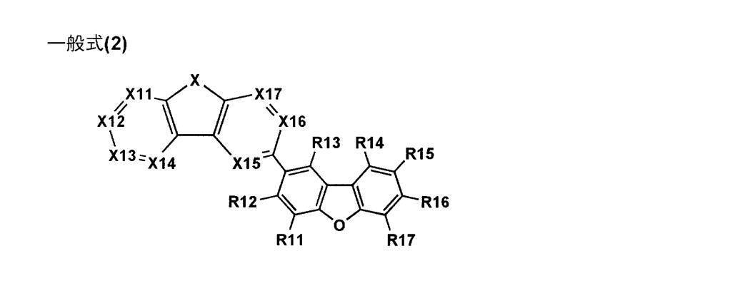
〔式中、R11~R17は、各々水素原子または置換基を表し、Xは、-O-、-S-、または-N(R10)-を表し、R10は水素原子または置換基を表す。X11~X17は-C(R18)=または-N=を表し、R18は水素原子または置換基を表す。-C(R18)=が複数存在する場合にはR18は同じでも異なっていてもよい。但し、R10~R18の少なくとも1つは置換基を表す。〕
3.前記一般式(2)のXが、-N(R10)-を表し、R11~R14、R16、R17が各々水素原子を表し、且つ、X11、X12、X14~X17が、各々-CH=または-N=を表すことを特徴とする前記2に記載の有機エレクトロルミネッセンス素子。
3.前記一般式(2)のXが、-N(R10)-を表し、R11~R14、R16、R17が各々水素原子を表し、且つ、X11、X12、X14~X17が、各々-CH=または-N=を表すことを特徴とする前記2に記載の有機エレクトロルミネッセンス素子。
4.前記一般式(2)のXが、-O-または-S-を表し、R11~R14、R16、R17が、各々水素原子であり、且つ、X11、X12、X14~X17が、各々-CH=を表すことを特徴とする前記2に記載の有機エレクトロルミネッセンス素子。
5.前記一般式(1)で表される化合物が下記一般式(3)で表される化合物であることを特徴とする前記1に記載の有機エレクトロルミネッセンス素子。
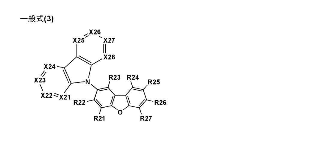
〔式中、R21~R27は、各々水素原子または置換基を表す。X21~X28は、各々-C(R28)=または-N=を表し、R28は水素原子または置換基を表す。-C(R28)=が複数存在する場合にはR28は同じでも異なっていてもよい。但し、R21~R28の少なくとも1つは置換基を表す。〕
6.前記一般式(3)のR21~R24、R26、R27が、各々水素原子を表し、X21、X22、X24、X25、X27、X28が、各々-CH=または-N=を表すことを特徴とする前記5に記載の有機エレクトロルミネッセンス素子。
6.前記一般式(3)のR21~R24、R26、R27が、各々水素原子を表し、X21、X22、X24、X25、X27、X28が、各々-CH=または-N=を表すことを特徴とする前記5に記載の有機エレクトロルミネッセンス素子。
7.前記一般式(1)で表される化合物が下記一般式(4)で表される化合物であることを特徴とする前記1に記載の有機エレクトロルミネッセンス素子。

〔式中、R31~R37は、各々水素原子または置換基を表す。X31~X35は、各々-C(R38)=または-N=を表し、R38は水素原子または置換基を表す。但し、X31~X35の少なくとも1つは、R38が置換基を表す-C(R38)=である。-C(R38)=が複数存在する場合にはR38は同じでも異なっていてもよい。〕
8.前記一般式(4)のR31~R34、R36、R37が、各々水素原子を表し、X33が、-CH=または-N=を表すことを特徴とする前記7に記載の有機エレクトロルミネッセンス素子。
8.前記一般式(4)のR31~R34、R36、R37が、各々水素原子を表し、X33が、-CH=または-N=を表すことを特徴とする前記7に記載の有機エレクトロルミネッセンス素子。
9.前記一般式(1)~(4)のいずれかで表される化合物が、ピリジン環または該ピリジン環を含む縮合芳香族複素環を部分構造として少なくとも1つ有することを特徴とする前記1~8のいずれか1項に記載の有機エレクトロルミネッセンス素子。
10.前記元素が、ナトリウム、カリウムまたはセシウムを表すことを特徴とする前記1~9のいずれか1項に記載の有機エレクトロルミネッセンス素子。
11.前記リン光発光性の有機金属錯体の少なくとも1つが、下記一般式(5)で表される化合物であることを特徴とする前記1~10のいずれか1項に記載の有機エレクトロルミネッセンス素子。

〔式中、P、Qは、各々炭素原子または窒素原子を表し、A1はP-Cと共に芳香族炭化水素環または芳香族複素環を形成する原子群を表す。A2はQ-Nと共に芳香族複素環を形成する原子群を表す。P1-L1-P2は2座の配位子を表し、P1、P2は各々独立に炭素原子、窒素原子、または酸素原子を表す。L1はP1、P2と共に2座の配位子を形成する原子群を表す。j1は1~3の整数を表し、j2は0~2の整数を表すが、j1+j2は2または3である。M1は元素周期表における8族~10族の金属元素を表す。〕
12.前記一般式(5)で表される化合物が下記一般式(6)で表される化合物であることを特徴とする前記11に記載の有機エレクトロルミネッセンス素子。
12.前記一般式(5)で表される化合物が下記一般式(6)で表される化合物であることを特徴とする前記11に記載の有機エレクトロルミネッセンス素子。
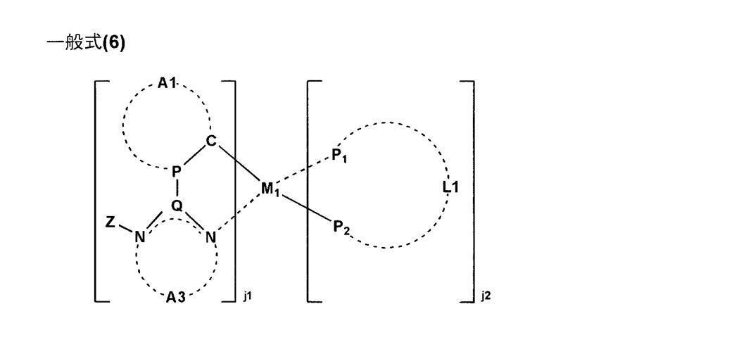
〔式中、Zは、炭化水素環基または複素環基を表す。P、Qは、各々炭素原子または窒素原子を表し、A1はP-Cと共に芳香族炭化水素環または芳香族複素環を形成する原子群を表す。A3は-C(R01)=C(R02)-、-N=C(R02)-、-C(R01)=N-または-N=N-を表し、R01、R02は、各々水素原子または置換基を表す。P1-L1-P2は2座の配位子を表し、P1、P2は各々独立に炭素原子、窒素原子、または酸素原子を表す。L1はP1、P2と共に2座の配位子を形成する原子群を表す。j1は1~3の整数を表し、j2は0~2の整数を表すが、j1+j2は2または3である。M1は元素周期表における8族~10族の遷移金属元素を表す。〕
13.前記一般式(6)で表される化合物が下記一般式(7)で表される化合物であることを特徴とする前記12に記載の有機エレクトロルミネッセンス素子。
13.前記一般式(6)で表される化合物が下記一般式(7)で表される化合物であることを特徴とする前記12に記載の有機エレクトロルミネッセンス素子。
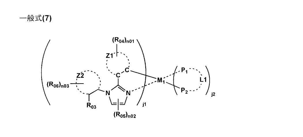
〔式中、R03は置換基を表し、R04は水素原子または置換基を表し、複数のR04は互いに結合して環を形成してもよい。n01は1~4の整数を表す。R05は水素原子または置換基を表し、複数のR05は互いに結合して環を形成してもよい。n02は1~2の整数を表す。R06は水素原子または置換基を表し、互いに結合して環を形成してもよい。n03は1~4の整数を表す。Z1はC-Cと共に6員の芳香族炭化水素環もしくは、5員または6員の芳香族複素環を形成するのに必要な原子群を表す。Z2は炭化水素環または複素環を形成するのに必要な原子群を表す。P1-L1-P2は2座の配位子を表し、P1、P2は各々独立に炭素原子、窒素原子または酸素原子を表す。L1はP1、P2と共に2座の配位子を形成する原子群を表す。j1は1~3の整数を表し、j2は0~2の整数を表すが、j1+j2は2または3である。M1は元素周期表における8族~10族の遷移金属元素を表す。R03とR06、R04とR06及びR05とR06は互いに結合して環を形成していてもよい。〕
14.前記一般式(7)で表される化合物が下記一般式(8)で表される化合物であることを特徴とする前記13に記載の有機エレクトロルミネッセンス素子。
14.前記一般式(7)で表される化合物が下記一般式(8)で表される化合物であることを特徴とする前記13に記載の有機エレクトロルミネッセンス素子。

〔式中、R03は置換基を表し、R04は水素原子または置換基を表し、複数のR04は互いに結合して環を形成してもよい。n01は1~4の整数を表す。R05は水素原子または置換基を表し、複数のR05は互いに結合して環を形成してもよい。n02は1~2の整数を表す。R06は水素原子または置換基を表し、互いに結合して環を形成してもよい。n03は1~3の整数を表す。R07は置換基または単結合手を表す。P1-L1-P2は2座の配位子を表し、P1、P2は各々独立に炭素原子、窒素原子または酸素原子を表す。L1はP1、P2と共に2座の配位子を形成する原子群を表す。j1は1~3の整数を表し、j2は0~2の整数を表すが、j1+j2は2または3である。M1は元素周期表における8族~10族の遷移金属元素を表す。〕
15.前記M1がイリジウムを表すことを特徴とする前記11~14のいずれか1項に記載の有機エレクトロルミネッセンス素子。
15.前記M1がイリジウムを表すことを特徴とする前記11~14のいずれか1項に記載の有機エレクトロルミネッセンス素子。
16.前記電子輸送層と発光層とを含む少なくとも2層の有機層が湿式法で形成されたことを特徴とする前記1~15のいずれか1項に記載の有機エレクトロルミネッセンス素子。
17.白色に発光することを特徴とする前記1~16のいずれか1項に記載の有機エレクトロルミネッセンス素子。
18.前記1~16のいずれか1項に記載の有機エレクトロルミネッセンス素子を備えたことを特徴とする照明装置。
19.前記1~16のいずれか1項に記載の有機エレクトロルミネッセンス素子を備えたことを特徴とする表示装置。
本発明により、高発光効率、低駆動電圧であり、耐熱性や生保存性に優れ、且つ、長寿命である有機エレクトロルミネッセンス素子を提供することができた。
併せて、該有機エレクトロルミネッセンス素子を備えた表示装置及び照明装置を提供することができた。
本発明の有機EL素子においては、請求項1~17のいずれか1項に記載の構成を有することにより、高発光効率、低駆動電圧であり、耐熱性や生保存性に優れ、且つ、長寿命である有機エレクトロルミネッセンス素子を提供することができた。
併せて、該有機エレクトロルミネッセンス素子を備えた表示装置及び照明装置を提供することができた。
以下、本発明の有機EL素子の各構成要素の詳細について、順次説明する。
本発明者らは前記目的を達成するために鋭意研究を重ねた結果、一般式(1)で表される化合物を有機エレクトロルミネッセンス素子の電子輸送層に用いることにより、高効率、長寿命である有機エレクトロルミネッセンス素子が得られることを見出した。
また、ジベンゾフラン環は平面性が高く、コア骨格に用いることでガラス転移温度(Tg)の高い材料を提供することが可能となった。ジベンゾフランと類似骨格の芳香環にカルバゾール環やフルオレン環があるが、カルバゾール環9位のNH部位やフルオレン環9位のCH2部位は反応活性が高く不安定である。そのため9位を置換する必要があるが、置換基を導入することによって平面性が崩れてしまう。
一方、ジベンゾフラン環では上記のような活性の高さがないため、カルバゾール環9位のNH部位やフルオレン環9位のCH2部位と同様の位置に置換基を導入する必要がなく平面性を維持することが可能である。その結果、密な薄膜を形成することが可能となり、膜の安定性が向上し保存性などが改良される。
また、元素周期表の第2周期に属する酸素原子は、第3周期に属する硫黄原子よりも不安定な荷電状態をとるため、酸素原子を構成原子として含む本発明に係る一般式(1)で表される化合物のようなジベンゾフラン誘導体は電子を渡しやすく、結果キャリアが移動しやすくなり低駆動電圧を達成できることが分かった。
更に、一般式(1)における置換位置Aは、共役長を伸ばさず、即ち、高い3重項エネルギー(T1)を維持したまま他の骨格と連結することが可能な位置であり、更にジベンゾフラン環の4位よりも合成上置換基の導入が容易なため、量産性に適している。
また、電子注入材料としては仕事関数の小さいフッ化リチウムに代表されるアルカリ金属やアルカリ土類金属がよく知られているが、本発明の電子輸送材料との組み合わせについて本発明者らが詳細に検討したところ、周期表第1族または第2族に属する元素であって、Mn+/M系の標準電極電位が-3Vvs.SHEよりも大きい元素の金属または金属化合物(錯体や塩を含む)を併用することによって、高効率でありながら同時に非常に低い電圧で有機EL素子を駆動させることが可能となった。
これは、酸化還元電位が小さい元素に比較して大きい元素は電子を受け取りやすいため、還元され金属の状態になりやすく、その結果、金属を通して陰極から電子輸送層へ電子が輸送されやすくなり、本発明のジベンゾフラン誘導体と電子注入材料を組み合わせて用いることにより高効率、低電圧の有機エレクトロルミネッセンス素子を提供することが可能となった。
尚、有機EL素子を構成する、陽極、陰極及び該陽極と該陰極との間に挟持される構成層(正孔注入層、正孔輸送層、発光層、電子輸送層、電子注入層等の有機層等)については後に詳細に説明する。
以下、一般式(1)で表される化合物について説明する。
《一般式(1)で表される化合物》
一般式(1)において、R1~R7で各々表される置換基の例としてはアルキル基(例えば、メチル基、エチル基、プロピル基、イソプロピル基、tert-ブチル基、ペンチル基、ヘキシル基、オクチル基、ドデシル基、トリデシル基、テトラデシル基、ペンタデシル基等)、シクロアルキル基(例えば、シクロペンチル基、シクロヘキシル基等)、アルケニル基(例えば、ビニル基、アリル基等)、アルキニル基(例えば、エチニル基、プロパルギル基等)、芳香族炭化水素基(芳香族炭化水素環基、芳香族炭素環基、アリール基等ともいい、例えば、フェニル基、p-クロロフェニル基、メシチル基、トリル基、キシリル基、ナフチル基、アントリル基、アズレニル基、アセナフテニル基、フルオレニル基、フェナントリル基、インデニル基、ピレニル基、ビフェニリル基等)、芳香族複素環基(例えば、ピリジル基、ピリミジニル基、フリル基、ピロリル基、イミダゾリル基、ベンゾイミダゾリル基、ピラゾリル基、ピラジニル基、トリアゾリル基(例えば、1,2,4-トリアゾール-1-イル基、1,2,3-トリアゾール-1-イル基等)、オキサゾリル基、ベンゾオキサゾリル基、チアゾリル基、イソオキサゾリル基、イソチアゾリル基、フラザニル基、チエニル基、キノリル基、ベンゾフリル基、ジベンゾフリル基、ベンゾチエニル基、ジベンゾチエニル基、インドリル基、カルバゾリル基、カルボリニル基、ジアザカルバゾリル基(前記カルボリニル基のカルボリン環を構成する炭素原子の一つが窒素原子で置き換わったものを示す)、キノキサリニル基、ピリダジニル基、トリアジニル基、キナゾリニル基、フタラジニル基等)、複素環基(例えば、ピロリジル基、イミダゾリジル基、モルホリル基、オキサゾリジル基等)、アルコキシ基(例えば、メトキシ基、エトキシ基、プロピルオキシ基、ペンチルオキシ基、ヘキシルオキシ基、オクチルオキシ基、ドデシルオキシ基等)、シクロアルコキシ基(例えば、シクロペンチルオキシ基、シクロヘキシルオキシ基等)、アリールオキシ基(例えば、フェノキシ基、ナフチルオキシ基等)、アルキルチオ基(例えば、メチルチオ基、エチルチオ基、プロピルチオ基、ペンチルチオ基、ヘキシルチオ基、オクチルチオ基、ドデシルチオ基等)、シクロアルキルチオ基(例えば、シクロペンチルチオ基、シクロヘキシルチオ基等)、アリールチオ基(例えば、フェニルチオ基、ナフチルチオ基等)、アルコキシカルボニル基(例えば、メチルオキシカルボニル基、エチルオキシカルボニル基、ブチルオキシカルボニル基、オクチルオキシカルボニル基、ドデシルオキシカルボニル基等)、アリールオキシカルボニル基(例えば、フェニルオキシカルボニル基、ナフチルオキシカルボニル基等)、スルファモイル基(例えば、アミノスルホニル基、メチルアミノスルホニル基、ジメチルアミノスルホニル基、ブチルアミノスルホニル基、ヘキシルアミノスルホニル基、シクロヘキシルアミノスルホニル基、オクチルアミノスルホニル基、ドデシルアミノスルホニル基、フェニルアミノスルホニル基、ナフチルアミノスルホニル基、2-ピリジルアミノスルホニル基等)、アシル基(例えば、アセチル基、エチルカルボニル基、プロピルカルボニル基、ペンチルカルボニル基、シクロヘキシルカルボニル基、オクチルカルボニル基、2-エチルヘキシルカルボニル基、ドデシルカルボニル基、フェニルカルボニル基、ナフチルカルボニル基、ピリジルカルボニル基等)、アシルオキシ基(例えば、アセチルオキシ基、エチルカルボニルオキシ基、ブチルカルボニルオキシ基、オクチルカルボニルオキシ基、ドデシルカルボニルオキシ基、フェニルカルボニルオキシ基等)、アミド基(例えば、メチルカルボニルアミノ基、エチルカルボニルアミノ基、ジメチルカルボニルアミノ基、プロピルカルボニルアミノ基、ペンチルカルボニルアミノ基、シクロヘキシルカルボニルアミノ基、2-エチルヘキシルカルボニルアミノ基、オクチルカルボニルアミノ基、ドデシルカルボニルアミノ基、フェニルカルボニルアミノ基、ナフチルカルボニルアミノ基等)、カルバモイル基(例えば、アミノカルボニル基、メチルアミノカルボニル基、ジメチルアミノカルボニル基、プロピルアミノカルボニル基、ペンチルアミノカルボニル基、シクロヘキシルアミノカルボニル基、オクチルアミノカルボニル基、2-エチルヘキシルアミノカルボニル基、ドデシルアミノカルボニル基、フェニルアミノカルボニル基、ナフチルアミノカルボニル基、2-ピリジルアミノカルボニル基等)、ウレイド基(例えば、メチルウレイド基、エチルウレイド基、ペンチルウレイド基、シクロヘキシルウレイド基、オクチルウレイド基、ドデシルウレイド基、フェニルウレイド基ナフチルウレイド基、2-ピリジルアミノウレイド基等)、スルフィニル基(例えば、メチルスルフィニル基、エチルスルフィニル基、ブチルスルフィニル基、シクロヘキシルスルフィニル基、2-エチルヘキシルスルフィニル基、ドデシルスルフィニル基、フェニルスルフィニル基、ナフチルスルフィニル基、2-ピリジルスルフィニル基等)、アルキルスルホニル基(例えば、メチルスルホニル基、エチルスルホニル基、ブチルスルホニル基、シクロヘキシルスルホニル基、2-エチルヘキシルスルホニル基、ドデシルスルホニル基等)、アリールスルホニル基またはヘテロアリールスルホニル基(例えば、フェニルスルホニル基、ナフチルスルホニル基、2-ピリジルスルホニル基等)、アミノ基(例えば、アミノ基、エチルアミノ基、ジメチルアミノ基、ブチルアミノ基、シクロペンチルアミノ基、2-エチルヘキシルアミノ基、ドデシルアミノ基、アニリノ基、ナフチルアミノ基、2-ピリジルアミノ基等)、ハロゲン原子(例えば、フッ素原子、塩素原子、臭素原子等)、フッ化炭化水素基(例えば、フルオロメチル基、トリフルオロメチル基、ペンタフルオロエチル基、ペンタフルオロフェニル基等)、シアノ基、ニトロ基、ヒドロキシ基、メルカプト基、シリル基(例えば、トリメチルシリル基、トリイソプロピルシリル基、トリフェニルシリル基、フェニルジエチルシリル基等)、ホスホノ基等が挙げられる。
一般式(1)において、R1~R7で各々表される置換基の例としてはアルキル基(例えば、メチル基、エチル基、プロピル基、イソプロピル基、tert-ブチル基、ペンチル基、ヘキシル基、オクチル基、ドデシル基、トリデシル基、テトラデシル基、ペンタデシル基等)、シクロアルキル基(例えば、シクロペンチル基、シクロヘキシル基等)、アルケニル基(例えば、ビニル基、アリル基等)、アルキニル基(例えば、エチニル基、プロパルギル基等)、芳香族炭化水素基(芳香族炭化水素環基、芳香族炭素環基、アリール基等ともいい、例えば、フェニル基、p-クロロフェニル基、メシチル基、トリル基、キシリル基、ナフチル基、アントリル基、アズレニル基、アセナフテニル基、フルオレニル基、フェナントリル基、インデニル基、ピレニル基、ビフェニリル基等)、芳香族複素環基(例えば、ピリジル基、ピリミジニル基、フリル基、ピロリル基、イミダゾリル基、ベンゾイミダゾリル基、ピラゾリル基、ピラジニル基、トリアゾリル基(例えば、1,2,4-トリアゾール-1-イル基、1,2,3-トリアゾール-1-イル基等)、オキサゾリル基、ベンゾオキサゾリル基、チアゾリル基、イソオキサゾリル基、イソチアゾリル基、フラザニル基、チエニル基、キノリル基、ベンゾフリル基、ジベンゾフリル基、ベンゾチエニル基、ジベンゾチエニル基、インドリル基、カルバゾリル基、カルボリニル基、ジアザカルバゾリル基(前記カルボリニル基のカルボリン環を構成する炭素原子の一つが窒素原子で置き換わったものを示す)、キノキサリニル基、ピリダジニル基、トリアジニル基、キナゾリニル基、フタラジニル基等)、複素環基(例えば、ピロリジル基、イミダゾリジル基、モルホリル基、オキサゾリジル基等)、アルコキシ基(例えば、メトキシ基、エトキシ基、プロピルオキシ基、ペンチルオキシ基、ヘキシルオキシ基、オクチルオキシ基、ドデシルオキシ基等)、シクロアルコキシ基(例えば、シクロペンチルオキシ基、シクロヘキシルオキシ基等)、アリールオキシ基(例えば、フェノキシ基、ナフチルオキシ基等)、アルキルチオ基(例えば、メチルチオ基、エチルチオ基、プロピルチオ基、ペンチルチオ基、ヘキシルチオ基、オクチルチオ基、ドデシルチオ基等)、シクロアルキルチオ基(例えば、シクロペンチルチオ基、シクロヘキシルチオ基等)、アリールチオ基(例えば、フェニルチオ基、ナフチルチオ基等)、アルコキシカルボニル基(例えば、メチルオキシカルボニル基、エチルオキシカルボニル基、ブチルオキシカルボニル基、オクチルオキシカルボニル基、ドデシルオキシカルボニル基等)、アリールオキシカルボニル基(例えば、フェニルオキシカルボニル基、ナフチルオキシカルボニル基等)、スルファモイル基(例えば、アミノスルホニル基、メチルアミノスルホニル基、ジメチルアミノスルホニル基、ブチルアミノスルホニル基、ヘキシルアミノスルホニル基、シクロヘキシルアミノスルホニル基、オクチルアミノスルホニル基、ドデシルアミノスルホニル基、フェニルアミノスルホニル基、ナフチルアミノスルホニル基、2-ピリジルアミノスルホニル基等)、アシル基(例えば、アセチル基、エチルカルボニル基、プロピルカルボニル基、ペンチルカルボニル基、シクロヘキシルカルボニル基、オクチルカルボニル基、2-エチルヘキシルカルボニル基、ドデシルカルボニル基、フェニルカルボニル基、ナフチルカルボニル基、ピリジルカルボニル基等)、アシルオキシ基(例えば、アセチルオキシ基、エチルカルボニルオキシ基、ブチルカルボニルオキシ基、オクチルカルボニルオキシ基、ドデシルカルボニルオキシ基、フェニルカルボニルオキシ基等)、アミド基(例えば、メチルカルボニルアミノ基、エチルカルボニルアミノ基、ジメチルカルボニルアミノ基、プロピルカルボニルアミノ基、ペンチルカルボニルアミノ基、シクロヘキシルカルボニルアミノ基、2-エチルヘキシルカルボニルアミノ基、オクチルカルボニルアミノ基、ドデシルカルボニルアミノ基、フェニルカルボニルアミノ基、ナフチルカルボニルアミノ基等)、カルバモイル基(例えば、アミノカルボニル基、メチルアミノカルボニル基、ジメチルアミノカルボニル基、プロピルアミノカルボニル基、ペンチルアミノカルボニル基、シクロヘキシルアミノカルボニル基、オクチルアミノカルボニル基、2-エチルヘキシルアミノカルボニル基、ドデシルアミノカルボニル基、フェニルアミノカルボニル基、ナフチルアミノカルボニル基、2-ピリジルアミノカルボニル基等)、ウレイド基(例えば、メチルウレイド基、エチルウレイド基、ペンチルウレイド基、シクロヘキシルウレイド基、オクチルウレイド基、ドデシルウレイド基、フェニルウレイド基ナフチルウレイド基、2-ピリジルアミノウレイド基等)、スルフィニル基(例えば、メチルスルフィニル基、エチルスルフィニル基、ブチルスルフィニル基、シクロヘキシルスルフィニル基、2-エチルヘキシルスルフィニル基、ドデシルスルフィニル基、フェニルスルフィニル基、ナフチルスルフィニル基、2-ピリジルスルフィニル基等)、アルキルスルホニル基(例えば、メチルスルホニル基、エチルスルホニル基、ブチルスルホニル基、シクロヘキシルスルホニル基、2-エチルヘキシルスルホニル基、ドデシルスルホニル基等)、アリールスルホニル基またはヘテロアリールスルホニル基(例えば、フェニルスルホニル基、ナフチルスルホニル基、2-ピリジルスルホニル基等)、アミノ基(例えば、アミノ基、エチルアミノ基、ジメチルアミノ基、ブチルアミノ基、シクロペンチルアミノ基、2-エチルヘキシルアミノ基、ドデシルアミノ基、アニリノ基、ナフチルアミノ基、2-ピリジルアミノ基等)、ハロゲン原子(例えば、フッ素原子、塩素原子、臭素原子等)、フッ化炭化水素基(例えば、フルオロメチル基、トリフルオロメチル基、ペンタフルオロエチル基、ペンタフルオロフェニル基等)、シアノ基、ニトロ基、ヒドロキシ基、メルカプト基、シリル基(例えば、トリメチルシリル基、トリイソプロピルシリル基、トリフェニルシリル基、フェニルジエチルシリル基等)、ホスホノ基等が挙げられる。
また、これらの置換基は上記の置換基によって更に置換されていてもよい。また、これらの置換基は複数が互いに結合して環を形成していてもよい。
一般式(1)において、Aで表されるフェニル基は、部分構造として、少なくとも1つのカルバゾール環、アザカルバゾール環、ジベンゾフラン環またはジベンゾチオフェン環を含む。
ここで、アザカルバゾール環とは、前記カルバゾール環を構成するベンゼン環の炭素原子が1つ以上窒素原子で置き換わったものを示す。
また、該部分構造は、無置換でも置換基を有していてもよく、該置換基は、一般式(1)において、R1~R7で各々表される置換基と同義である。
一般式(1)において、Aで表される芳香族複素環基としては、例えば、ピリジル基、ピリミジニル基、フリル基、ピロリル基、イミダゾリル基、ベンゾイミダゾリル基、ピラゾリル基、ピラジニル基、トリアゾリル基(例えば、1,2,4-トリアゾール-1-イル基、1,2,3-トリアゾール-1-イル基等)、オキサゾリル基、ベンゾオキサゾリル基、チアゾリル基、イソオキサゾリル基、イソチアゾリル基、フラザニル基、チエニル基、キノリル基、ベンゾフリル基、ジベンゾフリル基、ベンゾチエニル基、ジベンゾチエニル基、インドリル基、カルバゾリル基、カルボリニル基、ジアザカルバゾリル基(前記カルボリニル基のカルボリン環を構成する炭素原子の一つが窒素原子で置き換わったものを示す)、キノキサリニル基、ピリダジニル基、トリアジニル基、キナゾリニル基、フタラジニル基等が挙げられる。これらの基は、無置換でも更に、一般式(1)において、R1~R7で各々表される置換基を有していてもよい。
尚、該芳香族複素環基は、部分構造として、少なくとも1つのカルバゾール環、アザカルバゾール環、ジベンゾフラン環またはジベンゾチオフェン環を含む。
本発明に係る一般式(1)で表される化合物の更に好ましい態様としては、上記一般式(2)、(3)または(4)のいずれかで表される化合物が挙げられる。
《一般式(2)で表される化合物》
一般式(2)において、R11~R17で各々表される置換基は、一般式(1)において、R1~R7で各々表される置換基と同義である。
一般式(2)において、R11~R17で各々表される置換基は、一般式(1)において、R1~R7で各々表される置換基と同義である。
一般式(2)のXの-N(R10)-において、R10で表される置換基は、一般式(1)において、R1~R7で各々表される置換基と同義である。
一般式(2)のX11~X17において、-C(R18)=のR18で表される置換基は、一般式(1)において、R1~R7で各々表される置換基と同義である。
また、一般式(2)で表される化合物においても、下記に示す2種の好ましい態様(a)、(b)が挙げられる。
(a)一般式(2)のXが-N(R10)-を表し、R11~R14、R16、R17が各々水素原子を表し、且つ、X11、X12、X14~X17が、各々-CH=または-N=を表す場合、
(b)一般式(2)のXが-O-または-S-を表し、R11~R14、R16、R17が各々水素原子であり、且つ、X11、X12、X14~X17が、各々-CH=を表す場合、
である。
(b)一般式(2)のXが-O-または-S-を表し、R11~R14、R16、R17が各々水素原子であり、且つ、X11、X12、X14~X17が、各々-CH=を表す場合、
である。
《一般式(3)で表される化合物》
一般式(3)において、R21~R27で各々表される置換基は、一般式(1)において、R1~R7で各々表される置換基と同義である。
一般式(3)において、R21~R27で各々表される置換基は、一般式(1)において、R1~R7で各々表される置換基と同義である。
一般式(3)のX21~X28で各々表される-C(R28)=において、R28で表される置換基は、一般式(1)において、R1~R7で各々表される置換基と同義である。
また、一般式(3)で表される化合物においても、好ましい態様としては、下記に示すような態様(c)が挙げられる。
(c)一般式(3)のR21~R24、R26、R27が、各々水素原子を表し、X21、X22、X24、X25、X27、X28が、各々-CH=または-N=を表す場合、
である。
である。
《一般式(4)で表される化合物》
一般式(4)において、R31~R37で各々表される置換基は、一般式(1)において、R1~R7で各々表される置換基と同義である。
一般式(4)において、R31~R37で各々表される置換基は、一般式(1)において、R1~R7で各々表される置換基と同義である。
一般式(4)のX31~X35で各々表される-C(R38)=において、R38で表される置換基は、一般式(1)において、R1~R7で各々表される置換基と同義である。
また、一般式(4)で表される化合物においても、好ましい態様としては、下記に示す態様(d)が挙げられる。
(d)一般式(4)のR31~R34、R36、R37が、各々水素原子を表し、X33が、-CH=または-N=を表す場合、
である。
である。
以下、本発明に係る一般式(1)、(2)、(3)または(4)のいずれかで表される化合物の更に好ましい態様について以下に説明する。
《好ましい部分構造》
また、本発明に係る一般式(1)、(2)、(3)または(4)のいずれかで表される化合物の好ましい態様としては、ピリジン環または該ピリジン環を含む縮合芳香族複素環を部分構造として少なくとも1つ有することが好ましい。
また、本発明に係る一般式(1)、(2)、(3)または(4)のいずれかで表される化合物の好ましい態様としては、ピリジン環または該ピリジン環を含む縮合芳香族複素環を部分構造として少なくとも1つ有することが好ましい。
ここで、ピリジン環を含む縮合芳香族複素環とは、例えばβ-カルボリンのように、縮合環を構成する環の少なくとも1つがピリジン環であるような縮合芳香族複素環を指す。
《Tg(ガラス転移温度℃)》
本発明に係る一般式(1)、(2)、(3)または(4)のいずれかで表される化合物のTg(ガラス転移温度℃)を上げるためにはナフタレン環やアントラセン環など縮合環を化合物内に導入することが有効である。
本発明に係る一般式(1)、(2)、(3)または(4)のいずれかで表される化合物のTg(ガラス転移温度℃)を上げるためにはナフタレン環やアントラセン環など縮合環を化合物内に導入することが有効である。
しかし、縮合系の芳香族炭化水素環はT1(三重項励起状態、励起三重項状態を示す)が小さく、特に青色燐光発光性ドーパントと同時に用いる場合には適していない。
そこで、T1を下げずにTgを向上させる手段として、カルバゾール環やジベンゾフラン環などの芳香族複素縮合環を導入することが好ましい。
《好ましく含有される構成層及び該構成層の作製方法》
本発明に係る一般式(1)、(2)、(3)または(4)のいずれかで表される化合物は少なくとも電子輸送層に含有されるが、電子輸送層以外の層、例えば正孔輸送層や発光層に含有されていてもよい。
本発明に係る一般式(1)、(2)、(3)または(4)のいずれかで表される化合物は少なくとも電子輸送層に含有されるが、電子輸送層以外の層、例えば正孔輸送層や発光層に含有されていてもよい。
本発明に係る一般式(1)、(2)、(3)または(4)のいずれかで表される化合物を含有する層の作製方法としては、湿式法(ウェットプロセスともいう)、蒸着法等があるが、均質な膜が得られやすく、且つピンホールが生成しにくい等の点から、湿式法が好ましく用いられる。
ここで、湿式法としては、スピンコート法、キャスト法、ダイコート法、ブレードコート法、ロールコート法、インクジェット法、印刷法、スプレーコート法、カーテンコート法等があるが、精密な薄膜が形成可能で、且つ高生産性の点から、ダイコート法、ロールコート法、インクジェット法、スプレーコート法などのロール・ツー・ロール方式適性の高い方法が好ましい。また、層ごとに異なる製膜法を適用してもよい。
また、本発明に係る一般式(1)、(2)、(3)または(4)のいずれかで表される化合物を用いて塗布法(分散法も含む)により構成層を形成する場合、用いる溶剤に制限はないが、前記化合物のTgと溶剤の沸点Tbの関係が、下記式(1)を満足することが好ましい。
式(1)
Tg+10℃≧Tb
また、本発明の有機EL素子を構成する有機層の3層以上が塗布で作製されることが好ましく、更には、陰極も銀ナノ粒子などを用い塗布で形成されてもよい。
Tg+10℃≧Tb
また、本発明の有機EL素子を構成する有機層の3層以上が塗布で作製されることが好ましく、更には、陰極も銀ナノ粒子などを用い塗布で形成されてもよい。
以下、本発明に係る一般式(1)、(2)、(3)または(4)のいずれかで表される化合物の具体例を示すが、本発明はこれらに限定されない。
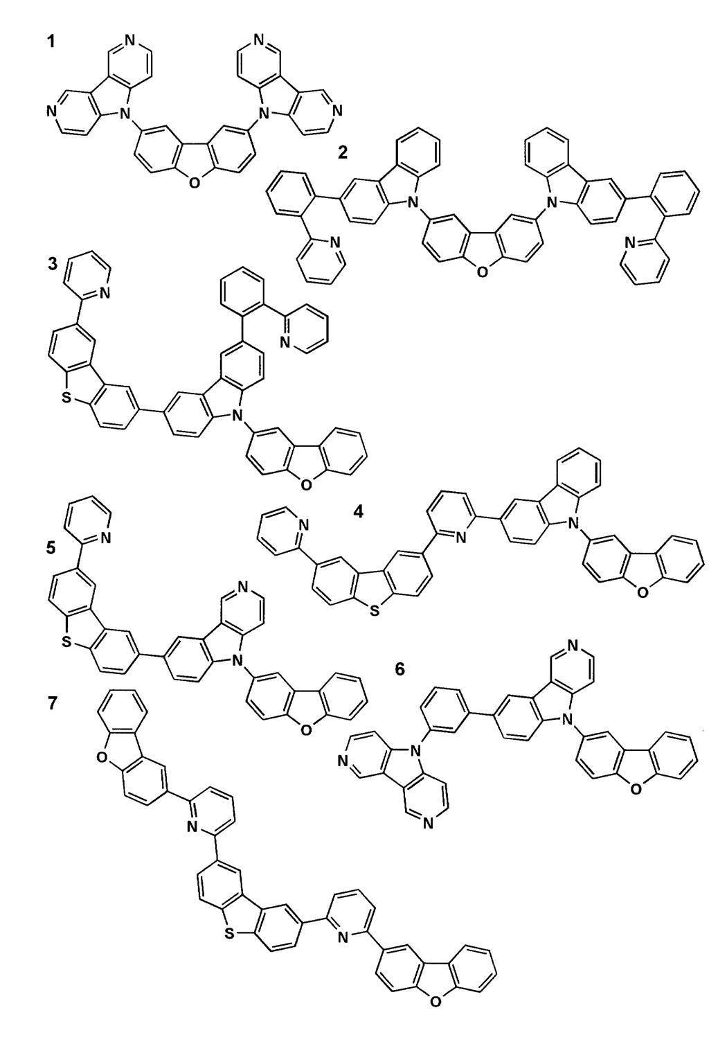
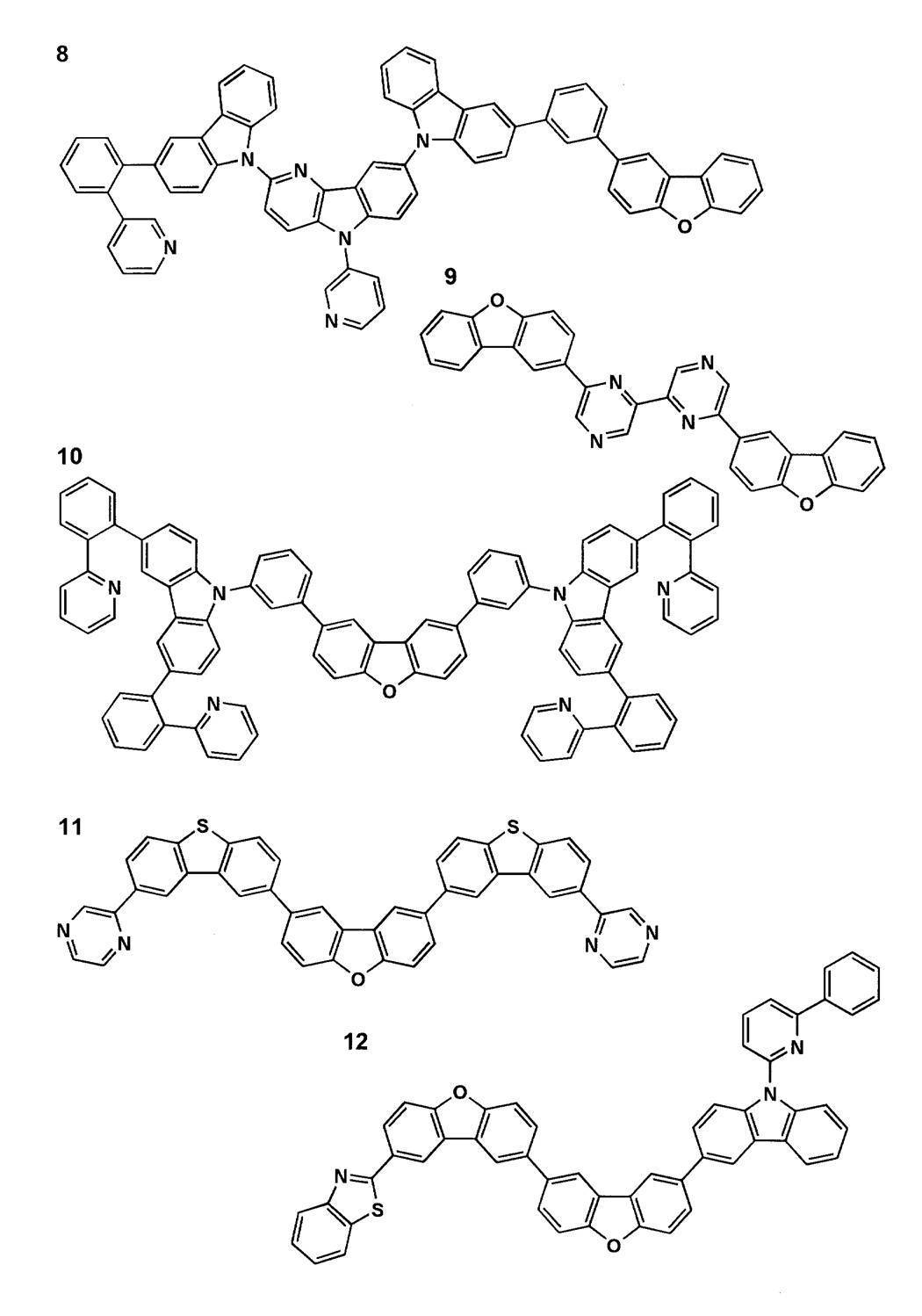


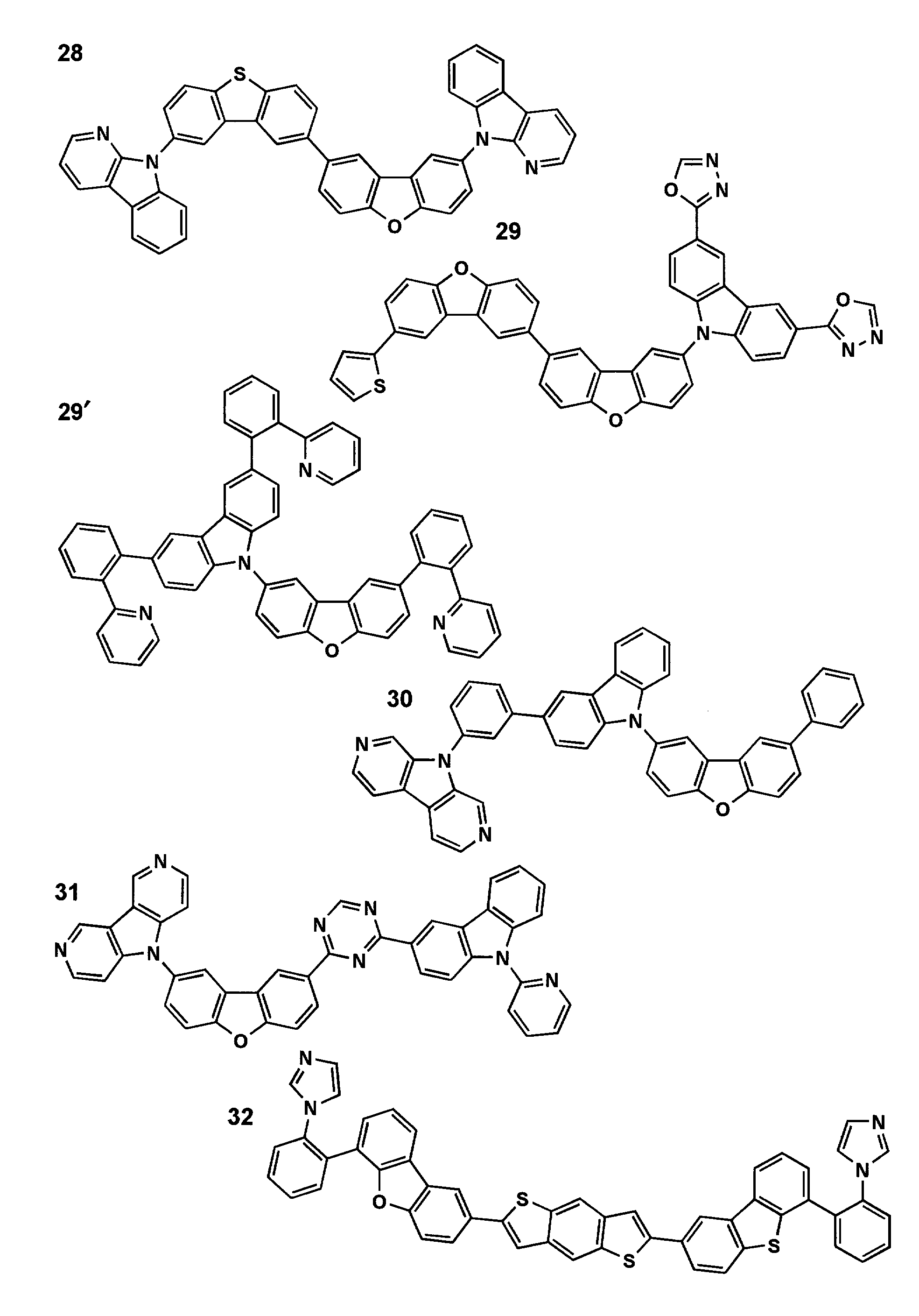

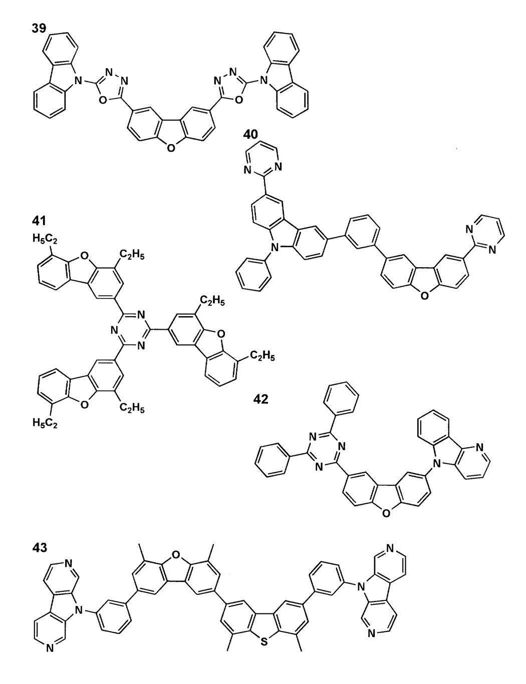
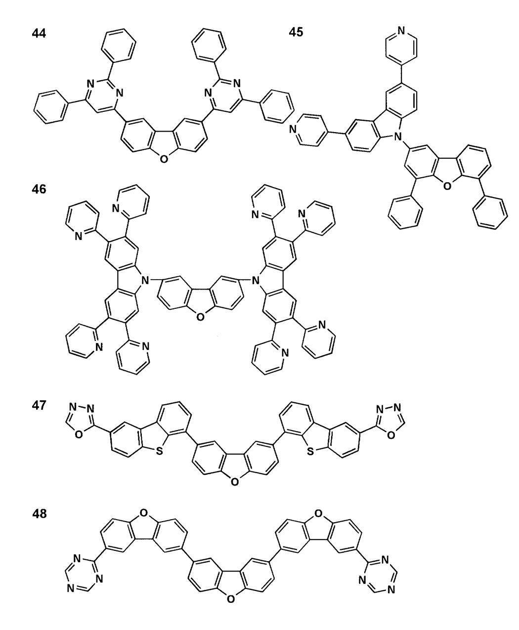
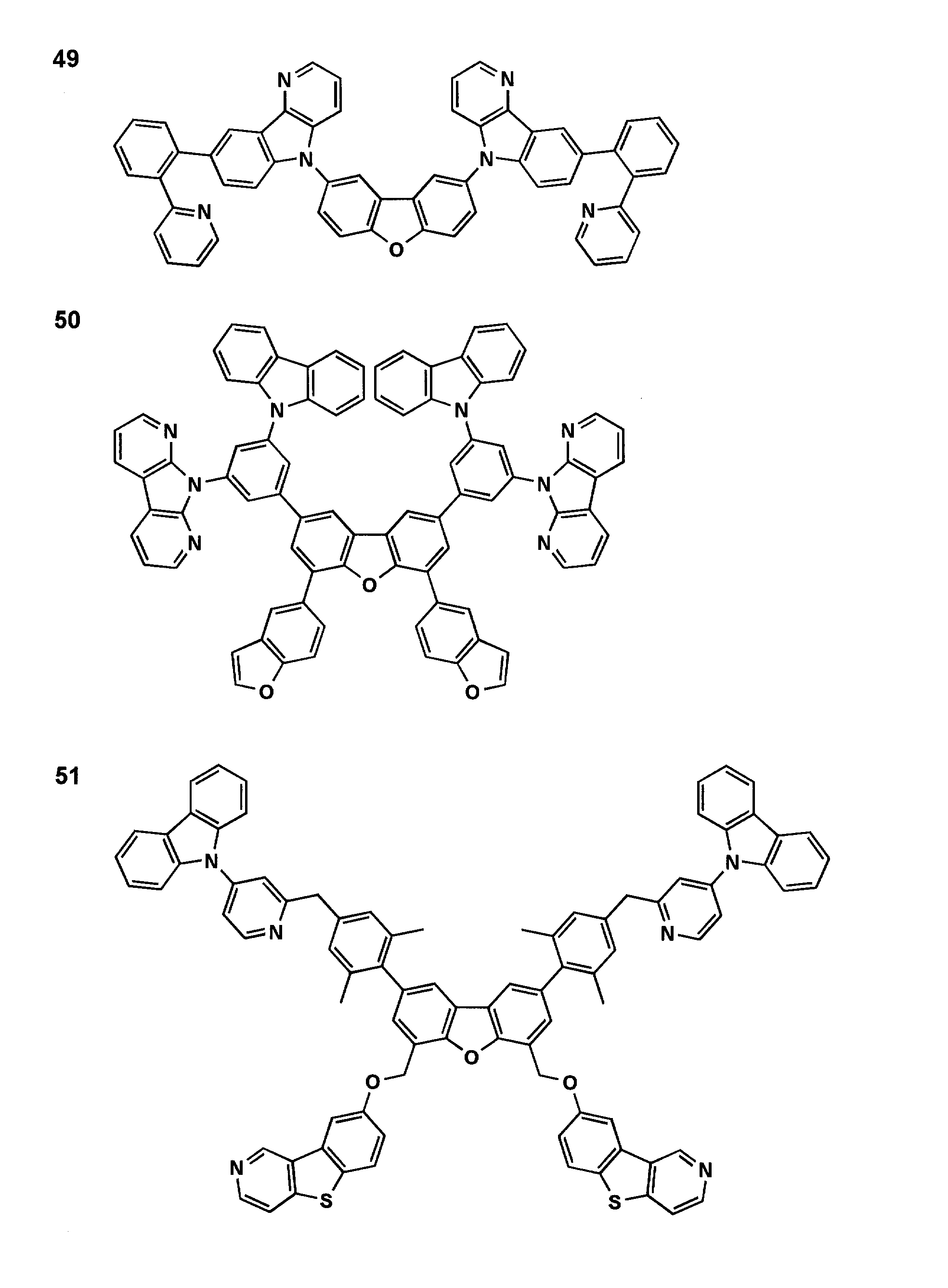
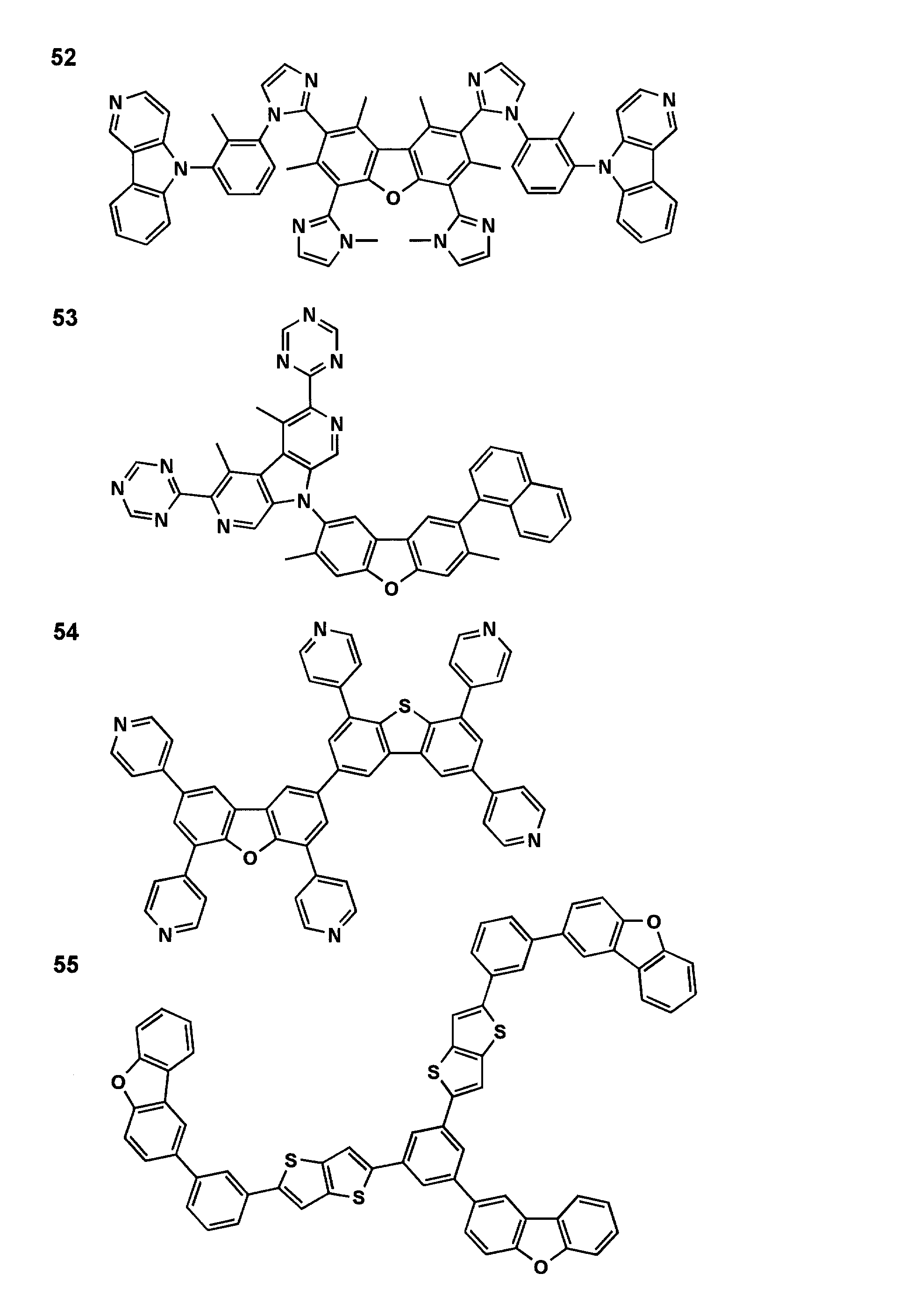
本発明に係る一般式(1)、(2)、(3)または(4)のいずれかで表される化合物は、国際公開第07/111176号パンフレット、Chem.Mater.2008,20,5951、実験化学講座第5版(日本化学会編)等に記載の公知の方法を参照して合成することができる。
《一般式(5)で表される化合物》
本発明の有機EL素子に含有されるリン光発光性の金属錯体としては、上記一般式(5)で表される化合物が好ましい。
本発明の有機EL素子に含有されるリン光発光性の金属錯体としては、上記一般式(5)で表される化合物が好ましい。
以下、一般式(5)で表される化合物について説明する。尚、一般式(5)で表されるリン光発光性の金属錯体は、本発明の有機EL素子の発光層に発光ドーパントとして含有されることが好ましい態様であるが、発光層以外の構成層(本発明の有機EL素子の構成層については後に詳細に説明する。)に含有されていても良い。
一般式(5)において、A1がP-Cと共に形成する芳香族炭化水素環としては、ベンゼン環、ビフェニル環、ナフタレン環、アズレン環、アントラセン環、フェナントレン環、ピレン環、クリセン環、ナフタセン環、トリフェニレン環、o-テルフェニル環、m-テルフェニル環、p-テルフェニル環、アセナフテン環、コロネン環、フルオレン環、フルオラントレン環、ナフタセン環、ペンタセン環、ペリレン環、ペンタフェン環、ピセン環、ピレン環、ピラントレン環、アンスラアントレン環等が挙げられる。
これらの環は更に、一般式(1)において、R1~R7で各々表される置換基を有してもよい。
一般式(5)において、A1が、P-Cと共に形成する芳香族複素環としては、フラン環、チオフェン環、オキサゾール環、ピロール環、ピリジン環、ピリダジン環、ピリミジン環、ピラジン環、トリアジン環、ベンゾイミダゾール環、オキサジアゾール環、トリアゾール環、イミダゾール環、ピラゾール環、チアゾール環、インドール環、ベンゾイミダゾール環、ベンゾチアゾール環、ベンゾオキサゾール環、キノキサリン環、キナゾリン環、フタラジン環、カルバゾール環、アザカルバゾール環等が挙げられる。
ここで、アザカルバゾール環とは、前記カルバゾール環を構成するベンゼン環の炭素原子が1つ以上窒素原子で置き換わったものを示す。
これらの環は更に、一般式(1)において、R1~R7で各々表される置換基を有してもよい。
一般式(5)において、A2が、Q-Nと共に形成する芳香族複素環としては、オキサゾール環、オキサジアゾール環、オキサトリアゾール環、イソオキサゾール環、テトラゾール環、チアジアゾール環、チアトリアゾール環、イソチアゾール環、ピロール環、ピリジン環、ピリダジン環、ピリミジン環、ピラジン環、トリアジン環、イミダゾール環、ピラゾール環、トリアゾール環等が挙げられる。
これらの環は更に、一般式(1)において、R1~R7で各々表される置換基を有してもよい。
一般式(5)において、P1-L1-P2で表される2座の配位子の具体例としては、フェニルピリジン、フェニルピラゾール、フェニルイミダゾール、フェニルトリアゾール、フェニルテトラゾール、ピラザボール、アセチルアセトン、ピコリン酸等が挙げられる。
一般式(5)において、j1は1~3の整数を表し、j2は0~2の整数を表すが、j1+j2は2または3を表す、中でも、j2は0である場合が好ましい。
一般式(5)において、M1は元素周期表における8族~10族の遷移金属元素(単に遷移金属ともいう)が用いられるが、中でも、イリジウム好ましい。
《一般式(6)で表される化合物》
本発明に係る一般式(5)で表される化合物の中でも、一般式(6)で表される化合物が好ましい。
本発明に係る一般式(5)で表される化合物の中でも、一般式(6)で表される化合物が好ましい。
一般式(6)において、Zで表される炭化水素環基としては、非芳香族炭化水素環基、芳香族炭化水素環基が挙げられ、非芳香族炭化水素環基としては、シクロプロピル基、シクロペンチル基、シクロヘキシル基等が挙げられる。これらの基は、無置換でも後述する置換基を有していてもよい。
また、芳香族炭化水素環基(芳香族炭化水素基、アリール基等ともいう)としては、例えば、フェニル基、p-クロロフェニル基、メシチル基、トリル基、キシリル基、ナフチル基、アントリル基、アズレニル基、アセナフテニル基、フルオレニル基、フェナントリル基、インデニル基、ピレニル基、ビフェニリル基等が挙げられる。
これらの基は、無置換でもよく、一般式(1)において、R1~R7で各々表される置換基を有してもよい。
一般式(6)において、Zで表される複素環基としては、非芳香族複素環基、芳香族複素環基等が挙げられ、非芳香族複素環基としては、例えば、エポキシ環、アジリジン環、チイラン環、オキセタン環、アゼチジン環、チエタン環、テトラヒドロフラン環、ジオキソラン環、ピロリジン環、ピラゾリジン環、イミダゾリジン環、オキサゾリジン環、テトラヒドロチオフェン環、スルホラン環、チアゾリジン環、ε-カプロラクトン環、ε-カプロラクタム環、ピペリジン環、ヘキサヒドロピリダジン環、ヘキサヒドロピリミジン環、ピペラジン環、モルホリン環、テトラヒドロピラン環、1,3-ジオキサン環、1,4-ジオキサン環、トリオキサン環、テトラヒドロチオピラン環、チオモルホリン環、チオモルホリン-1,1-ジオキシド環、ピラノース環、ジアザビシクロ[2,2,2]-オクタン環等から導出される基を挙げられる。
これらの基は、無置換でもよく、一般式(1)において、R1~R7で各々表される置換基を有してもよい。
芳香族複素環基としては、例えば、ピリジル基、ピリミジニル基、フリル基、ピロリル基、イミダゾリル基、ベンゾイミダゾリル基、ピラゾリル基、ピラジニル基、トリアゾリル基(例えば、1,2,4-トリアゾール-1-イル基、1,2,3-トリアゾール-1-イル基等)、オキサゾリル基、ベンゾオキサゾリル基、チアゾリル基、イソオキサゾリル基、イソチアゾリル基、フラザニル基、チエニル基、キノリル基、ベンゾフリル基、ジベンゾフリル基、ベンゾチエニル基、ジベンゾチエニル基、インドリル基、カルバゾリル基、カルボリニル基、ジアザカルバゾリル基(前記カルボリニル基のカルボリン環を構成する炭素原子の一つが窒素原子で置き換わったものを示す)、キノキサリニル基、ピリダジニル基、トリアジニル基、キナゾリニル基、フタラジニル基等が挙げられる。
これらの基は、無置換でもよく、一般式(1)において、R1~R7で各々表される置換基を有してもよい。
好ましくは、Zで表される基は芳香族炭化水素環基または芳香族複素環基である。
以下に一般式(6)におけるZの好ましい例を挙げるが、Zは以下の例示以外にも無置換でもよく、更に置換基を有していてもよく、これらの例に限定されない。尚、*は結合位置を表す。


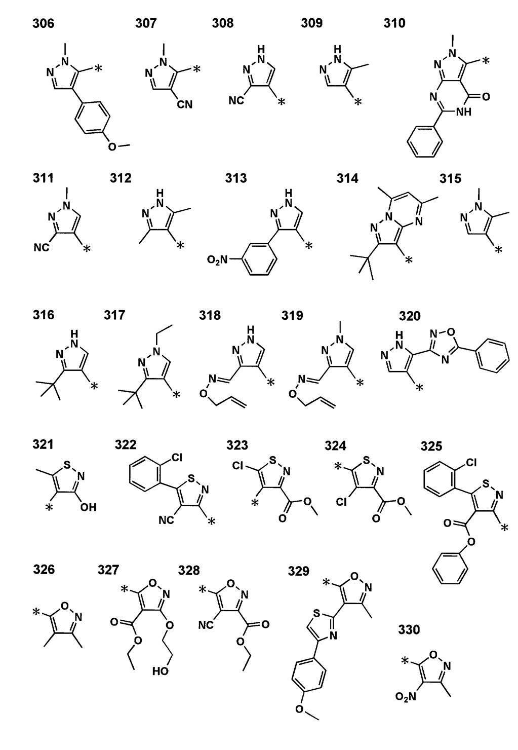

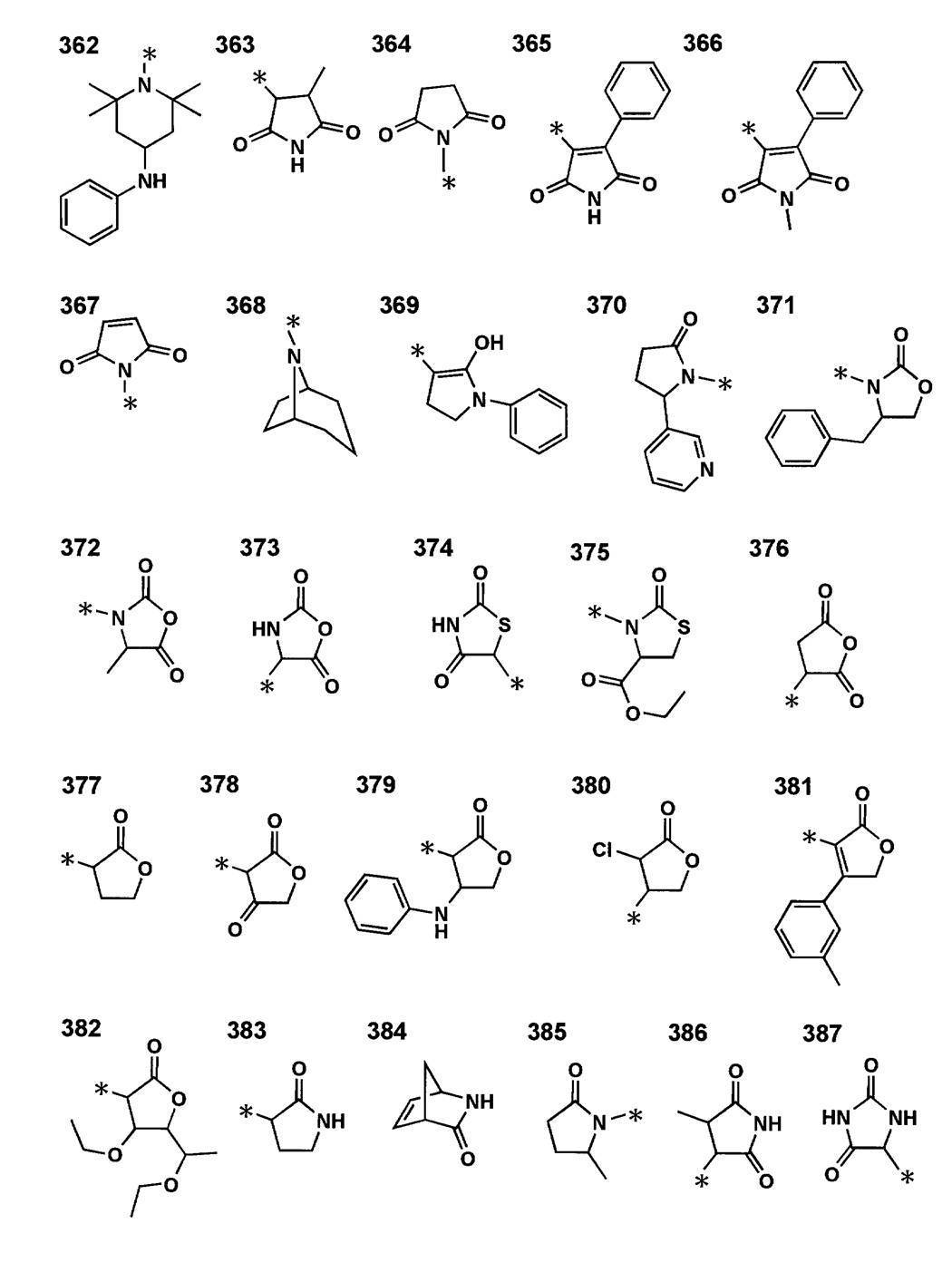
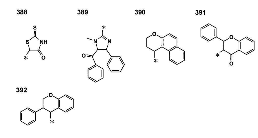
一般式(6)において、A1が、P-Cと共に形成する芳香族炭化水素環としては、ベンゼン環、ビフェニル環、ナフタレン環、アズレン環、アントラセン環、フェナントレン環、ピレン環、クリセン環、ナフタセン環、トリフェニレン環、o-テルフェニル環、m-テルフェニル環、p-テルフェニル環、アセナフテン環、コロネン環、フルオレン環、フルオラントレン環、ナフタセン環、ペンタセン環、ペリレン環、ペンタフェン環、ピセン環、ピレン環、ピラントレン環、アンスラアントレン環等が挙げられる。
これらの環は更に、一般式(1)において、R1~R7で各々表される置換基を有してもよい。
一般式(6)において、A1が、P-Cと共に形成する芳香族複素環としては、フラン環、チオフェン環、オキサゾール環、ピロール環、ピリジン環、ピリダジン環、ピリミジン環、ピラジン環、トリアジン環、ベンゾイミダゾール環、オキサジアゾール環、トリアゾール環、イミダゾール環、ピラゾール環、チアゾール環、インドール環、ベンゾイミダゾール環、ベンゾチアゾール環、ベンゾオキサゾール環、キノキサリン環、キナゾリン環、フタラジン環、カルバゾール環、カルボリン環、アザカルバゾール環等が挙げられる。
ここで、アザカルバゾール環とは、前記カルバゾール環を構成するベンゼン環の炭素原子が1つ以上窒素原子で置き換わったものを示す。
これらの環は更に、一般式(1)において、R1~R7で各々表される置換基を有してもよい。
一般式(6)のA3で表される、-C(R01)=C(R02)-、-N=C(R02)-、-C(R01)=N-において、R01、R02で各々表される置換基は、一般式(1)において、R1~R7で各々表される置換基と同義である。
一般式(6)において、P1-L1-P2で表される2座の配位子の具体例としては、フェニルピリジン、フェニルピラゾール、フェニルイミダゾール、フェニルトリアゾール、フェニルテトラゾール、ピラザボール、アセチルアセトン、ピコリン酸等が挙げられる。
また、j1は1~3の整数を表し、j2は0~2の整数を表すが、j1+j2は2または3を表す、中でも、j2は0である場合が好ましい。
一般式(6)において、M1で表される元素周期表における8族~10族の遷移金属元素(単に遷移金属ともいう)は、一般式(5)において、M1で表される元素周期表における8族~10族の遷移金属元素と同義である。
《一般式(7)で表される化合物》
上記一般式(6)で表される化合物の好ましい態様のひとつとして、上記一般式(7)で表される化合物が挙げられる。
上記一般式(6)で表される化合物の好ましい態様のひとつとして、上記一般式(7)で表される化合物が挙げられる。
一般式(7)において、R03、R04、R05、R06で各々表される置換基は、一般式(1)において、R1~R7で各々表される置換基と同義である。
一般式(7)において、Z1がC-Cと共に形成する6員の芳香族炭化水素環としては、ベンゼン環が挙げられる。
これらの環は更に、一般式(1)において、R1~R7で各々表される置換基を有してもよい。
一般式(7)において、Z1がC-Cと共に形成する5員または6員の芳香族複素環としては、例えば、オキサゾール環、オキサジアゾール環、オキサトリアゾール環、イソオキサゾール環、テトラゾール環、チアジアゾール環、チアトリアゾール環、イソチアゾール環、チオフェン環、フラン環、ピロール環、ピリジン環、ピリダジン環、ピリミジン環、ピラジン環、トリアジン環、イミダゾール環、ピラゾール環、トリアゾール環等が挙げられる。
これらの環は更に、一般式(1)において、R1~R7で各々表される置換基を有してもよい。
一般式(7)において、P1-L1-P2で表される2座の配位子は、一般式(5)において、P1-L1-P2で表される2座の配位子と同義である。
一般式(7)において、M1で表される元素周期表における8族~10族の遷移金属元素は、一般式(5)において、M1で表される元素周期表における8族~10族の遷移金属元素と同義である。
《一般式(8)で表される化合物》
更に、一般式(7)で表される化合物の中でも、上記一般式(8)で表される化合物が好ましい。
更に、一般式(7)で表される化合物の中でも、上記一般式(8)で表される化合物が好ましい。
一般式(8)において、R03、R04、R05、R06、R07で各々表される置換基は、一般式(1)において、R1~R7で各々表される置換基と同義である。
一般式(8)において、P1-L1-P2で表される2座の配位子は、一般式(5)において、P1-L1-P2で表される2座の配位子と同義である。
一般式(8)において、M1で表される元素周期表における8族~10族の遷移金属元素は、一般式(5)において、M1で表される元素周期表における8族~10族の遷移金属元素と同義である。
本発明に係る一般式(5)、(6)、(7)または(8)で各々表される化合物は、Eur.J.Chem.2005,1637-1643等に記載の方法で、含窒素環化合物またはイミダゾール化合物に対応するハロゲン化合物を反応させるか、SYNTHESIS 2003,17,2661-2666等に記載の、対応するアミンとグリオキザール、及びアルデヒドと塩化アンモニウムとの反応等を参照することにより合成可能である。
以下、本発明に係る一般式(5)、(6)、(7)または(8)のいずれかで表される化合物(金属錯体ともいう)の具体例を挙げるが、本発明はこれらに限定されない。


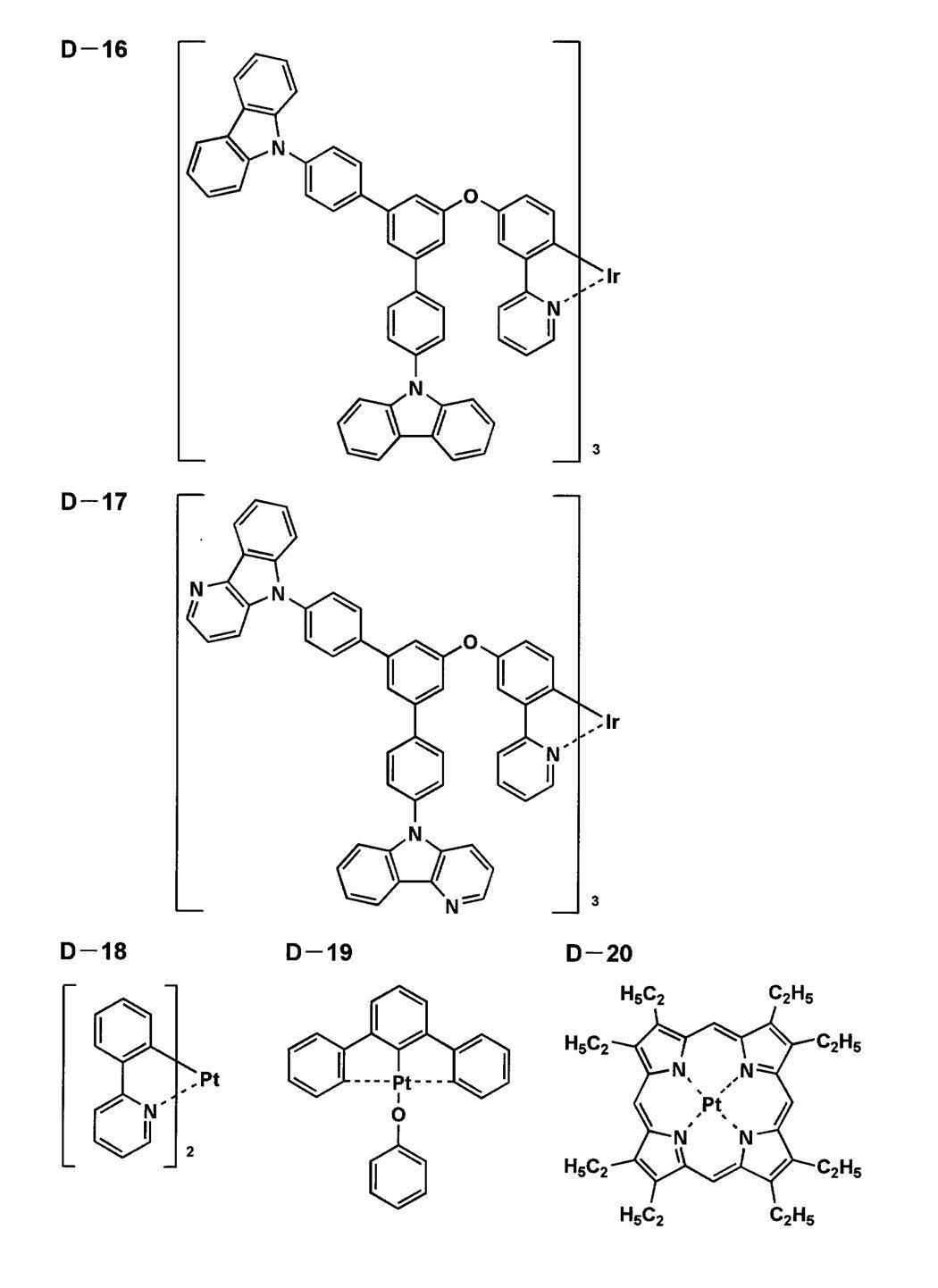


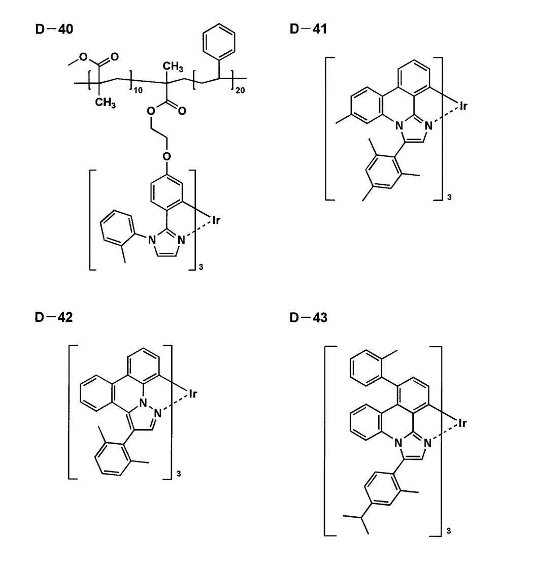
これらの金属錯体は、例えば、Organic Letter誌、vol3、No.16、2579~2581頁(2001)、Inorganic Chemistry,第30巻、第8号、1685~1687頁(1991年)、J.Am.Chem.Soc.,123巻、4304頁(2001年)、Inorganic Chemistry,第40巻、第7号、1704~1711頁(2001年)、Inorganic Chemistry,第41巻、第12号、3055~3066頁(2002年)、New Journal of Chemistry.,第26巻、1171頁(2002年)、European Journal of Organic Chemistry,第4巻、695~709頁(2004年)、更にこれらの文献中に記載の参考文献等の方法を適用することにより合成できる。
以下に、代表的な化合物の合成例を示す。
《例示化合物D-26の合成》

窒素雰囲気下で2-フェニル-(2,4,6-トリメチルフェニル)-1H-イミダゾール、18g(0.06861モル)を2-エトキシエタノール350mlに溶解した溶液に、塩化イリジウム3水和物、8.1g(0.02297モル)及び100mlの水を加え、窒素雰囲気下で5時間還流した。
反応液を冷却し、メタノール500mlを加え、析出した結晶を濾取した。得られた結晶を更にメタノールで洗浄し、乾燥後15.2g(収率88.4%)の錯体Aを得た。
窒素雰囲気下で錯体A、14.5g(0.009662モル)及び炭酸ナトリウム、14.5gを2-エトキシエタノール350mlに懸濁させた。この懸濁液にアセチルアセトン3.9g(0.03895モル)を加え、窒素雰囲気下で2時間還流した。
反応液を冷却後、減圧濾過によって炭酸ナトリウム及び無機塩を除去した。溶媒を減圧濃縮した後に得られた固体に水1Lを加えて懸濁後、固体を濾取した。
得られた結晶を更にメタノール/水=1/1混合溶液で洗浄し、乾燥後14.7g(収率93.6%)の錯体Bを得た。
窒素雰囲気下で錯体B、7.5g(0.009214モル)及び2-フェニル-(2,4,6-トリメチルフェニル)-1H-イミダゾール、6.0g(0.02287モル)をグリセリン400mlに懸濁させた。窒素雰囲気下で反応温度150~160℃の間で2時間反応させ、錯体Bの消失を確認したところで反応終了とした。
反応液を冷却し、メタノール500mlを加え、析出した結晶を濾取した。
得られた結晶を更にメタノールで洗浄し、乾燥後収量7.1g(収率78.9%)の粗生成物を得た。この粗生成物を少量の塩化メチレンに溶解し、シカゲルカラムクロマトグラフィーによって精製し(塩化メチレン)6.5g(収率72.2%)の例示化合物D-26を得た。
日立製作所製F-4500を用いて測定した例示化合物D-26の溶液におけるリン光発光波長は、466nmであった(2-メチルテトラヒドロフラン中)。
《有機EL素子の構成層》
本発明の有機EL素子の構成層について説明する。本発明において、有機EL素子の層構成の好ましい具体例を以下に示すが、本発明はこれらに限定されない。
本発明の有機EL素子の構成層について説明する。本発明において、有機EL素子の層構成の好ましい具体例を以下に示すが、本発明はこれらに限定されない。
(i)陽極/発光層/電子輸送層/陰極
(ii)陽極/正孔輸送層/発光層/電子輸送層/陰極
(iii)陽極/正孔輸送層/発光層/正孔阻止層/電子輸送層/陰極
(iv)陽極/正孔輸送層/発光層/正孔阻止層/電子輸送層/陰極バッファー層/陰極
(v)陽極/陽極バッファー層/正孔輸送層/発光層/正孔阻止層/電子輸送層/陰極バッファー層/陰極
更に、発光層間には非発光性の中間層を有していてもよい。本発明の有機EL素子としては白色発光層であることが好ましく、これらを用いた照明装置であることが好ましい。
(ii)陽極/正孔輸送層/発光層/電子輸送層/陰極
(iii)陽極/正孔輸送層/発光層/正孔阻止層/電子輸送層/陰極
(iv)陽極/正孔輸送層/発光層/正孔阻止層/電子輸送層/陰極バッファー層/陰極
(v)陽極/陽極バッファー層/正孔輸送層/発光層/正孔阻止層/電子輸送層/陰極バッファー層/陰極
更に、発光層間には非発光性の中間層を有していてもよい。本発明の有機EL素子としては白色発光層であることが好ましく、これらを用いた照明装置であることが好ましい。
本発明の有機EL素子を構成する各層について説明する。
《電子輸送層》
本発明に係る一般式(1)、(2)、(3)または(4)のいずれかで表される化合物は、本発明の有機EL素子の構成層である少なくとも1層の電子輸送層に含有されるが、本発明の有機EL素子のその他の構成層(後に、詳細に説明する。)に含有されていても良い。
本発明に係る一般式(1)、(2)、(3)または(4)のいずれかで表される化合物は、本発明の有機EL素子の構成層である少なくとも1層の電子輸送層に含有されるが、本発明の有機EL素子のその他の構成層(後に、詳細に説明する。)に含有されていても良い。
ここで、電子輸送層とは電子を輸送する機能を有する材料からなり、広い意味で電子注入層、正孔阻止層も電子輸送層に含まれる。電子輸送層は単層もしくは複数層を設けることができる。
電子輸送層は陰極より注入された電子を発光層に伝達する機能を有していればよく、電子輸送層の構成材料としては従来公知の化合物の中から任意のものを選択し併用することも可能である。
電子輸送層に用いられる従来公知の材料(以下、電子輸送材料という)の例としては、ニトロ置換フルオレン誘導体、ジフェニルキノン誘導体、チオピランジオキシド誘導体、ナフタレンペリレン等の複素環テトラカルボン酸無水物、カルボジイミド、フレオレニリデンメタン誘導体、アントラキノジメタン及びアントロン誘導体、オキサジアゾール誘導体、カルボリン誘導体、または、該カルボリン誘導体のカルボリン環を構成する炭化水素環の炭素原子の少なくとも一つが窒素原子で置換されている環構造を有する誘導体等が挙げられる。
更に、上記オキサジアゾール誘導体において、オキサジアゾール環の酸素原子を硫黄原子に置換したチアジアゾール誘導体、電子吸引性基として知られているキノキサリン環を有するキノキサリン誘導体も電子輸送材料として用いることができる。
これらの材料を高分子鎖に導入した、またはこれらの材料を高分子の主鎖とした高分子材料を用いることもできる。
また、8-キノリノール誘導体の金属錯体、例えば、トリス(8-キノリノール)アルミニウム(Alq)、トリス(5,7-ジクロロ-8-キノリノール)アルミニウム、トリス(5,7-ジブロモ-8-キノリノール)アルミニウム、トリス(2-メチル-8-キノリノール)アルミニウム、トリス(5-メチル-8-キノリノール)アルミニウム、ビス(8-キノリノール)亜鉛(Znq)等、及びこれらの金属錯体の中心金属がIn、Mg、Cu、Ca、Sn、GaまたはPbに置き替わった金属錯体も電子輸送材料として用いることができる。
その他、メタルフリーもしくはメタルフタロシアニン、またはそれらの末端がアルキル基やスルホン酸基等で置換されているものも電子輸送材料として用いることができる。
また、n型-Si、n型-SiC等の無機半導体も電子輸送材料として用いることができる。
また、電子輸送層が陰極に隣接している場合は、電子輸送層に周期表第1族または第2族に属する元素であって、該元素の金属イオン(Mn+)/金属(M)系の標準電極電位が-3Vvs.SHEよりも大きい元素の金属または金属化合物が含有されていてもよい。
電子輸送層は電子輸送材料を、例えば、真空蒸着法、湿式法(ウェットプロセスともいい、例えば、スピンコート法、キャスト法、ダイコート法、ブレードコート法、ロールコート法、インクジェット法、印刷法、スプレーコート法、カーテンコート法、LB法(ラングミュア・ブロジェット(Langmuir Blodgett法)等を挙げることができる。)等により、薄膜化することにより形成することが好ましい。
有機EL素子の構成層の形成法については、有機EL素子の作製方法のところで詳細に説明する。
電子輸送層の膜厚については特に制限はないが、通常は5nm~5000nm程度、好ましくは5nm~200nmである。この電子輸送層は上記材料の一種または二種以上からなる一層構造であってもよい。
以下、本発明の白色有機EL素子の電子輸送層の形成に好ましく併用される従来公知の化合物(電子輸送材料)の具体例を挙げるが、本発明はこれらに限定されない。

《発光層》
本発明に係る発光層は、電極または電子輸送層、正孔輸送層から注入されてくる電子及び正孔が再結合して発光する層であり、発光する部分は発光層の層内であっても発光層と隣接層との界面であってもよい。
本発明に係る発光層は、電極または電子輸送層、正孔輸送層から注入されてくる電子及び正孔が再結合して発光する層であり、発光する部分は発光層の層内であっても発光層と隣接層との界面であってもよい。
発光層の膜厚の総和は特に制限はないが、膜の均質性や、発光時に不必要な高電圧を印加するのを防止し、かつ、駆動電流に対する発光色の安定性向上の観点から、2nm~5μmの範囲に調整することが好ましく、更に好ましくは2nm~200nmの範囲に調整され、特に好ましくは、5nm~100nmの範囲である。
発光層の作製には、後述する発光ドーパントやホスト化合物を、例えば、真空蒸着法、湿式法(ウェットプロセスともいい、例えば、スピンコート法、キャスト法、ダイコート法、ブレードコート法、ロールコート法、インクジェット法、印刷法、スプレーコート法、カーテンコート法、LB法(ラングミュア・ブロジェット(Langmuir Blodgett法)等を挙げることができる。)等により製膜して形成することができる。(本発明の化合物を発光層に用いる場合、ウェットプロセスで作製することが好ましい。)
本発明の有機EL素子の発光層には、発光ドーパント(リン光発光性ドーパント(リン光ドーパント、リン光発光性ドーパント基ともいう)や蛍光ドーパント等)化合物と、発光ホスト化合物とを含有することが好ましい。
本発明の有機EL素子の発光層には、発光ドーパント(リン光発光性ドーパント(リン光ドーパント、リン光発光性ドーパント基ともいう)や蛍光ドーパント等)化合物と、発光ホスト化合物とを含有することが好ましい。
(発光性ドーパント化合物)
発光性ドーパント化合物(発光ドーパントともいう)について説明する。
発光性ドーパント化合物(発光ドーパントともいう)について説明する。
発光性ドーパントとしては、蛍光ドーパント(蛍光性化合物ともいう)、リン光ドーパント(リン光発光体、リン光性化合物、リン光発光性化合物等ともいう)を用いることができる。
(リン光ドーパント(リン光発光ドーパントともいう))
本発明に係るリン光ドーパントについて説明する。
本発明に係るリン光ドーパントについて説明する。
本発明に係るリン光ドーパント化合物は、励起三重項からの発光が観測される化合物であり、具体的には室温(25℃)にてリン光発光する化合物であり、リン光量子収率が、25℃において0.01以上の化合物であると定義されるが、好ましいリン光量子収率は0.1以上である。
上記リン光量子収率は、第4版実験化学講座7の分光IIの398頁(1992年版、丸善)に記載の方法により測定できる。溶液中でのリン光量子収率は種々の溶媒を用いて測定できるが、本発明に係るリン光ドーパントは、任意の溶媒のいずれかにおいて上記リン光量子収率(0.01以上)が達成されればよい。
リン光ドーパントの発光は原理としては2種挙げられ、1つはキャリアが輸送されるホスト化合物上でキャリアの再結合が起こって発光性ホスト化合物の励起状態が生成し、このエネルギーをリン光ドーパントに移動させることでリン光ドーパントからの発光を得るというエネルギー移動型、もう1つはリン光ドーパントがキャリアトラップとなり、リン光ドーパント上でキャリアの再結合が起こり、リン光ドーパント化合物からの発光が得られるというキャリアトラップ型であるが、いずれの場合においても、リン光ドーパントの励起状態のエネルギーはホスト化合物の励起状態のエネルギーよりも低いことが条件である。
本発明の有機EL素子は、発光層の少なくともひとつがリン光発光性の有機金属錯体(リン光発光ドーパント、リン光ドーパント等ともいう)を含有するが、該リン光発光性の有機金属錯体としては、本発明に係る一般式(5)、(6)、(7)または(8)のいずれかで表される化合物を含有することが好ましい。
更に、本発明に係る一般式(5)、(6)、(7)または(8)のいずれかで表される化合物において、M1は元素周期表における8族~10族の遷移金属元素を表すが、中でもイリジウムが好ましい。
また、本発明に係る発光層には、以下の特許公報に記載されている化合物等を併用してもよい。
例えば、国際公開第00/70655号パンフレット、特開2002-280178号公報、特開2001-181616号公報、特開2002-280179号公報、特開2001-181617号公報、特開2002-280180号公報、特開2001-247859号公報、特開2002-299060号公報、特開2001-313178号公報、特開2002-302671号公報、特開2001-345183号公報、特開2002-324679号公報、国際公開第02/15645号パンフレット、特開2002-332291号公報、特開2002-50484号公報、特開2002-332292号公報、特開2002-83684号公報、特表2002-540572号公報、特開2002-117978号公報、特開2002-338588号公報、特開2002-170684号公報、特開2002-352960号公報、国際公開第01/93642号パンフレット、特開2002-50483号公報、特開2002-100476号公報、特開2002-173674号公報、特開2002-359082号公報、特開2002-175884号公報、特開2002-363552号公報、特開2002-184582号公報、特開2003-7469号公報、特表2002-525808号公報、特開2003-7471号公報、特表2002-525833号公報、特開2003-31366号公報、特開2002-226495号公報、特開2002-234894号公報、特開2002-235076号公報、特開2002-241751号公報、特開2001-319779号公報、特開2001-319780号公報、特開2002-62824号公報、特開2002-100474号公報、特開2002-203679号公報、特開2002-343572号公報、特開2002-203678号公報等である。
(蛍光ドーパント(蛍光性化合物ともいう))
蛍光ドーパントとしては、クマリン系色素、ピラン系色素、シアニン系色素、クロコニウム系色素、スクアリウム系色素、オキソベンツアントラセン系色素、フルオレセイン系色素、ローダミン系色素、ピリリウム系色素、ペリレン系色素、スチルベン系色素、ポリチオフェン系色素、または希土類錯体系蛍光体等や、レーザー色素に代表される蛍光量子収率が高い化合物が挙げられる。
蛍光ドーパントとしては、クマリン系色素、ピラン系色素、シアニン系色素、クロコニウム系色素、スクアリウム系色素、オキソベンツアントラセン系色素、フルオレセイン系色素、ローダミン系色素、ピリリウム系色素、ペリレン系色素、スチルベン系色素、ポリチオフェン系色素、または希土類錯体系蛍光体等や、レーザー色素に代表される蛍光量子収率が高い化合物が挙げられる。
また本発明に係る発光ドーパントは、複数種の化合物を併用して用いてもよく、構造の異なるリン光ドーパント同士の組み合わせや、リン光ドーパントと蛍光ドーパントを組み合わせて用いてもよい。
(発光ホスト化合物(発光ホスト等ともいう))
本発明においてホスト化合物は、発光層に含有される化合物の内で、その層中での質量比が20%以上であり、且つ室温(25℃)においてリン光発光のリン光量子収率が、0.1未満の化合物と定義される。好ましくはリン光量子収率が0.01未満である。また、発光層に含有される化合物の中で、その層中での質量比が20%以上であることが好ましい。
本発明においてホスト化合物は、発光層に含有される化合物の内で、その層中での質量比が20%以上であり、且つ室温(25℃)においてリン光発光のリン光量子収率が、0.1未満の化合物と定義される。好ましくはリン光量子収率が0.01未満である。また、発光層に含有される化合物の中で、その層中での質量比が20%以上であることが好ましい。
本発明に用いることができる発光ホストとしては、特に制限はなく、従来有機EL素子で用いられる化合物を用いることができる。代表的にはカルバゾール誘導体、トリアリールアミン誘導体、芳香族誘導体、含窒素複素環化合物、チオフェン誘導体、フラン誘導体、オリゴアリーレン化合物等の基本骨格を有するもの、または、カルボリン誘導体やジアザカルバゾール誘導体(ここで、ジアザカルバゾール誘導体とは、カルボリン誘導体のカルボリン環を構成する炭化水素環の少なくとも1つの炭素原子が窒素原子で置換されているものを表す。)等が挙げられる。
本発明に用いることができる公知の発光ホストとしては正孔輸送能、電子輸送能を有しつつ、且つ、発光の長波長化を防ぎ、なおかつ高Tg(ガラス転移温度)である化合物が好ましい。
また、本発明においては、(本発明の発光ホスト及び/または公知の発光ホスト)を単独で用いてもよく、または複数種併用して用いてもよい。
発光ホストを複数種用いることで、電荷の移動を調整することが可能であり、有機EL素子を高効率化することができる。
また、前記リン光ドーパントとして用いられる公知の化合物を複数種用いることで、異なる発光を混ぜることが可能となり、これにより任意の発光色を得ることができる。
また、本発明に用いられる発光ホストとしては、低分子化合物でも、繰り返し単位をもつ高分子化合物でもよく、ビニル基やエポキシ基のような重合性基を有する低分子化合物(重合性発光ホスト)でもよく、このような化合物を一種または複数種用いても良い。
公知の発光ホストの具体例としては、以下の文献に記載の化合物が挙げられる。
特開2001-257076号公報、同2002-308855号公報、同2001-313179号公報、同2002-319491号公報、同2001-357977号公報、同2002-334786号公報、同2002-8860号公報、同2002-334787号公報、同2002-15871号公報、同2002-334788号公報、同2002-43056号公報、同2002-334789号公報、同2002-75645号公報、同2002-338579号公報、同2002-105445号公報、同2002-343568号公報、同2002-141173号公報、同2002-352957号公報、同2002-203683号公報、同2002-363227号公報、同2002-231453号公報、同2003-3165号公報、同2002-234888号公報、同2003-27048号公報、同2002-255934号公報、同2002-260861号公報、同2002-280183号公報、同2002-299060号公報、同2002-302516号公報、同2002-305083号公報、同2002-305084号公報、同2002-308837号公報等。
以下、本発明の有機EL素子の発光層の発光ホストとして用いられる具体例を挙げるが、本発明はこれらに限定されない。
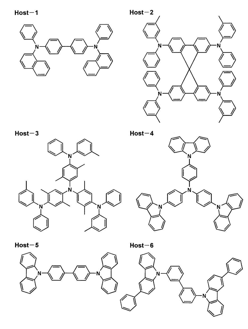
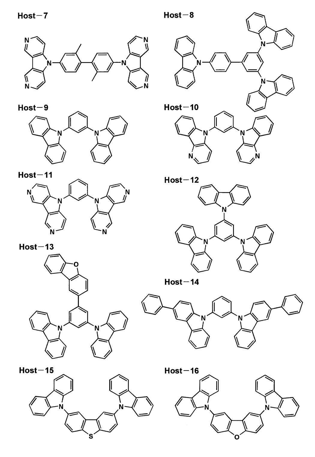

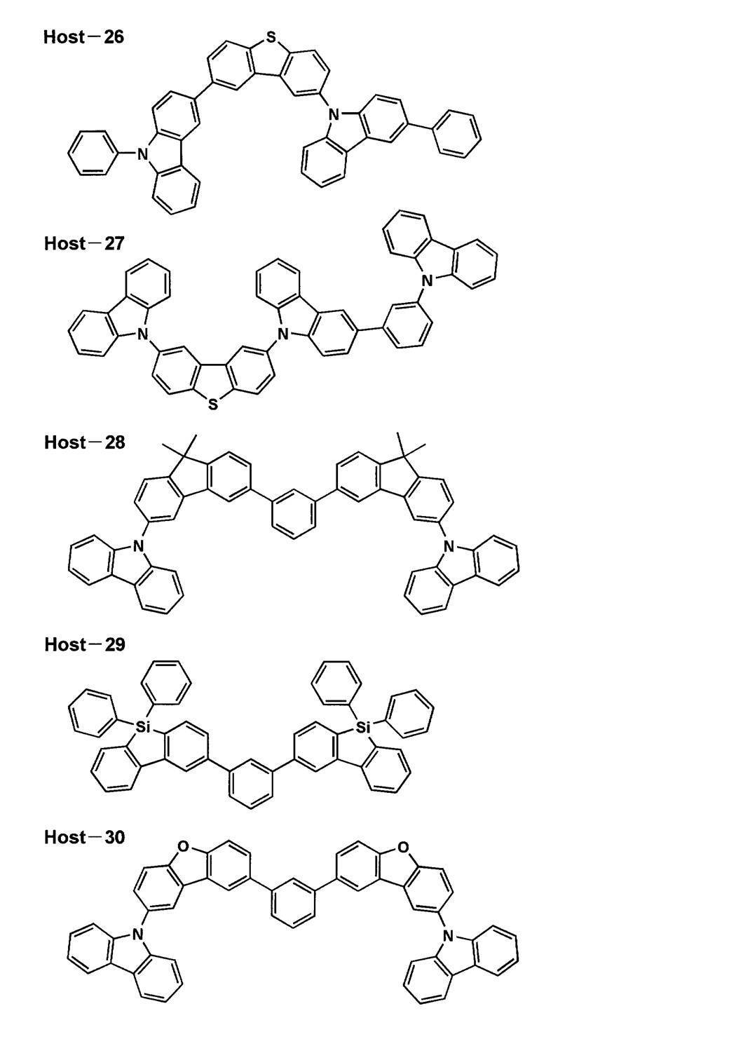
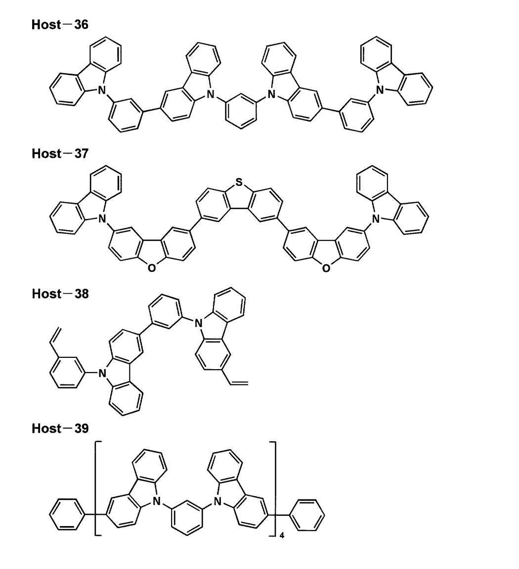


《陰極》
一方、陰極としては仕事関数の小さい(4eV以下)金属(電子注入性金属と称する)、合金、電気伝導性化合物及びこれらの混合物を電極物質とするものが用いられる。このような電極物質の具体例としては、ナトリウム、ナトリウム-カリウム合金、マグネシウム、リチウム、マグネシウム/銅混合物、マグネシウム/銀混合物、マグネシウム/アルミニウム混合物、マグネシウム/インジウム混合物、アルミニウム/酸化アルミニウム(Al2O3)混合物、インジウム、リチウム/アルミニウム混合物、希土類金属等が挙げられる。
一方、陰極としては仕事関数の小さい(4eV以下)金属(電子注入性金属と称する)、合金、電気伝導性化合物及びこれらの混合物を電極物質とするものが用いられる。このような電極物質の具体例としては、ナトリウム、ナトリウム-カリウム合金、マグネシウム、リチウム、マグネシウム/銅混合物、マグネシウム/銀混合物、マグネシウム/アルミニウム混合物、マグネシウム/インジウム混合物、アルミニウム/酸化アルミニウム(Al2O3)混合物、インジウム、リチウム/アルミニウム混合物、希土類金属等が挙げられる。
本発明においてはこれらの中で、電子注入性及び酸化等に対する耐久性の点から、電子注入性金属である周期表第1族または第2族に属する元素であって、該元素の金属イオン(Mn+)/金属(M)系の標準電極電位が-3Vvs.SHEよりも大きい元素の金属または金属化合物とこれより仕事関数の値が大きく安定な周期表第1族また第2族以外に属する元素の金属である第二金属との混合物、または第二金属のみ、例えば、マグネシウム/銀混合物、マグネシウム/アルミニウム混合物、マグネシウム/インジウム混合物、カリウム/アルミニウム混合物、アルミニウム等が用いられる。
陰極はこれらの電極物質を蒸着やスパッタリング等の方法により薄膜を形成させることにより、作製することができる。また、陰極としてのシート抵抗は数百Ω/□以下が好ましく、膜厚は通常10nm~5μm、好ましくは50nm~200nmの範囲で選ばれる。尚、発光した光を透過させるため、有機EL素子の陽極または陰極のいずれか一方が透明または半透明であれば発光輝度が向上し好都合である。
また、陰極に上記金属を1nm~20nmの膜厚で作製した後に、陽極の説明で挙げた導電性透明材料をその上に作製することで、透明または半透明の陰極を作製することができ、これを応用することで陽極と陰極の両方が透過性を有する素子を作製することができる。
《注入層:電子注入層(陰極バッファー層)、正孔注入層》
注入層は必要に応じて設け、電子注入層と正孔注入層があり、上記の如く陽極と発光層または正孔輸送層の間、及び陰極と発光層または電子輸送層との間に存在させてもよい。
注入層は必要に応じて設け、電子注入層と正孔注入層があり、上記の如く陽極と発光層または正孔輸送層の間、及び陰極と発光層または電子輸送層との間に存在させてもよい。
注入層とは、駆動電圧低下や発光輝度向上のために電極と有機層間に設けられる層のことで、「有機EL素子とその工業化最前線(1998年11月30日エヌ・ティー・エス社発行)」の第2編第2章「電極材料」(123~166頁)に詳細に記載されており、正孔注入層(陽極バッファー層)と電子注入層(陰極バッファー層)とがある。
陽極バッファー層(正孔注入層)は、特開平9-45479号公報、同9-260062号公報、同8-288069号公報等にもその詳細が記載されており、具体例として、銅フタロシアニンに代表されるフタロシアニンバッファー層、酸化バナジウムに代表される酸化物バッファー層、アモルファスカーボンバッファー層、ポリアニリン(エメラルディン)やポリチオフェン等の導電性高分子を用いた高分子バッファー層等が挙げられる。
陰極バッファー層(電子注入層)は、ストロンチウムやアルミニウム等に代表される金属バッファー層、酸化アルミニウムに代表される酸化物バッファー層、フッ化カリウムやフッ化カルシウムに代表される周期表第1族または第2族に属する元素であって、該元素の金属イオン(Mn+)/金属(M)系の標準電極電位が-3Vvs.SHEよりも大きい元素の金属または金属化合物のバッファー層等が挙げられる。
上記バッファー層(注入層)はごく薄い膜であることが望ましく、素材にもよるがその膜厚は0.1nm~5μmの範囲が好ましい。
本発明の有機EL素子においては、上記の陰極または陰極に接する構成層(例えば、電子注入層(陰極バッファー層))中に、周期表の第1族または第2族に属する元素であり、該元素の金属イオン(Mn+)/金属(M)系の標準電極電位が-3Vvs.SHEよりも大きい元素の金属または金属化合物を含有することが特徴である。
ここで、金属化合物とは、塩化物や錯体、金属有機化合物などをいう。
本発明に係るMn+/M系の標準電極電位E°は、温度25℃、溶質の活量がすべて1の水溶液中における、標準水素電極に対する電極電位であり、例えば「改定第3版 化学便覧 基礎編II」(日本化学会編)のII-474ページ、表12・46の値を参考にできる。
また、本発明に係る、周期表の第1族または第2族に属する元素であり、該元素の金属イオン(Mn+)/金属(M)系の標準電極電位が-3Vvs.SHEよりも大きい元素の金属または金属化合物を構成する元素としては、具体的には、K(-2.925(V))、Ca(-2.840(V))、Na(-2.714(V))、Mg(-2.356(V))、Cs(-2.923(V))等を挙げることができる。特に、電子注入性及び安定性の観点からK、Na、Csが好ましい。
《阻止層:正孔阻止層、電子阻止層》
阻止層は、上記の如く有機化合物薄膜の基本構成層の他に必要に応じて設けられるものである。例えば、特開平11-204258号公報、同11-204359号公報、及び「有機EL素子とその工業化最前線(1998年11月30日エヌ・ティー・エス社発行)」の237頁等に記載されている正孔阻止(ホールブロック)層がある。
阻止層は、上記の如く有機化合物薄膜の基本構成層の他に必要に応じて設けられるものである。例えば、特開平11-204258号公報、同11-204359号公報、及び「有機EL素子とその工業化最前線(1998年11月30日エヌ・ティー・エス社発行)」の237頁等に記載されている正孔阻止(ホールブロック)層がある。
正孔阻止層とは広い意味では電子輸送層の機能を有し、電子を輸送する機能を有しつつ正孔を輸送する能力が著しく小さい正孔阻止材料からなり、電子を輸送しつつ正孔を阻止することで電子と正孔の再結合確率を向上させることができる。
また、後述する電子輸送層の構成を必要に応じて、本発明に係わる正孔阻止層として用いることができる。
本発明の有機EL素子の正孔阻止層は、発光層に隣接して設けられていることが好ましい。
正孔阻止層には、前述のホスト化合物として挙げた、カルバゾール誘導体、カルボリン誘導体、ジアザカルバゾール誘導体(ここで、ジアザカルバゾール誘導体とは、カルボリン環を構成する炭素原子のいずれかひとつが窒素原子で置き換わったものを示す)を含有することが好ましい。
また、本発明においては、複数の発光色の異なる複数の発光層を有する場合、その発光極大波長が最も短波にある発光層が、全発光層中、最も陽極に近いことが好ましいが、このような場合、該最短波層と該層の次に陽極に近い発光層との間に正孔阻止層を追加して設けることが好ましい。更には、該位置に設けられる正孔阻止層に含有される化合物の50質量%以上が、前記最短波発光層のホスト化合物に対しそのイオン化ポテンシャルが0.3eV以上大きいことが好ましい。
イオン化ポテンシャルは化合物のHOMO(最高占有軌道)レベルにある電子を真空準位に放出するのに必要なエネルギーで定義され、例えば下記に示すような方法により求めることができる。
(1)米国Gaussian社製の分子軌道計算用ソフトウェアであるGaussian98(Gaussian98、Revision A.11.4,M.J.Frisch,et al,Gaussian,Inc.,Pittsburgh PA,2002.)を用い、キーワードとしてB3LYP/6-31G*を用いて構造最適化を行うことにより算出した値(eV単位換算値)として求めることができる。この計算値が有効な背景には、この手法で求めた計算値と実験値の相関が高いためである。
(2)イオン化ポテンシャルは光電子分光法で直接測定する方法により求めることもできる。例えば、理研計器社製の低エネルギー電子分光装置「Model AC-1」を用いて、あるいは紫外光電子分光として知られている方法を好適に用いることができる。
一方、電子阻止層とは広い意味では正孔輸送層の機能を有し、正孔を輸送する機能を有しつつ電子を輸送する能力が著しく小さい材料からなり、正孔を輸送しつつ電子を阻止することで電子と正孔の再結合確率を向上させることができる。
また、後述する正孔輸送層の構成を必要に応じて電子阻止層として用いることができる。本発明に係る正孔阻止層、電子輸送層の膜厚としては、好ましくは3nm~100nmであり、更に好ましくは5nm~30nmである。
《正孔輸送層》
正孔輸送層とは正孔を輸送する機能を有する正孔輸送材料からなり、広い意味で正孔注入層、電子阻止層も正孔輸送層に含まれる。正孔輸送層は単層または複数層設けることができる。
正孔輸送層とは正孔を輸送する機能を有する正孔輸送材料からなり、広い意味で正孔注入層、電子阻止層も正孔輸送層に含まれる。正孔輸送層は単層または複数層設けることができる。
正孔輸送材料としては、正孔の注入または輸送、電子の障壁性のいずれかを有するものであり、有機物、無機物のいずれであってもよい。
例えば、トリアゾール誘導体、オキサジアゾール誘導体、イミダゾール誘導体、ポリアリールアルカン誘導体、ピラゾリン誘導体及びピラゾロン誘導体、フェニレンジアミン誘導体、アリールアミン誘導体、アミノ置換カルコン誘導体、オキサゾール誘導体、スチリルアントラセン誘導体、フルオレノン誘導体、ヒドラゾン誘導体、スチルベン誘導体、シラザン誘導体、アニリン系共重合体、また導電性高分子オリゴマー、特にチオフェンオリゴマー等が挙げられる。
正孔輸送材料としては上記のものを使用することができるが、ポルフィリン化合物、芳香族第3級アミン化合物及びスチリルアミン化合物、特に芳香族第3級アミン化合物を用いることが好ましい。
芳香族第3級アミン化合物及びスチリルアミン化合物の代表例としては、N,N,N′,N′-テトラフェニル-4,4′-ジアミノフェニル;N,N′-ジフェニル-N,N′-ビス(3-メチルフェニル)-〔1,1′-ビフェニル〕-4,4′-ジアミン(TPD);2,2-ビス(4-ジ-p-トリルアミノフェニル)プロパン;1,1-ビス(4-ジ-p-トリルアミノフェニル)シクロヘキサン;N,N,N′,N′-テトラ-p-トリル-4,4′-ジアミノビフェニル;1,1-ビス(4-ジ-p-トリルアミノフェニル)-4-フェニルシクロヘキサン;ビス(4-ジメチルアミノ-2-メチルフェニル)フェニルメタン;ビス(4-ジ-p-トリルアミノフェニル)フェニルメタン;N,N′-ジフェニル-N,N′-ジ(4-メトキシフェニル)-4,4′-ジアミノビフェニル;N,N,N′,N′-テトラフェニル-4,4′-ジアミノジフェニルエーテル;4,4′-ビス(ジフェニルアミノ)クオードリフェニル;N,N,N-トリ(p-トリル)アミン;4-(ジ-p-トリルアミノ)-4′-〔4-(ジ-p-トリルアミノ)スチリル〕スチルベン;4-N,N-ジフェニルアミノ-(2-ジフェニルビニル)ベンゼン;3-メトキシ-4′-N,N-ジフェニルアミノスチルベンゼン;N-フェニルカルバゾール、更には米国特許第5,061,569号明細書に記載されている2個の縮合芳香族環を分子内に有するもの、例えば、4,4′-ビス〔N-(1-ナフチル)-N-フェニルアミノ〕ビフェニル(NPD)、特開平4-308688号公報に記載されているトリフェニルアミンユニットが3つスターバースト型に連結された4,4′,4″-トリス〔N-(3-メチルフェニル)-N-フェニルアミノ〕トリフェニルアミン(MTDATA)等が挙げられる。
更にこれらの材料を高分子鎖に導入した、またはこれらの材料を高分子の主鎖とした高分子材料を用いることもできる。
また、p型-Si、p型-SiC等の無機化合物も正孔注入材料、正孔輸送材料として使用することができる。
また、特開平11-251067号公報、J.Huang et.al.著文献(Applied Physics Letters 80(2002),p.139)に記載されているような、所謂p型正孔輸送材料を用いることもできる。本発明においては、より高効率の発光素子が得られることからこれらの材料を用いることが好ましい。
正孔輸送層は上記正孔輸送材料を、例えば、真空蒸着法、スピンコート法、キャスト法、インクジェット法を含む印刷法、LB法等の公知の方法により、薄膜化することにより形成することができる。
正孔輸送層の膜厚については特に制限はないが、通常は5nm~5μm程度、好ましくは5nm~200nmである。この正孔輸送層は上記材料の一種または2種以上からなる一層構造であってもよい。
また、不純物をドープしたp性の高い正孔輸送層を用いることもできる。その例としては、特開平4-297076号公報、特開2000-196140号公報、同2001-102175号公報の各公報、J.Appl.Phys.,95,5773(2004)等に記載されたものが挙げられる。
本発明においては、このようなp性の高い正孔輸送層を用いることが、より低消費電力の素子を作製することができるため好ましい。
以下、本発明の有機EL素子の正孔輸送層の形成に好ましく用いられる化合物の具体例を挙げるが、本発明はこれらに限定されない。


《陽極》
有機EL素子における陽極としては、仕事関数の大きい(4eV以上)金属、合金、電気伝導性化合物及びこれらの混合物を電極物質とするものが好ましく用いられる。このような電極物質の具体例としては、Au等の金属、CuI、インジウムチンオキシド(ITO)、SnO2、ZnO等の導電性透明材料が挙げられる。
有機EL素子における陽極としては、仕事関数の大きい(4eV以上)金属、合金、電気伝導性化合物及びこれらの混合物を電極物質とするものが好ましく用いられる。このような電極物質の具体例としては、Au等の金属、CuI、インジウムチンオキシド(ITO)、SnO2、ZnO等の導電性透明材料が挙げられる。
また、IDIXO(In2O3-ZnO)等非晶質で透明導電膜を作製可能な材料を用いてもよい。陽極はこれらの電極物質を蒸着やスパッタリング等の方法により薄膜を形成させ、フォトリソグラフィー法で所望の形状のパターンを形成してもよく、あるいはパターン精度をあまり必要としない場合は(100μm以上程度)、上記電極物質の蒸着やスパッタリング時に所望の形状のマスクを介してパターンを形成してもよい。
あるいは、有機導電性化合物のように塗布可能な物質を用いる場合には、印刷方式、コーティング方式等湿式成膜法を用いることもできる。この陽極より発光を取り出す場合には、透過率を10%より大きくすることが望ましく、また陽極としてのシート抵抗は数百Ω/□以下が好ましい。
更に膜厚は材料にもよるが、通常10nm~1000nm、好ましくは10nm~200nmの範囲で選ばれる。
《支持基板》
本発明の有機EL素子に用いることのできる支持基板(以下、基体、基板、基材、支持体等とも言う)としては、ガラス、プラスチック等の種類には特に限定はなく、また透明であっても不透明であってもよい。支持基板側から光を取り出す場合には、支持基板は透明であることが好ましい。好ましく用いられる透明な支持基板としては、ガラス、石英、透明樹脂フィルムを挙げることができる。特に好ましい支持基板は、有機EL素子にフレキシブル性を与えることが可能な樹脂フィルムである。
本発明の有機EL素子に用いることのできる支持基板(以下、基体、基板、基材、支持体等とも言う)としては、ガラス、プラスチック等の種類には特に限定はなく、また透明であっても不透明であってもよい。支持基板側から光を取り出す場合には、支持基板は透明であることが好ましい。好ましく用いられる透明な支持基板としては、ガラス、石英、透明樹脂フィルムを挙げることができる。特に好ましい支持基板は、有機EL素子にフレキシブル性を与えることが可能な樹脂フィルムである。
樹脂フィルムとしては、例えば、ポリエチレンテレフタレート(PET)、ポリエチレンナフタレート(PEN)等のポリエステル、ポリエチレン、ポリプロピレン、セロファン、セルロースジアセテート、セルローストリアセテート、セルロースアセテートブチレート、セルロースアセテートプロピオネート(CAP)、セルロースアセテートフタレート(TAC)、セルロースナイトレート等のセルロースエステル類またはそれらの誘導体、ポリ塩化ビニリデン、ポリビニルアルコール、ポリエチレンビニルアルコール、シンジオタクティックポリスチレン、ポリカーボネート、ノルボルネン樹脂、ポリメチルペンテン、ポリエーテルケトン、ポリイミド、ポリエーテルスルホン(PES)、ポリフェニレンスルフィド、ポリスルホン類、ポリエーテルイミド、ポリエーテルケトンイミド、ポリアミド、フッ素樹脂、ナイロン、ポリメチルメタクリレート、アクリルあるいはポリアリレート類、アートン(商品名JSR社製)あるいはアペル(商品名三井化学社製)といったシクロオレフィン系樹脂等を挙げられる。
樹脂フィルムの表面には、無機物、有機物の被膜またはその両者のハイブリッド被膜が形成されていてもよく、JIS K 7129-1992に準拠した方法で測定された、水蒸気透過度(25±0.5℃、相対湿度(90±2)%RH)が0.01g/(m2・24h)以下のバリア性フィルムであることが好ましく、更には、JIS K 7126-1987に準拠した方法で測定された酸素透過度が、10-3ml/(m2・24h・atm)以下、水蒸気透過度が、10-5g/(m2・24h)以下の高バリア性フィルムであることが好ましい。
バリア膜を形成する材料としては、水分や酸素等素子の劣化をもたらすものの浸入を抑制する機能を有する材料であればよく、例えば、酸化珪素、二酸化珪素、窒化珪素等を用いることができる。更に該膜の脆弱性を改良するために、これら無機層と有機材料からなる層の積層構造を持たせることがより好ましい。無機層と有機層の積層順については特に制限はないが、両者を交互に複数回積層させることが好ましい。
バリア膜の形成方法については特に限定はなく、例えば、真空蒸着法、スパッタリング法、反応性スパッタリング法、分子線エピタキシー法、クラスタ-イオンビーム法、イオンプレーティング法、プラズマ重合法、大気圧プラズマ重合法、プラズマCVD法、レーザーCVD法、熱CVD法、コーティング法等を用いることができるが、特開2004-68143号公報に記載されているような大気圧プラズマ重合法によるものが特に好ましい。
不透明な支持基板としては、例えば、アルミ、ステンレス等の金属板、フィルムや不透明樹脂基板、セラミック製の基板等が挙げられる。
本発明の有機EL素子の発光の室温における外部取り出し効率は、1%以上であることが好ましく、より好ましくは5%以上である。
ここに、外部取り出し量子効率(%)=有機EL素子外部に発光した光子数/有機EL素子に流した電子数×100である。
また、カラーフィルター等の色相改良フィルター等を併用しても、有機EL素子からの発光色を蛍光体を用いて多色へ変換する色変換フィルターを併用してもよい。色変換フィルターを用いる場合においては、有機EL素子の発光のλmaxは480nm以下が好ましい。
《有機EL素子の製造方法》
有機EL素子の製造方法の一例として、陽極/正孔注入層/正孔輸送層/発光層/正孔阻止層/電子輸送層/陰極バッファー層(電子注入層)/陰極からなる素子の製造方法について説明する。
有機EL素子の製造方法の一例として、陽極/正孔注入層/正孔輸送層/発光層/正孔阻止層/電子輸送層/陰極バッファー層(電子注入層)/陰極からなる素子の製造方法について説明する。
まず、適当な基体上に所望の電極物質、例えば、陽極用物質からなる薄膜を1μm以下、好ましくは10nm~200nmの膜厚になるように形成させ、陽極を作製する。
次に、この上に素子材料である正孔注入層、正孔輸送層、発光層、正孔阻止層、電子輸送層、陰極バッファー層等の有機化合物を含有する薄膜を形成させる。
湿式法としては、スピンコート法、キャスト法、ダイコート法、ブレードコート法、ロールコート法、インクジェット法、印刷法、スプレーコート法、カーテンコート法、LB法等があるが、精密な薄膜が形成可能で、且つ高生産性の点から、ダイコート法、ロールコート法、インクジェット法、スプレーコート法などのロール・ツー・ロール方式適性の高い方法が好ましい。また、層ごとに異なる製膜法を適用してもよい。
本発明に係る有機EL材料を溶解または分散する液媒体としては、例えば、メチルエチルケトン、シクロヘキサノン等のケトン類、酢酸エチル等の脂肪酸エステル類、ジクロロベンゼン等のハロゲン化炭化水素類、トルエン、キシレン、メシチレン、シクロヘキシルベンゼン等の芳香族炭化水素類、シクロヘキサン、デカリン、ドデカン等の脂肪族炭化水素類、DMF、DMSO等の有機溶媒を用いることができる。
また、分散方法としては、超音波、高剪断力分散やメディア分散等の分散方法により分散することができる。
これらの層の形成後、その上に陰極用物質からなる薄膜を1μm以下、好ましくは50nm~200nmの範囲の膜厚になるように形成させ、陰極を設けることにより所望の有機EL素子が得られる。
また、順序を逆にして、陰極、陰極バッファー層、電子輸送層、正孔阻止層、発光層、正孔輸送層、正孔注入層、陽極の順に作製することも可能である。
このようにして得られた多色の表示装置に、直流電圧を印加する場合には陽極を+、陰極を-の極性として電圧2V~40V程度を印加すると発光が観測できる。また交流電圧を印加してもよい。尚、印加する交流の波形は任意でよい。
本発明の有機EL素子の作製は、一回の真空引きで一貫して正孔注入層から陰極まで作製するのが好ましいが、途中で取り出して異なる製膜法を施しても構わない。その際、作業を乾燥不活性ガス雰囲気下で行うことが好ましい。
《封止》
本発明に用いられる封止手段としては、例えば、封止部材と電極、支持基板とを接着剤で接着する方法を挙げることができる。
本発明に用いられる封止手段としては、例えば、封止部材と電極、支持基板とを接着剤で接着する方法を挙げることができる。
封止部材としては、有機EL素子の表示領域を覆うように配置されておればよく、凹板状でも平板状でもよい。また透明性、電気絶縁性は特に問わない。
具体的には、ガラス板、ポリマー板・フィルム、金属板・フィルム等が挙げられる。ガラス板としては、特にソーダ石灰ガラス、バリウム・ストロンチウム含有ガラス、鉛ガラス、アルミノケイ酸ガラス、ホウケイ酸ガラス、バリウムホウケイ酸ガラス、石英等を挙げることができる。
また、ポリマー板としては、ポリカーボネート、アクリル、ポリエチレンテレフタレート、ポリエーテルサルファイド、ポリサルフォン等を挙げることができる。金属板としては、ステンレス、鉄、銅、アルミニウム、マグネシウム、ニッケル、亜鉛、クロム、チタン、モリブテン、シリコン、ゲルマニウム及びタンタルからなる群から選ばれる一種以上の金属または合金からなるものが挙げられる。
本発明においては、素子を薄膜化できるということからポリマーフィルム、金属フィルムを好ましく使用することができる。
更には、ポリマーフィルムは、JIS K 7126-1987に準拠した方法で測定された酸素透過度が1×10⁻³ml/(m2・24h・atm)以下、JIS K 7129-1992に準拠した方法で測定された、水蒸気透過度(25±0.5℃、相対湿度(90±2)%RH)が、1×10⁻³g/(m2・24h)以下のものであることが好ましい。
封止部材を凹状に加工するのは、サンドブラスト加工、化学エッチング加工等が使われる。
接着剤として具体的には、アクリル酸系オリゴマー、メタクリル酸系オリゴマーの反応性ビニル基を有する光硬化及び熱硬化型接着剤、2-シアノアクリル酸エステル等の湿気硬化型等の接着剤を挙げることができる。また、エポキシ系等の熱及び化学硬化型(二液混合)を挙げることができる。また、ホットメルト型のポリアミド、ポリエステル、ポリオレフィンを挙げることができる。また、カチオン硬化タイプの紫外線硬化型エポキシ樹脂接着剤を挙げることができる。
なお、有機EL素子が熱処理により劣化する場合があるので、室温から80℃までに接着硬化できるものが好ましい。また、前記接着剤中に乾燥剤を分散させておいてもよい。封止部分への接着剤の塗布は市販のディスペンサーを使ってもよいし、スクリーン印刷のように印刷してもよい。
また、有機層を挟み支持基板と対向する側の電極の外側に該電極と有機層を被覆し、支持基板と接する形で無機物、有機物の層を形成し封止膜とすることも好適にできる。この場合、該膜を形成する材料としては、水分や酸素等素子の劣化をもたらすものの浸入を抑制する機能を有する材料であればよく、例えば、酸化珪素、二酸化珪素、窒化珪素等を用いることができる。
更に、該膜の脆弱性を改良するために、これら無機層と有機材料からなる層の積層構造を持たせることが好ましい。これらの膜の形成方法については、特に限定はなく、例えば真空蒸着法、スパッタリング法、反応性スパッタリング法、分子線エピタキシー法、クラスタ-イオンビーム法、イオンプレーティング法、プラズマ重合法、大気圧プラズマ重合法、プラズマCVD法、レーザーCVD法、熱CVD法、コーティング法等を用いることができる。
封止部材と有機EL素子の表示領域との間隙には、気相及び液相では、窒素、アルゴン等の不活性気体やフッ化炭化水素、シリコンオイルのような不活性液体を注入することが好ましい。また真空とすることも可能である。また、内部に吸湿性化合物を封入することもできる。
吸湿性化合物としては、例えば、金属酸化物(例えば、酸化ナトリウム、酸化カリウム、酸化カルシウム、酸化バリウム、酸化マグネシウム、酸化アルミニウム等)、硫酸塩(例えば、硫酸ナトリウム、硫酸カルシウム、硫酸マグネシウム、硫酸コバルト等)、金属ハロゲン化物(例えば、塩化カルシウム、塩化マグネシウム、フッ化セシウム、フッ化タンタル、臭化セリウム、臭化マグネシウム、沃化バリウム、沃化マグネシウム等)、過塩素酸類(例えば、過塩素酸バリウム、過塩素酸マグネシウム等)等が挙げられ、硫酸塩、金属ハロゲン化物及び過塩素酸類においては無水塩が好適に用いられる。
《保護膜、保護板》
有機層を挟み支持基板と対向する側の前記封止膜、あるいは前記封止用フィルムの外側に、素子の機械的強度を高めるために保護膜、あるいは保護板を設けてもよい。特に封止が前記封止膜により行われている場合には、その機械的強度は必ずしも高くないため、このような保護膜、保護板を設けることが好ましい。これに使用することができる材料としては、前記封止に用いたのと同様なガラス板、ポリマー板・フィルム、金属板・フィルム等を用いることができるが、軽量且つ薄膜化ということからポリマーフィルムを用いることが好ましい。
有機層を挟み支持基板と対向する側の前記封止膜、あるいは前記封止用フィルムの外側に、素子の機械的強度を高めるために保護膜、あるいは保護板を設けてもよい。特に封止が前記封止膜により行われている場合には、その機械的強度は必ずしも高くないため、このような保護膜、保護板を設けることが好ましい。これに使用することができる材料としては、前記封止に用いたのと同様なガラス板、ポリマー板・フィルム、金属板・フィルム等を用いることができるが、軽量且つ薄膜化ということからポリマーフィルムを用いることが好ましい。
《光取り出し》
有機EL素子は空気よりも屈折率の高い(屈折率が1.7~2.1程度)層の内部で発光し、発光層で発生した光のうち15%から20%程度の光しか取り出せないことが一般的に言われている。これは、臨界角以上の角度θで界面(透明基板と空気との界面)に入射する光は、全反射を起こし素子外部に取り出すことができないことや、透明電極ないし発光層と透明基板との間で光が全反射を起こし、光が透明電極ないし発光層を導波し、結果として光が素子側面方向に逃げるためである。
有機EL素子は空気よりも屈折率の高い(屈折率が1.7~2.1程度)層の内部で発光し、発光層で発生した光のうち15%から20%程度の光しか取り出せないことが一般的に言われている。これは、臨界角以上の角度θで界面(透明基板と空気との界面)に入射する光は、全反射を起こし素子外部に取り出すことができないことや、透明電極ないし発光層と透明基板との間で光が全反射を起こし、光が透明電極ないし発光層を導波し、結果として光が素子側面方向に逃げるためである。
この光の取り出しの効率を向上させる手法としては、例えば、透明基板表面に凹凸を形成し、透明基板と空気界面での全反射を防ぐ方法(米国特許第4,774,435号明細書)、基板に集光性を持たせることにより効率を向上させる方法(特開昭63-314795号公報)、素子の側面等に反射面を形成する方法(特開平1-220394号公報)、基板と発光体の間に中間の屈折率を持つ平坦層を導入し、反射防止膜を形成する方法(特開昭62-172691号公報)、基板と発光体の間に基板よりも低屈折率を持つ平坦層を導入する方法(特開2001-202827号公報)、基板、透明電極層や発光層のいずれかの層間(含む、基板と外界間)に回折格子を形成する方法(特開平11-283751号公報)等がある。
本発明においては、これらの方法を本発明の有機EL素子と組み合わせて用いることができるが、基板と発光体の間に基板よりも低屈折率を持つ平坦層を導入する方法、あるいは基板、透明電極層や発光層のいずれかの層間(含む、基板と外界間)に回折格子を形成する方法を好適に用いることができる。
本発明はこれらの手段を組み合わせることにより、更に高輝度あるいは耐久性に優れた素子を得ることができる。
透明電極と透明基板の間に低屈折率の媒質を光の波長よりも長い厚みで形成すると、透明電極から出てきた光は、媒質の屈折率が低いほど外部への取り出し効率が高くなる。
低屈折率層としては、例えば、エアロゲル、多孔質シリカ、フッ化マグネシウム、フッ素系ポリマー等が挙げられる。透明基板の屈折率は一般に1.5~1.7程度であるので、低屈折率層は屈折率がおよそ1.5以下であることが好ましい。また、更に1.35以下であることが好ましい。
また、低屈折率媒質の厚みは媒質中の波長の2倍以上となるのが望ましい。これは低屈折率媒質の厚みが、光の波長程度になってエバネッセントで染み出した電磁波が基板内に入り込む膜厚になると、低屈折率層の効果が薄れるからである。
全反射を起こす界面もしくはいずれかの媒質中に回折格子を導入する方法は、光取り出し効率の向上効果が高いという特徴がある。この方法は回折格子が1次の回折や2次の回折といった所謂ブラッグ回折により、光の向きを屈折とは異なる特定の向きに変えることができる性質を利用して、発光層から発生した光のうち層間での全反射等により外に出ることができない光を、いずれかの層間もしくは、媒質中(透明基板内や透明電極内)に回折格子を導入することで光を回折させ、光を外に取り出そうとするものである。
導入する回折格子は、二次元的な周期屈折率を持っていることが望ましい。これは発光層で発光する光はあらゆる方向にランダムに発生するので、ある方向にのみ周期的な屈折率分布を持っている一般的な1次元回折格子では、特定の方向に進む光しか回折されず、光の取り出し効率がさほど上がらない。
しかしながら、屈折率分布を二次元的な分布にすることにより、あらゆる方向に進む光が回折され、光の取り出し効率が上がる。
回折格子を導入する位置としては前述の通り、いずれかの層間もしくは媒質中(透明基板内や透明電極内)でもよいが、光が発生する場所である有機発光層の近傍が望ましい。
このとき、回折格子の周期は媒質中の光の波長の約1/2~3倍程度が好ましい。
回折格子の配列は正方形のラチス状、三角形のラチス状、ハニカムラチス状等、2次元的に配列が繰り返されることが好ましい。
《集光シート》
本発明の有機EL素子は基板の光取り出し側に、例えば、マイクロレンズアレイ状の構造を設けるように加工する、または、所謂集光シートと組み合わせることにより、特定方向、例えば、素子発光面に対し正面方向に集光することにより、特定方向上の輝度を高めることができる。
本発明の有機EL素子は基板の光取り出し側に、例えば、マイクロレンズアレイ状の構造を設けるように加工する、または、所謂集光シートと組み合わせることにより、特定方向、例えば、素子発光面に対し正面方向に集光することにより、特定方向上の輝度を高めることができる。
マイクロレンズアレイの例としては、基板の光取り出し側に一辺が30μmでその頂角が90度となるような四角錐を2次元に配列する。一辺は10μm~100μmが好ましい。これより小さくなると回折の効果が発生して色付く、大きすぎると厚みが厚くなり好ましくない。
集光シートとしては、例えば、液晶表示装置のLEDバックライトで実用化されているものを用いることが可能である。このようなシートとして、例えば、住友スリーエム社製輝度上昇フィルム(BEF)等を用いることができる。
プリズムシートの形状としては、例えば、基材に頂角90度、ピッチ50μmの△状のストライプが形成されたものであってもよいし、頂角が丸みを帯びた形状、ピッチをランダムに変化させた形状、その他の形状であってもよい。
また、発光素子からの光放射角を制御するために、光拡散板・フィルムを集光シートと併用してもよい。例えば、(株)きもと製拡散フィルム(ライトアップ)等を用いることができる。
《用途》
本発明の有機EL素子は、表示デバイス、ディスプレイ、各種発光光源として用いることができる。発光光源として、例えば、照明装置(家庭用照明、車内照明)、時計や液晶用バックライト、看板広告、信号機、光記憶媒体の光源、電子写真複写機の光源、光通信処理機の光源、光センサーの光源等が挙げられるがこれに限定するものではないが、特に液晶表示装置のバックライト、照明用光源としての用途に有効に用いることができる。
本発明の有機EL素子は、表示デバイス、ディスプレイ、各種発光光源として用いることができる。発光光源として、例えば、照明装置(家庭用照明、車内照明)、時計や液晶用バックライト、看板広告、信号機、光記憶媒体の光源、電子写真複写機の光源、光通信処理機の光源、光センサーの光源等が挙げられるがこれに限定するものではないが、特に液晶表示装置のバックライト、照明用光源としての用途に有効に用いることができる。
本発明の有機EL素子においては、必要に応じ成膜時にメタルマスクやインクジェットプリンティング法等でパターニングを施してもよい。パターニングする場合は、電極のみをパターニングしてもよいし、電極と発光層をパターニングしてもよいし、素子全層をパターニングしてもよく、素子の作製においては、従来公知の方法を用いることができる。
本発明の有機EL素子や本発明に係る化合物の発光する色は、「新編色彩科学ハンドブック」(日本色彩学会編、東京大学出版会、1985)の108頁の図4.16において、分光放射輝度計CS-1000(コニカミノルタセンシング(株)製)で測定した結果をCIE色度座標に当てはめたときの色で決定される。
また、本発明の有機EL素子が白色素子の場合には、白色とは、2度視野角正面輝度を上記方法により測定した際に、1000cd/m2でのCIE1931表色系における色度がX=0.33±0.07、Y=0.33±0.1の領域内にあることを言う。
《表示装置》
本発明の表示装置について説明する。本発明の表示装置は、本発明の有機EL素子を具備したものである。
本発明の表示装置について説明する。本発明の表示装置は、本発明の有機EL素子を具備したものである。
本発明の表示装置は単色でも多色でもよいが、ここでは多色表示装置について説明する。多色表示装置の場合は発光層形成時のみシャドーマスクを設け、一面に蒸着法、キャスト法、スピンコート法、インクジェット法、印刷法等で膜を形成できる。
発光層のみパターニングを行う場合、その方法に限定はないが、好ましくは蒸着法、インクジェット法、スピンコート法、印刷法である。
表示装置に具備される有機EL素子の構成は、必要に応じて上記の有機EL素子の構成例の中から選択される。
また、有機EL素子の製造方法は、上記の本発明の有機EL素子の製造の一態様に示したとおりである。
得られた多色表示装置に直流電圧を印加する場合には、陽極を+、陰極を-の極性として電圧2V~40V程度を印加すると発光が観測できる。また、逆の極性で電圧を印加しても電流は流れずに発光は全く生じない。更に交流電圧を印加する場合には、陽極が+、陰極が-の状態になったときのみ発光する。尚、印加する交流の波形は任意でよい。
多色表示装置は、表示デバイス、ディスプレイ、各種発光光源として用いることができる。表示デバイス、ディスプレイにおいて、青、赤、緑発光の3種の有機EL素子を用いることによりフルカラーの表示が可能となる。
表示デバイス、ディスプレイとしては、テレビ、パソコン、モバイル機器、AV機器、文字放送表示、自動車内の情報表示等が挙げられる。特に静止画像や動画像を再生する表示装置として使用してもよく、動画再生用の表示装置として使用する場合の駆動方式は単純マトリクス(パッシブマトリクス)方式でもアクティブマトリクス方式でもどちらでもよい。
発光光源としては家庭用照明、車内照明、時計や液晶用のバックライト、看板広告、信号機、光記憶媒体の光源、電子写真複写機の光源、光通信処理機の光源、光センサーの光源等が挙げられるが、本発明はこれらに限定されない。
以下、本発明の有機EL素子を有する表示装置の一例を図面に基づいて説明する。
図1は有機EL素子から構成される表示装置の一例を示した模式図である。有機EL素子の発光により画像情報の表示を行う、例えば、携帯電話等のディスプレイの模式図である。
ディスプレイ1は複数の画素を有する表示部A、画像情報に基づいて表示部Aの画像走査を行う制御部B等からなる。
制御部Bは表示部Aと電気的に接続され、複数の画素それぞれに外部からの画像情報に基づいて走査信号と画像データ信号を送り、走査信号により走査線毎の画素が画像データ信号に応じて順次発光して画像走査を行って画像情報を表示部Aに表示する。
図2は表示部Aの模式図である。
表示部Aは基板上に、複数の走査線5及びデータ線6を含む配線部と複数の画素3等とを有する。表示部Aの主要な部材の説明を以下に行う。
図においては、画素3の発光した光が白矢印方向(下方向)へ取り出される場合を示している。
配線部の走査線5及び複数のデータ線6はそれぞれ導電材料からなり、走査線5とデータ線6は格子状に直交して、直交する位置で画素3に接続している(詳細は図示していない)。
画素3は走査線5から走査信号が印加されると、データ線6から画像データ信号を受け取り、受け取った画像データに応じて発光する。
発光の色が赤領域の画素、緑領域の画素、青領域の画素を適宜同一基板上に並置することによって、フルカラー表示が可能となる。
次に、画素の発光プロセスを説明する。
図3は画素の模式図である。
画素は有機EL素子10、スイッチングトランジスタ11、駆動トランジスタ12、コンデンサ13等を備えている。複数の画素に有機EL素子10として、赤色、緑色、青色発光の有機EL素子を用い、これらを同一基板上に並置することでフルカラー表示を行うことができる。
図3において、制御部Bからデータ線6を介してスイッチングトランジスタ11のドレインに画像データ信号が印加される。そして、制御部Bから走査線5を介してスイッチングトランジスタ11のゲートに走査信号が印加されると、スイッチングトランジスタ11の駆動がオンし、ドレインに印加された画像データ信号がコンデンサ13と駆動トランジスタ12のゲートに伝達される。
画像データ信号の伝達により、コンデンサ13が画像データ信号の電位に応じて充電されるとともに、駆動トランジスタ12の駆動がオンする。駆動トランジスタ12は、ドレインが電源ライン7に接続され、ソースが有機EL素子10の電極に接続されており、ゲートに印加された画像データ信号の電位に応じて電源ライン7から有機EL素子10に電流が供給される。
制御部Bの順次走査により走査信号が次の走査線5に移ると、スイッチングトランジスタ11の駆動がオフする。しかし、スイッチングトランジスタ11の駆動がオフしてもコンデンサ13は充電された画像データ信号の電位を保持するので、駆動トランジスタ12の駆動はオン状態が保たれて、次の走査信号の印加が行われるまで有機EL素子10の発光が継続する。順次走査により次に走査信号が印加されたとき、走査信号に同期した次の画像データ信号の電位に応じて駆動トランジスタ12が駆動して有機EL素子10が発光する。
即ち、有機EL素子10の発光は、複数の画素それぞれの有機EL素子10に対して、アクティブ素子であるスイッチングトランジスタ11と駆動トランジスタ12を設けて、複数の画素3それぞれの有機EL素子10の発光を行っている。このような発光方法をアクティブマトリクス方式と呼んでいる。
ここで、有機EL素子10の発光は複数の階調電位を持つ多値の画像データ信号による複数の階調の発光でもよいし、2値の画像データ信号による所定の発光量のオン、オフでもよい。また、コンデンサ13の電位の保持は次の走査信号の印加まで継続して保持してもよいし、次の走査信号が印加される直前に放電させてもよい。
本発明においては、上述したアクティブマトリクス方式に限らず、走査信号が走査されたときのみデータ信号に応じて有機EL素子を発光させるパッシブマトリクス方式の発光駆動でもよい。
図4はパッシブマトリクス方式による表示装置の模式図である。図4において、複数の走査線5と複数の画像データ線6が画素3を挟んで対向して格子状に設けられている。
順次走査により走査線5の走査信号が印加されたとき、印加された走査線5に接続している画素3が画像データ信号に応じて発光する。
パッシブマトリクス方式では画素3にアクティブ素子が無く、製造コストの低減が計れる。
《照明装置》
本発明の照明装置について説明する。本発明の照明装置は上記有機EL素子を有する。
本発明の照明装置について説明する。本発明の照明装置は上記有機EL素子を有する。
本発明の有機EL素子に共振器構造を持たせた有機EL素子として用いてもよく、このような共振器構造を有した有機EL素子の使用目的としては、光記憶媒体の光源、電子写真複写機の光源、光通信処理機の光源、光センサーの光源等が挙げられるが、これらに限定されない。また、レーザー発振をさせることにより上記用途に使用してもよい。
また、本発明の有機EL素子は照明用や露光光源のような一種のランプとして使用してもよいし、画像を投影するタイプのプロジェクション装置や、静止画像や動画像を直接視認するタイプの表示装置(ディスプレイ)として使用してもよい。
動画再生用の表示装置として使用する場合の駆動方式は、単純マトリクス(パッシブマトリクス)方式でもアクティブマトリクス方式でもどちらでもよい。または、異なる発光色を有する本発明の有機EL素子を2種以上使用することにより、フルカラー表示装置を作製することが可能である。
また、本発明の有機EL材料は照明装置として、実質白色の発光を生じる有機EL素子に適用できる。複数の発光材料により複数の発光色を同時に発光させて混色により白色発光を得る。複数の発光色の組み合わせとしては、青色、緑色、青色の3原色の3つの発光極大波長を含有させたものでもよいし、青色と黄色、青緑と橙色等の補色の関係を利用した2つの発光極大波長を含有したものでもよい。
また複数の発光色を得るための発光材料の組み合わせは、複数のリン光または蛍光で発光する材料を複数組み合わせたもの、蛍光またはリン光で発光する発光材料と、発光材料からの光を励起光として発光する色素材料との組み合わせたもののいずれでもよいが、本発明に係る白色有機EL素子においては、発光ドーパントを複数組み合わせ混合するだけでよい。
発光層、正孔輸送層あるいは電子輸送層等の形成時のみマスクを設け、マスクにより塗り分ける等単純に配置するだけでよく、他層は共通であるのでマスク等のパターニングは不要であり、一面に蒸着法、キャスト法、スピンコート法、インクジェット法、印刷法等で例えば電極膜を形成でき、生産性も向上する。
この方法によれば、複数色の発光素子をアレー状に並列配置した白色有機EL装置と異なり、素子自体が発光白色である。
発光層に用いる発光材料としては特に制限はなく、例えば、液晶表示素子におけるバックライトであれば、CF(カラーフィルター)特性に対応した波長範囲に適合するように、本発明に係る金属錯体、また公知の発光材料の中から任意のものを選択して組み合わせて白色化すればよい。
《本発明の照明装置の一態様》
本発明の有機EL素子を具備した、本発明の照明装置の一態様について説明する。
本発明の有機EL素子を具備した、本発明の照明装置の一態様について説明する。
本発明の有機EL素子の非発光面をガラスケースで覆い、厚み300μmのガラス基板を封止用基板として用いて、周囲にシール材として、エポキシ系光硬化型接着剤(東亞合成社製ラックストラックLC0629B)を適用し、これを陰極上に重ねて透明支持基板と密着させ、ガラス基板側からUV光を照射して、硬化させて、封止し、図5、図6に示すような照明装置を形成することができる。
図5は、照明装置の概略図を示し、本発明の有機EL素子101はガラスカバー102で覆われている(尚、ガラスカバーでの封止作業は、有機EL素子101を大気に接触させることなく窒素雰囲気下のグローブボックス(純度99.999%以上の高純度窒素ガスの雰囲気下)で行った。)。
図6は、照明装置の断面図を示し、図6において、105は陰極、106は有機EL層、107は透明電極付きガラス基板を示す。
尚、ガラスカバー102内には窒素ガス108が充填され、捕水剤109が設けられている。
以下、実施例により本発明を詳細に説明するが、本発明はこれらに限定されない。
また、実施例に用いる化合物の構造を以下に示す。
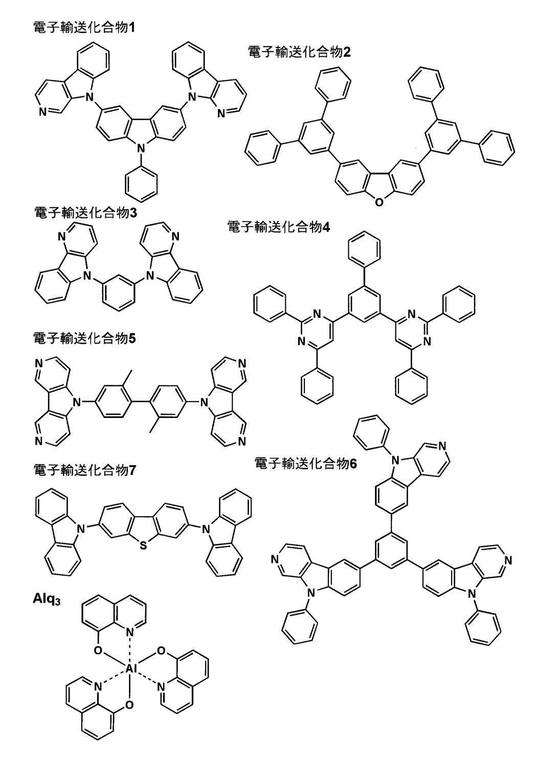
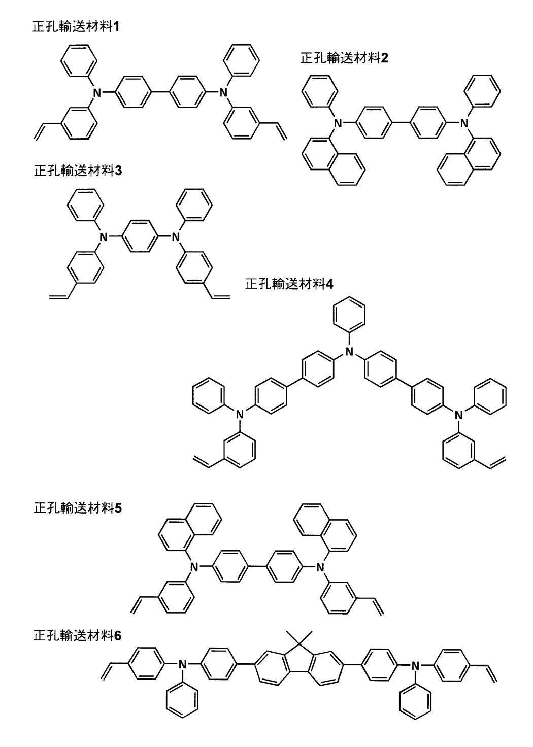
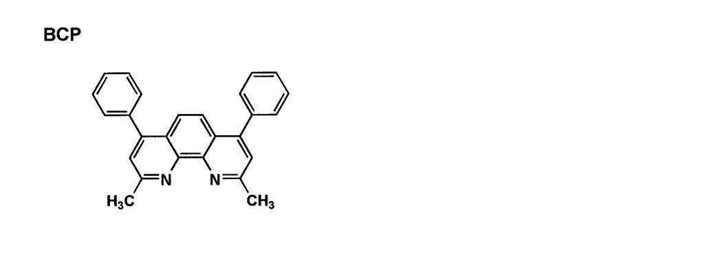
実施例1
《有機EL素子1-1の作製》
陽極として100mm×100mm×1.1mmのガラス基板上にITO(インジウムチンオキシド)を100nm製膜した基板(NHテクノグラス社製NA-45)にパターニングを行った後、このITO透明電極を設けた透明支持基板をイソプロピルアルコールで超音波洗浄し、乾燥窒素ガスで乾燥し、UVオゾン洗浄を5分間行った。
《有機EL素子1-1の作製》
陽極として100mm×100mm×1.1mmのガラス基板上にITO(インジウムチンオキシド)を100nm製膜した基板(NHテクノグラス社製NA-45)にパターニングを行った後、このITO透明電極を設けた透明支持基板をイソプロピルアルコールで超音波洗浄し、乾燥窒素ガスで乾燥し、UVオゾン洗浄を5分間行った。
この透明支持基板上に、ポリ(3,4-エチレンジオキシチオフェン)-ポリスチレンスルホネート(PEDOT/PSS、Bayer社製、Baytron P Al 4083)を純水で70%に希釈した溶液を用い、3000rpm、30秒の条件でスピンコート法により薄膜を形成した後、200℃にて1時間乾燥し、膜厚20nmの正孔輸送層を設けた。
この基板を窒素雰囲気下に移し、正孔輸送層上に、50mgの正孔輸送材料1を10mlのトルエンに溶解した溶液を1500rpm、30秒の条件で正孔輸送層上にスピンコーティングし、薄膜を形成した。更に180秒間紫外光を照射し、光重合・架橋を行い、膜厚約20nmの第2正孔輸送層とした。
この第2正孔輸送層上に、100mgのHost-24と10mgのD-1を10mlのトルエンに溶解した溶液を用いて600rpm、30秒の条件でスピンコート法により薄膜を形成した。60℃で1時間真空乾燥し、膜厚約70nmの発光層とした。
次にこの発光層上に、50mgの電子輸送化合物1を10mlのヘキサフルオロイソプロパノール(HFIP)に溶解した溶液を用いて、1000rpm、30秒の条件でスピンコート法により薄膜を形成した。更に60℃で1時間真空乾燥し、膜厚約30nmの電子輸送層とした。
続いて、この基板を真空蒸着装置の基板ホルダーに固定し、真空槽を4×10⁻⁴Paまで減圧した後、陰極バッファー層としてフッ化ナトリウムを0.4nm、更に陰極としてアルミニウムを110nm蒸着して陰極を形成し、有機EL素子1-1を作製した。
《有機EL素子1-2~1-4の作製》
有機EL素子1-1の作製において、電子輸送化合物1を下記に化合物に変えた以外は同様にして、有機EL素子1-2~1-4を作製した。
有機EL素子1-1の作製において、電子輸送化合物1を下記に化合物に変えた以外は同様にして、有機EL素子1-2~1-4を作製した。
《有機EL素子1-1~1-4の評価》
得られた有機EL素子1-1~1-4を評価するに際しては、作製後の各有機EL素子の非発光面をガラスカバーで覆い、ガラスカバーと有機EL素子が作製されたガラス基板とが接触するガラスカバー側の周囲にシール剤としてエポキシ系光硬化型接着剤(東亞合成社製ラクストラックLC0629B)を適用し、これを上記陰極側に重ねて前記透明支持基板と密着させ、ガラス基板側からUV光を照射して硬化させ、封止して、上記の図5、図6に示すような照明装置を形成し、次いで、下記の測定法に従って、経時保存性の評価を行った。
得られた有機EL素子1-1~1-4を評価するに際しては、作製後の各有機EL素子の非発光面をガラスカバーで覆い、ガラスカバーと有機EL素子が作製されたガラス基板とが接触するガラスカバー側の周囲にシール剤としてエポキシ系光硬化型接着剤(東亞合成社製ラクストラックLC0629B)を適用し、これを上記陰極側に重ねて前記透明支持基板と密着させ、ガラス基板側からUV光を照射して硬化させ、封止して、上記の図5、図6に示すような照明装置を形成し、次いで、下記の測定法に従って、経時保存性の評価を行った。
(経時安定性)
各有機EL素子を85℃で24時間保存した後、保存前後における2.5mA/cm2の定電流駆動での各電圧を測定し、各電圧比を下式に従って求め、これを経時安定性の尺度とした。
各有機EL素子を85℃で24時間保存した後、保存前後における2.5mA/cm2の定電流駆動での各電圧を測定し、各電圧比を下式に従って求め、これを経時安定性の尺度とした。
経時安定性(%)=保存後の電圧(2.5mA/cm2)/保存前の電圧(2.5mA/cm2)×100
得られた結果を下記に示す。
得られた結果を下記に示す。
有機EL素子 電子輸送性材料 経時安定性 備考
(%)
1-1 電子輸送化合物1 147 比較例
1-2 47 123 本発明
1-3 45 119 本発明
1-4 1 114 本発明
上記から、比較の素子に比べて、本発明の有機EL素子は保存後の電圧の上昇が抑制されており、経時安定性(保存性)に優れていることが明らかである。
(%)
1-1 電子輸送化合物1 147 比較例
1-2 47 123 本発明
1-3 45 119 本発明
1-4 1 114 本発明
上記から、比較の素子に比べて、本発明の有機EL素子は保存後の電圧の上昇が抑制されており、経時安定性(保存性)に優れていることが明らかである。
実施例2
《有機EL素子2-1の作製》
陽極として100mm×100mm×1.1mmのガラス基板上にITO(インジウムチンオキシド)を100nm製膜した基板(NHテクノグラス社製NA45)にパターニングを行った後、このITO透明電極を設けた透明支持基板をイソプロピルアルコールで超音波洗浄し、乾燥窒素ガスで乾燥し、UVオゾン洗浄を5分間行った。
《有機EL素子2-1の作製》
陽極として100mm×100mm×1.1mmのガラス基板上にITO(インジウムチンオキシド)を100nm製膜した基板(NHテクノグラス社製NA45)にパターニングを行った後、このITO透明電極を設けた透明支持基板をイソプロピルアルコールで超音波洗浄し、乾燥窒素ガスで乾燥し、UVオゾン洗浄を5分間行った。
この透明支持基板を市販の真空蒸着装置の基板ホルダーに固定し、一方モリブデン製抵抗加熱ボートに正孔輸送材料2(NPD)を200mg入れ、別のモリブデン製抵抗加熱ボートにホスト化合物としてHost-34を200mg入れ、別のモリブデン製抵抗加熱ボートにD-25を入れ、更に別のモリブデン製抵抗加熱ボートに電子輸送化合物2を入れ、真空蒸着装置に取り付けた。
次いで真空槽を4×10⁻⁴Paまで減圧した後、正孔輸送材料2の入った前記加熱ボートに通電して加熱し、蒸着速度0.1nm/秒で透明支持基板上に蒸着し、正孔輸送層を設けた。更にHost-34とD-25の入った前記加熱ボートに通電して加熱し、各々蒸着速度0.2nm/秒、0.012nm/秒で前記正孔輸送層上に共蒸着して発光層を設けた。
尚、蒸着時の基板温度は室温であった。更に、電子輸送化合物2の入った前記加熱ボートに通電して加熱し、蒸着速度0.1nm/秒で前記発光層の上に蒸着して電子輸送層を設けた。尚、蒸着時の基板温度は室温であった。
引き続き、フッ化カリウム0.5nm及びアルミニウム110nmを蒸着して陰極を形成し、有機EL素子2-1を作製した。
《有機EL素子2-2~2-4の作製》
有機EL素子2-1の作製において、電子輸送化合物2を下記の化合物に変えた以外は同様にして、有機EL素子2-2-~2-4を作製した。
有機EL素子2-1の作製において、電子輸送化合物2を下記の化合物に変えた以外は同様にして、有機EL素子2-2-~2-4を作製した。
《有機EL素子2-1~2-4の評価》
得られた有機EL素子2-1~2-4を評価するに際しては、実施例1の有機EL素子1-1~1-4と同様に封止し、図5、図6に示すような照明装置を形成して評価した。
得られた有機EL素子2-1~2-4を評価するに際しては、実施例1の有機EL素子1-1~1-4と同様に封止し、図5、図6に示すような照明装置を形成して評価した。
以下のようにして得られた有機EL素子の評価を行い、その結果を表2に示す。
〈経時安定性〉
有機EL素子を60℃、70%RHの条件で一ヶ月保存後、実施例1と同様に保存前後における2.5mA/cm2の定電流駆動での各電圧を測定し、各電圧比を下式に従って求め、これを経時安定性の尺度とした。
有機EL素子を60℃、70%RHの条件で一ヶ月保存後、実施例1と同様に保存前後における2.5mA/cm2の定電流駆動での各電圧を測定し、各電圧比を下式に従って求め、これを経時安定性の尺度とした。
経時安定性(%)=保存後の電圧(2.5mA/cm2)/保存前の電圧(2.5mA/cm2)×100
得られた結果を以下に示す。
得られた結果を以下に示す。
有機EL素子 電子輸送性材料 経時安定性 備考
(%)
2-1 電子輸送化合物2 136 比較例
2-2 41 121 本発明
2-3 40 116 本発明
2-4 36 110 本発明
上記から、比較の素子に比べて、本発明の有機EL素子は、保存後の電圧の上昇が抑制されており、経時安定性(保存性)に優れていることが明らかである。
(%)
2-1 電子輸送化合物2 136 比較例
2-2 41 121 本発明
2-3 40 116 本発明
2-4 36 110 本発明
上記から、比較の素子に比べて、本発明の有機EL素子は、保存後の電圧の上昇が抑制されており、経時安定性(保存性)に優れていることが明らかである。
実施例3
《有機EL素子3-1の作製》
陽極として100mm×100mm×1.1mmのガラス基板上にITO(インジウムチンオキシド)を100nm製膜した基板(NHテクノグラス社製NA45)にパターニングを行った後、このITO透明電極を設けた透明支持基板をイソプロピルアルコールで超音波洗浄し、乾燥窒素ガスで乾燥し、UVオゾン洗浄を5分間行った。
《有機EL素子3-1の作製》
陽極として100mm×100mm×1.1mmのガラス基板上にITO(インジウムチンオキシド)を100nm製膜した基板(NHテクノグラス社製NA45)にパターニングを行った後、このITO透明電極を設けた透明支持基板をイソプロピルアルコールで超音波洗浄し、乾燥窒素ガスで乾燥し、UVオゾン洗浄を5分間行った。
この透明支持基板上に、ポリ(3,4-エチレンジオキシチオフェン)-ポリスチレンスルホネート(PEDOT/PSS、Bayer社製、Baytron P Al 4083)を純水で70%に希釈した溶液を用い、3000rpm、30秒の条件でスピンコート法により薄膜を形成した後、200℃にて1時間乾燥し、膜厚20nmの正孔輸送層を設けた。
この透明支持基板を市販の真空蒸着装置の基板ホルダーに固定し、一方モリブデン製抵抗加熱ボートに正孔輸送材料2(NPD)を200mg入れ、別のモリブデン製抵抗加熱ボートにホスト化合物としてHost-30を200mg入れ、別のモリブデン製抵抗加熱ボートにD-26を入れ、更に別のモリブデン製抵抗加熱ボートに電子輸送化合物3を入れ、真空蒸着装置に取り付けた。
次いで、真空槽を4×10⁻⁴Paまで減圧した後、正孔輸送材料2の入った前記加熱ボートに通電して加熱し、蒸着速度0.1nm/秒で正孔輸送層上に蒸着し、正孔輸送層2を設けた。
更に、Host-30とD-26の入った前記加熱ボートに通電して加熱し、それぞれ蒸着速度0.2nm/秒、0.012nm/秒で前記正孔輸送層2上に共蒸着して発光層を設けた。
尚、蒸着時の基板温度は室温であった。更に、電子輸送化合物3の入った前記加熱ボートに通電して加熱し、蒸着速度0.1nm/秒で前記発光層の上に蒸着して電子輸送層を設けた。尚、蒸着時の基板温度は室温であった。
引き続き、フッ化カリウム0.5nm及びアルミニウム110nmを蒸着して陰極を形成し、有機EL素子3-1を作製した。
《有機EL素子3-2~3-4の作製》
有機EL素子3-1の作製において、電子輸送化合物3を下記の化合物に変えた以外は同様にして、有機EL素子3-2~3-4を作製した。
有機EL素子3-1の作製において、電子輸送化合物3を下記の化合物に変えた以外は同様にして、有機EL素子3-2~3-4を作製した。
《有機EL素子3-1~3-4の評価》
得られた有機EL素子3-1~3-4を評価するに際しては、有機EL素子1-1~1-4と同様に封止し、図5、図6に示すような照明装置を形成して評価した。
得られた有機EL素子3-1~3-4を評価するに際しては、有機EL素子1-1~1-4と同様に封止し、図5、図6に示すような照明装置を形成して評価した。
以下のようにして、得られた有機EL素子の評価を行った。
(外部取り出し量子効率)
有機EL素子を室温(約23℃~25℃)下、2.5mA/cm2の定電流条件下で発光させ、発光開始直後の発光輝度(L)[cd/m2]を測定することにより外部取り出し量子効率(η)を算出した。
有機EL素子を室温(約23℃~25℃)下、2.5mA/cm2の定電流条件下で発光させ、発光開始直後の発光輝度(L)[cd/m2]を測定することにより外部取り出し量子効率(η)を算出した。
ここで、発光輝度の測定はCS-1000(コニカミノルタセンシング製)を用いた。外部取り出し量子効率は有機EL素子3-1を100とする相対値で表した。
(発光寿命)
有機EL素子を室温下、2.5mA/cm2の定電流条件下による連続発光を行い、初期輝度の半分の輝度になるのに要する時間(τ1/2)を測定した。発光寿命は有機EL素子3-1を100と設定する相対値で表した。
有機EL素子を室温下、2.5mA/cm2の定電流条件下による連続発光を行い、初期輝度の半分の輝度になるのに要する時間(τ1/2)を測定した。発光寿命は有機EL素子3-1を100と設定する相対値で表した。
得られた結果を下記に示す。
有機EL素子 電子輸送性材料 外部取り出し 寿命 備考
量子効率(%)
3-1 電子輸送化合物3 100 100 比較例
3-2 42 124 330 本発明
3-3 43 123 410 本発明
3-4 27 127 500 本発明
上記から、比較の素子に比べて、本発明の有機EL素子は外部取り出し量子効率が高く、寿命も長いことが明らかである。
量子効率(%)
3-1 電子輸送化合物3 100 100 比較例
3-2 42 124 330 本発明
3-3 43 123 410 本発明
3-4 27 127 500 本発明
上記から、比較の素子に比べて、本発明の有機EL素子は外部取り出し量子効率が高く、寿命も長いことが明らかである。
実施例4
《有機EL素子4-1の作製》
有機EL素子1-1の作製おいて、正孔輸送材料1の変わりに正孔輸送材料3を5mgと正孔輸送材料4を45mgとを10mlのトルエンに溶解した混合溶液を用い、Host-24の変わりにHost-25を用い、D-1の代わりにD-30を用い、更に電子輸送化合物1の変わりにBCPを用いた以外は同様にして、有機EL素子4-1を作製した。
《有機EL素子4-1の作製》
有機EL素子1-1の作製おいて、正孔輸送材料1の変わりに正孔輸送材料3を5mgと正孔輸送材料4を45mgとを10mlのトルエンに溶解した混合溶液を用い、Host-24の変わりにHost-25を用い、D-1の代わりにD-30を用い、更に電子輸送化合物1の変わりにBCPを用いた以外は同様にして、有機EL素子4-1を作製した。
《有機EL素子4-2~4-5の作製》
有機EL素子4-1の作製において、BCPを下記の化合物に変えた以外は同様にして、有機EL素子4-1~4-5を作製した。
有機EL素子4-1の作製において、BCPを下記の化合物に変えた以外は同様にして、有機EL素子4-1~4-5を作製した。
《有機EL素子4-1~4-5の評価》
得られた有機EL素子4-1~4-5を評価するに際しては、有機EL素子1-1~1-4と同様に封止し、図5、図6に示すような照明装置を形成して評価した。
得られた有機EL素子4-1~4-5を評価するに際しては、有機EL素子1-1~1-4と同様に封止し、図5、図6に示すような照明装置を形成して評価した。
以下のようにして、得られた有機EL素子の評価を行った。
(発光輝度)
各有機EL素子に室温(約23℃~25℃)下、4V直流電圧を印加した時の発光輝度(cd/m2)を測定した。
各有機EL素子に室温(約23℃~25℃)下、4V直流電圧を印加した時の発光輝度(cd/m2)を測定した。
(外部取り出し量子効率)
実施例3の有機EL素子3-1~3-4の場合と同様にして2.5mA/cm2の定電流条件下における部取り出し量子効率を求めた。
実施例3の有機EL素子3-1~3-4の場合と同様にして2.5mA/cm2の定電流条件下における部取り出し量子効率を求めた。
尚、評価にあたり、発光輝度及び外部取り出し量子効率は有機EL素子4-1を100とする相対値で表した。
(電圧上昇率)
6mA/cm2の一定電流で駆動したときに、初期電圧と150時間後の電圧を測定した。初期電圧に対する100時間後の電圧の相対値を電圧上昇率とした。
6mA/cm2の一定電流で駆動したときに、初期電圧と150時間後の電圧を測定した。初期電圧に対する100時間後の電圧の相対値を電圧上昇率とした。
得られた結果を下記に示す。
有機EL 電子輸送性 外部取り出し 寿命 電圧 備考
素子 材料 量子効率(%) 上昇率
4-1 BCP 100 100 122 比較例
4-2 電子輸送化合物4 114 164 120 比較例
4-3 44 127 365 114 本発明
4-4 38 129 410 112 本発明
4-5 29’ 138 555 111 本発明
上記から、比較の素子に比べて、本発明の有機EL素子は外部取り出し量子効率が高く、寿命も長く、且つ、電圧上昇率も低いことが明らかである。
有機EL 電子輸送性 外部取り出し 寿命 電圧 備考
素子 材料 量子効率(%) 上昇率
4-1 BCP 100 100 122 比較例
4-2 電子輸送化合物4 114 164 120 比較例
4-3 44 127 365 114 本発明
4-4 38 129 410 112 本発明
4-5 29’ 138 555 111 本発明
上記から、比較の素子に比べて、本発明の有機EL素子は外部取り出し量子効率が高く、寿命も長く、且つ、電圧上昇率も低いことが明らかである。
実施例5
《有機EL素子5-1の作製》
有機EL素子1-1の作製において、Host-24をHost-9に代え、D-1をD-24に代え、電子輸送化合物1を電子輸送化合物5に代え、フッ化ナトリウムの代わりにフッ化リチウムを用いた以外は同様にして、有機EL素子5-1を作製した。
《有機EL素子5-1の作製》
有機EL素子1-1の作製において、Host-24をHost-9に代え、D-1をD-24に代え、電子輸送化合物1を電子輸送化合物5に代え、フッ化ナトリウムの代わりにフッ化リチウムを用いた以外は同様にして、有機EL素子5-1を作製した。
《有機EL素子5-2~5-5の作製》
有機EL素子5-1の作製において、フッ化リチウムと電子輸送性材料を下記の組み合わせに代えた以外は同様にして、有機EL素子5-2~5-5を各々作製した。
有機EL素子5-1の作製において、フッ化リチウムと電子輸送性材料を下記の組み合わせに代えた以外は同様にして、有機EL素子5-2~5-5を各々作製した。
《有機EL素子5-1~5-5の評価》
得られた有機EL素子5-1~5-5を評価するに際しては、有機EL素子1-1~1-4と同様に封止し、図5、図6に示すような照明装置を形成して評価した。
得られた有機EL素子5-1~5-5を評価するに際しては、有機EL素子1-1~1-4と同様に封止し、図5、図6に示すような照明装置を形成して評価した。
作製した素子について、実施例3の有機EL素子3-1~3-4と同様にして2.5mA/cm2の定電流条件下における部取り出し量子効率及び電圧を求めた。
尚、評価にあたり、有機EL素子5-1の結果を各々100とする相対値で表した。
有機EL 電子輸送性 電子注入層 外部取り出し 電圧 備考
素子 材料 量子効率(%) 上昇率
5-1 電子輸送化合物5 LiF 100 100 比較例
5-2 46 LiF 110 86 比較例
5-3 電子輸送化合物5 KF 105 62 比較例
5-4 46 KF 117 45 本発明
5-5 2 KF 119 43 本発明
尚、上記の電子注入層の形成に用いられたLiF、KFを構成する金属元素の標準電極電位を以下に示す。
有機EL 電子輸送性 電子注入層 外部取り出し 電圧 備考
素子 材料 量子効率(%) 上昇率
5-1 電子輸送化合物5 LiF 100 100 比較例
5-2 46 LiF 110 86 比較例
5-3 電子輸送化合物5 KF 105 62 比較例
5-4 46 KF 117 45 本発明
5-5 2 KF 119 43 本発明
尚、上記の電子注入層の形成に用いられたLiF、KFを構成する金属元素の標準電極電位を以下に示す。
Li -3.045(V):比較例
K -2.925(V):本発明
上記から、比較の素子に比べて、本発明の有機EL素子は外部取り出し量子効率が高く、且つ、電圧上昇率も低いことが明らかである。
K -2.925(V):本発明
上記から、比較の素子に比べて、本発明の有機EL素子は外部取り出し量子効率が高く、且つ、電圧上昇率も低いことが明らかである。
実施例6
《有機EL素子6-1の作製》
有機EL素子3-1の作製おいて、Host-30をHost-25に代え、D-26をD-9に代え、電子輸送化合物3を電子輸送化合物6に代えた以外は同様にして、有機EL素子6-1を作製した。
《有機EL素子6-1の作製》
有機EL素子3-1の作製おいて、Host-30をHost-25に代え、D-26をD-9に代え、電子輸送化合物3を電子輸送化合物6に代えた以外は同様にして、有機EL素子6-1を作製した。
《有機EL素子6-2~6-4の作製》
有機EL素子6-1の作製において、D-9と電子輸送化合物6を下記の組み合わせに代えた以外は同様にして、有機EL素子6-2-~6-4を作製した。
有機EL素子6-1の作製において、D-9と電子輸送化合物6を下記の組み合わせに代えた以外は同様にして、有機EL素子6-2-~6-4を作製した。
《有機EL素子6-1~6-4の評価》
得られた有機EL素子6-1~6-4を評価するに際しては、有機EL素子1-1~1-4と同様に封止し、図5、図6に示すような照明装置を形成して評価した。
得られた有機EL素子6-1~6-4を評価するに際しては、有機EL素子1-1~1-4と同様に封止し、図5、図6に示すような照明装置を形成して評価した。
作製した素子について、実施例3の有機EL素子3-1~3-4と同様にして2.5mA/cm2の定電流条件下における外部取り出し量子効率及び発光寿命を求めた。
また、2.5mA/cm2の定電流条件下における連続発光を行った際の発光色を目視で評価した。それぞれ有機EL素子6-1の結果を100とする相対値で表した。
得られた結果を下記に示す。
有機EL ドーパント 電子輸送性 外部取り出し 寿命 発光色 備考
素子 材料 量子効率(%)
6-1 D-9 電子輸送化合物6 100 100 青 比較例
6-2 D-9 24 109 150 青 本発明
6-3 D-24 24 113 680 青 本発明
6-4 D-26 24 123 4500 青 本発明
上記から、比較に比べて、本発明の有機EL素子は、外部取り出し量子効率が高く、長寿命であることが判った。
有機EL ドーパント 電子輸送性 外部取り出し 寿命 発光色 備考
素子 材料 量子効率(%)
6-1 D-9 電子輸送化合物6 100 100 青 比較例
6-2 D-9 24 109 150 青 本発明
6-3 D-24 24 113 680 青 本発明
6-4 D-26 24 123 4500 青 本発明
上記から、比較に比べて、本発明の有機EL素子は、外部取り出し量子効率が高く、長寿命であることが判った。
実施例7
《有機EL素子7-1の作製》
有機EL素子1-1の作製おいて、Host-24をHost-15に代え、D-1をD-10に代え、電子輸送化合物1を電子輸送化合物4に代えた以外は同様にして、有機EL素子7-1を作製した。
《有機EL素子7-1の作製》
有機EL素子1-1の作製おいて、Host-24をHost-15に代え、D-1をD-10に代え、電子輸送化合物1を電子輸送化合物4に代えた以外は同様にして、有機EL素子7-1を作製した。
《有機EL素子7-2及び7-3の作製》
有機EL素子7-1の作製において、ホスト化合物と電子輸送性材料の組み合わせを下記に変えた以外は同様にして、有機EL素子7-2及び7-3を作製した。
有機EL素子7-1の作製において、ホスト化合物と電子輸送性材料の組み合わせを下記に変えた以外は同様にして、有機EL素子7-2及び7-3を作製した。
《有機EL素子7-1~7-3の評価》
得られた有機EL素子7-1~7-3を評価するに際しては、有機EL素子1-1~1-4と同様に封止し、図5、図6に示すような照明装置を形成して評価した。
得られた有機EL素子7-1~7-3を評価するに際しては、有機EL素子1-1~1-4と同様に封止し、図5、図6に示すような照明装置を形成して評価した。
作製した素子について、実施例3の有機EL素子3-1~3-4と同様にして2.5mA/cm2の定電流条件下における部取り出し量子効率及び発光寿命を求めた。
尚、評価にあたり、有機EL素子7-1のデータを各々100とする相対値で表した。
得られた結果を下記に示す。
有機EL ホスト 電子輸送性 外部取り出し 寿命 備考
素子 化合物 材料 量子効率(%)
7-1 Host-15 電子輸送化合物4 100 100 比較例
7-2 Host-15 37 130 350 本発明
7-3 Host-16 37 134 720 本発明
上記から、比較に比べて、本発明の有機EL素子は、外部取り出し量子効率が高く、長寿命であることが判った。
有機EL ホスト 電子輸送性 外部取り出し 寿命 備考
素子 化合物 材料 量子効率(%)
7-1 Host-15 電子輸送化合物4 100 100 比較例
7-2 Host-15 37 130 350 本発明
7-3 Host-16 37 134 720 本発明
上記から、比較に比べて、本発明の有機EL素子は、外部取り出し量子効率が高く、長寿命であることが判った。
実施例8(白色素子の作製)
《有機ELフルカラー表示装置の作製》
図7は有機ELフルカラー表示装置の概略構成図を示す。陽極としてガラス基板201上にITO透明電極(202)を100nm成膜した基板(NHテクノグラス社製NA45)に100μmのピッチでパターニングを行った後、このガラス基板上でITO透明電極の間に非感光性ポリイミドの隔壁203(幅20μm、厚さ2.0μm)をフォトリソグラフィーで形成させた。
《有機ELフルカラー表示装置の作製》
図7は有機ELフルカラー表示装置の概略構成図を示す。陽極としてガラス基板201上にITO透明電極(202)を100nm成膜した基板(NHテクノグラス社製NA45)に100μmのピッチでパターニングを行った後、このガラス基板上でITO透明電極の間に非感光性ポリイミドの隔壁203(幅20μm、厚さ2.0μm)をフォトリソグラフィーで形成させた。
ITO電極上ポリイミド隔壁の間に下記組成の正孔注入層組成物を、インクジェットヘッド(エプソン社製;MJ800C)を用いて吐出注入し、紫外光を150秒間照射し、60℃、10分間の乾燥処理により膜厚40nmの正孔注入層204を作製した。
この正孔注入層上に、各々下記の青色発光層組成物、緑色発光層組成物、赤色発光層組成物を同様にインクジェットヘッドを使用して吐出注入し、60℃、10分間乾燥処理し、それぞれの発光層(205B、205G、205R)を形成させた。次に、発光層を覆うように上に化合物例25を20nm蒸着し、更にフッ化ナトリウムを0.6nm、陰極としてAl(206)を130nm真空蒸着して有機EL素子を作製した。
作製した有機EL素子はそれぞれの電極に電圧を印加することにより各々青色、緑色、赤色の発光を示し、フルカラー表示装置として利用できることがわかった。
(正孔注入層組成物)
正孔輸送材料5 20質量部
シクロヘキシルベンゼン 50質量部
イソプロピルビフェニル 50質量部
(青色発光層組成物)
Host-9 0.7質量部
D-26 0.04質量部
シクロヘキシルベンゼン 50質量部
イソプロピルビフェニル 50質量部
(緑色発光層組成物)
Host-9 0.7質量部
D-1 0.04質量部
シクロヘキシルベンゼン 50質量部
イソプロピルビフェニル 50質量部
(赤色発光層組成物)
Host-9 0.7質量部
D-10 0.04質量部
シクロヘキシルベンゼン 50質量部
イソプロピルビフェニル 50質量部
実施例9
《白色の有機EL素子9-1の作製》
陽極として100mm×100mm×1.1mmのガラス基板上にITO(インジウムチンオキシド)を100nm成膜した基板(NHテクノグラス社製NA45)にパターニングを行った後、このITO透明電極を設けた透明支持基板をイソプロピルアルコールで超音波洗浄し、乾燥窒素ガスで乾燥し、UVオゾン洗浄を5分間行った。
この透明支持基板上に、ポリ(3,4-エチレンジオキシチオフェン)-ポリスチレンスルホネート(PEDOT/PSS、Bayer社製、Baytron P Al 4083)を純水で70%に希釈した溶液を3000rpm、30秒でスピンコート法により成膜した後、200℃にて1時間乾燥し、膜厚30nmの第一正孔輸送層を設けた。
この基板を窒素雰囲気下に移し、第一正孔輸送層上に、50mgの正孔輸送材料6を10mlのトルエンに溶解した溶液を1000rpm、30秒の条件下、スピンコート法により成膜した。180秒間紫外光を照射し、光重合・架橋を行った後、60℃で1時間真空乾燥し第2正孔輸送層とした。
次に、Host-25(60mg)、D-6(3.0mg)、D-24(3.0mg)をトルエン6mlに溶解した溶液を用い、1000rpm、30秒の条件下、スピンコート法により成膜した。60℃で1時間真空乾燥し発光層とした。
更に、化合物例3(30mg)をヘキサフルオロイソプロパノール(HFIP) 5mlに溶解した溶液を用い、1500rpm、30秒の条件下、スピンコート法により成膜した後、60℃で1時間真空乾燥し電子輸送層とした。
続いて、この基板を真空蒸着装置の基板ホルダーに固定し、モリブデン製抵抗加熱ボートにAlq3を200mg入れ、真空蒸着装置に取り付けた。真空槽を4×10⁻⁴Paまで減圧した後、Alq3の入った前記加熱ボートに通電して加熱し、蒸着速度0.1nm/秒で前記電子輸送層の上に蒸着して、更に膜厚40nmの第2の電子輸送層を設けた。
尚、蒸着時の基板温度は室温(23℃~25℃)であった。
引き続き、フッ化カリウム0.5nm及びアルミニウム110nmを蒸着して陰極を形成し、有機EL素子9-1を作製した。
この素子に通電したところほぼ白色の光が得られ、照明装置として使用できることが判った。尚、例示の他の化合物に置き換えても同様に白色の発光が得られることが判った。
1 ディスプレイ
3 画素
5 走査線
6 データ線
7 電源ライン
10 有機EL素子
11 スイッチングトランジスタ
12 駆動トランジスタ
13 コンデンサ
A 表示部
B 制御部
101 有機EL素子
102 ガラスカバー
105 陰極
106 有機EL層
107 透明電極付きガラス基板
108 窒素ガス
109 捕水剤
201 ガラス基板
202 ITO透明電極
203 隔壁
204 正孔注入層
205B、205G、205R 発光層
3 画素
5 走査線
6 データ線
7 電源ライン
10 有機EL素子
11 スイッチングトランジスタ
12 駆動トランジスタ
13 コンデンサ
A 表示部
B 制御部
101 有機EL素子
102 ガラスカバー
105 陰極
106 有機EL層
107 透明電極付きガラス基板
108 窒素ガス
109 捕水剤
201 ガラス基板
202 ITO透明電極
203 隔壁
204 正孔注入層
205B、205G、205R 発光層
Claims (19)
- 陽極と陰極の間に発光層を含む複数の構成層が狭持されてなる有機エレクトロルミネッセンス素子において、
該構成層として、下記一般式(1)で表される化合物を少なくとも一種含有する電子輸送層を有し、該発光層の少なくとも1つがリン光発光性の有機金属錯体を含有し、かつ、該陰極または該陰極に接する構成層中に、周期表第1族または第2族に属する元素の金属または金属化合物を含有し、該元素の金属イオン(Mn+)/金属(M)系の標準電極電位が-3Vvs.SHEよりも大きいことを特徴とする有機エレクトロルミネッセンス素子。
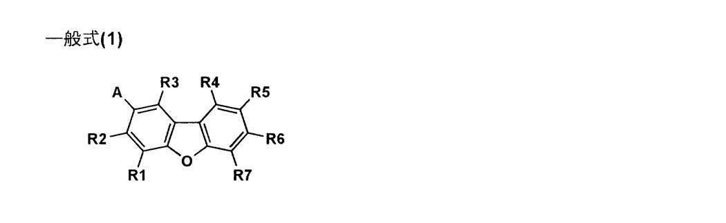
〔式中、R1~R7は、各々水素原子または置換基を表す。Aは、フェニル基または芳香族複素環基を表す。但し、Aは部分構造として、少なくとも1つのカルバゾール環、アザカルバゾール環、ジベンゾフラン環またはジベンゾチオフェン環を含む。〕 - 前記一般式(1)で表される化合物が下記一般式(2)で表される化合物であることを特徴とする請求項1に記載の有機エレクトロルミネッセンス素子。
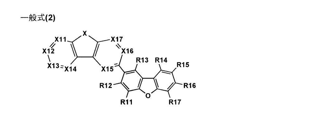
〔式中、R11~R17は、各々水素原子または置換基を表し、Xは、-O-、-S-、または-N(R10)-を表し、R10は水素原子または置換基を表す。X11~X17は-C(R18)=または-N=を表し、R18は水素原子または置換基を表す。-C(R18)=が複数存在する場合にはR18は同じでも異なっていてもよい。但し、R10~R18の少なくとも1つは置換基を表す。〕 - 前記一般式(2)のXが、-N(R10)-を表し、R11~R14、R16、R17が各々水素原子を表し、且つ、X11、X12、X14~X17が、各々-CH=または-N=を表すことを特徴とする請求項2に記載の有機エレクトロルミネッセンス素子。
- 前記一般式(2)のXが、-O-または-S-を表し、R11~R14、R16、R17が、各々水素原子であり、且つ、X11、X12、X14~X17が、各々-CH=を表すことを特徴とする請求項2に記載の有機エレクトロルミネッセンス素子。
- 前記一般式(1)で表される化合物が下記一般式(3)で表される化合物であることを特徴とする請求項1に記載の有機エレクトロルミネッセンス素子。
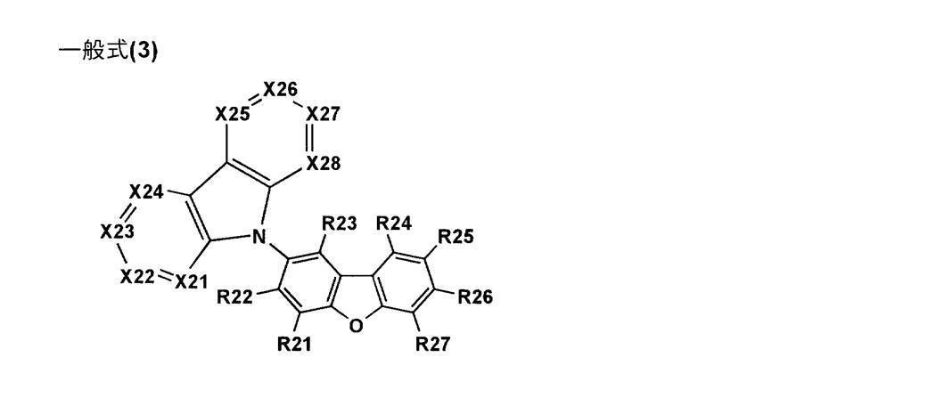
〔式中、R21~R27は、各々水素原子または置換基を表す。X21~X28は、各々-C(R28)=または-N=を表し、R28は水素原子または置換基を表す。-C(R28)=が複数存在する場合にはR28は同じでも異なっていてもよい。但し、R21~R28の少なくとも1つは置換基を表す。〕 - 前記一般式(3)のR21~R24、R26、R27が、各々水素原子を表し、X21、X22、X24、X25、X27、X28が、各々-CH=または-N=を表すことを特徴とする請求項5に記載の有機エレクトロルミネッセンス素子。
- 前記一般式(1)で表される化合物が下記一般式(4)で表される化合物であることを特徴とする請求項1に記載の有機エレクトロルミネッセンス素子。

〔式中、R31~R37は、各々水素原子または置換基を表す。X31~X35は、各々-C(R38)=または-N=を表し、R38は水素原子または置換基を表す。但し、X31~X35の少なくとも1つは、R38が置換基を表す-C(R38)=である。-C(R38)=が複数存在する場合にはR38は同じでも異なっていてもよい。〕 - 前記一般式(4)のR31~R34、R36、R37が、各々水素原子を表し、X33が、-CH=または-N=を表すことを特徴とする請求項7に記載の有機エレクトロルミネッセンス素子。
- 前記一般式(1)~(4)のいずれかで表される化合物が、ピリジン環または該ピリジン環を含む縮合芳香族複素環を部分構造として少なくとも1つ有することを特徴とする請求項1~8のいずれか1項に記載の有機エレクトロルミネッセンス素子。
- 前記元素が、ナトリウム、カリウムまたはセシウムを表すことを特徴とする請求項1~9のいずれか1項に記載の有機エレクトロルミネッセンス素子。
- 前記リン光発光性の有機金属錯体の少なくとも1つが、下記一般式(5)で表される化合物であることを特徴とする請求項1~10のいずれか1項に記載の有機エレクトロルミネッセンス素子。

〔式中、P、Qは、各々炭素原子または窒素原子を表し、A1はP-Cと共に芳香族炭化水素環または芳香族複素環を形成する原子群を表す。A2はQ-Nと共に芳香族複素環を形成する原子群を表す。P1-L1-P2は2座の配位子を表し、P1、P2は各々独立に炭素原子、窒素原子、または酸素原子を表す。L1はP1、P2と共に2座の配位子を形成する原子群を表す。j1は1~3の整数を表し、j2は0~2の整数を表すが、j1+j2は2または3である。M1は元素周期表における8族~10族の金属元素を表す。〕 - 前記一般式(5)で表される化合物が下記一般式(6)で表される化合物であることを特徴とする請求項11に記載の有機エレクトロルミネッセンス素子。

〔式中、Zは、炭化水素環基または複素環基を表す。P、Qは、各々炭素原子または窒素原子を表し、A1はP-Cと共に芳香族炭化水素環または芳香族複素環を形成する原子群を表す。A3は-C(R01)=C(R02)-、-N=C(R02)-、-C(R01)=N-または-N=N-を表し、R01、R02は、各々水素原子または置換基を表す。P1-L1-P2は2座の配位子を表し、P1、P2は各々独立に炭素原子、窒素原子、または酸素原子を表す。L1はP1、P2と共に2座の配位子を形成する原子群を表す。j1は1~3の整数を表し、j2は0~2の整数を表すが、j1+j2は2または3である。M1は元素周期表における8族~10族の遷移金属元素を表す。〕 - 前記一般式(6)で表される化合物が下記一般式(7)で表される化合物であることを特徴とする請求項12に記載の有機エレクトロルミネッセンス素子。

〔式中、R03は置換基を表し、R04は水素原子または置換基を表し、複数のR04は互いに結合して環を形成してもよい。n01は1~4の整数を表す。R05は水素原子または置換基を表し、複数のR05は互いに結合して環を形成してもよい。n02は1~2の整数を表す。R06は水素原子または置換基を表し、互いに結合して環を形成してもよい。n03は1~4の整数を表す。Z1はC-Cと共に6員の芳香族炭化水素環もしくは、5員または6員の芳香族複素環を形成するのに必要な原子群を表す。Z2は炭化水素環または複素環を形成するのに必要な原子群を表す。P1-L1-P2は2座の配位子を表し、P1、P2は各々独立に炭素原子、窒素原子または酸素原子を表す。L1はP1、P2と共に2座の配位子を形成する原子群を表す。j1は1~3の整数を表し、j2は0~2の整数を表すが、j1+j2は2または3である。M1は元素周期表における8族~10族の遷移金属元素を表す。R03とR06、R04とR06及びR05とR06は互いに結合して環を形成していてもよい。〕 - 前記一般式(7)で表される化合物が下記一般式(8)で表される化合物であることを特徴とする請求項13に記載の有機エレクトロルミネッセンス素子。

〔式中、R03は置換基を表し、R04は水素原子または置換基を表し、複数のR04は互いに結合して環を形成してもよい。n01は1~4の整数を表す。R05は水素原子または置換基を表し、複数のR05は互いに結合して環を形成してもよい。n02は1~2の整数を表す。R06は水素原子または置換基を表し、互いに結合して環を形成してもよい。n03は1~3の整数を表す。R07は置換基または単結合手を表す。P1-L1-P2は2座の配位子を表し、P1、P2は各々独立に炭素原子、窒素原子または酸素原子を表す。L1はP1、P2と共に2座の配位子を形成する原子群を表す。j1は1~3の整数を表し、j2は0~2の整数を表すが、j1+j2は2または3である。M1は元素周期表における8族~10族の遷移金属元素を表す。〕 - 前記M1がイリジウムを表すことを特徴とする請求項11~14のいずれか1項に記載の有機エレクトロルミネッセンス素子。
- 前記電子輸送層と発光層とを含む少なくとも2層の有機層が湿式法で形成されたことを特徴とする請求項1~15のいずれか1項に記載の有機エレクトロルミネッセンス素子。
- 白色に発光することを特徴とする請求項1~16のいずれか1項に記載の有機エレクトロルミネッセンス素子。
- 請求項1~16のいずれか1項に記載の有機エレクトロルミネッセンス素子を備えたことを特徴とする照明装置。
- 請求項1~16のいずれか1項に記載の有機エレクトロルミネッセンス素子を備えたことを特徴とする表示装置。
Priority Applications (3)
| Application Number | Priority Date | Filing Date | Title |
|---|---|---|---|
| US13/145,842 US9617255B2 (en) | 2009-02-06 | 2010-01-21 | Organic electroluminescent element, and illumination device and display device each comprising the element |
| JP2010549426A JP5541167B2 (ja) | 2009-02-06 | 2010-01-21 | 有機エレクトロルミネッセンス素子、該素子を備えた照明装置及び表示装置 |
| EP10738415.8A EP2395573B1 (en) | 2009-02-06 | 2010-01-21 | Organic electroluminescent element, and illumination device and display device each comprising the element |
Applications Claiming Priority (2)
| Application Number | Priority Date | Filing Date | Title |
|---|---|---|---|
| JP2009025871 | 2009-02-06 | ||
| JP2009-025871 | 2009-02-06 |
Publications (1)
| Publication Number | Publication Date |
|---|---|
| WO2010090077A1 true WO2010090077A1 (ja) | 2010-08-12 |
Family
ID=42541981
Family Applications (1)
| Application Number | Title | Priority Date | Filing Date |
|---|---|---|---|
| PCT/JP2010/050692 WO2010090077A1 (ja) | 2009-02-06 | 2010-01-21 | 有機エレクトロルミネッセンス素子、該素子を備えた照明装置及び表示装置 |
Country Status (4)
| Country | Link |
|---|---|
| US (1) | US9617255B2 (ja) |
| EP (2) | EP2395573B1 (ja) |
| JP (1) | JP5541167B2 (ja) |
| WO (1) | WO2010090077A1 (ja) |
Cited By (57)
| Publication number | Priority date | Publication date | Assignee | Title |
|---|---|---|---|---|
| WO2011051404A1 (de) | 2009-10-28 | 2011-05-05 | Basf Se | Heteroleptische carben-komplexe und deren verwendung in der organischen elektronik |
| WO2011073149A1 (de) | 2009-12-14 | 2011-06-23 | Basf Se | Metallkomplexe, enthaltend diazabenzimidazolcarben-liganden und deren verwendung in oleds |
| WO2012080052A1 (en) | 2010-12-13 | 2012-06-21 | Basf Se | Bispyrimidines for electronic applications |
| JP2012142510A (ja) * | 2011-01-06 | 2012-07-26 | Konica Minolta Holdings Inc | 有機エレクトロニクス素子、それを具備した表示装置及び照明装置 |
| WO2012145173A1 (en) * | 2011-04-08 | 2012-10-26 | Universal Display Corporation | Substituted oligoazacarbazoles for light emitting diodes |
| JP2013016717A (ja) * | 2011-07-06 | 2013-01-24 | Konica Minolta Holdings Inc | 有機エレクトロルミネッセンス素子、表示装置及び照明装置 |
| US8362246B2 (en) | 2010-12-13 | 2013-01-29 | Basf Se | Bispyrimidines for electronic applications |
| US20130056720A1 (en) * | 2010-05-03 | 2013-03-07 | Hyung-Sun Kim | Compound for organic optoelectronic device, organic light emitting diode including the same and display including the organic light emitting diode |
| JP2013168471A (ja) * | 2012-02-15 | 2013-08-29 | Konica Minolta Inc | 有機エレクトロニクス素子、表示装置及び照明装置 |
| JP2013187211A (ja) * | 2012-03-06 | 2013-09-19 | Konica Minolta Inc | 有機エレクトロルミネッセンス素子、表示装置及び照明装置 |
| US20130256644A1 (en) * | 2010-12-01 | 2013-10-03 | Hyung-Sun Kim | Compound for organic optoelectronic device, organic light emitting diode including the same and display including the organic light emitting diode |
| WO2014013721A1 (ja) * | 2012-07-20 | 2014-01-23 | 出光興産株式会社 | 含窒素ヘテロ芳香族環化合物、それを用いた有機エレクトロルミネッセンス素子 |
| WO2014012972A1 (en) | 2012-07-19 | 2014-01-23 | Basf Se | Dinuclear metal complexes comprising carbene ligands and the use thereof in oleds |
| US8691401B2 (en) | 2010-04-16 | 2014-04-08 | Basf Se | Bridged benzimidazole-carbene complexes and use thereof in OLEDS |
| JP2014077046A (ja) * | 2012-10-10 | 2014-05-01 | Konica Minolta Inc | 発光層形成用インク組成物、発光素子の作製方法及びエレクトロルミネッセンスデバイス |
| WO2014147134A1 (en) | 2013-03-20 | 2014-09-25 | Basf Se | Azabenzimidazole carbene complexes as efficiency booster in oleds |
| US20140306207A1 (en) * | 2011-10-26 | 2014-10-16 | Idemitsu Kosan Co., Ltd. | Organic electroluminescence element, and material for organic electroluminescence element |
| WO2014177518A1 (en) | 2013-04-29 | 2014-11-06 | Basf Se | Transition metal complexes with carbene ligands and the use thereof in oleds |
| WO2015000955A1 (en) | 2013-07-02 | 2015-01-08 | Basf Se | Monosubstituted diazabenzimidazole carbene metal complexes for use in organic light emitting diodes |
| JP2015082537A (ja) * | 2013-10-22 | 2015-04-27 | コニカミノルタ株式会社 | 有機エレクトロルミネッセンス素子、その製造方法及び有機エレクトロルミネッセンスデバイス |
| JP2015117235A (ja) * | 2013-11-13 | 2015-06-25 | 株式会社半導体エネルギー研究所 | 有機化合物、発光素子、ディスプレイモジュール、照明モジュール、発光装置、表示装置、電子機器及び照明装置 |
| US9142792B2 (en) | 2010-06-18 | 2015-09-22 | Basf Se | Organic electronic devices comprising a layer comprising at least one metal organic compound and at least one metal oxide |
| KR20150108787A (ko) * | 2014-03-18 | 2015-09-30 | 유니버셜 디스플레이 코포레이션 | 유기 전계발광 물질 및 소자 |
| WO2016016791A1 (en) | 2014-07-28 | 2016-02-04 | Idemitsu Kosan Co., Ltd (Ikc) | 2,9-functionalized benzimidazolo[1,2-a]benzimidazoles as hosts for organic light emitting diodes (oleds) |
| EP2982676A1 (en) | 2014-08-07 | 2016-02-10 | Idemitsu Kosan Co., Ltd. | Benzimidazo[2,1-B]benzoxazoles for electronic applications |
| EP2993215A1 (en) | 2014-09-04 | 2016-03-09 | Idemitsu Kosan Co., Ltd. | Azabenzimidazo[2,1-a]benzimidazoles for electronic applications |
| US9315724B2 (en) | 2011-06-14 | 2016-04-19 | Basf Se | Metal complexes comprising azabenzimidazole carbene ligands and the use thereof in OLEDs |
| EP3015469A1 (en) | 2014-10-30 | 2016-05-04 | Idemitsu Kosan Co., Ltd. | 5-((benz)imidazol-2-yl)benzimidazo[1,2-a]benzimidazoles for electronic applications |
| WO2016079169A1 (en) | 2014-11-18 | 2016-05-26 | Basf Se | Pt- or pd-carbene complexes for use in organic light emitting diodes |
| WO2016079667A1 (en) | 2014-11-17 | 2016-05-26 | Idemitsu Kosan Co., Ltd. | Indole derivatives for electronic applications |
| JP2016106406A (ja) * | 2016-01-07 | 2016-06-16 | コニカミノルタ株式会社 | 有機エレクトロニクス素子、表示装置及び照明装置 |
| EP3034506A1 (en) | 2014-12-15 | 2016-06-22 | Idemitsu Kosan Co., Ltd | 4-functionalized carbazole derivatives for electronic applications |
| EP3034507A1 (en) | 2014-12-15 | 2016-06-22 | Idemitsu Kosan Co., Ltd | 1-functionalized dibenzofurans and dibenzothiophenes for organic light emitting diodes (OLEDs) |
| JP2016129240A (ja) * | 2010-10-29 | 2016-07-14 | 株式会社半導体エネルギー研究所 | 発光素子、発光装置、照明装置および電子機器 |
| EP3053918A1 (en) | 2015-02-06 | 2016-08-10 | Idemitsu Kosan Co., Ltd | 2-carbazole substituted benzimidazoles for electronic applications |
| EP3054498A1 (en) | 2015-02-06 | 2016-08-10 | Idemitsu Kosan Co., Ltd. | Bisimidazodiazocines |
| EP3061759A1 (en) | 2015-02-24 | 2016-08-31 | Idemitsu Kosan Co., Ltd | Nitrile substituted dibenzofurans |
| EP3070144A1 (en) | 2015-03-17 | 2016-09-21 | Idemitsu Kosan Co., Ltd. | Seven-membered ring compounds |
| EP3072943A1 (en) | 2015-03-26 | 2016-09-28 | Idemitsu Kosan Co., Ltd. | Dibenzofuran/carbazole-substituted benzonitriles |
| EP3075737A1 (en) | 2015-03-31 | 2016-10-05 | Idemitsu Kosan Co., Ltd | Benzimidazolo[1,2-a]benzimidazole carrying aryl- or heteroarylnitril groups for organic light emitting diodes |
| WO2016193243A1 (en) | 2015-06-03 | 2016-12-08 | Udc Ireland Limited | Highly efficient oled devices with very short decay times |
| EP3150606A1 (en) | 2015-10-01 | 2017-04-05 | Idemitsu Kosan Co., Ltd. | Benzimidazolo[1,2-a]benzimidazoles carrying benzofurane or benzothiophene groups for organic light emitting diodes |
| EP3150604A1 (en) | 2015-10-01 | 2017-04-05 | Idemitsu Kosan Co., Ltd. | Benzimidazolo[1,2-a]benzimidazole carrying benzimidazolo[1,2-a]benzimidazolyl groups, carbazolyl groups, benzofurane groups or benzothiophene groups for organic light emitting diodes |
| WO2017056053A1 (en) | 2015-10-01 | 2017-04-06 | Idemitsu Kosan Co., Ltd. | Benzimidazolo[1,2-a]benzimidazole carrying benzimidazolo[1,2-a]benzimidazolyl groups, carbazolyl groups, benzofurane groups or benzothiophene groups for organic light emitting diodes |
| WO2017056055A1 (en) | 2015-10-01 | 2017-04-06 | Idemitsu Kosan Co., Ltd. | Benzimidazolo[1,2-a]benzimidazole carrying triazine groups for organic light emitting diodes |
| WO2017078182A1 (en) | 2015-11-04 | 2017-05-11 | Idemitsu Kosan Co., Ltd. | Benzimidazole fused heteroaryls |
| WO2017093958A1 (en) | 2015-12-04 | 2017-06-08 | Idemitsu Kosan Co., Ltd. | Benzimidazolo[1,2-a]benzimidazole derivatives for organic light emitting diodes |
| WO2017109722A1 (en) | 2015-12-21 | 2017-06-29 | Idemitsu Kosan Co., Ltd. | Nitrogen-containing heterocyclic compounds and organic electroluminescence devices containing them |
| JP2017152706A (ja) * | 2011-11-22 | 2017-08-31 | 出光興産株式会社 | 有機エレクトロルミネッセンス素子 |
| WO2017178864A1 (en) | 2016-04-12 | 2017-10-19 | Idemitsu Kosan Co., Ltd. | Seven-membered ring compounds |
| EP3239161A1 (en) | 2013-07-31 | 2017-11-01 | UDC Ireland Limited | Luminescent diazabenzimidazole carbene metal complexes |
| US9862739B2 (en) | 2014-03-31 | 2018-01-09 | Udc Ireland Limited | Metal complexes, comprising carbene ligands having an O-substituted non-cyclometalated aryl group and their use in organic light emitting diodes |
| EP3318566A1 (en) | 2012-09-20 | 2018-05-09 | UDC Ireland Limited | Azadibenzofurans for electronic applications |
| WO2018131320A1 (ja) | 2017-01-10 | 2018-07-19 | 住友化学株式会社 | 有機デバイスの製造方法 |
| US10147891B2 (en) | 2014-01-09 | 2018-12-04 | Samsung Sdi Co., Ltd. | Organic compound, organic optoelectronic device, and display device |
| EP3415521A1 (en) | 2011-06-14 | 2018-12-19 | UDC Ireland Limited | Metal complexes comprising azabenzimidazole carbene ligands and the use thereof in oleds |
| US10347851B2 (en) | 2013-12-20 | 2019-07-09 | Udc Ireland Limited | Highly efficient OLED devices with very short decay times |
Families Citing this family (19)
| Publication number | Priority date | Publication date | Assignee | Title |
|---|---|---|---|---|
| NZ589018A (en) * | 2008-05-07 | 2012-07-27 | Bayer Cropscience Ag | Synergistic active ingredient combinations |
| JP5472301B2 (ja) * | 2009-07-07 | 2014-04-16 | コニカミノルタ株式会社 | 有機エレクトロルミネッセンス素子、新規な化合物、照明装置及び表示装置 |
| JP5506475B2 (ja) * | 2010-03-15 | 2014-05-28 | ユー・ディー・シー アイルランド リミテッド | 有機電界発光素子の製造方法 |
| JP5870045B2 (ja) | 2011-02-07 | 2016-02-24 | 出光興産株式会社 | ビスカルバゾール誘導体及びそれを用いた有機エレクトロルミネッセンス素子 |
| JP5880274B2 (ja) | 2012-05-21 | 2016-03-08 | コニカミノルタ株式会社 | 有機エレクトロルミネッセンス素子、照明装置及び表示装置 |
| JP6317544B2 (ja) * | 2013-02-15 | 2018-04-25 | 出光興産株式会社 | 有機エレクトロルミネッセンス素子および電子機器 |
| CN110713485A (zh) * | 2014-03-18 | 2020-01-21 | 环球展览公司 | 有机电致发光材料和装置 |
| GB2530541A (en) * | 2014-09-25 | 2016-03-30 | Cambridge Display Tech Ltd | Light-emitting metal complex and device |
| JP5831654B1 (ja) | 2015-02-13 | 2015-12-09 | コニカミノルタ株式会社 | 芳香族複素環誘導体、それを用いた有機エレクトロルミネッセンス素子、照明装置及び表示装置 |
| CN106316925A (zh) * | 2015-06-26 | 2017-01-11 | 上海和辉光电有限公司 | 一种有机电致发光化合物及其应用 |
| CN106318379A (zh) * | 2015-07-03 | 2017-01-11 | 上海和辉光电有限公司 | 一种有机电致发光化合物及其应用 |
| KR102054276B1 (ko) | 2016-06-29 | 2019-12-10 | 삼성에스디아이 주식회사 | 유기 광전자 소자용 화합물, 유기 광전자 소자용 조성물, 유기 광전자 소자 및 표시 장치 |
| KR102027961B1 (ko) | 2016-06-29 | 2019-10-02 | 삼성에스디아이 주식회사 | 유기 광전자 소자용 화합물, 유기 광전자 소자용 조성물, 유기 광전자 소자 및 표시 장치 |
| KR102050000B1 (ko) | 2016-07-12 | 2019-11-28 | 삼성에스디아이 주식회사 | 유기 광전자 소자용 화합물, 유기 광전자 소자용 조성물, 유기 광전자 소자 및 표시 장치 |
| KR102054277B1 (ko) | 2016-07-29 | 2019-12-10 | 삼성에스디아이 주식회사 | 유기 광전자 소자용 조성물, 유기 광전자 소자 및 표시 장치 |
| US11158817B2 (en) | 2017-01-05 | 2021-10-26 | Samsung Sdi Co., Ltd. | Compound for organic optoelectronic device, composition for organic optoelectronic device and organic optoelectronic device and display device |
| KR102148199B1 (ko) * | 2017-12-19 | 2020-08-26 | 재단법인대구경북과학기술원 | 전자수송용 유기반도체 소재 |
| KR102163072B1 (ko) * | 2017-12-27 | 2020-10-07 | 주식회사 엘지화학 | 유기 발광 소자 |
| US20210206785A1 (en) * | 2020-01-08 | 2021-07-08 | Universal Display Corporation | Organic electroluminescent materials and devices |
Citations (110)
| Publication number | Priority date | Publication date | Assignee | Title |
|---|---|---|---|---|
| JPS62172691A (ja) | 1986-01-24 | 1987-07-29 | 株式会社小松製作所 | 薄膜el素子 |
| US4774435A (en) | 1987-12-22 | 1988-09-27 | Gte Laboratories Incorporated | Thin film electroluminescent device |
| JPS63314795A (ja) | 1987-06-18 | 1988-12-22 | Komatsu Ltd | 薄膜el素子 |
| JPH01220394A (ja) | 1988-02-29 | 1989-09-04 | Hitachi Ltd | 高輝度el素子 |
| US5061569A (en) | 1990-07-26 | 1991-10-29 | Eastman Kodak Company | Electroluminescent device with organic electroluminescent medium |
| JPH04297076A (ja) | 1991-01-31 | 1992-10-21 | Toshiba Corp | 有機el素子 |
| JPH04308688A (ja) | 1991-04-08 | 1992-10-30 | Pioneer Electron Corp | 有機エレクトロルミネッセンス素子 |
| JPH08288069A (ja) | 1995-04-07 | 1996-11-01 | Sanyo Electric Co Ltd | 有機エレクトロルミネッセンス素子 |
| JPH0945479A (ja) | 1995-07-27 | 1997-02-14 | Hewlett Packard Co <Hp> | 有機エレクトロルミネセンス装置及び有機エレクトロルミネセンス装置の製造方法 |
| JPH09260062A (ja) | 1996-03-25 | 1997-10-03 | Tdk Corp | 有機エレクトロルミネセンス素子 |
| JPH11204359A (ja) | 1998-01-14 | 1999-07-30 | Tokin Corp | 圧粉磁芯の製造方法と製造装置 |
| JPH11204258A (ja) | 1998-01-09 | 1999-07-30 | Sony Corp | 電界発光素子及びその製造方法 |
| JPH11251067A (ja) | 1998-03-02 | 1999-09-17 | Junji Kido | 有機エレクトロルミネッセント素子 |
| JPH11283751A (ja) | 1998-03-27 | 1999-10-15 | Nec Corp | 有機エレクトロルミネッセンス素子 |
| WO2000007065A1 (fr) | 1998-07-29 | 2000-02-10 | Matsushita Electric Industrial Co., Ltd. | Dispositif d'affichage a diffusion et procede d'excitation de ce dispositif |
| JP2000196140A (ja) | 1998-12-28 | 2000-07-14 | Sharp Corp | 有機エレクトロルミネッセンス素子とその製造法 |
| US6097147A (en) | 1998-09-14 | 2000-08-01 | The Trustees Of Princeton University | Structure for high efficiency electroluminescent device |
| JP2001102175A (ja) | 1999-09-29 | 2001-04-13 | Junji Kido | 有機エレクトロルミネッセント素子、有機エレクトロルミネッセント素子群及びその発光スペクトルの制御方法 |
| JP2001181617A (ja) | 1999-12-27 | 2001-07-03 | Fuji Photo Film Co Ltd | オルトメタル化白金錯体からなる発光素子材料および発光素子 |
| JP2001181616A (ja) | 1999-12-27 | 2001-07-03 | Fuji Photo Film Co Ltd | オルトメタル化パラジウム錯体からなる発光素子材料および発光素子 |
| JP2001202827A (ja) | 1999-11-10 | 2001-07-27 | Matsushita Electric Works Ltd | 透明導電性基板、発光素子、平面発光板、平面発光板の製造方法、平面蛍光ランプ、プラズマディスプレイ |
| JP2001247859A (ja) | 1999-12-27 | 2001-09-14 | Fuji Photo Film Co Ltd | オルトメタル化イリジウム錯体からなる発光素子材料、発光素子および新規イリジウム錯体 |
| JP2001257076A (ja) | 2000-03-13 | 2001-09-21 | Tdk Corp | 有機el素子 |
| JP2001313179A (ja) | 2000-05-01 | 2001-11-09 | Mitsubishi Chemicals Corp | 有機電界発光素子 |
| JP2001313178A (ja) | 2000-04-28 | 2001-11-09 | Pioneer Electronic Corp | 有機エレクトロルミネッセンス素子 |
| JP2001319780A (ja) | 2000-05-02 | 2001-11-16 | Fuji Photo Film Co Ltd | 発光素子 |
| JP2001319779A (ja) | 2000-05-02 | 2001-11-16 | Fuji Photo Film Co Ltd | 発光素子 |
| WO2001093642A1 (en) | 2000-05-30 | 2001-12-06 | The Trustees Of Princeton University | Phosphorescent organic light emitting devices |
| JP2001345183A (ja) | 2000-03-28 | 2001-12-14 | Fuji Photo Film Co Ltd | 高効率赤色発光素子、イリジウム錯体から成る発光素子材料及び新規イリジウム錯体 |
| JP2001357977A (ja) | 2000-06-12 | 2001-12-26 | Fuji Photo Film Co Ltd | 有機電界発光素子 |
| JP2002008860A (ja) | 2000-04-18 | 2002-01-11 | Mitsubishi Chemicals Corp | 有機電界発光素子 |
| JP2002015871A (ja) | 2000-04-27 | 2002-01-18 | Toray Ind Inc | 発光素子 |
| JP2002043056A (ja) | 2000-07-19 | 2002-02-08 | Canon Inc | 発光素子 |
| JP2002050483A (ja) | 2000-05-22 | 2002-02-15 | Showa Denko Kk | 有機エレクトロルミネッセンス素子および発光材料 |
| JP2002050484A (ja) | 2000-05-22 | 2002-02-15 | Semiconductor Energy Lab Co Ltd | 発光装置および電気器具 |
| WO2002015645A1 (en) | 2000-08-11 | 2002-02-21 | The Trustees Of Princeton University | Organometallic compounds and emission-shifting organic electrophosphorescence |
| JP2002062824A (ja) | 2000-06-05 | 2002-02-28 | Semiconductor Energy Lab Co Ltd | 発光装置 |
| JP2002075645A (ja) | 2000-08-29 | 2002-03-15 | Semiconductor Energy Lab Co Ltd | 発光装置 |
| JP2002083684A (ja) | 2000-06-23 | 2002-03-22 | Semiconductor Energy Lab Co Ltd | 発光装置 |
| JP2002100474A (ja) | 2000-09-25 | 2002-04-05 | Kyocera Corp | 有機エレクトロルミネッセンス素子 |
| JP2002100476A (ja) | 2000-07-17 | 2002-04-05 | Fuji Photo Film Co Ltd | 発光素子及びアゾール化合物 |
| JP2002105445A (ja) | 2000-09-29 | 2002-04-10 | Fuji Photo Film Co Ltd | 有機発光素子材料及びそれを用いた有機発光素子 |
| JP2002117978A (ja) | 2000-07-17 | 2002-04-19 | Fuji Photo Film Co Ltd | 発光素子及びイリジウム錯体 |
| JP2002141173A (ja) | 2000-08-22 | 2002-05-17 | Semiconductor Energy Lab Co Ltd | 発光装置 |
| JP2002170684A (ja) | 2000-09-21 | 2002-06-14 | Fuji Photo Film Co Ltd | 発光素子及びイリジウム錯体 |
| JP2002173674A (ja) | 2000-09-21 | 2002-06-21 | Fuji Photo Film Co Ltd | 発光素子および新規レニウム錯体 |
| JP2002175884A (ja) | 2000-09-26 | 2002-06-21 | Canon Inc | 発光素子及び発光素子用金属配位化合物 |
| JP2002184582A (ja) | 2000-09-28 | 2002-06-28 | Semiconductor Energy Lab Co Ltd | 発光装置 |
| JP2002203683A (ja) | 2000-10-30 | 2002-07-19 | Toyota Central Res & Dev Lab Inc | 有機電界発光素子 |
| JP2002203679A (ja) | 2000-12-27 | 2002-07-19 | Fuji Photo Film Co Ltd | 発光素子 |
| JP2002203678A (ja) | 2000-12-27 | 2002-07-19 | Fuji Photo Film Co Ltd | 発光素子 |
| JP2002525833A (ja) | 1998-09-25 | 2002-08-13 | アイシス イノヴェイション リミテッド | 二価ランタノイド金属錯体 |
| JP2002226495A (ja) | 2000-11-29 | 2002-08-14 | Canon Inc | 金属配位化合物、発光素子及び表示装置 |
| JP2002231453A (ja) | 2000-11-30 | 2002-08-16 | Mitsubishi Chemicals Corp | 有機電界発光素子 |
| JP2002234894A (ja) | 2000-11-29 | 2002-08-23 | Canon Inc | 金属配位化合物、発光素子及び表示装置 |
| JP2002234888A (ja) | 2001-02-09 | 2002-08-23 | Mitsui Chemicals Inc | アミン化合物および該化合物を含有する有機電界発光素子 |
| JP2002235076A (ja) | 2001-02-09 | 2002-08-23 | Fuji Photo Film Co Ltd | 遷移金属錯体及びそれからなる発光素子用材料、並びに発光素子 |
| JP2002241751A (ja) | 2001-02-21 | 2002-08-28 | Fuji Photo Film Co Ltd | 発光素子用材料及び発光素子 |
| JP2002255934A (ja) | 2000-12-25 | 2002-09-11 | Fuji Photo Film Co Ltd | 新規化合物、その重合体、それらを利用した発光素子材料およびその発光素子 |
| JP2002260861A (ja) | 2001-01-02 | 2002-09-13 | Eastman Kodak Co | 有機発光デバイス |
| JP2002280180A (ja) | 2001-03-16 | 2002-09-27 | Canon Inc | 有機発光素子 |
| JP2002280183A (ja) | 2000-12-28 | 2002-09-27 | Toshiba Corp | 有機el素子および表示装置 |
| JP2002280179A (ja) | 2001-03-16 | 2002-09-27 | Canon Inc | 有機発光素子 |
| JP2002280178A (ja) | 2001-03-16 | 2002-09-27 | Canon Inc | 有機発光素子 |
| JP2002299060A (ja) | 2001-03-30 | 2002-10-11 | Fuji Photo Film Co Ltd | 有機発光素子 |
| JP2002302516A (ja) | 2001-04-03 | 2002-10-18 | Fuji Photo Film Co Ltd | 新規ポリマーおよびそれを用いた発光素子 |
| JP2002305083A (ja) | 2001-04-04 | 2002-10-18 | Mitsubishi Chemicals Corp | 有機電界発光素子 |
| JP2002302671A (ja) | 2000-02-10 | 2002-10-18 | Fuji Photo Film Co Ltd | イリジウム錯体からなる発光素子材料及び発光素子 |
| JP2002305084A (ja) | 2000-12-25 | 2002-10-18 | Fuji Photo Film Co Ltd | 新規インドール誘導体およびそれを利用した発光素子 |
| JP2002308855A (ja) | 2001-04-05 | 2002-10-23 | Fuji Photo Film Co Ltd | 新規化合物、およびそれを用いた発光素子 |
| JP2002308837A (ja) | 2001-04-05 | 2002-10-23 | Fuji Photo Film Co Ltd | 新規化合物、およびそれを用いた発光素子 |
| JP2002319491A (ja) | 2000-08-24 | 2002-10-31 | Fuji Photo Film Co Ltd | 発光素子及び新規重合体子 |
| JP2002324679A (ja) | 2001-04-26 | 2002-11-08 | Honda Motor Co Ltd | 有機エレクトロルミネッセンス素子 |
| JP2002322292A (ja) | 2001-04-23 | 2002-11-08 | Nitto Denko Corp | 熱融着性ポリイミド樹脂フィルムとこれを用いた多層配線板 |
| JP2002334787A (ja) | 2001-03-09 | 2002-11-22 | Sony Corp | 有機電界発光素子 |
| JP2002332291A (ja) | 2001-03-08 | 2002-11-22 | Canon Inc | 金属配位化合物、電界発光素子及び表示装置 |
| JP2002334789A (ja) | 2001-03-09 | 2002-11-22 | Sony Corp | 有機電界発光素子 |
| JP2002334786A (ja) | 2001-03-09 | 2002-11-22 | Sony Corp | 有機電界発光素子 |
| JP2002334788A (ja) | 2001-03-09 | 2002-11-22 | Sony Corp | 有機電界発光素子 |
| JP2002540572A (ja) | 1999-03-23 | 2002-11-26 | ザ ユニバーシティー オブ サザン カリフォルニア | 有機ledの燐光性ドーパントとしてのシクロメタル化金属錯体 |
| JP2002338588A (ja) | 2001-03-14 | 2002-11-27 | Canon Inc | 金属配位化合物、電界発光素子及び表示装置 |
| JP2002338579A (ja) | 2001-03-16 | 2002-11-27 | Fuji Photo Film Co Ltd | ヘテロ環化合物及びそれを用いた発光素子 |
| JP2002343572A (ja) | 2001-03-14 | 2002-11-29 | Canon Inc | ポルフィリン誘導体化合物を用いた発光素子および表示装置 |
| JP2002343568A (ja) | 2001-05-10 | 2002-11-29 | Sony Corp | 有機電界発光素子 |
| JP2002352957A (ja) | 2001-05-23 | 2002-12-06 | Honda Motor Co Ltd | 有機エレクトロルミネッセンス素子 |
| JP2002352960A (ja) | 2001-05-29 | 2002-12-06 | Hitachi Ltd | 薄膜電界発光素子 |
| JP2002359082A (ja) | 2001-03-28 | 2002-12-13 | Semiconductor Energy Lab Co Ltd | 有機発光素子および前記素子を用いた発光装置 |
| JP2002363227A (ja) | 2001-04-03 | 2002-12-18 | Fuji Photo Film Co Ltd | 新規ポリマーおよびそれを用いた発光素子 |
| JP2002363552A (ja) | 2001-03-08 | 2002-12-18 | Univ Of Hong Kong | 有機金属発光材料 |
| JP2003003165A (ja) | 2001-06-25 | 2003-01-08 | Showa Denko Kk | 有機発光素子および発光材料 |
| JP2003007471A (ja) | 2001-04-13 | 2003-01-10 | Semiconductor Energy Lab Co Ltd | 有機発光素子および前記素子を用いた発光装置 |
| JP2003007469A (ja) | 2001-06-25 | 2003-01-10 | Canon Inc | 発光素子及び表示装置 |
| JP2003027048A (ja) | 2001-07-11 | 2003-01-29 | Fuji Photo Film Co Ltd | 発光素子 |
| JP2003031366A (ja) | 2001-07-11 | 2003-01-31 | Semiconductor Energy Lab Co Ltd | ドーパントを用いた有機発光素子および発光装置 |
| JP2004068143A (ja) | 2002-06-10 | 2004-03-04 | Konica Minolta Holdings Inc | 薄膜形成方法並びに該薄膜形成方法により薄膜が形成された基材 |
| JP2005112765A (ja) | 2003-10-07 | 2005-04-28 | Mitsui Chemicals Inc | 複素環化合物および該化合物を含有する有機電界発光素子 |
| JP2007126403A (ja) | 2005-11-04 | 2007-05-24 | Sanyo Electric Co Ltd | ジベンゾチオフェン誘導体及びそれらを用いた有機エレクトロルミネッセンス素子 |
| WO2007111176A1 (ja) | 2006-03-24 | 2007-10-04 | Idemitsu Kosan Co., Ltd. | 有機エレクトロルミネッセンス素子用材料及びそれを用いた有機エレクトロルミネッセンス素子 |
| WO2007132886A1 (ja) * | 2006-05-17 | 2007-11-22 | Konica Minolta Holdings, Inc. | 有機エレクトロルミネッセンス素子材料、有機エレクトロルミネッセンス素子、表示装置及び照明装置 |
| JP2008060379A (ja) * | 2006-08-31 | 2008-03-13 | Mitsui Chemicals Inc | 有機電界発光素子および芳香族化合物 |
| JP2008074939A (ja) * | 2006-09-21 | 2008-04-03 | Konica Minolta Holdings Inc | 有機エレクトロルミネッセンス素子材料、有機エレクトロルミネッセンス素子、表示装置及び照明装置 |
| WO2008132965A1 (ja) * | 2007-04-17 | 2008-11-06 | Konica Minolta Holdings, Inc. | 白色有機エレクトロルミネッセンス素子、及び照明装置 |
| JP2008270190A (ja) * | 2007-03-29 | 2008-11-06 | Konica Minolta Holdings Inc | 白色発光有機エレクトロルミネッセンス素子及び照明装置 |
| WO2008146838A1 (ja) * | 2007-05-30 | 2008-12-04 | Konica Minolta Holdings, Inc. | 有機エレクトロルミネッセンス素子、表示装置及び照明装置 |
| JP2009021336A (ja) * | 2007-07-11 | 2009-01-29 | Konica Minolta Holdings Inc | 有機エレクトロルミネッセンス素子、表示装置及び照明装置 |
| JP2009158848A (ja) * | 2007-12-27 | 2009-07-16 | Idemitsu Kosan Co Ltd | 有機エレクトロルミネッセンス素子用材料及びそれを用いた有機エレクトロルミネッセンス素子 |
| JP2009155300A (ja) * | 2007-12-27 | 2009-07-16 | Idemitsu Kosan Co Ltd | 有機エレクトロルミネッセンス素子用材料及びそれを用いた有機エレクトロルミネッセンス素子 |
| JP2009263579A (ja) * | 2008-04-28 | 2009-11-12 | Idemitsu Kosan Co Ltd | 有機エレクトロルミネッセンス素子用材料及びそれを用いた有機エレクトロルミネッセンス素子 |
| JP2009267255A (ja) * | 2008-04-28 | 2009-11-12 | Idemitsu Kosan Co Ltd | 有機エレクトロルミネッセンス素子用材料及びそれを用いた有機エレクトロルミネッセンス素子 |
| JP2010034548A (ja) * | 2008-07-01 | 2010-02-12 | Toray Ind Inc | 発光素子 |
Family Cites Families (6)
| Publication number | Priority date | Publication date | Assignee | Title |
|---|---|---|---|---|
| EP3321954A1 (en) | 1999-05-13 | 2018-05-16 | The Trustees of Princeton University | Very high efficiency organic light emitting devices based on electrophosphorescence |
| CN101355141B (zh) | 2001-06-15 | 2012-02-29 | 佳能株式会社 | 有机电致发光元件 |
| JP2007180277A (ja) * | 2005-12-28 | 2007-07-12 | Konica Minolta Holdings Inc | 有機エレクトロルミネッセンス素子、表示装置及び照明装置 |
| EP1998387B1 (en) * | 2006-03-17 | 2015-04-22 | Konica Minolta Holdings, Inc. | Organic electroluminescent device, display and illuminating device |
| EP2166584B1 (en) * | 2007-07-10 | 2016-06-08 | Idemitsu Kosan Co., Ltd. | Material for organic electroluminescence element, and organic electroluminescence element prepared by using the material |
| EP2123733B1 (en) * | 2008-05-13 | 2013-07-24 | Konica Minolta Holdings, Inc. | Organic electroluminescent element, display device and lighting device |
-
2010
- 2010-01-21 US US13/145,842 patent/US9617255B2/en active Active
- 2010-01-21 EP EP10738415.8A patent/EP2395573B1/en active Active
- 2010-01-21 JP JP2010549426A patent/JP5541167B2/ja active Active
- 2010-01-21 EP EP16157776.2A patent/EP3046156A1/en not_active Withdrawn
- 2010-01-21 WO PCT/JP2010/050692 patent/WO2010090077A1/ja active Application Filing
Patent Citations (111)
| Publication number | Priority date | Publication date | Assignee | Title |
|---|---|---|---|---|
| JPS62172691A (ja) | 1986-01-24 | 1987-07-29 | 株式会社小松製作所 | 薄膜el素子 |
| JPS63314795A (ja) | 1987-06-18 | 1988-12-22 | Komatsu Ltd | 薄膜el素子 |
| US4774435A (en) | 1987-12-22 | 1988-09-27 | Gte Laboratories Incorporated | Thin film electroluminescent device |
| JPH01220394A (ja) | 1988-02-29 | 1989-09-04 | Hitachi Ltd | 高輝度el素子 |
| US5061569A (en) | 1990-07-26 | 1991-10-29 | Eastman Kodak Company | Electroluminescent device with organic electroluminescent medium |
| JPH04297076A (ja) | 1991-01-31 | 1992-10-21 | Toshiba Corp | 有機el素子 |
| JPH04308688A (ja) | 1991-04-08 | 1992-10-30 | Pioneer Electron Corp | 有機エレクトロルミネッセンス素子 |
| JPH08288069A (ja) | 1995-04-07 | 1996-11-01 | Sanyo Electric Co Ltd | 有機エレクトロルミネッセンス素子 |
| JPH0945479A (ja) | 1995-07-27 | 1997-02-14 | Hewlett Packard Co <Hp> | 有機エレクトロルミネセンス装置及び有機エレクトロルミネセンス装置の製造方法 |
| JPH09260062A (ja) | 1996-03-25 | 1997-10-03 | Tdk Corp | 有機エレクトロルミネセンス素子 |
| JPH11204258A (ja) | 1998-01-09 | 1999-07-30 | Sony Corp | 電界発光素子及びその製造方法 |
| JPH11204359A (ja) | 1998-01-14 | 1999-07-30 | Tokin Corp | 圧粉磁芯の製造方法と製造装置 |
| JPH11251067A (ja) | 1998-03-02 | 1999-09-17 | Junji Kido | 有機エレクトロルミネッセント素子 |
| JPH11283751A (ja) | 1998-03-27 | 1999-10-15 | Nec Corp | 有機エレクトロルミネッセンス素子 |
| WO2000007065A1 (fr) | 1998-07-29 | 2000-02-10 | Matsushita Electric Industrial Co., Ltd. | Dispositif d'affichage a diffusion et procede d'excitation de ce dispositif |
| US6097147A (en) | 1998-09-14 | 2000-08-01 | The Trustees Of Princeton University | Structure for high efficiency electroluminescent device |
| JP2002525808A (ja) | 1998-09-14 | 2002-08-13 | ザ、トラスティーズ オブ プリンストン ユニバーシティ | 高効率の電界発光デバイスのための構造 |
| JP2002525833A (ja) | 1998-09-25 | 2002-08-13 | アイシス イノヴェイション リミテッド | 二価ランタノイド金属錯体 |
| JP2000196140A (ja) | 1998-12-28 | 2000-07-14 | Sharp Corp | 有機エレクトロルミネッセンス素子とその製造法 |
| JP2002540572A (ja) | 1999-03-23 | 2002-11-26 | ザ ユニバーシティー オブ サザン カリフォルニア | 有機ledの燐光性ドーパントとしてのシクロメタル化金属錯体 |
| JP2001102175A (ja) | 1999-09-29 | 2001-04-13 | Junji Kido | 有機エレクトロルミネッセント素子、有機エレクトロルミネッセント素子群及びその発光スペクトルの制御方法 |
| JP2001202827A (ja) | 1999-11-10 | 2001-07-27 | Matsushita Electric Works Ltd | 透明導電性基板、発光素子、平面発光板、平面発光板の製造方法、平面蛍光ランプ、プラズマディスプレイ |
| JP2001181617A (ja) | 1999-12-27 | 2001-07-03 | Fuji Photo Film Co Ltd | オルトメタル化白金錯体からなる発光素子材料および発光素子 |
| JP2001181616A (ja) | 1999-12-27 | 2001-07-03 | Fuji Photo Film Co Ltd | オルトメタル化パラジウム錯体からなる発光素子材料および発光素子 |
| JP2001247859A (ja) | 1999-12-27 | 2001-09-14 | Fuji Photo Film Co Ltd | オルトメタル化イリジウム錯体からなる発光素子材料、発光素子および新規イリジウム錯体 |
| JP2002302671A (ja) | 2000-02-10 | 2002-10-18 | Fuji Photo Film Co Ltd | イリジウム錯体からなる発光素子材料及び発光素子 |
| JP2001257076A (ja) | 2000-03-13 | 2001-09-21 | Tdk Corp | 有機el素子 |
| JP2001345183A (ja) | 2000-03-28 | 2001-12-14 | Fuji Photo Film Co Ltd | 高効率赤色発光素子、イリジウム錯体から成る発光素子材料及び新規イリジウム錯体 |
| JP2002008860A (ja) | 2000-04-18 | 2002-01-11 | Mitsubishi Chemicals Corp | 有機電界発光素子 |
| JP2002015871A (ja) | 2000-04-27 | 2002-01-18 | Toray Ind Inc | 発光素子 |
| JP2001313178A (ja) | 2000-04-28 | 2001-11-09 | Pioneer Electronic Corp | 有機エレクトロルミネッセンス素子 |
| JP2001313179A (ja) | 2000-05-01 | 2001-11-09 | Mitsubishi Chemicals Corp | 有機電界発光素子 |
| JP2001319779A (ja) | 2000-05-02 | 2001-11-16 | Fuji Photo Film Co Ltd | 発光素子 |
| JP2001319780A (ja) | 2000-05-02 | 2001-11-16 | Fuji Photo Film Co Ltd | 発光素子 |
| JP2002050484A (ja) | 2000-05-22 | 2002-02-15 | Semiconductor Energy Lab Co Ltd | 発光装置および電気器具 |
| JP2002050483A (ja) | 2000-05-22 | 2002-02-15 | Showa Denko Kk | 有機エレクトロルミネッセンス素子および発光材料 |
| WO2001093642A1 (en) | 2000-05-30 | 2001-12-06 | The Trustees Of Princeton University | Phosphorescent organic light emitting devices |
| JP2002062824A (ja) | 2000-06-05 | 2002-02-28 | Semiconductor Energy Lab Co Ltd | 発光装置 |
| JP2001357977A (ja) | 2000-06-12 | 2001-12-26 | Fuji Photo Film Co Ltd | 有機電界発光素子 |
| JP2002083684A (ja) | 2000-06-23 | 2002-03-22 | Semiconductor Energy Lab Co Ltd | 発光装置 |
| JP2002100476A (ja) | 2000-07-17 | 2002-04-05 | Fuji Photo Film Co Ltd | 発光素子及びアゾール化合物 |
| JP2002117978A (ja) | 2000-07-17 | 2002-04-19 | Fuji Photo Film Co Ltd | 発光素子及びイリジウム錯体 |
| JP2002043056A (ja) | 2000-07-19 | 2002-02-08 | Canon Inc | 発光素子 |
| WO2002015645A1 (en) | 2000-08-11 | 2002-02-21 | The Trustees Of Princeton University | Organometallic compounds and emission-shifting organic electrophosphorescence |
| JP2002141173A (ja) | 2000-08-22 | 2002-05-17 | Semiconductor Energy Lab Co Ltd | 発光装置 |
| JP2002319491A (ja) | 2000-08-24 | 2002-10-31 | Fuji Photo Film Co Ltd | 発光素子及び新規重合体子 |
| JP2002075645A (ja) | 2000-08-29 | 2002-03-15 | Semiconductor Energy Lab Co Ltd | 発光装置 |
| JP2002173674A (ja) | 2000-09-21 | 2002-06-21 | Fuji Photo Film Co Ltd | 発光素子および新規レニウム錯体 |
| JP2002170684A (ja) | 2000-09-21 | 2002-06-14 | Fuji Photo Film Co Ltd | 発光素子及びイリジウム錯体 |
| JP2002100474A (ja) | 2000-09-25 | 2002-04-05 | Kyocera Corp | 有機エレクトロルミネッセンス素子 |
| JP2002175884A (ja) | 2000-09-26 | 2002-06-21 | Canon Inc | 発光素子及び発光素子用金属配位化合物 |
| JP2002184582A (ja) | 2000-09-28 | 2002-06-28 | Semiconductor Energy Lab Co Ltd | 発光装置 |
| JP2002105445A (ja) | 2000-09-29 | 2002-04-10 | Fuji Photo Film Co Ltd | 有機発光素子材料及びそれを用いた有機発光素子 |
| JP2002203683A (ja) | 2000-10-30 | 2002-07-19 | Toyota Central Res & Dev Lab Inc | 有機電界発光素子 |
| JP2002234894A (ja) | 2000-11-29 | 2002-08-23 | Canon Inc | 金属配位化合物、発光素子及び表示装置 |
| JP2002226495A (ja) | 2000-11-29 | 2002-08-14 | Canon Inc | 金属配位化合物、発光素子及び表示装置 |
| JP2002231453A (ja) | 2000-11-30 | 2002-08-16 | Mitsubishi Chemicals Corp | 有機電界発光素子 |
| JP2002255934A (ja) | 2000-12-25 | 2002-09-11 | Fuji Photo Film Co Ltd | 新規化合物、その重合体、それらを利用した発光素子材料およびその発光素子 |
| JP2002305084A (ja) | 2000-12-25 | 2002-10-18 | Fuji Photo Film Co Ltd | 新規インドール誘導体およびそれを利用した発光素子 |
| JP2002203678A (ja) | 2000-12-27 | 2002-07-19 | Fuji Photo Film Co Ltd | 発光素子 |
| JP2002203679A (ja) | 2000-12-27 | 2002-07-19 | Fuji Photo Film Co Ltd | 発光素子 |
| JP2002280183A (ja) | 2000-12-28 | 2002-09-27 | Toshiba Corp | 有機el素子および表示装置 |
| JP2002260861A (ja) | 2001-01-02 | 2002-09-13 | Eastman Kodak Co | 有機発光デバイス |
| JP2002234888A (ja) | 2001-02-09 | 2002-08-23 | Mitsui Chemicals Inc | アミン化合物および該化合物を含有する有機電界発光素子 |
| JP2002235076A (ja) | 2001-02-09 | 2002-08-23 | Fuji Photo Film Co Ltd | 遷移金属錯体及びそれからなる発光素子用材料、並びに発光素子 |
| JP2002241751A (ja) | 2001-02-21 | 2002-08-28 | Fuji Photo Film Co Ltd | 発光素子用材料及び発光素子 |
| JP2002332291A (ja) | 2001-03-08 | 2002-11-22 | Canon Inc | 金属配位化合物、電界発光素子及び表示装置 |
| JP2002363552A (ja) | 2001-03-08 | 2002-12-18 | Univ Of Hong Kong | 有機金属発光材料 |
| JP2002334788A (ja) | 2001-03-09 | 2002-11-22 | Sony Corp | 有機電界発光素子 |
| JP2002334787A (ja) | 2001-03-09 | 2002-11-22 | Sony Corp | 有機電界発光素子 |
| JP2002334786A (ja) | 2001-03-09 | 2002-11-22 | Sony Corp | 有機電界発光素子 |
| JP2002334789A (ja) | 2001-03-09 | 2002-11-22 | Sony Corp | 有機電界発光素子 |
| JP2002338588A (ja) | 2001-03-14 | 2002-11-27 | Canon Inc | 金属配位化合物、電界発光素子及び表示装置 |
| JP2002343572A (ja) | 2001-03-14 | 2002-11-29 | Canon Inc | ポルフィリン誘導体化合物を用いた発光素子および表示装置 |
| JP2002338579A (ja) | 2001-03-16 | 2002-11-27 | Fuji Photo Film Co Ltd | ヘテロ環化合物及びそれを用いた発光素子 |
| JP2002280178A (ja) | 2001-03-16 | 2002-09-27 | Canon Inc | 有機発光素子 |
| JP2002280180A (ja) | 2001-03-16 | 2002-09-27 | Canon Inc | 有機発光素子 |
| JP2002280179A (ja) | 2001-03-16 | 2002-09-27 | Canon Inc | 有機発光素子 |
| JP2002359082A (ja) | 2001-03-28 | 2002-12-13 | Semiconductor Energy Lab Co Ltd | 有機発光素子および前記素子を用いた発光装置 |
| JP2002299060A (ja) | 2001-03-30 | 2002-10-11 | Fuji Photo Film Co Ltd | 有機発光素子 |
| JP2002363227A (ja) | 2001-04-03 | 2002-12-18 | Fuji Photo Film Co Ltd | 新規ポリマーおよびそれを用いた発光素子 |
| JP2002302516A (ja) | 2001-04-03 | 2002-10-18 | Fuji Photo Film Co Ltd | 新規ポリマーおよびそれを用いた発光素子 |
| JP2002305083A (ja) | 2001-04-04 | 2002-10-18 | Mitsubishi Chemicals Corp | 有機電界発光素子 |
| JP2002308855A (ja) | 2001-04-05 | 2002-10-23 | Fuji Photo Film Co Ltd | 新規化合物、およびそれを用いた発光素子 |
| JP2002308837A (ja) | 2001-04-05 | 2002-10-23 | Fuji Photo Film Co Ltd | 新規化合物、およびそれを用いた発光素子 |
| JP2003007471A (ja) | 2001-04-13 | 2003-01-10 | Semiconductor Energy Lab Co Ltd | 有機発光素子および前記素子を用いた発光装置 |
| JP2002322292A (ja) | 2001-04-23 | 2002-11-08 | Nitto Denko Corp | 熱融着性ポリイミド樹脂フィルムとこれを用いた多層配線板 |
| JP2002324679A (ja) | 2001-04-26 | 2002-11-08 | Honda Motor Co Ltd | 有機エレクトロルミネッセンス素子 |
| JP2002343568A (ja) | 2001-05-10 | 2002-11-29 | Sony Corp | 有機電界発光素子 |
| JP2002352957A (ja) | 2001-05-23 | 2002-12-06 | Honda Motor Co Ltd | 有機エレクトロルミネッセンス素子 |
| JP2002352960A (ja) | 2001-05-29 | 2002-12-06 | Hitachi Ltd | 薄膜電界発光素子 |
| JP2003003165A (ja) | 2001-06-25 | 2003-01-08 | Showa Denko Kk | 有機発光素子および発光材料 |
| JP2003007469A (ja) | 2001-06-25 | 2003-01-10 | Canon Inc | 発光素子及び表示装置 |
| JP2003027048A (ja) | 2001-07-11 | 2003-01-29 | Fuji Photo Film Co Ltd | 発光素子 |
| JP2003031366A (ja) | 2001-07-11 | 2003-01-31 | Semiconductor Energy Lab Co Ltd | ドーパントを用いた有機発光素子および発光装置 |
| JP2004068143A (ja) | 2002-06-10 | 2004-03-04 | Konica Minolta Holdings Inc | 薄膜形成方法並びに該薄膜形成方法により薄膜が形成された基材 |
| JP2005112765A (ja) | 2003-10-07 | 2005-04-28 | Mitsui Chemicals Inc | 複素環化合物および該化合物を含有する有機電界発光素子 |
| JP2007126403A (ja) | 2005-11-04 | 2007-05-24 | Sanyo Electric Co Ltd | ジベンゾチオフェン誘導体及びそれらを用いた有機エレクトロルミネッセンス素子 |
| WO2007111176A1 (ja) | 2006-03-24 | 2007-10-04 | Idemitsu Kosan Co., Ltd. | 有機エレクトロルミネッセンス素子用材料及びそれを用いた有機エレクトロルミネッセンス素子 |
| WO2007132886A1 (ja) * | 2006-05-17 | 2007-11-22 | Konica Minolta Holdings, Inc. | 有機エレクトロルミネッセンス素子材料、有機エレクトロルミネッセンス素子、表示装置及び照明装置 |
| JP2008060379A (ja) * | 2006-08-31 | 2008-03-13 | Mitsui Chemicals Inc | 有機電界発光素子および芳香族化合物 |
| JP2008074939A (ja) * | 2006-09-21 | 2008-04-03 | Konica Minolta Holdings Inc | 有機エレクトロルミネッセンス素子材料、有機エレクトロルミネッセンス素子、表示装置及び照明装置 |
| JP2008270190A (ja) * | 2007-03-29 | 2008-11-06 | Konica Minolta Holdings Inc | 白色発光有機エレクトロルミネッセンス素子及び照明装置 |
| WO2008132965A1 (ja) * | 2007-04-17 | 2008-11-06 | Konica Minolta Holdings, Inc. | 白色有機エレクトロルミネッセンス素子、及び照明装置 |
| WO2008146838A1 (ja) * | 2007-05-30 | 2008-12-04 | Konica Minolta Holdings, Inc. | 有機エレクトロルミネッセンス素子、表示装置及び照明装置 |
| JP2009021336A (ja) * | 2007-07-11 | 2009-01-29 | Konica Minolta Holdings Inc | 有機エレクトロルミネッセンス素子、表示装置及び照明装置 |
| JP2009158848A (ja) * | 2007-12-27 | 2009-07-16 | Idemitsu Kosan Co Ltd | 有機エレクトロルミネッセンス素子用材料及びそれを用いた有機エレクトロルミネッセンス素子 |
| JP2009155300A (ja) * | 2007-12-27 | 2009-07-16 | Idemitsu Kosan Co Ltd | 有機エレクトロルミネッセンス素子用材料及びそれを用いた有機エレクトロルミネッセンス素子 |
| JP2009263579A (ja) * | 2008-04-28 | 2009-11-12 | Idemitsu Kosan Co Ltd | 有機エレクトロルミネッセンス素子用材料及びそれを用いた有機エレクトロルミネッセンス素子 |
| JP2009267255A (ja) * | 2008-04-28 | 2009-11-12 | Idemitsu Kosan Co Ltd | 有機エレクトロルミネッセンス素子用材料及びそれを用いた有機エレクトロルミネッセンス素子 |
| JP2010034548A (ja) * | 2008-07-01 | 2010-02-12 | Toray Ind Inc | 発光素子 |
Non-Patent Citations (20)
| Title |
|---|
| "Bunko II of Dai 4 Han Jikken Kagaku Koza 7", 1992, MARUZEN CO., LTD., pages: 398 |
| "Chern. Mater.", vol. 20, 2008, article "Experimental Chemistry Lectures", pages: 5951 |
| "Organic EL Elements and Industrialization Front Thereof", 30 November 1998, N. T. S CORP., pages: 273 |
| "Organic EL Elements and Industrialization Front thereof", vol. 2, 30 November 1998, N. T. S CORP., pages: 123 - 166 |
| "Shinpen Shikisai Kagaku Handbook", 1985, TOKYO DAIGAKU SHUPPAN KAI, pages: 108 |
| EUR. 1. CHEM., 2005, pages 1637 - 1643 |
| INORGANIC CHEMISTRY, vol. 30, no. 8, 1991, pages 1685 - 1687 |
| INORGANIC CHEMISTRY, vol. 40, no. 7, 2001, pages 1704 - 1711 |
| INORGANIC CHEMISTRY, vol. 41, no. 12, 2002, pages 3055 - 3066 |
| J. AM. CHEM. SOC., vol. 123, 2001, pages 4304 |
| J. APPL. PHYS., vol. 95, 2004, pages 5773 |
| J. HUANG ET AL., APPLIED PHYSICS LETTERS, vol. 80, 2002, pages 139 |
| M. A. BALDO, PRINCETON UNIVERSITY, NATURE, vol. 395, 1998, pages 151 - 154 |
| NATURE, vol. 403, no. 17, 2000, pages 750 - 753 |
| NEW JOURNAL OF CHEMISTRY, vol. 26, 2002, pages 1171 |
| ORGANIC LETTER, vol. 3, no. 16, 2001, pages 2579 - 2581 |
| ORGANIC LETTERS, vol. 18, no. 3, 2006, pages 415 - 418 |
| S. LAMANSKY ET AL., J. AM. CHEM. SOC., vol. 123, 2001, pages 4304 |
| See also references of EP2395573A4 |
| SYNTHESIS, vol. 17, 2003, pages 2661 - 2666 |
Cited By (90)
| Publication number | Priority date | Publication date | Assignee | Title |
|---|---|---|---|---|
| WO2011051404A1 (de) | 2009-10-28 | 2011-05-05 | Basf Se | Heteroleptische carben-komplexe und deren verwendung in der organischen elektronik |
| US11189806B2 (en) | 2009-10-28 | 2021-11-30 | Udc Ireland Limited | Heteroleptic carbene complexes and the use thereof in organic electronics |
| US11871654B2 (en) | 2009-10-28 | 2024-01-09 | Udc Ireland Limited | Heteroleptic carbene complexes and the use thereof in organic electronics |
| US10090476B2 (en) | 2009-12-14 | 2018-10-02 | Udc Ireland Limited | Metal complexes comprising diazabenzmidazolocarbene ligands and the use thereof in OLEDs |
| US9487548B2 (en) | 2009-12-14 | 2016-11-08 | Udc Ireland Limited | Metal complexes comprising diazabenzimidazolocarbene ligands and the use thereof in OLEDs |
| US11839140B2 (en) | 2009-12-14 | 2023-12-05 | Udc Ireland Limited | Metal complexes comprising diazabenzmidazolocarbene ligands and the use thereof in OLEDS |
| US11444254B2 (en) | 2009-12-14 | 2022-09-13 | Udc Ireland Limited | Metal complexes comprising diazabenzmidazolocarbene ligands and the use thereof in OLEDs |
| WO2011073149A1 (de) | 2009-12-14 | 2011-06-23 | Basf Se | Metallkomplexe, enthaltend diazabenzimidazolcarben-liganden und deren verwendung in oleds |
| US10916716B2 (en) | 2009-12-14 | 2021-02-09 | Udc Ireland Limited | Metal complexes comprising diazabenzmidazolocarbene ligands and the use thereof in OLEDS |
| US8691401B2 (en) | 2010-04-16 | 2014-04-08 | Basf Se | Bridged benzimidazole-carbene complexes and use thereof in OLEDS |
| US20130056720A1 (en) * | 2010-05-03 | 2013-03-07 | Hyung-Sun Kim | Compound for organic optoelectronic device, organic light emitting diode including the same and display including the organic light emitting diode |
| US9543530B2 (en) * | 2010-05-03 | 2017-01-10 | Cheil Industries, Inc. | Compound for organic optoelectronic device, organic light emitting diode including the same and display including the organic light emitting diode |
| US9142792B2 (en) | 2010-06-18 | 2015-09-22 | Basf Se | Organic electronic devices comprising a layer comprising at least one metal organic compound and at least one metal oxide |
| JP2016129240A (ja) * | 2010-10-29 | 2016-07-14 | 株式会社半導体エネルギー研究所 | 発光素子、発光装置、照明装置および電子機器 |
| US20130256644A1 (en) * | 2010-12-01 | 2013-10-03 | Hyung-Sun Kim | Compound for organic optoelectronic device, organic light emitting diode including the same and display including the organic light emitting diode |
| WO2012080052A1 (en) | 2010-12-13 | 2012-06-21 | Basf Se | Bispyrimidines for electronic applications |
| CN103261171B (zh) * | 2010-12-13 | 2016-03-30 | 巴斯夫欧洲公司 | 用于电子应用的双嘧啶类 |
| CN103261171A (zh) * | 2010-12-13 | 2013-08-21 | 巴斯夫欧洲公司 | 用于电子应用的双嘧啶类 |
| US8362246B2 (en) | 2010-12-13 | 2013-01-29 | Basf Se | Bispyrimidines for electronic applications |
| JP2012142510A (ja) * | 2011-01-06 | 2012-07-26 | Konica Minolta Holdings Inc | 有機エレクトロニクス素子、それを具備した表示装置及び照明装置 |
| KR101950045B1 (ko) * | 2011-04-08 | 2019-02-19 | 유니버셜 디스플레이 코포레이션 | 발광 다이오드용 치환된 올리고아자카르바졸 |
| US8580399B2 (en) | 2011-04-08 | 2013-11-12 | Universal Display Corporation | Substituted oligoazacarbazoles for light emitting diodes |
| WO2012145173A1 (en) * | 2011-04-08 | 2012-10-26 | Universal Display Corporation | Substituted oligoazacarbazoles for light emitting diodes |
| KR20140025445A (ko) * | 2011-04-08 | 2014-03-04 | 유니버셜 디스플레이 코포레이션 | 발광 다이오드용 치환된 올리고아자카르바졸 |
| JP2014511861A (ja) * | 2011-04-08 | 2014-05-19 | ユニバーサル ディスプレイ コーポレイション | 発光ダイオードのための置換オリゴアザカルバゾール |
| US9315724B2 (en) | 2011-06-14 | 2016-04-19 | Basf Se | Metal complexes comprising azabenzimidazole carbene ligands and the use thereof in OLEDs |
| EP3415521A1 (en) | 2011-06-14 | 2018-12-19 | UDC Ireland Limited | Metal complexes comprising azabenzimidazole carbene ligands and the use thereof in oleds |
| JP2013016717A (ja) * | 2011-07-06 | 2013-01-24 | Konica Minolta Holdings Inc | 有機エレクトロルミネッセンス素子、表示装置及び照明装置 |
| US10128456B2 (en) * | 2011-10-26 | 2018-11-13 | Idemitsu Kosan Co., Ltd. | Organic electroluminescence element, and material for organic electroluminescence element |
| US20140306207A1 (en) * | 2011-10-26 | 2014-10-16 | Idemitsu Kosan Co., Ltd. | Organic electroluminescence element, and material for organic electroluminescence element |
| JP2017152706A (ja) * | 2011-11-22 | 2017-08-31 | 出光興産株式会社 | 有機エレクトロルミネッセンス素子 |
| JP2013168471A (ja) * | 2012-02-15 | 2013-08-29 | Konica Minolta Inc | 有機エレクトロニクス素子、表示装置及び照明装置 |
| JP2013187211A (ja) * | 2012-03-06 | 2013-09-19 | Konica Minolta Inc | 有機エレクトロルミネッセンス素子、表示装置及び照明装置 |
| WO2014012972A1 (en) | 2012-07-19 | 2014-01-23 | Basf Se | Dinuclear metal complexes comprising carbene ligands and the use thereof in oleds |
| EP3133079A1 (en) | 2012-07-19 | 2017-02-22 | UDC Ireland Limited | Dinuclear metal complexes comprising carbene ligands and the use thereof in oleds |
| US9590196B2 (en) | 2012-07-19 | 2017-03-07 | Udc Ireland Limited | Dinuclear metal complexes comprising carbene ligands and the use thereof in OLEDs |
| WO2014013721A1 (ja) * | 2012-07-20 | 2014-01-23 | 出光興産株式会社 | 含窒素ヘテロ芳香族環化合物、それを用いた有機エレクトロルミネッセンス素子 |
| EP3318566A1 (en) | 2012-09-20 | 2018-05-09 | UDC Ireland Limited | Azadibenzofurans for electronic applications |
| US10249827B2 (en) | 2012-09-20 | 2019-04-02 | Udc Ireland Limited | Azadibenzofurans for electronic applications |
| JP2014077046A (ja) * | 2012-10-10 | 2014-05-01 | Konica Minolta Inc | 発光層形成用インク組成物、発光素子の作製方法及びエレクトロルミネッセンスデバイス |
| WO2014147134A1 (en) | 2013-03-20 | 2014-09-25 | Basf Se | Azabenzimidazole carbene complexes as efficiency booster in oleds |
| WO2014177518A1 (en) | 2013-04-29 | 2014-11-06 | Basf Se | Transition metal complexes with carbene ligands and the use thereof in oleds |
| EP3266789A1 (en) | 2013-07-02 | 2018-01-10 | UDC Ireland Limited | Monosubstituted diazabenzimidazole carbene metal complexes for use in organic light emitting diodes |
| EP3608329A1 (en) | 2013-07-02 | 2020-02-12 | UDC Ireland Limited | Monosubstituted diazabenzimidazole carbene metal complexes for use in organic light emitting diodes |
| WO2015000955A1 (en) | 2013-07-02 | 2015-01-08 | Basf Se | Monosubstituted diazabenzimidazole carbene metal complexes for use in organic light emitting diodes |
| EP3239161A1 (en) | 2013-07-31 | 2017-11-01 | UDC Ireland Limited | Luminescent diazabenzimidazole carbene metal complexes |
| JP2015082537A (ja) * | 2013-10-22 | 2015-04-27 | コニカミノルタ株式会社 | 有機エレクトロルミネッセンス素子、その製造方法及び有機エレクトロルミネッセンスデバイス |
| JP2015117235A (ja) * | 2013-11-13 | 2015-06-25 | 株式会社半導体エネルギー研究所 | 有機化合物、発光素子、ディスプレイモジュール、照明モジュール、発光装置、表示装置、電子機器及び照明装置 |
| US10347851B2 (en) | 2013-12-20 | 2019-07-09 | Udc Ireland Limited | Highly efficient OLED devices with very short decay times |
| US11765967B2 (en) | 2013-12-20 | 2023-09-19 | Udc Ireland Limited | Highly efficient OLED devices with very short decay times |
| EP3916822A1 (en) | 2013-12-20 | 2021-12-01 | UDC Ireland Limited | Highly efficient oled devices with very short decay times |
| US11075346B2 (en) | 2013-12-20 | 2021-07-27 | Udc Ireland Limited | Highly efficient OLED devices with very short decay times |
| US10147891B2 (en) | 2014-01-09 | 2018-12-04 | Samsung Sdi Co., Ltd. | Organic compound, organic optoelectronic device, and display device |
| KR20150108787A (ko) * | 2014-03-18 | 2015-09-30 | 유니버셜 디스플레이 코포레이션 | 유기 전계발광 물질 및 소자 |
| KR102317691B1 (ko) * | 2014-03-18 | 2021-10-26 | 유니버셜 디스플레이 코포레이션 | 유기 전계발광 물질 및 소자 |
| US10370396B2 (en) | 2014-03-31 | 2019-08-06 | Udc Ireland Limited | Metal complexes, comprising carbene ligands having an O-substituted non-cyclometallated aryl group and their use in organic light emitting diodes |
| US9862739B2 (en) | 2014-03-31 | 2018-01-09 | Udc Ireland Limited | Metal complexes, comprising carbene ligands having an O-substituted non-cyclometalated aryl group and their use in organic light emitting diodes |
| US10118939B2 (en) | 2014-03-31 | 2018-11-06 | Udc Ireland Limited | Metal complexes, comprising carbene ligands having an o-substituted non-cyclometalated aryl group and their use in organic light emitting diodes |
| WO2016016791A1 (en) | 2014-07-28 | 2016-02-04 | Idemitsu Kosan Co., Ltd (Ikc) | 2,9-functionalized benzimidazolo[1,2-a]benzimidazoles as hosts for organic light emitting diodes (oleds) |
| EP2982676A1 (en) | 2014-08-07 | 2016-02-10 | Idemitsu Kosan Co., Ltd. | Benzimidazo[2,1-B]benzoxazoles for electronic applications |
| EP2993215A1 (en) | 2014-09-04 | 2016-03-09 | Idemitsu Kosan Co., Ltd. | Azabenzimidazo[2,1-a]benzimidazoles for electronic applications |
| EP3015469A1 (en) | 2014-10-30 | 2016-05-04 | Idemitsu Kosan Co., Ltd. | 5-((benz)imidazol-2-yl)benzimidazo[1,2-a]benzimidazoles for electronic applications |
| WO2016067261A1 (en) | 2014-10-30 | 2016-05-06 | Idemitsu Kosan Co., Ltd. | 5-((benz)imidazol-2-yl)benzimidazo[1,2-a]benzimidazoles for electronic applications |
| WO2016079667A1 (en) | 2014-11-17 | 2016-05-26 | Idemitsu Kosan Co., Ltd. | Indole derivatives for electronic applications |
| WO2016079169A1 (en) | 2014-11-18 | 2016-05-26 | Basf Se | Pt- or pd-carbene complexes for use in organic light emitting diodes |
| EP3034506A1 (en) | 2014-12-15 | 2016-06-22 | Idemitsu Kosan Co., Ltd | 4-functionalized carbazole derivatives for electronic applications |
| EP3034507A1 (en) | 2014-12-15 | 2016-06-22 | Idemitsu Kosan Co., Ltd | 1-functionalized dibenzofurans and dibenzothiophenes for organic light emitting diodes (OLEDs) |
| WO2016097983A1 (en) | 2014-12-15 | 2016-06-23 | Idemitsu Kosan Co., Ltd. | 1-functionalized dibenzofurans and dibenzothiophenes for organic light emitting diodes (oleds) |
| EP3053918A1 (en) | 2015-02-06 | 2016-08-10 | Idemitsu Kosan Co., Ltd | 2-carbazole substituted benzimidazoles for electronic applications |
| WO2016125110A1 (en) | 2015-02-06 | 2016-08-11 | Idemitsu Kosan Co., Ltd. | Bisimidazolodiazocines |
| EP3054498A1 (en) | 2015-02-06 | 2016-08-10 | Idemitsu Kosan Co., Ltd. | Bisimidazodiazocines |
| EP3061759A1 (en) | 2015-02-24 | 2016-08-31 | Idemitsu Kosan Co., Ltd | Nitrile substituted dibenzofurans |
| EP3070144A1 (en) | 2015-03-17 | 2016-09-21 | Idemitsu Kosan Co., Ltd. | Seven-membered ring compounds |
| EP3072943A1 (en) | 2015-03-26 | 2016-09-28 | Idemitsu Kosan Co., Ltd. | Dibenzofuran/carbazole-substituted benzonitriles |
| EP3075737A1 (en) | 2015-03-31 | 2016-10-05 | Idemitsu Kosan Co., Ltd | Benzimidazolo[1,2-a]benzimidazole carrying aryl- or heteroarylnitril groups for organic light emitting diodes |
| WO2016157113A1 (en) | 2015-03-31 | 2016-10-06 | Idemitsu Kosan Co., Ltd. | Benzimidazolo[1,2-a]benzimidazole carrying aryl- or heteroarylnitril groups for organic light emitting diodes |
| EP4060757A1 (en) | 2015-06-03 | 2022-09-21 | UDC Ireland Limited | Highly efficient oled devices with very short decay times |
| WO2016193243A1 (en) | 2015-06-03 | 2016-12-08 | Udc Ireland Limited | Highly efficient oled devices with very short decay times |
| EP3150604A1 (en) | 2015-10-01 | 2017-04-05 | Idemitsu Kosan Co., Ltd. | Benzimidazolo[1,2-a]benzimidazole carrying benzimidazolo[1,2-a]benzimidazolyl groups, carbazolyl groups, benzofurane groups or benzothiophene groups for organic light emitting diodes |
| WO2017056053A1 (en) | 2015-10-01 | 2017-04-06 | Idemitsu Kosan Co., Ltd. | Benzimidazolo[1,2-a]benzimidazole carrying benzimidazolo[1,2-a]benzimidazolyl groups, carbazolyl groups, benzofurane groups or benzothiophene groups for organic light emitting diodes |
| EP3150606A1 (en) | 2015-10-01 | 2017-04-05 | Idemitsu Kosan Co., Ltd. | Benzimidazolo[1,2-a]benzimidazoles carrying benzofurane or benzothiophene groups for organic light emitting diodes |
| WO2017056055A1 (en) | 2015-10-01 | 2017-04-06 | Idemitsu Kosan Co., Ltd. | Benzimidazolo[1,2-a]benzimidazole carrying triazine groups for organic light emitting diodes |
| WO2017056052A1 (en) | 2015-10-01 | 2017-04-06 | Idemitsu Kosan Co., Ltd. | Benzimidazolo[1,2-a]benzimidazole carrying benzimidazolo[1,2-a]benzimidazolyl groups, carbazolyl groups, benzofurane groups or benzothiophene groups for organic light emitting diodes |
| WO2017078182A1 (en) | 2015-11-04 | 2017-05-11 | Idemitsu Kosan Co., Ltd. | Benzimidazole fused heteroaryls |
| WO2017093958A1 (en) | 2015-12-04 | 2017-06-08 | Idemitsu Kosan Co., Ltd. | Benzimidazolo[1,2-a]benzimidazole derivatives for organic light emitting diodes |
| WO2017109722A1 (en) | 2015-12-21 | 2017-06-29 | Idemitsu Kosan Co., Ltd. | Nitrogen-containing heterocyclic compounds and organic electroluminescence devices containing them |
| WO2017109727A1 (en) | 2015-12-21 | 2017-06-29 | Idemitsu Kosan Co., Ltd. | Hetero-condensed phenylquinazolines and their use in electronic devices |
| JP2016106406A (ja) * | 2016-01-07 | 2016-06-16 | コニカミノルタ株式会社 | 有機エレクトロニクス素子、表示装置及び照明装置 |
| WO2017178864A1 (en) | 2016-04-12 | 2017-10-19 | Idemitsu Kosan Co., Ltd. | Seven-membered ring compounds |
| WO2018131320A1 (ja) | 2017-01-10 | 2018-07-19 | 住友化学株式会社 | 有機デバイスの製造方法 |
Also Published As
| Publication number | Publication date |
|---|---|
| EP2395573A4 (en) | 2012-08-08 |
| US20110272687A1 (en) | 2011-11-10 |
| JP5541167B2 (ja) | 2014-07-09 |
| EP2395573B1 (en) | 2019-02-27 |
| US9617255B2 (en) | 2017-04-11 |
| JPWO2010090077A1 (ja) | 2012-08-09 |
| EP3046156A1 (en) | 2016-07-20 |
| EP2395573A1 (en) | 2011-12-14 |
Similar Documents
| Publication | Publication Date | Title |
|---|---|---|
| JP5541167B2 (ja) | 有機エレクトロルミネッセンス素子、該素子を備えた照明装置及び表示装置 | |
| JP5707665B2 (ja) | 有機エレクトロルミネッセンス素子、該素子を備えた照明装置及び表示装置 | |
| JP5983648B2 (ja) | 有機エレクトロルミネッセンス素子、有機エレクトロルミネッセンス素子用化合物、有機エレクトロルミネッセンス素子の製造方法、照明装置及び表示装置 | |
| JP5765223B2 (ja) | 有機エレクトロルミネッセンス素子の製造方法、並びに有機エレクトロルミネッセンス素子を備えた照明装置及び表示装置 | |
| JP5604848B2 (ja) | 有機エレクトロルミネッセンス素子用材料、有機エレクトロルミネッセンス素子、照明装置及び表示装置 | |
| JP5659478B2 (ja) | 有機エレクトロルミネッセンス素子、照明装置及び表示装置 | |
| JP5577650B2 (ja) | 有機エレクトロルミネッセンス素子、有機エレクトロルミネッセンス素子材料、表示装置及び照明装置 | |
| JP5765380B2 (ja) | 有機エレクトロルミネッセンス素子、有機エレクトロルミネッセンス素子材料、表示装置及び照明装置 | |
| JP5853964B2 (ja) | 有機エレクトロルミネッセンス素子、照明装置及び表示装置 | |
| JP5267557B2 (ja) | 有機エレクトロルミネッセンス素子、照明装置及び表示装置 | |
| JP5760896B2 (ja) | 有機エレクトロルミネッセンス素子、表示装置、照明装置および有機エレクトロルミネッセンス材料 | |
| JP2010021336A (ja) | 有機エレクトロルミネッセンス素子、照明装置及び表示装置 | |
| JP6094480B2 (ja) | 有機エレクトロルミネッセンス素子、照明装置、表示装置及び有機エレクトロルミネッセンス素子の製造方法 | |
| JP5692011B2 (ja) | 有機エレクトロルミネッセンス素子材料、有機エレクトロルミネッセンス素子、表示装置、並びに照明装置 | |
| JP5569531B2 (ja) | 有機エレクトロルミネッセンス素子、有機エレクトロルミネッセンス素子材料、表示装置及び照明装置 | |
| JP5652083B2 (ja) | 有機エレクトロルミネッセンス素子、表示装置及び照明装置 | |
| JP5659819B2 (ja) | 有機エレクトロルミネッセンス素子材料、有機エレクトロルミネッセンス素子と、表示装置及び照明装置 | |
| JP2010118591A (ja) | 有機エレクトロルミネッセンス素子、表示装置、照明装置及び有機エレクトロルミネッセンス素子材料 | |
| JP2014017494A (ja) | 有機エレクトロルミネッセンス素子、該素子を備えた照明装置及び表示装置 | |
| WO2013027633A1 (ja) | 有機エレクトロルミネッセンス素子、照明装置及び表示装置 | |
| JP5776808B2 (ja) | 有機エレクトロルミネッセンス素子用材料、有機エレクトロルミネッセンス素子、照明装置及び表示装置 | |
| JP5603195B2 (ja) | 有機エレクトロルミネッセンス素子その製造方法、照明装置及び表示装置 |
Legal Events
| Date | Code | Title | Description |
|---|---|---|---|
| 121 | Ep: the epo has been informed by wipo that ep was designated in this application |
Ref document number: 10738415 Country of ref document: EP Kind code of ref document: A1 |
|
| WWE | Wipo information: entry into national phase |
Ref document number: 2010549426 Country of ref document: JP |
|
| WWE | Wipo information: entry into national phase |
Ref document number: 13145842 Country of ref document: US |
|
| WWE | Wipo information: entry into national phase |
Ref document number: 2010738415 Country of ref document: EP |
|
| NENP | Non-entry into the national phase |
Ref country code: DE |