WO2012073887A1 - 蛍光体及び発光装置 - Google Patents
蛍光体及び発光装置 Download PDFInfo
- Publication number
- WO2012073887A1 WO2012073887A1 PCT/JP2011/077378 JP2011077378W WO2012073887A1 WO 2012073887 A1 WO2012073887 A1 WO 2012073887A1 JP 2011077378 W JP2011077378 W JP 2011077378W WO 2012073887 A1 WO2012073887 A1 WO 2012073887A1
- Authority
- WO
- WIPO (PCT)
- Prior art keywords
- phosphor
- light
- general formula
- emission
- satisfies
- Prior art date
Links
Images


Classifications
-
- C—CHEMISTRY; METALLURGY
- C09—DYES; PAINTS; POLISHES; NATURAL RESINS; ADHESIVES; COMPOSITIONS NOT OTHERWISE PROVIDED FOR; APPLICATIONS OF MATERIALS NOT OTHERWISE PROVIDED FOR
- C09K—MATERIALS FOR MISCELLANEOUS APPLICATIONS, NOT PROVIDED FOR ELSEWHERE
- C09K11/00—Luminescent, e.g. electroluminescent, chemiluminescent materials
- C09K11/08—Luminescent, e.g. electroluminescent, chemiluminescent materials containing inorganic luminescent materials
- C09K11/77—Luminescent, e.g. electroluminescent, chemiluminescent materials containing inorganic luminescent materials containing rare earth metals
- C09K11/7701—Chalogenides
-
- C—CHEMISTRY; METALLURGY
- C09—DYES; PAINTS; POLISHES; NATURAL RESINS; ADHESIVES; COMPOSITIONS NOT OTHERWISE PROVIDED FOR; APPLICATIONS OF MATERIALS NOT OTHERWISE PROVIDED FOR
- C09K—MATERIALS FOR MISCELLANEOUS APPLICATIONS, NOT PROVIDED FOR ELSEWHERE
- C09K11/00—Luminescent, e.g. electroluminescent, chemiluminescent materials
- C09K11/08—Luminescent, e.g. electroluminescent, chemiluminescent materials containing inorganic luminescent materials
- C09K11/77—Luminescent, e.g. electroluminescent, chemiluminescent materials containing inorganic luminescent materials containing rare earth metals
- C09K11/7783—Luminescent, e.g. electroluminescent, chemiluminescent materials containing inorganic luminescent materials containing rare earth metals containing two or more rare earth metals one of which being europium
- C09K11/7792—Aluminates
-
- C—CHEMISTRY; METALLURGY
- C09—DYES; PAINTS; POLISHES; NATURAL RESINS; ADHESIVES; COMPOSITIONS NOT OTHERWISE PROVIDED FOR; APPLICATIONS OF MATERIALS NOT OTHERWISE PROVIDED FOR
- C09K—MATERIALS FOR MISCELLANEOUS APPLICATIONS, NOT PROVIDED FOR ELSEWHERE
- C09K11/00—Luminescent, e.g. electroluminescent, chemiluminescent materials
- C09K11/08—Luminescent, e.g. electroluminescent, chemiluminescent materials containing inorganic luminescent materials
- C09K11/77—Luminescent, e.g. electroluminescent, chemiluminescent materials containing inorganic luminescent materials containing rare earth metals
- C09K11/7783—Luminescent, e.g. electroluminescent, chemiluminescent materials containing inorganic luminescent materials containing rare earth metals containing two or more rare earth metals one of which being europium
- C09K11/7793—Germanates
-
- H—ELECTRICITY
- H01—ELECTRIC ELEMENTS
- H01L—SEMICONDUCTOR DEVICES NOT COVERED BY CLASS H10
- H01L33/00—Semiconductor devices with at least one potential-jump barrier or surface barrier specially adapted for light emission; Processes or apparatus specially adapted for the manufacture or treatment thereof or of parts thereof; Details thereof
- H01L33/48—Semiconductor devices with at least one potential-jump barrier or surface barrier specially adapted for light emission; Processes or apparatus specially adapted for the manufacture or treatment thereof or of parts thereof; Details thereof characterised by the semiconductor body packages
- H01L33/50—Wavelength conversion elements
- H01L33/501—Wavelength conversion elements characterised by the materials, e.g. binder
- H01L33/502—Wavelength conversion materials
-
- H—ELECTRICITY
- H05—ELECTRIC TECHNIQUES NOT OTHERWISE PROVIDED FOR
- H05B—ELECTRIC HEATING; ELECTRIC LIGHT SOURCES NOT OTHERWISE PROVIDED FOR; CIRCUIT ARRANGEMENTS FOR ELECTRIC LIGHT SOURCES, IN GENERAL
- H05B33/00—Electroluminescent light sources
- H05B33/12—Light sources with substantially two-dimensional radiating surfaces
- H05B33/14—Light sources with substantially two-dimensional radiating surfaces characterised by the chemical or physical composition or the arrangement of the electroluminescent material, or by the simultaneous addition of the electroluminescent material in or onto the light source
-
- H—ELECTRICITY
- H01—ELECTRIC ELEMENTS
- H01L—SEMICONDUCTOR DEVICES NOT COVERED BY CLASS H10
- H01L2224/00—Indexing scheme for arrangements for connecting or disconnecting semiconductor or solid-state bodies and methods related thereto as covered by H01L24/00
- H01L2224/01—Means for bonding being attached to, or being formed on, the surface to be connected, e.g. chip-to-package, die-attach, "first-level" interconnects; Manufacturing methods related thereto
- H01L2224/42—Wire connectors; Manufacturing methods related thereto
- H01L2224/44—Structure, shape, material or disposition of the wire connectors prior to the connecting process
- H01L2224/45—Structure, shape, material or disposition of the wire connectors prior to the connecting process of an individual wire connector
- H01L2224/45001—Core members of the connector
- H01L2224/45099—Material
- H01L2224/451—Material with a principal constituent of the material being a metal or a metalloid, e.g. boron (B), silicon (Si), germanium (Ge), arsenic (As), antimony (Sb), tellurium (Te) and polonium (Po), and alloys thereof
- H01L2224/45138—Material with a principal constituent of the material being a metal or a metalloid, e.g. boron (B), silicon (Si), germanium (Ge), arsenic (As), antimony (Sb), tellurium (Te) and polonium (Po), and alloys thereof the principal constituent melting at a temperature of greater than or equal to 950°C and less than 1550°C
- H01L2224/45144—Gold (Au) as principal constituent
-
- H—ELECTRICITY
- H01—ELECTRIC ELEMENTS
- H01L—SEMICONDUCTOR DEVICES NOT COVERED BY CLASS H10
- H01L2224/00—Indexing scheme for arrangements for connecting or disconnecting semiconductor or solid-state bodies and methods related thereto as covered by H01L24/00
- H01L2224/01—Means for bonding being attached to, or being formed on, the surface to be connected, e.g. chip-to-package, die-attach, "first-level" interconnects; Manufacturing methods related thereto
- H01L2224/42—Wire connectors; Manufacturing methods related thereto
- H01L2224/47—Structure, shape, material or disposition of the wire connectors after the connecting process
- H01L2224/48—Structure, shape, material or disposition of the wire connectors after the connecting process of an individual wire connector
- H01L2224/4805—Shape
- H01L2224/4809—Loop shape
- H01L2224/48091—Arched
-
- H—ELECTRICITY
- H01—ELECTRIC ELEMENTS
- H01L—SEMICONDUCTOR DEVICES NOT COVERED BY CLASS H10
- H01L33/00—Semiconductor devices with at least one potential-jump barrier or surface barrier specially adapted for light emission; Processes or apparatus specially adapted for the manufacture or treatment thereof or of parts thereof; Details thereof
- H01L33/48—Semiconductor devices with at least one potential-jump barrier or surface barrier specially adapted for light emission; Processes or apparatus specially adapted for the manufacture or treatment thereof or of parts thereof; Details thereof characterised by the semiconductor body packages
- H01L33/50—Wavelength conversion elements
- H01L33/507—Wavelength conversion elements the elements being in intimate contact with parts other than the semiconductor body or integrated with parts other than the semiconductor body
Definitions
- the present invention relates to a phosphor and a light emitting device including the phosphor.
- a light-emitting device including an LED and a phosphor that converts the wavelength of light emitted from the LED can be highly efficient, small, thin, and power-saving, and can be arbitrarily selected depending on the application such as white color or light bulb color. It has the feature that it is possible to emit light in the colors. For this reason, this type of light-emitting device can be used for indoor and outdoor lighting fixtures, liquid crystal displays, backlight light sources for mobile phones and personal digital assistants, display devices used for indoor and outdoor advertisements, in-vehicle light sources, and the like. Expected and being developed.
- a light emitting device for example, see Patent Document 1 including a blue LED and a yellow phosphor is most popular.
- this light emitting device it is utilized that blue and yellow are in a complementary color relationship, and a part of blue light emitted from the blue LED is converted into yellow light by a yellow phosphor, so that the light emitting device emits blue light. Pseudo white light including yellow light is emitted.
- the pseudo white light contains little or no green light and red light, and thus has a problem of low color rendering. .
- a light emitting device that emits white light a light emitting device that includes a blue LED, a green phosphor, and a red phosphor (see, for example, Patent Document 2), and a light emitting device that includes a near ultraviolet LED, a blue phosphor, a green phosphor, and a red phosphor.
- An apparatus see, for example, Patent Document 3 has also been proposed. These light emitting devices emit white light that is relatively close to natural light including blue light, green light, and red light.
- Patent Document 2 as a green phosphor, it is possible to emit a light emission spectrum that absorbs blue light emission, has a peak at 530 to 570 nm, and extends to at least 700 nm, has a garnet structure, and contains cerium.
- a photoluminescent phosphor is disclosed.
- Patent Document 3 discloses a phosphor having a general formula Eu s (Si, Al) 6-s (O, N) 8 and having a beta sialon crystal structure as a green phosphor.
- s is a number from 0.011 to 0.019.
- the wavelength range of the excitation light is 440 to 460 nm in order to stabilize the emission intensity of the green phosphor. It will be limited to the range. For this reason, this green phosphor is effective only when used with a blue LED. For example, when used with a near-ultraviolet LED, there is a problem that the emission intensity of the green phosphor does not increase sufficiently. Furthermore, even when this green phosphor is used with a blue LED, the emission wavelength of the blue LED varies depending on the production lot of the blue LED, or the emission wavelength fluctuates due to the temperature rise of the blue LED. There is also a problem that the emission intensity of the green phosphor easily fluctuates greatly. For this reason, the luminous flux and chromaticity of white light emitted from the light emitting device are likely to fluctuate.
- the green phosphor disclosed in Patent Document 3 is manufactured through a process in which a raw material is baked at a high temperature of 1820 ° C. to 2200 ° C. in a nitrogen atmosphere. For this reason, there is a problem in that a manufacturing facility for high-temperature heating is required and the manufacturing process becomes very complicated, resulting in an increase in manufacturing cost.
- Japanese Patent No. 3700502 Japanese Patent No. 4148245 Japanese Patent No. 4104013
- the present invention has been made in view of the above-mentioned reasons, and the object of the present invention is to be excited efficiently by excitation light in a wavelength range from blue light to near ultraviolet light to emit green fluorescence.
- An object of the present invention is to provide a phosphor that can be easily manufactured with a small change in emission intensity with respect to wavelength variation, and a light-emitting device including the phosphor.
- the phosphor according to the present invention has a chemical structure represented by the following general formula (A).
- a (M 1-a x Eu a Mn x ) L (Si 1-b Ge b ) 2 O 7 (A) (A is one or more elements selected from Li, Na, and K, M is one or more elements selected from Mg, Ca, Sr, Ba, and Zn, and L is Ga, Al, Sc, Y , La, Gd, and Lu, one or more elements selected from Lu, a is a number satisfying 0.001 ⁇ a ⁇ 0.3, b is a number satisfying 0 ⁇ b ⁇ 0.5, and x is 0 ⁇ x It is a number satisfying ⁇ 0.2.)
- the phosphor according to the present invention has a chemical structure represented by the following general formula (1).
- A is one or more elements selected from Li, Na, and K
- M is one or more elements selected from Mg, Ca, Sr, Ba, Zn, and Mn
- L is Ga, Al, Sc. , Y, La, Gd and Lu
- a is a number satisfying 0.001 ⁇ a ⁇ 0.3
- b is a number satisfying 0 ⁇ b ⁇ 0.5.
- x in the general formula (A) preferably satisfies 0 ⁇ x ⁇ 0.2.
- Li is contained in A in the said General formula (1).
- Na is contained in A in the general formula (A).
- a in the general formula (A) is composed of at least two elements.
- M in the general formula (A) is composed of at least two elements.
- Sc in L in the general formula (A) is contained. It is also preferable that Y in L in the general formula (A) is further contained.
- the phosphor according to the present invention preferably has a composition represented by the following general formula (2).
- a 1 1-y A 2 y Ba 1-a Eu a ScSi 2 O 7 (2) (A 1 and A 2 are elements selected from Li, Na, and K, and A 1 and A 2 are different from each other.
- Y is a number that satisfies 0 ⁇ y ⁇ 1, and a is 0. (The number satisfies 001 ⁇ a ⁇ 0.3.)
- the phosphor according to the present invention preferably has a composition represented by the following general formula (3).
- the phosphor according to the present invention preferably has a composition represented by the following general formula (4).
- the phosphor according to the present invention preferably has a composition represented by the following general formula (5).
- the phosphor according to the present invention preferably has a composition represented by the following general formula (6).
- a light-emitting device includes: a light-emitting element that emits light having a main light emission peak in a range of 350 nm to 470 nm; and a wavelength conversion member that absorbs and emits light emitted from the light-emitting element, and the wavelength conversion member Comprises the phosphor.
- the phosphor according to the present invention is efficiently excited by excitation light in a wavelength range from blue light to near ultraviolet light to emit green fluorescence, and the change in emission intensity with respect to wavelength variation of the excitation light is small, and easily. It can be manufactured.
- the light emitting device exhibits high luminous efficiency and wavelength conversion efficiency by including the phosphor.
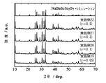
- FIG. 5 is a graph showing diffraction intensity curves obtained by powder X-ray diffraction measurement and diffraction intensity curves obtained by simulation of NaBaScSi 2 O 7 for the phosphor particles obtained in Examples 7 to 11.
- FIG. 5 is a graph showing diffraction intensity curves obtained by powder X-ray diffraction measurement and diffraction intensity curves obtained by simulation of NaBaScSi 2 O 7 for the phosphor particles obtained in Examples 7 to 11.
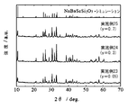
- FIG. 7 is a graph showing diffraction intensity curves obtained by powder X-ray diffraction measurement and diffraction intensity curves obtained by simulation of NaBaScSi 2 O 7 for the phosphor particles obtained in Examples 15 to 18.
- FIG. 7 is a graph showing diffraction intensity curves obtained by powder X-ray diffraction measurement and diffraction intensity curves obtained by simulation of NaBaScSi 2 O 7 for the phosphor particles obtained in Examples 15 to 18.
- FIG. 6 is a graph showing diffraction intensity curves obtained by powder X-ray diffraction measurement and diffraction intensity curves obtained by simulation of NaBaScSi 2 O 7 for the phosphor particles obtained in Examples 19 to 22.
- FIG. FIG. 7 is a graph showing diffraction intensity curves obtained by powder X-ray diffraction measurement and diffraction intensity curves obtained by simulation of NaBaScSi 2 O 7 for the phosphor particles obtained in Examples 23 to 25.
- FIG. It is a graph which shows the measurement result of the excitation spectrum and emission spectrum about the particle
- FIG. 6 is a graph showing emission intensity at emission peak wavelengths in emission spectra for Examples 7 to 11.
- 10 is a graph showing emission intensity at emission peak wavelengths in emission spectra for Examples 15 to 18.
- 6 is a graph showing emission intensity at emission peak wavelengths in emission spectra for Examples 19 to 22.
- 6 is a graph showing emission intensity at emission peak wavelengths in emission spectra for Examples 23 to 25.
- 6 is a graph showing measurement results of excitation spectra and emission spectra for the phosphor particles obtained in Examples 7 to 11.
- 6 is a graph showing measurement results of excitation spectra and emission spectra for the phosphor particles obtained in Examples 28 to 31.
- 6 is a graph showing measurement results of excitation spectra and emission spectra for the phosphor particles obtained in Examples 32-35.
- the phosphor according to the present embodiment has a chemical structure represented by the following general formula (A).
- A is one or more elements selected from Li, Na, and K
- M is one or more elements selected from Mg, Ca, Sr, Ba, and Zn
- L is Ga, Al, Sc, Y
- a is a number that satisfies 0.001 ⁇ a ⁇ 0.3
- b is a number that satisfies 0 ⁇ b ⁇ 0.5
- x is 0 ⁇ x ⁇ It is a number satisfying 0.2.
- compositions represented by the general formulas (1) to (6) to be described later are all subordinate concepts of the composition represented by the general formula (A), and are therefore represented by the general formulas (1) to (6).
- the phosphors having the composition are all included in the phosphor having the chemical structure represented by the general formula (A).
- the composition ratio (molar ratio) of A: (M 1-a x Eu a Mn x ): L: (Si 1-b Ge b ): O is 1: 1: 1: Although it is 2: 7, there may naturally be a case where the composition ratio in the phosphor does not exactly follow this due to partial defects in the crystal structure, contamination of impurities, and other reasons. However, even if the composition ratio of the phosphor is not completely coincident with 1: 1: 1: 2: 7, the composition ratio is substantially 1: 1: 1: 2: 7 based on common general technical knowledge. If considered, this phosphor is within the scope of the present invention.
- the phosphor according to the present embodiment has a chemical structure represented by the following general formula (1).
- A is one or more elements selected from Li, Na, and K
- M is one or more elements selected from Mg, Ca, Sr, Ba, and Zn
- L is Ga, Al, Sc, Y, La
- Gd and Lu a is a number satisfying 0.001 ⁇ a ⁇ 0.3
- b is a number satisfying 0 ⁇ b ⁇ 0.5.
- This phosphor is a silicate-based phosphor activated with divalent europium ions.
- the ion serving as the emission center is a divalent europium ion Eu 2+ .
- This Eu 2+ is dissolved in the crystal by substituting this M for a part of the site occupied by the divalent ions of the metal element M in the crystal.
- the phosphor is excited by efficiently absorbing excitation light in the wavelength range from near ultraviolet light to blue light, particularly in the wavelength range of 350 to 470 nm. Efficiently emits long-wavelength fluorescence.
- A is one or more alkali metal elements selected from Li, Na, and K.
- A may be composed of only one element of Li, Na, and K, or may be composed of two or more elements.
- the ratio of each of the two or more elements in A may be an appropriate ratio.
- a in the general formula (A) and the general formula (1) necessarily contains Li. That is, it is preferable that A consists of Li or A consists of Li and at least one of Na and K. In this case, Eu 2+ ions are easily selectively replaced with the divalent ions of the metal element M at the sites occupied by the divalent ions of the metal element M in the crystal. Therefore, the luminous efficiency of the phosphor is particularly high. Become. In particular, the ratio of Li in A is preferably 1 to 100 mol%.
- a in General Formula (A) and General Formula (1) necessarily contains Na. That is, it is preferable that A consists of Na alone, or A consists of Na and at least one of Li and K. In this case, the crystallinity of the phosphor is further improved.
- a in general formula (A) and general formula (1) consists of at least two elements. That is, it is preferable that A consists of at least two of Na, Li and K. In this case, the emission peak wavelength can be adjusted within a range of several nm by adjusting the composition ratio.
- M is one or more metal elements selected from Mg, Ca, Sr, Ba, and Zn as described above.
- M may be composed of only one element of Mg, Ca, Sr, Ba, or Zn, or may be composed of two or more elements.
- the ratio of each of the two or more elements in M may be an appropriate ratio.
- the metal element M becomes a divalent ion as described above.
- M in the general formula (A) and the general formula (1) necessarily includes Ba. That is, it is preferable that M is composed only of Ba, or that M is composed of Ba and at least one of Mg, Ca, Sr, and Zn. In this case, the crystallinity of the phosphor is further improved.
- M in the general formula (A) and the general formula (1) is composed of at least two elements. That is, it is preferable that M consists of at least two of Mg, Ca, Sr, Ba, and Zn. In this case, the emission peak wavelength can be adjusted within a range of several nm by adjusting the composition ratio.
- a is a number indicating the molar ratio of Eu to the metal element M, and is a number satisfying 0.001 ⁇ a ⁇ 0.3 as described above.
- the value of a is 0.001 or more, the concentration of divalent europium ions in the crystal is sufficiently high, and when the value of a is 0.3 or less, concentration quenching is suppressed, This sufficiently increases the emission intensity of the phosphor.
- the value of a is particularly preferably 0.2 or less. That is, when a is a number satisfying 0.001 ⁇ a ⁇ 0.2, the emission intensity of the phosphor is particularly high.
- a is preferably a number satisfying 0.01 ⁇ a ⁇ 0.1.
- L is one or more metal elements selected from Ga, Al, Sc, Y, La, Gd, and Lu as described above.
- L may be composed of only one element of Ga, Al, Sc, Y, La, Gd, and Lu, or may be composed of two or more elements.
- the ratio of each of the two or more elements in L may be an appropriate ratio.
- the metal element L becomes a trivalent ion.
- L in the general formula (A) and the general formula (1) necessarily includes Sc. That is, it is preferable that L consists only of Sc, or that L consists of Sc and at least one of Ga, Al, Y, La, Gd, and Lu. In this case, the crystallinity of the phosphor is further improved.
- L in the general formula (A) and the general formula (1) includes Sc and further includes Y. That is, it is preferable that L is composed only of Sc and Y, or L is composed of Sc and Y, and at least one of Ga, Al, La, Gd, and Lu. In this case, the emission peak wavelength can be adjusted within a range of several nm by adjusting the composition ratio.
- a part of Si in the crystal may be substituted with Ge.
- b is a number indicating the molar ratio (substitution ratio) of Ge to Si, and is a number satisfying 0 ⁇ b ⁇ 0.5 as described above. When the value of b is 0.5 or less, the high luminous efficiency of the phosphor is maintained.
- a mixture is prepared by blending multiple types of raw materials.
- the blending ratio of the raw materials is adjusted so that the metal element in the mixture matches the composition represented by the general formula (A) or the general formula (1).
- a in the general formula (1) is Na
- M is Ba
- L is Sc
- b 0, that is, a phosphor having a composition of NaBaScSi 2 O 7 : Eu 2+ is produced
- powders of Na 2 CO 3 , BaCO 3 , Eu 2 O 3 , Sc 2 O 3 , and SiO 2 are used. The mixing ratio of these raw materials is adjusted so that the molar ratio of Na, Ba, Sc, Si and Eu in the mixture matches the composition of the phosphor.
- a container made of a material such as alumina or quartz is prepared, and the mixture is put into this container.
- the mixture in the container is fired at a temperature of 1000 to 1300 ° C. in a non-oxidizing gas atmosphere.
- the non-oxidizing gas atmosphere is preferably a weak reducing gas atmosphere such as a hydrogen / nitrogen mixed gas atmosphere.
- a mixture may be pre-baked in air
- the firing temperature at the time of temporary firing is preferably equal to or lower than the firing temperature at the time of main firing (when firing in the non-oxidizing gas atmosphere following the temporary firing).
- the phosphor according to this embodiment can be manufactured through a process in which the raw material is baked at a relatively low temperature of 1000 to 1300 ° C. in a non-oxidizing gas atmosphere. This eliminates the need for manufacturing equipment for high-temperature heating and simplifies the manufacturing process. Therefore, the phosphor according to the present embodiment can be easily manufactured.
- the sintered body obtained by sintering the mixture is crushed and pulverized, and then washed with water or acid to remove unnecessary components. Thereby, a phosphor powder having a target composition is obtained.
- the phosphor according to the present embodiment can be applied to a light emitting device including a light emitting element such as an LED.
- the light-emitting element is not particularly limited, but is preferably a light-emitting element that emits light having a main light emission peak in the range of 350 nm to 470 nm.
- a nitride semiconductor LED is mentioned as a preferable example of such a light emitting element.
- the emission wavelength of the nitride semiconductor LED is 410 nm or less. However, when the emission wavelength is in the range of 365 nm to 410 nm, the nitride semiconductor LED is particularly efficient. Emits light. When the nitride semiconductor LED emits blue light, the nitride semiconductor LED emits light with particularly high efficiency when the emission wavelength of the nitride semiconductor LED is in the range of 420 nm to 480 nm. Therefore, when the phosphor according to the present embodiment is applied to a light-emitting device including such a nitride semiconductor LED, the light-emitting efficiency of the light-emitting device is particularly high.
- the phosphor has a composition represented by the following formula (2).
- a 1 and A 2 are elements selected from Li, Na, and K, and A 1 and A 2 are different from each other.
- a 1 is particularly Na.
- a 2 is in particular K or Li.
- y is a value that indicates the molar ratio of A 2 to the sum of A 1 and A 2. This y may be any number that satisfies 0 ⁇ y ⁇ 1.
- a 1 is Na and A 2 is K
- y preferably satisfies 0.05 ⁇ y ⁇ 0.7.
- a 1 is Na and A 2 is Li
- y preferably satisfies 0.3 ⁇ y ⁇ 0.7.
- the phosphor has a composition represented by the following formula (3).
- the phosphor has a composition represented by the following formula (4).
- z represents the molar ratio of Y to the total of Sc and Y. This z may be any number that satisfies 0 ⁇ z ⁇ 1. In particular, z preferably satisfies 0.05 ⁇ z ⁇ 0.5, and z preferably satisfies 0.05 ⁇ z ⁇ 0.3.
- the phosphor has a composition represented by the following formula (5).
- M 1 and M 2 are elements selected from Mg, Ca, Sr, Ba, and Zn, and M 1 and M 2 are different from each other.
- M 1 is particularly Ba.
- M 2 is particularly Sr or Ca.
- p is a value that indicates the molar ratio of M 1 to the total of M 1, M 2, and Eu
- q denotes a molar ratio of M 2 to the sum of M 1, M 2, and Eu Value.
- M 1 is Ba and M 2 is Sr
- q preferably satisfies 0.1 ⁇ q ⁇ 0.3.
- M 1 is Ba and M 2 is Ca
- q preferably satisfies 0 ⁇ q ⁇ 0.1.
- the phosphor has a composition of 0 ⁇ x ⁇ 0.2 in the general formula (A).
- the phosphor is represented by the following general formula (6), and x has a composition satisfying 0 ⁇ x ⁇ 0.2.
- A is one or more elements selected from Li, Na, and K
- M is one or more elements selected from Mg, Ca, Sr, Ba, and Zn
- L is one or more elements selected from Ga, Al, Sc, Y, La, Gd, and Lu.
- x is a value indicating the molar ratio of Mn to the total of M, Eu, and Mn.
- x is more preferably 0.01 ⁇ x ⁇ 0.2, more preferably 0.01 ⁇ x ⁇ 0.1, and particularly preferably 0.01 ⁇ x ⁇ 0.07. preferable.
- the phosphor is excited by efficiently absorbing the excitation light in the wavelength range from near ultraviolet light to blue light, particularly in the wavelength range of 350 to 470 nm, and is more than the wavelength of the excitation light. Efficiently emits long-wavelength fluorescence.
- the emission spectrum of the phosphor in these embodiments has a strong emission peak in the green range, and the emission color of the phosphor is green.
- the emission spectrum of the phosphor has an emission peak in the red region. This is considered to be because Mn is used as a coactivator.
- the intensity of the emission peak in the red region is small compared to the emission peak in the green region.
- the emission color of the phosphor becomes green, and since a relatively small emission peak also appears in the red region, the color rendering of the light emitting device including this phosphor Especially improved.
- the light emitting device 1 includes an LED chip 10 that is a light emitting element, a mounting substrate 20, an optical member 60, a sealing portion 50, and a wavelength conversion member (color conversion member) 70.
- the wavelength conversion member (color conversion member) 70 includes phosphor particles formed from the phosphor according to the present embodiment.
- the LED chip 10 is mounted on the mounting substrate 20.
- the shape of the mounting substrate 20 is a rectangular plate shape in plan view.
- a pair of conductor patterns 23 for supplying power to the LED chip 10 are formed on the first surface facing the thickness direction of the mounting substrate 20, and the LED chip 10 is further mounted on the first surface.
- the LED chip 10 and the conductor pattern 23 are electrically connected by a bonding wire 14.
- the optical member 60 is a dome-shaped member, and is fixed on the first surface of the mounting substrate 20.
- the LED chip 10 is accommodated between the optical member 60 and the mounting substrate 20.
- the optical member 60 has a function of controlling the orientation of light emitted from the LED chip 10.
- the sealing part 50 is formed from a translucent sealing material.
- the sealing portion 50 is filled in a space surrounded by the optical member 60 and the mounting substrate 20.
- the sealing portion 50 seals the LED chip 10 and a plurality of (in this embodiment, two) bonding wires 14.
- the wavelength conversion member 70 is formed in a dome shape so as to surround the optical member 60.
- the phosphor particles 71 in the wavelength conversion member 70 are excited by the light emitted from the LED chip 10 (excitation light), and fluorescent light having a longer wavelength than the excitation light (the emission color of the LED chip 10 and Emits converted light consisting of light of different colors.
- a gap 80 in which a gas such as air is enriched is interposed between the optical member 60 and the wavelength conversion member 70.
- an annular weir 27 that surrounds the outer periphery of the optical member 60 is formed on the first surface of the mounting substrate 20, an annular weir 27 that surrounds the outer periphery of the optical member 60 is formed.
- the dam portion 27 is formed so as to protrude from the first surface. Therefore, when the optical member 60 is fixed to the mounting substrate 20, even if the sealing material overflows from the space surrounded by the optical member 60 and the mounting substrate 20, the sealing material is blocked by the dam portion 27. I can be dammed up.
- the main light emission peak of the LED chip 10 is preferably in the range of 350 nm to 470 nm.
- Examples of such an LED chip 10 include a GaN-based blue LED chip that emits blue light and a near-ultraviolet LED chip that emits near-ultraviolet light.
- a GaN-based blue LED chip uses an n-type SiC substrate having a lattice constant or crystal structure closer to that of GaN than a sapphire substrate and having conductivity, as a crystal growth substrate.
- a light-emitting portion having a double hetero structure is formed on the SiC substrate.
- the light emitting portion is formed by, for example, an epitaxial growth method (for example, MOVPE method) using a GaN-based compound semiconductor material or the like as a raw material.
- the LED chip 10 includes a cathode electrode on the surface facing the first surface of the mounting substrate 20 and an anode electrode on the opposite surface.
- the cathode electrode and the anode electrode are constituted by, for example, a laminated film of a Ni film and an Au film.
- the material for the cathode electrode and the anode electrode is not particularly limited, and may be any material as long as good ohmic characteristics can be obtained. For example, Al may be used.
- the structure of the LED chip 10 is not limited to the above structure.
- a support substrate such as an Si substrate that supports the light emitting part is fixed to the light emitting part, and then the crystal growth substrate is removed.
- the LED chip 10 may be formed.
- the mounting board 20 includes a rectangular plate-shaped heat transfer plate 21 and a wiring board 22.
- the heat transfer plate 21 is formed from a heat conductive material.
- the LED chip 10 is mounted on the heat transfer plate 21.
- the wiring board 22 is, for example, a rectangular flexible printed wiring board.
- the wiring board 22 is fixed on the heat transfer plate 21 via, for example, a polyolefin-based fixing sheet 29.
- a rectangular window hole 24 that exposes the mounting position of the LED chip 10 on the heat transfer plate 21 is formed at the center of the wiring board 22. Inside this window hole 24, the LED chip 10 is mounted on the heat transfer plate 21 via a submount member 30 described later. Therefore, the heat generated in the LED chip 10 is conducted to the submount member 30 and the heat transfer plate 21 without passing through the wiring board 22.
- the wiring board 22 includes an insulating base material 221 made of a polyimide film and a pair of conductor patterns 23 for supplying power to the LED chip 10 formed on the insulating base material 221. Furthermore, the wiring board 22 includes a protective layer 26 that covers each conductor pattern 23 and covers a portion on the insulating base material 221 where the conductor pattern 23 is not formed.
- the protective layer 26 is formed of, for example, a white resist (resin) having light reflectivity. In this case, even if light is radiated from the LED chip 10 toward the wiring substrate 22, the light is reflected by the protective layer 26, thereby suppressing light absorption in the wiring substrate 22.
- Each conductor pattern 23 is formed in an outer peripheral shape slightly smaller than half of the outer peripheral shape of the insulating base material 221.
- the insulating base material 221 may be formed of an FR4 substrate, an FR5 substrate, a paper phenol resin substrate, or the like.
- Each conductor pattern 23 includes two terminal portions 231 each having a rectangular shape in plan view.
- the terminal portion 231 is located in the vicinity of the window hole 24 of the wiring board 22, and the bonding wire 14 is connected to the terminal portion 231.
- Each conductor pattern 23 further includes one external connection electrode portion 232 having a circular shape in plan view.
- the external connection electrode portion 232 is located near the outer periphery of the wiring board 22.
- the conductor pattern 23 is composed of a laminated film of a Cu film, a Ni film, and an Au film, for example.
- the protective layer 26 is patterned so that each conductor pattern 23 is partially exposed from the protective layer 26. In the vicinity of the window hole 24 of the wiring board 22, the terminal portion 231 in each conductor pattern 23 is exposed from the protective layer 26. Further, the external connection electrode portions 232 in each conductor pattern 23 are exposed from the protective layer 26 near the outer periphery of the wiring board 22.
- the LED chip 10 is mounted on the heat transfer plate 21 via the submount member 30 as described above.
- the submount member 30 relieves stress acting on the LED chip 10 due to a difference in linear expansion coefficient between the LED chip 10 and the heat transfer plate 21.
- the submount member 30 is formed in a rectangular plate shape having a size larger than the chip size of the LED chip 10.
- the submount member 30 has not only a function of relieving the stress but also a heat conduction function of conducting heat generated in the LED chip 10 in a wider range than the chip size of the LED chip 10 in the heat transfer plate 21. Yes.
- the LED chip 10 is mounted on the heat transfer plate 21 via the submount member 30, so that the heat generated by the LED chip 10 passes through the submount member 30 and the heat transfer plate 21.
- the heat acting on the LED chip 10 due to the difference in linear expansion coefficient between the LED chip 10 and the heat transfer plate 21 is relieved.
- the submount member 30 is made of, for example, AlN having a relatively high thermal conductivity and an insulating property.
- the cathode electrode of the LED chip 10 is superposed on the submount member 30, and the cathode electrode is bonded with an electrode pattern (not shown) connected to the cathode electrode and a metal fine wire (for example, a gold fine wire, an aluminum fine wire, etc.). It is electrically connected to one of the two conductor patterns 23 through the wire 14.
- the LED chip 10 is electrically connected through a bonding wire 14 to a conductor pattern 23 that is not connected to the cathode electrode.
- solder such as SnPb, AuSn, SnAgCu, silver paste, or the like is used. It is particularly preferable to use lead-free solder such as AuSn or SnAgCu.
- solder such as SnPb, AuSn, SnAgCu, silver paste, or the like is used. It is particularly preferable to use lead-free solder such as AuSn or SnAgCu.
- the submount member 30 is made of Cu and AuSn is used for bonding the LED chip 10 and the submount member 30, Au or Ag is previously formed on the surfaces of the submount member 30 and the LED chip 10 to be bonded to each other. It is preferable to perform a pretreatment for forming a metal layer made of For joining the submount member 30 and the heat transfer plate 21, for example, lead-free solder such as AuSn or SnAgCu is preferably used.
- the material of the submount member 30 is not limited to AlN, and any material may be used as long as its linear expansion coefficient is relatively close to 6H—SiC, which is a material for a crystal growth substrate, and its thermal conductivity is relatively high.
- SiC which is a material for a crystal growth substrate
- thermal conductivity is relatively high.
- composite SiC, Si, Cu, CuW, or the like may be employed as the material of the submount member 30. Since the submount member 30 has the above-described heat conduction function, the area of the surface of the heat transfer plate 21 facing the LED chip 10 is the area of the surface of the LED chip 10 facing the heat transfer plate 21. It is desirable that it be sufficiently large.
- the heat transfer is larger than the dimension from the surface on the LED chip 10 side facing the thickness direction of the heat transfer plate 21 to the surface on the LED chip 10 side facing the thickness direction of the protective layer 26.
- the dimension from the surface of the plate 21 to the surface on the LED chip 10 side facing the thickness direction of the submount member 30 is larger.
- the thickness dimension of the submount member 30 is set so as to have such a positional relationship. For this reason, the light emitted from the LED chip 10 is suppressed from being absorbed by the wiring board 22 through the inside of the window hole 24 of the wiring board 22. Thereby, the light extraction efficiency from the LED chip 10 to the outside is further improved, and the light output of the light emitting device is further improved.
- a reflective film that reflects light emitted from the LED chip 10 is formed around the position where the LED chip 10 is disposed on the surface of the submount member 30 facing the thickness direction of the LED chip 10. Good. In this case, the light emitted from the LED chip 10 is prevented from being absorbed by the submount member 30. Thereby, the light extraction efficiency from the LED chip 10 to the outside is further improved, and the light output of the light emitting device is further improved.
- the reflective film is composed of, for example, a laminated film of a Ni film and an Ag film.
- a silicone resin may be used as a sealing material that is a material for forming the above-described sealing portion 50.
- a silicone resin may be used.
- an acrylic resin, glass, or the like may be used instead of the silicone resin.
- the optical member 60 is made of a light transmissive material (eg, silicone resin, glass, etc.).
- a light transmissive material eg, silicone resin, glass, etc.
- a difference in refractive index and a difference in linear expansion coefficient between the optical member 60 and the sealing portion 50 can be reduced.
- the light emission surface 602 (surface facing the side opposite to the LED chip 10) of the optical member 60 is light emitted from the light incident surface 601 (surface facing the LED chip 10 side) into the optical member 60.
- a convex curved surface is formed so as not to be totally reflected at the boundary between the surface 602 and the gap 80.
- the optical member 60 is disposed so that the optical axis of the LED chip 10 coincides. Therefore, the light emitted from the LED chip 10 and incident on the light incident surface 601 of the optical member 60 can easily reach the wavelength conversion member 70 without being totally reflected at the boundary between the light emitting surface 602 and the gap layer 80.
- the total luminous flux emitted from the light emitting device increases.
- the optical member 60 is formed to have a uniform thickness along the normal direction regardless of the position.
- the wavelength converting member 70 has a light incident surface 701 (a surface facing the LED chip 10 side) formed in a shape along the light emitting surface 602 of the optical member 60. Therefore, regardless of the position of the light emitting surface 602 of the optical member 60, the distance between the light emitting surface 602 of the optical member 60 and the wavelength conversion member 70 in the normal direction is a substantially constant value.
- the wavelength conversion member 70 is formed so that the thickness along the normal direction is uniform regardless of the position.
- the wavelength conversion member 70 is fixed to the mounting substrate 20 with, for example, an adhesive (for example, silicone resin, epoxy resin).
- Light emitted from the LED chip 10 enters the wavelength conversion member 70 from the light incident surface 701, and goes out of the wavelength conversion member 70 through the light emission surface (surface opposite to the LED chip 10) 702 of the wavelength conversion member 70. Emitted.
- the wavelength conversion member 70 When light passes through the wavelength conversion member 70, a part of this light is wavelength-converted by the phosphor particles in the wavelength conversion member 70. Thereby, light of a color corresponding to the combination of the light emitted from the LED chip 10 and the type of phosphor particles in the wavelength conversion member 70 is emitted from the light emitting device 1.
- the wavelength conversion member 70 includes a translucent medium 72 and a plurality of phosphor particles 71 dispersed in the translucent medium 72. At least a part of the phosphor particles 71 is formed from the phosphor according to the present embodiment.
- the wavelength conversion member 70 contains phosphor particles other than the phosphor particles formed from the phosphor according to the present embodiment as the phosphor particles 71 together with the phosphor particles formed from the phosphor according to the present embodiment. May be.
- the wavelength conversion member 70 is used as the phosphor particle 71 and the fluorescence according to the present embodiment. It contains red phosphor particles together with green phosphor particles formed from the body.
- the blue light emitted from the LED chip 10 without wavelength conversion and the light converted in wavelength by the red phosphor particles and the green phosphor particles in the wavelength conversion member 70 are emitted from the wavelength conversion member 70. The Thereby, white light is emitted from the light emitting device 1.
- the phosphor constituting the red phosphor particles fluorescence having a composition such as (Ca, Sr) 2 Si 5 N 8 : Eu 2+ , (Ca, Sr) AlSiN 3 : Eu 2+ , CaS: Eu 2+.
- the body is mentioned.
- Other green phosphor particles may be used in combination with the green phosphor particles formed from the phosphor according to the present embodiment.
- the phosphor constituting the green phosphor particles formed from the phosphor other than the phosphor according to the present embodiment (Ba, Sr) 2 SiO 4 : Eu 2+ , Y 3 Al 5 O 12 : Ce
- a phosphor having a composition such as 3+ , (Ba, Sr, Ca) Si 2 O 2 N 2 : Eu 2+ , (Ca, Mg) 3 Sc 2 Si 3 O 12 : Ce 3+ , CaSc 2 O 4 : Ce 3+ Can be mentioned.
- the method of selecting the phosphor particles 71 for emitting white light from the light emitting device 1 is not limited to the above example.
- the wavelength conversion member 70 may contain a green phosphor formed from the phosphor according to the present embodiment, yellow phosphor particles, and orange phosphor particles.
- the wavelength conversion member 70 is used as the phosphor particle 71, for example, according to the present embodiment.
- red phosphor particles and blue phosphor particles are contained.
- phosphors constituting the red phosphor particles in this case La 2 O 2 S: Eu 3+ , (Ca, Sr) 2 Si 5 N 8 : Eu 2+ , (Ca, Sr) AlSiN 3 : Eu 2+, etc.
- a phosphor having a composition may be mentioned.
- Examples of the phosphor constituting the blue phosphor particles include BaMgAl 10 O 17 : Eu 2+ , (Sr, Ca, Ba) 10 (PO 4 ) 6 Cl 2 : Eu 2+ , and Sr 3 MgSi 2 O 8 : Eu 2+ .
- a phosphor having a composition may be mentioned.
- Other green phosphor particles may be used in combination with the green phosphor particles formed from the phosphor according to the present embodiment.
- phosphors constituting the green phosphor particles formed from phosphors other than the phosphor according to the present embodiment (Ba, Sr) 2 SiO 4 : Eu 2+ , BaMgAl 10 O 17 : Eu 2+ .
- Examples include phosphors having a composition such as Mn 2+ , (Ba, Sr, Ca) Si 2 O 2 N 2 : Eu 2+ .
- the particle diameter of the phosphor particles 71 is not particularly limited, but the larger the average particle diameter of the phosphor particles 71, the smaller the defect density in the phosphor particles 71, the less energy loss during light emission, and the light emission efficiency. Get higher.
- the average particle diameter of the phosphor particles 71 is preferably 1 ⁇ m or more, and more preferably 5 ⁇ m or more. This average particle diameter is a value measured by a laser diffraction / scattering particle size distribution measuring apparatus.
- the phosphor particles 71 may be subjected to appropriate surface treatment such as coating in order to suppress reflection of excitation light and fluorescence at the interface between the phosphor particles 71 and the translucent medium 72.
- the refractive index of the translucent medium 72 is preferably close to the refractive index of the phosphor particles 71, but is not limited thereto.
- the material of the translucent medium 72 include a silicon compound having a siloxane bond and glass. Since these materials are excellent in heat resistance and light resistance (durability against light having a short wavelength such as blue to ultraviolet), the light is transmitted by light in a wavelength range from blue light to ultraviolet light, which is excitation light of the phosphor particles 71. Deterioration of the medium 72 is suppressed.
- silicon compounds include composites formed by crosslinking a silicone resin, an organosiloxane hydrolysis condensate, an organosiloxane condensate, etc.
- an acrylic resin or an organic / inorganic hybrid material formed by mixing and bonding an organic component and an inorganic component at the nm level or molecular level may be employed.
- the content of the phosphor particles 71 in the wavelength conversion member 70 takes into consideration the types of the phosphor particles 71 and the translucent medium 72, the dimensions of the wavelength conversion member 70, the wavelength conversion capability required for the wavelength conversion member 70, and the like. For example, it is in the range of 5% by mass to 30% by mass.
- the phosphor particles 71 When the wavelength conversion member 70 is irradiated with excitation light of the phosphor particles 71, the phosphor particles 71 absorb the excitation light and emit fluorescence having a wavelength longer than that of the excitation light. Thereby, when light passes through the wavelength conversion member 70, the wavelength of this light is converted by the phosphor particles 71.
- a phosphor (NaBaScSi 2 O7: Eu 2+ ) having a composition in which A is Na, M is Ba, L is Sc, a is 0.01, and b is 0 is synthesized as follows. did.
- each powder of Na 2 CO 3 , BaCO 3 , Eu 2 O 3 , Sc 2 O 3 , and SiO 2 was weighed to obtain 1.0: 1.98: 0.01: 1.0: 4.0.
- the mixed powders were obtained by blending at a molar ratio of 2 and mixing them with a ball mill.
- the mixed powder was placed in an alumina crucible and pre-baked by heating at 1100 ° C. for 12 hours in the air.
- the powder obtained thereby is put in an alumina crucible and heated at 1110 ° C. for 12 hours in a hydrogen / argon mixed gas atmosphere of 5% hydrogen concentration. This was fired.
- the sintered body formed by the main firing was pulverized to obtain phosphor particles.
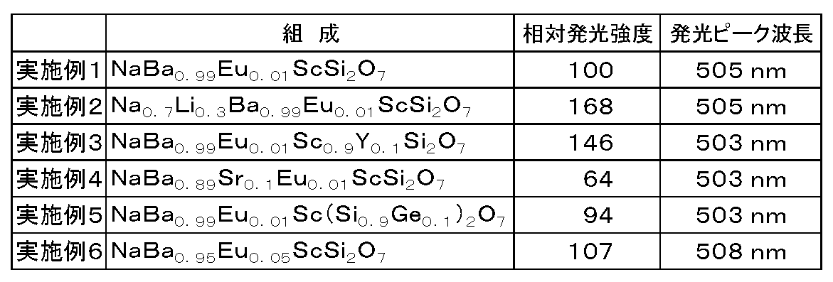
- Example 2 phosphors having the compositions shown in Table 1 were produced by changing the raw material composition for producing the phosphors.
- raw materials not used in Example 1 Li 2 CO 3 as a Li compound, SrCO 3 as a Sr compound, Y 2 O 3 as a Y compound, and GeO 2 as a Ge compound were used.
- Table 1 also shows the emission intensity of the fluorescence emitted from the phosphors obtained in Examples 1 to 6.
- This emission intensity is the intensity of the peak wavelength of the emission spectrum, and is a value (relative emission intensity) normalized by setting the emission intensity value of the phosphor obtained in Example 1 to 100.
- the excitation spectra of the phosphors obtained in Examples 1 to 6 were also measured simultaneously using the above apparatus.
- the monitor wavelength was the peak wavelength in the emission spectrum.
- the waveform of the excitation spectrum of these phosphors is relatively flat from the near ultraviolet region to the blue region, and therefore emits light even when the wavelength of the excitation light varies in the near ultraviolet region to the blue region. It was confirmed that the intensity fluctuation was small.
- FIG. 5 shows the excitation spectrum of the phosphor obtained in Example 1.
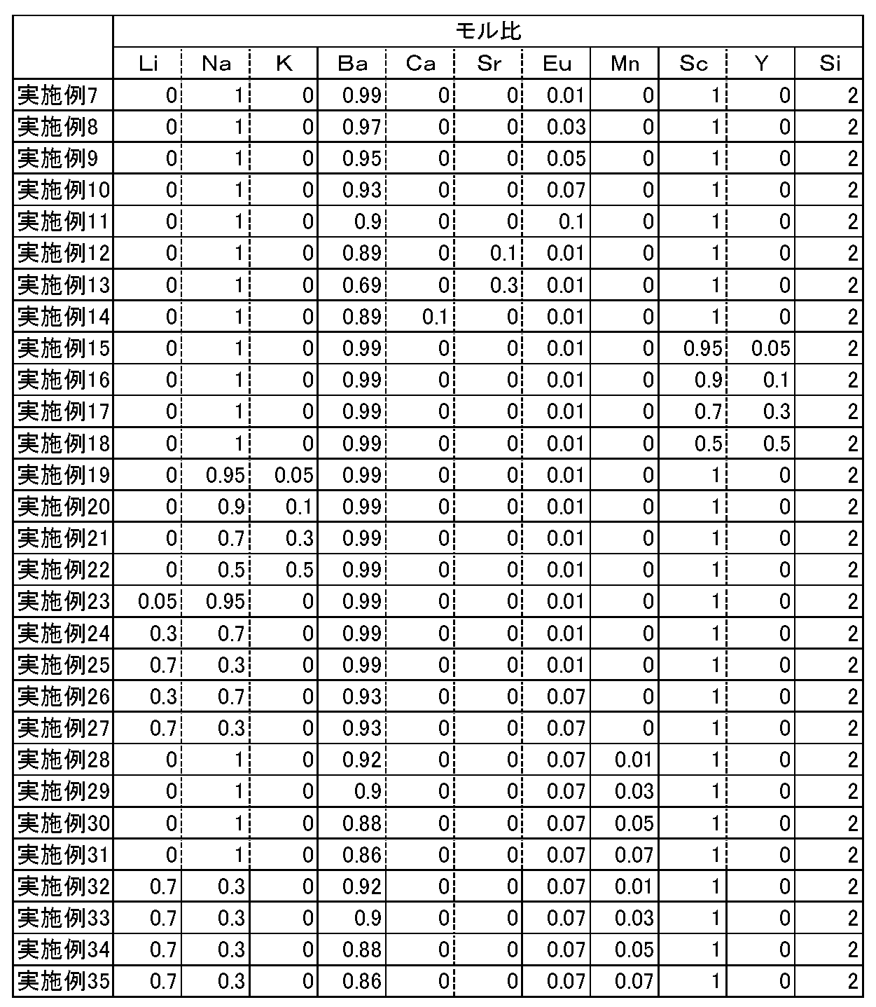
- Li 2 CO 3 powder as a raw material containing Li, Na 2 CO 3 powder as a raw material containing Na, K 2 CO 3 powder as a raw material containing K, BaCO 3 powder as a raw material containing Ba, and a raw material containing Ca as a CaCO 3, a SrCO 3 powder as a raw material containing Sr, a MnCO 3 powder as raw material containing Mn, the Eu 2 O 3 powder as a raw material containing Eu, and Sc 2 O 3 as a raw material containing Sc, and Y Y 2 O 3 powder was prepared as a raw material containing, and SiO 2 powder was prepared as a raw material containing Si, respectively.
- Example 7 the raw materials were blended so that the molar ratio of Na, Ba, Eu, Sc, and Si was 1: (1-a): a: 1: 2.
- the raw materials were blended so that the molar ratio of Na, Ba, Sr, Eu, Sc, and Si was 1: p: q: a: 1: 2.
- Example 14 the raw materials were blended so that the molar ratio of Na, Ba, Ca, Eu, Sc and Si was 1: p: q: a: 1: 2.
- Example 15 to 18 the raw materials were blended so that the molar ratio of Na, Ba, Eu, Sc, Y, and Si was 1: (1-a): a: (1-z): z: 2. .
- the raw materials were blended so that the molar ratio of Na, K, Ba, Eu, Sc, and Si was (1-y): y: (1-a): a: 1: 2.
- the raw materials were blended so that the molar ratio of Na, Li, Ba, Eu, Sc, and Si was (1-y): y: (1-a): a: 1: 2.
- Example 28 to 31 the raw materials were blended so that the molar ratio of Na, Ba, Eu, Mn, Sc, and Si was 1: (0.93-x): 0.07: x: 1: 2.
- the molar ratio of Li, Na, Ba, Mn, Eu, Sc, and Si was 0.7: 0.3: (0.93-x): 0.07: x: 1: 2.
- the raw materials were blended so that
- Tables 2 and 3 show specific molar ratios of metal elements and values of a, p, q, y, and z in each example.
- the mixture was placed in an alumina crucible and pre-baked by heating at 1100 ° C. for 12 hours in the air.
- the powder obtained thereby is put in an alumina crucible and heated at 1110 ° C. for 12 hours in a hydrogen / argon mixed gas atmosphere of 5% hydrogen concentration. This was fired.
- the sintered body formed by the main firing was pulverized to obtain phosphor particles.
- the wavelength of the excitation light was set to 450 nm.
- the monitor wavelength was the wavelength at which the emission intensity of the emission spectrum was the maximum value in each example.
- the peak wavelength in the emission spectrum was around 500 nm, and the color of the fluorescence emitted from these phosphor particles was green. Furthermore, in the phosphor particles obtained in any of the examples, the waveform of the excitation spectrum is relatively flat from the near ultraviolet region to the blue region. Therefore, the excitation particles are excited in the near ultraviolet region to the blue region. It was confirmed that even if the wavelength of light fluctuates, the fluctuation of the emission intensity is small.
- FIG. 12 shows an emission spectrum (solid line) and an excitation spectrum (dashed line) for the phosphor particles obtained in Example 27.
- the emission intensity in FIG. 12 is a value (relative emission intensity) normalized by setting the emission intensity at the peak wavelength to 100.
- Table 4 and FIG. 13 below show the emission intensity at the emission peak wavelength in the emission spectrum for Examples 7 to 11.
- the emission intensity is a value (relative emission intensity) normalized by setting the emission intensity value of the phosphor obtained in Example 7 to 100.
- Table 5 below shows the emission intensity at the emission peak wavelength in the emission spectrum for Examples 7 and 12 to 14.
- the emission intensity is a value (relative emission intensity) normalized by setting the emission intensity value of the phosphor obtained in Example 7 to 100.
- Table 6 below and FIG. 14 show the emission intensity at the emission peak wavelength in the emission spectrum for Examples 7 and 15 to 18.
- the emission intensity is a value (relative emission intensity) normalized by setting the emission intensity value of the phosphor obtained in Example 7 to 100.
- Table 7 and FIG. 15 below show the emission intensity at the emission peak wavelength in the emission spectrum for Examples 7 and 19-22.
- the emission intensity is a value (relative emission intensity) normalized by setting the emission intensity value of the phosphor obtained in Example 7 to 100.
- FIG. 16 shows the emission intensity at the emission peak wavelength in the emission spectrum for Examples 7 and 23 to 25.
- the emission intensity is a value (relative emission intensity) normalized by setting the emission intensity value of the phosphor obtained in Example 7 to 100.
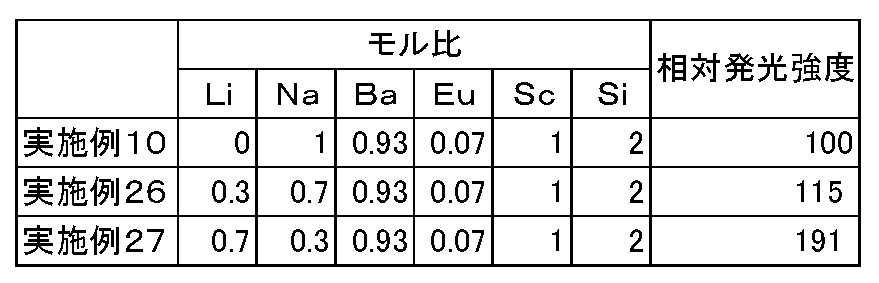
- Table 8 below shows the emission intensity at the emission peak wavelength in the emission spectrum for Examples 10, 26 and 27.
- the emission intensity is a value (relative emission intensity) normalized by setting the emission intensity value of the phosphor obtained in Example 10 to 100.
- Example 9 has the same composition as Example 6, but the emission intensity is higher in Example 9. Since the measurement result of the emission intensity of Example 9 was highly reproducible, it is determined that the measurement result of Example 9 is more reliable.
- the emission spectra of the fluorescence emitted from the phosphors obtained in Examples 7 to 11 and Examples 28 to 35 were measured.
- a measuring apparatus a spectrofluorometer FP-6500 manufactured by JASCO Corporation was used, and the wavelength of the excitation light applied to the phosphor was set to 450 nm.
- the excitation spectra of the phosphors obtained in Examples 7 to 11 were measured simultaneously using the above apparatus.
- the monitor wavelength was the peak wavelength in the emission spectrum of each phosphor.
- the waveform of the excitation spectrum of these phosphors is relatively flat from the near ultraviolet region to the blue region, and therefore emits light even when the wavelength of the excitation light varies in the near ultraviolet region to the blue region. It was confirmed that the intensity fluctuation was small.
- FIG. 17 shows an emission spectrum (solid line) and an excitation spectrum (dashed line) for the phosphor particles obtained in Examples 7 to 11.
- FIG. 18 shows the emission spectrum (solid line) and the excitation spectrum (dashed line) for the phosphor particles obtained in Examples 28 to 31.
- FIG. 19 shows an emission spectrum (solid line) and an excitation spectrum (dashed line) for the phosphor particles obtained in Examples 32-35.
- the peak wavelengths in the emission spectra of the phosphor particles obtained in Examples 7 to 11 and Examples 28 to 31 are in the vicinity of 500 nm and are emitted from these phosphor particles.
- the fluorescent color was green.
- the waveform of the excitation spectrum of these phosphor particles is relatively flat from the near ultraviolet region to the blue region, so that the wavelength of the excitation light varies in the near ultraviolet region to the blue region. Also, it was confirmed that the fluctuation of the emission intensity was small.
- Table 9 below shows the emission intensity at the emission peak wavelength in the emission spectrum for the phosphors obtained in Examples 7 to 11 and Examples 28 to 35.
- the emission intensity is a value (relative emission intensity) normalized by setting the emission intensity value of the phosphor obtained in Example 7 to 100.
- Table 9 also shows the ratio of the intensity of the maximum peak in the red region to the intensity of the maximum peak in the green region in the emission spectrum for the phosphors obtained in Examples 28 to 35.
Landscapes
- Chemical & Material Sciences (AREA)
- Engineering & Computer Science (AREA)
- Inorganic Chemistry (AREA)
- Materials Engineering (AREA)
- Organic Chemistry (AREA)
- Microelectronics & Electronic Packaging (AREA)
- Manufacturing & Machinery (AREA)
- Computer Hardware Design (AREA)
- Power Engineering (AREA)
- Led Device Packages (AREA)
- Luminescent Compositions (AREA)
Abstract
Description
(AはLi,Na,及びKの中から選ばれる一種以上の元素、MはMg,Ca,Sr,Ba,及びZnの中から選ばれる一種以上の元素、LはGa,Al,Sc,Y,La,Gd,及びLuの中から選ばれる一種以上の元素、aは0.001≦a≦0.3を満たす数、bは0≦b≦0.5を満たす数、xは0≦x≦0.2を満たす数である。)
本発明において、前記一般式(A)における、xが、x=0を満たすことが好ましい。この場合、本発明に係る蛍光体は、下記一般式(1)で表される化学構造を有する。
(AはLi,Na,及びKの中から選ばれる一種以上の元素、MはMg,Ca,Sr,Ba,Zn,及びMnの中から選ばれる一種以上の元素、LはGa,Al,Sc,Y,La,Gd,及びLuの中から選ばれる一種以上の元素、aは0.001≦a≦0.3を満たす数、bは0≦b≦0.5を満たす数である。)
本発明において、前記一般式(A)におけるxが、0<x≦0.2を満たすことも好ましい。
本発明において、前記一般式(A)におけるAにNaが含まれていることも好ましい。
(A1及びA2はLi,Na,及びKの中から選ばれる元素であり、A1とA2とは互いに異なる。yは、0<y<1を満たす数であり、aは0.001≦a≦0.3を満たす数である。)
本発明に係る蛍光体は、下記一般式(3)で表される組成を有することも好ましい。
(aは0.001≦a≦0.3を満たす数である。)
本発明に係る蛍光体は、下記一般式(4)で表される組成を有することも好ましい。
(zは0<z<1を満たす数、aは0.001≦a≦0.3を満たす数である。)
本発明に係る蛍光体は、下記一般式(5)で表される組成を有することも好ましい。
(M1及びM2はMg,Ca,Sr,Ba,及びZnの中から選ばれる元素であり、M1とM2とは互いに異なる。aは0.001≦a≦0.3を満たす数であり、pは0<p<1を満たす数であり、qは0<q<1を満たす数であり、p、q及びaはp+q+a=1を満たす。)
本発明に係る蛍光体は、下記一般式(6)で表される組成を有することも好ましい。
(AはLi,Na,及びKの中から選ばれる一種以上の元素、M3はMg,Ca,Sr,Ba,及びZnの中から選ばれる一種以上の元素、LはGa,Al,Sc,Y,La,Gd,及びLuの中から選ばれる一種以上の元素、aは0.001≦a≦0.3を満たす数、bは0≦b≦0.5を満たす数、xは0.01≦x≦0.1を満たす数である。)
本発明に係る発光装置は、主発光ピークが350nm~470nmの範囲にある光を発する発光素子と、前記発光素子から発せられる光を吸収して発光する波長変換部材とを備え、前記波長変換部材が前記蛍光体を備えている。
本実施形態による蛍光体は、下記一般式(A)で表される化学構造を有する。
AはLi,Na,及びKの中から選ばれる一種以上の元素、MはMg,Ca,Sr,Ba,及びZnの中から選ばれる一種以上の元素、LはGa,Al,Sc,Y,La,Gd,及びLuの中から選ばれる一種以上の元素、aは0.001≦a≦0.3を満たす数、bは0≦b≦0.5を満たす数、xは0≦x≦0.2を満たす数である。
AはLi,Na,Kの中から選ばれる一種以上の元素、MはMg,Ca,Sr,Ba,Znの中から選ばれる一種以上の元素、LはGa,Al,Sc,Y,La,Gd,Luの中から選ばれる一種以上の元素、aは0.001≦a≦0.3を満たす数、bは0≦b≦0.5を満たす数である。
この第一の態様において、A1及びA2はLi,Na,Kの中から選ばれる元素であり、A1とA2とは互いに異なる。A1としては特にNaが挙げられる。A2としては特にK又はLiが挙げられる。
第三の態様においては、蛍光体は次の式(4)に示される組成を有する。
式(4)において、zはScとYの合計に対するYのモル比を示す。このzは、0<z<1を満たす数であればよい。特にzは0.05≦z≦0.5を満たすことが好ましく、zは0.05<z<0.3を満たすことも好ましい。
この第四の態様において、M1及びM2はMg,Ca,Sr,Ba,Znの中から選ばれる元素であり、M1とM2とは互いに異なる。M1としては特にBaが挙げられる。M2としては特にSr又はCaが挙げられる。
この第五の態様において、AはLi,Na,及びKの中から選ばれる一種以上の元素であり、MはMg,Ca,Sr,Ba,及びZnの中から選ばれる一種以上の元素であり、LはGa,Al,Sc,Y,La,Gd,及びLuの中から選ばれる一種以上の元素である。
本実施形態に係る発光装置について説明する。この発光装置1は、図1,2に示されるように、発光素子であるLEDチップ10、実装基板20、光学部材60、封止部50、並びに波長変換部材(色変換部材)70を備える。後述するように、波長変換部材(色変換部材)70は本実施形態に係る蛍光体から形成される蛍光体粒子を備える。
る蛍光体が挙げられる。本実施形態に係る蛍光体から形成される緑色蛍光体粒子と共に、それ以外の緑色蛍光体粒子が併用されてもよい。この場合の本実施形態に係る蛍光体以外の蛍光体から形成される緑色蛍光体粒子を構成する蛍光体としては、(Ba,Sr)2SiO4:Eu2+、Y3Al5O12:Ce3+、(Ba,Sr,Ca)Si2O2N2:Eu2+、(Ca,Mg)3Sc2Si3O12:Ce3+、CaSc2O4:Ce3+などの組成を有する蛍光体が挙げられる。発光装置1から白色光が出射されるための、蛍光体粒子71の選定の仕方は、前記の例に限られない。例えば波長変換部材70は、本実施形態に係る蛍光体から形成される緑色蛍光体と、黄色蛍光体粒子及び橙色蛍光体粒子とを含有してもよい。
一般式(1)中のAがNa、MがBa、LがSc、aが0.01、bが0である組成を有する蛍光体(NaBaScSi2O7:Eu2+)を、次のように合成した。
実施例1において、蛍光体を作製するための原料組成を変更することで、表1に示す組成を有する蛍光体を作製した。実施例1では使用されていない原料としては、Li化合物であるLi2CO3、Sr化合物であるSrCO3、Y化合物であるY2O3、並びにGe化合物であるGeO2を用いた。
実施例1~6で得られた蛍光体から発せられる蛍光の発光スペクトルを測定した。測定装置としては日本分光株式会社製の分光蛍光光度計FP-6500を用い、蛍光体へ照射する励起光の波長は450nmとした。その結果、実施例1~6で得られた蛍光体の発光スペクトルのピーク波長は表1に示される値であり、これらの発光スペクトルはピーク波長を中心としたブロードなスペクトルであった。これらの蛍光体から発せられた蛍光の色は緑色であった。図4は実施例1で得られた蛍光体の発光スペクトルを示す。
Liを含む原料としてLi2CO3粉末を、Naを含む原料としてNa2CO3粉末を、Kを含む原料としてK2CO3粉末を、Baを含む原料としてBaCO3粉末を、Caを含む原料としてCaCO3を、Srを含む原料としてSrCO3粉末を、Mnを含む原料としてMnCO3粉末を、Euを含む原料としてEu2O3粉末を、Scを含む原料としてSc2O3を、Yを含む原料としてY2O3粉末を、Siを含む原料としてSiO2粉末を、それぞれ用意した。

実施例7~25で得られた蛍光体の粒子の、CuKα線を利用した粉末X線回折測定をおこなった。実施例7~11についての結果を図6に、実施例12,13についての結果を図7に、実施例14についての結果を図8に、実施例15~18についての結果を図9に、実施例19~22についての結果を図10に、実施例23~25についての結果を図11に、それぞれ示す。更に、参考のため、図7~11には、NaBaScSi2O7の、シミュレーションにより得られた回折強度曲線も併せて示す。
実施例7~27で得られた蛍光体の粒子について、励起スペクトルと発光スペクトルを測定した。測定装置としては日本分光株式会社製の分光蛍光光度計FP-6500を用いた。


70 波長変換部材
Claims (16)
- 下記一般式(A)で表される化学構造を有する蛍光体。
A(M1‐a-xEuaMnx)L(Si1‐bGeb)2O7 …(A)
(AはLi,Na,及びKの中から選ばれる一種以上の元素、MはMg,Ca,Sr,Ba,及びZnの中から選ばれる一種以上の元素、LはGa,Al,Sc,Y,La,Gd,及びLuの中から選ばれる一種以上の元素、aは0.001≦a≦0.3を満たす数、bは0≦b≦0.5を満たす数、xは0≦x≦0.2を満たす数である。) - 前記一般式(A)におけるxが、x=0を満たす請求項1に記載の蛍光体。
- 前記一般式(A)におけるxが、0<x≦0.2を満たす請求項1に記載の蛍光体。
- 前記一般式(A)におけるAにLiが含まれている請求項1乃至3のいずれか一項に記載の蛍光体。
- 前記一般式(A)におけるAにNaが含まれている請求項1乃至4のいずれか一項に記載の蛍光体。
- 前記一般式(A)におけるAが少なくとも二種の元素からなる請求項1乃至5のいずれか一項に記載の蛍光体。
- 前記一般式(A)におけるMにBaが含まれている請求項1乃至6のいずれか一項に記載の蛍光体。
- 前記一般式(A)におけるMが少なくとも二種の元素からなる請求項1乃至7のいずれか一項に記載の蛍光体。
- 前記一般式(A)におけるLにScが含まれている請求項1乃至8のいずれか一項に記載の蛍光体。
- 前記一般式(A)におけるLに更にYが含まれている請求項9に記載の蛍光体。
- 下記一般式(2)で表される組成を有する請求項1,2又は4に記載の蛍光体。
A1 1-yA2 yBa1-aEuaScSi2O7 …(2)
(A1及びA2はLi,Na,及びKの中から選ばれる元素であり、A1とA2とは互いに異なる。yは、0<y<1を満たす数であり、aは0.001≦a≦0.3を満たす数である。) - 下記一般式(3)で表される組成を有する請求項1又は2に記載の蛍光体。
NaBa1-aEuaScSi2O7 …(3)
(aは0.001≦a≦0.3を満たす数である。) - 下記一般式(4)で表される組成を有する請求項1又は2に記載の蛍光体。
NaBa1-aEuaSc1-zYzSi2O7 …(4)
(zは0<z<1を満たす数、aは0.001≦a≦0.3を満たす数である。) - 下記一般式(5)で表される組成を有する請求項1又は2に記載の蛍光体。
NaM1 pM2 qEuaScSi2O7 …(5)
(M1及びM2はMg,Ca,Sr,Ba,及びZnの中から選ばれる元素であり、M1とM2とは互いに異なる。aは0.001≦a≦0.3を満たす数であり、pは0<p<1を満たす数であり、qは0<q<1を満たす数であり、p、q及びaはp+q+a=1を満たす。) - 下記一般式(6)で表される組成を有する請求項3に記載の蛍光体。
A(M3 1‐a-xEuaMnx)L(Si1‐bGeb)2O7 …(6)
(AはLi,Na,及びKの中から選ばれる一種以上の元素、MはMg,Ca,Sr,Ba,及びZnの中から選ばれる一種以上の元素、LはGa,Al,Sc,Y,La,Gd,及びLuの中から選ばれる一種以上の元素、aは0.001≦a≦0.3を満たす数、bは0≦b≦0.5を満たす数、xは0.01≦x≦0.2を満たす数である。) - 主発光ピークが350nm~470nmの範囲にある光を発する発光素子と、前記発光素子から発せられる光を吸収して発光する波長変換部材とを備え、前記波長変換部材が請求項1乃至15のいずれか一項記載の蛍光体を備えている発光装置。
Priority Applications (4)
| Application Number | Priority Date | Filing Date | Title |
|---|---|---|---|
| CN201180043068.2A CN103097488B (zh) | 2010-11-30 | 2011-11-28 | 荧光体及发光装置 |
| JP2012546857A JP5677463B2 (ja) | 2010-11-30 | 2011-11-28 | 蛍光体及び発光装置 |
| US13/818,766 US8816377B2 (en) | 2010-11-30 | 2011-11-28 | Phosphor and light emitting device |
| EP11845308.3A EP2604669B1 (en) | 2010-11-30 | 2011-11-28 | Phosphor and light emitting device |
Applications Claiming Priority (4)
| Application Number | Priority Date | Filing Date | Title |
|---|---|---|---|
| JP2010-267108 | 2010-11-30 | ||
| JP2010267108 | 2010-11-30 | ||
| JP2011027495 | 2011-02-10 | ||
| JP2011-027495 | 2011-02-10 |
Publications (1)
| Publication Number | Publication Date |
|---|---|
| WO2012073887A1 true WO2012073887A1 (ja) | 2012-06-07 |
Family
ID=46171819
Family Applications (1)
| Application Number | Title | Priority Date | Filing Date |
|---|---|---|---|
| PCT/JP2011/077378 WO2012073887A1 (ja) | 2010-11-30 | 2011-11-28 | 蛍光体及び発光装置 |
Country Status (6)
| Country | Link |
|---|---|
| US (1) | US8816377B2 (ja) |
| EP (1) | EP2604669B1 (ja) |
| JP (1) | JP5677463B2 (ja) |
| CN (1) | CN103097488B (ja) |
| TW (1) | TWI418611B (ja) |
| WO (1) | WO2012073887A1 (ja) |
Cited By (4)
| Publication number | Priority date | Publication date | Assignee | Title |
|---|---|---|---|---|
| CN102703073A (zh) * | 2012-06-18 | 2012-10-03 | 中国科学院福建物质结构研究所 | 钪硅酸盐荧光粉及其制备方法 |
| CN103172356A (zh) * | 2013-01-18 | 2013-06-26 | 河北联合大学 | 一种Sr2MgSi2O7:Eu2+,Dy3+透明陶瓷的合成方法 |
| WO2017069455A1 (ko) * | 2015-10-21 | 2017-04-27 | 주식회사 효성 | 산질화물 형광체와 그 제조방법 및 백색 발광소자 |
| KR20180078448A (ko) * | 2016-12-29 | 2018-07-10 | 주식회사 효성 | 산질화물 형광체와 그 제조방법 |
Families Citing this family (7)
| Publication number | Priority date | Publication date | Assignee | Title |
|---|---|---|---|---|
| US9699422B2 (en) | 2011-10-04 | 2017-07-04 | Prysm, Inc. | Composite and other phosphor materials for emitting visible light and applications in generation of visible light including light-emitting screens |
| CN103275718A (zh) * | 2013-06-18 | 2013-09-04 | 中国地质大学(北京) | 一种绿光型硅酸盐荧光粉及其制备方法 |
| EP3043395B1 (en) | 2013-09-05 | 2018-11-07 | Panasonic Intellectual Property Management Co., Ltd. | Light-emitting device |
| DE102013113382A1 (de) | 2013-12-03 | 2015-06-03 | Osram Gmbh | Leuchtstoffmischung, Licht emittierendes Halbleiterbauelement mit einer Leuchtstoffmischung und Straßenlaterne mit einer Leuchtstoffmischung |
| CN107431112B (zh) * | 2015-04-03 | 2020-01-10 | 夏普株式会社 | 发光装置 |
| CN111575004B (zh) * | 2020-05-27 | 2023-03-24 | 杭州电子科技大学 | 一种Eu2+掺杂的蓝-绿光可控的荧光粉及其制备方法和应用 |
| CN113249125B (zh) * | 2021-04-02 | 2022-10-18 | 杭州电子科技大学 | Ce3+掺杂的硅酸盐基绿色荧光粉及其制备方法和应用 |
Citations (6)
| Publication number | Priority date | Publication date | Assignee | Title |
|---|---|---|---|---|
| JP2004161981A (ja) * | 2002-09-24 | 2004-06-10 | Nichia Chem Ind Ltd | 蛍光体 |
| JP3700502B2 (ja) | 1996-07-29 | 2005-09-28 | 日亜化学工業株式会社 | 発光ダイオード |
| WO2007029369A1 (ja) * | 2005-09-06 | 2007-03-15 | Niigata University | 発光ダイオード用蛍光体 |
| JP2008069250A (ja) * | 2006-09-13 | 2008-03-27 | Niigata Univ | 発光ダイオード用蛍光体 |
| JP4104013B2 (ja) | 2005-03-18 | 2008-06-18 | 株式会社フジクラ | 発光デバイス及び照明装置 |
| JP4148245B2 (ja) | 2004-06-30 | 2008-09-10 | 三菱化学株式会社 | 蛍光体、及び、それを用いた発光素子、並びに、画像表示装置、照明装置 |
Family Cites Families (15)
| Publication number | Priority date | Publication date | Assignee | Title |
|---|---|---|---|---|
| US6013199A (en) * | 1997-03-04 | 2000-01-11 | Symyx Technologies | Phosphor materials |
| US6466135B1 (en) * | 2000-05-15 | 2002-10-15 | General Electric Company | Phosphors for down converting ultraviolet light of LEDs to blue-green light |
| US6809781B2 (en) * | 2002-09-24 | 2004-10-26 | General Electric Company | Phosphor blends and backlight sources for liquid crystal displays |
| DE10259946A1 (de) * | 2002-12-20 | 2004-07-15 | Tews, Walter, Dipl.-Chem. Dr.rer.nat.habil. | Leuchtstoffe zur Konversion der ultravioletten oder blauen Emission eines lichtemittierenden Elementes in sichtbare weiße Strahlung mit sehr hoher Farbwiedergabe |
| US6953536B2 (en) * | 2003-02-25 | 2005-10-11 | University Of Georgia Research Foundation, Inc. | Long persistent phosphors and persistent energy transfer technique |
| US8308980B2 (en) * | 2004-06-10 | 2012-11-13 | Seoul Semiconductor Co., Ltd. | Light emitting device |
| CN100472827C (zh) * | 2004-11-18 | 2009-03-25 | 皇家飞利浦电子股份有限公司 | 具有转换结构的发光设备 |
| US7276183B2 (en) * | 2005-03-25 | 2007-10-02 | Sarnoff Corporation | Metal silicate-silica-based polymorphous phosphors and lighting devices |
| US7733310B2 (en) * | 2005-04-01 | 2010-06-08 | Prysm, Inc. | Display screens having optical fluorescent materials |
| JP5291458B2 (ja) * | 2005-05-25 | 2013-09-18 | コーニンクレッカ フィリップス エレクトロニクス エヌ ヴィ | エレクトロルミネッセンス装置 |
| US7952270B2 (en) * | 2005-07-14 | 2011-05-31 | Koninklijke Philips Electronics N.V. | Electroluminescent device |
| DE102006037730A1 (de) * | 2006-08-11 | 2008-02-14 | Merck Patent Gmbh | LED-Konversionsleuchtstoffe in Form von keramischen Körpern |
| TWI351767B (en) * | 2007-10-02 | 2011-11-01 | Nanya Technology Corp | Two-bit flash memory |
| CN101824321B (zh) * | 2010-04-13 | 2012-09-19 | 中国科学院长春光学精密机械与物理研究所 | 一种基于蓝光激发的白光led用荧光粉及其制备方法 |
| CN101805607A (zh) * | 2010-04-15 | 2010-08-18 | 南昌大学 | 硅酸盐绿光荧光粉的低温合成方法 |
-
2011
- 2011-11-28 WO PCT/JP2011/077378 patent/WO2012073887A1/ja active Application Filing
- 2011-11-28 TW TW100143551A patent/TWI418611B/zh active
- 2011-11-28 JP JP2012546857A patent/JP5677463B2/ja active Active
- 2011-11-28 EP EP11845308.3A patent/EP2604669B1/en active Active
- 2011-11-28 US US13/818,766 patent/US8816377B2/en active Active
- 2011-11-28 CN CN201180043068.2A patent/CN103097488B/zh active Active
Patent Citations (6)
| Publication number | Priority date | Publication date | Assignee | Title |
|---|---|---|---|---|
| JP3700502B2 (ja) | 1996-07-29 | 2005-09-28 | 日亜化学工業株式会社 | 発光ダイオード |
| JP2004161981A (ja) * | 2002-09-24 | 2004-06-10 | Nichia Chem Ind Ltd | 蛍光体 |
| JP4148245B2 (ja) | 2004-06-30 | 2008-09-10 | 三菱化学株式会社 | 蛍光体、及び、それを用いた発光素子、並びに、画像表示装置、照明装置 |
| JP4104013B2 (ja) | 2005-03-18 | 2008-06-18 | 株式会社フジクラ | 発光デバイス及び照明装置 |
| WO2007029369A1 (ja) * | 2005-09-06 | 2007-03-15 | Niigata University | 発光ダイオード用蛍光体 |
| JP2008069250A (ja) * | 2006-09-13 | 2008-03-27 | Niigata Univ | 発光ダイオード用蛍光体 |
Non-Patent Citations (7)
| Title |
|---|
| AKIRA KOMENO ET AL.: "Shinki Keisan'enkei Keikotai no Kaihatsu", 18TH FALL MEETING OF THE CERAMIC SOCIETY OF JAPAN, DAI 1 KAI ASIA-OCEANIA CERAMIC RENMEI KOKUSAI KAIGI KOEN YOKOSHU, 27 September 2005 (2005-09-27), pages 435, XP008169759 * |
| IOSHITAKA KAWAKAMI ET AL.: "Shinki LED-yo Keikotai no Kaihatsu", 19TH FALL MEETING DF THE CERAMIC SOCIETY OF JAPAN KOEN YOKOSHU, 19 September 2006 (2006-09-19), pages 87, XP008169755 * |
| See also references of EP2604669A4 |
| TOMOYUKI NAKANO ET AL.: "Hakushoku LED-yo no Shinki na Ba-Sc-Si-kei Sankabutsu to Sanchikkabutsu no Gosei", 21ST FALL MEETING OF THE CERAMIC SOCIETY OF JAPAN KOEN YOKOSHU, 17 September 2008 (2008-09-17), pages 246, XP008169757 * |
| YOSHITAKA KAWAKAMI ET AL.: "Development of novel alkaline earth silicate phosphor for LED", RARE EARTHS, 23 May 2006 (2006-05-23), pages 136 - 137, XP008170616 * |
| YOSHITAKA KAWAKAMI ET AL.: "Development of novel green phosphor for a white LED", RARE EARTHS, 10 May 2007 (2007-05-10), pages 146 - 147, XP008170617 * |
| YOSHITAKA KAWAKAMI ET AL.: "Shinki Hakushoku LED-yo Keikotai no Kaihatsu", 20TH FALL MEETING OF THE CERAMIC SOCIETY OF JAPAN KOEN YOKOSHU, 12 September 2007 (2007-09-12), XP008169756 * |
Cited By (6)
| Publication number | Priority date | Publication date | Assignee | Title |
|---|---|---|---|---|
| CN102703073A (zh) * | 2012-06-18 | 2012-10-03 | 中国科学院福建物质结构研究所 | 钪硅酸盐荧光粉及其制备方法 |
| CN102703073B (zh) * | 2012-06-18 | 2016-08-03 | 中国科学院福建物质结构研究所 | 钪硅酸盐荧光粉及其制备方法 |
| CN103172356A (zh) * | 2013-01-18 | 2013-06-26 | 河北联合大学 | 一种Sr2MgSi2O7:Eu2+,Dy3+透明陶瓷的合成方法 |
| WO2017069455A1 (ko) * | 2015-10-21 | 2017-04-27 | 주식회사 효성 | 산질화물 형광체와 그 제조방법 및 백색 발광소자 |
| KR101737230B1 (ko) * | 2015-10-21 | 2017-05-18 | 주식회사 효성 | 산질화물 형광체와 그 제조방법 및 백색 발광소자 |
| KR20180078448A (ko) * | 2016-12-29 | 2018-07-10 | 주식회사 효성 | 산질화물 형광체와 그 제조방법 |
Also Published As
| Publication number | Publication date |
|---|---|
| TW201237146A (en) | 2012-09-16 |
| JP5677463B2 (ja) | 2015-02-25 |
| EP2604669A1 (en) | 2013-06-19 |
| US8816377B2 (en) | 2014-08-26 |
| JPWO2012073887A1 (ja) | 2014-05-19 |
| TWI418611B (zh) | 2013-12-11 |
| CN103097488A (zh) | 2013-05-08 |
| CN103097488B (zh) | 2014-09-03 |
| US20130146930A1 (en) | 2013-06-13 |
| EP2604669B1 (en) | 2015-11-25 |
| EP2604669A4 (en) | 2014-10-08 |
Similar Documents
| Publication | Publication Date | Title |
|---|---|---|
| JP5677463B2 (ja) | 蛍光体及び発光装置 | |
| JP4128564B2 (ja) | 発光装置 | |
| US7753553B2 (en) | Illumination system comprising color deficiency compensating luminescent material | |
| KR20070041737A (ko) | 백색 광 방출 다이오드(led)를 위한 새로운 형광체시스템 | |
| JP4425977B1 (ja) | 窒化物赤色蛍光体及びこれを利用する白色発光ダイオード | |
| JP5566263B2 (ja) | 発光モジュール | |
| US20090079327A1 (en) | Green light emitting phosphor and light emitting device using the same | |
| KR101176212B1 (ko) | 알카리 토류 포스포러스 나이트라이드계 형광체와 그 제조방법 및 이를 이용한 발광장치 | |
| JP5662821B2 (ja) | 蛍光体及び発光装置 | |
| KR101093575B1 (ko) | 적색 질화물 형광체 및 이를 이용한 백색 발광다이오드 | |
| JP5795971B2 (ja) | 蛍光体及び発光装置 | |
| WO2014068907A1 (ja) | 蛍光体、波長変換部材及び発光装置 | |
| JP5662820B2 (ja) | 蛍光体及び発光装置 | |
| KR101039264B1 (ko) | 적색 질화물 형광체 및 이를 이용한 백색 발광다이오드 | |
| KR101013768B1 (ko) | 세라믹 질화물 적색 형광체 및 이를 이용한 백색발광다이오드 | |
| KR100966296B1 (ko) | 적색 질화물 형광체 및 이를 이용한 백색 발광다이오드 | |
| CN112608739A (zh) | 红色荧光体以及使用其的发光装置 |
Legal Events
| Date | Code | Title | Description |
|---|---|---|---|
| WWE | Wipo information: entry into national phase |
Ref document number: 201180043068.2 Country of ref document: CN |
|
| 121 | Ep: the epo has been informed by wipo that ep was designated in this application |
Ref document number: 11845308 Country of ref document: EP Kind code of ref document: A1 |
|
| ENP | Entry into the national phase |
Ref document number: 2012546857 Country of ref document: JP Kind code of ref document: A |
|
| WWE | Wipo information: entry into national phase |
Ref document number: 13818766 Country of ref document: US Ref document number: 2011845308 Country of ref document: EP |
|
| NENP | Non-entry into the national phase |
Ref country code: DE |