WO2013185871A1 - Compounds for electronic devices - Google Patents
Compounds for electronic devices Download PDFInfo
- Publication number
- WO2013185871A1 WO2013185871A1 PCT/EP2013/001374 EP2013001374W WO2013185871A1 WO 2013185871 A1 WO2013185871 A1 WO 2013185871A1 EP 2013001374 W EP2013001374 W EP 2013001374W WO 2013185871 A1 WO2013185871 A1 WO 2013185871A1
- Authority
- WO
- WIPO (PCT)
- Prior art keywords
- organic
- compounds
- identically
- differently
- occurrence
- Prior art date
Links
- 0 CCC(C)(C)C=C1C=Cc2c(*)c(*)cc3c2[C@]1[C@](C=***)C=C3 Chemical compound CCC(C)(C)C=C1C=Cc2c(*)c(*)cc3c2[C@]1[C@](C=***)C=C3 0.000 description 2
Classifications
-
- C—CHEMISTRY; METALLURGY
- C07—ORGANIC CHEMISTRY
- C07C—ACYCLIC OR CARBOCYCLIC COMPOUNDS
- C07C255/00—Carboxylic acid nitriles
- C07C255/49—Carboxylic acid nitriles having cyano groups bound to carbon atoms of six-membered aromatic rings of a carbon skeleton
- C07C255/58—Carboxylic acid nitriles having cyano groups bound to carbon atoms of six-membered aromatic rings of a carbon skeleton containing cyano groups and singly-bound nitrogen atoms, not being further bound to other hetero atoms, bound to the carbon skeleton
-
- C—CHEMISTRY; METALLURGY
- C07—ORGANIC CHEMISTRY
- C07C—ACYCLIC OR CARBOCYCLIC COMPOUNDS
- C07C211/00—Compounds containing amino groups bound to a carbon skeleton
- C07C211/43—Compounds containing amino groups bound to a carbon skeleton having amino groups bound to carbon atoms of six-membered aromatic rings of the carbon skeleton
- C07C211/57—Compounds containing amino groups bound to a carbon skeleton having amino groups bound to carbon atoms of six-membered aromatic rings of the carbon skeleton having amino groups bound to carbon atoms of six-membered aromatic rings being part of condensed ring systems of the carbon skeleton
- C07C211/61—Compounds containing amino groups bound to a carbon skeleton having amino groups bound to carbon atoms of six-membered aromatic rings of the carbon skeleton having amino groups bound to carbon atoms of six-membered aromatic rings being part of condensed ring systems of the carbon skeleton with at least one of the condensed ring systems formed by three or more rings
-
- C—CHEMISTRY; METALLURGY
- C07—ORGANIC CHEMISTRY
- C07D—HETEROCYCLIC COMPOUNDS
- C07D213/00—Heterocyclic compounds containing six-membered rings, not condensed with other rings, with one nitrogen atom as the only ring hetero atom and three or more double bonds between ring members or between ring members and non-ring members
- C07D213/02—Heterocyclic compounds containing six-membered rings, not condensed with other rings, with one nitrogen atom as the only ring hetero atom and three or more double bonds between ring members or between ring members and non-ring members having three double bonds between ring members or between ring members and non-ring members
- C07D213/04—Heterocyclic compounds containing six-membered rings, not condensed with other rings, with one nitrogen atom as the only ring hetero atom and three or more double bonds between ring members or between ring members and non-ring members having three double bonds between ring members or between ring members and non-ring members having no bond between the ring nitrogen atom and a non-ring member or having only hydrogen or carbon atoms directly attached to the ring nitrogen atom
- C07D213/60—Heterocyclic compounds containing six-membered rings, not condensed with other rings, with one nitrogen atom as the only ring hetero atom and three or more double bonds between ring members or between ring members and non-ring members having three double bonds between ring members or between ring members and non-ring members having no bond between the ring nitrogen atom and a non-ring member or having only hydrogen or carbon atoms directly attached to the ring nitrogen atom with hetero atoms or with carbon atoms having three bonds to hetero atoms with at the most one bond to halogen, e.g. ester or nitrile radicals, directly attached to ring carbon atoms
- C07D213/72—Nitrogen atoms
- C07D213/74—Amino or imino radicals substituted by hydrocarbon or substituted hydrocarbon radicals
-
- C—CHEMISTRY; METALLURGY
- C07—ORGANIC CHEMISTRY
- C07F—ACYCLIC, CARBOCYCLIC OR HETEROCYCLIC COMPOUNDS CONTAINING ELEMENTS OTHER THAN CARBON, HYDROGEN, HALOGEN, OXYGEN, NITROGEN, SULFUR, SELENIUM OR TELLURIUM
- C07F7/00—Compounds containing elements of Groups 4 or 14 of the Periodic System
- C07F7/02—Silicon compounds
- C07F7/08—Compounds having one or more C—Si linkages
- C07F7/0803—Compounds with Si-C or Si-Si linkages
- C07F7/081—Compounds with Si-C or Si-Si linkages comprising at least one atom selected from the elements N, O, halogen, S, Se or Te
-
- C—CHEMISTRY; METALLURGY
- C09—DYES; PAINTS; POLISHES; NATURAL RESINS; ADHESIVES; COMPOSITIONS NOT OTHERWISE PROVIDED FOR; APPLICATIONS OF MATERIALS NOT OTHERWISE PROVIDED FOR
- C09B—ORGANIC DYES OR CLOSELY-RELATED COMPOUNDS FOR PRODUCING DYES, e.g. PIGMENTS; MORDANTS; LAKES
- C09B57/00—Other synthetic dyes of known constitution
- C09B57/001—Pyrene dyes
-
- C—CHEMISTRY; METALLURGY
- C09—DYES; PAINTS; POLISHES; NATURAL RESINS; ADHESIVES; COMPOSITIONS NOT OTHERWISE PROVIDED FOR; APPLICATIONS OF MATERIALS NOT OTHERWISE PROVIDED FOR
- C09B—ORGANIC DYES OR CLOSELY-RELATED COMPOUNDS FOR PRODUCING DYES, e.g. PIGMENTS; MORDANTS; LAKES
- C09B57/00—Other synthetic dyes of known constitution
- C09B57/008—Triarylamine dyes containing no other chromophores
-
- C—CHEMISTRY; METALLURGY
- C09—DYES; PAINTS; POLISHES; NATURAL RESINS; ADHESIVES; COMPOSITIONS NOT OTHERWISE PROVIDED FOR; APPLICATIONS OF MATERIALS NOT OTHERWISE PROVIDED FOR
- C09K—MATERIALS FOR MISCELLANEOUS APPLICATIONS, NOT PROVIDED FOR ELSEWHERE
- C09K11/00—Luminescent, e.g. electroluminescent, chemiluminescent materials
- C09K11/06—Luminescent, e.g. electroluminescent, chemiluminescent materials containing organic luminescent materials
-
- H—ELECTRICITY
- H05—ELECTRIC TECHNIQUES NOT OTHERWISE PROVIDED FOR
- H05B—ELECTRIC HEATING; ELECTRIC LIGHT SOURCES NOT OTHERWISE PROVIDED FOR; CIRCUIT ARRANGEMENTS FOR ELECTRIC LIGHT SOURCES, IN GENERAL
- H05B33/00—Electroluminescent light sources
- H05B33/12—Light sources with substantially two-dimensional radiating surfaces
- H05B33/14—Light sources with substantially two-dimensional radiating surfaces characterised by the chemical or physical composition or the arrangement of the electroluminescent material, or by the simultaneous addition of the electroluminescent material in or onto the light source
-
- H—ELECTRICITY
- H10—SEMICONDUCTOR DEVICES; ELECTRIC SOLID-STATE DEVICES NOT OTHERWISE PROVIDED FOR
- H10K—ORGANIC ELECTRIC SOLID-STATE DEVICES
- H10K85/00—Organic materials used in the body or electrodes of devices covered by this subclass
- H10K85/60—Organic compounds having low molecular weight
- H10K85/631—Amine compounds having at least two aryl rest on at least one amine-nitrogen atom, e.g. triphenylamine
- H10K85/633—Amine compounds having at least two aryl rest on at least one amine-nitrogen atom, e.g. triphenylamine comprising polycyclic condensed aromatic hydrocarbons as substituents on the nitrogen atom
-
- C—CHEMISTRY; METALLURGY
- C09—DYES; PAINTS; POLISHES; NATURAL RESINS; ADHESIVES; COMPOSITIONS NOT OTHERWISE PROVIDED FOR; APPLICATIONS OF MATERIALS NOT OTHERWISE PROVIDED FOR
- C09K—MATERIALS FOR MISCELLANEOUS APPLICATIONS, NOT PROVIDED FOR ELSEWHERE
- C09K2211/00—Chemical nature of organic luminescent or tenebrescent compounds
- C09K2211/10—Non-macromolecular compounds
- C09K2211/1003—Carbocyclic compounds
- C09K2211/1007—Non-condensed systems
-
- C—CHEMISTRY; METALLURGY
- C09—DYES; PAINTS; POLISHES; NATURAL RESINS; ADHESIVES; COMPOSITIONS NOT OTHERWISE PROVIDED FOR; APPLICATIONS OF MATERIALS NOT OTHERWISE PROVIDED FOR
- C09K—MATERIALS FOR MISCELLANEOUS APPLICATIONS, NOT PROVIDED FOR ELSEWHERE
- C09K2211/00—Chemical nature of organic luminescent or tenebrescent compounds
- C09K2211/10—Non-macromolecular compounds
- C09K2211/1003—Carbocyclic compounds
- C09K2211/1011—Condensed systems
-
- C—CHEMISTRY; METALLURGY
- C09—DYES; PAINTS; POLISHES; NATURAL RESINS; ADHESIVES; COMPOSITIONS NOT OTHERWISE PROVIDED FOR; APPLICATIONS OF MATERIALS NOT OTHERWISE PROVIDED FOR
- C09K—MATERIALS FOR MISCELLANEOUS APPLICATIONS, NOT PROVIDED FOR ELSEWHERE
- C09K2211/00—Chemical nature of organic luminescent or tenebrescent compounds
- C09K2211/10—Non-macromolecular compounds
- C09K2211/1003—Carbocyclic compounds
- C09K2211/1014—Carbocyclic compounds bridged by heteroatoms, e.g. N, P, Si or B
-
- H—ELECTRICITY
- H10—SEMICONDUCTOR DEVICES; ELECTRIC SOLID-STATE DEVICES NOT OTHERWISE PROVIDED FOR
- H10K—ORGANIC ELECTRIC SOLID-STATE DEVICES
- H10K50/00—Organic light-emitting devices
- H10K50/10—OLEDs or polymer light-emitting diodes [PLED]
- H10K50/11—OLEDs or polymer light-emitting diodes [PLED] characterised by the electroluminescent [EL] layers
-
- Y—GENERAL TAGGING OF NEW TECHNOLOGICAL DEVELOPMENTS; GENERAL TAGGING OF CROSS-SECTIONAL TECHNOLOGIES SPANNING OVER SEVERAL SECTIONS OF THE IPC; TECHNICAL SUBJECTS COVERED BY FORMER USPC CROSS-REFERENCE ART COLLECTIONS [XRACs] AND DIGESTS
- Y02—TECHNOLOGIES OR APPLICATIONS FOR MITIGATION OR ADAPTATION AGAINST CLIMATE CHANGE
- Y02E—REDUCTION OF GREENHOUSE GAS [GHG] EMISSIONS, RELATED TO ENERGY GENERATION, TRANSMISSION OR DISTRIBUTION
- Y02E10/00—Energy generation through renewable energy sources
- Y02E10/50—Photovoltaic [PV] energy
- Y02E10/549—Organic PV cells
Definitions
- the present invention describes novel compounds and the use thereof in electronic devices.
- the operating voltage is high, especially in the case of fluorescent OLEDs, and should therefore be reduced further in order to improve the power efficiency.
- the present invention therefore relates to these compounds and to the use thereof especially in OLEDs.
- the invention therefore relates to compounds of the formula (1)
- Ar is at each occurrence, identically or differently, an aromatic or
- heteroaromatic ring system having 5 to 40 aromatic ring atoms, which may be substituted by one or more radicals R 1 , wherein two Ar may be connected to each other by means of E;
- E is at each occurrence, identically or differently, a single bond, N(R 1 ), O, S, C(R 1 ) 2 , C(R 1 ) 2 -C(R 1 ) 2 or Si(R ) 2 ;
- W is at each occurrence, identically or differently, CR 1 or N in the case where W has no substituent X or Y; and W is C in the case where W has a substituent X or Y;
- H atoms may be replaced by F, CI Br, I, CN, or NO 2 , or an aromatic or heteroaromatic ring system having 5 to 40 aromatic ring atoms, which may be substituted by one or more non- aromatic radicals R 1 , or an aryloxy or heteroaryloxy group having 5 to 40 aromatic ring atoms, which may be substituted by one or more non-aromatic radicals R 1 , or a combination of these systems; two or more substituents R 1 here may also form a mono- or polycyclic ring system with one another; R 2 is at each occurrence, identically or differently, H, D, F, or an aliphatic or aromatic hydrocarbon radical having 1 to 20 C atoms; n is at each occurrence, identically or differently, 0 or 1.
- An electron donating group according to this invention is a monovalent group which is connected via an electron rich heteroatom.
- an electron donating group according to the invention is a group which has a positive mesomeric effect (+M-effect).
- electron donating groups according to the invention are -N(Ar) 2l -P(Ar) 2 , -OAr or -SAr.
- an electron donating group is -N(Ar) 2 , or -P(Ar) 2 .
- an aryl group or heteroaryl group is taken to mean an aromatic group or heteroaromatic group respectively having a common aromatic electron system, where an aryl group contains 6 to 24 C atoms and a heteroaryl group contains 2 to 24 C atoms and a total of at least 5 aromatic ring atoms.
- the heteroatoms are preferably selected from N, O and/or S.
- this can be a single homo- or heterocyclic ring, for example benzene, pyridine, thiophene, etc., or it can be a condensed aromatic ring system in which at least two aromatic or heteroaromatic rings, for example benzene rings, are fused to one another, i.e.
- aryl or heteroaryl group may be substituted or unsubstituted; any substituents present may likewise form further ring systems.
- systems such as naphthalene, anthracene, phenanthrene, pyrene, etc., are to be regarded as aryl groups for the purposes of this invention and quinoline, acridine, dibenzothiophene, dibenzofuran, carbazole, etc., are to be regarded as heteroaryl groups for the purposes of this invention, while, for example, biphenyl, fluorene, spirobifluorene, etc., are not aryl groups since separate aromatic electron systems are present here.
- an aromatic ring system contains 6 to 40 C atoms in the ring system.
- a hetero- aromatic ring system contains 2 to 40 C atoms and at least one heteroatom in the ring system, with the proviso that the total number of C atoms and heteroatoms is at least 5.
- the heteroatoms are preferably selected from N, O and/or S.
- heteroaromatic ring system is intended to be taken to mean a system which does not necessarily contain only aryl or heteroaryl groups, but in which, in addition, a plurality of aryl or heteroaryl groups may be interrupted by a short, non-aromatic unit (less than 10% of the atoms other than H, preferably less than 5% of the atoms other than H), such as, for example, a C, N or O atom.
- a short, non-aromatic unit less than 10% of the atoms other than H, preferably less than 5% of the atoms other than H
- systems such as 9,9'-spiro- bifluorene, 9,9-diarylfluorene, triarylamine, diaryl ether, etc., are also to be regarded as aromatic ring systems for the purposes of this invention.
- a Ci- to C 4 o-alkyl group a C 2 - to C 4 o-alkenyl or a C 2 - to C 4 o-alkynyl group, in which individual H atoms or CH 2 groups may also be substituted by the above-mentioned groups, to be the radicals methyl, ethyl, n-propyl, i-propyl, n-butyl, i-butyl, s-butyl, t-butyl, 2-methylbutyl, n-pentyl, s-pentyl, tert-pentyl, 2-pentyl, cyclopentyl, n-hexyl, s-hexyl, tert-hexyl, 2-hexyl, 3- hexyl, cyclohexyl, 2-methylpentyl, n-heptyl, 2-hept
- Ci- to C 40 -alkoxy group is particularly preferably taken to mean methoxy, ethoxy, n-propoxy, i-propoxy, n-butoxy, i-butoxy, s-butoxy, t-butoxy or 2-methylbutoxy.
- a C2- C24-aryl or -heteroaryl group which can be monovalent or divalent depending on the use, may in each case also be substituted by the above-mentioned radicals R 1 and may be linked to the aromatic or heteroaromatic ring system via any desired positions, is taken to mean, in particular, groups derived from benzene, naphthalene, anthracene, phenanthrene, pyrene, dihydropyrene, chrysene, perylene, fluoranthene, benzanthracene, tetra- cene, pentacene, benzopyrene, furan, benzofuran, isobenzofuran, di- benzofuran, thiophene, benzothiophene, isobenzothiophene, dibenzothio- phene, pyrrole, indole, isoindole, carbazole, pyridine, quinoline, isoquino- line,
- aromatic and heteroaromatic ring systems are taken to mean, in particular, biphenylene, terphenylene, fluorene, spirobifluorene, dihydrophenanthrene, tetrahydropyrene or cis- or trans-indenofluorene, in addition to the above-mentioned aryl and heteroaryl groups.
- the group W stands for CH the case where W has no substituent Y or X; and W stands for C in the case where W has a substituent Y or X.
- Preferred embodiments of the invention are the compounds of one of formulae (2) to (3),
- an aromatic or heteroaromatic ring system is selected from benzene, ortho-, meta- or para-biphenyl, fluorene, naphthalene, anthracene, phenanthrene, benzanthracene, pyridine, pyrene, thiophene, triphenylamine, diphenyl-1 -naphthylamine, diphenyl-2- naphthylamine, phenyldi(1-naphthyl)amine and phenyldi(2-naphthyl)amine, each of which may be substituted by R 1 .
- the symbol Ar is very particularly preferable for the symbol Ar to be, identically or differently at each occurrence, phenyl, 1- naphthyl or 2-naphthyl, each of which may be substituted by one or two radicals R 1 .
- R 1 particularly preferably stands for H, F, CN, methyl, tert-butyl, or a monovalent aryl or heteroaryl group having 5 to 14 C atoms, which may be substituted by one or more non-aromatic radicals R 1 , where two aromatic radicals R 1 may form a ring system with one another.
- Preferred structures of the formula (2) and (3) are the structures of the formulae (4) to (7) depicted below.
- Preference is furthermore given to compounds of the formulae (1) to (7) in which the symbol X is at each occurrence, identically or differently, selected from the group consisting of F, CI, -P( O)(Ar)2, -SC ⁇ Ar, -SOAr and CN as the electron withdrawing group.
- X is, identically or differently at each occurrence, F or CN;
- Y is N(Ar) 2 ; is, identically or differently at each occurrence, an aryl or a heteroaryl group having 5 to 14 C atoms, which may be substituted by one or more radicals R 1 ; and
- R 1 is defined as above.
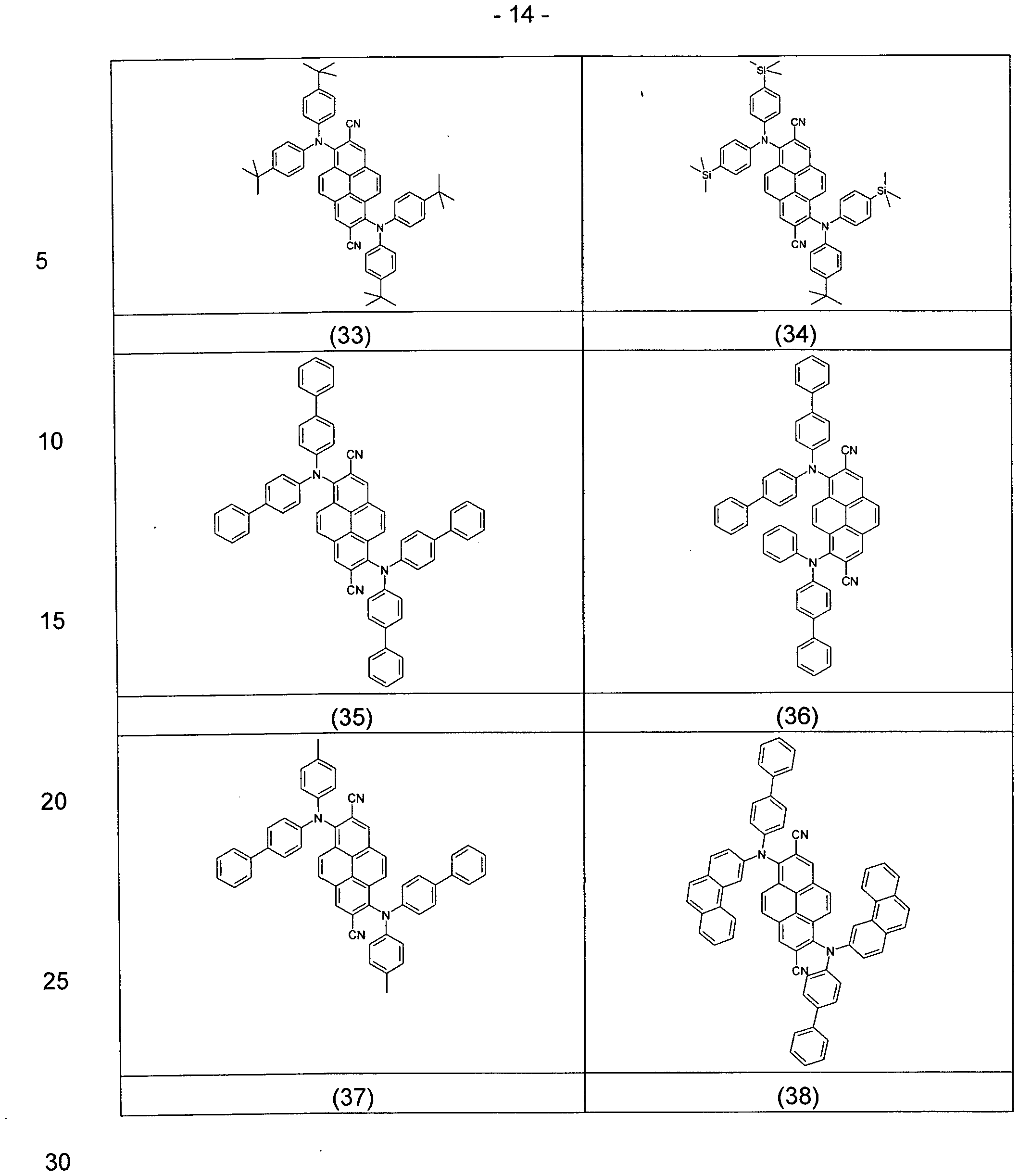
- Examples of preferred compounds of one of the formula (1) to the formula (7) are structures (1) to (50) depicted below.
- the compounds according to the invention can be prepared by synthetic steps known to the person skilled in the art, such as, for example, bromination, Suzuki coupling, Hartwig-Buchwald coupling, etc.
- the compounds of the formula (1) to formula (7) can be prepared as shown in Synthesis Schemes 1 and 2.
- the 1 ,6- and 1 ,8-diaminopyrene derivatives (Scheme 1) can be
- the 2,7-diaminopyrene derivatives (Scheme 2) can be synthesized according to the following reactions. Pyren-2,7-bis(boronate)ester is obtained in one-step synthesis via an iridium-based catalyst. The bromination of pyren-2,7-bis(boronate)ester using a catalyst, for example CuBr 2 affords 2,7-dibromopyrene. The following Buchwald-Hartwig amination leads to diamino derivatives. The end products are obtained by subsequent bromination, optional separation of isomers and cyanation of the diamino derivatives.
- the present invention thus further concerns a method of preparing a compound according to the invention, where the method comprises a) performing a bromination of a pyrene derivative,
- the present invention further concerns a method of preparing a compound according to the invention, where the method comprises
- the present invention likewise relates to the use of the compounds according to the invention in the corresponding devices and to these devices themselves.
- the compounds of the formula (1) according to the invention are suitable for use in electronic devices, in particular in organic electroluminescent devices (OLEDs, PLEDs).
- OLEDs organic electroluminescent devices
- PLEDs organic electroluminescent devices
- the compounds are employed in various functions and layers.
- the invention still furthermore relates to organic electronic devices com- prising at least one compound of the formula (1), in particular organic electroluminescent devices comprising an anode, cathode and at least one emitting layer, characterised in that at least one organic layer, which may be an emitting layer or an another layer, comprises at least one compound of the formula (1).
- the layer comprising the at least one compound according to the formula (1) is an emitting layer.
- the organic electroluminescent device may also comprise further layers. These are selected, for example, from in each case one or more hole-injection layers, hole-transport layers, hole-blocking layers, electron-transport layers, electron-injection layers, electron-blocking layers, exciton-blocking layers, charge-generation layers (IDMC 2003, Taiwan; Session 21 OLED (5), T. Matsumoto, T. Nakada, J. Endo, K. Mori, N. Kawamura, A. Yokoi, J. Kido, Multiphoton Organic EL Device Having Charge Generation Layer) and/or organic or inorganic p/n transitions.
- each of these layers does not necessarily have to be present, and the choice of the layers always depends on the compounds used and in particular also on whether it is a fluorescent or phosphorescent electroluminescent device.
- the organic electroluminescent device may also comprise a plurality of emitting layers, where at least one organic layer comprises at least one compound of the formula (1).
- These emission layers particularly preferably have in total a plurality of emission maxima between 380 nm and 750 nm, resulting overall in white emission, i.e. various emitting compounds which are able to fluoresce or phosphoresce and emit blue and yellow, orange or red light are used in the emitting layers.
- Particular preference is given to three-layer systems, i.e. systems having three emitting layers, where at least one of these layers comprises at least one compound of the formula (1) and where the three layers exhibit blue, green and orange or red emis- sion (for the basic structure, see, for example, WO 05/011013).
- Emitters which have broad-band emission bands and thus exhibit white emission are likewise suitable for white emission.
- the compounds of the formula (1) prefferably be em- ployed as emitter compounds, preferably in an emitting layer.
- an emitting layer is a layer which can emit light. If the compounds of the formula (1) are used as emitter, it may be preferred for them to be used in combination with one or more host materials.
- host material preferably a material having a larger energy gap between HOMO level and LUMO level than the energy gap of the compounds of formula (1) is used.
- Preferred host materials are selected from the classes of the oligoarylenes (for example 2,2',7,7'-tetraphenylspirobifluorene in accordance with
- EP 676461 or dinaphthylanthracene
- the oligoarylenes containing condensed aromatic groups for example DPVBi or spiro-DPVBi in accordance with EP 676461
- the polypodal metal complexes for example in accordance with
- the electron-conducting compounds in particular ketones, phosphine oxides, sulfoxides, etc. (for example in accordance with WO 05/084081 and WO 05/084082), the atropisomers (for example in accordance with WO 06/048268), the boronic acid derivatives (for example in accordance with WO 06/117052) or the benzanthracenes (for example in accordance with WO 08/145239).
- Particularly preferred matrix materials are selected from the classes of the oligoarylenes, comprising naphthalene, anthracene, benzanthracene and/or pyrene or atropisomers of these compounds, the oligoarylenevinylenes, the ketones, the phosphine oxides and the sulfoxides.
- Very particularly preferred matrix materials are selected from the classes of the oligoarylenes, comprising anthracene, benzanthracene, benzophenanthrene and/or pyrene or atropisomers of these compounds, such as anthracenes disclosed in
- An oligoarylene in the sense of this invention is intended to be taken to mean a compound in which at least three aryl or arylene groups are bonded to one another.
- the proportion of the emitter of the formula (1) in the emitting layer is between 0.01 vol% and 100%, preferably between 0.1 % and 50 % by volume. It is particularly preferable for the proportion to be between 0.5 % to 20% by volume, very particularly, between 1 % to 10% by volume is preferable.
- an organic electroluminescent device characterised in that one or more layers are coated by a sublimation process.
- the materials are vapour-deposited in vacuum sublimation units at an initial pressure of usually below 10 ⁇ 5 mbar, preferably below 10 "6 mbar.
- the initial pressure it is also possible for the initial pressure to be even lower, for example below 10 ⁇ 7 mbar.
- an organic electroluminescent device characterised in that one or more layers are coated by the OVPD (organic vapour phase deposition) process or with the aid of carrier-gas sublimation.
- the materials are applied at a pressure between 10 ⁇ 5 mbar and 1 bar.
- OVJP organic vapour jet printing
- the materials are applied directly through a nozzle and are thus structured (for example M. S. Arnold et al., Appl. Phys. Lett. 2008, 92, 053301).
- an organic electroluminescent device characterised in that one or more layers are produced from solution, such as, for example, by spin coating, or by means of any desired printing proc- ess, such as, for example, screen printing, flexographic printing or offset printing, but particularly preferably LITI (light-induced thermal imaging, thermal transfer printing) or ink-jet printing.
- Soluble compounds of the formula (1) are necessary for this purpose. High solubility can be achieved by a suitable substitution of the compounds, for example with long-chain alkyl groups or oligophenyl groups such as quaterphenyl groups.
- the processing of the compounds according to the invention from the liquid phase requires formulations of the compounds according to the invention.
- These formulations can be, for example, solutions, dispersions or mini-emulsions. It may be preferred to use mixtures of two or more solvents for this purpose.
- Suitable and preferred solvents are, for example, toluene, anisole, o-, m- or p- xylene, methyl benzoate, dimethylanisole, mesitylene, tetralin, veratrol, THF, methyl-THF, THP, chlorobenzene, dioxane, phenoxytoluene, in particular 3-phenoxytoluene, or mixtures of these solvents.
- the present invention therefore furthermore relates to a formulation, in particular a solution or dispersion, comprising at least one compound of the formula (1) or the preferred embodiments indicated above and at least one solvent, in particular an organic solvent.
- a formulation in particular a solution or dispersion
- solvent in particular an organic solvent.
- the compounds according to the invention used as emitters in the emission layer exhibit a longer operational lifetime than compounds according to prior art.
- the starting materials were - unless mentioned otherwise - purchased from ALDRICH or ABCR.
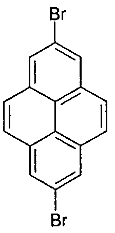
- the starting point can be, for example, 1 ,6-, 2,7- or 1 ,8-dibromopyrene, Journal of the American Chemical Society, 2004, 126(14), 4540; Angew. Chem. Int. Ed. 2008, 47, 10175, Chemical Reviews DOI: 10.1021/cr100428a, Chem. Comm. 2005, 2172.
- the intermediate compounds can be prepared as follows. (Intermediates 1 to 19 )
- the following syntheses are carried out, unless indicated otherwise, in dried solvents under a protective-gas atmosphere.
- the starting materials can be purchased from ALDRICH.
- the solid obtained is recrystallised 5x from dioxane/toluene and sublimed in vacuo (10 "5 mbar, 340°C), giving 5.2 g (37%) of 2,7-dicyano- N ) N,N',N'-tetrakis-(2,4-dimethylphenyl)pyrene-1 ,6-diamine as a colourless solid. Purity > 99.9%.
- the solid obtained is recrystallised 5x from dioxane/toluene and sublimed in vacuo (10 ⁇ 5 mbar, 360°C), giving 5.2 g (37%) of N,N,N ⁇ N'-tetrakis(2,4- dimethylphenyl)-2,7-difluoropyrene-1 ,6-diamine as a colourless solid.
- Vacuum-evaporated OLEDs according to the invention and OLEDs in accordance with the prior art are produced by a general process in accordance with WO 2004/058911 , which is adapted to the circumstances described here (layer-thickness variation, materials used).
- the OLEDs have in principle the following layer structure: substrate / optional hole-injection layer (HIL) / hole-transport layer (HTL) / optional interlayer (IL) / electron-blocking layer (EBL) / emission layer (EML) / optional hole-blocking layer (HBL) / electron- transport layer (ETL) / optional electron-injection layer (EIL) and finally a cathode.
- the cathode is formed by an aluminium layer with a thickness of 100 nm.
- Table 1 The precise structure of the OLEDs is shown in Table 1.
- Table 3 The materials required for the production of the OLEDs are shown in Table 3.
- the materials are applied by thermal vapour deposition in a vacuum chamber.
- the emission layer here always consists of at least one matrix material (host material) and an emitting dopant (emitter), which is admixed to the matrix material or materials in a certain proportion by volume by co- evaporation.
- An expression such as H1(95%):SEBV1(5%) here means that the material SEBV1 is present in the layer in a proportion by volume of 5%, H1 is present in a proportion by volume of 95%.
- the electron- transport layer may also consist of a mixture of two materials.
- the materials according to the invention can be applied also from solution and lead to OLEDs with a good device performance having a simpler device structure versus vacuum processed devices, c. f. examples Esol vs. Vsol.
- PLEDs polymer light emitting devices
- the configuration consists of Substrate /ITO/PEDOT (80 nm) / Interlayer/ Emissionlayer (50nm) / ETL / cathode. Hole injection is done via the Interlayer; in this case HIL-012 (HILsol) of Merck was used.
- HIL-012 HILsol
- the dopant according to the invention to be used in the emission layer is dissolved along with the matrix in toluene.
- Hsol(92%):SEBV1(8%) here means that the material SEBV1 is present in the layer in a proportion by weight of 8%, and Hsol is present in a proportion by weight of 92%.
- the typical concentration of these solutions is in the range between 16 and 25 g/L, if, like in this case a layer thickness of 50 nm is required via spincoating.
- the emission layer is spincoated in an inert atmosphere, here argon, and dried for 10 min at a temperature of 120 °C.
- the aforementioned layers HBL and ETL can be evaporated on top of the EML; the interlayer can be substituted by one or several layers likewise, under the prerequisite that the processing from solution of the downstreaming layers like the EML does not dissolve the interlayer which has been applied before.
- the OLEDs are characterised by standard methods. For this purpose, the electroluminescence spectra, the current efficiency (measured in cd/A), the power efficiency (measured in Im/W) and the external quantum efficiency (EQE, measured in per cent) as a function of luminous density, calculated from current-voltage-luminous density characteristic lines (IUL characteristic lines), and the lifetime are determined.
- the electroluminescence spectra are recorded at a brightness of 1000 cd/m 2 and from it the CIE 1931 x and y colour coordinates are calculated.
- the lifetime is defined as the time after which the luminous density has dropped from a certain initial luminous density to a certain proportion.
- the expression LD70 @ 50 mA means that the lifetime given is the time at which the luminous density has dropped to 70% of the initial luminous density when the device is driven at constant current of 50 mA/cm 2 , c.f. table.
- the values for the lifetime can be converted into a figure for other initial luminous densities with the aid of conversion formulae known to the person skilled in the art.
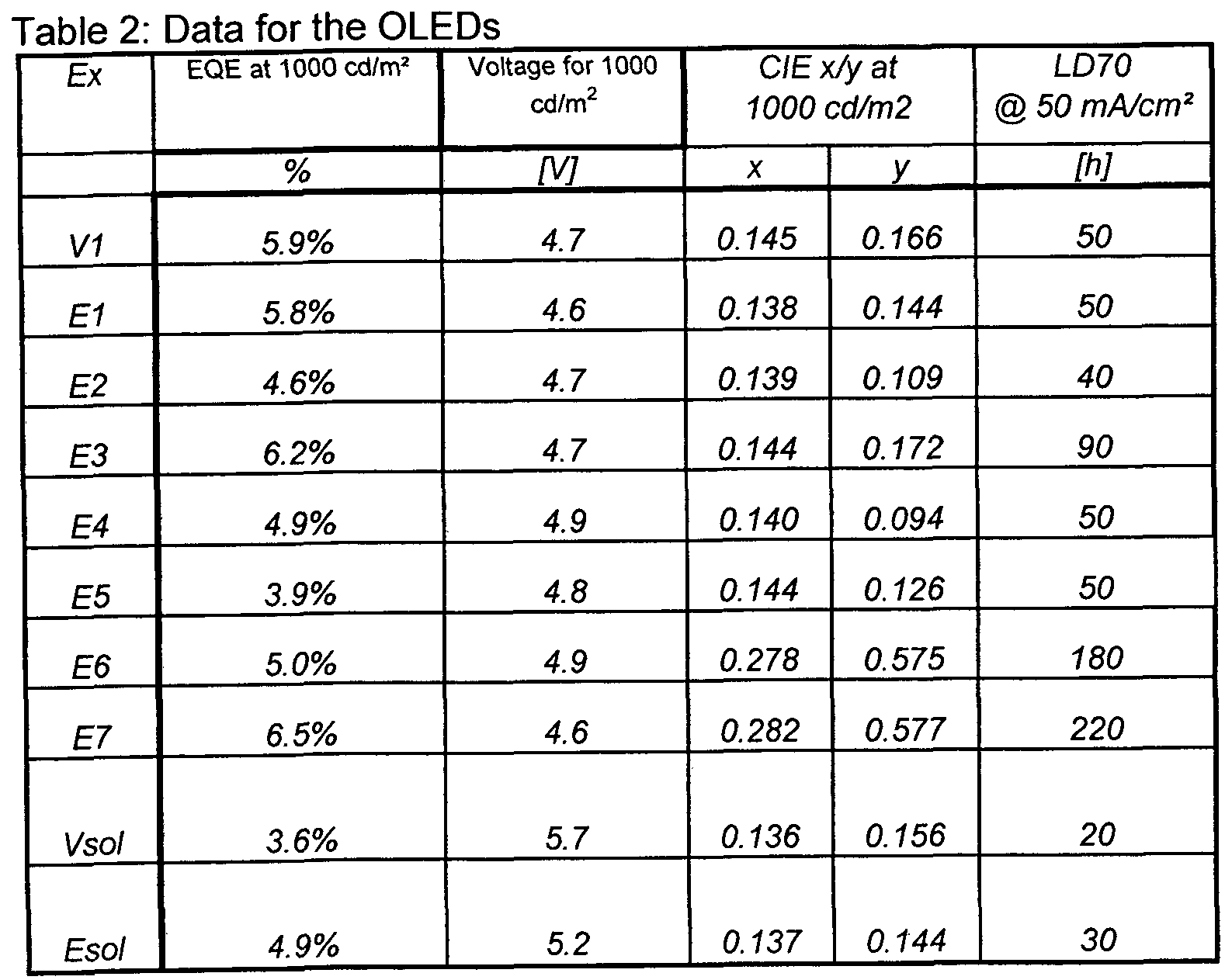
- Example V1 to Esol The data for the various OLEDs (examples V1 to Esol) are summarised in Table 2.
- Examples V1 and Vsol are comparative examples in accordance with the prior art,
- Examples E1 - Esol show data for OLEDs in which materials according to the invention are employed.
- SEBV1 shows a shorter lifetime when comparing with compounds according to this invention with similar CIE coordinates, e.g. V1 compared to E3.
- the emitters of this invention show a narrow emission spectrum, are efficient and show long lifetime. Furthermore they can be used in low doping concentration.
- inventive devices show deeper blue color coordinates at similar lifetime compared to the reference example V1 (E1 , E2, E4, E5).
- inventive examples E6 and E7 show green emission at long lifetimes (180 h and 220 h).
- the inventive emitter When processing from solution, the inventive emitter shows a good lifetime in combination with deep blue colour (Esol).
Abstract
The present invention relates to organic electroluminescent devices comprising compounds of the formula (1), in particular as blue singlet emitting materials in an electroluminescent layer.
Description
Compounds for electronic devices
The present invention describes novel compounds and the use thereof in electronic devices.
The general structure of organic electroluminescent devices is described, for example, in JP3564859B, US2008 0119671 A1 , JP2007-224171A and KR20110002155A. However, these devices still exhibit considerable problems which require urgent improvement:
1. The efficiency is still not high enough and should be improved.
2. There is still a need for improvement in the operating lifetime, in particular in the case of blue (and also green) emission.
3. The operating voltage is high, especially in the case of fluorescent OLEDs, and should therefore be reduced further in order to improve the power efficiency.
Especially, there is a strong demand for devices with a long device lifetime and for devices which show a constantly good efficiency and low operating voltage, having blue or green emitters. This is of major importance, in particular, for large display size applications. Further improvements are desirable here, in particular in the case of blue emitting materials.
Prior art for emitting materials are pyrene derivatives which are substituted by two to four amino groups, in accordance with KR2011002155A.
However, no examples are disclosed having one or two electron donating groups in combination with electron withdrawing groups which are substituted at certain positions of the pyrene skeleton.
Surprisingly, the inventors of the present application have found that pyrene derivatives having one or two electron withdrawing groups that are in ortho position to an electron donating group have significant
improvements here. These compounds especially enable a long operating
lifetime, and at the same time a constantly good efficiency and low operating voltage, compared with the corresponding conventional compounds. The present invention therefore relates to these compounds and to the use thereof especially in OLEDs.
The invention therefore relates to compounds of the formula (1)

X is at each occurrence, identically or differently, F, CI, -P(=0)(Ar)2)
-S02Ar, -SOAr or CN; characterized in that X must be in ortho position to the Y;
Ar is at each occurrence, identically or differently, an aromatic or
heteroaromatic ring system having 5 to 40 aromatic ring atoms, which may be substituted by one or more radicals R1, wherein two Ar may be connected to each other by means of E;
E is at each occurrence, identically or differently, a single bond, N(R1), O, S, C(R1)2, C(R1)2-C(R1)2 or Si(R )2; W is at each occurrence, identically or differently, CR1 or N in the case where W has no substituent X or Y; and W is C in the case where W has a substituent X or Y;
R1 is at each occurrence, identically or differently, H, D, F, CI, Br, I, CN, N02) B(OR2)2, Si(R2)3, a straight-chain alkyl, alkoxy or thioalkoxy group
having 1 to 40 C atoms or a straight-chain alkenyl or alkynyl group having 2 to 40 C atoms or a branched or cyclic alkyl, alkenyl, alkynyl, alkoxy or thioalkoxy group having 3 to 40 C atoms, each of which may be substituted by one or more radicals R2, where one or more non- adjacent CH2 groups may be replaced by -R2C=CR2-, -C≡C-, Si(R2)2, Ge(R )2, Sn(R2)2l C=O, C=S, C=S, C=Se, C=NR2, -0-, -S-, -COO-, or
-CONR2-, and where one or more H atoms may be replaced by F, CI Br, I, CN, or NO2, or an aromatic or heteroaromatic ring system having 5 to 40 aromatic ring atoms, which may be substituted by one or more non- aromatic radicals R1, or an aryloxy or heteroaryloxy group having 5 to 40 aromatic ring atoms, which may be substituted by one or more non-aromatic radicals R1, or a combination of these systems; two or more substituents R1 here may also form a mono- or polycyclic ring system with one another; R2 is at each occurrence, identically or differently, H, D, F, or an aliphatic or aromatic hydrocarbon radical having 1 to 20 C atoms; n is at each occurrence, identically or differently, 0 or 1. The group X which is at each occurrence, identically or differently, F, CI, -P(=0)(Ar)2, -S02Ar, -SOAr or CN; represents an electron withdrawing group, i.e. a group which has a negative mesomeric effect (-M-effect).
An electron donating group according to this invention is a monovalent group which is connected via an electron rich heteroatom. In particular, an electron donating group according to the invention is a group which has a positive mesomeric effect (+M-effect).
For example, electron donating groups according to the invention are -N(Ar)2l -P(Ar)2, -OAr or -SAr. Preferably, an electron donating group is -N(Ar)2 , or -P(Ar)2.
For the purposes of the present invention, an aryl group or heteroaryl group is taken to mean an aromatic group or heteroaromatic group respectively having a common aromatic electron system, where an aryl
group contains 6 to 24 C atoms and a heteroaryl group contains 2 to 24 C atoms and a total of at least 5 aromatic ring atoms. The heteroatoms are preferably selected from N, O and/or S. For the purposes of this invention, this can be a single homo- or heterocyclic ring, for example benzene, pyridine, thiophene, etc., or it can be a condensed aromatic ring system in which at least two aromatic or heteroaromatic rings, for example benzene rings, are fused to one another, i.e. are condensed onto one another by anellation, i.e. having at least one common edge and thus also a common aromatic system. This aryl or heteroaryl group may be substituted or unsubstituted; any substituents present may likewise form further ring systems. Thus, for example, systems such as naphthalene, anthracene, phenanthrene, pyrene, etc., are to be regarded as aryl groups for the purposes of this invention and quinoline, acridine, dibenzothiophene, dibenzofuran, carbazole, etc., are to be regarded as heteroaryl groups for the purposes of this invention, while, for example, biphenyl, fluorene, spirobifluorene, etc., are not aryl groups since separate aromatic electron systems are present here.
For the purposes of this invention, an aromatic ring system contains 6 to 40 C atoms in the ring system. For the purposes of this invention, a hetero- aromatic ring system contains 2 to 40 C atoms and at least one heteroatom in the ring system, with the proviso that the total number of C atoms and heteroatoms is at least 5. The heteroatoms are preferably selected from N, O and/or S. For the purposes of this invention, an aromatic or
heteroaromatic ring system is intended to be taken to mean a system which does not necessarily contain only aryl or heteroaryl groups, but in which, in addition, a plurality of aryl or heteroaryl groups may be interrupted by a short, non-aromatic unit (less than 10% of the atoms other than H, preferably less than 5% of the atoms other than H), such as, for example, a C, N or O atom. Thus, for example, systems such as 9,9'-spiro- bifluorene, 9,9-diarylfluorene, triarylamine, diaryl ether, etc., are also to be regarded as aromatic ring systems for the purposes of this invention.
For the purposes of the present invention, it is particularly preferable for a Ci- to C4o-alkyl group, a C2- to C4o-alkenyl or a C2- to C4o-alkynyl group, in which individual H atoms or CH2 groups may also be substituted by the
above-mentioned groups, to be the radicals methyl, ethyl, n-propyl, i-propyl, n-butyl, i-butyl, s-butyl, t-butyl, 2-methylbutyl, n-pentyl, s-pentyl, tert-pentyl, 2-pentyl, cyclopentyl, n-hexyl, s-hexyl, tert-hexyl, 2-hexyl, 3- hexyl, cyclohexyl, 2-methylpentyl, n-heptyl, 2-heptyl, 3-heptyl, 4-heptyl, cycloheptyl, 1-methylcyclohexyl, n-octyl, 2-ethylhexyl, cyclooctyl, 1- bicyclo[2.2.2]octyl, 2-bicyclo[2.2.2]octyl, 2-(2,6-dimethyl)octyl, 3-(3,7- dimethyl)octyl, trifluoromethyl, pentafluoroethyl, 2,2,2-trifluoroethyl, ethenyl, propenyl, butenyl, pentenyl, cyclopentenyl, hexenyl, heptynyl,
cyclohexenyl, heptenyl, cycloheptenyl, octenyl, cyclooctenyl, ethynyl, propynyl, butynyl, pentynyl, hexynyl or octynyl. A Ci- to C40-alkoxy group is particularly preferably taken to mean methoxy, ethoxy, n-propoxy, i-propoxy, n-butoxy, i-butoxy, s-butoxy, t-butoxy or 2-methylbutoxy. A C2- C24-aryl or -heteroaryl group, which can be monovalent or divalent depending on the use, may in each case also be substituted by the above-mentioned radicals R1 and may be linked to the aromatic or heteroaromatic ring system via any desired positions, is taken to mean, in particular, groups derived from benzene, naphthalene, anthracene, phenanthrene, pyrene, dihydropyrene, chrysene, perylene, fluoranthene, benzanthracene, tetra- cene, pentacene, benzopyrene, furan, benzofuran, isobenzofuran, di- benzofuran, thiophene, benzothiophene, isobenzothiophene, dibenzothio- phene, pyrrole, indole, isoindole, carbazole, pyridine, quinoline, isoquino- line, acridine, phenanthridine, benzo-5,6-quinoline, benzo-6,7-quinoline, benzo-7,8-quinoline, phenothiazine, phenoxazine, pyrazole, indazole, imidazole, benzimidazole, naphthimidazole, phenanthrimidazole, pyridimida- zole, pyrazinimidazole, quinoxalinimidazole, oxazole, benzoxazole, naph- thoxazole, anthroxazole, phenanthroxazole, isoxazole, 1 ,2-thiazole, 1 ,3- thiazole, benzothiazole, pyridazine, benzopyridazine, pyrimidine, benzo- pyrimidine, quinoxaline, pyrazine, phenazine, naphthyridine, azacarbazole, benzocarboline, phenanthroline, 1 ,2,3-triazole, 1 ,2,4-triazole, benzotri- azole, 1 ,2,3-oxadiazole, 1 ,2,4-oxadiazole, 1 ,2,5-oxadiazole, 1 ,3,4-oxadi- azole, 1 ,2,3-thiadiazole, 1 ,2,4-thiadiazole, 1 ,2,5-thiadiazole, 1 ,3,4-thiadia- zole, 1 ,3,5-triazine, 1 ,2,4-triazine, 1 ,2,3-triazine, tetrazole, 1 ,2,4,5-tetrazine, 1 ,2,3,4-tetrazine, 1 ,2,3,5-tetrazine, purine, pteridine, indolizine, benzothia- diazole. For the purposes of this invention, aromatic and heteroaromatic ring systems are taken to mean, in particular, biphenylene, terphenylene, fluorene, spirobifluorene, dihydrophenanthrene, tetrahydropyrene or cis- or
trans-indenofluorene, in addition to the above-mentioned aryl and heteroaryl groups.
In a preferred embodiment of the invention, the group W stands for CH the case where W has no substituent Y or X; and W stands for C in the case where W has a substituent Y or X.
Preferred embodiments of the invention are the compounds of one of formulae (2) to (3),
formula (2)

Preference is given to compounds of the formulae (2) to (3) in which the symbol Y stands for, identically or differently at each occurrence, -N(Ar)2, -P(Ar)2> -OAr or -SAr. It is particularly preferable for the symbol Y to be -N(Ar)2 or -P(Ar)2.
Preference is furthermore given to compounds of the formulae (2) to (3) in which the symbol n = 1.
Preference is furthermore given to compounds of the formulae (2) to (3) in which the symbol Ar stands, identically or differently at each occurrence, for an aromatic or heteroaromatic ring system having 5 to 16 aromatic ring atoms, for a triarylamine or for spirobifluorene, each of which may be sub-
stituted by one or more radicals R1, here, it is particularly preferable for the symbol Ar to be an aryl or a heteroaryl group having 5 to 14 C atoms, which may be substituted by one or more radicals R1.
It is particularly preferable for an aromatic or heteroaromatic ring system to be selected from benzene, ortho-, meta- or para-biphenyl, fluorene, naphthalene, anthracene, phenanthrene, benzanthracene, pyridine, pyrene, thiophene, triphenylamine, diphenyl-1 -naphthylamine, diphenyl-2- naphthylamine, phenyldi(1-naphthyl)amine and phenyldi(2-naphthyl)amine, each of which may be substituted by R1. It is very particularly preferable for the symbol Ar to be, identically or differently at each occurrence, phenyl, 1- naphthyl or 2-naphthyl, each of which may be substituted by one or two radicals R1.
Preference is furthermore given to compounds of the formulae (1) to (3) in which the symbol R1 stands, identically or differently at each occurrence, for H, F, CN, a straight-chain alkyl group having 1 to 5 C atoms or a branched alkyl group having 3 to 5 C atoms, where in each case one or more non-adjacent CH2 groups may be replaced by -R2C=CR2-, -O- or -S- and where one or more H atoms may be replaced by F, or a monovalent aryl or heteroaryl group having 5 to 16 aromatic ring atoms, which may be substituted by one or more non-aromatic radicals R1, where two or more radicals R1 may form a ring system with one another.
R1 particularly preferably stands for H, F, CN, methyl, tert-butyl, or a monovalent aryl or heteroaryl group having 5 to 14 C atoms, which may be substituted by one or more non-aromatic radicals R1, where two aromatic radicals R1 may form a ring system with one another.
Preferred structures of the formula (2) and (3) are the structures of the formulae (4) to (7) depicted below.

formula (6)

The symbols and indices here have the above mentioned meanings, where the compounds may be substituted in all free positions by groups R1 and are preferably unsubstituted.
Preference is given to compounds of the formulae (4) to (7) in which the symbol Y stands, identically or differently at each occurrence, -N(Ar)2) -P(Ar)2, -OAr or -SAr. It is very particularly preferable for the symbol Y to be -N(Ar)2 or -P(Ar)2.
Preference is furthermore given to compounds of the formulae (1) to (7) in which the symbol X is at each occurrence, identically or differently, selected from the group consisting of F, CI, -P(=O)(Ar)2, -SC^Ar, -SOAr and CN as the electron withdrawing group. Very particular preference is given to compounds of the formulae (1) to (7) in which the symbol X at each occurrence, identically or differently, is selected from F or CN, very particularly CN.
In the statements above, the preferred embodiments of the symbols and indices used are indicated in each case. Particular preference is given to
compounds of the formulae (1) to (7) in which the preferred embodiments indicated above are combined with one another.
Highly preferred embodiments of compounds according to the present invention are compounds according to one of formulae (4) to (7), where
X is, identically or differently at each occurrence, F or CN;
Y is N(Ar)2; is, identically or differently at each occurrence, an aryl or a heteroaryl group having 5 to 14 C atoms, which may be substituted by one or more radicals R1; and
R1 is defined as above.
Examples of preferred compounds of one of the formula (1) to the formula (7) are structures (1) to (50) depicted below.


The compounds according to the invention can be prepared by synthetic steps known to the person skilled in the art, such as, for example, bromination, Suzuki coupling, Hartwig-Buchwald coupling, etc. The compounds of the formula (1) to formula (7) can be prepared as shown in Synthesis Schemes 1 and 2. The 1 ,6- and 1 ,8-diaminopyrene derivatives (Scheme 1) can be
synthesized according to the following reactions. Firstly, the bromination of pyrene affords a mixture of two isomeric compounds (1 ,6- and 1 ,8- dibromopyrene). The isomers can be separated, for example by
recrystallization. The following Buchwald-Hartwig amination leads to diamino derivatives. The end products are obtained by subsequent bromination and cyanation of the diamino derivatives.
The 2,7-diaminopyrene derivatives (Scheme 2) can be synthesized according to the following reactions. Pyren-2,7-bis(boronate)ester is obtained in one-step synthesis via an iridium-based catalyst. The
bromination of pyren-2,7-bis(boronate)ester using a catalyst, for example CuBr2 affords 2,7-dibromopyrene. The following Buchwald-Hartwig amination leads to diamino derivatives. The end products are obtained by subsequent bromination, optional separation of isomers and cyanation of the diamino derivatives.
Synthesis Scheme 1 :


Further compounds according to the invention can easily be synthesised in accordance with these and similar synthesis schemes in the process known to the person skilled in the art of organic synthesis.
The present invention thus further concerns a method of preparing a compound according to the invention, where the method comprises a) performing a bromination of a pyrene derivative,
b) optionally carrying out a separation process to isolate the desired isomer;
c) performing a Buchwald-Hartwig coupling reaction with an arylamine; d) carrying out a bromination and a cyanation of the diamino pyrene derivative.
The present invention further concerns a method of preparing a compound according to the invention, where the method comprises
a) performing a boronation step to obtain a pyrene-2,7-bis (boronate) ester, b) carrying out a bromination step where Br is introduced in the positions of boron,
c) performing a Buchwald-Hartwig coupling reaction with an arylamine, d) carrying out a bromination,
e) optionally, carrying out a separation process to separate the desired isomer,
f) carrying out a cyanation step.
The present invention likewise relates to the use of the compounds according to the invention in the corresponding devices and to these devices themselves.
The compounds of the formula (1) according to the invention are suitable for use in electronic devices, in particular in organic electroluminescent devices (OLEDs, PLEDs). The compounds are employed in various functions and layers.
The invention still furthermore relates to organic electronic devices com- prising at least one compound of the formula (1), in particular organic electroluminescent devices comprising an anode, cathode and at least one emitting layer, characterised in that at least one organic layer, which may be an emitting layer or an another layer, comprises at least one compound of the formula (1). Preferably, the layer comprising the at least one compound according to the formula (1) is an emitting layer.
Apart from the cathode, the anode and the emitting layer, the organic electroluminescent device may also comprise further layers. These are selected, for example, from in each case one or more hole-injection layers, hole-transport layers, hole-blocking layers, electron-transport layers, electron-injection layers, electron-blocking layers, exciton-blocking layers, charge-generation layers (IDMC 2003, Taiwan; Session 21 OLED (5), T. Matsumoto, T. Nakada, J. Endo, K. Mori, N. Kawamura, A. Yokoi, J. Kido, Multiphoton Organic EL Device Having Charge Generation Layer) and/or organic or inorganic p/n transitions. However, it should be pointed out that each of these layers does not necessarily have to be present, and the choice of the layers always depends on the compounds used and in particular also on whether it is a fluorescent or phosphorescent electroluminescent device.
The organic electroluminescent device may also comprise a plurality of emitting layers, where at least one organic layer comprises at least one compound of the formula (1). These emission layers particularly preferably have in total a plurality of emission maxima between 380 nm and 750 nm, resulting overall in white emission, i.e. various emitting compounds which
are able to fluoresce or phosphoresce and emit blue and yellow, orange or red light are used in the emitting layers. Particular preference is given to three-layer systems, i.e. systems having three emitting layers, where at least one of these layers comprises at least one compound of the formula (1) and where the three layers exhibit blue, green and orange or red emis- sion (for the basic structure, see, for example, WO 05/011013). Emitters which have broad-band emission bands and thus exhibit white emission are likewise suitable for white emission.
It is particularly preferred for the compounds of the formula (1) to be em- ployed as emitter compounds, preferably in an emitting layer.
For the purposes of this invention, an emitting layer is a layer which can emit light. If the compounds of the formula (1) are used as emitter, it may be preferred for them to be used in combination with one or more host materials. As host material, preferably a material having a larger energy gap between HOMO level and LUMO level than the energy gap of the compounds of formula (1) is used.
Preferred host materials are selected from the classes of the oligoarylenes (for example 2,2',7,7'-tetraphenylspirobifluorene in accordance with
EP 676461 or dinaphthylanthracene), in particular the oligoarylenes containing condensed aromatic groups, the oligoarylenevinylenes (for example DPVBi or spiro-DPVBi in accordance with EP 676461), the polypodal metal complexes (for example in accordance with
WO 04/081017), the hole-conducting compounds (for example in
accordance with WO 04/058911), the electron-conducting compounds, in particular ketones, phosphine oxides, sulfoxides, etc. (for example in accordance with WO 05/084081 and WO 05/084082), the atropisomers (for example in accordance with WO 06/048268), the boronic acid derivatives (for example in accordance with WO 06/117052) or the benzanthracenes (for example in accordance with WO 08/145239). Particularly preferred matrix materials are selected from the classes of the oligoarylenes, comprising naphthalene, anthracene, benzanthracene and/or pyrene or
atropisomers of these compounds, the oligoarylenevinylenes, the ketones, the phosphine oxides and the sulfoxides. Very particularly preferred matrix materials are selected from the classes of the oligoarylenes, comprising anthracene, benzanthracene, benzophenanthrene and/or pyrene or atropisomers of these compounds, such as anthracenes disclosed in
WO 2008/145239. An oligoarylene in the sense of this invention is intended to be taken to mean a compound in which at least three aryl or arylene groups are bonded to one another.
If the compound of the formula (1) is employed as emitter in an emitting layer, the proportion of the emitter of the formula (1) in the emitting layer is between 0.01 vol% and 100%, preferably between 0.1 % and 50 % by volume. It is particularly preferable for the proportion to be between 0.5 % to 20% by volume, very particularly, between 1 % to 10% by volume is preferable.
Preference is furthermore given to an organic electroluminescent device, characterised in that one or more layers are coated by a sublimation process. In this, the materials are vapour-deposited in vacuum sublimation units at an initial pressure of usually below 10~5 mbar, preferably below 10"6 mbar. However, it is also possible for the initial pressure to be even lower, for example below 10~7 mbar.
Preference is likewise given to an organic electroluminescent device, characterised in that one or more layers are coated by the OVPD (organic vapour phase deposition) process or with the aid of carrier-gas sublimation. Here, the materials are applied at a pressure between 10~5 mbar and 1 bar. A special case of this process is the OVJP (organic vapour jet printing) process, in which the materials are applied directly through a nozzle and are thus structured (for example M. S. Arnold et al., Appl. Phys. Lett. 2008, 92, 053301).
Preference is furthermore given to an organic electroluminescent device, characterised in that one or more layers are produced from solution, such as, for example, by spin coating, or by means of any desired printing proc-
ess, such as, for example, screen printing, flexographic printing or offset printing, but particularly preferably LITI (light-induced thermal imaging, thermal transfer printing) or ink-jet printing. Soluble compounds of the formula (1) are necessary for this purpose. High solubility can be achieved by a suitable substitution of the compounds, for example with long-chain alkyl groups or oligophenyl groups such as quaterphenyl groups.
The processing of the compounds according to the invention from the liquid phase, for example by spin coating or by printing processes, requires formulations of the compounds according to the invention. These formulations can be, for example, solutions, dispersions or mini-emulsions. It may be preferred to use mixtures of two or more solvents for this purpose. Suitable and preferred solvents are, for example, toluene, anisole, o-, m- or p- xylene, methyl benzoate, dimethylanisole, mesitylene, tetralin, veratrol, THF, methyl-THF, THP, chlorobenzene, dioxane, phenoxytoluene, in particular 3-phenoxytoluene, or mixtures of these solvents.
The present invention therefore furthermore relates to a formulation, in particular a solution or dispersion, comprising at least one compound of the formula (1) or the preferred embodiments indicated above and at least one solvent, in particular an organic solvent. The way in which solutions of this type can be prepared is known to the person skilled in the art and is described, for example, in WO 2002/072714, WO 2003/019694,
WO 2010/093592 and the literature cited therein. in spite of the description dealing mainly with use in OLEDs, it is possible for the person skilled in the art, without further inventive step, also to employ the compounds according to the invention for further uses in other electronic devices, for example for organic field-effect transistors (O-FETs), organic thin-film transistors (O-TFTs), organic light-emitting transistors (O- LETs), organic integrated circuits (O-ICs), organic solar cells (O-SCs), organic field-quench devices (O-FQDs), light-emitting electrochemical cells (LECs), organic photoreceptors or organic laser diodes (O-lasers), to mention but a few applications.
The compounds according to the invention have the following surprising advantages over the prior art upon application in organic
electroluminescent devices:
1. The compounds according to the invention used as emitters in the emission layer exhibit a longer operational lifetime than compounds according to prior art.
2. Preferably efficiency, driving voltage and colour coordinates of
corresponding devices of the inventive compounds are also better than devices with compounds according to prior art.
Use Examples
The invention is explained in greater detail by the following examples with- out thereby wishing to restrict it.
The following syntheses were carried out under a protective-gas
atmosphere, unless indicated otherwise. The starting materials were - unless mentioned otherwise - purchased from ALDRICH or ABCR. The starting point can be, for example, 1 ,6-, 2,7- or 1 ,8-dibromopyrene, Journal of the American Chemical Society, 2004, 126(14), 4540; Angew. Chem. Int. Ed. 2008, 47, 10175, Chemical Reviews DOI: 10.1021/cr100428a, Chem. Comm. 2005, 2172. The intermediate compounds can be prepared as follows. (Intermediates 1 to 19 )
Intermediate 1: Synthesis of 1,6- and 1,8-dibromopyrene

58 g (0.287 mol) of pyrene are initially introduced in 1750 ml of chloroform. A solution of 31 ml (0.609 mol) of Br2 in 250 ml of chloroform is
subsequently added dropwise at RT with exclusion of light. The reaction mixture is heated under reflux for 4 h. After cooling, the precipitated solid is filtered off with suction and washed with ethanol and dried. The solid obtained is recrystallised 3 times from CHCI3. Yield: 1 ,6- dibromopyrene 73.4 g (0.201 mol), 71.1% of theory, and 1 ,8-dibromopyrene 20.6 g (0.06 mol), 20% of theory.
Intermediate 2: Synthesis of 2,7-dibromopyrene
Intermediate 2-1: Synthesis of 2,2'-(2,7-pyrenediyl)bis(4,4,5,5- tetramethyl-1,3,2-dioxaborolane)
 12.03 g (59.5 mmol) of pyrene, 33.5 g (131.8 mmol) of
bis(pinacolato)diborane and [lr(OMe)COD]2 (5 mol%) and 4 ,4'-d i-te rt-b uty I- 2,2'-bipyridine (10 mol%) are suspended in 750 ml of cyclohexane. The reaction mixture is heated under reflux for 16 h. After cooling, the organic phase is separated off, washed three times with 200 ml of water and sub- sequently evaporated to dryness. The residue is recrystallised from toluene. The content of product according to 1 H-NMR is about 97% with an overall yield of 21.43 g (80%).
Intermediate 2-2: Synthesis of 2,7-dibromopyrene
45.4 g (0.1 mol) of 2)2,-(2,7-pyrenediyl)bis(4>4,5,5-tetramethyl-1 ,3,2- dioxaborolane) and 111.5 g (0.5 mol) of copper(ll) bromide are suspended in 750 ml of i-PrOH and 300 ml of water. The reaction mixture is heated under reflux for 16 h. After cooling, the solid is separated off and washed three times with 200 ml of water. The residue is recrystallised from toluene. The content of product according to 1H-NMR is about 96% with an overall yield of 29.52 g (82%).
The following syntheses are carried out, unless indicated otherwise, in dried solvents under a protective-gas atmosphere. The starting materials can be purchased from ALDRICH.
Intermediate 3: Synthesis of N,N,N',N'-tetrakis-(2,4- dimethylphenyl)py rene-1 ,6-diamine

19.08 g (0.053 mol) of 1 ,6-dibromopyrene and 27.0 g (0.12 mol) of N-(2,4- dimethylphenyl)-2,4-dimethylphenylamine (Miguel Angel Chem Taiwan) are dissolved in 500 ml of xylene and degassed. 0.15 ml (0.66 mmol / 1 M soln. in toluene) of tri-tert-butylphosphine, 15.61 g (0.162 mol) of NaOtBu
and 89.44 mg (0.398 mmol) of Pd(OAc)2 are added, and the mixture is degassed again and heated under reflux for 12 h. When the reaction is complete, the warm mixture is filtered through aluminium oxide B (activity grade 1), washed with water, dried and evaporated. The residue is purified by Soxhlet extraction with toluene / heptane (1 :1) and crystallised from toluene. The content of product according to HPLC is 98% with an overall yield of 14.8 g (43%).
The following compounds can be obtained analogously:


Intermediate 11: Synthesis of 2,7-dibromo-N,N,N,,N'-tetrakis(2,4- dimethylphenyl)-pyrene-1,6-diamine

The following compounds can be obtained analogously:


Compound 1: Synthesis of 2,7-dicyano-N,N,N\N'-tetrakis-(2,4- dimethylphenyl)-pyrene-1,6-diamine

dimethylformamide, and pyridine (5 ml) and 5.16 g (0.058 mol) of copper(l) cyanide are added. The reaction mixture is heated under reflux at 150°C for 20 h. 200 ml of 10% NH4OH solution are added dropwise to the cooled batch, and 500 ml of heptane and a further 100 ml of water are then added The precipitated solid is filtered off with suction via a frit and dried at 40°C in vacuo. The solid obtained is recrystallised 5x from dioxane/toluene and sublimed in vacuo (10"5 mbar, 340°C), giving 5.2 g (37%) of 2,7-dicyano- N)N,N',N'-tetrakis-(2,4-dimethylphenyl)pyrene-1 ,6-diamine as a colourless solid. Purity > 99.9%.
The following compounds can be obtained analogously:


25 mmol of 2,7-dibromo-N,N)N'>N,-tetrakis-(2,4-dimethylphenyl)pyrene-1 ,6- diamine are dissolved in 600 ml of dry THF, and the mixture is cooled to -78°C. 26.2 ml (65.7 mmol / 2.5 M in hexane) of n-BuLi are added at this temperature over the course of about 30 min., and the mixture is
subsequently stirred at -78°C for a further 2.5 h. 7.3 ml (65.7 mmol) of trimethyl borate are added as rapidly as possible at this temperature, and the reaction is allowed to come slowly to RT (about 18 h). The reaction mixture is mixed with 2.64 g (66 mmol) of NaOH in 20 ml of MeOH and then cooled to 0°C, and AgOTf (1.05 eq.) is added. After 1 hour at 0°C, the organic phase is dried azeotropically using acetone. 200 ml of acetone are added dropwise to the cooled batch, and MS3A (5.0 g) and 1-chloromethyl- 4-fluoro-1 ,4-diazoniabicyclo[2.2.2]octane bis(trifluoroborate) (23.72 g, 66 mmol, 1.05 equiv.) are then added. After 3 hours at room temperature, the reaction solution is filtered through Celite and washed with water, and the precipitated solid is filtered off with suction via a frit and dried at 40°C in vacuo.
The solid obtained is recrystallised 5x from dioxane/toluene and sublimed in vacuo (10~5 mbar, 360°C), giving 5.2 g (37%) of N,N,N\N'-tetrakis(2,4- dimethylphenyl)-2,7-difluoropyrene-1 ,6-diamine as a colourless solid.
Purity > 99.9%.
The following compounds can be obtained analogously:

Device Examples (V1 to Esol): Production of vacuum-evaporated OLEDs
Vacuum-evaporated OLEDs according to the invention and OLEDs in accordance with the prior art are produced by a general process in accordance with WO 2004/058911 , which is adapted to the circumstances described here (layer-thickness variation, materials used).
The data for various OLEDs are presented in examples V1 to Esol below (see Table 2). Glass plates coated with structured ITO (indium tin oxide) of a thickness of 50 nm are coated with 20 nm of PEDOT (poly(3,4- ethylenedioxy-2,5-thiophene), spin-coated from water; purchased from Heraeus Precious Metals GmbH & Co. KG, Germany, for improved processing. These coated glass plates form the substrates onto which the OLEDs are applied. The OLEDs have in principle the following layer structure: substrate / optional hole-injection layer (HIL) / hole-transport layer (HTL) / optional interlayer (IL) / electron-blocking layer (EBL) / emission layer (EML) / optional hole-blocking layer (HBL) / electron- transport layer (ETL) / optional electron-injection layer (EIL) and finally a cathode. The cathode is formed by an aluminium layer with a thickness of
100 nm. The precise structure of the OLEDs is shown in Table 1. The materials required for the production of the OLEDs are shown in Table 3.
The materials are applied by thermal vapour deposition in a vacuum chamber. The emission layer here always consists of at least one matrix material (host material) and an emitting dopant (emitter), which is admixed to the matrix material or materials in a certain proportion by volume by co- evaporation. An expression such as H1(95%):SEBV1(5%) here means that the material SEBV1 is present in the layer in a proportion by volume of 5%, H1 is present in a proportion by volume of 95%. Analogously, the electron- transport layer may also consist of a mixture of two materials.
The materials according to the invention can be applied also from solution and lead to OLEDs with a good device performance having a simpler device structure versus vacuum processed devices, c. f. examples Esol vs. Vsol.
The manufacturing of these devices is according to the manufacturing of polymer light emitting devices (PLEDs), which is described numerously in literature (e.g. in WO 2004/037887 A2). The configuration consists of Substrate /ITO/PEDOT (80 nm) / Interlayer/ Emissionlayer (50nm) / ETL / cathode. Hole injection is done via the Interlayer; in this case HIL-012 (HILsol) of Merck was used. In this application the dopant according to the invention to be used in the emission layer is dissolved along with the matrix in toluene. An expression such as Hsol(92%):SEBV1(8%) here means that the material SEBV1 is present in the layer in a proportion by weight of 8%, and Hsol is present in a proportion by weight of 92%. The typical concentration of these solutions is in the range between 16 and 25 g/L, if, like in this case a layer thickness of 50 nm is required via spincoating. The emission layer is spincoated in an inert atmosphere, here argon, and dried for 10 min at a temperature of 120 °C. Between EML and cathode the aforementioned layers HBL and ETL can be evaporated on top of the EML; the interlayer can be substituted by one or several layers likewise, under the prerequisite that the processing from solution of the downstreaming layers like the EML does not dissolve the interlayer which has been applied before.
The OLEDs are characterised by standard methods. For this purpose, the electroluminescence spectra, the current efficiency (measured in cd/A), the power efficiency (measured in Im/W) and the external quantum efficiency (EQE, measured in per cent) as a function of luminous density, calculated from current-voltage-luminous density characteristic lines (IUL characteristic lines), and the lifetime are determined. The electroluminescence spectra are recorded at a brightness of 1000 cd/m2 and from it the CIE 1931 x and y colour coordinates are calculated. The lifetime is defined as the time after which the luminous density has dropped from a certain initial luminous density to a certain proportion. The expression LD70 @ 50 mA means that the lifetime given is the time at which the luminous density has dropped to 70% of the initial luminous density when the device is driven at constant current of 50 mA/cm2, c.f. table. The values for the lifetime can be converted into a figure for other initial luminous densities with the aid of conversion formulae known to the person skilled in the art.
The data for the various OLEDs (examples V1 to Esol) are summarised in Table 2. Examples V1 and Vsol are comparative examples in accordance with the prior art, Examples E1 - Esol show data for OLEDs in which materials according to the invention are employed.
Some of the examples are explained in greater detail below in order to illustrate the advantages of the compounds according to the invention. However, it should be pointed out that this only represents a selection of the results shown in Table 2. As can be seen from the table, significant improvements over the prior art are also achieved on the use of the compounds according to the invention that are not described in greater detail. In some cases improvement in all parameters is achieved, but in some cases only an improvement in one parameter, e.g. in the efficiency or voltage or lifetime is observed. However, even the improvement of one of the said parameters represents a significant advance.
Use of compounds according to the invention as emitters in fluorescent OLEDS
The use of compounds according to the invention as emitters (dopants) in OLEDs thus produces significant improvements with respect to lifetime, in particular combination with deep blue colour.
Examples are shown with green and blue emitting OLEDs employing compounds according to the invention. When comparing with reference compound SEBV1 from KR2011-0002155, SEBV1 shows a shorter lifetime when comparing with compounds according to this invention with similar CIE coordinates, e.g. V1 compared to E3.
The emitters of this invention show a narrow emission spectrum, are efficient and show long lifetime. Furthermore they can be used in low doping concentration.
Also, many of the inventive devices show deeper blue color coordinates at similar lifetime compared to the reference example V1 (E1 , E2, E4, E5). Inventive examples E6 and E7 show green emission at long lifetimes (180 h and 220 h).
When processing from solution, the inventive emitter shows a good lifetime in combination with deep blue colour (Esol).
Table 1: Structures of the OLEDs


Claims
Patent Claims
1. Compounds of the formula (1)

Y is an electron donating group;
X is at each occurrence, identically or differently, F, CI, -P(=0)(Ar)2, -S02Ar, -SOAr or CN; characterized in that X must be in ortho position to Y;
Ar is at each occurrence, identically or differently, an aromatic or heteroaromatic ring system having 5 to 40 aromatic ring atoms, which may be substituted by one or more radicals R1, wherein two Ar may be connected to each other by a group E;
E is at each occurrence, identically or differently, a single bond, N(R1), O, S, C(R1)2) C(R1)2-C(R )2 or Si(R1)2; is at each occurrence, identically or differently, CR1 or N in the case where W has no substituent X or Y; and W is C in the case where W has a substituent X or Y; is at each occurrence, identically or differently, H, D, F, CI, Br, I, CN, NO2, B(OR2)2, Si(R2)3, a straight-chain alkyl, alkoxy or thioalkoxy group having 1 to 40 C atoms or a straight-chain
9
alkenyl or alkynyl group having 2 to 40 C atoms or a branched or cyclic alkyl, alkenyl, alkynyl, alkoxy or thioalkoxy group having 3 to 40 C atoms, each of which may be substituted by one or more radicals R2, where one or more non-adjacent CH2 groups may be replaced by -R2C=CR2-, -C≡C-, Si(R2)2, Ge(R2)2, Sn(R2)2, C=0, C=S, C=S, C=Se, C=NR2, -0-, -S-, -COO-, or -CONR2-, and where one or more H atoms may be replaced by F, CI, Br, I, CN, or NO2, or an aromatic or heteroaromatic ring system having 5 to 40 aromatic ring atoms, which may be substituted by one or more non- aromatic radicals R1, or an aryloxy or heteroaryloxy group having 5 to 40 aromatic ring atoms, which may be substituted by one or more non-aromatic radicals R , or a combination of these systems; two or more substituents R here may also form a mono- or polycyclic ring system with one another;
R2 is at each occurrence, identically or differently, H, D, F, or an aliphatic or aromatic hydrocarbon radical having 1 to 20 C atoms; n is at each occurrence, identically or differently, 0 or 1 ;
Compounds according to Claim 1 , characterized in that the index n = 1.
Compounds according to Claim 1 or 2, characterized in that W is CH in the case where W has no substituent Y or X; and W is C in the case where W has a substituent Y or X.
Compounds according to one or more of claims 1 to 2, selected from compounds of one of the formulae (2) to (3)

formula (2)

formula (3) where the symbols and indices used have the meanings mentioned in Claim 1 or 2.
5. Compounds according to one or more of Claims 1 to 3, selected from compounds of one of the formulae (4) to (7)

formula (4)

formula (5)

formula (6)

formula (7)
where the symbols and indices used have the meanings mentioned in Claim 1 , and where the compounds may be substituted in all free positions by groups R1.
Compounds according to one or more of Claims 1 to 5, characterized in that X is on each occurrence, identically or differently, CN or F.
Compounds according to one or more of Claims 1 to 6 characterized that Y is on each occurrence, identically or differently, -N(Ar)2, -P(Ar)2, -OAr or -SAr.
Use of compounds according to one or more of Claims 1 to 7 in
electronic devices, in particular in organic electroluminescent devices.
Organic electronic devices comprising at least one compound
according to one or more of Claims 1 to 7, in particular selected from the group consisting of organic field-effect transistors (O-FETs), organic thin film transistors (O-TFTs), organic light emitting transistors (O-LETs), organic integrated circuits (O-ICs), organic solar cells (O- SCs), organic field-quench devices (O-FQDs), light-emitting
electrochemical cells (LECs), organic electroluminescent devices (OLEDs), organic photoreceptors and organic laser diodes (O-lasers).
10. Organic electroluminescent device according to claim 9, wherein said organic electroluminescent device comprises at least one cathode, one anode, one organic layer located between said cathode and anode, wherein said organic layer comprises at least one host material and one compound according to one or more of claims 1 to 7.
11. Method of preparing a compound according to one or more of claims 1 to 7, comprising
a) performing a bromination of a pyrene derivative,
b) optionally carrying out a separation process to isolate the desired isomer;
c) performing a Buchwald-Hartwig coupling reaction with an arylamine;
d) carrying out a bromination and a cyanation of the diamino pyrene derivative.
12. Method of preparing a compound according to one or more of claims 1 to 7, comprising
a) performing a boronation step to obtain a pyrene-2,7-bis (boronate) ester,
b) carrying out a bromination step where Br is introduced in the positions of boron,
c) performing a Buchwald-Hartwig coupling reaction with an arylamine,
d) carrying out a bromination,
e) optionally, carrying out a separation process to separate the desired isomer,
f) carrying out a cyanation step.
Priority Applications (1)
| Application Number | Priority Date | Filing Date | Title |
|---|---|---|---|
| DE112013002910.3T DE112013002910T5 (en) | 2012-06-12 | 2013-05-08 | Connections for electronic devices |
Applications Claiming Priority (2)
| Application Number | Priority Date | Filing Date | Title |
|---|---|---|---|
| EP12004426.8 | 2012-06-12 | ||
| EP12004426 | 2012-06-12 |
Publications (1)
| Publication Number | Publication Date |
|---|---|
| WO2013185871A1 true WO2013185871A1 (en) | 2013-12-19 |
Family
ID=48430653
Family Applications (1)
| Application Number | Title | Priority Date | Filing Date |
|---|---|---|---|
| PCT/EP2013/001374 WO2013185871A1 (en) | 2012-06-12 | 2013-05-08 | Compounds for electronic devices |
Country Status (2)
| Country | Link |
|---|---|
| DE (1) | DE112013002910T5 (en) |
| WO (1) | WO2013185871A1 (en) |
Cited By (65)
| Publication number | Priority date | Publication date | Assignee | Title |
|---|---|---|---|---|
| WO2016193243A1 (en) | 2015-06-03 | 2016-12-08 | Udc Ireland Limited | Highly efficient oled devices with very short decay times |
| WO2017036573A1 (en) | 2015-08-28 | 2017-03-09 | Merck Patent Gmbh | Compounds for electronic devices |
| CN106588675A (en) * | 2015-10-14 | 2017-04-26 | 陕西莱特迈思光电材料有限公司 | New organic compounds and organic electroluminescent devices containing them |
| WO2017133829A1 (en) | 2016-02-05 | 2017-08-10 | Merck Patent Gmbh | Materials for electronic devices |
| WO2018007421A1 (en) | 2016-07-08 | 2018-01-11 | Merck Patent Gmbh | Materials for organic electroluminescent devices |
| DE102017008794A1 (en) | 2016-10-17 | 2018-04-19 | Merck Patent Gmbh | Materials for use in electronic devices |
| WO2018069167A1 (en) | 2016-10-10 | 2018-04-19 | Merck Patent Gmbh | Electronic device |
| WO2018083053A1 (en) | 2016-11-02 | 2018-05-11 | Merck Patent Gmbh | Materials for electronic devices |
| CN108017662A (en) * | 2016-10-28 | 2018-05-11 | 学校法人关西学院 | Boric acid or borate or the method that polycyclc aromatic compound or Ppolynuclear aromatic polymer compounds are manufactured using them |
| WO2018087020A1 (en) | 2016-11-08 | 2018-05-17 | Merck Patent Gmbh | Compounds for electronic devices |
| WO2018095888A1 (en) | 2016-11-25 | 2018-05-31 | Merck Patent Gmbh | Bisbenzofuran-fused 2,8-diaminoindeno[1,2-b]fluorene derivatives and related compounds as materials for organic electroluminescent devices (oled) |
| WO2018095940A1 (en) | 2016-11-25 | 2018-05-31 | Merck Patent Gmbh | Bisbenzofuran-fused indeno[1,2-b]fluorene derivatives and related compounds as materials for organic electroluminescent devices (oled) |
| WO2018095839A1 (en) | 2016-11-22 | 2018-05-31 | Merck Patent Gmbh | Bridged triarylamines for electronic devices |
| WO2018114882A1 (en) | 2016-12-22 | 2018-06-28 | Merck Patent Gmbh | Materials for electronic devices |
| WO2018134392A1 (en) | 2017-01-23 | 2018-07-26 | Merck Patent Gmbh | Materials for organic electroluminescent devices |
| WO2018141706A1 (en) | 2017-02-02 | 2018-08-09 | Merck Patent Gmbh | Materials for electronic devices |
| WO2018158232A1 (en) | 2017-03-01 | 2018-09-07 | Merck Patent Gmbh | Organic electroluminescent device |
| WO2018157981A1 (en) | 2017-03-02 | 2018-09-07 | Merck Patent Gmbh | Materials for organic electronic devices |
| WO2018197447A1 (en) | 2017-04-25 | 2018-11-01 | Merck Patent Gmbh | Compounds for electronic devices |
| WO2018234220A1 (en) | 2017-06-21 | 2018-12-27 | Merck Patent Gmbh | Materials for electronic devices |
| WO2018234346A1 (en) | 2017-06-23 | 2018-12-27 | Merck Patent Gmbh | Materials for organic electroluminescent devices |
| WO2019002198A1 (en) | 2017-06-26 | 2019-01-03 | Merck Patent Gmbh | Homogeneous mixtures |
| WO2019002190A1 (en) | 2017-06-28 | 2019-01-03 | Merck Patent Gmbh | Materials for electronic devices |
| WO2019020654A1 (en) | 2017-07-28 | 2019-01-31 | Merck Patent Gmbh | Spirobifluorene derivatives for use in electronic devices |
| WO2019048443A1 (en) | 2017-09-08 | 2019-03-14 | Merck Patent Gmbh | Materials for electronic devices |
| WO2019076789A1 (en) | 2017-10-17 | 2019-04-25 | Merck Patent Gmbh | Materials for organic electroluminescent devices |
| WO2019101719A1 (en) | 2017-11-23 | 2019-05-31 | Merck Patent Gmbh | Materials for electronic devices |
| WO2019101833A1 (en) | 2017-11-24 | 2019-05-31 | Merck Patent Gmbh | Materials for organic electroluminescent devices |
| WO2019101835A1 (en) | 2017-11-24 | 2019-05-31 | Merck Patent Gmbh | Materials for organic electroluminescent devices |
| WO2019115577A1 (en) | 2017-12-15 | 2019-06-20 | Merck Patent Gmbh | Substituted aromatic amines for use in organic electroluminescent devices |
| WO2019121483A1 (en) | 2017-12-20 | 2019-06-27 | Merck Patent Gmbh | Heteroaromatic compounds |
| US10347851B2 (en) | 2013-12-20 | 2019-07-09 | Udc Ireland Limited | Highly efficient OLED devices with very short decay times |
| WO2019170578A1 (en) | 2018-03-06 | 2019-09-12 | Merck Patent Gmbh | Materials for organic electroluminescent devices |
| WO2019170572A1 (en) | 2018-03-06 | 2019-09-12 | Merck Patent Gmbh | Materials for organic electroluminescent devices |
| WO2019175149A1 (en) | 2018-03-16 | 2019-09-19 | Merck Patent Gmbh | Materials for organic electroluminescent devices |
| WO2020043640A1 (en) | 2018-08-28 | 2020-03-05 | Merck Patent Gmbh | Materials for organic electroluminescent devices |
| WO2020043657A1 (en) | 2018-08-28 | 2020-03-05 | Merck Patent Gmbh | Materials for organic electroluminescent devices |
| WO2020043646A1 (en) | 2018-08-28 | 2020-03-05 | Merck Patent Gmbh | Materials for organic electroluminescent devices |
| WO2020053150A1 (en) | 2018-09-12 | 2020-03-19 | Merck Patent Gmbh | Materials for organic electroluminescent devices |
| WO2020089138A1 (en) | 2018-10-31 | 2020-05-07 | Merck Patent Gmbh | Materials for organic electroluminescent devices |
| WO2020178230A1 (en) | 2019-03-04 | 2020-09-10 | Merck Patent Gmbh | Ligands for nano-sized materials |
| WO2020208051A1 (en) | 2019-04-11 | 2020-10-15 | Merck Patent Gmbh | Materials for organic electroluminescent devices |
| WO2021089450A1 (en) | 2019-11-04 | 2021-05-14 | Merck Patent Gmbh | Materials for organic electroluminescent devices |
| WO2021094269A1 (en) | 2019-11-12 | 2021-05-20 | Merck Patent Gmbh | Materials for organic electroluminescent devices |
| WO2021180950A1 (en) | 2020-03-13 | 2021-09-16 | Merck Patent Gmbh | Materials for organic electroluminescent devices |
| WO2021191058A1 (en) | 2020-03-23 | 2021-09-30 | Merck Patent Gmbh | Materials for organic electroluminescent devices |
| WO2022017997A1 (en) | 2020-07-22 | 2022-01-27 | Merck Patent Gmbh | Materials for organic electroluminescent devices |
| WO2022017998A1 (en) | 2020-07-22 | 2022-01-27 | Merck Patent Gmbh | Materials for organic electroluminescent devices |
| WO2022112541A1 (en) | 2020-11-30 | 2022-06-02 | Merck Patent Gmbh | Materials for organic electroluminescent devices |
| WO2022214506A1 (en) | 2021-04-09 | 2022-10-13 | Merck Patent Gmbh | Materials for organic electroluminescent devices |
| WO2022214566A1 (en) | 2021-04-09 | 2022-10-13 | Merck Patent Gmbh | Materials for organic electroluminescent devices |
| WO2022214507A1 (en) | 2021-04-09 | 2022-10-13 | Merck Patent Gmbh | Materials for organic electroluminescent devices |
| EP4079742A1 (en) | 2021-04-14 | 2022-10-26 | Merck Patent GmbH | Metal complexes |
| WO2023036976A1 (en) | 2021-09-13 | 2023-03-16 | Merck Patent Gmbh | Materials for organic electroluminescent devices |
| WO2023052272A1 (en) | 2021-09-28 | 2023-04-06 | Merck Patent Gmbh | Materials for electronic devices |
| WO2023052314A1 (en) | 2021-09-28 | 2023-04-06 | Merck Patent Gmbh | Materials for electronic devices |
| WO2023052313A1 (en) | 2021-09-28 | 2023-04-06 | Merck Patent Gmbh | Materials for electronic devices |
| WO2023052275A1 (en) | 2021-09-28 | 2023-04-06 | Merck Patent Gmbh | Materials for electronic devices |
| WO2023094412A1 (en) | 2021-11-25 | 2023-06-01 | Merck Patent Gmbh | Materials for electronic devices |
| WO2023117837A1 (en) | 2021-12-21 | 2023-06-29 | Merck Patent Gmbh | Process for preparing deuterated organic compounds |
| WO2023152346A1 (en) | 2022-02-14 | 2023-08-17 | Merck Patent Gmbh | Materials for electronic devices |
| WO2023208899A1 (en) | 2022-04-28 | 2023-11-02 | Merck Patent Gmbh | Materials for organic electroluminescent devices |
| WO2023222559A1 (en) | 2022-05-18 | 2023-11-23 | Merck Patent Gmbh | Process for preparing deuterated organic compounds |
| WO2024013004A1 (en) | 2022-07-11 | 2024-01-18 | Merck Patent Gmbh | Materials for electronic devices |
| WO2024033282A1 (en) | 2022-08-09 | 2024-02-15 | Merck Patent Gmbh | Materials for organic electroluminescent devices |
Citations (18)
| Publication number | Priority date | Publication date | Assignee | Title |
|---|---|---|---|---|
| EP0676461A2 (en) | 1994-04-07 | 1995-10-11 | Hoechst Aktiengesellschaft | Spiro compounds and their application as electroluminescence materials |
| WO2002072714A1 (en) | 2001-03-10 | 2002-09-19 | Covion Organic Semiconductors Gmbh | Solutions and dispersions of organic semiconductors |
| WO2003019694A2 (en) | 2001-08-24 | 2003-03-06 | Covion Organic Semiconductors Gmbh | Solutions of polymer semiconductors |
| WO2004037887A2 (en) | 2002-10-25 | 2004-05-06 | Covion Organic Semiconductors Gmbh | Conjugated polymers containing arylamine units, the representation thereof and the use of the same |
| WO2004058911A2 (en) | 2002-12-23 | 2004-07-15 | Covion Organic Semiconductors Gmbh | Organic electroluminescent element |
| JP3564859B2 (en) | 1996-04-01 | 2004-09-15 | 東洋インキ製造株式会社 | Organic electroluminescent device material and organic electroluminescent device using the same |
| WO2004081017A1 (en) | 2003-03-11 | 2004-09-23 | Covion Organic Semiconductors Gmbh | Metal complexes |
| WO2005011013A1 (en) | 2003-07-21 | 2005-02-03 | Covion Organic Semiconductors Gmbh | Organic electroluminescent element |
| WO2005084081A1 (en) | 2004-02-20 | 2005-09-09 | Merck Patent Gmbh | Organic electronic devices |
| EP1604974A1 (en) * | 2003-03-20 | 2005-12-14 | Idemitsu Kosan Co., Ltd. | Aromatic amine derivative and organic electroluminescent element made with the same |
| WO2006048268A1 (en) | 2004-11-06 | 2006-05-11 | Merck Patent Gmbh | Organic electroluminescent device |
| WO2006117052A1 (en) | 2005-05-03 | 2006-11-09 | Merck Patent Gmbh | Organic electroluminescent device and boric acid and borinic acid derivatives used therein |
| JP2007224171A (en) | 2006-02-24 | 2007-09-06 | Toray Ind Inc | Material for light-emitting device and the resultant light-emitting device |
| US20080119671A1 (en) | 2006-11-17 | 2008-05-22 | Canon Kabushiki Kaisha | Pyrene compound and organic light emitting device |
| WO2008145239A2 (en) | 2007-05-29 | 2008-12-04 | Merck Patent Gmbh | Benzanthracene derivatives for organic electroluminescent devices |
| WO2010093592A1 (en) | 2009-02-11 | 2010-08-19 | Universal Display Corporation | Liquid compositions for inkjet printing of organic layers or other uses |
| KR20110002155A (en) | 2009-07-01 | 2011-01-07 | 주식회사 엘지화학 | New compounds and organic electronic device using the same |
| EP2441750A1 (en) * | 2009-12-16 | 2012-04-18 | Idemitsu Kosan Co., Ltd. | Aromatic amine derivative and organic electroluminescent element using same |
-
2013
- 2013-05-08 WO PCT/EP2013/001374 patent/WO2013185871A1/en active Application Filing
- 2013-05-08 DE DE112013002910.3T patent/DE112013002910T5/en not_active Withdrawn
Patent Citations (19)
| Publication number | Priority date | Publication date | Assignee | Title |
|---|---|---|---|---|
| EP0676461A2 (en) | 1994-04-07 | 1995-10-11 | Hoechst Aktiengesellschaft | Spiro compounds and their application as electroluminescence materials |
| JP3564859B2 (en) | 1996-04-01 | 2004-09-15 | 東洋インキ製造株式会社 | Organic electroluminescent device material and organic electroluminescent device using the same |
| WO2002072714A1 (en) | 2001-03-10 | 2002-09-19 | Covion Organic Semiconductors Gmbh | Solutions and dispersions of organic semiconductors |
| WO2003019694A2 (en) | 2001-08-24 | 2003-03-06 | Covion Organic Semiconductors Gmbh | Solutions of polymer semiconductors |
| WO2004037887A2 (en) | 2002-10-25 | 2004-05-06 | Covion Organic Semiconductors Gmbh | Conjugated polymers containing arylamine units, the representation thereof and the use of the same |
| WO2004058911A2 (en) | 2002-12-23 | 2004-07-15 | Covion Organic Semiconductors Gmbh | Organic electroluminescent element |
| WO2004081017A1 (en) | 2003-03-11 | 2004-09-23 | Covion Organic Semiconductors Gmbh | Metal complexes |
| EP1604974A1 (en) * | 2003-03-20 | 2005-12-14 | Idemitsu Kosan Co., Ltd. | Aromatic amine derivative and organic electroluminescent element made with the same |
| WO2005011013A1 (en) | 2003-07-21 | 2005-02-03 | Covion Organic Semiconductors Gmbh | Organic electroluminescent element |
| WO2005084081A1 (en) | 2004-02-20 | 2005-09-09 | Merck Patent Gmbh | Organic electronic devices |
| WO2005084082A1 (en) | 2004-02-20 | 2005-09-09 | Merck Patent Gmbh | Organic electronic devices |
| WO2006048268A1 (en) | 2004-11-06 | 2006-05-11 | Merck Patent Gmbh | Organic electroluminescent device |
| WO2006117052A1 (en) | 2005-05-03 | 2006-11-09 | Merck Patent Gmbh | Organic electroluminescent device and boric acid and borinic acid derivatives used therein |
| JP2007224171A (en) | 2006-02-24 | 2007-09-06 | Toray Ind Inc | Material for light-emitting device and the resultant light-emitting device |
| US20080119671A1 (en) | 2006-11-17 | 2008-05-22 | Canon Kabushiki Kaisha | Pyrene compound and organic light emitting device |
| WO2008145239A2 (en) | 2007-05-29 | 2008-12-04 | Merck Patent Gmbh | Benzanthracene derivatives for organic electroluminescent devices |
| WO2010093592A1 (en) | 2009-02-11 | 2010-08-19 | Universal Display Corporation | Liquid compositions for inkjet printing of organic layers or other uses |
| KR20110002155A (en) | 2009-07-01 | 2011-01-07 | 주식회사 엘지화학 | New compounds and organic electronic device using the same |
| EP2441750A1 (en) * | 2009-12-16 | 2012-04-18 | Idemitsu Kosan Co., Ltd. | Aromatic amine derivative and organic electroluminescent element using same |
Non-Patent Citations (7)
| Title |
|---|
| ANGEW. CHEM. INT. ED., vol. 47, 2008, pages 10175 |
| CHEM. COMM., 2005, pages 2172 |
| CHEMICAL REVIEWS |
| DATABASE WPI Section Ch Derwent World Patents Index; Class E11, AN 2011-B00116, XP002710465, "New substituted pyrene derivative used for organic layer e.g. hole implant layer, hole transport layer and light emitting layer for organic electronic device e.g. organic light emitting device and organic phosphorescence device" * |
| JOURNAL OF THE AMERICAN CHEMICAL SOCIETY, vol. 126, no. 14, 2004, pages 4540 |
| M. S. ARNOLD ET AL., APPL. PHYS. LETT., vol. 92, 2008, pages 053301 |
| T. MATSUMOTO; T. NAKADA; J. ENDO; K. MORI; N. KAWAMURA; A. YOKOI; J. KIDO: "IDMC 2003, Taiwan; Session 21 OLED (5", MULTIPHOTON ORGANIC EL DEVICE HAVING CHARGE GENERATION LAYER |
Cited By (76)
| Publication number | Priority date | Publication date | Assignee | Title |
|---|---|---|---|---|
| US11075346B2 (en) | 2013-12-20 | 2021-07-27 | Udc Ireland Limited | Highly efficient OLED devices with very short decay times |
| US10347851B2 (en) | 2013-12-20 | 2019-07-09 | Udc Ireland Limited | Highly efficient OLED devices with very short decay times |
| US11765967B2 (en) | 2013-12-20 | 2023-09-19 | Udc Ireland Limited | Highly efficient OLED devices with very short decay times |
| EP3916822A1 (en) | 2013-12-20 | 2021-12-01 | UDC Ireland Limited | Highly efficient oled devices with very short decay times |
| WO2016193243A1 (en) | 2015-06-03 | 2016-12-08 | Udc Ireland Limited | Highly efficient oled devices with very short decay times |
| EP4060757A1 (en) | 2015-06-03 | 2022-09-21 | UDC Ireland Limited | Highly efficient oled devices with very short decay times |
| WO2017036573A1 (en) | 2015-08-28 | 2017-03-09 | Merck Patent Gmbh | Compounds for electronic devices |
| CN106588675A (en) * | 2015-10-14 | 2017-04-26 | 陕西莱特迈思光电材料有限公司 | New organic compounds and organic electroluminescent devices containing them |
| CN106588675B (en) * | 2015-10-14 | 2019-06-25 | 陕西莱特迈思光电材料有限公司 | Novel organic compound and organic electroluminescence device comprising it |
| WO2017133829A1 (en) | 2016-02-05 | 2017-08-10 | Merck Patent Gmbh | Materials for electronic devices |
| WO2018007421A1 (en) | 2016-07-08 | 2018-01-11 | Merck Patent Gmbh | Materials for organic electroluminescent devices |
| EP3792235A1 (en) | 2016-07-08 | 2021-03-17 | Merck Patent GmbH | Materials for organic electroluminescent devices |
| EP4113643A1 (en) | 2016-10-10 | 2023-01-04 | Merck Patent GmbH | Electronic device |
| WO2018069167A1 (en) | 2016-10-10 | 2018-04-19 | Merck Patent Gmbh | Electronic device |
| EP4255151A2 (en) | 2016-10-10 | 2023-10-04 | Merck Patent GmbH | Spiro[fluorene-9,9'-(thio)xanthene] compounds |
| DE102017008794A1 (en) | 2016-10-17 | 2018-04-19 | Merck Patent Gmbh | Materials for use in electronic devices |
| JP2018076281A (en) * | 2016-10-28 | 2018-05-17 | 学校法人関西学院 | Boronic acid or boronic ester, or method of producing polycyclic aromatic compound or polycyclic aromatic polymer compound using them |
| JP7030302B2 (en) | 2016-10-28 | 2022-03-07 | 学校法人関西学院 | Boronic acid or boronic acid ester, or a method for producing a polycyclic aromatic compound or a polycyclic aromatic multimer compound using them. |
| CN108017662A (en) * | 2016-10-28 | 2018-05-11 | 学校法人关西学院 | Boric acid or borate or the method that polycyclc aromatic compound or Ppolynuclear aromatic polymer compounds are manufactured using them |
| WO2018083053A1 (en) | 2016-11-02 | 2018-05-11 | Merck Patent Gmbh | Materials for electronic devices |
| WO2018087020A1 (en) | 2016-11-08 | 2018-05-17 | Merck Patent Gmbh | Compounds for electronic devices |
| WO2018095839A1 (en) | 2016-11-22 | 2018-05-31 | Merck Patent Gmbh | Bridged triarylamines for electronic devices |
| WO2018095888A1 (en) | 2016-11-25 | 2018-05-31 | Merck Patent Gmbh | Bisbenzofuran-fused 2,8-diaminoindeno[1,2-b]fluorene derivatives and related compounds as materials for organic electroluminescent devices (oled) |
| WO2018095940A1 (en) | 2016-11-25 | 2018-05-31 | Merck Patent Gmbh | Bisbenzofuran-fused indeno[1,2-b]fluorene derivatives and related compounds as materials for organic electroluminescent devices (oled) |
| WO2018114882A1 (en) | 2016-12-22 | 2018-06-28 | Merck Patent Gmbh | Materials for electronic devices |
| WO2018134392A1 (en) | 2017-01-23 | 2018-07-26 | Merck Patent Gmbh | Materials for organic electroluminescent devices |
| WO2018141706A1 (en) | 2017-02-02 | 2018-08-09 | Merck Patent Gmbh | Materials for electronic devices |
| WO2018158232A1 (en) | 2017-03-01 | 2018-09-07 | Merck Patent Gmbh | Organic electroluminescent device |
| WO2018157981A1 (en) | 2017-03-02 | 2018-09-07 | Merck Patent Gmbh | Materials for organic electronic devices |
| WO2018197447A1 (en) | 2017-04-25 | 2018-11-01 | Merck Patent Gmbh | Compounds for electronic devices |
| WO2018234220A1 (en) | 2017-06-21 | 2018-12-27 | Merck Patent Gmbh | Materials for electronic devices |
| WO2018234346A1 (en) | 2017-06-23 | 2018-12-27 | Merck Patent Gmbh | Materials for organic electroluminescent devices |
| WO2019002198A1 (en) | 2017-06-26 | 2019-01-03 | Merck Patent Gmbh | Homogeneous mixtures |
| WO2019002190A1 (en) | 2017-06-28 | 2019-01-03 | Merck Patent Gmbh | Materials for electronic devices |
| WO2019020654A1 (en) | 2017-07-28 | 2019-01-31 | Merck Patent Gmbh | Spirobifluorene derivatives for use in electronic devices |
| WO2019048443A1 (en) | 2017-09-08 | 2019-03-14 | Merck Patent Gmbh | Materials for electronic devices |
| WO2019076789A1 (en) | 2017-10-17 | 2019-04-25 | Merck Patent Gmbh | Materials for organic electroluminescent devices |
| WO2019101719A1 (en) | 2017-11-23 | 2019-05-31 | Merck Patent Gmbh | Materials for electronic devices |
| EP4242286A2 (en) | 2017-11-23 | 2023-09-13 | Merck Patent GmbH | Materials for electronic devices |
| WO2019101835A1 (en) | 2017-11-24 | 2019-05-31 | Merck Patent Gmbh | Materials for organic electroluminescent devices |
| WO2019101833A1 (en) | 2017-11-24 | 2019-05-31 | Merck Patent Gmbh | Materials for organic electroluminescent devices |
| WO2019115577A1 (en) | 2017-12-15 | 2019-06-20 | Merck Patent Gmbh | Substituted aromatic amines for use in organic electroluminescent devices |
| WO2019121483A1 (en) | 2017-12-20 | 2019-06-27 | Merck Patent Gmbh | Heteroaromatic compounds |
| WO2019170572A1 (en) | 2018-03-06 | 2019-09-12 | Merck Patent Gmbh | Materials for organic electroluminescent devices |
| WO2019170578A1 (en) | 2018-03-06 | 2019-09-12 | Merck Patent Gmbh | Materials for organic electroluminescent devices |
| WO2019175149A1 (en) | 2018-03-16 | 2019-09-19 | Merck Patent Gmbh | Materials for organic electroluminescent devices |
| WO2020043657A1 (en) | 2018-08-28 | 2020-03-05 | Merck Patent Gmbh | Materials for organic electroluminescent devices |
| WO2020043646A1 (en) | 2018-08-28 | 2020-03-05 | Merck Patent Gmbh | Materials for organic electroluminescent devices |
| WO2020043640A1 (en) | 2018-08-28 | 2020-03-05 | Merck Patent Gmbh | Materials for organic electroluminescent devices |
| WO2020053150A1 (en) | 2018-09-12 | 2020-03-19 | Merck Patent Gmbh | Materials for organic electroluminescent devices |
| WO2020089138A1 (en) | 2018-10-31 | 2020-05-07 | Merck Patent Gmbh | Materials for organic electroluminescent devices |
| WO2020178230A1 (en) | 2019-03-04 | 2020-09-10 | Merck Patent Gmbh | Ligands for nano-sized materials |
| WO2020208051A1 (en) | 2019-04-11 | 2020-10-15 | Merck Patent Gmbh | Materials for organic electroluminescent devices |
| WO2021089450A1 (en) | 2019-11-04 | 2021-05-14 | Merck Patent Gmbh | Materials for organic electroluminescent devices |
| WO2021094269A1 (en) | 2019-11-12 | 2021-05-20 | Merck Patent Gmbh | Materials for organic electroluminescent devices |
| WO2021180950A1 (en) | 2020-03-13 | 2021-09-16 | Merck Patent Gmbh | Materials for organic electroluminescent devices |
| WO2021191058A1 (en) | 2020-03-23 | 2021-09-30 | Merck Patent Gmbh | Materials for organic electroluminescent devices |
| WO2022017997A1 (en) | 2020-07-22 | 2022-01-27 | Merck Patent Gmbh | Materials for organic electroluminescent devices |
| WO2022017998A1 (en) | 2020-07-22 | 2022-01-27 | Merck Patent Gmbh | Materials for organic electroluminescent devices |
| WO2022112541A1 (en) | 2020-11-30 | 2022-06-02 | Merck Patent Gmbh | Materials for organic electroluminescent devices |
| WO2022214507A1 (en) | 2021-04-09 | 2022-10-13 | Merck Patent Gmbh | Materials for organic electroluminescent devices |
| WO2022214566A1 (en) | 2021-04-09 | 2022-10-13 | Merck Patent Gmbh | Materials for organic electroluminescent devices |
| WO2022214506A1 (en) | 2021-04-09 | 2022-10-13 | Merck Patent Gmbh | Materials for organic electroluminescent devices |
| EP4079742A1 (en) | 2021-04-14 | 2022-10-26 | Merck Patent GmbH | Metal complexes |
| WO2023036976A1 (en) | 2021-09-13 | 2023-03-16 | Merck Patent Gmbh | Materials for organic electroluminescent devices |
| WO2023052275A1 (en) | 2021-09-28 | 2023-04-06 | Merck Patent Gmbh | Materials for electronic devices |
| WO2023052313A1 (en) | 2021-09-28 | 2023-04-06 | Merck Patent Gmbh | Materials for electronic devices |
| WO2023052314A1 (en) | 2021-09-28 | 2023-04-06 | Merck Patent Gmbh | Materials for electronic devices |
| WO2023052272A1 (en) | 2021-09-28 | 2023-04-06 | Merck Patent Gmbh | Materials for electronic devices |
| WO2023094412A1 (en) | 2021-11-25 | 2023-06-01 | Merck Patent Gmbh | Materials for electronic devices |
| WO2023117837A1 (en) | 2021-12-21 | 2023-06-29 | Merck Patent Gmbh | Process for preparing deuterated organic compounds |
| WO2023152346A1 (en) | 2022-02-14 | 2023-08-17 | Merck Patent Gmbh | Materials for electronic devices |
| WO2023208899A1 (en) | 2022-04-28 | 2023-11-02 | Merck Patent Gmbh | Materials for organic electroluminescent devices |
| WO2023222559A1 (en) | 2022-05-18 | 2023-11-23 | Merck Patent Gmbh | Process for preparing deuterated organic compounds |
| WO2024013004A1 (en) | 2022-07-11 | 2024-01-18 | Merck Patent Gmbh | Materials for electronic devices |
| WO2024033282A1 (en) | 2022-08-09 | 2024-02-15 | Merck Patent Gmbh | Materials for organic electroluminescent devices |
Also Published As
| Publication number | Publication date |
|---|---|
| DE112013002910T5 (en) | 2015-03-19 |
Similar Documents
| Publication | Publication Date | Title |
|---|---|---|
| JP7439031B2 (en) | Compounds and organic electroluminescent devices | |
| KR102627527B1 (en) | Material for organic electroluminescent devices | |
| WO2013185871A1 (en) | Compounds for electronic devices | |
| EP3334731B1 (en) | Phenoxazine derivatives for organic electroluminescent devices | |
| KR102602818B1 (en) | 6,9,15,18-tetrahydro-S-indaceno[1,2-B:5,6-B']difluorene derivatives and their uses in electronic devices | |
| EP3297978B1 (en) | Materials for organic electroluminescent devices | |
| JP5774487B2 (en) | Materials for organic electroluminescent devices | |
| KR102540425B1 (en) | Bisbenzofuran-fused 2,8-diaminoindeno[1,2-B]fluorene derivatives and related compounds as materials for organic electroluminescent devices (OLED) | |
| KR102284234B1 (en) | Derivatives of 2-diarylaminofluorene and organic electronic compounds containing them | |
| KR102163770B1 (en) | Materials for organic electroluminescence devices | |
| US8304095B2 (en) | Organic electroluminescent devices | |
| KR102599160B1 (en) | Materials for organic electroluminescent devices | |
| JP5694194B2 (en) | Materials for organic electroluminescent devices | |
| JP6141397B2 (en) | Materials for organic electroluminescent devices | |
| KR102095704B1 (en) | Phenanthrene compounds for organic electronic devices | |
| US20080220285A1 (en) | Novel Materials for Organic Electroluminescent Devices | |
| EP3334732A1 (en) | Phenoxazine derivatives for organic electroluminescent devices | |
| JP2017025067A (en) | Triphenylene-based materials for organic electroluminescent devices | |
| KR102238852B1 (en) | Spiro-condensed lactam compounds for organic electroluminescent devices | |
| JP2012508699A (en) | Materials for organic electroluminescence devices | |
| KR20210076207A (en) | Fluorenes and electronic devices containing them | |
| KR102362338B1 (en) | Materials for organic light-emitting devices | |
| KR102088150B1 (en) | Compounds for organic electroluminescent devices | |
| JP2023123425A (en) | Materials for electronic devices | |
| KR20200005627A (en) | Organoboron Complexes for Organic Electroluminescent Devices |
Legal Events
| Date | Code | Title | Description |
|---|---|---|---|
| 121 | Ep: the epo has been informed by wipo that ep was designated in this application |
Ref document number: 13722286 Country of ref document: EP Kind code of ref document: A1 |
|
| WWE | Wipo information: entry into national phase |
Ref document number: 112013002910 Country of ref document: DE Ref document number: 1120130029103 Country of ref document: DE |
|
| 122 | Ep: pct application non-entry in european phase |
Ref document number: 13722286 Country of ref document: EP Kind code of ref document: A1 |