WO2014091958A1 - 有機エレクトロルミネッセンス素子材料、有機エレクトロルミネッセンス素子、照明装置及び表示装置 - Google Patents
有機エレクトロルミネッセンス素子材料、有機エレクトロルミネッセンス素子、照明装置及び表示装置 Download PDFInfo
- Publication number
- WO2014091958A1 WO2014091958A1 PCT/JP2013/082333 JP2013082333W WO2014091958A1 WO 2014091958 A1 WO2014091958 A1 WO 2014091958A1 JP 2013082333 W JP2013082333 W JP 2013082333W WO 2014091958 A1 WO2014091958 A1 WO 2014091958A1
- Authority
- WO
- WIPO (PCT)
- Prior art keywords
- group
- general formula
- organic
- ring
- layer
- Prior art date
Links
- 239000000463 material Substances 0.000 title claims abstract description 163
- 238000005286 illumination Methods 0.000 title description 8
- 150000001875 compounds Chemical class 0.000 claims abstract description 165
- 125000001424 substituent group Chemical group 0.000 claims abstract description 59
- 125000005647 linker group Chemical group 0.000 claims abstract description 28
- 125000004430 oxygen atom Chemical group O* 0.000 claims abstract description 14
- 229910052717 sulfur Inorganic materials 0.000 claims abstract description 11
- 125000004434 sulfur atom Chemical group 0.000 claims abstract description 11
- 125000000609 carbazolyl group Chemical group C1(=CC=CC=2C3=CC=CC=C3NC12)* 0.000 claims abstract description 8
- 239000010410 layer Substances 0.000 claims description 308
- 229910052757 nitrogen Inorganic materials 0.000 claims description 43
- 125000006615 aromatic heterocyclic group Chemical group 0.000 claims description 40
- 239000012044 organic layer Substances 0.000 claims description 36
- -1 Represents a group Chemical group 0.000 claims description 32
- 238000005401 electroluminescence Methods 0.000 claims description 30
- 229910052799 carbon Inorganic materials 0.000 claims description 22
- 125000003808 silyl group Chemical group [H][Si]([H])([H])[*] 0.000 claims description 18
- 125000000217 alkyl group Chemical group 0.000 claims description 17
- 125000002915 carbonyl group Chemical group [*:2]C([*:1])=O 0.000 claims description 17
- MPQXHAGKBWFSNV-UHFFFAOYSA-N oxidophosphanium Chemical group [PH3]=O MPQXHAGKBWFSNV-UHFFFAOYSA-N 0.000 claims description 17
- 125000003342 alkenyl group Chemical group 0.000 claims description 16
- 125000003545 alkoxy group Chemical group 0.000 claims description 16
- 125000000304 alkynyl group Chemical group 0.000 claims description 16
- 125000004093 cyano group Chemical group *C#N 0.000 claims description 16
- 229910052805 deuterium Inorganic materials 0.000 claims description 16
- 125000004431 deuterium atom Chemical group 0.000 claims description 16
- 125000005843 halogen group Chemical group 0.000 claims description 16
- 125000003277 amino group Chemical group 0.000 claims description 12
- 239000003446 ligand Substances 0.000 claims description 12
- 125000004433 nitrogen atom Chemical group N* 0.000 claims description 12
- 125000002887 hydroxy group Chemical group [H]O* 0.000 claims description 11
- 125000003396 thiol group Chemical group [H]S* 0.000 claims description 11
- 125000001997 phenyl group Chemical group [H]C1=C([H])C([H])=C(*)C([H])=C1[H] 0.000 claims description 9
- 229910052802 copper Inorganic materials 0.000 claims description 6
- 239000002356 single layer Substances 0.000 claims description 6
- 125000004432 carbon atom Chemical group C* 0.000 claims description 3
- 229910052741 iridium Inorganic materials 0.000 claims description 3
- 229910052697 platinum Inorganic materials 0.000 claims description 3
- 229910052703 rhodium Inorganic materials 0.000 claims description 3
- 125000002029 aromatic hydrocarbon group Chemical group 0.000 claims 11
- 238000000034 method Methods 0.000 description 134
- YXFVVABEGXRONW-UHFFFAOYSA-N Toluene Chemical compound CC1=CC=CC=C1 YXFVVABEGXRONW-UHFFFAOYSA-N 0.000 description 99
- 239000000758 substrate Substances 0.000 description 68
- 230000032258 transport Effects 0.000 description 61
- 239000002019 doping agent Substances 0.000 description 54
- 239000010408 film Substances 0.000 description 54
- 238000002347 injection Methods 0.000 description 44
- 239000007924 injection Substances 0.000 description 44
- 230000005525 hole transport Effects 0.000 description 43
- IJGRMHOSHXDMSA-UHFFFAOYSA-N Atomic nitrogen Chemical compound N#N IJGRMHOSHXDMSA-UHFFFAOYSA-N 0.000 description 41
- 238000000605 extraction Methods 0.000 description 41
- 239000000203 mixture Substances 0.000 description 41
- CSNNHWWHGAXBCP-UHFFFAOYSA-L Magnesium sulfate Chemical compound [Mg+2].[O-][S+2]([O-])([O-])[O-] CSNNHWWHGAXBCP-UHFFFAOYSA-L 0.000 description 36
- 230000000903 blocking effect Effects 0.000 description 30
- 150000004945 aromatic hydrocarbons Chemical group 0.000 description 29
- 238000004519 manufacturing process Methods 0.000 description 28
- XLYOFNOQVPJJNP-UHFFFAOYSA-N water Substances O XLYOFNOQVPJJNP-UHFFFAOYSA-N 0.000 description 24
- 239000011521 glass Substances 0.000 description 23
- 229910052751 metal Inorganic materials 0.000 description 23
- 239000002184 metal Substances 0.000 description 23
- 239000000243 solution Substances 0.000 description 23
- 239000002904 solvent Substances 0.000 description 23
- LWIHDJKSTIGBAC-UHFFFAOYSA-K tripotassium phosphate Chemical compound [K+].[K+].[K+].[O-]P([O-])([O-])=O LWIHDJKSTIGBAC-UHFFFAOYSA-K 0.000 description 22
- 230000015572 biosynthetic process Effects 0.000 description 21
- 230000002829 reductive effect Effects 0.000 description 21
- 239000000872 buffer Substances 0.000 description 20
- 229910052943 magnesium sulfate Inorganic materials 0.000 description 18
- 235000019341 magnesium sulphate Nutrition 0.000 description 18
- 239000010409 thin film Substances 0.000 description 18
- 150000001721 carbon Chemical group 0.000 description 17
- 238000004440 column chromatography Methods 0.000 description 17
- 238000001914 filtration Methods 0.000 description 17
- HPALAKNZSZLMCH-UHFFFAOYSA-M sodium;chloride;hydrate Chemical class O.[Na+].[Cl-] HPALAKNZSZLMCH-UHFFFAOYSA-M 0.000 description 17
- 239000000975 dye Substances 0.000 description 16
- 230000006870 function Effects 0.000 description 16
- 238000007789 sealing Methods 0.000 description 16
- 238000010586 diagram Methods 0.000 description 15
- 238000011156 evaluation Methods 0.000 description 15
- 230000008569 process Effects 0.000 description 15
- 238000000576 coating method Methods 0.000 description 14
- 238000010438 heat treatment Methods 0.000 description 14
- YJVFFLUZDVXJQI-UHFFFAOYSA-L palladium(ii) acetate Chemical compound [Pd+2].CC([O-])=O.CC([O-])=O YJVFFLUZDVXJQI-UHFFFAOYSA-L 0.000 description 14
- 238000010992 reflux Methods 0.000 description 14
- VNFWTIYUKDMAOP-UHFFFAOYSA-N sphos Chemical compound COC1=CC=CC(OC)=C1C1=CC=CC=C1P(C1CCCCC1)C1CCCCC1 VNFWTIYUKDMAOP-UHFFFAOYSA-N 0.000 description 14
- 230000002194 synthesizing effect Effects 0.000 description 13
- 229910052782 aluminium Inorganic materials 0.000 description 12
- XAGFODPZIPBFFR-UHFFFAOYSA-N aluminium Chemical compound [Al] XAGFODPZIPBFFR-UHFFFAOYSA-N 0.000 description 12
- 239000011159 matrix material Substances 0.000 description 12
- 229910000404 tripotassium phosphate Inorganic materials 0.000 description 11
- 235000019798 tripotassium phosphate Nutrition 0.000 description 11
- 229910052749 magnesium Inorganic materials 0.000 description 10
- 239000011777 magnesium Substances 0.000 description 10
- VYPSYNLAJGMNEJ-UHFFFAOYSA-N silicon dioxide Inorganic materials O=[Si]=O VYPSYNLAJGMNEJ-UHFFFAOYSA-N 0.000 description 10
- 238000004528 spin coating Methods 0.000 description 10
- 0 *C1CCCCC1 Chemical compound *C1CCCCC1 0.000 description 9
- FYYHWMGAXLPEAU-UHFFFAOYSA-N Magnesium Chemical compound [Mg] FYYHWMGAXLPEAU-UHFFFAOYSA-N 0.000 description 9
- XLOMVQKBTHCTTD-UHFFFAOYSA-N Zinc monoxide Chemical compound [Zn]=O XLOMVQKBTHCTTD-UHFFFAOYSA-N 0.000 description 9
- 239000003086 colorant Substances 0.000 description 9
- 238000000151 deposition Methods 0.000 description 9
- 230000000694 effects Effects 0.000 description 9
- 239000007772 electrode material Substances 0.000 description 9
- 230000003993 interaction Effects 0.000 description 9
- 238000005259 measurement Methods 0.000 description 9
- 229920000642 polymer Polymers 0.000 description 9
- ZOKXTWBITQBERF-UHFFFAOYSA-N Molybdenum Chemical compound [Mo] ZOKXTWBITQBERF-UHFFFAOYSA-N 0.000 description 8
- 239000000853 adhesive Substances 0.000 description 8
- 230000008021 deposition Effects 0.000 description 8
- PQXKHYXIUOZZFA-UHFFFAOYSA-M lithium fluoride Chemical compound [Li+].[F-] PQXKHYXIUOZZFA-UHFFFAOYSA-M 0.000 description 8
- 229910052750 molybdenum Inorganic materials 0.000 description 8
- 239000011733 molybdenum Substances 0.000 description 8
- 238000007639 printing Methods 0.000 description 8
- 238000001771 vacuum deposition Methods 0.000 description 8
- 230000001070 adhesive effect Effects 0.000 description 7
- 230000000052 comparative effect Effects 0.000 description 7
- 230000003287 optical effect Effects 0.000 description 7
- 238000000059 patterning Methods 0.000 description 7
- 238000006862 quantum yield reaction Methods 0.000 description 7
- 229920005989 resin Polymers 0.000 description 7
- 239000011347 resin Substances 0.000 description 7
- 238000003860 storage Methods 0.000 description 7
- 238000007740 vapor deposition Methods 0.000 description 7
- UHOVQNZJYSORNB-UHFFFAOYSA-N Benzene Chemical compound C1=CC=CC=C1 UHOVQNZJYSORNB-UHFFFAOYSA-N 0.000 description 6
- KFZMGEQAYNKOFK-UHFFFAOYSA-N Isopropanol Chemical compound CC(C)O KFZMGEQAYNKOFK-UHFFFAOYSA-N 0.000 description 6
- 239000003990 capacitor Substances 0.000 description 6
- 239000011248 coating agent Substances 0.000 description 6
- 239000006185 dispersion Substances 0.000 description 6
- 238000002360 preparation method Methods 0.000 description 6
- 230000001681 protective effect Effects 0.000 description 6
- 125000003118 aryl group Chemical group 0.000 description 5
- 230000004888 barrier function Effects 0.000 description 5
- 238000005266 casting Methods 0.000 description 5
- 239000010949 copper Substances 0.000 description 5
- HHNHBFLGXIUXCM-GFCCVEGCSA-N cyclohexylbenzene Chemical compound [CH]1CCCC[C@@H]1C1=CC=CC=C1 HHNHBFLGXIUXCM-GFCCVEGCSA-N 0.000 description 5
- 229910001873 dinitrogen Inorganic materials 0.000 description 5
- 238000009826 distribution Methods 0.000 description 5
- 239000004973 liquid crystal related substance Substances 0.000 description 5
- 230000006798 recombination Effects 0.000 description 5
- 238000005215 recombination Methods 0.000 description 5
- 238000004544 sputter deposition Methods 0.000 description 5
- 239000011787 zinc oxide Substances 0.000 description 5
- HKTCLPBBJDIBGF-UHFFFAOYSA-N 1-phenyl-2-propan-2-ylbenzene Chemical group CC(C)C1=CC=CC=C1C1=CC=CC=C1 HKTCLPBBJDIBGF-UHFFFAOYSA-N 0.000 description 4
- UJOBWOGCFQCDNV-UHFFFAOYSA-N 9H-carbazole Chemical compound C1=CC=C2C3=CC=CC=C3NC2=C1 UJOBWOGCFQCDNV-UHFFFAOYSA-N 0.000 description 4
- BZHCVCNZIJZMRN-UHFFFAOYSA-N 9h-pyridazino[3,4-b]indole Chemical class N1=CC=C2C3=CC=CC=C3NC2=N1 BZHCVCNZIJZMRN-UHFFFAOYSA-N 0.000 description 4
- JUJWROOIHBZHMG-UHFFFAOYSA-N Pyridine Chemical group C1=CC=NC=C1 JUJWROOIHBZHMG-UHFFFAOYSA-N 0.000 description 4
- 229910010413 TiO 2 Inorganic materials 0.000 description 4
- QVGXLLKOCUKJST-UHFFFAOYSA-N atomic oxygen Chemical compound [O] QVGXLLKOCUKJST-UHFFFAOYSA-N 0.000 description 4
- XJHCXCQVJFPJIK-UHFFFAOYSA-M caesium fluoride Chemical compound [F-].[Cs+] XJHCXCQVJFPJIK-UHFFFAOYSA-M 0.000 description 4
- 239000000470 constituent Substances 0.000 description 4
- IYYZUPMFVPLQIF-ALWQSETLSA-N dibenzothiophene Chemical class C1=CC=CC=2[34S]C3=C(C=21)C=CC=C3 IYYZUPMFVPLQIF-ALWQSETLSA-N 0.000 description 4
- 238000007607 die coating method Methods 0.000 description 4
- 230000005281 excited state Effects 0.000 description 4
- 125000004435 hydrogen atom Chemical group [H]* 0.000 description 4
- 230000006872 improvement Effects 0.000 description 4
- 229910052738 indium Inorganic materials 0.000 description 4
- AMGQUBHHOARCQH-UHFFFAOYSA-N indium;oxotin Chemical compound [In].[Sn]=O AMGQUBHHOARCQH-UHFFFAOYSA-N 0.000 description 4
- TWNQGVIAIRXVLR-UHFFFAOYSA-N oxo(oxoalumanyloxy)alumane Chemical compound O=[Al]O[Al]=O TWNQGVIAIRXVLR-UHFFFAOYSA-N 0.000 description 4
- 229910052760 oxygen Inorganic materials 0.000 description 4
- 239000001301 oxygen Substances 0.000 description 4
- VLTRZXGMWDSKGL-UHFFFAOYSA-N perchloric acid Chemical class OCl(=O)(=O)=O VLTRZXGMWDSKGL-UHFFFAOYSA-N 0.000 description 4
- 230000035699 permeability Effects 0.000 description 4
- 238000006116 polymerization reaction Methods 0.000 description 4
- 238000010791 quenching Methods 0.000 description 4
- 230000000171 quenching effect Effects 0.000 description 4
- 229910052710 silicon Inorganic materials 0.000 description 4
- 235000012239 silicon dioxide Nutrition 0.000 description 4
- 238000005507 spraying Methods 0.000 description 4
- IANQTJSKSUMEQM-UHFFFAOYSA-N 1-benzofuran Chemical group C1=CC=C2OC=CC2=C1 IANQTJSKSUMEQM-UHFFFAOYSA-N 0.000 description 3
- FCEHBMOGCRZNNI-UHFFFAOYSA-N 1-benzothiophene Chemical group C1=CC=C2SC=CC2=C1 FCEHBMOGCRZNNI-UHFFFAOYSA-N 0.000 description 3
- ZWEHNKRNPOVVGH-UHFFFAOYSA-N 2-Butanone Chemical compound CCC(C)=O ZWEHNKRNPOVVGH-UHFFFAOYSA-N 0.000 description 3
- IAZDPXIOMUYVGZ-UHFFFAOYSA-N Dimethylsulphoxide Chemical compound CS(C)=O IAZDPXIOMUYVGZ-UHFFFAOYSA-N 0.000 description 3
- 239000004593 Epoxy Substances 0.000 description 3
- XEKOWRVHYACXOJ-UHFFFAOYSA-N Ethyl acetate Chemical compound CCOC(C)=O XEKOWRVHYACXOJ-UHFFFAOYSA-N 0.000 description 3
- WHXSMMKQMYFTQS-UHFFFAOYSA-N Lithium Chemical compound [Li] WHXSMMKQMYFTQS-UHFFFAOYSA-N 0.000 description 3
- 229910006404 SnO 2 Inorganic materials 0.000 description 3
- NIXOWILDQLNWCW-UHFFFAOYSA-N acrylic acid group Chemical group C(C=C)(=O)O NIXOWILDQLNWCW-UHFFFAOYSA-N 0.000 description 3
- 229910045601 alloy Inorganic materials 0.000 description 3
- 239000000956 alloy Substances 0.000 description 3
- 239000012298 atmosphere Substances 0.000 description 3
- 229910052788 barium Inorganic materials 0.000 description 3
- DSAJWYNOEDNPEQ-UHFFFAOYSA-N barium atom Chemical compound [Ba] DSAJWYNOEDNPEQ-UHFFFAOYSA-N 0.000 description 3
- 238000004364 calculation method Methods 0.000 description 3
- 239000000969 carrier Substances 0.000 description 3
- 230000008859 change Effects 0.000 description 3
- 238000004891 communication Methods 0.000 description 3
- 238000001723 curing Methods 0.000 description 3
- 238000007766 curtain coating Methods 0.000 description 3
- TXCDCPKCNAJMEE-UHFFFAOYSA-N dibenzofuran Chemical group C1=CC=C2C3=CC=CC=C3OC2=C1 TXCDCPKCNAJMEE-UHFFFAOYSA-N 0.000 description 3
- 150000002430 hydrocarbons Chemical group 0.000 description 3
- 125000002883 imidazolyl group Chemical group 0.000 description 3
- APFVFJFRJDLVQX-UHFFFAOYSA-N indium atom Chemical compound [In] APFVFJFRJDLVQX-UHFFFAOYSA-N 0.000 description 3
- 125000001041 indolyl group Chemical group 0.000 description 3
- QWXYZCJEXYQNEI-OSZHWHEXSA-N intermediate I Chemical compound COC(=O)[C@@]1(C=O)[C@H]2CC=[N+](C\C2=C\C)CCc2c1[nH]c1ccccc21 QWXYZCJEXYQNEI-OSZHWHEXSA-N 0.000 description 3
- 229910052744 lithium Inorganic materials 0.000 description 3
- 229910001507 metal halide Inorganic materials 0.000 description 3
- 150000005309 metal halides Chemical class 0.000 description 3
- 150000002894 organic compounds Chemical class 0.000 description 3
- 239000011368 organic material Substances 0.000 description 3
- 150000004866 oxadiazoles Chemical class 0.000 description 3
- 238000012856 packing Methods 0.000 description 3
- 238000005192 partition Methods 0.000 description 3
- ATGAWOHQWWULNK-UHFFFAOYSA-I pentapotassium;[oxido(phosphonatooxy)phosphoryl] phosphate Chemical compound [K+].[K+].[K+].[K+].[K+].[O-]P([O-])(=O)OP([O-])(=O)OP([O-])([O-])=O ATGAWOHQWWULNK-UHFFFAOYSA-I 0.000 description 3
- 229920000139 polyethylene terephthalate Polymers 0.000 description 3
- 239000005020 polyethylene terephthalate Substances 0.000 description 3
- 229920006254 polymer film Polymers 0.000 description 3
- 238000012545 processing Methods 0.000 description 3
- 125000003373 pyrazinyl group Chemical group 0.000 description 3
- KRLLUZSLSSIQKH-UHFFFAOYSA-N pyrrolo[3,2-c]carbazole Chemical group C12=CC=CC=C2N=C2C1=C1N=CC=C1C=C2 KRLLUZSLSSIQKH-UHFFFAOYSA-N 0.000 description 3
- 239000000377 silicon dioxide Substances 0.000 description 3
- PJANXHGTPQOBST-UHFFFAOYSA-N stilbene Chemical compound C=1C=CC=CC=1C=CC1=CC=CC=C1 PJANXHGTPQOBST-UHFFFAOYSA-N 0.000 description 3
- 229910052718 tin Inorganic materials 0.000 description 3
- 239000011135 tin Substances 0.000 description 3
- JYEUMXHLPRZUAT-UHFFFAOYSA-N 1,2,3-triazine Chemical group C1=CN=NN=C1 JYEUMXHLPRZUAT-UHFFFAOYSA-N 0.000 description 2
- TYBGSZGTQQIASN-UHFFFAOYSA-N 1h-[1]benzofuro[2,3-g]indole Chemical compound C1=CC=C2C3=C(NC=C4)C4=CC=C3OC2=C1 TYBGSZGTQQIASN-UHFFFAOYSA-N 0.000 description 2
- DMEVMYSQZPJFOK-UHFFFAOYSA-N 3,4,5,6,9,10-hexazatetracyclo[12.4.0.02,7.08,13]octadeca-1(18),2(7),3,5,8(13),9,11,14,16-nonaene Chemical group N1=NN=C2C3=CC=CC=C3C3=CC=NN=C3C2=N1 DMEVMYSQZPJFOK-UHFFFAOYSA-N 0.000 description 2
- OGGKVJMNFFSDEV-UHFFFAOYSA-N 3-methyl-n-[4-[4-(n-(3-methylphenyl)anilino)phenyl]phenyl]-n-phenylaniline Chemical compound CC1=CC=CC(N(C=2C=CC=CC=2)C=2C=CC(=CC=2)C=2C=CC(=CC=2)N(C=2C=CC=CC=2)C=2C=C(C)C=CC=2)=C1 OGGKVJMNFFSDEV-UHFFFAOYSA-N 0.000 description 2
- 229910018072 Al 2 O 3 Inorganic materials 0.000 description 2
- XKRFYHLGVUSROY-UHFFFAOYSA-N Argon Chemical compound [Ar] XKRFYHLGVUSROY-UHFFFAOYSA-N 0.000 description 2
- 229910015902 Bi 2 O 3 Inorganic materials 0.000 description 2
- 229920008347 Cellulose acetate propionate Polymers 0.000 description 2
- RYGMFSIKBFXOCR-UHFFFAOYSA-N Copper Chemical compound [Cu] RYGMFSIKBFXOCR-UHFFFAOYSA-N 0.000 description 2
- XEEYBQQBJWHFJM-UHFFFAOYSA-N Iron Chemical compound [Fe] XEEYBQQBJWHFJM-UHFFFAOYSA-N 0.000 description 2
- TWRXJAOTZQYOKJ-UHFFFAOYSA-L Magnesium chloride Chemical compound [Mg+2].[Cl-].[Cl-] TWRXJAOTZQYOKJ-UHFFFAOYSA-L 0.000 description 2
- PXHVJJICTQNCMI-UHFFFAOYSA-N Nickel Chemical compound [Ni] PXHVJJICTQNCMI-UHFFFAOYSA-N 0.000 description 2
- CTMHKKILJJRXII-UHFFFAOYSA-N O=P(c1ccccc1)(c(cc1)ccc1-c(cc1)ccc1-c1ccccc1-c(cccc1)c1-c1ccccc1-c1ccccc1)c(cc1)cc(c2cc(-c3cccc(-c(cc4)cc(c5c6)c4[s]c5ccc6-c4ccccc4)c3)ccc22)c1[n]2-c1ccccc1 Chemical compound O=P(c1ccccc1)(c(cc1)ccc1-c(cc1)ccc1-c1ccccc1-c(cccc1)c1-c1ccccc1-c1ccccc1)c(cc1)cc(c2cc(-c3cccc(-c(cc4)cc(c5c6)c4[s]c5ccc6-c4ccccc4)c3)ccc22)c1[n]2-c1ccccc1 CTMHKKILJJRXII-UHFFFAOYSA-N 0.000 description 2
- BTVJVXULSVRWKQ-UHFFFAOYSA-N O=P(c1ccccc1)(c(cc1)ccc1-c(cc1)ccc1-c1ccccc1-c1ccccc1-c(cccc1)c1-c1ccccc1)c(cc1)cc(c2cc(-c3cccc(-c4ccc(c5cc(-c6ccccc6)ccc5[s]5)c5c4)c3)ccc22)c1[n]2-c1ccccc1 Chemical compound O=P(c1ccccc1)(c(cc1)ccc1-c(cc1)ccc1-c1ccccc1-c1ccccc1-c(cccc1)c1-c1ccccc1)c(cc1)cc(c2cc(-c3cccc(-c4ccc(c5cc(-c6ccccc6)ccc5[s]5)c5c4)c3)ccc22)c1[n]2-c1ccccc1 BTVJVXULSVRWKQ-UHFFFAOYSA-N 0.000 description 2
- CBENFWSGALASAD-UHFFFAOYSA-N Ozone Chemical compound [O-][O+]=O CBENFWSGALASAD-UHFFFAOYSA-N 0.000 description 2
- 229920000144 PEDOT:PSS Polymers 0.000 description 2
- 239000004952 Polyamide Substances 0.000 description 2
- 239000004698 Polyethylene Substances 0.000 description 2
- 239000004642 Polyimide Substances 0.000 description 2
- 229910052581 Si3N4 Inorganic materials 0.000 description 2
- XUIMIQQOPSSXEZ-UHFFFAOYSA-N Silicon Chemical compound [Si] XUIMIQQOPSSXEZ-UHFFFAOYSA-N 0.000 description 2
- BQCADISMDOOEFD-UHFFFAOYSA-N Silver Chemical compound [Ag] BQCADISMDOOEFD-UHFFFAOYSA-N 0.000 description 2
- PJANXHGTPQOBST-VAWYXSNFSA-N Stilbene Natural products C=1C=CC=CC=1/C=C/C1=CC=CC=C1 PJANXHGTPQOBST-VAWYXSNFSA-N 0.000 description 2
- WYURNTSHIVDZCO-UHFFFAOYSA-N Tetrahydrofuran Chemical compound C1CCOC1 WYURNTSHIVDZCO-UHFFFAOYSA-N 0.000 description 2
- YTPLMLYBLZKORZ-UHFFFAOYSA-N Thiophene Chemical compound C=1C=CSC=1 YTPLMLYBLZKORZ-UHFFFAOYSA-N 0.000 description 2
- ATJFFYVFTNAWJD-UHFFFAOYSA-N Tin Chemical compound [Sn] ATJFFYVFTNAWJD-UHFFFAOYSA-N 0.000 description 2
- 238000004220 aggregation Methods 0.000 description 2
- 230000002776 aggregation Effects 0.000 description 2
- 125000004450 alkenylene group Chemical group 0.000 description 2
- 125000002947 alkylene group Chemical group 0.000 description 2
- QVQLCTNNEUAWMS-UHFFFAOYSA-N barium oxide Chemical compound [Ba]=O QVQLCTNNEUAWMS-UHFFFAOYSA-N 0.000 description 2
- 239000005388 borosilicate glass Substances 0.000 description 2
- OSGAYBCDTDRGGQ-UHFFFAOYSA-L calcium sulfate Chemical compound [Ca+2].[O-]S([O-])(=O)=O OSGAYBCDTDRGGQ-UHFFFAOYSA-L 0.000 description 2
- 150000001716 carbazoles Chemical class 0.000 description 2
- 238000006243 chemical reaction Methods 0.000 description 2
- 239000003795 chemical substances by application Substances 0.000 description 2
- 238000004140 cleaning Methods 0.000 description 2
- 229920001940 conductive polymer Polymers 0.000 description 2
- 150000004696 coordination complex Chemical class 0.000 description 2
- ZYGHJZDHTFUPRJ-UHFFFAOYSA-N coumarin Chemical compound C1=CC=C2OC(=O)C=CC2=C1 ZYGHJZDHTFUPRJ-UHFFFAOYSA-N 0.000 description 2
- JHIVVAPYMSGYDF-UHFFFAOYSA-N cyclohexanone Chemical compound O=C1CCCCC1 JHIVVAPYMSGYDF-UHFFFAOYSA-N 0.000 description 2
- NNBZCPXTIHJBJL-UHFFFAOYSA-N decalin Chemical compound C1CCCC2CCCCC21 NNBZCPXTIHJBJL-UHFFFAOYSA-N 0.000 description 2
- 230000007423 decrease Effects 0.000 description 2
- 230000006866 deterioration Effects 0.000 description 2
- SNRUBQQJIBEYMU-UHFFFAOYSA-N dodecane Chemical compound CCCCCCCCCCCC SNRUBQQJIBEYMU-UHFFFAOYSA-N 0.000 description 2
- 230000005684 electric field Effects 0.000 description 2
- 230000009477 glass transition Effects 0.000 description 2
- 239000011261 inert gas Substances 0.000 description 2
- 150000002484 inorganic compounds Chemical class 0.000 description 2
- 229910010272 inorganic material Inorganic materials 0.000 description 2
- 238000007733 ion plating Methods 0.000 description 2
- 238000010884 ion-beam technique Methods 0.000 description 2
- 238000001182 laser chemical vapour deposition Methods 0.000 description 2
- 230000000670 limiting effect Effects 0.000 description 2
- 239000007788 liquid Substances 0.000 description 2
- ORUIBWPALBXDOA-UHFFFAOYSA-L magnesium fluoride Chemical compound [F-].[F-].[Mg+2] ORUIBWPALBXDOA-UHFFFAOYSA-L 0.000 description 2
- 229910001635 magnesium fluoride Inorganic materials 0.000 description 2
- 230000007246 mechanism Effects 0.000 description 2
- 150000002739 metals Chemical class 0.000 description 2
- 238000002156 mixing Methods 0.000 description 2
- 238000001451 molecular beam epitaxy Methods 0.000 description 2
- 239000012299 nitrogen atmosphere Substances 0.000 description 2
- 230000036961 partial effect Effects 0.000 description 2
- 230000000737 periodic effect Effects 0.000 description 2
- 238000000016 photochemical curing Methods 0.000 description 2
- 238000000206 photolithography Methods 0.000 description 2
- IEQIEDJGQAUEQZ-UHFFFAOYSA-N phthalocyanine Chemical compound N1C(N=C2C3=CC=CC=C3C(N=C3C4=CC=CC=C4C(=N4)N3)=N2)=C(C=CC=C2)C2=C1N=C1C2=CC=CC=C2C4=N1 IEQIEDJGQAUEQZ-UHFFFAOYSA-N 0.000 description 2
- 238000005268 plasma chemical vapour deposition Methods 0.000 description 2
- 229920001643 poly(ether ketone) Polymers 0.000 description 2
- 229920002492 poly(sulfone) Polymers 0.000 description 2
- 229920002647 polyamide Polymers 0.000 description 2
- 239000004417 polycarbonate Substances 0.000 description 2
- 229920000515 polycarbonate Polymers 0.000 description 2
- 229920000728 polyester Polymers 0.000 description 2
- 229920000573 polyethylene Polymers 0.000 description 2
- 229920001721 polyimide Polymers 0.000 description 2
- 239000002861 polymer material Substances 0.000 description 2
- 229920000123 polythiophene Polymers 0.000 description 2
- 150000004032 porphyrins Chemical class 0.000 description 2
- NROKBHXJSPEDAR-UHFFFAOYSA-M potassium fluoride Chemical compound [F-].[K+] NROKBHXJSPEDAR-UHFFFAOYSA-M 0.000 description 2
- 239000010453 quartz Substances 0.000 description 2
- 125000001567 quinoxalinyl group Chemical class N1=C(C=NC2=CC=CC=C12)* 0.000 description 2
- 229910052761 rare earth metal Inorganic materials 0.000 description 2
- 150000002910 rare earth metals Chemical class 0.000 description 2
- 238000005546 reactive sputtering Methods 0.000 description 2
- 239000010703 silicon Substances 0.000 description 2
- HQVNEWCFYHHQES-UHFFFAOYSA-N silicon nitride Chemical compound N12[Si]34N5[Si]62N3[Si]51N64 HQVNEWCFYHHQES-UHFFFAOYSA-N 0.000 description 2
- 229910052814 silicon oxide Inorganic materials 0.000 description 2
- 229910052709 silver Inorganic materials 0.000 description 2
- 239000004332 silver Substances 0.000 description 2
- 239000010935 stainless steel Substances 0.000 description 2
- 229910001220 stainless steel Inorganic materials 0.000 description 2
- 235000021286 stilbenes Nutrition 0.000 description 2
- 229910052712 strontium Inorganic materials 0.000 description 2
- CIOAGBVUUVVLOB-UHFFFAOYSA-N strontium atom Chemical compound [Sr] CIOAGBVUUVVLOB-UHFFFAOYSA-N 0.000 description 2
- 239000000126 substance Substances 0.000 description 2
- 150000003467 sulfuric acid derivatives Chemical class 0.000 description 2
- 238000002230 thermal chemical vapour deposition Methods 0.000 description 2
- 239000012780 transparent material Substances 0.000 description 2
- 238000007738 vacuum evaporation Methods 0.000 description 2
- 125000000391 vinyl group Chemical group [H]C([*])=C([H])[H] 0.000 description 2
- QGKMIGUHVLGJBR-UHFFFAOYSA-M (4z)-1-(3-methylbutyl)-4-[[1-(3-methylbutyl)quinolin-1-ium-4-yl]methylidene]quinoline;iodide Chemical compound [I-].C12=CC=CC=C2N(CCC(C)C)C=CC1=CC1=CC=[N+](CCC(C)C)C2=CC=CC=C12 QGKMIGUHVLGJBR-UHFFFAOYSA-M 0.000 description 1
- UWRZIZXBOLBCON-VOTSOKGWSA-N (e)-2-phenylethenamine Chemical class N\C=C\C1=CC=CC=C1 UWRZIZXBOLBCON-VOTSOKGWSA-N 0.000 description 1
- OCJBOOLMMGQPQU-UHFFFAOYSA-N 1,4-dichlorobenzene Chemical compound ClC1=CC=C(Cl)C=C1 OCJBOOLMMGQPQU-UHFFFAOYSA-N 0.000 description 1
- VERMWGQSKPXSPZ-BUHFOSPRSA-N 1-[(e)-2-phenylethenyl]anthracene Chemical class C=1C=CC2=CC3=CC=CC=C3C=C2C=1\C=C\C1=CC=CC=C1 VERMWGQSKPXSPZ-BUHFOSPRSA-N 0.000 description 1
- MVWPVABZQQJTPL-UHFFFAOYSA-N 2,3-diphenylcyclohexa-2,5-diene-1,4-dione Chemical class O=C1C=CC(=O)C(C=2C=CC=CC=2)=C1C1=CC=CC=C1 MVWPVABZQQJTPL-UHFFFAOYSA-N 0.000 description 1
- SMZOUWXMTYCWNB-UHFFFAOYSA-N 2-(2-methoxy-5-methylphenyl)ethanamine Chemical compound COC1=CC=C(C)C=C1CCN SMZOUWXMTYCWNB-UHFFFAOYSA-N 0.000 description 1
- IJVRPNIWWODHHA-UHFFFAOYSA-N 2-cyanoprop-2-enoic acid Chemical class OC(=O)C(=C)C#N IJVRPNIWWODHHA-UHFFFAOYSA-N 0.000 description 1
- HONWGFNQCPRRFM-UHFFFAOYSA-N 2-n-(3-methylphenyl)-1-n,1-n,2-n-triphenylbenzene-1,2-diamine Chemical compound CC1=CC=CC(N(C=2C=CC=CC=2)C=2C(=CC=CC=2)N(C=2C=CC=CC=2)C=2C=CC=CC=2)=C1 HONWGFNQCPRRFM-UHFFFAOYSA-N 0.000 description 1
- MGADZUXDNSDTHW-UHFFFAOYSA-N 2H-pyran Chemical compound C1OC=CC=C1 MGADZUXDNSDTHW-UHFFFAOYSA-N 0.000 description 1
- AHDTYXOIJHCGKH-UHFFFAOYSA-N 4-[[4-(dimethylamino)-2-methylphenyl]-phenylmethyl]-n,n,3-trimethylaniline Chemical compound CC1=CC(N(C)C)=CC=C1C(C=1C(=CC(=CC=1)N(C)C)C)C1=CC=CC=C1 AHDTYXOIJHCGKH-UHFFFAOYSA-N 0.000 description 1
- ZOKIJILZFXPFTO-UHFFFAOYSA-N 4-methyl-n-[4-[1-[4-(4-methyl-n-(4-methylphenyl)anilino)phenyl]cyclohexyl]phenyl]-n-(4-methylphenyl)aniline Chemical compound C1=CC(C)=CC=C1N(C=1C=CC(=CC=1)C1(CCCCC1)C=1C=CC(=CC=1)N(C=1C=CC(C)=CC=1)C=1C=CC(C)=CC=1)C1=CC=C(C)C=C1 ZOKIJILZFXPFTO-UHFFFAOYSA-N 0.000 description 1
- DUSWRTUHJVJVRY-UHFFFAOYSA-N 4-methyl-n-[4-[2-[4-(4-methyl-n-(4-methylphenyl)anilino)phenyl]propan-2-yl]phenyl]-n-(4-methylphenyl)aniline Chemical compound C1=CC(C)=CC=C1N(C=1C=CC(=CC=1)C(C)(C)C=1C=CC(=CC=1)N(C=1C=CC(C)=CC=1)C=1C=CC(C)=CC=1)C1=CC=C(C)C=C1 DUSWRTUHJVJVRY-UHFFFAOYSA-N 0.000 description 1
- MVIXNQZIMMIGEL-UHFFFAOYSA-N 4-methyl-n-[4-[4-(4-methyl-n-(4-methylphenyl)anilino)phenyl]phenyl]-n-(4-methylphenyl)aniline Chemical group C1=CC(C)=CC=C1N(C=1C=CC(=CC=1)C=1C=CC(=CC=1)N(C=1C=CC(C)=CC=1)C=1C=CC(C)=CC=1)C1=CC=C(C)C=C1 MVIXNQZIMMIGEL-UHFFFAOYSA-N 0.000 description 1
- XIQGFRHAIQHZBD-UHFFFAOYSA-N 4-methyl-n-[4-[[4-(4-methyl-n-(4-methylphenyl)anilino)phenyl]-phenylmethyl]phenyl]-n-(4-methylphenyl)aniline Chemical compound C1=CC(C)=CC=C1N(C=1C=CC(=CC=1)C(C=1C=CC=CC=1)C=1C=CC(=CC=1)N(C=1C=CC(C)=CC=1)C=1C=CC(C)=CC=1)C1=CC=C(C)C=C1 XIQGFRHAIQHZBD-UHFFFAOYSA-N 0.000 description 1
- ZYASLTYCYTYKFC-UHFFFAOYSA-N 9-methylidenefluorene Chemical class C1=CC=C2C(=C)C3=CC=CC=C3C2=C1 ZYASLTYCYTYKFC-UHFFFAOYSA-N 0.000 description 1
- VIJYEGDOKCKUOL-UHFFFAOYSA-N 9-phenylcarbazole Chemical compound C1=CC=CC=C1N1C2=CC=CC=C2C2=CC=CC=C21 VIJYEGDOKCKUOL-UHFFFAOYSA-N 0.000 description 1
- 238000006677 Appel reaction Methods 0.000 description 1
- DKPFZGUDAPQIHT-UHFFFAOYSA-N Butyl acetate Natural products CCCCOC(C)=O DKPFZGUDAPQIHT-UHFFFAOYSA-N 0.000 description 1
- XMWRBQBLMFGWIX-UHFFFAOYSA-N C60 fullerene Chemical class C12=C3C(C4=C56)=C7C8=C5C5=C9C%10=C6C6=C4C1=C1C4=C6C6=C%10C%10=C9C9=C%11C5=C8C5=C8C7=C3C3=C7C2=C1C1=C2C4=C6C4=C%10C6=C9C9=C%11C5=C5C8=C3C3=C7C1=C1C2=C4C6=C2C9=C5C3=C12 XMWRBQBLMFGWIX-UHFFFAOYSA-N 0.000 description 1
- JZLBWXYOSXRKKK-UHFFFAOYSA-N CC(C(C=C1)c2cccc3c2c(cccc2)c2[n]3-c(c(c2c3)c4[o]c2ccc3-c2cc(-c(cc3)ccc3-c3ccccc3)ccc2)ccc4-[n]2c3ccccc3c3c2cccc3)c(c2ccccc22)c1[n]2-c1cc(-[n]2c(cccc3)c3c3ccccc23)cc(c2c3)c1[o]c2ccc3-c1cccc(-c(cc2)ccc2-c2ccccc2)c1 Chemical compound CC(C(C=C1)c2cccc3c2c(cccc2)c2[n]3-c(c(c2c3)c4[o]c2ccc3-c2cc(-c(cc3)ccc3-c3ccccc3)ccc2)ccc4-[n]2c3ccccc3c3c2cccc3)c(c2ccccc22)c1[n]2-c1cc(-[n]2c(cccc3)c3c3ccccc23)cc(c2c3)c1[o]c2ccc3-c1cccc(-c(cc2)ccc2-c2ccccc2)c1 JZLBWXYOSXRKKK-UHFFFAOYSA-N 0.000 description 1
- ZCMQHKLBRVCOQH-UHFFFAOYSA-N CCC(C)(C)c1cccc(C(C)(CC)c2ccccc2)c1 Chemical compound CCC(C)(C)c1cccc(C(C)(CC)c2ccccc2)c1 ZCMQHKLBRVCOQH-UHFFFAOYSA-N 0.000 description 1
- UXVMQQNJUSDDNG-UHFFFAOYSA-L Calcium chloride Chemical compound [Cl-].[Cl-].[Ca+2] UXVMQQNJUSDDNG-UHFFFAOYSA-L 0.000 description 1
- OKTJSMMVPCPJKN-UHFFFAOYSA-N Carbon Chemical group [C] OKTJSMMVPCPJKN-UHFFFAOYSA-N 0.000 description 1
- 239000004215 Carbon black (E152) Substances 0.000 description 1
- 229920000298 Cellophane Polymers 0.000 description 1
- 229920000623 Cellulose acetate phthalate Polymers 0.000 description 1
- 229920001747 Cellulose diacetate Polymers 0.000 description 1
- 229920002284 Cellulose triacetate Polymers 0.000 description 1
- VYZAMTAEIAYCRO-UHFFFAOYSA-N Chromium Chemical compound [Cr] VYZAMTAEIAYCRO-UHFFFAOYSA-N 0.000 description 1
- XDTMQSROBMDMFD-UHFFFAOYSA-N Cyclohexane Chemical compound C1CCCCC1 XDTMQSROBMDMFD-UHFFFAOYSA-N 0.000 description 1
- 238000004057 DFT-B3LYP calculation Methods 0.000 description 1
- IMROMDMJAWUWLK-UHFFFAOYSA-N Ethenol Chemical compound OC=C IMROMDMJAWUWLK-UHFFFAOYSA-N 0.000 description 1
- YCKRFDGAMUMZLT-UHFFFAOYSA-N Fluorine atom Chemical compound [F] YCKRFDGAMUMZLT-UHFFFAOYSA-N 0.000 description 1
- 229910004542 HfN Inorganic materials 0.000 description 1
- DGAQECJNVWCQMB-PUAWFVPOSA-M Ilexoside XXIX Chemical compound C[C@@H]1CC[C@@]2(CC[C@@]3(C(=CC[C@H]4[C@]3(CC[C@@H]5[C@@]4(CC[C@@H](C5(C)C)OS(=O)(=O)[O-])C)C)[C@@H]2[C@]1(C)O)C)C(=O)O[C@H]6[C@@H]([C@H]([C@@H]([C@H](O6)CO)O)O)O.[Na+] DGAQECJNVWCQMB-PUAWFVPOSA-M 0.000 description 1
- 229910000799 K alloy Inorganic materials 0.000 description 1
- MPCRDALPQLDDFX-UHFFFAOYSA-L Magnesium perchlorate Chemical compound [Mg+2].[O-]Cl(=O)(=O)=O.[O-]Cl(=O)(=O)=O MPCRDALPQLDDFX-UHFFFAOYSA-L 0.000 description 1
- CERQOIWHTDAKMF-UHFFFAOYSA-N Methacrylic acid Chemical compound CC(=C)C(O)=O CERQOIWHTDAKMF-UHFFFAOYSA-N 0.000 description 1
- 239000004839 Moisture curing adhesive Substances 0.000 description 1
- YNAVUWVOSKDBBP-UHFFFAOYSA-N Morpholine Chemical group C1COCCN1 YNAVUWVOSKDBBP-UHFFFAOYSA-N 0.000 description 1
- PAYRUJLWNCNPSJ-UHFFFAOYSA-N N-phenyl amine Natural products NC1=CC=CC=C1 PAYRUJLWNCNPSJ-UHFFFAOYSA-N 0.000 description 1
- 239000000020 Nitrocellulose Substances 0.000 description 1
- 239000004677 Nylon Substances 0.000 description 1
- CTQNGGLPUBDAKN-UHFFFAOYSA-N O-Xylene Chemical compound CC1=CC=CC=C1C CTQNGGLPUBDAKN-UHFFFAOYSA-N 0.000 description 1
- KDDDYULMTNPKRI-UHFFFAOYSA-N O=P(c1ccccc1)(c(cc1)cc(c2c3CCC(c(cc4)ccc4-c(cc4)cc(c5c6)c4[o]c5ccc6-c4ccccc4)=C2)c1[n]3-c1ccccc1)c1cc(-c2cc(-c3cc(-c4cccc(-c5cc(-c6ccccc6)ccc5)c4)ccc3)ccc2)ccc1 Chemical compound O=P(c1ccccc1)(c(cc1)cc(c2c3CCC(c(cc4)ccc4-c(cc4)cc(c5c6)c4[o]c5ccc6-c4ccccc4)=C2)c1[n]3-c1ccccc1)c1cc(-c2cc(-c3cc(-c4cccc(-c5cc(-c6ccccc6)ccc5)c4)ccc3)ccc2)ccc1 KDDDYULMTNPKRI-UHFFFAOYSA-N 0.000 description 1
- IIANRVFTQHTDOH-UHFFFAOYSA-N O=P(c1ccccc1)(c(cc1c2cc(-c(cc3)ccc3-c(cc3)cc(c4c5)c3[o]c4ccc5-c3ccccc3)ccc22)ccc1[n]2-c1ccccc1)c1cc(-c2cccc(-c3cc(-c4cc(-c5cc(-c6ccccc6)ccc5)ccc4)ccc3)c2)ccc1 Chemical compound O=P(c1ccccc1)(c(cc1c2cc(-c(cc3)ccc3-c(cc3)cc(c4c5)c3[o]c4ccc5-c3ccccc3)ccc22)ccc1[n]2-c1ccccc1)c1cc(-c2cccc(-c3cc(-c4cc(-c5cc(-c6ccccc6)ccc5)ccc4)ccc3)c2)ccc1 IIANRVFTQHTDOH-UHFFFAOYSA-N 0.000 description 1
- KZPPCJPMPONNRZ-UHFFFAOYSA-N O=P(c1ccccc1)(c1ccccc1)c(cc1c2c3cccc2)ccc1[n]3-c1cc(-c(cccc2c3c4)c2[o]c3ccc4-c2cccc(-c3cccc(-c4ccccc4)c3)c2)ccc1 Chemical compound O=P(c1ccccc1)(c1ccccc1)c(cc1c2c3cccc2)ccc1[n]3-c1cc(-c(cccc2c3c4)c2[o]c3ccc4-c2cccc(-c3cccc(-c4ccccc4)c3)c2)ccc1 KZPPCJPMPONNRZ-UHFFFAOYSA-N 0.000 description 1
- OAICVXFJPJFONN-UHFFFAOYSA-N Phosphorus Chemical compound [P] OAICVXFJPJFONN-UHFFFAOYSA-N 0.000 description 1
- 229920001609 Poly(3,4-ethylenedioxythiophene) Polymers 0.000 description 1
- 229920012266 Poly(ether sulfone) PES Polymers 0.000 description 1
- 239000004697 Polyetherimide Substances 0.000 description 1
- 239000004721 Polyphenylene oxide Substances 0.000 description 1
- 239000004734 Polyphenylene sulfide Substances 0.000 description 1
- 239000004743 Polypropylene Substances 0.000 description 1
- 239000004372 Polyvinyl alcohol Substances 0.000 description 1
- 229920001328 Polyvinylidene chloride Polymers 0.000 description 1
- 206010037660 Pyrexia Diseases 0.000 description 1
- KEAYESYHFKHZAL-UHFFFAOYSA-N Sodium Chemical compound [Na] KEAYESYHFKHZAL-UHFFFAOYSA-N 0.000 description 1
- PMZURENOXWZQFD-UHFFFAOYSA-L Sodium Sulfate Chemical compound [Na+].[Na+].[O-]S([O-])(=O)=O PMZURENOXWZQFD-UHFFFAOYSA-L 0.000 description 1
- UCKMPCXJQFINFW-UHFFFAOYSA-N Sulphide Chemical compound [S-2] UCKMPCXJQFINFW-UHFFFAOYSA-N 0.000 description 1
- 229920010524 Syndiotactic polystyrene Polymers 0.000 description 1
- 229910003087 TiOx Inorganic materials 0.000 description 1
- RTAQQCXQSZGOHL-UHFFFAOYSA-N Titanium Chemical compound [Ti] RTAQQCXQSZGOHL-UHFFFAOYSA-N 0.000 description 1
- 239000007983 Tris buffer Substances 0.000 description 1
- HCHKCACWOHOZIP-UHFFFAOYSA-N Zinc Chemical compound [Zn] HCHKCACWOHOZIP-UHFFFAOYSA-N 0.000 description 1
- 229910008322 ZrN Inorganic materials 0.000 description 1
- NNLVGZFZQQXQNW-ADJNRHBOSA-N [(2r,3r,4s,5r,6s)-4,5-diacetyloxy-3-[(2s,3r,4s,5r,6r)-3,4,5-triacetyloxy-6-(acetyloxymethyl)oxan-2-yl]oxy-6-[(2r,3r,4s,5r,6s)-4,5,6-triacetyloxy-2-(acetyloxymethyl)oxan-3-yl]oxyoxan-2-yl]methyl acetate Chemical compound O([C@@H]1O[C@@H]([C@H]([C@H](OC(C)=O)[C@H]1OC(C)=O)O[C@H]1[C@@H]([C@@H](OC(C)=O)[C@H](OC(C)=O)[C@@H](COC(C)=O)O1)OC(C)=O)COC(=O)C)[C@@H]1[C@@H](COC(C)=O)O[C@@H](OC(C)=O)[C@H](OC(C)=O)[C@H]1OC(C)=O NNLVGZFZQQXQNW-ADJNRHBOSA-N 0.000 description 1
- FJWGYAHXMCUOOM-QHOUIDNNSA-N [(2s,3r,4s,5r,6r)-2-[(2r,3r,4s,5r,6s)-4,5-dinitrooxy-2-(nitrooxymethyl)-6-[(2r,3r,4s,5r,6s)-4,5,6-trinitrooxy-2-(nitrooxymethyl)oxan-3-yl]oxyoxan-3-yl]oxy-3,5-dinitrooxy-6-(nitrooxymethyl)oxan-4-yl] nitrate Chemical compound O([C@@H]1O[C@@H]([C@H]([C@H](O[N+]([O-])=O)[C@H]1O[N+]([O-])=O)O[C@H]1[C@@H]([C@@H](O[N+]([O-])=O)[C@H](O[N+]([O-])=O)[C@@H](CO[N+]([O-])=O)O1)O[N+]([O-])=O)CO[N+](=O)[O-])[C@@H]1[C@@H](CO[N+]([O-])=O)O[C@@H](O[N+]([O-])=O)[C@H](O[N+]([O-])=O)[C@H]1O[N+]([O-])=O FJWGYAHXMCUOOM-QHOUIDNNSA-N 0.000 description 1
- XHCLAFWTIXFWPH-UHFFFAOYSA-N [O-2].[O-2].[O-2].[O-2].[O-2].[V+5].[V+5] Chemical compound [O-2].[O-2].[O-2].[O-2].[O-2].[V+5].[V+5] XHCLAFWTIXFWPH-UHFFFAOYSA-N 0.000 description 1
- 230000009471 action Effects 0.000 description 1
- 239000004964 aerogel Substances 0.000 description 1
- 150000001338 aliphatic hydrocarbons Chemical class 0.000 description 1
- 150000001339 alkali metal compounds Chemical class 0.000 description 1
- 150000001341 alkaline earth metal compounds Chemical class 0.000 description 1
- 239000005354 aluminosilicate glass Substances 0.000 description 1
- 125000003368 amide group Chemical group 0.000 description 1
- 229910003481 amorphous carbon Inorganic materials 0.000 description 1
- 239000010405 anode material Substances 0.000 description 1
- 150000008425 anthrones Chemical class 0.000 description 1
- 229910052786 argon Inorganic materials 0.000 description 1
- 150000004982 aromatic amines Chemical class 0.000 description 1
- 125000003710 aryl alkyl group Chemical group 0.000 description 1
- 125000000732 arylene group Chemical group 0.000 description 1
- 125000004429 atom Chemical group 0.000 description 1
- SGUXGJPBTNFBAD-UHFFFAOYSA-L barium iodide Chemical compound [I-].[I-].[Ba+2] SGUXGJPBTNFBAD-UHFFFAOYSA-L 0.000 description 1
- 229910001638 barium iodide Inorganic materials 0.000 description 1
- 229940075444 barium iodide Drugs 0.000 description 1
- 150000001555 benzenes Chemical group 0.000 description 1
- HFACYLZERDEVSX-UHFFFAOYSA-N benzidine Chemical compound C1=CC(N)=CC=C1C1=CC=C(N)C=C1 HFACYLZERDEVSX-UHFFFAOYSA-N 0.000 description 1
- KPUZEFOFXJIVFS-UHFFFAOYSA-N c(cc1)ccc1-c(cc1)cc(c2c3cccc2)c1[n]3-c1cc(-c2cccc3c2[o]c(cc2)c3cc2-c2cccc(-c3cccc(-c4ccccc4)c3)c2)ncn1 Chemical compound c(cc1)ccc1-c(cc1)cc(c2c3cccc2)c1[n]3-c1cc(-c2cccc3c2[o]c(cc2)c3cc2-c2cccc(-c3cccc(-c4ccccc4)c3)c2)ncn1 KPUZEFOFXJIVFS-UHFFFAOYSA-N 0.000 description 1
- KVLXNFHONSTCQA-UHFFFAOYSA-N c(cc1)ccc1-c(cc1)ccc1-c(cc1)ccc1-c(cc1)cc(c2c3ccc(-c4c(c5ccccc5[n]5-c6cccc(c7c8)c6[o]c7ccc8-c6cccc(-c(cc7)ccc7-c7ccccc7)c6)c5ccc4)c2)c1[n]3-c(cc1c2c3)ccc1[o]c2ccc3-[n]1c2ccccc2c2c1cccc2 Chemical compound c(cc1)ccc1-c(cc1)ccc1-c(cc1)ccc1-c(cc1)cc(c2c3ccc(-c4c(c5ccccc5[n]5-c6cccc(c7c8)c6[o]c7ccc8-c6cccc(-c(cc7)ccc7-c7ccccc7)c6)c5ccc4)c2)c1[n]3-c(cc1c2c3)ccc1[o]c2ccc3-[n]1c2ccccc2c2c1cccc2 KVLXNFHONSTCQA-UHFFFAOYSA-N 0.000 description 1
- KHCXSWHGVFRBAX-UHFFFAOYSA-N c(cc1)ccc1-c(cc1)ccc1-c(cc1)ccc1-c(cc1)cc(c2c3cccc2)c1[n]3-c1ccc2[o]c(c(-[n]3c4ccccc4c4c3cccc4)ccc3)c3c2c1 Chemical compound c(cc1)ccc1-c(cc1)ccc1-c(cc1)ccc1-c(cc1)cc(c2c3cccc2)c1[n]3-c1ccc2[o]c(c(-[n]3c4ccccc4c4c3cccc4)ccc3)c3c2c1 KHCXSWHGVFRBAX-UHFFFAOYSA-N 0.000 description 1
- HAEPTCGAXUOBJZ-UHFFFAOYSA-N c(cc1)ccc1-c(cc1)ccc1-c(cc1)ccc1-c(cc1)ccc1-c(cc1)ccc1-c(cc1)ccc1[Si+](c1ccccc1)(c1ccccc1)c(cc1)c2[s]c3ccccc3c2c1-[n]1c(ccc(-[n]2c(cccc3)c3c3c2cccc3)c2)c2c2ccccc12 Chemical compound c(cc1)ccc1-c(cc1)ccc1-c(cc1)ccc1-c(cc1)ccc1-c(cc1)ccc1-c(cc1)ccc1[Si+](c1ccccc1)(c1ccccc1)c(cc1)c2[s]c3ccccc3c2c1-[n]1c(ccc(-[n]2c(cccc3)c3c3c2cccc3)c2)c2c2ccccc12 HAEPTCGAXUOBJZ-UHFFFAOYSA-N 0.000 description 1
- UWSBFHSUYGSODF-UHFFFAOYSA-N c(cc1)ccc1-c(cc1)ccc1-c(cc1)ccc1-c(cc1)ccc1-c(cc1)ccc1-c(cc1)ccc1[Si+](c1ccccc1)(c1ccccc1)c1cc(-[n]2c(ccc(-[n]3c4ccccc4c4c3cccc4)c3)c3c3c2cccc3)cc2c1[o]c1ccccc21 Chemical compound c(cc1)ccc1-c(cc1)ccc1-c(cc1)ccc1-c(cc1)ccc1-c(cc1)ccc1-c(cc1)ccc1[Si+](c1ccccc1)(c1ccccc1)c1cc(-[n]2c(ccc(-[n]3c4ccccc4c4c3cccc4)c3)c3c3c2cccc3)cc2c1[o]c1ccccc21 UWSBFHSUYGSODF-UHFFFAOYSA-N 0.000 description 1
- PIDUWOYGNSHCCL-UHFFFAOYSA-N c(cc1)ccc1-c(cc1)ccc1-c(cc1)ccc1-c(cc1c2c3cccc2)ccc1[n]3-c1cccc(-c2c3[o]c4ccccc4c3ccc2)c1 Chemical compound c(cc1)ccc1-c(cc1)ccc1-c(cc1)ccc1-c(cc1c2c3cccc2)ccc1[n]3-c1cccc(-c2c3[o]c4ccccc4c3ccc2)c1 PIDUWOYGNSHCCL-UHFFFAOYSA-N 0.000 description 1
- IWFQOODDYPUDRI-UHFFFAOYSA-N c(cc1)ccc1-c(cc1)ccc1-c1cccc(-c(cc2c3ccc4)ccc2[o]c3c4-c2cccc(-[n]3c4ccccc4c4c3cccc4)c2)c1 Chemical compound c(cc1)ccc1-c(cc1)ccc1-c1cccc(-c(cc2c3ccc4)ccc2[o]c3c4-c2cccc(-[n]3c4ccccc4c4c3cccc4)c2)c1 IWFQOODDYPUDRI-UHFFFAOYSA-N 0.000 description 1
- PLFRQMXADODGCY-UHFFFAOYSA-N c(cc1)ccc1-c(cc1)ccc1-c1cccc(-c2cc(-c(cc3)cc4c3[o]c3c4cccc3-c3cccc(-[n]4c5ccccc5c5c4cccc5)c3)ccc2)c1 Chemical compound c(cc1)ccc1-c(cc1)ccc1-c1cccc(-c2cc(-c(cc3)cc4c3[o]c3c4cccc3-c3cccc(-[n]4c5ccccc5c5c4cccc5)c3)ccc2)c1 PLFRQMXADODGCY-UHFFFAOYSA-N 0.000 description 1
- NSTYMFRGAGNFPA-UHFFFAOYSA-N c(cc1)ccc1-c(cc1c2c3cccc2)ccc1[n]3-c1cc(-c2cccc(c3c4)c2[o]c3ccc4-c2cccc(-c3cccc(-c4cccc(-c5ccccc5)c4)c3)c2)ccc1 Chemical compound c(cc1)ccc1-c(cc1c2c3cccc2)ccc1[n]3-c1cc(-c2cccc(c3c4)c2[o]c3ccc4-c2cccc(-c3cccc(-c4cccc(-c5ccccc5)c4)c3)c2)ccc1 NSTYMFRGAGNFPA-UHFFFAOYSA-N 0.000 description 1
- LCDSGHVIHHXFSY-UHFFFAOYSA-N c(cc1)ccc1-c(cc1c2c3cccc2)ccc1[n]3-c1nc(-c2cccc(c3c4)c2[o]c3ccc4-c2cccc(-c3cccc(-c4ccccc4)c3)c2)ncn1 Chemical compound c(cc1)ccc1-c(cc1c2c3cccc2)ccc1[n]3-c1nc(-c2cccc(c3c4)c2[o]c3ccc4-c2cccc(-c3cccc(-c4ccccc4)c3)c2)ncn1 LCDSGHVIHHXFSY-UHFFFAOYSA-N 0.000 description 1
- KHFHFDAQLDVXAK-UHFFFAOYSA-N c(cc1)ccc1-c1cc(-c2cc(-c3cc(-c(cc4)cc(c5ccccc55)c4[n]5-c4ccc5[o]c(cccc6)c6c5c4)ccc3)ccc2)ccc1 Chemical compound c(cc1)ccc1-c1cc(-c2cc(-c3cc(-c(cc4)cc(c5ccccc55)c4[n]5-c4ccc5[o]c(cccc6)c6c5c4)ccc3)ccc2)ccc1 KHFHFDAQLDVXAK-UHFFFAOYSA-N 0.000 description 1
- BVCHGCHKQPRHQC-UHFFFAOYSA-N c(cc1)ccc1-c1cccc(-c2cc(-c(cc3)cc(c4c5cccc4)c3[n]5-c3cc(-c4c5[o]c(cccc6)c6c5ccc4)ccc3)ccc2)c1 Chemical compound c(cc1)ccc1-c1cccc(-c2cc(-c(cc3)cc(c4c5cccc4)c3[n]5-c3cc(-c4c5[o]c(cccc6)c6c5ccc4)ccc3)ccc2)c1 BVCHGCHKQPRHQC-UHFFFAOYSA-N 0.000 description 1
- WRRFAPUHSZHVJF-UHFFFAOYSA-O c(cc1)ccc1-c1cccc(-c2cc(-c3cccc(-c4cc(-c5cccc([SH+](c6ccccc6)(c6ccccc6)c6c7[s]c8ccccc8c7cc(-[n]7c(ccc(-[n]8c9ccccc9c9c8cccc9)c8)c8c8c7cccc8)c6)c5)ccc4)c3)ccc2)c1 Chemical compound c(cc1)ccc1-c1cccc(-c2cc(-c3cccc(-c4cc(-c5cccc([SH+](c6ccccc6)(c6ccccc6)c6c7[s]c8ccccc8c7cc(-[n]7c(ccc(-[n]8c9ccccc9c9c8cccc9)c8)c8c8c7cccc8)c6)c5)ccc4)c3)ccc2)c1 WRRFAPUHSZHVJF-UHFFFAOYSA-O 0.000 description 1
- 229910052791 calcium Inorganic materials 0.000 description 1
- 239000011575 calcium Substances 0.000 description 1
- 239000001110 calcium chloride Substances 0.000 description 1
- 229910001628 calcium chloride Inorganic materials 0.000 description 1
- BRPQOXSCLDDYGP-UHFFFAOYSA-N calcium oxide Chemical compound [O-2].[Ca+2] BRPQOXSCLDDYGP-UHFFFAOYSA-N 0.000 description 1
- 239000000292 calcium oxide Substances 0.000 description 1
- ODINCKMPIJJUCX-UHFFFAOYSA-N calcium oxide Inorganic materials [Ca]=O ODINCKMPIJJUCX-UHFFFAOYSA-N 0.000 description 1
- 235000011132 calcium sulphate Nutrition 0.000 description 1
- 150000001718 carbodiimides Chemical class 0.000 description 1
- 238000003763 carbonization Methods 0.000 description 1
- 239000010406 cathode material Substances 0.000 description 1
- 125000002091 cationic group Chemical group 0.000 description 1
- 229920002678 cellulose Polymers 0.000 description 1
- HKQOBOMRSSHSTC-UHFFFAOYSA-N cellulose acetate Chemical compound OC1C(O)C(O)C(CO)OC1OC1C(CO)OC(O)C(O)C1O.CC(=O)OCC1OC(OC(C)=O)C(OC(C)=O)C(OC(C)=O)C1OC1C(OC(C)=O)C(OC(C)=O)C(OC(C)=O)C(COC(C)=O)O1.CCC(=O)OCC1OC(OC(=O)CC)C(OC(=O)CC)C(OC(=O)CC)C1OC1C(OC(=O)CC)C(OC(=O)CC)C(OC(=O)CC)C(COC(=O)CC)O1 HKQOBOMRSSHSTC-UHFFFAOYSA-N 0.000 description 1
- 229920006217 cellulose acetate butyrate Polymers 0.000 description 1
- 229940081734 cellulose acetate phthalate Drugs 0.000 description 1
- 239000000919 ceramic Substances 0.000 description 1
- MOOUSOJAOQPDEH-UHFFFAOYSA-K cerium(iii) bromide Chemical compound [Br-].[Br-].[Br-].[Ce+3] MOOUSOJAOQPDEH-UHFFFAOYSA-K 0.000 description 1
- 238000003486 chemical etching Methods 0.000 description 1
- 229910052804 chromium Inorganic materials 0.000 description 1
- 239000011651 chromium Substances 0.000 description 1
- 229940044175 cobalt sulfate Drugs 0.000 description 1
- 229910000361 cobalt sulfate Inorganic materials 0.000 description 1
- KTVIXTQDYHMGHF-UHFFFAOYSA-L cobalt(2+) sulfate Chemical compound [Co+2].[O-]S([O-])(=O)=O KTVIXTQDYHMGHF-UHFFFAOYSA-L 0.000 description 1
- 230000000295 complement effect Effects 0.000 description 1
- 239000004020 conductor Substances 0.000 description 1
- 229920001577 copolymer Polymers 0.000 description 1
- 229960000956 coumarin Drugs 0.000 description 1
- 235000001671 coumarin Nutrition 0.000 description 1
- 239000013078 crystal Substances 0.000 description 1
- MGNZXYYWBUKAII-UHFFFAOYSA-N cyclohexa-1,3-diene Chemical group C1CC=CC=C1 MGNZXYYWBUKAII-UHFFFAOYSA-N 0.000 description 1
- 125000000113 cyclohexyl group Chemical group [H]C1([H])C([H])([H])C([H])([H])C([H])(*)C([H])([H])C1([H])[H] 0.000 description 1
- 125000001511 cyclopentyl group Chemical group [H]C1([H])C([H])([H])C([H])([H])C([H])(*)C1([H])[H] 0.000 description 1
- 125000001559 cyclopropyl group Chemical group [H]C1([H])C([H])([H])C1([H])* 0.000 description 1
- 230000007547 defect Effects 0.000 description 1
- 239000002274 desiccant Substances 0.000 description 1
- 238000011161 development Methods 0.000 description 1
- 150000004826 dibenzofurans Chemical class 0.000 description 1
- 229940117389 dichlorobenzene Drugs 0.000 description 1
- 235000014113 dietary fatty acids Nutrition 0.000 description 1
- 238000009792 diffusion process Methods 0.000 description 1
- 238000007865 diluting Methods 0.000 description 1
- 230000003292 diminished effect Effects 0.000 description 1
- 238000001035 drying Methods 0.000 description 1
- 238000010292 electrical insulation Methods 0.000 description 1
- 125000006575 electron-withdrawing group Chemical group 0.000 description 1
- 229920000775 emeraldine polymer Polymers 0.000 description 1
- 125000003700 epoxy group Chemical group 0.000 description 1
- 239000003822 epoxy resin Substances 0.000 description 1
- 125000004185 ester group Chemical group 0.000 description 1
- 125000001033 ether group Chemical group 0.000 description 1
- 230000005284 excitation Effects 0.000 description 1
- 239000000284 extract Substances 0.000 description 1
- 239000000194 fatty acid Substances 0.000 description 1
- 229930195729 fatty acid Natural products 0.000 description 1
- 230000002349 favourable effect Effects 0.000 description 1
- 150000008376 fluorenones Chemical class 0.000 description 1
- 125000003983 fluorenyl group Chemical group C1(=CC=CC=2C3=CC=CC=C3CC12)* 0.000 description 1
- GNBHRKFJIUUOQI-UHFFFAOYSA-N fluorescein Chemical compound O1C(=O)C2=CC=CC=C2C21C1=CC=C(O)C=C1OC1=CC(O)=CC=C21 GNBHRKFJIUUOQI-UHFFFAOYSA-N 0.000 description 1
- 239000007850 fluorescent dye Substances 0.000 description 1
- 239000011737 fluorine Substances 0.000 description 1
- 229910052731 fluorine Inorganic materials 0.000 description 1
- 229910003472 fullerene Inorganic materials 0.000 description 1
- 150000002240 furans Chemical class 0.000 description 1
- 229910052733 gallium Inorganic materials 0.000 description 1
- 239000007789 gas Substances 0.000 description 1
- 229910052732 germanium Inorganic materials 0.000 description 1
- GNPVGFCGXDBREM-UHFFFAOYSA-N germanium atom Chemical compound [Ge] GNPVGFCGXDBREM-UHFFFAOYSA-N 0.000 description 1
- 150000008282 halocarbons Chemical class 0.000 description 1
- RBTKNAXYKSUFRK-UHFFFAOYSA-N heliogen blue Chemical compound [Cu].[N-]1C2=C(C=CC=C3)C3=C1N=C([N-]1)C3=CC=CC=C3C1=NC([N-]1)=C(C=CC=C3)C3=C1N=C([N-]1)C3=CC=CC=C3C1=N2 RBTKNAXYKSUFRK-UHFFFAOYSA-N 0.000 description 1
- 125000001072 heteroaryl group Chemical group 0.000 description 1
- 125000005549 heteroarylene group Chemical group 0.000 description 1
- 125000005842 heteroatom Chemical group 0.000 description 1
- 125000000623 heterocyclic group Chemical group 0.000 description 1
- FUZZWVXGSFPDMH-UHFFFAOYSA-M hexanoate Chemical compound CCCCCC([O-])=O FUZZWVXGSFPDMH-UHFFFAOYSA-M 0.000 description 1
- 229940083761 high-ceiling diuretics pyrazolone derivative Drugs 0.000 description 1
- 239000012943 hotmelt Substances 0.000 description 1
- 150000007857 hydrazones Chemical class 0.000 description 1
- 229930195733 hydrocarbon Natural products 0.000 description 1
- 150000002460 imidazoles Chemical class 0.000 description 1
- 150000003949 imides Chemical class 0.000 description 1
- 230000001771 impaired effect Effects 0.000 description 1
- 239000012535 impurity Substances 0.000 description 1
- PQNFLJBBNBOBRQ-UHFFFAOYSA-N indane Chemical group C1=CC=C2CCCC2=C1 PQNFLJBBNBOBRQ-UHFFFAOYSA-N 0.000 description 1
- 125000003454 indenyl group Chemical group C1(C=CC2=CC=CC=C12)* 0.000 description 1
- 238000007641 inkjet printing Methods 0.000 description 1
- 229940079865 intestinal antiinfectives imidazole derivative Drugs 0.000 description 1
- UEEXRMUCXBPYOV-UHFFFAOYSA-N iridium;2-phenylpyridine Chemical compound [Ir].C1=CC=CC=C1C1=CC=CC=N1.C1=CC=CC=C1C1=CC=CC=N1.C1=CC=CC=C1C1=CC=CC=N1 UEEXRMUCXBPYOV-UHFFFAOYSA-N 0.000 description 1
- 229910052742 iron Inorganic materials 0.000 description 1
- 150000002576 ketones Chemical class 0.000 description 1
- 238000003475 lamination Methods 0.000 description 1
- 239000000990 laser dye Substances 0.000 description 1
- 239000005355 lead glass Substances 0.000 description 1
- 239000007791 liquid phase Substances 0.000 description 1
- 238000004020 luminiscence type Methods 0.000 description 1
- OTCKOJUMXQWKQG-UHFFFAOYSA-L magnesium bromide Chemical compound [Mg+2].[Br-].[Br-] OTCKOJUMXQWKQG-UHFFFAOYSA-L 0.000 description 1
- 229910001623 magnesium bromide Inorganic materials 0.000 description 1
- 229910001629 magnesium chloride Inorganic materials 0.000 description 1
- BLQJIBCZHWBKSL-UHFFFAOYSA-L magnesium iodide Chemical compound [Mg+2].[I-].[I-] BLQJIBCZHWBKSL-UHFFFAOYSA-L 0.000 description 1
- 229910001641 magnesium iodide Inorganic materials 0.000 description 1
- 239000000395 magnesium oxide Substances 0.000 description 1
- CPLXHLVBOLITMK-UHFFFAOYSA-N magnesium oxide Inorganic materials [Mg]=O CPLXHLVBOLITMK-UHFFFAOYSA-N 0.000 description 1
- AXZKOIWUVFPNLO-UHFFFAOYSA-N magnesium;oxygen(2-) Chemical compound [O-2].[Mg+2] AXZKOIWUVFPNLO-UHFFFAOYSA-N 0.000 description 1
- 238000000691 measurement method Methods 0.000 description 1
- AUHZEENZYGFFBQ-UHFFFAOYSA-N mesitylene Substances CC1=CC(C)=CC(C)=C1 AUHZEENZYGFFBQ-UHFFFAOYSA-N 0.000 description 1
- 125000001827 mesitylenyl group Chemical group [H]C1=C(C(*)=C(C([H])=C1C([H])([H])[H])C([H])([H])[H])C([H])([H])[H] 0.000 description 1
- 150000002736 metal compounds Chemical class 0.000 description 1
- 229910044991 metal oxide Inorganic materials 0.000 description 1
- 150000004706 metal oxides Chemical class 0.000 description 1
- 239000013081 microcrystal Substances 0.000 description 1
- 238000004776 molecular orbital Methods 0.000 description 1
- BBDFECYVDQCSCN-UHFFFAOYSA-N n-(4-methoxyphenyl)-4-[4-(n-(4-methoxyphenyl)anilino)phenyl]-n-phenylaniline Chemical group C1=CC(OC)=CC=C1N(C=1C=CC(=CC=1)C=1C=CC(=CC=1)N(C=1C=CC=CC=1)C=1C=CC(OC)=CC=1)C1=CC=CC=C1 BBDFECYVDQCSCN-UHFFFAOYSA-N 0.000 description 1
- IBHBKWKFFTZAHE-UHFFFAOYSA-N n-[4-[4-(n-naphthalen-1-ylanilino)phenyl]phenyl]-n-phenylnaphthalen-1-amine Chemical group C1=CC=CC=C1N(C=1C2=CC=CC=C2C=CC=1)C1=CC=C(C=2C=CC(=CC=2)N(C=2C=CC=CC=2)C=2C3=CC=CC=C3C=CC=2)C=C1 IBHBKWKFFTZAHE-UHFFFAOYSA-N 0.000 description 1
- AODWRBPUCXIRKB-UHFFFAOYSA-N naphthalene perylene Chemical group C1=CC=CC2=CC=CC=C21.C1=CC(C2=CC=CC=3C2=C2C=CC=3)=C3C2=CC=CC3=C1 AODWRBPUCXIRKB-UHFFFAOYSA-N 0.000 description 1
- 125000001624 naphthyl group Chemical group 0.000 description 1
- 229910052759 nickel Inorganic materials 0.000 description 1
- 125000000449 nitro group Chemical group [O-][N+](*)=O 0.000 description 1
- 229920001220 nitrocellulos Polymers 0.000 description 1
- ORQBXQOJMQIAOY-UHFFFAOYSA-N nobelium Chemical compound [No] ORQBXQOJMQIAOY-UHFFFAOYSA-N 0.000 description 1
- JFNLZVQOOSMTJK-KNVOCYPGSA-N norbornene Chemical compound C1[C@@H]2CC[C@H]1C=C2 JFNLZVQOOSMTJK-KNVOCYPGSA-N 0.000 description 1
- 229920001778 nylon Polymers 0.000 description 1
- 239000003921 oil Substances 0.000 description 1
- 238000005457 optimization Methods 0.000 description 1
- 239000003960 organic solvent Substances 0.000 description 1
- 230000010355 oscillation Effects 0.000 description 1
- WCPAKWJPBJAGKN-UHFFFAOYSA-N oxadiazole Chemical group C1=CON=N1 WCPAKWJPBJAGKN-UHFFFAOYSA-N 0.000 description 1
- 150000007978 oxazole derivatives Chemical class 0.000 description 1
- 230000003647 oxidation Effects 0.000 description 1
- 238000007254 oxidation reaction Methods 0.000 description 1
- GPRIERYVMZVKTC-UHFFFAOYSA-N p-quaterphenyl Chemical group C1=CC=CC=C1C1=CC=C(C=2C=CC(=CC=2)C=2C=CC=CC=2)C=C1 GPRIERYVMZVKTC-UHFFFAOYSA-N 0.000 description 1
- 125000002080 perylenyl group Chemical group C1(=CC=C2C=CC=C3C4=CC=CC5=CC=CC(C1=C23)=C45)* 0.000 description 1
- CSHWQDPOILHKBI-UHFFFAOYSA-N peryrene Natural products C1=CC(C2=CC=CC=3C2=C2C=CC=3)=C3C2=CC=CC3=C1 CSHWQDPOILHKBI-UHFFFAOYSA-N 0.000 description 1
- 239000012071 phase Substances 0.000 description 1
- 150000004986 phenylenediamines Chemical class 0.000 description 1
- 238000001420 photoelectron spectroscopy Methods 0.000 description 1
- 125000003386 piperidinyl group Chemical group 0.000 description 1
- 229920003023 plastic Polymers 0.000 description 1
- 239000004033 plastic Substances 0.000 description 1
- 229920003229 poly(methyl methacrylate) Polymers 0.000 description 1
- 229920001467 poly(styrenesulfonates) Polymers 0.000 description 1
- 229920000767 polyaniline Polymers 0.000 description 1
- 229920001230 polyarylate Polymers 0.000 description 1
- 125000005575 polycyclic aromatic hydrocarbon group Chemical group 0.000 description 1
- 229920000647 polyepoxide Polymers 0.000 description 1
- 229920000570 polyether Polymers 0.000 description 1
- 229920001601 polyetherimide Polymers 0.000 description 1
- 239000011112 polyethylene naphthalate Substances 0.000 description 1
- 239000004926 polymethyl methacrylate Substances 0.000 description 1
- 229920000306 polymethylpentene Polymers 0.000 description 1
- 239000011116 polymethylpentene Substances 0.000 description 1
- 229920000098 polyolefin Polymers 0.000 description 1
- 229920000069 polyphenylene sulfide Polymers 0.000 description 1
- 229920001155 polypropylene Polymers 0.000 description 1
- 229920002451 polyvinyl alcohol Polymers 0.000 description 1
- 239000005033 polyvinylidene chloride Substances 0.000 description 1
- BITYAPCSNKJESK-UHFFFAOYSA-N potassiosodium Chemical compound [Na].[K] BITYAPCSNKJESK-UHFFFAOYSA-N 0.000 description 1
- 239000011698 potassium fluoride Substances 0.000 description 1
- 235000003270 potassium fluoride Nutrition 0.000 description 1
- CHWRSCGUEQEHOH-UHFFFAOYSA-N potassium oxide Chemical compound [O-2].[K+].[K+] CHWRSCGUEQEHOH-UHFFFAOYSA-N 0.000 description 1
- 229910001950 potassium oxide Inorganic materials 0.000 description 1
- JEXVQSWXXUJEMA-UHFFFAOYSA-N pyrazol-3-one Chemical class O=C1C=CN=N1 JEXVQSWXXUJEMA-UHFFFAOYSA-N 0.000 description 1
- 150000003219 pyrazolines Chemical class 0.000 description 1
- PBMFSQRYOILNGV-UHFFFAOYSA-N pyridazine Chemical group C1=CC=NN=C1 PBMFSQRYOILNGV-UHFFFAOYSA-N 0.000 description 1
- 125000000714 pyrimidinyl group Chemical group 0.000 description 1
- WVIICGIFSIBFOG-UHFFFAOYSA-N pyrylium Chemical compound C1=CC=[O+]C=C1 WVIICGIFSIBFOG-UHFFFAOYSA-N 0.000 description 1
- MCJGNVYPOGVAJF-UHFFFAOYSA-N quinolin-8-ol Chemical class C1=CN=C2C(O)=CC=CC2=C1 MCJGNVYPOGVAJF-UHFFFAOYSA-N 0.000 description 1
- DLJHXMRDIWMMGO-UHFFFAOYSA-N quinolin-8-ol;zinc Chemical compound [Zn].C1=CN=C2C(O)=CC=CC2=C1.C1=CN=C2C(O)=CC=CC2=C1 DLJHXMRDIWMMGO-UHFFFAOYSA-N 0.000 description 1
- 238000011160 research Methods 0.000 description 1
- 238000012827 research and development Methods 0.000 description 1
- 230000002441 reversible effect Effects 0.000 description 1
- 238000005096 rolling process Methods 0.000 description 1
- 150000003839 salts Chemical class 0.000 description 1
- 238000005488 sandblasting Methods 0.000 description 1
- 238000007650 screen-printing Methods 0.000 description 1
- 239000000565 sealant Substances 0.000 description 1
- 239000003566 sealing material Substances 0.000 description 1
- 239000004065 semiconductor Substances 0.000 description 1
- 239000005361 soda-lime glass Substances 0.000 description 1
- 229910052708 sodium Inorganic materials 0.000 description 1
- 239000011734 sodium Substances 0.000 description 1
- 229910000104 sodium hydride Inorganic materials 0.000 description 1
- 239000012312 sodium hydride Substances 0.000 description 1
- KKCBUQHMOMHUOY-UHFFFAOYSA-N sodium oxide Chemical compound [O-2].[Na+].[Na+] KKCBUQHMOMHUOY-UHFFFAOYSA-N 0.000 description 1
- 229910001948 sodium oxide Inorganic materials 0.000 description 1
- 229910052938 sodium sulfate Inorganic materials 0.000 description 1
- 235000011152 sodium sulphate Nutrition 0.000 description 1
- 230000003595 spectral effect Effects 0.000 description 1
- 125000005504 styryl group Chemical group 0.000 description 1
- 125000000542 sulfonic acid group Chemical group 0.000 description 1
- 125000000472 sulfonyl group Chemical group *S(*)(=O)=O 0.000 description 1
- 230000001629 suppression Effects 0.000 description 1
- 230000001360 synchronised effect Effects 0.000 description 1
- 238000001308 synthesis method Methods 0.000 description 1
- 238000003786 synthesis reaction Methods 0.000 description 1
- 229940042055 systemic antimycotics triazole derivative Drugs 0.000 description 1
- 229910052715 tantalum Inorganic materials 0.000 description 1
- GUVRBAGPIYLISA-UHFFFAOYSA-N tantalum atom Chemical compound [Ta] GUVRBAGPIYLISA-UHFFFAOYSA-N 0.000 description 1
- YRGLXIVYESZPLQ-UHFFFAOYSA-I tantalum pentafluoride Chemical compound F[Ta](F)(F)(F)F YRGLXIVYESZPLQ-UHFFFAOYSA-I 0.000 description 1
- YLQBMQCUIZJEEH-UHFFFAOYSA-N tetrahydrofuran Natural products C=1C=COC=1 YLQBMQCUIZJEEH-UHFFFAOYSA-N 0.000 description 1
- CXWXQJXEFPUFDZ-UHFFFAOYSA-N tetralin Chemical group C1=CC=C2CCCCC2=C1 CXWXQJXEFPUFDZ-UHFFFAOYSA-N 0.000 description 1
- 229920001187 thermosetting polymer Polymers 0.000 description 1
- 150000004867 thiadiazoles Chemical class 0.000 description 1
- 125000000101 thioether group Chemical group 0.000 description 1
- 229930192474 thiophene Natural products 0.000 description 1
- 150000003577 thiophenes Chemical class 0.000 description 1
- IBBLKSWSCDAPIF-UHFFFAOYSA-N thiopyran Chemical compound S1C=CC=C=C1 IBBLKSWSCDAPIF-UHFFFAOYSA-N 0.000 description 1
- HLLICFJUWSZHRJ-UHFFFAOYSA-N tioxidazole Chemical compound CCCOC1=CC=C2N=C(NC(=O)OC)SC2=C1 HLLICFJUWSZHRJ-UHFFFAOYSA-N 0.000 description 1
- 239000010936 titanium Substances 0.000 description 1
- 229910052719 titanium Inorganic materials 0.000 description 1
- 238000012546 transfer Methods 0.000 description 1
- 238000002834 transmittance Methods 0.000 description 1
- 125000005259 triarylamine group Chemical group 0.000 description 1
- 125000006617 triphenylamine group Chemical group 0.000 description 1
- 125000005580 triphenylene group Chemical group 0.000 description 1
- 238000004402 ultra-violet photoelectron spectroscopy Methods 0.000 description 1
- 229910001935 vanadium oxide Inorganic materials 0.000 description 1
- PXXNTAGJWPJAGM-UHFFFAOYSA-N vertaline Natural products C1C2C=3C=C(OC)C(OC)=CC=3OC(C=C3)=CC=C3CCC(=O)OC1CC1N2CCCC1 PXXNTAGJWPJAGM-UHFFFAOYSA-N 0.000 description 1
- 239000008096 xylene Substances 0.000 description 1
- 229910052725 zinc Inorganic materials 0.000 description 1
- 239000011701 zinc Substances 0.000 description 1
- YVTHLONGBIQYBO-UHFFFAOYSA-N zinc indium(3+) oxygen(2-) Chemical compound [O--].[Zn++].[In+3] YVTHLONGBIQYBO-UHFFFAOYSA-N 0.000 description 1
Images


Classifications
-
- C—CHEMISTRY; METALLURGY
- C07—ORGANIC CHEMISTRY
- C07D—HETEROCYCLIC COMPOUNDS
- C07D405/00—Heterocyclic compounds containing both one or more hetero rings having oxygen atoms as the only ring hetero atoms, and one or more rings having nitrogen as the only ring hetero atom
- C07D405/02—Heterocyclic compounds containing both one or more hetero rings having oxygen atoms as the only ring hetero atoms, and one or more rings having nitrogen as the only ring hetero atom containing two hetero rings
- C07D405/04—Heterocyclic compounds containing both one or more hetero rings having oxygen atoms as the only ring hetero atoms, and one or more rings having nitrogen as the only ring hetero atom containing two hetero rings directly linked by a ring-member-to-ring-member bond
-
- C—CHEMISTRY; METALLURGY
- C07—ORGANIC CHEMISTRY
- C07D—HETEROCYCLIC COMPOUNDS
- C07D405/00—Heterocyclic compounds containing both one or more hetero rings having oxygen atoms as the only ring hetero atoms, and one or more rings having nitrogen as the only ring hetero atom
- C07D405/14—Heterocyclic compounds containing both one or more hetero rings having oxygen atoms as the only ring hetero atoms, and one or more rings having nitrogen as the only ring hetero atom containing three or more hetero rings
-
- C—CHEMISTRY; METALLURGY
- C07—ORGANIC CHEMISTRY
- C07D—HETEROCYCLIC COMPOUNDS
- C07D409/00—Heterocyclic compounds containing two or more hetero rings, at least one ring having sulfur atoms as the only ring hetero atoms
- C07D409/02—Heterocyclic compounds containing two or more hetero rings, at least one ring having sulfur atoms as the only ring hetero atoms containing two hetero rings
- C07D409/04—Heterocyclic compounds containing two or more hetero rings, at least one ring having sulfur atoms as the only ring hetero atoms containing two hetero rings directly linked by a ring-member-to-ring-member bond
-
- C—CHEMISTRY; METALLURGY
- C07—ORGANIC CHEMISTRY
- C07D—HETEROCYCLIC COMPOUNDS
- C07D409/00—Heterocyclic compounds containing two or more hetero rings, at least one ring having sulfur atoms as the only ring hetero atoms
- C07D409/14—Heterocyclic compounds containing two or more hetero rings, at least one ring having sulfur atoms as the only ring hetero atoms containing three or more hetero rings
-
- C—CHEMISTRY; METALLURGY
- C07—ORGANIC CHEMISTRY
- C07D—HETEROCYCLIC COMPOUNDS
- C07D487/00—Heterocyclic compounds containing nitrogen atoms as the only ring hetero atoms in the condensed system, not provided for by groups C07D451/00 - C07D477/00
- C07D487/02—Heterocyclic compounds containing nitrogen atoms as the only ring hetero atoms in the condensed system, not provided for by groups C07D451/00 - C07D477/00 in which the condensed system contains two hetero rings
- C07D487/04—Ortho-condensed systems
-
- C—CHEMISTRY; METALLURGY
- C07—ORGANIC CHEMISTRY
- C07D—HETEROCYCLIC COMPOUNDS
- C07D493/00—Heterocyclic compounds containing oxygen atoms as the only ring hetero atoms in the condensed system
- C07D493/02—Heterocyclic compounds containing oxygen atoms as the only ring hetero atoms in the condensed system in which the condensed system contains two hetero rings
- C07D493/04—Ortho-condensed systems
-
- C—CHEMISTRY; METALLURGY
- C07—ORGANIC CHEMISTRY
- C07F—ACYCLIC, CARBOCYCLIC OR HETEROCYCLIC COMPOUNDS CONTAINING ELEMENTS OTHER THAN CARBON, HYDROGEN, HALOGEN, OXYGEN, NITROGEN, SULFUR, SELENIUM OR TELLURIUM
- C07F15/00—Compounds containing elements of Groups 8, 9, 10 or 18 of the Periodic System
- C07F15/0006—Compounds containing elements of Groups 8, 9, 10 or 18 of the Periodic System compounds of the platinum group
- C07F15/002—Osmium compounds
-
- C—CHEMISTRY; METALLURGY
- C07—ORGANIC CHEMISTRY
- C07F—ACYCLIC, CARBOCYCLIC OR HETEROCYCLIC COMPOUNDS CONTAINING ELEMENTS OTHER THAN CARBON, HYDROGEN, HALOGEN, OXYGEN, NITROGEN, SULFUR, SELENIUM OR TELLURIUM
- C07F15/00—Compounds containing elements of Groups 8, 9, 10 or 18 of the Periodic System
- C07F15/0006—Compounds containing elements of Groups 8, 9, 10 or 18 of the Periodic System compounds of the platinum group
- C07F15/0033—Iridium compounds
-
- C—CHEMISTRY; METALLURGY
- C07—ORGANIC CHEMISTRY
- C07F—ACYCLIC, CARBOCYCLIC OR HETEROCYCLIC COMPOUNDS CONTAINING ELEMENTS OTHER THAN CARBON, HYDROGEN, HALOGEN, OXYGEN, NITROGEN, SULFUR, SELENIUM OR TELLURIUM
- C07F7/00—Compounds containing elements of Groups 4 or 14 of the Periodic System
- C07F7/02—Silicon compounds
- C07F7/08—Compounds having one or more C—Si linkages
- C07F7/0803—Compounds with Si-C or Si-Si linkages
- C07F7/081—Compounds with Si-C or Si-Si linkages comprising at least one atom selected from the elements N, O, halogen, S, Se or Te
- C07F7/0812—Compounds with Si-C or Si-Si linkages comprising at least one atom selected from the elements N, O, halogen, S, Se or Te comprising a heterocyclic ring
- C07F7/0814—Compounds with Si-C or Si-Si linkages comprising at least one atom selected from the elements N, O, halogen, S, Se or Te comprising a heterocyclic ring said ring is substituted at a C ring atom by Si
-
- C—CHEMISTRY; METALLURGY
- C07—ORGANIC CHEMISTRY
- C07F—ACYCLIC, CARBOCYCLIC OR HETEROCYCLIC COMPOUNDS CONTAINING ELEMENTS OTHER THAN CARBON, HYDROGEN, HALOGEN, OXYGEN, NITROGEN, SULFUR, SELENIUM OR TELLURIUM
- C07F7/00—Compounds containing elements of Groups 4 or 14 of the Periodic System
- C07F7/02—Silicon compounds
- C07F7/08—Compounds having one or more C—Si linkages
- C07F7/10—Compounds having one or more C—Si linkages containing nitrogen having a Si-N linkage
-
- C—CHEMISTRY; METALLURGY
- C07—ORGANIC CHEMISTRY
- C07F—ACYCLIC, CARBOCYCLIC OR HETEROCYCLIC COMPOUNDS CONTAINING ELEMENTS OTHER THAN CARBON, HYDROGEN, HALOGEN, OXYGEN, NITROGEN, SULFUR, SELENIUM OR TELLURIUM
- C07F9/00—Compounds containing elements of Groups 5 or 15 of the Periodic System
- C07F9/02—Phosphorus compounds
- C07F9/547—Heterocyclic compounds, e.g. containing phosphorus as a ring hetero atom
- C07F9/6558—Heterocyclic compounds, e.g. containing phosphorus as a ring hetero atom containing at least two different or differently substituted hetero rings neither condensed among themselves nor condensed with a common carbocyclic ring or ring system
- C07F9/65586—Heterocyclic compounds, e.g. containing phosphorus as a ring hetero atom containing at least two different or differently substituted hetero rings neither condensed among themselves nor condensed with a common carbocyclic ring or ring system at least one of the hetero rings does not contain nitrogen as ring hetero atom
-
- C—CHEMISTRY; METALLURGY
- C09—DYES; PAINTS; POLISHES; NATURAL RESINS; ADHESIVES; COMPOSITIONS NOT OTHERWISE PROVIDED FOR; APPLICATIONS OF MATERIALS NOT OTHERWISE PROVIDED FOR
- C09K—MATERIALS FOR MISCELLANEOUS APPLICATIONS, NOT PROVIDED FOR ELSEWHERE
- C09K11/00—Luminescent, e.g. electroluminescent, chemiluminescent materials
- C09K11/06—Luminescent, e.g. electroluminescent, chemiluminescent materials containing organic luminescent materials
-
- H—ELECTRICITY
- H05—ELECTRIC TECHNIQUES NOT OTHERWISE PROVIDED FOR
- H05B—ELECTRIC HEATING; ELECTRIC LIGHT SOURCES NOT OTHERWISE PROVIDED FOR; CIRCUIT ARRANGEMENTS FOR ELECTRIC LIGHT SOURCES, IN GENERAL
- H05B33/00—Electroluminescent light sources
- H05B33/12—Light sources with substantially two-dimensional radiating surfaces
- H05B33/14—Light sources with substantially two-dimensional radiating surfaces characterised by the chemical or physical composition or the arrangement of the electroluminescent material, or by the simultaneous addition of the electroluminescent material in or onto the light source
-
- H—ELECTRICITY
- H10—SEMICONDUCTOR DEVICES; ELECTRIC SOLID-STATE DEVICES NOT OTHERWISE PROVIDED FOR
- H10K—ORGANIC ELECTRIC SOLID-STATE DEVICES
- H10K85/00—Organic materials used in the body or electrodes of devices covered by this subclass
- H10K85/30—Coordination compounds
- H10K85/341—Transition metal complexes, e.g. Ru(II)polypyridine complexes
- H10K85/342—Transition metal complexes, e.g. Ru(II)polypyridine complexes comprising iridium
-
- H—ELECTRICITY
- H10—SEMICONDUCTOR DEVICES; ELECTRIC SOLID-STATE DEVICES NOT OTHERWISE PROVIDED FOR
- H10K—ORGANIC ELECTRIC SOLID-STATE DEVICES
- H10K85/00—Organic materials used in the body or electrodes of devices covered by this subclass
- H10K85/30—Coordination compounds
- H10K85/341—Transition metal complexes, e.g. Ru(II)polypyridine complexes
- H10K85/346—Transition metal complexes, e.g. Ru(II)polypyridine complexes comprising platinum
-
- H—ELECTRICITY
- H10—SEMICONDUCTOR DEVICES; ELECTRIC SOLID-STATE DEVICES NOT OTHERWISE PROVIDED FOR
- H10K—ORGANIC ELECTRIC SOLID-STATE DEVICES
- H10K85/00—Organic materials used in the body or electrodes of devices covered by this subclass
- H10K85/40—Organosilicon compounds, e.g. TIPS pentacene
-
- H—ELECTRICITY
- H10—SEMICONDUCTOR DEVICES; ELECTRIC SOLID-STATE DEVICES NOT OTHERWISE PROVIDED FOR
- H10K—ORGANIC ELECTRIC SOLID-STATE DEVICES
- H10K85/00—Organic materials used in the body or electrodes of devices covered by this subclass
- H10K85/60—Organic compounds having low molecular weight
- H10K85/631—Amine compounds having at least two aryl rest on at least one amine-nitrogen atom, e.g. triphenylamine
- H10K85/636—Amine compounds having at least two aryl rest on at least one amine-nitrogen atom, e.g. triphenylamine comprising heteroaromatic hydrocarbons as substituents on the nitrogen atom
-
- H—ELECTRICITY
- H10—SEMICONDUCTOR DEVICES; ELECTRIC SOLID-STATE DEVICES NOT OTHERWISE PROVIDED FOR
- H10K—ORGANIC ELECTRIC SOLID-STATE DEVICES
- H10K85/00—Organic materials used in the body or electrodes of devices covered by this subclass
- H10K85/60—Organic compounds having low molecular weight
- H10K85/649—Aromatic compounds comprising a hetero atom
- H10K85/654—Aromatic compounds comprising a hetero atom comprising only nitrogen as heteroatom
-
- H—ELECTRICITY
- H10—SEMICONDUCTOR DEVICES; ELECTRIC SOLID-STATE DEVICES NOT OTHERWISE PROVIDED FOR
- H10K—ORGANIC ELECTRIC SOLID-STATE DEVICES
- H10K85/00—Organic materials used in the body or electrodes of devices covered by this subclass
- H10K85/60—Organic compounds having low molecular weight
- H10K85/649—Aromatic compounds comprising a hetero atom
- H10K85/657—Polycyclic condensed heteroaromatic hydrocarbons
- H10K85/6572—Polycyclic condensed heteroaromatic hydrocarbons comprising only nitrogen in the heteroaromatic polycondensed ring system, e.g. phenanthroline or carbazole
-
- H—ELECTRICITY
- H10—SEMICONDUCTOR DEVICES; ELECTRIC SOLID-STATE DEVICES NOT OTHERWISE PROVIDED FOR
- H10K—ORGANIC ELECTRIC SOLID-STATE DEVICES
- H10K85/00—Organic materials used in the body or electrodes of devices covered by this subclass
- H10K85/60—Organic compounds having low molecular weight
- H10K85/649—Aromatic compounds comprising a hetero atom
- H10K85/657—Polycyclic condensed heteroaromatic hydrocarbons
- H10K85/6574—Polycyclic condensed heteroaromatic hydrocarbons comprising only oxygen in the heteroaromatic polycondensed ring system, e.g. cumarine dyes
-
- H—ELECTRICITY
- H10—SEMICONDUCTOR DEVICES; ELECTRIC SOLID-STATE DEVICES NOT OTHERWISE PROVIDED FOR
- H10K—ORGANIC ELECTRIC SOLID-STATE DEVICES
- H10K85/00—Organic materials used in the body or electrodes of devices covered by this subclass
- H10K85/60—Organic compounds having low molecular weight
- H10K85/649—Aromatic compounds comprising a hetero atom
- H10K85/657—Polycyclic condensed heteroaromatic hydrocarbons
- H10K85/6576—Polycyclic condensed heteroaromatic hydrocarbons comprising only sulfur in the heteroaromatic polycondensed ring system, e.g. benzothiophene
-
- C—CHEMISTRY; METALLURGY
- C09—DYES; PAINTS; POLISHES; NATURAL RESINS; ADHESIVES; COMPOSITIONS NOT OTHERWISE PROVIDED FOR; APPLICATIONS OF MATERIALS NOT OTHERWISE PROVIDED FOR
- C09K—MATERIALS FOR MISCELLANEOUS APPLICATIONS, NOT PROVIDED FOR ELSEWHERE
- C09K2211/00—Chemical nature of organic luminescent or tenebrescent compounds
- C09K2211/10—Non-macromolecular compounds
- C09K2211/1003—Carbocyclic compounds
- C09K2211/1007—Non-condensed systems
-
- C—CHEMISTRY; METALLURGY
- C09—DYES; PAINTS; POLISHES; NATURAL RESINS; ADHESIVES; COMPOSITIONS NOT OTHERWISE PROVIDED FOR; APPLICATIONS OF MATERIALS NOT OTHERWISE PROVIDED FOR
- C09K—MATERIALS FOR MISCELLANEOUS APPLICATIONS, NOT PROVIDED FOR ELSEWHERE
- C09K2211/00—Chemical nature of organic luminescent or tenebrescent compounds
- C09K2211/10—Non-macromolecular compounds
- C09K2211/1003—Carbocyclic compounds
- C09K2211/1011—Condensed systems
-
- C—CHEMISTRY; METALLURGY
- C09—DYES; PAINTS; POLISHES; NATURAL RESINS; ADHESIVES; COMPOSITIONS NOT OTHERWISE PROVIDED FOR; APPLICATIONS OF MATERIALS NOT OTHERWISE PROVIDED FOR
- C09K—MATERIALS FOR MISCELLANEOUS APPLICATIONS, NOT PROVIDED FOR ELSEWHERE
- C09K2211/00—Chemical nature of organic luminescent or tenebrescent compounds
- C09K2211/10—Non-macromolecular compounds
- C09K2211/1003—Carbocyclic compounds
- C09K2211/1014—Carbocyclic compounds bridged by heteroatoms, e.g. N, P, Si or B
-
- C—CHEMISTRY; METALLURGY
- C09—DYES; PAINTS; POLISHES; NATURAL RESINS; ADHESIVES; COMPOSITIONS NOT OTHERWISE PROVIDED FOR; APPLICATIONS OF MATERIALS NOT OTHERWISE PROVIDED FOR
- C09K—MATERIALS FOR MISCELLANEOUS APPLICATIONS, NOT PROVIDED FOR ELSEWHERE
- C09K2211/00—Chemical nature of organic luminescent or tenebrescent compounds
- C09K2211/10—Non-macromolecular compounds
- C09K2211/1018—Heterocyclic compounds
- C09K2211/1025—Heterocyclic compounds characterised by ligands
- C09K2211/1029—Heterocyclic compounds characterised by ligands containing one nitrogen atom as the heteroatom
-
- C—CHEMISTRY; METALLURGY
- C09—DYES; PAINTS; POLISHES; NATURAL RESINS; ADHESIVES; COMPOSITIONS NOT OTHERWISE PROVIDED FOR; APPLICATIONS OF MATERIALS NOT OTHERWISE PROVIDED FOR
- C09K—MATERIALS FOR MISCELLANEOUS APPLICATIONS, NOT PROVIDED FOR ELSEWHERE
- C09K2211/00—Chemical nature of organic luminescent or tenebrescent compounds
- C09K2211/10—Non-macromolecular compounds
- C09K2211/1018—Heterocyclic compounds
- C09K2211/1025—Heterocyclic compounds characterised by ligands
- C09K2211/1044—Heterocyclic compounds characterised by ligands containing two nitrogen atoms as heteroatoms
-
- C—CHEMISTRY; METALLURGY
- C09—DYES; PAINTS; POLISHES; NATURAL RESINS; ADHESIVES; COMPOSITIONS NOT OTHERWISE PROVIDED FOR; APPLICATIONS OF MATERIALS NOT OTHERWISE PROVIDED FOR
- C09K—MATERIALS FOR MISCELLANEOUS APPLICATIONS, NOT PROVIDED FOR ELSEWHERE
- C09K2211/00—Chemical nature of organic luminescent or tenebrescent compounds
- C09K2211/10—Non-macromolecular compounds
- C09K2211/1018—Heterocyclic compounds
- C09K2211/1025—Heterocyclic compounds characterised by ligands
- C09K2211/1059—Heterocyclic compounds characterised by ligands containing three nitrogen atoms as heteroatoms
-
- C—CHEMISTRY; METALLURGY
- C09—DYES; PAINTS; POLISHES; NATURAL RESINS; ADHESIVES; COMPOSITIONS NOT OTHERWISE PROVIDED FOR; APPLICATIONS OF MATERIALS NOT OTHERWISE PROVIDED FOR
- C09K—MATERIALS FOR MISCELLANEOUS APPLICATIONS, NOT PROVIDED FOR ELSEWHERE
- C09K2211/00—Chemical nature of organic luminescent or tenebrescent compounds
- C09K2211/10—Non-macromolecular compounds
- C09K2211/1018—Heterocyclic compounds
- C09K2211/1025—Heterocyclic compounds characterised by ligands
- C09K2211/1088—Heterocyclic compounds characterised by ligands containing oxygen as the only heteroatom
-
- C—CHEMISTRY; METALLURGY
- C09—DYES; PAINTS; POLISHES; NATURAL RESINS; ADHESIVES; COMPOSITIONS NOT OTHERWISE PROVIDED FOR; APPLICATIONS OF MATERIALS NOT OTHERWISE PROVIDED FOR
- C09K—MATERIALS FOR MISCELLANEOUS APPLICATIONS, NOT PROVIDED FOR ELSEWHERE
- C09K2211/00—Chemical nature of organic luminescent or tenebrescent compounds
- C09K2211/10—Non-macromolecular compounds
- C09K2211/1018—Heterocyclic compounds
- C09K2211/1025—Heterocyclic compounds characterised by ligands
- C09K2211/1092—Heterocyclic compounds characterised by ligands containing sulfur as the only heteroatom
-
- C—CHEMISTRY; METALLURGY
- C09—DYES; PAINTS; POLISHES; NATURAL RESINS; ADHESIVES; COMPOSITIONS NOT OTHERWISE PROVIDED FOR; APPLICATIONS OF MATERIALS NOT OTHERWISE PROVIDED FOR
- C09K—MATERIALS FOR MISCELLANEOUS APPLICATIONS, NOT PROVIDED FOR ELSEWHERE
- C09K2211/00—Chemical nature of organic luminescent or tenebrescent compounds
- C09K2211/10—Non-macromolecular compounds
- C09K2211/1018—Heterocyclic compounds
- C09K2211/1025—Heterocyclic compounds characterised by ligands
- C09K2211/1096—Heterocyclic compounds characterised by ligands containing other heteroatoms
-
- C—CHEMISTRY; METALLURGY
- C09—DYES; PAINTS; POLISHES; NATURAL RESINS; ADHESIVES; COMPOSITIONS NOT OTHERWISE PROVIDED FOR; APPLICATIONS OF MATERIALS NOT OTHERWISE PROVIDED FOR
- C09K—MATERIALS FOR MISCELLANEOUS APPLICATIONS, NOT PROVIDED FOR ELSEWHERE
- C09K2211/00—Chemical nature of organic luminescent or tenebrescent compounds
- C09K2211/18—Metal complexes
- C09K2211/185—Metal complexes of the platinum group, i.e. Os, Ir, Pt, Ru, Rh or Pd
-
- H—ELECTRICITY
- H10—SEMICONDUCTOR DEVICES; ELECTRIC SOLID-STATE DEVICES NOT OTHERWISE PROVIDED FOR
- H10K—ORGANIC ELECTRIC SOLID-STATE DEVICES
- H10K2101/00—Properties of the organic materials covered by group H10K85/00
- H10K2101/10—Triplet emission
-
- H—ELECTRICITY
- H10—SEMICONDUCTOR DEVICES; ELECTRIC SOLID-STATE DEVICES NOT OTHERWISE PROVIDED FOR
- H10K—ORGANIC ELECTRIC SOLID-STATE DEVICES
- H10K50/00—Organic light-emitting devices
- H10K50/10—OLEDs or polymer light-emitting diodes [PLED]
- H10K50/11—OLEDs or polymer light-emitting diodes [PLED] characterised by the electroluminescent [EL] layers
-
- H—ELECTRICITY
- H10—SEMICONDUCTOR DEVICES; ELECTRIC SOLID-STATE DEVICES NOT OTHERWISE PROVIDED FOR
- H10K—ORGANIC ELECTRIC SOLID-STATE DEVICES
- H10K50/00—Organic light-emitting devices
- H10K50/80—Constructional details
- H10K50/805—Electrodes
- H10K50/81—Anodes
-
- H—ELECTRICITY
- H10—SEMICONDUCTOR DEVICES; ELECTRIC SOLID-STATE DEVICES NOT OTHERWISE PROVIDED FOR
- H10K—ORGANIC ELECTRIC SOLID-STATE DEVICES
- H10K50/00—Organic light-emitting devices
- H10K50/80—Constructional details
- H10K50/805—Electrodes
- H10K50/82—Cathodes
Definitions
- the present invention relates to an organic electroluminescence element material, an organic electroluminescence element, and an illumination device and a display device using the same.
- the organic electroluminescence element material represented by the following general formulas (1) to (7) is included in the organic layer to improve the element performance.
- An organic electroluminescence element (hereinafter also referred to as an organic EL element) has a configuration in which a light-emitting layer containing a light-emitting compound is sandwiched between a cathode and an anode, and a positive electrode injected from the anode by applying an electric field.
- This is a light emitting device that uses the emission of light (fluorescence / phosphorescence) when excitons are generated by recombining electrons injected from holes and cathodes in the light emitting layer to generate excitons. is there.
- An organic EL element is an all-solid-state element composed of an organic material film with a thickness of only a submicron between electrodes, and can emit light at a voltage of several volts to several tens of volts. It is expected to be used for next-generation flat display and lighting.
- Organic EL elements that use phosphorescence emission can in principle achieve a light emission efficiency that is about four times that of organic EL elements that use fluorescence emission.
- Research and development of layer structure and electrodes are conducted all over the world. In particular, there are high expectations for the creation of new materials for improving device performance.
- the phosphorescence emission method is a method having a very high potential.
- an organic EL device using phosphorescence emission is greatly different from an organic EL device using fluorescence emission, and controls the position of the emission center.
- the method particularly how to recombine within the light emitting layer to stabilize the light emission, is an important technical issue for capturing the efficiency and lifetime of the device.
- a multi-layered device having a hole transport layer located on the anode side of the light emitting layer and an electron transport layer located on the cathode side of the light emitting layer in a form adjacent to the light emitting layer is well known. Yes.
- a mixed layer using a phosphorescent compound as a light emitting dopant and a light emitting host is often used for the light emitting layer.
- Organic EL devices using a compound described in the literature as a light-emitting host are inadequate in terms of light-emitting efficiency and light-emission lifetime, particularly in regions where the dopant concentration is high, and it has been found that further improvement techniques are essential. I came.
- the morphology of the thin film can be cited as one that greatly affects the performance of the organic EL element.
- the thin film of the organic EL element is preferably an amorphous one. If a part exists as a microcrystal, the part grows into a crystal at the time of driving and storage, and the influence of the grain boundary increases, and electric field concentration occurs. As a result, the device lifetime is considered to be shortened.
- an organic EL element using a conventional organic EL element material is not sufficient, and an organic EL element material that can further improve the element performance is demanded.
- an organic EL element material it is more desirable to have a production suitability by a wet process.
- the present invention has been made in view of the above-mentioned problems and situations, and the solutions are high luminous efficiency, low driving voltage, long life, little increase in voltage during driving, and further stability over time.
- An excellent organic electroluminescence element material, an organic electroluminescence element using the material, an illumination device, and a display device are provided.
- it is providing the organic electroluminescent element material which has further the production suitability by a wet process, an organic electroluminescent element using the same, an illuminating device, and a display apparatus.
- An organic electroluminescence device material which is a compound represented by the following general formula (1).
- R 1 to R 3 each independently represents a deuterium atom, a halogen atom, a cyano group, an alkyl group, an alkenyl group, an alkynyl group, an alkoxy group, a carbonyl group, an amino group, a silyl group, Represents a hydroxy group, a thiol group, a phosphine oxide group, an aromatic hydrocarbon ring group, an aromatic heterocyclic group, a non-aromatic hydrocarbon ring group or a non-aromatic heterocyclic group, and may further have a substituent.
- at least one of R 1 to R 3 is a group represented by the following general formula (2).
- each R 1 to R 3 may be the same or different, and may be bonded to each other to form a ring.
- n1 represents an integer of 0 to 8
- n2 represents an integer of 0 to 3
- n3 represents an integer of 0 to 4.
- Cbz represents a carbazolyl group.
- X represents an oxygen atom or a sulfur atom.
- L 1 represents a single bond or a divalent linking group.
- R 4 represents a substituent.
- R 5 is bonded with a deuterium atom, halogen atom, cyano group, alkyl group, alkenyl group, alkynyl group, alkoxy group, carbonyl group, silyl group, phosphine oxide group, aromatic hydrocarbon ring group, phenyl group and carbon atom.
- each R 4 and R 5 may be the same or different.
- n4 represents an integer of 0 to 4
- n5 represents an integer of 0 to 5.
- m represents an integer of 2 to 10.
- R 2 , R 3 , R 6 , R 12 ′ and R 12 ′′ each independently represents a deuterium atom, a halogen atom, a cyano group, an alkyl group, an alkenyl group, an alkynyl group, an alkoxy group.
- R 2 , R 3 , R 6 , R 12 ′ and R 12 ′′ is a group represented by the general formula (2). .
- R 2, R 3, R 12 ' and R 12 "if there is a plurality, respectively, each of R 2, R 3, R 12 ' and R 12" may be different even in the same, yet They may combine with each other to form a ring.
- n2 and n1d represent an integer of 0 to 3
- n3 and n1c represent an integer of 0 to 4
- n2 + n3 + n1c + n1d is 1 or more.
- X represents an oxygen atom or a sulfur atom.
- L 1 represents a single bond or a divalent linking group.
- R 2 , R 3 , R 6 , R 12 ′, R 12 ′′, n2, n3, n1c, n1d, X, and L 1 are R 2 , R in General Formula (3), respectively. 3 , R 6 , R 12 ′, R 12 ′′, n2, n3, n1c, n1d, X, and L 1 . ]
- R 2 , R 3 , R 1 ′ and R 1 ′′ each independently represents a deuterium atom, a halogen atom, a cyano group, an alkyl group, an alkenyl group, an alkynyl group, an alkoxy group, a carbonyl group, Represents a group, amino group, silyl group, hydroxy group, thiol group, phosphine oxide group, aromatic hydrocarbon ring group, aromatic heterocyclic group, non-aromatic hydrocarbon ring group or non-aromatic heterocyclic group, and further substituted
- at least one of R 2 , R 3 , R 1 ′ and R 1 ′′ is a group represented by the general formula (2).
- R 2, R 3, R 1 ' and R 1 "if there is a plurality, respectively, each of R 2, R 3, R 1 ' and R 1" may be different even in the same, yet They may be bonded to each other to form a ring.
- n2 represents an integer of 0 to 3
- n3, n1a and n1b each independently represents an integer of 0 to 4, and n2 + n3 + n1a + n1b is 1 or more.
- X represents an oxygen atom or a sulfur atom.
- L 1 represents a single bond or a divalent linking group.
- R 2 , R 3 , R 1 ′, R 1 ′′, n2, n3, n1a, n1b, X, and L 1 are R 2 , R 3 , R in General Formula (4), respectively.
- 1 ′, R 1 ′′, n2, n3, n1a, n1b, X, and L 1 are synonymous.
- R 4 represents a substituent.
- R 5 is a deuterium atom, halogen atom, cyano group, alkyl group, alkenyl group, alkynyl group, alkoxy group, carbonyl group, silyl group, phosphine oxide group, aromatic hydrocarbon ring group, non-aromatic hydrocarbon ring group Alternatively, it represents a non-aromatic heterocyclic group and may further have a substituent, and the substituents may be bonded to each other to form a ring.
- each R 4 and R 5 may be the same or different.
- n4 represents an integer of 0 to 4
- n5 represents an integer of 0 to 5.
- m represents an integer of 2 to 10.
- L 1 represents a single bond.
- an organic electroluminescent element having an anode, a cathode, and an organic layer composed of a single layer or a plurality of layers including a light emitting layer, and the organic layer is sandwiched between the anode and the cathode.
- An organic electroluminescent element comprising the organic electroluminescent element material according to any one of items 1 to 10 in at least one of the organic layers.
- Item 12 The organic electroluminescent element according to item 11, wherein at least one of the organic layers further contains a phosphorescent compound represented by the following general formula (DP).
- DP phosphorescent compound represented by the following general formula
- M represents Ir, Pt, Rh, Ru, Ag, Cu, or Os.
- a 1 , A 2 , B 1 and B 2 each independently represent a carbon atom or a nitrogen atom.
- Ring Z 1 represents a 6-membered aromatic hydrocarbon ring or 5-membered or 6-membered aromatic heterocycle formed together with A 1 and A 2 .
- Ring Z 2 represents a 5-membered or 6-membered aromatic heterocycle formed together with B 1 and B 2 .
- Ring Z 1 and ring Z 2 may have a substituent, and the substituents may be bonded to each other to form a condensed ring structure. Moreover, the substituent of each ligand may couple
- L ′ represents a monoanionic bidentate ligand coordinated to M.
- m ′ represents an integer of 0 to 2
- n ′ represents an integer of 1 to 3
- m ′ + n ′ is 2 or 3.
- the ligands represented by ring Z 1 and ring Z 2 and L ′ may be the same or different.
- An illumination device comprising the organic electroluminescence element according to any one of items 11 to 13.
- a display device comprising the organic electroluminescence element according to any one of items 11 to 13.
- an organic electroluminescence element material having high luminous efficiency, low driving voltage, long life, small voltage increase during driving, and excellent stability over time, and organic electroluminescence element using the same A lighting device and a display device can be provided.
- the organic electroluminescent element material which further has the production aptitude by a wet process, an organic electroluminescent element using the same, an illuminating device, and a display apparatus can be provided.
- the expression mechanism or action mechanism of the effect of the present invention is not clear, but is presumed as follows.
- the organic EL device material according to the present invention has a flexible partial structure represented by the general formula (2) at any part of R 1 to R 3 of the structure represented by the general formula (1). Good interaction between the same material or different materials.
- the compatibility between the organic EL device material of the present invention and a light-emitting dopant is improved, and the aggregation of the dopant is suppressed, resulting in concentration quenching and quenching due to interaction between excitons.
- the carrier mobility inside the light emitting layer has been improved by suppressing the above problems and further dispersing the dopant uniformly.
- R 5 in the general formula (2) of the present invention is an aromatic heterocyclic group
- R 5 in the general formula (2) of the present invention is an aromatic heterocyclic group
- due to the effect of the aromatic heterocyclic groups at both ends of the compound represented by the general formula (1) This may be undesirable because it facilitates meetings.
- the association between the compounds is likely to occur, it is presumed that the favorable interaction between the same material or different materials is impaired, and as a result, the light emission efficiency and the light emission lifetime of the organic EL element are likely to be reduced.
- the aromatic heterocycle represented by R 5 is bonded to the benzene ring in the general formula (2) at a carbon atom, the above-described association tends not to occur. I understood that.
- a heteroatom-carbon atom bond has a lower bond energy than a carbon atom-carbon atom bond and is easily cleaved.
- the aromatic heterocyclic ring and the general formula In (2) the bonding portion with the benzene ring is likely to be loaded, and the aromatic heterocycle tends to be cleaved more when bonded with a heteroatom than when bonded with a carbon atom.
- the aromatic heterocycle represented by R 5 is preferably bonded with a carbon atom.
- the organic EL device material according to the present invention has a substituent in the molecule having a high affinity with a phosphorescent compound represented by the general formula (DP) to be described later, While maintaining the amorphous state, the packing between molecules in the light emitting layer is made dense and the interaction between ⁇ electrons is increased to improve the electrical characteristics (low voltage driving performance), and as a result, the device lifetime is improved. It is estimated that Moreover, since the organic EL device material according to the present invention has a flexible partial structure represented by the general formula (2) in the molecule, the amorphousness of the formed layer can be maintained.
- Schematic diagram showing an example of a display device composed of organic EL elements Schematic diagram of display section A in FIG. Schematic diagram of pixels
- Schematic diagram of passive matrix type full color display device Schematic of lighting device
- Schematic configuration diagram of organic EL full-color display device Schematic configuration diagram of organic EL full-color display device
- Schematic configuration diagram of organic EL full-color display device Schematic configuration diagram of organic EL full-color display device
- Schematic configuration diagram of organic EL full-color display device Schematic configuration diagram of organic EL full-color display device
- Schematic configuration diagram of organic EL full-color display device Schematic configuration diagram of organic EL full-color display device
- the organic EL device material of the present invention is a compound represented by the following general formula (1), and at least one of R 1 to R 3 in the general formula (1) is represented by the following general formula (2). It represents the substituent to be used.
- This feature is a technical feature common to the inventions according to claims 1 to 15.
- the substituent represented by the general formula (2) is preferably a substituent represented by the following general formula (5).
- the compound represented by General formula (3) is a compound represented by following General formula (6).
- the compound represented by the general formula (4) is preferably a compound represented by the following general formula (7).
- the functions of the organic EL element such as luminous efficiency, driving voltage, luminous lifetime, voltage increase during driving, and stability over time, are improved.
- L 1 or L 2 represents a single bond.
- the ratio of the substituent represented by the general formula (2) or (5) in the compound is increased, the interaction force with the dopant is improved, and a preferable dispersion state can be obtained. It is done.
- the improvement in electrical fastness by using a single bond as the linking group is one of the reasons why the respective functions of the organic EL element are improved.
- ⁇ is used to mean that the numerical values described before and after it are included as a lower limit value and an upper limit value.
- the organic EL device material according to the present invention is a compound represented by the following general formula (1).
- the organic EL device according to the present invention contains a compound represented by the following general formula (1) in at least one of the organic layers, but is contained in at least one of the light emitting layer and the electron transport layer. It is preferable that
- X represents an oxygen atom or a sulfur atom.
- X represents an oxygen atom.
- L 1 represents a single bond or a divalent linking group.
- the divalent linking group represented by L 1 include an alkylene group, alkenylene group, ether group, thioether group, ester group, carbonyl group, amino group, amide group, silyl group, phosphine oxide group, and aromatic carbonization.
- a divalent linking group derived from a hydrogen ring a divalent linking group derived from an aromatic heterocycle, a divalent linking group derived from a non-aromatic hydrocarbon ring, or a non-aromatic heterocycle
- a divalent linking group derived from a combination thereof is derived from a combination thereof.
- an aromatic hydrocarbon ring a benzene ring, a naphthalene ring, a triphenylene ring, an indene ring, a fluorene ring etc. are preferable, for example, and a benzene ring is more preferable.
- the aromatic heterocycle include pyridine ring, pyrazine ring, pyrimidine ring, pyridazine ring, triazine ring, imidazole ring, indole ring, benzofuran ring, benzothiophene ring, carbazole ring, dibenzofuran ring, dibenzothiophene ring, benzofuranoindole.
- Ring, indoloindole ring, etc. are preferable, pyridine ring, pyrazine ring, imidazole ring, indole ring, benzofuran ring, benzothiophene ring, carbazole ring, dibenzofuran ring, dibenzothiophene ring, benzofuranoindole ring, indoloindole ring are more preferable.
- non-aromatic hydrocarbon ring examples include a cyclopropane ring, a cyclopentane ring, a cyclohexane ring, a cyclohexadiene ring, a tetrahydronaphthalene ring, and a dihydroindene ring.
- non-aromatic heterocyclic ring examples include a piperidine ring and a morpholine ring.
- divalent linking group represented by L 1 in the general formula (1) is shown below.
- the linking groups exemplified below may further have other substituents. Further, the present invention is not limited to these examples. Examples of the substituent that the linking group may have include the same groups as the substituents that R 1 to R 3 described later may have.
- R 1 to R 3 each independently represents a deuterium atom, a halogen atom, a cyano group, an alkyl group, an alkenyl group, an alkynyl group, an alkoxy group, a carbonyl group, an amino group, a silyl group, a hydroxy group
- each R 1 to R 3 may be the same or different, and may be further bonded to each other to form a ring.
- the group represented by R 1 to R 3 is preferably a silyl group, an aromatic hydrocarbon ring group, or an aromatic heterocyclic group, and the aromatic hydrocarbon ring or aromatic heterocyclic ring is preferably benzene.
- a ring, carbazole ring, dibenzofuran ring, dibenzothiophene ring, pyridine ring, pyrazine ring, indoloindole ring, indole ring, benzofuran ring, benzothiophene ring, imidazole ring or triazine ring are preferably used.
- R 1 to R 3 may have include, for example, a deuterium atom, a halogen atom, a cyano group, an alkyl group, an alkenyl group, an alkynyl group, an alkoxy group, a carbonyl group, an amino group, a silyl group, Hydroxy group, thiol group, phosphine oxide group, aromatic hydrocarbon ring group, aromatic heterocyclic group, non-aromatic hydrocarbon ring group, non-aromatic heterocyclic group, phosphino group, sulfonyl group, nitro group, etc. Further, it may be substituted.
- n1 represents an integer of 0 to 8
- n2 represents an integer of 0 to 3
- n3 represents an integer of 0 to 4.
- n1 + n2 + n3 is 1 or more.
- n1 is preferably 0 to 2, more preferably 0 or 1.
- At least one of n2 and n3 is preferably 1, more preferably 0 or 1, and further preferably n2 + n3 is 1.
- Cbz represents a carbazolyl group
- L 1 and R 1 in the general formula (1) may be bonded to any site where the carbazole ring can be bonded.
- R 1 to R 3 represents a group represented by the following general formula (2).
- * represents a binding site with the structure represented by the general formula (1).
- R 4 represents a substituent.
- substituent represented by R 4 include the same groups as the substituents that R 1 to R 3 may have.
- R 5 is a deuterium atom, halogen atom, cyano group, alkyl group, alkenyl group, alkynyl group, alkoxy group, carbonyl group, silyl group, phosphine oxide group, aromatic hydrocarbon ring group, Represents an aromatic heterocyclic group, non-aromatic hydrocarbon cyclic group or non-aromatic heterocyclic group bonded to a phenyl group and a carbon atom, and may further have a substituent, and the substituents are bonded to each other.
- a ring may be formed.
- Examples of the substituent that R 5 may have include the same groups as the substituents that R 1 to R 3 may have. When a plurality of R 4 and R 5 are present, each R 4 and R 5 may be the same or different, but R 5 is not bonded to each other to form a ring.
- n4 represents an integer of 0 to 4, more preferably 0 or 1, and still more preferably 0.
- n5 represents an integer of 0 to 5, more preferably 0 or 1, and still more preferably 0.
- L 2 represents a single bond or a divalent linking group.
- Examples of the divalent linking group represented by L 2 include those similar to the divalent linking group represented by L 1 in the above general formula (1).
- n represents an integer of 2 to 10.
- the compound represented by the general formula (1) is preferably a compound represented by the following general formula (3).
- R 2 , R 3 , R 6 , R 12 ′ and R 12 ′′ each independently represents a deuterium atom, a halogen atom, a cyano group, an alkyl group, an alkenyl group, an alkynyl group or an alkoxy group.
- R 2 , R 3 , R 6 , R 12 ′ and R 12 ′′ include the same groups as those preferably used for R 1 to R 3 described above. Examples of the substituent which R 2 , R 3 , R 6 , R 12 ′ and R 12 ′′ may have include the same groups as the substituents which R 1 to R 3 may have. It is done.
- n2 and n1d represent an integer of 0 to 3
- n3 and n1c represent an integer of 0 to 4
- n2 + n3 + n1c + n1d is 1 or more.
- At least one of n2 and n3 is preferably 1, more preferably 0 or 1, and further preferably n2 + n3 is 1.
- n1c and n1d are preferably 0 or 1, and more preferably n1c + n1d is 1.
- L ⁇ 1 > and X are synonymous with L ⁇ 1 > and X in General formula (1).
- R 2 , R 3 , R 6 , R 12 ′ and R 12 ′′ represents a group represented by the general formula (2).
- the compound represented by the general formula (3) is preferably a compound represented by the following general formula (6).
- R 2 , R 3 , R 6 , R 12 ′, R 12 ′′, n2, n3, n1c, n1d, X and L 1 are R 2 , R 3 in the general formula (3). , R 6 , R 12 ′, R 12 ′′, n 2, n 3, n 1 c, n 1 d, X and L 1 .
- the compound represented by the general formula (1) is preferably a compound represented by the following general formula (4).
- R 2 , R 3 , R 1 ′ and R 1 ′′ each independently represents a deuterium atom, a halogen atom, a cyano group, an alkyl group, an alkenyl group, an alkynyl group, an alkoxy group or a carbonyl group.
- Preferable groups represented by R 2 , R 3 , R 1 ′ and R 1 ′′ include the same groups as those preferably used for R 1 to R 3 in the above general formula (1).
- Examples of the substituent that R 2 , R 3 , R 1 ′, and R 1 ′′ may have are the same as the substituents that R 1 to R 3 in General Formula (1) may have. Groups.
- n2 represents an integer of 0 to 3
- n3, n1a and n1b each independently represents an integer of 0 to 4, and n2 + n3 + n1a + n1b is 1 or more.
- At least one of n2 and n3 is preferably 1, more preferably 0 or 1, and further preferably n2 + n3 is 1.
- n1a and n1b are preferably 0 or 1, more preferably n1a + n1b is 1.
- L 1 and X have the same meanings as L 1 and X in the general formula (1).
- R 2 , R 3 , R 1 ′ and R 1 ′′ represents a group represented by the general formula (2).
- the compound represented by the general formula (4) is preferably a compound represented by the following general formula (7).
- R 2 , R 3 , R 1 ′, R 1 ′′, n2, n3, n1a, n1b, X and L 1 are R 2 , R 3 , R 1 in the general formula (4).
- R 1 ", n2, n3, n1a, is synonymous n1b, and X and L 1.
- the group represented by the general formula (2) is preferably a group represented by the following general formula (5).
- * represents a binding site with the structure represented by the general formula (1), (3), (4), (6) or (7).
- the group represented by the general formula (5) has a structure in which aromatic rings are linked at the meta position, and has higher flexibility than other linked structures.
- a compound having a group represented by the general formula (5) is used as a light-emitting host, a dense packing is formed by interaction with a light-emitting dopant, and the amorphousness of the film is greatly improved. It is estimated that
- L 2 is preferably a single bond. This is because the higher the ratio of the group represented by the general formula (2) or (5) in the compound, the better the interaction force with the dopant, and a preferable dispersion state. Thereby, the light emission efficiency and light emission lifetime of an organic EL element can be improved. As another factor, it is also estimated that the electrical robustness is highest when the linking group is a single bond.
- m is preferably an integer of 2 to 5.
- m is 1 or less, the flexibility of the group represented by the general formula (2) or the general formula (5) is lost, and the ability to form a thin film is deteriorated at high temperature and high humidity.
- the morphologies of the thin film are likely to change, such as being easily crystallized when stored, resulting in a decrease in device performance.
- m is 10 or more, the molecular weight of the entire compound is excessively increased, so that high heat is applied during vapor deposition and the compound is easily decomposed. Furthermore, the solvent solubility is significantly reduced, and coating unevenness is likely to occur.
- the film has appropriate flexibility, but it is most effective that m is in the range of 2 to 5 from the viewpoints of flexibility, deposition suitability and solvent solubility. Presumed.
- L 1 is preferably a single bond.
- X preferably represents an oxygen atom.
- the Tg (glass transition temperature) of the host compound is preferably higher from the viewpoint of stability over time and production suitability during device fabrication, preferably 100 ° C. or higher, more preferably 120 ° C. or higher, and still more preferably. Is 130 ° C. or higher.
- the compound represented by the general formula (1) is more than the phosphorescent compound. It is preferable to have a high lowest excited triplet energy (T 1 ), more preferably T 1 is 2.7 eV or more, further preferably T 1 is 2.75 eV or more, and T 1 is 2.8 eV. The above is particularly preferable.
- Compound H-486 can be synthesized by the following scheme.
- Intermediate C was synthesized as follows. In a 100 ml three-necked flask thoroughly purged with nitrogen, 3.32 g of intermediate A, 2.47 g of intermediate B, 1.64 g of S-phos, 0.224 g of palladium acetate, and 6.3 g of tripotassium phosphate. 3 g was added and dissolved in 100 ml of toluene. The resulting solution was heated to reflux. After confirming the formation of the target product, 200 ml of water was added, and extraction with toluene was performed. The obtained organic layer was washed with saturated brine, magnesium sulfate was added, and the mixture was stirred for 10 min. Insoluble matter was removed by filtration, and the solvent was distilled off under reduced pressure, and the resulting residue was produced by column chromatography to obtain the desired product.
- Compound H-486 was synthesized as follows using Intermediate C and Intermediate D.
- Intermediate C In a 100 ml three-necked flask thoroughly purged with nitrogen, 4.98 g of intermediate C, 3.5 g of intermediate D, 1.64 g of S-phos, 0.224 g of palladium acetate, and 6.3 potassium triphosphate. 3 g was added and dissolved in 100 ml of toluene. The resulting solution was heated to reflux. After confirming the formation of the target product, 100 ml of water was added, and extraction with toluene was performed. The obtained organic layer was washed with saturated brine, magnesium sulfate was added, and the mixture was stirred for 10 min. Insoluble matter was removed by filtration, and the solvent was distilled off under reduced pressure, and the resulting residue was produced by column chromatography to obtain the desired product.
- Compound H-487 can be synthesized by the following scheme.
- Intermediate G was synthesized as follows. In a 200 ml three-necked flask thoroughly purged with nitrogen, 2.07 g of intermediate E, 1.4 g of intermediate F, 1.64 g of S-phos, 0.224 g of palladium acetate, and 6.3 potassium triphosphate. 3 g was added and dissolved in 100 ml of toluene. The resulting solution was heated to reflux. After confirming the formation of the target product, 100 ml of water was added, and extraction with toluene was performed. The obtained organic layer was washed with saturated brine, magnesium sulfate was added, and the mixture was stirred for 10 min. Insoluble matter was removed by filtration, and the solvent was distilled off under reduced pressure, and the resulting residue was produced by column chromatography to obtain the desired product.
- Intermediate H was synthesized as follows. 2.22 g of Intermediate G was added to a 200 ml three-necked flask thoroughly purged with nitrogen, dissolved in 100 ml of DMF, and ice-cooled. 1.8 g of NBS was added to the resulting solution and stirred at room temperature. After confirming the formation of the target product, 100 ml of water was added, and extraction with toluene was performed. The obtained organic layer was washed with saturated brine, magnesium sulfate was added, and the mixture was stirred for 10 min. Insoluble matter was removed by filtration, and the solvent was distilled off under reduced pressure, and the resulting residue was produced by column chromatography to obtain the desired product.
- Intermediate I was synthesized as follows. 2.8 g of Intermediate I was added to a 200 ml three-necked flask thoroughly purged with nitrogen, dissolved in 100 ml of tetrahydrofuran, and cooled on ice. 0.3 g of sodium hydride was added to the resulting solution and stirred at room temperature. After confirming the formation of the target product, 100 ml of water was added, and extraction with toluene was performed. The obtained organic layer was washed with saturated brine, magnesium sulfate was added, and the mixture was stirred for 10 min. Insoluble matter was removed by filtration, and the solvent was distilled off under reduced pressure, and the resulting residue was produced by column chromatography to obtain the desired product.
- Intermediate K was synthesized as follows. Add 2.81 g of Intermediate I, 1.67 g of carbazole, 1.64 g of S-phos, 0.224 g of palladium acetate, and 6.3 g of tripotassium phosphate to a 100 ml three-necked flask thoroughly purged with nitrogen , Dissolved in 100 ml of toluene. The resulting solution was heated to reflux. After confirming the formation of the target product, 100 ml of water was added, and extraction with toluene was performed. The obtained organic layer was washed with saturated brine, magnesium sulfate was added, and the mixture was stirred for 10 min. Insoluble matter was removed by filtration, and the solvent was distilled off under reduced pressure, and the resulting residue was produced by column chromatography to obtain the desired product.
- Compound H-487 was synthesized using Intermediate K and Intermediate L as follows. In a 200 ml three-necked flask thoroughly purged with nitrogen, 3.67 g of intermediate K, 2.74 g of intermediate L, 1.64 g of S-phos, 0.224 g of palladium acetate, and 6.24 g of tripotassium phosphate. 3 g was added and dissolved in 100 ml of toluene. The resulting solution was heated to reflux. After confirming the formation of the target product, 100 ml of water was added, and extraction with toluene was performed. The obtained organic layer was washed with saturated brine, magnesium sulfate was added, and the mixture was stirred for 10 min. Insoluble matter was removed by filtration, and the solvent was distilled off under reduced pressure, and the resulting residue was produced by column chromatography to obtain the desired product.
- Compound H-488 can be synthesized by the following scheme.
- Intermediate O was synthesized as follows. In a 200 ml three-necked flask thoroughly purged with nitrogen, 2.46 g of intermediate M, 4.32 g of intermediate N, 1.64 g of S-phos, 0.224 g of palladium acetate, and tripotassium phosphate 6. 3 g was added and dissolved in 100 ml of toluene. The resulting solution was heated to reflux. After confirming the formation of the target product, 200 ml of water was added, and extraction with toluene was performed. The obtained organic layer was washed with saturated brine, magnesium sulfate was added, and the mixture was stirred for 10 min. Insoluble matter was removed by filtration, and the solvent was distilled off under reduced pressure, and the resulting residue was produced by column chromatography to obtain the desired product.
- Compound H-488 was synthesized as follows using Intermediate B and Intermediate O.
- Intermediate B In a 200 ml three-necked flask thoroughly purged with nitrogen, 4.7 g of intermediate O, 2.47 g of intermediate B, 1.64 g of S-phos, 0.224 g of palladium acetate, and 6.3 g of tripotassium phosphate. 3 g was added and dissolved in 100 ml of toluene. The resulting solution was heated to reflux. After confirming the formation of the target product, 200 ml of water was added, and extraction with toluene was performed. The obtained organic layer was washed with saturated brine, magnesium sulfate was added, and the mixture was stirred for 10 min. Insoluble matter was removed by filtration, and the solvent was distilled off under reduced pressure, and the resulting residue was produced by column chromatography to obtain the desired product.
- Compound H-489 can be synthesized by the following scheme.
- Intermediate R was synthesized as follows. In a 200 ml three-necked flask thoroughly purged with nitrogen, 3.73 g of intermediate P, 2.43 g of intermediate Q, 1.64 g of S-phos, 0.224 g of palladium acetate, and 6.3 g of tripotassium phosphate. 3 g was added and dissolved in 100 ml of toluene. The resulting solution was heated to reflux. After confirming the formation of the target product, 200 ml of water was added, and extraction with toluene was performed. The obtained organic layer was washed with saturated brine, magnesium sulfate was added, and the mixture was stirred for 10 min. Insoluble matter was removed by filtration, and the solvent was distilled off under reduced pressure, and the resulting residue was produced by column chromatography to obtain the desired product.
- Compound H-489 was synthesized using Intermediate R and Intermediate S as follows. In a 200 ml three-necked flask thoroughly purged with nitrogen, 4.88 g of intermediate R, 6.60 g of intermediate S, 1.64 g of S-phos, 0.224 g of palladium acetate, and 6.30 g of tripotassium phosphate. 3 g was added and dissolved in 100 ml of toluene. The resulting solution was heated to reflux. After confirming the formation of the target product, 200 ml of water was added, and extraction with toluene was performed. The obtained organic layer was washed with saturated brine, magnesium sulfate was added, and the mixture was stirred for 10 min. Insoluble matter was removed by filtration, and the solvent was distilled off under reduced pressure, and the resulting residue was produced by column chromatography to obtain the desired product.
- Compound H-490 can be synthesized by the following scheme.
- Compound H-490 was synthesized using Intermediate R and Intermediate T as follows. In a 200 ml three-necked flask thoroughly purged with nitrogen, 4.88 g of intermediate R, 5.84 g of intermediate T, 1.64 g of S-phos, 0.224 g of palladium acetate, and 6.24 g of tripotassium phosphate. 3 g was added and dissolved in 100 ml of toluene. The resulting solution was heated to reflux. After confirming the formation of the target product, 200 ml of water was added, and extraction with toluene was performed. The obtained organic layer was washed with saturated brine, magnesium sulfate was added, and the mixture was stirred for 10 min. Insoluble matter was removed by filtration, and the solvent was distilled off under reduced pressure, and the resulting residue was produced by column chromatography to obtain the desired product.
- Compound H-437 can be synthesized according to the following scheme.
- Compound H-437 was synthesized using Intermediate R and Intermediate N as follows. In a 200 ml three-necked flask thoroughly purged with nitrogen, 4.88 g of intermediate R, 4.32 g of intermediate N, 1.64 g of S-phos, 0.224 g of palladium acetate, and 6.3 g of tripotassium phosphate. 3 g was added and dissolved in 100 ml of toluene. The resulting solution was heated to reflux. After confirming the formation of the target product, 200 ml of water was added, and extraction with toluene was performed. The obtained organic layer was washed with saturated brine, magnesium sulfate was added, and the mixture was stirred for 10 min. Insoluble matter was removed by filtration, and the solvent was distilled off under reduced pressure, and the resulting residue was produced by column chromatography to obtain the desired product.
- Compound H-491 can be synthesized by the following scheme.
- Compound H-491 was synthesized using Intermediate R and Intermediate V as follows. In a 200 ml three-necked flask thoroughly purged with nitrogen, 4.88 g of intermediate R, 3.56 g of intermediate V, 1.64 g of S-phos, 0.224 g of palladium acetate, and 6.3 potassium triphosphate. 3 g was added and dissolved in 100 ml of toluene. The resulting solution was heated to reflux. After confirming the formation of the target product, 200 ml of water was added, and extraction with toluene was performed. The obtained organic layer was washed with saturated brine, magnesium sulfate was added, and the mixture was stirred for 10 min. Insoluble matter was removed by filtration, and the solvent was distilled off under reduced pressure, and the resulting residue was produced by column chromatography to obtain the desired product.
- Compound H-492 can be synthesized by the following scheme.
- Intermediate X was synthesized as follows. Add 2.47 g of intermediate W, 1.67 g of carbazole, 1.64 g of S-phos, 0.224 g of palladium acetate, and 6.3 g of tripotassium phosphate to a 200 ml three-necked flask thoroughly purged with nitrogen. , Dissolved in 100 ml of toluene. The resulting solution was heated to reflux. After confirming the formation of the target product, 200 ml of water was added, and extraction with toluene was performed. The obtained organic layer was washed with saturated brine, magnesium sulfate was added, and the mixture was stirred for 10 min. Insoluble matter was removed by filtration, and the solvent was distilled off under reduced pressure, and the resulting residue was produced by column chromatography to obtain the desired product.
- Intermediate Y was synthesized as follows. Intermediate X was added to 3.33 g of a 200 ml three-necked flask thoroughly purged with nitrogen, dissolved in 100 ml of DMF, and ice-cooled. 1.8 g of NBS was added to the resulting solution and stirred at room temperature. After confirming the formation of the target product, 100 ml of water was added, and extraction with toluene was performed. The obtained organic layer was washed with saturated brine, magnesium sulfate was added, and the mixture was stirred for 10 min. Insoluble matter was removed by filtration, and the solvent was distilled off under reduced pressure, and the resulting residue was produced by column chromatography to obtain the desired product.
- Compound H-492 was synthesized using Intermediate Y and Intermediate U as follows. In a 200 ml three-necked flask thoroughly purged with nitrogen, 4.12 g of intermediate Y, 4.32 g of intermediate U, 1.64 g of S-phos, 0.224 g of palladium acetate, and 6.3 g of tripotassium phosphate. 3 g was added and dissolved in 100 ml of toluene. The resulting solution was heated to reflux. After confirming the formation of the target product, 200 ml of water was added, and extraction with toluene was performed. The obtained organic layer was washed with saturated brine, magnesium sulfate was added, and the mixture was stirred for 10 min. Insoluble matter was removed by filtration, and the solvent was distilled off under reduced pressure, and the resulting residue was produced by column chromatography to obtain the desired product.
- the phosphorescent compound preferably used in the organic EL device according to the present invention is a compound represented by the following general formula (DP).
- the phosphorescent compound represented by the following general formula (DP) is preferably contained in the light emitting layer together with the organic EL element material represented by the above general formula (1).
- M represents Ir, Pt, Rh, Ru, Ag, Cu, or Os
- a 1 , A 2 , B 1, and B 2 each independently represent a carbon atom or a nitrogen atom.
- Ring Z 1 represents a 6-membered aromatic hydrocarbon ring or 5-membered or 6-membered aromatic heterocycle formed with A 1 and A 2
- ring Z 2 is formed with B 1 and B 2 Represents a 5- or 6-membered aromatic heterocyclic ring.
- Ring Z 1 and ring Z 2 may have a substituent, and the substituents may be bonded to each other to form a condensed ring structure.
- the substituent of each ligand may mutually couple
- At least one of B 1 and B 2 is preferably a nitrogen atom
- the ring Z 2 is preferably a 5-membered aromatic heterocyclic ring.
- L ′ represents a monoanionic bidentate ligand coordinated to M.
- m ′ represents an integer of 0 to 2
- n ′ represents an integer of 1 to 3
- m ′ + n ′ is 2 or 3.
- the ligands represented by ring Z 1 and ring Z 2 and L ′ may be the same or different.
- Examples of the substituent that the ring Z 1 and the ring Z 2 may have include a hydrogen atom, a deuterium atom, a halogen atom, a cyano group, an alkyl group, an alkenyl group, an alkynyl group, an alkoxy group, a hydroxyl group, a thiol group, and a carbonyl group.
- Group, amino group, silyl group, phosphine oxide group, arylalkyl group, aryl group, heteroaryl group, aromatic hydrocarbon ring group, aromatic heterocyclic group, non-aromatic hydrocarbon ring group or non-aromatic heterocyclic group And may further form a condensed ring structure and may further have a substituent.
- the compound represented by the general formula (DP) is preferably a compound represented by the following general formula (DP-1).
- M, A 1 , A 2 , B 1 , B 2 , ring Z 1 , L ′, m ′, and n ′ are M, A 1 , a 2, B 1, B 2 , ring Z 1, L ', m' is synonymous with and n '.
- B 3 to B 5 are a group of atoms that form an aromatic heterocyclic ring, and represent a carbon atom, nitrogen atom, oxygen atom, or sulfur atom that may have a substituent.
- substituents that B 3 to B 5 may have include the same substituents that the ring Z 1 and the ring Z 2 in the general formula (DP) may have.
- the aromatic heterocycle formed by B 1 to B 5 is any one of the following general formulas (DP-1a), (DP-1b), and (DP-1c) It is preferable to be represented by
- * 1 represents a binding site with A 2 in the general formula (DP-1)
- * 2 represents the general formula (DP 1 represents the binding site to M in 1).
- Rb 3 to Rb 5 represent a hydrogen atom or a substituent
- the substituents represented by Rb 3 to Rb 5 include Examples thereof are the same as the substituents that the ring Z 1 and the ring Z 2 in the general formula (DP) may have.
- B 4 and B 5 each independently represent a carbon atom or a nitrogen atom, and more preferably at least one of B 4 and B 5 represents a carbon atom.
- B 3 and B 4 each independently represent a carbon atom or a nitrogen atom, and more preferably at least one of B 3 and B 4 represents a carbon atom.
- the compound represented by the above general formula (DP) is preferably a compound represented by the following general formula (DP-2).
- M, A 1 , A 2 , B 1 , B 2 , the ring Z 1 , L ′, m ′ and n ′ are M, A 1 , a 2, B 1, B 2 , ring Z 1, L ', m' is synonymous with and n '.
- ring Z 2 represents a 5-membered aromatic heterocycle formed together with B 1 to B 3 .
- a 3 and B 3 each independently represent a carbon atom or a nitrogen atom
- L ′′ represents a divalent linking group.
- Examples of the divalent linking group represented by L ′′ include an alkylene group, an alkenylene group, an arylene group, a heteroarylene group, a divalent heterocyclic group, —O—, —S—, or any combination thereof. Linking groups and the like.
- the compound represented by the general formula (DP-2) is preferably a compound represented by the following general formula (DP-2a).
- M, A 1 , A 2 , A 3 , B 1 , B 2 , B 3 , ring Z 1 , ring Z 2 , L ′, m ′ and n ′ are represented by the general formula ( DP-2) has the same meaning as M, A 1 , A 2 , A 3 , B 1 , B 2 , B 3 , ring Z 1 , ring Z 2 , L ′, m ′ and n ′.
- L ′′ 1 and L ′′ 2 each independently represent C—Rb 6 or a nitrogen atom, and Rb 6 represents a hydrogen atom or a substituent.
- Rb6 may be bonded to each other to form a ring.
- a 2 preferably represents a carbon atom
- a 1 represents a carbon atom. It is preferable to represent.
- the ring Z 1 is preferably represent a substituted or unsubstituted benzene ring or a pyridine ring, more preferably represents a benzene ring.
- Anode / light emitting layer unit / electron transport layer / cathode (ii) Anode / hole transport layer / light emitting layer unit / electron transport layer / cathode (iii) anode / hole transport layer / light emitting layer unit / hole blocking Layer / electron transport layer / cathode (iv) anode / hole transport layer / light emitting layer unit / electron transport layer / electron injection layer / cathode (v) anode / hole injection layer / hole transport layer / light emitting layer unit / electron Transport layer / electron injection layer / cathode (vi) anode / hole transport layer / light emitting layer unit / hole blocking layer / electron transport layer / electron injection layer / cathode (vii) anode / hole injection layer / hole transport layer / Light emitting layer unit / hole blocking layer / electron transport layer / electron injection layer / cathode As the blocking layer, an electron blocking layer
- the light emitting layer unit (hereinafter simply referred to as a light emitting layer as appropriate) may be a single light emitting layer or a plurality of light emitting layers. Furthermore, the light emitting layer unit may have a non-light emitting intermediate layer between a plurality of light emitting layers, and may have a multi-photon unit configuration in which the intermediate layer is a charge generation layer.
- the charge generation layer includes ITO (indium tin oxide), IZO (indium zinc oxide), ZnO 2 , TiN, ZrN, HfN, TiOx, VOx, CuI, InN, GaN, CuAlO 2 , CuGaO.
- conductive inorganic compound layers such as SrCu 2 O 2 , LaB 6 , and RuO 2
- two-layer films such as Au / Bi 2 O 3 , SnO 2 / Ag / SnO 2 , ZnO / Ag / ZnO, Bi 2 Multilayer films such as O 3 / Au / Bi 2 O 3 , TiO 2 / TiN / TiO 2 , TiO 2 / ZrN / TiO 2 , fullerenes such as C60
- conductive organic layers such as oligothiophene, metal phthalocyanines, Examples thereof include conductive organic compound layers such as metal-free phthalocyanines, metal porphyrins, and metal-free porphyrins.
- the light emitting layer in the organic EL element of the present invention is preferably a white light emitting layer, and an illumination device using these is preferable.
- the organic EL element preferably has a white luminescent color.
- the light-emitting layer is a layer that emits light by recombination of electrons and holes injected from the electrode or the electron transport layer and the hole transport layer. It may be an interface with an adjacent layer.
- the total thickness of the light emitting layer is not particularly limited, from the viewpoint of improving the stability of the emitted color against the uniformity of the film, preventing unnecessary application of high voltage during light emission, and driving current. It is preferably adjusted to a range of 2 to 5000 nm, more preferably adjusted to a range of 2 to 200 nm, and particularly preferably adjusted to a range of 5 to 100 nm.
- a light-emitting dopant or a host compound which will be described later, is used, for example, a vacuum deposition method, a wet method (also referred to as a wet process, for example, a spin coating method, a casting method, a die coating method, a blade coating method, a roll coating).
- a wet method also referred to as a wet process, for example, a spin coating method, a casting method, a die coating method, a blade coating method, a roll coating.
- the inkjet method, the printing method, the spray coating method, the curtain coating method, the LB method Liangmuir-Blodgett method, etc.
- the light emitting layer of the organic EL device of the present invention contains a light emitting dopant (phosphorescent dopant (also referred to as phosphorescent dopant, phosphorescent dopant group) or fluorescent dopant) compound and a light emitting host compound. Is preferred.
- a light emitting dopant phosphorescent dopant (also referred to as phosphorescent dopant, phosphorescent dopant group) or fluorescent dopant) compound and a light emitting host compound. Is preferred.
- Luminescent dopant The luminescent dopant (luminescent dopant, also simply referred to as a dopant) will be described.
- a fluorescent dopant also referred to as a fluorescent compound
- a phosphorescent dopant also referred to as a phosphorescent emitter, a phosphorescent compound, or a phosphorescent compound
- a fluorescent dopant also referred to as a fluorescent compound
- a phosphorescent dopant also referred to as a phosphorescent emitter, a phosphorescent compound, or a phosphorescent compound
- the phosphorescent dopant (also referred to as phosphorescent dopant) that can be used in the present invention will be described.
- the phosphorescent dopant according to the present invention is a compound in which light emission from an excited triplet is observed. Specifically, it is a compound that emits phosphorescence at room temperature (25 ° C.), and is defined as a compound having a phosphorescence quantum yield of 0.01 or more at 25 ° C. 1 or more.
- the phosphorescence quantum yield can be measured by the method described in Spectroscopic II, page 398 (1992 edition, Maruzen) of Experimental Chemistry Course 4 of the 4th edition. Although the phosphorescence quantum yield in a solution can be measured using various solvents, the phosphorescence dopant that can be used in the present invention has the phosphorescence quantum yield (0.01 or more) in any solvent. It only has to be achieved.
- the phosphorescent dopant There are two types of light emission of the phosphorescent dopant in principle. One is the recombination of carriers on the host compound to which carriers are transported to generate an excited state of the luminescent host compound, and this energy is used as the phosphorescent dopant. It is an energy transfer type in which light emission from a phosphorescent dopant is obtained by moving to. The other is a carrier trap type in which a phosphorescent dopant serves as a carrier trap, carrier recombination occurs on the phosphorescent dopant, and light emission from the phosphorescent dopant is obtained. In any case, it is a condition that the excited state energy of the phosphorescent dopant is lower than the excited state energy of the host compound.
- the organic EL device according to the present invention contains a phosphorescent compound represented by any one of the above general formulas (DP), (DP-1), (DP-2), and (DP-2a). It is preferable.
- Fluorescent dopants include coumarin dyes, pyran dyes, cyanine dyes, croconium dyes, squalium dyes, oxobenzanthracene dyes, fluorescein dyes, rhodamines. And dyes having a high fluorescence quantum yield such as laser dyes, and the like, and dyes based on dyes, pyrylium dyes, perylene dyes, stilbene dyes, polythiophene dyes or rare earth complex phosphors.
- the luminescent dopant that can be used in the present invention may be a combination of a plurality of types of compounds.
- a combination of a light dopant and a fluorescent dopant may be used.
- the luminescent host compound (also referred to as luminescent host, host compound, host material, etc.) is a compound contained in the luminescent layer, and the mass ratio in that layer is 20% or more.
- a phosphorescence quantum yield of phosphorescence emission at room temperature (25 ° C.) is defined as a compound of less than 0.1.
- the phosphorescence quantum yield is preferably less than 0.01.
- the mass ratio in the layer is 50% or more among the compounds contained in a light emitting layer.
- the light-emitting host that can be used in the present invention is not particularly limited, and compounds conventionally used in organic EL devices can be used.
- the host compound of the organic EL element according to the present invention the organic EL element material represented by the general formula (1) according to the present invention is preferably used.
- a conventionally known compound may be used in combination with the compound represented by the general formula (1) according to the present invention.
- the compounds that may be used in combination are typically those having a basic skeleton such as carbazole derivatives, triarylamine derivatives, aromatic derivatives, nitrogen-containing heterocyclic compounds, thiophene derivatives, furan derivatives, oligoarylene compounds, or carbolines.
- Derivatives and diazacarbazole derivatives are those in which at least one carbon atom of the hydrocarbon ring constituting the carboline ring of the carboline derivative is substituted with a nitrogen atom
- a compound that has a hole transporting ability and an electron transporting ability, prevents the emission of light from being increased in wavelength, and has a high Tg (glass transition temperature) is preferable.
- the organic EL device material represented by the general formula (1) or a conventionally known host compound may be used alone, or a plurality of types may be used in combination.
- a plurality of types of host compounds it is possible to adjust the movement of charges, and the organic EL element can be made highly efficient.
- a plurality of phosphorescent compounds represented by the above general formula (DP) or conventionally known phosphorescent dopants it is possible to mix different light emission, thereby obtaining an arbitrary emission color. Can do.
- the light emitting host used in the present invention may be a low molecular compound, a high molecular compound having a repeating unit, or a low molecular compound having a polymerizable group such as a vinyl group or an epoxy group (polymerizable light emitting host). It is also possible to use one or a plurality of such compounds.
- Injection layer hole injection layer (anode buffer layer), electron injection layer (cathode buffer layer) >> The injection layer is a layer provided as necessary, and includes an electron injection layer and a hole injection layer. The injection layer may be present between the anode and the hole transport layer, between the cathode and the electron transport layer, or between the anode and the light emitting layer, as shown in the above layer configuration, And between the light emitting layer and the light emitting layer.
- An injection layer is a layer provided between an electrode and an organic layer in order to reduce drive voltage and improve light emission luminance.
- Organic EL element and its forefront of industrialization (issued by NTT Corporation on November 30, 1998) ) ”, Chapter 2,“ Electrode Materials ”(pages 123 to 166), which has a hole injection layer (anode buffer layer) and an electron injection layer (cathode buffer layer).
- anode buffer layer hole injection layer
- copper phthalocyanine is used.
- cathode buffer layer (electron injection layer) The details of the cathode buffer layer (electron injection layer) are described in JP-A-6-325871, JP-A-9-17574, JP-A-10-74586, and the like. Specifically, strontium, aluminum, etc.
- Metal buffer layer typified by, alkali metal compound buffer layer typified by lithium fluoride and potassium fluoride, alkaline earth metal compound buffer layer typified by magnesium fluoride and cesium fluoride, typified by aluminum oxide Examples thereof include an oxide buffer layer.
- the buffer layer (injection layer) is preferably a very thin film, and the layer thickness is preferably in the range of 0.1 to 5000 nm, although it depends on the material.
- ⁇ Blocking layer hole blocking layer, electron blocking layer>
- the blocking layer is provided as necessary in addition to the basic constituent layer of the organic compound thin film as described above. For example, it is described in JP-A Nos. 11-204258 and 11-204359, and “Organic EL elements and the forefront of industrialization (published by NTT Corporation on November 30, 1998)” on page 237. There is a hole blocking (hole blocking) layer.
- the hole blocking layer has a function of an electron transport layer in a broad sense, and is made of a hole blocking material that has a function of transporting electrons and has a remarkably small ability to transport holes. The probability of recombination of electrons and holes can be improved by blocking.
- the structure of the electron transport layer described later can be used as a hole blocking layer as necessary.
- the hole blocking layer of the organic EL device of the present invention is preferably provided adjacent to the light emitting layer.
- the hole blocking material the carbazole derivatives, carboline derivatives, diazacarbazole derivatives mentioned above as the host compounds (wherein diazacarbazole derivatives are any one of the carbon atoms constituting the carboline ring is a nitrogen atom) Can be used).
- the organic EL element material represented by the above general formula (1) can also be preferably used.
- the light emitting layer having the shortest wavelength of the light emission maximum wavelength is closest to the anode among all the light emitting layers preferable.
- 50% by mass or more of the compound contained in the hole blocking layer provided at this position has an ionization potential of 0.3 eV or more larger than the host compound of the shortest wave emitting layer.
- the ionization potential is defined by the energy required to emit electrons at the HOMO (highest occupied orbital) level of the compound to the vacuum level, and can be determined by, for example, the following method.
- Gaussian 98 Gaussian 98, Revision A.11.4, MJ Frisch, et al, Gaussian, Inc., Pittsburgh PA, 2002.
- a molecular orbital calculation software manufactured by Gaussian, USA
- eV unit converted value calculated by performing structure optimization using B3LYP / 6-31G *.
- This calculation value is effective because the correlation between the calculation value obtained by this method and the experimental value is high.
- the ionization potential can also be obtained by a method of directly measuring by photoelectron spectroscopy.
- a low energy electron spectrometer “Model AC-1” manufactured by Riken Keiki Co., Ltd. or a method known as ultraviolet photoelectron spectroscopy can be suitably used.
- the electron blocking layer has a function of a hole transport layer in a broad sense, and is made of a material that has a function of transporting holes and has an extremely small ability to transport electrons, and transports electrons while transporting holes. By blocking, the recombination probability of electrons and holes can be improved.
- the structure of the hole transport layer described later can be used as an electron blocking layer as necessary.
- the thickness of the hole blocking layer and electron blocking layer that can be used in the present invention is preferably 3 to 100 nm, and more preferably 5 to 30 nm.
- the hole transport layer is made of a hole transport material having a function of transporting holes, and in a broad sense, a hole injection layer and an electron blocking layer are also included in the hole transport layer.
- the hole transport layer can be provided as a single layer or a plurality of layers.
- the hole transport material has any one of hole injection or transport and electron barrier properties, and may be either organic or inorganic.
- triazole derivatives, oxadiazole derivatives, imidazole derivatives, polyarylalkane derivatives, pyrazoline derivatives and pyrazolone derivatives, phenylenediamine derivatives, arylamine derivatives, amino-substituted chalcone derivatives, oxazole derivatives, styrylanthracene derivatives, fluorenone derivatives, hydrazone derivatives examples thereof include stilbene derivatives, silazane derivatives, aniline copolymers, and conductive polymer oligomers, particularly thiophene oligomers.
- azatriphenylene derivatives such as those described in JP-T-2003-519432 and JP-A-2006-135145 can also be used as hole transport materials.
- the above-mentioned materials can be used as the hole transport material, but it is preferable to use a porphyrin compound, an aromatic tertiary amine compound and a styrylamine compound, particularly an aromatic tertiary amine compound.
- aromatic tertiary amine compounds and styrylamine compounds include N, N, N ′, N′-tetraphenyl-4,4′-diaminophenyl; N, N′-diphenyl-N, N′— Bis (3-methylphenyl)-[1,1′-biphenyl] -4,4′-diamine (TPD); 2,2-bis (4-di-p-tolylaminophenyl) propane; 1,1-bis (4-di-p-tolylaminophenyl) cyclohexane; N, N, N ′, N′-tetra-p-tolyl-4,4′-diaminobiphenyl; 1,1-bis (4-di-p-tolyl) Aminophenyl) -4-phenylcyclohexane; bis (4-dimethylamino-2-methylphenyl) phenylmethane; bis (4-di-p-tolylaminoph
- a polymer material in which these materials are introduced into a polymer chain or these materials are used as a polymer main chain can also be used.
- inorganic compounds such as p-type-Si and p-type-SiC can be used as the hole injection material and the hole transport material.
- JP-A-11-251067, J. Org. Huang et. al. It is also possible to use so-called p-type hole transport materials as described in the literature (Applied Physics Letters 80 (2002), p.139). In the present invention, these materials are preferably used because a light-emitting element with higher efficiency can be obtained.
- the hole transport layer can be formed by thinning the hole transport material by a known method such as a vacuum deposition method, a spin coating method, a casting method, a printing method including an ink jet method, or an LB method. it can.
- the layer thickness of the hole transport layer is not particularly limited, but is usually about 5 to 5000 nm, preferably 5 to 200 nm.
- the hole transport layer may have a single layer structure composed of one or more of the above materials.
- a hole transport layer having a high p property doped with impurities can be used.
- examples thereof include JP-A-4-297076, JP-A-2000-196140, JP-A-2001-102175, J. Pat. Appl. Phys. 95, 5773 (2004), and the like.
- the electron transport layer is made of a material having a function of transporting electrons, and in a broad sense, an electron injection layer and a hole blocking layer are also included in the electron transport layer.
- the electron transport layer can be provided with a single layer or a plurality of layers.
- the electron transport layer only needs to have a function of transmitting electrons injected from the cathode to the light emitting layer.
- any one of conventionally known compounds may be selected and used in combination. Is possible.
- electron transport materials examples include polycyclic aromatic hydrocarbons such as nitro-substituted fluorene derivatives, diphenylquinone derivatives, thiopyran dioxide derivatives, naphthalene perylene, Ring tetracarboxylic anhydride, carbodiimide, fluorenylidenemethane derivative, anthraquinodimethane and anthrone derivative, oxadiazole derivative, carboline derivative, or at least one carbon atom of the hydrocarbon ring constituting the carboline ring of the carboline derivative And a derivative having a ring structure in which one is substituted with a nitrogen atom, or a hexaazatriphenylene derivative.
- polycyclic aromatic hydrocarbons such as nitro-substituted fluorene derivatives, diphenylquinone derivatives, thiopyran dioxide derivatives, naphthalene perylene, Ring tetracarboxylic anhydride, carbodiimi
- a thiadiazole derivative in which the oxygen atom of the oxadiazole ring is substituted with a sulfur atom, and a quinoxaline derivative having a quinoxaline ring known as an electron-withdrawing group can also be used as an electron transport material.
- metal complexes of 8-quinolinol derivatives such as tris (8-quinolinol) aluminum (Alq), tris (5,7-dichloro-8-quinolinol) aluminum, tris (5,7-dibromo-8-quinolinol) aluminum Tris (2-methyl-8-quinolinol) aluminum, tris (5-methyl-8-quinolinol) aluminum, bis (8-quinolinol) zinc (Znq), etc., or the central metal of these metal complexes is In, Mg, Metal complexes replaced with Cu, Ca, Sn, Ga, or Pb can also be used as the electron transport material.
- metal-free or metal phthalocyanine or those in which the terminal is substituted with an alkyl group or a sulfonic acid group can also be used as the electron transport material.
- An inorganic semiconductor such as n-type-Si and n-type-SiC can also be used as an electron transport material.
- the electron transport layer is made of an electron transport material such as a vacuum deposition method, a wet method (also referred to as a wet process, such as a spin coating method, a casting method, a die coating method, a blade coating method, a roll coating method, an ink jet method, a printing method, or a spraying method. It is preferably formed by thinning by a coating method, a curtain coating method, an LB method (such as Langmuir-Blodgett method)).
- a vacuum deposition method such as a vacuum deposition method, a wet method (also referred to as a wet process, such as a spin coating method, a casting method, a die coating method, a blade coating method, a roll coating method, an ink jet method, a printing method, or a spraying method. It is preferably formed by thinning by a coating method, a curtain coating method, an LB method (such as Langmuir-Blodgett method)
- the layer thickness of the electron transport layer is not particularly limited, but is usually about 5 to 5000 nm, preferably 5 to 200 nm.
- the electron transport layer may have a single layer structure composed of one or more of the above materials.
- an n-type dopant such as a metal complex or a metal compound such as a metal halide may be doped.
- an electrode material made of a metal, an alloy, an electrically conductive compound, or a mixture thereof having a high work function (4 eV or more) is preferably used.
- electrode materials include metals such as Au, and conductive transparent materials such as CuI, indium tin oxide (ITO), SnO 2 , and ZnO.
- an amorphous material such as IDIXO (In 2 O 3 —ZnO) that can form a transparent conductive film may be used.
- the anode may be a thin film formed by vapor deposition or sputtering of these electrode materials, and a pattern of a desired shape may be formed by photolithography, or when pattern accuracy is not so high (about 100 ⁇ m or more) A pattern may be formed through a mask having a desired shape at the time of vapor deposition or sputtering of the electrode material.
- a wet film forming method such as a printing method or a coating method can be used.
- the transmittance is greater than 10%, and the sheet resistance as the anode is preferably several hundred ⁇ / ⁇ or less.
- the layer thickness depends on the material, it is usually selected in the range of 10 to 1000 nm, preferably 10 to 200 nm.
- cathode a material having a low work function (4 eV or less) metal (referred to as an electron injecting metal), an alloy, an electrically conductive compound, and a mixture thereof as an electrode material is used.
- electrode materials include sodium, sodium-potassium alloy, magnesium, lithium, magnesium / copper mixture, magnesium / silver mixture, magnesium / aluminum mixture, magnesium / indium mixture, aluminum / aluminum oxide (Al 2 O 3 ) Mixtures, indium, lithium / aluminum mixtures, rare earth metals and the like.
- a mixture of an electron injecting metal and a second metal which is a stable metal having a larger work function than this for example, a magnesium / silver mixture, Magnesium / aluminum mixtures, magnesium / indium mixtures, aluminum / aluminum oxide (Al 2 O 3 ) mixtures, lithium / aluminum mixtures, aluminum and the like are preferred.
- the cathode can be produced by forming a thin film of these electrode materials by a method such as vapor deposition or sputtering.
- the sheet resistance as the cathode is preferably several hundred ⁇ / ⁇ or less, and the layer thickness is usually selected in the range of 10 to 5000 nm, preferably 50 to 200 nm.
- a transparent or translucent cathode can be produced by producing the conductive transparent material mentioned in the above description of the anode on the cathode after producing the metal with a layer thickness of 1 to 20 nm on the cathode.
- a support substrate (hereinafter also referred to as a substrate, substrate, substrate, support, etc.) that can be used in the organic EL device of the present invention, there is no particular limitation on the type of glass, plastic, etc., and it is transparent. May be opaque. When extracting light from the support substrate side, the support substrate is preferably transparent. Examples of the transparent support substrate preferably used include glass, quartz, and a transparent resin film. A particularly preferable support substrate is a resin film capable of giving flexibility to the organic EL element.
- polyesters such as polyethylene terephthalate (PET) and polyethylene naphthalate (PEN), polyethylene, polypropylene, cellophane, cellulose diacetate, cellulose triacetate, cellulose acetate butyrate, cellulose acetate propionate (CAP), Cellulose esters such as cellulose acetate phthalate (TAC) and cellulose nitrate or derivatives thereof, polyvinylidene chloride, polyvinyl alcohol, polyethylene vinyl alcohol, syndiotactic polystyrene, polycarbonate, norbornene resin, polymethylpentene, polyether ketone, polyimide , Polyethersulfone (PES), polyphenylene sulfide, polysulfone , Polyether imide, polyether ketone imide, polyamide, fluororesin, nylon, polymethyl methacrylate, acrylic or polyarylate, arton (trade name, manufactured by JSR) or abortion (trade name, manufactured by Mitsui
- the water vapor permeability (25 ⁇ 0.5 ° C., measured by a method according to JIS K 7129-1992) It is preferably a barrier film having a relative humidity (90 ⁇ 2)% RH) of 0.01 g / (m 2 ⁇ 24 h) or less, and further, oxygen permeation measured by a method according to JIS K 7126-1987.
- the film is preferably a high barrier film having a degree of 10 ⁇ 3 ml / (m 2 ⁇ 24 h ⁇ atm) or less and a water vapor permeability of 10 ⁇ 5 g / (m 2 ⁇ 24 h) or less.
- the material for forming the barrier film may be any material as long as it has a function of suppressing entry of elements that cause deterioration of elements such as moisture and oxygen.
- silicon oxide, silicon dioxide, silicon nitride, or the like can be used.
- the method for forming the barrier film is not particularly limited.
- the vacuum deposition method, sputtering method, reactive sputtering method, molecular beam epitaxy method, cluster ion beam method, ion plating method, plasma polymerization method, atmospheric pressure plasma weight A combination method, a plasma CVD method, a laser CVD method, a thermal CVD method, a coating method, and the like can be used, but an atmospheric pressure plasma polymerization method as described in JP-A-2004-68143 is particularly preferable.
- the opaque support substrate examples include metal plates such as aluminum and stainless steel, films, opaque resin substrates, ceramic substrates, and the like.
- the external extraction efficiency at room temperature of light emission of the organic EL device of the present invention is preferably 1% or more, and more preferably 5% or more.
- external extraction quantum efficiency (%) number of photons emitted to the outside of the organic EL element / number of electrons flowed to the organic EL element ⁇ 100.
- a hue improvement filter such as a color filter may be used in combination, or a color conversion filter that converts the emission color from the organic EL element into multiple colors using a phosphor may be used in combination.
- the ⁇ max of light emission of the organic EL element is preferably 480 nm or less.
- ⁇ Sealing> As a sealing means used for this invention, the method of adhere
- the sealing member may be disposed so as to cover the display area of the organic EL element, and may be a concave plate shape or a flat plate shape. Further, transparency and electrical insulation are not particularly limited.
- Specific examples include a glass plate, a polymer plate / film, and a metal plate / film.
- the glass plate include soda-lime glass, barium / strontium-containing glass, lead glass, aluminosilicate glass, borosilicate glass, barium borosilicate glass, and quartz.
- the polymer plate include those formed from polycarbonate, acrylic, polyethylene terephthalate, polyether sulfide, polysulfone and the like.
- Examples of the metal plate include those made of one or more metals or alloys selected from the group consisting of stainless steel, iron, copper, aluminum, magnesium, nickel, zinc, chromium, titanium, molybdenum, silicon, germanium, and tantalum.
- a polymer film and a metal film can be preferably used because the element can be thinned.
- the polymer film has an oxygen permeability measured by a method according to JIS K 7126-1987 of 1 ⁇ 10 ⁇ 3 ml / (m 2 ⁇ 24 h ⁇ atm) or less, and a method according to JIS K 7129-1992. It is preferable that the water vapor permeability (25 ⁇ 0.5 ° C., relative humidity (90 ⁇ 2)% RH) measured in (1) is 1 ⁇ 10 ⁇ 3 g / (m 2 ⁇ 24 h) or less.
- sealing member For processing the sealing member into a concave shape, sandblasting, chemical etching, or the like is used.
- the adhesive include photocuring and thermosetting adhesives having reactive vinyl groups of acrylic acid oligomers and methacrylic acid oligomers, and moisture curing adhesives such as 2-cyanoacrylates. be able to.
- hot-melt type polyamide, polyester, and polyolefin can be mentioned.
- a cationic curing type ultraviolet curing epoxy resin adhesive can be mentioned.
- an organic EL element may deteriorate by heat processing, what can be adhesively cured from room temperature to 80 ° C. is preferable.
- a desiccant may be dispersed in the adhesive.
- Application of the adhesive to the sealing portion may use a commercially available dispenser, or may be printed like screen printing.
- the electrode and the organic layer are coated on the outside of the electrode facing the support substrate with the organic layer interposed therebetween, and an inorganic or organic layer is formed in contact with the support substrate to form a sealing film.
- the material for forming the film may be any material that has a function of suppressing intrusion of elements that cause deterioration of elements such as moisture and oxygen.
- silicon oxide, silicon dioxide, silicon nitride, or the like may be used. it can.
- the method for forming these films is not particularly limited.
- a polymerization method, a plasma CVD method, a laser CVD method, a thermal CVD method, a coating method, or the like can be used.
- an inert gas such as nitrogen or argon, or an inert liquid such as fluorinated hydrocarbon or silicon oil can be injected in the gas phase and liquid phase.
- an inert gas such as nitrogen or argon, or an inert liquid such as fluorinated hydrocarbon or silicon oil
- a vacuum is also possible.
- a hygroscopic compound can also be enclosed inside.
- hygroscopic compound examples include metal oxides (for example, sodium oxide, potassium oxide, calcium oxide, barium oxide, magnesium oxide, aluminum oxide) and sulfates (for example, sodium sulfate, calcium sulfate, magnesium sulfate, cobalt sulfate).
- metal oxides for example, sodium oxide, potassium oxide, calcium oxide, barium oxide, magnesium oxide, aluminum oxide
- sulfates for example, sodium sulfate, calcium sulfate, magnesium sulfate, cobalt sulfate.
- metal halides eg calcium chloride, magnesium chloride, cesium fluoride, tantalum fluoride, cerium bromide, magnesium bromide, barium iodide, magnesium iodide etc.
- perchloric acids eg perchloric acid Barium, magnesium perchlorate, and the like
- anhydrous salts are preferably used in sulfates, metal halides, and perchloric acids.
- a protective film or a protective plate may be provided outside the sealing film on the side facing the support substrate with the organic layer interposed therebetween or on the outside of the sealing film.
- the mechanical strength is not necessarily high, and thus it is preferable to provide such a protective film and a protective plate.
- the same glass plate, polymer plate / film, metal plate / film, and the like used for the sealing can be used, but the polymer film is light and thin. Is preferably used.
- the organic EL element emits light inside a layer having a refractive index higher than that of air (refractive index is about 1.7 to 2.1) and can extract only about 15% to 20% of the light generated in the light emitting layer. It is generally said. This is because light incident on the interface (interface between the transparent substrate and air) at an angle ⁇ greater than the critical angle causes total reflection and cannot be taken out of the device, or between the transparent electrode or light emitting layer and the transparent substrate. This is because the light is totally reflected between the light and the light is guided through the transparent electrode or the light emitting layer, and as a result, the light escapes in the direction of the element side surface.
- a method for improving the light extraction efficiency for example, a method of forming irregularities on the surface of the transparent substrate to prevent total reflection at the interface between the transparent substrate and the air (US Pat. No. 4,774,435), A method for improving efficiency by giving light condensing property to a substrate (Japanese Patent Laid-Open No. 63-314795), a method of forming a reflective surface on the side surface of an element (Japanese Patent Laid-Open No. 1-220394), and light emission from the substrate A method of forming an antireflection film by introducing a flat layer having an intermediate refractive index between the bodies (Japanese Patent Laid-Open No.
- these methods can be used in combination with the organic EL device of the present invention.
- a method of introducing a flat layer having a lower refractive index than the substrate between the substrate and the light emitter, or a substrate, transparent A method of forming a diffraction grating between any layers of the electrode layer and the light emitting layer (including between the substrate and the outside) can be suitably used.
- by combining these means it is possible to obtain an element having higher luminance or durability.
- the low refractive index layer examples include aerogel, porous silica, magnesium fluoride, and a fluorine-based polymer. Since the refractive index of the transparent substrate is generally about 1.5 to 1.7, the low refractive index layer preferably has a refractive index of about 1.5 or less. Further, it is preferably 1.35 or less.
- the thickness of the low refractive index medium is preferably at least twice the wavelength in the medium. This is because the effect of the low refractive index layer is diminished if the thickness of the low refractive index medium is about the wavelength of light and the electromagnetic wave exuded by evanescent enters the substrate.
- the method of introducing a diffraction grating into an interface or any medium that causes total reflection is characterized by a high effect of improving light extraction efficiency.
- This method uses the property that the diffraction grating can change the direction of light to a specific direction different from refraction by so-called Bragg diffraction such as first-order diffraction and second-order diffraction.
- Bragg diffraction such as first-order diffraction and second-order diffraction.
- the diffraction grating to be introduced has a two-dimensional periodic refractive index. This is because light emitted from the light-emitting layer is randomly generated in all directions, so in a general one-dimensional diffraction grating having a periodic refractive index distribution only in a certain direction, only light traveling in a specific direction is diffracted. Therefore, the light extraction efficiency does not increase so much.
- the refractive index distribution a two-dimensional distribution
- the light traveling in all directions is diffracted, and the light extraction efficiency is increased.
- the position where the diffraction grating is introduced may be in any of the layers or in the medium (in the transparent substrate or the transparent electrode), but is preferably in the vicinity of the organic light emitting layer where light is generated.
- the period of the diffraction grating is preferably about 1/2 to 3 times the wavelength of light in the medium.
- the arrangement of the diffraction grating is preferably two-dimensionally repeated such as a square lattice, a triangular lattice, or a honeycomb lattice.
- the organic EL device of the present invention can be processed to provide, for example, a microlens array-like structure on the light extraction side of the substrate, or combined with a so-called condensing sheet, for example, in a specific direction, for example, the device light emitting surface.
- luminance in a specific direction can be raised by condensing in a front direction.
- quadrangular pyramids having a side of 30 ⁇ m and an apex angle of 90 degrees are arranged two-dimensionally on the light extraction side of the substrate.
- One side is preferably 10 ⁇ m to 100 ⁇ m. If it becomes smaller than this, the effect of diffraction will generate
- the condensing sheet it is possible to use, for example, a sheet that has been put to practical use in an LED backlight of a liquid crystal display device.
- a brightness enhancement film (BEF) manufactured by Sumitomo 3M Limited can be used.
- BEF brightness enhancement film
- the shape of the prism sheet for example, a triangular stripe having a vertex angle of 90 degrees and a pitch of 50 ⁇ m may be formed on the base material, or the vertex angle is rounded and the pitch is changed randomly. Other shapes may be used.
- a light diffusing plate / film may be used in combination with the light collecting sheet.
- a diffusion film (light-up) manufactured by Kimoto Co., Ltd. can be used.
- a thin film made of a desired electrode material for example, an anode material, is formed on a suitable substrate so as to have a layer thickness of 1 ⁇ m or less, preferably 10 to 200 nm, and an anode is manufactured.
- a thin film containing an organic compound such as a hole injection layer, a hole transport layer, a light emitting layer, a hole blocking layer, an electron transport layer, or an electron injection layer, which is a device material, is formed thereon.
- the thin film can be formed by a vacuum deposition method, a wet method (also referred to as a wet process), or the like.
- Wet methods include spin coating, casting, die coating, blade coating, roll coating, ink jet, printing, spray coating, curtain coating, and LB, but precise thin films can be formed.
- a method having high suitability for a roll-to-roll method such as a die coating method, a roll coating method, an ink jet method, or a spray coating method is preferable.
- a different film formation method may be applied for each layer.
- liquid medium for dissolving or dispersing the organic EL material examples include ketones such as methyl ethyl ketone and cyclohexanone, fatty acid esters such as ethyl acetate, halogenated hydrocarbons such as dichlorobenzene, toluene, Aromatic hydrocarbons such as xylene, mesitylene and cyclohexylbenzene, aliphatic hydrocarbons such as cyclohexane, decalin and dodecane, and organic solvents such as DMF and DMSO can be used.
- a dispersion method it can disperse
- a thin film made of a cathode material is formed thereon so as to have a layer thickness of 1 ⁇ m or less, preferably in the range of 50 to 200 nm, and a desired organic EL device can be obtained by providing a cathode. .
- the cathode, electron injection layer, electron transport layer, hole blocking layer, light emitting layer, hole transport layer, hole injection layer, and anode can be formed in the reverse order.
- the organic EL device of the present invention it is preferable to produce from the hole injection layer to the cathode consistently by a single evacuation, but it may be taken out halfway and subjected to different film forming methods. At that time, it is preferable to perform the work in a dry inert gas atmosphere.
- the organic EL element of the present invention can be used as a display device, a display, and various light emission sources.
- lighting devices home lighting, interior lighting
- clock and liquid crystal backlights billboard advertisements, traffic lights, light sources of optical storage media, light sources of electrophotographic copying machines, light sources of optical communication processors, light
- the light source of a sensor etc. are mentioned, It is not limited to this, It can use effectively for the use as a backlight of a liquid crystal display device, and an illumination light source especially.
- patterning may be performed by a metal mask, an ink jet printing method, or the like as needed during film formation.
- patterning only the electrode may be patterned, the electrode and the light emitting layer may be patterned, or the entire layer of the element may be patterned.
- a conventionally known method is used. Can do.
- the light emission color of the organic EL device of the present invention and the compound according to the present invention is shown in FIG. 4.16 on page 108 of “New Color Science Handbook” (edited by the Japan Color Society, University of Tokyo Press, 1985). It is determined by the color when the result measured with a total of CS-1000 (manufactured by Konica Minolta Sensing Co., Ltd.) is applied to the CIE chromaticity coordinates.
- the display device of the present invention will be described.
- the display device of the present invention comprises the organic EL element of the present invention.
- the display device of the present invention may be single color or multicolor, but here, the multicolor display device will be described.
- a shadow mask is provided only at the time of forming a light emitting layer, and a film can be formed on one surface by vapor deposition, casting, spin coating, ink jet, printing, or the like.
- the method is not limited. However, the vapor deposition method, the ink jet method, the spin coating method, and the printing method are preferable.
- the configuration of the organic EL element included in the display device is selected from the above-described configuration examples of the organic EL element as necessary.
- the manufacturing method of an organic EL element is as having shown in the one aspect
- a DC voltage When a DC voltage is applied to the multicolor display device thus obtained, light emission can be observed by applying a voltage of about 2 V to 40 V with the positive polarity of the anode and the negative polarity of the cathode. Further, even when a voltage is applied with the opposite polarity, no current flows and no light emission occurs. Further, when an AC voltage is applied, light is emitted only when the anode is in the + state and the cathode is in the-state.
- the alternating current waveform to be applied may be arbitrary.
- the multicolor display device can be used as a display device, a display, and various light sources.
- a display device or display full-color display is possible by using three types of organic EL elements of blue, red, and green light emission.
- Display devices and displays include televisions, personal computers, mobile devices, AV devices, teletext displays, information displays in automobiles, and the like. In particular, it may be used as a display device for reproducing still images and moving images, and the driving method when used as a display device for reproducing moving images may be either a simple matrix (passive matrix) method or an active matrix method.
- Light sources include home lighting, interior lighting, clock and liquid crystal backlights, billboard advertisements, traffic lights, light sources for optical storage media, light sources for electrophotographic copying machines, light sources for optical communication processors, light sources for optical sensors, etc.
- the present invention is not limited to these examples.
- FIG. 1 is a schematic view showing an example of a display device composed of organic EL elements. It is a schematic diagram of a display such as a mobile phone that displays image information by light emission of an organic EL element.
- the display 1 includes a display unit A having a plurality of pixels, a control unit B that performs image scanning of the display unit A based on image information, and the like.
- the control unit B is electrically connected to the display unit A, and sends a scanning signal and an image data signal to each of a plurality of pixels based on image information from the outside, and the pixels for each scanning line respond to the image data signal by the scanning signal.
- the image information is sequentially emitted to scan the image and display the image information on the display unit A.
- FIG. 2 is a schematic diagram of the display unit A.
- the display unit A includes a wiring unit including a plurality of scanning lines 5 and data lines 6, a plurality of pixels 3 and the like on a substrate.
- the main members of the display unit A will be described below.
- FIG. 2 shows a case where the light emitted from the pixel 3 is extracted in the direction of the white arrow (downward).
- the scanning line 5 and the plurality of data lines 6 in the wiring portion are each made of a conductive material, and the scanning lines 5 and the data lines 6 are orthogonal to each other in a grid pattern and are connected to the pixels 3 at the orthogonal positions (details are illustrated). Not)
- the pixel 3 When the scanning signal is applied from the scanning line 5, the pixel 3 receives the image data signal from the data line 6 and emits light according to the received image data.
- Full-color display is possible by appropriately arranging pixels in the red region, the green region, and the blue region on the same substrate.
- FIG. 3 is a schematic diagram of a pixel.
- the pixel includes an organic EL element 10, a switching transistor 11, a driving transistor 12, a capacitor 13, and the like.
- a full color display can be performed by using red, green, and blue light emitting organic EL elements as the organic EL elements 10 in a plurality of pixels, and juxtaposing them on the same substrate.
- an image data signal is applied from the control unit B to the drain of the switching transistor 11 via the data line 6.
- a scanning signal is applied from the control unit B to the gate of the switching transistor 11 via the scanning line 5
- the driving of the switching transistor 11 is turned on, and the image data signal applied to the drain is supplied to the capacitor 13 and the driving transistor 12. Is transmitted to the gate.
- the capacitor 13 is charged according to the potential of the image data signal, and the drive transistor 12 is turned on.
- the drive transistor 12 has a drain connected to the power supply line 7 and a source connected to the electrode of the organic EL element 10.
- the power supply line 7 connects the organic EL element 10 to the potential of the image data signal applied to the gate. Current is supplied.
- the driving of the switching transistor 11 is turned off.
- the driving of the driving transistor 12 is kept on and the next scanning signal is applied. Until then, the light emission of the organic EL element 10 continues.
- the driving transistor 12 is driven according to the potential of the next image data signal synchronized with the scanning signal, and the organic EL element 10 emits light.
- the organic EL element 10 emits light by the switching transistor 11 and the drive transistor 12 that are active elements for the organic EL elements 10 of the plurality of pixels, and the organic EL elements 10 of the plurality of pixels 3 emit light. It is carried out.
- Such a light emitting method is called an active matrix method.
- the light emission of the organic EL element 10 may be light emission of a plurality of gradations by a multi-value image data signal having a plurality of gradation potentials, or by turning on / off a predetermined light emission amount by a binary image data signal. good.
- the potential of the capacitor 13 may be held continuously until the next scanning signal is applied, or may be discharged immediately before the next scanning signal is applied.
- the present invention not only the active matrix method described above, but also a passive matrix light emission drive in which an organic EL element emits light according to a data signal only when a scanning signal is scanned.
- FIG. 4 is a schematic view of a passive matrix display device.
- a plurality of scanning lines 5 and a plurality of image data lines 6 are provided in a lattice shape so as to face each other with the pixel 3 interposed therebetween.
- the scanning signal of the scanning line 5 is applied by sequential scanning, the pixels 3 connected to the applied scanning line 5 emit light according to the image data signal.
- the pixel 3 has no active element, and the manufacturing cost can be reduced.
- the lighting device of the present invention comprises the organic EL element of the present invention.
- the organic EL element of the present invention may be used as an organic EL element having a resonator structure.
- the purpose of use of the organic EL element having such a resonator structure is as follows.
- the light source of a machine, the light source of an optical communication processing machine, the light source of a photosensor, etc. are mentioned, However It is not limited to these. Moreover, you may use for the said use by making a laser oscillation.
- the organic EL device of the present invention may be used as a kind of lamp for illumination or exposure light source, a projection device for projecting an image, or a display for directly viewing a still image or a moving image. It may be used as a device (display). When used as a display device for reproducing moving images, either a simple matrix (passive matrix) method or an active matrix method may be used. Moreover, it is possible to produce a full-color display device by using two or more organic EL elements of the present invention having different emission colors.
- the organic EL material of the present invention can be applied to an organic EL element that emits substantially white light as a lighting device.
- a plurality of light emitting colors are simultaneously emitted by a plurality of light emitting materials to obtain white light emission by color mixing.
- As a combination of a plurality of light emission colors one containing three light emission maximum wavelengths of three primary colors of red, green, and blue may be used, or two of the complementary colors such as blue and yellow, blue green and orange may be used. The thing containing the light emission maximum wavelength may be used.
- a combination of light emitting materials for obtaining a plurality of emission colors is a combination of a plurality of phosphorescent or fluorescent materials, a light emitting material that emits fluorescence or phosphorescence, and light from the light emitting material as excitation light. Any of those combined with a dye material that emits light may be used, but in the white organic EL device according to the present invention, a plurality of light emitting dopants may be mixed and mixed.
- an electrode film can be formed by a vapor deposition method, a cast method, a spin coating method, an ink jet method, a printing method, or the like, and productivity is also improved. According to this method, unlike a white organic EL device in which light emitting elements of a plurality of colors are arranged in parallel in an array, the elements themselves are luminescent white.
- luminescent material used for a light emitting layer For example, if it is a backlight in a liquid crystal display element, the metal complex which concerns on this invention so that it may suit the wavelength range corresponding to CF (color filter) characteristic, Any one of known luminescent materials may be selected and combined to whiten.
- CF color filter
- One aspect of the lighting device of the present invention that includes the organic EL element of the present invention will be described.
- the non-light emitting surface of the organic EL device of the present invention is covered with a glass case, a glass substrate having a thickness of 300 ⁇ m is used as a sealing substrate, and an epoxy-based photocurable adhesive (LUX TRACK manufactured by Toagosei Co., Ltd.) is used as a sealing material.
- LC0629B is applied, and this is overlaid on the cathode to be in close contact with the transparent support substrate, irradiated with UV light from the glass substrate side, cured and sealed, and an illumination device as shown in FIGS. Can be formed.
- FIG. 5 shows a schematic diagram of a lighting device, and the organic EL element 101 of the present invention is covered with a glass cover 102 (in addition, the sealing operation with the glass cover is to bring the organic EL element 101 into contact with the atmosphere. And a glove box under a nitrogen atmosphere (in an atmosphere of high-purity nitrogen gas having a purity of 99.999% or more).
- FIG. 6 shows a cross-sectional view of the lighting device.
- 105 denotes a cathode
- 106 denotes an organic EL layer
- 107 denotes a glass substrate with a transparent electrode.
- the glass cover 102 (see FIG. 5) is filled with nitrogen gas 108 and a water catching agent 109 is provided.
- Comparative-1 is No. 8 in U.S. Pat. No. 8,114,530. 26 compounds.
- comparative-2 is No. 8 described in US Pat. No. 8,114,530. 28 compounds.
- comparative-3 is No. described in International Publication No. 2009/008099. 81 compounds.
- comparative-4 is No. described in International Publication No. 2009/008099. 91 compounds.
- Comparative-5 is No. described in International Publication No. 2009/008100. 27 compounds.
- comparative-6 is a compound of 1-325 described in JP2012-49518.
- HTM is a compound described in US Pat. No. 8,114,530.
- ETM-1 is a compound described in US Pat. No. 8,114,530.
- DPM-2 is a compound of K-21 described in US Pat. No. 8,114,530.
- Example 1 ⁇ Production of Organic EL Element 1-1 >> After patterning on a substrate (NH45 manufactured by NH Techno Glass Co., Ltd.) formed by depositing 100 nm of ITO (Indium Tin Oxide) on a glass substrate of 100 mm ⁇ 100 mm ⁇ 1.1 mm as an anode, this ITO transparent electrode The provided transparent support substrate was ultrasonically cleaned with isopropyl alcohol, dried with dry nitrogen gas, and subjected to UV ozone cleaning for 5 minutes.
- a substrate NH45 manufactured by NH Techno Glass Co., Ltd.
- ITO Indium Tin Oxide
- This transparent support substrate is fixed to a substrate holder of a commercially available vacuum evaporation apparatus, while 200 mg of HT-30 (HT) is added as a hole injection material to a resistance heating boat made of molybdenum, and a hole transport material is added to another molybdenum resistance heating boat.
- ETL electron transport material
- the heating boat containing the hole injection material HT-30 is energized and heated, and deposited on the transparent support substrate at a deposition rate of 0.1 nm / second.
- a hole injection layer having a layer thickness of 10 nm was provided.
- the heating boat containing the hole transport material HTM was energized and heated, and deposited on the hole injection layer at a deposition rate of 0.1 nm / second to provide a hole transport layer having a layer thickness of 30 nm.
- the heating boat containing comparative-4 and DPM-2 was energized and heated, and co-deposited on the hole transport layer at a deposition rate of 0.1 nm / second and 0.010 nm / second, respectively.
- a 40 nm light emitting layer was provided.
- the heating boat containing the first electron transporting material ETM-1 is energized and heated, and is deposited on the light emitting layer at a deposition rate of 0.1 nm / second to provide a first electron transporting layer having a thickness of 10 nm. It was.
- the heating boat containing the second electron transport material ET-7 is energized and heated, and deposited on the first electron transport layer at a deposition rate of 0.1 nm / sec. A layer was provided.
- lithium fluoride is vapor-deposited to form an electron injection layer (cathode buffer layer) having a layer thickness of 0.5 nm, and aluminum is further vapor-deposited to form a cathode having a layer thickness of 110 nm.
- an organic EL element 1-1 is produced. did.
- Organic EL elements 1-2 to 1-16 were prepared in the same manner as in the production of the organic EL element 1-1 except that the dopant, host material, and first electron transport material were changed to the compounds shown in Table 1.
- Stability over time After storing an organic EL device at 60 ° C. and 70% RH for one month, the power efficiency before and after storage is determined, and the respective power efficiency ratios are determined according to the following formulas.
- a scale. Stability over time (%) (power efficiency after storage / power efficiency before storage) ⁇ 100
- the power efficiency was obtained by measuring the front luminance and luminance angle dependency of each organic EL element using a spectral radiance meter CS-1000 (manufactured by Konica Minolta Sensing Co., Ltd.) and obtaining the front luminance of 1000 cd / m 2 . Using.
- the organic EL element using the organic EL element material represented by the general formula (1) according to the present invention has a light emission efficiency and a light emission lifetime as compared with the organic EL element of the comparative example. It was clear that the drive voltage was excellent and the drive voltage was low, and the voltage increase during driving was suppressed. It was also found that the stability over time was excellent. Moreover, when the organic EL element material represented by General formula (1) was contained in both the light emitting layer and the 1st electron carrying layer, it turned out that element performance improves further.
- the organic EL element using the organic EL element material represented by the general formula (1) according to the present invention is superior in luminous efficiency and emission lifetime and low in comparison with the organic EL element of the comparative example. It was clear that the voltage was a driving voltage, and it was found that the voltage increase during driving was suppressed. It was also found that the stability over time was excellent. Moreover, when the organic EL element material represented by General formula (1) was contained in both the light emitting layer and the 1st electron carrying layer, it turned out that element performance improves further.
- spin coating was performed using a solution obtained by diluting poly (3,4-ethylenedioxythiophene) -polystyrene sulfonate (PEDOT / PSS, Bayer Co., Ltd., Baytron P Al4083) to 70% with pure water. After forming a thin film by the method, it was dried at 200 ° C. for 1 hour to provide a first hole transport layer having a layer thickness of 30 nm.
- PEDOT / PSS polystyrene sulfonate
- the substrate was transferred to a nitrogen atmosphere, and 50 mg of Poly (N, N′-bis (4-butylphenyl) -N, N′-bis (phenyl)) benzidine (American Dye) was formed on the first hole transport layer.
- a thin film was formed by spin coating under a condition of 2500 rpm for 30 seconds using a solution of ADS-254 manufactured by Source Co., Ltd. dissolved in 10 ml of toluene. Furthermore, it vacuum-dried at 60 degreeC for 1 hour, and the 2nd positive hole transport layer was formed.
- this substrate is fixed to the substrate holder of the vacuum evaporation apparatus, while 200 mg of ET-42 is put in a molybdenum resistance heating boat as the first electron transport material, and the second electron transport material is put in another molybdenum resistance heating boat. 200 mg of ET-7 was added and attached to a vacuum deposition apparatus.
- the heating boat containing the first electron transport material ET-42 was energized and heated, and the deposition rate was 0.1 nm / sec.
- the first electron transport layer having a layer thickness of 10 nm was provided.
- the heating boat containing the second electron transport material ET-7 is energized and heated, and deposited on the first electron transport layer at a deposition rate of 0.1 nm / sec.
- a transport layer was provided.
- lithium fluoride is vapor-deposited to form an electron injection layer (cathode buffer layer) having a thickness of 0.5 nm, and aluminum is further vapor-deposited to form a cathode having a thickness of 110 nm, thereby producing an organic EL element 3-1. did.
- organic EL elements 3-2 to 3-19 were produced in the same manner except that the dopant, the host material, and the first electron transport material were changed to the compounds shown in Table 3. .
- the organic EL element using the organic EL element material represented by the general formula (1) according to the present invention is superior in light emission efficiency and light emission lifetime and low in comparison with the organic EL element of the comparative example. It was clear that the voltage was a driving voltage, and it was found that the voltage increase during driving was suppressed. It was also found that the stability over time was excellent. Moreover, it turned out that the organic EL element material represented by General formula (1) also has wet process suitability.
- the organic EL device using the organic EL device material represented by the general formula (1) according to the present invention is superior in light emission efficiency and light emission lifetime and low in comparison with the organic EL device of the comparative example. It was clear that the voltage was a driving voltage, and it was found that the voltage increase during driving was suppressed. It was also found that the stability over time was excellent. Moreover, it turned out that the organic EL element material represented by General formula (1) also has wet process suitability.
- FIG. 7 shows a schematic configuration diagram of an organic EL full-color display device. After patterning at a pitch of 100 ⁇ m on a substrate (NH45 manufactured by NH Techno Glass Co., Ltd.) having a 100 nm thick ITO transparent electrode 202 as an anode on a glass substrate 201 (see FIG. 7A), on this glass substrate 201 Then, a non-photosensitive polyimide partition wall 203 (width 20 ⁇ m, thickness 2.0 ⁇ m) was formed between the ITO transparent electrodes 202 by photolithography (see FIG. 7B).
- a hole injection layer composition having the following composition is ejected and injected on the ITO electrode 202 between the partition walls 203 using an inkjet head (manufactured by Epson Corporation; MJ800C), irradiated with ultraviolet light for 200 seconds, and 60 ° C.
- a hole injection layer 204 having a layer thickness of 40 nm was provided by a drying process for 10 minutes (see FIG. 7C).
- a blue light-emitting layer composition, a green light-emitting layer composition, and a red light-emitting layer composition having the following compositions are similarly ejected and injected onto the hole injection layer 204 using an inkjet head, and dried at 60 ° C. for 10 minutes. Then, the light emitting layers 205B, 205G, and 205R for each color were provided (see FIG. 7D).
- an electron transport material is deposited so as to cover each of the light emitting layers 205B, 205G, and 205R to provide an electron transport layer (not shown) having a thickness of 20 nm, and lithium fluoride is further deposited to form a layer having a thickness of 0.6 nm.
- An electron injection layer (not shown) was provided, Al was deposited, and a cathode 206 having a layer thickness of 130 nm was provided to produce an organic EL device (see FIG. 7E).
- the produced organic EL elements showed blue, green, and red light emission by applying a voltage to the electrodes, respectively, and were found to be usable as a full-color display device.
- an organic electroluminescence element As described above, according to the present invention, an organic electroluminescence element, an illuminating device, and a display having high luminous efficiency, low driving voltage, long life, small voltage increase during driving, and excellent stability over time.
- An apparatus can be provided.
- the organic EL element which has the said effect can be manufactured with a wet process.
- the organic EL element using the organic EL element material represented by the general formula (1) according to the present invention is excellent in luminous efficiency and luminous lifetime as compared with the organic EL element of the comparative example, and is low. It was clear that the voltage was a driving voltage, and it was found that the voltage increase during driving was suppressed. It was also found that the stability over time was excellent. Moreover, when the organic EL element material represented by General formula (1) was contained in both the light emitting layer and the 1st electron carrying layer, it turned out that element performance improves further.
- the organic EL element using the organic EL element material represented by the general formula (1) according to the present invention is excellent in luminous efficiency and luminous lifetime as compared with the organic EL element of the comparative example, and is low. It was clear that the voltage was a driving voltage, and it was found that the voltage increase during driving was suppressed. It was also found that the stability over time was excellent. Moreover, when the organic EL element material represented by General formula (1) was contained in both the light emitting layer and the 1st electron carrying layer, it turned out that element performance improves further.
- the organic EL element using the organic EL element material represented by the general formula (1) according to the present invention is superior in light emission efficiency and light emission lifetime and low in comparison with the organic EL element of the comparative example. It was clear that the voltage was a driving voltage, and it was found that the voltage increase during driving was suppressed. It was also found that the stability over time was excellent. Moreover, when the organic EL element material represented by General formula (1) was contained in both the light emitting layer and the 1st electron carrying layer, it turned out that element performance improves further.
- the present invention provides an organic electroluminescent element material having high luminous efficiency, low driving voltage, long life, small voltage increase during driving, and excellent stability over time, and organic electroluminescence using the same. It is suitable for providing a luminescence element, a lighting device, and a display device. Moreover, it is suitable for providing the organic electroluminescent element material which further has the production suitability by a wet process, an organic electroluminescent element using the same, an illuminating device, and a display apparatus.
Abstract
Description
一方、材料の観点からは、素子性能向上に対する新規材料創出の期待が大きい。
また、ウェットプロセスによる生産適性を更に有する有機エレクトロルミネッセンス素子材料、これを用いた有機エレクトロルミネッセンス素子、照明装置及び表示装置を提供することである。
すなわち、本発明に係る上記課題は、以下の手段により解決される。

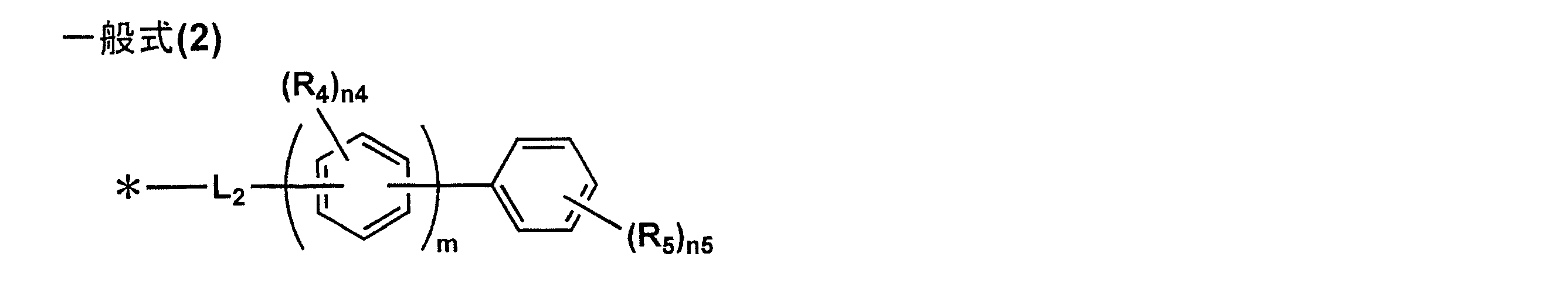


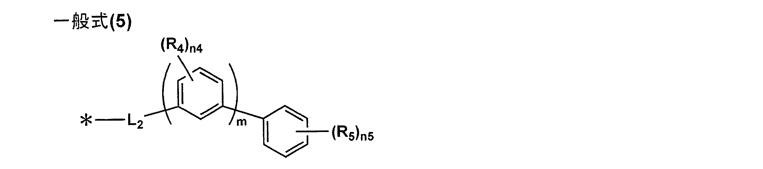
前記有機層の少なくとも1層に、第1項から第10項の何れか一項に記載の有機エレクトロルミネッセンス素子材料が含有されていることを特徴とする有機エレクトロルミネッセンス素子。
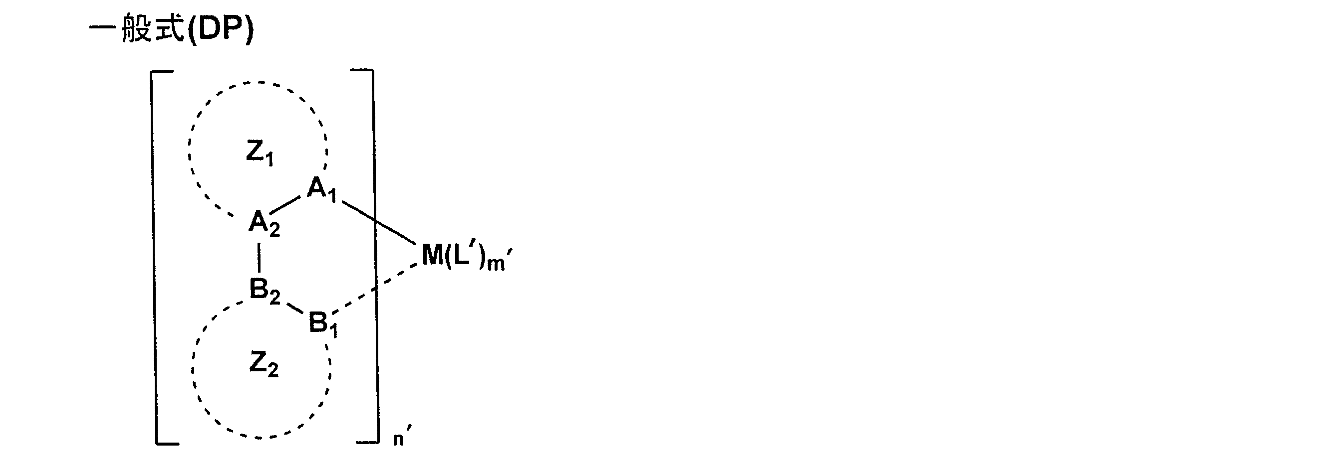
本発明の効果の発現機構ないし作用機構については、明確にはなっていないが、以下のように推察している。
本発明に係る有機EL素子材料は、一般式(1)で表される構造のR1~R3の何れかの部位に、一般式(2)で表されるフレキシブルな部分構造を有することにより、同一材料間若しくは異種材料間で、良好な相互作用を示す。すなわち、発光ホストとして用いた場合においては、本発明の有機EL素子材料と発光ドーパントとの相溶性が向上し、ドーパントの凝集が抑制され、結果的に濃度消光、励起子同士の相互作用による消光等の問題が抑制され、更にドーパントが均一に分散することにより、発光層内部でのキャリア移動性が向上したものと推定される。これにより、高い発光効率、低駆動電圧、さらに発光の長寿命化を同時に達成できたものと考えられる。
一方で、本発明の一般式(2)におけるR5が芳香族複素環基の場合は、一般式(1)で表される化合物の両末端の芳香族複素環基の効果により、化合物同士の会合が起きやすくなるため、好ましくない場合がある。化合物同士の会合が起きやすくなると、同一材料間若しくは異種材料間での良好な相互作用が損なわれ、結果、有機EL素子の発光効率の低下や発光寿命の低下が起こりやすくなると推定される。発明者らがさらに検討したところ、R5で表される芳香族複素環が炭素原子で一般式(2)におけるベンゼン環と結合した場合においては、上記のような会合が起きにくくなる傾向があることが分かった。
また、一般にヘテロ原子-炭素原子結合の方が炭素原子-炭素原子結合よりも結合エネルギーが低く、切断されやすいことは知られている。一般式(1)で表される化合物において、特に励起状態や荷電状態でR5で表される芳香族複素環部分の電荷密度が高くなっている場合においては、該芳香族複素環と一般式(2)におけるベンゼン環との結合部分に負荷がかかりやすく、該芳香族複素環が炭素原子で結合している場合よりもヘテロ原子で結合している場合の方が切断されやすい傾向があるため、化合物の耐久性という点からも、R5で表される芳香族複素環は炭素原子で結合していることが好ましい。
また、本発明に係る有機EL素子材料は、後述する一般式(DP)に代表されるリン光発光性化合物と親和性の高い置換基を分子内に有するため、発光ホストとして使用することで、非晶質を保ったまま、発光層内の分子間のパッキングを密にし、π電子間の相互作用を大きくすることで、電気特性(低電圧駆動性)を向上させ、その結果素子寿命を向上させることができるものと推定される。
また、本発明に係る有機EL素子材料は、一般式(2)に代表されるフレキシブルな部分構造を分子内に有するため、形成した層の非晶質性を保つことができ、有機EL素子を高温、高湿下で保存した場合においても形成層の非晶質性を保つことができ、更に薄膜形成能が高いため、膜のモルフォロジーの変化が小さく、均質な膜を形成できる。これにより、保存後においても良好な性能を示すことができたものと考えられる。
また、本発明においては、一般式(2)で表される置換基が、下記一般式(5)で表される置換基であることが好ましい。これにより、有機EL素子の発光効率、駆動電圧、発光寿命、駆動時の電圧上昇、経時安定性の各機能が向上するという効果が得られる。
また、本発明においては、一般式(3)で表される化合物が、下記一般式(6)で表される化合物であることが好ましい。これにより、有機EL素子の発光効率、駆動電圧、発光寿命、駆動時の電圧上昇、経時安定性の各機能が向上するという効果が得られる。
また、本発明においては、一般式(4)で表される化合物が、下記一般式(7)で表される化合物であることが好ましい。これにより、有機EL素子の発光効率、駆動電圧、発光寿命、駆動時の電圧上昇、経時安定性の各機能が向上するという効果が得られる。
また、本発明においては、一般式(1)~(7)において、L1又はL2が、単結合を表すことが好ましい。これにより、化合物中に占める一般式(2)又は(5)で表される置換基の割合が高くなり、ドーパントとの相互作用力が向上し、好ましい分散状態を与えることができるという効果が得られる。また、連結基を単結合とすることで、電気的堅牢性が向上することも、有機EL素子の各機能が向上するという効果が得られる一因だと推測している。
本発明に係る有機EL素子材料は、下記一般式(1)で表される化合物である。本発明に係る有機EL素子には、有機層の少なくとも1層に、下記一般式(1)で表される化合物が含有されているものであるが、発光層及び電子輸送層の少なくとも一方に含有されていることが好ましい。
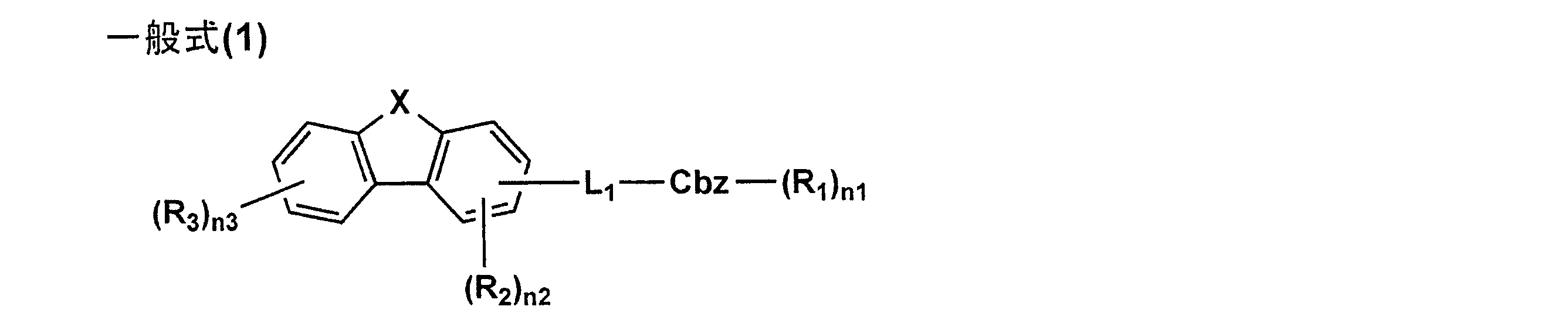
L1で表される2価の連結基としては、例えば、アルキレン基、アルケニレン基、エーテル基、チオエーテル基、エステル基、カルボニル基、アミノ基、アミド基、シリル基、ホスフィンオキシド基、芳香族炭化水素環から導出される2価の連結基、芳香族複素環から導出される2価の連結基、非芳香族炭化水素環から導出される2価の連結基、非芳香族複素環から導出される2価の連結基、又はこれらの組み合わせから導出される2価の連結基等が挙げられる。
ここで、芳香族炭化水素環としては、例えば、ベンゼン環、ナフタレン環、トリフェニレン環、インデン環、フルオレン環等が好ましく、ベンゼン環がより好ましい。芳香族複素環としては、例えば、ピリジン環、ピラジン環、ピリミジン環、ピリダジン環、トリアジン環、イミダゾール環、インドール環、ベンゾフラン環、ベンゾチオフェン環、カルバゾール環、ジベンゾフラン環、ジベンゾチオフェン環、ベンゾフラノインドール環、インドロインドール環等が好ましく、ピリジン環、ピラジン環、イミダゾール環、インドール環、ベンゾフラン環、ベンゾチオフェン環、カルバゾール環、ジベンゾフラン環、ジベンゾチオフェン環、ベンゾフラノインドール環、インドロインドール環がより好ましい。非芳香族炭化水素環としては、例えば、シクロプロパン環、シクロペンタン環、シクロヘキサン環、シクロヘキサジエン環、テトラヒドロナフタレン環、ジヒドロインデン環等が挙げられる。非芳香族複素環としては、例えば、ピペリジン環、モルフォリン環等が挙げられる。

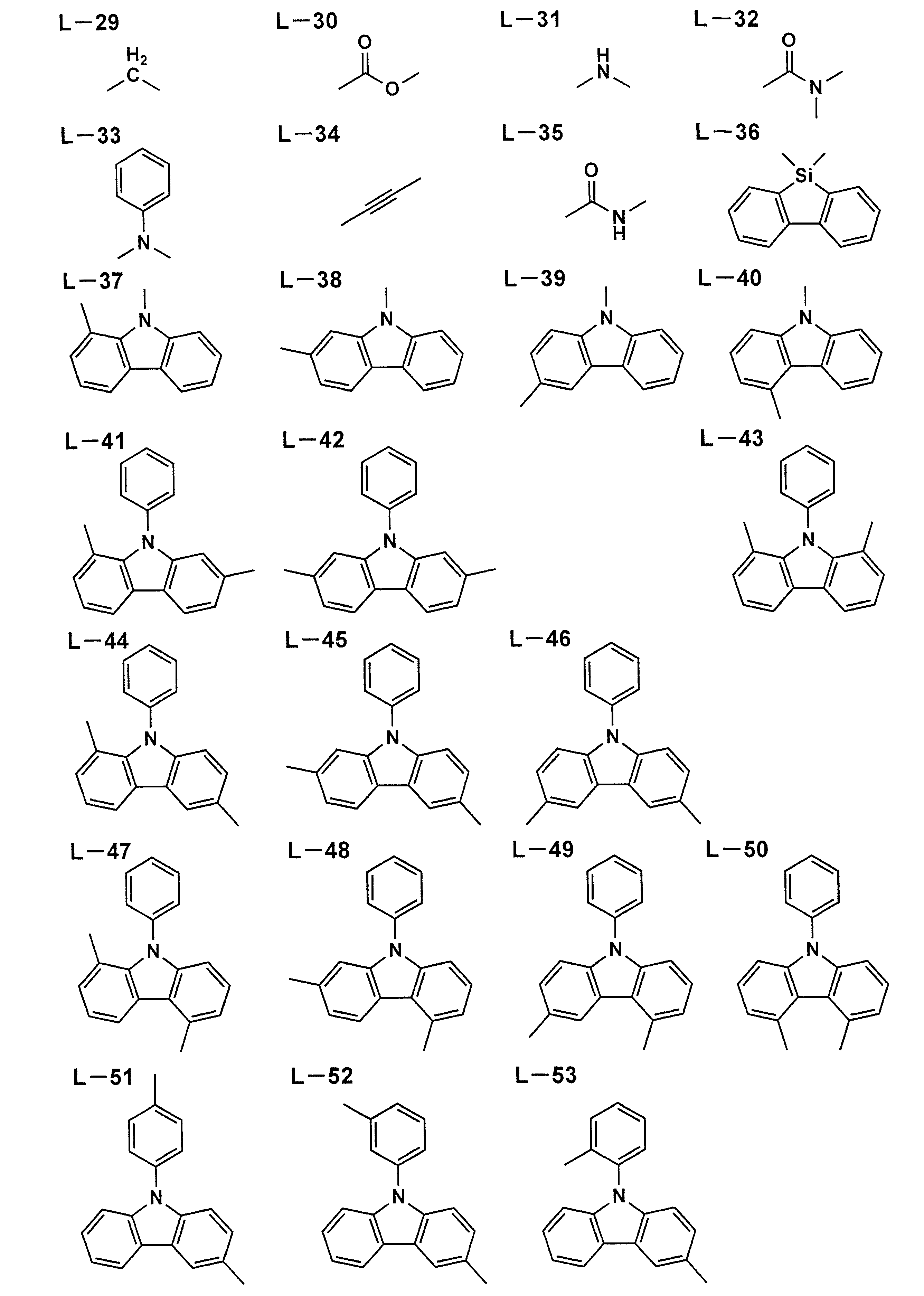


R1~R3で表される基としては、好ましくはシリル基、芳香族炭化水素環基、芳香族複素環基が挙げられ、芳香族炭化水素環又は芳香族複素環としては、好ましくはベンゼン環、カルバゾール環、ジベンゾフラン環、ジベンゾチオフェン環、ピリジン環、ピラジン環、インドロインドール環、インドール環、ベンゾフラン環、ベンゾチオフェン環、イミダゾール環又はトリアジン環が好ましく用いられる。
R1~R3が有していても良い置換基としては、例えば、重水素原子、ハロゲン原子、シアノ基、アルキル基、アルケニル基、アルキニル基、アルコキシ基、カルボニル基、アミノ基、シリル基、ヒドロキシ基、チオール基、ホスフィンオキシド基、芳香族炭化水素環基、芳香族複素環基、非芳香族炭化水素環基、非芳香族複素環基、ホスフィノ基、スルホニル基、ニトロ基等が挙げられ、更に置換されていても良い。
n1は、好ましくは0~2であり、より好ましくは0又は1である。n2及びn3は、好ましくは少なくとも一方が1であり、より好ましくは各々0又は1であり、更に好ましくはn2+n3が1である。

R5が有していても良い置換基としては、前述のR1~R3が有していても良い置換基と同様の基が挙げられる。
R4及びR5がそれぞれ複数存在する場合は、各々のR4及びR5は、同じでも異なっていても良いが、R5同士が互いに結合して環を形成することはない。
一般式(2)において、n5は、0~5の整数を表し、より好ましくは0又は1であり、更に好ましくは0である。
L2で表される2価の連結基としては、上記した一般式(1)においてL1で表される2価の連結基と同様のものが挙げられる。

R2、R3、R6、R12’及びR12”で表される好ましい基としては、前述のR1~R3で好ましく用いられる基と同様の基が挙げられる。
R2、R3、R6、R12’及びR12”が有していても良い置換基としては、前述のR1~R3が有していても良い置換基と同様の基が挙げられる。
n2及びn3は、好ましくは少なくとも一方が1であり、より好ましくは各々0又は1であり、更に好ましくはn2+n3が1である。n1c及びn1dは、好ましくは0又は1であり、より好ましくはn1c+n1dが1である。


R2、R3、R1’及びR1”で表される好ましい基としては、前述の一般式(1)におけるR1~R3で好ましく用いられる基と同様の基が挙げられる。
R2、R3、R1’及びR1”が有していても良い置換基としては、前述の一般式(1)におけるR1~R3が有していても良い置換基と同様の基が挙げられる。
n2及びn3は、好ましくは少なくとも一方が1であり、より好ましくは各々0又は1であり、更に好ましくはn2+n3が1である。n1a及びn1bは、好ましくは0又は1であり、より好ましくはn1a+n1bが1である。

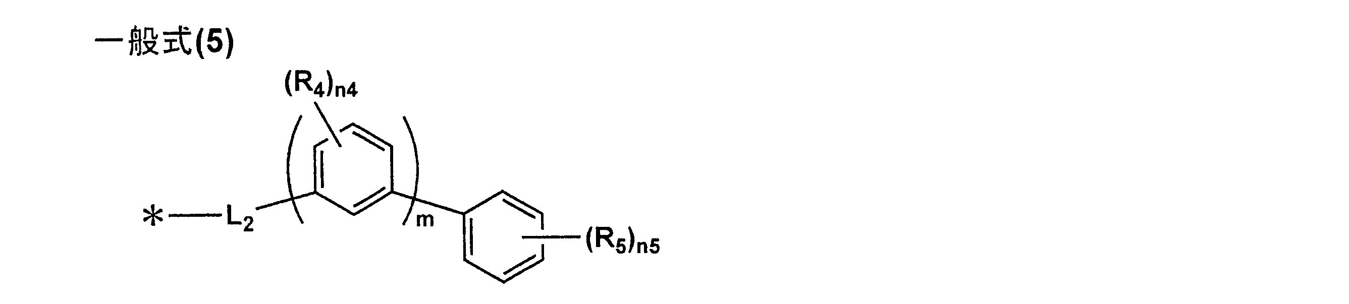
これは、化合物中に占める一般式(2)又は(5)で表される基の割合が高いほど、ドーパントとの相互作用力が向上し、好ましい分散状態を与えるためである。これにより、有機EL素子の発光効率及び発光寿命を向上させることができる。その他の要因として、連結基が単結合である場合が、最も電気的堅牢性が高いという点も推定される。
一方で、mが10以上であると、化合物全体の分子量が増大しすぎるため、蒸着時に高熱がかかり、化合物が分解しやすくなってしまう。更に、溶剤溶解性についても著しく低下してしまい、塗布ムラが発生しやすくなってしまう。したがって、mが2~10である場合が適切なフレキシビリティーを有するが、フレキシビリティー、蒸着適性及び溶剤溶解性の観点から、mが2~5の範囲にあることが最も有効であると推定される。
また、上記した一般式(1)で表される化合物が、後述するリン光発光性化合物と同時に用いられる場合には、一般式(1)で表される化合物が当該リン光発光性化合物よりも高い最低励起三重項エネルギー(T1)を有することが好ましく、T1が2.7eV以上であることがより好ましく、T1が2.75eV以上であることが更に好ましく、T1が2.8eV以上であることが特に好ましい。

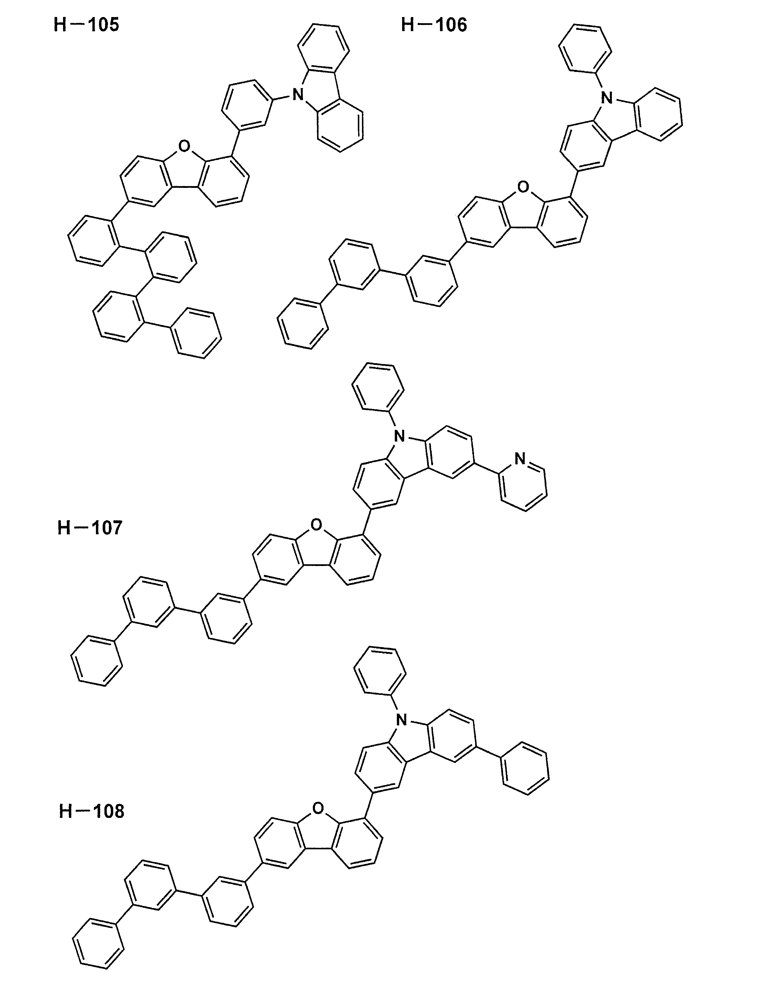
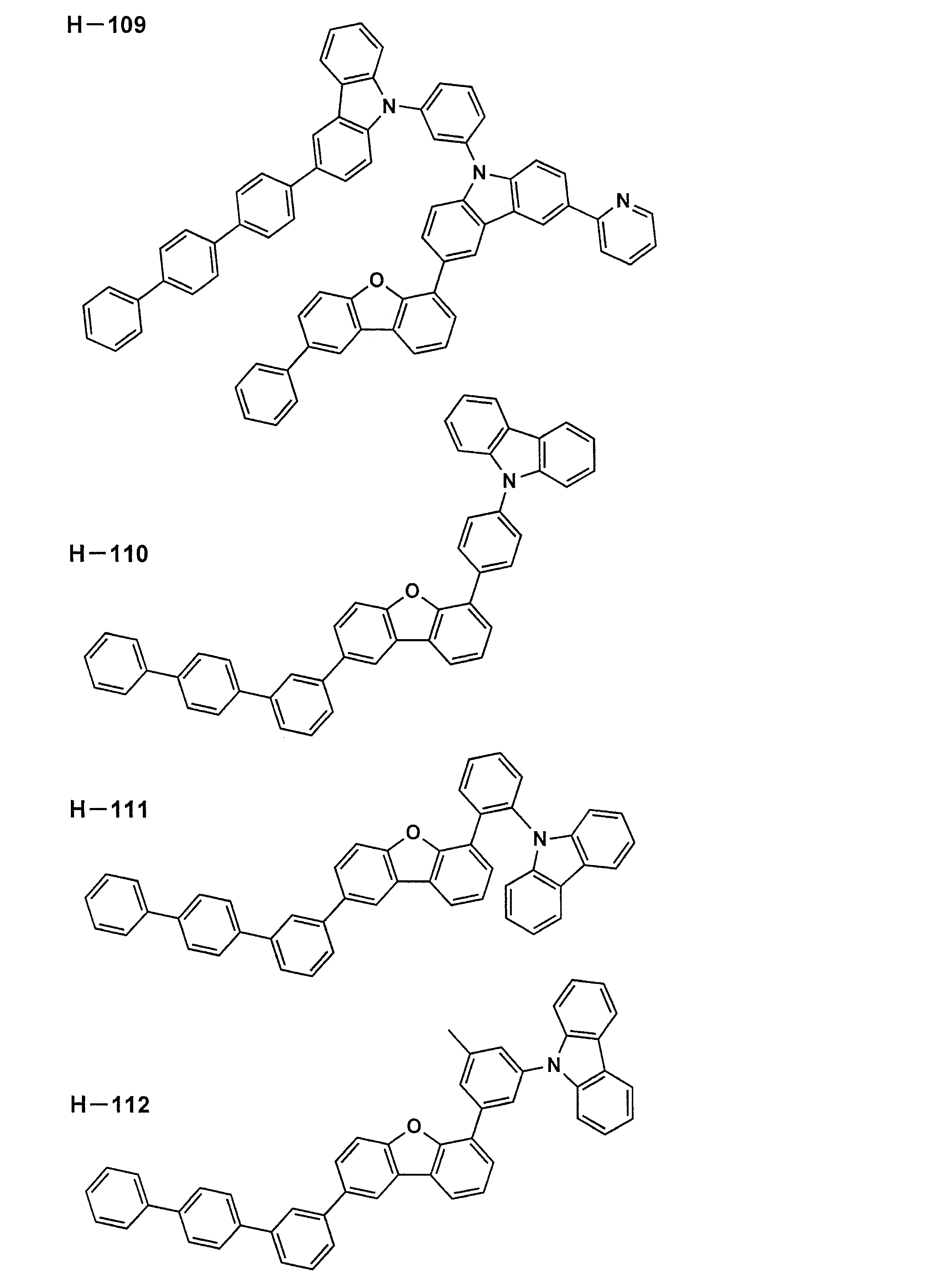
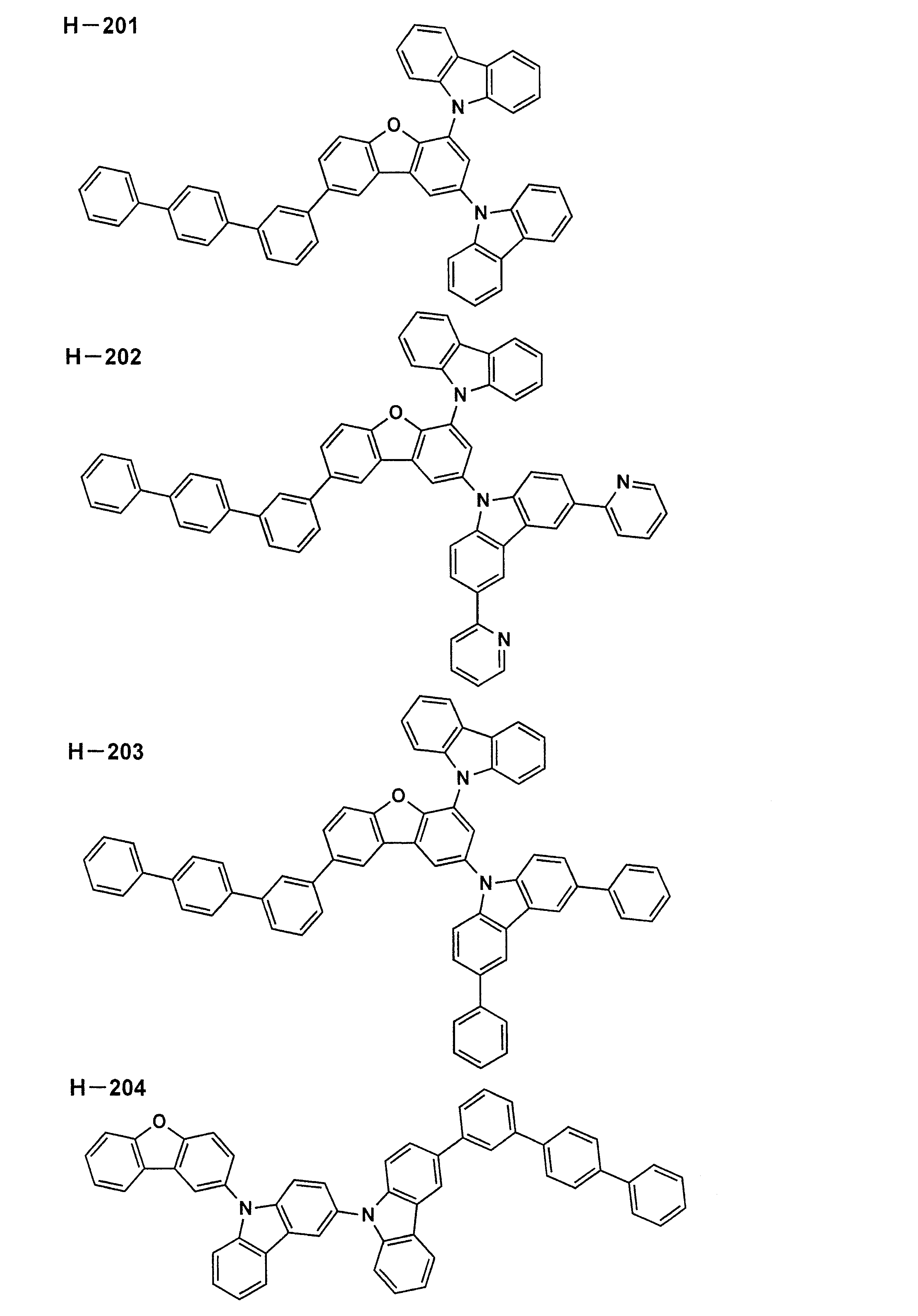

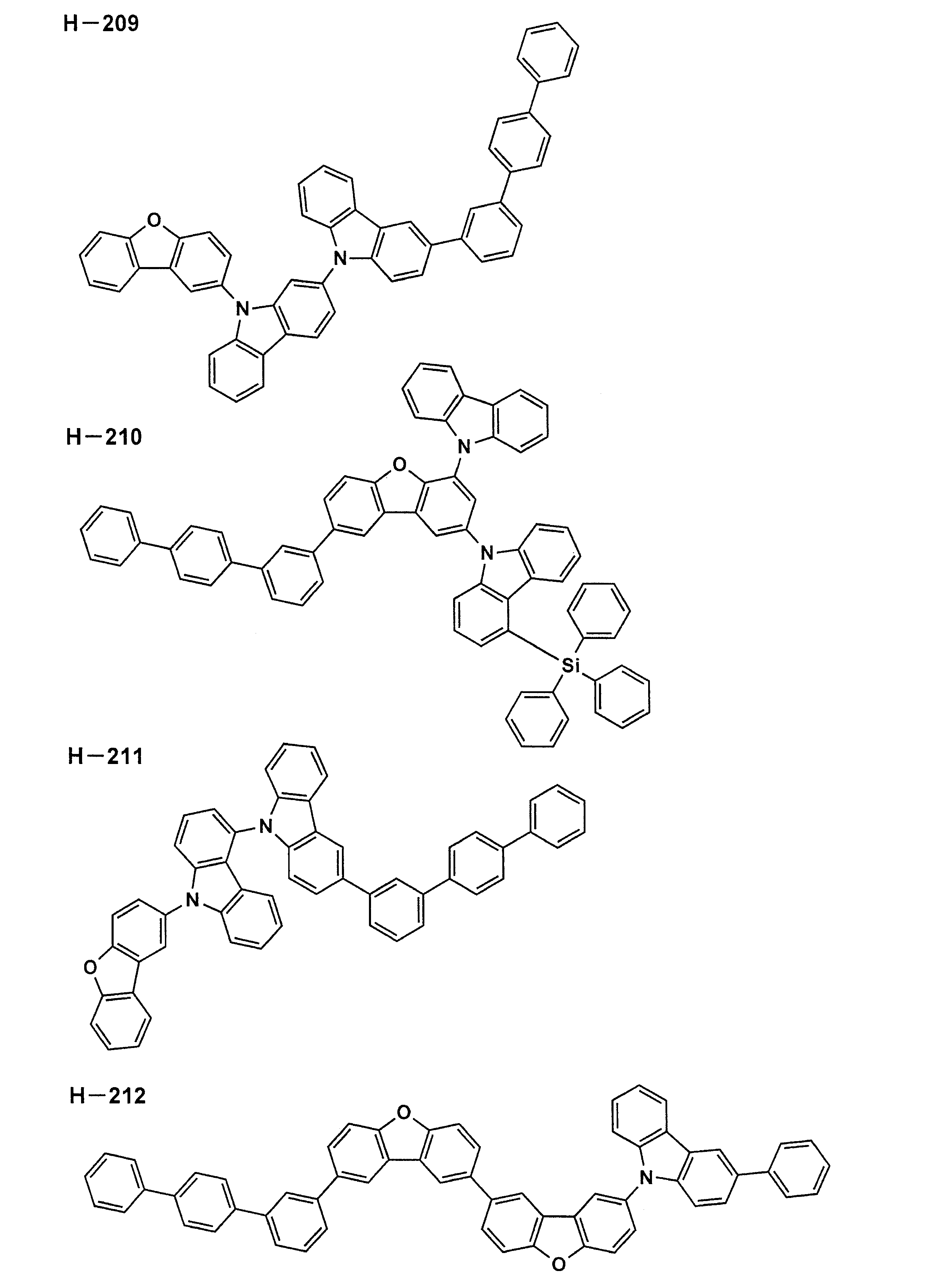


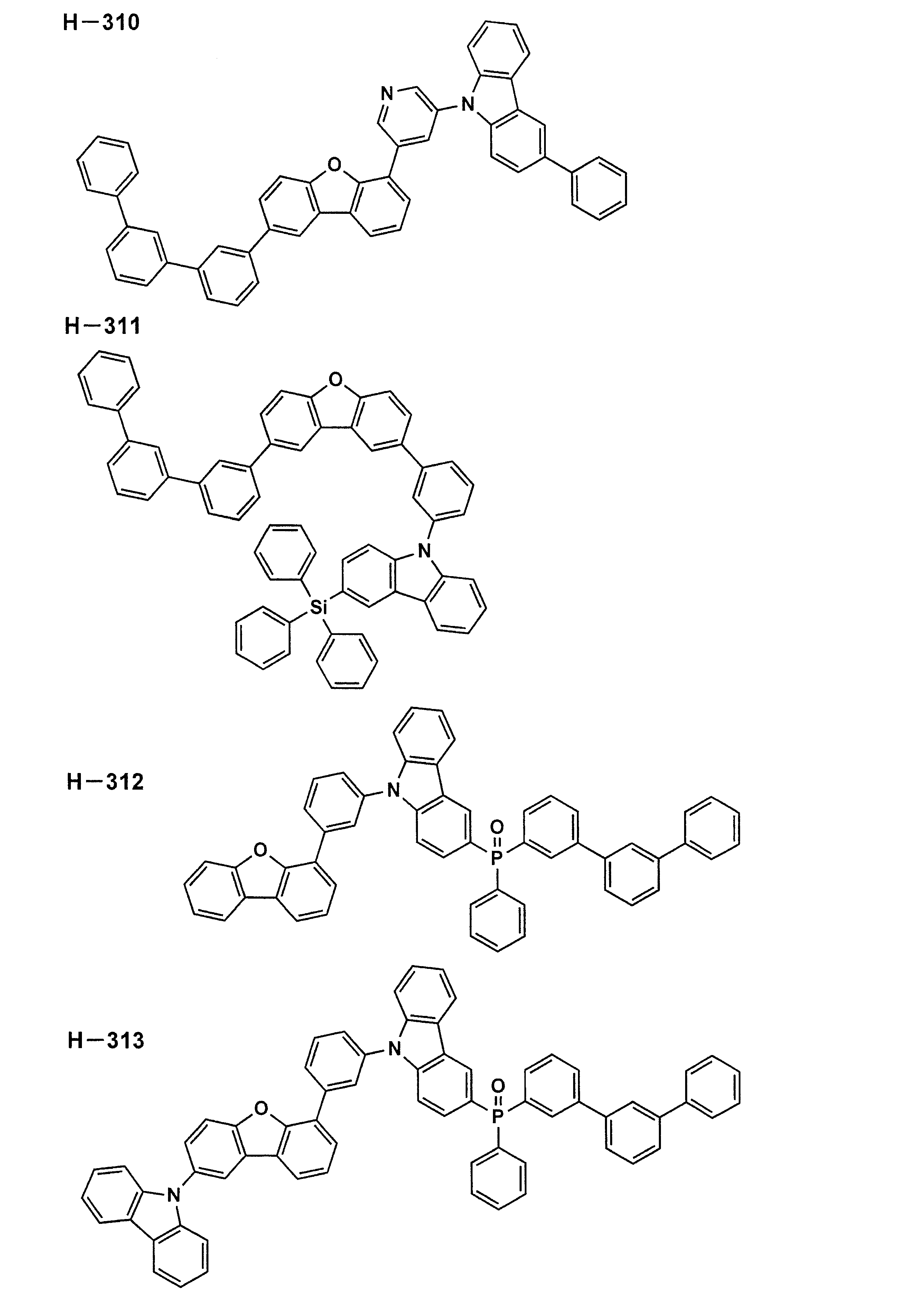


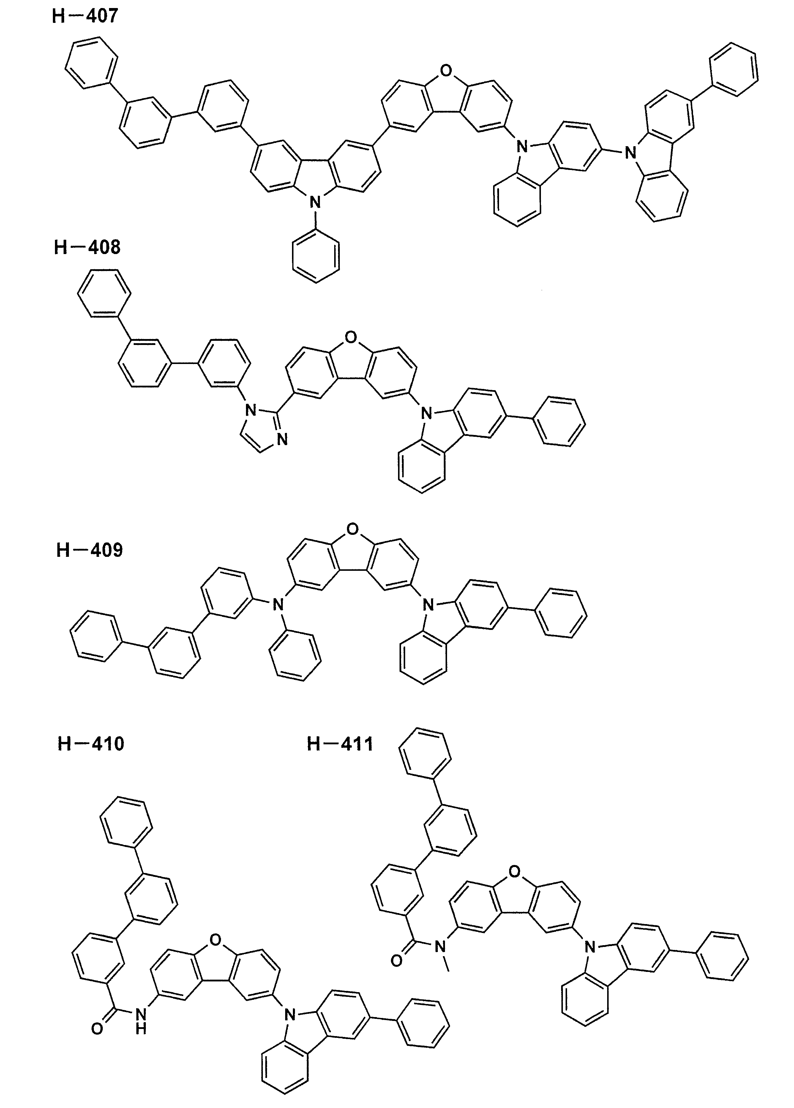


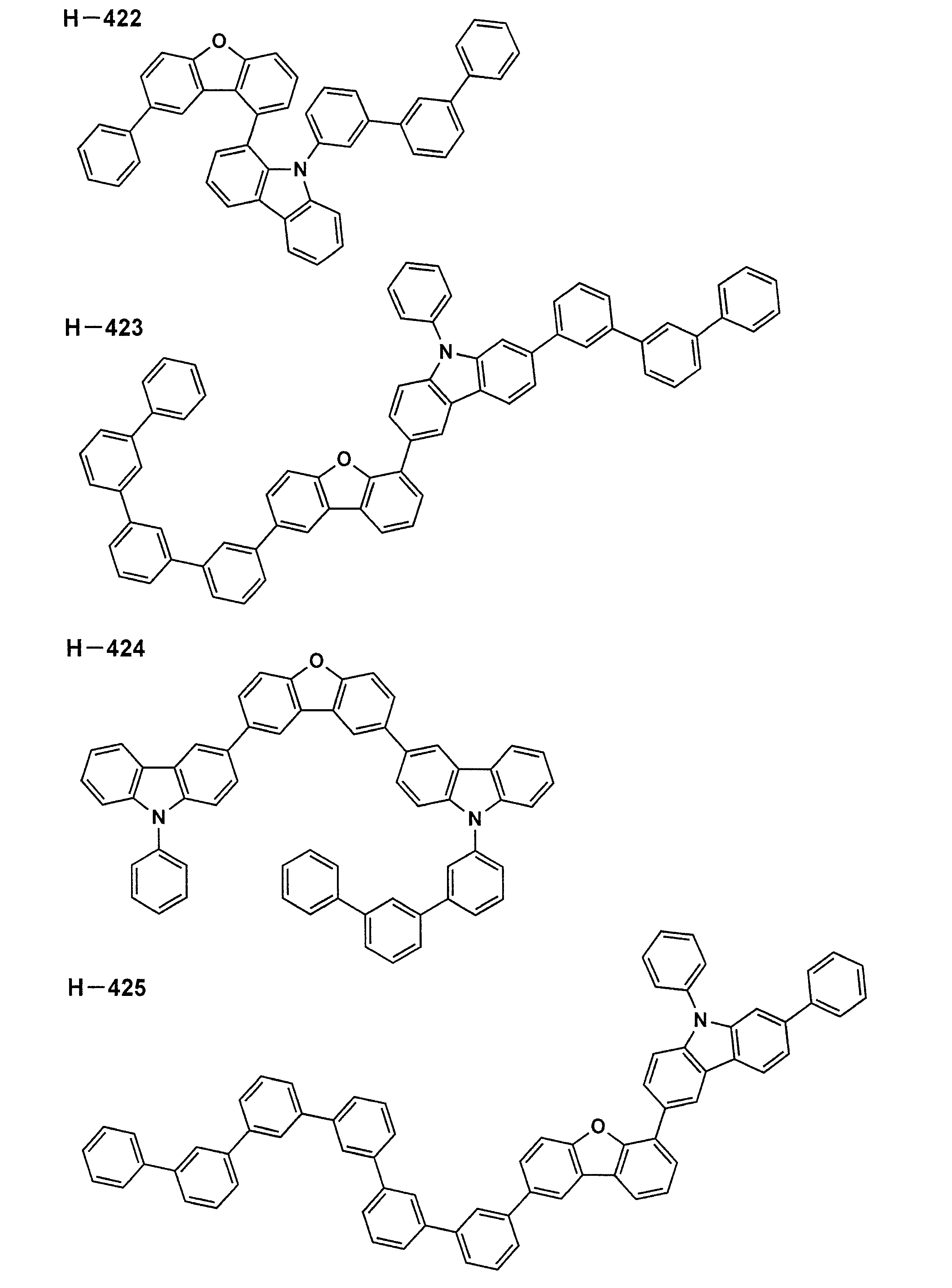
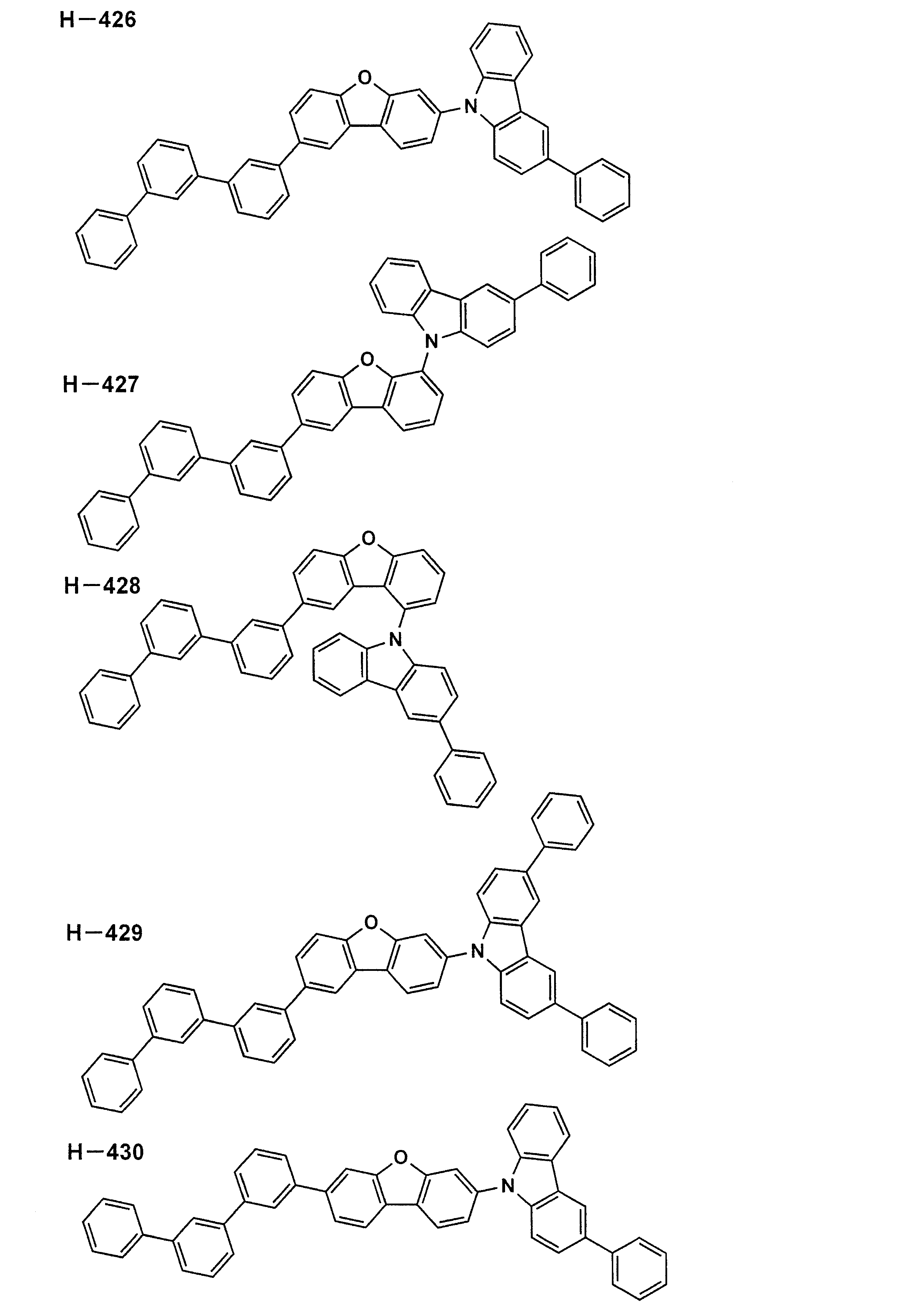
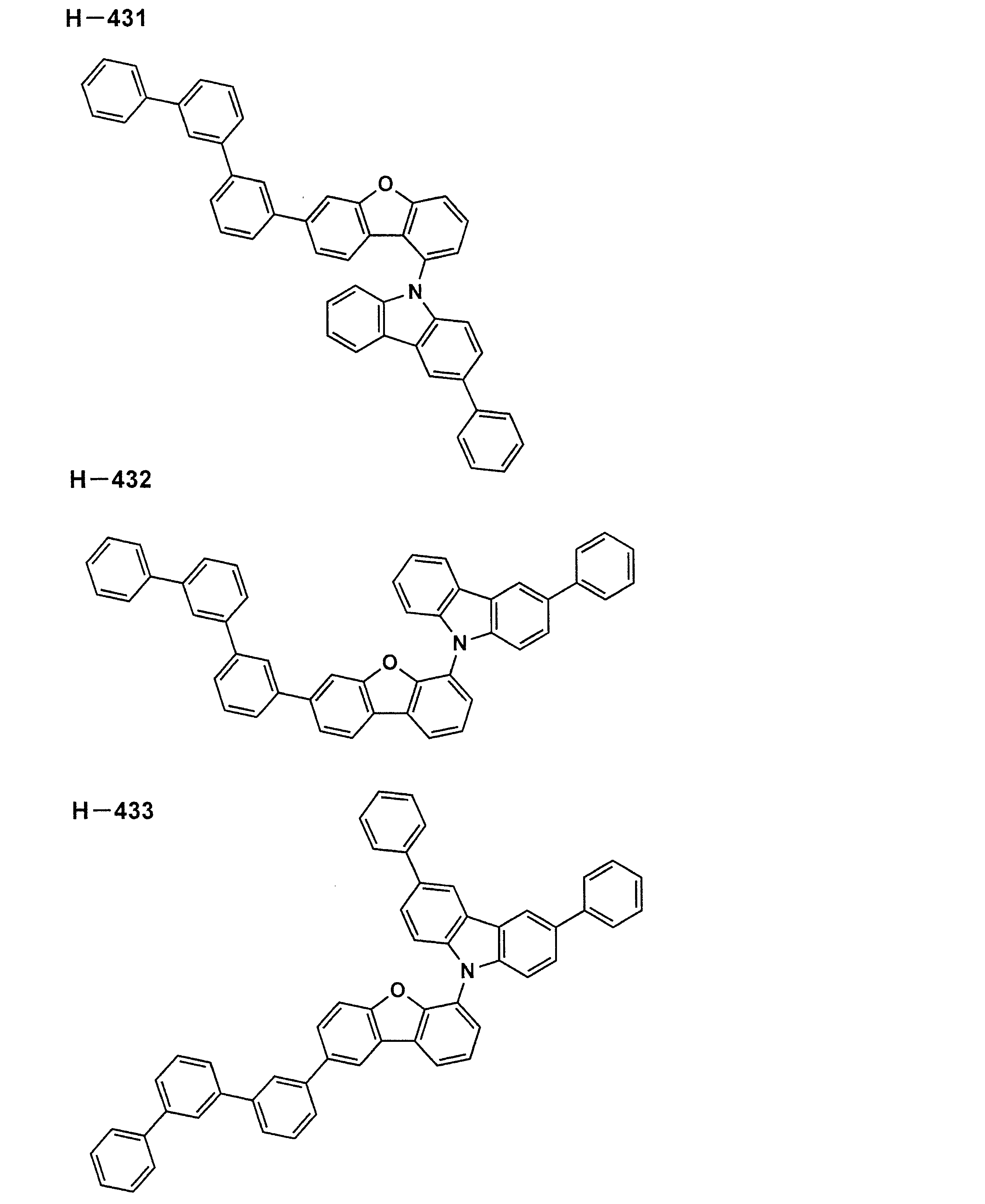

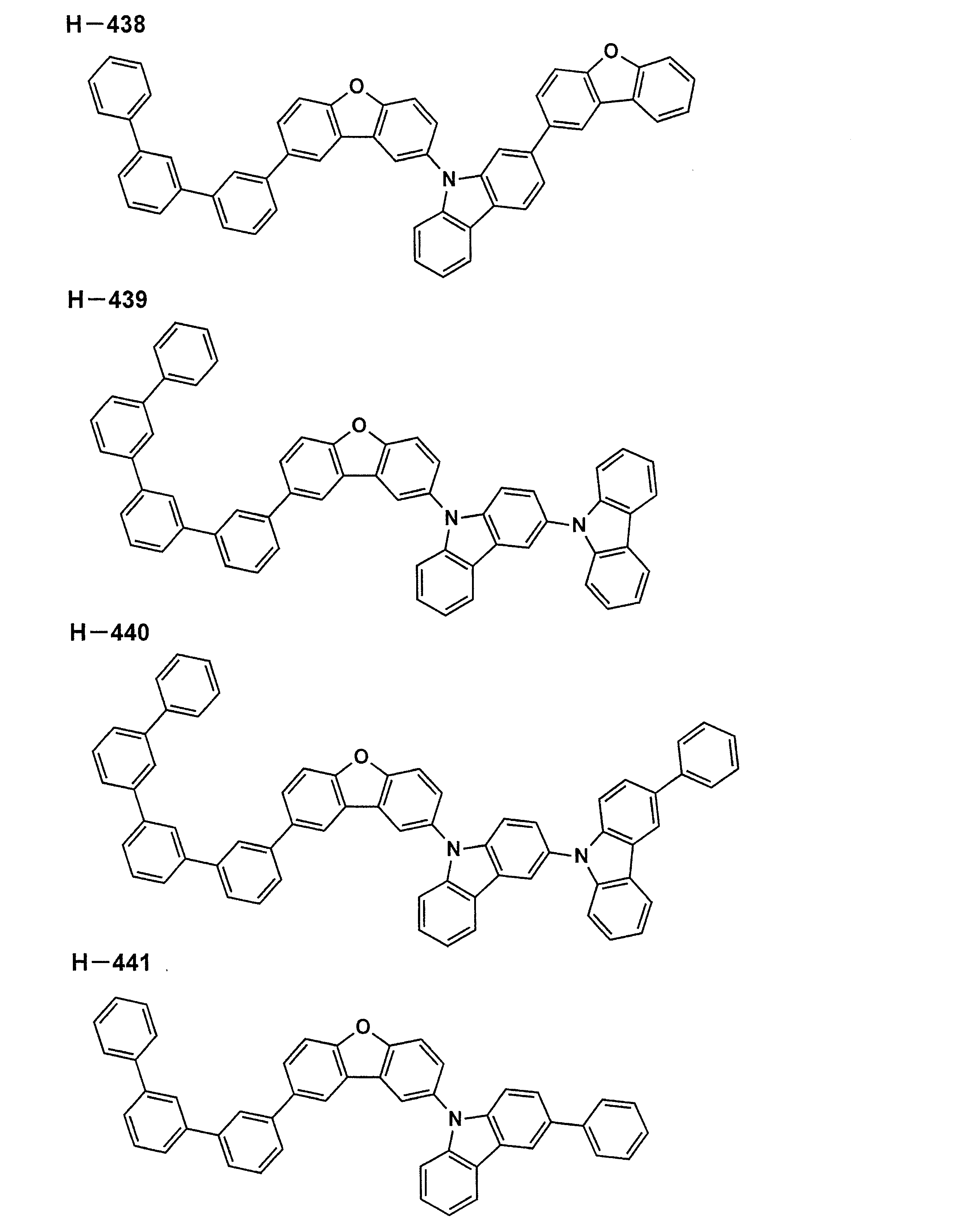
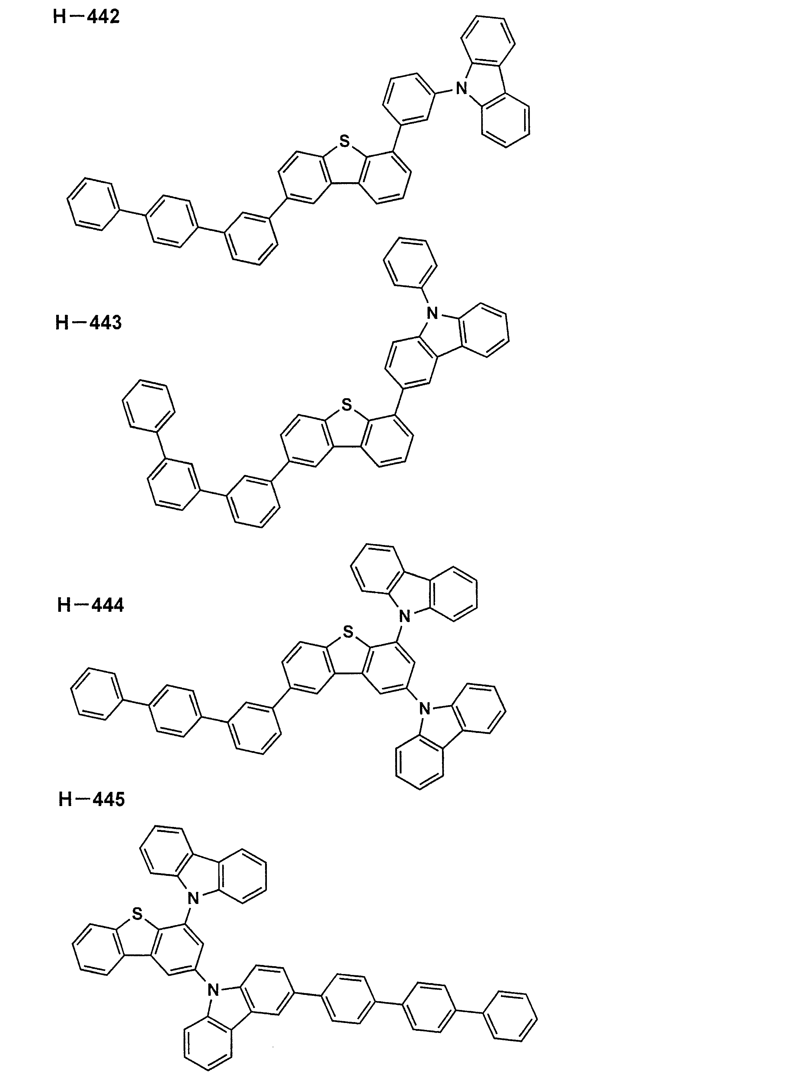
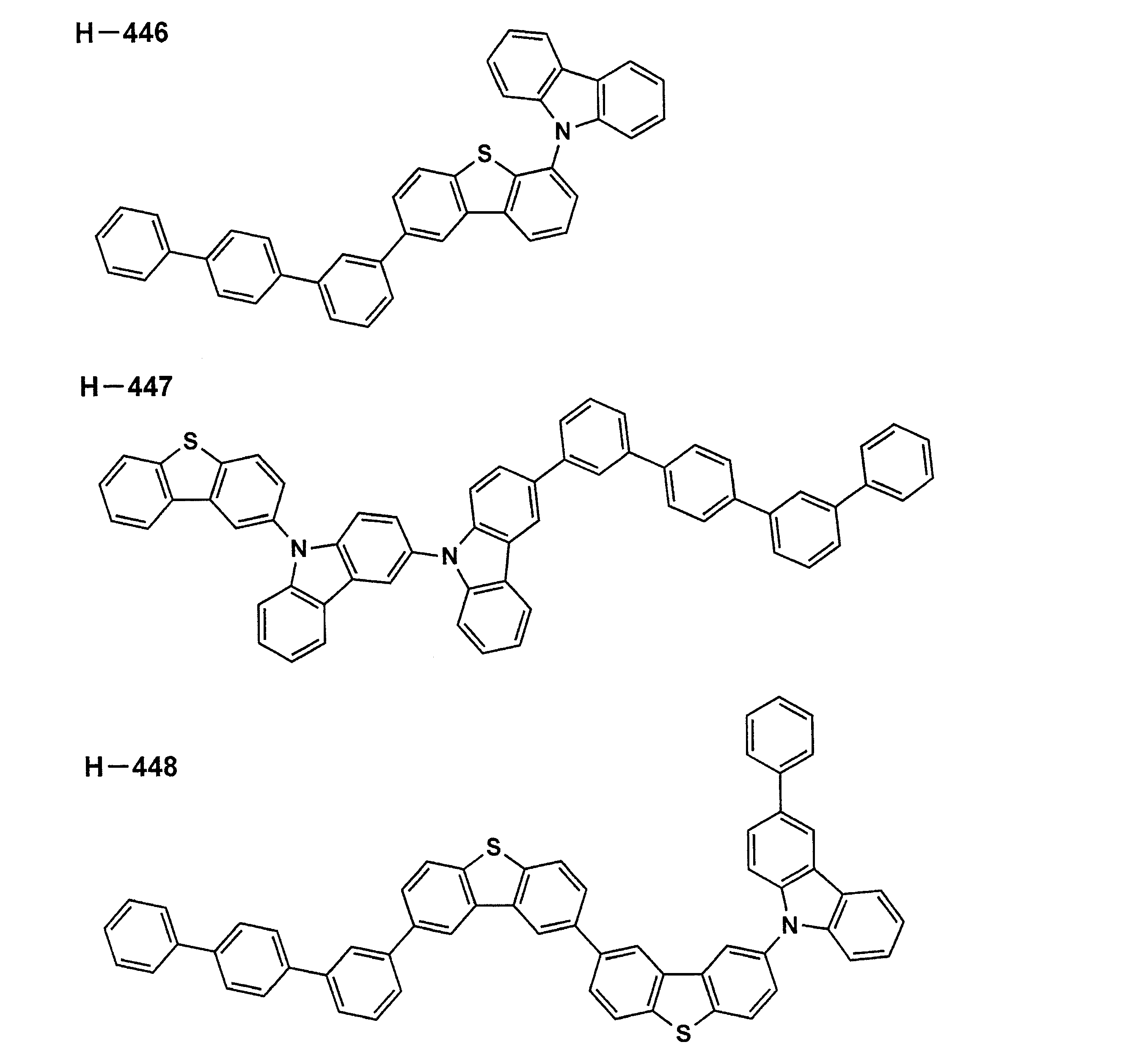
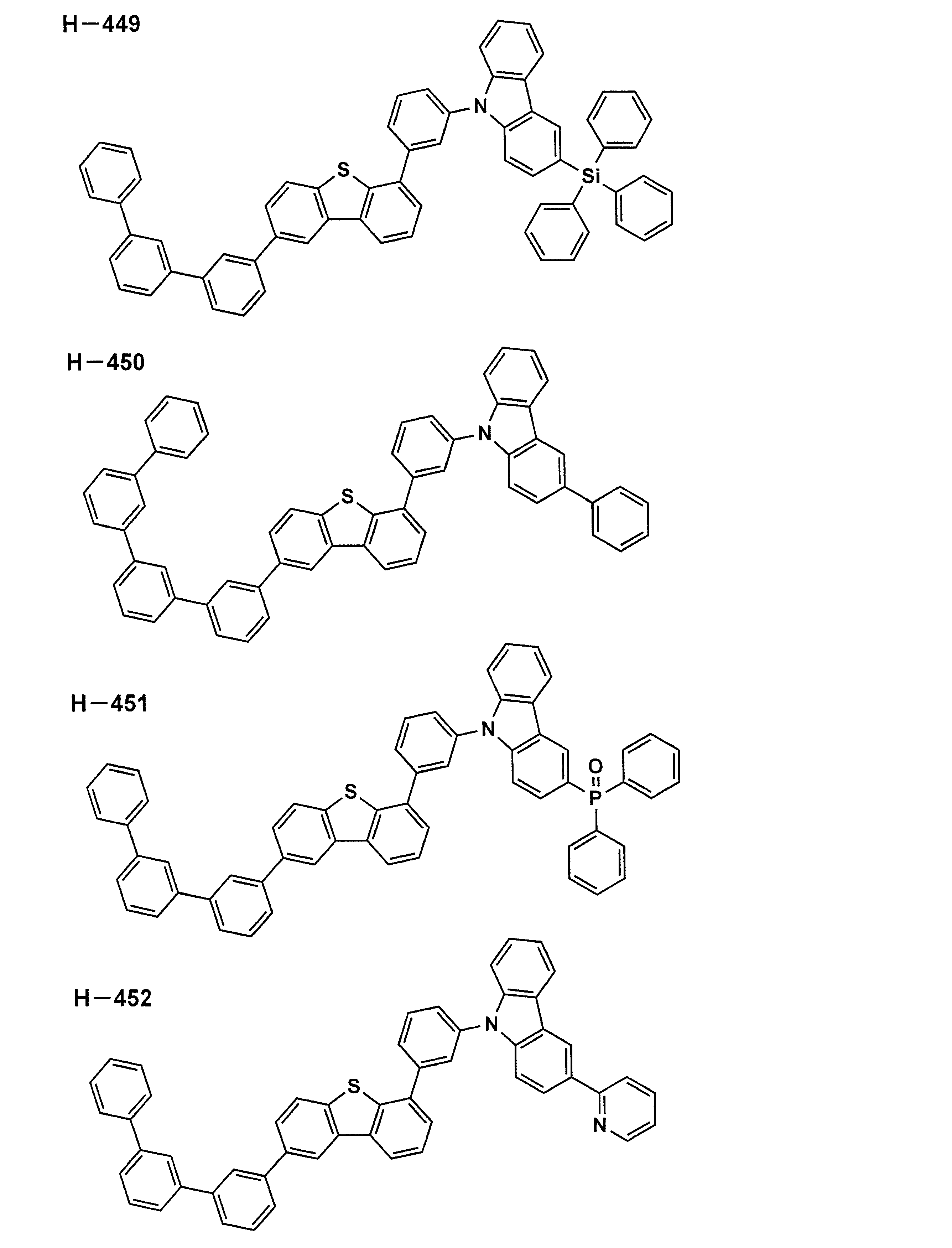

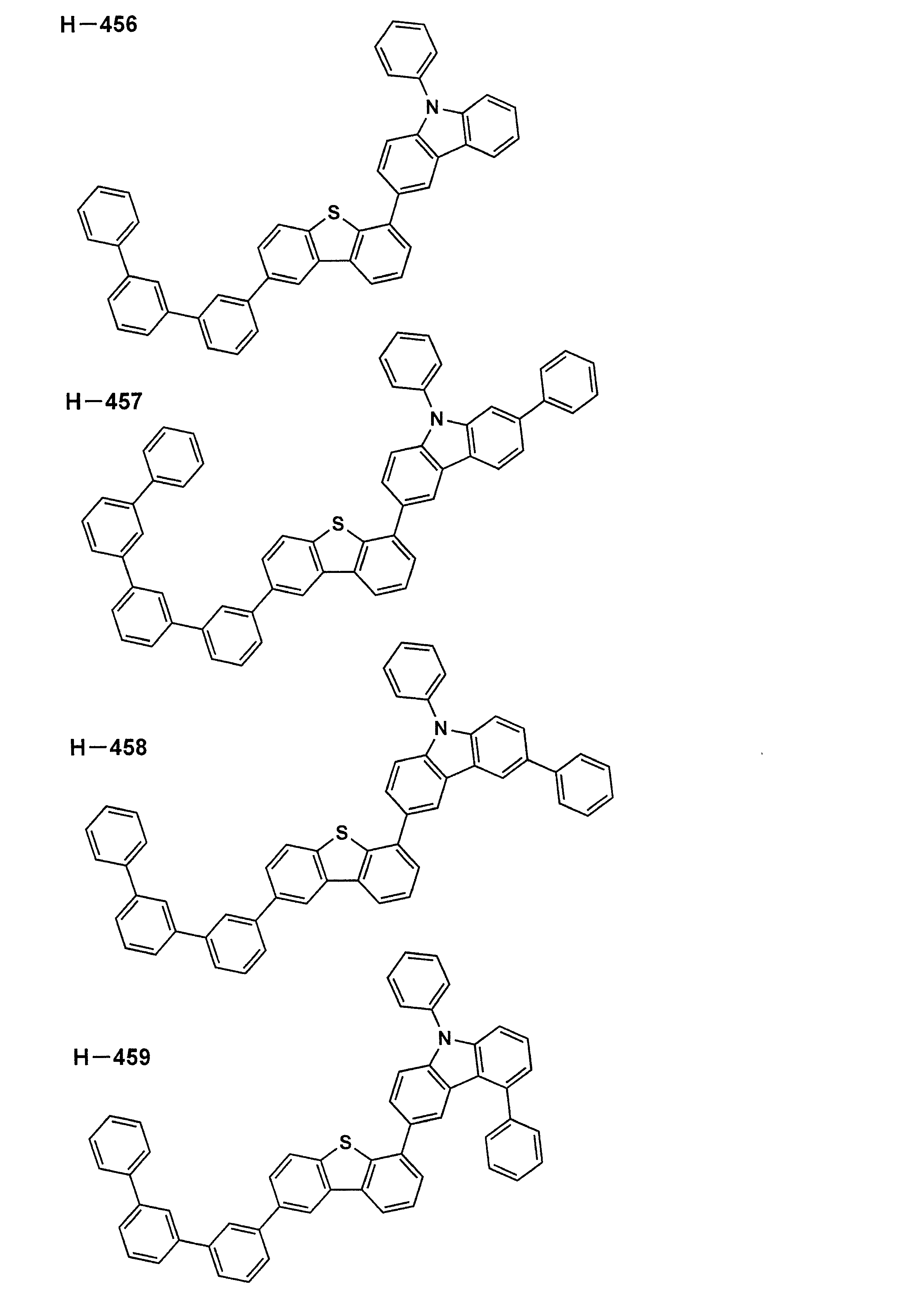
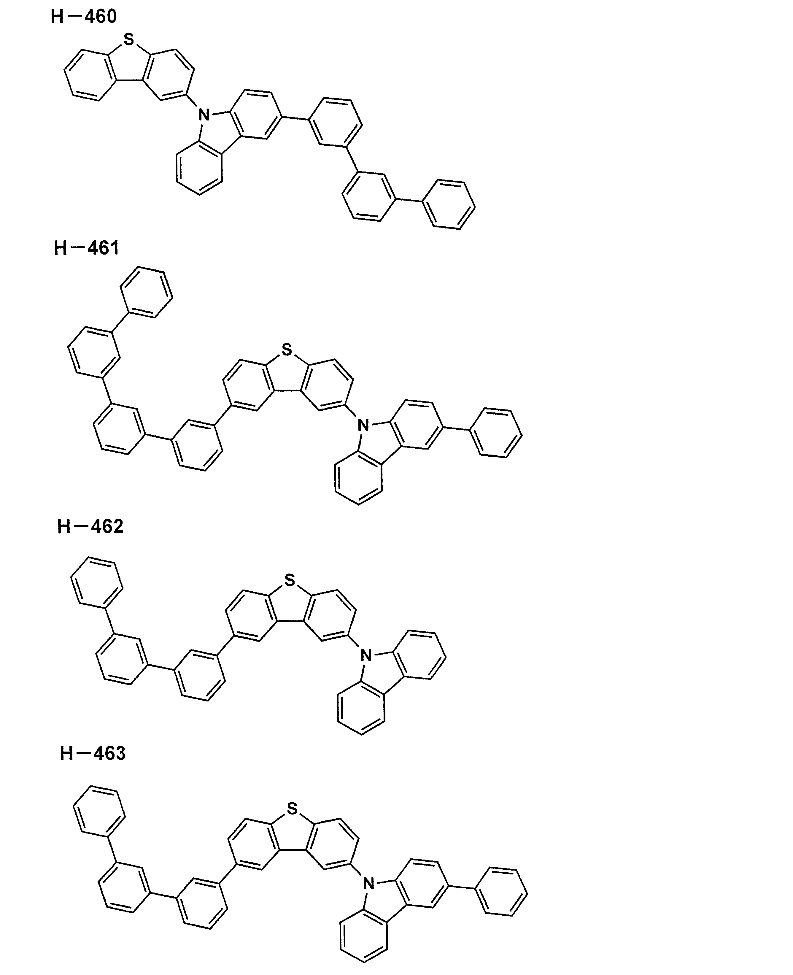
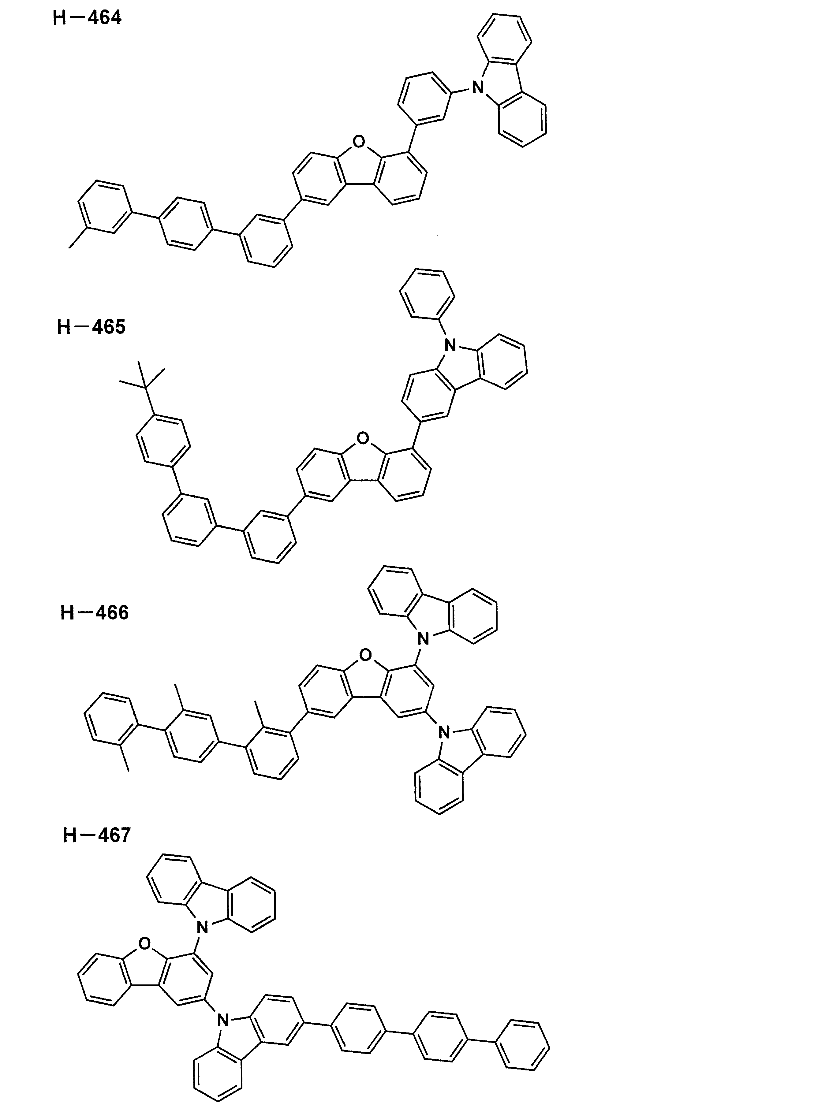

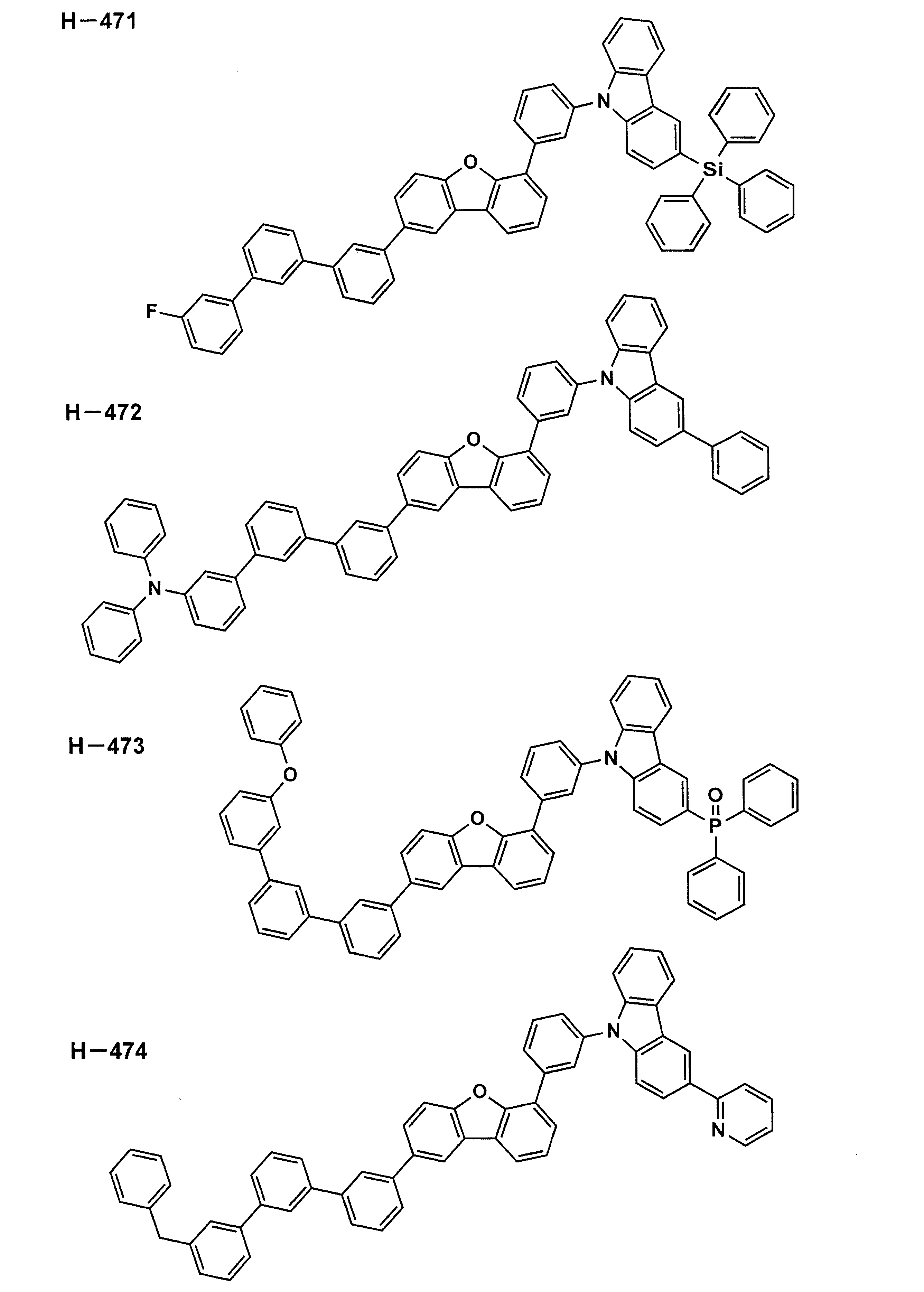
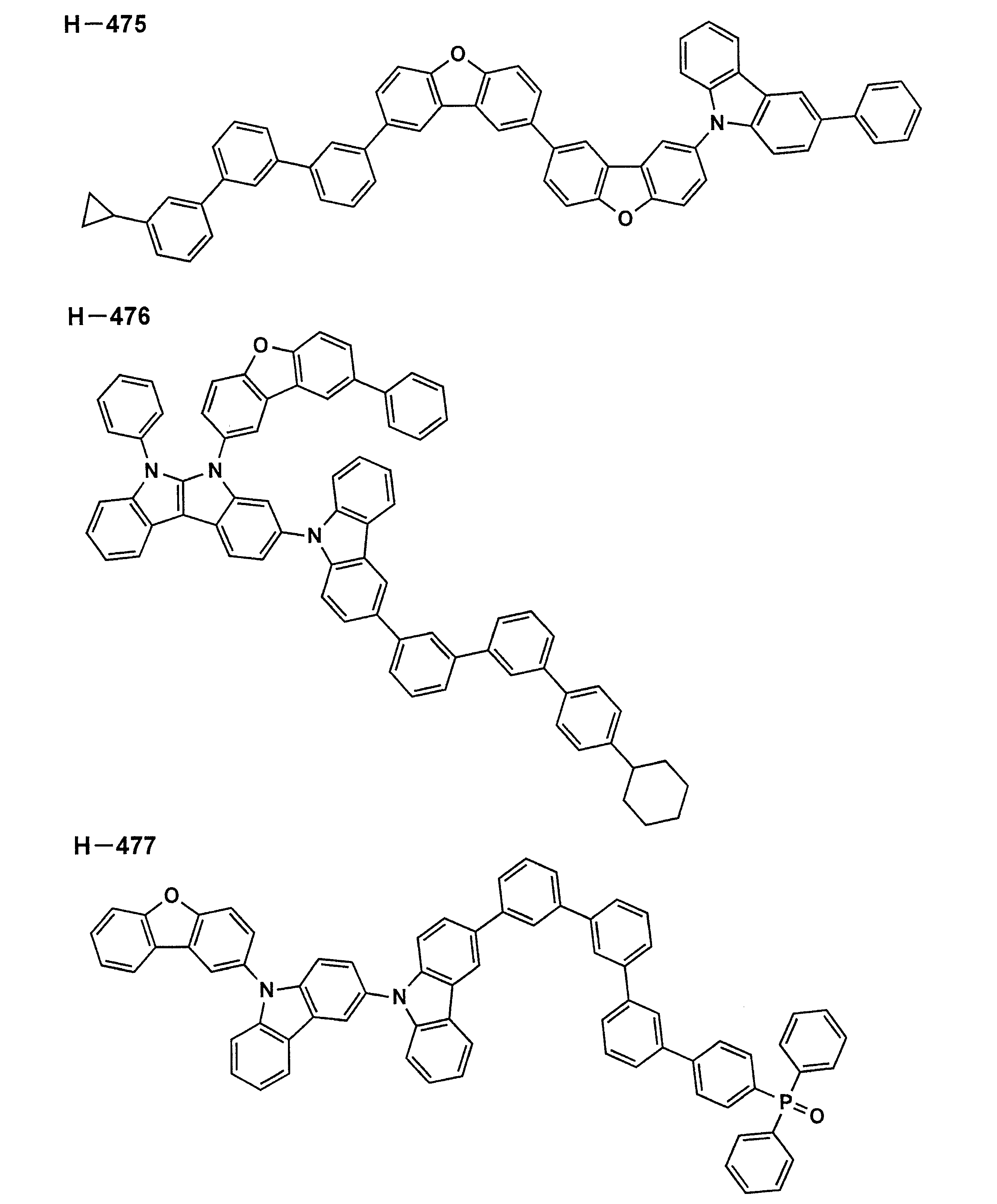
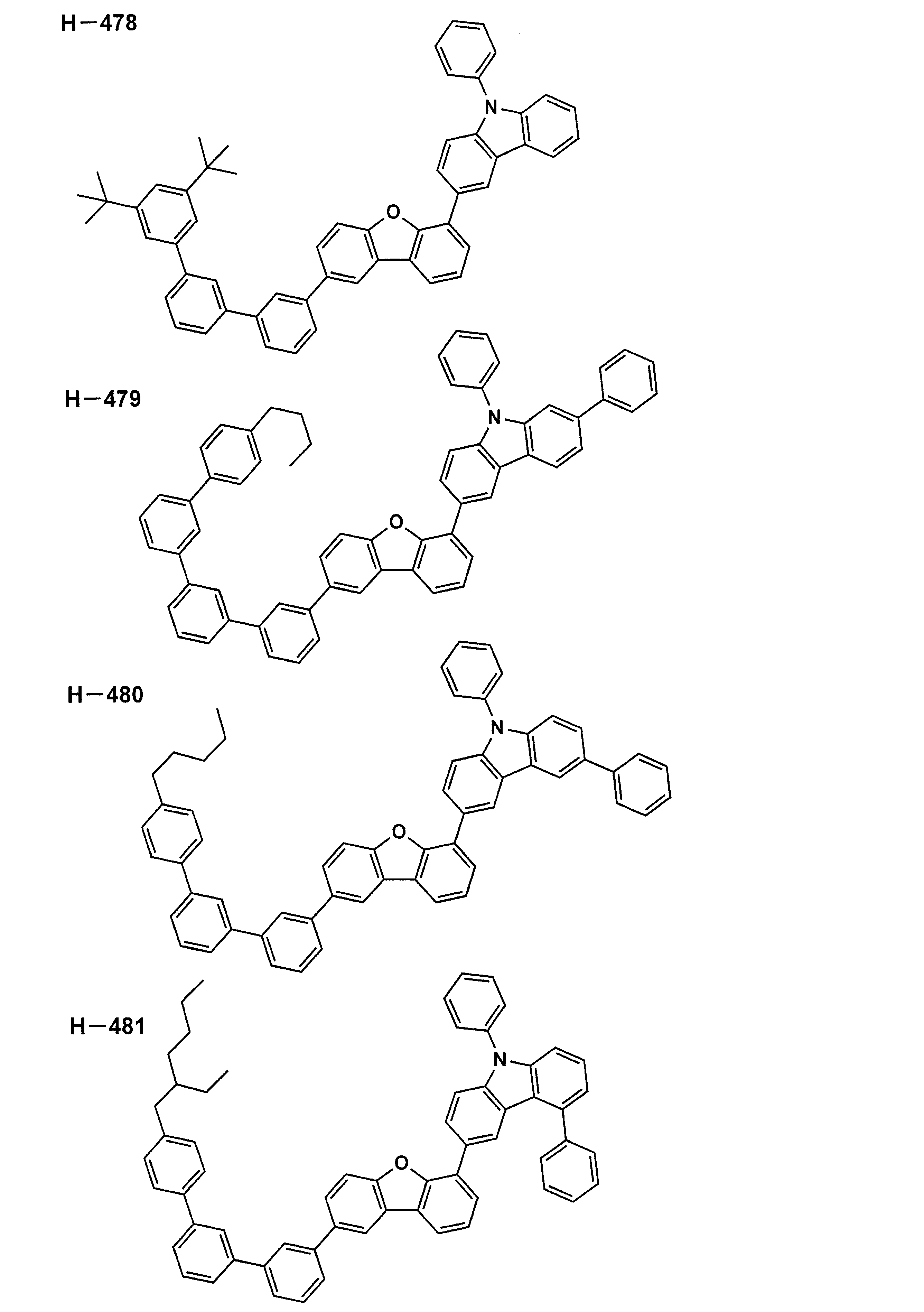


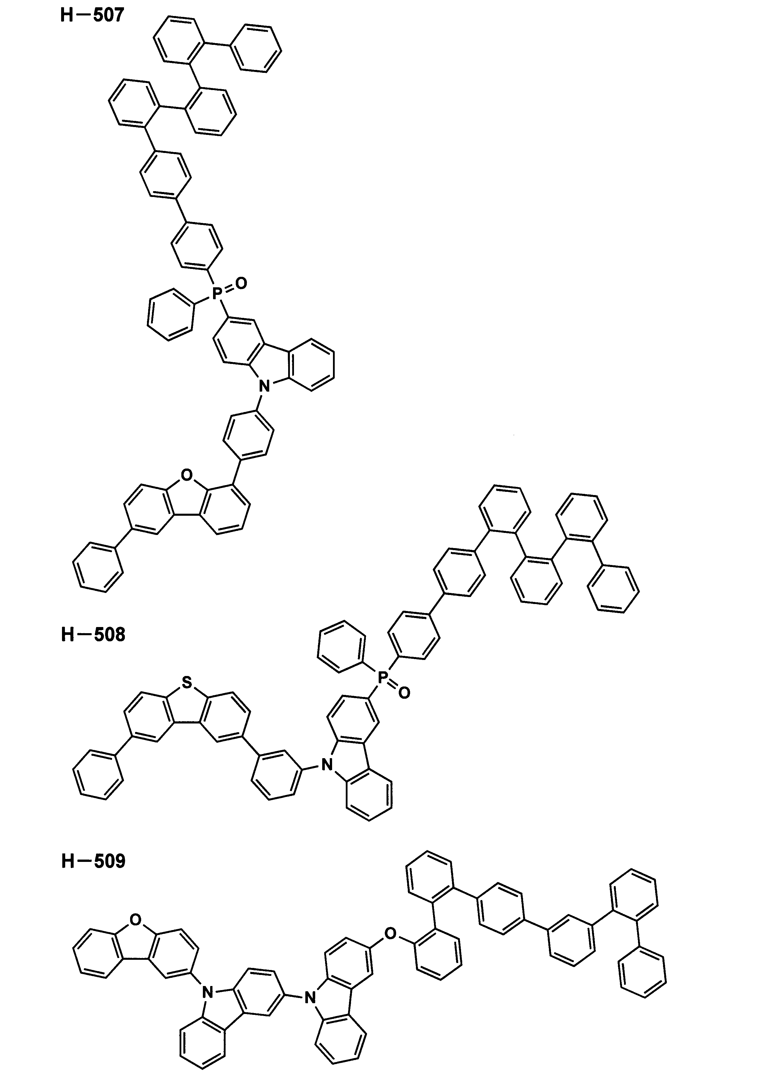
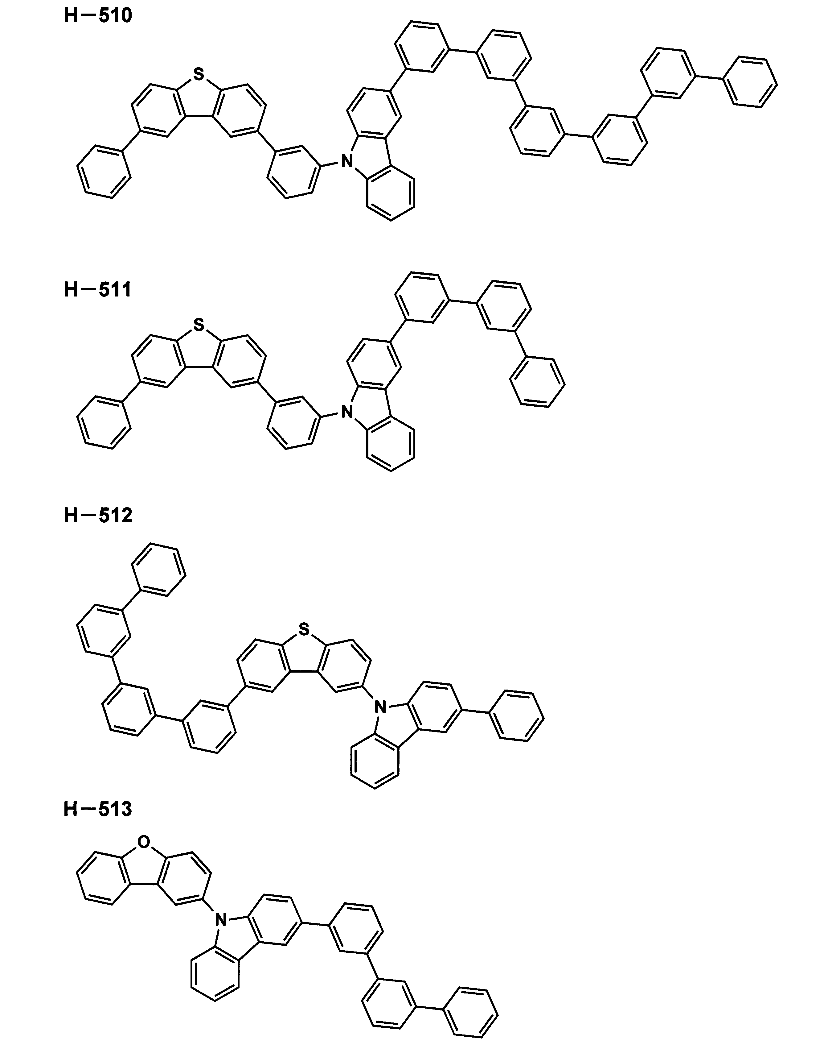


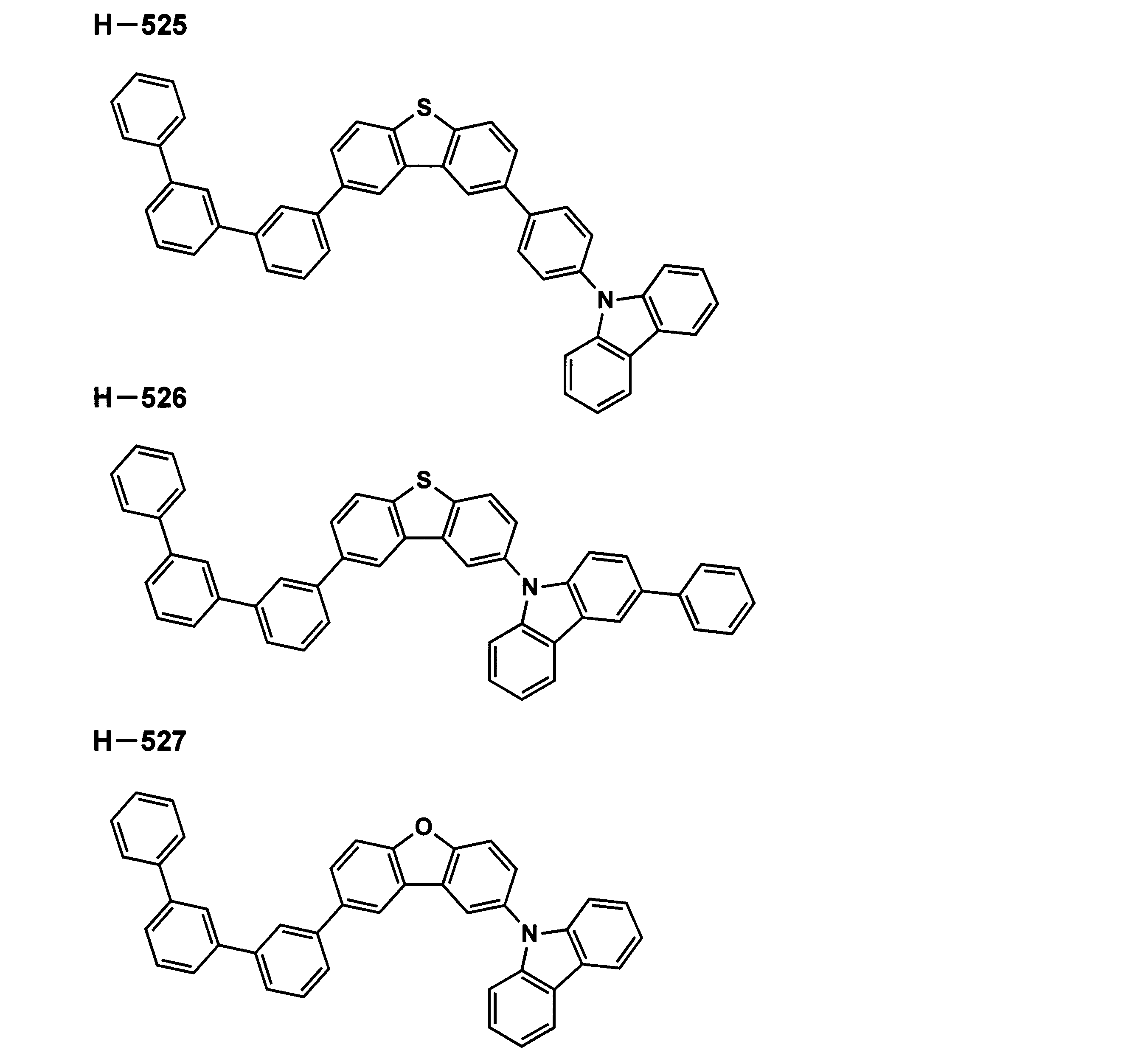

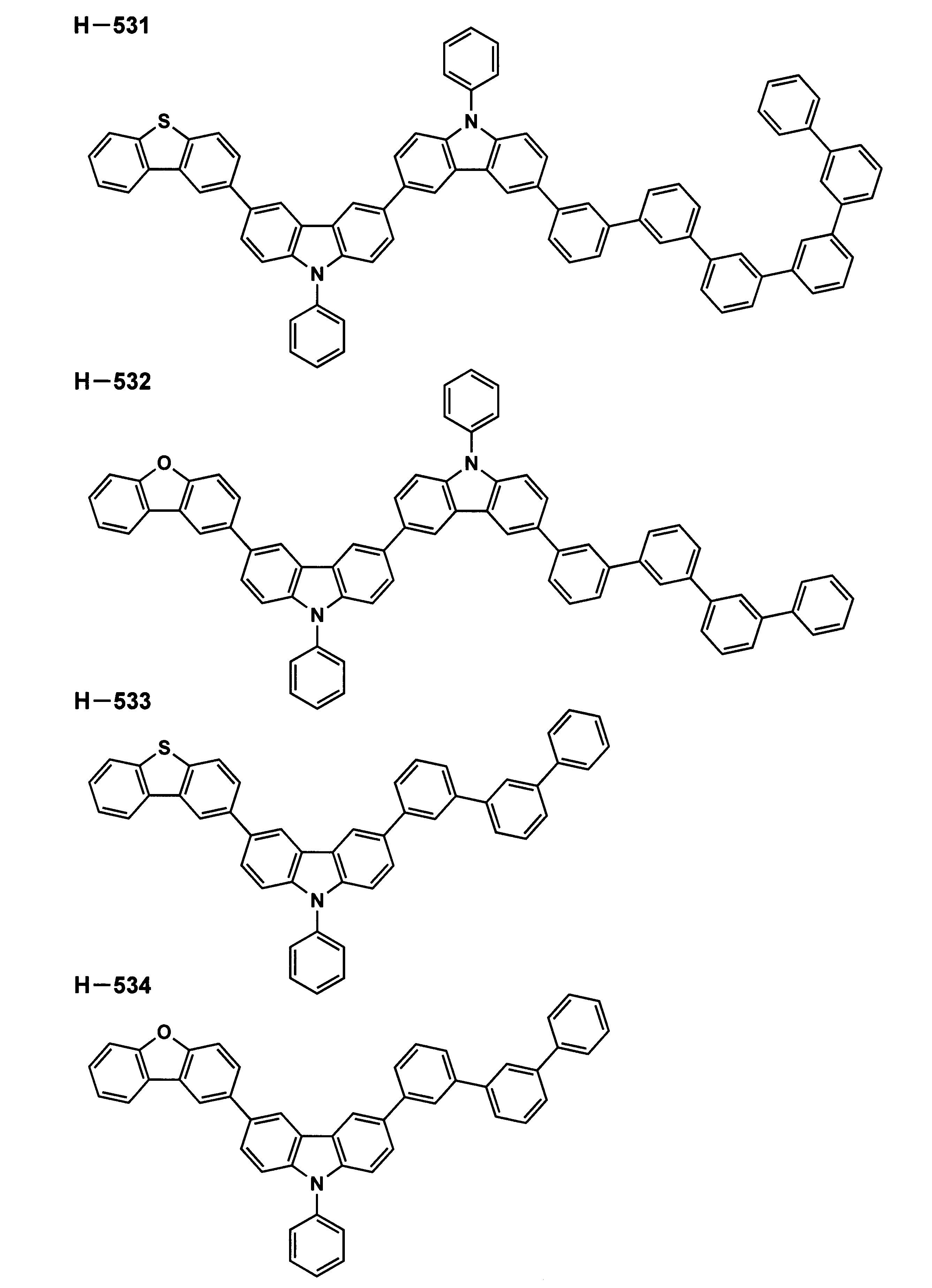
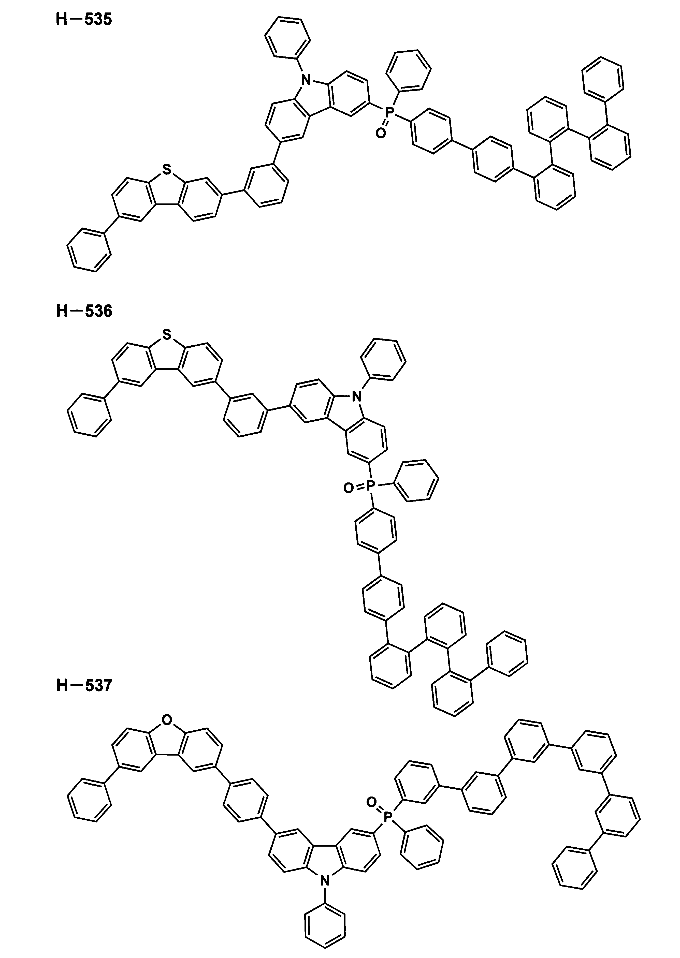
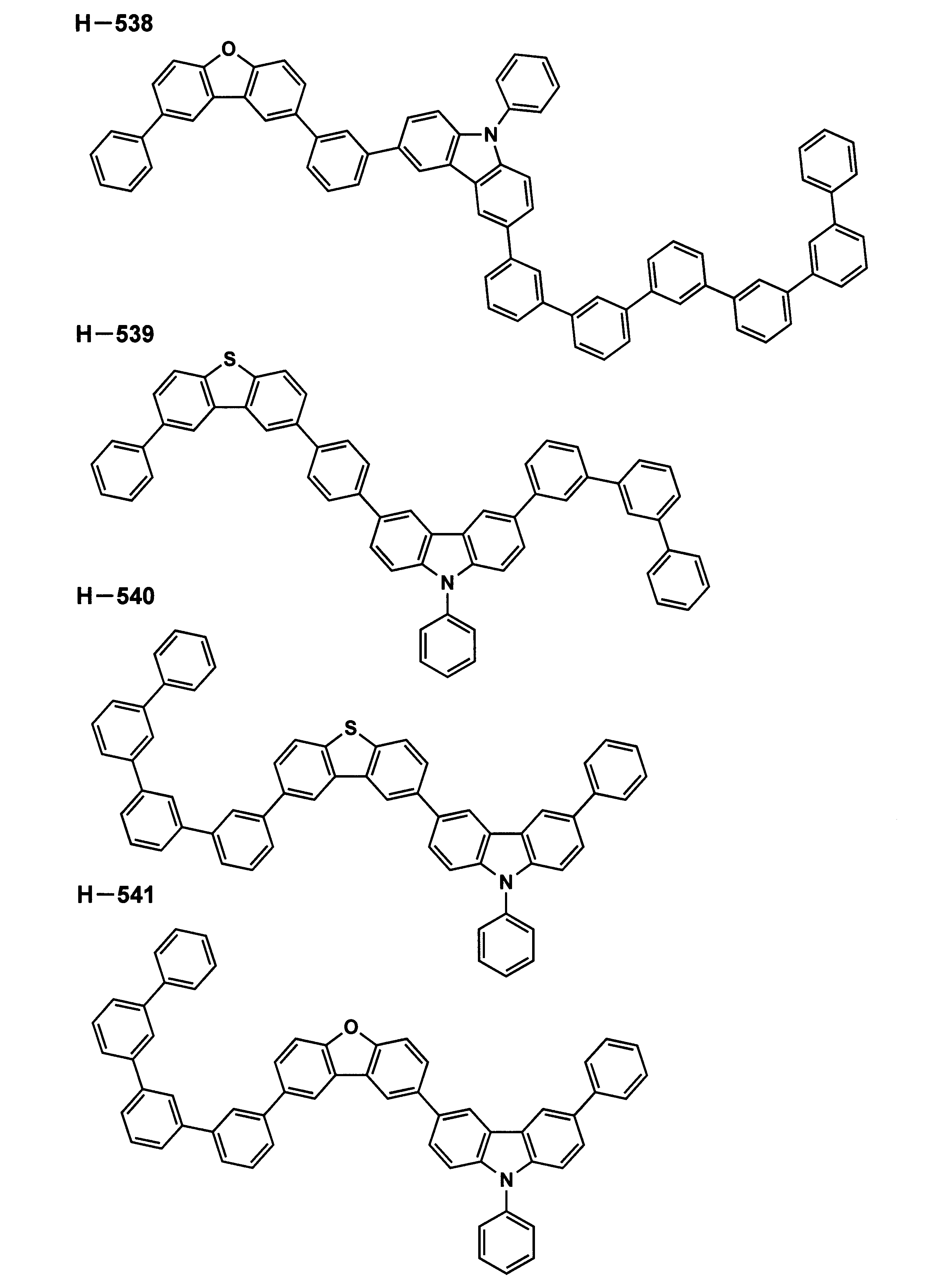

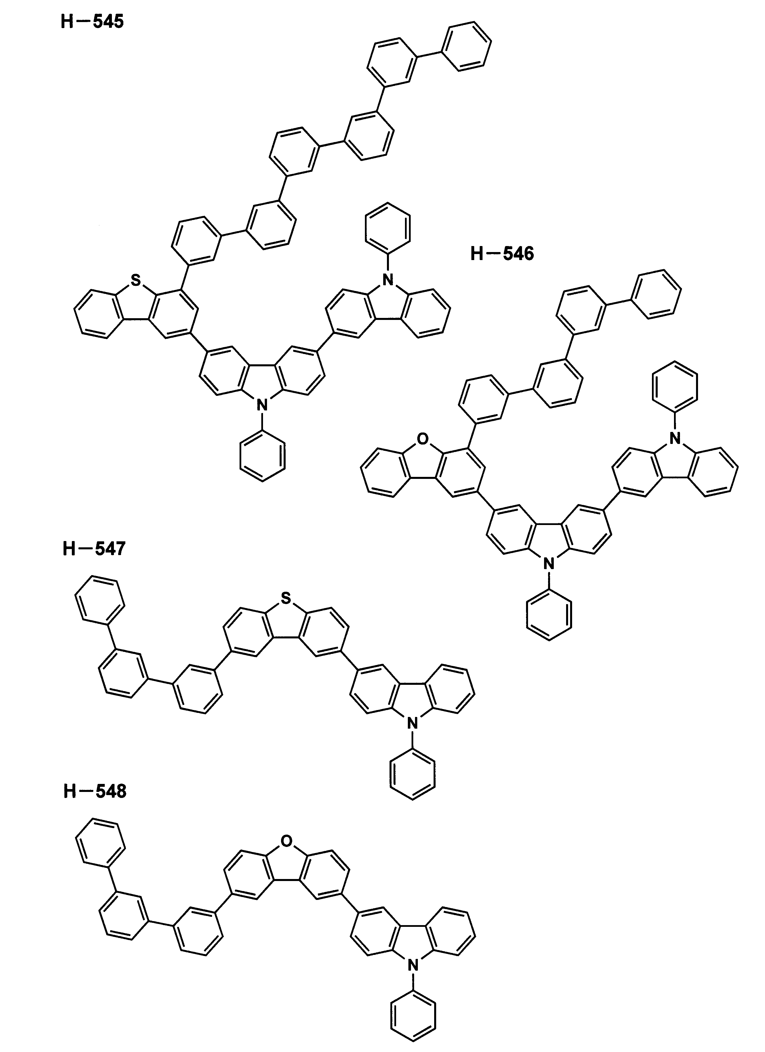
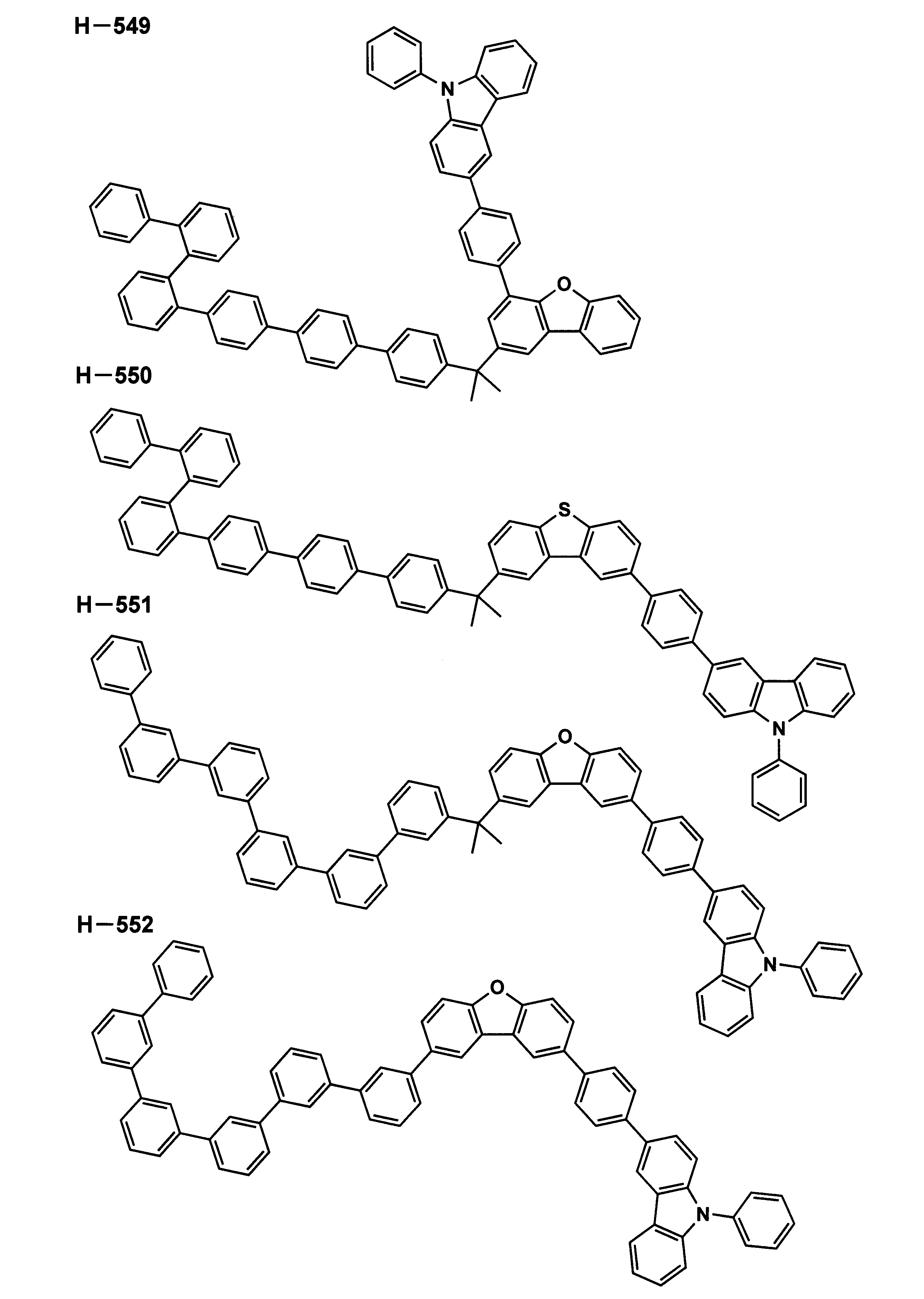


中間体Bは、非特許文献(The journal of organic chemistry 1997 1348-1355)を参考に合成された。
十分に窒素置換された100mlの3口フラスコに中間体Aを3.32g、中間体Bを2.47g、S-phosを1.64g、酢酸パラジウムを0.224g、リン酸三カリウムを6.3g加え、100mlのトルエンに溶解した。得られた溶液を加熱還流した。目的物の生成を確認した後、200mlの水を加え、トルエンにて抽出操作を行った。得られた有機層を飽和食塩水で洗浄し、硫酸マグネシウムを加え10分間攪拌した。不溶物を濾過で除き、溶媒を減圧留去して得られた残渣をカラムクロマトグラフィーで生成することで目的物を得た。
十分に窒素置換された100mlの3口フラスコに中間体Cを4.98g、中間体Dを3.5g、S-phosを1.64g、酢酸パラジウムを0.224g、リン酸三カリウムを6.3g加え、100mlのトルエンに溶解した。得られた溶液を加熱還流した。目的物の生成を確認した後、100mlの水を加え、トルエンにて抽出操作を行った。得られた有機層を飽和食塩水で洗浄し、硫酸マグネシウムを加え10分間攪拌した。不溶物を濾過で除き、溶媒を減圧留去して得られた残渣をカラムクロマトグラフィーで生成することで目的物を得た。
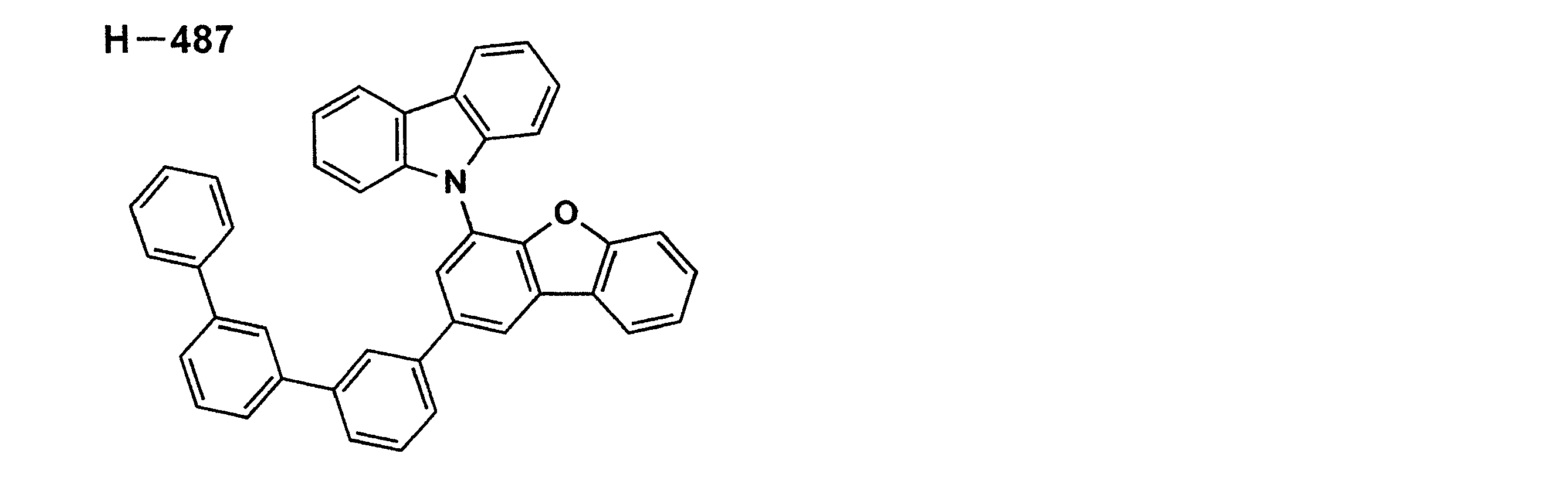

十分に窒素置換された200mlの3口フラスコに中間体Eを2.07g、中間体Fを1.4g、S-phosを1.64g、酢酸パラジウムを0.224g、リン酸三カリウムを6.3g加え、100mlのトルエンに溶解した。得られた溶液を加熱還流した。目的物の生成を確認した後、100mlの水を加え、トルエンにて抽出操作を行った。得られた有機層を飽和食塩水で洗浄し、硫酸マグネシウムを加え10分間攪拌した。不溶物を濾過で除き、溶媒を減圧留去して得られた残渣をカラムクロマトグラフィーで生成することで目的物を得た。
十分に窒素置換された200mlの3口フラスコに中間体Gを2.22g加え、100mlのDMFに溶解し、氷冷した。得られた溶液に1.8gのNBSを加え、室温で攪拌した。目的物の生成を確認した後、100mlの水を加え、トルエンにて抽出操作を行った。得られた有機層を飽和食塩水で洗浄し、硫酸マグネシウムを加え10分間攪拌した。不溶物を濾過で除き、溶媒を減圧留去して得られた残渣をカラムクロマトグラフィーで生成することで目的物を得た。
十分に窒素置換された200mlの3口フラスコに中間体Iを2.8g加え、100mlのテトラヒドロフランに溶解し、氷冷した。得られた溶液に0.3gのソジウムヒドリドを加え、室温で攪拌した。目的物の生成を確認した後、100mlの水を加え、トルエンにて抽出操作を行った。得られた有機層を飽和食塩水で洗浄し、硫酸マグネシウムを加え10分間攪拌した。不溶物を濾過で除き、溶媒を減圧留去して得られた残渣をカラムクロマトグラフィーで生成することで目的物を得た。
十分に窒素置換された100mlの3口フラスコに中間体Iを2.81g、カルバゾールを1.67g、S-phosを1.64g、酢酸パラジウムを0.224g、リン酸三カリウムを6.3g加え、100mlのトルエンに溶解した。得られた溶液を加熱還流した。目的物の生成を確認した後、100mlの水を加え、トルエンにて抽出操作を行った。得られた有機層を飽和食塩水で洗浄し、硫酸マグネシウムを加え10分間攪拌した。不溶物を濾過で除き、溶媒を減圧留去して得られた残渣をカラムクロマトグラフィーで生成することで目的物を得た。
十分に窒素置換された200mlの3口フラスコに中間体Kを3.67g、中間体Lを2.74g、S-phosを1.64g、酢酸パラジウムを0.224g、リン酸三カリウムを6.3g加え、100mlのトルエンに溶解した。得られた溶液を加熱還流した。目的物の生成を確認した後、100mlの水を加え、トルエンにて抽出操作を行った。得られた有機層を飽和食塩水で洗浄し、硫酸マグネシウムを加え10分間攪拌した。不溶物を濾過で除き、溶媒を減圧留去して得られた残渣をカラムクロマトグラフィーで生成することで目的物を得た。

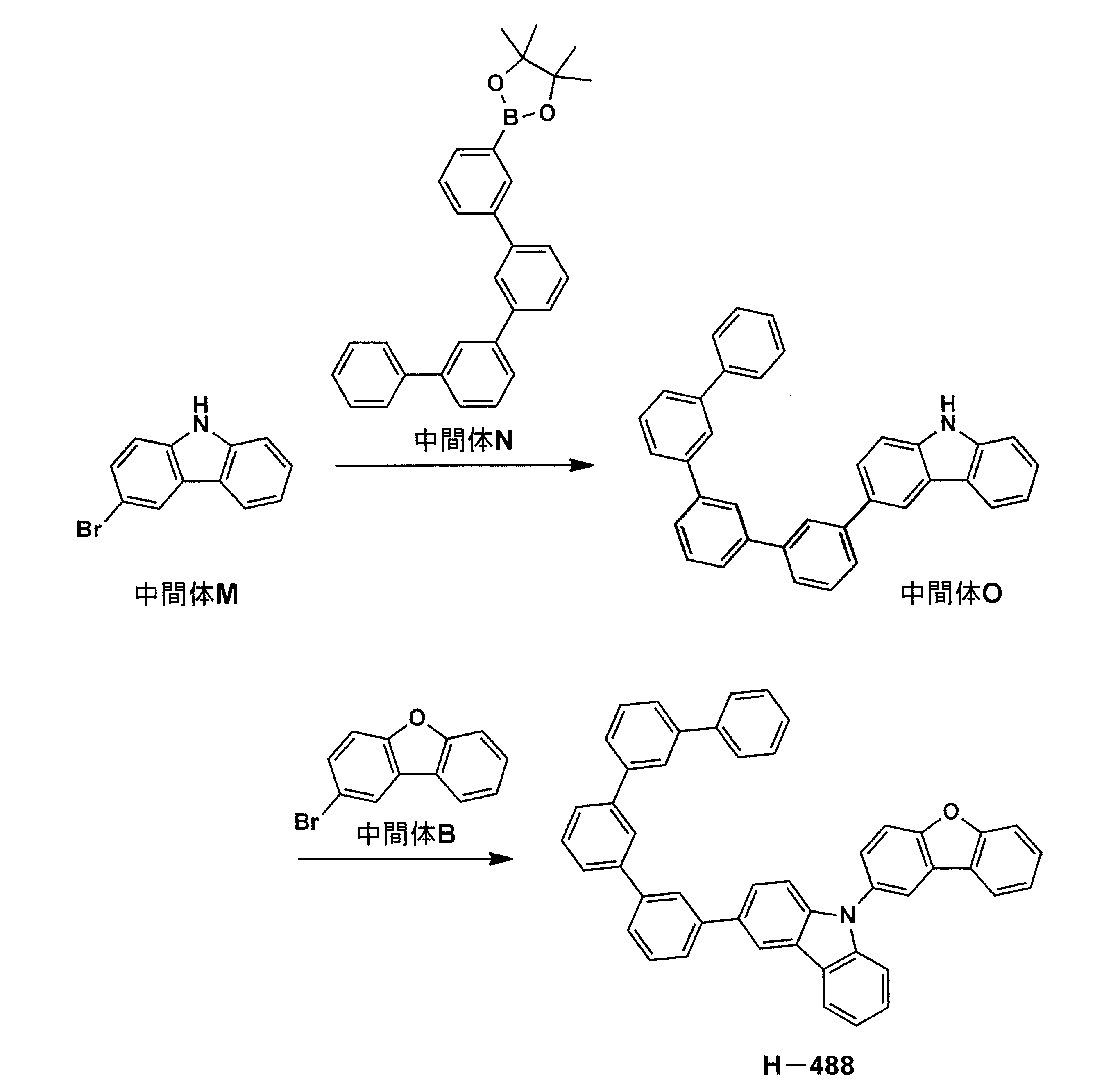
十分に窒素置換された200mlの3口フラスコに中間体Mを2.46g、中間体Nを4.32g、S-phosを1.64g、酢酸パラジウムを0.224g、リン酸三カリウムを6.3g加え、100mlのトルエンに溶解した。得られた溶液を加熱還流した。目的物の生成を確認した後、200mlの水を加え、トルエンにて抽出操作を行った。得られた有機層を飽和食塩水で洗浄し、硫酸マグネシウムを加え10分間攪拌した。不溶物を濾過で除き、溶媒を減圧留去して得られた残渣をカラムクロマトグラフィーで生成することで目的物を得た。
十分に窒素置換された200mlの3口フラスコに中間体Oを4.7g、中間体Bを2.47g、S-phosを1.64g、酢酸パラジウムを0.224g、リン酸三カリウムを6.3g加え、100mlのトルエンに溶解した。得られた溶液を加熱還流した。目的物の生成を確認した後、200mlの水を加え、トルエンにて抽出操作を行った。得られた有機層を飽和食塩水で洗浄し、硫酸マグネシウムを加え10分間攪拌した。不溶物を濾過で除き、溶媒を減圧留去して得られた残渣をカラムクロマトグラフィーで生成することで目的物を得た。
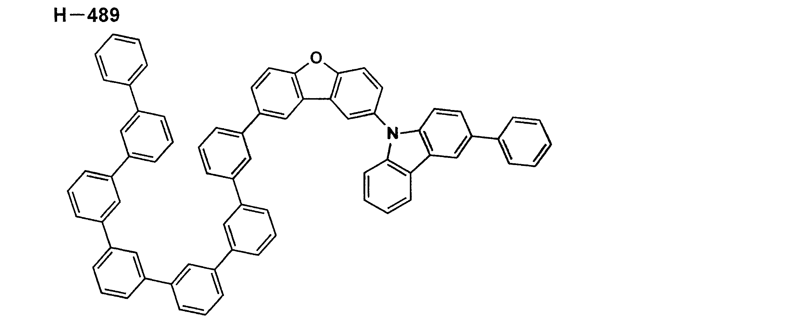
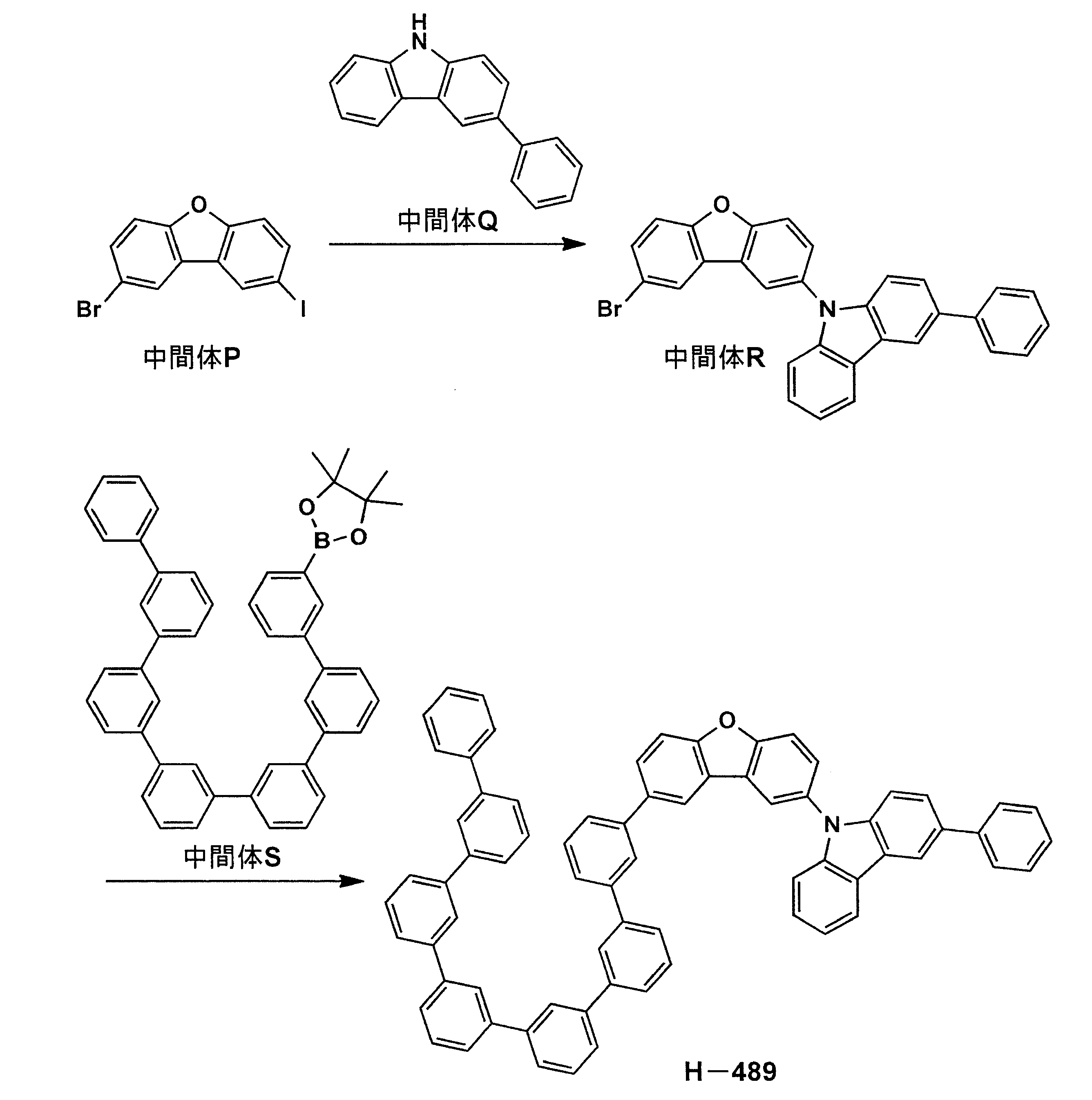
中間体Qは、特許文献(US/2010/76201)を参考に合成された。
十分に窒素置換された200mlの3口フラスコに中間体Pを3.73g、中間体Qを2.43g、S-phosを1.64g、酢酸パラジウムを0.224g、リン酸三カリウムを6.3g加え、100mlのトルエンに溶解した。得られた溶液を加熱還流した。目的物の生成を確認した後、200mlの水を加え、トルエンにて抽出操作を行った。得られた有機層を飽和食塩水で洗浄し、硫酸マグネシウムを加え10分間攪拌した。不溶物を濾過で除き、溶媒を減圧留去して得られた残渣をカラムクロマトグラフィーで生成することで目的物を得た。
十分に窒素置換された200mlの3口フラスコに中間体Rを4.88g、中間体Sを6.60g、S-phosを1.64g、酢酸パラジウムを0.224g、リン酸三カリウムを6.3g加え、100mlのトルエンに溶解した。得られた溶液を加熱還流した。目的物の生成を確認した後、200mlの水を加え、トルエンにて抽出操作を行った。得られた有機層を飽和食塩水で洗浄し、硫酸マグネシウムを加え10分間攪拌した。不溶物を濾過で除き、溶媒を減圧留去して得られた残渣をカラムクロマトグラフィーで生成することで目的物を得た。
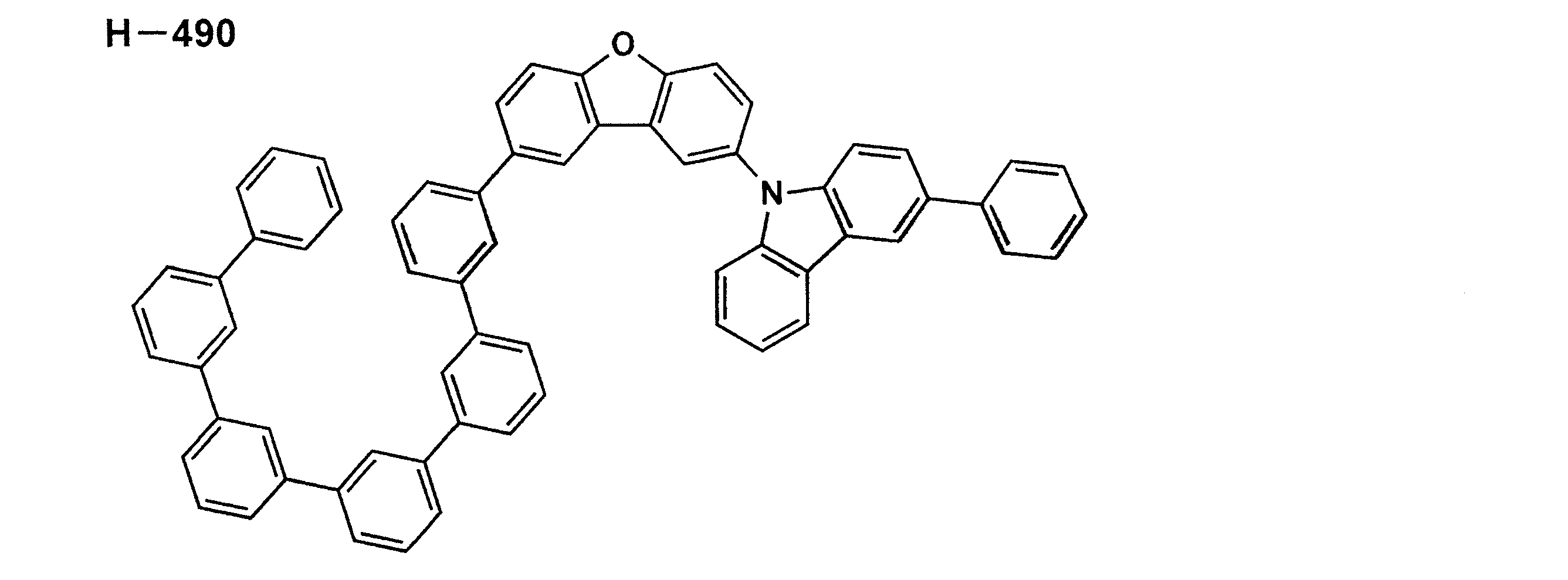

十分に窒素置換された200mlの3口フラスコに中間体Rを4.88g、中間体Tを5.84g、S-phosを1.64g、酢酸パラジウムを0.224g、リン酸三カリウムを6.3g加え、100mlのトルエンに溶解した。得られた溶液を加熱還流した。目的物の生成を確認した後、200mlの水を加え、トルエンにて抽出操作を行った。得られた有機層を飽和食塩水で洗浄し、硫酸マグネシウムを加え10分間攪拌した。不溶物を濾過で除き、溶媒を減圧留去して得られた残渣をカラムクロマトグラフィーで生成することで目的物を得た。
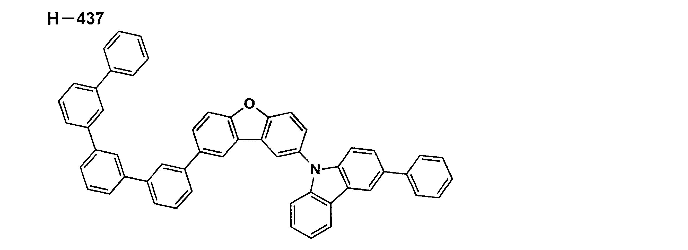
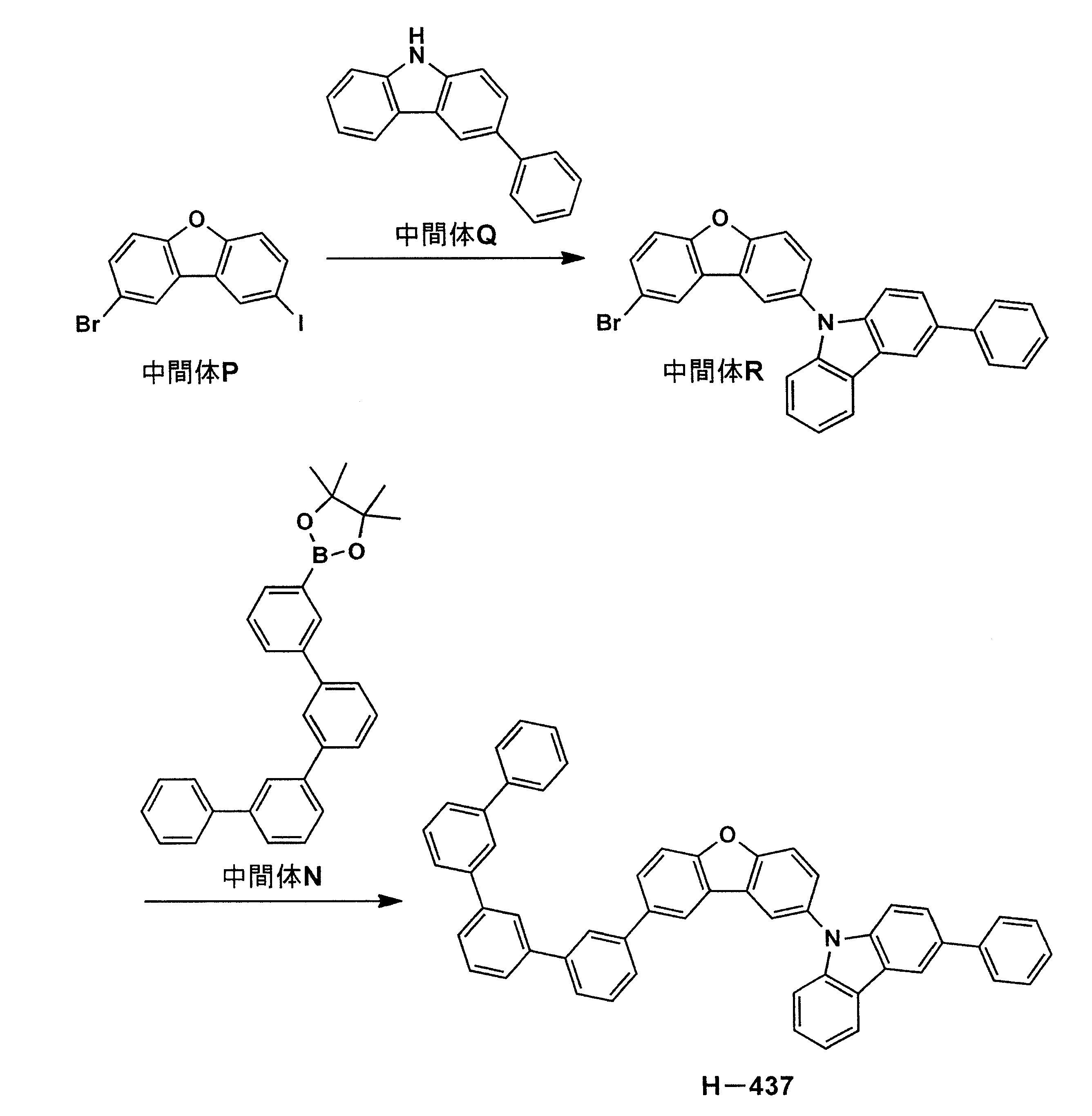
十分に窒素置換された200mlの3口フラスコに中間体Rを4.88g、中間体Nを4.32g、S-phosを1.64g、酢酸パラジウムを0.224g、リン酸三カリウムを6.3g加え、100mlのトルエンに溶解した。得られた溶液を加熱還流した。目的物の生成を確認した後、200mlの水を加え、トルエンにて抽出操作を行った。得られた有機層を飽和食塩水で洗浄し、硫酸マグネシウムを加え10分間攪拌した。不溶物を濾過で除き、溶媒を減圧留去して得られた残渣をカラムクロマトグラフィーで生成することで目的物を得た。


十分に窒素置換された200mlの3口フラスコに中間体Rを4.88g、中間体Vを3.56g、S-phosを1.64g、酢酸パラジウムを0.224g、リン酸三カリウムを6.3g加え、100mlのトルエンに溶解した。得られた溶液を加熱還流した。目的物の生成を確認した後、200mlの水を加え、トルエンにて抽出操作を行った。得られた有機層を飽和食塩水で洗浄し、硫酸マグネシウムを加え10分間攪拌した。不溶物を濾過で除き、溶媒を減圧留去して得られた残渣をカラムクロマトグラフィーで生成することで目的物を得た。
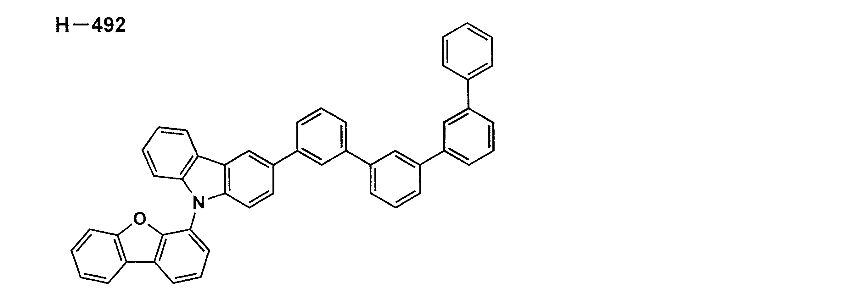

十分に窒素置換された200mlの3口フラスコに中間体Wを2.47g、カルバゾールを1.67g、S-phosを1.64g、酢酸パラジウムを0.224g、リン酸三カリウムを6.3g加え、100mlのトルエンに溶解した。得られた溶液を加熱還流した。目的物の生成を確認した後、200mlの水を加え、トルエンにて抽出操作を行った。得られた有機層を飽和食塩水で洗浄し、硫酸マグネシウムを加え10分間攪拌した。不溶物を濾過で除き、溶媒を減圧留去して得られた残渣をカラムクロマトグラフィーで生成することで目的物を得た。
十分に窒素置換された200mlの3口フラスコに中間体Xを3.33g加え、100mlのDMFに溶解し、氷冷した。得られた溶液に1.8gのNBSを加え、室温で攪拌した。目的物の生成を確認した後、100mlの水を加え、トルエンにて抽出操作を行った。得られた有機層を飽和食塩水で洗浄し、硫酸マグネシウムを加え10分間攪拌した。不溶物を濾過で除き、溶媒を減圧留去して得られた残渣をカラムクロマトグラフィーで生成することで目的物を得た。
十分に窒素置換された200mlの3口フラスコに中間体Yを4.12g、中間体Uを4.32g、S-phosを1.64g、酢酸パラジウムを0.224g、リン酸三カリウムを6.3g加え、100mlのトルエンに溶解した。得られた溶液を加熱還流した。目的物の生成を確認した後、200mlの水を加え、トルエンにて抽出操作を行った。得られた有機層を飽和食塩水で洗浄し、硫酸マグネシウムを加え10分間攪拌した。不溶物を濾過で除き、溶媒を減圧留去して得られた残渣をカラムクロマトグラフィーで生成することで目的物を得た。
次に、本発明に係る有機EL素子に好ましく用いられるリン光発光性化合物について説明する。
本発明に係る有機EL素子に好ましく用いられるリン光発光性化合物は、下記一般式(DP)で表される化合物である。下記一般式(DP)で表されるリン光発光性化合物は、上記した一般式(1)で表される有機EL素子材料と共に発光層に含有されていることが好ましい。

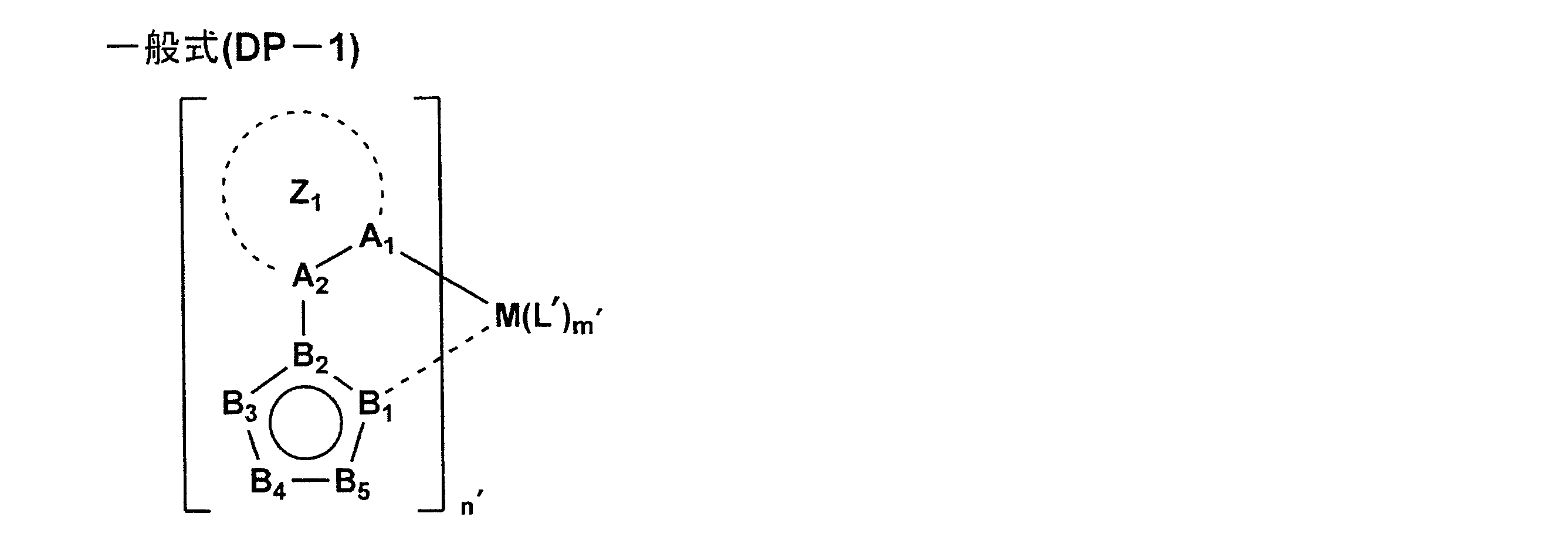
B3~B5が有していても良い置換基としては、上記した一般式(DP)における環Z1及び環Z2が有していても良い置換基と同様のものが挙げられる。

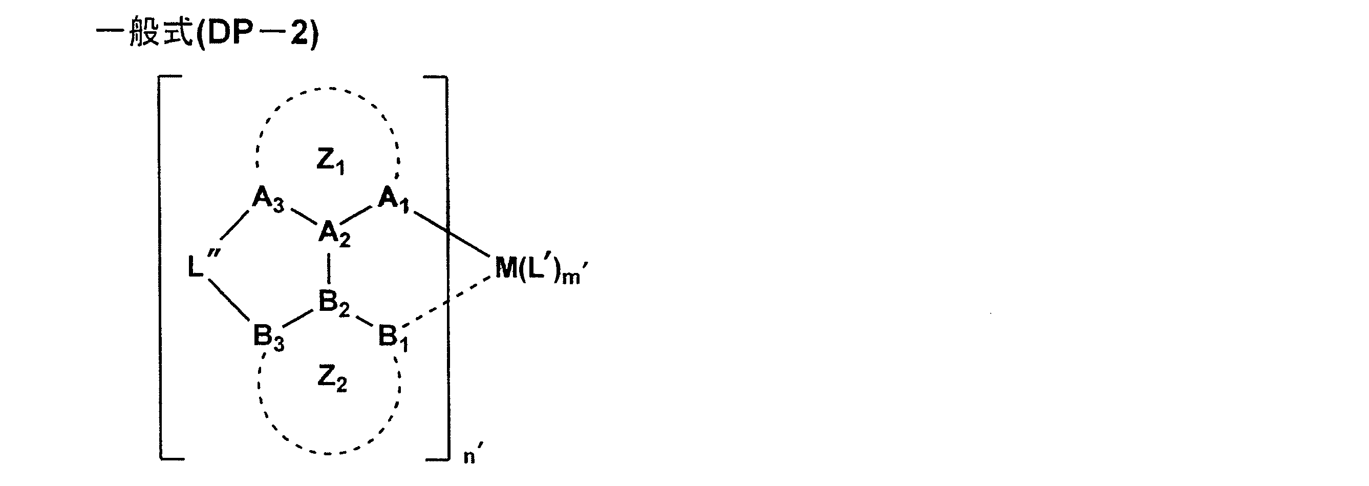
L"で表される2価の連結基としては、例えば、アルキレン基、アルケニレン基、アリーレン基、ヘテロアリーレン基、2価の複素環基、-O-、-S-、又はこれらを任意に組み合わせた連結基等が挙げられる。

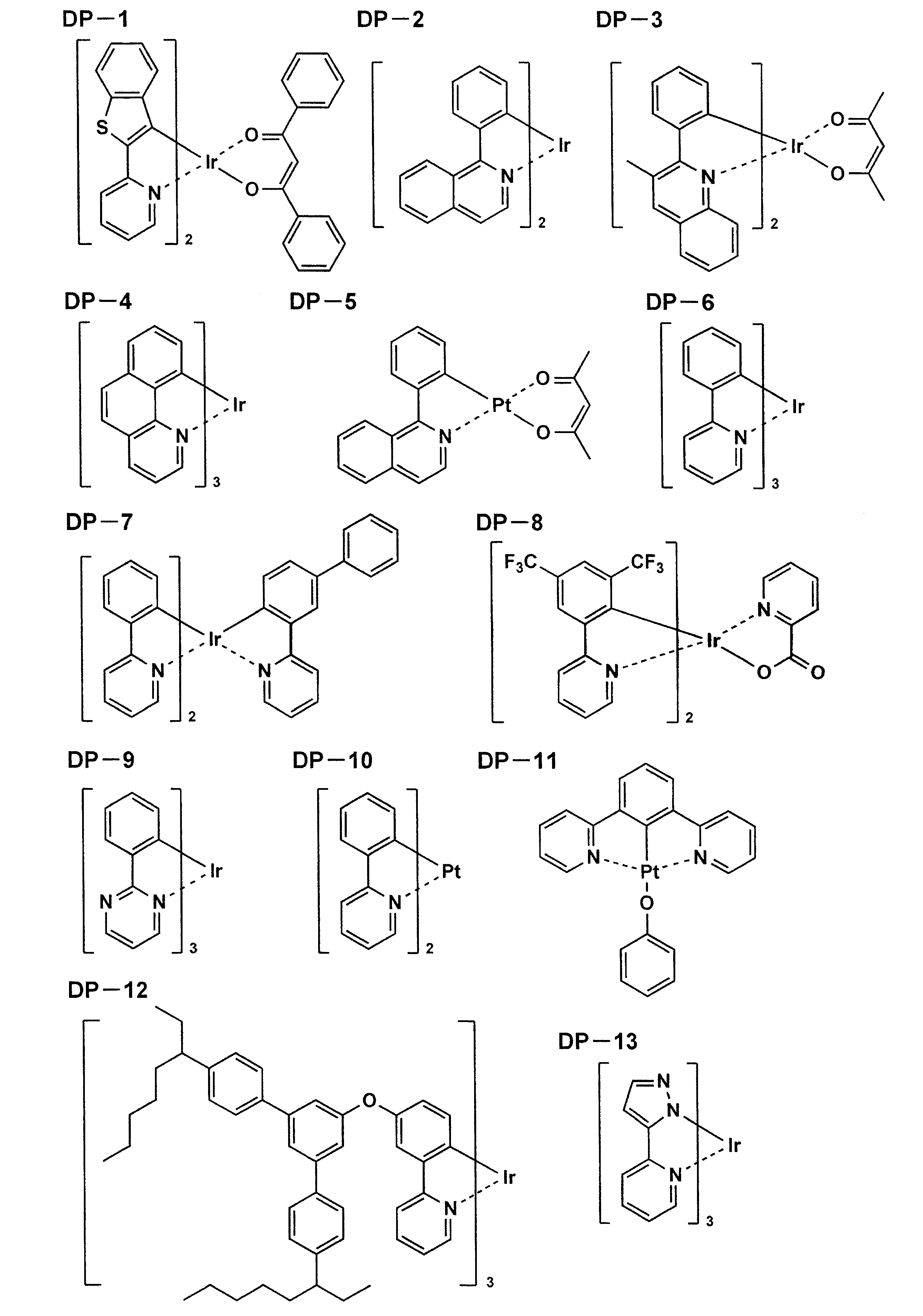
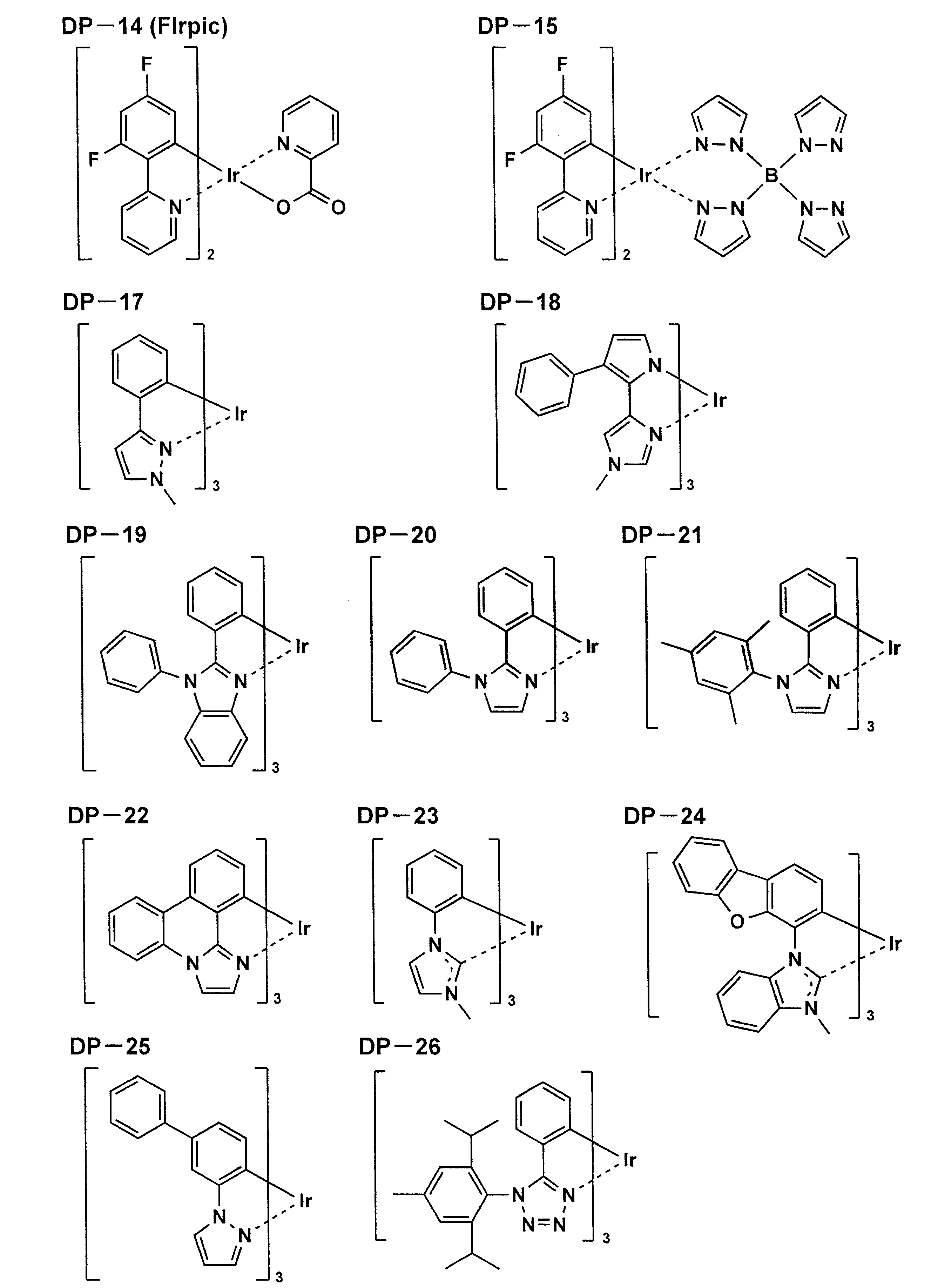
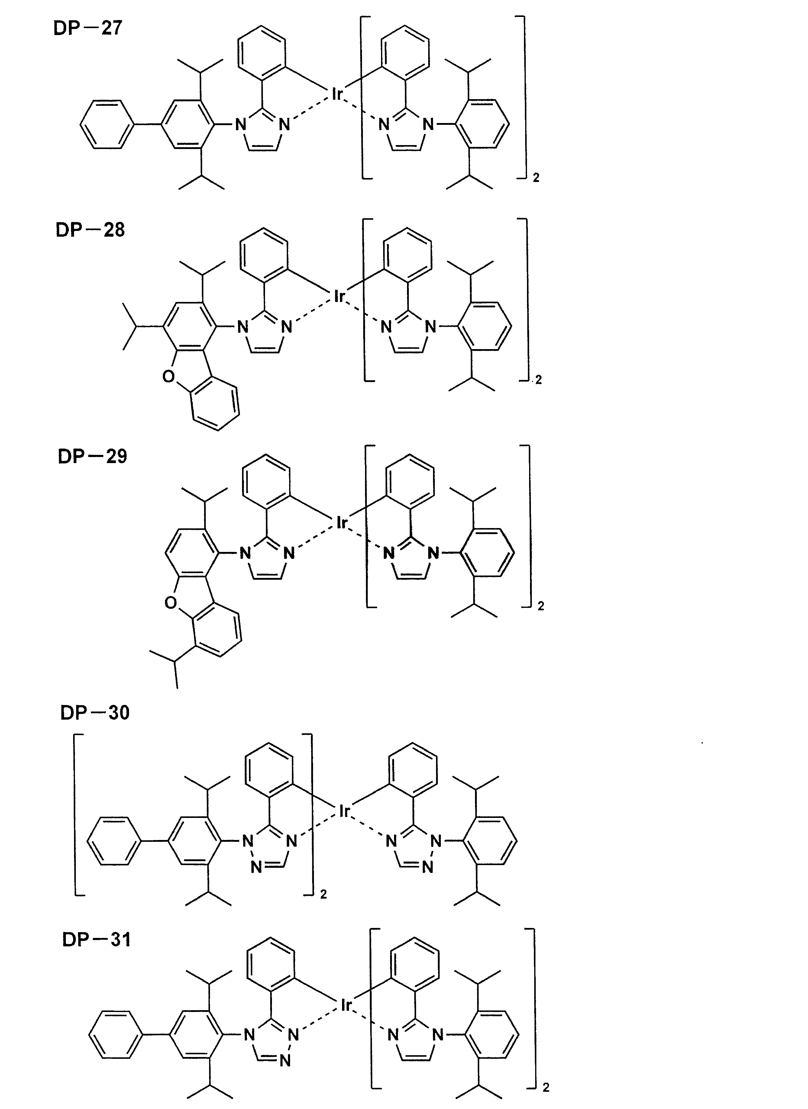


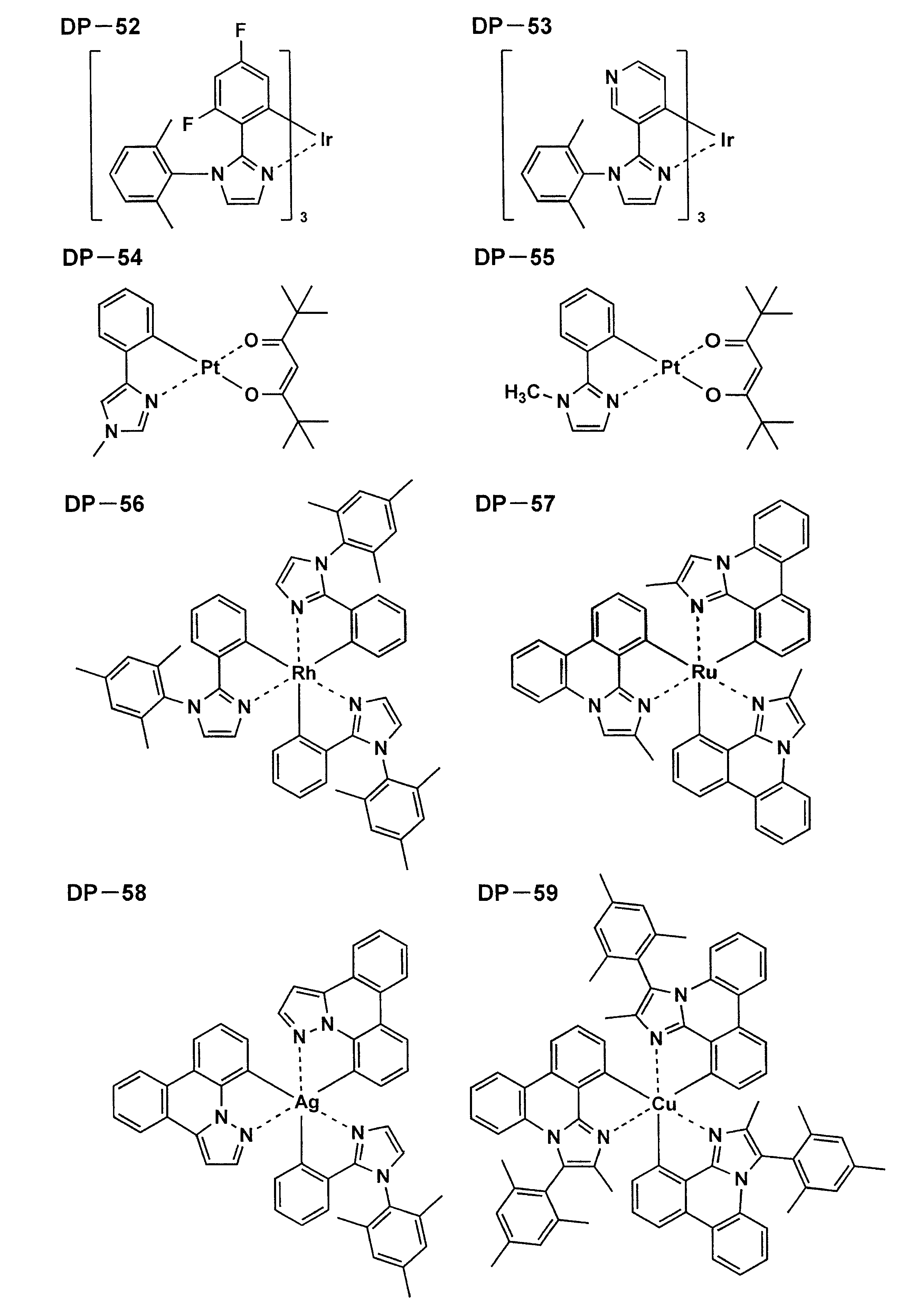
本発明の有機EL素子の構成層について説明する。本発明の有機EL素子において、陽極と陰極との間に挟持される各種有機層の層構成の好ましい具体例を以下に示すが、本発明はこれらに限定されない。
(ii)陽極/正孔輸送層/発光層ユニット/電子輸送層/陰極
(iii)陽極/正孔輸送層/発光層ユニット/正孔阻止層/電子輸送層/陰極
(iv)陽極/正孔輸送層/発光層ユニット/電子輸送層/電子注入層/陰極
(v)陽極/正孔注入層/正孔輸送層/発光層ユニット/電子輸送層/電子注入層/陰極
(vi)陽極/正孔輸送層/発光層ユニット/正孔阻止層/電子輸送層/電子注入層/陰極
(vii)陽極/正孔注入層/正孔輸送層/発光層ユニット/正孔阻止層/電子輸送層/電子注入層/陰極
なお、阻止層としては正孔阻止層の他に、電子阻止層を用いることもできる。
発光層は、電極又は電子輸送層及び正孔輸送層から注入されてくる電子及び正孔が再結合して発光する層であり、発光する部分は発光層の層内であっても発光層と隣接層との界面であっても良い。
発光性ドーパント(発光ドーパント、単にドーパントともいう)について説明する。発光性ドーパントとしては、蛍光ドーパント(蛍光性化合物ともいう)、リン光ドーパント(リン光発光体、リン光性化合物、リン光発光性化合物ともいう)を用いることができる。
本発明に用いることができるリン光ドーパント(リン光発光ドーパントともいう)について説明する。
本発明に係るリン光ドーパントは、励起三重項からの発光が観測される化合物である。具体的には室温(25℃)にてリン光発光する化合物であり、リン光量子収率が、25℃において0.01以上の化合物であると定義されるが、好ましいリン光量子収率は0.1以上である。
上記リン光量子収率は、第4版実験化学講座7の分光IIの398頁(1992年版、丸善)に記載の方法により測定できる。溶液中でのリン光量子収率は種々の溶媒を用いて測定できるが、本発明に用いることができるリン光ドーパントは、任意の溶媒の何れかにおいて上記リン光量子収率(0.01以上)が達成されれば良い。
例えば、国際公開第00/70655号、特開2002-280178号公報、特開2001-181616号公報、特開2002-280179号公報、特開2001-181617号公報、特開2002-280180号公報、特開2001-247859号公報、特開2002-299060号公報、特開2001-313178号公報、特開2002-302671号公報、特開2001-345183号公報、特開2002-324679号公報、国際公開第02/15645号、特開2002-332291号公報、特開2002-50484号公報、特開2002-332292号公報、特開2002-83684号公報、特表2002-540572号公報、特開2002-117978号公報、特開2002-338588号公報、特開2002-170684号公報、特開2002-352960号公報、国際公開第01/93642号、特開2002-50483号公報、特開2002-100476号公報、特開2002-173674号公報、特開2002-359082号公報、特開2002-175884号公報、特開2002-363552号公報、特開2002-184582号公報、特開2003-7469号公報、特表2002-525808号公報、特開2003-7471号公報、特表2002-525833号公報、特開2003-31366号公報、特開2002-226495号公報、特開2002-234894号公報、特開2002-235076号公報、特開2002-241751号公報、特開2001-319779号公報、特開2001-319780号公報、特開2002-62824号公報、特開2002-100474号公報、特開2002-203679号公報、特開2002-343572号公報、特開2002-203678号公報等である。
蛍光ドーパント(蛍光性化合物ともいう)としては、クマリン系色素、ピラン系色素、シアニン系色素、クロコニウム系色素、スクアリウム系色素、オキソベンツアントラセン系色素、フルオレセイン系色素、ローダミン系色素、ピリリウム系色素、ペリレン系色素、スチルベン系色素、ポリチオフェン系色素又は希土類錯体系蛍光体等や、レーザー色素に代表される蛍光量子収率が高い化合物が挙げられる。
また、本発明に用いることができる発光ドーパントは、複数種の化合物を併用して用いても良く、構造の異なるリン光ドーパント同士の組み合わせや、リン光ドーパントと蛍光ドーパントを組み合わせて用いても良い。
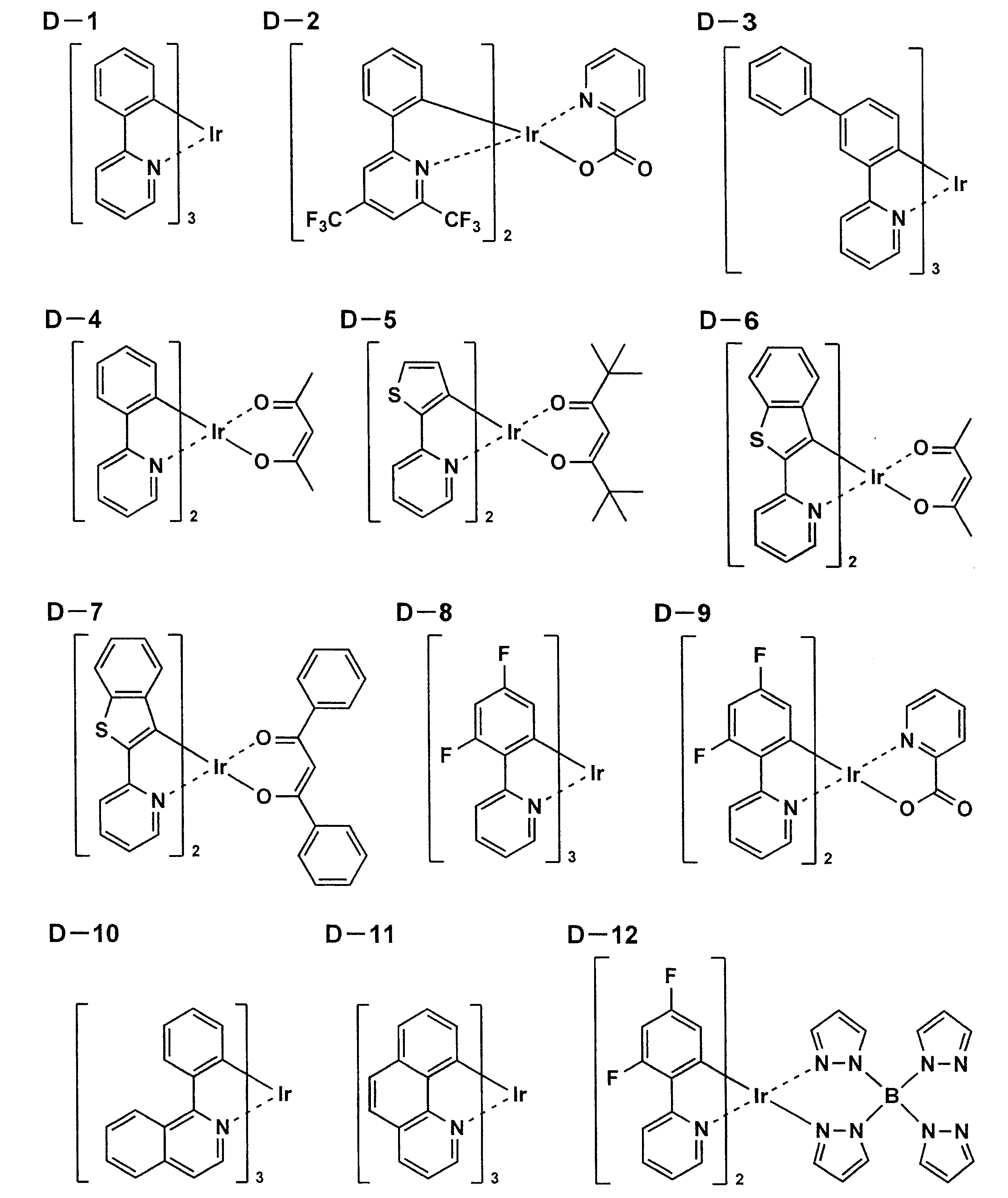


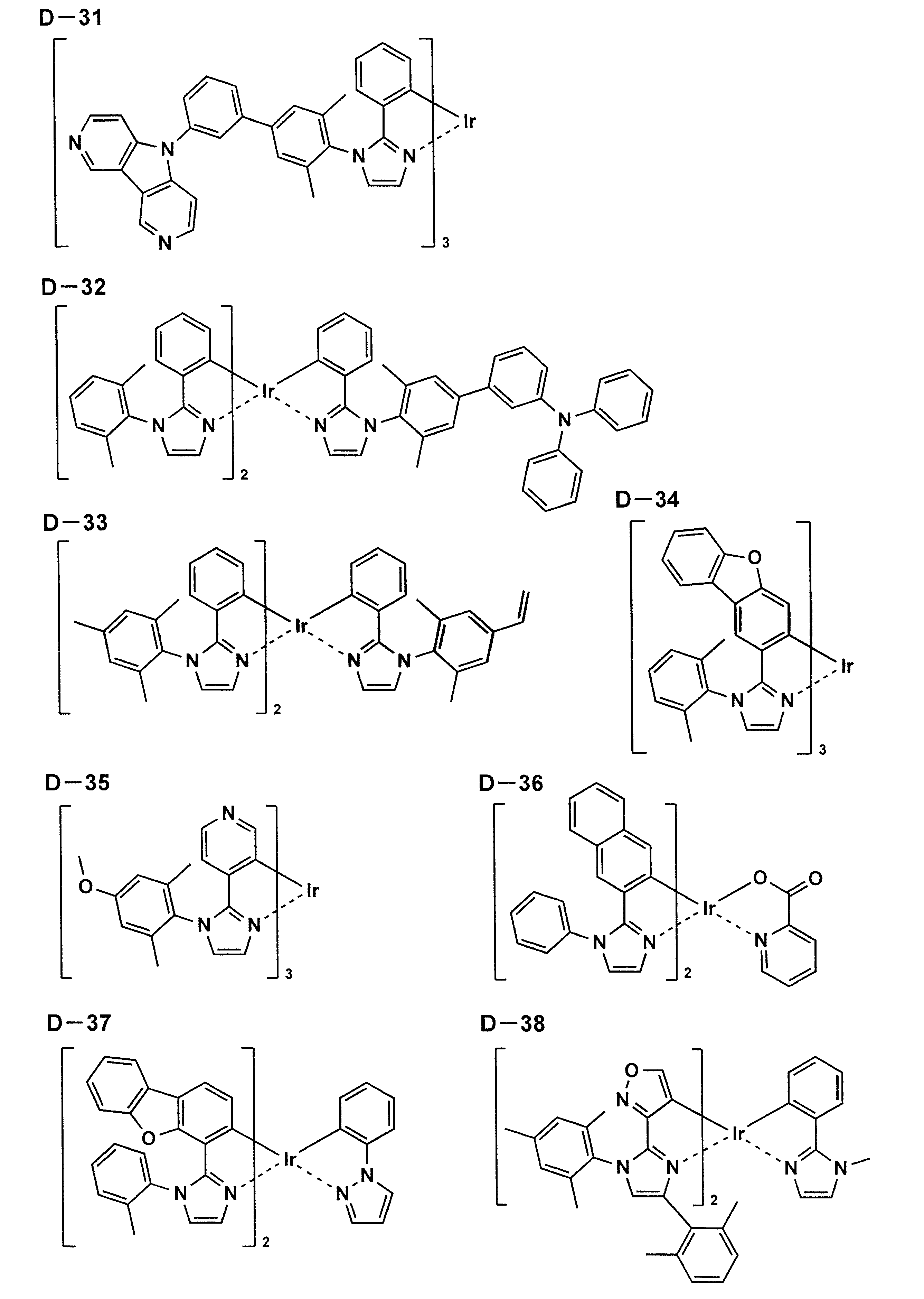
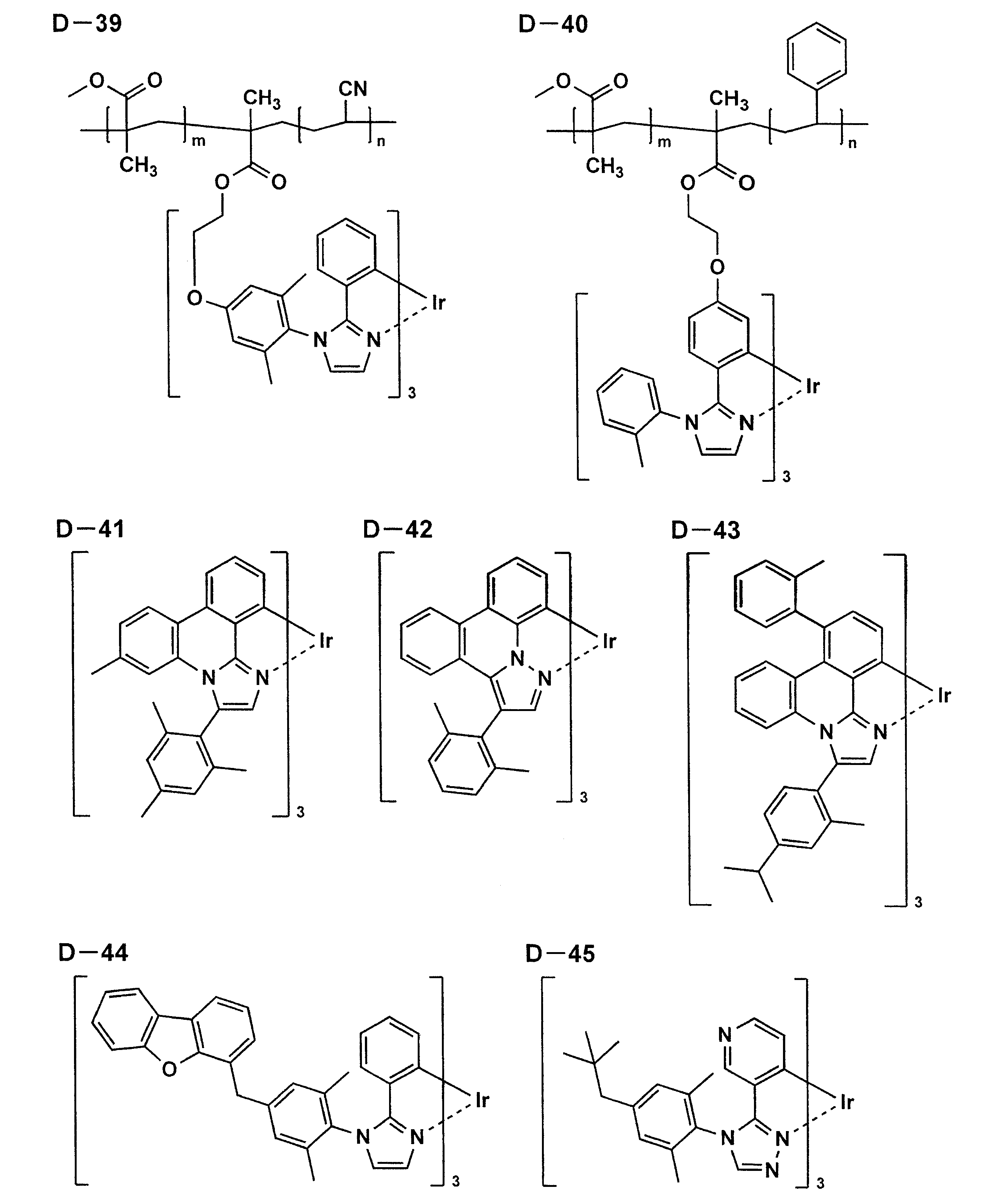
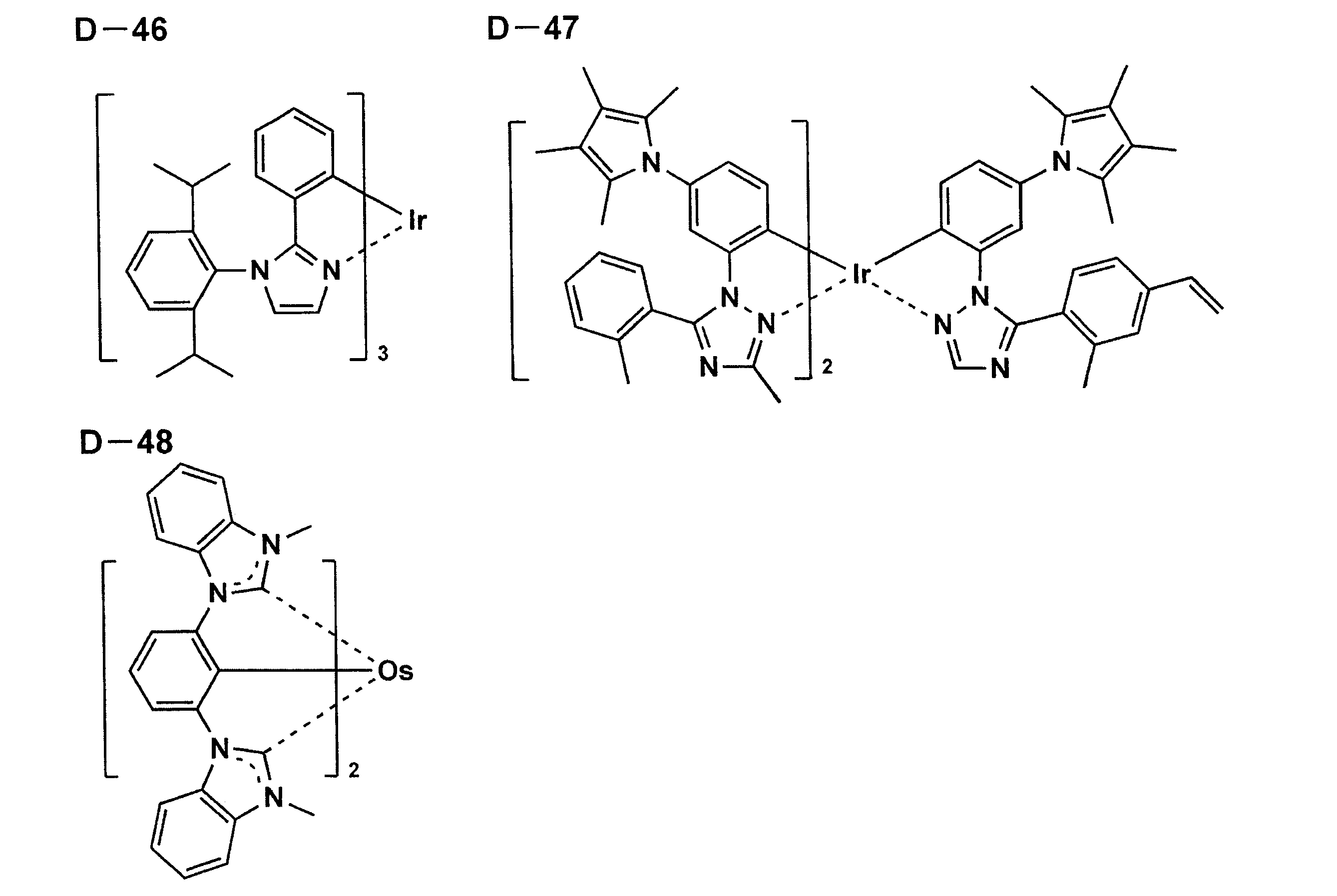
本発明において発光ホスト化合物(発光ホスト、ホスト化合物、ホスト材料等ともいう)は、発光層に含有される化合物の内で、その層中での質量比が20%以上であり、且つ室温(25℃)においてリン光発光のリン光量子収率が、0.1未満の化合物と定義される。好ましくはリン光量子収率が0.01未満である。また、発光層に含有される化合物の内で、その層中での質量比が50%以上であることが好ましい。
特開2001-257076号公報、同2002-308855号公報、同2001-313179号公報、同2002-319491号公報、同2001-357977号公報、同2002-334786号公報、同2002-8860号公報、同2002-334787号公報、同2002-15871号公報、同2002-334788号公報、同2002-43056号公報、同2002-334789号公報、同2002-75645号公報、同2002-338579号公報、同2002-105445号公報、同2002-343568号公報、同2002-141173号公報、同2002-352957号公報、同2002-203683号公報、同2002-363227号公報、同2002-231453号公報、同2003-3165号公報、同2002-234888号公報、同2003-27048号公報、同2002-255934号公報、同2002-260861号公報、同2002-280183号公報、同2002-299060号公報、同2002-302516号公報、同2002-305083号公報、同2002-305084号公報、同2002-308837号公報等。
注入層は必要に応じて設ける層であり、電子注入層と正孔注入層がある。注入層は、上記の層構成に示すように、陽極と正孔輸送層との間や、陰極と電子輸送層との間に存在させても良いし、陽極と発光層との間や、陰極と発光層との間に存在させても良い。
阻止層は、上記の如く有機化合物薄膜の基本構成層の他に必要に応じて設けられるものである。例えば、特開平11-204258号公報、同11-204359号公報、及び「有機EL素子とその工業化最前線(1998年11月30日エヌ・ティー・エス社発行)」の237頁等に記載されている正孔阻止(ホールブロック)層がある。
(1)米国Gaussian社製の分子軌道計算用ソフトウェアであるGaussian98(Gaussian98、Revision A.11.4,M.J.Frisch,et al,Gaussian,Inc.,Pittsburgh PA,2002.)を用い、キーワードとしてB3LYP/6-31G*を用いて構造最適化を行うことにより算出した値(eV単位換算値)として求めることができる。この計算値が有効な背景には、この手法で求めた計算値と実験値の相関が高いためである。
(2)イオン化ポテンシャルは光電子分光法で直接測定する方法により求めることもできる。例えば、理研計器社製の低エネルギー電子分光装置「Model AC-1」を用いて、あるいは紫外光電子分光として知られている方法を好適に用いることができる。
正孔輸送層とは正孔を輸送する機能を有する正孔輸送材料からなり、広い意味で正孔注入層、電子阻止層も正孔輸送層に含まれる。正孔輸送層は単層又は複数層設けることができる。
また、特表2003-519432号公報や特開2006-135145号公報等に記載されているようなアザトリフェニレン誘導体も同様に正孔輸送材料として用いることができる。
正孔輸送層の層厚については特に制限はないが、通常は5~5000nm程度、好ましくは5~200nmである。この正孔輸送層は上記材料の一種又は2種以上からなる一層構造であっても良い。
本発明においては、このようなp性の高い正孔輸送層を用いることが、より低消費電力の素子を作製することができるため好ましい。

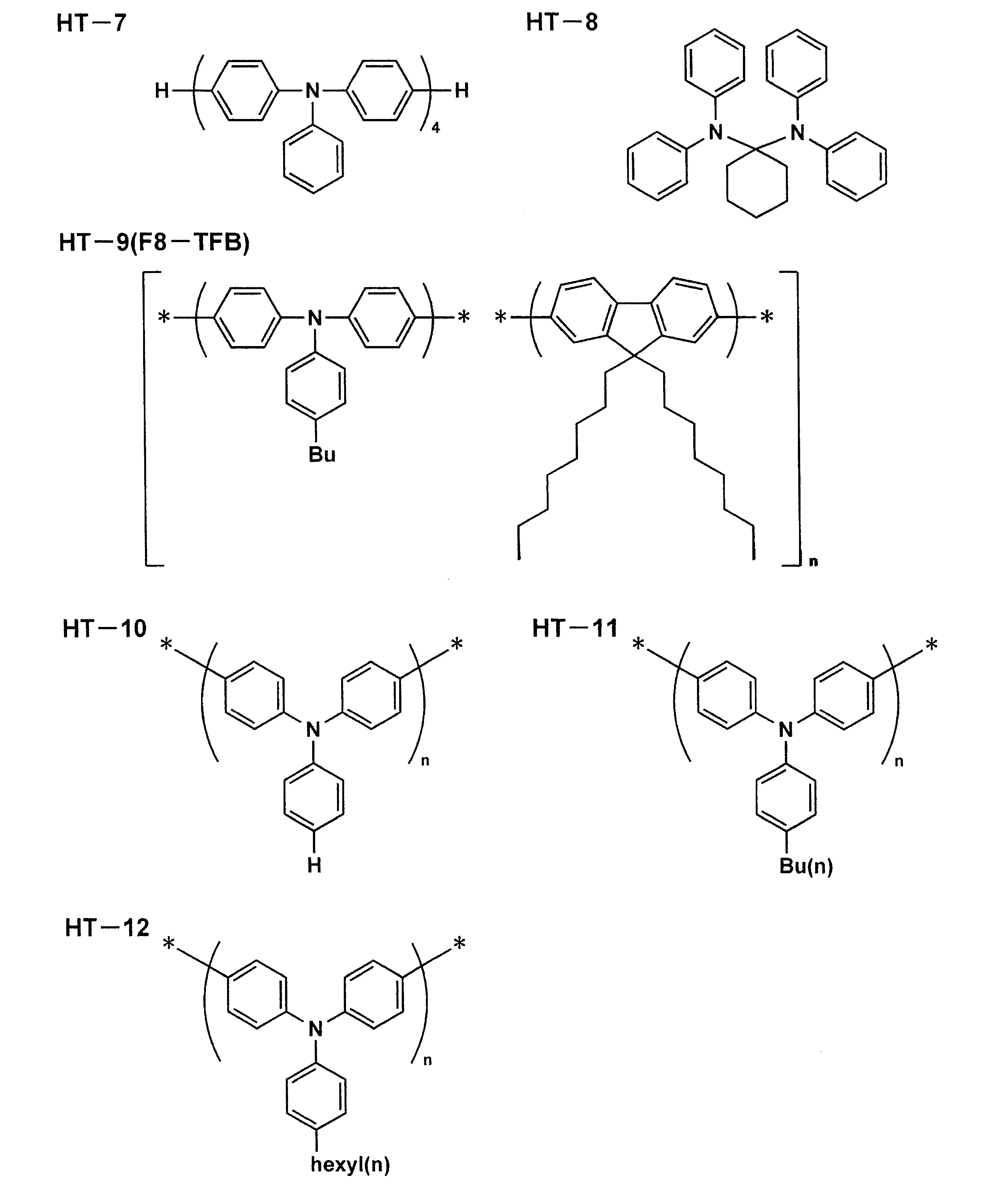
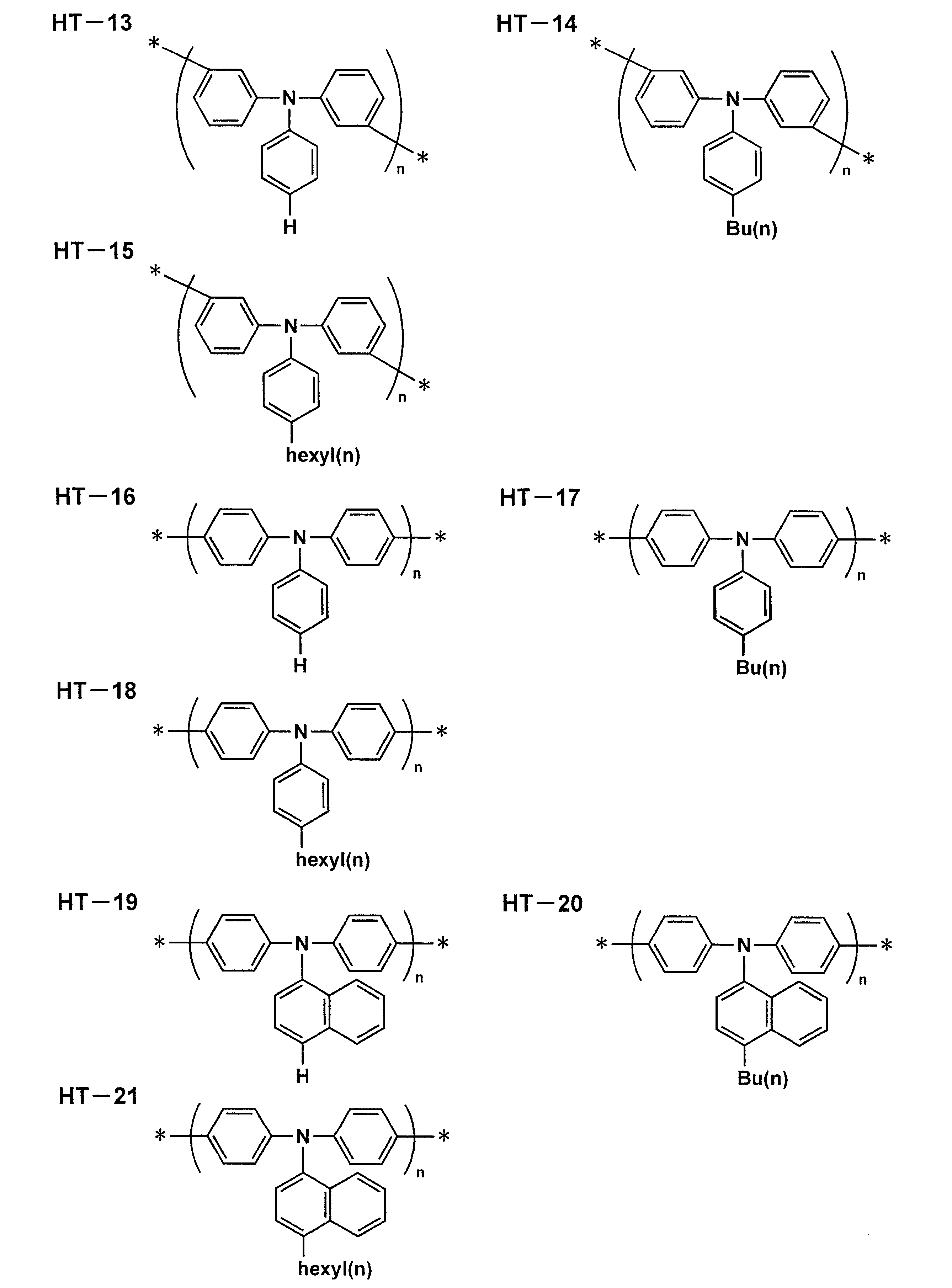
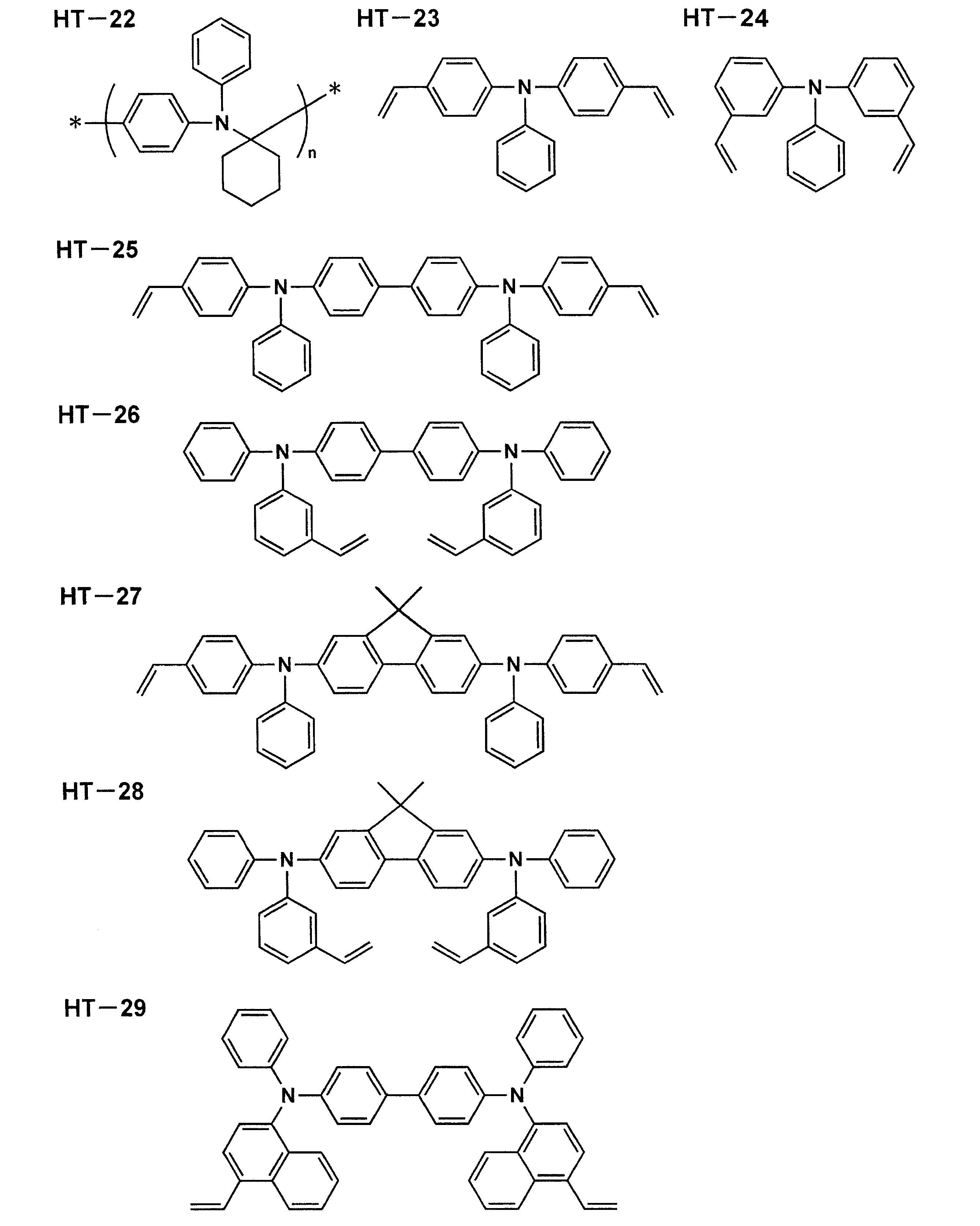
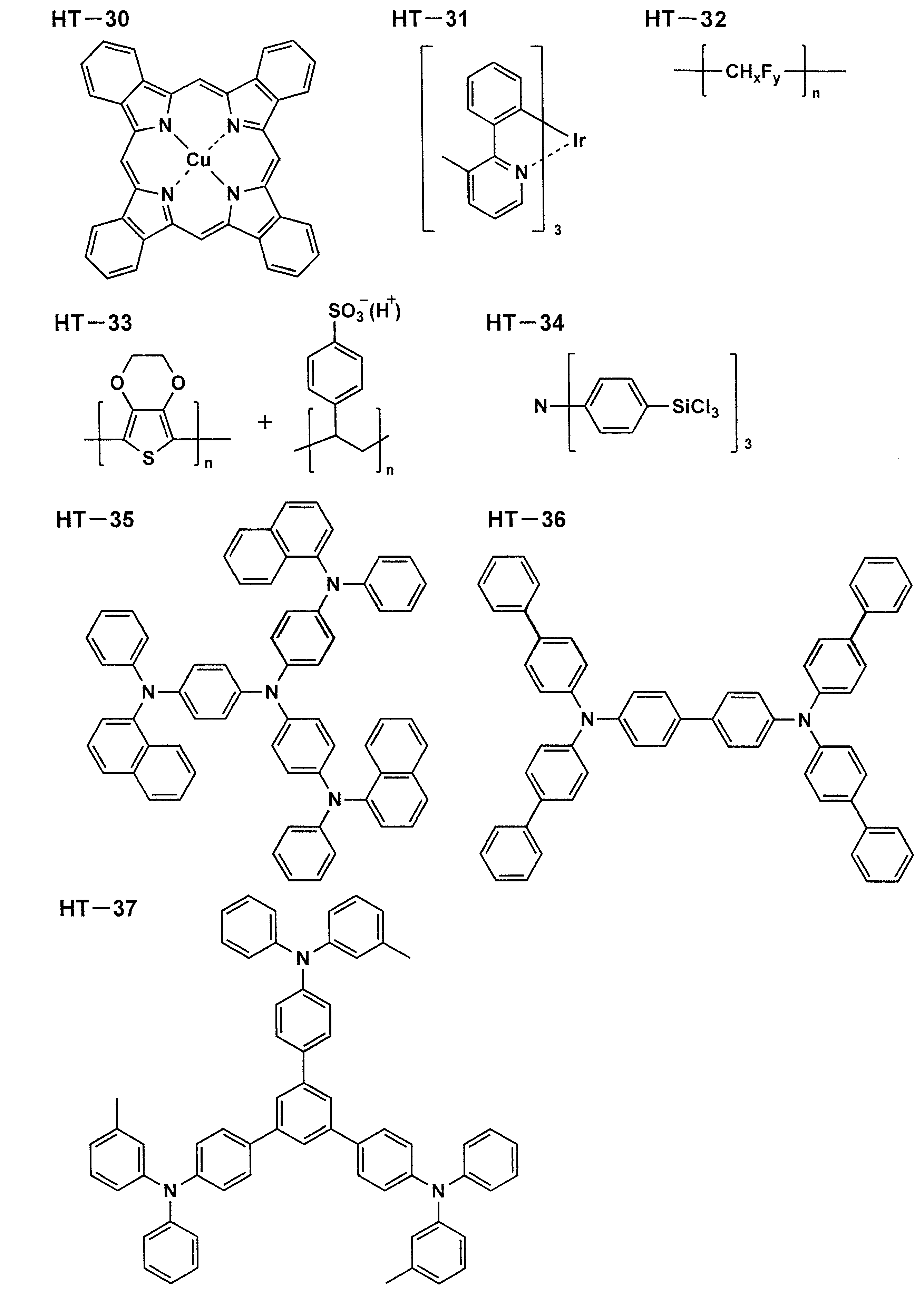
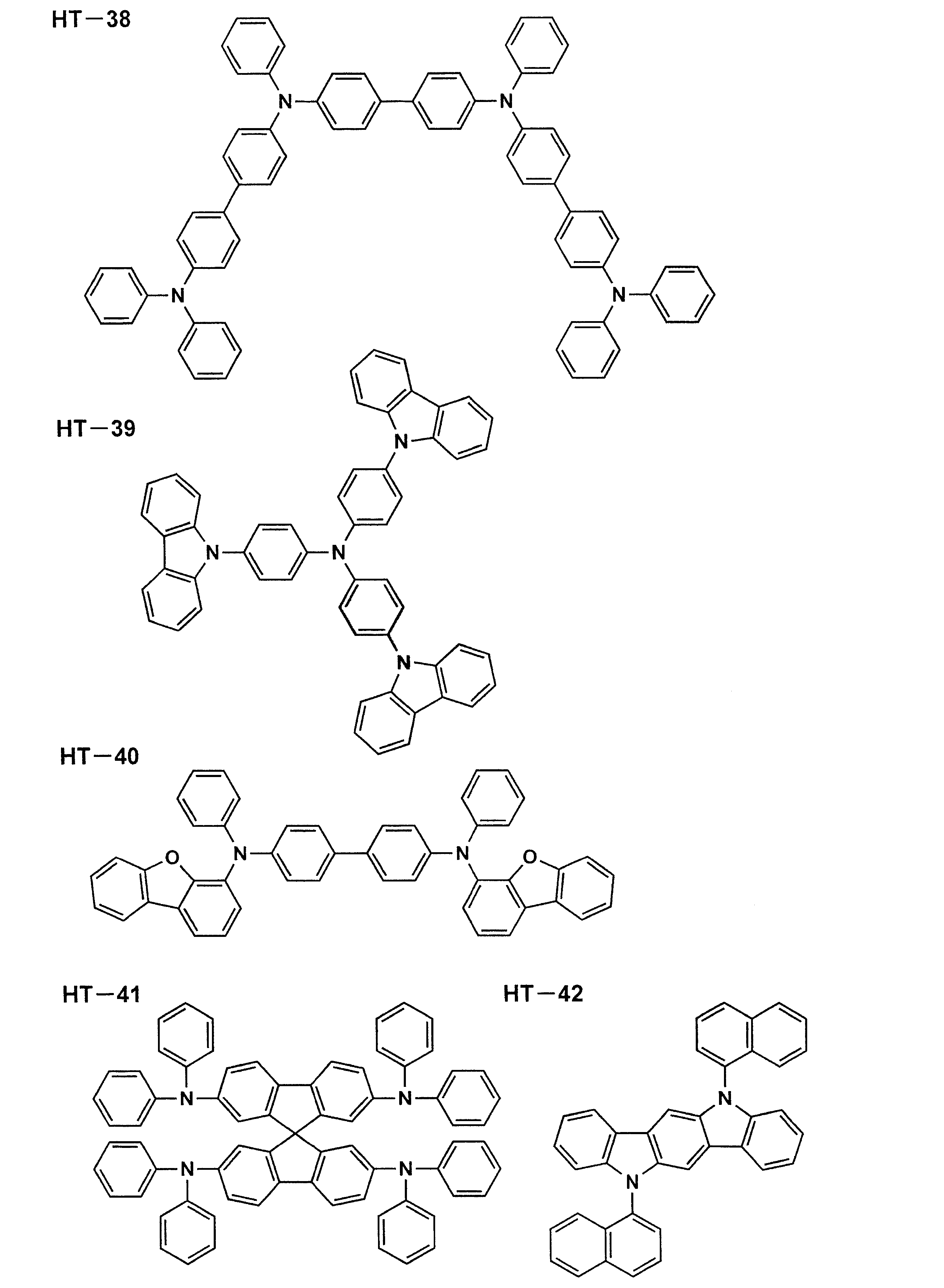

電子輸送層とは電子を輸送する機能を有する材料からなり、広い意味で電子注入層、正孔阻止層も電子輸送層に含まれる。電子輸送層は単層若しくは複数層を設けることができる。
更に、上記オキサジアゾール誘導体において、オキサジアゾール環の酸素原子を硫黄原子に置換したチアジアゾール誘導体、電子吸引性基として知られているキノキサリン環を有するキノキサリン誘導体も電子輸送材料として用いることができる。

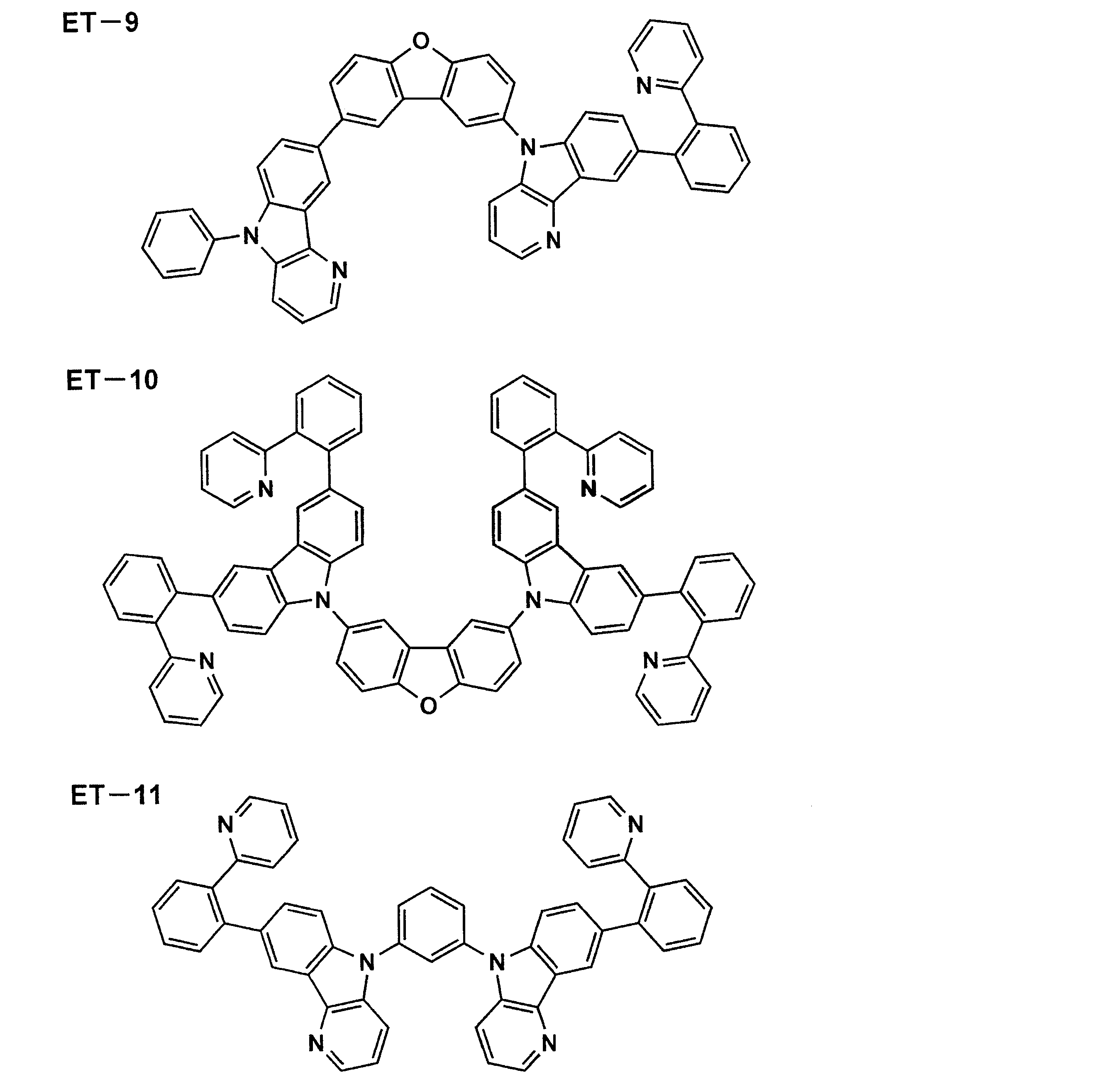

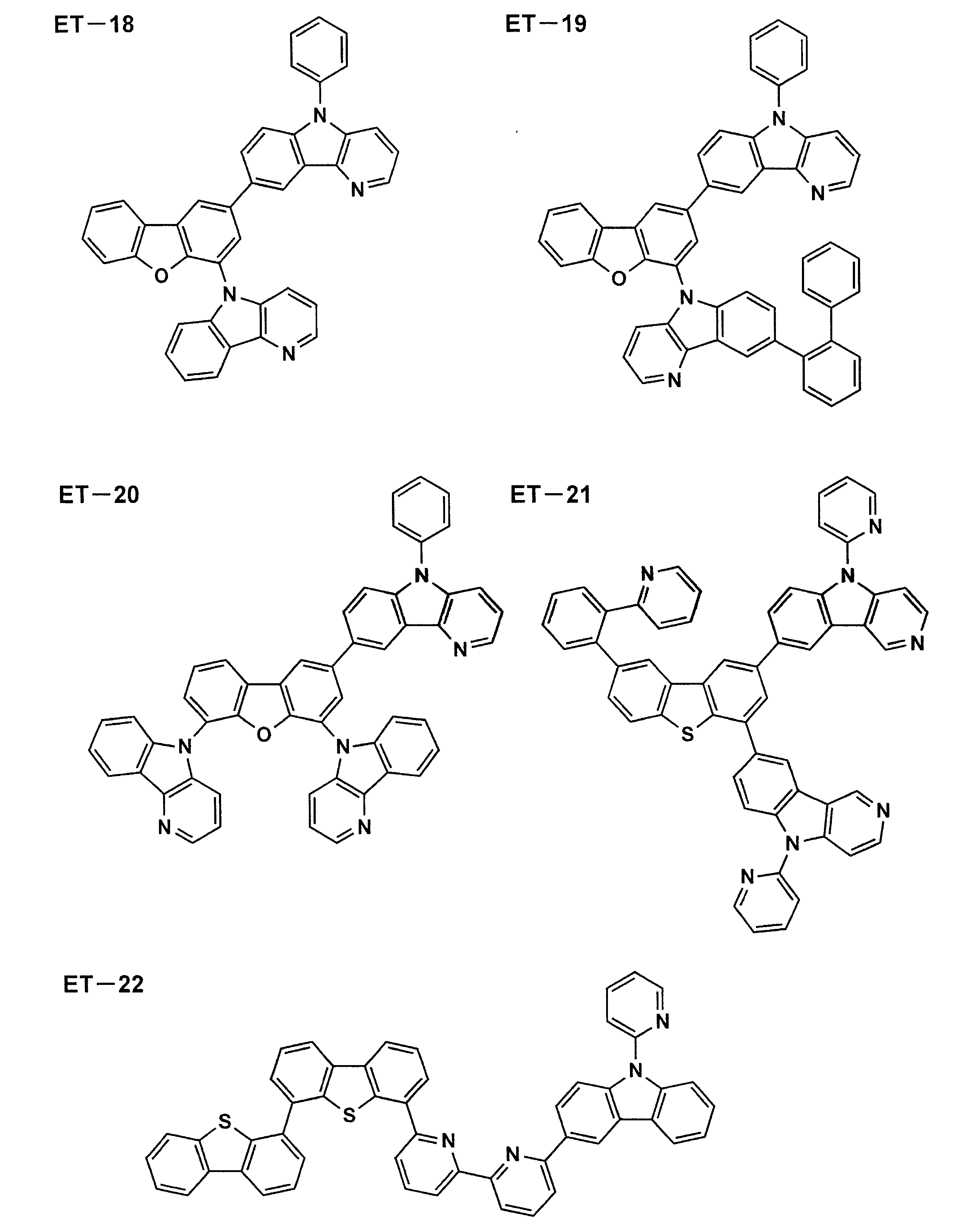

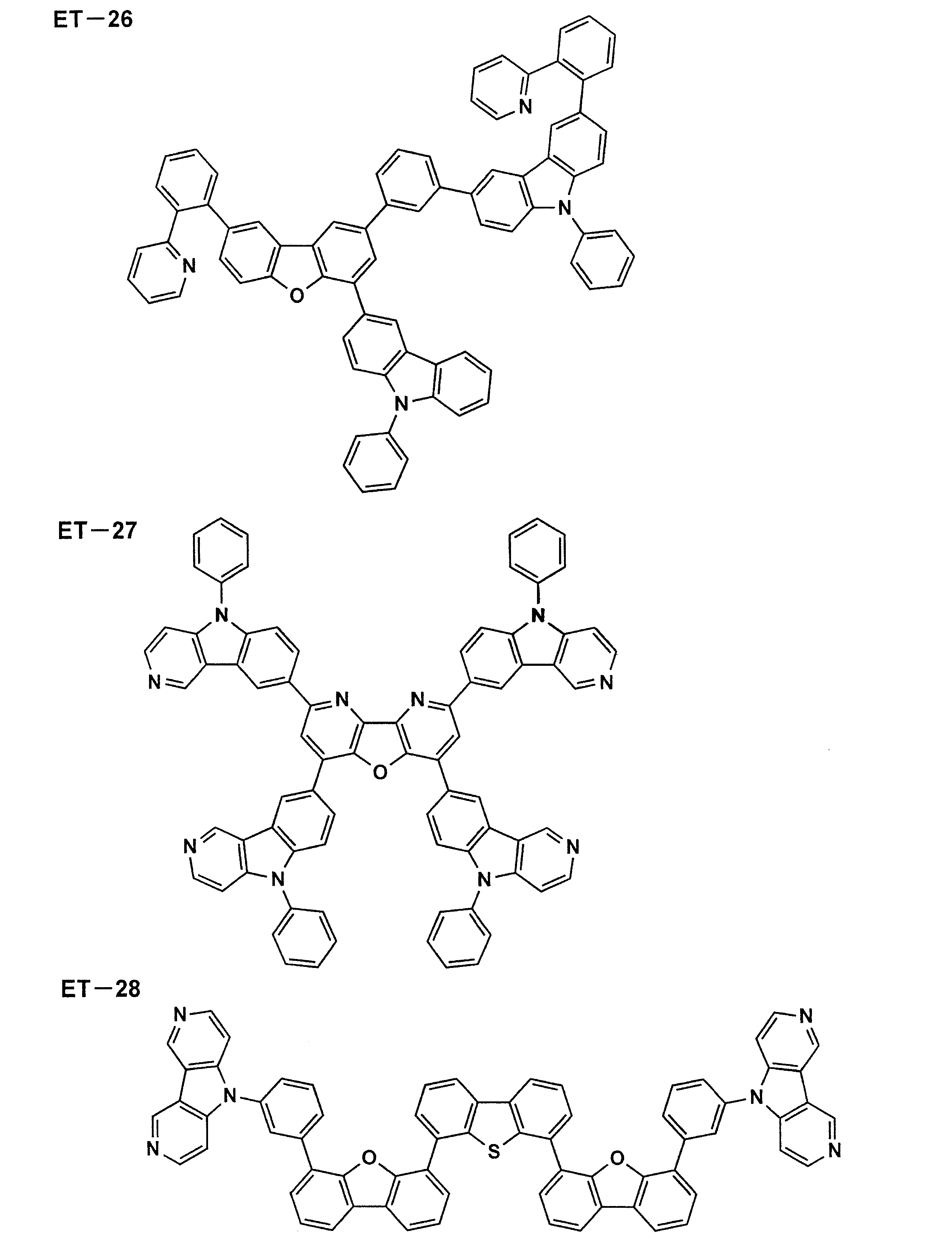
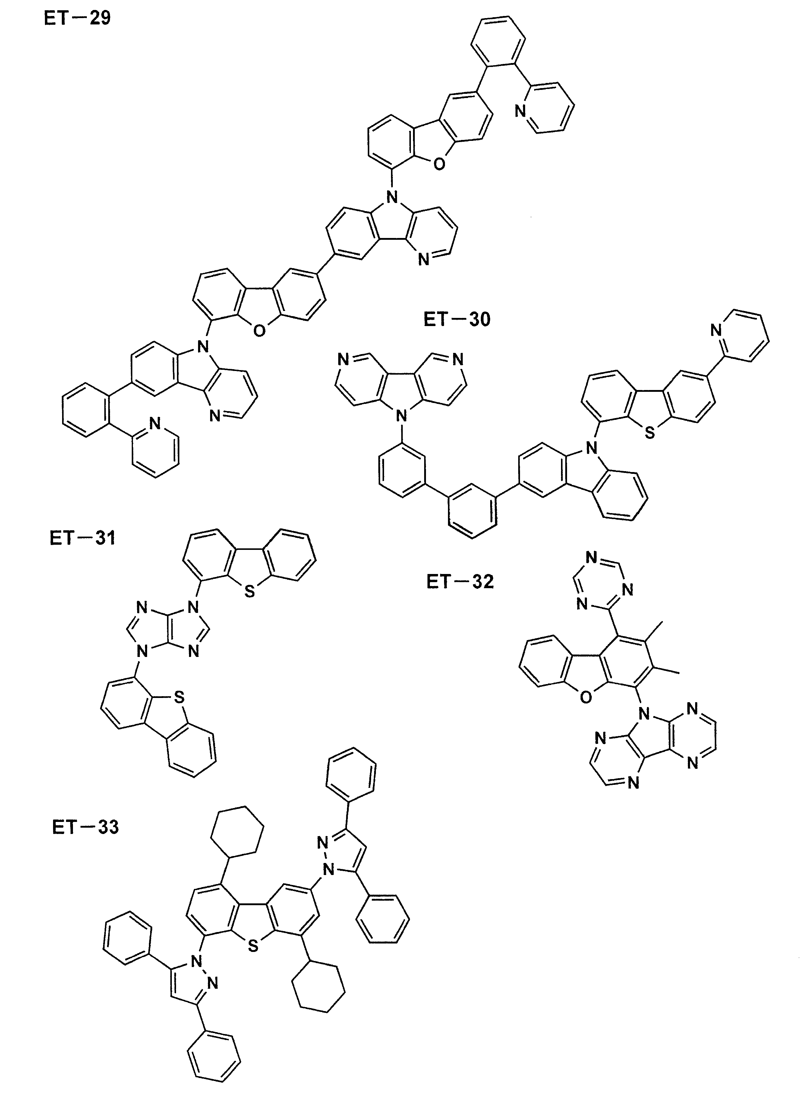

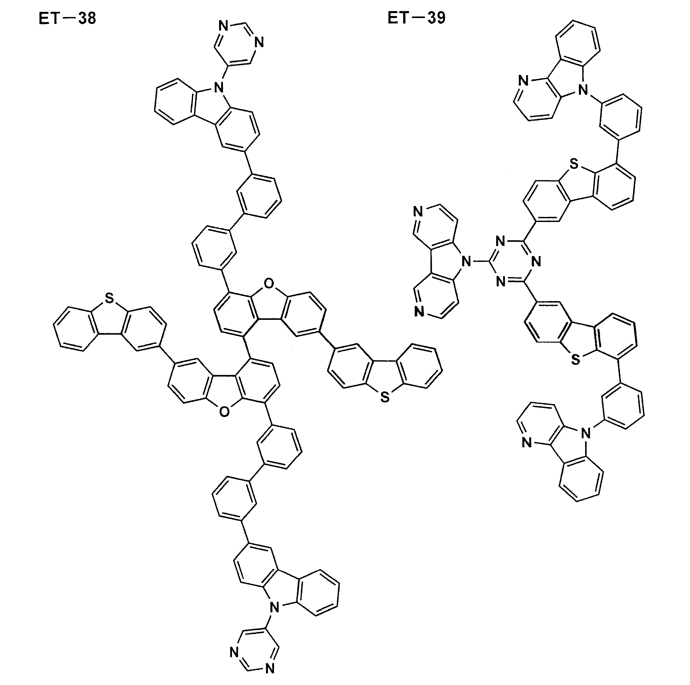
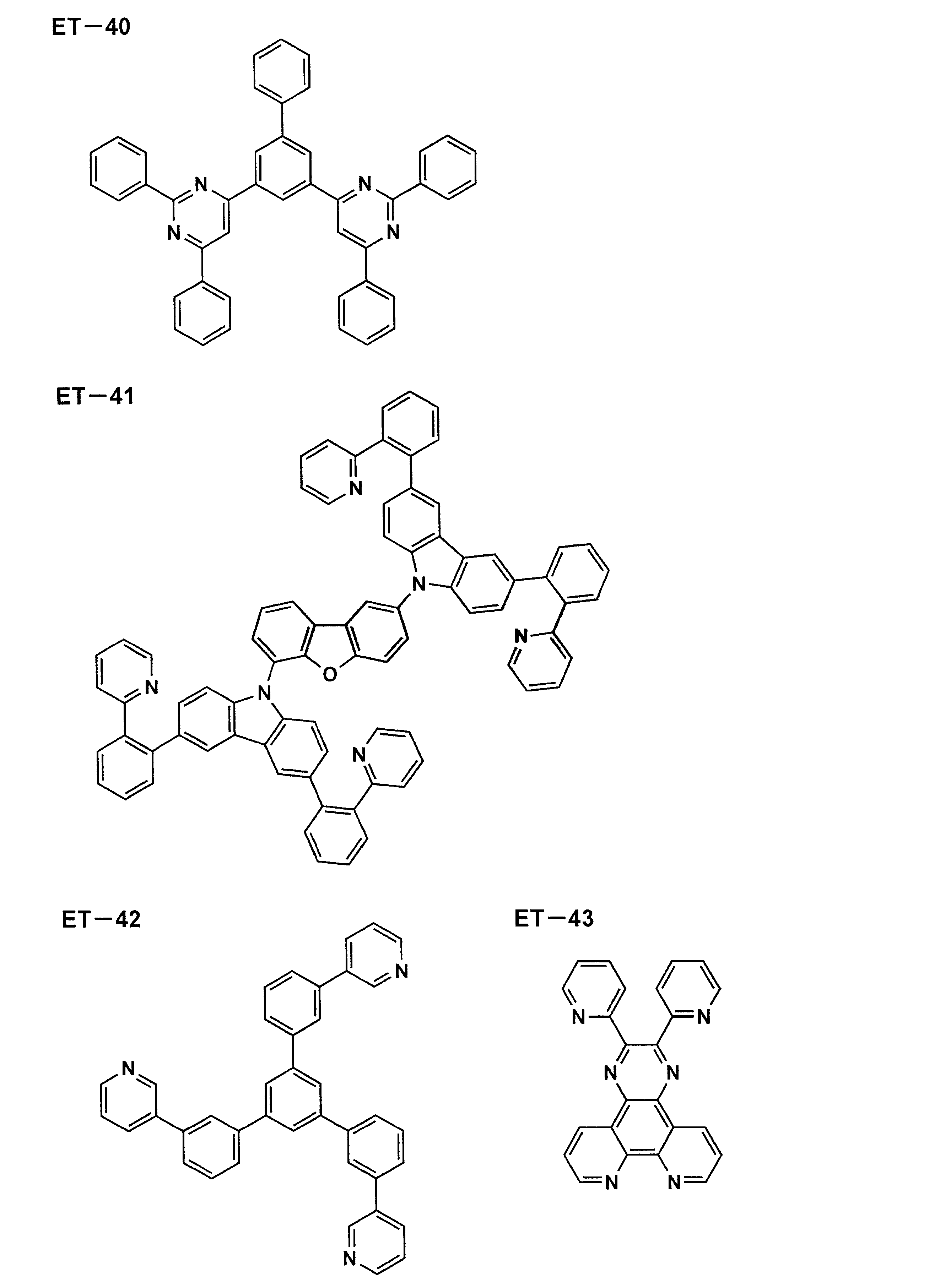
有機EL素子における陽極としては、仕事関数の大きい(4eV以上)金属、合金、電気伝導性化合物及びこれらの混合物を電極物質とするものが好ましく用いられる。このような電極物質の具体例としては、Au等の金属、CuI、インジウムチンオキシド(ITO)、SnO2、ZnO等の導電性透明材料が挙げられる。
一方、陰極としては仕事関数の小さい(4eV以下)金属(電子注入性金属と称する)、合金、電気伝導性化合物及びこれらの混合物を電極物質とするものが用いられる。このような電極物質の具体例としては、ナトリウム、ナトリウム-カリウム合金、マグネシウム、リチウム、マグネシウム/銅混合物、マグネシウム/銀混合物、マグネシウム/アルミニウム混合物、マグネシウム/インジウム混合物、アルミニウム/酸化アルミニウム(Al2O3)混合物、インジウム、リチウム/アルミニウム混合物、希土類金属等が挙げられる。これらの中で、電子注入性及び酸化等に対する耐久性の点から、電子注入性金属とこれより仕事関数の値が大きく安定な金属である第二金属との混合物、例えば、マグネシウム/銀混合物、マグネシウム/アルミニウム混合物、マグネシウム/インジウム混合物、アルミニウム/酸化アルミニウム(Al2O3)混合物、リチウム/アルミニウム混合物、アルミニウム等が好適である。
また、陰極に上記金属を1~20nmの層厚で作製した後に、上記した陽極の説明で挙げる導電性透明材料をその上に作製することで、透明又は半透明の陰極を作製することができ、これを応用することで陽極と陰極の両方が透過性を有する素子を作製することができる。
本発明の有機EL素子に用いることのできる支持基板(以下、基体、基板、基材、支持体等とも言う)としては、ガラス、プラスチック等の種類には特に限定はなく、また透明であっても不透明であっても良い。支持基板側から光を取り出す場合には、支持基板は透明であることが好ましい。好ましく用いられる透明な支持基板としては、ガラス、石英、透明樹脂フィルムを挙げることができる。特に好ましい支持基板は、有機EL素子にフレキシブル性を与えることが可能な樹脂フィルムである。
ここで、外部取り出し量子効率(%)=有機EL素子外部に発光した光子数/有機EL素子に流した電子数×100である。
本発明に用いられる封止手段としては、例えば、封止部材と電極、支持基板とを接着剤で接着する方法を挙げることができる。
また、ポリマー板としては、ポリカーボネート、アクリル、ポリエチレンテレフタレート、ポリエーテルサルファイド、ポリサルフォン等から形成されたものを挙げることができる。
金属板としては、ステンレス、鉄、銅、アルミニウム、マグネシウム、ニッケル、亜鉛、クロム、チタン、モリブテン、シリコン、ゲルマニウム及びタンタルからなる群から選ばれる一種以上の金属又は合金からなるものが挙げられる。
更には、ポリマーフィルムは、JIS K 7126-1987に準拠した方法で測定された酸素透過度が1×10⁻³ml/(m2・24h・atm)以下、JIS K 7129-1992に準拠した方法で測定された、水蒸気透過度(25±0.5℃、相対湿度(90±2)%RH)が、1×10⁻³g/(m2・24h)以下のものであることが好ましい。
有機層を挟み支持基板と対向する側の前記封止膜、あるいは前記封止用フィルムの外側に、素子の機械的強度を高めるために保護膜、あるいは保護板を設けても良い。特に封止が前記封止膜により行われている場合には、その機械的強度は必ずしも高くないため、このような保護膜、保護板を設けることが好ましい。これに使用することができる材料としては、前記封止に用いたのと同様なガラス板、ポリマー板・フィルム、金属板・フィルム等を用いることができるが、軽量且つ薄膜化ということからポリマーフィルムを用いることが好ましい。
有機EL素子は空気よりも屈折率の高い(屈折率が1.7~2.1程度)層の内部で発光し、発光層で発生した光のうち15%から20%程度の光しか取り出せないことが一般的に言われている。これは、臨界角以上の角度θで界面(透明基板と空気との界面)に入射する光は、全反射を起こし素子外部に取り出すことができないことや、透明電極ないし発光層と透明基板との間で光が全反射を起こし、光が透明電極ないし発光層を導波し、結果として光が素子側面方向に逃げるためである。
本発明はこれらの手段を組み合わせることにより、更に高輝度あるいは耐久性に優れた素子を得ることができる。
このとき、回折格子の周期は媒質中の光の波長の約1/2~3倍程度が好ましい。
本発明の有機EL素子は基板の光取り出し側に、例えば、マイクロレンズアレイ状の構造を設けるように加工したり、あるいは所謂集光シートと組み合わせたりすることにより、特定方向、例えば、素子発光面に対し正面方向に集光することにより、特定方向上の輝度を高めることができる。
有機EL素子の作製方法の一例として、陽極/正孔注入層(陽極バッファー層)/正孔輸送層/発光層/正孔阻止層/電子輸送層/電子注入層(陰極バッファー層)/陰極からなる素子の作製方法について説明する。
湿式法としては、スピンコート法、キャスト法、ダイコート法、ブレードコート法、ロールコート法、インクジェット法、印刷法、スプレーコート法、カーテンコート法、LB法等があるが、精密な薄膜が形成可能で、且つ高生産性の点から、ダイコート法、ロールコート法、インクジェット法、スプレーコート法などのロール・ツー・ロール方式適性の高い方法が好ましい。また、層ごとに異なる成膜法を適用しても良い。
また、分散方法としては、超音波、高剪断力分散やメディア分散等の分散方法により分散することができる。
本発明の有機EL素子は、表示デバイス、ディスプレイ、各種発光光源として用いることができる。発光光源として、例えば、照明装置(家庭用照明、車内照明)、時計や液晶用バックライト、看板広告、信号機、光記憶媒体の光源、電子写真複写機の光源、光通信処理機の光源、光センサーの光源等が挙げられるがこれに限定するものではないが、特に液晶表示装置のバックライト、照明用光源としての用途に有効に用いることができる。
本発明の表示装置について説明する。本発明の表示装置は、本発明の有機EL素子を具備したものである。本発明の表示装置は単色でも多色でも良いが、ここでは多色表示装置について説明する。
発光層のみパターニングを行う場合、その方法に限定はないが、好ましくは蒸着法、インクジェット法、スピンコート法、印刷法である。
図1は有機EL素子から構成される表示装置の一例を示した模式図である。有機EL素子の発光により画像情報の表示を行う、例えば、携帯電話等のディスプレイの模式図である。
表示部Aは基板上に、複数の走査線5及びデータ線6を含む配線部と複数の画素3等とを有する。表示部Aの主要な部材の説明を以下に行う。
図2においては、画素3の発光した光が白矢印方向(下方向)へ取り出される場合を示している。
即ち、有機EL素子10の発光は、複数の画素それぞれの有機EL素子10に対して、アクティブ素子であるスイッチングトランジスター11と駆動トランジスター12を設けて、複数の画素3それぞれの有機EL素子10の発光を行っている。このような発光方法をアクティブマトリクス方式と呼んでいる。
本発明の照明装置について説明する。本発明の照明装置は、本発明の有機EL素子を具備したものである。本発明の有機EL素子に共振器構造を持たせた有機EL素子として用いても良く、このような共振器構造を有した有機EL素子の使用目的としては、光記憶媒体の光源、電子写真複写機の光源、光通信処理機の光源、光センサーの光源等が挙げられるが、これらに限定されない。また、レーザー発振をさせることにより上記用途に使用しても良い。
また複数の発光色を得るための発光材料の組み合わせは、複数のリン光又は蛍光で発光する材料を複数組み合わせたもの、蛍光又はリン光で発光する発光材料と、発光材料からの光を励起光として発光する色素材料との組み合わせたものの何れでも良いが、本発明に係る白色有機EL素子においては、発光ドーパントを複数組み合わせ混合するだけで良い。
本発明の有機EL素子を具備した、本発明の照明装置の一態様について説明する。
本発明の有機EL素子の非発光面をガラスケースで覆い、厚み300μmのガラス基板を封止用基板として用いて、周囲にシール材として、エポキシ系光硬化型接着剤(東亞合成社製ラックストラックLC0629B)を適用し、これを陰極上に重ねて透明支持基板と密着させ、ガラス基板側からUV光を照射して、硬化させて、封止し、図5及び図6に示すような照明装置を形成することができる。
以下に説明する実施例で用いられる化合物の構造を以下に示す。なお、下記に示す3-1-1~4-7-2は、上記した一般式(1)~(7)で表される有機EL素子材料に該当する。
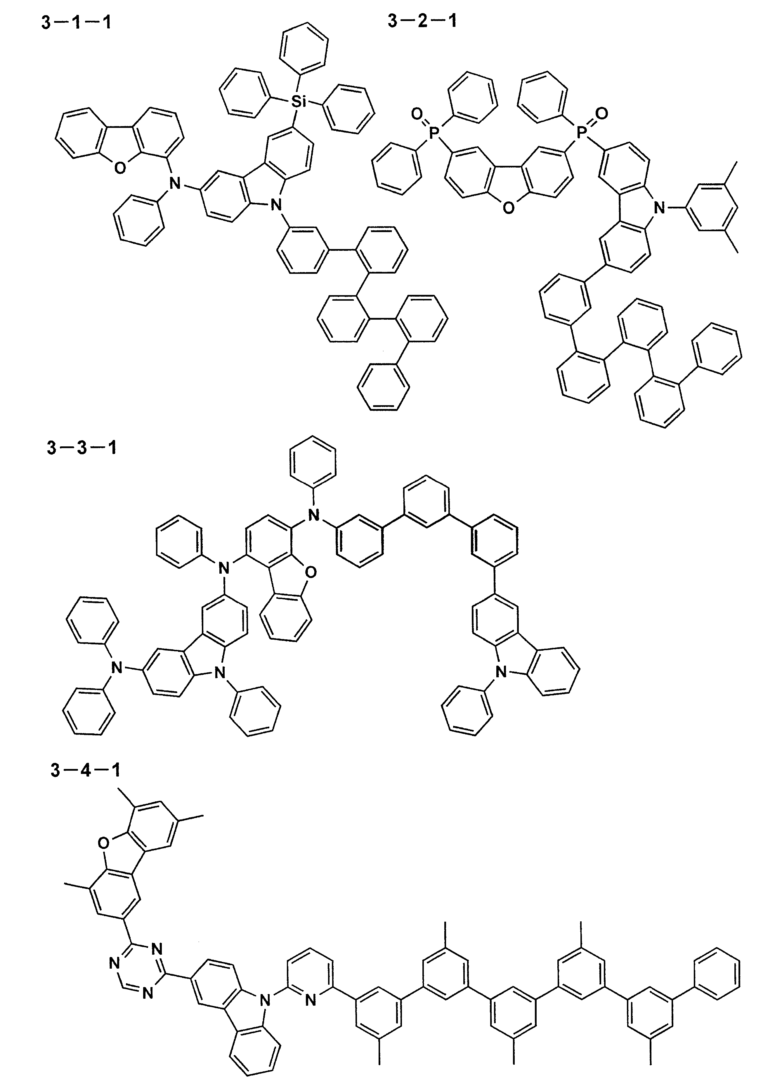


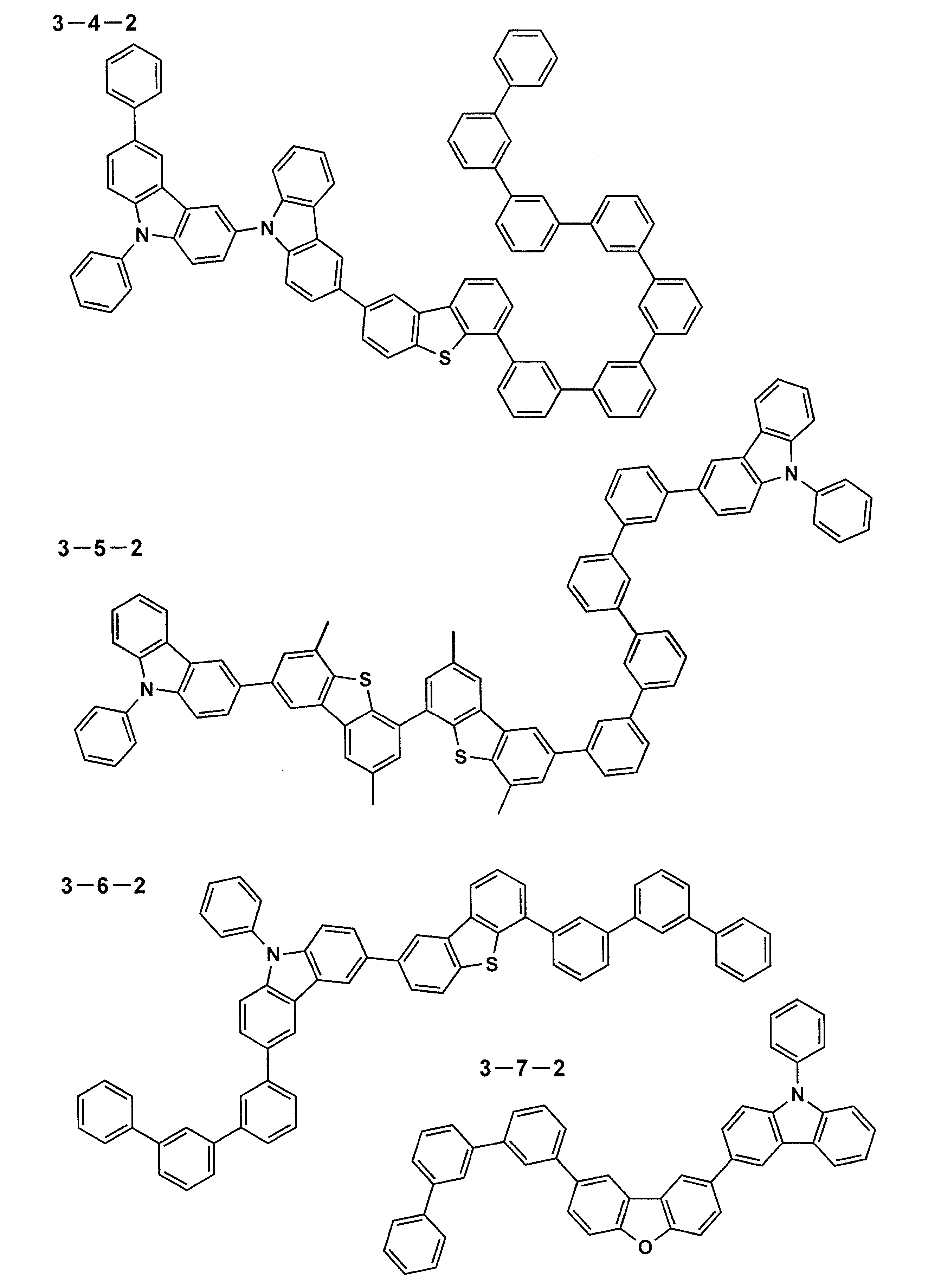


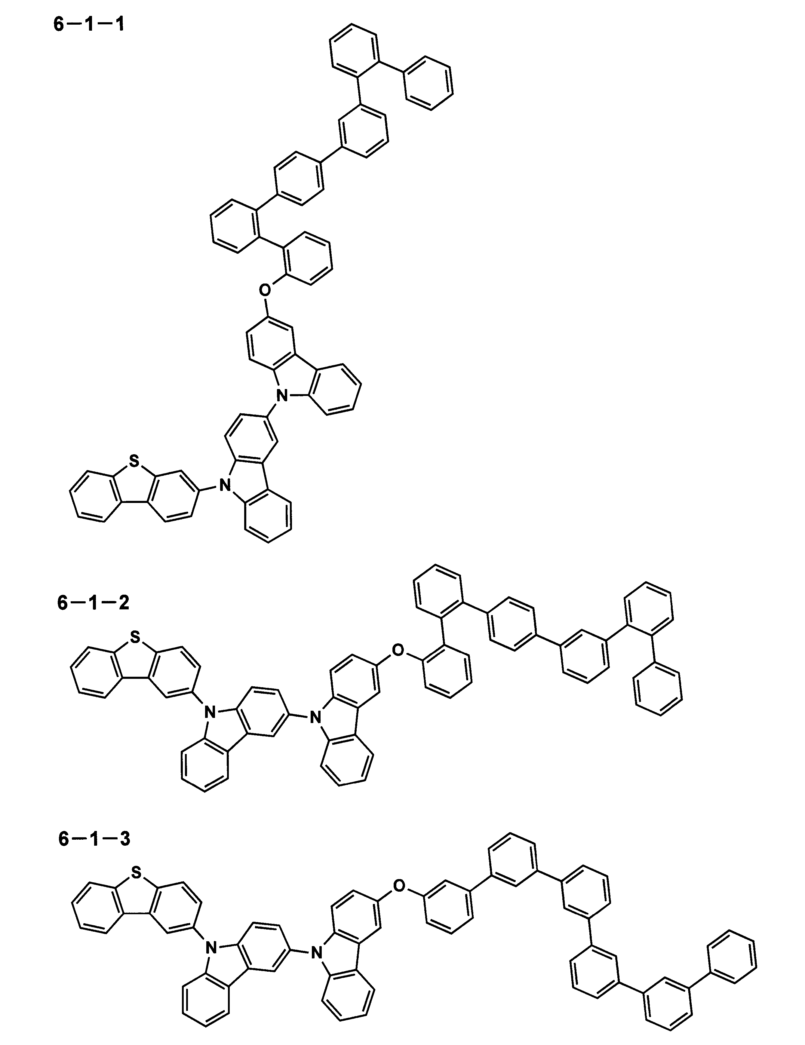
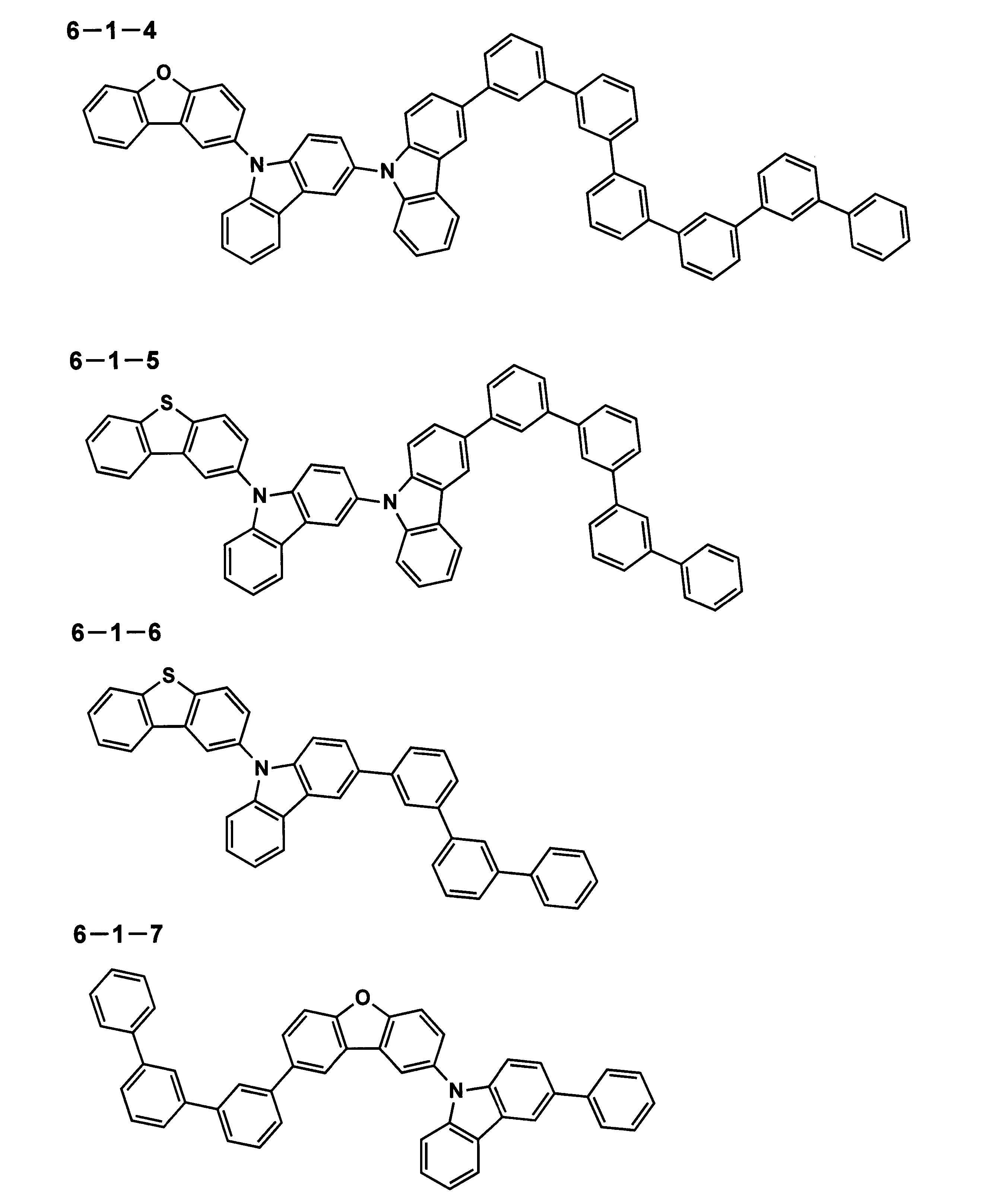


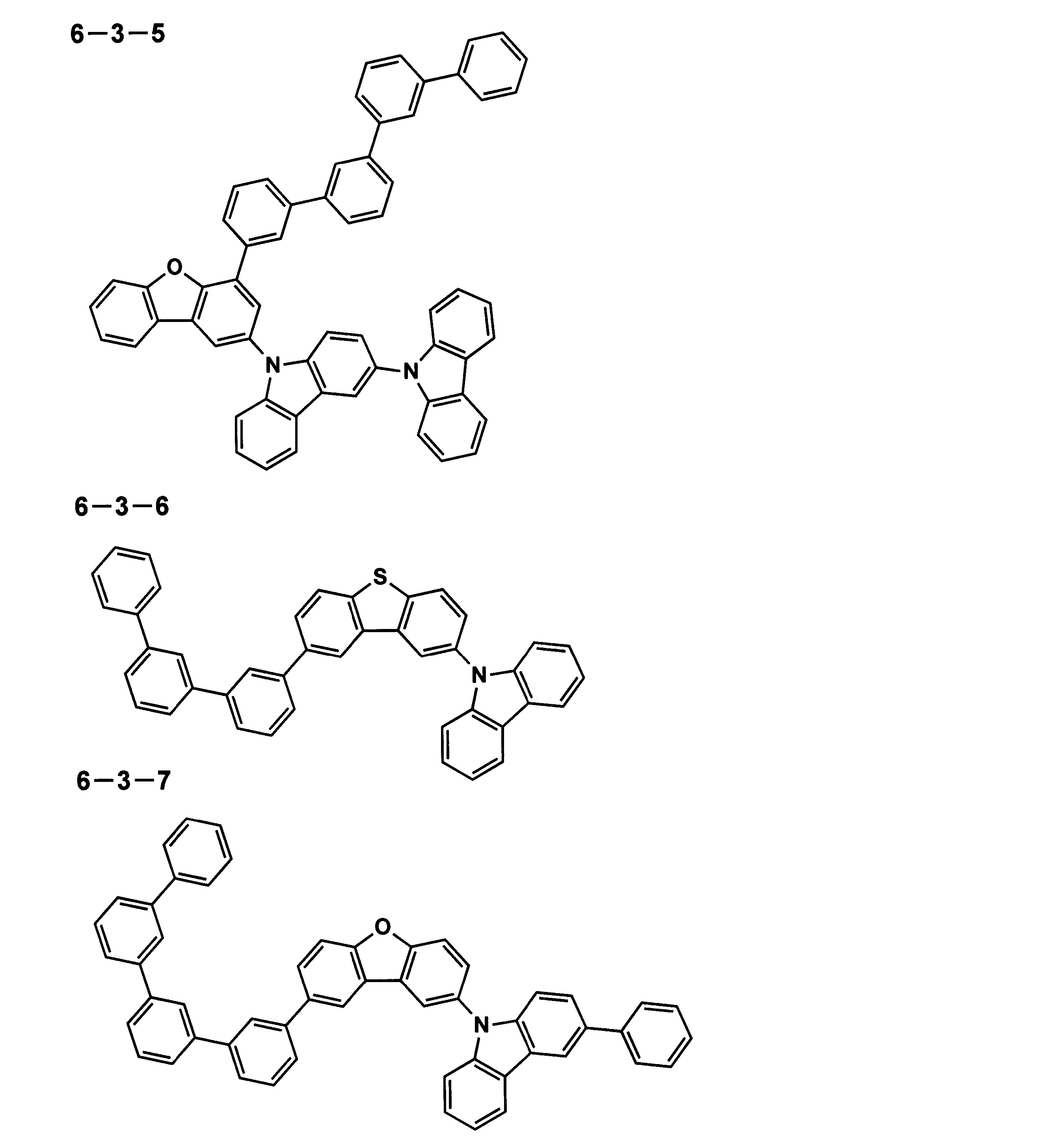

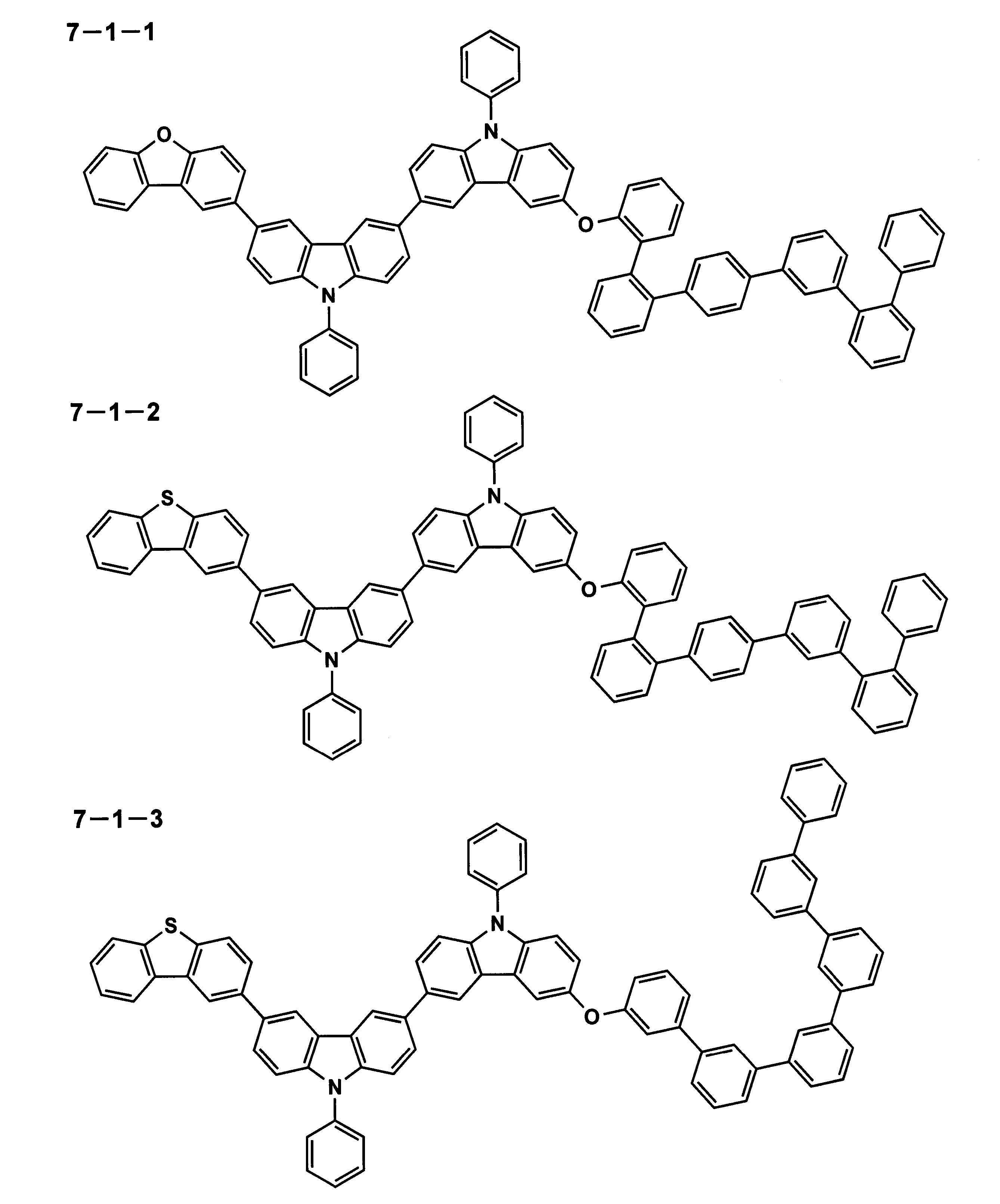

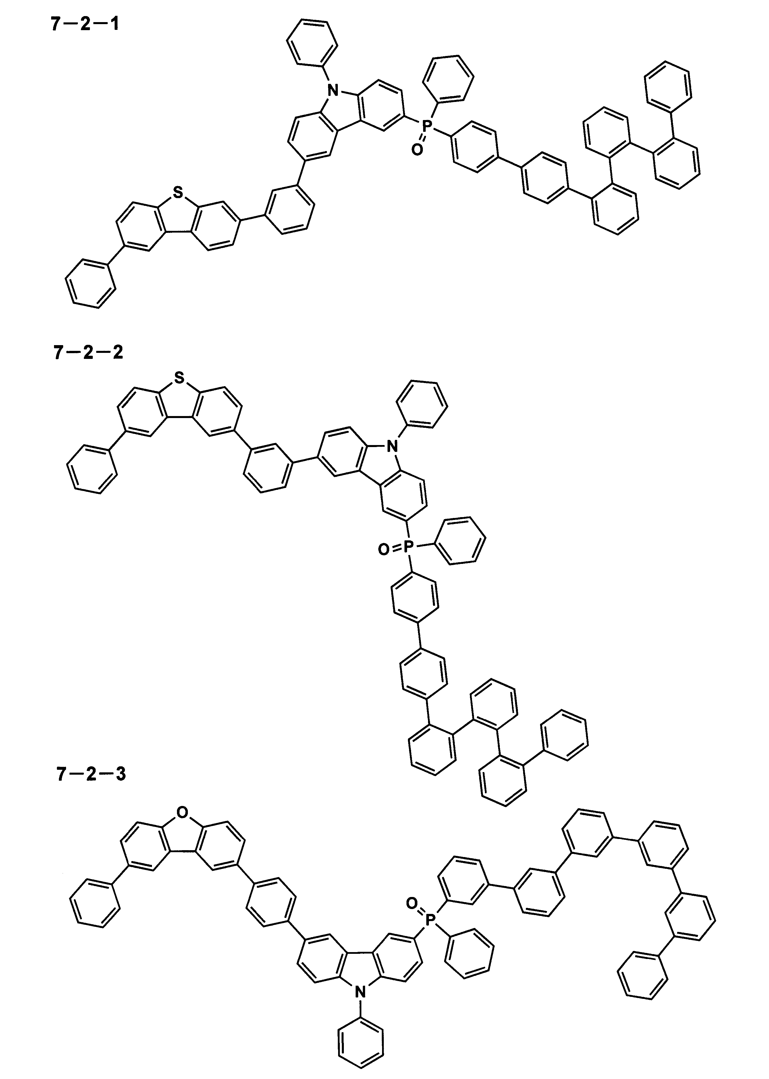

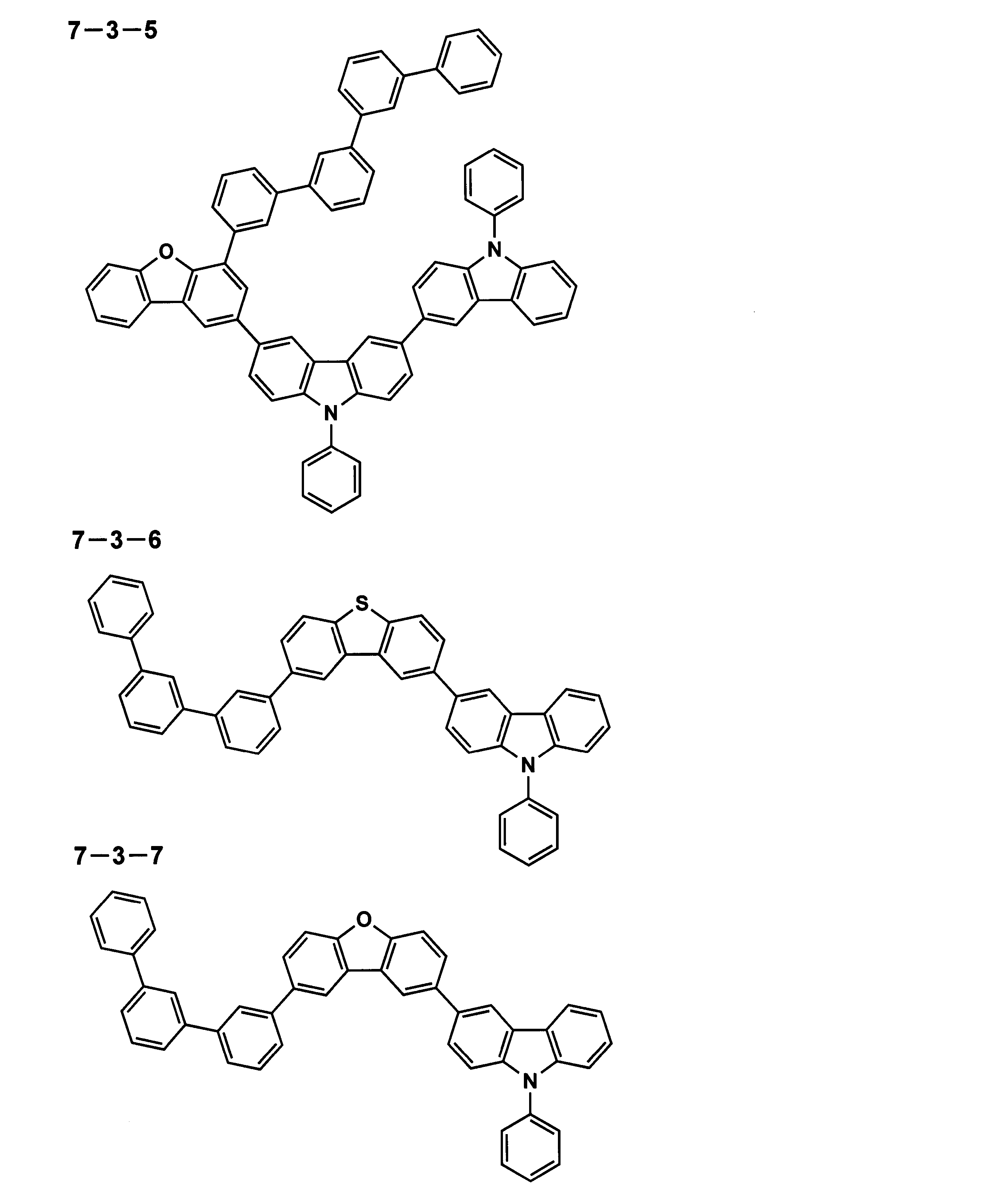
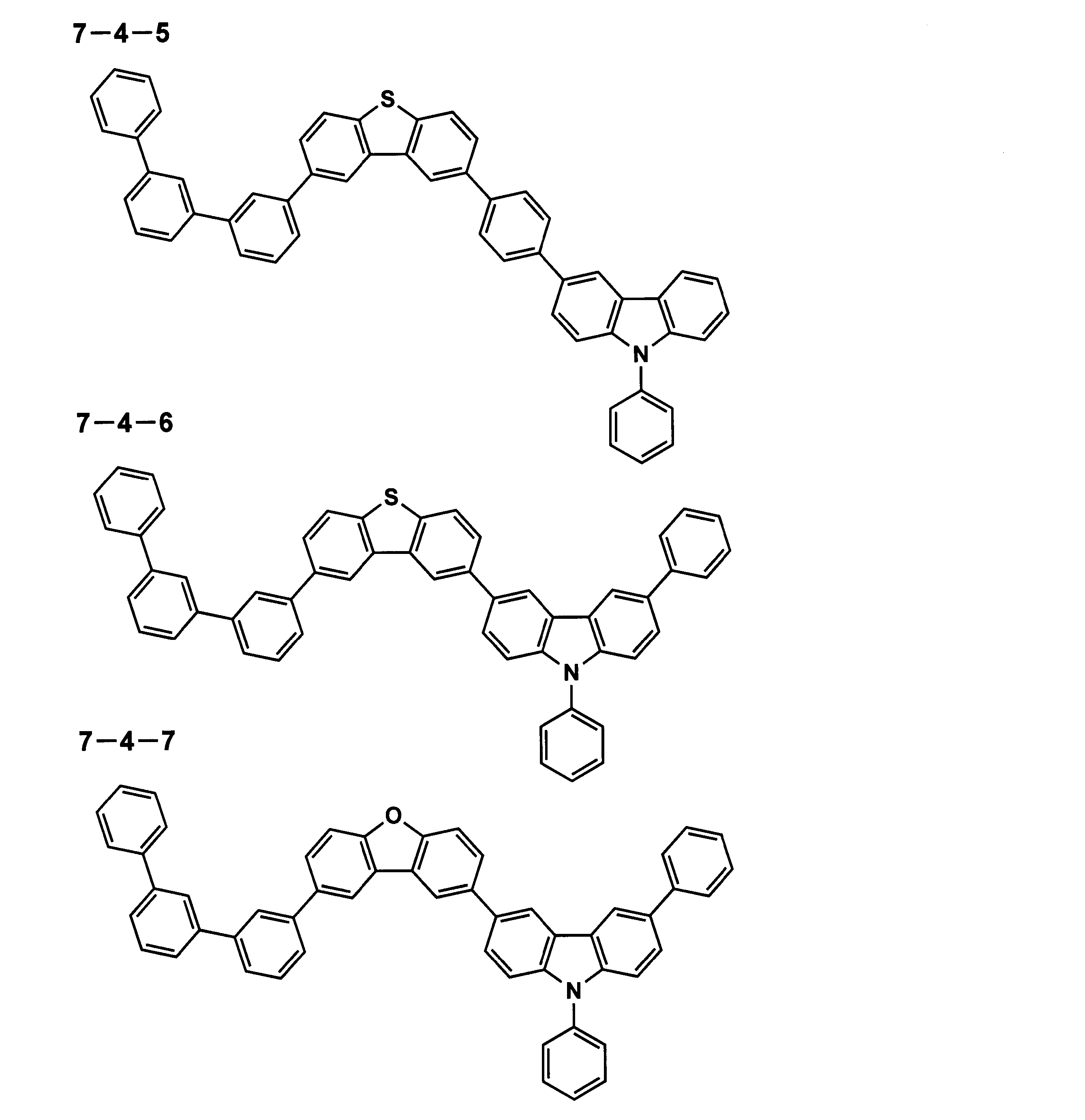


comparative-2は、米国特許第8114530号明細書記載のNo.28の化合物である。
comparative-3は、国際公開第2009/008099号記載のNo.81の化合物である。
comparative-4は、国際公開第2009/008099号記載のNo.91の化合物である。
comparative-5は、国際公開第2009/008100号記載のNo.27の化合物である。
comparative-6は、特開2012-49518号公報記載の1-325の化合物である。
ETM-1は、米国特許第8114530号明細書記載の化合物である。
DPM-2は、米国特許第8114530号明細書記載のK-21の化合物である。
《有機EL素子1-1の作製》
陽極として100mm×100mm×1.1mmのガラス基板上にITO(Indium Tin Oxide;酸化インジウムスズ)を100nm成膜した基板(NHテクノグラス社製NA45)にパターニングを行った後、このITO透明電極を設けた透明支持基板をイソプロピルアルコールで超音波洗浄し、乾燥窒素ガスで乾燥し、UVオゾン洗浄を5分間行った。
有機EL素子1-1の作製において、ドーパントとホスト材料と第1電子輸送材料を表1に記載の化合物に変えた以外は同様にして、有機EL素子1-2~1-16を作製した。
得られた有機EL素子1-1~1-16を評価するに際しては、作製後の各有機EL素子の非発光面をガラスケースで覆い、厚み300μmのガラス基板を封止用基板として用いて、周囲にシール材としてエポキシ系光硬化型接着剤(東亞合成社製ラックストラックLC0629B)を適用し、これを上記陰極上に重ねて前記透明支持基板と密着させ、ガラス基板側からUV光を照射して硬化させて封止し、図5及び図6に示すような照明装置を作製して評価した。
このようにして作製した各サンプルについて下記の評価を行った。評価結果を表1に示す。
有機EL素子を室温(25℃)、2.5mA/cm2の定電流条件下による点灯を行い、点灯開始直後の発光輝度(L)[cd/m2]を測定することにより、外部取り出し量子効率(η)(単に、効率ともいう)を算出した。
ここで、発光輝度の測定はCS-1000(コニカミノルタセンシング製)を用いて行い、外部取り出し量子効率は有機EL素子1-1を100とする相対値で表した。
下記に示す測定法に従って、半減寿命の評価を行った。各有機EL素子を初期輝度1000cd/m2を与える電流で定電流駆動して、初期輝度の1/2(500cd/m2)になる時間を求め、これを半減寿命の尺度とした。なお、半減寿命は有機EL素子1-1を100とする相対値で表した。
有機EL素子を室温(25℃)、2.5mA/cm2の定電流条件下で駆動したときの電圧を各々測定し、測定結果を下記に示すように、有機EL素子1-1を100として各々相対値で示した。
電圧=(各素子の駆動電圧/有機EL素子1-1の駆動電圧)×100
なお、値が小さいほうが比較に対して駆動電圧が低いことを示す。
有機EL素子を室温(25℃)、2.5mA/cm2の定電流条件下により駆動した時の電圧を各々測定し、測定結果を下記に示した計算式により計算し、得られた結果を表1に示した。
有機EL素子1-1を100とする相対値で表した。
駆動時の電圧上昇(相対値)=輝度半減時の駆動電圧-初期駆動電圧
なお、値が小さいほうが比較に対して駆動時の電圧上昇が小さいことを示す。
有機EL素子を60℃、70%RHの条件で1カ月保存後、保存前後における各電力効率を求め、各々の電力効率比を下式に従って求め、これを経時安定性の尺度とした。
経時安定性(%)=(保存後の電力効率/保存前の電力効率)×100
なお、電力効率は分光放射輝度計CS-1000(コニカミノルタセンシング社製)を用いて、各有機EL素子の正面輝度及び輝度角度依存性を測定し、正面輝度1000cd/m2において求めたものを用いた。

表1から明らかな通り、本発明に係る一般式(1)で表される有機EL素子材料を用いた有機EL素子は、比較例の有機EL素子に比べ、発光効率及び発光寿命に優れ、低駆動電圧であることが明らかであり、また駆動時の電圧上昇も抑えられていることがわかった。更に、経時安定性に優れていることもわかった。また、一般式(1)で表される有機EL素子材料を発光層及び第1電子輸送層の両方に含有させると、素子性能が更に向上することがわかった。
《有機EL素子2-1~2-19の作製》
有機EL素子1-1の作製において、正孔輸送材料をHT-2に変更し、更にホスト材料、ドーパント及び第1電子輸送材料を表2に示す化合物に変更した。それ以外は同様にして、有機EL素子2-1~2-19を各々作製した。
得られた有機EL素子2-1~2-19を評価するに際しては、当該有機EL素子を実施例1の有機EL素子1-1~1-16と同様に封止し、図5及び図6に示すような照明装置を形成して評価した。
このようにして作製した各サンプルに対し、実施例1と同様に、外部取り出し量子効率、半減寿命、駆動電圧、駆動時の電圧上昇及び経時安定性について評価を行った。評価結果を表2に示す。なお、表2における外部取り出し量子効率、半減寿命、駆動電圧、及び駆動時の電圧上昇の測定結果は、有機EL素子2-1の測定値を100とする相対値で表した。
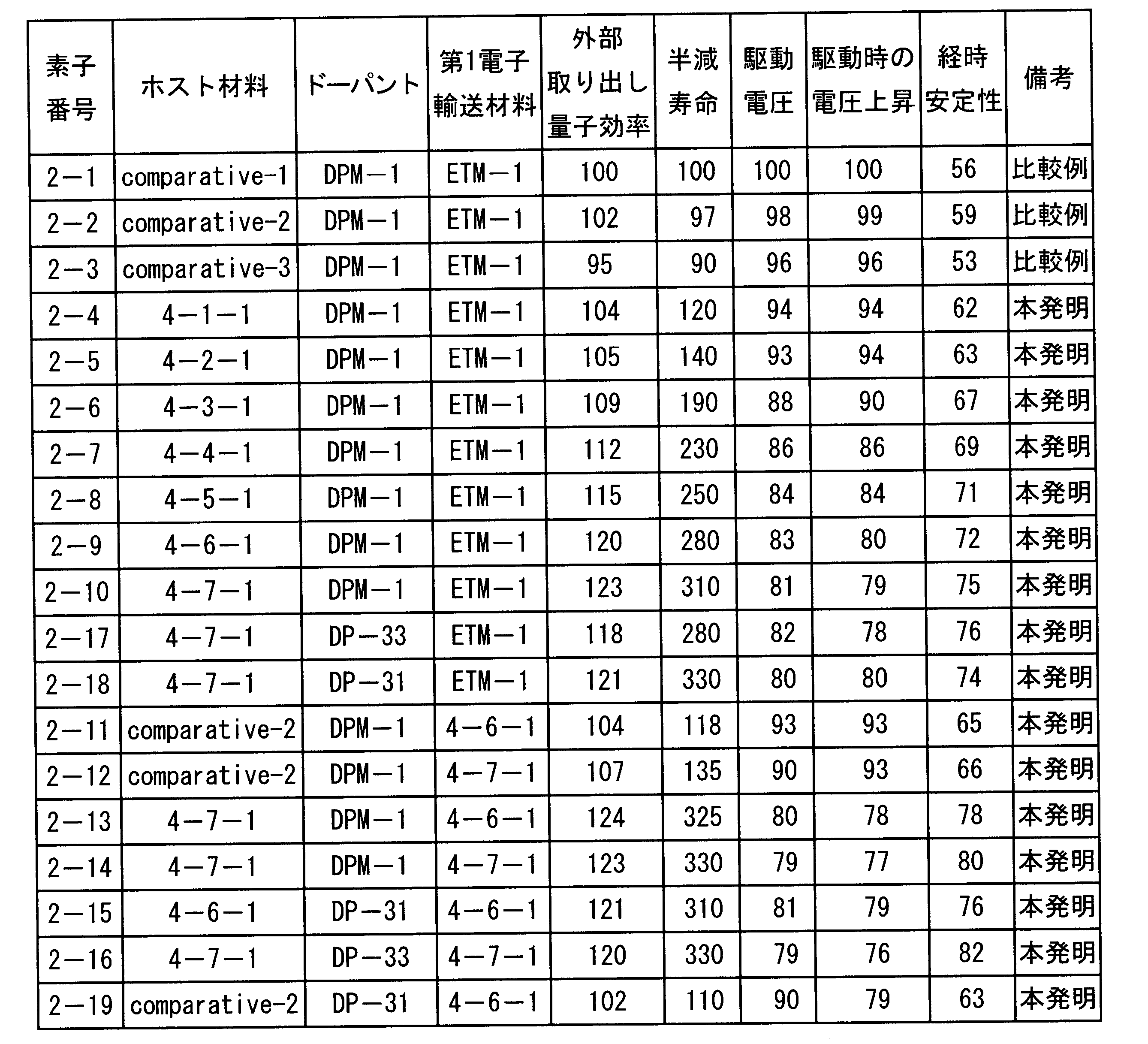
《有機EL素子3-1の作製》
100mm×100mm×1.1mmのガラス基板上に、陽極としてITO(Indium Tin Oxide;酸化インジウムスズ)を100nm成膜した基板(AvanStrate株式会社製、NA-45)にパターニングを行った。その後、このITO透明電極を設けた透明支持基板をイソプロピルアルコールで超音波洗浄し、乾燥窒素ガスで乾燥して、UVオゾン洗浄を5分間行った。
有機EL素子3-1の作製において、ドーパントとホスト材料と第1電子輸送材料とを表3に記載の化合物に変えた以外は同様にして、有機EL素子3-2~3-19を作製した。
得られた有機EL素子3-1~3-19を評価するに際しては、当該有機EL素子を実施例1の有機EL素子1-1~1-16と同様に封止し、図5及び図6に示すような照明装置を形成して評価した。
このようにして作製した各サンプルに対し、実施例1と同様に、外部取り出し量子効率、半減寿命、駆動電圧、駆動時の電圧上昇及び経時安定性について評価を行った。評価結果を表3に示す。なお、表3における外部取り出し量子効率、半減寿命、駆動電圧、及び駆動時の電圧上昇の測定結果は、有機EL素子3-1の測定値を100とする相対値で表した。

《有機EL素子4-1~4-16の作製》
有機EL素子3-1の作製において、ホスト材料、ドーパント及び第1電子輸送材料を表4に示す化合物に変更した。それ以外は同様にして、有機EL素子4-1~4-16を各々作製した。
得られた有機EL素子4-1~4-16を評価するに際しては、当該有機EL素子を実施例1の有機EL素子1-1~1-16と同様に封止し、図5及び図6に示すような照明装置を形成して評価した。
このようにして作製した各サンプルに対し、実施例1と同様に、外部取り出し量子効率、半減寿命、駆動電圧、駆動時の電圧上昇及び経時安定性について評価を行った。評価結果を表4に示す。なお、表4における外部取り出し量子効率、半減寿命、駆動電圧、及び駆動時の電圧上昇の測定結果は、有機EL素子4-1の測定値を100とする相対値で表した。

《有機ELフルカラー表示装置の作製》
図7は、有機ELフルカラー表示装置の概略構成図を示す。
ガラス基板201上に、陽極としてITO透明電極202を100nm成膜した基板(NHテクノグラス社製NA45)に100μmのピッチでパターニングを行った後(図7(a)参照)、このガラス基板201上であってITO透明電極202の間に非感光性ポリイミドの隔壁203(幅20μm、厚さ2.0μm)をフォトリソグラフィーで形成した(図7(b)参照)。
HT-44:20質量部
シクロヘキシルベンゼン:50質量部
イソプロピルビフェニル:50質量部
(青色発光層組成物)
ホスト材料4-7-2:0.7質量部
DP-55:0.04質量部
シクロヘキシルベンゼン:50質量部
イソプロピルビフェニル:50質量部
(緑色発光層組成物)
ホスト材料4-7-2:0.7質量部
D-1:0.04質量部
シクロヘキシルベンゼン:50質量部
イソプロピルビフェニル:50質量部
(赤色発光層組成物)
ホスト材料4-7-2:0.7質量部
D-10:0.04質量部
シクロヘキシルベンゼン:50質量部
イソプロピルビフェニル:50質量部
また、ウェットプロセスによって、上記効果を有する有機EL素子を製造することができる。
《有機EL素子6-1~6-35の作製》
有機EL素子1-1の作製において、正孔輸送材料をHT-2に変更し、更にホスト材料、ドーパント及び第1電子輸送材料を表5に示す化合物に変更した。それ以外は同様にして、有機EL素子6-1~6-35を各々作製した。
得られた有機EL素子6-1~6-35を評価するに際しては、当該有機EL素子を実施例1の有機EL素子1-1~1-16と同様に封止し、図5及び図6に示すような照明装置を形成して評価した。
このようにして作製した各サンプルに対し、実施例1と同様に、外部取り出し量子効率、半減寿命、駆動電圧、駆動時の電圧上昇及び経時安定性について評価を行った。評価結果を表5に示す。なお、表5における外部取り出し量子効率、半減寿命、駆動電圧、及び駆動時の電圧上昇の測定結果は、有機EL素子6-1の測定値を100とする相対値で表した。

《有機EL素子7-1~7-35の作製》
有機EL素子1-1の作製において、正孔輸送材料をHT-2に変更し、更にホスト材料、ドーパント及び第1電子輸送材料を表6に示す化合物に変更した。それ以外は同様にして、有機EL素子7-1~7-35を各々作製した。
得られた有機EL素子7-1~7-35を評価するに際しては、当該有機EL素子を実施例1の有機EL素子1-1~1-16と同様に封止し、図5及び図6に示すような照明装置を形成して評価した。
このようにして作製した各サンプルに対し、実施例1と同様に、外部取り出し量子効率、半減寿命、駆動電圧、駆動時の電圧上昇及び経時安定性について評価を行った。評価結果を表6に示す。なお、表6における外部取り出し量子効率、半減寿命、駆動電圧、及び駆動時の電圧上昇の測定結果は、有機EL素子7-1の測定値を100とする相対値で表した。
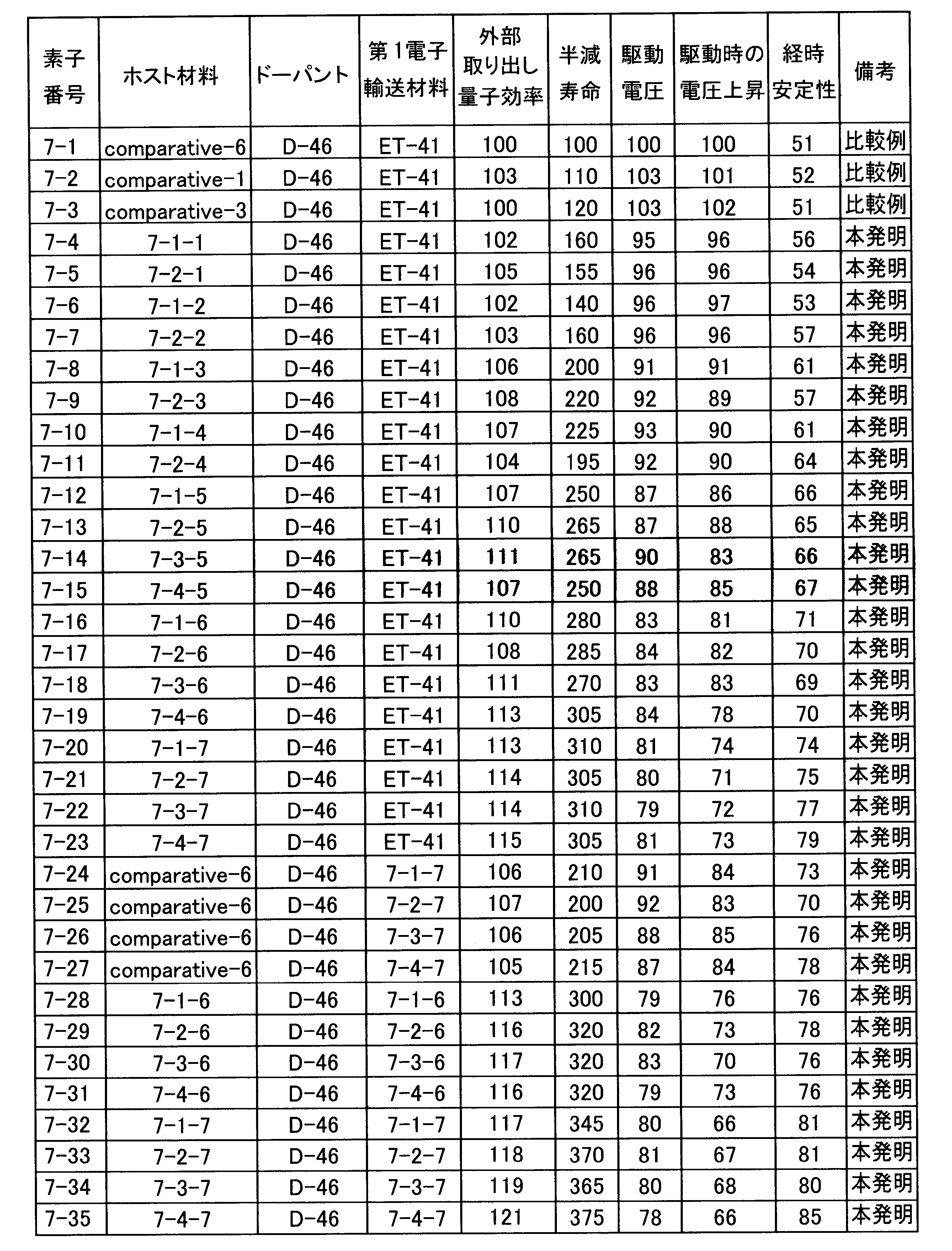
《有機EL素子8-1~8-31の作製》
有機EL素子4-1の作製において、ホスト材料、ドーパント及び第1電子輸送材料を表7に示す化合物に変更した。それ以外は同様にして、有機EL素子8-1~8-31を各々作製した。
得られた有機EL素子8-1~8-31を評価するに際しては、当該有機EL素子を実施例1の有機EL素子1-1~1-16と同様に封止し、図5及び図6に示すような照明装置を形成して評価した。
このようにして作製した各サンプルに対し、実施例1と同様に、外部取り出し量子効率、半減寿命、駆動電圧、駆動時の電圧上昇及び経時安定性について評価を行った。評価結果を表7に示す。なお、表7における外部取り出し量子効率、半減寿命、駆動電圧、及び駆動時の電圧上昇の測定結果は、有機EL素子8-1の測定値を100とする相対値で表した。
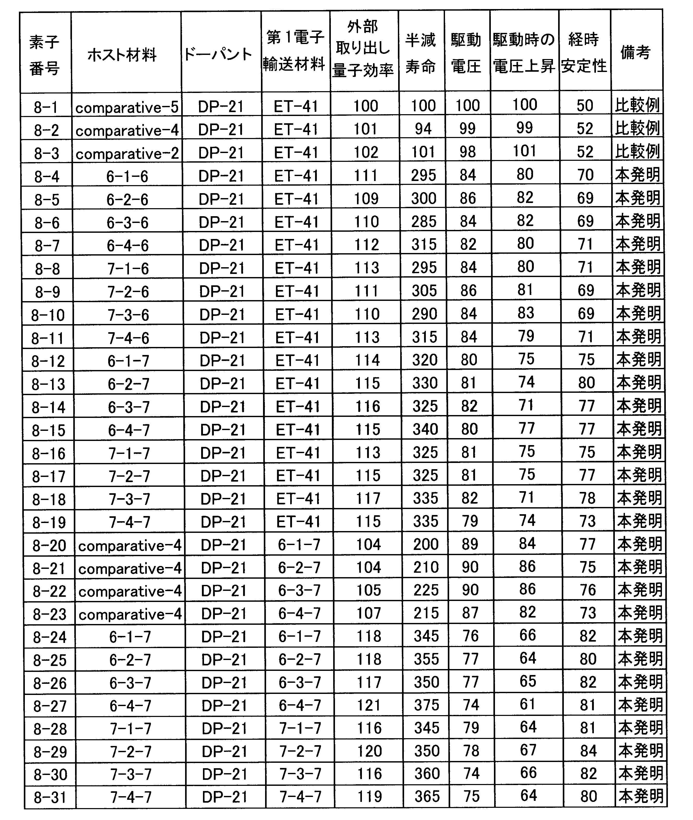
また、ウェットプロセスによる生産適性を更に有する有機エレクトロルミネッセンス素子材料、これを用いた有機エレクトロルミネッセンス素子、照明装置及び表示装置を提供することに適している。
3 画素
5 走査線
6 データ線
7 電源ライン
10 有機EL素子
11 スイッチングトランジスター
12 駆動トランジスター
13 コンデンサー
101 有機EL素子
102 ガラスカバー
105 陰極
106 有機EL層
107 透明電極付きガラス基板
108 窒素ガス
109 捕水剤
201 ガラス基板
202 ITO透明電極
203 隔壁
204 正孔注入層
205B、205G、205R 発光層
206 陰極
A 表示部
B 制御部
Claims (15)
- 下記一般式(1)で表される化合物であることを特徴とする有機エレクトロルミネッセンス素子材料。
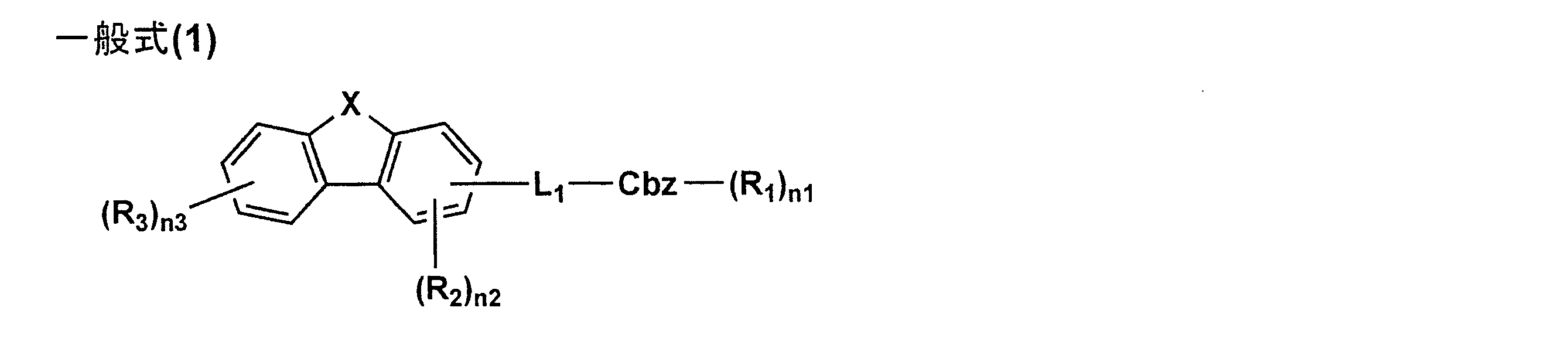
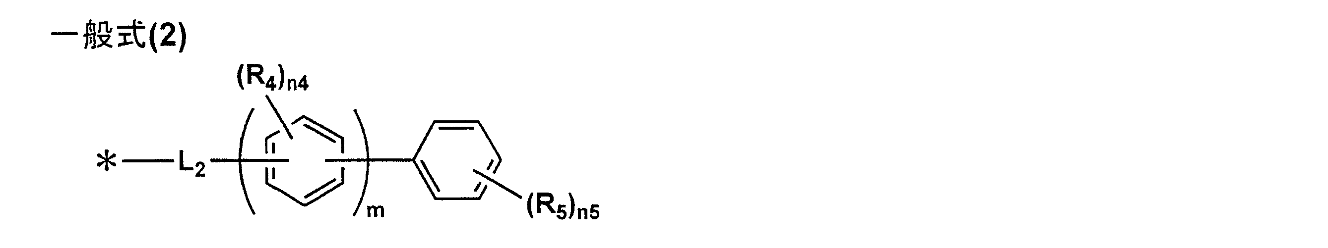
- 前記一般式(1)で表される化合物が、下記一般式(3)で表される化合物であることを特徴とする請求項1に記載の有機エレクトロルミネッセンス素子材料。

- 前記一般式(3)で表される化合物が、下記一般式(6)で表される化合物であることを特徴とする請求項2に記載の有機エレクトロルミネッセンス素子材料。

- 前記一般式(1)で表される化合物が、下記一般式(4)で表される化合物であることを特徴とする請求項1に記載の有機エレクトロルミネッセンス素子材料。
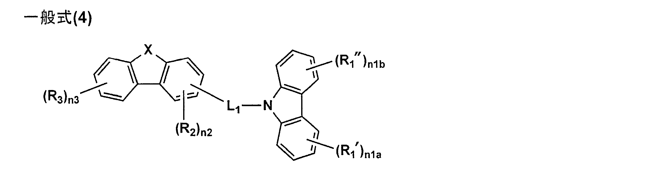
- 前記一般式(4)で表される化合物が、下記一般式(7)で表される化合物であることを特徴とする請求項4に記載の有機エレクトロルミネッセンス素子材料。
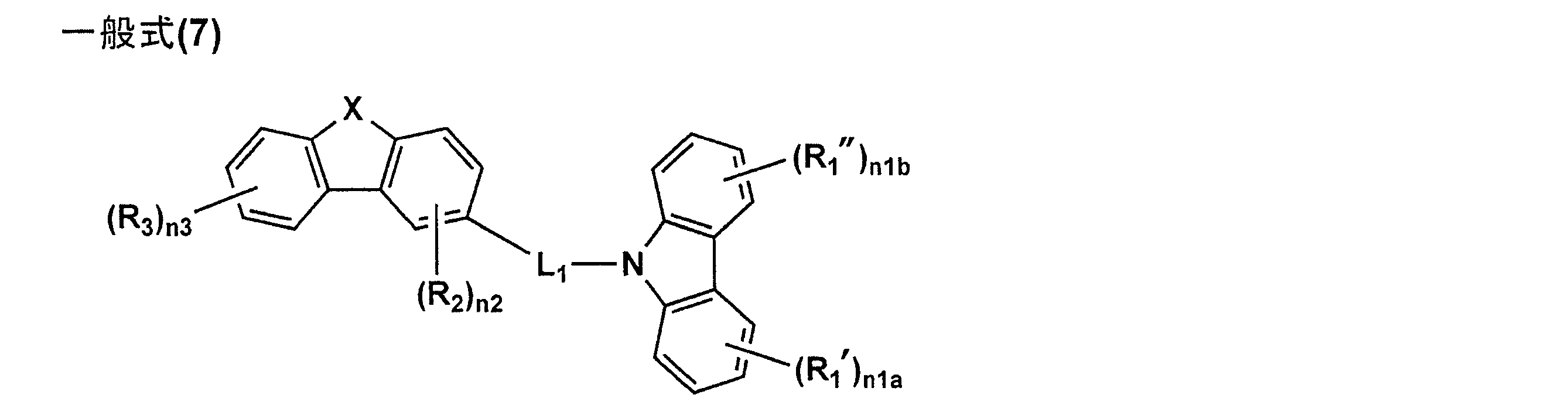
- 前記一般式(2)で表される基が、下記一般式(5)で表される基であることを特徴とする請求項1~5の何れか一項に記載の有機エレクトロルミネッセンス素子材料。
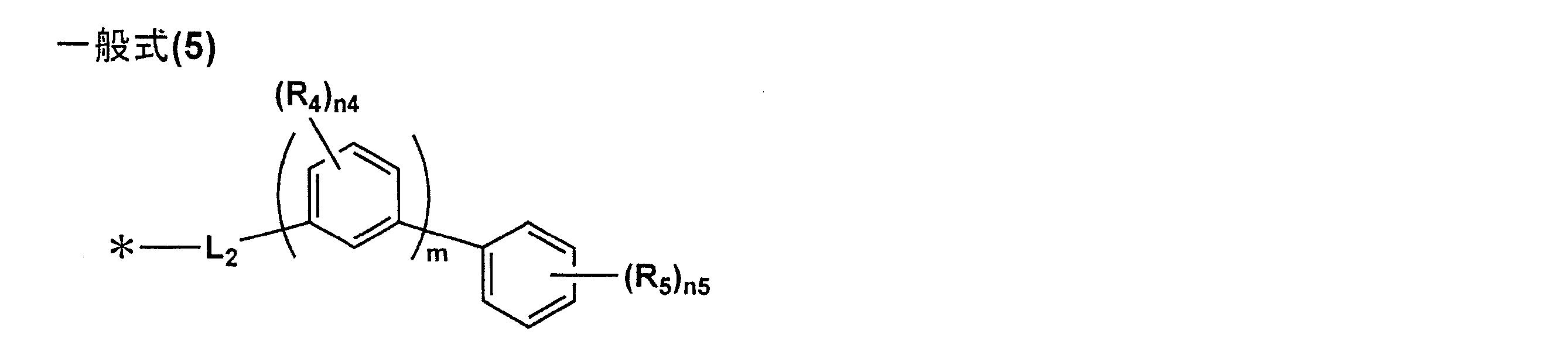
- 前記一般式(2)又は(5)におけるL2が、単結合を表すことを特徴とする請求項1~6の何れか一項に記載の有機エレクトロルミネッセンス素子材料。
- 前記一般式(2)又は(5)におけるmが、2~5の整数を表すことを特徴とする請求項1~7の何れか一項に記載の有機エレクトロルミネッセンス素子材料。
- 前記一般式(1)、(3)、(4)、(6)又は(7)において、L1が、単結合を表すことを特徴とする請求項1から8の何れか一項に記載の有機エレクトロルミネッセンス素子材料。
- 前記一般式(1)、(3)、(4)、(6)又は(7)において、Xが、酸素原子を表すことを特徴とする請求項1から9の何れか一項に記載の有機エレクトロルミネッセンス素子材料。
- 陽極と、陰極と、発光層を含む、単層又は複数層からなる有機層とを有し、前記有機層が前記陽極と前記陰極との間に挟持された有機エレクトロルミネッセンス素子において、
前記有機層の少なくとも1層に、請求項1から10の何れか一項に記載の有機エレクトロルミネッセンス素子材料が含有されていることを特徴とする有機エレクトロルミネッセンス素子。 - 前記有機層の少なくとも1層に更に下記一般式(DP)で表されるリン光発光性化合物が含有されていることを特徴とする請求項11に記載の有機エレクトロルミネッセンス素子。

- 発光色が白色であることを特徴とする請求項11又は12に記載の有機エレクトロルミネッセンス素子。
- 請求項11から13の何れか一項に記載の有機エレクトロルミネッセンス素子を備えたことを特徴とする照明装置。
- 請求項11から13の何れか一項に記載の有機エレクトロルミネッセンス素子を備えたことを特徴とする表示装置。
Priority Applications (6)
| Application Number | Priority Date | Filing Date | Title |
|---|---|---|---|
| KR1020157014994A KR101798738B1 (ko) | 2012-12-10 | 2013-12-02 | 유기 일렉트로루미네센스 소자 재료, 유기 일렉트로루미네센스 소자, 조명 장치 및 표시 장치 |
| JP2014551985A JP6428267B2 (ja) | 2012-12-10 | 2013-12-02 | 有機エレクトロルミネッセンス素子材料、有機エレクトロルミネッセンス素子、照明装置及び表示装置 |
| US14/650,753 US9944629B2 (en) | 2012-12-10 | 2013-12-02 | Material for organic electroluminescent element, organic electroluminescent element, illumination device, and display device |
| KR1020197000924A KR101995191B1 (ko) | 2012-12-10 | 2013-12-02 | 유기 일렉트로루미네센스 소자 재료, 유기 일렉트로루미네센스 소자, 조명 장치 및 표시 장치 |
| KR1020177032476A KR20170127065A (ko) | 2012-12-10 | 2013-12-02 | 유기 일렉트로루미네센스 소자 재료, 유기 일렉트로루미네센스 소자, 조명 장치 및 표시 장치 |
| EP13861633.9A EP2930762B1 (en) | 2012-12-10 | 2013-12-02 | Material for organic electroluminescent element, organic electroluminescent element, illumination device, and display device |
Applications Claiming Priority (4)
| Application Number | Priority Date | Filing Date | Title |
|---|---|---|---|
| JP2012269292 | 2012-12-10 | ||
| JP2012-269292 | 2012-12-10 | ||
| JP2013-007631 | 2013-01-18 | ||
| JP2013007631 | 2013-01-18 |
Publications (1)
| Publication Number | Publication Date |
|---|---|
| WO2014091958A1 true WO2014091958A1 (ja) | 2014-06-19 |
Family
ID=50934250
Family Applications (1)
| Application Number | Title | Priority Date | Filing Date |
|---|---|---|---|
| PCT/JP2013/082333 WO2014091958A1 (ja) | 2012-12-10 | 2013-12-02 | 有機エレクトロルミネッセンス素子材料、有機エレクトロルミネッセンス素子、照明装置及び表示装置 |
Country Status (5)
| Country | Link |
|---|---|
| US (1) | US9944629B2 (ja) |
| EP (1) | EP2930762B1 (ja) |
| JP (1) | JP6428267B2 (ja) |
| KR (3) | KR101995191B1 (ja) |
| WO (1) | WO2014091958A1 (ja) |
Cited By (12)
| Publication number | Priority date | Publication date | Assignee | Title |
|---|---|---|---|---|
| JP2013526042A (ja) * | 2010-04-28 | 2013-06-20 | コモンウェルス サイエンティフィック アンドインダストリアル リサーチ オーガナイゼーション | イリジウムおよび関連する第viii族の燐光性金属多環化合物に基づくエレクトロルミネセント素子 |
| EP3015464A1 (en) * | 2014-10-28 | 2016-05-04 | Samsung Display Co., Ltd. | Material for heterocyclic organic electroluminescent device and heterocyclic organic electroluminescent device including the same |
| WO2016089080A1 (ko) * | 2014-12-02 | 2016-06-09 | 주식회사 두산 | 유기 발광 화합물 및 이를 포함하는 유기 전계 발광 소자 |
| EP3072943A1 (en) | 2015-03-26 | 2016-09-28 | Idemitsu Kosan Co., Ltd. | Dibenzofuran/carbazole-substituted benzonitriles |
| JP2017222636A (ja) * | 2016-05-11 | 2017-12-21 | ヒソン・マテリアル・リミテッドHeesung Material Ltd. | ヘテロ環化合物およびこれを用いた有機発光素子 |
| JP2018024634A (ja) * | 2016-07-28 | 2018-02-15 | 東ソー株式会社 | 新規なカルバゾール化合物及びその用途 |
| JP2018522898A (ja) * | 2015-07-27 | 2018-08-16 | ヒソン・マテリアル・リミテッドHeesung Material Ltd. | ヘテロ環化合物およびこれを用いた有機発光素子 |
| JP2019505475A (ja) * | 2015-12-01 | 2019-02-28 | ドク サン ネオルクス カンパニー リミテッド | 有機電子素子用化合物、それを用いた有機電子素子及びその電子装置 |
| JP2019505478A (ja) * | 2015-12-08 | 2019-02-28 | ヒソン・マテリアル・リミテッドHeesung Material Ltd. | ヘテロ環化合物およびこれを用いた有機発光素子 |
| CN110256415A (zh) * | 2019-06-26 | 2019-09-20 | 上海天马有机发光显示技术有限公司 | 一种化合物、光提取材料、有机光电装置及电子设备 |
| CN112566908A (zh) * | 2018-08-13 | 2021-03-26 | 辛诺拉有限公司 | 用于光电器件的有机分子 |
| WO2023085047A1 (ja) * | 2021-11-09 | 2023-05-19 | キヤノン株式会社 | 有機発光素子 |
Families Citing this family (8)
| Publication number | Priority date | Publication date | Assignee | Title |
|---|---|---|---|---|
| CN105906549A (zh) * | 2016-04-28 | 2016-08-31 | 吉林奥来德光电材料股份有限公司 | 一种咔唑类化合物及其制备方法、有机电致发光器件 |
| KR101885899B1 (ko) | 2016-11-07 | 2018-08-06 | 주식회사 엘지화학 | 신규한 헤테로 고리 화합물 및 이를 이용한 유기발광 소자 |
| KR101915716B1 (ko) * | 2016-12-20 | 2018-11-08 | 희성소재 (주) | 유기 발광 소자 및 유기 발광 소자의 유기물층용 조성물 |
| KR102392679B1 (ko) * | 2017-05-23 | 2022-05-04 | 엘티소재주식회사 | 헤테로고리 화합물 및 이를 포함하는 유기 발광 소자 |
| KR102571401B1 (ko) * | 2018-06-01 | 2023-08-31 | 엘지디스플레이 주식회사 | 유기 화합물과 이를 포함하는 유기발광다이오드 및 유기발광 표시장치 |
| KR102628848B1 (ko) | 2018-08-10 | 2024-01-25 | 삼성디스플레이 주식회사 | 축합환 화합물 및 이를 포함하는 유기 발광 소자 |
| KR20200046229A (ko) * | 2018-10-23 | 2020-05-07 | 덕산네오룩스 주식회사 | 유기전기 소자용 화합물, 이를 이용한 유기전기소자 및 그 전자 장치 |
| CN112745285A (zh) * | 2019-10-31 | 2021-05-04 | 昱镭光电科技股份有限公司 | 胺基氧芴化合物及其有机电致发光器件 |
Citations (118)
| Publication number | Priority date | Publication date | Assignee | Title |
|---|---|---|---|---|
| JPS62172691A (ja) | 1986-01-24 | 1987-07-29 | 株式会社小松製作所 | 薄膜el素子 |
| US4774435A (en) | 1987-12-22 | 1988-09-27 | Gte Laboratories Incorporated | Thin film electroluminescent device |
| JPS63314795A (ja) | 1987-06-18 | 1988-12-22 | Komatsu Ltd | 薄膜el素子 |
| JPH01220394A (ja) | 1988-02-29 | 1989-09-04 | Hitachi Ltd | 高輝度el素子 |
| US5061569A (en) | 1990-07-26 | 1991-10-29 | Eastman Kodak Company | Electroluminescent device with organic electroluminescent medium |
| JPH04297076A (ja) | 1991-01-31 | 1992-10-21 | Toshiba Corp | 有機el素子 |
| JPH04308688A (ja) | 1991-04-08 | 1992-10-30 | Pioneer Electron Corp | 有機エレクトロルミネッセンス素子 |
| JPH06325871A (ja) | 1993-05-18 | 1994-11-25 | Mitsubishi Kasei Corp | 有機電界発光素子 |
| JPH08288069A (ja) | 1995-04-07 | 1996-11-01 | Sanyo Electric Co Ltd | 有機エレクトロルミネッセンス素子 |
| JPH0917574A (ja) | 1995-04-27 | 1997-01-17 | Pioneer Electron Corp | 有機エレクトロルミネッセンス素子 |
| JPH0945479A (ja) | 1995-07-27 | 1997-02-14 | Hewlett Packard Co <Hp> | 有機エレクトロルミネセンス装置及び有機エレクトロルミネセンス装置の製造方法 |
| JPH09260062A (ja) | 1996-03-25 | 1997-10-03 | Tdk Corp | 有機エレクトロルミネセンス素子 |
| JPH1074586A (ja) | 1996-07-29 | 1998-03-17 | Eastman Kodak Co | エレクトロルミネセンスデバイスで用いられる二層電子注入電極 |
| JPH11204359A (ja) | 1998-01-14 | 1999-07-30 | Tokin Corp | 圧粉磁芯の製造方法と製造装置 |
| JPH11204258A (ja) | 1998-01-09 | 1999-07-30 | Sony Corp | 電界発光素子及びその製造方法 |
| JPH11251067A (ja) | 1998-03-02 | 1999-09-17 | Junji Kido | 有機エレクトロルミネッセント素子 |
| JPH11283751A (ja) | 1998-03-27 | 1999-10-15 | Nec Corp | 有機エレクトロルミネッセンス素子 |
| JP2000196140A (ja) | 1998-12-28 | 2000-07-14 | Sharp Corp | 有機エレクトロルミネッセンス素子とその製造法 |
| WO2000070655A2 (en) | 1999-05-13 | 2000-11-23 | The Trustees Of Princeton University | Very high efficiency organic light emitting devices based on electrophosphorescence |
| JP2001102175A (ja) | 1999-09-29 | 2001-04-13 | Junji Kido | 有機エレクトロルミネッセント素子、有機エレクトロルミネッセント素子群及びその発光スペクトルの制御方法 |
| JP2001181616A (ja) | 1999-12-27 | 2001-07-03 | Fuji Photo Film Co Ltd | オルトメタル化パラジウム錯体からなる発光素子材料および発光素子 |
| JP2001181617A (ja) | 1999-12-27 | 2001-07-03 | Fuji Photo Film Co Ltd | オルトメタル化白金錯体からなる発光素子材料および発光素子 |
| JP2001202827A (ja) | 1999-11-10 | 2001-07-27 | Matsushita Electric Works Ltd | 透明導電性基板、発光素子、平面発光板、平面発光板の製造方法、平面蛍光ランプ、プラズマディスプレイ |
| JP2001247859A (ja) | 1999-12-27 | 2001-09-14 | Fuji Photo Film Co Ltd | オルトメタル化イリジウム錯体からなる発光素子材料、発光素子および新規イリジウム錯体 |
| JP2001257076A (ja) | 2000-03-13 | 2001-09-21 | Tdk Corp | 有機el素子 |
| JP2001313178A (ja) | 2000-04-28 | 2001-11-09 | Pioneer Electronic Corp | 有機エレクトロルミネッセンス素子 |
| JP2001313179A (ja) | 2000-05-01 | 2001-11-09 | Mitsubishi Chemicals Corp | 有機電界発光素子 |
| JP2001319780A (ja) | 2000-05-02 | 2001-11-16 | Fuji Photo Film Co Ltd | 発光素子 |
| JP2001319779A (ja) | 2000-05-02 | 2001-11-16 | Fuji Photo Film Co Ltd | 発光素子 |
| WO2001093642A1 (en) | 2000-05-30 | 2001-12-06 | The Trustees Of Princeton University | Phosphorescent organic light emitting devices |
| JP2001345183A (ja) | 2000-03-28 | 2001-12-14 | Fuji Photo Film Co Ltd | 高効率赤色発光素子、イリジウム錯体から成る発光素子材料及び新規イリジウム錯体 |
| JP2001357977A (ja) | 2000-06-12 | 2001-12-26 | Fuji Photo Film Co Ltd | 有機電界発光素子 |
| JP2002008860A (ja) | 2000-04-18 | 2002-01-11 | Mitsubishi Chemicals Corp | 有機電界発光素子 |
| JP2002015871A (ja) | 2000-04-27 | 2002-01-18 | Toray Ind Inc | 発光素子 |
| JP2002043056A (ja) | 2000-07-19 | 2002-02-08 | Canon Inc | 発光素子 |
| JP2002050483A (ja) | 2000-05-22 | 2002-02-15 | Showa Denko Kk | 有機エレクトロルミネッセンス素子および発光材料 |
| JP2002050484A (ja) | 2000-05-22 | 2002-02-15 | Semiconductor Energy Lab Co Ltd | 発光装置および電気器具 |
| WO2002015645A1 (en) | 2000-08-11 | 2002-02-21 | The Trustees Of Princeton University | Organometallic compounds and emission-shifting organic electrophosphorescence |
| JP2002062824A (ja) | 2000-06-05 | 2002-02-28 | Semiconductor Energy Lab Co Ltd | 発光装置 |
| JP2002075645A (ja) | 2000-08-29 | 2002-03-15 | Semiconductor Energy Lab Co Ltd | 発光装置 |
| JP2002083684A (ja) | 2000-06-23 | 2002-03-22 | Semiconductor Energy Lab Co Ltd | 発光装置 |
| JP2002100474A (ja) | 2000-09-25 | 2002-04-05 | Kyocera Corp | 有機エレクトロルミネッセンス素子 |
| JP2002100476A (ja) | 2000-07-17 | 2002-04-05 | Fuji Photo Film Co Ltd | 発光素子及びアゾール化合物 |
| JP2002105445A (ja) | 2000-09-29 | 2002-04-10 | Fuji Photo Film Co Ltd | 有機発光素子材料及びそれを用いた有機発光素子 |
| JP2002117978A (ja) | 2000-07-17 | 2002-04-19 | Fuji Photo Film Co Ltd | 発光素子及びイリジウム錯体 |
| JP2002141173A (ja) | 2000-08-22 | 2002-05-17 | Semiconductor Energy Lab Co Ltd | 発光装置 |
| JP2002170684A (ja) | 2000-09-21 | 2002-06-14 | Fuji Photo Film Co Ltd | 発光素子及びイリジウム錯体 |
| JP2002173674A (ja) | 2000-09-21 | 2002-06-21 | Fuji Photo Film Co Ltd | 発光素子および新規レニウム錯体 |
| JP2002175884A (ja) | 2000-09-26 | 2002-06-21 | Canon Inc | 発光素子及び発光素子用金属配位化合物 |
| JP2002184582A (ja) | 2000-09-28 | 2002-06-28 | Semiconductor Energy Lab Co Ltd | 発光装置 |
| JP2002203683A (ja) | 2000-10-30 | 2002-07-19 | Toyota Central Res & Dev Lab Inc | 有機電界発光素子 |
| JP2002203678A (ja) | 2000-12-27 | 2002-07-19 | Fuji Photo Film Co Ltd | 発光素子 |
| JP2002203679A (ja) | 2000-12-27 | 2002-07-19 | Fuji Photo Film Co Ltd | 発光素子 |
| JP2002525808A (ja) | 1998-09-14 | 2002-08-13 | ザ、トラスティーズ オブ プリンストン ユニバーシティ | 高効率の電界発光デバイスのための構造 |
| JP2002525833A (ja) | 1998-09-25 | 2002-08-13 | アイシス イノヴェイション リミテッド | 二価ランタノイド金属錯体 |
| JP2002226495A (ja) | 2000-11-29 | 2002-08-14 | Canon Inc | 金属配位化合物、発光素子及び表示装置 |
| JP2002231453A (ja) | 2000-11-30 | 2002-08-16 | Mitsubishi Chemicals Corp | 有機電界発光素子 |
| JP2002234888A (ja) | 2001-02-09 | 2002-08-23 | Mitsui Chemicals Inc | アミン化合物および該化合物を含有する有機電界発光素子 |
| JP2002234894A (ja) | 2000-11-29 | 2002-08-23 | Canon Inc | 金属配位化合物、発光素子及び表示装置 |
| JP2002235076A (ja) | 2001-02-09 | 2002-08-23 | Fuji Photo Film Co Ltd | 遷移金属錯体及びそれからなる発光素子用材料、並びに発光素子 |
| JP2002241751A (ja) | 2001-02-21 | 2002-08-28 | Fuji Photo Film Co Ltd | 発光素子用材料及び発光素子 |
| JP2002255934A (ja) | 2000-12-25 | 2002-09-11 | Fuji Photo Film Co Ltd | 新規化合物、その重合体、それらを利用した発光素子材料およびその発光素子 |
| JP2002260861A (ja) | 2001-01-02 | 2002-09-13 | Eastman Kodak Co | 有機発光デバイス |
| JP2002280183A (ja) | 2000-12-28 | 2002-09-27 | Toshiba Corp | 有機el素子および表示装置 |
| JP2002280178A (ja) | 2001-03-16 | 2002-09-27 | Canon Inc | 有機発光素子 |
| JP2002280180A (ja) | 2001-03-16 | 2002-09-27 | Canon Inc | 有機発光素子 |
| JP2002280179A (ja) | 2001-03-16 | 2002-09-27 | Canon Inc | 有機発光素子 |
| JP2002299060A (ja) | 2001-03-30 | 2002-10-11 | Fuji Photo Film Co Ltd | 有機発光素子 |
| JP2002302516A (ja) | 2001-04-03 | 2002-10-18 | Fuji Photo Film Co Ltd | 新規ポリマーおよびそれを用いた発光素子 |
| JP2002305083A (ja) | 2001-04-04 | 2002-10-18 | Mitsubishi Chemicals Corp | 有機電界発光素子 |
| JP2002305084A (ja) | 2000-12-25 | 2002-10-18 | Fuji Photo Film Co Ltd | 新規インドール誘導体およびそれを利用した発光素子 |
| JP2002302671A (ja) | 2000-02-10 | 2002-10-18 | Fuji Photo Film Co Ltd | イリジウム錯体からなる発光素子材料及び発光素子 |
| JP2002308837A (ja) | 2001-04-05 | 2002-10-23 | Fuji Photo Film Co Ltd | 新規化合物、およびそれを用いた発光素子 |
| JP2002308855A (ja) | 2001-04-05 | 2002-10-23 | Fuji Photo Film Co Ltd | 新規化合物、およびそれを用いた発光素子 |
| JP2002319491A (ja) | 2000-08-24 | 2002-10-31 | Fuji Photo Film Co Ltd | 発光素子及び新規重合体子 |
| JP2002324679A (ja) | 2001-04-26 | 2002-11-08 | Honda Motor Co Ltd | 有機エレクトロルミネッセンス素子 |
| JP2002334789A (ja) | 2001-03-09 | 2002-11-22 | Sony Corp | 有機電界発光素子 |
| JP2002332292A (ja) | 2001-03-08 | 2002-11-22 | Canon Inc | 金属配位化合物、電界発光素子及び表示装置 |
| JP2002334787A (ja) | 2001-03-09 | 2002-11-22 | Sony Corp | 有機電界発光素子 |
| JP2002332291A (ja) | 2001-03-08 | 2002-11-22 | Canon Inc | 金属配位化合物、電界発光素子及び表示装置 |
| JP2002334786A (ja) | 2001-03-09 | 2002-11-22 | Sony Corp | 有機電界発光素子 |
| JP2002334788A (ja) | 2001-03-09 | 2002-11-22 | Sony Corp | 有機電界発光素子 |
| JP2002540572A (ja) | 1999-03-23 | 2002-11-26 | ザ ユニバーシティー オブ サザン カリフォルニア | 有機ledの燐光性ドーパントとしてのシクロメタル化金属錯体 |
| JP2002338579A (ja) | 2001-03-16 | 2002-11-27 | Fuji Photo Film Co Ltd | ヘテロ環化合物及びそれを用いた発光素子 |
| JP2002338588A (ja) | 2001-03-14 | 2002-11-27 | Canon Inc | 金属配位化合物、電界発光素子及び表示装置 |
| JP2002343568A (ja) | 2001-05-10 | 2002-11-29 | Sony Corp | 有機電界発光素子 |
| JP2002343572A (ja) | 2001-03-14 | 2002-11-29 | Canon Inc | ポルフィリン誘導体化合物を用いた発光素子および表示装置 |
| JP2002352957A (ja) | 2001-05-23 | 2002-12-06 | Honda Motor Co Ltd | 有機エレクトロルミネッセンス素子 |
| JP2002352960A (ja) | 2001-05-29 | 2002-12-06 | Hitachi Ltd | 薄膜電界発光素子 |
| JP2002359082A (ja) | 2001-03-28 | 2002-12-13 | Semiconductor Energy Lab Co Ltd | 有機発光素子および前記素子を用いた発光装置 |
| JP2002363227A (ja) | 2001-04-03 | 2002-12-18 | Fuji Photo Film Co Ltd | 新規ポリマーおよびそれを用いた発光素子 |
| JP2002363552A (ja) | 2001-03-08 | 2002-12-18 | Univ Of Hong Kong | 有機金属発光材料 |
| JP2003003165A (ja) | 2001-06-25 | 2003-01-08 | Showa Denko Kk | 有機発光素子および発光材料 |
| JP2003007471A (ja) | 2001-04-13 | 2003-01-10 | Semiconductor Energy Lab Co Ltd | 有機発光素子および前記素子を用いた発光装置 |
| JP2003007469A (ja) | 2001-06-25 | 2003-01-10 | Canon Inc | 発光素子及び表示装置 |
| JP2003027048A (ja) | 2001-07-11 | 2003-01-29 | Fuji Photo Film Co Ltd | 発光素子 |
| JP2003031366A (ja) | 2001-07-11 | 2003-01-31 | Semiconductor Energy Lab Co Ltd | ドーパントを用いた有機発光素子および発光装置 |
| JP2003519432A (ja) | 1999-12-31 | 2003-06-17 | エルジー・ケミカル・カンパニー・リミテッド | p−型半導体性質を有する有機化合物を含む電子素子 |
| JP2004068143A (ja) | 2002-06-10 | 2004-03-04 | Konica Minolta Holdings Inc | 薄膜形成方法並びに該薄膜形成方法により薄膜が形成された基材 |
| JP2006135145A (ja) | 2004-11-08 | 2006-05-25 | Sony Corp | 表示素子用有機材料および表示素子 |
| WO2007132886A1 (ja) * | 2006-05-17 | 2007-11-22 | Konica Minolta Holdings, Inc. | 有機エレクトロルミネッセンス素子材料、有機エレクトロルミネッセンス素子、表示装置及び照明装置 |
| WO2009008099A1 (ja) | 2007-07-10 | 2009-01-15 | Idemitsu Kosan Co., Ltd. | 有機エレクトロルミネッセンス素子用材料及びそれを用いた有機エレクトロルミネッセンス素子 |
| US20090131673A1 (en) | 2005-05-30 | 2009-05-21 | Junichi Tanabe | Electroluminescent Device |
| US20100076201A1 (en) | 2008-09-19 | 2010-03-25 | Semiconductor Energy Laboratory Co., Ltd. | Carbazole Derivative and Method for Producing the Same |
| WO2010095621A1 (ja) * | 2009-02-18 | 2010-08-26 | 出光興産株式会社 | 芳香族アミン誘導体及び有機エレクトロルミネッセンス素子 |
| EP2301926A1 (en) | 2008-06-05 | 2011-03-30 | Idemitsu Kosan Co., Ltd. | Halogen compound, polycyclic compound, and organic electroluminescence element comprising the polycyclic compound |
| WO2011152596A1 (ko) * | 2010-06-01 | 2011-12-08 | 제일모직 주식회사 | 유기광전소자용 화합물 및 이를 포함하는 유기광전소자 |
| JP2012049518A (ja) | 2010-07-27 | 2012-03-08 | Konica Minolta Holdings Inc | 有機エレクトロルミネッセンス素子材料、化合物、有機エレクトロルミネッセンス素子、表示装置、並びに照明装置 |
| WO2012036482A1 (en) * | 2010-09-17 | 2012-03-22 | Rohm And Haas Electronic Materials Korea Ltd. | Novel organic electroluminescent compounds and organic electroluminescent device using the same |
| WO2012050371A1 (en) * | 2010-10-13 | 2012-04-19 | Rohm And Haas Electronic Materials Korea Ltd. | Novel compounds for organic electronic material and organic electroluminescent device using the same |
| WO2012134124A1 (en) * | 2011-03-25 | 2012-10-04 | Rohm And Haas Electronic Materials Korea Ltd. | Novel compounds for organic electronic material and organic electroluminescent device using the same |
| WO2012141499A1 (en) * | 2011-04-12 | 2012-10-18 | Rohm And Haas Electronic Materials Korea Ltd. | Novel compounds for organic electronic material and organic electroluminescent device using the same |
| WO2012150826A1 (en) * | 2011-05-03 | 2012-11-08 | Rohm And Haas Electronic Materials Korea Ltd. | Novel organic electroluminescent compounds and an organic electroluminescent device using the same |
| WO2012157211A1 (ja) * | 2011-05-13 | 2012-11-22 | ソニー株式会社 | 有機el多色発光装置 |
| WO2013039073A1 (ja) * | 2011-09-15 | 2013-03-21 | 出光興産株式会社 | 芳香族アミン誘導体およびそれを用いた有機エレクトロルミネッセンス素子 |
| WO2013073874A1 (en) * | 2011-11-18 | 2013-05-23 | Rohm And Haas Electronic Materials Korea Ltd. | Novel organic electroluminescent compounds and an organic electroluminescent device using the same |
| WO2013137001A1 (ja) * | 2012-03-12 | 2013-09-19 | 新日鉄住金化学株式会社 | 有機電界発光素子 |
| WO2013187689A1 (en) * | 2012-06-13 | 2013-12-19 | Rohm And Haas Electronic Materials Korea Ltd. | Novel organic electroluminescent compounds and organic electroluminescent device comprising the same |
Family Cites Families (6)
| Publication number | Priority date | Publication date | Assignee | Title |
|---|---|---|---|---|
| JP5742092B2 (ja) * | 2009-09-02 | 2015-07-01 | 三菱化学株式会社 | 有機化合物、電荷輸送材料、有機電界発光素子用組成物、有機電界発光素子、有機elディスプレイ及び有機el照明 |
| JP2011202389A (ja) * | 2010-03-25 | 2011-10-13 | Sumitomo Bakelite Co Ltd | 防水方法 |
| JP2012055107A (ja) * | 2010-09-02 | 2012-03-15 | Daikin Ind Ltd | リプル電圧検出方法 |
| JP5880274B2 (ja) * | 2012-05-21 | 2016-03-08 | コニカミノルタ株式会社 | 有機エレクトロルミネッセンス素子、照明装置及び表示装置 |
| JP6194645B2 (ja) | 2012-09-27 | 2017-09-13 | 東ソー株式会社 | アミン化合物及びその用途 |
| CN103848858A (zh) * | 2012-11-28 | 2014-06-11 | 海洋王照明科技股份有限公司 | 一种有机半导体材料、制备方法和电致发光器件 |
-
2013
- 2013-12-02 KR KR1020197000924A patent/KR101995191B1/ko active IP Right Grant
- 2013-12-02 KR KR1020157014994A patent/KR101798738B1/ko active IP Right Grant
- 2013-12-02 WO PCT/JP2013/082333 patent/WO2014091958A1/ja active Application Filing
- 2013-12-02 US US14/650,753 patent/US9944629B2/en active Active
- 2013-12-02 EP EP13861633.9A patent/EP2930762B1/en active Active
- 2013-12-02 KR KR1020177032476A patent/KR20170127065A/ko active Search and Examination
- 2013-12-02 JP JP2014551985A patent/JP6428267B2/ja active Active
Patent Citations (120)
| Publication number | Priority date | Publication date | Assignee | Title |
|---|---|---|---|---|
| JPS62172691A (ja) | 1986-01-24 | 1987-07-29 | 株式会社小松製作所 | 薄膜el素子 |
| JPS63314795A (ja) | 1987-06-18 | 1988-12-22 | Komatsu Ltd | 薄膜el素子 |
| US4774435A (en) | 1987-12-22 | 1988-09-27 | Gte Laboratories Incorporated | Thin film electroluminescent device |
| JPH01220394A (ja) | 1988-02-29 | 1989-09-04 | Hitachi Ltd | 高輝度el素子 |
| US5061569A (en) | 1990-07-26 | 1991-10-29 | Eastman Kodak Company | Electroluminescent device with organic electroluminescent medium |
| JPH04297076A (ja) | 1991-01-31 | 1992-10-21 | Toshiba Corp | 有機el素子 |
| JPH04308688A (ja) | 1991-04-08 | 1992-10-30 | Pioneer Electron Corp | 有機エレクトロルミネッセンス素子 |
| JPH06325871A (ja) | 1993-05-18 | 1994-11-25 | Mitsubishi Kasei Corp | 有機電界発光素子 |
| JPH08288069A (ja) | 1995-04-07 | 1996-11-01 | Sanyo Electric Co Ltd | 有機エレクトロルミネッセンス素子 |
| JPH0917574A (ja) | 1995-04-27 | 1997-01-17 | Pioneer Electron Corp | 有機エレクトロルミネッセンス素子 |
| JPH0945479A (ja) | 1995-07-27 | 1997-02-14 | Hewlett Packard Co <Hp> | 有機エレクトロルミネセンス装置及び有機エレクトロルミネセンス装置の製造方法 |
| JPH09260062A (ja) | 1996-03-25 | 1997-10-03 | Tdk Corp | 有機エレクトロルミネセンス素子 |
| JPH1074586A (ja) | 1996-07-29 | 1998-03-17 | Eastman Kodak Co | エレクトロルミネセンスデバイスで用いられる二層電子注入電極 |
| JPH11204258A (ja) | 1998-01-09 | 1999-07-30 | Sony Corp | 電界発光素子及びその製造方法 |
| JPH11204359A (ja) | 1998-01-14 | 1999-07-30 | Tokin Corp | 圧粉磁芯の製造方法と製造装置 |
| JPH11251067A (ja) | 1998-03-02 | 1999-09-17 | Junji Kido | 有機エレクトロルミネッセント素子 |
| JPH11283751A (ja) | 1998-03-27 | 1999-10-15 | Nec Corp | 有機エレクトロルミネッセンス素子 |
| JP2002525808A (ja) | 1998-09-14 | 2002-08-13 | ザ、トラスティーズ オブ プリンストン ユニバーシティ | 高効率の電界発光デバイスのための構造 |
| JP2002525833A (ja) | 1998-09-25 | 2002-08-13 | アイシス イノヴェイション リミテッド | 二価ランタノイド金属錯体 |
| JP2000196140A (ja) | 1998-12-28 | 2000-07-14 | Sharp Corp | 有機エレクトロルミネッセンス素子とその製造法 |
| JP2002540572A (ja) | 1999-03-23 | 2002-11-26 | ザ ユニバーシティー オブ サザン カリフォルニア | 有機ledの燐光性ドーパントとしてのシクロメタル化金属錯体 |
| WO2000070655A2 (en) | 1999-05-13 | 2000-11-23 | The Trustees Of Princeton University | Very high efficiency organic light emitting devices based on electrophosphorescence |
| JP2001102175A (ja) | 1999-09-29 | 2001-04-13 | Junji Kido | 有機エレクトロルミネッセント素子、有機エレクトロルミネッセント素子群及びその発光スペクトルの制御方法 |
| JP2001202827A (ja) | 1999-11-10 | 2001-07-27 | Matsushita Electric Works Ltd | 透明導電性基板、発光素子、平面発光板、平面発光板の製造方法、平面蛍光ランプ、プラズマディスプレイ |
| JP2001181616A (ja) | 1999-12-27 | 2001-07-03 | Fuji Photo Film Co Ltd | オルトメタル化パラジウム錯体からなる発光素子材料および発光素子 |
| JP2001247859A (ja) | 1999-12-27 | 2001-09-14 | Fuji Photo Film Co Ltd | オルトメタル化イリジウム錯体からなる発光素子材料、発光素子および新規イリジウム錯体 |
| JP2001181617A (ja) | 1999-12-27 | 2001-07-03 | Fuji Photo Film Co Ltd | オルトメタル化白金錯体からなる発光素子材料および発光素子 |
| JP2003519432A (ja) | 1999-12-31 | 2003-06-17 | エルジー・ケミカル・カンパニー・リミテッド | p−型半導体性質を有する有機化合物を含む電子素子 |
| JP2002302671A (ja) | 2000-02-10 | 2002-10-18 | Fuji Photo Film Co Ltd | イリジウム錯体からなる発光素子材料及び発光素子 |
| JP2001257076A (ja) | 2000-03-13 | 2001-09-21 | Tdk Corp | 有機el素子 |
| JP2001345183A (ja) | 2000-03-28 | 2001-12-14 | Fuji Photo Film Co Ltd | 高効率赤色発光素子、イリジウム錯体から成る発光素子材料及び新規イリジウム錯体 |
| JP2002008860A (ja) | 2000-04-18 | 2002-01-11 | Mitsubishi Chemicals Corp | 有機電界発光素子 |
| JP2002015871A (ja) | 2000-04-27 | 2002-01-18 | Toray Ind Inc | 発光素子 |
| JP2001313178A (ja) | 2000-04-28 | 2001-11-09 | Pioneer Electronic Corp | 有機エレクトロルミネッセンス素子 |
| JP2001313179A (ja) | 2000-05-01 | 2001-11-09 | Mitsubishi Chemicals Corp | 有機電界発光素子 |
| JP2001319780A (ja) | 2000-05-02 | 2001-11-16 | Fuji Photo Film Co Ltd | 発光素子 |
| JP2001319779A (ja) | 2000-05-02 | 2001-11-16 | Fuji Photo Film Co Ltd | 発光素子 |
| JP2002050483A (ja) | 2000-05-22 | 2002-02-15 | Showa Denko Kk | 有機エレクトロルミネッセンス素子および発光材料 |
| JP2002050484A (ja) | 2000-05-22 | 2002-02-15 | Semiconductor Energy Lab Co Ltd | 発光装置および電気器具 |
| WO2001093642A1 (en) | 2000-05-30 | 2001-12-06 | The Trustees Of Princeton University | Phosphorescent organic light emitting devices |
| JP2002062824A (ja) | 2000-06-05 | 2002-02-28 | Semiconductor Energy Lab Co Ltd | 発光装置 |
| JP2001357977A (ja) | 2000-06-12 | 2001-12-26 | Fuji Photo Film Co Ltd | 有機電界発光素子 |
| JP2002083684A (ja) | 2000-06-23 | 2002-03-22 | Semiconductor Energy Lab Co Ltd | 発光装置 |
| JP2002100476A (ja) | 2000-07-17 | 2002-04-05 | Fuji Photo Film Co Ltd | 発光素子及びアゾール化合物 |
| JP2002117978A (ja) | 2000-07-17 | 2002-04-19 | Fuji Photo Film Co Ltd | 発光素子及びイリジウム錯体 |
| JP2002043056A (ja) | 2000-07-19 | 2002-02-08 | Canon Inc | 発光素子 |
| WO2002015645A1 (en) | 2000-08-11 | 2002-02-21 | The Trustees Of Princeton University | Organometallic compounds and emission-shifting organic electrophosphorescence |
| JP2002141173A (ja) | 2000-08-22 | 2002-05-17 | Semiconductor Energy Lab Co Ltd | 発光装置 |
| JP2002319491A (ja) | 2000-08-24 | 2002-10-31 | Fuji Photo Film Co Ltd | 発光素子及び新規重合体子 |
| JP2002075645A (ja) | 2000-08-29 | 2002-03-15 | Semiconductor Energy Lab Co Ltd | 発光装置 |
| JP2002173674A (ja) | 2000-09-21 | 2002-06-21 | Fuji Photo Film Co Ltd | 発光素子および新規レニウム錯体 |
| JP2002170684A (ja) | 2000-09-21 | 2002-06-14 | Fuji Photo Film Co Ltd | 発光素子及びイリジウム錯体 |
| JP2002100474A (ja) | 2000-09-25 | 2002-04-05 | Kyocera Corp | 有機エレクトロルミネッセンス素子 |
| JP2002175884A (ja) | 2000-09-26 | 2002-06-21 | Canon Inc | 発光素子及び発光素子用金属配位化合物 |
| JP2002184582A (ja) | 2000-09-28 | 2002-06-28 | Semiconductor Energy Lab Co Ltd | 発光装置 |
| JP2002105445A (ja) | 2000-09-29 | 2002-04-10 | Fuji Photo Film Co Ltd | 有機発光素子材料及びそれを用いた有機発光素子 |
| JP2002203683A (ja) | 2000-10-30 | 2002-07-19 | Toyota Central Res & Dev Lab Inc | 有機電界発光素子 |
| JP2002226495A (ja) | 2000-11-29 | 2002-08-14 | Canon Inc | 金属配位化合物、発光素子及び表示装置 |
| JP2002234894A (ja) | 2000-11-29 | 2002-08-23 | Canon Inc | 金属配位化合物、発光素子及び表示装置 |
| JP2002231453A (ja) | 2000-11-30 | 2002-08-16 | Mitsubishi Chemicals Corp | 有機電界発光素子 |
| JP2002255934A (ja) | 2000-12-25 | 2002-09-11 | Fuji Photo Film Co Ltd | 新規化合物、その重合体、それらを利用した発光素子材料およびその発光素子 |
| JP2002305084A (ja) | 2000-12-25 | 2002-10-18 | Fuji Photo Film Co Ltd | 新規インドール誘導体およびそれを利用した発光素子 |
| JP2002203679A (ja) | 2000-12-27 | 2002-07-19 | Fuji Photo Film Co Ltd | 発光素子 |
| JP2002203678A (ja) | 2000-12-27 | 2002-07-19 | Fuji Photo Film Co Ltd | 発光素子 |
| JP2002280183A (ja) | 2000-12-28 | 2002-09-27 | Toshiba Corp | 有機el素子および表示装置 |
| JP2002260861A (ja) | 2001-01-02 | 2002-09-13 | Eastman Kodak Co | 有機発光デバイス |
| JP2002235076A (ja) | 2001-02-09 | 2002-08-23 | Fuji Photo Film Co Ltd | 遷移金属錯体及びそれからなる発光素子用材料、並びに発光素子 |
| JP2002234888A (ja) | 2001-02-09 | 2002-08-23 | Mitsui Chemicals Inc | アミン化合物および該化合物を含有する有機電界発光素子 |
| JP2002241751A (ja) | 2001-02-21 | 2002-08-28 | Fuji Photo Film Co Ltd | 発光素子用材料及び発光素子 |
| JP2002332292A (ja) | 2001-03-08 | 2002-11-22 | Canon Inc | 金属配位化合物、電界発光素子及び表示装置 |
| JP2002363552A (ja) | 2001-03-08 | 2002-12-18 | Univ Of Hong Kong | 有機金属発光材料 |
| JP2002332291A (ja) | 2001-03-08 | 2002-11-22 | Canon Inc | 金属配位化合物、電界発光素子及び表示装置 |
| JP2002334787A (ja) | 2001-03-09 | 2002-11-22 | Sony Corp | 有機電界発光素子 |
| JP2002334788A (ja) | 2001-03-09 | 2002-11-22 | Sony Corp | 有機電界発光素子 |
| JP2002334786A (ja) | 2001-03-09 | 2002-11-22 | Sony Corp | 有機電界発光素子 |
| JP2002334789A (ja) | 2001-03-09 | 2002-11-22 | Sony Corp | 有機電界発光素子 |
| JP2002343572A (ja) | 2001-03-14 | 2002-11-29 | Canon Inc | ポルフィリン誘導体化合物を用いた発光素子および表示装置 |
| JP2002338588A (ja) | 2001-03-14 | 2002-11-27 | Canon Inc | 金属配位化合物、電界発光素子及び表示装置 |
| JP2002280178A (ja) | 2001-03-16 | 2002-09-27 | Canon Inc | 有機発光素子 |
| JP2002280179A (ja) | 2001-03-16 | 2002-09-27 | Canon Inc | 有機発光素子 |
| JP2002338579A (ja) | 2001-03-16 | 2002-11-27 | Fuji Photo Film Co Ltd | ヘテロ環化合物及びそれを用いた発光素子 |
| JP2002280180A (ja) | 2001-03-16 | 2002-09-27 | Canon Inc | 有機発光素子 |
| JP2002359082A (ja) | 2001-03-28 | 2002-12-13 | Semiconductor Energy Lab Co Ltd | 有機発光素子および前記素子を用いた発光装置 |
| JP2002299060A (ja) | 2001-03-30 | 2002-10-11 | Fuji Photo Film Co Ltd | 有機発光素子 |
| JP2002302516A (ja) | 2001-04-03 | 2002-10-18 | Fuji Photo Film Co Ltd | 新規ポリマーおよびそれを用いた発光素子 |
| JP2002363227A (ja) | 2001-04-03 | 2002-12-18 | Fuji Photo Film Co Ltd | 新規ポリマーおよびそれを用いた発光素子 |
| JP2002305083A (ja) | 2001-04-04 | 2002-10-18 | Mitsubishi Chemicals Corp | 有機電界発光素子 |
| JP2002308855A (ja) | 2001-04-05 | 2002-10-23 | Fuji Photo Film Co Ltd | 新規化合物、およびそれを用いた発光素子 |
| JP2002308837A (ja) | 2001-04-05 | 2002-10-23 | Fuji Photo Film Co Ltd | 新規化合物、およびそれを用いた発光素子 |
| JP2003007471A (ja) | 2001-04-13 | 2003-01-10 | Semiconductor Energy Lab Co Ltd | 有機発光素子および前記素子を用いた発光装置 |
| JP2002324679A (ja) | 2001-04-26 | 2002-11-08 | Honda Motor Co Ltd | 有機エレクトロルミネッセンス素子 |
| JP2002343568A (ja) | 2001-05-10 | 2002-11-29 | Sony Corp | 有機電界発光素子 |
| JP2002352957A (ja) | 2001-05-23 | 2002-12-06 | Honda Motor Co Ltd | 有機エレクトロルミネッセンス素子 |
| JP2002352960A (ja) | 2001-05-29 | 2002-12-06 | Hitachi Ltd | 薄膜電界発光素子 |
| JP2003003165A (ja) | 2001-06-25 | 2003-01-08 | Showa Denko Kk | 有機発光素子および発光材料 |
| JP2003007469A (ja) | 2001-06-25 | 2003-01-10 | Canon Inc | 発光素子及び表示装置 |
| JP2003031366A (ja) | 2001-07-11 | 2003-01-31 | Semiconductor Energy Lab Co Ltd | ドーパントを用いた有機発光素子および発光装置 |
| JP2003027048A (ja) | 2001-07-11 | 2003-01-29 | Fuji Photo Film Co Ltd | 発光素子 |
| JP2004068143A (ja) | 2002-06-10 | 2004-03-04 | Konica Minolta Holdings Inc | 薄膜形成方法並びに該薄膜形成方法により薄膜が形成された基材 |
| JP2006135145A (ja) | 2004-11-08 | 2006-05-25 | Sony Corp | 表示素子用有機材料および表示素子 |
| US20090131673A1 (en) | 2005-05-30 | 2009-05-21 | Junichi Tanabe | Electroluminescent Device |
| WO2007132886A1 (ja) * | 2006-05-17 | 2007-11-22 | Konica Minolta Holdings, Inc. | 有機エレクトロルミネッセンス素子材料、有機エレクトロルミネッセンス素子、表示装置及び照明装置 |
| WO2009008099A1 (ja) | 2007-07-10 | 2009-01-15 | Idemitsu Kosan Co., Ltd. | 有機エレクトロルミネッセンス素子用材料及びそれを用いた有機エレクトロルミネッセンス素子 |
| WO2009008100A1 (ja) | 2007-07-10 | 2009-01-15 | Idemitsu Kosan Co., Ltd. | 有機エレクトロルミネッセンス素子用材料及びそれを用いた有機エレクトロルミネッセンス素子 |
| US8114530B2 (en) | 2007-07-10 | 2012-02-14 | Idemitsu Kosan Co., Ltd. | Material for organic electroluminescence device and organic electroluminescence device utilizing the same |
| EP2301926A1 (en) | 2008-06-05 | 2011-03-30 | Idemitsu Kosan Co., Ltd. | Halogen compound, polycyclic compound, and organic electroluminescence element comprising the polycyclic compound |
| US20100076201A1 (en) | 2008-09-19 | 2010-03-25 | Semiconductor Energy Laboratory Co., Ltd. | Carbazole Derivative and Method for Producing the Same |
| WO2010095621A1 (ja) * | 2009-02-18 | 2010-08-26 | 出光興産株式会社 | 芳香族アミン誘導体及び有機エレクトロルミネッセンス素子 |
| WO2011152596A1 (ko) * | 2010-06-01 | 2011-12-08 | 제일모직 주식회사 | 유기광전소자용 화합물 및 이를 포함하는 유기광전소자 |
| JP2012049518A (ja) | 2010-07-27 | 2012-03-08 | Konica Minolta Holdings Inc | 有機エレクトロルミネッセンス素子材料、化合物、有機エレクトロルミネッセンス素子、表示装置、並びに照明装置 |
| WO2012036482A1 (en) * | 2010-09-17 | 2012-03-22 | Rohm And Haas Electronic Materials Korea Ltd. | Novel organic electroluminescent compounds and organic electroluminescent device using the same |
| WO2012050371A1 (en) * | 2010-10-13 | 2012-04-19 | Rohm And Haas Electronic Materials Korea Ltd. | Novel compounds for organic electronic material and organic electroluminescent device using the same |
| WO2012134124A1 (en) * | 2011-03-25 | 2012-10-04 | Rohm And Haas Electronic Materials Korea Ltd. | Novel compounds for organic electronic material and organic electroluminescent device using the same |
| WO2012141499A1 (en) * | 2011-04-12 | 2012-10-18 | Rohm And Haas Electronic Materials Korea Ltd. | Novel compounds for organic electronic material and organic electroluminescent device using the same |
| WO2012150826A1 (en) * | 2011-05-03 | 2012-11-08 | Rohm And Haas Electronic Materials Korea Ltd. | Novel organic electroluminescent compounds and an organic electroluminescent device using the same |
| WO2012157211A1 (ja) * | 2011-05-13 | 2012-11-22 | ソニー株式会社 | 有機el多色発光装置 |
| WO2013039073A1 (ja) * | 2011-09-15 | 2013-03-21 | 出光興産株式会社 | 芳香族アミン誘導体およびそれを用いた有機エレクトロルミネッセンス素子 |
| WO2013073874A1 (en) * | 2011-11-18 | 2013-05-23 | Rohm And Haas Electronic Materials Korea Ltd. | Novel organic electroluminescent compounds and an organic electroluminescent device using the same |
| WO2013137001A1 (ja) * | 2012-03-12 | 2013-09-19 | 新日鉄住金化学株式会社 | 有機電界発光素子 |
| WO2013187689A1 (en) * | 2012-06-13 | 2013-12-19 | Rohm And Haas Electronic Materials Korea Ltd. | Novel organic electroluminescent compounds and organic electroluminescent device comprising the same |
Non-Patent Citations (11)
| Title |
|---|
| "Bunko II of Jikken Kagaku Koza 7 (Spectroscopy II, Experimental Chemistry 7) (4th Edition)", 1992, MARUZEN COMPANY, LIMITED, pages: 398 |
| "Shinpen Shikisai Kagaku Handobukku (New Scientific Handbook of Color", 1985, UNIVERSITY OF TOKYO PRESS, pages: 108 |
| ANGEWANDTE CHEMIE INTERNATIONAL, 2010, pages 10214 - 10216 |
| APPL. PHYS. LETT., vol. 95, 2009, pages 243303 |
| J. APPL. PHYS., vol. 95, 2004, pages 5773 |
| J. HUANG ET AL., APPLIED PHYSICS LETTERS, vol. 80, 2002, pages 139 |
| See also references of EP2930762A4 |
| THE JOURNAL OF ORGANIC CHEMISTRY, 1997, pages 1348 - 1355 |
| THE JOURNAL OF ORGANIC CHEMISTRY, 2009, pages 4490 - 4498 |
| YUKI EL SOSHI: "Sonokougyouka Saizensen (Organic EL elements and Their Frontiers of Industrial Applications)", vol. 2, 30 November 1998, NTS INC., article "Chapter 2 "Denkyoku zairyo (Electrode material)", pages: 123 - 166 |
| YUKI EL SOSHI; SONOKOUGYOUKA SAIZENSEN: "Organic EL elements and Their Frontiers of Industrial Applications", 30 November 1998, NTS INC., pages: 237 |
Cited By (16)
| Publication number | Priority date | Publication date | Assignee | Title |
|---|---|---|---|---|
| JP2013526042A (ja) * | 2010-04-28 | 2013-06-20 | コモンウェルス サイエンティフィック アンドインダストリアル リサーチ オーガナイゼーション | イリジウムおよび関連する第viii族の燐光性金属多環化合物に基づくエレクトロルミネセント素子 |
| EP3015464A1 (en) * | 2014-10-28 | 2016-05-04 | Samsung Display Co., Ltd. | Material for heterocyclic organic electroluminescent device and heterocyclic organic electroluminescent device including the same |
| US9590186B2 (en) | 2014-10-28 | 2017-03-07 | Samsung Display Co., Ltd. | Material for organic electroluminescent device and organic electroluminescent device including the same |
| EP3214080A1 (en) * | 2014-10-28 | 2017-09-06 | Samsung Display Co., Ltd. | Material for heterocyclic organic electroluminescent device and heterocyclic organic electroluminescent device including the same |
| US11050025B2 (en) | 2014-10-28 | 2021-06-29 | Samsung Display Co., Ltd. | Material for organic electroluminescent device and organic electroluminescent device including the same |
| WO2016089080A1 (ko) * | 2014-12-02 | 2016-06-09 | 주식회사 두산 | 유기 발광 화합물 및 이를 포함하는 유기 전계 발광 소자 |
| EP3072943A1 (en) | 2015-03-26 | 2016-09-28 | Idemitsu Kosan Co., Ltd. | Dibenzofuran/carbazole-substituted benzonitriles |
| JP2018522898A (ja) * | 2015-07-27 | 2018-08-16 | ヒソン・マテリアル・リミテッドHeesung Material Ltd. | ヘテロ環化合物およびこれを用いた有機発光素子 |
| US10381577B2 (en) | 2015-07-27 | 2019-08-13 | Heesung Material Ltd. | Hetero-cyclic compound and organic light emitting device using the same |
| JP2019505475A (ja) * | 2015-12-01 | 2019-02-28 | ドク サン ネオルクス カンパニー リミテッド | 有機電子素子用化合物、それを用いた有機電子素子及びその電子装置 |
| JP2019505478A (ja) * | 2015-12-08 | 2019-02-28 | ヒソン・マテリアル・リミテッドHeesung Material Ltd. | ヘテロ環化合物およびこれを用いた有機発光素子 |
| JP2017222636A (ja) * | 2016-05-11 | 2017-12-21 | ヒソン・マテリアル・リミテッドHeesung Material Ltd. | ヘテロ環化合物およびこれを用いた有機発光素子 |
| JP2018024634A (ja) * | 2016-07-28 | 2018-02-15 | 東ソー株式会社 | 新規なカルバゾール化合物及びその用途 |
| CN112566908A (zh) * | 2018-08-13 | 2021-03-26 | 辛诺拉有限公司 | 用于光电器件的有机分子 |
| CN110256415A (zh) * | 2019-06-26 | 2019-09-20 | 上海天马有机发光显示技术有限公司 | 一种化合物、光提取材料、有机光电装置及电子设备 |
| WO2023085047A1 (ja) * | 2021-11-09 | 2023-05-19 | キヤノン株式会社 | 有機発光素子 |
Also Published As
| Publication number | Publication date |
|---|---|
| JPWO2014091958A1 (ja) | 2017-01-05 |
| KR101798738B1 (ko) | 2017-11-16 |
| KR20190006608A (ko) | 2019-01-18 |
| EP2930762A1 (en) | 2015-10-14 |
| KR101995191B1 (ko) | 2019-07-02 |
| EP2930762A4 (en) | 2016-11-02 |
| US20150322337A1 (en) | 2015-11-12 |
| EP2930762B1 (en) | 2020-09-16 |
| KR20170127065A (ko) | 2017-11-20 |
| US9944629B2 (en) | 2018-04-17 |
| JP6428267B2 (ja) | 2018-11-28 |
| KR20150081451A (ko) | 2015-07-14 |
Similar Documents
| Publication | Publication Date | Title |
|---|---|---|
| JP6428267B2 (ja) | 有機エレクトロルミネッセンス素子材料、有機エレクトロルミネッセンス素子、照明装置及び表示装置 | |
| JP5747736B2 (ja) | 有機エレクトロルミネッセンス素子、表示装置及び照明装置 | |
| JP5978843B2 (ja) | イリジウム錯体化合物、有機エレクトロルミネッセンス素子材料、有機エレクトロルミネッセンス素子、照明装置及び表示装置 | |
| JP5880274B2 (ja) | 有機エレクトロルミネッセンス素子、照明装置及び表示装置 | |
| JP5742581B2 (ja) | 有機エレクトロルミネッセンス素子、表示装置、照明装置 | |
| WO2013168688A1 (ja) | 有機エレクトロルミネッセンス素子、照明装置及び表示装置 | |
| JP6020112B2 (ja) | 有機エレクトロルミネッセンス素子材料及び有機エレクトロルミネッセンス素子 | |
| JP6146415B2 (ja) | 有機エレクトロルミネッセンス素子、照明装置及び表示装置 | |
| JP5884626B2 (ja) | 有機エレクトロルミネッセンス素子、表示装置及び照明装置 | |
| JP6011542B2 (ja) | 有機エレクトロルミネッセンス素子、表示装置及び照明装置 | |
| JP2015213119A (ja) | 有機エレクトロルミネッセンス素子用材料、有機エレクトロルミネッセンス素子、照明装置及び表示装置 | |
| JP2014111549A (ja) | イリジウム錯体、有機エレクトロルミネッセンス素子材料およびこれを用いた有機エレクトロルミネッセンス素子 | |
| JP5849867B2 (ja) | 有機エレクトロルミネッセンス素子、表示装置及び照明装置 | |
| JP6187214B2 (ja) | 金属錯体、有機エレクトロルミネッセンス素子材料、有機エレクトロルミネッセンス素子、表示装置及び照明装置 | |
| WO2016056562A1 (ja) | イリジウム錯体、有機エレクトロルミネッセンス材料、有機エレクトロルミネッセンス素子、表示装置及び照明装置 | |
| JP6020473B2 (ja) | イリジウム錯体化合物、有機エレクトロルミネッセンス素子材料、有機エレクトロルミネッセンス素子、照明装置及び表示装置 | |
| WO2016175068A1 (ja) | 有機エレクトロルミネッセンス素子用材料、有機エレクトロルミネッセンス素子、表示装置及び照明装置 | |
| JP6020466B2 (ja) | 有機エレクトロルミネッセンス素子、表示装置及び照明装置 | |
| JP5817640B2 (ja) | 有機エレクトロルミネッセンス素子、照明装置及び表示装置 | |
| JP5924401B2 (ja) | 有機エレクトロルミネッセンス素子、照明装置及び表示装置 | |
| JP6011616B2 (ja) | 有機エレクトロルミネッセンス素子 |
Legal Events
| Date | Code | Title | Description |
|---|---|---|---|
| 121 | Ep: the epo has been informed by wipo that ep was designated in this application |
Ref document number: 13861633 Country of ref document: EP Kind code of ref document: A1 |
|
| ENP | Entry into the national phase |
Ref document number: 2014551985 Country of ref document: JP Kind code of ref document: A |
|
| ENP | Entry into the national phase |
Ref document number: 20157014994 Country of ref document: KR Kind code of ref document: A |
|
| WWE | Wipo information: entry into national phase |
Ref document number: 14650753 Country of ref document: US |
|
| NENP | Non-entry into the national phase |
Ref country code: DE |
|
| WWE | Wipo information: entry into national phase |
Ref document number: 2013861633 Country of ref document: EP |