WO2015022974A1 - Organic electroluminescent element - Google Patents
Organic electroluminescent element Download PDFInfo
- Publication number
- WO2015022974A1 WO2015022974A1 PCT/JP2014/071373 JP2014071373W WO2015022974A1 WO 2015022974 A1 WO2015022974 A1 WO 2015022974A1 JP 2014071373 W JP2014071373 W JP 2014071373W WO 2015022974 A1 WO2015022974 A1 WO 2015022974A1
- Authority
- WO
- WIPO (PCT)
- Prior art keywords
- group
- general formula
- organic compound
- organic
- compound
- Prior art date
Links
- 0 CC(*(c1c(*)c(C)c(C)c(*)c1-1)c2c-1c(*)c(C)c(*)c2*)=* Chemical compound CC(*(c1c(*)c(C)c(C)c(*)c1-1)c2c-1c(*)c(C)c(*)c2*)=* 0.000 description 9
- AQMDHTROVGLWKO-PRANZFGFSA-N CC[C@H](C)CC([C@H](C)CC)C([C@@H]1C)[C@H]1NC[C@@H](C)CC=C Chemical compound CC[C@H](C)CC([C@H](C)CC)C([C@@H]1C)[C@H]1NC[C@@H](C)CC=C AQMDHTROVGLWKO-PRANZFGFSA-N 0.000 description 1
- IMDDHBQJGKLREH-VHVZSMTASA-N C[C@@H](C[C@@H](C)N/C(/C=C\C1)=C/CC[C@H](C)[C@@H]1C=C)N Chemical compound C[C@@H](C[C@@H](C)N/C(/C=C\C1)=C/CC[C@H](C)[C@@H]1C=C)N IMDDHBQJGKLREH-VHVZSMTASA-N 0.000 description 1
- JWMUCRSMDZSUII-UHFFFAOYSA-N c(cc1)cc2c1Sc(cccc1)c1N2c(cc1)ccc1-c1nc(nccc2)c2nc1 Chemical compound c(cc1)cc2c1Sc(cccc1)c1N2c(cc1)ccc1-c1nc(nccc2)c2nc1 JWMUCRSMDZSUII-UHFFFAOYSA-N 0.000 description 1
- WTZIFSROGGHXOR-UHFFFAOYSA-N c(cc1)cc2c1Sc1ccccc1N2c(cc1)ccc1-c1nc(cccc2)c2nc1 Chemical compound c(cc1)cc2c1Sc1ccccc1N2c(cc1)ccc1-c1nc(cccc2)c2nc1 WTZIFSROGGHXOR-UHFFFAOYSA-N 0.000 description 1
- IPPYOUPMOCNQRM-UHFFFAOYSA-N c(cc1)cc2c1Sc1ccccc1N2c(cc1)ccc1-c1nc(nccn2)c2nc1 Chemical compound c(cc1)cc2c1Sc1ccccc1N2c(cc1)ccc1-c1nc(nccn2)c2nc1 IPPYOUPMOCNQRM-UHFFFAOYSA-N 0.000 description 1
- GHUQLHZNHKZCEB-UHFFFAOYSA-N c(cc1)ccc1-c1nc(-c(cc2)ccc2-[n]2c(ccc(-c(cc3)cc(c4ccccc44)c3[n]4-c(cc3)ccc3-c3nc(-c4ccccc4)nc(-c4ccccc4)n3)c3)c3c3ccccc23)nc(-c2ccccc2)n1 Chemical compound c(cc1)ccc1-c1nc(-c(cc2)ccc2-[n]2c(ccc(-c(cc3)cc(c4ccccc44)c3[n]4-c(cc3)ccc3-c3nc(-c4ccccc4)nc(-c4ccccc4)n3)c3)c3c3ccccc23)nc(-c2ccccc2)n1 GHUQLHZNHKZCEB-UHFFFAOYSA-N 0.000 description 1
- UJMZSCDMXRZBDI-UHFFFAOYSA-N c(cc1)ccc1-c1nc(-c2ccccc2)nc(-c(cc2)ccc2-[n]2c(ccc(-c(cc3)cc4c3[nH]c3c4cccc3)c3)c3c3ccccc23)n1 Chemical compound c(cc1)ccc1-c1nc(-c2ccccc2)nc(-c(cc2)ccc2-[n]2c(ccc(-c(cc3)cc4c3[nH]c3c4cccc3)c3)c3c3ccccc23)n1 UJMZSCDMXRZBDI-UHFFFAOYSA-N 0.000 description 1
- FSYHCHFFXBBIKT-UHFFFAOYSA-N c(cc1)ccc1C(N=C1c(cc2)ccc2-[n](c(ccc(-c(cc2c3ccccc33)ccc2[n]3-c2ccccc2)c2)c2c2c3)c2ccc3-c(cc2c3c4cccc3)ccc2[n]4-c2ccccc2)=[N-]1c1ccccc1 Chemical compound c(cc1)ccc1C(N=C1c(cc2)ccc2-[n](c(ccc(-c(cc2c3ccccc33)ccc2[n]3-c2ccccc2)c2)c2c2c3)c2ccc3-c(cc2c3c4cccc3)ccc2[n]4-c2ccccc2)=[N-]1c1ccccc1 FSYHCHFFXBBIKT-UHFFFAOYSA-N 0.000 description 1
- OMYXAJBHJACOIH-UHFFFAOYSA-N c(cc1)ccc1C(N=C1c(cc2)ccc2-[n]2c(ccc(-c(cc3)cc(c4c5cccc4)c3[n]5-c3ccccc3)c3)c3c3ccccc23)=[N-]1c1ccccc1 Chemical compound c(cc1)ccc1C(N=C1c(cc2)ccc2-[n]2c(ccc(-c(cc3)cc(c4c5cccc4)c3[n]5-c3ccccc3)c3)c3c3ccccc23)=[N-]1c1ccccc1 OMYXAJBHJACOIH-UHFFFAOYSA-N 0.000 description 1
Images


Classifications
-
- H—ELECTRICITY
- H10—SEMICONDUCTOR DEVICES; ELECTRIC SOLID-STATE DEVICES NOT OTHERWISE PROVIDED FOR
- H10K—ORGANIC ELECTRIC SOLID-STATE DEVICES
- H10K85/00—Organic materials used in the body or electrodes of devices covered by this subclass
- H10K85/60—Organic compounds having low molecular weight
- H10K85/649—Aromatic compounds comprising a hetero atom
- H10K85/657—Polycyclic condensed heteroaromatic hydrocarbons
- H10K85/6572—Polycyclic condensed heteroaromatic hydrocarbons comprising only nitrogen in the heteroaromatic polycondensed ring system, e.g. phenanthroline or carbazole
-
- C—CHEMISTRY; METALLURGY
- C09—DYES; PAINTS; POLISHES; NATURAL RESINS; ADHESIVES; COMPOSITIONS NOT OTHERWISE PROVIDED FOR; APPLICATIONS OF MATERIALS NOT OTHERWISE PROVIDED FOR
- C09K—MATERIALS FOR MISCELLANEOUS APPLICATIONS, NOT PROVIDED FOR ELSEWHERE
- C09K11/00—Luminescent, e.g. electroluminescent, chemiluminescent materials
- C09K11/06—Luminescent, e.g. electroluminescent, chemiluminescent materials containing organic luminescent materials
-
- H—ELECTRICITY
- H10—SEMICONDUCTOR DEVICES; ELECTRIC SOLID-STATE DEVICES NOT OTHERWISE PROVIDED FOR
- H10K—ORGANIC ELECTRIC SOLID-STATE DEVICES
- H10K50/00—Organic light-emitting devices
- H10K50/10—OLEDs or polymer light-emitting diodes [PLED]
- H10K50/11—OLEDs or polymer light-emitting diodes [PLED] characterised by the electroluminescent [EL] layers
- H10K50/12—OLEDs or polymer light-emitting diodes [PLED] characterised by the electroluminescent [EL] layers comprising dopants
- H10K50/121—OLEDs or polymer light-emitting diodes [PLED] characterised by the electroluminescent [EL] layers comprising dopants for assisting energy transfer, e.g. sensitization
-
- H—ELECTRICITY
- H10—SEMICONDUCTOR DEVICES; ELECTRIC SOLID-STATE DEVICES NOT OTHERWISE PROVIDED FOR
- H10K—ORGANIC ELECTRIC SOLID-STATE DEVICES
- H10K85/00—Organic materials used in the body or electrodes of devices covered by this subclass
- H10K85/60—Organic compounds having low molecular weight
- H10K85/615—Polycyclic condensed aromatic hydrocarbons, e.g. anthracene
- H10K85/622—Polycyclic condensed aromatic hydrocarbons, e.g. anthracene containing four rings, e.g. pyrene
-
- H—ELECTRICITY
- H10—SEMICONDUCTOR DEVICES; ELECTRIC SOLID-STATE DEVICES NOT OTHERWISE PROVIDED FOR
- H10K—ORGANIC ELECTRIC SOLID-STATE DEVICES
- H10K85/00—Organic materials used in the body or electrodes of devices covered by this subclass
- H10K85/60—Organic compounds having low molecular weight
- H10K85/649—Aromatic compounds comprising a hetero atom
- H10K85/654—Aromatic compounds comprising a hetero atom comprising only nitrogen as heteroatom
-
- H—ELECTRICITY
- H10—SEMICONDUCTOR DEVICES; ELECTRIC SOLID-STATE DEVICES NOT OTHERWISE PROVIDED FOR
- H10K—ORGANIC ELECTRIC SOLID-STATE DEVICES
- H10K85/00—Organic materials used in the body or electrodes of devices covered by this subclass
- H10K85/60—Organic compounds having low molecular weight
- H10K85/649—Aromatic compounds comprising a hetero atom
- H10K85/656—Aromatic compounds comprising a hetero atom comprising two or more different heteroatoms per ring
-
- H—ELECTRICITY
- H10—SEMICONDUCTOR DEVICES; ELECTRIC SOLID-STATE DEVICES NOT OTHERWISE PROVIDED FOR
- H10K—ORGANIC ELECTRIC SOLID-STATE DEVICES
- H10K85/00—Organic materials used in the body or electrodes of devices covered by this subclass
- H10K85/60—Organic compounds having low molecular weight
- H10K85/649—Aromatic compounds comprising a hetero atom
- H10K85/657—Polycyclic condensed heteroaromatic hydrocarbons
-
- C—CHEMISTRY; METALLURGY
- C09—DYES; PAINTS; POLISHES; NATURAL RESINS; ADHESIVES; COMPOSITIONS NOT OTHERWISE PROVIDED FOR; APPLICATIONS OF MATERIALS NOT OTHERWISE PROVIDED FOR
- C09K—MATERIALS FOR MISCELLANEOUS APPLICATIONS, NOT PROVIDED FOR ELSEWHERE
- C09K2211/00—Chemical nature of organic luminescent or tenebrescent compounds
- C09K2211/10—Non-macromolecular compounds
- C09K2211/1003—Carbocyclic compounds
- C09K2211/1011—Condensed systems
-
- C—CHEMISTRY; METALLURGY
- C09—DYES; PAINTS; POLISHES; NATURAL RESINS; ADHESIVES; COMPOSITIONS NOT OTHERWISE PROVIDED FOR; APPLICATIONS OF MATERIALS NOT OTHERWISE PROVIDED FOR
- C09K—MATERIALS FOR MISCELLANEOUS APPLICATIONS, NOT PROVIDED FOR ELSEWHERE
- C09K2211/00—Chemical nature of organic luminescent or tenebrescent compounds
- C09K2211/10—Non-macromolecular compounds
- C09K2211/1003—Carbocyclic compounds
- C09K2211/1014—Carbocyclic compounds bridged by heteroatoms, e.g. N, P, Si or B
-
- C—CHEMISTRY; METALLURGY
- C09—DYES; PAINTS; POLISHES; NATURAL RESINS; ADHESIVES; COMPOSITIONS NOT OTHERWISE PROVIDED FOR; APPLICATIONS OF MATERIALS NOT OTHERWISE PROVIDED FOR
- C09K—MATERIALS FOR MISCELLANEOUS APPLICATIONS, NOT PROVIDED FOR ELSEWHERE
- C09K2211/00—Chemical nature of organic luminescent or tenebrescent compounds
- C09K2211/10—Non-macromolecular compounds
- C09K2211/1018—Heterocyclic compounds
- C09K2211/1025—Heterocyclic compounds characterised by ligands
- C09K2211/1029—Heterocyclic compounds characterised by ligands containing one nitrogen atom as the heteroatom
- C09K2211/1033—Heterocyclic compounds characterised by ligands containing one nitrogen atom as the heteroatom with oxygen
-
- C—CHEMISTRY; METALLURGY
- C09—DYES; PAINTS; POLISHES; NATURAL RESINS; ADHESIVES; COMPOSITIONS NOT OTHERWISE PROVIDED FOR; APPLICATIONS OF MATERIALS NOT OTHERWISE PROVIDED FOR
- C09K—MATERIALS FOR MISCELLANEOUS APPLICATIONS, NOT PROVIDED FOR ELSEWHERE
- C09K2211/00—Chemical nature of organic luminescent or tenebrescent compounds
- C09K2211/10—Non-macromolecular compounds
- C09K2211/1018—Heterocyclic compounds
- C09K2211/1025—Heterocyclic compounds characterised by ligands
- C09K2211/1044—Heterocyclic compounds characterised by ligands containing two nitrogen atoms as heteroatoms
-
- C—CHEMISTRY; METALLURGY
- C09—DYES; PAINTS; POLISHES; NATURAL RESINS; ADHESIVES; COMPOSITIONS NOT OTHERWISE PROVIDED FOR; APPLICATIONS OF MATERIALS NOT OTHERWISE PROVIDED FOR
- C09K—MATERIALS FOR MISCELLANEOUS APPLICATIONS, NOT PROVIDED FOR ELSEWHERE
- C09K2211/00—Chemical nature of organic luminescent or tenebrescent compounds
- C09K2211/10—Non-macromolecular compounds
- C09K2211/1018—Heterocyclic compounds
- C09K2211/1025—Heterocyclic compounds characterised by ligands
- C09K2211/1074—Heterocyclic compounds characterised by ligands containing more than three nitrogen atoms as heteroatoms
- C09K2211/1077—Heterocyclic compounds characterised by ligands containing more than three nitrogen atoms as heteroatoms with oxygen
-
- C—CHEMISTRY; METALLURGY
- C09—DYES; PAINTS; POLISHES; NATURAL RESINS; ADHESIVES; COMPOSITIONS NOT OTHERWISE PROVIDED FOR; APPLICATIONS OF MATERIALS NOT OTHERWISE PROVIDED FOR
- C09K—MATERIALS FOR MISCELLANEOUS APPLICATIONS, NOT PROVIDED FOR ELSEWHERE
- C09K2211/00—Chemical nature of organic luminescent or tenebrescent compounds
- C09K2211/18—Metal complexes
- C09K2211/186—Metal complexes of the light metals other than alkali metals and alkaline earth metals, i.e. Be, Al or Mg
-
- H—ELECTRICITY
- H10—SEMICONDUCTOR DEVICES; ELECTRIC SOLID-STATE DEVICES NOT OTHERWISE PROVIDED FOR
- H10K—ORGANIC ELECTRIC SOLID-STATE DEVICES
- H10K2101/00—Properties of the organic materials covered by group H10K85/00
- H10K2101/10—Triplet emission
-
- H—ELECTRICITY
- H10—SEMICONDUCTOR DEVICES; ELECTRIC SOLID-STATE DEVICES NOT OTHERWISE PROVIDED FOR
- H10K—ORGANIC ELECTRIC SOLID-STATE DEVICES
- H10K2101/00—Properties of the organic materials covered by group H10K85/00
- H10K2101/20—Delayed fluorescence emission
-
- H—ELECTRICITY
- H10—SEMICONDUCTOR DEVICES; ELECTRIC SOLID-STATE DEVICES NOT OTHERWISE PROVIDED FOR
- H10K—ORGANIC ELECTRIC SOLID-STATE DEVICES
- H10K2101/00—Properties of the organic materials covered by group H10K85/00
- H10K2101/30—Highest occupied molecular orbital [HOMO], lowest unoccupied molecular orbital [LUMO] or Fermi energy values
-
- H—ELECTRICITY
- H10—SEMICONDUCTOR DEVICES; ELECTRIC SOLID-STATE DEVICES NOT OTHERWISE PROVIDED FOR
- H10K—ORGANIC ELECTRIC SOLID-STATE DEVICES
- H10K85/00—Organic materials used in the body or electrodes of devices covered by this subclass
- H10K85/30—Coordination compounds
- H10K85/321—Metal complexes comprising a group IIIA element, e.g. Tris (8-hydroxyquinoline) gallium [Gaq3]
- H10K85/324—Metal complexes comprising a group IIIA element, e.g. Tris (8-hydroxyquinoline) gallium [Gaq3] comprising aluminium, e.g. Alq3
-
- H—ELECTRICITY
- H10—SEMICONDUCTOR DEVICES; ELECTRIC SOLID-STATE DEVICES NOT OTHERWISE PROVIDED FOR
- H10K—ORGANIC ELECTRIC SOLID-STATE DEVICES
- H10K85/00—Organic materials used in the body or electrodes of devices covered by this subclass
- H10K85/60—Organic compounds having low molecular weight
- H10K85/631—Amine compounds having at least two aryl rest on at least one amine-nitrogen atom, e.g. triphenylamine
-
- Y—GENERAL TAGGING OF NEW TECHNOLOGICAL DEVELOPMENTS; GENERAL TAGGING OF CROSS-SECTIONAL TECHNOLOGIES SPANNING OVER SEVERAL SECTIONS OF THE IPC; TECHNICAL SUBJECTS COVERED BY FORMER USPC CROSS-REFERENCE ART COLLECTIONS [XRACs] AND DIGESTS
- Y02—TECHNOLOGIES OR APPLICATIONS FOR MITIGATION OR ADAPTATION AGAINST CLIMATE CHANGE
- Y02B—CLIMATE CHANGE MITIGATION TECHNOLOGIES RELATED TO BUILDINGS, e.g. HOUSING, HOUSE APPLIANCES OR RELATED END-USER APPLICATIONS
- Y02B20/00—Energy efficient lighting technologies, e.g. halogen lamps or gas discharge lamps
Definitions
- the present invention relates to an organic electroluminescence device having high luminous efficiency.
- organic light emitting devices such as organic electroluminescence devices (organic EL devices)
- organic electroluminescence devices organic electroluminescence devices
- various studies have been made to improve the light emission efficiency by devising materials used for the light emitting layer.
- organic electroluminescence devices that use a host material and a guest material (light-emitting dopant), and emit light by transferring excitation energy generated in the host material to the guest material.
- Patent Documents 1 and 2 disclose organic electroluminescent elements using a host material, a light-emitting dopant, and an assist dopant as materials for the light-emitting layer.
- the assist dopant supplements the movement of carriers in the light emitting layer.
- a hole-moving material such as a phenylamine derivative is used.
- an electron mobility material is used. This document describes that the use of such assist dopants increases the probability of carrier recombination and increases the light emission efficiency of the organic electroluminescence element.
- Patent Document 3 a first dopant made of a material that can convert triplet excitation energy into light emission and having a first energy gap, and a material that can convert triplet excitation energy into light emission and
- An organic electroluminescent device using a second dopant having a second energy gap larger than the energy gap and a host material having a third energy gap larger than the second energy gap as a material of the light emitting layer is disclosed.
- An organometallic complex having iridium as a central metal is described as an example of the first dopant and the second dopant.
- This document describes that the use of a combination of two types of dopants and a host material improves the light emission efficiency of the organic electroluminescence element, lowers the driving voltage, and improves the light emission lifetime. Yes.
- Patent Documents 1 and 2 cannot sufficiently increase the light emission efficiency for the following reasons. That is, in an organic electroluminescence device using a host material and a light-emitting dopant, when holes and electrons are injected into the light-emitting layer, holes and electrons are recombined mainly in the molecule of the host material to generate excitation energy. The material enters an excited singlet state and an excited triplet state. The formation probability of this excited singlet exciton (singlet exciton) and excited triplet exciton (triplet exciton) is statistically 25% for singlet excitons and triplet excitons. 75%.
- the luminescent dopant is a perylene derivative, an oxadiazole derivative, or an anthracene derivative as exemplified in the same document
- the energy of the singlet exciton is transferred to the luminescent dopant, and the luminescent dopant is excited by a singlet. Excited to the term state.
- the luminescent dopant excited to the excited singlet state then emits fluorescence when returning to the ground state.
- the energy of the triplet exciton does not move to the luminescent dopant, and the triplet exciton returns to the ground state as it is without contributing to light emission.
- the organic electroluminescence element of Patent Document 3 uses a material capable of converting triplet excitation energy such as iridium organometallic complex into light emission as the first dopant.
- the iridium organometallic complex is known to receive excited triplet energy from the host material by virtue of its heavy metal, and in this system as well, the first dopant is composed of the excited triplet state host material and the second dopant. It is thought that energy can be received and converted into luminescence.
- the excited triplet state has a long lifetime, energy saturation occurs due to saturation of the excited state and interaction with excitons in the excited triplet state, and the quantum yield of phosphorescence is generally not high. For this reason, it is difficult for the organic electroluminescent element of the same literature mainly using light emission (phosphorescence) from triplet excitation energy to sufficiently increase the light emission efficiency.
- the present inventors have conducted intensive studies for the purpose of providing an organic electroluminescence element having high luminous efficiency in consideration of the problems of these conventional techniques.
- the present inventors have found that when a delayed phosphor is used as an assist dopant, the delayed triplet state delayed phosphor crosses back to the excited singlet state, resulting in triplet excitation energy. It has been found that an organic electroluminescence device having a high luminous efficiency can be provided. Based on these findings, the present inventors have provided the following present invention as means for solving the above problems.
- An organic electroluminescence device having an anode, a cathode, and at least one organic layer including a light emitting layer between the anode and the cathode, wherein the light emitting layer satisfies the following formula (A):
- An organic electroluminescent device comprising at least one organic compound, a second organic compound, and a third organic compound, wherein the second organic compound is a delayed phosphor, and the third organic compound is a light emitter.
- E S1 (A) > E S1 (B)> E S1 (C) (In the above formula, E S1 (A) represents the lowest excited singlet energy level of the first organic compound, E S1 (B) represents the lowest excited singlet energy level of the second organic compound, and E S1 (C) represents the lowest excited singlet energy level of the third organic compound.) [2] The organic electro according to [1], wherein the second organic compound has an energy difference ⁇ E st of 0.3 eV or less between the lowest excited singlet state and the lowest excited triplet state of 77K. Luminescence element.
- the organic electroluminescence device of the present invention is characterized by extremely high luminous efficiency because it uses a combination of three types of organic compounds that satisfy specific conditions.
- the present invention can greatly improve the luminous efficiency when the third organic compound is a compound that emits fluorescence when returning from the lowest excited singlet energy level to the ground energy level.
- FIG. 2 is a transient decay curve of organic electroluminescence elements produced in Example 1 and Comparative Examples 1 and 3.
- FIG. 2 is an absorption emission spectrum of an organic compound used in Example 3. 4 is an emission spectrum of the organic electroluminescence device produced in Example 3.
- 6 is a graph showing luminance-external quantum efficiency characteristics of an organic electroluminescence element fabricated in Example 3.
- 6 is a graph showing voltage-current density characteristics of an organic electroluminescence element produced in Example 3.
- 6 is an emission spectrum of the organic electroluminescence device produced in Example 4.
- 6 is an emission spectrum of a delayed fluorescence component of an organic electroluminescence device produced in Example 4.
- 6 is a transient attenuation curve of an organic electroluminescence element produced in Example 4.
- 6 is a graph showing luminance-external quantum efficiency characteristics of an organic electroluminescence element fabricated in Example 4.
- 6 is an emission spectrum of the organic electroluminescence device produced in Example 5.
- 6 is a graph showing voltage-current density characteristics of an organic electroluminescence element fabricated in Example 5.
- FIG. 6 is a graph showing current density-external quantum efficiency characteristics of an organic electroluminescence element fabricated in Example 5.
- FIG. 6 is a graph showing luminance-external quantum efficiency characteristics of an organic electroluminescence element fabricated in Example 6.
- 6 is a graph showing luminance-external quantum efficiency characteristics of the organic electroluminescence device fabricated in Example 7.
- 10 is a graph showing luminance-external quantum efficiency characteristics of the organic electroluminescence device fabricated in Example 8.
- 10 is a graph showing the luminance-external quantum efficiency characteristics of the organic electroluminescence device fabricated in Example 9.
- a numerical range represented by using “to” means a range including numerical values described before and after “to” as a lower limit value and an upper limit value.
- the isotope species of the hydrogen atom present in the molecule of the compound used in the present invention is not particularly limited. For example, all the hydrogen atoms in the molecule may be 1 H, or a part or all of them are 2 H. (Deuterium D) may be used.
- the organic electroluminescence device of the present invention has a structure in which an organic layer is formed between an anode, a cathode, and an anode and a cathode.
- the organic layer includes at least a light emitting layer, and the organic electroluminescent element of the present invention is characterized by the structure of the light emitting layer. This configuration will be described in detail later.
- the organic layer may be composed only of the light emitting layer, or may have one or more organic layers in addition to the light emitting layer. Examples of such other organic layers include a hole transport layer, a hole injection layer, an electron blocking layer, a hole blocking layer, an electron injection layer, an electron transport layer, and an exciton blocking layer.
- the hole transport layer may be a hole injection / transport layer having a hole injection function
- the electron transport layer may be an electron injection / transport layer having an electron injection function.
- FIG. 1 A specific example of the structure of an organic electroluminescence element is shown in FIG. 1, 1 is a substrate, 2 is an anode, 3 is a hole injection layer, 4 is a hole transport layer, 5 is a light emitting layer, 6 is an electron transport layer, and 7 is a cathode. Below, each member and each layer of an organic electroluminescent element are demonstrated.
- the light emitting layer is a layer that emits light after excitons are generated by recombination of holes and electrons injected from the anode and the cathode, respectively.
- the light emitting layer includes at least a first organic compound, a second organic compound, and a third organic compound that satisfy the following formula (A), and the second organic compound is a delayed phosphor.
- the third organic compound is a light emitter.
- E S1 (A) represents the lowest excited singlet energy level of the first organic compound
- E S1 (B) represents the lowest excited singlet energy level of the second organic compound
- E S1 (C ) Represents the lowest excited singlet energy level of the third organic compound.
- the “delayed phosphor” in the present invention can cross the inverted singlet state after transitioning to the excited triplet state, and emits fluorescence when returning from the excited singlet state to the ground state. Refers to organic compounds.
- the lowest excited singlet energies E S1 (A), E S1 (B), E S1 (C) of the first to third organic compounds satisfy the above formula (A) and Since the two organic compound is a delayed phosphor, excitation energy generated by recombination of holes and electrons injected into the light emitting layer is efficiently converted into fluorescence, and high light emission efficiency can be obtained. This is thought to be due to the following reasons. That is, in this light emitting layer, when excitation energy is generated by recombination of holes and electrons, each organic compound contained in the light emitting layer transitions from a ground state to an excited singlet state and an excited triplet state.
- the formation probability of an organic compound in the excited singlet state (singlet exciton) and an organic compound in the excited triplet state (triplet exciton) is statistically 25% for singlet excitons and 75 for triplet excitons. %. Then, the energies of the first organic compound and the second organic compound in the excited singlet state among excitons move to the third organic compound, and the third organic compound in the ground state transitions to the excited singlet state. The third organic compound in the excited singlet state then emits fluorescence when returning to the ground state.
- the second organic compound is a delayed phosphor
- the second organic compound in the excited triplet state intersects the excited singlet state, and this inverse intersystem crossing.
- the singlet excitation energy due to is also transferred to the third organic compound.
- the energy of the second organic compound in the excited triplet state having a large abundance ratio also indirectly contributes to light emission, and the light emission efficiency of the organic electroluminescence device is greatly improved as compared with the configuration in which the light emitting layer does not contain the second organic compound. Can be improved.
- light emission mainly occurs from the third organic compound.
- the light emission may be partly or partly from the first organic compound and the second organic compound. This luminescence includes both fluorescence and delayed fluorescence.
- the organic electroluminescence device of the present invention has the first organic compound and the second organic compound as long as the above formula (A) is satisfied, the second organic compound is a delayed phosphor, and the third organic compound is a light emitter.
- the type and combination of the second organic compound are not particularly limited.
- the organic electroluminescence device of the present invention preferably satisfies the following formula (B) from the standpoint of realizing higher luminous efficiency.
- E T1 (A) represents the lowest excited triplet energy level at 77 K of the first organic compound
- E T1 (B) represents the lowest excited triplet energy level at 77 K of the second organic compound.
- the relationship between the lowest excited triplet energy level E T1 (B) at 77 K of the second organic compound and the lowest excited triplet energy level E T1 (C) at 77 K of the third organic compound is not particularly limited. You may select so that it may become T1 (B)> E T1 (C).
- T1 (B)> E T1 (C) the lowest excited triplet energy level at 77 K of the second organic compound.
- the delayed phosphor used as the second organic compound is not particularly limited, but is preferably a thermally activated delayed phosphor that crosses back from the excited singlet state to the excited triplet state by absorption of thermal energy. .
- Thermally activated delayed phosphor absorbs the heat generated by the device and crosses the reverse triplet from the excited triplet state to the excited singlet relatively easily and efficiently contributes to the emission of the excited triplet energy. Can do.
- the difference ⁇ E st between the energy level E s1 in the lowest excited singlet state and the energy level E T1 in the lowest excited triplet state of 77K is preferably 0.3 eV or less. More preferably, it is 0.2 eV or less, further preferably 0.1 eV or less, and still more preferably 0.08 eV or less.
- the reverse intersystem crossing from the excited triplet state to the excited singlet state occurs relatively easily, and the excited triplet energy can efficiently contribute to light emission. .
- the delayed phosphor used as the second organic compound is not particularly limited as long as it can emit delayed fluorescence.
- a compound represented by the following general formula (1) can be preferably used.
- Ar 1 to Ar 3 each independently represents a substituted or unsubstituted aryl group, and at least one represents an aryl group substituted with a group represented by the following general formula (2) .
- R 1 to R 8 each independently represents a hydrogen atom or a substituent.
- Z represents O, S, O ⁇ C or Ar 4 —N
- Ar 4 represents a substituted or unsubstituted aryl group.
- R 1 and R 2 , R 2 and R 3 , R 3 and R 4 , R 5 and R 6 , R 6 and R 7 , R 7 and R 8 may be bonded to each other to form a cyclic structure. Good.
- the aromatic ring constituting the aryl group represented by Ar 1 to Ar 3 in the general formula (1) may be a single ring or a fused ring. Specific examples include a benzene ring, a naphthalene ring, an anthracene ring, and a phenanthrene ring. Can be mentioned.
- the aryl group preferably has 6 to 40 carbon atoms, more preferably 6 to 20 carbon atoms, and still more preferably 6 to 14 carbon atoms.
- At least one of Ar 1 to Ar 3 is an aryl group substituted with a group represented by the general formula (2).
- Two of Ar 1 to Ar 3 may be aryl groups substituted with a group represented by the general formula (2), or all three may be substituted with a group represented by the general formula (2) It may be an aryl group.
- One aryl group may be substituted with two or more groups represented by the general formula (2).
- R 1 to R 8 each independently represents a hydrogen atom or a substituent.
- R 1 to R 8 may all be hydrogen atoms.
- substituents may be the same or different.
- substituents include a hydroxy group, a halogen atom, a cyano group, an alkyl group having 1 to 20 carbon atoms, an alkoxy group having 1 to 20 carbon atoms, an alkylthio group having 1 to 20 carbon atoms, and an alkyl substitution having 1 to 20 carbon atoms.
- substituents are a halogen atom, a cyano group, a substituted or unsubstituted alkyl group having 1 to 20 carbon atoms, an alkoxy group having 1 to 20 carbon atoms, a substituted or unsubstituted aryl group having 6 to 40 carbon atoms, carbon A substituted or unsubstituted heteroaryl group having 3 to 40 carbon atoms, a substituted or unsubstituted dialkylamino group having 1 to 10 carbon atoms, a substituted or unsubstituted diarylamino group having 12 to 40 carbon atoms, and 12 to 40 carbon atoms A substituted or unsubstituted carbazolyl group; More preferred substituents are a fluorine atom, a chlorine atom, a cyano group, a substituted or unsubstituted alkyl group having 1 to 10 carbon atoms
- an unsubstituted dialkylamino group a substituted or unsubstituted diarylamino group having 12 to 40 carbon atoms, a substituted or unsubstituted aryl group having 6 to 15 carbon atoms, and a substituted or unsubstituted heteroaryl group having 3 to 12 carbon atoms It is a group.
- the alkyl group in the present specification may be linear, branched or cyclic, and more preferably has 1 to 6 carbon atoms. Specific examples thereof include a methyl group, an ethyl group, a propyl group, and butyl. A tert-butyl group, a pentyl group, a hexyl group and an isopropyl group.
- the aryl group may be a single ring or a fused ring, and specific examples thereof include a phenyl group and a naphthyl group.
- the alkoxy group may be linear, branched or cyclic, and more preferably has 1 to 6 carbon atoms.
- the two alkyl groups of the dialkylamino group may be the same or different from each other, but are preferably the same.
- the two alkyl groups of the dialkylamino group may each independently be linear, branched or cyclic, and more preferably have 1 to 6 carbon atoms.
- Specific examples include a methyl group, an ethyl group, Examples thereof include a propyl group, a butyl group, a pentyl group, a hexyl group, and an isopropyl group.
- Two alkyl groups of the dialkylamino group may be bonded to each other to form a cyclic structure together with the nitrogen atom of the amino group.
- the aryl group that can be employed as the substituent may be a single ring or a fused ring, and specific examples thereof include a phenyl group and a naphthyl group.
- the heteroaryl group may be a monocyclic ring or a fused ring, and specific examples include a pyridyl group, a pyridazyl group, a pyrimidyl group, a triazyl group, a triazolyl group, and a benzotriazolyl group.
- These heteroaryl groups may be a group bonded through a hetero atom or a group bonded through a carbon atom constituting a heteroaryl ring.
- the two aryl groups of the diarylamino group may be monocyclic or fused, and specific examples thereof include a phenyl group and a naphthyl group. Two aryl groups of the diarylamino group may be bonded to each other to form a cyclic structure together with the nitrogen atom of the amino group.
- An example is a 9-carbazolyl group.
- R 1 and R 2 , R 2 and R 3 , R 3 and R 4 , R 5 and R 6 , R 6 and R 7 , R 7 and R 8 are bonded to each other to form a cyclic structure. May be formed.
- the cyclic structure may be an aromatic ring or an alicyclic ring, and may contain a hetero atom.
- the hetero atom here is preferably selected from the group consisting of a nitrogen atom, an oxygen atom and a sulfur atom.
- Examples of cyclic structures formed include benzene ring, naphthalene ring, pyridine ring, pyridazine ring, pyrimidine ring, pyrazine ring, pyrrole ring, imidazole ring, pyrazole ring, triazole ring, imidazoline ring, oxazole ring, isoxazole ring, thiazole And a ring, an isothiazole ring, a cyclohexadiene ring, a cyclohexene ring, a cyclopentaene ring, a cycloheptatriene ring, a cycloheptadiene ring, and a cycloheptaene ring.
- Z in the general formula (2) represents O, S, O ⁇ C or Ar 4 —N
- Ar 4 represents a substituted or unsubstituted aryl group.
- the aromatic ring constituting the aryl group represented by Ar 4 may be a single ring or a fused ring, and specific examples include a benzene ring, a naphthalene ring, an anthracene ring, and a phenanthrene ring.
- the aryl group preferably has 6 to 40 carbon atoms, more preferably 6 to 20 carbon atoms.
- the description and preferred range of the substituent that can be taken by R 1 to R 8 can be referred to.
- the group represented by the general formula (2) is a group having a structure represented by the following general formula (3), a group having a structure represented by the following general formula (4), or A group having a structure represented by the following general formula (5) is preferable.
- R 1 to R 8 each independently represents a hydrogen atom or a substituent.
- R 1 and R 2 , R 2 and R 3 , R 3 and R 4 , R 5 and R 6 , R 6 and R 7 , R 7 and R 8 may be bonded to each other to form a cyclic structure. Good.
- the compound represented by the general formula (1) particularly includes a structure represented by the following general formula (6).
- Ar 2 , Ar 3 , Ar 2 ′ and Ar 3 ′ each independently represent a substituted or unsubstituted aryl group
- Ar 5 and Ar 5 ′ each independently represent a substituted or unsubstituted arylene.
- R 1 ⁇ R 8 each independently represent a hydrogen atom or a substituent.
- R 1 and R 2 , R 2 and R 3 , R 3 and R 4 , R 5 and R 6 , R 6 and R 7 , R 7 and R 8 may be bonded to each other to form a cyclic structure. Good.
- the aromatic ring constituting the arylene group that can be taken by Ar 5 and Ar 5 ′ of the general formula (6) may be a single ring or a fused ring. Specific examples include a benzene ring, a naphthalene ring, an anthracene ring, Mention may be made of phenanthrene rings.
- the arylene group preferably has 6 to 40 carbon atoms, more preferably 6 to 20 carbon atoms, and still more preferably 6 to 14 carbon atoms.
- R 1 ⁇ R 8 of general formula (6) For the description and the preferred range of R 1 ⁇ R 8 of general formula (6), reference can be made to the descriptions and preferred ranges of R 1 ⁇ R 8 in the general formula (2).
- a compound in which Ar 2 and Ar 2 ′ are the same, Ar 3 and Ar 3 ′ are the same, and Ar 5 and Ar 5 ′ are the same is easily synthesized. There is an advantage of being.
- the compound represented by the general formula (1) preferably has a structure represented by the following general formula (7).
- R 11 to R 25 represents a group represented by the above general formula (2), and the other each independently represents a hydrogen atom or a substituent other than the above general formula (2).
- At least one of R 11 to R 25 in the general formula (7) is a group represented by the general formula (2), but the number of substitutions of the group represented by the general formula (2) is R 11 to R 25 . Of these, 1 to 9 is preferable, and 1 to 6 is more preferable. For example, it can be selected within a range of 1 to 3.
- the group represented by the general formula (2) may be bonded to each of the three benzene rings bonded to the 1,3,5-triazine ring, or may be bonded to only one or two of them. You may do it.
- Preferred is the case where each of the three benzene rings has 0 to 3 groups represented by the general formula (2), and more preferred is that each of the three benzene rings is represented by the general formula (2). In this case, 0 to 2 groups are present.
- the case where each of the three benzene rings has 0 or 1 group represented by the general formula (2) can be selected.
- the substitution position of the group represented by the general formula (2) may be either R 11 ⁇ R 25 is a substituted positions in the R 12 ⁇ R 14, R 17 ⁇ R 19 and R 22 ⁇ R 24 It is preferable to select from.
- R 11 ⁇ R 25 is a substituted positions in the R 12 ⁇ R 14, R 17 ⁇ R 19 and R 22 ⁇ R 24 It is preferable to select from.
- 0 to 2 of R 12 to R 14 , 0 to 2 of R 17 to R 19 , and 0 to 2 of R 22 to R 24 are represented by the general formula (2).
- 0 or 1 of R 12 to R 14 , 0 or 1 of R 17 to R 19 , or 0 or 1 of R 22 to R 24 is represented by the general formula (2)
- the case where it is group represented by can be illustrated.
- the substitution position is R 12 or R 13.
- the substitution positions are R 12 and R 14 , or any of R 12 and R 13 or that it is preferable that either R 17 or R 18.
- the substitution position is any of R 12 , R 14 , R 17, or R 18 ; Alternatively, either R 12 or R 13 , R 17 or R 18 , and R 22 or R 23 is preferred.
- R 11 to R 25 those not represented by the general formula (2) each independently represent a hydrogen atom or a substituent other than the general formula (2). All of these may be hydrogen atoms. Moreover, when two or more are substituents, those substituents may be the same or different. For the explanation and preferred ranges of the substituents that R 11 to R 25 can take, the explanation and preferred ranges of the substituents that R 1 to R 8 can take can be referred to.
- R 11 and R 12 , R 12 and R 13 , R 13 and R 14 , R 14 and R 15 , R 16 and R 17 , R 17 and R 18 , R 18 and R 19 , R 19 and R 20 , R 21 and R 22 , R 22 and R 23 , R 23 and R 24 , and R 24 and R 25 may be bonded to each other to form a cyclic structure.
- R 21 and R 22 , R 22 and R 23 , R 23 and R 24 , and R 24 and R 25 may be bonded to each other to form a cyclic structure.
- the group represented by the general formula (2) included in the general formula (7) is a group having a structure represented by the general formula (3) or a structure represented by the general formula (4). Or a group having a structure represented by the general formula (5).
- the compound represented by the general formula (7) preferably has a symmetrical molecular structure.
- R 11 , R 16 and R 21 in the general formula (7) are the same
- R 12 , R 17 and R 22 are the same
- R 13 , R 18 and R 23 are the same
- R 14 , R 19 and R 24 are the same
- R 15 , R 20 and R 25 are the same.
- a compound in which R 13 , R 18, and R 23 are groups represented by the general formula (2) and the others are hydrogen atoms can be given.
- the compound represented by the general formula (7) particularly includes a structure represented by the following general formula (8).
- R 1 ⁇ R 8, R 11, R 12, R 14 ⁇ R 25, R 11 ', R 12' to and R 14 ' ⁇ R 25' each independently represent a hydrogen atom or a substituent To express.
- R 1 ⁇ R 8 of general formula (8) reference can be made to the descriptions and preferred ranges of R 1 ⁇ R 8 in the general formula (2).
- the corresponding description in the general formula (2) the corresponding description in the general formula (2)
- the delayed phosphor used as the second organic compound for example, a compound represented by the following general formula (9) can also be preferably used.
- X is an oxygen atom, a sulfur atom, or a nitrogen atom (a hydrogen atom or a substituent is bonded to the nitrogen atom, and the substituent is an alkyl group having 1 to 10 carbon atoms or 6 carbon atoms)
- R 1 to R 8 each independently represents a hydrogen atom or a substituent.
- at least one of R 1 to R 8 is each independently a group represented by any one of the following general formulas (10) to (14).
- X may be either an oxygen atom or a sulfur atom, but is preferably an oxygen atom.
- the group represented by any one of the following general formulas (10) to (14) may be only one, or may be two or more.
- any one of the following formulas (10) to (14) Is preferably at least one of R 1 to R 4 and at least one of R 5 to R 8 .
- the groups represented by any of the following general formulas (10) to (14) are 1 to 3 of R 1 to R 4 and 1 to 3 of R 5 to R 8. It is preferably 1 or 2 of R 1 to R 4 , and more preferably 1 or 2 of R 5 to R 8 .
- R 1 to R 4 are represented by any of the general formulas (10) to (14)
- R 5 to R 8 are represented by any of the general formulas (10) to (14).
- the number of groups may be the same or different, but is preferably the same.
- R 1 to R 4 at least one of R 2 to R 4 is preferably a group represented by any one of the general formulas (10) to (14), and at least R 3 is represented by the general formula (10). It is more preferably a group represented by any one of (14) to (14).
- R 5 to R 8 at least one of R 5 to R 7 is preferably a group represented by any one of the general formulas (10) to (14), and at least R 6 is a general formula ( The group represented by any one of 10) to (14) is more preferable.
- Preferred compounds are those in which R 3 and R 6 in the general formula (9) are groups represented by any one of the general formulas (10) to (14), and R 2 and R 7 in the general formula (9) are general.
- a compound which is a group represented by any one of formulas (10) to (14), and R 2 , R 3 , R 6 and R 7 in formula (9) are any one of formulas (10) to (14)
- a more preferred compound is a compound in which R 3 and R 6 are groups represented by any one of the general formulas (10) to (14).
- the groups represented by any of the plurality of general formulas (10) to (14) present in the general formula (9) may be the same or different, but are preferably the same.
- the group represented by the general formula (9) preferably has a symmetrical structure.
- R 1 and R 8 , R 2 and R 7 , R 3 and R 6 , and R 4 and R 5 are preferably the same.
- Compounds of general formula (9) is more preferably both of R 3 and R 6 is a group represented by any one of the following formulas (10) to (14).
- a preferred compound is a compound in which at least one of R 3 or R 6 in the general formula (9) is a group represented by the following general formula (10) or (11).
- L 20 , L 30 , L 40 , L 50 and L 60 each independently represent a single bond or a divalent linking group
- R 21 to R 28 , R 31 to R 38 , R 3a , R 3b , R 41 to R 48 , R 4a , R 51 to R 58 , and R 61 to R 68 each independently represent a hydrogen atom or a substituent.
- L 20 , L 30 , L 40 , L 50 and L 60 may be a single bond or a divalent linking group, but are preferably a single bond.
- At least one of R 1 to R 8 in the general formula (9) is a group represented by the general formulas (10) to (14) in which L 20 , L 30 , L 40 , L 50 , and L 60 are linking groups.
- the number of linking groups present in the general formula (9) may be only one, or may be two or more.
- these linking groups may be the same or different.
- Examples of the divalent linking group that L 20 , L 30 , L 40 , L 50 , and L 60 can take include, for example, an alkenylene group, an alkynylene group, an arylene group, a thiophendiyl group, and a linking group composed of a combination thereof. Can do.
- the alkylene group or alkenylene group preferably has 2 to 10 carbon atoms, more preferably 2 to 6 carbon atoms, and still more preferably 2 to 4 carbon atoms. Further, the carbon number of the arylene group is preferably 6 to 10, more preferably 6, and even more preferably a paraphenylene group.
- Examples of the thiophenediyl group include a 3,4-thiophenediyl group and a 2,5-thiophenediyl group.
- Preferred examples of the general linking group include a linking group represented by — (CR a ⁇ CR b ) n—.
- R a and R b each independently represent a hydrogen atom or an alkyl group.
- the alkyl group preferably has 1 to 6 carbon atoms, more preferably 1 to 3 carbon atoms.
- n is preferably 1 to 5, more preferably 1 to 3, and still more preferably 1 or 2.
- —CH ⁇ CH— and — (CH ⁇ CH) 2 — can be mentioned.
- the number of substituents in the general formulas (10) to (14) is not particularly limited.
- R 21 to R 28 , R 31 to R 38 , R 3a , R 3b , R 41 to R 48 , R 4a , R 51 to R 58 , R 61 to R All of 68 may be unsubstituted (that is, a hydrogen atom), but at least one of R 21 to R 28 , R 31 to R 38 , R 41 to R 48 , R 51 to R 58 , and R 61 to R 68 is acceptable.
- R 21 to R 28 , R 31 to R 38 , R 3a , R 3b , R 41 to R 48 , R 4a , R 51 to R 58 , R 61 to R 68 can be substituted with R 1 to R 8.
- Examples of possible substituents include a hydroxy group, a halogen atom, a cyano group, an alkyl group having 1 to 20 carbon atoms, an alkoxy group having 1 to 20 carbon atoms, an alkylthio group having 1 to 20 carbon atoms, and an alkyl having 1 to 20 carbon atoms.
- substituents are a halogen atom, a cyano group, a substituted or unsubstituted alkyl group having 1 to 20 carbon atoms, an alkoxy group having 1 to 20 carbon atoms, a substituted or unsubstituted aryl group having 6 to 40 carbon atoms, carbon A substituted or unsubstituted heteroaryl group having 3 to 40 carbon atoms, and a dialkyl-substituted amino group having 1 to 20 carbon atoms.
- substituents are a halogen atom, a cyano group, a substituted or unsubstituted alkyl group having 1 to 20 carbon atoms, an alkoxy group having 1 to 20 carbon atoms, a substituted or unsubstituted aryl group having 6 to 40 carbon atoms, carbon A substituted or unsubstituted heteroaryl group having 3 to 40 carbon atoms, and a dialkyl-substituted amino group having 1 to 20 carbon
- substituents are a fluorine atom, a chlorine atom, a cyano group, a substituted or unsubstituted alkyl group having 1 to 10 carbon atoms, a substituted or unsubstituted alkoxy group having 1 to 10 carbon atoms, and a substituted group having 6 to 15 carbon atoms.
- it is an unsubstituted aryl group or a substituted or unsubstituted heteroaryl group having 3 to 12 carbon atoms.
- R 23 , R 26 , R 33 , R 36 , R 43 , R 46 , R 53 , R 56 , R 63 , R 66 is independently selected from the above general formulas (10) to (14). It is preferable that it is group represented by either.
- the cyclic structure may be an aromatic ring or an alicyclic ring, may contain a hetero atom, and the cyclic structure may be a condensed ring of two or more rings.
- the hetero atom here is preferably selected from the group consisting of a nitrogen atom, an oxygen atom and a sulfur atom.
- Examples of cyclic structures formed include benzene ring, naphthalene ring, pyridine ring, pyridazine ring, pyrimidine ring, pyrazine ring, pyrrole ring, imidazole ring, pyrazole ring, triazole ring, imidazoline ring, oxazole ring, isoxazole ring, thiazole And a ring, an isothiazole ring, a cyclohexadiene ring, a cyclohexene ring, a cyclopentaene ring, a cycloheptatriene ring, a cycloheptadiene ring, and a cycloheptaene ring.
- the following luminescent materials that can emit delayed fluorescence can also be preferably used.
- Preferred examples of the light emitting material include compounds represented by the following general formula.
- the entire specification of the publication including the description of paragraphs 0008 to 0048 and 0095 to 0133 of WO2013 / 154064 is cited herein as a part of this specification.
- at least one of R 1 ⁇ R 5 represents a cyano group
- at least one of R 1 ⁇ R 5 represents a group represented by the following general formula (111)
- the remaining R 1 to R 5 each represents a hydrogen atom or a substituent.
- R 21 to R 28 each independently represents a hydrogen atom or a substituent.
- ⁇ A> R 25 and R 26 together form a single bond.
- ⁇ B> R 27 and R 28 together represent an atomic group necessary for forming a substituted or unsubstituted benzene ring.
- R 1 to R 5 is preferably a group represented by any one of the following general formulas (112) to (115).
- R 31 to R 38 each independently represents a hydrogen atom or a substituent.
- R 41 to R 46 each independently represents a hydrogen atom or a substituent.
- R 51 to R 62 each independently represents a hydrogen atom or a substituent.
- R 71 to R 80 each independently represents a hydrogen atom or a substituent.
- Preferred examples of the light emitting material include the following compounds.
- 0 to 1 of R 1 to R 5 are cyano groups
- 1 to 5 of R 1 to R 5 are groups represented by the following General Formula (132)
- the rest R 1 to R 5 are a hydrogen atom or a substituent other than those described above.
- R 11 to R 20 each independently represents a hydrogen atom or a substituent.
- R 11 and R 12 , R 12 and R 13 , R 13 and R 14 , R 14 and R 15 , R 15 and R 16 , R 16 and R 17 , R 17 and R 18 , R 18 and R 19 , R 19 And R 20 may be bonded to each other to form a cyclic structure.
- L 12 represents a substituted or unsubstituted arylene group or a substituted or unsubstituted heteroarylene group.
- R 21 to R 24 , R 27 to R 38 , R 41 to R 48 , R 51 to R 58 , R 61 to R 65 , R 71 to R 79 , R 81 R 90 each independently represents a hydrogen atom or a substituent.
- L 13 to L 18 each independently represents a substituted or unsubstituted arylene group or a substituted or unsubstituted heteroarylene group.
- [3] The compound according to [1] or [2], wherein R 3 in the general formula (131) is a cyano group.
- [4] The compound according to any one of [1] to [3], wherein R 1 and R 4 in the general formula (131) are a group represented by the general formula (132).
- [5] The compound according to any one of [1] to [4], wherein L 12 in the general formula (132) is a phenylene group.
- Preferred examples of the light emitting material include compounds represented by the following general formula.
- the entire specification of the publication including the descriptions of paragraphs 0007 to 0047 and 0073 to 0085 of WO2013 / 011954, is cited herein as a part of the specification of the present application.
- R 1 , R 2 , R 3 , R 4 , R 5 , R 6 , R 7 , R 8 and R 17 are each independently a hydrogen atom or an electron donating group, One represents an electron donating group.
- R 9 , R 10 , R 11 , R 12 , R 13 , R 14 , R 15 and R 16 are each independently a hydrogen atom or an electron withdrawing group having no unshared electron pair at the ⁇ -position.
- Z is a single bond, an electron withdrawing without a R 9, R 10, R 11 , R 12, R 13, R 14, at least one of R 15 and R 16 are unshared electron pair to the position ⁇ It is a group.
- D1 to D3 represent aryl groups substituted with the following electron donating groups
- A1 to A5 represent the following electron withdrawing groups
- H represents a hydrogen atom
- Ph represents a phenyl group.
- Preferred examples of the light emitting material include compounds represented by the following general formula.
- the entire specification of the publication including the descriptions of paragraphs 0007 to 0033 and 0059 to 0066 of WO 2013/011955 is cited herein as a part of the specification of the present application.
- R 1 , R 2 , R 3 , R 4 , R 5 , R 6 , R 7 and R 8 are each independently a hydrogen atom or an electron-donating group, and at least one of Represents an electron donating group.
- R 9 , R 10 , R 11 , R 12 , R 13 , R 14 , R 15 and R 16 are each independently a hydrogen atom or an electron withdrawing group, and at least one represents an electron withdrawing group.
- D1 to D10 represent unsubstituted electron donating groups having the following skeleton.
- Preferred examples of the light emitting material include compounds represented by the following general formula.
- the entire specification of the publication including the descriptions of paragraphs 0008 to 0071 and 0118 to 0133 of WO2013 / 081088 is cited herein as a part of the specification of the present application.
- any one of Y 1 , Y 2 and Y 3 represents a nitrogen atom and the remaining one represents a methine group, or all of Y 1 , Y 2 and Y 3 represent a nitrogen atom.
- Z 1 and Z 2 each independently represent a hydrogen atom or a substituent.
- R 1 to R 8 each independently represents a hydrogen atom or a substituent, and at least one of R 1 to R 8 represents a substituted or unsubstituted diarylamino group or a substituted or unsubstituted carbazolyl group.
- the compound represented by the general formula (161) includes at least two carbazole structures in the molecule.
- Preferred examples of the light emitting material include compounds represented by the following general formula.
- the entire specification of the gazette including paragraphs 0008 to 0020 and 0038 to 0040 of JP 2013-116975 A is cited herein as a part of the specification of the present application.
- R 1 , R 2 , R 4 to R 8 , R 11 , R 12 and R 14 to R 18 each independently represent a hydrogen atom or a substituent.
- Preferred examples of the light emitting material include the following compounds.
- a compound represented by the following general formula (191) Ar 1 represents a substituted or unsubstituted arylene group, and Ar 2 and Ar 3 each independently represent a substituted or unsubstituted aryl group.
- R 1 to R 8 each independently represents a hydrogen atom or a substituent, and at least one of R 1 to R 8 is a substituted or unsubstituted diarylamino group.
- R 1 and R 2 , R 2 and R 3 , R 3 and R 4 , R 5 and R 6 , R 6 and R 7 , R 7 and R 8 may be bonded to each other to form a cyclic structure. Good.
- At least one of R 1 to R 4 in the general formula (191) is a substituted or unsubstituted diarylamino group, and at least one of R 5 to R 8 is a substituted or unsubstituted diarylamino group
- R 3 and R 6 in the general formula (191) are a substituted or unsubstituted diarylamino group.
- R 1 to R 8 and R 11 to R 24 each independently represent a hydrogen atom or a substituent, and at least one of R 1 to R 8 is a substituted or unsubstituted diarylamino group It is.
- R 1 and R 2 , R 2 and R 3 , R 3 and R 4 , R 5 and R 6 , R 6 and R 7 , R 7 and R 8 , R 11 and R 12 , R 12 and R 13 , R 13 And R 14 , R 14 and R 15 , R 16 and R 17 , R 17 and R 18 , R 18 and R 19 , R 19 and R 20 , R 21 and R 22 , R 23 and R 24 are bonded to each other.
- a ring structure may be formed.
- At least one of R 1 to R 4 in the general formula (192) is a substituted or unsubstituted diarylamino group, and at least one of R 5 to R 8 is a substituted or unsubstituted diarylamino group [7] The compound according to [7]. [9] The compound according to [8], wherein R 3 and R 6 in the general formula (192) are substituted or unsubstituted diarylamino groups.
- Ph represents a phenyl group.
- Preferred examples of the light emitting material include the following compounds.
- a compound represented by the following general formula (201). wherein R 1 to R 8 each independently represents a hydrogen atom or a substituent, at least one of R 1 to R 8 is a substituted or unsubstituted carbazolyl group.
- Ar 1 to Ar 3 each represents Independently represents a substituted or unsubstituted aromatic or heteroaromatic ring.
- Preferred examples of the light emitting material include compounds represented by the following general formula.
- the entire specification of the publication including the descriptions of paragraphs 0007 to 0032 and 0079 to 0084 of WO 2013/133359 is cited herein as a part of the specification of the present application.
- Z 1 , Z 2 and Z 3 each independently represent a substituent.
- Ar 1 , Ar 2 , Ar 3 , Ar 4 , Ar 5 and Ar 6 each independently represent a substituted or unsubstituted aryl group.
- Ar 1 , Ar 2 , Ar 3 , Ar 4 , Ar 5, and Ar 6 are all the same, and are collectively referred to as Ar.
- R 1 to R 10 each independently represents a hydrogen atom or a substituent, and at least one of R 1 to R 10 is a substituted or unsubstituted aryl group, substituted or unsubstituted A substituted diarylamino group, or a substituted or unsubstituted 9-carbazolyl group.
- R 1 and R 2 , R 2 and R 3 , R 3 and R 4 , R 4 and R 5 , R 5 and R 6 , R 6 and R 7 , R 7 and R 8 , R 8 and R 9 , R 9 And R 10 may be bonded to each other to form a cyclic structure.
- R 1 to R 4 each independently represents a hydrogen atom or a substituted or unsubstituted (N, N-diarylamino) aryl group, and at least one of R 1 to R 4 is substituted or It represents an unsubstituted (N, N-diarylamino) aryl group.
- Two aryl groups constituting the diarylamino part of the (N, N-diarylamino) aryl group may be linked to each other.
- W 1 , W 2 , X 1 , X 2 , Y 1 , Y 2 , Z 1 and Z 2 each independently represent a carbon atom or a nitrogen atom.
- m 1 to m 4 each independently represents 0, 1 or 2.
- Preferred examples of the light emitting material include compounds represented by the following general formula.
- R 1 to R 6 each independently represents a hydrogen atom or a substituent, and at least one of R 1 to R 6 represents a substituted or unsubstituted (N, N-diarylamino) aryl group Represents. Two aryl groups constituting the diarylamino part of the (N, N-diarylamino) aryl group may be linked to each other.
- X 1 to X 6 and Y 1 to Y 6 each independently represent a carbon atom or a nitrogen atom.
- n 1 , n 2 , p 1 , p 2 , q 1 and q 2 each independently represents 0, 1 or 2.
- Preferred examples of the light emitting material include the following compounds.
- 1 to 4 of A 1 to A 7 represent N, and the rest each independently represents CR.
- R represents a non-aromatic group.
- Ar 1 to Ar 3 each independently represents a substituted or unsubstituted arylene group.
- Z represents a single bond or a linking group.
- the general formula (252) 1 to 4 of A 1 to A 7 represent N, and the rest each independently represents C—R. R represents a non-aromatic group.
- Ar 1 represents a substituted or unsubstituted arylene group.
- R 11 to R 14 and R 17 to R 20 each independently represents a hydrogen atom or a substituent.
- R 11 and R 12 , R 12 and R 13 , R 13 and R 14 , R 17 and R 18 , R 18 and R 19 , and R 19 and R 20 may be bonded to each other to form a cyclic structure.
- Z 1 represents a single bond or a linking group having 1 or 2 linking chain long atoms.
- R represents a non-aromatic group.
- Ar 1 represents a substituted or unsubstituted arylene group.
- Y represents a substituted or unsubstituted carbazol-9-yl group, a substituted or unsubstituted 10H-phenoxazin-10-yl group, a substituted or unsubstituted 10H-phenothiazin-10-yl group, or a substituted or unsubstituted 10H -Represents a phenazin-5-yl group.
- Y in the general formula (253) is a group represented by any of the following general formulas (254) to (257).
- R 21 to R 24 , R 27 to R 38 , R 41 to R 48 , R 51 to R 58 , and R 61 to R 65 are each independently a hydrogen atom or a substituent. Represents a group.
- R 21 and R 22 , R 22 and R 23 , R 23 and R 24 , R 27 and R 28 , R 28 and R 29 , R 29 and R 30 , R 31 and R 32 , R 32 and R 33 , R 33 And R 34 , R 35 and R 36 , R 36 and R 37 , R 37 and R 38 , R 41 and R 42 , R 42 and R 43 , R 43 and R 44 , R 45 and R 46 , R 46 and R 47 , R 47 and R 48 , R 51 and R 52 , R 52 and R 53 , R 53 and R 54 , R 55 and R 56 , R 56 and R 57 , R 57 and R 58 , R 61 and R 62 , R 62 and R 63 , R 63 and R 64 , R 64 and R 65 , R 54 and R 61 , and R 55 and R 65 may be bonded to each other to form a cyclic structure.
- R 21 ′ to R 24 ′ and R 27 ′ to R 30 each independently represents a hydrogen atom or a substituent, and at least one of R 23 ′ and R 28 ′ is a substituent. is there.
- R 21 ' and R 22' , R 22 ' and R 23' , R 23 ' and R 24' , R 27 ' and R 28' , R 28 ' and R 29' , R 29 ' and R 30' are bonded to each other Thus, a ring structure may be formed.
- R 23 ′ and R 28 ′ are a substituted or unsubstituted diarylamino group, or a substituted or unsubstituted carbazol-9-yl group [ 5].
- Y in the general formula (253) is a group represented by the general formula (255).
- Preferred examples of the light emitting material include the following compounds.
- R 1 to R 10 each independently represents a hydrogen atom or a substituent.
- at least one of R 1 to R 10 is each independently a group represented by the following general formula (272).
- R 1 and R 2 , R 2 and R 3 , R 3 and R 4 , R 4 and R 5 , R 6 and R 7 , R 7 and R 8 , R 8 and R 9 , R 9 and R 10 are bonded to each other.
- a ring structure may be formed.
- R 11 to R 20 each independently represents a hydrogen atom or a substituent.
- R 11 and R 12 , R 12 and R 13 , R 13 and R 14 , R 14 and R 15 , R 15 and R 16 , R 16 and R 17 , R 17 and R 18 , R 18 and R 19 , R 19 And R 20 may be bonded to each other to form a cyclic structure.
- Ph represents a substituted or unsubstituted phenylene group.
- n1 represents 0 or 1.
- Ph represents a substituted or unsubstituted phenylene group.
- n1 represents 0 or 1.
- [3] It is characterized in that at least one of R 1 to R 5 in general formula (271) and at least one of R 6 to R 10 are a group represented by general formula (272).
- [4] The compound according to [3], wherein R 3 and R 8 in the general formula (271) are a group represented by the general formula (272).
- [5] The compound according to any one of [1] to [4], wherein the group represented by the general formula (272) is a group represented by the general formula (274) .
- Preferred examples of the light emitting material include the following compounds.
- a compound comprising a compound represented by the following general formula (281).
- X represents an oxygen atom or a sulfur atom.
- R 1 ⁇ R 8 each independently represent a hydrogen atom or a substituent. However, at least one of R 1 to R 8 is each independently a group represented by any one of the following general formulas (282) to (287).
- R 1 and R 2 , R 2 and R 3 , R 3 and R 4 , R 5 and R 6 , R 6 and R 7 , R 7 and R 8 , R 8 and R 9 , R 9 and R 1 are bonded to each other Thus, a ring structure may be formed.
- R 9 represents a substituent.
- R 9 contains an atom having a lone pair of electrons that does not form a single bond with a boron atom
- the atom may be coordinated with the boron atom to form a cyclic structure.
- L 12 to L 17 each independently represents a single bond or a divalent linking group
- * represents a bonding site to the benzene ring in the general formula (281).
- R 11 to R 20 , R 21 to R 28 , R 31 to R 38 , R 3a , R 3b , R 41 to R 48 , R 4a , R 51 to R 58 , R 61 to R 68 are each independently hydrogen Represents an atom or substituent.
- At least one of R 2 , R 3 , R 6 , and R 7 in the general formula (281) is a group represented by any one of the general formulas (282) to (287) [1] The compound according to any one of [3].
- R 3 and R 6 in formula (281) is, according to each, characterized in that a group represented by any one of formulas independently (282) - (287) [5] Compound.
- Preferred examples of the light emitting material include the following compounds.
- X represents O, S, N—R 11 , C ⁇ O, C (R 12 ) (R 13 ) or Si (R 14 ) (R 15 ), and Y represents O, S Or represents N—R 16 .
- Ar 1 represents a substituted or unsubstituted arylene group, and Ar 2 represents an aromatic ring or a heteroaromatic ring.
- R 1 to R 8 and R 11 to R 16 each independently represents a hydrogen atom or a substituent.
- R 1 and R 2 , R 2 and R 3 , R 3 and R 4 , R 5 and R 6 , R 6 and R 7 , R 7 and R 8 may be bonded to each other to form a cyclic structure.
- X represents O, S, N—R 11 , C ⁇ O, C (R 12 ) (R 13 ) or Si (R 14 ) (R 15 )
- Y represents O, S Or represents N—R 16 .
- Ar 2 represents an aromatic ring or a heteroaromatic ring.
- R 1 to R 8 , R 11 to R 16 and R 21 to R 24 each independently represents a hydrogen atom or a substituent.
- R 1 and R 2 , R 2 and R 3 , R 3 and R 4 , R 5 and R 6 , R 6 and R 7 , R 7 and R 8 , R 21 and R 22 , R 23 and R 24 are respectively They may be bonded to each other to form a cyclic structure.
- the compound according to [1], wherein the compound represented by the general formula (291) is a compound represented by the following general formula (293).
- X represents O, S, N—R 11 , C ⁇ O, C (R 12 ) (R 13 ) or Si (R 14 ) (R 15 ), and Y represents O, S Or represents N—R 16 .
- R 1 to R 8 , R 11 to R 16 , R 21 to R 24 and R 31 to R 34 each independently represent a hydrogen atom or a substituent.
- R 1 and R 2 , R 2 and R 3 , R 3 and R 4 , R 5 and R 6 , R 6 and R 7 , R 7 and R 8 , R 21 and R 22 , R 23 and R 24 , R 31 And R 32 , R 32 and R 33 , and R 33 and R 34 may be bonded to each other to form a cyclic structure.
- Y is O, S or N—R 16 , and R 16 is a substituted or unsubstituted aryl group. .
- R 1 to R 8 are each independently a hydrogen atom, a fluorine atom, a chlorine atom, a cyano group, a substituted or unsubstituted alkyl group having 1 to 10 carbon atoms, a substituted or unsubstituted group having 1 to 10 carbon atoms.
- Preferred examples of the light emitting material include the following compounds.
- a compound represented by the following general formula (301) (D) n-A [In General Formula (301), D represents a group represented by the following General Formula (302), and A represents an n-valent group including a structure represented by the following General Formula (303). n represents an integer of 1 to 8. ]
- Z 1 represents O, S, C ⁇ O, C (R 21 ) (R 22 ), Si (R 23 ) (R 24 ), N—Ar 3 or a single bond; 21 to R 24 each independently represents an alkyl group having 1 to 8 carbon atoms, and Ar 3 represents a substituted or unsubstituted aryl group.
- R 1 ⁇ R 8 each independently represent a hydrogen atom or a substituent.
- R 1 and R 2 , R 2 and R 3 , R 3 and R 4 , R 5 and R 6 , R 6 and R 7 , R 7 and R 8 may be bonded to each other to form a cyclic structure.
- Z 1 is a single bond
- at least one of R 1 to R 8 represents a substituted or unsubstituted diarylamino group.
- Y represents O, S or N—Ar 4
- Ar 4 represents a substituted or unsubstituted aryl group.
- Z 1 in the general formula (302) represents O, S, C ⁇ O, C (R 21 ) (R 22 ), Si (R 23 ) (R 24 ), or a single bond.
- a in the general formula (301) has a structure represented by the following general formula (304).
- Y represents O, S or N—Ar 4
- Ar 1 and Ar 2 each independently represent a substituted or unsubstituted aromatic group.
- n in the general formula (301) is an integer of 1 to 4.
- Z 1 and Z 2 are each independently O, S, C ⁇ O, C (R 21 ) (R 22 ), Si (R 23 ) (R 24 ), N—Ar 3 or Represents a single bond
- R 21 to R 24 each independently represents an alkyl group having 1 to 8 carbon atoms
- Ar 3 represents a substituted or unsubstituted aryl group.
- Ar 1 and Ar 2 each independently represent a substituted or unsubstituted aromatic group.
- Y represents O, S or N—Ar 4
- Ar 4 represents a substituted or unsubstituted aryl group.
- R 1 to R 8 and R 11 to R 18 each independently represents a hydrogen atom or a substituent.
- R 1 and R 2 , R 2 and R 3 , R 3 and R 4 , R 5 and R 6 , R 6 and R 7 , R 7 and R 8 , R 11 and R 12 , R 12 and R 13 , R 13 And R 14 , R 15 and R 16 , R 16 and R 17 , and R 17 and R 18 may be bonded to each other to form a cyclic structure.
- n1 and n2 each independently represents an integer of 0 to 8, and the sum of n1 and n2 is 1 to 8.
- the compound according to [6], wherein Z 1 and Z 2 in the general formula (305) are each independently O, S, N—Ar 3 or a single bond.
- the compound according to [6] or [7], wherein Y in the general formula (305) is O or N—Ar 4 .
- Z 1 represents O, S, C ⁇ O, C (R 21 ) (R 22 ), Si (R 23 ) (R 24 ), N—Ar 3 or a single bond; 21 to R 24 each independently represents an alkyl group having 1 to 8 carbon atoms, and Ar 3 represents a substituted or unsubstituted aryl group.
- Ar 1 ′ represents a substituted or unsubstituted arylene group.
- Ar 2 ′ represents a substituted or unsubstituted aryl group.
- R 1 ⁇ R 8 each independently represent a hydrogen atom or a substituent.
- R 1 and R 2 , R 2 and R 3 , R 3 and R 4 , R 5 and R 6 , R 6 and R 7 , R 7 and R 8 may be bonded to each other to form a cyclic structure.
- Z 1 is a single bond, at least one of R 1 to R 8 represents a substituted or unsubstituted diarylamino group.
- Z 1 and Z 2 are each independently O, S, C ⁇ O, C (R 21 ) (R 22 ), Si (R 23 ) (R 24 ), N—Ar 3 or Represents a single bond
- R 21 to R 24 each independently represents an alkyl group having 1 to 8 carbon atoms
- Ar 3 represents a substituted or unsubstituted aryl group.
- Ar 1 ′′ and Ar 2 ′′ each independently represent a substituted or unsubstituted arylene group.
- Y represents O, S or N—Ar 4
- Ar 4 represents a substituted or unsubstituted aryl group.
- R 1 to R 8 and R 11 to R 18 each independently represents a hydrogen atom or a substituent.
- R 1 and R 2 , R 2 and R 3 , R 3 and R 4 , R 5 and R 6 , R 6 and R 7 , R 7 and R 8 , R 11 and R 12 , R 12 and R 13 , R 13 And R 14 , R 15 and R 16 , R 16 and R 17 , and R 17 and R 18 may be bonded to each other to form a cyclic structure.
- Z 1 and Z 2 in the general formula (307) are the same, Ar 1 ′′ and Ar 2 ′′ are the same, R 1 and R 14 are the same, and R 2 and R 13 are the same.
- R 3 and R 12 are the same, R 4 and R 11 are the same, R 5 and R 18 are the same, R 6 and R 17 are the same, R 7 and R 16 are the same , R 8 and R 15 are the same, [10].
- the compound according to [10] or [11], wherein Z 1 and Z 2 in the general formula (307) are each independently O, S or N—Ar 3 .
- Preferred examples of the light emitting material include the following compounds.
- Formula (311) ADA [In the general formula (311), D represents the following formula: Wherein the hydrogen atom in the structure may be substituted with a substituent, and two A's are each independently the following groups: Represents a group of a structure selected from: (wherein a hydrogen atom in the structure may be substituted with a substituent). ]
- R 1 to R 8 and R 11 to R 20 each independently represents a hydrogen atom or a substituent.
- R 1 and R 2 , R 2 and R 3 , R 3 and R 4 , R 5 and R 6 , R 6 and R 7 , R 7 and R 8 , R 11 and R 12 , R 12 and R 13 , R 13 And R 14 , R 14 and R 15 , R 16 and R 17 , R 17 and R 18 , R 18 and R 19 , and R 19 and R 20 may be bonded to each other to form a cyclic structure.
- R 12 is a cyano group or a group having the following structure (however, a hydrogen atom may be substituted with a substituent)
- R 13 is a cyano group or a group having any structure of the following group (wherein a hydrogen atom may be substituted with a substituent)
- R 17 is a cyano group or a group having the following structure (however, a hydrogen atom may be substituted with a substituent), R 18 is a cyano group or a group of any of the following groups (wherein a hydrogen atom may be substituted with a substituent), or R 17 and R 18 are bonded to each other, and together with the benzene ring to which R 17 and R 18 are bonded, a group that forms one of the following structures (however, a hydrogen atom may be substituted with a substituent) ).
- R 1 to R 8 in the general formula (313) are each independently a hydrogen atom, a substituted or unsubstituted alkyl group having 1 to 10 carbon atoms, a substituted or unsubstituted alkoxy group having 1 to 10 carbon atoms, [6]
- R 12 , R 13 , R 17 and R 18 in the general formula (313) have a substituent so as to satisfy the above conditions ⁇ 1> and ⁇ 2>;
- Each of R 11 to R 20 independently represents a hydrogen atom, a fluorine atom, a chlorine atom, a cyano group, a substituted or unsubstituted alkyl group having 1 to 10 carbon atoms, a substituted or unsubstituted alkoxy group having 1 to 10 carbon atoms, A substituted or unsubstituted dialkylamino group having 1 to 10 carbon atoms, a substituted or unsubstituted diarylamino group having 12 to 40 carbon atoms, a substituted or unsubstituted aryl group having 6 to 15 carbon atoms, or 3 to 12 carbon atoms.
- the substituent in which the hydrogen atom having the structure described in the above ⁇ 1> and ⁇ 2> in the general formula (313) may be substituted is a fluorine atom, a chlorine atom, a cyano group, a carbon number of 1 to 10 substituted or unsubstituted alkyl groups, 1 to 10 carbon atoms substituted or unsubstituted alkoxy groups, 1 to 10 carbon atoms substituted or unsubstituted dialkylamino groups, 12 to 40 carbon atoms substituted or unsubstituted [4] to [4] characterized by being selected from the group consisting of a diarylamino group, a substituted or unsubstituted aryl group having 6 to 15 carbon atoms, and a substituted or unsubstituted heteroaryl group having 3 to 12 carbon atoms The compound according to any one of 6].
- the molecular weight of the second organic compound is preferably 1500 or less, and more preferably 1200 or less, when it is intended to use a light-emitting layer containing the second organic compound formed by vapor deposition, for example.
- it is 1000 or less, more preferably 800 or less.
- the lower limit of the molecular weight is, for example, the molecular weight of the minimum compound represented by these general formulas if it is a compound represented by the general formula (1) or (9).
- coating method even if it is a comparatively large molecular weight, it can use preferably regardless of molecular weight.
- the delayed phosphor that can be used as the second organic compound in the present invention is not limited to the compound represented by the general formula (1), and as long as the formula (A) is satisfied, the general formula (1) A delayed phosphor other than the compound represented by the formula can also be used.
- Examples of other delayed phosphors include compounds in which the triazine skeleton of the general formula (1) is a pyridine skeleton, and compounds in which various heterocyclic structures are substituted on a benzophenone skeleton or a xanthone skeleton.
- the first organic compound is an organic compound having a minimum excited singlet energy higher than that of the second organic compound and the third organic compound, and functions as a host material responsible for carrier transport and the energy of the third organic compound in the compound. It has a function to be confined in. Accordingly, the third organic compound can efficiently convert the energy generated by recombination of holes and electrons in the molecule and the energy received from the first organic compound and the second organic compound into light emission. In addition, an organic electroluminescence element with high luminous efficiency can be realized.
- the first organic compound is preferably an organic compound that has a hole transporting ability and an electron transporting ability, prevents an increase in the wavelength of light emission, and has a high glass transition temperature.
- R and R 1 to R 10 in the structural formulas of the following exemplary compounds each independently represent a hydrogen atom or a substituent.
- n represents an integer of 3 to 5.
- the third organic compound is a light emitter that has a lowest lowest excited singlet energy than the first organic compound and the second organic compound.
- the third organic compound receives energy from the first organic compound and the second organic compound in the excited singlet state, and from the second organic compound in the excited singlet state by crossing the reverse triplet state into the excited singlet state. Fluorescence is emitted when transitioning to the term excited state and then returning to the ground state.
- the light emitter used as the third organic compound is not particularly limited as long as it can emit light upon receiving energy from the first organic compound and the second organic compound as described above. Or phosphorescence.
- the light emitter used as the third organic compound emits fluorescence when returning from the lowest excited singlet energy level to the ground energy level.
- the third organic compound satisfies the relationship of the formula (A)
- two or more kinds may be used.
- a desired color can be emitted by using two or more third organic compounds having different emission colors in combination.
- the preferable compound which can be used as a 3rd organic compound is mentioned for every luminescent color.
- Et represents an ethyl group
- i-Pr represents an isopropyl group.
- the following compounds can also be used as the third organic compound.
- content of each organic compound contained in a light emitting layer is not specifically limited, It is preferable that content of a 2nd organic compound is smaller than content of a 1st organic compound. Thereby, higher luminous efficiency can be obtained.
- the first organic compound content W1. is preferably 15% by weight or more and 99.9% by weight or less, and the content W2 of the second organic compound is preferably 5.0% by weight or more and 50% by weight or less, and the content of the third organic compound
- the amount W3 is preferably 0.5% by weight or more and 5.0% by weight or less.
- the light emitting layer may be composed of only the first organic compound to the third organic compound, or may contain an organic compound other than the first organic compound to the third organic compound.
- Examples of the organic compound other than the first organic compound to the third organic compound include an organic compound having a hole transport ability and an organic compound having an electron transport ability.
- the organic compound having a hole transport ability and the organic compound having an electron transport ability the following hole transport material and electron transport material can be referred to.
- the organic electroluminescence device of the present invention is preferably supported on a substrate.
- the substrate is not particularly limited and may be any substrate conventionally used for organic electroluminescence elements.
- a substrate made of glass, transparent plastic, quartz, silicon, or the like can be used.
- an electrode material made of a metal, an alloy, an electrically conductive compound, or a mixture thereof having a high work function (4 eV or more) is preferably used.
- electrode materials include metals such as Au, and conductive transparent materials such as CuI, indium tin oxide (ITO), SnO 2 , and ZnO.
- conductive transparent materials such as CuI, indium tin oxide (ITO), SnO 2 , and ZnO.
- an amorphous material such as IDIXO (In 2 O 3 —ZnO) that can form a transparent conductive film may be used.
- a thin film may be formed by vapor deposition or sputtering of these electrode materials, and a pattern of a desired shape may be formed by photolithography, or when pattern accuracy is not so high (about 100 ⁇ m or more) ), A pattern may be formed through a mask having a desired shape at the time of vapor deposition or sputtering of the electrode material.
- wet film-forming methods such as a printing system and a coating system, can also be used.
- the transmittance be greater than 10%, and the sheet resistance as the anode is preferably several hundred ⁇ / ⁇ or less.
- the film thickness depends on the material, it is usually selected in the range of 10 to 1000 nm, preferably 10 to 200 nm.
- cathode a material having a low work function (4 eV or less) metal (referred to as an electron injecting metal), an alloy, an electrically conductive compound, and a mixture thereof as an electrode material is used.
- electrode materials include sodium, sodium-potassium alloy, magnesium, lithium, magnesium / copper mixture, magnesium / silver mixture, magnesium / aluminum mixture, magnesium / indium mixture, aluminum / aluminum oxide (Al 2 O 3 ) Mixtures, indium, lithium / aluminum mixtures, rare earth metals and the like.
- a mixture of an electron injecting metal and a second metal which is a stable metal having a larger work function value than this for example, a magnesium / silver mixture
- Suitable are a magnesium / aluminum mixture, a magnesium / indium mixture, an aluminum / aluminum oxide (Al 2 O 3 ) mixture, a lithium / aluminum mixture, aluminum and the like.
- the cathode can be produced by forming a thin film of these electrode materials by a method such as vapor deposition or sputtering.
- the sheet resistance as the cathode is preferably several hundred ⁇ / ⁇ or less, and the film thickness is usually selected in the range of 10 nm to 5 ⁇ m, preferably 50 to 200 nm.
- the emission luminance is advantageously improved.
- a transparent or semi-transparent cathode can be produced. By applying this, an element in which both the anode and the cathode are transparent is used. Can be produced.
- the injection layer is a layer provided between the electrode and the organic layer for lowering the driving voltage and improving the luminance of light emission, and includes a hole injection layer and an electron injection layer, Further, it may be present between the cathode and the light emitting layer or the electron transport layer.
- the injection layer can be provided as necessary.
- the blocking layer is a layer that can prevent diffusion of charges (electrons or holes) and / or excitons existing in the light emitting layer to the outside of the light emitting layer.
- the electron blocking layer can be disposed between the light emitting layer and the hole transport layer and blocks electrons from passing through the light emitting layer toward the hole transport layer.
- a hole blocking layer can be disposed between the light emitting layer and the electron transporting layer to prevent holes from passing through the light emitting layer toward the electron transporting layer.
- the blocking layer can also be used to block excitons from diffusing outside the light emitting layer. That is, each of the electron blocking layer and the hole blocking layer can also function as an exciton blocking layer.
- the term “electron blocking layer” or “exciton blocking layer” as used herein is used in the sense of including a layer having the functions of an electron blocking layer and an exciton blocking layer in one layer.
- the hole blocking layer has a function of an electron transport layer in a broad sense.
- the hole blocking layer has a role of blocking holes from reaching the electron transport layer while transporting electrons, thereby improving the recombination probability of electrons and holes in the light emitting layer.
- the material for the hole blocking layer the material for the electron transport layer described later can be used as necessary.
- the electron blocking layer has a function of transporting holes in a broad sense.
- the electron blocking layer has a role to block electrons from reaching the hole transport layer while transporting holes, thereby improving the probability of recombination of electrons and holes in the light emitting layer. .
- the exciton blocking layer is a layer for preventing excitons generated by recombination of holes and electrons in the light emitting layer from diffusing into the charge transport layer. It becomes possible to efficiently confine in the light emitting layer, and the light emission efficiency of the device can be improved.
- the exciton blocking layer can be inserted on either the anode side or the cathode side adjacent to the light emitting layer, or both can be inserted simultaneously.
- the layer when the exciton blocking layer is provided on the anode side, the layer can be inserted adjacent to the light emitting layer between the hole transport layer and the light emitting layer, and when inserted on the cathode side, the light emitting layer and the cathode Between the luminescent layer and the light-emitting layer.
- a hole injection layer, an electron blocking layer, or the like can be provided between the anode and the exciton blocking layer adjacent to the anode side of the light emitting layer, and the excitation adjacent to the cathode and the cathode side of the light emitting layer can be provided.
- an electron injection layer, an electron transport layer, a hole blocking layer, and the like can be provided.
- the blocking layer is disposed, at least one of the excited singlet energy and the excited triplet energy of the material used as the blocking layer is preferably higher than the excited singlet energy and the excited triplet energy of the light emitting material.
- the hole transport layer is made of a hole transport material having a function of transporting holes, and the hole transport layer can be provided as a single layer or a plurality of layers.
- the hole transport material has any one of hole injection or transport and electron barrier properties, and may be either organic or inorganic.
- hole transport materials that can be used include, for example, triazole derivatives, oxadiazole derivatives, imidazole derivatives, carbazole derivatives, indolocarbazole derivatives, polyarylalkane derivatives, pyrazoline derivatives and pyrazolone derivatives, phenylenediamine derivatives, arylamine derivatives, Examples include amino-substituted chalcone derivatives, oxazole derivatives, styrylanthracene derivatives, fluorenone derivatives, hydrazone derivatives, stilbene derivatives, silazane derivatives, aniline copolymers, and conductive polymer oligomers, particularly thiophene oligomers.
- An aromatic tertiary amine compound and an styrylamine compound are preferably used, and an aromatic tertiary amine compound is more preferably used.
- the electron transport layer is made of a material having a function of transporting electrons, and the electron transport layer can be provided as a single layer or a plurality of layers.
- the electron transport material (which may also serve as a hole blocking material) may have a function of transmitting electrons injected from the cathode to the light emitting layer.
- Examples of the electron transport layer that can be used include nitro-substituted fluorene derivatives, diphenylquinone derivatives, thiopyrandioxide derivatives, carbodiimides, fluorenylidenemethane derivatives, anthraquinodimethane and anthrone derivatives, oxadiazole derivatives, and the like.
- a thiadiazole derivative in which the oxygen atom of the oxadiazole ring is substituted with a sulfur atom, and a quinoxaline derivative having a quinoxaline ring known as an electron withdrawing group can also be used as an electron transport material.
- a polymer material in which these materials are introduced into a polymer chain or these materials are used as a polymer main chain can also be used.
- the compound represented by the general formula (1) may be used not only for the light emitting layer but also for layers other than the light emitting layer.
- the compound represented by General formula (1) used for a light emitting layer and the compound represented by General formula (1) used for layers other than a light emitting layer may be same or different.
- the compound represented by the general formula (1) may be used for the injection layer, blocking layer, hole blocking layer, electron blocking layer, exciton blocking layer, hole transporting layer, electron transporting layer, and the like. .
- the method for forming these layers is not particularly limited, and the layer may be formed by either a dry process or a wet process.
- the preferable material which can be used for an organic electroluminescent element is illustrated concretely.
- the material that can be used in the present invention is not limited to the following exemplary compounds. Moreover, even if it is a compound illustrated as a material which has a specific function, it can also be diverted as a material which has another function.
- R and R 2 to R 7 each independently represent a hydrogen atom or a substituent.
- n represents an integer of 3 to 5.
- the organic electroluminescent device produced by the above-described method emits light by applying an electric field between the anode and the cathode of the obtained device. At this time, if the light is emitted by excited singlet energy, light having a wavelength corresponding to the energy level is confirmed as fluorescence emission and delayed fluorescence emission. In addition, in the case of light emission by excited triplet energy, a wavelength corresponding to the energy level is confirmed as phosphorescence. Since normal fluorescence has a shorter fluorescence lifetime than delayed fluorescence, the emission lifetime can be distinguished from fluorescence and delayed fluorescence.
- the excited triplet energy is unstable and is converted into heat and the like, and the lifetime is short and it is immediately deactivated.
- the excited triplet energy of a normal organic compound it can be measured by observing light emission under extremely low temperature conditions.
- the organic electroluminescence element of the present invention can be applied to any of a single element, an element having a structure arranged in an array, and a structure in which an anode and a cathode are arranged in an XY matrix. According to the present invention, an organic light emitting device with greatly improved light emission efficiency can be obtained by containing the compound represented by the general formula (1) in the light emitting layer.
- the organic light emitting device such as the organic electroluminescence device of the present invention can be further applied to various uses. For example, it is possible to produce an organic electroluminescence display device using the organic electroluminescence element of the present invention.
- organic electroluminescence device of the present invention can be applied to organic electroluminescence illumination and backlights that are in great demand.
- Photonics C11347), source meter (Ceethley: 2400 series), semiconductor parameter analyzer (Agilent Technology: E5273A), optical power meter measuring device (Newport: 1930C), optical spectrometer ( The measurement was carried out using a spectroradiometer (manufactured by Topcon Co., Ltd .: SR-3) and a streak camera (C4334, manufactured by Hamamatsu Photonics Co., Ltd.).
- the lowest excited singlet energy level E S1 and the lowest excited triplet energy level E T1 of the compounds used in Examples and Comparative Examples were determined by the following procedure.
- the energy difference ⁇ E st between the lowest excited singlet state and the lowest excited triplet state of 77K was obtained by calculating the difference between E S1 and E T1 .
- (1) Lowest excited singlet energy level E S1 The sample to be measured was deposited on a Si substrate to prepare a sample, and the fluorescence spectrum of this sample was measured at room temperature (300K). In the fluorescence spectrum, the vertical axis represents light emission and the horizontal axis represents wavelength.
- the maximum point having a peak intensity of 10% or less of the maximum peak intensity of the spectrum is not included in the above-mentioned maximum value on the shortest wavelength side, and has the maximum slope value closest to the maximum value on the shortest wavelength side.
- the tangent drawn at the point where the value was taken was taken as the tangent to the rising edge of the phosphorescence spectrum on the short wavelength side.
- Example 1 Production and evaluation of organic electroluminescence device using mCBP (first organic compound), PXZ-TRZ (second organic compound), and TBRb (third organic compound) Prepared.
- FIG. 2 shows a transient attenuation curve of the PXZ-TRZ thin film. From FIG. 2, it was confirmed that PXZ-TRZ is an organic compound exhibiting delayed fluorescence. The energy difference ⁇ E st between the lowest excited singlet state of PXZ-TRZ and the lowest excited triplet state of 77K was 0.070 eV.
- an organic electroluminescence element was fabricated using mCBP, PXZ-TRZ, and TBRb as materials for the light emitting layer.
- Each thin film was laminated at a vacuum degree of 5.0 ⁇ 10 ⁇ 5 Pa or less by a vacuum deposition method on a glass substrate on which an anode made of indium tin oxide (ITO) having a thickness of 110 nm was formed.
- ITO indium tin oxide
- HATCN was formed on ITO with a thickness of 10 nm
- TrisPCz was formed thereon with a thickness of 30 nm.
- mCBP, PXZ-TRZ, and TBRb were co-evaporated from different evaporation sources to form a 15 nm thick layer as a light emitting layer.
- the concentration of PXZ-TRZ was selected in the range of 10 to 50% by weight, and the concentration of TBRb was 1% by weight.
- T2T was formed to a thickness of 10 nm
- BPyTP2 was formed thereon to a thickness of 55 nm.
- lithium fluoride (LiF) was vacuum-deposited at 0.8 nm
- aluminum (Al) was deposited at a thickness of 100 nm to form a cathode, thereby obtaining various organic electroluminescent elements having different light-emitting layer composition ratios. It was.
- FIG. 3 shows the emission spectrum of the manufactured organic electroluminescence device
- FIG. 4 shows the luminance-external quantum efficiency characteristics
- FIGS. 5 and 6 show the transient decay curves.
- Example 1 Fabrication and Evaluation of Organic Electroluminescence Device Using mCBP and TBRb
- a vapor deposition film composed of mCBP and 1 wt% TBRb was formed without using a vapor deposition source of PXZ-TRZ. Except for this, an organic electroluminescence element was obtained in the same manner as in Example 1.
- the emission spectrum, luminance-external quantum efficiency characteristic, and transient attenuation curve of the manufactured organic electroluminescence device are shown in FIG. 3, FIG. 4, FIG. 5, and FIG. 6 together with the measurement results of Example 1.
- Example 2 Production and evaluation of organic electroluminescence device using PXZ-TRZ and TBRb
- a vapor deposition film composed of PXZ-TRZ and 1 wt% TBRb was used without using an mCBP vapor deposition source.
- An organic electroluminescent element was obtained in the same manner as in Example 1 except that it was formed.
- the emission spectrum and luminance-external quantum efficiency characteristics of the produced organic electroluminescence device are shown in FIG. 3 and FIG. 4 together with the measurement result of Example 1.
- the organic electroluminescent device of Example 1 in which the light emitting layer contains mCBP, PXZ-TRZ, and TBRb is the organic of Comparative Example 1 that does not use PXZ-TRZ or Comparative Example 2 that does not use mCBP.
- the external quantum efficiency and the current efficiency were remarkably higher than those of the electroluminescence element, and the characteristics were excellent.
- the organic electroluminescence device of Example 1 has a luminance half-life compared to the organic electroluminescence device of Comparative Example 1 that does not use PXZ-TRZ or Comparative Example 3 that does not use TBRb. It was much longer. Further, from FIG.
- the time LT90 until the luminance is attenuated to 90% is 1 hour when PXZ-TRZ is 0%, and 3.5 hours when 10% by weight. 25% by weight was 9.7 hours, and 50% by weight was 12.5 hours. It was found that the addition of PXZ-TRZ to the light emitting layer significantly extended the device durability of the organic electroluminescence device. However, since there was almost no difference in element durability between the PXZ-TRZ concentrations of 25% and 50%, it was found that the concentration of PXZ-TRZ is preferably less than 50%, that is, less than the concentration of mCBP.
- Example 2 Production and evaluation of organic electroluminescence device using ADN (first organic compound), PXZ-TRZ (second organic compound), and TBRb (third organic compound)
- ADN first organic compound
- PXZ-TRZ second organic compound
- TBRb third organic compound
- An organic electroluminescence device was prepared and evaluated using ADN as the first organic compound instead of mCBP.
- ADN has a lowest excited singlet energy level E S1 of 2.83 eV and a lowest excited triplet energy level E T1 of 1.69 eV. From the organic electroluminescence device of Example 2, light emission having a wavelength of about 560 nm was observed. It was confirmed that the organic electroluminescence device of Example 1 achieved significantly higher external quantum efficiency than the organic electroluminescence device of Example 2, and exhibited much better characteristics.
- Example 3 Quaternary organic electroluminescence using mCBP (first organic compound), PXZ-TRZ (second organic compound), TBRb (third organic compound A), and DBP (third organic compound B) Fabrication and Evaluation of Device
- an organic electroluminescence device was fabricated using only TBRb as the third organic compound.
- the following DBP was also used as the third organic compound to fabricate an organic electroluminescence device. And evaluated. DBP has a lowest excited singlet energy level E S1 of 2.0 eV.
- Each thin film was laminated at a vacuum degree of 5.0 ⁇ 10 ⁇ 5 Pa or less by a vacuum deposition method on a glass substrate on which an anode made of indium tin oxide (ITO) having a thickness of 110 nm was formed.
- ITO indium tin oxide
- HATCN was formed on ITO with a thickness of 10 nm
- TrisPCz was formed thereon with a thickness of 30 nm.
- mCBP, PXZ-TRZ, TBRb, and DBP were co-evaporated from different deposition sources to form a 15 nm thick layer as a light emitting layer.
- the concentration of PXZ-TRZ was 10% by weight
- the concentration of TBRb was 3.0% by weight
- the concentration of DBP was 1.0% by weight.
- T2T was formed to a thickness of 10 nm
- BPyTP2 was formed thereon to a thickness of 55 nm.
- lithium fluoride (LiF) was vacuum-deposited at 0.8 nm
- aluminum (Al) was evaporated at a thickness of 100 nm to form a cathode to obtain an organic electroluminescence device.
- the absorption emission spectra of PXZ-TRZ (second organic compound), TBRb (third organic compound A), and DBP (third organic compound B) are shown in FIG.
- the CIE chromaticity (x, y) was (0.65, 0.35).
- the luminance-external quantum efficiency characteristics of the manufactured organic electroluminescence device are shown in FIG. 9, and the voltage-current density characteristics are shown in FIG. It was confirmed that the manufactured organic electroluminescence device achieved an external quantum efficiency as high as 7.6%.
- Example 4 Production and evaluation of organic electroluminescent device using CBP (first organic compound), ptris-PXZ-TRZ (second organic compound), DBP (third organic compound)
- CBP first organic compound
- ptris-PXZ-TRZ second organic compound
- DBP third organic compound
- CBP has a lowest excited singlet energy level E S1 of 3.26 eV and a lowest excited triplet energy level E T1 of 2.55 eV
- ptris-PXZ-TRZ has a lowest excited singlet energy level E S1 of 2.
- the lowest excited triplet energy level E T1 is 2.16 eV.
- Each thin film was formed on a glass substrate on which an anode made of indium tin oxide (ITO) having a thickness of 110 nm was formed by the same film forming method as in Example 1.
- ITO indium tin oxide
- ⁇ -NPD is formed on ITO to a thickness of 35 nm, and then CBP, ptris-PXZ-TRZ, and DBP are co-evaporated from different evaporation sources to form a layer having a thickness of 15 nm. It was set as the light emitting layer.
- the concentration of ptris-PXZ-TRZ was 15 wt%
- the concentration of DBP was 1 wt%.
- TPBi is formed to a thickness of 65 nm
- lithium fluoride (LiF) is vacuum-deposited thereon to 0.8 nm
- aluminum (Al) is evaporated to a thickness of 100 nm to form a cathode.
- An organic electroluminescence device was obtained.
- the organic electroluminescent element manufactured, the emission spectrum was measured by setting the luminance 10cd / m 2, 100cd / m 2, 500cd / m 2 or 1000 cd / m 2,. The result is shown in FIG.
- the CIE chromaticity (x, y) was (0.64, 0.36).
- the emission spectrum of the delayed fluorescence component of the manufactured organic electroluminescence device is shown in FIG.
- FIG. 14 shows the luminance-external quantum efficiency characteristics of the manufactured organic electroluminescence device.
- FIG. 14 also shows the luminance-external quantum efficiency characteristics of an organic electroluminescent element (CBP; 1 wt% -DBP) in which a light emitting layer is formed without using ptris-PXZ-TRZ for comparison. It was confirmed that the organic electroluminescence device of this example achieved an external quantum efficiency as high as 12%.
- the power efficiency was 18.0 lm / W, and the current efficiency was 16.5 cd / A.
- Example 5 Preparation and evaluation of organic electroluminescence device using DPEPO (first organic compound), ASAQ (second organic compound), TBPe (third organic compound)
- DPEPO first organic compound
- ASAQ second organic compound
- TBPe third organic compound
- ASAQ has the lowest excited singlet energy level E S1 of 2.75 eV
- the triplet energy level E T1 is 2.52 eV
- TBPe has the lowest excited singlet energy level E S1 of 2.70 eV.
- Each thin film was formed on a glass substrate on which an anode made of indium tin oxide (ITO) having a thickness of 110 nm was formed by the same film forming method as in Example 1.
- ITO indium tin oxide
- ⁇ -NPD was formed on ITO to a thickness of 35 nm
- mCP was formed thereon to a thickness of 10 nm.
- DPEPO, ASAQ, and TBPe were co-evaporated from different vapor deposition sources to form a 15 nm thick layer as a light emitting layer.
- the concentration of ASAQ was 15% by weight
- the concentration of TBPe was 1% by weight.
- DPEPO was formed to a thickness of 8 nm, and TPBi was formed thereon to a thickness of 37 nm.
- lithium fluoride (LiF) was vacuum-deposited by 0.8 nm, and then aluminum (Al) was vapor-deposited to a thickness of 100 nm to form a cathode to obtain an organic electroluminescence device.
- the emission spectrum of the manufactured organic electroluminescence element is shown in FIG.
- the CIE chromaticity (x, y) was (0.17, 0.30).
- FIG. 16 shows the voltage-current density characteristics of the manufactured organic electroluminescence device
- FIG. 17 shows the current density-external quantum efficiency characteristics. It was confirmed that the manufactured organic electroluminescence device achieved an external quantum efficiency as high as 13.4%.
- Example 6 Preparation and evaluation of organic electroluminescent device using DPEPO (first organic compound), ASAQ (second organic compound), TBPe (third organic compound) Other than changing the thickness of TPBi to 57 nm Obtained an organic electroluminescence device in the same manner as in Example 5.
- Table 24 shows the energy difference ⁇ E st between the lowest excited singlet state and the lowest excited triplet state and the photoluminescence quantum efficiency ⁇ PL of the formed light emitting layer.
- FIG. 18 shows the luminance-external quantum efficiency characteristics of the manufactured organic electroluminescence device, and Table 25 shows the characteristic values.
- Example 7 Production and evaluation of organic electroluminescence device using mCP (first organic compound), MN04 (second organic compound), and TTPA (third organic compound)
- mCP first organic compound
- MN04 second organic compound
- TTPA third organic compound
- the following mCP is used as the first organic compound.
- An organic electroluminescence device was prepared and evaluated using the following MN04 as the second organic compound and TTPA as the third organic compound.
- mCP has the lowest excited singlet energy level E S1 of 3.30 eV and the lowest excited triplet energy level E T1 of 2.90 eV
- MN04 has the lowest excited singlet energy level E S1 of 2.60 eV
- the triplet energy level E T1 is 2.47 eV
- TTPA has the lowest excited singlet energy level E S1 of 2.34 eV.
- Each thin film was formed on a glass substrate on which an anode made of indium tin oxide (ITO) having a thickness of 110 nm was formed by the same film forming method as in Example 1.
- ITO indium tin oxide
- TAPC was formed on ITO to a thickness of 35 nm, and mCP, MN04, and TTPA were co-deposited from different evaporation sources to form a 15 nm-thick layer as a light emitting layer.
- the concentration of MN04 was 50% by weight
- the concentration of TTPA was 1% by weight.
- TPBi is formed to a thickness of 65 nm
- lithium fluoride (LiF) is vacuum-deposited thereon to 0.8 nm
- aluminum (Al) is evaporated to a thickness of 100 nm to form a cathode.
- Table 24 shows the energy difference ⁇ E st between the lowest excited singlet state and the lowest excited triplet state and the photoluminescence quantum efficiency ⁇ PL of the formed light emitting layer.
- FIG. 19 shows the luminance-external quantum efficiency characteristics of the manufactured organic electroluminescence device
- Table 25 shows the characteristic values.
- Example 8 Production and Evaluation of Organic Electroluminescent Device Using mCBP (First Organic Compound), PXZ-TRZ (Second Organic Compound), and TBRb (Third Organic Compound)
- mCBP is used as the first organic compound.
- An organic electroluminescence device was prepared and evaluated using the compound, PXZ-TRZ as the second organic compound, and TBRb as the third organic compound.
- Each thin film was formed on a glass substrate on which an anode made of indium tin oxide (ITO) having a thickness of 110 nm was formed by the same film forming method as in Example 1.
- ITO indium tin oxide
- TAPC is formed on ITO to a thickness of 35 nm, and then mCBP, PXZ-TRZ, and TBRb are co-evaporated from different evaporation sources to form a 30 nm-thick layer as a light emitting layer.
- concentration of PXZ-TRZ was 25% by weight
- concentration of TBRb was 1% by weight.
- T2T was formed to a thickness of 10 nm, and Alq3 was formed thereon to a thickness of 55 nm.
- LiF lithium fluoride
- Al aluminum
- Table 24 shows the energy difference ⁇ Est between the lowest excited singlet state and the lowest excited triplet state and the photoluminescence quantum efficiency ⁇ PL of the formed light emitting layer.
- FIG. 20 shows the luminance-external quantum efficiency characteristics of the manufactured organic electroluminescence device, and Table 25 shows the characteristic values.
- Example 9 Production and evaluation of organic electroluminescent device using CBP (first organic compound), ptris-PXZ-TRZ (second organic compound), DBP (third organic compound) An organic electroluminescent device was fabricated and evaluated using 1 organic compound, ptris-PXZ-TRZ as the second organic compound, and DBP as the third organic compound. Each thin film was formed on a glass substrate on which an anode made of indium tin oxide (ITO) having a thickness of 110 nm was formed by the same film forming method as in Example 1.
- ITO indium tin oxide
- TAPC is formed on ITO to a thickness of 35 nm, and then CBP, ptris-PXZ-TRZ, and DBP are co-evaporated from different evaporation sources to form a 15 nm-thick layer. It was. At this time, the concentration of ptris-PXZ-TRZ was 15 wt%, and the concentration of DBP was 1 wt%.
- TPBi is formed to a thickness of 65 nm, lithium fluoride (LiF) is vacuum-deposited thereon to 0.8 nm, and then aluminum (Al) is evaporated to a thickness of 100 nm to form a cathode. An organic electroluminescence device was obtained.
- Table 24 shows the energy difference ⁇ E st between the lowest singlet state and the lowest excited triplet state and the photoluminescence quantum efficiency ⁇ PL of the formed light-emitting layer.
- FIG. 21 shows the luminance-external quantum efficiency characteristics of the manufactured organic electroluminescence device, and Table 25 shows the characteristic values.
- the organic electroluminescence element of the present invention can obtain high luminous efficiency, it can be applied to various devices as an image display device. For this reason, this invention has high industrial applicability.
Abstract
Description
すなわち、ホスト材料と発光性ドーパントを用いる有機エレクトロルミネッセンス素子では、発光層にホールおよび電子が注入されると、主としてホスト材料の分子内でホールと電子が再結合して励起エネルギーが発生し、ホスト材料が励起一重項状態および励起三重項状態になる。この励起一重項状態の励起子(一重項励起子)と励起三重項状態の励起子(三重項励起子)との形成確率は、統計的に一重項励起子が25%、三重項励起子が75%である。
そして、発光性ドーパントが同文献に例示されているようなペリレン誘導体、オキサジアゾール誘導体、アントラセン誘導体である場合、一重項励起子のエネルギーは発光性ドーパントに移動して該発光性ドーパントを励起一重項状態に励起する。励起一重項状態に励起された発光性ドーパントは、その後基底状態に戻るときに蛍光を放射する。これに対して、三重項励起子のエネルギーは発光性ドーパントに移動せず、三重項励起子は発光に寄与せずにそのまま基底状態に戻る。このため、この有機エレクトロルミネッセンス素子では、アシストドーパントによってキャリアの再結合の確率が高くなったとしても、励起子全体の75%を占める三重項励起子のエネルギーが無駄になり、発光効率の向上に限界がある。 However, the organic electroluminescence elements of
That is, in an organic electroluminescence device using a host material and a light-emitting dopant, when holes and electrons are injected into the light-emitting layer, holes and electrons are recombined mainly in the molecule of the host material to generate excitation energy. The material enters an excited singlet state and an excited triplet state. The formation probability of this excited singlet exciton (singlet exciton) and excited triplet exciton (triplet exciton) is statistically 25% for singlet excitons and triplet excitons. 75%.
When the luminescent dopant is a perylene derivative, an oxadiazole derivative, or an anthracene derivative as exemplified in the same document, the energy of the singlet exciton is transferred to the luminescent dopant, and the luminescent dopant is excited by a singlet. Excited to the term state. The luminescent dopant excited to the excited singlet state then emits fluorescence when returning to the ground state. On the other hand, the energy of the triplet exciton does not move to the luminescent dopant, and the triplet exciton returns to the ground state as it is without contributing to light emission. For this reason, in this organic electroluminescence device, even if the probability of carrier recombination is increased by the assist dopant, the energy of triplet excitons that occupy 75% of the total excitons is wasted, and the luminous efficiency is improved. There is a limit.
式(A) ES1(A)>ES1(B)>ES1(C)
(上式において、ES1(A)は前記第1有機化合物の最低励起一重項エネルギー準位を表し、ES1(B)は前記第2有機化合物の最低励起一重項エネルギー準位を表し、ES1(C)は前記第3有機化合物の最低励起一重項エネルギー準位を表す。)
[2] 前記第2有機化合物は、最低励起一重項状態と77Kの最低励起三重項状態とのエネルギーの差ΔEstが0.3eV以下であることを特徴とする[1]に記載の有機エレクトロルミネッセンス素子。
[3] 前記第2有機化合物は、最低励起一重項状態と77Kの最低励起三重項状態とのエネルギーの差ΔEstが0.08eV以下であることを特徴とする[1]に記載の有機エレクトロルミネッセンス素子。
[4] 前記第1有機化合物と前記第2有機化合物が以下の式(B)を満たすことを特徴とする[1]~[3]のいずれか1項に記載の有機エレクトロルミネッセンス素子。
式(B) ET1(A)>ET1(B)
(上式において、ET1(A)は第1有機化合物の77Kにおける最低励起三重項エネルギー準位を表し、ET1(B)は第2有機化合物の77Kにおける最低励起三重項エネルギー準位を表す。)
[5] 前記第3有機化合物は、最低励起一重項エネルギー準位から基底エネルギー準位に戻るときに蛍光を放射するものであることを特徴とする[1]~[4]のいずれか1項に記載の有機エレクトロルミネッセンス素子。
[6] 前記発光層における前記第2有機化合物の含有量が前記第1有機化合物の含有量よりも小さいことを特徴とする[1]~[5]のいずれか1項に記載の有機エレクトロルミネッセンス素子。
[7] 前記発光層は、前記第3有機化合物として2種以上の化合物を含むことを特徴とする[1]~[6]のいずれか1項に記載の有機エレクトロルミネッセンス素子。
[8] 前記発光層は、前記第1有機化合物と前記第2有機化合物と前記第3有機化合物の他に、1種または2種以上の有機化合物を含むことを特徴とする[1]~[7]のいずれか1項に記載の有機エレクトロルミネッセンス素子。 [1] An organic electroluminescence device having an anode, a cathode, and at least one organic layer including a light emitting layer between the anode and the cathode, wherein the light emitting layer satisfies the following formula (A): An organic electroluminescent device comprising at least one organic compound, a second organic compound, and a third organic compound, wherein the second organic compound is a delayed phosphor, and the third organic compound is a light emitter.
Formula (A) E S1 (A) > E S1 (B)> E S1 (C)
(In the above formula, E S1 (A) represents the lowest excited singlet energy level of the first organic compound, E S1 (B) represents the lowest excited singlet energy level of the second organic compound, and E S1 (C) represents the lowest excited singlet energy level of the third organic compound.)
[2] The organic electro according to [1], wherein the second organic compound has an energy difference ΔE st of 0.3 eV or less between the lowest excited singlet state and the lowest excited triplet state of 77K. Luminescence element.
[3] The organic electro according to [1], wherein the second organic compound has an energy difference ΔE st of 0.08 eV or less between the lowest excited singlet state and the lowest excited triplet state of 77K. Luminescence element.
[4] The organic electroluminescent element according to any one of [1] to [3], wherein the first organic compound and the second organic compound satisfy the following formula (B):
Formula (B) E T1 (A)> E T1 (B)
(In the above formula, E T1 (A) represents the lowest excited triplet energy level at 77 K of the first organic compound, and E T1 (B) represents the lowest excited triplet energy level at 77 K of the second organic compound. .)
[5] Any one of [1] to [4], wherein the third organic compound emits fluorescence when returning from the lowest excited singlet energy level to the ground energy level. The organic electroluminescent element of description.
[6] The organic electroluminescence according to any one of [1] to [5], wherein the content of the second organic compound in the light emitting layer is smaller than the content of the first organic compound. element.
[7] The organic electroluminescent element according to any one of [1] to [6], wherein the light emitting layer includes two or more compounds as the third organic compound.
[8] The light emitting layer includes one or more organic compounds in addition to the first organic compound, the second organic compound, and the third organic compound. [7] The organic electroluminescence device according to any one of [7].
本発明の有機エレクトロルミネッセンス素子は、陽極、陰極、および陽極と陰極の間に有機層を形成した構造を有する。有機層は、少なくとも発光層を含むものであり、本発明の有機エレクトロルミネッセンス素子は発光層の構成に特徴がある。この構成については、後に詳述する。
有機層は、発光層のみからなるものであってもよいし、発光層の他に1層以上の有機層を有するものであってもよい。そのような他の有機層として、正孔輸送層、正孔注入層、電子阻止層、正孔阻止層、電子注入層、電子輸送層、励起子阻止層などを挙げることができる。正孔輸送層は正孔注入機能を有した正孔注入輸送層でもよく、電子輸送層は電子注入機能を有した電子注入輸送層でもよい。具体的な有機エレクトロルミネッセンス素子の構造例を図1に示す。図1において、1は基板、2は陽極、3は正孔注入層、4は正孔輸送層、5は発光層、6は電子輸送層、7は陰極を表わす。
以下において、有機エレクトロルミネッセンス素子の各部材および各層について説明する。 [Layer structure of organic electroluminescence element]
The organic electroluminescence device of the present invention has a structure in which an organic layer is formed between an anode, a cathode, and an anode and a cathode. The organic layer includes at least a light emitting layer, and the organic electroluminescent element of the present invention is characterized by the structure of the light emitting layer. This configuration will be described in detail later.
The organic layer may be composed only of the light emitting layer, or may have one or more organic layers in addition to the light emitting layer. Examples of such other organic layers include a hole transport layer, a hole injection layer, an electron blocking layer, a hole blocking layer, an electron injection layer, an electron transport layer, and an exciton blocking layer. The hole transport layer may be a hole injection / transport layer having a hole injection function, and the electron transport layer may be an electron injection / transport layer having an electron injection function. A specific example of the structure of an organic electroluminescence element is shown in FIG. In FIG. 1, 1 is a substrate, 2 is an anode, 3 is a hole injection layer, 4 is a hole transport layer, 5 is a light emitting layer, 6 is an electron transport layer, and 7 is a cathode.
Below, each member and each layer of an organic electroluminescent element are demonstrated.
発光層は、陽極および陰極のそれぞれから注入された正孔および電子が再結合することにより励起子が生成した後、発光する層である。
本発明の有機エレクトロルミネッセンス素子では、発光層は、以下の式(A)を満たす第1有機化合物と第2有機化合物と第3有機化合物とを少なくとも含み、第2有機化合物は遅延蛍光体であり、第3有機化合物は発光体である。
式(A) ES1(A)>ES1(B)>ES1(C)
上式において、ES1(A)は第1有機化合物の最低励起一重項エネルギー準位を表し、ES1(B)は第2有機化合物の最低励起一重項エネルギー準位を表し、ES1(C)は第3有機化合物の最低励起一重項エネルギー準位を表す。
また、本発明における「遅延蛍光体」は、励起三重項状態に遷移した後、励起一重項状態に逆項間交差することができ、励起一重項状態から基底状態に戻るときに蛍光を放射する有機化合物のことを言う。なお、励起三重項状態から励起一重項状態への逆項間交差により生じる光の寿命は、通常の蛍光(即時蛍光)やりん光よりも長くなるため、これらよりも遅延した蛍光として観察される。このため、このような蛍光を「遅延蛍光」と称する。 [Light emitting layer]
The light emitting layer is a layer that emits light after excitons are generated by recombination of holes and electrons injected from the anode and the cathode, respectively.
In the organic electroluminescence device of the present invention, the light emitting layer includes at least a first organic compound, a second organic compound, and a third organic compound that satisfy the following formula (A), and the second organic compound is a delayed phosphor. The third organic compound is a light emitter.
Formula (A) E S1 (A)> E S1 (B)> E S1 (C)
In the above formula, E S1 (A) represents the lowest excited singlet energy level of the first organic compound, E S1 (B) represents the lowest excited singlet energy level of the second organic compound, and E S1 (C ) Represents the lowest excited singlet energy level of the third organic compound.
In addition, the “delayed phosphor” in the present invention can cross the inverted singlet state after transitioning to the excited triplet state, and emits fluorescence when returning from the excited singlet state to the ground state. Refers to organic compounds. In addition, since the lifetime of the light produced by the back-to-back crossing from the excited triplet state to the excited singlet state is longer than normal fluorescence (immediate fluorescence) or phosphorescence, it is observed as fluorescence delayed from these. . For this reason, such fluorescence is referred to as “delayed fluorescence”.
すなわち、この発光層では、ホールおよび電子の再結合によって励起エネルギーが発生すると、発光層に含まれる各有機化合物が基底状態から励起一重項状態および励起三重項状態に遷移する。励起一重項状態の有機化合物(一重項励起子)と励起三重項状態の有機化合物(三重項励起子)との形成確率は、統計的に一重項励起子が25%、三重項励起子が75%である。そして、励起子のうち励起一重項状態の第1有機化合物および第2有機化合物のエネルギーが第3有機化合物に移動し、基底状態の第3有機化合物が励起一重項状態に遷移する。励起一重項状態になった第3有機化合物は、その後基底状態に戻るときに蛍光を放射する。 In such a light emitting layer, the lowest excited singlet energies E S1 (A), E S1 (B), E S1 (C) of the first to third organic compounds satisfy the above formula (A) and Since the two organic compound is a delayed phosphor, excitation energy generated by recombination of holes and electrons injected into the light emitting layer is efficiently converted into fluorescence, and high light emission efficiency can be obtained. This is thought to be due to the following reasons.
That is, in this light emitting layer, when excitation energy is generated by recombination of holes and electrons, each organic compound contained in the light emitting layer transitions from a ground state to an excited singlet state and an excited triplet state. The formation probability of an organic compound in the excited singlet state (singlet exciton) and an organic compound in the excited triplet state (triplet exciton) is statistically 25% for singlet excitons and 75 for triplet excitons. %. Then, the energies of the first organic compound and the second organic compound in the excited singlet state among excitons move to the third organic compound, and the third organic compound in the ground state transitions to the excited singlet state. The third organic compound in the excited singlet state then emits fluorescence when returning to the ground state.
なお、本発明の有機エレクトロルミネッセンス素子において、発光は主として第3有機化合物から生じるが、発光の一部あるいは部分的に第1有機化合物および第2有機化合物からの発光であってもかまわない。また、この発光は蛍光発光および遅延蛍光発光の両方を含む。 At this time, in the organic electroluminescence device of the present invention, since the second organic compound is a delayed phosphor, the second organic compound in the excited triplet state intersects the excited singlet state, and this inverse intersystem crossing. The singlet excitation energy due to is also transferred to the third organic compound. For this reason, the energy of the second organic compound in the excited triplet state having a large abundance ratio also indirectly contributes to light emission, and the light emission efficiency of the organic electroluminescence device is greatly improved as compared with the configuration in which the light emitting layer does not contain the second organic compound. Can be improved.
In the organic electroluminescence device of the present invention, light emission mainly occurs from the third organic compound. However, the light emission may be partly or partly from the first organic compound and the second organic compound. This luminescence includes both fluorescence and delayed fluorescence.
式(B) ET1(A)>ET1(B)
上式において、ET1(A)は第1有機化合物の77Kにおける最低励起三重項エネルギー準位を表し、ET1(B)は第2有機化合物の77Kにおける最低励起三重項エネルギー準位を表す。第2有機化合物の77Kにおける最低励起三重項エネルギー準位ET1(B)と、第3有機化合物の77Kにおける最低励起三重項エネルギー準位ET1(C)の関係は特に制限されないが、例えばET1(B)>ET1(C)となるように選択してもよい。
以下において、好ましい具体例を参照しながら本発明をさらに具体的に説明するが、本発明の範囲は以下の具体例に基づく説明により限定的に解釈されるべきものではない。 The organic electroluminescence device of the present invention has the first organic compound and the second organic compound as long as the above formula (A) is satisfied, the second organic compound is a delayed phosphor, and the third organic compound is a light emitter. The type and combination of the second organic compound are not particularly limited. The organic electroluminescence device of the present invention preferably satisfies the following formula (B) from the standpoint of realizing higher luminous efficiency.
Formula (B) E T1 (A)> E T1 (B)
In the above formula, E T1 (A) represents the lowest excited triplet energy level at 77 K of the first organic compound, and E T1 (B) represents the lowest excited triplet energy level at 77 K of the second organic compound. The relationship between the lowest excited triplet energy level E T1 (B) at 77 K of the second organic compound and the lowest excited triplet energy level E T1 (C) at 77 K of the third organic compound is not particularly limited. You may select so that it may become T1 (B)> E T1 (C).
Hereinafter, the present invention will be described more specifically with reference to preferred specific examples. However, the scope of the present invention should not be construed as being limited by the description based on the following specific examples.
第2有機化合物として用いる遅延蛍光体としては、特に限定されないが、熱エネルギーの吸収によって励起一重項状態から励起三重項状態に逆項間交差する熱活性化型の遅延蛍光体であることが好ましい。熱活性化型の遅延蛍光体は、デバイスが発する熱を吸収して励起三重項状態から励起一重項へ比較的容易に逆項間交差し、その励起三重項エネルギーを効率よく発光に寄与させることができる。 (Second organic compound)
The delayed phosphor used as the second organic compound is not particularly limited, but is preferably a thermally activated delayed phosphor that crosses back from the excited singlet state to the excited triplet state by absorption of thermal energy. . Thermally activated delayed phosphor absorbs the heat generated by the device and crosses the reverse triplet from the excited triplet state to the excited singlet relatively easily and efficiently contributes to the emission of the excited triplet energy. Can do.
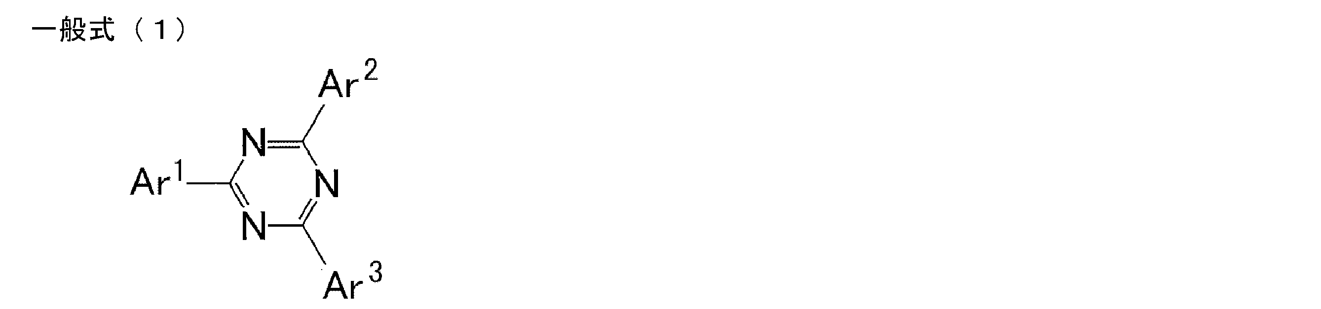
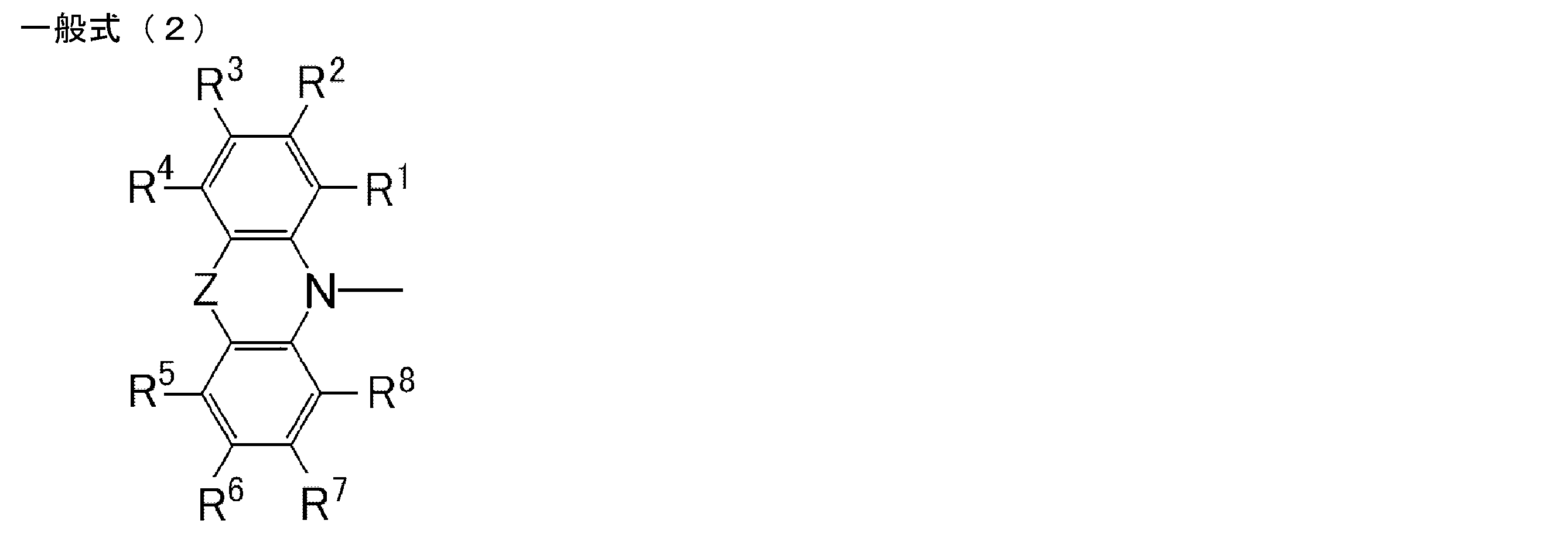
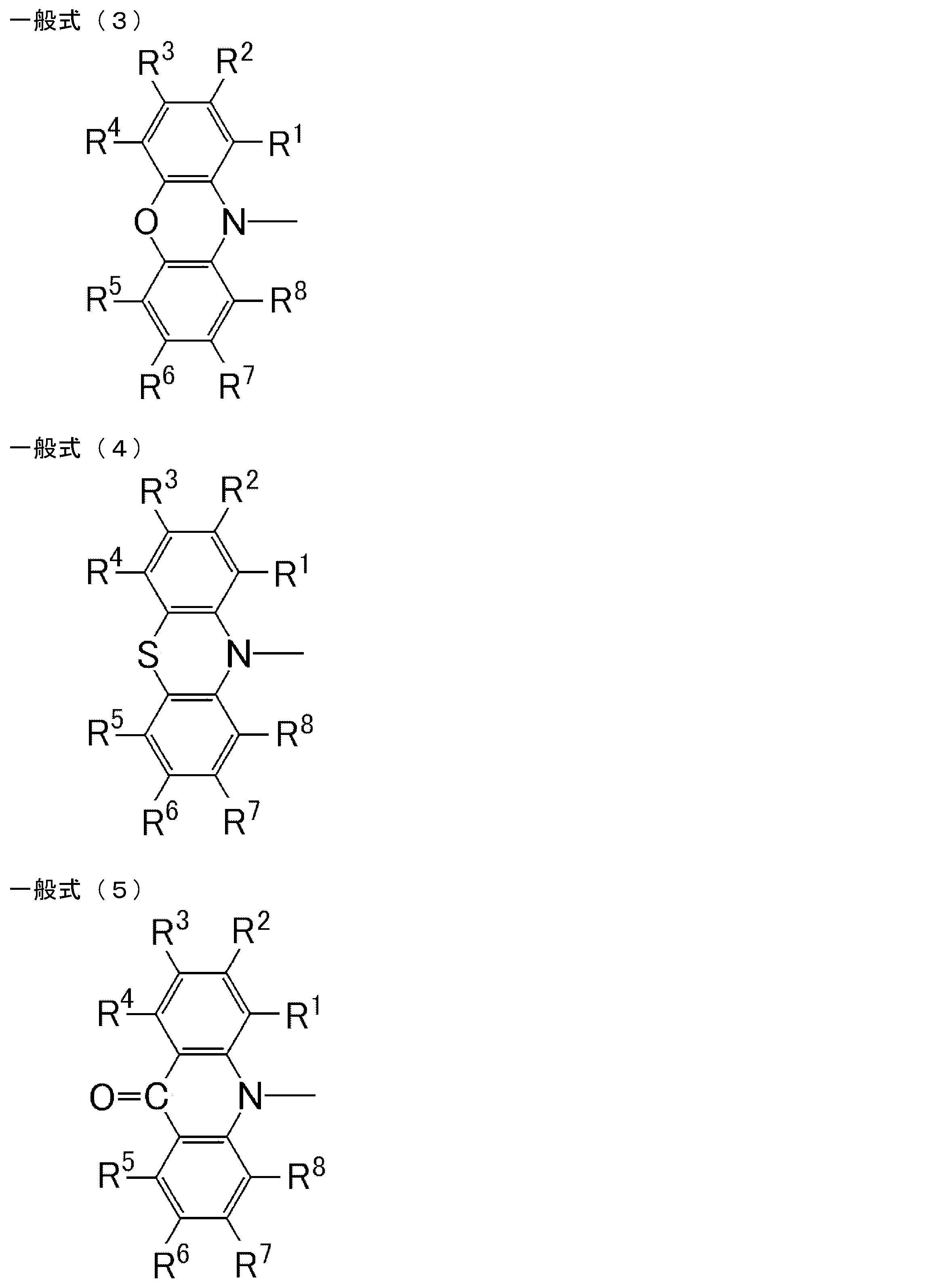
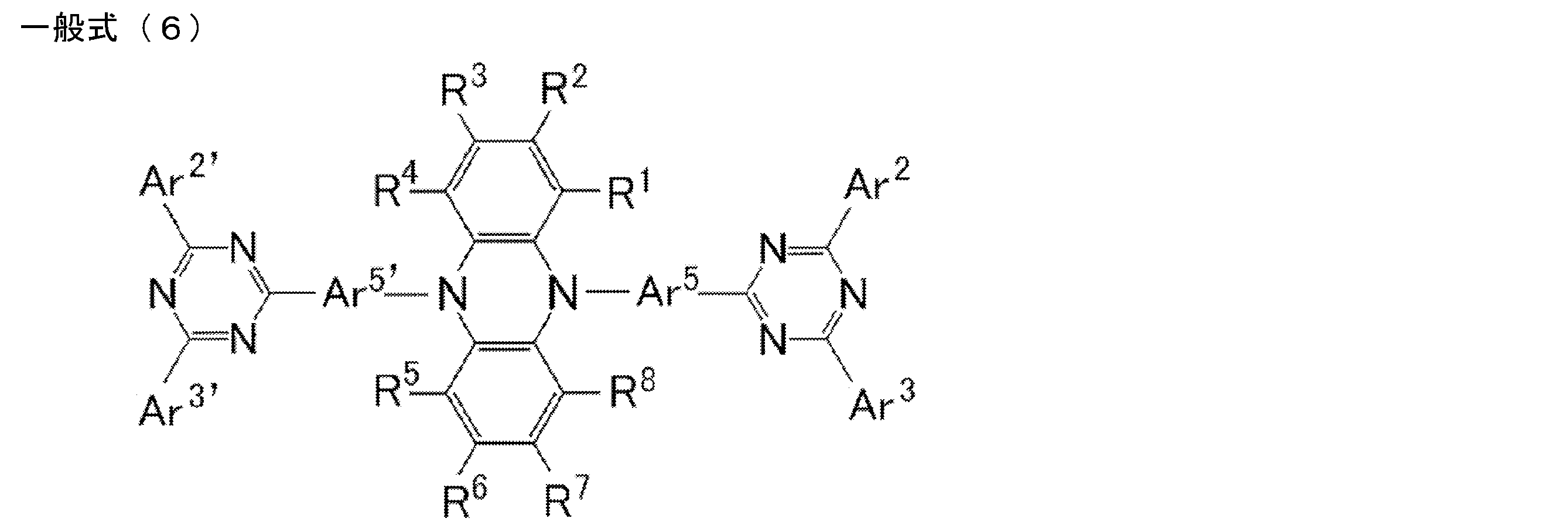
一般式(6)のAr2、Ar3、Ar2’およびAr3’の説明と好ましい範囲については、一般式(1)のAr1~Ar3の説明と好ましい範囲を参照することができる。一般式(6)のAr5およびAr5’がとりうるアリーレン基を構成する芳香環は、単環であっても融合環であってもよく、具体例としてベンゼン環、ナフタレン環、アントラセン環、フェナントレン環を挙げることができる。アリーレン基の炭素数は6~40であることが好ましく、6~20であることがより好ましく、6~14であることがさらに好ましい。一般式(6)のR1~R8の説明と好ましい範囲については、一般式(2)のR1~R8の説明と好ましい範囲を参照することができる。
一般式(6)で表される化合物のうち、Ar2とAr2’が同一であり、Ar3とAr3’が同一であり、Ar5とAr5’が同一である化合物は合成が容易であるという利点がある。 In the general formula (6), Ar 2 , Ar 3 , Ar 2 ′ and Ar 3 ′ each independently represent a substituted or unsubstituted aryl group, and Ar 5 and Ar 5 ′ each independently represent a substituted or unsubstituted arylene. Represents a group. R 1 ~ R 8 each independently represent a hydrogen atom or a substituent. R 1 and R 2 , R 2 and R 3 , R 3 and R 4 , R 5 and R 6 , R 6 and R 7 , R 7 and R 8 may be bonded to each other to form a cyclic structure. Good.
For the explanation and preferred ranges of Ar 2 , Ar 3 , Ar 2 ′ and Ar 3 ′ in the general formula (6), the explanation and preferred ranges of Ar 1 to Ar 3 in the general formula (1) can be referred to. The aromatic ring constituting the arylene group that can be taken by Ar 5 and Ar 5 ′ of the general formula (6) may be a single ring or a fused ring. Specific examples include a benzene ring, a naphthalene ring, an anthracene ring, Mention may be made of phenanthrene rings. The arylene group preferably has 6 to 40 carbon atoms, more preferably 6 to 20 carbon atoms, and still more preferably 6 to 14 carbon atoms. For the description and the preferred range of R 1 ~ R 8 of general formula (6), reference can be made to the descriptions and preferred ranges of R 1 ~ R 8 in the general formula (2).
Of the compounds represented by the general formula (6), a compound in which Ar 2 and Ar 2 ′ are the same, Ar 3 and Ar 3 ′ are the same, and Ar 5 and Ar 5 ′ are the same is easily synthesized. There is an advantage of being.
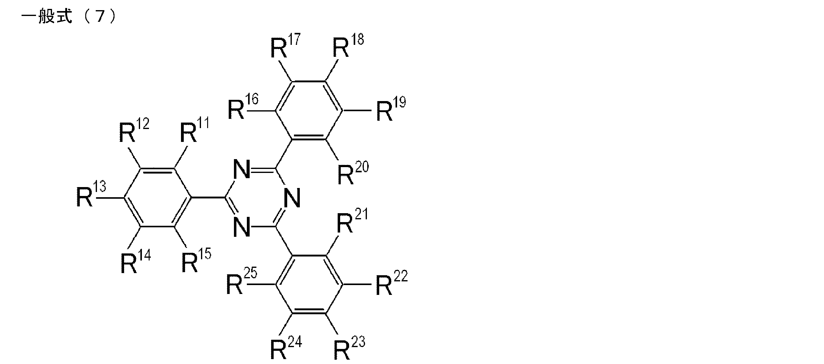
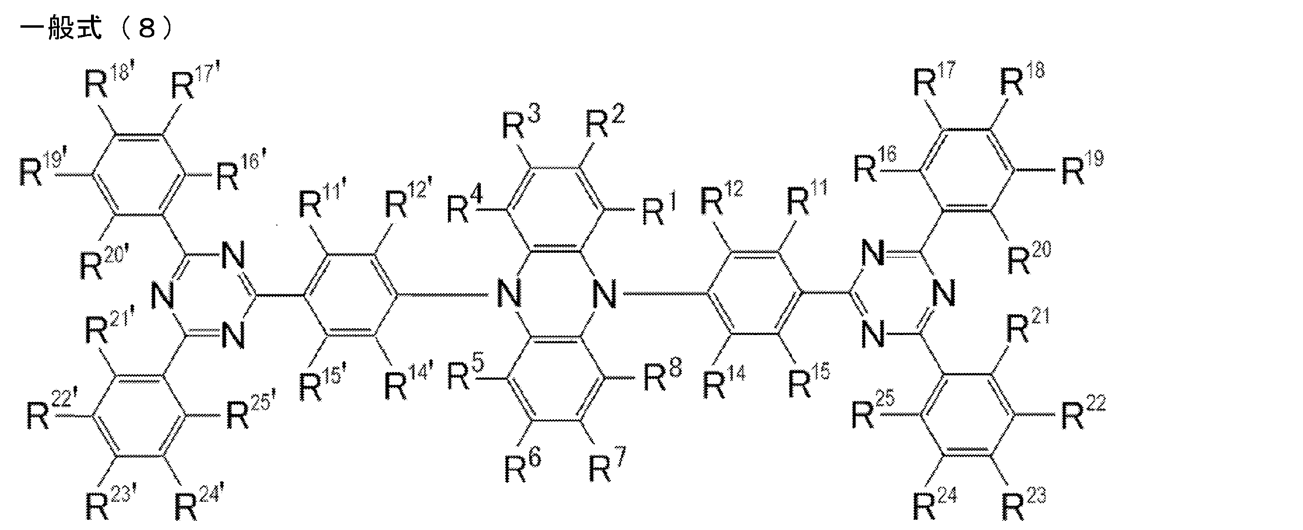

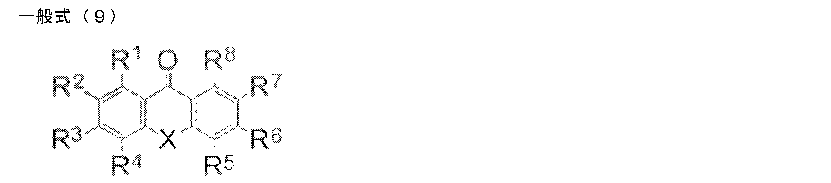
R1~R8のうち下記一般式(10)~(14)のいずれかで表される基は、1つのみであってもよいし、2つ以上であってもよいが、1~4つであることが好ましく、1つまたは2つであることがより好ましい。一般式(9)中に複数の一般式(10)~(14)で表される基が存在する場合、それらの基は同一であっても異なっていてもよい。
下記一般式(10)~(14)のいずれかで表される基がR1~R8のうちの1つのみであるときは、R2またはR3が下記一般式(10)~(14)のいずれかで表される基であることが好ましく、R3が下記一般式(10)~(14)のいずれかで表される基であることがより好ましい。
一方、R1~R8のうちの2つ以上が下記一般式(10)~(14)のいずれかで表される基であるときは、下記一般式(10)~(14)のいずれかで表される基は、R1~R4の少なくとも1つと、R5~R8の少なくとも1つであることが好ましい。このとき、下記一般式(10)~(14)のいずれかで表される基は、R1~R4のうちの1~3つ、R5~R8のうちの1~3つであることが好ましく、R1~R4のうちの1または2つ、R5~R8のうちの1または2つであることがより好ましい。R1~R4のうち一般式(10)~(14)のいずれかで表される基の数と、R5~R8のうち一般式(10)~(14)のいずれかで表される基の数は同じであっても異なっていてもよいが、同じであることが好ましい。R1~R4のうちでは、R2~R4の少なくとも1つが一般式(10)~(14)のいずれかで表される基であることが好ましく、少なくともR3が一般式(10)~(14)のいずれかで表される基であることがより好ましい。また、R5~R8のうちでは、R5~R7の少なくとも1つが一般式(10)~(14)のいずれかで表される基であることが好ましく、少なくともR6が一般式(10)~(14)のいずれかで表される基であることがより好ましい。好ましい化合物は、一般式(9)のR3とR6が一般式(10)~(14)のいずれかで表される基である化合物、一般式(9)のR2とR7が一般式(10)~(14)のいずれかで表される基である化合物、一般式(9)のR2、R3、R6、R7が一般式(10)~(14)のいずれかで表される基である化合物であり、さらに好ましい化合物はR3とR6が一般式(10)~(14)のいずれかで表される基である化合物である。一般式(9)中に存在する複数の一般式(10)~(14)のいずれかで表される基は、同一であっても異なっていてもよいが、同一であることが好ましい。また、一般式(9)で表される基は対称構造をとっていることも好ましい。すなわち、R1とR8、R2とR7、R3とR6、R4とR5は、それぞれ同一であることが好ましい。
一般式(9)の化合物は、R3とR6の両方が下記一般式(10)~(14)のいずれかで表される基であることがより好ましい。好ましい化合物は、一般式(9)のR3またはR6の少なくとも1つが下記一般式(10)または(11)で表される基である化合物である。 In the general formula (9), X is an oxygen atom, a sulfur atom, or a nitrogen atom (a hydrogen atom or a substituent is bonded to the nitrogen atom, and the substituent is an alkyl group having 1 to 10 carbon atoms or 6 carbon atoms) To 14 aryl groups are preferred, and R 1 to R 8 each independently represents a hydrogen atom or a substituent. However, at least one of R 1 to R 8 is each independently a group represented by any one of the following general formulas (10) to (14). X may be either an oxygen atom or a sulfur atom, but is preferably an oxygen atom.
Of R 1 to R 8, the group represented by any one of the following general formulas (10) to (14) may be only one, or may be two or more. It is preferable that it is one, and it is more preferable that it is one or two. When a plurality of groups represented by general formulas (10) to (14) are present in general formula (9), these groups may be the same or different.
When the group represented by any one of the following general formulas (10) to (14) is only one of R 1 to R 8 , R 2 or R 3 is represented by the following general formulas (10) to (14 ), And R 3 is more preferably a group represented by any one of the following general formulas (10) to (14).
On the other hand, when two or more of R 1 - R 8 is a group represented by any one of the following formulas (10) to (14), any one of the following formulas (10) to (14) Is preferably at least one of R 1 to R 4 and at least one of R 5 to R 8 . At this time, the groups represented by any of the following general formulas (10) to (14) are 1 to 3 of R 1 to R 4 and 1 to 3 of R 5 to R 8. It is preferably 1 or 2 of R 1 to R 4 , and more preferably 1 or 2 of R 5 to R 8 . R 1 to R 4 are represented by any of the general formulas (10) to (14), and R 5 to R 8 are represented by any of the general formulas (10) to (14). The number of groups may be the same or different, but is preferably the same. Of R 1 to R 4 , at least one of R 2 to R 4 is preferably a group represented by any one of the general formulas (10) to (14), and at least R 3 is represented by the general formula (10). It is more preferably a group represented by any one of (14) to (14). Among R 5 to R 8 , at least one of R 5 to R 7 is preferably a group represented by any one of the general formulas (10) to (14), and at least R 6 is a general formula ( The group represented by any one of 10) to (14) is more preferable. Preferred compounds are those in which R 3 and R 6 in the general formula (9) are groups represented by any one of the general formulas (10) to (14), and R 2 and R 7 in the general formula (9) are general. A compound which is a group represented by any one of formulas (10) to (14), and R 2 , R 3 , R 6 and R 7 in formula (9) are any one of formulas (10) to (14) A more preferred compound is a compound in which R 3 and R 6 are groups represented by any one of the general formulas (10) to (14). The groups represented by any of the plurality of general formulas (10) to (14) present in the general formula (9) may be the same or different, but are preferably the same. The group represented by the general formula (9) preferably has a symmetrical structure. That is, R 1 and R 8 , R 2 and R 7 , R 3 and R 6 , and R 4 and R 5 are preferably the same.
Compounds of general formula (9) is more preferably both of R 3 and R 6 is a group represented by any one of the following formulas (10) to (14). A preferred compound is a compound in which at least one of R 3 or R 6 in the general formula (9) is a group represented by the following general formula (10) or (11).
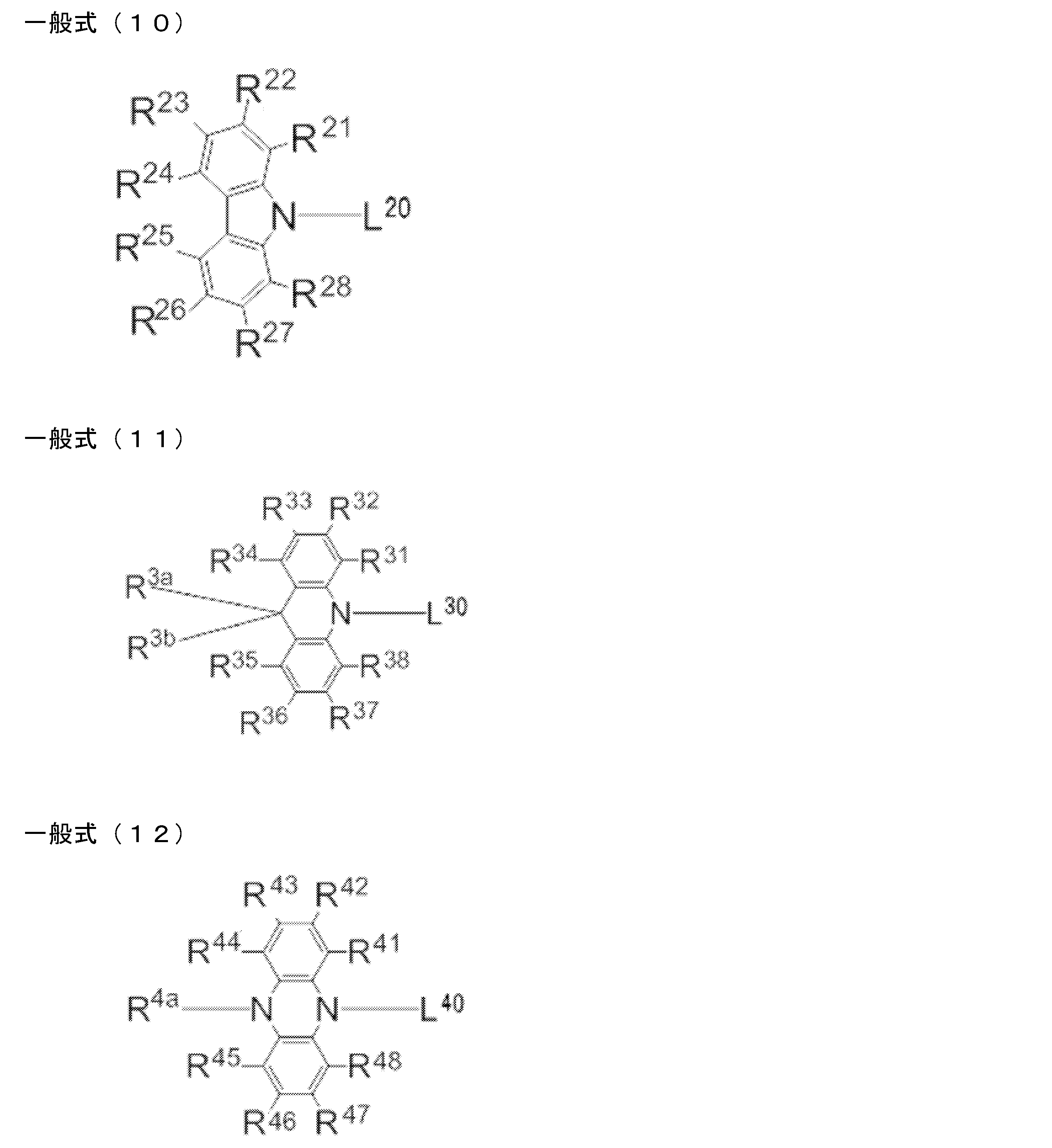

L20,L30,L40、L50,L60は、単結合であっても二価の連結基であってもよいが、単結合であることが好ましい。一般式(9)のR1~R8の少なくとも1つが、L20,L30,L40、L50,L60が連結基である一般式(10)~(14)で表される基であるとき、一般式(9)に存在する連結基の数は、1つのみであってもよいし、2つ以上であってもよい。一般式(9)中に複数の連結基が存在する場合、それらの連結基は同一であっても異なっていてもよい。L20,L30,L40、L50,L60がとりうるニ価の連結基としては、例えば、アルケニレン基、アルキニレン基、アリーレン基、チオフェンジイル基、これらの組み合わせからなる連結基を挙げることができる。アルキレン基やアルケニレン基の炭素数は2~10であることが好ましく、2~6であることがより好ましく、2~4であることがさらに好ましい。また、アリーレン基の炭素数は6~10であることが好ましく、6であることがより好ましく、パラフェニレン基がさらにより好ましい。チオフェンジイル基として、3,4-チオフェンジイル基、2,5-チオフェンジイル基を挙げることができる。好ましい連結基の一般式として-(CRa=CRb)n-で表される連結基を挙げることができる。ここでRaおよびRbは、各々独立に水素原子またはアルキル基を表す。アルキル基の炭素数は1~6であることが好ましく、1~3であることがより好ましい。nは1~5であることが好ましく、1~3であることがより好ましく、1または2であることがさらに好ましい。例えば、-CH=CH-や-(CH=CH)2-を挙げることができる。 In the general formulas (10) to (14), L 20 , L 30 , L 40 , L 50 and L 60 each independently represent a single bond or a divalent linking group, R 21 to R 28 , R 31 to R 38 , R 3a , R 3b , R 41 to R 48 , R 4a , R 51 to R 58 , and R 61 to R 68 each independently represent a hydrogen atom or a substituent.
L 20 , L 30 , L 40 , L 50 and L 60 may be a single bond or a divalent linking group, but are preferably a single bond. At least one of R 1 to R 8 in the general formula (9) is a group represented by the general formulas (10) to (14) in which L 20 , L 30 , L 40 , L 50 , and L 60 are linking groups. In some cases, the number of linking groups present in the general formula (9) may be only one, or may be two or more. When a plurality of linking groups are present in the general formula (9), these linking groups may be the same or different. Examples of the divalent linking group that L 20 , L 30 , L 40 , L 50 , and L 60 can take include, for example, an alkenylene group, an alkynylene group, an arylene group, a thiophendiyl group, and a linking group composed of a combination thereof. Can do. The alkylene group or alkenylene group preferably has 2 to 10 carbon atoms, more preferably 2 to 6 carbon atoms, and still more preferably 2 to 4 carbon atoms. Further, the carbon number of the arylene group is preferably 6 to 10, more preferably 6, and even more preferably a paraphenylene group. Examples of the thiophenediyl group include a 3,4-thiophenediyl group and a 2,5-thiophenediyl group. Preferred examples of the general linking group include a linking group represented by — (CR a ═CR b ) n—. Here, R a and R b each independently represent a hydrogen atom or an alkyl group. The alkyl group preferably has 1 to 6 carbon atoms, more preferably 1 to 3 carbon atoms. n is preferably 1 to 5, more preferably 1 to 3, and still more preferably 1 or 2. For example, —CH═CH— and — (CH═CH) 2 — can be mentioned.
R21~R28、R31~R38、R3a、R3b、R41~R48、R4a、R51~R58、R61~R68がとりうる置換基と、R1~R8とりうる置換基として、例えばヒドロキシ基、ハロゲン原子、シアノ基、炭素数1~20のアルキル基、炭素数1~20のアルコキシ基、炭素数1~20のアルキルチオ基、炭素数1~20のアルキル置換アミノ基、炭素数2~20のアシル基、炭素数6~40のアリール基、炭素数3~40のヘテロアリール基、炭素数2~10のアルケニル基、炭素数2~10のアルキニル基、炭素数2~10のアルコキシカルボニル基、炭素数1~10のアルキルスルホニル基、炭素数1~10のハロアルキル基、アミド基、炭素数2~10のアルキルアミド基、炭素数3~20のトリアルキルシリル基、炭素数4~20のトリアルキルシリルアルキル基、炭素数5~20のトリアルキルシリルアルケニル基、炭素数5~20のトリアルキルシリルアルキニル基およびニトロ基等が挙げられる。これらの具体例のうち、さらに置換基により置換可能なものは置換されていてもよい。より好ましい置換基は、ハロゲン原子、シアノ基、炭素数1~20の置換もしくは無置換のアルキル基、炭素数1~20のアルコキシ基、炭素数6~40の置換もしくは無置換のアリール基、炭素数3~40の置換もしくは無置換のヘテロアリール基、炭素数1~20のジアルキル置換アミノ基である。さらに好ましい置換基は、フッ素原子、塩素原子、シアノ基、炭素数1~10の置換もしくは無置換のアルキル基、炭素数1~10の置換もしくは無置換のアルコキシ基、炭素数6~15の置換もしくは無置換のアリール基、炭素数3~12の置換もしくは無置換のヘテロアリール基である。
また、R23、R26、R33、R36、R43、R46、R53、R56、R63、R66の少なくとも1つは、各々独立に上記一般式(10)~(14)のいずれかで表される基であることが好ましい。 The number of substituents in the general formulas (10) to (14) is not particularly limited. In each of the general formulas (10) to (14), R 21 to R 28 , R 31 to R 38 , R 3a , R 3b , R 41 to R 48 , R 4a , R 51 to R 58 , R 61 to R All of 68 may be unsubstituted (that is, a hydrogen atom), but at least one of R 21 to R 28 , R 31 to R 38 , R 41 to R 48 , R 51 to R 58 , and R 61 to R 68 is acceptable. Is preferably a substituent, and more preferably at least one of R 23 , R 26 , R 33 , R 36 , R 43 , R 46 , R 53 , R 56 , R 63 , R 66 is a substituent. . Further, when a plurality of substituents are present in the general formulas (10) to (14), these substituents may be the same or different.
R 21 to R 28 , R 31 to R 38 , R 3a , R 3b , R 41 to R 48 , R 4a , R 51 to R 58 , R 61 to R 68 can be substituted with R 1 to R 8. Examples of possible substituents include a hydroxy group, a halogen atom, a cyano group, an alkyl group having 1 to 20 carbon atoms, an alkoxy group having 1 to 20 carbon atoms, an alkylthio group having 1 to 20 carbon atoms, and an alkyl having 1 to 20 carbon atoms. A substituted amino group, an acyl group having 2 to 20 carbon atoms, an aryl group having 6 to 40 carbon atoms, a heteroaryl group having 3 to 40 carbon atoms, an alkenyl group having 2 to 10 carbon atoms, an alkynyl group having 2 to 10 carbon atoms, C2-C10 alkoxycarbonyl group, C1-C10 alkylsulfonyl group, C1-C10 haloalkyl group, amide group, C2-C10 alkylamide group, C3-C20 trialkyl Silyl group, 4 to 20 carbon atoms Alkylsilyl group, a trialkylsilyl alkenyl group having 5 to 20 carbon atoms, and the like trialkylsilyl alkynyl group and a nitro group having 5 to 20 carbon atoms. Among these specific examples, those that can be substituted with a substituent may be further substituted. More preferred substituents are a halogen atom, a cyano group, a substituted or unsubstituted alkyl group having 1 to 20 carbon atoms, an alkoxy group having 1 to 20 carbon atoms, a substituted or unsubstituted aryl group having 6 to 40 carbon atoms, carbon A substituted or unsubstituted heteroaryl group having 3 to 40 carbon atoms, and a dialkyl-substituted amino group having 1 to 20 carbon atoms. More preferable substituents are a fluorine atom, a chlorine atom, a cyano group, a substituted or unsubstituted alkyl group having 1 to 10 carbon atoms, a substituted or unsubstituted alkoxy group having 1 to 10 carbon atoms, and a substituted group having 6 to 15 carbon atoms. Alternatively, it is an unsubstituted aryl group or a substituted or unsubstituted heteroaryl group having 3 to 12 carbon atoms.
In addition, at least one of R 23 , R 26 , R 33 , R 36 , R 43 , R 46 , R 53 , R 56 , R 63 , R 66 is independently selected from the above general formulas (10) to (14). It is preferable that it is group represented by either.
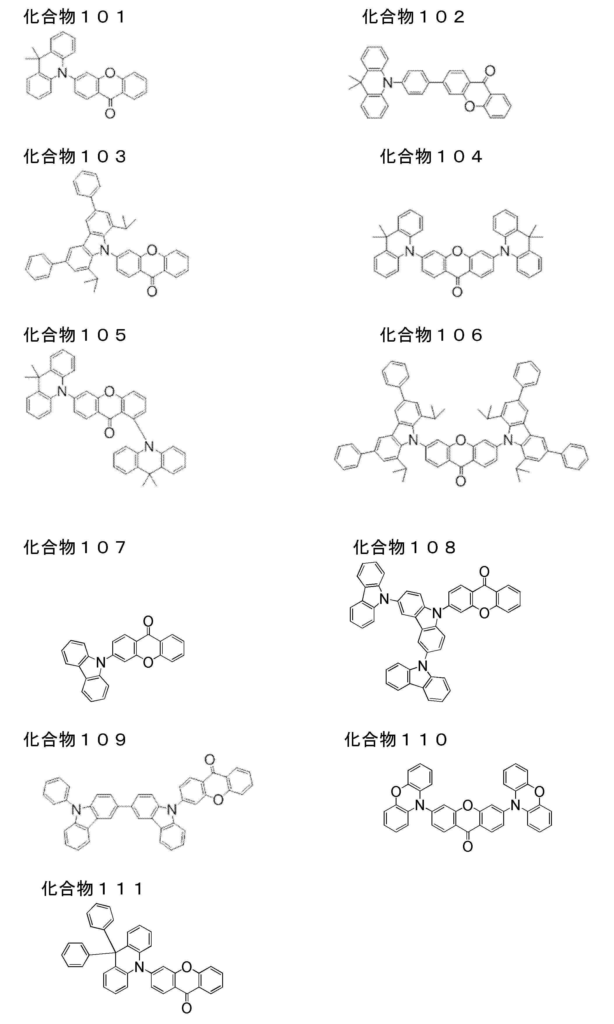


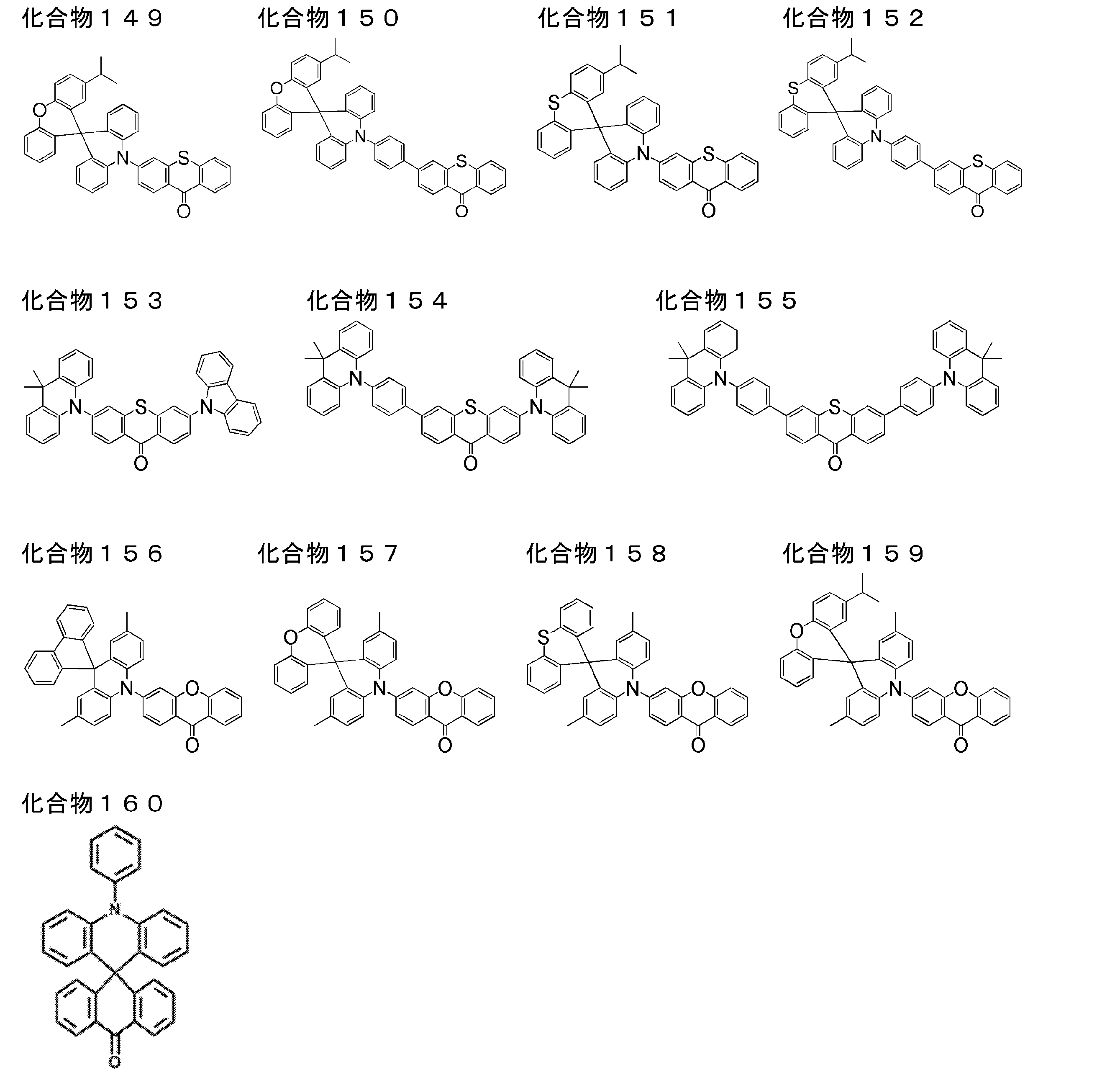
好ましい発光材料として下記一般式で表される化合物を挙げることができる。また、WO2013/154064号公報の段落0008~0048および0095~0133の記載を始めとする該公報の明細書全文を、本願明細書の一部としてここに引用する。

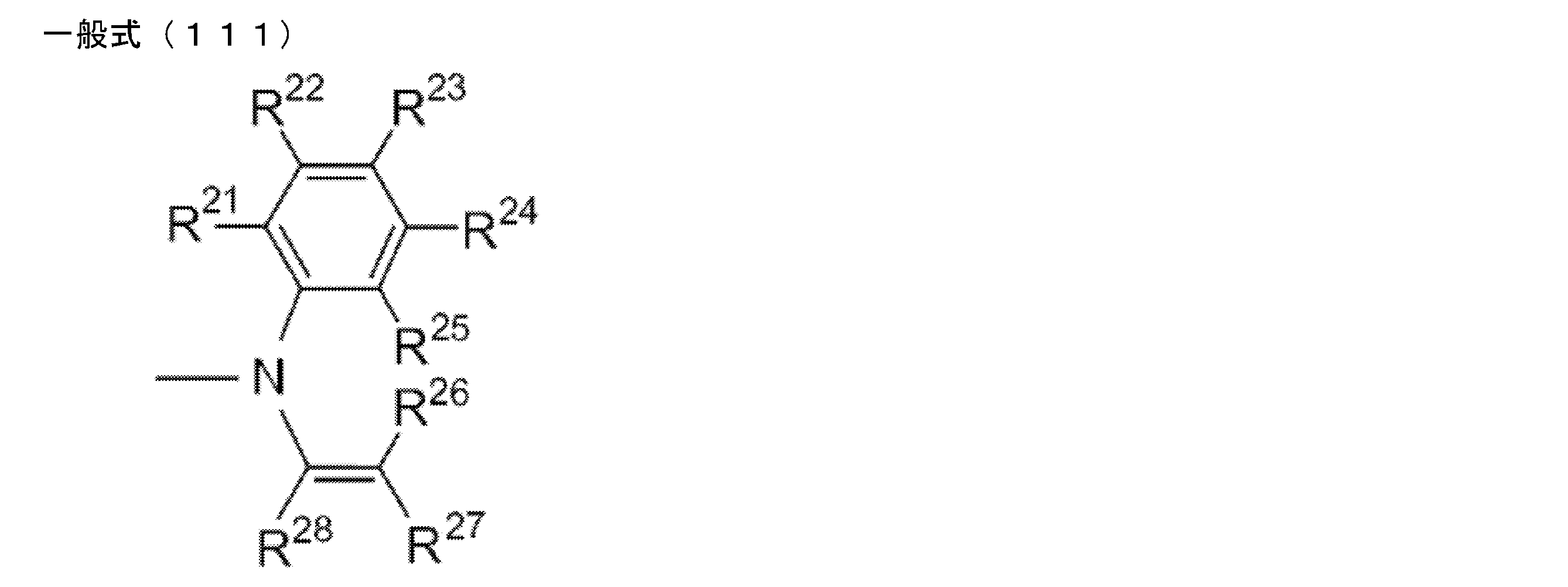
<A> R25およびR26は一緒になって単結合を形成する。
<B> R27およびR28は一緒になって置換もしくは無置換のベンゼン環を形成するのに必要な原子団を表す。] As the second organic compound, the following luminescent materials that can emit delayed fluorescence can also be preferably used.
Preferred examples of the light emitting material include compounds represented by the following general formula. In addition, the entire specification of the publication including the description of paragraphs 0008 to 0048 and 0095 to 0133 of WO2013 / 154064 is cited herein as a part of this specification.
<A> R 25 and R 26 together form a single bond.
<B> R 27 and R 28 together represent an atomic group necessary for forming a substituted or unsubstituted benzene ring. ]

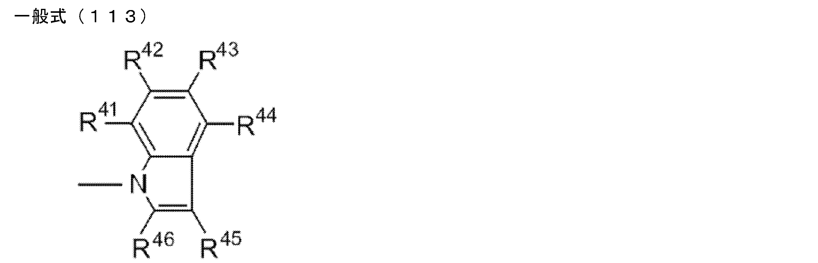
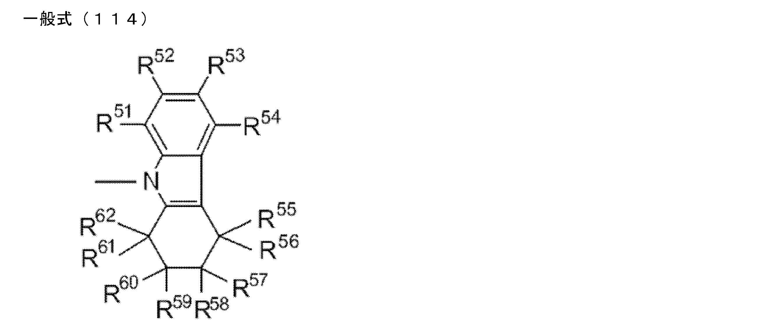


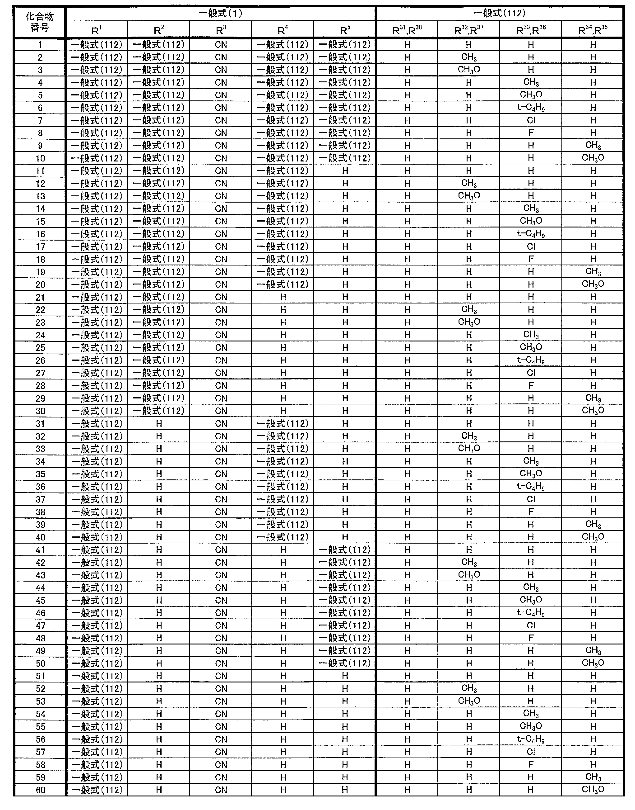


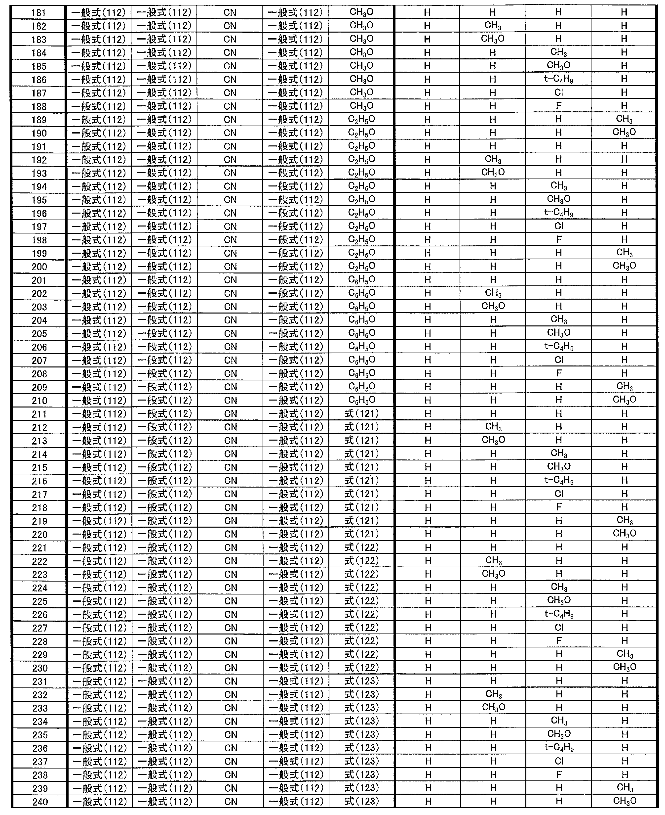
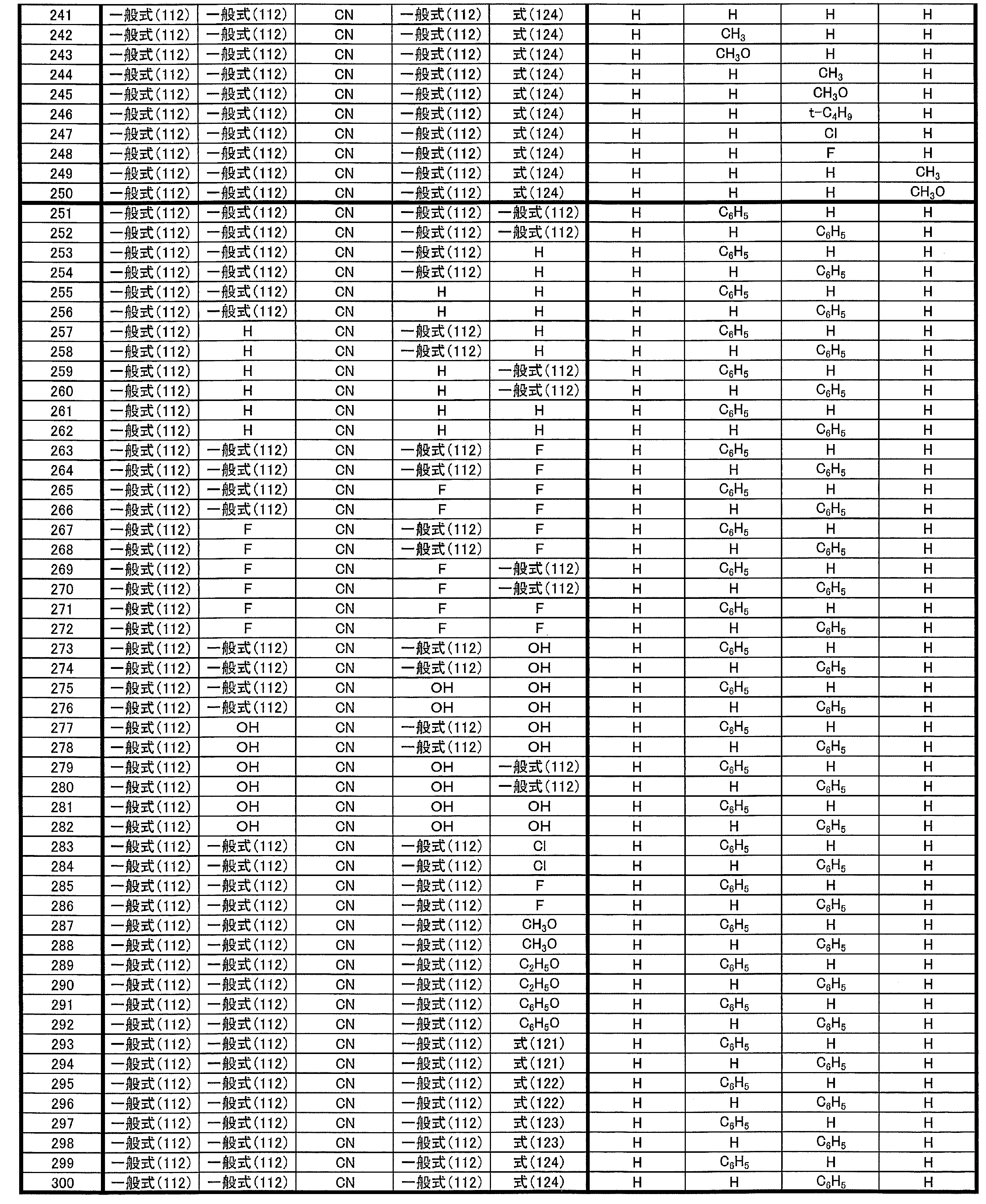
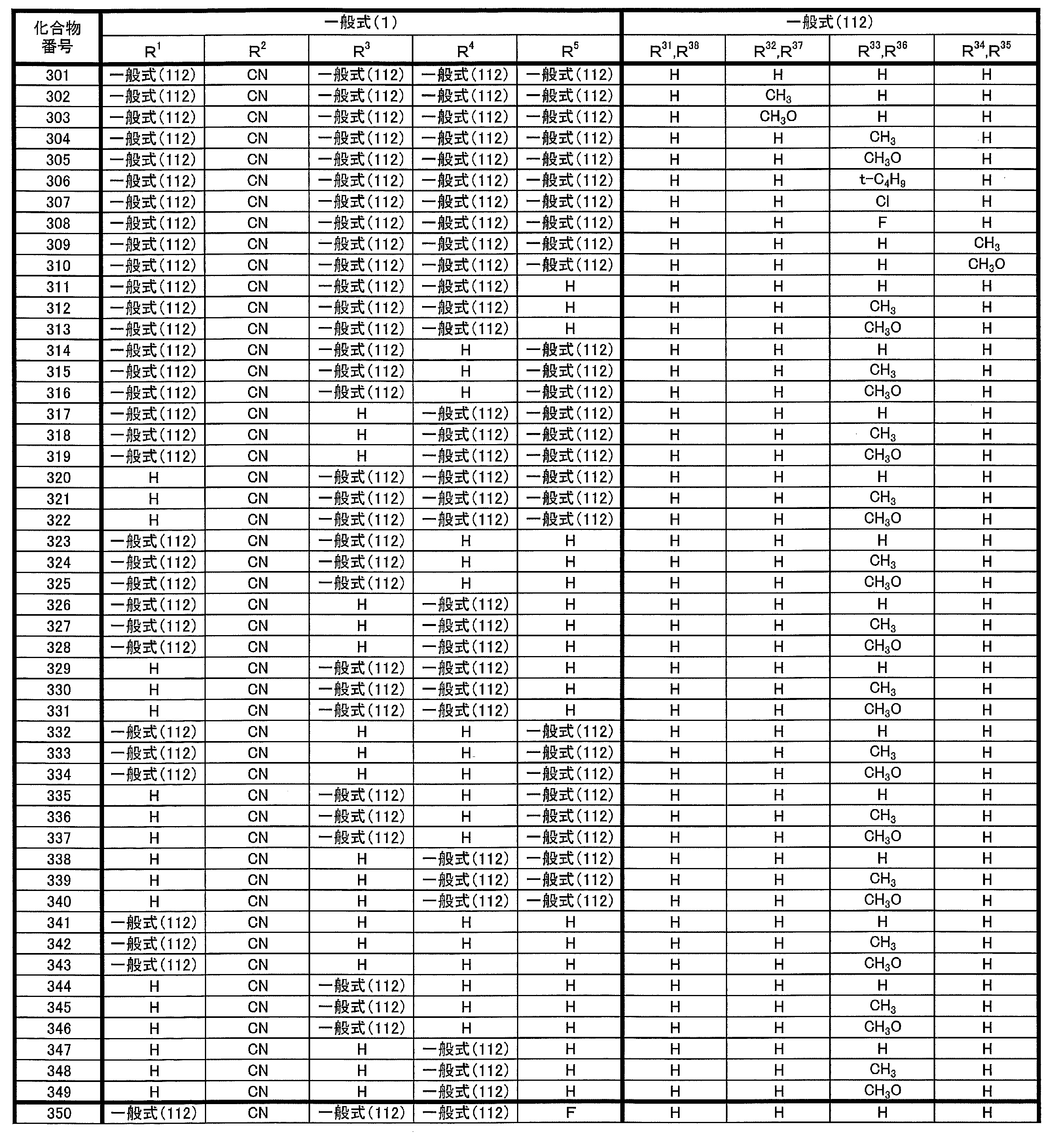
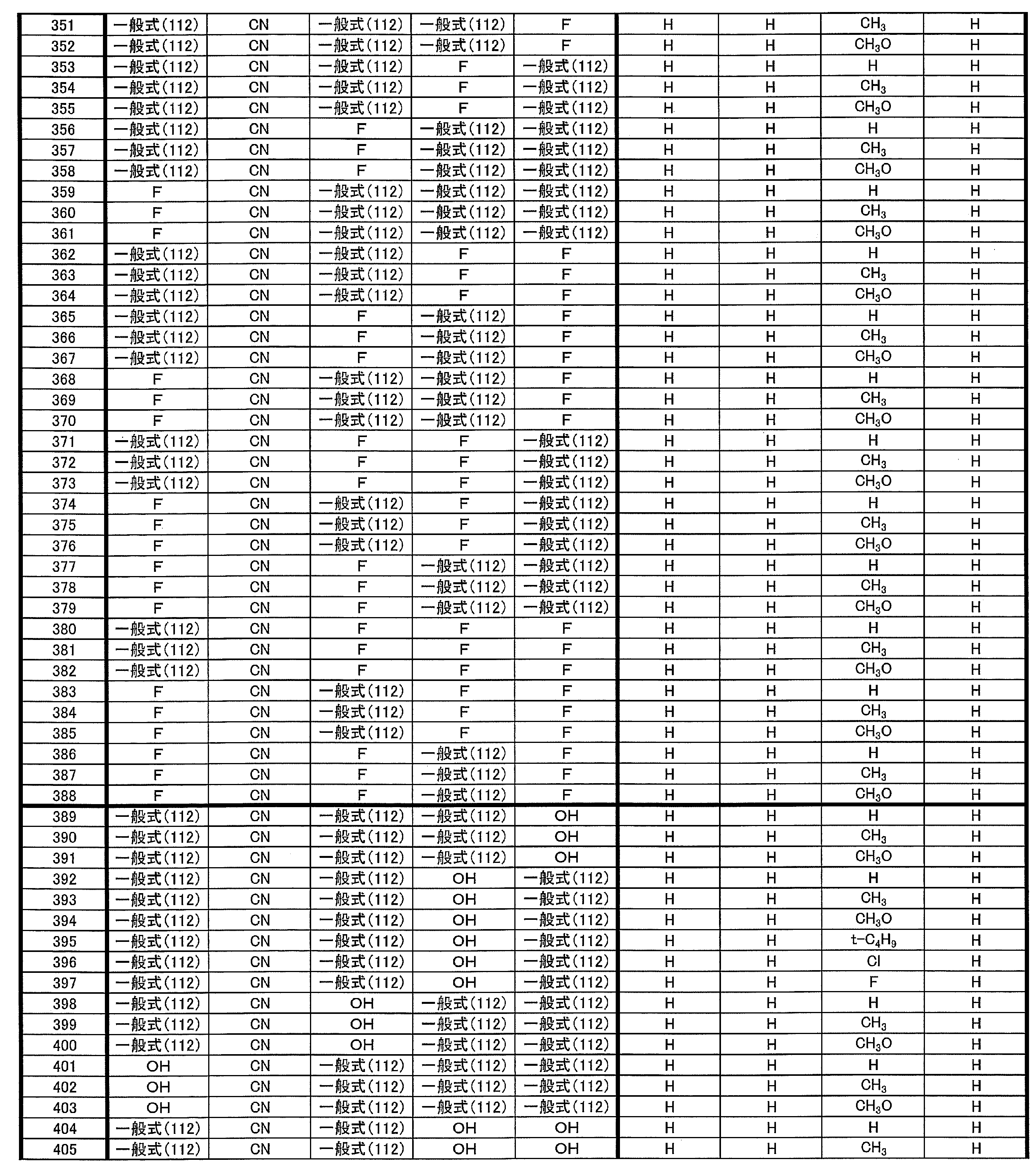
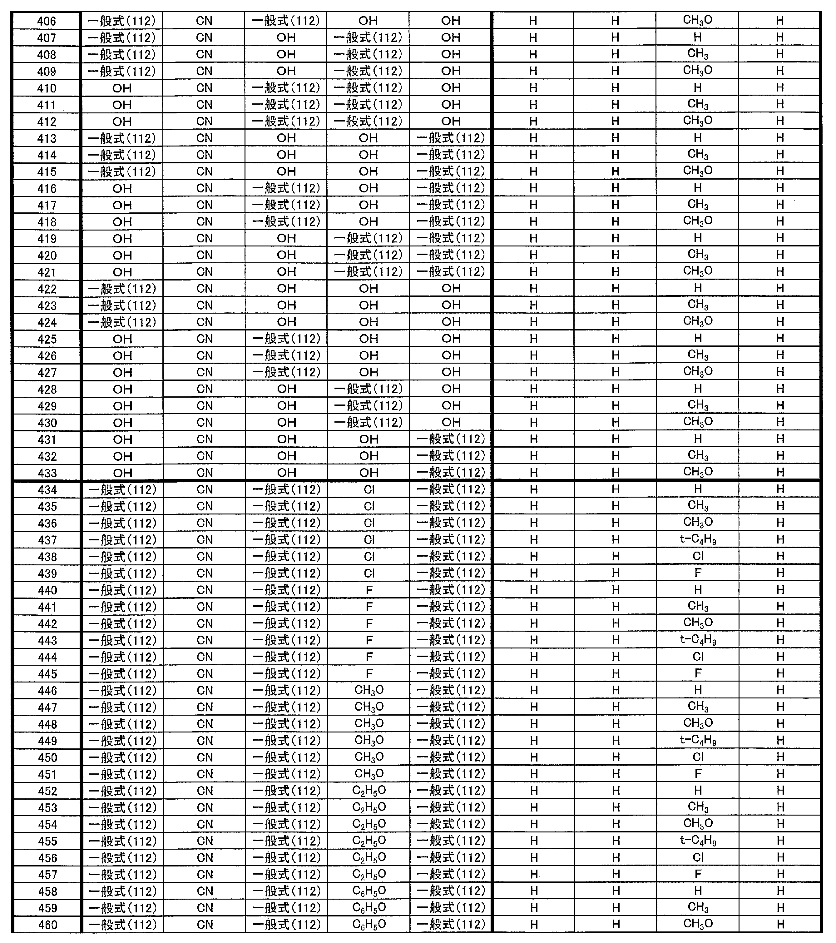
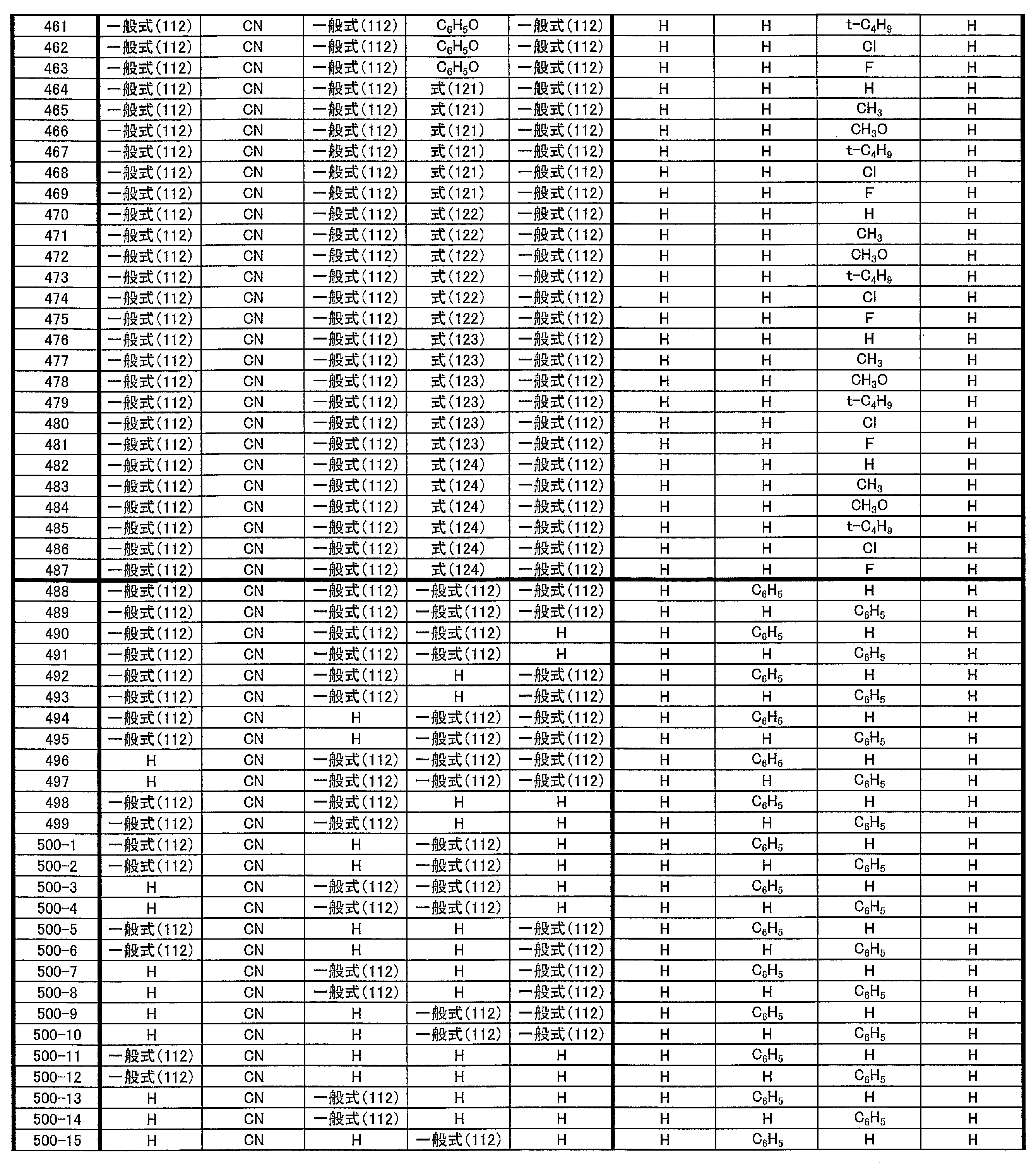
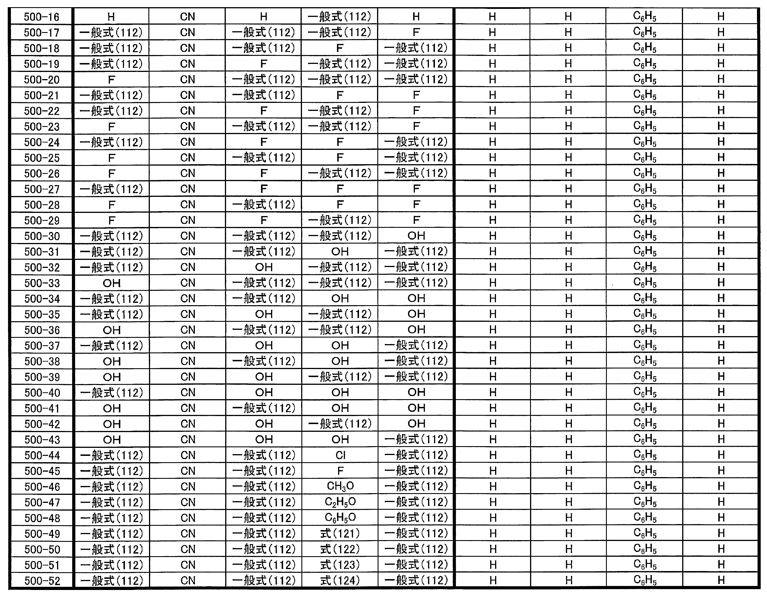
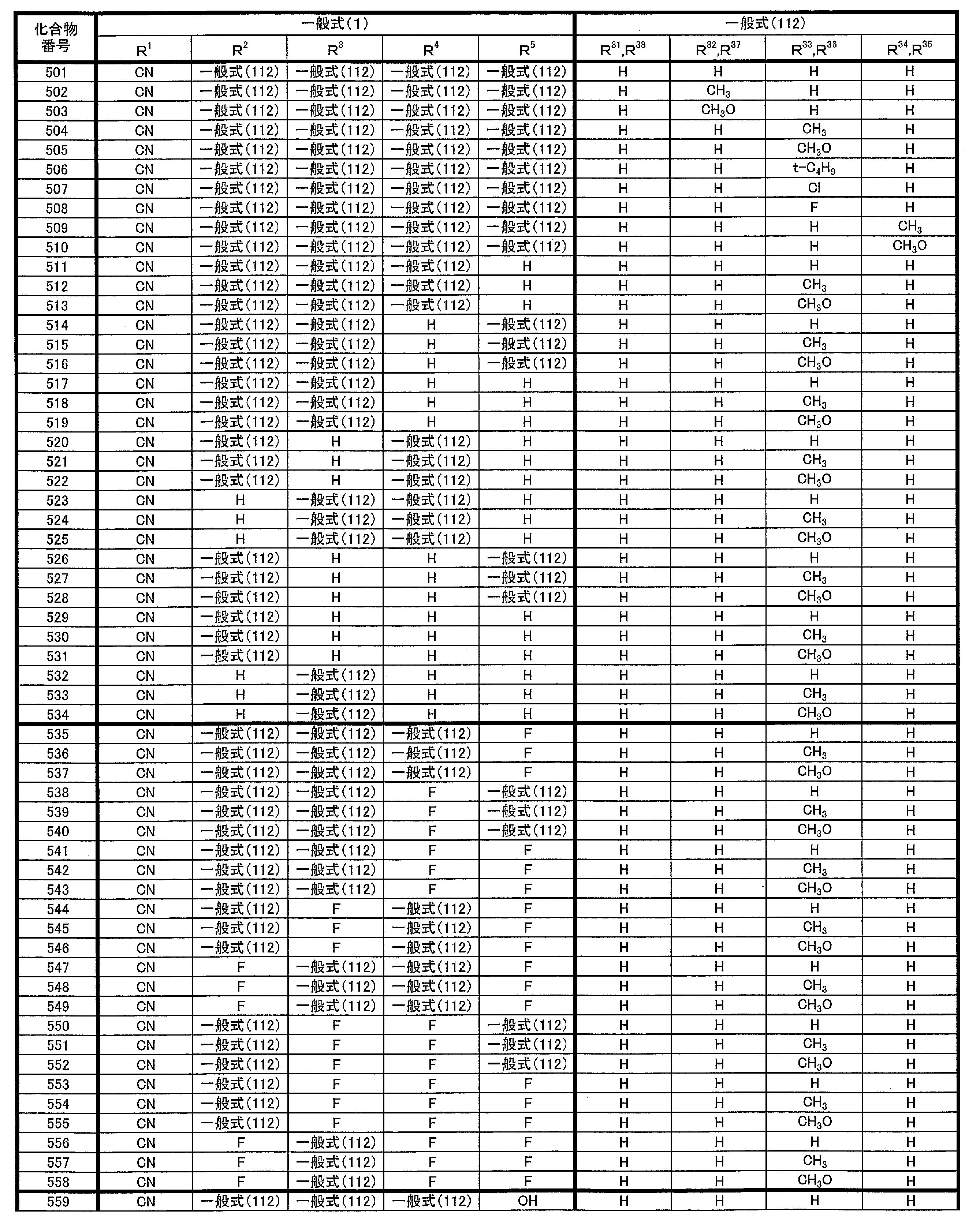

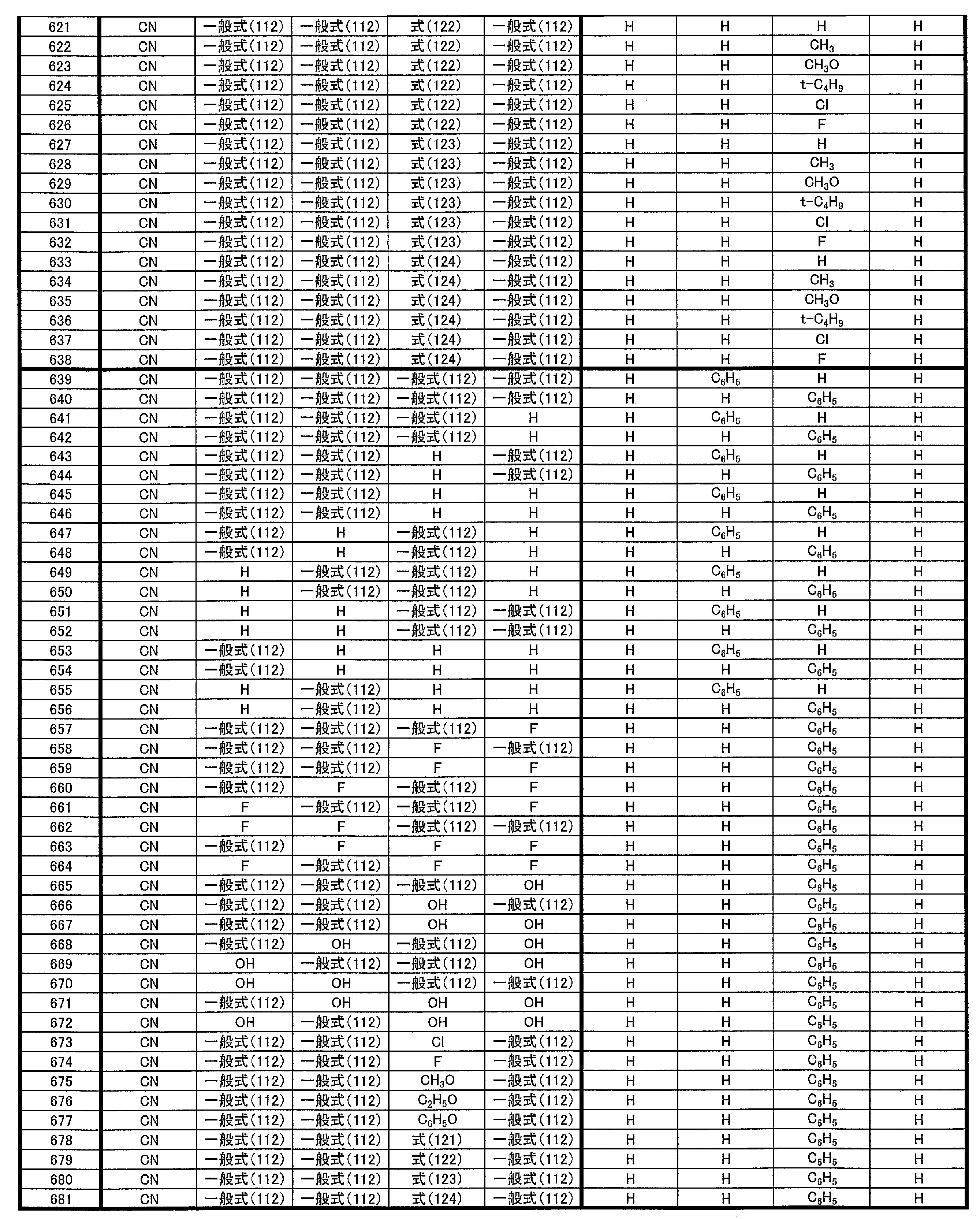
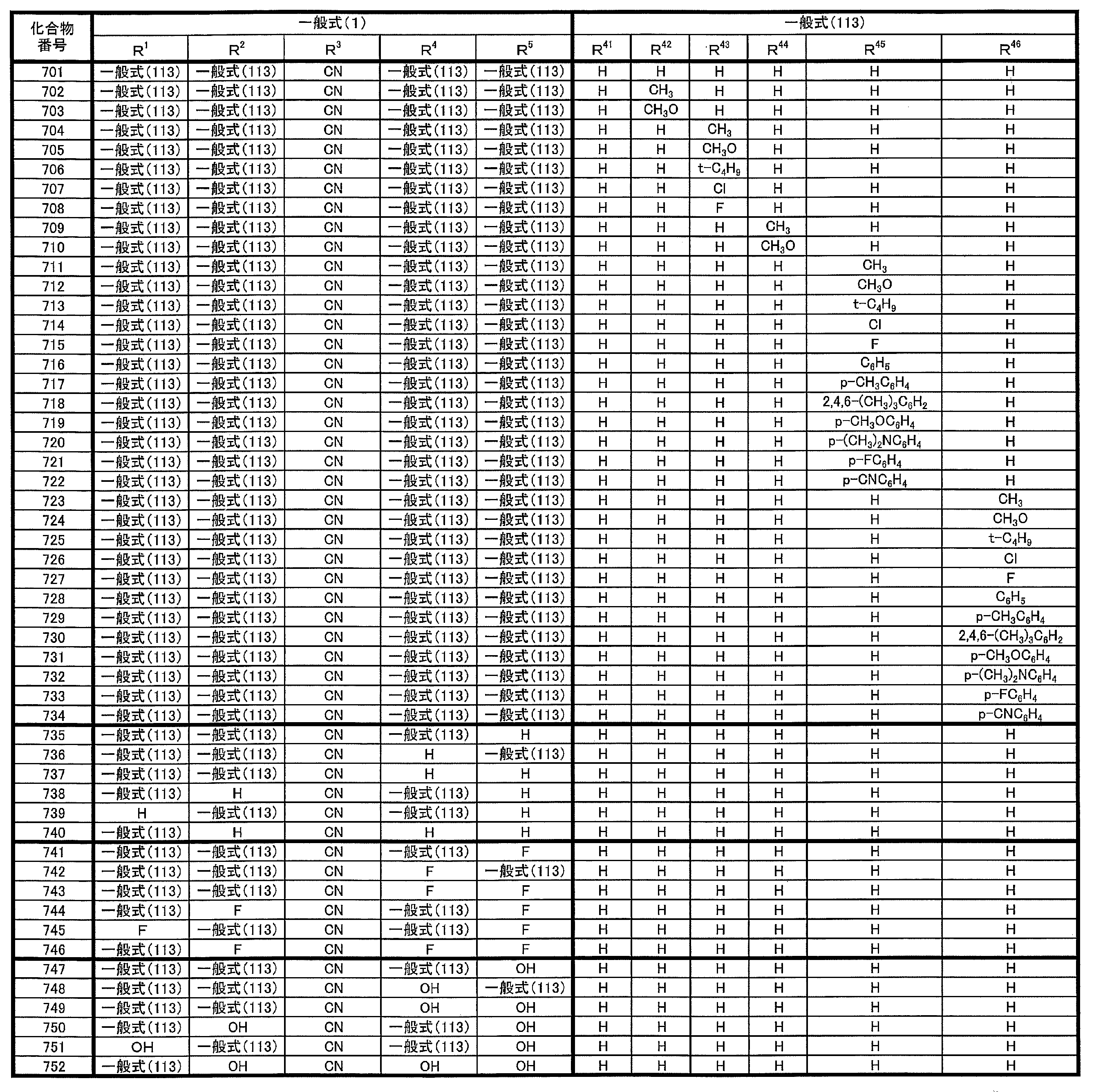

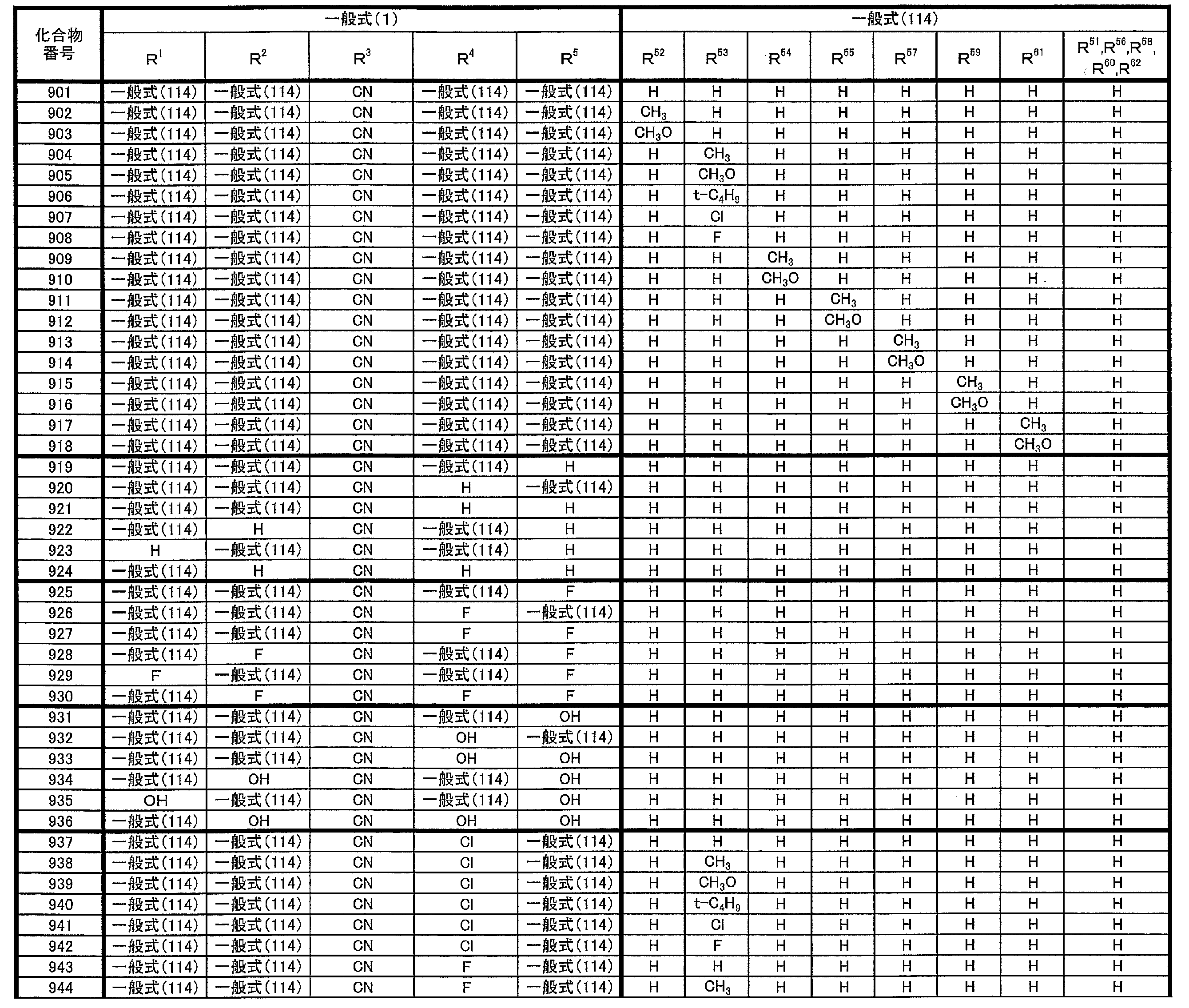
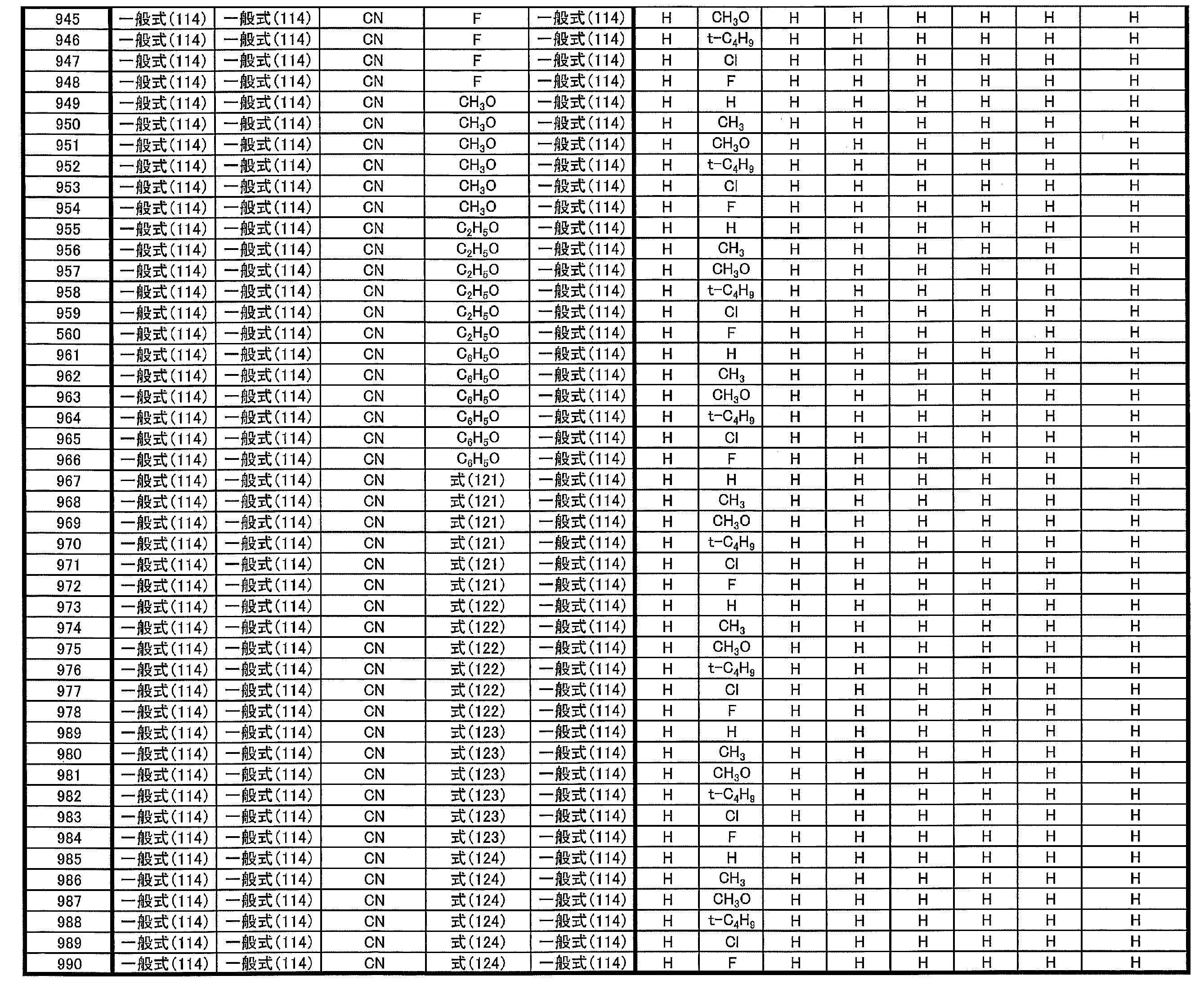
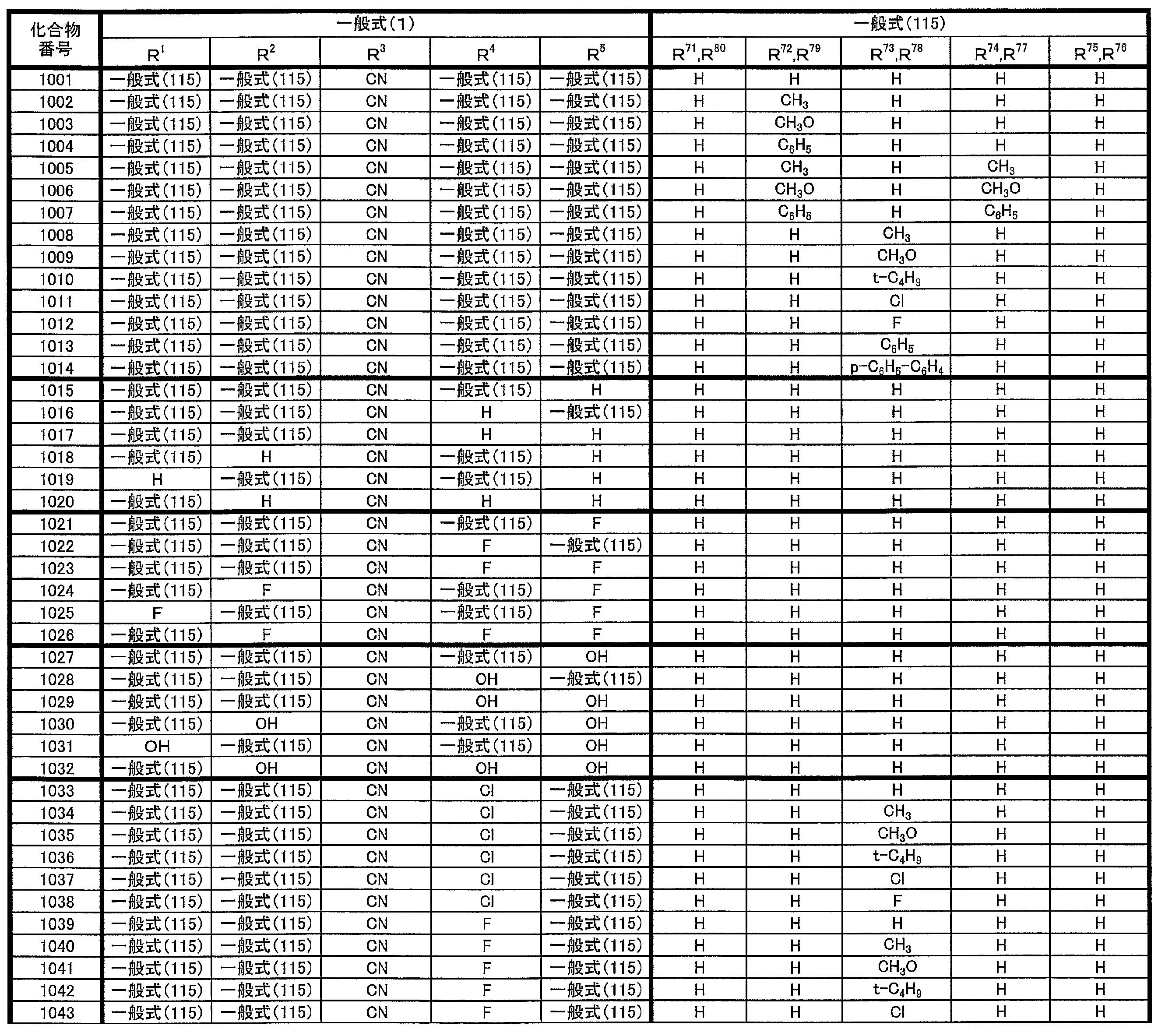

[1] 下記一般式(131)で表される化合物。
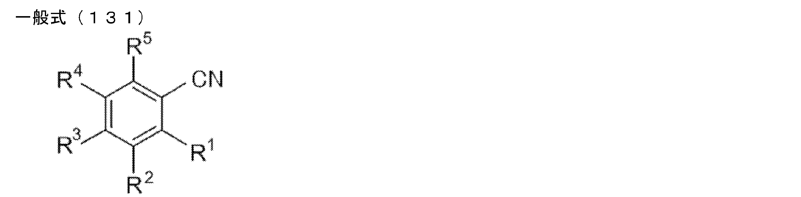
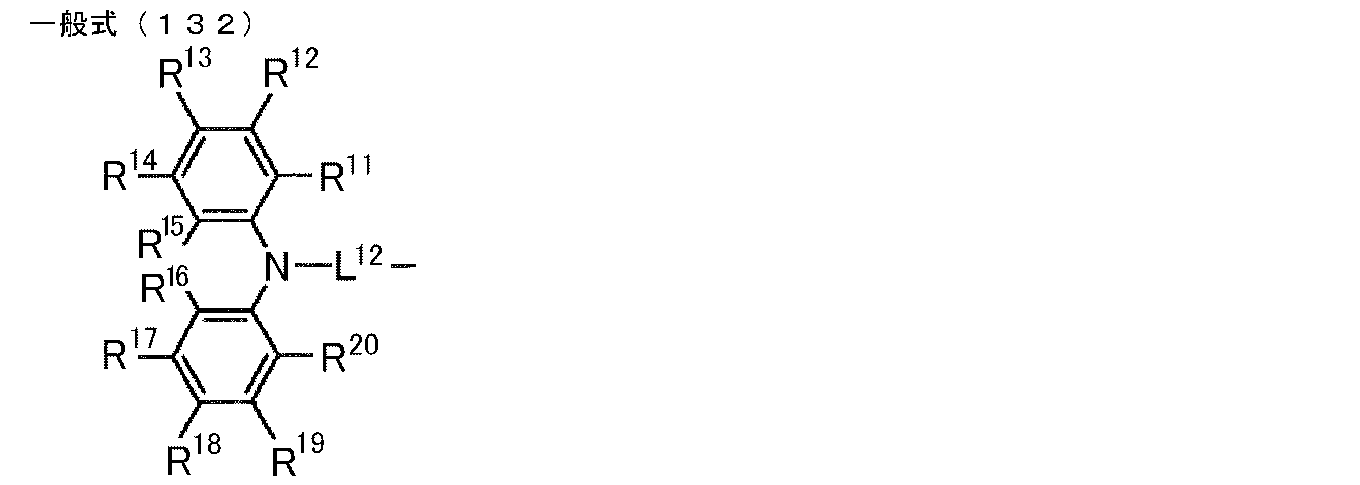
[2] 前記一般式(132)で表される基が、下記一般式(133)~(138)のいずれかで表される基であることを特徴とする[1]に記載の化合物。

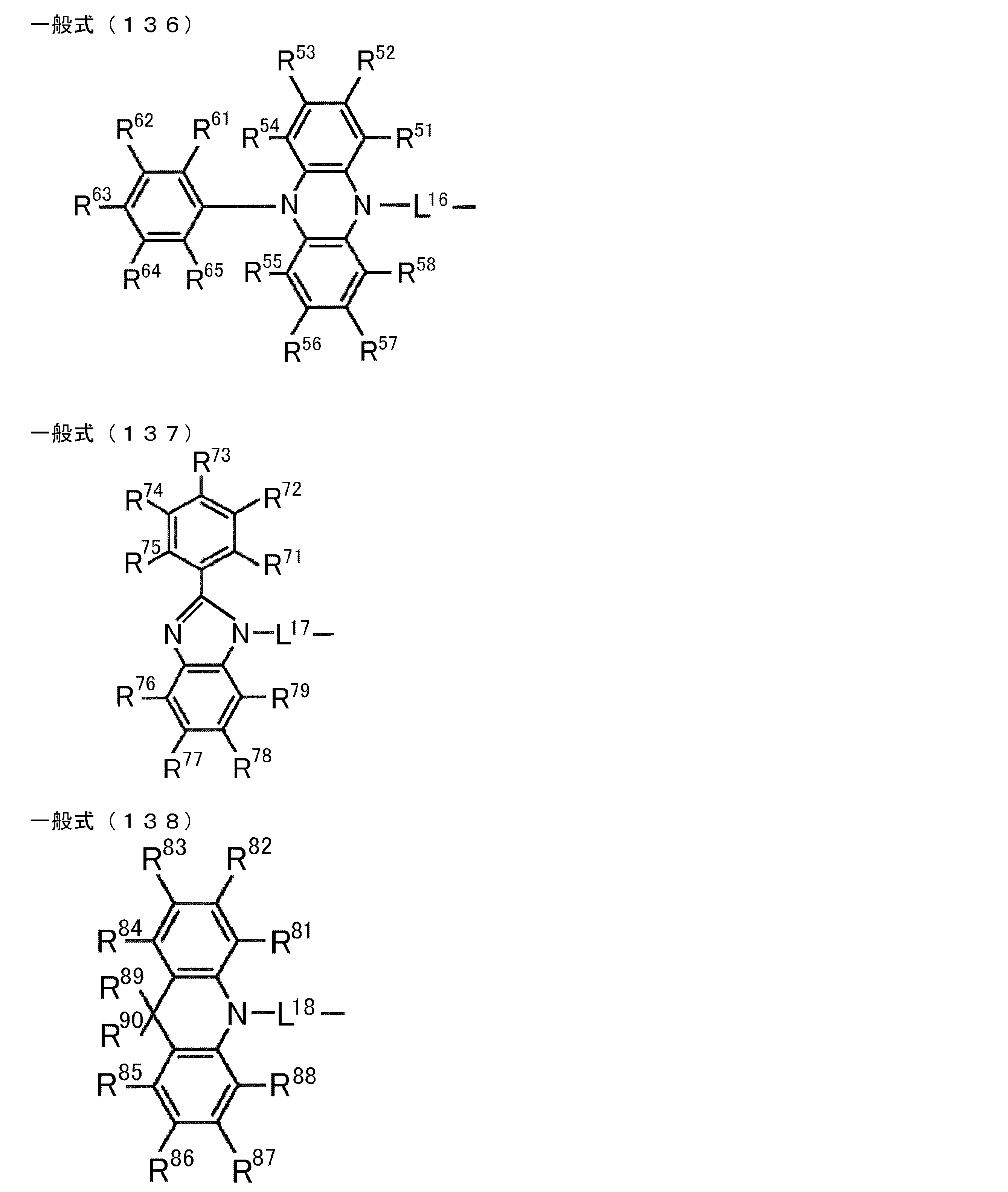
[3] 一般式(131)のR3が、シアノ基であることを特徴とする[1]または[2]に記載の化合物。
[4] 一般式(131)のR1とR4が前記一般式(132)で表される基であることを特徴とする[1]~[3]のいずれか1項に記載の化合物。
[5] 前記一般式(132)のL12が、フェニレン基であることを特徴とする[1]~[4]のいずれか1項に記載の化合物。
[6] 前記一般式(132)で表される基が、前記一般式(133)で表される基であることを特徴とする[1]~[5]のいずれか1項に記載の化合物。
[7] 前記一般式(133)のL13が、1,3-フェニレン基であることを特徴とする[6]に記載の化合物。
[8] 前記一般式(132)で表される基が、前記一般式(134)で表される基であることを特徴とする[1]~[5]のいずれか1項に記載の化合物。
[9] 前記一般式(134)のL14が、1,4-フェニレン基であることを特徴とする[8]に記載の化合物。
[10] 前記一般式(132)で表される基が、前記一般式(138)で表される基であることを特徴とする[1]~[5]のいずれか1項に記載の化合物。
[11] 前記一般式(132)のL18が、1,4-フェニレン基である[10]に記載の化合物。 Preferred examples of the light emitting material include the following compounds.
[1] A compound represented by the following general formula (131).
[2] The compound according to [1], wherein the group represented by the general formula (132) is a group represented by any one of the following general formulas (133) to (138).
[3] The compound according to [1] or [2], wherein R 3 in the general formula (131) is a cyano group.
[4] The compound according to any one of [1] to [3], wherein R 1 and R 4 in the general formula (131) are a group represented by the general formula (132).
[5] The compound according to any one of [1] to [4], wherein L 12 in the general formula (132) is a phenylene group.
[6] The compound according to any one of [1] to [5], wherein the group represented by the general formula (132) is a group represented by the general formula (133) .
[7] The L 13 in the general formula (133) is a compound having the constitution [6] to be a 1,3-phenylene group.
[8] The compound according to any one of [1] to [5], wherein the group represented by the general formula (132) is a group represented by the general formula (134) .
[9] The compound according to [8], wherein L 14 in the general formula (134) is a 1,4-phenylene group.
[10] The compound according to any one of [1] to [5], wherein the group represented by the general formula (132) is a group represented by the general formula (138) .
[11] The compound according to [10], wherein L 18 in the general formula (132) is a 1,4-phenylene group.
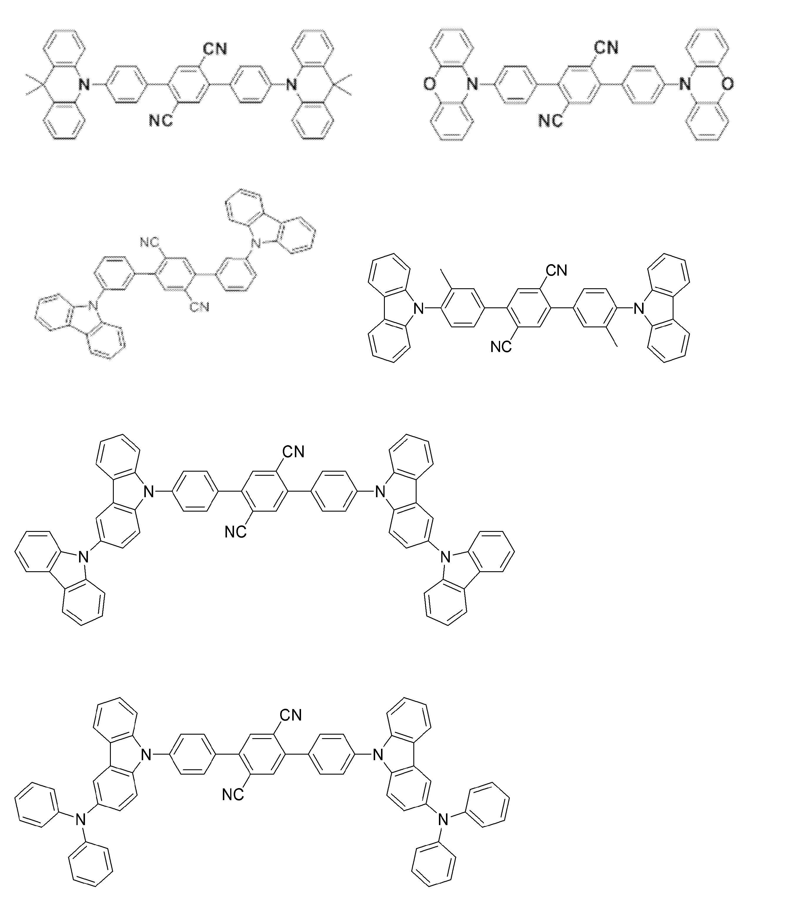
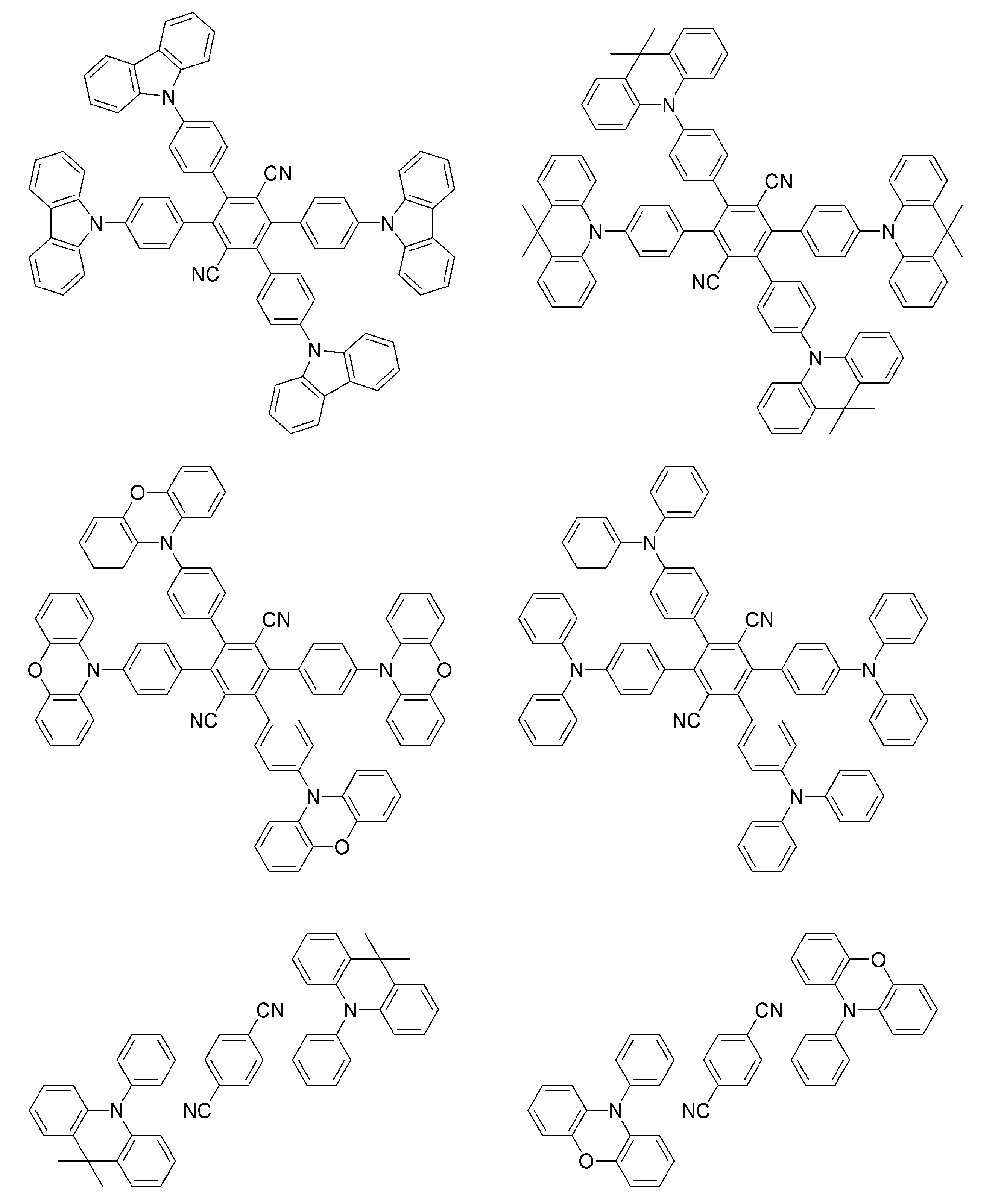
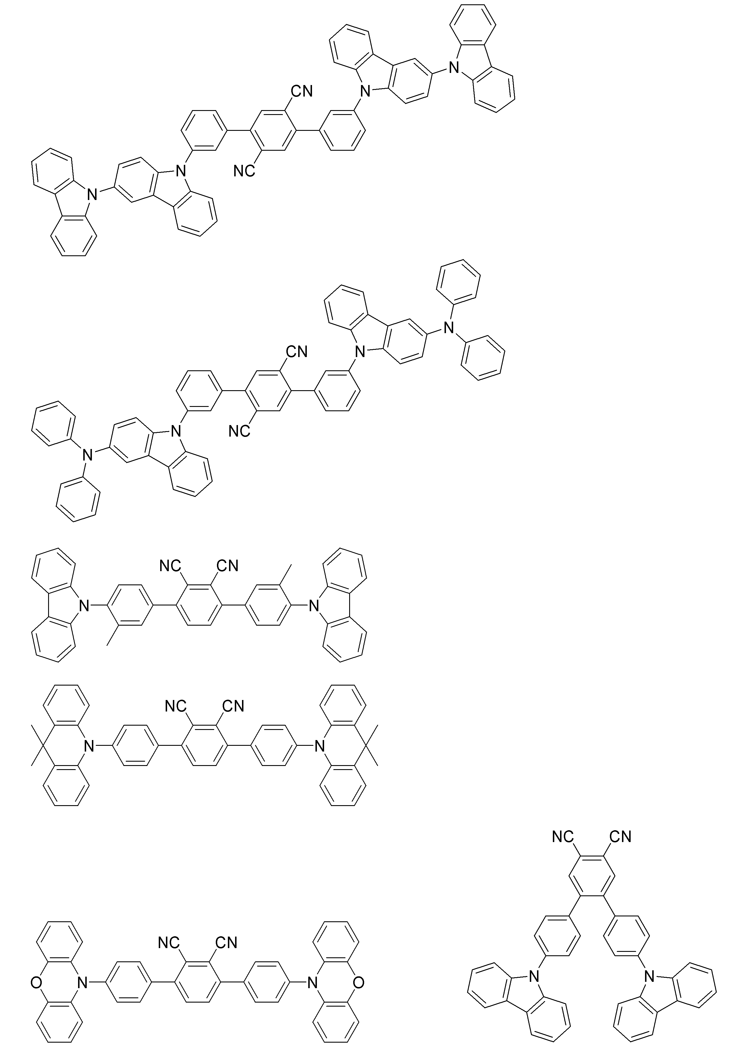
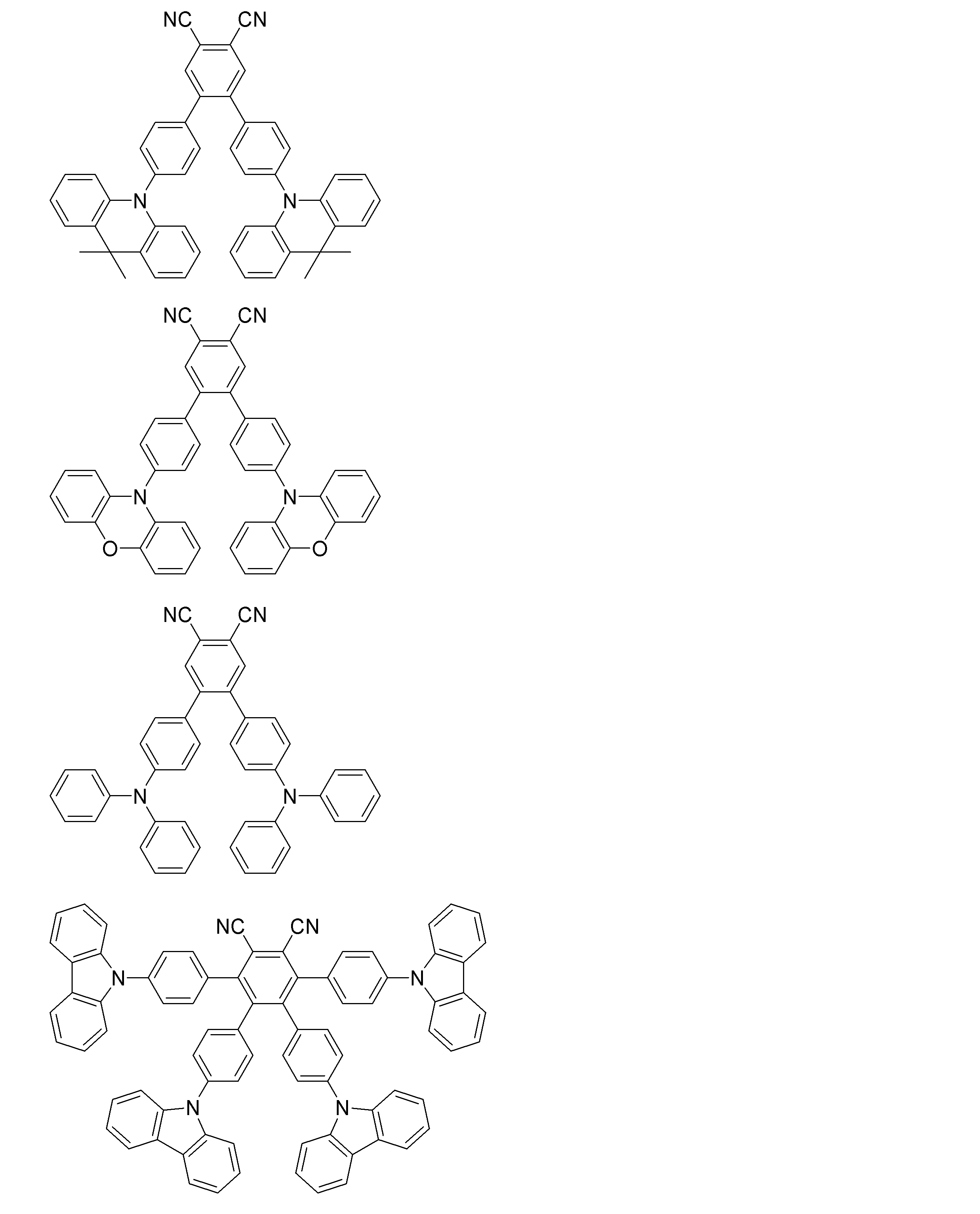

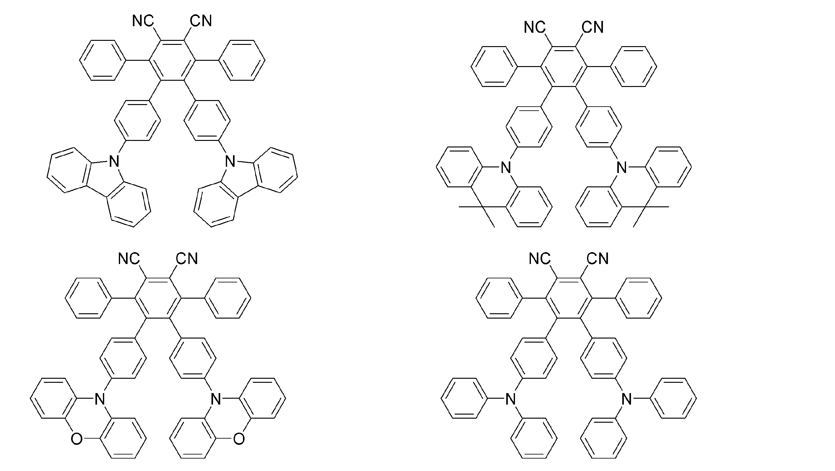
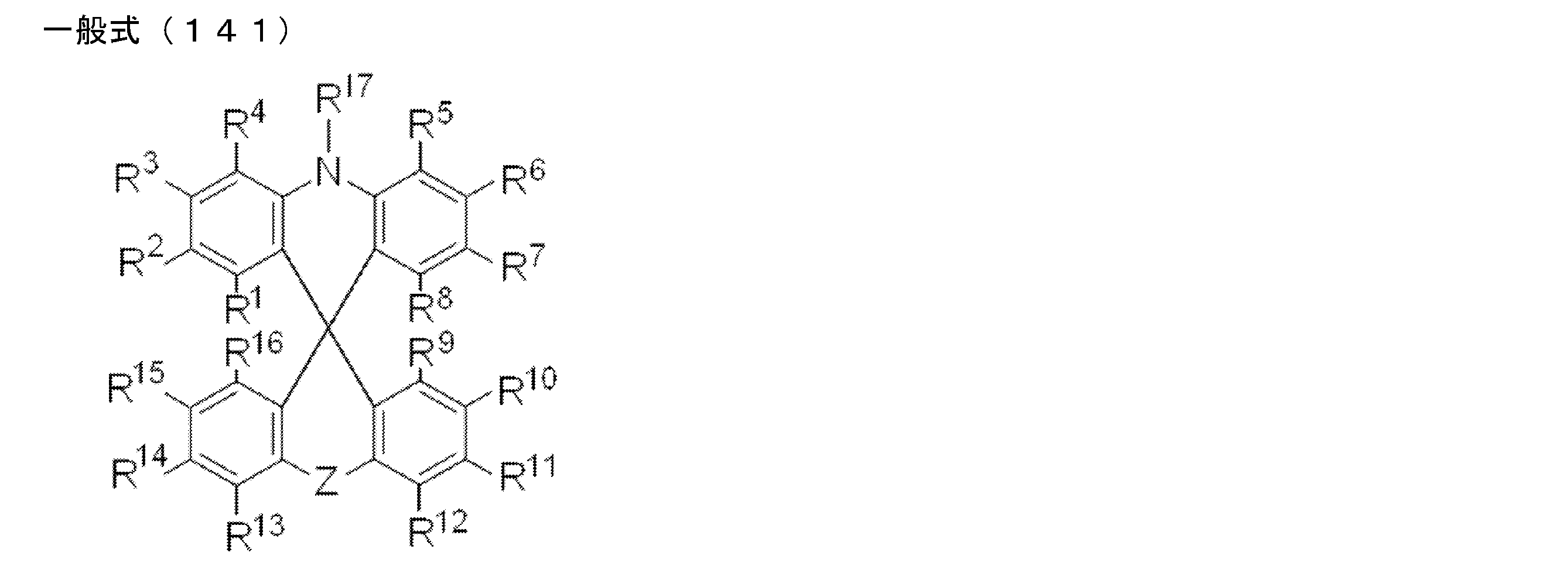
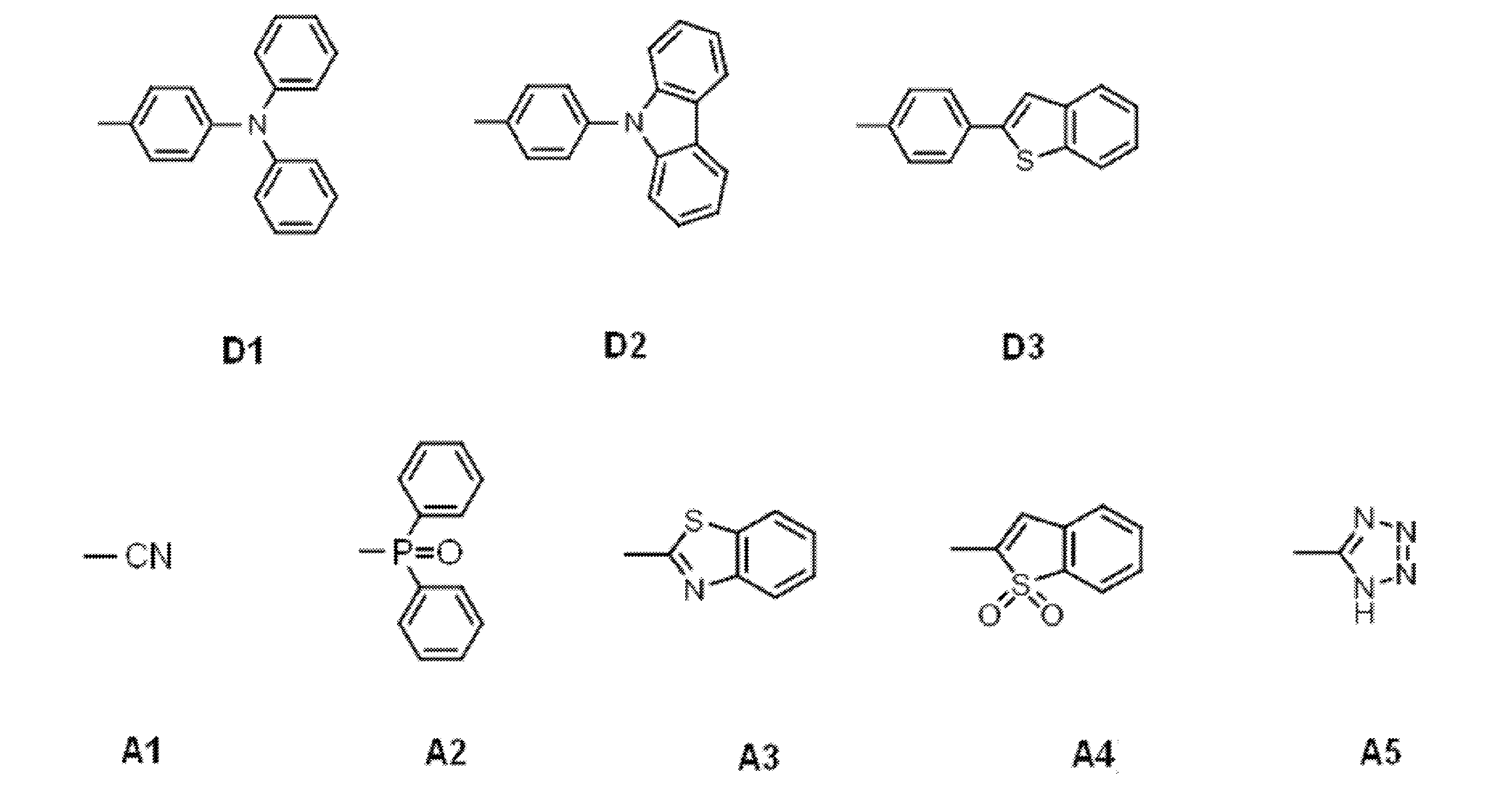
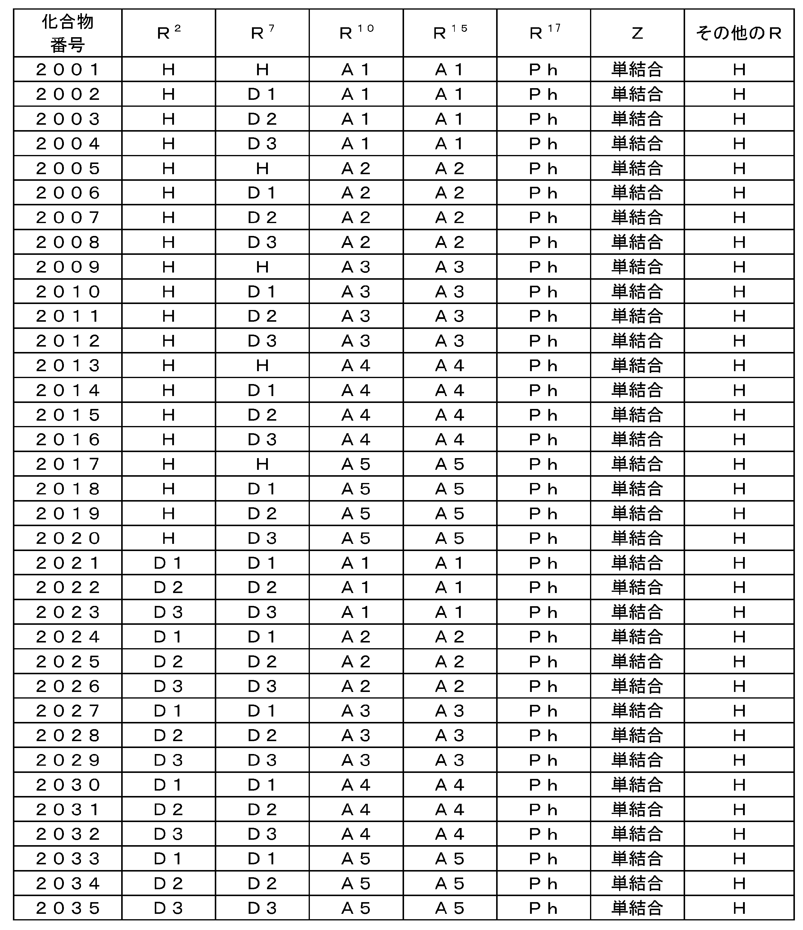


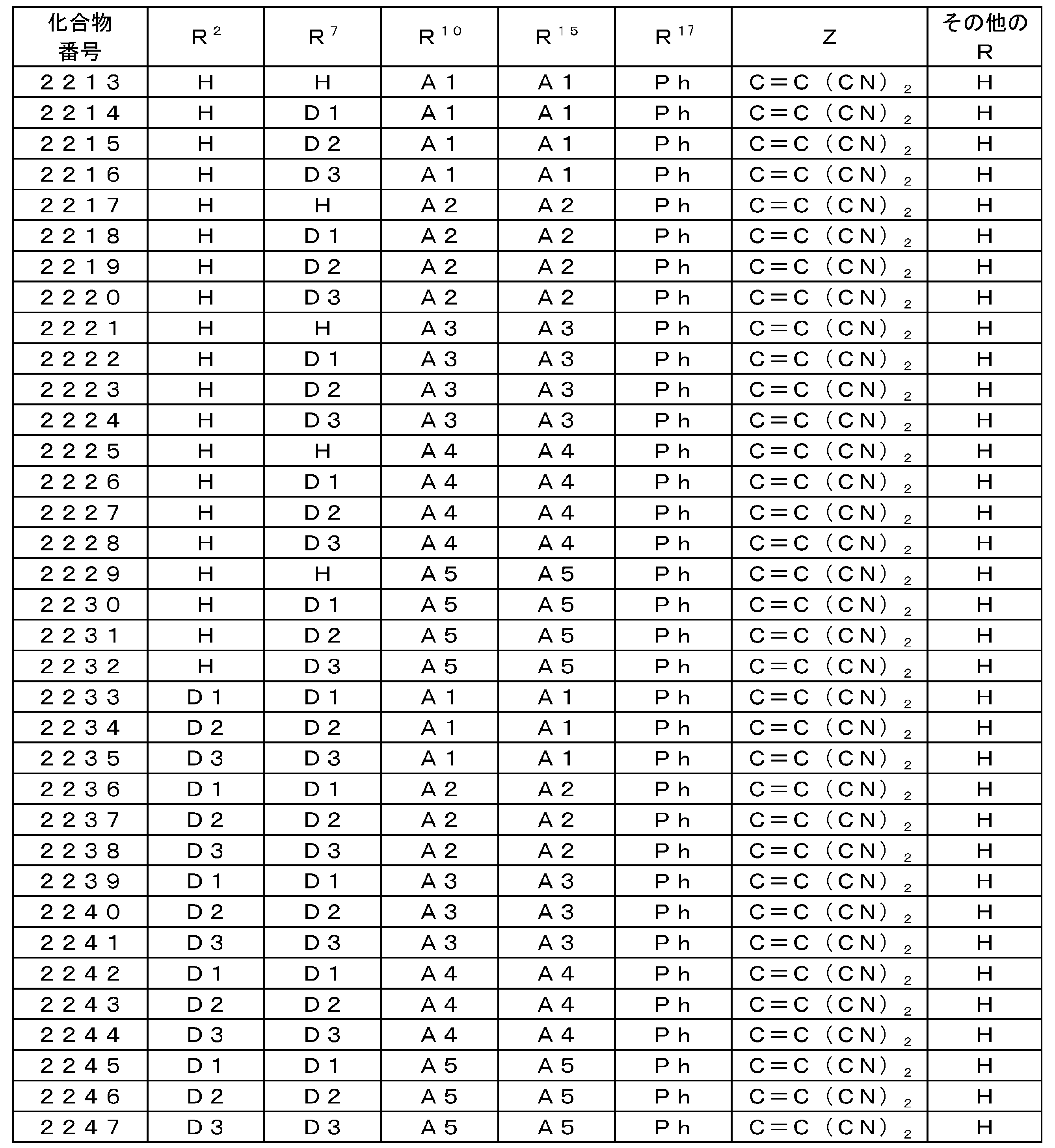

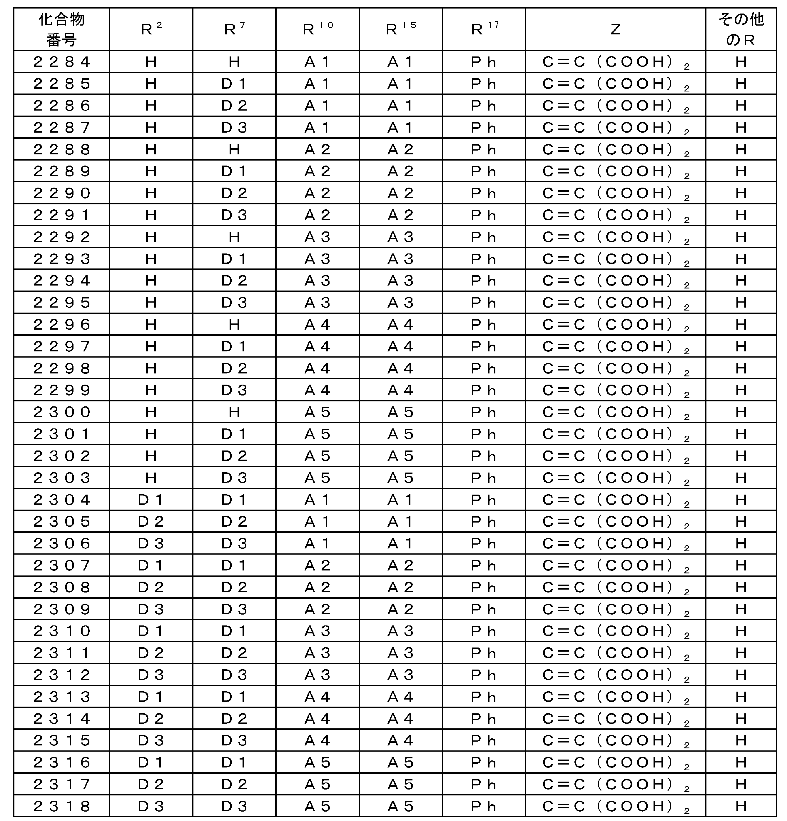
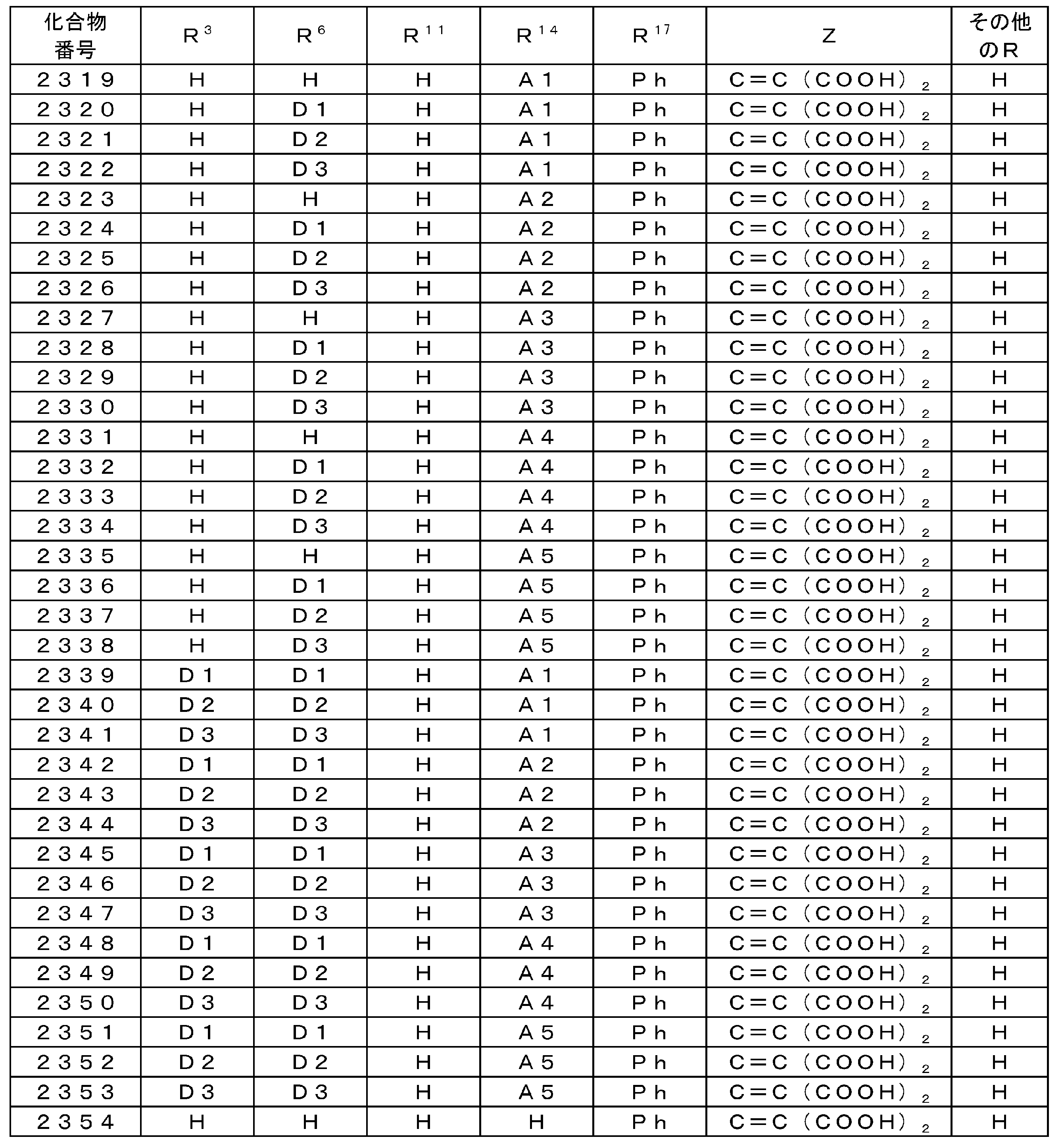

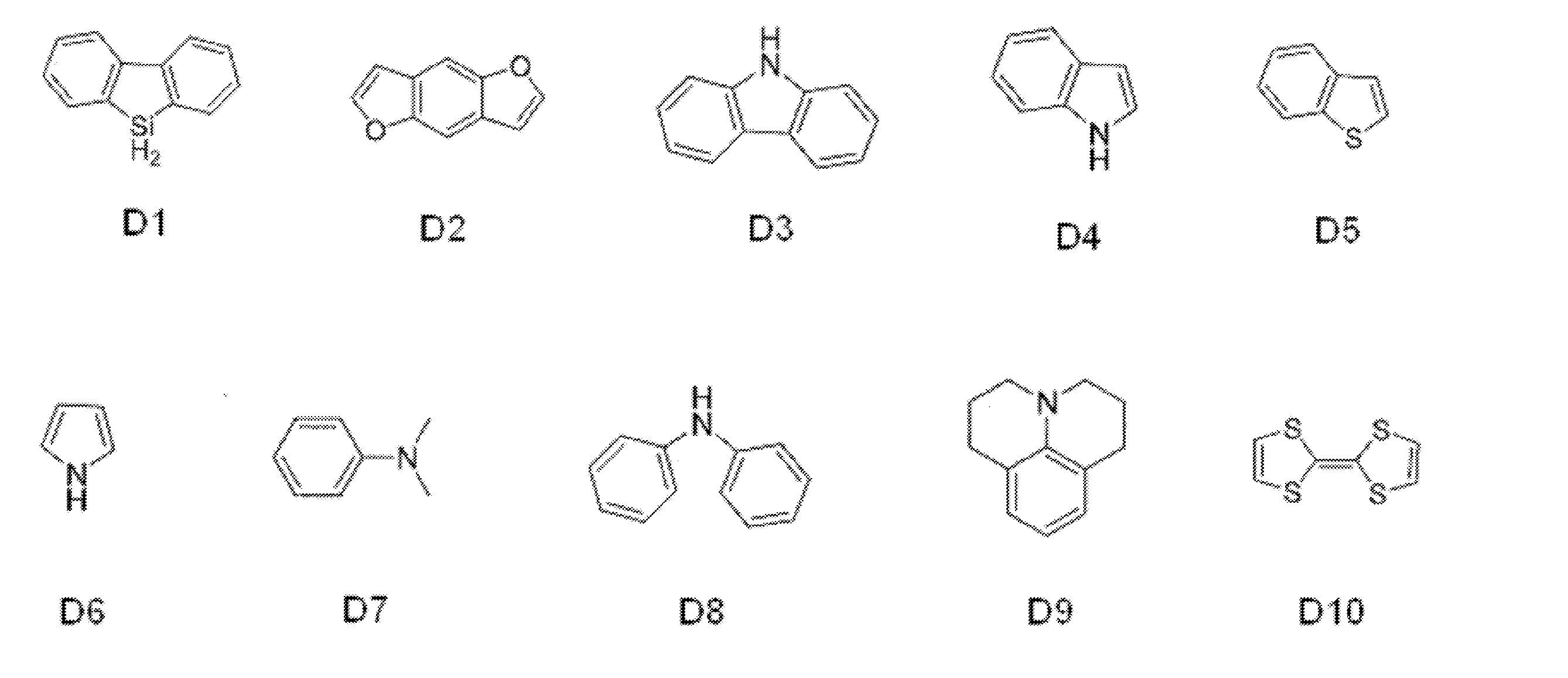
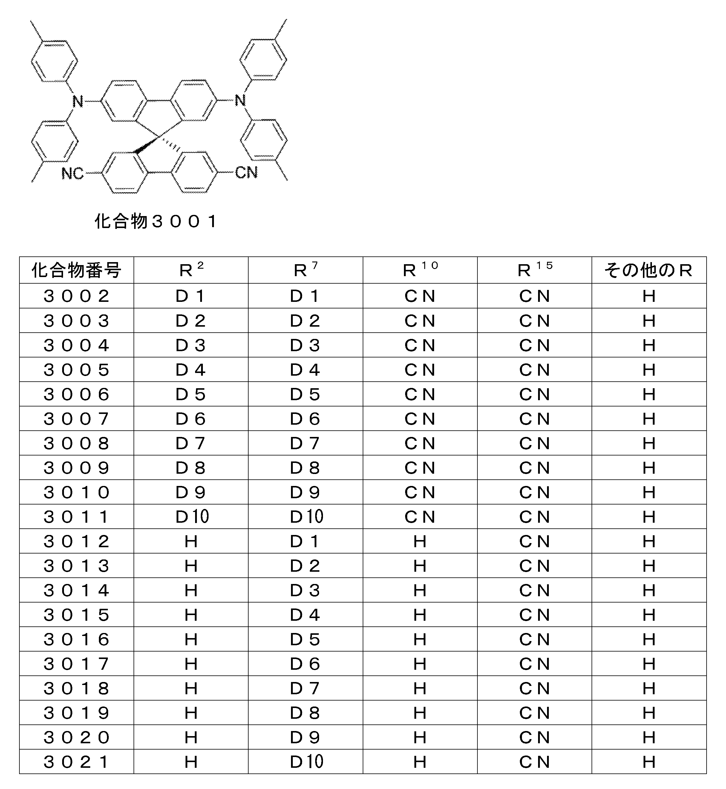

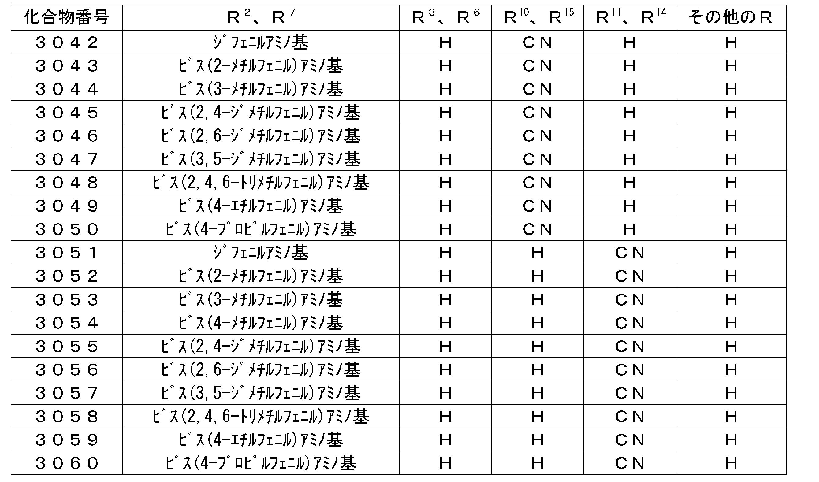
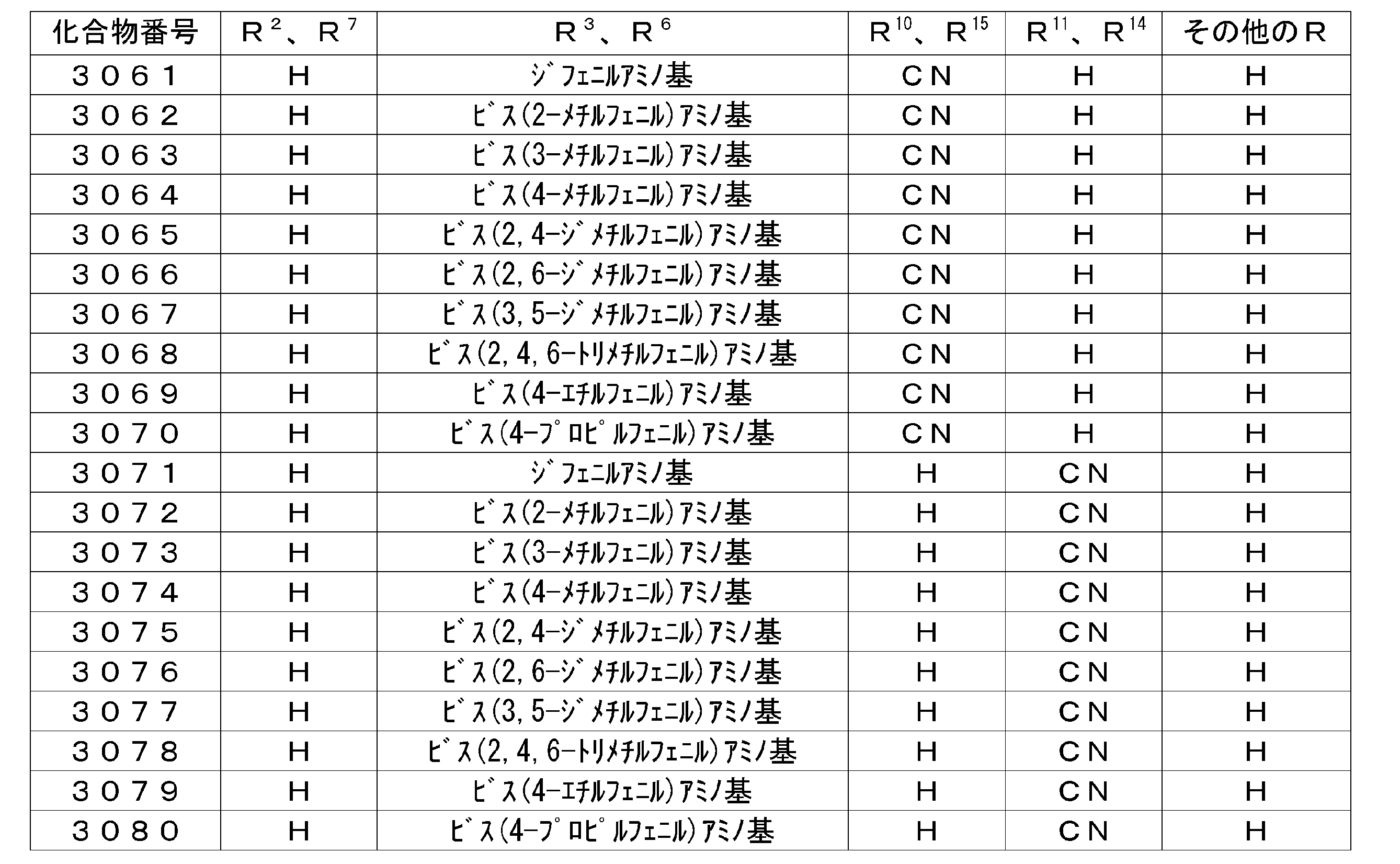
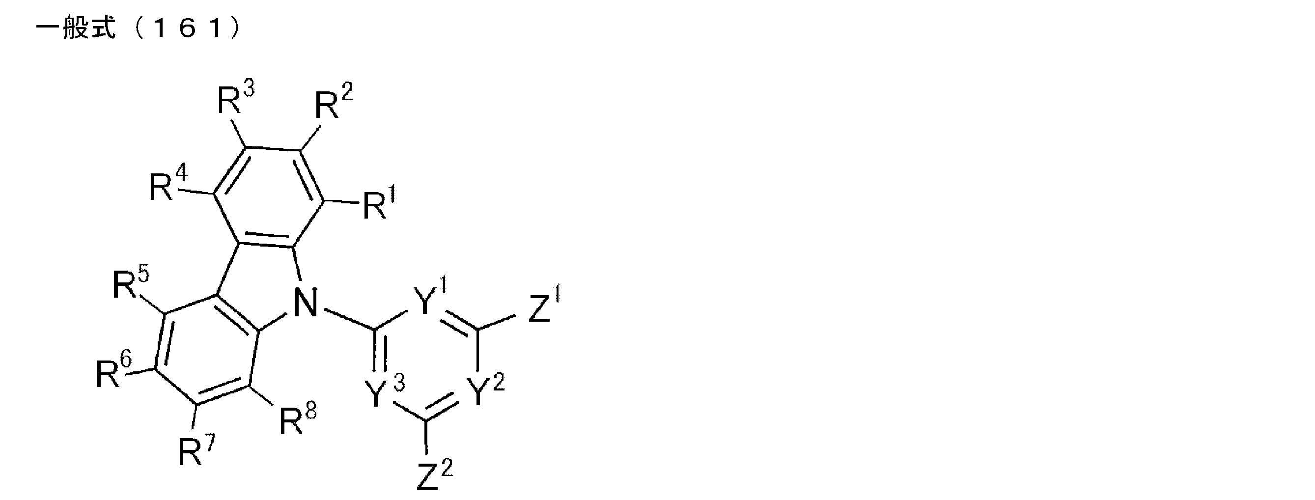

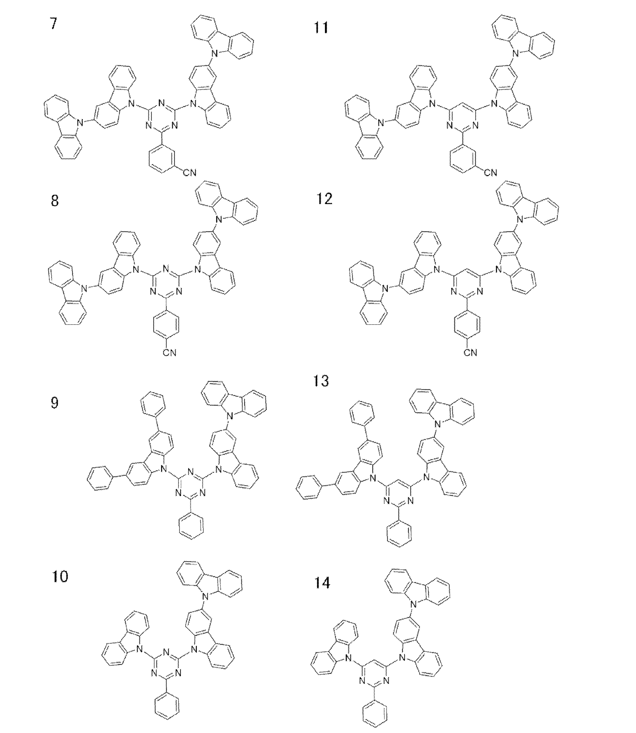
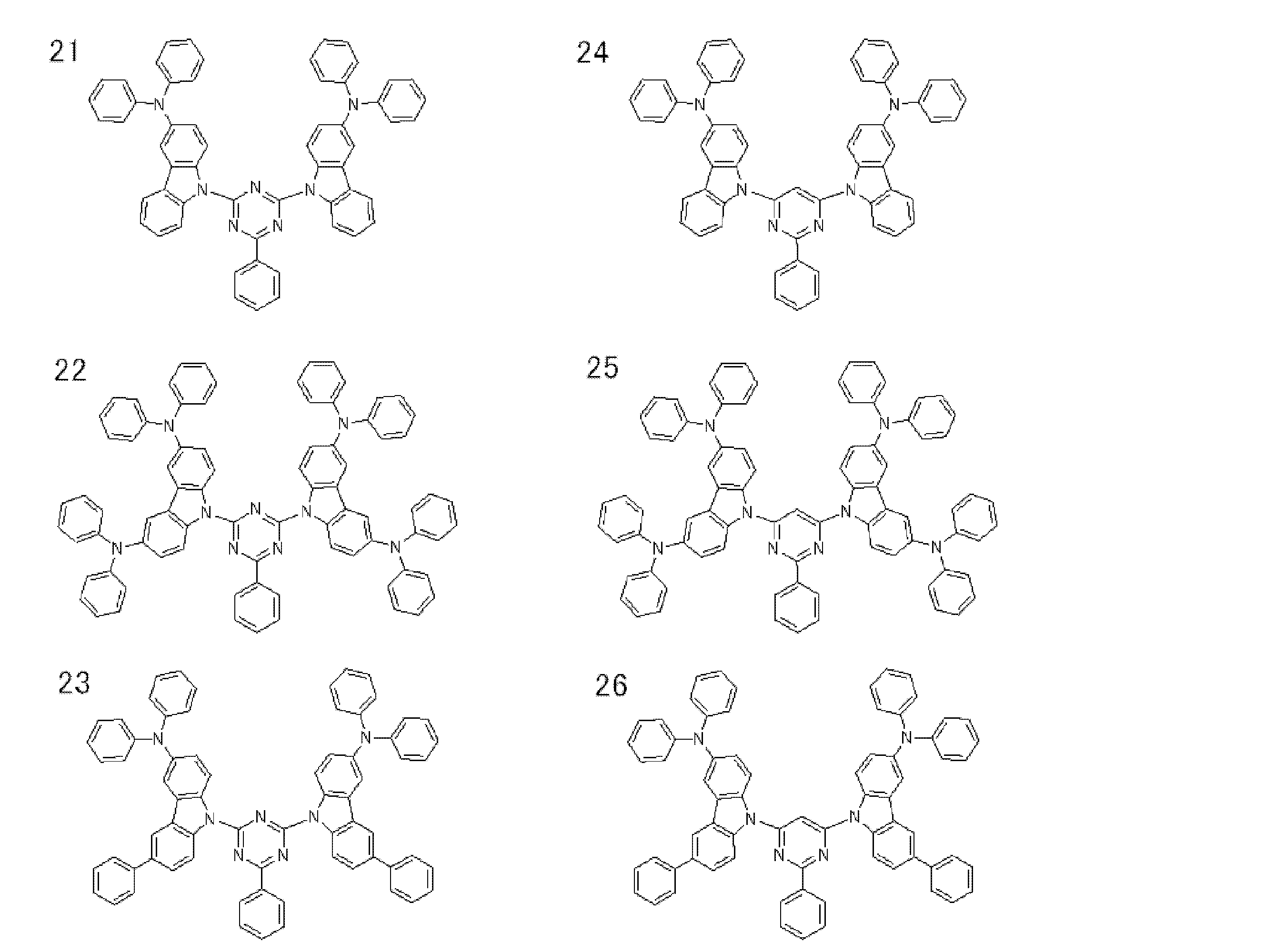
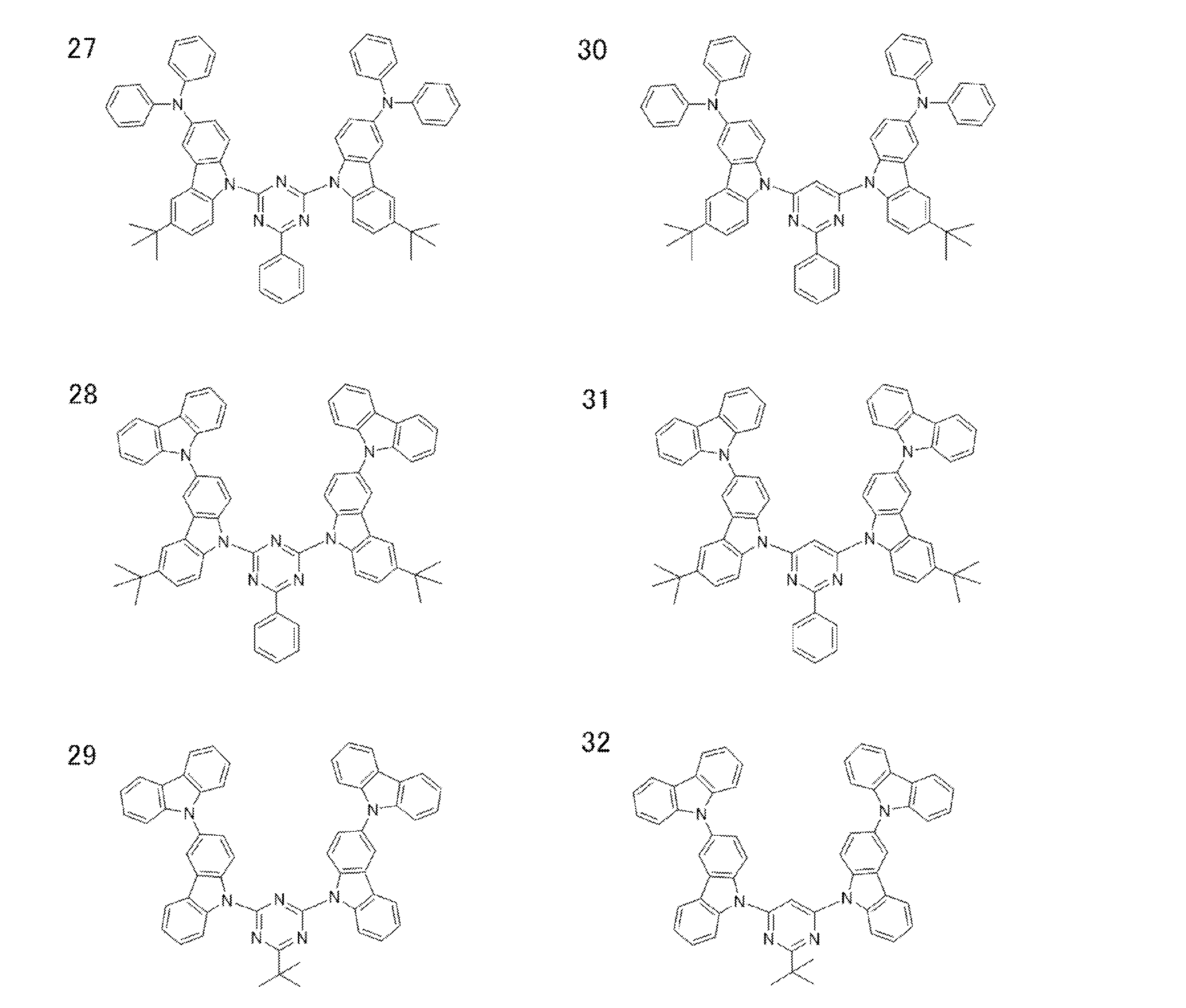

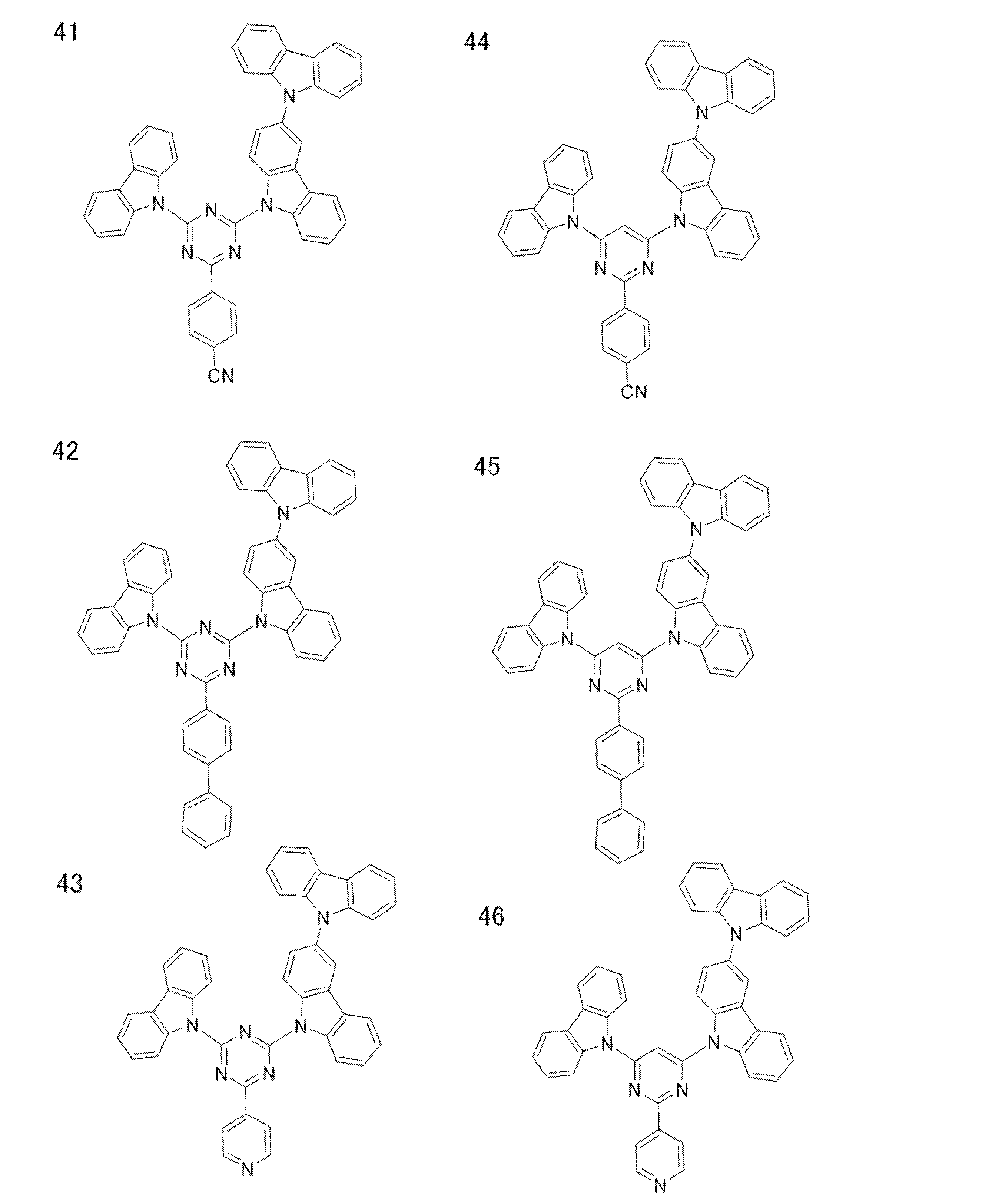


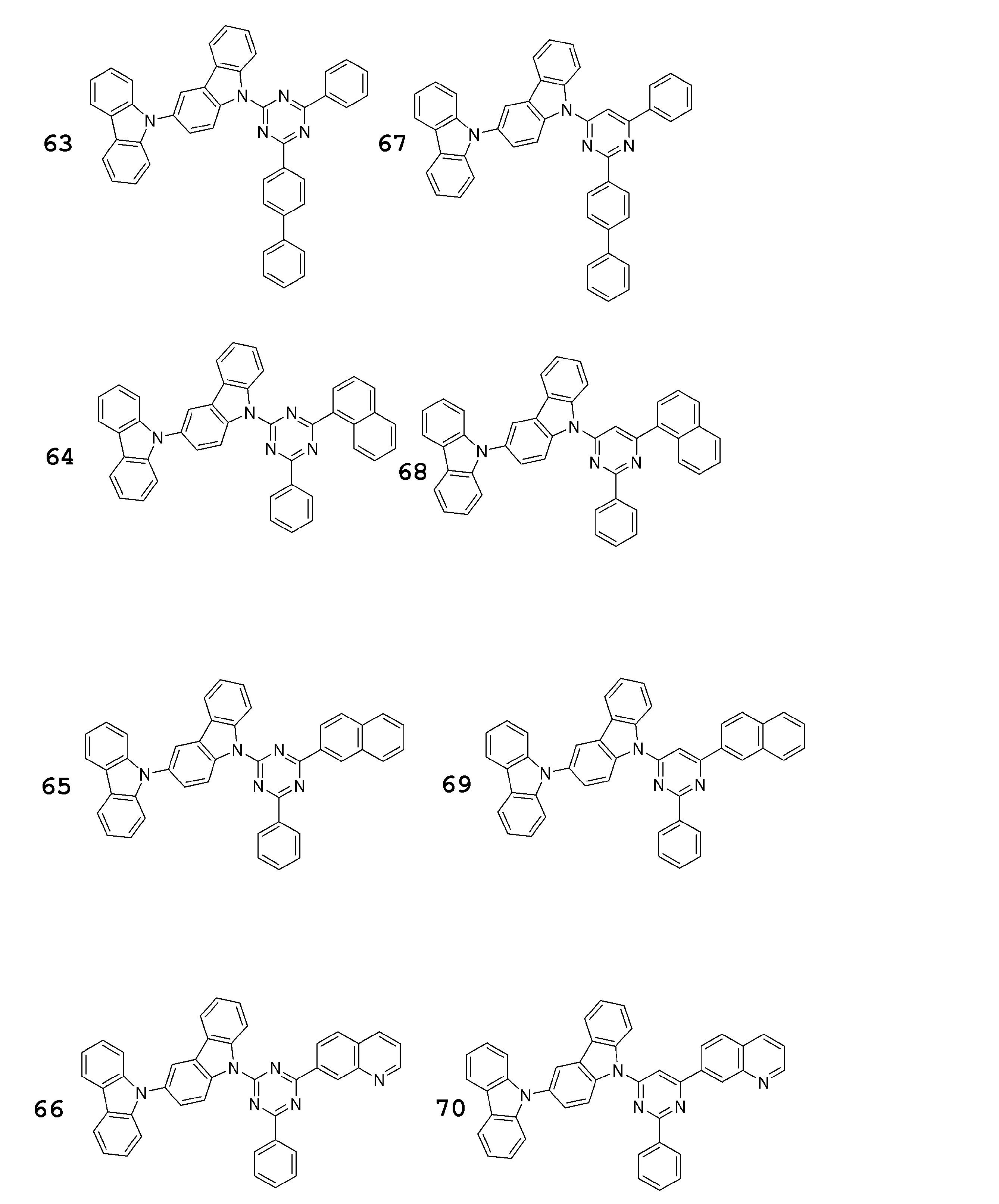
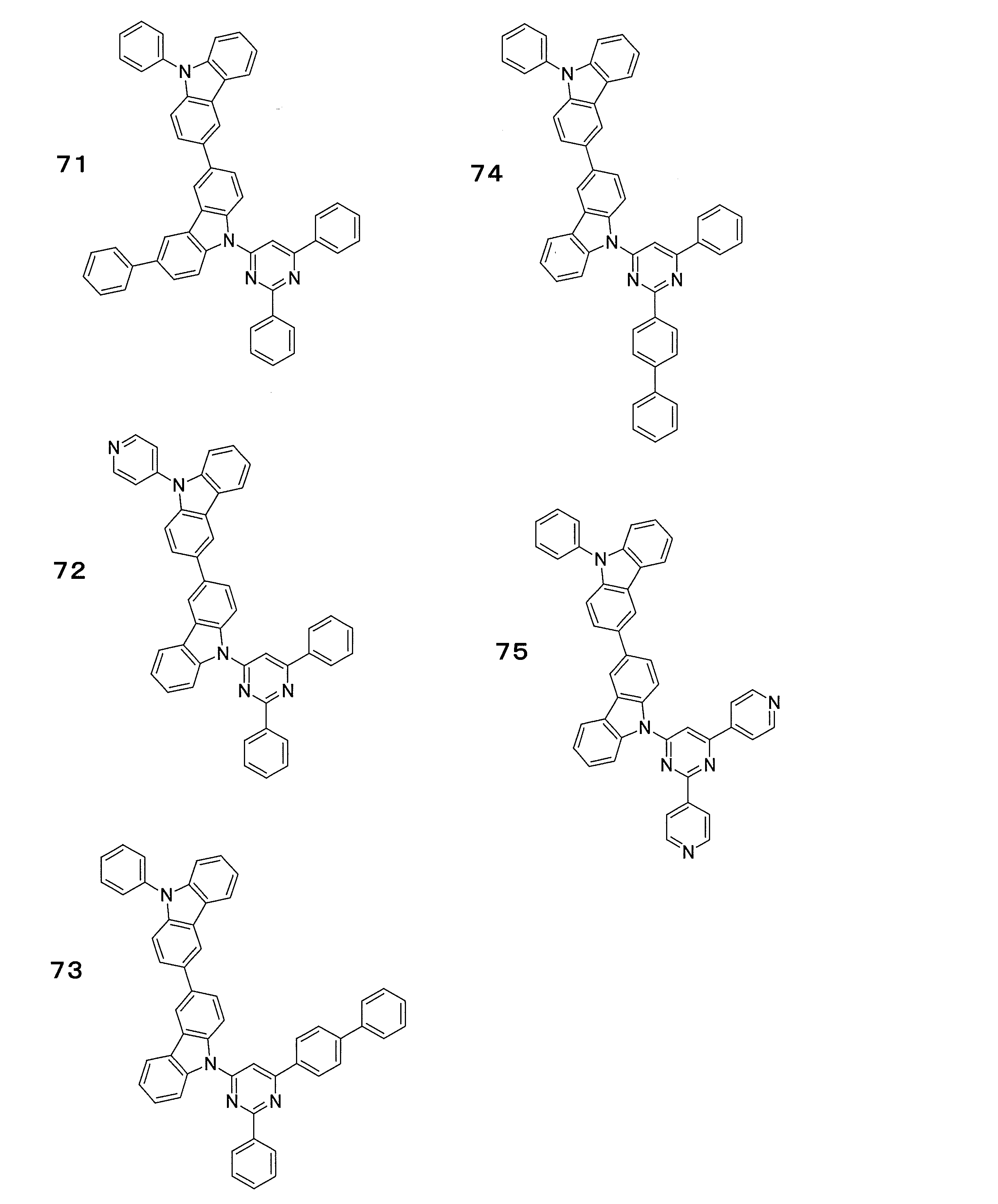


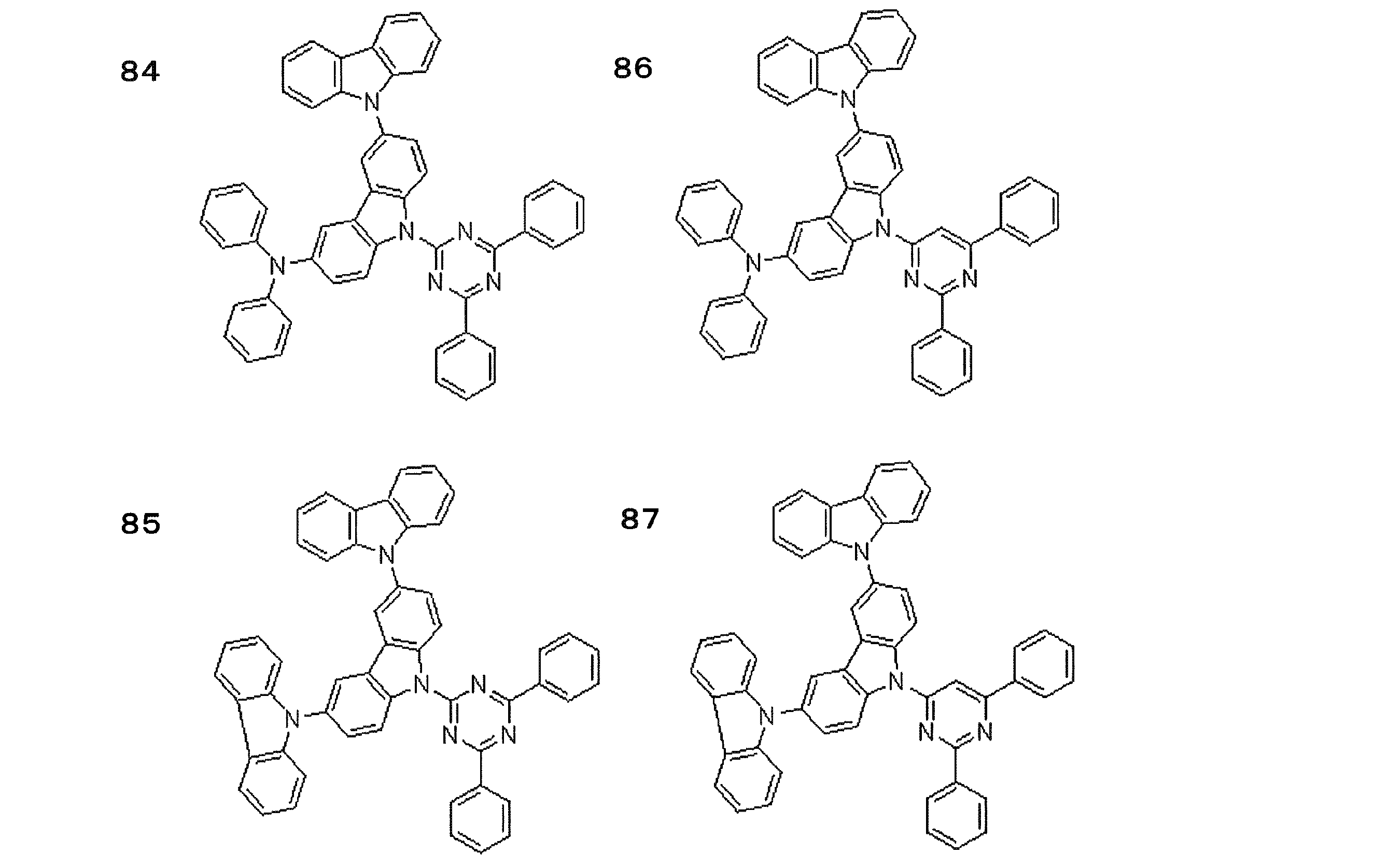


[1] 下記一般式(191)で表される化合物。

[2] 一般式(191)のR1~R4の少なくとも1つが置換もしくは無置換のジアリールアミノ基であって、R5~R8の少なくとも1つが置換もしくは無置換のジアリールアミノ基であることを特徴とする[1]に記載の化合物。
[3] 一般式(191)のR3およびR6が置換もしくは無置換のジアリールアミノ基であることを特徴とする[2]に記載の化合物。
[4] 一般式(191)のR1~R8の少なくとも1つが置換もしくは無置換のジフェニルアミノ基であることを特徴とする[1]~[3]のいずれか1項に記載の化合物。
[5] 一般式(191)のAr2およびAr3が各々独立に置換もしくは無置換のフェニル基であることを特徴とする[1]~[4]のいずれか1項に記載の化合物。
[6] 一般式(191)のAr1が各々独立に置換もしくは無置換のフェニレン基、置換もしくは無置換のナフチレン基、または置換もしくは無置換のアントラセニレン基であることを特徴とする[1]~[5]のいずれか1項に記載の化合物。
[7] 下記一般式(192)で表される構造を有することを特徴とする[1]に記載の化合物。

[8] 一般式(192)のR1~R4の少なくとも1つが置換もしくは無置換のジアリールアミノ基であって、R5~R8の少なくとも1つが置換もしくは無置換のジアリールアミノ基であることを特徴とする[7]に記載の化合物。
[9] 一般式(192)のR3およびR6が置換もしくは無置換のジアリールアミノ基であることを特徴とする[8]に記載の化合物。 Preferred examples of the light emitting material include the following compounds.
[1] A compound represented by the following general formula (191).
[2] At least one of R 1 to R 4 in the general formula (191) is a substituted or unsubstituted diarylamino group, and at least one of R 5 to R 8 is a substituted or unsubstituted diarylamino group [1] The compound according to [1].
[3] The compound according to [2], wherein R 3 and R 6 in the general formula (191) are a substituted or unsubstituted diarylamino group.
[4] The compound according to any one of [1] to [3], wherein at least one of R 1 to R 8 in the general formula (191) is a substituted or unsubstituted diphenylamino group.
[5] The compound according to any one of [1] to [4], wherein Ar 2 and Ar 3 in formula (191) are each independently a substituted or unsubstituted phenyl group.
[6] The Ar 1 in the general formula (191) is each independently a substituted or unsubstituted phenylene group, a substituted or unsubstituted naphthylene group, or a substituted or unsubstituted anthracenylene group. [5] The compound according to any one of [5].
[7] The compound according to [1], which has a structure represented by the following general formula (192).
[8] At least one of R 1 to R 4 in the general formula (192) is a substituted or unsubstituted diarylamino group, and at least one of R 5 to R 8 is a substituted or unsubstituted diarylamino group [7] The compound according to [7].
[9] The compound according to [8], wherein R 3 and R 6 in the general formula (192) are substituted or unsubstituted diarylamino groups.
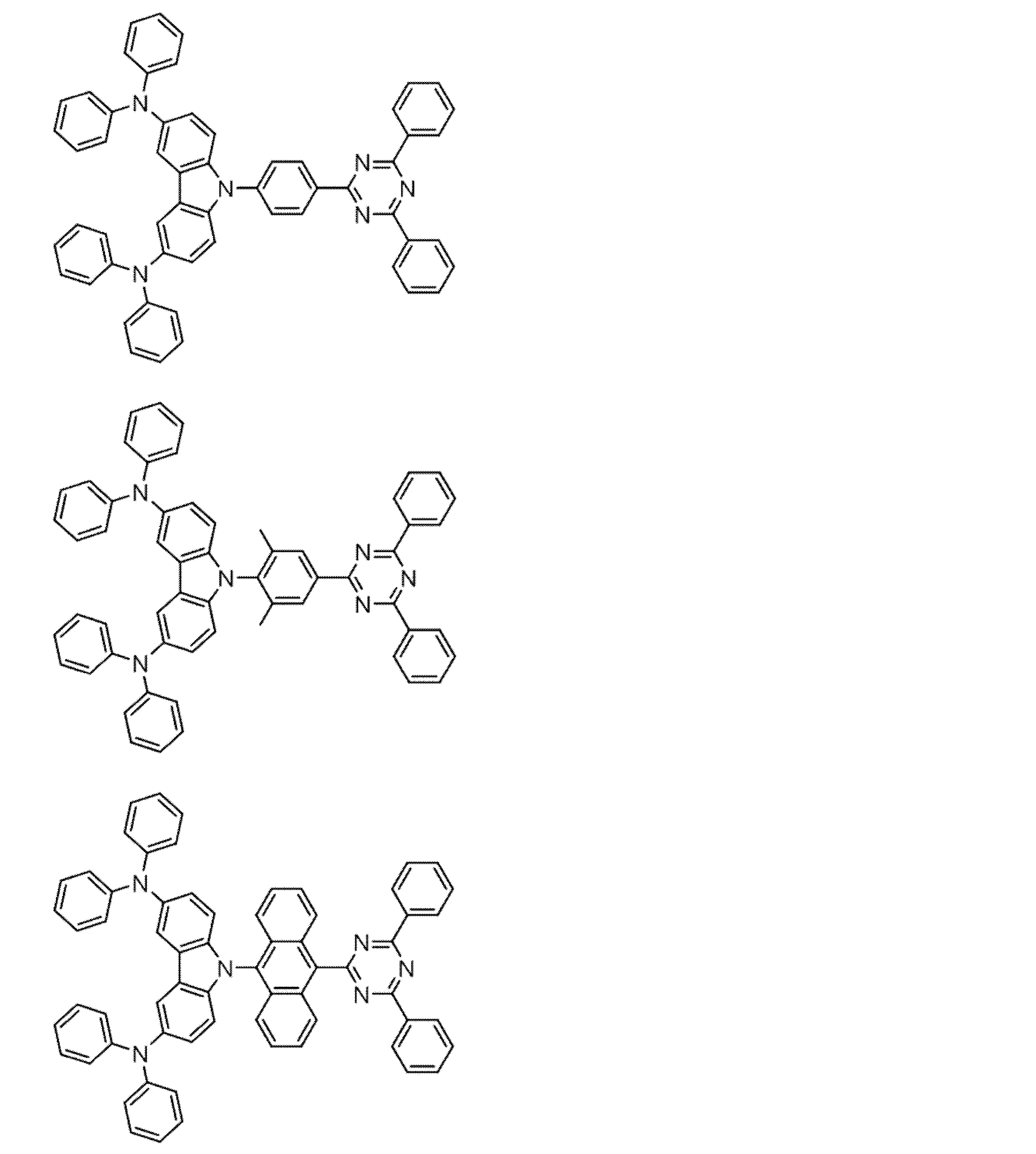
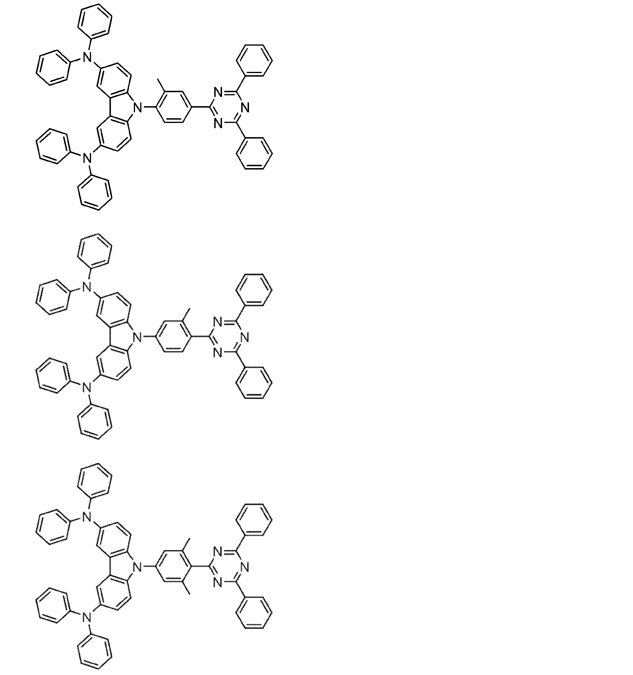
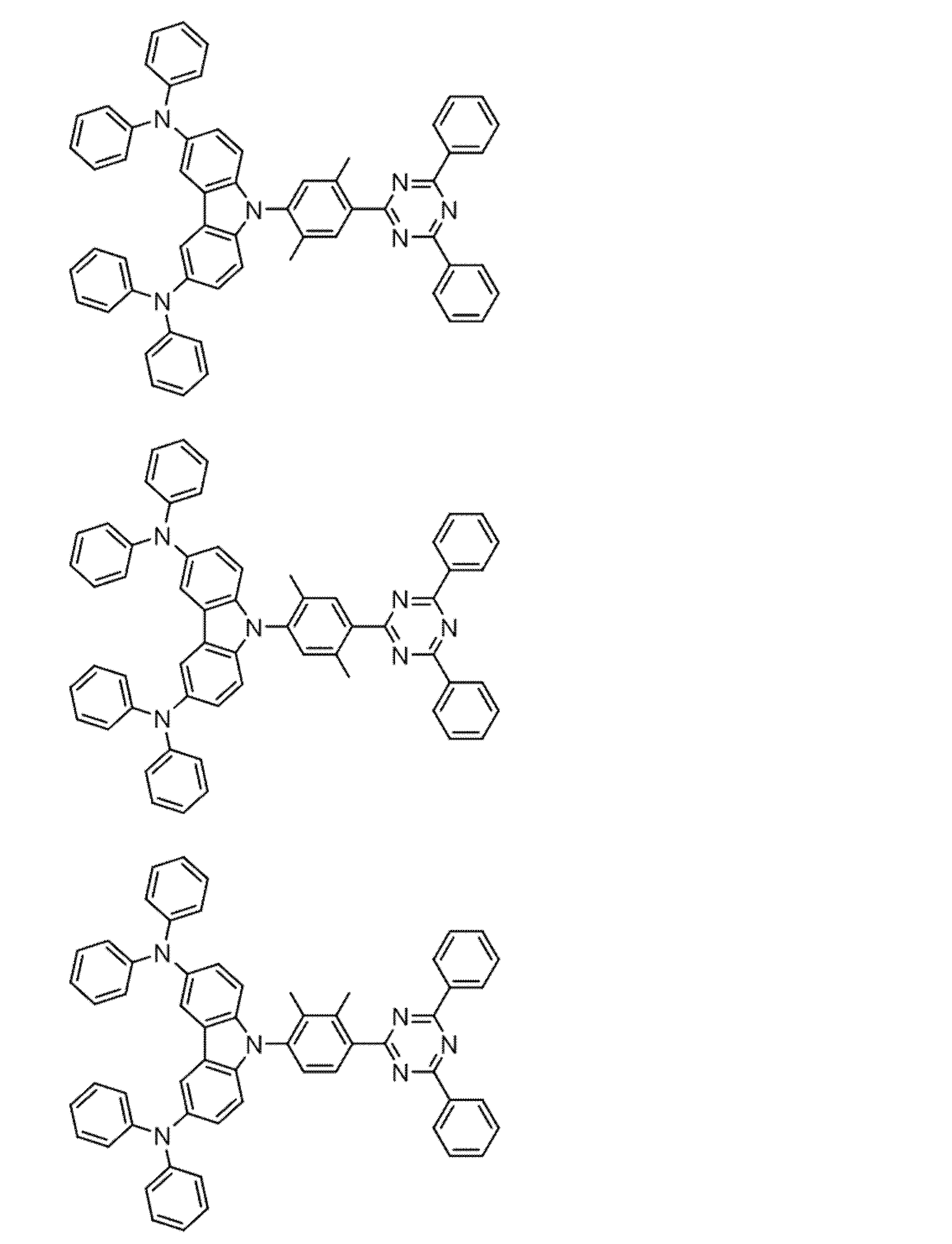
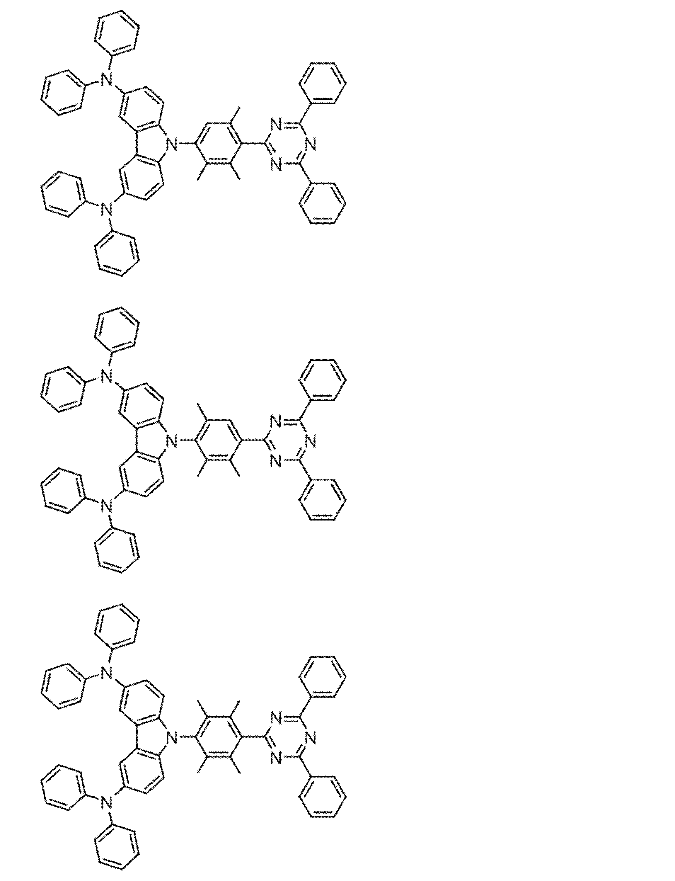
[1]下記一般式(201)で表される化合物。
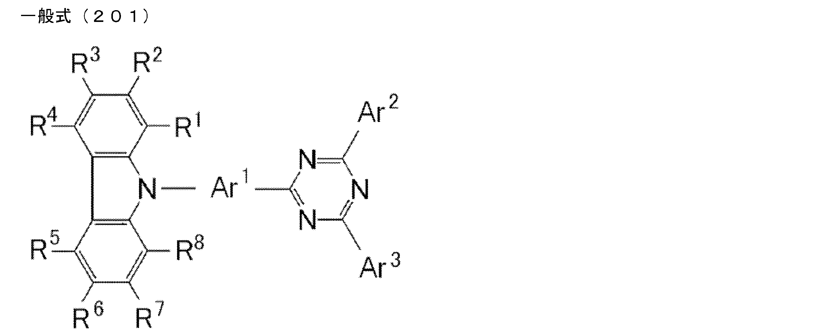
[2]前記一般式(201)のR3およびR6の少なくとも一つが置換もしくは無置換のカルバゾリル基である[1]の化合物。
[3]前記カルバゾリル基が、1-カルバゾリル基、2-カルバゾリル基、3-カルバゾリル基または4-カルバゾリル基である[1]または[2]に記載の化合物。
[4]前記カルバゾリル基が、カルバゾール環構造中の窒素原子に置換基を有する[1]~[3]のいずれか一つの化合物。。
[5]前記一般式(201)のAr1、Ar2およびAr3の少なくとも一つが、ベンゼン環またはナフタレン環である[1]~[4]のいずれか一つの化合物。 Preferred examples of the light emitting material include the following compounds.
[1] A compound represented by the following general formula (201).
[2] The compound of [1], wherein at least one of R 3 and R 6 in the general formula (201) is a substituted or unsubstituted carbazolyl group.
[3] The compound according to [1] or [2], wherein the carbazolyl group is a 1-carbazolyl group, 2-carbazolyl group, 3-carbazolyl group or 4-carbazolyl group.
[4] The compound according to any one of [1] to [3], wherein the carbazolyl group has a substituent on a nitrogen atom in the carbazole ring structure. .
[5] The compound according to any one of [1] to [4], wherein at least one of Ar 1 , Ar 2 and Ar 3 in the general formula (201) is a benzene ring or a naphthalene ring.
[7]前記一般式(201)のAr1、Ar2およびAr3がベンゼン環である[1]~[6]のいずれか一つの化合物。 [6] The compound according to any one of [1] to [5], wherein Ar 1 , Ar 2 and Ar 3 in the general formula (201) are the same aromatic ring or heteroaromatic ring.
[7] The compound according to any one of [1] to [6], wherein Ar 1 , Ar 2 and Ar 3 in the general formula (201) are benzene rings.
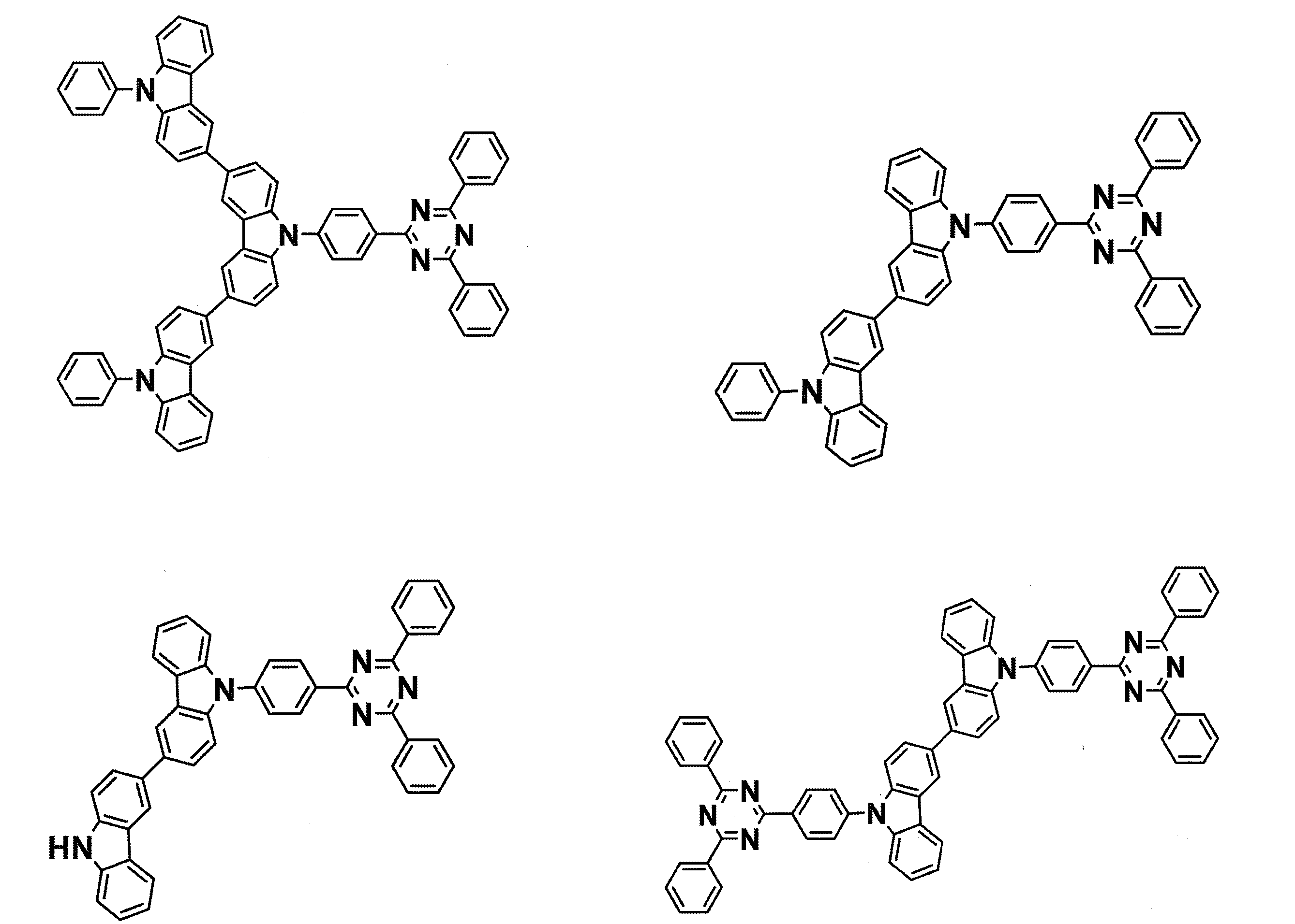
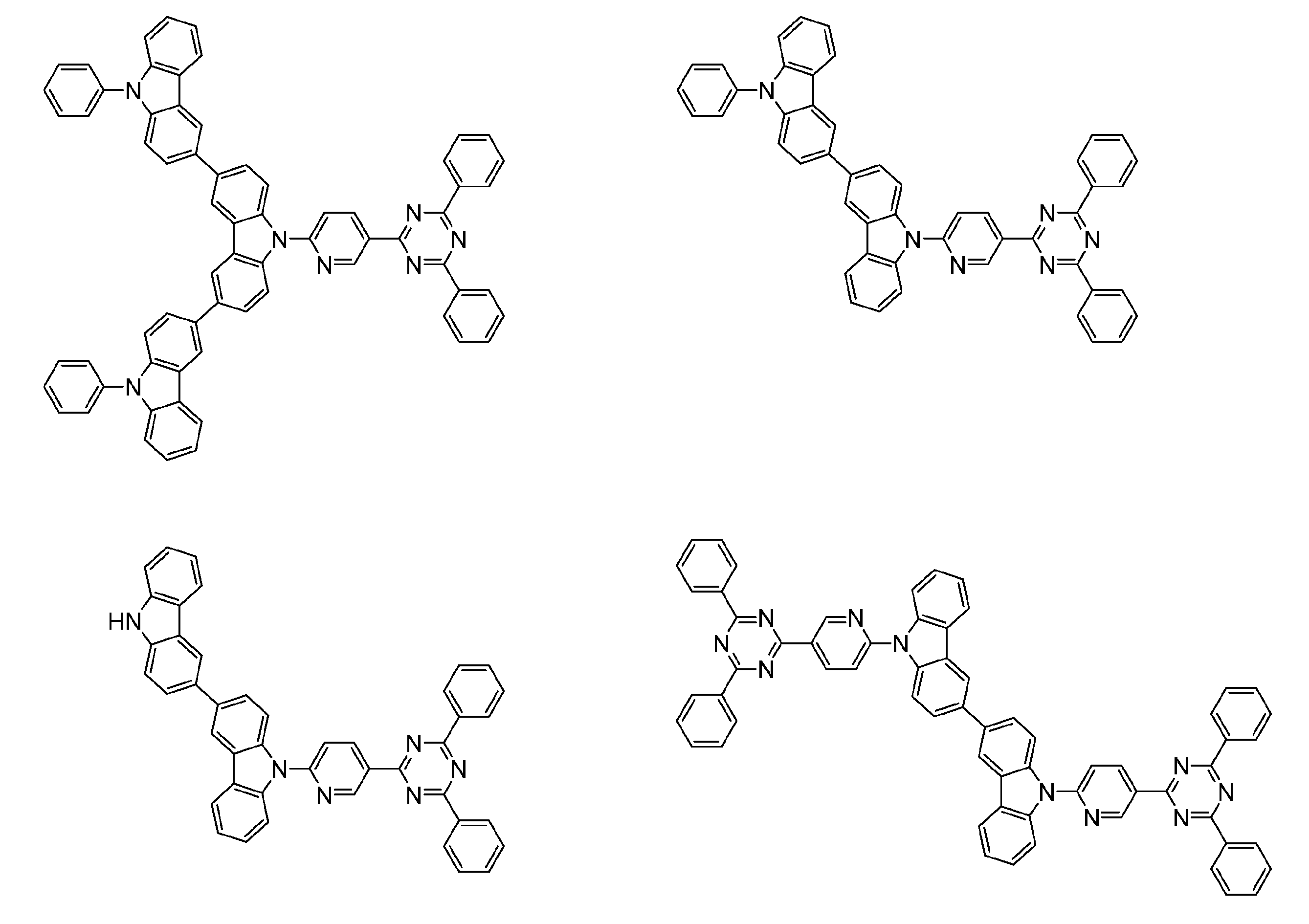

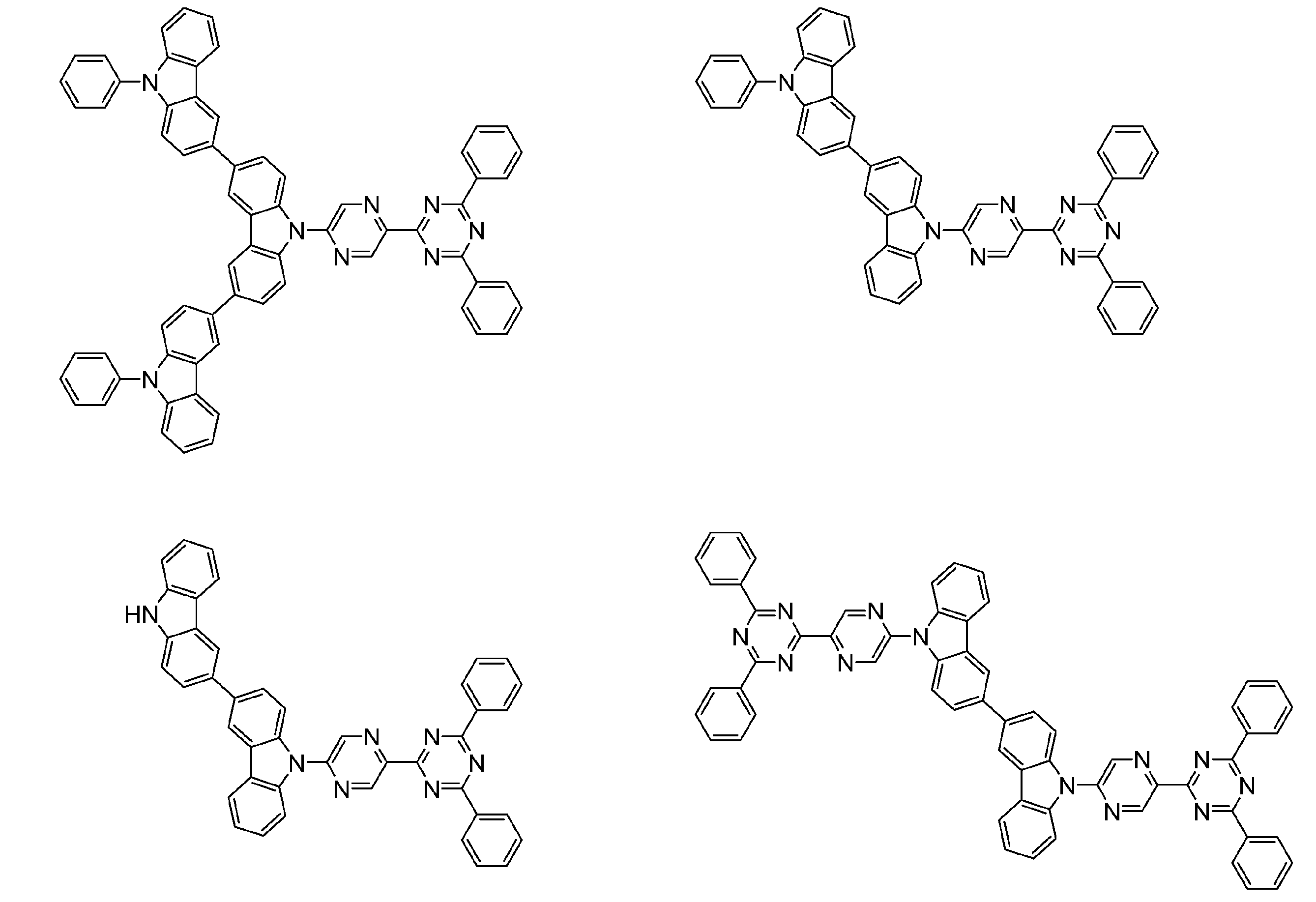

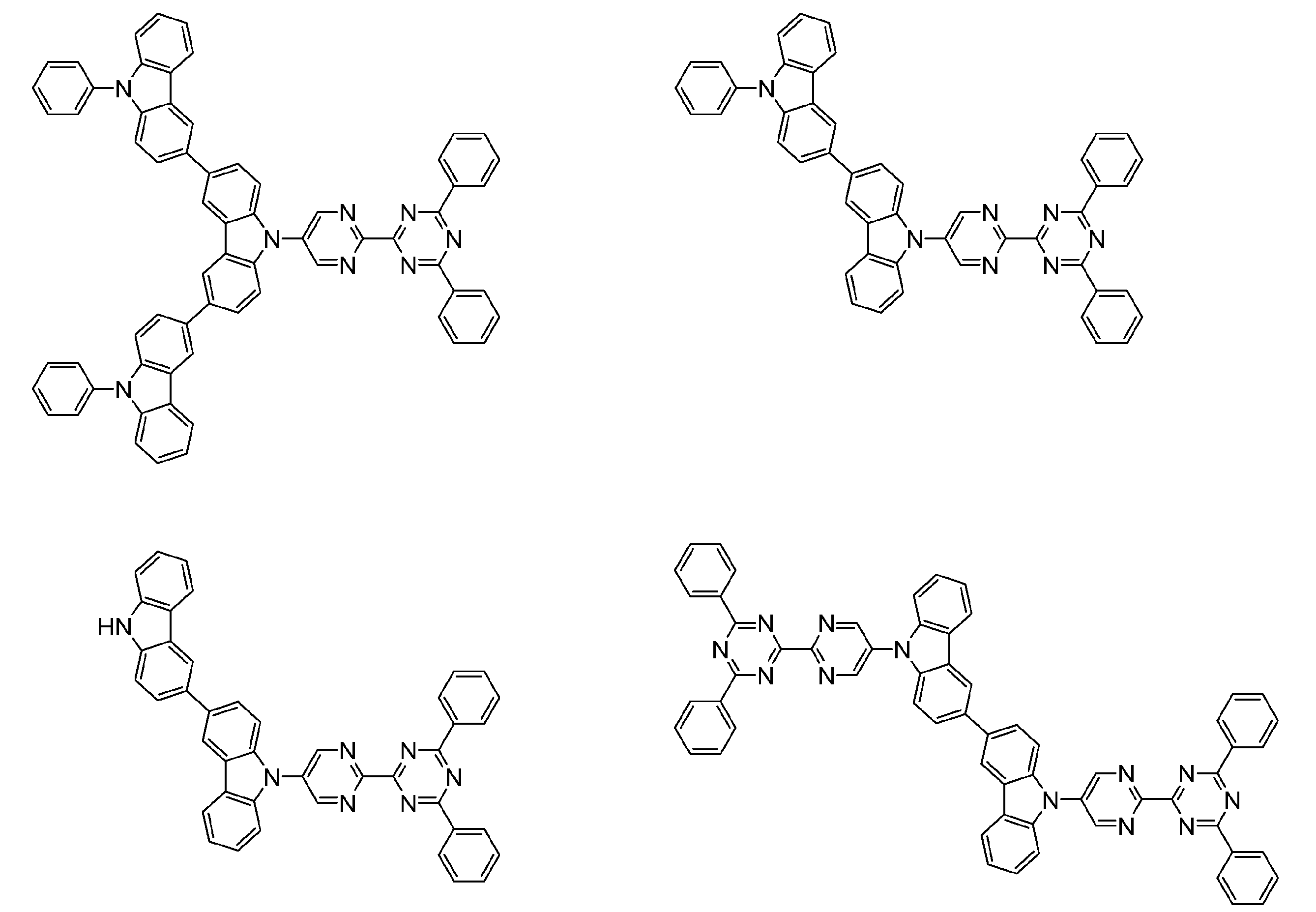
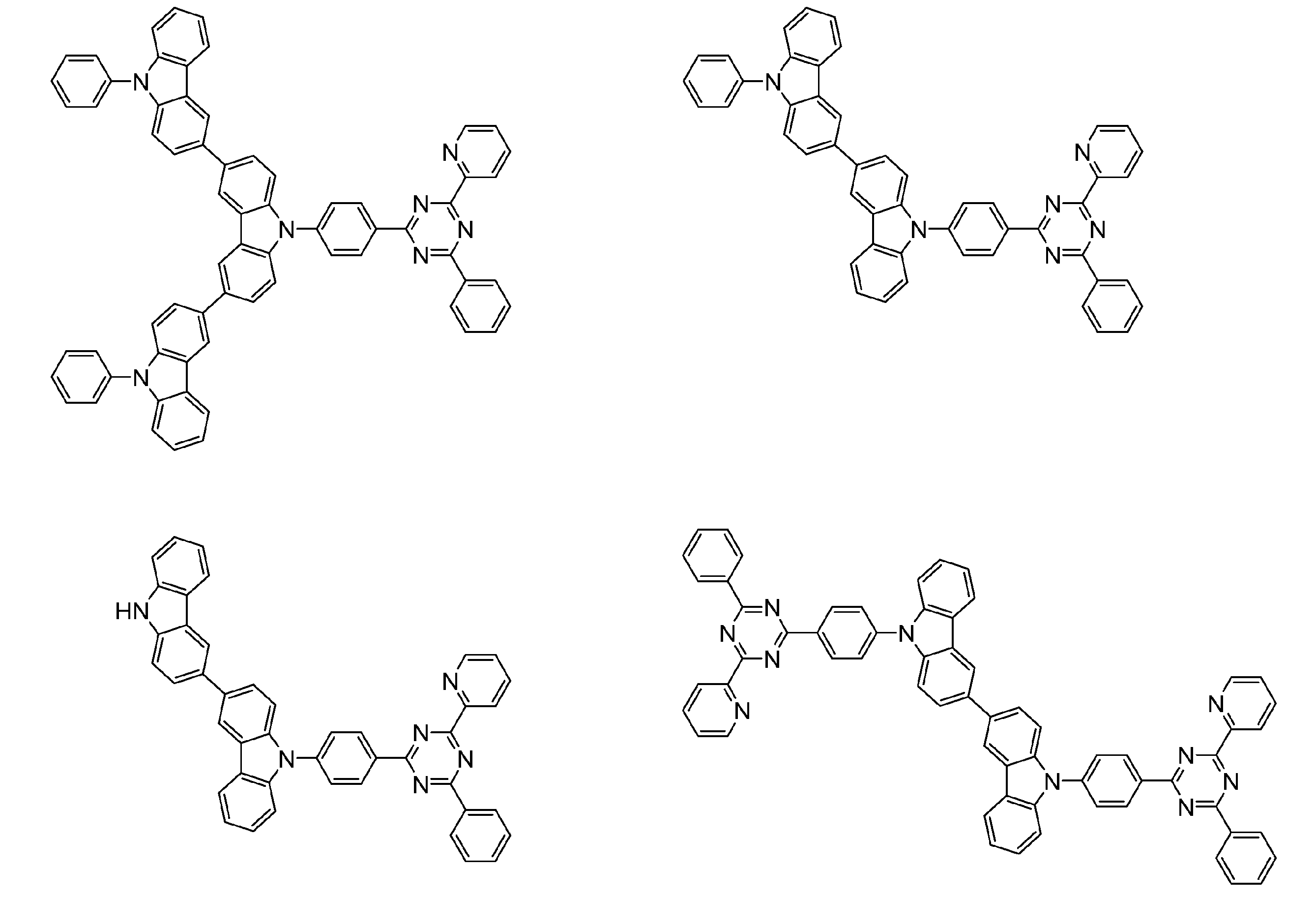


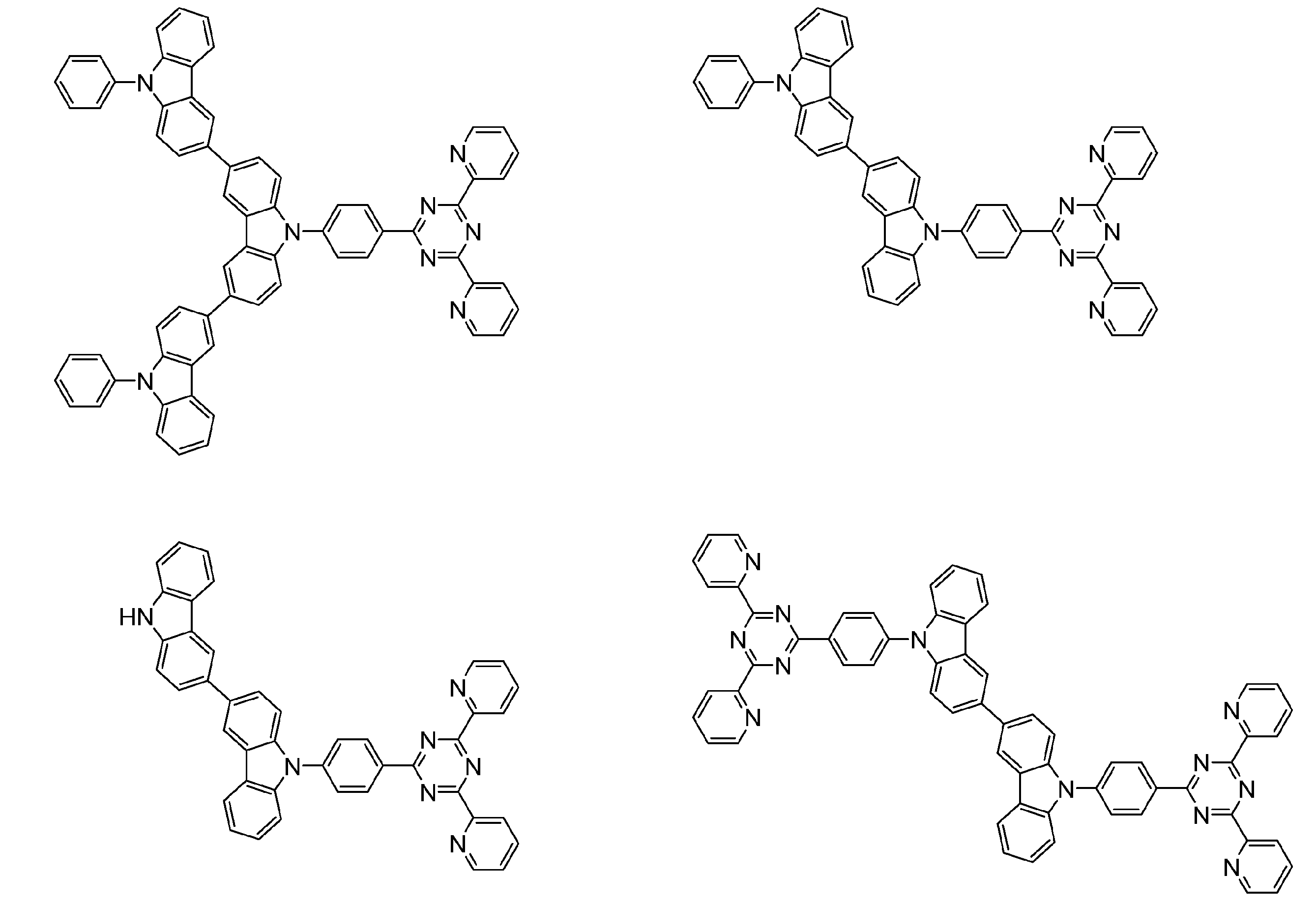

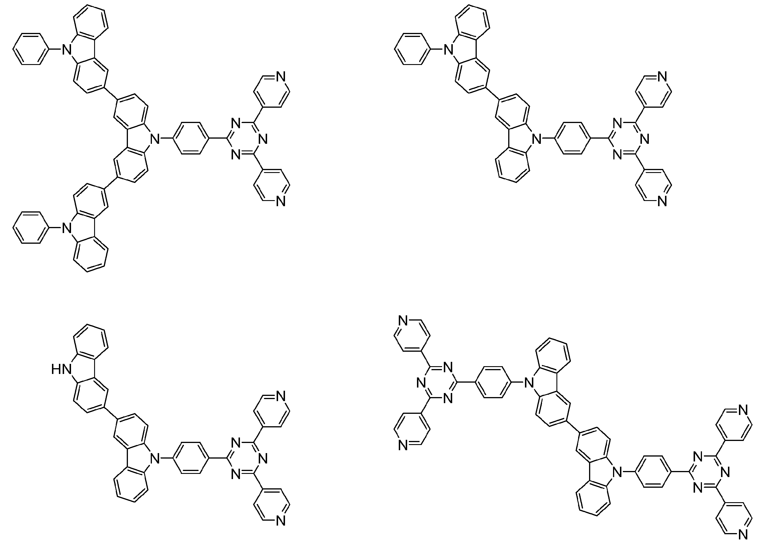
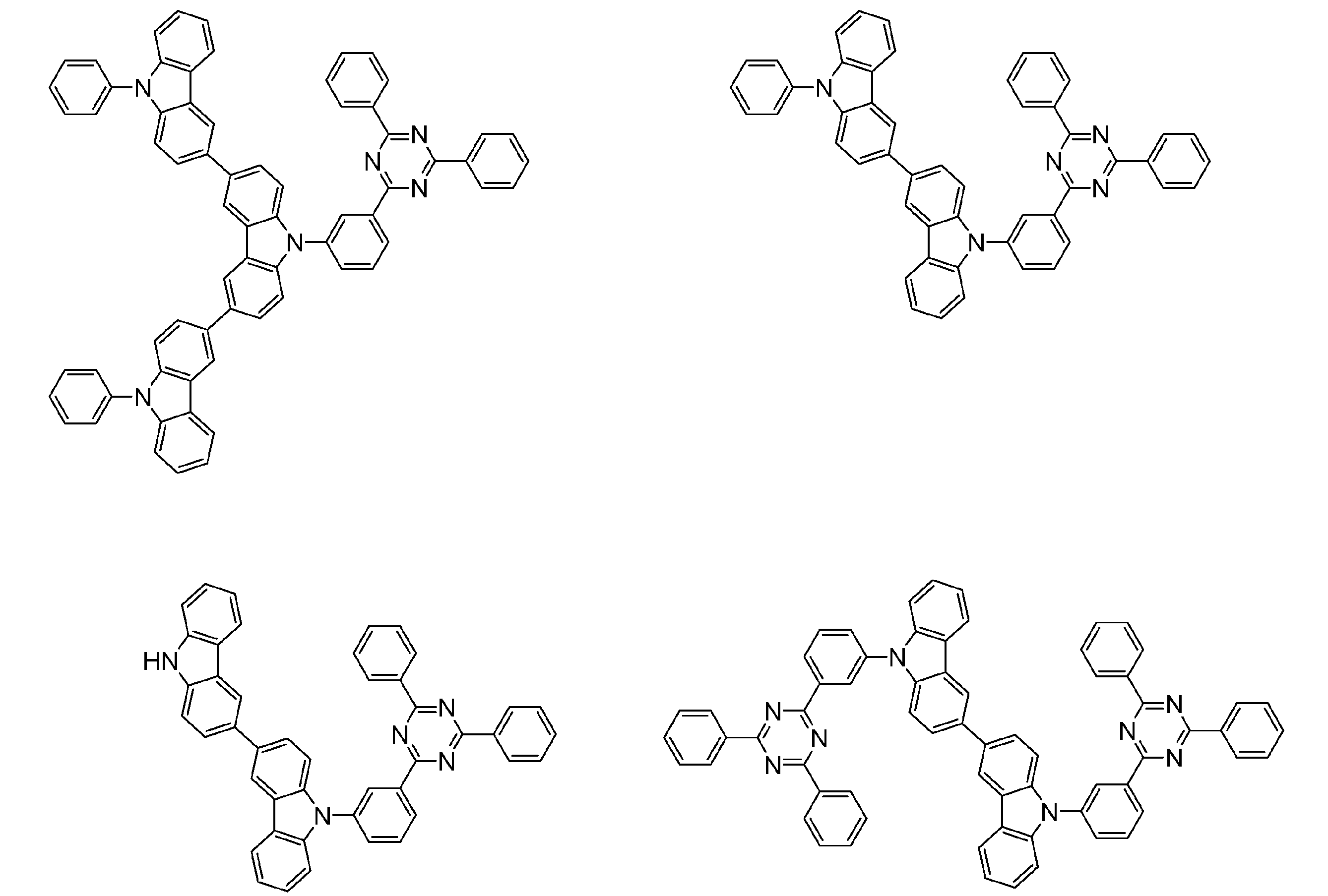


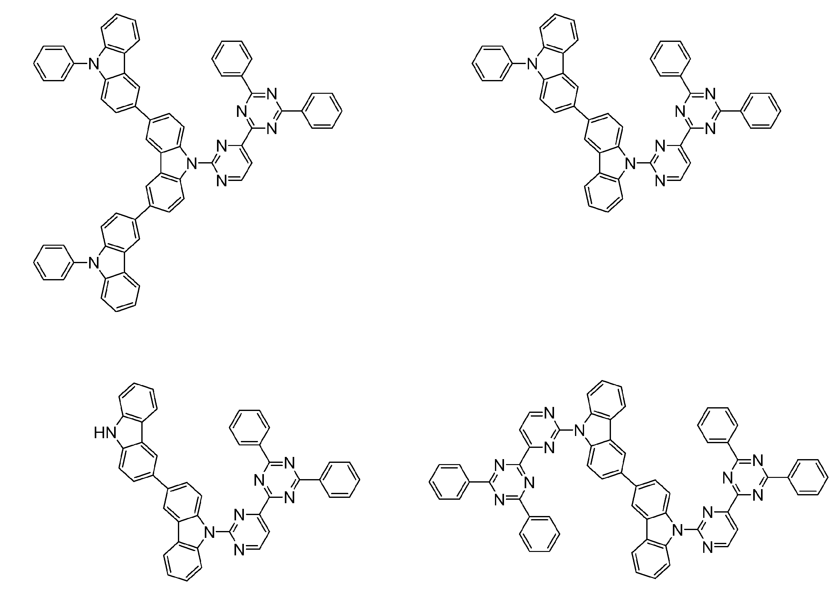

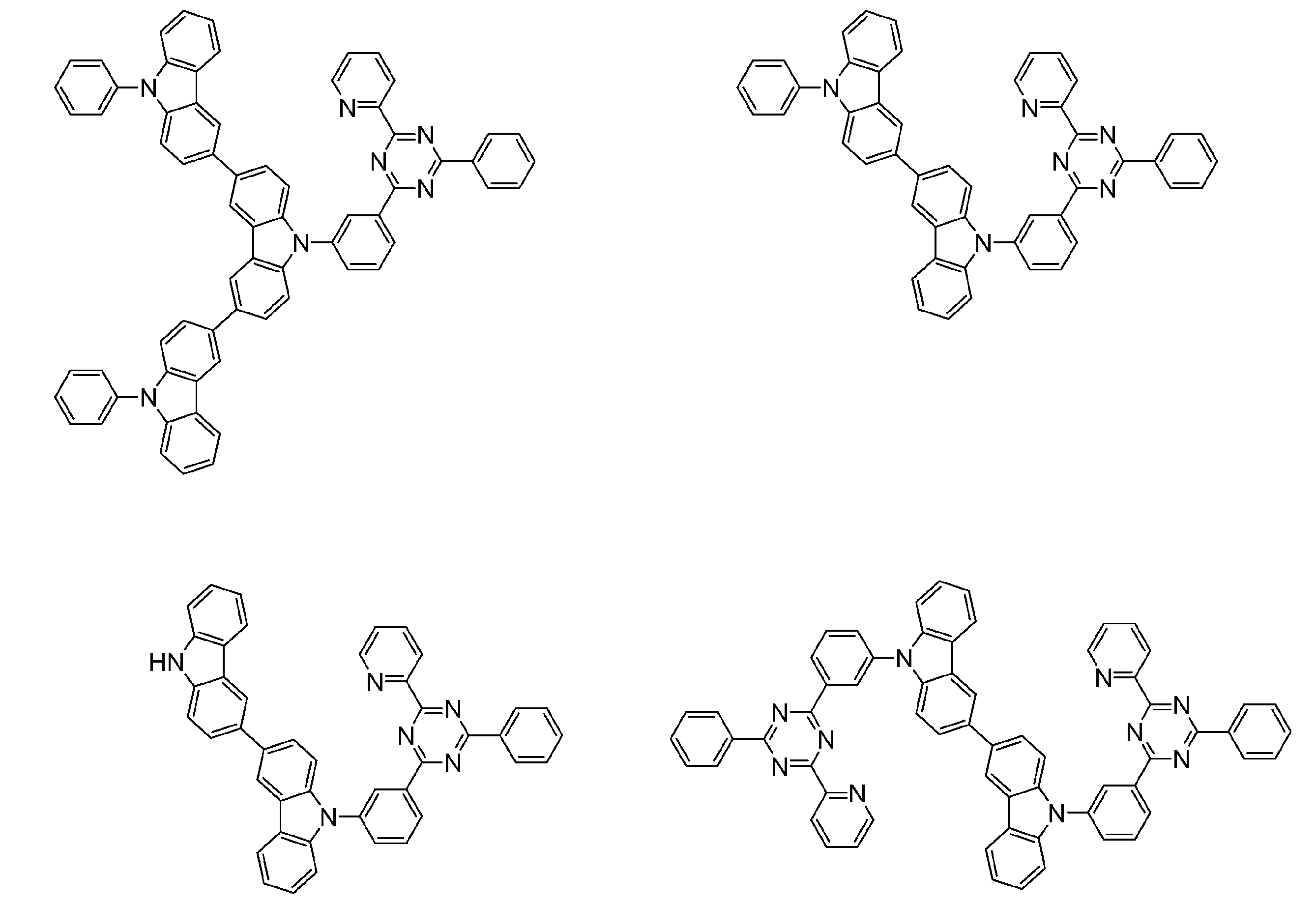
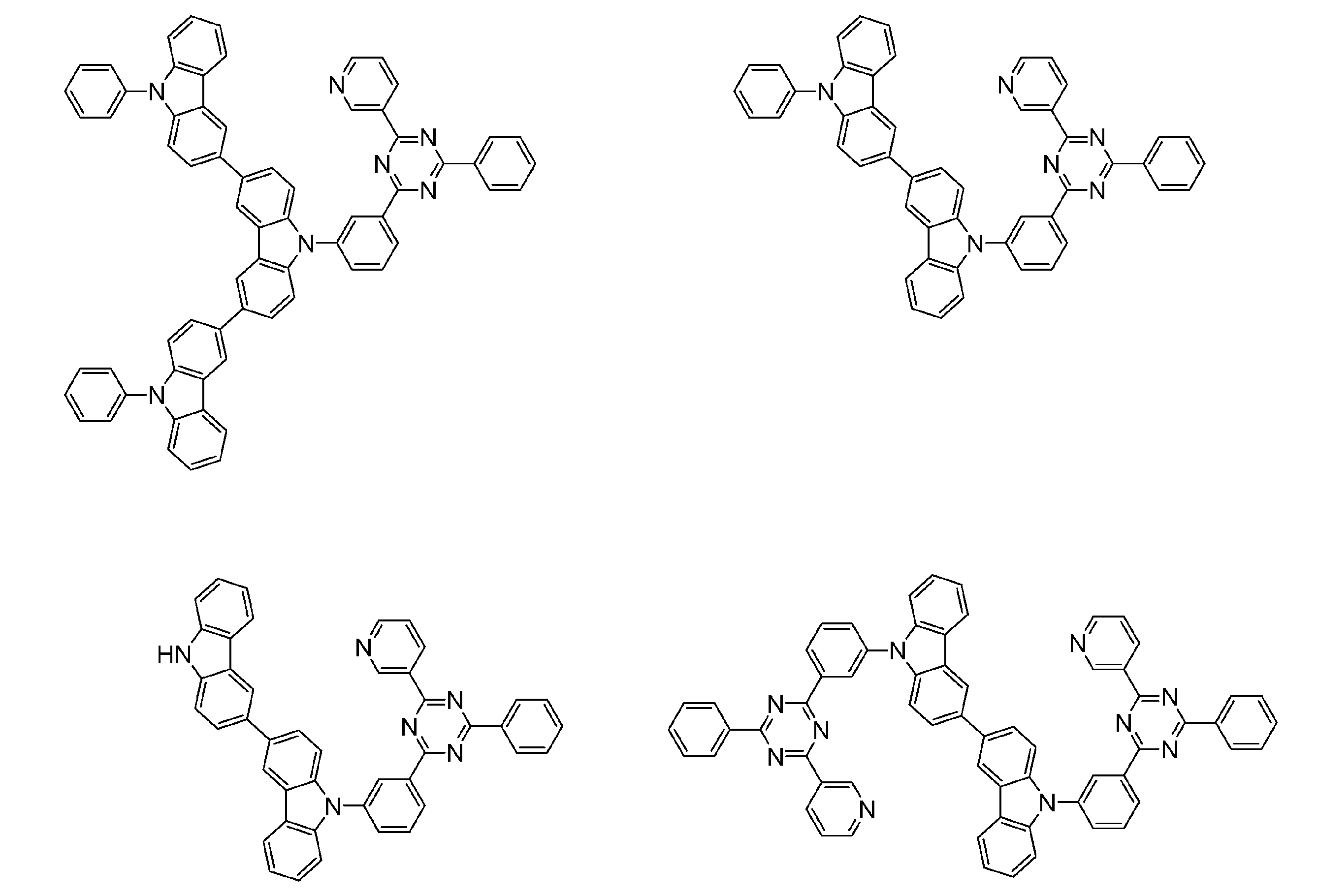


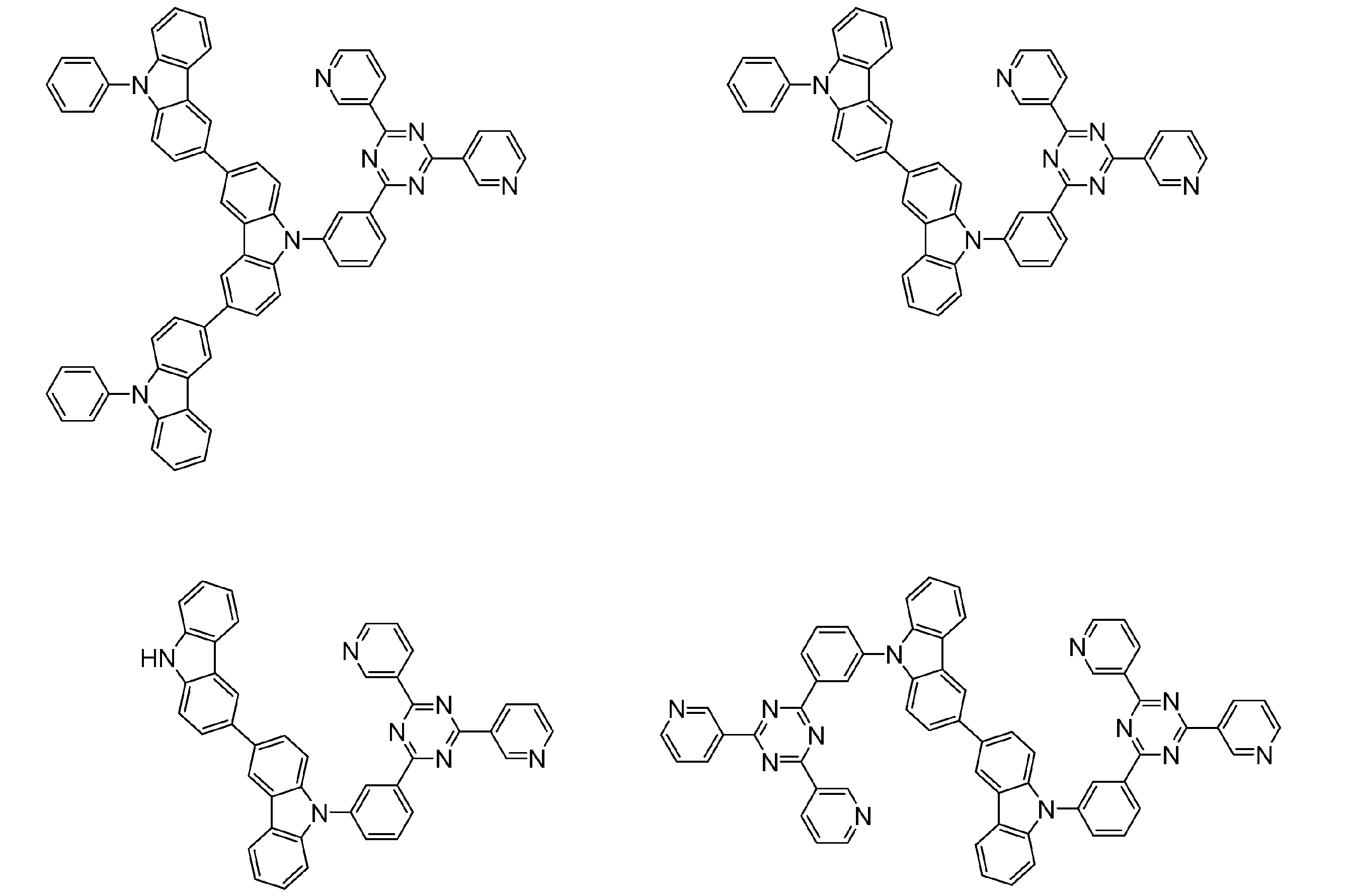
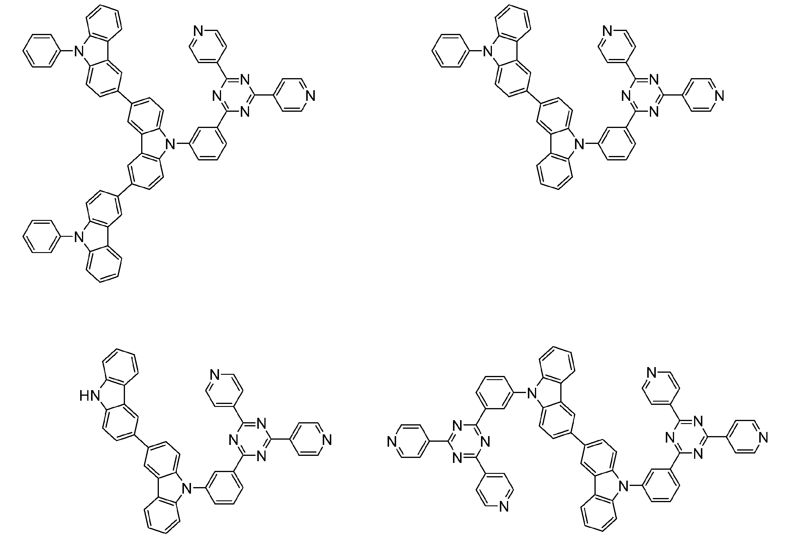
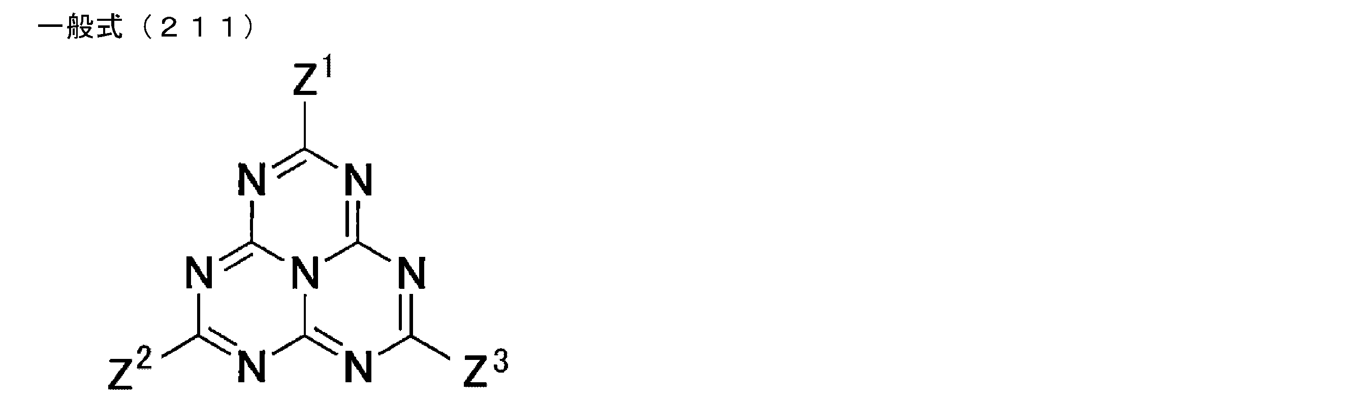
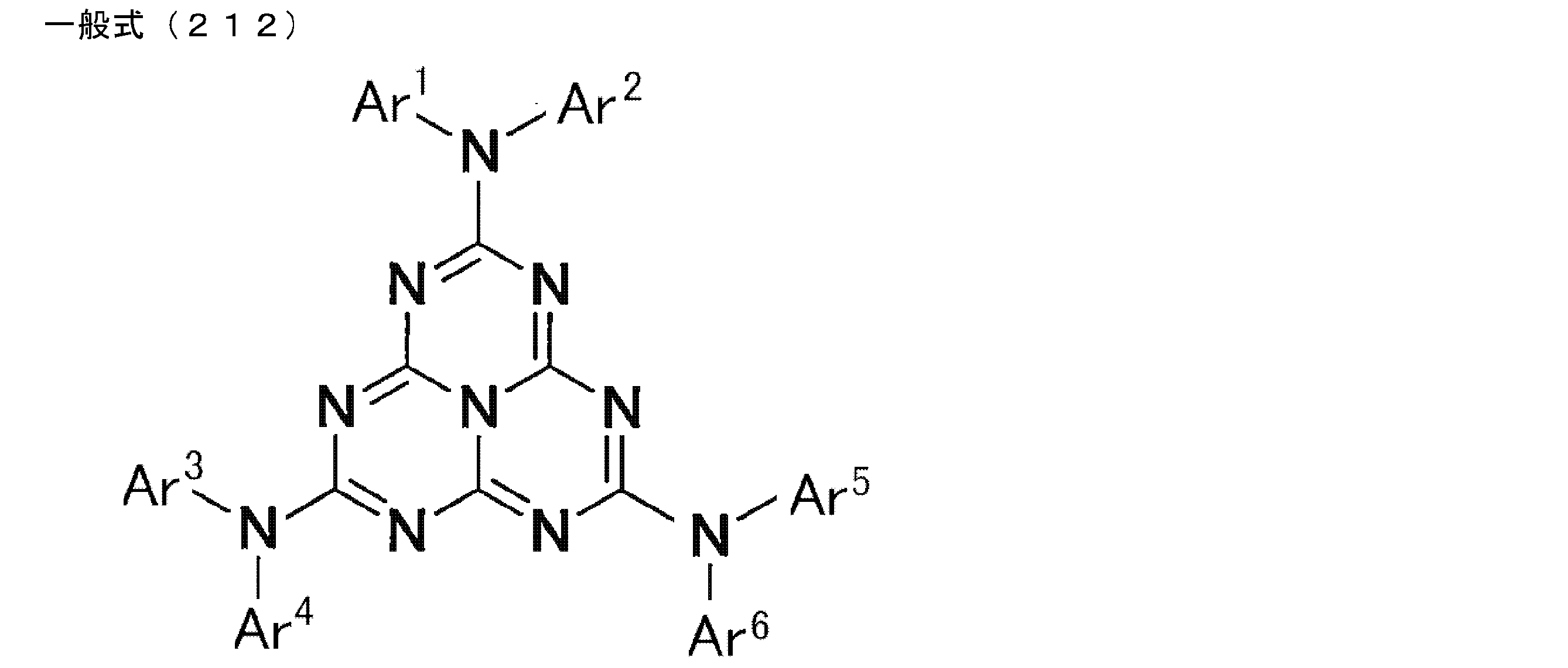


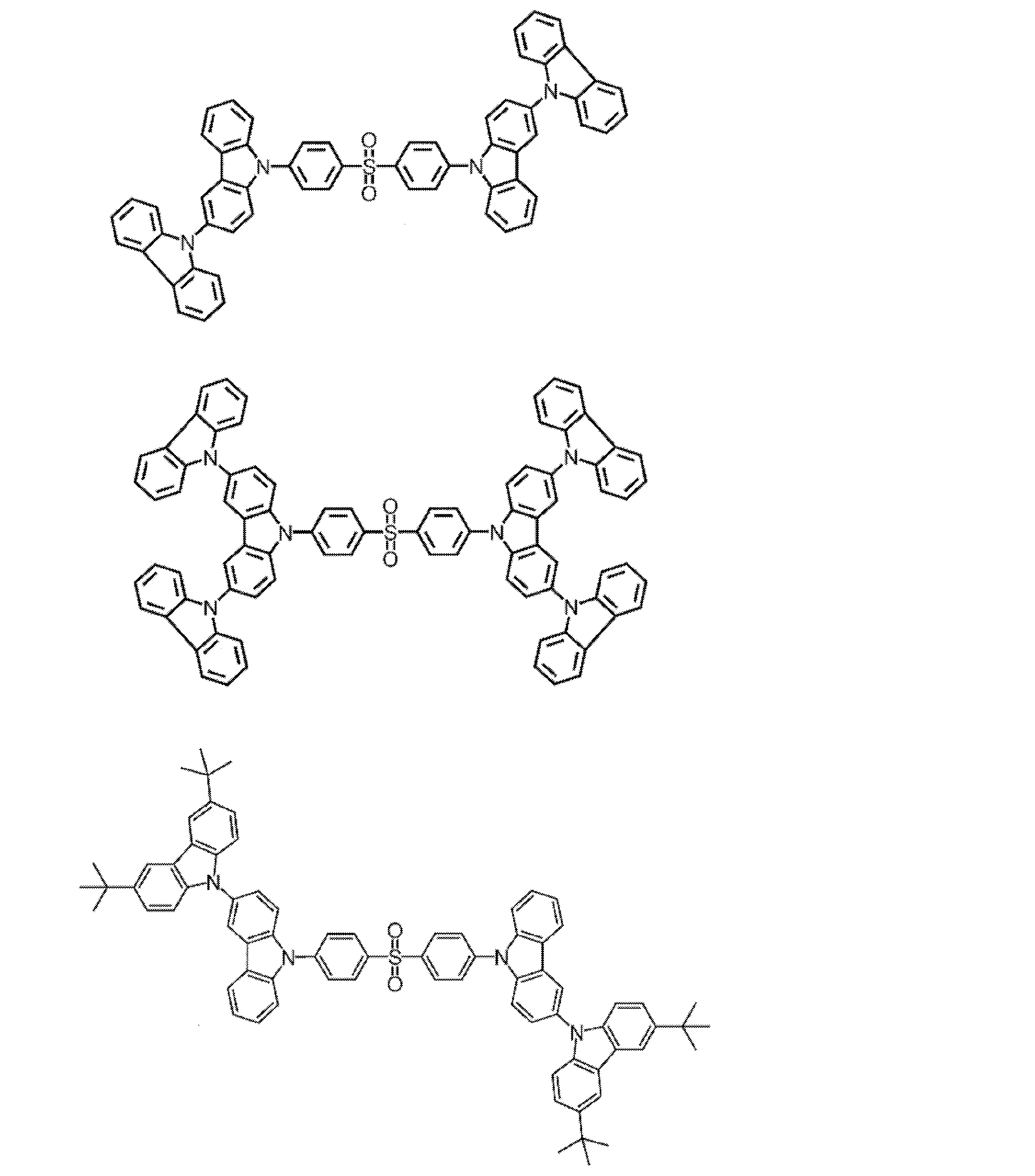
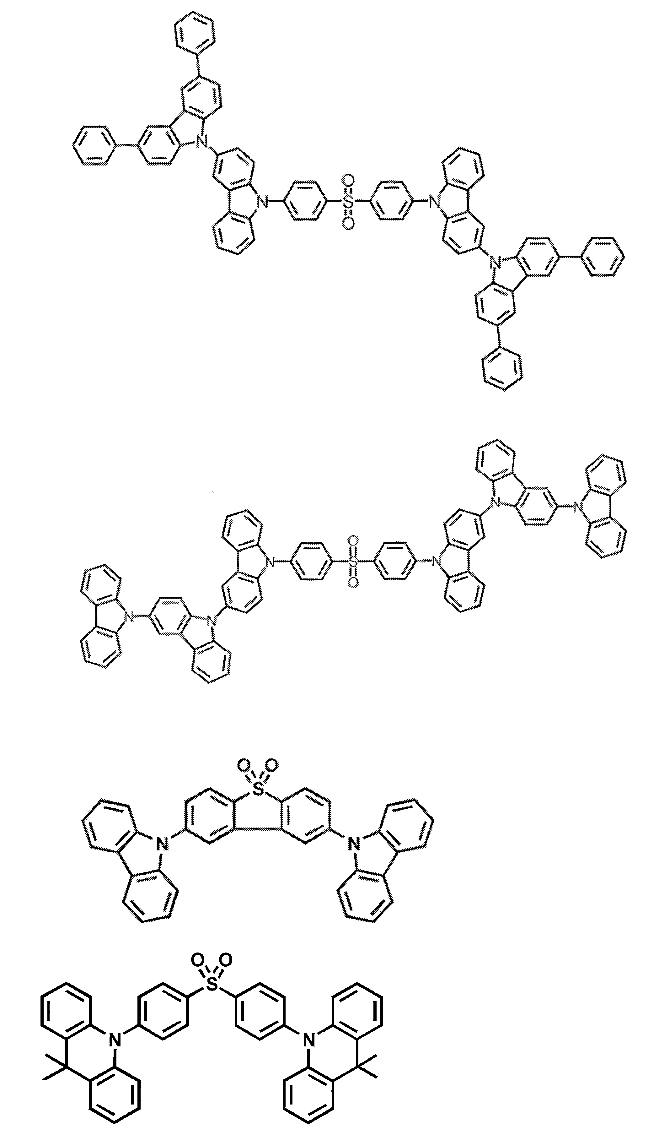
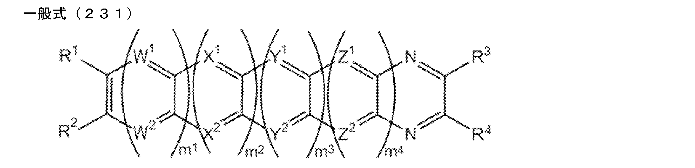

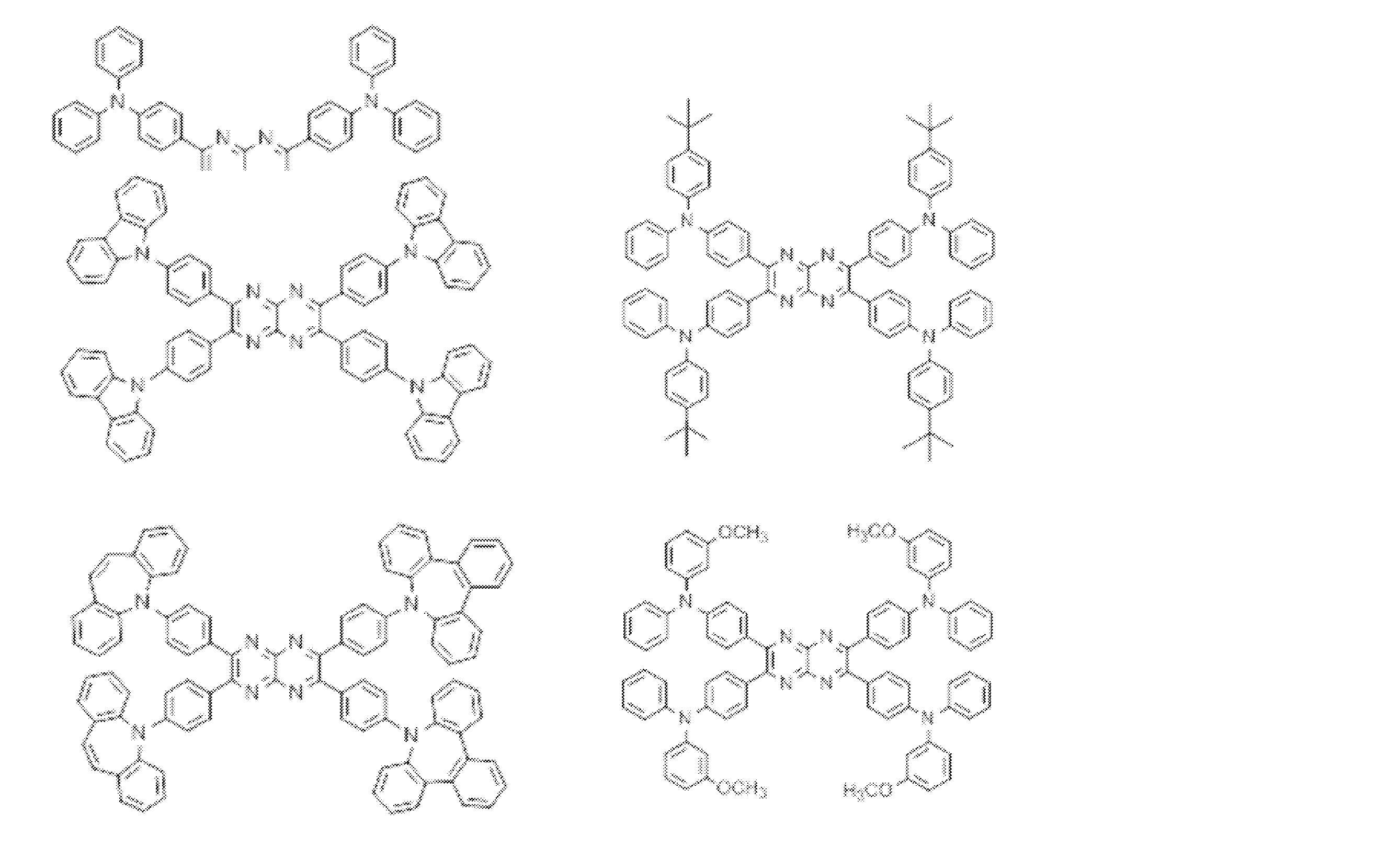

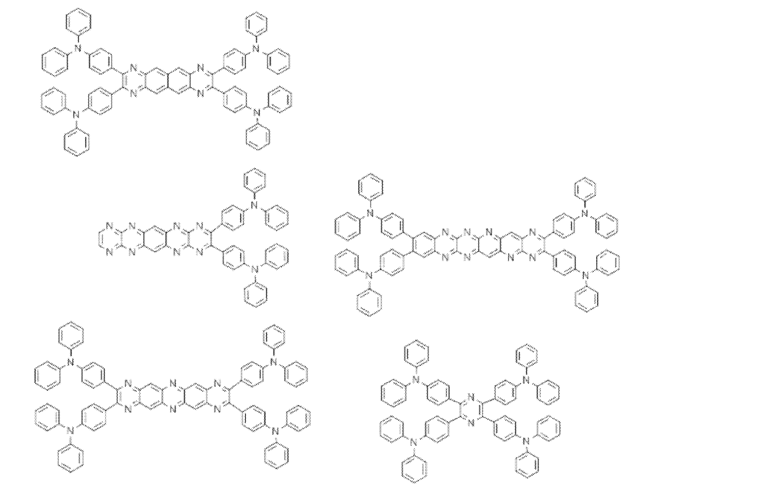
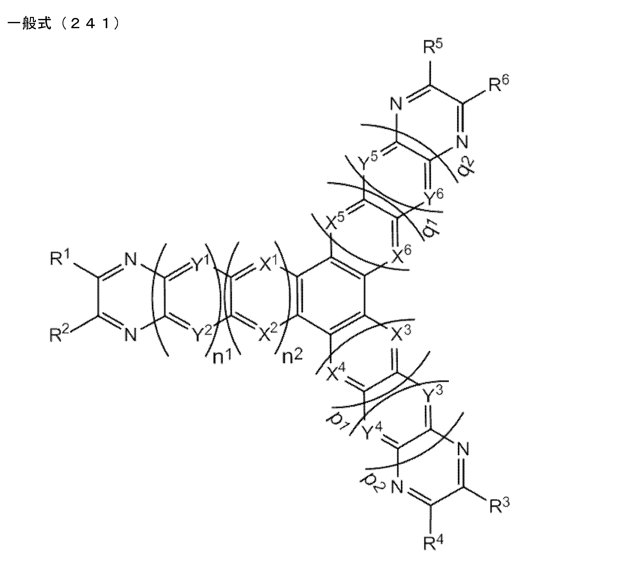
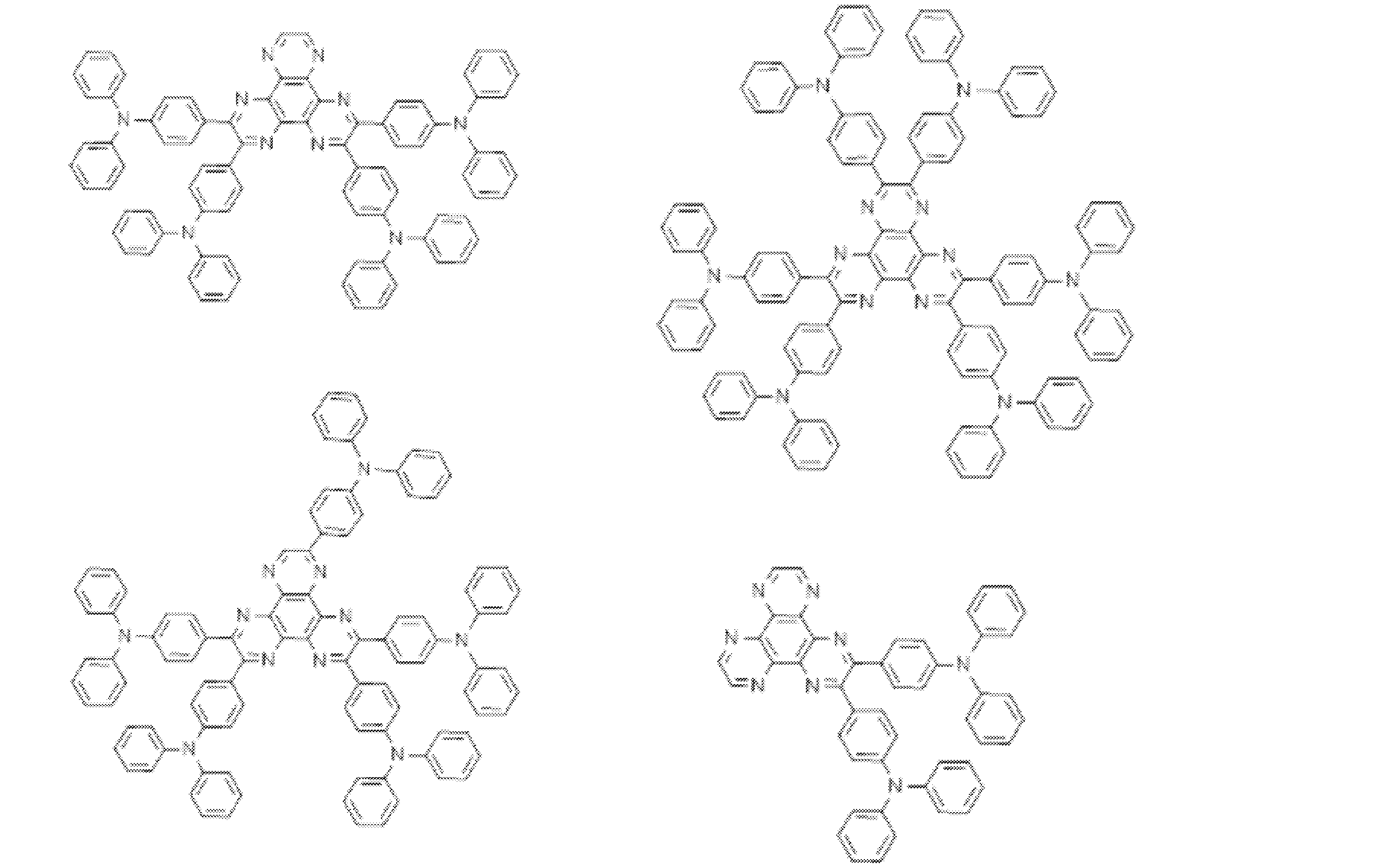

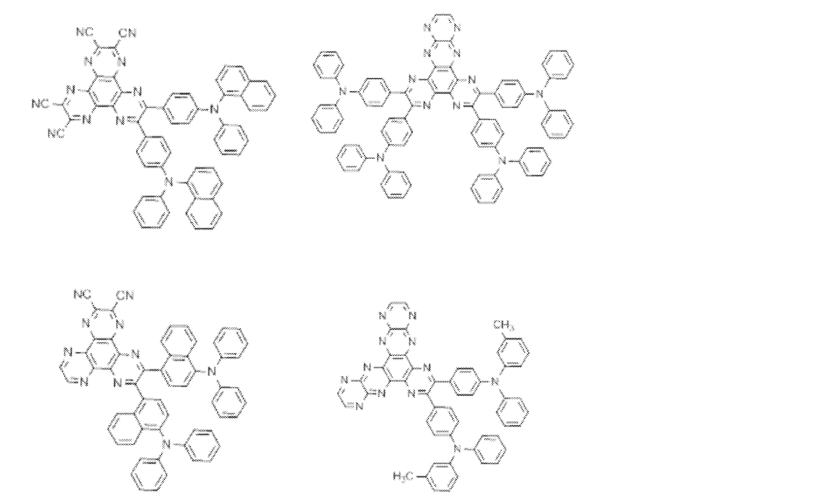
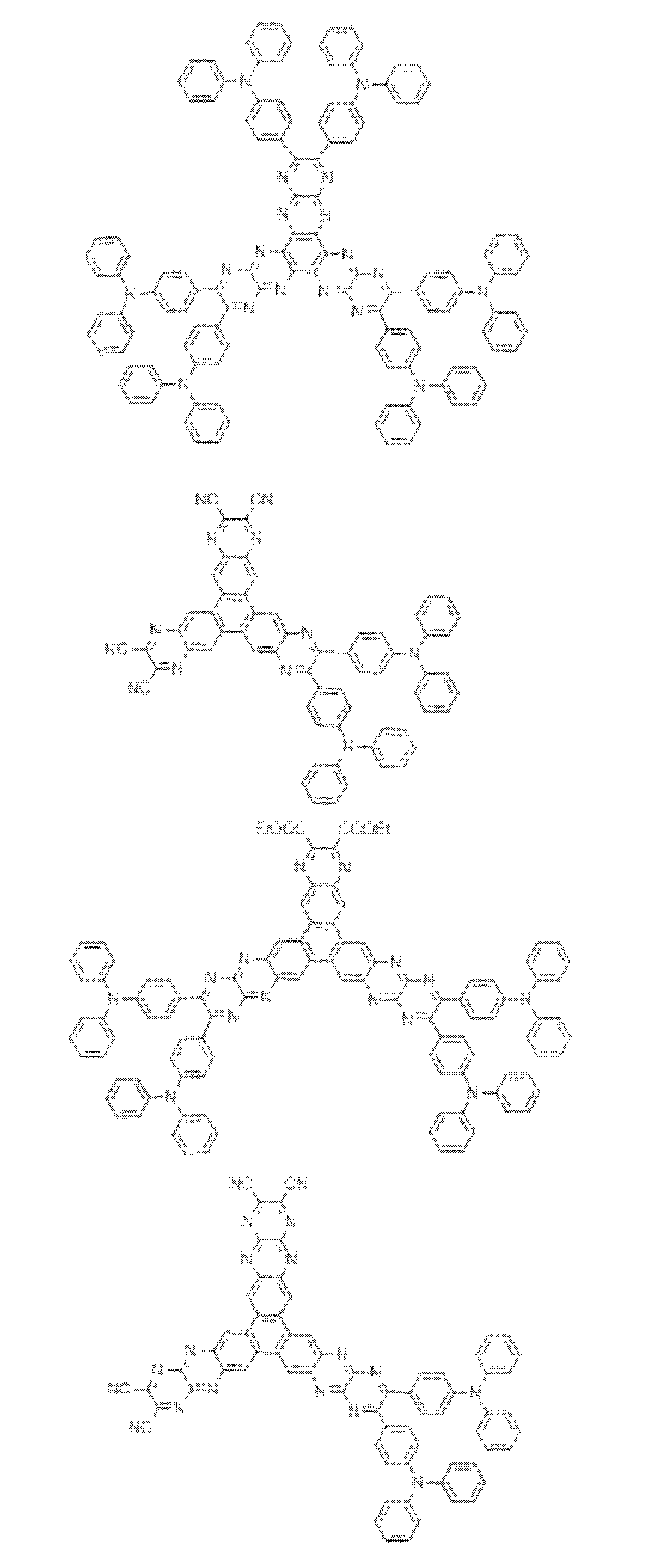
[1] 下記一般式(251)で表される化合物。

[2] 前記一般式(251)で表される化合物が下記一般式(252)で表される構造を有することを特徴とする[1]に記載の化合物。
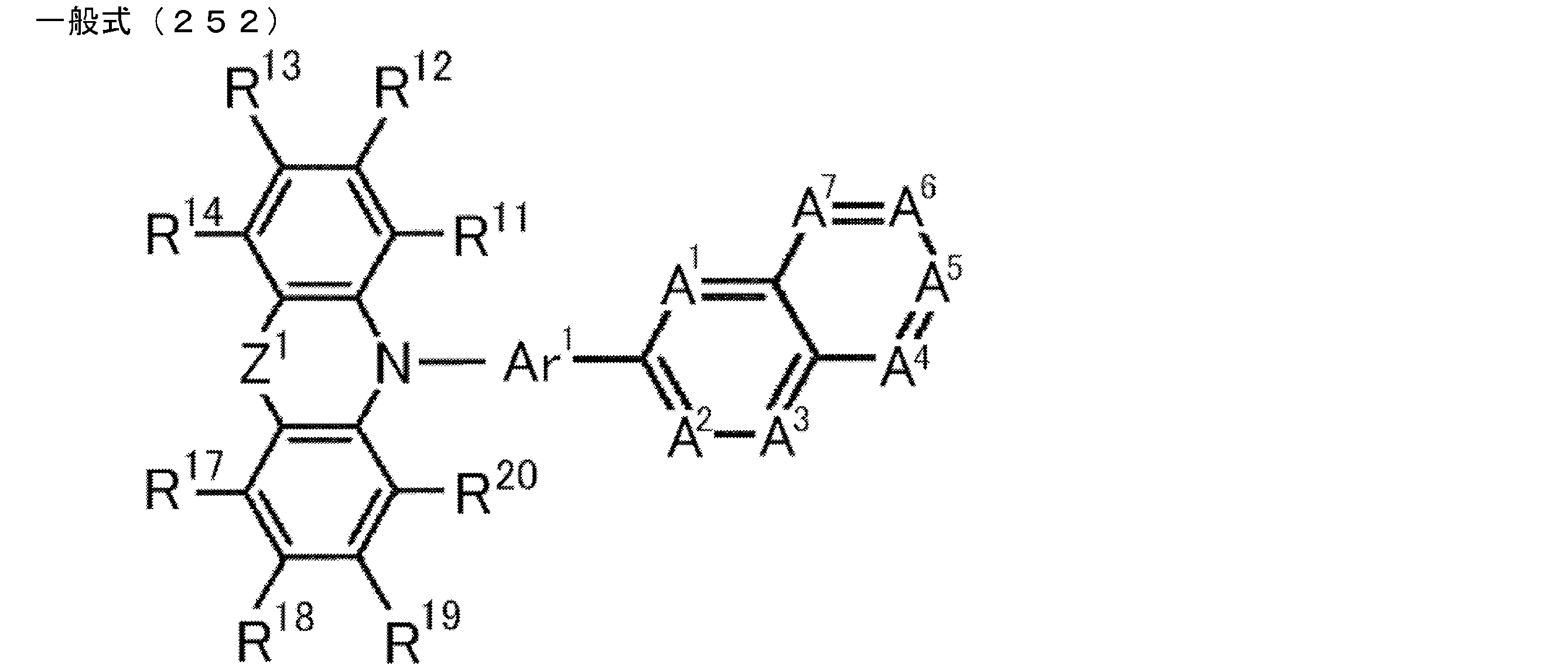
[3] 前記一般式(251)で表される化合物が下記一般式(253)で表される構造を有することを特徴とする[1]に記載の化合物。
[4] 前記一般式(253)のYが下記一般式(254)~(257)のいずれかで表される基であることを特徴とする[3]に記載の化合物。

[5] 前記一般式(253)のYが下記一般式(258)で表される基であることを特徴とする[3]に記載の化合物。
[6] 一般式(258)において、R23'とR28'の少なくとも一方は置換もしくは無置換のジアリールアミノ基、または置換もしくは無置換のカルバゾール-9-イル基であることを特徴とする[5]に記載の化合物。
[7] 前記一般式(253)のYが前記一般式(255)で表される基であることを特徴とする[4]に記載の化合物。 Preferred examples of the light emitting material include the following compounds.
[1] A compound represented by the following general formula (251).
[2] The compound according to [1], wherein the compound represented by the general formula (251) has a structure represented by the following general formula (252).
[3] The compound according to [1], wherein the compound represented by the general formula (251) has a structure represented by the following general formula (253).
[4] The compound according to [3], wherein Y in the general formula (253) is a group represented by any of the following general formulas (254) to (257).
[5] The compound according to [3], wherein Y in the general formula (253) is a group represented by the following general formula (258).
[6] In General Formula (258), at least one of R 23 ′ and R 28 ′ is a substituted or unsubstituted diarylamino group, or a substituted or unsubstituted carbazol-9-yl group [ 5].
[7] The compound according to [4], wherein Y in the general formula (253) is a group represented by the general formula (255).

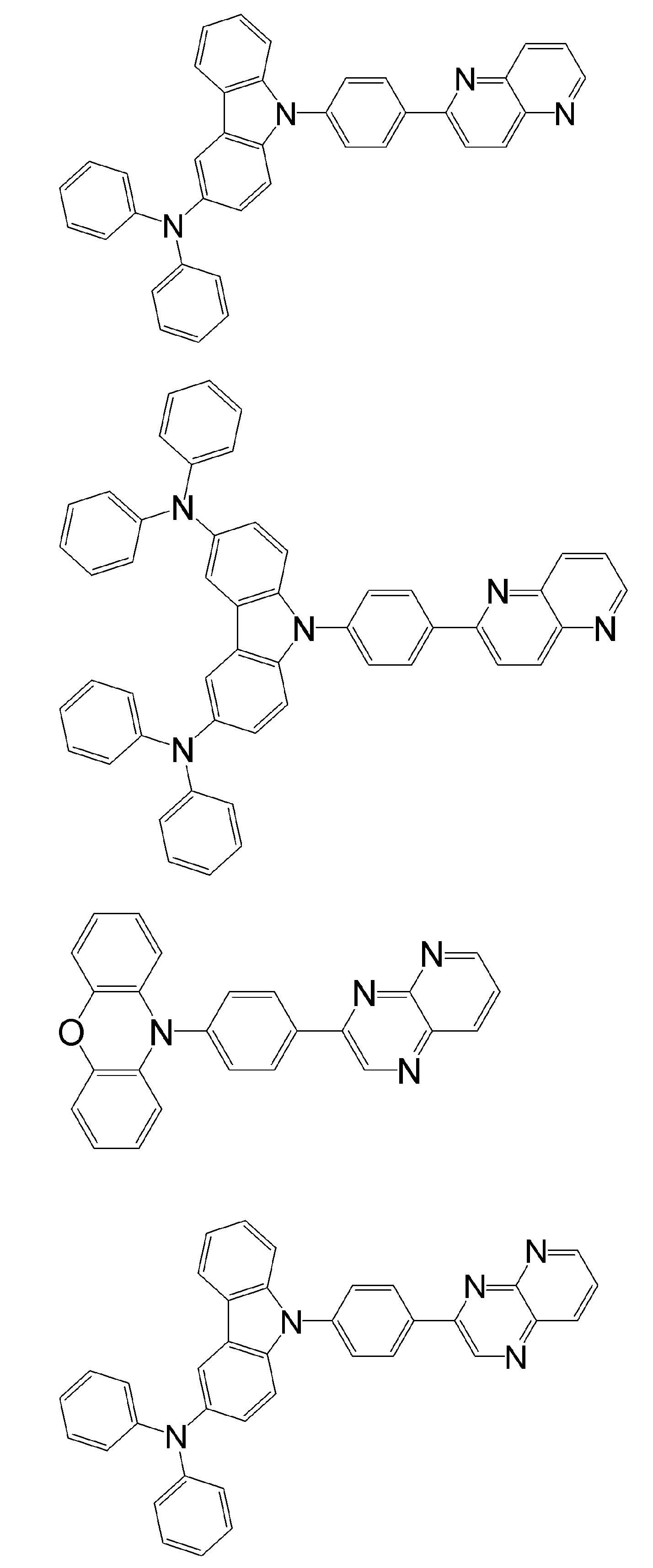
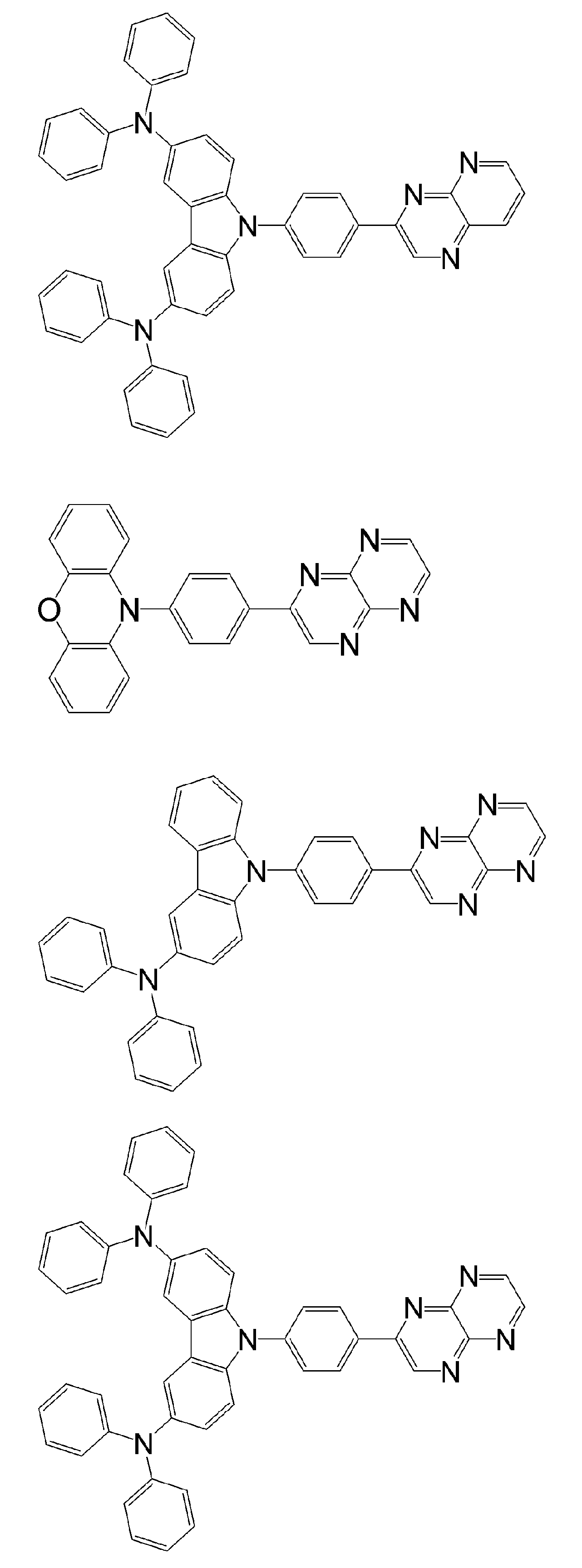
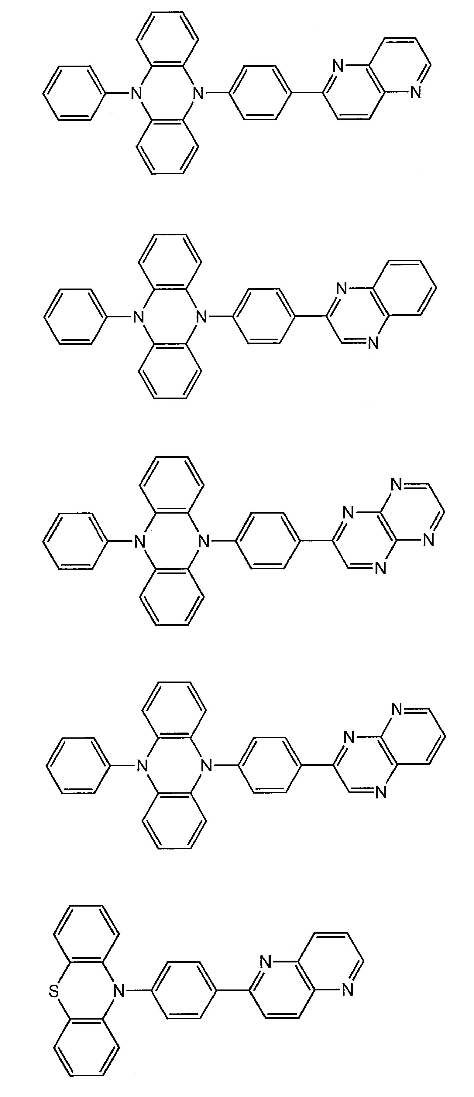
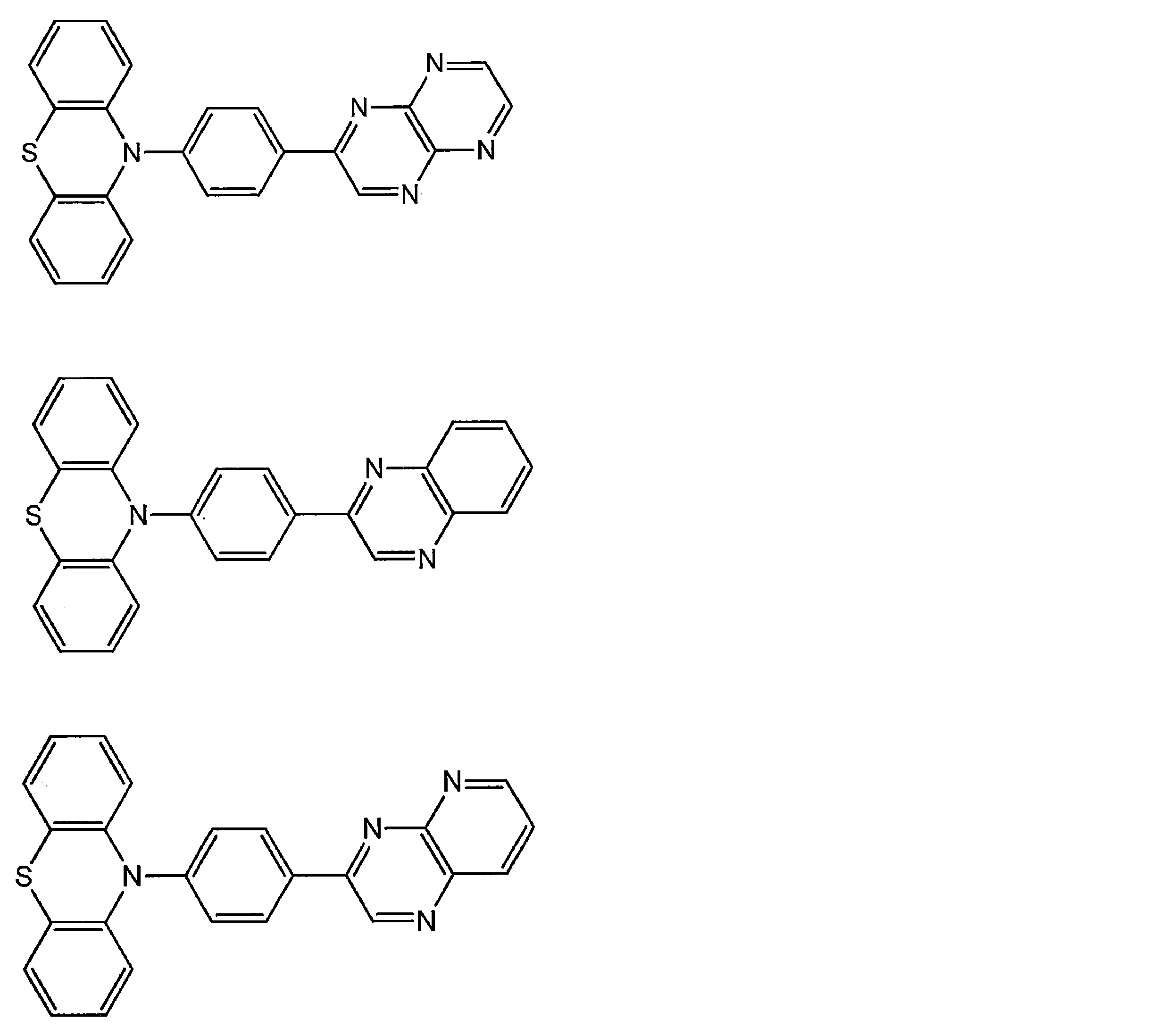
[1] 下記一般式(271)で表される化合物。
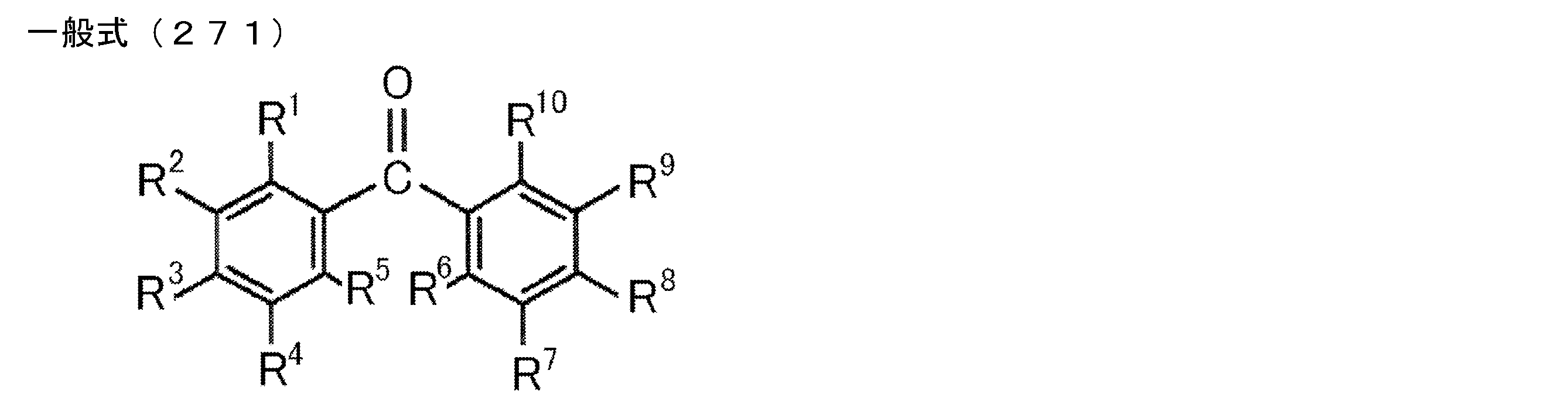
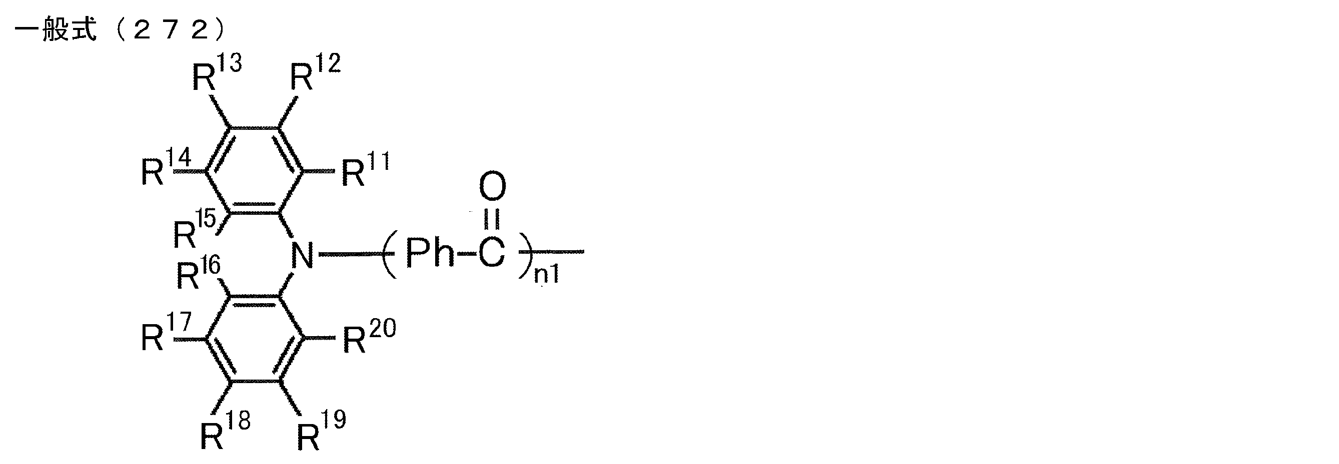
[1] A compound represented by the following general formula (271).
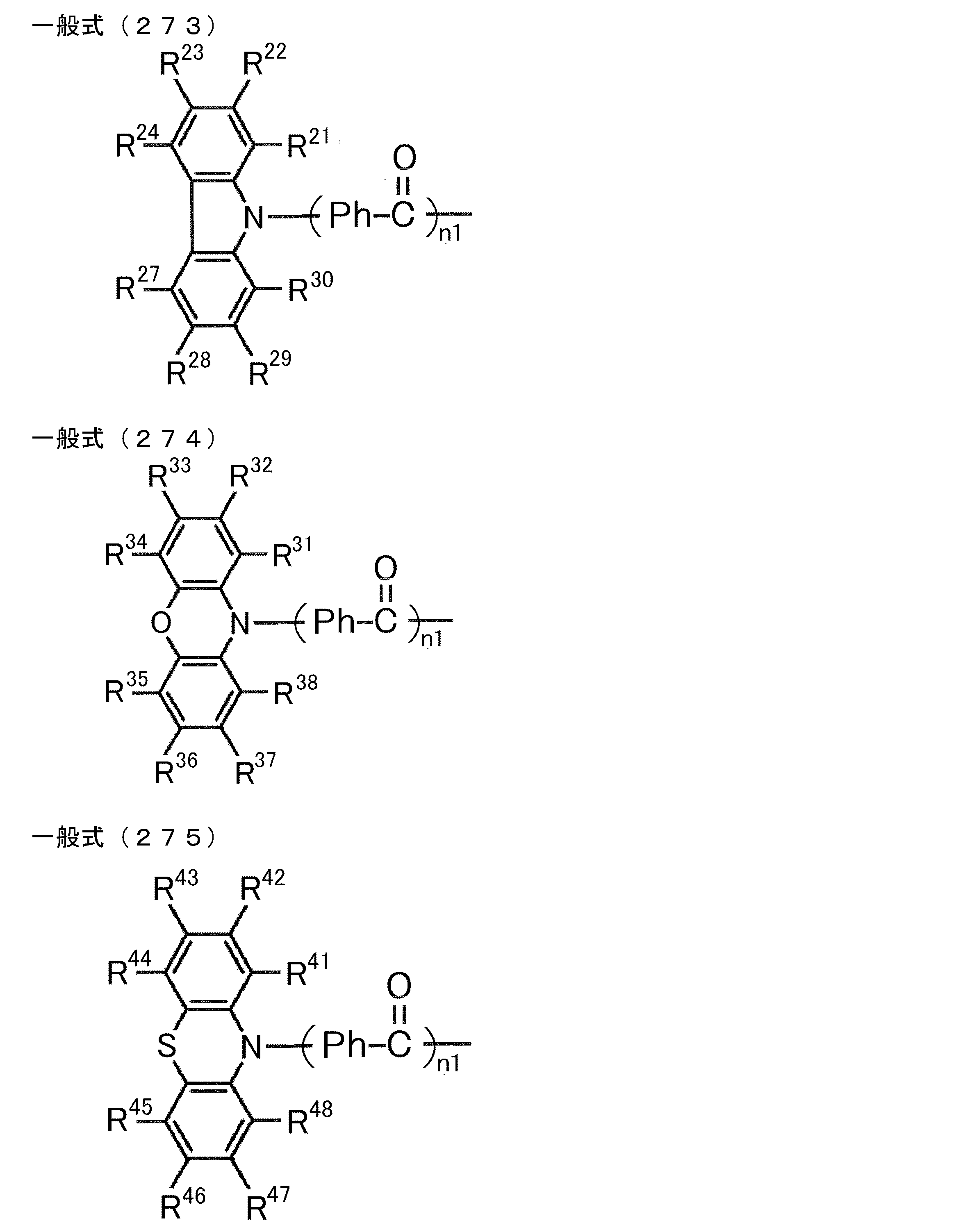

[3] 一般式(271)のR1~R5のうちの少なくとも1つと、R6~R10のうちの少なくとも1つが、前記一般式(272)で表される基であることを特徴とする[1]または[2]に記載の化合物。
[4] 一般式(271)のR3とR8が、前記一般式(272)で表される基であることを特徴とする[3]に記載の化合物。
[5] 前記一般式(272)で表される基が、前記一般式(274)で表される基であることを特徴とする[1]~[4]のいずれか1項に記載の化合物。
[6] 前記一般式(272)で表される基が、前記一般式(273)で表される基であることを特徴とする[1]~[4]のいずれか1項に記載の化合物。
[7] 前記一般式(273)のR21~R24、R27~R30の少なくとも1つが置換基であることを特徴とする[6]に記載の化合物。
[8] 前記置換基が、前記一般式(273)~(278)のいずれかで表される基であることを特徴とする[7]に記載の化合物。
[9] 前記一般式(273)のR23およびR28の少なくとも1つが前記置換基であることを特徴とする[8]に記載の化合物。 [2] The compound according to [1], wherein the group represented by the general formula (272) is a group represented by any one of the following general formulas (273) to (278).
[3] It is characterized in that at least one of R 1 to R 5 in general formula (271) and at least one of R 6 to R 10 are a group represented by general formula (272). The compound according to [1] or [2].
[4] The compound according to [3], wherein R 3 and R 8 in the general formula (271) are a group represented by the general formula (272).
[5] The compound according to any one of [1] to [4], wherein the group represented by the general formula (272) is a group represented by the general formula (274) .
[6] The compound according to any one of [1] to [4], wherein the group represented by the general formula (272) is a group represented by the general formula (273) .
[7] The compound according to [6], wherein at least one of R 21 to R 24 and R 27 to R 30 in the general formula (273) is a substituent.
[8] The compound according to [7], wherein the substituent is a group represented by any one of the general formulas (273) to (278).
[9] The compound according to [8], wherein at least one of R 23 and R 28 in the general formula (273) is the substituent.


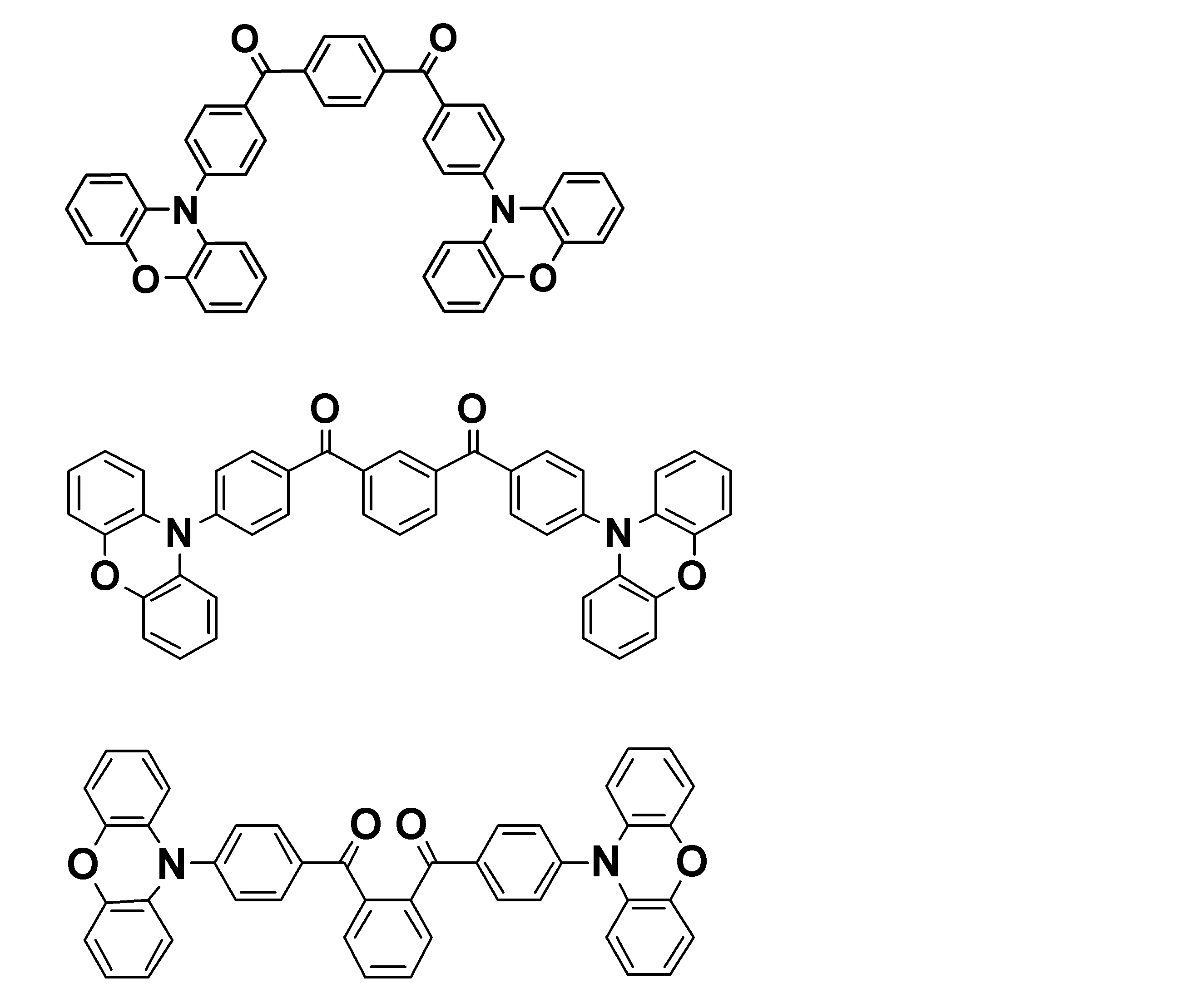


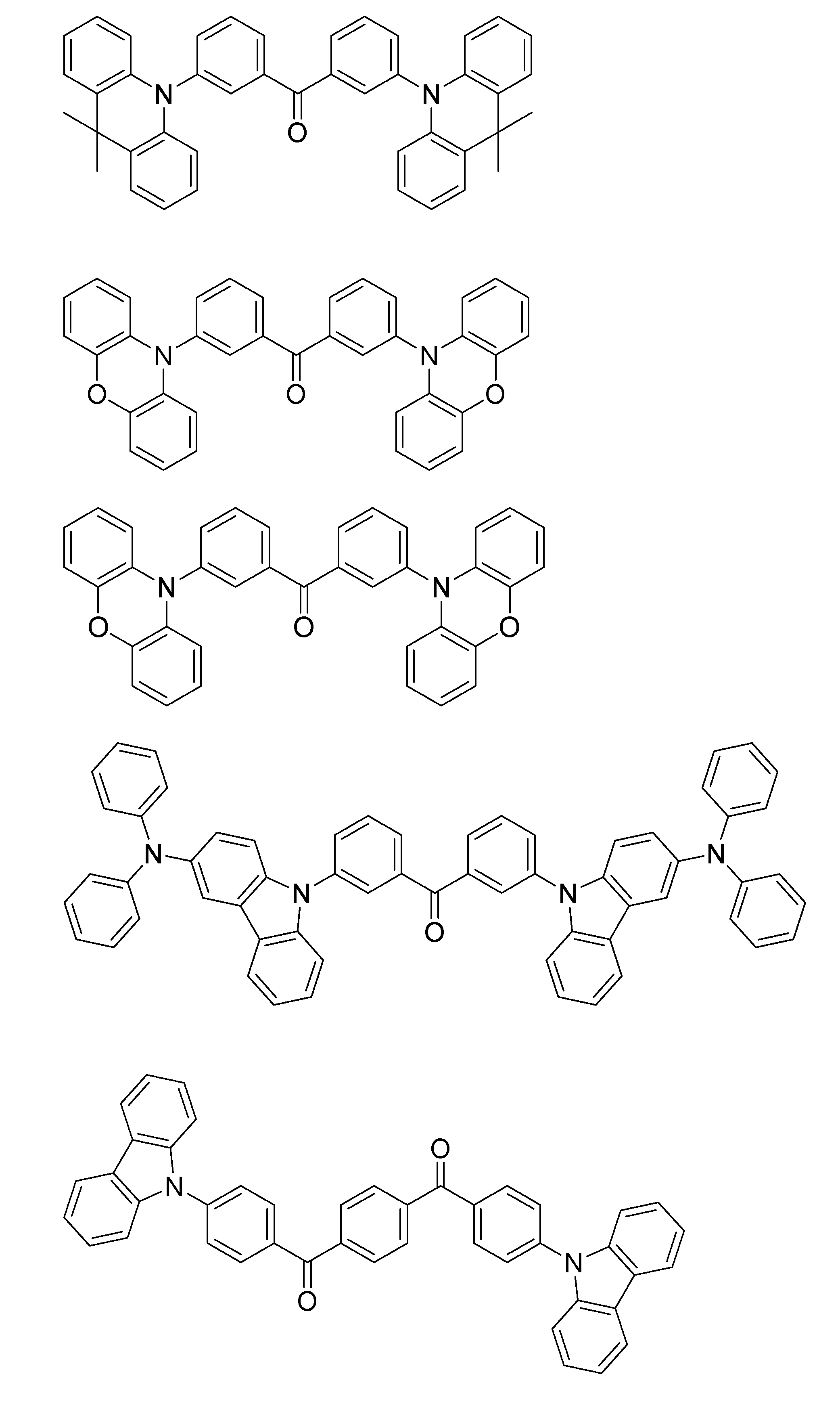

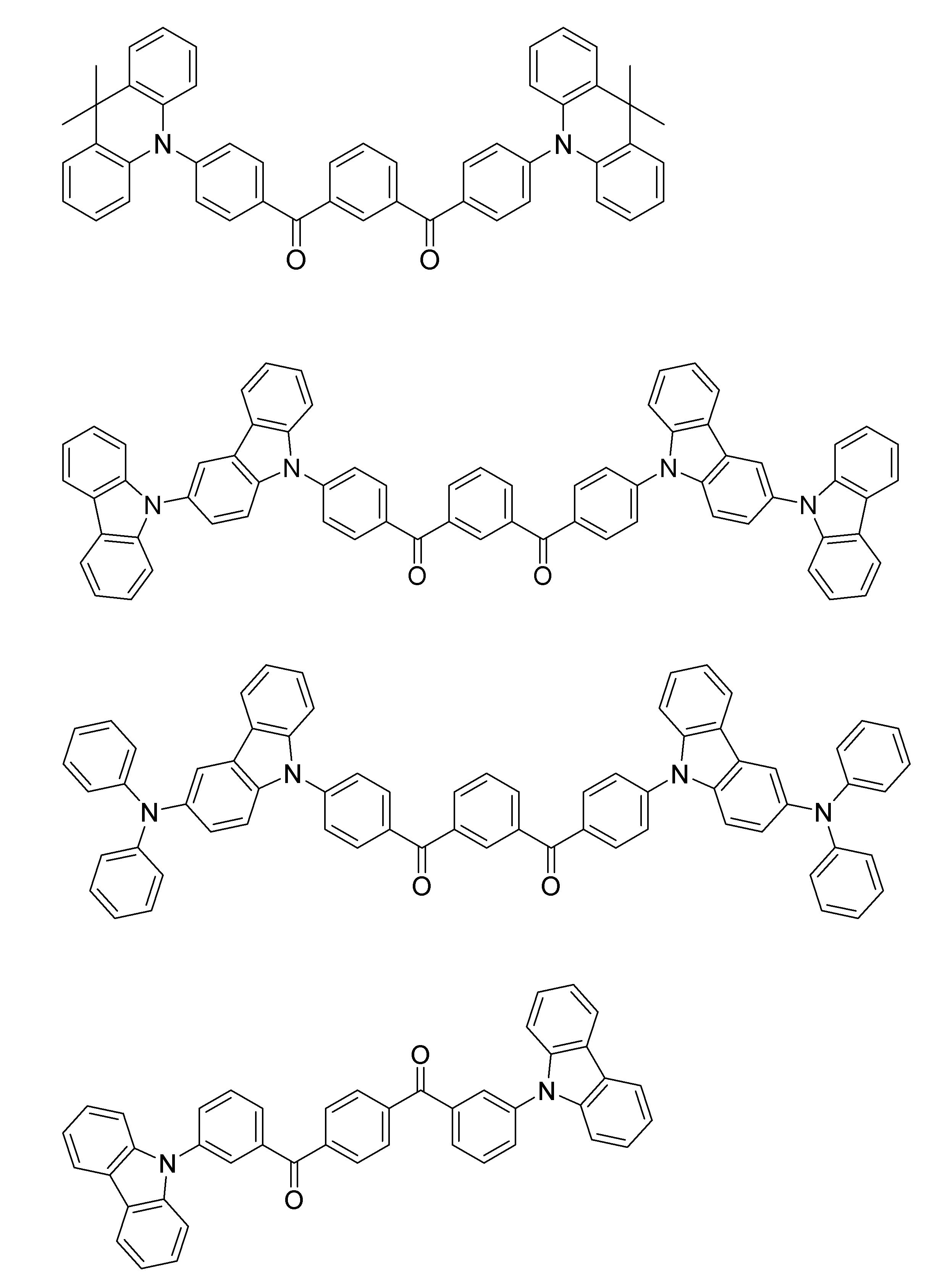
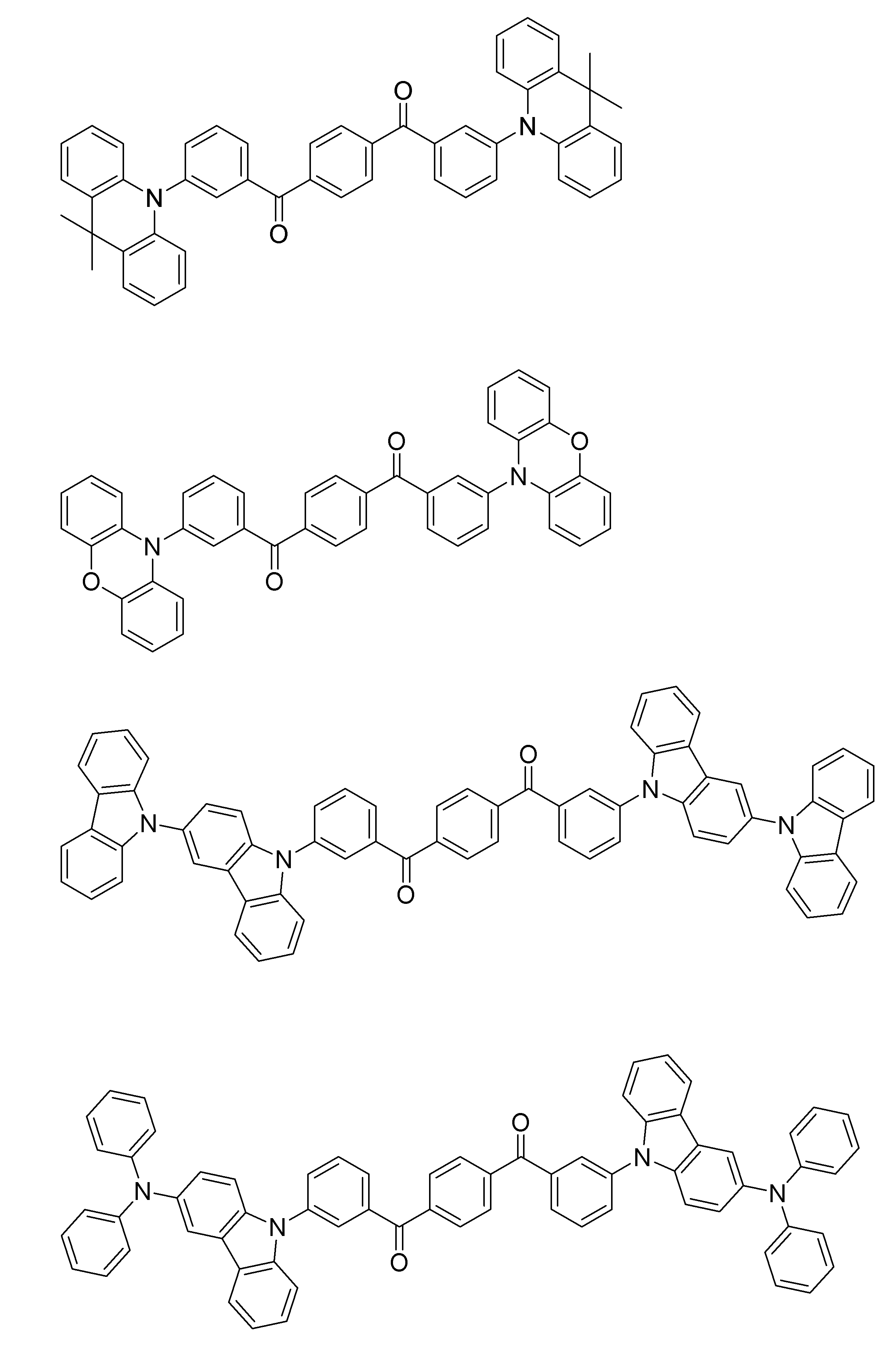


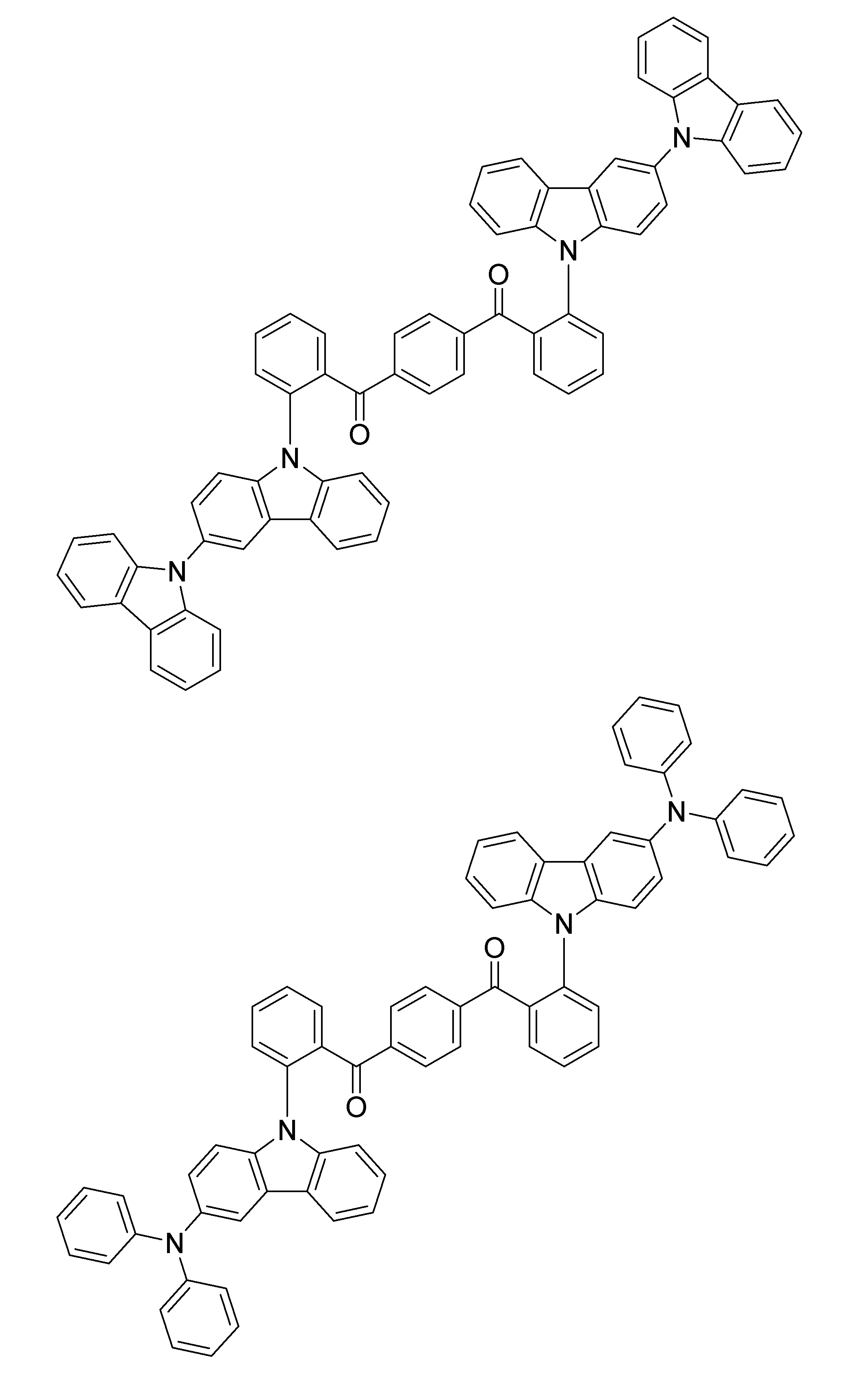
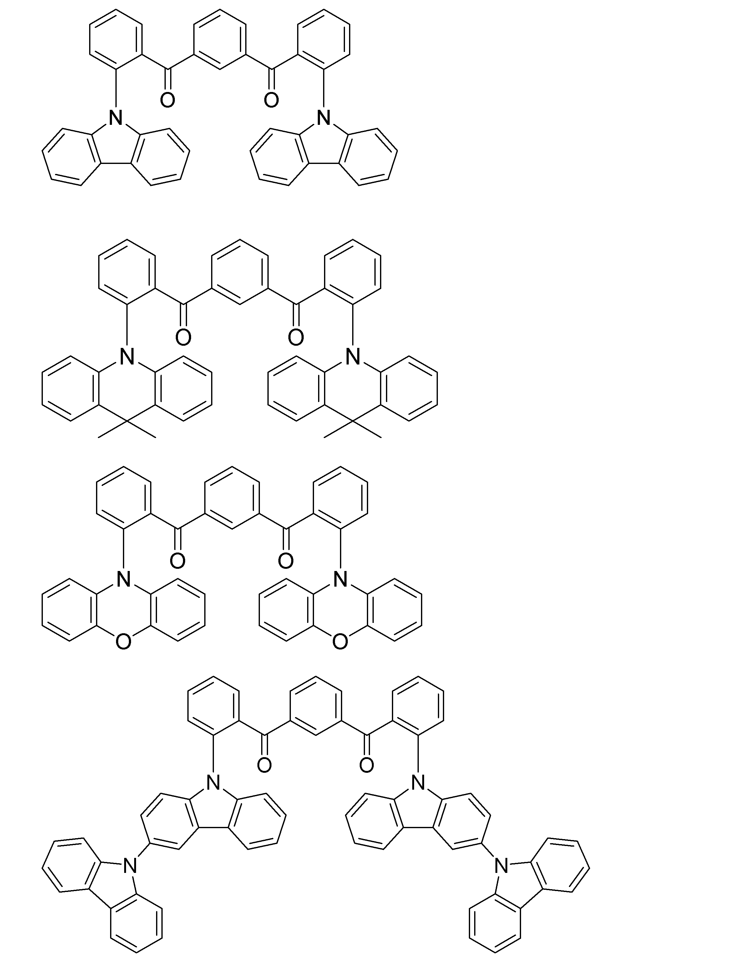
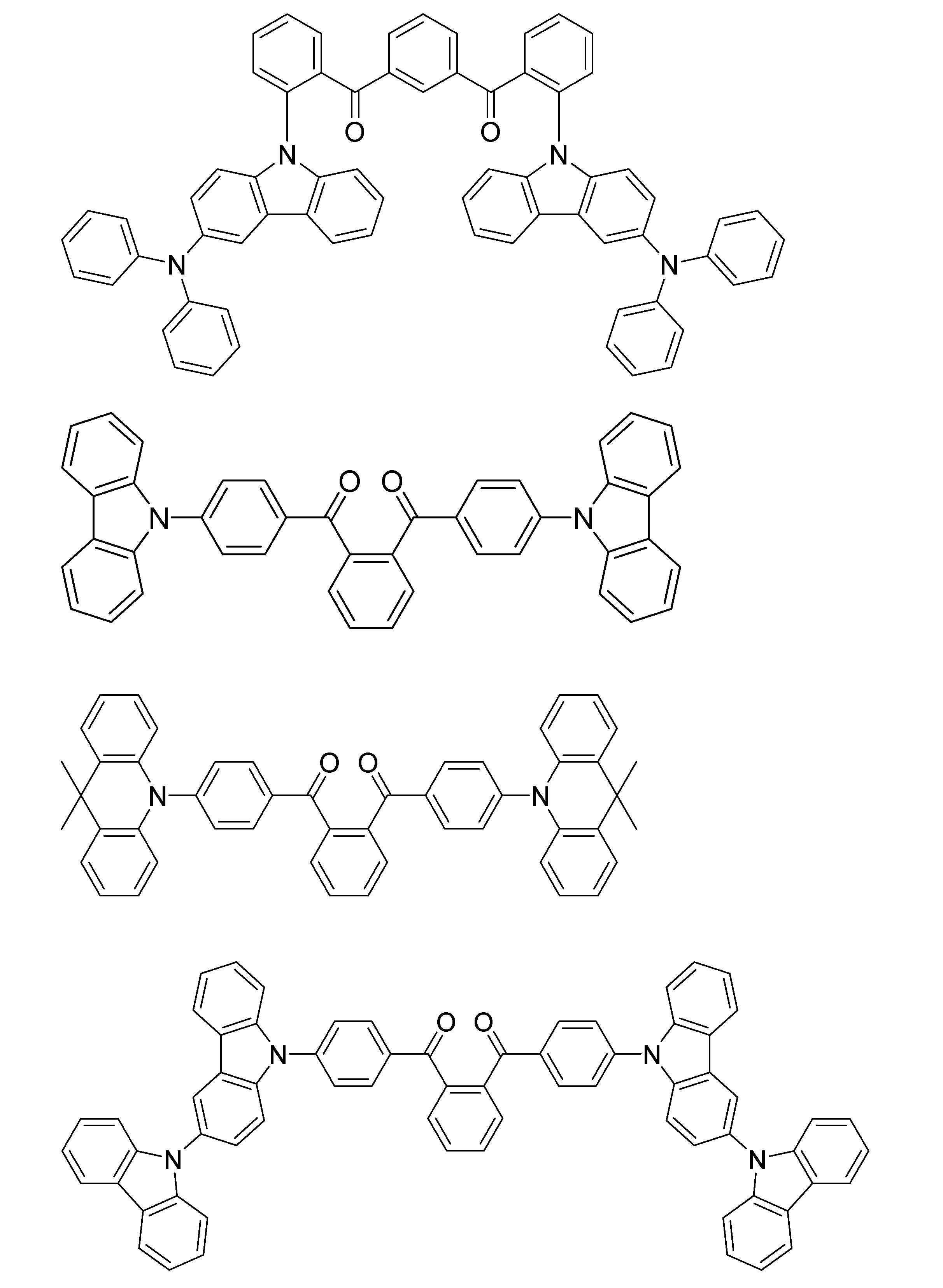

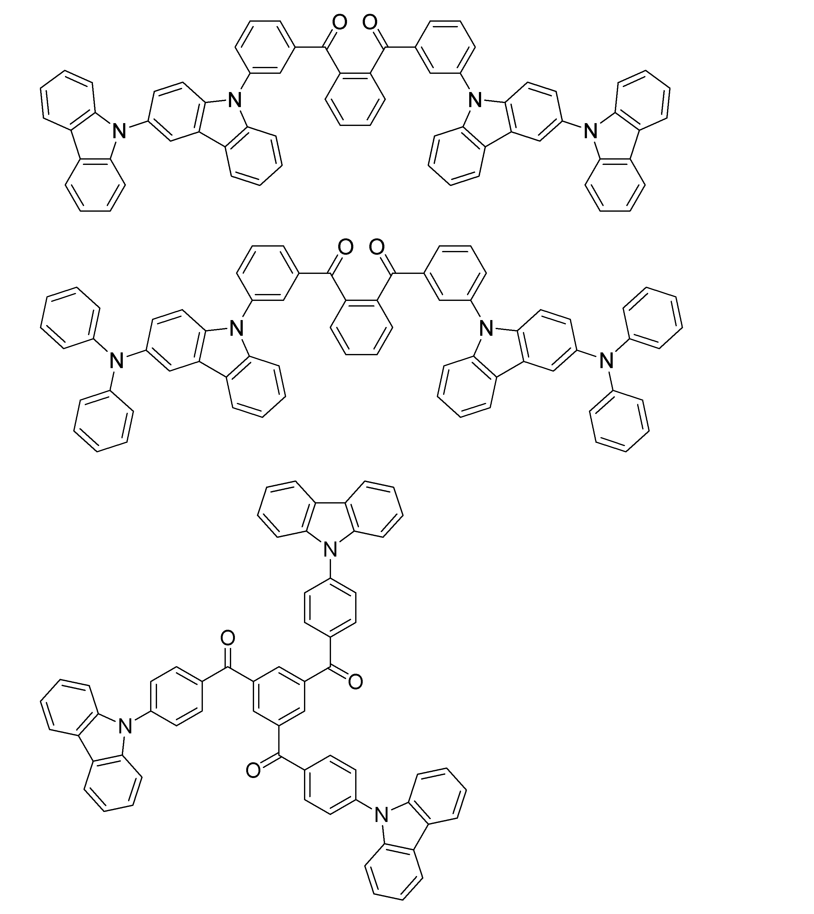
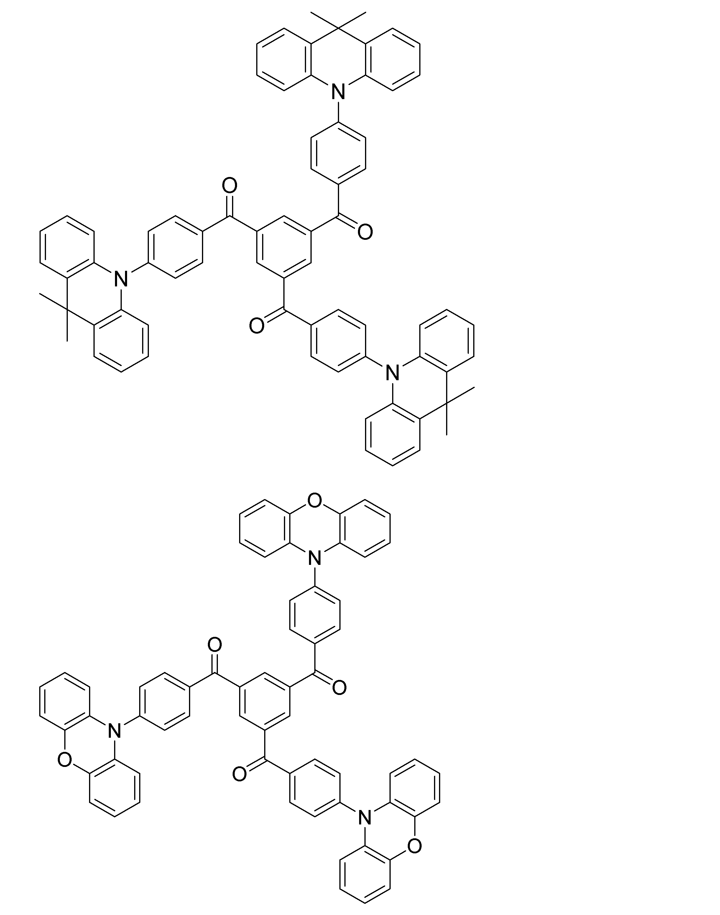

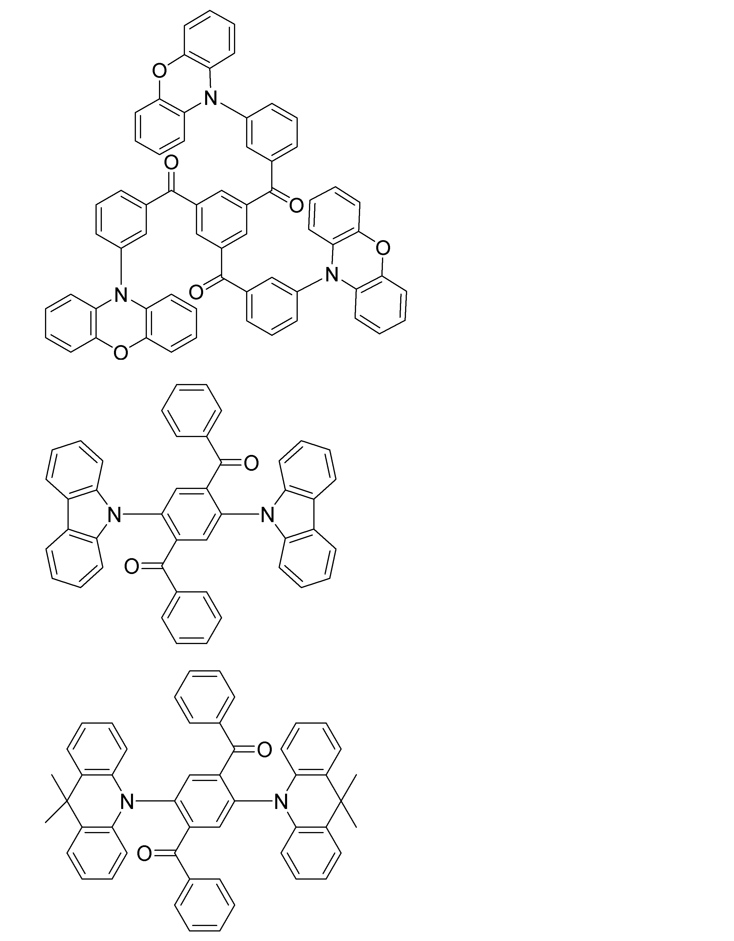


[1] 下記一般式(281)で表される化合物からなる化合物。
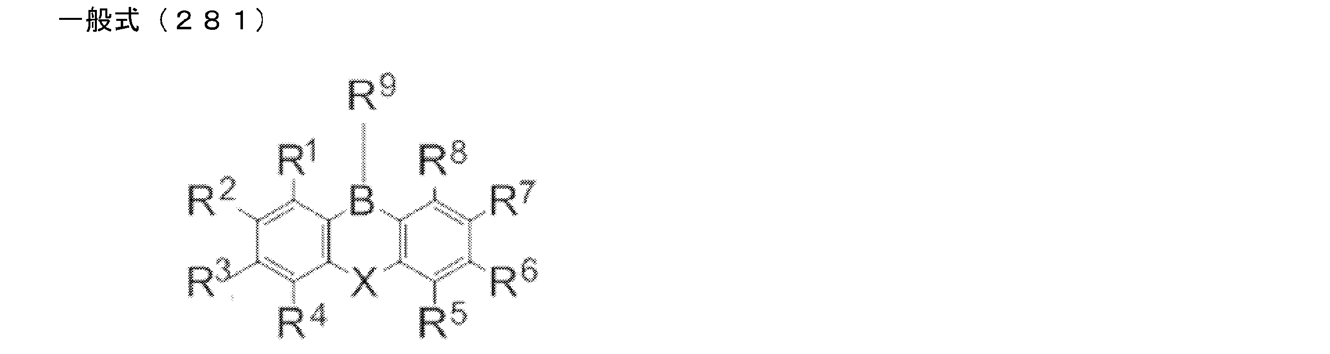

[2] 一般式(281)のR1~R8の少なくとも1つが前記一般式(283)~(287)のいずれかで表される基であることを特徴とする[1]に記載の化合物。
[3] 一般式(281)のR1~R8の少なくとも1つが前記一般式(283)で表される基である場合に、前記一般式(283)のR21~R28のうち少なくとも1つは置換基であることを特徴とする[1]または[2]に記載の化合物。
[4] 一般式(281)のR2、R3、R6、およびR7の少なくとも1つが前記一般式(282)~(287)のいずれかで表される基であることを特徴とする[1]~[3]のいずれか1項に記載の化合物。
[5] 一般式(281)のR3およびR6の少なくとも1つが前記一般式(282)~(287)のいずれかで表される基であることを特徴とする[4]に記載の化合物。
[6] 一般式(281)のR3とR6が、各々独立に前記一般式(282)~(287)のいずれかで表される基であることを特徴とする[5]に記載の化合物。
[7] 前記一般式(282)のR11~R20の少なくとも1つ、前記一般式(283)のR21~R28の少なくとも1つ、前記一般式(284)のR31~R38の少なくとも1つと、R3aおよびR3bの少なくとも1つ、前記一般式(285)のR41~R48の少なくとも1つ、前記一般式(286)のR51~R58の少なくとも1つ、および前記一般式(287)のR61~R68の少なくとも1つが置換基であることを特徴とする[1]~[6]のいずれか1項に記載の化合物。
[8] 前記一般式(282)のR13およびR18の少なくとも一方、前記一般式(283)のR23およびR26の少なくとも一方、前記一般式(284)のR33およびR36の少なくとも一方と、R3aおよびR3bの少なくとも一方、前記一般式(285)のR43およびR46の少なくとも一方、前記一般式(286)のR53およびR56の少なくとも一方、並びに前記一般式(287)のR63およびR66の少なくとも一方が置換基であることを特徴とする[7]に記載の化合物。
[9] 前記一般式(282)のR13およびR18の少なくとも一方、前記一般式(283)のR23およびR26の少なくとも一方、前記一般式(284)のR33およびR36の少なくとも一方と、R3aおよびR3bの少なくとも一方、前記一般式(285)のR43およびR46の少なくとも一方、前記一般式(286)のR53およびR56の少なくとも一方、並びに前記一般式(287)のR63およびR66の少なくとも一方が、前記一般式(282)~(287)のいずれかで表される基であることを特徴とする[8]に記載の化合物。
[10] 前記一般式(282)~(287)のL12~L17が、単結合であることを特徴とする[1]~[9]のいずれか1項に記載の化合物。
[11] 一般式(281)のXが、酸素原子であることを特徴とする[1]~[10]のいずれか1項に記載の化合物。
[12] 一般式(281)のR9が、下記一般式(a)で表される基であることを特徴とする[1]~[11]のいずれか1項に記載の化合物。

[13] 前記一般式(a)のR9aとR9eが置換基であることを特徴とする[12]に記載の化合物。
[14] 一般式(281)のR1~R8の少なくとも1つが前記一般式(284)で表される基であることを特徴とする[1]~[13]のいずれか1項に記載の化合物。
[15] 一般式(281)のR3とR6、またはR2とR7が、前記一般式(284)で表される基であることを特徴とする[1]~[4]、[7]~[14]のいずれか1項に記載の化合物。
[16] 前記一般式(284)のR3aとR3bが、置換基であることを特徴とする[14]または[15]に記載の化合物。
[17] 前記置換基が、炭素数1~15のアルキル基またはフェニル基であることを特徴とする[14]~[16]のいずれか1項に記載の化合物。
[18] 前記一般式(284)のR3aとR3bが互いに結合して環状構造を形成していることを特徴とする[14]~[16]のいずれか1項に記載の化合物。 Preferred examples of the light emitting material include the following compounds.
[1] A compound comprising a compound represented by the following general formula (281).
[2] The compound according to [1], wherein at least one of R 1 to R 8 in the general formula (281) is a group represented by any one of the general formulas (283) to (287) .
[3] When at least one of R 1 to R 8 in the general formula (281) is a group represented by the general formula (283), at least one of R 21 to R 28 in the general formula (283) One is a substituent, The compound as described in [1] or [2] characterized by the above-mentioned.
[4] At least one of R 2 , R 3 , R 6 , and R 7 in the general formula (281) is a group represented by any one of the general formulas (282) to (287) [1] The compound according to any one of [3].
[5] The compound according to [4], wherein at least one of R 3 and R 6 in the general formula (281) is a group represented by any one of the general formulas (282) to (287) .
[6] R 3 and R 6 in formula (281) is, according to each, characterized in that a group represented by any one of formulas independently (282) - (287) [5] Compound.
[7] At least one of R 11 to R 20 in the general formula (282), at least one of R 21 to R 28 in the general formula (283), and R 31 to R 38 in the general formula (284) At least one, at least one of R 3a and R 3b , at least one of R 41 to R 48 of the general formula (285), at least one of R 51 to R 58 of the general formula (286), and [6] The compound according to any one of [1] to [6], wherein at least one of R 61 to R 68 in the general formula (287) is a substituent.
[8] At least one of R 13 and R 18 in the general formula (282), at least one of R 23 and R 26 in the general formula (283), and at least one of R 33 and R 36 in the general formula (284) And at least one of R 3a and R 3b , at least one of R 43 and R 46 in the general formula (285), at least one of R 53 and R 56 in the general formula (286), and the general formula (287) The compound according to [7], wherein at least one of R 63 and R 66 is a substituent.
[9] At least one of R 13 and R 18 in the general formula (282), at least one of R 23 and R 26 in the general formula (283), and at least one of R 33 and R 36 in the general formula (284) And at least one of R 3a and R 3b , at least one of R 43 and R 46 in the general formula (285), at least one of R 53 and R 56 in the general formula (286), and the general formula (287) At least one of R 63 and R 66 in the formula (8) is a group represented by any one of the general formulas (282) to (287).
[10] The compound according to any one of [1] to [9], wherein L 12 to L 17 in the general formulas (282) to (287) are a single bond.
[11] The compound according to any one of [1] to [10], wherein X in the general formula (281) is an oxygen atom.
[12] The compound according to any one of [1] to [11], wherein R 9 in the general formula (281) is a group represented by the following general formula (a).
[13] The compound according to [12], wherein R 9a and R 9e in the general formula (a) are substituents.
[14] Any one of [1] to [13], wherein at least one of R 1 to R 8 in the general formula (281) is a group represented by the general formula (284). Compound.
[15] R 1 and R 6 or R 2 and R 7 in the general formula (281) are groups represented by the general formula (284), [1] to [4], [ [7] The compound according to any one of [14].
[16] The compound according to [14] or [15], wherein R 3a and R 3b in the general formula (284) are substituents.
[17] The compound according to any one of [14] to [16], wherein the substituent is an alkyl group having 1 to 15 carbon atoms or a phenyl group.
[18] The compound according to any one of [14] to [16], wherein R 3a and R 3b in the general formula (284) are bonded to each other to form a cyclic structure.
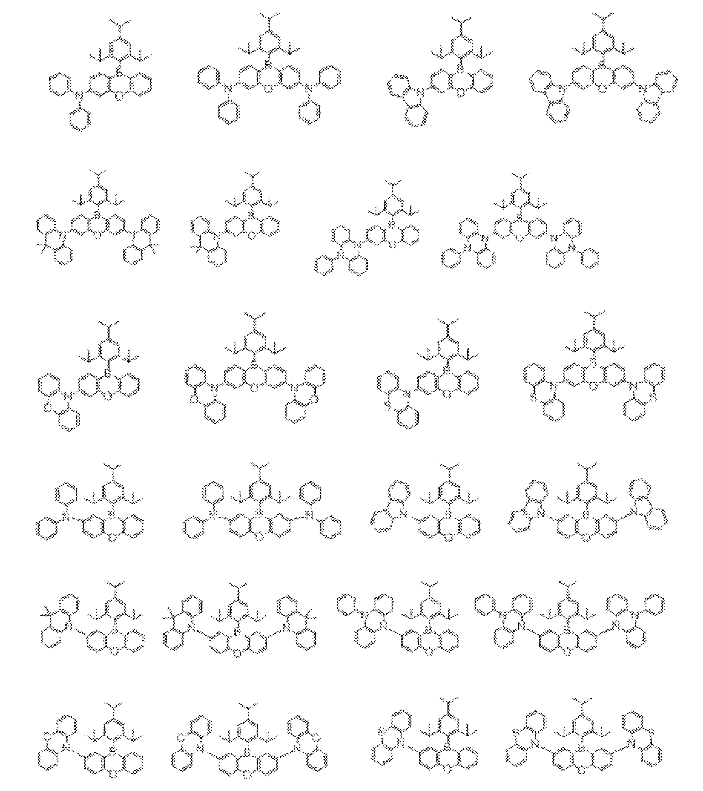


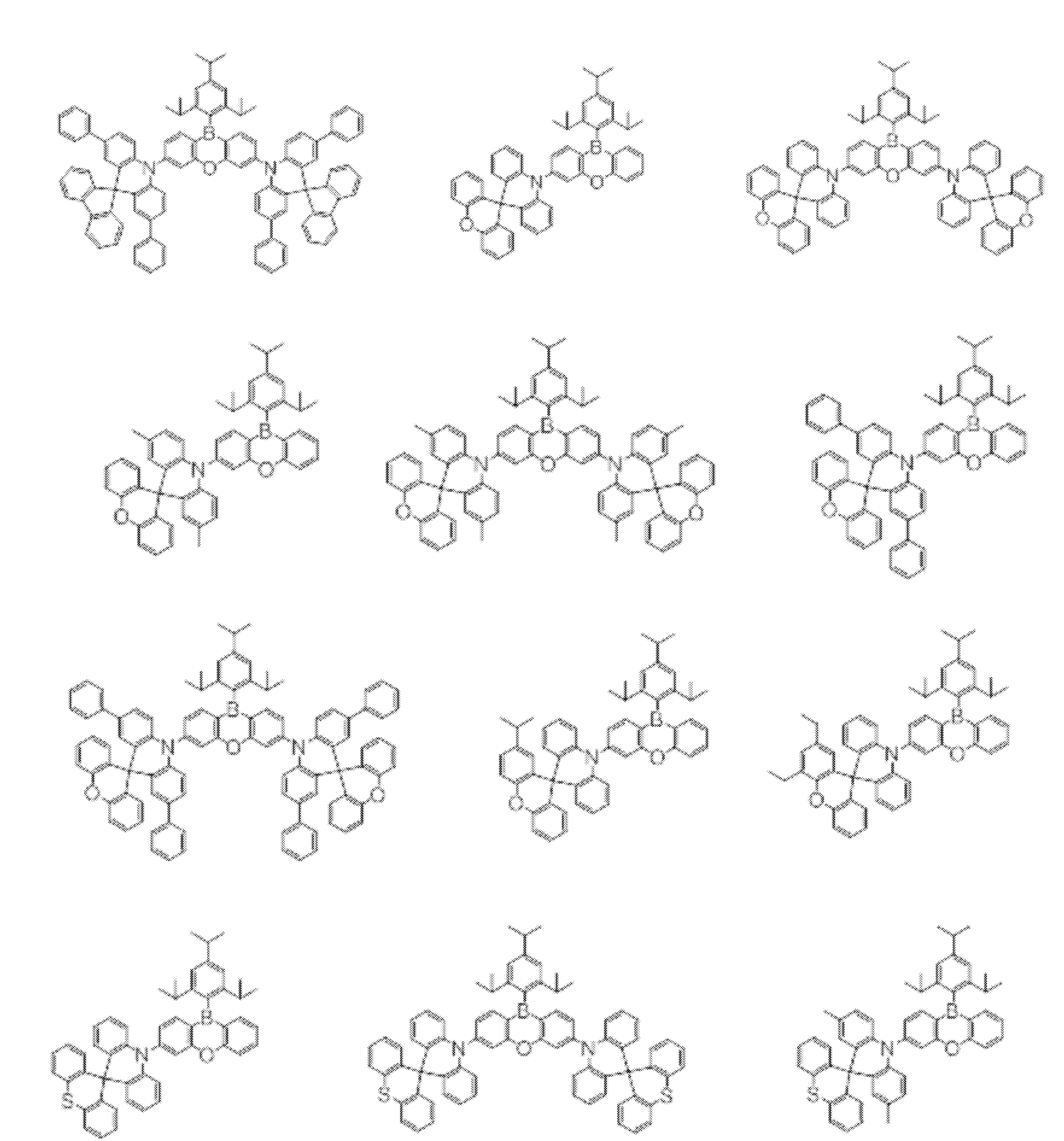


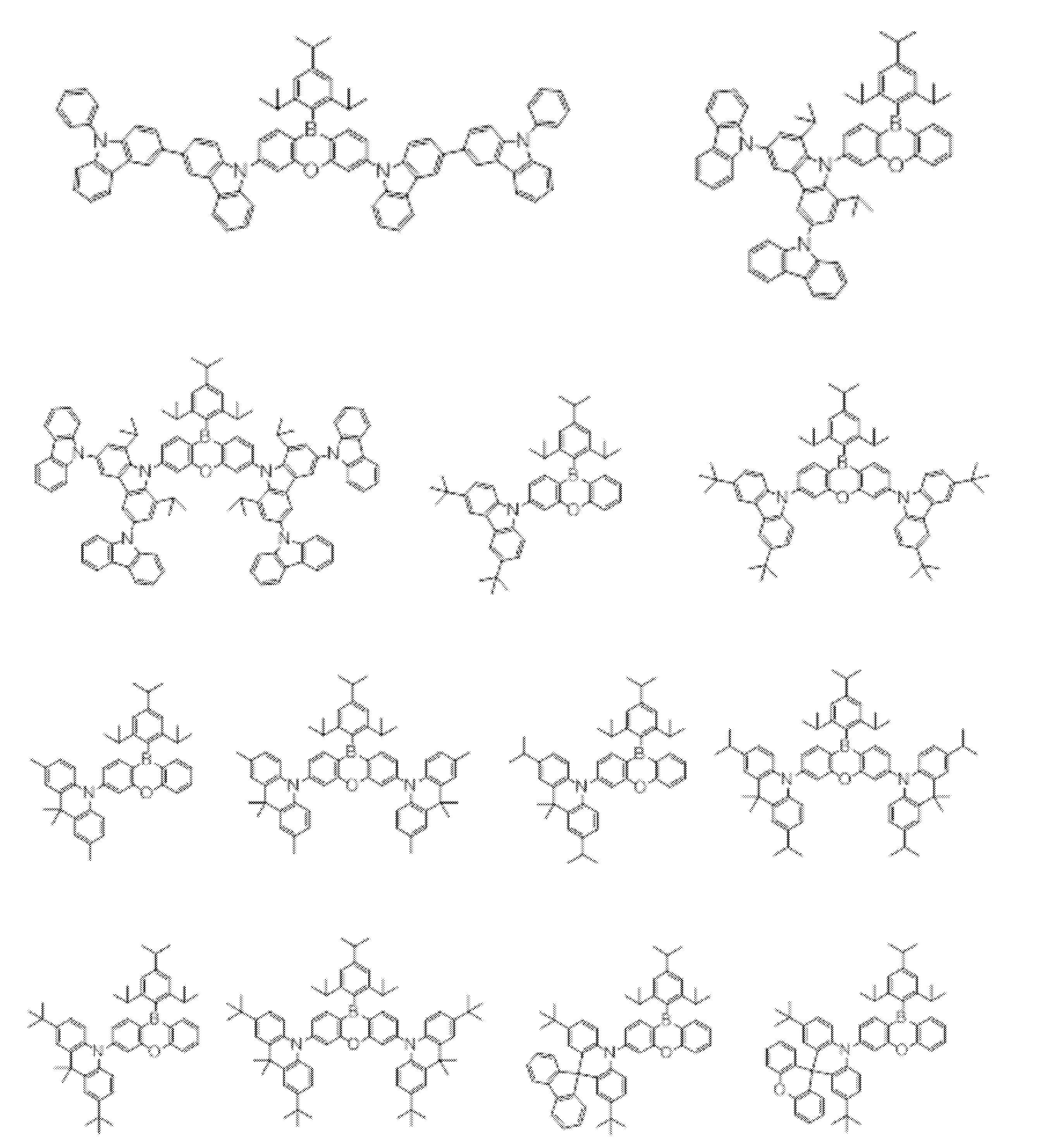
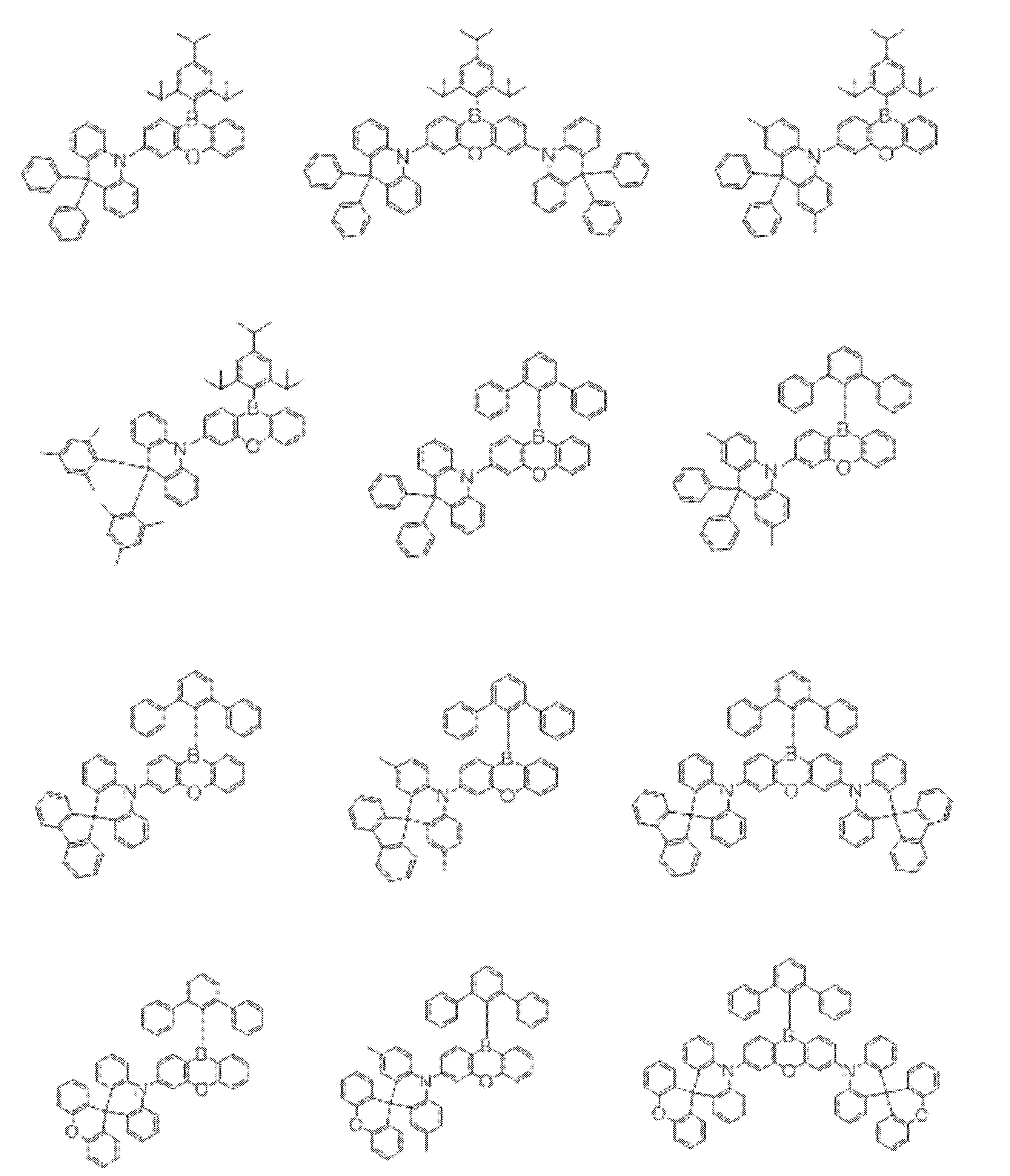


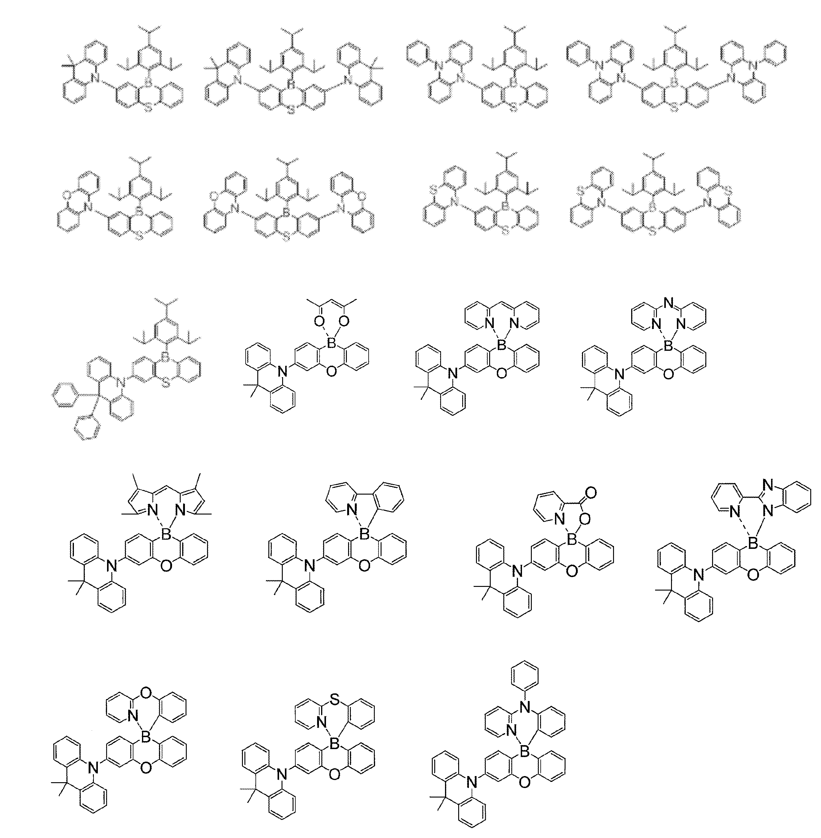

[1] 下記一般式(291)で表される化合物。

[2] 前記一般式(291)で表される化合物が、下記一般式(292)で表される化合物であることを特徴とする[1]に記載の化合物。
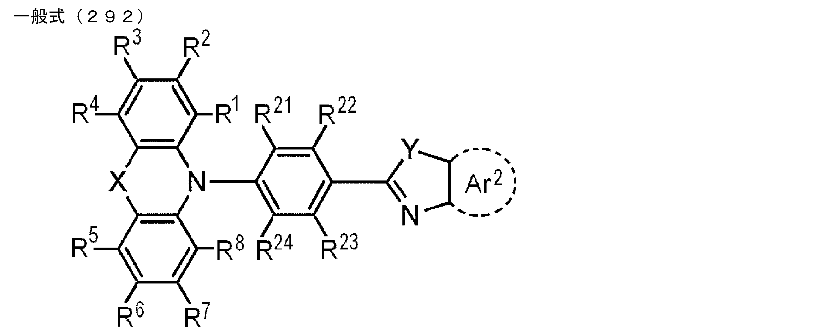
[3] 前記一般式(291)で表される化合物が、下記一般式(293)で表される化合物であることを特徴とする[1]に記載の化合物。

[4] XがOまたはSであることを特徴とする[1]~[3]のいずれか1項に記載の化合物。
[5] YがO、SまたはN-R16であって、R16が置換もしくは無置換のアリール基であることを特徴とする[1]~[4]のいずれか1項に記載の化合物。
[6] R1~R8が、各々独立に水素原子、フッ素原子、塩素原子、シアノ基、炭素数1~10の置換もしくは無置換のアルキル基、炭素数1~10の置換もしくは無置換のアルコキシ基、炭素数1~10の置換もしくは無置換のジアルキルアミノ基、炭素数12~40の置換もしくは無置換のジアリールアミノ基、炭素数6~15の置換もしくは無置換のアリール基、または炭素数3~12の置換もしくは無置換のヘテロアリール基であることを特徴とする[1]~[5]のいずれか1項に記載の化合物。 Preferred examples of the light emitting material include the following compounds.
[1] A compound represented by the following general formula (291).
[2] The compound according to [1], wherein the compound represented by the general formula (291) is a compound represented by the following general formula (292).
[3] The compound according to [1], wherein the compound represented by the general formula (291) is a compound represented by the following general formula (293).
[4] The compound according to any one of [1] to [3], wherein X is O or S.
[5] The compound according to any one of [1] to [4], wherein Y is O, S or N—R 16 , and R 16 is a substituted or unsubstituted aryl group. .
[6] R 1 to R 8 are each independently a hydrogen atom, a fluorine atom, a chlorine atom, a cyano group, a substituted or unsubstituted alkyl group having 1 to 10 carbon atoms, a substituted or unsubstituted group having 1 to 10 carbon atoms. An alkoxy group, a substituted or unsubstituted dialkylamino group having 1 to 10 carbon atoms, a substituted or unsubstituted diarylamino group having 12 to 40 carbon atoms, a substituted or unsubstituted aryl group having 6 to 15 carbon atoms, or the number of
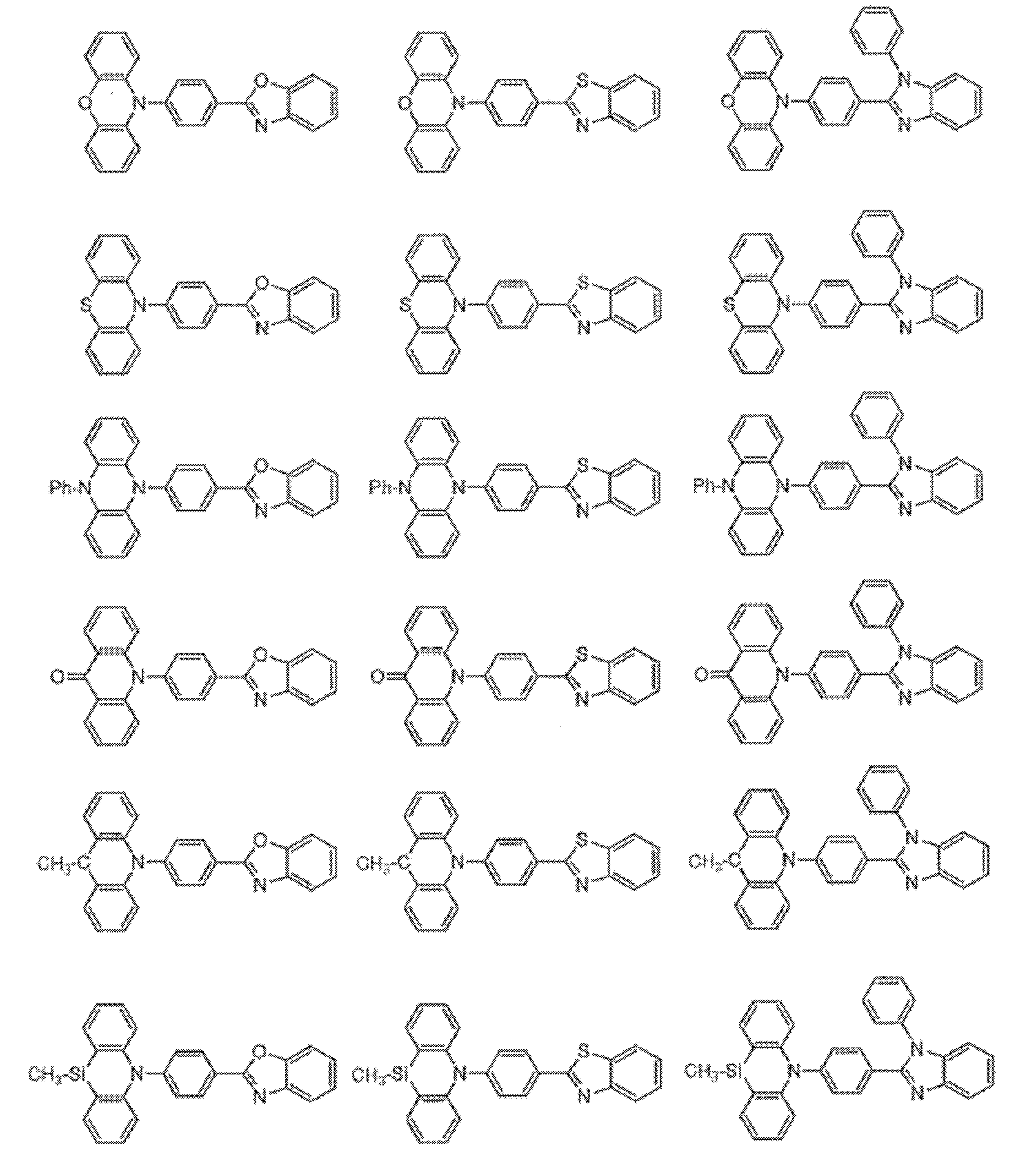
[1] 下記一般式(301)で表される化合物。
一般式(301)
(D)n-A
[一般式(301)において、Dは下記一般式(302)で表される基であり、Aは下記一般式(303)で表される構造を含むn価の基を表す。nは1~8のいずれかの整数を表す。]
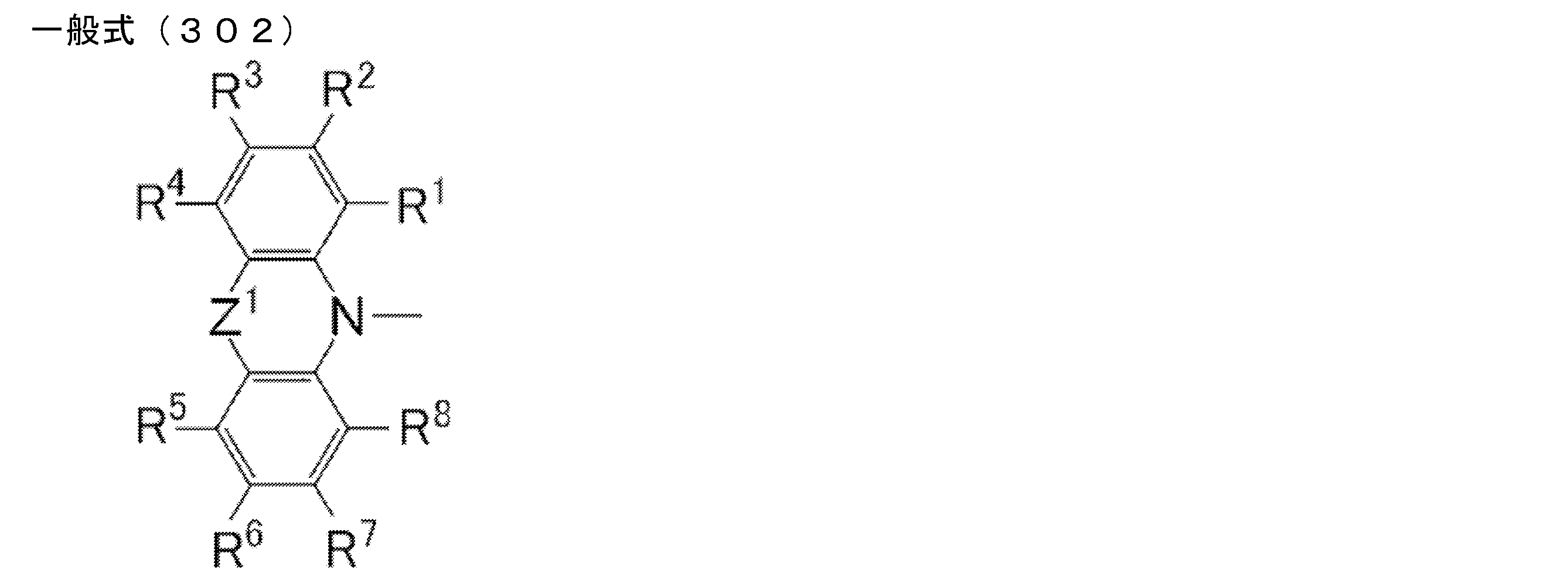
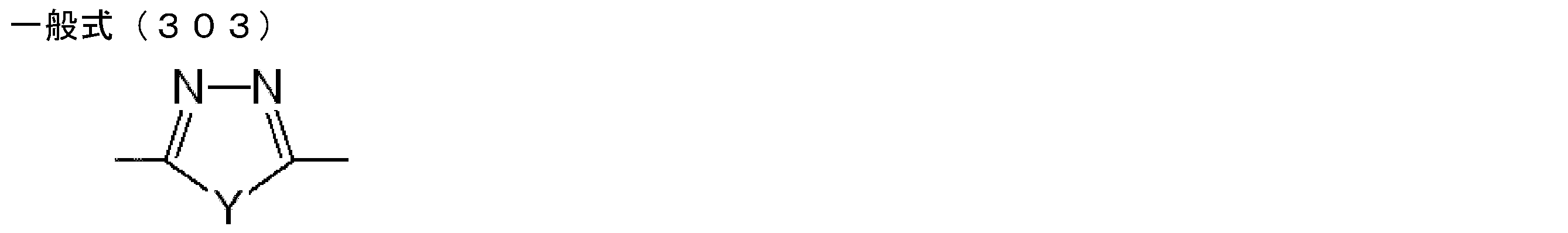
[1] A compound represented by the following general formula (301).
General formula (301)
(D) n-A
[In General Formula (301), D represents a group represented by the following General Formula (302), and A represents an n-valent group including a structure represented by the following General Formula (303). n represents an integer of 1 to 8. ]
[3] 一般式(302)のZ1が、N-Ar3を表す[1]に記載の化合物。 [2] As described in [1], Z 1 in the general formula (302) represents O, S, C═O, C (R 21 ) (R 22 ), Si (R 23 ) (R 24 ), or a single bond. Compound.
[3] The compound according to [1], wherein Z 1 in the general formula (302) represents N—Ar 3 .

[5] 一般式(301)のnが1~4のいずれかの整数であることを特徴とする[1]~[4]のいずれか一項に記載の化合物。 [4] The compound according to any one of [1] to [3], wherein A in the general formula (301) has a structure represented by the following general formula (304).
[5] The compound according to any one of [1] to [4], wherein n in the general formula (301) is an integer of 1 to 4.
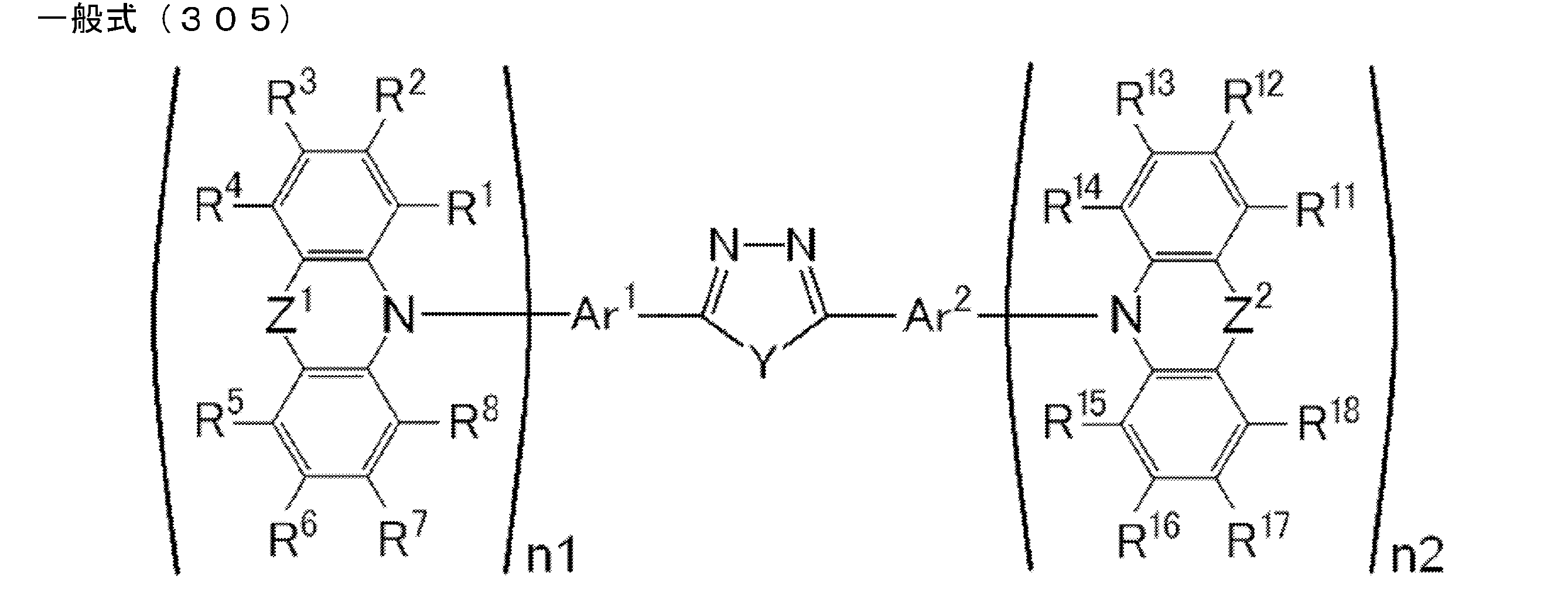
[7] 一般式(305)のZ1およびZ2が各々独立にO、S、N-Ar3または単結合であることを特徴とする[6]に記載の化合物。
[8] 一般式(305)のYがOまたはN-Ar4であることを特徴とする[6]または[7]に記載の化合物。 [6] The compound according to any one of [1] to [3], which is represented by the general formula (305).
[7] The compound according to [6], wherein Z 1 and Z 2 in the general formula (305) are each independently O, S, N—Ar 3 or a single bond.
[8] The compound according to [6] or [7], wherein Y in the general formula (305) is O or N—Ar 4 .

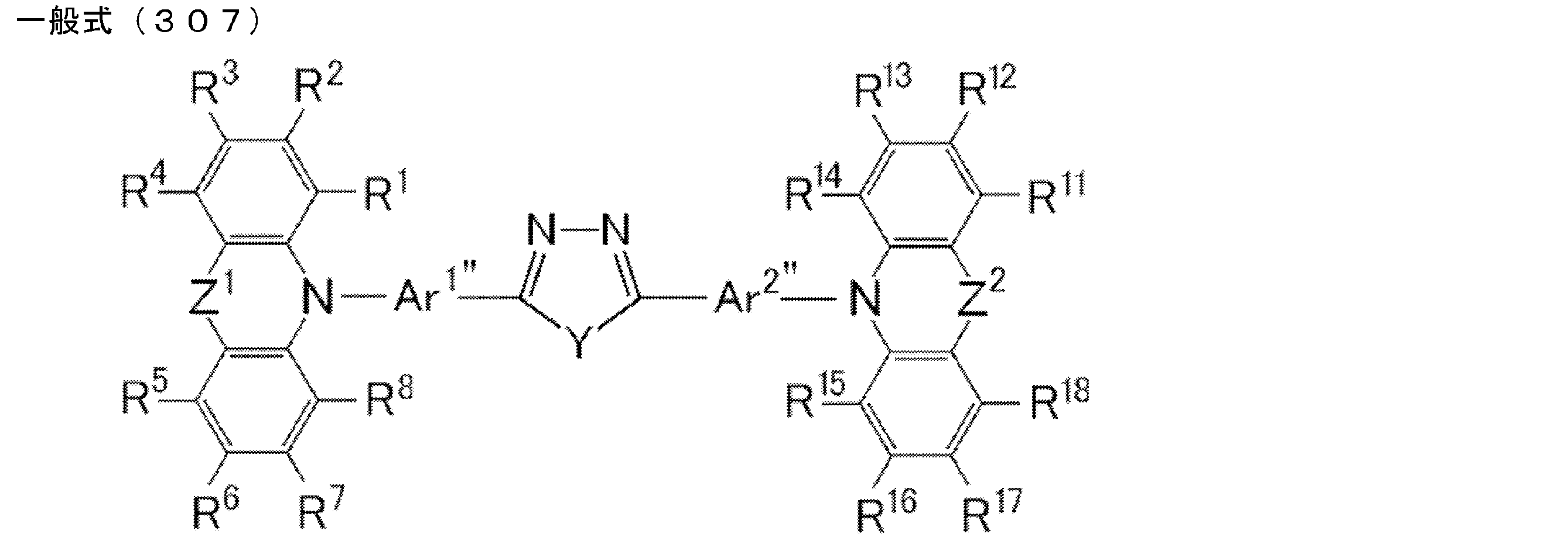
[11] 一般式(307)のZ1とZ2が同一であり、Ar1"とAr2"が同一であり、R1とR14が同一であり、R2とR13が同一であり、R3とR12が同一であり、R4とR11が同一であり、R5とR18が同一であり、R6とR17が同一であり、R7とR16が同一であり、R8とR15が同一であることを特徴とする[10]に記載の化合物。
[12] 一般式(307)のZ1とZ2が各々独立にO、SまたはN-Ar3であることを特徴とする[10]または[11]に記載の化合物。 [10] The compound according to any one of [1] to [3], which is represented by the following general formula (307).
[11] Z 1 and Z 2 in the general formula (307) are the same, Ar 1 ″ and Ar 2 ″ are the same, R 1 and R 14 are the same, and R 2 and R 13 are the same. R 3 and R 12 are the same, R 4 and R 11 are the same, R 5 and R 18 are the same, R 6 and R 17 are the same, R 7 and R 16 are the same , R 8 and R 15 are the same, [10].
[12] The compound according to [10] or [11], wherein Z 1 and Z 2 in the general formula (307) are each independently O, S or N—Ar 3 .
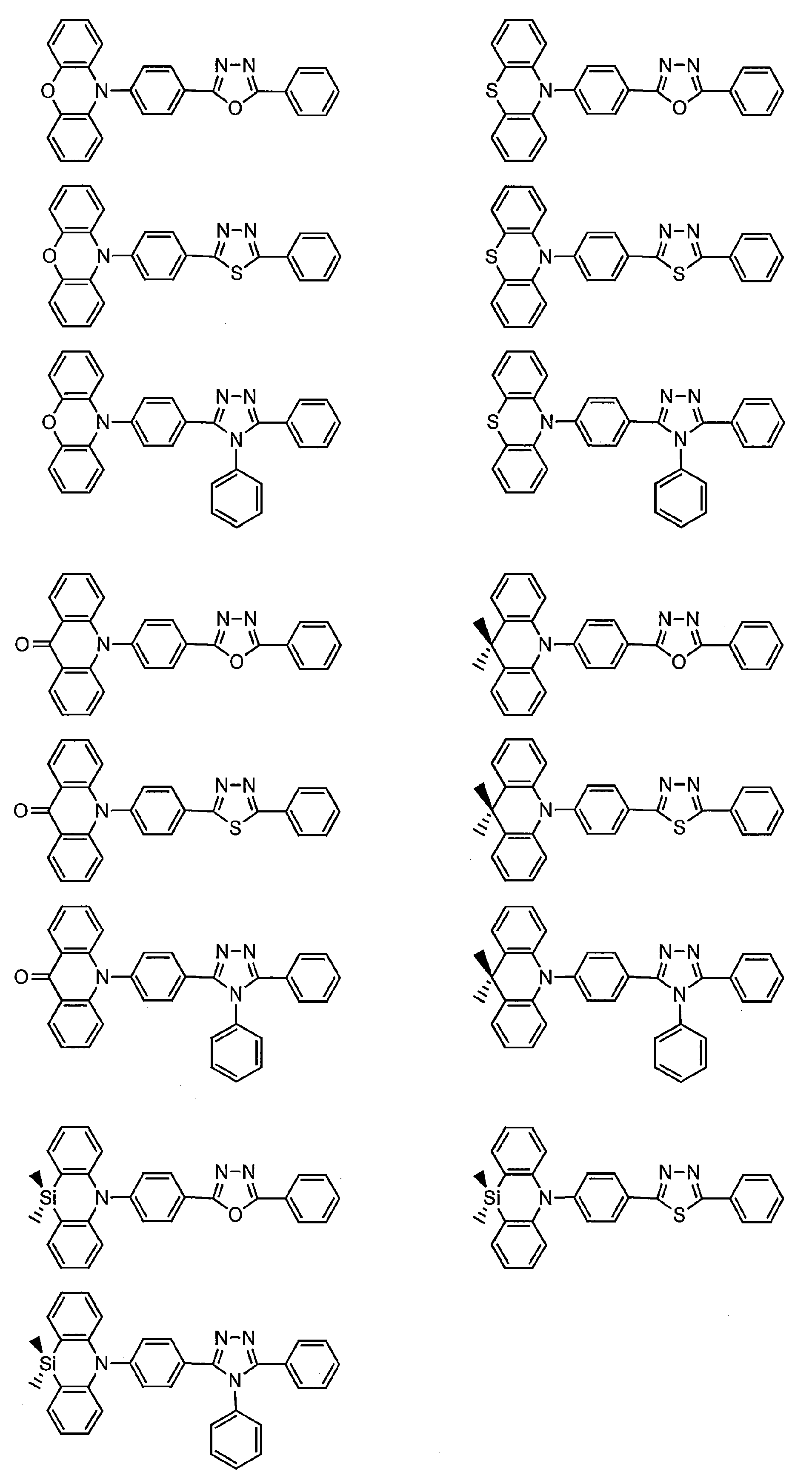
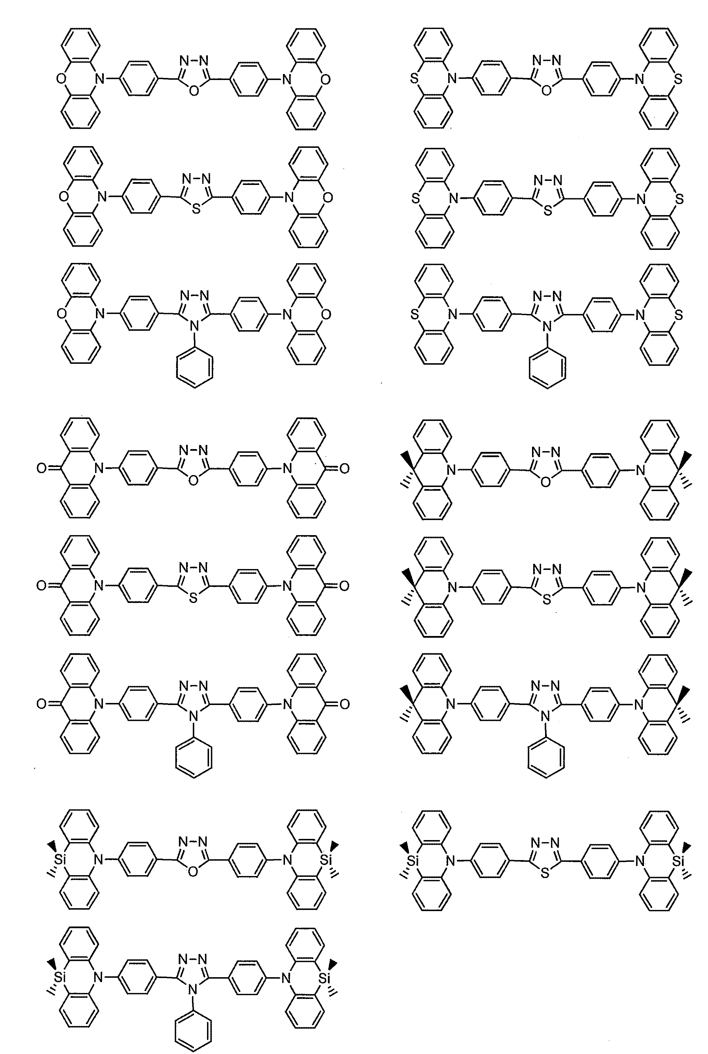


[1] 下記一般式(311)で表される化合物。
一般式(311)
A-D-A
[一般式(311)において、Dは下記式:


[1] A compound represented by the following general formula (311).
Formula (311)
ADA
[In the general formula (311), D represents the following formula:

[3] 一般式(311)の2つのAが同一の構造を有することを特徴とする[1]または[2]に記載の化合物。 [2] The compound according to [1], wherein D in the general formula (311) has a structure represented by the following general formula (312).
[3] The compound according to [1] or [2], wherein two A's in the general formula (311) have the same structure.

<1> R12がシアノ基または下記構造の基(ただし水素原子は置換基で置換されていてもよい)であるか、
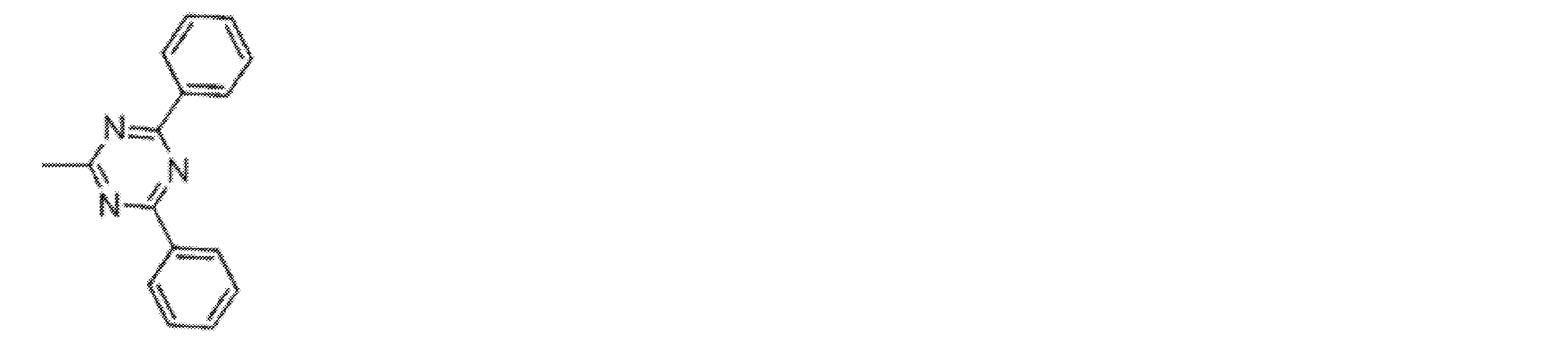


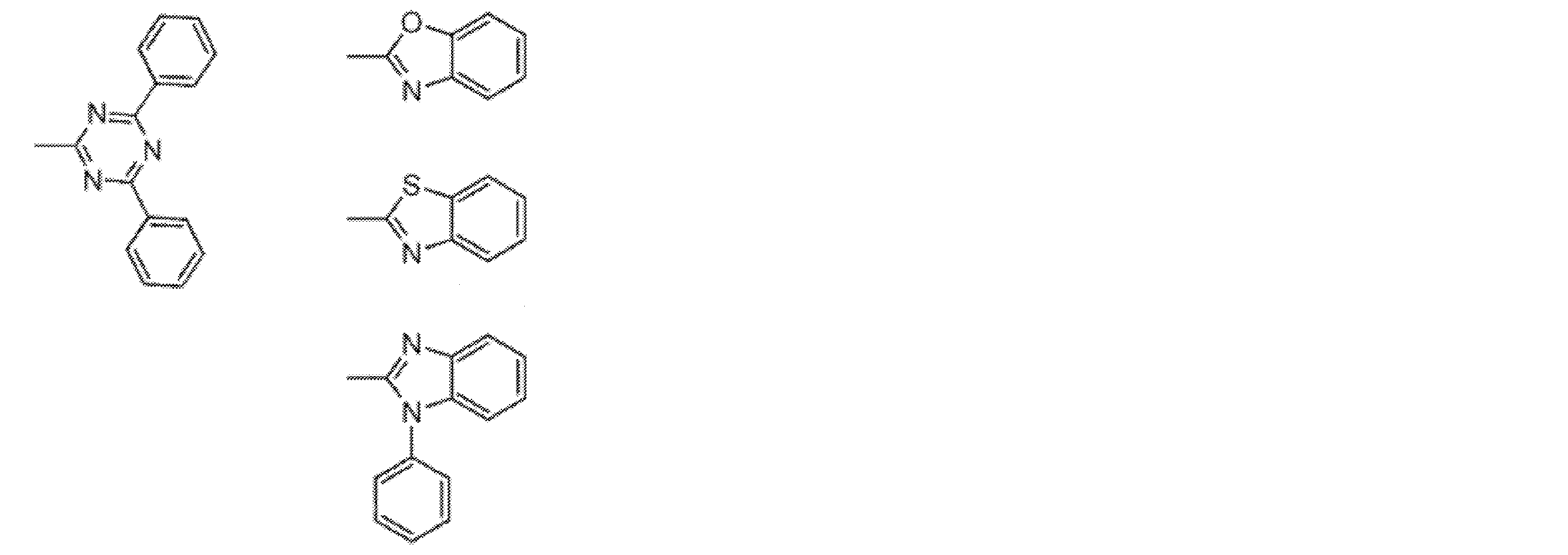

[5] 一般式(313)のR1~R8が、各々独立に水素原子、炭素数1~10の置換もしくは無置換のアルキル基、炭素数1~10の置換もしくは無置換のアルコキシ基、炭素数6~15の置換もしくは無置換のアリール基、または炭素数3~12の置換もしくは無置換のヘテロアリール基であることを特徴とする[4]に記載の化合物。
[6] 一般式(313)のR12、R13、R17、R18のうちの少なくとも2つが上記<1>および<2>の条件を満たすように置換基を有しており、それ以外のR11~R20が各々独立に水素原子、フッ素原子、塩素原子、シアノ基、炭素数1~10の置換もしくは無置換のアルキル基、炭素数1~10の置換もしくは無置換のアルコキシ基、炭素数1~10の置換もしくは無置換のジアルキルアミノ基、炭素数12~40の置換もしくは無置換のジアリールアミノ基、炭素数6~15の置換もしくは無置換のアリール基、または炭素数3~12の置換もしくは無置換のヘテロアリール基であることを特徴とする[4]または[5]に記載の化合物。
[7] 一般式(313)の上記<1>および<2>中に記載される構造の水素原子が置換されていてもよい置換基が、フッ素原子、塩素原子、シアノ基、炭素数1~10の置換もしくは無置換のアルキル基、炭素数1~10の置換もしくは無置換のアルコキシ基、炭素数1~10の置換もしくは無置換のジアルキルアミノ基、炭素数12~40の置換もしくは無置換のジアリールアミノ基、炭素数6~15の置換もしくは無置換のアリール基、および炭素数3~12の置換もしくは無置換のヘテロアリール基からなる群より選択されることを特徴とする[4]~[6]のいずれか1項に記載の化合物。 [4] The compound according to any one of [1] to [3], which is represented by the following general formula (313):
<1> R 12 is a cyano group or a group having the following structure (however, a hydrogen atom may be substituted with a substituent),
[5] R 1 to R 8 in the general formula (313) are each independently a hydrogen atom, a substituted or unsubstituted alkyl group having 1 to 10 carbon atoms, a substituted or unsubstituted alkoxy group having 1 to 10 carbon atoms, [6] The compound according to [4], which is a substituted or unsubstituted aryl group having 6 to 15 carbon atoms or a substituted or unsubstituted heteroaryl group having 3 to 12 carbon atoms.
[6] At least two of R 12 , R 13 , R 17 and R 18 in the general formula (313) have a substituent so as to satisfy the above conditions <1> and <2>; Each of R 11 to R 20 independently represents a hydrogen atom, a fluorine atom, a chlorine atom, a cyano group, a substituted or unsubstituted alkyl group having 1 to 10 carbon atoms, a substituted or unsubstituted alkoxy group having 1 to 10 carbon atoms, A substituted or unsubstituted dialkylamino group having 1 to 10 carbon atoms, a substituted or unsubstituted diarylamino group having 12 to 40 carbon atoms, a substituted or unsubstituted aryl group having 6 to 15 carbon atoms, or 3 to 12 carbon atoms The compound according to [4] or [5], which is a substituted or unsubstituted heteroaryl group.
[7] The substituent in which the hydrogen atom having the structure described in the above <1> and <2> in the general formula (313) may be substituted is a fluorine atom, a chlorine atom, a cyano group, a carbon number of 1 to 10 substituted or unsubstituted alkyl groups, 1 to 10 carbon atoms substituted or unsubstituted alkoxy groups, 1 to 10 carbon atoms substituted or unsubstituted dialkylamino groups, 12 to 40 carbon atoms substituted or unsubstituted [4] to [4] characterized by being selected from the group consisting of a diarylamino group, a substituted or unsubstituted aryl group having 6 to 15 carbon atoms, and a substituted or unsubstituted heteroaryl group having 3 to 12 carbon atoms The compound according to any one of 6].


また、発光層を塗布法で成膜する場合には、比較的大きな分子量のものであっても分子量を問わずに好ましく用いることができる。 The molecular weight of the second organic compound is preferably 1500 or less, and more preferably 1200 or less, when it is intended to use a light-emitting layer containing the second organic compound formed by vapor deposition, for example. Preferably, it is 1000 or less, more preferably 800 or less. The lower limit of the molecular weight is, for example, the molecular weight of the minimum compound represented by these general formulas if it is a compound represented by the general formula (1) or (9).
Moreover, when forming a light emitting layer by the apply | coating method, even if it is a comparatively large molecular weight, it can use preferably regardless of molecular weight.
第1有機化合物は、第2有機化合物および第3有機化合物よりも最低励起一重項エネルギーが大きい有機化合物であり、キャリアの輸送を担うホスト材料としての機能や第3有機化合物のエネルギーを該化合物中に閉じ込める機能を有する。これにより、第3有機化合物は、分子内でホールと電子とが再結合することによって生じたエネルギー、および、第1有機化合物および第2有機化合物から受け取ったエネルギーを効率よく発光に変換することができ、発光効率が高い有機エレクトロルミネッセンス素子を実現することができる。
第1有機化合物としては、正孔輸送能、電子輸送能を有し、かつ発光の長波長化を防ぎ、なおかつ高いガラス転移温度を有する有機化合物であることが好ましい。以下に、第1有機化合物として用いることができる好ましい化合物を挙げる。なお、以下の例示化合物の構造式におけるR、R1~R10は、各々独立に水素原子または置換基を表す。nは3~5の整数を表す。 (First organic compound)
The first organic compound is an organic compound having a minimum excited singlet energy higher than that of the second organic compound and the third organic compound, and functions as a host material responsible for carrier transport and the energy of the third organic compound in the compound. It has a function to be confined in. Accordingly, the third organic compound can efficiently convert the energy generated by recombination of holes and electrons in the molecule and the energy received from the first organic compound and the second organic compound into light emission. In addition, an organic electroluminescence element with high luminous efficiency can be realized.
The first organic compound is preferably an organic compound that has a hole transporting ability and an electron transporting ability, prevents an increase in the wavelength of light emission, and has a high glass transition temperature. Below, the preferable compound which can be used as a 1st organic compound is mentioned. Note that R and R 1 to R 10 in the structural formulas of the following exemplary compounds each independently represent a hydrogen atom or a substituent. n represents an integer of 3 to 5.

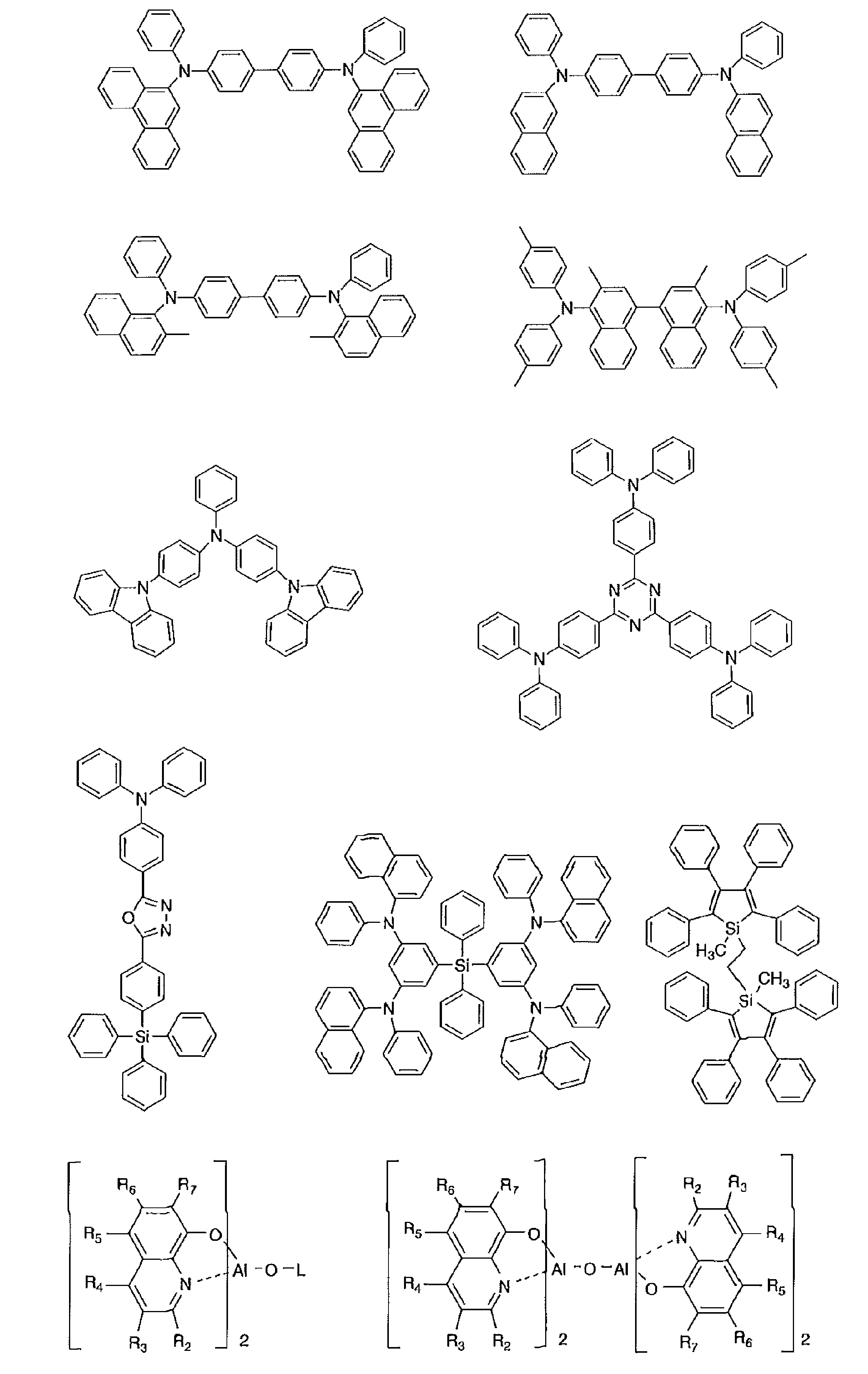
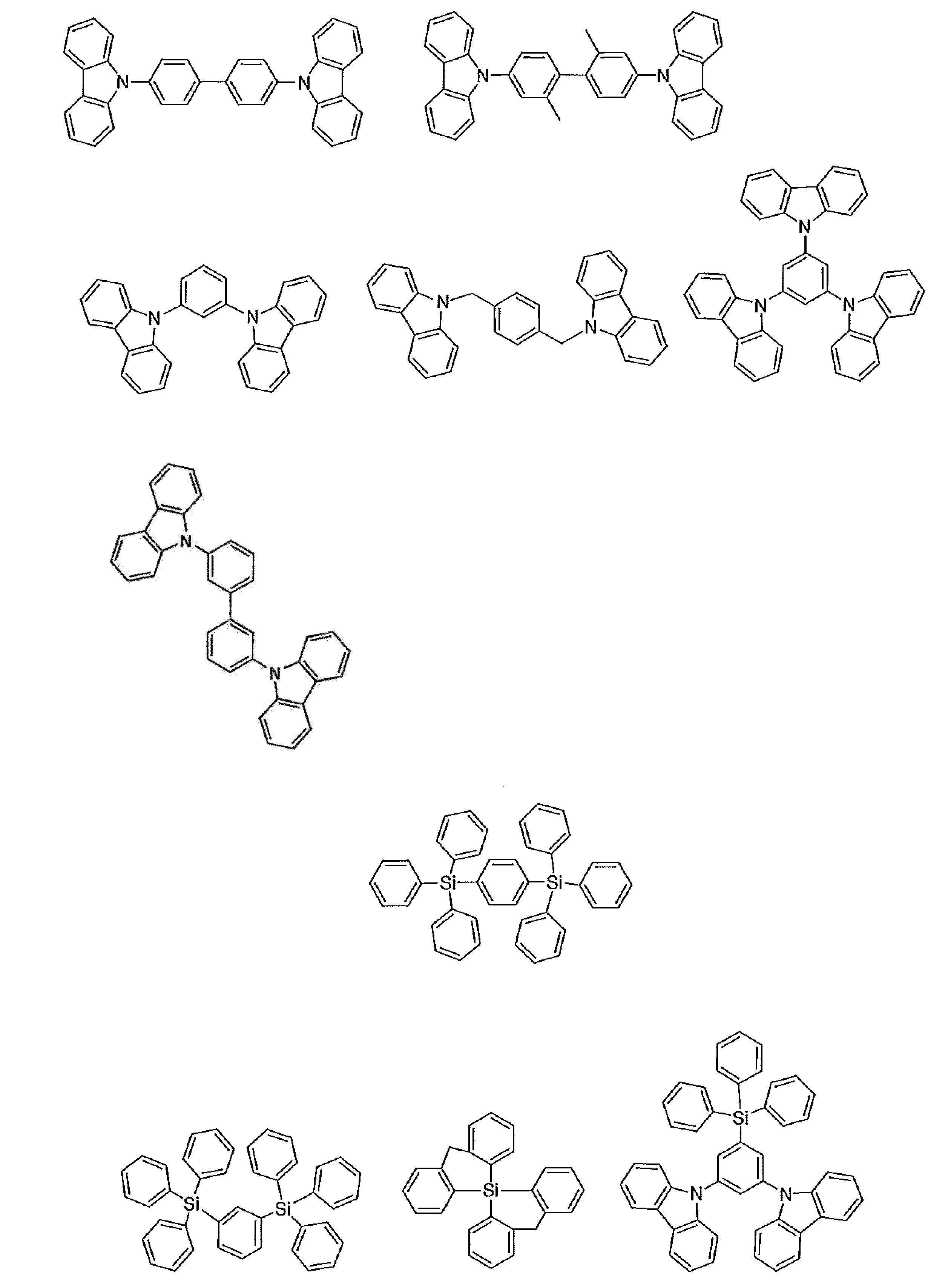


第3有機化合物は、第1有機化合物および第2有機化合物よりも最低励起一重項エネルギーが小さい発光体である。第3有機化合物は、励起一重項状態の第1有機化合物および第2有機化合物と、励起三重項状態から逆項間交差して励起一重項状態になった第2有機化合物からエネルギーを受け取って一重項励起状態に遷移し、その後基底状態に戻るときに蛍光を放射する。第3有機化合物として用いる発光体としては、このように第1有機化合物および第2有機化合物からエネルギーを受け取って発光し得るものであれば特に限定されず、発光は蛍光であっても、遅延蛍光であっても、りん光であっても構わない。中でも、第3有機化合物として用いる発光体は、最低励起一重項エネルギー準位から基底エネルギー準位に戻るときに蛍光を放射するものであることが好ましい。第3有機化合物は、式(A)の関係を満たすものであれば2種以上を用いてもよい。例えば、発光色が異なる2種以上の第3有機化合物を併用することにより、所望の色を発光させることが可能になる。
以下に、第3有機化合物として用いることができる好ましい化合物を発光色毎に挙げる。なお、以下の例示化合物の構造式において、Etはエチル基を表し、i-Prはイソプロピル基を表す。 (Third organic compound)
The third organic compound is a light emitter that has a lowest lowest excited singlet energy than the first organic compound and the second organic compound. The third organic compound receives energy from the first organic compound and the second organic compound in the excited singlet state, and from the second organic compound in the excited singlet state by crossing the reverse triplet state into the excited singlet state. Fluorescence is emitted when transitioning to the term excited state and then returning to the ground state. The light emitter used as the third organic compound is not particularly limited as long as it can emit light upon receiving energy from the first organic compound and the second organic compound as described above. Or phosphorescence. Especially, it is preferable that the light emitter used as the third organic compound emits fluorescence when returning from the lowest excited singlet energy level to the ground energy level. As long as the third organic compound satisfies the relationship of the formula (A), two or more kinds may be used. For example, a desired color can be emitted by using two or more third organic compounds having different emission colors in combination.
Below, the preferable compound which can be used as a 3rd organic compound is mentioned for every luminescent color. In the structural formulas of the following exemplary compounds, Et represents an ethyl group, and i-Pr represents an isopropyl group.
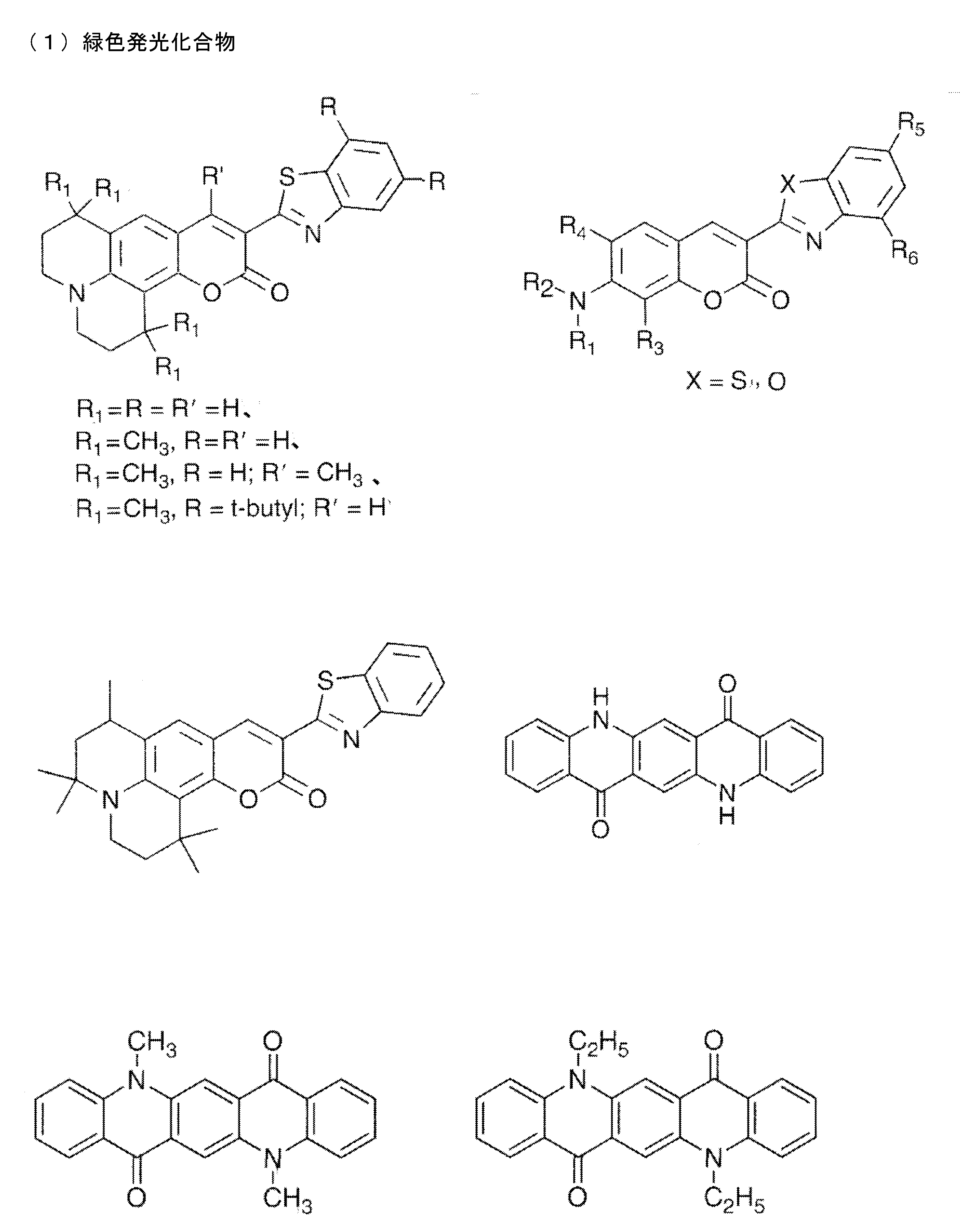
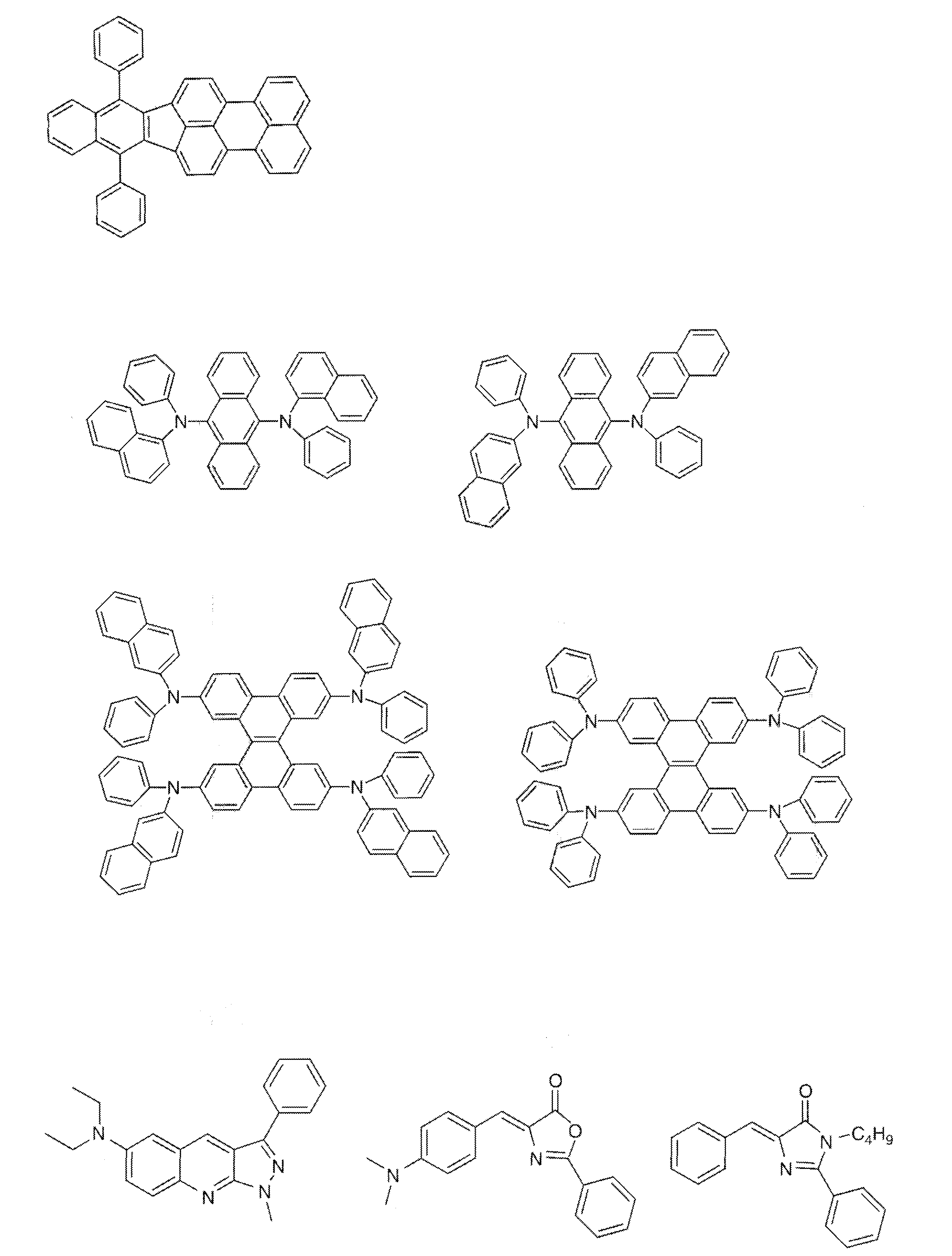
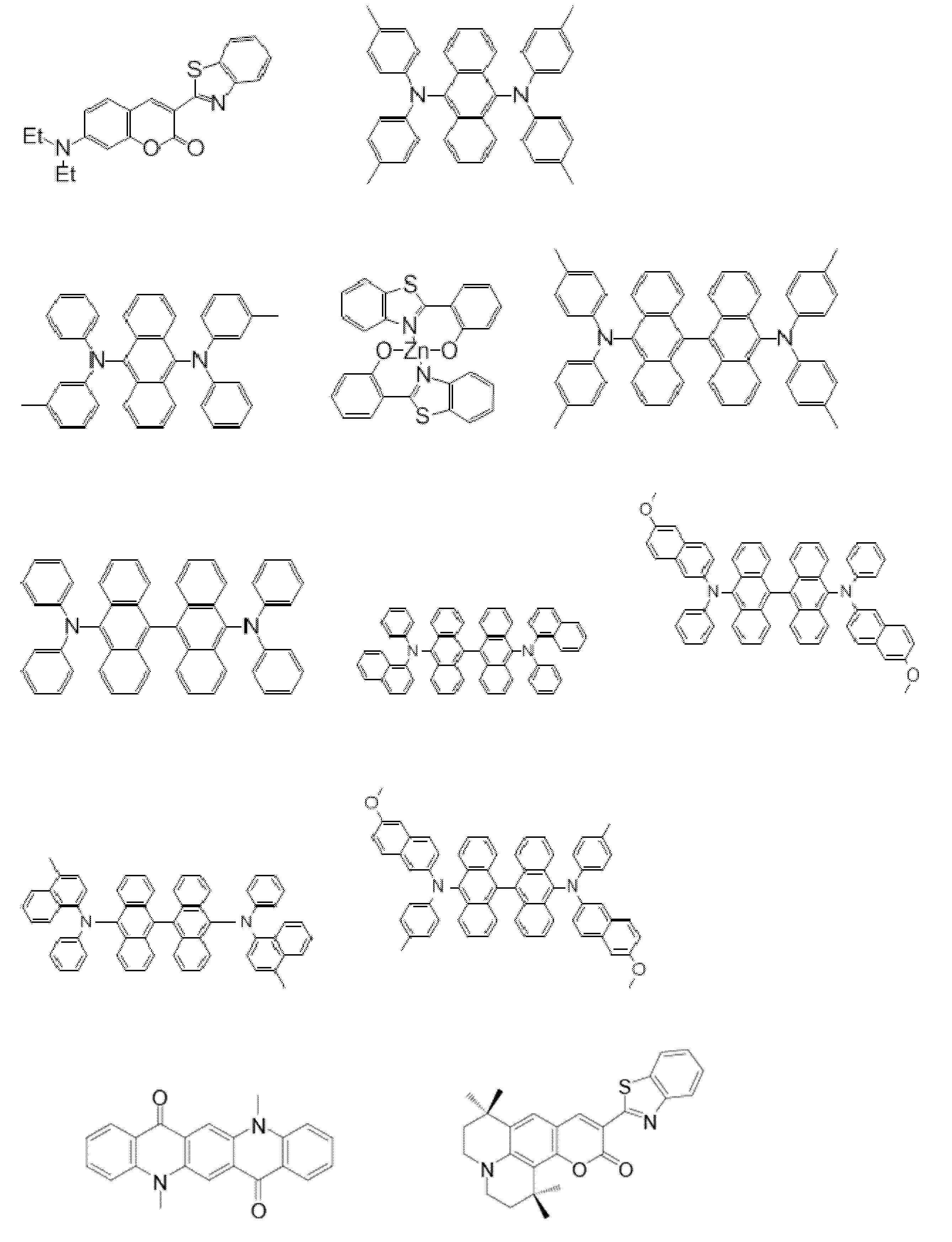

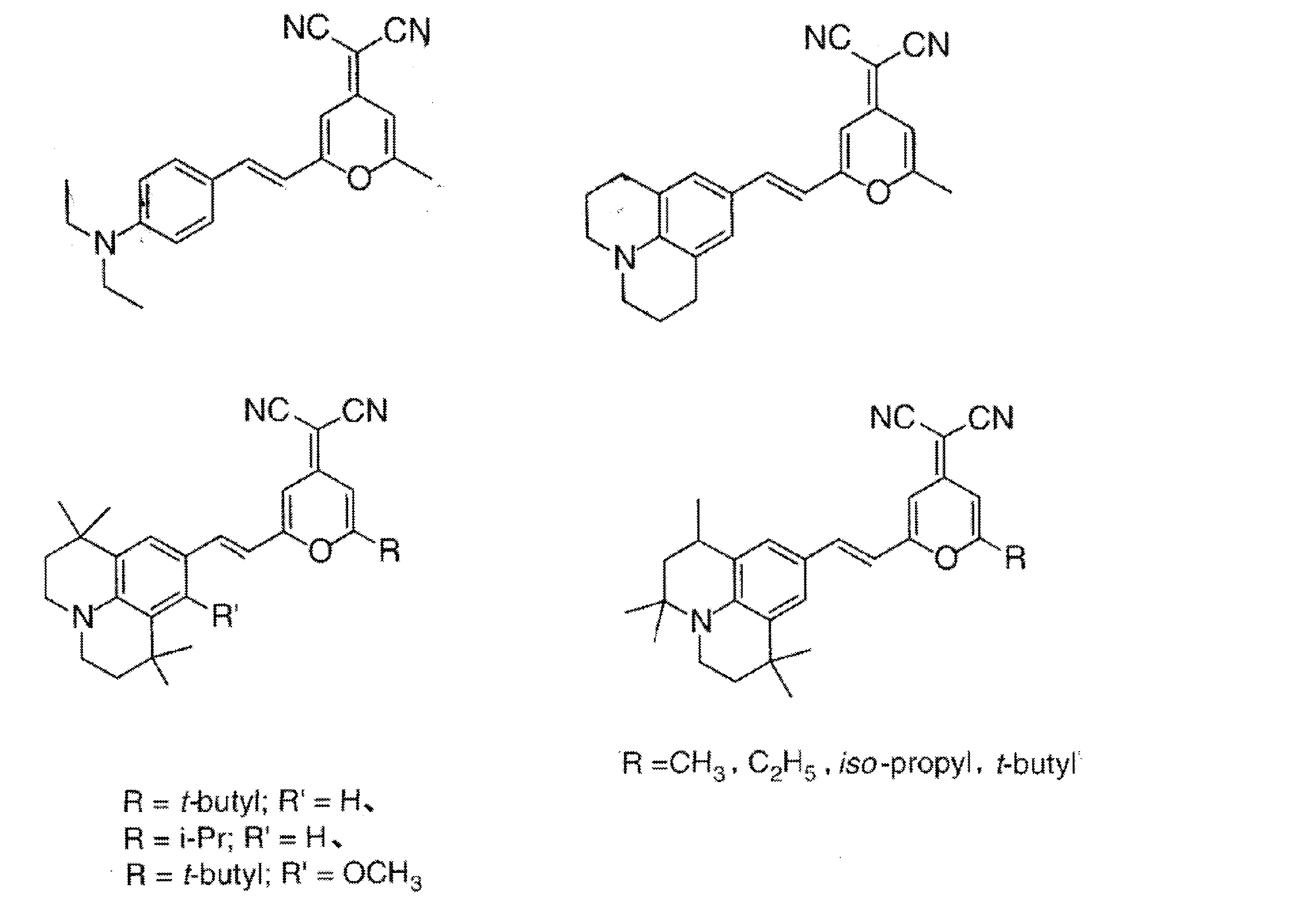
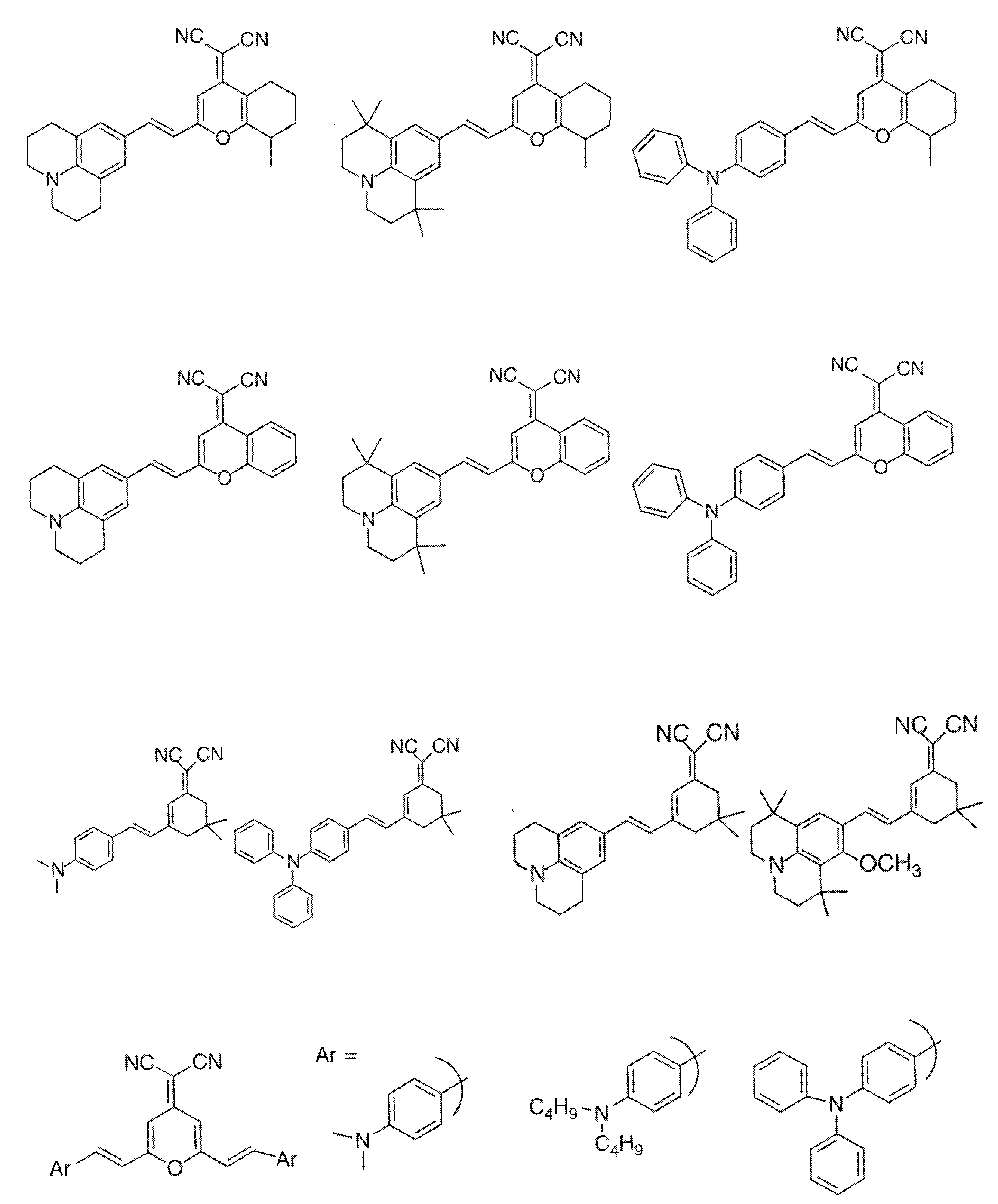
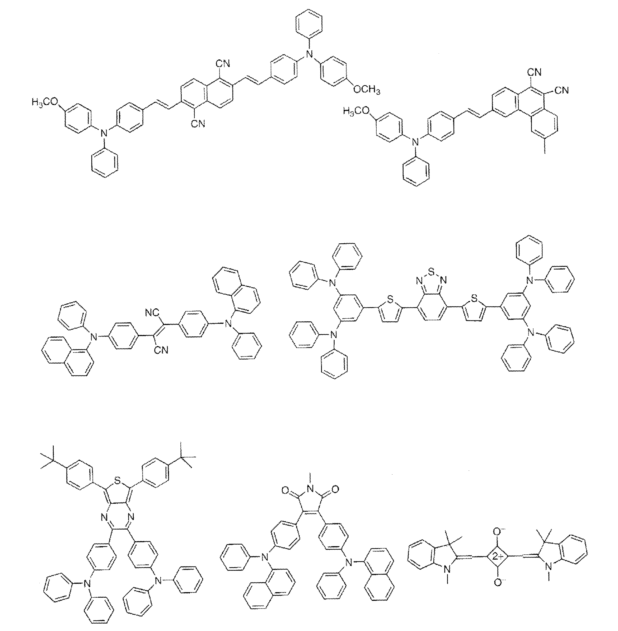
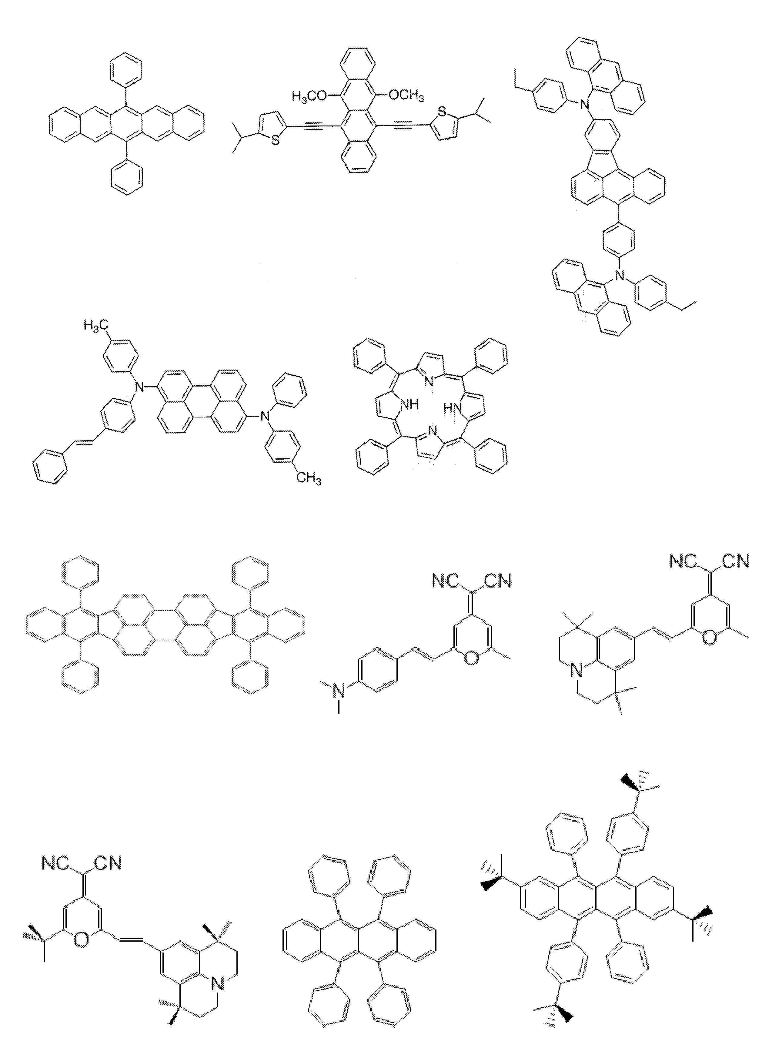

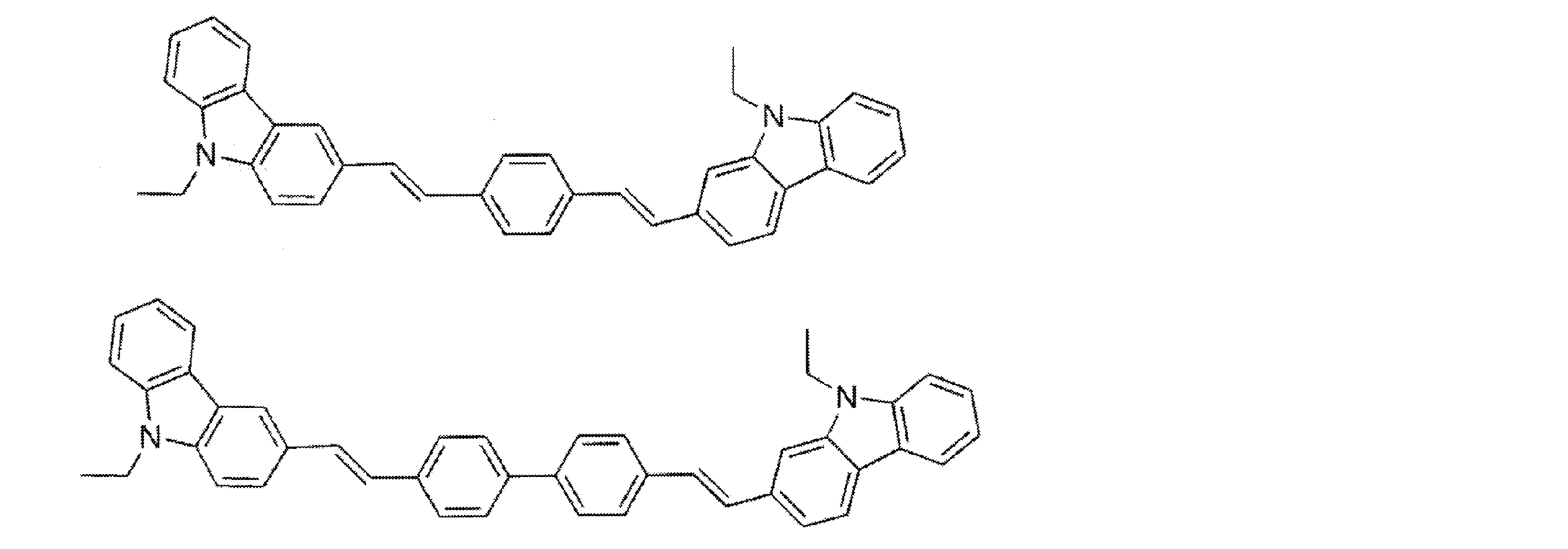
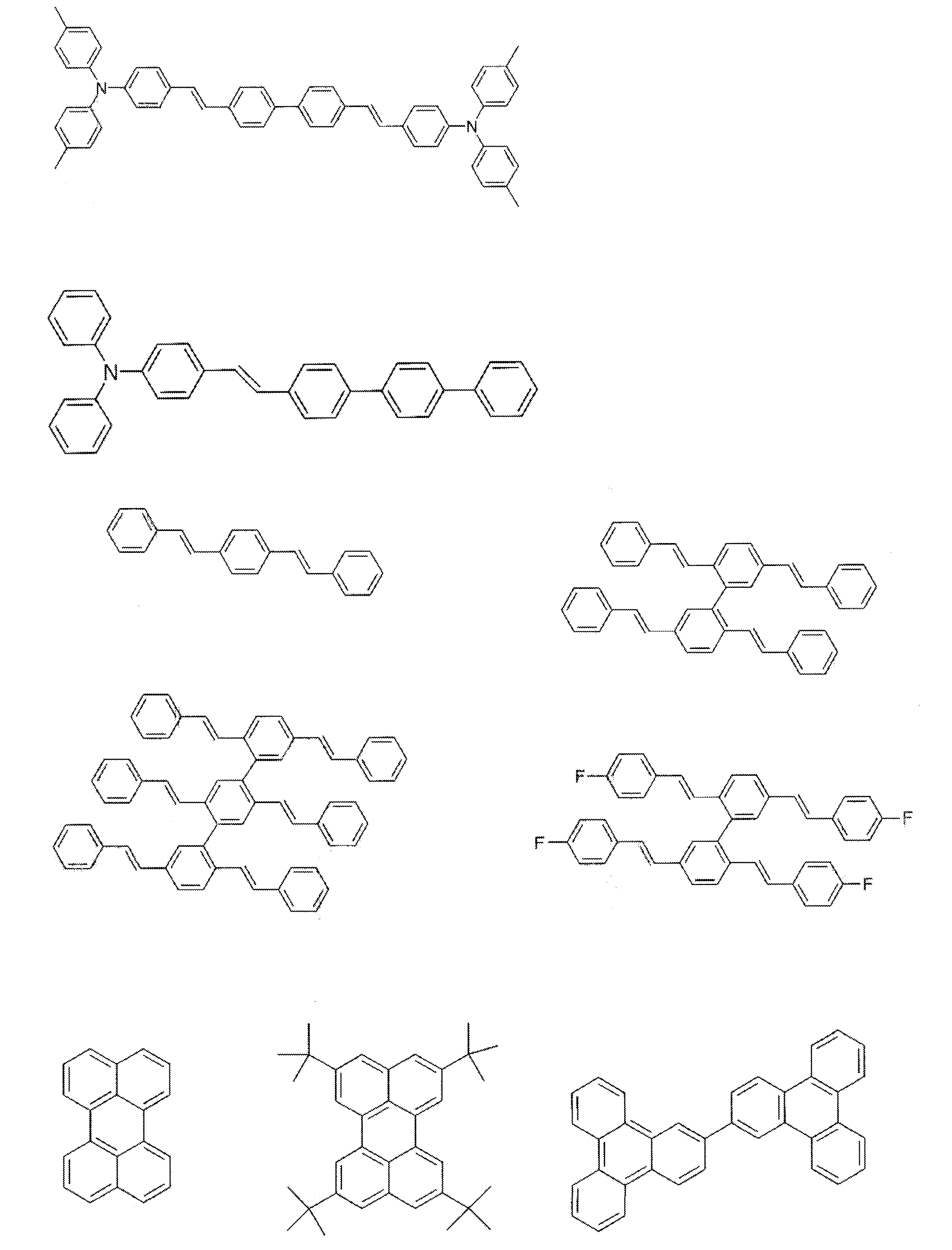

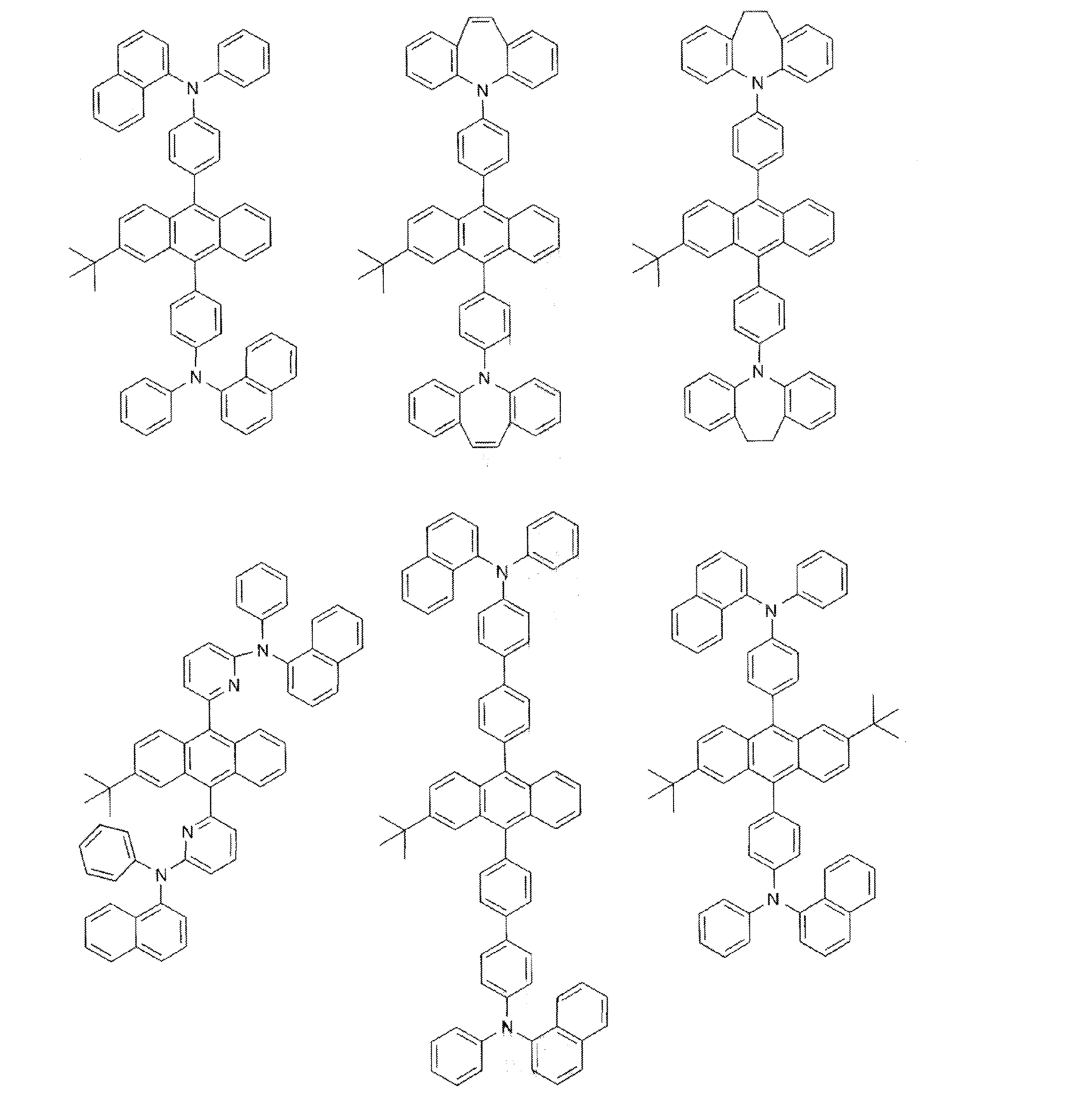
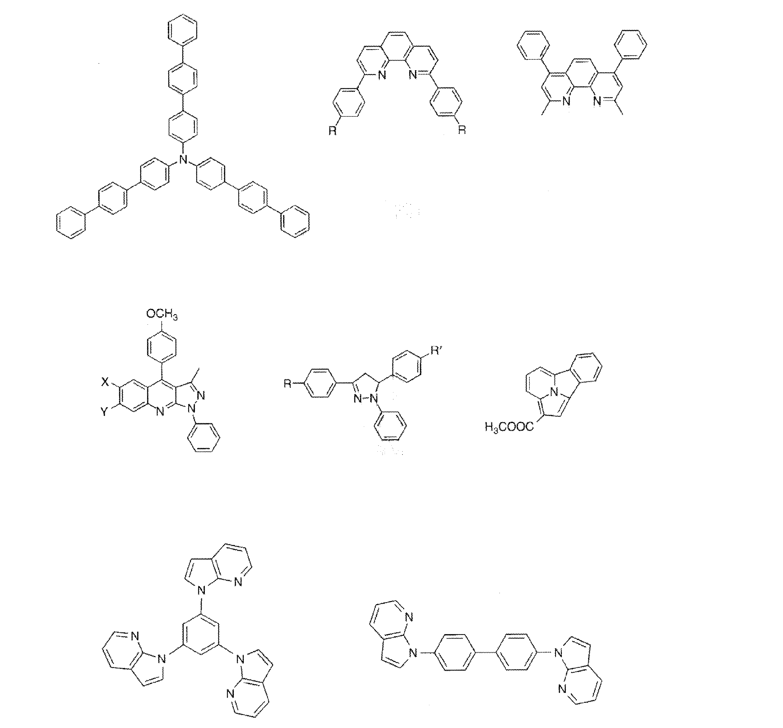

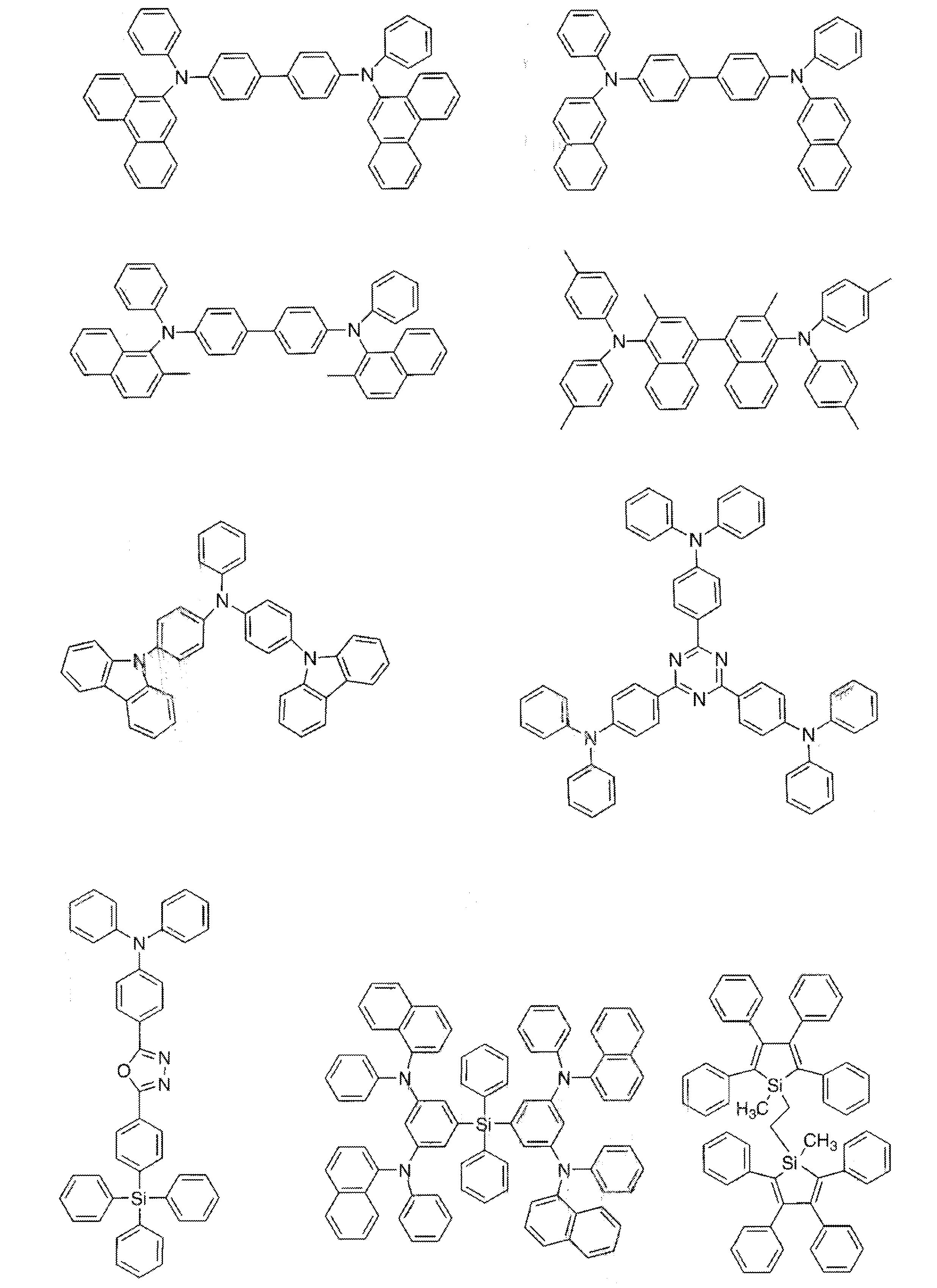

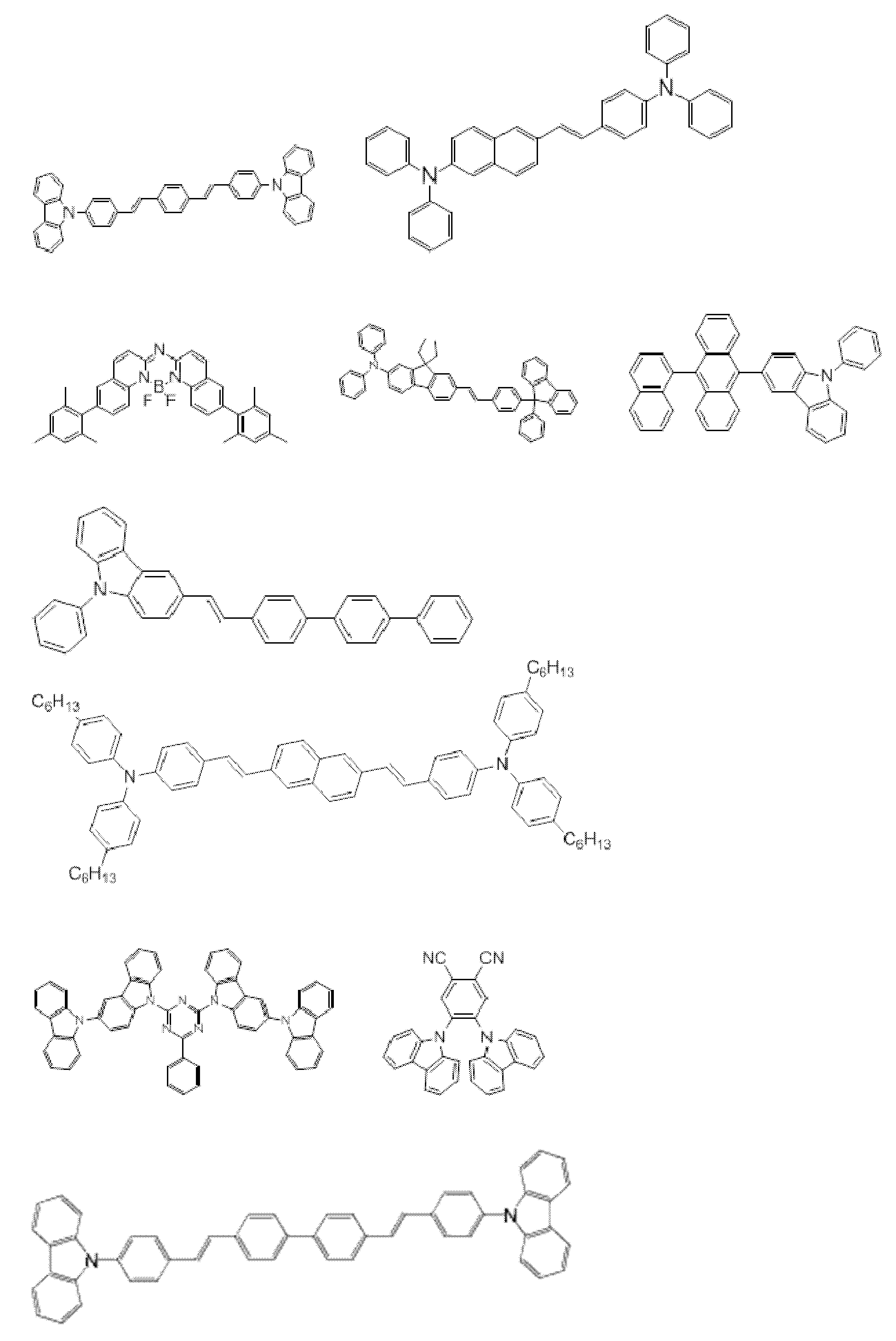
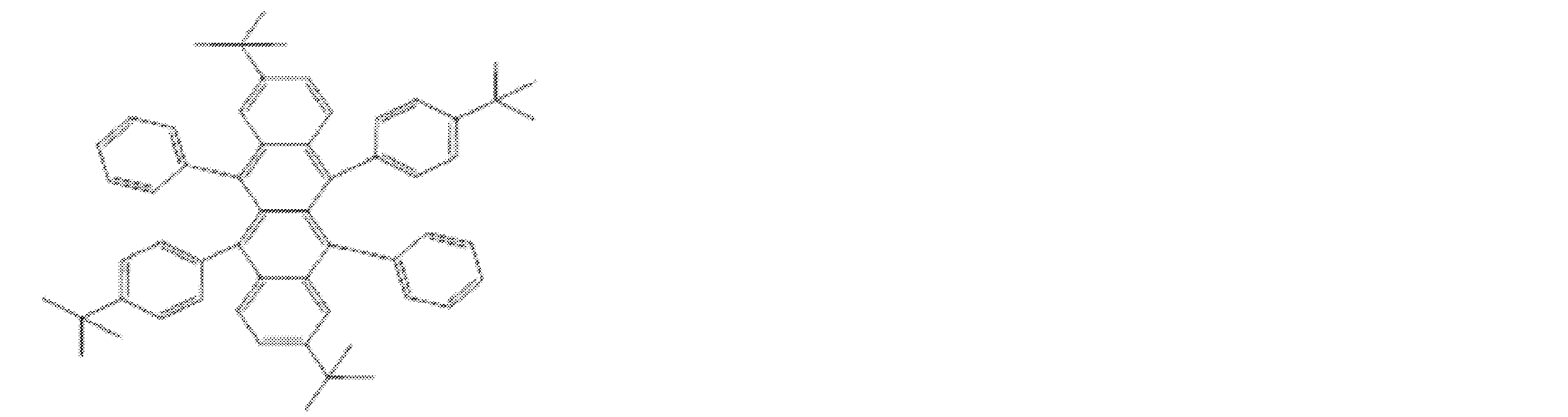

発光層に含まれる各有機化合物の含有量は、特に限定されないが、第2有機化合物の含有量は第1有機化合物の含有量よりも小さいことが好ましい。これにより、より高い発光効率を得ることができる。具体的には、第1有機化合物の含有量W1と第2有機化合物の含有量W2と第3有機化合物の含有量W3の合計重量を100重量%としたとき、第1有機化合物の含有量W1は15重量%以上、99.9重量%以下であることが好ましく、第2有機化合物の含有量W2は5.0重量%以上、50重量%以下であることが好ましく、第3有機化合物の含有量W3は0.5重量%以上、5.0重量%以下であることが好ましい。 (Contents of first organic compound, second organic compound, and third organic compound)
Although content of each organic compound contained in a light emitting layer is not specifically limited, It is preferable that content of a 2nd organic compound is smaller than content of a 1st organic compound. Thereby, higher luminous efficiency can be obtained. Specifically, when the total weight of the first organic compound content W1, the second organic compound content W2, and the third organic compound content W3 is 100% by weight, the first organic compound content W1. Is preferably 15% by weight or more and 99.9% by weight or less, and the content W2 of the second organic compound is preferably 5.0% by weight or more and 50% by weight or less, and the content of the third organic compound The amount W3 is preferably 0.5% by weight or more and 5.0% by weight or less.
発光層は、第1有機化合物~第3有機化合物のみから構成されていてもよいし、第1有機化合物~第3有機化合物以外の有機化合物を含んでいてもよい。第1有機化合物~第3有機化合物以外の有機化合物としては、例えば正孔輸送能を有する有機化合物、電子輸送能を有する有機化合物等を挙げることができる。正孔輸送能を有する有機化合物、電子輸送能を有する有機化合物としては、下記の正孔輸送材料、電子輸送材料をそれぞれ参照することができる。 (Other organic compounds)
The light emitting layer may be composed of only the first organic compound to the third organic compound, or may contain an organic compound other than the first organic compound to the third organic compound. Examples of the organic compound other than the first organic compound to the third organic compound include an organic compound having a hole transport ability and an organic compound having an electron transport ability. As the organic compound having a hole transport ability and the organic compound having an electron transport ability, the following hole transport material and electron transport material can be referred to.
本発明の有機エレクトロルミネッセンス素子は、基板に支持されていることが好ましい。この基板については、特に制限はなく、従来から有機エレクトロルミネッセンス素子に慣用されているものであればよく、例えば、ガラス、透明プラスチック、石英、シリコンなどからなるものを用いることができる。 [substrate]
The organic electroluminescence device of the present invention is preferably supported on a substrate. The substrate is not particularly limited and may be any substrate conventionally used for organic electroluminescence elements. For example, a substrate made of glass, transparent plastic, quartz, silicon, or the like can be used.
有機エレクトロルミネッセンス素子における陽極としては、仕事関数の大きい(4eV以上)金属、合金、電気伝導性化合物およびこれらの混合物を電極材料とするものが好ましく用いられる。このような電極材料の具体例としてはAu等の金属、CuI、インジウムチンオキシド(ITO)、SnO2、ZnO等の導電性透明材料が挙げられる。また、IDIXO(In2O3-ZnO)等非晶質で透明導電膜を作製可能な材料を用いてもよい。陽極はこれらの電極材料を蒸着やスパッタリング等の方法により、薄膜を形成させ、フォトリソグラフィー法で所望の形状のパターンを形成してもよく、あるいはパターン精度をあまり必要としない場合は(100μm以上程度)、上記電極材料の蒸着やスパッタリング時に所望の形状のマスクを介してパターンを形成してもよい。あるいは、有機導電性化合物のように塗布可能な材料を用いる場合には、印刷方式、コーティング方式等湿式成膜法を用いることもできる。この陽極より発光を取り出す場合には、透過率を10%より大きくすることが望ましく、また陽極としてのシート抵抗は数百Ω/□以下が好ましい。さらに膜厚は材料にもよるが、通常10~1000nm、好ましくは10~200nmの範囲で選ばれる。 [anode]
As the anode in the organic electroluminescence element, an electrode material made of a metal, an alloy, an electrically conductive compound, or a mixture thereof having a high work function (4 eV or more) is preferably used. Specific examples of such electrode materials include metals such as Au, and conductive transparent materials such as CuI, indium tin oxide (ITO), SnO 2 , and ZnO. Alternatively, an amorphous material such as IDIXO (In 2 O 3 —ZnO) that can form a transparent conductive film may be used. For the anode, a thin film may be formed by vapor deposition or sputtering of these electrode materials, and a pattern of a desired shape may be formed by photolithography, or when pattern accuracy is not so high (about 100 μm or more) ), A pattern may be formed through a mask having a desired shape at the time of vapor deposition or sputtering of the electrode material. Or when using the material which can be apply | coated like an organic electroconductivity compound, wet film-forming methods, such as a printing system and a coating system, can also be used. When light emission is extracted from the anode, it is desirable that the transmittance be greater than 10%, and the sheet resistance as the anode is preferably several hundred Ω / □ or less. Further, although the film thickness depends on the material, it is usually selected in the range of 10 to 1000 nm, preferably 10 to 200 nm.
一方、陰極としては、仕事関数の小さい(4eV以下)金属(電子注入性金属と称する)、合金、電気伝導性化合物およびこれらの混合物を電極材料とするものが用いられる。このような電極材料の具体例としては、ナトリウム、ナトリウム-カリウム合金、マグネシウム、リチウム、マグネシウム/銅混合物、マグネシウム/銀混合物、マグネシウム/アルミニウム混合物、マグネシウム/インジウム混合物、アルミニウム/酸化アルミニウム(Al2O3)混合物、インジウム、リチウム/アルミニウム混合物、希土類金属等が挙げられる。これらの中で、電子注入性および酸化等に対する耐久性の点から、電子注入性金属とこれより仕事関数の値が大きく安定な金属である第二金属との混合物、例えば、マグネシウム/銀混合物、マグネシウム/アルミニウム混合物、マグネシウム/インジウム混合物、アルミニウム/酸化アルミニウム(Al2O3)混合物、リチウム/アルミニウム混合物、アルミニウム等が好適である。陰極はこれらの電極材料を蒸着やスパッタリング等の方法により薄膜を形成させることにより、作製することができる。また、陰極としてのシート抵抗は数百Ω/□以下が好ましく、膜厚は通常10nm~5μm、好ましくは50~200nmの範囲で選ばれる。なお、発光した光を透過させるため、有機エレクトロルミネッセンス素子の陽極または陰極のいずれか一方が、透明または半透明であれば発光輝度が向上し好都合である。
また、陽極の説明で挙げた導電性透明材料を陰極に用いることで、透明または半透明の陰極を作製することができ、これを応用することで陽極と陰極の両方が透過性を有する素子を作製することができる。 [cathode]
On the other hand, as the cathode, a material having a low work function (4 eV or less) metal (referred to as an electron injecting metal), an alloy, an electrically conductive compound, and a mixture thereof as an electrode material is used. Specific examples of such electrode materials include sodium, sodium-potassium alloy, magnesium, lithium, magnesium / copper mixture, magnesium / silver mixture, magnesium / aluminum mixture, magnesium / indium mixture, aluminum / aluminum oxide (Al 2 O 3 ) Mixtures, indium, lithium / aluminum mixtures, rare earth metals and the like. Among these, from the point of durability against electron injection and oxidation, a mixture of an electron injecting metal and a second metal which is a stable metal having a larger work function value than this, for example, a magnesium / silver mixture, Suitable are a magnesium / aluminum mixture, a magnesium / indium mixture, an aluminum / aluminum oxide (Al 2 O 3 ) mixture, a lithium / aluminum mixture, aluminum and the like. The cathode can be produced by forming a thin film of these electrode materials by a method such as vapor deposition or sputtering. The sheet resistance as the cathode is preferably several hundred Ω / □ or less, and the film thickness is usually selected in the range of 10 nm to 5 μm, preferably 50 to 200 nm. In order to transmit the emitted light, if either one of the anode or the cathode of the organic electroluminescence element is transparent or translucent, the emission luminance is advantageously improved.
In addition, by using the conductive transparent material mentioned in the description of the anode as a cathode, a transparent or semi-transparent cathode can be produced. By applying this, an element in which both the anode and the cathode are transparent is used. Can be produced.
注入層とは、駆動電圧低下や発光輝度向上のために電極と有機層間に設けられる層のことで、正孔注入層と電子注入層があり、陽極と発光層または正孔輸送層の間、および陰極と発光層または電子輸送層との間に存在させてもよい。注入層は必要に応じて設けることができる。 [Injection layer]
The injection layer is a layer provided between the electrode and the organic layer for lowering the driving voltage and improving the luminance of light emission, and includes a hole injection layer and an electron injection layer, Further, it may be present between the cathode and the light emitting layer or the electron transport layer. The injection layer can be provided as necessary.
阻止層は、発光層中に存在する電荷(電子もしくは正孔)および/または励起子の発光層外への拡散を阻止することができる層である。電子阻止層は、発光層および正孔輸送層の間に配置されることができ、電子が正孔輸送層の方に向かって発光層を通過することを阻止する。同様に、正孔阻止層は発光層および電子輸送層の間に配置されることができ、正孔が電子輸送層の方に向かって発光層を通過することを阻止する。阻止層はまた、励起子が発光層の外側に拡散することを阻止するために用いることができる。すなわち電子阻止層、正孔阻止層はそれぞれ励起子阻止層としての機能も兼ね備えることができる。本明細書でいう電子阻止層または励起子阻止層は、一つの層で電子阻止層および励起子阻止層の機能を有する層を含む意味で使用される。 [Blocking layer]
The blocking layer is a layer that can prevent diffusion of charges (electrons or holes) and / or excitons existing in the light emitting layer to the outside of the light emitting layer. The electron blocking layer can be disposed between the light emitting layer and the hole transport layer and blocks electrons from passing through the light emitting layer toward the hole transport layer. Similarly, a hole blocking layer can be disposed between the light emitting layer and the electron transporting layer to prevent holes from passing through the light emitting layer toward the electron transporting layer. The blocking layer can also be used to block excitons from diffusing outside the light emitting layer. That is, each of the electron blocking layer and the hole blocking layer can also function as an exciton blocking layer. The term “electron blocking layer” or “exciton blocking layer” as used herein is used in the sense of including a layer having the functions of an electron blocking layer and an exciton blocking layer in one layer.
正孔阻止層とは広い意味では電子輸送層の機能を有する。正孔阻止層は電子を輸送しつつ、正孔が電子輸送層へ到達することを阻止する役割があり、これにより発光層中での電子と正孔の再結合確率を向上させることができる。正孔阻止層の材料としては、後述する電子輸送層の材料を必要に応じて用いることができる。 [Hole blocking layer]
The hole blocking layer has a function of an electron transport layer in a broad sense. The hole blocking layer has a role of blocking holes from reaching the electron transport layer while transporting electrons, thereby improving the recombination probability of electrons and holes in the light emitting layer. As the material for the hole blocking layer, the material for the electron transport layer described later can be used as necessary.
電子阻止層とは、広い意味では正孔を輸送する機能を有する。電子阻止層は正孔を輸送しつつ、電子が正孔輸送層へ到達することを阻止する役割があり、これにより発光層中での電子と正孔が再結合する確率を向上させることができる。 [Electron blocking layer]
The electron blocking layer has a function of transporting holes in a broad sense. The electron blocking layer has a role to block electrons from reaching the hole transport layer while transporting holes, thereby improving the probability of recombination of electrons and holes in the light emitting layer. .
励起子阻止層とは、発光層内で正孔と電子が再結合することにより生じた励起子が電荷輸送層に拡散することを阻止するための層であり、本層の挿入により励起子を効率的に発光層内に閉じ込めることが可能となり、素子の発光効率を向上させることができる。励起子阻止層は発光層に隣接して陽極側、陰極側のいずれにも挿入することができ、両方同時に挿入することも可能である。すなわち、励起子阻止層を陽極側に有する場合、正孔輸送層と発光層の間に、発光層に隣接して該層を挿入することができ、陰極側に挿入する場合、発光層と陰極との間に、発光層に隣接して該層を挿入することができる。また、陽極と、発光層の陽極側に隣接する励起子阻止層との間には、正孔注入層や電子阻止層などを有することができ、陰極と、発光層の陰極側に隣接する励起子阻止層との間には、電子注入層、電子輸送層、正孔阻止層などを有することができる。阻止層を配置する場合、阻止層として用いる材料の励起一重項エネルギーおよび励起三重項エネルギーの少なくともいずれか一方は、発光材料の励起一重項エネルギーおよび励起三重項エネルギーよりも高いことが好ましい。 [Exciton blocking layer]
The exciton blocking layer is a layer for preventing excitons generated by recombination of holes and electrons in the light emitting layer from diffusing into the charge transport layer. It becomes possible to efficiently confine in the light emitting layer, and the light emission efficiency of the device can be improved. The exciton blocking layer can be inserted on either the anode side or the cathode side adjacent to the light emitting layer, or both can be inserted simultaneously. That is, when the exciton blocking layer is provided on the anode side, the layer can be inserted adjacent to the light emitting layer between the hole transport layer and the light emitting layer, and when inserted on the cathode side, the light emitting layer and the cathode Between the luminescent layer and the light-emitting layer. Further, a hole injection layer, an electron blocking layer, or the like can be provided between the anode and the exciton blocking layer adjacent to the anode side of the light emitting layer, and the excitation adjacent to the cathode and the cathode side of the light emitting layer can be provided. Between the child blocking layer, an electron injection layer, an electron transport layer, a hole blocking layer, and the like can be provided. When the blocking layer is disposed, at least one of the excited singlet energy and the excited triplet energy of the material used as the blocking layer is preferably higher than the excited singlet energy and the excited triplet energy of the light emitting material.
正孔輸送層とは正孔を輸送する機能を有する正孔輸送材料からなり、正孔輸送層は単層または複数層設けることができる。
正孔輸送材料としては、正孔の注入または輸送、電子の障壁性のいずれかを有するものであり、有機物、無機物のいずれであってもよい。使用できる公知の正孔輸送材料としては例えば、トリアゾール誘導体、オキサジアゾール誘導体、イミダゾール誘導体、カルバゾール誘導体、インドロカルバゾール誘導体、ポリアリールアルカン誘導体、ピラゾリン誘導体およびピラゾロン誘導体、フェニレンジアミン誘導体、アリールアミン誘導体、アミノ置換カルコン誘導体、オキサゾール誘導体、スチリルアントラセン誘導体、フルオレノン誘導体、ヒドラゾン誘導体、スチルベン誘導体、シラザン誘導体、アニリン系共重合体、また導電性高分子オリゴマー、特にチオフェンオリゴマー等が挙げられるが、ポルフィリン化合物、芳香族第3級アミン化合物およびスチリルアミン化合物を用いることが好ましく、芳香族第3級アミン化合物を用いることがより好ましい。 [Hole transport layer]
The hole transport layer is made of a hole transport material having a function of transporting holes, and the hole transport layer can be provided as a single layer or a plurality of layers.
The hole transport material has any one of hole injection or transport and electron barrier properties, and may be either organic or inorganic. Known hole transport materials that can be used include, for example, triazole derivatives, oxadiazole derivatives, imidazole derivatives, carbazole derivatives, indolocarbazole derivatives, polyarylalkane derivatives, pyrazoline derivatives and pyrazolone derivatives, phenylenediamine derivatives, arylamine derivatives, Examples include amino-substituted chalcone derivatives, oxazole derivatives, styrylanthracene derivatives, fluorenone derivatives, hydrazone derivatives, stilbene derivatives, silazane derivatives, aniline copolymers, and conductive polymer oligomers, particularly thiophene oligomers. An aromatic tertiary amine compound and an styrylamine compound are preferably used, and an aromatic tertiary amine compound is more preferably used.
電子輸送層とは電子を輸送する機能を有する材料からなり、電子輸送層は単層または複数層設けることができる。
電子輸送材料(正孔阻止材料を兼ねる場合もある)としては、陰極より注入された電子を発光層に伝達する機能を有していればよい。使用できる電子輸送層としては例えば、ニトロ置換フルオレン誘導体、ジフェニルキノン誘導体、チオピランジオキシド誘導体、カルボジイミド、フレオレニリデンメタン誘導体、アントラキノジメタンおよびアントロン誘導体、オキサジアゾール誘導体等が挙げられる。さらに、上記オキサジアゾール誘導体において、オキサジアゾール環の酸素原子を硫黄原子に置換したチアジアゾール誘導体、電子吸引基として知られているキノキサリン環を有するキノキサリン誘導体も、電子輸送材料として用いることができる。さらにこれらの材料を高分子鎖に導入した、またはこれらの材料を高分子の主鎖とした高分子材料を用いることもできる。 [Electron transport layer]
The electron transport layer is made of a material having a function of transporting electrons, and the electron transport layer can be provided as a single layer or a plurality of layers.
The electron transport material (which may also serve as a hole blocking material) may have a function of transmitting electrons injected from the cathode to the light emitting layer. Examples of the electron transport layer that can be used include nitro-substituted fluorene derivatives, diphenylquinone derivatives, thiopyrandioxide derivatives, carbodiimides, fluorenylidenemethane derivatives, anthraquinodimethane and anthrone derivatives, oxadiazole derivatives, and the like. Furthermore, in the above oxadiazole derivative, a thiadiazole derivative in which the oxygen atom of the oxadiazole ring is substituted with a sulfur atom, and a quinoxaline derivative having a quinoxaline ring known as an electron withdrawing group can also be used as an electron transport material. Furthermore, a polymer material in which these materials are introduced into a polymer chain or these materials are used as a polymer main chain can also be used.
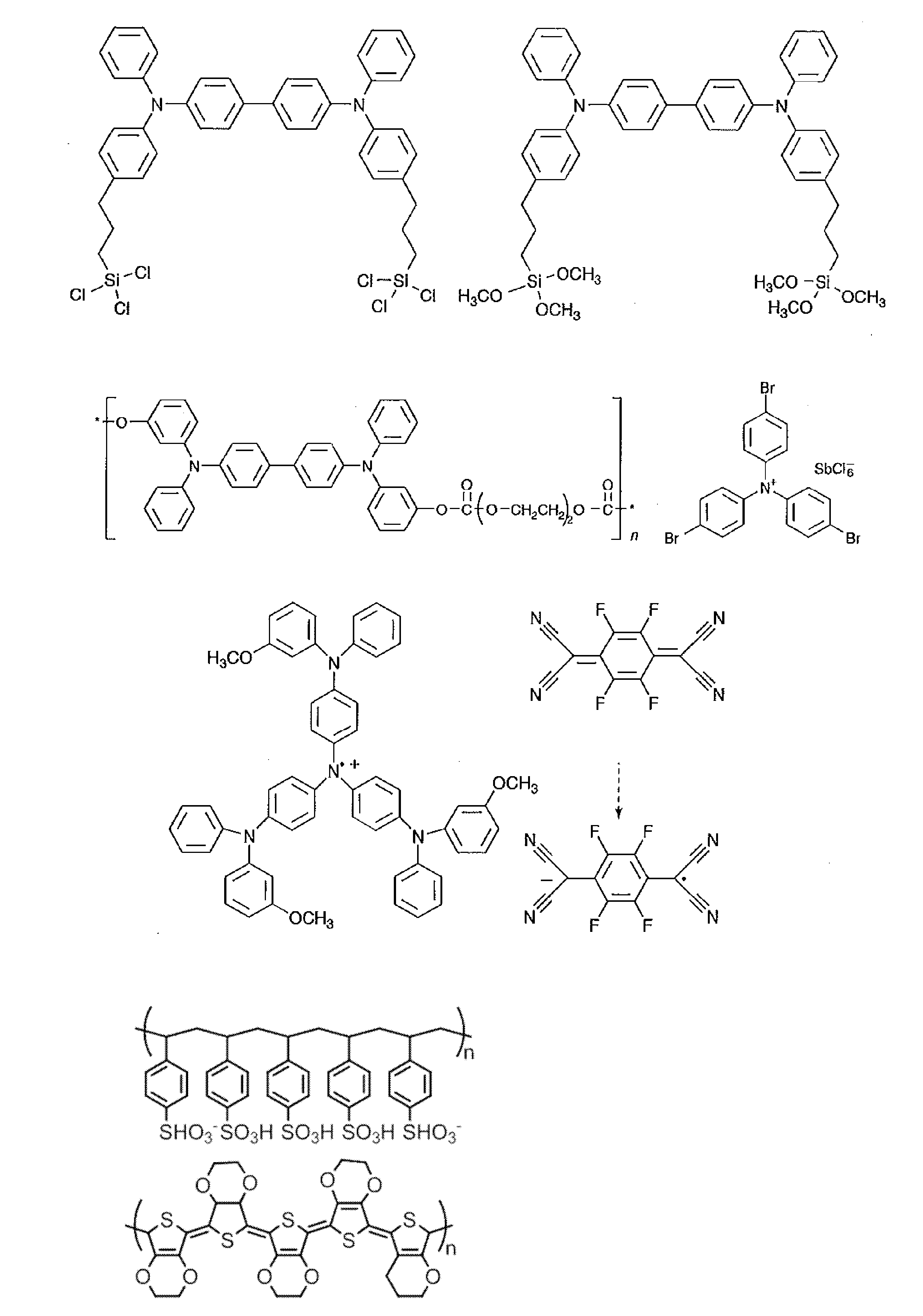


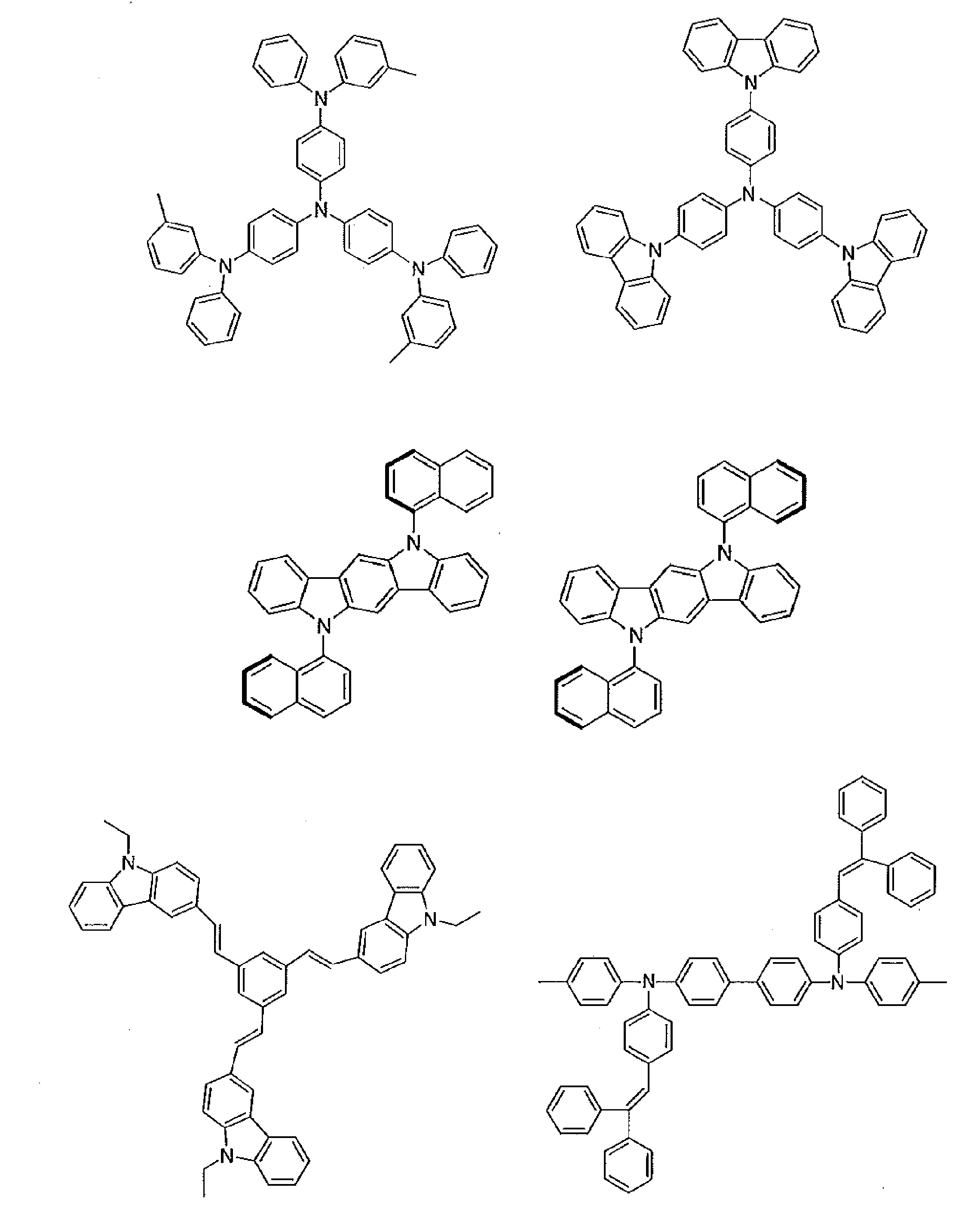
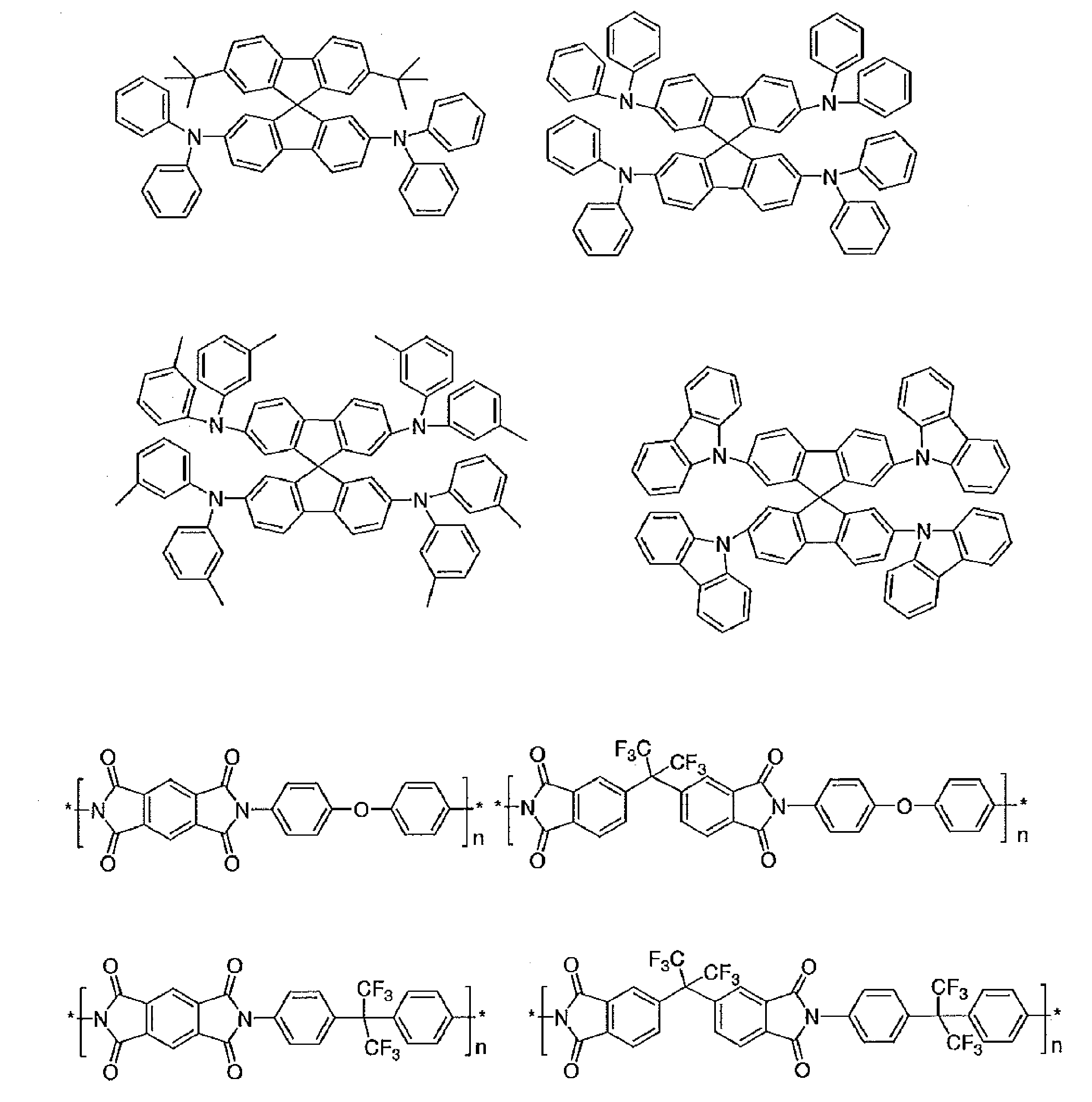
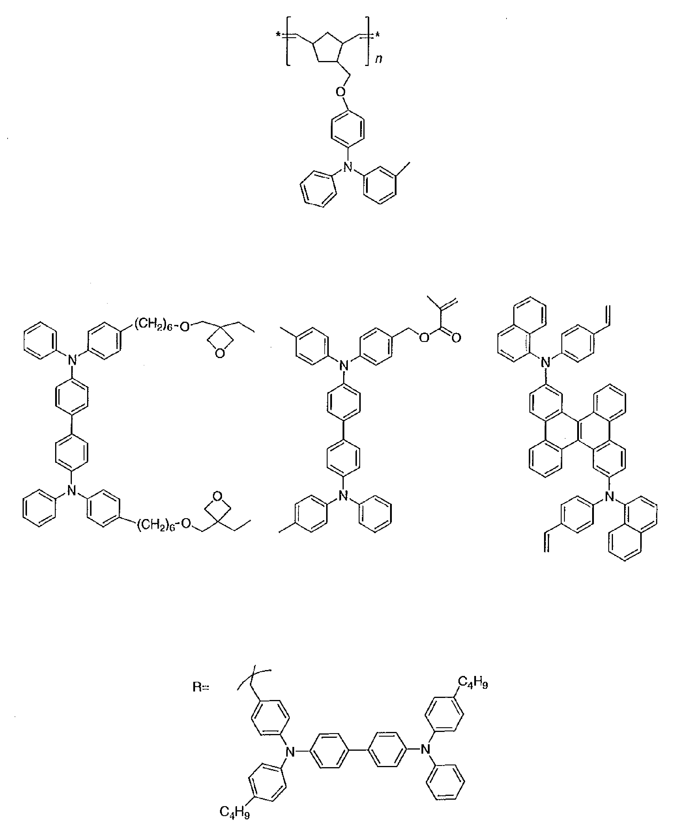
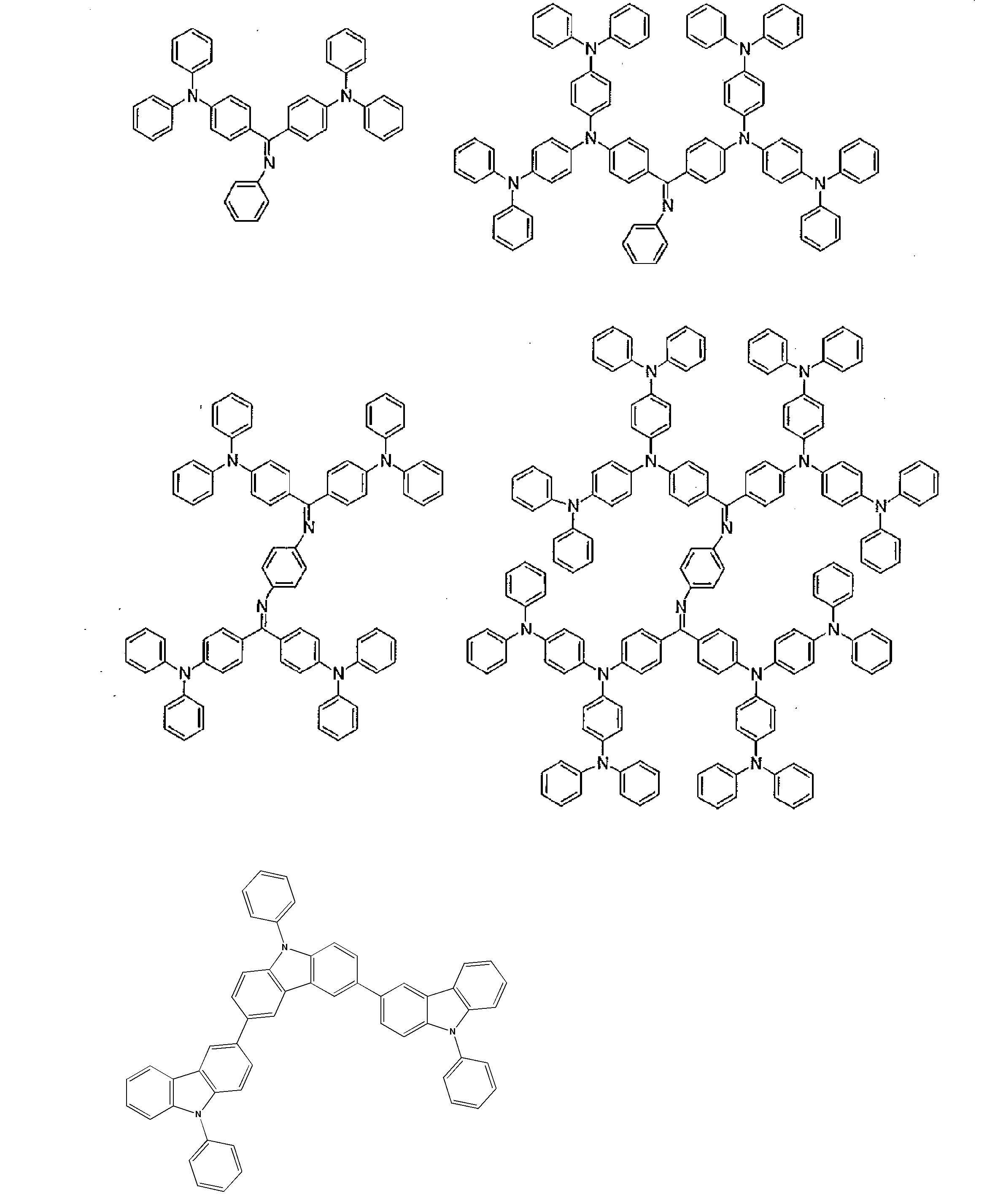
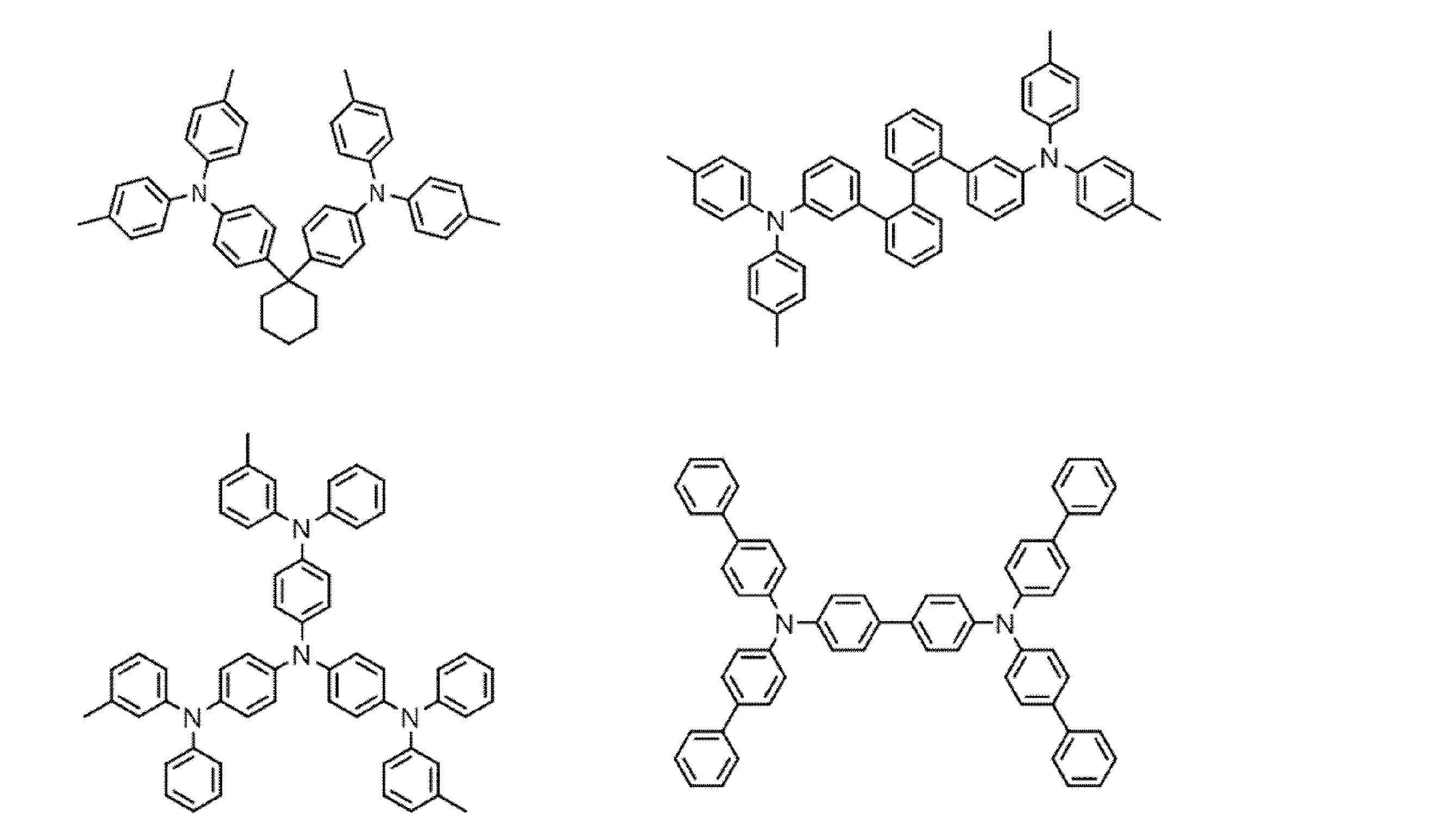


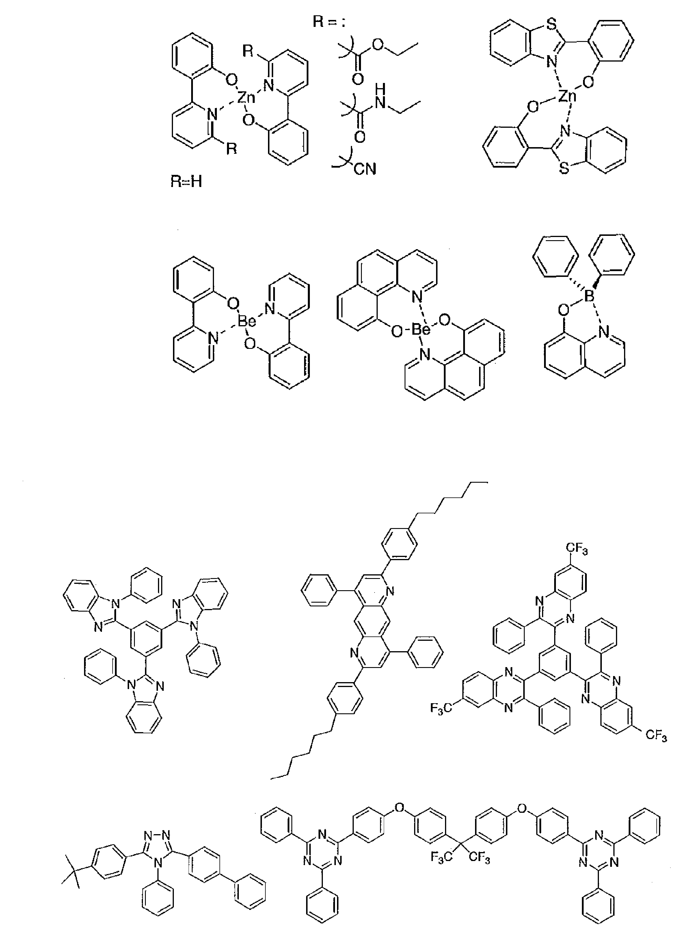
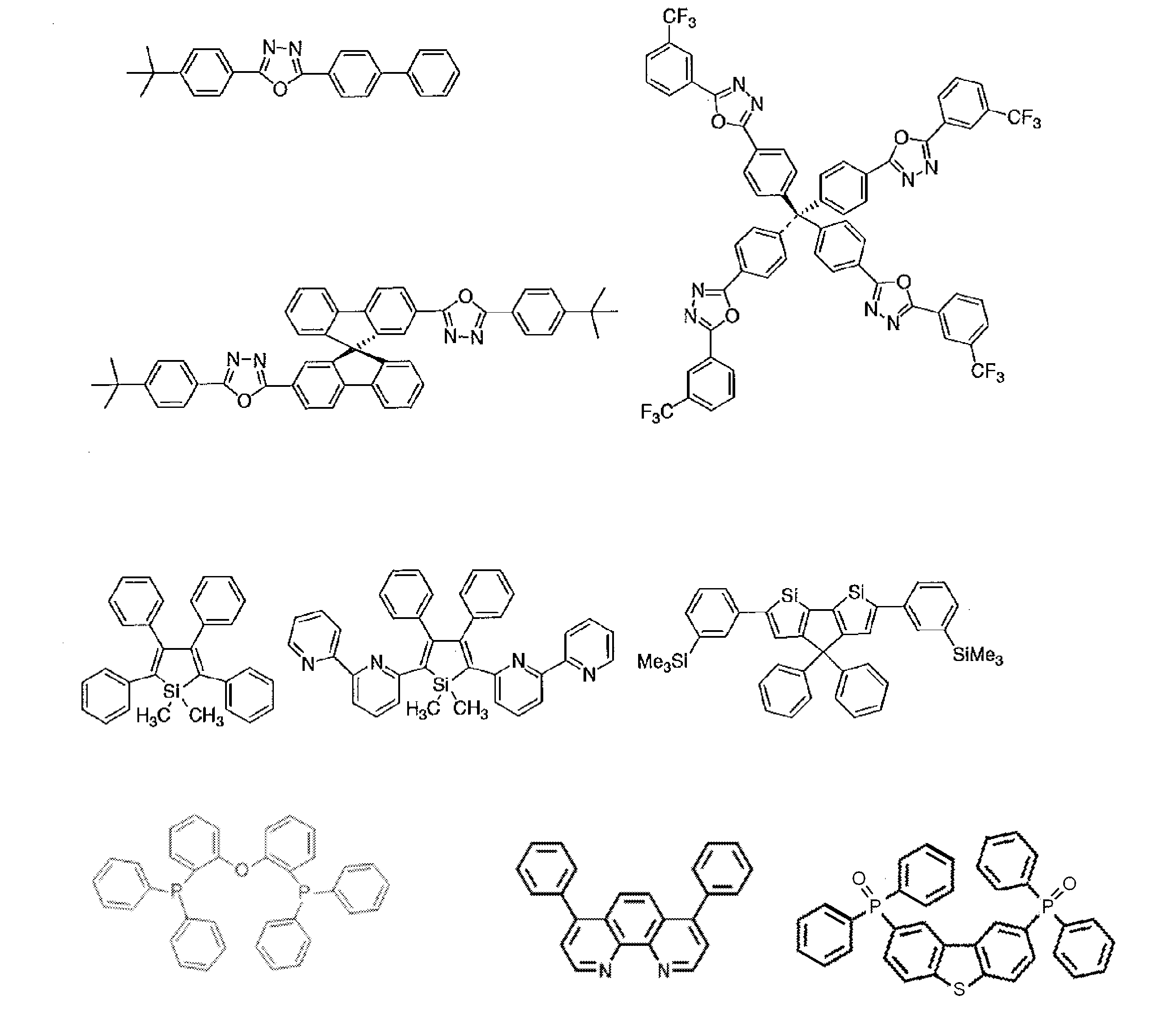
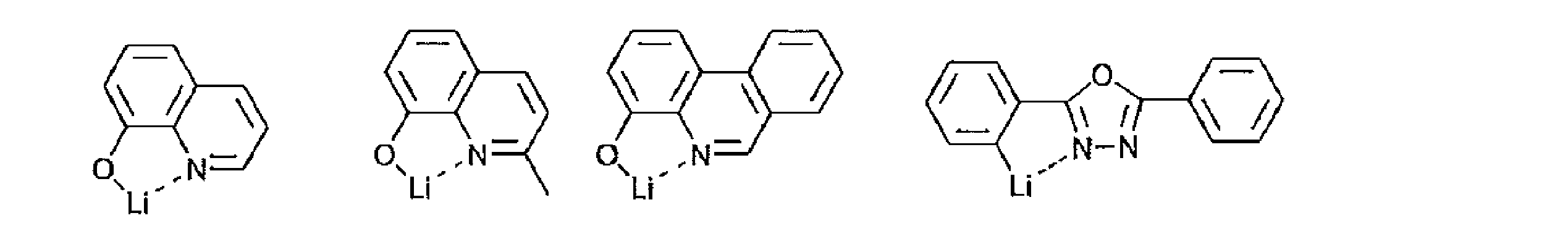
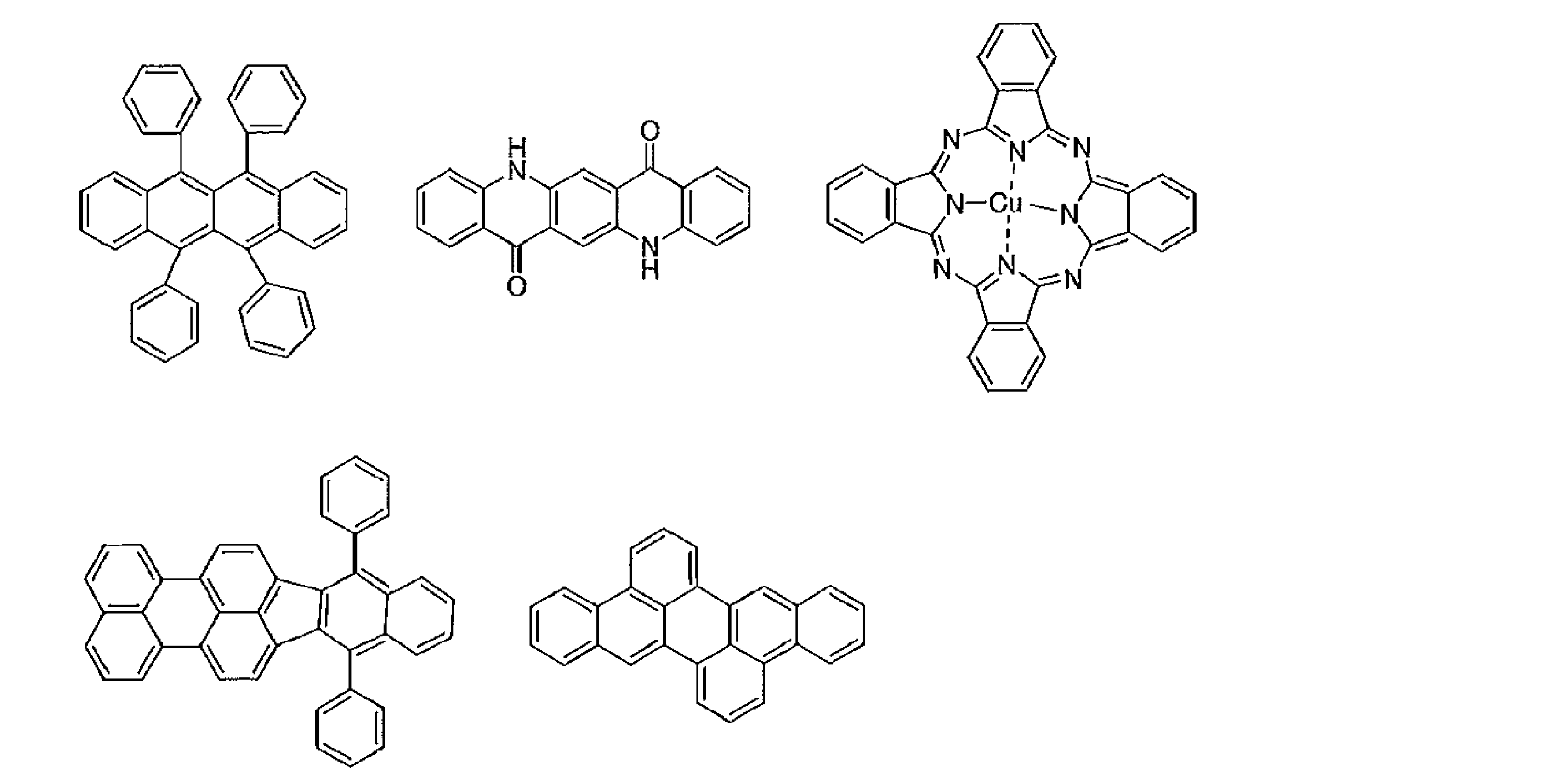
一方、りん光については、本発明の化合物のような通常の有機化合物では、励起三重項エネルギーは不安定で熱等に変換され、寿命が短く直ちに失活するため、室温では殆ど観測できない。通常の有機化合物の励起三重項エネルギーを測定するためには、極低温の条件での発光を観測することにより測定可能である。 The organic electroluminescent device produced by the above-described method emits light by applying an electric field between the anode and the cathode of the obtained device. At this time, if the light is emitted by excited singlet energy, light having a wavelength corresponding to the energy level is confirmed as fluorescence emission and delayed fluorescence emission. In addition, in the case of light emission by excited triplet energy, a wavelength corresponding to the energy level is confirmed as phosphorescence. Since normal fluorescence has a shorter fluorescence lifetime than delayed fluorescence, the emission lifetime can be distinguished from fluorescence and delayed fluorescence.
On the other hand, with respect to phosphorescence, in ordinary organic compounds such as the compounds of the present invention, the excited triplet energy is unstable and is converted into heat and the like, and the lifetime is short and it is immediately deactivated. In order to measure the excited triplet energy of a normal organic compound, it can be measured by observing light emission under extremely low temperature conditions.
(1)最低励起一重項エネルギー準位ES1
測定対象化合物をSi基板上に蒸着して試料を作製し、常温(300K)でこの試料の蛍光スペクトルを測定した。蛍光スペクトルは、縦軸を発光、横軸を波長とした。この発光スペクトルの短波側の立ち下がりに対して接線を引き、その接線と横軸との交点の波長値 λedge[nm]を求めた。この波長値を次に示す換算式でエネルギー値に換算した値をES1とした。
換算式:ES1[eV]=1239.85/λedge
発光スペクトルの測定には、励起光源に窒素レーザー(Lasertechnik Berlin社製、MNL200)を検出器には、ストリークカメラ(浜松ホトニクス社製、C4334)を用いた。 The lowest excited singlet energy level E S1 and the lowest excited triplet energy level E T1 of the compounds used in Examples and Comparative Examples were determined by the following procedure. The energy difference ΔE st between the lowest excited singlet state and the lowest excited triplet state of 77K was obtained by calculating the difference between E S1 and E T1 .
(1) Lowest excited singlet energy level E S1
The sample to be measured was deposited on a Si substrate to prepare a sample, and the fluorescence spectrum of this sample was measured at room temperature (300K). In the fluorescence spectrum, the vertical axis represents light emission and the horizontal axis represents wavelength. A tangent line was drawn with respect to the fall of the emission spectrum on the short wave side, and a wavelength value λ edge [nm] at the intersection of the tangent line and the horizontal axis was obtained. A value obtained by converting this wavelength value into an energy value by the following conversion formula was defined as E S1 .
Conversion formula: E S1 [eV] = 1239.85 / λedge
For the measurement of the emission spectrum, a nitrogen laser (Lasertechnik Berlin, MNL200) was used as an excitation light source, and a streak camera (Hamamatsu Photonics, C4334) was used as a detector.
一重項エネルギーES1と同じ試料を77[K]に冷却し、励起光(337nm)を燐光測定用試料に照射し、ストリークカメラを用いて、燐光強度を測定した。この燐光スペクトルの短波長側の立ち上がりに対して接線を引き、その接線と横軸との交点の波長値λedge[nm]を求めた。この波長値を次に示す換算式でエネルギー値に換算した値をET1とした。
換算式:ET1[eV]=1239.85/λedge
燐光スペクトルの短波長側の立ち上がりに対する接線は以下のように引いた。燐光スペクトルの短波長側から、スペクトルの極大値のうち、最も短波長側の極大値までスペクトル曲線上を移動する際に、長波長側に向けて曲線上の各点における接線を考える。この接線は、曲線が立ち上がるにつれ(つまり縦軸が増加するにつれ)、傾きが増加する。この傾きの値が極大値をとる点において引いた接線を、当該燐光スペクトルの短波長側の立ち上がりに対する接線とした。
なお、スペクトルの最大ピーク強度の10%以下のピーク強度をもつ極大点は、上述の最も短波長側の極大値には含めず、最も短波長側の極大値に最も近い、傾きの値が極大値をとる点において引いた接線を当該燐光スペクトルの短波長側の立ち上がりに対する接線とした。 (2) Lowest excited triplet energy level E T1
The same sample as the singlet energy E S1 was cooled to 77 [K], the sample for phosphorescence measurement was irradiated with excitation light (337 nm), and the phosphorescence intensity was measured using a streak camera. A tangent line was drawn with respect to the rising edge of the phosphorescence spectrum on the short wavelength side, and a wavelength value λ edge [nm] at the intersection of the tangent line and the horizontal axis was obtained. A value obtained by converting this wavelength value into an energy value by the following conversion formula was defined as ET1 .
Conversion formula: E T1 [eV] = 1239.85 / λedge
The tangent to the short wavelength rising edge of the phosphorescence spectrum was drawn as follows. When moving on the spectrum curve from the short wavelength side of the phosphorescence spectrum to the maximum value on the shortest wavelength side among the maximum values of the spectrum, tangents at each point on the curve are considered toward the long wavelength side. The slope of this tangent line increases as the curve rises (that is, as the vertical axis increases). The tangent drawn at the point where the value of the slope takes the maximum value was taken as the tangent to the rising edge of the phosphorescence spectrum on the short wavelength side.
In addition, the maximum point having a peak intensity of 10% or less of the maximum peak intensity of the spectrum is not included in the above-mentioned maximum value on the shortest wavelength side, and has the maximum slope value closest to the maximum value on the shortest wavelength side. The tangent drawn at the point where the value was taken was taken as the tangent to the rising edge of the phosphorescence spectrum on the short wavelength side.
発光層の材料として下記の有機化合物を準備した。
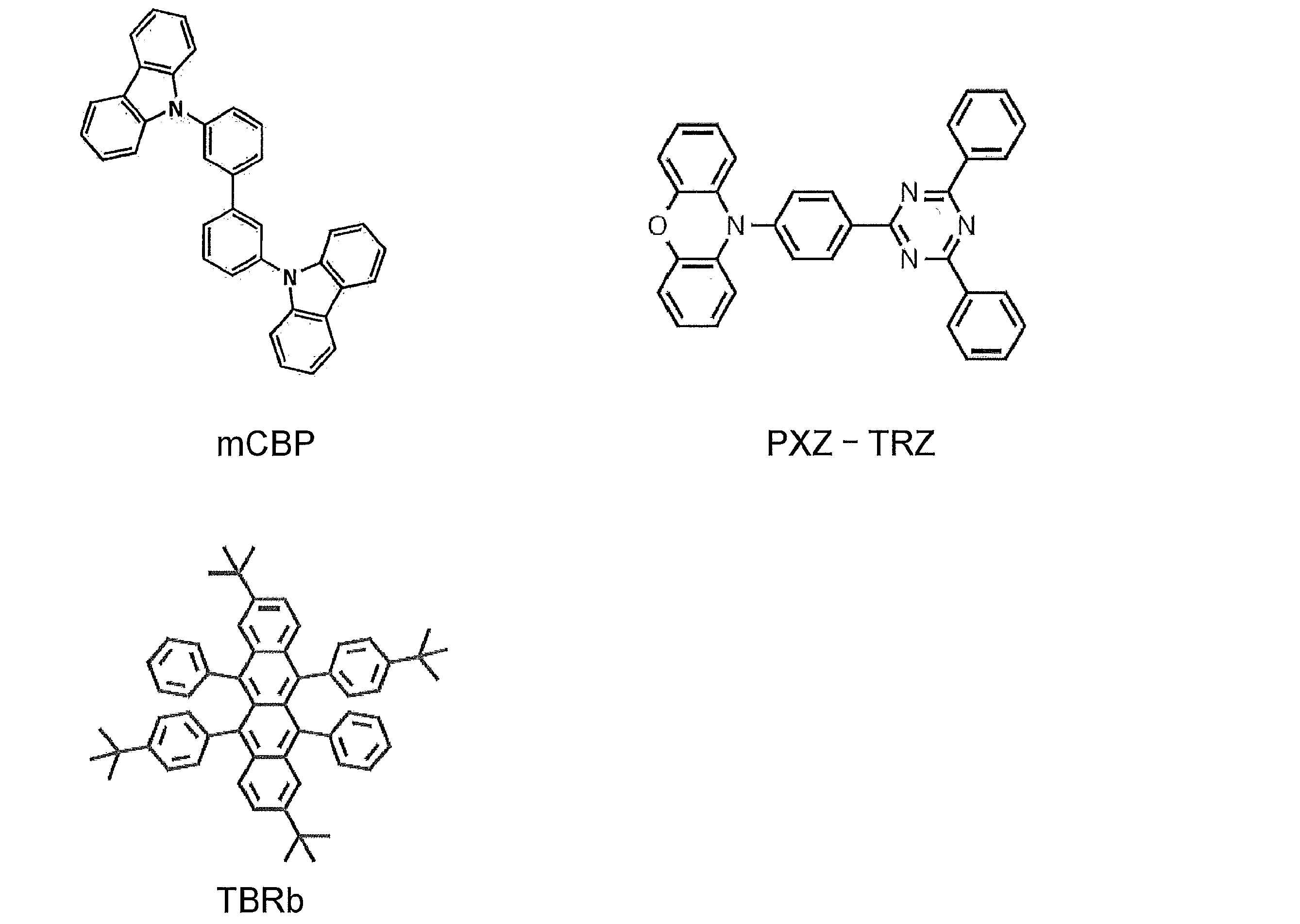
膜厚110nmのインジウム・スズ酸化物(ITO)からなる陽極が形成されたガラス基板上に、各薄膜を真空蒸着法にて、真空度5.0×10⁻⁵Pa以下で積層した。まず、ITO上にHATCNを10nmの厚さに形成し、その上にTrisPCzを30nmの厚さに形成した。次に、mCBPとPXZ-TRZとTBRbとを異なる蒸着源から共蒸着し、15nmの厚さの層を形成して発光層とした。この時、PXZ-TRZの濃度は10~50重量%の範囲で選択し、TBRbの濃度は1重量%とした。次に、T2Tを10nmの厚さに形成し、その上にBPyTP2を55nmの厚さに形成した。さらに、フッ化リチウム(LiF)を0.8nm真空蒸着し、次いでアルミニウム(Al)を100nmの厚さに蒸着することにより陰極を形成し、発光層の組成比が異なる各種有機エレクトロルミネッセンス素子を得た。
製造した有機エレクトロルミネッセンス素子の発光スペクトルを図3に示し、輝度-外部量子効率特性を図4に示し、過渡減衰曲線を図5、図6に示した。 Next, an organic electroluminescence element was fabricated using mCBP, PXZ-TRZ, and TBRb as materials for the light emitting layer.
Each thin film was laminated at a vacuum degree of 5.0 × 10 −5 Pa or less by a vacuum deposition method on a glass substrate on which an anode made of indium tin oxide (ITO) having a thickness of 110 nm was formed. First, HATCN was formed on ITO with a thickness of 10 nm, and TrisPCz was formed thereon with a thickness of 30 nm. Next, mCBP, PXZ-TRZ, and TBRb were co-evaporated from different evaporation sources to form a 15 nm thick layer as a light emitting layer. At this time, the concentration of PXZ-TRZ was selected in the range of 10 to 50% by weight, and the concentration of TBRb was 1% by weight. Next, T2T was formed to a thickness of 10 nm, and BPyTP2 was formed thereon to a thickness of 55 nm. Further, lithium fluoride (LiF) was vacuum-deposited at 0.8 nm, and then aluminum (Al) was deposited at a thickness of 100 nm to form a cathode, thereby obtaining various organic electroluminescent elements having different light-emitting layer composition ratios. It was.
FIG. 3 shows the emission spectrum of the manufactured organic electroluminescence device, FIG. 4 shows the luminance-external quantum efficiency characteristics, and FIGS. 5 and 6 show the transient decay curves.
発光層を形成する際、PXZ-TRZの蒸着源を使用せず、mCBPと1重量%TBRbからなる蒸着膜を形成したこと以外は、実施例1と同様にして有機エレクトロルミネッセンス素子を得た。
製造した有機エレクトロルミネッセンス素子の発光スペクトル、輝度-外部量子効率特性、過渡減衰曲線を、上記の図3、図4、図5、図6に実施例1の測定結果と併せて示した。 Comparative Example 1 Fabrication and Evaluation of Organic Electroluminescence Device Using mCBP and TBRb When forming a light emitting layer, a vapor deposition film composed of mCBP and 1 wt% TBRb was formed without using a vapor deposition source of PXZ-TRZ. Except for this, an organic electroluminescence element was obtained in the same manner as in Example 1.
The emission spectrum, luminance-external quantum efficiency characteristic, and transient attenuation curve of the manufactured organic electroluminescence device are shown in FIG. 3, FIG. 4, FIG. 5, and FIG. 6 together with the measurement results of Example 1.
発光層を形成する際、mCBPの蒸着源を使用せず、PXZ-TRZと1重量%TBRbからなる蒸着膜を形成したこと以外は、実施例1と同様にして有機エレクトロルミネッセンス素子を得た。
製造した有機エレクトロルミネッセンス素子の発光スペクトル、輝度-外部量子効率特性を、上記の図3、図4に実施例1の測定結果と併せて示した。 (Comparative Example 2) Production and evaluation of organic electroluminescence device using PXZ-TRZ and TBRb When forming a light emitting layer, a vapor deposition film composed of PXZ-TRZ and 1 wt% TBRb was used without using an mCBP vapor deposition source. An organic electroluminescent element was obtained in the same manner as in Example 1 except that it was formed.
The emission spectrum and luminance-external quantum efficiency characteristics of the produced organic electroluminescence device are shown in FIG. 3 and FIG. 4 together with the measurement result of Example 1.
発光層を形成する際、TBRbの蒸着源を使用せず、mCBPと25重量%PXZ-TRZからなる蒸着膜を形成したこと以外は、実施例1と同様にして有機エレクトロルミネッセンス素子を得た。
製造した有機エレクトロルミネッセンス素子の過渡減衰曲線を、実施例1、比較例1の測定結果と併せて図6に示した。
また、各特性図から求めた各有機エレクトロルミネッセンス素子の特性値を表22に示し、図6の過渡減衰曲線を測定する際の初期輝度および図6から求めた輝度半減時間を表23に示す。 (Comparative Example 3) Preparation and evaluation of organic electroluminescence device using mCBP and PXZ-TRZ When forming a light emitting layer, a TBRb vapor deposition source was not used, and a vapor deposition film composed of mCBP and 25 wt% PXZ-TRZ was used. An organic electroluminescent element was obtained in the same manner as in Example 1 except that it was formed.
The transient attenuation curve of the manufactured organic electroluminescence element is shown in FIG. 6 together with the measurement results of Example 1 and Comparative Example 1.
In addition, Table 22 shows the characteristic values of each organic electroluminescence element obtained from each characteristic diagram, and Table 23 shows the initial luminance when the transient attenuation curve of FIG. 6 is measured and the luminance half time obtained from FIG.


また、表23に示すように、実施例1の有機エレクトロルミネッセンス素子は、PXZ-TRZを用いていない比較例1またはTBRbを用いていない比較例3の有機エレクトロルミネッセンス素子に比べて輝度半減時間が遥かに長いものであった。
さらに、図5から、初期輝度(1,000cd/cm2)負担時において、輝度が90%まで減衰するまでの時間LT90は、PXZ-TRZが0%で1時間、10重量%で3.5時間、25重量%で9.7時間、50重量%で12.5時間であり、発光層にPXZ-TRZを添加することで有機エレクトロルミネッセンス素子の素子耐久性が大幅に延長することがわかった。ただし、PXZ-TRZの濃度が25%と50%とで素子耐久性にほとんど差がないことから、PXZ-TRZの濃度は50%未満、すなわちmCBPの濃度より小さいことが好ましいことがわかった。 As shown in Table 22, the organic electroluminescent device of Example 1 in which the light emitting layer contains mCBP, PXZ-TRZ, and TBRb is the organic of Comparative Example 1 that does not use PXZ-TRZ or Comparative Example 2 that does not use mCBP. The external quantum efficiency and the current efficiency were remarkably higher than those of the electroluminescence element, and the characteristics were excellent.
In addition, as shown in Table 23, the organic electroluminescence device of Example 1 has a luminance half-life compared to the organic electroluminescence device of Comparative Example 1 that does not use PXZ-TRZ or Comparative Example 3 that does not use TBRb. It was much longer.
Further, from FIG. 5, when the initial luminance (1,000 cd / cm 2 ) is loaded, the time LT90 until the luminance is attenuated to 90% is 1 hour when PXZ-TRZ is 0%, and 3.5 hours when 10% by weight. 25% by weight was 9.7 hours, and 50% by weight was 12.5 hours. It was found that the addition of PXZ-TRZ to the light emitting layer significantly extended the device durability of the organic electroluminescence device. However, since there was almost no difference in element durability between the PXZ-TRZ concentrations of 25% and 50%, it was found that the concentration of PXZ-TRZ is preferably less than 50%, that is, less than the concentration of mCBP.
本実施例では、実施例1のmCBPのかわりにADNを第1有機化合物として用いて有機エレクトロルミネッセンス素子を作製し評価した。ADNは最低励起一重項エネルギー準位ES1が2.83eVで最低励起三重項エネルギー準位ET1が1.69eVである。実施例2の有機エレクトロルミネッセンス素子からは波長約560nmの発光が認められた。
実施例2の有機エレクトロルミネッセンス素子よりも、実施例1の有機エレクトロルミネッセンス素子は有意に高い外部量子効率を達成しており、一段と優れた特性を示すことが確認された。
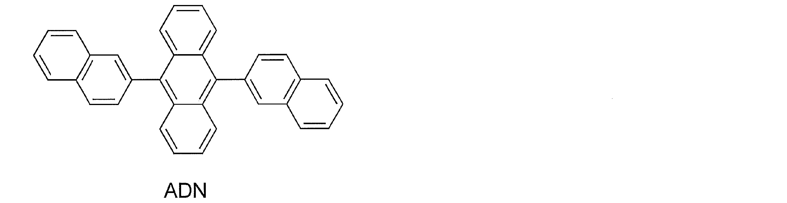
It was confirmed that the organic electroluminescence device of Example 1 achieved significantly higher external quantum efficiency than the organic electroluminescence device of Example 2, and exhibited much better characteristics.
実施例1では第3有機化合物としてTBRbのみを用いて有機エレクトロルミネッセンス素子を作製したが、本実施例ではさらに下記のDBPも第3有機化合物として用いて有機エレクトロルミネッセンス素子を作製して評価した。DBPは、最低励起一重項エネルギー準位ES1が2.0eVである。
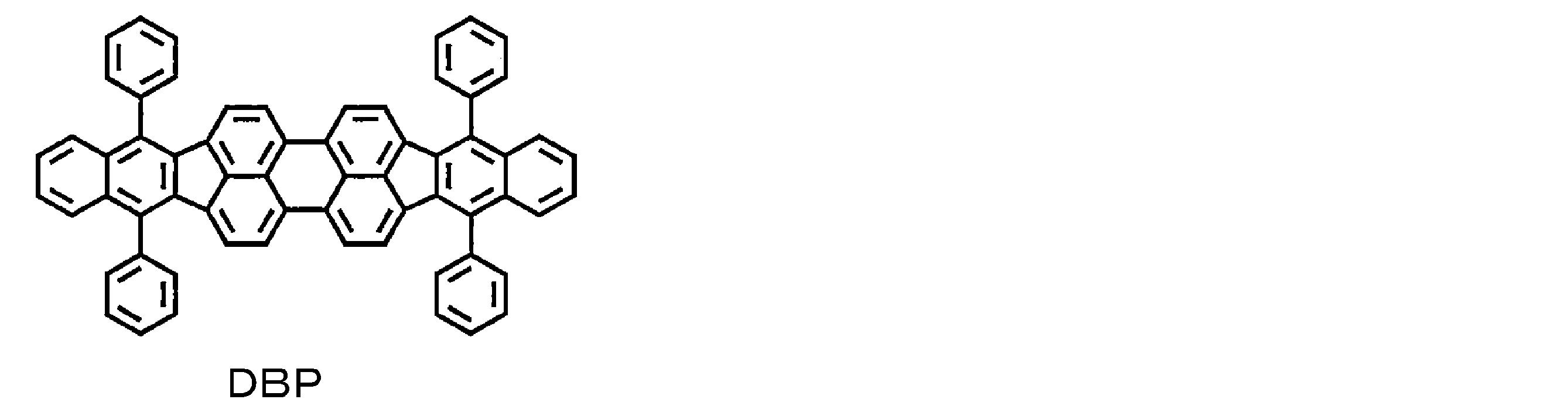
PXZ-TRZ(第2有機化合物)とTBRb(第3有機化合物A)とDBP(第3有機化合物B)の吸収発光スペクトルを図7に示し、製造した有機エレクトロルミネッセンス素子の発光スペクトルを図8に示す。CIE色度(x,y)は(0.65,0.35)であった。また、製造した有機エレクトロルミネッセンス素子の輝度-外部量子効率特性を図9に示し、電圧-電流密度特性を図10に示した。製造した有機エレクトロルミネッセンス素子は7.6%もの高い外部量子効率を達成したことが確認された。 Each thin film was laminated at a vacuum degree of 5.0 × 10 −5 Pa or less by a vacuum deposition method on a glass substrate on which an anode made of indium tin oxide (ITO) having a thickness of 110 nm was formed. First, HATCN was formed on ITO with a thickness of 10 nm, and TrisPCz was formed thereon with a thickness of 30 nm. Next, mCBP, PXZ-TRZ, TBRb, and DBP were co-evaporated from different deposition sources to form a 15 nm thick layer as a light emitting layer. At this time, the concentration of PXZ-TRZ was 10% by weight, the concentration of TBRb was 3.0% by weight, and the concentration of DBP was 1.0% by weight. Next, T2T was formed to a thickness of 10 nm, and BPyTP2 was formed thereon to a thickness of 55 nm. Furthermore, lithium fluoride (LiF) was vacuum-deposited at 0.8 nm, and then aluminum (Al) was evaporated at a thickness of 100 nm to form a cathode to obtain an organic electroluminescence device.
The absorption emission spectra of PXZ-TRZ (second organic compound), TBRb (third organic compound A), and DBP (third organic compound B) are shown in FIG. 7, and the emission spectrum of the manufactured organic electroluminescence device is shown in FIG. Show. The CIE chromaticity (x, y) was (0.65, 0.35). Further, the luminance-external quantum efficiency characteristics of the manufactured organic electroluminescence device are shown in FIG. 9, and the voltage-current density characteristics are shown in FIG. It was confirmed that the manufactured organic electroluminescence device achieved an external quantum efficiency as high as 7.6%.
本実施例では下記のCBPを第1有機化合物として用い、下記のptris-PXZ-TRZを第2有機化合物として用い、DBPを第3有機化合物として用いて有機エレクトロルミネッセンス素子を作製して評価した。CBPは最低励起一重項エネルギー準位ES1が3.26eVで最低励起三重項エネルギー準位ET1が2.55eVであり、ptris-PXZ-TRZは最低励起一重項エネルギー準位ES1が2.30eVで最低励起三重項エネルギー準位ET1が2.16eVでありである。
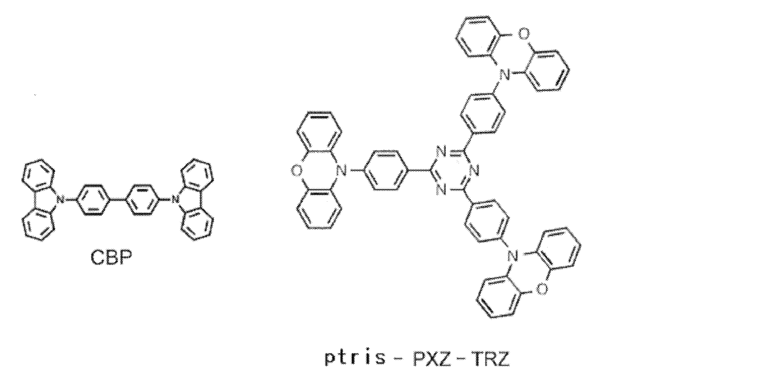
まず、ITO上にα-NPDを35nmの厚さに形成し、その上に、CBPとptris-PXZ-TRZとDBPとを異なる蒸着源から共蒸着し、15nmの厚さの層を形成して発光層とした。この時、ptris-PXZ-TRZの濃度は15重量%とし、DBPの濃度は1重量%とした。次に、TPBiを65nmの厚さに形成し、その上にフッ化リチウム(LiF)を0.8nm真空蒸着し、次いでアルミニウム(Al)を100nmの厚さに蒸着することにより陰極を形成して有機エレクトロルミネッセンス素子を得た。
製造した有機エレクトロルミネッセンス素子について、輝度を10cd/m2、100cd/m2、500cd/m2、または1000cd/m2に設定して発光スペクトルを測定した。その結果を図11に示す。CIE色度(x,y)は(0.64,0.36)であった。また、製造した有機エレクトロルミネッセンス素子の遅延蛍光成分の発光スペクトルを図12に示し、過渡減衰曲線を図13に示した。内部量子効率ηintは59%であり、一重項励起子生成効率ηγSは74%であった。さらに、製造した有機エレクトロルミネッセンス素子の輝度-外部量子効率特性を図14に示した。なお、図14には、比較としてptris-PXZ-TRZを用いずに発光層を形成した有機エレクトロルミネッセンス素子(CBP;1wt%-DBP)の輝度―外部量子効率特性も併せて示した。本実施例の有機エレクトロルミネッセンス素子は、12%もの高い外部量子効率を達成したことが確認された。また、電力効率は18.0lm/W、電流効率は16.5cd/Aであった。 Each thin film was formed on a glass substrate on which an anode made of indium tin oxide (ITO) having a thickness of 110 nm was formed by the same film forming method as in Example 1.
First, α-NPD is formed on ITO to a thickness of 35 nm, and then CBP, ptris-PXZ-TRZ, and DBP are co-evaporated from different evaporation sources to form a layer having a thickness of 15 nm. It was set as the light emitting layer. At this time, the concentration of ptris-PXZ-TRZ was 15 wt%, and the concentration of DBP was 1 wt%. Next, TPBi is formed to a thickness of 65 nm, lithium fluoride (LiF) is vacuum-deposited thereon to 0.8 nm, and then aluminum (Al) is evaporated to a thickness of 100 nm to form a cathode. An organic electroluminescence device was obtained.
The organic electroluminescent element manufactured, the emission spectrum was measured by setting the
本実施例では下記のDPEPOを第1有機化合物として用い、下記のASAQを第2有機化合物として用い、下記のTBPeを第3有機化合物として用いて有機エレクトロルミネッセンス素子を作製して評価した。DPEPOは最低励起一重項エネルギー準位ES1が3.20eVで最低励起三重項エネルギー準位ET1が3,00eVであり、ASAQは最低励起一重項エネルギー準位ES1が2.75eVで最低励起三重項エネルギー準位ET1が2.52eVであり、TBPeは最低励起一重項エネルギー準位ES1が2.70eVである。

まず、ITO上にα-NPDを35nmの厚さに形成し、その上にmCPを10nmの厚さに形成した。次に、DPEPOとASAQとTBPeとを異なる蒸着源から共蒸着し、15nmの厚さの層を形成して発光層とした。この時、ASAQの濃度は15重量%とし、TBPeの濃度は1重量%とした。次に、DPEPOを8nmの厚さに形成し、その上にTPBiを37nmの厚さに形成した。その上にフッ化リチウム(LiF)を0.8nm真空蒸着し、次いでアルミニウム(Al)を100nmの厚さに蒸着することにより陰極を形成して有機エレクトロルミネッセンス素子を得た。
製造した有機エレクトロルミネッセンス素子の発光スペクトルを図15に示す。CIE色度(x,y)は(0.17,0.30)であった。また、製造した有機エレクトロルミネッセンス素子の電圧-電流密度特性を図16に示し、電流密度-外部量子効率特性を図17に示した。製造した有機エレクトロルミネッセンスルミネッセンス素子は13.4%もの高い外部量子効率を達成したことが確認された。 Each thin film was formed on a glass substrate on which an anode made of indium tin oxide (ITO) having a thickness of 110 nm was formed by the same film forming method as in Example 1.
First, α-NPD was formed on ITO to a thickness of 35 nm, and mCP was formed thereon to a thickness of 10 nm. Next, DPEPO, ASAQ, and TBPe were co-evaporated from different vapor deposition sources to form a 15 nm thick layer as a light emitting layer. At this time, the concentration of ASAQ was 15% by weight, and the concentration of TBPe was 1% by weight. Next, DPEPO was formed to a thickness of 8 nm, and TPBi was formed thereon to a thickness of 37 nm. On top of that, lithium fluoride (LiF) was vacuum-deposited by 0.8 nm, and then aluminum (Al) was vapor-deposited to a thickness of 100 nm to form a cathode to obtain an organic electroluminescence device.
The emission spectrum of the manufactured organic electroluminescence element is shown in FIG. The CIE chromaticity (x, y) was (0.17, 0.30). Further, FIG. 16 shows the voltage-current density characteristics of the manufactured organic electroluminescence device, and FIG. 17 shows the current density-external quantum efficiency characteristics. It was confirmed that the manufactured organic electroluminescence device achieved an external quantum efficiency as high as 13.4%.
TPBiの厚さを57nmに変更したこと以外は、実施例5と同様にして有機エレクトロルミネッセンス素子を得た。
形成した発光層の、最低励起一重項状態と最低励起三重項状態とのエネルギー差ΔEstと、フォトルミネッセンス量子効率φPLを表24に示す。また、製造した有機エレクトロルミネッセンス素子の輝度-外部量子効率特性を図18に示し、特性値を表25に示す。 (Example 6) Preparation and evaluation of organic electroluminescent device using DPEPO (first organic compound), ASAQ (second organic compound), TBPe (third organic compound) Other than changing the thickness of TPBi to 57 nm Obtained an organic electroluminescence device in the same manner as in Example 5.
Table 24 shows the energy difference ΔE st between the lowest excited singlet state and the lowest excited triplet state and the photoluminescence quantum efficiency φ PL of the formed light emitting layer. In addition, FIG. 18 shows the luminance-external quantum efficiency characteristics of the manufactured organic electroluminescence device, and Table 25 shows the characteristic values.
本実施例では下記のmCPを第1有機化合物として用い、下記のMN04を第2有機化合物として用い、下記のTTPAを第3有機化合物として用いて有機エレクトロルミネッセンス素子を作製して評価した。mCPは最低励起一重項エネルギー準位ES1が3.30eVで最低励起三重項エネルギー準位ET1が2.90eVであり、MN04は最低励起一重項エネルギー準位ES1が2.60eVで最低励起三重項エネルギー準位ET1が2.47eVであり、TTPAは最低励起一重項エネルギー準位ES1が2.34eVである。

まず、ITO上にTAPCを35nmの厚さに形成し、その上に、mCPとMN04とTTPAとを異なる蒸着源から共蒸着し、15nmの厚さの層を形成して発光層とした。この時、MN04の濃度は50重量%とし、TTPAの濃度は1重量%とした。次に、TPBiを65nmの厚さに形成し、その上にフッ化リチウム(LiF)を0.8nm真空蒸着し、次いでアルミニウム(Al)を100nmの厚さに蒸着することにより陰極を形成して有機エレクトロルミネッセンス素子を得た。
形成した発光層の、最低励起一重項状態と最低励起三重項状態とのエネルギー差ΔEstと、フォトルミネッセンス量子効率φPLを表24に示す。また、製造した有機エレクトロルミネッセンス素子の輝度-外部量子効率特性を図19に示し、特性値を表25に示す。 Each thin film was formed on a glass substrate on which an anode made of indium tin oxide (ITO) having a thickness of 110 nm was formed by the same film forming method as in Example 1.
First, TAPC was formed on ITO to a thickness of 35 nm, and mCP, MN04, and TTPA were co-deposited from different evaporation sources to form a 15 nm-thick layer as a light emitting layer. At this time, the concentration of MN04 was 50% by weight, and the concentration of TTPA was 1% by weight. Next, TPBi is formed to a thickness of 65 nm, lithium fluoride (LiF) is vacuum-deposited thereon to 0.8 nm, and then aluminum (Al) is evaporated to a thickness of 100 nm to form a cathode. An organic electroluminescence device was obtained.
Table 24 shows the energy difference ΔE st between the lowest excited singlet state and the lowest excited triplet state and the photoluminescence quantum efficiency φ PL of the formed light emitting layer. In addition, FIG. 19 shows the luminance-external quantum efficiency characteristics of the manufactured organic electroluminescence device, and Table 25 shows the characteristic values.
本実施例ではmCBPを第1有機化合物として用い、PXZ-TRZを第2有機化合物として用い、TBRbを第3有機化合物として用いて有機エレクトロルミネッセンス素子を作製して評価した。
膜厚110nmのインジウム・スズ酸化物(ITO)からなる陽極が形成されたガラス基板上に、実施例1と同様の製膜方法により各薄膜を形成した。
まず、ITO上にTAPCを35nmの厚さに形成し、その上に、mCBPとPXZ-TRZとTBRbとを異なる蒸着源から共蒸着し、30nmの厚さの層を形成して発光層とした。この時、PXZ-TRZの濃度は25重量%とし、TBRbの濃度は1重量%とした。次に、T2Tを10nmの厚さに形成し、その上にAlq3を55nmの厚さに形成した。その上にフッ化リチウム(LiF)を0.8nm真空蒸着し、次いでアルミニウム(Al)を100nmの厚さに蒸着することにより陰極を形成して有機エレクトロルミネッセンス素子を得た。
形成した発光層の、最低励起一重項状態と最低励起三重項状態とのエネルギー差ΔEstとフォトルミネッセンス量子効率φPLを表24に示す。また、製造した有機エレクトロルミネッセンス素子の輝度-外部量子効率特性を図20に示し、特性値を表25に示す。 Example 8 Production and Evaluation of Organic Electroluminescent Device Using mCBP (First Organic Compound), PXZ-TRZ (Second Organic Compound), and TBRb (Third Organic Compound) In this example, mCBP is used as the first organic compound. An organic electroluminescence device was prepared and evaluated using the compound, PXZ-TRZ as the second organic compound, and TBRb as the third organic compound.
Each thin film was formed on a glass substrate on which an anode made of indium tin oxide (ITO) having a thickness of 110 nm was formed by the same film forming method as in Example 1.
First, TAPC is formed on ITO to a thickness of 35 nm, and then mCBP, PXZ-TRZ, and TBRb are co-evaporated from different evaporation sources to form a 30 nm-thick layer as a light emitting layer. . At this time, the concentration of PXZ-TRZ was 25% by weight, and the concentration of TBRb was 1% by weight. Next, T2T was formed to a thickness of 10 nm, and Alq3 was formed thereon to a thickness of 55 nm. On top of that, lithium fluoride (LiF) was vacuum-deposited by 0.8 nm, and then aluminum (Al) was vapor-deposited to a thickness of 100 nm to form a cathode to obtain an organic electroluminescence device.
Table 24 shows the energy difference ΔEst between the lowest excited singlet state and the lowest excited triplet state and the photoluminescence quantum efficiency φ PL of the formed light emitting layer. In addition, FIG. 20 shows the luminance-external quantum efficiency characteristics of the manufactured organic electroluminescence device, and Table 25 shows the characteristic values.
本実施例ではCBPを第1有機化合物として用い、ptris-PXZ-TRZを第2有機化合物として用い、DBPを第3有機化合物として用いて有機エレクトロルミネッセンス素子を作製して評価した。
膜厚110nmのインジウム・スズ酸化物(ITO)からなる陽極が形成されたガラス基板上に、実施例1と同様の製膜方法により各薄膜を形成した。
まず、ITO上にTAPCを35nmの厚さに形成し、その上に、CBPとptris-PXZ-TRZとDBPとを異なる蒸着源から共蒸着し、15nmの厚さの層を形成して発光層とした。この時、ptris-PXZ-TRZの濃度は15重量%とし、DBPの濃度は1重量%とした。次に、TPBiを65nmの厚さに形成し、その上にフッ化リチウム(LiF)を0.8nm真空蒸着し、次いでアルミニウム(Al)を100nmの厚さに蒸着することにより陰極を形成して有機エレクトロルミネッセンス素子を得た。
形成した発光層の、最低起一重項状態と最低励起三重項状態とのエネルギー差ΔEstと、フォトルミネッセンス量子効率φPLを表24に示す。また、製造した有機エレクトロルミネッセンス素子の輝度-外部量子効率特性を図21に示し、特性値を表25に示す。 (Example 9) Production and evaluation of organic electroluminescent device using CBP (first organic compound), ptris-PXZ-TRZ (second organic compound), DBP (third organic compound) An organic electroluminescent device was fabricated and evaluated using 1 organic compound, ptris-PXZ-TRZ as the second organic compound, and DBP as the third organic compound.
Each thin film was formed on a glass substrate on which an anode made of indium tin oxide (ITO) having a thickness of 110 nm was formed by the same film forming method as in Example 1.
First, TAPC is formed on ITO to a thickness of 35 nm, and then CBP, ptris-PXZ-TRZ, and DBP are co-evaporated from different evaporation sources to form a 15 nm-thick layer. It was. At this time, the concentration of ptris-PXZ-TRZ was 15 wt%, and the concentration of DBP was 1 wt%. Next, TPBi is formed to a thickness of 65 nm, lithium fluoride (LiF) is vacuum-deposited thereon to 0.8 nm, and then aluminum (Al) is evaporated to a thickness of 100 nm to form a cathode. An organic electroluminescence device was obtained.
Table 24 shows the energy difference ΔE st between the lowest singlet state and the lowest excited triplet state and the photoluminescence quantum efficiency φ PL of the formed light-emitting layer. In addition, FIG. 21 shows the luminance-external quantum efficiency characteristics of the manufactured organic electroluminescence device, and Table 25 shows the characteristic values.
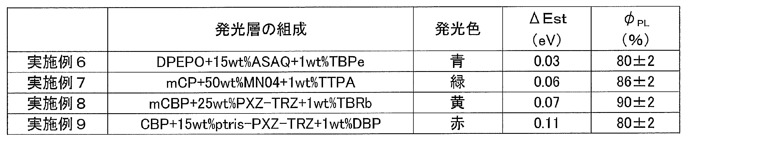
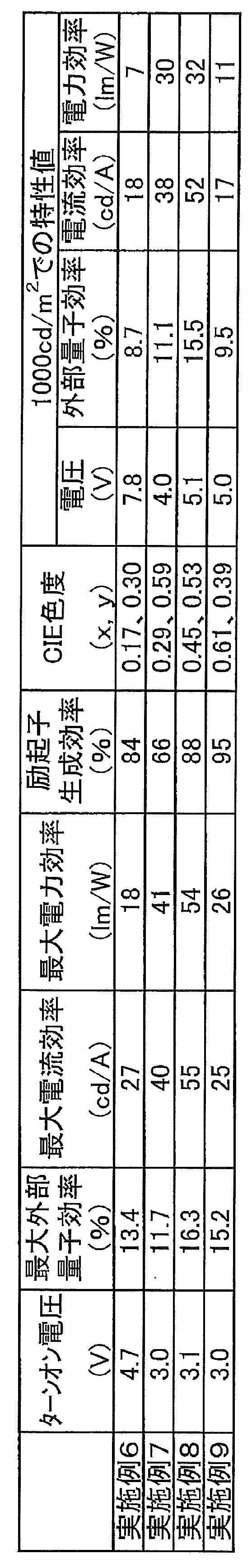

2 陽極
3 正孔注入層
4 正孔輸送層
5 発光層
6 電子輸送層
7 陰極 DESCRIPTION OF
Claims (8)
- 陽極、陰極、および前記陽極と前記陰極の間に発光層を含む少なくとも1層の有機層を有する有機エレクトロルミネッセンス素子であって、
前記発光層は、以下の式(A)を満たす第1有機化合物と第2有機化合物と第3有機化合物とを少なくとも含み、前記第2有機化合物は遅延蛍光体であり、前記第3有機化合物は発光体であることを特徴とする有機エレクトロルミネッセンス素子。
式(A) ES1(A)>ES1(B)>ES1(C)
(上式において、ES1(A)は前記第1有機化合物の最低励起一重項エネルギー準位を表し、ES1(B)は前記第2有機化合物の最低励起一重項エネルギー準位を表し、ES1(C)は前記第3有機化合物の最低励起一重項エネルギー準位を表す。) An organic electroluminescence device having an anode, a cathode, and at least one organic layer including a light emitting layer between the anode and the cathode,
The light emitting layer includes at least a first organic compound, a second organic compound, and a third organic compound that satisfy the following formula (A), the second organic compound is a delayed phosphor, and the third organic compound is: An organic electroluminescence element characterized by being a light emitter.
Formula (A) E S1 (A) > E S1 (B)> E S1 (C)
(In the above formula, E S1 (A) represents the lowest excited singlet energy level of the first organic compound, E S1 (B) represents the lowest excited singlet energy level of the second organic compound, and E S1 (C) represents the lowest excited singlet energy level of the third organic compound.) - 前記第2有機化合物は、最低励起一重項状態と77Kの最低励起三重項状態とのエネルギーの差ΔEstが0.3eV以下であることを特徴とする請求項1に記載の有機エレクトロルミネッセンス素子。 2. The organic electroluminescence device according to claim 1, wherein the second organic compound has an energy difference ΔE st of 0.3 eV or less between a lowest excited singlet state and a 77 K lowest excited triplet state.
- 前記第2有機化合物は、最低励起一重項状態と77Kの最低励起三重項状態とのエネルギーの差ΔEstが0.08eV以下であることを特徴とする請求項1に記載の有機エレクトロルミネッセンス素子。 2. The organic electroluminescence device according to claim 1, wherein the second organic compound has an energy difference ΔE st of 0.08 eV or less between a lowest excited singlet state and a 77 K lowest excited triplet state.
- 前記第1有機化合物と前記第2有機化合物が以下の式(B)を満たすことを特徴とする請求項1~3のいずれか1項に記載の有機エレクトロルミネッセンス素子。
式(B) ET1(A)>ET1(B)
(上式において、ET1(A)は第1有機化合物の77Kにおける最低励起三重項エネルギー準位を表し、ET1(B)は第2有機化合物の77Kにおける最低励起三重項エネルギー準位を表す。) The organic electroluminescence device according to any one of claims 1 to 3, wherein the first organic compound and the second organic compound satisfy the following formula (B).
Formula (B) E T1 (A)> E T1 (B)
(In the above formula, E T1 (A) represents the lowest excited triplet energy level at 77 K of the first organic compound, and E T1 (B) represents the lowest excited triplet energy level at 77 K of the second organic compound. .) - 前記第3有機化合物は、最低励起一重項エネルギー準位から基底エネルギー準位に戻るときに蛍光を放射するものであることを特徴とする請求項1~4のいずれか1項に記載の有機エレクトロルミネッセンス素子。 5. The organic electro luminescence device according to claim 1, wherein the third organic compound emits fluorescence when returning from the lowest excited singlet energy level to the ground energy level. Luminescence element.
- 前記発光層における前記第2有機化合物の含有量が前記第1有機化合物の含有量よりも小さいことを特徴とする請求項1~5のいずれか1項に記載の有機エレクトロルミネッセンス素子。 6. The organic electroluminescence device according to claim 1, wherein the content of the second organic compound in the light emitting layer is smaller than the content of the first organic compound.
- 前記発光層は、前記第3有機化合物として2種以上の化合物を含むことを特徴とする請求項1~6のいずれか1項に記載の有機エレクトロルミネッセンス素子。 The organic electroluminescent element according to any one of claims 1 to 6, wherein the light emitting layer contains two or more kinds of compounds as the third organic compound.
- 前記発光層は、前記第1有機化合物と前記第2有機化合物と前記第3有機化合物の他に、1種または2種以上の有機化合物を含むことを特徴とする請求項1~7のいずれか1項に記載の有機エレクトロルミネッセンス素子。 The light emitting layer includes one or more organic compounds in addition to the first organic compound, the second organic compound, and the third organic compound. 2. The organic electroluminescence device according to item 1.
Priority Applications (12)
| Application Number | Priority Date | Filing Date | Title |
|---|---|---|---|
| KR1020207035361A KR102335123B1 (en) | 2013-08-14 | 2014-08-13 | Organic electroluminescent element |
| KR1020167006684A KR102191957B1 (en) | 2013-08-14 | 2014-08-13 | Organic electroluminescent element |
| EP20152673.8A EP3706182B1 (en) | 2013-08-14 | 2014-08-13 | Organic electroluminescent device |
| KR1020237018853A KR20230088510A (en) | 2013-08-14 | 2014-08-13 | Organic electroluminescent element |
| US14/911,761 US10862047B2 (en) | 2013-08-14 | 2014-08-13 | Organic electroluminescent device |
| KR1020227040753A KR102577829B1 (en) | 2013-08-14 | 2014-08-13 | Organic electroluminescent element |
| EP14836585.1A EP3035401A4 (en) | 2013-08-14 | 2014-08-13 | Organic electroluminescent element |
| EP22204502.3A EP4152910A1 (en) | 2013-08-14 | 2014-08-13 | Organic electroluminescent device |
| KR1020217039087A KR102543775B1 (en) | 2013-08-14 | 2014-08-13 | Organic electroluminescent element |
| CN201480043716.8A CN105453294B (en) | 2013-08-14 | 2014-08-13 | Organic electroluminescent device |
| US17/071,719 US11450817B2 (en) | 2013-08-14 | 2020-10-15 | Organic electroluminescent device |
| US17/809,786 US11944010B2 (en) | 2013-08-14 | 2022-06-29 | Organic electroluminescent device |
Applications Claiming Priority (4)
| Application Number | Priority Date | Filing Date | Title |
|---|---|---|---|
| JP2013168587 | 2013-08-14 | ||
| JP2013-168587 | 2013-08-14 | ||
| JP2014038472 | 2014-02-28 | ||
| JP2014-038472 | 2014-02-28 |
Related Child Applications (2)
| Application Number | Title | Priority Date | Filing Date |
|---|---|---|---|
| US14/911,761 A-371-Of-International US10862047B2 (en) | 2013-08-14 | 2014-08-13 | Organic electroluminescent device |
| US17/071,719 Division US11450817B2 (en) | 2013-08-14 | 2020-10-15 | Organic electroluminescent device |
Publications (1)
| Publication Number | Publication Date |
|---|---|
| WO2015022974A1 true WO2015022974A1 (en) | 2015-02-19 |
Family
ID=52468359
Family Applications (1)
| Application Number | Title | Priority Date | Filing Date |
|---|---|---|---|
| PCT/JP2014/071373 WO2015022974A1 (en) | 2013-08-14 | 2014-08-13 | Organic electroluminescent element |
Country Status (7)
| Country | Link |
|---|---|
| US (3) | US10862047B2 (en) |
| EP (3) | EP4152910A1 (en) |
| JP (2) | JP5669163B1 (en) |
| KR (5) | KR20230088510A (en) |
| CN (1) | CN105453294B (en) |
| TW (1) | TWI633170B (en) |
| WO (1) | WO2015022974A1 (en) |
Cited By (34)
| Publication number | Priority date | Publication date | Assignee | Title |
|---|---|---|---|---|
| CN105254562A (en) * | 2015-09-01 | 2016-01-20 | 华南理工大学 | Organic small molecule luminescent material and organic electroluminescent device prepared from same |
| CN105322099A (en) * | 2015-11-30 | 2016-02-10 | 华南理工大学 | Full-fluorescence white light organic light-emitting diode and preparation method thereof |
| EP3072943A1 (en) * | 2015-03-26 | 2016-09-28 | Idemitsu Kosan Co., Ltd. | Dibenzofuran/carbazole-substituted benzonitriles |
| WO2017099160A1 (en) * | 2015-12-08 | 2017-06-15 | 出光興産株式会社 | Organic el light emitting apparatus and electronic instrument |
| JP2017130643A (en) * | 2015-07-24 | 2017-07-27 | 株式会社半導体エネルギー研究所 | Light-emitting element, light-emitting device, electronic device, lighting device, and lighting system |
| JPWO2016125807A1 (en) * | 2015-02-06 | 2017-11-24 | 出光興産株式会社 | Organic electroluminescence device and electronic device |
| US9905779B2 (en) | 2013-12-26 | 2018-02-27 | Idemitsu Kosan Co., Ltd. | Organic electroluminescent element and electronic device |
| US10297764B2 (en) | 2015-09-14 | 2019-05-21 | Samsung Electronics Co., Ltd. | Mixture, thin film, and organic light emitting device including mixture and thin film |
| WO2019115577A1 (en) | 2017-12-15 | 2019-06-20 | Merck Patent Gmbh | Substituted aromatic amines for use in organic electroluminescent devices |
| WO2020064582A1 (en) | 2018-09-24 | 2020-04-02 | Merck Patent Gmbh | Method for the production of a granular material |
| US10615348B2 (en) | 2015-11-16 | 2020-04-07 | Samsung Electronics Co., Ltd. | Organic light-emitting device |
| US10693095B2 (en) | 2014-08-29 | 2020-06-23 | Semiconductor Energy Laboratory Co., Ltd. | Light-emitting element, display device, electronic device, and lighting device |
| WO2020178230A1 (en) | 2019-03-04 | 2020-09-10 | Merck Patent Gmbh | Ligands for nano-sized materials |
| CN111668392A (en) * | 2015-06-03 | 2020-09-15 | Udc 爱尔兰有限责任公司 | High efficiency OLED device with very short decay time |
| US10923664B2 (en) | 2015-09-14 | 2021-02-16 | Samsung Electronics Co., Ltd. | Composition, thin film, and organic light emitting device including composition and thin film |
| WO2021122868A1 (en) | 2019-12-19 | 2021-06-24 | Merck Patent Gmbh | Compounds for electronic devices |
| KR20210095933A (en) | 2018-11-30 | 2021-08-03 | 가부시키가이샤 큐럭스 | Film manufacturing method, organic semiconductor device manufacturing method and organic semiconductor device |
| WO2021157642A1 (en) | 2020-02-04 | 2021-08-12 | 株式会社Kyulux | Host material, composition, and organic electroluminescent element |
| WO2021235549A1 (en) | 2020-05-22 | 2021-11-25 | 株式会社Kyulux | Compound, light-emitting material, and light-emitting element |
| WO2022009790A1 (en) * | 2020-07-06 | 2022-01-13 | 株式会社Kyulux | Organic luminescent element |
| WO2022025248A1 (en) | 2020-07-31 | 2022-02-03 | 株式会社Kyulux | Compound, light-emitting material, and light-emitting element |
| WO2022129114A1 (en) | 2020-12-18 | 2022-06-23 | Merck Patent Gmbh | Nitrogenous compounds for organic electroluminescent devices |
| WO2022129116A1 (en) | 2020-12-18 | 2022-06-23 | Merck Patent Gmbh | Indolo[3.2.1-jk]carbazole-6-carbonitrile derivatives as blue fluorescent emitters for use in oleds |
| WO2022129113A1 (en) | 2020-12-18 | 2022-06-23 | Merck Patent Gmbh | Nitrogenous heteroaromatic compounds for organic electroluminescent devices |
| WO2022229234A1 (en) | 2021-04-30 | 2022-11-03 | Merck Patent Gmbh | Nitrogenous heterocyclic compounds for organic electroluminescent devices |
| WO2022244503A1 (en) | 2021-05-20 | 2022-11-24 | 株式会社Kyulux | Organic light emitting element |
| WO2022270602A1 (en) | 2021-06-23 | 2022-12-29 | 株式会社Kyulux | Organic light-emitting element and film |
| WO2022270354A1 (en) | 2021-06-23 | 2022-12-29 | 株式会社Kyulux | Compound, light-emitting material, and organic light-emitting element |
| WO2022270113A1 (en) | 2021-06-23 | 2022-12-29 | 株式会社Kyulux | Organic electroluminescent element |
| WO2023282224A1 (en) | 2021-07-06 | 2023-01-12 | 株式会社Kyulux | Organic light-emitting element and design method therefor |
| WO2023041454A1 (en) | 2021-09-14 | 2023-03-23 | Merck Patent Gmbh | Boronic heterocyclic compounds for organic electroluminescent devices |
| WO2023072799A1 (en) | 2021-10-27 | 2023-05-04 | Merck Patent Gmbh | Boronic and nitrogenous heterocyclic compounds for organic electroluminescent devices |
| WO2023161168A1 (en) | 2022-02-23 | 2023-08-31 | Merck Patent Gmbh | Aromatic hetreocycles for organic electroluminescent devices |
| WO2023161167A1 (en) | 2022-02-23 | 2023-08-31 | Merck Patent Gmbh | Nitrogenous heterocycles for organic electroluminescent devices |
Families Citing this family (63)
| Publication number | Priority date | Publication date | Assignee | Title |
|---|---|---|---|---|
| KR20230088510A (en) | 2013-08-14 | 2023-06-19 | 가부시키가이샤 큐럭스 | Organic electroluminescent element |
| CN104716268B (en) * | 2013-12-17 | 2017-09-29 | 北京维信诺科技有限公司 | A kind of organic electroluminescence device and preparation method thereof |
| JP6433935B2 (en) * | 2013-12-26 | 2018-12-05 | 出光興産株式会社 | Organic electroluminescence device and electronic device |
| JP2017123352A (en) | 2014-03-31 | 2017-07-13 | 出光興産株式会社 | Organic electroluminescent element and electronic device |
| JP6374329B2 (en) * | 2014-06-26 | 2018-08-15 | 出光興産株式会社 | ORGANIC ELECTROLUMINESCENT ELEMENT, MATERIAL FOR ORGANIC ELECTROLUMINESCENT ELEMENT, AND ELECTRONIC DEVICE |
| JP6482782B2 (en) * | 2014-07-18 | 2019-03-13 | 国立大学法人九州大学 | Organic light emitting device |
| JP6742236B2 (en) * | 2014-08-26 | 2020-08-19 | 出光興産株式会社 | Organic electroluminescence device and electronic device |
| JP2017212024A (en) * | 2014-08-28 | 2017-11-30 | 出光興産株式会社 | Organic electroluminescent device and electronic equipment |
| KR102460658B1 (en) * | 2014-08-29 | 2022-10-31 | 삼성전자주식회사 | Organic light emitting device |
| TWI814143B (en) * | 2015-03-09 | 2023-09-01 | 日商半導體能源研究所股份有限公司 | Light-emitting element, display device, electronic device, and lighting device |
| TWI779405B (en) * | 2015-03-09 | 2022-10-01 | 日商半導體能源研究所股份有限公司 | Light-emitting element, display device, electronic device, and lighting device |
| KR20230130152A (en) * | 2015-03-27 | 2023-09-11 | 이데미쓰 고산 가부시키가이샤 | Organic electroluminescent element, electronic device and compound |
| CN106328816B (en) * | 2015-06-16 | 2018-11-13 | 昆山国显光电有限公司 | A kind of organic electroluminescence device and preparation method thereof |
| CN113889586A (en) * | 2015-07-08 | 2022-01-04 | 株式会社半导体能源研究所 | Light-emitting element, display device, electronic device, and lighting device |
| JP6838268B2 (en) * | 2015-10-21 | 2021-03-03 | コニカミノルタ株式会社 | Light conversion material, light conversion film, and light emitting element |
| CN106892857B (en) | 2015-12-18 | 2020-02-18 | 昆山国显光电有限公司 | Thermal activation delayed fluorescent material and application thereof in organic electroluminescent device |
| WO2017115608A1 (en) * | 2015-12-28 | 2017-07-06 | コニカミノルタ株式会社 | π-CONJUGATED COMPOUND, ORGANIC ELECTROLUMINESCENT ELEMENT MATERIAL, LIGHT EMITTING MATERIAL, CHARGE TRANSPORT MATERIAL, LUMINESCENT THIN FILM, ORGANIC ELECTROLUMINESCENT ELEMENT, DISPLAY DEVICE AND LIGHTING DEVICE |
| JP2019061974A (en) * | 2015-12-28 | 2019-04-18 | 出光興産株式会社 | Organic electroluminescent element and electronic apparatus |
| US10672252B2 (en) | 2015-12-31 | 2020-06-02 | Delta Faucet Company | Water sensor |
| WO2017146191A1 (en) * | 2016-02-24 | 2017-08-31 | 出光興産株式会社 | Organic electroluminescent element, and electronic device |
| JP6808329B2 (en) * | 2016-02-25 | 2021-01-06 | 株式会社ジャパンディスプレイ | Materials for organic electroluminescence display devices and organic electroluminescence display devices |
| CN107043382A (en) * | 2016-04-25 | 2017-08-15 | 中节能万润股份有限公司 | A kind of compound as core using triazine and its application on organic electroluminescence device |
| JP7253646B2 (en) * | 2016-04-28 | 2023-04-06 | メルク パテント ゲゼルシャフト ミット ベシュレンクテル ハフツング | π-conjugated compound, organic electroluminescence device material, light-emitting material, charge transport material, light-emitting thin film, organic electroluminescence device, display device and lighting device |
| WO2018008721A1 (en) * | 2016-07-08 | 2018-01-11 | コニカミノルタ株式会社 | Organic electroluminescent element, display device, and illumination device |
| JP6890784B2 (en) | 2016-11-30 | 2021-06-18 | 国立大学法人九州大学 | Organic electroluminescence device and biometric device |
| JP6869509B2 (en) * | 2016-11-30 | 2021-05-12 | 国立大学法人九州大学 | Organic electroluminescence device and biometric device |
| US11444248B2 (en) | 2016-11-30 | 2022-09-13 | Kyushu University, National University Corporation | Organic electro-luminescent element and bioinstrumentation device |
| CN106803543A (en) * | 2017-01-20 | 2017-06-06 | 瑞声科技(南京)有限公司 | Organic light emitting display |
| CN108346756B (en) * | 2017-01-24 | 2020-03-20 | 中节能万润股份有限公司 | Organic electroluminescent device |
| KR20180113659A (en) * | 2017-04-06 | 2018-10-17 | 삼성디스플레이 주식회사 | Light emission material and organic electroluminescence device including the same |
| CN106972109B (en) * | 2017-04-21 | 2018-10-12 | 瑞声科技(南京)有限公司 | A kind of luminescent device |
| JP7085176B2 (en) * | 2017-05-30 | 2022-06-16 | 株式会社Kyulux | Films, film manufacturing methods, organic light emitting devices, luminaires and compounds |
| CN106972111B (en) * | 2017-06-01 | 2018-11-20 | 上海天马有机发光显示技术有限公司 | Organic luminescent device and display device |
| CN107256927B (en) * | 2017-06-13 | 2020-01-24 | 上海天马有机发光显示技术有限公司 | Organic light emitting device and display apparatus |
| KR102024811B1 (en) * | 2017-08-02 | 2019-11-14 | 서울대학교산학협력단 | Organic light-emitting device |
| JP7125146B2 (en) * | 2017-08-09 | 2022-08-24 | 学校法人沖縄科学技術大学院大学学園 | Luminescent composition, phosphorescent element and wavelength control method |
| US11637263B2 (en) | 2017-11-02 | 2023-04-25 | Semiconductor Energy Laboratory Co., Ltd. | Light-emitting element, display device, electronic device, and lighting device each including TADF organic compound |
| KR102648402B1 (en) | 2018-06-12 | 2024-03-18 | 삼성디스플레이 주식회사 | Condensed-cyclic compound and organic light emitting device including the same |
| US11367837B2 (en) * | 2018-07-20 | 2022-06-21 | Samsung Electronics Co., Ltd. | Organic light-emitting device |
| KR102605293B1 (en) * | 2018-08-07 | 2023-11-22 | 엘지디스플레이 주식회사 | Organic light emitting diode and organic light emitting device having the diode |
| JP7325731B2 (en) * | 2018-08-23 | 2023-08-15 | 国立大学法人九州大学 | organic electroluminescence element |
| CN112585778A (en) | 2018-08-23 | 2021-03-30 | 国立大学法人九州大学 | Organic light-emitting element, composition, and film |
| EP3640999B1 (en) | 2018-10-15 | 2022-01-05 | cynora GmbH | Organic electroluminescent device emitting blue light |
| TW202030306A (en) | 2018-11-15 | 2020-08-16 | 學校法人關西學院 | Organic electroluminescent devices, display apparatuses, and lighting apparatuses |
| KR20200068503A (en) * | 2018-12-05 | 2020-06-15 | 엘지디스플레이 주식회사 | Organic light emitting diode and organic light emitting device having the diode |
| KR20200072891A (en) * | 2018-12-13 | 2020-06-23 | 엘지디스플레이 주식회사 | Delayed fluorescence compound, and Organic light emitting diode and Organic light emitting display device including the same |
| JP7393345B2 (en) * | 2018-12-14 | 2023-12-06 | 出光興産株式会社 | Organic electroluminescent devices, compounds, materials for organic electroluminescent devices, and electronic devices |
| KR20200076817A (en) | 2018-12-19 | 2020-06-30 | 삼성디스플레이 주식회사 | Organic light-emitting device and display including the same |
| JP7341172B2 (en) | 2019-02-06 | 2023-09-08 | 株式会社半導体エネルギー研究所 | Light emitting devices, electronic equipment and lighting equipment |
| TWI699919B (en) * | 2019-03-15 | 2020-07-21 | 元智大學 | Organic light-emitting diode |
| WO2020218558A1 (en) | 2019-04-26 | 2020-10-29 | 学校法人関西学院 | Compound, material for organic device, composition for forming light-emitting layer, organic field-effect transistor, organic thin-film solar cell, organic electroluminescent element, display device, and illumination device |
| JP2020203875A (en) | 2019-06-13 | 2020-12-24 | 学校法人関西学院 | Polycyclic aromatic compound |
| KR20200143566A (en) | 2019-06-13 | 2020-12-24 | 삼성디스플레이 주식회사 | Organic light emitting device |
| KR20210015429A (en) * | 2019-08-02 | 2021-02-10 | 엘지디스플레이 주식회사 | Organic compound, organic light emitting diode and organic light emitting device having the compound |
| KR20210028408A (en) * | 2019-09-04 | 2021-03-12 | 엘지디스플레이 주식회사 | Organic light emitting diode and organic light emitting device having the diode |
| KR102544979B1 (en) | 2019-10-04 | 2023-06-20 | 삼성디스플레이 주식회사 | Organic light-emitting device and apparatus including the same |
| KR102505882B1 (en) | 2019-10-04 | 2023-03-06 | 삼성디스플레이 주식회사 | Organic light-emitting device and apparatus including the same |
| KR20210046439A (en) * | 2019-10-18 | 2021-04-28 | 엘지디스플레이 주식회사 | Organic light emitting diode and organic light emitting device including the same |
| JPWO2021241677A1 (en) | 2020-05-29 | 2021-12-02 | ||
| CN114249715A (en) * | 2020-09-25 | 2022-03-29 | 江苏三月科技股份有限公司 | Organic compound containing xanthone and triazine structure and application thereof |
| WO2022107798A1 (en) * | 2020-11-17 | 2022-05-27 | 株式会社Kyulux | Organic electroluminescence element, and design method and program for light emitting composition |
| WO2022230573A1 (en) * | 2021-04-26 | 2022-11-03 | 株式会社Kyulux | Organic light-emitting device and method for making same |
| JPWO2022264857A1 (en) | 2021-06-15 | 2022-12-22 |
Citations (20)
| Publication number | Priority date | Publication date | Assignee | Title |
|---|---|---|---|---|
| JP2002050483A (en) * | 2000-05-22 | 2002-02-15 | Showa Denko Kk | Organic electro luminescence element and luminescent material |
| JP2003520391A (en) * | 1999-07-21 | 2003-07-02 | ザ、トラスティーズ オブ プリンストン ユニバーシティ | Intersystem crossing agents for effective use of excitons in organic light-emitting devices |
| JP2005071986A (en) * | 2003-08-04 | 2005-03-17 | Fuji Photo Film Co Ltd | Organic electroluminescent element |
| JP2005108727A (en) | 2003-09-30 | 2005-04-21 | Sanyo Electric Co Ltd | Organic electroluminescent element |
| JP2005108726A (en) | 2003-09-30 | 2005-04-21 | Sanyo Electric Co Ltd | Organic electroluminescent element and organic compound for electroluminescent element |
| JP2006041395A (en) | 2004-07-29 | 2006-02-09 | Sanyo Electric Co Ltd | Organic electroluminescent element |
| JP2010245061A (en) * | 2007-07-07 | 2010-10-28 | Idemitsu Kosan Co Ltd | Organic el element |
| WO2012050001A1 (en) * | 2010-10-12 | 2012-04-19 | 新日鐵化学株式会社 | Chalcogen-containing aromatic compound, organic semiconductor material, and organic electronic device |
| WO2012133188A1 (en) * | 2011-03-25 | 2012-10-04 | 出光興産株式会社 | Organic electroluminescent element |
| WO2013011955A1 (en) | 2011-07-15 | 2013-01-24 | 国立大学法人九州大学 | Delayed-fluorescence material and organic electroluminescence element using same |
| WO2013011954A1 (en) | 2011-07-15 | 2013-01-24 | 国立大学法人九州大学 | Organic electroluminescence element and compound used therein |
| WO2013081088A1 (en) | 2011-12-02 | 2013-06-06 | 国立大学法人九州大学 | Organic light emitting device and delayed fluorescent material and compound used therein |
| JP2013116975A (en) | 2011-12-02 | 2013-06-13 | Kyushu Univ | Delayed fluorescent material, organic light emitting device, and compound |
| WO2013133359A1 (en) | 2012-03-09 | 2013-09-12 | 国立大学法人九州大学 | Light-emitting material, and organic light-emitting element |
| WO2013154064A1 (en) | 2012-04-09 | 2013-10-17 | 国立大学法人九州大学 | Organic light emitting element, and light emitting material and compound used in same |
| WO2013161437A1 (en) | 2012-04-25 | 2013-10-31 | 国立大学法人九州大学 | Light-emitting material and organic light-emitting element |
| JP2014009352A (en) | 2012-07-03 | 2014-01-20 | Kyushu Univ | Light-emitting material, compound, and organic light-emitting element |
| JP2014009224A (en) | 2012-07-03 | 2014-01-20 | Kyushu Univ | Light-emitting material, compound, and organic light-emitting element |
| WO2014013947A1 (en) * | 2012-07-20 | 2014-01-23 | 出光興産株式会社 | Organic electroluminescent element |
| WO2014104315A1 (en) * | 2012-12-28 | 2014-07-03 | 出光興産株式会社 | Organic electroluminescent element |
Family Cites Families (17)
| Publication number | Priority date | Publication date | Assignee | Title |
|---|---|---|---|---|
| EP1214746A2 (en) | 2000-05-22 | 2002-06-19 | Showa Denko K.K. | Organic electroluminescent device and light-emitting material |
| TW518768B (en) * | 2000-05-22 | 2003-01-21 | Showa Denko Kk | Organic electroluminescent device and light-emitting material |
| WO2006015567A1 (en) | 2004-08-13 | 2006-02-16 | Novaled Ag | Layer arrangement for a light-emitting component |
| JP5371404B2 (en) * | 2008-12-10 | 2013-12-18 | 凸版印刷株式会社 | Electron transporting material and light emitting device |
| US8993129B2 (en) * | 2009-12-07 | 2015-03-31 | Nippon Steel & Sumikin Chemical Co., Ltd. | Fluorescence and delayed fluorescence-type organic light-emitting material and element |
| JP2013120770A (en) * | 2011-12-06 | 2013-06-17 | Canon Inc | Organic light-emitting element |
| JP2013168587A (en) | 2012-02-16 | 2013-08-29 | Sharp Corp | Light emitting device, semiconductor laser element and lighting device |
| JP6076153B2 (en) * | 2012-04-20 | 2017-02-08 | 株式会社半導体エネルギー研究所 | LIGHT EMITTING ELEMENT, LIGHT EMITTING DEVICE, DISPLAY DEVICE, ELECTRONIC DEVICE, AND LIGHTING DEVICE |
| US8994013B2 (en) * | 2012-05-18 | 2015-03-31 | Semiconductor Energy Laboratory Co., Ltd. | Light-emitting element, light-emitting device, display device, electronic device, and lighting device |
| JP5904054B2 (en) | 2012-08-15 | 2016-04-13 | 日本電気株式会社 | Information processing apparatus, discount registration method, and program |
| JP6113993B2 (en) | 2012-10-03 | 2017-04-12 | 出光興産株式会社 | Organic electroluminescence device |
| US9512136B2 (en) * | 2012-11-26 | 2016-12-06 | Universal Display Corporation | Organic electroluminescent materials and devices |
| WO2014104346A1 (en) * | 2012-12-28 | 2014-07-03 | 出光興産株式会社 | Organic electroluminescent element |
| JP6513565B2 (en) * | 2013-03-29 | 2019-05-22 | 株式会社Kyulux | Organic electroluminescent device |
| JP6314974B2 (en) | 2013-03-29 | 2018-04-25 | コニカミノルタ株式会社 | ORGANIC ELECTROLUMINESCENT ELEMENT, LIGHTING DEVICE, DISPLAY DEVICE, LIGHT EMITTING THIN FILM AND COMPOSITION AND LIGHT EMITTING METHOD |
| KR20230088510A (en) | 2013-08-14 | 2023-06-19 | 가부시키가이샤 큐럭스 | Organic electroluminescent element |
| JP5905916B2 (en) | 2013-12-26 | 2016-04-20 | 出光興産株式会社 | Organic electroluminescence device and electronic device |
-
2014
- 2014-08-13 KR KR1020237018853A patent/KR20230088510A/en active IP Right Grant
- 2014-08-13 KR KR1020217039087A patent/KR102543775B1/en active IP Right Grant
- 2014-08-13 KR KR1020167006684A patent/KR102191957B1/en active IP Right Grant
- 2014-08-13 US US14/911,761 patent/US10862047B2/en active Active
- 2014-08-13 KR KR1020207035361A patent/KR102335123B1/en active IP Right Grant
- 2014-08-13 EP EP22204502.3A patent/EP4152910A1/en active Pending
- 2014-08-13 JP JP2014164686A patent/JP5669163B1/en active Active
- 2014-08-13 WO PCT/JP2014/071373 patent/WO2015022974A1/en active Application Filing
- 2014-08-13 CN CN201480043716.8A patent/CN105453294B/en active Active
- 2014-08-13 EP EP14836585.1A patent/EP3035401A4/en not_active Withdrawn
- 2014-08-13 KR KR1020227040753A patent/KR102577829B1/en active IP Right Grant
- 2014-08-13 EP EP20152673.8A patent/EP3706182B1/en active Active
- 2014-08-14 TW TW103127967A patent/TWI633170B/en active
- 2014-12-10 JP JP2014249534A patent/JP6670042B2/en active Active
-
2020
- 2020-10-15 US US17/071,719 patent/US11450817B2/en active Active
-
2022
- 2022-06-29 US US17/809,786 patent/US11944010B2/en active Active
Patent Citations (20)
| Publication number | Priority date | Publication date | Assignee | Title |
|---|---|---|---|---|
| JP2003520391A (en) * | 1999-07-21 | 2003-07-02 | ザ、トラスティーズ オブ プリンストン ユニバーシティ | Intersystem crossing agents for effective use of excitons in organic light-emitting devices |
| JP2002050483A (en) * | 2000-05-22 | 2002-02-15 | Showa Denko Kk | Organic electro luminescence element and luminescent material |
| JP2005071986A (en) * | 2003-08-04 | 2005-03-17 | Fuji Photo Film Co Ltd | Organic electroluminescent element |
| JP2005108727A (en) | 2003-09-30 | 2005-04-21 | Sanyo Electric Co Ltd | Organic electroluminescent element |
| JP2005108726A (en) | 2003-09-30 | 2005-04-21 | Sanyo Electric Co Ltd | Organic electroluminescent element and organic compound for electroluminescent element |
| JP2006041395A (en) | 2004-07-29 | 2006-02-09 | Sanyo Electric Co Ltd | Organic electroluminescent element |
| JP2010245061A (en) * | 2007-07-07 | 2010-10-28 | Idemitsu Kosan Co Ltd | Organic el element |
| WO2012050001A1 (en) * | 2010-10-12 | 2012-04-19 | 新日鐵化学株式会社 | Chalcogen-containing aromatic compound, organic semiconductor material, and organic electronic device |
| WO2012133188A1 (en) * | 2011-03-25 | 2012-10-04 | 出光興産株式会社 | Organic electroluminescent element |
| WO2013011954A1 (en) | 2011-07-15 | 2013-01-24 | 国立大学法人九州大学 | Organic electroluminescence element and compound used therein |
| WO2013011955A1 (en) | 2011-07-15 | 2013-01-24 | 国立大学法人九州大学 | Delayed-fluorescence material and organic electroluminescence element using same |
| WO2013081088A1 (en) | 2011-12-02 | 2013-06-06 | 国立大学法人九州大学 | Organic light emitting device and delayed fluorescent material and compound used therein |
| JP2013116975A (en) | 2011-12-02 | 2013-06-13 | Kyushu Univ | Delayed fluorescent material, organic light emitting device, and compound |
| WO2013133359A1 (en) | 2012-03-09 | 2013-09-12 | 国立大学法人九州大学 | Light-emitting material, and organic light-emitting element |
| WO2013154064A1 (en) | 2012-04-09 | 2013-10-17 | 国立大学法人九州大学 | Organic light emitting element, and light emitting material and compound used in same |
| WO2013161437A1 (en) | 2012-04-25 | 2013-10-31 | 国立大学法人九州大学 | Light-emitting material and organic light-emitting element |
| JP2014009352A (en) | 2012-07-03 | 2014-01-20 | Kyushu Univ | Light-emitting material, compound, and organic light-emitting element |
| JP2014009224A (en) | 2012-07-03 | 2014-01-20 | Kyushu Univ | Light-emitting material, compound, and organic light-emitting element |
| WO2014013947A1 (en) * | 2012-07-20 | 2014-01-23 | 出光興産株式会社 | Organic electroluminescent element |
| WO2014104315A1 (en) * | 2012-12-28 | 2014-07-03 | 出光興産株式会社 | Organic electroluminescent element |
Non-Patent Citations (1)
| Title |
|---|
| HIROKI UOYAMA ET AL.: "Highly efficient organic light-emitting diodes from delayed fluorescence", NATURE, vol. 492, 12 December 2012 (2012-12-12), pages 234 - 238, XP055048388 * |
Cited By (48)
| Publication number | Priority date | Publication date | Assignee | Title |
|---|---|---|---|---|
| US9905779B2 (en) | 2013-12-26 | 2018-02-27 | Idemitsu Kosan Co., Ltd. | Organic electroluminescent element and electronic device |
| US11569456B2 (en) | 2013-12-26 | 2023-01-31 | Idemitsu Kosan Co., Ltd. | Organic electroluminescent element and electronic device |
| US10811616B2 (en) | 2013-12-26 | 2020-10-20 | Idemitsu Kosan Co., Ltd. | Organic electroluminescent element and electronic device |
| US11563191B2 (en) | 2014-08-29 | 2023-01-24 | Semiconductor Energy Laboratory Co., Ltd. | Light-emitting element with light-emitting layer including first and second organic compounds, display device, electronic device, and lighting device |
| US10693095B2 (en) | 2014-08-29 | 2020-06-23 | Semiconductor Energy Laboratory Co., Ltd. | Light-emitting element, display device, electronic device, and lighting device |
| US10714700B2 (en) | 2014-08-29 | 2020-07-14 | Semiconductor Energy Laboratory Co., Ltd. | Light-emitting element, display device, electronic device, and lighting device |
| JPWO2016125807A1 (en) * | 2015-02-06 | 2017-11-24 | 出光興産株式会社 | Organic electroluminescence device and electronic device |
| EP3072943A1 (en) * | 2015-03-26 | 2016-09-28 | Idemitsu Kosan Co., Ltd. | Dibenzofuran/carbazole-substituted benzonitriles |
| CN111668392B (en) * | 2015-06-03 | 2024-01-23 | Udc 爱尔兰有限责任公司 | High efficiency OLED device with extremely short decay time |
| EP3304612B1 (en) * | 2015-06-03 | 2022-05-04 | UDC Ireland Limited | Highly efficient oled devices with very short decay times |
| CN111668392A (en) * | 2015-06-03 | 2020-09-15 | Udc 爱尔兰有限责任公司 | High efficiency OLED device with very short decay time |
| JP2017130643A (en) * | 2015-07-24 | 2017-07-27 | 株式会社半導体エネルギー研究所 | Light-emitting element, light-emitting device, electronic device, lighting device, and lighting system |
| CN105254562A (en) * | 2015-09-01 | 2016-01-20 | 华南理工大学 | Organic small molecule luminescent material and organic electroluminescent device prepared from same |
| US10923664B2 (en) | 2015-09-14 | 2021-02-16 | Samsung Electronics Co., Ltd. | Composition, thin film, and organic light emitting device including composition and thin film |
| US10297764B2 (en) | 2015-09-14 | 2019-05-21 | Samsung Electronics Co., Ltd. | Mixture, thin film, and organic light emitting device including mixture and thin film |
| US10615348B2 (en) | 2015-11-16 | 2020-04-07 | Samsung Electronics Co., Ltd. | Organic light-emitting device |
| CN105322099A (en) * | 2015-11-30 | 2016-02-10 | 华南理工大学 | Full-fluorescence white light organic light-emitting diode and preparation method thereof |
| CN108369992A (en) * | 2015-12-08 | 2018-08-03 | 出光兴产株式会社 | Organic E L light-emitting device and electronic apparatus |
| US11322711B2 (en) | 2015-12-08 | 2022-05-03 | Idemitsu Kosan Co., Ltd. | Organic EL light emitting apparatus and electronic instrument |
| JP7017933B2 (en) | 2015-12-08 | 2022-02-09 | 出光興産株式会社 | Organic EL light emitting device and electronic device |
| EP3389107A4 (en) * | 2015-12-08 | 2019-08-14 | Idemitsu Kosan Co., Ltd | Organic el light emitting apparatus and electronic instrument |
| US10854838B2 (en) | 2015-12-08 | 2020-12-01 | Idemitsu Kosan Co., Ltd. | Organic EL light emitting apparatus and electronic instrument |
| JP2021009859A (en) * | 2015-12-08 | 2021-01-28 | 出光興産株式会社 | Organic el light-emitting device and electronic apparatus |
| WO2017099160A1 (en) * | 2015-12-08 | 2017-06-15 | 出光興産株式会社 | Organic el light emitting apparatus and electronic instrument |
| JPWO2017099160A1 (en) * | 2015-12-08 | 2018-09-27 | 出光興産株式会社 | ORGANIC EL LIGHT EMITTING DEVICE AND ELECTRONIC DEVICE |
| CN108369992B (en) * | 2015-12-08 | 2021-09-10 | 出光兴产株式会社 | Organic EL light-emitting device and electronic apparatus |
| WO2019115577A1 (en) | 2017-12-15 | 2019-06-20 | Merck Patent Gmbh | Substituted aromatic amines for use in organic electroluminescent devices |
| WO2020064582A1 (en) | 2018-09-24 | 2020-04-02 | Merck Patent Gmbh | Method for the production of a granular material |
| KR20210095933A (en) | 2018-11-30 | 2021-08-03 | 가부시키가이샤 큐럭스 | Film manufacturing method, organic semiconductor device manufacturing method and organic semiconductor device |
| WO2020178230A1 (en) | 2019-03-04 | 2020-09-10 | Merck Patent Gmbh | Ligands for nano-sized materials |
| WO2021122868A1 (en) | 2019-12-19 | 2021-06-24 | Merck Patent Gmbh | Compounds for electronic devices |
| WO2021157642A1 (en) | 2020-02-04 | 2021-08-12 | 株式会社Kyulux | Host material, composition, and organic electroluminescent element |
| WO2021235549A1 (en) | 2020-05-22 | 2021-11-25 | 株式会社Kyulux | Compound, light-emitting material, and light-emitting element |
| WO2022009790A1 (en) * | 2020-07-06 | 2022-01-13 | 株式会社Kyulux | Organic luminescent element |
| WO2022025248A1 (en) | 2020-07-31 | 2022-02-03 | 株式会社Kyulux | Compound, light-emitting material, and light-emitting element |
| WO2022129116A1 (en) | 2020-12-18 | 2022-06-23 | Merck Patent Gmbh | Indolo[3.2.1-jk]carbazole-6-carbonitrile derivatives as blue fluorescent emitters for use in oleds |
| WO2022129113A1 (en) | 2020-12-18 | 2022-06-23 | Merck Patent Gmbh | Nitrogenous heteroaromatic compounds for organic electroluminescent devices |
| WO2022129114A1 (en) | 2020-12-18 | 2022-06-23 | Merck Patent Gmbh | Nitrogenous compounds for organic electroluminescent devices |
| WO2022229234A1 (en) | 2021-04-30 | 2022-11-03 | Merck Patent Gmbh | Nitrogenous heterocyclic compounds for organic electroluminescent devices |
| WO2022244503A1 (en) | 2021-05-20 | 2022-11-24 | 株式会社Kyulux | Organic light emitting element |
| WO2022270602A1 (en) | 2021-06-23 | 2022-12-29 | 株式会社Kyulux | Organic light-emitting element and film |
| WO2022270354A1 (en) | 2021-06-23 | 2022-12-29 | 株式会社Kyulux | Compound, light-emitting material, and organic light-emitting element |
| WO2022270113A1 (en) | 2021-06-23 | 2022-12-29 | 株式会社Kyulux | Organic electroluminescent element |
| WO2023282224A1 (en) | 2021-07-06 | 2023-01-12 | 株式会社Kyulux | Organic light-emitting element and design method therefor |
| WO2023041454A1 (en) | 2021-09-14 | 2023-03-23 | Merck Patent Gmbh | Boronic heterocyclic compounds for organic electroluminescent devices |
| WO2023072799A1 (en) | 2021-10-27 | 2023-05-04 | Merck Patent Gmbh | Boronic and nitrogenous heterocyclic compounds for organic electroluminescent devices |
| WO2023161168A1 (en) | 2022-02-23 | 2023-08-31 | Merck Patent Gmbh | Aromatic hetreocycles for organic electroluminescent devices |
| WO2023161167A1 (en) | 2022-02-23 | 2023-08-31 | Merck Patent Gmbh | Nitrogenous heterocycles for organic electroluminescent devices |
Also Published As
| Publication number | Publication date |
|---|---|
| JP2015179817A (en) | 2015-10-08 |
| EP3706182B1 (en) | 2022-11-16 |
| US11450817B2 (en) | 2022-09-20 |
| TWI633170B (en) | 2018-08-21 |
| EP3035401A1 (en) | 2016-06-22 |
| KR20230088510A (en) | 2023-06-19 |
| US20160190478A1 (en) | 2016-06-30 |
| JP2015179809A (en) | 2015-10-08 |
| KR102543775B1 (en) | 2023-06-14 |
| US20210074927A1 (en) | 2021-03-11 |
| KR20220162841A (en) | 2022-12-08 |
| US20220344598A1 (en) | 2022-10-27 |
| CN105453294B (en) | 2018-02-02 |
| KR102191957B1 (en) | 2020-12-16 |
| KR20160044522A (en) | 2016-04-25 |
| JP5669163B1 (en) | 2015-02-12 |
| TW201510175A (en) | 2015-03-16 |
| EP3706182A1 (en) | 2020-09-09 |
| KR20200140938A (en) | 2020-12-16 |
| EP3035401A4 (en) | 2017-01-04 |
| JP6670042B2 (en) | 2020-03-18 |
| EP4152910A1 (en) | 2023-03-22 |
| US10862047B2 (en) | 2020-12-08 |
| KR20210148427A (en) | 2021-12-07 |
| KR102335123B1 (en) | 2021-12-03 |
| KR102577829B1 (en) | 2023-09-12 |
| CN105453294A (en) | 2016-03-30 |
| US11944010B2 (en) | 2024-03-26 |
Similar Documents
| Publication | Publication Date | Title |
|---|---|---|
| JP5669163B1 (en) | Organic electroluminescence device | |
| JP6513565B2 (en) | Organic electroluminescent device | |
| WO2016042997A1 (en) | Organic electroluminescent element | |
| KR102196821B1 (en) | Organic light-emitting element | |
| JP7182774B2 (en) | light emitting element | |
| JP6567504B2 (en) | Organic light emitting device | |
| KR20180099713A (en) | Organic electroluminescent device | |
| TW202100720A (en) | Melt mixture for organic electroluminescent element, and organic electroluminescent element | |
| TW201538514A (en) | Organic electroluminescent device material and organic electroluminescent device using the same | |
| WO2016111196A1 (en) | Compound, mixture, light-emitting layer, organic light-emitting element, and assist dopant | |
| WO2022168825A1 (en) | Organic electroluminescence element, method for designing luminous composition, and program | |
| JP7408125B2 (en) | Charge transport materials and organic light emitting devices | |
| TWI712599B (en) | Organic electroluminescent material and organic electroluminescent element using the same | |
| JP7337369B2 (en) | Organic light emitting device, laminate and light emitting method | |
| JP7395136B2 (en) | Composition and organic light emitting device | |
| WO2022230573A1 (en) | Organic light-emitting device and method for making same | |
| WO2022244503A1 (en) | Organic light emitting element | |
| CN116710535A (en) | Organic electroluminescent element and method for manufacturing the same | |
| JP2018111751A (en) | Light emitting material, compound and organic light emitting element |
Legal Events
| Date | Code | Title | Description |
|---|---|---|---|
| WWE | Wipo information: entry into national phase |
Ref document number: 201480043716.8 Country of ref document: CN |
|
| 121 | Ep: the epo has been informed by wipo that ep was designated in this application |
Ref document number: 14836585 Country of ref document: EP Kind code of ref document: A1 |
|
| WWE | Wipo information: entry into national phase |
Ref document number: 14911761 Country of ref document: US |
|
| NENP | Non-entry into the national phase |
Ref country code: DE |
|
| WWE | Wipo information: entry into national phase |
Ref document number: 2014836585 Country of ref document: EP |
|
| ENP | Entry into the national phase |
Ref document number: 20167006684 Country of ref document: KR Kind code of ref document: A |