WO2015087960A1 - Structured illumination microscope, structured illumination method and program - Google Patents

Structured illumination microscope, structured illumination method and program Download PDF

Info

Publication number
WO2015087960A1
WO2015087960A1 PCT/JP2014/082804 JP2014082804W WO2015087960A1 WO 2015087960 A1 WO2015087960 A1 WO 2015087960A1 JP 2014082804 W JP2014082804 W JP 2014082804W WO 2015087960 A1 WO2015087960 A1 WO 2015087960A1
Authority
WO
WIPO (PCT)
Prior art keywords
voltage
pattern
image
voltage pattern
light
Prior art date
Application number
PCT/JP2014/082804
Other languages
French (fr)
Japanese (ja)
Inventor
文宏 嶽
亮介 小松
庸介 清水
Original Assignee
株式会社ニコン
Priority date (The priority date is an assumption and is not a legal conclusion. Google has not performed a legal analysis and makes no representation as to the accuracy of the date listed.)
Filing date
Publication date
Application filed by 株式会社ニコン filed Critical 株式会社ニコン
Priority to JP2015552502A priority Critical patent/JP6197880B2/en
Priority to EP14869186.8A priority patent/EP3081976B1/en
Publication of WO2015087960A1 publication Critical patent/WO2015087960A1/en
Priority to US15/103,646 priority patent/US10302927B2/en
Priority to US16/377,634 priority patent/US10725276B2/en
Priority to US16/804,341 priority patent/US11009692B2/en

Links

Images

Classifications

    • GPHYSICS
    • G02OPTICS
    • G02BOPTICAL ELEMENTS, SYSTEMS OR APPARATUS
    • G02B21/00Microscopes
    • G02B21/06Means for illuminating specimens
    • G02B21/08Condensers
    • G02B21/082Condensers for incident illumination only
    • GPHYSICS
    • G02OPTICS
    • G02BOPTICAL ELEMENTS, SYSTEMS OR APPARATUS
    • G02B21/00Microscopes
    • G02B21/0004Microscopes specially adapted for specific applications
    • G02B21/002Scanning microscopes
    • G02B21/0024Confocal scanning microscopes (CSOMs) or confocal "macroscopes"; Accessories which are not restricted to use with CSOMs, e.g. sample holders
    • G02B21/0032Optical details of illumination, e.g. light-sources, pinholes, beam splitters, slits, fibers
    • GPHYSICS
    • G02OPTICS
    • G02BOPTICAL ELEMENTS, SYSTEMS OR APPARATUS
    • G02B21/00Microscopes
    • G02B21/0004Microscopes specially adapted for specific applications
    • G02B21/002Scanning microscopes
    • G02B21/0024Confocal scanning microscopes (CSOMs) or confocal "macroscopes"; Accessories which are not restricted to use with CSOMs, e.g. sample holders
    • G02B21/0052Optical details of the image generation
    • G02B21/0056Optical details of the image generation based on optical coherence, e.g. phase-contrast arrangements, interference arrangements
    • GPHYSICS
    • G02OPTICS
    • G02BOPTICAL ELEMENTS, SYSTEMS OR APPARATUS
    • G02B21/00Microscopes
    • G02B21/0004Microscopes specially adapted for specific applications
    • G02B21/002Scanning microscopes
    • G02B21/0024Confocal scanning microscopes (CSOMs) or confocal "macroscopes"; Accessories which are not restricted to use with CSOMs, e.g. sample holders
    • G02B21/0052Optical details of the image generation
    • G02B21/0068Optical details of the image generation arrangements using polarisation
    • GPHYSICS
    • G02OPTICS
    • G02BOPTICAL ELEMENTS, SYSTEMS OR APPARATUS
    • G02B21/00Microscopes
    • G02B21/0004Microscopes specially adapted for specific applications
    • G02B21/002Scanning microscopes
    • G02B21/0024Confocal scanning microscopes (CSOMs) or confocal "macroscopes"; Accessories which are not restricted to use with CSOMs, e.g. sample holders
    • G02B21/008Details of detection or image processing, including general computer control
    • GPHYSICS
    • G02OPTICS
    • G02BOPTICAL ELEMENTS, SYSTEMS OR APPARATUS
    • G02B21/00Microscopes
    • G02B21/06Means for illuminating specimens
    • GPHYSICS
    • G02OPTICS
    • G02BOPTICAL ELEMENTS, SYSTEMS OR APPARATUS
    • G02B21/00Microscopes
    • G02B21/36Microscopes arranged for photographic purposes or projection purposes or digital imaging or video purposes including associated control and data processing arrangements
    • G02B21/365Control or image processing arrangements for digital or video microscopes
    • G02B21/367Control or image processing arrangements for digital or video microscopes providing an output produced by processing a plurality of individual source images, e.g. image tiling, montage, composite images, depth sectioning, image comparison
    • GPHYSICS
    • G02OPTICS
    • G02BOPTICAL ELEMENTS, SYSTEMS OR APPARATUS
    • G02B27/00Optical systems or apparatus not provided for by any of the groups G02B1/00 - G02B26/00, G02B30/00
    • G02B27/58Optics for apodization or superresolution; Optical synthetic aperture systems
    • GPHYSICS
    • G02OPTICS
    • G02FOPTICAL DEVICES OR ARRANGEMENTS FOR THE CONTROL OF LIGHT BY MODIFICATION OF THE OPTICAL PROPERTIES OF THE MEDIA OF THE ELEMENTS INVOLVED THEREIN; NON-LINEAR OPTICS; FREQUENCY-CHANGING OF LIGHT; OPTICAL LOGIC ELEMENTS; OPTICAL ANALOGUE/DIGITAL CONVERTERS
    • G02F1/00Devices or arrangements for the control of the intensity, colour, phase, polarisation or direction of light arriving from an independent light source, e.g. switching, gating or modulating; Non-linear optics
    • G02F1/01Devices or arrangements for the control of the intensity, colour, phase, polarisation or direction of light arriving from an independent light source, e.g. switching, gating or modulating; Non-linear optics for the control of the intensity, phase, polarisation or colour 
    • G02F1/13Devices or arrangements for the control of the intensity, colour, phase, polarisation or direction of light arriving from an independent light source, e.g. switching, gating or modulating; Non-linear optics for the control of the intensity, phase, polarisation or colour  based on liquid crystals, e.g. single liquid crystal display cells
    • G02F1/137Devices or arrangements for the control of the intensity, colour, phase, polarisation or direction of light arriving from an independent light source, e.g. switching, gating or modulating; Non-linear optics for the control of the intensity, phase, polarisation or colour  based on liquid crystals, e.g. single liquid crystal display cells characterised by the electro-optical or magneto-optical effect, e.g. field-induced phase transition, orientation effect, guest-host interaction or dynamic scattering
    • G02F1/13768Devices or arrangements for the control of the intensity, colour, phase, polarisation or direction of light arriving from an independent light source, e.g. switching, gating or modulating; Non-linear optics for the control of the intensity, phase, polarisation or colour  based on liquid crystals, e.g. single liquid crystal display cells characterised by the electro-optical or magneto-optical effect, e.g. field-induced phase transition, orientation effect, guest-host interaction or dynamic scattering based on magneto-optical effects
    • GPHYSICS
    • G02OPTICS
    • G02FOPTICAL DEVICES OR ARRANGEMENTS FOR THE CONTROL OF LIGHT BY MODIFICATION OF THE OPTICAL PROPERTIES OF THE MEDIA OF THE ELEMENTS INVOLVED THEREIN; NON-LINEAR OPTICS; FREQUENCY-CHANGING OF LIGHT; OPTICAL LOGIC ELEMENTS; OPTICAL ANALOGUE/DIGITAL CONVERTERS
    • G02F1/00Devices or arrangements for the control of the intensity, colour, phase, polarisation or direction of light arriving from an independent light source, e.g. switching, gating or modulating; Non-linear optics
    • G02F1/29Devices or arrangements for the control of the intensity, colour, phase, polarisation or direction of light arriving from an independent light source, e.g. switching, gating or modulating; Non-linear optics for the control of the position or the direction of light beams, i.e. deflection
    • G02F1/292Devices or arrangements for the control of the intensity, colour, phase, polarisation or direction of light arriving from an independent light source, e.g. switching, gating or modulating; Non-linear optics for the control of the position or the direction of light beams, i.e. deflection by controlled diffraction or phased-array beam steering
    • GPHYSICS
    • G01MEASURING; TESTING
    • G01NINVESTIGATING OR ANALYSING MATERIALS BY DETERMINING THEIR CHEMICAL OR PHYSICAL PROPERTIES
    • G01N21/00Investigating or analysing materials by the use of optical means, i.e. using sub-millimetre waves, infrared, visible or ultraviolet light
    • G01N21/62Systems in which the material investigated is excited whereby it emits light or causes a change in wavelength of the incident light
    • G01N21/63Systems in which the material investigated is excited whereby it emits light or causes a change in wavelength of the incident light optically excited
    • G01N21/64Fluorescence; Phosphorescence
    • G01N21/645Specially adapted constructive features of fluorimeters
    • G01N21/6456Spatial resolved fluorescence measurements; Imaging
    • G01N21/6458Fluorescence microscopy
    • GPHYSICS
    • G02OPTICS
    • G02FOPTICAL DEVICES OR ARRANGEMENTS FOR THE CONTROL OF LIGHT BY MODIFICATION OF THE OPTICAL PROPERTIES OF THE MEDIA OF THE ELEMENTS INVOLVED THEREIN; NON-LINEAR OPTICS; FREQUENCY-CHANGING OF LIGHT; OPTICAL LOGIC ELEMENTS; OPTICAL ANALOGUE/DIGITAL CONVERTERS
    • G02F1/00Devices or arrangements for the control of the intensity, colour, phase, polarisation or direction of light arriving from an independent light source, e.g. switching, gating or modulating; Non-linear optics
    • G02F1/01Devices or arrangements for the control of the intensity, colour, phase, polarisation or direction of light arriving from an independent light source, e.g. switching, gating or modulating; Non-linear optics for the control of the intensity, phase, polarisation or colour 
    • G02F1/13Devices or arrangements for the control of the intensity, colour, phase, polarisation or direction of light arriving from an independent light source, e.g. switching, gating or modulating; Non-linear optics for the control of the intensity, phase, polarisation or colour  based on liquid crystals, e.g. single liquid crystal display cells
    • G02F1/137Devices or arrangements for the control of the intensity, colour, phase, polarisation or direction of light arriving from an independent light source, e.g. switching, gating or modulating; Non-linear optics for the control of the intensity, phase, polarisation or colour  based on liquid crystals, e.g. single liquid crystal display cells characterised by the electro-optical or magneto-optical effect, e.g. field-induced phase transition, orientation effect, guest-host interaction or dynamic scattering
    • G02F1/139Devices or arrangements for the control of the intensity, colour, phase, polarisation or direction of light arriving from an independent light source, e.g. switching, gating or modulating; Non-linear optics for the control of the intensity, phase, polarisation or colour  based on liquid crystals, e.g. single liquid crystal display cells characterised by the electro-optical or magneto-optical effect, e.g. field-induced phase transition, orientation effect, guest-host interaction or dynamic scattering based on orientation effects in which the liquid crystal remains transparent
    • G02F1/141Devices or arrangements for the control of the intensity, colour, phase, polarisation or direction of light arriving from an independent light source, e.g. switching, gating or modulating; Non-linear optics for the control of the intensity, phase, polarisation or colour  based on liquid crystals, e.g. single liquid crystal display cells characterised by the electro-optical or magneto-optical effect, e.g. field-induced phase transition, orientation effect, guest-host interaction or dynamic scattering based on orientation effects in which the liquid crystal remains transparent using ferroelectric liquid crystals
    • GPHYSICS
    • G09EDUCATION; CRYPTOGRAPHY; DISPLAY; ADVERTISING; SEALS
    • G09GARRANGEMENTS OR CIRCUITS FOR CONTROL OF INDICATING DEVICES USING STATIC MEANS TO PRESENT VARIABLE INFORMATION
    • G09G3/00Control arrangements or circuits, of interest only in connection with visual indicators other than cathode-ray tubes
    • G09G3/20Control arrangements or circuits, of interest only in connection with visual indicators other than cathode-ray tubes for presentation of an assembly of a number of characters, e.g. a page, by composing the assembly by combination of individual elements arranged in a matrix no fixed position being assigned to or needed to be assigned to the individual characters or partial characters
    • G09G3/34Control arrangements or circuits, of interest only in connection with visual indicators other than cathode-ray tubes for presentation of an assembly of a number of characters, e.g. a page, by composing the assembly by combination of individual elements arranged in a matrix no fixed position being assigned to or needed to be assigned to the individual characters or partial characters by control of light from an independent source
    • G09G3/36Control arrangements or circuits, of interest only in connection with visual indicators other than cathode-ray tubes for presentation of an assembly of a number of characters, e.g. a page, by composing the assembly by combination of individual elements arranged in a matrix no fixed position being assigned to or needed to be assigned to the individual characters or partial characters by control of light from an independent source using liquid crystals
    • G09G3/3611Control of matrices with row and column drivers
    • G09G3/3622Control of matrices with row and column drivers using a passive matrix
    • G09G3/3629Control of matrices with row and column drivers using a passive matrix using liquid crystals having memory effects, e.g. ferroelectric liquid crystals

Abstract

This structured illumination microscope is provided with: a spatial light modulator which includes ferroelectric liquid crystals; an interference optical system which illuminates a specimen with an interference pattern generated by causing interference with light from the spatial light modulator; a control unit which applies a voltage pattern having a prescribed voltage value distribution to the ferroelectric liquid crystals; an imaging optical system which forms an image of the specimen irradiated with the interference pattern; an imaging element which captures the image formed by the imaging optical system to generate an image; and a demodulation unit which uses multiple images to generate a demodulated image. The control unit applies, to the ferroelectric liquid crystals, an image generation voltage pattern for generating a demodulated image, and a burn-in prevention voltage pattern calculated on the basis of the image generation voltage pattern.

Description

構造化照明顕微鏡、構造化照明方法、及びプログラムStructured illumination microscope, structured illumination method, and program
 本発明は、構造化照明顕微鏡、構造化照明方法、及びプログラムに関する。
 本願は、2013年12月12日に出願された日本国特許出願2013-257512号に基づき優先権を主張し、その内容をここに援用する。
The present invention relates to a structured illumination microscope, a structured illumination method, and a program.
This application claims priority based on the Japan patent application 2013-257512 for which it applied on December 12, 2013, and uses the content here.
 顕微鏡装置において、光学系の分解能を越えた観察を可能とする超解像顕微鏡がある。
 この超解像顕微鏡の一形態として、空間変調された照明光により標本を照明して変調画像を取得し、その変調画像を復調することにより、標本の超解像画像を生成する構造化照明顕微鏡(SIM:Structured Illumination Microscopy)が知られている(例えば、特許文献1を参照)。この手法においては、光源から射出された光束を回折格子等により複数の光束に分岐し、それらの光束を標本の近傍で互いに干渉させることで形成された干渉縞で標本を照明することにより、標本の変調画像を取得している。
In a microscope apparatus, there is a super-resolution microscope that allows observation beyond the resolution of an optical system.
As one form of this super-resolution microscope, a structured illumination microscope that generates a super-resolution image of a specimen by illuminating the specimen with spatially modulated illumination light to obtain a modulated image and demodulating the modulated image (SIM: Structured Illumination Microscopy) is known (see, for example, Patent Document 1). In this method, the sample is illuminated by the interference fringes formed by branching the light beam emitted from the light source into a plurality of light beams by a diffraction grating or the like and causing these light beams to interfere with each other in the vicinity of the sample. The modulated image is acquired.
米国再発行特許発明第38307号US Reissue Patent No. 38307
 上述した構造化照明顕微鏡において、強誘電性液晶を用いた空間光変調器を、光束を複数の光束に分岐するための回折格子等として使用することが知られている。空間光変調器を構成する液晶素子に駆動電圧を印加することにより、この液晶素子を通過する照明光の位相を変調させることができる。
 一方、強誘電性液晶を用いた液晶表示装置では、液晶素子に同符号の駆動電圧が印加され続けると、液晶素子に電圧を掛けても他の安定状態に変移しない焼き付きと呼ばれる現象が生じることがある。このため、強誘電性液晶を用いた液晶表示装置では、駆動電圧の逆電圧を液晶素子に印加することにより、焼き付きを抑制する手法が提案されている。
 しかしながら、上述した構造化照明顕微鏡において、強誘電性液晶を用いた空間光変調器を使用する場合、液晶素子に駆動電圧の逆電圧を印加している時間は、構造化照明顕微鏡にとって不要な時間であるため、逆電圧を印加しない場合に比べて撮像時間が長くなるという問題があった。つまり、上記のような構造化照明顕微鏡において、強誘電性液晶を用いた空間光変調器を使用する場合に、液晶素子の焼き付きを効率よく抑制するという課題があった。
In the structured illumination microscope described above, it is known to use a spatial light modulator using ferroelectric liquid crystal as a diffraction grating or the like for branching a light beam into a plurality of light beams. By applying a driving voltage to the liquid crystal elements constituting the spatial light modulator, the phase of illumination light passing through the liquid crystal elements can be modulated.
On the other hand, in a liquid crystal display device using ferroelectric liquid crystal, if a driving voltage of the same sign is continuously applied to the liquid crystal element, a phenomenon called burn-in that does not change to another stable state occurs even when a voltage is applied to the liquid crystal element. There is. For this reason, in a liquid crystal display device using a ferroelectric liquid crystal, a method has been proposed in which image sticking is suppressed by applying a reverse voltage of the drive voltage to the liquid crystal element.
However, when a spatial light modulator using a ferroelectric liquid crystal is used in the structured illumination microscope described above, the time during which the reverse voltage of the drive voltage is applied to the liquid crystal element is not necessary for the structured illumination microscope. Therefore, there is a problem that the imaging time becomes longer than when no reverse voltage is applied. That is, in the structured illumination microscope as described above, when a spatial light modulator using a ferroelectric liquid crystal is used, there is a problem of efficiently suppressing the burn-in of the liquid crystal element.
 本発明の態様は、空間光変調器として用いた液晶素子の焼き付きを効率よく抑制することができる構造化照明顕微鏡、構造化照明方法、及びプログラムを提供することを目的とする。 An object of an aspect of the present invention is to provide a structured illumination microscope, a structured illumination method, and a program that can efficiently suppress burn-in of a liquid crystal element used as a spatial light modulator.
 本発明の一態様に係る構造化照明顕微鏡は、強誘電性液晶を含む空間光変調器と、 前記空間光変調器からの光を互いに干渉させることにより生成された干渉縞によって標本を照明する干渉光学系と、所定の電圧値分布を有する電圧パターンを、前記強誘電性液晶に印加する制御部と、前記干渉縞が照射された前記標本の像を形成する結像光学系と、前記結像光学系が形成した前記像を撮像して画像を生成する撮像素子と、前記画像を複数用いて、復調画像を生成する復調部とを備える構造化照明顕微鏡であって、前記制御部は、前記復調画像を生成するための画像生成用電圧パターンと、前記画像生成用電圧パターンに基づいて算出される焼き付き防止電圧パターンとを、前記強誘電性液晶に印加する。 A structured illumination microscope according to an aspect of the present invention includes a spatial light modulator including a ferroelectric liquid crystal and interference that illuminates a specimen with interference fringes generated by causing light from the spatial light modulator to interfere with each other. An optical system; a control unit that applies a voltage pattern having a predetermined voltage value distribution to the ferroelectric liquid crystal; an imaging optical system that forms an image of the specimen irradiated with the interference fringes; and the imaging A structured illumination microscope comprising: an image sensor that captures the image formed by an optical system to generate an image; and a demodulator that generates a demodulated image using a plurality of the images. An image generation voltage pattern for generating a demodulated image and a burn-in prevention voltage pattern calculated based on the image generation voltage pattern are applied to the ferroelectric liquid crystal.
 本発明の一態様に係る構造化照明方法は、(a)強誘電性液晶を含む空間光変調器からの光を互いに干渉させることにより生成された干渉縞によって標本を照明することと、(b)所定の電圧値分布を有する電圧パターンを、前記強誘電性液晶に印加することと、(c)前記干渉縞が照射された前記標本の像を形成することと、(d)前記(c)で形成した前記像を撮像して画像を生成することと、(e)前記画像を複数用いて、復調画像を生成することとを有する構造化照明方法であって、前記(b)では、前記復調画像を生成するための画像生成用電圧パターンと、前記画像生成用電圧パターンに基づいて算出される焼き付き防止電圧パターンとを、前記強誘電性液晶に印加する。 A structured illumination method according to an aspect of the present invention includes (a) illuminating a specimen with interference fringes generated by causing light from spatial light modulators including a ferroelectric liquid crystal to interfere with each other; ) Applying a voltage pattern having a predetermined voltage value distribution to the ferroelectric liquid crystal; (c) forming an image of the specimen irradiated with the interference fringes; (d) (c) And (e) generating a demodulated image by using a plurality of the images, and in (b), the structured illumination method includes: An image generation voltage pattern for generating a demodulated image and a burn-in prevention voltage pattern calculated based on the image generation voltage pattern are applied to the ferroelectric liquid crystal.
 本発明の一態様に係るプログラムは、コンピュータに、(a)強誘電性液晶を含む空間光変調器からの光を互いに干渉させることにより生成された干渉縞によって標本を照明することと、(b)所定の電圧値分布を有する電圧パターンを、前記強誘電性液晶に印加することと、(c)前記干渉縞が照射された前記標本の像を形成することと、(d)前記(c)で形成した前記像を撮像して画像を生成することと、(e)前記画像を複数用いて、復調画像を生成することとを実行させるためのプログラムであって、前記(b)では、前記復調画像を生成するための画像生成用電圧パターンと、前記画像生成用電圧パターンに基づいて算出される焼き付き防止電圧パターンとを、前記強誘電性液晶に印加する。 A program according to an aspect of the present invention includes: (a) illuminating a specimen with interference fringes generated by causing light from spatial light modulators including a ferroelectric liquid crystal to interfere with each other; ) Applying a voltage pattern having a predetermined voltage value distribution to the ferroelectric liquid crystal; (c) forming an image of the specimen irradiated with the interference fringes; (d) (c) And (e) generating a demodulated image using a plurality of the images, wherein (b) An image generation voltage pattern for generating a demodulated image and a burn-in prevention voltage pattern calculated based on the image generation voltage pattern are applied to the ferroelectric liquid crystal.
 本発明の態様によれば、空間光変調器として用いた液晶素子の焼き付きを効率よく抑制することができる。 According to the aspect of the present invention, it is possible to efficiently suppress the burn-in of the liquid crystal element used as the spatial light modulator.
本発明の第1の実施形態に係る観察装置を示す概要図である。1 is a schematic diagram illustrating an observation apparatus according to a first embodiment of the present invention. 本実施形態の光変調部の構成の一例を示す模式図である。It is a schematic diagram which shows an example of a structure of the light modulation part of this embodiment. 本実施形態の光変調部の構成の一例を示す模式図である。It is a schematic diagram which shows an example of a structure of the light modulation part of this embodiment. 本実施形態の光変調部が変化させる光の位相の一例を示す模式図である。It is a schematic diagram which shows an example of the phase of the light which the light modulation part of this embodiment changes. 本実施形態の光変調部が変化させる光の位相の一例を示す模式図である。It is a schematic diagram which shows an example of the phase of the light which the light modulation part of this embodiment changes. 本実施形態の光変調部が変化させる光の位相の一例を示す模式図である。It is a schematic diagram which shows an example of the phase of the light which the light modulation part of this embodiment changes. 本実施形態の駆動制御部が印加する電圧パターンの一例を示す模式図である。It is a schematic diagram which shows an example of the voltage pattern which the drive control part of this embodiment applies. 本実施形態の駆動制御部が光変調部に印加する電圧パターンの順序の一例を示す模式図である。It is a schematic diagram which shows an example of the order of the voltage pattern which the drive control part of this embodiment applies to a light modulation part. 電圧パターンの印加順序の比較例を示す模式図である。It is a schematic diagram which shows the comparative example of the application order of a voltage pattern. 本実施形態の駆動制御部が光変調部に印加する電圧パターンの順序の変形例を示す模式図である。It is a schematic diagram which shows the modification of the order of the voltage pattern which the drive control part of this embodiment applies to an optical modulation part. 本実施形態の駆動制御部が印加する電圧パターンの第1の変形例を示す模式図である。It is a schematic diagram which shows the 1st modification of the voltage pattern which the drive control part of this embodiment applies. 本実施形態の駆動制御部が印加する電圧パターンの第2の変形例を示す模式図である。It is a schematic diagram which shows the 2nd modification of the voltage pattern which the drive control part of this embodiment applies. 本実施形態の駆動制御部が印加する電圧パターンの第3の変形例を示す模式図である。It is a schematic diagram which shows the 3rd modification of the voltage pattern which the drive control part of this embodiment applies. 本実施形態の駆動制御部が印加する電圧パターンの第4の変形例を示す模式図である。It is a schematic diagram which shows the 4th modification of the voltage pattern which the drive control part of this embodiment applies. 本実施形態の駆動制御部が印加する電圧パターンの第5の変形例を示す模式図である。It is a schematic diagram which shows the 5th modification of the voltage pattern which the drive control part of this embodiment applies. 本実施形態の駆動制御部が印加する電圧パターンの印加順序の変形例を示す模式図である。It is a schematic diagram which shows the modification of the application order of the voltage pattern which the drive control part of this embodiment applies. 本実施形態の撮像部が撮像した干渉縞の一例を示す模式図である。It is a schematic diagram which shows an example of the interference fringe imaged by the imaging part of this embodiment. 本実施形態の撮像部が撮像した干渉縞の一例を示す模式図である。It is a schematic diagram which shows an example of the interference fringe imaged by the imaging part of this embodiment.
 以下、本発明の説明に先立ち、2次元構造化照明顕微鏡装置(2D-SIM:2D-Structured Illumination Microscopy)と、3次元構造化照明顕微鏡装置(3D-SIM:3D-Structured Illumination Microscopy)とについて説明する。
 一般的に、蛍光顕微鏡では、蛍光物質を含む標本の蛍光分布が観察されるが、2D-SIMでは、2光束干渉による干渉縞(構造化照明)を用いて標本を照明することにより、標本の蛍光分布と構造化照明の分布によるモアレが形成される。そして、このモアレ像(変調像)を取得し、復調することにより、標本面と水平な方向(光軸と垂直な方向)の標本の構造に対して、解像度の高い標本画像を得ることができる。
 一方、3D-SIMでは、3光束干渉による干渉縞(構造化照明)を用いて標本を照明することにより、光軸方向にも干渉縞を形成することができるため、光軸方向の標本の構造に対してもモアレを発生させることができる。これにより、光軸方向の標本の構造に対しても解像度の高い標本画像を得ることができる。
 以下の実施形態の説明では、3D-SIMを例に挙げて説明するが、2D-SIMに対しても適用可能である。
Prior to the description of the present invention, a two-dimensional structured illumination microscope apparatus (2D-SIM: 2D-Structured Illumination Microscopy) and a three-dimensional structured illumination microscope apparatus (3D-SIM) will be described below. To do.
In general, in a fluorescence microscope, the fluorescence distribution of a specimen containing a fluorescent material is observed. In 2D-SIM, by illuminating the specimen using interference fringes (structured illumination) due to two-beam interference, Moire is formed by the distribution of fluorescence and structured illumination. Then, by acquiring and demodulating this moire image (modulated image), a sample image with high resolution can be obtained with respect to the structure of the sample in a direction horizontal to the sample surface (direction perpendicular to the optical axis). .
On the other hand, in the 3D-SIM, the interference fringes can be formed in the optical axis direction by illuminating the specimen using the interference fringes (structured illumination) due to the three-beam interference. Moire can also be generated. Thereby, it is possible to obtain a specimen image with high resolution even for the specimen structure in the optical axis direction.
In the following description of the embodiment, 3D-SIM will be described as an example, but the present invention can also be applied to 2D-SIM.
 [第1の実施形態]
 以下、図面を参照して、本発明の第1の実施形態を説明する。
 図1は、本発明の第1の実施形態に係る観察装置1(構造化照明顕微鏡)を示す概要図である。本実施形態の観察装置1とは、例えば、生体の細胞などの標本SPを観察する顕微鏡装置である。
[First embodiment]
Hereinafter, a first embodiment of the present invention will be described with reference to the drawings.
FIG. 1 is a schematic diagram showing an observation apparatus 1 (structured illumination microscope) according to the first embodiment of the present invention. The observation apparatus 1 of this embodiment is a microscope apparatus that observes a specimen SP such as a living body cell, for example.
 観察装置1は、照明装置10、及び撮像部210を備える。照明装置10は、標本SPを干渉縞で照明する。撮像部210は、後述する干渉光学系200によって結像された干渉縞で変調された標本SPの蛍光像を撮像し、撮像した画像に基づいて、標本SPの像を生成する。 The observation device 1 includes a lighting device 10 and an imaging unit 210. The illumination device 10 illuminates the specimen SP with interference fringes. The imaging unit 210 captures a fluorescent image of the specimen SP modulated by the interference fringes formed by the interference optical system 200 described later, and generates an image of the specimen SP based on the captured image.
 照明装置10は、所定の照明領域LA上に干渉縞を形成する。標本SPは、照明領域LA上またはその近傍に配置される。すなわち、照明装置10は、標本SPを照明するとともに、標本SP上に干渉縞を形成する。 The illumination device 10 forms interference fringes on a predetermined illumination area LA. The specimen SP is arranged on or near the illumination area LA. That is, the illumination device 10 illuminates the sample SP and forms interference fringes on the sample SP.
 本実施形態に係る照明装置10は、光源装置100、光変調部120、駆動制御部160、及び干渉光学系200を備える。
 光源装置100は、光源101を含み、レーザ光を光変調部120に対して射出するように構成されている。光変調部120は、入射した光を複数の次数に回折する。
 干渉光学系200は、光変調部120で回折された複数の回折光(分岐光)を干渉させて干渉縞を生成する。また、干渉光学系200は、干渉縞で変調された標本SPの蛍光像を撮像部210の撮像面において結像させる。駆動制御部160は、光変調部120を駆動して、干渉縞の位相、方向、ピッチを制御する。すなわち、駆動制御部160は、光変調部120に駆動電圧を印加する制御装置(制御部)の一例である。駆動制御部160は、例えば、電源装置、コンピュータ等から構成されている。
The illumination device 10 according to this embodiment includes a light source device 100, a light modulation unit 120, a drive control unit 160, and an interference optical system 200.
The light source device 100 includes a light source 101 and is configured to emit laser light to the light modulation unit 120. The light modulation unit 120 diffracts incident light into a plurality of orders.
The interference optical system 200 generates interference fringes by causing the plurality of diffracted lights (branched light) diffracted by the light modulation unit 120 to interfere with each other. The interference optical system 200 forms an image of the fluorescence image of the sample SP modulated with the interference fringes on the imaging surface of the imaging unit 210. The drive control unit 160 drives the light modulation unit 120 to control the phase, direction, and pitch of the interference fringes. That is, the drive control unit 160 is an example of a control device (control unit) that applies a drive voltage to the light modulation unit 120. The drive control unit 160 includes, for example, a power supply device, a computer, and the like.
 本実施形態に係る光源装置100は、光源101、導光部材102、及びコリメータ104を含む。光源101は、例えばレーザーダイオードなどの発光素子(一次光源)を含み、レーザ光を導光部材102に導入する。導光部材102は、例えば光ファイバーを含み、入射された光源101からの光をコリメータ104へ導く。なお、導光部材102から光が射出される射出端面は、二次光源となっている。コリメータ104は、光源から導光部材102を介して入射する光を平行光とする。 The light source device 100 according to the present embodiment includes a light source 101, a light guide member 102, and a collimator 104. The light source 101 includes a light emitting element (primary light source) such as a laser diode, for example, and introduces laser light into the light guide member 102. The light guide member 102 includes, for example, an optical fiber, and guides incident light from the light source 101 to the collimator 104. Note that the exit end face from which light is emitted from the light guide member 102 is a secondary light source. The collimator 104 converts light incident from the light source through the light guide member 102 into parallel light.
 本実施形態に係る干渉光学系200は、複数のレンズ部材を含む。具体的には、干渉光学系200は、偏光ビームスプリッター201と、レンズ群202と、マスク203と、ダイクロイックミラー204と、1/2波長板205と、フィルタ206と、フィルタ207とを備える。 The interference optical system 200 according to the present embodiment includes a plurality of lens members. Specifically, the interference optical system 200 includes a polarization beam splitter 201, a lens group 202, a mask 203, a dichroic mirror 204, a half-wave plate 205, a filter 206, and a filter 207.
 偏光ビームスプリッター201は、コリメータ104と、光変調部120と、レンズ202-1との間の光路に配置される。偏光ビームスプリッター201は、X方向に偏光した光を透過させ、Y方向に偏光した光を反射する。偏光ビームスプリッター201はコリメータ104から射出された光を光変調部120に導くとともに、光変調部120が反射した光の一部をレンズ202-1に導く。ここで、コリメータ104から射出された光は、X方向の直線偏光にできる。これにより偏光ビームスプリッター201による光量の損失を小さくすることができる。偏光ビームスプリッター201の作用については後述する。
 マスク203は、レンズ202-1と、レンズ202-2との間の光路に配置され、偏光ビームスプリッター201から射出された光のうち、少なくとも一部を通過させる。このマスク203は、板状であり、光軸AX1に対してほぼ垂直に設置される。
 1/2波長板205は、レンズ202-1と、レンズ202-2との間の光路に配置され、偏光ビームスプリッター201から射出された光の偏光状態を構造化照明の方向ごとに変化させる。具体的には、1/2波長板205は、偏光ビームスプリッター201から射出された光の偏光状態を,照明領域LAにおける光の入射面に対してS偏光に変換する。なお、1/2波長板205は偏光ビームスプリッター201と対物レンズ202-4の間であれば、どこに設置してもよい。
The polarization beam splitter 201 is disposed in the optical path between the collimator 104, the light modulation unit 120, and the lens 202-1. The polarization beam splitter 201 transmits light polarized in the X direction and reflects light polarized in the Y direction. The polarization beam splitter 201 guides the light emitted from the collimator 104 to the light modulator 120 and guides a part of the light reflected by the light modulator 120 to the lens 202-1. Here, the light emitted from the collimator 104 can be converted into linearly polarized light in the X direction. Thereby, the loss of the light quantity by the polarization beam splitter 201 can be reduced. The operation of the polarization beam splitter 201 will be described later.
The mask 203 is disposed in the optical path between the lens 202-1 and the lens 202-2, and allows at least a part of the light emitted from the polarization beam splitter 201 to pass therethrough. The mask 203 has a plate shape and is installed substantially perpendicular to the optical axis AX1.
The half-wave plate 205 is disposed in the optical path between the lens 202-1 and the lens 202-2, and changes the polarization state of the light emitted from the polarization beam splitter 201 for each direction of structured illumination. Specifically, the half-wave plate 205 converts the polarization state of the light emitted from the polarization beam splitter 201 into S-polarized light with respect to the light incident surface in the illumination area LA. The half-wave plate 205 may be installed anywhere as long as it is between the polarizing beam splitter 201 and the objective lens 202-4.
 レンズ群202には、レンズ202-1~5が含まれる。レンズ202-1~202-5の少なくとも1つは、所定の対称軸の周りで回転対称な形状のレンズ部材を含む。このうち、対物レンズ202-4は、いわゆる対物レンズである。このようなレンズ部材としては、例えば、球面レンズ、あるいは非球面レンズが挙げられる。本実施形態において、レンズ202-1~202-3が有する回転対称な形状のレンズ部材の対称軸を、適宜、干渉光学系200の光軸AX1という。レンズ202-1は、光学面OS1を形成する。光学面OS1は、対物レンズ202-4の後側焦点面(瞳面)の共役面であり、いわゆる瞳共役面である。 The lens group 202 includes lenses 202-1 to 202-5. At least one of the lenses 202-1 to 202-5 includes a lens member having a rotationally symmetric shape about a predetermined symmetry axis. Among these, the objective lens 202-4 is a so-called objective lens. Examples of such a lens member include a spherical lens and an aspheric lens. In the present embodiment, the symmetry axis of the rotationally symmetric lens member included in the lenses 202-1 to 202-3 is appropriately referred to as an optical axis AX1 of the interference optical system 200. The lens 202-1 forms an optical surface OS1. The optical surface OS1 is a conjugate plane of the rear focal plane (pupil plane) of the objective lens 202-4, and is a so-called pupil conjugate plane.
 ダイクロイックミラー204は、光波長に応じて反射・透過特性が異なる反射透過部材である。ダイクロイックミラー204は、レンズ202-3、対物レンズ202-4、及びレンズ202-5の間の光路に配置されており、レンズ202-3から入射する光の少なくとも一部を対物レンズ202-4の方向へ反射し、対物レンズ202-4から入射する光のうち、少なくとも一部をレンズ202-5の方向に透過する特性を有する。
 フィルタ206は、レンズ202-3と、ダイクロイックミラー204との間の光路に配置されており、励起光のみを透過させる。
 フィルタ207は、ダイクロイックミラー204と、レンズ202-5との間の光路に配置されており、励起光を透過させずに蛍光のみを透過させる。
The dichroic mirror 204 is a reflection / transmission member having different reflection / transmission characteristics depending on the light wavelength. The dichroic mirror 204 is disposed in the optical path between the lens 202-3, the objective lens 202-4, and the lens 202-5, and at least part of the light incident from the lens 202-3 is transferred to the objective lens 202-4. The light is reflected in the direction and transmits at least a part of the light incident from the objective lens 202-4 in the direction of the lens 202-5.
The filter 206 is disposed in the optical path between the lens 202-3 and the dichroic mirror 204, and transmits only the excitation light.
The filter 207 is disposed in the optical path between the dichroic mirror 204 and the lens 202-5, and transmits only fluorescence without transmitting excitation light.
 レンズ202-2は、レンズ202-1とともに、光変調部120と光学的に共役な光学面OS2を形成する。光学面OS2には、光源装置100からの光により照らされている光変調部120の中間像が形成される。レンズ202-3及び対物レンズ202-4は、光学面OS2と光学的に共役な光学面OS3を形成する。光学面OS2が光変調部120と光学的に共役であるので、光学面OS3は、光変調部120と光学的に共役である。照明装置10の照明領域LAは、光学面OS3上、または標本SP上に形成される干渉縞の合焦精度が許容範囲に収まるように光学面OS3の近傍に設定される。 The lens 202-2 and the lens 202-1 form an optical surface OS2 that is optically conjugate with the light modulation unit 120. On the optical surface OS2, an intermediate image of the light modulation unit 120 illuminated by light from the light source device 100 is formed. The lens 202-3 and the objective lens 202-4 form an optical surface OS3 that is optically conjugate with the optical surface OS2. Since the optical surface OS2 is optically conjugate with the light modulation unit 120, the optical surface OS3 is optically conjugate with the light modulation unit 120. The illumination area LA of the illumination device 10 is set in the vicinity of the optical surface OS3 so that the focusing accuracy of interference fringes formed on the optical surface OS3 or the specimen SP is within an allowable range.
 レンズ202-5は、照明領域LAと光学的に共役な光学面OS4を形成する。光学面OS4は、照明領域LAを物体面としたときの像面に相当する。光学面OS4には、照明されている標本SPの像が形成される。本実施形態において、対物レンズ202-4、レンズ202-5それぞれは、所定の対称軸の周りで回転対称な形状のレンズ部材を含み、この対称軸を干渉光学系200の光軸AX2という。また、光軸AX2は、干渉光学系200のうちレンズ202-1~202-3までの部分の光軸AX1に対して実質的に垂直に設定される。ダイクロイックミラー204において標本SPからの光が入射する面は、干渉光学系200の光軸AX1と干渉光学系200の光軸AX2のそれぞれに対し、例えば約45°の角度をなして、傾いている。照明されている標本SPからの光は、対物レンズ202-4、ダイクロイックミラー204、及びレンズ202-5を介して、光学面OS4に入射する。 The lens 202-5 forms an optical surface OS4 that is optically conjugate with the illumination area LA. The optical surface OS4 corresponds to an image plane when the illumination area LA is an object plane. An image of the illuminated specimen SP is formed on the optical surface OS4. In the present embodiment, each of the objective lens 202-4 and the lens 202-5 includes a lens member having a rotationally symmetric shape around a predetermined symmetry axis, and this symmetry axis is referred to as an optical axis AX2 of the interference optical system 200. The optical axis AX2 is set substantially perpendicular to the optical axis AX1 of the part of the interference optical system 200 from the lenses 202-1 to 202-3. In the dichroic mirror 204, the surface on which the light from the specimen SP is incident is inclined at an angle of, for example, about 45 ° with respect to each of the optical axis AX1 of the interference optical system 200 and the optical axis AX2 of the interference optical system 200. . Light from the illuminated specimen SP enters the optical surface OS4 through the objective lens 202-4, the dichroic mirror 204, and the lens 202-5.
 本実施形態に係る撮像部210は、撮像素子211、及び撮像制御部212を含む。撮像素子211は、CCDセンサー、CMOSセンサーなどのイメージセンサーを含む。撮像素子211は、複数のフォトダイオードが配列された受光面と、複数のフォトダイオードから信号を読み出す読出回路とを含む。撮像素子211の受光面は、標本SPが配置される照明領域LAと光学的に共役な光学面OS4に配置される。撮像素子211の受光面は、干渉光学系200の光軸AX2の方向において、焦点深度の範囲内で光学面OS4からずれていてもよい。撮像制御部212は、撮像素子211の読出回路を制御し、撮像タイミングなどを制御するとともに、読出回路からの信号に基づいて、標本SPの画像を生成するための演算を行う。 The imaging unit 210 according to the present embodiment includes an imaging element 211 and an imaging control unit 212. The image sensor 211 includes an image sensor such as a CCD sensor or a CMOS sensor. The image sensor 211 includes a light receiving surface on which a plurality of photodiodes are arranged, and a readout circuit that reads signals from the plurality of photodiodes. The light receiving surface of the image sensor 211 is disposed on an optical surface OS4 that is optically conjugate with the illumination area LA in which the specimen SP is disposed. The light receiving surface of the image sensor 211 may be displaced from the optical surface OS4 within the range of the focal depth in the direction of the optical axis AX2 of the interference optical system 200. The imaging control unit 212 controls the readout circuit of the imaging element 211 to control imaging timing and the like, and performs an operation for generating an image of the specimen SP based on a signal from the readout circuit.
 次に、図2A、2Bを参照して、光変調部120について、より詳しく説明する。
 図2Aは、本実施形態の光変調部120の構成の一例を示す模式図である。この光変調部120は、強誘電性液晶(Ferroelectric Liquid Crystal, FLC)を用いた空間光変調器(Spatial Light Modulator, SLM)を備えている。強誘電性液晶は、液晶分子が自発分極を持ち、層構造を有する。光変調部120は、この強誘電性液晶を用いた空間光変調器を回折格子として用いることにより、構造化照明の切り替えの高速化を実現している。すなわち、光変調部120は、光源からの光を複数の分岐光に分岐する分岐部材の一例である。光変調部120は、図2Aに示すように、強誘電性液晶を用いた液晶パネルとしての、XY平面に格子状に配置された複数の画素Pxを備えている。光変調部120は、画素Pxに印加される電圧によって、入射する光の位相を変化させることにより、光学面OS3に生じる干渉縞の方位、位相およびピッチを変化させることができる。
 光変調部120は、図2Bに示すように、第1電極基板121(第1基板)と、第2電極基板124(第2基板)とがZ軸方向に積層された構造である。第1電極基板121は、例えばガラス基板から構成されており、その表面に、例えばシリコンによって形成される画素電極122を有する。第1電極基板121上には、例えば図示しないTFT等の回路を有していてもよい。第2電極基板124は、例えばガラス基板から構成されており、その表面に、透明電極123を有する。光変調部120は、透明電極123の電位を基準電位とした場合に、第1電極基板121の画素電極122にプラス電位の電圧(例えば、電圧V1)、または、マイナス電位の電圧(例えば、電圧-(マイナス)V1)を印加する。
 以下、各画素電極122にプラス電位の電圧(例えば、電圧V1)が印加される場合を説明のための便宜上「白状態」と記述し、マイナス電位の電圧(例えば、電圧-(マイナス)V1)が印加される場合を説明のための便宜上「黒状態」と記述する。後述するように、光変調部120は、各画素電極122にプラス電位の電圧が印加されるか、マイナス電位の電圧が印加されるかにより、画素毎に反射光の位相を変化させることができる。
Next, the light modulation unit 120 will be described in more detail with reference to FIGS. 2A and 2B.
FIG. 2A is a schematic diagram illustrating an example of the configuration of the light modulation unit 120 of the present embodiment. The light modulator 120 includes a spatial light modulator (SLM) using a ferroelectric liquid crystal (FLC). The ferroelectric liquid crystal has a layer structure in which liquid crystal molecules have spontaneous polarization. The light modulator 120 uses the spatial light modulator using the ferroelectric liquid crystal as a diffraction grating, thereby realizing high-speed switching of structured illumination. That is, the light modulation unit 120 is an example of a branching member that branches light from a light source into a plurality of branched lights. As shown in FIG. 2A, the light modulation unit 120 includes a plurality of pixels Px arranged in a lattice pattern on the XY plane as a liquid crystal panel using ferroelectric liquid crystal. The light modulation unit 120 can change the azimuth, phase, and pitch of the interference fringes generated on the optical surface OS3 by changing the phase of the incident light according to the voltage applied to the pixel Px.
As shown in FIG. 2B, the light modulation unit 120 has a structure in which a first electrode substrate 121 (first substrate) and a second electrode substrate 124 (second substrate) are stacked in the Z-axis direction. The first electrode substrate 121 is made of, for example, a glass substrate, and has a pixel electrode 122 formed of, for example, silicon on the surface thereof. On the first electrode substrate 121, for example, a circuit such as a TFT (not shown) may be provided. The second electrode substrate 124 is made of, for example, a glass substrate, and has a transparent electrode 123 on the surface thereof. When the potential of the transparent electrode 123 is set as a reference potential, the light modulation unit 120 applies a positive potential voltage (for example, voltage V1) or a negative potential voltage (for example, voltage) to the pixel electrode 122 of the first electrode substrate 121. -(Minus) V1) is applied.
Hereinafter, a case where a positive potential voltage (for example, voltage V1) is applied to each pixel electrode 122 is referred to as a “white state” for convenience of explanation, and a negative potential voltage (for example, voltage − (minus) V1). For the sake of explanation, the case where is applied is described as “black state”. As will be described later, the light modulation unit 120 can change the phase of the reflected light for each pixel depending on whether a positive potential voltage or a negative potential voltage is applied to each pixel electrode 122. .
 光変調部120の構成について、さらに詳細に説明する。光変調部120が備える空間光変調器は、強誘電性液晶の分子がXY平面内に平行に分布しており、印加される電圧に応じて、その分子の配向状態が2つの状態に変化する。この2つの状態は、上述した「白状態」および「黒状態」の状態に対応する。強誘電性液晶の分子は、長軸と短軸とを有する。この強誘電性液晶の分子の屈折率は、長軸方向と短軸方向で異なるため、直線偏光した光が長軸方向に入射した場合と、短軸方向に入射した場合とにおいて、異なる位相差を光に付与することができる。すなわち、この光変調部120を構成する空間光変調器は、印加される電圧によって光学軸方向を2状態で切り替えることができる波長板として機能する。また、この空間光変調器は、強誘電性液晶を用いているため、例えば、ネマティック液晶などを用いた場合に比べて、電圧の変化に対する屈折率の変化の速度を向上させることができる。例えば、この空間光変調器は、マイクロ秒単位で光学軸方向を2状態に切り替えることができる。 The configuration of the light modulation unit 120 will be described in more detail. In the spatial light modulator provided in the light modulation unit 120, the molecules of the ferroelectric liquid crystal are distributed in parallel in the XY plane, and the alignment state of the molecules changes into two states according to the applied voltage. . These two states correspond to the above-described “white state” and “black state” states. The ferroelectric liquid crystal molecule has a major axis and a minor axis. Since the refractive index of the molecules of the ferroelectric liquid crystal is different between the major axis direction and the minor axis direction, the phase difference differs between when the linearly polarized light is incident in the major axis direction and when incident in the minor axis direction. Can be imparted to light. That is, the spatial light modulator constituting the light modulation unit 120 functions as a wave plate that can switch the optical axis direction in two states by an applied voltage. In addition, since this spatial light modulator uses ferroelectric liquid crystal, for example, the rate of change in refractive index with respect to voltage change can be improved as compared with the case where nematic liquid crystal or the like is used. For example, the spatial light modulator can switch the optical axis direction between two states in units of microseconds.
 この空間光変調器が付与する位相差Δφは、光波長をλ、分子の長軸と短軸の屈折率差をΔn、素子の厚みをdとすると、次の式(1)によって表される。 The phase difference Δφ imparted by this spatial light modulator is expressed by the following equation (1), where λ is the optical wavelength, Δn is the difference in refractive index between the major and minor axes of the molecule, and d is the thickness of the element. .
Figure JPOXMLDOC01-appb-M000001
 ここで、反射型空間光変調器の場合は、dを2dで置き換える。位相差Δφ=πとなるように設定することにより、この空間光変調器は、光にとってλ/2板として機能する。
 このような性質を利用することにより、強誘電性液晶を用い空間光変調器を、振幅型、あるいは位相型回折格子として利用することができる。この光変調部120が、入射する光の位相を変化させる具体例について、図3A~3Cを参照して説明する。
Here, in the case of a reflective spatial light modulator, d is replaced with 2d. By setting the phase difference Δφ = π, this spatial light modulator functions as a λ / 2 plate for light.
By utilizing such properties, a spatial light modulator using a ferroelectric liquid crystal can be used as an amplitude type or phase type diffraction grating. A specific example in which the light modulation unit 120 changes the phase of incident light will be described with reference to FIGS. 3A to 3C.
 図3A~3Cは、本実施形態の光変調部120が変化させる光の位相の一例を示す模式図である。図3Aに示すように、光源101から発せられ、導光部材102、及びコリメータ104を介して偏光ビームスプリッター201を透過する光L1は、光変調部120に入射する。光変調部120は、入射する光L1に対し白状態または黒状態によって位相を変調し、光L2を反射する。偏光ビームスプリッター201は、入射する光L2のうち特定の偏光状態の光のみを、光L3として反射する。反射された光L3は、レンズ202-1、マスク203を介して対物レンズ202-4に導かれる。 3A to 3C are schematic diagrams illustrating an example of the phase of light that is changed by the light modulation unit 120 of the present embodiment. As shown in FIG. 3A, the light L <b> 1 emitted from the light source 101 and transmitted through the polarization beam splitter 201 via the light guide member 102 and the collimator 104 enters the light modulation unit 120. The light modulator 120 modulates the phase of the incident light L1 according to the white state or the black state, and reflects the light L2. The polarization beam splitter 201 reflects only light in a specific polarization state as incident light L2 as light L3. The reflected light L3 is guided to the objective lens 202-4 through the lens 202-1 and the mask 203.
 ここで、光変調部120による光の変調について詳細に説明する。図3Bは、光変調部120における画素Pxの概念図である。図3Bにおいて、直線は液晶分子の長軸方向を表している。この液晶分子は、上述したように、白状態と黒状態では異なる配向状態を示す。液晶分子の2方向の角度の差をθ1とし、θ1の2等分線にあたる方位を偏光軸AXpと定義する。以下、図3C(C-1)に示すように、光変調部120に入射する光L1の偏光状態が偏光軸AXpに平行である場合、すなわち、光L1の偏光方向と偏光軸AXpとのなす角(角度θ0)が0(ゼロ)[°]である場合について説明する。
 また、位相差Δφ=πであるとする。このとき光変調部120は、白状態の場合、偏光軸AXpに対して入射する光の偏光方向を角度θ1だけ反時計方向に回転させる。また、光変調部120は、黒状態の場合、偏光軸AXpに対して入射する光の偏光方向を時計方向に角度θ1だけ回転させる(図3C(C-2)を参照。)。つまり、光変調部120により、白状態の光L2と、黒状態の光L2との偏光方向の角度差は角度2θ1となる。ここで、偏光をベクトル分解してX偏光成分とY偏光成分を考える。Y偏光成分では、白状態と黒状態のピクセル(画素)で位相差がπ[rad]となっている。つまりY偏光成分にとって、光変調部120は、位相差π[rad]の回折格子としてみなせる。したがって、光変調部120により、±1次回折光、加えて高次回折光が生じる。一方、X偏光成分では、白状態と黒状態のピクセル(画素)で位相差はゼロである。この場合、光変調部120による回折光としては0次回折光のみが生じる。偏光ビームスプリッター201は、入射する光L2のうち,Y偏光成分のみを反射し,レンズ202-1に導く。したがって、白状態の光L2については角度θ1の光のY成分に相当する角度θ2の光が選択され、黒状態の光L2については角度-θ1の光のY成分に相当する角度‐θ2の光が選択される(図3C(C-3)を参照。)。このため、光L3の偏光状態は白状態と黒状態で位相差がπ[rad]となる。その結果、光変調部120から生じた回折光のうち、偏光方向が等しく位相差がπ[rad]だけ異なる光のみを抽出することができる。回折光の偏光が全て揃っているため、偏光制御が容易となる。具体的には、干渉縞のコントラストを高くするために、構造化照明の偏光方向を照明領域LAにおける光の入射面に対してS偏光とすることができるが、このような偏光制御も容易となる。
Here, the light modulation by the light modulation unit 120 will be described in detail. FIG. 3B is a conceptual diagram of the pixel Px in the light modulation unit 120. In FIG. 3B, the straight line represents the major axis direction of the liquid crystal molecules. As described above, the liquid crystal molecules exhibit different alignment states in the white state and the black state. A difference in angle between two directions of liquid crystal molecules is defined as θ1, and an orientation corresponding to a bisector of θ1 is defined as a polarization axis AXp. Hereinafter, as shown in FIG. 3C (C-1), when the polarization state of the light L1 incident on the light modulation unit 120 is parallel to the polarization axis AXp, that is, between the polarization direction of the light L1 and the polarization axis AXp. A case where the angle (angle θ0) is 0 (zero) [°] will be described.
Further, it is assumed that the phase difference Δφ = π. At this time, in the white state, the light modulation unit 120 rotates the polarization direction of the light incident on the polarization axis AXp counterclockwise by the angle θ1. In the black state, the light modulation unit 120 rotates the polarization direction of light incident on the polarization axis AXp by an angle θ1 in the clockwise direction (see FIG. 3C (C-2)). In other words, the optical modulator 120 causes the angle difference between the polarization directions of the white light L2 and the black light L2 to be an angle 2θ1. Here, X polarization component and Y polarization component are considered by vector decomposition of polarization. In the Y-polarized component, the phase difference is π [rad] between the white state and black state pixels. That is, for the Y polarization component, the light modulation unit 120 can be regarded as a diffraction grating having a phase difference of π [rad]. Therefore, the light modulation unit 120 generates ± first-order diffracted light and, in addition, high-order diffracted light. On the other hand, in the X-polarized light component, the phase difference is zero between the white state and black state pixels. In this case, only the 0th-order diffracted light is generated as the diffracted light by the light modulation unit 120. The polarization beam splitter 201 reflects only the Y-polarized component of the incident light L2 and guides it to the lens 202-1. Therefore, for the white state light L2, the light of the angle θ2 corresponding to the Y component of the light of the angle θ1 is selected, and for the black state light L2, the light of the angle −θ2 corresponding to the Y component of the light of the angle −θ1. Is selected (see FIG. 3C (C-3)). Therefore, the polarization state of the light L3 is a white state and a black state, and the phase difference is π [rad]. As a result, from the diffracted light generated from the light modulation unit 120, it is possible to extract only light having the same polarization direction and different phase difference by π [rad]. Since all the polarized light of the diffracted light is prepared, the polarization control becomes easy. Specifically, in order to increase the contrast of the interference fringes, the polarization direction of the structured illumination can be S-polarized with respect to the light incident surface in the illumination area LA. Become.
 [構造化照明光の生成]
 上述したように、光変調部120は、入射する光L1を変調し、位相型回折格子として機能させることができる。光変調部120により、出射される回折光を干渉させることによって構造化照明を生成することができる。光変調部120は、+(プラス)1次回折光、0次回折光、及び-(マイナス)1次回折光を含む、回折光を発生させる。以下の説明において、干渉光学系200の光軸AX1対する各回折光の方向を、適宜、回折方向という。
[Generation of structured illumination light]
As described above, the light modulation unit 120 can modulate the incident light L1 and function as a phase type diffraction grating. The light modulation unit 120 can generate structured illumination by causing the emitted diffracted light to interfere. The light modulation unit 120 generates diffracted light including + (plus) 1st order diffracted light, 0th order diffracted light, and − (minus) 1st order diffracted light. In the following description, the direction of each diffracted light with respect to the optical axis AX1 of the interference optical system 200 is appropriately referred to as a diffraction direction.
 図1の説明に戻り、光変調部120で回折した0次回折光は、レンズ202-1により、レンズ202-1への入射角により定まる光学面OS1上の点A0に集光される。光変調部120で回折した+1次回折光は、レンズ202-1により、レンズ202-1への入射角により定まる光学面OS1上の点A1に集光される。光変調部120で回折した-1次回折光は、レンズ202-1により、レンズ202-1への入射角により定まる光学面OS1上の点A2に集光される。マスク203は各回折光の集光位置近傍に設置され、0次回折光、+1次回折光および-1次回折光を通過させ、余計な回折光を遮断するように構成されている。 Returning to the description of FIG. 1, the 0th-order diffracted light diffracted by the light modulator 120 is condensed by the lens 202-1 at a point A0 on the optical surface OS1 determined by the incident angle to the lens 202-1. The + 1st order diffracted light diffracted by the light modulation unit 120 is condensed by the lens 202-1 at a point A1 on the optical surface OS1 determined by the incident angle to the lens 202-1. The −1st order diffracted light diffracted by the light modulation unit 120 is condensed by the lens 202-1 at a point A2 on the optical surface OS1 determined by the incident angle to the lens 202-1. The mask 203 is installed in the vicinity of the condensing position of each diffracted light, and is configured to allow the 0th-order diffracted light, the + 1st-order diffracted light, and the −1st-order diffracted light to pass therethrough and to block unnecessary diffracted light.
 これら0次回折光、及び±1次回折光の各回折光は、マスク203を通過して、レンズ202-2に入射する。この各回折光は、レンズ202-2、202-3により、対物レンズ202-4の後側焦点面(瞳面)上のそれぞれの位置に集光される。対物レンズ202-4の後側焦点面(瞳面)上のそれぞれの位置から射出したそれぞれの光は、角度の異なる平行光束となり、対物レンズ202-4から標本SPに向かって射出される。対物レンズ202-4から射出され、平行光束となった各回折光は、照明領域LAに配置された標本SP上で干渉する。 The diffracted light of these 0th order diffracted light and ± 1st order diffracted light passes through the mask 203 and enters the lens 202-2. The diffracted lights are condensed at respective positions on the rear focal plane (pupil plane) of the objective lens 202-4 by the lenses 202-2 and 202-3. The lights emitted from the respective positions on the rear focal plane (pupil plane) of the objective lens 202-4 become parallel light beams having different angles, and are emitted from the objective lens 202-4 toward the specimen SP. Each diffracted light emitted from the objective lens 202-4 and converted into a parallel light beam interferes on the specimen SP arranged in the illumination area LA.
 このようにして、各回折光が標本SP上で干渉し、標本SP上に干渉縞が形成される。
 各回折光が干渉した干渉縞の位相は、照明領域LAにおける各回折光の位相差に応じた位相になる。換言すると、各回折光の位相差を制御することにより、照明領域LAにおける干渉縞の位相を制御できる。
In this way, each diffracted light interferes on the specimen SP, and interference fringes are formed on the specimen SP.
The phase of the interference fringes with which each diffracted light interferes becomes a phase corresponding to the phase difference of each diffracted light in the illumination area LA. In other words, the phase of the interference fringes in the illumination area LA can be controlled by controlling the phase difference of each diffracted light.
[干渉縞に基づく画像復調]
 撮像部210(復調部)は、この干渉縞で変調された標本像(変調像、モアレ像)を撮像し、撮像したモアレ像を復調することにより、高い解像度の画像を得る。以下、撮像部210がモアレ像を復調する方法について説明する。復調方法は、例えば、米国特許番号8115806に記載の方法が使用できるが、この方法に限られない。以下、復調方法の一例を説明する。まず、簡単のため、2D-SIMの復調方法を例に挙げて説明する。
[Image demodulation based on interference fringes]
The imaging unit 210 (demodulation unit) captures a sample image (modulated image, moire image) modulated with the interference fringes, and demodulates the captured moire image to obtain a high-resolution image. Hereinafter, a method in which the imaging unit 210 demodulates a moire image will be described. As a demodulation method, for example, the method described in US Pat. No. 8,115,806 can be used, but it is not limited to this method. Hereinafter, an example of the demodulation method will be described. First, for simplicity, a 2D-SIM demodulation method will be described as an example.
 点像強度分布Pr(x)を持つ光学系において、蛍光密度分布Or(x)を有する標本に対し、単一の空間周波数成分Kを持つ正弦波状の照明を与えた場合に取得される標本の像は、 In an optical system having a point image intensity distribution Pr (x), a sample acquired when a sample having a fluorescence density distribution Or (x) is given a sinusoidal illumination having a single spatial frequency component K. The statue
Figure JPOXMLDOC01-appb-M000002
 と表すことができる。ここで、φは構造化照明の位相である。
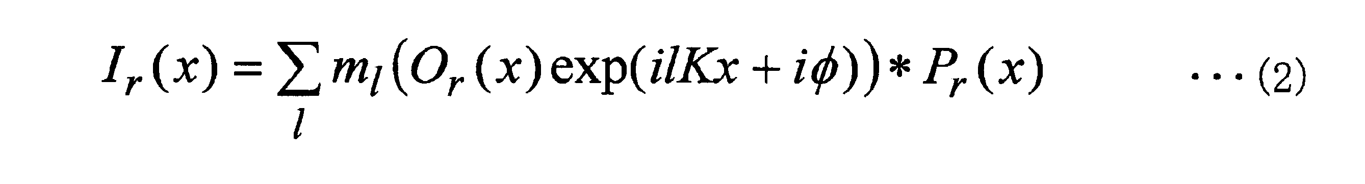
 ここで、l=-1,0,1であり、mlは照明光の変調振幅である。l=0の成分は、構造化照明によって変調を受けない0次成分であり、l=-1,1の成分はそれぞれ、変調を受けた±1次成分(モアレ)である。この式(2)において、記号*は畳み込み積分を表す。以下、実空間における量には添え字rを、波数空間における量には添え字kをつけて表す。この式(2)をフーリエ変換し、波数空間で表記すると、
It can be expressed as. Where φ is the phase of structured illumination.
Here, l = −1, 0, 1 and ml is the modulation amplitude of the illumination light. The components of l = 0 are zero-order components that are not modulated by structured illumination, and the components of l = −1,1 are ± primary components (moire) that are modulated. In this equation (2), the symbol * represents a convolution integral. Hereinafter, the subscript r is added to the quantity in the real space, and the subscript k is added to the quantity in the wave number space. When this equation (2) is Fourier transformed and expressed in wave number space,
Figure JPOXMLDOC01-appb-M000003
 式(3)において、Pr(x)のフーリエ変換Pk(k)は光学系の伝達関数 (OTF; Optical Transfer Function)を表す。 In Equation (3), the Fourier transform Pk (k) of Pr (x) represents an optical system transfer function (OTF; Optical Transfer Function).
 式(3)におけるl=-1,1に対応するOk(k-K),Ok(k+K)は、標本の持つ空間周波数成分を、構造化照明の空間周波数成分Kだけずらすことを意味している。すなわち、これはkという空間周波数成分までしか取得することのできない光学系であっても、標本が持つそれより高い空間周波数成分を取得できることを表している。このために、干渉縞の周期はこの光学系で結像できる範囲でできるだけ短くできる。 Ok (k−K) and Ok (k + K) corresponding to l = −1, 1 in Equation (3) mean that the spatial frequency component of the sample is shifted by the spatial frequency component K of structured illumination. Yes. That is, this indicates that even an optical system that can acquire only a spatial frequency component of k can acquire a higher spatial frequency component than that of the sample. For this reason, the period of the interference fringes can be made as short as possible within the range that can be imaged by this optical system.
 ここで、干渉縞の縞パターンをずらしながら撮像を行うと、同一の空間周波数成分、変調振幅を持ち、位相φのみ異なる画像がN枚得られる。このときのj番目の画像信号強度Ikj(k)は、j番目の画像の構造化照明位相をφjと表すと、 Here, when imaging is performed while shifting the fringe pattern of the interference fringes, N images having the same spatial frequency component and modulation amplitude and only the phase φ are obtained. The j-th image signal intensity Ikj (k) at this time is represented by φj as the structured illumination phase of the j-th image.
Figure JPOXMLDOC01-appb-M000004
 である。すなわち、式(4)によりN個の方程式が得られる。ここで、これらの方程式においてOk(k+lK),(l=-1,0,1)が未知数であるため、N≧3であれば、これらの方程式を解くことができる。 It is. That is, N equations can be obtained from the equation (4). Here, since Ok (k + lK) and (l = −1, 0, 1) are unknown numbers in these equations, these equations can be solved if N ≧ 3.
 ここで、強度分布を持たない照明を与えた場合の光学系が持つPk(k)が検出可能な範囲は、光波長λ、対物レンズのNAに対して、k=-2NA/λ~2NA/λであるから、上記で得られたOk(k+lK)はl=-1,0,1に対して、k=-2NA/λ-K~2NA/λ-K、k=2NA/λ~2NA/λ、k=-2NA/λ+K~2NA/λ+Kの情報を含む。したがって、Ok(k+lK)全体としてはk=-2NA/λ-K~2NA/λ+Kまでの情報を含むので、これをOk(k)と定義しなおして逆フーリエ変換を行い実空間の情報(標本Or(x)の画像)に戻すことにより、高い解像度を持った顕微鏡画像を得ることができる。すなわち、撮像部210は、上述した演算によって画像復調を行うことにより、超解像効果を得ることができる。 Here, the range in which Pk (k) of the optical system in the case of illumination with no intensity distribution can be detected is k = −2 NA / λ to 2 NA / with respect to the optical wavelength λ and the NA of the objective lens. Therefore, Ok (k + 1K) obtained above is k = -2NA / λ-K to 2NA / λ-K, k = 2NA / λ to 2NA / with respect to l = -1, 0, 1. The information of λ, k = −2NA / λ + K to 2NA / λ + K is included. Therefore, since Ok (k + 1K) as a whole includes information from k = -2NA / λ-K to 2NA / λ + K, this is redefined as Ok (k), and inverse Fourier transform is performed to perform real space information (sample). By returning to the image of Or (x), a microscope image having a high resolution can be obtained. That is, the imaging unit 210 can obtain a super-resolution effect by performing image demodulation by the above-described calculation.
 この結果得られた像は、空間変調がなされた1次元方向のみに高い解像度を持つ。さらに、空間変調を施す方向を少なくとも2方向に変化させ、それぞれの方向について1次元と同様の処理を施すことにより、撮像部210は、2次元方向においておよそ等方的に高い解像度を持った顕微鏡画像を得ることができる。 The resulting image has a high resolution only in the one-dimensional direction where spatial modulation is performed. Further, by changing the direction of spatial modulation in at least two directions and performing the same processing as in one dimension in each direction, the imaging unit 210 is a microscope having approximately isotropically high resolution in the two-dimensional direction. An image can be obtained.
 なお、空間変調画像に対して最小自乗法による連立方程式を構成しておき、これを解くことによっても、撮像部210は、高い解像度を持った顕微鏡画像を得ることができる。 Note that the imaging unit 210 can obtain a microscopic image having a high resolution by constructing simultaneous equations based on the least square method on the spatially modulated image and solving the equations.
 上記説明したように、2D-SIMでは、1次元方向において、干渉縞の位相を変化させて少なくとも3枚の画像を取得することにより、1次元方向において、高い解像度を持った標本画像を取得することができる。
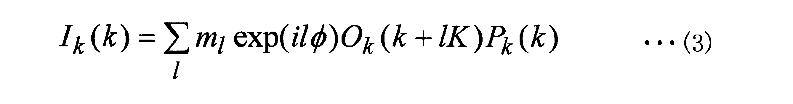
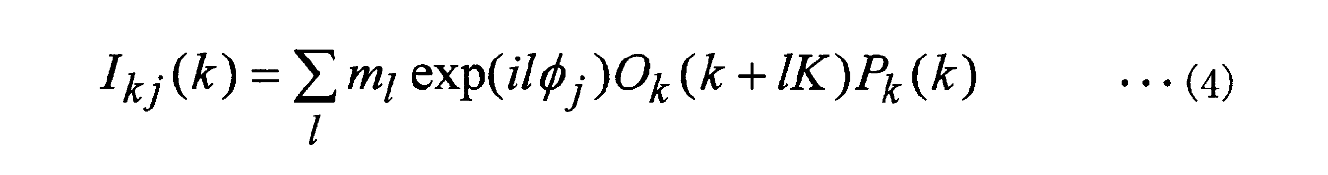
 以上、2D-SIMにおける復調方法を説明したが、3D-SIMでは、3光束干渉による干渉縞を用いるため、取得画像に混在する成分は、変調を受けていない0次成分、標本面内の1次元方向における超解像成分となる±2次成分、光軸方向の超解像成分となる±1次成分の5成分となる。したがって、3D-SIMでは、未知数が5つとなるので、少なくとも5枚の画像を取得することにより、上述した2D-SIMと同様に、画像を復元することができる。3D-SIMでは面内方向に加えて、光軸方向においても超解像観察を実現できる。
As described above, in the 2D-SIM, by acquiring at least three images by changing the phase of the interference fringe in the one-dimensional direction, a sample image having a high resolution is acquired in the one-dimensional direction. be able to.
The demodulation method in 2D-SIM has been described above. In 3D-SIM, since interference fringes due to three-beam interference are used, the components mixed in the acquired image are zero-order components that are not modulated, and 1 in the sample plane. There are five components: a ± second order component that is a super-resolution component in the dimension direction and a ± first order component that is a super-resolution component in the optical axis direction. Therefore, since there are five unknowns in the 3D-SIM, by acquiring at least five images, it is possible to restore the image in the same manner as the 2D-SIM described above. In 3D-SIM, super-resolution observation can be realized in the optical axis direction in addition to the in-plane direction.
[干渉縞の例]
 次に、図4を参照して、駆動制御部160が制御する回折光の干渉により形成される干渉縞の一例について説明する。上述したように、+(プラス)1次回折光、0次回折光、及び-(マイナス)1次回折光を光学面OS3において干渉させた場合、この干渉縞のパターン(以下、縞パターン)を5パターンにすることにより、光学面OS3の面内方向および光軸AX2方向に超解像効果を得ることができ、すなわち、3D-SIMとなる。5パターンそれぞれは、互いに方向とピッチが同じであり、かつ、位相が異なる縞パターンである。なお、超解像効果を得るためには、Nパターンの回折光の干渉により形成される干渉縞のうち、隣あう縞パターンの位相差は、2π/N[rad]にできる。例えば、上述したように縞パターンが5パターンある場合には、隣あう縞パターンの位相差は、2π/5[rad]にできる。ただし、2D-SIMに限っては、π/3[rad]でもよい。ここで、隣合う縞パターンとは、互いの位相差が最も小さくなるものが隣同士になるように、縞パターンを並べたときに、隣合う縞パターンを意味する。なお、位相の周期性を考慮して、位相差は、mを整数として、2π(m+1/N)[rad]であってもよいが、これらの位相差は全て2π[rad]以下に換算することができるため、ここでは位相差を2π[rad]以下として説明する。
 また、上記では、縞パターンという用語を用いて説明したが、縞パターンの位相とは、干渉縞の位相を意味し、縞パターンの方向とは干渉縞の方向を意味し、縞パターンのピッチとは干渉縞のピッチを意味する。以下の記載でも同様である。
[Examples of interference fringes]
Next, an example of interference fringes formed by interference of diffracted light controlled by the drive control unit 160 will be described with reference to FIG. As described above, when + (plus) 1st order diffracted light, 0th order diffracted light, and − (minus) 1st order diffracted light are caused to interfere on the optical surface OS3, this interference fringe pattern (hereinafter referred to as a fringe pattern) is changed to 5 patterns. By doing so, it is possible to obtain a super-resolution effect in the in-plane direction of the optical surface OS3 and in the direction of the optical axis AX2, that is, 3D-SIM. Each of the five patterns is a stripe pattern having the same direction and pitch and different phases. In order to obtain a super-resolution effect, the phase difference between adjacent fringe patterns among interference fringes formed by interference of N patterns of diffracted light can be 2π / N [rad]. For example, when there are five stripe patterns as described above, the phase difference between adjacent stripe patterns can be 2π / 5 [rad]. However, π / 3 [rad] may be used only for 2D-SIM. Here, the adjacent fringe pattern means an adjacent fringe pattern when the fringe patterns are arranged so that the ones having the smallest phase difference are adjacent to each other. In consideration of the periodicity of the phase, the phase difference may be 2π (m + 1 / N) [rad] where m is an integer, but these phase differences are all converted to 2π [rad] or less. Therefore, here, the phase difference is described as 2π [rad] or less.
In the above description, the term fringe pattern is used, but the phase of the fringe pattern means the phase of the interference fringe, the direction of the fringe pattern means the direction of the interference fringe, and the pitch of the fringe pattern Means the pitch of interference fringes. The same applies to the following description.
 図4は、本実施形態の駆動制御部160が印加する電圧パターンの一例を示す模式図である。駆動制御部160は、光変調部120の各画素Pxに印加する電圧パターンを制御することにより、回折光の縞パターンを光学面OS3に生じさせる。具体的には、駆動制御部160は、図4に示す電圧パターンA~A(画像生成用電圧パターン)を光変調部120に印加することにより、これらの電圧パターンに応じた縞パターンを生じさせる。図4において、白色として示される部分(白部分)は、上述した白状態を意味し、プラス電位の電圧(例えば、電圧V1)が印加される場合である。一方、図4において、黒色として示される部分(黒部分)は、上述した黒状態を意味し、マイナス電位の電圧(例えば、電圧-(マイナス)V1)が印加される場合である。なお、白部分にマイナス電位の電圧が印加され、黒部分にプラス電位の電圧が印加されてもよい。この一例における電圧パターンは、いずれも縞ピッチ5.3[pixel]であり、縞方位2[°]である縞パターンを生じさせるための電圧パターンである。なお、角度のとり方として、時計の0時方向を角度0[°]、時計回りに角度が増加すると定義する。ただし、角度0[°]とする位置は、適宜変更可能である。この場合、縞方位もそれに応じて適宜変更される。また、ここでは白部分と黒部分の電圧パターン比は1:1に設定してある。これ以外の電圧パターンの場合のシーケンスについては後述する。
 これら電圧パターンA~Aは、隣あう電圧パターンそれぞれによって形成される干渉縞の位相差は、2π/N[rad]となるように構成されている。例えば、電圧パターンAおよび電圧パターンAは、それぞれによって形成される干渉縞の位相差が2π/5[rad]ように構成されている。また、電圧パターンAと電圧パターンAとは、それぞれによって形成される干渉縞の位相差が2π/5[rad]となるように構成されている。
 駆動制御部160は、これらの電圧パターンA~Aを順次生じさせることにより、光学面OS3の面内方向および光軸AX2方向に超解像効果を得ることを可能にする。
FIG. 4 is a schematic diagram illustrating an example of a voltage pattern applied by the drive control unit 160 of the present embodiment. The drive control unit 160 generates a fringe pattern of diffracted light on the optical surface OS3 by controlling the voltage pattern applied to each pixel Px of the light modulation unit 120. Specifically, the drive control unit 160 applies the voltage patterns A 1 to A 5 (image generation voltage patterns) shown in FIG. 4 to the light modulation unit 120, thereby generating a fringe pattern corresponding to these voltage patterns. Cause it to occur. In FIG. 4, a portion shown as white (white portion) means the above-described white state, and is a case where a positive potential voltage (for example, voltage V1) is applied. On the other hand, in FIG. 4, a black portion (black portion) means the above-described black state, and is a case where a negative potential voltage (for example, voltage-(minus) V1) is applied. Note that a negative potential voltage may be applied to the white portion, and a positive potential voltage may be applied to the black portion. The voltage pattern in this example is a voltage pattern for generating a fringe pattern having a fringe pitch of 5.3 [pixel] and a fringe orientation of 2 [°]. In addition, as a method of taking the angle, it is defined that the 0 o'clock direction of the watch is an angle 0 [°], and the angle is increased clockwise. However, the position where the angle is 0 [°] can be changed as appropriate. In this case, the stripe orientation is also changed accordingly. Here, the voltage pattern ratio of the white part and the black part is set to 1: 1. The sequence in the case of other voltage patterns will be described later.
These voltage patterns A 1 to A 5 are configured such that the phase difference between interference fringes formed by adjacent voltage patterns is 2π / N [rad]. For example, the voltage pattern A 1 and the voltage pattern A 2 are configured such that the phase difference between the interference fringes formed by each of them is 2π / 5 [rad]. Further, the voltage pattern A 2 and the voltage pattern A 3 are configured such that the phase difference between the interference fringes formed by the voltage pattern A 2 and the voltage pattern A 3 is 2π / 5 [rad].
The drive controller 160 sequentially generates these voltage patterns A 1 to A 5, thereby making it possible to obtain a super-resolution effect in the in-plane direction of the optical surface OS3 and in the direction of the optical axis AX2.
 ここで、光変調部120の第1電極基板121と第2電極基板124との間の電位差の時間総和がゼロでない場合には、第1電極基板121と第2電極基板124との間の電圧に直流成分が存在する。この電圧の直流成分に偏りが生じる場合には、強誘電性液晶の内部イオンが一方向に引き付けられることにより、液晶素子に電圧を掛けても他の安定状態に変移しない焼き付きと呼ばれる現象が生じることがある。第1電極基板121と第2電極基板124との間に焼き付きが生じるか否か、または焼き付きが生じる場合の程度は、電極基板間に印加された電圧の直流成分により決まる。したがって、その電極基板間に印加された電圧の直流成分を相殺するように逆電圧を印加することにより、焼き付きを抑止することができる。具体的には、上述した縞パターンを生じさせる場合に、構造化照明としての光を照射する照射期間と、構造化照明としての光を照射しない非照射期間とを設ける。非照射期間において,光は例えば図示しないシャッターにより遮光される.駆動制御部160は、この非照射期間において、照射期間とは逆の電圧を光変調部120に印加することにより、焼き付きを抑止することができる。すなわち、駆動制御部160は、構造化照明としての光を照射するための複数の電圧パターンから算出した反転パターンを光変調部120に印加することにより、焼き付きを抑止することができる。 Here, when the time sum of the potential difference between the first electrode substrate 121 and the second electrode substrate 124 of the light modulation unit 120 is not zero, the voltage between the first electrode substrate 121 and the second electrode substrate 124. Has a direct current component. When the DC component of this voltage is biased, the internal ions of the ferroelectric liquid crystal are attracted in one direction, causing a phenomenon called burn-in that does not change to another stable state even when a voltage is applied to the liquid crystal element. Sometimes. Whether or not seizure occurs between the first electrode substrate 121 and the second electrode substrate 124, or the extent to which seizure occurs, is determined by the DC component of the voltage applied between the electrode substrates. Therefore, the burn-in can be suppressed by applying the reverse voltage so as to cancel the DC component of the voltage applied between the electrode substrates. Specifically, when the above-described stripe pattern is generated, an irradiation period in which light as structured illumination is irradiated and a non-irradiation period in which light as structured illumination is not irradiated are provided. During the non-irradiation period, light is blocked by a shutter (not shown), for example. In this non-irradiation period, the drive control unit 160 can suppress image sticking by applying a voltage opposite to the irradiation period to the light modulation unit 120. That is, the drive control unit 160 can suppress burn-in by applying to the light modulation unit 120 an inversion pattern calculated from a plurality of voltage patterns for irradiating light as structured illumination.
 具体的には、駆動制御部160は、図4に示す反転パターンAinv(焼き付き防止電圧パターン)を光変調部120に印加する。ここで、反転パターンAinvとは、積算電圧パターンAsumの電位を反転させた電圧パターンである。この積算電圧パターンAsumとは、電圧パターンA~Aの白部分を+1、黒部分を-1とした場合に、電圧パターンA~Aの各ピクセルの電圧値をピクセルごとに積算した電圧パターンである。すなわち、駆動制御部160は、電圧パターンA~Aを積算した電圧パターンを逆電圧にした反転パターンAinvを光変調部120に印加する。これにより、駆動制御部160は、光変調部120に印加される電圧の時間総和がゼロになるようにして、直流成分を相殺する。このため、駆動制御部160は、光変調部120の焼き付きを抑止することができる。このとき、駆動制御部160は、例えば、図5に示す順序によって電圧パターンを印加する。 Specifically, the drive control unit 160 applies the inversion pattern A inv (burn-in prevention voltage pattern) illustrated in FIG. 4 to the light modulation unit 120. Here, the inversion pattern A inv is a voltage pattern in which the potential of the integrated voltage pattern A sum is inverted. And the cumulative voltage pattern A sum, integrated white portion of the voltage patterns A 1 ~ A 5 +1, when -1 black part, the voltage value of each pixel of the voltage patterns A 1 ~ A 5 per pixel This is the voltage pattern. That is, the drive control unit 160 applies an inversion pattern A inv in which the voltage pattern obtained by integrating the voltage patterns A 1 to A 5 is a reverse voltage to the light modulation unit 120. Thereby, the drive control unit 160 cancels the DC component so that the total time of the voltage applied to the light modulation unit 120 becomes zero. For this reason, the drive control unit 160 can suppress burn-in of the light modulation unit 120. At this time, the drive control unit 160 applies the voltage pattern in the order shown in FIG. 5, for example.
 図5は、本実施形態の駆動制御部160が光変調部120に印加する電圧パターンの順序の一例を示す模式図である。図5に示すように、駆動制御部160は、時刻tの経過とともに電圧パターンA~Aと、反転パターンAinvとを順次印加する。ここで、電圧パターンA~Aを1周期の電圧パターンとする。言い換えると、1周期の電圧パターンとは、方向およびピッチが同じである複数の縞パターンであり、上述した2D-SIMでは3枚であり、3D-SIMでは、5枚である。駆動制御部160は、時刻t1~t2において、電圧パターンAを印加する。また、駆動制御部160は、時刻t2~t3において、電圧パターンAを印加する。これと同様にして、駆動制御部160は、時刻t3~t6において、電圧パターンA~Aを順次印加する。また、駆動制御部160は、時刻t6~t7を非照射期間にして、この非照射期間に反転パターンAinvを印加する。この図5に示すように電圧パターンA~Aと、反転パターンAinvとを順次印加することにより、駆動制御部160は、光変調部120の焼き付きを抑止することができる。 FIG. 5 is a schematic diagram illustrating an example of the order of voltage patterns applied to the light modulation unit 120 by the drive control unit 160 of the present embodiment. As shown in FIG. 5, the drive control unit 160 sequentially applies the voltage patterns A 1 to A 5 and the inversion pattern A inv as time t passes. Here, the voltage patterns A 1 to A 5 are defined as a voltage pattern of one cycle. In other words, the voltage pattern of one cycle is a plurality of stripe patterns having the same direction and pitch, and is 3 in the 2D-SIM described above and 5 in the 3D-SIM. Drive control unit 160, at time t1 ~ t2, applies a voltage pattern A 1. The drive control unit 160, at time t2 ~ t3, applies a voltage pattern A 2. Similarly to this, the drive control unit 160 sequentially applies the voltage patterns A 3 to A 5 at times t 3 to t 6. Further, the drive control unit 160 sets the times t6 to t7 as a non-irradiation period, and applies the reverse pattern A inv during the non-irradiation period. As shown in FIG. 5, by sequentially applying the voltage patterns A 1 to A 5 and the inversion pattern A inv , the drive control unit 160 can suppress burn-in of the light modulation unit 120.
 ここで、図6を参照して従来の手法による電圧パターンの印加順序と、本実施形態の駆動制御部160による電圧パターンの印加順序とを、比較して説明する。
 図6は、電圧パターンの印加順序の比較例を示す模式図である。本実施形態とは異なる印加順序を図6(A)に示す。図6(A)に示す印加順序によれば、電圧パターンAに対する反転パターンA’を、電圧パターンAの後、すなわち次の電圧パターンAを印加する前に印加する。すなわち図6(A)に示す印加順序によると、ある電圧パターンと、この電圧パターンに対する反転パターンとを交互に印加する。ここで、1つの電圧パターンを印加する時間をTとすると、電圧パターンと、反転パターンとを交互に印加する場合に、1周期の電圧パターンを印加するために要する時間は、時刻t0Aから時刻t10Aまでの時間であり、すなわち10Tである。一方、本実施形態の駆動制御部160による電圧パターンの印加順序を図6(B)に示す。駆動制御部160による電圧パターンの印加順序によれば、電圧パターンA~Aの積算値に対する反転パターンA’を、電圧パターンA~Aの印加後に印加する。ここで、図6(B)における反転パターンA’とは、上述した反転パターンAinvである。すなわち、駆動制御部160による電圧パターンの印加順序によれば、電圧パターンA~Aの印加後に反転パターンA’を1回だけ印加する。ここで、電圧パターンの印加後に、反転パターンを1回だけ印加する場合、1周期の電圧パターンを印加するために要する時間は、時刻t0Bから時刻t6Bまでであり、すなわち6Tである。したがって、駆動制御部160による電圧パターンの印加順序によれば、1周期の電圧パターンを印加するために要する時間を、図6(A)に示す印加順序に比べて短縮することができる。この具体例の場合においては、駆動制御部160による電圧パターンの印加順序によれば、1周期の電圧パターンを印加するために要する時間を約40[%]短縮することができる。これにより、照明装置10は、観察装置1が観察に要する時間を短縮することができる。このように、本実施形態の駆動制御部160によれば、空間光変調器として用いた液晶素子の焼き付きを効率よく抑制することができる。また、例えば、本発明の実施形態に係る超解像顕微鏡を使用して生きた細胞を観察する場合、従来よりも高速なダイナミクスを観察することができる。したがって、本発明の実施形態に係る超解像顕微鏡は、例えば、生きた細胞を観察するのに適している。
Here, with reference to FIG. 6, the voltage pattern application sequence according to the conventional method and the voltage pattern application sequence by the drive control unit 160 of the present embodiment will be described in comparison.
FIG. 6 is a schematic diagram illustrating a comparative example of the application order of voltage patterns. An application order different from that of the present embodiment is shown in FIG. According to application order shown in FIG. 6 (A), an inverted pattern A 1 'for the voltage patterns A 1, after the voltage patterns A 1, that is applied before applying the next voltage pattern A 2. That is, according to the application sequence shown in FIG. 6A, a certain voltage pattern and an inversion pattern corresponding to this voltage pattern are alternately applied. Here, when the time for applying one voltage pattern is T, the time required to apply a voltage pattern of one cycle when the voltage pattern and the inversion pattern are applied alternately is from time t0A to time t10A. Time, i.e. 10T. On the other hand, the application order of the voltage pattern by the drive control unit 160 of this embodiment is shown in FIG. According to order of applying voltage pattern by the drive control unit 160, a reverse pattern A 'with respect to the integrated value of the voltage patterns A 1 ~ A 5, is applied after the application of the voltage patterns A 1 ~ A 5. Here, the inversion pattern A ′ in FIG. 6B is the inversion pattern A inv described above. That is, according to the voltage pattern application sequence by the drive control unit 160, the reverse pattern A ′ is applied only once after the voltage patterns A 1 to A 5 are applied. Here, after applying the voltage pattern, when the inversion pattern is applied only once, the time required to apply one cycle of the voltage pattern is from time t0B to time t6B, that is, 6T. Therefore, according to the application order of the voltage pattern by the drive control unit 160, the time required to apply one cycle of the voltage pattern can be shortened compared to the application order shown in FIG. In the case of this specific example, according to the application order of the voltage pattern by the drive control unit 160, the time required to apply the voltage pattern of one cycle can be shortened by about 40 [%]. Thereby, the illuminating device 10 can shorten the time which the observation apparatus 1 requires for observation. Thus, according to the drive control unit 160 of the present embodiment, it is possible to efficiently suppress burn-in of the liquid crystal element used as the spatial light modulator. In addition, for example, when observing living cells using the super-resolution microscope according to the embodiment of the present invention, it is possible to observe dynamics faster than in the past. Therefore, the super-resolution microscope according to the embodiment of the present invention is suitable for observing living cells, for example.
[変形例1]
 なお、ここまで駆動制御部160が、電圧パターンA~Aの積算値に対する反転パターンを、電圧パターンA~Aの印加後に1回だけ印加する例について説明したが、これに限られない。駆動制御部160は、例えば、図7に示す順序によって電圧パターンと反転パターンとを印加してもよい。
 図7は、本実施形態の駆動制御部160が光変調部120に印加する電圧パターンの順序の変形例を示す模式図である。この変形例において、駆動制御部160は、反転パターンAinv-1(焼き付き防止電圧パターン)と、反転パターンAinv-2(焼き付き防止電圧パターン)とを、電圧パターンA~Aを印加する間に、印加する。具体的には、駆動制御部160は、電圧パターンA~Aを印加した後、電圧パターンAを印加する前に反転パターンAinv-1を印加する。また、駆動制御部160は、電圧パターンA~Aを印加した後、電圧パターンAを印加する前に反転パターンAinv-2を印加する。ここで、反転パターンAinv-1および反転パターンAinv-2とは、図5で示したAinvの電圧値を等分することにより生成された反転パターンである。したがって、これら複数の反転パターン(ここでは、反転パターンAinv-1および反転パターンAinv-2)は、積算することにより、上述した反転パターンAinvと同一の電位を有する。例えば、反転パターンAinv-1および反転パターンAinv-2は、それぞれ上述した反転パターンAinvの半分の電圧による反転パターンである。この変形例において、駆動制御部160は、電圧パターンA~Aの印加周期において複数回に分けて反転パターンを印加する。このように複数の反転パターンを複数回に分けて印加した場合であっても、電圧パターンの印加周期(例えば、1周期)あたりに印加される反転パターンの電圧の積算値は、上述した反転パターンAinvと同一の電圧になる。これにより、このように複数の反転パターンを複数回に分けて印加した場合であっても、電圧パターンA~Aによる直流成分を反転パターンによって相殺することができる。したがって、このように複数の反転パターンを複数回に分けて印加した場合であっても、1周期の電圧パターンを印加するために要する時間を、上述した図6(A)に示す印加順序に比べて短縮することができる。これにより、照明装置10は、観察装置1が観察に要する時間を短縮することができる。このように、本実施形態の駆動制御部160によれば、空間光変調器として用いた液晶素子の焼き付きを効率よく抑制することができる。
[Modification 1]
Here, to the drive controller 160, a reverse pattern with respect to the integrated value of the voltage patterns A 1 ~ A 5, an example has been described to be applied only once after the application of the voltage patterns A 1 ~ A 5, limited to Absent. For example, the drive control unit 160 may apply the voltage pattern and the inversion pattern in the order shown in FIG.
FIG. 7 is a schematic diagram illustrating a modification of the order of voltage patterns applied to the light modulation unit 120 by the drive control unit 160 of the present embodiment. In this modification, the drive control unit 160 applies the inversion pattern A inv-1 (burn-in prevention voltage pattern) and the inversion pattern A inv-2 (burn-in prevention voltage pattern) to the voltage patterns A 1 to A 5 . In between. Specifically, after applying the voltage patterns A 1 to A 3 , the drive control unit 160 applies the reverse pattern A inv-1 before applying the voltage pattern A 4 . The drive controller 160 applies the reverse pattern A inv-2 after applying the voltage patterns A 4 to A 5 and before applying the voltage pattern A 1 . Here, the inversion pattern A inv-1 and the inversion pattern A inv-2 are inversion patterns generated by equally dividing the voltage value of A inv shown in FIG. Therefore, the plurality of inversion patterns (here, inversion pattern A inv-1 and inversion pattern A inv-2 ) have the same potential as the inversion pattern A inv described above by integrating. For example, the inversion pattern A inv-1 and the inversion pattern A inv-2 are inversion patterns with half the voltage of the inversion pattern A inv described above. In this modification, the drive control unit 160 applies the inversion pattern in a plurality of times in the application cycle of the voltage patterns A 1 to A 5 . Thus, even when a plurality of inversion patterns are applied in a plurality of times, the integrated value of the voltages of the inversion patterns applied per voltage pattern application cycle (for example, one cycle) is the above-described inversion pattern. It becomes the same voltage as A inv . Thus, even when a plurality of inversion patterns are applied in a plurality of times as described above, the DC components due to the voltage patterns A 1 to A 5 can be canceled by the inversion patterns. Therefore, even when a plurality of inversion patterns are applied in a plurality of times as described above, the time required to apply a voltage pattern of one cycle is compared with the application sequence shown in FIG. Can be shortened. Thereby, the illuminating device 10 can shorten the time which the observation apparatus 1 requires for observation. Thus, according to the drive control unit 160 of the present embodiment, it is possible to efficiently suppress burn-in of the liquid crystal element used as the spatial light modulator.
[変形例2]
 また、ここまで縞パターンの方向が1方向である場合、すなわち縞ピッチ5.3[pixel]、縞方位2[°]の縞パターンの場合について説明したがこれに限られない。ここで、観察装置1は、複数の方向に回転させた複数の縞方位の縞パターンによって観察することにより、光学面OS3の面内で等方的な分解能を得ることができる。例えば、観察装置1は、3つの縞方位の縞パターンによって観察することにより、光学面OS3の面内で等方的な分解能を得ることができる。図8および図9を参照して、駆動制御部160が印加する電圧パターンの変形例について説明する。
[Modification 2]
Although the case where the direction of the stripe pattern is one direction, that is, the case of the stripe pattern having a stripe pitch of 5.3 [pixel] and a stripe orientation of 2 [°] has been described so far, the present invention is not limited thereto. Here, the observation apparatus 1 can obtain isotropic resolution in the plane of the optical surface OS3 by observing with a stripe pattern having a plurality of stripe orientations rotated in a plurality of directions. For example, the observation apparatus 1 can obtain isotropic resolution in the plane of the optical surface OS3 by observing with a stripe pattern having three stripe directions. A modification of the voltage pattern applied by the drive control unit 160 will be described with reference to FIGS.
 図8は、本実施形態の駆動制御部160が印加する電圧パターンの第1の変形例を示す模式図である。駆動制御部160は、図8に示す電圧パターンB~B(画像生成用電圧パターン)を光変調部120に印加することにより、これらの電圧パターンに応じた縞パターンを生じさせる。この変形例における電圧パターンは、縞ピッチ5.3[pixel]であり、縞方位-58[°]である縞パターンを生じさせるための電圧パターンである。ここで、駆動制御部160は、図8に示す反転パターンBinv(焼き付き防止電圧パターン)を光変調部120に印加する。ここで、反転パターンBinvとは、積算電圧パターンBsumの電位を反転させた電圧パターンである。
 積算電圧パターンBsumとは、白部分を+1、黒部分を-1とした場合に、電圧パターンB~Bの各ピクセルの電圧値をピクセルごとに積算した電圧パターンである。
 すなわち、駆動制御部160は、電圧パターンB~Bを積算した電圧パターンを逆電圧にした反転パターンを光変調部120に印加する。これにより、駆動制御部160は、光変調部120に印加される電圧の時間総和がゼロになるようにして、直流成分を相殺する。
FIG. 8 is a schematic diagram illustrating a first modification of the voltage pattern applied by the drive control unit 160 of the present embodiment. The drive control unit 160 applies the voltage patterns B 1 to B 5 (image generation voltage patterns) shown in FIG. 8 to the light modulation unit 120 to generate a fringe pattern corresponding to these voltage patterns. The voltage pattern in this modification is a voltage pattern for generating a fringe pattern having a fringe pitch of 5.3 [pixel] and a fringe orientation of −58 [°]. Here, the drive control unit 160 applies the inversion pattern B inv (burn-in prevention voltage pattern) illustrated in FIG. 8 to the light modulation unit 120. Here, the inversion pattern B inv is a voltage pattern obtained by inverting the potential of the integrated voltage pattern B sum .
The integrated voltage pattern B sum is a voltage pattern in which the voltage values of the pixels of the voltage patterns B 1 to B 5 are integrated for each pixel when the white portion is +1 and the black portion is -1.
That is, the drive control unit 160 applies an inversion pattern in which the voltage pattern obtained by integrating the voltage patterns B 1 to B 5 is a reverse voltage, to the light modulation unit 120. Thereby, the drive control unit 160 cancels the DC component so that the total time of the voltage applied to the light modulation unit 120 becomes zero.
 図9は、本実施形態の駆動制御部160が印加する電圧パターンの第2の変形例を示す模式図である。駆動制御部160は、図9に示す電圧パターンC~C(画像生成用電圧パターン)を光変調部120に印加することにより、これらの電圧パターンに応じた縞パターンを生じさせる。この変形例における電圧パターンは、縞ピッチ5.3[pixel]であり、縞方位62[°]である縞パターンを生じさせるための電圧パターンである。ここで、駆動制御部160は、図9に示す反転パターンCinv(焼き付き防止電圧パターン)を光変調部120に印加する。ここで、反転パターンCinvとは、積算電圧パターンCsumの電位を反転させた電圧パターンである。
 積算電圧パターンCsumとは、白部分を+1、黒部分を-1とした場合に、電圧パターンC~Cの各ピクセルの電圧値をピクセルごとに積算した電圧パターンである。
 すなわち、駆動制御部160は、電圧パターンC~Cを積算した電圧パターンを逆電圧にした反転パターンを光変調部120に印加する。これにより、駆動制御部160は、光変調部120に印加される電圧の時間総和がゼロになるようにして、直流成分を相殺する。
FIG. 9 is a schematic diagram illustrating a second modification of the voltage pattern applied by the drive control unit 160 of the present embodiment. The drive control unit 160 applies the voltage patterns C 1 to C 5 (image generation voltage patterns) shown in FIG. 9 to the light modulation unit 120, thereby generating a fringe pattern corresponding to these voltage patterns. The voltage pattern in this modification is a voltage pattern for generating a fringe pattern having a fringe pitch of 5.3 [pixel] and a fringe orientation of 62 [°]. Here, the drive control unit 160 applies the inversion pattern C inv (burn-in prevention voltage pattern) illustrated in FIG. 9 to the light modulation unit 120. Here, the inverted pattern C inv is a voltage pattern obtained by inverting the potential of the integrated voltage pattern C sum .
The integrated voltage pattern C sum is a voltage pattern in which the voltage values of the pixels of the voltage patterns C 1 to C 5 are integrated for each pixel when the white portion is +1 and the black portion is −1.
That is, the drive control unit 160 applies an inversion pattern in which the voltage pattern obtained by integrating the voltage patterns C 1 to C 5 is a reverse voltage to the light modulation unit 120. Thereby, the drive control unit 160 cancels the DC component so that the total time of the voltage applied to the light modulation unit 120 becomes zero.
 この変形例の場合、駆動制御部160は、図6(B)に示したように電圧パターンと反転パターンとを繰り返し印加する。具体的には、駆動制御部160は、電圧パターンA~Aを印加した後に、反転パターンA’を印加する。また、駆動制御部160は、電圧パターンB~Bを印加した後に、反転パターンB’を印加する。ここで、図6(B)における反転パターンB’とは、上述した反転パターンBinvである。また、駆動制御部160は、電圧パターンC~Cを印加した後に、反転パターンC’を印加する。ここで、図6(B)における反転パターンC’とは、上述した反転パターンCinvである。このような印加順序によっても、1周期の電圧パターンを印加するために要する時間を、上述した図6(A)に示す印加順序に比べて短縮することができる。これにより、照明装置10は、観察装置1が観察に要する時間を短縮することができる。このように、本実施形態の駆動制御部160によれば、空間光変調器として用いた液晶素子の焼き付きを効率よく抑制することができる。
 したがって、3つの縞方位の縞パターンによって観察することにより、光学面OS3の面内で等方的な分解能を得ることができる、3D-SIMの場合においても、本発明は有用である。
In the case of this modification, the drive control unit 160 repeatedly applies the voltage pattern and the inversion pattern as shown in FIG. Specifically, the drive control unit 160 applies the reverse pattern A ′ after applying the voltage patterns A 1 to A 5 . The drive controller 160 applies the reverse pattern B ′ after applying the voltage patterns B 1 to B 5 . Here, the inversion pattern B ′ in FIG. 6B is the inversion pattern B inv described above. The drive control unit 160 applies the reverse pattern C ′ after applying the voltage patterns C 1 to C 5 . Here, the inversion pattern C ′ in FIG. 6B is the inversion pattern C inv described above. Even in such an application order, the time required to apply a voltage pattern of one cycle can be shortened compared to the application order shown in FIG. Thereby, the illuminating device 10 can shorten the time which the observation apparatus 1 requires for observation. Thus, according to the drive control unit 160 of the present embodiment, it is possible to efficiently suppress burn-in of the liquid crystal element used as the spatial light modulator.
Therefore, the present invention is useful even in the case of 3D-SIM in which isotropic resolution can be obtained in the plane of the optical surface OS3 by observing with a stripe pattern of three stripe orientations.
 なお、A~A、B~B、C~Cを表示後に、A’、B’、C’を表示してもよい。また、図4、8、9において白黒の割合が等しいパターンについて説明してきたが、本手法はこれに限らない。以下、白に対する黒の比を規格化したものをDuty比と定義する。白黒の割合が等しい場合はDuty比=0.5となる。図10~図12にDuty比が0.7のパターンを示す。Duty比を0.5から変化させることで0次回折光をより効率よく発生させることができる。 Note that A ′, B ′, and C ′ may be displayed after displaying A 1 to A 5 , B 1 to B 5 , and C 1 to C 5 . Moreover, although the patterns having the same monochrome ratio have been described in FIGS. 4, 8, and 9, the present method is not limited to this. Hereinafter, the standard ratio of black to white is defined as the duty ratio. When the ratio of black and white is equal, the duty ratio is 0.5. 10 to 12 show patterns with a duty ratio of 0.7. By changing the duty ratio from 0.5, the 0th-order diffracted light can be generated more efficiently.
 図10は、本実施形態の駆動制御部が印加する電圧パターンの第3の変形例を示す模式図である。図10においては、方位とピッチは図4と等しく、Dutyのみが異なる。位相の異なる5つのパターンD~D(画像生成用電圧パターン)を示す。各パターンの黒を-1、白を+1として総和を取ると、最小値は-3、最大値は-1から構成される2値電圧パターン(パターンDsum)が得られる。パターンDsumは1つのパターンDsum1と2つのパターンDsum2の和で構成される。より具体的には、図10に示すように、パターンDsum1は、-1と1とから構成される2値電圧パターンであり、パターンDsum2は、-1のみから構成される1値電圧パターンである。したがって、これらの反転パターンをパターンDinv1(焼き付き防止電圧パターン)とパターンDinv2(焼き付き防止電圧パターン)と定義し、それら3枚のパターンをパターンD~Dの各パターンと同じ時間だけ表示する。ここで、パターンDsumとは、第2の電圧パターンの一例である。パターンDsumは、第1の電圧値と、第2の電圧値とを有する、1つの2値電圧パターン(この一例においては、パターンDsum1)と、第1の電圧値および第2の電圧値の少なくとも一方のみを有する1値電圧パターン(この一例においては、パターンDsum2)を複数有する。 FIG. 10 is a schematic diagram illustrating a third modification of the voltage pattern applied by the drive control unit of the present embodiment. In FIG. 10, the azimuth and pitch are the same as in FIG. 4, and only the duty is different. Five patterns D 1 to D 5 (voltage patterns for image generation) having different phases are shown. When the sum of black and white is -1 and +1 for each pattern, a binary voltage pattern (pattern D sum ) composed of -3 for the minimum value and -1 for the maximum value is obtained. The pattern D sum is composed of the sum of one pattern D sum1 and two patterns D sum2 . More specifically, as shown in FIG. 10, the pattern D sum1 is a binary voltage pattern consists of -1 and 1 Prefecture, pattern D sum2 is 1 binary voltage pattern composed only -1 It is. Therefore, these inversion patterns are defined as pattern D inv1 (anti-burn-in voltage pattern) and pattern D inv2 (anti-burn-in voltage pattern), and these three patterns are displayed for the same time as each of the patterns D 1 to D 5. To do. Here, the pattern D sum is an example of a second voltage pattern. The pattern D sum has one binary voltage pattern (in this example, the pattern D sum1 ) having a first voltage value and a second voltage value, and the first voltage value and the second voltage value. A plurality of one-value voltage patterns (in this example, the pattern D sum2 ) having at least one of the above.
 図11は、本実施形態の駆動制御部が印加する電圧パターンの第4の変形例を示す模式図である。図11においては、方位とピッチは図8と等しく、Dutyのみが異なる。図11においてパターンE~E(画像生成用電圧パターン)とは、位相の異なる5つのパターンである。各パターンの黒を-1、白を+1として総和を取ると、最小値は-3、最大値は-1から構成される2値電圧パターン(パターンEsum)が得られる。パターンEsumは1つのパターンEsum1と2つのパターンEsum2の和で構成される。より具体的には、図11に示すように、パターンEsum1は、-1と1とから構成される2値電圧パターンであり、パターンEsum2は、-1のみから構成される1値電圧パターンである。したがって、これらの反転パターンEinv(焼き付き防止電圧パターン)はパターンEinv1とパターンEinv2により構成される。 FIG. 11 is a schematic diagram illustrating a fourth modification of the voltage pattern applied by the drive control unit of the present embodiment. In FIG. 11, the azimuth and pitch are the same as in FIG. 8, and only the duty is different. In FIG. 11, patterns E 1 to E 5 (image generation voltage patterns) are five patterns having different phases. When the sum of black and white is +1 and +1 is obtained for each pattern, a binary voltage pattern (pattern E sum ) composed of -3 for the minimum value and -1 for the maximum value is obtained. Pattern E sum consists one pattern E sum1 and the sum of the two patterns E sum2. More specifically, as shown in FIG. 11, the pattern E sum1 is a binary voltage pattern consists of -1 and 1 Prefecture, pattern E sum2 is 1 binary voltage pattern composed only -1 It is. Therefore, these inversion patterns E inv (burn-in prevention voltage pattern) are composed of a pattern E inv1 and a pattern E inv2 .
 図12は、本実施形態の駆動制御部が印加する電圧パターンの第5の変形例を示す模式図である。図12においては、方位とピッチは図9と等しく、Dutyのみが異なる。図12においてパターンF~F(画像生成用電圧パターン)とは、位相の異なる5つのパターンである。各パターンの黒を-1、白を+1として総和を取ると、最小値は-3、最大値は-1から構成される2値電圧パターン(パターンFsum)が得られる。パターンFsumは1つのパターンFsum1と2つのパターンFsum2の和で構成される。より具体的には、図12に示すように、パターンFsum1は、-1と1とから構成される2値電圧パターンであり、パターンFsum2は、-1のみから構成される1値電圧パターンである。したがって、これらの反転パターンFinv(焼き付き防止電圧パターン)はパターンFinv1とパターンFinv2により構成される。 FIG. 12 is a schematic diagram illustrating a fifth modification of the voltage pattern applied by the drive control unit of the present embodiment. In FIG. 12, the azimuth | direction and pitch are the same as FIG. 9, and only Duty differs. In FIG. 12, patterns F 1 to F 5 (image generation voltage patterns) are five patterns having different phases. When the sum of black and white is +1 and +1 is obtained for each pattern, a binary voltage pattern (pattern F sum ) composed of -3 for the minimum value and -1 for the maximum value is obtained. The pattern F sum is composed of the sum of one pattern F sum1 and two patterns F sum2 . More specifically, as shown in FIG. 12, the pattern F sum1 is a binary voltage pattern consists of -1 and 1 Prefecture, pattern F sum2 is 1 binary voltage pattern composed only -1 It is. Therefore, these inversion patterns F inv (burn-in prevention voltage pattern) are constituted by the pattern F inv1 and the pattern F inv2 .
 ここで、反転パターンが何枚のパターンで表現されるかは、総和をとった時の、最大値あるいは最小値の値によって決まる。最大値と最小値の絶対値がともに1であれば、反転パターンは1枚でよい。これは図4、図8、図9の各図に示す場合に相当する。最大値あるいは最小値の絶対値が1を超える場合、反転パターンは3枚必要となる。これは、図10~図12の各図に示す場合に相当する。図13に図10~図12の各図に示すパターンにより3D-SIMを実施する時の画像表示シーケンスを示す。 Here, how many patterns the reverse pattern is expressed depends on the maximum or minimum value when the sum is taken. If the absolute value of the maximum value and the minimum value are both 1, one reverse pattern is sufficient. This corresponds to the cases shown in FIGS. 4, 8, and 9. When the absolute value of the maximum value or the minimum value exceeds 1, three reverse patterns are required. This corresponds to the case shown in each of FIGS. FIG. 13 shows an image display sequence when 3D-SIM is performed using the patterns shown in FIGS.
 図13は、本実施形態の駆動制御部が印加する電圧パターンの印加順序の変形例を示す模式図である。図13(A)は1枚ごとに反転パターンを表示させた場合、図13(B)は本手法を用いた場合である。本手法を用いることで、表示パターン数を4/5に低減することができ、これにより1.25倍の高速化が実現できる。 FIG. 13 is a schematic diagram showing a modification of the application order of voltage patterns applied by the drive control unit of the present embodiment. FIG. 13A shows a case where a reverse pattern is displayed for each sheet, and FIG. 13B shows a case where this method is used. By using this method, the number of display patterns can be reduced to 4/5, thereby realizing a speed increase of 1.25 times.
 次に、図14A、14Bを参照して、照明装置10が生成した干渉縞の方向とピッチ、すなわち波数ベクトルの計測方法について説明する。
 図14A、14Bは、本実施形態の撮像部210が撮像した干渉縞の一例を示す模式図である。上述したように、撮像部210は、光学面OS3に生じる干渉縞の画像を撮像し、撮像した画像を復調することによって、高解像度の画像を得る。このとき、例えば撮像制御部212は、撮像した光学面OS3に生じる干渉縞の画像に基づいて、光学面OS3に生じている干渉縞の方向とピッチ、すなわち波数ベクトルを計測することができる。例えば、図14B(B-1)~(B-3)に示すように、干渉縞の方向が3方向に変化する場合においても、撮像制御部212は、波数ベクトルを計測することができる。
 例えば、図14Aにおいて、矢印aは干渉縞の方向を示し、矢印bは干渉縞の波数ベクトルの方向を示し、矢印cは、干渉縞のピッチを示す。
Next, with reference to FIGS. 14A and 14B, a method for measuring the direction and pitch of interference fringes generated by the illumination device 10, that is, a wave number vector will be described.
14A and 14B are schematic diagrams illustrating an example of interference fringes imaged by the imaging unit 210 of the present embodiment. As described above, the imaging unit 210 captures an image of interference fringes generated on the optical surface OS3 and demodulates the captured image to obtain a high-resolution image. At this time, for example, the imaging control unit 212 can measure the direction and pitch of the interference fringes generated on the optical surface OS3, that is, the wave vector, based on the image of the interference fringes generated on the captured optical surface OS3. For example, as shown in FIGS. 14B (B-1) to (B-3), even when the direction of the interference fringes changes in three directions, the imaging control unit 212 can measure the wave vector.
For example, in FIG. 14A, arrow a indicates the direction of the interference fringes, arrow b indicates the direction of the wave number vector of the interference fringes, and arrow c indicates the pitch of the interference fringes.
 また、次に示すようにしても、照明装置10が生成した干渉縞の方向とピッチ、すなわち波数ベクトルは、計測され得る。観察装置1は、光学面OS3の位置に、標本SPの代わりに鏡MLの反射面を配置することができる。撮像部210は、鏡MLによって反射された干渉縞の画像を撮像する。このとき、ダイクロイックミラー204はハーフミラー(不図示)に置き換えることができる。このとき、例えば撮像制御部212は、撮像した光学面OS3に生じる干渉縞の画像に基づいて、光学面OS3に生じている干渉縞の方向とピッチ、すなわち波数ベクトルを計測することができる。 Also, as described below, the direction and pitch of the interference fringes generated by the illumination device 10, that is, the wave vector can be measured. The observation apparatus 1 can arrange the reflection surface of the mirror ML at the position of the optical surface OS3 instead of the sample SP. The imaging unit 210 captures an image of interference fringes reflected by the mirror ML. At this time, the dichroic mirror 204 can be replaced with a half mirror (not shown). At this time, for example, the imaging control unit 212 can measure the direction and pitch of the interference fringes generated on the optical surface OS3, that is, the wave vector, based on the image of the interference fringes generated on the captured optical surface OS3.
 なお、電圧パターンA~Aを印加した際に生じる干渉縞の方向(縞方位)は、2[°]であると説明したが、所望の値に対する方位のずれ(偏差)は、5[°]以内にできる。また、このずれ(偏差)は、2[°]以内であることが好ましく、1[°]以内であることがさらに好ましい。また、このずれ(偏差)は、電圧パターンB~Bを印加した際に生じる干渉縞の方向、および電圧パターンC~Cを印加した際に生じる干渉縞の方向においても、電圧パターンA~Aを印加した際に生じる干渉縞の方向と同様である。 Although the direction of the interference fringes (fringing azimuth) generated when the voltage patterns A 1 to A 5 are applied is 2 [°], the azimuth deviation (deviation) with respect to a desired value is 5 [ Within °]. The deviation (deviation) is preferably within 2 [°], and more preferably within 1 [°]. This deviation (deviation) is also caused in the direction of the interference fringes generated when the voltage patterns B 1 to B 5 are applied and the direction of the interference fringes generated when the voltage patterns C 1 to C 5 are applied. This is the same as the direction of interference fringes generated when A 1 to A 5 are applied.
 なお、上述において、駆動制御部160は、光変調部120に印加する駆動電圧を、光変調部120が備えるすべての画素Pxに印加するとして説明したが、これに限られない。駆動制御部160は、光変調部120が備えるすべての画素Pxのうち、例えば、構造化照明に有効な画素(有効画素)にのみ、駆動電圧を印加してもよい。 In the above description, the drive control unit 160 has been described as applying the drive voltage applied to the light modulation unit 120 to all the pixels Px included in the light modulation unit 120, but is not limited thereto. The drive control unit 160 may apply the drive voltage only to, for example, pixels (effective pixels) effective for structured illumination among all the pixels Px included in the light modulation unit 120.
 なお、上述において、駆動制御部160が光変調部120に印加する電圧が、電圧V1と、電圧-(マイナス)V1との2値の電圧である例について説明したが、これに限られない。駆動制御部160は、上述した2値以外の値の電圧を光変調部120に印加する構成であってもよい。また、駆動制御部160は、上述した2値の電圧を積算した電圧に基づく2値の電圧による反転パターンにより直流成分を相殺するとして説明したが、これに限られない。駆動制御部160は、電圧パターンの積算値を相殺する反転パターンを印加すればよい。例えば、駆動制御部160は、電圧パターンの積算値が、上述した2値以外の値の電圧になる場合には、この2値以外の値の電圧の逆電圧による反転パターンによって積算値を相殺してもよい。また、駆動制御部160は、反転パターンの印加時間を変化させることによって、電圧パターンの積算値を相殺する構成であってもよい。例えば、電圧パターンの積算値が、反転パターンの電圧値の2倍の電圧である場合には、駆動制御部160は、反転パターンを印加する時間を2倍にすることにより、電圧パターンの積算値を相殺する。また、駆動制御部160は、電圧パターンの1周期ごとに反転パターンを印加するとして説明したが、これに限られない。駆動制御部160は、電圧パターンの複数の周期ごとに、複数の周期における積算値の反転パターンを印加してもよい。 In the above description, the example in which the voltage applied to the light modulation unit 120 by the drive control unit 160 is a binary voltage of the voltage V1 and the voltage − (minus) V1 has been described, but the present invention is not limited thereto. The drive control unit 160 may be configured to apply a voltage having a value other than the binary value described above to the light modulation unit 120. In addition, although the drive control unit 160 has been described as canceling the DC component by the inversion pattern of the binary voltage based on the voltage obtained by integrating the binary voltage described above, the present invention is not limited to this. The drive control unit 160 may apply an inversion pattern that cancels the integrated value of the voltage pattern. For example, when the integrated value of the voltage pattern becomes a voltage with a value other than the binary value described above, the drive control unit 160 cancels the integrated value with an inversion pattern due to the reverse voltage of the voltage with a value other than the binary value. May be. Further, the drive control unit 160 may be configured to cancel the integrated value of the voltage pattern by changing the application time of the inversion pattern. For example, when the integrated value of the voltage pattern is twice as high as the voltage value of the inversion pattern, the drive control unit 160 doubles the time for applying the inversion pattern to thereby calculate the integrated value of the voltage pattern. Offset. Moreover, although the drive control part 160 demonstrated as applying an inversion pattern for every period of a voltage pattern, it is not restricted to this. The drive control unit 160 may apply an inverted pattern of integrated values in a plurality of cycles for each of a plurality of cycles of the voltage pattern.
 以上、本発明の実施形態を、図面を参照して詳述してきたが、具体的な構成はこの実施形態に限られるものではなく、本発明の趣旨を逸脱しない範囲で適宜変更を加えることができる。上述した各実施形態に記載の構成を組み合わせてもよい。 The embodiment of the present invention has been described in detail with reference to the drawings. However, the specific configuration is not limited to this embodiment, and appropriate modifications may be made without departing from the spirit of the present invention. it can. You may combine the structure as described in each embodiment mentioned above.
 なお、図1などにおいてマスク203は、レンズ202-1とレンズ202-2との間の光路に配置されているが、偏光ビームスプリッター201と照明領域LAとの間において、光変調部120によって回折された複数の光線束の光路が互いに重複しない、いずれの位置に配置されていてもよい。例えば、マスク203は、光学面OS1と光学的に共役な面の位置またはその近傍に配置されていてもよい。 In FIG. 1 and the like, the mask 203 is disposed in the optical path between the lens 202-1 and the lens 202-2, but is diffracted by the light modulation unit 120 between the polarization beam splitter 201 and the illumination area LA. The optical paths of the plurality of light bundles thus arranged may be arranged at any position where they do not overlap each other. For example, the mask 203 may be arranged at the position of the optical conjugate with the optical surface OS1 or in the vicinity thereof.
 なお、光源装置100の構成については、適宜変更可能である。上述の実施形態において、光源装置100は、照明装置10の一部であるが、光源装置100の少なくとも一部が照明装置10の外部の装置であってもよい。 In addition, about the structure of the light source device 100, it can change suitably. In the above-described embodiment, the light source device 100 is a part of the lighting device 10, but at least a part of the light source device 100 may be a device outside the lighting device 10.
 なお、図1などには各レンズが1つの部材で描かれているが、各レンズが有するレンズ部材の数は、1つでもよいし2つ以上でもよい。干渉光学系200は、回転対称な形状のレンズ部材の一部をカットしたカットレンズを含んでいてもよいし、回転非対称な自由曲面レンズを含んでいてもよい。 In addition, although each lens is drawn by one member in FIG. 1 etc., the number of lens members which each lens has may be one, and may be two or more. The interference optical system 200 may include a cut lens obtained by cutting a part of a rotationally symmetric lens member, or may include a rotationally asymmetric free-form surface lens.
 なお、図1などにおいて光変調部120が反射型である場合について説明したが、光変調部120が透過型であってもよい。 In addition, although the case where the light modulation part 120 is a reflection type was demonstrated in FIG. 1 etc., the light modulation part 120 may be a transmission type.
 なお、上述した各実施形態の観察装置1が備える各制御部(駆動制御部160、撮像制御部212)が備える各部は、専用のハードウェアにより実現されるものであってもよく、また、メモリおよびマイクロプロセッサにより実現させるものであってもよい。 In addition, each part with which each control part (the drive control part 160, the imaging control part 212) with which the observation apparatus 1 of each embodiment mentioned above is provided may be implement | achieved by dedicated hardware, and memory It may also be realized by a microprocessor.
 なお、観察装置1が備える各制御部は、メモリおよびCPU(中央演算装置)により構成され、表示装置が備える各部の機能を実現するためのプログラムをメモリにロードして実行することによりその機能を実現させるものであってもよい。 In addition, each control part with which the observation apparatus 1 is provided is comprised with memory and CPU (central processing unit), and the function for implement | achieving the function of each part with which a display apparatus is provided is loaded into memory, and the function is performed. It may be realized.
 また、観察装置1が備える各制御部の機能を実現するためのプログラムをコンピュータ読み取り可能な記録媒体に記録して、この記録媒体に記録されたプログラムをコンピュータシステムに読み込ませ、実行することにより、制御部が備える各部による処理を行ってもよい。なお、ここでいう「コンピュータシステム」とは、OSや周辺機器等のハードウェアを含むものとする。 In addition, by recording a program for realizing the function of each control unit included in the observation apparatus 1 on a computer-readable recording medium, causing the computer system to read and execute the program recorded on the recording medium, You may perform the process by each part with which a control part is provided. Here, the “computer system” includes an OS and hardware such as peripheral devices.
 また、「コンピュータシステム」は、WWWシステムを利用している場合であれば、ホームページ提供環境(あるいは表示環境)も含むものとする。
 また、「コンピュータ読み取り可能な記録媒体」とは、フレキシブルディスク、光磁気ディスク、ROM、CD-ROM等の可搬媒体、コンピュータシステムに内蔵されるハードディスク等の記憶装置のことをいう。さらに「コンピュータ読み取り可能な記録媒体」とは、インターネット等のネットワークや電話回線等の通信回線を介してプログラムを送信する場合の通信線のように、短時間の間、動的にプログラムを保持するもの、その場合のサーバやクライアントとなるコンピュータシステム内部の揮発性メモリのように、一定時間プログラムを保持しているものも含むものとする。また上記プログラムは、前述した機能の一部を実現するためのものであってもよく、さらに前述した機能をコンピュータシステムにすでに記録されているプログラムとの組み合わせで実現できるものであってもよい。
Further, the “computer system” includes a homepage providing environment (or display environment) if a WWW system is used.
The “computer-readable recording medium” refers to a storage device such as a flexible medium, a magneto-optical disk, a portable medium such as a ROM or a CD-ROM, and a hard disk incorporated in a computer system. Furthermore, the “computer-readable recording medium” dynamically holds a program for a short time like a communication line when transmitting a program via a network such as the Internet or a communication line such as a telephone line. In this case, a volatile memory in a computer system serving as a server or a client in that case, and a program that holds a program for a certain period of time are also included. The program may be a program for realizing a part of the functions described above, and may be a program capable of realizing the functions described above in combination with a program already recorded in a computer system.
 一実施形態では、構造化照明装置は、複数の画素電極が設けられた第1基板と、前記第1基板に対向する第2基板と、前記第1基板と前記第2基板とにより挟持された強誘電性液晶とを含み、光源からの光を複数の分岐光に分岐する分岐部材と;前記複数の分岐光を互いに干渉させることにより生成された干渉縞によって標本を照明する干渉光学系と;前記画素電極毎に印加される駆動電圧値の分布を電圧パターンとし、前記電圧パターンが示す駆動電圧値の駆動電圧を、前記複数の画素電極を介して前記強誘電性液晶に印加する制御部と;を備え、前記電圧パターンには、前記分布が互いに異なる複数の第1電圧パターンと、前記複数の前記第1電圧パターンの積算値に基づく少なくとも1つの第2電圧パターンとが含まれ、前記制御部は、前記複数の第1の電圧パターンおよび第2の電圧パターンそれぞれが示す駆動電圧値の駆動電圧を順次印加する。
 上記実施形態では、前記第1の電圧パターンは、プラスの電位を有する第1の電圧値と、前記第1の電圧値と絶対値が同じであってマイナスの電位を有する第2の電圧値とを有する2値電圧パターンにできる。
 上記実施形態では、前記第2の電圧パターンは、前記第1の電圧値と、前記第2の電圧値とを有する、1つの2値電圧パターンにできる。
 上記実施形態では、前記第2の電圧パターンは、前記第1の電圧値と、前記第2の電圧値とを有する、1つの2値電圧パターンと、前記第1の電圧値および前記第2の電圧値の少なくとも一方のみを有する1値電圧パターンを複数有することができる。
 上記実施形態では、前記第2電圧パターンは、前記複数の前記第1電圧パターンが示す前記駆動電圧値の積算値の逆電圧に基づいて生成されることができる。
 上記実施形態では、前記干渉光学系により生成される干渉縞のパターンは、前記電圧パターンの前記分布に対応して決定され、前記複数の前記第1電圧パターンは、N個の前記第1電圧パターンから構成される電圧パターン組を有し、前記電圧パターン組において、前記N個の前記第1電圧パターンそれぞれは、前記干渉縞のパターンの方向が互いに一致するように生成されることができる。
 上記実施形態では、前記N個の前記第1電圧パターンは、隣合う前記干渉縞のパターンの位相差が、2π/Nになるように、それぞれ生成されることができる。
 上記実施形態では、前記複数の前記第1電圧パターンは、前記電圧パターン組を複数有し、前記複数の電圧パターン組は、前記干渉縞の方向が互いに異なるように生成されることができる。
 上記実施形態では、前記第2電圧パターンは、前記N個の前記第1電圧パターンが示す前記駆動電圧値の積算値の逆電圧に基づいて、少なくとも1つ生成されており、前記制御部は、前記N個の前記第1電圧パターンがそれぞれ示す前記駆動電圧と、前記生成された前記第2電圧パターンが示す前記駆動電圧とを、順次印加することができる。
 上記実施形態では、前記第2電圧パターンは、すべての前記電圧パターン組に含まれるそれぞれの前記第1電圧パターンが示す前記駆動電圧値の積算値の逆電圧に基づいて生成されており、前記制御部は、前記電圧パターン組に含まれる複数の前記第1電圧パターンが示す前記駆動電圧値の駆動電圧を前記電圧パターン組ごとに順次印加し、前記第2電圧パターンが示す前記駆動電圧を印加することができる。
In one embodiment, the structured illumination device is sandwiched between a first substrate provided with a plurality of pixel electrodes, a second substrate facing the first substrate, and the first substrate and the second substrate. A branching member that includes a ferroelectric liquid crystal and branches light from a light source into a plurality of branched lights; an interference optical system that illuminates a specimen with interference fringes generated by causing the plurality of branched lights to interfere with each other; A control unit configured to use a distribution of driving voltage values applied to each pixel electrode as a voltage pattern, and to apply the driving voltage of the driving voltage value indicated by the voltage pattern to the ferroelectric liquid crystal via the plurality of pixel electrodes; The voltage pattern includes a plurality of first voltage patterns having different distributions and at least one second voltage pattern based on an integrated value of the plurality of first voltage patterns, and the control Part is Sequentially applying the plurality of first voltage pattern and the second driving voltage of the driving voltage value indicated by each voltage pattern.
In the embodiment, the first voltage pattern includes a first voltage value having a positive potential, and a second voltage value having the same absolute value as that of the first voltage value and having a negative potential. A binary voltage pattern having
In the above embodiment, the second voltage pattern can be a single binary voltage pattern having the first voltage value and the second voltage value.
In the above embodiment, the second voltage pattern includes one binary voltage pattern having the first voltage value and the second voltage value, the first voltage value, and the second voltage value. A plurality of one-value voltage patterns having at least one of voltage values can be provided.
In the above embodiment, the second voltage pattern can be generated based on a reverse voltage of an integrated value of the drive voltage values indicated by the plurality of first voltage patterns.
In the above embodiment, the pattern of interference fringes generated by the interference optical system is determined corresponding to the distribution of the voltage patterns, and the plurality of first voltage patterns are N pieces of the first voltage patterns. In the voltage pattern set, each of the N first voltage patterns may be generated such that directions of the interference fringe patterns coincide with each other.
In the embodiment, the N first voltage patterns may be generated such that a phase difference between adjacent interference fringe patterns is 2π / N.
In the embodiment, the plurality of first voltage patterns include a plurality of voltage pattern sets, and the plurality of voltage pattern sets may be generated so that directions of the interference fringes are different from each other.
In the above embodiment, at least one second voltage pattern is generated based on a reverse voltage of an integrated value of the drive voltage values indicated by the N first voltage patterns, and the control unit includes: The drive voltage indicated by each of the N first voltage patterns and the drive voltage indicated by the generated second voltage pattern may be sequentially applied.
In the above embodiment, the second voltage pattern is generated based on a reverse voltage of an integrated value of the drive voltage values indicated by the first voltage patterns included in all the voltage pattern sets, and the control The unit sequentially applies the driving voltage of the driving voltage value indicated by the plurality of first voltage patterns included in the voltage pattern set for each voltage pattern set, and applies the driving voltage indicated by the second voltage pattern. be able to.
 別の実施形態では、構造化照明顕微鏡装置は、上記実施形態のいずれか一つに記載の構造化照明装置と、前記干渉縞によって照明された前記標本からの観察光を結像することにより形成された前記標本の変調像を撮像して、前記標本の変調画像を取得する撮像装置と、前記変調画像を復調する演算装置と、を備える。 In another embodiment, the structured illumination microscope apparatus is formed by imaging the observation light from the specimen illuminated by the interference fringes and the structured illumination apparatus according to any one of the above embodiments. An imaging device that captures the modulated image of the sample obtained to acquire the modulated image of the sample, and an arithmetic device that demodulates the modulated image.
 1…観察装置、10…照明装置、100…光源装置、120…光変調部、200…干渉光学系、160…駆動制御部、210…撮像部。 DESCRIPTION OF SYMBOLS 1 ... Observation apparatus, 10 ... Illumination apparatus, 100 ... Light source device, 120 ... Light modulation part, 200 ... Interference optical system, 160 ... Drive control part, 210 ... Imaging part.

Claims (12)

  1.  強誘電性液晶を含む空間光変調器と、
     前記空間光変調器からの光を互いに干渉させることにより生成された干渉縞によって標本を照明する干渉光学系と、
     所定の電圧値分布を有する電圧パターンを、前記強誘電性液晶に印加する制御部と、
     前記干渉縞が照射された前記標本の像を形成する結像光学系と、
     前記結像光学系が形成した前記像を撮像して画像を生成する撮像素子と、
     前記画像を複数用いて、復調画像を生成する復調部と
     を備える構造化照明顕微鏡であって、
     前記制御部は、
     前記復調画像を生成するための画像生成用電圧パターンと、前記画像生成用電圧パターンに基づいて算出される焼き付き防止電圧パターンとを、前記強誘電性液晶に印加する
     構造化照明顕微鏡。
    A spatial light modulator including a ferroelectric liquid crystal;
    An interference optical system that illuminates the specimen with interference fringes generated by causing the light from the spatial light modulators to interfere with each other;
    A control unit for applying a voltage pattern having a predetermined voltage value distribution to the ferroelectric liquid crystal;
    An imaging optical system for forming an image of the specimen irradiated with the interference fringes;
    An image sensor that captures the image formed by the imaging optical system and generates an image;
    A structured illumination microscope comprising a demodulation unit that generates a demodulated image using a plurality of the images,
    The controller is
    A structured illumination microscope that applies an image generation voltage pattern for generating the demodulated image and a burn-in prevention voltage pattern calculated based on the image generation voltage pattern to the ferroelectric liquid crystal.
  2.  前記焼き付き防止電圧パターンは、前記復調画像を生成するために用いられない
     請求項1に記載の構造化照明顕微鏡。
    The structured illumination microscope according to claim 1, wherein the burn-in prevention voltage pattern is not used to generate the demodulated image.
  3.  前記制御部は、
     前記復調画像を生成するための画像生成用電圧パターンと、複数の前記画像生成用電圧パターンに基づいて算出される焼き付き防止電圧パターンとを前記強誘電性液晶に印加する
     請求項1又は2に記載の構造化照明顕微鏡。
    The controller is
    The voltage pattern for image generation for generating the demodulated image and a burn-in prevention voltage pattern calculated based on the plurality of voltage patterns for image generation are applied to the ferroelectric liquid crystal. Structured illumination microscope.
  4.  前記制御部は、
     予め決められた順序で前記画像生成用電圧パターンを印加して、前記干渉縞の位相および方向を変化させ、
     前記干渉縞の方向が変化する前後で、前記焼き付き防止電圧パターンを印加する
     請求項1~3のいずれか1項に記載の構造化照明顕微鏡。
    The controller is
    Applying the image generating voltage pattern in a predetermined order to change the phase and direction of the interference fringes;
    The structured illumination microscope according to any one of claims 1 to 3, wherein the burn-in prevention voltage pattern is applied before and after the direction of the interference fringes changes.
  5.  前記焼き付き防止電圧パターンは、
     前記予め決められた順序において連続する複数の前記画像生成用電圧パターンに基づいて算出される
     請求項4に記載の構造化照明顕微鏡。
    The burn-in prevention voltage pattern is:
    The structured illumination microscope according to claim 4, wherein the structured illumination microscope is calculated based on a plurality of the image generation voltage patterns that are continuous in the predetermined order.
  6.  前記焼き付き防止電圧パターンは、
     前記予め決められた順序において連続する複数の前記画像生成用電圧パターンを積算した積算電圧パターンの逆電圧に基づいて算出される
     請求項4に記載の構造化照明顕微鏡。
    The burn-in prevention voltage pattern is:
    The structured illumination microscope according to claim 4, wherein the structured illumination microscope is calculated based on a reverse voltage of an integrated voltage pattern obtained by integrating the plurality of image generation voltage patterns continuous in the predetermined order.
  7.  前記空間光変調器は、
     複数の画素電極が設けられた第1基板と、前記第1基板に対向する第2基板と、前記第1基板と前記第2基板とにより挟持された強誘電性液晶とを含み、
     前記制御部は、
     前記電圧パターンを、前記画素電極を介して、前記空間光変調器に印加する
     請求項1~6のいずれか1項に記載の構造化照明顕微鏡。
    The spatial light modulator is
    A first substrate provided with a plurality of pixel electrodes; a second substrate facing the first substrate; and a ferroelectric liquid crystal sandwiched between the first substrate and the second substrate;
    The controller is
    The structured illumination microscope according to any one of claims 1 to 6, wherein the voltage pattern is applied to the spatial light modulator via the pixel electrode.
  8.  前記画像生成用電圧パターンは、
     プラスの電位を有する第1の電圧値と、前記第1の電圧値と絶対値が同じであってマイナスの電位を有する第2の電圧値とから構成される
     請求項1~7に記載の構造化照明顕微鏡。
    The image generation voltage pattern is:
    The structure according to claim 1, comprising a first voltage value having a positive potential and a second voltage value having the same absolute value as that of the first voltage value and having a negative potential. Lighting microscope.
  9.  前記制御部は、前記画像生成用電圧パターンが印加された時間と、前記焼き付き防止電圧パターンが印加される時間が同じになるように、前記焼き付き防止電圧パターンを印加する
     請求項1~8のいずれか1項に記載の構造化照明顕微鏡。
    The control unit applies the burn-in prevention voltage pattern so that a time during which the image generation voltage pattern is applied is equal to a time during which the burn-in prevention voltage pattern is applied. The structured illumination microscope according to claim 1.
  10.  前記制御部は、前記干渉縞の方向を少なくとも2回変化させた後、前記焼き付き防止電圧パターンを印加する
     請求項4~9のいずれか1項に記載の構造化照明顕微鏡。
    The structured illumination microscope according to any one of claims 4 to 9, wherein the controller changes the direction of the interference fringes at least twice and then applies the burn-in prevention voltage pattern.
  11.  (a)強誘電性液晶を含む空間光変調器からの光を互いに干渉させることにより生成された干渉縞によって標本を照明することと、
     (b)所定の電圧値分布を有する電圧パターンを、前記強誘電性液晶に印加することと、
     (c)前記干渉縞が照射された前記標本の像を形成することと、
     (d)前記(c)で形成した前記像を撮像して画像を生成することと、
     (e)前記画像を複数用いて、復調画像を生成することと
     を有する構造化照明方法であって、
     前記(b)では、前記復調画像を生成するための画像生成用電圧パターンと、前記画像生成用電圧パターンに基づいて算出される焼き付き防止電圧パターンとを、前記強誘電性液晶に印加する
     構造化照明方法。
    (A) illuminating the specimen with interference fringes generated by interfering with light from spatial light modulators comprising a ferroelectric liquid crystal;
    (B) applying a voltage pattern having a predetermined voltage value distribution to the ferroelectric liquid crystal;
    (C) forming an image of the specimen irradiated with the interference fringes;
    (D) capturing the image formed in (c) to generate an image;
    (E) a structured illumination method comprising: generating a demodulated image using a plurality of the images,
    In (b), an image generation voltage pattern for generating the demodulated image and a burn-in prevention voltage pattern calculated based on the image generation voltage pattern are applied to the ferroelectric liquid crystal. Lighting method.
  12.  コンピュータに、
     (a)強誘電性液晶を含む空間光変調器からの光を互いに干渉させることにより生成された干渉縞によって標本を照明することと、
     (b)所定の電圧値分布を有する電圧パターンを、前記強誘電性液晶に印加することと、
     (c)前記干渉縞が照射された前記標本の像を形成することと、
     (d)前記(c)で形成した前記像を撮像して画像を生成することと、
     (e)前記画像を複数用いて、復調画像を生成することと
     を実行させるためのプログラムであって、
     前記(b)では、前記復調画像を生成するための画像生成用電圧パターンと、前記画像生成用電圧パターンに基づいて算出される焼き付き防止電圧パターンとを、前記強誘電性液晶に印加する
     プログラム。
    On the computer,
    (A) illuminating the specimen with interference fringes generated by interfering with light from spatial light modulators comprising a ferroelectric liquid crystal;
    (B) applying a voltage pattern having a predetermined voltage value distribution to the ferroelectric liquid crystal;
    (C) forming an image of the specimen irradiated with the interference fringes;
    (D) capturing the image formed in (c) to generate an image;
    (E) using a plurality of the images to generate a demodulated image,
    In (b), a program for applying an image generation voltage pattern for generating the demodulated image and a burn-in prevention voltage pattern calculated based on the image generation voltage pattern to the ferroelectric liquid crystal.
PCT/JP2014/082804 2013-12-12 2014-12-11 Structured illumination microscope, structured illumination method and program WO2015087960A1 (en)

Priority Applications (5)

Application Number Priority Date Filing Date Title
JP2015552502A JP6197880B2 (en) 2013-12-12 2014-12-11 Structured illumination microscope, structured illumination method, and program
EP14869186.8A EP3081976B1 (en) 2013-12-12 2014-12-11 Structured illumination microscope, structured illumination method and program
US15/103,646 US10302927B2 (en) 2013-12-12 2016-06-10 Structured illumination microscope, structured illumination method, and program
US16/377,634 US10725276B2 (en) 2013-12-12 2019-04-08 Structured illumination microscope, structured illumination method, and program
US16/804,341 US11009692B2 (en) 2013-12-12 2020-02-28 Structured illumination microscope, structured illumination method, and program

Applications Claiming Priority (2)

Application Number Priority Date Filing Date Title
JP2013-257512 2013-12-12
JP2013257512 2013-12-12

Related Child Applications (1)

Application Number Title Priority Date Filing Date
US201615103646A Continuation 2013-12-12 2016-06-10

Publications (1)

Publication Number Publication Date
WO2015087960A1 true WO2015087960A1 (en) 2015-06-18

Family

ID=53371259

Family Applications (1)

Application Number Title Priority Date Filing Date
PCT/JP2014/082804 WO2015087960A1 (en) 2013-12-12 2014-12-11 Structured illumination microscope, structured illumination method and program

Country Status (4)

Country Link
US (3) US10302927B2 (en)
EP (1) EP3081976B1 (en)
JP (3) JP6197880B2 (en)
WO (1) WO2015087960A1 (en)

Cited By (7)

* Cited by examiner, † Cited by third party
Publication number Priority date Publication date Assignee Title
WO2017068620A1 (en) * 2015-10-19 2017-04-27 株式会社ニコン Structured illumination microscope, observation method, and microscope control program
JP2017223726A (en) * 2016-06-13 2017-12-21 株式会社ニコン Microscope device, observation method, and control program
JP2018055082A (en) * 2016-09-28 2018-04-05 株式会社Screenホールディングス Converter, illuminator, and light sheet fluorescence microscope
WO2018140773A1 (en) * 2017-01-26 2018-08-02 President And Fellows Of Harvard College Widefield, high-speed optical sectioning
WO2019031230A1 (en) * 2017-08-07 2019-02-14 ソニー株式会社 Phase modulation device, lighting device, and projector
KR20210003594A (en) * 2019-07-02 2021-01-12 한국과학기술연구원 Structure illumination microscope-based on checkerboard pattern
CN113466192A (en) * 2021-06-16 2021-10-01 浙大宁波理工学院 Ultra-high-speed real-time super-resolution microscopic imaging method

Families Citing this family (17)

* Cited by examiner, † Cited by third party
Publication number Priority date Publication date Assignee Title
WO2013001805A1 (en) * 2011-06-29 2013-01-03 株式会社ニコン Structured illumination optical system and structured illumination microscope device
JP6351951B2 (en) * 2013-10-22 2018-07-04 浜松ホトニクス株式会社 Total reflection light irradiation device
JP6635052B2 (en) * 2015-02-05 2020-01-22 株式会社ニコン Structured illumination microscope and observation method
US10989661B2 (en) * 2015-05-01 2021-04-27 The Board Of Regents Of The University Of Texas System Uniform and scalable light-sheets generated by extended focusing
US9995923B2 (en) * 2015-05-27 2018-06-12 Hamamatsu Photonics K.K. Control apparatus and control method for spatial light modulator
WO2017180680A1 (en) 2016-04-12 2017-10-19 The Board Of Regents Of The University Of Texas System LIGHT-SHEET MICROSCOPE WITH PARALLELIZED 3D lMAGE ACQUISITION
US11226291B2 (en) * 2017-03-16 2022-01-18 Sony Corporation Biological substance analysis method, biological substance analyzer, and biological substance analysis system
WO2019006433A1 (en) 2017-06-30 2019-01-03 Preza Chrysanthe Multi-focal light-sheet structured illumination fluorescence microscopy system
KR101934956B1 (en) * 2017-10-18 2019-03-18 고려대학교 산학협력단 Apparatus and method for single-molecule localization with structured illumination and phase detection
DE102018110072A1 (en) * 2018-04-26 2019-10-31 Carl Zeiss Microscopy Gmbh Optical arrangement for structured illumination for a light microscope and method for this purpose
JP7205190B2 (en) * 2018-11-22 2023-01-17 ウシオ電機株式会社 Optical measuring instrument
WO2021077075A1 (en) * 2019-10-19 2021-04-22 SequLITE Genomics US, Inc. Virtual fiducials
US10895727B1 (en) * 2019-10-19 2021-01-19 SequLITE Genomics US, Inc. Microscope for locating structures on the inner surface of a fluidic channel
DE102019129932B4 (en) * 2019-11-06 2023-12-21 Technische Universität Braunschweig Optical detection device and method for operating an optical detection device
TWI733442B (en) * 2019-11-14 2021-07-11 財團法人工業技術研究院 Optical measurement system
US11507020B2 (en) 2019-11-14 2022-11-22 Industrial Technology Research Institute Optical measurement system for obtaining and analyzing surface topography of object
JP2022069273A (en) * 2020-10-23 2022-05-11 株式会社リガク Image forming type x-ray microscope

Citations (8)

* Cited by examiner, † Cited by third party
Publication number Priority date Publication date Assignee Title
JP2002072252A (en) * 2000-08-24 2002-03-12 Rohm Co Ltd Anti-ferroelectric liquid crystal display
USRE38307E1 (en) 1995-02-03 2003-11-11 The Regents Of The University Of California Method and apparatus for three-dimensional microscopy with enhanced resolution
JP2004001348A (en) * 2002-04-05 2004-01-08 Rohm Co Ltd Printhead and imaging apparatus
JP2007072403A (en) * 2005-09-09 2007-03-22 Nikon Corp Projector
JP2007213081A (en) * 2003-02-06 2007-08-23 Toshiba Corp Three-dimensional image display apparatus
WO2008132976A1 (en) * 2007-04-12 2008-11-06 Nikon Corporation Microscope device
US8115806B2 (en) 2005-03-30 2012-02-14 Nikon Corporation Image forming method and microscope device
WO2013136356A1 (en) * 2012-03-12 2013-09-19 Sekisui Integrated Research Inc. 3d shape measurement apparatus

Family Cites Families (15)

* Cited by examiner, † Cited by third party
Publication number Priority date Publication date Assignee Title
JP2549433B2 (en) * 1989-03-13 1996-10-30 株式会社日立製作所 Electro-optical modulator driving method and printer
JP2695600B2 (en) * 1993-10-01 1997-12-24 浜松ホトニクス株式会社 Optical inspection equipment
GB2339321B (en) * 1995-11-06 2000-04-12 Sharp Kk Liquid crystal display apparatus
GB2323204A (en) * 1997-03-15 1998-09-16 Sharp Kk Spatial light modulator and display
JP2000330539A (en) 1999-05-17 2000-11-30 Sony Corp Picture recording and reproducing device and sticking reducing method
JP4920834B2 (en) * 2000-06-26 2012-04-18 キヤノン株式会社 Image display device and driving method of image display device
KR100540109B1 (en) 2003-02-06 2006-01-10 가부시끼가이샤 도시바 Stereoscopic image display apparatus
US20060102910A1 (en) * 2004-10-29 2006-05-18 Semiconductor Energy Laboratory Co., Ltd. Method for manufacturing light emitting device
EP1804229B1 (en) * 2005-12-28 2016-08-17 Semiconductor Energy Laboratory Co., Ltd. Display device and method for inspecting the same
US8054275B2 (en) * 2006-09-12 2011-11-08 Sharp Kabushiki Kaisha Liquid crystal driving circuit and method with correction coefficients based on current and previous frame gradation ranges
JP2011053442A (en) 2009-09-02 2011-03-17 Sony Corp Liquid crystal display device, method for controlling display of liquid crystal display device, and display control program
EP3726274B1 (en) * 2010-04-26 2023-08-23 Nikon Corporation Structured illumination microscope apparatus and an image forming apparatus
WO2012153495A1 (en) * 2011-05-06 2012-11-15 株式会社ニコン Structured illumination microscope and structured illumination viewing method
WO2013001805A1 (en) * 2011-06-29 2013-01-03 株式会社ニコン Structured illumination optical system and structured illumination microscope device
JP6000554B2 (en) 2012-01-24 2016-09-28 オリンパス株式会社 Microscope system

Patent Citations (8)

* Cited by examiner, † Cited by third party
Publication number Priority date Publication date Assignee Title
USRE38307E1 (en) 1995-02-03 2003-11-11 The Regents Of The University Of California Method and apparatus for three-dimensional microscopy with enhanced resolution
JP2002072252A (en) * 2000-08-24 2002-03-12 Rohm Co Ltd Anti-ferroelectric liquid crystal display
JP2004001348A (en) * 2002-04-05 2004-01-08 Rohm Co Ltd Printhead and imaging apparatus
JP2007213081A (en) * 2003-02-06 2007-08-23 Toshiba Corp Three-dimensional image display apparatus
US8115806B2 (en) 2005-03-30 2012-02-14 Nikon Corporation Image forming method and microscope device
JP2007072403A (en) * 2005-09-09 2007-03-22 Nikon Corp Projector
WO2008132976A1 (en) * 2007-04-12 2008-11-06 Nikon Corporation Microscope device
WO2013136356A1 (en) * 2012-03-12 2013-09-19 Sekisui Integrated Research Inc. 3d shape measurement apparatus

Non-Patent Citations (1)

* Cited by examiner, † Cited by third party
Title
See also references of EP3081976A4

Cited By (13)

* Cited by examiner, † Cited by third party
Publication number Priority date Publication date Assignee Title
EP3367151A4 (en) * 2015-10-19 2019-07-24 Nikon Corporation Structured illumination microscope, observation method, and microscope control program
WO2017068620A1 (en) * 2015-10-19 2017-04-27 株式会社ニコン Structured illumination microscope, observation method, and microscope control program
JPWO2017068620A1 (en) * 2015-10-19 2018-08-02 株式会社ニコン Structured illumination microscope, observation method, and microscope control program
US10900900B2 (en) 2015-10-19 2021-01-26 Nikon Corporation Structured illumination microscope, observation method, and storage medium
JP2017223726A (en) * 2016-06-13 2017-12-21 株式会社ニコン Microscope device, observation method, and control program
JP2018055082A (en) * 2016-09-28 2018-04-05 株式会社Screenホールディングス Converter, illuminator, and light sheet fluorescence microscope
WO2018140773A1 (en) * 2017-01-26 2018-08-02 President And Fellows Of Harvard College Widefield, high-speed optical sectioning
US11237109B2 (en) 2017-01-26 2022-02-01 President And Fellows Of Harvard College Widefield, high-speed optical sectioning
WO2019031230A1 (en) * 2017-08-07 2019-02-14 ソニー株式会社 Phase modulation device, lighting device, and projector
US11796904B2 (en) 2017-08-07 2023-10-24 Sony Corporation Phase modulator, lighting system, and projector
KR20210003594A (en) * 2019-07-02 2021-01-12 한국과학기술연구원 Structure illumination microscope-based on checkerboard pattern
KR102260563B1 (en) * 2019-07-02 2021-06-07 한국과학기술연구원 Structure illumination microscope-based on checkerboard pattern
CN113466192A (en) * 2021-06-16 2021-10-01 浙大宁波理工学院 Ultra-high-speed real-time super-resolution microscopic imaging method

Also Published As

Publication number Publication date
US10725276B2 (en) 2020-07-28
JP2017219857A (en) 2017-12-14
JP6197880B2 (en) 2017-09-20
EP3081976A4 (en) 2017-09-06
US20200201013A1 (en) 2020-06-25
US10302927B2 (en) 2019-05-28
EP3081976A1 (en) 2016-10-19
JP2019168716A (en) 2019-10-03
US20160320600A1 (en) 2016-11-03
JP6540760B2 (en) 2019-07-10
US20190235223A1 (en) 2019-08-01
US11009692B2 (en) 2021-05-18
EP3081976B1 (en) 2022-06-15
JPWO2015087960A1 (en) 2017-03-16

Similar Documents

Publication Publication Date Title
JP6540760B2 (en) Structured illumination microscope, structured illumination method, and program
US10739574B2 (en) Structured illumination optical system and structured illumination microscope device
US11187883B2 (en) Structured illuminating microscopy apparatus
US9897790B2 (en) Structured illumination device and structured illumination microscope device
US10067331B2 (en) Structured illumination microscope device
US10900900B2 (en) Structured illumination microscope, observation method, and storage medium
JP6194710B2 (en) Structured illumination device and structured illumination microscope device
JP6413364B2 (en) Illumination optical system and microscope apparatus
Lai et al. Angular-polarization multiplexing with spatial light modulators for resolution enhancement in digital holographic microscopy
WO2015052920A1 (en) Structured illumination device and structured illumination microscope device
JP6286982B2 (en) Structured illumination microscope
RU124384U1 (en) DEVICE FOR RESEARCH OF OPTICAL ANISOTROPY OF OBJECT BY INTERFEROMETRIC METHOD
US20230359147A1 (en) Image reproduction device, hologram recording device, and digital holography device
Dovhaliuk Polarization digital holographic microscopy using low-cost liquid crystal polarization rotators
JP2024044416A (en) Gradient light interference microscope
Vijayakumar et al. Improvement of spectral and axial resolutions in modified coded aperture correlation holography (COACH) imaging system
Paturzo et al. Resolution-enhanced approaches in digital holography
CN109643025A (en) Rotation geometry phase hologram with the application for manufacturing geometric phase optical element

Legal Events

Date Code Title Description
121 Ep: the epo has been informed by wipo that ep was designated in this application

Ref document number: 14869186

Country of ref document: EP

Kind code of ref document: A1

ENP Entry into the national phase

Ref document number: 2015552502

Country of ref document: JP

Kind code of ref document: A

WWE Wipo information: entry into national phase

Ref document number: 15103646

Country of ref document: US

NENP Non-entry into the national phase

Ref country code: DE

REEP Request for entry into the european phase

Ref document number: 2014869186

Country of ref document: EP

WWE Wipo information: entry into national phase

Ref document number: 2014869186

Country of ref document: EP